16/09/2008 16/09/2008 TWEPP 2008 [email protected] TWEPP 2008 [email protected] 1 Gianluca Aglieri Rinella Gianluca Aglieri Rinella 1 On behalf of the ALICE Silicon Pixel On behalf of the ALICE Silicon Pixel Detector Team Detector Team 1 CERN, European Organization for Nuclear Research CERN, European Organization for Nuclear Research The Level 0 Pixel Trigger System for The Level 0 Pixel Trigger System for the ALICE experiment: the ALICE experiment: implementation, testing and implementation, testing and commissioning commissioning

Gianluca Aglieri Rinella 1 On behalf of the ALICE Silicon Pixel Detector Team
Dec 30, 2015
The Level 0 Pixel Trigger System for the ALICE experiment: implementation, testing and commissioning. Gianluca Aglieri Rinella 1 On behalf of the ALICE Silicon Pixel Detector Team 1 CERN, European Organization for Nuclear Research. Outline. ALICE Silicon Pixel Detector Detector modules - PowerPoint PPT Presentation
Welcome message from author
This document is posted to help you gain knowledge. Please leave a comment to let me know what you think about it! Share it to your friends and learn new things together.
Transcript
16/09/200816/09/2008 TWEPP 2008 [email protected] 2008 [email protected] 11
Gianluca Aglieri RinellaGianluca Aglieri Rinella11
On behalf of the ALICE Silicon Pixel Detector TeamOn behalf of the ALICE Silicon Pixel Detector Team
11CERN, European Organization for Nuclear ResearchCERN, European Organization for Nuclear Research
The Level 0 Pixel Trigger System for The Level 0 Pixel Trigger System for the ALICE experiment: the ALICE experiment:
implementation, testing and commissioningimplementation, testing and commissioning
The Level 0 Pixel Trigger System for The Level 0 Pixel Trigger System for the ALICE experiment: the ALICE experiment:
implementation, testing and commissioningimplementation, testing and commissioning
16/09/200816/09/2008 TWEPP 2008 [email protected] 2008 [email protected] 22
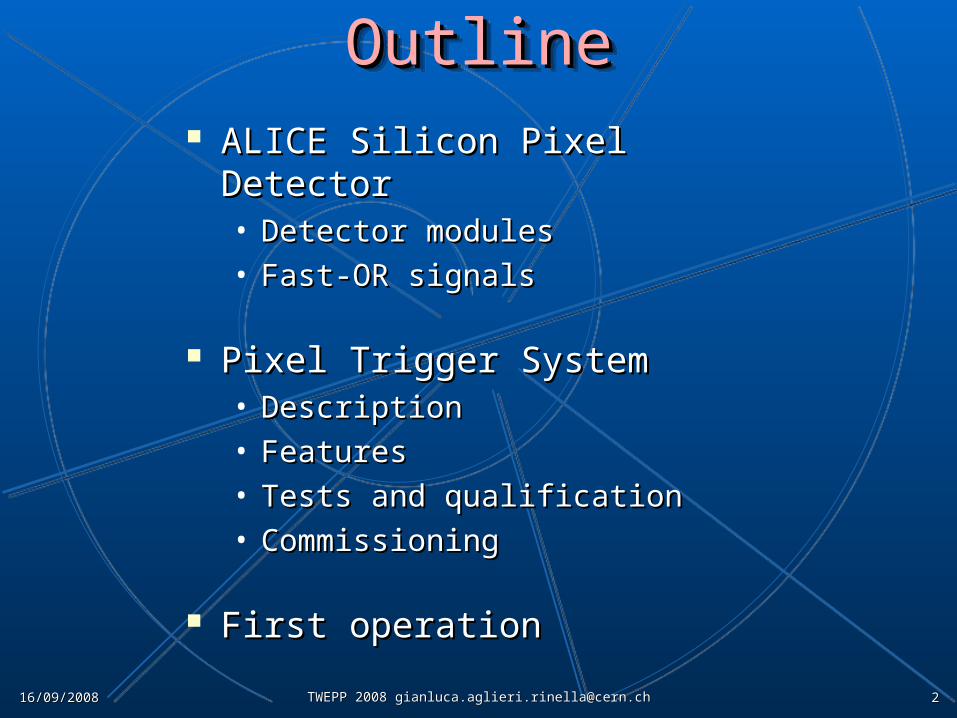
OutlineOutlineOutlineOutline ALICE Silicon Pixel DetectorALICE Silicon Pixel Detector
• Detector modulesDetector modules• Fast-OR signalsFast-OR signals
Pixel Trigger SystemPixel Trigger System• DescriptionDescription• FeaturesFeatures• Tests and qualificationTests and qualification• CommissioningCommissioning
First operation First operation
16/09/200816/09/2008 TWEPP 2008 [email protected] 2008 [email protected] 33
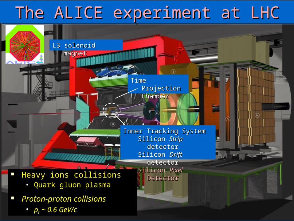
The ALICE experiment at LHCThe ALICE experiment at LHCThe ALICE experiment at LHCThe ALICE experiment at LHC
Heavy ions collisionsHeavy ions collisions• Quark gluon plasmaQuark gluon plasma
Proton-proton collisionsProton-proton collisions• pptt ~ 0.6 GeV/c ~ 0.6 GeV/c
L3 solenoid magnetL3 solenoid magnet
Inner Tracking SystemInner Tracking SystemSilicon Silicon StripStrip detector detectorSilicon Silicon DriftDrift detector detectorSilicon Silicon PixelPixel Detector Detector
Time Projection Time Projection ChamberChamber
16/09/200816/09/2008 TWEPP 2008 [email protected] 2008 [email protected] 44
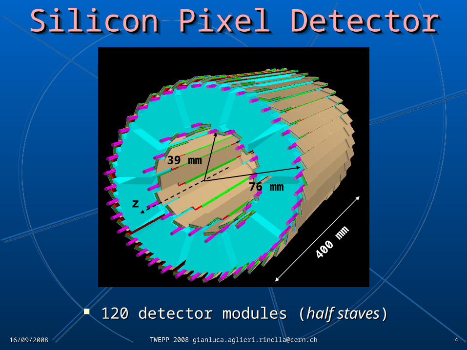
Silicon Pixel DetectorSilicon Pixel DetectorSilicon Pixel DetectorSilicon Pixel Detector
120 detector modules (120 detector modules (half staveshalf staves))
76 mm
39 mm
z
400
mm

16/09/200816/09/2008 TWEPP 2008 [email protected] 2008 [email protected] 55
SPD half staveSPD half staveSPD half staveSPD half stave Each half stave (120):Each half stave (120):
• Si pixel sensors (pixel size 425x50 umSi pixel sensors (pixel size 425x50 um2)2)
• 10 readout pixel chips (32x256=8192 pixels)10 readout pixel chips (32x256=8192 pixels) 10 MHz10 MHz
• Readout Multi Chip Module Readout Multi Chip Module 40 MHz40 MHz Provides 10 MHz to pixel chipsProvides 10 MHz to pixel chips
Silicon Pixel Detector half stave
Half stave
Sensor
Pixel chips
Readout MCM
Sensor
800 Mb/s
141 mm

16/09/200816/09/2008 TWEPP 2008 [email protected] 2008 [email protected] 66
Fast-OR signalsFast-OR signalsFast-OR signalsFast-OR signalsSPD Half Stave
Half stave
Sensor
Pixel chips
Readout MCM
Sensor141 mm
1
Pixel chip prompt Fast-ORPixel chip prompt Fast-OR• Active if at least one pixel hit in the chip matrixActive if at least one pixel hit in the chip matrix• 10 on each of 120 optical links (1200) 10 on each of 120 optical links (1200) • Transmitted every 100 nsTransmitted every 100 ns
Low latency pad detector Low latency pad detector 1200 pads of 13x14 mm1200 pads of 13x14 mm22

16/09/200816/09/2008 TWEPP 2008 [email protected] 2008 [email protected] 77
Pixel Trigger electronics
CTPProcessingFast-OR extraction
Optical splitters
To DAQ
120 G-Link
1200 bits @ 10 MHz
800 ns
350 ns 200 ns 225 ns 25 ns
Pixel Trigger SystemPixel Trigger SystemPixel Trigger SystemPixel Trigger System
• Overall latency: Overall latency: 800 ns800 ns
• Space occupancy (1 crate)Space occupancy (1 crate)
• Bottleneck: data deserialization and Fast-OR extractionBottleneck: data deserialization and Fast-OR extraction Processing time < 25 nsProcessing time < 25 ns

16/09/200816/09/2008 TWEPP 2008 [email protected] 2008 [email protected] 88
Pixel Trigger system electronicsPixel Trigger system electronicsPixel Trigger system electronicsPixel Trigger system electronics
Large I/OVirtex4
Virtex4
DDL SIU
TTCRx
Optical TxRx4
JTAG
USB
Zarlin
k
Virtex4
Zarlin
k
Virtex4
400 mm
Zarlin
k
Virtex4
12
Zarlin
k
Virtex4
160 mm
86 m
m
360
mm
Zarlin
kVirtex4
9U VME size processing board (BRAIN)9U VME size processing board (BRAIN)• Main processing FPGA (960 user I/O pins, 1513 BGA)Main processing FPGA (960 user I/O pins, 1513 BGA)
2x5 receiver boards (OPTIN) connected as mezzanine boards2x5 receiver boards (OPTIN) connected as mezzanine boards
Data flow parallelism Data flow parallelism (~1000 lines) (~1000 lines) • 800 impedance 800 impedance
matched lines matched lines • Digitally Controlled Digitally Controlled
ImpedanceImpedance• Double Data RateDouble Data Rate
High speed optical High speed optical interfacesinterfaces• Alice Detector Data LinkAlice Detector Data Link• Timing TriggerTiming Trigger

16/09/200816/09/2008 TWEPP 2008 [email protected] 2008 [email protected] 99
OPTIN receiver boardOPTIN receiver boardOPTIN receiver boardOPTIN receiver board 12 channels12 channels
• Parallel optical receiver moduleParallel optical receiver module• 12 closely packed G-link deserializer ASICs12 closely packed G-link deserializer ASICs

16/09/200816/09/2008 TWEPP 2008 [email protected] 2008 [email protected] 1010
BRAIN and OPTIN boardsBRAIN and OPTIN boardsBRAIN and OPTIN boardsBRAIN and OPTIN boards
Control FPGA
DDL SIU
OPTIN boards
Processing FPGA
Optical fan-incable
400 mm
16/09/200816/09/2008 TWEPP 2008 [email protected] 2008 [email protected] 1111
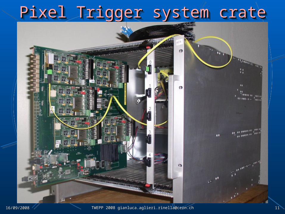
Pixel Trigger system cratePixel Trigger system cratePixel Trigger system cratePixel Trigger system crate

16/09/200816/09/2008 TWEPP 2008 [email protected] 2008 [email protected] 1212
Interconnection test and power consumptionInterconnection test and power consumptionInterconnection test and power consumptionInterconnection test and power consumption Electrical interconnectsElectrical interconnects
• Full JTAG testingFull JTAG testing• Dedicated tests for Dedicated tests for
lines non accessible by JTAGlines non accessible by JTAG high speed differential lineshigh speed differential lines
Heat sinks on all regulators and deserializersHeat sinks on all regulators and deserializers• Peak board temperature: 45 °C (measured)Peak board temperature: 45 °C (measured)• Peak junction temperature: 72 °C (thermal model)Peak junction temperature: 72 °C (thermal model)
Currents overestimated in design phaseCurrents overestimated in design phase• Thermal model was Thermal model was too conservativetoo conservative
II5V5V [A] [A] II3.3V3.3V [A] [A] P [W]P [W]
OPTINOPTIN 2.82.8 0.3750.375 15.315.3
BRAINBRAIN 7.97.9 1.61.6 4545
Total PITTotal PIT 36.136.1 5.45.4 198198
16/09/200816/09/2008 TWEPP 2008 [email protected] 2008 [email protected] 1313
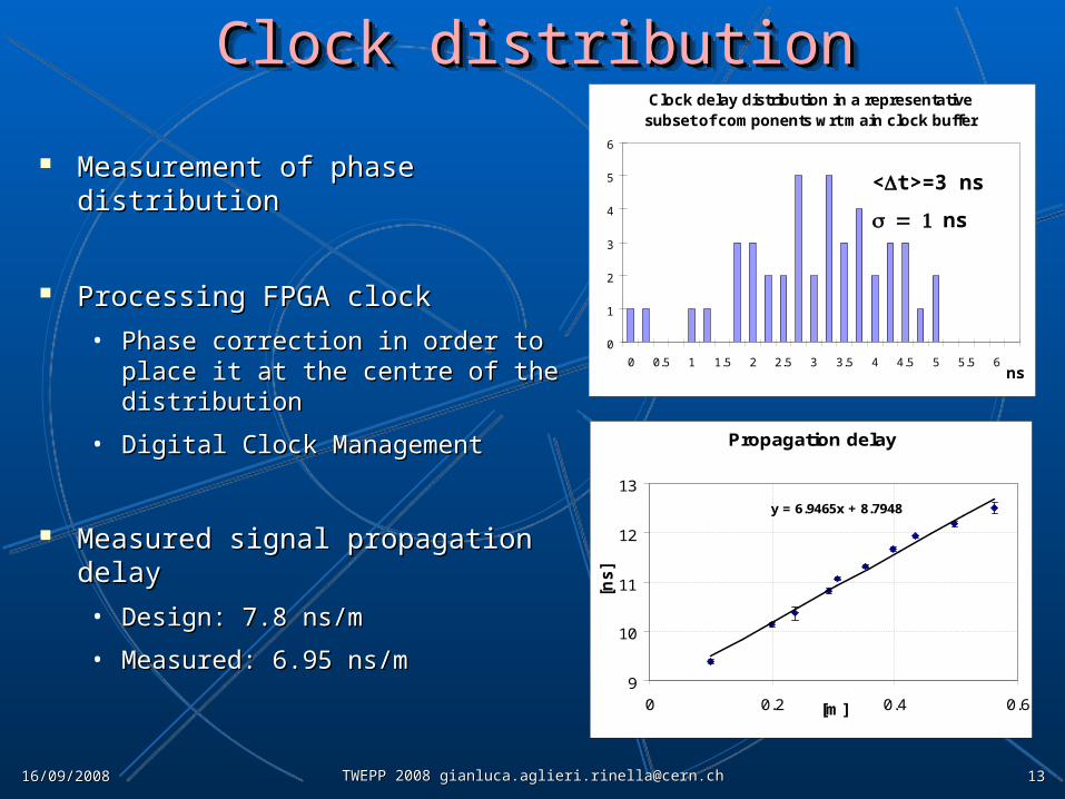
Clock distributionClock distributionClock distributionClock distribution
Measurement of phase Measurement of phase distribution distribution
Processing FPGA clockProcessing FPGA clock
• Phase correction in order to place Phase correction in order to place it at the centre of the distributionit at the centre of the distribution
• Digital Clock ManagementDigital Clock Management
Measured signal propagation Measured signal propagation delaydelay
• Design: 7.8 ns/mDesign: 7.8 ns/m
• Measured: 6.95 ns/mMeasured: 6.95 ns/m
Clock delay distribution in a representative subset of components wrt main clock buffer
0
1
2
3
4
5
6
0 0.5 1 1.5 2 2.5 3 3.5 4 4.5 5 5.5 6ns
<t>=3 ns
ns
Propagation delay
y = 6.9465x + 8.7948
9
10
11
12
13
0 0.2 0.4 0.6[m]
[ns
]
16/09/200816/09/2008 TWEPP 2008 [email protected] 2008 [email protected] 1414
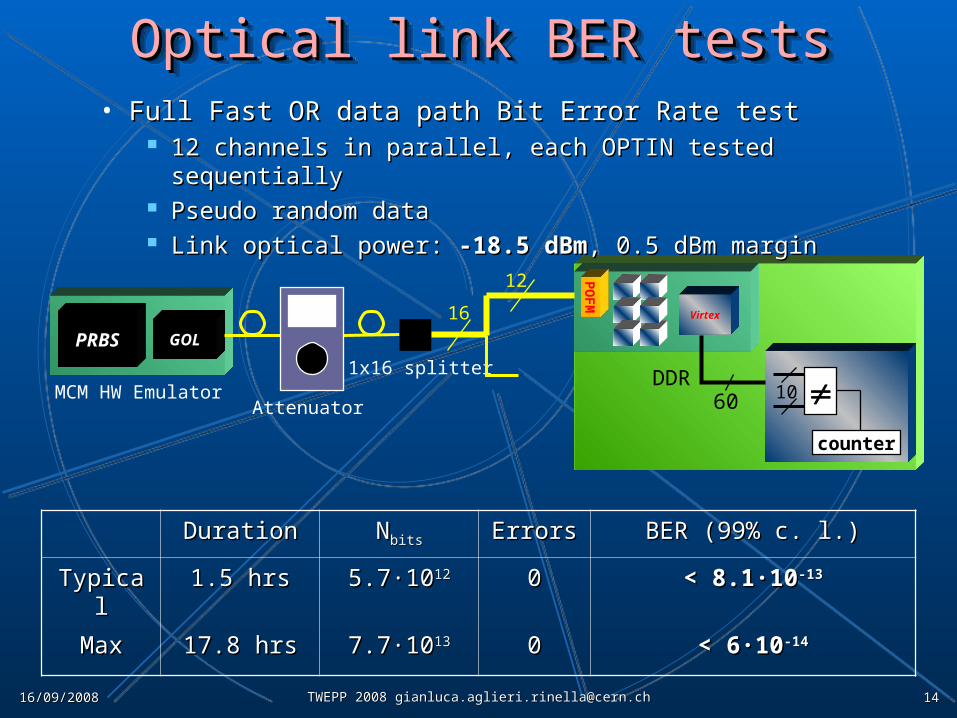
Optical link BER testsOptical link BER testsOptical link BER testsOptical link BER tests
PO
FM
Virtex
GOLPRBS
Attenuator
1x16 splitter
16
12
60 10
counter
MCM HW EmulatorDDR
• Full Fast OR data path Bit Error Rate test Full Fast OR data path Bit Error Rate test 12 channels in parallel, each OPTIN tested sequentially12 channels in parallel, each OPTIN tested sequentially Pseudo random data Pseudo random data Link optical power: Link optical power: -18.5 dBm-18.5 dBm, 0.5 dBm margin, 0.5 dBm margin
DurationDuration NNbitsbits ErrorsErrors BER (99% c. l.)BER (99% c. l.)
TypicalTypical 1.5 hrs1.5 hrs 5.7·105.7·101212 00 < 8.1·10< 8.1·10-13-13
MaxMax 17.8 hrs17.8 hrs 7.7·107.7·101313 00 < 6·10< 6·10-14-14

16/09/200816/09/2008 TWEPP 2008 [email protected] 2008 [email protected] 1515
Fast OR data path integrityFast OR data path integrityFast OR data path integrityFast OR data path integrity
PO
FM
Virtex
10
counters
PO
FM
Virtex
PO
FM
Virtex
PO
FM
Virtex
PO
FM
Virtex
10·60 DDR
• Fast OR dedicated lines (600) Bit Error Rate test Fast OR dedicated lines (600) Bit Error Rate test 10 OPTIN boards, 120 channels simultaneously running10 OPTIN boards, 120 channels simultaneously running On board generation of User Defined data functionality On board generation of User Defined data functionality
(pseudo random sequences)(pseudo random sequences)
Duration: 15 hrsDuration: 15 hrs
• NNbitsbits = 6.48·10 = 6.48·101414
• Errors = 0Errors = 0
BER < BER < 7.1·107.1·10-15-15 (99% c.l.) (99% c.l.)
16/09/200816/09/2008 TWEPP 2008 [email protected] 2008 [email protected] 1616
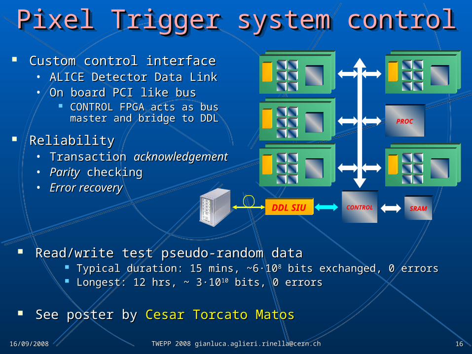
Pixel Trigger system controlPixel Trigger system controlPixel Trigger system controlPixel Trigger system control
PROC
CONTROLDDL SIU
Custom control interface Custom control interface • ALICE Detector Data LinkALICE Detector Data Link• On board PCI like busOn board PCI like bus
CONTROL FPGA acts as bus CONTROL FPGA acts as bus master and bridge to DDLmaster and bridge to DDL
ReliabilityReliability• Transaction Transaction acknowledgementacknowledgement• ParityParity checking checking• Error recoveryError recovery
Read/write test pseudo-random dataRead/write test pseudo-random data Typical duration: 15 mins, ~6·10Typical duration: 15 mins, ~6·1088 bits exchanged, 0 errors bits exchanged, 0 errors Longest: 12 hrs, ~ 3·10Longest: 12 hrs, ~ 3·101010 bits, 0 errors bits, 0 errors
See poster by See poster by Cesar Torcato Matos Cesar Torcato Matos
SRAM

16/09/200816/09/2008 TWEPP 2008 [email protected] 2008 [email protected] 1717
Latency measurementLatency measurementLatency measurementLatency measurement
733 ns
Test pulse ->Test pulse ->
PIT output ->PIT output ->
Laboratory measurementLaboratory measurement
In ALICEIn ALICE• 768 ns768 ns (best case) (best case)• 793 ns793 ns (realignment) (realignment)

16/09/200816/09/2008 TWEPP 2008 [email protected] 2008 [email protected] 1818
Installation in ALICE experimentInstallation in ALICE experimentInstallation in ALICE experimentInstallation in ALICE experiment
Optical splitters
Central TriggerProcessor
LTU
ClkSerial
C side
A side
Data
TTC
TTC
36.6±0.2 m
107.6±0.15 m
38.5±0.2 m
60C.R.
PIT main outputs L0 in

16/09/200816/09/2008 TWEPP 2008 [email protected] 2008 [email protected] 1919
SynchronizationSynchronizationSynchronizationSynchronization
0FO(n-1)
1Fb(n-1)
2 3 0FO(n)
1Fb(n)
2 3 0FO(n+1)
1Fb(n+1)
2 3
BC clock
HS i
HS j
HS k 0FO(n-1)
1Fb(n-1)
2 3 0FO(n)
1Fb(n)
2 3 0FO(n+1)
1Fb(n+1)
23
0FO(n-1)
1Fb(n-1)
2 3 0FO(n)
1Fb(n)
2 3 0FO(n+1)
1Fb(n+1)
23
40 MHz clocks aligned by equalizing fibers length40 MHz clocks aligned by equalizing fibers length 10 MHz clock phases aligned by broadcast signal on TTC10 MHz clock phases aligned by broadcast signal on TTC
One clock period uncertainty left One clock period uncertainty left -> Measure relative phases-> Measure relative phases Measure arrival time of trigger feedbackMeasure arrival time of trigger feedback
16/09/200816/09/2008 TWEPP 2008 [email protected] 2008 [email protected] 2020
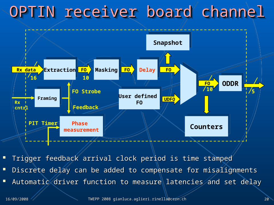
OPTIN receiver board channelOPTIN receiver board channelOPTIN receiver board channelOPTIN receiver board channel
FramingFraming
DelayDelayExtractionExtraction
User defined FO
User defined FORx
cntrl
FO FO
UDFO
FO Strobe
FO ODDRODDR16
10 5
Phase measurement
Phase measurement
CountersCountersPIT Timer
SnapshotSnapshot
MaskingMaskingFO
10
Rx data
Feedback
Trigger feedback arrival clock period is time stampedTrigger feedback arrival clock period is time stamped Discrete delay can be added to compensate for misalignmentsDiscrete delay can be added to compensate for misalignments Automatic driver function to measure latencies and set delayAutomatic driver function to measure latencies and set delay

16/09/200816/09/2008 TWEPP 2008 [email protected] 2008 [email protected] 2121
Frame alignmentFrame alignmentFrame alignmentFrame alignment
0FO
1Fb
2 3 0FO
1L1 FB
2 3 0FO
1Fb(n+1)
23
A side
C side
0FO
1Fb
2 3 0FO
1L1 FB
2 3 0FO
1Fb(n+1)
2 3
0FO
1Fb
2 3 0FO
1L1 FB
2 3 0FO
1Fb(n+1)
23
0FO
1Fb
2 3 0FO
1L1 FB
2 3 0FO
1Fb(n+1)
23
0FO
1Fb
2 3 0FO
1L1 FB
2 3 0FO
1Fb(n+1)
23
0FO
1Fb
2 3 0FO
1L1 FB
2 3 0FO
1Fb(n+1)
2 3
0FO
1Fb
2 3 0FO
1L1 FB
2 3 0FO
1Fb(n+1)
2 3
0FO
1Fb
2 3 0FO
1L1 FB
2 3 0FO
1Fb(n+1)
2 3
16/09/200816/09/2008 TWEPP 2008 [email protected] 2008 [email protected] 2222
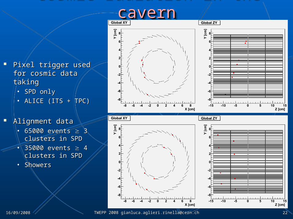
Cosmic radiation in the cavernCosmic radiation in the cavernCosmic radiation in the cavernCosmic radiation in the cavern
Pixel trigger used for Pixel trigger used for cosmic data takingcosmic data taking• SPD onlySPD only• ALICE (ITS + TPC) ALICE (ITS + TPC)
Alignment dataAlignment data• 65000 events 65000 events 3 3
clusters in SPDclusters in SPD• 35000 events 35000 events 4 4
clusters in SPDclusters in SPD• ShowersShowers
16/09/200816/09/2008 TWEPP 2008 [email protected] 2008 [email protected] 2323
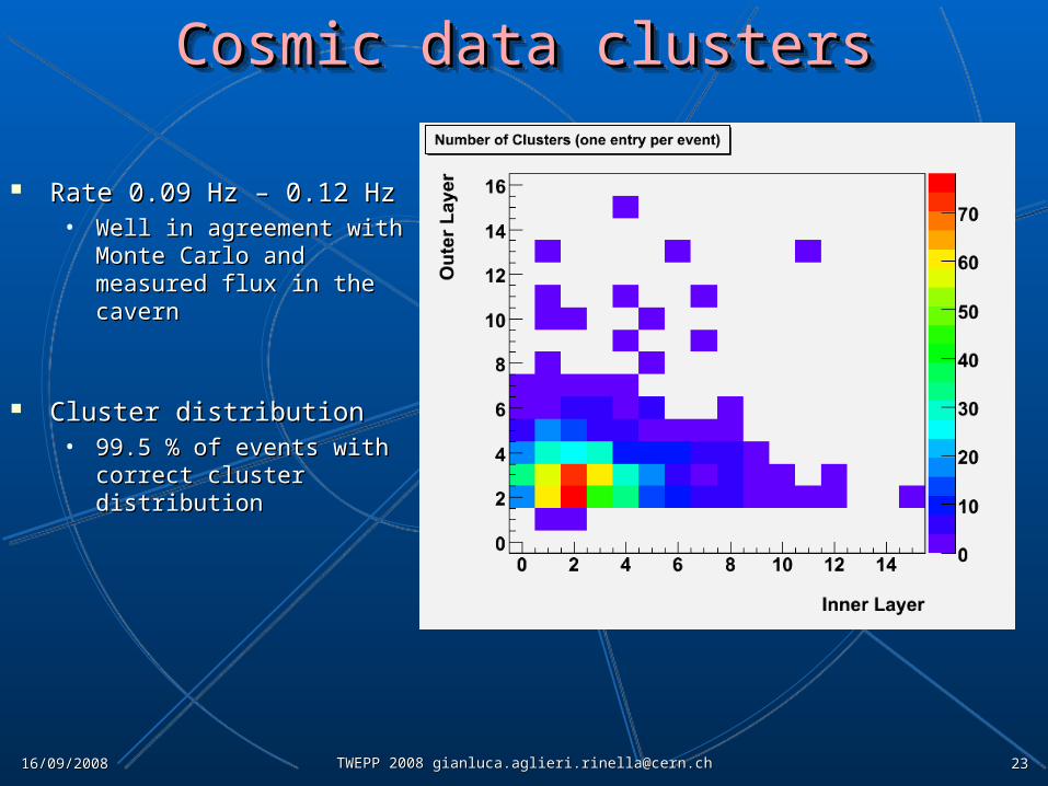
Cosmic data clustersCosmic data clustersCosmic data clustersCosmic data clusters
Rate 0.09 Hz – 0.12 HzRate 0.09 Hz – 0.12 Hz• Well in agreement with Well in agreement with
Monte Carlo and Monte Carlo and measured flux in the measured flux in the caverncavern
Cluster distributionCluster distribution• 99.5 % of events with 99.5 % of events with
correct cluster distribution correct cluster distribution
16/09/200816/09/2008 TWEPP 2008 [email protected] 2008 [email protected] 2424
SummarySummarySummarySummary
The ALICE Pixel Trigger system allows to include the The ALICE Pixel Trigger system allows to include the prompt Fast-OR outputs of the Silicon Pixel Detector in the prompt Fast-OR outputs of the Silicon Pixel Detector in the Level 0 trigger decisionLevel 0 trigger decision
• ALICE is the only LHC experiment including the vertex detector ALICE is the only LHC experiment including the vertex detector in the first trigger decision from startupin the first trigger decision from startup
The Pixel Trigger systemThe Pixel Trigger system
• Installed and operationalInstalled and operational
• Board level and system level challenging requirements Board level and system level challenging requirements
• Highly compact solution including original developmentsHighly compact solution including original developments
• Commissioning and first operationCommissioning and first operation
16/09/200816/09/2008 TWEPP 2008 [email protected] 2008 [email protected] 2525
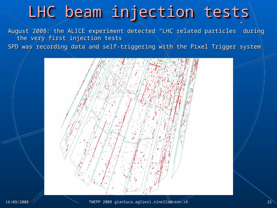
LHC beam injection testsLHC beam injection testsLHC beam injection testsLHC beam injection testsAugust 2008: the ALICE experiment detected “LHC related particles” during August 2008: the ALICE experiment detected “LHC related particles” during
the very first injection teststhe very first injection tests
SPD was recording data and self-triggering with the Pixel Trigger systemSPD was recording data and self-triggering with the Pixel Trigger system
16/09/200816/09/2008 TWEPP 2008 [email protected] 2008 [email protected] 2626
ReferencesReferencesReferencesReferences
References: References:
G. Aglieri Rinella et al., “G. Aglieri Rinella et al., “The Level 0 Pixel Trigger system for the ALICE The Level 0 Pixel Trigger system for the ALICE experimentexperiment”, Journal of Instrumentation JINST 2P01007 and Proceedings of the ”, Journal of Instrumentation JINST 2P01007 and Proceedings of the 12th Workshop on Electronics for LHC and Future Experiments, LECC06, 12th Workshop on Electronics for LHC and Future Experiments, LECC06, September 2006, Valencia, SpainSeptember 2006, Valencia, Spain
A. Kluge et al., “A. Kluge et al., “The ALICE Silicon Pixel DetectorThe ALICE Silicon Pixel Detector”, Nuclear Instruments and ”, Nuclear Instruments and Methods A, Volume 582, Issue 3, 1 December 2007, Pages 728-732 Methods A, Volume 582, Issue 3, 1 December 2007, Pages 728-732
ALICE collaboration, “ALICE physics Performance Report”, CERN-LHCC-2003-049, J. ALICE collaboration, “ALICE physics Performance Report”, CERN-LHCC-2003-049, J. Phys., G30 (2004) 1517-1763Phys., G30 (2004) 1517-1763
J. Conrad et al., “Minimum Bias Triggers in Proton-Proton collisions with the VZERO J. Conrad et al., “Minimum Bias Triggers in Proton-Proton collisions with the VZERO and Silicon Pixel Detectors”, ALICE Internal note, ALICE-INT-2005-025, 19/10/2005and Silicon Pixel Detectors”, ALICE Internal note, ALICE-INT-2005-025, 19/10/2005
16/09/200816/09/2008 TWEPP 2008 [email protected] 2008 [email protected] 2727
Spare slidesSpare slidesSpare slidesSpare slides

16/09/200816/09/2008 TWEPP 2008 [email protected] 2008 [email protected] 2828
SPD detectorSPD detectorSPD detectorSPD detector

16/09/200816/09/2008 TWEPP 2008 [email protected] 2008 [email protected] 2929
Triggering with SPD Fast-ORTriggering with SPD Fast-ORTriggering with SPD Fast-ORTriggering with SPD Fast-OR
• Extract and process Fast-OR signals Extract and process Fast-OR signals • Generate input for the Level 0 (fastest) trigger decisionGenerate input for the Level 0 (fastest) trigger decision
1200 Fast-OR signals on 120 optical links every 100 ns1200 Fast-OR signals on 120 optical links every 100 ns
• Proton-protonProton-proton Minimum biasMinimum bias High multiplicity studiesHigh multiplicity studies Topological selection (jets)Topological selection (jets)
• Heavy ionsHeavy ions Selection of impact parameterSelection of impact parameter
• AlgorithmsAlgorithms Topology (Global OR, Vertex)Topology (Global OR, Vertex) MultiplicityMultiplicity Boolean functions of 1200 Fast-OR bitsBoolean functions of 1200 Fast-OR bits

16/09/200816/09/2008 TWEPP 2008 [email protected] 2008 [email protected] 3030
Trigger algorithmsTrigger algorithmsTrigger algorithmsTrigger algorithms Combinational (boolean AND/OR) functions of 1200 Fast-OR bitsCombinational (boolean AND/OR) functions of 1200 Fast-OR bits
• Occupancy (multiplicity)Occupancy (multiplicity)• Coincidence trigger (topology)Coincidence trigger (topology)
Not possible: iterative algorithms on data setNot possible: iterative algorithms on data set
Example: vertex trigger Example: vertex trigger Pseudo-Tracklet: one chip hit on inner and one on outer layer, in line with region +/-Pseudo-Tracklet: one chip hit on inner and one on outer layer, in line with region +/-
10 cm around vertex10 cm around vertex
Chip map for pixel trigger electronics calculated from simulation: (L11,L21), (L12, Chip map for pixel trigger electronics calculated from simulation: (L11,L21), (L12, L22), … , (L1n, L2n)L22), … , (L1n, L2n)
FPGA FPGA looks for at least 1 out of 11000looks for at least 1 out of 11000 pseudo-tracklets pseudo-tracklets• Processing time 12.4 ns (Xilinx ISE)Processing time 12.4 ns (Xilinx ISE)• 4% of FPGA resources (Xilinx ISE)4% of FPGA resources (Xilinx ISE)
FPGA FPGA countscounts how many out of 11000 tracklets are present how many out of 11000 tracklets are present• ~27 ns processing time (Xilinx ISE)~27 ns processing time (Xilinx ISE)• 5% of FPGA resources (Xilinx ISE)5% of FPGA resources (Xilinx ISE)

16/09/200816/09/2008 TWEPP 2008 [email protected] 2008 [email protected] 3131
Multiplicity triggerMultiplicity triggerMultiplicity triggerMultiplicity trigger
Domenico Elia
16/09/200816/09/2008 TWEPP 2008 [email protected] 2008 [email protected] 3232
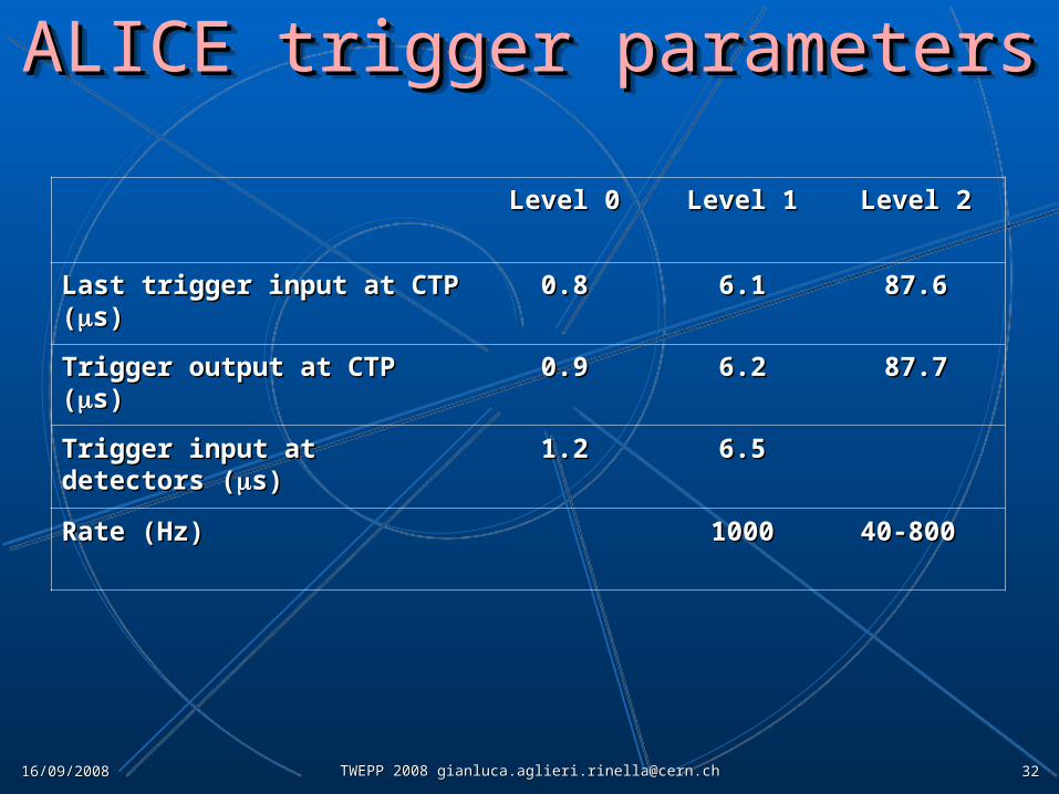
ALICE trigger parametersALICE trigger parametersALICE trigger parametersALICE trigger parameters
Level 0Level 0 Level 1Level 1 Level 2Level 2
Last trigger input at CTP Last trigger input at CTP ((s)s)
0.80.8 6.16.1 87.687.6
Trigger output at CTP (Trigger output at CTP (s)s) 0.90.9 6.26.2 87.787.7
Trigger input at detectors Trigger input at detectors ((s)s)
1.21.2 6.56.5
Rate (Hz)Rate (Hz) 10001000 40-800 40-800

16/09/200816/09/2008 TWEPP 2008 [email protected] 2008 [email protected] 3333
Angular resolutionAngular resolutionAngular resolutionAngular resolution
16/09/200816/09/2008 TWEPP 2008 [email protected] 2008 [email protected] 3434
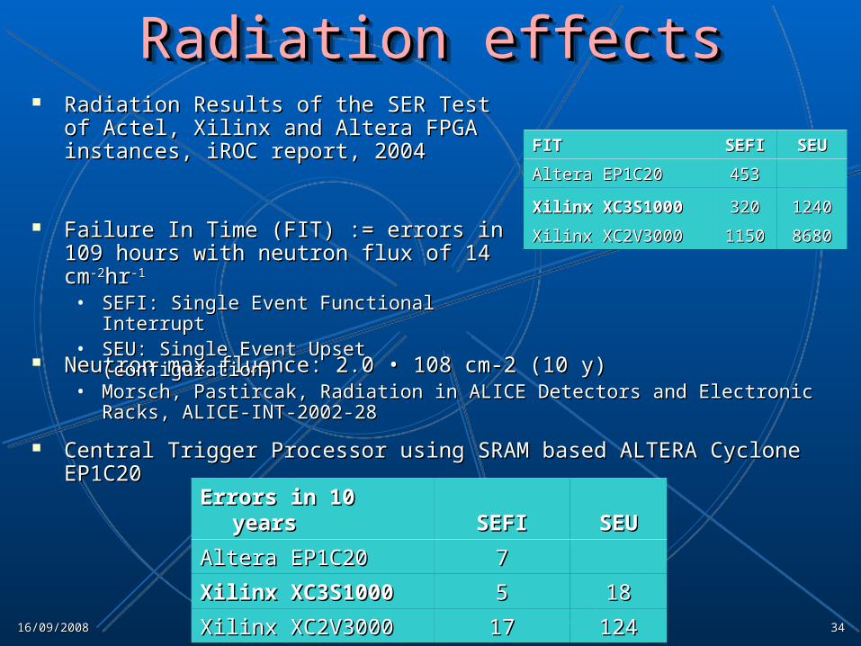
Radiation effectsRadiation effectsRadiation effectsRadiation effects
Neutron max fluence: 2.0 Neutron max fluence: 2.0 • • 108 cm-2 (10 y)108 cm-2 (10 y)• Morsch, Pastircak, Radiation in ALICE Detectors and Electronic Racks, Morsch, Pastircak, Radiation in ALICE Detectors and Electronic Racks,
ALICE-INT-2002-28ALICE-INT-2002-28
Central Trigger Processor using SRAM based ALTERA Cyclone EP1C20Central Trigger Processor using SRAM based ALTERA Cyclone EP1C20
FITFIT SEFISEFI SEUSEU
Altera EP1C20Altera EP1C20 453453
Xilinx XC3S1000Xilinx XC3S1000 320320 12401240
Xilinx XC2V3000Xilinx XC2V3000 11501150 86808680
Errors in 10 yearsErrors in 10 years SEFISEFI SEUSEU
Altera EP1C20Altera EP1C20 77
Xilinx XC3S1000Xilinx XC3S1000 55 1818
Xilinx XC2V3000Xilinx XC2V3000 1717 124124
Radiation Results of the SER Test of Radiation Results of the SER Test of Actel, Xilinx and Altera FPGA instances, Actel, Xilinx and Altera FPGA instances, iROC report, 2004iROC report, 2004
Failure In Time (FIT) := errors in 109 Failure In Time (FIT) := errors in 109 hours with neutron flux of 14 cmhours with neutron flux of 14 cm-2-2hrhr-1-1
• SEFI: Single Event Functional Interrupt SEFI: Single Event Functional Interrupt • SEU: Single Event Upset (configuration)SEU: Single Event Upset (configuration)
16/09/200816/09/2008 TWEPP 2008 [email protected] 2008 [email protected] 3535
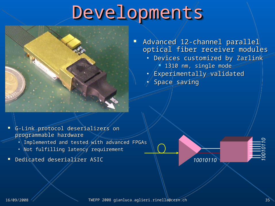
DevelopmentsDevelopmentsDevelopmentsDevelopments Advanced 12-channel parallel Advanced 12-channel parallel
optical fiber receiver modulesoptical fiber receiver modules• Devices customized by ZarlinkDevices customized by Zarlink
1310 nm, single mode1310 nm, single mode• Experimentally validatedExperimentally validated• Space savingSpace saving
G-Link protocol deserializers on G-Link protocol deserializers on programmable hardwareprogrammable hardware• Implemented and tested with advanced FPGAsImplemented and tested with advanced FPGAs• Not fulfilling latency requirementNot fulfilling latency requirement
Dedicated deserializer ASICDedicated deserializer ASIC 10010110 100
1011
0

16/09/200816/09/2008 TWEPP 2008 [email protected] 2008 [email protected] 3636
Latencies of processesLatencies of processesLatencies of processesLatencies of processes
Serialization, deserialization, Serialization, deserialization, processing latencyprocessing latency
Hardware emulator of the Silicon Pixel Hardware emulator of the Silicon Pixel Detector as data sourceDetector as data source
Overall latency: Overall latency: 800 ns800 ns
215 ns
Latencies
0 100 200 300 400 500 600 700 800 900[ns]
Fast-OR readout - 325 ns Serialization (GOL) - 25 nsTransmission - 200 ns Deserialization - 100 ns
Fast-OR extraction - 50 ns Transfer to BRAIN - 50 nsAlgorithm processing - 25 ns Transmission to CTP - 25 ns
16/09/200816/09/2008 TWEPP 2008 [email protected] 2008 [email protected] 3737
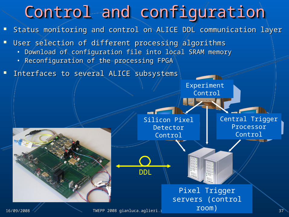
Control and configurationControl and configurationControl and configurationControl and configuration Status monitoring and control on ALICE DDL communication layerStatus monitoring and control on ALICE DDL communication layer
User selection of different processing algorithmsUser selection of different processing algorithms• Download of configuration file into local SRAM memoryDownload of configuration file into local SRAM memory• Reconfiguration of the processing FPGAReconfiguration of the processing FPGA
Interfaces to several ALICE subsystemsInterfaces to several ALICE subsystems
Pixel Trigger servers (control room)
DDL
Experiment Control
Silicon Pixel Detector Control
Central Trigger Processor Control
Related Documents