www.cypress.com Document No. 002-20929 Rev. ** 1 AN220929 Getting Started with EZ-BLE WICED Modules Author: David Solda Associated Project: Yes Associated Part Family: CYBLE-0130XX-00 Software Version: WICED ® SMART™ SDK v2.2.3 Related Application Notes: For a complete list of the application notes, click here. AN220929 introduces you to Cypress’ EZ-BLE™ WICED family of Bluetooth modules. EZ-BLE modules are fully qualified and certified Bluetooth Low Energy (BLE) solutions. These modules provide a complete Bluetooth solution, integrating a Bluetooth radio system, two crystals, antenna, and passive components required for BLE operation. This application note helps you explore the EZ-BLE Module architecture and development tools and shows you how to create your first project with the WICED Smart SDK, the development tool used for all WICED-based EZ-BLE Modules. This application note also guides you to more resources to accelerate in-depth learning about EZ-BLE WICED solutions. Contents 1 Introduction ..................................................................2 2 More Information .........................................................2 2.1 EZ-BLE WICED Module Datasheet ....................2 2.2 EZ-BLE WICED Evaluation Boards ....................2 2.3 Silicon Device Datasheet ....................................3 2.4 Cypress WICED Bluetooth Community ...............3 2.5 Application Notes ................................................3 2.6 Technical Support ...............................................3 3 EZ-BLE WICED Module Overview ..............................3 3.1 EZ-BLE WICED Module Family Features ...........4 3.2 EZ-BLE WICED Module Low Power Modes .......5 3.3 EZ-BLE WICED Module Device Security ............5 3.4 EZ-BLE WICED Marketing Part Number Overview ........................................6 4 Development Tools......................................................7 4.1 WICED SMART SDK and IDE ............................7 4.2 CySmart PC Application ................................... 14 4.3 CySmart Mobile App ......................................... 16 5 Development Kits and Evaluation Boards ................. 18 5.1 EZ-BLE WICED Module Evaluation Boards ...... 18 6 EZ-BLE WICED Module Development Setup (WICED SMART SDK) .................................... 19 7 My First EZ-BLE WICED Module Design .................. 20 7.1 About the Design .............................................. 20 7.2 Prerequisites ..................................................... 20 7.3 Part 1: Configure the Design ............................. 20 7.4 Part 2: Write the Firmware ................................ 25 7.5 Part 3: Program the Device ............................... 38 7.6 Part 4: Test Your Design................................... 40 7.7 Design Source .................................................. 43 8 Module Placement and Enclosure Considerations.......................................... 43 8.1 Antenna Ground Clearance .............................. 43 8.2 Module Placement in a Host System ................ 44 8.3 Enclosure Effects on Antenna Performance ....................................... 45 8.4 Guidelines for Enclosures and Ground Plane............................................. 47 9 Manufacturing with EZ-BLE WICED Modules ........... 49 9.1 SMT Manufacturing Pick-and-Place ................. 49 9.2 Manufacturing Solder Reflow ............................ 49 10 Summary ................................................................... 50 11 Related Application Notes ......................................... 50 Appendix A. Cypress Terms of Art ............................ 51 Appendix B. EZ-BLE WICED Module Product Details .......................................................... 52 B.1 EZ-BLE WICED Part Number Details ............... 53 Appendix C. EZ-BLE WICED Evaluation Board Details ............................................................. 62 Appendix D. Code Examples..................................... 66 Appendix E. Example Project main.c ........................ 67 Appendix F. Makefile Customization ......................... 73 Appendix G. Regulatory Information.......................... 74 G.1 Module Regulatory Reports and Certificates .... 76 Document History............................................................ 77 Worldwide Sales and Design Support ............................. 78

Welcome message from author
This document is posted to help you gain knowledge. Please leave a comment to let me know what you think about it! Share it to your friends and learn new things together.
Transcript
www.cypress.com Document No. 002-20929 Rev. ** 1
AN220929
Getting Started with EZ-BLE WICED Modules
Author: David Solda
Associated Project: Yes
Associated Part Family: CYBLE-0130XX-00
Software Version: WICED® SMART™ SDK v2.2.3
Related Application Notes: For a complete list of the application notes, click here.
AN220929 introduces you to Cypress’ EZ-BLE™ WICED family of Bluetooth modules. EZ-BLE modules are fully
qualified and certified Bluetooth Low Energy (BLE) solutions. These modules provide a complete Bluetooth solution,
integrating a Bluetooth radio system, two crystals, antenna, and passive components required for BLE operation. This
application note helps you explore the EZ-BLE Module architecture and development tools and shows you how to create
your first project with the WICED Smart SDK, the development tool used for all WICED-based EZ-BLE Modules. This
application note also guides you to more resources to accelerate in-depth learning about EZ-BLE WICED solutions.
Contents 1 Introduction .................................................................. 2 2 More Information ......................................................... 2
2.1 EZ-BLE WICED Module Datasheet .................... 2 2.2 EZ-BLE WICED Evaluation Boards .................... 2 2.3 Silicon Device Datasheet .................................... 3 2.4 Cypress WICED Bluetooth Community ............... 3 2.5 Application Notes ................................................ 3 2.6 Technical Support ............................................... 3
3 EZ-BLE WICED Module Overview .............................. 3 3.1 EZ-BLE WICED Module Family Features ........... 4 3.2 EZ-BLE WICED Module Low Power Modes ....... 5 3.3 EZ-BLE WICED Module Device Security ............ 5 3.4 EZ-BLE WICED Marketing Part Number Overview ........................................ 6
4 Development Tools ...................................................... 7 4.1 WICED SMART SDK and IDE ............................ 7 4.2 CySmart PC Application ................................... 14 4.3 CySmart Mobile App ......................................... 16
5 Development Kits and Evaluation Boards ................. 18 5.1 EZ-BLE WICED Module Evaluation Boards ...... 18
6 EZ-BLE WICED Module Development Setup (WICED SMART SDK) .................................... 19 7 My First EZ-BLE WICED Module Design .................. 20
7.1 About the Design .............................................. 20 7.2 Prerequisites ..................................................... 20 7.3 Part 1: Configure the Design ............................. 20 7.4 Part 2: Write the Firmware ................................ 25 7.5 Part 3: Program the Device ............................... 38
7.6 Part 4: Test Your Design ................................... 40 7.7 Design Source .................................................. 43
8 Module Placement and Enclosure Considerations.......................................... 43
8.1 Antenna Ground Clearance .............................. 43 8.2 Module Placement in a Host System ................ 44 8.3 Enclosure Effects on Antenna Performance ....................................... 45 8.4 Guidelines for Enclosures and Ground Plane ............................................. 47
9 Manufacturing with EZ-BLE WICED Modules ........... 49 9.1 SMT Manufacturing Pick-and-Place ................. 49 9.2 Manufacturing Solder Reflow ............................ 49
10 Summary ................................................................... 50 11 Related Application Notes ......................................... 50 Appendix A. Cypress Terms of Art ............................ 51 Appendix B. EZ-BLE WICED Module Product Details .......................................................... 52
B.1 EZ-BLE WICED Part Number Details ............... 53 Appendix C. EZ-BLE WICED Evaluation Board Details ............................................................. 62 Appendix D. Code Examples ..................................... 66 Appendix E. Example Project main.c ........................ 67 Appendix F. Makefile Customization ......................... 73 Appendix G. Regulatory Information .......................... 74
G.1 Module Regulatory Reports and Certificates .... 76 Document History ............................................................ 77 Worldwide Sales and Design Support ............................. 78

Getting Started with EZ-BLE WICED Modules
www.cypress.com Document No. 002-20929 Rev. ** 2
1 Introduction
Bluetooth Low Energy (BLE) is an ultra-low-power wireless standard defined by the Bluetooth Special Interest Group (SIG) for low-power, short-range communication. It features a physical layer, protocol stack, and profile architecture, all designed and optimized for the lowest power consumption. BLE operates in the 2.4-GHz ISM band, with a data rate up to 1 Mbps for 4.2 compliant devices, and up to 2 Mbps for BLE 5.0 compliant devices.
BLE is used in a wide range of applications. The use of BLE in these applications also varies widely in production volume, from very low- to high-volume end products. The use of fully qualified, certified, BLE modules removes time- consuming RF board design and costly qualification/certification processes. As such, modules have quickly become the design preference.
WICED (pronounced “wik-id”) is Cypress IoT platform that enables rapid development and deployment of connected IoT products. Wireless Internet Connectivity for Embedded Devices (WICED) in conjunction with EZ-BLE modules provides a great feature set to simplify development and release of BLE-enabled products by eliminating the complexity of wireless RF hardware design, allowing customers to focus on their IoT product development.
The WICED SMART™ SDK is pre-integrated, pre-tested and continuously updated, containing:
WICED APIs and drivers to make wireless connectivity easy and flexible
Proven production ready stacks (e.g., networking, security)
Pre-integrated world-class IoT cloud platforms (e.g., Amazon AWS, IBM BlueMix)
The EZ-BLE module and WICED ecosystem accelerate your time-to-market, by providing:
Partners who are experts in product development with the WICED SDK
Partners who are experts in integrating embedded systems with mobile and cloud applications
A professional, highly engaged community
The Cypress EZ-BLE WICED Module family provides fully integrated, qualified, and certified BLE systems that integrate 24-MHz crystal oscillators, passive components, on-board chip or trace antennas, and the WICED BLE chip, which includes the Bluetooth radio, analog-to-digital converter inputs, PWM control, serial communication protocols (I
2C, SPI, UART), memory, and an ARM
® Cortex
®-M3 microcontroller.
EZ-BLE WICED Modules enable quick time-to-market by eliminating time-consuming and costly RF hardware development, certification, and qualification processes, offering an effective alternative to completing a BLE system design from the ground up.
EZ-BLE WICED Modules provide the most cost-effective solution for sensor-based Internet of Things (IoT) solutions, while providing world-class RF performance by utilizing the latest Cypress WICED silicon devices.
2 More Information
This section provides a list of EZ-BLE Module learning resources that can help you to get started and develop complete applications with your EZ-BLE Module.
2.1 EZ-BLE WICED Module Datasheet
The EZ-BLE WICED Module datasheets list the features, pinouts, device-level specifications, and fixed-function peripheral electrical specifications of the EZ-BLE WICED Modules.
2.2 EZ-BLE WICED Evaluation Boards
Each EZ-BLE WICED Module offers a low-cost Arduino-compatible evaluation board to provide an easy-to-use vehicle to develop and evaluate EZ-BLE WICED Modules without requiring custom hardware design. These evaluation boards are standalone Arduino-compatible baseboards, capable of interfacing to Arduino-compatible shields.
Getting Started with EZ-BLE WICED Modules
www.cypress.com Document No. 002-20929 Rev. ** 3
2.3 Silicon Device Datasheet
Cypress WICED BLE datasheets lists the features, pinouts, device-level specifications, and fixed-function peripheral electrical specifications of all Cypress WICED BLE devices. Datasheets for applicable WICED BLE devices discussed in this application note can be found at the below links:
CYW20737 Single-Chip Bluetooth Low Energy-Only System-On-Chip
2.4 Cypress WICED Bluetooth Community
Whether you’re a customer, partner, or a developer interested in the latest Cypress innovations, the Cypress WICED Bluetooth Community offers you a place to learn, share and engage with both Cypress experts and other embedded engineers around the world.
2.5 Application Notes
Application notes assist you with understanding specific features of your device for designing your BLE application. For a complete list, visit Cypress WICED BLE application notes.
2.6 Technical Support
If you have any questions, our technical support team is happy to assist you. You can create a support request by visiting Cypress Technical Support.
If you are in the United States, you can talk to our technical support team by calling our toll-free number: +1-800-541-4736. You can also use the following support resources if you need quick assistance.
Self-help
Local sales office locations
3 EZ-BLE WICED Module Overview
This application note introduces the reader specifically to the EZ-BLE WICED Module solution and how to get started. If you are looking for a detailed overview of the Bluetooth Low Energy standard, see AN91267 - Getting Started with PSoC
® 4 BLE.
EZ-BLE WICED Modules offer fully integrated and fully certified BLE solutions allowing rapid development and deployment of your BLE product. This section provides an overview of the EZ-BLE WICED Modules available today. For detailed information on each module referenced in this section, see Appendix B: EZ-BLE Module Product Details.
All EZ-BLE WICED Modules ship with all required components to achieve full BLE functionality, including:
PCB substrate
Cypress WICED BLE IC
Refer to the Module datasheet for references and links to the datasheet of the silicon used in each module.
Crystal oscillators
24.0-MHz external crystal oscillator
EZ-BLE WICED BLE Modules do not contain a 32-kHz external crystal oscillator, but utilize the integrated oscillator on the silicon device. Each module does provide an option for an external 32-kHz input if desired.
Chip or Trace antenna
Passive components (resistor, capacitor, inductor)
RF Shield, unless otherwise noted
Getting Started with EZ-BLE WICED Modules
www.cypress.com Document No. 002-20929 Rev. ** 4
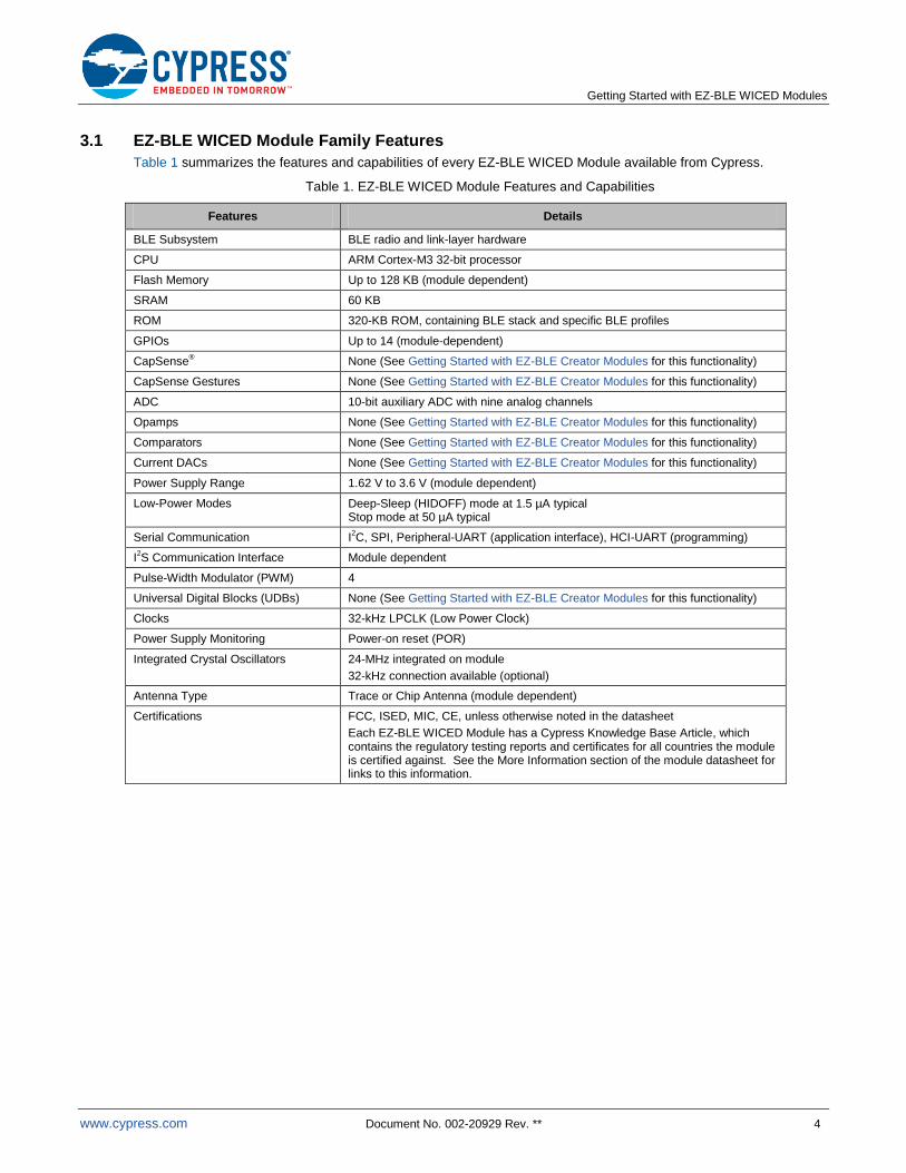
3.1 EZ-BLE WICED Module Family Features
Table 1 summarizes the features and capabilities of every EZ-BLE WICED Module available from Cypress.
Table 1. EZ-BLE WICED Module Features and Capabilities
Features Details
BLE Subsystem BLE radio and link-layer hardware
CPU ARM Cortex-M3 32-bit processor
Flash Memory Up to 128 KB (module dependent)
SRAM 60 KB
ROM 320-KB ROM, containing BLE stack and specific BLE profiles
GPIOs Up to 14 (module-dependent)
CapSense® None (See Getting Started with EZ-BLE Creator Modules for this functionality)
CapSense Gestures None (See Getting Started with EZ-BLE Creator Modules for this functionality)
ADC 10-bit auxiliary ADC with nine analog channels
Opamps None (See Getting Started with EZ-BLE Creator Modules for this functionality)
Comparators None (See Getting Started with EZ-BLE Creator Modules for this functionality)
Current DACs None (See Getting Started with EZ-BLE Creator Modules for this functionality)
Power Supply Range 1.62 V to 3.6 V (module dependent)
Low-Power Modes Deep-Sleep (HIDOFF) mode at 1.5 µA typical Stop mode at 50 µA typical
Serial Communication I2C, SPI, Peripheral-UART (application interface), HCI-UART (programming)
I2S Communication Interface Module dependent
Pulse-Width Modulator (PWM) 4
Universal Digital Blocks (UDBs) None (See Getting Started with EZ-BLE Creator Modules for this functionality)
Clocks 32-kHz LPCLK (Low Power Clock)
Power Supply Monitoring Power-on reset (POR)
Integrated Crystal Oscillators 24-MHz integrated on module
32-kHz connection available (optional)
Antenna Type Trace or Chip Antenna (module dependent)
Certifications FCC, ISED, MIC, CE, unless otherwise noted in the datasheet
Each EZ-BLE WICED Module has a Cypress Knowledge Base Article, which contains the regulatory testing reports and certificates for all countries the module is certified against. See the More Information section of the module datasheet for links to this information.
Getting Started with EZ-BLE WICED Modules
www.cypress.com Document No. 002-20929 Rev. ** 5
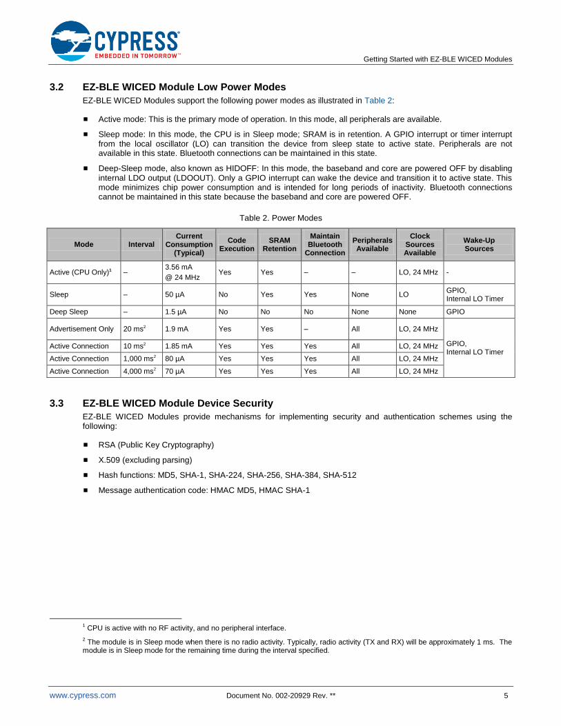
3.2 EZ-BLE WICED Module Low Power Modes
EZ-BLE WICED Modules support the following power modes as illustrated in Table 2:
Active mode: This is the primary mode of operation. In this mode, all peripherals are available.
Sleep mode: In this mode, the CPU is in Sleep mode; SRAM is in retention. A GPIO interrupt or timer interrupt from the local oscillator (LO) can transition the device from sleep state to active state. Peripherals are not available in this state. Bluetooth connections can be maintained in this state.
Deep-Sleep mode, also known as HIDOFF: In this mode, the baseband and core are powered OFF by disabling internal LDO output (LDOOUT). Only a GPIO interrupt can wake the device and transition it to active state. This mode minimizes chip power consumption and is intended for long periods of inactivity. Bluetooth connections cannot be maintained in this state because the baseband and core are powered OFF.
Table 2. Power Modes
Mode Interval Current
Consumption (Typical)
Code Execution
SRAM Retention
Maintain Bluetooth
Connection
Peripherals Available
Clock Sources Available
Wake-Up Sources
Active (CPU Only)1 – 3.56 mA
@ 24 MHz Yes Yes – – LO, 24 MHz -
Sleep – 50 µA No Yes Yes None LO GPIO, Internal LO Timer
Deep Sleep – 1.5 µA No No No None None GPIO
Advertisement Only 20 ms2 1.9 mA Yes Yes – All LO, 24 MHz
GPIO, Internal LO Timer
Active Connection 10 ms2 1.85 mA Yes Yes Yes All LO, 24 MHz
Active Connection 1,000 ms2 80 µA Yes Yes Yes All LO, 24 MHz
Active Connection 4,000 ms2 70 µA Yes Yes Yes All LO, 24 MHz
3.3 EZ-BLE WICED Module Device Security
EZ-BLE WICED Modules provide mechanisms for implementing security and authentication schemes using the following:
RSA (Public Key Cryptography)
X.509 (excluding parsing)
Hash functions: MD5, SHA-1, SHA-224, SHA-256, SHA-384, SHA-512
Message authentication code: HMAC MD5, HMAC SHA-1
1 CPU is active with no RF activity, and no peripheral interface.
2 The module is in Sleep mode when there is no radio activity. Typically, radio activity (TX and RX) will be approximately 1 ms. The
module is in Sleep mode for the remaining time during the interval specified.
Getting Started with EZ-BLE WICED Modules
www.cypress.com Document No. 002-20929 Rev. ** 6
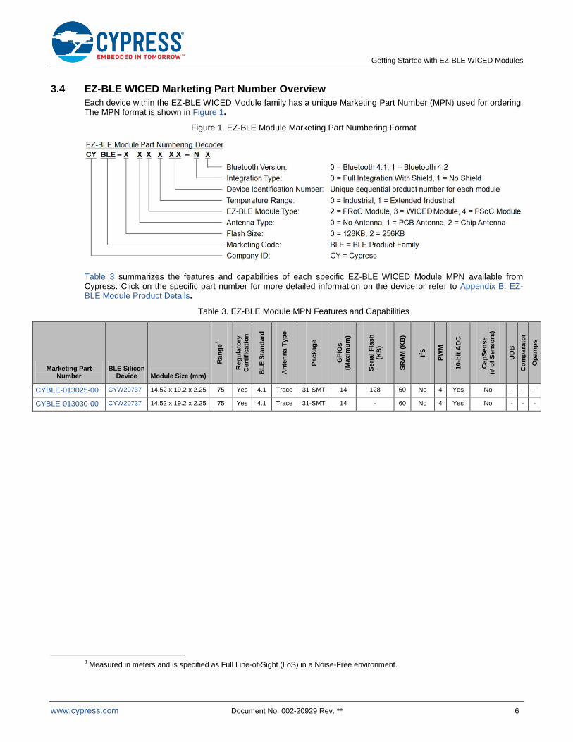
3.4 EZ-BLE WICED Marketing Part Number Overview
Each device within the EZ-BLE WICED Module family has a unique Marketing Part Number (MPN) used for ordering. The MPN format is shown in Figure 1.
Figure 1. EZ-BLE Module Marketing Part Numbering Format
Table 3 summarizes the features and capabilities of each specific EZ-BLE WICED Module MPN available from Cypress. Click on the specific part number for more detailed information on the device or refer to Appendix B: EZ-BLE Module Product Details.
Table 3. EZ-BLE Module MPN Features and Capabilities
Marketing Part Number
BLE Silicon Device Module Size (mm)
Ran
ge
3
Reg
ula
tory
Cert
ific
ati
on
BL
E S
tan
dard
An
ten
na
Typ
e
Pack
ag
e
GP
IOs
(Ma
xim
um
)
Seri
al
Fla
sh
(KB
)
SR
AM
(K
B)
I2S
PW
M
10-b
it A
DC
Cap
Sen
se
(# o
f S
en
so
rs)
UD
B
Co
mp
ara
tor
Op
am
ps
CYBLE-013025-00 CYW20737 14.52 x 19.2 x 2.25 75 Yes 4.1 Trace 31-SMT 14 128 60 No 4 Yes No - - -
CYBLE-013030-00 CYW20737 14.52 x 19.2 x 2.25 75 Yes 4.1 Trace 31-SMT 14 - 60 No 4 Yes No - - -
3 Measured in meters and is specified as Full Line-of-Sight (LoS) in a Noise-Free environment.

Getting Started with EZ-BLE WICED Modules
www.cypress.com Document No. 002-20929 Rev. ** 7
4 Development Tools
Cypress supports EZ-BLE WICED Modules with high-quality, integrated software tools. These include the following software:
1. WICED SMART SDK and IDE (used for EZ-BLE modules based on CYW20737 silicon)
2. CySmart PC application
3. CySmart Android app
4. CySmart iOS app
4.1 WICED SMART SDK and IDE
The WICED SMART SDK provides an Eclipse-based IDE and complete software library for developing on CYW20737-based EZ-BLE modules. This tool enables a simple build and download process as well as debugging capabilities on supported development kits. It also includes the graphical WICED Bluetooth Designer tool for quickly
defining new BLE designs and custom GATT database structures.
Note, this SDK is only applicable to EZ-BLE WICED Modules, and should not be used with EZ-BT WICED Modules
or EZ-BLE Creator modules.
The WICED SMART SDK includes the following:
Bluetooth 4.1 software stack including GAP, ATT, GATT, and SMP profiles
Generic profile-level API
Drivers to access onboard peripherals including UART, SPI, I2C, ADC, PWM, Keyscan, etc.
Reference applications for the devices with profiles defined by the Bluetooth SIG
WICED SMART API documentation and related documents
Utilities to support development in Windows, OS X, and Linux environments
Drivers and detailed information to access the five sensors on the WICED_SENSE2 evaluation kit
The WICED SMART SDK runs on 32- and 64-bit versions of Microsoft Windows, OS X, and Linux. The SDK is distributed as both a standalone 7-zip file suitable for all operating systems and a bundle with the WICED Integrated Development Environment as an executable installer for Windows and Mac operating systems. The development computer requires a single USB port to connect to the WICED SMART tag.
Note that a 32-bit version of Java is required to run the Eclipse-based IDE.
4.1.1 WICED SMART IDE Overview
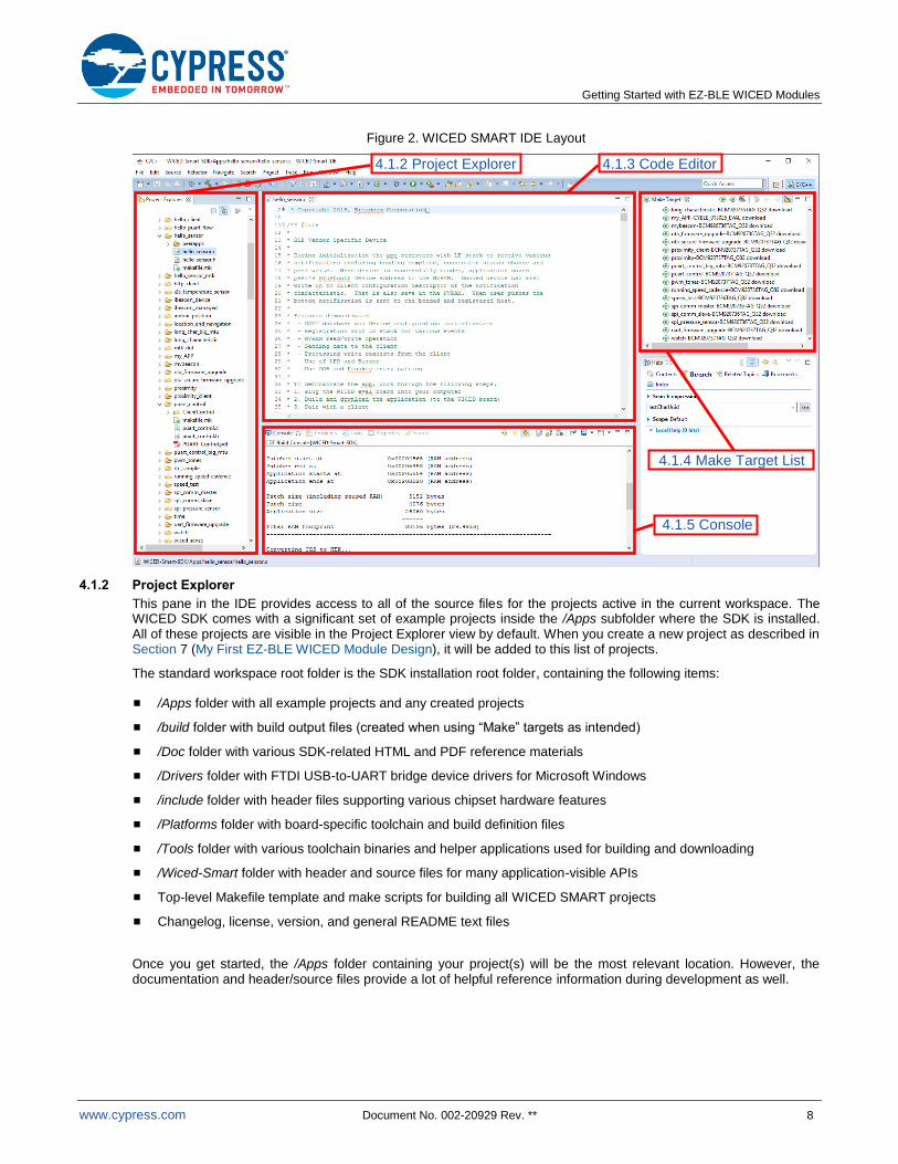
The WICED SMART SDK comes with an Eclipse-based IDE that provides a comprehensive environment for creating, building, programming, and debugging WICED BLE applications. Figure 2 below shows the default layout with various sections of the IDE.
Building and downloading WICED SMART projects requires a slightly different procedure than some IDEs and toolchains use, so it is a good idea to familiarize yourself with the application early.
Getting Started with EZ-BLE WICED Modules
www.cypress.com Document No. 002-20929 Rev. ** 8
Figure 2. WICED SMART IDE Layout
4.1.2 Project Explorer
This pane in the IDE provides access to all of the source files for the projects active in the current workspace. The WICED SDK comes with a significant set of example projects inside the /Apps subfolder where the SDK is installed. All of these projects are visible in the Project Explorer view by default. When you create a new project as described in Section 7 (My First EZ-BLE WICED Module Design), it will be added to this list of projects.
The standard workspace root folder is the SDK installation root folder, containing the following items:
/Apps folder with all example projects and any created projects
/build folder with build output files (created when using “Make” targets as intended)
/Doc folder with various SDK-related HTML and PDF reference materials
/Drivers folder with FTDI USB-to-UART bridge device drivers for Microsoft Windows
/include folder with header files supporting various chipset hardware features
/Platforms folder with board-specific toolchain and build definition files
/Tools folder with various toolchain binaries and helper applications used for building and downloading
/Wiced-Smart folder with header and source files for many application-visible APIs
Top-level Makefile template and make scripts for building all WICED SMART projects
Changelog, license, version, and general README text files
Once you get started, the /Apps folder containing your project(s) will be the most relevant location. However, the documentation and header/source files provide a lot of helpful reference information during development as well.
4.1.5 Console
4.1.4 Make Target List
4.1.3 Code Editor 4.1.2 Project Explorer
Getting Started with EZ-BLE WICED Modules
www.cypress.com Document No. 002-20929 Rev. ** 9
4.1.3 Code Editor
This pane allows editing all source code present in any project in the workspace. Open-source files are arranged by tabs for easy navigation. The Eclipse IDE foundation provides comprehensive syntax highlighting features, code completion, and other helpful functionality.
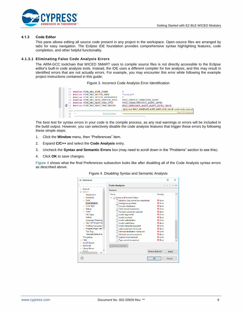
4.1.3.1 Eliminating False Code Analysis Errors
The ARM-GCC toolchain that WICED SMART uses to compile source files is not directly accessible to the Eclipse editor’s built-in code analysis tools. Instead, the IDE uses a different compiler for live analysis, and this may result in identified errors that are not actually errors. For example, you may encounter this error while following the example project instructions contained in this guide:
Figure 3. Incorrect Code Analysis Error Identification
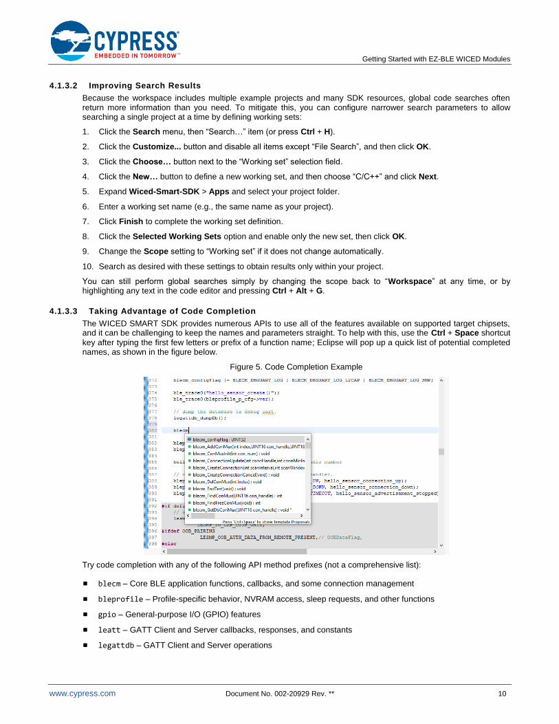
The best test for syntax errors in your code is the compile process, as any real warnings or errors will be included in the build output. However, you can selectively disable the code analysis features that trigger these errors by following these simple steps:
1. Click the Window menu, then “Preferences” item.
2. Expand C/C++ and select the Code Analysis entry.
3. Uncheck the Syntax and Semantic Errors box (may need to scroll down in the “Problems” section to see this).
4. Click OK to save changes.
Figure 4 shows what the final Preferences subsection looks like after disabling all of the Code Analysis syntax errors as described above.
Figure 4. Disabling Syntax and Semantic Analysis
Getting Started with EZ-BLE WICED Modules
www.cypress.com Document No. 002-20929 Rev. ** 10
4.1.3.2 Improving Search Results
Because the workspace includes multiple example projects and many SDK resources, global code searches often return more information than you need. To mitigate this, you can configure narrower search parameters to allow searching a single project at a time by defining working sets:
1. Click the Search menu, then “Search…” item (or press Ctrl + H).
2. Click the Customize... button and disable all items except “File Search”, and then click OK.
3. Click the Choose… button next to the “Working set” selection field.
4. Click the New… button to define a new working set, and then choose “C/C++” and click Next.
5. Expand Wiced-Smart-SDK > Apps and select your project folder.
6. Enter a working set name (e.g., the same name as your project).
7. Click Finish to complete the working set definition.
8. Click the Selected Working Sets option and enable only the new set, then click OK.
9. Change the Scope setting to “Working set” if it does not change automatically.
10. Search as desired with these settings to obtain results only within your project.
You can still perform global searches simply by changing the scope back to “Workspace” at any time, or by highlighting any text in the code editor and pressing Ctrl + Alt + G.
4.1.3.3 Taking Advantage of Code Completion
The WICED SMART SDK provides numerous APIs to use all of the features available on supported target chipsets, and it can be challenging to keep the names and parameters straight. To help with this, use the Ctrl + Space shortcut
key after typing the first few letters or prefix of a function name; Eclipse will pop up a quick list of potential completed names, as shown in the figure below.
Figure 5. Code Completion Example
Try code completion with any of the following API method prefixes (not a comprehensive list):
blecm – Core BLE application functions, callbacks, and some connection management
bleprofile – Profile-specific behavior, NVRAM access, sleep requests, and other functions
gpio – General-purpose I/O (GPIO) features
leatt – GATT Client and Server callbacks, responses, and constants
legattdb – GATT Client and Server operations

Getting Started with EZ-BLE WICED Modules
www.cypress.com Document No. 002-20929 Rev. ** 11
lesmp – Security Manager Protocol (SMP) features such as pairing/bonding
lel2cap – L2CAP connectivity features (includes some connection and ATT-related behavior)
puart – Peripheral UART features
devlpm – Low-power-mode features
adc – Analog/Digital Conversion (ADC) features
pwm – Pulse Width Modulation (PWM) features
4.1.4 Make Target List
This pane contains individual build targets for all of the example projects that come pre-installed with the WICED SMART SDK, as well as make targets for any new projects that you create. Each build target provides a unique combination of the following items:
Project name (e.g., “find_me”)
Target platform (e.g., “CYBLE_013025_EVAL”)
Operational arguments (e.g., “download”, “UART=COM5”, and others)
Double-clicking on a make target will trigger the build process for that target. You can also use the F9 keyboard
shortcut in the Eclipse IDE to rebuild the last selected make target.
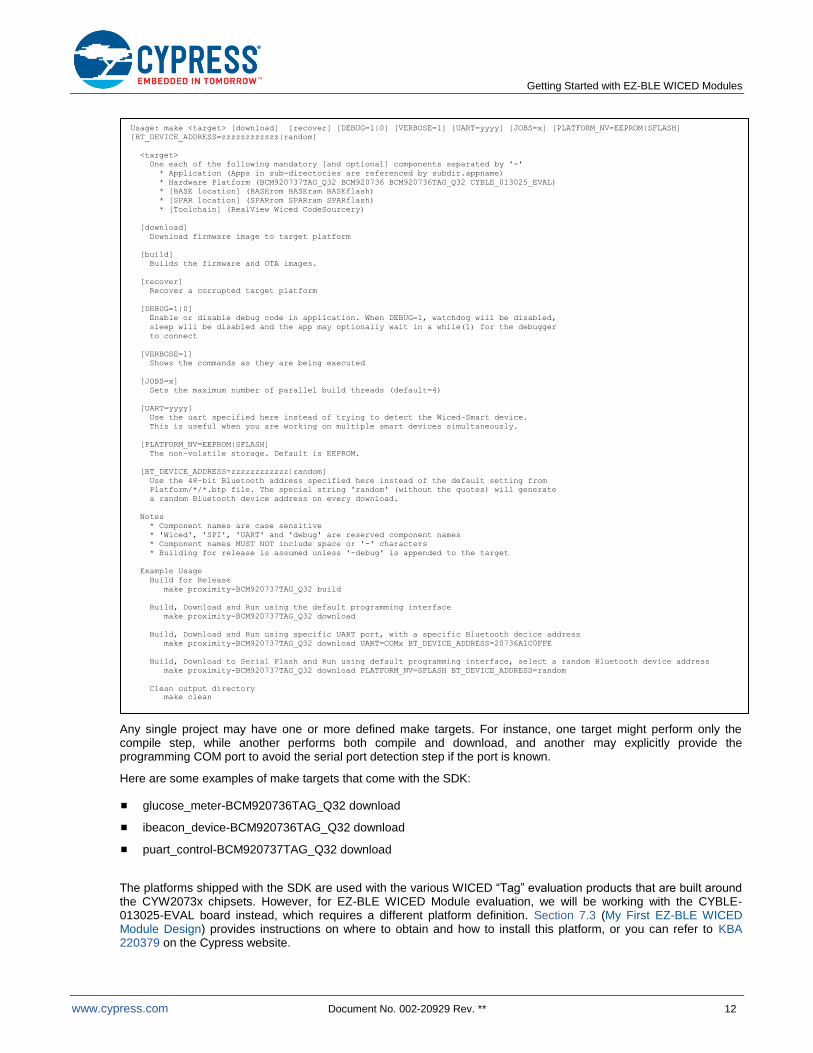
The project name and target platform are separated by a dash (“–”), while the name/target and all subsequent operational arguments are separated by spaces. Possible arguments are described in the output from the “help” target, which you can build at any time to see details. The output from this target is reproduced here for quick reference:
Getting Started with EZ-BLE WICED Modules
www.cypress.com Document No. 002-20929 Rev. ** 12
Any single project may have one or more defined make targets. For instance, one target might perform only the compile step, while another performs both compile and download, and another may explicitly provide the programming COM port to avoid the serial port detection step if the port is known.
Here are some examples of make targets that come with the SDK:
glucose_meter-BCM920736TAG_Q32 download
ibeacon_device-BCM920736TAG_Q32 download
puart_control-BCM920737TAG_Q32 download
The platforms shipped with the SDK are used with the various WICED “Tag” evaluation products that are built around the CYW2073x chipsets. However, for EZ-BLE WICED Module evaluation, we will be working with the CYBLE-013025-EVAL board instead, which requires a different platform definition. Section 7.3 (My First EZ-BLE WICED Module Design) provides instructions on where to obtain and how to install this platform, or you can refer to KBA 220379 on the Cypress website.
Usage: make <target> [download] [recover] [DEBUG=1|0] [VERBOSE=1] [UART=yyyy] [JOBS=x] [PLATFORM_NV=EEPROM|SFLASH]
[BT_DEVICE_ADDRESS=zzzzzzzzzzzz|random]
<target>
One each of the following mandatory [and optional] components separated by '-'
* Application (Apps in sub-directories are referenced by subdir.appname)
* Hardware Platform (BCM920737TAG_Q32 BCM920736 BCM920736TAG_Q32 CYBLE_013025_EVAL)
* [BASE location] (BASErom BASEram BASEflash)
* [SPAR location] (SPARrom SPARram SPARflash)
* [Toolchain] (RealView Wiced CodeSourcery)
[download]
Download firmware image to target platform
[build]
Builds the firmware and OTA images.
[recover]
Recover a corrupted target platform
[DEBUG=1|0]
Enable or disable debug code in application. When DEBUG=1, watchdog will be disabled,
sleep will be disabled and the app may optionally wait in a while(1) for the debugger
to connect
[VERBOSE=1]
Shows the commands as they are being executed
[JOBS=x]
Sets the maximum number of parallel build threads (default=4)
[UART=yyyy]
Use the uart specified here instead of trying to detect the Wiced-Smart device.
This is useful when you are working on multiple smart devices simultaneously.
[PLATFORM_NV=EEPROM|SFLASH]
The non-volatile storage. Default is EEPROM.
[BT_DEVICE_ADDRESS=zzzzzzzzzzzz|random]
Use the 48-bit Bluetooth address specified here instead of the default setting from
Platform/*/*.btp file. The special string 'random' (without the quotes) will generate
a random Bluetooth device address on every download.
Notes
* Component names are case sensitive
* 'Wiced', 'SPI', 'UART' and 'debug' are reserved component names
* Component names MUST NOT include space or '-' characters
* Building for release is assumed unless '-debug' is appended to the target
Example Usage
Build for Release
make proximity-BCM920737TAG_Q32 build
Build, Download and Run using the default programming interface
make proximity-BCM920737TAG_Q32 download
Build, Download and Run using specific UART port, with a specific Bluetooth decice address
make proximity-BCM920737TAG_Q32 download UART=COMx BT_DEVICE_ADDRESS=20736A1C0FFE
Build, Download to Serial Flash and Run using default programming interface, select a random Bluetooth device address
make proximity-BCM920737TAG_Q32 download PLATFORM_NV=SFLASH BT_DEVICE_ADDRESS=random
Clean output directory
make clean

Getting Started with EZ-BLE WICED Modules
www.cypress.com Document No. 002-20929 Rev. ** 13
4.1.5 Console
This pane provides access to compiler output, which is helpful for status updates and critical for error analysis. The same area of the IDE window also allows a quick look at search results after performing a search, and enabled code analysis warnings or errors, and tasks identified by “TODO” comments in source files.
4.1.5.1 Debug Trace Output
One other key feature that the console pane optionally provides is specially decoded output from debug traces. This feature allows one-way output during normal code execution on the module. This debug output typically comes out the HCI UART TX pin (though it may be reconfigured in code to use the peripheral UART TX pin if PUART is not otherwise used). It allows printf-like formatting of output strings with between zero and six variable arguments in
addition to the format string, via the following set of functions:
ble_trace0(string)
ble_trace1(string, arg1)
ble_trace2(string, arg1, arg2)
...
ble_trace6(string, arg1, arg2, arg3, arg4, arg5, arg6)
This set of functions behaves like the typical variable-argument printf function in C, except that the maximum
supported variable argument count is six.
Most examples and the automatically generated code from the WICED Bluetooth Designer tool use this debug trace output for simple execution flow monitoring. Since it is not possible to perform true break/step debugging with the WICED SMART SDK, this type of debug output is immensely helpful during the development phase.
To use debug tracing with the CYBLE-013025-EVAL board, follow this procedure:
1. Set SW1 positions 1-4 (PUART) to the OFF state and positions 5-6 (HCI UART) to the ON state.
2. Compile and download the firmware into the module (application will begin executing immediately).
3. Set SW1 position 6 (HCI UART RX) to the OFF state to disconnect it from the host.
4. Use the Trace menu and select Start Debug Traces to begin capturing and decoding data.
Figure 6. Starting Debug Traces
5. Optionally, reboot the board with the SW2 (RESET) button if you need to capture boot-time output.
6. When finished, use the Trace menu and Stop Debug Traces item to detach the console and release the serial
port to allow downloading firmware again.
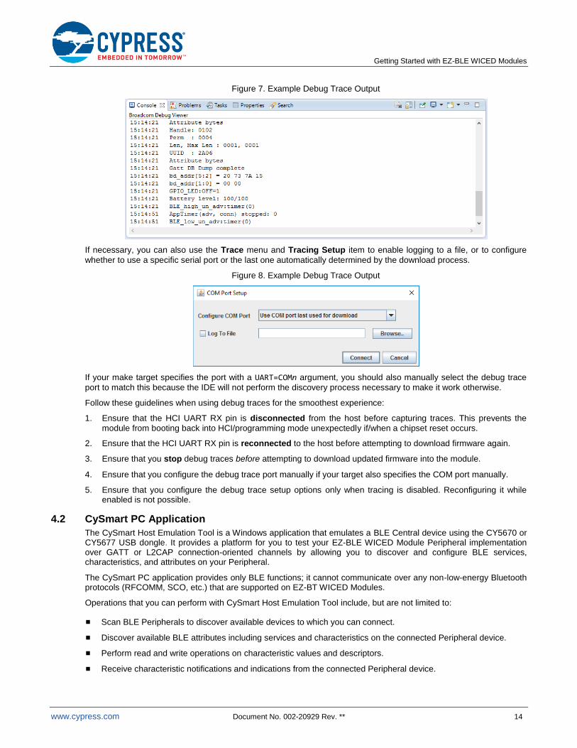
The console output with debug traces enabled in the “find_me” example illustrated in this document looks like Figure 7 below. The standard behavior begins with a create() message followed by a GATT database structure dump, and
then the module begins advertising.
Getting Started with EZ-BLE WICED Modules
www.cypress.com Document No. 002-20929 Rev. ** 14
Figure 7. Example Debug Trace Output
If necessary, you can also use the Trace menu and Tracing Setup item to enable logging to a file, or to configure
whether to use a specific serial port or the last one automatically determined by the download process.
Figure 8. Example Debug Trace Output
If your make target specifies the port with a UART=COMn argument, you should also manually select the debug trace
port to match this because the IDE will not perform the discovery process necessary to make it work otherwise.
Follow these guidelines when using debug traces for the smoothest experience:
1. Ensure that the HCI UART RX pin is disconnected from the host before capturing traces. This prevents the
module from booting back into HCI/programming mode unexpectedly if/when a chipset reset occurs.
2. Ensure that the HCI UART RX pin is reconnected to the host before attempting to download firmware again.
3. Ensure that you stop debug traces before attempting to download updated firmware into the module.
4. Ensure that you configure the debug trace port manually if your target also specifies the COM port manually.
5. Ensure that you configure the debug trace setup options only when tracing is disabled. Reconfiguring it while enabled is not possible.
4.2 CySmart PC Application
The CySmart Host Emulation Tool is a Windows application that emulates a BLE Central device using the CY5670 or CY5677 USB dongle. It provides a platform for you to test your EZ-BLE WICED Module Peripheral implementation over GATT or L2CAP connection-oriented channels by allowing you to discover and configure BLE services, characteristics, and attributes on your Peripheral.
The CySmart PC application provides only BLE functions; it cannot communicate over any non-low-energy Bluetooth protocols (RFCOMM, SCO, etc.) that are supported on EZ-BT WICED Modules.
Operations that you can perform with CySmart Host Emulation Tool include, but are not limited to:
Scan BLE Peripherals to discover available devices to which you can connect.
Discover available BLE attributes including services and characteristics on the connected Peripheral device.
Perform read and write operations on characteristic values and descriptors.
Receive characteristic notifications and indications from the connected Peripheral device.
Getting Started with EZ-BLE WICED Modules
www.cypress.com Document No. 002-20929 Rev. ** 15
Establish a bond with the connected Peripheral device using BLE Security Manager procedures.
Establish a BLE L2CAP connection-oriented session with the Peripheral device and exchange data per the Bluetooth 4.1 specification.
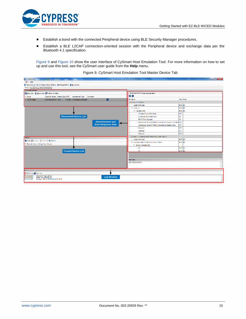
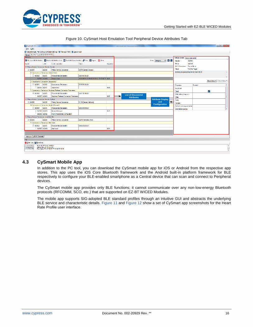
Figure 9 and Figure 10 show the user interface of CySmart Host Emulation Tool. For more information on how to set up and use this tool, see the CySmart user guide from the Help menu.
Figure 9. CySmart Host Emulation Tool Master Device Tab
Advertisement and
Scan Response Data
Discovered Device List
Log Window
Trusted Device List
Getting Started with EZ-BLE WICED Modules
www.cypress.com Document No. 002-20929 Rev. ** 16
Figure 10. CySmart Host Emulation Tool Peripheral Device Attributes Tab
Attribute Display
and
Configuration
List of Discovered
Attributes
4.3 CySmart Mobile App
In addition to the PC tool, you can download the CySmart mobile app for iOS or Android from the respective app stores. This app uses the iOS Core Bluetooth framework and the Android built-in platform framework for BLE respectively to configure your BLE-enabled smartphone as a Central device that can scan and connect to Peripheral devices.
The CySmart mobile app provides only BLE functions; it cannot communicate over any non-low-energy Bluetooth protocols (RFCOMM, SCO, etc.) that are supported on EZ-BT WICED Modules.
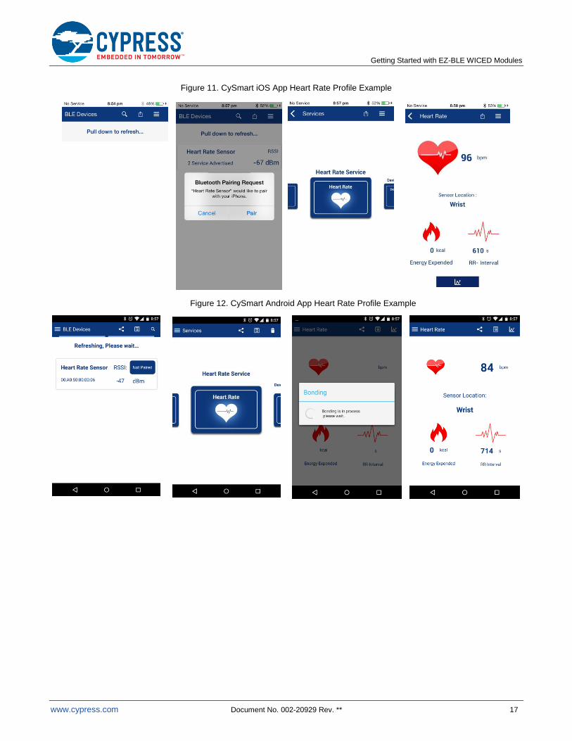
The mobile app supports SIG-adopted BLE standard profiles through an intuitive GUI and abstracts the underlying BLE service and characteristic details. Figure 11 and Figure 12 show a set of CySmart app screenshots for the Heart Rate Profile user interface.
Getting Started with EZ-BLE WICED Modules
www.cypress.com Document No. 002-20929 Rev. ** 17
Figure 11. CySmart iOS App Heart Rate Profile Example
Figure 12. CySmart Android App Heart Rate Profile Example

Getting Started with EZ-BLE WICED Modules
www.cypress.com Document No. 002-20929 Rev. ** 18
5 Development Kits and Evaluation Boards
Cypress provides easy-to-use evaluation boards to help you develop your EZ-BLE WICED Module design.
5.1 EZ-BLE WICED Module Evaluation Boards
Each EZ-BLE WICED Module provides an evaluation board that can be used to develop and test the performance of the Cypress EZ-BLE WICED Module. EZ-BLE WICED evaluation boards are Arduino-compatible baseboards, designed to work as stand-alone evaluation vehicles, or in conjunction with Arduino-compatible shields.
EZ-BLE WICED evaluation boards allow you to evaluate Cypress EZ-BLE Modules without having to design custom hardware to mount the Cypress EZ-BLE Module.
Table 4 lists available EZ-BLE WICED Modules and their corresponding evaluation board part numbers. Click on your evaluation board for additional information.
Table 4. EZ-BLE Modules and Corresponding Evaluation Board Part Numbers
EZ-BLE WICED Module Part Number EZ-BLE WICED Evaluation Board Part Number
CYBLE-013025-00 CYBLE-013025-EVAL
CYBLE-013030-00 CYBLE-013025-EVAL
Each EZ-BLE WICED evaluation board contains the following components:
Cypress EZ-BLE Module – soldered directly to the evaluation board
PCB substrate
Arduino-compatible baseboard headers
USB-to-UART Bridge
USB connection (for WICED SMART SDK PC interface, programming, and EZ-Serial interface)
Connection headers for HCI-UART direct connection (as needed)
A configuration switch network is provided to configure the UART connection to the USB connector. This switch network can be configured to enable either HCI-UART or Peripheral-UART to the USB connector.
Header connection for current consumption measurement
Configuration headers for setting the desired power supply level
Power supply jumper for current consumption measurement
Reset and switch
User-defined switch element
Inductors (for power supply noise reduction) – refer to your EZ-BLE WICED Module datasheet for recommended external components)
EZ-BLE WICED evaluation boards are designed to simulate the placement and connection of the EZ-BLE Modules in a final application. All host-side layout pattern recommendations (as shown in each specific module’s datasheet) are followed for each evaluation board.
See Appendix C: EZ-BLE WICED Evaluation Board Details for details on the connections available for each of the EZ-BLE WICED evaluation boards.
Getting Started with EZ-BLE WICED Modules
www.cypress.com Document No. 002-20929 Rev. ** 19
6 EZ-BLE WICED Module Development Setup (WICED SMART SDK)
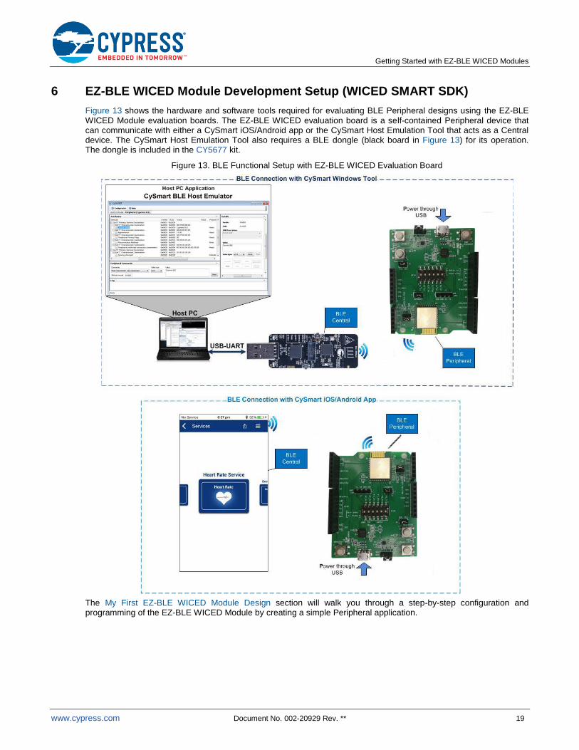
Figure 13 shows the hardware and software tools required for evaluating BLE Peripheral designs using the EZ-BLE WICED Module evaluation boards. The EZ-BLE WICED evaluation board is a self-contained Peripheral device that can communicate with either a CySmart iOS/Android app or the CySmart Host Emulation Tool that acts as a Central device. The CySmart Host Emulation Tool also requires a BLE dongle (black board in Figure 13) for its operation. The dongle is included in the CY5677 kit.
Figure 13. BLE Functional Setup with EZ-BLE WICED Evaluation Board
The My First EZ-BLE WICED Module Design section will walk you through a step-by-step configuration and programming of the EZ-BLE WICED Module by creating a simple Peripheral application.
Getting Started with EZ-BLE WICED Modules
www.cypress.com Document No. 002-20929 Rev. ** 20
7 My First EZ-BLE WICED Module Design
This section gives you a step-by-step process for building a simple design with the CYBLE-013025-EVAL kit using the WICED SMART SDK and IDE.
7.1 About the Design
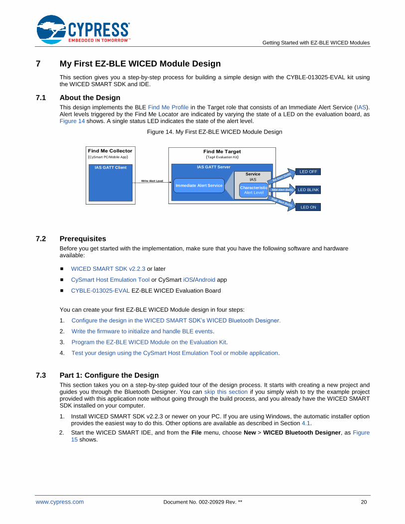
This design implements the BLE Find Me Profile in the Target role that consists of an Immediate Alert Service (IAS). Alert levels triggered by the Find Me Locator are indicated by varying the state of a LED on the evaluation board, as Figure 14 shows. A single status LED indicates the state of the alert level.
Figure 14. My First EZ-BLE WICED Module Design
(CySmart PC/Mobile App)(CySmart PC/Mobile App)
IAS GATT Client
Write Alert Level
(Tag4 Evaluation Kit)(Tag4 Evaluation Kit)
IAS GATT Server
Service
IAS
Characteristic
Alert Level
Immediate Alert ServiceMild Alert (0x01)
LED OFF
LED BLINK
LED ON
(Tag4 Evaluation Kit)
IAS GATT Server
Service
IAS
Characteristic
Alert Level
Immediate Alert ServiceMild Alert (0x01)
LED OFF
LED BLINK
LED ON
7.2 Prerequisites
Before you get started with the implementation, make sure that you have the following software and hardware available:
WICED SMART SDK v2.2.3 or later
CySmart Host Emulation Tool or CySmart iOS/Android app
CYBLE-013025-EVAL EZ-BLE WICED Evaluation Board
You can create your first EZ-BLE WICED Module design in four steps:
1. Configure the design in the WICED SMART SDK’s WICED Bluetooth Designer.
2. Write the firmware to initialize and handle BLE events.
3. Program the EZ-BLE WICED Module on the Evaluation Kit.
4. Test your design using the CySmart Host Emulation Tool or mobile application.
7.3 Part 1: Configure the Design
This section takes you on a step-by-step guided tour of the design process. It starts with creating a new project and guides you through the Bluetooth Designer. You can skip this section if you simply wish to try the example project provided with this application note without going through the build process, and you already have the WICED SMART SDK installed on your computer.
1. Install WICED SMART SDK v2.2.3 or newer on your PC. If you are using Windows, the automatic installer option provides the easiest way to do this. Other options are available as described in Section 4.1.
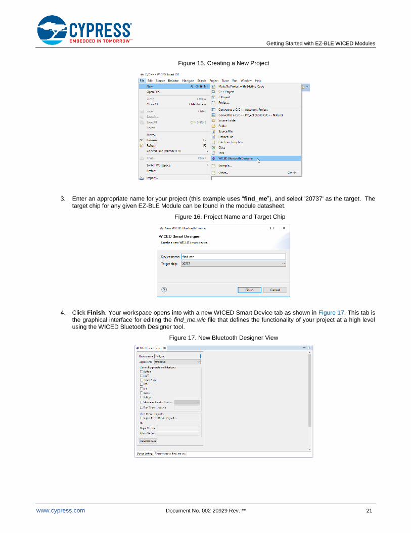
2. Start the WICED SMART IDE, and from the File menu, choose New > WICED Bluetooth Designer, as Figure
15 shows.
Getting Started with EZ-BLE WICED Modules
www.cypress.com Document No. 002-20929 Rev. ** 21
Figure 15. Creating a New Project
3. Enter an appropriate name for your project (this example uses “find_me”), and select '20737' as the target. The
target chip for any given EZ-BLE Module can be found in the module datasheet.
Figure 16. Project Name and Target Chip
4. Click Finish. Your workspace opens into with a new WICED Smart Device tab as shown in Figure 17. This tab is
the graphical interface for editing the find_me.wic file that defines the functionality of your project at a high level using the WICED Bluetooth Designer tool.
Figure 17. New Bluetooth Designer View
Getting Started with EZ-BLE WICED Modules
www.cypress.com Document No. 002-20929 Rev. ** 22
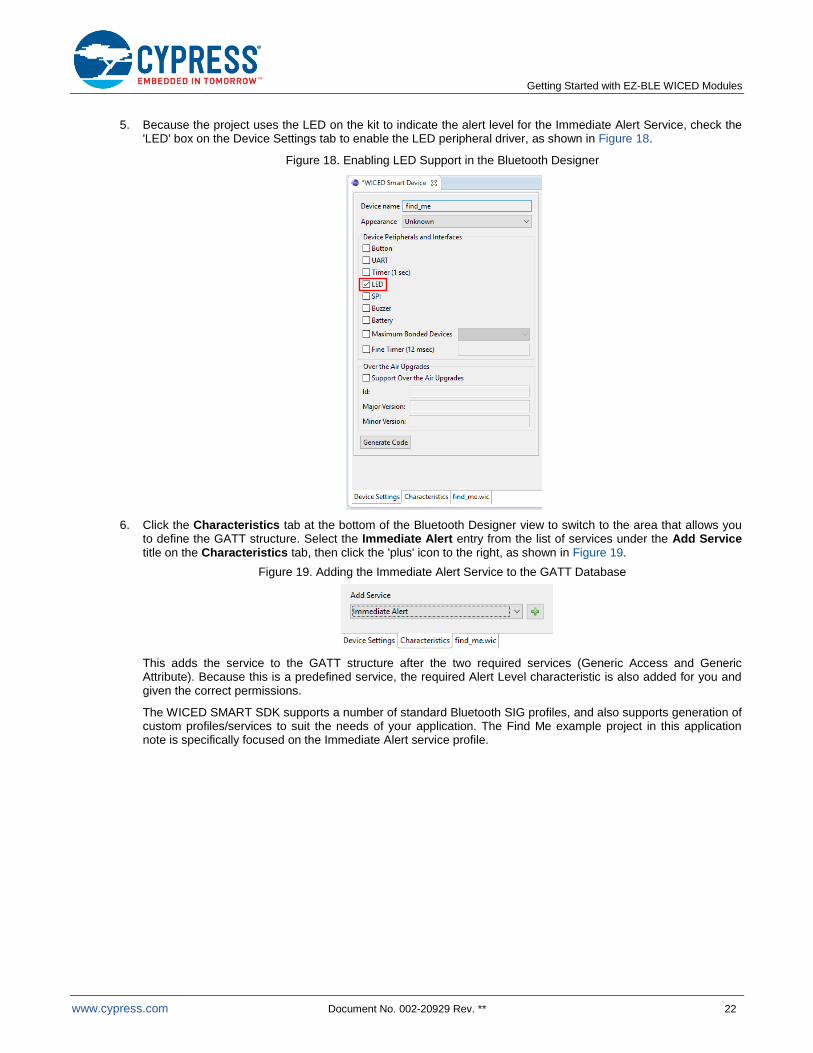
5. Because the project uses the LED on the kit to indicate the alert level for the Immediate Alert Service, check the 'LED' box on the Device Settings tab to enable the LED peripheral driver, as shown in Figure 18.
Figure 18. Enabling LED Support in the Bluetooth Designer
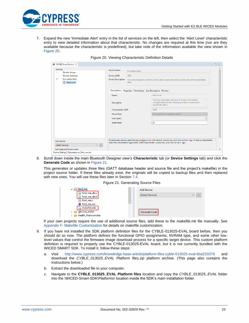
6. Click the Characteristics tab at the bottom of the Bluetooth Designer view to switch to the area that allows you to define the GATT structure. Select the Immediate Alert entry from the list of services under the Add Service title on the Characteristics tab, then click the 'plus' icon to the right, as shown in Figure 19.
Figure 19. Adding the Immediate Alert Service to the GATT Database
This adds the service to the GATT structure after the two required services (Generic Access and Generic Attribute). Because this is a predefined service, the required Alert Level characteristic is also added for you and given the correct permissions.
The WICED SMART SDK supports a number of standard Bluetooth SIG profiles, and also supports generation of custom profiles/services to suit the needs of your application. The Find Me example project in this application note is specifically focused on the Immediate Alert service profile.
Getting Started with EZ-BLE WICED Modules
www.cypress.com Document No. 002-20929 Rev. ** 23
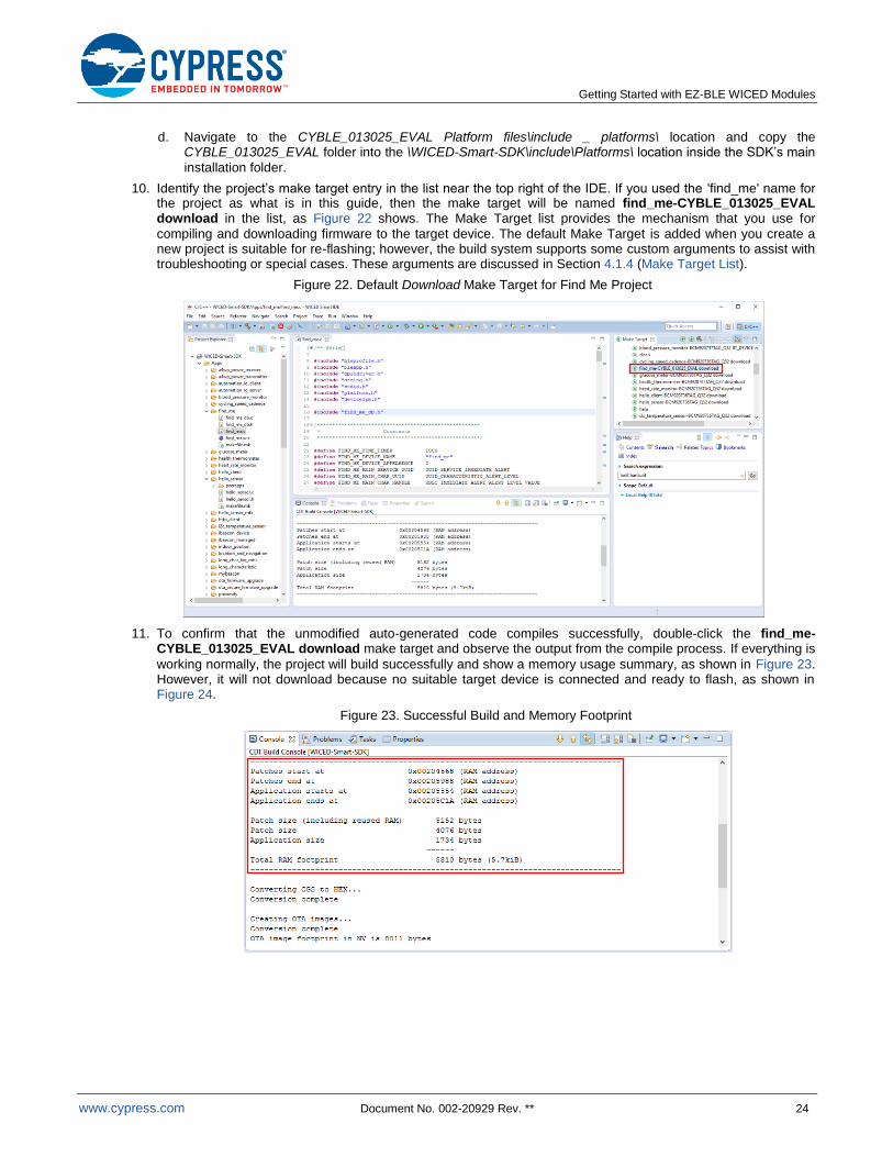
7. Expand the new 'Immediate Alert' entry in the list of services on the left, then select the 'Alert Level' characteristic entry to view detailed information about that characteristic. No changes are required at this time (nor are they available because the characteristic is predefined), but take note of the information available the view shown in Figure 20.
Figure 20. Viewing Characteristic Definition Details
8. Scroll down inside the main Bluetooth Designer view’s Characteristic tab (or Device Settings tab) and click the Generate Code as shown in Figure 21.
This generates or updates three files (GATT database header and source file and the project’s makefile) in the project source folder. If these files already exist, the originals will be copied to backup files and then replaced with new ones. You will use these files later in Section 7.4.
Figure 21. Generating Source Files
If your own projects require the use of additional source files, add these to the makefile.mk file manually. See Appendix F: Makefile Customization for details on makefile customization.
9. If you have not installed the SDK platform definition files for the CYBLE-013025-EVAL board before, then you should do so now. The platform defines the functional GPIO assignments, NVRAM type, and some other low-level values that control the firmware image download process for a specific target device. This custom platform definition is required to properly use the CYBLE-013025-EVAL board, but it is not currently bundled with the WICED SMART SDK. To install it, follow these steps:
a. Visit http://www.cypress.com/knowledge-base-article/platform-files-cyble-013025-eval-kba220379 and download the CYBLE_013025_EVAL Platform files.zip platform archive. (This page also contains the instructions below.)
b. Extract the downloaded file to your computer.
c. Navigate to the CYBLE_013025_EVAL Platform files location and copy the CYBLE_013025_EVAL folder into the \WICED-Smart-SDK\Platforms\ location inside the SDK’s main installation folder.
Getting Started with EZ-BLE WICED Modules
www.cypress.com Document No. 002-20929 Rev. ** 24
d. Navigate to the CYBLE_013025_EVAL Platform files\include _ platforms\ location and copy the CYBLE_013025_EVAL folder into the \WICED-Smart-SDK\include\Platforms\ location inside the SDK’s main
installation folder.
10. Identify the project’s make target entry in the list near the top right of the IDE. If you used the 'find_me' name for the project as what is in this guide, then the make target will be named find_me-CYBLE_013025_EVAL download in the list, as Figure 22 shows. The Make Target list provides the mechanism that you use for
compiling and downloading firmware to the target device. The default Make Target is added when you create a new project is suitable for re-flashing; however, the build system supports some custom arguments to assist with troubleshooting or special cases. These arguments are discussed in Section 4.1.4 (Make Target List).
Figure 22. Default Download Make Target for Find Me Project
11. To confirm that the unmodified auto-generated code compiles successfully, double-click the find_me-CYBLE_013025_EVAL download make target and observe the output from the compile process. If everything is
working normally, the project will build successfully and show a memory usage summary, as shown in Figure 23. However, it will not download because no suitable target device is connected and ready to flash, as shown in Figure 24.
Figure 23. Successful Build and Memory Footprint
Getting Started with EZ-BLE WICED Modules
www.cypress.com Document No. 002-20929 Rev. ** 25
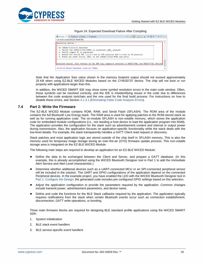
Figure 24. Expected Download Failure After Compiling
Note that the Application Size value shown in the memory footprint output should not exceed approximately 25 KB when using EZ-BLE WICED Modules based on the CYW20737 device. The chip will not boot or run properly with applications larger than this.
In addition, the WICED SMART IDE may show some symbol resolution errors in the main code window. Often, these symbols can be resolved correctly, and the IDE is misidentifying issues in the code due to differences between the code analysis toolchain and the one used for the final build process. For instructions on how to disable these errors, see Section 4.1.3.1 (Eliminating False Code Analysis Errors).
7.4 Part 2: Write the Firmware
The EZ-BLE WICED Module contains ROM, RAM, and Serial Flash (SFLASH). The ROM area of the module contains the full Bluetooth Low Energy stack. The RAM area is used for applying patches to the ROM-stored stack as well as for running application code. The on-module SFLASH is non-volatile memory, which stores the application code for embedded module configurations (i.e., not needing a host device to load the application program into RAM). The application provides the configuration for the stack such as advertisement content and interval or output power during transmission. Also, the application focuses on application-specific functionality while the stack deals with the low-level details. For example, the stack transparently handles a GATT Client read request or discovery.
Stack patches and most application logic are stored outside of the chip itself in SFLASH memory. This is also the memory used for temporary image storage during an over-the-air (OTA) firmware update process. This non-volatile storage area is integrated on the EZ-BLE WICED Module.
The following main steps are required to develop an application for an EZ-BLE WICED Module:
Define the data to be exchanged between the Client and Server, and prepare a GATT database. (In this example, this is already accomplished using the WICED Bluetooth Designer tool in Part 1 to add the Immediate Alert Service and Alert Level characteristic.)
Determine whether additional devices such as a UART-connected MCU or an SPI-connected peripheral sensor will be included in the solution. The UART and GPIO configurations of the application depend on the connected Peripheral devices. In the example project, you have enabled the LED with the WICED Bluetooth Designer tool in Part 1: Configure the Design; the generated code includes pre-configured GPIO settings based on this selection.
Adjust the application configuration to provide the parameters required by the application. Common changes include transmit power, advertisement parameters, and device name.
Define and code the functions for the BLE Stack callbacks required by the application. The application typically requires notifications from the stack when certain Bluetooth events occur such as connection establishment, disconnection, GATT write operations, or bonding.
Three main firmware blocks are required for designing BLE standard profile applications using the WICED SMART SDK:
1. System initialization
2. BLE stack event handlers
3. BLE service-specific event handlers

Getting Started with EZ-BLE WICED Modules
www.cypress.com Document No. 002-20929 Rev. ** 26
The following sections discuss these blocks with respect to the design that you configured in Part 1: Configure the Design. Many of the functions involved in these are auto-generated for you based on the settings chosen in the WICED Bluetooth Designer; however, some of these functions need to have additional code added in order to achieve the specific behavior that your application requires.
Unlike other platforms, the WICED SMART BLE stack does not require or provide an application-level “main loop” function that repeats forever. Instead, the main loop is handled internally along with low-power transitions, and all application behavior must be fully event-driven based on interrupts triggered by timers, wireless (BLE) activity, or wired (GPIO, UART, etc.) activity.
7.4.1 System In it ia l iza t ion
When the EZ-BLE WICED Module starts up, it initializes the BLE stack and executes the application initialization function named APPLICATION_INIT. This initialization function must call the bleapp_set_cfg function, which
provides the BLE stack with pointers to application data structures, including the GATT database, application configuration, UART configuration, GPIO configuration, and a pointer to a create function that is called when the
application starts.
The ROM image in the module also contains some basic application logic. The full source code for these functions is included in the WICED SMART SDK in the /Wiced-Smart/bleapp/app directory. The new application is flexible in what portions of the ROM code to use. If the ROM code completely matches the requirements, the APPLICATION_INIT
function should simply point to the data structures and then create functions from the ROM code. However, most designs will need more customized behavior than this provides.
The following data structures are present in every EZ-BLE WICED application:
The GATT database identifies data objects to the BLE stack that are exchanged between the peripheral and the client application.
Application configuration, which specifies parameters shared between the application and the BLE stack.
UART and GPIO configurations. In some cases, the application requires a connection to a Peripheral device (for example, a measurement sensor). Although drivers for most Peripheral buses are included in the CYW20737 ROM, some code must be written to support the hardware. For example, some applications may require processing of data received over the UART or SPI interfaces.
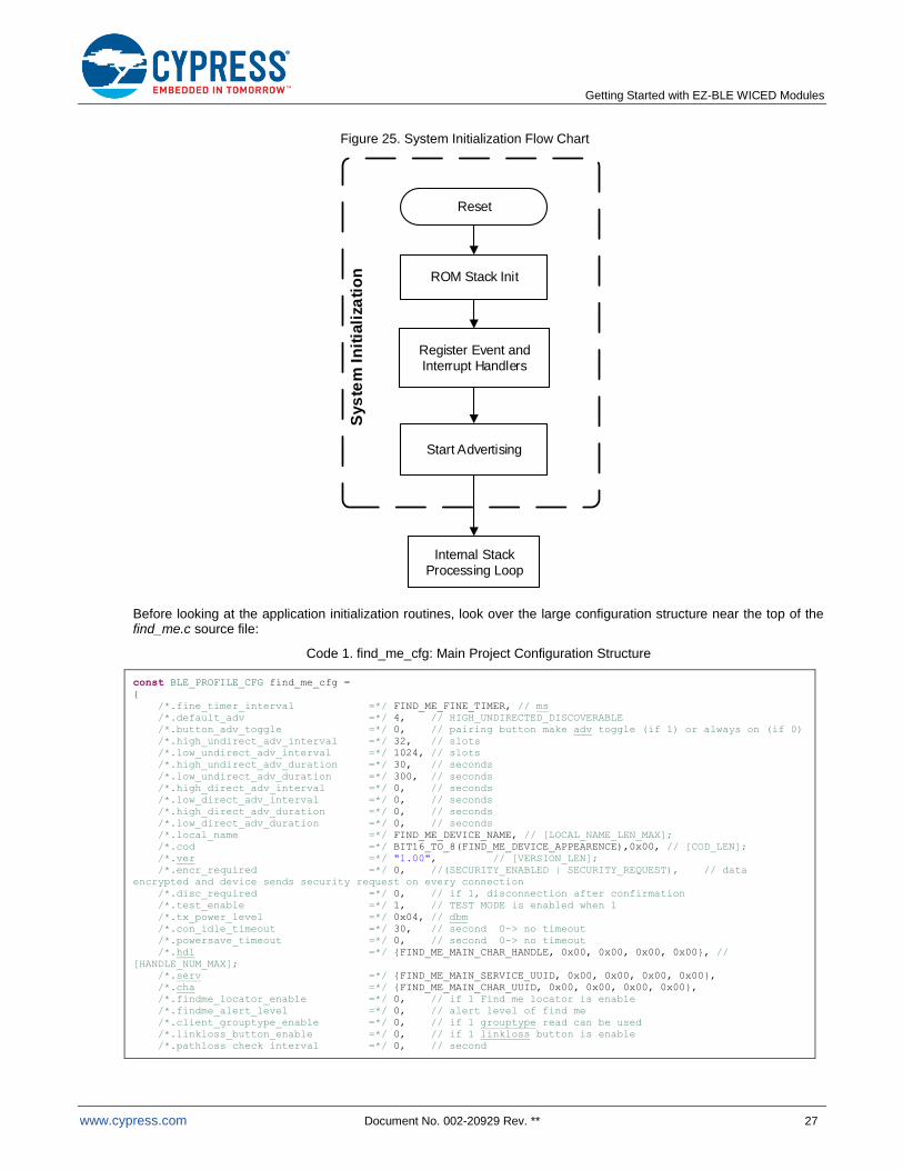
Figure 25 shows the flowchart and firmware source code for system initialization.
Getting Started with EZ-BLE WICED Modules
www.cypress.com Document No. 002-20929 Rev. ** 27
Figure 25. System Initialization Flow Chart
Reset
ROM Stack Init
Register Event and Interrupt Handlers
Start Advertising
Sys
tem
In
itia
liza
tio
n
Internal Stack Processing Loop
Before looking at the application initialization routines, look over the large configuration structure near the top of the find_me.c source file:
Code 1. find_me_cfg: Main Project Configuration Structure
const BLE_PROFILE_CFG find_me_cfg =
{
/*.fine_timer_interval =*/ FIND_ME_FINE_TIMER, // ms
/*.default_adv =*/ 4, // HIGH_UNDIRECTED_DISCOVERABLE
/*.button_adv_toggle =*/ 0, // pairing button make adv toggle (if 1) or always on (if 0)
/*.high_undirect_adv_interval =*/ 32, // slots
/*.low_undirect_adv_interval =*/ 1024, // slots
/*.high_undirect_adv_duration =*/ 30, // seconds
/*.low_undirect_adv_duration =*/ 300, // seconds
/*.high_direct_adv_interval =*/ 0, // seconds
/*.low_direct_adv_interval =*/ 0, // seconds
/*.high_direct_adv_duration =*/ 0, // seconds
/*.low_direct_adv_duration =*/ 0, // seconds
/*.local_name =*/ FIND_ME_DEVICE_NAME, // [LOCAL_NAME_LEN_MAX];
/*.cod =*/ BIT16_TO_8(FIND_ME_DEVICE_APPEARENCE),0x00, // [COD_LEN];
/*.ver =*/ "1.00", // [VERSION_LEN];
/*.encr_required =*/ 0, //(SECURITY_ENABLED | SECURITY_REQUEST), // data
encrypted and device sends security request on every connection
/*.disc_required =*/ 0, // if 1, disconnection after confirmation
/*.test_enable =*/ 1, // TEST MODE is enabled when 1
/*.tx_power_level =*/ 0x04, // dbm
/*.con_idle_timeout =*/ 30, // second 0-> no timeout
/*.powersave_timeout =*/ 0, // second 0-> no timeout
/*.hdl =*/ {FIND_ME_MAIN_CHAR_HANDLE, 0x00, 0x00, 0x00, 0x00}, //
[HANDLE_NUM_MAX];
/*.serv =*/ {FIND_ME_MAIN_SERVICE_UUID, 0x00, 0x00, 0x00, 0x00},
/*.cha =*/ {FIND_ME_MAIN_CHAR_UUID, 0x00, 0x00, 0x00, 0x00},
/*.findme_locator_enable =*/ 0, // if 1 Find me locator is enable
/*.findme_alert_level =*/ 0, // alert level of find me
/*.client_grouptype_enable =*/ 0, // if 1 grouptype read can be used
/*.linkloss_button_enable =*/ 0, // if 1 linkloss button is enable
/*.pathloss_check_interval =*/ 0, // second
Getting Started with EZ-BLE WICED Modules
www.cypress.com Document No. 002-20929 Rev. ** 28
/*.alert_interval =*/ 0, // interval of alert
/*.high_alert_num =*/ 0, // number of alert for each interval
/*.mild_alert_num =*/ 0, // number of alert for each interval
/*.status_led_enable =*/ 1, // if 1 status LED is enable
/*.status_led_interval =*/ 0, // second
/*.status_led_con_blink =*/ 0, // blink num of connection
/*.status_led_dir_adv_blink =*/ 0, // blink num of dir adv
/*.status_led_un_adv_blink =*/ 0, // blink num of undir adv
/*.led_on_ms =*/ 0, // led blink on duration in ms
/*.led_off_ms =*/ 0, // led blink off duration in ms
/*.buz_on_ms =*/ 100, // buzzer on duration in ms
/*.button_power_timeout =*/ 0, // seconds
/*.button_client_timeout =*/ 0, // seconds
/*.button_discover_timeout =*/ 0, // seconds
/*.button_filter_timeout =*/ 0, // seconds
#ifdef BLE_UART_LOOPBACK_TRACE
/*.button_uart_timeout =*/ 15, // seconds
#endif
};
This configuration structure allows simple control over default advertisement parameters, some of the profile-specific behavior, encryption requirements, power output, and hardware peripherals. In many cases, the SDK provides APIs that allow you to trigger behavior with custom settings rather than the values that are set here. However, you can often use these configuration values as-is and avoid further complexity in your code.
The 'find_me' example described in this guide does not require any modifications to this structure.
The first visible entry point in the 'find_me' example application you have created here is the APPLICATION_INIT function, as shown in Code 2 here:
Code 2. APPLICATION_INIT: ROM-Driven Initialization
// Application initialization
APPLICATION_INIT()
{
bleapp_set_cfg((UINT8 *)gatt_database,
gatt_database_len,
(void *)&find_me_cfg,
(void *)&find_me_puart_cfg,
(void *)&find_me_gpio_cfg,
find_me_create);
}
This small function simply calls the bleapp_set_cfg function as described above, with pointers to various
application-specific implementations of the GATT database, application configuration, UART configuration, GPIO configuration, and the create function.
Note that this function already exists and does not need to be added to your project source file. The blapp_set_cfg function is declared in the bleapp.h standard SDK library include file, although the implementation is in ROM.
These key structures, values, and functions used as arguments here are implemented in two different parts of the automatically generated source files coming from the WICED Bluetooth Designer tool.
The find_me.c source file contains the following:
The find_me_cfg variable, which has the BLE_PROFILE_CFG structure type, and defines default advertisement
and connection intervals, security requirements, transmit power, device name, appearance, timeouts, and other settings.
The find_me_puart_cfg variable, which has the BLE_PROFILE_PUART_CFG structure type, and defines the
peripheral UART baud rate and pin assignment.
The find_me_create function, which runs once after the BLE stack itself has initialized, and is ready to hand off
the execution to the application-level initialization routine.
The find_me_db.c/.h source files contain the following:
Getting Started with EZ-BLE WICED Modules
www.cypress.com Document No. 002-20929 Rev. ** 29
The gatt_database variable, which is a contiguous byte array and defines the complete GATT structure to be
used by the Server.
The gatt_database_len variable, which defines the length of the GATT database definition in bytes.
The find_me_gpio_cfg variable, which has the BLE_PROFILE_GPIO_CFG structure type and defines the GPIO
configuration used by the application.
These files and the data structures and functions they contain make up all of the application-specific functionality currently in the application.
The next function to look at is find_me_create, which runs after the ROM-driven BLE stack initialization finishes.
This function sets up all of the application-specific behavior and registers many application callbacks to occur when various link layer, GAP, or GATT events occur within the stack as shown in Code 3.
Code 3. find_me_create: Application-Driven Initialization
// Create device
void find_me_create(void)
{
extern UINT8 bleprofile_adv_num;
extern UINT8 bleprofile_scanrsp_num;
ble_trace0("create()");
ble_trace0(bleprofile_p_cfg->ver);
bleprofile_adv_num = 0x0;
bleprofile_scanrsp_num = 0x0;
// dump the database to debug uart.
legattdb_dumpDb();
bleprofile_Init(bleprofile_p_cfg);
bleprofile_GPIOInit(bleprofile_gpio_p_cfg);
// Initialized ROM code which will monitor the battery
blebat_Init();
// Read NVRAM
bleprofile_ReadNVRAM(VS_BLE_HOST_LIST, sizeof(find_me_hostinfo), (UINT8 *)&find_me_hostinfo);
// register connection up and connection down handler.
bleprofile_regAppEvtHandler(BLECM_APP_EVT_LINK_UP, find_me_connection_up);
bleprofile_regAppEvtHandler(BLECM_APP_EVT_LINK_DOWN, find_me_connection_down);
bleprofile_regAppEvtHandler(BLECM_APP_EVT_ADV_TIMEOUT, find_me_advertisement_stopped);
// handler for Encryption changed.
blecm_regEncryptionChangedHandler(find_me_encryption_changed);
// handler for Bond result
lesmp_regSMPResultCb((LESMP_SINGLE_PARAM_CB) find_me_smp_bond_result);
// register to process client writes
legattdb_regWriteHandleCb((LEGATTDB_WRITE_CB)find_me_write_handler);
// register interrupt handler
bleprofile_regIntCb((BLEPROFILE_SINGLE_PARAM_CB) find_me_interrupt_handler);
//registers timer
find_me_reg_timer();
// advertise first vendor specific service
if(sizeof(find_me_uuid_main_service) > 1)
{
// total length should be less than 31 bytes
BLE_ADV_FIELD adv[3];
BLE_ADV_FIELD scr[1];
// flags
adv[0].len = 1 + 1;
adv[0].val = ADV_FLAGS;
adv[0].data[0] = LE_LIMITED_DISCOVERABLE | BR_EDR_NOT_SUPPORTED;
adv[1].len = sizeof(find_me_uuid_main_service) + 1;
Getting Started with EZ-BLE WICED Modules
www.cypress.com Document No. 002-20929 Rev. ** 30
adv[1].val = sizeof(find_me_uuid_main_service) == 16 ?
ADV_SERVICE_UUID128_COMP : ADV_SERVICE_UUID16_COMP;
memcpy(adv[1].data, &find_me_uuid_main_service[0], sizeof(find_me_uuid_main_service));
// Tx power level
adv[2].len = TX_POWER_LEN+1;
adv[2].val = ADV_TX_POWER_LEVEL;
adv[2].data[0] = bleprofile_p_cfg->tx_power_level;
// name
scr[0].len = strlen(bleprofile_p_cfg->local_name) + 1;
scr[0].val = ADV_LOCAL_NAME_COMP;
memcpy(scr[0].data, bleprofile_p_cfg->local_name, scr[0].len - 1);
bleprofile_GenerateADVData(adv, 3);
bleprofile_GenerateScanRspData(scr, 1);
}
blecm_setTxPowerInADV(0);
// start device advertisements. By default Advertisements will contain flags, device name,
// appearance and main service UUID.
bleprofile_Discoverable(HIGH_UNDIRECTED_DISCOVERABLE, NULL);
// ToDo: Do your initialization on app startup
}
The find_me_write_handler callback function is of particular interest because it lets the application process
incoming GATT write operations. This will be discussed in more detail in the next section.
Take note of how the find_me_create initialization function ends, which occurs right before the stack gets execution
control again. The code sets advertisement output power to +0 dBm and begins fast undirected/connectable advertisements. Because of this, a remote device is able to connect to the find_me Peripheral, which will trigger a new callback (the find_me_connection_up event handler registered above) and allow further application-specific
behavior.
7.4.2 BLE Stack Event Handlers
The BLE stack residing on EZ-BLE WICED Modules requires individual event handler callbacks for most types of BLE activity. In the previous section, the find_me_create function registers application functions to handle some of
these events like connection, disconnection, advertisement timeout, and GATT write. This section describes the purpose and functionality of each of these callbacks within the context of the 'find_me' example project.
Unlike the single BLE event handler 'master' function found in PSoC®/PRoC™-based BLE designs, the EZ-BLE
WICED stack does not bundle every application-level event into one top-level callback function. Instead, most events have dedicated callbacks that must be registered independently, as shown in Code 3 above. If you are exploring EZ-BLE WICED solutions after previously learning PSoC/PRoC EZ-BLE solution practices, keep this architectural difference in mind.
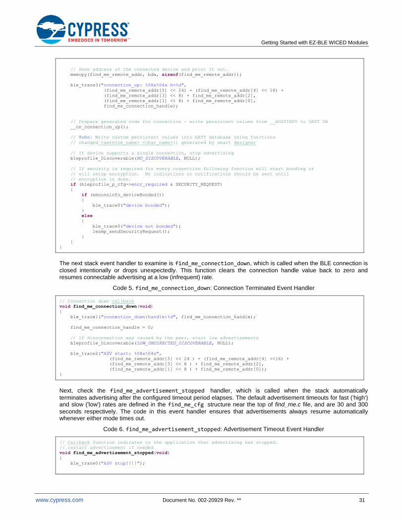
The first event handler to examine is find_me_connection_up, which is called when a new BLE connection is
established. Aside from some debug output through the module’s trace UART mechanism, this function performs the following notable operations:
1. Stores the connection handle in a global variable
2. Calls the generic __on_connection_up function (internally tests for existing bonded device entry)
3. Stops advertising to prevent additional incoming connection attempts
4. Checks encryption requirements and requested bonding as necessary
The Bluetooth Designer tool also provides some “TODO” code comments to help explain where certain customizations should go.
Code 4. find_me_connection_up: New Connection Event Handler
// Connection up callback function is called on every connection establishment
void find_me_connection_up(void)
{
find_me_connection_handle = (UINT16)emconinfo_getConnHandle();
UINT8 *bda = (UINT8 *)emconninfo_getPeerPubAddr();
Getting Started with EZ-BLE WICED Modules
www.cypress.com Document No. 002-20929 Rev. ** 31
// Save address of the connected device and print it out.
memcpy(find_me_remote_addr, bda, sizeof(find_me_remote_addr));
ble_trace3("connection_up: %08x%04x h=%d",
(find_me_remote_addr[5] << 24) + (find_me_remote_addr[4] << 16) +
(find_me_remote_addr[3] << 8) + find_me_remote_addr[2],
(find_me_remote_addr[1] << 8) + find_me_remote_addr[0],
find_me_connection_handle);
// Prepare generated code for connection - write persistent values from __HOSTINFO to GATT DB
__on_connection_up();
// ToDo: Write custom persistent values into GATT database using functions
// changed_<service_name>_<char_name>() generated by smart designer
// If device supports a single connection, stop advertising
bleprofile_Discoverable(NO_DISCOVERABLE, NULL);
// If security is required for every connection following function will start bonding or
// will setup encryption. No indications or notifications should be sent until
// encryption is done.
if (bleprofile_p_cfg->encr_required & SECURITY_REQUEST)
{
if (emconninfo_deviceBonded())
{
ble_trace0("device bonded");
}
else
{
ble_trace0("device not bonded");
lesmp_sendSecurityRequest();
}
}
}
The next stack event handler to examine is find_me_connection_down, which is called when the BLE connection is
closed intentionally or drops unexpectedly. This function clears the connection handle value back to zero and resumes connectable advertising at a low (infrequent) rate.
Code 5. find_me_connection_down: Connection Terminated Event Handler
// Connection down callback
void find_me_connection_down(void)
{
ble_trace1("connection_down:handle:%d", find_me_connection_handle);
find_me_connection_handle = 0;
// If disconnection was caused by the peer, start low advertisements
bleprofile_Discoverable(LOW_UNDIRECTED_DISCOVERABLE, NULL);
ble_trace2("ADV start: %08x%04x",
(find_me_remote_addr[5] << 24 ) + (find_me_remote_addr[4] <<16) +
(find_me_remote_addr[3] << 8 ) + find_me_remote_addr[2],
(find_me_remote_addr[1] << 8 ) + find_me_remote_addr[0]);
}
Next, check the find_me_advertisement_stopped handler, which is called when the stack automatically
terminates advertising after the configured timeout period elapses. The default advertisement timeouts for fast ('high') and slow ('low') rates are defined in the find_me_cfg structure near the top of find_me.c file, and are 30 and 300
seconds respectively. The code in this event handler ensures that advertisements always resume automatically whenever either mode times out.
Code 6. find_me_advertisement_stopped: Advertisement Timeout Event Handler
// Callback function indicates to the application that advertising has stopped.
// restart advertisement if needed
void find_me_advertisement_stopped(void)
{
ble_trace0("ADV stop!!!!");
Getting Started with EZ-BLE WICED Modules
www.cypress.com Document No. 002-20929 Rev. ** 32
// If disconnection was caused by the peer, start low advertisements
bleprofile_Discoverable(LOW_UNDIRECTED_DISCOVERABLE, NULL);
}
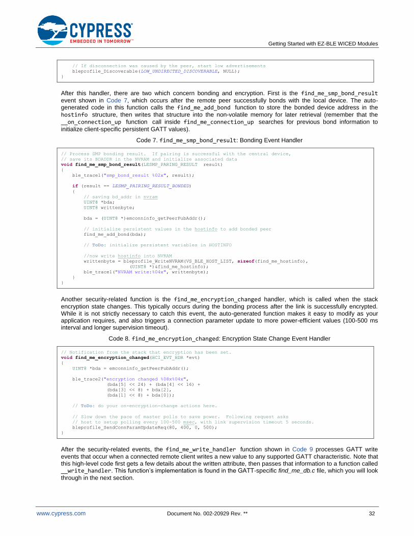
After this handler, there are two which concern bonding and encryption. First is the find_me_smp_bond_result event shown in Code 7, which occurs after the remote peer successfully bonds with the local device. The auto-generated code in this function calls the find_me_add_bond function to store the bonded device address in the
hostinfo structure, then writes that structure into the non-volatile memory for later retrieval (remember that the
__on_connection_up function call inside find_me_connection_up searches for previous bond information to
initialize client-specific persistent GATT values).
Code 7. find_me_smp_bond_result: Bonding Event Handler
// Process SMP bonding result. If pairing is successful with the central device,
// save its BDADDR in the NVRAM and initialize associated data
void find_me_smp_bond_result(LESMP_PARING_RESULT result)
{
ble_trace1("smp_bond_result %02x", result);
if (result == LESMP_PAIRING_RESULT_BONDED)
{
// saving bd_addr in nvram
UINT8 *bda;
UINT8 writtenbyte;
bda = (UINT8 *)emconninfo_getPeerPubAddr();
// initialize persistent values in the hostinfo to add bonded peer
find_me_add_bond(bda);
// ToDo: initialize persistent variables in HOSTINFO
//now write hostinfo into NVRAM
writtenbyte = bleprofile_WriteNVRAM(VS_BLE_HOST_LIST, sizeof(find_me_hostinfo),
(UINT8 *)&find_me_hostinfo);
ble_trace1("NVRAM write:%04x", writtenbyte);
}
}
Another security-related function is the find_me_encryption_changed handler, which is called when the stack
encryption state changes. This typically occurs during the bonding process after the link is successfully encrypted. While it is not strictly necessary to catch this event, the auto-generated function makes it easy to modify as your application requires, and also triggers a connection parameter update to more power-efficient values (100-500 ms interval and longer supervision timeout).
Code 8. find_me_encryption_changed: Encryption State Change Event Handler
// Notification from the stack that encryption has been set.
void find_me_encryption_changed(HCI_EVT_HDR *evt)
{
UINT8 *bda = emconninfo_getPeerPubAddr();
ble_trace2("encryption changed %08x%04x",
(bda[5] << 24) + (bda[4] << 16) +
(bda[3] << 8) + bda[2],
(bda[1] << 8) + bda[0]);
// ToDo: do your on-encryption-change actions here.
// Slow down the pace of master polls to save power. Following request asks
// host to setup polling every 100-500 msec, with link supervision timeout 5 seconds.
bleprofile_SendConnParamUpdateReq(80, 400, 0, 500);
}
After the security-related events, the find_me_write_handler function shown in Code 9 processes GATT write
events that occur when a connected remote client writes a new value to any supported GATT characteristic. Note that this high-level code first gets a few details about the written attribute, then passes that information to a function called __write_handler. This function’s implementation is found in the GATT-specific find_me_db.c file, which you will look
through in the next section.
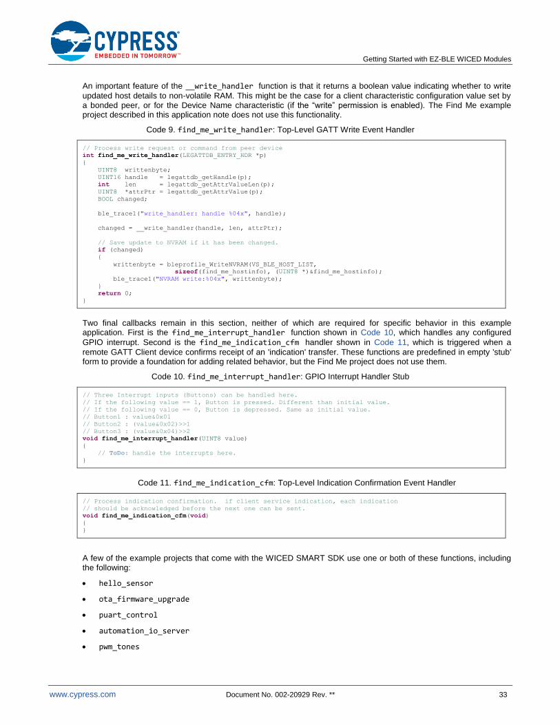
Getting Started with EZ-BLE WICED Modules
www.cypress.com Document No. 002-20929 Rev. ** 33
An important feature of the __write_handler function is that it returns a boolean value indicating whether to write
updated host details to non-volatile RAM. This might be the case for a client characteristic configuration value set by a bonded peer, or for the Device Name characteristic (if the “write” permission is enabled). The Find Me example project described in this application note does not use this functionality.
Code 9. find_me_write_handler: Top-Level GATT Write Event Handler
// Process write request or command from peer device
int find_me_write_handler(LEGATTDB_ENTRY_HDR *p)
{
UINT8 writtenbyte;
UINT16 handle = legattdb_getHandle(p);
int len = legattdb_getAttrValueLen(p);
UINT8 *attrPtr = legattdb_getAttrValue(p);
BOOL changed;
ble_trace1("write_handler: handle %04x", handle);
changed = __write_handler(handle, len, attrPtr);
// Save update to NVRAM if it has been changed.
if (changed)
{
writtenbyte = bleprofile_WriteNVRAM(VS_BLE_HOST_LIST,
sizeof(find_me_hostinfo), (UINT8 *)&find_me_hostinfo);
ble_trace1("NVRAM write:%04x", writtenbyte);
}
return 0;
}
Two final callbacks remain in this section, neither of which are required for specific behavior in this example application. First is the find_me_interrupt_handler function shown in Code 10, which handles any configured
GPIO interrupt. Second is the find_me_indication_cfm handler shown in Code 11, which is triggered when a
remote GATT Client device confirms receipt of an 'indication' transfer. These functions are predefined in empty 'stub' form to provide a foundation for adding related behavior, but the Find Me project does not use them.
Code 10. find_me_interrupt_handler: GPIO Interrupt Handler Stub
// Three Interrupt inputs (Buttons) can be handled here.
// If the following value == 1, Button is pressed. Different than initial value.
// If the following value == 0, Button is depressed. Same as initial value.
// Button1 : value&0x01
// Button2 : (value&0x02)>>1
// Button3 : (value&0x04)>>2
void find_me_interrupt_handler(UINT8 value)
{
// ToDo: handle the interrupts here.
}
Code 11. find_me_indication_cfm: Top-Level Indication Confirmation Event Handler
// Process indication confirmation. if client service indication, each indication
// should be acknowledged before the next one can be sent.
void find_me_indication_cfm(void)
{
}
A few of the example projects that come with the WICED SMART SDK use one or both of these functions, including the following:
hello_sensor
ota_firmware_upgrade
puart_control
automation_io_server
pwm_tones
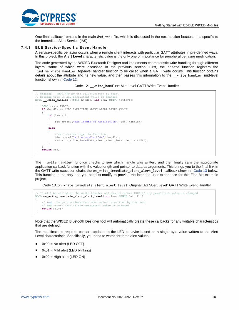
Getting Started with EZ-BLE WICED Modules
www.cypress.com Document No. 002-20929 Rev. ** 34
One final callback remains in the main find_me.c file, which is discussed in the next section because it is specific to the Immediate Alert Service (IAS).
7.4.3 BLE Service -Specif ic Event Handler
A service-specific behavior occurs when a remote client interacts with particular GATT attributes in pre-defined ways. In this project, the Alert Level characteristic value is the only one of importance for peripheral behavior modification.
The code generated by the WICED Bluetooth Designer tool implements characteristic write handling through different layers, some of which were dscussed in the previous section. First, the create function registers the
find_me_write_handler top-level handler function to be called when a GATT write occurs. This function obtains
details about the attribute and its new value, and then passes this information to the __write_handler mid-level
function shown in Code 12.
Code 12. __write_handler: Mid-Level GATT Write Event Handler
// Updates __HOSTINFO by the value written by peer.
// Returns true if any persistent value is changed
BOOL __write_handler(UINT16 handle, int len, UINT8 *attrPtr)
{
BOOL res = FALSE;
if (handle == HDLC_IMMEDIATE_ALERT_ALERT_LEVEL_VALUE)
{
if (len > 1)
{
ble_trace2("bad length:%d handle:%04x", len, handle);
}
else
{
//call custom on_write function
ble_trace1("write handle:%04x", handle);
res = on_write_immediate_alert_alert_level(len, attrPtr);
}
}
return res;
}
The __write_handler function checks to see which handle was written, and then finally calls the appropriate
application callback function with the value length and pointer to data as arguments. This brings you to the final link in the GATT write execution chain, the on_write_immediate_alert_alert_level callback shown in Code 13 below.
This function is the only one you need to modify to provide the intended user experience for this Find Me example project.
Code 13. on_write_immediate_alert_alert_level: Original IAS “Alert Level” GATT Write Event Handler
// It will be called at the write handler and should return TRUE if any persistent value is changed
BOOL on_write_immediate_alert_alert_level(int len, UINT8 *attrPtr)
{
// Todo: do your actions here when value is written by the peer
// and return TRUE if any persistent value is changed
return FALSE;
}
Note that the WICED Bluetooth Designer tool will automatically create these callbacks for any writable characteristics that are defined.
The modifications required concern updates to the LED behavior based on a single-byte value written to the Alert Level characteristic. Specifically, you need to watch for three alert values:
0x00 = No alert (LED OFF)
0x01 = Mild alert (LED blinking)
0x02 = High alert (LED ON)
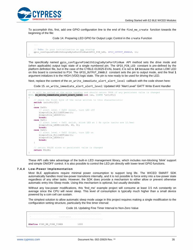
Getting Started with EZ-BLE WICED Modules
www.cypress.com Document No. 002-20929 Rev. ** 35
To accomplish this, first, add one GPIO configuration line to the end of the find_me_create function towards the
beginning of the file:
Code 14. Preparing LED GPIO for Output Logic Control in the create Function
...
// ToDo: Do your initialization on app startup
gpio_configurePinWithSingleBytePortPinNum(GPIO_PIN_LED, GPIO_OUTPUT_ENABLE, 1);
}
The specifically named gpio_configurePinWithSingleBytePortPinNum API method sets the drive mode and
(when applicable) output logic state of a single numbered pin. The GPIO_PIN_LED constant is pre-defined by the platform definition file, but in the case of the CYBLE-013025-EVAL board, it is set to 14 because the active LOW LED
on this board is connected to P14. The GPIO_OUTPUT_ENABLE constant sets the pin to output mode, and the final 1
argument initializes it to the HIGH (VDD) logic state. The pin is now ready to be used for driving the LED.
Next, replace the content of the on_write_immediate_alert_alert_level callback with the code shown here:
Code 15. on_write_immediate_alert_alert_level: Updated IAS “Alert Level” GATT Write Event Handler
// It will be called at the write handler and should return TRUE if any persistent value is changed
BOOL on_write_immediate_alert_alert_level(int len, UINT8 *attrPtr)
{
// check the first byte of the value written to this characteristic
switch (attrPtr[0])
{
case 0x00:
// alert level = 0x00 (none), turn LED off
bleprofile_KillLEDTimer();
bleprofile_LEDOff();
break;
case 0x01:
// alert level = 0x01 (mild), blink LED at 1 Hz cycle (units are 12.5ms)
bleprofile_LEDBlink(40, 40, 0);
break;
case 0x02:
// alert level = 0x02 (high), turn LED on
bleprofile_KillLEDTimer();
bleprofile_LEDOn();
break;
}
// return FALSE since no persistent value is changed
return FALSE;
}
These API calls take advantage of the built-in LED management library, which includes non-blocking 'blink' support and simple ON/OFF control. It is also possible to control the LED pin directly with lower-level GPIO functions.
7.4.4 Low-Power Implementat ion
Most BLE applications require minimal power consumption to support long life. The WICED SMART SDK automatically handles most low-power transitions internally, and it is not possible to force entry into a low-power state regardless of any other tasks. However, the SDK does provide a mechanism to either allow or prevent otherwise automatic entry into Sleep mode. Using this mechanism is optional, but usually desirable.
Without any low-power modifications, this 'find_me' example project will consume at least 3.5 mA constantly on average since the CPU will never sleep. This level of consumption is typically much higher than a small device powered by a coin cell can sustain.
The simplest solution to allow automatic sleep mode usage in this project requires making a single modification to the configuration setting structure, particularly the fine timer interval:
Code 16. Updating Fine Timer Interval to Non-Zero Value
/******************************************************
* Constants
******************************************************/
#define FIND_ME_FINE_TIMER 1000
Getting Started with EZ-BLE WICED Modules
www.cypress.com Document No. 002-20929 Rev. ** 36
#define FIND_ME_DEVICE_NAME "find_me"
#define FIND_ME_DEVICE_APPEARENCE 0
#define FIND_ME_MAIN_SERVICE_UUID UUID_SERVICE_IMMEDIATE_ALERT
The default value for this interval is 0, which effectively results in disabling sleep, even if the application does not make use of any fine timer functions (which this example does not). A value of 1000 indicates a 1-second interval (as this is measurement is miliseconds), and with this, the module can properly sleep automatically. With this configuration change, this 'find_me' example project will consume approximately the following amounts of current, on average:
1.8 mA during fast advertising (on boot, for up to 30 seconds)
106 µA during slow advertising (30 seconds after boot or immediately after disconnection)
250 µA while connected to a remote peer @ 100 ms connection interval
7.4.4.1 Managing Low-Power Operation in the Application
Sometimes, you need more control over sleep states, particularly if you are using certain peripherals. For example, the peripheral UART interface is disabled while in sleep mode, so if you need to remain awake due to expected incoming UART data, automatic sleep mode may not be suitable.
In order to manage low-power operation in your application, you will need some or all of the following APIs:
devlpm_init()
devlpm_registerForLowPowerQueries(callback, context)
devlpm_enableWakeFrom(source)
devlpm_enterLowPowerMode()
bleprofile_PrepareHidOff()
These functions enable Sleep/Deep Sleep low-power entry, wake sources, and an application-level callback, which you can use to keep the CPU from entering Sleep or Deep Sleep states. To add some additional low-power support to your project, first place the following initialization code into the find_me_create function:
Code 17. find_me_create: Application-Driven Initialization
// Create device
void find_me_create(void)
{
...
bleprofile_Init(bleprofile_p_cfg);
bleprofile_GPIOInit(bleprofile_gpio_p_cfg);
// Initialize low-power system and application control callback
devlpm_init();
devlpm_registerForLowPowerQueries(find_me_lpm_queriable, 0);
// Initialized ROM code which will monitor the battery
blebat_Init();
...
}
Next, add a new find_me_lpm_queriable callback function declaration and implementation to handle queries about
allowable sleep states:
Code 18. find_me_lpm_queriable: Application-Driven Sleep Prevention
/******************************************************
* Function Prototypes
******************************************************/
...
static void find_me_encryption_changed( HCI_EVT_HDR *evt );
static int find_me_write_handler( LEGATTDB_ENTRY_HDR *p );
Getting Started with EZ-BLE WICED Modules
www.cypress.com Document No. 002-20929 Rev. ** 37
static void find_me_interrupt_handler( UINT8 value );
UINT32 find_me_lpm_queriable(LowPowerModePollType type, UINT32 context);
...
// Callback called by the FW when ready to sleep/deep-sleep.
// Do not allow any sleep if UART transmissions are ongoing.
// Do not allow deep sleep if BLE activity is ongoing.
UINT32 find_me_lpm_queriable(LowPowerModePollType type, UINT32 context)
{
UINT32 result = 0; // assume sleep disabled
// check sleep type query
switch (type)
{
case LOW_POWER_MODE_POLL_TYPE_SLEEP:
// return 0 to prevent standard sleep, otherwise max microsecond count to allow
// (other processes may wake earlier than your specified max)
result = 0xFFFFFFFF; // max
break;
case LOW_POWER_MODE_POLL_TYPE_POWER_OFF:
// return 0 to prevent deep sleep, non-zero to allow
result = 1; // allow
break;
}
// should not reach this point since only two types of sleep exist
return result;
}
Notice the basic logic in this implementation. There are two possible types of Sleep queries; the 'sleep' type concerns standard sleep, while the 'power off' type concerns Deep Sleep (also known as HIDOFF). You should not allow standard Sleep if you need continuing UART operation, but BLE advertising and connectivity will continue to function in this state. You should not allow Deep Sleep if you need any BLE activity to continue.
Finally, to demonstrate the ultra-low-power Deep Sleep state, you can optionally make the following modification to the find_me_connection_down method so that the firmware enters Deep Sleep after the client disconnects:
Code 19. find_me_connection_down Modification: Deep Sleep After Disconnection
// Connection down callback
void find_me_connection_down(void)
{
ble_trace1("connection_down:handle:%d", find_me_connection_handle);
find_me_connection_handle = 0;
// If disconnection was caused by the peer, start low advertisements
//bleprofile_Discoverable(LOW_UNDIRECTED_DISCOVERABLE, NULL);
// If disconnection was caused by the peer, enter deep sleep mode
bleprofile_PrepareHidOff();
...
The average current while in Deep Sleep mode should be on the order of 1.5 µA.
Note that if you change the 'power off' (Deep Sleep) query result assignment to '0' in the find_me_lpm_queriable
function, the bleprofile_PrepareHidOff() API will not put the module into Deep Sleep despite being explicitly
called, because the application-level query function is still called and the result is tested before the chipset enters Deep Sleep.
The devlpm_enterLowPowerMode() API behaves similarly to this, requesting entry into standard Sleep mode when
called. However, it is often not necessary to use this function explicitly because internal power management routines will automatically attempt to enter Sleep mode as often as reasonably possible.
The devlpm_enableWakeFrom() API can be used to set up specific wake sources, such as GPIOs, to be used in
conjunction with any configured GPIO interrupts. If Sleep states do not need GPIO intervention but can be logically controlled by application code, then this API is not needed.

Getting Started with EZ-BLE WICED Modules
www.cypress.com Document No. 002-20929 Rev. ** 38
7.4.4.2 Eliminating Leakage Current
Depending on the peripheral connections present in your final hardware design, you may need to make special considerations to avoid leakage on the P0 pin (PUART TX if peripheral UART is enabled). This pin defaults to a digital-mode high-impedance “floating” state in the ROM-based initialization code, and will leak a noticeable amount of current if left unconnected in this state.
There are three basic ways to eliminate leakage on this pin:
1. Externally drive or pull the P0 pin to a known state
2. Enable peripheral UART operation in your application (PUART initialization will set P0 to digital output mode)
3. Configure P0 to a non-floating state manually in your application code
On the CYBLE-013025-EVAL board, you can pull P0 high by setting SW1 position 1 to the ON state. This will connect P0 (PUART TX) to the on-board USB-to-UART bridge IC’s RX pin, which is weakly pulled high. However, you should ensure that you do not also simultaneously set SW1 position 5 to the ON state and enable PUART operation in the application. This could potentially result in PUART TX and HCI UART TX to drive in opposite logic states, resulting in a short between VDD and GND and possibly damaging the module.
You can configure P0 to an internally pulled state by adding the following single line of code to the end of the find_me_create function:
Code 20. find_me_create Modification: Configure P0 to Known State
...
// start device advertisements. By default Advertisements will contain flags, device name,
// appearance and main service UUID.
bleprofile_Discoverable(HIGH_UNDIRECTED_DISCOVERABLE, NULL);
// ToDo: Do your initialization on app startup
gpio_configurePinWithSingleBytePortPinNum(GPIO_PIN_LED, GPIO_OUTPUT_ENABLE, 1);
gpio_configurePinWithSingleBytePortPinNum(0, GPIO_PULL_UP, 1);
}
This call to the gpio_configurePinWithSingleBytePortPinNum() API will internally pull P0 to the HIGH logic state
and eliminate leakage.
7.5 Part 3: Program the Device
This section shows how to program the EZ-BLE WICED Evaluation Board. The CYBLE-013025-00 module on this evaluation board includes a UART-based bootloader in the onboard chipset ROM, and therefore does not require an external programmer of any kind.
Note: The source project for this design is available on this application note’s webpage.
7.5.1 Host UART Interface Selection and Preparation
Host access to the HCI UART interface required for programming is available using either the built-in USB-to-UART bridge or the 4-pin J2 header on the module and an external UART device. The SW1 six-position DIP switch controls
whether the USB-to-UART bridge is connected to the HCI UART or Peripheral UART pins on the module, and therefore you must set it properly to provide the correct pin routing.
Table 5. SW1 DIP Switch Settings for Programming
Programming Interface
SW1 Positions Detail
1 2 3 4 5 6
Built-in USB-to-UART OFF OFF OFF OFF ON ON PUART disconnected, HCI UART connected
J2 and external UART any any any any OFF OFF PUART irrelevant, HCI UART disconnected
Switch positions 1, 2, 3, and 4 control the Peripheral UART connection to the USB-to-UART bridge IC on the evaluation board, while positions 5 and 6 control the HCI UART connection to the same USB-to-UART bridge IC. You should not set all six SW1 positions to ON under any circumstances, as this will directly connect both module UARTs RX and TX pairs together. This could result in a state where both TX pins are driving in opposite directions, causing an internal short between VDD and GND.
Getting Started with EZ-BLE WICED Modules
www.cypress.com Document No. 002-20929 Rev. ** 39
7.5.2 Boot Modes and Effect ive Operat ional States
Beginning from a power-on or reset, the boot sequence for the CYW20737 chipset inside the EZ-BLE WICED Module follows the process defined below:
1. Code in ROM executes and initializes the device processor, clock domains, peripherals, etc.
2. The following checks then occur:
a. The boot ROM checks for connected EEPROM and for a valid configuration, issuing several commands on the I2C pins. If no configuration or EEPROM is found via I
2C, it will check Serial Flash (SFLASH) for a valid
configuration via SPI.
b. The boot ROM calculates the checksum of the first 11 bytes of the Static Section (SS) of the non-volatile memory. If the checksum fails, it will increment through certain locations in memory until it finds a valid SS to use. If it does not find one, it will only boot from ROM. The first three bytes of the SS in use should always be 0x01 0x00 0x08. The mini-driver contained in the WICED SMART SDK will ensure that the SS section of the non-volatile memory contains the correct information.
3. The chipset then proceeds to either application mode or programming (HCI) mode depending first on the state of the HCI_UART RX pin, and secondarily on whether a valid configuration was found in the previous step:
a. If HCI_UART RX is asserted, the chipset will boot into programming (HCI) mode regardless of whether a valid configuration was found in nonvolatile memory.
b. If HCI_UART RX is not asserted and a valid configuration is found in either memory location, the Boot ROM will continue to load the rest of the configuration, patch data, and user application code from the external non-volatile memory.
c. If HCI_UART RX is not asserted and no valid configuration was found, the Boot ROM will stop executing further instructions.
To ensure that you have placed the module into the correct mode for programming, press the SW2 RESET button on the evaluation board after adjusting the DIP switch positions and/or external UART connection as described in the previous section.
7.5.3 Compil ing and Downloading into the Module
Now that you have completed the code updates and prepared the programming interface, all that remains is to compile and flash the firmware image into the target device. To do this, simply double-click on the make target that you defined previously (find_me-CYBLE_013025_EVAL download).
After a brief compile process, the Console output in the WICED SMART IDE should indicate success, as shown in Figure 26.
Figure 26. Programming the Firmware
If you do not see this success message, ensure that you have correctly connected and configured the programming interface from the host as described in the previous sections, and try downloading again. If it continues to fail, refer to the recovery steps outlined below.
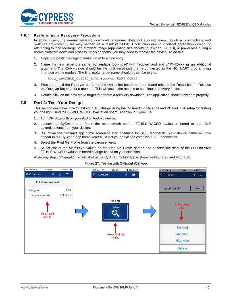
Getting Started with EZ-BLE WICED Modules
www.cypress.com Document No. 002-20929 Rev. ** 40
7.5.4 Performing a Recovery Procedure
In some cases, the normal firmware download procedure does not succeed even though all connections and switches are correct. This may happen as a result of SFLASH corruption due to incorrect application design, or attempting to load too-large of a firmware image (application size should not exceed ~26 KB), or power loss during a normal firmware download process. If this happens, you may need to recover the device. To do this:
1. Copy and paste the original make target to a new entry.
2. Name the new target the same, but replace 'download' with ’recover' and add UART=COMxx as an additional
argument. The COMxx value should be the host serial port that is connected to the HCI UART programming
interface on the module. The final make target name should be similar to this:
find_me-CYBLE_013025_EVAL recover UART=COM17
3. Press and hold the Recover button on the evaluation board, and press and release the Reset button. Release
the Recover button after a moment. This will cause the module to boot into a recovery mode.
4. Double-click on the new make target to perform a recovery download. The application should now boot properly.
7.6 Part 4: Test Your Design
This section describes how to test your BLE design using the CySmart mobile apps and PC tool. The setup for testing your design using the EZ-BLE WICED evaluation board is shown in Figure 13.
1. Turn ON Bluetooth on your iOS or Android device.
2. Launch the CySmart app. Press the reset switch on the EZ-BLE WICED evaluation board to start BLE advertisements from your design.
3. Pull down the CySmart app home screen to start scanning for BLE Peripherals. Your device name will now appear in the CySmart app home screen. Select your device to establish a BLE connection.
4. Select the Find Me Profile from the carousel view.
5. Select one of the Alert Level values on the Find Me Profile screen and observe the state of the LED on your EZ-BLE WICED evaluation board change based on your selection.
A step-by-step configuration screenshot of the CySmart mobile app is shown in Figure 27 and Figure 28.
Figure 27. Testing with CySmart iOS App
Select your device
Select Find Me Profile
Select Alert Level
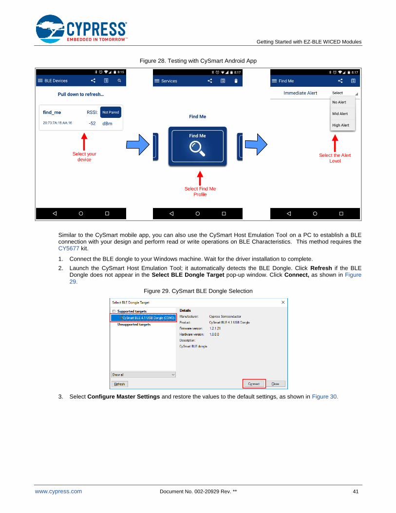
Getting Started with EZ-BLE WICED Modules
www.cypress.com Document No. 002-20929 Rev. ** 41
Figure 28. Testing with CySmart Android App
Select your device
Select Find Me Profile
Select the Alert Level
Select your device
Select Find Me Profile
Select the Alert Level
Similar to the CySmart mobile app, you can also use the CySmart Host Emulation Tool on a PC to establish a BLE connection with your design and perform read or write operations on BLE Characteristics. This method requires the CY5677 kit.
1. Connect the BLE dongle to your Windows machine. Wait for the driver installation to complete.
2. Launch the CySmart Host Emulation Tool; it automatically detects the BLE Dongle. Click Refresh if the BLE Dongle does not appear in the Select BLE Dongle Target pop-up window. Click Connect, as shown in Figure
29.
Figure 29. CySmart BLE Dongle Selection
3. Select Configure Master Settings and restore the values to the default settings, as shown in Figure 30.
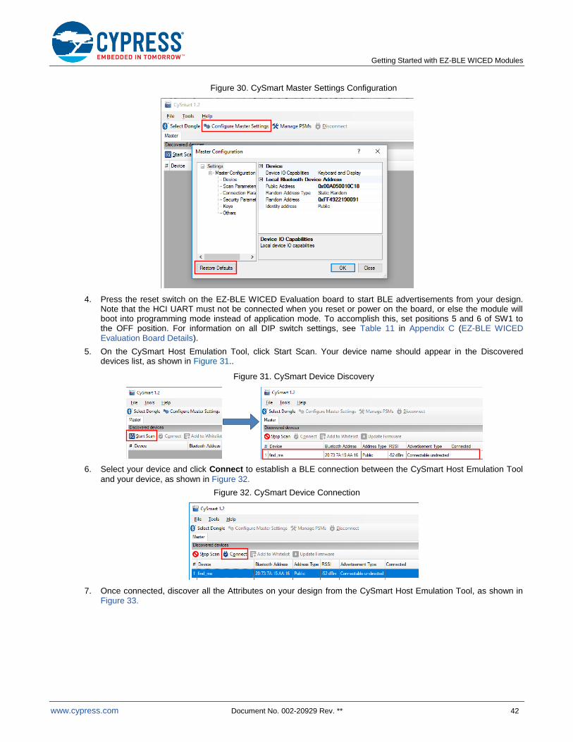
Getting Started with EZ-BLE WICED Modules
www.cypress.com Document No. 002-20929 Rev. ** 42
Figure 30. CySmart Master Settings Configuration
4. Press the reset switch on the EZ-BLE WICED Evaluation board to start BLE advertisements from your design. Note that the HCI UART must not be connected when you reset or power on the board, or else the module will boot into programming mode instead of application mode. To accomplish this, set positions 5 and 6 of SW1 to the OFF position. For information on all DIP switch settings, see Table 11 in Appendix C (EZ-BLE WICED Evaluation Board Details).
5. On the CySmart Host Emulation Tool, click Start Scan. Your device name should appear in the Discovered devices list, as shown in Figure 31..
Figure 31. CySmart Device Discovery
6. Select your device and click Connect to establish a BLE connection between the CySmart Host Emulation Tool
and your device, as shown in Figure 32.
Figure 32. CySmart Device Connection
7. Once connected, discover all the Attributes on your design from the CySmart Host Emulation Tool, as shown in Figure 33.
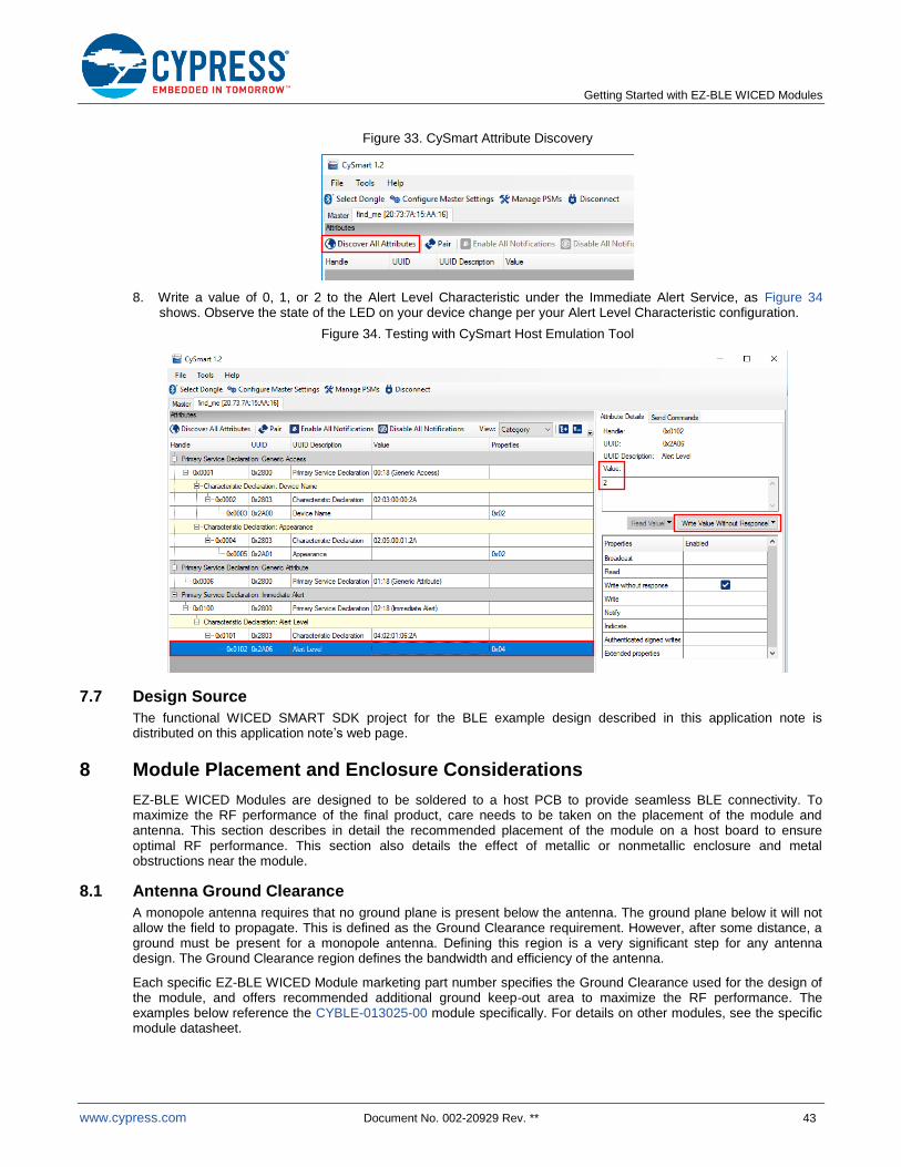
Getting Started with EZ-BLE WICED Modules
www.cypress.com Document No. 002-20929 Rev. ** 43
Figure 33. CySmart Attribute Discovery
8. Write a value of 0, 1, or 2 to the Alert Level Characteristic under the Immediate Alert Service, as Figure 34 shows. Observe the state of the LED on your device change per your Alert Level Characteristic configuration.
Figure 34. Testing with CySmart Host Emulation Tool
7.7 Design Source
The functional WICED SMART SDK project for the BLE example design described in this application note is distributed on this application note’s web page.
8 Module Placement and Enclosure Considerations
EZ-BLE WICED Modules are designed to be soldered to a host PCB to provide seamless BLE connectivity. To maximize the RF performance of the final product, care needs to be taken on the placement of the module and antenna. This section describes in detail the recommended placement of the module on a host board to ensure optimal RF performance. This section also details the effect of metallic or nonmetallic enclosure and metal obstructions near the module.
8.1 Antenna Ground Clearance
A monopole antenna requires that no ground plane is present below the antenna. The ground plane below it will not allow the field to propagate. This is defined as the Ground Clearance requirement. However, after some distance, a ground must be present for a monopole antenna. Defining this region is a very significant step for any antenna design. The Ground Clearance region defines the bandwidth and efficiency of the antenna.
Each specific EZ-BLE WICED Module marketing part number specifies the Ground Clearance used for the design of the module, and offers recommended additional ground keep-out area to maximize the RF performance. The examples below reference the CYBLE-013025-00 module specifically. For details on other modules, see the specific module datasheet.
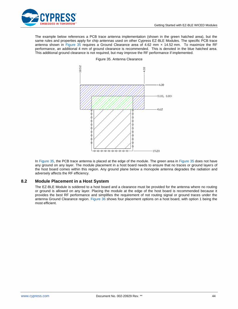
Getting Started with EZ-BLE WICED Modules
www.cypress.com Document No. 002-20929 Rev. ** 44
The example below references a PCB trace antenna implementation (shown in the green hatched area), but the same rules and properties apply for chip antennas used on other Cypress EZ-BLE Modules. The specific PCB trace antenna shown in Figure 35 requires a Ground Clearance area of 4.62 mm × 14.52 mm. To maximize the RF performance, an additional 4 mm of ground clearance is recommended. This is denoted in the blue hatched area. This additional ground clearance is not required, but may improve the RF performance if implemented.
Figure 35. Antenna Clearance
In Figure 35, the PCB trace antenna is placed at the edge of the module. The green area in Figure 35 does not have any ground on any layer. The module placement in a host board needs to ensure that no traces or ground layers of the host board comes within this region. Any ground plane below a monopole antenna degrades the radiation and adversely affects the RF efficiency.
8.2 Module Placement in a Host System
The EZ-BLE Module is soldered to a host board and a clearance must be provided for the antenna where no routing or ground is allowed on any layer. Placing the module at the edge of the host board is recommended because it provides the best RF performance and simplifies the requirement of not routing signal or ground traces under the antenna Ground Clearance region. Figure 36 shows four placement options on a host board, with option 1 being the most efficient.

Getting Started with EZ-BLE WICED Modules
www.cypress.com Document No. 002-20929 Rev. ** 45
Figure 36. Module Placement in a Host Board
Figure 36 shows an example of four positions of the module in a host board, “1”, “2”, “3”, and “4”. The white area shown around the module is the additional clearance area. For the antenna in question, it is recommended to provide a clearance area of 4 mm in each direction. For details on the recommended clearance area for your EZ-BLE Module, see the specific module datasheet.
As can be seen in Figure 36, when placing the module at the edge (placement options “1” or “3”) of the host board, the additional clearance area is only required facing inwards towards the center of the main board. In all cases, there must be no possibility of signal or ground traces to be beneath the antenna Ground Clearance region. Conversely, if the module is placed in the middle (placement option “2”) of the host board, the clearance area must be provided in order to achieve an optimal RF performance.
Placement option “1” or “3” are the best options shown in Figure 36, because it removes the need to reroute signal or ground traces away from the Ground Clearance region of the module (because no GPIO are located at the top left or right corner of the module). Furthermore, it minimizes additional clearance area if optimal RF performance is desired, because the antenna faces outward with the antenna exposed to open space.
In placement option “4”, although the module is placed at the edge of the host board, the antenna is not exposed to the maximum amount of free space.
Placement option “2” not only wastes PCB real estate, but also provides diminished RF performance compared to position “1” and “3”.
8.3 Enclosure Effects on Antenna Performance
Antennas used in consumer products are sensitive to the PCB RF ground size, the product’s plastic casing, and metallic enclosures. This section describes the effect of each of these environmental factors on RF performance.
8.3.1 Antenna Near-Fie ld and Far-Field
Every antenna contains two regions surrounding it: 1) the near-field and 2) the far-field.
The near-field is the region where the radiated field has not yet formed. In this region, the electric and magnetic fields are not orthogonal to each other. This region is very close to the antenna. The near-field region has two regions: the reactive near-field region and the radiating near-field region. The transition to a far-field region happens in the radiating near-field region.
Shield
4 mm 4 mm
4 mm
Clearance Region outside of module
4 mm
4 mm
4 mm
Ground Clearance Region
4 mm

Getting Started with EZ-BLE WICED Modules
www.cypress.com Document No. 002-20929 Rev. ** 46
The radiation field is formed after the transition to the far-field region. In this region, the relative angular variation of the field does not depend on the distance. This means that if you plot the angular radiation field at a distance from the antenna in the far-field region, their shapes remain the same. Only with distance, the field strength decreases. However, the shape of the radiation pattern remains the same with respect to the angular variation. This region is called the far-field region. An object in the far field does not affect the radiation pattern much. However, any obstruction in the near-field can completely change the radiation pattern. If the obstruction is metal, the effect on the radiation pattern is much more pronounced. Figure 37 shows the regions for a dipole antenna.
Figure 37. Near and Far Field
For a module based on a 2.4-GHz chip antenna, the near-field extends up to 4 mm.
8.3.2 Effect of Nonmeta l l ic Enclosure
Any plastic enclosure changes the resonating frequency of the antenna. The antenna can be modeled as an LC resonator whose resonant frequency decreases when either L (inductance) or C (capacitance) increases. A larger RF ground plane and plastic casing increase the effective capacitance and thus reduce the resonant frequency. See the application note AN91445 for more details on the effect of an enclosure.
Figure 38 details a module antenna in a plastic enclosure. The clearance from the antenna to the plastic enclosure can be as little as 2 mm. However, clearance of this amount can affect the tuning of the antenna. This can be resolved by retuning the antenna; however for a module solution, it is not recommended to attempt retuning of the antenna. To minimize effects on the module antenna, it is recommended to have a minimum clearance of 5 mm.
Figure 38. EZ-BLE WICED Module Inside of a Plastic Mouse Enclosure
8.3.3 Effect of Meta l l ic Objects
An antenna is sensitive to the presence of metallic objects in its vicinity. A metallic object shorts the electric field and thus changes the radiation field. Depending on the size of the obstruction, electromagnetic waves go through different diffraction patterns or may be completely shielded by the metallic object.
5 mm
Dipole Antenna With length D

Getting Started with EZ-BLE WICED Modules
www.cypress.com Document No. 002-20929 Rev. ** 47
Metallic objects in the near-field can have a drastic impact on the radiation pattern. The thickness of the CYBLE-013025-00 module is 2.25 mm (including the shield) and the near field of this module extends up to 4 mm from the antenna. Therefore, it is recommended that any metallic obstruction be at least 6.2 mm away from the PCB plane to avoid negative effects to the RF performance. Cypress recommends an 8-mm gap from the module PCB plane to any metallic enclosure. Figure 39 details the required clearance from the EZ-BLE WICED Module to small metal obstructions.
Figure 39. Clearance from Small Metal Obstructions
8.3.4 Recommendations for Placement over a Large Metal Plane
The other effect of metal is the formation of an image antenna. The best practice in this case is to orient the metal orthogonal to the antenna to ensure minimum effects. If the length or width of the plane approaches the size of the module, it is considered a large metal object near the antenna. Figure 40 details two placement options for this scenario. Of these two placement options, option “1” should be avoided.
It is recommended to not have any large metallic objects parallel to the antenna. This has a drastic effect because the image antenna is of opposite polarity. The interference caused by such an antenna is destructive to RF radiation.
If it is not possible to avoid a large metallic object running parallel to the module plane, you should maintain a distance (h) of at least 30 mm. This will ensure that the interference caused by the image antenna will not be completely destructive. The radiation will be strongly directional below the 30-mm distance; the efficiency will dramatically drop at a distance (h) below 8 mm. At a distance (h) of around 2 mm, the radiation efficiency can go below 20%.
Figure 40. Clearance from a Large Metal Plane
8.4 Guidelines for Enclosures and Ground Plane
Use the following best practices with respect to enclosure design and ground planes:
Ensure that there is no component, mounting screw or ground plane near the tip or the length of the antenna located on the EZ-BLE WICED Module.
Ensure that no battery cable, microphone cable, or trace crosses the antenna trace on the PCB.
Ensure that the antenna is not completely covered by a metallic enclosure. If the product has a metallic casing or shield, the casing should not cover the antenna. No metal is allowed in the antenna near the field.
Module
Conducting plate
(1) (2)
h
Module
8 mm
6.2 mm

Getting Started with EZ-BLE WICED Modules
www.cypress.com Document No. 002-20929 Rev. ** 48
Ensure that paint on plastic enclosures is nonmetallic near the antenna.
Ensure that the orientation of the antenna is in-line with the final product orientation (if possible) so that radiation is maximized in the desired direction. The polarization and position of the receive antenna should be taken into account so that the module can be oriented to maximize the radiation.
Ensure that there is no ground directly below the antenna Ground Clearance region of the module.

Getting Started with EZ-BLE WICED Modules
www.cypress.com Document No. 002-20929 Rev. ** 49
9 Manufacturing with EZ-BLE WICED Modules
EZ-BLE WICED Modules are intended to be used with traditional Surface Mount Technology (SMT) manufacturing lines and are compatible with industry-standard reflow profiles for Pb-free solders.
9.1 SMT Manufacturing Pick-and-Place
The modules should be picked up from the topside of the module using industry-standard pick-and-place machinery and nozzles. The ideal location for picking up the module is on the shield area of the module. For the optimal location for your EZ-BLE WICED Module, see the module’s datasheet.
Each module MPN has a unique center-of-mass detailed in each product’s datasheet. This center-of-mass is the area that represents the optimal location to pick up the unit with the nozzle. Using the center-of-mass guidelines for the pick-and-place location minimizes SMT line disturbances caused by units releasing prematurely from the nozzle.
Figure 41 shows an image of a nozzle used by Cypress for manufacturing the CYBLE-013025-EVAL Evaluation Board product. See the center-of-mass dimensions in each module’s datasheet to select an appropriate nozzle for your manufacturing line equipment.
Figure 41. Nozzle Used by Cypress for Evaluation Board Production
Figure 42 shows an image of a Cypress EZ-BLE Module being picked up at the center-of-mass by the nozzle referenced above.
Figure 42. Image of Nozzle Used by Cypress for Evaluation Board Production
9.2 Manufacturing Solder Reflow
EZ-BLE WICED Modules are compatible with industry-standard reflow profiles for Pb-free solder. Table 6 details the solder reflow specifications for all modules.
Table 6. EZ-BLE WICED Module Solder Reflow Specification
Module Package Maximum Peak Temperature Time at Maximum Temperature
All Packages 260 oC 30 seconds

Getting Started with EZ-BLE WICED Modules
www.cypress.com Document No. 002-20929 Rev. ** 50
10 Summary
This application note explores the EZ-BLE WICED Module solutions, architectures, development tools, host board placement and orientation, and production manufacturing. EZ-BLE WICED Modules are fully integrated BLE solutions that allow rapid development and production release for customer applications. The core of the EZ-BLE WICED Modules is the Cypress WICED Bluetooth Smart ICs, integrating the Bluetooth radio, analog and digital peripheral functions, memory, and an ARM Cortex-M3 microcontroller. The Cypress EZ-BLE Module family provides multiple module options to service the needs of any customer application.
11 Related Application Notes
AN91445 – Antenna Design Guide
AN96841 – Getting Started With EZ-BLE Creator Modules
About the Author Name: David Solda (DSO)
Title: Senior Business Unit Director
Background: David Solda has a BS in Computer/Electrical Engineering, a BS in Mathematics, and an MBA from Santa Clara University, California.

Getting Started with EZ-BLE WICED Modules
www.cypress.com Document No. 002-20929 Rev. ** 51
Appendix A. Cypress Terms of Art
This section lists the most commonly used terms that you might hear while working with Cypress’s PSoC family of devices.
PSoC – PSoC is a programmable, embedded design platform that includes a CPU, such as the 32-bit ARM Cortex-
M0, with both analog and digital programmable blocks. It accelerates embedded system design with reliable, easy-to-use solutions, such as touch sensing and enables low-power designs.
PRoC BLE – PRoC BLE is a 32-bit, 48-MHz ARM Cortex-M0 BLE solution with CapSense, 12-bit ADC, four timers,
counters, pulse-width modulators (TCPWM), thirty-six GPIOs, two serial communication blocks (SCBs), LCD, and I2S. PRoC BLE includes a royalty-free BLE stack compatible with Bluetooth 4.1 and provides a complete, programmable, and flexible solution for HID, remote controls, toys, beacons, and wireless chargers. In addition to these applications, PRoC BLE provides a simple, low-cost way to add BLE connectivity to any system.
PSoC 4 BLE – A PSoC 4 IC with an integrated BLE radio that includes a royalty-free BLE protocol stack compatible
with the Bluetooth 4.1 or 4.2 specifications.
EZ-BLE™
PRoC Module (EZ-BLE PRoC) – EZ-BLE PRoC Module is a fully integrated, fully certified, 10 mm × 10
mm × 1.8 mm, programmable, Bluetooth Smart or Bluetooth Low Energy (BLE) module designed for ease-of-use and reducing time-to-market. It contains Cypress’s PRoC BLE chip, two crystals, chip antenna, shield and passive components. EZ-BLE PRoC Module provides a simple and low cost way to add a microcontroller, CapSense touch controller and Bluetooth Smart connectivity to any system.
EZ-BLE™
PSoC Module (EZ-BLE PSoC) – An integrated, easy-to-use, fully certified Bluetooth Smart module
designed to reduce time-to-market and development cost. Contains PSoC 4 BLE, two crystals, an antenna and passive components.
EZ-BLE™ WICED Module (EZ-BLE WICED) - EZ-BLE WICED Modules are fully integrated, fully certified, Bluetooth
Smart or Bluetooth Low Energy (BLE) module designed for ease-of-use and reducing time-to-market. It contains Cypress’s WICED BLE chip, one crystal, PCB trace antenna, shield and passive components. EZ-BLE WICED Module provides a simple and low cost way to add a microcontroller and Bluetooth Smart connectivity to any system.
EZ-BT™ WICED Modules (EZ-BT WICED) - EZ-BT WICED Modules are fully integrated, fully certified, Bluetooth
Smart Ready (Bluetooth Basic Rate, Enhanced Data Rate, and Bluetooth Low-Energy) modules designed for ease-of-use and reducing time-to-market. They contain Cypress’ WICED dual-mode chip, one crystal, PCB trace antenna, shield and passive components. EZ-BT WICED Modules provide a simple and low-cost way to add a microcontroller and Bluetooth Smart Ready connectivity to any system.
PSoC Creator™
– PSoC 3, PSoC 4, and PSoC 5LP Integrated Design Environment (IDE) software that installs on
your PC and allows concurrent hardware and firmware design of PSoC systems, or hardware design followed by export to other popular IDEs.
WICED SMART SDK – Cypress' WICED (Wireless Connectivity for Embedded Devices) is a full-featured platform
with proven Software Development Kits (SDKs) and turnkey hardware solutions from partners to readily enable Wi-Fi and Bluetooth connectivity in system design.

Getting Started with EZ-BLE WICED Modules
www.cypress.com Document No. 002-20929 Rev. ** 52
Appendix B. EZ-BLE WICED Module Product Details
The information contained for each module part number includes the following:
Physical image for each EZ-BLE WICED Module marketing part number
Pinout and functionality for each EZ-BLE WICED Module marketing part number
Recommended host PCB layout footprint for each EZ-BLE WICED Module marketing part number
Recommended additional clearance area for each EZ-BLE WICED Module marketing part number
To jump to your specific EZ-BLE WICED Module, click the marketing part number in the below list:
CYBLE-0130XX-00
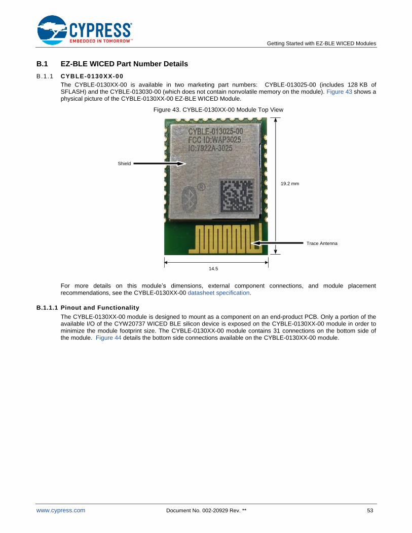
Getting Started with EZ-BLE WICED Modules
www.cypress.com Document No. 002-20929 Rev. ** 53
B.1 EZ-BLE WICED Part Number Details
B.1.1 CYBLE-0130XX-00
The CYBLE-0130XX-00 is available in two marketing part numbers: CYBLE-013025-00 (includes 128 KB of SFLASH) and the CYBLE-013030-00 (which does not contain nonvolatile memory on the module). Figure 43 shows a physical picture of the CYBLE-0130XX-00 EZ-BLE WICED Module.
Figure 43. CYBLE-0130XX-00 Module Top View
For more details on this module’s dimensions, external component connections, and module placement recommendations, see the CYBLE-0130XX-00 datasheet specification.
B.1.1.1 Pinout and Functionality
The CYBLE-0130XX-00 module is designed to mount as a component on an end-product PCB. Only a portion of the available I/O of the CYW20737 WICED BLE silicon device is exposed on the CYBLE-0130XX-00 module in order to minimize the module footprint size. The CYBLE-0130XX-00 module contains 31 connections on the bottom side of the module. Figure 44 details the bottom side connections available on the CYBLE-0130XX-00 module.
14.5 mm
Shield
Trace Antenna
19.2 mm
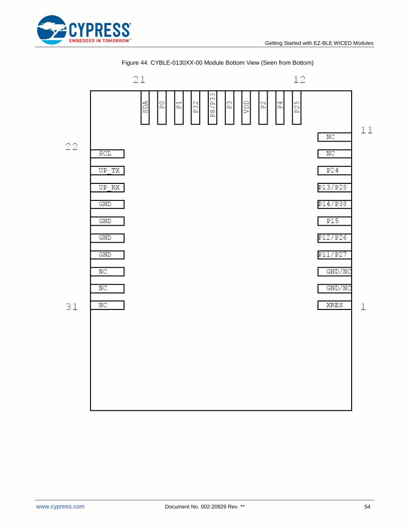
Getting Started with EZ-BLE WICED Modules
www.cypress.com Document No. 002-20929 Rev. ** 54
Figure 44. CYBLE-0130XX-00 Module Bottom View (Seen from Bottom)
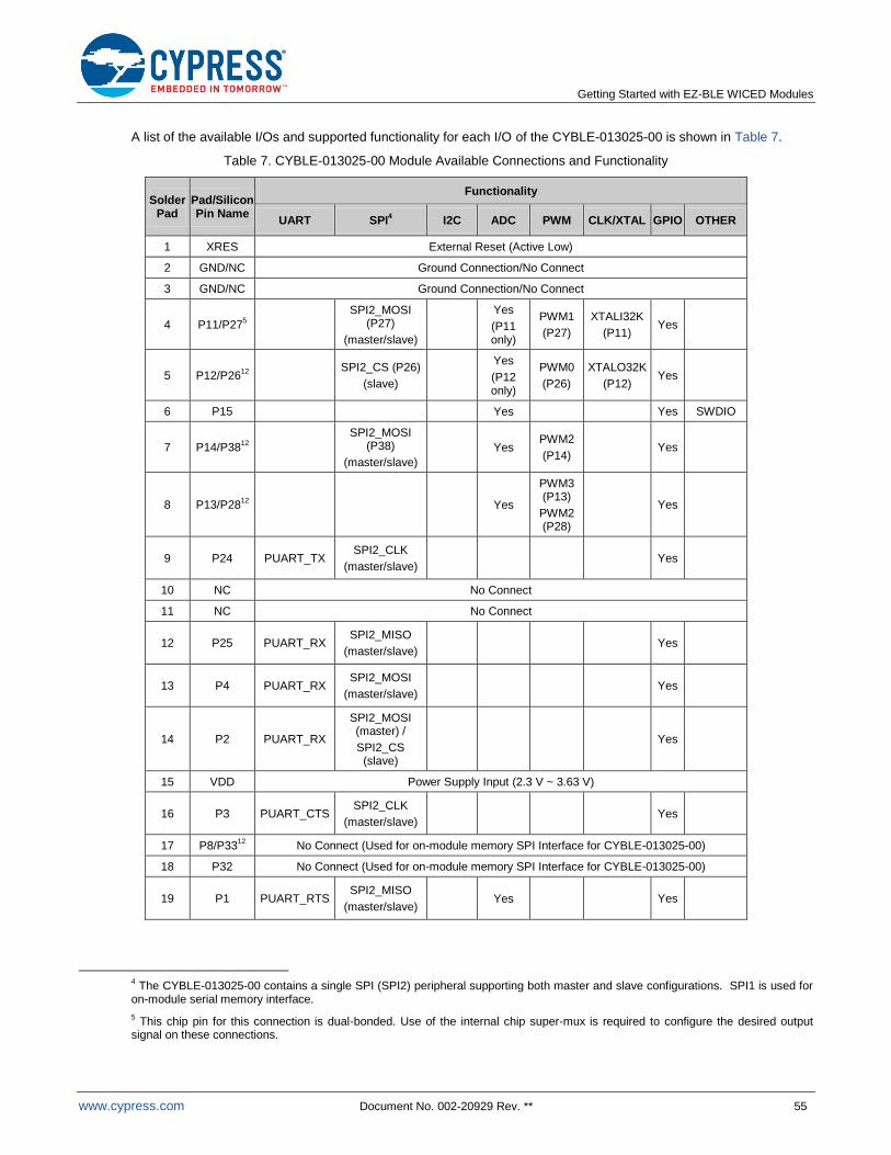
Getting Started with EZ-BLE WICED Modules
www.cypress.com Document No. 002-20929 Rev. ** 55
A list of the available I/Os and supported functionality for each I/O of the CYBLE-013025-00 is shown in Table 7.
Table 7. CYBLE-013025-00 Module Available Connections and Functionality
Solder Pad
Pad/Silicon Pin Name
Functionality
UART SPI4 I2C ADC PWM CLK/XTAL GPIO OTHER
1 XRES External Reset (Active Low)
2 GND/NC Ground Connection/No Connect
3 GND/NC Ground Connection/No Connect
4 P11/P275
SPI2_MOSI (P27)
(master/slave)
Yes
(P11 only)
PWM1
(P27)
XTALI32K
(P11) Yes
5 P12/P2612
SPI2_CS (P26)
(slave)
Yes
(P12 only)
PWM0
(P26)
XTALO32K
(P12) Yes
6 P15 Yes Yes SWDIO
7 P14/P3812
SPI2_MOSI (P38)
(master/slave)
Yes PWM2
(P14) Yes
8 P13/P2812
Yes
PWM3 (P13)
PWM2 (P28)
Yes
9 P24 PUART_TX SPI2_CLK
(master/slave) Yes
10 NC No Connect
11 NC No Connect
12 P25 PUART_RX SPI2_MISO
(master/slave) Yes
13 P4 PUART_RX SPI2_MOSI
(master/slave) Yes
14 P2 PUART_RX
SPI2_MOSI (master) /
SPI2_CS (slave)
Yes
15 VDD Power Supply Input (2.3 V ~ 3.63 V)
16 P3 PUART_CTS SPI2_CLK
(master/slave) Yes
17 P8/P3312
No Connect (Used for on-module memory SPI Interface for CYBLE-013025-00)
18 P32 No Connect (Used for on-module memory SPI Interface for CYBLE-013025-00)
19 P1 PUART_RTS SPI2_MISO
(master/slave) Yes Yes
4 The CYBLE-013025-00 contains a single SPI (SPI2) peripheral supporting both master and slave configurations. SPI1 is used for
on-module serial memory interface.
5 This chip pin for this connection is dual-bonded. Use of the internal chip super-mux is required to configure the desired output
signal on these connections.
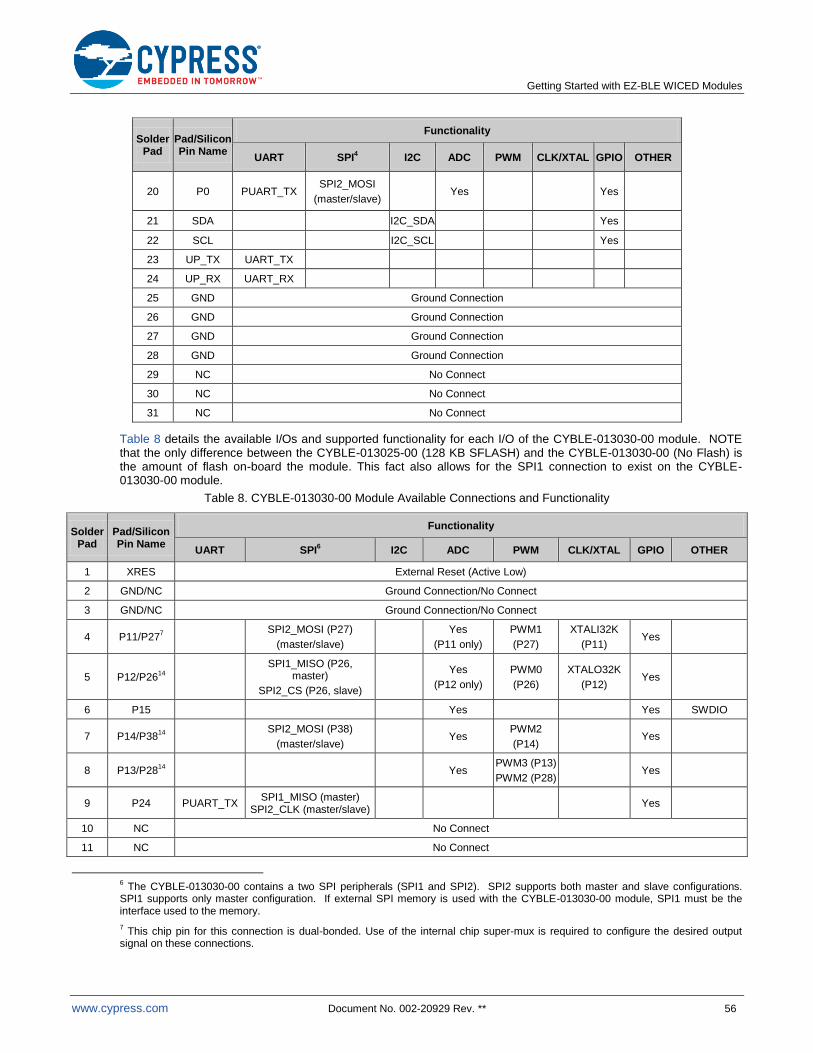
Getting Started with EZ-BLE WICED Modules
www.cypress.com Document No. 002-20929 Rev. ** 56
Solder Pad
Pad/Silicon Pin Name
Functionality
UART SPI4 I2C ADC PWM CLK/XTAL GPIO OTHER
20 P0 PUART_TX SPI2_MOSI
(master/slave) Yes Yes
21 SDA I2C_SDA Yes
22 SCL I2C_SCL Yes
23 UP_TX UART_TX
24 UP_RX UART_RX
25 GND Ground Connection
26 GND Ground Connection
27 GND Ground Connection
28 GND Ground Connection
29 NC No Connect
30 NC No Connect
31 NC No Connect
Table 8 details the available I/Os and supported functionality for each I/O of the CYBLE-013030-00 module. NOTE that the only difference between the CYBLE-013025-00 (128 KB SFLASH) and the CYBLE-013030-00 (No Flash) is the amount of flash on-board the module. This fact also allows for the SPI1 connection to exist on the CYBLE-013030-00 module.
Table 8. CYBLE-013030-00 Module Available Connections and Functionality
Solder Pad
Pad/Silicon Pin Name
Functionality
UART SPI6 I2C ADC PWM CLK/XTAL GPIO OTHER
1 XRES External Reset (Active Low)
2 GND/NC Ground Connection/No Connect
3 GND/NC Ground Connection/No Connect
4 P11/P277
SPI2_MOSI (P27)
(master/slave)
Yes
(P11 only)
PWM1
(P27)
XTALI32K
(P11) Yes
5 P12/P2614
SPI1_MISO (P26, master)
SPI2_CS (P26, slave)
Yes
(P12 only)
PWM0
(P26)
XTALO32K
(P12) Yes
6 P15 Yes Yes SWDIO
7 P14/P3814
SPI2_MOSI (P38)
(master/slave) Yes
PWM2
(P14) Yes
8 P13/P2814
Yes PWM3 (P13)
PWM2 (P28) Yes
9 P24 PUART_TX SPI1_MISO (master)
SPI2_CLK (master/slave) Yes
10 NC No Connect
11 NC No Connect
6 The CYBLE-013030-00 contains a two SPI peripherals (SPI1 and SPI2). SPI2 supports both master and slave configurations.
SPI1 supports only master configuration. If external SPI memory is used with the CYBLE-013030-00 module, SPI1 must be the interface used to the memory.
7 This chip pin for this connection is dual-bonded. Use of the internal chip super-mux is required to configure the desired output
signal on these connections.
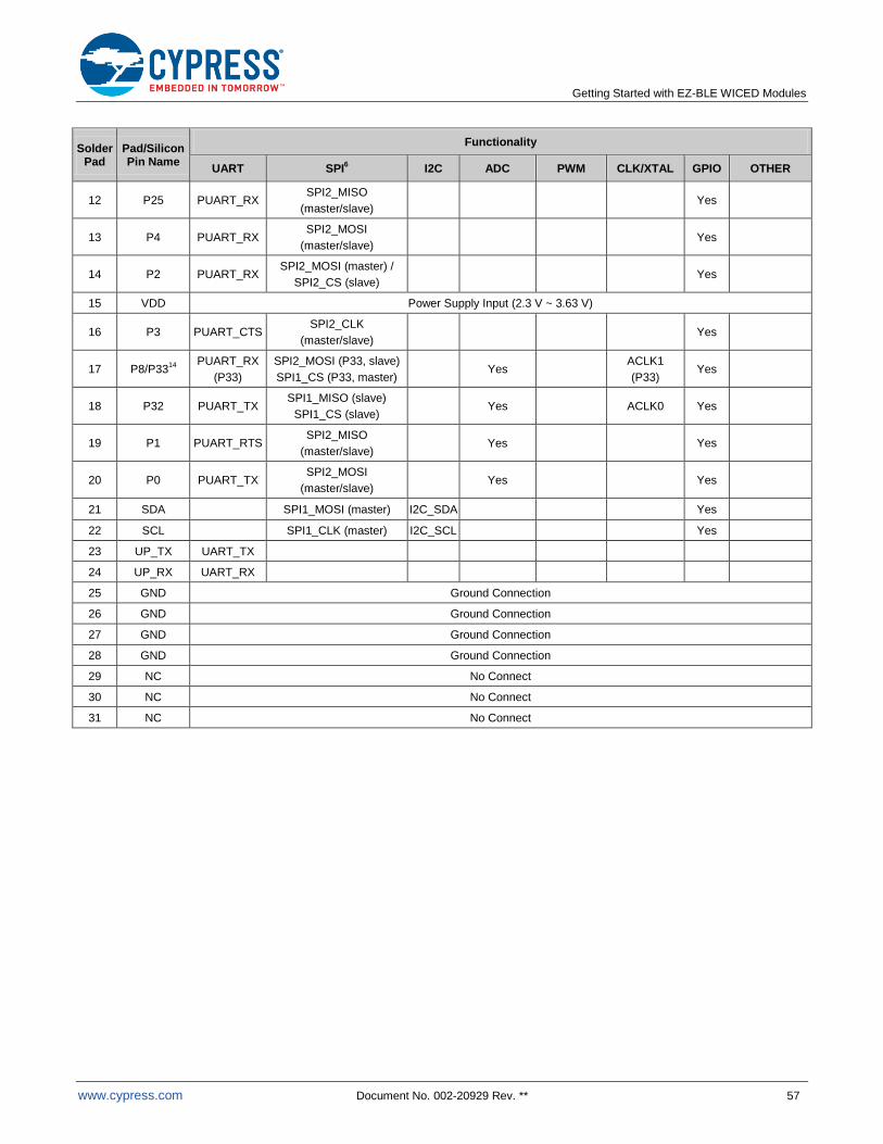
Getting Started with EZ-BLE WICED Modules
www.cypress.com Document No. 002-20929 Rev. ** 57
Solder Pad
Pad/Silicon Pin Name
Functionality
UART SPI6 I2C ADC PWM CLK/XTAL GPIO OTHER
12 P25 PUART_RX SPI2_MISO
(master/slave) Yes
13 P4 PUART_RX SPI2_MOSI
(master/slave) Yes
14 P2 PUART_RX SPI2_MOSI (master) /
SPI2_CS (slave) Yes
15 VDD Power Supply Input (2.3 V ~ 3.63 V)
16 P3 PUART_CTS SPI2_CLK
(master/slave) Yes
17 P8/P3314
PUART_RX
(P33)
SPI2_MOSI (P33, slave)
SPI1_CS (P33, master) Yes
ACLK1
(P33) Yes
18 P32 PUART_TX SPI1_MISO (slave)
SPI1_CS (slave) Yes ACLK0 Yes
19 P1 PUART_RTS SPI2_MISO
(master/slave) Yes Yes
20 P0 PUART_TX SPI2_MOSI
(master/slave) Yes Yes
21 SDA SPI1_MOSI (master) I2C_SDA Yes
22 SCL SPI1_CLK (master) I2C_SCL Yes
23 UP_TX UART_TX
24 UP_RX UART_RX
25 GND Ground Connection
26 GND Ground Connection
27 GND Ground Connection
28 GND Ground Connection
29 NC No Connect
30 NC No Connect
31 NC No Connect
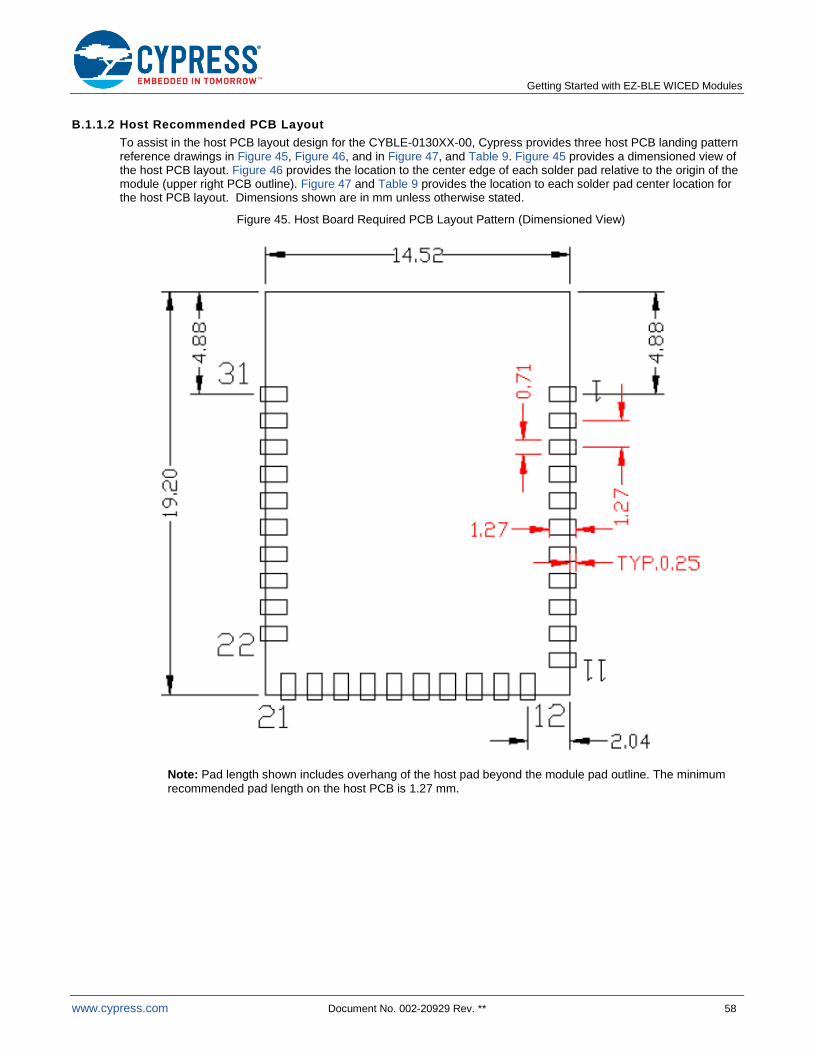
Getting Started with EZ-BLE WICED Modules
www.cypress.com Document No. 002-20929 Rev. ** 58
B.1.1.2 Host Recommended PCB Layout
To assist in the host PCB layout design for the CYBLE-0130XX-00, Cypress provides three host PCB landing pattern reference drawings in Figure 45, Figure 46, and in Figure 47, and Table 9. Figure 45 provides a dimensioned view of the host PCB layout. Figure 46 provides the location to the center edge of each solder pad relative to the origin of the module (upper right PCB outline). Figure 47 and Table 9 provides the location to each solder pad center location for the host PCB layout. Dimensions shown are in mm unless otherwise stated.
Figure 45. Host Board Required PCB Layout Pattern (Dimensioned View)
Note: Pad length shown includes overhang of the host pad beyond the module pad outline. The minimum
recommended pad length on the host PCB is 1.27 mm.
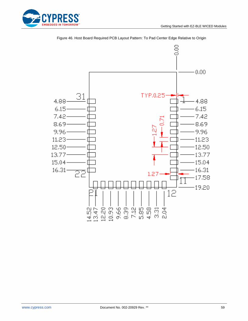
Getting Started with EZ-BLE WICED Modules
www.cypress.com Document No. 002-20929 Rev. ** 59
Figure 46. Host Board Required PCB Layout Pattern: To Pad Center Edge Relative to Origin
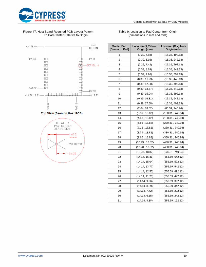
Getting Started with EZ-BLE WICED Modules
www.cypress.com Document No. 002-20929 Rev. ** 60
Figure 47. Host Board Required PCB Layout Pattern To Pad Center Relative to Origin
Table 9. Location to Pad Center from Origin (dimensions in mm and mils)
Solder Pad (Center of Pad)
Location (X,Y) from Origin (mm)
Location (X,Y) from Origin (mils)
1 (0.39, 4.88) (15.35, 192.13)
2 (0.39, 6.15) (15.35, 242.13)
3 (0.39, 7.42) (15.35, 292.13)
4 (0.39, 8.69) (15.35, 342.13)
5 (0.39, 9.96) (15.35, 392.13)
6 (0.39, 11.23) (15.35, 442.13)
7 (0.39, 12.50) (15.35, 492.13)
8 (0.39, 13.77) (15.35, 542.13)
9 (0.39, 15.04) (15.35, 592.13)
10 (0.39, 16.31) (15.35, 642.13)
11 (0.39, 17.58) (15.35, 492.13)
12 (2.04, 18.82) (80.31, 740.94)
13 (3.31 , 18.82) (130.31 , 740.94)
14 (4.58 , 18.82) (180.31 , 740.94)
15 (5.85 , 18.82) (230.31 , 740.94)
16 (7.12 , 18.82) (280.31 , 740.94)
17 (8.39 , 18.82) (330.31 , 740.94)
18 (9.66 , 18.82) (380.31 , 740.94)
19 (10.93 , 18.82) (430.31 , 740.94)
20 (12.20 , 18.82) (480.31 , 740.94)
21 (13.47, 18.82) (530.31, 740.94)
22 (14.14, 16.31) (556.69, 642.12)
23 (14.14, 15.04) (556.69, 592.12)
24 (14.14, 13.77) (556.69, 542.12)
25 (14.14, 12.50) (556.69, 492.12)
26 (14.14, 11.23) (556.69, 442.12)
27 (14.14, 9.96) (556.69, 392.12)
28 (14.14, 8.69) (556.69, 342.12)
29 (14.14, 7.42) (556.69, 292.12)
30 (14.14, 6.15) (556.69, 242.12)
31 (14.14, 4.88) (556.69, 192.12)

Getting Started with EZ-BLE WICED Modules
www.cypress.com Document No. 002-20929 Rev. ** 61
Figure 48 below details additional host board keep out area to achieve optimal RF performance with the CYBLE-0130XX-00 module (denoted in blue hatched area).
Figure 48. Host Board Additional Keep Out Area for Optimal RF Performance
Getting Started with EZ-BLE WICED Modules
www.cypress.com Document No. 002-20929 Rev. ** 62
Appendix C. EZ-BLE WICED Evaluation Board Details
Appendix C provides detailed information on each EZ-BLE WICED Evaluation Boards. The information contained for each subsection below includes the following:
Physical image for each EZ-BLE WICED Evaluation marketing part number
What’s included on the specific EZ-BLE WICED Evaluation board
To jump to your specific EZ-BLE WICED Evaluation board, click the marketing part number in the below list:
CYBLE-013025-EVAL
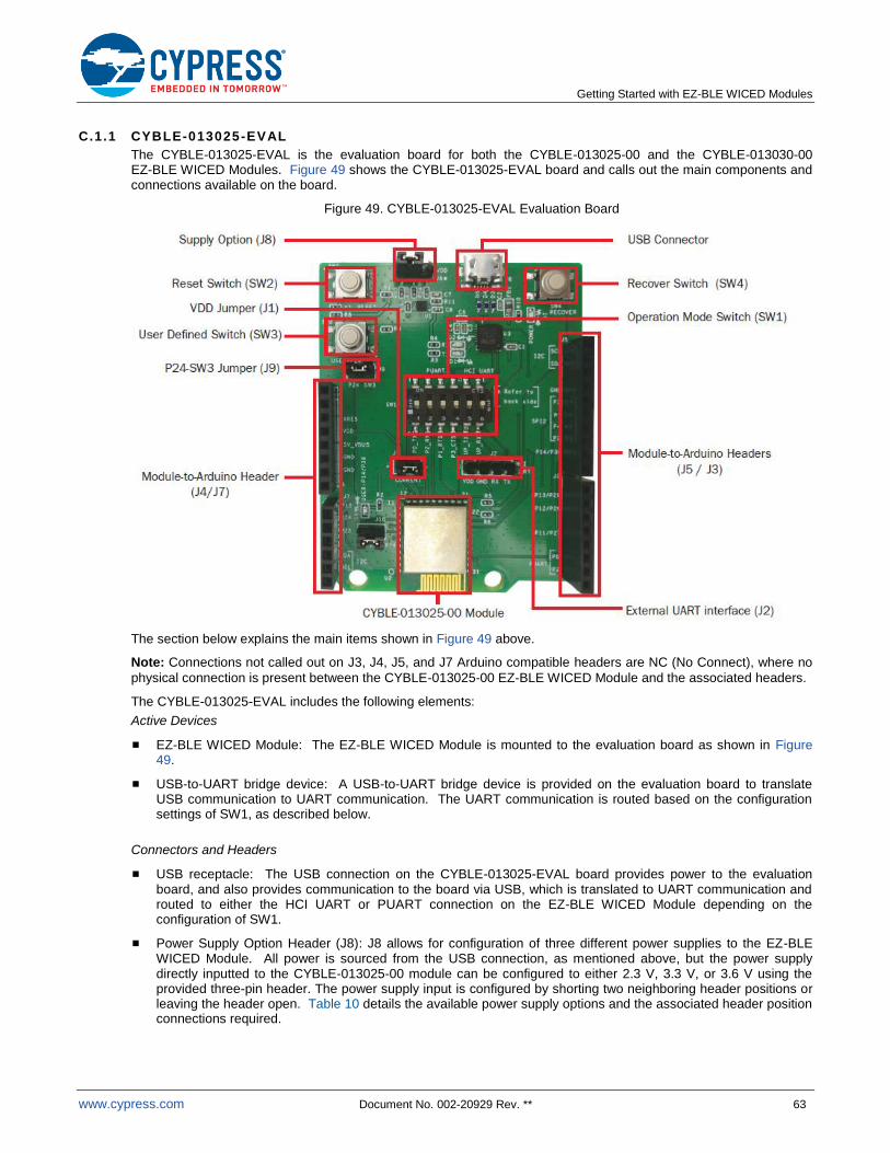
Getting Started with EZ-BLE WICED Modules
www.cypress.com Document No. 002-20929 Rev. ** 63
C.1.1 CYBLE-013025-EVAL
The CYBLE-013025-EVAL is the evaluation board for both the CYBLE-013025-00 and the CYBLE-013030-00 EZ-BLE WICED Modules. Figure 49 shows the CYBLE-013025-EVAL board and calls out the main components and connections available on the board.
Figure 49. CYBLE-013025-EVAL Evaluation Board
The section below explains the main items shown in Figure 49 above.
Note: Connections not called out on J3, J4, J5, and J7 Arduino compatible headers are NC (No Connect), where no
physical connection is present between the CYBLE-013025-00 EZ-BLE WICED Module and the associated headers.
The CYBLE-013025-EVAL includes the following elements:
Active Devices
EZ-BLE WICED Module: The EZ-BLE WICED Module is mounted to the evaluation board as shown in Figure 49.
USB-to-UART bridge device: A USB-to-UART bridge device is provided on the evaluation board to translate USB communication to UART communication. The UART communication is routed based on the configuration settings of SW1, as described below.
Connectors and Headers
USB receptacle: The USB connection on the CYBLE-013025-EVAL board provides power to the evaluation board, and also provides communication to the board via USB, which is translated to UART communication and routed to either the HCI UART or PUART connection on the EZ-BLE WICED Module depending on the configuration of SW1.
Power Supply Option Header (J8): J8 allows for configuration of three different power supplies to the EZ-BLE WICED Module. All power is sourced from the USB connection, as mentioned above, but the power supply directly inputted to the CYBLE-013025-00 module can be configured to either 2.3 V, 3.3 V, or 3.6 V using the provided three-pin header. The power supply input is configured by shorting two neighboring header positions or leaving the header open. Table 10 details the available power supply options and the associated header position connections required.

Getting Started with EZ-BLE WICED Modules
www.cypress.com Document No. 002-20929 Rev. ** 64
Table 10. J8 Header Power Supply Connection Options
2.3 V Supply Leave connections open; do not short any header connections
3.3 V Supply Short J8 header positions 2 & 3
3.6 V Supply Short J8 header positions 1 & 2
All Other Configurations Not Allowed
Arduino-compatible base headers – headers J3/J4/J5/J7: The CYBLE-013025-EVAL provides Arduino-compatible base headers that can be used for Arduino shield interfacing. The associated signals that are routed out to these headers are noted on the PCB silk screen on both the top and bottom side of the evaluation board.
HCI UART direct connection header (J2): The J2 header provides all HCI UART communication lines to the user. This allows for connection to the EZ-BLE WICED Module without having to connect through USB. This can be used to connect a host controller evaluation board directly to the EZ-BLE WICED Module HCI UART connection. HCI UART connections are not brought out to the Arduino-compatible headers.
Power consumption measurement header (J1): J1 is provided to allow for easy power consumption measurement reading with a multi-meter or current measurement probe.
User Element Disconnection Headers (J9 and J10): J9 (USER SW2) and J10 (USER D6 - LED) are provided to allow for disconnection of these elements from the CYBLE-013025-00 module. In both cases, the GPIO that is routed to these USER elements is also routed to the Arduino-compatible headers. This may be desired if you plan to use either of these GPIOs through the Arduino-compatible headers.
Switches and LEDs
SW1 (UART configuration switch): SW1 controls the configuration of which UART connection is active, HCI UART or Peripheral UART (PUART). SW1 is a six-position switch, and provides the following configuration states:
Table 11. SW1 UART Communication Configuration Options
SW1
Switch Position State
Position 1, 2, 3, and 4 are set to ON Position
Position 1, 2, 3, and 4 are set to OFF Position
Position 5 and 6 are set to ON Position
CONFIGURATION IS NOT ALLOWED
HCI UART Communication
Programming Mode
Position 5 and 6 are set to OFF Position
Peripheral UART (PUART) Communication
Application Mode
Application Mode
Notes on the above table are below:
It is not allowed to have all six switch positions set to the ON state. This would lead to both HCI UART and
PUART being actively connected to the EZ-BLE WICED Module, and could lead to a VDD to GND short.
The HCI UART Communication Configuration (Positions 5 and 6 = ON; Positions 1-4 = OFF) is the mode that the
evaluation board should be in when interfacing to the WICED SMART SDK, with the goal of downloading a compiled image to the EZ-BLE WICED Module.
The PUART/Application Mode (Positions 5 and 6 = OFF; Positions 1-4 = ON) is the configuration mode to use
when running application code from SFLASH on the EZ-BLE WICED Module. NOTE that the EZ-BLE WICED Module will not boot from SFLASH if HCI UART Mode is active on SW1. This mode also provides the PUART communication interface, which can be used for terminal communication on a PC.
The Application mode (All switch positions = OFF) allows the EZ-BLE WICED Module to boot from SFLASH and
run application code developed and programmed into the module previously. This mode disables both the HCI UART and PUART communication from host PC. PUART communication can still be accomplished through the Arduino-compatible headers if desired. Similarly, HCI communication can be accomplished through the J2 header.

Getting Started with EZ-BLE WICED Modules
www.cypress.com Document No. 002-20929 Rev. ** 65
SW2 (RESET switch): SW2 is a tactile switch that is connected directly to the XRES connection of the CYBLE-013025-00 module. Activating this switch will reset the EZ-BLE WICED Module.
SW3 (USER switch): SW3 is provided as an element that the user can configure as desired. The SW3 element is connected to P24 on the CYBLE-013025-00 module (solder pad 9).
SW4 (RECOVER switch): SW4 is provided to recover a module that has the standard programming bootloader and/or application image corrupted or erased. Recovery mode is activated by holding this button down while pressing and releasing SW2 (RESET). Recovery mode is not typically necessary during normal development.
D1 and D2 LEDs are provided to display programming activity while in progress.
D7 LED is provided to show that power is provided from the host PC.
D6 USER LED is provided for user-configured behavior as desired. The D6 LED is connected to the module P14/P26 connection (solder pad 7).
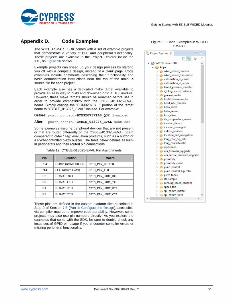
Getting Started with EZ-BLE WICED Modules
www.cypress.com Document No. 002-20929 Rev. ** 66
Appendix D. Code Examples
The WICED SMART SDK comes with a set of example projects that demonstrate a variety of BLE and peripheral functionality. These projects are available in the Project Explorer inside the IDE, as Figure 50 shows.
Example projects can speed up your design process by starting you off with a complete design, instead of a blank page. Code examples include comments describing their functionality and basic demonstration instructions near the top of the main .c
source file for each project.
Each example also has a dedicated make target available to provide an easy way to build and download onto a BLE module. However, these make targets should be renamed before use in order to provide compatibility with the CYBLE-013025-EVAL board. Simply change the “BCM92073x…” portion of the target name to “CYBLE_013025_EVAL” instead. For example:
Before: puart_control-BCM920737TAG_Q32 download
After: puart_control-CYBLE_013025_EVAL download
Some examples assume peripheral devices that are not present or that are routed differently on the CYBLE-013025-EVAL board compared to older “Tag” evaluation products, such as a button or a PWM-controlled piezo buzzer. The table below defines all built-in peripherals and their routed pin connections.
Table 12. CYBLE-013025-EVAL Pin Assignments
Pin Function Macro
P24 Button (active HIGH) GPIO_PIN_BUTTON
P14 LED (active LOW) GPIO_PIN_LED
P2 PUART RXD GPIO_PIN_UART_RX
P0 PUART TXD GPIO_PIN_UART_TX
P1 PUART RTS GPIO_PIN_UART_RTS
P3 PUART CTS GPIO_PIN_UART_CTS
These pins are defined in the custom platform files described in Step 9 of Section 7.3 (Part 1: Configure the Design), accessible via compiler macros to improve code portability. However, some projects may also use pin numbers directly. As you explore the examples that come with the SDK, be sure to double-check any instances of GPIO pin usage if you encounter compiler errors or missing peripheral functionality.
Figure 50. Code Examples in WICED SMART
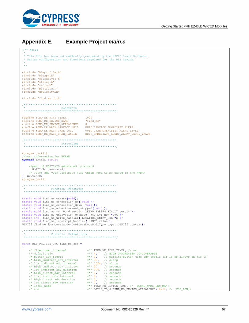
Getting Started with EZ-BLE WICED Modules
www.cypress.com Document No. 002-20929 Rev. ** 67
Appendix E. Example Project main.c
/** @file *
* This file has been automatically generated by the WICED Smart Designer.
* Device configuration and functions required for the BLE device.
*
*/
#include "bleprofile.h"
#include "bleapp.h"
#include "gpiodriver.h"
#include "string.h"
#include "stdio.h"
#include "platform.h"
#include "devicelpm.h"
#include "find_me_db.h"
/******************************************************
* Constants
******************************************************/
#define FIND_ME_FINE_TIMER 1000
#define FIND_ME_DEVICE_NAME "find_me"
#define FIND_ME_DEVICE_APPEARENCE 0
#define FIND_ME_MAIN_SERVICE_UUID UUID_SERVICE_IMMEDIATE_ALERT
#define FIND_ME_MAIN_CHAR_UUID UUID_CHARACTERISTIC_ALERT_LEVEL
#define FIND_ME_MAIN_CHAR_HANDLE HDLC_IMMEDIATE_ALERT_ALERT_LEVEL_VALUE
/******************************************************
* Structures
******************************************************/
#pragma pack(1)
//host information for NVRAM
typedef PACKED struct
{
//part of HOSTINFO generated by wizard
__HOSTINFO generated;
// ToDo: add your variables here which need to be saved in the NVRAM
} HOSTINFO;
#pragma pack()
/******************************************************
* Function Prototypes
******************************************************/
static void find_me_create(void);
static void find_me_connection_up( void );
static void find_me_connection_down( void );
static void find_me_advertisement_stopped( void );
static void find_me_smp_bond_result( LESMP_PARING_RESULT result );
static void find_me_encryption_changed( HCI_EVT_HDR *evt );
static int find_me_write_handler( LEGATTDB_ENTRY_HDR *p );
static void find_me_interrupt_handler( UINT8 value );
UINT32 find_me_lpm_queriable(LowPowerModePollType type, UINT32 context);
/******************************************************
* Variables Definitions
******************************************************/
const BLE_PROFILE_CFG find_me_cfg =
{
/*.fine_timer_interval =*/ FIND_ME_FINE_TIMER, // ms
/*.default_adv =*/ 4, // HIGH_UNDIRECTED_DISCOVERABLE
/*.button_adv_toggle =*/ 0, // pairing button make adv toggle (if 1) or always on (if 0)
/*.high_undirect_adv_interval =*/ 32, // slots
/*.low_undirect_adv_interval =*/ 1024, // slots
/*.high_undirect_adv_duration =*/ 30, // seconds
/*.low_undirect_adv_duration =*/ 300, // seconds
/*.high_direct_adv_interval =*/ 0, // seconds
/*.low_direct_adv_interval =*/ 0, // seconds
/*.high_direct_adv_duration =*/ 0, // seconds
/*.low_direct_adv_duration =*/ 0, // seconds
/*.local_name =*/ FIND_ME_DEVICE_NAME, // [LOCAL_NAME_LEN_MAX];
/*.cod =*/ BIT16_TO_8(FIND_ME_DEVICE_APPEARENCE),0x00, // [COD_LEN];
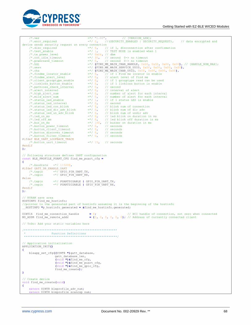
Getting Started with EZ-BLE WICED Modules
www.cypress.com Document No. 002-20929 Rev. ** 68
/*.ver =*/ "1.00", // [VERSION_LEN];
/*.encr_required =*/ 0, //(SECURITY_ENABLED | SECURITY_REQUEST), // data encrypted and
device sends security request on every connection
/*.disc_required =*/ 0, // if 1, disconnection after confirmation
/*.test_enable =*/ 1, // TEST MODE is enabled when 1
/*.tx_power_level =*/ 0x04, // dbm
/*.con_idle_timeout =*/ 30, // second 0-> no timeout
/*.powersave_timeout =*/ 0, // second 0-> no timeout
/*.hdl =*/ {FIND_ME_MAIN_CHAR_HANDLE, 0x00, 0x00, 0x00, 0x00}, // [HANDLE_NUM_MAX];
/*.serv =*/ {FIND_ME_MAIN_SERVICE_UUID, 0x00, 0x00, 0x00, 0x00},
/*.cha =*/ {FIND_ME_MAIN_CHAR_UUID, 0x00, 0x00, 0x00, 0x00},
/*.findme_locator_enable =*/ 0, // if 1 Find me locator is enable
/*.findme_alert_level =*/ 0, // alert level of find me
/*.client_grouptype_enable =*/ 0, // if 1 grouptype read can be used
/*.linkloss_button_enable =*/ 0, // if 1 linkloss button is enable
/*.pathloss_check_interval =*/ 0, // second
/*.alert_interval =*/ 0, // interval of alert
/*.high_alert_num =*/ 0, // number of alert for each interval
/*.mild_alert_num =*/ 0, // number of alert for each interval
/*.status_led_enable =*/ 1, // if 1 status LED is enable
/*.status_led_interval =*/ 0, // second
/*.status_led_con_blink =*/ 0, // blink num of connection
/*.status_led_dir_adv_blink =*/ 0, // blink num of dir adv
/*.status_led_un_adv_blink =*/ 0, // blink num of undir adv
/*.led_on_ms =*/ 0, // led blink on duration in ms
/*.led_off_ms =*/ 0, // led blink off duration in ms
/*.buz_on_ms =*/ 100, // buzzer on duration in ms
/*.button_power_timeout =*/ 0, // seconds
/*.button_client_timeout =*/ 0, // seconds
/*.button_discover_timeout =*/ 0, // seconds
/*.button_filter_timeout =*/ 0, // seconds
#ifdef BLE_UART_LOOPBACK_TRACE
/*.button_uart_timeout =*/ 15, // seconds
#endif
};
// Following structure defines UART configuration
const BLE_PROFILE_PUART_CFG find_me_puart_cfg =
{
/*.baudrate =*/ 115200,
#ifdef GATT_DB_ENABLE_UART
/*.txpin =*/ GPIO_PIN_UART_TX,
/*.rxpin =*/ GPIO_PIN_UART_RX,
#else
/*.txpin =*/ PUARTDISABLE | GPIO_PIN_UART_TX,
/*.rxpin =*/ PUARTDISABLE | GPIO_PIN_UART_RX,
#endif
};
// NVRAM save area
HOSTINFO find_me_hostinfo;
//pointer to the generated part of hostinfo assuming it is the beginning of the hostinfo
__HOSTINFO *p_hostinfo_generated = &find_me_hostinfo.generated;
UINT16 find_me_connection_handle = 0; // HCI handle of connection, not zero when connected
BD_ADDR find_me_remote_addr = {0, 0, 0, 0, 0, 0}; // Address of currently connected client
// ToDo: Add your static variables here
/******************************************************
* Function Definitions
******************************************************/
// Application initialization
APPLICATION_INIT()
{
bleapp_set_cfg((UINT8 *)gatt_database,
gatt_database_len,
(void *)&find_me_cfg,
(void *)&find_me_puart_cfg,
(void *)&find_me_gpio_cfg,
find_me_create);
}
// Create device
void find_me_create(void)
{
extern UINT8 bleprofile_adv_num;
extern UINT8 bleprofile_scanrsp_num;
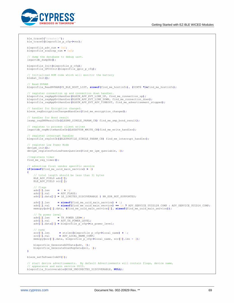
Getting Started with EZ-BLE WICED Modules
www.cypress.com Document No. 002-20929 Rev. ** 69
ble_trace0("create()");
ble_trace0(bleprofile_p_cfg->ver);
bleprofile_adv_num = 0x0;
bleprofile_scanrsp_num = 0x0;
// dump the database to debug uart.
legattdb_dumpDb();
bleprofile_Init(bleprofile_p_cfg);
bleprofile_GPIOInit(bleprofile_gpio_p_cfg);
// Initialized ROM code which will monitor the battery
blebat_Init();
// Read NVRAM
bleprofile_ReadNVRAM(VS_BLE_HOST_LIST, sizeof(find_me_hostinfo), (UINT8 *)&find_me_hostinfo);
// register connection up and connection down handler.
bleprofile_regAppEvtHandler(BLECM_APP_EVT_LINK_UP, find_me_connection_up);
bleprofile_regAppEvtHandler(BLECM_APP_EVT_LINK_DOWN, find_me_connection_down);
bleprofile_regAppEvtHandler(BLECM_APP_EVT_ADV_TIMEOUT, find_me_advertisement_stopped);
// handler for Encryption changed.
blecm_regEncryptionChangedHandler(find_me_encryption_changed);
// handler for Bond result
lesmp_regSMPResultCb((LESMP_SINGLE_PARAM_CB) find_me_smp_bond_result);
// register to process client writes
legattdb_regWriteHandleCb((LEGATTDB_WRITE_CB)find_me_write_handler);
// register interrupt handler
bleprofile_regIntCb((BLEPROFILE_SINGLE_PARAM_CB) find_me_interrupt_handler);
// register Low Power Mode
devlpm_init();
devlpm_registerForLowPowerQueries(find_me_lpm_queriable, 0);
//registers timer
find_me_reg_timer();
// advertise first vendor specific service
if(sizeof(find_me_uuid_main_service) > 1)
{
// total length should be less than 31 bytes
BLE_ADV_FIELD adv[3];
BLE_ADV_FIELD scr[1];
// flags
adv[0].len = 1 + 1;
adv[0].val = ADV_FLAGS;
adv[0].data[0] = LE_LIMITED_DISCOVERABLE | BR_EDR_NOT_SUPPORTED;
adv[1].len = sizeof(find_me_uuid_main_service) + 1;
adv[1].val = sizeof(find_me_uuid_main_service) == 16 ? ADV_SERVICE_UUID128_COMP : ADV_SERVICE_UUID16_COMP;
memcpy(adv[1].data, &find_me_uuid_main_service[0], sizeof(find_me_uuid_main_service));
// Tx power level
adv[2].len = TX_POWER_LEN+1;
adv[2].val = ADV_TX_POWER_LEVEL;
adv[2].data[0] = bleprofile_p_cfg->tx_power_level;
// name
scr[0].len = strlen(bleprofile_p_cfg->local_name) + 1;
scr[0].val = ADV_LOCAL_NAME_COMP;
memcpy(scr[0].data, bleprofile_p_cfg->local_name, scr[0].len - 1);
bleprofile_GenerateADVData(adv, 3);
bleprofile_GenerateScanRspData(scr, 1);
}
blecm_setTxPowerInADV(0);
// start device advertisements. By default Advertisements will contain flags, device name,
// appearance and main service UUID.
bleprofile_Discoverable(HIGH_UNDIRECTED_DISCOVERABLE, NULL);
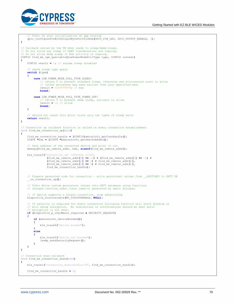
Getting Started with EZ-BLE WICED Modules
www.cypress.com Document No. 002-20929 Rev. ** 70
// ToDo: Do your initialization on app startup
gpio_configurePinWithSingleBytePortPinNum(GPIO_PIN_LED, GPIO_OUTPUT_ENABLE, 1);
}
// Callback called by the FW when ready to sleep/deep-sleep.
// Do not allow any sleep if UART transmissions are ongoing.
// Do not allow deep sleep if BLE activity is ongoing.
UINT32 find_me_lpm_queriable(LowPowerModePollType type, UINT32 context)
{
UINT32 result = 0; // assume sleep disabled
// check sleep type query
switch (type)
{
case LOW_POWER_MODE_POLL_TYPE_SLEEP:
// return 0 to prevent standard sleep, otherwise max microsecond count to allow
// (other processes may wake earlier than your specified max)
result = 0xFFFFFFFF; // max
break;
case LOW_POWER_MODE_POLL_TYPE_POWER_OFF:
// return 0 to prevent deep sleep, non-zero to allow
result = 1; // allow
break;
}
// should not reach this point since only two types of sleep exist
return result;
}
// Connection up callback function is called on every connection establishment
void find_me_connection_up(void)
{
find_me_connection_handle = (UINT16)emconinfo_getConnHandle();
UINT8 *bda = (UINT8 *)emconninfo_getPeerPubAddr();
// Save address of the connected device and print it out.
memcpy(find_me_remote_addr, bda, sizeof(find_me_remote_addr));
ble_trace3("connection_up: %08x%04x h=%d",
(find_me_remote_addr[5] << 24) + (find_me_remote_addr[4] << 16) +
(find_me_remote_addr[3] << 8) + find_me_remote_addr[2],
(find_me_remote_addr[1] << 8) + find_me_remote_addr[0],
find_me_connection_handle);
// Prepare generated code for connection - write persistent values from __HOSTINFO to GATT DB
__on_connection_up();
// ToDo: Write custom persistent values into GATT database using functions
// changed_<service_name>_<char_name>() generated by smart disigner
// If device supports a single connection, stop advertising
bleprofile_Discoverable(NO_DISCOVERABLE, NULL);
// If security is required for every connection following function will start bonding or
// will setup encryption. No indications or notifications should be sent until
// encryption is not done.
if (bleprofile_p_cfg->encr_required & SECURITY_REQUEST)
{
if (emconninfo_deviceBonded())
{
ble_trace0("device bonded");
}
else
{
ble_trace0("device not bonded");
lesmp_sendSecurityRequest();
}
}
}
// Connection down callback
void find_me_connection_down(void)
{
ble_trace1("connection_down:handle:%d", find_me_connection_handle);
find_me_connection_handle = 0;
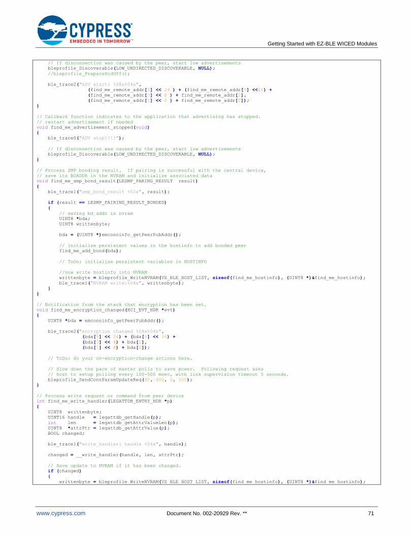
Getting Started with EZ-BLE WICED Modules
www.cypress.com Document No. 002-20929 Rev. ** 71
// If disconnection was caused by the peer, start low advertisements
bleprofile_Discoverable(LOW_UNDIRECTED_DISCOVERABLE, NULL);
//bleprofile_PrepareHidOff();
ble_trace2("ADV start: %08x%04x",
(find_me_remote_addr[5] << 24 ) + (find_me_remote_addr[4] <<16) +
(find_me_remote_addr[3] << 8 ) + find_me_remote_addr[2],
(find_me_remote_addr[1] << 8 ) + find_me_remote_addr[0]);
}
// Callback function indicates to the application that advertising has stopped.
// restart advertisement if needed
void find_me_advertisement_stopped(void)
{
ble_trace0("ADV stop!!!!");
// If disconnection was caused by the peer, start low advertisements
bleprofile_Discoverable(LOW_UNDIRECTED_DISCOVERABLE, NULL);
}
// Process SMP bonding result. If pairing is successful with the central device,
// save its BDADDR in the NVRAM and initialize associated data
void find_me_smp_bond_result(LESMP_PARING_RESULT result)
{
ble_trace1("smp_bond_result %02x", result);
if (result == LESMP_PAIRING_RESULT_BONDED)
{
// saving bd_addr in nvram
UINT8 *bda;
UINT8 writtenbyte;
bda = (UINT8 *)emconninfo_getPeerPubAddr();
// initialize persistent values in the hostinfo to add bonded peer
find_me_add_bond(bda);
// ToDo: initialize persistent variables in HOSTINFO
//now write hostinfo into NVRAM
writtenbyte = bleprofile_WriteNVRAM(VS_BLE_HOST_LIST, sizeof(find_me_hostinfo), (UINT8 *)&find_me_hostinfo);
ble_trace1("NVRAM write:%04x", writtenbyte);
}
}
// Notification from the stack that encryption has been set.
void find_me_encryption_changed(HCI_EVT_HDR *evt)
{
UINT8 *bda = emconninfo_getPeerPubAddr();
ble_trace2("encryption changed %08x%04x",
(bda[5] << 24) + (bda[4] << 16) +
(bda[3] << 8) + bda[2],
(bda[1] << 8) + bda[0]);
// ToDo: do your on-encryption-change actions here.
// Slow down the pace of master polls to save power. Following request asks
// host to setup polling every 100-500 msec, with link supervision timeout 5 seconds.
bleprofile_SendConnParamUpdateReq(80, 400, 0, 500);
}
// Process write request or command from peer device
int find_me_write_handler(LEGATTDB_ENTRY_HDR *p)
{
UINT8 writtenbyte;
UINT16 handle = legattdb_getHandle(p);
int len = legattdb_getAttrValueLen(p);
UINT8 *attrPtr = legattdb_getAttrValue(p);
BOOL changed;
ble_trace1("write_handler: handle %04x", handle);
changed = __write_handler(handle, len, attrPtr);
// Save update to NVRAM if it has been changed.
if (changed)
{
writtenbyte = bleprofile_WriteNVRAM(VS_BLE_HOST_LIST, sizeof(find_me_hostinfo), (UINT8 *)&find_me_hostinfo);
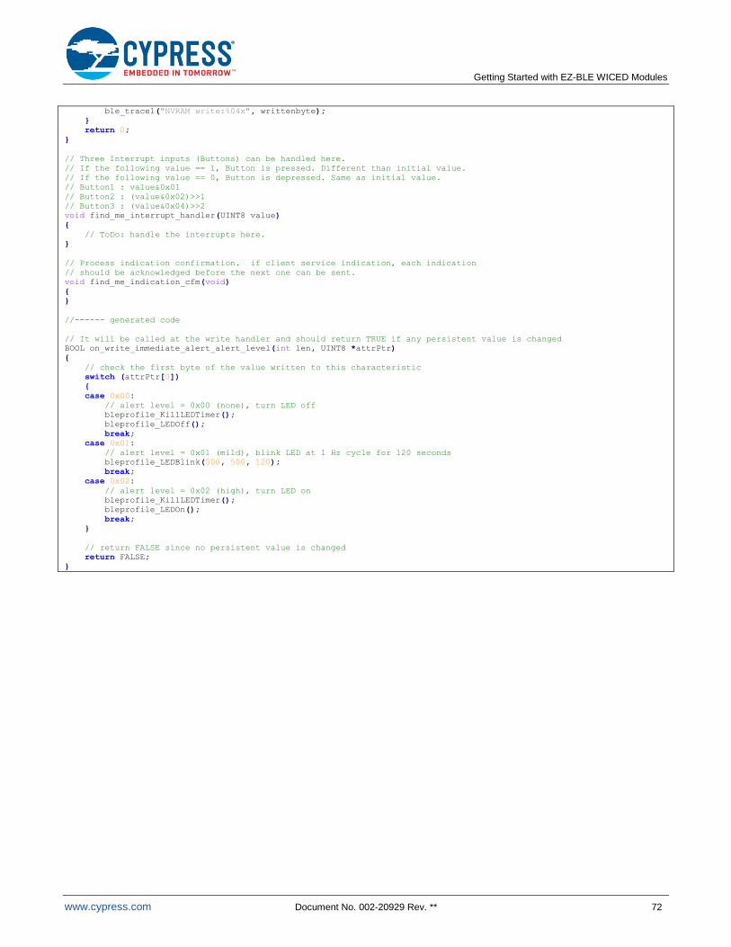
Getting Started with EZ-BLE WICED Modules
www.cypress.com Document No. 002-20929 Rev. ** 72
ble_trace1("NVRAM write:%04x", writtenbyte);
}
return 0;
}
// Three Interrupt inputs (Buttons) can be handled here.
// If the following value == 1, Button is pressed. Different than initial value.
// If the following value == 0, Button is depressed. Same as initial value.
// Button1 : value&0x01
// Button2 : (value&0x02)>>1
// Button3 : (value&0x04)>>2
void find_me_interrupt_handler(UINT8 value)
{
// ToDo: handle the interrupts here.
}
// Process indication confirmation. if client service indication, each indication
// should be acknowledged before the next one can be sent.
void find_me_indication_cfm(void)
{
}
//------ generated code
// It will be called at the write handler and should return TRUE if any persistent value is changed
BOOL on_write_immediate_alert_alert_level(int len, UINT8 *attrPtr)
{
// check the first byte of the value written to this characteristic
switch (attrPtr[0])
{
case 0x00:
// alert level = 0x00 (none), turn LED off
bleprofile_KillLEDTimer();
bleprofile_LEDOff();
break;
case 0x01:
// alert level = 0x01 (mild), blink LED at 1 Hz cycle for 120 seconds
bleprofile_LEDBlink(500, 500, 120);
break;
case 0x02:
// alert level = 0x02 (high), turn LED on
bleprofile_KillLEDTimer();
bleprofile_LEDOn();
break;
}
// return FALSE since no persistent value is changed
return FALSE;
}

Getting Started with EZ-BLE WICED Modules
www.cypress.com Document No. 002-20929 Rev. ** 73
Appendix F. Makefile Customization
The WICED SMART SDK build system uses a hierarchical Makefile structure when building each project. The root Makefile is found in the main SDK installation folder as \WICED-Smart-SDK\Makefile, and each project contains its own specific makefile.mk file along with the source files in its dedicated directory. To customize the build process for a specific project, always edit the project’s own makefile.mk content instead of modifying the top-level file.
The most common changes that you may need to make are as follows:
1. Adding new .c source files to be compiled and linked:
Splitting the source code into multiple files can greatly improve organization and maintainability as the project grows. To add more files to the build process beyond the initial set that is created from the WICED Bluetooth Designer tool, use the APP_SRC keyword:
You can include as many extra files as you need. Note that the very first file should use the direct assignment operator (“=”), while all subsequent files should use the append operator (“+=”).
2. Adding extra include folders into the search path:
Some projects require the use of additional libraries that assume particular 'include' folders are in the compiler’s include search path. To avoid having to rewrite source files with explicit include paths throughout, use the INCS keyword along with the $(DIR) variable to denote the project’s root folder:
You can add as many extra include search folders as you need. Note that all additional folders should use the append operator (“+=”) since the SDK’s top-level Makefile assigns some folders already. Using the direct assignment operator (“=”) will wipe out these default folders and break the compile process.
3. Applying pre-built optional patches that are part of the WICED SDK:
Since the WICED SMART Bluetooth LE stack is part of the chipset ROM inside the module, updates and fixes to low-level functionality require the use of precompiled patches, which are loaded and applied during the boot process. These patches must be included especially during the compile process so that they are part of the final firmware binary image. To specify patches for this purpose, use the APP_PATCHES_AND_LIBS keyword:
Patches are optional and may be added in any order. You can find a description of all available patches that ship with the SDK in the following location:
\WICED-Smart-SDK\Wiced-Smart\tier2\brcm\libraries\lib\readme
APP_PATCHES_AND_LIBS += config_nvram_fixes.a
APP_PATCHES_AND_LIBS += disable_sw_timer_as_wake_source.a
APP_PATCHES_AND_LIBS += bt_clock_based_periodic_timer.a
INCS += $(DIR)/library1/include
INCS += $(DIR)/library2/include INCS += $(DIR)/some/other/include
APP_SRC = find_me.c
APP_SRC += find_me_db.c
APP_SRC += extrafile1.c APP_SRC += extrafile2.c APP_SRC += subfolder/subfile1.c
APP_SRC += subfolder/subfile2.c
Getting Started with EZ-BLE WICED Modules
www.cypress.com Document No. 002-20929 Rev. ** 74
Appendix G. Regulatory Information
FCC:
FCC NOTICE:
Cypress EZ-BLE Modules, including integrated antennas, comply with Part 15 of the FCC Rules. When stated in the module datasheet, the modules meet the requirements for modular transmitter approval as detailed in FCC public Notice DA00-1407.transmitter Operation is subject to the following two conditions: (1) This device may not cause harmful interference, and (2) This device must accept any interference received, including interference that may cause undesired operation.
CAUTION
The FCC requires the user to be notified that any changes or modifications made to this device that are not expressly approved by Cypress Semiconductor may void the user's authority to operate the equipment.
Any certified modules provided by Cypress have been tested and found to comply with the limits for a Class B digital device, pursuant to Part 15 of the FCC Rules. These limits are designed to provide reasonable protection against harmful interference in a residential installation. This equipment generates uses and can radiate radio frequency energy and, if not installed and used in accordance with the instructions, may cause harmful interference to radio communications. However, there is no guarantee that interference will not occur in a particular installation. If this equipment does cause harmful interference to radio or television reception, which can be determined by turning the equipment off and on, the user is encouraged to try to correct the interference by one or more of the following measures:
Reorient or relocate the receiving antenna.
Increase the separation between the equipment and receiver.
Connect the equipment into an outlet on a circuit different from that to which the receiver is connected.
Consult the dealer or an experienced radio/TV technician for help
LABELING REQUIREMENTS
The Original Equipment Manufacturer (OEM) must ensure that FCC labeling requirements are met. This includes a clearly visible label on the outside of the OEM enclosure specifying the appropriate Cypress Semiconductor FCC identifier for this product as well as the FCC Notice above. The FCC identifier for each module is listed in the module datasheet, and is of the form “FCC ID: WAPxxxx”, where “xxxx” denotes the module-specific FCC identifier. In any case, the end product using a certified Cypress module must be labeled on the exterior with "Contains FCC ID: WAPxxxx", where “xxxx” is the module-specific FCC identifier.
ANTENNA WARNING
Please refer to the module datasheet for details on the specific antenna used for the module design. Each Cypress certified module may have a different Antenna design. When integrated in the OEMs product, these antennas require installation preventing end-users from replacing them with non-approved antennas. Any antenna not listed in the module datasheet must be tested to comply with FCC Section 15.203 for unique antenna connectors and Section 15.247 for emissions.

Getting Started with EZ-BLE WICED Modules
www.cypress.com Document No. 002-20929 Rev. ** 75
RF EXPOSURE
To comply with FCC RF Exposure requirements, the Original Equipment Manufacturer (OEM) must ensure to install
the approved antenna in the previous. The preceding statement must be included as a CAUTION statement in manuals, for products operating with the approved antennas listed in the module datasheet, to alert users on FCC RF Exposure compliance. Any notification to the end user of installation or removal instructions about the integrated radio module is not allowed. The radiated output power of Cypress certified modules with antenna mounted is far below the FCC radio frequency exposure limits. Nevertheless, use Cypress modules in such a manner that minimizes the potential for human contact during normal operation. End users may not be provided with the module installation instructions. OEM integrators and end users must be provided with transmitter operating conditions for satisfying RF exposure compliance.
Innovation, Science and Economic Development (ISED) Canada Certification
When indicated in the module datasheet, Cypress EZ-BLE modules are licensed to meet the regulatory requirements of Innovation, Science and Economic Development (ISED) Canada. Refer to the module datasheet for details on the specific IC identifier. The IC identifier will be of the form: License: IC: 7922A-xxxx, where “xxxx” is the ID for a specific module. Manufacturers of mobile, fixed or portable devices incorporating this module are advised to clarify any regulatory questions and ensure compliance for SAR and/or RF exposure limits. Users can obtain Canadian information on RF exposure and compliance from www.ic.gc.ca. Cypress EZ-BLE modules have been designed to operate with the antennas listed in the module datasheet. Antennas not included in the module datasheet or having a gain greater than what is specified in the module datasheet are strictly prohibited for use with this device. The required antenna impedance is 50 ohms. The antenna used for this transmitter must not be co-located or operating in conjunction with any other antenna or transmitter.
ISED NOTICE
Cypress EZ-BLE modules, including the built-in antenna complies with Canada RSS-GEN Rules. Cypress EZ-BLE modules meet the requirements for modular transmitter approval as detailed in RSS-GEN. Operation is subject to the following two conditions: (1) This device may not cause harmful interference, and (2) This device must accept any interference received, including interference that may cause undesired operation. Les modules Cypress EZ-BLE, y compris l'antenne intégrée, sont conformes aux Règles RSS-GEN de Canada. Les modules Cypress EZ-BLE répondent aux exigences d'approbation de l'émetteur modulaire, tel que décrit dans RSS-GEN. L'opération est soumise aux deux conditions suivantes: (1) Cet appareil ne doit pas causer d'interférences nuisibles, et (2) Cet appareil doit accepter toute interférence reçue, y compris les interférences susceptibles de provoquer un fonctionnement indésirable.
ISED INTERFERENCE STATEMENT FOR CANADA
Cypress EZ-BLE modules comply with Innovation, Science and Economic Development (ISED) Canada license-exempt RSS standard(s). Operation is subject to the following two conditions: (1) this device may not cause interference, and (2) this device must accept any interference, including interference that may cause undesired operation of the device. Les modules Cypress EZ-BLE sont conformes aux normes RSS, exemptées de licences et exemptées de licence de l'Innovation, des Sciences et du Développement (ISED). Le fonctionnement est soumis aux deux conditions suivantes: (1) cet appareil ne doit pas provoquer d'interférence, et (2) cet appareil doit accepter toute interférence, y compris les interférences susceptibles de provoquer un fonctionnement indésirable de l'appareil.

Getting Started with EZ-BLE WICED Modules
www.cypress.com Document No. 002-20929 Rev. ** 76
ISED RADIATION EXPOSURE STATEMENT FOR CANADA
Cypress EZ-BLE modules comply with ISED radiation exposure limits set forth for an uncontrolled environment. Please refer to the module datasheet for any details on integration requirements for radiation exposure. Les modules Cypress EZ-BLE sont conformes aux limites d'exposition au rayonnement ISED prévues pour un environnement incontrôlé. Veuillez vous référer à la fiche technique du module pour tout détail sur les exigences d'intégration pour l'exposition au rayonnement.
LABELING REQUIREMENTS The Original Equipment Manufacturer (OEM) must ensure that IC labeling requirements are met. This includes a clearly visible label on the outside of the OEM enclosure specifying the appropriate Cypress Semiconductor IC identifier for this product as well as the IC Notice above. The IC identifier is 7922A-xxxx, where “xxxx” is the specific IC ID for a given module. In any case, the end product must be labeled in its exterior with "Contains IC: 7922A-xxxx",
where “xxxx” is the module specific ID as indicated in the module datasheet. Le fabricant d'équipement d'origine (OEM) doit s'assurer que les exigences d'étiquetage IC sont respectées. Cela comprend une étiquette clairement visible à l'extérieur de l'enceinte OEM spécifiant l'identifiant Cypress Semiconductor approprié pour ce produit ainsi que l'avis IC ci-dessus. L'identifiant IC est 7922A-xxxx, où "xxxx" est l'ID CI spécifique pour un module donné. En tout cas, le produit final doit être étiqueté dans son extérieur avec "Contient IC: 7922A-xxxx", où "xxxx" est l'ID spécifique du module comme indiqué dans la fiche technique du module.
EUROPEAN DECLARATION OF CONFORMITY
Hereby, Cypress Semiconductor declares that the EZ-BLE Bluetooth modules, when indicated on the module datasheet, comply with the essential requirements and other relevant provisions of Directive 2014. As a result of the conformity assessment procedure described in Annex III of the Directive 2014, the end-customer equipment should be labeled as follows:
When indicated in the module datasheet, the module used in the specified reference design can be used in the following countries: Austria, Belgium, Cyprus, Czech Republic, Denmark, Estonia, Finland, France, Germany, Greece, Hungary, Ireland, Italy, Latvia, Lithuania, Luxembourg, Malta, Poland, Portugal, Slovakia, Slovenia, Spain, Sweden, The Netherlands, the United Kingdom, Switzerland, and Norway.
MIC JAPAN
When indicated, Cypress EZ-BLE modules are certified as a module with a specific type certification number detailed in the module datasheet. End products that integrate modules that are certified for Japan do not need additional MIC Japan certification for the end product.
End product can display the certification label of the embedded module as display in the specific module datasheet.
G.1 Module Regulatory Reports and Certificates
Table 13 details the knowledge base articles that contain the test reports and certificates for each EZ-BLE module. These knowledge base article can be found by visiting www.cypress.com and searching for the KBA number below, or by clicking on the hyperlinks in the below table.
Table 13. Regulatory Test Report and Certificate KBA Reference
EZ-BLE Module
Part Number Knowledge Base Article Containing Regulatory Reports and Certificates
CYBLE-013025-00 KBA219623
CYBLE-013030-00
Getting Started with EZ-BLE WICED Modules
www.cypress.com Document No. 002-20929 Rev. ** 77
Document History
Document Title: AN220929 – Getting Started with EZ-BLE WICED Modules
Document Number: 002-20929
Revision ECN Orig. of Change
Submission Date Description of Change
** 5879338 DSO 10/27/2017 New application note

Getting Started with EZ-BLE WICED Modules
www.cypress.com Document No. 002-20929 Rev. ** 78
Worldwide Sales and Design Support
Cypress maintains a worldwide network of offices, solution centers, manufacturer’s representatives, and distributors. To find the office closest to you, visit us at Cypress Locations.
Products
ARM® Cortex
® Microcontrollers cypress.com/arm
Automotive cypress.com/automotive
Clocks & Buffers cypress.com/clocks
Interface cypress.com/interface
Internet of Things cypress.com/iot
Memory cypress.com/memory
Microcontrollers cypress.com/mcu
PSoC cypress.com/psoc
Power Management ICs cypress.com/pmic
Touch Sensing cypress.com/touch
USB Controllers cypress.com/usb
Wireless Connectivity cypress.com/wireless
PSoC® Solutions
PSoC 1 | PSoC 3 | PSoC 4 | PSoC 5LP | PSoC 6
Cypress Developer Community
Forums | WICED IOT Forums | Projects | Videos | Blogs |
Training | Components
Technical Support
cypress.com/support
All other trademarks or registered trademarks referenced herein are the property of their respective owners.
Cypress Semiconductor 198 Champion Court San Jose, CA 95134-1709
© Cypress Semiconductor Corporation, 2017. This document is the property of Cypress Semiconductor Corporation and its subsidiaries, including Spansion LLC (“Cypress”). This document, including any software or firmware included or referenced in this document (“Software”), is owned by Cypress under the intellectual property laws and treaties of the United States and other countries worldwide. Cypress reserves all rights under such laws and treaties and does not, except as specifically stated in this paragraph, grant any license under its patents, copyrights, trademarks, or other intellectual property rights. If the Software is not accompanied by a license agreement and you do not otherwise have a written agreement with Cypress governing the use of the Software, then Cypress hereby grants you a personal, non-exclusive, nontransferable license (without the right to sublicense) (1) under its copyright rights in the Software (a) for Software provided in source code form, to modify and reproduce the Software solely for use with Cypress hardware products, only internally within your organization, and (b) to distribute the Software in binary code form externally to end users (either directly or indirectly through resellers and distributors), solely for use on Cypress hardware product units, and (2) under those claims of Cypress’s patents that are infringed by the Software (as provided by Cypress, unmodified) to make, use, distribute, and import the Software solely for use with Cypress hardware products. Any other use, reproduction, modification, translation, or compilation of the Software is prohibited. TO THE EXTENT PERMITTED BY APPLICABLE LAW, CYPRESS MAKES NO WARRANTY OF ANY KIND, EXPRESS OR IMPLIED, WITH REGARD TO THIS DOCUMENT OR ANY SOFTWARE OR ACCOMPANYING HARDWARE, INCLUDING, BUT NOT LIMITED TO, THE IMPLIED WARRANTIES OF MERCHANTABILITY AND FITNESS FOR A PARTICULAR PURPOSE. To the extent permitted by applicable law, Cypress reserves the right to make changes to this document without further notice. Cypress does not assume any liability arising out of the application or use of any product or circuit described in this document. Any information provided in this document, including any sample design information or programming code, is provided only for reference purposes. It is the responsibility of the user of this document to properly design, program, and test the functionality and safety of any application made of this information and any resulting product. Cypress products are not designed, intended, or authorized for use as critical components in systems designed or intended for the operation of weapons, weapons systems, nuclear installations, life-support devices or systems, other medical devices or systems (including resuscitation equipment and surgical implants), pollution control or hazardous substances management, or other uses where the failure of the device or system could cause personal injury, death, or property damage (“Unintended Uses”). A critical component is any component of a device or system whose failure to perform can be reasonably expected to cause the failure of the device or system, or to affect its safety or effectiveness. Cypress is not liable, in whole or in part, and you shall and hereby do release Cypress from any claim, damage, or other liability arising from or related to all Unintended Uses of Cypress products. You shall indemnify and hold Cypress harmless from and against all claims, costs, damages, and other liabilities, including claims for personal injury or death, arising from or related to any Unintended Uses of Cypress products. Cypress, the Cypress logo, Spansion, the Spansion logo, and combinations thereof, WICED, PSoC, CapSense, EZ-USB, F-RAM, and Traveo are trademarks or registered trademarks of Cypress in the United States and other countries. For a more complete list of Cypress trademarks, visit cypress.com. Other names and brands may be claimed as property of their respective owners.
Related Documents