North American PCB Military Technology Roadmap George Dudnikov Senior vice President and Chief Technology Officer, Sanmina-SCI

Welcome message from author
This document is posted to help you gain knowledge. Please leave a comment to let me know what you think about it! Share it to your friends and learn new things together.
Transcript

North American PCB Military Technology Roadmap
George Dudnikov Senior vice President and Chief Technology Officer,
Sanmina-SCI

George Dudnikov Senior Vice President and Chief Technology Officer, Sanmina SCI
Photo not available
About the Author
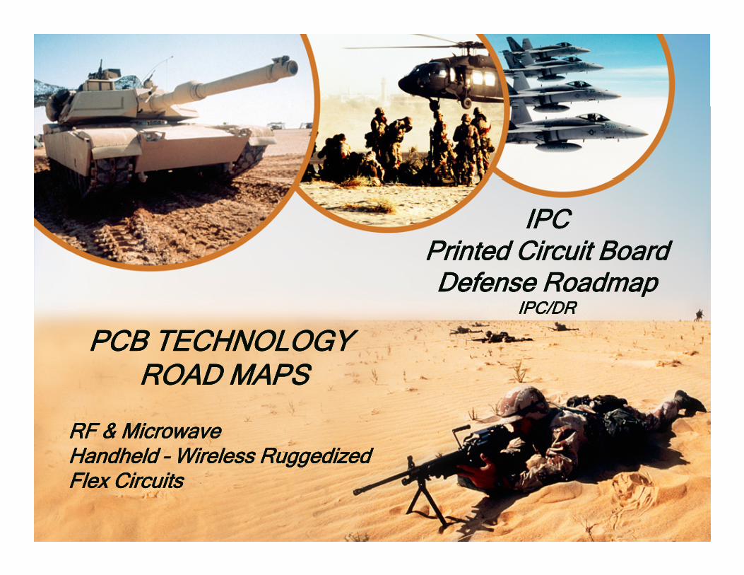
IPC IPC Printed Circuit BoardPrinted Circuit BoardPrinted Circuit Board Printed Circuit Board Defense Roadmap Defense Roadmap
IPC/DRIPC/DR
PCB TECHNOLOGYPCB TECHNOLOGYROAD MAPSROAD MAPS
RF & MicrowaveRF & MicrowaveHandheld Handheld –– Wireless RuggedizedWireless RuggedizedFlex CircuitsFlex Circuits

Roadmap Purpose and Scope
Purpose• To assist the EA, leading North American printed board manufacturers
of the IPC EA Task Force created this roadmap, which identifies theof the IPC EA Task Force created this roadmap, which identifies the challenging printed board designs and materials that will be required to meet future DoD and OEM needs.
• The task force believes this roadmap can facilitate better communication between:
– The printed board industry– OEMs designing and manufacturing military hardware; – DoD and the military electronics supply chain.
• The electronics industry would benefit from a more complete y punderstanding of current and future DoD/OEM needs particularly in the areas of critical parts, materials and designs.
Scope of the IPC Defense Roadmap (IPC/DR)Id tifi d dd th h ll i i t d b d d i• Identifies and addresses the challenging printed board designs, production processes and materials required to meet future DoD and OEM needs for 2009 and 2010.
• Identifies anticipated advances in technology that require gap-filling. Th d l d h IPC• The roadmaps are not a replacement or amendment to the IPC International Technology Roadmap for Electronic Interconnections.

IPC PCB Defense Roadmaps
Introductions• RF & Microwave
– George Dudnikov - Sanmina
• Ruggedized Handheld & Wireless– Andy Cameron – TTM Technologies
• Flex and Rigid Flex Al W V l Fl Ci it– Al Wasserzug – Vulcan Flex Circuit

IPC Printed Circuit Board IPC Printed Circuit Board D f R dD f R dDefense Roadmap Defense Roadmap IPC/DRIPC/DR
PCB Materials and TechnologyPCB Materials and Technology for RF Microwave Applications
George Dudnikov George Dudnikov SanminaSanmina -- SCISCISanmina Sanmina SCISCI
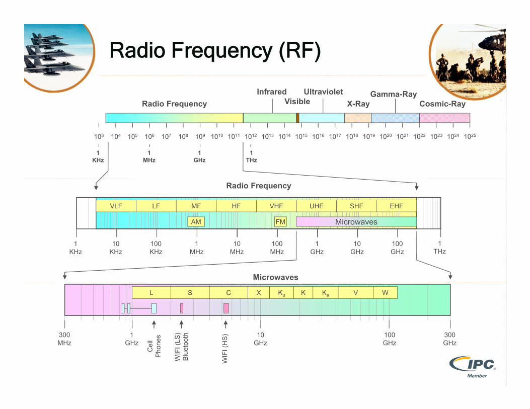
Radio Frequency (RF)
Radio FrequencyInfrared
VisibleUltraviolet
X-RayGamma-Ray
Cosmic-Ray
1MHz
1GHz
1THz
1KHz
103 104 105 106 107 108 109 1010 1011 1012 1013 1014 1015 1016 1017 1018 1019 1020 1021 1022 1023 1024 1025
VLF LF MF HF VHF UHF SHF EHF
Radio Frequency
AM FM Microwaves
10KHz
100KHz
1MHz
10MHz
100MHz
1GHz
10GHz
100GHz
1THz
1KHz
Microwaves
300 1 10 100 300
L S C X Ku K Ka V W
) h300MHz
1GHz
10GHz
100GHz
300GHz
WIF
I (LS
)B
luet
ooth
WIF
I (H
S)
Cel
lPh
ones

RF and Microwave Roadmap
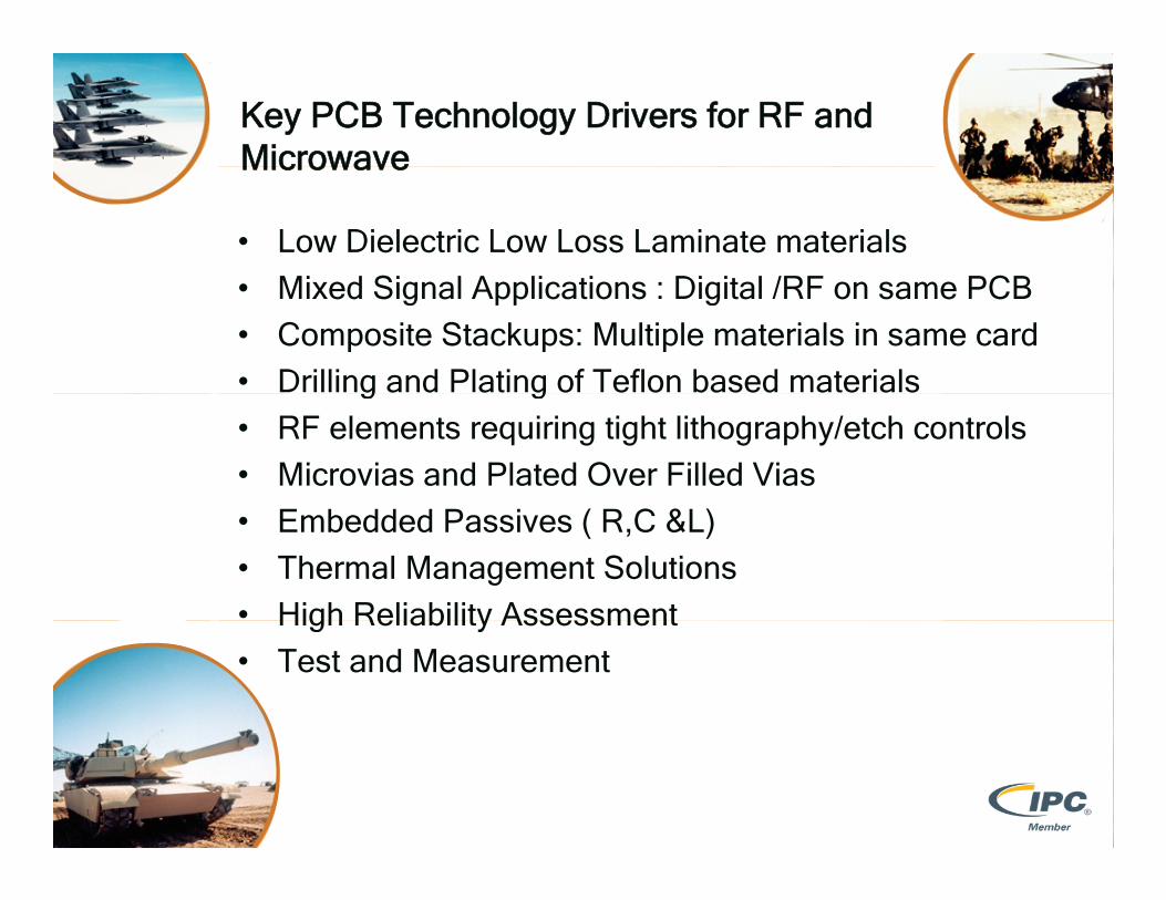
Key PCB Technology Drivers for RF and MicrowaveMicrowave
• Low Dielectric Low Loss Laminate materials
Mi d Si l A li ti Di it l /RF PCB• Mixed Signal Applications : Digital /RF on same PCB
• Composite Stackups: Multiple materials in same card
• Drilling and Plating of Teflon based materials g g
• RF elements requiring tight lithography/etch controls
• Microvias and Plated Over Filled Vias
• Embedded Passives ( R,C &L)
• Thermal Management Solutions
• High Reliability AssessmentHigh Reliability Assessment
• Test and Measurement
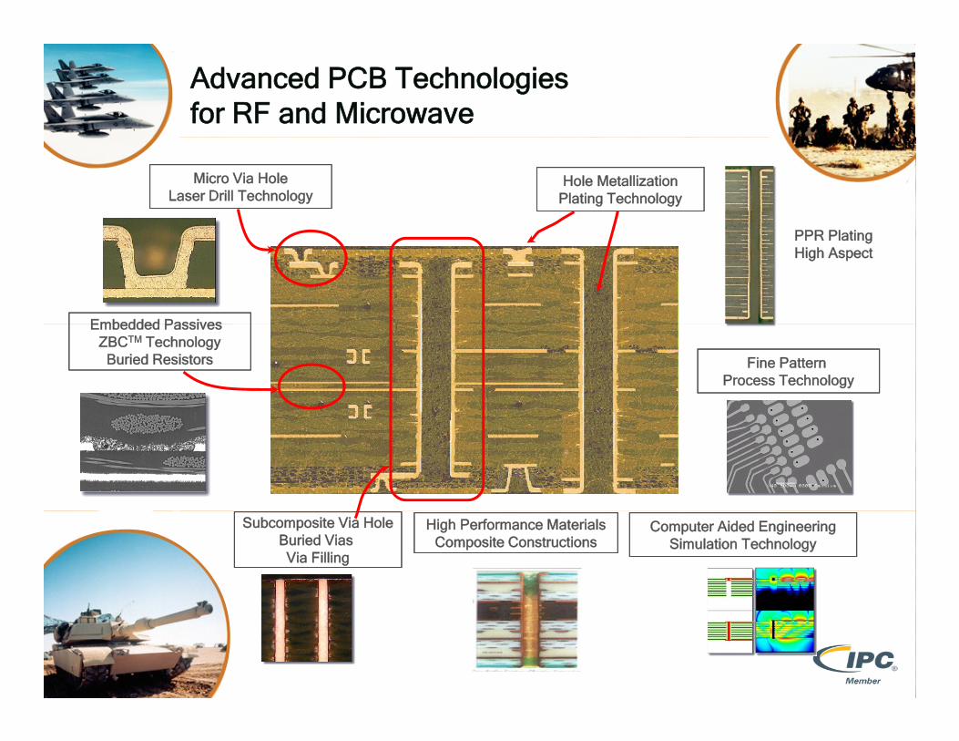
Advanced PCB Technologies for RF and Microwave
Micro Via HoleLaser Drill Technology
Hole MetallizationPlating Technology
PPR Pl i
Embedded Passives
PPR PlatingHigh Aspect
Embedded Passives ZBCTM TechnologyBuried Resistors Fine Pattern
Process Technology
Subcomposite Via HoleBuried Vias Via Filling
Computer Aided EngineeringSimulation Technology
High Performance MaterialsComposite Constructions
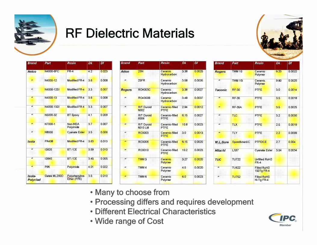
RF Dielectric Materials
• Many to choose fromP i diff d i d l t• Processing differs and requires development
• Different Electrical Characteristics• Wide range of Cost
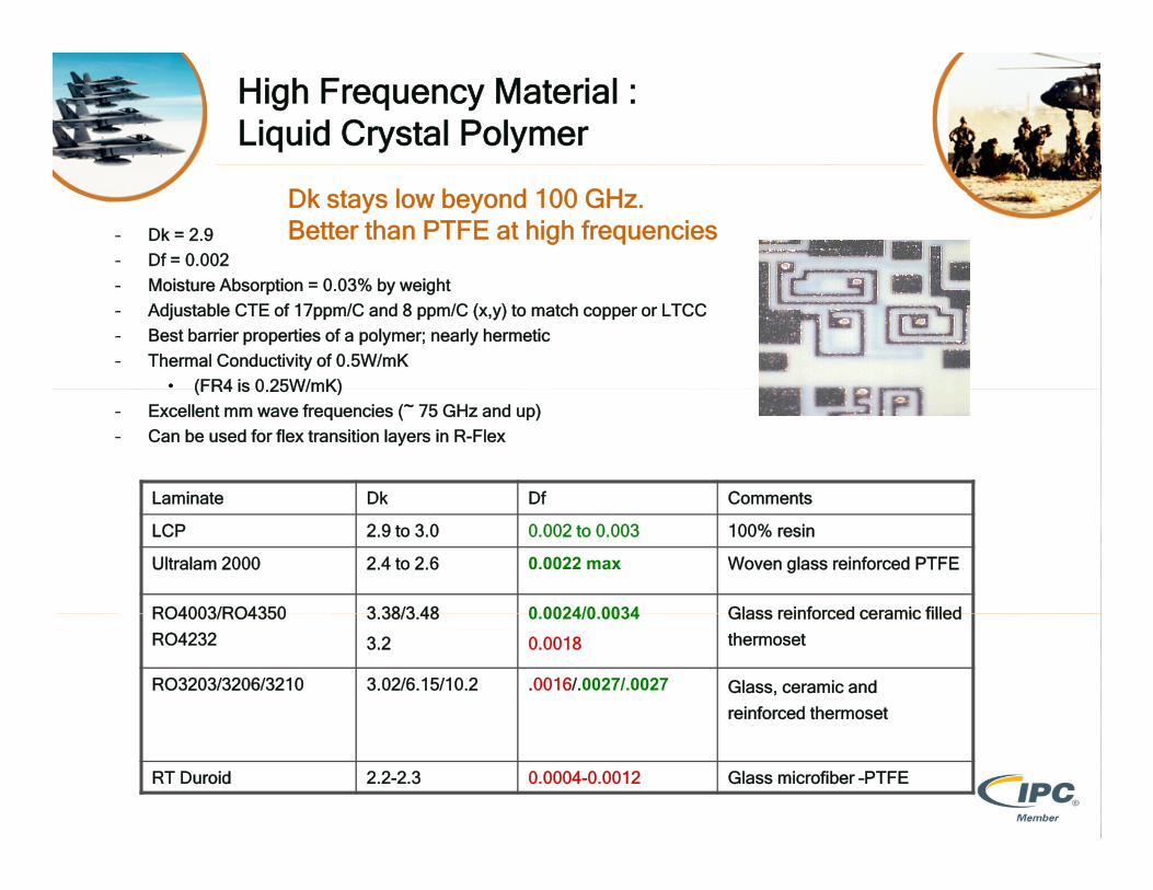
High Frequency Material :Liquid Crystal Polymer
– Dk = 2.9
– Df = 0.002
Dk stays low beyond 100 GHz.Better than PTFE at high frequencies
– Moisture Absorption = 0.03% by weight
– Adjustable CTE of 17ppm/C and 8 ppm/C (x,y) to match copper or LTCC
– Best barrier properties of a polymer; nearly hermetic
– Thermal Conductivity of 0.5W/mK
• (FR4 is 0 25W/mK)(FR4 is 0.25W/mK)
– Excellent mm wave frequencies (~ 75 GHz and up)
– Can be used for flex transition layers in R-Flex
Laminate Dk Df CommentsLaminate Dk Df Comments
LCP 2.9 to 3.0 0.002 to 0.003 100% resin
Ultralam 2000 2.4 to 2.6 0.0022 max Woven glass reinforced PTFE
RO4003/RO4350 3 38/3 48 0 0024/0 0034 Glass reinforced ceramic filledRO4003/RO4350
RO4232
3.38/3.48
3.2
0.0024/0.0034
0.0018
Glass reinforced ceramic filled
thermoset
RO3203/3206/3210 3.02/6.15/10.2 .0016/.0027/.0027 Glass, ceramic and
reinforced thermoset
RT Duroid 2.2-2.3 0.0004-0.0012 Glass microfiber –PTFE
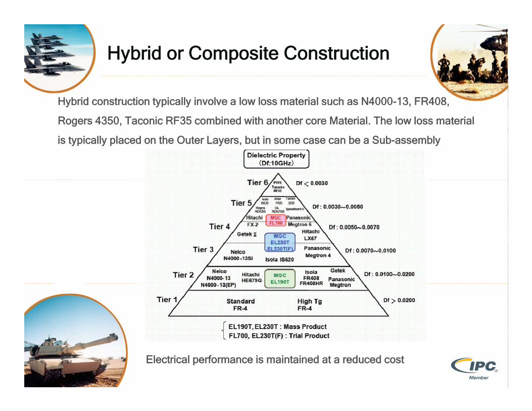
Hybrid or Composite Construction
Hybrid construction typically involve a low loss material such as N4000-13, FR408,
Rogers 4350, Taconic RF35 combined with another core Material. The low loss material
is typically placed on the Outer Layers, but in some case can be a Sub-assembly
Electrical performance is maintained at a reduced cost
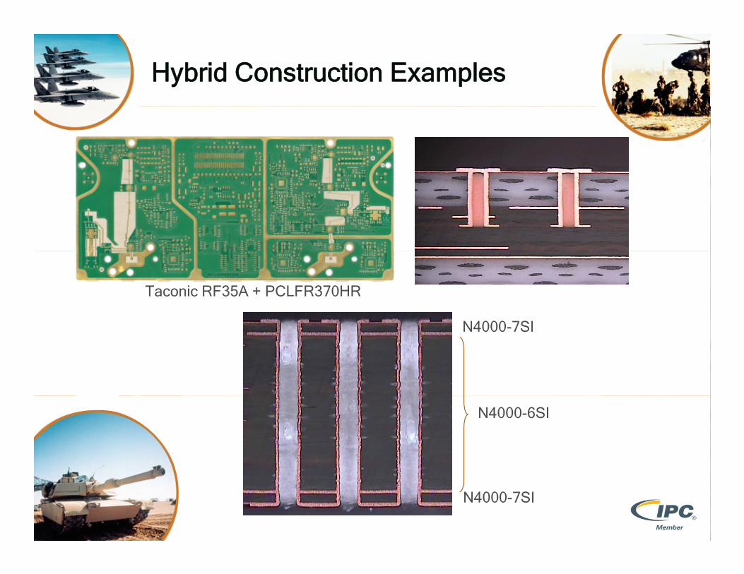
Hybrid Construction Examples
Taconic RF35A + PCLFR370HR
N4000 7SIN4000-7SI
N4000-6SI
N4000-7SI
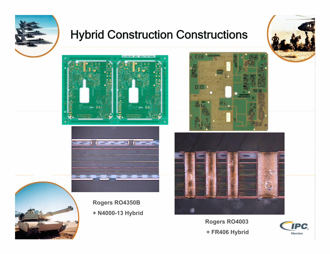
Hybrid Construction Constructions
Rogers RO4350B
+ N4000-13 HybridRogers RO4003
+ FR406 Hybrid
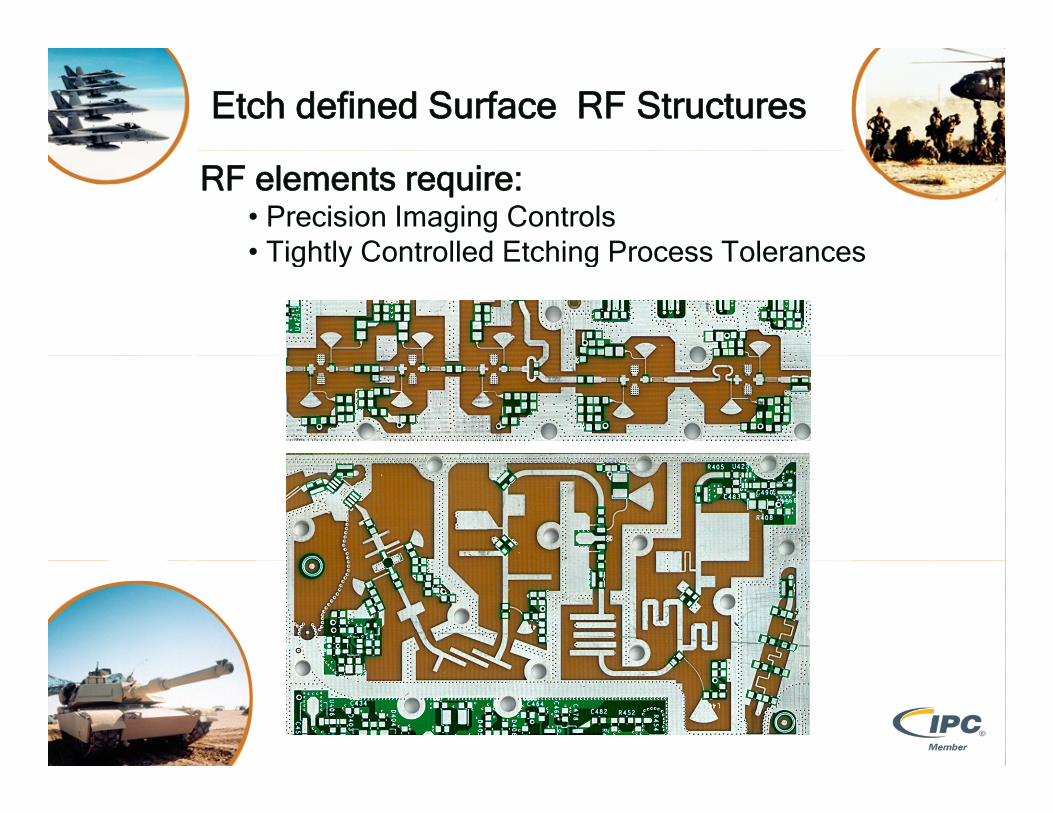
Etch defined Surface RF Structures
RF elements require:• Precision Imaging Controls• Tightly Controlled Etching Process Tolerances• Tightly Controlled Etching Process Tolerances
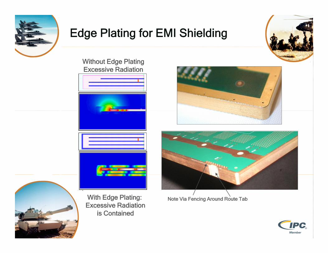
Edge Plating for EMI Shielding
Without Edge PlatingExcessive Radiation
With Edge Plating: Excessive Radiation
Note Via Fencing Around Route TabExcessive Radiation
is Contained

Circuit Isolation Using Via Fencing
Single Row
Double RowFor
IncreasedIsolation

Complex RF Power Divider Networks usingPTF Buried Resistors
• Complex Wilkenson Power Divider Network For RFDivider Network For RF Scanning Beam Array Antennas
• Using Low Cost Polymer g yThick Film Resistors embedded on internal layers
• Embedded Passives add functionality with reducedfunctionality with reduced space and weight
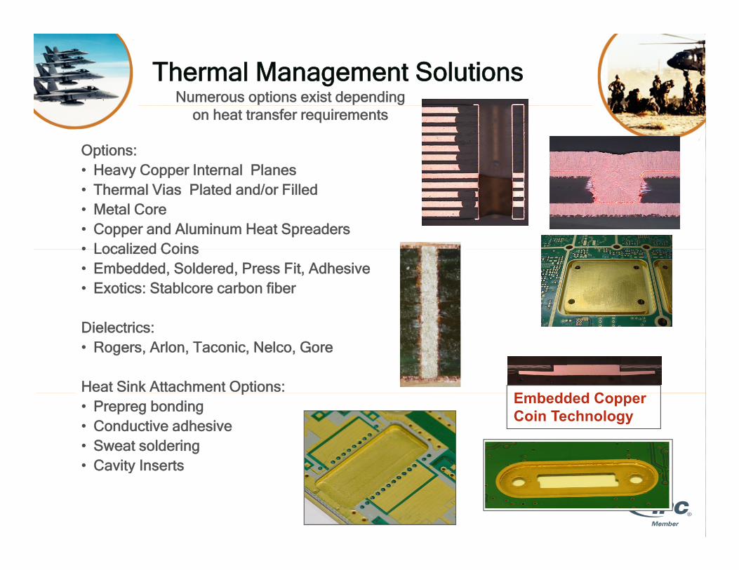
Thermal Management SolutionsNumerous options exist depending
Options:• Heavy Copper Internal Planes
on heat transfer requirements
y pp• Thermal Vias Plated and/or Filled• Metal Core • Copper and Aluminum Heat Spreaders• Localized Coins• Localized Coins• Embedded, Soldered, Press Fit, Adhesive• Exotics: Stablcore carbon fiber
Dielectrics:• Rogers, Arlon, Taconic, Nelco, Gore
Heat Sink Attachment Options:E b dd d C
p• Prepreg bonding• Conductive adhesive• Sweat soldering• Cavity Inserts
Embedded Copper Coin Technology
• Cavity Inserts
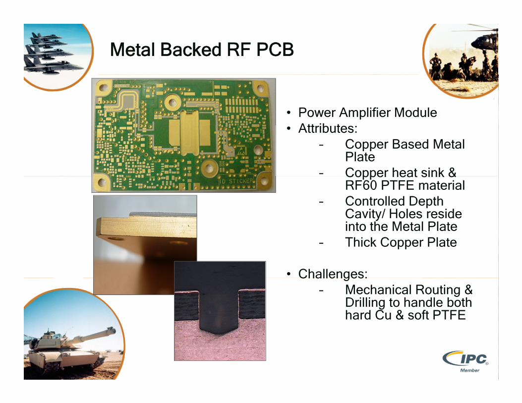
Metal Backed RF PCB
• Power Amplifier Module Att ib t• Attributes:
– Copper Based Metal Plate
– Copper heat sink &Copper heat sink & RF60 PTFE material
– Controlled Depth Cavity/ Holes reside into the Metal Plateinto the Metal Plate
– Thick Copper Plate
• Challenges:Challenges:– Mechanical Routing &
Drilling to handle both hard Cu & soft PTFE

IPC Printed Circuit Board IPC Printed Circuit Board Defense RoadmapDefense RoadmapDefense Roadmap Defense Roadmap IPC/DRIPC/DR
Handheld Handheld –– Wireless RuggedizedWireless RuggedizedPCB Technology Road MapPCB Technology Road MapC ec o ogy oad apC ec o ogy oad ap
Andy Cameron Andy Cameron TTM TechnologiesTTM Technologies
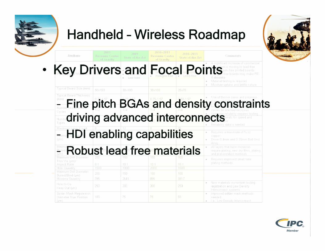
Handheld – Wireless Roadmap
• Key Drivers and Focal Points
– Fine pitch BGAs and density constraints p ydriving advanced interconnects
– HDI enabling capabilities
– Robust lead free materials

Fine-Pitch BGA ImplicationsConventional Mechanically Drilled Through ViasConventional Mechanically Drilled Through Vias• 1.00mm = 39.4 mils pitch• 0.80mm = 31.4 mils pitch
Annular Ring Requirements Class 2 or 3 Center of GravityCenter of Gravity.65-.50mm
State of the Art40mm and below.40mm and below
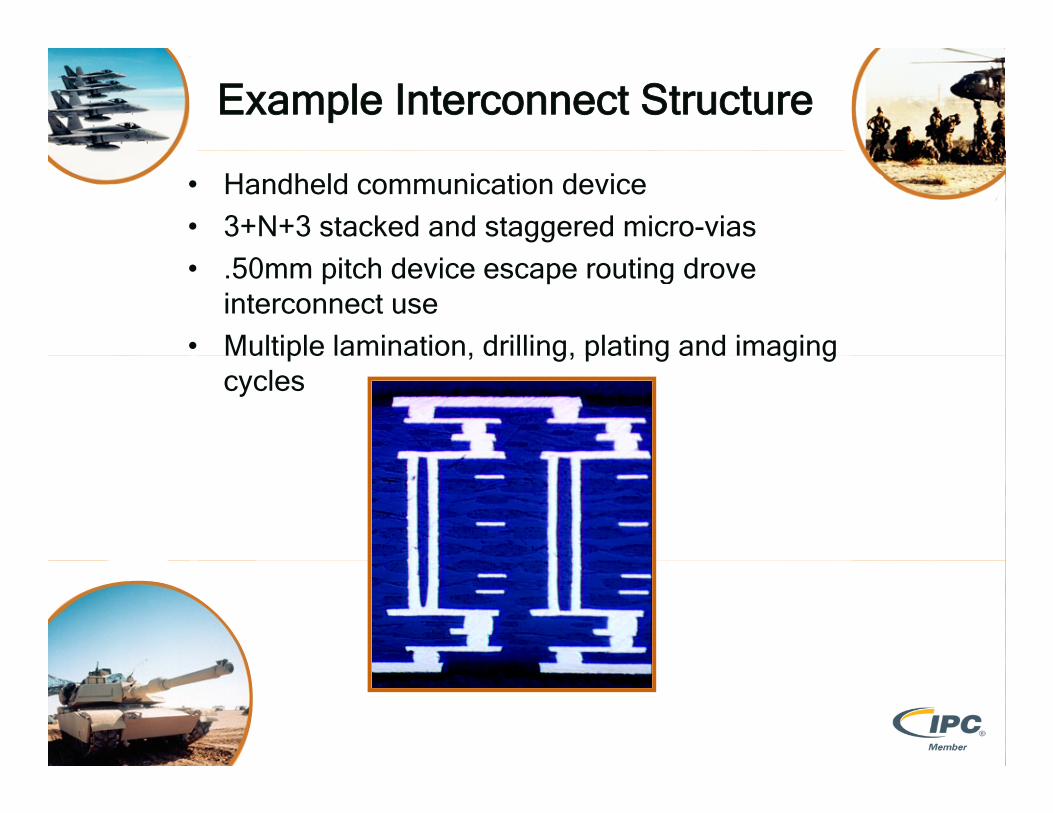
Example Interconnect Structure
• Handheld communication device
• 3+N+3 stacked and staggered micro-vias
• .50mm pitch device escape routing drove interconnect use
• Multiple lamination, drilling, plating and imagingMultiple lamination, drilling, plating and imaging cycles
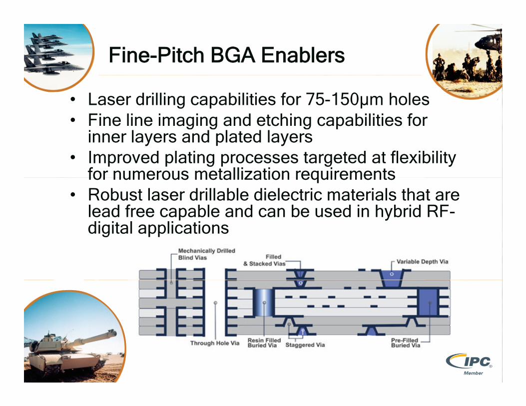
Fine-Pitch BGA Enablers
• Laser drilling capabilities for 75-150µm holes• Fine line imaging and etching capabilities for g g g p
inner layers and plated layers • Improved plating processes targeted at flexibility
for numerous metallization requirementsfor numerous metallization requirements• Robust laser drillable dielectric materials that are
lead free capable and can be used in hybrid RF-digital applicationsdigital applications
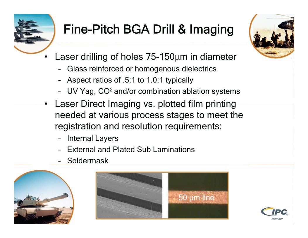
Fine-Pitch BGA Drill & Imaging
• Laser drilling of holes 75-150µm in diameter– Glass reinforced or homogenous dielectrics
– Aspect ratios of .5:1 to 1.0:1 typically
– UV Yag, CO2 and/or combination ablation systems
• Laser Direct Imaging vs plotted film printing• Laser Direct Imaging vs. plotted film printing needed at various process stages to meet the registration and resolution requirements:– Internal Layers
– External and Plated Sub Laminations
– Soldermask
50 50 µm line m line
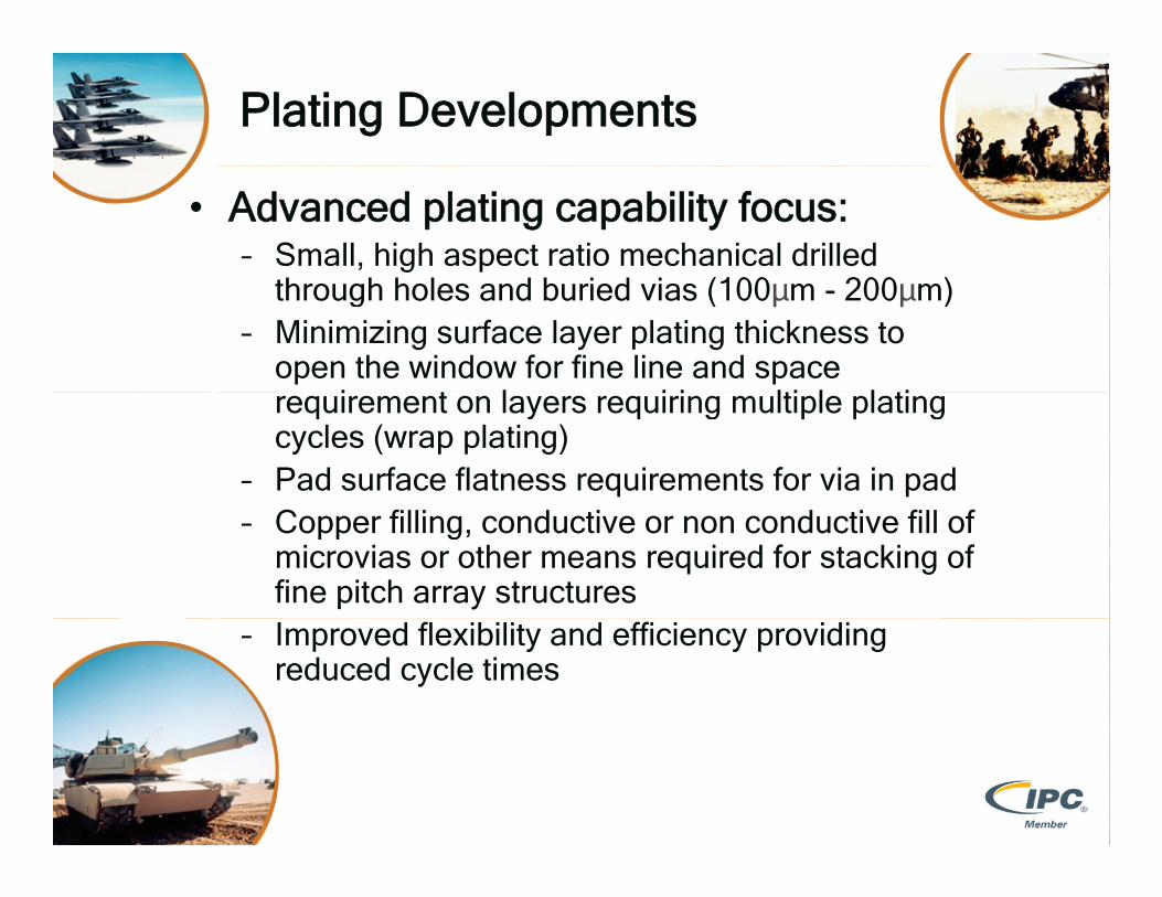
Plating Developments
• Advanced plating capability focus:– Small, high aspect ratio mechanical drilled
h h h l d b i d i (100 200 )through holes and buried vias (100µm - 200µm)– Minimizing surface layer plating thickness to
open the window for fine line and space i t l i i lti l l tirequirement on layers requiring multiple plating
cycles (wrap plating)– Pad surface flatness requirements for via in pad – Copper filling, conductive or non conductive fill of
microvias or other means required for stacking of fine pitch array structures
– Improved flexibility and efficiency providing reduced cycle times

Robust Lead Free Materials
• Lead Free material challenges– Naturally occurring moisture levels and lead-free temperatures y g p
combine to double the vapor pressure within the PCB
– Delamination risk increases at lead-free assembly temperatures – may not be evident on the surface p y
– Design points, thicker product and tighter hole to hole spacing can make delamination more prevalent
– Lead free resin systems are generally more brittle in nature andLead free resin systems are generally more brittle in nature and require additional process optimization
– Product requiring multiple lamination cycles degrades the materials resilience to further thermal excursions in 245-260 Cmaterials resilience to further thermal excursions in 245 260 C lead free assembly
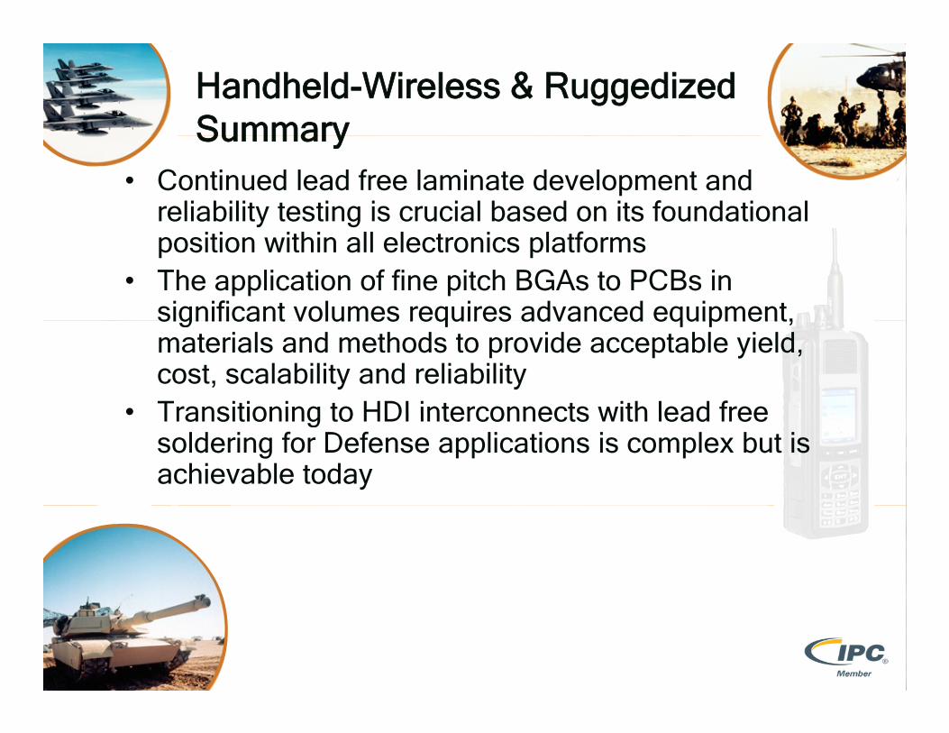
Handheld-Wireless & Ruggedized SummarySummary
• Continued lead free laminate development and reliability testing is crucial based on its foundational position within all electronics platforms
• The application of fine pitch BGAs to PCBs in significant volumes requires advanced equipment,significant volumes requires advanced equipment, materials and methods to provide acceptable yield, cost, scalability and reliability
• Transitioning to HDI interconnects with lead free• Transitioning to HDI interconnects with lead free soldering for Defense applications is complex but is achievable today
IPC Printed Circuit Board IPC Printed Circuit Board Defense RoadmapDefense RoadmapDefense Roadmap Defense Roadmap IPC/DRIPC/DR
Flex Circuit Flex Circuit Flex Circuit Flex Circuit Technology Road MapTechnology Road Map
Al WAl WAl WasserzugAl WasserzugVulcan Flex Circuit Corporation Vulcan Flex Circuit Corporation
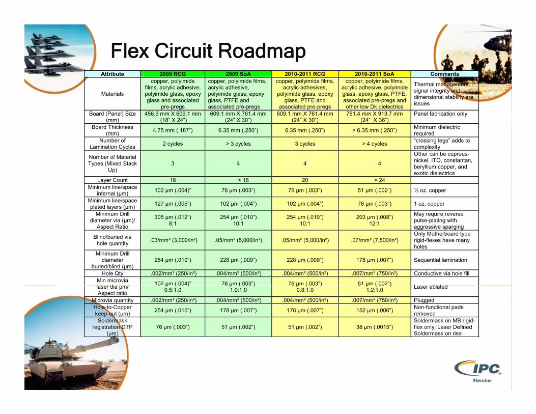
Flex Circuit RoadmapAttribute 2009 RCG 2009 SoA 2010-2011 RCG 2010-2011 SoA Comments
Materials
copper, polyimide films, acrylic adhesive, polyimide glass, epoxy glass and associated
pre-pregs
copper, polyimide films, acrylic adhesive, polyimide glass, epoxy glass, PTFE and associated pre-pregs
copper, polyimide films, acrylic adhesives,
polyimide glass, epoxy glass, PTFE and
associated pre-pregs
copper, polyimide films, acrylic adhesive, polyimide glass, epoxy glass, PTFE, associated pre-pregs and other low Dk dielectrics
Thermal management, signal integrity and dimensional stability are issues
Board (Panel) Size (mm)
456.9 mm X 609.1 mm (18” X 24”)
609.1 mm X 761.4 mm (24” X 30”)
609.1 mm X 761.4 mm (24” X 30”)
761.4 mm X 913.7 mm (24” X 36”)
Panel fabrication only
Board Thickness 4 75 ( 187”) 6 35 ( 250”) 6 35 ( 250”) 6 35 ( 250”) Minimum dielectricBoard Thickness (mm) 4.75 mm (.187”) 6.35 mm (.250”) 6.35 mm (.250”) > 6.35 mm (.250”) Minimum dielectric
required Number of
Lamination Cycles 2 cycles > 3 cycles 3 cycles > 4 cycles “crossing legs” adds to complexity
Number of Material Types (Mixed Stack
Up) 3 4 4 4
Other can be cuprous-nickel, ITO, constantan, beryllium copper, and exotic dielectrics
Layer Count 16 > 16 20 > 24Layer Count 16 > 16 20 > 24Minimum line/space
internal (µm) 102 μm (.004)” 76 μm (.003”) 76 μm (.003”) 51 μm (.002”) ½ oz. copper
Minimum line/space plated layers (µm) 127 μm (.005”) 102 μm (.004”) 102 μm (.004”) 76 μm (.003”) 1 oz. copper
Minimum Drill diameter via (µm)/
Aspect Ratio
305 μm (.012”) 8:1
254 μm (.010”) 10:1
254 μm (.010”) 10:1
203 μm (.008”) 12:1
May require reverse pulse-plating with aggressive sparging Only Motherboard typeBlind/buried via
hole quantity .03/mm² (3,000/in²) .05/mm² (5,000/in²) .05/mm² (5,000/in²) .07/mm² (7,500/in²) Only Motherboard type rigid-flexes have many holes
Minimum Drill diameter
buried/blind (µm) 254 μm (.010”) 228 μm (.009”) 228 μm (.009”) 178 μm (.007”) Sequential lamination
Hole Qty .002/mm² (250/in²) .004/mm² (500/in²) .004/mm² (500/in²) .007/mm² (750/in²) Conductive via hole fill Min microvia l di / 102 μm (.004)” 76 μm (.003”) 76 μm (.003”) 51 μm (.002”) L bl t dlaser dia µm/ Aspect ratio
0 μ ( 00 )0.5:1.0
6 μ ( 003 )1.0:1.0
6 μ ( 003 )0.8:1.0
5 μ ( 00 )1.2:1.0 Laser ablated
Microvia quantity .002/mm² (250/in²) .004/mm² (500/in²) .004/mm² (500/in²) .007/mm² (750/in²) Plugged Hole-to-Copper keep-out (µm) 254 μm (.010”) 178 μm (.007”) 178 μm (.007”) 152 μm (.006”) Non-functional pads
removed Soldermask
registration DTP (µm)
76 μm (.003”) 51 μm (.002”) 51 μm (.002”) 38 μm (.0015”) Soldermask on MB rigid-flex only; Laser Defined Soldermask on rise
Flex Circuit Roadmap
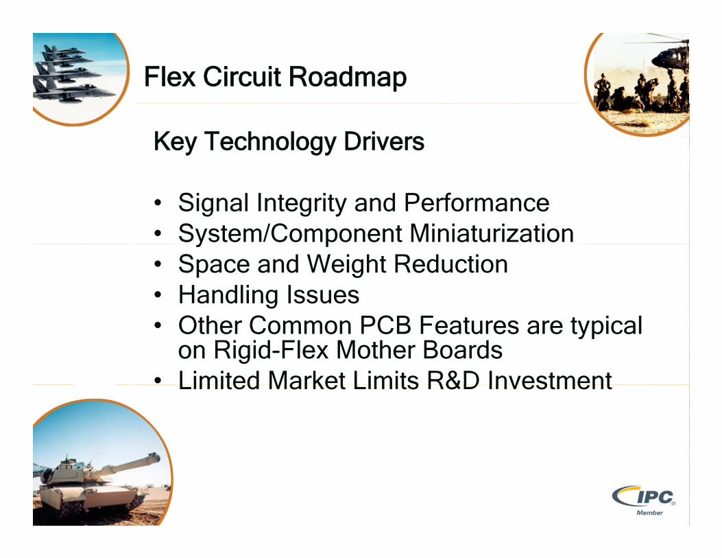
Key Technology Drivers
• Signal Integrity and Performance• System/Component Miniaturizationy p• Space and Weight Reduction• Handling Issues• Other Common PCB Features are typical
on Rigid-Flex Mother Boards• Limited Market Limits R&D InvestmentLimited Market Limits R&D Investment

Flex Circuit Roadmap
Product Evolutions Supporting Drivers• Rigid Flex Circuit Board• Rigid-Flex Circuit Board
• Backplane
• Motherboard
• Sculpted Flex Circuit
• Coax & Twisted Shielded Pair emulation
• Oversized Flex Harness (> 36” long)• Formed-To-Install Flex Circuits
• Chip On Flex/TAB/Flip Chip• Chip-On-Flex/TAB/Flip-Chip

Flex Circuit RoadmapBackplane Type Rigid-Flex
Circuit Board in Carrier

Flex Circuit RoadmapM h b d TMotherboard Type
Rigid-Flex Circuit Board

Flex Circuit Roadmap
No. Designation rigid flex Description Spec0.0020 Copper plating & HASL finish IPC-60130.00140.0150
0.0050 2 plys 1080 prepreg, no-flow IPC-4101/24
| * * * * * * * * * * * MATERIAL * * * * * * * * * * * |
IPC-4101/24Pads Only1
15 mil epoxy (FR-4) core with 1 oz. copper one side
| * * LAYER * * | | THICKNESS |
p y p p g,
0.0030 1 mil polyimide film/2 mil adhesive IPC-4203/12 2A Power 0.0028 0.0028
0.0010 0.00103 GND 0.0028 0.0028
0.0030 1 mil polyimide film/2 mil adhesive IPC-4203/1
0 0050 2 plys 1080 prepreg no-flow IPC-4101/24
IPC-4204/111 mil polyimide film with 2 oz.
copper both sides, adhesive-less (AP9212)
0.0050 2 plys 1080 prepreg, no-flow IPC-4101/24
0.0030 1 mil polyimide film/2 mil adhesive IPC-4203/14 Signals 0.0014 0.0014
0.0020 0.0020
0.0050 2 plys 1080 prepreg, no-flow IPC-4101/24
0 0030 1 mil polyimide film/2 mil adhesive IPC-4203/1
IPC-4204/112 mil polyimide film with 1 oz. copper one side, adhesive-less
0.0030 1 mil polyimide film/2 mil adhesive IPC 4203/15 GND 0.0028 0.0028
0.0010 0.00106 4A Power 0.0028 0.0028
0.0030 1 mil polyimide film/2 mil adhesive IPC-4203/1
0.0050 2 plys 1080 prepreg, no-flow IPC-4101/24
0 0150
IPC-4204/11
15 mil epoxy (FR 4) core with 1
1 mil polyimide film with 2 oz. copper both sides, adhesive-less
(AP9212)
0.01500.00140.0020 Copper plating & HASL finish IPC-6013
0.0734 overall thickness (metal-to-metal)0.0068 less outer metalization0.0666 overall thickness (glass-to-glass)
7IPC-4101/24
Pads Only
15 mil epoxy (FR-4) core with 1 oz. copper one side
Typical Rigid-Flex Cross-Section
Flex Circuit Roadmap
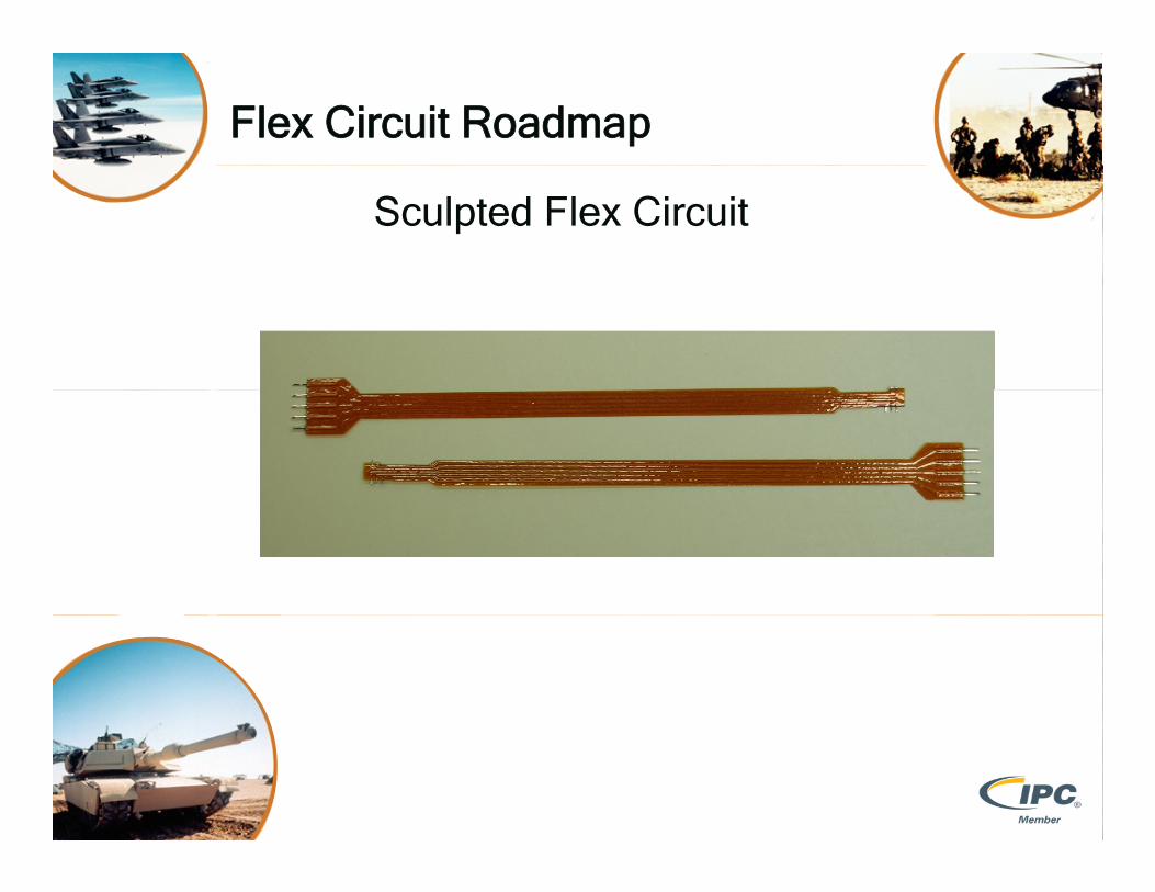
Sculpted Flex Circuit
Flex Circuit Roadmap
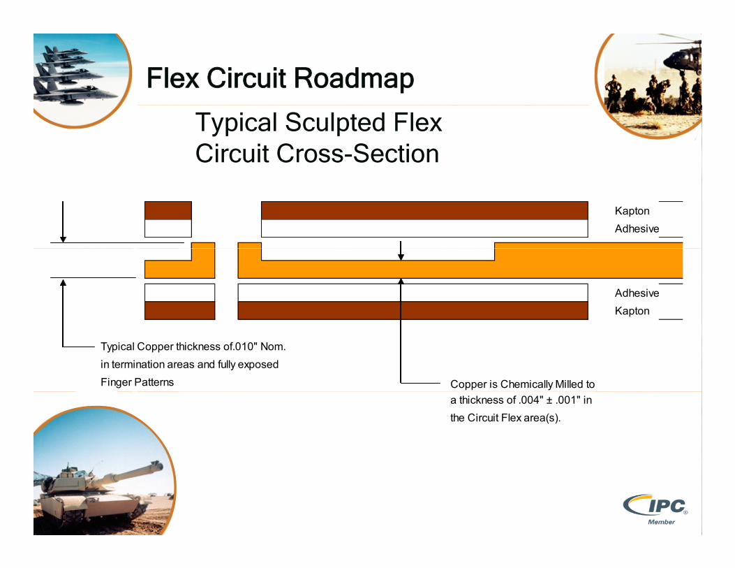
Typical Sculpted FlexCircuit Cross-Section
KaptonAdhesive
AdhesiveKapton
Typical Copper thickness of.010" Nom.in termination areas and fully exposedFinger Patterns Copper is Chemically Milled to
a thickness of .004" ± .001" inthe Circuit Flex area(s).

Flex Circuit Roadmap
Oversized Flex Harness

Flex Circuit RoadmapInnovative Shielding Techniques
Flex Leg Width
Cross-Section of Silver Polymer "Stitching" on Typical Rigid-Flex Leg
?
Flex Leg Width
.025" minimum edge of ground trace to edge of Flex Leg
Top Side Coverc?
Silver Polymer S
Layer 4
Layer 5 Copper Conduct
Internal Dielectri
Internal Dielectri
Internal Dielectri?
?
?
Copper Conduct
Layer 8
Layer 6
Copper Conduct
?
Layer 7
Copper Conduct
Copper Conduct
Internal Dielectri
Internal Dielectri?
?
=
Silver Polymer S
Bottom Side Cov
Internal Dielectri
designates a ground trace. On Layers 4 and 8 these traces are in direct contacted with the Silver Polymer. On Layers 5, 6 & 7 these traces are "floating" grounds and are of a width that is at least 3 times the thickness of the
?
?
dielectric material between conductive layers - so as to provide a shield for the cable sides from external EMI in various frequencies. All ground traces are electrically connected to each other through vias in the rigid sections.
Flex Circuit Roadmap
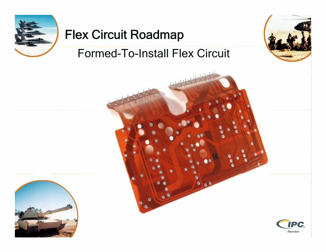
Formed-To-Install Flex Circuit

Flex Circuit Roadmap
Innovations in Support of Drivers
M t i l D l t• Materials Development• Low Dk dielectrics
• Adhesive-less laminates
• Shielding alternatives
• “No Flow” pre-pregs
• Embedded passive laminatesEmbedded passive laminates
• Process Development• Selective covercoat bonding
• Thermal management modeling
• Layer registration/sequential lamination
• Impedance modelingpeda ce ode g
Flex Circuit Roadmap
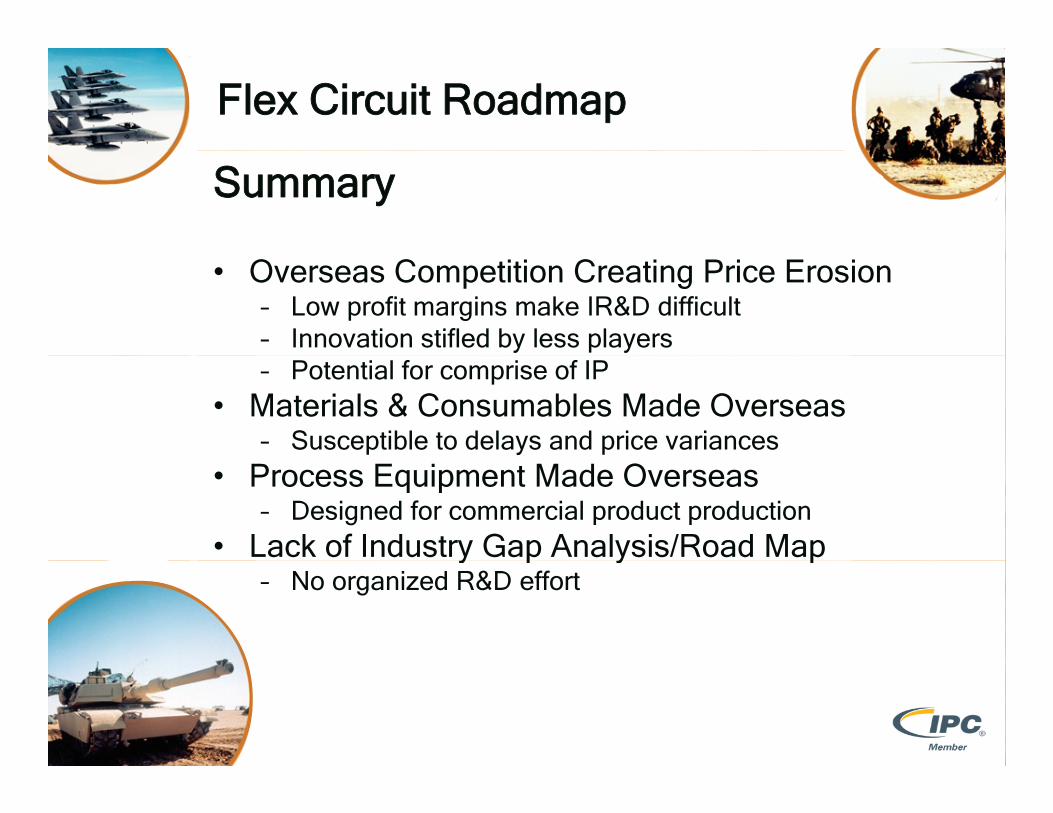
Summary
• Overseas Competition Creating Price Erosion– Low profit margins make IR&D difficult– Innovation stifled by less players– Potential for comprise of IP
• Materials & Consumables Made Overseas– Susceptible to delays and price variances
• Process Equipment Made Overseas– Designed for commercial product production
• Lack of Industry Gap Analysis/Road Map y p y p– No organized R&D effort

IPC Printed Circuit Board IPC Printed Circuit Board Defense RoadmapsDefense RoadmapsDefense Roadmaps Defense Roadmaps IPC/DRIPC/DR
Summary and Common Summary and Common Challenges Challenges Challenges Challenges

PCB Technology and Market Migration
• The Market Trend is Obvious• Certain D&A PCBs are being off-shored • Defense and Aerospace Companies Must Think of the Long Termp p g
Impact on Domestic PCB Industry• Reverse ITAR Potential • Innovations will be required to compete and retain technological
advantageadvantage
Lets not forget about PCB consumables• Laminate Materials• Chemistry• Drill Bits • Equipment
IPC Programs : D&A Technology RoadmapD&A Task ForceD&A Task ForceIP Protection Standard

Next Gen PCBs require capital Next Gen PCBs require capital investment and advanced capabilitiesinvestment and advanced capabilitiespp
New 24”x36” Hi-Speed LDILaser Direct Imager
New 26”x38” Large Format Mod Drill for +/-0 0005” t ll d d th bilit dLaser Direct Imager 0.0005” controlled depth capability and
Ultra-Hi Aspect Ratio Drilling
3’x5’ Autoclave Microwave/Rf Market,up to 27”x48” panel sizes, and Complex Full-Flex/Rigid-Flex
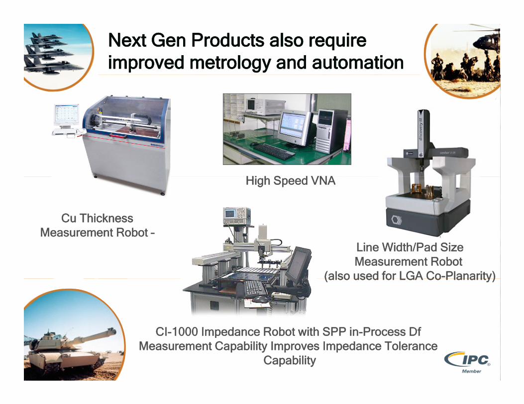
Next Gen Products also require Next Gen Products also require improved metrology and automationimproved metrology and automation
Hi h S d VNA
Cu Thickness
High Speed VNA
Measurement Robot –Line Width/Pad Size Measurement Robot
(also used for LGA Co-Planarity)(also used for LGA Co Planarity)
CI 1000 Impedance Robot ith SPP in Process DfCI-1000 Impedance Robot with SPP in-Process Df Measurement Capability Improves Impedance Tolerance
Capability

Defense Roadmaps Summary
• DoD needs to be concerned with current PCB market transition• D&A market will continue to be the focus of NA based fabricators• D&A market will continue to be the focus of NA based fabricators• Market growth depends on economic climate and government
funding• The domestic PCB industry needs to lobby for retention of this y y
market in NA and to prevent further off-shoring• Technology demands of D&A PCBs will continue to increase with
focus on bandwidth, size and weight reductionNA PCB f b i t ill d t k it l i t t i• NA PCB fabricators will need to make capital investments in equipment and infrastructure to support next gen PCBs
• Innovation and IP Protection will be key to retaining competitive edgeedge

Defense Road Maps
Question and Answer
Related Documents