Sensors and Actuators A 197 (2013) 96–105 Contents lists available at SciVerse ScienceDirect Sensors and Actuators A: Physical jo u r n al homep age: www.elsevier.com/locate/sna Geometric optimization of a differential planar eddy currents probe for non-destructive testing Luis S. Rosado a,b,c,∗ , João C. Gonzalez d , Telmo G. Santos d , Pedro M. Ramos a,b , Moisés Piedade a,c a Instituto Superior Técnico (IST), Universidade Técnica de Lisboa, 1049-001 Lisboa, Portugal b Instituto de Telecomunicac ¸ ões (IT), 1049-001 Lisboa, Portugal c Instituto de Engenharia de Sistemas e Computadores (INESC), Investigac ¸ ão e Desenvolvimento, 1000-029 Lisboa, Portugal d Departamento de Engenharia Mecânica e Industrial, Faculdade de Ciências e Tecnologia (UNIDEMI), Universidade Nova de Lisboa, 2829-516 Caparica, Portugal a r t i c l e i n f o Article history: Received 2 January 2013 Received in revised form 4 April 2013 Accepted 5 April 2013 Available online 12 April 2013 Keywords: Planar probe Differential probe Geometrical optimization Eddy currents Non-destructive testing a b s t r a c t The influence of the geometrical parameters of an eddy currents planar probe intended for non- destructive testing is reported in this paper. Finite element modeling simulations were used to evaluate the effect of each geometrical parameter on the probe response amplitude and spatial discrimination while testing an arbitrary defect. A representative set of probes was produced and used to experimentally validate the simulation study. The reported results show that modifications of the studied parameters can substantially improve the probe performance targeting specific testing requirements. Additional probes were produced using a parameters combination optimized for two different testing situations. It was also shown that the modification of the defects properties does not substantially modifies the relative effectiveness of the additional probes produced. © 2013 Elsevier B.V. All rights reserved. 1. Introduction The eddy currents technique is one of the preferred non- destructive testing (NDT) methods on the inspection of deployed metallic components. Typical applications include the inspection of welded or riveted joints on critical parts applied in industrial fields such as the aerospace and power generation. The method is based on the induction of electrical current in the part under test while simultaneously measuring the resulting magnetic field. The eddy currents flow is disturbed by flaws or conductivity changes modifying the original magnetic field thus enabling the detection and characterization of defects [1]. In a basic probe, induction and sensing of the eddy currents is done in a single cylindrical coil whose electrical impedance changes indicate the presence or absence of defects and conductivity variations [1]. The design of eddy current probes targeting specific applications has received special attention from the scientific community in the last years. In Ref. [2], an eddy current probe was used to detect defects around bolt holes of aircraft lap joints using multiple fre- quencies. In a similar application, the use of pulsed eddy currents and a specific probe design to detect defects near rivets is reported in Ref. [3]. Another eddy current probe design was proposed to assess the decarburization level and integrity of rails [4]. In Ref. [5], ∗ Corresponding author. E-mail address: [email protected] (L.S. Rosado). a remote field eddy current probe is proposed to the inspection of steam generator tubes in nuclear power plants. For the same appli- cation, a probe with multiple coils was reported in Ref. [6]. A remote field eddy current probe was also proposed to detect stress corro- sion in gas transmission pipelines [7]. In many situations, the design of eddy current probes is supported by simulations with finite ele- ment modeling (FEM) as was presented in Refs. [8–10] for different probe designs and testing conditions. In other situations, closed form expressions can be obtained to evaluate the probe responses such as in Ref. [11] for stratified parts. As seen from the previous examples, applications of the eddy currents method are usually critical parts whose failure may result on human or economic losses. The effectiveness of an eddy cur- rent probe is primarily conditioned by its operation mode and basic design. Even so, the probe design optimization is decisive to achieve high levels of reliability usually required by the probe end- application. Some papers studied and proposed methodologies to improve the sensitivity of eddy current probes through the selec- tion of an optimal construction parameters set. The work reported in Ref. [12] showed that the parameters that most influence the per- formance of cylindrical coils eddy current probes are the number and spacing between windings, the dimensional aspect ratio and the internal ferrite core length. The effect of seven construction parameters was experimentally demonstrated through the inspec- tion of an aluminum piece with an electro discharge machined notch defect. In Ref. [13], an optimization study was performed for both cylindrical and rectangular coil probes based on the FEM 0924-4247/$ – see front matter © 2013 Elsevier B.V. All rights reserved. http://dx.doi.org/10.1016/j.sna.2013.04.010

Welcome message from author
This document is posted to help you gain knowledge. Please leave a comment to let me know what you think about it! Share it to your friends and learn new things together.
Transcript
Gn
La
b
c
d
ARRAA
KPDGEN
1
dmofibwemaaca
hldqaia
0h
Sensors and Actuators A 197 (2013) 96– 105
Contents lists available at SciVerse ScienceDirect
Sensors and Actuators A: Physical
jo u r n al homep age: www.elsev ier .com/ locate /sna
eometric optimization of a differential planar eddy currents probe foron-destructive testing
uis S. Rosadoa,b,c,∗, João C. Gonzalezd, Telmo G. Santosd, Pedro M. Ramosa,b, Moisés Piedadea,c
Instituto Superior Técnico (IST), Universidade Técnica de Lisboa, 1049-001 Lisboa, PortugalInstituto de Telecomunicac ões (IT), 1049-001 Lisboa, PortugalInstituto de Engenharia de Sistemas e Computadores (INESC), Investigac ão e Desenvolvimento, 1000-029 Lisboa, PortugalDepartamento de Engenharia Mecânica e Industrial, Faculdade de Ciências e Tecnologia (UNIDEMI), Universidade Nova de Lisboa, 2829-516 Caparica, Portugal
a r t i c l e i n f o
rticle history:eceived 2 January 2013eceived in revised form 4 April 2013ccepted 5 April 2013vailable online 12 April 2013
a b s t r a c t
The influence of the geometrical parameters of an eddy currents planar probe intended for non-destructive testing is reported in this paper. Finite element modeling simulations were used to evaluatethe effect of each geometrical parameter on the probe response amplitude and spatial discriminationwhile testing an arbitrary defect. A representative set of probes was produced and used to experimentallyvalidate the simulation study. The reported results show that modifications of the studied parameters can
eywords:lanar probeifferential probeeometrical optimizationddy currents
substantially improve the probe performance targeting specific testing requirements. Additional probeswere produced using a parameters combination optimized for two different testing situations. It wasalso shown that the modification of the defects properties does not substantially modifies the relativeeffectiveness of the additional probes produced.
© 2013 Elsevier B.V. All rights reserved.
on-destructive testing. Introduction
The eddy currents technique is one of the preferred non-estructive testing (NDT) methods on the inspection of deployedetallic components. Typical applications include the inspection
f welded or riveted joints on critical parts applied in industrialelds such as the aerospace and power generation. The method isased on the induction of electrical current in the part under testhile simultaneously measuring the resulting magnetic field. The
ddy currents flow is disturbed by flaws or conductivity changesodifying the original magnetic field thus enabling the detection
nd characterization of defects [1]. In a basic probe, inductionnd sensing of the eddy currents is done in a single cylindricaloil whose electrical impedance changes indicate the presence orbsence of defects and conductivity variations [1].
The design of eddy current probes targeting specific applicationsas received special attention from the scientific community in the
ast years. In Ref. [2], an eddy current probe was used to detectefects around bolt holes of aircraft lap joints using multiple fre-uencies. In a similar application, the use of pulsed eddy currents
nd a specific probe design to detect defects near rivets is reportedn Ref. [3]. Another eddy current probe design was proposed tossess the decarburization level and integrity of rails [4]. In Ref. [5],∗ Corresponding author.E-mail address: [email protected] (L.S. Rosado).
924-4247/$ – see front matter © 2013 Elsevier B.V. All rights reserved.ttp://dx.doi.org/10.1016/j.sna.2013.04.010
a remote field eddy current probe is proposed to the inspection ofsteam generator tubes in nuclear power plants. For the same appli-cation, a probe with multiple coils was reported in Ref. [6]. A remotefield eddy current probe was also proposed to detect stress corro-sion in gas transmission pipelines [7]. In many situations, the designof eddy current probes is supported by simulations with finite ele-ment modeling (FEM) as was presented in Refs. [8–10] for differentprobe designs and testing conditions. In other situations, closedform expressions can be obtained to evaluate the probe responsessuch as in Ref. [11] for stratified parts.
As seen from the previous examples, applications of the eddycurrents method are usually critical parts whose failure may resulton human or economic losses. The effectiveness of an eddy cur-rent probe is primarily conditioned by its operation mode andbasic design. Even so, the probe design optimization is decisive toachieve high levels of reliability usually required by the probe end-application. Some papers studied and proposed methodologies toimprove the sensitivity of eddy current probes through the selec-tion of an optimal construction parameters set. The work reportedin Ref. [12] showed that the parameters that most influence the per-formance of cylindrical coils eddy current probes are the numberand spacing between windings, the dimensional aspect ratio andthe internal ferrite core length. The effect of seven construction
parameters was experimentally demonstrated through the inspec-tion of an aluminum piece with an electro discharge machinednotch defect. In Ref. [13], an optimization study was performedfor both cylindrical and rectangular coil probes based on the FEM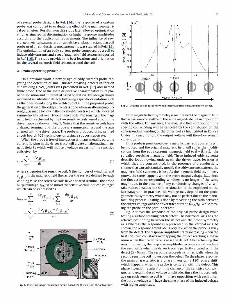
d Actuators A 197 (2013) 96– 105 97
opceaepTiif
2
gsIniatrsndaac
cnc
ε
w�
wow
U
L.S. Rosado et al. / Sensors an
f several probe designs. In Ref. [14], the response of a customrobe was computed to evaluate the effect of the main geometri-al parameters. Results from this study later allowed optimizationmphasizing spatial discrimination or higher response amplitudesccording to the application requirements. The influence of sev-ral geometrical parameters on a multilayer planar rectangular coilrobe used on conductivity measurements was studied in Ref. [15].he optimization of an eddy current probe composed by a coil tonduce eddy currents and a set of magnetic field sensors is reportedn Ref. [16]. The study provided the best locations and orientationor the several magnetic field sensors around the coil.
. Probe operating principle
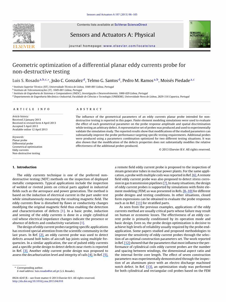
On a previous work, a new design of eddy currents probe tar-eting the detection of small surface breaking defects in frictiontir welding (FSW) joints was presented in Ref. [17] and namedOnic probe. One of the main distinctive characteristics is its pla-ar disposition and differential based operation. This design allows
ncreased sensitivity to defects following a specific orientation suchs the ones found along the welded joints. In the proposed probe,he generation of the eddy currents is done when an alternating cur-ent, Iin, is made to flow in the so called driver trace which is locatedymmetrically between two sensitive coils. The sensing of the mag-etic field is achieved by the two sensitive coils wired around theriver trace as shown in Fig. 1. Notice that the sensitive coils have
shared terminal and the probe is symmetrical around the axisligned with the driver trace. The probe is produced using printedircuit board (PCB) technology on a single support substrate.
When the probe is free of interaction with any metallic part, theurrent flowing in the driver trace will create an alternating mag-etic field �Bd which will induce a voltage on each of the sensitiveoils given by
c =N∑
i=1
−d�
c−→Bd,Pi
dt(1)
here c denotes the sensitive coil, N the number of windings and
c−→B ,Pi
is the magnetic field flux across the surface defined by each
inding Pi. As the sensitive coils have a shared terminal, the probeutput voltage Uout is the sum of the sensitive coils induced voltageshich can be expressed as
out =N∑
i=1
−d�
1−→B d,Pi
dt+
N∑
i=1
−d�
2−→B d,Pi
dt
=N∑
i=1
−d(�
1−→B d,Pi
+ �2−→B d,Pi
)
dt(2)
Fig. 1. Probe prototype on printed circuit board (PCB) seen from the active side.
Fig. 2. Original design response when testing a surface breaking notch defect.
If the magnetic field symmetry is maintained, the magnetic fieldflux across one coil will be of the same magnitude but in oppositionwith the other. For instance, the magnetic flux contribution of aspecific coil winding will be canceled by the contribution on thecorresponding winding of the other coil as highlighted in Eq. (2).Under this assumption, the output voltage will therefore remainclose to zero.
If the probe is positioned over a metallic part, eddy currents willbe induced and the original magnetic field will suffer the modifi-cations from the eddy currents magnetic field to �B = �Bd + �Be, theso called resulting magnetic field. These induced eddy currentsdescribe loops flowing underneath the driver trace, location atwhich they are concentrated. In the presence of a conductivitychange that can substantially modify the eddy currents pattern, themagnetic field symmetry is lost. As the magnetic field asymmetrygrows, the same happens with the probe output voltage, Uout sincethe flux across corresponding windings is no longer of the samemagnitude. In the absence of any conductivity changes, Uout willtake reduced values in a similar situation to the explained on thelast paragraph. In practice, this voltage may depend on the probegeometrical symmetry which may not be perfect due to the manu-facturing process. Testing is done by measuring the ratio betweenthe output voltage and the driver trace current, Uout/Iin, while mov-ing the probe on the part under test.
Fig. 2 shows the response of the original probe design whiletesting a surface breaking notch defect. The horizontal axis has therelative positioning between the defect and the probe symmetryaxis whereas the response is represented in the vertical axis. Asshown, the response amplitude is very low when the probe is awayfrom the defect. The response amplitude starts increasing when thefirst sensitive coil starts overlapping the defect reaching a maxi-mum when the driver trace is near the defect. After achieving thismaximum value, the response amplitude decreases until reachingthe zero value when the driver trace is perfectly aligned with thedefect (X = 0 mm). The response proceeds symmetrically when thesecond sensitive coil moves over the defect. On the phase response,the main characteristic is a phase inversion (a 180◦ phase shift)which happens when the probe is centered with the defect. Thisphase inversion results from the change of the sensitive coil with
greater overall induced voltage amplitude. Since the induced volt-age on each sensitive coil is in phase opposition with each other,the output voltage will have the same phase of the induced voltagewith higher amplitude.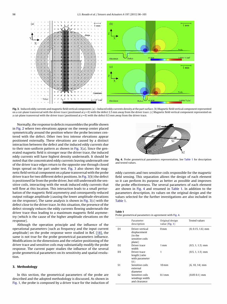
98 L.S. Rosado et al. / Sensors and Actuators A 197 (2013) 96– 105
F ddy currents density at the part surface. (b) Magnetic field vertical component representedo 2.5 mm away from the driver trace. (c) Magnetic field vertical component represented ona mm away from the driver trace.
istpiteenolndiswboodddtr
oasMdrpt
3
dF
parameters description, its values on the original design and thevalues selected for the further investigations are also included inTable 1.
Table 1Probe geometrical parameters in agreement with Fig. 4.
Parameterdescription
Original designvalue (Fig. 1)
Tested values
D1 Driver verticaldisplacement(to thesensitive coilsplane)
0 mm {0, 0.15, 1.6} mm
D2 Driver tracewidth
1 mm {0.5, 1, 1.5} mm
D3 Driver tracelength (ratiowith parameterS1)
1 {0.5, 1, 1.5} mm
S1 Sensitive coilsexternal
10 mm {6, 10, 14} mm
ig. 3. Induced eddy currents and magnetic field vertical component. (a) – Induced en a cut-plane transversal with the driver trace (positioned at y = 0) with the defect
cut-plane transversal with the driver trace (positioned at y = 0) with the defect 0.5
Normally, the response to defects reassembles the profile shownn Fig. 2 where two elevations appear on the sweep center placedymmetrically around the position where the probe becomes cen-ered with the defect. Other two less intense elevations appearositioned externally. These elevations are caused by a distinct
nteraction between the defect and the induced eddy currents dueo their non-uniform pattern as shown in Fig. 3(a). Since the gen-rated magnetic field is stronger near the driver trace, the inducedddy currents will have highest density underneath. It should beoted that the concentrated eddy currents leaving underneath onef the driver trace edges return to the opposite one through closedoops spread on the part under test. Fig. 3 also shows the mag-etic field vertical component on a plane transversal with the proberiver trace for two different defect positions. In Fig. 3(b) the defect
s positioned far from the probe driver, but still underneath the sen-itive coils, interacting with the weak induced eddy currents thatill flow at this location. This interaction leads to a small pertur-
ation of the magnetic field asymmetry and consequently reducedutput voltage amplitude (causing the lower amplitude elevationsn the response). The same analysis is shown in Fig. 3(c) with theefect close to the driver trace. In this situation, the presence of theefect strongly reduces the eddy currents flowing underneath theriver trace thus leading to a maximum magnetic field asymme-ry (which is the cause of the higher amplitude elevations on theesponse).
Although the operation principle and the influence of theperational parameters (such as frequency and the input currentmplitude) on the probe response were studied in Ref. [18], theame is not true for the probe geometrical parameters influence.odifications in the dimensions and the relative positioning of the
river trace and sensitive coils may substantially modify the probeesponse. The current paper studies the influence of the severalrobe geometrical parameters on its sensitivity and spatial resolu-ion.
. Methodology
In this section, the geometrical parameters of the probe areescribed and the adopted methodology is discussed. As shown inig. 1, the probe is composed by a driver trace for the induction of
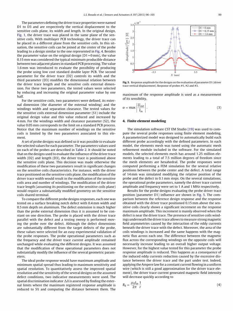
Fig. 4. Probe geometrical parameters representation. See Table 1 for descriptionand tested values.
eddy currents and two sensitive coils responsible for the magneticfield sensing. This separation allows the design of each elementso it can perform its purpose as better as possible and improvesthe probe effectiveness. The several parameters of each elementare shown in Fig. 4 and resumed in Table 1. In addition to the
diameterS2 Sensitive coils
windings widthand clearance
0.1 mm {0.05 0.1} mm
d Actuators A 197 (2013) 96– 105 99
DsFsbult0b1tpttsbh
nwto4vNcm
totwtmotdctwc
t0tspiatttutse
msrdsnr
L.S. Rosado et al. / Sensors an
The parameters defining the driver trace properties were named1 to D3 and are respectively the vertical displacement to the
ensitive coils plane, its width and length. In the original design,ig. 1, the driver trace was placed in the same plane of the sen-itive coils. With multilayer PCB technology, the driver trace cane placed in a different plane from the sensitive coils. In this sit-ation, the sensitive coils can be joined at the center of the probe
eading to a design similar to the one represented in Fig. 4. Besideshe parameter value on the original design (D1 = 0 mm), the value.15 mm was considered the typical minimum producible distanceetween two adjacent planes in standard PCB processing. The value.6 mm was introduced to evaluate the possibility of producinghe probe using low cost standard double layer PCB. The secondarameter for the driver trace (D2) controls its width and thehird parameter (D3) modifies the dimensional relation betweenhe driver trace length and the sensitive coils external dimen-ion. For these two parameters, the tested values were selectedy reducing and increasing the original parameter value by onealf.
For the sensitive coils, two parameters were defined, its exter-al dimension (the diameter of the external winding) and theindings width and separation clearance. The tested values for
he sensitive coils external dimension parameter (S1) include theriginal design value and this value reduced and increased by
mm. For the windings width and clearance parameter (S2), thealue 0.05 mm corresponds to the limit on a standard PCB process.otice that the maximum number of windings on the sensitiveoils is limited by the two parameters associated to this ele-ent.A set of probe designs was defined so it was possible to evaluate
he selected values for each parameter. The parameters values usedn each of the probes are described in Table 2. It should be notedhat on the designs used to evaluate the influence of the driver traceidth (D2) and length (D3), the driver trace is positioned above
he sensitive coils plane. This decision was made otherwise theodification of these two parameters result in significant changes
n the sensitive coils characteristics. For instance, with the driverrace positioned on the sensitive coils plane, the modification of theriver trace width would result in the modification of the sensitiveoils area and number of windings. The modification of the driverrace length (assuming its positioning on the sensitive coils plane)ould require a substantially modified geometry on the sensitive
oils shared terminal.To compare the different probe designs responses, each one was
ested on a surface breaking notch defect with 0.4 mm width and.5 mm depth on aluminum. The defect extension is much higherhan the probe external dimension thus it is assumed to be con-tant on one direction. The probe is placed with the driver tracearallel with the defect and a testing sweep is performed mov-
ng the probe over the defect. Although the defect dimensionsre substantially different from the target defects of the probe,hese values were selected for an easy experimental validation ofhe probe responses. The probe operational parameters such ashe frequency and the driver trace current amplitude remainednchanged while evaluating the different designs. It was assumedhat the modification of these operational parameters does notubstantially modify the influence of the several geometric param-ters.
The ideal probe response would have maximum amplitude andinimum spatial spread thus leading to maximum sensitivity and
patial resolution. To quantitatively assess the improved spatialesolution and the sensitivity of the several designs on the assumed
efect conditions, two indicative measurements were used. Thepatial discrimination indicator �X is assessed by finding the exter-al limits where the maximum registered response amplitude iseduced to 5% and computing the distance between them. TheFig. 5. Response amplitude for the designs on the evaluation of parameter D1 (drivertrace vertical displacement). Response of probes #1, #2 and #3.
maximum of the response amplitude is used as a measurementof its sensibility,
= max
∣∣∣∣Uout
Iin
∣∣∣∣ . (3)
4. Finite element modeling
The simulation software CST EM Studio [19] was used to com-pute the several probe responses using finite element modeling.A parameterized model was designed to automatically build eachdifferent probe accordingly with the defined parameters. In eachmodel, the elements mesh was tuned using the automatic meshrefinement module included in the software. For the simulatedmodels, the selected elements mesh has around 1.25 million ele-ments leading to a total of 7.5 million degrees of freedom sincethe mesh elements are hexahedral. The probe responses werecomputed performing a FEM simulation for the several relativepositions between the probe center and the defect. A total rangeof 14 mm was simulated modifying the relative position of theprobe and the defect in 0.1 mm steps. On the several simulations,the operational probe parameters, namely the driver trace currentamplitude and frequency were set to 1 A and 1 MHz respectively.
Results for the probe designs evaluating the probe driver traceposition (parameter D1) influence are shown in Fig. 5. The com-parison between the reference design response and the responseobtained with the driver trace positioned 0.15 mm above the sen-sitive coils clearly shows a significant increment on the responsemaximum amplitude. This increment is mainly observed when thedefect is near the driver trace. The presence of sensitive coils wind-ings underneath the driver trace allows to measure strong magneticfield asymmetries caused by the interaction of the eddy currentsbeneath the driver trace with the defect. Moreover, the area of thecoils windings is increased and the same happens with the mag-netic flux across each one. The difference between the magneticflux across the corresponding windings on the opposite coils willnecessarily increase leading to an overall higher output voltage.However, for the highest value tested for this parameter the proberesponse amplitude is reduced. This happens as a consequence ofthe induced eddy currents reduction caused by the excessive dis-tance between the driver trace and the part under test. Indeed,applying the Ampere law for a constant current flowing in a uniformwire (which is still a good approximation for the driver trace ele-ment), the driver trace current generated magnetic field intensity
will decrease quickly according toBd = �0Iin2�
1r
(4)
100 L.S. Rosado et al. / Sensors and Actuators A 197 (2013) 96– 105
Table 2Probe designs to evaluate the parameters influence.
Evaluated parameter Probe design Reference design D1 [mm] D2 [mm] D3 S1 [mm] S2 [mm]
0 0.15 1.6 0.5 1 1.5 0.5 1 1.5 6 10 14 0.1 0.05
– #1 – × × × × ×D1 #2 #1 × × × × ×
#3 #1 × × × × ×D2 #4 #3 × × × × ×
#5 #3 × × × × ×D3 #6 #3 × × × × ×
#7 #3 × × × × ×× × × ×× × × ×× × × ×
w
ttt(a1ttacsmbvpiatnwh
e2tTescso
Ft
S1 #8 #1 ×
#9 #1 ×
S2 #10 #1 ×
here r is the distance and �0 is the magnetic permeability.The driver trace width influence is illustrated in Fig. 6 where
he simulation results for the 3 parameter values are shown. Notehat in the designs whose response is represented on the figure,he driver trace is displaced 1.6 mm from the sensitive coils planeD1 = 1.6 mm). As shown in the figure, the response maximummplitude is very similar either the driver trace has 0.5 mm or
mm. These minor modifications can be explained by noting thathe driver trace width is substantially smaller than the distance tohe metallic part (which is equal to the addition of parameter D1nd the distance between the probe and the metallic part). In thisase, the magnetic field intensity Bd at the metallic surface has amall dependency on the driver trace current density, dependingostly on its overall value. Thus, the induced eddy currents will
e similar both in disposition and density. For the highest testedalue, the probe response amplitude is affected mainly when therobe is near the defect. In this condition, the driver trace width
s close to the distance to the metallic surface. The magnetic fieldt the metallic surface will have greater dependence on the driverrace current density leading to less intense eddy currents under-eath the driver trace. Therefore, the magnetic field asymmetryhen the driver trace is near the defects is reduced and the sameappens with the probe response amplitude.
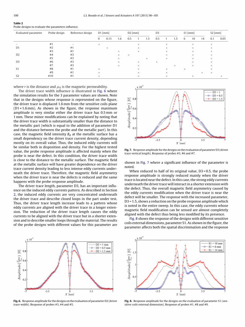
The driver trace length, parameter D3, has an important influ-nce on the induced eddy currents pattern. As described in Section, the induced eddy currents are very concentrated underneathhe driver trace and describe closed loops in the part under test.hus, the driver trace length increase leads to a pattern whoseddy currents are aligned with the driver trace in a longer exten-ion. The reduction of the driver trace length causes the eddy
urrents to be aligned with the driver trace but in a shorter exten-ion and to describe smaller loops through the material. The resultsf the probe designs with different values for this parameter areig. 6. Response amplitude for the designs on the evaluation of parameter D2 (driverrace width). Response of probes #3, #4 and #5.
Fig. 7. Response amplitude for the designs on the evaluation of parameter D3 (drivertrace vertical length). Response of probes #3, #6 and #7.
shown in Fig. 7 where a significant influence of the parameter isnoted.
When reduced to half of its original value, D3 = 0.5, the proberesponse amplitude is strongly reduced mainly when the drivertrace is located near the defect. In this case, the strong eddy currentsunderneath the driver trace will interact in a shorter extension withthe defect. Thus, the overall magnetic field asymmetry caused bythe eddy currents modification when the driver trace is near thedefect will be smaller. The response with the increased parameter,D3 = 1.5, shows a reduction on the probe response amplitude whichis noted in the entire sweep. In this case, the eddy currents whosemagnetic field modification can be sensed are almost completely
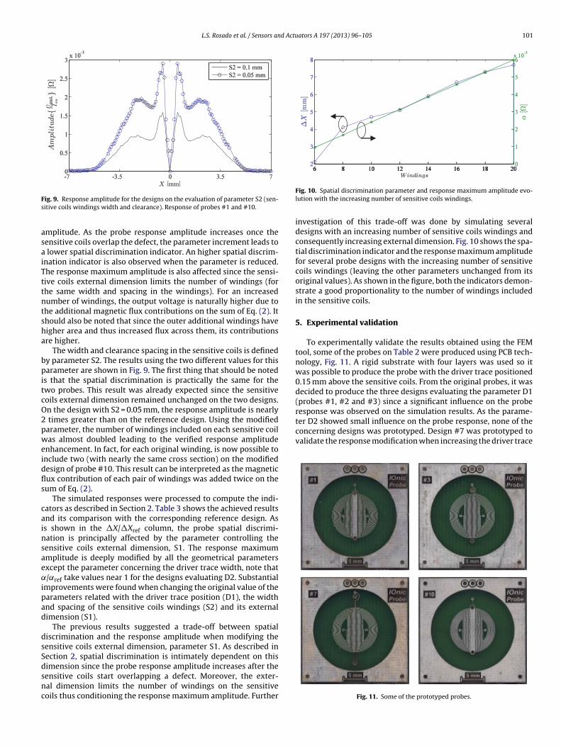
aligned with the defect thus being less modified by its presence.Fig. 8 shows the response of the designs with different sensitivecoils external dimensions, parameter S1. As shown in the figure, theparameter affects both the spatial discrimination and the response
Fig. 8. Response amplitude for the designs on the evaluation of parameter S1 (sen-sitive coils external dimension). Response of probes #1, #8 and #9.
L.S. Rosado et al. / Sensors and Actuators A 197 (2013) 96– 105 101
Fs
asaiTttntsha
bpitcO2pweidfls
cainsae˛ipad
dsSdsnc
response was observed on the simulation results. As the parame-ter D2 showed small influence on the probe response, none of theconcerning designs was prototyped. Design #7 was prototyped tovalidate the response modification when increasing the driver trace
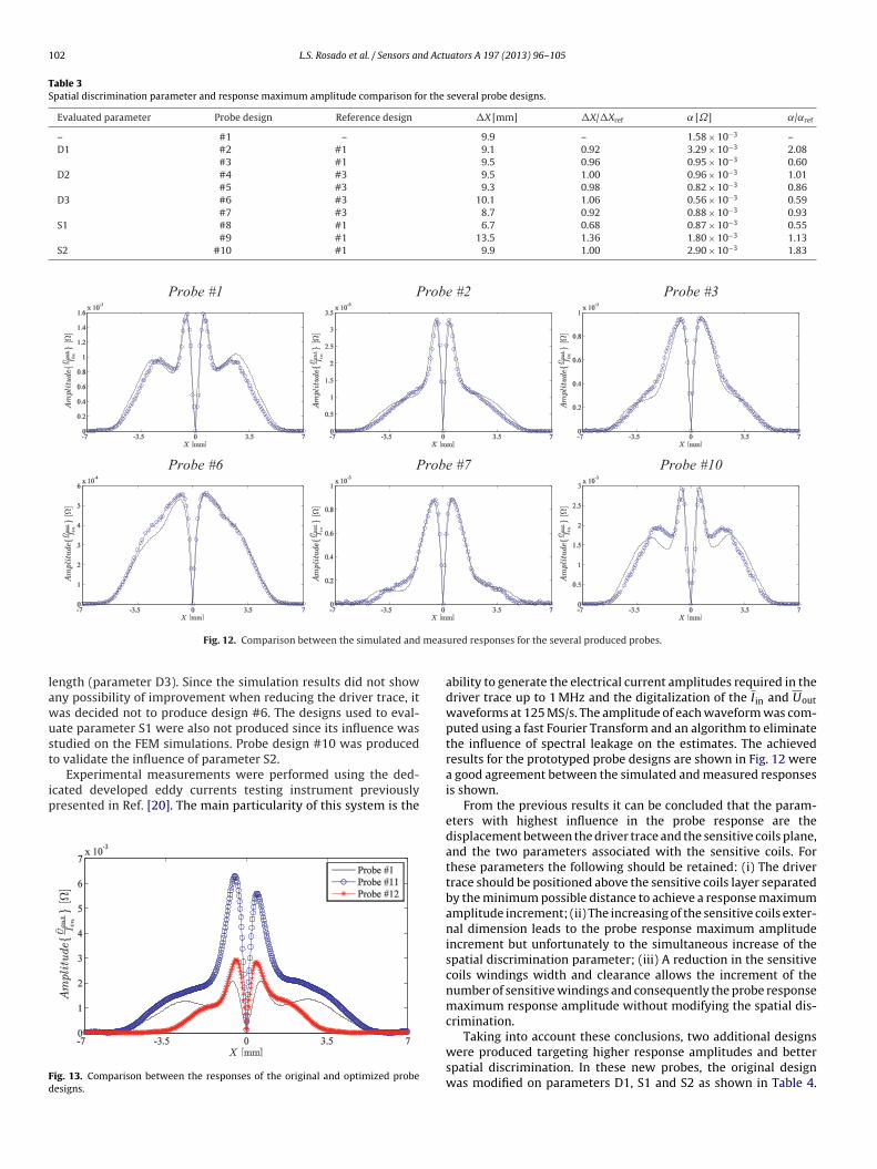
ig. 9. Response amplitude for the designs on the evaluation of parameter S2 (sen-itive coils windings width and clearance). Response of probes #1 and #10.
mplitude. As the probe response amplitude increases once theensitive coils overlap the defect, the parameter increment leads to
lower spatial discrimination indicator. An higher spatial discrim-nation indicator is also observed when the parameter is reduced.he response maximum amplitude is also affected since the sensi-ive coils external dimension limits the number of windings (forhe same width and spacing in the windings). For an increasedumber of windings, the output voltage is naturally higher due tohe additional magnetic flux contributions on the sum of Eq. (2). Ithould also be noted that since the outer additional windings haveigher area and thus increased flux across them, its contributionsre higher.
The width and clearance spacing in the sensitive coils is definedy parameter S2. The results using the two different values for thisarameter are shown in Fig. 9. The first thing that should be noted
s that the spatial discrimination is practically the same for thewo probes. This result was already expected since the sensitiveoils external dimension remained unchanged on the two designs.n the design with S2 = 0.05 mm, the response amplitude is nearly
times greater than on the reference design. Using the modifiedarameter, the number of windings included on each sensitive coilas almost doubled leading to the verified response amplitude
nhancement. In fact, for each original winding, is now possible tonclude two (with nearly the same cross section) on the modifiedesign of probe #10. This result can be interpreted as the magneticux contribution of each pair of windings was added twice on theum of Eq. (2).
The simulated responses were processed to compute the indi-ators as described in Section 2. Table 3 shows the achieved resultsnd its comparison with the corresponding reference design. Ass shown in the �X/�Xref column, the probe spatial discrimi-ation is principally affected by the parameter controlling theensitive coils external dimension, S1. The response maximummplitude is deeply modified by all the geometrical parametersxcept the parameter concerning the driver trace width, note that/˛ref take values near 1 for the designs evaluating D2. Substantial
mprovements were found when changing the original value of thearameters related with the driver trace position (D1), the widthnd spacing of the sensitive coils windings (S2) and its externalimension (S1).
The previous results suggested a trade-off between spatialiscrimination and the response amplitude when modifying theensitive coils external dimension, parameter S1. As described inection 2, spatial discrimination is intimately dependent on this
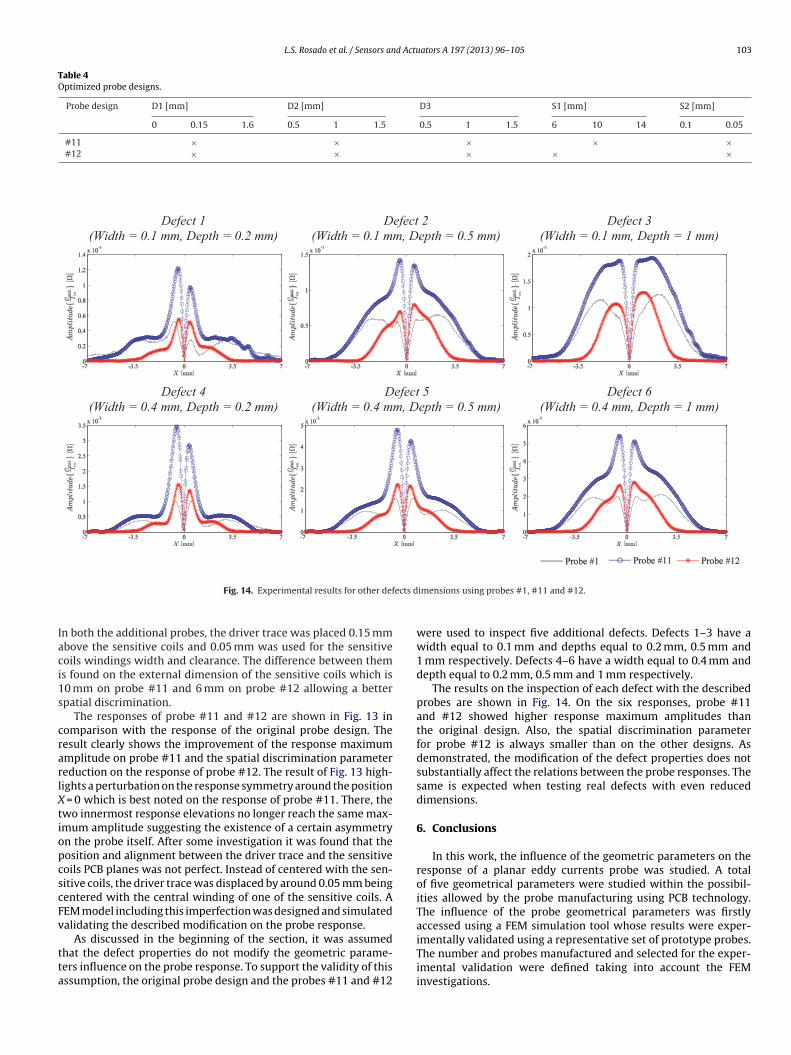
imension since the probe response amplitude increases after theensitive coils start overlapping a defect. Moreover, the exter-al dimension limits the number of windings on the sensitiveoils thus conditioning the response maximum amplitude. FurtherFig. 10. Spatial discrimination parameter and response maximum amplitude evo-lution with the increasing number of sensitive coils windings.
investigation of this trade-off was done by simulating severaldesigns with an increasing number of sensitive coils windings andconsequently increasing external dimension. Fig. 10 shows the spa-tial discrimination indicator and the response maximum amplitudefor several probe designs with the increasing number of sensitivecoils windings (leaving the other parameters unchanged from itsoriginal values). As shown in the figure, both the indicators demon-strate a good proportionality to the number of windings includedin the sensitive coils.
5. Experimental validation
To experimentally validate the results obtained using the FEMtool, some of the probes on Table 2 were produced using PCB tech-nology, Fig. 11. A rigid substrate with four layers was used so itwas possible to produce the probe with the driver trace positioned0.15 mm above the sensitive coils. From the original probes, it wasdecided to produce the three designs evaluating the parameter D1(probes #1, #2 and #3) since a significant influence on the probe
Fig. 11. Some of the prototyped probes.
102 L.S. Rosado et al. / Sensors and Actuators A 197 (2013) 96– 105
Table 3Spatial discrimination parameter and response maximum amplitude comparison for the several probe designs.
Evaluated parameter Probe design Reference design �X [mm] �X/�Xref [˝] ˛/˛ref
– #1 – 9.9 – 1.58 × 10⁻³ –D1 #2 #1 9.1 0.92 3.29 × 10⁻³ 2.08
#3 #1 9.5 0.96 0.95 × 10⁻³ 0.60D2 #4 #3 9.5 1.00 0.96 × 10⁻³ 1.01
#5 #3 9.3 0.98 0.82 × 10⁻³ 0.86D3 #6 #3 10.1 1.06 0.56 × 10⁻³ 0.59
#7 #3 8.7 0.92 0.88 × 10⁻³ 0.93S1 #8 #1 6.7 0.68 0.87 × 10⁻³ 0.55
#9 #1 13.5 1.36 1.80 × 10⁻³ 1.13S2 #10 #1 9.9 1.00 2.90 × 10⁻³ 1.83
Probe #1 Probe #2 Probe #3
Probe #6 Probe #7 Probe #10
meas
lawust
ip
Fd
Fig. 12. Comparison between the simulated and
ength (parameter D3). Since the simulation results did not showny possibility of improvement when reducing the driver trace, itas decided not to produce design #6. The designs used to eval-ate parameter S1 were also not produced since its influence wastudied on the FEM simulations. Probe design #10 was produced
o validate the influence of parameter S2.Experimental measurements were performed using the ded-cated developed eddy currents testing instrument previouslyresented in Ref. [20]. The main particularity of this system is the
ig. 13. Comparison between the responses of the original and optimized probeesigns.
ured responses for the several produced probes.
ability to generate the electrical current amplitudes required in thedriver trace up to 1 MHz and the digitalization of the Iin and Uout
waveforms at 125 MS/s. The amplitude of each waveform was com-puted using a fast Fourier Transform and an algorithm to eliminatethe influence of spectral leakage on the estimates. The achievedresults for the prototyped probe designs are shown in Fig. 12 werea good agreement between the simulated and measured responsesis shown.
From the previous results it can be concluded that the param-eters with highest influence in the probe response are thedisplacement between the driver trace and the sensitive coils plane,and the two parameters associated with the sensitive coils. Forthese parameters the following should be retained: (i) The drivertrace should be positioned above the sensitive coils layer separatedby the minimum possible distance to achieve a response maximumamplitude increment; (ii) The increasing of the sensitive coils exter-nal dimension leads to the probe response maximum amplitudeincrement but unfortunately to the simultaneous increase of thespatial discrimination parameter; (iii) A reduction in the sensitivecoils windings width and clearance allows the increment of thenumber of sensitive windings and consequently the probe responsemaximum response amplitude without modifying the spatial dis-crimination.
Taking into account these conclusions, two additional designswere produced targeting higher response amplitudes and betterspatial discrimination. In these new probes, the original designwas modified on parameters D1, S1 and S2 as shown in Table 4.
L.S. Rosado et al. / Sensors and Actuators A 197 (2013) 96– 105 103
Table 4Optimized probe designs.
Probe design D1 [mm] D2 [mm] D3 S1 [mm] S2 [mm]
0 0.15 1.6 0.5 1 1.5 0.5 1 1.5 6 10 14 0.1 0.05
#11 × × × × ×#12 × × × × ×
Defect 1 Defect 2 Defect 3 (Width = 0.1 mm , De pth = 0.2 mm) (Width = 0.1 mm , De pth = 0.5 mm) (Width = 0.1 mm , De pth = 1 mm)
Defect 4 Defect 5 Defect 6 (Width = 0.4 mm , De pth = 0.2 mm) (Width = 0.4 mm , De pth = 0.5 mm) (Width = 0.4 mm , De pth = 1 mm)
ects d
Iaci1s
crarlXtiopcscFv
tta
Fig. 14. Experimental results for other def
n both the additional probes, the driver trace was placed 0.15 mmbove the sensitive coils and 0.05 mm was used for the sensitiveoils windings width and clearance. The difference between thems found on the external dimension of the sensitive coils which is0 mm on probe #11 and 6 mm on probe #12 allowing a betterpatial discrimination.
The responses of probe #11 and #12 are shown in Fig. 13 inomparison with the response of the original probe design. Theesult clearly shows the improvement of the response maximummplitude on probe #11 and the spatial discrimination parametereduction on the response of probe #12. The result of Fig. 13 high-ights a perturbation on the response symmetry around the position
= 0 which is best noted on the response of probe #11. There, thewo innermost response elevations no longer reach the same max-mum amplitude suggesting the existence of a certain asymmetryn the probe itself. After some investigation it was found that theosition and alignment between the driver trace and the sensitiveoils PCB planes was not perfect. Instead of centered with the sen-itive coils, the driver trace was displaced by around 0.05 mm beingentered with the central winding of one of the sensitive coils. AEM model including this imperfection was designed and simulatedalidating the described modification on the probe response.
As discussed in the beginning of the section, it was assumedhat the defect properties do not modify the geometric parame-ers influence on the probe response. To support the validity of thisssumption, the original probe design and the probes #11 and #12
imensions using probes #1, #11 and #12.
were used to inspect five additional defects. Defects 1–3 have awidth equal to 0.1 mm and depths equal to 0.2 mm, 0.5 mm and1 mm respectively. Defects 4–6 have a width equal to 0.4 mm anddepth equal to 0.2 mm, 0.5 mm and 1 mm respectively.
The results on the inspection of each defect with the describedprobes are shown in Fig. 14. On the six responses, probe #11and #12 showed higher response maximum amplitudes thanthe original design. Also, the spatial discrimination parameterfor probe #12 is always smaller than on the other designs. Asdemonstrated, the modification of the defect properties does notsubstantially affect the relations between the probe responses. Thesame is expected when testing real defects with even reduceddimensions.
6. Conclusions
In this work, the influence of the geometric parameters on theresponse of a planar eddy currents probe was studied. A totalof five geometrical parameters were studied within the possibil-ities allowed by the probe manufacturing using PCB technology.The influence of the probe geometrical parameters was firstlyaccessed using a FEM simulation tool whose results were exper-
imentally validated using a representative set of prototype probes.The number and probes manufactured and selected for the exper-imental validation were defined taking into account the FEMinvestigations.
1 d Actu
ptteunaabm
sdapmtflfwn
otnor
twoadtd
ootiTpwrw
fTatdtwcaac
A
CPP
[
[
[
[
[
[
[
[
[
[
[
04 L.S. Rosado et al. / Sensors an
From the reported results it was shown that the driver traceositioning above the sensitive coils level can substantially increasehe probe response amplitude. Although the distance of the driverrace to the surface probe increases (leading to weaker inducedddy currents), this position enables joining the two sensitive coilsnderneath. The response amplitude is improved since the mag-etic field is better sensed where eddy currents have higher densitynd thus greater interaction with the defect. Nevertheless, it waslso shown that, to achieve effective improvements, the distanceetween this element and the part under test should be mini-ized.Regarding the driver trace width, it was shown that it has very
mall influence on the probe response. Its modification changes theensity of the current flowing on the driver trace but this barelyffects the induced eddy currents. Nevertheless, differences on therobe response were found when the parameters took the maxi-um considered value on the methodology. In this case, the driver
race current density was reduced enough to spread the currentsowing underneath the driver trace on a wider zone of the part sur-
ace. The observed response amplitude reduction is caused by theeaker interaction between the defect and the induced currentsear the driver trace.
The driver trace length parameter showed a strong influencen the probe response. The results have shown that designinghe driver trace with a length equal to the sensitive coils exter-al dimension is the best option. In fact, this enables the inductionf the eddy currents on the overall sensing area thus improving theesponse amplitude.
Both sensitive coils parameters play an important role onhe probe response. Its external dimension is intimately relatedith the probe spatial discrimination. Indeed, the modification
f this parameter defines a limit on the sensed magnetic fieldnd ultimately on the eddy currents whose modification due toefects can be measured. An almost proportional relation betweenhe parameter and the spatial discrimination indicator has beenemonstrated.
Finally, it was shown that the number of windings includedn the sensitive coils, as expected, has a remarkable impactn the response amplitude. This predictable effect results fromhe modification of the probe sensing capability as each wind-ng adds an induced voltage contribution on the probe output.herefore, to increase the probe response amplitude without com-romise its spatial discrimination, it is necessary to reduce theidth and spacing of the sensitive coils windings using high
esolution PCB processing (allowing the inclusion of additionalindings).
The conclusions from this study provided important guidelinesor the probe optimization targeting different testing requirements.wo examples of optimized probe designs were demonstratednd used to inspect several defects to confirm the validity ofhe adopted methodology. The additional results with modifiedefect characteristics showed that the relative effectiveness ofhe probe designs is not affected by the defect properties. Futureork will focus on the evaluation of other manufacturing pro-
esses with increased capabilities regarding geometric resolutionnd tighter tolerances on the alignment of the several layers. Inddition, the use of thin film production technology is also beingonsidered.
cknowledgements
The authors would like to acknowledge Fundac ão para aiência e Tecnologia (FCT) for its financial support via thehD scholarship FCT-SFRH/BD/65860/2009 and project PTDC/EEI-RO/3219/2012.
ators A 197 (2013) 96– 105
References
[1] R. Halmshaw, Introduction to the Non-Destructive Testing of Welded Joints,Woodhead Publishing, Abington, Cambridge, England, 1996.
[2] P. Underhill, T. Krause, Eddy current analysis of mid-bore and corner cracks inbolt holes, NDT & E International 44 (October) (2011) 513–518.
[3] I. Abidin, C. Mandache, G. Tian, M. Morozov, Pulsed eddy current testing withvariable duty cycle on rivet joints, NDT & E International 42 (October) (2009)599–605.
[4] W. Zhu, S. Cruchley, W. Yin, X. Hao, C. Davis, A. Peyton, Evaluation of raildecarburisation depth using a H-shaped electromagnetic sensor, NDT & E Inter-national 46 (March) (2012) 63–69.
[5] H. Fukutomi, T. Takagi, M. Nishikawa, Remote field eddy current techniqueapplied to non-magnetic steam generator tubes, NDT & E International 34(January) (2001) 17–23.
[6] P. Joubert, Y. Bihan, D. Placko, Localization of defects in steam generator tubesusing a multi-coil eddy current probe dedicated to high speed inspection, NDT& E International 35 (January) (2002) 53–59.
[7] D. Kim, L. Udpa, S. Udpa, Remote field eddy current testing for detection of stresscorrosion cracks in gas transmission pipelines, Materials Letters 58 (June 2004)2102–2104.
[8] D. Sadler, C. Ahn, On-chip eddy current sensor for proximity sensing andcrack detection, Sensors and Actuators A: Physical 91 (3) (July 2001) 340–345.
[9] Y. Li, G. Tian, S. Ward, Numerical simulations on electromagnetic NDT athigh speed, Insight – Non-Destructive Testing and Condition Monitoring 48(February (2)) (2006).
10] P. Joubert, E. Vourc’h, V. Thomas, Experimental validation of an eddy currentprobe dedicated to the multi-frequency imaging of bore holes, Sensors andActuators A: Physical 185 (October) (2012) 132–138.
11] G. Tian, Y. Li, C. Mandache, Study of lift-off invariance for pulsed eddy-currentsignals, IEEE Transactions on Magnetics 45 (January (1)) (2009) 184–191.
12] T. Capobianco, J. Splett, H. Iyer, Eddy current probe sensitivity as a function ofcoil construction parameters, Research in Nondestructive Evaluation Journal 2(September) (1990) 169–186.
13] Y. Yating, D. Pingan, Optimization of an eddy current sensor using finiteelement method, in: Proceedings of the International Conference on Mecha-tronics and Automation 2007 (ICMA 2007), August, 2007, pp. 3795–3800.
14] T. Chady, R. Sikora, Optimization of eddy-current sensor for multifre-quency systems, IEEE Transactions on Magnetics 39 (May) (2003) 1313–1316.
15] J. Fava, L. Lanzani, M. Ruch, Multilayer planar rectangular coils for eddy currenttesting: Design considerations, NDT & E International 42 (December) (2009)713–720.
16] J. Pavo, K. Miya, Optimal design of eddy current testing probe using fluxsetmagnetic field sensors, IEEE Transactions on Magnetics 32 (May) (1996) 1597–1600.
17] L. Rosado, T. Santos, M. Piedade, P. Ramos, P. Vilac a, Advanced technique fornon-destructive testing of friction stir welding of metals, Measurement 43(October (8)) (2010) 1021–1030.
18] L. Rosado, T. Santos, P. Ramos, P. Vilac a, M. Piedade, A differential planar eddycurrents probe: fundamentals, modeling and experimental evaluation, NDT &E International 51 (October) (2012) 85–93.
19] TEAM Benchmark 8 – Non-destructive testing example: Coil above a crack, CST,AG, April 2009.
20] L. Rosado, M. Piedade, P. Ramos, T. Santos, P. Vilac a, A reconfigurable dig-ital signal processing system for eddy currents non-destructive testing,in: Proceedings of the IEEE International Instrumentation and Measure-ment Technology Conference 2010 (I2MTC 2010), May, 2010, pp. 1284–1289.
Biographies
Luis S. Rosado received the M.Sc. degree in electronics engineering from the InstitutoSuperior Técnico, Universidade Técnica de Lisboa, Lisboa, Portugal, in 2009, where heis currently working toward the Ph.D. degree. His doctoral studies are focused on thedevelopment and application of eddy current probes and digital signal processingalgorithms for non-destructive testing.
João C. Gonzalez received the M.Sc. degree in mechanical engineering from the Fac-uldade de Ciências e Tecnologia, Universidade Nova de Lisboa, Portugal, in 2011. Heis currently a researcher at the core of mechanical technology in FCT-UNL, and hisstudies are focused on the development and application of mechanical devices fornon-destructive testing.
Telmo G. Santos received the Ph.D. degree in mechanical engineering from the Insti-tuto Superior Técnico, Universidade Técnica de Lisboa (UTL), Lisboa, Portugal, in2009. He is currently an Assistant Professor with the Department of Mechanical andIndustrial Engineering, Faculdade de Ciências e Tecnologia, Universidade Nova de
Lisboa (FCT-UNL), where his research is done in the UNIDEMI. His research interestsinclude non-destructive testing and manufacturing processes as friction stir welding(FSW) and friction stir processing (FSP).Pedro M. Ramos was born in Lisboa, Portugal, in 1972. He received the Diplomaand the M.Sc. and Ph.D. degrees in electrical and computers engineering from
d Actu
t1Tim1sqTo
trical and Computer Engineering, UTL, where his research is done in the SignalProcessing Systems (SIPS) Research Group, Instituto de Engenharia de Sistemas e
L.S. Rosado et al. / Sensors an
he Instituto Superior Técnico, Universidade Técnica de Lisboa (UTL), Lisboa, in995, 1997, and 2001, espectively. Since 1999, he has been a Member of theeaching and Research Staff with the Instituto Superior Técnico, UTL, where hes currently an Assistant Professor and has also been a Member of the Instru-
entation and Measurement Research Group, Instituto de Telecomunicac ões, since
995. His current research interests include impedance measurements, impedancepectroscopy, sine-fitting algorithms, automatic measurement systems, and power-uality monitoring/measurements. Professor Ramos has been a member of IMEKOC4 – Measurement of Electrical Quantities since 2006 and the Scientific Secretaryf IMEKO TC4 since 2012. IEEE Senior Member since 2013.ators A 197 (2013) 96– 105 105
Moisés Piedade received the Ph.D. degree in electrical and computer engineer-ing from the Instituto Superior Técnico, Universidade Técnica de Lisboa (UTL),Lisboa, Portugal, in 1983. He is currently a Professor with the Department of Elec-
Computadores-Investigac ão e Desenvolvimento. His research interests include elec-tronic systems, signal-acquisition and processing systems, and circuits and systemsfor biomedical applications.
Related Documents