Rochester Institute of Technology Rochester Institute of Technology RIT Scholar Works RIT Scholar Works Theses 2004 Generalized analytical model for RF planar inductors using a Generalized analytical model for RF planar inductors using a segmentation technique segmentation technique Marie Yvanoff Follow this and additional works at: https://scholarworks.rit.edu/theses Recommended Citation Recommended Citation Yvanoff, Marie, "Generalized analytical model for RF planar inductors using a segmentation technique" (2004). Thesis. Rochester Institute of Technology. Accessed from This Thesis is brought to you for free and open access by RIT Scholar Works. It has been accepted for inclusion in Theses by an authorized administrator of RIT Scholar Works. For more information, please contact [email protected].

Welcome message from author
This document is posted to help you gain knowledge. Please leave a comment to let me know what you think about it! Share it to your friends and learn new things together.
Transcript
Rochester Institute of Technology Rochester Institute of Technology
RIT Scholar Works RIT Scholar Works
Theses
2004
Generalized analytical model for RF planar inductors using a Generalized analytical model for RF planar inductors using a
segmentation technique segmentation technique
Marie Yvanoff
Follow this and additional works at: https://scholarworks.rit.edu/theses
Recommended Citation Recommended Citation Yvanoff, Marie, "Generalized analytical model for RF planar inductors using a segmentation technique" (2004). Thesis. Rochester Institute of Technology. Accessed from
This Thesis is brought to you for free and open access by RIT Scholar Works. It has been accepted for inclusion in Theses by an authorized administrator of RIT Scholar Works. For more information, please contact [email protected].

Approved by:
GENERALIZED ANALYTICAL MODEL FOR RF PLANAR INDUCTORS
USING A SEGMENTATION TECHNIQUE
by
Marie Yvanoff
A Thesis submitted in Partial Fulfillment of the
Requirements for the Degree of
MASTERS OF SCIENCE
In
Electrical Engineering
Professor Jayanti Venkataraman (Dr. Jayanti Venkataraman - Advisor)
Professor __ S_a_n_t_o_s_h_K_o_K_u_ri_n_e_c __ (Dr. Santosh Kurinec - Committee Advisor)
Professor Syed Saifullslam (Dr. Syed Islam - Committee Advisor)
Professor __ R_o_b_e_r_t _B_o_w_m_a_n __ _ (Dr. Robert Bowman - Department Head)
DEPARTMENT OF ELECTRICAL ENGINEERING
COLLEGE OF ENGINEERING
ROCHESTER INSTITUTE OF TECHNOLOGY
ROCHESTER, NY
MAY 2004
~ This work was supported by the __ National Science Foundation under grant ECS 0219379

Thesis Release Permission
DEPARTMENT OF ELECTRICAL ENGINEERING COLLEGE OF ENGINEERING
ROCHESTER INSTITUTE OF TECHNOLOGY ROCHESTER, NY
MAY, 2004
Title of Thesis:
GENERALIZED ANALYTICAL MODEL FOR RF PLANAR INDUCTORS
USING A SEGMENTATION TECHNIQUE
I, Marie Yvanoff, hereby grant permission to Wallace Memorial Library of Rochester
Institute of Technology to reproduce this thesis in whole or in part. Any reproduction will
not be for commercial use of profit.
Signature _M_a_r"_le_Y_v_a_n_o_ff_ Date 06/0 L; /01.;-

Acknowledgment
ACKNOWLEDGMENT
Many people supported me during the completion of this thesis.
First of all I wish to express my sincere gratitude to my advisor; Dr. Jayanti
Venkataraman. Her help, support, guidance and encouragements were priceless
throughout this work. Not only is she an outstanding professor, she is an even greater
person.
Thanks also to the committee members, Dr. Santosh Kurinec and Dr. Syed Islam for
reviewing my Thesis.
Next, I want to thank my co-workers in theMicromagnetic group, CodyWashburn, Tejas
Jhaveri and Gary Fino advised by Dr. Kurinec. Thanks also to my colleagues in the
Fields Lab, Lakshmi Achutha, JeffMc.Figgins andMike Seymour and for keeping a very
enjoyable working atmosphere and helping me whenever I needed.
I would like to show my gratitude to my family for their kindness and support. It's tough
to be away from home.
Last but not least, I would like to thank my best friend, Omar for always being here when
I needed him. I would have turned crazy without you. Shoukran.
This work was supported by the National Science Foundation under grant ECS 0219379.

Abstract
ABSTRACT
The planar coil inductor has become a very critical circuit component in RF mixed
signal application where it can reside either on the package or in the chip. However, there
is no clear methodology to accurately analyze the behavior of the inductor over a broad
range of frequencies and for obtaining a particular physical layout for a required value of
inductance. At present, it has been done by full wave solvers, approximate quasistatic
analysis, and lumped element equivalent circuits, each with its own advantages and
limitations. This work presents an analytical model based on a segmentation method in
conjunction with a Green's function for a power/ground plane model. This method has
been used to obtain analytical closed form solution for planar coil inductors of two
popular shapes, the rectangular and circular configurations. The model includes a ground
plane and the coil configuration such as spacing and line width, and the materia]
characteristic such as conductivity of the metal layer and the dielectric parameters. It is a
frequency dependant solution that includes the resonant modes in the cavity formed by
the inductor and the ground plane. This method has been applied successfully to
rectangular and circular coil inductors of different dimensions where there is excellent
agreement with full wave solvers. Inductors on a package and in a chip have been
fabricated and experimental results show excellent agreement to predicted values
obtained from this analytical work.
Also presented in this work is a comparison of popular EM full wave solvers and two
quasistatic methods, the advantages and limitations of each have been discussed.
Experimental techniques to measure for RF silicon IC Inductors have been developed.
n

Table Of Contents
TABLE OF CONTENTS
Acknowledgment i
Abstract ii
Table ofContents iii
List ofFigures v
List ofTables vi
1. Introduction 1
2. Contributions andMotivation ofPresentWork
2.1 Contributions 4
2.2 Organization ofThesis 5
3. Planar Inductor, On Chip and In Package
3.1 Coil parameters 7
3.2 Coil characterization 10
4. AnalyticalModel
4.1 Segmentation Technique 15
4.2 Rectangular Coils Inductor 20
4.2. 1 Green 'sfunction ofRectangular open cavities 22
4.2.2 Impedancematrix 23
4.2.3 Considerationsfor convergence issuesfor analyticalmodel 24
4.3 Circular Coils Inductor 34
4.3.1 Green'sfunction ofannular sector cavities 34
4.3.2 Impedancematrix 37
4.3.3 Considerationsfor convergence issuesfor analyticalmodel 39
4.4 Implementation of theAnalyticalmodel for Planar Inductors 43
5. NumericalModeling ofplanar Inductor
5.1 MaxwelBD 44
5. 1. 1 Setting up themodel 45
5. 1.2 Setting up boundaries 46
5. 1.3 ImpedanceMatrixResults 47
in

Table OfContents
5.2 High Frequency Structure Simulator HFSS 48
5.3 Analysis and Simulation of Inductors and Transformers for ICs 45
5.4 Current sheetmethod 49
5.5 Comparison with Published Results 50
5.6 Advantages and limitations 52
5.7 Ferrite Filled Inductors 53
6. Results
6.1 Comparison with HFSS 57
6.1.1 Planar rectangular coil 58
6.1.2 Planar circular coil 60
6.2 Comparisonwith Experimental Results 62
6.2. 1 One-turn rectangular coil 62
6.2.2 Two-turn rectangular coil 63
6.3 Investigation ofCoil Inductor Geometry for a limited footprint area 65
6.3. 1 1mpact ofnumber ofturns, spacing andwidth 66
6.3.2 Impact ofdielectric thickness 69
7. Measurement Techniques
7.1 Layout for one port measurement 71
7.2 Layout for two-portmeasurement 72
7.3 Calibration procedure 74
7.4Measurements 76
8. Conclusion
8.1 Summary ofContributions for the presentWork 78
8. 1. 1 Development and validation ofanalyticalmodel 78
8. 1.2 Computer tools assessment 78
8. 1.3 On-chip inductormeasurement techniques 79
8.2 FutureWork 79
References 81
, Appendix 84
iv

List ofFigures
List ofFigures
1 -
a) Rectangular coil layout, b) Circular coil layout, 9
Inductor cross section, c) On-chip, and d) In package
2 - Two Port Microwave Network 10
3 - Equivalent Circuit for a 2-port Network 1 1
4 -
a) Planar Inductor b) Current sheetApproximation [30] 1 1
c) Current sheet Segmentation d)Inductor lines Segmentation
5 - Rectangular Coil b)Planar Inductor b)Segmented Inductor c)InterconnectMatrix 12
6 - Circular Coil b)Planar Inductor b)Segmented Inductor c)InterconnectMatrix 12
7 -
a) Segmented Circular Coil b) InterconnectMatrix 1 3
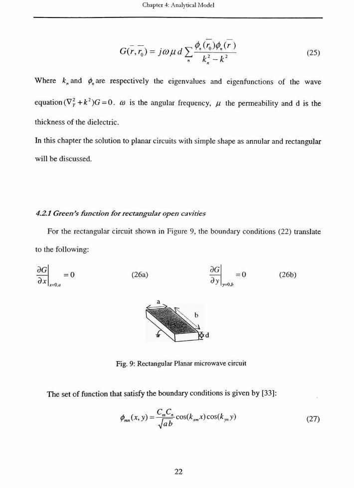
8 - Planar microwave circuit 21
9 - Rectangular Planar microwave circuit 22
10 -
a) Rectangular Planar microwave circuit b) x-y plane / port placements 24
1 1 -
a) Hoop inductor divided into b) 4 segments and c) 7 segments 25
12 - Comparison ofHFSS ResultsVs SegmentationMethod for different 26
number of segments
13 -
a) inductor layout b) cross section view 27
c)Comparison ofHFSS Results Vs Segmentation Method
14 -
Interconnecting Ports 28
15 -
a) Single loop inductorwith dielectric parameters: d =5pm, tan(8)=0,er4 29
b) Inductance Vs Frequency Vs number ofPort divisions
16 -
a) Single loop inductorwith dielectric parameters: d =5um, tan(8)=0, er=4 30
b) Inductance Vs Frequency for different number ofPort divisions
c) Absolute Percent Error for Inductance from Segmentation Results to HFSS results
17 Fringing effects 31
1 8 -
a) Inductor Layoutwith dielectric: d =5um, tan(8)=0, sr=4 32
for different Number of eigenmodes b) withN fixed at 1 5 c) withM fixed at 75
19 - Annular sector 34
20 - Circular Coil generation: Example of2-turn circular inductor 39
21 -
a) Two-loop circular inductor b) segmented inductor 40
22 -
a) Single turn circular inductor b) cross-section view 41
c) Inductance Vs Frequency23 -
a) Single turn circular inductor 42
b) Inductance Vs. Frequency for different value ofGreen's function eignenmodes
24 - Maxwell 3D Layoutwith long vias 45
25 - MaxwelBD, Layout- Closed loop 46
26 - Silicon IC planar Inductor 50
27 - Inductance L and Q ([31]), usingMaxwelBD and HFSS 51
28 - Example 1 : a) Planar Inductor b) HFSS andMomentum [31] 51
29 - Example 2: a) Planar Inductor b) HFSS and SONNET [32] 51
30 - Lumped Port Element set up with HFSS 53f
31 - Ferrite Permeability Vs. Frequency (Courtesy Ferronics Inc) 54
32 - Ferrite LoadedMicro-Inductor. ( t^= l[xm, tsio2
= 2um, tsi = 300um.) 54

List ofFigures
33 - Inductance Vs. Ferrite thickness d (um) 55
34 -
a) Planar inductor for comparison with HFSS b) Reactance Vs. Frequency 58
35 -
a) Two-turn rectangular planar inductor for comparison with HFSS59
b) ReactanceVs. Frequency36 - Results for two turn inductor (fig34) with a dielectric thickness equal to 300um 59
Reactance / w Vs. Frequency for Comparison with HFSS
37 -
a) Circular inductor for comparisonwith HFSS b) Reactance Vs. Frequency 60
38 -
a) Circular inductor for comparison with HFSS b) Reactance Vs. Frequency 61
39 -
a) Millingmachine b) One turn inductor constructed 62
40 -
a) Planar inductor for comparison with Experimentalxesults63
b) Cross view of Inductor c)Reactance / w Vs. Frequency41 2 Turn Inductor constructed for one port measurement 63
42 -
a) Planar inductor for comparison with Experimental results64
b) Cross view of Inductor c)ReactanceVs. Frequency43 - Fixed parameters a) Inductor Layout b) Cross-section view 65
44 -
a) Reactance vs. Frequency 67
b) Quality Factor vs. Frequency for a varying number of turns
45 -
a) Inductance vs. Spacing b) Quality Factor vs. Spacing 68
Planar inductor geometry:
46 -
a) Reactance Vs Width b) Quality Factor vs.Width 69
47 -
a) Planar Inductor Layout b) cross-section view 70
c) Reactance vs. Frequency for different dielectric thickness
48 - a-d): 2 different options of 1 port configuration Layout and cross-section view 72
49 - a-d): 2 different options of 2 port configuration Layout and cross-section view 73
50 - a-b): Test fixture with Open and Short Structures 74
51 - Measured device (DUT) with Parasitic 75
52 - Measured Open 75
53 - Measured Short 75
54 - Planar CopperMicrolnductor Layout and Cross-sectionView 76
55 - Network Analyzer and Probe Station Set-up 76
56 - Probes andWafer 77
57 - Multiple dielectrics 79
vi

List ofTables
List ofTables
Chapter 4:
1- Resistance and Inductance Value for different design Configuration 51
2- Inductance and Resistance of ferrite-loaded Inductors 52
vn

Chapter 1 : Introduction
1. INTRODUCTION
In early Si integrated devices, active components played a more important role than
passive components. Components such as transistors have been continuously shrinking in
size, while passive devices have remained very large and placed externally on the board.
Technology improvements have enabled Si circuits to operate at higher frequency [1]
where the critical passive elements such as inductors are small enough to be realized on-
chip. The size of the circuit board has also reduced due to fewer external components.
This has brought a significant progress to personal communication devices where
portability is essential. The use of on-chip passives such as inductive elements in silicon
radio-frequency integrated circuits allowed better performance in Si low-noise amplifiers
[2] [3], distributed dc-dc power converters [4], mixers and oscillators [5]-[7].
Consequently, it is becoming critical to be able to model the behavior of passives
over a broad range of frequencies accurately, primarily the inductor. Analyzing and
modeling the inductance introduces many difficulties. The parameters of interest for the
design of inductors are inductance and quality factor and also a limited footprint area.
Unfortunately, there are no simple analytical formulations to determine them accurately.
At present, it has been done by full wave solvers, approximate quasistatic analysis, and
lumped element equivalent circuits, each with its own advantages and limitations.
The benefit of generating a solution using full wave solver is to include all
electromagnetic effects subject to boundary conditions. MaxwelBD, High Frequency
,Structure Simulator (HFSS) and MOMENTUM are examples of such tools based on
finite element modeling. Those commercial tools are intense in computer memory usage
Chapter 1 : Introduction
and time, especially for complicated structures. They merely analyze a particular
inductor layout and do not serve as practical design tools, so design optimization is
achieved for a given footprint area by trial and error. Although these are widely used
tools, at present, there is no assessment of and comparison between the tools to help the
designer choose the appropriate software tool, best suited for the frequency range and
physical geometry. Such a study needs to be done.
As for the quasistatic approach, Analysis of Si Inductors and Transformers for IC's
(ASITIC) [8] has been developed specifically for the design of on-chip inductors and
transformer. ASITIC provides a quick analysis compared to the time intensive nature of
the full wave solvers while providing an equivalent circuit model for the parasitics.
However port definitions are not well defined. The procedure for optimizing geometry to
meet design constraints still relies upon a collection of approximate lumped-element
solutions, and several iterations are needed to get the optimum layout at a particular
frequency.
The analytical formulation which uses coupled line couplers and corner
discontinuities [9], proposed an approach to model rectangular spiral inductors. The
discontinuities of the circuit such as the bends are modeled using scalable models, and
the multiple coupled lines use a distributed model relating impedance and admittance
r
matrices. Although this model gives a frequency dependent solution, it involves a very
tedious and complicated derivation and is therefore not suited as either an analysis or
design tool.

Chapter 1 : Introduction
Another technique originally developed by Nguyen and Meyer [1] for the modeling
of the inductor uses lumped element circuit models which approximate the circuit with
individual inductances, resistances and substrate capacitances. Efforts have also been
made to improve and understand this technique in greater [10][12], as well as introduce
the eddy current losses within the substrate [13]-[16], skin effect and current crowding
[17]-[22]. It finally contained up to 22 elements [23]. While it usually produces a rapid
calculation dependent on the frequency, any change in the inductor requires another
modeling iteration beginning with the calculation of each parameter.
Simple formulas for planar inductors without a ground plane as frequency
independent solution have been published [24]-[29]. Another method based on the
current sheet distribution [30] introduces simple expressions for spiral inductors by
approximating the sides of the spiral by a current sheet with uniform current distribution.
Although these expressions give good insight to help the designer, it needs a better
expression to take care of magnetic coupling to the substrate. It also assumes that the
current distribution is uniform in all the conductors, which becomes untrue at higher
frequency with the skin and proximity effects. The major disadvantages are that it does
not give a frequency dependant expression and does not include ground plane and
material parameters.
It is vital, for the designer of an RF circuit to be able to optimize inductors. And
despite all the work and improvement in the research being made formodeling inductors,
there is still a critical need for a simple closed form expression for inductor design that
includes ground plane and material parameters.

Chapter 2: Contributions and Motivation ofPresentWork
2. CONTRIBUTIONS ANDMOTIVATION OF PRESENTWORK
The use of embedded passive components has the potential of shrinking the size of
circuit devices and also reducing their cost. Modeling the behavior of passive devices
accurately and with the minimum computation time has become critical. The motivation
of this present work is to develop a closed form solution to be used as a quick design tool.
The formulation has to be frequency dependent and has to include a ground plane. The
design tool presented in this work is a very useful tool that provides its independence
from full wave solvers which are computationally expensive to use. This tool will be
beneficial for applications with passive components because it provides a fast and
accurate solution.
2.1 Contributions
Major contributions for this work are as follow:
1 . An analytical model has been developed with a closed form solution for inductors
with 2 popular shapes, circular coil and rectangular coil. The method uses a segmentation
technique in conjunction with a Green's function of a cavitymodel. The model includes a
ground plane and the coil configuration such as spacing and line width, and the material
characteristic such as conductivity of the metal layer and the dielectric parameters. The
results obtained are frequency dependent, and can be extracted in the form of S and Z-
matrices. The input impedance and the quality factor of the inductor are extracted from
the Z matrix results. A comparison of this model has been made with full wave solvers

Chapter 2: Contributions and Motivation ofPresent Work
for a wide range of inductors at different frequencies. A design methodology is described
to optimize the inductor layout for a given inductance and footprint area.
2. The need for assessing various computer tools available to date has been addressed
in the present work. The four popular tools, HFSS, MaxwelBD, ASITIC and SONNET
have been compared and the advantages and disadvantages of each have been discussed
in order to help the designer to choose the best suited tool. Defining the nature and
placement of the port is critical. Comparisons have been made with known examples
[12][31][32]available in the literature. Ferrite loaded micro-inductors have been modeled
to obtain higher quality factor and inductance values for a limited footprint area. The tool
best suited for this purpose has been suggested.
3. Inductors have been fabricated and experimental verifications have been done in
order to validate the analytical model.
2.2 Organization
The following chapter presents an overall discussion on On-Chip and in-package
planar inductor characterization and configuration.
The analytical model is developed in Chapter 3. The technique using a segmentation
method in conjunction with a ground/power plane model is fully described. Green's
function for reptangular shaped power plane and annular sector are derived in detail.
Closed form expressions for the inductance for each shape, rectangular and circular have
been obtained.

Chapter 2: Contributions and Motivation ofPresent Work
Chapter 4 presents an assessment of the commercially available computer tools and
lists their advantages and limitations in order to help the designer choose the best suited
tool. Ferrite loaded micro-inductors have been modeled.
Chapter 5 presents the results where the analytical model has been applied to a wide
range of planar inductors. To validate the theory, comparisons have been made to HFSS
results and also to experimental measurements.
Chapter 6 describes the different measurement techniques for On-Chip Silicon IC
microinductors.
A conclusion and contribution of the present work is presented in Chapter 7. Future
work for this project is also given.

Chapter 3: Planar Inductors
3. PLANAR INDUCTORS ON-CHIPAND IN PACKAGE
3.1 Coil parameters
It has been seen that the use of inductive elements in integrated circuits is becoming
increasingly important. As the size of integrated circuits is continuously shrinking, it is
becoming critical to optimize the inductor layout. In order to optimize an inductor design,
all the coil parameters and physical constraints need to be considered. The parameters of
interest are the inductance and quality factor, the objective is to maximize the quality
factor for a given inductance value. The first constraint for the designer is the maximum
footprint area available on the chip or in the package. Whether the inductor is fabricated
on chip or in the package, the other constraints are the material parameters, such as
dielectric and substrate thickness, permittivity, losstangent and conductivity. The first
parameter the designer has to choose is a particular inductor shape. For an ease of
fabrication, the most popular ones are the rectangular and circular coils. The numbers of
turns, width of the lines, and spacing between the lines also have to be considered. In
order to get a particular inductance for a particular footprint area, there are an optimum
number of turns for a certain width and spacing value. Experiment and published work
show that the increase in the line width results in a higher quality factor and a higher
inductance. However, skin effect becomes significant as this width increases. The
increase in the line spacing between the metal lines results in a decrease in the mutual
inductance and therefore in the total inductance, suggesting that the spacing should be as
>small as possible. Eventually, the optimum parameters for the spiral inductor have to be

Chapter 3: Planar Inductors
determined by its layout and the specifications of the circuit to which it is part. The
parasitic elements due to the dielectric and substrate parameters entail engineering trade
offs. Thus, it is critical to have an analytical formulation for spiral inductors in order to
determine an accurate value for the inductance and quality factor to permit the designer to
choose the optimal inductor for a given application.
The parameters that need to be optimized for an inductor design can be specified by
the following and shown in Figure 1 :
1. Shape: rectangular, circular, hexagonal, octagonal.
2. Number of turns, n
3. Metal width: w
4. Spacing between the metal lines: s
5. Footprint area (a, b)
6. Dielectric layer, thickness of the oxide tdieiectric, Sdiekctric
7. Substrate parameters: t^bstrate, ^substrate, O-snsbtrate

Chapter 3: Planar Inductors
a)b)
Dielectric- -
EMiBlC-r--
Conductor
>^tdielecmc. Edielectric, tan(8)
^substrales ^substrate, ^susbtrate
**"" iwia
5L\ ^dielectric) Edielectric tan(d)
23m^K----
Conductor
Substrate
C Ground plane
Dielectric
c) d)
Fig. 1 : a) Rectangular coil layout, b) Circular coil layout,
Inductor cross section, c) On-chip, and d) In package
Figure La and Figure Lb show the layout for rectangular and circular coil layout. The
inductor can be realized on-chip (Fig.l.c) or in the package (Fig.l.d). Usually, the planar
inductor is realized on the top metal layer to reduce the capacitance between the substrate
and the spiral. It can be sitting on top of a dielectric and substrate layer when it is realized
on-chip, or on top of a dielectric and a ground plane in the package. On the chip, the
space below the inductor is kept free and no traces are present, due to the electromagnetic
fields generated by the inductor. The designer has the freedom to add another metal layer
and place a metal layer used as a ground plane below the oxide layer. Adding another
metal layer to the process and using it as a ground plane can be approximated as the
package configuration and leads to high-Q inductors.

Chapter 3: Planar Inductors
3.2 Coil Characterization
As seen in Figure 1 a and b, the inductor can be represented as a 2 port network, with
one port at the outer edge of the spiral and the other port at the inner edge. In order to
give a complete description of N-port network, the scattering and impedance matrix are
used. An arbitrary 2-port microwave network is considered and shown in Figure 2.
Portl Port 2
r+
[S]\~
+ ?
a)
v+
r2
Portl >
Port 2
.7>
^ :[Z] X
b)
Fig.2: Two-port Microwave Network
In Figure 2a,V~
is the amplitude of the voltage wave incident on port n, and V+
is
the amplitude of the voltage wave reflecting from port n. The scattering matrix or [S]
matrix relates the incident and reflected voltage waves and gives a complete description
of the network and is defined as the following for a 2-port network:
v: S22 Sn(D
Sr is the transmission coefficient from port j to port i. Ss is the reflection coefficient at
port i when the other port is terminated by a matched load.
The impedance matrix [Z] relates voltage and currents of the network and is defined as:
10

Chapter 3: Planar Inductors
V,
Z 7^11 ^12
7 7~22 ^22
.
(2)
Where the total voltage and current at port i are given by:
v.=v++vri i i
L=r-i:
(3a)
(3b)
Zy is the transfer impedance between port i and port j. Zrt is the input impedance at port I
when all the other ports are open-circuited.
The [S] matrix can be determined from the [Z] matrix and vice versa.
From the impedance matrix definition (2), the 2-port network is described in terms of
impedance parameters:
V =7 J +7 J
V =7 1+7 1
(4a)
(4b)
These equations leads to the T equivalent circuit as shown in figure 3:
'i h?
Zil Zj2 - Z22 Z21<
. - .
Pdrtl Zi2 v2
Fig.3: Equivalent circuit for a 2 port Network
11

Chapter 3: Planar Inductors
At portl, the input impedance with port 2 terminated by ZLis:
7 7Z. =Z-
12 21 (5)7+7^22 TZyL
The input impedance can also be written as: Z = R + jcoL where R is the internal
resistance and L the inductance of the coil. The solution for the inductance L is then
given by the following:
LJMZJ (6)
2?tf
The quality factor describes the frequency selectivity of a resonant circuit or cavity.
In the present work, where the inductor is placed over a ground place, the Q of the
resulting cavity is an important factor. The definition of Q is based on the maximum
energy stored in the electric and magnetic field and average power dissipated in the
conductors.
^.
.max energy stored
Q =2n* (7)
energy dissipated per cycle
/>*
Q = o)
'w_+w.y
(8)
Where Wm is the average magnetic energy stored, We the average electrical energy
stored, P, the power loss, T the period and a) the angular frequency.
At resonance, the average stored magnetic and electric energy are equal, and the quality
factor becomes:
12

Chapter 3: Planar Inductors
2Wm 2W
P P11
11
Where co^is the resonant frequency
The average magnetic stored energy and power loss are defined as:
Wm=-LIm
2
P,=RI2
Substituting (8) and (9) into (7) the quality factor becomes:
13
(9)
1. T2
00)
01)
G3 =*>of
02)

Chapter 4: Analytical Model
4. ANALYTICALDEVELOPMENT
In previously published work [30], inductance expressions have been developed
where the planar inductor (FigAa) has been approximated by four current sheets
(Fig.4.b) of equivalent current densities.
^.fjurrerit direction
a) b) c)
Fig.4: a) Planar inductor b) Current sheet approximation [30]
c) Current sheet Segmentation d) Inductor Lines Segmentation
Based on the current sheet approximation [30], the first idea for the analytical
development was to approximate the planar inductor (FigAa) and segment it as shown in
Figure 4.c. Each segment containing a ground plane and a dielectric substrate can be
viewed as a power/ground plane model. This model can therefore be chosen to
characterize each individual segment with the final model obtained using a technique
describes later. Comparison of these results with a full wave solvers indicated that the
inductor needs to be model as shown in Figure 4.c where the spacing between the lines
needs to be incorporated. This means that each turn of the inductor needs to be
considered as a separate segment as shown in Figure 4.d.
For this analytical model a segmentation method using an interconnecting matrix is
used in conjunction with the wave model solution to the ground/power plane. By this
technique, simple expressions have been developed that require a very short
14

Chapter 4: Analytical Model
computational time. The principle of the segmentation method as well as the cavity
model for different shaped circuit is described in this chapter.
4.1 Segmentation technique
In this work, a segmentation method is used that is based on dividing the geometry of
the inductor into rectangles and combining the characteristics of the segmented elements
by an interface network that includes spacing, line width, dielectric characteristic and
ground plane. As example, a 2-turn rectangular inductor (Fig.5a) and a 2-turn circular
inductor (Fig.6.b) have been segmented into n segments. The segments are connected via
interconnecting ports that are different from the excitation ports 1 and 2 (Fig.5.b and
Fig.fj.b), using an interfacing network (Fig.5.c and Fig.6.c).
segmented
Tports
excitation
ports
Fig.5: Rectangular Coil a) Planar inductor b) segmented inductor c) Interface Network
aportl
"portl
segmented aport2
portsQ_
bpon2
I.N
a) b) c)
Fig.6: Circular Coil a) Planar inductor b) segmented inductor c) Interface Network
15

Chapter 4: Analytical Model
The interconnect matrix is a fictitious network where the number of ports of the
interface network is equal to the number of external ports (lp,2p) plus the number of
segmented ports. The external port pi is internally connected to the1st
port of the matrix
and the external port p2 is directly connected to the n port of the interconnect matrix as
shown in Figure 7. The matrix is also used to represent all the interconnection between
the different ports. As an example, for the 2 turn inductor in Fig.8, the1st
segment SI and
the2nd
segment S2 are connected via 2 links, port 2 is connected to port 4 and port 3 is
connected to port 5, the connection are reported inside the interconnect matrix. (Fig.7.b).
Portl
a) b)
Fig.7: a) Segmented CircularCoil b) Interface Network
The incideiit waves of the interface network are defined as: aJp, a2p,ai,a2,...,an and the
reflected waves as: b)p, b2p,bi,b2,...,b,which leads to the following scatteringmatrix:
16

Chapter 4: Analytical Model
1?
K 2,
=KJ2
b-
n_
a-
n_
(13)
Where [S, N J is equal to 1 when ports i and j are connected, and is equal to 0 when
ports i and j are not connected or when i = j. The matrix \Sj N Jexpresses connection
between segments. As port lp and 2p are directly connected in the interface network to
port 1 and n respectively (Fig.7.b). \S, N J is now expressed as follows:
[sj=
0 0
\]0 0 H,
2ps.ui
(14a)
WhereV, and V., are row vectors andV'
are column vectors defined byIP
(Fig.l4d-e).
yip=(10...0) (14b) V2 = (0...01)2p (14c)
V =
0
vOy
(14d) V =
Y2P
0
vly
(14e)
17

Chapter 4: Analytical Model
The vector V, represents the connection with the external port pi and the other ports
of the interconnect matrix and the V2 represents the connections with the external port
2p and the other ports of the interconnect matrix.
The final S-matrix of the inductor is a (2x2) matrix giving bip and b2P in terms of only
aip and a2p.
Because the external ports port lp and port 2p are respectively connected to port 1
and n of the interconnect matrix,
K=
a> (15a) b. =a2p n (15b)
Therefore, equation (13) can be rewritten as in (16).
p,l V T"0"
K= [sj
a2+
0
a, +ip
0
bn
_
a_
r._
0 1
a.
06)
The matrix of the segmentary units is defined as (17a).
V X
a2= lsc]
K
_an_A.
(17a)
18

Chapter 4: Analytical Model
where
lsc]=
S, 0
s2
0 s
(17b)
(Si, S2.... Sn) are the S matrices of the individual segments, and are calculated from
the Z-matrices (Zi, Z2.... Z7) corresponding to the individual segments is computed with
the ground/power plane model described in the following chapter. The resulting Z
matrices are transformed to S-matrices in order to combine the segments through the
interface network.
Combining (16) and (17) to eliminate the b-vector, we obtain:
a.
a^
a
= {[u-scsinnsc]) a]p + ([U-ScSinr[Sc]) a2p
To simplify the notation we define thematrix[T]:
T = [E-ScSinr[SJ
Where U is the'(n x n) unitmatrix.
Substituting (15a) and (15b) into (18)We can finally obtain:
K=ai =TnaiP+Tua2P
fe, =a =T,a, +T a,2p n n\ \p rm 2p
(18)
(19)
(20a)
(20b)
19

Chapter 4: Analytical Model
The final 2x2 S-matrix of the inductor consists of a submatrix of T where the four
elements are at crosspoint between the1st
and last column and1st
and last rows:
[S] =Tu T.
11 \n
(21)T. T
_n\ m
The resulting S matrix of order of 2 x 2 is converted to the Zmatrix using:
[z]= ([u]-[sy(Z0[uhZ0[s]) (22)
Where Z0is the characteristic impedance.
By this technique, the characteristics of planar circuits are computed by combining
those of the segmented elements. Simple expressions have been developed that require a
very short computational time. For this particular example, the entire circuit is a two port
circuit. The same method can be used formultiport circuit.
4.2 Rectangular coils Inductor:
The impedance of a two dimensional microwave circuits observable at n ports can be
expressed with the Green's function. The (i, j) element of the impedance matrix is given
in (23) -[33]:
z*=^4rfte(*o)^(23)
WfVVj WiWj
where W\ andWJ are the widths of the ports.
The Green's function is the impulse response of a system and can be obtained using a
unit source as the driving function. The Green's function can be obtained analytically
20

Chapter 4: Analytical Model
when the shape of the circuit is relatively simple, and the characteristics of the circuit are
derived using equation (23).
For a planar microwave circuit, as shown in Figure 8, the basic equation to describe the
electromagnetic field is a two dimensional wave equation, known as Helmholtz equation.
Metal layer -
Dielectric layer -
-> ^ d, E^de tan(5)< Ground plane
Fig.8: Planarmicrowave circuit
The solutions of the Helmholtz equation:
(V2T+k2)G =
-jcojUdS(r~-70) (24)
under given boundary conditions (magnetic wall have been assumed at the periphery):
dG
dn
= 0 (22) are obtained.
where JU is the permeability, CD is the angular frequency, d is the dielectric thickness and
k is the wave number.
n is the normal 'at any point on the periphery. The time dependence exp(-j 0)t) is assumed
for all fields on the planar circuit. The Green's function can be expressed in terms of the
eigenfunctions as in (25).
21
Chapter 4: Analytical Model
GCr.T.^ja.MdY^P-(25)
n
Where kn and 0nare respectively the eigenvalues and eigenfunctions of the wave
equation (V+fc2)G = 0. CO is the angular frequency, p the permeability and d is the
thickness of the dielectric.
In this chapter the solution to planar circuits with simple shape as annular and rectangular
will be discussed.
4.2.1 Green's function forrectangular open cavities
For the rectangular circuit shown in Figure 9, the boundary conditions (22) translate
to the following:
dGdG
dx;r=0,a
= 0 (26a)oy
= 0 (26b)y=0J>
Fig. 9: Rectangular Planarmicrowave circuit
The set of function that satisfy the boundary conditions is given by [33]:
C C#,(*. y) =-f=-cos(kxmx)cos(kyny) (27)
Jab
22

Chapter 4: Analytical Model
|1 m = 0 fl n = 0where k =mnla, k=n7rlb, C ={ ,_ C =< ^-
m
V2 m*0
"
V2 n*0
>71
The resonant frequency can be written as:
'-sfe^^^-sfcJ[v) +(t) +(f)
(28)
The equation for the resonant frequency shows that the dominant mode is the one
with the smallest dimension. In this case, the dielectric thickness d is electrically thin, and
the dominant modes should be the one in the x and y directions, so we are looking at the
mnO mode. This is why there is no z-term in equation (28).
The Green's function for the rectangular circuit becomes as in (29):
I,_JCQpd ^^ 2 2 cos(/^x0)cos(/c^y0)cos(/cCT*)cos(^y) (29)
en*, y \x0,y0) 2-1 2-1 "> ; 2 , ; 2 ; 2nh
'><' m " hL
+kz
m represents the m'th eigenmode in the x-direction and n represents the n'th eigenmode
in the y-direction. k represents the wave number, CO is the angular frequency, e is the
dielectric permittivity, p the permeability and d the height of the dielectric.
Accounting for the loss in the dielectric material, the wave number k is given in (30):
-^M-+3)(30)
where r = , (31)J\nf poQ
23

Chapter 4: Analytical Model
tan() is the loss tangent of the dielectric, / the frequency, and <7C the conductivity of
the metal layer.
4.2.2 ImpedanceMatrix
Substituting (29) into (23) and integrating over the port region, the ijxh. element of the
impedance matrix is expressed as the following [37]:
Z-7=ZZ IZ^^ ^z^^^y^cos^x.Ocos^ypcos^^.)
m=0tt"KkL+k-k<)
sm k^ii^-^IH^
sin
( w^Wk^
W . W_k ^~
2 \
(32)
a and b are the metal plane widths in the x and y directions respectively. xi,yi,xj and
y.are the coordinates of the center location of the ffh and jth ports. W^.W^W^- and
W are the fth and/th port widths in the x and y directions.
Port i ( x; , yi )
Porti
b)Portj ( xj , ^ )
Fig.10: a) Rectangular Planarmicrowave circuit b) x-y plane / port placements
24

Chapter 4: Analytical Model
4.2.3 Considerations for convergence issues for analyticalmodel
In order to achieve better results, different parameters such as the numbers of
segments, the number of port divisions in between adjacent segments and the number of
terms in the x and y directions can be optimized. This section investigates the value of
these different variables in order to get a good convergence. The interest of this section is
not only to optimize the technique but also to improve the computer time of the method.
The results of the segmentation method are compared with those obtained from HFSS.
1) Optimum Number of Segments:
The number of segments required is a determinant parameter to get a good convergence
for the inductor. Figure 1 1 shows different ways to segment a one loop inductor into
rectangles. The minimum number of rectangles that are necessary to divide the inductor
is 4 as in Figure 1 1 .b. Another way to segment the inductor is to take account of the
corner discontinuities and the lines and to segment the one loop inductor with 7 segments
as in Figure 1 1 .c.
-4 ?
1fagS-
b
IU t
>M
' "far ri As'
Portl p0rt2
a) b) c)
Fig. lira) Hoop inductor divided into b) 4 segments and c) 7 segments
25
Chapter 4: Analytical Model
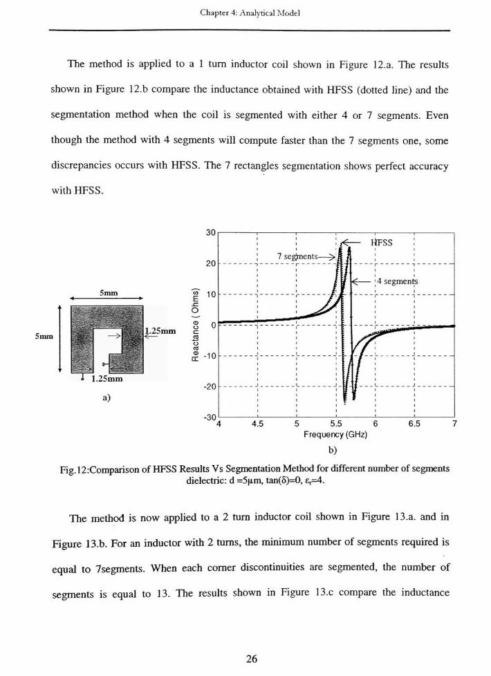
The method is applied to a 1 turn inductor coil shown in Figure 12.a. The results
shown in Figure 12.b compare the inductance obtained with HFSS (dotted line) and the
segmentation method when the coil is segmented with either 4 or 7 segments. Even
though the method with 4 segments will compute faster than the 7 segments one, some
discrepancies occurs with HFSS. The 7 rectangles segmentation shows perfect accuracy
with HFSS.
5mm
5mm
"
jllllllfe.25mmyu
* 1.25mm
a)
-30' '
5 5.5 6
Frequency (GHz)
b)
Fig.l2:Comparison ofHFSS Results Vs SegmentationMethod for different number of segments
dielectric: d =5nm, tan(8)=0, ^=4.
The method is now applied to a 2 turn inductor coil shown in Figure 13.a. and in
Figure 13.b. For an inductor with 2 turns, the minimum number of segments required is
equal to 7segments. When each comer discontinuities are segmented, the number of
segments is equal to 13. The results shown in Figure 13.c compare the inductance
26

Chapter 4: Analytical Model
obtained with HFSS (dotted line) and the segmentation method when the coil is
segmented with either 7 or 13 segments. The 13 rectangles segmentation shows perfect
accuracy with HFSS. When the coil is only segmented with 7 segments, discrepancies
occur in frequency as well as in magnitude.
?, fsst gsg i raft
t r^rdielectric, ,=4
Sround
b)
-10
-15
-20
-25
ifflFSS ' I
13 segments---^kl\ '
7'segments
-
-v-frr -r"
H^|[-t-i--
,J1-
1 ' /i i m
J W _
I t
I I
I i /fi?FrI I
1 1
1 1
1 t
1 1
[ ; 1 :t i ji r i i i
1 .3 1 .35 1 .4 1 .45 1 .5 1 .55
Frequency (GHz)
c)
1 .6 1 .65 1 .7
Fig.l3:a) inductor layout b) cross section view
c)Comparison ofHFSS Results Vs SegmentationMethod for different numbers of segments
The comparison for the one turn and2- mm inductor with HFSS show that the results
can be incorrect if the inductor is not properly segmented. The results are even more
affected when the number of turns increases. Adding segments to model each corner
separately provides correctresults. In conclusion, the number of segments should include
one for every corner and onefor each side. This is to ensure that discontinuity effects are
'included in the model.
27
Chapter 4: Analytical Model
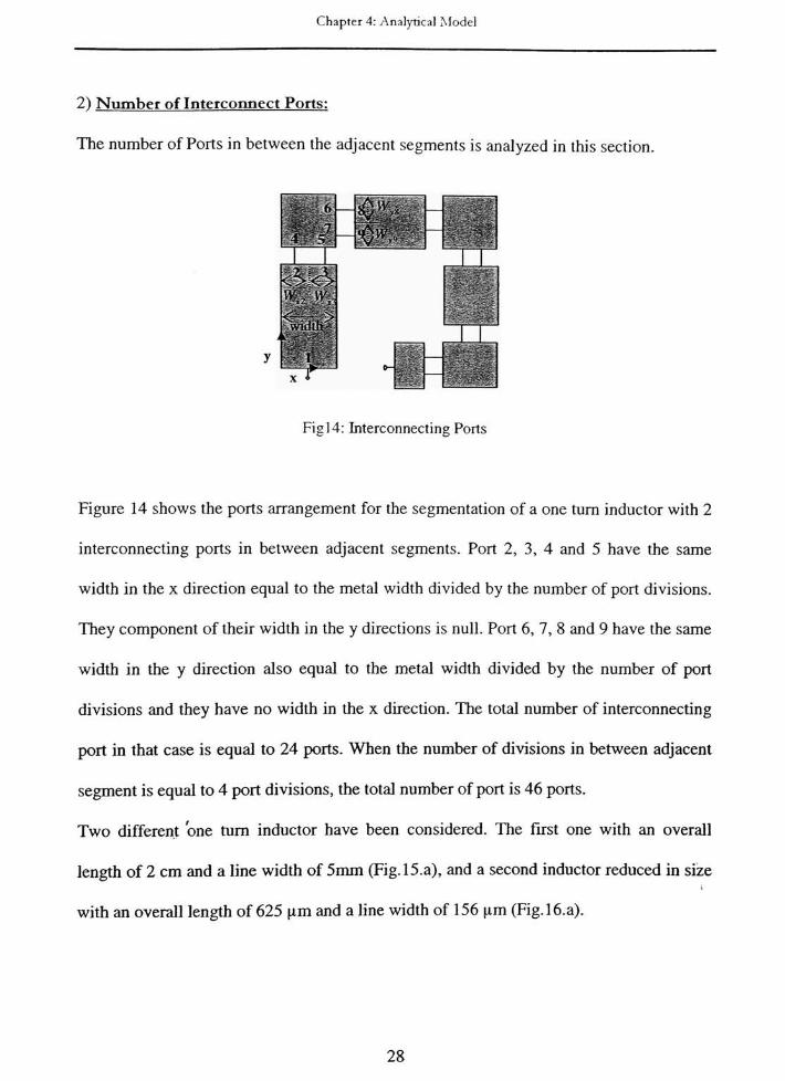
2)Number of Interconnect Ports:
The number ofPorts in between the adjacent segments is analyzed in this section.
Figl4: Interconnecting Ports
Figure 14 shows the ports arrangement for the segmentation of a one turn inductor with 2
interconnecting ports in between adjacent segments. Port 2, 3, 4 and 5 have the same
width in the x direction equal to the metal width divided by the number of port divisions.
They component of their width in the y directions is null. Port 6, 7, 8 and 9 have the same
width in the y direction also equal to the metal width divided by the number of port
divisions and they have no width in the x direction. The total number of interconnecting
port in that case is equal to 24 ports. When the number of divisions in between adjacent
segment is equal to 4 port divisions, the total number of port is 46 ports.
Two different one turn inductor have been considered. The first one with an overall
length of 2 cm and a line width of 5mm (Fig. 15.a), and a second inductor reduced in size
with an overall length of 625 p,m and a line width of 156 p.m (Fig.l6.a).
28

Chapter 4: Analytical Model
The1st
inductor has been modeled with a 2 port and a 4 port divisions in between
segments. The results of the inductance value shown in Figure 15.b are compared with
HFSS (dotted line).25
20
15
2cm
1.3
4ports4-f
'5 ports
?r 1 porti n
: n\ / 1 1
' HFSS /'
- .Z 'I .
-r A
w
If i i
ii-
1- - - -
1.35 1.451.4
Frequency (GHz)
b)
Fig. J 5: a) Single loop inductorwith dielectric parameters: d =5u,m, tan(8)=0, e,=4.
b) Inductance Vs Frequency Vs number ofPort divisions
1.5
It is clearly observed that the results are more accurate as the number of port divisions
increases. As the number of port divisions is equal to 4, the segmentation method
perfectly matches HFSS results.
As the width of the line decreases, the necessary number of port divisions in between
segment might not be the same. The second inductor case with a line width of 1.25mm
and a overall size of 5mm is segmented with a different number of port divisions in
between the adjacent segments. The results are shown in Figure 16.b and are compared
again with HFSS (circle markers). In that case, 12 ports are necessary to obtain a perfect
agreementwith HFSS with a percentage error less than 0.15% (Figure 16.c).
29

Chapter 4: AnalyticalModel
5 mm
5 mm
'
- UBS
: 1
' >
o-
<
1.25 mm
0.5 mm
a)
LLi
4.5
4
3.5
3
2.5
2
1.5
1
0.5
5.5 5.55 5.6
Frequency (GHz)
b)
I 1 1
j=Sports -i
i t
1
1
1
1
1
1
1
1
fir1 8 -ports
l l
1
1
1
t / \-'U
j + 1
) l
I
i
I
1
I
t
1 1 ' \
j 1 ' \
/ 1 ' *
/ /'
~1 1
/ // / ^M
i iu ponsi i
1 '
\ 12 ports
ily -i_______^
5.4 5.45 5.5 5.55 5.6 5.65
Frequency (GHz)c)
5.7 5.75
Fig.1 6:t a) Single loop inductorwith dielectric parameters: d =5u,m, tan(5)=0, e,=4.
b) InductanceVs Frequency for different number ofPort divisions
c) Absolute Percent Error for Inductance from Segmentation Results to HFSS results
30

Chapter 4: Analytical Model
As the width of the line decreases, more interconnect ports are needed. This is caused by
fringing effects that are larger when the width is smaller.
a m 5Fig 17: Fringing effects
3) Number ofGreen's function eigenmodes:
As previously discussed, the response of each segment is computed independently
using the ground/power plane model. For each segments, the impedance matrix is
calculated with a double summation on the Green's function eigenmodes:
-.2 /-2
z>j=ZZ
i?!ld^2m c;2,cos(^>,/)cos^j:-)cos^>,;)cos^^)m^0n=^ab(kxm+k k )
*sinc(k K\Kyn
9V
zJ
sine
(, Wnk^, Isinc
XT71 r
VzJ
sine
( W^k -1-
xm r\
Vz
(33)
The necessary number ofGreen's function eigenmodes in the x and in the y direction
needs to be determine in order to obtain a good convergence of the model. In the
summation, m represents the m'th eigenmode in the x-direction and n represents the n'th
eigenmode in the y-direction. For this model, m also represents the eigenmode of the
largest dimension and is summed from 0 to M and n represents the eigenmode of the
smallest direction and is summed from 0 to N as in Figure 27.a. For the corner
discontinuities, both Green's function eigenmodes in the x and y directions are summed
with the same number of eigenmodes.
31

Chapter 4: Analytical Model
A 2 turn inductor has been considered for this example (Fig 18.a). The inductor has an
overall length of 2cm a width line of 2mm and a spacing of 2mm. The segmentation takes
into account all the corner discontinuities, and the number of ports division in between
adjacent segments is set to 4 ports.
M
* y
M \ .
a"
*
^N
/
X H
--
M
jHf:
N|-
2 mm
N
x10
2 cm
a)
30
20
10
as
-10
1.45 1.5
Frequency (GHz)
b)
1.55
-20
-30
----*=
4Shs|JU !n = 1 !
r [ ;
^ ^=5 ;i
' '"~jj$r~>~"
HF.SS
r i\jJ7"
r i
1.4 1.45 1.5
Frequency (GHz)c)
1.55
Fig.18: a) Inductor Layoutwith dielectric: d =5^m, tan(8)=0, ,=4.
for differentNumber of eigenmodes b) with N fixed at 15 c) withM fixed at 75
As shown in Figure 18 b and c, the solution becomes closer to the expected results as trie
number of eigenmodes increases.
32

Chapter 4: Analytical Model
4) Summary for Segmentation ofRectangular Coils:
The segmentation needs to be done to ensure that discontinuity effects are included in
the model. The number of segments should include one for every comer and one for each
side. A proper segmentation for a one turn inductor is shown in Figure 1 I.e.
The number of the port divisions in between adjacent segments needs also to be
optimized in function of the width of the line. It has been seen that for a width of 5mm,
the number of interconnecting ports required is 5, and for a width of 1.25, 12 ports were
required to obtain perfect agreement with HFSS.
Finally, the convergence also requires a proper number for the Green's function
eigenmodes in order to obtain accurate results. Convergence as been seen when the
number of Green's function eigenmodes of the largest dimension was set to 75 and the
number ofGreen's function eigenmodes of the smallest dimension was set to 15.
33

Chapter 4: Analytical Model
4.3 Circular Coils Inductor:
43.1 Green's function for annular Sector cavities
The Helmoltz equation (24) expressed in the 2-D cylindrical coordinate system is
given in (34):
1 d ( dG) 1 d2G
pdp{ dp) p2d<p
1+k2G = S(p-p0)5(<p-</>0)
P(34)
The term jcopdhas been removed and will be reintroduced later in the final solution.
The boundary conditions require perfect magnetic wall and require that the derivative of
the Green's function go to zero with respect to the normal to the boundary.
Fig.19: Annular sector
For the annular sector shown in Figure 19, the boundary condition gives the following
equation
dG
dp
= 0 (35a)dG
p=aj>
d(/>0 (35b)
=0,cr
a is the sector angle, p is the radialdistance and <p is the azimuth angle
34

Chapter 4: AnalyticalModel
First, the solution for the homogeneous differential equation has to be obtained:
1 d ( dg) 1 d2g l2 n
pdp V dp)p2
df(36)
The operatorM is defined as follow: MG =
d2G
d</>2
Equation (33) becomes (37):
\_d_pdp "TpY
M_\P2
+k2\g=0 (37)
This is a Bessel differential equation with order -J-M [34], with the following solution:
g=AJ^(pk) +BY^(pk) (38)
Jnand Yn represent the Bessel function of the first and second kind.
The solution for the Green's function that satisfies the boundary conditions (32a) is given
by [34] a solution of the homogeneous equation except at/7 -
p0 and is of the form of:
G =
a<p<p0
Y^(bk)J^(pk)-J^(bk)Y^(pk)
p0<p<b
(39)
The prime functionsJ and F represents the derivative of the Bessel function of the first
and second kind/n andF .
The following functions are defined to simplify the notations:
/ (ak,pk)= (ak)Jn (pk)
-
Jn {ak)Yn (pk)
f(ak,pk) = Yn(ak)Jn{pk)-Jn{ak)Yn{pk)
(40)
(41)
35

Chapter 4: Analytical Model
The following continuity conditions must also be satisfied,
G\ _=G
+
\p=Po \p=Po
dG
dpP=Po
dG
dpP=Po
Po
(42)
(43)
To satisfy (42) the solutions of (39) are cross-multiplied and the solutions for the
homogeneous equation result in (44):
G =
f^(ak,pk)f^(bk,p0k)
a<p<p0
fjzfi (bk,pk) fj-f (ak, p0 k)
p0<p<b
(44)
Substituting (44) into (43), we obtain (45):
dG
dpP=Po
dG
dpP=Po
2f^(bk,ak)
xp0
To satisfy (43), (39) results in (46):
f^(ak,pk)f^(bk,p0k)^S((p-<p0)
G =
2f^(bk,ak)
a<p<pQ<b
fj-^{bk,pk) f^{ak,p0 k)7c8(<p-<pQ)
2f^(bk,ak)
a<p0<p<b
(45)
(46)
The green function is expressed in terms of the differential operatorM. The eigenfunction
and eigenvalues ofM are required to transform (46).
36

Chapter 4: Analytical Model
By [34], the normalized eigenfunctions and the set of eigenvalues are given in (47):
cos(n d>)V =
p-
V p
(47a)
{-nl-rt,-n22,...} (47b)
Where n pi, I = n I a, a is the sector angle, and a = \p|2p*0
By [38], for any continuous function F( ),
r,^zr* ^v vv2epfnp(ak,pk)f(ak,p0k)cos(n<p)cos(n<f>0) (48)
p=o 2fn(bk,ak)
Using (48) into (46), we obtain the following Green's function:
_^lopf {ak,pk)f
'
(ak,p0k)cos(np<p)cos(np<p0) f4
G(p,HPo^0)=2u'
: ,,,,
v ;
P=o 2fnp(ak,bk)
Unlike [35], where a can only take a few discrete value that make n an integer, in (49)
there is no restriction placed ona .
Reintroducing the jcopd term, the Green's function for the annular sector is given in
(50):
jcoldly pfn? (ak,pk)fnp (ak,p0 k)cos(np0)cos(np0o) (50)
(1/7 = 0
a<p<p0<k 0<<f><a, 0<<p0<a, <rp=L^0
One special case is when a = nwhich is the Green's function for a semicircular disk.
37

Chapter 4: Analytical Model
4.3.2 ImpedanceMatrix
The impedance matrix is derived using (50) and (23). When the ports are at the inner
periphery (/? = a) and the other ports at the outer periphery (p = b), the impedance
matrix elements are given by [34]:
_
jcopdl^ Pfnp (<**>#*)/,,, (&/c,p^)cos(72^,)sin(pA,.)cos(n^.)sin(7ipA .)
^
p=0 fn (bk,ak)
2A }P_KW,"pJ
k denotes the wave number and is defined as: k - co^Jps ,Q) is the angular frequency, fis
the dielectric permittivity, p the permeability and d the height of the dielectric.
W. and W;are the widths, (/?,,$) and(/77,0;) are the coordinates of porti and portj.
A. = sin
'W\
K2PiJ
(52)
When p is equal to zero, the denominator becomes null and the result of the impedance
matrix is undefined.
sinCx)
Knowing that lim = 1 ,we multiply the denominator and numerator of the
*-*x
equation by (n A,) *(n A , ), and the impedancematrix when p= 0 becomes:
jcopd I <7pfn, (**Pfrfn, (bk,Pjk) cos(/i,4 )cosfn^ )%\
2Pi\ (
KW'n,
"A
fnp(bk,ak)
sm(npAj) sin(7tpA,)
"A,
A
(53)
38
Chapter 4: Analytical Model
sin(n A=) sin(n A;)Since, lim = lim = 1
p-*> n^. p-o
OpA;
Jijlp=0"
jcopdl Gpfnyk,pfC)fnp {bktpjk)cos(npfi )cos(np0. ) (2p.&.Y 2/7;Ay.
/ (**,**) v w; jv w; y
(54)
4.3.3 Considerations for convergence issues foranalyticalmodel
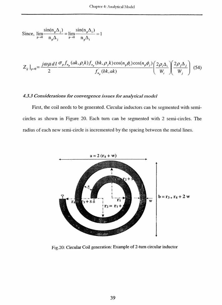
First, the coil needs to be generated. Circular inductors can be segmented with semi
circles as shown in Figure 20. Each mm can be segmented with 2 semi-circles. The
radius of each new semi-circle is incremented by the spacing between the metal lines.
a = 2 (r4 + w)
b = T3 + T4 + 2 W
Fig.20: Circular Coil generation: Example of 2-turn circular inductor
39

Chapter 4: Analytical Model
As previously discussed for the rectangular coils, different variables need also an
optimization for circular coils, such as the number of segments, the number of ports
needed and the number of Green's function eigenmodes. This section investigates the
value of these different variables in order to get a good convergence. The results of the
segmentation method are compared to HFSS.
1) Number of Segments:
The number of segments needs to be determined at first. An example of the segmentation
of a 2-turn inductor is shown in Figure 21 where each semi-segment corresponds to a
segment. The 2-tum inductor is segmented by 4 annular sectors with sector angle equal to
71.
Port2
a)b)
Fig.2 1 : a) Two-loop circular inductor b) segmented
40

Chapter 4: AnalyticalModel
A one turn inductor is considered with an overall length of 2cm, a spacing of 2mm
and a width line of 2mm. (fig 22.a).
2cm
^<-2mm
a)
5um [
metal layer, o = inf
/
30
20
10
<0 n
o u
c
so
CO
CD
DC -10
ndielectrics,^
Sround
b)
-20
-30
i
- HFSS
Segmentation Methodf
3
If
I
2.5
Frequency (GHz)
c)
3.5
Fig.22: a) Single rum circular inductor b) cross-section view
c) Inductance Vs Frequency
Themethod using 2 segments for the one-rum inductormatches perfectly HFSS results.
As opposed to rectangular inductors, circular inductor does not encounter the problem of
comer discontinuities, and the number of segments only needs to include one segment for
each semi-circle. It is not necessary to segment the inductorwith quarters of circle.
2) Number ofports:
The impedance matrix formula (51) relates the impedance seen at one port from
another port when the ports are either at the inner periphery or at the outer periphery of
the annular sector. The Green's function need to be re-integrated in order to be able to
41

Chapter 4: Analytical Model
place the port anywhere in the annular sector. Comparison with HFSS have shown that it
was not necessary, 2 ports in between adjacent segment are sufficient, one at the inner
periphery and another one at the outer periphery.
3) Number ofGreen's function eigenmodes:
The response of each segment is computed independently using the ground/power
plane model. For each segments, the impedance matrix is calculated with summation on
the Green's function eigenmodes.
80
60 -
2cm_40
CO
E
2.20
<^- 2mm s o
a)
-20
-40
-60
I P= 20;
-i--V
p;=80-U|
>"p=io-
HFSS |/
2.4 2.6 2.8 3 32
Frequency (GHz)
b)
3.4 3.6
Fig.23: a) Single turn circular inductor
b) Inductance Vs. Frequency for different value ofGreen's function eignenmodes
In Figure 23 .b, the results of the segmentationmethod is compared to HFSS (dotted line).
As the number ofGreen's function eigenmodes increases, the solution converges to the
42

Chapter 4: Analytical Model
expected results.When p is equal to 80, the segmentation methods agrees very well with
HFSS results.
4) Summary for segmentation of circular Coils:
A proper segmentation needs to be done to ensure that all effects are included in the
model. The number of segments should include one for semi-circle and one for each side.
The number of the port divisions in between adjacent segments needs also to be
optimized in function of the width of the line. It has been seen that only 2 ports were
required and sufficient for the Impedance formulation of every subcorner.
Finally, the convergence also requires a proper number for the Green's function
eigenmodes in order to obtain accurate results. Convergence with HFSS results has been
observed when the number ofGreen's function eigenmodes set to 80 modes.
4.4 Summary of the Analyticalmodel
At first the parameters of the planar coil inductor are defined. The geometry of the
inductor is then segmented into sets of rectangular or annular shapes. The interconnecting
ports are defined in between adjacent segments. The impedance matrix of each segment
is computed and converted into S-matrix. The S-matrix of each segments are combined
to get the final S-matrix of the overall network and finally, segmentation technique is
used to obtain the characteristic of the n port inductor.
43

Chapter 5: Numerical Modeling
5. NUMERICAL MODELING OF INDUCTORS USING EXISTING
FULLWAVE SOLVERSAND QUASISTATICAPPROACHES
The present work is a very valuable study to help the designer choose the appropriate
software tool, best suited for the frequency range and physical geometry. Three EM
simulation tools have been chosen, namely MaxwelBD, HFSS and ASITIC. Each of
these has a set of advantages and limitations.
In the following section, each tool is described for setting up the model, defining the
physical structure, setting up boundaries, assigning excitation ports and extraction results.
Those popular software tools are compared where some of the results have been obtained
using HFSS and MaxwelBD and others have been extracted from published results.
Comparisons are also made with the current sheet method. The advantages and
limitations have been discussed.
5.1 MaxwelBD
Maxwell 3D is a full wave Solver that analyzes electric and magnetic fields in three-
dimensional structures. The designer draws the structure and specifies all the relevant
material properties, boundary conditions and sources.
The eddy current field solver computes includes the effect of the AC currents in the
conductors and obtains the time varying external magnetic fields by imposing boundary
conditions. As frequency increases is, the skin depth decreases requiring a finermesh for
the solution procedure. Results can be extracted in the form of electric and magnetic field
plots and ImpedanceMatrix as a function of frequency.
44
Chapter 5: Numerical Modeling
5.1.1 Setting up themodel:
The software tool is fairly user friendly; however, certain rules have to be followed
for an accurate inductor modeling:
2D and 3D models can be drawn. 2D objects such as spiral and square inductors can
be exported fromMaxwell2D.
Input and Output terminals have to be planar faces or 2D sheet objects.
These terminals have to match the exact cross section of the object in order to apply a
source to it.
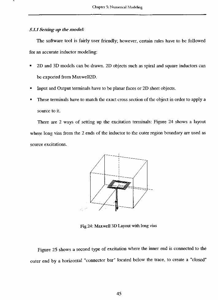
There are 2 ways of setting up the excitation terminals: Figure 24 shows a layout
where long vias from the 2 ends of the inductor to the outer region boundary are used as
source excitations.
Fig.24:Maxwell 3D Layout with long vias
Figure 25 shows a second type of excitation where the inner end is connected to the
outer end by a horizontal "connectorbar"
located below the trace, to create a"closed"
45

Chapter 5: Numerical Modeling
loop for the current. This solution minimizes the extra inductive effects of the long vias.
One terminal is added somewhere in the loop to assign the current direction.
Fig.25: MaxwelBD Layout - Closed loop
5.1.2Setting up boundaries:
Li the Setup Boundary panel, different setups can be chosen where multiple effects
can be simulated.
1) "Displacement currenteffect"
is turned on for every object including conductors and
dielectrics.
2) "Eddy currenteffect"
is turned on for every conductive object, even if the material
has a small conductivity.
46

Chapter 5: Numerical Modeling
5.1.3 ImpedanceMatrixResults:
The impedance Matrix gives the relationship between AC Voltages and AC currents
formultiple conductors. The impedance matrix computed byMaxwelBD is of the form:
Z = R + jO)L (55)
Where R is the internal resistance of the current loop, L the self-inductance of the loop
and co the angular frequency. wL Represents the inductive reactance of the loop.
The inductance solution is obtained by a magnetostatic inductance solution:
1 f- - (56)
I2
I
Where B is the magnetic flux density and H ,the complex conjugate ofmagnetic flux.
To calculate the resistance, the system computes the Ohmic Loss P:
P = fy./Vv (57)2(7
V
Where J is the current density and o is the conductivity.
In terms of resistance and total of current 7, the Ohmic loss becomes:
P =
RIRMS2
(58)
The resistance is then computed using:
\J J*dv
R = z
71 (59)Vlp**
47

Chapter 5: Numerical Modeling
5.2 High Frequency Structure Simulator - HFSS
HFSS is also a full wave solver, where you can compute basic electromagnetic field
quantities. In order to generate an electromagnetic field solution, HFSS employs the finite
element method and the tetrahedral segmentation of the entire space. The layout of the
structure has to be drawn using CAD tools, the material characteristics have to be
specified for each object, and the ports and special surface characteristics has to be
identified. HFSS will generate the necessary field solutions and associated port
characteristics and S-parameters. For a specific frequency range, an adaptive mesh is
chosen to be generated at2/3r
of the entire range. HFSS can perform a sweep and
generate a solution across a range of frequencies.
Different types of excitation are available in HFSS; they are used to specify the
sources of electromagnetic fields and charges, currents or voltages on objects or surfaces
in the design. The 2 excitations of interests when modeling planar inductors are the wave
port and the Lumped Port.
The Wave Port represents the surface through which a signal enters or exits the
geometry.
The Lumped Port is an internal surface Port similar to the wave port. Lumped Port
gives you the possibility to define ports located internally and to compute S-
parameters directly at the port.
The Results comes in the form of S-Y and Zmatrices.
48

Chapter 5: Numerical Modeling
5.3 Analysis and Simulation of Inductors and Transformers for ICs
ASITIC is a computer aided design tool for passive devices over conductive silicon
substrates. ASITIC converts Maxwell's Equations into a linear system of equations with
the aid of the semi-analytical Green Functions.
Inductances and capacitance matrices are constructed -> matrix elements are
computed from numerical volume/surface integration of the Green Function.
Capacitance and Inductance Matrix are assembled into a large system of equations by
the Partial Element Equivalent Circuit formulation. (KCL, KVL, charge conservation,
electrical and analogs ofMaxwell's Equation).
System equation is solved for the electrical properties of the system.
ASITIC works with a technology file that describes the substrate and metal layers of
the process. This file also contains process specific parameters such as layer thickness
and the sheet resistance of the various layers. The inductors does not need to be drawn,
input parameters such as Number of Turns, outer dimension, metal layer, metal width and
spacing are entered in order to draw planar inductors of different shapes. It can also be
used to model transformers, bond pads and capacitors. The results are obtained in the
form of resistance, inductance, S-matrix, and equivalent circuit model.
5.4 Current sheetmethod [30]
The current sheet approach [30] yields a simple accurate expression for self and
mutual inductance. Current sheet refers to a conductive sheet with finite width and
infinitesimal thickness where the sides of the spiral inductor are approximated to 4
49

Chapter 5: Numerical Modeling
rectangular current sheets and the concept of Geometry Mean Distance (GMD),
Arithmetic Mean Distance (AMD) and Arithmetic Mean Square Distance (AMSD) are
used. The resulting expression is [30]:
t^wc/^v^yi(60)
The outer and inner dimensions are dout and din respectively. The average diameter:
dove = (dout + din )/2, and the fill ratio of the spiral: p= (dout - din ) I (dout - din ). The
constants cj, C2, cs and C4 depend on inductor shape and are given in [30].
5.5 Comparisonwith Published Results
Two examples for an inductor configuration as shown in Figure 26 have been
considered for calculating inductance and quality factor Q. In example 1, the coil, a 240
um square, has 4 turns, a metal width of 13.7 um and a spacing of 10.25pm (Figure 28).
The resistivity of the silicon is 5Q.cm with a dielectric constant of 11.9 and oxide
thickness is 4 pm. For the same example, Figure 27 shows the comparison ofMaxwelBD
and HFSS and Figure 28 compares HFSS and Momentum. To compare HFSS with
SONNET, example 2 (Figure 29) has been considered using a 9-turn, 210pm square spiral
inductor with a spacing line of 5.5 um, metal width of 6.5 pm and metal thickness of 2
urn. The resistivity of the silicon is 10f2.cm with a dielectric constant of 11.7 and oxide
thickness is 5 pin with a dielectric constant of 3.9.
s^SJSSlSl'- ^SSfeJ Silicon dioxide
|a Silicon
50

Chapter 5: Numerical Modeling
0.5 1 1.5 2
Fig.27: InductanceL^-e- ) and Q ([31]), using MaxwelBD (- -
-), and HFSS( )
8
13.7u_m
10.25 um
240 tim
Xc
o
c
o
3
c
- Inductance
Quality Factor
4 6 8
Frequency (GHz)
Fig.28: example 1: a) Planar Inductor b) HFSS ( ), andMomentum ( ). [31]
2 4o
210 pm "-
1 2O
.
-^-=^77""^^"^.
SONNET
HFSS
1 1 1
-^^~-~~--
2 3 4
Frequency (GHz)
b)
Fig.29: example 2: a) Planar Inductor b) HFSS and SONNET [32]51

Chapter 5: Numerical Modeling
5.6Advantages and Limitations
The advantages and limitations of the tools MaxwelBD, HFSS and ASITIC can be
summarized as follows:
MaxwelBD shows good agreement with HFSS (Fig.27) in the low gigahertz and
megahertz region. The inductance obtained by the current sheet method for the same
example 1 is 2.9nH and compares well with these tools. The discrepancies for the quality
factor obtained from MaxwelBD are probably due to the parasitics not considered in
equation (3). Also, MaxwelBD appears to have limitations above 2GHz since it does not
show a resonance, as do HFSS andMomentum in Figure 28.
On the other hand HFSS shows very good agreement with published data at all
frequencies and compares very well with other full wave solvers such as Momentum and
SONNET. Some of the discrepancies seen in Figure 28 are probably due to the fact that
the silicon thickness not given in [3 1 ] has been assumed.
The comparison between ASITIC and HFSS has been done by several authors and
summarized in [32]. HFSS has better accuracy for inductance and resistance whereas
ASITIC seems to underestimate these values. However, the advantage ofASITIC is that
it provides a quick analysis as opposed to the time intense nature of the full wave solvers
and also provides an equivalent circuit model for the parasitics.
Another advantage of HFSS is that its ability to define ports at the inner end of the
inductor as shown in Figure 30. This option is not available in MaxwelBD and is unclear
in ASITIC where the ports are already defined.
52

Chapter 5: NumericalModeling
Despite all the advantages of HFSS, it seems to have some difficulties in drawing
precise mesh in the low megahertz region. In conclusion, MaxwelBD appears to be the
best tool at low frequencies while HFSS, SONNET,Momentum provide better accuracies
in the higher frequency range. Quick analysis can be done either by current sheet method
orASITIC.
Fig.30: Lumped Port Element set up with HFSS
5.7 Ferrite Filled Inductors
Ferrimagnetic materials are oxide of irons combined with one or more of the
transition metals such as manganese, Nickel or Zinc. These provide a high resistivity as
well as high permeability, which make them attractive as a possible core for planar
microinductorswith the objective of increasing inductance and Q.
In the presentwork, the ferrite is assumed to be driven by small signals and small bias
field so that it is not driven into saturation and the linear portion of the B-H curve can be
53

Chapter 5: Numerical Modeling
used. For such ferrites, known as soft ferrites, the permeability will be frequency
dependent (Fig.31) and need not be modeled as a tensor.
10000
5000
-O
03
<D
E
(5
q.
1000
500
x J LLLU1 J L i iiiLU i J i J _j i_i i_
J. i J LLL1H J L i 1J1LU 1 1 1J_J IJ1_
1 I 111)111 1 L iJ Ml' ' 1 l 1 1 1 I
l t l l l l i l l i i i i i i i l i i i i i 1 I l l
t \ i rmiT t r i Turn j t i - i nr
-t 1 i - h *- *--i-i + 1 i "^^w* + *-*-* ' "?--J I r -i
4 1 1- 1- L UW4 1 1 I- 4-4 4N^4 1 1 - 4- i 1 1 *
t 1 111(111 1 1 1 1 1 1 1 1\ 1 1 1 1 1 1 1 1
T i i-
r r ri~iT 1 i t-TTTrn~^V"
' 1~
t n-r
j-it~
i i i i i i i i i i i iiiiim N. i i i i i i l i
t 1 rrrrnT 1 ir-
t i t r n ^^ 1~
T ~i ~l ~nr*
i i i i i i i i i i i j i i i i i i \ i t I i i i i
4. 1 l-UI-H-l-l 1 I I-4.44-1-1-I l-^C 4.-4.-I-I-I-I4-
1 1 1 1 1 1 1 1 I t ) 1 1 1 1 1 1 1 1 \ l 1 1 1 1 1 1
1 1 1 1 1 1 1 1 1 1 1 1 1 1 1 1 1 1 t \^ ) 1 1 1 II
1 1 1 1 1 1 1 1 1 1 1 1 t ! 1 1 1 ] 1 l\l 1 1 1 1 1
1 1 1 1 1 1 1 1 1 t 1 1 1 I 1 1 i 1 1 1 "Al 1 1 i 1 1
1 t 1 > 1 1 1 1 1 1 1 1 1 1 1 1 1 1 1 1 iXl lilt
1 f 1 1 1 1 1 1 1 1 1 1 1 1 1 1 1 1 1 1 1 T I 1 1 1
1 1 1 1 1 1 1 1 1 1 1 1 1 1 1 1 1 1 1 1 1 1 I 1 1 1
1 1 I 1 1 1 1 1 1 1 t 1 I 1 1 1 1 1 1 1 1 1 1 1 1 1
i i iiiiiii 1 1 i i r l 1 i r 1 i i i i
10 10
Frequency (GHz)
10 10
Fig.31: Ferrite Permeability Vs. Frequency (Courtesy Ferronics Inc)
There is several ways where the inductor can be loaded by the ferrite (fig 31)
Hj Copper
I-
j Si02
Ferrite ^ Sj
Fig.32: Ferrite LoadedMicro-Inductor. ( t^ = lum, tsio2 = 2um, tsi = 300pm.)
From the comparison of all the modeling tools discussed in section U, MaxwelBD is
best suited for low frequency analysis and allows for the loading of the inductor with
54

Chapter 5: Numerical Modeling
ferrite. Such a layout is not possible with ASITIC, or the current sheet method. The
HFSS, SONNET andMomentum, could be used at high frequencies.
Using MaxwelBD, three different configuration shown in Figure 31 have been simulated
at a frequency of 100MHz, for a particular value of permeability, p =1000 where an
inductor with an inductance L = 7.5nH has been chosen and d is equal to 2pm.
Design R (Ohms) L(nH)
Without ferrite 7.54 7.78
Fig 32.a) 7.53 7.99
Fig 32.D) 7.53 13.54
Fig 32.c) 7.54 14.65
Table 1: Resistance and Inductance Value for different design configurations
It can be seen that the inductance improves significantly when the ferrite thickness
increases. Further, when the ferrite layout is below the metal layer, the inductance is
higher. (Fig32.c). However, the fabrication process for configuration (Fig32.b) is more
likely feasible than (Fig32.c).
For the configuration in figure 6.b, the ferrite thickness d is varied, and the inductance
obtained fromMaxwelBD is shown in figure 7.
15
I
<D
8 10+-*
o
c
0 12 3
Ferrite thickness d (pm)
Fig. 33: Inductance Vs. Ferrite thickness d (um)
55

Chapter 5: Numerical Modeling
A significant increase in the value of inductance is observed when the ferrite
thickness d becomes greater than the metal thickness (Fig.33), steadily increasing and
finally reaching a maximum value. After this value has been reached, the increase in
thickness d does not seem to affect the inductance.
Finally, using a frequency dependent value of the permeability from Figure 3 1 and an
inductor of 7.5nH, the inductance and resistance have been obtained for the configuration
shown in figure 6.b where the ferrite thickness d equal to 2pm. Results are given in
Table2.
Frequency Mr R (Ohms) L(nH)
10 kHz 5000 7.5383 13.087
80kHz 5000 7.5383 13.087
300kHz 5100 7.533 13.097
700 kHz 3850 7.526 13.019
1MHz 3100 7.5205 12.997
5 MHz 750 735217 12.65
Table.2: Inductance and Resistance of ferrite-loaded Inductors
56

Chapter 6: Results
6. RESULTS
In order to validate the analytical model, two types of comparison have been made,
one with full wave solver and the other with measured results. HFSS has been chosen as
the full wave solver since it has been shown in the previous section to be the most
appropriate tool to simulate inductors for a wide range of frequency where ports are
internally located.
The accuracy of the model is investigated for inductor shape, number of turns,
footprint area, width and spacing of the line, as well as dielectric parameters. In each
case, comparisons have been made to HFSS. In order to further validate the method,
experimental measurements have been compared with predicted values for planar
inductors in a package. Finally, for a given footprint area and frequency of interest in a
particular package or chip where the dielectric parameters and thickness have been
defined, design considerations have been investigated. Also discussed here is the impact
on the inductance and the quality factor by the inductor geometry such as number of
turns, spacing and line width.
6.1 Comparison of analytical modelwith HFSS
In this section, rectangular coils and circular coils have been modeled to validate the
theory for the coil geometry such as number of turns, line width, spacing and dielectric
height. i
57

Chapter 6: Results
6.1.1 Planarrectangular coil
1) Single-turn rectangular coil
The single turn rectangular Coil shown in Figure 34.a is analyzed and compared with
HFSS. The dielectric is lossless and the conductors are perfect. The substrate for this
example has a e, of 4 and a thickness of 5pm. The Reactance extracted from the Z
parameters (Figure 34.b) shows excellent agreement between the analytical model and
HFSS results. For both HFSS and the present work, the inductor is inductive until 1 .39
GHz where it becomes capacitive.
5 mm
Port 1
-25
1.2
11-
1
HFSS
PresentWork
j_
j-;- 1
_
1
-
l^"""""*
J
1 ' '
1.3 1.4
Frequency(GHz)
b)
1.5 1.6
Fig.34: a) Planar inductor for comparison withHFSS b) Reactance Vs. Frequency
2) Two-turn rectangular coil
A 2-turn rectangular Coil shown in Figure 35.a is now analyzed and compared with
HFSS. The dielectric is lossless and the conductors are perfect. The substrate for this has
a 8r of 4 and a thickness of 5pm.
58

Chapter 6: Results
2 cm
2 cm
2 mm
Port 2
25
20
15
10
5
0
a)
3 -5o
to
<D
S: -10
-15
-20
-25
HFSS-
SegmentationMethod-
i
:x;::"Tj: ^J
"A
t i\
1 1.2 1.4 1.6
Frequency (GHz)
b)
1.8
Fig.35: a) Two-tum rectangular planar inductor for comparison with HFSS b) Reactance Vs. Frequency
Again, the results in Figure 35.b show perfect agreement with HFSS.
The inductor with the same parameters as in figure 33.a is again analyzed. The substrate
for this has now a e, of 4 and a thickness of 300pm. The results for the analytical model
and HFSS are shown in figure 34.
3) Impact of dielectric thickness
3x10
***'
Segmentation Method
2.5
2
--
HFSS Results
1.5
<D
O
C
Bo
co
CD
rr
1
0.5
0
-0.5
5 if
1 ; /I \
Is ff\ / /\* * /1: ' /\\ / /
-1
-1.5
jlV V
1 1.5 2 2.5 3
Frequency (GHz)
Fig.36: Results for two rum inductor (fig34) with a dielectric thickness equal to 300um
Reactance /w Vs. Frequency for Comparison with HFSS
59

Chapter 6: Results
Small variations are present between HFSS Results and the present analytical work.
This is due to a high dielectric thickness. The Green's function has been developed
assuming that the thickness of the dielectric to be electrically thin. Nevertheless, there is
still good agreement between HFSS and the segmentation method.
6.1.2Planar circular coil
the impact on the inductance and the quality factor by the inductor geometry such as
number of turns, spacing and line width.
1) Single turn circular coil
The single turn circular Coil shown in Figure 37.a is analyzed and compared with
HFSS. The dielectric is lossless and the conductors are perfect. The substrate for this has
a 8r of4 and a thickness of 5pm.
30
20
2cm
^-2mm
a)
10
E
O
0c
re
o
CO
CD
DC -10
-20
-30
I l
HFSS
Segmentation Method
*
if
i
i
\i
>
2.5
Frequency (GHz)
b)
3.5
Fig.37: a) Circular inductor for comparison withHFSS b) Reactance Vs. Frequency
60

Chapter 6: Results
The Reactance extracted from the Z parameters (figure 37.b) shows excellent agreement
between the analytical model and HFSS results. For both HFSS and the present work, the
inductor is inductive until 3 GHz and then becomes capacitive.
2) Impact of line width for single turn circular coil
Another single mm circular coil with a wider width line and outer dimension shown
in Figure 38.a is analyzed and compared with HFSS. The dielectric is lossless and the
conductors are perfect. The substrate for this has a sr of 4 and a thickness of 5pm.
20
3cm
-5
-10
1 ?
.. J __
i L- ..
! T 1
I .....L..1mn-nnrr
-rnnnrrf^6*!
3.2 3.4 3.6
Frequency (GHz)b)
3.8
Fig.38: a) Circular inductor for comparison withHFSS b) Reactance Vs. Frequency
Again, the results shown in figure 36.c show very good agreement with HFSS.
61

Chapter 6: Results
6.2 Comparisonwith experimental Results
A further validation of the analytical method has been done with experimental results.
Inductors have been made on a printed circuit milling machine using copper clad Duroid,
Rogers RT5850. One port measurements were made using the Agilent Technologies
E8363B.
6.2.1 One-turn rectangular coil
The one mm rectangular inductor was constructed using a substrate with a thickness of
31 inches, a dielectric constant of 2.33. The metal and ground layers are made of copper.
Fig.39: a)Millingmachine b) One rum inductor constructed
The inductor constructed (Fig 39.a and 39.b) had an overall size of 19.5mm, a width line
of 4.6mm and a spacing of 2.16mm as shown in Figure 40.a. The cross-view of the
inductor is shown in figure 38.b. Measurements were done with network analyzer from 1
to 10GHz. The one port measurements and the results of the analytical model are shown
in Figure 40.c. Very good agreement between the predicted results and the experimental
62

Chapter 6: Results
results are observed. Little discrepencies are observed at the higher frequency. This might
be due to the dielectric loss not constant along the frequency.
193 mm 800
- v HgarjBKfclftjT HBWjijg
600
193 mm
RSBBSs
~~^i
4.6 mm
_
40
w
j= 200
o
i
31 inches.
2.16 mm
Portl
a)
cop
J
per
o
o
o
o
o
l' "-1
f1
i t -600
Dielectric: E, =2.33copper
tar (5) = 0.01-800
b)
1
1PresentWork
MeausredI
)
t
1
.
! \ \
1
11
1. *
1 jr
1 f
' *
'
\f'
j
i
i
i
3 4 5 6
Frequency(GHz)
c)
Fig.40: a) Planar inductor for comparison with Experimental results
b) Cross view of Inductor c)Reactance / >v Vs. Frequency
6.2.2 Two-turn rectangular coil
A two-turn rectangular inductor was also constructed using the same substrate with a
thickness of 31 inches, a dielectric constant of 2.33. The metal and ground layers are
made of copper
Fig.41: 2 Turn Inductor constructed for one port measurement
63

Chapter 6: Results
The inductor constructed (Fig 41) had an overall size of 19.5mm, a width line of 2.3 mm
and a spacing of 2.8 mm as shown in Figure 42.a. The cross-sectional view of the
inductor is shown in Figure 42.b. Measurements were done with network analyzer from 1
to 10GHz. The one port measurements and the results of the analytical model are shown
in Figure 4 I.e.
193 mm
193 mm
2.8 mm
31 inches
2.3 mm
1000
800
600
400
200
Dielectric: s, =2.33
tan(8) = 0.01
b)
copper
8
'
| 200
co 400
CD
< 600
-800
-1000
1
I I
J
JfJ*
1
1
1
1
J
f L _
a
I j. _
X I
? 1
I";"!-;--"j"!---|- "i" -J~
i--^--i-,L
i : i i ;
L L l__l _l J i.
4 5 6
Frequency (GHz)
c)
10
Fig.42: a) Planar inductor for comparison with Experimental results
b) Cross view of Inductor c)Reactance Vs. Frequency
Small discrepancies between measured data and predicted values are observed in
figure 41.c and' can be explained by several reasons. First of all, human fabrications
errors could have been provided by the milling machine. The dielectric is not rubbed off
completely uniformly, and themeasurements of the coil geometry are made with a certain
error tolerance. Next, the SNA connectors were used for measurements. The analytical
64

Chapter 6: Results
model assumed the ports to have an impedance of 50 ohms in order to extract the S-
matrix. Loading the cavity with a probe was not accurately known. And the actual
impedance could be slightly different to 50 Ohms and would lead to different predicted
results. Finally, the Duroid material used was known to have a losstangent equal to 0.01.
Since the loss in the dielectric are not independent of the frequency, there will be a much
better agreement over the frequency range, if a frequency dependent profile was available
for the loss tangent with the Duroid. Considering these possible reasons for discrepancies,
the good agreement of predicted and measurement results validate the analytical model.
6.3 Investigation ofCoil Inductor Geometry for a limited foot-print area
The parameters of interest for the design of inductors are the inductance and quality
factor for a given substrate, a limited footprint area and a frequency range of interest. The
parameters given to the designer are the footprint area (cW), the thickness (d), the
permittivity(e,- ) and loss tangent ( tan(5) ) of the dielectric as shown in figure 43.
aW fixed
.3. _^_^j
d^,: fixedd: fixed
T
copper
copper
a)
Dielectric: e,. and tan(8): fixed
b)
Fig.43: Fixed parameters a) Inductor Layout b) Cross-section view
65

Chapter 6: Results
In this section, the impact of the geometry parameters such as the number of turns,
the spacing between the conductor line, the width of the line and the dielectric thickness
are discussed.
63.1 Impact ofnumberofturns, Spacing and Width
The impacts on the inductance and the quality factor by the inductor geometry are
discussed here. A limited footprint area is chosen with dom equal to 1cm (fig 42). The
required design frequency is 2.45 GHz. The substrate is lossless and has a dielectric
constant of 4 and a thickness of 5um. The shape of the inductor is chosen to be
rectangular. At first the impact of the number of rums with a fixed spacing and a fixed
width is observed over a frequency range that includes the frequency of interest. Next,
with the number of turns chosen, the inductance and quality factor of the inductor at
2.45GHz is analyzed for a varying line spacing and width.
1) Number ofTurns
The inductor coil has a spacing of 0.25 mm, a line width of 1mm and an outer
dimension of 1cm. The number of turns varies from 1 to 3 turns. The reactance and
quality factor of the inductor for differentnumber ofmm along the frequency are shown
in Figure 44.
66

Chapter 6: Results
30
20
w
E 10
sz
CD f)o
u
c'
o
co -10
CD
rx
-20
-30
I I 1 1 1 , ,
1 1
1' '
t 1 1
1 1 turn
2 turns i
3 turns 1
1' < 1
? 1 1/
1
# 1'
i /i /
/J
1 1
1 fl 1
1 "1 1
1 ''I 1
U 1 1
1
2 2.25 2.5 2.75 3 3.25 3.5 3.75 4
Frequency (GHz)
a)
40
30
20
cr
10
M 0
E
-10-
-20
I I I I I I 1 1
1 turn
2 lums
3 lums
/ ; \; / ;\ ; ; /\/< / '
\-
v r r \t t t \t n ~r ~i f i \ -i A
i i i i i
-30
2 2.2 2.4 2.6 2.8 3 3.2 3.4 3.6 3.8 4
Frequency (GHz)
b)
Fig.44: a) Reactance vs. Frequency b) Quality Factor vs. Frequency for a varying number of turns
Planar inductor geometry: footprint area = 1cm x 1cm,width = 1mm. Spacing = 1mm
As seen in Figure 43.a, the reactance increases as the number of turn increases. There
are also a larger number of resonant frequencies as the number of turn increases. The
inductor can be inductive or capacitive. At the frequency of interest (2.45 Ghz), the
67

Chapter 6: Results
inductor coil is only inductive with a positive quality factor for the 2turn configuration as
seen in Figure 44 a and b.
In the following analysis, the number of turns for the inductor is fixed at 2, and the
impact of the spacing and width are observed at a fixed frequency, 2.45GHz.
2) Spacing between the lines
The inductor coil chosen has now 2 turns, the foot print area is kept to 1cm, and the
line width is 1mm. The substrate is lossless, its thickness is 5pm and its dielectric
constant is 4. The frequency is kept fixed at 2.45 GHz, and the spacing varies from 0.2
mm to 1.4 mm. The results for the inductance as well as quality factor for a varying
spacing are shown in Figure 45.
ID
C
3
1.2
1
0.8
0.6
0.4
02
0
x10
1 I 1 I L
I I 1 I r
1 i i l l-
0 0.25 0.5 0.75 1
^pacing (mm)
a)
1.25 1.5
35
30
25
20
15
10
5
0
i 1 \y^- 1 >\J
l i /- i i i N
J. -Jj i j. i
1 Z I I L 1
/ 1 I -1 1
1 1 I L I
0.25 0.5 0.75 1
Spacing (mm)
b)
1.25
Fig.45: a) Inductance vs. Spacing b) Quality Factor vs. Spacing
Planar inductor geometry: footprint area = 1cm x 1cm ,width = 1mm. Frequency = 2.45 GHz
1.5
68

Chapter 6: Results
As shown in Figure 45, the increase of the spacing between the conductor lines
results in a decrease of inductance value. These results are suggesting that the spacing
should be kept as small as possible for a higher inductance.
3)Width of the lines
The same 2tum inductor with an overall area of1cm2
is again analyzed at 2.45GHz
for different values of the line width. The spacing is fixed at 0.2mm.
The results for the inductance as well as quality factor for a varying line width are
shown in Figure 46.
03
E
CD
O
c
3o
CO
CD
IT
8
6
4
2
0
-2
6.2 0.4 0.6 0.8
i i
s = 200nm
s = 50um
--"'-
1
1 i 1 / ..1
1 t 1 -i-A t
:_
1 1.2 1.4 1.6 1.8
Width (mm)
a)
60
50
40
30
20
10
0
-10
-20
s = 200jim
s = 50um
1 11 1 f T
1 i I I t>>"
X -. |
i i i i i yy-i rN: --i
i r i i / / i i \ \
i ^'"--u. i i i i i
0.2 0.4 0.6 0.8 1 12
Width (mm)
1.4 1.6 1.8
b)
Fig.46: a) Reactance Vs Width b) Quality Factor vs.Width
Planar inductor geometry: footprint area = 1cm x 1cm , spacing= 0.2 mm, frequency = 2.45GHz
69

Chapter 6: Results
6.3.2Impact ofDielectric Thickness
The inductor coil has 2turns, a spacing of 2mm, a line width of 2mm and an outer
dimension of 2cm. The substrate has a dielectric constant of 4 and its thickness varies
from 2 to 30 pm.
2 cm
2mm
T 2 mm
Portl
(0.05, 0) cm
A
a)
metal layer, a = inf
rda_,
dielectric, ,=4gronnd
b)
1.5 2
Frequency (GHz)
c)
Fig.47: a) Planar Inductor Layout b) cross-section view
c) Reactance vs. Frequency for different dielectric thickness
Results of the reactance are shown in Figure 47.c. As predicted, the resonant frequencies
remain the same'as the dielectric thickness of the substrate changes.
70

Chapter 7: Measurement Techniques
7.MEASUREMENT TECHNIQUES
To confirm the validity of our model, several structures will be fabricated and device
characteristics will be compared to simulated predictions. Different method of
measurements as well as de-embedding techniques can be found in literature. In order to
perform s-parameter measurements, a test structure has to be designed. Ground Signal
Ground (GSG) test structures are a prerequisite for proper quality factormeasurements.
The s-parameters will be measured using the Agilent Technologies E8363B Network
analyzer. Cascade Microtech 9000 analytical probe station will be used as well as
ground-signal-ground coplanar cascade probes with 150 and 1000 pm pitches available.
The effects of the test fixture will be removed by the de-embedding procedure.
7.1 Layout for one port measurement:
To simplify the measurements, only one port on wafer test fixture is designed. Two
examples of one port measurement test structures and their cross sectional views are
shown in Figure 48.a through d. For both test fixtures, the signal is applied to the outer
port and the inner port of the inductor is grounded. For the first model, vias are used to
connect the inner port as well as the 2 ground pads of the GSG structure to the substrate.
For the second model, the via goes under the spiral through the silicon dioxide and comes
back on top of the silicon to connect theinner port of the spiral to the outer ground. The
inductor is surrounded by ground as shown in Figure 48.c, which also serves to isolate
different test structures on the same wafer.
71

Chapter 7: Measurement Techniques
1000 pm
1000 um
Portl
a): Inner Port Grounded
1000 pm
1000 pm
Signal
c): Inner Port Extended to Ground
Signal
GKD
b)
GND
Fig.48.a-d): 2 different options of 1 port configuration Layout and cross-section view
7.2 Layout for two-port measurement:
Two examples of two-portmeasurement test structures and their cross sectional views
are shown in Figure 49.a through d. For both test fixtures, signal is applied for the outer
port as well as the inner port. For the firstmodel, the via goes under the spiral through the
silicon and comes back on top of the silicon to connect the inner port of the spiral to the
outer ground.
72

Chapter 7: Measurement Techniques
The 2 ends of the inductor are connected to the signal. The signal sent at port 1 can be
viewed at port2. The S]2 and S21 parameters can be measured as well as the reflecting
coefficient at both ports. This arrangement provides for the integration ofmicro-inductors
into other circuitry.
The second arrangement shown in Figure 49.c has a pad at the inner port, this avoids
a secpnd metallization layer and the vias are shown in figure20.a and 20.b.
For this arrangement, 1000 pm pitch probes are needed as compared to the other
structure where 150 pm pitch probes as well as 1000 pm pitch probes can be used.
150 pm
150 pm
/.-:; GSG Coplanar Probes
a): Inner Port extended to Signal pad
1000 um
1000 um
GSG Coplanar Probes
c): Signal pad at inner port
Signal
SiO,
Si
Signal
d)
Signal
Fig.49.a-d): 2 different options of 2 port configuration Layout and cross-section view
73

Chapter 7: Measurement Techniques
Currently, the layout shown in Figures 48 and 49 are under fabrication and testing
will be conducted when they are completed.
7.3 Calibration procedure:
De-embedding of parasitic element is very important for accurate RF characterization
of inductors. What is measured is the response of the device and the parasitic associated
with the pads, like probe contact resistance or resistance of metal leads which are
important due to the low intrinsic inductor resistance. To allow an efficient de-
embedding, calibration procedures have to be established with loads on the same
substrate. The Open and Short will be realized on the same chip as shown in Figure 50.a
and 50.b. Whereas for theMatch Load, the calibration substrate provide by Cascade will
be used. The characterization of the inductor is done by the measurement of the S-
parameters. The pads contribution has to be separated from the measurements to evaluate
the intrinsic inductor only.
a)b)
Fig.50.a-b): Test fixture with Open and Short Structures.
74

Chapter 7: Measurement Techniques
The parasitic of the OPEN consists only of parallel elements to the Device Under
Test (DUT). The parasitic of the SHORT consist only of the series element to the DUT.
Use of Z and Y correction also helps eliminate residual CAL errors. Figure 50 shows the
device under test with the parasitic. The measurements of the Open and Short as shown
in Figure 51 and figure 52 are used to extract out the parasitic to isolate the DUT.
Zl
DUT
Z2
Yl Y2
Fie.51 : Measured device (DUT) with ParasiticFig.52: Measured Open
Fig.53: Measured Short
75

Chapter 7: Measurement Techniques
7.3Measurements:
Inductors have been fabricated.
1000 um
1000 pm
Copper
Si
b)
a)
Fig.54: Planar Copper Microlnductor Layout and Cross-section View
Using a network analyzer and a probe station, the S-parameters will be measured, and the
Inductance, resistance and Quality factor will be extracted from the admittance and
impedancematrices.
Fig.55: Network Analyzer and Probe Station Set-up
76
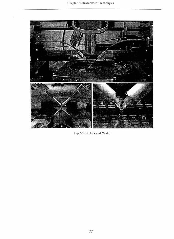
Chapter 7: Measurement Techniques
Fig.56: Probes andWafer
77

Chapter 8: Conclusion
8. CONCLUSION
8.1 Contributions ofpresentwork
8.1.1Development and validation ofanalyticalmodel
The major focus of this work is the development of analytical models which provides
a closed form solution for the inductance of two popular planar shapes, the circular and
rectangular coil with the ability to extract results in the form of S and Z-matrices. The
input impedance and the quality factor of the inductor are extracted from the Z matrix
results. The unique feature of this model is the inclusion of a ground plane and a
frequency dependent solution. Dielectric and conductor losses have also been included.
The validation of the analytical model has been done by comparison with a full wave
solver and by experimental measurements. There is an excellent agreement with HFSS
for a wide range of inductors at different frequencies for both rectangular and circular
coils. As for the experimental verifications, there is an excellent agreement of measured
data with predicted values for a one turn and a two turn rectangular coil. Impact of the
coil parameters have been discussed and analyzed for a given footprint area at a particular
frequency of interest.
8.1.2 Computer tools assessment
A comparison has been made to assess the advantages and limitations of commercial
full wave solvers (HFSS, MaxwelBD, Momentum, and SONNET) and quasistatic
analytical tools (ASITIC, current sheet method). From this study, MaxwelBD appears to
provide well suited for ferrite filled inductors and for low frequencies. However HFSS
78

Chapter 8: Conclusion
appears to be more appropriate for analyzing inductor over a wide range of frequency,
and also allows the flexibility of ports to be located internally. For these reasons, HFSS
has been chosen for validating the present analytical model.
In order to investigate the performance of ferrite-loaded inductors, MaxwelBD has
been used. It is shown that the inductance increases significantly when the inductors are
ferrite loaded. However, there is an optimum ferrite thickness beyond which the
inductance value is not affected. Also, it seems necessary to do an accurate modeling of
losses in both the ferrite and in silicon substrate. Such work is currently under progress.
8.1.3On-chip inductormeasurement techniques
A variety of inductor test structure layout hasbeen described for silicon IC inductors
and calibration models are given for use with a vector network analyzer. The most
feasible layout was chosen to confirm with the available fabrication procedures and test
methodology. Copper Micro-inductors have been fabricated and tested using a vector
network analyzer and a cascade probe station.
8.2 Future Work
The following analytical work needs to be done:
The Analytical model will be improved to include multiple dielectrics(Fig.57):
l
2
Zin,l
Ziin,2
Fig.57: Multiple dielectrics
79
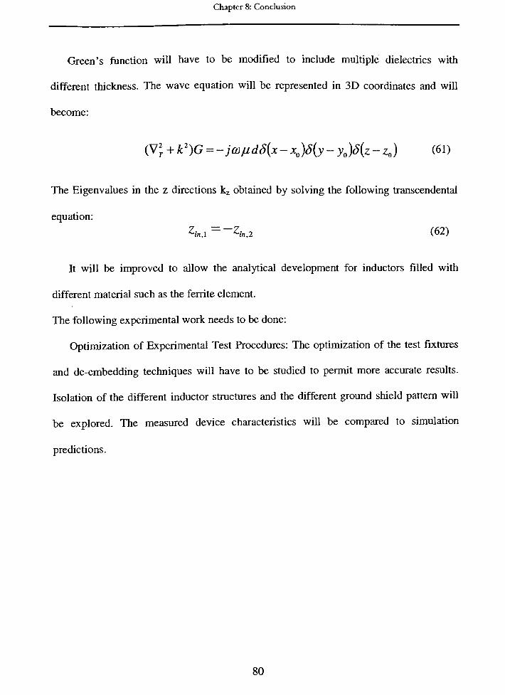
Chapter 8: Conclusion
Green's function will have to be modified to include multiple dielectrics with
different thickness. The wave equation will be represented in 3D coordinates and will
become:
(V2T + k2)G =
-jujp;dS(x-x0)S(y-y0)S{z-z0) (61)
The Eigenvalues in the z directions kz obtained by solving the following transcendental
equation:
ZinA =~Zin,2 (62)
It will be improved to allow the analytical development for inductors filled with
different material such as the ferrite element.
The following experimental work needs to be done:
Optimization of Experimental Test Procedures: The optimization of the test fixtures
and de-embedding techniques will have to be studied to permit more accurate results.
Isolation of the different inductor structures and the different ground shield pattern will
be explored. The measured device characteristics will be compared to simulation
predictions.
80

References
REFERENCES
[1] N. M. Nguyen and R. G. Meyer, "Si lC-compatible inductors and LC passivefilters,"
IEEE J. Solid-
State Circuits, vol. 25, Aug. 1990.
[2] J. Ryynanen, K. Kivekas, J. Jussila, L. Sumanen, A. Parssinen and K.A. I Halonen, "A Single-ChipMultimode Receiver for GSM900, DCSI800, PCS1900, and CDMA", IEEE Journal of Solid State
Circuits, April 2003.
[3] A.O. Adan, T. Yoshimasu, S. Shitara, N. Tanba and M. Fukurni, "Linearity and low-noise performance
ofSOIMOSFETsforRFapplications"
, IEEE Transactions on Electron Devices, May 2002.
[4] E. J. Brandon, E.Wesseling, V. White, C. Ramsey, L. Del Castillo and U. Lieneweg, "Fabrication and
Characterization of Microinductors for Distributed Power Converters", IEEE Transaction on
Magnetics, July 2003.
[5] C.R.C De Ranter, G. Van der Plas, M.S.J Steyaert, G.G.E Gielen and W.M.C Sansen, "CYCLONE:
automated design and layout ofRFLC-oscillators"
IEEE Transactions on Computer-Aided Design of
Integrated Circuits and Systems, Oct. 2002.
[6] M.S.J. Steyaert, J. Janssens, B. deMuer, M. Borremans and N. Itoh, "A 2-V CMOS cellular transceiver
front-end", IEEE Journal of Solid-State Circuits, Dec. 2000.
[7] S. Otaka, T. Yamaji, R. Fujimoto, C. Takahashi and H. Tanimoto, "A low local input 1.9 GHz Si-
bipolar quadrature modulator with no adjustmenf IEEE Journal of Solid-State Circuits, Jan. 1996.
[8] AliM. Niknejad,"
Design, Simulation andApplications ofInductors and Transformersfor Si RF lCs",
Kluwer Academic Publishers, September 2000.
[9] Sidharth Dalmia, Sung Hwan Min and Madhavan Swaminathan "Modeling RF Passive circuits using
coupled lines and scalable models",//!/!/!, Electronic components and Technology conference, 2001.
[10] J. N. Burghartz, M. Soyuer, and K. A. Jenkins, "Microwave inductors and capacitors in standard
multilevel interconnect silicon technology,"
IEEE Trans. Microwave Theory Tech., Jan. 1996.
[11] J. R. Long and M. A. Copeland, "The modeling, characterization, and design ofmonolithicinductors
for silicon RF lCs,"
IEEE J. Solid-State Circuits, Mar. 1997.
[12] C. P. Yue and S. S. Wong, "Physical modeling of spiral inductors onsilicon,"
IEEE Trans. Electron
Devices,Mar. 2000.
[13] P. Arcioni, R. Castello, L. Perregrini, E. Sacchi,and F. Svelto, "An improved lumped-element
equivalent circuitfor on silicon integratedinductors,"
in Proc. RAWCON, Aug. 9-12, 1998.
[14] W. B. Kuhn and N. K. Yanduru, "Spiral inductor substrate loss modelingin silicon RF lCs,
"
in Proc.
RAWCON, Aug. 9-12, 1998, pp. 305-308.
[15] D. Melendy, P. Francis, C. Pichler, K. Hwang,G. Srinivasan, and A. Weisshaar, "A new wideband
compact model for spiral inductors inRFICs,"
IEEE Electron Device Lett.,May 2002.
[16] J. N. Burghartz and B. Rejaei, "On thedesign ofRF spiral inductors on silicon,
"
IEEE Trans. Electron
, Devices, vol. 50, pp. 718-729, Mar. 2003.
[17] J. Craninckx and M. S. J. Steyaert, "A 1 .8-GHzlow-phase-noise CMOS VCO using optimized hollow
spiralinductors,"
IEEE J. Solid-State Circuits,May 1997.
81

References
[18] W. B. Kuhn and N. M. Ibrahim, "Analysis of current crowding effects in multiturn spiralinductors,"
IEEE Trans.Microwave Theory Tech., Jan. 2001 .
[19] J. Sieiro, J. M. Lopez-Villegas, J. Cabanillas, J. A. Osorio, and J. Samitier, "A physical frequency-
dependent compact model for RF integrated inductors,"
IEEE Trans. Microwave Theory Tech Jan2002.
[20] B.-L. Ooi, D.-X. Xu, P.-S. Kooi, and F. Lin, "An improved prediction of series resistance in spiralinductormodeling with eddy-current effect,
"
IEEE Trans. Microwave Theory Tech., Sept. 2002.
[21] W. Y. Yin, S. J. Pan, Y. B. Gan, L. W. Li, and B. L. Ooi, "Global performance evaluation ofvariouson-chip square spiral inductors on GaAs substrates,
"
Proc. Circuits, Devices, and Systems, Feb. 2003.
[22] J. Gil and H. Shin, "A simple wide-band on-chip inductor model for silicon-based RFlCs,"
IEEETrans. Microwave Theory Tech., Sept. 2003.
[23] Y. Cao, R. A. Groves, X. Huang, N. D. Zamdmer, J.-O. Plouchart, R. A. Wachnik, T.-J. King, and C.
Hu, "Frequency-independent equivalentcircuit model for on-chip spiral inductors,"
IEEE J. Solid-
State Circuits,Mar. 2003.
[24] H.M. Greenhouse, "Design ofPlanar RectangularMicroelectronic Inductors', IEEE Transactions on
Parts, Hybrids, and Pacakging, June 1974.
[25] Voorman J. O. Voorman, Continuous-time analog integrated filters, IEEE Press, 1993.
[26] Dill H. G. Dill, "Designing inductorsfor thin-fillmapplications"
Electronic Design.vol. 12, 1964.
[27] Bryan H. E. Bryan, "Printed inductors and capacitors", Tele-tech and electronic industries, December1955.
[28] J. Crols, P. Kinget, J. Craninckx, and M. Steyeart, "An analytical model ofplanar inductors on lowlydoped silicon substrates for analog design up to
3GHz"
in Symposium on VLSI Circuits, Digest of
Technical Papers, 1996.
[29] S. Asgaran, "New Accurate Physics-Based Closed Form Expressions for Compact Modeling and
Design ofon Chip Spiral Inductors", IEEE 2002.
[30]S.S. Mohan, M. del Mar Hershenson, S.P Boyd, S.P. and T.H Lee, "Simple Accurate Expressionsfor
Planar Spiral Inductance", IEEE, October 1 999.
[31] John R. Long andMiles A. Copeland, "Modeling ofMonolithic inductors and transformersfor silicon
RFIC design", MTT-S Symposium on Technologies forWireless Applications Digest, Feb. 1995.
[32] J. A. Power, S.C Kelly, E.C Griffith and M. O'Neill, "An Investigation ofOn-Chip Spiral Inductors on
a 0.6 um BiCMOS.TechnologyforRFApplications"
,IEEE1999.
[33] T. Okoshi. Planar Circuits ForMicrowaves andLightwaves. Springer series in Electrophysics.
[34] F. A. Alhargan and S. R. Judah, "Circular andAnnularSector Planar Components ofArbitraryAngle
for N-Way PowerDividers/Combiners"
IEEE Transactions on Microwave Theory and Techniques,
September 1994.
i
[35] R. Ghadha and K. C. Gupta, "Green 's function for circular sectors, annular rings, and annular
sectors inplanarmicrowavecircuits"
IEEE Trans. Microwave Theory and Tech., 1981.
82
References
[36] K. C Gupta and M. D. Abouzahra: "Planar circuitanalysis"
Numerical Techniques for Microwave
and PassiveMillimeter-Wave Passive Structures, New York: Wiley, 1984, ch.4.
[37] G. Lei, R.W. Techentin, P.R Hayes, D.J Schwab and B.K Gilbert, "Wave Model Solution to the
Ground/Power Plane Noise problem", IEEE Transactions on Instrumentation and measurement, April
1995
[38] G.F. Roach, Green'sfunctions. New York: Van Nostrand 1970.
83

Appendix
Al Spiral Loss Mechanisms
Various loss mechanisms are present in ICs and they are summarized here. The spiral
inductor is placed on top of a oxide layer and a substrate.
Al.lMetalLosses:
A signal current I is applied and carried by the metal winding. The series resistance the
metal conductor traces will dissipate some of the signal. The series resistance comes from
the following: resistivity x length -f area characteristic of imperfect conductors:
_
Pi
R.
Wteff
t~ represents the effective conductor thickness.
Considering the current distribution in a microstrip line, the equivalent conductor
thickness is given by:
teff(f) = S(f)[l-e-"S(f)]
t: physical conductor thickness
5(f) : skin depth of the conductivemetal (6(f) f'V2)
As the frequency increases, the series resistance also increases where the skin depth is
still larger than the thickness of the metal.While the resistance increases with frequency,
other lossmechanisms begin to play amore significant roleat higher frequency.
84

Appendix
The current distribution in the metal layer changes due to eddy currents in the
metalization at higher frequency, as known as skin and proximity effects, current
constriction, and current crowding.
At high frequency, the current is pushed to the outer layer or skin of the conductor
instead ofusing the full metal area for current flow.
The effective conductor thickness decreases, but the current density increases, as a result
more energy is converted into heat.
The skin depth (effective depth of penetration) is defined with the following equation:
\poco
Where: p=permeability of the material
<T = resistivity
co = frequency
A1.2Substrate Losses:
The substrate is a major source of loss and frequency limitation.
A current flows in the metal layer. An electric field is magnetically induced in the
substrate underneath the metal layer (Faraday-Lenz Law), which leads to a current Isubs
flowing in the substrate. This current flow opposes the original change in magnetic field
and flows in the opposite direction from the original current flowing inside the conductor.
Therefore, the total magnetic field will be smaller. Those currents are a cause for extra
resistive losses and decreases in inductance.
85

Appendix
A1.3 Solution toprevent loss:
1) Very wide metal conductors will not be efficient, because of the skin effect. Which
pushes the current to the outer edge of the metal. The center of the lines won't be used for
the current flow with the lines are too wide.
2) The coil shouldn't be filled in the center; the generation of eddy currents increases
the resistance of the coil especially at the most inner turns.
3) The magnetic field of smaller coils less penetrates into the substrate, the area
occupied by the coil should then be limited.
4) Patterned ground shield: Ground shield is broken to prevent eddy currents from
flowing in it.
86
Related Documents