Sensors and Actuators A 130–131 (2006) 371–378 GaN-on-patterned-silicon (GPS) technique for fabrication of GaN-based MEMS Zhenchuan Yang ∗ , Ruonan Wang, Deliang Wang, Baoshun Zhang, Kei May Lau, Kevin J. Chen Department of Electrical and Electronic Engineering, Hong Kong University of Science and Technology, Clear Water Bay, Kowloon, Hong Kong Received 3 June 2005; received in revised form 10 November 2005; accepted 22 November 2005 Available online 20 January 2006 Abstract A method for fabricating suspended gallium nitride (GaN) structures for microelectromechanical systems (MEMS) without direct etching of GaN is demonstrated. The process combines a selective area growth of GaN-on-patterned-silicon-substrate (GPS) and a subsequent sacrificial wet etching of the silicon under the GaN structures. Both anisotropic and isotropic wet etching techniques are used to carry out the sacrificial etching. The experimental results show that the GPS–MEMS technique can be used to batch-fabricate various GaN-based MEMS devices with common silicon micromachining equipments. © 2005 Elsevier B.V. All rights reserved. Keywords: GaN; MEMS; Selective area growth 1. Introduction The advantages on electrical, mechanical and chemical prop- erties, such as wide band gap, large elastic modulus, high piezoelectric and piezoresistive coefficients, as well as chemical inertness, make gallium nitride (GaN)-based materials attractive for making microelectromechanical systems (MEMS), espe- cially those for use in harsh environments [1–6]. However, the development of GaN-based MEMS devices is still at an early stage. One obstacle in the way of developing GaN-based MEMS is the lack of efficient GaN etching and undercutting techniques. Due to the strong chemical stability of GaN, there are no effective conventional wet etchant available for etch- ing high quality GaN films [7]. Various dry etching techniques have been developed for patterning GaN structures, but have the drawbacks including plasma-induced damage and the lack of undercutting capability [8]. Minsky et al. demonstrated the feasibility of using photoelectrochemical (PEC) etching tech- nique to effectively etch GaN at room temperature [9], which is further developed to have the capability of undercutting GaN ∗ Corresponding author. Tel.: +852 23588530; fax: +852 23581485. E-mail address: [email protected] (Z. Yang). through dopant-selective etching and bandgap-selective etching [1,2]. However, the conventional PEC etching techniques need metal masks, which make it difficult to fabricate active elec- tronic devices on patterned GaN structures. Contactless etching techniques using photoresist or silicon dioxide as masks have been developed to overcome the problem mentioned above, but the main drawback of contactless etching is that the etch rate saturates with time when the pH value of etchants was less than 12.0 [7], and then is inefficient for etching thick GaN layers. Furthermore, both PEC etching and contactless etching techniques need carefully designed illumination sys- tem, the backside illuminated PEC (BIPEC) etching also need transparent substrate and double side lithography. NG et al. developed a polar-selective etching technique to pattern GaN structures [10], since the hard-to-etch sapphire is used as sub- strate, undercutting cannot be performed for the release of the microstructures. Other approaches using etchant-selective materials as sacri- ficial layer to undercut GaN are also developed. Mileham et al. have used aluminum nitride (AlN) as sacrificial layer to make suspended GaN microdisks [11]. Davies et al. [3] and Neu- berger et al. [5] have demonstrated the technique using silicon as sacrificial material to make suspended GaN cantilever on sil- icon substrate, respectively. But the two techniques still need a 0924-4247/$ – see front matter © 2005 Elsevier B.V. All rights reserved. doi:10.1016/j.sna.2005.11.047

Welcome message from author
This document is posted to help you gain knowledge. Please leave a comment to let me know what you think about it! Share it to your friends and learn new things together.
Transcript
Sensors and Actuators A 130–131 (2006) 371–378
GaN-on-patterned-silicon (GPS) technique forfabrication of GaN-based MEMS
Zhenchuan Yang ∗, Ruonan Wang, Deliang Wang, Baoshun Zhang,Kei May Lau, Kevin J. Chen
Department of Electrical and Electronic Engineering, Hong Kong University of Science and Technology,Clear Water Bay, Kowloon, Hong Kong
Received 3 June 2005; received in revised form 10 November 2005; accepted 22 November 2005Available online 20 January 2006
Abstract
A method for fabricating suspended gallium nitride (GaN) structures for microelectromechanical systems (MEMS) without direct etching ofGaN is demonstrated. The process combines a selective area growth of GaN-on-patterned-silicon-substrate (GPS) and a subsequent sacrificial wetetching of the silicon under the GaN structures. Both anisotropic and isotropic wet etching techniques are used to carry out the sacrificial etching.Ts©
K
1
epifcteMtaihtofni
0d
he experimental results show that the GPS–MEMS technique can be used to batch-fabricate various GaN-based MEMS devices with commonilicon micromachining equipments.
2005 Elsevier B.V. All rights reserved.
eywords: GaN; MEMS; Selective area growth
. Introduction
The advantages on electrical, mechanical and chemical prop-rties, such as wide band gap, large elastic modulus, highiezoelectric and piezoresistive coefficients, as well as chemicalnertness, make gallium nitride (GaN)-based materials attractiveor making microelectromechanical systems (MEMS), espe-ially those for use in harsh environments [1–6]. However,he development of GaN-based MEMS devices is still at anarly stage. One obstacle in the way of developing GaN-basedEMS is the lack of efficient GaN etching and undercutting
echniques. Due to the strong chemical stability of GaN, therere no effective conventional wet etchant available for etch-ng high quality GaN films [7]. Various dry etching techniquesave been developed for patterning GaN structures, but havehe drawbacks including plasma-induced damage and the lackf undercutting capability [8]. Minsky et al. demonstrated theeasibility of using photoelectrochemical (PEC) etching tech-ique to effectively etch GaN at room temperature [9], whichs further developed to have the capability of undercutting GaN
through dopant-selective etching and bandgap-selective etching[1,2]. However, the conventional PEC etching techniques needmetal masks, which make it difficult to fabricate active elec-tronic devices on patterned GaN structures. Contactless etchingtechniques using photoresist or silicon dioxide as masks havebeen developed to overcome the problem mentioned above,but the main drawback of contactless etching is that the etchrate saturates with time when the pH value of etchants wasless than 12.0 [7], and then is inefficient for etching thickGaN layers. Furthermore, both PEC etching and contactlessetching techniques need carefully designed illumination sys-tem, the backside illuminated PEC (BIPEC) etching also needtransparent substrate and double side lithography. NG et al.developed a polar-selective etching technique to pattern GaNstructures [10], since the hard-to-etch sapphire is used as sub-strate, undercutting cannot be performed for the release of themicrostructures.
Other approaches using etchant-selective materials as sacri-ficial layer to undercut GaN are also developed. Mileham et al.have used aluminum nitride (AlN) as sacrificial layer to makesuspended GaN microdisks [11]. Davies et al. [3] and Neu-
∗ Corresponding author. Tel.: +852 23588530; fax: +852 23581485.E-mail address: [email protected] (Z. Yang).
berger et al. [5] have demonstrated the technique using siliconas sacrificial material to make suspended GaN cantilever on sil-icon substrate, respectively. But the two techniques still need a
924-4247/$ – see front matter © 2005 Elsevier B.V. All rights reserved.
oi:10.1016/j.sna.2005.11.047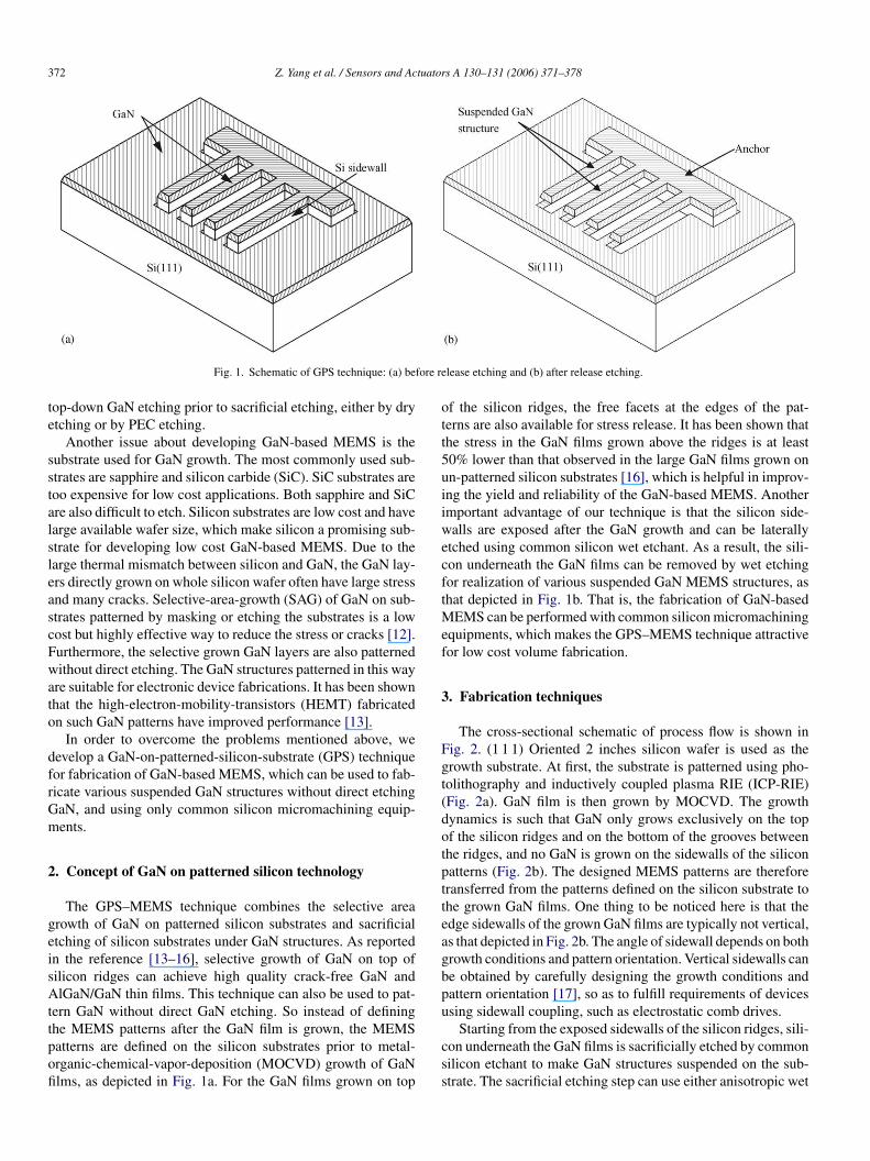
372 Z. Yang et al. / Sensors and Actuators A 130–131 (2006) 371–378
Fig. 1. Schematic of GPS technique: (a) before release etching and (b) after release etching.
top-down GaN etching prior to sacrificial etching, either by dryetching or by PEC etching.
Another issue about developing GaN-based MEMS is thesubstrate used for GaN growth. The most commonly used sub-strates are sapphire and silicon carbide (SiC). SiC substrates aretoo expensive for low cost applications. Both sapphire and SiCare also difficult to etch. Silicon substrates are low cost and havelarge available wafer size, which make silicon a promising sub-strate for developing low cost GaN-based MEMS. Due to thelarge thermal mismatch between silicon and GaN, the GaN lay-ers directly grown on whole silicon wafer often have large stressand many cracks. Selective-area-growth (SAG) of GaN on sub-strates patterned by masking or etching the substrates is a lowcost but highly effective way to reduce the stress or cracks [12].Furthermore, the selective grown GaN layers are also patternedwithout direct etching. The GaN structures patterned in this wayare suitable for electronic device fabrications. It has been shownthat the high-electron-mobility-transistors (HEMT) fabricatedon such GaN patterns have improved performance [13].
In order to overcome the problems mentioned above, wedevelop a GaN-on-patterned-silicon-substrate (GPS) techniquefor fabrication of GaN-based MEMS, which can be used to fab-ricate various suspended GaN structures without direct etchingGaN, and using only common silicon micromachining equip-ments.
2
geisAttpofi
of the silicon ridges, the free facets at the edges of the pat-terns are also available for stress release. It has been shown thatthe stress in the GaN films grown above the ridges is at least50% lower than that observed in the large GaN films grown onun-patterned silicon substrates [16], which is helpful in improv-ing the yield and reliability of the GaN-based MEMS. Anotherimportant advantage of our technique is that the silicon side-walls are exposed after the GaN growth and can be laterallyetched using common silicon wet etchant. As a result, the sili-con underneath the GaN films can be removed by wet etchingfor realization of various suspended GaN MEMS structures, asthat depicted in Fig. 1b. That is, the fabrication of GaN-basedMEMS can be performed with common silicon micromachiningequipments, which makes the GPS–MEMS technique attractivefor low cost volume fabrication.
3. Fabrication techniques
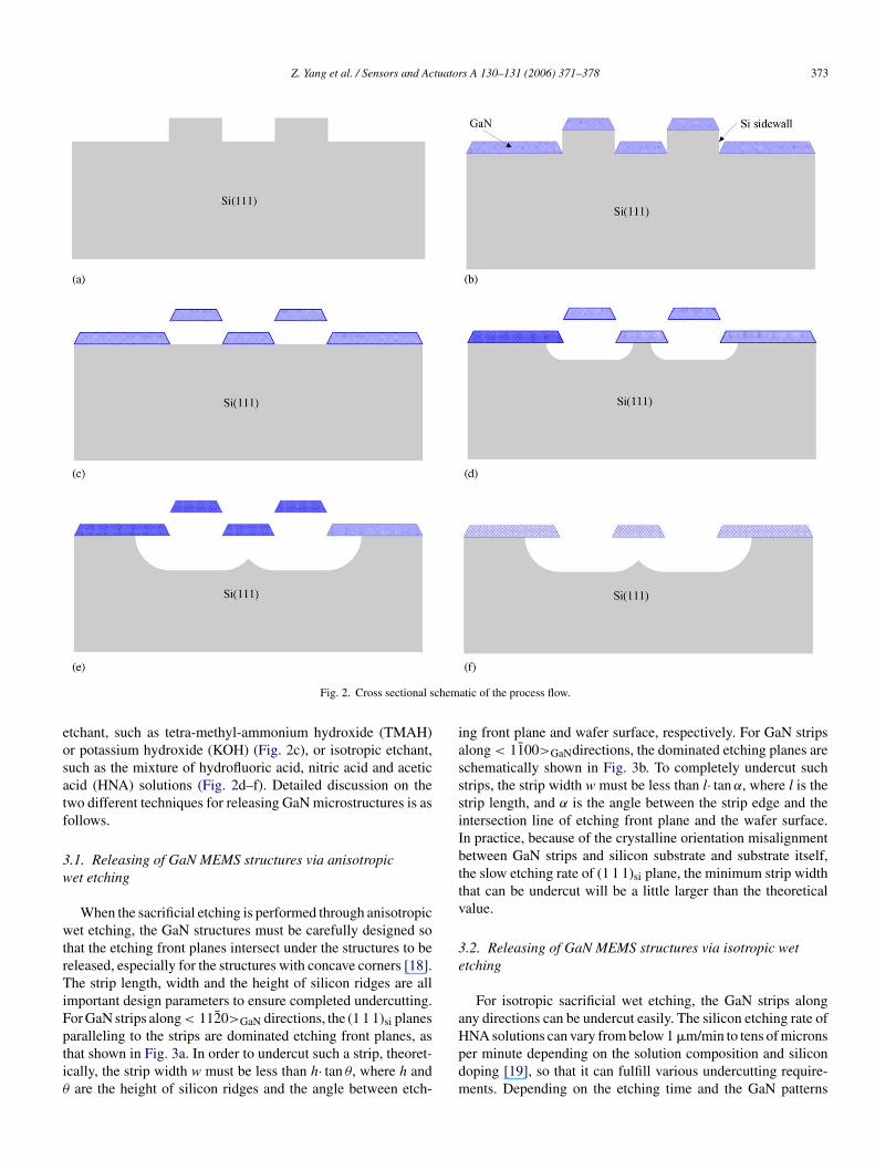
The cross-sectional schematic of process flow is shown inFig. 2. (1 1 1) Oriented 2 inches silicon wafer is used as thegrowth substrate. At first, the substrate is patterned using pho-tolithography and inductively coupled plasma RIE (ICP-RIE)(Fig. 2a). GaN film is then grown by MOCVD. The growthdynamics is such that GaN only grows exclusively on the topof the silicon ridges and on the bottom of the grooves betweentptteagbpu
css
. Concept of GaN on patterned silicon technology
The GPS–MEMS technique combines the selective arearowth of GaN on patterned silicon substrates and sacrificialtching of silicon substrates under GaN structures. As reportedn the reference [13–16], selective growth of GaN on top ofilicon ridges can achieve high quality crack-free GaN andlGaN/GaN thin films. This technique can also be used to pat-
ern GaN without direct GaN etching. So instead of defininghe MEMS patterns after the GaN film is grown, the MEMSatterns are defined on the silicon substrates prior to metal-rganic-chemical-vapor-deposition (MOCVD) growth of GaNlms, as depicted in Fig. 1a. For the GaN films grown on top
he ridges, and no GaN is grown on the sidewalls of the siliconatterns (Fig. 2b). The designed MEMS patterns are thereforeransferred from the patterns defined on the silicon substrate tohe grown GaN films. One thing to be noticed here is that thedge sidewalls of the grown GaN films are typically not vertical,s that depicted in Fig. 2b. The angle of sidewall depends on bothrowth conditions and pattern orientation. Vertical sidewalls cane obtained by carefully designing the growth conditions andattern orientation [17], so as to fulfill requirements of devicessing sidewall coupling, such as electrostatic comb drives.
Starting from the exposed sidewalls of the silicon ridges, sili-on underneath the GaN films is sacrificially etched by commonilicon etchant to make GaN structures suspended on the sub-trate. The sacrificial etching step can use either anisotropic wet
Z. Yang et al. / Sensors and Actuators A 130–131 (2006) 371–378 373
Fig. 2. Cross sectional schematic of the process flow.
etchant, such as tetra-methyl-ammonium hydroxide (TMAH)or potassium hydroxide (KOH) (Fig. 2c), or isotropic etchant,such as the mixture of hydrofluoric acid, nitric acid and aceticacid (HNA) solutions (Fig. 2d–f). Detailed discussion on thetwo different techniques for releasing GaN microstructures is asfollows.
3.1. Releasing of GaN MEMS structures via anisotropicwet etching
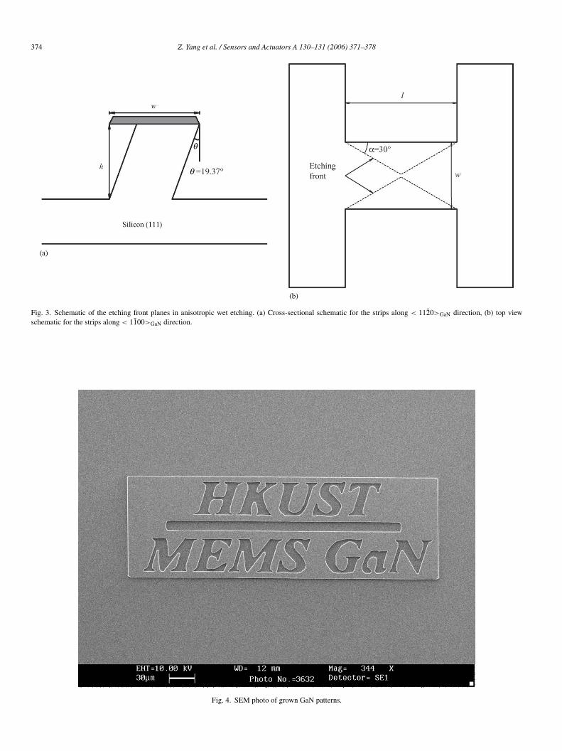
When the sacrificial etching is performed through anisotropicwet etching, the GaN structures must be carefully designed sothat the etching front planes intersect under the structures to bereleased, especially for the structures with concave corners [18].The strip length, width and the height of silicon ridges are allimportant design parameters to ensure completed undercutting.For GaN strips along < 1120>GaN directions, the (1 1 1)si planesparalleling to the strips are dominated etching front planes, asthat shown in Fig. 3a. In order to undercut such a strip, theoret-ically, the strip width w must be less than h· tan θ, where h andθ are the height of silicon ridges and the angle between etch-
ing front plane and wafer surface, respectively. For GaN stripsalong < 1100>GaNdirections, the dominated etching planes areschematically shown in Fig. 3b. To completely undercut suchstrips, the strip width w must be less than l· tan α, where l is thestrip length, and α is the angle between the strip edge and theintersection line of etching front plane and the wafer surface.In practice, because of the crystalline orientation misalignmentbetween GaN strips and silicon substrate and substrate itself,the slow etching rate of (1 1 1)si plane, the minimum strip widththat can be undercut will be a little larger than the theoreticalvalue.
3.2. Releasing of GaN MEMS structures via isotropic wetetching
For isotropic sacrificial wet etching, the GaN strips alongany directions can be undercut easily. The silicon etching rate ofHNA solutions can vary from below 1 �m/min to tens of micronsper minute depending on the solution composition and silicondoping [19], so that it can fulfill various undercutting require-ments. Depending on the etching time and the GaN patterns
374 Z. Yang et al. / Sensors and Actuators A 130–131 (2006) 371–378
Fig. 3. Schematic of the etching front planes in anisotropic wet etching. (a) Cross-sectional schematic for the strips along < 1120>GaN direction, (b) top viewschematic for the strips along < 1100>GaN direction.
Fig. 4. SEM photo of grown GaN patterns.
Z. Yang et al. / Sensors and Actuators A 130–131 (2006) 371–378 375
designed, the isotropic etching can be used to undercut only theGaN structures grown on top of silicon ridges (Fig. 2d), or theGaN structures grown both on the top of the ridges and on thebottom of grooves (Fig. 2e). It even can be used to completelylift-off the GaN structures grown on the top of the silicon ridges,as that shown in Fig. 2f.
During undercutting, the silicon under the anchor area isalso etched, so in order to ensure that the GaN structures aresuspended on the substrate with at least one end anchored onthe substrate, the anchor area must be large enough. Otherwise,another mask layer, such as silicon nitride for TMAH etching,is needed to protect the anchor areas from undercutting.
F<
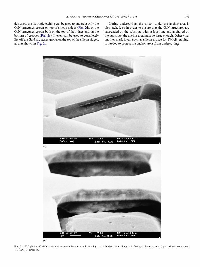
ig. 5. SEM photos of GaN structures undercut by anisotropic etching, (a) a1100>GaNdirection.
bridge beam along < 1120>GaN direction, and (b) a bridge beam along
376 Z. Yang et al. / Sensors and Actuators A 130–131 (2006) 371–378
4. Results and discussions
The height of the silicon ridges in our experiment isabout 2 �m, and the thickness of the grown GaN is 1.0 �m.Detailed conditions for GaN growth can be found in ref.[16]. Fig. 4 is a scanning electron microscope (SEM)
photo of such grown GaN structures on patterned sub-strate.
Both anisotropic and isotropic wet etchings are carried outin our experiments. For anisotropic wet undercutting, we use a25% TMAH solution heated to 80 ◦C to undercut the GaN struc-tures, the lateral undercutting rate is about 0.6 �m/min. A 30%
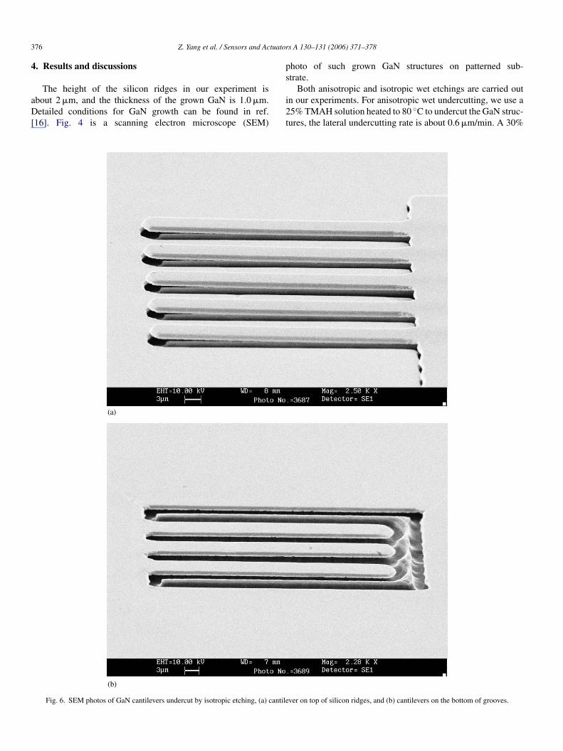
Fig. 6. SEM photos of GaN cantilevers undercut by isotropic etching, (a) cantile
ver on top of silicon ridges, and (b) cantilevers on the bottom of grooves.
Z. Yang et al. / Sensors and Actuators A 130–131 (2006) 371–378 377
KOH solution at 80 ◦C is also tested, and the lateral undercut-ting rate is about 1.1 �m/min. Fig. 5(a) and (b) are SEM photosof suspended GaN beams fabricated by anisotropic wet etch-ing. The beam in Fig. 5a is along < 11 2 0>GaN direction, andthe length and width are 8 and 1.5 �m, respectively. The beamin Fig. 5b is along < 1 1 0 0>GaN direction, and the length andwidth are 10 and 3 �m, respectively. From Fig. 5, we can see thatthe edge of beam along < 1 1 0 0>GaNbecomes rough after etch-ing, which implies that the edge is attacked by the anisotropicetchant. This result can be explained by the crystallographic anddislocation dependent etching properties of GaN films [20,21].After selective area growth, the crystalline plane of sidewall forbeams along < 1 1 2 0>GaN and < 1100>GaN are (1 1 0 1)GaNand (1 1 2 2)GaN, respectively, and the (1 1 0 1)GaN plane is muchstable than (1 1 2 2)GaN [17]. Furthermore, due to the larger lat-eral growth rate, < 1100>GaN strips have overgrown GaN wings[22], which can be etched fast for their low dislocation density.
For isotropic undercutting, a (99:1) HNO3/HF solution isused at room temperature, which shows a lateral etching rateabout 1.5 �m/min. Fig. 6a and b shows SEM photos of GaNcantilevers fabricated by isotropic etching. Cantilevers in Fig. 6aare 50 �m long and 5 �m wide, which are grown on the topof silicon ridges. The cantilevers in Fig. 6b are fabricated bylifting-off the GaN on the top of silicon ridges, as that describedin Fig. 2f. From our experimental results, the isotropic etchanthas little effect on the GaN structures, so it is more suitable foru
5
wTgasKcGfil
A
otC
R
[3] S. Davies, T.S. Huang, M.H. Gass, A.J. Papworth, T.B. Joyce, P.R.Chalker, Fabrication of GaN cantilevers on silicon substrates formicroelectromechanical devices, Appl. Phys. Lett. 84 (2004) 2556–2558.
[4] S.J. Pearton, B.S. Kang, Kim Suku, F. Ren, B.P. Gila, C.R. Abernathy,Jenshan Lin, S.N.G. Chu, GaN-based diodes and transistors for chemical,gas, biological and pressure sensing, J. Phys.: Condens. Mater. 16 (2004)R961–R994.
[5] M. Neuberger, T. Zimmermann, P. Benkart, M. Kunze, I. Daumiller, A.Dadgar, A. Krost, E. Kohn, GaN based piezo sensors, Device researchconference, Notre Dame, USA, June 21–23, 2004, pp. 45–46.
[6] B.S. Kang, S. Kim, F. Ren, J.W. Johnson, R.J. Therrien, P. Rajagopal,J.C. Roberts, E.L. Piner, K.J. Linthicum, S.N.G. Chu, K. Baik, B.P. Gila,C.R. Abernathy, S.J. Pearton, Pressure-induced changes in the conduc-tivity of AlGaN/GaN high-electron mobility-transistor membranes, Appl.Phys. Lett. 85 (2004) 2962–2964.
[7] D. Zhuang, J.H. Edgar, Wet etching of GaN, AlN, and SiC: a review,Mater. Sci. Eng. R 48 (2005) 1–46.
[8] S.J. Pearton, R.J. Shul, Fan Ren, A review of dry etching of GaN andrelated materials, MRS Internet J. Nitride Semicond. Res. 5 (11) (2000).
[9] M.S. Minsky, M. White, E.L. Hu, Room temperature photoenhancedwet etching of GaN, Appl. Phys. Lett. 68 (1996) 1531–1533.
[10] H.M. NG, W. Parz, N.G. Weimann, A. Chowdhury, Patterning GaNmicrostructures by polarity-selective chemical etching, Jpn. J. Appl.Phys. 42 (Part 2) (2003) L1405–L1407.
[11] J.R. Mileham, S.J. Pearton, C.R. Abernathy, J.D. MacKenzie, R.J. Shul,S.P. Kilcoyne, Patterning of AlN InN, and GaN in KOH-based solutions,J. Vac. Sci. Technol. A 14 (1996) 836–839.
[12] S. Pal, C. Jacob, Silicon—a new substrate for GaN growth, Bull. Mater.Sci. 27 (2004) 501–504.
[13] S. Jia, Y. Dikme, D. Wang, K.J. Chen, K.M. Lau, M. Heuken,
[
[
[
[
[
[
[
[
[
B
ZPa
ndercutting, especially when the required etching time is long.
. Conclusions
A technique for fabricating suspended GaN MEMS structuresithout direct etching GaN has been successfully demonstrated.he GPS–MEMS technique uses a combination of selective arearowth of GaN on patterned (1 1 1) silicon substrate (GPS) andsubsequent sacrificial wet etching the silicon under the GaN
tructures. Both anisotropic etching solutions, such as TMAH,OH, and isotropic etching solutions, such as HNA, are suc-essfully used to do the sacrificial wet etching. Except theaN growing step, all the other processing steps can be per-
ormed with common silicon micromachining equipment, whichmplies that the GPS–MEMS technique can be used to developow cost GaN-based MEMS devices.
cknowledgement
The authors thank Mr. Shuo Jia for discussions on fabricationf the patterned structures. This work is partially supported byhe Research Grant Council of Hong Kong Government underERG grant HKUST6317/04E.
eferences
[1] R.P. Strittmatter, R.A. Beach, T.C. McGill, Fabrication of GaN sus-pended microstructures, Appl. Phys. Lett. 78 (2001) 3226–3228.
[2] A.R. Stonas, N.C. MacDonald, K.L. Turner, S.P. DenBaars, E.L. Hu,Photoelectrochemical undercut etching for fabrication of GaN microelec-tromechanical systems, J. Vac. Sci. Technol. B 19 (2001) 2838–2841.
AlGaN–GaN HEMTs on patterned silicon (1 1 1) substrate, IEEE Elec-tron. Dev. Lett. 26 (2005) 130–132.
14] A. Strittmatter, S. Rodt, L. Reißmann, D. Bimberg, H. Schroder, E.Obermeier, T. Riemann, J. Christen, A. Krost, Maskless epitaxial lateralovergrowth of GaN layers on structured Si(1 1 1) substrates, Appl. Phys.Lett. 78 (2001) 727–729.
15] S. Zamir, B. Meyler, J. Salzman, Laterally confined epitaxy of GaN onsilicon substrates, J. Cryst. Growth 230 (2001) 341–345.
16] D. Wang, S. Jia, K.J. Chen, K.M. Lau, Y. Dikme, P. Van Gemmern,Y.C. Lin, H. Kalisch, R.H. Jansen, M. Heuken, Micro-Raman-scatteringstudy of stress distribution in GaN films grown on patterned Si(1 1 1)by metal-organic chemical-vapor deposition, J. Appl. Phys. 97 (2005),056103.
17] K. Hiramatsu, K. Nishiyama, A. Motogaito, H. Miyake, Y. Iyechika,T. Maeda, Recent progress in selective area growth and epitaxial lateralovergrowth of III-nitrides: effects of reactor pressure in MOVPE growth,Phys. Stat. Sol. 176 (1999) 535–543.
18] S. Lee, S. Park, D. Cho, The surface/bulk micromachining (SBM) pro-cess: a new method for fabricating released MEMS in single crystalsilicon, J. Microelectromech. Syst. 8 (1999) 409–416.
19] G.T.A. Kovacs, N.I. Maluf, K.E. Petersen, Bulk micromachining of sil-icon, Proc. IEEE 86 (1998) 1536–1551.
20] D.A. Stocker, E.F. Schubert, J.M. Redwing, Crystallographic wet chem-ical etching of GaN, Appl. Phys. Lett. 73 (1998) 2654–2656.
21] Y. Gao, M.D. Craven, J.S. Speck, S.P. DenBaars, E.L. Hu, Dislocation-and crystallographic-dependent photoelectrochemical wet etching of gal-lium nitride, Appl. Phys. Lett. 84 (2004) 3322–3324.
22] D. Kapolnek, S. Keller, R. Vetury, R.D. Underwood, P. Kozodoy, S.P.Den Baars, U.K. Mishra, Anisotropic epitaxial lateral growth in GaNselective area epitaxy, Appl. Phys. Lett. 71 (1997) 1204–1206.
iographies
henchuan Yang received his BS and PhD degree in microelectronics ateking University, China, in 1998 and 2004, respectively. He is a researchssociate with Hong Kong University of Science & Technology since 2004.
378 Z. Yang et al. / Sensors and Actuators A 130–131 (2006) 371–378
His research interests include micromachined inertial sensors and GaN-basedMEMS.
Ruonan Wang was born in China in 1979. He received the bachelor’s andmaster’s degrees in materials science and engineering at Tsinghua Universityin China, in 2001 and 2003, respectively. Now he is working towards thePhD degree in electrical and electronic engineering at Hong Kong Universityof Science and Technology. His research interests are fabrication, charac-terization techniques for RF semiconductor devices and micromachined RFcomponents.
Deliang Wang received the BSc degree from the University of Science andTechnology, Beijing, China, in 1989, the MSc degree from The Institute ofSolid State Physics, Chinese Academy of Sciences, China, in 1992, and thePhD degree from Goettingen University, Germany, in 1997, all in physics.His research currently focuses on the design, growth, and characterization ofAlGaN/GaN-based films and HEMTs on Si substrates grown by MOCVD.
Baoshun Zhang was born in Jilin, China. He received BS and MS degrees inChangchun University of Science and Technology, and PhD degrees in Insti-tute of Semiconductors, Chinese Academy of Science. From 1991 to 2000,He has been engaged in fabrication of semiconductor lasers and materialgrowth (MBE). Currently, His research interests are in the epitaxy growth ofIII–V nitrides devices by using MOVPE.
Kei May Lau received the BS and MS degrees in physics from the Univer-sity of Minnesota, Minneapolis, St. Paul, in 1976 and 1977, respectively andthe Ph.D. degree in electrical engineering from Rice University, Houston,TX, USA in 1981. From 1980 to 1982, she was a senior engineer at M/A-COM Gallium Arsenide Products, Inc., where she worked on the epitaxialgrowth of GaAs for microwave devices, the development of high-efficiencyand millimeter-wave IMPATT diodes, and multiwafer epitaxy by the chlo-rC(c
rials and devices programs at UMass. Her research group has performedstudies on heterostructures, quantum wells, strained-layers, III–V selectiveepitaxy, high-frequency, and photonic devices. She has been a professor inthe Electrical and Electronic Engineering Department at HKUST since thesummer of 2000. She established the Photonics Technology Center for theR&D effort in widegap and other III–V semiconductor materials and devices.Dr. Lau was a recipient of the National Science Foundation (NSF) FacultyAwards for Women (FAW) Scientists and Engineers. She served on the IEEEElectron Devices Society Administrative Committee. She is now serving onthe Electronic Materials Committee of the Minerals, Metals, and MaterialsSociety (TMS) of the American Institute of Materials Engineers. She was aneditor of the IEEE Transactions on Electron Devices from 1996 to 2002.
Kevin J. Chen received the BS degree from the Department of Electronics,Peking University, Beijing, China, in 1988 and the PhD degree in physicsfrom the University of Maryland, College Park, in 1993. From 1994 to 1995,he was a Research Engineer in NTT LSI Laboratories, Atsugi, Japan, engag-ing in the research and development of functional quantum effect devices andheterojunction FETs (HFETs). From 1996 to 1998, he was an Assistant Pro-fessor in the Department of Electronic Engineering, City University of HongKong, carrying out research on high-speed device and circuit simulations.He then joined the wireless semiconductor division of Agilent Technologies,Inc. (formerly Hewlett-Packard Co.), Santa Clara, CA, USA in 1999 work-ing on enhancement mode PHEMT RF power amplifiers used in dual-bandGSM/DCS wireless handsets. His work at Agilent covered RF characteriza-tion and modeling of microwave transistors, RF ICs, and package design.He joined the Department of Electrical and Electronic Engineering, HongKong University of Science and Technology, as an assistant professor in2000. His research interests include fabrication, characterization, and model-ing techniques of novel RF/microwave devices (both active and passive),RF/microwave power amplifiers, RF packaging technologies and MEMS(nb
ide transport process. In the fall of 1982, she joined the Electrical andomputer Engineering Department, University of Massachusetts, Amherst
UMass), where she became a professor in 1993. She initiated organometallichemical vapor deposition (OMCVD), and compound semiconductor mate-
micro-electromechanical systems). In particular, he has been focusing onovel device structure design and device fabrication technologies for GaN-ased HFETs. Dr. Chen is a member of IEEE, and IEICE.
Related Documents