Fuzzy Logic Control of MPPT Controller for PV Systems by Mahmud Ahmed Sasi A Thesis submitted to School of Graduate Studies in Partial fulfillment of the Requirements for the degree of Master of Engineering Faculty of Engineering and Applied Science Memorial University of Newfoundland May 2017 St. John’s, Newfoundland, Canada

Welcome message from author
This document is posted to help you gain knowledge. Please leave a comment to let me know what you think about it! Share it to your friends and learn new things together.
Transcript

Fuzzy Logic Control of MPPT Controller for PV Systems
by
Mahmud Ahmed Sasi
A Thesis submitted to School of Graduate Studies in Partial fulfillment of the Requirements for the degree of
Master of Engineering
Faculty of Engineering and Applied Science Memorial University of Newfoundland
May 2017
St. John’s, Newfoundland, Canada

II
Abstract
This thesis presents a comparison between two methods to optimize the energy extraction in a
photovoltaic (PV) power system. The maximum power of a PV module varies due to changing
temperature, solar radiation, and load. To maximize efficiency, PV systems use a maximum power
point tracker (MPPT) to constantly extract the highest power that can be produced by a solar panel
and then deliver it to the load. The general structure of an MPPT system contains a DC-DC
converter (an electronic device that converts a source of direct current DC from one voltage level
to another) and a controller. The MPPT finds and maintains operations at the maximum power
point using a tracking algorithm during variations in weather conditions. Many different
algorithms of MPPT have been proposed and discussed in the literature, but most of these methods
have disadvantages in terms of efficiency, accuracy, and flexibility. Because of the nonlinear
behavior of PV module current-voltage characteristics and the nonlinearity of DC-DC converters
due to switching, conventional controllers are unable to provide the best response, especially when
dealing with wide parameter variations and line transients. The goal of this work is to design and
implement a maximum power point tracker that uses a fuzzy logic control algorithm. Fuzzy logic
naturally provides a superior controller for this type of nonlinear application. This method also
benefits from the artificial intelligence approach for overcoming the complexity in modeling
nonlinear systems. In order to succeed in this work, an MPPT system consisting of a PV module,
a DC-DC converter, batteries, and a fuzzy logic controller is designed and simulated in Simulink.
Analyses of buck, boost, and buck-boost converter characteristics are carried out to find the most
suitable topology for the PV system used. An integrated model of the PV module with the
identified converter and batteries is simulated in MATLAB to derive the expert knowledge needed
to formulate and tune the fuzzy logic controller. The simulation results show that the fuzzy logic

III
controller is able to obtain the desired outcomes and is ready to be applied to the hardware system.
This entire research work aims to compare two types of controller-based MPPT techniques. Both
MPPTs are based on the same topology of DC-DC converter and are applied with the same PV
system specifications. That is, one of the MPPTs was kept at its original specifications and the
other one was modified by changing the internal PIC 16F684 controller with an external Arduino
Uno controller. Based on a MATLAB fuzzy logic design, the Arduino code was programmed and
uploaded into an Arduino board by using Arduino software (IDE). The proposed method illustrates
that the performance of MPPT is improved in terms of oscillations about the maximum power
point, speed, and sensitivity to parameter variation. The results indicate that a significant amount
of extra power can be extracted from a photovoltaic module by using a fuzzy logic-based
maximum power point tracker in comparison with a PIC 16F684 controller-based maximum power
tracker. Moreover, this gives improved efficiency for the operation of a PV power system, since
batteries can be sufficiently charged and used during periods of low solar radiation.

IV
Acknowledgements
First and foremost, I am grateful to Allah for the good health and well-being that were
necessary to complete this research.
I would like to express my sincere gratitude to my supervisor, Prof. Tariq Iqbal, for the
continuous support he provided for my MSc studies and related research, for his patience,
motivation, and immense knowledge. His guidance was invaluable.
I am also grateful to my parents and all my family members for the constant encouragement,
support and attention they provided.
I would also like to express my gratitude to everyone who directly or indirectly have lent
their hands to this project.
I would also like to extend my thanks to my friends and colleagues for their continuous
support during my graduate program.
I would like to gratefully acknowledge my home country of Libya, which provided the
scholarship that made continuing my Master’s degree possible. I would also like to give special
thanks to Mr. Muamer Shebani, a Ph.D. student at Memorial University, who helped me with some
solutions in Matlab simulation.

V
Table of Contents
Abstract ........................................................................................................................................... II
Acknowledgements ....................................................................................................................... IV
List of Tables ................................................................................................................................. X
List of Figures ............................................................................................................................... XI
List of Abbreviations ................................................................................................................. XVI
List of symbols ......................................................................................................................... XVIII
Chapter 1 ......................................................................................................................................... 1
1. Introduction and Literature Review .................................................................................... 1
1.1 Background ................................................................................................................. 1
1.2 Statement of the Problem ............................................................................................ 2
1.3 Objectives ................................................................................................................... 3
1.4 Introduction to Fuzzy Logic .............................................................................................. 4
1.4.1 Fuzzification .............................................................................................................. 8
1.4.2 Membership Functions ............................................................................................... 9
1.4.3 Fuzzy Rules .............................................................................................................. 10
1.4.4 Inference engine ....................................................................................................... 11
1.4.5 Defuzzification ......................................................................................................... 12
1.5 Photovoltaic Systems (PVs) ............................................................................................ 12
1.5.1 PV cell characteristics .............................................................................................. 14
1.6 DC-DC Converters .......................................................................................................... 20
1.7 Batteries .......................................................................................................................... 22

VI
1.8 Maximum Power Point Tracking .................................................................................... 24
1.9 Literature review ............................................................................................................. 27
1.10 Thesis Organization ...................................................................................................... 41
Chapter 2 ....................................................................................................................................... 43
2. Introduction and Modeling of a Photovoltaic Module ...................................................... 43
2.1 Introduction ..................................................................................................................... 43
2.2 Renewable Energy Forms ............................................................................................... 44
2.2.1 Wind Power ............................................................................................................. 44
2.2.2 Solar Power .............................................................................................................. 45
2.2.3 Hydropower ............................................................................................................. 46
2.2.4 Biomass .................................................................................................................... 47
2.2.5 Geothermal ............................................................................................................... 48
2.2.6 Wave Power ............................................................................................................. 49
2.3 Solar-Photovoltaic Energy .............................................................................................. 50
2.3.1 Global spread of photovoltaics ................................................................................ 50
2.3.2 PV system benefits ................................................................................................... 51
2.3.3 PV cell types ............................................................................................................ 52
2.4 Different Photovoltaic Systems ...................................................................................... 54
2.4.1 Stand-alone systems ................................................................................................. 54
2.4.2 Grid-connected systems ........................................................................................... 55
2.4.3 PV system features ................................................................................................... 56
2.5 Equivalent circuit and mathematical model .................................................................... 58
2.5.1 Nomenclature ........................................................................................................... 58

VII
2.5.2 Mathematical Model of a Photovoltaic Module ...................................................... 59
2.5.3 Reference Model ...................................................................................................... 60
2.5.4 Model Process .......................................................................................................... 61
2.5.4.1 (Converting operating temperature from Celsius to Kelvin) ............................ 61
2.5.4.2 (Calculating of PV module (A) light-generated current) .................................. 62
2.5.4.3 (Deriving of short-circuit current) .................................................................... 62
2.5.4.4 (Mathematical model of saturation current of PV module) .............................. 63
2.5.4.5 (Producing the NsAkT term of PV module ) .................................................... 64
2.5.4.6 (PV module (A) output current Ipv) ................................................................... 64
2.5.4.7 (Extracting of Ipv, Vout, Ppv of PV module) ........................................................ 65
2.6 Model Validation ............................................................................................................ 67
2.7 Conclusion ...................................................................................................................... 68
Chapter 3 ....................................................................................................................................... 69
3. DC-DC Converters and Maximum Power Point Tracking ............................................... 69
3.1 DC-DC Converters .......................................................................................................... 69
3.2 Maximum Power Point Tracking .................................................................................... 70
3.3 Optimum Converter Topology Identification for Maximum Power Point Tracking ...... 72
3.3.1 Buck Converter ........................................................................................................ 72
3.3.2 Boost Converter ....................................................................................................... 73
3.3.3 Buck-Boost Converter ............................................................................................. 73
3.4 Buck-Boost Converter Model ......................................................................................... 74
3.4.1 Mode 1 ..................................................................................................................... 74
3.4.2 Mode 2 ..................................................................................................................... 76

VIII
3.4.3 Mode 3 ..................................................................................................................... 78
3.5 Averaging model of Buck-Boost Converter ................................................................... 79
3.5.1 The State Space Averaging Model .......................................................................... 79
3.5.2 Converter Averaged Model ...................................................................................... 81
3.5.3 Buck-Boost Converter Simulink Model .................................................................. 82
3.6 Results of Simulation ...................................................................................................... 84
3.7 Conclusion ...................................................................................................................... 85
Chapter 4 ....................................................................................................................................... 86
4. Fuzzy Logic Controller Design and System Simulation ................................................... 86
4.1 Design of Fuzzy Logic Controller Parameters ................................................................ 86
4.1.1 PV Module with MPPT based Fuzzy Logic Controller ........................................... 86
4.1.2 Fuzzy controller structure ........................................................................................ 87
4.1.2.1 Fuzzification ..................................................................................................... 88
4.1.2.2 Inference ........................................................................................................... 88
4.1.2.3 Defuzzification .................................................................................................. 88
4.2 Membership functions of the proposed fuzzy system ..................................................... 89
4.2.1 Derivation of Control Rules ..................................................................................... 90
4.2.2 Tuning of Control Rules .......................................................................................... 91
4.3 Conclusion ...................................................................................................................... 98
Chapter 5 ....................................................................................................................................... 99
5. Hardware Implementation and Test Results ..................................................................... 99
5.1 Hardware Components .................................................................................................... 99
5.1.1 PV module ............................................................................................................... 99

IX
5.1.2 Solar charge controller ........................................................................................... 100
5.1.3 Batteries ................................................................................................................. 101
5.1.4 Arduino Uno .......................................................................................................... 102
5.1.5 Voltage and current sensors ................................................................................... 103
5.2 Experiment process ....................................................................................................... 104
5.3 Experiment results and comments ................................................................................ 108
5.4 Conclusion .................................................................................................................... 111
Chapter 6 ..................................................................................................................................... 112
6. Conclusion and Future work ........................................................................................... 112
6.1 Conclusion ........................................................................................................................ 112
6.2 Contribution ...................................................................................................................... 113
6.3 Future Work ...................................................................................................................... 114
References ................................................................................................................................... 115
Appendices .................................................................................................................................. 123
Arduino code of fuzzy logic algorithm ................................................................................... 123

X
List of Tables
Table 2-1: Electrical Characteristics Data of 130W PV Module .................................................. 60
Table 4-1: Fuzzy controller rules. ................................................................................................. 91
Table 4-2: Optimum duty cycle at different values of input current and input voltage. ............... 94
Table 4-3: Simulation results of fuzzy MPPT. ............................................................................. 95
Table 5-1: The Specifications of a commercial 15A Solar Charge Controller. .......................... 101
Table 5-2: Technical specification of Arduino Uno. .................................................................. 103
Table 5-3: The input power of original MPPT VS the input power of fuzzy MPPT. ................ 108
Table 5-4: Sample readings of battery power of original MPPT VS battery power of fuzzy
MPPT. ................................................................................................................................. 110
XI
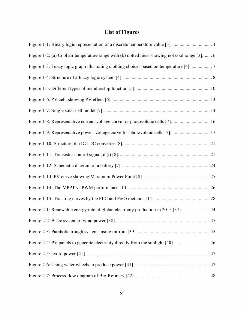
List of Figures
Figure 1-1: Binary logic representation of a discrete temperature value [3]. ................................. 4
Figure 1-2: (a) Cool air temperature range with (b) dotted lines showing not cool range [3]. ....... 6
Figure 1-3: Fuzzy logic graph illustrating clothing choices based on temperature [4]. ................. 7
Figure 1-4: Structure of a fuzzy logic system [4]. .......................................................................... 8
Figure 1-5: Different types of membership function [5]. ............................................................. 10
Figure 1-6: PV cell, showing PV effect [6] .................................................................................. 13
Figure 1-7: Single solar cell model [7]. ........................................................................................ 14
Figure 1-8: Representative current-voltage curve for photovoltaic cells [7]. ............................... 16
Figure 1-9: Representative power–voltage curve for photovoltaic cells [7]. ................................ 17
Figure 1-10: Structure of a DC-DC converter [8]. ........................................................................ 21
Figure 1-11: Transistor control signal, d (t) [8]. ........................................................................... 21
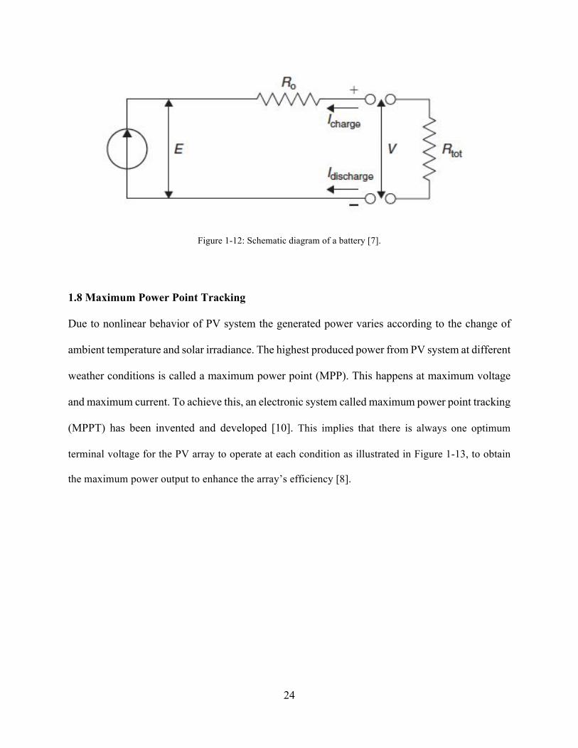
Figure 1-12: Schematic diagram of a battery [7]. ......................................................................... 24
Figure 1-13: PV curve showing Maximum Power Point [8]. ....................................................... 25
Figure 1-14: The MPPT vs PWM performance [10]. ................................................................... 26
Figure 1-15: Tracking curves by the FLC and P&O methods [14]. ............................................. 28
Figure 2-1: Renewable energy rate of global electricity production in 2015 [37]. ....................... 44
Figure 2-2: Basic system of wind power [38]. .............................................................................. 45
Figure 2-3: Parabolic trough systems using mirrors [39]. ............................................................ 45
Figure 2-4: PV panels to generate electricity directly from the sunlight [40]. ............................. 46
Figure 2-5: hydro power [41] ........................................................................................................ 47
Figure 2-6: Using water wheels to produce power [41]. .............................................................. 47
Figure 2-7: Process flow diagram of Bio-Refinery [42]. .............................................................. 48
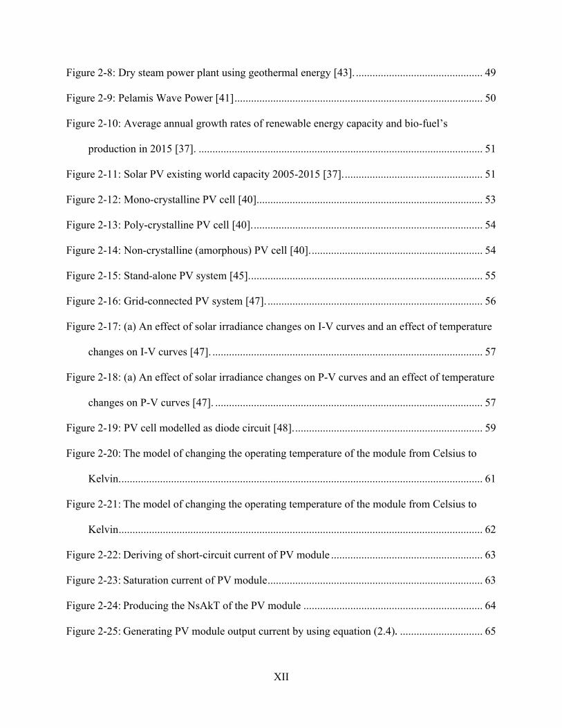
XII
Figure 2-8: Dry steam power plant using geothermal energy [43]. .............................................. 49
Figure 2-9: Pelamis Wave Power [41] .......................................................................................... 50
Figure 2-10: Average annual growth rates of renewable energy capacity and bio-fuel’s
production in 2015 [37]. ....................................................................................................... 51
Figure 2-11: Solar PV existing world capacity 2005-2015 [37]. .................................................. 51
Figure 2-12: Mono-crystalline PV cell [40]. ................................................................................. 53
Figure 2-13: Poly-crystalline PV cell [40]. ................................................................................... 54
Figure 2-14: Non-crystalline (amorphous) PV cell [40]. .............................................................. 54
Figure 2-15: Stand-alone PV system [45]. .................................................................................... 55
Figure 2-16: Grid-connected PV system [47]. .............................................................................. 56
Figure 2-17: (a) An effect of solar irradiance changes on I-V curves and an effect of temperature
changes on I-V curves [47]. .................................................................................................. 57
Figure 2-18: (a) An effect of solar irradiance changes on P-V curves and an effect of temperature
changes on P-V curves [47]. ................................................................................................. 57
Figure 2-19: PV cell modelled as diode circuit [48]. .................................................................... 59
Figure 2-20:The model of changing the operating temperature of the module from Celsius to
Kelvin. ................................................................................................................................... 61
Figure 2-21:The model of changing the operating temperature of the module from Celsius to
Kelvin .................................................................................................................................... 62
Figure 2-22:Deriving of short-circuit current of PV module ....................................................... 63
Figure 2-23:Saturation current of PV module .............................................................................. 63
Figure 2-24:Producing the NsAkT of the PV module ................................................................. 64
Figure 2-25:Generating PV module output current by using equation (2.4). .............................. 65

XIII
Figure 2-26:The output current, voltage and power of PV module ............................................. 65
Figure 2-27:Actual proposed PV model ...................................................................................... 66
Figure 2-28: Simulink PV module model mask dialog box ......................................................... 66
Figure 2-29: Manufacturer-supplied (a) V-I and P-V curves at different irradiance and 25oC
temperature, (b) V-I and P-V curves at 1000W/m2 and different temperatures .................. 67
Figure 2-30: (a) Different solar radiation at 25oC and (b) different irradiance at 45oC of PV
module power-voltage curves ............................................................................................... 68
Figure 3-1: DC-DC converter structure [53]. ............................................................................... 69
Figure 3-2: d (t), the transistor control signal [53]. ....................................................................... 70
Figure 3-3: Maximum power point tracking of a PV module [53]. .............................................. 71
Figure 3-4: A buck-boost converter circuit [54]. .......................................................................... 74
Figure 3-5: The boost converter circuit diagram during ton [54]. ................................................ 75
Figure 3-6: Circuit of the buck-boost converter during toff (CCM) [54]. ...................................... 77
Figure 3-7: The buck-boost converted circuit diagram during toff (DCM) [54]. ......................... 78
Figure 3-8: Simulink model buck-boost converter [56]. .............................................................. 83
Figure 3-9: Simulink/MATLAB model of buck-boost converter with the modified solar panel. 83
Figure 3-10: Buck-boost converter output voltage inductor resistance effects ............................ 85
Figure 3-11: Buck-boost converter efficiency inductor resistance effect ..................................... 85
Figure 4-1: Fuzzy control scheme for a maximum power point tracker [57]. .............................. 87
Figure 4-2: Flow chart of the fuzzy logic algorithm. .................................................................... 87
Figure 4-3: Structure of fuzzy logic controller [59]. ..................................................................... 89
Figure 4-4: Membership functions for (a) input current of converter (b) input voltage of
converter (c) output duty cycle of fuzzy controller. ............................................................. 90

XIV
Figure 4-5: Fuzzy logic designer in Matlab tool box. ................................................................... 92
Figure 4-6: Graphical representation of fuzzy controller rules. .................................................... 93
Figure 4-7: Fuzzy controller rule viewer. ..................................................................................... 93
Figure 4-8: The optimum duty cycle from fuzzy controller. ........................................................ 94
Figure 4-9: Fuzzy system simulation based maximum power point tracking of photovoltaic. .... 95
Figure 4-10: Input power versus output power (a) and PWM (b) at 200w/m^2. ......................... 96
Figure 4-11: Input power versus output power (a) and PWM (b) at 400w/m^2. ......................... 96
Figure 4-12: Input power versus output power (a) and PWM (b) at 600w/m^2. ......................... 97
Figure 4-13: Input power versus output power (a) and PWM (b) at 800w/m^2. ......................... 97
Figure 4-14: Input power versus output power (a) and PWM (b) at 1000w/m^2. ....................... 97
Figure 5-1: PV array consisting of 12 V, 130 watt modules. ..................................................... 100
Figure 5-2: 15A ECO-WORTHY solar charge regulator [60]. .................................................. 100
Figure 5-3: 12 Volt deep cycle battery for photovoltaic system [61]. ........................................ 102
Figure 5-4: Arduino Uno board (a) and Open source Arduino IDE interface (b). ..................... 102
Figure 5-5: DIYmall Voltage Sensor for Arduino DC0-25V (a) and ACS712ELC-20A current
sensor (b). ............................................................................................................................ 103
Figure 5-6: Arduino code of fuzzy controller. ............................................................................ 104
Figure 5-7: Modified MPPT for applying fuzzy controller. ....................................................... 105
Figure 5-8: Reading voltage and current sensors on computer. .................................................. 106
Figure 5-9: Practical experiment of comparing between two maximum power point tracking
algorithms. .......................................................................................................................... 106
Figure 5-10: Different light meter readings during a typical test run. ........................................ 107
Figure 5-11: Observing the change in PWM due to the change of voltage and current of PV. . 108

XV
Figure 5-12: Comparison between original MPPT and fuzzy MPPT in terms of input power. . 109
Figure 5-13: Curves of batteries power of the proposed MPPTs. ............................................... 110

XVI
List of Abbreviations
DC-DC converter An electronic device that converts a source of direct current (DC) from one voltage level to another
PV Photovoltaic
MPPT
Maximum Power Point Tracker
AI
Artificial Intelligence
PLC
Programmable Logic Controller
COG
Centroid of Gravity
BOA
Bisector of Area
MOM
Mean of Maximum
DC
Direct Current
AC
Alternative Current
Ah
Ampere Hours
SOC
State of Charge
MPP
Maximum Power Point
PWM
Pulse Width Modulation
P&O
Perturbation and Observation
IC
Incremental Conductance
FLC
Fuzzy Logic Controller
MF
Membership Function
UOD
Universe Of Discourse
SEPIC
Single-Ended Primary-Inductor Converter

XVII
AFLC
Adaptive Fuzzy Logic Control
ANN
Artificial Neural Network
EPP Estimate-Perturb-Perturb Method
NN Neural Network
HC Hill Climbing Techniques
MW/h Megawatt Per Hour
WEC Wave Energy Converter
CCM Continuous Conduction Mode
DCM Discontinuous Conduction Mode
RE Renewable Energy

XVIII
List of symbols
!" The Control Output Obtained by Utilizing The
COG Defuzzification Method
-
TC
The Absolute Temperature of The Cell Kelvin
q
The Electronic Charge =1.602´10-19 J/V Colom
V
The Voltage Imposed Across The Cell Volt
Io
The Dark Saturation Current Ampere
Gt Specific Solar Irradiance -
Ropt
Optimal Load Resistance Ohm
Pmax
Maximum Power Watt
Imax
Maximum Current Ampere
Vmax
Maximum Voltage Volt
FF
Fill Factor -
qmax
Nominal Capacity Coulomb
CO2 Carbon Dioxide -
Vpv
PV Module Output Voltage Volt
Voc
Open Circuit Voltage Volt
Isc
Short Circuit Current Ampere
Ipv
PV Module Output Current Ampere
Tr
Reference Temperature Kelvin
Iph
PV Module Light-Generated Current Ampere
Is
PV Module Saturation Current Ampere
A, B Ideality Factor = 1.6 -

XIX
K Boltzman Constant = 1.38064852(79)×10−23
J/K
Rs PV Module Series Resistance Ohm
Iscr PV Module Short-Circuit Current (25oc and
1000W/M2)
Ampere
Ki Short-Circuit Current Temperature Coefficient Ampere/ oC
λ PV Module Illumination -
Ego Band Gap for Silicon --
Ns Number of Cells Connected in Series -
Np Number of Cells Connected in Parallel -
Vmp Voltage at Maximum Power Volt
Imp Current at Maximum Power Ampere
G Sun Light w/m2
Vout Output Voltage Volt
Ppv PV Power Watt
vg(t) Input Voltage of Dc-Dc Converter Volt
vo(t) Output Voltage of Dc-Dc Converter Volt
δ (t) Control Signal Volt
d (t) Duty Cycle -
Ts Switching Period Second
ton Time When the Switch of Converter is On Second
toff Time When the Switch of Converter is Off Second
Pmp Maximum Power Watt
Ropt Optimal Equivalent Output Resistance Ohm

XX
Ig Input Current Ampere
Io Output Current Ampere
D Equilibrium Duty Cycle -
R’ Resistance of Load Ohm
C Capacitor farad
L Inductor Henry
T Diode -
Q Transistor -
RL Resistance in Series with Inductor Ohm
RC Resistance in Series with Capacitor Ohm
VT Forward Voltage Drop of Diode Volt
Vm Output Voltage of PV Module Volt
Im Output Current of PV Module Ampere
S The Converter Switch -
µ The Membership Degree of Output X -
IDE Arduino software -
fis Extension of Matlab fuzzy file -

1
Chapter 1
1. Introduction and Literature Review This thesis presents the design and implementation of a fuzzy logic-based maximum power point
tracker (MPPT) for a photovoltaic power supply. In this chapter, the background of the problem is
described and the motivation for the work is presented. A literature review of existing MPPT
algorithms is then carried out and the purpose for using fuzzy logic technique in maximum power
point tracking is discussed. The final section in this chapter provides an overview of the
organization of the thesis.
1.1 Background
There is a noticeable increase in energy consumption due to increases in industrial development
and human consumption. This issue has driven interest in research and technological investments
related to the optimization of energy efficiency and the use of sustainable and renewable energy
sources. At the same time, the use of fossil fuels for the generation of power is decreasing and also
becoming more expensive. The most important consideration in replacing conventional energy
sources with more environmentally friendly renewable sources (such as solar and wind energy) is
finding out how to extract the maximum energy and deliver the maximum power at a minimum
cost for the desired load. Integration of two or more types of energy sources may offer the best
way of improving power generation by varying the contribution from each energy source,
depending on the load demand. The main purpose of this work is to develop and optimize
maximum power point tracking and control of a multi-source alternative energy generation system
consisting of photovoltaic (PV) modules, wind generators and other sources. PV power is a
renewable energy source that has recently sparked significant interest and may in the near future
replace nonrenewable sources such as fossil fuels. However, to achieve this change-over, PV
2
power cost per kilowatt-hour has to be competitive in comparison to fossil fuel energy sources.
The material used in the structure of solar cells and the technology used in arranging the solar cells
to form a module are considered key factors that affect the efficiency of PV modules. At the present
time, PV modules have only about 12-26% efficiency in converting solar irradiance to electricity,
which is quite low [1]. Gallium Arsenide solar cells have a high rate of efficiency of 29%, whereas
Silicon solar cells have about 12-14% efficiency [2]. Moreover, efficiency can drop due to load
conditions, PV module temperature, or decreases in solar insulation. In order to capture the
maximum-rated power from a PV module, it is necessary to operate the module at its optimal
power point. To do this, a controller called a maximum power point tracker is required. PV
modules are non-linear power sources and their output power depends on the terminal operating
voltage. Therefore, the function of the MPPT is to compensate for the varying current-voltage
characteristics of the solar cell. The MPPT modifies the output voltage and current of the PV
module and determines the operating point that will give the maximum power. The MPPT must
be able to accurately track the constantly varying operating point where the maximum power is
delivered to increase the efficiency of the PV module.
1.2 Statement of the Problem
The use of PV power systems is relatively low due to low efficiency and relatively high cost per
watt compared to fossil fuels. Therefore, much work still needs to be done to increase the efficiency
of PV systems and make them more reliable. The first step to understanding and discussing how
to improve PV module efficiency is through modeling and simulation. After obtaining good
modeling and simulation of a PV module, it is possible to design and develop different ways to
optimize the system operation. Many different methods of maximum power tracking in PV power
applications have been reported in the literature. However, most of the current methods have

3
drawbacks, such as low efficiency, low accuracy and slowness of response. Thus, this research
aims to find more reliable and accurate ways to achieve the desired power that can be produced by
a PV system during various weather conditions. The approach is called MPPT-based fuzzy logic
control. The control algorithm follows the excellent approach representation and deduction
capabilities of fuzzy logic to fix the flaws of existing methods.
1.3 Objectives
The main purpose of this research is to design and implement a fuzzy logic-based maximum power
point tracker for a photovoltaic power supply. In order to accomplish this work, an MPPT model
consisting of a dc-dc converter and a fuzzy logic controller is developed. Analyses of buck, boost,
and buck-boost converter characteristics are then carried out to choose the most suitable topology
that fits all components of the entire PV system. A combined model of the PV module and the
selected buck-boost converter is simulated, and the results used to obtain the best design needed
to formulate and tune the fuzzy logic control algorithm for tracking the maximum power. The
simulated fuzzy logic behavior is converted to Arduino code and uploaded to an Arduino Uno
board using Arduino software (IDE). As well, the proposed fuzzy logic controller is implemented
in hardware with a suitable converter and then compared with another MPPT-based PIC 16F684
microcontroller and the same topology of a dc-dc converter. The results indicate that the proposed
method is better than the PIC 16F684-based MPPT in terms of the system’s speed response and
maximum power derivation.

4
1.4 Introduction to Fuzzy Logic
Fuzzy logic is the area of artificial intelligence (AI) associated with reasoning algorithms. Its
primary purpose is to mimic human thought patterns and decision-making abilities in machine
applications. Fuzzy logic algorithms are often used in situations where binary-form process data
are not applicable. So, for instance, statements such as “It’s cool” and “She’s old” do not offer the
reader concrete notions either about air temperature or a person’s age. Examples of concrete
statements would be “It’s 70 degrees Fahrenheit” or “The woman is 90 years old.” The task of
applying fuzzy logic is to translate inexact statements like “It’s cool” or “She’s old” into concepts
that are more exact and thus make sense from a logical perspective. So, for instance, when
discussing a cool temperature, a PLC (Programmable Logic Controller) that includes fuzzy logic
capabilities would state both the degree of coolness and its association to both cold and hot. With
this information, the degree of coldness in relation to hotness would help determine that “warm”
indicated a temperature somewhere between cold and hot. Thus, “cold”, in terms of straight binary
logic, could be one discrete value (for our purposes, designated as logic 1), while hot could be the
other (here, designated as logic 0). However, the notion of “warm” remains valueless, as shown in
Figure 1-1[3].
Figure 1-1: Binary logic representation of a discrete temperature value [3].

5
Fuzzy logic, unlike binary logic, is considered ‘gray’ logic in that it describes values that
are somewhere in the middle between two distinct features. In other words, fuzzy logic creates a
data range by assigning two distinct values – namely, 1 (indicating a maximum degree) and 0
(indicating a minimum degree). Figure 1-2a shows varying degrees of cool air, with 70 degrees
Fahrenheit being designated as the ideal of “cool air” and thus given a value of 1. Any temperature
above 80 degrees Fahrenheit is therefore designated as “hot”, while temperatures less than 60
degrees Fahrenheit are designated as “cold”. In this way, temperatures lower than 60 and higher
than 80 are considered outside the ideally “cool” range.
A different way to consider this range of “cool” temperatures is shown in Figure 1-2b. In
the figure, we can see that the dotted line indicates temperatures that are not cool (i.e., they are
instead either cold or hot). So, a temperature of 65 degrees Fahrenheit is framed in a fuzzy logic
algorithm as being “half cool and half cold” or 50% cool / 50% cold. This demarcation points to a
certain range or degree of coolness. However, temperatures less than 60 degrees Fahrenheit are
designated by fuzzy logic algorithm as “cold”.

6
Figure 1-2: (a) Cool air temperature range with (b) dotted lines showing not cool range [3].
The real-life application of a fuzzy logic algorithm is where it gets both useful and interesting. For
instance, our fuzzy logic temperature algorithm can assist when deciding what kind of clothing is
more suitable (i.e., clothing for colder weather or clothing for warmer weather). Clothing choice
is determined by temperature (here referenced as the “input”) together with its designated range.
So, for instance, and as illustrated in Figure 1-3, a short-sleeved light-fabric shirt might be
appropriate attire for a 70-degree Fahrenheit temperature, whereas a long-sleeved, heavy-fabric
shirt would be more appropriate in temperatures below 65 degrees. Additionally, were the input
designated as 25% cool and 75% cold (e.g., 62 degrees Fahrenheit), the best choice might be to
wear a sweater with the shirt, depending both on the temperature and its coolness value. In fact,
the output of a fuzzy system may be affected by any number of inputs (e.g., temperature,
precipitation, etc.). Hence, any decisions around the output must be made in reference to the
knowledge base established by the fuzzy logic graph.

7
In able to function properly, fuzzy logic ‘feeds’ on information in order to process its reasoning.
The information is provided by whoever understands the functioning of the process and is held in
storage within the fuzzy system. For example, if the temperature increases in a steam-heating
system, the person operating that system (here designated as the “expert” or the one with the
information) might request his or her team member to turn the steam valve “somewhat” clockwise.
A fuzzy system would likely read “somewhat” as a specific degree of a turn (i.e., an 8-degree
rotation) that would shut the valve by about 4%. Here, the term “somewhat” is considered a fuzzy
descriptor, indicating that it does not have a definite value [4].
Figure 1-3: Fuzzy logic graph illustrating clothing choices based on temperature [4].
Fuzzy logic functions by designating and enacting rules that combine an expert’s inputs with the
wanted outputs. There are usually four main determining factors of fuzzy logic: fuzzy sets,
membership functions, linguistic variables and fuzzy rules. These four factors are explained in
detail below and Figure 1-4 shows the main structure of a fuzzy logic system.
1) A rule-based system best described by ‘If-Then’ designations (as illustrated in Figure 1-3).
These rules generally include fuzzy logic quantification made by an expert on how to attain optimal
control.

8
2) An inference mechanism that optimally mimics expert decision-making by both
‘understanding’ the information and then applying it, again towards optimal control of the input
factors.
3) A fuzzification interface that changes inputs into knowledge that the inference mechanism
(factor #2) can then utilize when designating and following rules.
4) A defuzzification interface that changes the outcomes of the inference mechanism (factor #2)
into useable inputs that will ‘feed’ the process and move it forward.
Figure 1-4: Structure of a fuzzy logic system [4].
1.4.1 Fuzzification Fuzzification is a process whereby clearly delineated values are made fuzzy. To accomplish
fuzzification, the linguistic variables and terms to be utilized must first be defined. Numerical
values are not used in this process; rather, words and/or phrases from a natural language comprise
both the input and output variables. To start the process, a specific linguistic variable is broken
down (i.e., decomposed) into its composite linguistic terms. Take, for instance, an air-conditioning
system. In this system, temperature (T) is the linguistic variable that designates the room’s

9
temperature, which can be described (qualified) in general linguistic terms as “hot” or “cold”.
Working from this point, Temperature (T) = {too cold, cold, warm, hot, too hot} can then serve as
the decomposition set for the linguistic variable temperature. The individual features of this
decomposition are labeled as linguistic terms and represent a part of the temperature’s total values.
Then, in order to translate the “crisp” (i.e., non-fuzzy) input data to fuzzy linguistic terms, we can
apply membership functions, as explained below [5].
1.4.2 Membership Functions The membership function is a way to express graphically the participation level of individual
inputs. It allocates a value to the inputs that can also serve as functional overlaps between the
inputs. In so doing, the membership function strongly influences the output response.
A critical determining factor of the membership function is configuration or, as it is usually termed,
“shape”. The various potential shapes include Gaussian, triangular, trapezoidal, generalized bell
and sigmoidal. Of these, the triangular shape is the one most commonly applied, and the degree of
membership function is usually in the [0 1] range. The definitions and graphs of the various
membership functions are illustrated in Figure 1-5.

10
Figure 1-5: Different types of membership function [5].
Furthermore, the membership functions designate the various elements in a set as being either
discrete or continuous. Discrete form membership function is in a list (vector) format, whereas the
continuous form is a mathematical function, perhaps even a program. Overall, the discrete form is
more commonly applied.
A triangular membership function comprises straight line segments and is thus easy and
practical to apply under fuzzy control. However, the Gaussian membership function approach is
better suited when smooth and continuous output is desired.
1.4.3 Fuzzy Rules As touched on briefly above, rule bases are developed to control output variables in a fuzzy logic
system. The main aim of fuzzy systems is to create a theoretical foundation for to make logical
assumptions and associations among inexact terms of reference. In fuzzy logic technological
systems, this is called approximate reasoning. The main subjects and verbs of fuzzy logic are

11
comprised of fuzzy sets and fuzzy operators, or so-called “If-Then” rule statements. These are
applied when developing the “If-Then” conditionality statements that are the hallmark and basis
of fuzzy logic. So, for instance, if a fuzzy rule asserts that if x is A, then y must be B if A and B
are values designated by fuzzy sets stipulating a range of X and Y, respectively. In this rule, the
“If” portion is deemed the antecedent or premise, while the “Then” portion is referred to as the
conditional consequent or conclusion. Ultimately, a fuzzy rule is, at its core, an If-Then rule that
features both conditions and a conclusion.
The process of fuzzy logic control proceeds from a set of input data derived from any number of
sensors; these data are then ‘fed’ into the control system. Concurrently, the values of these input
variables undergo a change known as “fuzzification”, which tranforms the discrete values into a
broad range of values. Fuzzified inputs are then measured against a series of production rules, and
the rules selected generate the outputs. Finally, output data are “defuzzified” through control
commands [5].
1.4.4 Inference engine Inference is a process whereby novel information is derived via existing information. In fuzzy
logic control systems, inference refers to a process whereby the final result is derived by combining
the outcomes of each rule in terms of fuzzy values. There are several different methods that can
be followed to obtain inference, the most popular of which are Mamdani and Takagi-Sugeno-
Kang.
The Mamdani approach was developed by Ebrahim H. Mamdani as a means to modifying the
behavior of a steam engine and boiler in 1975. Mamdani’s (1975) control method derives from
Lofti Zadeh’s (1973) paper describing fuzzy algorithms for complex systems and decision
processes. In Zadeh’s (1973) method, the minimum operation Rc is applied as a fuzzy implication,

12
while the max-min operator is applied to obtain the composition. For instance, let us assume that
the following form comprises a designated rule base. Hence:
IF input x = A AND input y = B
THEN output z = C
1.4.5 Defuzzification The process of defuzzification is a means to change the fuzzy output of the inference engine to a
clearly defined (crisp) output by applying membership functions such as those utilized by the
fuzzifier. Examples of defuzzification approaches include (in no particular order) Centroid of
Gravity (COG), Bisector of Area (BOA), Weighted Average, Mean of Maximum (MOM), First of
Maxima and Last of Maxima. While each defuzzification procedure is based on the application’s
properties, choosing a suitable defuzzification strategy is an art rather than a science (i.e., there is
no fool-proof method, but instead tends to proceed by “feel”).
Having said that, Centroid of Gravity (COG) is currently the most commonly applied
defuzzification approach, mainly for its relative simplicity. The base equation for COG is:
!" = ∫&'& ( ()(
∫&'& ( )( (1.1)
Where !" is the control output obtained by utilizing the COG defuzzification method.
1.5 Photovoltaic Systems (PVs)
Photovoltaic (PV) energy is the outcome of the direct conversion of light energy into electricity.
The conversion is achieved via thin semiconductor devices called photovoltaic cells, which are
also sometimes called solar cells or PV cells as shown in Figure 1-6. PV cells are basically flat
light-sensitive diodes comprised of the same or similar materials as those used in transistors,

13
computer chips, and related technology. A PV cell functions as follows: A semiconductor absorbs
enough energy from a light photon to transfer it to electrons. The high-energy electrons would then
pass their energy to the semiconductor material, and in so doing create heat through recombining
with the positively-charged “holes” formed by the light. An internal electrical field then emerges
as a result of the PV cell’s junction that exists between the two forms of the semiconductor. When
the electric field channels the charged electrons to one side of the cell (to prevent them from
creating heat), a difference in voltage is thus formed between the opposite cell sides. An electric
current is then able to be drawn from the cell through the contacts on the two sides.
A PV cell creates electricity similar to how a chemical battery cell does (i.e., as a direct current
[DC]). The electrical power created is limited by the amount of received light (irradiance), as well
as the cell’s temperature and the PV cell’s connections [6].
Figure 1-6: PV cell, showing PV effect [6]

14
1.5.1 PV cell characteristics Solar cells comprise semiconductor materials (usually silicon) and are coated such that a positive
electric field is created on the backside and a negative one on the front (the side that faces the sun).
At its core, a photovoltaic PV generator is simply a collection of solar cells, connections, protective
parts, and supports. Thus, when photons (energy from the sun) come into contact with the solar
cell, electrons are loosened from the atoms in the semiconductor material. The ‘loosening’ causes
the formation of pairs of electron-holes, and the electrical conductors attach to the positive and
negative sides. In so doing, an electrical circuit emerges, within which electrons are captured as
an electric current referred to as a photocurrent, Iph. During the night or other times when it is dark
outside, the solar cell remains passive and functions like a diode. In other words, it acts as a p–n
junction, creating neither current nor voltage. Conversely, if the cell is hooked to a sizeable
external voltage supply, it creates a current known as a diode or dark current, ID. Typically, a solar
cell normally functions with an electrical equivalent one-diode model, as depicted in Figure 1-7
(Lorenzo, 1994). Such a circuit is used for separate cells, a module comprising several cells, or an
array comprising numerous modules [7].
Figure 1-7: Single solar cell model [7].

15
As can be seen from Figure 1-7, the model includes a current source, Iph, a single diode, and a
series resistance (RS) that indicates the resistance level within the cells. The diode includes an
internal shunt resistance as well, as is depicted in Figure 1-7. The net current which demarcates
the difference between the photocurrent, Iph, and the normal diode current, ID, is considered the net
current, which is calculated thus:
I = Iph – ID = Iph – Io *+,-(/0123)
567− 1 −
/0123
2:; (1.2)
Load resistance is usually considerably smaller than shunt resistance. However, load resistance is
usually much larger than series resistance, which means that a relatively small amount of power
actually ‘disappears’ (i.e., dissipates) within the cell. If we overlook these two resistances, we can
calculate the net current as being the difference between the photocurrent, Iph, and the normal diode
current, ID. This can be represented by the following equation:
I = Iph – ID = Iph – Io *+,-/
567− 1 (1.3)
Where:
K is equal to Boltzmann’s gas constant, = 1.381´10-23 J/K;
TC is equal to the absolute temperature of the cell (K);
q is the electronic charge =1.602´10-19 J/V;
V is the voltage imposed across the cell (V); and
Io is the dark saturation current, which is based on temperature (A).
Figure 1-8 depicts the typical I-V curve of a solar cell for a specific irradiance (Gt) and cell
temperature, TC. The current generated by a PV cell is based both on the external voltage and the
sunlight affecting the cell. If the cell is short-circuited, the current peaks (short-circuit current, Isc),
and the voltage for the cell plummets to 0. In contrast, if the PV cell circuit is open (and with the
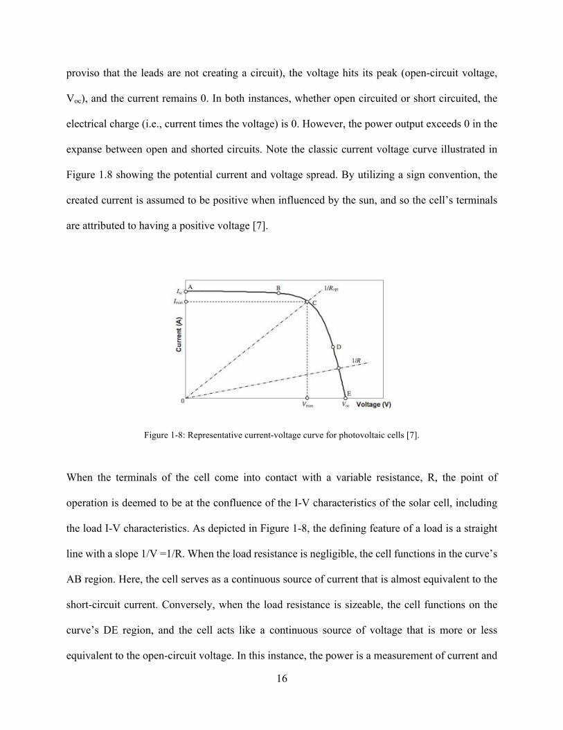
16
proviso that the leads are not creating a circuit), the voltage hits its peak (open-circuit voltage,
Voc), and the current remains 0. In both instances, whether open circuited or short circuited, the
electrical charge (i.e., current times the voltage) is 0. However, the power output exceeds 0 in the
expanse between open and shorted circuits. Note the classic current voltage curve illustrated in
Figure 1.8 showing the potential current and voltage spread. By utilizing a sign convention, the
created current is assumed to be positive when influenced by the sun, and so the cell’s terminals
are attributed to having a positive voltage [7].
Figure 1-8: Representative current-voltage curve for photovoltaic cells [7].
When the terminals of the cell come into contact with a variable resistance, R, the point of
operation is deemed to be at the confluence of the I-V characteristics of the solar cell, including
the load I-V characteristics. As depicted in Figure 1-8, the defining feature of a load is a straight
line with a slope 1/V =1/R. When the load resistance is negligible, the cell functions in the curve’s
AB region. Here, the cell serves as a continuous source of current that is almost equivalent to the
short-circuit current. Conversely, when the load resistance is sizeable, the cell functions on the
curve’s DE region, and the cell acts like a continuous source of voltage that is more or less
equivalent to the open-circuit voltage. In this instance, the power is a measurement of current and

17
voltage’s product. Moreover, the results shown in Figure 1-9 can be attained if this exercise is
undertaken and measurements entered on a P-V graph. Point C in Figure 1.8 illustrates the instance
when the peak power moves beyond the maximum power point.
Figure 1-9: Representative power–voltage curve for photovoltaic cells [7].
The load resistance then become optimal, Ropt, and the power that “disappeared” as a result of the
resistive load is at its greatest and is represented by:
Pmax=Imax* Vmax (1.4)
In the same figure, point C is also referred to as the maximum power point, which here demarcates
the operating points Pmax, Imax, and Vmax. These points are characterized by maximized output
power. If we consider Pmax, an extra parameter (i.e., the fill factor or FF) may be added, as follows:
Pmax =Isc*Voc*FF (1.5)
or
FF= Pmax / Isc*Voc = Imax* Vmax / Isc*Voc (1.6)
As can be inferred, the fill factor denotes the genuine I-V characteristic. So, for good cells, the fill
factor is valued higher than 0.7 but declines with each rise in cell temperature. Therefore, in both
illuminating and loading a PV cell to make the voltage equate the Vmax of the PV cell, the output
power is maximized. There are several different ways to load the cell, including utilizing resistive

18
loads, electronic loads, or batteries. The normal parameters for a single-crystal solar cell regarding
current density are:
Isc = 32 mA/cm2, Voc =0.58 V, Vmax = 0.47 V, FF = 0.72, and Pmax = 2273 mW [7].
When viewing Figure 1.8 in yet greater detail, some additional parameters that emerge are both
the short-circuit current and the open-circuit voltage. The short-circuit current, Isc, is the higher
value of the current created by the cell. It emerges through the short-circuit conditions (i.e., V = 0)
and is equivalent to Iph. The open-circuit voltage is related to the decline in voltage on the diode
when it is impacted by the photocurrent, Iph. This is the same as ID, if the current created is I = 0.
This measurement indicates the cell’s voltage under conditions of darkness (either during the night
or during a storm) and is derived from Eq. (1.3):
*+,-/<=567
− 1 = 1>=1<
(1.7)
Which is solved for Voc:
Voc = 567-?@
1>=1<+ 1 = BC?@
1>=1<+ 1 (1.8)
Where Vt. thermal voltage (V) given by:
Vt = 567
- (1.9)
The output power a photovoltaic cell is given by:
P =I*V (1.10)
The output power depends also on the load resistance, R; and by considering that V = I*R, it gives:
P =I2 *R (1.11)
Substituting Eq. (1.3) into Eq. (1.10) gives:
P = D37 −DE *+,-/
567− 1 B (1.12)
Equation (1.12) can be differentiated with respect to V. By putting the derivative equal to 0, the

19
external voltage, Vmax, that gives the maximum power of solar cell can be obtained by:
*+,-/FGH
5671 +
-/FGH
567= 1 +
1>=1<
(1.13)
This is a clear equation of the voltage Vmax, which maximizes the power by knowing the short
circuit current (Isc), PV photo current (Iph), the dark saturation current (Io), and the absolute cell
temperature, TC. If the values of these three parameters are known, then Vmax can be obtained
from Eq. (1.13) by trial and error.
The load current, Imax, which maximizes the output power, can be found by substituting Eq. (1.13)
into Eq. (1.3):
Imax = Isc - Io *+,-/
567− 1 = D37 −DE
I0J>=J<
I0KLFGHMN=
− 1 (1.14)
Which gives:
Imax = -/FGH
5670-/FGH(D37 + DE) (1.15)
By using Eq. (1.4),
Pmax= -/FGHO
5670-/FGH(D37 + DE) (1.16)
Efficiency is another standard of PV cells that is always discussed. Efficiency is described as the
maximum electrical power output divided by the fallen light power. Efficiency is usually taken for
a PV cell temperature of 25 0C and incident light at an irradiance of 1000 W/m2 with a spectrum
close to that of sunlight at solar noon. An enhancement in cell efficiency is directly leading to a
cost reduction in photovoltaic systems. A series of R&D efforts have been made on each step of
the photovoltaic process. Through this technological progress, the efficiency of a single crystalline

20
silicon solar cell reaches 14–15% and the polycrystalline silicon solar cells shows 12–13%
efficiency in the mass production lines [7]. Another parameter of interest is the maximum
efficiency, which is the ratio between the maximum power and the incident light power, given by:
PQRS = TFGH
TUV=
1FGH/FGH
WXY (1.17)
Where
A= cell area (m2)
1.6 DC-DC Converters
Due to nonlinearity of PV system the output power is changeable according to the change of
atmosphere conditions. Therefore, the best device can play the role of regulating the voltage and
current output of PV source is called dc-dc converter [8]. Figure 1-10 illustrates a schematic
diagram for a DC-DC converter. The converter changes DC input voltage Z[(\) into DC output
voltageZE(\), but at a different voltage level than that of the input. Preferably, this change is done
with low losses to the converter, so the transistor functions as a switch, applying the control signal
d(t). As illustrated in Figure 1-11, the control remains at high for a designated period \E] and at
low for a designated period\E^^ [8].

21
Figure 1-10: Structure of a DC-DC converter [8].
When the transistor is ‘ON’, the voltage is low, indicating that the transistor’s power loss is also
low. However, when the transistor is ‘OFF’, both the current passing through it and the power loss
are likewise low. To control the average output voltage, the width of the pulses must be altered
when the switching period,_3, is constant. In the interval 0 to 1, the duty cycle, d(t), is a real value
equal to the ratio of the width of a pulse to the switching period, i.e., d(t) = \E]/_3.
Figure 1-11: Transistor control signal, d (t) [8].
When low losses are the desired aim, capacitors and inductors rather than resistors are used in DC-
DC converters because they have no or very low losses. Moreover, the electrical components are

22
easily connected in various combinations (topologies), each of which features different properties.
Three standard converter topologies are so-called buck, boost, and buck-boost converters. The
output voltage of the buck converter is lower than that of the input voltage, whereas the boost
converter features an output voltage that is greater than the input voltage. Meanwhile, the buck-
boost converter can produce an output voltage magnitude greater or less than the input voltage
magnitude [9].
1.7 Batteries
Most PV systems need some form of battery to power the system during non-daylight hours or
times of heavy cloud cover. During these darkness periods, a PV system alone is unable to satisfy
the requirements for power. The load and availability of the product in large part determine which
type and size of batteries are used. The batteries are usually situated where temperatures are
generally moderate and the area is well ventilated. Nowadays, batteries are usually lead-acid,
nickel cadmium, nickel hydride, and lithium. Of these options, the type used the most are deep-
cycle lead-acid batteries. Not only are deep-cycle lead-acid batteries readily available in several
different sizes, but they can be flooded or valve-regulated. Although flooded (that is, wet) batteries
often need more involved forms of maintenance routines, they also last longer. In contrast, valve-
regulated batteries may need less attention after installment, but they may have a considerably
shorter life. The primary need and defining characteristic of PV system batteries is that they must
be able to sustain constant deep charging and discharging while remaining fully functional. PV
batteries resemble car batteries, but car batteries cannot sustain constant charging and so should
not be considered an option for PV systems. To obtain greater capacity, batteries should have a
parallel arrangement. In stand-alone PV systems, the role of batteries is to store the electric power
generated during the time frame when the system covers the load completely (that is, without the

23
assistance of batteries or other backups) [7]. Batteries should also store excess power generated or
when it is sunny but the power demand is negligible. In times of relatively low solar irradiation,
batteries can provide extra needed energy. Batteries might also be needed due to changes in the
PV system output. Batteries are categorized by their nominal capacity (qmax), meaning the number
of ampere hours (Ah) that can be extracted from the battery in predetermined discharge conditions.
In general terms, a battery’s efficiency is determined by the ratio of the charge extracted (Ah)
during discharge, which is then divided by the amount of charge (Ah) required to reinstate the first
state of charge (SOC). Therefore, the battery’s life span and efficiency rate are determined by the
SOC as well as the charging and discharging current. The SOC is calculated from the ratio of the
battery’s present capacity and its nominal capacity, such that:
SOC = q /qmax (1.18)
SOC values can range from 0 to 1. Hence, if SOC = 1, the battery is fully charged, whereas if SOC
= 0, the battery is entirely discharged. Additional parameters are the charge or discharge regime
and the battery life. The charge (or discharge) regime is measured in hours and delineates the
relationship between a battery’s nominal capacity and the current at which it is charged (or
discharged). For instance, if the discharge regime for a battery equals 40 h with a nominal capacity
of 200 Ah discharged at 5 A, the battery’s actual lifetime can be calculated by determining how
many charge-discharge cycles the battery can endure before being reduced to 80% capacity.
Overall, batteries are considered voltage sources, E, when in series with internal resistance, Ro, as
depicted in Figure 1-12. In this example, the terminal voltage, V, is calculated by
V= E – I*Ro [7] (1.19)
24
Figure 1-12: Schematic diagram of a battery [7].
1.8 Maximum Power Point Tracking
Due to nonlinear behavior of PV system the generated power varies according to the change of
ambient temperature and solar irradiance. The highest produced power from PV system at different
weather conditions is called a maximum power point (MPP). This happens at maximum voltage
and maximum current. To achieve this, an electronic system called maximum power point tracking
(MPPT) has been invented and developed [10]. This implies that there is always one optimum
terminal voltage for the PV array to operate at each condition as illustrated in Figure 1-13, to obtain
the maximum power output to enhance the array’s efficiency [8].

25
Figure 1-13: PV curve showing Maximum Power Point [8].
In other words, an MPPT is a complete electronic system that varies the electrical operating point
of the modules so that the modules can deliver maximum available power. Any increase in power
that is reaped from the modules that increases battery charge current. The basic method of charge
controller is called PWM (Pulse Width Modulation). Its operation based on simply connecting the
modules directly to the battery. But this technique forces the PV modules to operate at battery
voltage, actually it is not the ideal operating voltage at which the modules are able to produce their
maximum available power (PPWM<PMPPT). Where PPWM is the extracted power by using
PWM controller and PMPPT is the obtained power using MPPT controller.

26
Figure 1-14: The MPPT vs PWM performance [10].
For instance, as shown in Figure 1-14, the classical PWM controller frugally connects the module
to the battery and hence forces the module to operate at 12V (Vpwm). By forcing a PV panel of
75W module to operate at 12V (Vpwm) the PWM reduces artificially power production to nearly
53W. This means the PWM decreases the efficiency of PV modules to about 29%. On the other
hand, using MPPT system in a solar charge controller can calculate the voltage at which the module
is able to produce maximum power (Vmp). Thus, the MPPT can extract the full 75W (+30% power),
regardless of present battery voltage as illustrated in Figure 1-14 above [10].

27
1.9 Literature review
Many MPPT algorithms have been proposed and are generally categorized into the following
groups as examples: 1) Perturbation and Observation (P&O) methods; 2) Incremental Conductance
(IC) methods; 3) Fuzzy logic and neural network-based methods and much more.
In [11] the (P&O) and (IC) methods of MPPT controllers were simulated and analyzed with
photovoltaic panels and a boost DC-DC converter. The results show that the IC controller gave a
stable output, but the P&O controller could achieve the maximum power output at 23.66 V, which
means it was better than the IC performance.
A Sliding Mode Control method of MPPT controller was used with the photovoltaic system, DC-
DC boost converter, DC-AC inverter and load. The system was implemented in
MATLAB/Simulink and was evaluated as an adequate performance of designed control [12].
The comparison between fuzzy logic control-based MPPT and P&O techniques was simulated and
tested in MATLAB/Simulink. The entire system included a photovoltaic panel, boost converter,
MPP controller and resistor load. The results were shown that the fuzzy control system gave a
better performance than the P&O system. In other words, when the simulation was tested under
three different conditions of irradiance (500, 700 and 1000 W/m2), the fuzzy controller was able
to give the best duty cycle that could drive the DC-DC converter to produce the maximum power
point of the PV system. Although both methods gave almost the same values of MPP at a steady
state, the fuzzy system could have a faster time response than P&O. Moreover, the efficiency of

28
the overall system was improved by minimizing the energy losses when there was a change in
solar irradiance [13].
A fuzzy logic controller (FLC)-based MPPT and a conventional Perturb and Observation (P&O)
were implemented in MATLAB/Simulink. The FLC is based on Sugeno’s method, which is
associated with the max-min composition. Both proposed methods of MPPT have been tested
under the same variations of solar irradiance and a constant temperature. Figure 1-15 shows that
the FLC response was faster than that of the conventional MPPT, whereas the overshoots of the
system are almost the same. Therefore, the FLC can improve the performance of the system more
than the P&O. Finally, using a hardware system with a real photovoltaic panel should be an aim
for future work [14].
Figure 1-15: Tracking curves by the FLC and P&O methods [14].

29
In [15] a fuzzy control-based MPPT of a photovoltaic system has been implemented and
represented. The whole system contains a solar panel, DC-DC buck boost converter and load. The
implementation was simulated in MATLAB/Simulink with a disturbance in the photovoltaic
temperature and irradiation values. The outcomes illustrate that the performance of fuzzy control
was done successfully and accurately in all assumed conditions. The oscillation around MPP is
decreased and the response is faster in comparison with the P&O technique. Therefore, the
proposed fuzzy system gave a higher performance than P&O.
Even though the photovoltaic system (PV) needs little maintenance and is environmentally-
friendly, it has some disadvantages such as low energy conversion efficiency and high initial cost.
Therefore, to get the greatest benefit from the PV system it is essential that the PV system runs at
its maximum power point during a variation of irradiance and temperature. Due to the importance
of this topic much research has been conducted and many papers have been published regarding
the different MPPT techniques. Hence, this thesis focused on the other diffused technique of
MPPT, which is the P&O method. The system was simulated in MATLAB using a PV, P&O
MPPT, and buck and buck-boost converter. The obtained results show that the P&O was able to
track the maximum power point successfully and quickly, but the buck converter is much more
effective than the buck-boost converter, especially in reducing the oscillations produced due to the
use of the P&O technique [16].
An intelligent fuzzy logic control (FLC) was used to obtain the maximum power point of a
photovoltaic system under different temperature and irradiation conditions. The proposed FLC
technique was applied to boost the DC-DC converter and was simulated in MATLAB/Simulink.

30
The goal of this work was to control the voltage of the solar panel to get the maximum power that
can be produced by observing the PV system under any change in temperature and insolation. The
results obtained from the FLC were compared with those obtained from the perturbation and
observation controller (P&O) and were discussed. It was clearly shown that the FLC performance
was faster than the P&O controller in the transitional state and gave a much smoother signal with
fewer oscillations at a steady state. Finally, a faster and steadier FLC of MPPT controller was
achieved and this made it possible to find the maximum power point in a shorter time in
comparison with the P&O controller [17].
A fuzzy logic controller (FLC) for tracking the maximum power point of the photovoltaic system
was proposed and implemented. The control system was based on the power variation and output
voltage variation as inputs and the duty cycle (D) as the output of the system which controls the
DC-DC converter by giving the pulse into the MOSFET switch. The proposed FLC-based MPPT
could simultaneously improve the dynamic and steady state performance of the PV system in
comparison with the (P&O) technique. Due to improvement in the performance of the proposed
method, an asymmetrical membership function (MF) concept was also proposed. Two steps were
proposed to determine the universe of discourse (UOD) of the input MF. Compared with the
proposed symmetrical FLC-based MPPT method, the transient time and the MPPT tracking
accuracy were further improved by 42.8% and 0.06%, respectively [18].
Both temperature and solar irradiation have an effect on the electricity that is produced by the
photovoltaic system. The PV system can deliver the maximum power to the load at a specific
operating point, which is defined as the maximum power point (MPP). Therefore, many methods

31
have been developed to maximize the output power of the photovoltaic system by continuously
tracking the maximum power point. The fuzzy logic-based MPPT algorithm was designed for a
10 KW PV system that was installed at the Cape Institute of Technology. The proposed FLC
technique was based on comparing two types of fuzzy membership functions, triangular
membership functions and Gaussian membership functions. The proposed FLC was combined
with the PV system and simulated in MATLAB/Simulink. The simulation results show that the
FLC using triangular membership functions was faster than the one using Gaussian membership
functions. Generally, the performance of the fuzzy logic controller could keep the maximum power
point at a stable rate [19].
The incremental conductance method is one of many MPPT techniques that have been
implemented for small and medium power applications. A complete linearized small signal model
for the incremental conductance MPPT algorithm has been proposed and integrated with a boost
DC-DC converter topology. Due to the redundancy of state variables within the control system,
the classical linearization mechanisms initially have led to an unsolvable system. To deal with this
challenge, another styling process using Taylor Series expansions was adopted. There is very good
agreement between the output of the model and the simulation results of a PV system in
PSCAD/EMTDC. The system’s state-space representation allows for stability and control design
as well as analysis of robustness. It is well known that the incremental conductance MPPT
algorithm is extremely robust even under changing conditions in solar irradiance. Therefore,
according to the above modeling approach, PV solar arrays based on incremental conductance-
based MPPT are able to be completely integrated into software for eigenvalue analysis, along with
conventional generators. The model presented above is easily adaptable to PV system

32
configurations that include different converter topologies [20].
A Cuk converter is used to compare and contrast the energy of two MPPTs, a Perturb and Observe
(P&O) controller, and an Incremental Conductance (IC) controller, recording the power output,
current and voltage for various combinations. As well, MATLAB/Simulink tools are used to
measure the performance of the energy point. A single solar panel with standard insulation and
temperature is added to the simulation circuit. Given the results, the optimal controller for MPPT
is the IC one, as it provides improved output for Cuk converters [21].
Non-conventional energy sources are increasingly assuming a key role in the reduction of carbon
emissions and fossil fuel exhaust. Likewise, solar power and fuel cells are becoming important
features of residential loads. To obtain the consumption rates for solar power, the researcher’s first
look at the maximum power point trackers of two string photovoltaic panels in a conventional 5-
KW DC distribution system, with both voltage and current phased to maximum power at 35.4V
and 4.94A, respectively. This setup is coupled to an AC grid that features a bi-directional inverter.
After initiating two PV strings and two MPPTs, the P&O approach is used for MPPT, giving the
current balancing of two MPPT modules in parallel. Next, the P&O method is compared to the IC
method. To do so, the bi-directional inverter is removed and a multilevel inverter installed, using
MATLAB/Simulink software to obtain results [22].
Over the years, researchers have employed several different approaches to extract maximum power
from a PV system. Some of these approaches involve MPPT techniques. This study features a
fuzzy logic-based MPPT algorithm for a 100 kW PV System, in which the proposed fuzzy MPPT

33
control technique manages the duty cycle of the DC-DC boost converter to obtain maximum power
from the PV system. Simulations are done, the proposed MPPT technique is explored, and
maximum power is tracked for a wide range of environmental conditions. In regard to the MPP,
the output voltage of the DC-DC Converter is changeable according to circumstances. Here, an
additional DC-DC buck-boost converter with PI control is employed to develop constancy in the
DC bus voltage. At the same time, a PWM inverter with an L-filter generates the 3-phase supply
that is needed for 3-phase load functions, along with single-phase loads. The results are given for
various temperature and irradiance conditions. MATLAB/Simulink is used to implement and
simulate the solar PV module fuzzy logic-based MPPT DC-DC converters, while a fuzzy logic
controller is applied to extract the maximum power from the solar PV module. Here, the algorithm
has been verified across various operating conditions, showing an error percentage ranging
between 0.29% and 1.19%. Furthermore, the simulation indicates that the system is guided by
alterations in temperature and irradiance. At the same time, there is rapid variation in output power
and the regulation shows solid robustness in the face of disturbances. Hence, this solar PV module
succeeds in both increasing the voltage and creating a signal where transient noise is nearly absent.
This indicates that the closed-loop system improves through the application of FLC, and that PV
power can be used in grid integration or remote generation plants. Aided by a duly-designed
inverter, PV power can also be utilized in industrial applications and consumer appliances. An L-
filter is used to create a pure sine wave output with low harmonics, while inverter output voltage
is used in grid integration [23].
The FLC scheme uses convergent distribution of the membership function to the fuzzy controller
(FC)-based single-ended primary-inductor converter (SEPIC) for MPPT operation of a

34
photovoltaic system and battery. However, the fuzzy controller for the SEPIC MPPT scheme
indicates a voltage without any changes in various load conditions at the inverter output (or load)
side. At different operating conditions, the converter undergoes simulated tests to gauge behavioral
changes. Meanwhile, the battery storage feeds the load with constant voltage, and with the help of
the PV module and SEPIC converter the battery will remain charged and controlled by FLC-based
MPPT. The proposed FLC-based MPPT with battery will provide more power to the load than it
would without a battery system. This is because the battery makes the voltage supply more constant
to the inverter input side. Hence, the proposed FLC-based MPPT scheme for the SEPIC converter
presents as a strongly viable potential candidate for real-time PV inverter applications in
changeable load conditions [24].
In [25], researchers show how photovoltaic generation systems are continuously under threat by
uncontrollable elements such as partial shading that can lead to power loss and hotspots. These
problems are further exacerbated by curves showing multiple peaks. Under such operating
conditions, conventional MPPT techniques can fail to provide optimum MPP. In light of this
crucial issue, several attempts have been made to develop an Adaptive Takagi-Sugeno Fuzzy
Inference System-based Fuzzy Logic Control MPPT. The mathematical model of the PV array is
simulated by utilizing MATLAB/Simulink. Several case studies on temperature and
inhomogeneous insolation and were investigated. However, to determine the appropriateness of
the proposed MPPT approach, a comparative analysis is carried out with two common MPPT
techniques and the results compared with two other techniques. In this comparison, all the
techniques are performed using a grid-connected PV system to measure the efficiency and
response of each in tracking the MPP under several different partial shading conditions. The

35
proposed fuzzy logic-based MPPT controller has been shown to surpass other conventional MPPT
techniques regarding harmonic reduction, tracking ability, and efficiency. Moreover, the proposed
approach demonstrates superior response speed towards the PV system, and the optimal operating
point does not oscillate around the MPP, even without knowledge of the actual model [25].
The fuzzy logic controller offers a good response to changes in cell temperature and solar
radiation, and a controller alters the duty cycle of a DC-DC converter as a control parameter.
Results of simulation tests indicate that the proposed system increases the system’s efficiency. The
model is simulated in a MATLAB/Simulink environment by first varying the solar radiation and
then varying the temperature. The output power and voltage obtained from the fuzzy logic-based
MPPT system is greater than that obtained from a conventional solar module. Moreover,
alternations in solar radiation and temperature do not have any impact on the system’s performance
levels, further indicating that the overall system efficiency has been enhanced. The controller’s
design is simpler than other conventional MPPT techniques, meaning that it will be more cost-
effective to manufacture and easier to operate [26].
The maximum power point tracking method utilizes adaptive fuzzy logic control for grid-
connected photovoltaic systems. In this study, the system is comprised of a single-phase inverter
and boost converter attached to a utility grid. To control the boost converter switch, adaptive fuzzy
logic is used for MPP tracking. Adaptive fuzzy logic controllers offer benefits like good
performance and fast response time. They can also adjust the fuzzy parameter in order to enhance
the control system. In this model, the single-phase inverter applies a predictive current control that
creates a current with sinusoidal waveform. The system is thus able to provide energy

36
characterized by low harmonics and increased power factor. To evaluate performance, the
conventional fuzzy logic controller and the adaptive fuzzy logic controller are simulated and then
implemented. Simulation and experimental results are given for both controllers under similar
atmospheric conditions. Based on the results, the adaptive fuzzy logic controller exhibits more
power than the conventional fuzzy logic controller. Furthermore, the study showed the AFLC for
controlling MPPT on a grid-connected photovoltaic system. The algorithm in AFLC was
simulated, with the results indicating that the system can adapt the fuzzy parameters for a fast
response time and reasonable transient performance, but is not sensitive to fluctuations in external
disturbances. As well, the simulation and experiment results indicated that, by using AFLC, MPPT
controllers exert more power than when using conventional controllers. The system can provide
energy to a utility with low harmonics and high power factor [27].
The use of the MPPT technique for PV panels with the support of an online learning artificial
neural network (ANN) has been highlighted. A mathematical model of the system is implemented
in MATLAB/Simulink environment, and the MPPT is applied through the IC algorithm and radial
basis function ANN. There were several criteria for the estimation of system performance, all of
which indicated that ANN can boost overall system efficiency by up to 10%. Moreover, ANN
sharply decreases power output deviation (P) while increasing the stability and responsiveness of
MPPT. By applying learned ANN, MPPT efficiency can increase up to 99%. The researchers show
how PV offers an environmentally friendly source of electricity. Specifically, the MPPT of the PV
output for all conditions of solar irradiance conditions is significant for maintaining low-cost
output power per unit and resulting in successful PV applications [28].

37
The researchers propose a novel approach for the MPPT control of PV systems that utilizes one
estimate process per two perturb processes to obtain maximum PV output. This estimate-perturb-
perturb (EPP) method conducts the search across extreme nonlinear PV characteristics, while the
estimate process makes up for the perturb process of irradiance-altering conditions. Compared to
previous methods, EPP succeeds in improving both the tracking accuracy and the speed of MPPT
control. By using the EPP approach a grid-connected PV system with three MPPT controls, gives
reliable and accurate maximum power tracking performance under all conditions, and that the
tracking speed is significantly improved compared to the modified P&O method. Simulation
results confirm that the tracking accuracy and speed of the proposed MPPT control [29].
A fuzzy logic controller uses voltage output as feedback to enhance the dynamic performance of
a boost DC-DC using MATLAB/Simulink software. The purpose of this approach is to create a
fuzzy logic controller on a control boost DC-DC converter. The fuzzy logic controller is included
in the system by devising a fuzzy logic control algorithm. Moreover, the design of the components,
including the inductor, has been carried out to enable the converter to function in continuous
conduction mode. The output is evaluated and compared as a simulation in MATLAB software
between open- and closed-loop circuits. Specifically, the 20 V input on the output voltage for the
closed-loop circuit (with fuzzy logic controller) with 0% overshoot indicates better performance
than the open-loop circuit (without fuzzy logic controller) with 80% overshoot. Furthermore, the
improvement of the output current’s valuation corresponds to the system and creates a constant
output current valuation of 0.5 A. This could not be possible in an open-loop circuit output current.
Thus, using a closed-loop circuit with fuzzy logic controller, the boost DC-DC converter holds an
output voltage value that matches the circuit requirement. The results indicate that the voltage

38
output can be controlled in a steady state for boost DC-DC converters by applying this
methodology. This approach could solve numerous issues related to stability, as fuzzy logic
controller can serve as an intelligent controller for appliances [30].
In using solar photovoltaic systems to tap into the sun’s energy for power generation, these systems
must incorporate MPPT techniques, the most common of which are Hill Climbing techniques (HC)
such as P&O and IC. These methods can enable a system to operate at MPP. Research done on hill
climbing MPPT techniques have succeeded in boosting overall efficiency of solar PV systems.
The review of these techniques is also done using algorithm flowcharts. The work shows that the
most efficient approaches are the variable step-size HC techniques of P&O and IC [31].
An overview of the benefits of a PV system and information on the most popular PV applications
has provided. Several studies on photovoltaics are focusing on various types of MPPT, including
circuit components. A wide range of MPPT algorithms and control methods, and the most common
approaches are simplified and explained in detail. The design and simulation of a streamlined and
highly efficient photovoltaic system is introduced, along with tests, comparisons and valuations of
several different MPPT systems. The focusing on issues inherent in MPPT and related system
components are shown. For example, The P&O method is less effective than the IC approach
mainly because the IC method can sense changes in solar irradiance but P&O cannot. The Short-
circuit current approach is less effective than the open-circuit voltage method because the former
approach alters the step voltage in the least effective direction. The examination of the extracted
energy results for both P&O and IC appeared to be more effective than open-circuit voltage and
short-circuit current. The best results, however, from approaches that utilize artificial intelligence,

39
such as fuzzy logic and Neural Network (NN) are shown. The outputs of both fuzzy logic and NN
show similar results depending on MF and Base Rule Table for fuzzy logic and trained data for
NN. A few other methods also showed reasonable outputs and good results, but their benefits
might not be obvious when choosing which one better suits the needs of the application [32].
A mathematical approach is used to model solar panels that involved mathematical equations for
calculating the solar panel current. At the same time, conventional inputs series and shunt
resistances were used as additional inputs. It was discovered that MPPT algorithms implementing
P&O and fuzzy logic techniques have similar voltages and current variables, and a standard
configuration of the boost converter using a MOSFET device as a switch was utilized to find a
constant DC output voltage. In this setup, the MPPT algorithms pointed to the appropriate duty
cycle where gating pulses were given to the switching device, enabling triggering occurs at the
MPP and the delivery of maximum power to the load. Furthermore, simulation results were
obtained in MATLAB/Simulink based on the developed mathematical and electrical models. A
solar PV array was successfully modeled and observed characteristic curves for variations in
temperature and irradiance as well as series and shunt resistances. The modeled MPPT controllers
based on P&O and fuzzy logic controllers, discovering that the fuzzy logic controller is more
effective than the P&O MPPT controller. This justifies the robustness of the fuzzy logic controller
[33].
A comparative study of single sensor-based MPPT techniques for solar photovoltaic water
pumping systems carried out, using a typical hill climbing algorithm to find and track the MPP,
based on information from a voltage sensor, tachometer, or manometer. The results of this study
were included and explicated to further justify the proposed techniques [34].

40
The maximum power point tracking (MPPT) controller for photovoltaic (PV) using fuzzy logic
based prototype was discussed and carried out. To control the current that is extracted from the
PV, a boost converter controlled by dSpace using DS 1104 board is connected to that prototype,
which is related to maximum power at the moment. That is known as the MPPT implementation.
In MATLAB simulation, the comparison results of MPPT using FLC and conventional method
(Perturbation and observation) is shown, and was done to verify and justify the controller before
real time system implementation. The prototype hardware is implemented and shown in real
system for 5kW case. The results are illustrated that the MPPT algorithm using fuzzy logic gives
faster and stable maximum power tracking as compared to the MPPT using the P&O method. By
using MATLAB/Simulink, the FLC has been implemented in dSpace to generate a FLC file, and
then the downloading of that file in DS1104 board to control the prototype boost converter is
completed and tested with small DC supply [35].
A photovoltaic (PV) panels is developed to power solar pumps. Those pumps rotate direct-current
(DC) motors that is fed by power electronic converters with maximum power point tracking
(MPPT). The MPPT is used to harvest the whole energy from the PV panels which depends on
the environmental conditions including irradiation and temperature. The sensing of both the input
current and the input voltage is done by the MPPT algorithm implementation which is expensive
technique to do. A water pumping system that is powered by a solar PV based on DC-DC converter
as MPPT module was investigated and implemented. The components of the system are PV array,
DC-DC boost converter and the DC motor coupled to a centrifugal pump. This method is applied
to find the maximum power point using the flow rate from a single sensor. The power t is captured

41
by a PV array and fed into a DC motor pump, and then the DC-DC boost converter gives the task
of tracking the MPP. A RISC microcontroller based on a flow rate sensor is used to draw the
maximum power available from the PV array that can run under all operating conditions. The
proposed method shows advantages of simplified hardware configuration, low cost and fast
convergence to reach the MPP as the comparison done with conventional hill climbing technique
[36].
According to previous study of different techniques of MPPT a fuzzy logic control based MPPT
has shown the best results in term of stability and speed response. Therefore, this thesis focused
on designing of fuzzy MPPT for PV system as a simulation firstly and then hardware
implementation. The whole study discusses the experimental performance between real time fuzzy
logic of MPPT using low cost Arduino Uno board and an MPPT using PIC 16F 684
microcontroller.
1.10 Thesis Organization
This thesis has six chapters. In Chapter 1, introduction to photovoltaic energy generation and its
characteristics is presented. The expected outcome of this research is illustrated as well as the
motivation of this work is presented. The fundamentals of fuzzy logic control, an overview of
existing MPPT algorithms, and the comparison is also presented. Chapter 2 shows the operation
and modeling framework for PV modules and a literature review on the photovoltaic module. The
solar cell characteristics and operation are discussed. The PV model and simulation results are
developed and compared with those provided in the manufacturer’s data sheets. Chapter 3
discussed a dc-dc converter topology for maximum power tracking by considering the buck, boost
and buck-boost topologies. A state space model of the identified converter is built. The simulation
result is used to examine the control strategies and to choose the converter components. In chapter

42
4, the PV module, converter models, and MPPT model are developed and combined. The
implementation of the fuzzy logic-based MPPT in a microcomputer is developed and simulated.
In Chapter 5, experimental results, simulation, and the discussion of the results are carried out and
well demonstrated. Chapter 6 shows the thesis conclusions and the suggestions for future work.

43
Chapter 2
2. Introduction and Modeling of a Photovoltaic Module
This chapter deals with the introduction of renewable energy and focuses specifically on solar
energy. Different types of renewable energy have been mentioned briefly in this chapter and the
main attention was on the photovoltaic systems (PV). Therefore, advantages and disadvantages of
photovoltaic system were included in this part of the thesis in addition to basic types of PV
cells and types of photovoltaic systems. Characteristics of PV systems was a key thing to
understand the operation of PV systems and how they are affected by ambient weather conditions.
Mathematical modeling of PV system was implemented and tested in MATLAB/SIMULINK
based on the fundamental equations of an equivalent circuit of PV cells. Finally, the desired PV
system was simulated according to manufacturer datasheet along with a maximum power point
tracking system (MPPT).
2.1 Introduction
With expected depletion of fossil fuels in coming years, renewable energy has become the most
important topic to focus on because it is clean and sustainable energy. Renewable energy is the
energy that is existed in natural resources such as solar power, wind power, hydropower, biomass
power, geothermal, and wave power. These energy sources are considered renewable sources
because they are continuously replenished on the earth. Unlike other non-renewable energy
sources, such as crude oil, natural gas and uranium, renewable sources have almost zero carbon
emissions which decrease the global warming problem and greenhouse effect phenomena.
Regardless the pollutants that are produced by non-renewable resources, fossil fuels
reserves are going down quickly, and this causes continuous increasing in its price whereas
renewable energy resources are free. Renewable energy has attracted a serious interest to become

44
alternative source of fossil fuels and its equivalents of non-renewable energy generators. Figure
2-1 illustrates the percentage of renewable energy of global energy production in the year of 2015
[37].
Figure 2-1: Renewable energy rate of global electricity production in 2015 [37].
2.2 Renewable Energy Forms
2.2.1 Wind Power Wind power can be defined as the energy available in airflows that can be reaped by using wind
turbines. These days the large wind turbine ranges between 600 kW and 7.5 MW. Wind turbine
power increases according to an increase of the cubic of wind speed. Therefore, wind turbines are
always setup on tall towers to face the wind that operates the generators [38]. Figure 2-2 shows a
basic system of wind power.
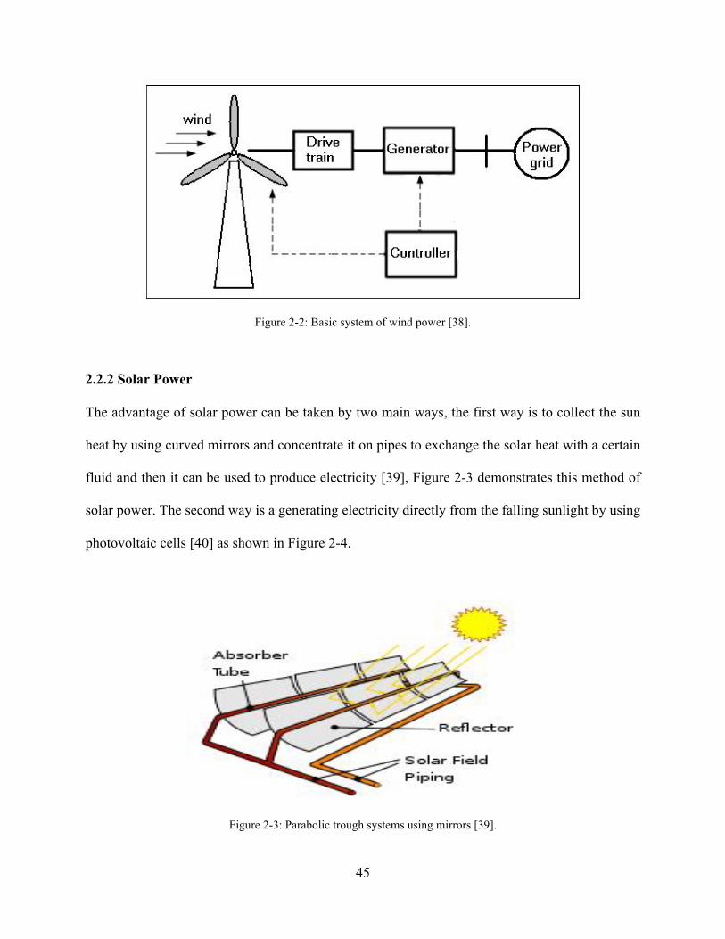
45
Figure 2-2: Basic system of wind power [38].
2.2.2 Solar Power The advantage of solar power can be taken by two main ways, the first way is to collect the sun
heat by using curved mirrors and concentrate it on pipes to exchange the solar heat with a certain
fluid and then it can be used to produce electricity [39], Figure 2-3 demonstrates this method of
solar power. The second way is a generating electricity directly from the falling sunlight by using
photovoltaic cells [40] as shown in Figure 2-4.
Figure 2-3: Parabolic trough systems using mirrors [39].

46
Figure 2-4: PV panels to generate electricity directly from the sunlight [40].
2.2.3 Hydropower The way of producing electric power from the potential energy of stored water in dams and water
falls is called hydropower system. This system uses water turbines to generate the power as shown
in Figure 2-5. Figure 2-6 shows another way which is putting water wheels that is linked to turbines
in fast flowing rivers to generate electricity without building water reservoirs or dams [41].

47
Figure 2-5: Hydro power [41]
Figure 2-6: Using water wheels to produce power [41].
2.2.4 Biomass Plants capture the energy from the sun through the photosynthesis phenomenon. Later on these
plants under special circumstances can release that stored energy at special circumstances. Number

48
of methods are used to generate bioenergy from the organic wastes, see Figure 2-7. This helps
environment to be a clean by waste disposal in addition to solve energy problem [42]. Also the
compost, which is useful for soil, can be used for bio refinery process.
Figure 2-7: Process flow diagram of Bio-Refinery [42].
2.2.5 Geothermal The word “Geothermal” is integrated of two Greek words which are geo (earth) and thermal (heat).
The harnessing of heat from underground sources is called “geothermal energy”. The required heat
flow temperatures for geothermal power generation are ranged between 212 °F and 482 °F
[43]. The used technologies contain plants of dry steam power, flash steam power, and binary cycle
power, as indicated in Figure 2-8. The current capacity installed in the world is 11 GW where
America, Philippines and Indonesia occupy the largest proportion [37]. Geothermal power could
be considered as a sustainable due to the small amount of the extracted heat in comparison of
Earth's heat content. The average of CO2 emitted from the existing geothermal electric plants is
122 kg per megawatt-hour (MW/h) of electricity, which is much less than that of fossil fuels plants
[44].

49
Figure 2-8: Dry steam power plant using geothermal energy [43].
2.2.6 Wave Power Wave power is the energy that is resulted from the ocean surface motion. Wave power can be
captured by using some machines such as Pelamis which is shown in Figure 2-9. This energy also
can be used for electricity generation, water desalination, or the pumping of water into reservoirs.
Machines able to exploit wave power are usually called wave energy converter (WEC). Wave
power is currently used in Portugal and the United Kingdom [41].

50
Figure 2-9: Pelamis Wave Power [41]
2.3 Solar-Photovoltaic Energy
2.3.1 Global spread of photovoltaics Unlike energy generated by hydro and wind, solar energy is not restricted by geography. In fact,
solar energy can be generated in most areas of the world. Photovoltaics are also spreading world-
wide, as they are proving to be the best means of producing solar-generated electricity. Figure
2-10 displays renewable energy growth rates in the year of 2015. It is clear that, photovoltaics
experienced the fastest growth compared to alternative renewable energy resources, while Figure
2-11 shows that the global capacity of photovoltaics nearly doubled within three years [37].

51
Figure 2-10: Average annual growth rates of renewable energy capacity and bio-fuel’s production in 2015 [37].
Figure 2-11: Solar PV existing world capacity 2005-2015 [37].
2.3.2 PV system benefits Photovoltaic systems have several benefits over other systems [40], as explained below:
1- PV systems are pre-packaged and installment-ready. Furthermore, because the modules are free
of moving parts, they require no serious maintenance.
2- The systems come in a different sizes and outputs, which make them operable across a range of
applications. Moreover, because PV systems are relatively light, transportation is not an issue.

52
3- The systems can expand simply by including additional modules. This can be done either in
parallel (i.e., to strengthen the current) or in series (i.e., to strengthen the voltage).
4- The system modules can handle excessive climatic conditions, such as extreme temperatures
(hot or cold) and strong winds. They can also withstand excessive amounts of atmospheric
moisture as well as salt. Furthermore, even in sunless conditions (e.g., night time or inclement
weather), PV systems continue to function due to their storage capabilities, which enable them to
generate consistent high-quality power with or without sunshine.
5- The systems are free of noise and carbon emissions, meaning they do not pollute.
Despite their many benefits, PV systems still have a few disadvantages, as follows:
1- Compared to alternative renewable resources, PV systems are quite expensive to produce.
2- There are still issues regarding maximum power point.
3- The systems must remain as free as possible from dust, thus requiring regular cleaning.
4- The systems are still relatively inefficient.
2.3.3 PV cell types Photovoltaic cells are produced in a variety of types, each of which has different benefits. Below
is a list of the most common forms of PVs [40].
1-Mono-crystalline (single crystalline) cells:
As shown in Figure 2-12, these types of cells derive from a single crystal of silicon and are quite
smooth in texture. Although they are the most efficient of the PV cells, mono-crystalline cells are
also the most costly to manufacture.

53
2-Poly-crystalline (multi-crystalline) cells:
As their name implies, polycrystalline cells are several crystals combined. As shown in Figure
2-13, they are cut from a block of silicon. Although PV solar panels made from poly-crystalline
cells types are less efficient than mono-crystalline cells, they are less expensive.
3-Amorphous cells:
As demonstrated in Figure 2-14, amorphous cells are produced by setting a thin film of non-
crystalline (i.e., amorphous) silicon on top of different surfaces. Of the three types of PV cells
listed here, amorphous cells provide the least efficient type of photovoltaic solar panels, but they
are also the least expensive to produce and have the characteristic of making PV panes flexible.
Figure 2-12: Mono-crystalline PV cell [40].

54
Figure 2-13: Poly-crystalline PV cell [40].
Figure 2-14: Non-crystalline (amorphous) PV cell [40].
2.4 Different Photovoltaic Systems
2.4.1 Stand-alone systems These kinds of systems are made up of an inverter (for DC to AC conversion), a PV panel, and a
battery bank for storage [45] [46]. Stand-alone systems, as pictured in Figure 2-15, are most
suitable for areas featuring limited energy requirements and readily available solar insulation. They
can also be aligned with a fossil fuel-generating system, enabling the generator to re-charge the

55
PV battery in extended periods of darkness or cloudy weather. The hybrid system lengthens the
life of the battery while requiring reduced amounts of generator fuel and maintenance.
Figure 2-15: Stand-alone PV system [45].
2.4.2 Grid-connected systems As shown in Figure 2-16, grid-connected systems feature PV solar modules that supply electrical
power through a high quality inverter and, unlike stand-alone systems, are directly connected to
power lines. The inverter in grid-connected systems changes PV-generated DC to AC [47]. It is
worth noting that generating stations based on PV modules are also considered grid-connected
systems, as they produce a large amount of power, which they then add to the grid power.

56
Figure 2-16: Grid-connected PV system [47].
Generally speaking, grid-connected systems are known to have higher potential than stand-alone
systems because grid-connected users can, for a price, off-load to a utility any electricity they are
not using. Then, if they have a shortage, they can make use of the utility’s supply.
2.4.3 PV system features Photovoltaics exhibit non-linear features, meaning that both output power and performance are
significantly impacted by any alterations in operating conditions such as solar irradiance, moisture
levels, and temperature. In Figure 2-17, we can see the impact of fluctuations in solar irradiance
and temperature on output current, voltage and power [47].

57
Figure 2-17: (a) An effect of solar irradiance changes on I-V curves and an effect of temperature changes on I-V
curves [47].
Figure 2-18: (a) An effect of solar irradiance changes on P-V curves and an effect of temperature changes on P-V
curves [47].
As shown in the above Figures, the PV’s output power is proportional to the received solar
irradiance while being inversely proportional to temperature. However, when changes occur in
temperature and solar irradiance, the point of maximum power likewise changes (see Figure 2-18).
When this happens, the maximum power point needs to be tracked by using DC-DC converters to

58
vary array terminal voltage. Chapter 3 discusses some common approaches used for tracking
maximum power point.
2.5 Equivalent circuit and mathematical model
A modified step-by-step process for photovoltaic (PV) module simulation using MATLAB/
Simulink is presented in this work. To explore the I-V and P-V features of a typical 260 watts
monocrystalline solar panel, a single-diode equivalent circuit is used. However, it is essential first
to characterize a circuit-based simulation model for a PV cell prior to permitting any interaction
with a power converter. The study demonstrates that PV cells are significantly impacted by factors
such as temperature and solar irradiation. Furthermore, the study results show that the simulation
blocks developed in MATLAB/Simulink function similarly to real PV modules, such that the PV
module’s behavior can be accurately estimated in terms of ambient temperature and solar
irradiance intensity, along with other designated design parameters. By modifying the stated
parameters, graphs are developed of I-V and P-V [47].
2.5.1 Nomenclature Vpv: PV module (V) output voltage
Voc: Open circuit voltage
Isc: Short circuit current
Ipv: PV module (A) output current
Tr: reference temperature, such that 298 K, T is the module operating temperature (in Kelvin)
Iph: PV module (A) light-generated current
Is: PV module saturation current (A)
A = B = ideality factor = 1.6
K: Boltzman constant (1.3805´10-23 J/K)

59
q: Electron charge (1.6´10-19 C)
Rs: PV module series resistance
Iscr: PV module short-circuit current (25o C and 1000W/m2 = 17A)
Ki: short-circuit current temperature coefficient (Iscr = 0.0017A / oC)
λ: PV module illumination (W/m2) (1000W/m2)
Ego: band gap for silicon (1.1 eV)
Ns: number of cells connected in series
Np: number of cells connected in parallel [48].
2.5.2 Mathematical Model of a Photovoltaic Module Through the PV effect, electromagnetic radiation from solar energy can be changed into electricity.
When exposed to sunlight, photons with more energy than the semi-conductor’s band-gap energy
make electron-hole pairs that are proportional to the incident irradiation. A solar cell is essentially
a p-n junction set on a thin wafer of semiconductor. Figure 2-19 shows the equivalent circuit of a
PV cell.
R
IRs
RpIph
IDV
Figure 2-19: PV cell modelled as diode circuit [48].
As shown, the current source, Iph, represents the cell photocurrent, Rsh represents the cell’s
intrinsic shunt resistances, while Rs represents the cell’s series resistances. Typically, the Rsh
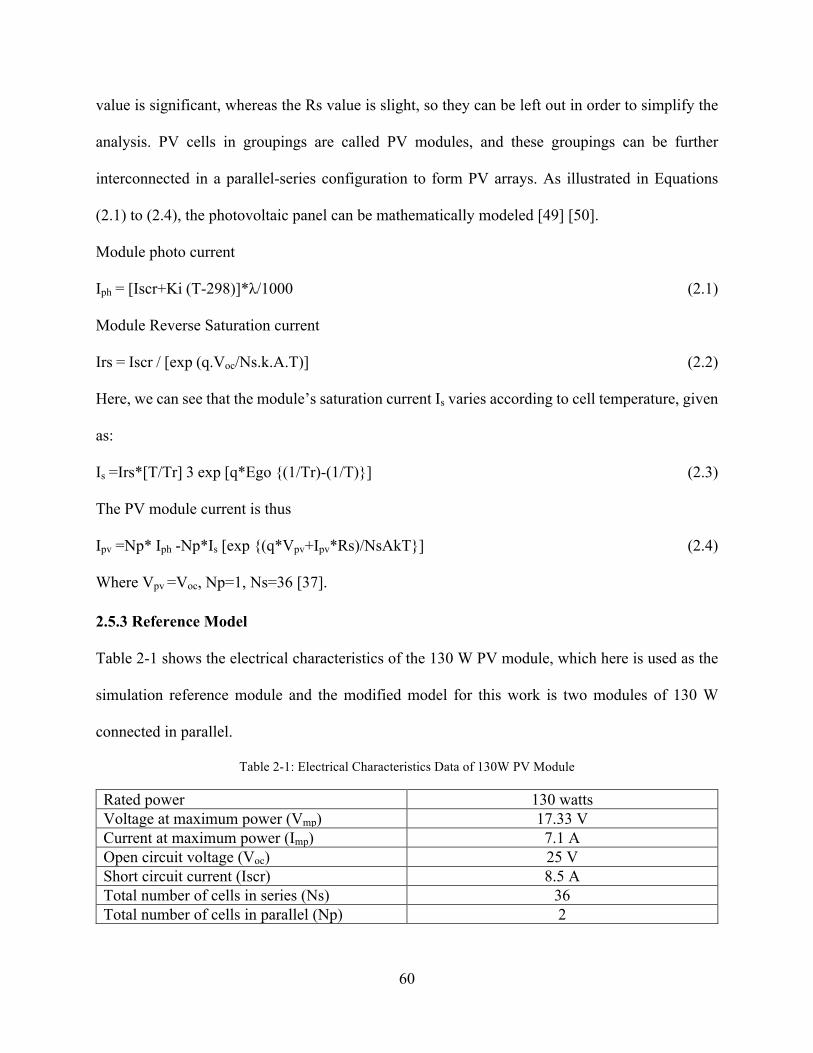
60
value is significant, whereas the Rs value is slight, so they can be left out in order to simplify the
analysis. PV cells in groupings are called PV modules, and these groupings can be further
interconnected in a parallel-series configuration to form PV arrays. As illustrated in Equations
(2.1) to (2.4), the photovoltaic panel can be mathematically modeled [49] [50].
Module photo current
Iph = [Iscr+Ki (T-298)]*λ/1000 (2.1)
Module Reverse Saturation current
Irs = Iscr / [exp (q.Voc/Ns.k.A.T)] (2.2)
Here, we can see that the module’s saturation current Is varies according to cell temperature, given
as:
Is =Irs*[T/Tr] 3 exp [q*Ego {(1/Tr)-(1/T)}] (2.3)
The PV module current is thus
Ipv =Np* Iph -Np*Is [exp {(q*Vpv+Ipv*Rs)/NsAkT}] (2.4)
Where Vpv =Voc, Np=1, Ns=36 [37].
2.5.3 Reference Model Table 2-1 shows the electrical characteristics of the 130 W PV module, which here is used as the
simulation reference module and the modified model for this work is two modules of 130 W
connected in parallel.
Table 2-1: Electrical Characteristics Data of 130W PV Module
Rated power 130 watts Voltage at maximum power (Vmp) 17.33 V Current at maximum power (Imp) 7.1 A Open circuit voltage (Voc) 25 V Short circuit current (Iscr) 8.5 A Total number of cells in series (Ns) 36 Total number of cells in parallel (Np) 2

61
The test condition electrical specifications are: cell temperature at 25°C; spectrum at 1.5 air mass;
and irradiance at 1 kW/m2.
2.5.4 Model Process Based on the Shockley diode equation, we consider a model of a moderately complex PV module
which features series resistance, diode saturation current, and temperature independence from the
photocurrent source. After receiving sunlight radiation, the PV cell changes a portion of the PV
potential into electricity with I-V and P-V output features. Next, the Simulink model is constructed
using the following steps as well as the equations given in section (2.5.2) of this work:
2.5.4.1 (Converting operating temperature from Celsius to Kelvin) Figure 2-20 shows the model that changes the operating temperature (in degrees) of the module
from Celsius to Kelvin [49].
Figure 2-20: The model of changing the operating temperature of the module from Celsius to Kelvin.

62
2.5.4.2 (Calculating of PV module (A) light-generated current) Figure 2-21 illustrates a model that features the following inputs: Insolation: (G / 1000) 1 kW/ m2
= 1; module operating temperature: Tak = 30 to 70°C; module reference temperature: Trk = 25°C;
and short-circuit current (Isc): reference temp = 17 A to calculate Iph [49].
Figure 2-21: Calculating of light-generated current.
2.5.4.3 (Deriving of short-circuit current) Figure 2-22 below, adopts the short-circuit current, Isc, and uses as inputs at reference temperature
of Iscr =17A and a module reference temperature of Trk = 25°C to calculate Irs [50].
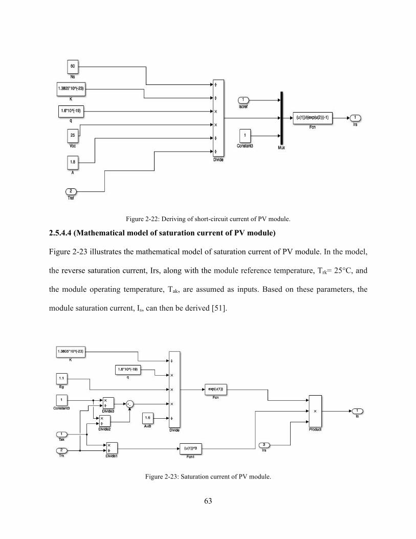
63
Figure 2-22: Deriving of short-circuit current of PV module.
2.5.4.4 (Mathematical model of saturation current of PV module) Figure 2-23 illustrates the mathematical model of saturation current of PV module. In the model,
the reverse saturation current, Irs, along with the module reference temperature, Trk= 25°C, and
the module operating temperature, Tak, are assumed as inputs. Based on these parameters, the
module saturation current, Is, can then be derived [51].
Figure 2-23: Saturation current of PV module.

64
2.5.4.5 (Producing the NsAkT term of PV module ) In Figure 2-24 below, the operating temperature in Kelvin Tak is first taken, after which the product,
NsAkT, is calculated using the exponential function denominator from equation (2.4). In Figure
2-24 below presented the calculation of NsAkT [51].
Figure 2-24: Producing the NsAkT of the PV module.
2.5.4.6 (PV module (A) output current Ipv)
The model in Figure 2-25 applies the approach demonstrated in equation (2.4), using the function
equation listed below to determine Ipv [51].
Ipv = u (3)-u (4)*(exp ((u (2)*(u (1) +u (6)))/ (u (5)))-1) (2.5)

65
Figure 2-25: Generating PV module output current by using equation (2.4).
2.5.4.7 (Extracting of Ipv, Vout, Ppv of PV module) As demonstrated in Figure 2-26, all 6 models featured above are interconnected in order to extract
Ipv,Vout and Ppv.
Figure 2-26: The output current, voltage and power of PV module.

66
The modified model presented in this work assumes that voltage, current and power are all outputs
of the subsystem PV module. The final PV model is illustrated in Figure 2-27 below and the
manufacturer-supplied model modifying parameters are set using the dialogue box shown in figure
2-28 as well. In addition, in this modeling the values of A were assumed as 1.2, 1.5 and 1.8.
Figure 2-27: Actual proposed PV model.
Figure 2-28: Simulink PV module model mask dialog box

67
2.6 Model Validation
Manufacturer-supplied data for the 260 watt mono crystalline solar panel module enabled us to
validate the model, with Table 1 providing the module’s electrical characteristics [52]. As can be
seen in Figure 2-29, the supplied data match the I-V characteristics of the model, while in Figure
2-30, we can see the power-voltage (P-V) curves under several different solar radiation levels and
ambient temperatures. From these data, it is clear that the simulated model is sufficiently accurate
[52].
Figure 2-29: Manufacturer-supplied (a) V-I and P-V curves at different irradiance and 250 C temperature, (b) V-I
and P-V curves at 1000W/m2 and different temperatures

68
Figure 2-30: (a) Different solar radiation at 250 C and (b) different irradiance at 450 C of PV module power-voltage
curves
2.7 Conclusion
A photovoltaic module was modeled in MATLAB/Simulink. When the results of the simulation
were compared to the manufacturer-supplied data, they were discovered to be similar. Hence, we
propose that the model is sufficiently detailed and thus could be used to model any type of solar
panel by using information given in the manufacturer’s data sheet. The model was then used in
Chapter 4 to develop an entire MPPT model based fuzzy control.

69
Chapter 3
3. DC-DC Converters and Maximum Power Point Tracking This chapter considers the topologies of three basic converters; buck, boost and buck-boost
converter. Each of these is used to identify the most suitable topology for PV module maximum
power point tracking performance. From this, a model of the most suitable topology will be
generated and this model will be used for a number of simulations aimed at identifying the impact
of component non-idealities on the output voltage and efficiency of the converter. The results of
these simulations can be used to select converter components and develop control strategies with
the model of the converter forming the main section of a complete MPPT model used for fuzzy
logic controller tuning.
3.1 DC-DC Converters
The diagram shown in Figure 3-1 is a typical DC-DC converter that converts DC input voltage
(vg(t)) to a different level of DC output voltage (vo(t)) [53]. One desirable outcome is that the
conversion results in low losses from the converter. As such, Figure 3-2 shows the control signal
δ (t) is held for a given time ton (high) and toff (low).
Figure 3-1: DC-DC converter structure [53].

70
The voltage across the transistor is low when it is switched on, thereby causing low power loss
from the transistor itself. Power loss is also low while the transistor is switched off as the current
passing through it is low. The pulse width is used to control the average voltage output with the
switching period Ts remains constant. The real value in the interval 0 to 1 is the duty cycle d(t),
which is equal to the width of a pulse to switching period ratio [53].
Figure 3-2: d (t), the transistor control signal [53].
Resistors are avoided in DC-DC converters in order to reduce losses. Instead, inductors and
capacitors are utilised as in ideal situations, their use will result in no losses. There are many
different ways, or topologies, in which the electrical components can be connected and combined,
with each resulting in differing properties. The three basic converter topologies are the buck-boost,
buck and boost types. Buck converters generate a lower output voltage than the input voltage,
boost converters generate a higher output voltage than the input voltage and buck-boost systems
are able to do both.
3.2 Maximum Power Point Tracking
A photovoltaic (PV) modules power is very much dependent on the connected load’s operating
voltage as well as the temperature of the cell and the level of solar radiation. By connecting a

71
variable load resistance R across the terminals of the module, one can determine the operating
point from the load I-V characteristic and the module I-V curve intersection. The operating
characteristic of a PV module is displayed in Figure 3-3, which shows that there are two zones;
the region of current source is Zone I whilst the region for voltage source is Zone II. There is high
internal impedance of the module in Zone I whilst the converse is true for Zone II. The knee of the
power curve is the point of maximum power Pmp. An increase in short-circuit current results from
an increase in temperature at constant solar radiation, which results in a decrease of internal
impedance. This is due to the decrease in open circuit voltage. When load impedance and source
internal impedance are equal, power delivery to the load in maximised in accordance with the
maximum power transfer theory. The characteristic of load can be determined by the straight line
slope of I/V = I/R. When the module behaves as a constant source of current at values close to Isc
in the AB region only, R is small. Conversely, when the module acts as a constant voltage source
as values close to Voc in the CD region, then R is large [53].
Figure 3-3: Maximum power point tracking of a PV module [53].
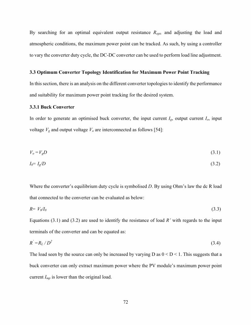
72
By searching for an optimal equivalent output resistance Ropt, and adjusting the load and
atmospheric conditions, the maximum power point can be tracked. As such, by using a controller
to vary the converter duty cycle, the DC-DC converter can be used to perform load line adjustment.
3.3 Optimum Converter Topology Identification for Maximum Power Point Tracking
In this section, there is an analysis on the different converter topologies to identify the performance
and suitability for maximum power point tracking for the desired system.
3.3.1 Buck Converter In order to generate an optimised buck converter, the input current Ig, output current Io, input
voltage Vg and output voltage Vo are interconnected as follows [54]:
Vo =VgD (3.1)
I0= Ig/D (3.2)
Where the converter’s equilibrium duty cycle is symbolised D. By using Ohm’s law the dc R load
that connected to the converter can be evaluated as below:
R= V0/I0 (3.3)
Equations (3.1) and (3.2) are used to identify the resistance of load R’ with regards to the input
terminals of the converter and can be equated as:
R’ =RL / D2 (3.4)
The load seen by the source can only be increased by varying D as 0 < D < 1. This suggests that a
buck converter can only extract maximum power where the PV module’s maximum power point
current Imp is lower than the original load.

73
3.3.2 Boost Converter The average output and input voltage and current values for an optimised boost converter are as
follows:
Vo = Vg / (1-D) (3.5)
Io = Ig (1 – D) (3.6)
The input side’s load resistance R’ is expressed as:
R’ = R (1− D)2 (3-7)
The load seen by source can only be decreased by varying D as 0 < D < 1. As such, a boost
converter’s tracker would only be able to extract maximum power when the PV module’s
maximum power point current Imp is higher than the original load (Zone I of Figure 3.3).
3.3.3 Buck-Boost Converter The averaged output and input voltage and current values for an optimised buck-boost converter
are as follows [54]:
Vo = Vg `
Ia` (3.8)
Io = Ig Ia`
` (3.9)
The input side’s load resistance R’ is equated as:
R’ = R Ia`
`2 (3.10)
As such, the load seen by the source can be decreased or increased by varying D as 0 < D < 1.
Therefore, the buck-boost converter can operate successfully in either Zones I or II. As a
conclusion from the previous analysis, it can be seen that the optimised buck-boost converter has
better performance than the other two topologies as maximum power point tracking can be
performed in both Zones shown in Figure 3-3. The next section sees the development of a state
space converter model [54].

74
3.4 Buck-Boost Converter Model
Figure 3-4 shows a buck-boost converter circuit, which consists of four main components; the
capacitor C, inductor L, diode T and transistor Q. It is necessary to consider some of the non-ideal
components of this system when modelling. Therefore, it commences with a model of a resistance
RL in series with an ideal inductor. This is followed by a resistance RC being modelled in series
with an ideal capacitor and RL and RC can be used as power loss indicator from the inductor and
capacitor, respectively. The diode has a forward voltage drop VT and there is an on-site resistance
on the transistor Rt. The converter can be utilised in up to three modes. The following subsection
details the state space of each mode [54].
Figure 3-4: A buck-boost converter circuit [54].
3.4.1 Mode 1 When the control system δ (t) is high, this mode is valid for the specific time interval given by (0
< t < ton). There is no conduction from the reverse biased diode when the transistor is on. The buck-
boost converter model is shown as ton in the circuit diagram given in Figure 3-5.

75
Figure 3-5: The boost converter circuit diagram during ton [54].
The following equations can be derived from the model by applying of Kirchhoff’s laws:
bc \ = d)ef(C)
)C= b[ \ − gc \ hC + hc (3.11)
gi \ = j)kl(C)
)C= −
kl C
202l (3.12)
bE \ = −2
202lbi \ (3.13)
g[ \ = gc \ (3.14)
Re-arranging Equations (3.11) and (3.12) gives,
)ef(C)
)C= −
2Y02fc
gc \ +I
cb[(\)
(3.15)
)k=(C)
)C= −
I
i 202lbi \
Equations (3.13), (3.14), and (3.15) are of the form:
m \ = nIm \ +oI!(\)

76
p \ = jIm \ +qI! \ (3.16)
Where,
m \ =gc \bi(\)
(3.17)
! \ = b[ \B6
(3.18)
p \ = bE \g[(\)
(3.19)
nI = −2Y02fc
0
0I
i(202l)
(3.20)
oI = I
c0
0 0 (3.21)
jI = 0 −
2
202l
1 0 (3.22)
q = 0 (3.23)
3.4.2 Mode 2 This mode is valid for the time interval (ton < t < ton + ϑt), where ton + ϑt < Ts, and ¶t is the time
when the inductor current is zero. In this mode, the transistor is OFF and the diode is ON (provided
iL(t) > 0). Therefore, the validity of time interval for this mode can be rearranged as (ton < t < Ts)
if (iL(t)) does not vanish. When the transistor is OFF, the voltage across the diode is the forward
voltage drop VT. The circuit in Figure 3-6 can therefore be used as a model of the buck-boost
converter during toff, for the continuous conduction mode (CCM) [54].

77
Figure 3-6: Circuit of the buck-boost converter during toff (CCM) [54].
Applying Kirchhoff’s laws, the following equations are obtained from the model:
bc \ = d)ef(C)
)C= −hcgc \ +higi \ +bi \ −B6 (3.24)
gi \ = −2
202lgc \ −
I
202lb7(\) (3.25)
bE \ = −bi(\) − gi(\)hi (3.26)
g[ \ = 0 (3.27)
The following state space model is obtained from equations (3.24) to (3.27)
m \ = nsm \ +os!(\)
(3.28)
p \ = jsm \ +qs! \
Where,
ns = −I
c hc +
22l202l
2
c(202l)
−2
i(202l)−
I
i(202l)
(3.29)

78
os = 0 −
I
c
0 0 (3.30)
js = 22l202l
−2
202l
0 0 (3.31)
E2 = E1. (3.32)
3.4.3 Mode 3 Whenever it exists, this mode is valid for the time interval (ton + ϑt < t ≤ Ts). The mode sees the
no conduction from the diode and the transistor is OFF, equated as iL(t) = 0. Therefore, Figure 3-
7 shows a circuit that can be used in the discontinuous conduction mode (DCM) as a buck-boost
converter model during toff.
Figure 3-7: The buck-boost converted circuit diagram during toff (DCM) [54].
The mode’s circuit functioning is described as:
gc \ = 0 (3.33)
gi \ = j)kl(C)
)C=
I
202lbi \ (3.34)
79
bE \ = −2
202lbi(\) (3.35)
g[ \ = 0 (3.36)
Equations (3.33) to (3.36) provide the corresponding standard state space model given as:
m \ = ntm \ +ot!(\)
(3.37)
p \ = jtm \ +qt! \
Where,
nt = 0 00
I
i(202l) (3.38)
ot = 0 (3.39)
jt = 0 −
2
202l
0 0 (3.40)
E3 = E1. (3.41)
3.5 Averaging model of Buck-Boost Converter
The converter as a linear time invariant system is represented by the averaged converter model by
disregarding the switching dynamics. As such, the state space averaging method is applied to the
state space model to generate the average converter model.
3.5.1 The State Space Averaging Model During a switching period the converter effectively switches between two linear time invariant
systems, but only in the converter’s natural frequencies and the converter input variations are
slower than the frequency of switching. When the transistor is on or off or the inductor current is
at zero, the converter acts as different time-invariant systems. Accordingly, the converters are able
to switch between time invariant periods between each switching period. Therefore, the converter

80
is effectively a time-varying system model. To estimate this time-varying system with a linear
continuous-time time-invariant system, a state space averaging [55] can be used. By using each
state-space time invariant system description as a starting point, the mean of the state space
descriptions can then be calculated with regards to their switching period duration. Most models
are time invariant and non-linear and has the duty cycle control signal as d(t) instead of δ (t). The
equation to describe the averaged state space model for a converter is given as [56]:
m = nm + ou , v = jm + qu (3.42)
The average matrices are described as:
n = wInI + wsns + wtnt
o = wIoI + wsos + wtot
j = wIjI + wsjs + wtjt
q = wIqI + wsqs + wtqt (3.43)
The switching period fractions are given as D1, D2 and D3 when the converter is operating in
modes 1, 2 and 3 respectively. The DC equilibrium components are:
m = DcBi
(3.44)
u =B[B6
(3.45)
v = BED[
(3.46)
The averaged vector’s equilibrium values are given in equations (3.44) to (3.46), where VC is the
capacitor voltage, Vg is the input voltage, IL is the inductor current, Ig is the input current, VT is
the diode forward conduction voltage drop and VO is the output voltage. By solving equation
(3.42), the output vectors and equilibrium state can be found:
m = naIou

81
v = −jnaIo + q u (3.47)
Equation (3.47) shows that averaged DC converter model. The buck-boost converter can also have
the principles of state-space averaging applied to generate the averaged DC model. By assuming
that the converter operates in the continuous conduction mode, the duty cycle notations can be
redefined as:
w =wI.
ws = 1 − w = w`.
wt = 0. (3.48)
3.5.2 Converter Averaged Model By applying equations (3.43) and (3.48) to those given in sections (3.4.1) and (3.4.2) they generate:
n = −I
c(hc + whC +
``22l202l
)``2
c(202l)
−``2
i(202l)−
I
i(202l)
(3.49)
o = `
c−``
c
0 0 (3.50)
j = ``022l202l
−2
202l
w 0 (3.51)
E = 0. (3.52)
By expanding equation (3.42) when m = 0, we can obtain the DC equations [55] [56]:
0 = −I
cwhC + hc +
``22l202l
Dc +``2
c 202lBi +
`
cB[ −
``
cB̀ (3.53)
0 = −``2
i(202l)Dc −
I
i(202l)Bi (3.54)
BE =``22l202l
Dc −2
202lBi (3.55)
D[ = wDc (3.56)

82
By simplifying equation (3.54) we get:
VC = −D` IL R (3.57)
Simplifying and substituting equation (3.57) into (3.55) we get:
Vo = −VC (3.58)
Rearranging and substituting equations (3.57) and (3.58) into (3.53) gives:
/</z=
`
``
(Ia{`L{{Lz
)
|f}{|Y{`O|
0~
{`O(~}||l
)0
~
(~}|l| )
(3.59)
By assuming ideal components in:
Rt =RL= VT = 0,
We can reduce equation (3.59) to:
/</z= −
`
``(I0|f{`O|
) (3.60)
The average power converter efficiency is given as:
P =/<1</z1z
=(Ia
{`L{{Lz
)
|f}{|Y{`O|
0~
{`O(~}||l
)0
~
(~}|l| )
(3.61)
Assuming Rt =RL= VT = 0, we can reduce equation (3.61) to:
P =I
I0|f{`O|
(3.62)
3.5.3 Buck-Boost Converter Simulink Model Using the Simulink/MATLAB block as shown in Figure 3-8, we can identify the average converter
model. Equations (3.49) to (3.52) describe the state space average model that has an s-function
code. Figure 3-9 shows the selected components parameters of buck-boost converter with the
modified solar panel. Vg input voltage, R load resistance, D duty cycle are the model inputs while
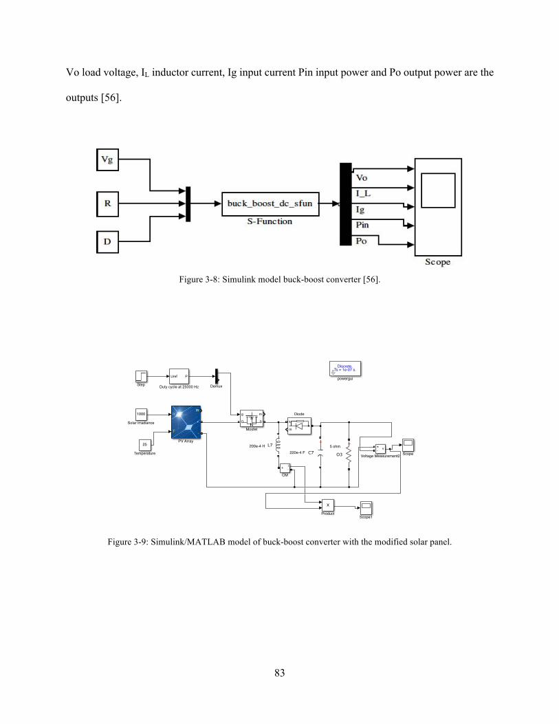
83
Vo load voltage, IL inductor current, Ig input current Pin input power and Po output power are the
outputs [56].
Figure 3-8: Simulink model buck-boost converter [56].
Figure 3-9: Simulink/MATLAB model of buck-boost converter with the modified solar panel.
200e-4 H220e-4 F
5 ohm +
O3
+
L7 +
C7
Ir
T
mm
+
-
PV Array
1000
Solar irradiance
25
Temperature
Uref P
Duty cycle at 25000 Hz Demux
v+-
Voltage Measurement2 Scope
ma
k
Diodeg m
D S
Mosfet
Discrete,Ts = 1e-07 s.
powergui
i+ -CM
ProductScope1
Step

84
3.6 Results of Simulation
Several values of RL/R are plotted from equation (3.60) in Figure 3-10 in order to visualise the
inductor resistance effect on voltage output based on the modified converter. There are two terms
in equation (3.60), which are –D/w` signifying the optimised conversion ration where RL=0 and
1/(1 +2f``O2
) signifies the inductor winding resistance effect. If w`sh is higher than RL then the
second term identifies unity and there is an equality between the conversion ratio and the ideal
value –D/w`. Conversely, where w`sh is lower than RL then there is a decrease in the second term
resulting in a decrease in Vo/Vg. The inductor winding resistance causes a specific effect on the
curve for Vo/Vg when the duty cycle D approaches unity. The curve tends towards zero rather than
approaching affinity at D=1.This is because the inductor is not connected to the output, therefore
there is no transference of output at D=1 therefore, output voltage is zero. There is a rapid increase
in inductor current that only the inductor resistance RL can limit. The inductor winding resistance
causes the loss of a lot of power and no delivery to the load. Therefore, as D approaches unity,
converter efficiency tends towards zero.
Several values of RL/R are plotted from equation (3.62) to Figure 3-11 in order to
demonstrate the converter efficiency impacts from inductor resistance. To obtain high efficiency,
equation (3.62) shows that w`sh will be higher than RL. Where w` is close to unity in a low duty
cycle, this is easier to attain whilst w` approaching zero in a high duty cycle makes it more difficult.
This is shown in Figure 3-11 where high efficiency can be seen at low duty cycles but there is a
rapid decrease in efficiency towards zero where D=1.

85
Figure 3-10: Buck-boost converter output voltage inductor resistance effects
Figure 3-11: Buck-boost converter efficiency inductor resistance effect
3.7 Conclusion
This chapter has studied the application of DC-DC converters in PV module maximum power
point tracking. The most suitable topology was the buck-boost converter as this allowed maximum
power tracking. As such, a model of the converter was generated before considering the effects of
non-ideal components and setting duty cycle limits on converter efficiency.

86
Chapter 4
4. Fuzzy Logic Controller Design and System Simulation This chapter studies the application of fuzzy logic control as algorithm for a maximum power point
tracking of photovoltaic system. Also the design and performance of the fuzzy system was tested
in Simulink/MATLAB with PV module and buck-boost converter and the rules of fuzzy logic
were formulated and validated. Finally, the results in this section were useful to be implemented
in the real fuzzy control system on actual hardware which is presented in next chapter.
4.1 Design of Fuzzy Logic Controller Parameters
4.1.1 PV Module with MPPT based Fuzzy Logic Controller Figure 4-1 illustrates the basic diagram of a fuzzy logic based maximum power point tracker. It
can be seen from the observation that the only two state variables are sensed as inputs of fuzzy
controller; output voltage and output current of PV module (Vm) and (Im). The fuzzy logic
controller, from measurements, gives a signal proportional to the converter duty cycle (D) which
is fed to the converter through a pulse width modulator. This modulator drives the value of D to
perform Pulse Width Modulation (PWM) that generates the control signals for the converter switch
(s). The fuzzy logic controller scheme is defined a closed loop system [57].

87
Figure 4-1: Fuzzy control scheme for a maximum power point tracker [58].
4.1.2 Fuzzy controller structure Fuzzy logic controller structure is based on fuzzy sets where a variable is a member of one or
more sets with a specified degree of membership. Benefits of using Fuzzy logic are; it allows us
to emulate the human reasoning process in computers, quantify imprecise information, make
decision based on vague information such as resistive load is connected to the PV module
through the buck boost dc-dc converter [58]. The block diagram of MPPT based fuzzy logic
control is shown in Figure 4-2 [57].
Figure 4-2: Block diagram of the fuzzy logic algorithm.

88
Also, Figure 4-3 illustrates the basic architecture of fuzzy controller which contains of the three
following blocks [59]:
4.1.2.1 Fuzzification Each input/output variable in the fuzzy logic controller is required which define the control surface
that can be expressed in fuzzy set notations using linguistic levels. Each input and output variables
of linguistic values divide its universe of discourse into adjacent intervals to form the membership
functions. The member value represents the extent at which a variable belongs to a particular level.
The converting of input/output variable process to linguistic levels is named as Fuzzification.
4.1.2.2 Inference A set of rules are used to governor the behavior of the control surface which relates the input and
output variables of the system. A typical rule would be:
If x is A THEN y is B.
Each of the rules that has any degree of truth in its premise, when a set of input variables are read,
a rule is fired and contributes to the forming of the control surface by approximately modifying it.
Then, when all the rules are fired that resulting control surface. It is expressed as a fuzzy set to
represent the constraints output. This process is called inference.
4.1.2.3 Defuzzification Defuzzification is known as the process of conversion of fuzzy quantity into crisp quantity. There
are many methods available for Defuzzification. The most common one is centroid method, which
illustrated by the following formula:
'(S S))S
'(S))S (4.1)
Where µ is the membership degree of output x.
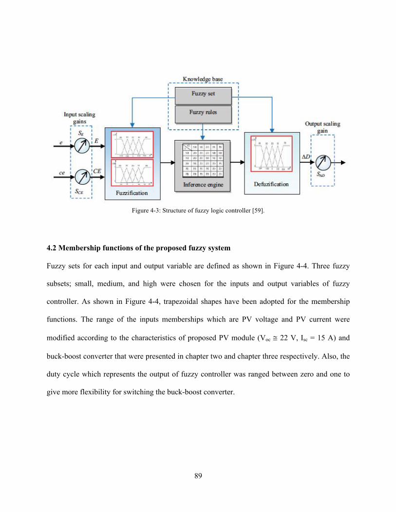
89
Figure 4-3: Structure of fuzzy logic controller [59].
4.2 Membership functions of the proposed fuzzy system
Fuzzy sets for each input and output variable are defined as shown in Figure 4-4. Three fuzzy
subsets; small, medium, and high were chosen for the inputs and output variables of fuzzy
controller. As shown in Figure 4-4, trapezoidal shapes have been adopted for the membership
functions. The range of the inputs memberships which are PV voltage and PV current were
modified according to the characteristics of proposed PV module (Voc @ 22 V, Isc = 15 A) and
buck-boost converter that were presented in chapter two and chapter three respectively. Also, the
duty cycle which represents the output of fuzzy controller was ranged between zero and one to
give more flexibility for switching the buck-boost converter.

90
(a) (b)
(c)
Figure 4-4: Membership functions for (a) input current of converter (b) input voltage of converter (c) output duty cycle of fuzzy controller.
4.2.1 Derivation of Control Rules Fuzzy control rules are extracted by analyzing the system behavior. The different operating
conditions are considered in order to improve tracking performance in terms of dynamic response
and robustness. The algorithm can be explained as follows:
The tracking process is started with an initial duty cycle, D= 0. The converter input current Im,
and voltage Vm, are then measured and sense the duty cycle that can give maximum power output
of the converter at that time based on predicted values that have already been entered into fuzzy

91
system. This operation repeats itself continuously until the power reaches the maximum value and
the system becomes stable.
4.2.2 Tuning of Control Rules The fuzzy rules of the proposed system have been derived from the system behavior and tested in
Simulink/MATLAB. Table 4-1 indicates the rules based on the membership functions that shown
in Figure 4-4.
Table 4-1: Fuzzy controller rules.
Current/Voltage small medium high
small H H M
medium H H M
high M M M
The rules in the table above are read as:
1- If ( current is small ) AND ( voltage is small ) then ( MD is high )
2- If ( current is small ) AND ( voltage is medium ) then ( MD is high )
3- If ( current is small ) AND ( voltage is high ) then ( MD is medium )
4- If ( current is medium ) AND ( voltage is small ) then ( MD is high )
5- If ( current is medium ) AND ( voltage is medium ) then ( MD is high )
6- If ( current is medium ) AND ( voltage is high ) then ( MD is medium )
7- If ( current is high ) AND ( voltage is small ) then ( MD is medium )
8- If ( current is high ) AND ( voltage is medium ) then ( MD is medium )
9- If ( current is high ) AND ( voltage is high ) then ( MD is medium )
Where MD is duty cycle that represents the output of fuzzy controller.

92
The fuzzy logic algorithm was simulated in Simulink/MATLAB using the fuzzy logic toolbox and
the rules were tuned precisely. The basic window of fuzzy designer is illustrated in Figure 4-5
where the controller based on Mamdani's fuzzy inference method and centroid method as a
defuzzification process is used.
Figure 4-5: Fuzzy logic designer in Matlab tool box.
Figure 4-6 demonstrates the fuzzy controller rule surface which is a graphical representation of the
rule base. And Figure 4-7 shows the rule viewer which indicates the operation of the fuzzy
controller during the change of inputs.
93
Figure 4-6: Graphical representation of fuzzy controller rules.
Figure 4-7: Fuzzy controller rule viewer.

94
After the fuzzy controller was modified in MATLAB the FIS file was created in order to be called
in the Simulink system. In Figure 4-8 we can observe the performance of the fuzzy controller by
reading the output of fuzzy controller at different values of inputs. Many readings of inputs and
outputs were taken and listed in Table 4-2.
Figure 4-8: The optimum duty cycle from fuzzy controller.
Table 4-2: Optimum duty cycle at different values of input current and input voltage.
Current Voltage Duty cycle
0.5 12 0.919
3 15 0.9169
5 18 0.7293
10 17 0.8454
10 25 0.6402
15 17.33 0.6429
15
Current
17.3
Voltage
PWM
Uref P
PWM Generator(2-Level)1
0.6429
Duty cycle
Fuzzy Logic Controller
with Ruleviewer

95
The entire system was combined and tested in Simulink/MATLAB for various values of solar
irradiation as shown in Figure 4-9.
Figure 4-9: Fuzzy system simulation based maximum power point tracking of photovoltaic.
The simulation model shown in Figure 4-9 was implemented in at Simulink/MATLAB at different
changes of irradiance. In order to check the fuzzy controller performance and the efficiency of the
converter the readings of input power and output power of the MPPT were taken at solar irradiance
(1000w/m^2, 800w/m^2, 600w/m^2, 400w/m^2, 200w/m^2) and also duty cycle was observed at
the same values of radiation. Table 4-2 shows more details about simulation results.
Table 4-3: Simulation results of fuzzy MPPT.
Irradiance (W/m^2) Input power (w) Output power (W) Duty cycle Efficiency % 1000 257.7 252 0.65 0.97788126 800 209.7 200.9 0.65 0.95803529 600 150.9 142.7 0.59 0.94565938 400 98.98 92.5 0.49 0.93453223 200 48.86 44.4 0.35 0.90871879
BUCK BOOST Converter for MPPT of 260 W PV system
+
O3
+
L7
+
C7Ir
T
mm
+
-
PV Array
1000
Constant
25
Constant1
Uref P
PWM Generator(2-Level)
DemuxFuzzy Logic Controller
with Ruleviewer
v+-
Voltage Measurement1
i+ -Current Measurement3
v+-
Voltage Measurement2 Scope
ma
k
Diodeg m
D S
Mosfet
Discrete,Ts = 1e-07 s.
powergui
i+ -CM
Product output power
+
_
m
Battery
Diode1
Diode2
Product1 output power1
+
C1
+
L3

96
Figure 4-10: Input power versus output power (a) and PWM (b) at 200w/m^2.
Figure 4-11: Input power versus output power (a) and PWM (b) at 400w/m^2.
The average efficiency of the converter was about 94.49% which means the MPPT based fuzzy
controller obtains the maximum power that can be extracted from the PV module at the
specification of the proposed system. Figures from 4-10 to 4-14 illustrate the curves of input power
and output power of the MPPT based fuzzy controller and buck-boost converter versus pulse width
modulation (PWM) at each input and output power.
(a) (b)
(a) (b)

97
Figure 4-12: Input power versus output power (a) and PWM (b) at 600w/m^2.
Figure 4-13: Input power versus output power (a) and PWM (b) at 800w/m^2.
Figure 4-14: Input power versus output power (a) and PWM (b) at 1000w/m^2.
(a) (b)
(a) (b)
(a) (b)

98
4.3 Conclusion
A Fuzzy controller for tracking maximum power point of photovoltaic source was proposed in this
chapter and simulated in Simulink/MATLAB. The controller was based on the basic blocks of
fuzzy system, which are (Fuzzification, Inference, and Defuzzification). These blocks read inputs
of fuzzy and program the process of the plant and convert the program into output action
respectively. The trapezoidal shapes of inputs and output membership functions were proposed in
this controller and Mamdani's fuzzy inference method and centroid method as a Defuzzification
process were chosen for this controller as well. The whole system includes PV, buck-boost
converter, fuzzy controller, and load was modeled and simulated under different changes of
irradiance. The results indicate that the proposed fuzzy controller performed well and valid to be
implemented on real time system.

99
Chapter 5
5. Hardware Implementation and Test Results This chapter presents the real-time implementation of fuzzy logic controller based maximum
power point tracking of photovoltaic system. The proposed controller was applied to the modified
solar charge controller by replacing built in PIC 16F684 controller with a programmed Arduino to
act as MPPT based fuzzy controller. The performance of the modified MPPT was compared to
another MPPT that based on PIC 16F684 controller. In addition, both MPPTs have the same
specifications except the duty cycle which depends on each controller that used in these MPPTs.
Moreover, the produced duty cycle is used to drive a pulse width modulation (PWM) that operates
dc-dc converter at the maximum power point. The purpose of this implementation is to evaluate
the performance of fuzzy controller based MPPT system in comparison with a manufactured
MPPT and validate the simulation results. More details about the hardware components and the
operation are included below in this chapter.
5.1 Hardware Components
This represents the whole real time system that was used in the thesis. The following devices are
the main parts of the hardware implementation:
5.1.1 PV module This module is the main part of this system which was studied in order to enhance its produced
power. In other words, PV module represents the electricity generator that generates the power
which the proposed controller was adjusted to extract the maximum power. Figure 5-1 shows the
exact PV that was worked on in the thesis and has the same specifications that was mentioned in
chapter two.

100
Figure 5-1: PV array consisting of 12 V, 130 watt modules.
5.1.2 Solar charge controller A charge regulator or charge controller is generally known as a voltage and/or current regulator to
prevent batteries from overcharging. The voltage and current coming from the solar panels are
regulated before going to the battery. For example, most of 12 volt panels output about 16 to 20
volts needs regulation in order to keep the batteries safe from the overcharging. Many batteries
require about 14 to 14.5 volts to get fully charged [60]. The chosen charge regulator for this work
is shown in Figure 5-2 and its specifications are illustrated in Table 5-1.
Figure 5-2: 15A ECO-WORTHY solar charge regulator [60].

101
Table 5-1: The Specifications of a commercial 15A Solar Charge Controller.
Technical Parameter
ICOSCL15A
Remark Nominal output
12V/24V
Max charge current
15A
Max load current
15A
Max solar panel
270Watt/540Watt
Over discharge protection
10.8V/21.6V
Adjustable before out of factory Reset
12V/24V
Adjustable
Over charger protection
14.5V/29V
Float charge
13.8V/27.6V
Self-consumption
2mA/4mA
Size
110*59*33mm
Waterproof
IP22
Operating temperature
20 to +60°c
Net weight
110g
PIC 16 F684 of one ECO – Worthy 15 A solar charge controller was replaced with an Arduino
Uno.
5.1.3 Batteries Batteries are elements which store the electricity that produced from renewable energy (RE)
sources such as: PV, wind, or hydro. These electric storages are used as a power source when there
is no production of RE. Most batteries employed in renewable energy systems have almost the
same electro-chemical reaction as the lead-acid battery in cars, but unlike car battery, they are
specifically designed for deep cycling. Also most RE systems have batteries that store between ten
and hundreds of times more energy than a car battery [61]. Figure 5-3 demonstrates the type of
battery that employed in this experiment.
102
Figure 5-4: Arduino Uno board (a) and Open source Arduino IDE interface (b).
Figure 5-3: 12 Volt deep cycle battery for photovoltaic system [61].
5.1.4 Arduino Uno This device is a type of microcontrollers which represents the brain of the MPPT controller.
Furthermore, its operation depends on the code that already programmed and uploaded into the
board by using open source Arduino software (IDE). Figure 5.4 shows the basic Arduino Uno
board and Arduino code window [62]. Also the technical specifications of Arduino uno are shown
in Table 5-2.
(a) (b)

103
Figure 5-5: DIYmall Voltage Sensor for Arduino DC0-25V (a) and ACS712ELC-20A current sensor (b).
Table 5-2: Technical specification of Arduino Uno.
Microcontroller ATmega328 Operating voltage 5V Input Voltage (recommended) 7-12V Input Voltage (limits) 6-20V Digital I/O Pins 14 (of which 6 provide PWM
output)
Analog Input Pins 6 DC Current per I/O Pin 40 mA DC Current for 3.3V Pin 50 mA Flash Memory 32 KB of which 0.5 KB used by bootloader
SRAM 2 KB EEPROM 1 KB Clock Speed 16 MHz
5.1.5 Voltage and current sensors As shown in Figure 5-5 these sensors are separate sensors and each one is used for its purpose.
Voltage sensor senses the voltage and current sensor senses the current. The selected sensor are
compatible with Arduino board and don’t need external power supply which means they consume
less power. Also they were chosen according to the produced PV voltage and current, which in
this case no more than 25 volts and 20 amps, to guarantee that they work at their ideal performance.
(a) (b)

104
5.2 Experiment process
In this process the MATLAB fuzzy file (FIS), which was created in simulation section, was
converted to Arduino code in order to apply fuzzy controller on practical setup (this was done
using the website: http://www.makeproto.com/projects/fuzzy/matlab_arduino_FIST/index.php).
Figure 5-6 shows the sample of this code and the full code is included in appendices of the thesis.
To apply the proposed fuzzy algorithm on the real MPPT, the 15A charge regulator, which is
shown in Figure 5-2, was modified by removing the PWM pin of PIC 16F684 controller from the
board of charge controller and replaced with Arduino PWM pin. In other words, the PWM pin of
Arduino was connected to the pin on the board that feeds PWM signal into MPPT and log data
from PV as well. Figure 5-7 displays the modification process of the MPPT where there is two
external wires the green for Arduino PWM pin and the black for Arduino ground pin.
Figure 5-6: Arduino code of fuzzy controller.

105
Figure 5-7: Modified MPPT for applying fuzzy controller.
After the modification was done, each MPPT (modified MPPT and original MPPT) was connected
to solar panel, battery, and load. Also, another Arduino Uno board was linked to another MPPT to
log data from identical solar panels and batteries. The Arduino that attached to original MPPT was
used to read voltage and current of PV and voltage and current of battery by using two voltage
sensors and two current sensors and the data was observed on the computer as shown in Figure
5-8. The modified MPPT was controlled by PWM signal that produced by Arduino according to
the change of voltage and current of PV, also other voltage and current sensors were used to read
battery voltage and battery current of this modified MPPT. The change in voltage and current of
PV depends on the change of the weather conditions such as irradiance and temperature. Figure
5-9 illustrates both MPPTs where the modified one is on the right side of the photo and the original
one is on the left side of the photo.

106
Figure 5-8: Reading voltage and current sensors on computer.
Figure 5-9: Practical experiment of comparing between two maximum power point tracking algorithms.

107
Figure 5-10: Different light meter readings during a typical test run.
Additionally, a micro SD card was installed on Arduino that attached to the modified MPPT for
logging data. This experiment was implemented in EN 2048 Electrical and Computer Lab in
Memorial University where PV module are installed and it took about six hours to record one set
of data during the sunny day. Furthermore, when the experiment was being in process many
readings of sunlight were taken by light meter and the change of PWM was observed by
oscilloscope as demonstrated in Figures 5-10 and 5-11 respectively. Moreover, the change in PWM
represents the performance of fuzzy controller. Finally, the outcomes of both MPPT based fuzzy
controller and MPPT based PIC 16 F684 were recorded and discussed in experiment results
procedure.

108
Figure 5-11: Observing the change in PWM due to the change of voltage and current of PV.
5.3 Experiment results and comments
The results of hardware implementation are represented in input power and output power that were
extracted from both compared MPPTs (Original MPPT and Fuzzy MPPT). Table 5-3 indicates
some readings of input power of each MPPT with different times. These results were plotted in
excel to compare the performance between these MPPTs from the curves shown in Figure 5-12.
Table 5-3: The input power of original MPPT VS the input power of fuzzy MPPT.
Original MPPT Fuzzy MPPT PV Voltage PV current PV power PV voltage PV current PV power Time date
15.38 0 0 22.24 0 0 0:00 28/2/2017 15.36 10.01 153.7536 14.48 10.84 156.9632 0:01 28/2/2017 15.41 9.912 152.74392 14.89 10.986 163.58154 10:49 28/2/2017 15.45 10.059 155.41155 14.99 10.498 157.36502 10:50 28/2/2017 15.58 9.668 150.62744 15.06 10.498 158.09988 10:53 28/2/2017 15.58 9.668 150.62744 14.99 10.303 154.44197 10:54 28/2/2017 15.36 9.033 138.74688 15.04 10.4 156.416 10:56 28/2/2017 15.36 9.033 138.74688 15.04 10.4 156.416 10:57 28/2/2017 15.36 9.033 138.74688 15.04 10.4 156.416 10:58 28/2/2017 15.36 9.033 138.74688 15.11 10.449 157.88439 10:59 28/2/2017 15.63 10.01 156.4563 15.16 10.498 159.14968 11:00 28/2/2017 15.63 10.01 156.4563 15.16 10.498 159.14968 11:01 28/2/2017 15.55 9.863 153.36965 15.16 10.449 158.40684 11:03 28/2/2017 15.55 9.766 151.8613 15.19 10.547 160.20893 11:06 28/2/2017
15.7 10.01 157.157 15.21 10.498 159.67458 11:07 28/2/2017

109
020406080
100120140160180
1 8 15 22 29 36 43 50 57 64 71 78 85 92 99 106
113
120
127
134
141
148
155
162
PV P
ower
(W)
Time (s)
Original MPPT
020406080
100120140160180
1 8 15 22 29 36 43 50 57 64 71 78 85 92 99 106
113
120
127
134
141
148
155
162
PV P
ower
(W)
Time (s)
Fuzzy MPPT
0
20
40
60
80
100
120
140
160
180
1 7 13 19 25 31 37 43 49 55 61 67 73 79 85 91 97 103
109
115
121
127
133
139
145
151
157
163
PV P
ower
(W)
Time (s)
OriginalVSFuzzy Original MPPT
Fuzzy MPPT
Figure 5-12: Comparison between original MPPT and fuzzy MPPT in terms of input power.
(a) (b)
(c)
Also from Table 5-3 ( A typical data set) we conclude that the MPPT based fuzzy controller
extracts the power that feeds about 320.67 W/h whilst the original MPPT produces about 288.9
W/h. This means the fuzzy controller added about 10% more produced power than original MPPT
in same conditions to charge the batteries. Table 5-4 represents battery power for each MPPT and
figures (5-13 a, b, c) show these readings.

110
0102030405060708090
100
1 7 13 19 25 31 37 43 49 55 61 67 73 79 85 91 97 103
109
115
121
127
133
139
Batte
ry P
ower
(W)
Tme (s)
Original MPPT
0
20
40
60
80
100
120
1 7 13 19 25 31 37 43 49 55 61 67 73 79 85 91 97 103
109
115
121
127
133
139
Batte
ry P
ower
(W)
Time (s)
Fuzzy MPPT
0
20
40
60
80
100
120
1 7 13 19 25 31 37 43 49 55 61 67 73 79 85 91 97 103
109
115
121
127
133
Batte
ry P
ower
(W)
Time (s)
Original vs Fuzzy
Original Battery PowerFuzzy Battery power
Figure 5-13: Curves of batteries power of the proposed MPPTs.
Table 5-4: Sample readings of battery power of original MPPT VS battery power of fuzzy MPPT.
Battery power of original MPPT Battery power of fuzzy MPPT 90.86674 103.18966 90.86674 103.18966
83.8215 89.6941 83.8215 89.6941
75.31372 89.6941 69.53295 84.43212
63.3759 84.43212 63.3759 84.43212
82.29375 84.43212 65.844 84.43212
44.95311 48.63507 49.08629 50.6632 49.08629 50.6632
70.3855 72.50757 55.20664 72.50757
(a) (b)
(c)

111
Additionally, more battery power means charging battery faster and this means MPPT based on
fuzzy controller can charge battery 10% faster than MPPT based on PIC 16F684 controller. Also,
this save money due to less power consumption. A number of such data sets were collected and
analyzed and all results showed that fuzzy logic controller outperformed the PIC 16 F684 based
MPPT controller.
5.4 Conclusion
The real-time implementation of fuzzy logic controller based MPPT of photovoltaic system has
been presented in this chapter. The proposed controller was applied to the Arduino and replaced
by PIC 16F684 controller to produce PWM that controls the dc-dc converter. The performance of
the modified MPPT was compared to another MPPT that based on PIC 16F684 controller. In
addition, both compared MPPTs have the same specifications but different duty cycle that
generated by different controllers. The goal of this implementation is to evaluate the performance
of fuzzy controller based MPPT system in comparison with a manufactured MPPT and validate
the simulation results.

112
Chapter 6
6. Conclusion and Future work 6.1 Conclusion The main purpose of this thesis study was to devise an approach to extract maximum energy from
a photovoltaic (PV) power system. To that end, we presented PV module maximum power point
tracking, along with several approaches to deal with current unresolved problems. Specifically, we
proposed a fuzzy logic-based algorithm for tracking optimal power, together with a system model
for developing and applying the algorithm. Several different components and subsystems were
analyzed and modeled in our work. The models were then tested towards validation and combined
to create the optimum power point tracker model. We also performed hardware implementation in
order to measure the algorithm’s performance in real-life situations. Analyses of the various dc-dc
converter topologies pointed to buck-boost topology as the most promising approach for the
maximum power tracker. Therefore, we modeled the PV module and buck-boost converter, and
validated them in Simulink. We then used the Fuzzy Logic Toolbox in MATLAB to formulate the
fuzzy logic algorithm.
By combining the PV module and converter model with the fuzzy logic controller, we created the
complete Maximum Power Point Tracker (MPPT) model, using it to tune the fuzzy logic controller
rules and membership functions. As demonstrated in our work, the PV module model is reasonably
accurate and able to model any solar panel simply by applying information from manufacturer data
sheets. Our simulation results indicate that the proposed fuzzy logic algorithm provides an average
efficiency of 94.49% under changeable conditions, including noise and other interferences.
Furthermore, we found that compared to other MPPT, the fuzzy controller offers improved
performance with regard to maximum power point oscillations, as well as speed and sensitivity to

113
parameter changes. This is possible because the rules of the fuzzy logic controller are able to be
separately designated and assigned across different regions of operations, resulting in highly
effective small-signal and large-signal operation.
In order to further gauge the abilities of our proposed algorithm, we performed a hardware design
and implementation of the MPPT, dividing the design into smaller components. We provided a
detailed description of the design problems in each subsystem and the decisions we made to
overcome them. Our results indicate that the algorithm can extract optimum power from a PV
module and deliver it to the load. The results also show that a large amount of additional energy
can be extracted from a photovoltaic module by applying a fuzzy logic-based maximum power
point tracker. These findings point to potentially improved efficiency in the photovoltaic power
system, as batteries can then be charged and used during low solar radiation periods. Over time,
improved efficiency is a guaranteed cost-saving measure.
6.2 Contribution The key function of this thesis was to improve the efficiency of photovoltaic power production.
During this work, the comparison between two identical solar panels was tested without any kind
of MPPT to ensure that there is no different in power of these identical PVs and the results were
presented as a poster in Newfoundland Electrical and Computer Engineering Conference (NECEC
2015). The other related work was on simulating of fuzzy logic controller based MPPT using buck
converter and this work was presented as a full paper at local NECEC conference in 2016. The
designed fuzzy logic MPPT was implemented using a low-cost microcontroller Arduino Uno.
Current and voltage sensors were employed to log all measurements. Experimental results using a
130 W PV module and a 12V battery indicate that the designed low-cost fuzzy logic based MPPT
controller always produces 10% more energy for charging battery than a commercially available

114
MPPT controller. Therefore, experimental results will soon be published in a peer-reviewed
journal paper.
6.3 Future Work The aim of a photovoltaic power system is to provide only as much power as is needed, an
approach known as power matching. In this approach, any power in a solar panel that remains non-
extracted (i.e., because it is not functioning at the current maximum power point) is then released
as surface heat. To implement this approach in a real-life situation, such as, for instance, a water
pump in a remote village, the MPPT circuit needs to have some way to know the amount of power
required to provide appropriate maximum power tracking to meet the power needs. Changes such
as these will significantly enhance the system’s functionality.
Future work could include methods for applying a fuzzy logic algorithm in a dedicated single-chip
microcontroller. As well, a Galileo board could be used rather than two Arduino boards to satisfy
memory space restrictions and boost microcontroller speed when testing and comparing two types
of MPPTs. This would also shorten the time required for hardware setup. Moreover, the circuit in
general could be changed so that it can provide power to the control circuit by utilizing MPPT-
charged batteries. Overall, although we conclude that we satisfactorily developed and implemented
a fuzzy logic-based maximum power point tracker for a photovoltaic power system, more work
still needs to be done to convert lab prototype to a commercial product. This thesis provides a
strong foundation for such work.

115
References [1] Ocran, T.A. et al, Artificial Neural Network Maximum Power Point Tracker for Solar Electric
Vehicle, Tsinghua Science & Technology, Vol. 10, No. 2, pp. 204-208, 2005.
[2] Xiaoting Wang, John Byrne, Lado Kurdgelashvili1 & Allen Barnett (2012). Introduction. High
efficiency photovoltaics: on the way to becoming a major electricity source. Retrieved from http://
http://ceep.udel.edu/wp-content/uploads/2013/08/2012_es_WIRE_EnergyEnvironment_high-
efficiency-solar_xiaoting+jb+lado+barnett.pdf
[3] Aneka Listrik.( 2008,December 29) PLCs and Fuzzy Logic.[Everything about Electrical].
Retrieved from https://anekalistrik.wordpress.com/2008/12/page/2/
[4] AlexBarru. Fuzzy logic.[Advanced PLC and Networks]. Retrieved from https://
https://www.slideshare.net/alexbarru
[5] L.A Zedah, “Outline of New Approach of the Analysis of Complex System and Decision
Processes”, 1963, IEEE Transactions System, Man, Cybern. Vol. SMC-3, no.1, pp.146-151.
[6] Spiers, David, and Jimmy Royer. Guidelines for the use of batteries in photovoltaic systems.
NESTE Advanced Power Systems, CANMET Energy Diversification Research Laboratory. 1998.
[7] Lorenzo, E., 1994. Solar Electricity Engineering of Photovoltaic Systems. Artes Graficas Gala,
S.L., Madrid,
Spain.
[8] Himanshu Kumar and R.K.Tripathi. “Simulation of variable incremental conductance method
with direct control method using boost converter”. Engineering and Systems 2012,
India. pp 1 - 5.
[9] R.W. Erickson, D. Makasimovic, Fundamentals of Power Electronics, 2nd
Edition, Kluwer Academic Publishers, 2001, page 311.

116
[10] Blue Sky Energy. (2009) Industry Leaders In Solar Boost™ Charge Controllers Maximum
Power Point Tracking (MPPT).[ What is MPPT?]. Retrieved from
https://www.blueskyenergyinc.com/faq/what_is_mppt
[11] Kondawar, Sangita S., and U. B. Vaidya. "A comparison of two MPPT techniques for pv
system in Matlab simulink." International Journal of Engineering Research and Development 2.7
(2012): 73-79.
[12] Orozco, MI Arteaga, et al. "Maximum power point tracker of a photovoltaic system using
sliding mode control." International Conference on Renewable Energies and Power Quality. 2009.
[13] Chouder, A., F. Guijoan, and S. Silvestre. "Simulation of fuzzy-based MPP tracker and
performance comparison with perturb & observe method." Revue des Energies Renouvelables 11.4
(2008): 577-586.
[14] Takun, Pongsakor, Somyot Kaitwanidvilai, and Chaiyan Jettanasen. "Maximum power point
tracking using fuzzy logic control for photovoltaic systems."Proceedings of International
MultiConference of Engineers and Computer Scientists. Hongkong. 2011.
[15] Noman, Abdullah M., Khaled E. Addoweesh, and Hussein M. Mashaly. "A fuzzy logic control
method for MPPT of PV systems." IECON 2012-38th Annual Conference on IEEE Industrial
Electronics Society. IEEE, 2012.
[16] Atallah, Ahmed M., Almoataz Y. Abdelaziz, and Raihan S. Jumaah. "Implementation of
perturb and observe MPPT of PV system with direct control method using buck and buck-boost
converters." Emerging Trends in Electrical, Electronics & Instrumentation Engineering: An
international Journal (EEIEJ) 1.1 (2014): 31-44.
[17] Cheikh, MS Aït, et al. "Maximum power point tracking using a fuzzy logic control
scheme." Revue des energies Renouvelables 10.3 (2007): 387-395.
117
[18] Liu, Chun-Liang, et al. "An asymmetrical fuzzy-logic-control-based MPPT algorithm for
photovoltaic systems." Energies 7.4 (2014): 2177-2193.
[19] Karthika, S., et al. "Fuzzy Logic Based Maximum Power Point Tracking Designed for 10kW
Solar Photovoltaic System with Different Membership Functions." International Journal of
Electrical, Computer, Electronics and Communication Engineering 8.6 (2014): 995-1000.
[20] Kish, Gregory Joseph, John Jaehwan Lee, and P. W. Lehn. "Modelling and control of
photovoltaic panels utilising the incremental conductance method for maximum power point
tracking." IET Renewable Power Generation 6.4 (2012): 259-266.
[21] Wankhede, R. B., and U. B. Vaidya. "Energy Comparison of MPPT Techniques Using Cuk
Converter." Energy 1.6 (2014).
[22] Sravani, Nallam, and G. Ravindra. "Operational Control of Two Maximum Power Point
Trackers for Two String Photovoltaic Panels in DC Distribution System."International Journal of
Advanced Research in Electrical, Electronics and Instrumentation Engineering03.08 (2014):
11291-1298. Web.
[23] Bogaraj, T., J. Kanagaraj, and E. Shalini. "Fuzzy logic based MPPT for solar PV
applications." International journal of innovative research (2014): 1566-1571.
[24] Thambi, G., et al. "Fuzzy-Logic-Controller-Based SEPIC Converter for MPPT in Standalone
PV Systems." International Research Journal of Engineering and Technology 2.2 (2015): 492-
497.
[25] Choudhury, Subhashree, and Pravat Kumar Rout. "Adaptive Fuzzy Logic Based MPPT
Control for PV System under Partial Shading Condition." International Journal of Renewable
Energy Research (IJRER) 5.4 (2015): 1252-1263.

118
[26] Cheema, Tejpal Singh, and Jaspreet Kaur. "Fuzzy Logic Based MPPT Algorithm for Solar
PV systems." International Journal of Innovative Research and Development|| ISSN 2278–
0211 3.5 (2014).
[27] Patcharaprakiti, Nopporn, and Suttichai Premrudeepreechacharn. "Maximum power point
tracking using adaptive fuzzy logic control for grid-connected photovoltaic system." Power
Engineering Society Winter Meeting, 2002. IEEE. Vol. 1. IEEE, 2002.
[28] Vasarevicius, D., R. Martavicius, and M. Pikutis. "Application of artificial neural networks
for maximum power point tracking of photovoltaic panels." Elektronika ir elektrotechnika 18.10
(2012): 65-68.
[29] Liu, C., B. Wu, and R. Cheung. "Advanced algorithm for MPPT control of photovoltaic
systems." Canadian Solar Buildings Conference, Montreal. 2004.
[30] Ismail, NF Nik, et al. "Fuzzy logic controller on DC/DC boost converter." Power and Energy
(PECon), 2010 IEEE International Conference on. IEEE, 2010.
[31] Rawat, Rahul, and S. S. Chandel. "Hill climbing techniques for tracking maximum power
point in solar photovoltaic systems-a review." Int. J. Sustain. Dev. Green Econ.(IJSDGE) 2 (2013):
90-95.
[32] el Motaleb, Ahmed Mohamed Abd. "Maximum Power Point Tracking in Photovoltaic
System."
[33] Sundarabalan, C. K., K. Selvi, and K. Sakeenathul Kubra. "Performance Investigation of
Fuzzy Logic Controlled MPPT for Energy Efficient Solar PV Systems." Power Electronics and
Renewable Energy Systems. Springer India, 2015. 761-770.
[34] Daoud, A., and A. Midoun. "Maximum power point tracking techniques for solar water
pumping systems." Revue des Energies Renouvelables 13.3 (2010): 497-507.

119
[35] Mohamed, Azah, and M. A. Hannan. "Hardware implementation of fuzzy logic based
maximum power point tracking controller for PV systems." Power Engineering and Optimization
Conference (PEOCO), 2010 4th International. IEEE, 2010.
[36] Daoud, Amine, and Abdelhamid Midoun. "Single sensor based photovoltaic maximum power
point tracking technique for solar water pumping system."Electrical Power Quality and
Utilisation. Journal 14.2 (2008): 69-72.
[37] Adib, Rana. "Renewables 2015 Global Status Report." (2016).
[38] Burton, Tony, et al. Wind energy handbook. John Wiley & Sons, 2001.
[39] Kalogirou, Soteris A. Solar energy engineering: processes and systems. Academic Press,
2013.
[40] Goetzberger, Adolf, and Volker Uwe Hoffmann. Photovoltaic solar energy generation. Vol.
112. Springer Science & Business Media, 2005.
[41] Francesco Carrasco. (2011) Introduction to Hydropower. The English press
[42] Hood, Elizabeth E., Peter Nelson, and Randall Powell, eds. Plant biomass conversion. John
Wiley & Sons, 2011.
[43] Blodgett, Leslie, and Kara Stack.Geothermal 101: basics of geothermal energy production
and use. Washington, D.C.: Geothermal Energy Association, 2009. Print.
[44] Maehlum, Mathias Aarre . "How a Geothermal Power Plant Generates
Electricity."Http://energyinformative.org/how-a-geothermal-power-plant-generates-electricity/.
Energy informative, 3 May 2013. Web.
[45] Diab, Hatem, Hadi El-Helw, and Hossam Talaat. "Intelligent maximum power tracking and
inverter hysteresis current control of grid-connected PV systems." Advances in Power
Conversion and Energy Technologies (APCET), 2012 International Conference on. IEEE, 2012.

120
[46] Wang, Hong, and Donglai Zhang. "The stand-alone PV generation system with parallel
battery charger." Electrical and Control Engineering (ICECE), 2010 International Conference on.
IEEE, 2010.
[47] Guo, XiaoYun, JinMei Chen, and QiHui Liu. "Real-time and grid-connected control of PV
power system." Advanced Power System Automation and Protection (APAP), 2011 International
Conference on. Vol. 2. IEEE, 2011.
[48] Pandiarajan, Natarajan, and Ranganath Muthu. "Mathematical modeling of photovoltaic
module with Simulink." Electrical Energy Systems (ICEES), 2011 1st International Conference
on. IEEE, 2011.
[49] Veerachary, Mummadi. "Power tracking for nonlinear PV sources with coupled inductor
SEPIC converter." IEEE transactions on aerospace and electronic systems 41.3 (2005): 1019-
1029.
[50] Altas, I. H., and A. M. Sharaf. "A photovoltaic array simulation model for matlab-simulink
GUI environment." Clean Electrical Power, 2007. ICCEP'07. International Conference on. IEEE,
2007.
[51] Jung, Jee-Hoon, and Shehab Ahmed. "Model construction of single crystalline photovoltaic
panels for real-time simulation." Energy Conversion Congress and Exposition (ECCE), 2010
IEEE. IEEE, 2010.
[52] Marketing, BP Solar Global. "BP Solar SX 75TU PV module data sheet (2002)."URL:
http://ww. solardepot. com/pdf/BPSX75TU. pdf (date: 20th Oct. 2005).
[53] R.W. Erickson, D. Makasimovic, Fundamentals of Power Electronics, 2nd
edition, Kluwer Academic Publishers, 2001, page 311.
[54] Mohan, Ned, and Tore M. Undeland. Power electronics: converters, applications, and design.
121
John Wiley & Sons, 2007.
[55] Middlebrook, R. D., and Slobodan Cuk. "A general unified approach to modelling
switching-converter power stages." Power Electronics Specialists Conference, 1976 IEEE. IEEE,
1976.
[56] Modabbernia, Mohammad Reza, et al. "The State Space Average Model of Buck-Boost
Switching Regulator Including all of The System Uncertainties."International Journal on
Computer Science and Engineering 5.2 (2013): 120.
[57] Erickson, Robert W., and Dragan Maksimovic. Fundamentals of power electronics.
Springer Science & Business Media, 2007.
[58] Mahamudul, Hasan, Mekhilef Saad, and Metselaar Ibrahim Henk. "Photovoltaic system
modeling with fuzzy logic based maximum power point tracking algorithm." International Journal
of Photoenergy 2013 (2013).
[59] Karthika, S., P. Rathika, and D. Devaraj. "Fuzzy logic based maximum power point tracking
designed for 10kw solar photovoltaic system." International Journal of Computer Science and
Management Research 2.2 (2013): 1421-1427.
[60] Bendib, B., et al. "Advanced Fuzzy MPPT Controller for a stand-alone PV system." Energy
Procedia 50 (2014): 383-392.
[61] "Everything you Need to Know About the Basics of Solar Charge Controllers."Northern
Arizona Wind & Sun. N.p., n.d. Web. 18 Apr. 2017. <https://www.solar-electric.com/solar-
charge-controller-basics.html/>.
[62] Davison, Alan. "Battery Storage."Battery Storage, types of batteries, charging batteries with
Renewable Energy. N.p., n.d. Web. 18 Apr. 2017.
<http://www.altenergy.org/renewables/battery-storage.html>.

122
[63] Arduino - ArduinoBoardUno. N.p., n.d. Web. 15 Sept. 2016.
<https://www.arduino.cc/en/Main/arduinoBoardUno>.

123
Appendices Arduino code of fuzzy logic algorithm #include "fis_header.h" #include <PWM.h> #include<SD.h> #include <SPI.h> File File1; int Time; int Day; int Month; int Year; int t; int h; int m; int dutycycle = 10; //use pin 11 on the Mega instead, otherwise there is a frequency cap at 31 Hz // how many points to fade the LED by int32_t frequency = 25000; //frequency (in Hz) // Number of inputs to the fuzzy inference system const int fis_gcI = 2; // Number of outputs to the fuzzy inference system const int fis_gcO = 1; // Number of rules to the fuzzy inference system const int fis_gcR = 9; FIS_TYPE g_fisInput[fis_gcI]; FIS_TYPE g_fisOutput[fis_gcO]; // Setup routine runs once when you press reset: int analogInput0 = A0; int analogInput1 = A1; float vout1 = 0.0; float vout2 = 0.0; float vin1 = 0.0; float vin2 = 0.0; float R1 = 30000.0; // float R2 = 7500; // 6688.6 for another sensor and 7500 for original one int value1 = 0; int value2 = 0;

124
const int analogIn2 = A2; const int analogIn3 = A3; int mVperAmp = 100; // use 100 for 20A Module and 66 for 30A Module int RawValue2= 0; int RawValue3= 0; int ACSoffset = 2500; double Voltage2 = 0; double Voltage3 = 0; double Amps2 = 0; double Amps3 = 0; void setup() { pinMode(analogInput0, INPUT); pinMode(analogInput1, INPUT); Serial.begin(9600); while(!Serial){} Serial.println("intialized SD card"); if(!SD.begin(4)){ Serial.println("intiliazed faild"); return; } Serial.println("intialized complet.\n"); File1 = SD.open("mahmod.txt", FILE_WRITE); File1.close(); //Serial.println("write text to file...."); Serial.println("Enter curren Day"); delay(7000); if (Serial.available() ) { Day = Serial.parseInt(); } Serial.println("Enter curren Month"); delay(7000); if (Serial.available() ) { Month = Serial.parseInt(); } Serial.println("Enter curren Year"); delay(7000); if (Serial.available() ) { Year = Serial.parseInt(); } Serial.println("Enter curren Time'HOUR 24 system'"); delay(7000); if (Serial.available() ) {

125
h = Serial.parseInt(); } Serial.println("Enter curren Time'MIN'"); delay(7000); if (Serial.available() ) { m = Serial.parseInt(); } Serial.println("done time"); Serial.print("PV Voltage"); Serial.print('\t'); Serial.print("Battery Voltage"); Serial.print('\t'); Serial.print('\t'); Serial.print("PV current"); Serial.print('\t'); Serial.print("Battery current"); Serial.print('\t'); Serial.print('\t'); Serial.print("fsi output"); Serial.print('\t'); Serial.print("Duty Cycle"); Serial.print('\t'); Serial.print("Time"); Serial.print('\t'); Serial.print('\t'); Serial.println("Date"); // initialize the Analog pins for input. // Pin mode for Input: input1 pinMode(analogInput0 , INPUT); // Pin mode for Input: input2 pinMode(analogIn2 , INPUT); // initialize the Analog pins for output. // Pin mode for Output: output1 pinMode(10 , OUTPUT); //initialize all timers except for 0, to save time keeping functions InitTimersSafe(); //sets the frequency for the specified pin bool success = SetPinFrequencySafe(dutycycle, frequency); }

126
// Loop routine runs over and over again forever: void loop() { while(h!=24){ while(m!=60){ // Read Input: input1 g_fisInput[0] = analogRead(analogInput0); // Read Input: input2 g_fisInput[1] = analogRead(analogIn2); g_fisOutput[0] = 0; fis_evaluate(); dutycycle = g_fisOutput[0]/4; // read the value at analog input value1 = analogRead(analogInput0); value2 = analogRead(analogInput1); vout1 = (value1 * 5.0) / 1024.0; // see text vout2 = (value2 * 5.0) / 1024.0; // see text vin1 = vout1 / (R2/(R1+R2)); vin2 = vout2 / (R2/(R1+R2)); RawValue2 = analogRead(analogIn2); Voltage2 = (RawValue2 / 1024.0) * 5000; // Gets you mV Amps2 = ((Voltage2 - ACSoffset) / mVperAmp); RawValue3 = analogRead(analogIn3); Voltage3 = (RawValue3 / 1024.0) * 5000; // Gets you mV Amps3 = ((Voltage3 - ACSoffset) / mVperAmp); Serial.print(vin1,2); Serial.print('\t'); Serial.print('\t'); Serial.print('\t'); Serial.print(vin2,2); Serial.print('\t'); Serial.print('\t'); Serial.print(Amps2,3); Serial.print("\t"); Serial.print("\t"); Serial.print('\t'); Serial.print(Amps3,3); Serial.print('\t'); Serial.print('\t');

127
Serial.print (g_fisOutput[0]); Serial.print('\t'); Serial.print('\t'); Serial.print(dutycycle); Serial.print('\t'); Serial.print('\t'); Serial.print(h); Serial.print(":"); Serial.print(m); Serial.print("\t"); Serial.print('\t'); Serial.print(Day); Serial.print("/"); Serial.print(Month); Serial.print("/"); Serial.println(Year); // Set output vlaue: output1 analogWrite(10,dutycycle); File1 = SD.open("mahmod.txt", FILE_WRITE); File1.print(vin1,2); File1.print('\t'); File1.print('\t'); File1.print(vin2,2); File1.print('\t'); File1.print('\t'); File1.print(Amps2,3); File1.print('\t'); File1.print('\t'); File1.print(Amps3,3); File1.print('\t'); File1.print('\t'); File1.print(g_fisOutput[0]); File1.print('\t'); File1.print('\t'); File1.print(dutycycle); File1.print('\t'); File1.print('\t'); File1.print(h); File1.print(":"); File1.print(m); File1.print("\t"); File1.print('\t'); File1.print(Day); File1.print("/"); File1.print(Month);

128
File1.print("/"); File1.println(Year); File1.close(); delay(60000); m=m+01; } m=0; h=h+01; if(h==24){ Day=Day+1; if(Day==30){ Day=1; Month=Month+1; if(Month==30){ Month=1; } } } } h=1; } //*********************************************************************** // Support functions for Fuzzy Inference System //*********************************************************************** // Triangular Member Function FIS_TYPE fis_trimf(FIS_TYPE x, FIS_TYPE* p) { FIS_TYPE a = p[0], b = p[1], c = p[2]; FIS_TYPE t1 = (x - a) / (b - a); FIS_TYPE t2 = (c - x) / (c - b); if ((a == b) && (b == c)) return (FIS_TYPE) (x == a); if (a == b) return (FIS_TYPE) (t2*(b <= x)*(x <= c)); if (b == c) return (FIS_TYPE) (t1*(a <= x)*(x <= b)); t1 = min(t1, t2); return (FIS_TYPE) max(t1, 0); } // Trapezoidal Member Function FIS_TYPE fis_trapmf(FIS_TYPE x, FIS_TYPE* p) { FIS_TYPE a = p[0], b = p[1], c = p[2], d = p[3]; FIS_TYPE t1 = ((x <= c) ? 1 : ((d < x) ? 0 : ((c != d) ? ((d - x) / (d - c)) : 0))); FIS_TYPE t2 = ((b <= x) ? 1 : ((x < a) ? 0 : ((a != b) ? ((x - a) / (b - a)) : 0)));

129
return (FIS_TYPE) min(t1, t2); } FIS_TYPE fis_min(FIS_TYPE a, FIS_TYPE b) { return min(a, b); } FIS_TYPE fis_max(FIS_TYPE a, FIS_TYPE b) { return max(a, b); } FIS_TYPE fis_array_operation(FIS_TYPE *array, int size, _FIS_ARR_OP pfnOp) { int i; FIS_TYPE ret = 0; if (size == 0) return ret; if (size == 1) return array[0]; ret = array[0]; for (i = 1; i < size; i++) { ret = (*pfnOp)(ret, array[i]); } return ret; } //*********************************************************************** // Data for Fuzzy Inference System //*********************************************************************** // Pointers to the implementations of member functions _FIS_MF fis_gMF[] = { fis_trimf, fis_trapmf }; // Count of member function for each Input int fis_gIMFCount[] = { 3, 3 }; // Count of member function for each Output int fis_gOMFCount[] = { 5 };
130
// Coefficients for the Input Member Functions FIS_TYPE fis_gMFI0Coeff1[] = { -511.5, 0, 511.5 }; FIS_TYPE fis_gMFI0Coeff2[] = { 0, 511.5, 1023 }; FIS_TYPE fis_gMFI0Coeff3[] = { 511.5, 1023, 1279, 1534 }; FIS_TYPE* fis_gMFI0Coeff[] = { fis_gMFI0Coeff1, fis_gMFI0Coeff2, fis_gMFI0Coeff3 }; FIS_TYPE fis_gMFI1Coeff1[] = { -255.8, 0, 510.5 }; FIS_TYPE fis_gMFI1Coeff2[] = { 0, 511.5, 1023 }; FIS_TYPE fis_gMFI1Coeff3[] = { 511.5, 1023, 1279, 1534 }; FIS_TYPE* fis_gMFI1Coeff[] = { fis_gMFI1Coeff1, fis_gMFI1Coeff2, fis_gMFI1Coeff3 }; FIS_TYPE** fis_gMFICoeff[] = { fis_gMFI0Coeff, fis_gMFI1Coeff }; // Coefficients for the Input Member Functions FIS_TYPE fis_gMFO0Coeff1[] = { -255.8, 0, 255.8 }; FIS_TYPE fis_gMFO0Coeff2[] = { 0, 255.8, 511.5 }; FIS_TYPE fis_gMFO0Coeff3[] = { 255.8, 511.5, 767.2 }; FIS_TYPE fis_gMFO0Coeff4[] = { 511.5, 767.2, 1023 }; FIS_TYPE fis_gMFO0Coeff5[] = { 767.2, 1023, 1279 }; FIS_TYPE* fis_gMFO0Coeff[] = { fis_gMFO0Coeff1, fis_gMFO0Coeff2, fis_gMFO0Coeff3, fis_gMFO0Coeff4, fis_gMFO0Coeff5 }; FIS_TYPE** fis_gMFOCoeff[] = { fis_gMFO0Coeff }; // Input membership function set int fis_gMFI0[] = { 0, 0, 1 }; int fis_gMFI1[] = { 0, 0, 1 }; int* fis_gMFI[] = { fis_gMFI0, fis_gMFI1}; // Output membership function set int fis_gMFO0[] = { 0, 0, 0, 0, 0 }; int* fis_gMFO[] = { fis_gMFO0}; // Rule Weights FIS_TYPE fis_gRWeight[] = { 1, 1, 1, 1, 1, 1, 1, 1, 1 }; // Rule Type int fis_gRType[] = { 1, 1, 1, 1, 1, 1, 1, 1, 1 }; // Rule Inputs int fis_gRI0[] = { 1, 1 }; int fis_gRI1[] = { 1, 2 }; int fis_gRI2[] = { 1, 3 }; int fis_gRI3[] = { 2, 1 }; int fis_gRI4[] = { 2, 2 }; int fis_gRI5[] = { 2, 3 }; int fis_gRI6[] = { 3, 1 }; int fis_gRI7[] = { 3, 2 }; int fis_gRI8[] = { 3, 3 };

131
int* fis_gRI[] = { fis_gRI0, fis_gRI1, fis_gRI2, fis_gRI3, fis_gRI4, fis_gRI5, fis_gRI6, fis_gRI7, fis_gRI8 }; // Rule Outputs int fis_gRO0[] = { 5 }; int fis_gRO1[] = { 4 }; int fis_gRO2[] = { 3 }; int fis_gRO3[] = { 4 }; int fis_gRO4[] = { 3 }; int fis_gRO5[] = { 2 }; int fis_gRO6[] = { 3 }; int fis_gRO7[] = { 2 }; int fis_gRO8[] = { 1 }; int* fis_gRO[] = { fis_gRO0, fis_gRO1, fis_gRO2, fis_gRO3, fis_gRO4, fis_gRO5, fis_gRO6, fis_gRO7, fis_gRO8 }; // Input range Min FIS_TYPE fis_gIMin[] = { 0, 0 }; // Input range Max FIS_TYPE fis_gIMax[] = { 1023, 1023 }; // Output range Min FIS_TYPE fis_gOMin[] = { 0 }; // Output range Max FIS_TYPE fis_gOMax[] = { 1023 }; //*********************************************************************** // Data dependent support functions for Fuzzy Inference System //*********************************************************************** FIS_TYPE fis_MF_out(FIS_TYPE** fuzzyRuleSet, FIS_TYPE x, int o) { FIS_TYPE mfOut; int r; for (r = 0; r < fis_gcR; ++r) { int index = fis_gRO[r][o]; if (index > 0) { index = index - 1; mfOut = (fis_gMF[fis_gMFO[o][index]])(x, fis_gMFOCoeff[o][index]); } else if (index < 0) {

132
index = -index - 1; mfOut = 1 - (fis_gMF[fis_gMFO[o][index]])(x, fis_gMFOCoeff[o][index]); } else { mfOut = 0; } fuzzyRuleSet[0][r] = fis_min(mfOut, fuzzyRuleSet[1][r]); } return fis_array_operation(fuzzyRuleSet[0], fis_gcR, fis_max); } FIS_TYPE fis_defuzz_centroid(FIS_TYPE** fuzzyRuleSet, int o) { FIS_TYPE step = (fis_gOMax[o] - fis_gOMin[o]) / (FIS_RESOLUSION - 1); FIS_TYPE area = 0; FIS_TYPE momentum = 0; FIS_TYPE dist, slice; int i; // calculate the area under the curve formed by the MF outputs for (i = 0; i < FIS_RESOLUSION; ++i){ dist = fis_gOMin[o] + (step * i); slice = step * fis_MF_out(fuzzyRuleSet, dist, o); area += slice; momentum += slice*dist; } return ((area == 0) ? ((fis_gOMax[o] + fis_gOMin[o]) / 2) : (momentum / area)); } //*********************************************************************** // Fuzzy Inference System //*********************************************************************** void fis_evaluate() { FIS_TYPE fuzzyInput0[] = { 0, 0, 0 }; FIS_TYPE fuzzyInput1[] = { 0, 0, 0 }; FIS_TYPE* fuzzyInput[fis_gcI] = { fuzzyInput0, fuzzyInput1, }; FIS_TYPE fuzzyOutput0[] = { 0, 0, 0, 0, 0 }; FIS_TYPE* fuzzyOutput[fis_gcO] = { fuzzyOutput0, }; FIS_TYPE fuzzyRules[fis_gcR] = { 0 }; FIS_TYPE fuzzyFires[fis_gcR] = { 0 }; FIS_TYPE* fuzzyRuleSet[] = { fuzzyRules, fuzzyFires }; FIS_TYPE sW = 0;

133
// Transforming input to fuzzy Input int i, j, r, o; for (i = 0; i < fis_gcI; ++i) { for (j = 0; j < fis_gIMFCount[i]; ++j) { fuzzyInput[i][j] = (fis_gMF[fis_gMFI[i][j]])(g_fisInput[i], fis_gMFICoeff[i][j]); } } int index = 0; for (r = 0; r < fis_gcR; ++r) { if (fis_gRType[r] == 1) { fuzzyFires[r] = FIS_MAX; for (i = 0; i < fis_gcI; ++i) { index = fis_gRI[r][i]; if (index > 0) fuzzyFires[r] = fis_min(fuzzyFires[r], fuzzyInput[i][index - 1]); else if (index < 0) fuzzyFires[r] = fis_min(fuzzyFires[r], 1 - fuzzyInput[i][-index - 1]); else fuzzyFires[r] = fis_min(fuzzyFires[r], 1); } } else { fuzzyFires[r] = FIS_MIN; for (i = 0; i < fis_gcI; ++i) { index = fis_gRI[r][i]; if (index > 0) fuzzyFires[r] = fis_max(fuzzyFires[r], fuzzyInput[i][index - 1]); else if (index < 0) fuzzyFires[r] = fis_max(fuzzyFires[r], 1 - fuzzyInput[i][-index - 1]); else fuzzyFires[r] = fis_max(fuzzyFires[r], 0); } } fuzzyFires[r] = fis_gRWeight[r] * fuzzyFires[r]; sW += fuzzyFires[r];

134
} if (sW == 0) { for (o = 0; o < fis_gcO; ++o) { g_fisOutput[o] = ((fis_gOMax[o] + fis_gOMin[o]) / 2); } } else { for (o = 0; o < fis_gcO; ++o) { g_fisOutput[o] = fis_defuzz_centroid(fuzzyRuleSet, o); } } }
Related Documents


![T gri d con - EWA · solar PV gen part of the c to [1]. Moreover, it define th define th plant to define th the pres define te network Unless othe PV generati standards. Finally,](https://static.cupdf.com/doc/110x72/5ed89c676714ca7f47683ef6/t-gri-d-con-solar-pv-gen-part-of-the-c-to-1-moreover-it-define-th-define-th.jpg)