Page 1 of 34 EXDCI-2 | Future HPC technologies 24/08/2020 FUTURE HPC TECHNOLOGIES The current technologies used for HPC systems will not be able to sustain the performance increase requested by the HPC/HPDA/AI 1 application communities. Since the end of the Dennard scaling and with the approaching end of the Moore’s law, the standard CMOS 2 technology has to be complemented by other approaches if we want to continue to deliver more performance. The three main HPC ecosystems beside Europe, namely US, China and Japan have undertaken significant research initiatives to work on these new approaches. The investigations include topics such as new materials that are more efficient than CMOS, new architecture, photonics, analogue system or quantum technologies. The level of investment is high in these three countries but we do not believe that they have already a competitive edge over Europe. This white paper presents first why is it mandatory to look for new HPC technologies. After a short presentation of the international landscape, we review the research options that could sustain the development of HPC. This analysis is the result of a work organized by EXDCI-2 to connect the HPC communities with the European electronics and photonics experts. The last section presents some recommendations for Europe to strengthen its position in technologies relevant for future HPC system. These recommendations could be implemented through EuroHPC actions and/or initiatives of the future Horizon Europe programme. 1 High Performance Computing/ High Performance Data Analytics/ Artificial Intelligence 2 Complementary Metal Oxide Semi-conductor

Welcome message from author
This document is posted to help you gain knowledge. Please leave a comment to let me know what you think about it! Share it to your friends and learn new things together.
Transcript

Page 1 of 34 EXDCI-2 | Future HPC technologies 24/08/2020
FUTURE HPC TECHNOLOGIES
The current technologies used for HPC systems will not be able to sustain the performance
increase requested by the HPC/HPDA/AI1 application communities. Since the end of the
Dennard scaling and with the approaching end of the Moore’s law, the standard CMOS2
technology has to be complemented by other approaches if we want to continue to deliver
more performance.
The three main HPC ecosystems beside Europe, namely US, China and Japan have
undertaken significant research initiatives to work on these new approaches. The
investigations include topics such as new materials that are more efficient than CMOS, new
architecture, photonics, analogue system or quantum technologies. The level of investment
is high in these three countries but we do not believe that they have already a competitive
edge over Europe.
This white paper presents first why is it mandatory to look for new HPC technologies. After
a short presentation of the international landscape, we review the research options that
could sustain the development of HPC. This analysis is the result of a work organized by
EXDCI-2 to connect the HPC communities with the European electronics and photonics
experts.
The last section presents some recommendations for Europe to strengthen its position in
technologies relevant for future HPC system. These recommendations could be
implemented through EuroHPC actions and/or initiatives of the future Horizon Europe
programme.
1 High Performance Computing/ High Performance Data Analytics/ Artificial Intelligence
2 Complementary Metal Oxide Semi-conductor
Page 2 of 34 EXDCI-2 | Future HPC technologies 24/08/2020
Table of contents Why do we need new technologies for future HPC systems? .............................................................................3
International landscape ..................................................................................................................................... 10
USA ................................................................................................................................................................ 10
China .............................................................................................................................................................. 14
Japan .............................................................................................................................................................. 15
Potential options for the future HPC technologies ........................................................................................... 19
Introduction ................................................................................................................................................... 19
Enhancements of current CMOS technologies .............................................................................................. 20
New architectures.......................................................................................................................................... 22
Hybrid of CMOS and other technologies: NVMs, silicon photonics .............................................................. 25
New solutions more efficient than CMOS ..................................................................................................... 26
Analogue computing ...................................................................................................................................... 28
New computing paradigm: quantum computing .......................................................................................... 28
Transversal questions .................................................................................................................................... 29
Summary ........................................................................................................................................................ 31
Conclusion and recommendations .................................................................................................................... 32
List of figures Figure 1: “Classical scaling” and “Curent scaling” ................................................................................................3
Figure 2: Evolution of processors over time .........................................................................................................4
Figure 3: energy consumption of ICT (from Nature, September 12, 2018) .........................................................5
Figure 4: cost of moving data ...............................................................................................................................6
Figure 5: Evolution of computing systems over time, driven by more and more efficiency (picture from Denis
Dutoit, CEA). .........................................................................................................................................................7
Figure 6: optical interconnect is efficient down to board, and perhaps to chip, where a serdes (electrical
interconnect) is replaced by a Photonic Interconnect Circuit (PIC). ....................................................................8
Figure 7: or efficient even at the chiplet level, with a photonic interposer. ........................................................8
Figure 8: the Fujitsu A64FX chip, core of the Fugaku computer. ...................................................................... 16
Figure 9: Nominal vs. actual node dimensions (Source: CEA Leti) .................................................................... 20
Figure 10: NeuRAM3 approach ......................................................................................................................... 24
Figure 11: Potential future architecture of an HPC node with several accelerators ........................................ 30

Page 3 of 34 EXDCI-2 | Future HPC technologies 24/08/2020
Why do we need new technologies for future HPC systems?
The end of Dennard scaling and excessive cost of Moore’s law:
Moore's law3 was for a long time accompanied by Dennard's law, i.e. doubling the operating frequency of the
processors with each generation was related to voltage reduction resulting in a constant energy density. The
IC architects therefore experienced a few tens of years of "happy scaling" where performance was
automatically improved with an increase of the frequency and number of transistors without impacting power
consumption (see Figure 1). In the 2000s, the frequency stabilized and multi-core architectures were
developed in accordance with Moore's law: as you can still increase the number of transistors per mm2, but
they cannot go faster, the logical idea is to duplicate the computing resources. However, the supply voltage
now remains almost constant across generations of technology, which consequently increases the energy
density in active mode. In addition, the thinness of the transistors drastically increases the leakage current
which become predominant. Today, we have reached the dissipation limits of silicon. Therefore, the main
challenge is now to reduce power consumption in integrated circuits, which will also stabilize the TCO (total
Cost of Ownership) of "computing" and HPC centres by reducing the electricity bill.
FIGURE 1: “CLASSICAL SCALING” AND “CURENT SCALING”4
3 These are called « laws » but they are not physics law, only observation and forecasts.
4 “classical scaling” shows the parameters when Dennard’s scaling was still active, when the geometrical size of the
technology (the technology “node”4) was reduced by factor “a”. “Current scaling” shows the evolution of the parameters
on small technology nodes, where Dennard’s scaling is not anymore valid.
Page 4 of 34 EXDCI-2 | Future HPC technologies 24/08/2020
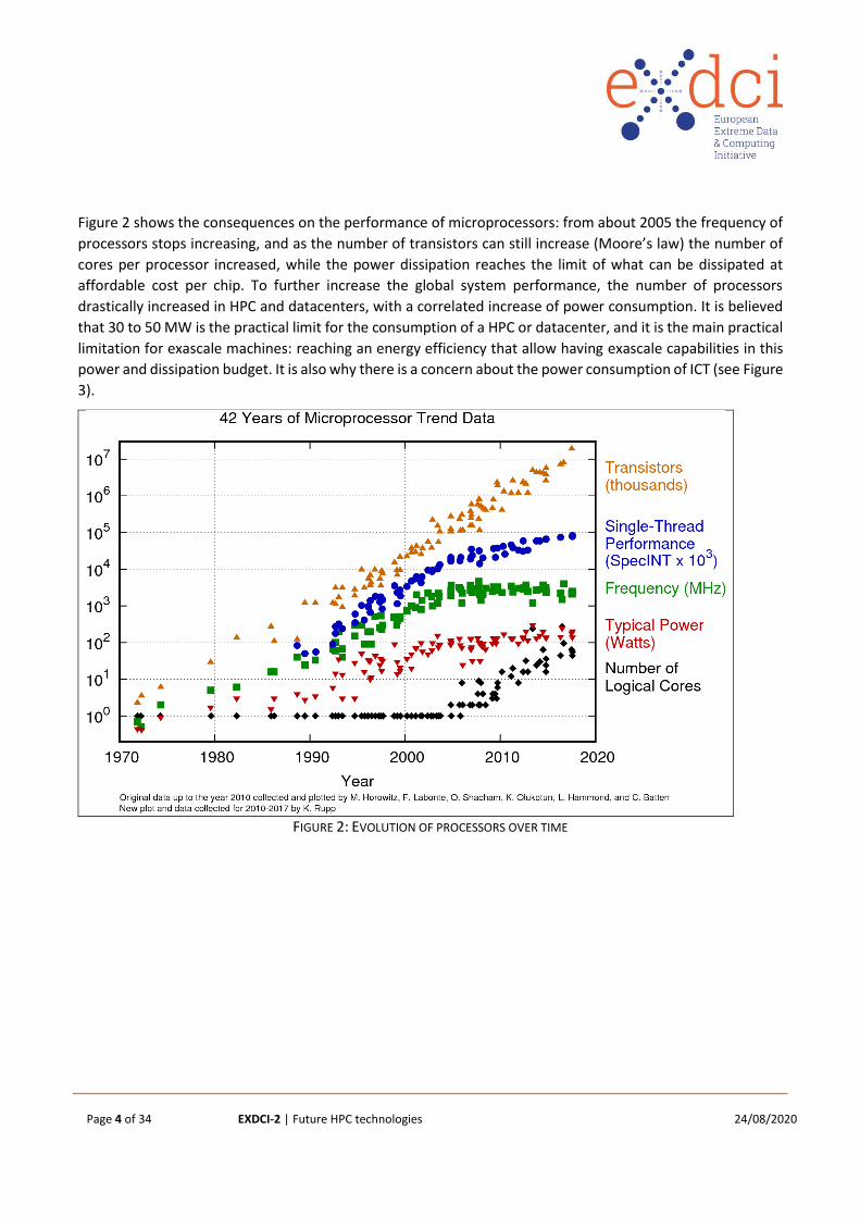
Figure 2 shows the consequences on the performance of microprocessors: from about 2005 the frequency of
processors stops increasing, and as the number of transistors can still increase (Moore’s law) the number of
cores per processor increased, while the power dissipation reaches the limit of what can be dissipated at
affordable cost per chip. To further increase the global system performance, the number of processors
drastically increased in HPC and datacenters, with a correlated increase of power consumption. It is believed
that 30 to 50 MW is the practical limit for the consumption of a HPC or datacenter, and it is the main practical
limitation for exascale machines: reaching an energy efficiency that allow having exascale capabilities in this
power and dissipation budget. It is also why there is a concern about the power consumption of ICT (see Figure
3).
FIGURE 2: EVOLUTION OF PROCESSORS OVER TIME
Page 5 of 34 EXDCI-2 | Future HPC technologies 24/08/2020
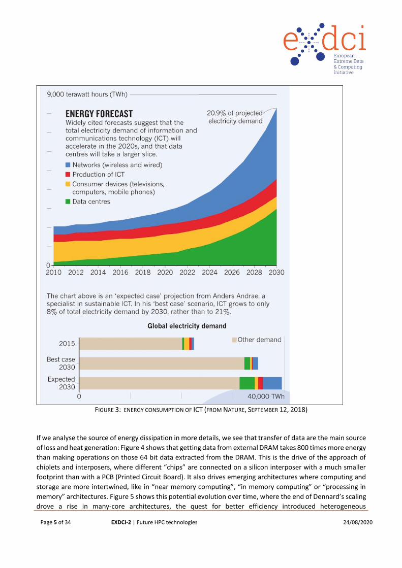
FIGURE 3: ENERGY CONSUMPTION OF ICT (FROM NATURE, SEPTEMBER 12, 2018)
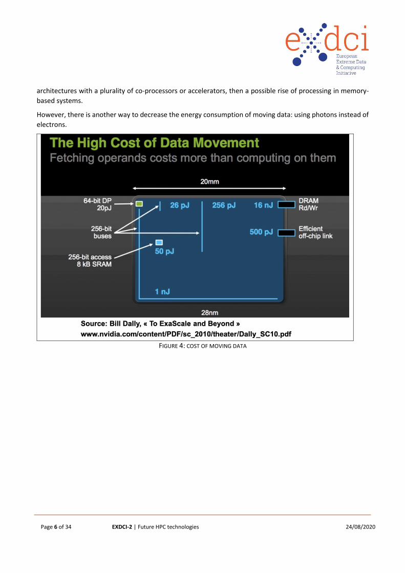
If we analyse the source of energy dissipation in more details, we see that transfer of data are the main source
of loss and heat generation: Figure 4 shows that getting data from external DRAM takes 800 times more energy
than making operations on those 64 bit data extracted from the DRAM. This is the drive of the approach of
chiplets and interposers, where different “chips” are connected on a silicon interposer with a much smaller
footprint than with a PCB (Printed Circuit Board). It also drives emerging architectures where computing and
storage are more intertwined, like in “near memory computing”, “in memory computing” or “processing in
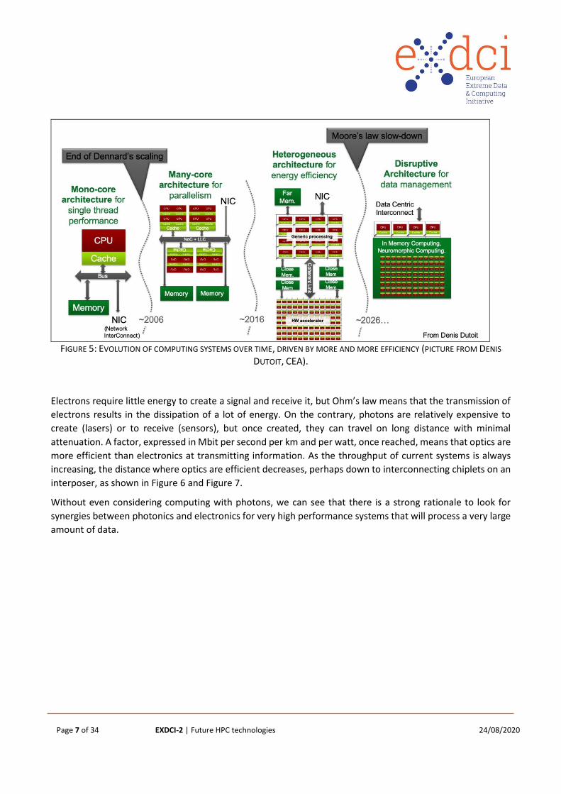
memory” architectures. Figure 5 shows this potential evolution over time, where the end of Dennard’s scaling
drove a rise in many-core architectures, the quest for better efficiency introduced heterogeneous
Page 6 of 34 EXDCI-2 | Future HPC technologies 24/08/2020
architectures with a plurality of co-processors or accelerators, then a possible rise of processing in memory-
based systems.
However, there is another way to decrease the energy consumption of moving data: using photons instead of
electrons.
FIGURE 4: COST OF MOVING DATA
Page 7 of 34 EXDCI-2 | Future HPC technologies 24/08/2020
FIGURE 5: EVOLUTION OF COMPUTING SYSTEMS OVER TIME, DRIVEN BY MORE AND MORE EFFICIENCY (PICTURE FROM DENIS
DUTOIT, CEA).
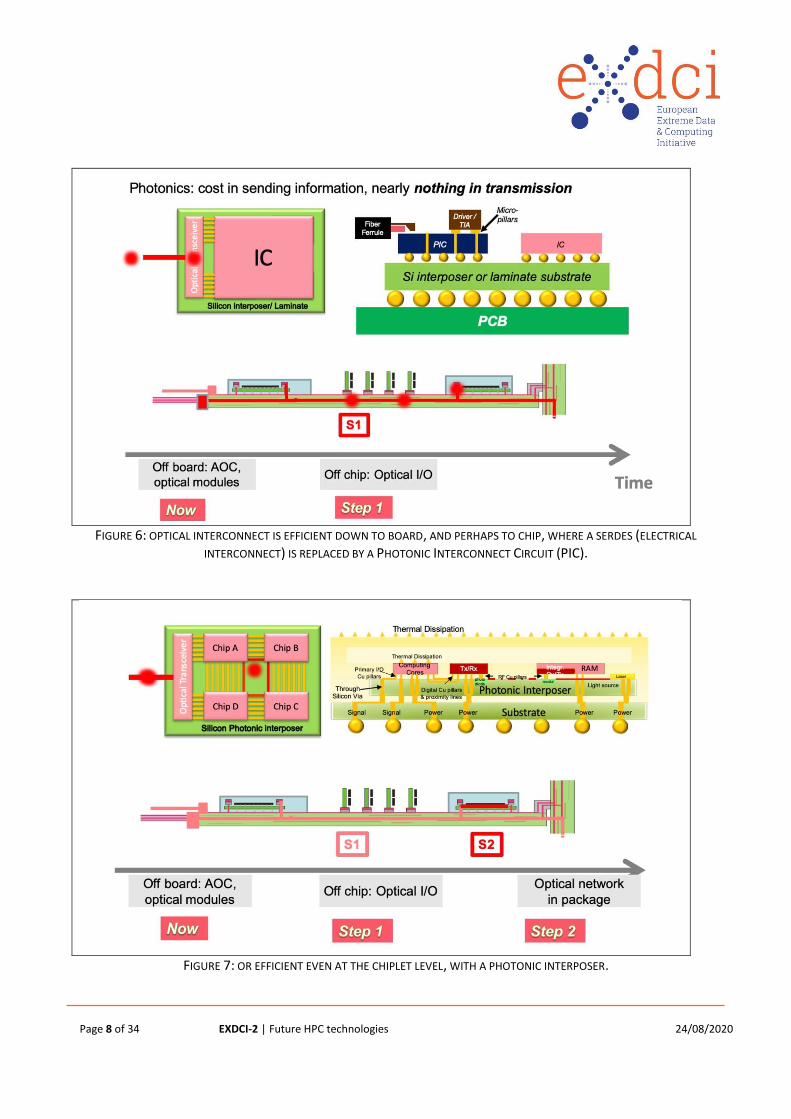
Electrons require little energy to create a signal and receive it, but Ohm’s law means that the transmission of
electrons results in the dissipation of a lot of energy. On the contrary, photons are relatively expensive to
create (lasers) or to receive (sensors), but once created, they can travel on long distance with minimal
attenuation. A factor, expressed in Mbit per second per km and per watt, once reached, means that optics are
more efficient than electronics at transmitting information. As the throughput of current systems is always
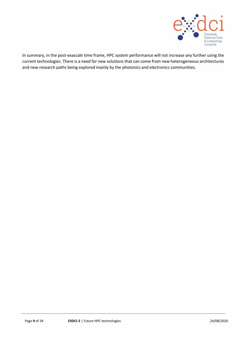
increasing, the distance where optics are efficient decreases, perhaps down to interconnecting chiplets on an
interposer, as shown in Figure 6 and Figure 7.
Without even considering computing with photons, we can see that there is a strong rationale to look for
synergies between photonics and electronics for very high performance systems that will process a very large
amount of data.
Page 8 of 34 EXDCI-2 | Future HPC technologies 24/08/2020
FIGURE 6: OPTICAL INTERCONNECT IS EFFICIENT DOWN TO BOARD, AND PERHAPS TO CHIP, WHERE A SERDES (ELECTRICAL
INTERCONNECT) IS REPLACED BY A PHOTONIC INTERCONNECT CIRCUIT (PIC).
FIGURE 7: OR EFFICIENT EVEN AT THE CHIPLET LEVEL, WITH A PHOTONIC INTERPOSER.
Page 9 of 34 EXDCI-2 | Future HPC technologies 24/08/2020
In summary, in the post-exascale time frame, HPC system performance will not increase any further using the
current technologies. There is a need for new solutions that can come from new heterogeneous architectures
and new research paths being explored mainly by the photonics and electronics communities.
Page 10 of 34 EXDCI-2 | Future HPC technologies 24/08/2020
International landscape
Before discussing the European situation, it is interesting to look at what is going on in the main international
HPC ecosystems. For this analysis, we have focused on the US, China and Japan which are the countries with
the most advanced programmes for post exascale HPC technologies.
USA
The United States, as usual in Information Technology, has been the first ecosystem to acknowledge that a
disruption has to happen to sustain the growth in performance of HPC systems. Several reports have been
issued for high level advisory committees. One of them “Future High Performance Computing Capabilities”
was issued as a “Summary Report of the Advanced Scientific Computing Advisory Committee (ASCAC)5” back
in 2017. These reports were the starting point of actions to launch ambitious research programmes. DARPA
(Defense Advanced Research Projects Agency) is very active in this field and has launched several programmes
relevant for HPC that are having a broad impact way beyond the defense domain:
• ERI Electronics Resurgence Initiative6
• ACCESS Accelerated Computation for Efficient Scientific Simulation7
• PIPES Photonics in the Package for Extreme Scalability8
A short description of these programmes can be found below.
ERI
Announced in 2017, ERI is a five-year, upwards of $1.5 billion investment to jumpstart innovation in the
electronics industry. To address the impending engineering and economic challenges confronting those
striving to push microelectronics technology forward, DARPA is nurturing research in circuit design tools,
advanced new materials, and systems architectures through a mix of new and emerging programmes. The first
phase of ERI is organized around 6 programmes:
5 https://science.osti.gov/-/media/ascr/ascac/pdf/meetings/201712/ASCAC-Future-HPC-
report.pdf?la=en&hash=2FEB999A02D5D4C30EAC01A0C090AAFCC49996E9
6 https://www.darpa.mil/work-with-us/electronics-resurgence-initiative
7 https://www.darpa.mil/program/accelerated-computation-for-efficient-scientific-simulation
8 https://www.darpa.mil/program/photonics-in-the-package-for-extreme-scalability

Page 11 of 34 EXDCI-2 | Future HPC technologies 24/08/2020
• Materials & Integration • Monolithic Integration of an SoC in Three Dimensions (3DSoC) • Framework for Novel Compute (FRANC)
• Architecture: • Software Defined Hardware (SDH) • Domain-Specific System on Chip (DSSoC)
• Design • Intelligent Design of Electronic Assets (IDEA) • Posh Open Source Hardware (POSH)
The Three Dimensional Monolithic System-on-a-Chip (3DSoC) programme seeks to develop the monolithic 3D
technology required to build logic, memory, and input/output (I/O) on a single die using a legacy lithography
node while improving performance by more than 50X when compared with leading edge technology nodes.
To achieve its goals, 3DSoC seeks to develop fabrication technology as well as the design flows required to
take advantage of the technology’s capabilities.
The Foundations Required for Novel Compute (FRANC) programme aims to develop innovative approaches to
advance compute technologies beyond the Von Neumann topology. Leveraging recent advances in materials,
devices, and integration technology, the programme seeks to develop novel memory-centric compute
topologies that break the traditional separation of processors and memory components to realize dramatic
advances in compute efficiency and throughput of the workload, especially for applications constrained by
size, weight, and power (SWaP). Innovative compute architectures and new, fast non-volatile storage and
memory-centric computing devices will be explored under FRANC to enable low latency compute near or
inside the data storage elements. Such approaches are particularly suited for applications relevant to artificial
intelligence (AI) where in-memory computation provides unique advantages over traditional Von Neumann
computation.
The goal of the Software Define Hardware (SDH) programme is to build runtime-reconfigurable hardware and
software that enables near ASIC 9 performance without sacrificing programmability for data-intensive
algorithms. Under the programme, data-intensive algorithms are defined as machine learning and data science
algorithms that process large volumes of data and are characterized by their usage of intense linear algebra,
graph search operations, and their associated data-transformation operators. The SDH programme aims to
create hardware/software systems that allow data-intensive algorithms to run at near ASIC efficiency without
the cost, development time, or single application limitations associated with ASICs.
Domain-Specific System on Chip (DSSoC) intends to demonstrate that the trade-off between flexibility and
efficiency is not fundamental. The programme plans to develop a method for determining the right amount
and type of specialization while making a system as programmable and flexible as possible. DSSoC wants to
de-couple the programmer from the underlying hardware with enough abstraction but still be able to utilize
the hardware optimally through intelligent scheduling. DSSoC specifically targets embedded systems where
the domain of applications sits at the edge and near the sensor. Workloads consist of small chunks of data but
9 Application Specific Integrated Circuit
Page 12 of 34 EXDCI-2 | Future HPC technologies 24/08/2020
often with a large number of algorithms required in the processing, meaning that high compute power and
low latency at low power are required.
The Intelligent Design of Electronic Assets (IDEA) programme seeks to develop a general purpose hardware
compiler for no-human-in-the-loop translation of source code or schematic to physical layout (GDSII) for SoCs,
System-In-Packages (SIPs), and Printed Circuit Boards (PCBs) in less than 24 hours. The programme aims to
leverage advances in applied machine learning, optimization algorithms, and expert systems to create a
compiler that could allow users with no prior design expertise to complete physical design at the most
advanced technology nodes.
The Posh Open Source Hardware (POSH) programme seeks to enable mathematically provable secure
electronics and create an open source hardware IP ecosystem, along with accompanying validation tools.
Under the programme, researchers will work to develop methodologies, standards, and simulation as well as
emulation technologies for the verification and mathematical inspection of analogue and digital IP to provide
proof of functionality and security. The program also aims to develop and release a number of silicon-proven
analogue and digital IP blocks on an open source platform to serve as a foundation for rapid design of complex
secure SoCs at leading edge technology nodes.
The initial programmes are expected to be followed by additional initiatives such as PIPES (see section 2.1.3).
ACCESS
In comparison to ERI, ACCESS is a much smaller programme but it is interesting because it illustrates well the
objective of finding disruptive computing solutions. The budget of ACCESS is small (in the range of $1M for
each project) and it has the rather focused objective of developing technologies for the acceleration of
scientific simulations of physical systems characterized by coupled partial differential equations (PDEs).
The Accelerated Computation for Efficient Scientific Simulation (ACCESS) programme seeks innovative ideas
for computational architectures that will achieve the equivalent of petaflops performance in a benchtop form-
factor and be capable of what traditional architectures would define as “strong” scaling for predictive scientific
simulations of interest.
The design and development of the prototypes are envisioned to leverage advances in optics, MEMS, additive
manufacturing, and other emerging technologies to develop new non-traditional analogue and digital
computational means and to overcome some of the current known limitations of these means, such as
precision and stability. Of particular interest are hybrid analogue/digital architectures that replace numerical
methods and memory-intensive computational parallelization with nonlinear and/or intrinsically parallel
physical processes to perform computations.
Unfortunately, we have not been able to find the list of the projects funded by this programme.
Page 13 of 34 EXDCI-2 | Future HPC technologies 24/08/2020
PIPES
After the ERI first phase and the launch of 6 research areas (see section above), it appears that other domains
have to be investigated to complement this first effort. Photonics was one of these and the ERI phase II
includes a new programme PIPES for this field.
The Photonics in the Package for Extreme Scalability (PIPES) programme, seeks to enable future system
scalability by developing high-bandwidth optical signalling technologies for digital microelectronics. Working
across three technical areas, PIPES aims to develop and embed integrated optical transceiver capabilities into
cutting-edge MCMs and create advanced optical packaging and switching technologies to address the data
movement demands of highly parallel systems.
The first technical area of the PIPES programme is focused on the development of high-performance optical
input/output (I/O) technologies packaged with advanced integrated circuits (ICs), including field
programmable gate arrays (FPGAs), graphics processing units (GPUs), and application-specific integrated
circuits (ASICs). Beyond technology development, the programme seeks to facilitate a domestic ecosystem to
support wider deployment of resulting technologies and broaden their impact.
The second technical area investigates novel component technologies and advanced link concepts for
disruptive approaches to highly scalable, in-package optical I/O for unprecedented throughput. The objective
is to answer the need for enormous improvements in bandwidth density and energy consumption to
accommodate future microelectronics I/O.
The third technical area of the PIPES programme will focus on the creation of low-loss optical packaging
approaches to enable high channel density and port counts, as well as reconfigurable, low-power optical
switching technologies. This aims to enable the development of massively interconnected networks with
hundreds to thousands of nodes that are expected due to the advance in the 2 previous areas.
The total budget is foreseen in the range of $65M for the three areas. The selected projects have started
during the second half of 2019.
Global view
The US effort is not limited to the above described programmes. Nevertheless, they give a vision of how the
US ecosystem acts and how the priorities are defined.
Besides these activities, it is worth mentioning:
- The US AI initiative launched in February 2019; - The National Quantum Initiative Act issued in December 2018. This initiative has announced a budget
of $1.2B to develop US leadership in quantum.
In conclusion, the US is undertaking a large research effort to maintain a dominant position in computing and
to prepare the technologies that will replace the current CMOS based chips.
Page 14 of 34 EXDCI-2 | Future HPC technologies 24/08/2020
China
Assessing the efforts of China on the future of HPC technologies, is difficult as access to information related to
the actual research projects is limited. This is why we have focused our analysis on the views presented in a
journal10 by members of the Chinese HPC ecosystem “Special Issue on Post-exascale Supercomputing” issued
in November 2018.
The main challenges identified by the Chinese HPC research community are:
1. Energy efficiency bottlenecks: The US Department of Energy’s exascale research programme sets a
goal of 1 exaflops at 20–40 MW, or 25–50 gigaflops/W, probably around the year 2022. The US
DARPA’s JUMP programme sets a more ambitious long-term goal of 3 peta operations per second per
watt, or 3 peta operations per joule (POPJ), possibly by around 2035. Here an operation is not
necessarily a 64-bit IEEE floating-point operation. Cambricon-1A, which was developed at the Institute
of Computing Technology of the Chinese Academy of Sciences in 2015 and targets machine learning
on small terminals such as smartphones, reached over 1 tera operations per joule (TOPJ)
2. Order-of-magnitude better devices: Emerging technologies, such as 3D-stacking, fully optical
communication, magnetic semiconductors, and memristors, are challenging mature technologies
used in today’s supercomputers which are based on CMOS
3. Novel systems architectures: Systems architecture has played a critical role in the history of modern
supercomputing. Architectural innovations, from vector supercomputers, SMP, ccNUMA, and MPP, to
clusters, have enabled the exponential growth of performance and scalability
4. Effective co-design of software and hardware: Currently, there is a wide gap between the peak
performance and the sustained performance that real applications can achieve, especially with new
applications with sparsity and irregularity, such as data analytics and complex multi-modal
applications
5. Ecosystem for diverse applications: the existing ecosystem has a tradition of scientific and
engineering computing, which is not enough for the new diverse applications that converge numeric
simulation, big data, and artificial intelligence. China proposes to build up a new supercomputing
ecosystem for application development, which supports the mixed or converged workloads of
arithmetic-intensive, data-intensive, and intelligent applications.
In order to tackle these challenges, the Chinese researchers work on the different HPC system components.
At computing node level, the solution that is proposed in based on the following choices:
− Processor: many-core architecture with each processing core supporting scalar double precision
floating-point processing instead of vector processing
− Co-processor: acceleration for specific applications, such as traditional scientific computation and
engineering applications, and emerging applications including data analytics and deep learning
− Sharing of high bandwidth memory
− Inter-processor link
10 https://link.springer.com/journal/11714/19/10
Page 15 of 34 EXDCI-2 | Future HPC technologies 24/08/2020
For the network, the expected technologies will serve to interconnect large nodes that are a heterogeneous
mix of central processing units (CPUs), accelerators, co-processors, and field programmable gate arrays
(FPGAs)/application specific integrated circuits (ASICs). The CPUs could also be a mix of strong and weak cores.
The nodes will also have a large amount of memory of different technologies, such as non-volatile random-
access memory and three dimensional (3D) stacked memory. The network technologies will:
- Be heterogeneous with wired or wireless interconnects. The on-chip interconnect technology would
have matured to incorporate wireless interconnection among the components within a node.
Similarly, photonic technologies would have matured to be used within a node or a rack. This can
provide a large number of concurrent communications among different components (CPUs,
accelerators, and memories) without contention. As each node will be dense, the nodes will need to
be connected to the overall network speed of terabits per second with multiple adapters/ports. This
will facilitate a good balance between inter- and intra-node transfers;
- Both wireless and photonic technologies will allow the establishment of high-dimensional topologies
within intra-core, intra-node, and intra-rack levels. These technologies will also facilitate one-to-many,
many-to-one, and many-to-many communications in a flexible manner with a good performance
- Allow capabilities to be increasingly offloaded to the network leading to an era of ‘in-network
computing’
The analysis of the Chinese community is not limited to hardware technologies. In terms of software, they
acknowledge that progress is also needed here if we want to have efficient post-exascale systems. The
directions that are highlighted are:
- programming effort shifting from computation to data, - precision optimization, - programmable hardware.
In summary, the Chinese ecosystem is already working on technologies for post-exascale systems both at the
hardware and software levels.
Japan
To analyse the situation in Japan is difficult because most of the documents are in Japanese and we do not
have found a specific publication like for China which summarizes the vision of the Japanese HPC ecosystem
on post-exascale technologies. However, an impression of the current Japanese efforts in technology can be
given by looking at their current initiatives in the domains of supercomputing, Artificial Intelligence and
quantum technologies.
Supercomputing
Japan has a long history of development of supercomputers. The Earth Simulator was dethroned in November
2004 as the top supercomputer in the world, but the Fujitsu’s K computer, based on 68544 SPARC64 VIIIfx
CPUs, each with eight cores, for a total of 548,352 core, processors developed in house, was at the top of the
Page 16 of 34 EXDCI-2 | Future HPC technologies 24/08/2020
TOP500 in 2011 with 10 petaflops. It was developed for RIKEN (an Institute for Physical and Chemical
Research). It should be noted that the K Computer did not use graphics processors or other accelerators. The
K Computer was also one of the most energy-efficient systems, and while dethroned on the TOP500, it stayed
or a long time at a good position on the Green500. It was also a very “equilibrated” machine, with a good ratio
compute/storage/communication, making it quite efficient on the HPCG benchmark where it was dethroned
only in 2018.
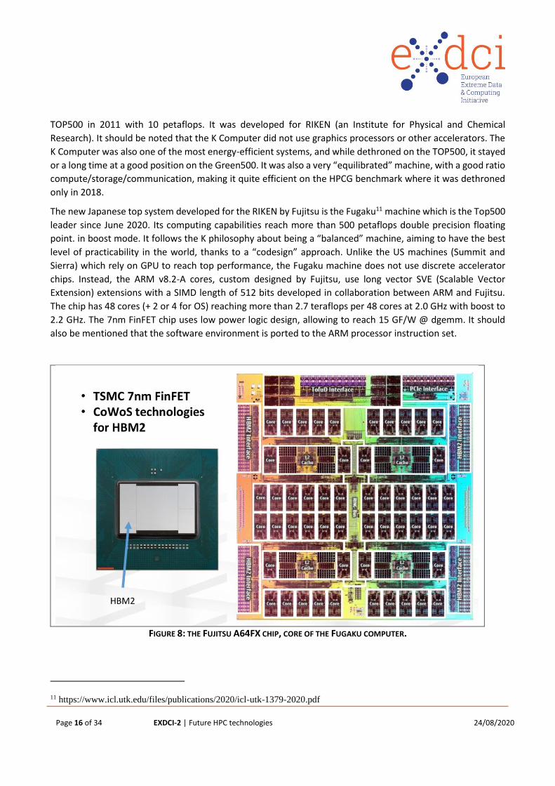
The new Japanese top system developed for the RIKEN by Fujitsu is the Fugaku11 machine which is the Top500
leader since June 2020. Its computing capabilities reach more than 500 petaflops double precision floating
point. in boost mode. It follows the K philosophy about being a “balanced” machine, aiming to have the best
level of practicability in the world, thanks to a “codesign” approach. Unlike the US machines (Summit and
Sierra) which rely on GPU to reach top performance, the Fugaku machine does not use discrete accelerator
chips. Instead, the ARM v8.2-A cores, custom designed by Fujitsu, use long vector SVE (Scalable Vector
Extension) extensions with a SIMD length of 512 bits developed in collaboration between ARM and Fujitsu.
The chip has 48 cores (+ 2 or 4 for OS) reaching more than 2.7 teraflops per 48 cores at 2.0 GHz with boost to
2.2 GHz. The 7nm FinFET chip uses low power logic design, allowing to reach 15 GF/W @ dgemm. It should
also be mentioned that the software environment is ported to the ARM processor instruction set.
FIGURE 8: THE FUJITSU A64FX CHIP, CORE OF THE FUGAKU COMPUTER.
11 https://www.icl.utk.edu/files/publications/2020/icl-utk-1379-2020.pdf
Page 17 of 34 EXDCI-2 | Future HPC technologies 24/08/2020
The machine will have two types of nodes: Compute Node and Compute & I/O Node connected by Fujitsu
TofuD, a 6D mesh/torus Interconnect.
In term of energy efficiency, the Fugaku system delivers 14.6 gigaflops/watt which is a quite impressive result
for an architecture without accelerator.
Artificial intelligence
Japan is offering supercomputing capacities to their researchers (and companies) working on Artificial
Intelligence. In 2015, The Ministry of Economy and Industry (METI) started the AIRC (Artificial Intelligence
Research Center), hosted by the AIST (Advanced Institute for Science and Technologies). The 2016 budget was
19.5 billion yen. They installed the “AI Bridging Cloud Infrastructure” (ABCI) which reached about 20 petaflops
in 2019. “AI Bridging Cloud Infrastructure (ABCI) is the world’s first large-scale Open AI Computing
Infrastructure, constructed and operated by National Institute of Advanced Industrial Science and Technology
(AIST), Japan. It delivers 19.9 petaflops of HPL performance and the world’s fastest training time of 1.17
minutes in ResNet-50 training on ImageNet datasets as of July 2019. ABCI consists of 1,088 compute nodes
each of which is equipped with two Intel Xeon Gold Scalable Processors, four NVIDIA Tesla V100 GPUs, two
InfiniBand EDR HCAs and an NVMe SSD. ABCI offers a sophisticated high performance AI development
environment realized by CUDA, Linux containers, on-demand parallel filesystem, MPI, including MVAPICH,
etc.” (from https://insidehpc.com/2019/09/the-abci-supercomputer-worlds-first-open-ai-computing-
infrastructure/ ).
Quantum computing
Japan is also active in quantum computing, but mainly in “analogue” quantum computing 12 (quantum
annealing). There are a few start-ups on quantum computing, and also a flagship project financed by MEXT
and working on transmon13 based qubits (for the “universal” quantum computer). Most applications are based
on combinatorial optimization for industry, transportation or traffic. Software stacks and simulations are also
being developed, also for the “universal quantum” approach, e.g. by the MDR company (https://mdrft.com/)
On the hardware side, NEC is developing a superconducting flux qubit for quantum annealer, somewhat a
competitor of the D-Wave machine. They claim that their forthcoming machine will be more efficient than D-
Wave because they will support a more generic interconnect, event better than the new “Pegasus”
interconnect of D-Wave. Optical based computing has a long history in Japan, and NTT is developing a quantum
annealer based on laser and coherent ising principle. The Cabinet Office ImPACT “Quantum Neural Network”
involves organizations such as NTT, NII (National Institute of Informatics). Fujitsu, Hitachi and Toshiba have
12 See section 3.7 for the definition of “analogue” and “universal” quantum computers
13 A transmon is a type of superconducting charge qubit that was designed to have reduced sensitivity to charge noise.
The transmon was developed by Robert J. Schoelkopf, Michel Devoret, Steven M. Girvin and their colleagues at Yale
University in 2007 (from Wikipedia)
Page 18 of 34 EXDCI-2 | Future HPC technologies 24/08/2020
digital solutions for the hardware implementation of simulated annealing. Fujitsu’s Digital Annealer14 is an
ASIC which can be used as coprocessor. The first generation (1024 “bits” with 16 bits inter-bit coupling
accuracy) is accessible by the cloud, while the second generation will support 8192 “bits” with 64 bits for
coupling accuracy. By combining chips by software, the 2019 servers can support up to 1M “bits”. Hitachi has
developed a CMOS Annealing machine15. Toshiba16 is developing hardware to support their quantum-inspired
algorithm “Simulated Bifurcation Algorithm”.
14 https://www.fujitsu.com/global/services/business-services/digital-annealer/index.html
15 https://www.hitachi.com/rd/portal/contents/story/cmos_annealing2/index.html
16 https://www.toshiba-sol.co.jp/en/pro/sbm/sbm.htm

Page 19 of 34 EXDCI-2 | Future HPC technologies 24/08/2020
Potential options for the future HPC technologies
This section presents the main technical findings about how the electronics and photonics technologies will
impact the future HPC system. This information is a synthesis of the discussions undertaken with the
electronics and photonics ecosystems and of the analysis of other technical documents.
Introduction
Today’s HPC system architecture is dominated by the standard CPU+GPU17 solution. This architecture has been
effective at offering the performance increase requested by HPC users while challenging them to exploit the
massive parallelism and heterogeneity offered by this solution.
We foresee little changes in the 2020-2023 time frame with the first exascale systems based on this approach.
After sustaining the growth in the number of operations per watt, new solutions will have to be found as
Moore’s law will fade and Dennard’s scaling gone. Progress can be made in three axes:
- New architectures
- New data representation schemes
- New technologies (compared to CMOS18)
Most of the new approaches are a combination of the three (or at least of two of them) but it is important to
understand that we have these three freedom degrees that can be played with:
- Switching from computing centric execution used by processors and GPU (akin to Von Neumann
architecture) to the data centric paradigm to reduce the overhead introduced by the data movement;
- Changing what is called an operation by playing with operand precision or introducing multi-bits or
analogue coding or other ways of encoding information (e.g. Quantum),
- Introducing new materials that will deliver more efficient way (in terms of timing and/or energy) to
store, switch and/or process information.
This gives a very broad set of options but only a few will emerge due to economic constraints, critical mass
issues, industrialization aspects, legacy and usability problems. The following sections present some of the
most promising paths.
17 Computing Processor Unit + Graphical Processor Unit
18 Complementary Metal Oxide Semi-conductor
Page 20 of 34 EXDCI-2 | Future HPC technologies 24/08/2020
Enhancements of current CMOS technologies
CMOS scaling
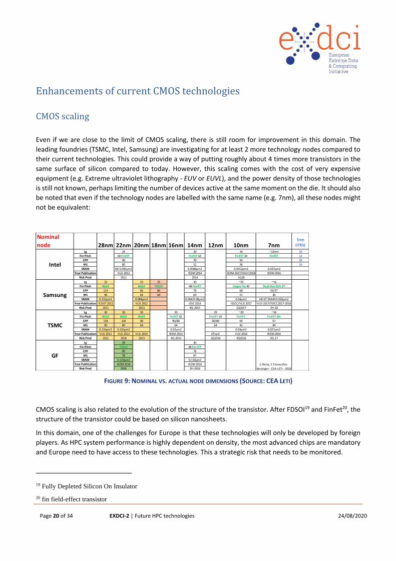
Even if we are close to the limit of CMOS scaling, there is still room for improvement in this domain. The
leading foundries (TSMC, Intel, Samsung) are investigating for at least 2 more technology nodes compared to
their current technologies. This could provide a way of putting roughly about 4 times more transistors in the
same surface of silicon compared to today. However, this scaling comes with the cost of very expensive
equipment (e.g. Extreme ultraviolet lithography - EUV or EUVL), and the power density of those technologies
is still not known, perhaps limiting the number of devices active at the same moment on the die. It should also
be noted that even if the technology nodes are labelled with the same name (e.g. 7nm), all these nodes might
not be equivalent:
FIGURE 9: NOMINAL VS. ACTUAL NODE DIMENSIONS (SOURCE: CEA LETI)
CMOS scaling is also related to the evolution of the structure of the transistor. After FDSOI19 and FinFet20, the
structure of the transistor could be based on silicon nanosheets.
In this domain, one of the challenges for Europe is that these technologies will only be developed by foreign
players. As HPC system performance is highly dependent on density, the most advanced chips are mandatory
and Europe need to have access to these technologies. This a strategic risk that needs to be monitored.
19 Fully Depleted Silicon On Insulator
20 fin field-effect transistor
Nominal
node 28nm 22nm 20nm 18nm 16nm 14nm 12nm 10nm 7nm5nm
(ITRS)
Lg 24 20 16 ~12nm 10
Fin Pitch 60 FinFET FinFET 42 FinFET 34 FinFET 12
CPP 90 70 54 32
M1 80 52 36 16
SRAM HD 0.092µm2 0.0588µm2 0.0312µm2 0.027µm2
Year Publication VLSI 2012 IEDM 2014 IEDM 2017/ISSCC2018 IEDM 2016
Risk Prod 2011 2014 1Q18
Lg 32 25 25 30 ~20 ~16
Fin Pitch BULK BULK FDSOI 48 FinFET Single Fin 42 Dual thin EUV 27
CPP 114 86 86 78 68 54/57
M1 90 64 64 64 51 36
SRAM 0.152µm2 0.084µm2 0.064/0.08µm2 0.04µm2 HD 6T SRAM 0.026µm2
Year Publication ICSIST 2011 VLSI 2012 JSSC 2014 ISSCC/VLSI 2017 VLSI 2017/ISSCC2017-2018
Risk Prod 2011 2013 4Q-2015 1Q2017 2H-18
Lg 30 30 30 33 25 ~20 ~16
Fin Pitch BULK BULK BULK FinFET 45 FinFET 45 FinFET FinFET 4th
CPP 118 105 90 90/80 90/80 64 57
M1 90 80 64 64 64 42 40
SRAM 0.155µm2 0.155µm2 0.07µm2 0.03µm2 0.027µm2
Year Publication VLSI 2012 VLSI 2012 VLSI 2014 IEDM 2013 6Track VLSI 2016 IEDM 2016
Risk Prod 2011 2018 2013 4Q-2015 3Q2016 4Q2016 3Q-17
Lg 28 30
Fin Pitch FDSOI 48 Fin FET
CPP 90 78
M1 78 67
SRAM 0.110µm2 0.110µm2
Year Publication IEDM 2016 IEDM 2016
Risk Prod 2016 2H-2016
Intel
Samsung
TSMC
GFC.Reita, C.Fenouillet-
Beranger - CEA-LETI - 2018
Page 21 of 34 EXDCI-2 | Future HPC technologies 24/08/2020
On the technology side, the challenge for the last CMOS technology nodes is to get a reduction of the energy
by transistor while increasing the number of transistors. Even if we cannot expect as in the past a decrease of
the energy by the same factor as the increase of transistors, progress in energy efficiency is mandatory to
make the new CMOS technology nodes a success for HPC systems.
2.5/3D stacking
2.5D/3D stacking provide a way of reducing the latency and energy and avoiding package bandwidth
bottlenecks when we want several chips to communicate together. 2.5 D stacking is the concept of small dies
(called chiplets) integrated on a common substrate (the interposer) that can be organic, passive silicon, active
silicon or using photonic technologies. 3D stacking is the stacking of layers of integrated circuits on top of each
other. It can be done either by wafer to wafer, chip to wafer stacking, or by monolithic 3D which allow a finer
granularity (down to the level of transistors). HPC is already benefiting from this technology with the first HPC
systems using high bandwidth memory (HBM or HMC21) and processor manufacturers (AMD, Fujitsu, Intel…)
having already used 2.5D in the latest products. The boost in memory bandwidth is a great improvement for
memory bound applications and a must for architectures with accelerators that require this kind of bandwidth
to deliver their performance. 2.5D also allows for mixed chiplets with various technologies, and for example,
with active interposers, having power conversions integrated “in the chip”, providing globally a better energy
efficiency.
It can also be a path for production of hybrid packages mixing chips of different architectures (see Section 3.3)
or even chips manufactured with different technologies (see Section 3.5) Nevertheless, stacking “compute”
chips with a higher heat dissipation than memory chips leads to thermal problems that today limit the number
of chips that could be put in a package.
Europe is present in this field with excellent know-how in the three main RTOs 22 and some research
installations to test new concepts. For an industrial development, as “High end” computing is more and more
important for the automotive market (Advanced Driver Assistance Systems and self-driving), the European
automotive industry might be a driver for having European actors in 2.5 D and the integration of complex
systems on dies or interposers.
The European EPI (European Processor Initiative) plans to use2.5 D technology, in the same way as AMD, Intel
and Fujitsu.
In this domain, one of the main technical challenges is the thermal dissipation of the stack. Innovations are
needed to solve this problem before 3D stacking can scale and deliver all of its promises.
Another challenge is the set-up of European industrial options. Even if today the RTOs have research
installations to design new concept chips, the industrial solutions are mainly coming from Asia. Having a
21 High Bandwidth Memory and Hybrid Memory Cube
22 Research and Technology Organizations: CEA, Fraunhofer, IMEC
Page 22 of 34 EXDCI-2 | Future HPC technologies 24/08/2020
European based option would be important from an independent and economic stand point because of the
potential of this technology.
To foster the development of European chiplets that can be integrated via 2.5/3D stacking, it could also be
strategic to work on integration standards. Having a commonly defined interface will provide an exploitation
path for new initiatives in the area of accelerator design.
Precision of operations
The trend in the past has been to provide more and more precision for operations as HPC was focused on
simulations where stability and convergence of algorithms depended on this feature. Today, for new
applications coming mainly from neural networks, high precision is not mandatory (the “learning phase of
Deep Neural Networks can be done in most case with 16-bits floating point operations) and switching to low
precision can save space (i.e. transistors and data paths) and energy.
The availability of 16 and 8 bit operations in processors and accelerators is a trend that will allow to adapt
precision to the needs of algorithms with an important saving in some cases.
On the reverse side, sometimes convergence of algorithms could benefit from high precision to reduce the
number of iterations and to save time and energy. New coding schemes are possible and alternative to the
IEEE 754 arithmetic, like UNUM23. Its implementation in processors could be more efficient then software
emulation of this high precision scheme.
The trend, to have flexibility in the representation of data, is a challenge for software development. The choice
of the representation could be made automatically with analysis of the pro and cons of the different options.
This could lead to the automatic selection of libraries optimized for different data formats.
This rethinking of data representations is also a precursor to a more disruptive approach with the use of
analogue options (see Section 3.6).
New architectures
Today standard processors and GPU accelerators are based on a Von Neumann architecture where a
controlled execution applies operations onto data that are stored in registers (fed by caches, fed by memory).
This architecture is very flexible but can be costly in terms of transistor, data paths and energy compared to
what is just needed for an application. This implies a lot of moves and duplications of data, which is not efficient
(bringing data from external memory is 3 orders of magnitude more energy demanding than a floating-point
operation on those data). However, there is a research path what proposes architectures that will be more
efficient for some classes of problems. Some of these new architectures can be implemented using standard
23 Universal Number
Page 23 of 34 EXDCI-2 | Future HPC technologies 24/08/2020
CMOS technology or providing opportunities to introduce new technologies that will be more efficient than
CMOS (see section 3.5).
Some concepts of new architectures are generic (see section on data flow or IMC24 below) or target a specific
class of algorithms (see section on neuromorphic, graph and simulated annealing below).
Data flow
In data flow architectures, data move between modules that perform the computation on the data. You do
not have any program counter that controls the execution of the instructions as in a Von Neumann
architecture. Deep Learning architecture (see section on neuromorphic architecture below) can be
implemented as a specific dataflow architecture (the main operations are matrix-based). The investigation of
dataflow architectures is linked to FPGA (Field Programmable Gate Array) as most of the ideas have not led to
the tape out of specific circuits but have been tested and implemented with FPGA.
With the slowdown of standard processors performance increase, development of data flow architectures can
provide an alternative to deliver this performance increase. The development of reconfigurable architectures
(like the Intel CSA Configurable Spatial Accelerator) and progress toward flexible reconfigurable FPGA will be
an asset for implementing data flow architectures.
IMC/PIM (In memory computing/Processor in memory)
These architectures couple the storage with some computing capabilities. The idea is that bringing the
computation to the memory will be cheaper in resources than moving data to the computing units. Most of
the time this approach is mixed with a standard architecture to allow computation on several data.
The architecture is also related to the development of Non-Volatile Memory (see Section 3.4) and appealing
as long as the cost of the in-memory computation is low.
Neuromorphic
The development of AI, and especially applications using Deep Learning techniques, has led to a huge interest
for neuromorphic architectures that are inspired by a theoretical model of a neuron. This architecture can be
used for AI tasks but can also be viewed as a generic classification function or a function approximation.
As more and more applications (or a part of an application) are mapped to this paradigm, it is worth developing
specific circuits that implement only the operations and data paths mandatory for this architecture. Several
examples already exist such as the Google Tensor Processing Unit chip or Fujitsu Deep Learning Unit chip.
24 In Memory Computing

Page 24 of 34 EXDCI-2 | Future HPC technologies 24/08/2020
These efforts have not exploited all the possible options and have not developed all the interesting features
of the architecture, so research in this area is still valuable.
We can distinguish various kind of possibilities:
1. Using classical digital arithmetic, but designing more specialized architectures (examples: TPU and
DLU)
2. Using another way of coding information, like “spikes” or their representation in AER coding (Address-
Event Representation) (see fig 12).
3. Using « physics » to make computation (e.g. Ohms law for products and Kirchhoff law for summation;
see Section 3.6 “Analog computing”).
Of course, the approaches can be combined. Typically, most people call “neuromorphic” the approaches using
option 2, because it is closer to the way the nervous system communicates.
One important aspect is that this architecture is a good candidate to introduce an alternative to CMOS (see
Section 3.5).
Figure 10: NeuRAM3 approach

Page 25 of 34 EXDCI-2 | Future HPC technologies 24/08/2020
Graph computing
Graphs play an important role in data representation and in some AI or optimization problems. As standard
processors have poor performance due the non-regular access to data, developing a specific architecture for
this problem can be relevant.
To our knowledge there is no current initiative trying to implement this path (the Graphcore company has
developed what they call a IPU (Intelligence Processor Unit) which is focused on AI applications and does not
use a graph computing focused architecture). Nevertheless, this path could lead to an important acceleration
for graph oriented problems.
Simulated annealing
Simulated annealing is a method for solving complex optimization problems. It can be implemented by
software on classical Von Neumann processors but you can also design an ASIC that will significantly speed-up
the computation by mapping directly the variables and their interactions and by providing a hardware based
random generator.
This approach has been implemented by Fujitsu with its “Digital Annealing” processor. This project has
developed a standard CMOS ASIC and a software stack to map the optimization problem to the circuit.
Other efforts use quantum devices (see section 3.7) to target the same class of problems (this approach
requires cryogenic operation which is not the case with CMOS based developments).
Hybrid of CMOS and other technologies: NVMs, silicon photonics
NVM (Non Volatile Memory)
Different technologies are being developed to propose Non-Volatile Memory. Besides the existing NAND,
resistive memory (memristor), phase change memory (PCM), metal oxide resistive random access memory
(RRAM or ReRAM), conductive bridge random access memory (CBRAM) and Spin-transfer torque magnetic
random access memory (STT-RAM) are interesting technologies. The developments in this domain have
several impacts for HPC. The energy to retrieve data is decreased, the latency to read the data is reduced and
the density can be increased (especially with solutions implementing multi-states storage for each cell).
NVMs also play a role in providing an easy implementation of the IMC/PIM architecture when compute
elements can be associated as in Memristive Computing.
Page 26 of 34 EXDCI-2 | Future HPC technologies 24/08/2020
Silicon photonics
Silicon photonics can be used either to compute or to provide interconnect between computing elements.
Compute
The properties of light can be used to perform computation. For example, the interaction of light whose phase
has been modulated according to inputs can produce operations over these inputs. This idea can be used to
implement neuromorphic architecture where the main operation is a scalar product.
This approach is promising but several steps are still to be achieved: assessment of the value proposal in term
of energy efficiency and industrialization path of the technology.
Another path is to use the massive parallelism of optics to perform complex operation (typically where the
complexity is not a linear increase versus the size of the problem). An example is the system proposed by the
start-up LightOn, integrated in an OVH cloud server (see Section 3.6 on analogue computing).
Interconnect
Photonics is already used for long distance communication in HPC systems (electrons are easy to create and
interface, they display attenuation with distance (Ohm’s law), while photons are energy demanding for
creation and interfacing but have low attenuation with distance). The technology is also appealing for rack
level communication. But perhaps the most interesting aspect will be at the package level with the
development of active interposer with embedded silicon photonics networks between chips or chiplets. The
bandwidth and the energy efficiency can be increased compared to current CMOS solutions.
Again, for these applications, a silicon photonics industrialization path has to be developed. European projects
have proposed or are working on interesting technologies. A solution for transferring these results to market
has to be found.
New solutions more efficient than CMOS
CMOS has been such an industrial success story that it has reduced the effort on alternative solutions to
implement transistor or computing elements. With the end of CMOS progress more emphasis will be put on
these other options even if it is still to be proven that they will be able to deliver more computing performance
than CMOS.
Page 27 of 34 EXDCI-2 | Future HPC technologies 24/08/2020
Superconducting
With the use of superconducting material, the expectation, based on the zero resistivity of the interconnects,
is that power consumption could be up to two orders of magnitude lower than that of classical CMOS based
supercomputers.
Nevertheless, superconducting circuits have still to overcome several drawbacks like density, switching time,
interfacing with external systems or noise reduction, become they can be seen as a potential solution for HPC.
Most of the time the implementation uses Josephson junctions and so has the same disadvantages as analogue
computing.
Magnetoelectric and spin-orbit MESO
Researchers from Intel and the University of California, Berkeley have proposed a new category of logic and
memory devices based on magnetoelectric and spin-orbit materials. These so-called “MESO” devices will be
able to support five times the number of logic circuits in the same space as CMOS transistors. In these devices,
logic and storage bits will be encoded by the spin state (up or down) of bismuth-iron-oxide, a multiferroic
material. Compared to CMOS the switching energy is better (by a factor of 10 to 30), switching voltage is lower
(by a factor of 5) and logic density is enhanced (by a factor of 5). In addition, its non-volatility enables ultralow
standby power.
This path is promising even if the roadblocks for industrialization are still difficult to assess.
Memristive devices
Besides the uses of the resistive memory for NVM and analogue neuromorphic architectures (see Sections 3.3
and 3.4), memristive devices can be interesting for implementing logic gates and computing. Even if the
switching time may be slower than CMOS, they can provide a better energy efficiency. The integration of
memory into logic allows to reprogram the logic, providing low power reconfigurable components and can
reduce energy and area constraints in principle due to the possibility of computing and storing in the same
device (computing in memory). Memristive devices can also be arranged in parallel networks to enable
massively parallel computing.
Again, for this technology, it is difficult to assess when it will be mature to propose a credible alternative for
computing.
Other materials
Research has been done on new materials that could lead to new ways to compute including carbon
nanotubes, graphene or diamond transistors. Nevertheless, at this stage of the research, it is too early to
assess whether these options will propose a valuable solution for HPC systems.
Page 28 of 34 EXDCI-2 | Future HPC technologies 24/08/2020
Analogue computing
Analog computing is when a physical (or chemical) process is used to perform a calculation. (An analogue
computer or analogue computer is a type of computer that uses the continuously changeable aspects of
physical phenomena such as electrical, mechanical, or hydraulic quantities to model the problem being solved.
– Wikipedia)
Optical systems
Optical systems can be used to compute some functions thank to the properties of light and optical devices
like lenses. This approach is extremely energy efficient compared to traditional computers. This technology
cannot suit every application but a number of algorithms as scalar products, convolution-like computations
(e.g. FFT, derivatives and correlation pattern matching), are naturally compatible. Some demonstrations have
been made by the EsCAPE project with the computation of spectral transforms by an optical system. The
precision of the results can be a problem if the spectral transform is the input of a subsequent algorithm
needing high resolution. Nevertheless, this method is well suited for correlation detection, sequence
alignment testing or pattern matching applications.
Optical systems have also been used to implement reservoir computing. Reservoir computing and Liquid State
Machines are models to solve classification problems and can be seen as “part” of neuromorphic architecture.
Nevertheless, this approach is often coupled with research to implement this model with analogue optical
computing.
Optical computing is the more advanced field of analogue computing with already two European start-up
(Optalysys and LightOn) proposing products for accelerating recognition applications.
Other options
Other options are possible like using thermal or electrical systems to find solutions of some differential
equation problems.
The mix of analogue/digital computing inside a CMOS chip can be a way to provide more energy efficient
solutions.
New computing paradigm: quantum computing
Quantum computing is a new paradigm where quantum properties are used to provide a system with
computing capacity. Today research in this field can be split into 2 categories:
Page 29 of 34 EXDCI-2 | Future HPC technologies 24/08/2020
1) The “universal” quantum computers based on qubit and gates performing operation on these qubits.
It uses two quantum properties, superposition (capacity to be at the same time in a superposition of
2 states) and entanglement (capacity to link the state of an element to the measure made on another
element). From these properties, a mathematical model of a universal quantum computer has been
developed. In this model a system of qubits can be put in a state that represents the superposition of
all the values of the computed function (i.e. this system has in “parallel” computed the values of a
function for all the 2N inputs).
2) The quantum annealers, or quantum simulators, represented for example by the D-Wave machine, use quantum physics to escape from local minima in optimization functions using quantum fluctuations. This class of machines is limited to problems that can be modelized such as minimization of function, like the travelling salesman, flow optimization, molecular simulation etc. Other possibilities are to use known quantum processes (like (ultra)cold atoms) to modelise other quantum related phenomenon, like in chemistry.
Most efforts have targeted the first approach. Nevertheless, developing a physical system that behaves like
the “universal” model is at the level of research and will need to solve hard problems such as the decoherence
of the qubits, a reliable measurement system, error correction and the NxN interconnection between the
qubits.
The EC flagship on quantum technologies addresses the topic with a good level of support compared to the
risk/reward of this domain.
Transversal questions
Integration with “classical” HPC systems
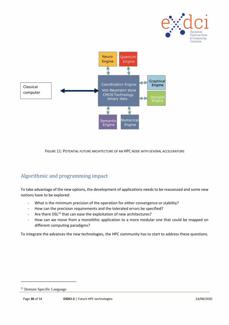
Most of the technologies presented in the previous sections are more complementary to current HPC system
technologies than a complete replacement solution. This leads to the question of the integration of these new
options within the current framework. Some of them can be viewed as accelerators that will take care of some
parts of the application while the rest will be computed by a classical system. Others such as NVM or IMC
needs a reshaping of the data and computing hierarchy.
Integration of accelerators or innovative data architectures (see fig 11) leads to the question of how to choose
either at compile time or at runtime between the several options for the execution of a computation and
storage of the data. The decision process will need the emergence of new compilation schemes or of new
runtime software.
Page 30 of 34 EXDCI-2 | Future HPC technologies 24/08/2020
FIGURE 11: POTENTIAL FUTURE ARCHITECTURE OF AN HPC NODE WITH SEVERAL ACCELERATORS
Algorithmic and programming impact
To take advantage of the new options, the development of applications needs to be reassessed and some new
notions have to be explored:
- What is the minimum precision of the operation for either convergence or stability?
- How can the precision requirements and the tolerated errors be specified?
- Are there DSL25 that can ease the exploitation of new architectures?
- How can we move from a monolithic application to a more modular one that could be mapped on
different computing paradigms?
To integrate the advances the new technologies, the HPC community has to start to address these questions.
25 Domain Specific Language
Classical
computer
Page 31 of 34 EXDCI-2 | Future HPC technologies 24/08/2020
Summary
It is clear that continuing scaling the CMOS technology will not be the major factor of performance increase in
the future, because we are reaching the limits of physics (and the cost to develop very advanced technology
nodes becomes very high). This analysis shows that the research paths are multiple and diverse in continue
increasing performance at affordable energy and cost. It is too ambitious to set priorities at this stage. A
precise assessment of the roadblocks and a risk/reward analysis would require more interactions and
significant work from the HPC, photonics and electronics research communities.
However, some of the technologies such as the 3D integration, dedicated and energy efficient accelerators
such as neuromorphic architectures, silicon photonics interconnects and analogue systems have a maturity
level which makes us believe that they will impact the HPC systems in a near future.
None of the technology paths will completely replace the current CMOS technology. The potential options are
more complementary, where the CMOS-based system could continue to act as an orchestrator of a diversity
of architectures and technologies. The integration of today’s and tomorrow’s computing/storage/networking
paradigms will be one of the challenges, together with the development of efficient software stacks that will
efficiently benefit from those emerging solutions while keeping the programming complexity to tractable
levels.

Page 32 of 34 EXDCI-2 | Future HPC technologies 24/08/2020
Conclusion and recommendations
EXDCI-2 has worked on connecting European experts from photonics, electronics and HPC. It has confirmed
the existence, in Europe, of research ideas with high potential for HPC (and for high performance edge
computing). The main conclusion is that research projects involving upstream technology providers and HPC
teams could deliver potential new solutions for HPC systems.
The new approaches are a combination of the three (or at least of two of them) degrees of freedom that can
be played with to deliver more performance in an energy efficient way:
- Switching from computing centric execution used by processors and GPU (akin to Von Neumann
architecture) to a data centric paradigm to reduce the overhead introduced by the data movement;
- Changing what is called an operation by playing with operand precision or introducing of multi-bits or
analogue coding or other ways of encoding information (e.g. Quantum),
- Introducing new materials that will deliver more efficient ways (in terms of timing and/or energy) to
store, switch and/or process information.
This gives a very broad set of options but only a few will emerge due to economic constraints, critical mass
issues, industrialization aspects, legacy and usability problems. To choose the most relevant research paths
and to accelerate the progress in Europe, we would like at the end of this white paper to propose 4
recommendations for the organization of the European research landscape.
R1: The interactions between the photonics, electronics and HPC communities have increased thanks
to the efforts of the EXDCI-2 project. The stakeholders have started a dialogue on how to work together
even if there are still some gaps in terms of language, expectations about maturity levels or working
habits. These interactions have been productive and should be continue beyond the time frame of the
EXDCI-2 project.
The way to implement a continuous interaction may be to have the domains ETPs (European Technology
Platforms) or equivalents to take over the initiative started by EXDCI-2. ETP4HPC, Photonics21 and
AENEAS can extend and amplify the dialogue to analyse the best way to work together and to assess
the potential of different research paths. This dialog can be implemented for example via technical
workshops such as the one organized by EXDCI-2 or other actions like webinars with mutual
presentations.
R1 Establish a continuous dialogue between photonics, electronics and HPC communities under the
supervision of Photonics21, AENEAS and ETP4HPC.
R2: In order to make this dialogue progress faster, it seems interesting to undertake small actions that
will work at the interface of the research teams. Even if it has not been successful achieved by EXDCI-2,
we believe that the development of a chain of producer/consumer research teams would be important
to achieve progress. Small actions could be implemented involving producer consumer research teams
to specify objectives, to propose common benchmarks, and to gather test data sets. These outputs could
help to focus the upstream research and deliver a way to evaluate the progress and so the potential of
different research paths.
Page 33 of 34 EXDCI-2 | Future HPC technologies 24/08/2020
These actions are not research projects per se but rather small efforts involving the two parts of a link
in the research chain. Experts from the two sides can deliver the outputs in a short time frame (6 months
seems enough) that will be used afterward for setting research project objectives and KPIs.
R2 Undertake small actions to specify research objectives, benchmarks and test data sets at the
interface of two research communities.
R3: After this study, we believe that in the next ten years the main path to increase HPC system
performance will be to integrate at low level new architectures (based or not on new materials). We do
not see the emergence of solutions that will radically replace the current technologies in this time frame.
Rather the new options will be complementary to the current one. To be efficient in this integration, it
is mandatory to do it at the lower level if we want to avoid costly data transfers and latencies. So, the
integration of heterogeneous chips or analogue technologies will be a must in the evolution of HPC.
Europe has interesting strengths in this field at the research level. If we want to have also a chance to
be successful at the industry level, we need to establish a standard for integration of heterogeneous
chips. This standard will allow the teams developing new accelerators to be sure that their work could
be integrated in a complete solution. Perhaps the word standard is too strong as the maturity of the
integration field is not yet achieved. Nevertheless, Europe needs to have experts to agree on common
specifications (that could be reviewed and evolutive) that will enable the integration of heterogeneous
chips. This effort could also be a way to push the European electronics industry to develop industrial
solutions as the market could be more stable and broader with this initiative.
This recommendation is also one of the EXDCI-2’s tasks on standards which has identified some strategic
domains where a European action on standards is of the utmost importance.
R3 Work on European specifications for the integration of heterogeneous chips.
R4: This EXDCI-2 initiative has showed that some European research ideas have good potential for future
HPC systems. To unleash them, research projects coupling upstream technologies providers and the
HPC community are mandatory. The results will not be for exascale systems even not for the first post
exascale systems, but we need to start the research projects soon if we want Europe to be in the position
to propose alternative solutions when the last CMOS technology processes will be reached.
The HPC systems and high performance edge devices can share some of the new technologies making
this investment even more attractive for Europe. The first analysis by European experts shows that
important benefits for science, industry and society depend on these new technologies.
The dialogue established within this task, also shows that the European stakeholders are motivated to
work together and see some potential for new technologies. The end of Moore’s law open the game
and Europe can re-position itself in the IT market. If we want to construct this European technology
value chain from basic technology up to HPC applications, we need to invest in a specific research
programme.
EuroHPC has great ambitions to reposition Europe in HPC. To construct the technology value chain of
the future HPC systems can be one of them.
Page 34 of 34 EXDCI-2 | Future HPC technologies 24/08/2020
R4 Launch a research program to develop new ideas coming from upstream technologies to provide
new solutions for upcoming HPC systems.
With the implementation of these 4 recommendations, we believe Europe can regain leadership in HPC
technologies.
Related Documents