BR Wiley/Razavi/Fundamentals of Microelectronics [Razavi.cls v. 2006] June 30, 2007 at 13:42 20 (1) 20 Chap. 1 Introduction to Microelectronics Amplification is an essential operation in many analog and digital systems. Analog circuits process signals that can assume various values at any time. By contrast, digital circuits deal with signals having only two levels and switching between these values at known points in time. Despite the “digital revolution,” analog circuits find wide application in most of today’s electronic systems. The voltage gain of an amplifier is defined as and sometimes expressed in decibels (dB) as . Kirchoff’s current law (KCL) states that the sum of all currents flowing into any node is zero. Kirchoff’s voltage law (KVL) states that the sum of all voltages around any loop is zero. Norton’s theorem allows simplifying a one-port circuit to a current source in parallel with an impedance. Similarly, Thevenin’s theorem reduces a one-port circuit to a voltage source in series with an impedance.

Welcome message from author
This document is posted to help you gain knowledge. Please leave a comment to let me know what you think about it! Share it to your friends and learn new things together.
Transcript

BR Wiley/Razavi/Fundamentals of Microelectronics [Razavi.cls v. 2006] June 30, 2007 at 13:42 20 (1)
20 Chap. 1 Introduction to Microelectronics
Amplification is an essential operation in many analog and digital systems.
Analog circuits process signals that can assume various values at any time. By contrast,
digital circuits deal with signals having only two levels and switching between these values
at known points in time.
Despite the “digital revolution,” analog circuits find wide application in most of today’s
electronic systems.
The voltage gain of an amplifier is defined as vout!vin and sometimes expressed in decibels(dB) as ! log%vout!vin&.
Kirchoff’s current law (KCL) states that the sum of all currents flowing into any node is
zero. Kirchoff’s voltage law (KVL) states that the sum of all voltages around any loop is
zero.
Norton’s theorem allows simplifying a one-port circuit to a current source in parallel with
an impedance. Similarly, Thevenin’s theorem reduces a one-port circuit to a voltage source
in series with an impedance.

BR Wiley/Razavi/Fundamentals of Microelectronics [Razavi.cls v. 2006] June 30, 2007 at 13:42 21 (1)
2
Basic Physics ofSemiconductors
Microelectronic circuits are based on complex semiconductor structures that have been under
active research for the past six decades. While this book deals with the analysis and design of
circuits, we should emphasize at the outset that a good understanding of devices is essential to
our work. The situation is similar to many other engineering problems, e.g., one cannot design a
high-performance automobile without a detailed knowledge of the engine and its limitations.
Nonetheless, we do face a dilemma. Our treatment of device physics must contain enough
depth to provide adequate understanding, but must also be sufficiently brief to allow quick entry
into circuits. This chapter accomplishes this task.
Our ultimate objective in this chapter is to study a fundamentally-important and versatile
device called the “diode.” However, just as we need to eat our broccoli before having desert, we
must develop a basic understanding of “semiconductor” materials and their current conduction
mechanisms before attacking diodes.
In this chapter, we begin with the concept of semiconductors and study the movement of
charge (i.e., the flow of current) in them. Next, we deal with the the “pn junction,” which also
serves as diode, and formulate its behavior. Our ultimate goal is to represent the device by a
circuit model (consisting of resistors, voltage or current sources, capacitors, etc.), so that a circuit
using such a device can be analyzed easily. The outline is shown below.
Charge Carriers
Doping
Transport of Carriers
PN Junction
Structure
Reverse and Forward
Bias Conditions
I/V Characteristics
Circuit Models
Semiconductors
It is important to note that the task of developing accurate models proves critical for all mi-
croelectronic devices. The electronics industry continues to place greater demands on circuits,
calling for aggressive designs that push semiconductor devices to their limits. Thus, a good un-
derstanding of the internal operation of devices is necessary.
As design managers often say, “If you do not push the devices and circuits to their limit but your competitor does,
then you lose to your competitor.”
21

BR Wiley/Razavi/Fundamentals of Microelectronics [Razavi.cls v. 2006] June 30, 2007 at 13:42 22 (1)
22 Chap. 2 Basic Physics of Semiconductors
2.1 Semiconductor Materials and Their Properties
Since this section introduces a multitude of concepts, it is useful to bear a general outline in
mind:
Charge Carriers
in Solids
Crystal Structure
Bandgap Energy
Holes
Modification of
Carrier Densities
Intrinsic Semiconductors
Extrinsic Semiconductors
Doping
Transport of
Carriers
Diffusion
Drift
Figure 2.1 Outline of this section.
This outline represents a logical thought process: (a) we identify charge carriers in solids and
formulate their role in current flow; (b) we examine means of modifying the density of charge
carriers to create desired current flow properties; (c) we determine current flow mechanisms.
These steps naturally lead to the computation of the current/voltage (I/V) characteristics of actual
diodes in the next section.
2.1.1 Charge Carriers in Solids
Recall from basic chemistry that the electrons in an atom orbit the nucleus in different “shells.”
The atom’s chemical activity is determined by the electrons in the outermost shell, called “va-
lence” electrons, and how complete this shell is. For example, neon exhibits a complete out-
ermost shell (with eight electrons) and hence no tendency for chemical reactions. On the other
hand, sodium has only one valence electron, ready to relinquish it, and chloride has seven valence
electrons, eager to receive one more. Both elements are therefore highly reactive.
The above principles suggest that atoms having approximately four valence electrons fall
somewhere between inert gases and highly volatile elements, possibly displaying interesting
chemical and physical properties. Shown in Fig. 2.2 is a section of the periodic table contain-
Boron
(B)
Carbon
(C)
Aluminum Silicon
(Al) (Si)
Phosphorous
(P)
Galium Germanium Arsenic
(Ge) (As)
III IV V
(Ga)
Figure 2.2 Section of the periodic table.
ing a number of elements with three to five valence electrons. As the most popular material in
microelectronics, silicon merits a detailed analysis.
Silicon is obtained from sand after a great deal of processing.

BR Wiley/Razavi/Fundamentals of Microelectronics [Razavi.cls v. 2006] June 30, 2007 at 13:42 23 (1)
Sec. 2.1 Semiconductor Materials and Their Properties 23
Covalent Bonds A silicon atom residing in isolation contains four valence electrons [Fig.
2.3(a)], requiring another four to complete its outermost shell. If processed properly, the sili-
Si Si
Si
Si
Si
Si
Si
Si
CovalentBond
Si
Si
Si
Si
Si
Si
Si
e
FreeElectron
(c)(a) (b)
Figure 2.3 (a) Silicon atom, (b) covalent bonds between atoms, (c) free electron released by thermal
energy.
con material can form a “crystal” wherein each atom is surrounded by exactly four others [Fig.
2.3(b)]. As a result, each atom shares one valence electron with its neighbors, thereby complet-
ing its own shell and those of the neighbors. The “bond” thus formed between atoms is called a
“covalent bond” to emphasize the sharing of valence electrons.
The uniform crystal depicted in Fig. 2.3(b) plays a crucial role in semiconductor devices. But,
does it carry current in response to a voltage? At temperatures near absolute zero, the valence
electrons are confined to their respective covalent bonds, refusing to move freely. In other words,
the silicon crystal behaves as an insulator for T K. However, at higher temperatures, elec-
trons gain thermal energy, occasionally breaking away from the bonds and acting as free charge
carriers [Fig. 2.3(c)] until they fall into another incomplete bond. We will hereafter use the term
“electrons” to refer to free electrons.
Holes When freed from a covalent bond, an electron leaves a “void” behind because the bond
is now incomplete. Called a “hole,” such a void can readily absorb a free electron if one becomes
available. Thus, we say an “electron-hole pair” is generated when an electron is freed, and an
“electron-hole recombination” occurs when an electron “falls” into a hole.
Why do we bother with the concept of the hole? After all, it is the free electron that actually
moves in the crystal. To appreciate the usefulness of holes, consider the time evolution illustrated
in Fig. 2.4. Suppose covalent bond number 1 contains a hole after losing an electron some time
Si
Si
Si
Si
Si
Si
Si
Si
Si
Si
Si
Si
Si
Si
1
2
Si
Si
Si
Si
Si
Si
Si
3
t = t1 t = t2 t = t3
Hole
Figure 2.4 Movement of electron through crystal.
before t ! t . At t ! t!, an electron breaks away from bond number 2 and recombines with the
hole in bond number 1. Similarly, at t ! t", an electron leaves bond number 3 and falls into thehole in bond number 2. Looking at the three “snapshots,” we can say one electron has traveled
from right to left, or, alternatively, one hole has moved from left to right. This view of current
flow by holes proves extremely useful in the analysis of semiconductor devices.
Bandgap Energy We must now answer two important questions. First, does any thermal
energy create free electrons (and holes) in silicon? No, in fact, a minimum energy is required to

BR Wiley/Razavi/Fundamentals of Microelectronics [Razavi.cls v. 2006] June 30, 2007 at 13:42 24 (1)
24 Chap. 2 Basic Physics of Semiconductors
dislodge an electron from a covalent bond. Called the “bandgap energy” and denoted by Eg , this
minimum is a fundamental property of the material. For silicon, Eg !!!" eV.
The second question relates to the conductivity of the material and is as follows. How many
free electrons are created at a given temperature? From our observations thus far, we postulate
that the number of electrons depends on bothEg and T : a greaterEg translates to fewer electrons,
but a higher T yields more electrons. To simplify future derivations, we consider the density (or
concentration) of electrons, i.e., the number of electrons per unit volume,ni, and write for silicon:
ni #!" !$!"T "# exp!Eg
"kTelectrons%cm (2.1)
where k !!01 !$ # J/K is called the Boltzmann constant. The derivation can be found in
books on semiconductor physics, e.g., [1]. As expected, materials having a larger Eg exhibit a
smaller ni. Also, as T " $, so do T "# and exp2!Eg%3"kT 45, thereby bringing ni toward zero.The exponential dependence of ni upon Eg reveals the effect of the bandgap energy on the
conductivity of the material. Insulators display a high Eg ; for example, Eg "!# eV for dia-
mond. Conductors, on the other hand, have a small bandgap. Finally, semiconductors exhibit a
moderate Eg , typically ranging from 1 eV to 1.5 eV.
Example 2.1Determine the density of electrons in silicon at T 0$$ K (room temperature) and T 6$$ K.
SolutionSince Eg !!!" eV !!78" !$ !$ J, we have
ni3T 0$$ K4 !!$1 !$!% electrons%cm (2.2)
ni3T 6$$ K4 !!#: !$!" electrons%cm ! (2.3)
Since for each free electron, a hole is left behind, the density of holes is also given by (2.2) and
(2.3).
ExerciseRepeat the above exercise for a material having a bandgap of 1.5 eV.
The ni values obtained in the above example may appear quite high, but, noting that siliconhas # !$## atoms%cm , we recognize that only one in # !$!# atoms benefit from a free
electron at room temperature. In other words, silicon still seems a very poor conductor. But, do
not despair! We next introduce a means of making silicon more useful.
2.1.2 Modification of Carrier Densities
Intrinsic and Extrinsic Semiconductors The “pure” type of silicon studied thus far is an
example of “intrinsic semiconductors,” suffering from a very high resistance. Fortunately, it is
possible to modify the resistivity of silicon by replacing some of the atoms in the crystal with
atoms of another material. In an intrinsic semiconductor, the electron density, n3 ni4, is equal
The unit eV (electron volt) represents the energy necessary to move one electron across a potential difference of 1
V. Note that 1 eV ! " !# !" J.

BR Wiley/Razavi/Fundamentals of Microelectronics [Razavi.cls v. 2006] June 30, 2007 at 13:42 25 (1)
Sec. 2.1 Semiconductor Materials and Their Properties 25
to the hole density, p. Thus,
np n i " (2.4)
We return to this equation later.
Recall from Fig. 2.2 that phosphorus (P) contains five valence electrons. What happens if
some P atoms are introduced in a silicon crystal? As illustrated in Fig. 2.5, each P atom shares
Si
Si
Si
Si
Si
Si
P e
Figure 2.5 Loosely-attached electon with phosphorus doping.
four electrons with the neighboring silicon atoms, leaving the fifth electron “unattached.” This
electron is free to move, serving as a charge carrier. Thus, if N phosphorus atoms are uniformly
introduced in each cubic centimeter of a silicon crystal, then the density of free electrons rises
by the same amount.
The controlled addition of an “impurity” such as phosphorus to an intrinsic semiconductor
is called “doping,” and phosphorus itself a “dopant.” Providing many more free electrons than
in the intrinsic state, the doped silicon crystal is now called “extrinsic,” more specifically, an
“n-type” semiconductor to emphasize the abundance of free electrons.As remarked earlier, the electron and hole densities in an intrinsic semiconductor are equal.
But, how about these densities in a doped material? It can be proved that even in this case,
np n i $ (2.5)
where n and p respectively denote the electron and hole densities in the extrinsic semiconductor.The quantity ni represents the densities in the intrinsic semiconductor (hence the subscript i) andis therefore independent of the doping level [e.g., Eq. (2.1) for silicon].
Example 2.2The above result seems quite strange. How can np remain constant while we add more donor
atoms and increase n?
SolutionEquation (2.5) reveals that p must fall below its intrinsic level as more n-type dopants are addedto the crystal. This occurs because many of the new electrons donated by the dopant “recombine”
with the holes that were created in the intrinsic material.
ExerciseWhy can we not say that n! p should remain constant?
Example 2.3A piece of crystalline silicon is doped uniformly with phosphorus atoms. The doping density is

BR Wiley/Razavi/Fundamentals of Microelectronics [Razavi.cls v. 2006] June 30, 2007 at 13:42 26 (1)
26 Chap. 2 Basic Physics of Semiconductors
! ! atoms/cm". Determine the electron and hole densities in this material at the room tempera-
ture.
SolutionThe addition of ! ! P atoms introduces the same number of free electrons per cubic centimeter.
Since this electron density exceeds that calculated in Example 2.1 by six orders of magnitude,
we can assume
n $ ! ! electrons"cm" (2.6)
It follows from (2.2) and (2.5) that
p $n#in
(2.7)
$ $ , !$ holes"cm" (2.8)
Note that the hole density has dropped below the intrinsic level by six orders of magnitude. Thus,
if a voltage is applied across this piece of silicon, the resulting current predominantly consists of
electrons.
ExerciseAt what doping level does the hole density drop by three orders of magnitude?
This example justifies the reason for calling electrons the “majority carriers” and holes the
“minority carriers” in an n-type semiconductor. We may naturally wonder if it is possible to
construct a “p-type” semiconductor, thereby exchanging the roles of electrons and holes.Indeed, if we can dope silicon with an atom that provides an insufficient number of electrons,
then we may obtain many incomplete covalent bonds. For example, the table in Fig. 2.2 suggests
that a boron (B) atom—with three valence electrons—can form only three complete covalent
bonds in a silicon crystal (Fig. 2.6). As a result, the fourth bond contains a hole, ready to absorb
Si
Si
Si
Si
Si
Si
B
Figure 2.6 Available hole with boron doping.
a free electron. In other words, N boron atoms contribute N boron holes to the conduction
of current in silicon. The structure in Fig. 2.6 therefore exemplifies a p-type semiconductor,providing holes as majority carriers. The boron atom is called an “acceptor” dopant.
Let us formulate our results thus far. If an intrinsic semiconductor is doped with a density of
ND (! ni) donor atoms per cubic centimeter, then the mobile charge densities are given by
Majority Carriers 4 n " ND (2.9)
Minority Carriers 4 p " n#iND
$ (2.10)
BR Wiley/Razavi/Fundamentals of Microelectronics [Razavi.cls v. 2006] June 30, 2007 at 13:42 27 (1)
Sec. 2.1 Semiconductor Materials and Their Properties 27
Similarly, for a density ofNA ( ni) acceptor atoms per cubic centimeter:
Majority Carriers + p ! NA (2.11)
Minority Carriers + n ! n iNA
# (2.12)
Since typical doping densities fall in the range of -.!" to -.!# atoms$cm$, the above expressions
are quite accurate.
Example 2.4Is it possible to use other elements of Fig. 2.2 as semiconductors and dopants?
SolutionYes, for example, some early diodes and transistors were based on germanium (Ge) rather than
silicon. Also, arsenic (As) is another common dopant.
ExerciseCan carbon be used for this purpose?
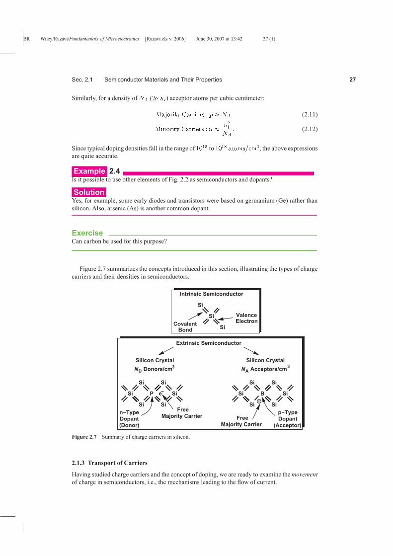
Figure 2.7 summarizes the concepts introduced in this section, illustrating the types of charge
carriers and their densities in semiconductors.
CovalentBond
Si
Si
SiElectronValence
Intrinsic Semiconductor
Extrinsic Semiconductor
Silicon Crystal
ND Donors/cm3
Silicon Crystal
N3
A Acceptors/cm
FreeMajority Carrier
Si
Si
Si
Si
Si
Si
P e
n−TypeDopant(Donor)
Si
Si
Si
Si
Si
Si
B
FreeMajority Carrier
Dopantp−Type
(Acceptor)
Figure 2.7 Summary of charge carriers in silicon.
2.1.3 Transport of Carriers
Having studied charge carriers and the concept of doping, we are ready to examine themovement
of charge in semiconductors, i.e., the mechanisms leading to the flow of current.

BR Wiley/Razavi/Fundamentals of Microelectronics [Razavi.cls v. 2006] June 30, 2007 at 13:42 28 (1)
28 Chap. 2 Basic Physics of Semiconductors
Drift We know from basic physics and Ohm’s law that a material can conduct current in re-
sponse to a potential difference and hence an electric field. The field accelerates the charge
carriers in the material, forcing some to flow from one end to the other. Movement of charge
carriers due to an electric field is called “drift.”!
Semiconductors behave in a similar manner. As shown in Fig. 2.8, the charge carriers are
E
Figure 2.8 Drift in a semiconductor.
accelerated by the field and accidentally collide with the atoms in the crystal, eventually reaching
the other end and flowing into the battery. The acceleration due to the field and the collision with
the crystal counteract, leading to a constant velocity for the carriers." We expect the velocity, v,to be proportional to the electric field strength, E:
v E" (2.13)
and hence
v #E" (2.14)
where # is called the “mobility” and usually expressed in cm#$#V ! s&. For example in silicon,the mobility of electrons, #n '()* cm#$#V ! s&, and that of holes, #p +,* cm#$#V ! s&.Of course, since electrons move in a direction opposite to the electric field, we must express the
velocity vector as
ve "#n
E % (2.15)
For holes, on the other hand,
vh #p
E % (2.16)
Example 2.5A uniform piece of n-type of silicon that is 1 #m long senses a voltage of 1 V. Determine the
velocity of the electrons.
SolutionSince the material is uniform, we have E V$L, where L is the length. Thus, E '*" ***V/cm and hence v #nE '%()# '*$ cm/s. In other words, electrons take #' #m&$#'%() #'*$ cm$s& -%+ ps to cross the 1-#m length.
Recall that the potential (voltage) difference, V , is equal to the negative integral of the electric field, E, with respectto distance: Vab
Ra
bEdx.
!The convention for direction of current assumes flow of positive charge from a positive voltage to a negative voltage.
Thus, if electrons flow from point A to point B, the current is considered to have a direction from B to A."This phenomenon is analogous to the “terminal velocity” that a sky diver with a parachute (hopefully, open)
experiences.

BR Wiley/Razavi/Fundamentals of Microelectronics [Razavi.cls v. 2006] June 30, 2007 at 13:42 29 (1)
Sec. 2.1 Semiconductor Materials and Their Properties 29
ExerciseWhat happens if the mobility is halved?
With the velocity of carriers known, how is the current calculated? We first note that an elec-
tron carries a negative charge equal to q !!" !# ! C. Equivalently, a hole carries a positivecharge of the same value. Now suppose a voltage V is applied across a uniform semiconductor
bar having a free electron density of n (Fig. 2.9). Assuming the electrons move with a velocity of
L
W h
xx1
t = t1 t = t
V1
1+ 1 s
metersv
xx1
V1
Figure 2.9 Current flow in terms of charge density.
v m/s, considering a cross section of the bar at x x and taking two “snapshots” at t t andt t $ ! second, we note that the total charge in v meters passes the cross section in 1 second.In other words, the current is equal to the total charge enclosed in v meters of the bar’s length.
Since the bar has a width ofW , we have:
I !v "W " h " n " q* (2.17)
where v "W " h represents the volume, n " q denotes the charge density in coulombs, and the
negative sign accounts for the fact that electrons carry negative charge.
Let us now reduce Eq. (2.17) to a more convenient form. Since for electrons, v !+nE, andsinceW " h is the cross section area of the bar, we write
Jn +nE " n " q* (2.18)
where Jn denotes the “current density,” i.e., the current passing through a unit cross section
area, and is expressed inA.cm". We may loosely say, “the current is equal to the charge velocity
times the charge density,” with the understanding that “current” in fact refers to current density,
and negative or positive signs are taken into account properly.
In the presence of both electrons and holes, Eq. (2.18) is modified to
Jtot +nE " n " q $ +pE " p " q (2.19)
q(+nn$ +pp)E! (2.20)
This equation gives the drift current density in response to an electric field E in a semiconductor
having uniform electron and hole densities.

BR Wiley/Razavi/Fundamentals of Microelectronics [Razavi.cls v. 2006] June 30, 2007 at 13:42 30 (1)
30 Chap. 2 Basic Physics of Semiconductors
Example 2.6In an experiment, it is desired to obtain equal electron and hole drift currents. How should the
carrier densities be chosen?
SolutionWe must impose
nn pp# (2.21)
and hence
n
p
p n
$ (2.22)
We also recall that np n i . Thus,
p
r n p
ni (2.23)
n
r p n
ni$ (2.24)
For example, in silicon, n% p !"#$%%&$ '$&!, yielding
p !$(&ni (2.25)
n $$#)(ni$ (2.26)
Since p and n are of the same order as ni, equal electron and hole drift currents can occur
for only a very lightly doped material. This confirms our earlier notion of majority carriers in
semiconductors having typical doping levels of !$!"-!$!# atoms%cm$.
ExerciseHow should the carrier densities be chosen so that the electron drift current is twice the hole
drift current?
Velocity Saturation We have thus far assumed that the mobility of carriers in semicon-
ductors is independent of the electric field and the velocity rises linearly with E according to
v E. In reality, if the electric field approaches sufficiently high levels, v no longer follows Elinearly. This is because the carriers collide with the lattice so frequently and the time between
the collisions is so short that they cannot accelerate much. As a result, v varies “sublinearly”
at high electric fields, eventually reaching a saturated level, vsat (Fig. 2.10). Called “velocity
saturation,” this effect manifests itself in some modern transistors, limiting the performance of
circuits.
In order to represent velocity saturation, we must modify v E accordingly. A simple
approach is to view the slope, , as a field-dependent parameter. The expression for must
This section can be skipped in a first reading.

BR Wiley/Razavi/Fundamentals of Microelectronics [Razavi.cls v. 2006] June 30, 2007 at 13:42 31 (1)
Sec. 2.1 Semiconductor Materials and Their Properties 31
E
vsat
µ 1
µ 2
Velocity
Figure 2.10 Velocity saturation.
therefore gradually fall toward zero as E rises, but approach a constant value for small E; i.e.,
! !
! " bE# (2.27)
where ! is the “low-field” mobility and b a proportionality factor. We may consider ! as the
“effective” mobility at an electric field E. Thus,
v !
! " bEE% (2.28)
Since for E !, v vsat, we have
vsat " b$ (2.29)
and hence b " %vsat. In other words,
v "
! "" E
vsat
E& (2.30)
Example 2.7A uniform piece of semiconductor 0.2 "m long sustains a voltage of 1 V. If the low-field mobility
is equal to 1350 cm!%%V " s( and the saturation velocity of the carriers !)" cm/s, determine
the effective mobility. Also, calculate the maximum allowable voltage such that the effective
mobility is only 10% lower than " .
SolutionWe have
E V
L(2.31)
*) kV%cm& (2.32)
It follows that
" "
! "" E
vsat
(2.33)
" ,&,*
(2.34)
!,- cm!%%V " s(& (2.35)

BR Wiley/Razavi/Fundamentals of Microelectronics [Razavi.cls v. 2006] June 30, 2007 at 13:42 32 (1)
32 Chap. 2 Basic Physics of Semiconductors
If the mobility must remain within 10% of its low-field value, then
!! "!
# $! E
vsat
$ (2.36)
and hence
E "#
!
vsat!
(2.37)
" %&' V%cm (2.38)
A device of length 0.2 !m experiences such a field if it sustains a voltage of +%&' V%cm, + & # ! cm, " #- .mV.
This example suggests that modern (submicron) devices incur substantial velocity saturation
because they operate with voltages much greater than 16.5 mV.
ExerciseAt what voltage does the mobility fall by 20%?
Diffusion In addition to drift, another mechanism can lead to current flow. Suppose a drop of
ink falls into a glass of water. Introducing a high local concentration of ink molecules, the drop
begins to “diffuse,” that is, the ink molecules tend to flow from a region of high concentration to
regions of low concentration. This mechanism is called “diffusion.”
A similar phenomenon occurs if charge carriers are “dropped” (injected) into a semiconduc-
tor so as to create a nonuniform density. Even in the absence of an electric field, the carriers
move toward regions of low concentration, thereby carrying an electric current so long as the
nonuniformity is sustained. Diffusion is therefore distinctly different from drift.
Figure 2.11 conceptually illustrates the process of diffusion. A source on the left continues
to inject charge carriers into the semiconductor, a nonuniform charge profile is created along the
x-axis, and the carriers continue to “roll down” the profile.
Injectionof Carriers
Nonuniform Concentration
Semiconductor Material
Figure 2.11 Diffusion in a semiconductor.
The reader may raise several questions at this point. What serves as the source of carriers in
Fig. 2.11? Where do the charge carriers go after they roll down to the end of the profile at the
far right? And, most importantly, why should we care?! Well, patience is a virtue and we will
answer these questions in the next section.
Example 2.8A source injects charge carriers into a semiconductor bar as shown in Fig. 2.12. Explain how the
current flows.

BR Wiley/Razavi/Fundamentals of Microelectronics [Razavi.cls v. 2006] June 30, 2007 at 13:42 33 (1)
Sec. 2.1 Semiconductor Materials and Their Properties 33
Injection
x
of Carriers
0
Figure 2.12 Injection of carriers into a semiconductor.
SolutionIn this case, two symmetric profiles may develop in both positive and negative directions along
the x-axis, leading to current flow from the source toward the two ends of the bar.
ExerciseIs KCL still satisfied at the point of injection?
Our qualitative study of diffusion suggests that the more nonuniform the concentration, the
larger the current. More specifically, we can write:
I dn
dx$ (2.39)
where n denotes the carrier concentration at a given point along the x-axis. We call dn%dx the
concentration “gradient” with respect to x, assuming current flow only in the x direction. If eachcarrier has a charge equal to q, and the semiconductor has a cross section area of A, Eq. (2.39)can be written as
I Aqdn
dx( (2.40)
Thus,
I AqDndn
dx$ (2.41)
whereDn is a proportionality factor called the “diffusion constant” and expressed in cm %s. For
example, in intrinsic silicon,Dn $% cm %s (for electrons), andDp &' cm
%s (for holes).As with the convention used for the drift current, we normalize the diffusion current to the
cross section area, obtaining the current density as
Jn qDndn
dx( (2.42)
Similarly, a gradient in hole concentration yields:
Jp !qDpdp
dx( (2.43)

BR Wiley/Razavi/Fundamentals of Microelectronics [Razavi.cls v. 2006] June 30, 2007 at 13:42 34 (1)
34 Chap. 2 Basic Physics of Semiconductors
With both electron and hole concentration gradients present, the total current density is given by
Jtot q
Dn
dn
dx Dp
dp
dx
!' (2.44)
Example 2.9Consider the scenario depicted in Fig. 2.11 again. Suppose the electron concentration is equal to
N at x ! and falls linearly to zero at x L (Fig. 2.13). Determine the diffusion current.
x
N
0
Injection
L
Figure 2.13 Current resulting from a linear diffusion profile.
SolutionWe have
Jn qDndn
dx(2.45)
qDn ! NL' (2.46)
The current is constant along the x-axis; i.e., all of the electrons entering the material at x !successfully reach the point at x L. While obvious, this observation prepares us for the next
example.
ExerciseRepeat the above example for holes.
Example 2.10Repeat the above example but assume an exponential gradient (Fig. 2.14):
x
N
0
Injection
L
Figure 2.14 Current resulting from an exponential diffusion profile.
n"x# N exp xLd
* (2.47)

BR Wiley/Razavi/Fundamentals of Microelectronics [Razavi.cls v. 2006] June 30, 2007 at 13:42 35 (1)
Sec. 2.2 PN Junction 35
where Ld is a constant.
SolutionWe have
Jn qDndn
dx(2.48)
qDnN
Ldexp
xLd
" (2.49)
Interestingly, the current is not constant along the x-axis. That is, some electrons vanish whiletraveling from x ! to the right. What happens to these electrons? Does this example violate
the law of conservation of charge? These are important questions and will be answered in the
next section.
ExerciseAt what value of x does the current density drop to 1% its maximum value?
Einstein Relation Our study of drift and diffusion has introduced a factor for each: #n (or
#p) andDn (orDp), respectively. It can be proved that # andD are related as:
D
#
kT
q" (2.50)
Called the “Einstein Relation,” this result is proved in semiconductor physics texts, e.g., [1]. Note
that kT(q ! "# mV at T $!! K.Figure 2.15 summarizes the charge transport mechanisms studied in this section.
E
Drift Current Diffusion Current
Jn =q µ n E
J =q µ p p
Jn =q nDdn
dx
J = q Ddx
− p
dpEp
n
p
Figure 2.15 Summary of drift and diffusion mechanisms.
2.2 PN Junction
We begin our study of semiconductor devices with the pn junction for three reasons. (1) The
device finds application in many electronic systems, e.g., in adapters that charge the batteries of
cellphones. (2) The pn junction is among the simplest semiconductor devices, thus providing a
The factor Ld is necessary to convert the exponent to a dimensionless quantity.

BR Wiley/Razavi/Fundamentals of Microelectronics [Razavi.cls v. 2006] June 30, 2007 at 13:42 36 (1)
36 Chap. 2 Basic Physics of Semiconductors
good entry point into the study of the operation of such complex structures as transistors. (3)
The pn junction also serves as part of transistors. We also use the term “diode” to refer to pnjunctions.
We have thus far seen that doping produces free electrons or holes in a semiconductor, and
an electric field or a concentration gradient leads to the movement of these charge carriers. An
interesting situation arises if we introduce n-type and p-type dopants into two adjacent sectionsof a piece of semiconductor. Depicted in Fig. 2.16 and called a “pn junction,” this structure playsa fundamental role in many semiconductor devices. The p and n sides are called the “anode” and
Si
Si
Si
Si
P e
Si
Si
Si
Si
B
n p
(a) (b)
AnodeCathode
Figure 2.16 PN junction.
the ”cathode,” respectively.
In this section, we study the properties and I/V characteristics of pn junctions. The following
outline shows our thought process, indicating that our objective is to develop circuit models that
can be used in analysis and design.
PN Junction
in Equilibrium
Depletion Region
Built−in Potential
PN Junction
Under Reverse Bias
Junction Capacitance
PN Junction
Under Forward Bias
I/V Characteristics
Figure 2.17 Outline of concepts to be studied.
2.2.1 PN Junction in Equilibrium
Let us first study the pn junction with no external connections, i.e., the terminals are open and
no voltage is applied across the device. We say the junction is in “equilibrium.”While seemingly
of no practical value, this condition provides insights that prove useful in understanding the
operation under nonequilibrium as well.
We begin by examining the interface between the n and p sections, recognizing that one sidecontains a large excess of holes and the other, a large excess of electrons. The sharp concentration
gradient for both electrons and holes across the junction leads to two large diffusion currents:
electrons flow from the n side to the p side, and holes flow in the opposite direction. Since we
must deal with both electron and hole concentrations on each side of the junction, we introduce
the notations shown in Fig. 2.18.
Example 2.11A pn junction employs the following doping levels:NA !"
! cm " andND % !" # cm ".Determine the hole and electron concentrations on the two sides.
SolutionFrom Eqs. (2.11) and (2.12), we express the concentrations of holes and electrons on the p side

BR Wiley/Razavi/Fundamentals of Microelectronics [Razavi.cls v. 2006] June 30, 2007 at 13:42 37 (1)
Sec. 2.2 PN Junction 37
n p
nn
np
pp
np
Majority
Minority
Majority
Minority
nn
np
ppnp
Carriers
Carriers Carriers
Carriers
: Concentration of electrons on n side
: Concentration of holes on n side
: Concentration of holes on p side
: Concentration of electrons on p sideFigure 2.18 .
respectively as:
pp NA (2.51)
!" ! cm " (2.52)
np n#iNA
(2.53)
%!#"&! !" $ cm "'#
!" ! cm "(2.54)
!#!! !"% cm "# (2.55)
Similarly, the concentrations on the n side are given by
nn ND (2.56)
(! !" & cm " (2.57)
pn n#iND
(2.58)
%!#"&! !" $ cm "'#(! !" & cm " (2.59)
)#*! !"% cm "# (2.60)
Note that the majority carrier concentration on each side is many orders of magnitude higher
than the minority carrier concentration on either side.
ExerciseRepeat the above example if ND drops by a factor of four.
The diffusion currents transport a great deal of charge from each side to the other, but they
must eventually decay to zero. This is because, if the terminals are left open (equilibrium condi-
tion), the device cannot carry a net current indefinitely.
We must now answer an important question: what stops the diffusion currents? We may pos-
tulate that the currents stop after enough free carriers have moved across the junction so as to
equalize the concentrations on the two sides. However, another effect dominates the situation and
stops the diffusion currents well before this point is reached.

BR Wiley/Razavi/Fundamentals of Microelectronics [Razavi.cls v. 2006] June 30, 2007 at 13:42 38 (1)
38 Chap. 2 Basic Physics of Semiconductors
To understand this effect, we recognize that for every electron that departs from the n side, a
positive ion is left behind, i.e., the junction evolves with time as conceptually shown in Fig. 2.19.
In this illustration, the junction is suddenly formed at t !, and the diffusion currents continueto expose more ions as time progresses. Consequently, the immediate vicinity of the junction is
depleted of free carriers and hence called the “depletion region.”
t t = t t == 0 1
n p
− − − −− − − −
− − − −− − − −
−
−
− − − −− − − −
− − − −
−
−
− − − − + + + ++++++
+ + + ++++++
+ + + ++++++
+ + + ++++++
FreeElectrons
FreeHoles
n p
− − −− − −
− − −− − −
−
−
− − −− − −
− − −
−
−
− − − + + +++++
+ + +++++
+ + +++++
+ + +++++
−−−−−
+++++
PositiveDonorIons Ions
NegativeAcceptor
n p
− − −− −
− − −− −
−
−
− − −− −
− −
−
−
− − − + + ++++
+ + ++++
+ + ++++
+ + ++++
−−−−−
+++++
+++++
−−−−−
DepletionRegion
Figure 2.19 Evolution of charge concentrations in a pn junction.
Now recall from basic physics that a particle or object carrying a net (nonzero) charge creates
an electric field around it. Thus, with the formation of the depletion region, an electric field
emerges as shown in Fig. 2.20. Interestingly, the field tends to force positive charge flow from
n p
− − −− −
− − −− −
−
−
− − −− −
− −
−
−
− − − + + ++++
+ + ++++
+ + ++++
+ + ++++
−−−−−
+++++
+++++
−−−−−
E
Figure 2.20 Electric field in a pn junction.
left to right whereas the concentration gradients necessitate the flow of holes from right to left
(and electrons from left to right). We therefore surmise that the junction reaches equilibrium once
the electric field is strong enough to completely stop the diffusion currents. Alternatively, we can
say, in equilibrium, the drift currents resulting from the electric field exactly cancel the diffusion
currents due to the gradients.
Example 2.12In the junction shown in Fig. 2.21, the depletion region has a width of b on the n side and a onthe p side. Sketch the electric field as a function of x.
SolutionBeginning at x & b, we note that the absence of net charge yields E !. At x ( b, eachpositive donor ion contributes to the electric field, i.e., the magnitude of E rises as x approacheszero. As we pass x !, the negative acceptor atoms begin to contribute negatively to the field,i.e., E falls. At x a, the negative and positive charge exactly cancel each other and E !.
The direction of the electric field is determined by placing a small positive test charge in the region and watching
how it moves: away from positive charge and toward negative charge.

BR Wiley/Razavi/Fundamentals of Microelectronics [Razavi.cls v. 2006] June 30, 2007 at 13:42 39 (1)
Sec. 2.2 PN Junction 39
n p
− −− −
− −−−
− − −− −
− −
−
−
− − + +++
+ ++
+ ++++
+ + ++++
−−−−−
+++++
+++++
−−−−−
E
x0 a− b
ND NA
−−
−
++
+
x0 a− b
E
Figure 2.21 Electric field profile in a pn junction.
ExerciseNoting that potential voltage is negative integral of electric field with respect to distance, plot
the potential as a function of x.
From our observation regarding the drift and diffusion currents under equilibrium, we may be
tempted to write:
jIdrift p Idrift nj ! jIdi% p Idi% nj" (2.61)
where the subscripts p and n refer to holes and electrons, respectively, and each current term
contains the proper polarity. This condition, however, allows an unrealistic phenomenon: if the
number of the electrons flowing from the n side to the p side is equal to that of the holes goingfrom the p side to the n side, then each side of this equation is zero while electrons continue
to accumulate on the p side and holes on the n side. We must therefore impose the equilibrium
condition on each carrier:
jIdrift pj jIdi% pj (2.62)
jIdrift nj jIdi% nj! (2.63)
Built-in Potential The existence of an electric field within the depletion region suggests that
the junction may exhibit a “built-in potential.” In fact, using (2.62) or (2.63), we can compute
this potential. Since the electric field E !dV%dx, and since (2.62) can be written as
q(ppE qDpdp
dx+ (2.64)
we have
!(ppdV
dx Dp
dp
dx! (2.65)
Dividing both sides by p and taking the integral, we obtain
!(p
Z x
x!
dV Dp
Z pp
pn
dp
p+ (2.66)

BR Wiley/Razavi/Fundamentals of Microelectronics [Razavi.cls v. 2006] June 30, 2007 at 13:42 40 (1)
40 Chap. 2 Basic Physics of Semiconductors
n p
nn
np
pp
np
xxx 1 2
Figure 2.22 Carrier profiles in a pn junction.
where pn and pp are the hole concentrations at x and x!, respectively (Fig. 2.22). Thus,
V x!! V x ! " Dp
$pln
pppn
% (2.67)
The right side represents the voltage difference developed across the depletion region and will
be denoted by V". Also, from Einstein’s relation, Eq. (2.50), we can replaceDp&$p with kT&q:
jV"j " kT
qln
pppn
% (2.68)
ExerciseWriting Eq. (2.64) for electron drift and diffusion currents, and carrying out the integration,
derive an equation for V" in terms of nn and np.
Finally, using (2.11) and (2.10) for pp and pn yields
V" "kT
qln
NAND
n!i% (2.69)
Expressing the built-in potential in terms of junction parameters, this equation plays a central
role in many semiconductor devices.
Example 2.13A silicon pn junction employsNA " %" &' # cm $ andND " *" &' # cm $. Determine thebuilt-in potential at room temperature (T " +'' K).
SolutionRecall from Example 2.1 that ni T " +'' K! " &%'-" &' " cm $. Thus,
V" # %. mV! ln %" &' #!" *" &' #!
&%'-" &' "!!(2.70)
# 0.- mV% (2.71)
ExerciseBy what factor should ND be changed to lower V" by 20 mV?

BR Wiley/Razavi/Fundamentals of Microelectronics [Razavi.cls v. 2006] June 30, 2007 at 13:42 41 (1)
Sec. 2.2 PN Junction 41
Example 2.14Equation (2.69) reveals that V is a weak function of the doping levels. How much does V change if NA or ND is increased by one order of magnitude?
SolutionWe can write
V ! VT ln$%NA ND
n!i! VT ln
NA NDn!i
(2.72)
! VT ln $% (2.73)
" &% mV )at T ! ,%% K.$ (2.74)
ExerciseHow much does V change if NA or ND is increased by a factor of three?
An interesting question may arise at this point. The junction carries no net current (because its
terminals remain open), but it sustains a voltage. How is that possible? We observe that the built-
in potential is developed to oppose the flow of diffusion currents (and is, in fact, sometimes called
the “potential barrier.”). This phenomenon is in contrast to the behavior of a uniform conducting
material, which exhibits no tendency for diffusion and hence no need to create a built-in voltage.
2.2.2 PN Junction Under Reverse Bias
Having analyzed the pn junction in equilibrium, we can now study its behavior under more
interesting and useful conditions. Let us begin by applying an external voltage across the device
as shown in Fig. 2.23, where the voltage source makes the n side more positive than the p side.We say the junction is under “reverse bias” to emphasize the connection of the positive voltage
to the n terminal. Used as a noun or a verb, the term “bias” indicates operation under some
“desirable” conditions. We will study the concept of biasing extensively in this and following
chapters.
We wish to reexamine the results obtained in equilibrium for the case of reverse bias. Let
us first determine whether the external voltage enhances the built-in electric field or opposes it.
Since under equilibrium,
E is directed from the n side to the p side, VR enhances the field. But, a
higher electric field can be sustained only if a larger amount of fixed charge is provided, requiring
that more acceptor and donor ions be exposed and, therefore, the depletion region be widened.
What happens to the diffusion and drift currents? Since the external voltage has strengthened
the field, the barrier rises even higher than that in equilibrium, thus prohibiting the flow of current.
In other words, the junction carries a negligible current under reverse bias."
With no current conduction, a reverse-biased pn junction does not seem particularly useful.
However, an important observation will prove otherwise. We note that in Fig. 2.23, as VB in-
creases, more positive charge appears on the n side and more negative charge on the p side.
As explained in Section 2.2.3, the current is not exactly zero.

BR Wiley/Razavi/Fundamentals of Microelectronics [Razavi.cls v. 2006] June 30, 2007 at 13:42 42 (1)
42 Chap. 2 Basic Physics of Semiconductors
n p
− − −− −
− − −− −
−
−
− − −− −
− −
−
−
− − − + + ++++
+ + ++++
+ + ++++
+ + ++++
−−−−−
+++++
+++++
−−−−−
n p
− −−
− −−
−
−
− −−
−
−
−
− − + +++
+ +++
+ +++
+ +++
−−−−−
+++++
+++++
−−−−−
VR
−−−−−
+++++
Figure 2.23 PN junction under reverse bias.
Thus, the device operates as a capacitor [Fig. 2.24(a)]. In essence, we can view the conductive
n and p sections as the two plates of the capacitor. We also assume the charge in the depletion
region equivalently resides on each plate.
n p
− − −− −
− − −− −
−
−
− − −− −
− −
−
−
− − − + + ++++
+ + ++++
+ + ++++
+ + ++++
−−−−−
+++++
+++++
−−−−−
− −−
− −−
−
−
− −−
−
−
−
− − + +++
+ +++
+ +++
+ +++
−−−−−
+++++
+++++
−−−−−
−−−−−
+++++
V
++++
−−
−−
VR1
R1 n pV
++++
−−
−−
V
R2
R2 VR1
(a) (b)
−
(more negative than )
Figure 2.24 Reduction of junction capacitance with reverse bias.
The reader may still not find the device interesting. After all, since any two parallel plates can
form a capacitor, the use of a pn junction for this purpose is not justified. But, reverse-biased
pn junctions exhibit a unique property that becomes useful in circuit design. Returning to Fig.
2.23, we recognize that, as VR increases, so does the width of the depletion region. That is, the
conceptual diagram of Fig. 2.24(a) can be drawn as in Fig. 2.24(b) for increasing values of VR,revealing that the capacitance of the structure decreases as the two plates move away from each
other. The junction therefore displays a voltage-dependent capacitance.
It can be proved that the capacitance of the junction per unit area is equal to
Cj Cj r! VR
V
$ (2.75)

BR Wiley/Razavi/Fundamentals of Microelectronics [Razavi.cls v. 2006] June 30, 2007 at 13:42 43 (1)
Sec. 2.2 PN Junction 43
where Cj denotes the capacitance corresponding to zero bias (VR !) and V is the built-inpotential [Eq. (2.69)]. (This equation assumes VR is negative for reverse bias.) The value of Cj
is in turn given by
Cj
r"siq
"
NANDNA ND
!
V " (2.76)
where #si represents the dielectric constant of silicon and is equal to !!$" #$#$ !% !" F/cm.! Plotted in Fig. 2.25, Cj indeed decreases as VR increases.
VR0
C j
Figure 2.25 Junction capacitance under reverse bias.
Example 2.15A pn junction is doped with NA & ' !%!# cm $ and ND & ( !%!% cm $. Determine thecapacitance of the device with (a) VR & % and VR & ! V.
SolutionWe first obtain the built-in potential:
V & VT lnNANDn&i
(2.77)
& %$"+ V$ (2.78)
Thus, for VR & % and q & !$- !% !' C, we have
Cj &
r#siq
'
NANDNA ND
! !V
(2.79)
& '$-$ !% ( F)cm&$ (2.80)
In microelectronics, we deal with very small devices and may rewrite this result as
Cj & %$'-$ fF)*m&" (2.81)
where 1 fF (femtofarad)& !% !% F. For VR & ! V,
Cj &Cj r!
VRV
(2.82)
& %$!"' fF)*m&$ (2.83)
!The dielectric constant of materials is usually written in the form r !, where r is the “relative” dielectric constantand a dimensionless factor (e.g., 11.7), and ! the dielectric constant of vacuum ( ! ! "# " F/cm).

BR Wiley/Razavi/Fundamentals of Microelectronics [Razavi.cls v. 2006] June 30, 2007 at 13:42 44 (1)
44 Chap. 2 Basic Physics of Semiconductors
ExerciseRepeat the above example if the donor concentration on the N side is doubled. Compare the
results in the two cases.
The variation of the capacitance with the applied voltage makes the device a “nonlinear”
capacitor because it does not satisfy Q CV . Nonetheless, as demonstrated by the followingexample, a voltage-dependent capacitor leads to interesting circuit topologies.
Example 2.16A cellphone incorporates a 2-GHz oscillator whose frequency is defined by the resonance fre-
quency of an LC tank (Fig. 2.26). If the tank capacitance is realized as the pn junction of
Example 2.15, calculate the change in the oscillation frequency while the reverse voltage goes
from 0 to 2 V. Assume the circuit operates at 2 GHz at a reverse voltage of 0 V, and the junction
area is 2000 'm .
LC
Oscillator
VR
Figure 2.26 Variable capacitor used to tune an oscillator.
SolutionRecall from basic circuit theory that the tank “resonates” if the impedances of the inductor and
the capacitor are equal and opposite: jL)res "jC)res# !. Thus, the resonance frequency isequal to
fres $
%+
$pLC, (2.84)
At VR &, Cj &,%'( fF/'m , yielding a total device capacitance of
Cj%tot"VR &# "&,%'( fF-'m #" "%&&& 'm # (2.85)
(+& fF, (2.86)
Setting fres to 2 GHz, we obtain
L $$,, nH, (2.87)
If VR goes to 2 V,
Cj%tot"VR % V# Cj"r$ 0
%
&,1+
" %&&& 'm (2.88)
%12 fF, (2.89)

BR Wiley/Razavi/Fundamentals of Microelectronics [Razavi.cls v. 2006] June 30, 2007 at 13:42 45 (1)
Sec. 2.2 PN Junction 45
Using this value along with L !!!" nH in Eq. (2.84), we have
fres#VR $ V& $!'" GHz! (2.90)
An oscillator whose frequency can be varied by an external voltage (VR in this case) is called
a “voltage-controlled oscillator” and used extensively in cellphones, microprocessors, personal
computers, etc.
ExerciseSome wireless systems operate at 5.2 GHz. Repeat the above example for this frequency,
assuming the junction area is still 2000 $m but the inductor value is scaled to reach 5.2
GHz.
In summary, a reverse-biased pn junction carries a negligible current but exhibits a voltage-
dependent capacitance. Note that we have tacitly developed a circuit model for the device under
this condition: a simple capacitance whose value is given by Eq. (2.75).
Another interesting application of reverse-biased diodes is in digital cameras (Chapter 1). If
light of sufficient energy is applied to a pn junction, electrons are dislodged from their covalent
bonds and hence electron-hole pairs are created. With a reverse bias, the electrons are attracted to
the positive battery terminal and the holes to the negative battery terminal. As a result, a current
flows through the diode that is proportional to the light intensity. We say the pn junction operatesas a “photodiode.”
2.2.3 PN Junction Under Forward Bias
Our objective in this section is to show that the pn junction carries a current if the p side is raisedto a more positive voltage than the n side (Fig. 2.27). This condition is called “forward bias.”
We also wish to compute the resulting current in terms of the applied voltage and the junction
parameters, ultimately arriving at a circuit model.
V
n p
− − −− − −
− − −− − −
−
−
− − −− − −
− − −
−
−
− − − + + +++++
+ + +++++
+ + +++++
+ + +++++
−−−−−
+++++
F
Figure 2.27 PN junction under forward bias.
From our study of the device in equilibrium and reverse bias, we note that the potential barrier
developed in the depletion region determines the device’s desire to conduct. In forward bias, the
external voltage, VF , tends to create a field directed from the p side toward the n side—opposite
to the built-in field that was developed to stop the diffusion currents. We therefore surmise that
VF in fact lowers the potential barrier by weakening the field, thus allowing greater diffusion
currents.

BR Wiley/Razavi/Fundamentals of Microelectronics [Razavi.cls v. 2006] June 30, 2007 at 13:42 46 (1)
46 Chap. 2 Basic Physics of Semiconductors
To derive the I/V characteristic in forward bias, we begin with Eq. (2.68) for the built-in
voltage and rewrite it as
pn!e pp!e
expV VT
! (2.91)
where the subscript e emphasizes equilibrium conditions [Fig. 2.28(a)] and VT kT%q is called
VF
n p
n
p
p
n
n p
n pn,e
n,e
p,e
p,e
n,f
pn,f
p,f
(a) (b)
pn,e
np,f
np,f
Figure 2.28 Carrier profiles (a) in equilibrium and (b) under forward bias.
the “thermal voltage” ( !" mV at T #$$ K). In forward bias, the potential barrier is loweredby an amount equal to the applied voltage:
pn"f pp"f
expV ! VFVT
( (2.92)
where the subscript f denotes forward bias. Since the exponential denominator drops consider-
ably, we expect pn"f to be much higher than pn"e (it can be proved that pp"f pp"e NA).
In other words, the minority carrier concentration on the p side rises rapidly with the forwardbias voltage while the majority carrier concentration remains relatively constant. This statement
applies to the n side as well.
Figure 2.28(b) illustrates the results of our analysis thus far. As the junction goes from equi-
librium to forward bias, np and pn increase dramatically, leading to a proportional change in thediffusion currents.!! We can express the change in the hole concentration on the n side as:
(pn pn"f ! pn"e (2.93)
pp"f
expV ! VFVT
! pp"e
expV VT
(2.94)
NA
expV VT
)expVFVT
! *+( (2.95)
Similarly, for the electron concentration on the p side:
(np ND
expV VT
)expVFVT
! *+( (2.96)
The width of the depletion region actually decreases in forward bias but we neglect this effect here.

BR Wiley/Razavi/Fundamentals of Microelectronics [Razavi.cls v. 2006] June 30, 2007 at 13:42 47 (1)
Sec. 2.2 PN Junction 47
Note that Eq. (2.69) indicates that exp#V !VT $ % NAND!n!i .
The increase in the minority carrier concentration suggests that the diffusion currents must
rise by a proportional amount above their equilibrium value, i.e.,
Itot NA
expV VT
#expVFVT
! &$ 'ND
expV VT
#expVFVT
! &$% (2.97)
Indeed, it can be proved that [1]
Itot % IS#expVFVT
! &$& (2.98)
where IS is called the “reverse saturation current” and given by
IS % Aqn!i #Dn
NALn'
Dp
NDLp$% (2.99)
In this equation, A is the cross section area of the device, and Ln and Lp are electron and hole“diffusion lengths,” respectively. Diffusion lengths are typically in the range of tens of microm-
eters. Note that the first and second terms in the parentheses correspond to the flow of electrons
and holes, respectively.
Example 2.17Determine IS for the junction of Example 2.13 at T % ())K if A % &)) ,m!, Ln % *) ,m,and Lp % () ,m.
SolutionUsing q % &%+" &) "# C, ni % &%)," &)" electrons!cm$ [Eq. (2.2)],Dn % (5 cm!!s, andDp % &* cm!!s, we have
IS % &%66" &) "% A% (2.100)
Since IS is extremely small, the exponential term in Eq. (2.98) must assume very large values so
as to yield a useful amount (e.g., 1 mA) for Itot.
ExerciseWhat junction area is necessary to raise IS to &) "& A.
An interesting question that arises here is: are the minority carrier concentrations constant
along the x-axis? Depicted in Fig. 2.29(a), such a scenario would suggest that electrons continueto flow from the n side to the p side, but exhibit no tendency to go beyond x % x! because ofthe lack of a gradient. A similar situation exists for holes, implying that the charge carriers do
not flow deep into the p and n sides and hence no net current results! Thus, the minority carrier
concentrations must vary as shown in Fig. 2.29(b) so that diffusion can occur.
This observation reminds us of Example 2.10 and the question raised in conjunction with it:
if the minority carrier concentration falls with x, what happens to the carriers and how can the
current remain constant along the x-axis? Interestingly, as the electrons enter the p side and rolldown the gradient, they gradually recombine with the holes, which are abundant in this region.

BR Wiley/Razavi/Fundamentals of Microelectronics [Razavi.cls v. 2006] June 30, 2007 at 13:42 48 (1)
48 Chap. 2 Basic Physics of Semiconductors
VF
n p
n p
n
n,f
pn,f
p,f
p,f
(a) (b)
ElectronFlow Flow
Hole
−−
−−
++
++
V
n p
n p
n
n,f
pn,f
p,f
p,f
ElectronFlow Flow
Hole
−−
−−
++
++ − − −
+++
F
xx1 x2 xx1 x2
Figure 2.29 (a) Constant and (b) variable majority carrier profiles ioutside the depletion region.
Similarly, the holes entering the n side recombine with the electrons. Thus, in the immediate
vicinity of the depletion region, the current consists of mostly minority carriers, but towards the
far contacts, it is primarily comprised of majority carriers (Fig. 2.30). At each point along the
x-axis, the two components add up to Itot.
V
n p
++
++ ++
+++
+
−−−−
−−−
−− − +
+++ ++
+++
+−−−−
−−−
−− −
x
F
Figure 2.30 Minority and majority carrier currents.
2.2.4 I/V Characteristics
Let us summarize our thoughts thus far. In forward bias, the external voltage opposes the built-in
potential, raising the diffusion currents substantially. In reverse bias, on the other hand, the ap-
plied voltage enhances the field, prohibiting current flow.We hereafterwrite the junction equation
as:
ID IS!expVD
VT %&$ (2.101)
where ID and VD denote the diode current and voltage, respectively. As expected, VD ' yieldsID '. (Why is this expected?) As VD becomes positive and exceeds severalVT , the exponential
term grows rapidly and ID ! IS exp!VD%VT &. We hereafter assume exp!VD%VT & " % in theforward bias region.
It can be proved that Eq. (2.101) also holds in reverse bias, i.e., for negative VD. If VD & 'and jVDj reaches several VT , then exp!VD%VT &$ % and
ID ! IS ' (2.102)

BR Wiley/Razavi/Fundamentals of Microelectronics [Razavi.cls v. 2006] June 30, 2007 at 13:42 49 (1)
Sec. 2.2 PN Junction 49
Figure 2.31 plots the overall I/V characteristic of the junction, revealing why IS is called the
“reverse saturation current.” Example 2.17 indicates that IS is typically very small. We therefore
VD
I D
I expV
VT
D
I S−
ReverseBias Bias
Forward
S
Figure 2.31 I-V characteristic of a pn junction.
view the current under reverse bias as “leakage.” Note that IS and hence the junction current
are proportional to the device cross section area [Eq. (2.99)]. For example, two identical devices
placed in parallel (Fig. 2.32) behave as a single junction with twice the IS .
n p
n p
A
A
VF
n p
VF
A2
Figure 2.32 Equivalence of parallel devices to a larger device.
Example 2.18Each junction in Fig. 2.32 employs the doping levels described in Example 2.13. Determine the
forward bias current of the composite device for VD !""mV and 800 mV at T !"" K.
SolutionFrom Example 2.17, IS ##$$ #" ! A for each junction. Thus, the total current is equal to
ID"tot%VD !"" mV( )IS%expVDVT
! (2.103)
" # $# pA (2.104)
Similarly, for VD " '(( mV:
ID"tot)VD " '(( mV! " ', #A (2.105)
ExerciseHow many of these diodes must be placed in parallel to obtain a current of 100 #A with a

BR Wiley/Razavi/Fundamentals of Microelectronics [Razavi.cls v. 2006] June 30, 2007 at 13:42 50 (1)
50 Chap. 2 Basic Physics of Semiconductors
voltage of 750 mV.
Example 2.19A diode operates in the forward bias region with a typical current level [i.e.,
ID IS exp#VD"VT $]. Suppose we wish to increase the current by a factor of 10. How
much change in VD is required?
SolutionLet us first express the diode voltage as a function of its current:
VD % VT lnIDIS
# (2.106)
We define I % ()ID and seek the corresponding voltage, VD :
VD % VT ln()IDIS
(2.107)
% VT lnIDIS
* VT ln () (2.108)
% VD * VT ln ()# (2.109)
Thus, the diode voltagemust rise by VT ln () +)mV (at T % ,))K) to accommodate a tenfoldincrease in the current. We say the device exhibits a 60-mV/decade characteristic, meaning VDchanges by 60 mV for a decade (tenfold) change in ID . More generally, an n-fold change in IDtranslates to a change of VT lnn in VD.
ExerciseBy what factor does the current change if the voltages changes by 120 mV?
Example 2.20The cross section area of a diode operating in the forward bias region is increased by a factor of
10. (a) Determine the change in ID if VD is maintained constant. (b) Determine the change in
VD if ID is maintained constant. Assume ID IS exp#VD"VT $.
Solution(a) Since IS ! A, the new current is given by
ID % ()IS expVDVT
(2.110)
% ()ID# (2.111)
(b) From the above example,
VD % VT lnID()IS
(2.112)
% VT lnIDIS" VT ln ()# (2.113)

BR Wiley/Razavi/Fundamentals of Microelectronics [Razavi.cls v. 2006] June 30, 2007 at 13:42 51 (1)
Sec. 2.2 PN Junction 51
Thus, a tenfold increase in the device area lowers the voltage by 60 mV if ID remains constant.
ExerciseA diode in forward bias with ID IS exp#VD"VT $ undergoes two simultaneous changes: thecurrent is raised by a factor ofm and the area is increased by a factor of n. Determine the changein the device voltage.
Constant-Voltage Model The exponential I/V characteristic of the diode results in nonlinear
equations, making the analysis of circuits quite difficult. Fortunately, the above examples imply
that the diode voltage is a relatively weak function of the device current and cross section area.
With typical current levels and areas, VD falls in the range of 700 - 800 mV. For this reason, we
often approximate the forward bias voltage by a constant value of 800 mV (like an ideal battery),
considering the device fully off if VD % %&&mV. The resulting characteristic is illustrated in Fig.2.33(a) with the turn-on voltage denoted by VD#on. Note that the current goes to infinity as VDtends to exceed VD#on because we assume the forward-biased diode operates as an ideal voltagesource. Neglecting the leakage current in reverse bias, we derive the circuit model shown in Fig.
2.33(b). We say the junction operates as an open circuit if VD % VD#on and as a constant voltagesource if we attempt to increase VD beyond VD#on. While not essential, the voltage source placed
in series with the switch in the off condition helps simplify the analysis of circuits: we can say
that in the transition from off to on, only the switch turns on and the battery always resides in
series with the switch.
VD
I D
VD,on
(a) (b)
VD,on
Forward Bias
Reverse Bias
VD,on
Figure 2.33 Constant-voltage diode model.
A number of questions may cross the reader’s mind at this point. First, why do we subject
the diode to such a seemingly inaccurate approximation? Second, if we indeed intend to use this
simple approximation, why did we study the physics of semiconductors and pn junctions in such
detail?
The developments in this chapter are representative of our treatment of all semiconductor de-
vices: we carefully analyze the structure and physics of the device to understand its operation; we
construct a “physics-based” circuit model; and we seek to approximate the resulting model, thus
arriving at progressively simpler representations. Device models having different levels of com-
plexity (and, inevitably, different levels of accuracy) prove essential to the analysis and design
of circuits. Simple models allow a quick, intuitive understanding of the operation of a complex
circuit, while more accurate models reveal the true performance.
Example 2.21Consider the circuit of Fig. 2.34. Calculate IX for VX ' ( V and VX ' ) V using (a) an
exponential model with IS ' )& ! A and (b) a constant-voltage model with VD#on ' %&&mV.

BR Wiley/Razavi/Fundamentals of Microelectronics [Razavi.cls v. 2006] June 30, 2007 at 13:42 52 (1)
52 Chap. 2 Basic Physics of Semiconductors
VR1
1D VD
= 1 kΩ
X
I X
Figure 2.34 Simple circuit using a diode.
Solution(a) Noting that ID IX , we have
VX IXR ! VD (2.114)
VD VT lnIXIS
# (2.115)
This equation must be solved by iteration: we guess a value for VD , compute the correspondingIX from IXR VX VD , determine the new value of VD from VD VT ln$IX$IS% anditerate. Let us guess VD &'(mV and hence
IX VX VD
R (2.116)
) V (#&' V
+ k-(2.117)
.#.' mA# (2.118)
Thus,
VD VT lnIXIS
(2.119)
&11 mV# (2.120)
With this new value of VD, we can obtain a more accurate value for IX :
IX ) V (#&11 V
+ k-(2.121)
.#.(+ mA# (2.122)
We note that the value of IX rapidly converges. Following the same procedure for VX + V, wehave
IX + V (#&' V
+ k-(2.123)
(#.' mA% (2.124)
which yields VD (#&2. V and hence IX (#.'3 mA. (b) A constant-voltage model readily
gives
IX .#. mA for VX ) V (2.125)
IX (#. mA for VX + V# (2.126)

BR Wiley/Razavi/Fundamentals of Microelectronics [Razavi.cls v. 2006] June 30, 2007 at 13:42 53 (1)
Sec. 2.3 Reverse Breakdown 53
The value of IX incurs some error, but it is obtained with much less computational effort than
that in part (a).
ExerciseRepeat the above example if the cross section area of the diode is increased by a factor of
10.
2.3 Reverse Breakdown
Recall from Fig. 2.31 that the pn junction carries only a small, relatively constant current in re-
verse bias. However, as the reverse voltage across the device increases, eventually “breakdown”
occurs and a sudden, enormous current is observed. Figure 2.35 plots the device I/V characteris-
tic, displaying this effect.
VD
I D
VBD
Breakdown
Figure 2.35 Reverse breakdown characteristic.
The breakdown resulting from a high voltage (and hence a high electric field) can occur in
any material. A common example is lightning, in which case the electric field in the air reaches
such a high level as to ionize the oxygen molecules, thus lowering the resistance of the air and
creating a tremendous current.
The breakdown phenomenon in pn junctions occurs by one of two possible mechanisms:
“Zener effect” and “avalanche effect.”
2.3.1 Zener Breakdown
The depletion region in a pn junction contains atoms that have lost an electron or a hole and,
therefore, provide no loosely-connected carriers. However, a high electric field in this region
may impart enough energy to the remaining covalent electrons to tear them from their bonds
[Fig. 2.36(a)]. Once freed, the electrons are accelerated by the field and swept to the n side of
the junction. This effect occurs at a field strength of about ! V/cm (1 V/#m).In order to create such high fields with reasonable voltages, a narrow depletion region is
required, which from Eq. (2.76) translates to high doping levels on both sides of the junction
(why?). Called the “Zener effect,” this type of breakdown appears for reverse bias voltages on
the order of 3-8 V.
This section can be skipped in a first reading.

BR Wiley/Razavi/Fundamentals of Microelectronics [Razavi.cls v. 2006] June 30, 2007 at 13:42 54 (1)
54 Chap. 2 Basic Physics of Semiconductors
Si
Si
Si
Si
Si
e
n pE
e
VR
Si
Si
Si
Si
Si
ee
n pE
VR
e
e
e
e
e
e
e
ee
(a)(b)
Figure 2.36 (a) Release of electrons due to high electric field, (b) avalanche effect.
2.3.2 Avalanche Breakdown
Junctions with moderate or low doping levels ( ! ! cm") generally exhibit no Zener break-
down. But, as the reverse bias voltage across such devices increases, an avalanche effect takes
place. Even though the leakage current is very small, each carrier entering the depletion region
experiences a very high electric field and hence a large acceleration, thus gaining enough energy
to break the electrons from their covalent bonds. Called “impact ionization,” this phenomenon
can lead to avalanche: each electron freed by the impact may itself speed up so much in the field
as to collide with another atom with sufficient energy, thereby freeing one more covalent-bond
electron. Now, these two electrons may again acquire energy and cause more ionizing collisions,
rapidly raising the number of free carriers.
An interesting contrast between Zener and avalanche phenomena is that they display opposite
temperature coefficients (TCs): VBD has a negative TC for Zener effect and positive TC for
avalanche effect. The two TCs cancel each other for VBD ""# V. For this reason, Zener diodeswith 3.5-V rating find application in some voltage regulators.
The Zener and avalanche breakdown effects do not damage the diodes if the resulting cur-
rent remains below a certain limit given by the doping levels and the geometry of the junction.
Both the breakdown voltage and the maximum allowable reverse current are specified by diode
manufacturers.
2.4 Chapter Summary
! Silicon contains four atoms in its last orbital. It also contains a small number of free elec-
trons at room temperature.
! When an electron is freed from a covalent bond, a “hole” is left behind.
! The bandgap energy is the minimum energy required to dislodge an electron from its co-
valent bond.
! To increase the number of free carriers, semiconductors are “doped” with certain impuri-
ties. For example, addition of phosphorous to silicon increases the number of free electrons
because phosphorous contains five electrons in its last orbital.
! For doped or undoped semiconductors, np $ n#i . For example, in an n-type material,n ND and hence p n#i &ND.
! Charge carriers move in semiconductors via two mechanisms: drift and diffusion.

BR Wiley/Razavi/Fundamentals of Microelectronics [Razavi.cls v. 2006] June 30, 2007 at 13:42 55 (1)
Sec. 2.4 Chapter Summary 55
The drift current density is proportional to the electric field and the mobility of the carriers
and is given by Jtot q!"nn" "pp#E.
The diffusion current density is proportional to the gradient of the carrier concentration
and given by Jtot q!Dndn(dx!Dpdp(dx#.
A pn junction is a piece of semiconductor that receives n-type doping in one section andp-type doping in an adjacent section.
The pn junction can be considered in three modes: equilibrium, reverse bias, and forward
bias.
Upon formation of the pn junction, sharp gradients of carrier densities across the junction
result in a high current of electrons and holes. As the carriers cross, they leave ionized
atoms behind, and a “depletion resgion” is formed. The electric field created in the deple-
tion region eventually stops the current flow. This condition is called equilibrium.
The electric field in the depletion results in a built-in potential across the region equal to
!kT(q# ln!NAND#(n i , typically in the range of 700 to 800 mV.
Under reverse bias, the junction carries negligible current and operates as a capacitor. The
capacitance itself is a function of the voltage applied across the device.
Under forward bias, the junction carries a current that is an exponential function of the
applie voltage: IS &exp!VF (VT #! *+. Since the exponential model often makes the analysis of circuits difficult, a constant-
voltage model may be used in some cases to estimate the circuit’s response with less
mathematical labor.
Under a high reverse bias voltage, pn junctions break down, conducting a very high cur-
rent. Depending on the structure and doping levels of the device, “Zener” or “avalanche”
breakdown may occur.
Problems
1. The intrinsic carrier concentration of germanium (GE) is expressed as
ni */,," *-!"T #* exp!Eg.kT
cm #1 (2.127)
where Eg -/,, eV.(a) Calculate ni at 1-- K and ,-- K and compare the results with those obtained in Example
2.1 for Si.
(b) Determine the electron and hole concentrations if Ge is doped with P at a density of
2" *-!$ cm #.2. An n-type piece of silicon experiences an electric field equal to 0.1 V/"m.
(a) Calculate the velocity of electrons and holes in this material.
(b) What doping level is necessary to provide a current density of 1 mA/"m under these
conditions? Assume the hole current is negligible.
3. A n-type piece of silicon with a length of -/* "m and a cross section area of
-/-2 "m"-/-2 "m sustains a voltage difference of 1 V.
(a) If the doping level is *-!% cm #, calculate the total current flowing through the device atT 1-- K.(b) Repeat (a) for T 3-- K assuming for simplicity that mobility does not change with
temperature. (This is not a good assumption.)

BR Wiley/Razavi/Fundamentals of Microelectronics [Razavi.cls v. 2006] June 30, 2007 at 13:42 56 (1)
56 Chap. 2 Basic Physics of Semiconductors
4. From the data in Problem 1, repeat Problem 3 for Ge. Assume n !"## cm !&V s) and
p *"## cm !&V s).
5. Figure 2.37 shows a p-type bar of silicon that is subjected to electron injection from the left
x0
ElectronsHoles
µm2
5 x 10¹⁶
2 x 10¹⁶
Figure 2.37
and hole injection from the right. Determine the total current flowing through the device if the
cross section area is equal to 1 m! * m.6. In Example 2.9, compute the total number of electrons “stored” in the material from x # to
x L. Assume the cross section area of the bar is equal to a.
7. Repeat Problem 6 for Example 2.10 but for x # to x ". Compare the results for linear
and exponential profiles.
8. Repeat Problem 7 if the electron and hole profiles are “sharp” exponentials, i.e., they fall to
negligible values at x + m and x #, respectively (Fig. 2.38).
x0
ElectronsHoles
µm2
5 x 10¹⁶
2 x 10¹⁶
Figure 2.38
9. How do you explain the phenomenon of drift to a high school student?
10. A junction employsND ,! *#!" cm # and NA -! *#!$ cm # .(a) Determine the majority and minority carrier concentrations on both sides.
(b) Calculate the built-in potential at T +,# K, !## K, and !,# K. Explain the trend.
11. Due to a manufacturing error, the p-side of a pn junction has not been doped. If ND !! *#!$ cm #, calculate the built-in potential at T !## K.
12. A pn junction with ND ! ! *#!$ cm # and NA + ! *#!% cm # experiences a reversebias voltage of 1.6 V.
(a) Determine the junction capacitance per unit area.
(b) By what factor shouldNA be increased to double the junction capacitance?
13. An oscillator application requires a variable capacitance with the characteristic shown in Fig.
2.39. Determine the requiredND if NA *#!"/cm .
14. Consider a pn junction in forward bias.(a) To obtain a current of 1 mA with a voltage of 750 mV, how should IS be chosen?
(b) If the diode cross section area is now doubled, what voltage yields a current of 1 mA?
15. Figure 2.40 shows two diodes with reverse saturation currents of IS! and IS placed in paral-lel.
(a) Prove that the parallel combination operates as an exponential device.

BR Wiley/Razavi/Fundamentals of Microelectronics [Razavi.cls v. 2006] June 30, 2007 at 13:42 57 (1)
Sec. 2.4 Chapter Summary 57
VR0
C j
−0.5−1.5
(fF/µm2 )
(V)
2.2
1.3
Figure 2.39
1D D2
I tot
VB
Figure 2.40
(b) If the total current is Itot, determine the current carried by each diode.
16. Two identical pn junctions are placed in series.
(a) Prove that this combination can be viewed as a single two-terminal device having an
exponential characteristic.
(b) For a tenfold change in the current, how much voltage change does such a device require?
17. Figure 2.41 shows two diodes with reverse saturation currents of IS and IS! placed in series.
1D 1D
VD2I BVD1
VB
Figure 2.41
Calculate IB , VD , and VD! in terms of VB , IS , and IS!.
18. In the circuit of Problem 17, we wish to increase IB by a factor of 10. What is the required
change in VB?
19. Consider the circuit shown in Fig. 2.42, where IS ! "# " A. Calculate VD and IX for
VX1D
ΩR1 2 k
I X
Figure 2.42
VX #$$ V, 0.8 V, 1 V, and 1.2 V. Note that VD changes little for VX ! #$% V.20. In the circuit of Fig. 2.42, the cross section area ofD is increased by a factor of 10. Determine
VD and IX for VX #$% V and 1.2 V. Compare the results with those obtained in Problem
19.
BR Wiley/Razavi/Fundamentals of Microelectronics [Razavi.cls v. 2006] June 30, 2007 at 13:42 58 (1)
58 Chap. 2 Basic Physics of Semiconductors
21. Suppose D in Fig. 2.42 must sustain a voltage of 850 mV for VX ! V. Calculate therequired IS .
22. For what value of VX in Fig. 2.42, does R sustain a voltage equal to VX$!? Assume IS ! "# ! A.
23. We have received the circuit shown in Fig. 2.43 and wish to determine R and IS . We note
VX1D
I X
R1
Figure 2.43
that VX " V! IX #%!mA and VX ! V! IX #%%mA. Calculate R and IS .
24. Figure 2.44 depicts a parallel resistor-diode combination. If IS & "# ! A, calculate VD
for IX " mA, 2 mA, and 4 mA.
1D ΩR1 1 kI X
Figure 2.44
25. In the circuit of Fig. 2.44, we wish D to carry a current of 0.5 mA for IX "%& mA.Determine the required IS .
26. For what value of IX in Fig. 2.44, does R carry a current equal to IX$!? Assume IS & "# ! A.
27. We have received the circuit shown in Fig. 2.45 and wish to determine R and IS . Measure-
1DR1I X VX
Figure 2.45
ments indicate that IX " mA ! VX "%! V and IX ! mA ! VX "%) V. CalculateR and IS .
28. The circuit illustrated in Fig. 2.46 employs two identical diodes with IS % "# ! A.
1D
ΩR1I X
D22 k
Figure 2.46
Calculate the voltage across R for IX ! mA.
29. In the circuit of Fig. 2.47, determine the value of R such that this resistor carries 0.5 mA.

BR Wiley/Razavi/Fundamentals of Microelectronics [Razavi.cls v. 2006] June 30, 2007 at 13:42 59 (1)
Sec. 2.4 Chapter Summary 59
1D
R1I X D2
1 mA
Figure 2.47
Assume IS ! "# ! A for each diode.
30. Sketch VX as a function of IX for the circuit shown in Fig. 2.48. Assume (a) a constant-
voltage model, (b) an exponential model.
1DR1I X VX
Figure 2.48
SPICE Problems
In the following problems, assume IS ! "# ! A.31. For the circuit shown in Fig. 2.49, plot Vout as a function of Iin. Assume Iin varies from 0 to
2mA.
1DI Voutin
Figure 2.49
32. Repeat Problem 31 for the circuit depicted in Fig. 2.50, where R " k$. At what value ofIin are the currents flowing throughD and R equal?
1DI in R1Vout
Figure 2.50
33. Using SPICE, determine the value of R in Fig. 2.50 such that D carries 1 mA if Iin %mA.
34. In the circuit of Fig. 2.51, R !## $. Plot Vout as a function of Vin if Vin varies from ! V to ! V. At what value of Vin are the voltage drops across R andD equal?
Vin 1D
R1
outV
Figure 2.51

BR Wiley/Razavi/Fundamentals of Microelectronics [Razavi.cls v. 2006] June 30, 2007 at 13:42 60 (1)
60 Chap. 2 Basic Physics of Semiconductors
35. In the circuit of Fig. 2.51, use SPICE to select the value of R such that Vout " #! V for
Vin " " V. We say the circuit “limits” the output.
References
1. B. Streetman and S. Banerjee, Solid-State Electronic Device, fifth edition, Prentice-Hall, 1999.
Related Documents