1 Functional electronic inversion layers at ferroelectric domain 1 walls 2 J. A. Mundy 1, *, J. Schaab 2, *, Y. Kumagai 2, *, A. Cano 3 , M. Stengel 4,5 , I. P. Krug 6 , D. M. 3 Gottlob 7 , H. Doganay 7 , M. E. Holtz 1 , R. Held 8 , Z. Yan 9,10 , E. Bourret 9 , C. M. Schneider 7 , D. 4 G. Schlom 8,11 , D. A. Muller 1,11 , R. Ramesh 9,12 , N. A. Spaldin 2 , and D. Meier 2,13,# 5 *These authors contributed equally to this work 6 # [email protected] 7 1 School of Applied and Engineering Physics, Cornell University, Ithaca, New York 14853, USA 8 2 Department of Materials, ETH Zürich, CH-8093 Zurich, Switzerland 9 3 CNRS, Université de Bordeaux, ICMCB, UPR 9048, 33600 Pessac, France 10 4 ICREA—Institució Catalana de Recerca i Estudis Avançats, 08010 Barcelona, Spain 11 5 Institut de Ciència de Materials de Barcelona (ICMAB-CSIC), Campus UAB, 08193 Bellaterra, Spain 12 6 Institut für Optik und Atomare Physik, TU Berlin, 10623 Berlin, Germany 13 7 Peter Grünberg Institute (PGI-6), Forschungszentrum Jülich, 52425 Jülich, Germany 14 8 Department of Materials Science and Engineering, Cornell University, Ithaca, New York 14853, USA 15 9 Materials Sciences Division, Lawrence Berkeley National Laboratory, Berkeley, California 94720, USA 16 10 Department of Physics, ETH Zurich, Otto-Stern-Weg 1, 8093 Zurich, Switzerland 17 11 Kavli Institute at Cornell for Nanoscale Science, Ithaca, New York 14853, USA 18 12 Department of Materials Science and Engineering and Department of Physics, UC Berkeley, Berkeley, 19 California 94720, USA 20 13 Department of Materials Science and Engineering, Norwegian University of Science and Technology, 21 7491 Trondheim, Norway 22 23 24 25 26 27

Welcome message from author
This document is posted to help you gain knowledge. Please leave a comment to let me know what you think about it! Share it to your friends and learn new things together.
Transcript

1
Functional electronic inversion layers at ferroelectric domain 1 walls 2 J. A. Mundy1,*, J. Schaab2,*, Y. Kumagai2,*, A. Cano3, M. Stengel4,5, I. P. Krug6, D. M. 3 Gottlob7, H. Doganay7, M. E. Holtz1, R. Held8, Z. Yan9,10, E. Bourret9, C. M. Schneider7, D. 4 G. Schlom8,11, D. A. Muller1,11, R. Ramesh9,12, N. A. Spaldin2, and D. Meier2,13,# 5 *These authors contributed equally to this work 6 #[email protected] 7 1 School of Applied and Engineering Physics, Cornell University, Ithaca, New York 14853, USA 8 2 Department of Materials, ETH Zürich, CH-8093 Zurich, Switzerland 9 3 CNRS, Université de Bordeaux, ICMCB, UPR 9048, 33600 Pessac, France 10 4 ICREA—Institució Catalana de Recerca i Estudis Avançats, 08010 Barcelona, Spain 11 5 Institut de Ciència de Materials de Barcelona (ICMAB-CSIC), Campus UAB, 08193 Bellaterra, Spain 12 6 Institut für Optik und Atomare Physik, TU Berlin, 10623 Berlin, Germany 13 7 Peter Grünberg Institute (PGI-6), Forschungszentrum Jülich, 52425 Jülich, Germany 14 8 Department of Materials Science and Engineering, Cornell University, Ithaca, New York 14853, USA 15 9 Materials Sciences Division, Lawrence Berkeley National Laboratory, Berkeley, California 94720, USA 16 10 Department of Physics, ETH Zurich, Otto-Stern-Weg 1, 8093 Zurich, Switzerland 17 11 Kavli Institute at Cornell for Nanoscale Science, Ithaca, New York 14853, USA 18 12 Department of Materials Science and Engineering and Department of Physics, UC Berkeley, Berkeley, 19 California 94720, USA 20 13 Department of Materials Science and Engineering, Norwegian University of Science and Technology, 21 7491 Trondheim, Norway 22 23 24 25 26 27

2
Ferroelectric domain walls hold great promise as functional 2D-materials because of 28 their unusual electronic properties. Particularly intriguing are the so-called charged 29 walls where a polarity mismatch causes local, diverging electrostatic potentials 30 requiring charge compensation and hence a change in the electronic structure. These 31 walls can exhibit significantly enhanced conductivity and serve as a circuit path. The 32 development of all-domain-wall devices, however, also requires walls with 33 controllable output to emulate electronic nano-components such as diodes and 34 transistors. Here we demonstrate electric-field control of the electronic transport at 35 ferroelectric domain walls. We reversibly switch from resistive to conductive behavior 36 at charged walls in semiconducting ErMnO3. We relate the transition to the formation 37 – and eventual activation – of an inversion layer that acts as the channel for the 38 charge transport. The findings provide new insight to the domain-wall physics in 39 ferroelectrics and foreshadow the possibility to design elementary digital devices for 40 all-domain-wall circuitry. 41 42 43 44 45 46 47 48 49

3
Recently, ferroelectric domain walls have been demonstrated to develop novel 50 electronic ground states that differ from those of the surrounding bulk material. In 51 addition, they can be induced, moved, and erased on demand, representing natural, 52 flexible interfaces with novel functional properties1-3. After the seminal discovery of 53 electrically conducting walls in the multiferroic semiconductor BiFeO3
4, there have been 54 numerous reports on conducting walls in prototypical ferroelectrics including 55 PbZr0.2Ti0.8O3
5, LiNbO36, and BaTiO3
7, as well as improper ferroelectrics such as 56 hexagonal RMnO3 (R = Sc, Y, In, Dy to Lu)8,9 and (Ca,Sr)3Ti2O7
10, indicating that such 57 conductivity is a general phenomenon2,3,11,12. Conducting domain walls are now 58 anticipated in a wide range of otherwise insulating ferroic materials, with the 59 observation of metallic domain walls in the magnetic insulator Nd2Ir2O7 being a major 60 new development13. Furthermore, recently established characterization methods allow 61 to determine intrinsic domain wall properties with unprecedented completeness. Local 62 Hall measurements, for instance, reveal the types, mobilities and densities of involved 63 carriers14, and advanced frequency-dependent15,16 and contact-free transport17,18 64 measurements provide insight into the underlying conduction mechanisms. In order to 65 make use of the exotic domain wall properties and ultimately design domain-wall-based 66 devices for nanotechnology, however, additional functionality beyond just conduction is 67 required that allows the behavior of classical electrical components to be emulated at 68 the nanoscale. Here, we demonstrate electric-field control of the electronic transport at 69 charged head-to-head domain walls in semiconducting ErMnO3. The electric field allows 70 reversible switching between resistive and conductive domain wall states, 71
4
corresponding to a domain-wall-based binary switch. We relate this qualitative change 72 in the transport behavior to the formation – and eventual activation – of an electronic 73 inversion layer at the head-to-head walls that acts as the channel for the charge 74 transport. 75
For our study we choose the narrow band gap, p-type semiconductor ErMnO3 (Eg 76 = 1.6 eV19) as it naturally develops all fundamental types of ferroelectric domain walls at 77 room temperature (TC = 1470 K20), including neutral (side-by-side) as well as negatively 78 (tail-to-tail) and positively charged (head-to-head) wall configurations8. Moreover, the 79 atomic structure and basic transport properties of these walls are particularly well-80 understood8,21,22. While the main interest in neutral domain walls is associated with 81 their functionality as insulating barriers23, charged domain walls are intriguing because 82 of their unique electrostatics, giving rise to diverse and tunable electronic transport 83 properties8. Enhanced electronic conductance has been reported for tail-to-tail walls in 84 ErMnO3 and explained based on the accumulation of mobile holes3,14. The holes 85 originate from interstitial oxygen anions24 and represent the majority carriers. These 86 carriers accumulate at tail-to-tail walls to screen the local, divergent electric field. 87 Likewise, head-to-head walls in the same sample exhibit suppressed conductance, which 88 has been explained by the depletion of majority carriers, with possible additional 89 contributions from minority carriers (electrons)8,11. The latter are particularly interesting, 90 as the involvement of both majority and minority carriers may give rise to novel, 91 functional domain-wall behavior. 92

5
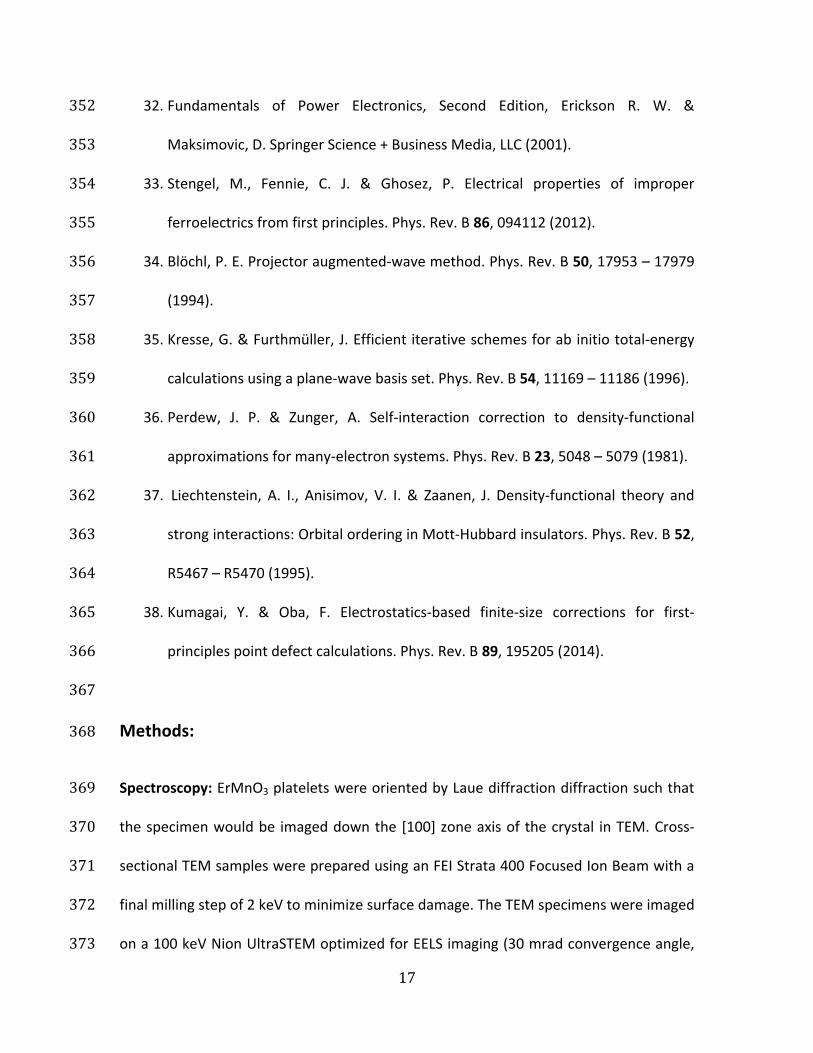
In order to study emergent domain-wall properties at head-to-head walls in 93 ErMnO3, we measure the local electronic transport over an extended voltage range. 94 Crystals of ErMnO3 were grown by the pressurized floating-zone method25 and 95 specimens with in-plane polarization and a thickness of ≈ 1 mm were prepared and 96 chemo-mechanically polished with silica slurry. In Fig. 1a–c we present conductive 97 atomic force microscopy (cAFM) data obtained with a conductive diamond-coated tip 98 (DCP12, NT-MDT) under sample bias voltages of up to 6 V. Test measurements on 99 different walls and with different tip-coatings reveal bulk-dominated transport behavior, 100 ensuring that intrinsic domain wall properties are probed (see Supplementary Notes and 101 Supplementary Fig. 1 and 2). At low bias voltage (Vbias = 2.5 V) we observe the 102 established transport behavior8,9 with conducting tail-to-tail (bright) and insulating 103 head-to-head (dark) domain walls (Fig. 1a). A qualitatively different transport 104 phenomenon, however, arises at higher voltage as shown by the scan in Fig. 1b, taken at 105 Vbias = 6 V. The spatially resolved data highlights that both tail-to-tail and head-to-head 106 walls can exhibit a higher electronic conductance than the surrounding domains. A more 107 detailed study is shown in Fig. 1c, which is conducted in an area with well-separated 108 walls to exclude crosstalk effects (see Supplementary Figure 3). Figure 1c shows the 109 relative domain-wall conductance, ΔI, after subtracting the bulk current, which for 110 reference, is shown in the inset to Fig. 1c (ΔI = Iwall – Ibulk). The comparison with respect 111 to the bulk (black dotted line in Fig. 1c) reveals that the head-to-head domain walls 112 become more conducting than the bulk above Vc ≈ 4.8 V, approaching the conductance 113 measured at the tail-to-tail walls for V > Vc. The transition from resistive (Iwall < Ibulk) to 114

6
conductive (Iwall > Ibulk) behavior occurs gradually and for moderate electric fields (see 115 also Supplementary Fig. 2). For comparison, more than one order of magnitude higher 116 electric fields are used to induce domain wall currents in BiFeO3 or PbZr0.2Ti0.8O3 thin 117 films4,5. The low electric field energy suggests a qualitative change in the electronic 118 transport at head-to-head walls rather than a breakdown of the insulating domain wall 119 state. This qualitative change, however, cannot be explained based on the depletion of 120 majority carriers (holes) alone. 121 To better understand this unusual transport phenomenon, we build a DFT-based 122 semi-classical model describing the redistribution of mobile carriers. Assuming that 123 ErMnO3 behaves like a simple band insulator we solve Poisson`s equation self-124 consistently with the carriers treated semi-classically (see Methods for details) and 125 obtain the band diagram presented in Fig. 1d. We see that far from the domain walls the 126 potential is flat and the Fermi level, EFermi, lies just below the valence-band maximum 127 (VBM) corresponding to a realistic carrier density of p0 = 2 ⋅ 1019 cm-3, i.e., a doping level 128 of 0.007 holes per unit cell. At the tail-to-tail walls the VBM shifts upwards and 129 generates more holes which screen the negative bound domain-wall charge, −2Pz (P = (0, 130 0, Pz)); this is consistent with the enhanced conductance measured at the tail-to-tail 131 domain walls8,9 (see Fig. 1a). For the head-to-head domain walls, we find a significant 132 band bending with the conduction-band minimum (CBM) dipping below the Fermi 133 energy. This implies that the screening at head-to-head domain walls is realized by both 134 a depletion of holes, occurring in a total range of about 22 nm, and an accumulation of 135 electrons right at the wall where the CBM lies below EFermi (see Fig. 1d). Thus, the simple 136

7
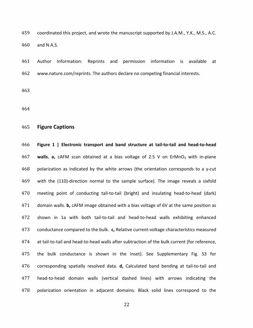
model indicates that the density of electrons, i.e., the minority carriers, is considerably 137 enhanced at the head-to-head walls. This result is in agreement with previous analytical 138 investigations11, demonstrating the soundness of our alternative DFT-based approach. In 139 both models, however, hole depletion needs to override the electron accumulation in 140 order to reproduce the experimental observation of insulating walls for V < Vc (Fig. 1a). 141 The latter is illustrated in Fig. 1e, where the density of carriers is plotted as a function of 142 the distance from the wall. The corresponding average carrier density – which is 143 proportional to the conductance – is shown in the inset. For V > Vc the electrons likely 144 dominate the domain-wall conductance as they are the only mobile carriers available for 145 charge transport at the head-to-head walls. Aside from the observed change in 146 conductance, the pronounced band bending at head-to-head walls is appealing for the 147 design of domain-wall-based transistors as sketched in Fig. 1f. The field effect associated 148 with the polarization charges can, in principle8,26, be used to modulate the conductivity 149 at the wall and, hence, serve as a natural, intrinsic gate. In the following, however, we 150 will focus on the voltage-driven transition from resistive to conductive behavior. 151 We next use electron energy loss spectroscopy (EELS) to probe the electronic 152 structure at the head-to-head walls at atomic resolution. Figure 2a shows a high-angle 153 annular dark field scanning transmission electron microscopy (HAADF-STEM) image of a 154 head-to-head domain wall imaged along the [100] zone axis of ErMnO3 (see Methods for 155 details). The erbium ions are shifted with respect to the manganese-oxygen polyhedra, 156 displaying either an up-down-down (−P domain) or down-up-up (+P domain) 157 arrangement21. These displacements indicate the local spontaneous polarization and 158

8
thus provide a local measure for the polarization reorientation across the head-to-head 159 wall. We find a rather abrupt discontinuity of the polarization orientation at the wall, 160 consistent with previous work21. Using spatially resolved EELS we investigate the 161 electrochemical wall structure by measuring the local manganese valence. Figure 2b 162 displays the evolution of the corresponding EELS spectra, taken at the Mn L2,3-edge, 163 across the head-to-head wall. Figure 2c shows an enlarged image of the Mn L3-edge 164 where the experimental data points are overlaid with a manganese reference spectrum 165 collected on the ErMnO3 sample away from the domain wall. The spectra collected 166 within the domain areas exhibit minor differences that reflect an inhomogeneity of the 167 electrical background. In the vicinity of the head-to-head wall, we clearly note a distinct 168 feature at ∼641 eV in the spectra. Here, the data is not well described by the Mn3+ 169 reference spectrum (see also Supplementary Figure 4). 170
To quantify the change observed at the Mn L2,3-edge at the head-to-head wall, 171 the full Mn L2,3-edge is fitted with two spectra corresponding to the Mn3+ and Mn2.8+ 172 valence states. The Mn2.8+ spectrum is calculated as a linear combination of Mn3+ and 173 Mn2+ spectra as described in the Supplementary Notes and Supplementary Fig. 5 (we 174 note that the spectrum of six-fold coordinated Mn2+ is used for reference as the current 175 work represents the first spectroscopic study of the Mn2+ electronic state in trigonal 176 bipyramidal coordination). The analysis reveals a statistically significant concentration of 177 the lower valence state spatially localized over 2 - 3 unit cells near the head-to-head 178 domain wall. Based on the valence concentration, we calculate the excess charge per 179 manganese atom at the domain wall relative to the Mn3+ state in the bulk27. This charge 180

9
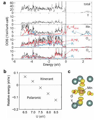
as a function of position is plotted in Fig. 2d. Aggregating over several such walls at 181 distinct locations in the material, we find that the local valence change is equivalent to 182 the accumulation of a negative charge of 0.09 ± 0.04 electrons per manganese atom at 183 the head-to-head wall position. Since the bulk polarization28 of ErMnO3 is ≈ 6 μC/cm2, 184 the amount of negative charge density needed to screen the polar discontinuity at the 185 head-to-head walls is ≈ 12 μC/cm2. This value converts into a carrier density in the order 186 of ≈ 0.1 (0.3) electrons per manganese ion (unit cell, u.c.), which is in the range of our 187 experimental uncertainty. Complementary EELS measurements at the oxygen K-edge 188 show no statistically relevant anomaly (Supplementary Fig. 5c), excluding that oxygen 189 vacancy formation is responsible for the local manganese valence change. EELS studies 190 at tail-to-tail walls and X-ray photoemission electron microscopy further confirm that 191 the lower valence state is a feature that is unique to the 2 – 3 unit cell wide area around 192 the head-to-head walls (see Supplementary Notes and Supplementary Fig. 6-8). In 193 agreement with our semi-classical model, the EELS results corroborate that electron 194 accumulation, in addition to hole depletion, plays an important role for the 195 compensation of the polarity mismatch at head-to-head domain walls in ErMnO3. 196 To determine the orbital character of the electrons and elucidate the relation 197 between their accumulation and the local manganese valence state, we perform first-198 principles calculations based on density functional theory (DFT) within the local density 199 approximation (LDA) +U method using YMnO3 as our model hexagonal manganite 200 (YMnO3 is structurally and electronically similar to ErMnO3, and the absence of f-201 electrons simplifies the DFT description). In Fig. 3a we show the calculated orbital-202
10
resolved density of states for the valence and conduction bands. We see that, consistent 203 with literature calculations29,30, the conduction band is narrow because it is formed from 204 localized -orbitals, with only minimal hybridization with neighboring axial oxygen pz-205 orbitals, whereas the valence band is broad, consisting of strongly hybridized and 206 delocalized manganese d- and oxygen 2p-states. At the head-to-head walls, where the 207 CBM dips below the Fermi level (Fig. 1d), we therefore expect localized electrons, 208 whereas holes at the VBM are delocalized in nature. This expectation is consistent with 209 our spectroscopy data, indicating a manganese valence change associated with the 210 accumulation of electrons. 211 While our theoretical analysis gives an appealing qualitative description of our 212 experimental data, at the quantitative level there is a discrepancy between the density 213 of electron carriers at the domain wall predicted by the semi-classical model and that 214 indicated by the EELS measurements. According to the cAFM measurements, hole 215 depletion needs to override the electron accumulation in the model, while EELS points 216 to a dominant electron-like compensation. This raises the question of whether an 217 additional mechanism is at play in the hexagonal manganites. The semi-classical model 218 and even our DFT band picture constitute a drastic simplification of the problem, 219 especially in a material such as ErMnO3, where many-body correlation effects likely play 220 an important role. In this context, it is important to recognize that electrons in the 221 spatially localized manganese -orbitals experience a strong on-site Coulombic 222 repulsion, which typically favors the formation of localized polaronic states rather than 223 itinerant Bloch states31. To verify whether such a scenario might apply to our case, we 224
11
calculate the energies of hypothetical polaronic states for both electrons and holes by 225 introducing a single electron or hole in a 120-atom supercell and lowering the local 226 symmetry around a manganese site (see Methods). We find (Fig. 3b) that an isolated 227 electron polaron has lower energy than an itinerant Bloch electron for U values of 7.5 eV 228 and higher. (In contrast, hole polarons remain unstable relative to the Bloch state even 229 for U values as large as 8.5 eV.) At head-to-head domain walls, we expect that polarons 230 arrange in a two-dimensional lattice, and thereby significantly reduce their formation 231 energy compared to the case of an isolated defect. We find that, by combining the latter 232 effect with the data of Fig. 3b and our band-bending model (see Supplementary 233 Information), polarons are most likely to form right at the head-to-head wall, for a 234 realistic range of values of both the Hubbard U (U ≈ 6-6.5 eV) and the bulk doping level. 235 Note that polarons should give an additional barrier to electronic conductivity at low 236 voltage, consistent with the observations presented in Fig. 1, lifting the band-model-237 related condition that hole depletion dominates over electron accumulation at head-to-238 head walls (Fig. 1e). 239 Thus, experiment and theory identify an accumulation of electrons at the head-240 to-head walls, leading to the formation of an inversion layer. The electrons are in a 241 localized polaronic state and hence do not contribute to the conductance at low voltage. 242 For high voltage (V > Vc) these electrons dominate the conductance as they are the only 243 available mobile carriers. In the polaronic picture, Vc is related to the transition from 244 localized to itinerant electrons and hence to the activation of the inversion layer as the 245 effective channel for the domain-wall transport. This behavior is fundamentally different 246

12
from the majority-carrier-enabled transport at tail-to-tail domain walls, which does not 247 involve significant lattice coupling14. 248
In Figure 4a,b we show how this behavior can be used in order to realize, e.g., a 249 domain-wall-based binary switch. The cAFM data in Fig. 4a is collected at a head-to-250 head wall as a function of time with the bias voltage varying repeatedly between V0 = 2 251 V and V0 + ΔV = 5 V. Due to the unusual I-V characteristic at the head-to-head wall, the 252 change in electric field allows reversible switching between resistive (I0 < Ibulk) and 253 conductive (I1 > Ibulk) behavior as reflected by the normalized domain-wall current 1 / ΔV 254 ⋅ (ΔI / Ibulk) in Fig. 4a. Figure 4b shows that the related electric-field induced gain, ΔI / ΔV, 255 can be enhanced by increasing the base voltage V0. The enhancement in gain, however, 256 is accompanied by the flow of a larger current I0, which causes irreversible changes in 257 the electronic surface structure and fast degradation of the domain-wall-based binary 258 switch after only two to three cycles (not shown). Note that the transition from resistive 259 to conductive behavior reflects a change from hole- to electron-dominated conductance. 260 This qualitative change in the transport behavior is a unique feature of the inversion 261 layer formed at the head-to-head walls. 262
The head-to-head domain walls studied in this work thus represent a natural 263 type of semiconducting oxide interface at which the nature of the electronic transport 264 can be manipulated at will and in a fully reversible fashion. This new degree of freedom 265 becomes possible as the local transport behavior is determined by the interplay 266 between holes and electrons. Now that we have shown that functional inversion layers 267

13
are formed at charged domain walls, the next step is to utilize individual walls in device-268 like architectures. In general, an involvement of both minority and majority carries is 269 appealing as it allows device paradigms to be extended into the realm of minority-270 carrier devices including bistable switches and bipolar transistors. Minority-carrier 271 devices are typically slower, but offer better on-state performance and larger 272 breakdown voltages32. With this, our results foreshadow conceptually new domain-wall 273 applications that go beyond conducting 2D channels that can be written, moved, and 274 erased on demand. This opportunity brings us an important step closer to the realization 275 of reconfigurable all-domain-wall circuits for next-generation nanotechnology. 276 277 References 278
1. Salje, E. K. H. Multiferroic domain boundaries as active memory devices: 279 Trajectories towards domain boundary engineering. Chem. Phys. Chem. 11, 940 - 280 950 (2010). 281
2. Catalan, G., Seidel, S., Ramesh, R., & Scott J. F. Domain wall nanoelectronics. Rev. 282 Mod. Phys. 84 119 (2012). 283
3. Meier, D. Functional multiferroic domain walls in multiferroics. J. Phys.: Condens. 284 Matter 27, 463003 (2015). 285
4. Seidel, J. et al. Conduction at domain walls in oxide multiferroics. Nat. Mater. 8, 286 229 – 234 (2009). 287

14
5. Maksymovych, P. et al. Tunable metallic conductance in ferroelectric 288 nanodomains. Nano Lett. 12, 209 – 213 (2012). 289
6. Schröder, M. et al. Conducting domain walls in Lithium Niobate single crystals. 290 Adv. Funct. Mater. 22, 3936 – 3944 (2012). 291
7. Sluka, T. et al. Free-electron gas at charged domain walls in insulating BaTiO3, 292 Nat. Commun. 4, 1808 (2013). 293
8. Meier, D. et al. Anisotropic conductance at improper ferroelectric domain walls. 294 Nat. Mater. 11, 284 – 288 (2012). 295
9. Wu, W., Horibe, Y., Lee, N., Cheong, S.-W. & Guest, J. R. Conduction of 296 topologically protected charged ferroelectric domain walls. Phys. Rev. Lett. 108, 297 077203 (2012). 298
10. Oh, Y. S., Luo, X., Huang, F.-T., Wang, Y., & Cheong, S.-W. Experimental 299 demonstration of hybrid improper ferroelectricity and the presence of abundant 300 charged walls in (Ca,Sr)3Ti2O7 crystals. Nat. Mater. 14, 407 – 413 (2015) 301
11. Eliseev, E. A., Morozovska, A. N., Svechnikov, G. S., Gopalan, V. & Shur, V. Ya. 302 Static conductivity of charged domain walls in uniaxial ferroelectric 303 semiconductors. Phys. Rev. B 83, 235313 (2011). 304
12. Gureev, M. Y., Tagantsev, A. K. & Setter, N. Head-to-head and tail-to-tail 180◦ 305 domain walls in an isolated ferroelectric. Phys. Rev. B 83, 184104 (2011). 306
13. Ma, E. Y. et al. Mobile metallic domain walls in an all-in-all-out magnetic 307 insulator. Science 350, 538 – 541 (2015). 308
15
14. Campbell, M. P. et al. Hall effect in charged conducting domain walls. Nature 309 Commun. 7, 13764 (2016). 310
15. Tselev, A. et al. Microwave a.c. conductivity of domain walls in ferroelectric thin 311 films. Nature Commun. 7, 11630 (2016). 312
16. Ruff, E. et al. Conductivity contrast and tunneling charge transport in the vortex-313 like ferroelectric domain pattern of multiferroic hexagonal YMnO3. Phys. Rev. 314 Lett. 118, 036803 (2017). 315
17. Schaab, J. et al. , Imaging and characterization of conducting ferroelectric 316 domain walls by photoemission electron microscopy. Appl. Phys. Lett. 104, 317 232904 (2014). 318
18. Schaab, J., et al. Contact-free mapping of electronic transport phenomena of 319 polar domains in SrMnO3 thin films, Phys. Rev. Appl. 5, 054009 (2016) 320
19. Kalashnikova, A. M. & Pisarev, R. V., Electronic structure of hexagonal rare-earth 321 manganites RMnO3, JETP 78, 143-147 (2003). 322
20. Chae, S. C. et al. Direct observation of the proliferation of ferroelectric loop 323 domains and vortex-antivortex Pairs. Phys. Rev. Lett. 108, 167603 (2012). 324
21. Zhang, Q. H. et al. Direct observation of interlocked domain walls in hexagonal 325 RMnO3 (R =Tm, Lu). Phys. Rev. B 85, 020102(R) (2012). 326
22. Kumagai, Y. & Spaldin, N. A., Structural domain walls in polar hexagonal 327 manganites. Nat. Commun. 4, 1540 (2012). 328
23. Choi et al. Insulating interlocked ferroelectric and structural antiphase domain 329 walls in multiferroic YMnO3. Nature Mater. 9, 253 – 258 (2010). 330

16
24. Skjærvø et al., Interstitial oxygen as a source of p-type conductivity in hexagonal 331 manganites, Nature Commun. 7, 13745 (2016). 332
25. Yan, Z. et al. Growth of High-quality hexagonal ErMnO3 single-crystals by the 333 pressurized floating-zone method. J. Cryst. Growth 409, 75 – 79 (2015). 334
26. Crassous, A., Sluka, T., Tagantsev, A. K., & Setter, N. Polarization charge as a 335 reconfigurable quasi-dopant in ferroelectric thin films. Nat. Nano. 10, 614 – 618 336 (2015). 337
27. Mundy, J. A. et al. Visualizing the interfacial evolution from charge compensation 338 to metallic screening across the manganite metal–insulator transition. Nat. 339 Commun. 5, 3464 (2014). 340
28. Coeuré, Ph., Guinet, F., Peuzin, J. C., Buisson, G. & Bertaut, E. F. Ferroelectric 341 properties of hexagonal orthomanganites of yttrium and rare earths. Proc. Int. 342 Meet. Ferroelectr. 1, Prague (1966). 343
29. Medvedeva, J. E., Anisimov, V. I., Korotin, M. A., Mryasov, O. N. & Freeman, A. J. 344 The effect of Coulomb correlation and magnetic ordering on the electronic 345 structure of hexagonal phases of ferroelectromagnetic YMnO3, J. Phys.: Condens. 346 Matter 12, 4947 – 4958 (2000). 347
30. Van Aken, B. B., Palstra, T. T. M., Filippetti, A. & Spaldin, N. A. The origin of 348 ferroelectricity in magnetoelectric YMnO3. Nat. Mater. 3, 164 – 170 (2004). 349
31. Rahmanizadeh, K., Wortmann, D., Bihlmayer, G. & Blügel, S. Charge and orbital 350 order at head-to-head domain walls in PbTiO3. Phys. Rev. B 90, 115104 (2014). 351
17
32. Fundamentals of Power Electronics, Second Edition, Erickson R. W. & 352 Maksimovic, D. Springer Science + Business Media, LLC (2001). 353
33. Stengel, M., Fennie, C. J. & Ghosez, P. Electrical properties of improper 354 ferroelectrics from first principles. Phys. Rev. B 86, 094112 (2012). 355
34. Blöchl, P. E. Projector augmented-wave method. Phys. Rev. B 50, 17953 – 17979 356 (1994). 357
35. Kresse, G. & Furthmüller, J. Efficient iterative schemes for ab initio total-energy 358 calculations using a plane-wave basis set. Phys. Rev. B 54, 11169 – 11186 (1996). 359
36. Perdew, J. P. & Zunger, A. Self-interaction correction to density-functional 360 approximations for many-electron systems. Phys. Rev. B 23, 5048 – 5079 (1981). 361
37. Liechtenstein, A. I., Anisimov, V. I. & Zaanen, J. Density-functional theory and 362 strong interactions: Orbital ordering in Mott-Hubbard insulators. Phys. Rev. B 52, 363 R5467 – R5470 (1995). 364
38. Kumagai, Y. & Oba, F. Electrostatics-based finite-size corrections for first-365 principles point defect calculations. Phys. Rev. B 89, 195205 (2014). 366 367
Methods: 368 Spectroscopy: ErMnO3 platelets were oriented by Laue diffraction diffraction such that 369 the specimen would be imaged down the [100] zone axis of the crystal in TEM. Cross-370 sectional TEM samples were prepared using an FEI Strata 400 Focused Ion Beam with a 371 final milling step of 2 keV to minimize surface damage. The TEM specimens were imaged 372 on a 100 keV Nion UltraSTEM optimized for EELS imaging (30 mrad convergence angle, 373

18
130 pA of usable beam current, ~ 1 Å spatial resolution). The microscope was equipped 374 with a Gatan Quantum Dual EELS spectrometer; EELS spectra were collected with a 0.1 375 eV/pixel dispersion resulting in 0.3 eV energy resolution. Fine structure information 376 from the O-K edge and Mn-L2,3 edge was collected simultaneously with the ADF signal. 377 Gain and dark noise were corrected using Digital Micrograph™. Four cross-sectional TEM 378 specimens were prepared from two distinct ErMnO3 platelets (within the platelets the 379 sample locations were separated by millimeters). Multiple distinct domain walls were 380 identified in each TEM specimen each separated by several microns. In sum, over a 381 dozen domain walls were analyzed. Post-acquisition, an off-line drift correction was 382 performed to correct the small sample drift (<0.5 Å/min). The Mn-L2,3 fine structure was 383 analyzed following a standard power law background subtraction from approximately 384 10 eV prior to the edge onset. No additional noise reduction algorithms were employed 385 to avoid artifacts. Scanning was performed in rapid succession perpendicular to the wall 386 orientation so that each scan included signal from across the wall as well as the 387 reference regions on either side. Signals were binned perpendicular to the scan 388 direction to produce a single line scan through the wall. Manganese positions were 389 identified from the integrated signal intensity; the signal was then summed over each 390 manganese position to produce a single spectrum from each row of manganese atoms 391 in the spectrum image. Averaging over manganese positions increased the signal to 392 noise for the EELS analysis. 393 Model Calculations: In our semi-classical model of the carrier redistribution at the 394 charged domain walls, we treat the bulk material as a p-type semiconductor using the 395

19
calculated density of states (DOS) and values of P = 7.1 μC/cm2 and ε = 1333 extracted 396 from DFT calculations of bulk YMnO3. The domain walls are introduced as charged 397 planes, with a surface charge density equal to ±2Pz. The equilibrium distribution of 398 screening carriers is calculated by iteratively solving the Poisson equation of a one-399 dimensional system with two isolated domain walls. The local carrier density is 400 determined at each step by integrating the bulk DOS to the trial Fermi level, and by 401 enforcing the condition of overall charge neutrality. 402 Density functional theory: First-principles calculations were performed using the 403 projector augmented-wave method34 as implemented in VASP35. PAW data sets with 404 radial cutoffs of 1.48, 1.22 and 0.80 Å for Y, Mn and O, respectively, were employed. The 405 exchange-correlation interactions between electrons were treated using the local 406 density approximation with Hubbard U correction36,37. The U and J parameters on the 407 Mn-3d orbitals were set to 5 and 0.88 eV, respectively. The P63cm noncollinear magnetic 408 configuration of YMnO3, which gives a band gap of 1.8 eV close to the experimental gap 409 of 1.6 eV19 was adopted. Lattice constants and internal positions were fully relaxed until 410 the stress and forces acting on all atoms converged to less than 0.02 GPa and 0.005 411 eV/Å, respectively. The cutoff energy was set to 550 eV, and a Γ centered 4 × 4 × 2 k-412 point sampling for the reciprocal space integration was employed. The projected 413 densities of states were evaluated within the spheres centered on the atomic sites with 414 radii of 1.82, 1.32, and 0.82 Å for Y, Mn, and O, respectively. For the calculations of 415 polarons, the lattice constants were fixed to the values of the relaxed unit cell, and a Γ 416 centered 2 × 2 × 2 k-point sampling was adopted. The local symmetry was reduced by 417

20
moving the apical oxygen ions away from the Mn ion by 0.2 Å so that an electron can 418 easily be captured to the Mn- orbital. Y ions were not moved in the initial structure, 419 but they were spontaneously relaxed to the lowest energy positions via structure 420 optimization. Relative energies between the polaronic and itinerant Bloch electrons 421 were calculated for 2 × 2 × 1 supercells composed of 120 atoms as a function of the U 422 parameter, with J fixed at 0.88 eV. For itinerant electrons, band-filling corrections were 423 applied. In order to remove the spurious electrostatic energy caused by the finite 424 background charge, we adopted the scheme of ref. 38. 425 Data availability. The data that support the findings of this study are available from the 426 authors on reasonable request. 427 Supplementary Information is linked to the online version of the paper at 428 www.nature.com/nature. 429 430 Acknowledgement: We thank M. Fiebig for direct financial support and scientific input, 431 M. Trassin and A. Kaiser for fruitful discussions. We thank HZB for the allocation of 432 synchrotron beam time and we thankfully acknowledge financial support by HZB. D.M., 433 J.S. and N.A.S. acknowledge funding from the ETH Zürich and the SNF (proposal Nr. 434 200021_149192, D.M. and J.S.), the Alexander von Humboldt Foundation (D.M.) and the 435 ERC Advanced Grant program (grant number 291151, N.A.S.). Electron microscopy 436 research at Cornell (J.A.M., M.E.H., D.A.M. and D.G.S.) was supported by the U.S. 437 Department of Energy, Office of Basic Energy Sciences, Division of Materials Sciences 438

21
and Engineering under Award #DE-SC0002334. This work made use of the electron 439 microscopy facility of the Cornell Center for Materials Research (CCMR) with support 440 from the National Science Foundation Materials Research Science and Engineering 441 Centers (MRSEC) program (DMR-1120296) and NSF IMR-0417392. We gratefully 442 acknowledge the use of facilities with the LeRoy Eyring Center for Solid State Science at 443 Arizona State University and assistance from J. Mardinly and T. Aoki. J.A.M. 444 acknowledges financial support from the Army Research Office in the form of a National 445 Defense Science & Engineering Graduate Fellowship and from the National Science 446 Foundation in the form of a National Science Foundation Graduate Research Fellowship. 447 M.S. was supported by MINECO-Spain through Grants No. FIS2013-48668-C2-2-P and No. 448 SEV-2015-0496, and Generalitat de Catalunya (2014 SGR301). E.B. and Z.Y. were 449 supported in part by the U.S. Department of Energy and carried out at the Lawrence 450 Berkeley National Laboratory under Contract No. DE-AC02-05CH11231. 451 452 Author Contributions: J.A.M. and M.E.H. conducted and analyzed the EELS 453 measurements, assisted by R.H., under supervision of D.A.M. and D.G.S. Y.K., M.S. and 454 N.A.S. performed the semiclassical and DFT calculations. J.S. performed the cAFM 455 measurements under supervision of D.M. The analysis in terms of X-PEEM was provided 456 by I.P.K., J.S., D.M.G., H.D., C.M.S. and D.M.; Z.Y., E.B. and R.R. allocated the samples. 457 A.C. and D.M. developed the concept of electric-field gating. D.M. initiated and 458
22
coordinated this project, and wrote the manuscript supported by J.A.M., Y.K., M.S., A.C. 459 and N.A.S. 460 Author Information: Reprints and permission information is available at 461 www.nature.com/reprints. The authors declare no competing financial interests. 462 463 464 Figure Captions 465 Figure 1 | Electronic transport and band structure at tail-to-tail and head-to-head 466 walls. a, cAFM scan obtained at a bias voltage of 2.5 V on ErMnO3 with in-plane 467 polarization as indicated by the white arrows (the orientation corresponds to a y-cut 468 with the (110)-direction normal to the sample surface). The image reveals a sixfold 469 meeting point of conducting tail-to-tail (bright) and insulating head-to-head (dark) 470 domain walls. b, cAFM image obtained with a bias voltage of 6V at the same position as 471 shown in 1a with both tail-to-tail and head-to-head walls exhibiting enhanced 472 conductance compared to the bulk. c, Relative current-voltage characteristics measured 473 at tail-to-tail and head-to-head walls after subtraction of the bulk current (for reference, 474 the bulk conductance is shown in the inset). See Supplementary Fig. S3 for 475 corresponding spatially resolved data. d, Calculated band bending at tail-to-tail and 476 head-to-head domain walls (vertical dashed lines) with arrows indicating the 477 polarization orientation in adjacent domains. Black solid lines correspond to the 478

23
conduction band minimum (CBM) and valence band maximum (VBM) for p0 = 2 · 1019 479 cm-3 with the horizontal dashed line indicating the Fermi level, EFermi. e, Calculated 480 carrier density at head-to-head walls. With increasing hole carrier density the screening 481 by hole depletion becomes more efficient so that the density of electrons decreases. 482 The inset presents the average carrier density. Lines are running averages based on a 483 Gaussian convolution function (∝ exp (− / ), s = 30 nm), which corresponds to a 484 realistic spatial resolution when mapping local current by cAFM. f, Conceptual sketch of 485 a domain-wall-based field-effect transistor with polarization charges playing the role of 486 the gate. 487 Figure 2 | Manganese valence change at head-to-head domain walls. a, HAADF-STEM 488 image of a head-to-head domain wall. The image is colored to indicate the magnitude 489 and direction of the displacement of erbium atoms with a sharp transition between +P 490 and −P domains (−P domain: up-down-down; +P domain: down-up-up as indicated by 491 yellow circles)21. The scale bar is 1 nm. b, Layer-by-layer EELS spectra showing the 492 evolution of the Mn L2,3-edge across the head-to-head domain wall. c, Zoom-in to the L3-493 edge in b. A comparison of the EELS spectra (blue dots) with Mn3+ reference data (solid 494 line) reveals a spectral feature around 641 eV (indicated by the dashed line) that occurs 495 in the vicinity of the head-to-head domain wall. d, Electron transfer (per manganese 496 atom at the domain wall) to the wall calculated from the local manganese valence 497 measured by EELS. Error bars are the standard error of the mean. 498

24
Figure 3 | Orbital nature of electrons at head-to-head domain walls. a, Orbital-resolved 499 density of states (DOS). The black lines indicate the sum of the local density of states, 500 while the blue and red lines show the contributions from the different orbitals. The 501 black dashed line at 0 eV indicates the Fermi energy. Oap and Oip represent the oxygens 502 located at the apical sites and in-plane sites, respectively, of the MnO-bipyramidal layers. 503 b, Calculated relative energy between electronic Bloch and polaron states. Data points 504 (black crosses) above the dashed line indicate that an itinerant Bloch state is stable for 505 the respective U values, whereas data points below the line show that a polaronic state 506 is stabilized. c, Illustration of the calculated electronic polaron state. 507 Figure 4 | Electric-field control of electronic transport at head-to-head domain walls. a, 508 Normalized domain-wall current measured as a function of time over 20 switching 509 cycles between resistive (I0 < Ibulk) and conducting (I1 > Ibulk) behavior. For voltages V0 = 510 2V and ΔV = 3V (see inset to 4a for a schematic illustration) , reversible control can be 511 reliably realized for 20 switching cycles, which is the largest number of cycles we 512 investigated. b, Enhanced gain can be achieved, e.g., by increasing I0, yielding ΔI / ΔV ≈ 513 15 pA V-1 for V0 = 4V and ΔV = 1V. The increase in gain, however, requires larger 514 currents which cause degradation as described in the main text. c, Sketch showing the 515 conductive domain-wall state for V = V0 + ΔV with itinerant electrons illustrated in blue. 516 d, Resistive domain-wall state with localized electrons for V0. 517
1
2
2.5 V
6.0 V
ca
b
cAFM
Bulk
1 µm
e
Distance
Car
rier
den
sity
/ u
.c.
0
0.1
21
01
9cm
-3
41
01
9cm
-3
61
01
9cm
-3
1
2d
Ener
gy (
eV)
EFermi VBM0
2
1
Distance
CBMf
Source
Drain
+ ++ ++ ++ ++ ++ ++ ++ +
Intrinsicgate
Ave
rage
den
sity
Rel
ativ
e co
nd
uct
ance
(p
A)
5 nm 10 nm
100 nm
640 650 640 645
P
a
640 645 0 0.05 0.1
Charge Transfer (e-)
-6
-4
-2
0
2
4
6
P
os
itio
n (
nm
)
Inte
ns
ity (
a.u
.)
dHAADF-STEM
Head-to-head
640 650 640 645640 650
Energy Loss (eV)
b cL3 L2
[010]
[001]
L3
b
a
Itinerant
Polaronic
c
Mn
YO

0 10 20 30 40
-0.5
0.0
0.5
1.0
1.5
0 2 4
V0 V0 V
I0
I1Wall
Input Output
a b
∆𝑉 = 3 V ∆𝑉 = 1 V
1 ∆𝑉
∆𝐼
𝐼 bulk
𝑉−1
𝑡 (s) 𝑡 (s)
++
+
++
++
++
+P
V0 V
c Itinerant
P+
++
++
++
++
+
e
V0
dLocalized
Related Documents