Programa 1. Introdução aos circuitos eléctricos 2. Grafos e circuitos resistivos lineares 3. Circuitos dinâmicos lineares 4. Regime forçado sinusoidal 5. Análise no domínio da frequência complexa – Funções de rede H(s): pólos e zeros – Diagramas de Bode de amplitude e de fase – Traçado assimptótico 6. Circuitos resistivos não-lineares

Welcome message from author
This document is posted to help you gain knowledge. Please leave a comment to let me know what you think about it! Share it to your friends and learn new things together.
Transcript

Programa
1. Introdução aos circuitos eléctricos2. Grafos e circuitos resistivos lineares3. Circuitos dinâmicos lineares4. Regime forçado sinusoidal5. Análise no domínio da frequência complexa
– Funções de rede H(s): pólos e zeros– Diagramas de Bode de amplitude e de fase– Traçado assimptótico
6. Circuitos resistivos não-lineares

1. Variable-Frequency Response AnalysisNetwork performance as function of frequency.Transfer function
2. Sinusoidal Frequency AnalysisBode plots to display frequency response data
3. Resonant CircuitsThe resonance phenomenon and its characterization
4. ScalingImpedance and frequency scaling
5. Filter NetworksNetworks with frequency selective characteristics:low-pass, high-pass, band-pass
VARIABLE-FREQUENCY NETWORKPERFORMANCE
LEARNING GOALS

°∠== 0RRZRResistor
VARIABLE FREQUENCY-RESPONSE ANALYSIS
In AC steady state analysis the frequency is assumed constant (e.g., 60Hz).Here we consider the frequency as a variable and examine how the performancevaries with the frequency.
Variation in impedance of basic components

°∠== 90LLjZL ωωInductor

Capacitor °−∠== 9011CCj
Zc ωω

Frequency dependent behavior of series RLC network
CjRCjLCj
CjLjRZeq ω
ωωω
ω 1)(1 2 ++=++=
CLCjRC
jj
ωωω )1( 2 −+
=−−
×
CLCRCZeq ω
ωω 222 )1()(|| −+= ⎟⎟
⎠
⎞⎜⎜⎝
⎛ −=∠ −
RCLCZeq ω
ω 1tan2
1
sCsRCLCssZ
sj
eq1)(
notation"in tion Simplifica"2 ++
=
≈ω

For all cases seen, and all cases to be studied, the impedance is of the form
011
1
011
1
......)(
bsbsbsbasasasasZ n
nn
n
mm
mm
++++++++
= −−
−−
sCZsLsZRsZ CLR
1,)(,)( ===
Simplified notation for basic components
Moreover, if the circuit elements (L,R,C, dependent sources) are real then theexpression for any voltage or current will also be a rational function in s
LEARNING EXAMPLE
sL
sC1
R
So VsCsLR
RsV/1
)(++
= SVsRCLCs
sRC12 ++
=
So VRCjLCj
RCjV
js
1)( 2 ++=
≈
ωωω
ω
°∠+××+××
××= −−
−
0101)1053.215()1053.21.0()(
)1053.215(332
3
ωωω
jjjVo
MATLAB can be effectively used to compute frequency response characteristics

USING MATLAB TO COMPUTE MAGNITUDE AND PHASE INFORMATION
011
1
011
1
......)(
bsbsbsbasasasasV n
nn
n
mm
mm
o ++++++++
= −−
−−
),(];,,...,,[
];,,...,,[
011
011
dennumfreqsbbbbden
aaaanum
nn
mm
>>=>>=>>
−
− MATLAB commands required to display magnitudeand phase as function of frequency
NOTE: Instead of comma (,) one can use space toseparate numbers in the array
1)1053.215()1053.21.0()()1053.215(
332
3
+××+××××
= −−
−
ωωω
jjjVo
EXAMPLE
» num=[15*2.53*1e-3,0];» den=[0.1*2.53*1e-3,15*2.53*1e-3,1];» freqs(num,den)
1a
2b 1b0b
Missing coefficients mustbe entered as zeros
» num=[15*2.53*1e-3 0];» den=[0.1*2.53*1e-3 15*2.53*1e-3 1];» freqs(num,den)
This sequence will alsowork. Must be careful notto insert blanks elsewhere

GRAPHIC OUTPUT PRODUCED BY MATLAB
Log-logplot
Semi-logplot

LEARNING EXAMPLE A possible stereo amplifier
Desired frequency characteristic(flat between 50Hz and 15KHz)
Postulated amplifier
Log frequency scale

Frequency domain equivalent circuit:
Frequency Analysis of Amplifier
)()(
)()(
sVsV
sVsV
in
o
S
in= )(/1
)( sVsCR
RsV Sinin
inin +
= ]1000[/1
/1)( inoo
oo V
RsCsCsV+
=
⎥⎦
⎤⎢⎣
⎡+⎥
⎦
⎤⎢⎣
⎡+
=ooinin
inin
RsCRsCRsCsG
11]1000[
1)( ⎥⎦
⎤⎢⎣⎡+⎥⎦
⎤⎢⎣⎡+
=π
ππ 000,40
000,40]1000[100 sss
( ) ( )( ) ( ) π
π
000,401001058.79
100101018.3191
1691
≈××=
≈××=−−−
−−−
oo
inin
RC
RC
required
actual
ππππ
000,40000,40]1000[)(000,40||100
sssGs ≈⇒<<<<
Frequency dependent behavior iscaused by reactive elements
)()()(
sVsVsG
S
o=
Voltage Gain
)50( Hz
)20( kHz

NETWORK FUNCTIONS
INPUT OUTPUT TRANSFER FUNCTION SYMBOLVoltage Voltage Voltage Gain Gv(s)Current Voltage Transimpedance Z(s)Current Current Current Gain Gi(s)Voltage Current Transadmittance Y(s)
When voltages and currents are defined at different terminal pairs we define the ratios as Transfer Functions
If voltage and current are defined at the same terminals we defineDriving Point Impedance/Admittance
Some nomenclature
EXAMPLE
⎩⎨⎧
=admittanceTransfer
tanceTransadmit)()()(
1
2
sVsIsYT
gain Voltage)()()(
1
2
sVsVsGv =
To compute the transfer functions one must solve the circuit. Any valid technique is acceptable

LEARNING EXAMPLE
⎩⎨⎧
=admittanceTransfer
tanceTransadmit)()()(
1
2
sVsIsYT
gain Voltage)()()(
1
2
sVsVsGv =
The textbook uses mesh analysis. We willuse Thevenin’s theorem
sLRsC
sZTH ||1)( 1+=1
11RsL
sLRsC +
+=
)()(
1
112
RsLsCRsLLCRssZTH +
++=
)()( 11
sVRsL
sLsVOC +=
−+
)(sVOC
)(sZTH
−
+)(2 sV
2R)(2 sI
=+
=)(
)()(2
2 sZRsVsI
TH
OC
)(
)(
1
112
2
11
RsLsCRsLLCRsR
sVRsL
sL
++++
+
121212
2
)()()(
RCRRLsLCRRsLCssYT ++++
=
)()(
)()()()( 2
1
22
1sYR
sVsIR
sVsVsG T
sv ===
)()(
1
1
RsLsCRsLsC
++
×

POLES AND ZEROS (More nomenclature)
011
1
011
1
......)(
bsbsbsbasasasasH n
nn
n
mm
mm
++++++++
= −−
−− Arbitrary network function
Using the roots, every (monic) polynomial can be expressed as aproduct of first order terms
))...()(())...()(()(
21
21
n
m
pspspszszszsKsH
−−−−−−
=
function network the of polesfunctionnetworktheofzeros
==
n
m
pppzzz
,...,,,...,,
21
21
The network function is uniquely determined by its poles and zerosand its value at some other value of s (to compute the gain)
EXAMPLE
1)0(22,22
,1
21
1
=−−=+−=
−=
Hjpjp
z :poles:zeros
=++−+
+=
)22)(22()1()(
jsjssKsH
841
2 +++
sssK
⇒== 181)0( KH
8418)( 2 ++
+=
ssssH

LEARNING EXTENSIONFind the driving point impedance at )(sVS
)()()(
sIsVsZ S=
)(sI
)(1)()(: sIsC
sIRsVin
inS +=KVL
=+=in
in sCRsZ 1)(
Replace numerical values
Ω⎥⎦⎤
⎢⎣⎡ + M
sπ1001

LEARNING EXTENSION
π)104(
000,20,50 :poles0 :zero
721
1
×=
−=−==
K
HzpHzpz
⎥⎦
⎤⎢⎣
⎡+⎥
⎦
⎤⎢⎣
⎡+
=ooinin
inin
RsCRsCRsCsG
11]1000[
1)( ⎥⎦
⎤⎢⎣⎡+⎥⎦
⎤⎢⎣⎡+
=π
ππ 000,40
000,40]1000[100 sss
For this case the gain was shown to be
))...()(())...()(()(
21
21
n
m
pspspszszszsKsH
−−−−−−
= Zeros = roots of numeratorPoles = roots of denominator
Find the pole and zero locations and value K for the voltage gain G(s) = Vo(s) / Vs(s)

Formas da função de transferência:
1. Forma geral
2. Forma de ganho, pólos e zeros
3. Forma das constantes de tempo
Ganho estático (K0) é o ganho que se observa quando ω=0, i.e. a resposta a sinais DC
Obtém-se a partir de qualquer razão entre tensões e correntes (ex: Vo/Vi, Vo/Ii, Io/Ii, Io/Vi)
zi = zero
pi = pólo
τZi=1/zi constante de tempo associada ao zero zi
τPi=1/pi constante de tempo associada ao pólo pi

SINUSOIDAL FREQUENCY ANALYSIS
)(sH
Circuit represented bynetwork function
⎭⎬⎫
+
+
)cos(0
)(0
θω
θω
tBeA tj
( )⎩⎨⎧
∠++
+
)(cos|)(|)(
0
)(0
ωθωωω θω
jHtjHBejHA tj
)()()(
)()(|)(|)(
ωφωω
ωωφωω
jeMjH
jHjHM
=
∠==
Notation
stics.characteri phase and magnitudecalledgenerally are offunctionas of Plots ωωφω ),(),(M
)(log)(
))(log20PLOTS BODE 10
10 ωωφ
ωvs
(M
⎩⎨⎧
. of function a as function network theanalyzewefrequency theof functionaasnetworkaofbehavior thestudy To
ωω)( jH

HISTORY OF THE DECIBEL
Originated as a measure of relative (radio) power
1
2)2 log10(|PPP dB =1Pover
21
22
21
22)2
22 log10log10(|
II
VVP
RVRIP dB ==⇒== 1Pover
By extension
||log20|||log20|||log20|
10
10
10
GGIIVV
dB
dB
dB
===
Using log scales the frequency characteristics of network functionshave simple asymptotic behavior.
The asymptotes can be used as reasonable and efficient approximations

]...)()(21[)1(]...)()(21[)1()()( 2
233310
bbba
N
jjjjjjjKjH
ωτωτςωτωτωτςωτωω
++++++
=±
General form of a network function showing basic terms
Frequencyindependent
...|)()(21|log20|1|log20
...|)()(21|log20|1|log20
||log20log20
21010
233310110
10010
−++−+−
++++++
±=
bbba jjj
jjj
jNK
ωτωτςωτ
ωτωτςωτ
ω DNDN
BAAB
loglog)log(
loglog)log(
−=
+=|)(|log20|)(| 10 ωω jHjH dB=
212
1
2121
zzzz
zzzz
∠−∠=∠
∠+∠=∠
...)(1
2tantan
...)(1
2tantan
900)(
211
23
3311
1
−−
−−
+−
++
°±=∠
−−
−−
b
bba
NjH
ωτωτςωτ
ωτωτςωτ
ω
Idea: Display each basic termseparately and add the results to
obtain final answer.
Let’s examine each basic term >>
]...)()(21)[1(]...)()(21)[1()( 2
233310
bbba
N
sssssssKsH
ττςτττςτ
++++++
=±
Poles/zerosat the origin
First order terms Quadratic terms for complex conjugate poles/zeros

Constant Term
Poles/Zeros at the origin
⎩⎨⎧
°±=∠×±=
→±
±±
90)()(log20|)(|)( 10
NjNjj N
dBN
N
ωωωω
linestraight a is thislogisaxis-xthe 10ω
0
1a

1bSimple pole or zero ωττ
ω
jsjs
+=+=
11 ⎪⎩
⎪⎨⎧
=+∠+=+
− ωτωτωτωτ
1
210
tan)1()(1log20|1|
jj dB
asymptotefrequency low 0|1| ≈+ dBjωτ
(20dB/dec)asymptotefrequency high ωτωτ 10log20|1| ≈+ dBjfrequency)akcorner/bre1whenmeet asymptotes two The (=ωτ
Behavior in the neighborhood of the corner:
FrequencyAsymptoteCurvedistance to asymptote Argument
corner 0dB 3dB 3 45
octave above 6dB 7db 1 63.4
octave below 0dB 1dB 1 26.6
1=ωτ2=ωτ5.0=ωτ
°≈+∠ 0)1( ωτj
°≈+∠ 90)1( ωτj
⇒<<1ωτ
⇒>>1ωτ
Asymptote for phase
High freq. asymptoteLow freq. Asym.

Simple zero
Simple pole
1b
1b
Quadratic pole or zero ])()(21[ 22 ωτωτς jjt ++= ])()(21[ 2ωτωτς −+= j
( ) ( )222102 2)(1log20|| ςωτωτ +−=dBt 2
12 )(1
2tanωτςωτ
−=∠ −t
1<<ωτ 0|| 2 ≈dBt °≈∠ 02t1>>ωτ 2
102 )(log20|| ωτ≈dBt °≈∠ 1802t1=ωτ )2(log20|| 102 ς=dBt °=∠ 902tCorner/break frequency
221 ςωτ −= 2102 12log20|| ςς −=dBt
ςς 2
12
21tan −=∠ −t
22
≤ςResonance frequency
2
Magnitude for quadratic pole
Phase for quadratic pole
↑↑ formulas for a complex zero ↓↓ plots for a complex pole (mirror vertically for the zero)
low freq. asymptote
high freq. asymptote 40dB/dec

LEARNING EXAMPLE Generate magnitude and phase plots
)102.0)(1()11.0(10)(++
+=
ωωωω
jjjjGvDraw asymptotes
for each term 1,10,50 :nersBreaks/cor
40
20
0
20−
dB
°−90
°90
1.0 1 10 100 1000
dB|10
decdB /20−
dec/45°−
decdB /20
dec/45°
Draw composites
)102.0)(1()11.0(10)(++
+=
ssssGv
Ex1

asymptotes

LEARNING EXAMPLE Generate magnitude and phase plots
)11.0()()1(25)( 2 +
+=
ωωωω
jjjjGv 101,:(corners)Breaks
40
20
0
20−
dB
°−90
°−270
°90
1.0 1 10 100
Draw asymptotes for each
dB28
decdB /40−
°−180
dec/45°
°− 45
Form composites
)11.0()1(25)( 2 +
+=
ssssGv
Ex2

( )21
020 0)(
KjK
dB
=⇔= ωω
Final results . . . And an extra hint on poles at the origin
decdB40−
decdB20−
decdB40−

LEARNING EXTENSION Sketch the magnitude characteristic
)100)(10()2(10)(
4
+++
=ωω
ωωjj
jjGformstandardinNOTisfunctiontheBut
10010,2,:breaks
Put in standard form)1100/)(110/(
)12/(20)(++
+=
ωωωω
jjjjG We need to show about
4 decades
40
20
0
20−
dB
°−90
°90
1 10 100 1000
dB|25
)1100/)(110/()12/(20)(++
+=
ssssG
Ex3

LEARNING EXTENSION Sketch the magnitude characteristic
2)()102.0(100)(
ωωω
jjjG +
=
origin theat pole Double50at break
formstandardinisIt
40
20
0
20−
dB
°−90
°−270
°90
1 10 100 1000
Once each term is drawn we form the composites
2
)102.0(100)(s
ssG +=
Ex4
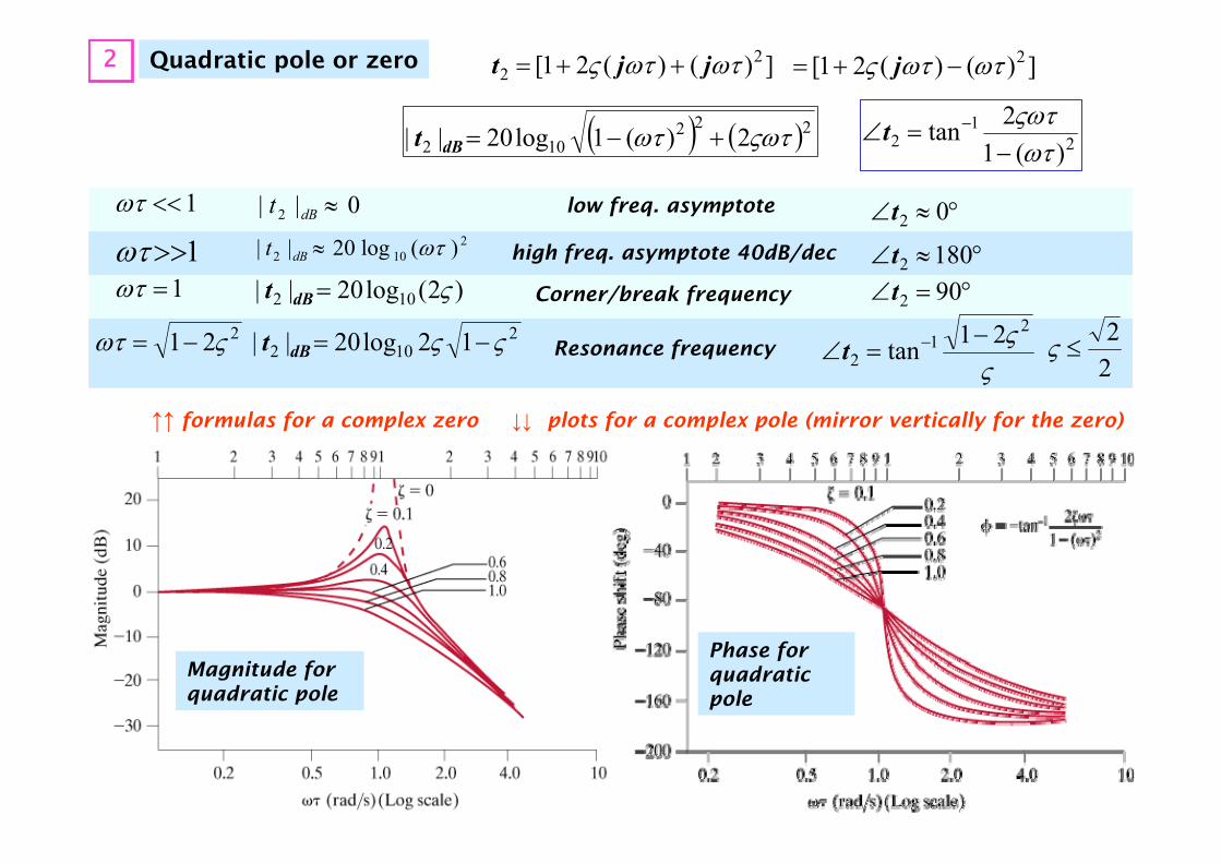
Put in standard form
)110/)(1()(
++=
ωωωωjjjjG
LEARNING EXTENSION Sketch the magnitude characteristic
)10)(1(10)(
++=
ωωωωjjjjG
10 1, :breaksorigin theat zero
formstandardinnot
40
20
0
20−
dB
°−90
°−270
°90
1.0 110
100Once each term is drawn we form the composites
decdB /20decdB /20−
)10)(1(10)(
++=
ssssG
Ex5

LEARNING EXAMPLE A function with complex conjugate poles
[ ]1004)()5.0(25)( 2 +++
=ωωω
ωωjjj
jjG
Put in standard form
[ ]125/)10/()15.0/(5.0)( 2 +++
=ωωω
ωωjjj
jjG
40
20
0
20−
dB
°−90
°90
01.0 1.0 1 10 100°−270
1=ωτ )2(log20|| 102 ς−=dBt
2.01.025/12
=⇒⎭⎬⎫
==
ςτςτ
])()(21[ 22 ωτωτς jjt ++=
dB8
Draw composite asymptote
Behavior close to corner of conjugate pole/zerois too dependent on damping ratio.Computer evaluation is better
)1004)(5.0(25)( 2 +++
=sss
ssG
Ex6

Evaluation of frequency response using MATLAB
[ ]1004)()5.0(25)( 2 +++
=ωωω
ωωjjj
jjG
» num=[25,0]; %define numerator polynomial» den=conv([1,0.5],[1,4,100]) %use CONV for polynomial multiplicationden =
1.0000 4.5000 102.0000 50.0000» freqs(num,den)
Using default options

Evaluation of frequency response using MATLAB User controlled
>> clear all; close all %clear workspace and close any open figure
>> figure(1) %open one figure window (not STRICTLY necessary)
>> w=logspace(-1,3,200);%define x-axis, [10^{-1} - 10^3], 200pts total
[ ]1004)()5.0(25)( 2 +++
=ωωω
ωωjjj
jjG
>> G=25*j*w./((j*w+0.5).*((j*w).^2+4*j*w+100)); %compute transfer function>> subplot(211) %divide figure in two. This is top part>> semilogx(w,20*log10(abs(G))); %put magnitude here
>> grid %put a grid and give proper title and labels>> ylabel('|G(j\omega)|(dB)'), title('Bode Plot: Magnitude response')

>> semilogx(w,unwrap(angle(G)*180/pi)) %unwrap avoids jumps from +180 to -180>> grid, ylabel('Angle H(j\omega)(\circ)'), xlabel('\omega (rad/s)')>> title('Bode Plot: Phase Response')
Evaluation of frequency response using MATLAB User controlled Continued
Repeat for phase
No xlabel here to avoid clutter
USE TO ZOOM IN A SPECIFIC REGION OF INTEREST
Compare with default!

LEARNING EXTENSION Sketch the magnitude characteristic
]136/)12/[()1(2.0)( 2 ++
+=
ωωωωω
jjjjjG 6/136/12
12/1=⇒=
=ςςτ
τ])()(21[ 2
2 ωτωτς jjt ++=
40
20
0
20−
dB
°−90
°−270
°90
1.0 110
100
1=ωτ )2(log20|| 102 ς−=dBt
decdB /20−
decdB /40−
decdB /0
12
dB5.9=
]136/)12/[()1(2.0)( 2 ++
+=
sssssG
Ex7

]136/)12/[()1(2.0)( 2 ++
+=
ωωωωω
jjjjjG
» num=0.2*[1,1];» den=conv([1,0],[1/144,1/36,1]);» freqs(num,den)

DETERMINING THE TRANSFER FUNCTION FROM THE BODE PLOT
This is the inverse problem of determining frequency characteristics. We will use only the composite asymptotes plot of the magnitude to postulatea transfer function. The slopes will provide information on the order
A
A. different from 0dB.There is a constant Ko
B
B. Simple pole at 0.11)11.0/( −+ωj
C
C. Simple zero at 0.5
)15.0/( +ωj
D
D. Simple pole at 3
1)13/( −+ωj
E
E. Simple pole at 20
1)120/( −+ωj
)120/)(13/)(11.0/()15.0/(10)(
++++
=ωωω
ωωjjj
jjG
20|
00
0
1020|dBK
dB KK =⇒=
If the slope is -40dB we assume double real pole. Unless we are given more data

LEARNING EXTENSIONDetermine a transfer function from the composite magnitude asymptotes plot
A
A. Pole at the origin. Crosses 0dB line at 5
ωj5
B
B. Zero at 5
C
C. Pole at 20
D
D. Zero at 50
E
E. Pole at 100
)1100/)(120/()150/)(15/(5)(++
++=
ωωωωωωjjj
jjjG
)1100/)(120/()150/)(15/(5)(
++++
=ssssssG
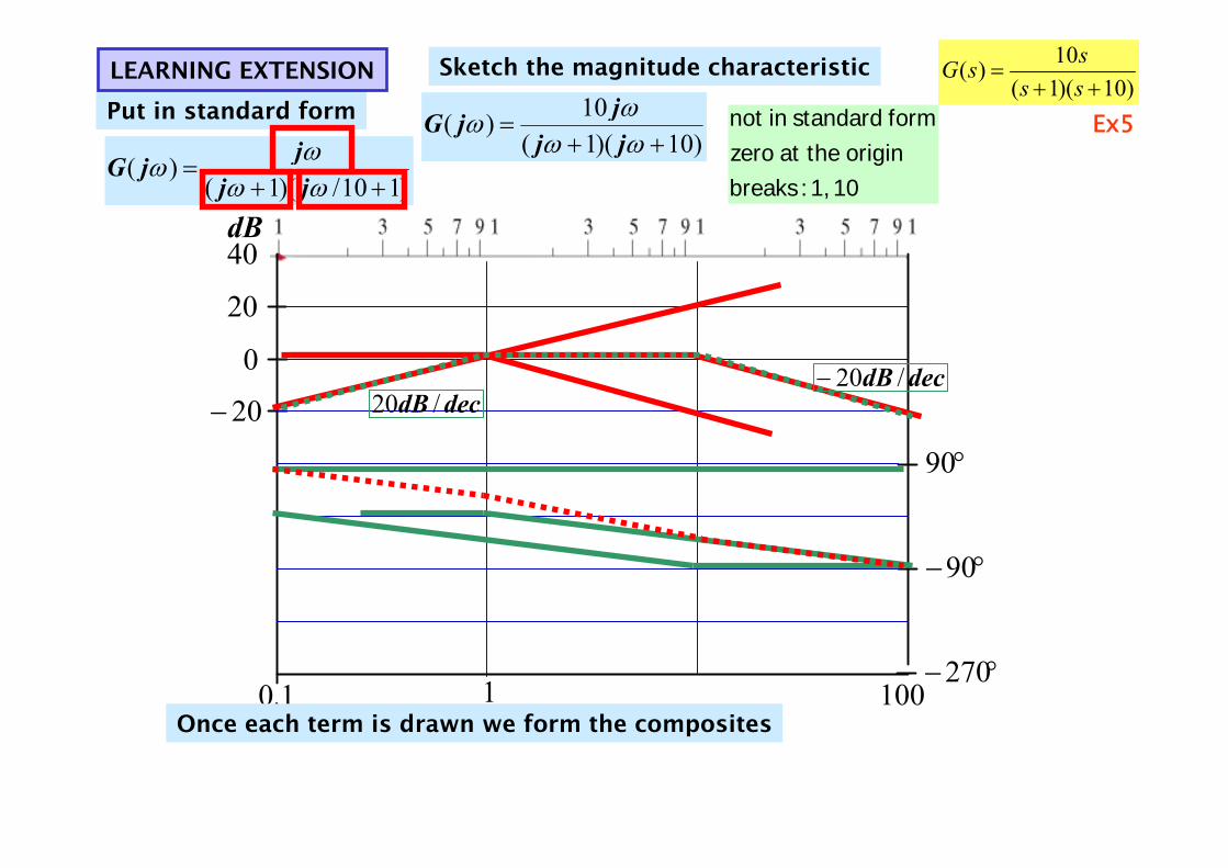
Resumo blocos diagrama de Bode
2. Pólo na origem:
H(s)=1/s
1. Pólo simples:
H(s)=a/(s+a)3. Pólo complexo
conjugado (assimpt.)
5. Zero na origem:
H(s)= s
4. Zero simples:
H(s)= (s+a)/a6. Zero complexo
conjugado (assimpt.)

Sistemas de 2ª ordem, sobre-amortecimento vs sub-amortecimento / ressonância
s → jω

RESONANT CIRCUITS - SERIES RESONANCE
Im { } 0Z⇒ =
⇒RESONANT FREQUENCY
PHASOR DIAGRAM
QUALITY FACTOR
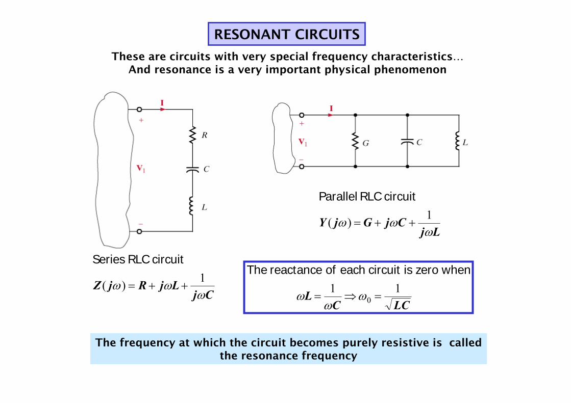
RESONANT CIRCUITS
These are circuits with very special frequency characteristics…And resonance is a very important physical phenomenon
CjLjRjZ
ωωω 1)( ++=
circuit RLC Series
LjCjGjY
ωωω 1)( ++=
circuitRLCParallel
LCCL 11
0 =⇒= ωω
ω
whenzeroiscircuit eachof reactanceThe
The frequency at which the circuit becomes purely resistive is calledthe resonance frequency

Properties of resonant circuits
At resonance the impedance/admittance is minimal
Current through the serial circuit/voltage across the parallel circuit canbecome very large (if resistance is small)
ξωω
211 :FactorQuality
0
0 ===CRR
LQ
222 )1(||
1)(
CLRZ
CjLjRjZ
ωω
ωωω
−+=
++=
222 )1(||
1)(
LCGY
CjLj
GjY
ωω
ωω
ω
−+=
++=
Given the similarities between series and parallel resonant circuits, we will focus on serial circuits

Properties of resonant circuits
At resonance the power factor is unity
CIRCUIT BELOW RESONANCE ABOVE RESONANCESERIES CAPACITIVE INDUCTIVEPARALLEL INDUCTIVE CAPACITIVE
Phasor diagram for series circuit Phasor diagram for parallel circuit
−
+
RV
−
−=
+
CIjVC ω
−
+Ljω
1GV1CVjω
LVjω
1−

LEARNING EXAMPLE Determine the resonant frequency, the voltage across eachelement at resonance and the value of the quality factor
LC1
0 =ω sec/2000)1010)(1025(
163
radFH
=××
=−−
I
AZ
VI S 52
010=
°∠==
Ω= 2Z resonanceAt
Ω=××= − 50)1025)(102( 330Lω
)(902505500 VjLIjVL °∠=×== ω
°−∠=×−==
Ω==
902505501
501
0
00
jICj
V
LC
C ω
ωω
RLQ 0ω
= 252
50==
||||
|||| 0
SC
SS
L
VQV
VQR
VLV
=
==ω
resonanceAt

LEARNING EXAMPLE Given L = 0.02H with a Q factor of 200, determine the capacitornecessary to form a circuit resonant at 1000Hz
RL0200 ω
=⇒= 200Q withL
LC1
0 =ωC02.0
110002 =×⇒ π FC μ27.1=⇒
What is the rating for the capacitor if the circuit is tested with a 10V supply?
VVC 2000|| =⇒||||
|||| 0
SC
SS
L
VQV
VQR
VLV
=
==ω
resonanceAt
Ω=××
=⇒ 59.1200
02.010002πR
AI 28.659.1
10==
The reactive power on the capacitorexceeds 12kVA

LEARNING EXTENSION Find the value of C that will place the circuit in resonanceat 1800rad/sec
LC1
0 =ω 218001.01
)(1.011800
×=⇒
×= C
CH
FC μ86.3=
Find the Q for the network and the magnitude of the voltage across thecapacitor
RLQ 0ω
=
603
1.01800=
×=Q
||||
|||| 0
SC
SS
L
VQV
VQR
VLV
=
==ω
resonanceAt
VVC 600|| =
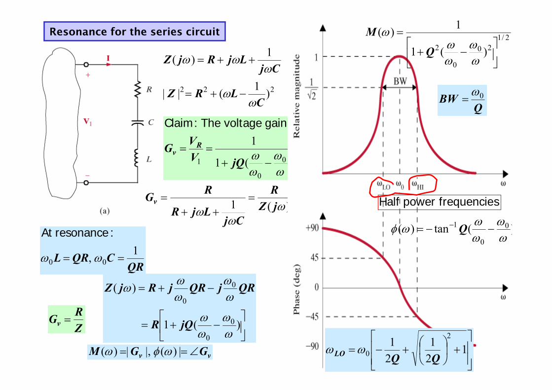
Resonance for the series circuit
222 )1(||
1)(
CLRZ
CjLjRjZ
ωω
ωωω
−+=
++=
QRCQRL 1, 00 == ωω
:resonanceAt
⎥⎦
⎤⎢⎣
⎡−+=
−+=
)(1
)(
0
0
0
0
ωω
ωω
ωω
ωωω
jQR
QRjQRjRjZ
)(1
10
0
1ωω
ωω −+
==jQV
VG Rv
isgainvoltageThe:Claim
)(1 ωω
ω jZR
CjLjR
RGv =++
=
vv GGM ∠== |)(|,|)( ωφω
2/120
0
2 )(1
1)(
⎥⎦
⎤⎢⎣
⎡−+
=
ωω
ωω
ω
Q
M
)(tan)( 0
0
1
ωω
ωωωφ −−= − Q
QBW 0ω=
⎥⎥⎦
⎤
⎢⎢⎣
⎡+⎟
⎠
⎞⎜⎝
⎛+−= 121
21 2
0 QQLO ωω
sfrequenciepower Half
ZRGv =

The Q factorCRR
LQ0
0 1ω
ω==
RLowQHigh :circuit seriesFor ⇔G)(lowR HighQHigh :circuitparallelFor ⇔
M
BW SmallQHigh ⇔
dissipates
Stores as Efield
Stores as M field
Capacitor and inductor exchange storedenergy. When one is at maximum the other is at zero
D
S
WWQ π2=
cycleby dissipatedenergy storedenergy maximumπ2=
Q can also be interpreted from anenergy point of view π
ωπω
221
20202 ×=×= mxeffD RIRIW
22
21
21
mxmxS CVLIW ==
ππω
220 QR
LWW
D
s =×
=

ENERGY TRANSFER IN RESONANT CIRCUITS
Normalizationfactor
( ) cos [ ]mO
Vi t t AR
ω=

LEARNING EXAMPLE
Ω2
mH2
Fμ5
Determine the resonant frequency, quality factor andbandwidth when R=2 and when R=0.2
CRRLQ
0
0 1ω
ω==
LC1
0 =ωQ
BW 0ω=
sec/10)105)(102(
1 4630 rad=
××=
−−ω
R Q2 10
0.2 100
R Q BW(rad/sec)2 10 1000
0.2 100 100
Evaluated with EXCEL
RQ 002.010000×= QBW /10000=
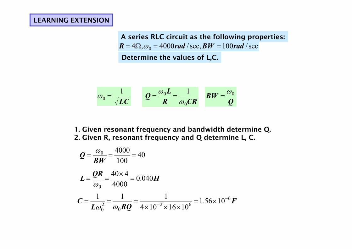
LEARNING EXTENSION
A series RLC circuit as the following properties:sec/100sec,/4000,4 0 radBWradR ==Ω= ω
Determine the values of L,C.
CRRLQ
0
0 1ω
ω==
LC1
0 =ωQ
BW 0ω=
1. Given resonant frequency and bandwidth determine Q.2. Given R, resonant frequency and Q determine L, C.
4010040000 ===
BWQ ω
HQRL 040.04000
4400
=×
==ω
FRQL
C 662
020
1056.11016104
111 −− ×=
×××===
ωω

LEARNING EXAMPLE Find R, L, C so that the circuit operates as a band-pass filterwith center frequency of 1000rad/s and bandwidth of 100rad/s
)(1 ωω
ω jZR
CjLjR
RGv =++
=
CRRLQ
0
0 1ω
ω==
LC1
0 =ωQ
BW 0ω=
dependent
Strategy: 1. Determine Q2. Use value of resonant frequency and Q to set up two equations in the three
unknowns3. Assign a value to one of the unknowns
10100
10000 ===BW
Q ω
RL
RLQ 1000100 =⇒=
ωLCLC1)10(1 23
0 =⇒=ω
For example FFC 6101 −== μ
HL 1=
Ω=100R

PROPERTIES OF RESONANT CIRCUITS: VOLTAGE ACROSS CAPACITOR
|||| 0 RVQV =resonanceAt
But this is NOT the maximum value for thevoltage across the capacitor
CRjLCCj
LjR
CjVV
S ωωω
ω
ω+−
=++
= 20
11
1
1
( )⎥⎥⎦
⎤
⎢⎢⎣
⎡⎟⎠
⎞⎜⎝
⎛+−
= 2221
1)(
Quu
ug
20
0;
SVVgu ==
ωω
( )22
22
2
1
)/1)(/(2)2)(1(20
⎥⎥⎦
⎤
⎢⎢⎣
⎡⎟⎠
⎞⎜⎝
⎛+−
+−−==
Quu
QQuuududg
CRRLQ
0
0 1ω
ω==
LC1
0 =ω
22 1)1(2
Qu =−⇒
20
maxmax 2
11Q
u −==ωω
2
2
424
max
411
211
41
1
Q
Q
QQQ
g−
=
⎟⎟⎠
⎞⎜⎜⎝
⎛−+
=
2
0
411
||||
Q
VQV S
−=

LEARNING EXAMPLE
mH50
Fμ5
Ω=Ω= 150, RR andwhenDetermine max0 ωω
Natural frequency depends only on L, C.Resonant frequency depends on Q.
sradLC
/2000)105)(105(
11620 =
××==
−−ω
CRRLQ
0
0 1ω
ω==
LC1
0 =ω
20
maxmax 2
11Q
u −==ωω
RQ 050.02000×= 2max 2
112000Q
−×=ω
R Q Wmax50 2 18711 100 2000
Evaluated with EXCEL and rounded to zero decimals
Using MATLAB one can display the frequency response

R=50Low QPoor selectivity
R=1High QGood selectivity

LEARNING EXAMPLE The Tacoma Narrows Bridge Opened: July 1, 1940Collapsed: Nov 7, 1940
Likely cause: windvarying at frequencysimilar to bridgenatural frequency
2.020 ×= πω
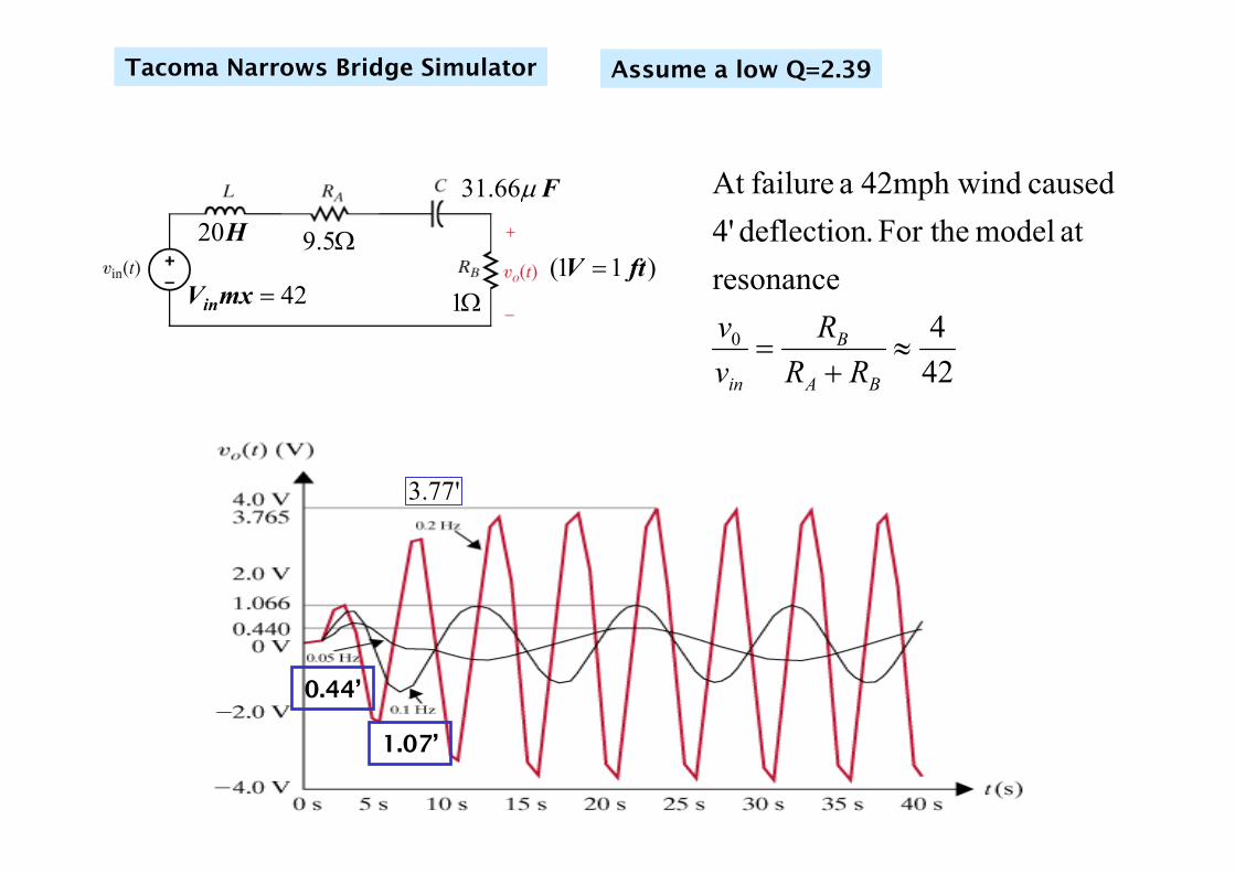
0.44’
1.07’
'77.3
Tacoma Narrows Bridge Simulator
)11( ftV =
424
resonanceat model For the .deflection 4'
caused 42mph wind a failureAt
0 ≈+
=BA
B
in RRR
vv
Ω1
Ω5.9H20
Fμ66.31
42=mxVin
Assume a low Q=2.39

PARALLEL RLC RESONANT CIRCUITS
222 )1(||
1)(
CLRZ
CjLjRjZ
ωω
ωωω
−+=
++=
222 )1(||
1)(
LCGY
CjLj
GjY
ωω
ωω
ω
−+=
++=
Impedance of series RLC Admittance of parallel RLC
IVYZLCCLGR
↔↔↔↔↔
,,,
esequivalencNotice
SS YVI =
SSL
SSC
SSG
IY
LjVLj
I
IY
CjCVjI
IYGGVI
ωω
ωω
11
==
==
==
||1||
||||
1
0
0
SL
SC
LC
SG
ILG
I
IG
CI
IIII
GYL
C
ω
ω
ωω
=
=
−==
=⇒=0
0
resonanceAt
CRRLQ
0
0 1ω
ω==
LC1
0 =ω
Series RLC
Parallel RLC
LGGCQ
0
0 1ω
ω==
LC1
0 =ω
|| SIQ=
Series RLC QBW 0ω=
Parallel RLCQ
BW 0ω=

VARIATION OF IMPEDANCE AND PHASOR DIAGRAM – PARALLEL CIRCUIT

LEARNING EXAMPLE
mHLFCSGVS
120,60001.0,0120
===°∠=
μ
If the source operates at the resonant frequency of the network, compute all the branch currents
SSL
SSC
SSG
IY
LjVLj
I
IY
CjCVjI
IYGGVI
ωω
ωω
11
==
==
==
||1||
||||
1
0
0
SL
SC
LC
SG
ILG
I
IG
CI
IIII
GYL
C
ω
ω
ωω
=
=
−==
=⇒=0
0
resonanceAt
|| SIQ=
SG IAI =°∠=°∠×= )(02.1012001.0
sradLC
/85.117)106(120.0
1140 =
××==
−ω
)(9049.80120)10600()85.117()901( 6 AIC °∠=°∠××××°∠= −
)(9049.8 AIL °−∠=
_______=xI

LEARNING EXAMPLE Derive expressions for the resonant frequency, half powerfrequencies, bandwidth and quality factor for the transfercharacteristic
in
out
IVH =
LjCjGYT ω
ω 1++=
Tin
out
T
inout YI
VHYIV 1
==⇒=
22 1
11
1||
⎟⎠⎞
⎜⎝⎛ −+
=++
=
LCGLj
CjGH
ωωω
ω
LC1
0 =ω :frequencyResonant
22max
||5.0|)(| HjH h =⇒ ωsfrequenciepower Half
22
2 21 GL
CGh
h =⎟⎟⎠
⎞⎜⎜⎝
⎛−+ω
ω
RG
H ==1|| max
GL
Ch
h ±=−⇒ω
ω 1
LCCG
CG
h1
22
2
+⎟⎠⎞
⎜⎝⎛+= mω
CGBW LOHI =−= ωω
LCR
LC
GBWQ ===
10ω
LGGCQ
0
0 1ω
ω==
⎥⎥⎦
⎤
⎢⎢⎣
⎡+⎟
⎠
⎞⎜⎝
⎛+−= 121
21 2
0 QQLO ωω
Replace and show

LEARNING EXAMPLE Increasing selectivity by cascading low Q circuits
Single stage tuned amplifier
( )( ) MHzsradFHLC
9.99/10275.61054.210
11 81260 =×=
×==
−−ω
398.010
1054.2250 6
12=
××= −
−LCR
LC
GBWQ ===
10ω

LEARNING EXTENSION Determine the resonant frequency, Q factor and bandwidth
FCmHLkR μ150,20,2 ==Ω=
Parallel RLC
LGGCQ
0
0 1ω
ω==
LC1
0 =ωQ
BW 0ω=
srad /577)10150)(1020(
1630 =
××=
−−ω
( ) 1732000/1
10150577 6=
××=
−
Q
sradBW /33.3173577
==

LEARNING EXTENSION 0 C, L, Determine ω
120,/1000,6 ==Ω= QsradBWkR
Parallel RLC
LGGCQ
0
0 1ω
ω==
LC1
0 =ωQ
BW 0ω=
sradBWQ /102.11000120 50 ×=×=×=ω
FRQC μω
167.0102.16000
1205
0=
××==
HQ
RL μω
417102.1120
60005
0=
××==
Can be used to verify computations

PRACTICAL RESONANT CIRCUIT The resistance of the inductor coils cannot beneglected
LjRCjjY
ωωω
++=
1)(LjRLjR
ωω
−−
×
22 )()(
LRLjRCjjY
ωωωω
+−
+=
⎟⎟⎠
⎞⎜⎜⎝
⎛+
−++
= 2222 )()()(
LRLCj
LRRjY
ωω
ωω
2
2210
)(⎟⎠⎞
⎜⎝⎛−=⇒=
+−⇒
LR
LCLRLCY Rωω
ω real
⇒==R
LQLC
000 ,1 ωω 2
00
11QR −=ωω
maxima are impedance and voltagethe resonanceAt .YIZIV ==
( )⎟⎟
⎠
⎞
⎜⎜
⎝
⎛⎟⎠⎞
⎜⎝⎛
⎟⎟⎠
⎞⎜⎜⎝
⎛+=⎟
⎟⎠
⎞⎜⎜⎝
⎛⎟⎠⎞
⎜⎝⎛+=
+=
20
2
0
22211
RLR
RLR
RLRZ RRR
MAXω
ωωωω
20RQZMAX =
How do you define a quality factor for this circuit?

LEARNING EXAMPLE ΩΩ= 5,50, RR for both Determine 0 ωω
⇒==R
LQLC
000 ,1 ωω 2
00
11QR −=ωω
sradFH
/2000)105)(1050(
1630 =
××=
−−ω
20
0112000,050.02000
QRQ R −=
×= ω
R Q0 Wr(rad/s) f(Hz)50 2 1732 275.75 20 1997 317.8
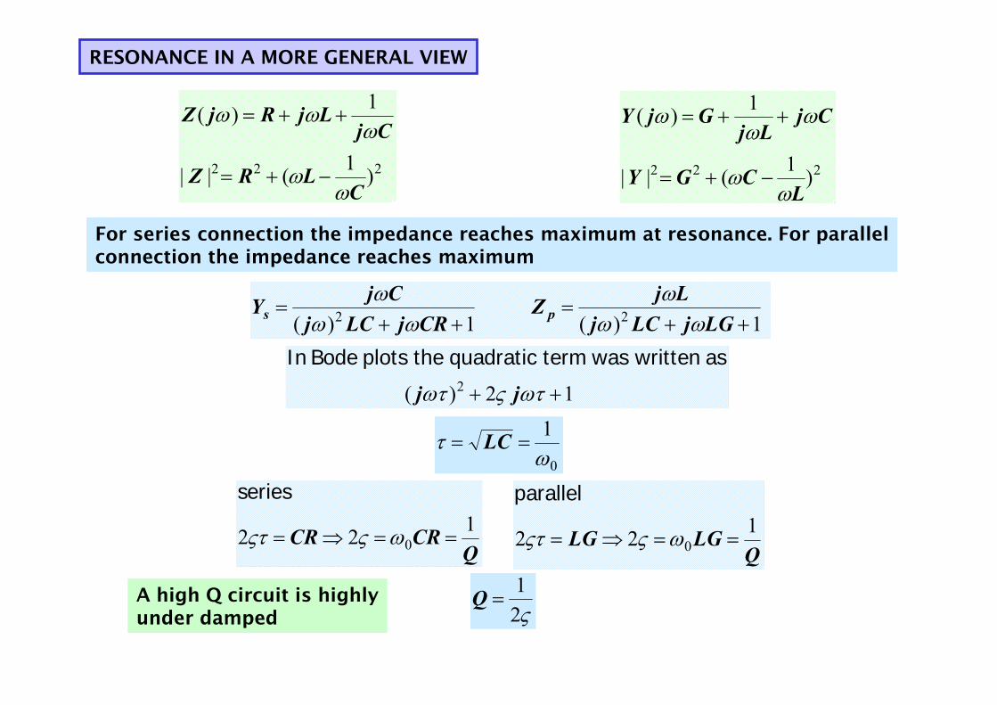
RESONANCE IN A MORE GENERAL VIEW
222 )1(||
1)(
CLRZ
CjLjRjZ
ωω
ωωω
−+=
++=
222 )1(||
1)(
LCGY
CjLj
GjY
ωω
ωω
ω
−+=
++=
For series connection the impedance reaches maximum at resonance. For parallelconnection the impedance reaches maximum
1)(1)( 22 ++=
++=
LGjLCjLjZ
CRjLCjCjY ps ωω
ωωω
ω
12)( 2 ++ ωτςωτ jj
aswrittenwastermquadratictheplotsBodeIn
0
1ω
τ == LC
QCRCR 122 0 ==⇒= ωςςτ
series
QLGLG 122 0 ==⇒= ωςςτ
parallel
ς21
=QA high Q circuit is highlyunder damped

Freq. Natural e Ressonância RLC série (Vs -> I) ou paralelo (Is -> V)
Em todas estas funções de transferência a frequência natural tem a expressão:
LCn1
=ω

Ressonância RLC série (Vs -> I) ou paralelo (Is -> V)
Ressonância nestes casos corresponde a Z ou Y reais (resistivos puros)
LCnr1
=≡ωω
Nota: definição mais geral: ωr é o máximizante da função de transferência
Nas funções de transferência I/Vsou Vr/Vs (RLC série), V/Is ou Ir/Is(RLC paralelo) temos:

Ressonância RLC série ou paralelo – outras funções
221 ξωω −= nr
Definição mais geral de ressonância: ωr é a frequência máximizante da função de transferência
Usando esta definição então os circuitos VC/Vs e IL/IS têm a seguinte frequência de ressonância:
221 ξωω−
= nr
Usando esta definição então os circuitos VL/VS e IC/IS têm a seguinte frequência de ressonância:

SCALING
Scaling techniques are used to change an idealized network into a morerealistic one or to adjust the values of the components
M
M
M
KCC
LKLRKR
→
→→
'
''
scalingimpedanceor Magnitude
''11'' 0 CLLC
CLLC ==⇒= ω
''00
RL
RLQ ωω==
Magnitude scaling does not change thefrequency characteristics nor the qualityof the network.
CCLL
ωKω' F
ωωωω 1
''1,'' ==
→unchanged iscomponent each of Impedance
scalingtimeor Frequency
F
F
KCC
KLL
RR
→
→
→
'
'
'
0'0 ωω FK=
)('
''0 BWK
QBW F==
ω
QR
LQ =='''
'0ω Constant Q
networks

LEARNING EXAMPLE
Ω= 2
H1=
F21
Determine the value of the elements and the characterisitcsof the network if the circuit is magnitude scaled by 100 andfrequency scaled by 1,000,000
2,22,/20 === BWQsradω
FC
HLR
2001'
100'200'
=
=Ω=
M
M
M
KCC
LKLRKR
→
→→
'
''
scalingimpedanceor Magnitude F
F
KCC
KLL
RR
→
→
→
'
'
'
FC
mHLR
μ2001''
100''200''
=
=Ω=
0'0 ωω FK=
)('
''0 BWK
QBW F==
ω
srad /10414.1 6''0 ×=ω
unchangedare 0,ωQ

LEARNING EXTENSION
elementscircuit resulting theDetermine 10,000.by scaledfrequency and 100by scaledmagnitudeis2FC1H,L,10RwithnetworkRLCAn ==Ω=
M
M
M
KCC
LKLRKR
→
→→
'
''
scalingimpedanceor Magnitude
FCHL
R
02.0'100'1000'
==
Ω=
F
F
KCC
KLL
RR
→
→
→
'
'
'scalingFrequency
FCHL
kR
μ2''01.0''
1''
==
Ω=

FILTER NETWORKS
Networks designed to have frequency selective behavior
COMMON FILTERS
Low-pass filterHigh-pass filter
Band-pass filter
Band-reject filter
We focus first onPASSIVE filters

Simple low-pass filter
RCjCj
R
CjVVGv ω
ω
ω+
=+
==1
11
1
1
0
RCj
Gv =+
= τωτ
;1
1
( )ωτωφ
ωτω
1
2
tan)(
11||)(
−−==∠
+==
v
v
G
GM
211,1max =⎟
⎠⎞
⎜⎝⎛ ==
τωMM
frequencypower half==τ
ω 1τ1
=BW

Simple high-pass filter
CRjCRj
CjR
RVVGv ω
ω
ω+
=+
==111
0
RCj
jGv =+
= τωτ
ωτ ;1
( )
ωτπωφ
ωτ
ωτω
1
2
tan2
)(
1||)(
−−==∠
+==
v
v
G
GM
211,1max =⎟
⎠⎞
⎜⎝⎛ ==
τωMM
frequencypower half==τ
ω 1
τω 1
=LO

Simple band-pass filter
Band-pass
⎟⎠⎞
⎜⎝⎛ −+
==
CLjR
RVVGv
ωω 11
0
( ) ( )222 1)(
−+=
LCRC
RCMωω
ωω
11=⎟
⎠⎞
⎜⎝⎛ =
LCM ω 0)()0( =∞=== ωω MM
( )2
4/)/( 20
2 ωω
++−=
LRLRLO
LC1
0 =ω
( )2
4/)/( 20
2 ωω
++=
LRLRHI
LRBW LOHI =−= ωω
)(2
1)( HILO MM ωω ==

Simple band-reject filter
0110
00 =⎟⎟⎠
⎞⎜⎜⎝
⎛−⇒=
CLj
LC ωωω
10 VV =⇒= circuitopenasactscapacitor the0at ω
10 VV =⇒∞= circuitopenasactsinductor theat ω
filter pass-bandtheinasdeterminedare HILO ωω ,

LEARNING EXAMPLE Depending on where the output is taken, this circuitcan produce low-pass, high-pass or band-pass or band-reject filters
Band-pass
Band-reject filter
⎟⎠⎞
⎜⎝⎛ −+
=
CLjR
LjVV
S
L
ωω
ω1 ( ) 1)(,00 =∞=== ωω
S
L
S
L
VV
VV
High-pass
⎟⎠⎞
⎜⎝⎛ −+
=
CLjR
CjVV
S
C
ωω
ω1
1
( ) 0)(,10 =∞=== ωωS
C
S
C
VV
VV
Low-pass
FCHLR μμ 159,159,10 ==Ω=for plot Bode

LEARNING EXAMPLE A simple notch filter to eliminate 60Hz interference
)1(1
1
CLj
CL
CjLj
CjLj
ZR
ωω
ωω
ωω
−=
+=
inReq
eq VZR
RV
+=0
∞=⎟⎠⎞
⎜⎝⎛ =
LCZR
1ω 010 =⎟
⎠⎞
⎜⎝⎛ =∴
LCV ω
( ) ( )tttvin 10002sin2.0602sin)( ×+×= ππ
FCmHL μ100,3.70 ==

LEARNING EXTENSION )( ωjGvfor plot BodetheofsticcharacterimagnitudetheSketch
RCjCj
R
CjjGv ωω
ωω+
=+
=1
11
1
)(
sradFRC /2.0)1020)(1010( 63 =×Ω×== −τ 20dB/dec- of asymptotefrequency High0dB/dec of asymptotefrequency low
5rad/s :frequencyer Break/corn

LEARNING EXTENSION )( ωjGvfor plot BodetheofsticcharacterimagnitudetheSketch
RCjRCj
CjR
RjGv ωω
ω
ω+
=+
=11)(
sradFRC /5.0)1020)(1025( 63 =×Ω×== −τ
srad /21==
τωat 0dB Crosses 20dB/dec.
20dB/dec- of asymptotefrequency High0dB/dec of asymptotefrequency low
2rad/s :frequencyer Break/corn

LEARNING EXTENSION )( ωjGvfor plot BodetheofsticcharacterimagnitudetheSketch
Band-pass
LCjRCjRCj
LjCj
R
RjGv 2)(11)(ωω
ω
ωω
ω++
=++
=
5.0102
1010102
,1010
3
363
362
=×
=⇒×==
==⇒=
−
−−
−−
ςςτ
ττ
RC
LC
sradRC
/10001==ωat 0dB Crosses 20dB/dec.
40dB/dec- of asymptotefrequency High0dB/dec of asymptotefrequency low
rad/s1000 :frequencyer Break/corn
( )2
4/)/( 20
2 ωω
++−=
LRLRLO
( )2
4/)/( 20
2 ωω
++=
LRLRHI
100010 ==
LCω
srad /618=
srad /1618=
decdB /40−

ACTIVE FILTERS
Passive filters have several limitations
1. Cannot generate gains greater than one
2. Loading effect makes them difficult to interconnect
3. Use of inductance makes them difficult to handle
Using operational amplifiers one can design all basic filters, and more, with only resistors and capacitors
The linear models developed for operational amplifiers circuits are valid, in amore general framework, if one replaces the resistors by impedances
Ideal Op-Amp
These currents arezero

Basic Inverting Amplifier
0=+V
+− =⇒ VV gain Infinite
0=−V
0==⇒ +II-impedanceinput Infinite
02
2
1
1 =+ZV
ZV
11
22 V
ZZV −=
Linear circuit equivalent
0=−I
1
2
ZZG −=
1
11 Z
VI =

Basic Non-inverting amplifier
1V
1V
0=+I
1
1
2
10
ZV
ZVV
=−
11
120 V
ZZZV +
=
1
21ZZG +=
01 =I
Basic Non-inverting Amplifier
Due to the internal op-amp circuitry, it haslimitations, e.g., for high frequency and/orlow voltage situations. The OperationalTransductance Amplifier (OTA) performswell in those situations

Operational Transductance Amplifier (OTA)
∞== 0RRin :OTAIdeal
COMPARISON BETWEEN OP-AMPS AND OTAs – PHYSICAL CONSTRUCTION
Comparison of Op-Amp and OTA - Parameters
Amplifier Type Ideal Rin Ideal Ro Ideal Gain Input Current input VoltageOp-Amp 0 0 0
OTA gm 0 nonzero∞∞ ∞
∞
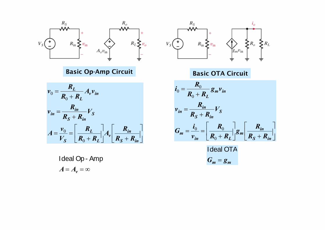
Basic Op-Amp Circuit Basic OTA Circuit
⎥⎦
⎤⎢⎣
⎡+⎥
⎦
⎤⎢⎣
⎡+
==
+=
+=
inS
inv
L
L
S
SinS
inin
invL
L
RRRA
RRR
VvA
VRR
Rv
vARR
Rv
0
0
00
⎥⎦
⎤⎢⎣
⎡+⎥
⎦
⎤⎢⎣
⎡+
==
+=
+=
inS
inm
Linm
SinS
inin
inmL
RRRg
RRR
viG
VRR
Rv
vgRR
Ri
0
00
0
00
∞== vAAAmp-Op Ideal mm gG =
OTAIdeal

Basic OTA Circuits
)0()(10
000
10
vdxxiC
v
vgit
m
+=
=
∫
)0()()( 00
10 vdxxvCgtv
tm += ∫
Integrator
In the frequency domain
10 VCj
gV m
ω=
00
0
=+−=ii
vgi
in
inm polarity)(notice
meq
in
in
gR
iv 1
==
ResistorSimulated

Basic OTA Adder
11vgm
22vgm
21 21vgvg mm +
ResistorSimulated
Equivalent representation
OTA APPLICATION
)(121
30 21
vgvgg
v mmm
+=
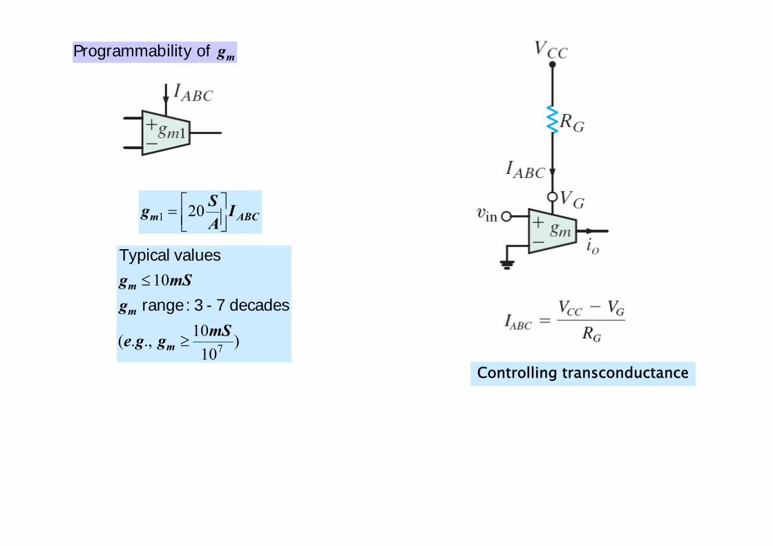
mg ofility Programmab
)10
10.,.(
10
7mSgge
gmSg
m
m
m
≥
≤decades 7 - 3 :range
valuesTypical
ABCm IASg ⎥⎦⎤
⎢⎣⎡= 201
Controlling transconductance

LEARNING EXAMPLE
ABCm
m
m
Ig
SmSg
mSg
20
1041044
74
=
×=≥
≤
−
resistoraProduce Ωk25
SSgg m
m
753 10410411025 −− ×>×=⇒=×
meq
in
in
gR
iv 1
==
Resistor Simulated
)(20104 5 AIASS ABC⎥⎦⎤
⎢⎣⎡=× −
AAI ABC μ2102 6 =×= −

LEARNING EXAMPLE Floating simulated resistor
1101 vgi m−= 1202 vgi m=
inmvgi −=0
One grounded terminal
011 ii −= 102 ii =
21 mm gg = operationproper For
ABCm
m
m
Ig
SmSg
mSg
20
1041044
74
=
×=≥
≤
−
resistor10MaProduce Ω
Sgm7
6 101010
1 −=×
= S7104 −×<
The resistor cannot be producedwith this OTA!

LEARNING EXAMPLE
210
210
321
210210
,,,
vvvvvv
ggg mmm
−=+=
b) a)
producetoSelect
ABCm
m
m
Ig
SmSg
mSg
20
1041044
74
=
×=≥
≤
−
)(121
30 21
vgvgg
v mmm
+=
Case a
2;103
2
3
1 ==m
m
m
m
gg
gg
Two equations in three unknowns.Select one transductance
)(102011.0 4
33 AImSg ABCm−×=⇒= Aμ5=
AImSg ABCm μ102.0 22 =⇒=
AImSg ABCm μ501 11 =⇒=
Case b
Reverse polarity of v2!

ANALOG MULTIPLIER
ASSUMES VG IS ZERO
Based on ‘modulating the control current

AUTOMATIC GAIN CONTROL
For simplicity of analysiswe drop the absolute value
IN O IN
IN O
v small v AvAv big vB
⇒ ≈
⇒ ≈

OTA-C CIRCUITS
Circuits created using capacitors, simulated resistors, adders and integrators
integrator
resistor
Frequency domain analysis assumingideal OTAs
1101 im VgI = 0202 VgI m−=
0201 IIIC +=CICj
Vω1
0 =
[ ]021101 VgVgCj
V mim −=ω
1
2
21
0 1 i
m
mm
Vg
Cjg
gV
ω+=
Magnitude Bode plot
1
0
iv V
VG =
2
1
m
mdc g
gA =
Cgf
Cg
mC
mC
2
2
2 =
=
π
ω

LEARNING EXAMPLE
)10(21
4
51
0
πωjV
VGi
v+
== :Desired
ABCm
m
m
Ig
SmSg
mSg
20
101011
63
=
=≥
≤
−
4=dcA kHzfCC 100)10(2 5 =⇒= πω
2
1
m
mdc g
gA =
Cgf
Cg
mC
mC
2
2
2 =
=
π
ω
Two equations in three unknowns.Select the capacitor value
pFC 25= Sgm6125
2 107.15)1025)(10(2 −− ×=×= π
OK
AISg ABCm μμ 14.38.62 11 =⇒=
AI ABC μ785.020
7.152 ==
biasesandncestransductathe Find

TOW-THOMAS OTA-C BIQUAD FILTER biquad ~ biquadratic
20
02
20
)()(
)()(
ωωωω
ωω
++
++=
jQ
j
CjBjAVV
i
CjVVgV i
m ω021
101−
=)( 201202 im VVgI −= )( 23303 oim VVgI −=
)(10302
202 II
CjV +=
ω
03i
)( unknownsfour andequationsFour 02010201 ,,, IIVV
1)()(12
132
21
21
32
321
2
3
2
2
01
+⎥⎦
⎤⎢⎣
⎡⎥⎦
⎤⎢⎣
⎡
⎥⎦
⎤⎢⎣
⎡−+⎥
⎦
⎤⎢⎣
⎡+
=+ ωω
ω
jggCgj
ggCC
VggVV
gg
gCj
V
mm
m
mm
im
mii
m
m
m
1)()(12
132
21
21
321
312
1
11
02
+⎥⎦
⎤⎢⎣
⎡⎥⎦
⎤⎢⎣
⎡
⎥⎦
⎤⎢⎣
⎡+⎥
⎦
⎤⎢⎣
⎡−
=+ ωω
ωω
jggCgj
ggCC
VgggCjV
gCjV
V
mm
m
mm
imm
mi
mi
1
22
3
21
2
30
21
210 ,,
CC
gggQ
Cg
QCCgg
m
mmmmm ===ωω
Filter Type A B CLow-pass 0 0 nonzeroBand-pass 0 nonzero 0High-pass nonzero 0 0 ⎪
⎪⎪
⎩
⎪⎪⎪
⎨
⎧
=
=
=
⇒⎭⎬⎫
==
CgBW
ggQ
Cg
CCgg
m
m
m
m
mm
3
3
0
21
21
ω

LEARNING EXAMPLE
ABCm
m
m
Ig
SmSg
mSg
20
1041044
74
=
×=≥
≤
−
5.- gainfrequency center and 75kHz, of bandwidth500kHz,offrequency center withfilter pass-bandaDesign
1)()(12
132
21
21
321
312
1
11
02
+⎥⎦
⎤⎢⎣
⎡⎥⎦
⎤⎢⎣
⎡
⎥⎦
⎤⎢⎣
⎡+⎥
⎦
⎤⎢⎣
⎡−
=+ ωω
ωω
jggCgj
ggCC
VgggCjV
gCjV
V
mm
m
mm
imm
mi
mi
1
22
3
21
2
30
21
210 ,,
CC
gggQ
Cg
QCCgg
m
mmmmm ===ωω
capacitorspF-50and ionconfiguratThomas-Towthe Use
BW03 =iV
3
20 |)(|
m
mv g
gjG =ω0)(1 2
21
210 =⎥
⎦
⎤⎢⎣
⎡+⇒= ωωω j
ggCC
mm
21 CC =
SgBW m μπ 56.23107521050
312
3 =××=×
= −
Sgm μ8.1175 2 =⇒=
( ) ( ) 213
61252
0 )105(108.1171052 −
−
×××
=××= mgπω Sgm μ5.2091 =⇒
AIAIAI
ABC
ABC
ABC
μμμ
18.189.547.10
3
2
1
===
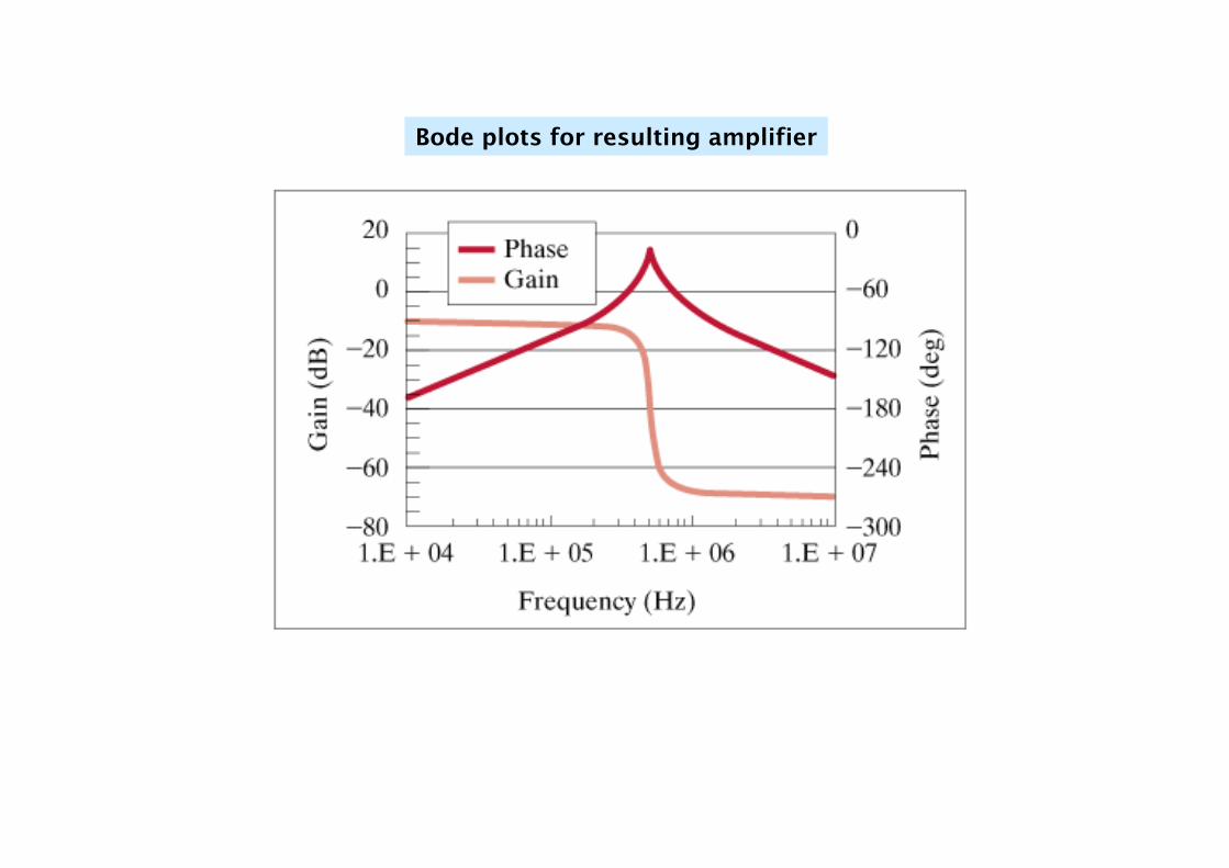
Bode plots for resulting amplifier

LEARNING BY APPLICATION Using a low-pass filter to reduce 60Hz ripple
Thevenin equivalent for AC/DCconverter
Using a capacitor to create a low-pass filter
Design criterion: place the corner frequencyat least a decade lower
THTH
OF VCRj
Vω+
=1
1
( )21||||CR
VVTH
THOF
ω+=
CRTHC
1=ω
||1.0|| THOF VV ≈
FCC μπ
05.5362
1500 =⇒×
=

Filtered output

LEARNING EXAMPLE Single stage tuned transistor amplifier
Select the capacitor for maximumgain at 91.1MHz
AntennaVoltage
Transistor Parallel resonant circuit
⎥⎦⎤
⎢⎣⎡−= CjLjR
VV
Aωω 1||||
100040
LCRCjj
CjVV
CjCj
CjLjR
A 1)(
/1000
4
//
111
10004
2
0
++−=
×++
−=
ωω
ω
ωω
ωω
LC/1frequency center with pass-Band
( ) ⇒=×− C6
6
101101.912π pFC 05.3=
1001000
410 ==⎟⎠⎞
⎜⎝⎛ = R
LCVV
Aω
AVV0for plot Bode Magnitude

LEARNING BY DESIGN Anti-aliasing filter
Nyquist CriterionWhen digitizing an analog signal, such as music, any frequency components
greater than half the sampling rate will be distorted
In fact they may appear as spurious components. The phenomenon is known as aliasing.
SOLUTION: Filter the signal before digitizing, and remove all components higherthan half the sampling rate. Such a filter is an anti-aliasing filter
For CD recording the industry standard is to sample at 44.1kHz.An anti-aliasing filter will be a low-pass with cutoff frequency of 22.05kHz
Single-pole low-pass filter
RCjVV
in ω+=
1101
050,2221×== πω
RCC
Ω=⇒= kRnFC 18.721
Resulting magnitude Bode plot
Attenuationin audio range

Improved anti-aliasing filter Two-stage buffered filter
−
+
01v
RCjVV
ω+=
11
01
02
RCjVV
in ω+=
1101
One-stage
Two-stage
Four-stage
( )nin
n
RCjVV
ω+=
110
stage-n

mHLFC
704.010
== μ
Magnitude Bode plot
( )sCsLRRR
VV
tapeamp
amp
tape
amp
/1||++=
⎥⎥⎥⎥⎥
⎦
⎤
⎢⎢⎢⎢⎢
⎣
⎡
+⎟⎟⎠
⎞⎜⎜⎝
⎛
++
++
=
1
1
2
2
tapeamp
tapeamp
amp
tape
amp
RRLsLCs
LCsRR
RVV
LC1
=frequency notch To design, pick one, e.g., C and determine the other
LEARNING BY DESIGN Notch filter to eliminate 60Hz hum
Notch filter characteristic

DESIGN EXAMPLE ANTI ALIASING FILTER FOR MIXED MODE CIRCUITS
Visualization of aliasing
Signals of differentfrequency and the samesamples
Ideally one wants to eliminate frequency components higher than twice the sampling frequency and make sure that all useful frequencies as properly sampled Design specification
Simplifying assumption
Infinite input resistance (no load on RC circuit)
Design equation
15.9R k∴ = Ω

(non-inverting op-amp)DESIGN EXAMPLE “BASS-BOOST” AMPLIFIER
DESIRED BODE PLOT
OPEN SWITCH
(6dB)
5002P
f =
Switch closed??

DESIGN EXAMPLE TREBLE BOOST
Original player response Desired boost
Proposed boost circuit
Non-inverting amplifier
Design equations
Filters
Related Documents