April 2007 Rev 4 1/14 14 SMA661AS Fully integrated GPS LNA IC Features ■ Power down function ■ Integrated matching networks ■ Low noise figure 1.15 dB @ 1.575 GHz ■ High gain 18 dB @ 1.575 GHz ■ High linearity (IIP3 = +3dBm) ■ Temperature compensated ■ Unconditionally stable ■ ESD protection (HBM ± 2kV) ■ 70 GHz Silicon Germanium Technology Applications ■ GPS Description The SMA661AS is the first low-noise amplifier with integrated matching networks and embedded power-down function. The chip, which requires only one external input capacitor, drastically reduces the application bill of materials and the PCB area, resulting in an ideal solution for compact and cost-effective GPS LNA. The SMA661AS, using the ST's leading-edge 70GHz SiGe BiCMOS technology, achieves excellent RF performance at the GPS frequency of 1.575GHz, in terms of power gain, noise Figure and linearity with a current consumption of 8.5mA. The device is unconditionally stable and ESD protected. All these features are steady over the operating temperature range of -40 o C to +85 o C. It's housed in ultra-miniature SOT666 plastic package. SOT666 (1.65 x 1.2 x 0.57 mm) Table 1. Device summary Part Number Marking Package Packing SMA661ASTR 661 SOT666 Tape and reel www.st.com

Welcome message from author
This document is posted to help you gain knowledge. Please leave a comment to let me know what you think about it! Share it to your friends and learn new things together.
Transcript
April 2007 Rev 4 1/14
14
SMA661AS
Fully integrated GPS LNA IC
Features■ Power down function
■ Integrated matching networks
■ Low noise figure 1.15 dB @ 1.575 GHz
■ High gain 18 dB @ 1.575 GHz
■ High linearity (IIP3 = +3dBm)
■ Temperature compensated
■ Unconditionally stable
■ ESD protection (HBM ± 2kV)
■ 70 GHz Silicon Germanium Technology
Applications■ GPS
DescriptionThe SMA661AS is the first low-noise amplifier with integrated matching networks and embedded power-down function. The chip, which requires only one external input capacitor, drastically reduces the application bill of materials and the PCB area, resulting in an ideal solution for compact and cost-effective GPS LNA.
The SMA661AS, using the ST's leading-edge 70GHz SiGe BiCMOS technology, achieves excellent RF performance at the GPS frequency of 1.575GHz, in terms of power gain, noise Figure and linearity with a current consumption of 8.5mA. The device is unconditionally stable and ESD protected. All these features are steady over the operating temperature range of -40 oC to +85 oC. It's housed in ultra-miniature SOT666 plastic package.
SOT666
(1.65 x 1.2 x 0.57 mm)
Table 1. Device summary
Part Number Marking Package Packing
SMA661ASTR 661 SOT666 Tape and reel
www.st.com
Contents SMA661AS
2/14
Contents
1 Pins description and circuit schematic . . . . . . . . . . . . . . . . . . . . . . . . . . 3
2 Electrical specifications . . . . . . . . . . . . . . . . . . . . . . . . . . . . . . . . . . . . . . 4
2.1 Absolute maximum ratings . . . . . . . . . . . . . . . . . . . . . . . . . . . . . . . . . . . . . 4
2.2 Electrical characteristics . . . . . . . . . . . . . . . . . . . . . . . . . . . . . . . . . . . . . . . 4
3 Typical performance . . . . . . . . . . . . . . . . . . . . . . . . . . . . . . . . . . . . . . . . . 5
4 Evaluation board description . . . . . . . . . . . . . . . . . . . . . . . . . . . . . . . . . . 8
5 Package and packing informations . . . . . . . . . . . . . . . . . . . . . . . . . . . . 10
5.1 Package informations . . . . . . . . . . . . . . . . . . . . . . . . . . . . . . . . . . . . . . . . 10
5.2 Packing informations . . . . . . . . . . . . . . . . . . . . . . . . . . . . . . . . . . . . . . . . 11
6 Revision history . . . . . . . . . . . . . . . . . . . . . . . . . . . . . . . . . . . . . . . . . . . 13
SMA661AS Pins description and circuit schematic
3/14
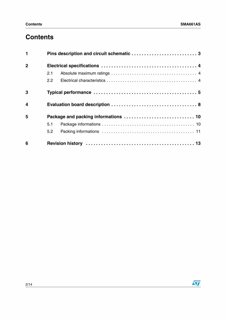
1 Pins description and circuit schematic
Figure 1. Pin connection
Figure 2. Application circuit schematic
Table 2. Pins description
Pin No. Pin Name
1 RF IN
2 GND
3 PD
4 RF OUT
5 GND
6 VCC
1
2
3
6
5
4
Top View
SM A661ASSM A661ASRF input RF IN
(1)
VCC (6)
G N D (2,5)
C1 RF O U T(4)
PD (3)
RF O utputSM A661ASSM A661AS
RF input RF IN
(1)
VCC (6)
G N D (2,5)
C1 RF O U T(4)
PD (3)
SM A661ASSM A661ASRF input RF IN
(1)
VCC (6)
G N D (2,5)
C1 RF O U T(4)
PD (3)
RF O utput
Electrical specifications SMA661AS
4/14
2 Electrical specifications
2.1 Absolute maximum ratings
2.2 Electrical characteristics(Ta = +25 °C, VCC = 2.7 V, ZL = ZS = 50 ohm, unless otherwise specified; measured according to Figure 13 at pin level)
Table 3. Absolute maximum ratings
Symbol Parameter Conditions Value Unit
Vcc Supply voltage 3.3 V
Tstg Storage temperature -60 to +150 oC
Ta Operating ambient temperature -40 to +85 oC
VESD Electrostatic Discharge HBM (ALL PINs) ± 2000 V
VESD Electrostatic Discharge MM (ALL PINs) ± 200 V
Table 4. Electrical characteristics
Symbol Parameters Test Conditions Min. Typ. Max. Unit
f Frequency 1575 MHz
Vcc Supply voltage 2.4 2.7 3 V
Icc Current Consumption 8.5 mA
IPDPower Down Mode Current Consumption
VPD ≤ VPDL 10 nA
Gp Power gain 18 dB
NF Noise figure 1.15 dB
IIP2 Input IP2f1 = 849 MHz, f2 = 2424 MHz, Pin = -30 dBm
0.5 dBm
IIP3 Input IP3f1 = 1574.5 MHz, f2 = 1575.5 MHz, Pin = -30 dBm
3 dBm
ISL Reverse Isolation -28 dB
RLin Input Return Loss f = 1500-1650 MHz 10 dB
RLout Output Return Loss f = 1500-1650 MHz 10 dB
VPDL(1)
1. The device is switched to OFF state
Power Down Low State
0.5 V
VPDH(2)
2. The device is switched to ON state
Power Down High State
1.0 V
Stability 100 - 10000 MHz Unconditionally stable
SMA661AS Typical performance
5/14
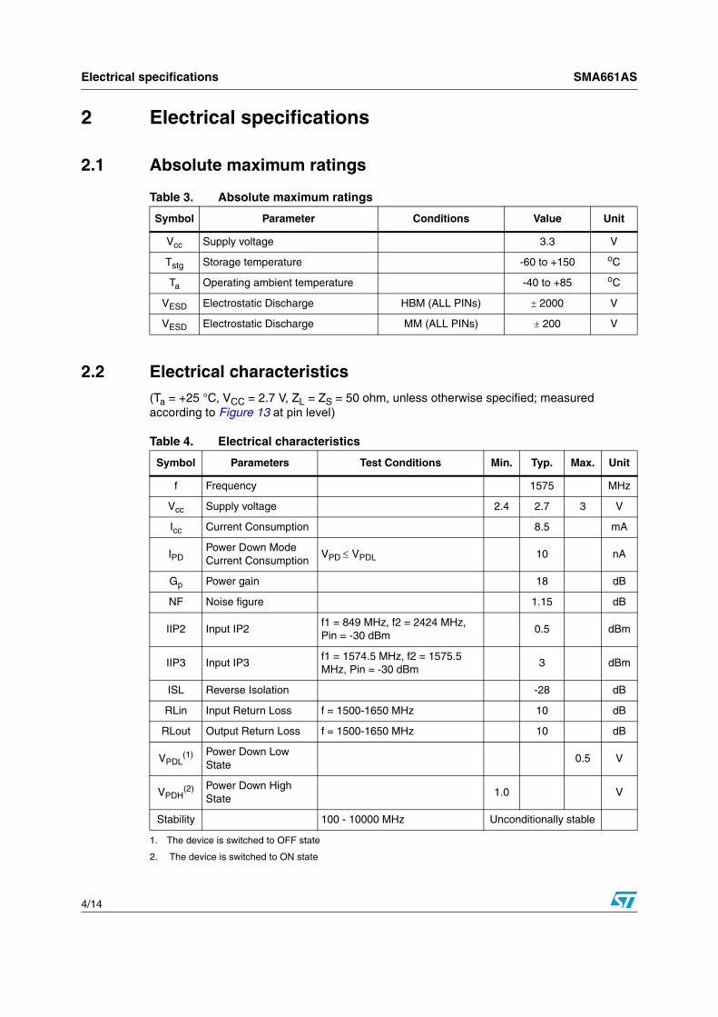
3 Typical performance
(Vcc = 2.7 V, ZL = ZS = 50 ohm, unless otherwise specified; measured according to Figure 13 at pin level)
Figure 3. Power Gain vs. Frequency Figure 4. Input Return Loss vs. Frequency
Figure 5. Noise Figure vs. Frequency Figure 6. Reverse Isolation vs. Frequency
Figure 7. Output Return Loss vs. Frequency Figure 8. IIP3 vs. Temperature
10
11
12
13
14
15
16
17
18
19
20
21
22
1000 1100 1200 1300 1400 1500 1600 1700 1800 1900 2000f (MHz)
Gp
(dB)
Ta = -40 ºC Ta = +25 ºC
Ta = +85 ºC
-20
-18
-16
-14
-12
-10
-8
-6
-4
-2
0
1000 1100 1200 1300 1400 1500 1600 1700 1800 1900 2000f (MHz)
IRL
(dB
)
Ta = +85 ºC
Ta = -40 ºC
Ta = +25 ºC
0.0
0.5
1.0
1.5
2.0
2.5
3.0
1500 1520 1540 1560 1580 1600
f (MHz)
NF
(dB
)
Ta = +85 ºC
Ta = +25 ºC
Ta = -40 ºC
-40
-38
-36
-34
-32
-30
-28
-26
-24
-22
-20
1000 1100 1200 1300 1400 1500 1600 1700 1800 1900 2000f (MHz)
ISL
(dB
) Ta = +85 ºC
Ta = -40 ºCTa = +25 ºC
-20
-18
-16
-14
-12
-10
-8
-6
-4
-2
0
1000 1100 1200 1300 1400 1500 1600 1700 1800 1900 2000
f (MHz)
OR
L (d
B)
Ta = -40 ºC
Ta = +85 ºCTa = +25 ºC
0
0.5
1
1.5
2
2.5
3
3.5
4
4.5
5
-40 25 85T (°C)
IIP3
(dB
m)
Typical performance SMA661AS
6/14
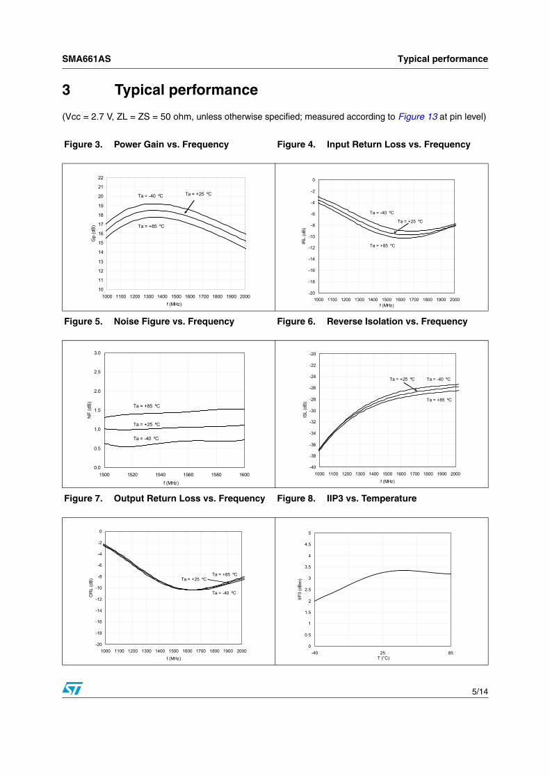
Note: S-Parameter are available on request.
Figure 9. Current Consumption vs. Temperature
Figure 10. Gain Power Down vs. Temperature
Figure 11. Power Down Current vs. Temperature
7.5
7.6
7.7
7.8
7.9
8
8.1
8.2
8.3
8.4
8.5
-40 25 +85T (°C)
Icc
(mA)
-25
-24
-23
-22
-21
-20
-19
-18
-17
-16
-15
-40 25 +85T (°C)
Gpd
(dB
)
0
10
20
30
40
50
60
-40 -15 10 35 60 85T (°C)
Ipd
(nA)
SMA661AS Typical performance
7/14
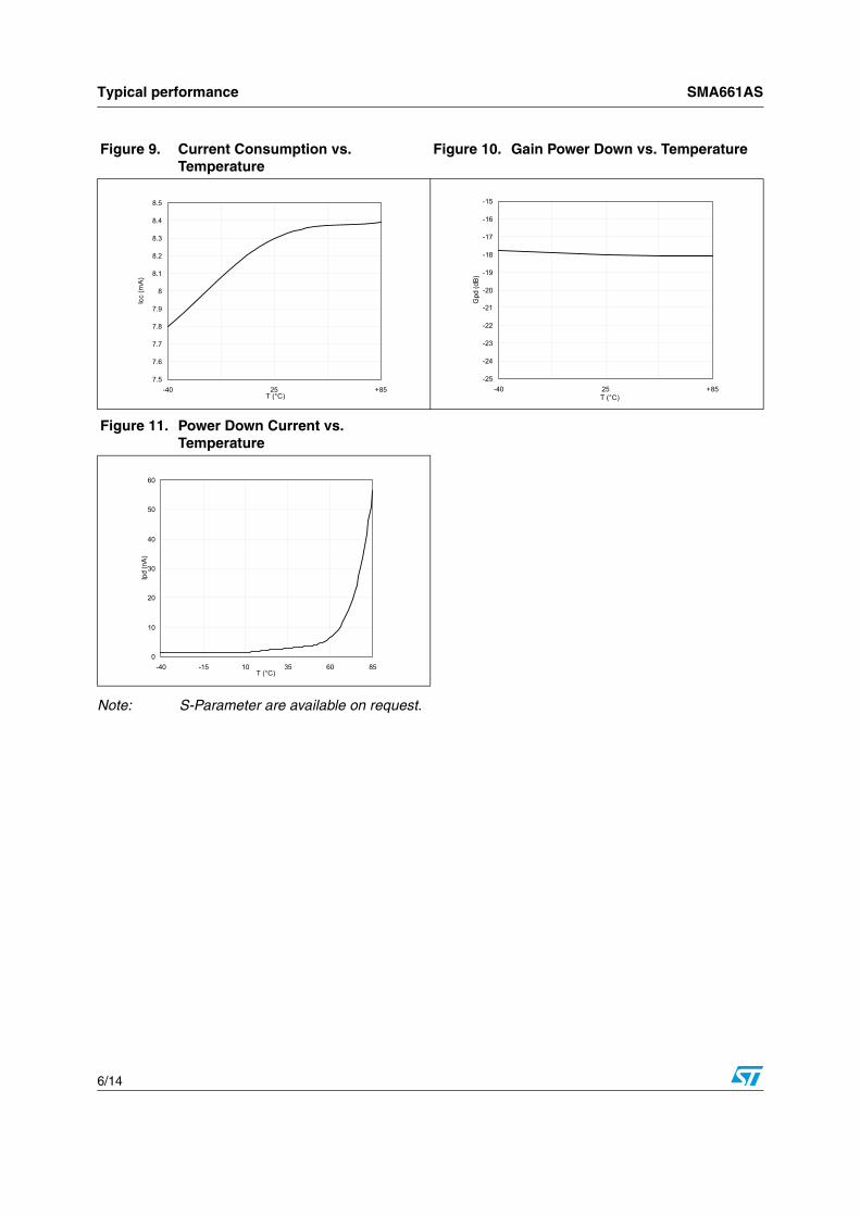
Figure 12. Stability
1 2 3 4 5 6 7 8 9 10 0
-K f (GHz)
0
0.5
1
1.5
2
2.5
3
3.5
4
4.5
5
K
Evaluation board description SMA661AS
8/14
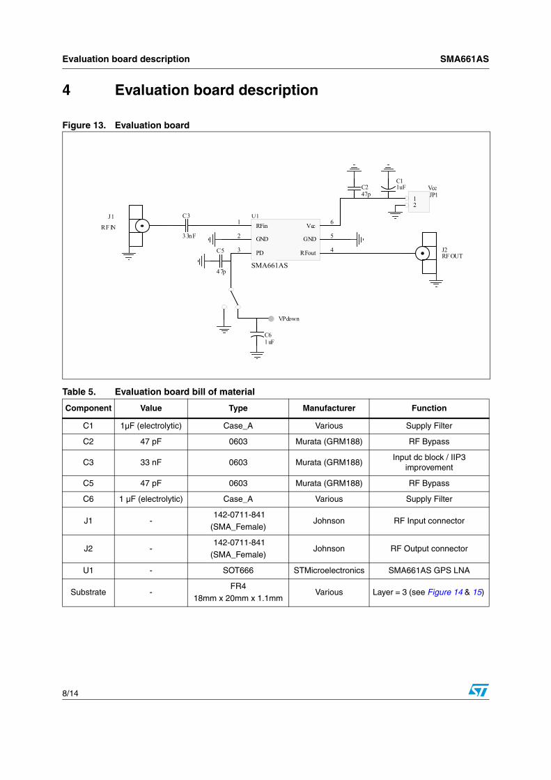
4 Evaluation board description
Figure 13. Evaluation board
C11uFC2
47p
J1
RF IN
J2RF OUT
C3
33nF
12
JP1Vcc
PD3
GND2RFin1 Vcc 6
GND 5
RFout 4
U1
SMA661
VPdown
C5
47p
C61uF
SMA661AS
Table 5. Evaluation board bill of material
Component Value Type Manufacturer Function
C1 1µF (electrolytic) Case_A Various Supply Filter
C2 47 pF 0603 Murata (GRM188) RF Bypass
C3 33 nF 0603 Murata (GRM188)Input dc block / IIP3
improvement
C5 47 pF 0603 Murata (GRM188) RF Bypass
C6 1 µF (electrolytic) Case_A Various Supply Filter
J1 - 142-0711-841
(SMA_Female)Johnson RF Input connector
J2 - 142-0711-841
(SMA_Female)Johnson RF Output connector
U1 - SOT666 STMicroelectronics SMA661AS GPS LNA
Substrate -FR4
18mm x 20mm x 1.1mmVarious Layer = 3 (see Figure 14 & 15)
SMA661AS Evaluation board description
9/14
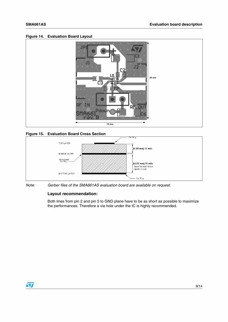
Figure 14. Evaluation Board Layout
Figure 15. Evaluation Board Cross Section
Note: Gerber files of the SMA661AS evaluation board are available on request.
Layout recommendation:
Both lines from pin 2 and pin 5 to GND plane have to be as short as possible to maximize the performances. Therefore a via hole under the IC is highly recommended.
18 mm
20 mm
Package and packing informations SMA661AS
10/14
5 Package and packing informations
5.1 Package informationsIn order to meet environmental requirements, ST offers this device in ECOPACK® package. This package has a Lead-free second level interconnect. The category of second Level Interconnect is marked on the package and on the inner box label, in compliance with JEDEC Standard JESD97. The maximum ratings related to soldering conditions are also marked on the inner box label. ECOPACK is an ST trademark.
ECOPACK specifications are available at: www.st.com.
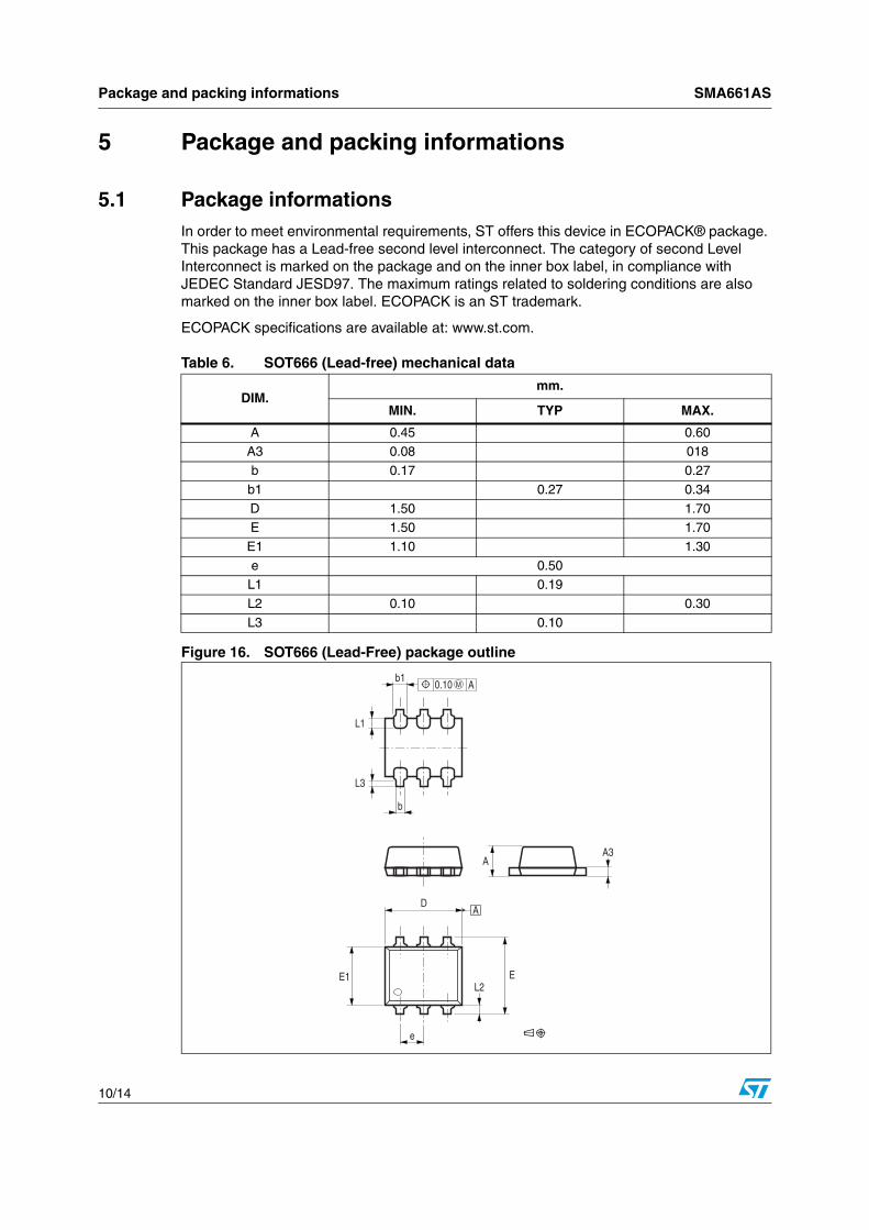
Figure 16. SOT666 (Lead-Free) package outline
Table 6. SOT666 (Lead-free) mechanical data
DIM.mm.
MIN. TYP MAX.
A 0.45 0.60A3 0.08 018
b 0.17 0.27
b1 0.27 0.34
D 1.50 1.70E 1.50 1.70
E1 1.10 1.30
e 0.50L1 0.19
L2 0.10 0.30
L3 0.10
E1 EL2
D
AA3
b10.10
b
M
e
A
L1
L3
A
SMA661AS Package and packing informations
11/14
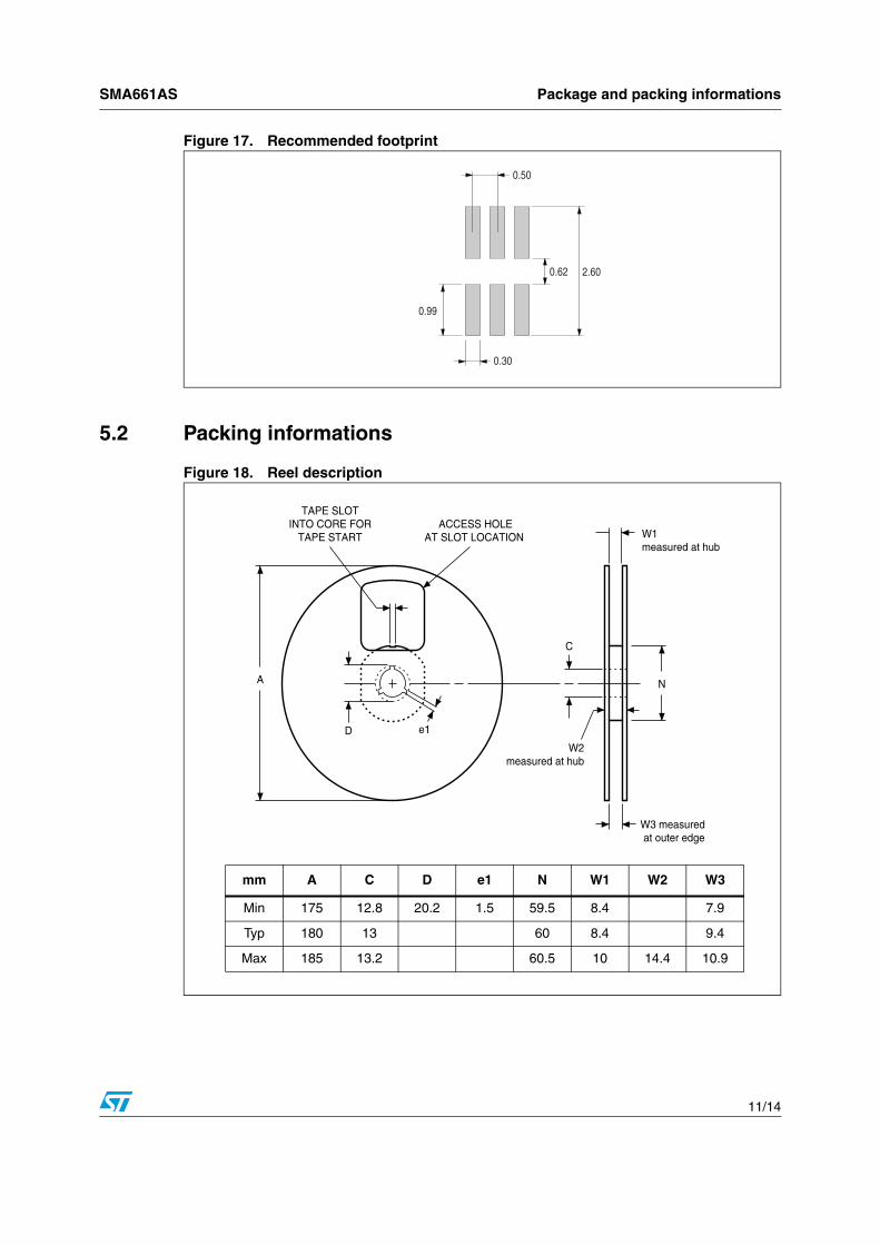
Figure 17. Recommended footprint
5.2 Packing informations
Figure 18. Reel description
0.50
0.30
0.99
0.62 2.60
A
D e1
C
N
W1measured at hub
W2measured at hub
W3 measured at outer edge
TAPE SLOTINTO CORE FOR
TAPE START ACCESS HOLE
AT SLOT LOCATION
mm A C D e1 N W1 W2 W3
Min 175 12.8 20.2 1.5 59.5 8.4 7.9
Typ 180 13 60 8.4 9.4
Max 185 13.2 60.5 10 14.4 10.9
Package and packing informations SMA661AS
12/14
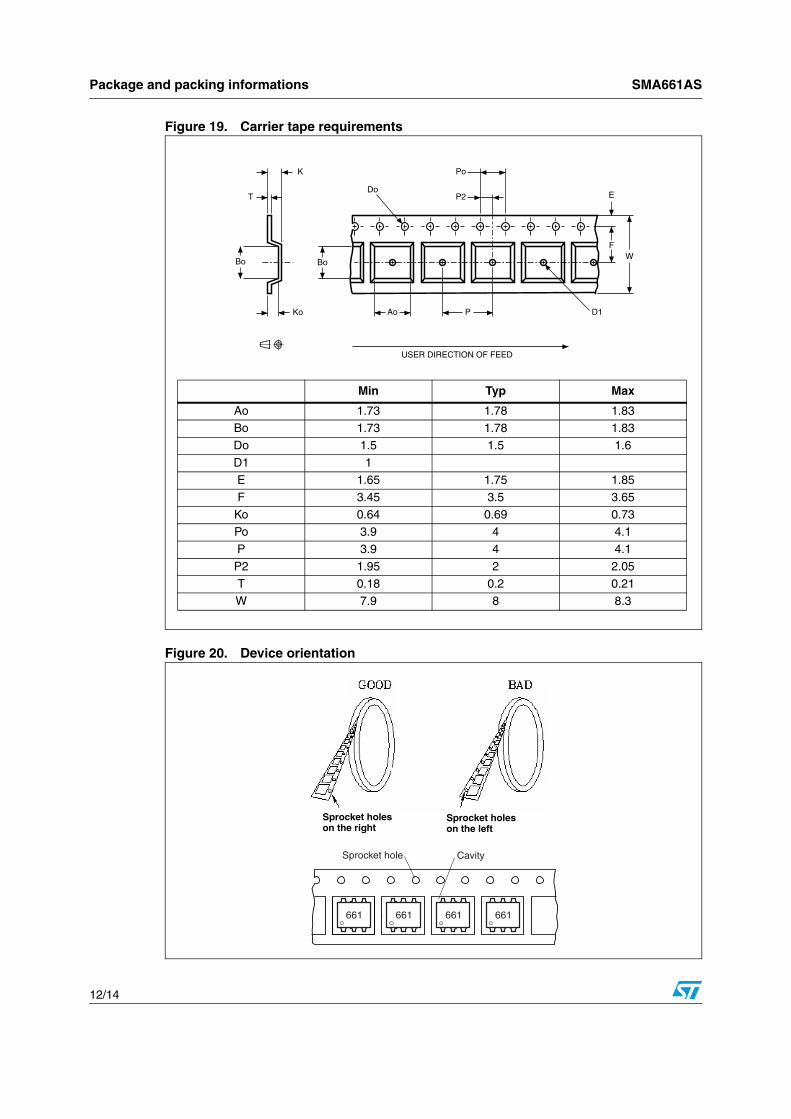
Figure 19. Carrier tape requirements
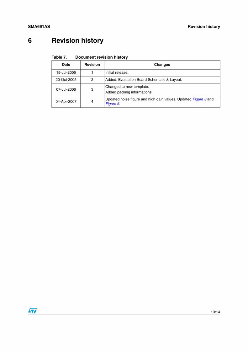
Figure 20. Device orientation
W
T
K
Bo
DoP2
Po
P
F
E
D1
USER DIRECTION OF FEED
Ao
Bo
Ko
Min Typ Max
Ao 1.73 1.78 1.83Bo 1.73 1.78 1.83
Do 1.5 1.5 1.6
D1 1E 1.65 1.75 1.85
F 3.45 3.5 3.65
Ko 0.64 0.69 0.73Po 3.9 4 4.1
P 3.9 4 4.1
P2 1.95 2 2.05
T 0.18 0.2 0.21W 7.9 8 8.3
Sprocket holeson the right
Sprocket holeson the left
661661 661 661
Sprocket hole Cavity
SMA661AS Revision history
13/14
6 Revision history
Table 7. Document revision history
Date Revision Changes
15-Jul-2005 1 Initial release.
20-Oct-2005 2 Added: Evaluation Board Schematic & Layout.
07-Jul-2006 3Changed to new template.
Added packing informations.
04-Apr-2007 4Updated noise figure and high gain values. Updated Figure 3 and Figure 5.
SMA661AS
14/14
Please Read Carefully:
Information in this document is provided solely in connection with ST products. STMicroelectronics NV and its subsidiaries (“ST”) reserve theright to make changes, corrections, modifications or improvements, to this document, and the products and services described herein at anytime, without notice.
All ST products are sold pursuant to ST’s terms and conditions of sale.
Purchasers are solely responsible for the choice, selection and use of the ST products and services described herein, and ST assumes noliability whatsoever relating to the choice, selection or use of the ST products and services described herein.
No license, express or implied, by estoppel or otherwise, to any intellectual property rights is granted under this document. If any part of thisdocument refers to any third party products or services it shall not be deemed a license grant by ST for the use of such third party productsor services, or any intellectual property contained therein or considered as a warranty covering the use in any manner whatsoever of suchthird party products or services or any intellectual property contained therein.
UNLESS OTHERWISE SET FORTH IN ST’S TERMS AND CONDITIONS OF SALE ST DISCLAIMS ANY EXPRESS OR IMPLIEDWARRANTY WITH RESPECT TO THE USE AND/OR SALE OF ST PRODUCTS INCLUDING WITHOUT LIMITATION IMPLIEDWARRANTIES OF MERCHANTABILITY, FITNESS FOR A PARTICULAR PURPOSE (AND THEIR EQUIVALENTS UNDER THE LAWSOF ANY JURISDICTION), OR INFRINGEMENT OF ANY PATENT, COPYRIGHT OR OTHER INTELLECTUAL PROPERTY RIGHT.
UNLESS EXPRESSLY APPROVED IN WRITING BY AN AUTHORIZED ST REPRESENTATIVE, ST PRODUCTS ARE NOTRECOMMENDED, AUTHORIZED OR WARRANTED FOR USE IN MILITARY, AIR CRAFT, SPACE, LIFE SAVING, OR LIFE SUSTAININGAPPLICATIONS, NOR IN PRODUCTS OR SYSTEMS WHERE FAILURE OR MALFUNCTION MAY RESULT IN PERSONAL INJURY,DEATH, OR SEVERE PROPERTY OR ENVIRONMENTAL DAMAGE. ST PRODUCTS WHICH ARE NOT SPECIFIED AS "AUTOMOTIVEGRADE" MAY ONLY BE USED IN AUTOMOTIVE APPLICATIONS AT USER’S OWN RISK.
Resale of ST products with provisions different from the statements and/or technical features set forth in this document shall immediately voidany warranty granted by ST for the ST product or service described herein and shall not create or extend in any manner whatsoever, anyliability of ST.
ST and the ST logo are trademarks or registered trademarks of ST in various countries.
Information in this document supersedes and replaces all information previously supplied.
The ST logo is a registered trademark of STMicroelectronics. All other names are the property of their respective owners.
© 2007 STMicroelectronics - All rights reserved
STMicroelectronics group of companies
Australia - Belgium - Brazil - Canada - China - Czech Republic - Finland - France - Germany - Hong Kong - India - Israel - Italy - Japan - Malaysia - Malta - Morocco - Singapore - Spain - Sweden - Switzerland - United Kingdom - United States of America
www.st.com
Related Documents