Version 1.1 FUJITSU SEMICONDUCTOR DATA SHEET 16-Bit Original Microcontroller CMOS F 2 MC-16LX MB90920 Series MB90F927/V920 ■ DESCRIPTIONS The FUJITSU MB90920 Series is a 16-bit general purpose high-capacity microcontroller designed for vehicle meter control applications etc. The instruction set retains the same AT architecture as the FUJITSU original F 2 MC-8L and F 2 MC-16L series, with further refinements including high-level language instructions, expanded addressing mode, enhanced (signed) multipler-divider computation and bit processing. In addition, a 32-bit accumulator is built in to enable long word processing. ■ FEATURES • Clock Built-in PLL clock frequency multiplication circuit. Selection of machine clocks (PLL clocks) is allowed among frequency division by 2 on oscillation clock and multiplication of 1 to 4 times of oscillation clock(for 4MHz oscillation clock, 4Hz to 16MHz). Operation by sub-clock(up to 50KHz : 100KHz oscillation clock divided by 2). (Continued) ■ PACKAGES Plastic QFP, 100-pin Plastic LQFP, 100-pin (FPT-100P-M06) (FPT-100P-M05) ˚

Welcome message from author
This document is posted to help you gain knowledge. Please leave a comment to let me know what you think about it! Share it to your friends and learn new things together.
Transcript

Version 1.1FUJITSU SEMICONDUCTORDATA SHEET
16-Bit Original MicrocontrollerCMOS
F2MC-16LX MB90920 SeriesMB90F927/V920
DESCRIPTIONSThe FUJITSU MB90920 Series is a 16-bit general purpose high-capacity microcontroller designed for vehiclemeter control applications etc.
The instruction set retains the same AT architecture as the FUJITSU original F2MC-8L and F2MC-16L series, withfurther refinements including high-level language instructions, expanded addressing mode, enhanced (signed)multipler-divider computation and bit processing.
In addition, a 32-bit accumulator is built in to enable long word processing.
FEATURES• Clock
Built-in PLL clock frequency multiplication circuit.Selection of machine clocks (PLL clocks) is allowed among frequency division by 2 on oscillation clock andmultiplication of 1 to 4 times of oscillation clock(for 4MHz oscillation clock, 4Hz to 16MHz).Operation by sub-clock(up to 50KHz : 100KHz oscillation clock divided by 2).
(Continued) PACKAGES
Plastic QFP, 100-pin Plastic LQFP, 100-pin
(FPT-100P-M06) (FPT-100P-M05)
1 30
31
50
14.00±0.20(.551±.008)
17.90±0.40(.705±.016)
INDEX
0.65(.026) 0.32±0.05(.013±.002)
M0.13(.005)0.17±0.06
(.007±.002)
0.10(.004)
Details of "A" part
(.035±.006)0.88±0.15
(.031±.008)0.80±0.20
0.25(.010)3.00
+0.35–0.20+.014–.008.118
(Mounting height)0~8˚
*

MB90920 Series
2
• 16-bit input capture (4 channels) Detects rising, falling, or both edges.16-bit capture register × 4Pin input edge detection latches the 16-bit free-run timer counter value, and generates an interrupt request.
• 16-bit reload timer (2 channels) 16-bit reload timer operation (select toggle output or one-shot output) Event count function selection provided
• Real Time Watch timer (main clock) Operates directly from oscillator clock.Compensates for oscillator deviationRead/write enabled second/minute/hour/date registerSignal interrupt
• 16-bit PPG (3channels) Output pins (3) , external trigger input pin (1) Output clock frequencies : fCP, fCP/22, fCP/24, fCP/26
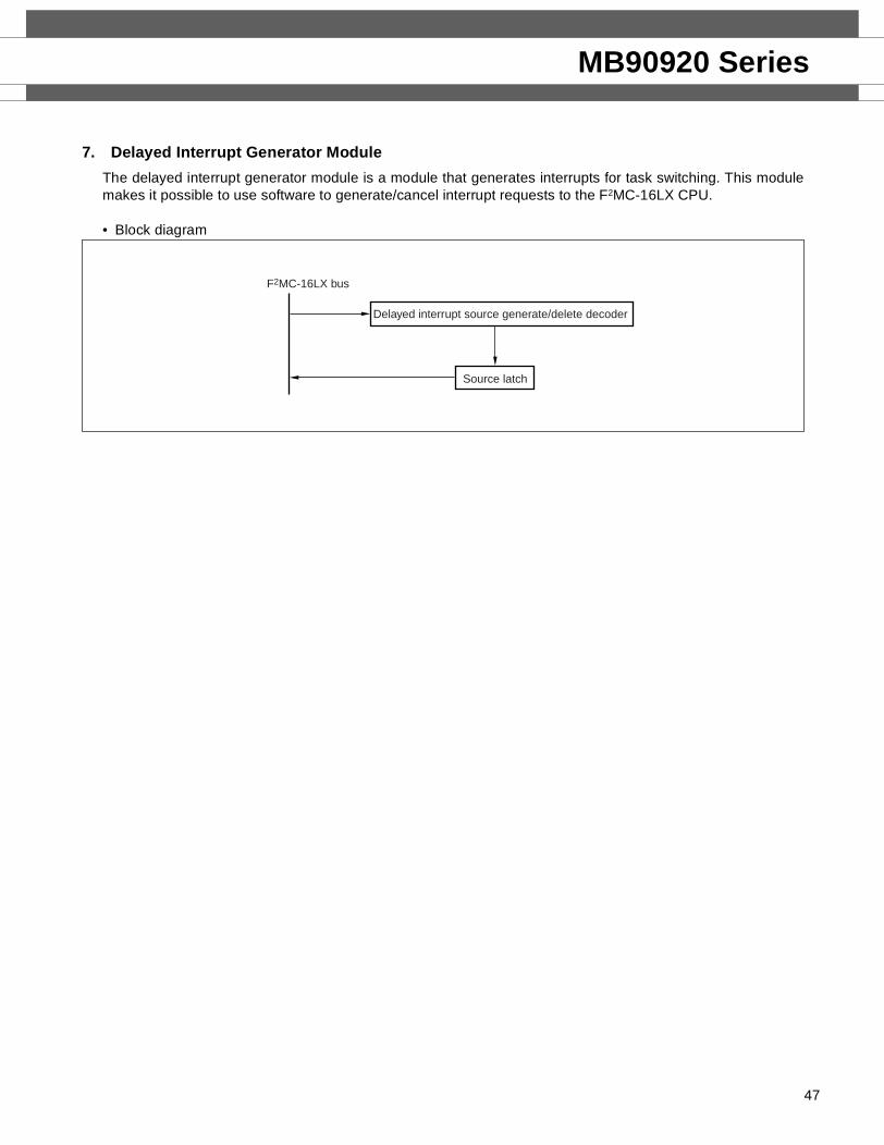
• Delay interruptGenerates interrupt for task switching.Interruptions to CPU can be generated/deleted by software setting.
• External interrupts (8 channels) 8-channel independent operationInterrupt source setting available : “L” to “H” edge/ “H” to “L” edge/ “L” level/ “H” level.
• A/D converter10-bit or 8-bit resolution × 8 channels (input multiplexed) Conversion time : 2.6µs (at fCP = 16 MHz) External trigger startup available (P50/INT0/ADTG) Internal timer startup available (16-bit reload timer 1)
• UART(LIN/SCI) (2 channels) Equipped with full duplex double bufferClock-asynchronous or clock-synchronous serial transmission is available
• SIO (1 channels)Cock synchronized data transmission.LSB-first or MSB-first data transmission selection are available.
• CAN interface Conforms to CAN specifications version 2.0 Part A and B.Automatic resend in case of error.Automatic transfer in response to remote frame.16 prioritized message buffers for data and messages for data and IDMultiple message supportReceiving filter has flexible configuration : All bit compare/all bit mask/two partial bit masksSupports up to 1 MbpsCAN WAKEUP function (connects RX internally to INT0)
• LCD controller/driver (32 segment x 4 common) Segment driver and command driver with direct LCD panel (display) drive capability
• Low voltage/Program Looping detect resetAutomatic reset when low voltage is detectedProgram Looping detection function
(Continued)

MB90920 Series
(Continued)• Stepping motor controller (4 channels)
High current output for all channels × 4Synchronized 8/10-bit PWM for all channels × 2
• Sound generator 8-bit PWM signal mixed with tone frequency from 8-bit reload counter.PWM frequencies : 62.5 kHz, 31.2 kHz, 15.6 kHz, 7.8kHz (at fCP = 16MHz) Tone frequencies : 1/2 PWM frequency, divided by (reload frequency +1)
• Input/output portsGeneral-purpose input/output port (CMOS output)- 70 ports (dual clock system)- 72 ports (single clock system)
• Capable of changing input voltage for portAutomotive/CMOS-Schmitt (initial level is Automotive in single-chip mode)
• Flash memory security functionProtect the content of FLASH memory (FLASH memory device only)
• Clock supervisor functionMain clock or sub-clock is monitored independently, generates reset and set the detection flag when the clocksource under monitoring is stopped.
3

MB90920 Series
4
PRODUCT LINEUP• MB90920 Series
Part number
Parameter
MB90F927 MB90V920
Configuration Flash ROM model Evaluation model
CPU F2MC-16LX CPU
Clock 2 systems / 1system (Select by option)
System clockOn-chip PLL clock multiplier type ( × 1, × 2, × 3, × 4, 1/2 when PLL stopped) Minimum instruction execution time 62.5 ns (with 4 MHz oscillation clock PLL × 4)
ROM Flash ROM 64 KB External
RAM 4 KB 10 KB
I/O port 70 (dual clock system) / 72 (single clock system)
SIO 1 Channel
LCD segment 32
UART UART(LIN/SCI) 2 Channels
CAN 1 Channel
16-Bit Input Capture 4 Channels
16-Bit Reload Timer 2 Channels
16-Bit Free Run Timer 1 Channel
Real Time Watch Timer 1 Channel
16-bit PPG 3 Channels
External Interrupt 8 Channels
A/D converter 8 Channels
LVD/CPU Loop Reset Yes No
Stepping Motro Control 4 Channels
Sound Generator 1 Channel
Flash Security Yes No
Clock Supervisor Yes
Operation Voltage 3.7V ~ 5.5V 4.5V ~ 5.5V
Packages QFP100, LQFP100 TBD

MB90920 Series
PIN ASSIGNMENTS• QFP 100
(TOP VIEW) (FPT-100P-M06)
123456789
101112131415161718192021222324252627282930
COM2COM3
P22/SEG0P23/SEG1P24/SEG2P25/SEG3P26/SEG4P27/SEG5P30/SEG6P31/SEG7
VSSP32/SEG8P33/SEG9
P34/SEG10P35/SEG11P36/SEG12P37/SEG13P40/SEG14P41/SEG15P42/SEG16P43/SEG17P44/SEG18
VCCP45/SEG19P46/SEG20P47/SEG21
CP90/SEG22P91/SEG23
V0
807978777675747372717069686766656463626160595857565554535251
P92/X0AP93/X1AP57/SGARSTP56/SGO/FRCKP55/RX0P54/TX0DVSSP87/PWM2M3P86/PWM2P3P85/PWM1M3P84/PWM1P3DVCCP83/PWM2M2P82/PWM2P2P81/PWM1M2P80/PWM1P2DVSSP77/PWM2M1P76/PWM2P1P75/PWM1M1P74/PWM1P1DVCCP73/PWM2M0P72/PWM2P0P71/PWM1M0P70/PWM1P0DVSSP53/INT3/SCLKMD2
81828384858687888990919293949596979899100
VSSX0X1
VCC
P00/SIN0/INT4/SEG24
P01/SOT0/INT5/SEG
25P02/SCK0/INT6/SEG
26P03/SIN1/INT7/SEG
27P04/SO
T1/SEG28
P05/SCK1/TRG/SEG
29P06/PPG
0/TOT1/SEG
30P07/PPG
1/TIN1/SEG31
P10/PPG2
P11/TOT0/W
OT
P12/TIN0/IN3P13/IN2P14/IN1P15/IN0
COM
0CO
M1
5049484746454443424140393837363534333231
MD1
MD0
P52/INT2/SOP51/INT1/SIP67/AN7P66/AN6P65/AN5P64/AN4V
SSP63/AN3P62/AN2P61/AN1P60/AN0AV
SSP50/INT0/ADTGAVRHAV
CCV3V2V1
5

MB90920 Series
6
• LQFP 100
(TOP VIEW) (FPT-100P-M05)
123456789
10111213141516171819202122232425
P22/SEG0P23/SEG1P24/SEG2P25/SEG3P26/SEG4P27/SEG5P30/SEG6P31/SEG7
VSSP32/SEG8P33/SEG9
P34/SEG10P35/SEG11P36/SEG12P37/SEG13P40/SEG14P41/SEG15P42/SEG16P43/SEG17P44/SEG18
VCCP45/SEG19P46/SEG20P47/SEG21
C
75747372717069686766656463626160595857565554535251
RSTP56/SGO/FRCKP55/RX0P54/TX0DVSSP87/PWM2M3P86/PWM2P3P85/PWM1M3P84/PWM1P3DVCCP83/PWM2M2P82/PWM2P2P81/PWM1M2P80/PWM1P2DVSSP77/PWM2M1P76/PWM2P1P75/PWM1M1P74/PWM1P1DVCCP73/PWM2M0P72/PWM2P0P71/PWM1M0P70/PWM1P0DVSS
767778798081828384858687888990919293949596979899100
50494847464544434241403938373635343332313029282726
P53/INT3/SC
LKM
D2
MD
1M
D0
P52/INT2/SO
P51/INT1/SI
P67/AN7
P66/AN6
P65/AN5
P64/AN4
VSS
P63/AN3
P62/AN2
P61/AN1
P60/AN0
AVSS
P50/INT0/AD
TGAVR
HAV
CC
V3V2V1V0P91/SEG23
P90/SEG22
P57/SGA
P93/X1AP92/X0A
VSSX0X1
VC
CP00/SIN
0/INT4/SEG
24P01/SO
T0/INT5/SEG
25P02/SC
K0/INT6/SEG
26P03/SIN
1/INT7/SEG
27P04/SO
T1/SEG28
P05/SCK1/TR
G/SEG
29P06/PPG
0/TOT1/SEG
30P07/PPG
1/TIN1/SEG
31P10/PPG
2P11/TO
T0/WO
TP12/TIN
0/IN3
P13/IN2
P14/IN1
P15/IN0
CO
M0
CO
M1
CO
M2
CO
M3

MB90920 Series
PIN DESCRIPTIONS
Pin no.Symbol Circuit
type DescriptionLQFP QFP
80 82 X0A
High speed oscillator input pin.
81 83 X1 High speed oscillator output pin.
78 80
P92 G General purpose I/O port.
X0A ALow speed oscillator input pin. If no oscillator is connected, apply pull-down processing.
77 79
P93 G General purpose I/O port.
X1A ALow speed oscillator output pin. If no oscillator is connected, leave open.
75 77 RST B Reset input pin.
83 85
P00
J
General purpose input/output port.
SIN0 UART ch.0 serial data input pin.
INT4 INT4 external interrupt input pin.
SEG24 LCD segment output.
84 86
P01
E
General purpose input/output port.
SOT0 UART ch.0 serial data output pin.
INT5 INT5 external interrupt input pin.
SEG25 LCD segment output.
85 87
P02
E
General purpose input/output port.
SCK0 UART ch.0 serial clock input/output pin.
INT6 INT6 external interrupt input pin.
SEG26 LCD segment output.
86 88
P03
J
General purpose input/output port.
SIN1 UART ch.1 serial data input pin.
INT7 INT7 external interrupt input pin.
SEG27 LCD segment output.
87 89
P04
E
General purpose input/output port.
SOT1 UART ch.1 serial data output pin.
SEG28 LCD segment output.
88 90
P05
E
General purpose input/output port.
SCK1 UART ch.1 serial clock input/output pin.
TRG 16-bit PPG ch.0-2 external trigger input pin.
SEG29 LCD segment output.
7

MB90920 Series
8
(Continued)
89 91
P06
E
General purpose input/output port.
PPG0 16-bit PPG ch.0 output pin.
TOT1 16-bit reload timer ch.1 TOT output pin.
SEG30 LCD segment output.
90 92
P07
E
General purpose input/output port.
PPG1 16-bit PPG ch.1 output pin.
TIN1 16-bit reload timer ch.1 TIN output pin.
SEG31 LCD segment output.
91 93P10
GGeneral purpose input/output port.
PPG2 16-bit PPG ch2. output pin.
92 94
P11
G
General purpose input/output port.
TOT0 16-bit reload timer ch.0 TOT output pin.
WOT Real-time watch timer WOT output pin.
93 95
P12
G
General purpose input/output port.
TIN0 16-bit reload timer ch.0 TIN output pin.
IN3 Input capture ch.3 trigger input pin.
94 to 96 96 to 98P13 to P15
GGeneral purpose input/output ports.
IN2 to IN0 Input capture ch.0-2 trigger input pins.
97 to 10099 to 100,
1 to 2COM0 to COM3 I LCD controller/driver common output pins.
1 to 6 3 to 8P22 to P27
EGeneral purpose input/output port.
SEG0 to SEG5 LCD controller/driver segment output pins.
7 to 15 9 to 17P30 to SEG37
EGeneral purpose input/output port.
SEG6 to SEG13 LCD controller/driver common output pins.
16 to 20, 22 to 24
18 to 22, 24 to 26
P40 to P47E
General purpose input output ports.
SEG14 to SEG21 LCD controller/driver segment output pins.
26 to 27 28 to 29P90 to P91
EGeneral purpose input output ports.
SEG22 to SEG23 LCD controller/driver segment output pins.
34 36
P50
G
General purpose input output ports.
INT0 INT0 external interrupt input pin.
ADTG A/D converter external trigger input pin.
36 to 39, 41 to 44
38 to 41, 43 to 46
P60 to P67F
General purpose input output ports.
AN0 to AN7 A/D converter input pins.
Pin no.Symbol Circuit
type DescriptionLQFP QFP

MB90920 Series
(Continued)
Pin no.Symbol Circuit
type DescriptionLQFP QFP
45 47
P51
G
General purpose input output port.
INT1 INT1 external interrupt input pin.
SI SIO data input pin.
46 48
P52
G
General purpose input output port.
INT2 INT2 external interrupt input pin.
SO SIO data ouput pin.
50 52
P53
G
General purpose input output port.
INT3 INT3 external interrupt input pin.
SCLK SIO clock input pin.
52 to 55 54 to 57
P70 to P73
H
General purpose input output ports.
PWM1P0PWM1M0PWM2P0PWM2M0
Stepping motor controller ch.0 output pins.
57 to 60 59 to 62
P74 to P77
H
General purpose input output ports.
PWM1P1PWM1M1PWM2P1PWM2M1
Stepping motor controller ch.1 output pins.
62 to 65 64 to 67
P80 to P83
H
General purpose input output ports.
PWM1P2PWM1M2PWM2P2PWM2M2
Stepping motor controller ch.2 output pins.
67 to 70 69 to 72
P84 to P87
H
General purpose input output ports.
PWM1P3PWM1M3PWM2P3PWM2M3
Stepping motor controller ch.3 output pins.
72 74P54
GGeneral purpose input output port.
TX0 CAN interface 0 TX output pin.
73 75P55
GGeneral purpose output port.
RX0 CAN interface 0 RX input pin.
74 76
P56
G
General purpose input output port.
SGO Sound generator SG0 output pin.
FRCK Free-run timer clock input pin.
9
MB90920 Series
10
Note:
*1 : Type C in MB90F927, type D in MB90V920.
Pin no.Symbol Circuit
type DescriptionLQFP QFP
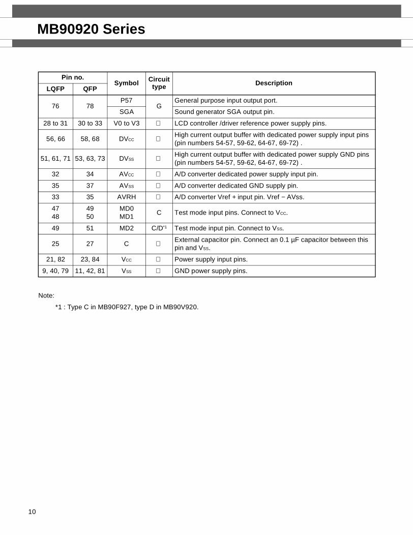
76 78P57
GGeneral purpose input output port.
SGA Sound generator SGA output pin.
28 to 31 30 to 33 V0 to V3 LCD controller /driver reference power supply pins.
56, 66 58, 68 DVCC High current output buffer with dedicated power supply input pins (pin numbers 54-57, 59-62, 64-67, 69-72) .
51, 61, 71 53, 63, 73 DVSS High current output buffer with dedicated power supply GND pins (pin numbers 54-57, 59-62, 64-67, 69-72) .
32 34 AVCC A/D converter dedicated power supply input pin.
35 37 AVSS A/D converter dedicated GND supply pin.
33 35 AVRH A/D converter Vref + input pin. Vref − AVss.
4748
4950
MD0MD1
C Test mode input pins. Connect to VCC.
49 51 MD2 C/D*1 Test mode input pin. Connect to VSS.
25 27 C External capacitor pin. Connect an 0.1 µF capacitor between this pin and VSS.
21, 82 23, 84 VCC Power supply input pins.
9, 40, 79 11, 42, 81 VSS GND power supply pins.

MB90920 Series
I/O CIRCUIT TYPE
(Continued)
Type Circuit Remarks
A
• Oscillation feedback resistance : approx. 1 MΩ (X0, X1 : MAIN)
• Oscillation feedback resistance : approx. 10 MΩ (X0A, X1A : SUB)
B
• Pull-up resistance attached : approx. 50 kΩ, hysteresis input
C
• Hysteresis input
D
• Pull-down resistance attached : approx. 50 kΩ, hysteresis input
E
• CMOS output• LCDC output• Hysteresis input
X1/X1A
X0/X0A
Standby control signal
Xout
Hysteresis input
Hysteresis input
Hyteresis input
LCDC output
Hysteresis input
Automotive input
11
MB90920 Series
12
(Continued)
(Continued)
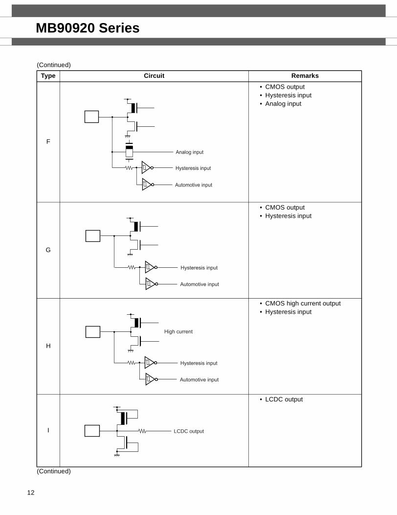
Type Circuit Remarks
F
• CMOS output• Hysteresis input• Analog input
G
• CMOS output• Hysteresis input
H
• CMOS high current output• Hysteresis input
I
• LCDC output
Analog input
Hysteresis input
Automotive input
Hysteresis input
Automotive input
High current
Hysteresis input
Automotive input
LCDC output

MB90920 Series
(Continued)
Type Circuit Remarks
J
• CMOS output• LCDC output• Hysteresis input 1 (0.7Vcc/
0.3Vcc type)• Hysteresis input 2 (0.8Vcc/
0.2Vcc type)
LCDC output
Hysteresis input 1
Automotive input
Hysteresis input 2
13

MB90920 Series
14
HANDLING DEVICESPrecautions for Handling Semiconductor Devices
• Strictly observe maximum rated voltages (prevent latchup)
When CMOS integrated circuit devices are subjected to applied voltages higher than VCC at input and outputpins other than medium- and high-withstand voltage pins, or to voltages lower than VSS, or when voltages inexcess of rated levels are applied between VCC and VSS, a phenomenon known as latchup can occur. In a latchupcondition, supply current can increase dramatically and may destroy semiconductor elements. In using semi-conductor devices, always take sufficient care to avoid exceeding maximum ratings.
Also care must be taken when power to analog systems is switched on or off, to ensure that the analog powersupply (AVCC, AVRH) , analog input and dedicated power supply for the high current output buffer pins (DVCC)do not exceed the digital power supply (VCC) .
Once the digital power supply (VCC) is switched on, the analog power (AVCC,AVRH) and dedicated power supplyfor the high current output buffer pins (DVCC) may be turned on in any sequence.
• Stable supply voltage
Even within the warranted operating range of VCC supply voltage, sudden fluctuations in supply voltage cancause abnormal operation. The recommended stability for ripple fluctuations (P-P values) at commercial fre-quencies (50 Hz to 60 Hz) should be within 10% of the standard VCC value, and voltage fluctuations that occurduring switching of power supplies etc. should be limited to transient fluctuation rates of 0.1 V/ms or less.
• Power-on procedures
In order to prevent abnormal operation of the internal built-in step-down circuits, voltage rise time during power-on should be attained within 50 µs (0.2 V to 2.7 V) .
• Treatment of unused pins
If unused input pins are left open, they may cause abnormal operation or latchup which may lead to permanentdamage to the semiconductor. Any such pins should be pulled up or pulled down through resistance of at least2 kΩ.
Any unused input/output pins should be left open in output status, or if found set to input status, they should betreated in the same way as input pins.
Any unused output pins should be left open.
• Treatment of A/D converter power supply pins
Even if the A/D converter is not used, pins should be connected so that AVCC = VCC, and AVSS = AVRH = VSS.
• Use of external clock signals
Even when an external clock is used, a stabilization period is required following a power-on reset or releasefrom sub clock mode or stop mode. Also, when an external clock is used it should drive only the X0 pin and theX1 pin should be left open, as shown in Figure 3.
X0
X1OPEN
MB90920 Series
Sample external clock connection

MB90920 Series
• Power supply pins
Devices are designed to prevent problems such as latchup when multiple VCC and VSS supply pins are used, byproviding internal connections between pins having the same potential. However, in order to reduce unwantedradiation, and to prevent abnormal operation of strobe signals due to rise in ground level, and to maintain totaloutput current ratings, all such pins should always be connected externally to power supplies and ground.
As shown in figure below, all VCC power supply pins must have the same potential. All VSS power supply pinsshould be handled in the same way. If there are multiple VCC or VSS systems, the device will not operate properlyeven within the warranted operating range.
In addition, care must be given to connecting the VCC and VSS pins of this device to a current source with as littleimpedance as possible. It is recommended that a bypass capacitor of 1.0 µF be connected between VCC andVSS as close to the pins as possible.
• Proper sequence of A/D converter power supply analog input
A/D converter power (AVCC, AVRH) and analog input (AN0-AN7) must be applied after the digital power supply(VCC) is switched on. When power is shut off, the A/D converter power supply and analog input must be cut offbefore the digital power supply is switched on (VCC) . In both power-on and shut-off, care should be taken thatAVRH does not exceed AVCC. Even when pins which double as analog input pins are used as input ports, besure that the input voltage does not exceed AVCC. (There is no problem if analog power supplies and digitalpower supplies are turned off and on at the same time.)
• Handling the power supply for high-current output buffer pins (DVCC, DVSS)
Always apply power to high-current output buffer pins (DVCC, DVSS) after the digital power supply (VCC) is turnedon. Also when switching power off, always shut off the power supply to the high-current output buffer pins (DVCC,DVSS) before switching off the digital power supply (VCC) . (There will be no problem if high-current output bufferpins and digital power supplies are turned off and on at the same time.)
Even when high-current output buffer pins are used as general purpose ports, the power for high current outputbuffer pins (DVCC, DVSS) should be applied to these pins.
• Pull-up/pull-down resistance
The MB90920 series does not support internal pull-up/pull-down resistance. If necessary, use external compo-nents.
VCC
VCCVCC
VCC
VCC
VSS
VSS
VSS
VSS
VSS
Power supply input pins (VCC/VSS)
15

MB90920 Series
16
• Precautions for when not using a sub clock signal.
If the X0A and X1A pins are not connected to an oscillator, apply pull-down treatment to the X0A pin and leavethe X1A pin open.
• Notes on during operation of PLL clock mode
If the PLL clock mode is selected, the microcontroller attempt to be working with the self-oscillating circuit evenwhen there is no external oscillator or external clock input is stopped. Performance of this operation, however,cannot be guaranteed.

MB90920 Series
BLOCK DIAGRAM
Note: SCK, SI, SO are not available in MB90V920.
X0, X1P92/X0A,P93/X1ARST
P57/SGAP56/SGO/FRCKP55/RX0P54/TX0P53/INT3/SCLKP52/INT2/SOP51/INT1/SIP50/INT0/ADTG
P87/PWM2M3P86/PWM2P3P85/PWM1M3P84/PWM1P3P83/PWM2M2P82/PWM2P2P81/PWM1M2P80/PWM1P2
P77/PWM2M1P76/PWM2P1P75/PWM1M1P74/PWM1P1P73/PWM2M0P72/PWM2P0P71/PWM1M0P70/PWM1P0
P67 to P60/AN7 to AN0
AVCC/AVSSAVRH
P91, P90/SEG23, SEG22
P47 to P40/SEG21 to SEG14
P37 to P30/SEG13 to SEG6
COM3 to COM0V3 to V0
P00/SIN0/INT4/SEG24P01/SOT0/INT5/SEG25P02/SCK0/INT6/SEG26P03/SIN1/INT7/SEG27P04/SOT1/SEG28P05/SCK1/TRG/SEG29P06/PPG0/TOT1/SEG30P07/PPG1/TIN1/SEG31
P10/PPG2P11/TOT0/WOTP12/TIN0/IN3P13/IN2P14/IN1P15/IN0
RAM
ROM
UART0/1
ICU0/1/2/3
PPG0/1/2
F2M
C-1
6LX
BUS
Clock controlcircuit
CPUF2MC-16LX core
Interruptcontroller
Sound generator
CAN controller
Prescaler0/1
Reload timer0/1
Real-timeWatch timer
Free-run timer
External interrupt (8 ch)
Port 8
Port 7
Port 6
Port 9
Port 4
Port 3
Port 5
Port 0
Port 1
Steppingmotor
Controller0/1/2/3
A/D converter (8 ch)
LCD controller/driver
Evaluation device (MB90V925)
No built-in ROM
Built-in RAM is 6 KB.
Port 2P27 to P22/
SEG5 to SEG0
Prescaler (SIO)
SIO
Low voltage/CPU opeartiondetection reset
Clock Supervisor
17

MB90920 Series
18
MEMORY MAP
Note : To select models without the ROM mirror function, see the “ROM Mirror Function Selection Module.” The image of the ROM data in the FF bank appears at the top of the 00 bank, in order to enable efficient use of small C compiler models. The lower 16-bit address for the FF bank will be assigned to the same address, so that tables in ROM can be referenced without declaring a “far” indication with the pointer. For example when accessing the address 00C000H, the actual access is to address FFC000H in ROM. Here the FF bank ROM area exceeds 48 KB, so that it is not possible to see the entire area in the 00 bank image. Therefore because the ROM data from FF4000H to FFFFFFH will appear in the image from 004000H to 00FFFFH, it is recommended that the ROM data table be stored in the area from FF4000H to FFFFFFH.
000000H
0000C0H
000100H
Address #2
Address #1
003900H
004000H
010000H
FFFFFFH
Single chip mode (with ROM mirror function)
Peripheral area
ROM area (FF bank image)
Register
ROM area
RAM area
Peripheral area
: Internal access memory
: Access prohibited
Parts No. Address #1 Address #2
MB90F927 FF0000H 001100H
MB90V920 FE0000H 001900H

MB90920 Series
I/O MAP• Other than CAN Interface
(Continued)
Address Register name Symbol Read/write Peripheral function Initial value
00H Port 0 data register PDR0 R/W Port 0 XXXX XXXX
01H Port 1 data register PDR1 R/W Port 1 - - XXXXXX
02H Port 2 data register PDR2 R/W Port 2 XXXXX X - -
03H Port 3 data register PDR3 R/W Port 3 XXXX XXXX
04H Port 4 data register PDR4 R/W Port 4 XXXX XXXX
05H Port 5 data register PDR5 R/W Port 5 XXXX XXXX
06H Port 6 data register PDR6 R/W Port 6 XXXX XXXX
07H Port 7 data register PDR7 R/W Port 7 XXXX XXXX
08H Port 8 data register PDR8 R/W Port 8 XXXX XXXX
09H Port 9 data register PDR9 R/W Port 9 - - - - - -XX
0AH to 0FH
(Disabled)
10H Port 0 direction register DDR0 R/W Port 0 0 0 0 0 0 0 0 0
11H Port 1 direction register DDR1 R/W Port 1 - - 0 0 0 0 0 0
12H Port 2 direction register DDR2 R/W Port 2 0 0 0 0 0 0 - -∗1
13H Port 3 direction register DDR3 R/W Port 3 0 0 0 0 0 0 0 0∗1
14H Port 4 direction register DDR4 R/W Port 4 0 0 0 0 0 0 0 0
15H Port 5 direction register DDR5 R/W Port 5 0 0 0 0 0 0 0 0
16H Port 6 direction register DDR6 R/W Port 6 0 0 0 0 0 0 0 0
17H Port 7 direction register DDR7 R/W Port 7 0 0 0 0 0 0 0 0
18H Port 8 direction register DDR8 R/W Port 8 0 0 0 0 0 0 0 0
19H Port 9 direction register DDR9 R/W Port 9 - - - - - - 0 0
1AH Analog input enable ADER R/W Port 6, A/D 1 1 1 1 1 1 1 1
1BH to 1FH
(Disabled)
20H A/D control status register lower ADCSL R/W
A/D converter
0 0 0 0 0 0 0 0
21H A/D control status register higher ADCSH R/W 0 0 0 0 0 0 0 0
22H A/D data register lower ADCRL R XXXX XXXX
23H A/D data register higher ADCRH R/W 0 0 1 0 1 XXX
24HCompare clear register CPCLR
R/W
16-bit free-run timer
XXXX XXXX
25H R/W XXXX XXXX
26HTimer data register TCDT
R/W 0 0 0 0 0 0 0 0
27H R/W 0 0 0 0 0 0 0 0
28H Timer control status register lower TCCSL R/W 0 0 0 0 0 0 0 0
29H Timer control status register higher TCCSH R/W 0 1 - 0 0 0 0 0
19

MB90920 Series
20
(Continued)
Address Register name Symbol Read/write Peripheral function Initial value
2AH PPG0 control status register lower PCNTL0 R/W16-bit PPG0
0 0 0 0 0 0 0 0
2BH PPG0 control status register higher PCNTH0 R/W 0 0 0 0 0 0 0 1
2CH PPG1 control status register lower PCNTL1 R/W16-bit PPG1
0 0 0 0 0 0 0 0
2DH PPG1 control status register higher PCNTH1 R/W 0 0 0 0 0 0 0 1
2EH PPG2 control status register lower PCNTL2 R/W16-bit PPG2
0 0 0 0 0 0 0 0
2FH PPG2 control status register higher PCNTH2 R/W 0 0 0 0 0 0 0 1
30H External interrupt enable ENIR R/W
External interrupt
0 0 0 0 0 0 0 0
31H External interrupt request EIRR R/W 0 0 0 0 0 0 0 0
32H External interrupt level lower ELVRL R/W 0 0 0 0 0 0 0 0
33H External interrupt level higher ELVRH R/W 0 0 0 0 0 0 0 0
34H Serial mode register 0 SMR0 R/W
UART(LIN/SCI) 0
0 0 0 0 0 0 0 0
35H Serial control register 0 SCR0 R/W 0 0 0 0 0 0 0 0
36HReception/Transmission data reg-ister 1
RDR0/TDR0
R/W 0 0 0 0 0 0 0 0
37H Serial status register 0 SSR0 R/W 0 0 0 0 1 0 0 0
38HExtended Communication Control Register 0
ECCR0 R/W 0 0 0 0 0 0 XX
39H Extended Status Control Register ESCR0 R/W 0 0 0 0 0 1 0 0
3AH Baud Rate Generator Register 00 BGR00 R/W 0 0 0 0 0 0 0 0
3BH Baud Rate Generator Register 01 BGR01 R/W 0 0 0 0 0 0 0 0
3CH (Disabled)
3DH Clock division control register 0 CDCR0 R/W Prescaler 0 - - - 0 0 0 0
3EH CAN wake-up control register CWUCR R/W CAN - - - - - - - 0
3FH Clock division control register 1 CDCR1 R/W Prescaler 0 - - - 0 0 0 0
40H to 4FH Area reserved for CAN interface 0
50H Timer control status register 0 lower TMCSR0L R/W
16-bit reload timer 0
0 0 0 0 0 0 0 0
51HTimer control status register 0 high-er
TMCSR0H R/W - - - 0 0 0 0 0
52H Timer register 0/Reload register 0
TMR0/TMRLR0
R/WXXXX XXXX
53H XXXX XXXX
54H Timer control status register 1 lower TMCSR1L R/W
16-bit reload timer 1
0 0 0 0 0 0 0 0
55HTimer control status register 1 high-er
TMCSR1H R/W - - - 0 0 0 0 0
56H Timer register 1/Reload register 1
TMR1/TMRLR1
R/WXXXX XXXX
57H XXXX XXXX

MB90920 Series
(Continued)
Address Register name Symbol Read/write Peripheral function Initial value
58H LCD output control register 1 LOCR1 R/WLCD
1 1 1 1 1 1 1 1
59H LCD output contorl register 2 LOCR2 R/W 0 0 0 0 0 0 0 0
5AH Sound control register lower SGCRL R/W
Sound generator
0 0 0 0 0 0 0 0
5BH Sound control register higher SGCRH R/W 0 - - - - 1 0 0
5CH Frequency data register SGFR R/W XX XXXXX X
5DH Amplitude data register SGAR R/W 0 0 0 0 0 0 0 0
5EH Decrement grade register SGDR R/W XX XXXXX X
5FH Tone count register SGTR R/W XX XXXXX X
60HInput capture register 0 IPCP0 R
Input capture 0/1
XX XXXXX X
61H XX XXXXX X
62HInput capture register 1 IPCP1 R
XX XXXXX X
63H XX XXXXX X
64HInput capture register 2 IPCP2 R
Input capture 2/3
XX XXXXX X
65H XX XXXXX X
66HInput capture register 3 IPCP3 R
XX XXXXX X
67H XX XXXXX X
68H Input capture control status 0/1 ICS01 R/W Input capture 0/1 0 0 0 0 0 0 0 0
69H Input Capture Edge Register 01 ICE01 R/W Input capture 0/1 XXX0 X0 XX
6AH Input capture control status 2/3 ICS23 R/W Input capture 2/3 0 0 0 0 0 0 0 0
6BH Input Capture Edge Register 23 ICE23 R/W Input capture 2/3 XX XXXXX X
6CH LCD control register lower LCRL R/W LCD controller/driver
0 0 0 1 0 0 0 0
6DH LCD control register higher LCRH R/W 0 0 0 0 0 0 0 0
6EHLow voltage/CPU operationdetection reset control register
LVRC R/WLow voltage/CPU opera-
tion detection reset1 0 1 1 1 0 0 0
6FH ROM mirror ROMM W ROM mirror X X X X X X X 1
70H to 7FH Area reserved for CAN interface 1
21

MB90920 Series
22
(Continued)
Address Register name Symbol Read/write Peripheral function Initial value
80H PWM control register 0 PWC0 R/WStepping motor
controller00 0 0 0 0 - - 0
81H (Disabled)
82H PWM control register 1 PWC1 R/WStepping motor
controller10 0 0 0 0 - - 0
83H (Disabled)
84H PWM control register 2 PWC2 R/WStepping motor
controller20 0 0 0 0 - - 0
85H (Disabled)
86H PWM control register 3 PWC3 R/WStepping motor
controller30 0 0 0 0 - - 0
87H to 89H (Disabled)
8AH A/D setting register 0 ADSR0 R/WA/D
0 0 0 0 0 0 0 0
8BH A/D setting register 1 ADSR1 R/W 0 0 0 0 0 0 0 0
8CH Port Input Level Select 0 PIL0 R/W Port Input Level Se-lect
0 0 0 0 0 0 0 0
8DH Port Input Level Select 1 PIL1 R/W - - - - 0 0 0 0
8EH to 9DH*4 (Disabled)
9EH ROM correction control register PACSR R/WAddress match
detection function- - - - - 0 - 0
9FH Delay interrupt/release DIRR R/W Delayed interrupt - - - - - - - 0

MB90920 Series
Address Register name Symbol Read/write Peripheral function Initial value
A0H Power saving mode LPMCR R/W Power savingcontrol circuit
0 0 0 1 1 0 0 0
A1H Clock select CKSCR R/W 1 1 1 1 1 1 0 0
A2H to A7H
(Disabled)
A8H Watchdog control WDTC R/W Watchdog timer XXXXX 1 1 1
A9H Time base timer control register TBTC R/W Time base timer 1 - - 0 0 1 0 0
AAH Watch timer control register WTC R/WWatch timer (sub-clock)
1 X 0 0 0 0 0 0
ABH to ADH
(Disabled)
AEH Flash control register FMCS R/W Flash interface 0 0 0 X 0 XX 0
AFH (Disabled)
B0H Interrupt control register 00 ICR00 R/W
Interrupt controller
0 0 0 0 0 1 1 1
B1H Interrupt control register 01 ICR01 R/W 0 0 0 0 0 1 1 1
B2H Interrupt control register 02 ICR02 R/W 0 0 0 0 0 1 1 1
B3H Interrupt control register 03 ICR03 R/W 0 0 0 0 0 1 1 1
B4H Interrupt control register 04 ICR04 R/W 0 0 0 0 0 1 1 1
B5H Interrupt control register 05 ICR05 R/W
Interrupt controller
0 0 0 0 0 1 1 1
B6H Interrupt control register 06 ICR06 R/W 0 0 0 0 0 1 1 1
B7H Interrupt control register 07 ICR07 R/W 0 0 0 0 0 1 1 1
B8H Interrupt control register 08 ICR08 R/W 0 0 0 0 0 1 1 1
B9H Interrupt control register 09 ICR09 R/W 0 0 0 0 0 1 1 1
BAH Interrupt control register 10 ICR10 R/W 0 0 0 0 0 1 1 1
BBH Interrupt control register 11 ICR11 R/W 0 0 0 0 0 1 1 1
BCH Interrupt control register 12 ICR12 R/W 0 0 0 0 0 1 1 1
BDH Interrupt control register 13 ICR13 R/W 0 0 0 0 0 1 1 1
BEH Interrupt control register 14 ICR14 R/W 0 0 0 0 0 1 1 1
BFH Interrupt control register 15 ICR15 R/W 0 0 0 0 0 1 1 1
C0H Serial mode control register (L) SMCSL R/W
SIO
- - - - 0 0 0 0
C1H Serial mode control register (H) SMCSH R/W 0 0 0 0 0 0 1 0
C2H Serial data register SDR R/W XXX XXXXX
C3H Clock division control register CDCRS R/WCommunication Prescaler (SIO) 0 - - - 0 0 0 0
23
MB90920 Series
24
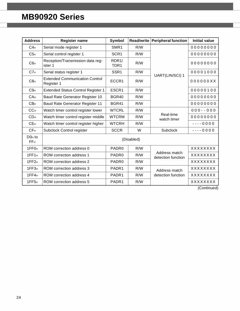
(Continued)
C4H Serial mode register 1 SMR1 R/W
UART(LIN/SCI) 1
0 0 0 0 0 0 0 0
C5H Serial control register 1 SCR1 R/W 0 0 0 0 0 0 0 0
C6HReception/Transmission data reg-ister 1
RDR1/TDR1
R/W 0 0 0 0 0 0 0 0
C7H Serial status register 1 SSR1 R/W 0 0 0 0 1 0 0 0
C8HExtended Communication Control Register 1
ECCR1 R/W 0 0 0 0 0 0 XX
C9H Extended Status Control Register 1 ESCR1 R/W 0 0 0 0 0 1 0 0
CAH Baud Rate Generator Register 10 BGR40 R/W 0 0 0 0 0 0 0 0
CBH Baud Rate Generator Register 11 BGR41 R/W 0 0 0 0 0 0 0 0
CCH Watch timer control register lower WTCRL R/WReal-time
watch timer
0 0 0 - - 0 0 0
CDH Watch timer control register middle WTCRM R/W 0 0 0 0 0 0 0 0
CEH Watch timer control register higher WTCRH R/W - - - - 0 0 0 0
CFH Subclock Control register SCCR W Subclock - - - - 0 0 0 0
D0H to FFH
(Disabled)
1FF0H ROM correction address 0 PADR0 R/WAddress match
detection function
XXX XXXXX
1FF1H ROM correction address 1 PADR0 R/W XXX XXXXX
1FF2H ROM correction address 2 PADR0 R/W XXX XXXXX
1FF3H ROM correction address 3 PADR1 R/W Address matchdetection function
XXX XXXXX
1FF4H ROM correction address 4 PADR1 R/W XXX XXXXX
1FF5H ROM correction address 5 PADR1 R/W XXX XXXXX
Address Register name Symbol Read/write Peripheral function Initial value

MB90920 Series
(Continued)
Address Register name Symbol Read/write Peripheral function Initial value
3900H to 391FH
(Disabled)
3920HPPG0 down counter register PDCR0 R
16-bit PPG 0
1 1 1 1 1 1 1 1
3921H 1 1 1 1 1 1 1 1
3922HPPG0 cycle setting register PCSR0 W
XXXX XXXX
3923H XXXX XXXX
3924HPPG0 duty setting register PDUT0 W
XXXX XXXX
3925H XXXX XXXX
3926H to 3927H
(Disabled)
3928HPPG1 down counter register PDCR1 R
16-bit PPG 1
1 1 1 1 1 1 1 1
3929H 1 1 1 1 1 1 1 1
392AHPPG1 cycle setting register PCSR1 W
XXXX XXXX
392BH XXXX XXXX
392CHPPG1 duty setting register PDUT1 W
XXXX XXXX
392DH XXXX XXXX
392EH to 392FH
(Disabled)
3930HPPG2 down counter register PDCR2 R
16 bit PPG 2
1 1 1 1 1 1 1 1
3931H 1 1 1 1 1 1 1 1
3932HPPG2 cycle setting register PCSR2 W
XXXX XXXX
3933H XXXX XXXX
3934HPPG2 duty setting register PDUT2 W
XXXX XXXX
3935H XXXX XXXX
3936H to 3957H
(Disabled)
3958H
Sub second data register WTBR R/W
Real timewatch timer
XXXX XXXX
3959H XXXX XXXX
395AH - - - XX XXX
395BH Second data register WTSR R/W - - XXXXXX
395CH Minute data register WTMR R/W - - XXXXXX
395DH Hour data register WTHR R/W - - - XX XXX
395EH Day data register WTDR R/W 0 0 - 0 0 0 0 1
3960H to 396FH
LCD display RAM VRAM R/WLCD controller/
driverXXXX XXXX
3970H Clock Supervisor Control Register CSVCR R, R/W Clock Supervisor 0 0 0 1 1 1 0 0
25
MB90920 Series
26
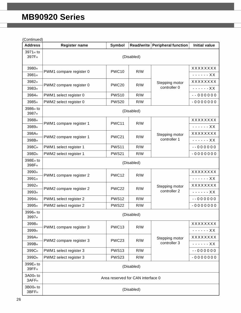
(Continued)
Address Register name Symbol Read/write Peripheral function Initial value
3971H to 397FH (Disabled)
3980HPWM1 compare register 0 PWC10 R/W
Stepping motorcontroller 0
XXXX XXXX
3981H - - - - - - XX
3982HPWM2 compare register 0 PWC20 R/W
XXXX XXXX
3983H - - - - - - XX
3984H PWM1 select register 0 PWS10 R/W - - 0 0 0 0 0 0
3985H PWM2 select register 0 PWS20 R/W - 0 0 0 0 0 0 0
3986H to 3987H
(Disabled)
3988HPWM1 compare register 1 PWC11 R/W
Stepping motorcontroller 1
XXXX XXXX
3989H - - - - - - XX
398AHPWM2 compare register 1 PWC21 R/W
XXXX XXXX
398BH - - - - - - XX
398CH PWM1 select register 1 PWS11 R/W - - 0 0 0 0 0 0
398DH PWM2 select register 1 PWS21 R/W - 0 0 0 0 0 0 0
398EH to 398FH
(Disabled)
3990HPWM1 compare register 2 PWC12 R/W
Stepping motorcontroller 2
XXXX XXXX
3991H - - - - - - XX
3992HPWM2 compare register 2 PWC22 R/W
XXXX XXXX
3993H - - - - - - XX
3994H PWM1 select register 2 PWS12 R/W - - 0 0 0 0 0 0
3995H PWM2 select register 2 PWS22 R/W - 0 0 0 0 0 0 0
3996H to 3997H
(Disabled)
3998HPWM1 compare register 3 PWC13 R/W
Stepping motorcontroller 3
XXXX XXXX
3999H - - - - - - XX
399AHPWM2 compare register 3 PWC23 R/W
XXXX XXXX
399BH - - - - - - XX
399CH PWM1 select register 3 PWS13 R/W - - 0 0 0 0 0 0
399DH PWM2 select register 3 PWS23 R/W - 0 0 0 0 0 0 0
399EH to 39FFH
(Disabled)
3A00H to 3AFFH
Area reserved for CAN interface 0
3B00H to 3BFFH
(Disabled)
MB90920 Series
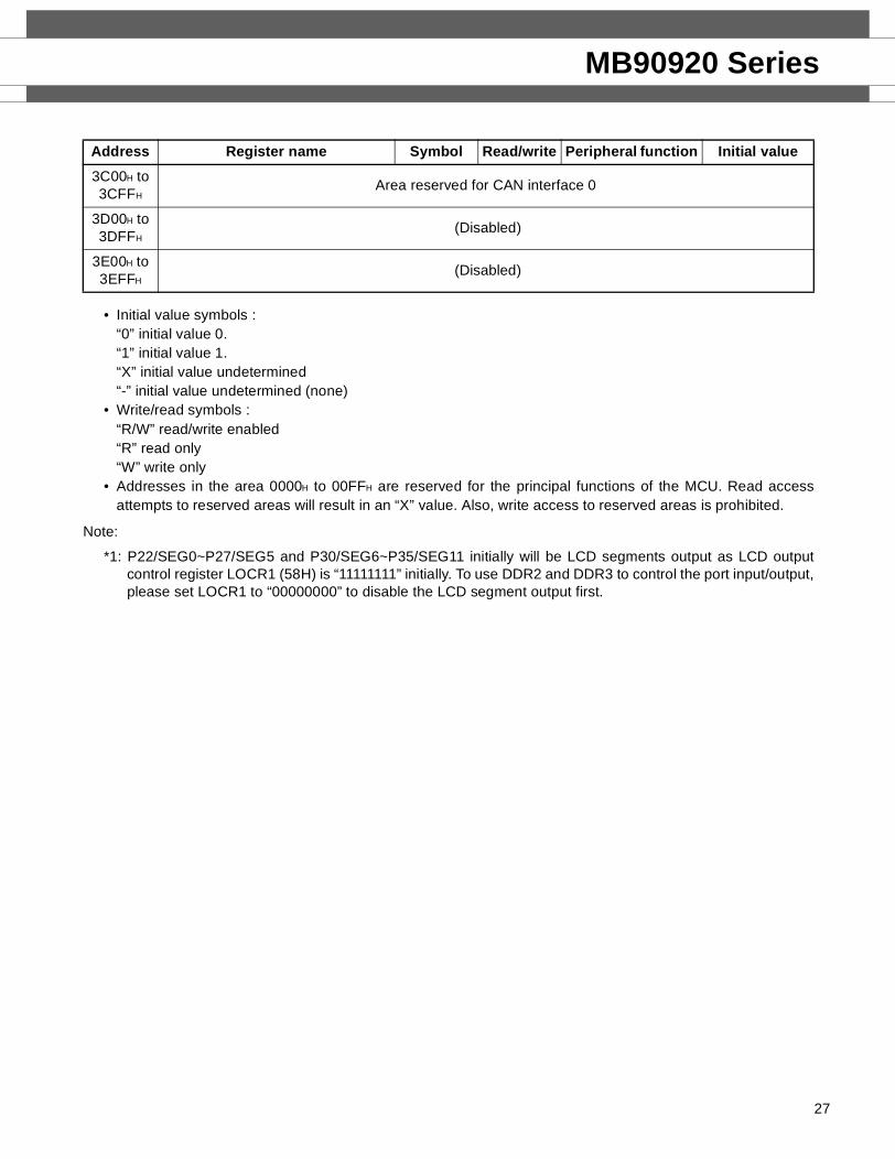
• Initial value symbols : “0” initial value 0.“1” initial value 1.“X” initial value undetermined“-” initial value undetermined (none)
• Write/read symbols : “R/W” read/write enabled“R” read only“W” write only
• Addresses in the area 0000H to 00FFH are reserved for the principal functions of the MCU. Read accessattempts to reserved areas will result in an “X” value. Also, write access to reserved areas is prohibited.
Note:
*1: P22/SEG0~P27/SEG5 and P30/SEG6~P35/SEG11 initially will be LCD segments output as LCD outputcontrol register LOCR1 (58H) is “11111111” initially. To use DDR2 and DDR3 to control the port input/output,please set LOCR1 to “00000000” to disable the LCD segment output first.
3C00H to 3CFFH
Area reserved for CAN interface 0
3D00H to 3DFFH
(Disabled)
3E00H to 3EFFH
(Disabled)
Address Register name Symbol Read/write Peripheral function Initial value
27
MB90920 Series
28
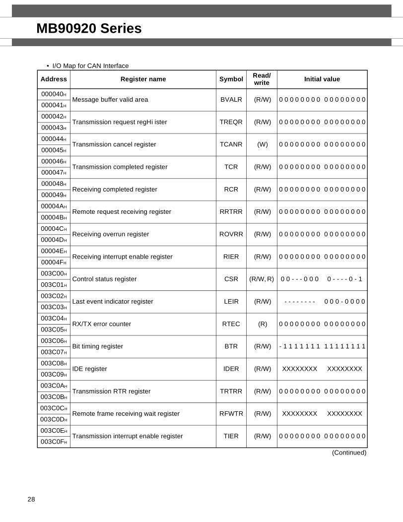
• I/O Map for CAN Interface
(Continued)
Address Register name Symbol Read/write Initial value
000040HMessage buffer valid area BVALR (R/W) 0 0 0 0 0 0 0 0 0 0 0 0 0 0 0 0
000041H
000042HTransmission request regHi ister TREQR (R/W) 0 0 0 0 0 0 0 0 0 0 0 0 0 0 0 0
000043H
000044HTransmission cancel register TCANR (W) 0 0 0 0 0 0 0 0 0 0 0 0 0 0 0 0
000045H
000046HTransmission completed register TCR (R/W) 0 0 0 0 0 0 0 0 0 0 0 0 0 0 0 0
000047H
000048HReceiving completed register RCR (R/W) 0 0 0 0 0 0 0 0 0 0 0 0 0 0 0 0
000049H
00004AHRemote request receiving register RRTRR (R/W) 0 0 0 0 0 0 0 0 0 0 0 0 0 0 0 0
00004BH
00004CHReceiving overrun register ROVRR (R/W) 0 0 0 0 0 0 0 0 0 0 0 0 0 0 0 0
00004DH
00004EHReceiving interrupt enable register RIER (R/W) 0 0 0 0 0 0 0 0 0 0 0 0 0 0 0 0
00004FH
003C00HControl status register CSR (R/W, R) 0 0 - - - 0 0 0 0 - - - - 0 - 1
003C01H
003C02HLast event indicator register LEIR (R/W) - - - - - - - - 0 0 0 - 0 0 0 0
003C03H
003C04HRX/TX error counter RTEC (R) 0 0 0 0 0 0 0 0 0 0 0 0 0 0 0 0
003C05H
003C06HBit timing register BTR (R/W) - 1 1 1 1 1 1 1 1 1 1 1 1 1 1 1
003C07H
003C08HIDE register IDER (R/W) XXXXXXXX XXXXXXXX
003C09H
003C0AHTransmission RTR register TRTRR (R/W) 0 0 0 0 0 0 0 0 0 0 0 0 0 0 0 0
003C0BH
003C0CHRemote frame receiving wait register RFWTR (R/W) XXXXXXXX XXXXXXXX
003C0DH
003C0EHTransmission interrupt enable register TIER (R/W) 0 0 0 0 0 0 0 0 0 0 0 0 0 0 0 0
003C0FH

MB90920 Series
(Continued)
Address Register name Symbol Read/write Initial value
003C10H
Acceptance mask select register AMSR (R/W)
XXXXXXXX XXXXXXXX003C11H
003C12HXXXXXXXX XXXXXXXX
003C13H
003C14H
Acceptance mask register 0 AMR0 (R/W)
XXXXXXXX XXXXXXXX003C15H
003C16HXXXXX- - - XXXXXXXX
003C17H
003C18H
Acceptance mask register 1 AMR1 (R/W)
XXXXXXXX XXXXXXXX003C19H
003C1AHXXXXX- - - XXXXXXXX
003C1BH
003A00H to
003A1FH
General purpose RAM (R/W) XXXXXXXX to XXXXXXXX
003A20H
ID register 0 IDR0 (R/W)
XXXXXXXX XXXXXXXX003A21H
003A22HXXXXX- - - XXXXXXXX
003A23H
003A24H
ID register 1 IDR1 (R/W)
XXXXXXXX XXXXXXXX003A25H
003A26HXXXXX- - - XXXXXXXX
003A27H
003A28H
ID register 2 IDR2 (R/W)
XXXXXXXX XXXXXXXX003A29H
003A2AHXXXXX- - - XXXXXXXX
003A2BH
003A2CH
ID register 3 IDR3 (R/W)
XXXXXXXX XXXXXXXX003A2DH
003A2EHXXXXX- - - XXXXXXXX
003A2FH
003A30H
ID register 4 IDR4 (R/W)
XXXXXXXX XXXXXXXX003A31H
003A32HXXXXX- - - XXXXXXXX
003A33H
29

MB90920 Series
30
(Continued)
Address Register name Symbol Read/write Initial value
003A34H
ID register 5 IDR5 (R/W)
XXXXXXXX XXXXXXXX003A35H
003A36HXXXXX- - - XXXXXXXX
003A37H
003A38H
ID register 6 IDR6 (R/W)
XXXXXXXX XXXXXXXX003A39H
003A3AHXXXXX- - - XXXXXXXX
003A3BH
003A3CH
ID register 7 IDR7 (R/W)
XXXXXXXX XXXXXXXX003A3DH
003A3EHXXXXX- - - XXXXXXXX
003A3FH
003A40H
ID register 8 IDR8 (R/W)
XXXXXXXX XXXXXXXX003A41H
003A42HXXXXX- - - XXXXXXXX
003A43H
003A44H
ID register 9 IDR9 (R/W)
XXXXXXXX XXXXXXXX003A45H
003A46HXXXXX- - - XXXXXXXX
003A47H
003A48H
ID register 10 IDR10 (R/W)
XXXXXXXX XXXXXXXX003A49H
003A4AHXXXXX- - - XXXXXXXX
003A4BH
003A4CH
ID register 11 IDR11 (R/W)
XXXXXXXX XXXXXXXX003A4DH
003A4EHXXXXX- - - XXXXXXXX
003A4FH
003A50H
ID register 12 IDR12 (R/W)
XXXXXXXX XXXXXXXX003A51H
003A52HXXXXX- - - XXXXXXXX
003A53H

MB90920 Series
(Continued)
Address Register name Symbol Read/write Initial value
003A54H
ID register 13 IDR13 (R/W)
XXXXXXXX XXXXXXXX003A55H
003A56HXXXXX- - - XXXXXXXX
003A57H
003A58H
ID register 14 IDR14 (R/W)
XXXXXXXX XXXXXXXX003A59H
003A5AHXXXXX- - - XXXXXXXX
003A5BH
003A5CH
ID register 15 IDR15 (R/W)
XXXXXXXX XXXXXXXX003A5DH
003A5EHXXXXX- - - XXXXXXXX
003A5FH
003A60HDLC register 0 DLCR0 (R/W) - - - -XXXX - - - -XXXX
003A61H
003A62HDLC register 1 DLCR1 (R/W) - - - -XXXX - - - -XXXX
003A63H
003A64HDLC register 2 DLCR2 (R/W) - - - -XXXX - - - -XXXX
003A65H
003A66HDLC register 3 DLCR3 (R/W) - - - -XXXX - - - -XXXX
003A67H
003A68HDLC register 4 DLCR4 (R/W) - - - -XXXX - - - -XXXX
003A69H
003A6AHDLC register 5 DLCR5 (R/W) - - - -XXXX - - - -XXXX
003A6BH
003A6CHDLC register 6 DLCR6 (R/W) - - - -XXXX - - - -XXXX
003A6DH
003A6EHDLC register 7 DLCR7 (R/W) - - - -XXXX - - - -XXXX
003A6FH
003A70HDLC register 8 DLCR8 (R/W) - - - -XXXX - - - -XXXX
003A71H
003A72HDLC register 9 DLCR9 (R/W) - - - -XXXX - - - -XXXX
003A73H
003A74HDLC register 10 DLCR10 (R/W) - - - -XXXX - - - -XXXX
003A75H
31

MB90920 Series
32
(Continued)
Address Register name Symbol Read/write Initial value
003A76HDLC register 11 DLCR11 (R/W) - - - -XXXX - - - -XXXX
003A77H
003A78HDLC register 12 DLCR12 (R/W) - - - -XXXX - - - -XXXX
003A79H
003A7AHDLC register 13 DLCR13 (R/W) - - - -XXXX - - - -XXXX
003A7BH
003A7CHDLC register 14 DLCR14 (R/W) - - - -XXXX - - - -XXXX
003A7DH
003A7EHDLC register 15 DLCR15 (R/W) - - - -XXXX - - - -XXXX
003A7FH
003A80H to
003A87H
Data register 0 (8 bytes) DTR0 (R/W) XXXXXXXX to XXXXXXXX
003A88H to
003A8FH
Data register 1 (8 bytes) DTR1 (R/W) XXXXXXXX to XXXXXXXX
003A90H to
003A87H
Data register 2 (8 bytes) DTR2 (R/W) XXXXXXXX to XXXXXXXX
003A98H to
003A9FH
Data register 3 (8 bytes) DTR3 (R/W) XXXXXXXX to XXXXXXXX
003AA0H to
003AA7H
Data register 4 (8 bytes) DTR4 (R/W) XXXXXXXX to XXXXXXXX
003AA8H to
003AAFH
Data register 5 (8 bytes) DTR5 (R/W) XXXXXXXX to XXXXXXXX
003AB0H to
003AB7H
Data register 6 (8 bytes) DTR6 (R/W) XXXXXXXX to XXXXXXXX
003AB8H to
003ABFH
Data register 7 (8 bytes) DTR7 (R/W) XXXXXXXX to XXXXXXXX
003AC0H to
003AC7H
Data register 8 (8 bytes) DTR8 (R/W) XXXXXXXX to XXXXXXXX
003AC8H to
003ACFH
Data register 9 (8 bytes) DTR9 (R/W) XXXXXXXX to XXXXXXXX
MB90920 Series
(Continued)
Address Register name Symbol Read/write Initial value
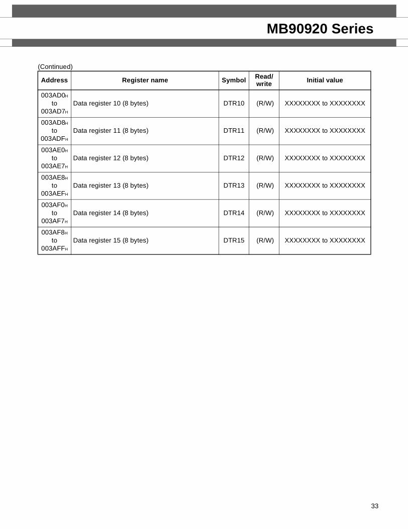
003AD0H to
003AD7H
Data register 10 (8 bytes) DTR10 (R/W) XXXXXXXX to XXXXXXXX
003AD8H to
003ADFH
Data register 11 (8 bytes) DTR11 (R/W) XXXXXXXX to XXXXXXXX
003AE0H to
003AE7H
Data register 12 (8 bytes) DTR12 (R/W) XXXXXXXX to XXXXXXXX
003AE8H to
003AEFH
Data register 13 (8 bytes) DTR13 (R/W) XXXXXXXX to XXXXXXXX
003AF0H to
003AF7H
Data register 14 (8 bytes) DTR14 (R/W) XXXXXXXX to XXXXXXXX
003AF8H to
003AFFH
Data register 15 (8 bytes) DTR15 (R/W) XXXXXXXX to XXXXXXXX
33

MB90920 Series
34
INTERRUPT SOURCES, INTERRUPT VECTORS, AND INTERRUPT CONTROL REGISTERS
Interrupt source EI2OScompatible
Interrupt vector Interrupt control register Priority*2Number Address ICR Address
Reset × #08 08H FFFFDCH High
INT9 instruction × #09 09H FFFFD8H
Exception processing × #10 0AH FFFFD4H
CAN0 RX × #11 0BH FFFFD0HICR00 0000B0H *1
CAN0 TX/NS × #12 0CH FFFFCCH
( Reserved) *3 × #13 0DH FFFFC8HICR01 0000B1H *1
SIO *3 #14 0EH FFFFC4H
Input capture 0 #15 0FH FFFFC0HICR02 0000B2H *1
DTP/external interrupt - ch 0 detected #16 10H FFFFBCH
Reload timer 0 #17 11H FFFFB8HICR03 0000B3H *1
DTP/external interrupt - ch 1 detected #18 12H FFFFB4H
Input capture 1 #19 13H FFFFB0HICR04 0000B4H *1
DTP/external interrupt - ch 2 detected #20 14H FFFFACH
Input capture 2 #21 15H FFFFA8HICR05 0000B5H *1
DTP/external interrupt - ch 3 detected #22 16H FFFFA4H
Input capture 3 #23 17H FFFFA0HICR06 0000B6H *1
DTP/external interrupt - ch 4/5 detected #24 18H FFFF9CH
PPG timer 0 #25 19H FFFF98HICR07 0000B7H *1
DTP/external interrupt - ch 6/7 detected #26 1AH FFFF94H
PPG timer 1 #27 1BH FFFF90HICR08 0000B8H *1
Reload timer 1 #28 1CH FFFF8CH
PPG timer 2 #29 1DH FFFF88HICR09 0000B9H *1
Real time watch timer × #30 1EH FFFF84H
Free-run timer over flow × #31 1FH FFFF80HICR10 0000BAH *1
A/D converter conversion end #32 20H FFFF7CH
Free-run timer clear × #33 21H FFFF78HICR11 0000BBH *1
Sound generator × #34 22H FFFF74H
Time base timer × #35 23H FFFF70HICR12 0000BCH *1
Watch timer (sub-clock) × #36 24H FFFF6CH
UART 1 RX #37 25H FFFF68HICR13 0000BDH *1
UART 1 TX #38 26H FFFF64H
UART 0 RX #39 27H FFFF60HICR14 0000BEH *1
UART 0 TX #40 28H FFFF5CH
Flash memory status × #41 29H FFFF58HICR15 0000BFH *1
Delayed interrupt generator module × #42 2AH FFFF54H Low

MB90920 Series
: Compatible, with EI2OS stop function : Compatible : Compatible when interrupt sources sharing ICR are not in use
× : Not compatible
*1 : • Peripheral functions sharing the ICR register have the same interrupt level. • If peripheral functions sharing the ICR register are using expanded intelligent I/O services, one or the other
cannot be used.• When peripheral functions are sharing the ICR register and one specifies expanded intelligent I/O services,
the interrupt from the other function cannot be used.
*2 : Priority applies when interrupts of the same level are generated.
*3 : SIO and CAN1 will share IRQ3 in EVA chip.
35
MB90920 Series
36
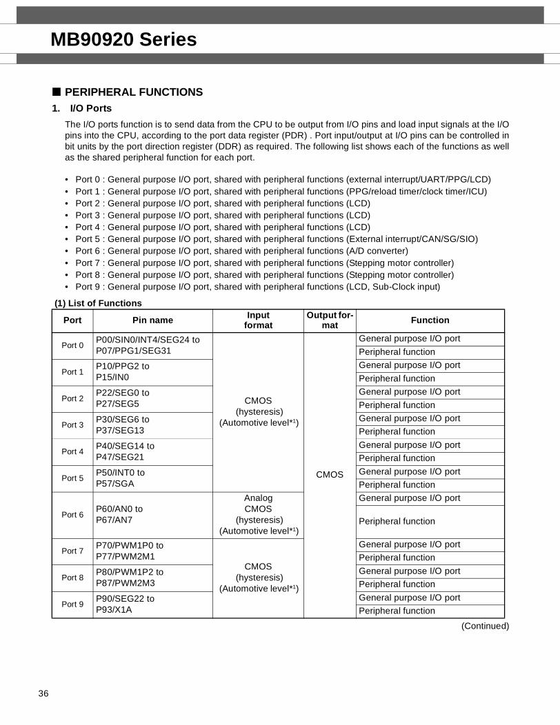
PERIPHERAL FUNCTIONS1. I/O Ports
The I/O ports function is to send data from the CPU to be output from I/O pins and load input signals at the I/Opins into the CPU, according to the port data register (PDR) . Port input/output at I/O pins can be controlled inbit units by the port direction register (DDR) as required. The following list shows each of the functions as wellas the shared peripheral function for each port.
• Port 0 : General purpose I/O port, shared with peripheral functions (external interrupt/UART/PPG/LCD) • Port 1 : General purpose I/O port, shared with peripheral functions (PPG/reload timer/clock timer/ICU) • Port 2 : General purpose I/O port, shared with peripheral functions (LCD)• Port 3 : General purpose I/O port, shared with peripheral functions (LCD) • Port 4 : General purpose I/O port, shared with peripheral functions (LCD) • Port 5 : General purpose I/O port, shared with peripheral functions (External interrupt/CAN/SG/SIO) • Port 6 : General purpose I/O port, shared with peripheral functions (A/D converter) • Port 7 : General purpose I/O port, shared with peripheral functions (Stepping motor controller) • Port 8 : General purpose I/O port, shared with peripheral functions (Stepping motor controller) • Port 9 : General purpose I/O port, shared with peripheral functions (LCD, Sub-Clock input)
(1) List of Functions
(Continued)
Port Pin name Inputformat
Output for-mat Function
Port 0P00/SIN0/INT4/SEG24 to P07/PPG1/SEG31
CMOS (hysteresis)
(Automotive level*1)
CMOS
General purpose I/O port
Peripheral function
Port 1P10/PPG2 to P15/IN0
General purpose I/O port
Peripheral function
Port 2P22/SEG0 to P27/SEG5
General purpose I/O port
Peripheral function
Port 3P30/SEG6 to P37/SEG13
General purpose I/O port
Peripheral function
Port 4P40/SEG14 to P47/SEG21
General purpose I/O port
Peripheral function
Port 5P50/INT0 to P57/SGA
General purpose I/O port
Peripheral function
Port 6P60/AN0 to P67/AN7
AnalogCMOS
(hysteresis) (Automotive level*1)
General purpose I/O port
Peripheral function
Port 7P70/PWM1P0 to P77/PWM2M1
CMOS (hysteresis)
(Automotive level*1)
General purpose I/O port
Peripheral function
Port 8P80/PWM1P2 to P87/PWM2M3
General purpose I/O port
Peripheral function
Port 9P90/SEG22 to P93/X1A
General purpose I/O port
Peripheral function

MB90920 Series
(Continued)
*1: Range of input voltage.For ratings see “3. DC Characteristics” in “ ELECTRICAL CHARACTERISTICS”.
Note : Port 6 also functions as an analog input pin. When using this port as a general purpose port, always write “0” to the corresponding analog input enable register (ADER) bit. The ADER bit is initialized to “1” at reset.
Port bit7 bit6 bit5 bit4 bit3 bit2 bit1 bit0
Port 0
P07 P06 P05 P04 P03 P02 P01 P00
PPG1 PPG0 SCK1 SOT1 SIN1 SCK0 SOT0 SIN0
TIN1 TOT1 TRG SEG28 INT7 INT6 INT5 INT4
SEG31 SEG30 SEG29 SEG27 SEG26 SEG25 SEG24
Port 1
P15 P14 P13 P12 P11 P10
IN0 IN1 IN2 IN3 WOT PPG2
TIN0 TOT0
Port 2P27 P26 P25 P24 P23 P22
SEG5 SEG4 SEG3 SEG2 SEG1 SEG0
Port 3P37 P36 P35 P34 P33 P32 P31 P30
SEG13 SEG12 SEG11 SEG10 SEG9 SEG8 SEG7 SEG6
Port 4P47 P46 P45 P44 P43 P42 P41 P40
SEG21 SEG20 SEG19 SEG18 SEG17 SEG16 SEG15 SEG14
Port 5
P57 P56 P55 P54 P53 P52 P51 P50
SGA SGO RX0 TX0 INT3 INT2 INT1 INT0
FRCK SCK SO SI ADTG
Port 6P67 P66 P65 P64 P63 P62 P61 P60
AN7 AN6 AN5 AN4 AN3 AN2 AN1 AN0
Port 7P77 P76 P75 P74 P73 P72 P71 P70
PWM2M1 PWM2P1 PWM1M1 PWM1P1 PWM2M0 PWM2P0 PWM1M0 PWM1P0
Port 8P87 P86 P85 P84 P83 P82 P81 P80
PWM2M3 PWM2P3 PWM1M3 PWM1P3 PWM2M2 PWM2P2 PWM1M2 PWM1P2
Port 9 P93 P92 P91 P90
X1A X0A SEG23 SEG22
37

MB90920 Series
38
(2) Block Diagrams
Ports 0, 1, 2, 3, 4, 5, 7, 8, 9
Peripheral function inputPeripheral function output
Peripheral function output enabledPDR (Port data register)
DDR (Port direction register)
Inte
rnal
dat
a bu
s
PDR read
DDR read
Output latch
Directionlatch
PDR write
DDR write
Pin
Standby control (SPL = 1)or LCD output enabled
ADER
Port 6
PDR (Port data register)
DDR (Port direction register)
Analog input
RDR read
PDR writeInte
rnal
dat
a bu
s
Output latch
Pin
Directionlatch
DDR write
DDR readStandby control (SPL = 1)
MB90920 Series
2. Watchdog Timer/Time Base Timer/Watch Timer
The watchdog timer, timer base timer, and watch timer have the following circuit configuration.
• Watchdog timer : Watchdog counter, control register, watchdog reset circuit• Time base timer : 18-bit timer, interval interrupt control circuit• Watch timer : 15-bit timer, interval interrupt control circuit
(1) Watchdog timer function
The watchdog timer is composed of a 2-bit watchdog counter that uses the carry signal from the 18-bit timebase timer or 15-bit watch timer as a clock source, plus a control register and watchdog reset control circuit.
After startup, this function will reset the CPU if not cleared within a given time.
(2) Time base timer function
The time base timer is an 18-bit free-run counter (time base counter) synchronized with the internal count clock(base oscillator divided by 2) , with an interval timer function providing a selection of four interval times. Otherfunctions include a timer output for an oscillator stabilization wait time and clock feed to the watchdog timer orother operating clocks. Note that the time base timer uses the main clock regardless of the setting of the MCSbit or SCS bit in the CKSCR register.
(3) Watch timer function
The watch timer provides functions including a clock source for the watchdog timer, a sub clock base oscillatorstabilization wait timer, and an interval timer to generate an interrupt at fixed intervals. Note that the watch timeruses the sub clock regardless of the setting of the MCS bit or SCS bit in the CKSCR register.
39

MB90920 Series
40
• Block Diagram
TBTC
PONR
WRST
ERST
SRST
TBC0
TBR
TBIE
TBOF
TBC1
WT1
WT0
WTE
WTC
WDCS
SCE
WTC2
WTC0
WTR
WTIE
WTOF
WDTC
WDTC
AND
CLROF
CLR
211
213
216
218
TBTRES
28
29
210
211
212
213
214
216
WTRES
211 213 216 218
210 213 214 216
Q RS
ANDQ R
S
AND
Q RS
Main base oscillatordivided by 2
Selector
Clock input
Time base timer
Time baseinterrupt
Selector
Selector
2-bitcounter
Watchdog resetgenerator circuit To WDGRST
internal resetgenerator circuit
F2 M
C-1
6LX
bus
Power-on reset, sub-clock stop
SGW
Watch timer
Clock input
Clock interruptSub base oscillator divided by 4
From power-on generator
RST pin
From RST bit in STBYCregister
to

MB90920 Series
3. Input Capture
This circuit is composed of a 16-bit free-run timer and four 16-bit input capture circuits.
(1) Input capture ( × 4)
The input capture circuits consist of four independent external input pins and corresponding capture registersand control registers. When the specified edge of the external signal input (at the input pin) is detected, the valueof the 16-bit free-run timer is saved in the capture register, and at the same time an interrupt can also begenerated.• The valid edge (rising edge, falling edge, both edges) of the external signal can be selected.• The four input capture circuits can operate independently.• The interrupt can be generated from the valid edge of the external input signal.
(2) 16-bit free-run timer ( × 1)
The 16-bit free-run timer is composed of a 16-bit up-counter, control register, 16-bit compare register, andprescaler. The output values from this counter are used as the base time for the input capture circuits.• The counter clock operation can be selected from 8 options. The eight internal clock settings are φ, φ/2, φ/4,
φ/8, φ/16, φ/32, φ/64, φ/128 where φ represents the machine clock cycle.• Interrupts can be generated from overflow events, or from compare match events with the compare register.
(Compare match operation requires a mode setting.) • The counter value can be initialized to “0000H” by a reset, soft clear, or a compare match with the compare
register.
(3) Block diagram
IVF IVFE STOP MODE SCLR CLK2 CLK1 CLK0
φ
MSI3 to 0 ICLR
EG11 EG10 EG01 EG00
ICRE
IN0/2
IN1/3
ICP0 ICP1 ICE0 ICE1
interrupt#31 (1FH)
Divider
Clock
16-bit free-run timer
F2 M
C-1
6LX
bus
16-bit compare clear register Compare circuitInterrupt#33 (21H)
A/D startup
Capture data register 0/2
Capture data register 1/3
Edge detection
Edge detection
Interrupt#19, #23
Interrupt#15, #21
41

MB90920 Series
42
4. 16-bit Reload Timer
The 16-bit reload timer can either count down in synchronization with three types of internal clock signals ininternal clock mode, or count down at the detection of the designated edge of an external signal. The user mayselect either function. This timer defines a transition from 0000H to FFFFH as an underflow event. Thus anunderflow occurs when counting from the value [Reload register setting + 1].
A selection of two counter operating modes are available. In reload mode, the counter is reset to the count valueand continues counting after an underflow, and in one-shot mode the count stops after an underflow. The countercan generate an interrupt when an underflow occurs, and is compatible with the expanded intelligent I/O services(EI2OS) .
(1) 16-bit Reload timer operating modes
(2) Internal clock mode
One of three input clocks is selected as the count clock, and can be used in one of the following operations.• Soft trigger operation
When “1” is written to the TRG bit in the timer control status register (TMCSR0/1) , the count operationstarts.Trigger input at the TRG bit is normally valid with an external trigger input, as well as an external gateinput.
• External trigger operationCount operation starts when a selected edge (rising, falling, both edges) is input at the TIN0/1 pin.
• External gate input operationCounting continues as long as the selected signal level (“L” or “H”) is input at the TIN0/1 pin.
(3) Event count mode (External clock mode)
In this mode a down count event occurs when a selected valid edge (rising, falling, both edges) is input at theTIN0/1 pin. This function can also be used as an interval timer when an external clock with a fixed period is used.
(4) Counter operation• Reload mode
In down count operation, when an underflow event (transition from “0000H” to “FFFFH”) occurs, the set countvalue is reloaded and count operation continues. The function can be used as an interval timer by generatingan interrupt request at each underflow event. Also, a toggle waveform that inverts at each underflow can beoutput from the TOT0/1 pin.
φ : Machine clock cycle. Figures in ( ) are values at machine clock frequency 16 MHz.
Clock mode Counter mode 16-bit reload timer operation
Internal clock modeReload mode Soft trigger operation
External trigger operationExternal gate input operationOne-shot mode
Event count mode (external clock mode)
Reload modeSoft trigger operation
One-shot mode
Counter clock Counter clock period Interval time
Internal clock
21/φ (0.125 µs) 0.125 µs to 8.192 ms
23/φ (0.5 µs) 0.5 µs to 32.68 ms
25/φ (2.0 µs) 2.0 µs to 131.1 ms
External clock 23/φ or greater (0.5 µs) 0.5 µs or greater

MB90920 Series
(5) One-shot mode
In down count operation, the count stops when an underflow event (transition from “0000H” to “FFFFH”) occurs.This function can generate an interrupt at each underflow. While the counter is operating, a rectangular waveform indicating that the count is in progress can be output form the TOT0 and TOT1 pins.
(6) Block diagram
UF
CLK
CLK
3
3 2
EN
CSL1 CSL0 OUTEOUTL RELD INTE UF CNTE TRGWOD2 WOD1 WOD0
P12/TIN0 *1
<P07/TIN1>
TMRLR0 *1
<TMRLR1>
TMR0 *1
<TMR1>
P11/TOT0 *1
<P06/TOT1>
Internal data bus
16-bit reload register
Reloadcontrol circuit
Reload signal
16-bit timer register (down counter)
Wait signalValid clockdecision circuit
Gate inputPrescaler
Machineclock Φ
To UART 0,1*1
<To A/D converter>
PinsOutput signal
generatorcircuitInverted
Clockselector
External clock
Inputcontrolcircuit
Pins
Function selection
Selectsignal
Operationcontrolcircuit
Interruptrequest signal#17 (11H)*2
<#28 (1CH)>
Timer control status register (TNGSR0)*1
<TNGSR1>
*1: Channel 0 and channel 1. Figures in < > are for channel 1.*2: Interrupt number
43

MB90920 Series
44
5. Real Time Watch Timer
The real time watch timer is composed of a real time watch timer control register, sub second data register,second/minute/hour data registers, 1/2 clock divider, 21-bit prescaler and second/minute/hour counters. Be-cause the MCU oscillation frequency operates on a given real time watch timer operation, a 4 MHz frequencyis assumed. The real time watch timer operates as a real world timer and provides real world time information.
• Block diagram
INTE1 INT1
OEOE
WOT
IRQ#30
INTE2
STUPDT
INT2 INTE3 INT3 INT4 INT4
Main oscillator clock
1/2 clockdivider
22-bitSub-second counter
Sub secondregister
Secondcounter
Minutecounter
Hourcounter
6-bit 6-bit 5-bit
Second Interrupt
Daycounter
5-bit
INT5 INT5
1/2 clockdivider
22-bit
Second/minute/hour/day register
INT0 INT0
0.5-second InterruptMinute Interrupt
Hour InterruptDay Interrupt
MonthInterrupt
MB90920 Series
6. PPG Timer
The PPG timer consists of a prescaler, one 16-bit down-counter, 16-bit data register with buffer for period setting,and 16-bit compare register with buffer for duty setting, plus pin control circuits.
The timer can output pulses synchronized with an externally input soft trigger. The period and duty of the outputpulse can be adjusted by rewriting the values in the two 16-bit registers.
(1) PWM function
Programmable to output a pulse, synchronized with a trigger.
Can also be used as a D/A converter with an external circuit.
(2) One-shot function
Detects the edge of a trigger input, and outputs a single pulse.
(3) Pin control• Set to “1” at a duty match (priority) .• Reset to “0” at a counter borrow event• Has a fixed output mode to output a simple all “L” ( or “H”) signal.• Polarity can be specified
(4) 16-bit down counter• Select from four types of counter operation clocks. Four internal clocks (φ, φ/4, φ/16, φ/64) φ : Machine clock
cycles.• The counter value can be initialized to “FFFFH” at a reset or counter borrow event.
(5) Interrupt requests• Timer startup• Counter borrow event (period match) • Duty match event• Counter borrow event (period match) or duty match event
(6) Multiple channels can be set to start up at an external trigger, or to restart during operation.
45

MB90920 Series
46
(7) Block diagram
1/1
1/4
1/16
1/64
CK
P05/SCK1/TRG
CMP
S Q
R
PCSR PDUT
Prescaler
Load
PSCT16-bit down counter
Start Borrow
PPG mask
Machine clock PPGoutput
Inversion bitEnable
Trigger inputInterrupt IRQ#25, 27, 29
Edge detection
Soft trigger
Interruptselection
MB90920 Series
7. Delayed Interrupt Generator Module
The delayed interrupt generator module is a module that generates interrupts for task switching. This modulemakes it possible to use software to generate/cancel interrupt requests to the F2MC-16LX CPU.
• Block diagram
F2MC-16LX bus
Delayed interrupt source generate/delete decoder
Source latch
47
MB90920 Series
48
8. DTP/External Interrupt Circuit
The DTP (Data transfer peripheral) /external interrupt circuit is located between an externally connected periph-eral device and the F2MC-16LX CPU and sends interrupt requests or data transfer requests generated from theperipheral device to the CPU, thereby generating external interrupt requests or starting the expanded intelligentI/O services (EI2OS) .
(1) DTP/external interrupt function
The DTP/external interrupt function uses a signal input from the DTP/external interrupt pin as a startup source.And it is accepted by the CPU by the same procedure as a normal hardware interrupt, and can generate anexternal interrupt or start the expanded intelligent I/O service (EI2OS) .
When the interrupt is accepted by the CPU, if the corresponding expanded intelligent I/O service (EI2OS) isprohibited the interrupt operates as an external interrupt function and branches to an interrupt routine. If theEI2OS is permitted the interrupt functions as a DTP function, using EI2OS for automatic data transfer, thenbranching to an interrupt routine after the completion of the specified number of data transfers.
ICR : Interrupt control register
Items External interrupt DTP function
Input pins 8 pins (P50/INT0/ADTG to P53/INT3, P00/SIN0/INT4/SEG24 to P03/INT7/SEG27)
Interrupt sources
Request level setting register (ELVR) sets the detection level, or selected edge for each pin
“H” level/ “L” level/ rising edge/falling edge input
“H” level/ “L” level input
Interrupt numbers #16 (10H) , #18 (12H) , #20 (14H) , #22 (16H) , #24 (18H) , #26 (1AH)
Interrupt control DTP/interrupt enable register (ENIR) permits/prohibits interrupt request output
Interrupt flags DTP/interrupt enable register (EIRR) stores interrupt sources
Process selection When EI2OS prohibited (ICR : ISE = 0) When EI2OS is enabled (ICR : ISE = 1)
ProcessingBranch to external interrupt processing routine
EI2OS performs automatic data transfer, then after a specified number of cycles, branches to an interrupt routine

MB90920 Series
(2) Block diagram
LB7 LA7 LB6 LA6 LB5 LA5 LB4 LA4 LB3 LA3 LB2 LA2 LB1 LA1 LB0 LA0
P03/INT7
P02/INT6
P01/INT5
P00/INT4
ER7 ER6 ER5 ER4 ER3 ER2 ER1 ER0
EN7 EN6 EN5 EN4 EN3 EN2 EN1 EN0
P50/INT0
P51/INT1
P52/INT2
P53/INT3
#16 (10H)#18 (12H)#20 (14H)#22 (16H)
#26 (1AH)
#24 (18H)
Request level setting register (ELVR)
Pin
Pin
Pin
Pin
Pin
Pin
Pin
Pin
Selector Selector
Selector
Selector
Selector Selector
Selector
Selector
Interrupt request number
Inte
rnal
dat
a bu
s
49

MB90920 Series
50
9. 8/10-bit A/D Converter
The 8/10-bit A/D converter has functions for using RC sequential comparator conversion format to convert analoginput voltage into 10-bit or 8-bit digital values. The input signal is selected from 8-channel analog input pins, andthe conversion start can be selected from three types : by software, 16-bit reload timer 1 or a trigger input froman external signal pin.
(1) 8/10-bit A/D converter functions
The A/D converter takes analog voltage signals (input voltage) input at analog input pins, and converts these todigital values, providing the following features.• Minimum conversion time is 1.9 µs (including sampling time) .• Minimum sampling time is 0.5 µs.• The conversion method is an RC sequential conversion in comparison with a sample hold circuit.• Either 10-bit or 8-bit resolution can be selected.• The analog input pin can select from 8 channels by a program setting.• At completion of A/D conversion, an interrupt request can be generated, or EI2OS can be started.• Because the conversion data protection function operates in an interrupt enabled state, no data is lost even
in continuous conversion.• The conversion start source may be selected from : software, 16-bit reload timer 1 (rising edge) , or external
trigger input (falling edge) .
Three conversion modes are available
Conversion mode Single conversion operation Scan conversion operation
Single conversion modeConverts the specified channel (1 channel only) one time, then stops.
Converts multiple consecutive channels (up to 8 channels may be specified) one time, then stops.
Continuous conversion mode
Converts the specified channel (1 channel only) repeatedly.
Converts multiple consecutive channels (up to 8 channels may be specified) repeatedly.
Stop conversion modeConverts the specified channel (1 channel only) one time, then pauses, waits until the next start is applied.
Converts multiple consecutive channels (up to 8 channels may be specified) , however pauses after conversion of each channel, waits until the next start is applied.

MB90920 Series
(2) Block diagram
AVCCAVRH
AN0AN1AN2AN3AN4AN5AN6AN7
MPX
ADCRH, L
ADCSH, L
P50/ADTG
AVSS
D/A converterIn
put c
ircui
t
Sequential comparatorregister
Comparator
Sample & hold circuit
F2M
C-1
6LX
bus
A/D data register
Dec
oder
A/D control status register, high
A/D control status register, low
Timer start16-bit reload timer 1
Trigger start Operating clock
Prescaler
Setting register, high
Analog input enable register
Setting register, low
φ
ADSRH, L
51

MB90920 Series
52
10. UART (LIN-SCI)
The UART is a general purpose serial data communication interface for synchronous communication, or asyn-chronous (start-stop synchronized) communication with external devices. Functions include normal bi-directionalfunctions, as well as master/slave type communication functions (multi-processor mode : master side onlysupported) , and special features for LIN-bus systems.
(1) UART Functions
The UART is a general purpose serial data communication interface for sending and receiving of serial datawith other CPU’s or peripheral devices, and provides the following functions.
Items Functions
Data buffer • Full duplex double buffer
Serial input• Perform oversampling 5 times and determine the received value by majority
decision of sampling time (asynchronous mode only)
Transfer modes• Clock synchronous (selecting start/stop synchronous or start/stop bit) • Clock asynchronous (start-stop can be used)
Baud rate• Dedicated baud-arte generator (The baud rate is consisted of 15-bit reload
counter.)• An external clock can be inputted and also be adjusted by reload counter.
Data length• 7-bit (other than synchronous or LIN mode) • 8-bit
Signal type • NRZ (Non return to zero)
Start bit timing • Synchronization to the falling edge of the start bit in the asynchronous mode
Detection of receiver error• Framing errors• Overrun errors• Parity errors (not enabled in multiprocessor mode)
Interrupt request
• Receiving interrupt (receiving completed, receiving error detection, LIN synchbreak detetion)
• Transmit interrupt (transmit data empty) • Interrupt request to ICU (LIN Synch field detection: LSYN)• Both the transmission and reception support EI2OS
Master/slave typecommunication function (multi-processor mode)
• 1 (master) -to-n (slave) communication enabled (only master side supported) .
Synchronous mode • Master of slave funciton
Pin access • Capable of reading the state of serial I/O pin directly
LIN bus option
• Master device operation• Slave device operation• LIN Synch break detection• LIN Synch break generation• Detection of start/stop edges in LIN Synch field connected to input capture 0
and 1
Synchronous serial clock• Synchronous serial clock can be continously outputted to SCK pin for synchro-
nous communication with start/stop bits.
Clock delay option • Special synchronous clock mode for delaying clock (useful to SPI)

MB90920 Series
Note : The UART in clock synchronous transfer does not add start bits or stop bits, but transfers data only.
: Setting not available*1 : “+” indicates an address/data selection bit (A/D) for communication control.*2 : In receiving only one stop bit is detected.
Operating modeData length Synchronization/
AsynchronousStop bit length
Data bit formatNo parity Parity
0 Normal mode 7 or 8-bits Asynchronous 1-bit or 2-bit *2 LSB first
MSB first1 Multi-processor mode 7 or 8 bits + 1 *1 Asynchronous
2 Normal mode 8 bits SynchronousNone, 1 bit,
2 bits
3 LIN mode 8 bits Asynchronous 1 bit LSB first
53

MB90920 Series
54
(2) Block diagram
Control bus
Machine clock
16-bitreload timer
P02/SCK0<P05/SCK1>
Pins
PinsOver-
samplingunit
RDR0/1
#39 (27H) *<#37 (25H) *>
#40 (28H) *<#38 (26H) *>
P00/SIN0<P03/SIN1>
TDR0/1
Clockselector
Transmission clock
Receivinginterrupt signals
Transmissioninterrupt signals
Receivingclock
Receivingcontrolcircuit
Transmissioncontrolcircuit
Start bitdetection circuit
Tranmission startcircuit
Received bitcounter
Tranmission bitcounter
Received paritycounter
Tranmission paritycounter
P01/SOT0<P04/SOT1
Pin
RBI
LBD
TBI
LBRLBL1LBL0
Receptionshift register
Tranmissionshift register
Rece-ivingend
Sending start
SOT0/1
SIN0/1
ErrorDetection
EI2OS receiving errorgenerator circuit (to CPU)
Internal data bus
PENPSBLCLA/DCRERXETXE
SCR0/1register
PEOREFRERDRFTDREBOSRIETIE
SSR0/1register
*: Interrupt number
Exclusive baudrate generatorCommunicationprescalerControl register(CDCR)
MD1MD0OTOEXTRESTUPCLUSCKEUSOE
SMR0/1register
LBR
MSSCDESSM
RBITBI
ECCR0/1register
LBIELBDLBL1LBL0SOPESIOPCCOSCES
ESCR0/1register
LIN breadgeneration
circuit
Bus idledetectioncircuit
LIN break/ SYnchFielddetection
unit

MB90920 Series
11. CAN Controller
The CAN controller is a self-contained module within a 16-bit microcomputer (F2MC-16LX) . The CAN (controllerarea network) controller is the standard protocol for serial transmissions among automotive controllers and iswidely used in the industry.
(1) CAN controller features
The CAN controller has the following features.• Conforms to CAN specifications version 2.0 A and B.
Supports sending and receiving in standard frame and expanded frame format.• Supports data frame sending by means of remote frame receiving.• 16 sending/receiving message buffers
29-bit ID and 8-byte dataMulti-level message buffer configuration
• Supports full bit compare, full bit mask as well as partial bet mask filtering.Provides two receiving mask registers for either standard frame or expanded frame format.
• Bit speed programmable from 10 KB/s to 1 MB/s (at machine clock 16MHz) • CAN WAKE UP function
55

MB90920 Series
56
(2) Block diagram
BTR
PSCPRPHRSJTOE
NS1,0NTNIE
HALTRSTS
CSR
RTEC
BVALR
TREQR
TCANR
TRTRR
RFWTR
TCR
TIER
RCR
RIER
RRTRR
ROVRR
AMSR
AMR0
AMR1
LEIR
IDR0 ~ 15,DLCR0 ~ 15,DTR0 ~ 15,
RAM
01
RBFX, TBFX, RDLC, TDLC, IDSEL
RBFX
IDSEL
TBFX
TBFX
PH1
RXFRMER
ACKER
BITER
ARBLOST
STFERRDLC
CRCER
TDLC
TDLC RDLC IDSEL
ARBLOST TXBITER, STFER,CRCER, FRMER,ACKER
SYNC, TSEG1, TSEG2
F2MC-16LX busTQ (operating clock)
Machineclock
Prescaler 1-to-64frequency divider
Bit timing generator
Node status changeinterrupt generator
Node statuschange interrupt
Busstate
machine
IDLE, SUSPND, TX, RX, ERR,
OVRLD
Errorcontrol
Send/receivesequencer
TBFxclear Send buffer
decision Datacounter
Receivingfilter
control
Errorframe
generator
Overloadframe
generator
Outputdriver
Send shiftregister
Stuffing
TBFx, set, clear CRCgenerator
ACKgeneratorSending completed
interrupt generator
Sendingcompletedinterrupt
RBFx, set CRC generatorerror checkReceiving completed
interrupt generator
Receivingcompletedinterrupt
RBFx, TBFx, set clearReceiving
shift register Destuffing/stuffing
error checkRBFxset
Arbitrationcheck
Bit errorcheckReceiving
filterReceiving bufferx
decision Acknowledge errorcheck
Form errorcheck
Inputlatch
RAM addressgenerator

MB90920 Series
12. LCD Controller/Driver
The LCD controller/driver has a built-in 16 × 8-bit display data memory, and controls the LCD display by meansof four common outputs and 32 segment outputs. A selection of three duty outputs are available. This block candrive an LCD (liquid crystal display) panel directly.
(1) LCD controller/driver functions
The LCD controller/driver provides functions for directly displaying the contents of display data memory (displayRAM) on the LCD panel by means of segment output and common output.• LCD drive voltage divider resistance is built-in. External divider resistance can also be connected.• Up to 4 common outputs (COM0 to COM3) and 32 segment outputs (SEG0 to SEG31) can be used.• 16-byte display data memory (display RAM) is built-in.• The duty can be selected at 1/2, 1/3, 1/4 (limited by bias setting) .• Drives the LCD directly.
: Recommended mode × : Use prohibited
Note : When the SEG0 to SEG31 pins have been selected as general purpose ports by the LCRH, LOCR0, LOCR1 setting, they cannot be used for segment output.
Bias 1/2 duty 1/3 duty 1/4 duty
1/2 bias × ×
1/3 bias ×
57

MB90920 Series
58
(2) Block diagram
4
24
V0 V1 V2 V3
COM0COM1COM2COM3
SEG0SEG1SEG2SEG3SEG4
SEG26SEG27SEG28SEG29SEG30SEG31
:
LCDC control register Low (LCRL)
Divider resistance
Time basetimer output
Prescaler Timingcontroller Common
driver
Inte
rnal
dat
a bu
s
AC
circ
uit
Display RAM, 16 ¥ 8 bits
Segmentdriver
LCDC control register High(LCRH/LOCR0/LOCR1)
Controller Driver
MB90920 Series
13. Low voltage/Program Looping Detection Reset Circuit
The Low voltage detection reset circuit is a function that monitors power supply voltage in order to detect whena voltage drops below a given voltage level. When a low voltage condition is detected, an internal reset signalis generated.
The Program Looping detection reset circuit is a count clock with a 20-bit counter that generates an internalreset signal if not cleared within a given time after startup.
(1) Low voltage detection reset circuit
When a low voltage condition is detected, the low voltage detection flag (LVRC : LVRF) is set to “1” and aninternal reset signal is output.
Because the low voltage detection circuit continues to operate even in stop mode, detection of a low voltagecondition generates an internal reset and releases stop mode.
During an internal RAM write cycle, an internal reset is generated after the completion of writing. During theoutput of this internal reset, the reset output from the low voltage detection circuit is suppressed.
(2) Program Looping detection reset circuit
The Program Looping detection reset circuit is a counter that prevents program looping. The counter startsautomatically after a power-on reset, and must be continually cleared within a given time. If the given time intervalelapses and the counter has not been cleared, a cause such as infinite program looping is assumed and aninternal reset signal is generated. The internal reset generated form the Program Looping detection circuit hasa width of 5 machine cycles.
* : This value assumes an oscillation clock waveform of 4 MHz.During recovery from standby mode the detection period is the maximum interval plus 20 µs.
This circuit does not operate in modes where CPU operation is stopped.
The Program Looping detection reset circuit counter is cleared under any of the following conditions.
1. Writing “0” to the LVRC register CL bit
2. Internal reset
3. Main oscillation clock stop
4. Transition to sleep mode
5. Transition to time base timer mode or clock mode
Detection voltage
4.0 V ± 0.3 V
Interval duration
220/FC (Approx. 262 ms *)
59

MB90920 Series
60
(3) Block diagram
−
+
VCC
VSS
Over flow
Reserved CL LVRF CPUF
Voltage comparatorcircuit
ConstantvoltagesourceProgram Looping detection circuit
Main oscillation clock
Counter
Internal resetClear Noise canceller
Low voltage/CPU operation detection reset control register (LVRC)
Internal data bus
ReservedReservedReservedReserved

MB90920 Series
14. Stepping Motor Controller
The stepping motor controller is composed of two PWM pulse generators, four motor drivers and selector logiccircuits.
The four motor drivers have a high output drive capacity and can be directly connected to the four ends of twomotor coils. They are designed to operate together with the PWM pulse generators and selector logic circuitsto control motor rotation. A synchronization mechanism assures synchronization of the two PWM pulse gener-ators.
• Block diagram
P1 P0
SC
OE1
OE2
PWM1Pn
PWM2Pn
PWM1Mn
PWM2MnCE
CK
EN
CK
ENPWM
PWM
BS n : 0 ~ 3
Machine clock
Prescaler
Output enable
PWM1 pulse generator Selector
PWM1 compare register PWM1 selector register
PWM2 pulse generator
Output enable
Selector
Load
PWM2 compare register PWM2 select register
61

MB90920 Series
62
15. Sound Generator
The sound generator is composed of a sound control register, frequency data register, amplitude data register,decrement grade register, tone count register, PWM pulse generator, frequency counter, decrement counter,and tone pulse counter.
• Block diagram
S1 S0
TONE OE2
INTE INT ST
1/d
DEC
OE1
COEN
PWM
CI
DEC
CICOEN
CICOEN
COEN
DEN
Q
SGA
SGO
IRQ#34
OE1
OE2
Clock input
Prescaler 8-bit PWMpulse generator
Frequencycounter
Toggleflip-flop
ReloadReload
Amplitude dataregister
Frequency dataregister
Decrementcounter
Decrement graderegister
Blend
Tone pulsecounter
Tone countregister

MB90920 Series
16. Serial I/O interface
The serial I/O interface is a serial I/O interface with an 8-bit channel configuration that is used to transfer databy clock synchronization.
Features of the serial I/O interface :• Converts 8-bit parallel data to serial and outputs the serial data, converts input serial data to parallel and
stores the data• The shift clock can be selected from five internal clocks and one external clock• Generated interrupt at end of serial data transfer if the serial I/O interrupt request is enabled• The data shift direction (transfer direction) can be selected as either LSB first or MSB first• The serial I/O can control input and output of the shift clock and can output the internal shift clock
SDR (Serial data register)
SO
Control circuit Shift clock counter
(MSB first) D0 to D7Select transfer directionD7 to D0 (LSB first)
SMD1SMD2 SMD0 SIE SIR BUSY STOP STRT MODE BDS SOE SCOE
SCLK
SI
Read
Write
Internal clock
IRQ # 14
Internal data bus
Initial value
012
Internal data bus
63

MB90920 Series
64
17. Clock Supervisor
The clock supervisor checks the oscillation of the main clock or sub-clock. When the main clock or sub-clockstops due to some breakdowns (20µs to 80µs: when the main clock is used, 160µs to 640µs: when the subclock is used), the control circuit of the clock supervisor switches the clock source to build-in CR oscillation clock,sets the detection flag, and generates reset.
Main clock and sub-clock monitor function can be enabled or disabled independently.
The clock monitor function will be disabled automatically once the device changes to stop mode, and will beenabled automatically if the monitor funciton is enabled before the stop mode.
• Block diagram
1/2
Internal bus
Clock Supervisor control register (CSVCR)
Control circuit Internal reset
Internal main clock
Internal sub clock
Main clock selector
Sub clock selector
Sub clock supervisor
Main clock supervisor
CR oscillation circuit
Enable
DetectionEnable
EnableDetection
Sub selection
Main selection
CR oscillation clock
Main clock
Sub clock

MB90920 Series
18. Address Match Detect Function
If the address setting is the same as the address detection register, an INT9 instruction is executed. Theintegrated address match detection function can be implemented by processing the INT9 interrupt serviceroutine.
Two address registers are used, each with its own compare enable bit. When there is a match between theaddress register and program counter, and the compare enable bit is set to “1” , the INT9 instruction is forciblyexecuted by the CPU.
• Block diagram
Address latch
Com
pare
Address detection register
Enable bit
F2MC-16LXCPU core
F2MC-16LX bus
65
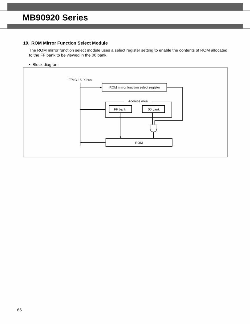
MB90920 Series
66
19. ROM Mirror Function Select Module
The ROM mirror function select module uses a select register setting to enable the contents of ROM allocatedto the FF bank to be viewed in the 00 bank.
• Block diagram
ROM
F2MC-16LX bus
ROM mirror function select register
Address area
FF bank 00 bank

MB90920 Series
ELECTRICAL CHARACTERISTICS1. Absolute Maximum Ratings
*1 : The parameter is based on VSS = AVSS = DVSS = 0.0 V.
*2 : AVCC, AVRH and DVCC shall never exceed VCC.Also, AVRH shall never exceed AVCC.
*3 : The maximum current to/from and input is limited by some means with extenal components, the ICLAMP rating supersedes the VI rating.
*4 : Maximum output current is defined as the peak value of the current of any one of the corresponding pins.
*5 : Average output current is defined as the value of the average current flowing over 100 ms at any one of the corresponding pins. The “average value” can be calculated from the formula of “operating current” times “operating factor”.
(Continued)
Parameter SymbolRating
Unit RemarksMin Max
Power supply voltage*1
VCC VSS − 0.3 VSS + 6.0 V
AVCC VSS − 0.3 VSS + 6.0 V AVCC = VCC*2
AVRH VSS − 0.3 VSS + 6.0 V AVCC ≥ AVRH*2
DVCC VSS − 0.3 VSS + 6.0 V DVCC = VCC*2
Input voltage*1 VI VSS − 0.3 VCC + 0.3 V *3
Output voltage*1 VO VSS − 0.3 VCC + 0.3 V
Maximum clamp current ICLAMP − 400 + 400 µA *7
Total maximum clamp current Σ| ICLAMP | 4 mA *7
“L”level maximum output current*4
IOL1 15 mA Other than P70 to P77, and P80 to P87
IOL2 40 mA P70 to 77, P80 to87
“L”level average output current*5
IOLAV1 4 mA Other than P70 to P77, and P80 to P87
IOLAV2 30 mA P70 to 77, P80 to 87
“L”level maximum total output current
ΣIOL1 100 mA Other than P70 to P77, and P80 to P87
ΣIOL2 330 mA P70 to 77, P80 to 87
“L”level average total output current
ΣIOLAV1 50 mA Other than P70 to P77, and P80 to P87
ΣIOLAV2 250 mA P70 to 77, P80 to 87
“H”level maximum output current
IOH1*4 − 15 mA Other than P70 to P77, and P80 to P87
IOH2*4 − 40 mA P70 to 77, P80 to 87
“H”level average output current
IOHAV1*5 − 4 mA Other than P70 to P77, and P80 to P87
IOHAV2*5 − 30 mA P70 to 77, P80 to 87
“H”level maximum total output current
ΣIOH1 − 100 mA Other than P70 to P77, and P80 to P87
ΣIOH2 − 330 mA P70 to 77, and P80 to 87
“H”level average total output current
ΣIOHAV1*6 − 50 mA Other than P70 to P77, and P80 to P87
ΣIOHAV2*6 − 250 mA P70 to 77, P80 to 87
Power consumption PD 500 mW
Operating temperature TA −40 +105 °C
Storage temperature TSTG −55 +150 °C
67

MB90920 Series
68
(Continued)
*6 : Average total output current is defined as the value of the average current flowing over 100 ms at all of the corresponding pins. The “average value” can be calculated from the formula of “operating current” times “ operating factor”.
*7 : • Applicable to pins : P10 to P15, P50 to P57, P70 to P77, P80 to P87• Use within recommended operating conditions.• Use at DC voltage (current) .• The +B signal should always be applied with a limiting resistance placed between the +B signal and the
microcontroller.• The value of the limiting resistance should be set so that when the +B signal is applied the input current to
the microcontroller pin does not exceed rated values, either instantaneously or for prolonged periods.• Note that when the microcontroller drive current is low, such as in the power saving modes, the +B input
potential may pass through the protective diode and increase the potential at the VCC pin, and this may affectother devices.
• Note that if a +B signal is input when the microcontroller current is off (not fixed at 0 V) , the power supplyis provided from the pins, so that incomplete operation may result.
• Note that if the +B input is applied during power-on, the power supply is provided from the pins and theresulting supply voltage may not be sufficient to operate the power-on reset.
• Care must be taken not to leave the +B input pin open.• Note that analog system input/output pins (LCD drive pins, comparator input pins, etc.) cannot accept +B
signal input.• Sample recommended circuits :
WARNING: Semiconductor devices can be permanently damaged by application of stress (voltage, current, temperature, etc.) in excess of absolute maximum ratings. Do not exceed these ratings.
P-ch
N-ch
VCC
R
+B input (0 V to 16 V)
Limitingresistance
Protective diode
• Input/Output equivalent circuits

MB90920 Series
2. Recommended Operating Conditions (VSS = DVSS = AVSS = 0.0 V)
* : For smoothing capacitor Cs connections, see the illustration below.
WARNING: The recommended operating conditions are required in order to ensure the normal operation of thesemiconductor device. All of the device’s electrical characteristics are warranted when the device isoperated within these ranges.
Always use semiconductor devices within their recommended operating condition ranges. Operationoutside these ranges may adversely affect reliability and could result in device failure.No warranty is made with respect to uses, operating conditions, or combinations not represented onthe data sheet. Users considering application outside the listed conditions are advised to contact theirFUJITSU representatives beforehand.
Parameter SymbolValue
Unit RemarksMin Max
Power supplyvoltage
VCC
AVCC
DVCC
3.7 5.5 V (MB90F927) Low voltage detection reset starts to work when power supply voltage is 4.0 V ± 0.3 V.
4.3 5.5 VHolding stop operation status (MB90F927)
Smoothing capacitor*
CS 0.1 1.0 µFUse a ceramic capacitor or other capacitor of equivalent frequency characteristics. A bypass capacitor on the VCC pin should have a capacitance greater than Cs.
Operatingtemperature
TA −40 +105 °C
C
CSVSS DVSS AVSS
• C pin connection
69
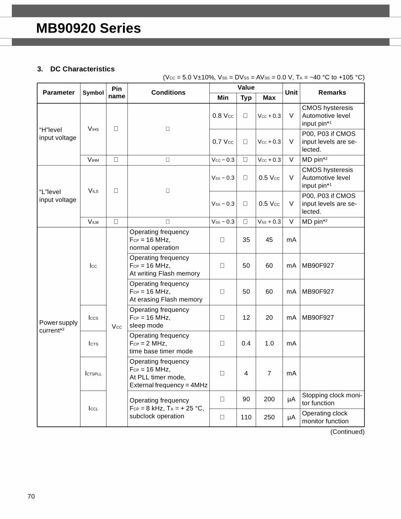
MB90920 Series
70
3. DC Characteristics (VCC = 5.0 V±10%, VSS = DVSS = AVSS = 0.0 V, TA = −40 °C to +105 °C)
(Continued)
Parameter SymbolPin
name ConditionsValue
Unit RemarksMin Typ Max
“H”level input voltage
VIHS
0.8 VCC VCC + 0.3 VCMOS hysteresisAutomotive levelinput pin*1
0.7 VCC VCC + 0.3 VP00, P03 if CMOS input levels are se-lected.
VIHM VCC − 0.3 VCC + 0.3 V MD pin*2
“L”level input voltage
VILS
VSS − 0.3 0.5 VCC VCMOS hysteresisAutomotive levelinput pin*1
VSS − 0.3 0.5 VCC VP00, P03 if CMOS input levels are se-lected.
VILM VSS − 0.3 VSS + 0.3 V MD pin*2
Power supply current*3
ICC
VCC
Operating frequencyFCP = 16 MHz, normal operation
35 45 mA
Operating frequencyFCP = 16 MHz, At writing Flash memory
50 60 mA MB90F927
Operating frequencyFCP = 16 MHz, At erasing Flash memory
50 60 mA MB90F927
ICCS
Operating frequencyFCP = 16 MHz, sleep mode
12 20 mA MB90F927
ICTS
Operating frequency FCP = 2 MHz, time base timer mode
0.4 1.0 mA
ICTSPLL
Operating frequencyFCP = 16 MHz, At PLL timer mode, External frequency = 4MHz
4 7 mA
ICCL
Operating frequency FCP = 8 kHz, TA = + 25 °C, subclock operation
90 200 µAStopping clock moni-tor function
110 250 µAOperating clock monitor function

MB90920 Series
(VCC = 5.0 V±10%, VSS = DVSS = AVSS = 0.0 V, TA = −40 °C to +105 °C)
(Continued)
Parameter Symbol Pin name Conditions
ValueUnit Remarks
Min Typ Max
Power supply current*3
ICCLS
VCC
Operating frequency FCP = 8 kHz, TA = + 25 °C, sub sleep operation
60 150 µAStopping clock monitor func-tion
80 200 µAOperating clock monitor function
ICCT
Operating frequency FCP = 8 kHz, TA = + 25 °C, clock mode
60 130 µAStopping clock monitor func-tion
80 170 µAOperating clock monitor function
ICCHTA = + 25 °C, stop mode
50 130 µA
Input leakage current
IIL All input pinsVCC = DVCC = AVCC = 5.5 VVSS < VI < VCC
−5 5 µA
Input capacitance 1
CIN1
Other than Vcc, Vss, DVcc, DVss, Avcc, Avss, C, P70 to P77, P80 to P87
5 15 pF
Input capacitance 2
CIN2P70 to P77, P80 to P87
15 45 pF
Pull-up resistance
RUP RST 25 50 100 kΩ
Pull-down resistance
RDOWN MD2 25 50 100 kΩ Except Flash device
Output H voltage 1
VOH1
Other than P70 to P77, P80 to P87
VCC = 4.5 VIOH = −4.0 mA
VCC − 0.5
V
Output H voltage 2
VOH2P70 to P77, P80 to P87
VCC = 4.5 VIOH = −30.0 mA
VCC − 0.5
V
Output L voltage 1
VOL1
Other than P70 to P77, P80 to P87
VCC = 4.5 VIOL = 4.0 mA
0.4 V
Output L voltage 2
VOL2P70 to P77, P80 to P87
VCC = 4.5 VIOL = 30.0 mA
0.55 V
71

MB90920 Series
72
(Continued) (VCC = 5.0 V±10%, VSS = DVSS = AVSS = 0.0 V, TA = −40 °C to +105 °C)
*1 : All input pins except X0, X0A, MD0, MD1, MD2, P00, P03 pins.
*2 : MD0, MD1, MD2 pins.
*3 : Supply current values assume external clock feed from the X1 pin and X1A pin. Users must be aware that supply current levels differ depending on whether an external clock or oscillator is used.
*4 : Defined as maximum variation in VOH2/VOL2 with all channel 0 PWM1P0/PWM1M0/PWM2P0/PWM2M0 simul-taneously ON. Similarly for other channels.
Parameter Symbol Pin name ConditionsValue
Unit RemarksMin Typ Max
Large current output drive capacity variation 1
∆VOH2
PWM1Pn, PWM1Mn, PWM2Pn, PWM2Mn, n = 0 to 3
VCC = 4.5 V IOH = 30.0 mA VOH2 maximum variation
0 90 mV *4
Large current output drive capacity variation 2
∆VOL2
PWM1Pn, PWM1Mn, PWM2Pn, PWM2Mn, n = 0 to 3
VCC = 4.5 V IOH = 30.0 mA VOL2 maximum variation
0 90 mV *4
LCD internal dividerresistance
RLCD
V0 to V1, V1 to V2, V2 to V3
50 100 200 kΩ
COM0 to COM3output imped-ance
RVCOMCOMn (n = 0 to 3)
2.5 kΩ
SEG0 to SEG31output imped-ance
RVSEGSEGn (n = 00 to 31)
15 kΩ
LCD leakagecurrent
ILCDC
V0 to V3COMm (m = 0 to 3) SEGn (n = 00 to 31)
− 5.0 + 5.0 µA

MB90920 Series
4. AC Characteristics
(1) Clock timing (VCC = 5.0 V±10%, VSS = DVSS = AVSS = 0.0 V, TA = −40 °C to +105 °C)
Parameter Symbol Pin name Condi-tions
ValueUnit Remarks
Min Typ Max
Base oscillation clock frequency
FC X0, X1
4 12 MHz 1/2 when PLL stops.
4 12 MHz PLL x 1
4 8 MHz PLL x 2
4 5.33 MHz PLL x 3
4 4 MHz PLL x 4
FLC X0A, X1A 32.768 kHz
Base oscillation clock cycle time
tCYL X0, X1 250 ns
tLCYL X0A, X1A 30.5 µ s
Input clock pulse width
PWH, PWL X0 10 nsUse duty ratio of 40 to 60% as a guideline
PWLH, PWLL X0A 15.2 µ s
Input clockrise, fall time
tcr, tcf X0, X0A 5 nsWith external clock signal
Input operating clock frequency
FCP 2 16 MHzUsing main clock, PLL clock
FLCP 8.192 kHz Using sub clock
Input operating clock cycle time
tCP 62.5 — 500 nsUsing main clock, PLL clock
tLCP 122.1 µ s Using sub clock
X0
tcf tcr
0.8 VCC
0.2 VCC
PWL
tCYL
PWH
X0A
tLCYL
tcf tcr
0.8 VCC
0.2 VCC
PWLH PWLL
• X0 clock timing
• X0A clock timing
73

MB90920 Series
74
• Range of warranted operation
The MB90F927enters reset mode at supply voltage below 4 V ± 0.3 V.
1642
5.5
3.7
Relation between internal operating clock frequency and supply voltage
MB90F927guaranteed operation range
Sup
ply
volta
ge V
CC (
V)
Guaranteed PLL operation range
Internal clock frequency fCP (MHz)
4.0
Guaranteed A/D Converteroperation range
168
16
8
Guaranteed oscillation frequency range
Inte
rnal
clo
ckfc
p (M
Hz)
External clock Fc (MHz)
12
2
4
4 12
x 1/2(PLL off)
x 1
x 2 x 4 x3

MB90920 Series
AC ratings are defined for the following measurement reference voltage values:
0.8 VCC
0.5 VCC
2.4 V
0.8 V
• Input signal waveform
Hysteresis input pin
• Output signal waveform
Output pin
75

MB90920 Series
76
(2) Reset input (VCC = 5.0 V±10%, VSS = AVSS = 0.0 V, TA = −40 °C to +105 °C)
*: Oscillator oscillation time is the time to reach 90% amplitude. For a crystal oscillator, this is a few to several hundred ms; for a FAR/ceramic oscillator, this is several hundred ms to a few ms, and for an external clock this is 100 µs.
Note : tCP : See “ (1) Clock input timing”.
Parameter Symbol Pin name ConditionsValue
Unit RemarksMin Max
Reset input time tRSTL RST
16 tCP ns In normal operation
Oscillator oscillation time* + 16 tCP
ms
In stop mode,sub clock mode,sub sleep mode, watch mode
RST
0.5 VCC
tRSTL
0.5 VCC
• Under normal operation
RST
X0
16 tcp
tRSTL
0.5 Vcc 0.5 Vcc
Internaloperationclock
Internalreset
90 % ofamplitude
Oscillatoroscillation time
Oscillator stabilization wait time
Execution of the instruction
• In stop mode, sub clock mode, sub sleep mode, watch mode

MB90920 Series
(3) Power-on reset, power on conditions (VSS = 0.0 V, TA = −40 °C to +105 °C)
Parameter Symbol Pin name Conditions
ValueUnit Remarks
Min Max
Power supply rise time tR
VCC
0.05 30 ms
Power supply start voltage VOFF 0.2 V
Power supply attained voltage VON 2.7 V
Power supply cutoff time tOFF 50 ms For repeat operation
VCC
0 V
VCC
VSS
5.0 V
tR
tOFF
2.7 V
0.2 V 0.2 V0.2 V
Extreme variations in voltage supply may activate a power-on reset. As the illustration below shows, when varying supply voltage during operation the use of a smoothvoltage rise with suppressed fluctuation is recommended. Also in this situation, the PLL clock on thedevice should not be used, however it is permissible to use the PLL clock during a voltage drop of1V/s or less.
3.0 V
RAM data hold
A rise slope of 50 mV orless is recommended
77

MB90920 Series
78
(4) UART0, UART1 and SIO timing (VCC = 5.0 V±10%, VSS = AVSS = 0.0 V, TA = −40 °C to +105 °C)
Notes : • AC ratings are for CLK synchronous mode.• CL is load capacitance connected to pin during testing.• tCP : See “ (1) Clock timing”.
Parameter Symbol Pin name ConditionsValue
Unit RemarksMin Max
Serial clock cycle time tSCYC SCK0, SCK1, SCK
8 tCP ns Internal shift clock mode output pin CL = 80 pF + 1•TTL
SCK fall to SOT delay time tSLOVSCK0, SCK1, SCKSOT0, SOT1, SO
−80 80 ns
Valid SIN to SCK rise tIVSH SCK0, SCK1, SCK SIN0, SIN1, SI
100 ns
SCK rise to valid SIN hold time tSHIX 60 ns
Serial clock “H” pulse width tSHSLSCK0, SCK1, SCK
4 tCP nsExternal shift clock mode output pin CL = 80 pF + 1•TTL
Serial clock “L” pulse width tSLSH 4 tCP ns
SCK fall to SOT delay time tSLOVSCK0, SCK1, SCKSOT0, SOT1, SO
150 ns
Valid SIN to SCK rise tIVSH SCK0, SCK1, SCKSIN0, SIN1, SI
60 ns
SCK rise to valid SIN hold time tSHIX 60 ns
• Internal shift clock mode
• External shift clock mode
SCK
SOT
SIN
tSCYC
tSLOV
tIVSH tSHIX
0.8 V 0.8 V
2.4 V
2.4 V
0.8 V
0.8 VCC
0.5 VCC
0.8 VCC
0.5 VCC
SCK
SOT
SIN
tSLSH tSHSL
tSLOV
tIVSH tSHIX
0.5 VCC 0.5 VCC
0.8 VCC 0.8 VCC
2.4 V
0.8 V
0.8 VCC
0.5 VCC
0.8 VCC
0.5 VCC

MB90920 Series
(5) Timer input timing (VCC = 5.0 V±10%, VSS = AVSS = 0.0 V, TA = −40 °C to +105 °C)
Note : tCP : See “ (1) Clock timing”.
(6) Trigger input timing (VCC = 5.0 V±10%, VSS = AVSS = 0.0 V, TA = −40 °C to +105 °C)
Note : tCP : See “ (1) Clock timing”.
Parameter Symbol Pin name ConditionsValue
Unit RemarksMin Max
Input pulse widthtTIWH
tTIWL
TIN0, TIN1, IN0, IN1, IN2, IN3,
4 tCP ns
Parameter Symbol Pin name ConditionsValue
Unit RemarksMin Max
Input pulse widthtTRGH, tTRGL
INT0 to INT7 5 tCP ns Under normal operation
1 µ s In stop mode
TIN0 ∼ TIN1IN0 ∼ IN3
0.8 VCC 0.8 VCC
0.5 VCC 0.5 VCC
tTIWH tTIWL
• Timer input timing
INT0 ∼ INT7 0.8 VCC 0.8 VCC
0.5 VCC 0.5 VCC
tTRGH tTRGL
• Trigger input timing
79

MB90920 Series
80
(7) Low voltage detection (VSS = AVSS = 0.0 V, TA = −40 °C to +105 °C)
Parameter Symbol Pin name ConditionsValue
Unit RemarksMin Typ Max
Detection voltage VDL VCC 3.7 4.0 4.3 VDuring voltage drop
Hysteresis width VHYS VCC 0.1 VDuring voltage rise
Power supply voltage fluctuation ratio
dV/dt VCC − 0.1 0.02 V/µs
Detection delay time td 35 µs
VHYS
dV
dt
Vni
td
VCC
td
Internal reset

MB90920 Series
5. A/D Conversion Block
(1) Electrical Characteristics (VCC = AVCC = 5.0 V±10%, 3.0V ≤ AVRH-AVss,VSS = AVSS = 0.0 V, TA = −40 °C to +105 °C)
*1 : Defined as supply current (when VCC = AVCC = AVRH = 5.0 V) with A/D converter not operating, and CPU in stop mode.
Parameter Symbol Pin nameValue
Unit RemarksMin Typ Max
Resolution 10 bit
Total error ± 3.0 LSB
Non-linear error ± 2.5 LSB
Differential linear error ± 1.9 LSB
Zero transition voltage VOT AN0 to AN7AVSS
− 1.5 LSBAVSS
+ 0.5 LSBAVSS
+ 2.5 LSBV 1 LSB =
(AVRH − AVSS) / 1024Full scale transition
voltageVFST AN0 to AN7
AVRH − 3.5 LSB
AVRH − 1.5 LSB
AVRH + 0.5 LSB
V
Sampling time tSMP 1.4
16,500 µs4.5V ≤ AVcc ≤ 5.5V
2.0 4.0V ≤ AVcc ≤ 4.5V
Compare time tCMP 0.5
µ s4.5V ≤ AVcc ≤ 5.5V
1.2 4.0V ≤ AVcc ≤ 4.5V
Analog portinput current
IAIN AN0 to AN7 -0.3 +0.3 µA
Analog input voltage VAIN AN0 to AN7 AVss AVRH V
Reference voltage AVRH AVRH AVss+2.7 AVCC V
Power supply currentIA
AVCC 3.5 7.5 mA
IAH 5 µA *1
Reference voltage feed current
IR AVRH 600 900 µA VAVRH = 5.0 V
IRH AVRH 5 µA *1
Inter-channel variation — AN0 to AN7 4 LSB
81

MB90920 Series
82
• Notes of the external impedance of the analog input and its sampling time • A/D converter with sample and hold circuit. If the external impedance is too high to keep sufficient sampling
time, the analog voltage charged to the internal sample and hold capacitor is insufficient, adversely affecting A/D conversion presicion.
(Continued)
R
C
Analog input Comparator
• Analog input circuit model
During sampling : ON
Note : The values are reference values.
MB90F927 R C4.5V ≤ AVcc ≤ 5.5V : 2.52 KΩ (Max) 10.7 pF (Max) 4.0V ≤ AVcc ≤ 4.5V : 13.6 KΩ (Max) 10.7 pF (Max) MB90V9204.5V ≤ AVcc ≤ 5.5V : 2.52 KΩ (Max) 10.7 pF (Max)4.0V ≤ AVcc ≤ 4.5V : 13.6 KΩ (Max) 10.7 pF (Max)

MB90920 Series
(Continued) • To satisfy the A/D conversion precision standard, consider the relationship between the external impedance
and minimum sampling time and either adjust the resistor value and operating frequency or decrease the external impedance so that the sampling time is longer than the minimum value.
• If the sampling time cannot be sufficient, connect a capacitor of about 0.1 µF to the analog input pin.
• About errorsAs |AVRH| becomes smaller, values of relative errors grow larger.
100
90
80
70
60
50
40
30
20
10
00 5 10 15 20 25 30 35
MB90F927
MB90V92520
18
16
14
12
10
8
6
4
2
00 1 2 3 4 5 6 87
MB90F927
MB90V925
(External impedance = 0 kΩ to 100 kΩ)
Ext
erna
l im
ped
ance
[kΩ
]
Minimum sampling time [µs]
(External impedance = 0 kΩ to 20 kΩ)
Ext
erna
l im
peda
nce
[kΩ
] Minimum sampling time [µs]
• The relationship between the external impedance and minimum sampling time
20
18
16
14
12
10
8
6
4
2
00 1 2 3 4 5 6 87
MB90F927
MB90V925
(External impedance = 0 kΩ to 20 kΩ)
Ext
erna
l im
peda
nce
[kΩ
]
Minimum sampling time [µs]
100
90
80
70
60
50
40
30
20
10
00 5 10 15 20 25 30 35
MB90F927
MB90V925
(External impedance = 0 kΩ to 100 kΩ)
Ext
erna
l im
peda
nce
[kΩ
]
Minimum sampling time [µs]
• At 4.5V ≤ AVcc ≤ 5.5V
• At 4.0V ≤ AVcc ≤ 4.5V
83

MB90920 Series
(2) Definition of terms
Resolution : Analog changes that are identifiable with the A/D converter.
Linearity error : The deviation of the straight line connecting the zero transition point (“00 0000 0000” ↔ “000000 0001”) with the full-scale transition point (“11 1111 1110” ↔ “11 1111 1111”) from actualconversion characteristics.
Differential linearity error : The deviation of input voltage needed to change the output code by 1 LSB from thetheoretical value.
Total error : The total error is defined as a difference between the actual value and the theoretical value,which includes zero-transition error/full-scale transition error and linearity error.
(Continued)
(Continued)
Total error
Actual conversion value
Analog input
Total error for digital output N = VNT − 1 LSB × (N − 1) + 0.5 LSB
1 LSB[LSB]
1 LSB = (Theoretical value) AVRH − AVss1024
[V]
VOT (Theoretical value) = AVss + 0.5 LSB [V]
VFST (Theoretical value) = AVRH − 1.5 LSB [V]
VNT : Voltage at a transition of digital output from (N - 1) to N
Actual conversion value
Theoreticalcharacteristics
(Measured value)
Dig
ital o
utpu
t
AVRss AVRH
3FF3FE3FD
004
003
002
001
0.5 LSB
VNT
1 LSB x (N - 1) + 0.5 LSB
0.5 LSB
Linearity error Differential linearity error

MB90920 Series
85
(Continued)
Plastic LQFP, 100-pin (FPT-100P-M05)
Note 1) * : These dimensions do not include resin protrusion.Note 2) Pins width and pins thickness include plating thickness.Note 3) Pins width do not include tie bar cutting remainder.
Dimensions in mm (inches) Note : The values in parentheses are reference values.
C 2003 FUJITSU LIMITED F100007S-c-4-6
14.00±0.10(.551±.004)SQ
16.00±0.20(.630±.008)SQ
1 25
26
51
76 50
75
100
0.50(.020) 0.20±0.05(.008±.002)
M0.08(.003)0.145±0.055
(.0057±.0022)
0.08(.003)
"A"
INDEX.059 –.004
+.008–0.10+0.20
1.50(Mounting height)
0˚~8˚
0.50±0.20(.020±.008)0.60±0.15
(.024±.006)
0.25(.010)
0.10±0.10(.004±.004)
Details of "A" part
(Stand off)
*

MB90920 Series
FUJITSU LIMITEDFor further information please contact:
Japan
FUJITSU LIMITEDMarketing DivisionElectronic DevicesShinjuku Dai-Ichi Seimei Bldg. 7-1,Nishishinjuku 2-chome, Shinjuku-ku,Tokyo 163-0721, JapanTel: +81-3-5322-3353Fax: +81-3-5322-3386http://edevice.fujitsu.com/
North and South America
FUJITSU MICROELECTRONICS AMERICA, INC.1250 E. Arques Avenue, M/S 333Sunnyvale, CA 94088-3470, U.S.A.Tel: +1-408-737-5600Fax: +1-408-737-5999http://www.fma.fujitsu.com/
Europe
FUJITSU MICROELECTRONICS EUROPE GmbHAm Siebenstein 6-10,D-63303 Dreieich-Buchschlag,GermanyTel: +49-6103-690-0Fax: +49-6103-690-122http://www.fme.fujitsu.com/
Asia Pacific
FUJITSU MICROELECTRONICS ASIA PTE LTD.#05-08, 151 Lorong Chuan,New Tech Park,Singapore 556741Tel: +65-6281-0770Fax: +65-6281-0220http://www.fmal.fujitsu.com/
Korea
FUJITSU MICROELECTRONICS KOREA LTD.1702 KOSMO TOWER, 1002 Daechi-Dong,Kangnam-Gu,Seoul 135-280KoreaTel: +82-2-3484-7100Fax: +82-2-3484-7111
http://www.fmk.fujitsu.com/
F0410 2004 FUJITSU LIMITED Printed in Japan
All Rights Reserved.
The contents of this document are subject to change without notice. Customers are advised to consult with FUJITSU salesrepresentatives before ordering.The information, such as descriptions of function and applicationcircuit examples, in this document are presented solely for thepurpose of reference to show examples of operations and uses ofFujitsu semiconductor device; Fujitsu does not warrant properoperation of the device with respect to use based on suchinformation. When you develop equipment incorporating thedevice based on such information, you must assume anyresponsibility arising out of such use of the information. Fujitsuassumes no liability for any damages whatsoever arising out ofthe use of the information.Any information in this document, including descriptions offunction and schematic diagrams, shall not be construed as licenseof the use or exercise of any intellectual property right, such aspatent right or copyright, or any other right of Fujitsu or any thirdparty or does Fujitsu warrant non-infringement of any third-party’sintellectual property right or other right by using such information.Fujitsu assumes no liability for any infringement of the intellectualproperty rights or other rights of third parties which would resultfrom the use of information contained herein.The products described in this document are designed, developedand manufactured as contemplated for general use, includingwithout limitation, ordinary industrial use, general office use,personal use, and household use, but are not designed, developedand manufactured as contemplated (1) for use accompanying fatalrisks or dangers that, unless extremely high safety is secured, couldhave a serious effect to the public, and could lead directly to death,personal injury, severe physical damage or other loss (i.e., nuclearreaction control in nuclear facility, aircraft flight control, air trafficcontrol, mass transport control, medical life support system, missilelaunch control in weapon system), or (2) for use requiringextremely high reliability (i.e., submersible repeater and artificialsatellite).Please note that Fujitsu will not be liable against you and/or anythird party for any claims or damages arising in connection withabove-mentioned uses of the products.Any semiconductor devices have an inherent chance of failure. Youmust protect against injury, damage or loss from such failures byincorporating safety design measures into your facility andequipment such as redundancy, fire protection, and prevention ofover-current levels and other abnormal operating conditions.If any products described in this document represent goods ortechnologies subject to certain restrictions on export under theForeign Exchange and Foreign Trade Law of Japan, the priorauthorization by Japanese government will be required for exportof those products from Japan.
86

MB90920 Series
87
Related Documents


