Fujitsu (Semiconductor Integrated Circuit Devices) Quality and Reliability Assurance For further information please contact: North and South America FUJITSU MICROELECTRONICS AMERICA, INC. 1250 E. Arques Avenue, M/S 333 Sunnyvale, CA 94085-5401, U.S.A. Tel: +1-408-737-5600 Fax: +1-408-737-5999 http://www.fma.fujitsu.com/ Europe FUJITSU MICROELECTRONICS EUROPE GmbH Pittlerstrasse 47, 63225 Langen, Germany Tel: +49-6103-690-0 Fax: +49-6103-690-122 http://emea.fujitsu.com/microelectronics/ Korea FUJITSU MICROELECTRONICS KOREA LTD. 206 KOSMO TOWER, 1002 Daechi-Dong, Gangnam-Gu,Seoul 135-280, Republic of Korea Tel: +82-2-3484-7100 Fax: +82-2-3484-7111 http://kr.fujitsu.com/fmk Asia Pacific FUJITSU MICROELECTRONICS ASIA PTE LTD. 151 Lorong Chuan, #05-08 New Tech Park 556741 Singapore Tel : +65-6281-0770 Fax : +65-6281-0220 http://www.fmal.fujitsu.com/ FUJITSU MICROELECTRONICS SHANGHAI CO., LTD. Rm. 3102, Bund Center, No.222 Yan An Road (E), Shanghai 200002, China Tel : +86-21-6146-3688 Fax : +86-21-6335-1605 http://cn.fujitsu.com/fmc FUJITSU MICROELECTRONICS PACIFIC ASIA LTD. 10/F., World Commerce Centre, 11 Canton Road Tsimshatsui, Kowloon Hong Kong Tel : +852-2377-0226 Fax : +852-2376-3269 http://cn.fujitsu.com/fmc/en/ FUJITSU MICROELECTRONICS LIMITED Shinjuku Dai-Ichi Seimei Bldg. 7-1, Nishishinjuku 2-chome, Shinjuku-ku, Tokyo 163-0722, Japan Tel: +81-3-5322-3347 Fax: +81-3-5322-3387 http://jp.fujitsu.com/fml/en/ FUJITSU MICROELECTRONICS LIMITED January,2009 Specifications are subject to change without notice. For further information please contact each office. All Rights Reserved. The contents of this document are subject to change without notice. Customers are advised to consult with sales representatives before ordering. The information, such as descriptions of function and application circuit examples, in this document are presented solely for the purpose of reference to show examples of operations and uses of FUJITSU MICROELECTRONICS device; FUJITSU MICROELECTRONICS does not warrant proper operation of the device with respect to use based on such information. When you develop equipment incorporating the device based on such information, you must assume any responsibility arising out of such use of the information. FUJITSU MICROELECTRONICS assumes no liability for any damages whatsoever arising out of the use of the information. Any information in this document, including descriptions of function and schematic diagrams, shall not be construed as license of the use or exercise of any intellectual property right, such as patent right or copyright, or any other right of FUJITSU MICROELECTRONICS or any third party or does FUJITSU MICROELECTRONICS warrant non-infringement of any third-party's intellectual property right or other right by using such information. FUJITSU MICROELECTRONICS assumes no liability for any infringement of the intellectual property rights or other rights of third parties which would result from the use of information contained herein. The products described in this document are designed, developed and manufactured as contemplated for general use, including without limitation, ordinary industrial use, general office use, personal use, and household use, but are not designed, developed and manufactured as contemplated (1) for use accompanying fatal risks or dangers that, unless extremely high safety is secured, could have a serious effect to the public, and could lead directly to death, personal injury, severe physical damage or other loss (i.e., nuclear reaction control in nuclear facility, aircraft flight control, air traffic control, mass transport control, medical life support system, missile launch control in weapon system), or (2) for use requiring extremely high reliability (i.e., submersible repeater and artificial satellite). Please note that FUJITSU MICROELECTRONICS will not be liable against you and/or any third party for any claims or damages arising in connection with above-mentioned uses of the products. Any semiconductor devices have an inherent chance of failure. You must protect against injury, damage or loss from such failures by incorporating safety design measures into your facility and equipment such as redundancy, fire protection, and prevention of over-current levels and other abnormal operating conditions. Exportation/release of any products described in this document may require necessary procedures in accordance with the regulations of the Foreign Exchange and Foreign Trade Control Law of Japan and/or US export control laws. The company names and brand names herein are the trademarks or registered trademarks of their respective owners. © 2002-2009 FUJITSU MICROELECTRONICS LIMITED Printed in Japan AD00-00003-12E January,2009 Edited: Sales Promotion Dept.

Welcome message from author
This document is posted to help you gain knowledge. Please leave a comment to let me know what you think about it! Share it to your friends and learn new things together.
Transcript

Fujitsu (Semiconductor Integrated Circuit Devices)
Quality and Reliability AssuranceFor further information please contact:
North and South AmericaFUJITSU MICROELECTRONICS AMERICA, INC.1250 E. Arques Avenue, M/S 333Sunnyvale, CA 94085-5401, U.S.A.Tel: +1-408-737-5600 Fax: +1-408-737-5999http://www.fma.fujitsu.com/
EuropeFUJITSU MICROELECTRONICS EUROPE GmbHPittlerstrasse 47, 63225 Langen,GermanyTel: +49-6103-690-0 Fax: +49-6103-690-122http://emea.fujitsu.com/microelectronics/
KoreaFUJITSU MICROELECTRONICS KOREA LTD.206 KOSMO TOWER, 1002 Daechi-Dong,Gangnam-Gu,Seoul 135-280, Republic of KoreaTel: +82-2-3484-7100 Fax: +82-2-3484-7111http://kr.fujitsu.com/fmk
Asia PacificFUJITSU MICROELECTRONICS ASIA PTE LTD.151 Lorong Chuan, #05-08 New Tech Park556741 SingaporeTel : +65-6281-0770 Fax : +65-6281-0220http://www.fmal.fujitsu.com/
FUJITSU MICROELECTRONICS SHANGHAI CO., LTD.Rm. 3102, Bund Center, No.222 Yan An Road (E),Shanghai 200002, ChinaTel : +86-21-6146-3688 Fax : +86-21-6335-1605http://cn.fujitsu.com/fmc
FUJITSU MICROELECTRONICS PACIFIC ASIA LTD.10/F., World Commerce Centre, 11 Canton RoadTsimshatsui, KowloonHong KongTel : +852-2377-0226 Fax : +852-2376-3269http://cn.fujitsu.com/fmc/en/
FUJITSU MICROELECTRONICS LIMITEDShinjuku Dai-Ichi Seimei Bldg. 7-1, Nishishinjuku 2-chome, Shinjuku-ku,Tokyo 163-0722, Japan Tel: +81-3-5322-3347 Fax: +81-3-5322-3387http://jp.fujitsu.com/fml/en/
FUJITSU MICROELECTRONICS LIMITEDJanuary,2009
Specifications are subject to change without notice. For further information please contact each office.
All Rights Reserved.The contents of this document are subject to change without notice.Customers are advised to consult with sales representatives before ordering.The information, such as descriptions of function and application circuit examples, in this document are presented solely for the purpose of reference to show examples of operations and uses of FUJITSU MICROELECTRONICS device; FUJITSU MICROELECTRONICS does not warrant proper operation of the device with respect to use based on such information. When you develop equipment incorporating the device based on such information, you must assume any responsibility arising out of such use of the information.FUJITSU MICROELECTRONICS assumes no liability for any damages whatsoever arising out of the use of the information.Any information in this document, including descriptions of function and schematic diagrams, shall not be construed as license of the use or exercise of any intellectual property right, such as patent right or copyright, or any other right of FUJITSU MICROELECTRONICS or any third party or does FUJITSU MICROELECTRONICS warrant non-infringement of any third-party's intellectual property right or other right by using such information. FUJITSU MICROELECTRONICS assumes no liability for any infringement of the intellectual property rights or other rights of third parties which would result from the use of information contained herein.The products described in this document are designed, developed and manufactured as contemplated for general use, including without limitation, ordinary industrial use, general office use, personal use, and household use, but are not designed, developed and manufactured as contemplated (1) for use accompanying fatal risks or dangers that, unless extremely high safety is secured, could have a serious effect tothe public, and could lead directly to death, personal injury, severe physical damage or other loss (i.e., nuclear reaction control in nuclear facility, aircraft flight control, air traffic control, mass transport control, medical life support system, missile launch control in weapon system), or (2) for use requiring extremely high reliability (i.e., submersible repeater and artificial satellite).Please note that FUJITSU MICROELECTRONICS will not be liable against you and/or any third party for any claims or damages arising in connection with above-mentioned uses of the products.Any semiconductor devices have an inherent chance of failure. You must protect against injury, damage or loss from such failures by incorporating safety design measures into your facility and equipment such as redundancy, fire protection, and prevention of over-current levels and other abnormal operating conditions.Exportation/release of any products described in this document may require necessary procedures in accordance with the regulations of the Foreign Exchange and Foreign Trade Control Law of Japan and/or US export control laws.The company names and brand names herein are the trademarks or registered trademarks of their respective owners.
© 2002-2009 FUJITSU MICROELECTRONICS LIMITED Printed in JapanAD00-00003-12E January,2009Edited: Sales Promotion Dept.

Explanation of the late President Kanjiro Okada's motto–
"Quality speaks for itself–no matter where you go"
In 1966, Fujitsu began a companywide movement to ensure high levels of quality and reliability.
During its preparation, then-president Kanjiro Okada stated that
"Suppressing costs and meeting deadlines is important, but these are meaningless if the quality is not good. Quality precedes everything."
This statement summarizes Fujitsu's unwavering commitment to quality.
Contents
Quality and Reliability-Key Words at FUJITSU MICROELECTRONICS (Semiconductor Devices) 2
The Key to High Levels of Quality and Reliability 4Personnel Training
• Overall Training System 4• Qfinity Activities • Quality Control Education and Training 5
Integrated Manufacturing Management to Ensure Quality Semiconductor Devices 6Organization to Ensure Quality and Reliability
• Areas of Responsibility • Organization of the Quality Assurance Division
• Quality Assurance System Structure 6
Ensuring the Quality and Reliability of Semiconductor Devices 8Quality and Reliability Management Program
• Design Review Flowchart 8• Design Review • Verification of Product Planning
• Verification of Technology and Basic Design • FMEA (Failure Mode and Effects Analysis) 9Reliability Test
• Process Qualification • Engineering Tests • Moisture Sensitivity Level 10• Production Qualification Tests 11• Screening • Burn-In 12• Reliability Monitoring Tests • FIT Rate 13
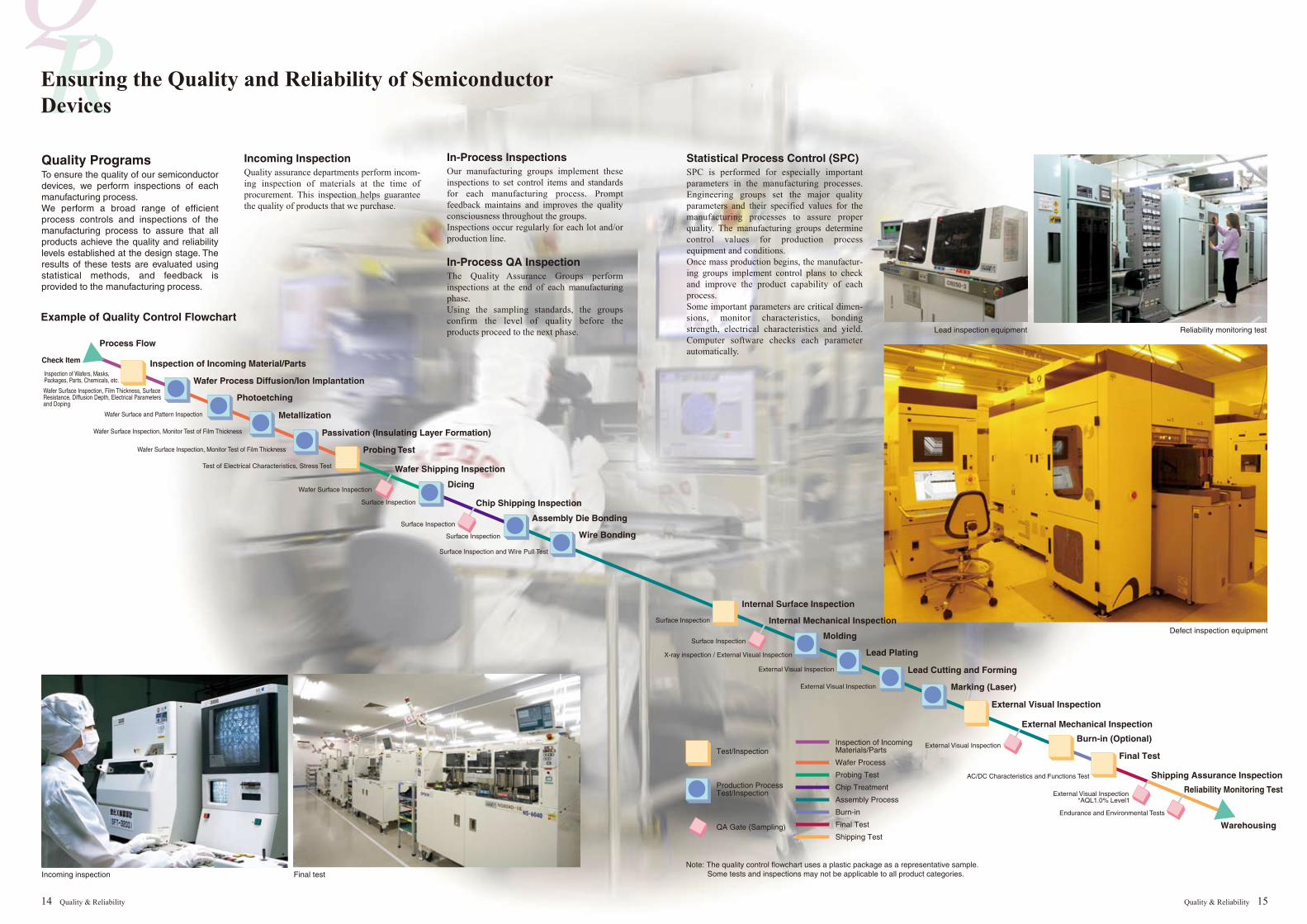
Ensuring the Quality and Reliability of Semiconductor Devices 14Quality Programs
• Example of Quality Control Flowchart • Incoming Inspection • In-Process Inspections
• In-Process QA Inspection 14• Statistical Process Control (SPC) 15
Maintaining the Quality and Reliability of Semiconductor Devices 16Quality and Reliability Support
• Equipment Maintenance • Measurement System Analysis (MSA) 16• Environmental Control • Electrostatic Discharge (ESD) Controls
• Shipment Control (Moisture Absorption Control) 17• Control of Components, Materials and Suppliers • In-Process Troubleshooting
• Design and Process Changes 18• Traceability • Document Management • Ensuring Continuous Improvement 19• Failure Analysis and Identification of Root Causes 20• Internal Quality Auditing • Third Party Certification 21
Business Diversity 22Providing Customized Products
• Quality Grades 22• Foundry Services • Bare Chips 23
Customer Satisfaction 24Customer Services and Support
• Quality and Reliability Database • Customer Audit 24• Failure Analysis 25
Environmental Issues 26
Technology Center and Plants for Semiconductor Devices 27
Quality & Reliability 1
2 Quality & Reliability Quality & Reliability 3
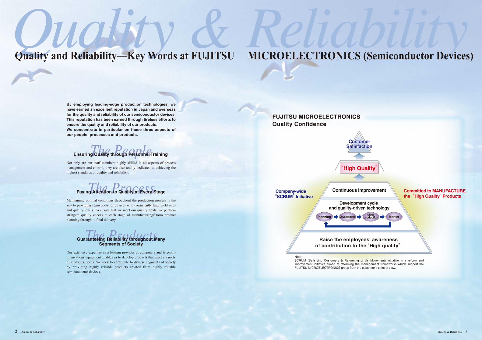
“High Quality”
Company-wide“SCRUM”Initiative
CustomerSatisfactionCustomer
Satisfaction
Committed to MANUFACTURE the“High Quality”Products
Note: SCRUM (Satisfying Customers & Reforming of Us Movement) initiative is a reform and improvement initiative aimed at reforming the management frameworks which support the FUJITSU MICROELECTRONICS group from the customer's point of view.
Raise the employees' awareness of contribution to the“High quality”
Continuous Improvement
Development cycle and quality-driven technology
Planning DevelopmentMass
production Market
Quality and Reliability—Key Words at FUJITSU MICROELECTRONICS (Semiconductor Devices)
Ensuring Quality through Personnel Training
Paying Attention to Quality at Every Stage
Maintaining optimal conditions throughout the production process is the key to providing semiconductor devices with consistently high yield rates and quality levels. To ensure that we meet our quality goals, we perform stringent quality checks at each stage of manufacturingÑfrom product planning through to final delivery.
Guaranteeing Reliability throughout ManySegments of Society
Our extensive expertise as a leading provider of computers and telecom-munications equipment enables us to develop products that meet a variety of customer needs. We seek to contribute to diverse segments of society by providing highly reliable products created from highly reliable semiconductor devices.
Not only are our staff members highly skilled in all aspects of process management and control, they are also totally dedicated to achieving the highest standards of quality and reliability.
By employing leading-edge production technologies, we have earned an excellent reputation in Japan and overseas for the quality and reliability of our semiconductor devices. This reputation has been earned through tireless efforts to ensure the quality and reliability of our products. We concentrate in particular on these three aspects of our people, processes and products.
FUJITSU MICROELECTRONICSQuality Confidence
Training Type
BasicTraining
OJT"on-the-jobtraining"
Item Contents
Company Outline
Outline of Semiconductors
Quality Control (QC)
Explanation of Safety and Sanitation
Qfinity Activities
Explanation of Standardization
Quality Management System
Environmental Management Systems
Inspection
Training in Areas Other than Inspection
Organization and Positioning of the QA Division
Operations and Types of Semiconductors, Semiconductor Production Processes, Handling of Semiconductors
Concept of Quality Control, Explanation of Quality and Reliability, Explanation of Inspection
Handling of Chemicals, Points to be Considered During Work
Outline of Activities
Necessity of Standardization, System of Standardization
Internal Quality Systems/ISO 9000 series, etc.
ISO 14001 Series and Fujitsu Environmental Management Systems
Basic Knowledge, Inspection Based on Specifications
How to Summarize Data, Defect Analysis, SPC, Completion Control
FUJITSU MICROELECTRONICS employ-ees receive quality control education and training in which they learn how to improve product quality by employing consistent quality goals. This training also helps to improve overall employee morale. In addition to performing regular quality control checks at each product stage, each employee is given the opportunity to independently apply their training results to perform autonomous self-checks, with the aim of ensuring quality and reliability and of identifying nonconforming products as rejects early on.
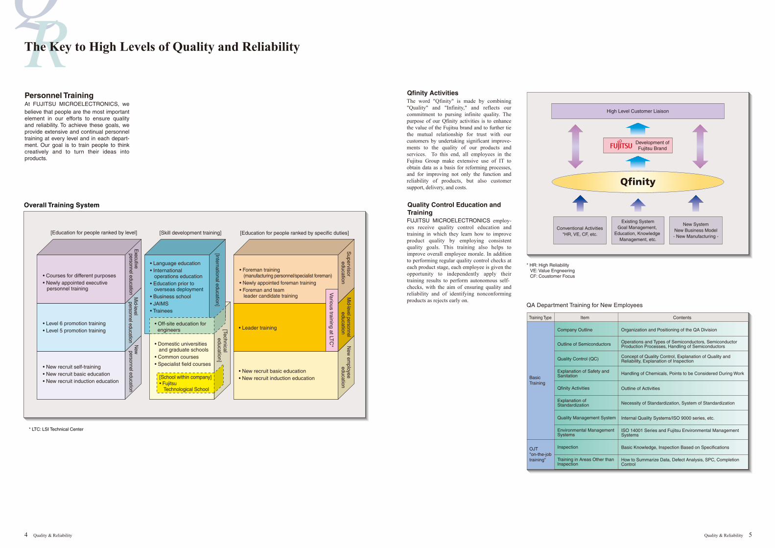
Personnel TrainingAt FUJITSU MICROELECTRONICS, we believe that people are the most important element in our efforts to ensure quality and reliability. To achieve these goals, we provide extensive and continual personnel training at every level and in each depart-ment. Our goal is to train people to think creatively and to turn their ideas into products.
* HR: High ReliabilityVE: Value EngneeringCF: Coustomer Focus
High Level Customer Liaison
Development ofFujitsu Brand
Conventional Activities*HR, VE, CF, etc.
Existing SystemGoal Management,
Education, Knowledge Management, etc.
New SystemNew Business Model- New Manufacturing -
The word "Qfinity" is made by combining "Quality" and "Infinity," and reflects our commitment to pursing infinite quality. The purpose of our Qfinity activities is to enhance the value of the Fujitsu brand and to further tie the mutual relationship for trust with our customers by undertaking significant improve-ments to the quality of our products and services. To this end, all employees in the Fujitsu Group make extensive use of IT to obtain data as a basis for reforming processes, and for improving not only the function and reliability of products, but also customer support, delivery, and costs.
* LTC: LSI Technical Center
4 Quality & Reliability Quality & Reliability 5
The Key to High Levels of Quality and Reliability
Overall Training System
Qfinity Activities
Quality Control Education andTraining
QA Department Training for New Employees
• Courses for different purposes• Newly appointed executive personnel training
• Foreman training(manufacturing personnel/specialist foreman)
• Newly appointed foreman training• Foreman and team leader candidate training
• Leader training
• New recruit basic education• New recruit induction education
• Language education• International operations education• Education prior to overseas deployment• Business school• JAIMS• Trainees
• Off-site education for engineers
• Domestic universities and graduate schools• Common courses• Specialist field courses
[School within company]• Fujitsu Technological School
• Level 6 promotion training• Level 5 promotion training
• New recruit self-training• New recruit basic education• New recruit induction education
Executive personnel education
[International education]
Supervisor
education
Various training at LT
C*
Mid-level personnel
educationN
ew em
ployee education
[Technical education]
Mid-level personnel education
New personnel education
[Education for people ranked by level] [Skill development training] [Education for people ranked by specific duties]

Production:
Material (purchasing)Control
Production ProcessControl
Inter-ProcessAudit/Inspection
Final Testing
Shipping Inspection
Facility Control
In-ProcessTroubleshooting
Failure Analysis
Collection and Application Information
Purchasing and QA Departments
Manufacturing Department
QA Department
Testing Department
QA Department
Facility Engineering Department
QA, Manufacturing and Testing Departments
Reliability Warranty and QA Departments
All Departments
Task Division in Charge
Development:
Reliability Design
Process Development
Design Review
Mass-ProductionEngineering Approval Testing
Design, Process, Assembly and Testing Departments
Design, Process, Assembly and Testing Departments
Design, Process, Assembly and Testing, QA and General Quality Assurance Departments
QA Department
Customer *Sales Department
*Sales Department : FUJITSU ELECTRONICS INC.
Device DesignDepartment
EngineeringDepartment
QualityAssurance Division Quality Assurance
Department Testing Department
Manufacturing Department Product Shipping
Department Production Control
Department Facility Maintenance
Department
Pla
nnin
g S
tage
Des
ign
and
Exp
erim
enta
l Dev
elop
men
tM
ass-
Pro
duct
ion
Sta
geF
ield
Manufacturing Plant
User Tec hnology Support Department
Development/Technology
Quality AssuranceDivision
Reliability and Quality ManagementDepartment, Akiruno Technology Center
(Responsible for Reliability and Quality Management)
Reliability Engineering Department,Akiruno Technology Center
(Responsible for Reliability Engineering)
Reliability and Quality Assurance Department,Akiruno Technology Center
(Responsible for Failure Analysis and Customer Support)
Quality Assurance Department,Mie/Aizuwakamatsu/Iwate Plant
Subsidiary Company QualityAssurance Departments*
FUJITSU INTEGRATED MICROTECHNOLOGY LTD.FUJITSU SEMICONDUCTOR TECHNOLOGY INC.
*
CS Delivery
Establishing Engineering Standards
Product Review (DR2)
Pilot Mass Production
Characteristics Evaluation Product Qualification Tests
Mass Production Review (DR3)
Establishing Manufacturing Standards
Manufacturing Product & Material Control
Warehousing
Delivery
Customer complaints
Information Product PlanningMarket Research
ES Delivery
Design Verification
Technical Review (DR1)
Pilot Production
Characteristics/Reliability Evaluation
Confirmation of Customer Specifications
Initial Shipping Control
Mass Production Stability Review (DR4)
Component and Material Incoming
Final Test Shipping Inspection
Equipment Maintenance
Shipping
Failure Analysis
Development Planning Review (DR0)
Customer complaints Handling
Quality/Customer complaints
Information
In-Process Inspection
Statistical Process Control (SPC)
In-ProcessQA Inspection
ReliabilityMonitoring Test
Quality/Customer complaintsInformation Related to Manufacturing
Legend: Basic route: Assist route: Information route
Table of task assignments by division
Organization to Ensure Quality and ReliabilityFUJITSU MICROELECTRONICS's system for ensuring the overall reliability of semicon-ductor devices involves the allocation of responsibility to every department engagedin a product's development and manufac-ture, including technologies and manufac-turing processes and the control of materi-als. The Quality Assurance Division controls this overall system.Quality assurance departments at each of FUJITSU MICROELECTRONICS's manu-facturing plants interact with the Quality Assurance Division which functions as the overall center for assuring quality and reliability.
To assure high levels of reliability, the depart-ment is charged with the following responsi-bilities.
Organization of the Quality Assurance Division
6 Quality & Reliability Quality & Reliability 7
Integrated Manufacturing Management to Ensure Quality Semiconductor Devices
Areas of Responsibility Quality Assurance System Structure
Function/Process/Requirements
Target Type:
Use:
Section in charge: Prepared by: Key date: FMEA NoInitial release: yy/mm/dd, Rev. No. and Rev. Date:(latest) yy/mm/dd (7)
Team:
Possible failure mode
Effect of failure Severity Class Failure cause/
mechanismCurrent design failure prevention management
Current design failure detection management Detection Risk priority
number (RPN) Measures Person in charge/Schedule
Measures and execution day
Effect of measures
Severity Occurrence Detection Risk priority number
Occurrence
8 Quality & Reliability
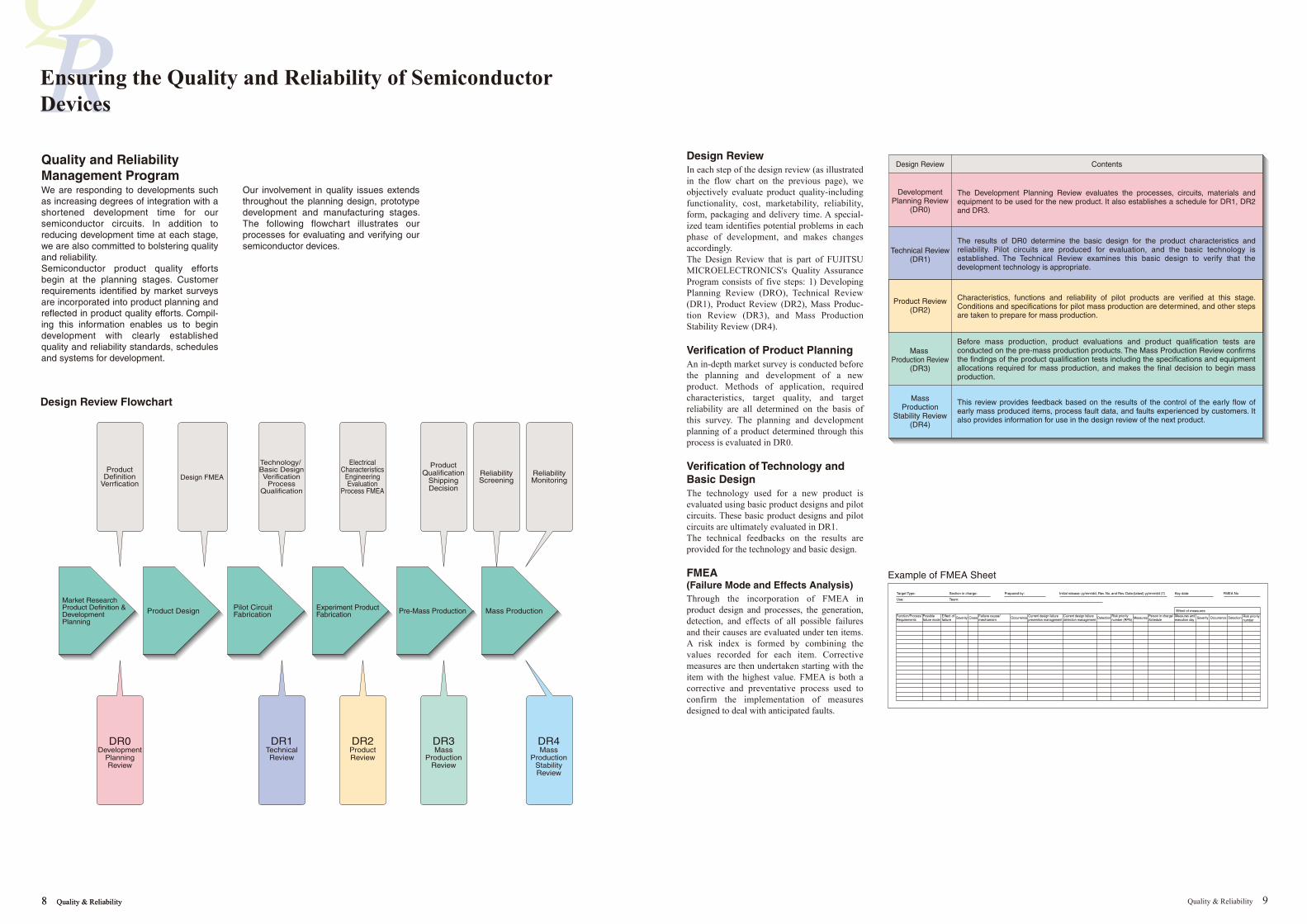
Quality and Reliability Management ProgramWe are responding to developments such as increasing degrees of integration with a shortened development time for our semiconductor circuits. In addition to reducing development time at each stage, we are also committed to bolstering quality and reliability.Semiconductor product quality efforts begin at the planning stages. Customer requirements identified by market surveys are incorporated into product planning and reflected in product quality efforts. Compil-ing this information enables us to begin development with clearly established quality and reliability standards, schedules and systems for development.
Our involvement in quality issues extendsthroughout the planning design, prototype development and manufacturing stages. The following flowchart illustrates our processes for evaluating and verifying our semiconductor devices.
ProductDefinition
VerrficationDesign FMEA
DR0Development
PlanningReview
DR1TechnicalReview
DR2ProductReview
DR3Mass
ProductionReview
DR4Mass
ProductionStabilityReview
Technology/ Basic DesignVerification
ProcessQualification
ElectricalCharacteristics
EngineeringEvaluation
Process FMEA
ProductQualification
ShippingDecision
ReliabilityScreening
ReliabilityMonitoring
Market ResearchProduct Definition &DevelopmentPlanning
Product Design Pilot CircuitFabrication
Experiment ProductFabrication Pre-Mass Production Mass Production
Design Review Contents
DevelopmentPlanning Review
(DR0)
Technical Review(DR1)
Product Review(DR2)
MassProduction Review
(DR3)
The results of DR0 determine the basic design for the product characteristics and reliability. Pilot circuits are produced for evaluation, and the basic technology is established. The Technical Review examines this basic design to verify that the development technology is appropriate.
Characteristics, functions and reliability of pilot products are verified at this stage. Conditions and specifications for pilot mass production are determined, and other steps are taken to prepare for mass production.
The Development Planning Review evaluates the processes, circuits, materials and equipment to be used for the new product. It also establishes a schedule for DR1, DR2 and DR3.
Before mass production, product evaluations and product qualification tests are conducted on the pre-mass production products. The Mass Production Review confirms the findings of the product qualification tests including the specifications and equipment allocations required for mass production, and makes the final decision to begin mass production.
MassProduction
Stability Review(DR4)
This review provides feedback based on the results of the control of the early flow of early mass produced items, process fault data, and faults experienced by customers. It also provides information for use in the design review of the next product.
Design ReviewIn each step of the design review (as illustrated in the flow chart on the previous page), we objectively evaluate product quality-including functionality, cost, marketability, reliability, form, packaging and delivery time. A special-ized team identifies potential problems in each phase of development, and makes changes accordingly.The Design Review that is part of FUJITSU MICROELECTRONICS's Quality Assurance Program consists of five steps: 1) Developing Planning Review (DRO), Technical Review (DR1), Product Review (DR2), Mass Produc-tion Review (DR3), and Mass Production Stability Review (DR4).
Verification of Product Planning An in-depth market survey is conducted before the planning and development of a new product. Methods of application, required characteristics, target quality, and target reliability are all determined on the basis of this survey. The planning and development planning of a product determined through this process is evaluated in DR0.
Verification of Technology and Basic DesignThe technology used for a new product is evaluated using basic product designs and pilot circuits. These basic product designs and pilot circuits are ultimately evaluated in DR1.The technical feedbacks on the results are provided for the technology and basic design.
FMEA(Failure Mode and Effects Analysis)Through the incorporation of FMEA in product design and processes, the generation, detection, and effects of all possible failures and their causes are evaluated under ten items. A risk index is formed by combining the values recorded for each item. Corrective measures are then undertaken starting with the item with the highest value. FMEA is both a corrective and preventative process used to confirm the implementation of measures designed to deal with anticipated faults.
8 Quality & Reliability Quality & Reliability 9
Ensuring the Quality and Reliability of SemiconductorDevices
Design Review Flowchart
Example of FMEA Sheet
NBTI[Negative Bias Temperature Instability]
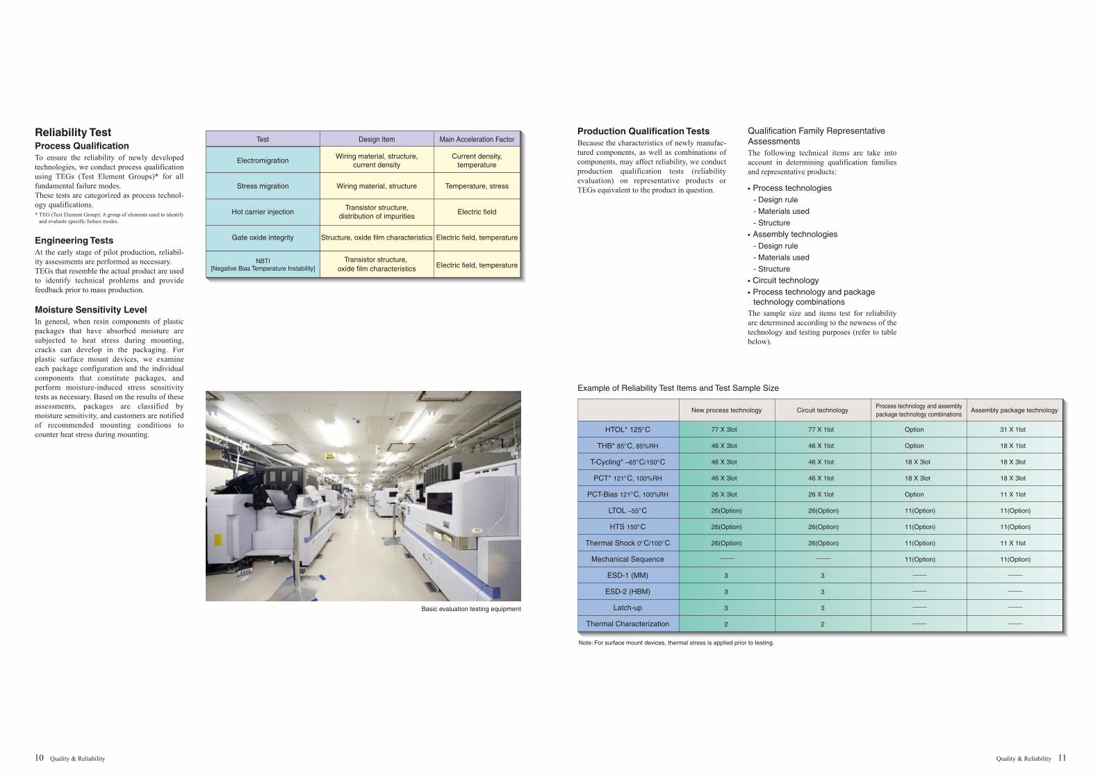
Note: For surface mount devices, thermal stress is applied prior to testing.
ElectromigrationWiring material, structure,
current densityCurrent density,
temperature
Stress migration Wiring material, structure Temperature, stress
Hot carrier injectionTransistor structure,
distribution of impuritiesElectric field
Gate oxide integrity Structure, oxide film characteristics Electric field, temperature
Transistor structure,oxide film characteristics Electric field, temperature
Test Design Item Main Acceleration Factor
77 X 3lot
46 X 3lot
46 X 3lot
46 X 3lot
26 X 3lot
26(Option)
26(Option)
26(Option)
3
3
3
2
77 X 1lot
46 X 1lot
46 X 1lot
46 X 1lot
26 X 1lot
26(Option)
26(Option)
26(Option)
3
3
3
2
Option
Option
18 X 3lot
18 X 3lot
Option
11(Option)
11(Option)
11(Option)
11(Option)
31 X 1lot
18 X 1lot
18 X 3lot
18 X 3lot
11 X 1lot
11(Option)
11(Option)
11 X 1lot
11(Option)
New process technology Circuit technologyProcess technology and assemblypackage technology combinations
Assembly package technology
Reliability TestProcess QualificationTo ensure the reliability of newly developed technologies, we conduct process qualification using TEGs (Test Element Groups)* for all fundamental failure modes.These tests are categorized as process technol-ogy qualifications.* TEG (Test Element Group): A group of elements used to identify
and evaluate specific failure modes.
Engineering TestsAt the early stage of pilot production, reliabil-ity assessments are performed as necessary. TEGs that resemble the actual product are used to identify technical problems and provide feedback prior to mass production.
Moisture Sensitivity LevelIn general, when resin components of plastic packages that have absorbed moisture are subjected to heat stress during mounting, cracks can develop in the packaging. For plastic surface mount devices, we examine each package configuration and the individual components that constitute packages, and perform moisture-induced stress sensitivity tests as necessary. Based on the results of these assessments, packages are classified by moisture sensitivity, and customers are notified of recommended mounting conditions to counter heat stress during mounting.
Production Qualification TestsBecause the characteristics of newly manufac-tured components, as well as combinations of components, may affect reliability, we conduct production qualification tests (reliability evaluation) on representative products or TEGs equivalent to the product in question.
Qualification Family Representative AssessmentsThe following technical items are take into account in determining qualification families and representative products:
• Process technologies- Design rule
- Materials used
- Structure• Assembly technologies
- Design rule
- Materials used
- Structure• Circuit technology• Process technology and package
technology combinationsThe sample size and items test for reliability are determined according to the newness of the technology and testing purposes (refer to table below).
HTOL* 125°C
THB* 85°C, 85%RH
T-Cycling* –65°C/150°C
PCT* 121°C, 100%RH
PCT-Bias 121°C, 100%RH
LTOL –55°C
HTS 150°C
Thermal Shock 0°C/100°C
Mechanical Sequence
ESD-1 (MM)
ESD-2 (HBM)
Latch-up
Thermal Characterization
10 Quality & Reliability Quality & Reliability 11
Example of Reliability Test Items and Test Sample Size
Basic evaluation testing equipment

Wafer Process
HTOL 150°C
THB 85°C, 85%RH or PCT-Bias 121°C, 100%RH
T-Cycling −65°C/150°C
PCT 121°C, 100%RH or PCT 134°C, 85%RH
46
26
46
46
—
—
46
46
Assembly(Plastic Package)
Inst
anta
neou
s Fa
ilure
Rat
e ( λ
)
EarlyFailure Period
After screening
Before screening
RandomFailure Period
Time (T)
WearoutFailure Period
ScreeningAs illustrated in Figure 1 (p13), the failure rates for LSIs follow a "bathtub curve." Even though ensuring quality at each stage of the production process and a range of tests and inspections eliminate most causes of failure, it is possible that some may persist.FUJITSU MICROELECTRONICS's reliability screening eliminates potential early faults. Conducted prior to shipping, it involves the application of stress at a level that will not damage the product in question.
Burn-InBurn-in is effective as a reliability screening to reject the early failures. In our factories, we strive for improvement in the everyday quality of our products. When the burn-in failure rate has been reduced to a certain level, we reduce the time required for burn-in, and eventually, eliminate it all together. Even after burn-in has been eliminated, products will be periodically sampled for burn-in to assure product quality.
Reliability Monitoring TestsOnce mass production begins, products are periodically monitored to confirm the unifor-mity of quality and reliability. Tests to monitor reliability are performed on representative samples from each production line.
FIT RateA failure rate is defined as "The rate at which an item which has been operated up to a particular point in time will bring on a failure within a specific unit of time" in the JIS Z8115.F26. The Figure 1 shows it as a bathtub curve. The time process of failure is divided into 3 periods; Early Failure Period, Random Failure Period, and Wearout Failure period.The failure rate of LSIs is in general described in the random failure period. The forecasted failure rate is obtained by the formula in Figure 2, using accelerated test data taken from qualification tests and reliability monitoring tests.
0
0.92
1
2.02
2
3.11
3
4.18
4
5.24
5
6.29
Number ofFailures
Coefficient γ
Table 1
λ : Failure rateγ : Reliability coefficient (60% reliability level is used.) (See Table 1.)n : Number of testst : Test timeKt : Temperature acceleration coefficientEa : Activation energyk : Boltzmann's constant (8.617E-5eV/K)T1 : Ambient temperature (absolute temperature)T2 : Test temperature (absolute temperature)Kv: Voltage acceleration coefficientE1 : Electric field strength of oxide film at rated voltage (MV/cm)E2 : Electric field strength of oxide film during test (MV/cm)
Burn-in Equipment
12 Quality & Reliability Quality & Reliability 13
Example of Reliability Monitoring Tests (Test Items and Test Samples)
Figure 1. Reliability Bathtub Curve
Figure 2: Failure Rate Calculation Method
Incoming inspection Final test
Defect inspection equipment
Check Item
Inspection of Wafers, Masks,Packages, Parts, Chemicals, etc.
Wafer Surface Inspection, Film Thickness, SurfaceResistance, Diffusion Depth, Electrical Parametersand Doping
Wafer Surface and Pattern Inspection
Wafer Surface Inspection, Monitor Test of Film Thickness
Wafer Surface Inspection, Monitor Test of Film Thickness
Test of Electrical Characteristics, Stress Test
Wafer Surface Inspection
Surface Inspection
Surface Inspection
Surface Inspection
Surface Inspection and Wire Pull Test
Surface Inspection
Surface Inspection
X-ray inspection / External Visual Inspection
External Visual Inspection
External Visual Inspection
External Visual Inspection
AC/DC Characteristics and Functions Test
External Visual Inspection
Endurance and Environmental Tests
Process Flow
Inspection of Incoming Material/Parts
Wafer Process Diffusion/Ion Implantation
Photoetching
Metallization
Passivation (Insulating Layer Formation)
Probing Test
Wafer Shipping Inspection
Dicing
Chip Shipping Inspection
Assembly Die Bonding
Wire Bonding
Internal Surface Inspection
Internal Mechanical Inspection
Burn-in (Optional)
Reliability Monitoring Test
Warehousing
Molding
Lead Plating
Marking (Laser)
Lead Cutting and Forming
External Visual Inspection
External Mechanical Inspection
Final Test
Shipping Assurance Inspection
*AQL1.0% Level1
Test/Inspection
Production ProcessTest/Inspection
QA Gate (Sampling)
Inspection of IncomingMaterials/Parts
Wafer Process
Probing Test
Chip Treatment
Assembly Process
Burn-in
Final Test
Shipping Test
Note: The quality control flowchart uses a plastic package as a representative sample. Some tests and inspections may not be applicable to all product categories.
Reliability monitoring testLead inspection equipment
Quality ProgramsTo ensure the quality of our semiconductor devices, we perform inspections of each manufacturing process.We perform a broad range of efficient process controls and inspections of the manufacturing process to assure that all products achieve the quality and reliability levels established at the design stage. The results of these tests are evaluated using statistical methods, and feedback is provided to the manufacturing process.
Incoming InspectionQuality assurance departments perform incom-ing inspection of materials at the time of procurement. This inspection helps guarantee the quality of products that we purchase.
Example of Quality Control Flowchart
In-Process InspectionsOur manufacturing groups implement these inspections to set control items and standards for each manufacturing process. Prompt feedback maintains and improves the quality consciousness throughout the groups.Inspections occur regularly for each lot and/or production line.
In-Process QA InspectionThe Quality Assurance Groups perform inspections at the end of each manufacturing phase.Using the sampling standards, the groups confirm the level of quality before the products proceed to the next phase.
Statistical Process Control (SPC)SPC is performed for especially important parameters in the manufacturing processes. Engineering groups set the major quality parameters and their specified values for the manufacturing processes to assure proper quality. The manufacturing groups determine control values for production process equipment and conditions.Once mass production begins, the manufactur-ing groups implement control plans to check and improve the product capability of each process.Some important parameters are critical dimen-sions, monitor characteristics, bonding strength, electrical characteristics and yield. Computer software checks each parameter automatically.
14 Quality & Reliability Quality & Reliability 15
Ensuring the Quality and Reliability of SemiconductorDevices
Environmental Control (Central Surveillance Center)
Quality and Reliability SupportInspection and testing are vital parts of semiconductor production. Yet they cannot guarantee absolute quality and reliability. Control of environment and equipment in the manufacturing process is equally important.
Equipment MaintenanceThe maintenance of the manufacturing equipment is another important aspect of maintaining product quality. At FUJITSU MICROELECTRONICS, each piece of production equipment is regularly inspected according to stringent control standards.Each plant's equipment maintenance group regularly calibrates all instruments used for measurements and inspections. Control ledgers record the results of the calibrations. Each piece of production equipment bears a label showing the deadline for the next calibration.Only experienced specialists calibrate the measuring instruments. The standard equipment used for the calibration is calibrated with a traceability system based on Japanese government standards.
Measurement System Analysis (MSA)Control of inspection and testing equipmentMeasurement and testing equipment are used for tests and inspections that verify that semiconductor devices meet the required specifications. From the time of introduction, equipment is controlled daily and also undergoes regular calibration.• Daily inspection and regular calibration
The cycle for regular calibration is determined separately for each piece of equipment and ranges from every six months through to every 24 months. Equipment is calibrated with a traceability system based on international standards.Daily inspection cycles are also determined separately for each piece of equipment.
• Measurement System AnalysisAt FUJITSU MICROELECTRONICS, we conduct measurement system analysis in order to analyze potential variations in measuring devices.We also ensure that gage repeatability and reproducibility and measurement system analysis correspond to process capabilities.
Environmental ControlThe manufacturing environment greatly affects the quality and reliability of semiconductors. To maintain consistent product quality, we strictly control temperature, humidity, dust levels and water purity at every phase of manufacturing.We impose rigorous standards on each item and regularly monitor every aspect of the environment. We also impose control standards for product storage.
Electrostatic Discharge (ESD) ControlsThe structure of semiconductors makes them extremely sensitive to static electricity. At FUJITSU MICROELECTRONICS, we design our integrated circuits to be as resistant to static electricity as possible. We also take extensive measures to reduce static electricity throughout the manufacturing process.
Shipment Control(Moisture Absorption Control)We use moisture-protective packing for our semiconductor devices according to moisture sensitivity level, because resins are highly subject to moisture damage during the mount-ing process of surface-mounted packages. Labeling provides information about the moisture sensitivity level of each product.
Use antistatic flooring materials with a surface resistance of 1x10⁵ to 1x10¹⁰Ω or antistatic mats
Use gloves made from materials that are charge resistant. Surface resistance of 1x10⁵ to 1x10¹¹Ω
Antistatic shoes that meet the following specification: Surface resistance of 1x10⁵ to 1x10¹⁰Ω
Wear antistatic clothes with surface resistance of 1x10⁵ to 1x10¹¹Ω
Straps that meet the following specification: Resistance to ground of 1x10⁵ to 1x10⁷Ω
Use stalls that meet the following specification: Surface resistance of 1x10⁵ to 1x10¹⁰Ω
Use work surfaces with a surface resistance of 1x10⁵ to 1x10¹⁰Ω
Use chairs with a resistance to ground of 1x10⁵ to 1x10⁸Ω
For electrically powered equipment, use grounded equipment
Wafer charge voltage: Use of carts with charge voltage controlled to less than ±300V
Store wafers in box. Shelves are either grounded or have charge voltage of less than 20kV.
Use grounded shelves with a surface resistance of 1x10⁵
to 1x10¹⁰Ω
Apply antistatic mats to shelves and ground to floor (resistance to ground of 1x10⁵ to 1x10¹⁰Ω)
Floors
Bench tops
Chairs
Carts
Storage shelves
Work clothes,dust proof clothes
Shoes
Wrist strap
Finger stalls
Gloves
Equipment
16 Quality & Reliability Quality & Reliability 17
Measurement Standards Traceability System
Meter Convention
Nationalresearchinstitutes
Publicinstitutes
FML*
*: FUJITSU MICROELECTRONICS LIMITED (abbreviated as FML)
International Committee of Weights and Measures
International System of Units
Maintaining the Quality and Reliability of Semiconductor Devices
Examples of Procedures to Control ESD
Wafer Process Assembly Process Test Process
Equipment Maintenance
(When carrying products without static electricity protection)
National Institute of Information andCommunications Technology
National Institute of AdvancedIndustrial Science and Technology
Japan QualityAssurance Organization
Japan Electric MetersInspection Corporation
Weights and MeasuresInspection Offices
Fujitsu Facilities MeasuringDevice Service
Manufacturers
Factory Weights andMeasures Control Office
On-site Measuring Devices
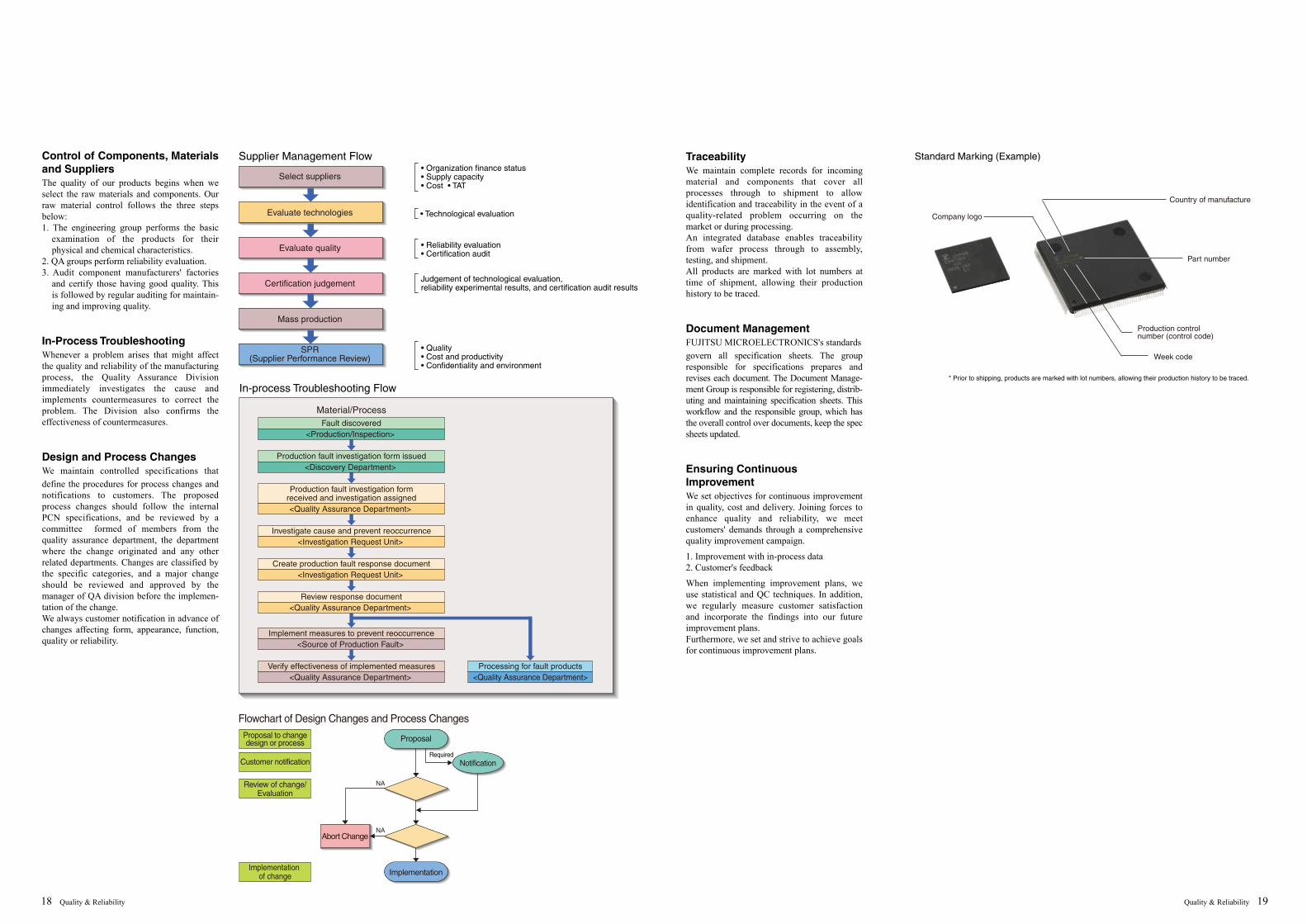
Company logo
* Prior to shipping, products are marked with lot numbers, allowing their production history to be traced.
Country of manufacture
Week code
Production control number (control code)
Part number
Control of Components, Materials and SuppliersThe quality of our products begins when we select the raw materials and components. Our raw material control follows the three steps below:1. The engineering group performs the basic
examination of the products for their physical and chemical characteristics.
2. QA groups perform reliability evaluation.3. Audit component manufacturers' factories
and certify those having good quality. This is followed by regular auditing for maintain-ing and improving quality.
In-Process TroubleshootingWhenever a problem arises that might affect the quality and reliability of the manufacturing process, the Quality Assurance Division immediately investigates the cause and implements countermeasures to correct the problem. The Division also confirms the effectiveness of countermeasures.
Design and Process ChangesWe maintain controlled specifications that define the procedures for process changes and notifications to customers. The proposed process changes should follow the internal PCN specifications, and be reviewed by a committee formed of members from the quality assurance department, the department where the change originated and any other related departments. Changes are classified by the specific categories, and a major change should be reviewed and approved by the manager of QA division before the implemen-tation of the change.We always customer notification in advance of changes affecting form, appearance, function, quality or reliability.
TraceabilityWe maintain complete records for incoming material and components that cover all processes through to shipment to allow identification and traceability in the event of a quality-related problem occurring on the market or during processing. An integrated database enables traceability from wafer process through to assembly, testing, and shipment. All products are marked with lot numbers at time of shipment, allowing their production history to be traced.
Document ManagementFUJITSU MICROELECTRONICS's standardsgovern all specification sheets. The group responsible for specifications prepares and revises each document. The Document Manage-ment Group is responsible for registering, distrib-uting and maintaining specification sheets. This workflow and the responsible group, which has the overall control over documents, keep the spec sheets updated.
Ensuring ContinuousImprovementWe set objectives for continuous improvement in quality, cost and delivery. Joining forces to enhance quality and reliability, we meet customers' demands through a comprehensive quality improvement campaign.
1. Improvement with in-process data2. Customer's feedback
When implementing improvement plans, we use statistical and QC techniques. In addition, we regularly measure customer satisfaction and incorporate the findings into our future improvement plans.Furthermore, we set and strive to achieve goals for continuous improvement plans.
18 Quality & Reliability Quality & Reliability 19
Supplier Management Flow
In-process Troubleshooting Flow
Flowchart of Design Changes and Process ChangesProposal to changedesign or process Proposal
NotificationRequired
Abort Change
Implementation
NA
NA
Customer notification
Review of change/Evaluation
Implementationof change
Material/Process
Implement measures to prevent reoccurrence<Source of Production Fault>
Verify effectiveness of implemented measures<Quality Assurance Department>
Fault discovered<Production/Inspection>
Production fault investigation form issued<Discovery Department>
Production fault investigation formreceived and investigation assigned<Quality Assurance Department>
Investigate cause and prevent reoccurrence<Investigation Request Unit>
Create production fault response document<Investigation Request Unit>
Review response document<Quality Assurance Department>
Processing for fault products<Quality Assurance Department>
• Organization finance status• Supply capacity• Cost • TAT
• Technological evaluation
• Reliability evaluation• Certification audit
Judgement of technological evaluation, reliability experimental results, and certification audit results
• Quality• Cost and productivity• Confidentiality and environment
Select suppliers
Evaluate technologies
Evaluate quality
Certification judgement
Mass production
SPR(Supplier Performance Review)
Standard Marking (Example)

20 Quality & Reliability Quality & Reliability 21
Internal Quality AuditingAt each plant, the following three types of audits are carried out periodically by the Quality Assurance Department.• Quality Management System (QMS) Audit
Audit conducted with the purpose of verifying the compatibility with QMS requirements and validity of rating requirements, department-specified requirements, customer requirements, legal regulation requirements that apply in relation to the product, etc.
• Manufacturing Process AuditAudit conducted to inspect the validity of the manufacturing process based on the documentation at the production factory such as control plans, process flowcharts, work standards, process FMEA, etc.
• Product AuditAudit conducted with the aim of verifying that the product meets the requirements at the appropriate stages during production and handover.
Third Party CertificationsIn relation to third party certifications of the quality management system, the following support is given for ISO9001 and for automobile-related ISO/TS16949 to support European automotive customers.
Failure Analysis and Identification of Root CausesEach of our factories not only monitor for faultsduring the production process, but also monitorthe results of wafer probing tests and final testing of completed products, and analyze the causes of defective products. These results are then used as feedback to the production process. Furthermore, the results of analysis of defective products that are actually returned from our customers are essential for preventing the malfunctions that occur for customers. The results are immediately reported to the related departments and the department will establish the preventive measures.
The analytic result obtained in this way is not only that the faults to be fixed, but also used to develop measures to prevent problems.The measures are also distributed sideways to areas where similar problems may occur.
Factory name and workplace Certification obtained Registration date Certification number Certifying institute
FUJITSU MICROELECTRONICS LIMITEDAkiruno Technology CenterMie PlantAizuwakamatsu PlantIwate Plant
FUJITSU MICROELECTRONICS LIMITEDMie PlantAizuwakamatsu PlantIwate Plant
Fujitsu Integrated Microtechnology Ltd. Head Office & Aizuwakamatsu PlantMiyagi PlantKyushu Plant
ISO9001
ISO/TS16949※
ISO9001
December 5, 2003
August 29, 2008August 29, 2008
December 5, 2003
November 26, 2004
JQA-QMA10719
JQA-AU0010-5JQA-AU0010-4JQA-AU0010-1
JQA-QMA11777
ISO9001:2000, ISO/TS16949:2002 Certification
JQA
Trend monitoring /data analysis
Process history
Com
plaintinform
ation
Status of complaints that occur/customer information
Direct contact with SRAMunit by nano-probe
Cross-sectional photoof gate unit (90 nm)
Quality Systems Accreditation Certificate
Investigation of Causes due to Fault Analysis
Approach to Analysis and Technology Improvements
Counterm
easure
*: Fujitsu Integrated Microtechnology Limited and Fujitsu Semiconductor Technology Limited are expected to obtain third party certification of ISO/TS16949 as follows. • Fujitsu Integrated Microtechnology Limited, Headquarters, Aizu factory and Miyagi factory: Middle of 2008 • Fujitsu Integrated Microtechnology Limited, Kyushu factory: Middle of 2009 • Fujitsu Semiconductor Technology Limited: Middle of 2009
Defect analysis
Determ
ining the cause
Root cause

For Standard Applications
G
GS
For Special Applications
GT
Providing Customized ProductsToday, semiconductors are used in a variety of fields, resulting in a diverse range of customer demand. FUJITSU MICROELECTRONICS has established quality grades for its LSI offerings to ensure that all products meet the required quality grade. We also provide customized products that satisfy the various shipping requirements of our customers.
Quality GradesOur quality assurance program assures the quality of FUJITSU MICROELECTRONICS's LSI products and is divided into three grades. Please consult the Sales Division to find out more about products used for special applica-tions.
Foundry ServicesMany of our customers have benefited from our LSI technologies via the wafer process foundry services.
Bare ChipsOur regular LSI products are packaged for easy handling, but in response to customer requests for size and weight reductions, we also ship "bare chips," that is, chips without any packaging.There is a greater possibility of in-transit damage to these chips, so extreme care should be taken when handling them. Customers are encouraged to conduct quality and reliability screening and testing for defects after mounting.
Note:Custom specifications may not be possible on some products. Please make specific inquiries when ordering.
22 Quality & Reliability Quality & Reliability 23
Business Diversity
Quality Grades
General applications
Industrial applications, general automotive control applications
Automobile drive control and engine control, automobile safety devices
CustomerFUJITSU MICROELECTRONICS
Wafer process Assembly Test
Planning stage
Design and prototype stage
Mass production migration stage
Product shipping stage
Mass production stage
Request
Check and investigate customer requirements
Agree on the development
Development investigation
Review plans
Design verification
Verify
Technical review
Development prototypePrototype product
delivery
Evaluate
Enter manufacturing contract
Factory audit by customer
Mass production migration review
Review mass-production shipping
Initial mass production
Initial distribution management
Mass production verification review
Product shipping
Product delivery
Quality information
Change designs Change production process
Respond to customer complaints
Fujitsu standard specification
Customer requirement specification
Special applications
Specific applications
Standardapplications General applications
Customer specific applications / Safety applicationsex) High-safety applications (nuclear reaction control in nuclear power plants, aircraft automatic flight control, air traffic control systems, operation control in mass transit systems, medical equipment for preserving life, missile launch control in weapons systems, etc.)
Enhanced Reliabilityex) Industrial, automotive, medical (where not directly related to life)
Customer complaints

Failure AnalysisWe carefully analyze all returned products that we receive from customers, take suitable measures to prevent recurrence and provide analytical feedback to the concerned groups. Because this feedback can directly improve reliability, it is our policy to give customer complaints full attention and to do everything possible to resolve problems.Customer complaints are first directed tothe Sales /Customer Support Departments. Information is then passed on to the Reliability & QA Departments for electronic and physical analysis to determine the cause of the failure. Related divisions take appropriate measures based on the results of these analysis. Further-more, in order to fully correct the problem, similar measures are taken at all our manufac-turing facilities.
1. Presentation of Information related to Defective ProductsFor analysis of defective products, the more information there is about the defects, the more accurate failure analysis is possible. For this reason, we elicit as much detailed information from the customer as possible when receiving the customer complaint.
2. Returning Defective GoodsCustomers are requested to send defective products in the original defective state, preventing exterior defect condition change, so that proper analysis may be performed.
3. Customer Complaints Handling Period (Standard)Whenever a customer complaint arises, the Reliability and Quality Assurance Department responds with an interim report within two days of receipt of the customer complaint. The Department produces a final report within two weeks of receipt of the customer complaint.
Customer Services and SupportAt FUJITSU MICROELECTRONICS, thecustomer always comes first. That is why we put such efforts into ensuring high quality and stable product supply.For every defect discovered, an in-depth analysis is conducted to determine the cause of the problem and to incorporate preventive measures into the development process. Customers are informed of all aspects of the situation. Because the results of these analyses can provide information vital to improving reliability, it is our policy to give customer complaints full attention and to do everything possible to resolve problems.Our database services and responses to audits demonstrate our commitment to an ongoing dialogue with our customers.
Quality and Reliability DatabaseWe have developed a database for providing information quickly to customers about quality and reliability data. The following data are available to customers.• Product qualification tests• Test data for reliability monitoring (Periodic reliability data on representative models)• Shipment inspections• Others
Customer AuditWe believe that customer audits and visits to our manufacturing facilities play an important role in building trust in our relationship. Customers are welcome to visit our facilities. Through extensive customer communications, we determine customer needs and incorporate these needs into our products to ensure customer satisfaction.
Micro Focus X-Ray TV System SEM (Scanning Electro Micro Scope)EPMA (Electron Probe Micro Analysis)
EMS (Emission Micro Scope)TEM(Transmission Electron Microscope) FIB (Focus Ion Beam)
24 Quality & Reliability Quality & Reliability 25
Customer Satisfaction
Process for Responding Customer Complaints
Custom
er
Sales DivisionQuality Assurance Division
Quality A
ssuranceD
epartment
TechnologyD
epartment
Plant
Reliability and Quality ManagementDepartment
(Akiruno Technology Center)
Engineering Department
Manufacturing/Management Department
ProductionPlanningDelivery
Design
Examination
Assembly
Process
ProcessAssembly
Examination
Various Analysis Systems

26 Quality & Reliability Quality & Reliability 27
Iwate Plant Aizuwakamatsu Plant
Fujitsu Integrated Microtechnology Ltd. Miyagi Plant
Mie Plant Fujitsu Integrated Microtechnology Ltd. Aizu Plant (Headquarters)
Fujitsu Integrated Microtechnology Ltd. Kyushu Plant
Fujitsu Semiconductor Technology, INC.
Small boilers burning natural gas
FRAM card
NAS battery
System power LSI(MB39C308)
Environmental Issues
At our company, the environment is an extremely important management issue, and environmental activities are promoted based on the environ-mental action plan of the Fujitsu Group.The Fujitsu Group will focus on five environmental issues in the future:
• Improving the environmental value of products and services • Global warming countermeasures • Reinforcing governance • Reinforcing risk management • Environmental and social contributions
As a member of the Fujitsu Group, each of our employees strives to continue environmental activities in their workplace and local regions, and works to reduce the load on the environment and improve our environmental efficiency.
Preventing Global WarmingFUJITSU MICROELECTRONICS creates semiconductor devices that conserve energy, and also provides a service that applies this to suppressing the generation of CO2 at the stage where the customer uses semiconductor devices.
• Energy-saving power systems that use highly-efficient systempower LSIs
• Paperless reception operations using FRAM cards
Third part certificationThe Fujitsu Group has received ISO14001 global integrated certifi-cation that applies to 88 domestic and 11 overseas companies. Our domestic headquarters are mutually certified by the Japan Audit and Certification Office for Environment and Quality (JACO) and our overseas headquarters by Det Norske Veritas (DNV).
Certification acquisition date: 12th September 1995Certification number: EC98J2005
Furthermore, efforts are being made to reduce emissions of CO2 and other greenhouse gases in factories and offices.
• Introduction of NAS batteries(contributes to zero atmospheric pollution emissions and reductions in CO2)
• Strategies to reduce energy consumption at basic facilities(establishment of small flow boilers and energy conversions, etc.)
Akiruno Technology CenterLand area: 122,000m2
Established July 2000
Land area: 69,500m2
Established October 2003
Land area: 290,000m2
Established September 1980
Land area: 147,000m2
Established October 1984
Land area: 61,200m2
Established October 2003Land area: 307,000m2
Established October 1984
Land area: 28,100m2
Established October 2003
Land area: 62,000m2
Established February 2007
Technology Center and Plants for Semiconductor Devices
28 Quality & Reliability Quality & Reliability 29
Related Documents