Service Modes, Error Codes, and Fault Finding EN 17 FTP1.1U 5. 5. Service Modes, Error Codes, and Fault Finding Index of this chapter: 1. Test points 2. Service Modes 3. Problems and solving tips (related to CSM) 4. ComPair 5. Error Codes 6. The blinking LED procedure 7. Protections 8. Repair tips 9. Software downloading 5.1 Test Points The chassis is equipped with test points printed on the circuit board assemblies. Perform measurements under the following conditions: • Service Default Mode. • Video: color bar signal. • Audio: 3 kHz left, 1 kHz right. 5.2 Service Modes Service Default Mode (SDM) and Service Alignment Mode (SAM) offer several features for the service technician, while the Customer Service Mode (CSM) is used for communication between a Philips Customer Care Centre (P3C) and a customer. There is also the option of using ComPair, a hardware interface between a computer (see requirements below) and the TV chassis. It offers the ability of structured troubleshooting, test pattern generation, error code reading, software version readout, and software upgrading. Minimum requirements: a Pentium processor, Windows 95/ 98, and a CD-ROM drive (see also paragraph “ComPair”). 5.2.1 Service Default Mode (SDM) Purpose • To create a pre-defined setting, to get the same measurement results as given in this manual. • To override SW protections. • To start the blinking LED procedure. Specifications • Tuning frequency: 61.25 MHz (channel 3). • Color system: NTSC. • All picture settings at 50 % (brightness, color, contrast). • All sound settings at 50 %, except volume at 25 %. • All service-unfriendly modes (if present) are disabled, like: – (Sleep) timer. – Child/parental lock. – Blue mute. – Automatic volume limiter (AVL). – Auto switch-off (when no video signal was received for 10 minutes). – Skip/blank of non-favorite pre-sets. – Smart modes. – Auto store of personal presets. – Auto user menu time-out. How to enter SDM Use one of the following methods: • Use the standard RC-transmitter and key in the code “062596”, directly followed by the “MENU” button. Note: It is possible that, together with the SDM, the main menu will appear. To switch it off, push the “MENU” button again. • Short for a moment the two solder pads (item 9018) on the SSP, with the indication “SDM”. Activation can be performed in all modes, except when the set has a problem with the main microprocessor. Caution: If the SDM is entered via the pins, all the software-controlled protections are de-activated. • Use the DST-emulation feature of ComPair. • Use the “DEFAULT” button on the Dealer Service Tool (RC7150, this remote is no longer available). After entering this mode, “SDM” will appear in the upper right corner of the screen. How to navigate When you press the “MENU” button on the RC transmitter, the set will toggle between the SDM and the normal user menu (with the SDM mode still active in the background). How to exit SDM Use one of the following methods: • Switch the set to STANDBY via the RC-transmitter. • Press the “EXIT” button in the DST-emulation feature of ComPair. • Via a standard customer RC-transmitter: key in “00”- sequence. 5.2.2 Service Alignment Mode (SAM) Purpose • To perform (software) alignments. • To change option settings. • To easily identify the used software version. • To view operation hours. • To display (or clear) the error code buffer. Specifications • Operation hours counter. • Software version. • Option settings. • Error buffer reading and erasing. • Software alignments. How to enter SAM Use one of the following methods: • Via a standard RC transmitter: key in the code “062596” directly followed by the “OSD [i+]” button. After entering SAM with this method a service warning will appear on the screen, you can continue by pressing any digit key on the RC. • Short for a moment the two solder pads (item 9017) on the SSP with the indication "SAM". Depending on the software version, it is possible that a service warning will appear. You can continue by pressing any digit key on the RC. • Use the DST-emulation feature of ComPair. • Press the ALIGN button on the DST while the set is in the normal operation After entering this mode, “SAM” will appear in the upper right corner of the screen. Contents of SAM: • OPERATION HOURS. Displays the accumulated total of operation hours (not the standby hours). • HARDWARE INFO. – ROM VERSION. Displays the date of the software and the software version of the ROM (example: TP11US_1.0_01234 = AAAABB_X.Y_NNNNN). • AAAA= the chassis name.

Welcome message from author
This document is posted to help you gain knowledge. Please leave a comment to let me know what you think about it! Share it to your friends and learn new things together.
Transcript
Service Modes, Error Codes, and Fault Finding EN 17FTP1.1U 5.
5. Service Modes, Error Codes, and Fault Finding
Index of this chapter:1. Test points2. Service Modes3. Problems and solving tips (related to CSM)4. ComPair5. Error Codes6. The blinking LED procedure7. Protections8. Repair tips9. Software downloading
5.1 Test Points
The chassis is equipped with test points printed on the circuit board assemblies. Perform measurements under the following conditions:• Service Default Mode.• Video: color bar signal.• Audio: 3 kHz left, 1 kHz right.
5.2 Service Modes
Service Default Mode (SDM) and Service Alignment Mode (SAM) offer several features for the service technician, while the Customer Service Mode (CSM) is used for communication between a Philips Customer Care Centre (P3C) and a customer. There is also the option of using ComPair, a hardware interface between a computer (see requirements below) and the TV chassis. It offers the ability of structured troubleshooting, test pattern generation, error code reading, software version readout, and software upgrading. Minimum requirements: a Pentium processor, Windows 95/98, and a CD-ROM drive (see also paragraph “ComPair”).
5.2.1 Service Default Mode (SDM)
Purpose• To create a pre-defined setting, to get the same
measurement results as given in this manual.• To override SW protections.• To start the blinking LED procedure.
Specifications• Tuning frequency: 61.25 MHz (channel 3).• Color system: NTSC.• All picture settings at 50 % (brightness, color, contrast).• All sound settings at 50 %, except volume at 25 %. • All service-unfriendly modes (if present) are disabled, like:
– (Sleep) timer.– Child/parental lock.– Blue mute.– Automatic volume limiter (AVL).– Auto switch-off (when no video signal was received for
10 minutes).– Skip/blank of non-favorite pre-sets.– Smart modes.– Auto store of personal presets.– Auto user menu time-out.
How to enter SDMUse one of the following methods:• Use the standard RC-transmitter and key in the code
“062596”, directly followed by the “MENU” button. Note: It is possible that, together with the SDM, the main menu will appear. To switch it off, push the “MENU” button again.
• Short for a moment the two solder pads (item 9018) on the SSP, with the indication “SDM”. Activation can be performed in all modes, except when the set has a problem with the main microprocessor.Caution: If the SDM is entered via the pins, all the software-controlled protections are de-activated.
• Use the DST-emulation feature of ComPair.• Use the “DEFAULT” button on the Dealer Service Tool
(RC7150, this remote is no longer available). After entering this mode, “SDM” will appear in the upper right corner of the screen.
How to navigateWhen you press the “MENU” button on the RC transmitter, the set will toggle between the SDM and the normal user menu (with the SDM mode still active in the background).
How to exit SDMUse one of the following methods:• Switch the set to STANDBY via the RC-transmitter.• Press the “EXIT” button in the DST-emulation feature of
ComPair.• Via a standard customer RC-transmitter: key in “00”-
sequence.
5.2.2 Service Alignment Mode (SAM)
Purpose• To perform (software) alignments.• To change option settings.• To easily identify the used software version.• To view operation hours.• To display (or clear) the error code buffer.
Specifications• Operation hours counter.• Software version.• Option settings.• Error buffer reading and erasing.• Software alignments.
How to enter SAMUse one of the following methods:• Via a standard RC transmitter: key in the code “062596”
directly followed by the “OSD [i+]” button. After entering SAM with this method a service warning will appear on the screen, you can continue by pressing any digit key on the RC.
• Short for a moment the two solder pads (item 9017) on the SSP with the indication "SAM". Depending on the software version, it is possible that a service warning will appear. You can continue by pressing any digit key on the RC.
• Use the DST-emulation feature of ComPair.• Press the ALIGN button on the DST while the set is in the
normal operation After entering this mode, “SAM” will appear in the upper right corner of the screen.
Contents of SAM:• OPERATION HOURS. Displays the accumulated total of
operation hours (not the standby hours).• HARDWARE INFO.
– ROM VERSION. Displays the date of the software and the software version of the ROM (example: TP11US_1.0_01234 = AAAABB_X.Y_NNNNN). • AAAA= the chassis name.
Service Modes, Error Codes, and Fault FindingEN 18 FTP1.1U5.
• BB= the region: EU= Europe, AP= Asia Pacific PAL/Multi, AN= Asia Pacific NTSC, US= USA, LT= LATAM.
• X.Y= the software version, where X is the main version number (different numbers are not compatible with one another) and Y is the sub version number (a higher number is always compatible with a lower number).
• NNNNN= last five digits of 12nc code software.– FBX VERSION (if present). Displays the software
version of the FBX.– SW VERSION EPLD. Displays the software version of
the EPLD.• ERRORS. (followed by maximal 10 errors). The most recent
error is displayed at the upper left (for an error explanation see paragraph “Error Codes”).
• DEFECTIVE MODULE. Here the module that generates the error is displayed. If there are multiple errors in the buffer, which are not all generated by a single module, there is probably another defect. It will then display the message “UNKNOWN” here.
• RESET ERROR BUFFER. When you press the “OK” button, the error buffer is reset.
• ALIGNMENTS. This will activate the “ALIGNMENTS” sub-menu.
• DEALER OPTIONS. Extra features for the dealers.• SERVICE OPTIONS. Extra features for Service.• INITIALISE NVM. When an NVM was corrupted (or
replaced) in the former EM3 chassis, the microprocessor replaces the content with default data (to assure that the set can operate). However, all pre-sets and alignment values are gone now, and option numbers are not correct. Therefore, this was a very drastic way. In this chassis, the procedure is implemented in another way: The moment the processor recognizes a corrupted NVM, the “initialise NVM” line will be highlighted. Now, you can do two things (dependent of the service instructions at that moment):– Save the content of the NVM via ComPair for
development analysis, before initializing. This will give the Philips Service department an extra possibility for diagnosis (e.g. when Development asks for this).
– Initialize the NVM (same as in the past, however now it happens conscious).
• STORE. All options and alignments are stored when pressing the “OK”-button
• FUNCTIONAL TEST. All devices are tested via the “OK” button. Eventual errors are displayed in the error buffer. The error buffer is not erased, the content returns when this test is terminated.
• DAILY MENUS. With the “OK” button, you can go to the normal user menu. SAM is still active in the background. With the “MENU” button, you return from the user menu to SAM menu. This feature can be helpful to quickly change some settings in the user menu.
• SW MAINTENANCE.– UPGRADE. More info see paragraph “Software
downloading”.
How to navigate• In SAM, you can select the menu items with the “CURSOR
UP/DOWN” key on the RC-transmitter. The selected item will be highlighted. When not all menu items fit on the screen, move the “CURSOR UP/DOWN” key to display the next/previous menu items.
• With the “CURSOR LEFT/RIGHT” keys, it is possible to:– (De) activate the selected menu item.– Change the value of the selected menu item.– Activate the selected submenu.
How to exit SAMUse one of the following methods:• Press the “MENU” button on the RC-transmitter, or• Switch the set to STANDBY via the RC-transmitter, or• Press the “EXIT” button on the DST.
5.2.3 Customer Service Mode (CSM)
PurposeWhen a customer is having problems with his TV-set, he can call his dealer. The service technician can than ask the customer to activate the CSM, in order to identify the status of the set. Now, the service technician can judge the severity of the complaint. In many cases, he can advise the customer how to solve the problem, or he can decide if it is necessary to visit the customer.The CSM is a read only mode; therefore, modifications in this mode are not possible.
How to enter CSMUse one of the following methods:• Press the “MUTE” button on the RC-transmitter
simultaneously with the “MENU” button on the TV (top control) for at least 4 seconds.
• Key in the code “123654” via the standard RC transmitter. Note: Activation of the CSM is only possible if there is no (user) menu on the screen!
How to navigateBy means of the “CURSOR-DOWN/UP” knob on the RC-transmitter, you can navigate through the menus.
Contents of CSM
CUSTOMER SERVICE MENU 1• SOFTWARE VERSION (example: TP11US_1.0_01234).
Displays the built-in software version. In case of field problems related to software, software can be upgraded (for more details, see paragraph Software downloading).
• SOFTWARE VERSION EPLD. The 12NC-number of the built-in EPLD software.
• FEATURE BOX. The 12NC-number of the built-in Feature Box software.
• SET TYPE. This information is very helpful for a helpdesk/workshop as reference for further diagnosis. In this way, it is not necessary for the customer to look at the rear of the TV-set.
• CODE 1. Gives the latest five errors of the error buffer. As soon as the built-in diagnose software has detected an error the buffer is adapted. The last occurred error is displayed on the leftmost position. Each error code is displayed as a 3-digit number. When less than 10 errors occur, the rest of the buffer is empty (000). See also paragraph Error Codes for a description.
• CODE 2. Gives the first five errors of the error buffer. See also paragraph Error Codes for a description.
• VOLUME. Gives the last status of the volume as set by the customer. The value can vary from 0 (volume is minimum) to 100 (volume is maximum). Volume values can be changed via the volume key on the RC-transmitter.
• BRIGHTNESS. Gives the last status of the brightness as set by the customer. The value can vary from 0 (brightness is minimum) to 100 (brightness is maximum). Brightness values can be changed via the “CURSOR LEFT” and “CURSOR RIGHT” keys on the RC-transmitter after pressing the “MENU” button and selecting “PICTURE” and “BRIGHTNESS”.
• CONTRAST. Gives the last status of the contrast as set by the customer. The value can vary from 0 (contrast is minimum) to 100 (contrast is maximum). Contrast values can be changed via “CURSOR LEFT” and “CURSOR RIGHT” keys on the RC-transmitter after pressing the “MENU” button and selecting “PICTURE” and “CONTRAST”.
Service Modes, Error Codes, and Fault Finding EN 19FTP1.1U 5.
CUSTOMER SERVICE MENU 2• COLOUR. Gives the last status of the color saturation, as
set by the customer. The value can vary from 0 (color is minimum) to 100 (color is maximum). Colour values can be changed via “CURSOR LEFT” and “CURSOR RIGHT” keys on the RC-transmitter after pressing the “MENU” button and selecting “PICTURE” and “COLOUR”.
• HUE. Only relevant for NTSC-signals (e.g. some NTSC-DVD-discs).
• SHARPNESS. Gives the sharpness value. The value can vary from 0 (sharpness is minimum) to 7 (sharpness is maximum). In case of bad antenna signals, a too high value of the sharpness can result in a noisy picture. Sharpness values can be changed via the “CURSOR LEFT” and “CURSOR RIGHT” keys on the RC-transmitter after pressing the “MENU” button and selecting “PICTURE” and “SHARPNESS”.
• HEADPHONE VOLUME. Gives the last status of the headphone volume, as set by the customer. The value can vary from 0 (volume is minimum) to 100 (volume is maximum). Headphone volume values can be changed via the “CURSOR LEFT” and “CURSOR RIGHT” keys on the RC-transmitter after pressing the “MENU” button and selecting “SOUND” and “HEADPHONE VOLUME”.
• SURROUND MODE. Indicates the by the customer selected surround mode (or automatically chosen mode). Possible values are “OFF”, “INCREDIBLE SURROUND” OR “DOLBY VIRTUAL”. These settings can be influenced after pressing the “MENU” button and selecting “SOUND” and SURROUND MODE”. It can also have been selected automatically by signaling bits (internal software).
• DIGITAL OPTION. Gives the selected digital mode, “PROGRESSIVE SCAN”, “MOVIE PLUS” or “PIXEL PLUS”. Change via “MENU”, “PICTURE”, “DIGITAL OPTIONS” (Not applicable for this set. Only “STANDARD” will be displayed).
• BALANCE. Indicates the balance settings, between “-50” and “+50”. Change via “MENU”, “SOUND”, and “BALANCE”. Not applicable for Dolby Pro Logic sets.
CUSTOMER SERVICE MENU 3• CENTRE MODE. Indicates if centre mode is set “ON” or
“OFF”. When centre mode is on, all TV speakers are used as one centre speaker. Change Centre mode via “MENU”, “SETUP”, “SPEAKERS”, and “CENTRE MODE”.
• DNR. Gives the selected DNR setting (Dynamic Noise Reduction), “OFF”, “MINIMUM”, “MEDIUM”, or “MAXIMUM”. Change via “MENU”, “PICTURE”, “DNR”
• NOISE FIGURE. Gives the noise ratio for the selected transmitter. This value can vary from 0 (good signal) to 127 (average signal) and to 255 (bad signal). For some software versions, the noise figure will only be valid when “Active Control” is set to “medium” or “maximum”.
• SOURCE. Indicates which source is used and the video/audio signal quality of the selected source. (Example: Tuner, Video/NICAM) Source: “TUNER”, “EXT1”, “EXT2”, “EXT3”, “EXT4”, “SIDE”, “AV1”, “AV2”, “AV3” or “AV4”. Video signal quality: “VIDEO”, “S-VIDEO”, “RGB 1FH”, “YPBPR 1FH 480P”, “YPBPR 1FH 576P”, “YPBPR 1FH 1080I”, “YPBPR 2FH 480P”, “YPBPR 2FH 576P”, “YPBPR 2FH 1080I”, “RGB 2FH 480P”, “RGB 2FH 576P” or “RGB 2FH 1080I”. Audio signal quality: “STEREO”, “SPDIF 1”, “SPDIF 2”, or “SPDIF”.
• AUDIO SYSTEM. Gives information about the audio system of the selected transmitter: “ANALOGUE MONO”, “ANALOGUE STEREO”, “PCM 2/0”, “DD 1/0”, “DD 2/0 LtRt”, “DD 2/0 L0R0”, “DD 2/1”, “DD 2/2”, “DD 3/0”, “DD 3/1”, “DD 3/2”, “DD 1+1”, “MPEG 1/0”, “MPEG 2/0”, “MPEG 2/0 LtRt”, “MPEG 2/1”, “MPEG 2/2”, “MPEG 3/0”, “MPEG 3/1”, “MPEG 3/2”, “MPEG 1+1” or “MPEG 2+2”.
• TUNED BIT. Not applicable for US sets.• SURROUND SPEAKERS. Not applicable for this set.• ON TIMER. Indicates if the “On Timer” is set “ON” or “OFF”
and if the timer is “ON” also displays start time, start day
and program number. Change via “MENU”, “TV”, “FEATURES”, and “ON TIMER”.
• PRESET LOCK. Not applicable for this set. • CHILD LOCK. Not applicable for this set.
CUSTOMER SERVICE MENU 4• TV RATINGS LOCK. Gives the setting of V-chip as
selected by the customer (for more details see user manual).
• MOVIE RATINGS LOCK. Gives the ability to select access to individual movies based on their MPAA ratings (for more details see user manual).
• V-CHIP TV STATUS. Gives the setting of the V-chip as applied by the selected TV-channel. Same values can be shown as for “TV Ratings Lock”.
• V-CHIP MOVIE STATUS. Gives the status of the V-chip from the selected TV-channel for individual movies based on their MPAA rating. Same values can be shown as ‘Movie Ratings Lock.’
• OPTIONS 1. Gives the option codes of option group 1 as set in SAM (Service Alignment Mode).
• OPTIONS 2. Gives the option codes of option group 2 as set in SAM (Service Alignment Mode).
• AVL. Indicates the last status of AVL (Automatic Volume Level): “ON” or “OFF”. Change via “MENU”, “TV”, “SOUND”, “AVL”.
CUSTOMER SERVICE MENU 5• DELTA VOLUME. Indicates the last status of the delta
volume for the selected preset as set by the customer: from “-12” to “+12”. Change via “MENU”, “TV”, “SOUND”, “DELTA VOLUME”. Note: This is not implemented yet.
How to exit CSMUse one of the following methods:• After you press a key on the RC-transmitter (with exception
of the “CHANNEL”, “VOLUME” and digit (0-9) keys), or • After you switch the TV-set “OFF” with the mains switch.
5.3 Problems and Solving Tips (related to CSM)
Note: Below described problems are all related to the TV settings (visible in the CSM menu). The procedures to change the value (or status) of the different settings are described above. New value(s) are automatically stored.
5.3.1 Picture Problems
Snowy/noisy picture1. Check in CSM line NOISE FIGURE. In case the value is
"127" or higher, and the value is also high on other programs, check the aerial cable/aerial system. For some software versions, the noise figure will only be valid when “Active Control” is set to “medium” or “maximum”.
2. Check in CSM lines SHARPNESS and NOISE FIGURE. In case the value of line SHARPNESS is "3" or "4" and the value of line NOISE FIGURE is high ("127" or higher), decrease the "Sharpness” value.
Picture too dark1. Press “Menu”, “TV”, “Picture”, “Smart Picture”. In case the
picture improves, increase the “Brightness” or the “Contrast” value. The new value(s) are automatically stored (in “personal” pre-set) for all TV channels.
2. Check in CSM line BRIGHTNESS and CONTRAST. If the value of these lines is low (< "10"), increase the “Brightness” or the “Contrast” value via the user menu.
Service Modes, Error Codes, and Fault FindingEN 20 FTP1.1U5.
Picture too bright1. Press “Menu”, “TV”, “Picture”, “Smart Picture”. In case the
picture improves, decrease the “Brightness” or the “Contrast” value. The new value(s) are automatically stored (in “personal” pre-set) for all TV channels.
2. Check in CSM lines BRIGHTNESS and CONTRAST. If the value of these lines is high (> 50), decrease the “Brightness” value or increase the “Contrast” value via the user menu.
White line around picture elements and text1. Press “Menu”, “TV”, “Picture”, “Smart Picture”. In case the
picture improves, decrease the “Sharpness” value. The new value is automatically stored (in “personal” pre-set) for all TV channels.
2. Check in CSM line “Sharpness”. If the value is high, decrease it. The new value is automatically stored for all TV channels.
No pictureCheck in CSM line TUNED BIT. In case the value is “No”, install the required program again. Open the installation menu and perform manual installation.
No pictureNo proper signal is received. Check the aerial cable/aerial system.
No picture or unstable pictureA scrambled or decoded signal is received.
Black and white pictureCheck in CSM line COLOUR. In case the value is low (< "10"), increase the “Colour” value via the user menu. The new value is automatically stored for all TV channels.
Menu text not sharp enough1. Press “MENU”, “TV”, “PICTURE”, “SMART PICTURE”. In
case picture improves, decrease the contrast value. The new value(s) are automatically stored for all TV channels.
2. Check line “Contrast”. The value is high (> 50). Decrease the contrast value.
5.3.2 Sound Problems
No sound from left and right speakerCheck line “Volume”. The value is low. Increase the value of “Volume”. The new value(s) are automatically stored (in “personal” pre-set) for all TV channels.
Sound too loud for left and right speakerCheck line “Volume”. The value is high. Decrease the value of “Volume”. The new value(s) are automatically stored (in “personal” pre-set) for all TV channels.
5.4 ComPair
5.4.1 Introduction
ComPair (Computer Aided Repair) is a service tool for Philips Consumer Electronics products. ComPair is a further development on the European DST (service remote control), which allows faster and more accurate diagnostics. ComPair has three big advantages:• ComPair helps you to quickly get an understanding on how
to repair the chassis in a short time by guiding you systematically through the repair procedures.
• ComPair allows very detailed diagnostics (on I2C level) and is therefore capable of accurately indicating problem areas. You do not have to know anything about I2C commands yourself because ComPair takes care of this.
• ComPair speeds up the repair time since it can automatically communicate with the chassis (when the
microprocessor is working) and all repair information is directly available. When ComPair is installed together with the SearchMan electronic manual of the defective chassis, schematics and PWBs are only a mouse click away.
5.4.2 Specifications
ComPair consists of a Windows based faultfinding program and an interface box between PC and the (defective) product. The ComPair interface box is connected to the PC via a serial or RS232 cable. For this chassis, the ComPair interface box and the TV communicate via a bi-directional service cable via the service connector. The ComPair faultfinding program is able to determine the problem of the defective television. ComPair can gather diagnostic information in two ways:• Automatic (by communication with the television): ComPair
can automatically read out the contents of the entire error buffer. Diagnosis is done on I2C level. ComPair can access the I2C bus of the television. ComPair can send and receive I2C commands to the micro controller of the television. In this way, it is possible for ComPair to communicate (read and write) to devices on the I2C busses of the TV-set.
• Manually (by asking questions to you): Automatic diagnosis is only possible if the micro controller of the television is working correctly and only to a certain extends. When this is not the case, ComPair will guide you through the faultfinding tree by asking you questions (e.g. Does the screen give a picture? Click on the correct answer: YES / NO) and showing you examples (e.g. Measure test-point I7 and click on the correct oscillogram you see on the oscilloscope). You can answer by clicking on a link (e.g. text or a waveform picture) that will bring you to the next step in the faultfinding process.
By a combination of automatic diagnostics and an interactive question / answer procedure, ComPair will enable you to find most problems in a fast and effective way. Beside fault finding, ComPair provides some additional features like:• Up- or downloading of pre-sets (only for Europe sets).• Managing of pre-set lists (only for Europe sets).• Emulation of the Dealer Service Tool (DST).• If both ComPair and SearchMan (Electronic Service
Manual) are installed, all the schematics and the PWBs of the set are available by clicking on the appropriate hyperlink. Example: Measure the DC-voltage on capacitor C2568 (Schematic/Panel) at the Mono-carrier.– Click on the “Panel” hyperlink to automatically show the
PWB with a highlighted capacitor C2568. – Click on the “Schematic” hyperlink to automatically
show the position of the highlighted capacitor.
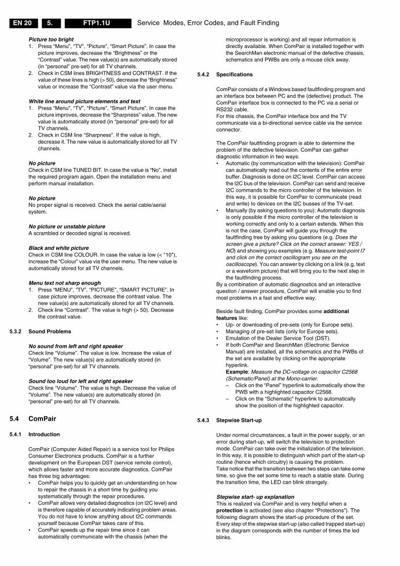
5.4.3 Stepwise Start-up
Under normal circumstances, a fault in the power supply, or an error during start-up, will switch the television to protection mode. ComPair can take over the initialization of the television. In this way, it is possible to distinguish which part of the start-up routine (hence which circuitry) is causing the problem. Take notice that the transition between two steps can take some time, so give the set some time to reach a stable state. During the transition time, the LED can blink strangely.
Stepwise start- up explanationThis is realized via ComPair and is very helpful when a protection is activated (see also chapter “Protections”). The following diagram shows the start-up procedure of the set. Every step of the stepwise start-up (also called trapped start-up) in the diagram corresponds with the number of times the led blinks.
Service Modes, Error Codes, and Fault Finding EN 21FTP1.1U 5.
Figure 5-1 Stepwise start-up diagram.
Step 1
Step 2
+5V and +8V is switched on
Put Stand-by line LOW
Keep sound amplifiers muted withsound enable = high
+8V and +5V get their nominallevel, detected by the OTC
Initialize EPLD
Activate protection algorithms for +8V and +5Vand I²C (start I²C protection the moment the
component is initialised).
Activate MSP reset
Initialize 3D Combfilter (USonly)
Initialize HIP: IF, source selection, 2fh input, video processingSwitch on the syncoutput: set_syncout_tristate= off
t<1500ms
Initialize PICNIC
Stand-bystart time extraction
stand-by bit = off t<500ms
Read NVM identificationenable watchdog
Semi stand-by
yes
Switch On PDP or
Initialize PDP
ON
OFF
OTC gets supply voltage
ON/OFF switch to ON
Start time extraction
Initialize tuner
Deactivate reset MSP andInitialize MSP
Stand-by bit set ?
OTC resets, Initialise IOpins
t<250ms
t>400ms
Step 3
Step 5
no
Read rest of NVM information
CL 36532053_064.eps221003
Service Modes, Error Codes, and Fault FindingEN 22 FTP1.1U5.
Note (*):• When the set is in stepwise mode and, due to stepping-up,
a protection is activated, the set will really go into protection (blinking LED). The set will not leave the stepwise-mode however. If state X is the state where the set went to protection, stepwise start-up will return to state X-1. At state (X-1) diagnostic measurements can be performed. Also, in the short time the set is in state X but not yet in protection, you can also do some measurements.
5.4.4 How To Connect
1. First, install the ComPair Browser software (see the Quick Reference Card for installation instructions).
2. Connect the RS232 interface cable between a free serial (COM) port of your PC and the PC connector (marked with “PC”) of the ComPair interface.
3. Connect the mains adapter to the supply connector (marked with “POWER 9V DC”) of the ComPair interface.
4. Switch the ComPair interface “OFF”.5. Switch the television set “OFF” with the mains switch.6. Connect the ComPair interface cable between the
connector on the rear side of the ComPair interface (marked with “I2C”) and the ComPair (or Service) connector at the rear side of the TV.
7. Plug the mains adapter in a mains outlet, and switch the interface “ON”. The green and red LEDs light up together. The red LED extinguishes after approx. 1 second while the green LED remains lit.
8. Start the ComPair program and read the “Introduction” chapter.
Figure 5-2 ComPair interface connection
5.4.5 How To Order
ComPair order codes:• ComPair Software: ST4191.• ComPair Interface Box: 4822 727 21631.• AC Adapter: T405-ND.• ComPair Quick Start Guide: ST4190.• ComPair firmware upgrade IC: 3122 785 90510
Note: If you encounter any problems, contact your local support desk.
5.5 Error Codes
5.5.1 Introduction
The error code buffer contains all detected errors since the last time the buffer was erased. The buffer is written from left to right, new errors are logged at the left side, and all other errors shift one position to the right. When an error has occurred, the error is added to the list of errors, provided the list is not full or the error is a protection error. When an error occurs and the error buffer is full, then the new error is not added, and the error buffer stays intact (history is maintained), except when the error is a protection error. To prevent that an occasional error stays in the list forever, the error is removed from the list after 50+ operation hours.
When multiple errors occur (errors occurred within a short time span), there is a high probability that there is some relation between them.
5.5.2 How to read the Error Buffer
Use one of the following methods:• On screen via the SAM (only if you have a picture).
Examples:– 0 0 0 0 0: No errors detected– 6 0 0 0 0: Error code 6 is the last and only detected error– 9 6 0 0 0: Error code 6 was first detected and error code
9 is the last detected error• Via the blinking LED procedure (when you have no picture).
See next paragraph.• Via ComPair.
5.5.3 How to clear the Error Buffer
Use one of the following methods:• By activation of the “RESET ERROR BUFFER” command
in the SAM menu.• With a normal RC, key in sequence “MUTE” followed by
“062599” and “OK”.• When you transmit the commands “DIAGNOSE” - “99” -
“OK” with ComPair (or with a DST).• If the content of the error buffer has not changed for 50+
hours, it resets automatically.
5.5.4 Error Codes
In case of non-intermittent faults, clear the error buffer before you begin the repair. This to ensure that old error codes are no longer present. Before clearing the buffer, write down the content, as this history can give you significant information. If possible, check the entire contents of the error buffer. In some situations, an error code is only the result of another error code and not the actual cause (e.g., a fault in the protection detection circuitry can also lead to a protection). There are various errors:• I2C device errors.• I2C bus errors.• Protection errors.• Errors not related to an I2C device, but of importance:
– FALCONIC (ERROR 26): at start-up, after initialization of the PICNIC, the presence of the FALCONIC can be checked.
– EAGLE (ERROR 27): at start-up, after initialization of the PICNIC, the presence of the Eagle can be checked.
CL36532075_063.eps260104
PC VCR I2CPower9V DC
TO SERVICECONNECTOR
Service Modes, Error Codes, and Fault Finding EN 23FTP1.1U 5.
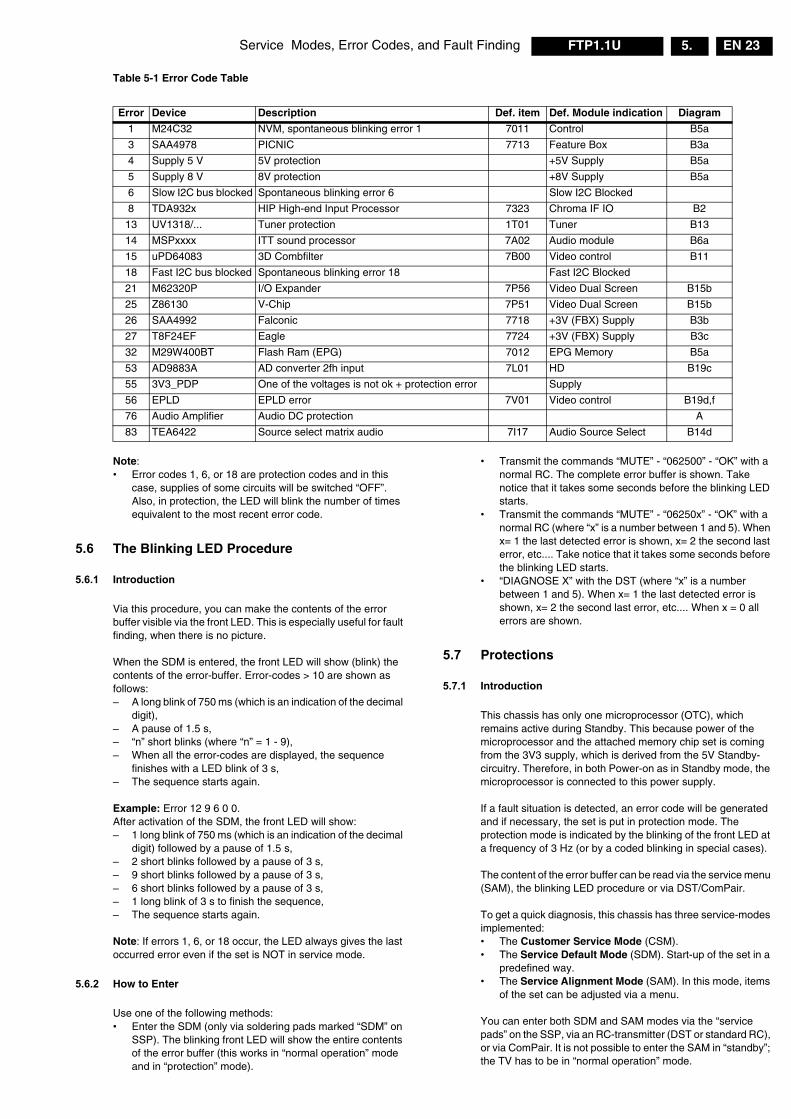
Table 5-1 Error Code Table
Note: • Error codes 1, 6, or 18 are protection codes and in this
case, supplies of some circuits will be switched “OFF”. Also, in protection, the LED will blink the number of times equivalent to the most recent error code.
5.6 The Blinking LED Procedure
5.6.1 Introduction
Via this procedure, you can make the contents of the error buffer visible via the front LED. This is especially useful for fault finding, when there is no picture. When the SDM is entered, the front LED will show (blink) the contents of the error-buffer. Error-codes > 10 are shown as follows:– A long blink of 750 ms (which is an indication of the decimal
digit),– A pause of 1.5 s,– “n” short blinks (where “n” = 1 - 9),– When all the error-codes are displayed, the sequence
finishes with a LED blink of 3 s,– The sequence starts again. Example: Error 12 9 6 0 0. After activation of the SDM, the front LED will show: – 1 long blink of 750 ms (which is an indication of the decimal
digit) followed by a pause of 1.5 s,– 2 short blinks followed by a pause of 3 s,– 9 short blinks followed by a pause of 3 s,– 6 short blinks followed by a pause of 3 s,– 1 long blink of 3 s to finish the sequence,– The sequence starts again. Note: If errors 1, 6, or 18 occur, the LED always gives the last occurred error even if the set is NOT in service mode.
5.6.2 How to Enter
Use one of the following methods:• Enter the SDM (only via soldering pads marked “SDM” on
SSP). The blinking front LED will show the entire contents of the error buffer (this works in “normal operation” mode and in “protection” mode).
• Transmit the commands “MUTE” - “062500” - “OK” with a normal RC. The complete error buffer is shown. Take notice that it takes some seconds before the blinking LED starts.
• Transmit the commands “MUTE” - “06250x” - “OK” with a normal RC (where “x” is a number between 1 and 5). When x= 1 the last detected error is shown, x= 2 the second last error, etc.... Take notice that it takes some seconds before the blinking LED starts.
• “DIAGNOSE X” with the DST (where “x” is a number between 1 and 5). When x= 1 the last detected error is shown, x= 2 the second last error, etc.... When x = 0 all errors are shown.
5.7 Protections
5.7.1 Introduction
This chassis has only one microprocessor (OTC), which remains active during Standby. This because power of the microprocessor and the attached memory chip set is coming from the 3V3 supply, which is derived from the 5V Standby-circuitry. Therefore, in both Power-on as in Standby mode, the microprocessor is connected to this power supply. If a fault situation is detected, an error code will be generated and if necessary, the set is put in protection mode. The protection mode is indicated by the blinking of the front LED at a frequency of 3 Hz (or by a coded blinking in special cases). The content of the error buffer can be read via the service menu (SAM), the blinking LED procedure or via DST/ComPair. To get a quick diagnosis, this chassis has three service-modes implemented:• The Customer Service Mode (CSM).• The Service Default Mode (SDM). Start-up of the set in a
predefined way.• The Service Alignment Mode (SAM). In this mode, items
of the set can be adjusted via a menu. You can enter both SDM and SAM modes via the “service pads” on the SSP, via an RC-transmitter (DST or standard RC), or via ComPair. It is not possible to enter the SAM in “standby”; the TV has to be in “normal operation” mode.
Error Device Description Def. item Def. Module indication Diagram
1 M24C32 NVM, spontaneous blinking error 1 7011 Control B5a
3 SAA4978 PICNIC 7713 Feature Box B3a
4 Supply 5 V 5V protection +5V Supply B5a
5 Supply 8 V 8V protection +8V Supply B5a
6 Slow I2C bus blocked Spontaneous blinking error 6 Slow I2C Blocked
8 TDA932x HIP High-end Input Processor 7323 Chroma IF IO B2
13 UV1318/... Tuner protection 1T01 Tuner B13
14 MSPxxxx ITT sound processor 7A02 Audio module B6a
15 uPD64083 3D Combfilter 7B00 Video control B11
18 Fast I2C bus blocked Spontaneous blinking error 18 Fast I2C Blocked
21 M62320P I/O Expander 7P56 Video Dual Screen B15b
25 Z86130 V-Chip 7P51 Video Dual Screen B15b
26 SAA4992 Falconic 7718 +3V (FBX) Supply B3b
27 T8F24EF Eagle 7724 +3V (FBX) Supply B3c
32 M29W400BT Flash Ram (EPG) 7012 EPG Memory B5a
53 AD9883A AD converter 2fh input 7L01 HD B19c
55 3V3_PDP One of the voltages is not ok + protection error Supply
56 EPLD EPLD error 7V01 Video control B19d,f
76 Audio Amplifier Audio DC protection A
83 TEA6422 Source select matrix audio 7I17 Audio Source Select B14d
Service Modes, Error Codes, and Fault FindingEN 24 FTP1.1U5.
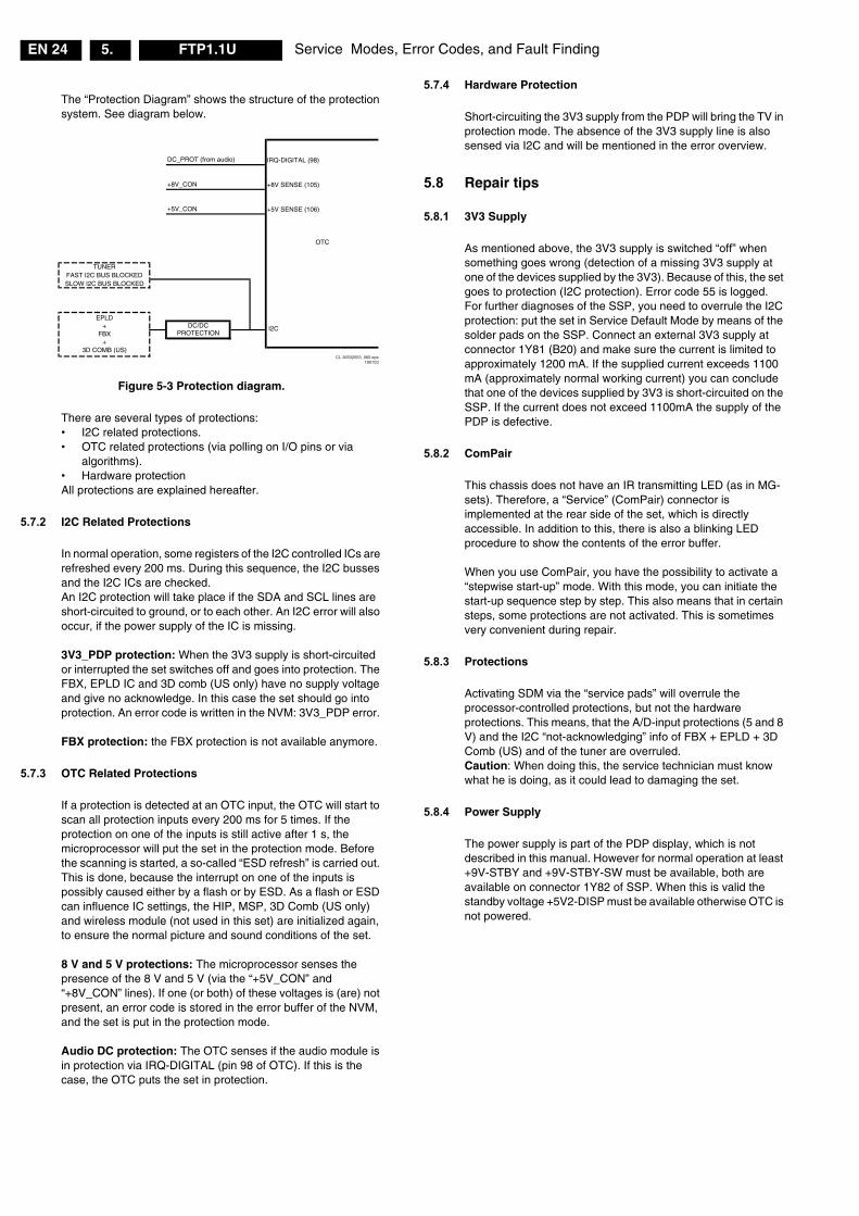
The “Protection Diagram” shows the structure of the protection system. See diagram below.
Figure 5-3 Protection diagram.
There are several types of protections:• I2C related protections.• OTC related protections (via polling on I/O pins or via
algorithms).• Hardware protectionAll protections are explained hereafter.
5.7.2 I2C Related Protections
In normal operation, some registers of the I2C controlled ICs are refreshed every 200 ms. During this sequence, the I2C busses and the I2C ICs are checked. An I2C protection will take place if the SDA and SCL lines are short-circuited to ground, or to each other. An I2C error will also occur, if the power supply of the IC is missing. 3V3_PDP protection: When the 3V3 supply is short-circuited or interrupted the set switches off and goes into protection. The FBX, EPLD IC and 3D comb (US only) have no supply voltage and give no acknowledge. In this case the set should go into protection. An error code is written in the NVM: 3V3_PDP error. FBX protection: the FBX protection is not available anymore.
5.7.3 OTC Related Protections
If a protection is detected at an OTC input, the OTC will start to scan all protection inputs every 200 ms for 5 times. If the protection on one of the inputs is still active after 1 s, the microprocessor will put the set in the protection mode. Before the scanning is started, a so-called “ESD refresh” is carried out. This is done, because the interrupt on one of the inputs is possibly caused either by a flash or by ESD. As a flash or ESD can influence IC settings, the HIP, MSP, 3D Comb (US only) and wireless module (not used in this set) are initialized again, to ensure the normal picture and sound conditions of the set. 8 V and 5 V protections: The microprocessor senses the presence of the 8 V and 5 V (via the “+5V_CON” and “+8V_CON” lines). If one (or both) of these voltages is (are) not present, an error code is stored in the error buffer of the NVM, and the set is put in the protection mode. Audio DC protection: The OTC senses if the audio module is in protection via IRQ-DIGITAL (pin 98 of OTC). If this is the case, the OTC puts the set in protection.
5.7.4 Hardware Protection
Short-circuiting the 3V3 supply from the PDP will bring the TV in protection mode. The absence of the 3V3 supply line is also sensed via I2C and will be mentioned in the error overview.
5.8 Repair tips
5.8.1 3V3 Supply
As mentioned above, the 3V3 supply is switched “off” when something goes wrong (detection of a missing 3V3 supply at one of the devices supplied by the 3V3). Because of this, the set goes to protection (I2C protection). Error code 55 is logged.For further diagnoses of the SSP, you need to overrule the I2C protection: put the set in Service Default Mode by means of the solder pads on the SSP. Connect an external 3V3 supply at connector 1Y81 (B20) and make sure the current is limited to approximately 1200 mA. If the supplied current exceeds 1100 mA (approximately normal working current) you can conclude that one of the devices supplied by 3V3 is short-circuited on the SSP. If the current does not exceed 1100mA the supply of the PDP is defective.
5.8.2 ComPair
This chassis does not have an IR transmitting LED (as in MG-sets). Therefore, a “Service” (ComPair) connector is implemented at the rear side of the set, which is directly accessible. In addition to this, there is also a blinking LED procedure to show the contents of the error buffer. When you use ComPair, you have the possibility to activate a “stepwise start-up” mode. With this mode, you can initiate the start-up sequence step by step. This also means that in certain steps, some protections are not activated. This is sometimes very convenient during repair.
5.8.3 Protections
Activating SDM via the “service pads” will overrule the processor-controlled protections, but not the hardware protections. This means, that the A/D-input protections (5 and 8 V) and the I2C “not-acknowledging” info of FBX + EPLD + 3D Comb (US) and of the tuner are overruled. Caution: When doing this, the service technician must know what he is doing, as it could lead to damaging the set.
5.8.4 Power Supply
The power supply is part of the PDP display, which is not described in this manual. However for normal operation at least +9V-STBY and +9V-STBY-SW must be available, both are available on connector 1Y82 of SSP. When this is valid the standby voltage +5V2-DISP must be available otherwise OTC is not powered.
DC_PROT (from audio) IRQ-DIGITAL (98)
+8V_CON +8V SENSE (105)
+5V_CON +5V SENSE (106)
OTC
TUNERFAST I2C BUS BLOCKEDSLOW I2C BUS BLOCKED
DC/DC I2CPROTECTION
EPLD+
FBX+
3D COMB (US)CL 36532053_065.eps
100703
Service Modes, Error Codes, and Fault Finding EN 25FTP1.1U 5.
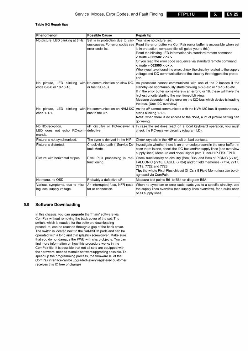
Table 5-2 Repair tips
5.9 Software Downloading
In this chassis, you can upgrade the “main” software via ComPair without removing the back cover of the set. The switch, which is needed for the software downloading procedure, can be reached through a gap of the back cover. The switch is located next to the SAM/SDM pads and can be operated with a long and thin (plastic) screwdriver. Make sure that you do not damage the PWB with sharp objects. You can find more information on how this procedure works in the ComPair file. It is possible that not all sets are equipped with the hardware, needed to make software upgrading possible. To speed up the programming process, the firmware IC of the ComPair interface can be upgraded (every registered customer receives this IC free of charge)
Phenomenon Possible Cause Repair tip
No picture, LED blinking at 3 Hz. Set is in protection due to vari-ous causes. For error codes seeerror-code list.
You have no picture, so:Read the error buffer via ComPair (error buffer is accessible when setis in protection, compare-file will guide you to this)Read the blinking LED information via standard remote command < mute > 06250x < ok >.Or you read the error code sequence via standard remote command < mute > 062500 < ok >.When you have found the error, check the circuitry related to the supplyvoltage and I2C-communication or the circuitry that triggers the protec-tion.
No picture, LED blinking withcode 6-6-6 or 18-18-18.
No communication on slow I2C-or fast I2C-bus.
As processor cannot communicate with one of the 2 busses it thestandby-led spontaneously starts blinking 6-6-6-etc or 18-18-18-etc...If in the error buffer somewhere is an error 6 or 18, these will have thehighest priority starting the mentioned blinking. Measure dependent of the error on the I2C-bus which device is loadingthe bus. (Use I2C-overview)
No picture, LED blinking withcode 1-1-1.
No communication on NVM-I2Cbus to the uP.
As the uP cannot communicate with the NVM I2C bus, it spontaneouslystarts blinking 1-1-1. Note: when there is no access to the NVM, a lot of picture setting cango wrong.
No RC-reception. LED does not echo RC-com-mands.
uP circuitry or RC-receiver isdefective.
In case the set does react on a local keyboard operation, you mustcheck the RC-receiver circuitry (diagram LD).
Picture is not synchronised. The sync is derived in the HIP. Check crystals in the HIP circuit on bad contacts.
Picture is distorted. Check video-path in Service De-fault Mode.
Investigate whether there is an error code present in the error buffer. Incase there is one, check the I2C-bus and/or supply lines (see overviewsupply lines).Measure and check signal path Tuner-HIP-FBX-EPLD.
Picture with horizontal stripes. Pixel Plus processing is mal-functioning.
Check functionality on circuitry (B3a, B3b, and B3c) of PICNIC (7713),FALCONIC (7718, EAGLE (7724) and/or field memories (7714, 7717,7719, 7722 and 7723.Tip: the whole Pixel Plus chipset (3 ICs + 5 Field Memories) can be di-agnosed via ComPair.
No menu, no OSD. Probably a defective uP. Measure test points B61to B64 on diagram B5A.
Various symptoms, due to miss-ing local supply voltage.
An interrupted fuse, NFR-resis-tor or connection.
When no symptom or error code leads you to a specific circuitry, usethe supply lines overview (see supply lines overview), for a quick scanof all supply lines.

Service Modes, Error Codes, and Fault FindingEN 26 FTP1.1U5.
Personal Notes:
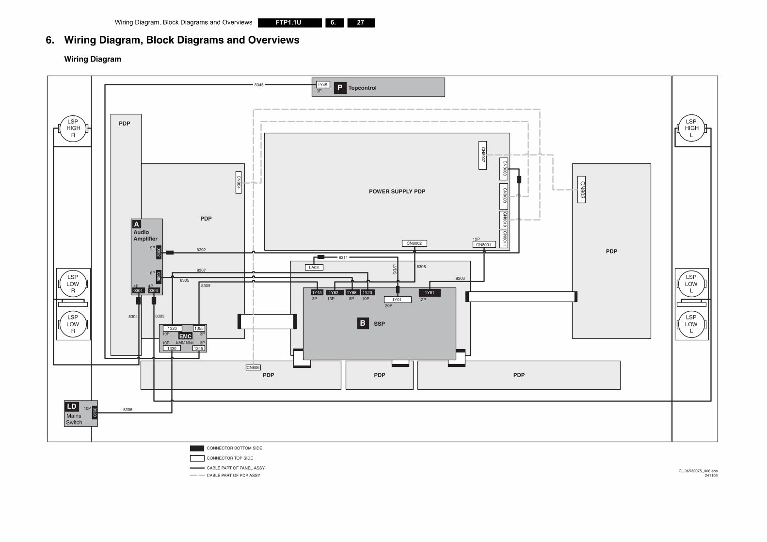
Wiring Diagram, Block Diagrams and Overviews 27FTP1.1U 6.
PDP
CN
803
CL 36532075_006.eps241103
LSPHIGH
L
LSPLOW
L
LSPLOW
L
0320
8306LDMainsSwitch
10P
CONNECTOR BOTTOM SIDE
CONNECTOR TOP SIDE
CABLE PART OF PANEL ASSY
CABLE PART OF PDP ASSY
6. Wiring Diagram, Block Diagrams and Overviews
Wiring Diagram
PDP PDP PDP
interface board PDP/SSB
POWER SUPPLY PDP
SSP
1Y45 1Y82 1Y88 1Y20
1Y01
1Y81
03020388
AudioAmplifier
CN8001CN8002
LA03C
N8010
CN
8011
CN
8007
CN
8008C
N8003C
N804
CN806
9P
12P
LVD
S
8302
83058309
8307
83038304
8303
8308
B
EMC filter
1330 1345
13551320
P Topcontrol1Y45
20P
10P13P 8P3P
10P 3P
10P 3P
EMC
3P
12P
A
8P
0304 03034P4P
PDP
PDP
LSPHIGH
R
LSPLOW
R
LSPLOW
R
8311
8345
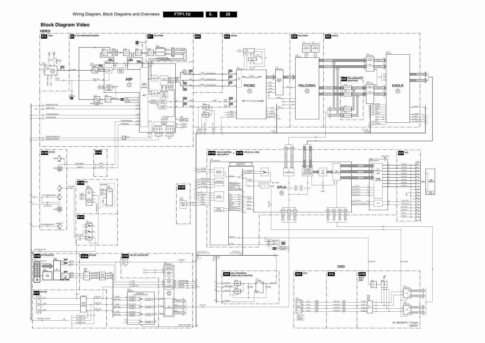
28FTP1.1U 6.Wiring Diagram, Block Diagrams and Overviews
GLE
2FH INTERFACE(BUFFERS)
B3D
FALREF
CLK32I
REFIN
Vref
INSTR1
SNDA
SNCL
CLK32E
Href
RSTR
CLK64
HD-E
VD-E
EAGLE
YGO (0-7)
7724TBF24EF
7V02DS90C385MTD
BUFFER
7743
A/D
DXB
DXA
7E16AD9066JR
BUFFER
7745
BUFFER
7742
BUFFER
7744
FM4(lower lines)
7722MS81V04160
ERR27
+VB
+3V3-EPLD
UVGO (0-7)
7723MS81V04160
YGO (0-7)
HVGO (0-7)
YF-BUFF (0-7)
UVF-BUFF (0-7)
OSD
-2FH (0-7)
-2FH (0-7)
EPLDOSD
B19E
11
OSDINSERTION
G-O
SD
(0-
5)
B-O
SD
(0-
5)
BL-
OS
D (
0-4)
TTLPARALLEL
toLVDS
LVDStransmitter
PLL
48
47
46
45
42
41
38
37
40
39
R (0-7)
G (0-7)
B (0-7)
45 25
U-VOUT (0-9)
Y-OUT (0-9)
G-OSD (0-5)
R-OSD (0-5)
A/D
DXB
DXA
7E09AD9066JR
BL-OSD (0-5)
B-OSD (0-5)
7E087E137E177E20
7E23 7E21
CLK-OSD
3705
6
1
1
11
6
11
2FHR-GFX R-OSD
37062FHG-GFX G-OSD
37072FHB-GFX B-OSD
3708FHFB-GFX BL-OSD
HD3-OTC
CL 36532075_113.eps020204
3703
2,5,11,18,19,20,23
18
19
20
2
11
23
5
FIELDMEMORY
FM5(lower lines)
FIELDMEMORY
17
16
14
15
22
CLOCK 32O
1
PARITY
55 27HS-OUT
54 28VS-OUT
49 30DE-OUT
50 31CLK-OUT
53 32LVDS-PWR-DOWN
VD-OTC
HD3-EPLD
VD-EPLD
TO OTC
B5A
B20
TXLCD0-
TXLCD0+
TXLCD1-
TXLCD1+
TXLCD2-
TXLCD2+
TXLCD3-
TXLCD3+
TXCLKLCD-
TXCLKLCD+
16
1Y01
15
13
12
1
14
17
20
10
9
4
3
7
6
SCL-DISP 19
SDA-DISP 20
VS-ON 11
PDP-GO 8
PDP-DISPLAY
I/O3
LVDSConn.
B3D
R/G/B-SC1-Y/U/V-IN 1FH
2FH I/O
B19A
B14C ERR53
7746CY23S02
2FH INTERFACE(ZERO DELAY BUFFER)
OTC
B3A
B19C
B5A B3ARGB/YUV/
MATRIX
SYNCPROC.
+CLOCK
GENERATOR
SERIALREGISTER
+POWER
MAN.
A/DCOVERTER
TXTOSD
SEE ALSOBLOCKDIAGRAMCONTROL
7D527D537D54
YPbPr/YUV
MATRIX
Y-VGA
U-VGA
V-VGA
Y-2
Y-2
Pb-2
Pr-2
R-VGA-BUF
G-VGA-BUF
B-VGA-BUF
SUB-Y-2FH7126:7131
SUB-U-2FH
SUB-V-2FH
SUB-Y-2FH
8
7
6
4
16
15
3
2
SUB-V-2FH
SUB-Y-2FH
SUB-U-2FH
V-VGA
Y-VGA
U-VGA
7D51TDA8601T
CLAMP
CLAMP3-STATE
RGB/YPbPrOUTPUT SELECTION
3-STATE
3-STATE
CLAMP
CLAMP
CLAMP
CLAMP
3-STATE
10
13
5
11
12
30
56
31
49
57
7L01AD9883AKST
67
2-9
70-77
12-19
65
64
66
CLK-2FH
SELECT-VGA-YPBPR
SYNCDET
V-2FH-AD-OUT
H-2FH-AD-OUT
H-DVI-BUF
8IN
FBIN
CLK-32ECLK-32P
2FH . 3FH
SWITCH-2FH
CLK-32O
CLK-32I
Y-AD (0-7)
UV-AD (0-7)
U-AD (0-7)V-2FH
Y-2FH
U-2FH
7747
2 2 OUT
1
4
1
7748
2 4
1
38483855
7001SAA5801H
3046-a77 R-TXT
3046-b78 G-TXT
3046-c79 B-TXT
3046-d80 FB-TXT 2
9, 10
2,3,4,13,16,17,19,20,21,212,23,26
23
2,3,4,9,10,11,16,17,18,19,20,21
3131822
6
26
13
3
18
22
7
8
9(2x)
10
SDA-F3
SCL-F3
IN-CVBS-SC1-AV1
SC1-R-IN-V-IN
SC1-G-IN-Y-IN
SC1-B-IN-U-IN
1
6
AV4
DVI RECEIVER DVI/RGB HDI A/D CONVERTERB19B7557SII905
DVIRECEIVER
7V26M24CO1
EDIDNVM B-DVI31
G-DVI26
R-DVI23
V-DVI19
H-DVI
V-DVI
H-DVI
18
18
9C
516
1724
1V21DVI-D CONNECTOR
DVI-SIGNALS
D7
D8
D11
D9 D10
7L03
SEE ALSOBLOCK DIAGRAM
CONTROL
Block Diagram Video
TUN1B13
1TO1UV1318ST
S-S
DA
S-S
CL
+33V
1410
AGCMONITOR
1406 7322
1411
18
CVBS-SC1-AV1-IN
CVBS-AV3-IN
Y-CVBS-SC2-AV2-IN
C-SC2-SVHS-IN 21
32
N.C.N.C.
34
SOUND BANDPASS4.5 MHz
SAW FILTERVIDEO
SOUNDFILTER4.5 MHz
CVBS-TXT
OTC
7323TDA9320H
PLLDEM
GROUPDELAYCOR.
VIDEOSWITCH
+CONTROL
QSSMIXER
AMDEMO
QSS-AM
QSS-AM
7,3
2
10 12 13 14
YPROC. Y/U/V
SWITCH
U U
YUV
V Y V
UY
R
SC
AR
T1
SC
AR
T2
V
Y
CPROC.
SYNCSEPAR.
61
60 HA50
VA50
515049
H-SYNCPROC.
V-SYNCPROC.
DECODERPAL
NTSCSECAM
C
3D-COMB
3
62
6364
5
TUNER
AGC1
7411
RGB/YUVMATRIX
7410
7415
L8
T1I5
V6
F14
20
I6Y5
TUNER AGC
SIF2SIF1
VIF1
VIF2
7320
12
84 Y
C8388
26 29
COUT-3D-COMB
COUT-3D-COMB
YOUT-3D-COMB
YOUT-3D-COMB
C Y28
7B00UPD64083CF 7B10
7740
7B09
7B02
G B
36 37 38 39
R G B
41 42 43 40
9
15
11
6TO8-/33
4
+5V
1 IF-TER
V2
16
SEEBLOCK DIAGRAMAUDIO
23
24
IF, I/O VIDEOPROCESSINGB2
ERR8
ERR13
B6AB5A
B5A
Y-CVBS-FRONT-IN
C-FRONT-IN
CVBS-SC2-MON-OUT
SC1-CVBS
R/G/B-SC1-Y/U/V-IN
VIDEO
Y50
7414
U50
V50
Y-PIP+MAIN-OUT
U-PIP+MAIN-OUT
V-PIP+MAIN-OUT
V8
V7
HIP
B6A3D-COMBB11 PICNICB3A FALCONICB3B EAB3C
57
46
47
1308
3.57MHz
NTSC M
SCL-F
SDA-F
SCL-F
SDA-F
INTR1
FIELDMEMORY
FM1
SNDAREF
SNCL
Href-EXT
CLK 32P
23
64KPROM
25
SYNC PROCESSING
DIGITALSIGNAL PROCESSING
PICNIC FALCONIC
3xADC
26
28
292 4
1
LATCH
771274HC573D
7713SAA4978H
7711M27C512
7714MS81V04160
3727
3722
HA50
L10
L6
L7
L8
L11
ERR3
4
5
CLI6
WEC
RSTW
RSTR
RNRST
CLK-64
CLK-VID
SDA-F3
CLK-2FH
DA (0-15)
7718SAA4992
FIELDMEMORY
3
7717MSM54V12222A
FIELDMEMORY
2
7717MSM54V12222A
ERR26
ERR??
7V01EP1C12Q240C0
7E02EPCS1
7741
2 4
1
5T02
EPLDERR56
UV
Y
B14B
SC1-CVBS
B14A
AV3-CVBS-IN
C-AV3-IN
I/O
I/O US EPLD I/O+ LVDSEPLD CONTROLAND SUPPLY
B15B
B19D
B19D
B19F
B14C
9
10
11
12
3
I/OEXP
7P56M62320
2
5
2
13
4
15
14
3
1
12
7I3274HC4053
14V-CHIP
7P51Z86130
15
3
5
S-SDA
OPTIONAL
S-SCL
S-SDA
S-SCL
SW
ITC
H-H
EF
9I02
9I00
1:2
CLOCKSWITCH
STANDARDDEFLECTION
INPUTCONTROL
SYNCCONTROL
EPLDFLASHRAM
YUVto
RGB
CLKP
UV DEMUXCONTRAST
SATURATIONBRIGHTNESS
PATHFOR3FH
ONLY
PATHFOR
1FH, 2FHONLY
UVCONVERTION
Y-O
UT
(0-
9)
U-V
OU
T (
0-9)
R-O
SD
(0-
5)
CLK-2FH
CLK-32P
Href-EXT
Href-EXT
VA
HD-E
VD-E
DATA
CLOCK
H-2FH-AD-OUT
V-2FH-AD-OUT
SYNCDET
MF (1-17)
Y-2F
H (
0-7)
UV
-2F
H (
0-7)
UV-2FH (0-7)
Y-2FH (0-7)
YF (0-7)
UVF (0-7)
9A04
9A05
9A06
1
NC.
3
4
5
6
3
4
FEA
SNDA
SNCL
1
2
30
12
21
13(2x)
89
12,21
3704
2 31 4 5
VR
EF
VA
SW
ITC
H_1
FH
SW
ITC
H_2
FH
+
9
6
13
7
8
1
12
14
15
26
2
6
SUPPLY
SCL-F3
SN-CL
SN-DA
CLK
-OS
D
CLK-32I
HD3-OTC
PWR-OK-PDP
LCD-PWR-ON
LAMP-ON
SELECT-VGA-YPBPR
10
18(2x)
16
9
Vref
2(2x)Href
11RSTR
17
21
19
20
REF
FALREF
REFIN
SWITCH-1FH
4SWITCH-2FH
3(2x)
CLKP
U-A
D (
0-7)
UV
-AD
(0-
7)
Y-A
D (
0-7)
IN-Y-CVBS-SC2-AV2
15
SVHS
2
43
AV1
AV3
CVBS
SC2-CVBS-MON-OUT5 MON-OUT
AV2
Y-2
4
SC2-R-C-IN
25
SVHS1
34
Wiring Diagram, Block Diagrams and Overviews 29FTP1.1U 6.
CL 36532075_115.eps040204
7D57
7D51
7D59
7132
7007
DRAMTXT
FLASHRAMEPG
NVM(OTC)
BUFFER
1409
SC1/SC4 AUDIO INPUT-SWITCH
7012
7011
7743
7718
7722
7724
FM4
CONIC EAGLE
7745
A07
7307
7107
7120
REG.SWITCH
I/O EXP.
V-CHIP.
7P567P51
COMBFILTER
1119CONNECTOR
I6
1V / div DC10us / div
PM3394B L8
1V / div DC20us / div
L6
500mV / div DC10us / div
PM3394B L7
500mV / div DC10us / div
PM3394B L9
1V / div DC250ns / div
PM3394B
iv AC div
1T01
1S36 1S46 1S88 1S20
TUNER
T1
V2
1V / div DC10us / div
PM3394B V5
1V / div DC10us / div
PM3394B V8
1V / div DC20us / div
PM3394BV7
500mV / div DC20us / div
PM3394BV6
500mV / div DC20us / div
PM3394B V9
2V / div DC200us / div
PM3394B V10
2V / div DC200us / div
PM3394B
F14
1V / div DC5ms / div
L10
1V / div DC20us / div
B51
2V / div DC100us / div
PM3394B B52
2V / div DC100us / div
PM3394B B53
2V / div DC5ms / div
PM3394B B54
2V / div DC5ms / div
PM3394B B55
2V / div DC250ns / div
PM3394B B57
500mV / div AC10us / div
PM3394B B58
1V / div DC5ms / div
PM3394B B60
500mV / div DC10us / div
PM3394B
1U05
5 V / div DC5µs / div
1U06
5 V / div DC5µs / div
200mV / div AC10µs / div
T1
B65
200mV / div AC10µs / div
B69
20mV / div AC1ms / div
B68
20mV / div AC1ms / div
20mV / div AC1ms / div
B67
20mV / div AC1ms / div
B66
20mV / d10µs /
I5
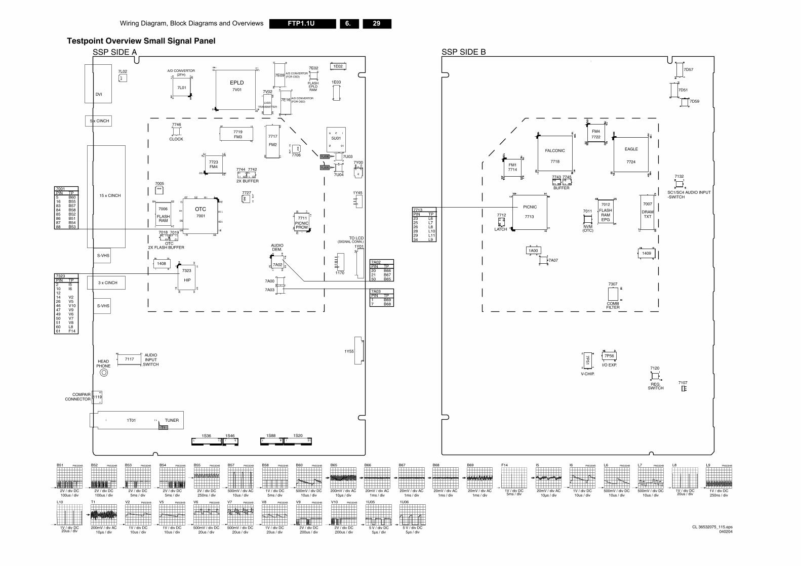
Testpoint Overview Small Signal PanelSSP SIDE A SSP SIDE B
7001PIN TP5 B6016 B5583 B5784 B5885 B5286 B5187 B5488 B53
7323PIN TP2 I510 I61214 V226 V546 V1047 V949 V650 V751 V860 L861 F14
7A03PIN TP1 B697 B68
7A02PIN TP20 B6621 B6750 B65
7713PIN TP23 L625 L726 L828 L1029 L1134 L9
FM1
FAL
PICNIC
LATCH
7714
77137712
1A00
7
1U06
1U05
1E02
1E03
5U01
7U03
7U04
7E02
FLASHEPLDRAM
7Y00
1Y45
7706
7717
FM2
7V02
LVDS
TRANSMITTER
7V01
EPLD
7E16
7E09
7719FM3
7723FM4
7744 7742
BUFFER
7727
7001
OTC
7746
CLOCK
7005
7006
FLASHRAM
7L02
7L01
A/D CONVERTOR(2FH)
A/D CONVERTOR(FOR OSD)
A/D CONVERTOR(FOR OSD)
3 x CINCH
HEADPHONE
15 x CINCH
S-VHS
2X
2X
5 x CINCH
1408
7323
HIP
OTCFLASH BUFFER
7018 7019
7117AUDIOINPUT
SWITCH
COMPAIR
1Y55
1170
1Y01
TO LCD(SIGNAL CONN.)
7711PICNICPROM
7A02
AUDIODEM.
7A00
7A03
DVI
S-VHS
30FTP1.1U 6.Wiring Diagram, Block Diagrams and Overviews
A3
CL 36532075_114.eps030204
DC-PROTECTCIRCUIT
F328
F428
F528
F735
F730
F231
F241
F211
F245
F245
F245
F248F330
F365
5335
3318
3315
3328
7330
7355
27
87315LM311D
AUDIO AMPL- L-HIGH
A4 AUDIO AMPL- L-LOW
A5 AUDIO AMPL- R-HIGH
A6 AUDIO AMPL- R-LOW
VCC-10-POS
VCC-10-NEG3355
3330
5366
7340
OUT_LH
OUT_LL
OUT_RH
OUT_RL
3337
VSND-POS
L-HIGH
L-LOW
VSND-NEG
OUT_PROT
73021,4
3
3
7260-ALM833DT
2
3259
+9V-STBY
VSND-POS
2330
3362
7365-2IRF7343
7365-1IRF7343
23552355
5365
D
SG
D
SG
F430F465
5435
3418
3428
34157430
7455
27
87415LM311D
L-HIGH1
AU-EN-NOT
3
7238-ALM833DT
2
3234
L-LOW1
5
7260-BLM833DT
6
3274
R-HIGH7
5
7238-BLM833DT
6
3244
L-HIGH7
VCC-10-POS
VCC-10-NEG
+9V-STBY A
3455
3430
5460
3437
VSND-POS
VSND-NEG
74021,4
3
2430
3462
7465-2IRF7343
7465-1IRF7343
24652455
5465
D
SG
D
SG
F530F565
5535
3518
3515
3528
7530
7555
27
87515LM311D
VCC-10-POS
VCC-10-NEG3555
3530
5560
3537
VSND-POS
TOCN8003POWERSUPPLY
VSND-NEG
75021,4
3
2530
3552
7565-2IRF7343
7565-1IRF7343
25652555
5565
D
SG
D
SG
F628
F630F665
5335
3618
3628
36157630
7655
27
87615LM311D
A7 SUPPLY & DC-PROTECTION
VCC-10-POS
VCC-10-NEG3655
3630
5660
3637
VSND-POS
VSND-NEG
76021,4
3
2630
3662
7665-2IRF7345
7665-1IRF7345
26652655
5665
D
SG
D
SG
0303
5
4
3
2
1
R-HIGH
R-LOW
0304
4
3
2
1
0302
9 DC-PROT
8
7
6
5
4
3
2
1
A3
A4
A5
A6
A7
VCC-10-POS
1730
7735,7736
7745,7746
STAB
STAB
2.5A
F740
F745
VSND-NEG
VCC-10 -NEG
1740
2.5A
OUT_LH
OUT_LL
OUT_RH
OUT_RL
OUT_PROT
7440
OUT_PROTA7
7540
OUT_PROTA7
7640
OUT_PROTA7
3220
3240
5753
96IRQ-FTVN.C.
N.C. 115
117 SEL_IN_2
N.C.CONTROL
+5V2
EPG-FLASH-RAM
4Mbit
AUXILIARYFLASH
PROGRAMCIRCUIT
FORFLASH RAMB55
OTC-FLASHB5C
3
2
1
1402
PROGRAMCONNECTOR
74LVC245APW 74LVC245APW
7010113
ON-OFF-LED
107KEYBOARD
LIGHTSENSOR 110
100RC+3V3
LED GREEN
116
N.C.
N.C.
N.C.
91 SDA
92
5
6
SCL
16
1710016Mhz
SEL_IN_1
7006LH28F320BJE
7007MSM51V18165F
7012M29W400BT
70187019
103 PWW-BLACKLIGHT
118 AUD-PWB-CTRL
ADDRESS
DATA
CONTROL
RP
DRAM(TXT)16Mbit
PROGRAMFLASH-RAM
SET SW32Mbit
7011MC24C32
EEPROMNVM.
4kByte
ERR1
ERR32
(OCTAL BUS TRANSCEIVER)
3S147S02
3S13
5S06
5S07
5S08
LED PANELLD
LIGHT_SENSOR
RC
3IB9
0320 1330 1320
RED
GREEN
RCRECEIVER
ON/OFFSWITCH
IY20
1
2
2
3
7
3
2
1
6
5
4
1
2
4
7103
6103
6127
7120
71077105
3
4
5
6
7
8
9
10
1
10
1
10
1N.C. N.C.
GREEN-LED
RED-LED
+8V6
LIGHT-SENSOR-IN
+9V-STBY
+9V-STBY-SW
RC-IN
2
3
4
5
6
7
8
9
10
+5V-STBY-SW+5VRELAYIO2
+5V2
+8V
1101
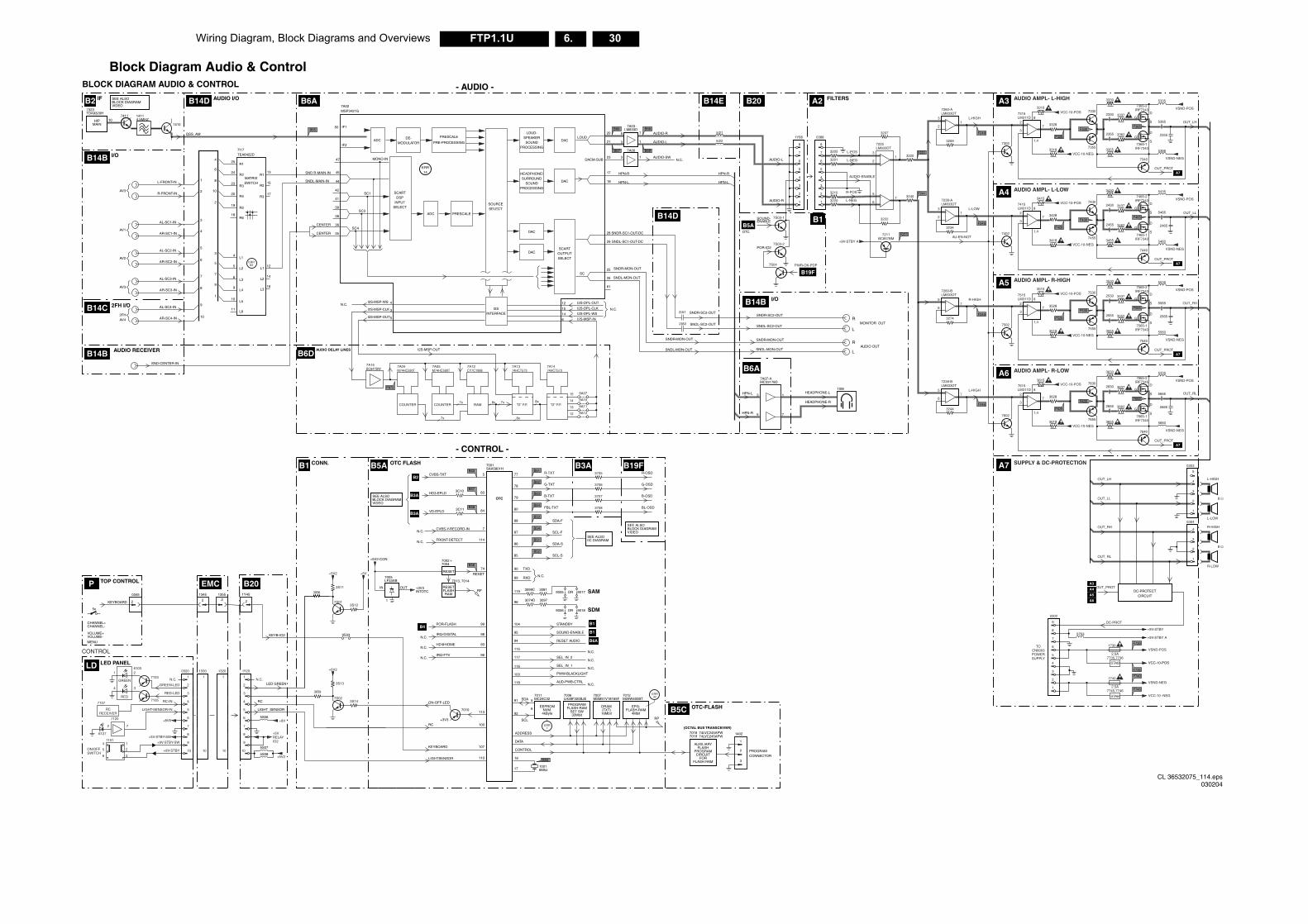
Block Diagram Audio & Control
7323TDA9320H
14114.5MHZ
QSS_AM
HIPMAIN
SEE ALSOBLOCK DIAGRAMVIDEO
IFB2
I/O
AUDIO RECEIVER
B14B
2FH I/OB14C
B14B
AUDIO I/OB14D FILTERS
B14B I/O
B6A
B6A B20B14E A2
B1B14D
10
B68
B69B67
B667410
7411
R-FRONT-IN
L-FRONT-IN
AL-SC1-IN
AV1
3
1
4
6
8
10
2
25
24
23
20
19
2
4
5
6
7
8
9
10
AR-SC1-IN
SND-CENTER-IN
SNDR-MON-OUT
SNDL-MON-OUTL
R
L
R
AL-SC2-IN
AR-SC2-IN
AL-SC3-IN
AR-SC3-IN
AL-SC4-IN
AR-SC4-IN
3
5
7
9
1
4
5
6
9
10
11
R1
7I17TEA6422D
R2
R3
13
15
45
47
IF1
7A02MSP3421G
IF2
50
44
SC3ADC
SC4
I2S-MSP-OUT
I2S-MSP-WS
I2S-MSP-CLK
I2S-DPL-OUT
I2S-DPL-CLK
I2S-DPL-WS
4
3
17
R1
R2
R3R4
R5
R6
MATRIXSWITCH
L1
L2
L3
L1
L2
L3L4
L5
L6
18
SND R-MAIN-IN
MONO-IN
SNDL-MAIN-IN
12
15
14
I2S-MSP-IN6
12
14
16
SCARTDSP
INPUTSELECT
CENTER
CENTER
N.C.
36
38
39
41
42
35
ERR83
SC1
N.C.
N.C.
SOURCESELECT
PRESCALE
I2SINTERFACE
DE-MODULATOR
ADC
ERR14
PRE-PROCESSING
PRESCALELOUD-
SPEAKERSOUND
PROCESSING
DAC
HEADPHONE/SURROUND
SOUNDPROCESSING
DAC
SCARTOUTPUTSELECT
DAC
DAC
LOUD
SC
20
21
23
17
18
DACM-SUB
7
1
AUDIO-R
AUDIO-L
AUDIO-R
SOUND-ENABLE
OTC
POR-IO2
AUDIO-LAUDIO-SW
HPN-R
HPN-L
HPN-R
HPN-L
28
25
26
61
SNDL-MON-OUT
SNDR-MON-OUT
SNDL-MON-OUT
SNDR-MON-OUT
SNDR-SC2-OUT
SNDL-SC2-OUT
SNDR-SC1-OUT-DC
SNDL-SC1-OUT-DC29
5
3
13
SNDR-SC2-OUT
MONITOR OUT
AUDIO OUT
SNDL-SC2-OUT
HPN-L
HPN-R
HEADPHONE-L
HEADPHONE-R
1I08
3
5
1
7
7A07-AMC33178D
7A03LM833D
7A00
2IA0
2IA1
B655I21
5I22
7S03-1
7S03-2
7S04
3
7225LM833DT
21
+9V-STBY A
PWR-OK-PDP
5
67
7211BC857BM
3205
3201
3215
3220
3705
0388
L-POS
L-NEG
AUDIO-ENABLE
R-POS
L-NEG
7
6
5
4
3
2
1
1Y88
7
88
6
5
4
3
2
1
3207
3222
B5A
B19F
SEE ALSOBLOCK DIAGRAMVIDEO
SEE ALSOBLOCK DIAGRAMVIDEO
OTC FLASHB5A
B6D
B3A B19FCONN.B1B2
B61B60
BLOCK DIAGRAM AUDIO & CONTROL
77
7001SAA5801H
5
OTC
CVBS-TXT
CVBS-Y-RECORD-IN
FRONT-DETECT
R-TXT
OUT +3V3INTOTC
N.C.
IN
+5V2-CON
B499POR-FLASH
98IRQ-DIGITAL
93HD@HOME
N.C.
B1
B1
B6A
B5884
7N.C.
N.C.114
RESET
B5674
RESET
B5783
B3A HD3-EPLD
B3A VD-EPLD
B6278 G-TXT
SEE ALSOIIC DIAGRAM
B6379 B-TXT
B6480 FBL-TXT
R-OSD
G-OSD
B-OSD
BL-OSD
B5388 SDA-F
B5487 SCL-F
B5186 SDA-S
B5285 SCL-S
104 STANDBY
90 TXD
89
119
96
RXD
90053099C 3081
3074D 3097
OR 9017
9006 OR 9018
SAM
SDM
95 SOUND-ENABLE
94 RESET AUDIO
RESETFLASHRAM
7002 :7004
7013, 7014
RP
1
7005LF33AB
3C10
3C11
3706
3707
3708
+5V2 +5V
3S127S01
3S11
9S33
AV3
AV2
AV3
2FHAV4
B20EMCTOP CONTROLP
KEYB-IO2
2
5x
KEYBOARD
MENU
CHANNEL+CHANNEL-
VOLUME+VOLUME-
0345
2
1Y451345 1355
2 2
3IB6
AUDIO DELAY LINES
13
7A04M74HC590T
7A15BC847BW
7A05M74HC590T
7A12CY7C1998
7x
7x
RAMCOUNTER COUNTER "D" F.F. "D" F.F.
7A1374HCT573
7A1474HCT573
8x7x8x
8x
I2S-MSP-OUT5
9A11
F872
12 9A12
14 9A10
15 9A07
- CONTROL -
- AUDIO -
Wiring Diagram, Block Diagrams and Overviews 31FTP1.1U 6.
I/O USB14B
B14E
H
1x
1x
2x
1x7x
2x
1x
1x1x1x
1x
1x
1x
5724
+5VA
Y 1x
1x
+5V2_RELAY_IO3
+5V2_RELAY_IO2
+5VA +5VA
1x
5E08 3E08
5E07 3E10
+5V_EPLD+5VA_OSD
+VB
5E00 3E04+VT
B19A
5D513D73
3D81
+8_VIDEO
REF2REF3
REF1
EPLD
EPLD OSD
B19F
+3V3-EPLD
+3V3-IO
+3V3-EPLD
+3V3-IO
6D93 6D64
6D62
B19E
HDI A/D CONVERTERB19C
5L07
5L13
5L09
5L14
5L11
5L15
+5V_EPLD
+5V
VD
+3V3_I2C
VD_1
VDD_1
PVD_1
VDD
PVD
+3V3-AD
7L02
EPLD CONTROLB19D
5E53+3V3_EPLD
+3V3-SIM
SD57+8V_EPLD
+8V_DISP
SD59
SD58 +5V_EPLD
+5V_DISP
+3V3_I2C+3V3_I2C
5E51+3V3_IO
+3V3_AD
+3V3_EPLD
+3V3_AD
+3V3_IO
5E59
5E50 +1V5
+1V5_PLA
7E051 3
3E18
3E147E18
4
3
7E244
3
CL 36532075_117.eps040204
+5V2
+9V
5I09+5V2_DISP
3ID66I055I10
3I31
+33V
5I06
5I05
91D1
91D2
+11V
+11V
+5V2
+8V_DISP +8V +8V
91D3
91D4
+9V_STBY
+5V
STANDBY_IO2 STANDBY_DISP
+3V3_PROTECT+3V3_PROTECT
3ID2
5I20
SUPPLY & DC PROTECTIONA7 FILTERSA2 :A3 A6
DVI RECEIVERDVI RGB B19B
5V30
5V25
5V21
3V3_AD
3V3_SI-IO
VCC_SI
3V3_TMDS
+3V3-AD
+3V3_I2C
4x
1x
1x
3x
1x
1x
2FH I/OB14C AUDIO I/OB14D
2FH INTERFACEB3D
77275742
5727
57265721
5748+3V3_FCD
+3V3_FC1
+3V3_FC2
+1V5_E
+1V5_FCA
+1V5_FCC
5743
5728
+2V5_E
+2V5_FCA
+2V5_FCD
5725
5722+2V5B
N.C.+8V_CON
+3V3A+3V3A
+3V3_FBX+3V3_FBX
+5V
+5V
+8V
+8V
+8VA+8VA
+11V
+11V_S+5V
3IB4
3IC1
7I07
3IB5
+5VIO+5V
3IN4
+11V_S
+11V
+9V+9V
7I09
1740
2A5
1730
2A5
5725
5335
0302
123456789
VSDN-NEG
+9V-STBY
Vcc-10-NEG
Vcc-10-POS+9V-STBY
Vcc-10-NEG
Vcc-10-POSVSDN-POS
VSDN-NEG
Vcc-10-NEG
Vcc-10-POS
VSDN-POS
DC-PROT
7745, 7746
7735, 7736
STAB
STAB
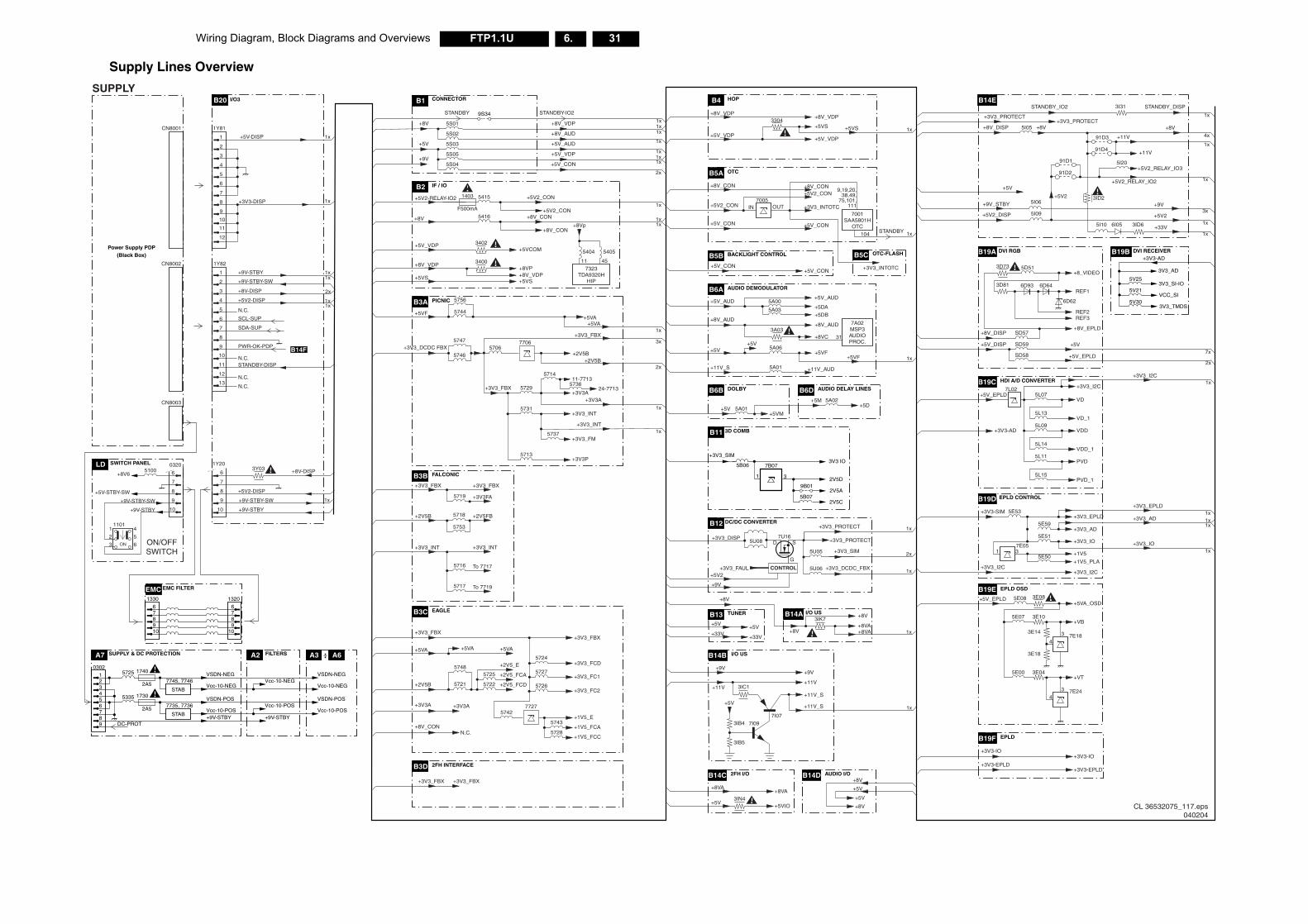
Supply Lines Overview
SWITCH PANELLD
DC/DC CONVERTERB12
IF / IO
CONNECTORI/O3
Power Supply PDP(Black Box)
B2
HOPB4
AUDIO DEMODULATORB6A
BACKLIGHT CONTROLB5B
TUNERB13
PICNICB3A
EAGLEB3C
FALCONICB3B
OTCB5A
OTC-FLASB5C
B20
ON/OFFSWITCH
0320
1101
ON
6
8
9
10
5100
+5V-STBY-SW
+8V6
+9V-STBY-SW
+9V-STBY
1403
F500mA
1
2
3
4
5
6
1Y81
1
2
3
4
5
6
7
+3V3-DISP
+5V-DISP
8
9
10
11
12
+9V-STBY
1Y20
6
77
8
9
10
1x
3x
2x
1x
1x
1x1x1x
1x
1x1x1x
2x
1x
1x1x
3A03
+5VA+5VF
+5VA
5744
+11V_AUD
5731+3V3_INT
+3V3_FBX
+3V3FA
+8V_AUD
5713
5737+3V3_FM
+3V3P
+3V3_FBX 5729
5714
5736
+3V3A
11-7713
24-7713
5416 +8V_CON
5415
+5V5A06
+5VF
+5DB
+5DA5756
7001SAA5801H
OTC
9,19,20,38,49,
75,101,111
+5V_CON
+5V2_CON+8V_CON
+3V3_INTOTC
B1
OUTIN +3V3_INTOTC
104
+8V_VDP3304
+5VS +5VS
+5V_VDP
7A02MSP3AUDIOPROC.7706
57065746
5747
5719
5753
+2V5FB
+2V5B+2V5B
+3V3_DCDC FBX
5718
31
5A01
5A01
5A00
5A03
7005
+8VC
+3V3_FBX
3400+8VP
3402+5VCOM
+5VS+8V_VDP
7323TDA9320H
HIP
5405
45
5404
11
+8Vp
+11V_S
+3V3_INT
+3V3A
+8V_AUD
+5V_AUD+5V_AUD
STANDB
STANDBY STANDBY-IO2
+5V+5VF
+8V
+5VS
+5V2-RELAY-IO2
+5V_CON
+5V2_CON
+8V_CON
+8V_VDP
+5V_VDP
+8V_VDP
+5V_VDP
+5V2+3V3_FAUL
+9V
+3V3_PROTECT
+3V3_PROTECT
I/O USB14A3IK7
+8VA
+8V
+8VA+8V
+3V3_FBX
+2V5B
+3V3_INT
+3V3_FBX
5716
5717
+3V3_INT
To 7717
To 7719
+3V3_FBX
+3V3_SIM
+3V3_DISP
5U05
7U165U08
+3V3_DCDC_FBX5U06
+5V+5V
+33V+33V
+5V_CON+5V_CON
DOLBYB6B
+5VM+5V
5A02
AUDIO DELAY LINESB6D
+5D+5M
5S01
5S02
5S03
+8V +8V_VDP
+8V_AUD
+5V_AUD
+5V_VDP
+5V_CON
+5V
1Y82
1
2
CN8001
CN8002
CN8003
3
4
5
6
7
+9V-STBY-SW
+8V-DISP
+5V2-DISP
N.C.
N.C.
SCL-SUP
SDA-SUP
PWR-OK-PDP
+8V-DISP
+5V2-DISP
+9V-STBY-SW
+9V-STBY
STANDBY-DISP
8
9
10
11
12
13N.C.
N.C.
3Y03
SUPPLY
1x1x
1x
1x
2x
1x1x
1x
5S05
5S04+9V
EMC FILTEREMC1330
678910
6789
10
1320
3D COMBB11
5B07
9B01
3V3 IO
2V5D
2V5A
2V5C
5B06 7B07
+3V3_SIM
1 3
CONTROL
D S
G
9S34
B14F
+5V2_CON
+5V2_CON
+8V_CON
+8V
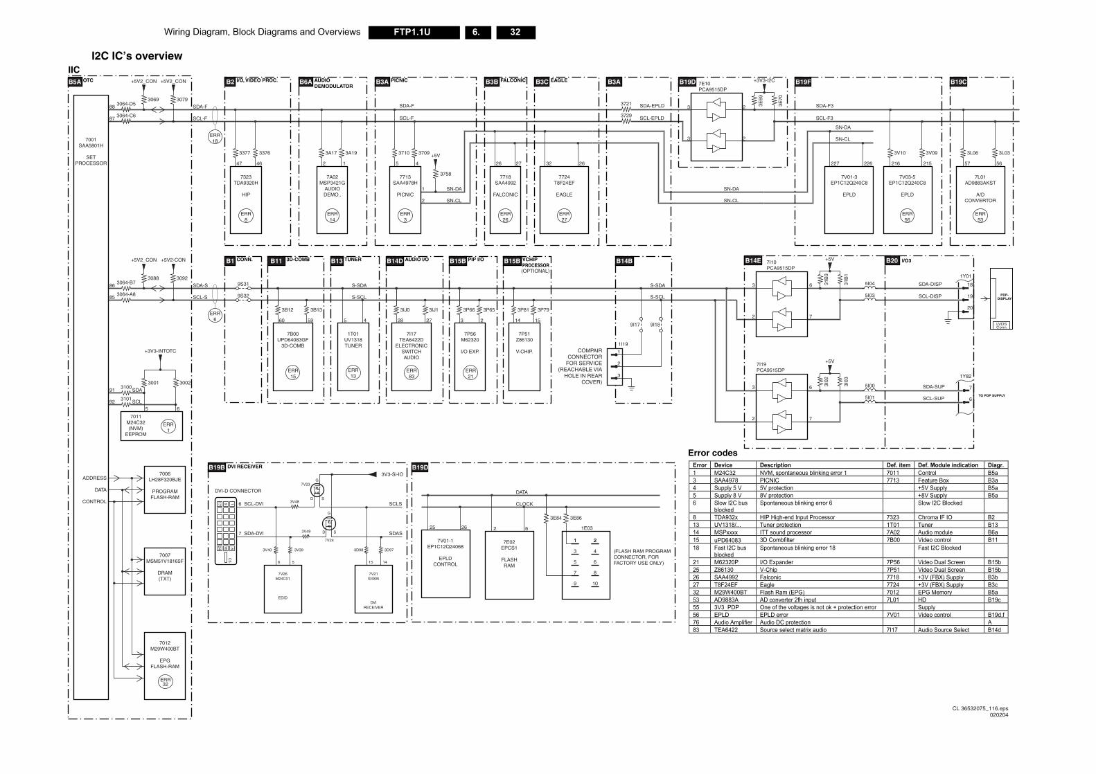
32FTP1.1U 6.Wiring Diagram, Block Diagrams and Overviews
SN-DA
SN-CL
CL 36532075_116.eps020204
SDA-F3
SCL-F3
B19F
216 215
7V03-5EP1C12Q240C8
EPLD
ERR56
3V10 3V09
227 226
7V01-3EP1C12Q240C8
EPLD
B19C
57 56
7L01AD9883AKST
A/DCONVERTOR
ERR53
3L06 3L03
3V40 3V39 3D98 3D97
+3V3-I2C
3E69
3E70
81624
I/O3
18
1Y01
19
20
7
1Y82
LVDSConn.
6
EP1C12Q24068(FLASH RAM PROGRAM
7E02EPCS1
3 4
4E B207I10PCA9515DP
6
7
+5V
31B
3
31B
1
7I19PCA9515DP
6
7
+5V
3I02
3I03
SDA-DISP
SCL-DISP
SDA-SUP
SCL-SUP
PDP-DISPLAY
TO PDP SUPPLY
5I04
5I03
5I00
5I01
!! " #
% & $
% & $
' ( ! %)
,! ,-. ) ! % -/ !" !0
* % * *
!** ) % ) /) '
+ /4 ) %
" ! " ! %)
!20 5# ) ' ) + %
.- ) + %
"% % & 7"89 $
5 & 7"89 $ %
"- ;/ 75 <9 5 < /$
+ % = 4- > ,+ %
0 4 - = & % $
5 >+ ) % )4
) + %
% % /# ) ! ) % % )
ERR32
7007MSM51V18165F
DRAM(TXT)
7012M29W400BT
EPGFLASH-RAM
6 5
7V26M24C01
EDID
15 14
7V21SII905
DVIRECEIVER
C5 EPLD
CONTROL
CONNECTOR, FOR FACTORY USE ONLY)
FLASHRAM
5 6
7 8
9 10
%)
'
6'
'
*"5"
:*
+
? +
' 5 >+
' ) /4
*5'
I2C IC’s overview
B14B
3064-D53079
SDA-F
SCL-F
+5V2_CON
+5V2_CON +5V2-CON
SDA-S
SCL-S
S-SDA
S-SCL
6 SCL-DVI
DVI-D CONNECTOR
7 SDA-DVI
SCLS
3V3-Si-IO
SDAS
OTCB5A
88
7001SAA5801H
SETPROCESSOR
ADDRESS
3064-C687
1
2
SN-DA
SN-CL
SN-DA
SN-CL
3064-B73088
+5V2_CON
3069
3092
86
3064-A8
3100
3101
85
I/O, VIDEO PROC.B2
CONN.B1 TUNERB13
3377
47 46
3376
7323TDA9320H
HIP
ERR8
S-SDA
S-SCL
45
1T01UV1318TUNER
ERR13
AUDIODEMODULATOR
B6A
2 1
7A02MSP3421G
AUDIODEMO..
ERR14
PICNICB3A
3710
5 4
3709
7713SAA4978H
PICNIC
ERR3
FALCONICB3B
26 27
7718SAA4992
FALCONIC
ERR26
EAGLEB3C B3A B19D
32 26
7E10PCA9515DP
7724T8F24EF
EAGLE
ERR27
ERR18
SDA
SCL
+3V3-INTOTC
3001 3002
91
92
7011M24C32(NVM)
EEPROM
7006LH28F320BJE
PROGRAMFLASH-RAM
ERR1
5 6
ERR6
DATA
CONTROL
SDA-F
SCL-F
SDA-EPLD
SCL-EPLD
+5V
3758
3P66
3
3
3
3P65
2
2
2
7P56M62320
I/O EXP.
ERR83
ERR21
AUDIO I/OB14D
3IJ0
28
3IJ1
27
7I17TEA6422D
ELECTRONICSWITCHAUDIO
ERR15
3D-COMBB11
3B12
60
3B13
59
7B00UPD64083GF
3D-COMB
PIP I/OB15B
3P81
14
3P79
15
7P51Z86130
V-CHIP.
VCHIPPROCESSOR
B15B
DVI RECEIVERB19B
IIC
1
1I19
9I17 9I18
2
3
COMPAIRCONNECTOR
FOR SERVICE(REACHABLE VIA
HOLE IN REARCOVER)
3A17 3A19
G
D S
G
D S
3V48
7V23
7V24
3V49
3729
3721
9S31
9S32
(OPTIONAL)
1917
DATA
CLOCK
3E84
1
3E86
2
B19D
25 26
7V01-1
2 6 1E03
1 2
B1
3
2
3
2
Error codes
$
$
' ( ! %)
*+#
12333
####
+'
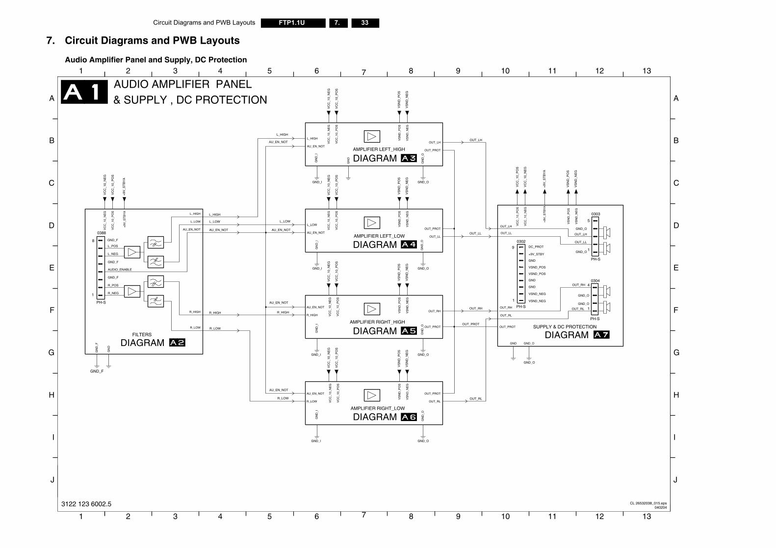
Circuit Diagrams and PWB Layouts 33FTP1.1U 7.
GND_O
GND_O
D_POS
D_POS
_STBY1
5
D
OUT_RH
OUT_RL
0304
_PROT
SUPPLY & DC PROTECTION
0303
PH-S
PH-S
GND_OD_NEG
D_NEG GND_O
4
D
C
B
A
D
OUT_LH
1
DIAGRAM
OUT_LL
131211
131211
J
I
H
G
F
ED
_NE
G
_PO
S
_NE
G
_PO
S
VS
ND
_NE
G
VS
ND
_PO
SV
SN
D_P
OS
+9V
_ST
BY
A+
9V_S
TB
YA
VS
ND
_NE
G
AU_EN_NOT
CL 26532038_015.eps040204
AMPLIFIER RIGHT_LOW
DIAGRAM
5
J
1 76432 1098
I
H AU_EN_NOT
GN
D_I
GN
D_O
OUT_PROT
OUT_RLR_LOW VC
C_1
0
VC
C_1
0
VS
ND
VS
ND
GND_I
OUT_RLR_LOW
GND_O
3122 123 6002.5
7. Circuit Diagrams and PWB Layouts
Audio Amplifier Panel and Supply, DC Protection
7
1
8
DIAGRAM
GND_F
0302DIAGRAM
VSN
VSN
& SUPPLY , DC PROTECTION
+9V
PH-S
GN
GND_F
AUDIO AMPLIFIER PANEL
AMPLIFIER RIGHT_HIGH
AMPLIFIER LEFT_LOW
L_NEG
L_POS
FILTERS
DC
DIAGRAM
R_NEG
0388
1
R_POS
VSN
VSN
9
PH-S
GN
DIAGRAM
AUDIO_ENABLE
GND_F
C
B
A
654321
AMPLIFIER LEFT_HIGH
1098
GN
G
F
E
D
VC
C_1
0_P
OS
VS
ND
_PO
S
VC
C_1
0_P
OS
GN
D_I
GN
D_O
L_LOW
OUT_LL
OUT_PROTVC
C_1
0_N
EG
VC
C_1
0_P
OS
VS
ND
_NE
G
VS
ND
_PO
S
GND_F
OUT_RL
VC
C_1
0_N
EG
VC
C_1
0_P
OS
VC
C_1
0_N
EG
AU_EN_NOT
GND_O
GND GND_O
OUT_LH
OUT_LL
OUT_PROT
OUT_RH
GND_O
+9V
_ST
BY
A+
9V_S
TB
YA
AU_EN_NOT
GN
D
GN
D_F
L_HIGH
L_LOW
R_HIGH
R_LOW
VC
C_1
0_N
EG
VC
C_1
0_P
OS
VS
ND
_NE
G
VC
C_1
0_N
EG
VC
C_1
0_P
OS
VS
ND
_NE
G
GND_O
VC
C_1
0_N
EG
VC
C_1
0_N
EG
GND_I
VC
C_1
0_P
OS
GND_I
VS
ND
_NE
G
VC
C_1
0_N
EG
AU_EN_NOT
GN
D_I
GN
D_O OUT_PROT
OUT_RHR_HIGH V
CC
_10_
NE
G
VC
C_1
0_P
OS
VS
ND
_NE
G
VS
ND
_PO
S
GND_O
AU_EN_NOT
GN
D
GN
D_I
GN
D_O
L_HIGHOUT_LH
OUT_PROT
VC
C_1
0_N
EG
VC
C_1
0_P
OS
VS
ND
_NE
G
VS
ND
_PO
SV
SN
D_P
OS
VC
C_1
0_N
EG
VS
ND
_NE
G
VS
ND
_PO
S
VC
C_1
0_P
OS
VS
ND
_PO
S
GND_I
R_LOWOUT_PROT
VC
C_1
0_P
OS
AU_EN_NOT
AU_EN_NOT
AU_EN_NOT
AU_EN_NOT
R_HIGHR_HIGHOUT_RH
OUT_LL
OUT_LH
L_HIGH
L_HIGH
L_LOW L_LOW
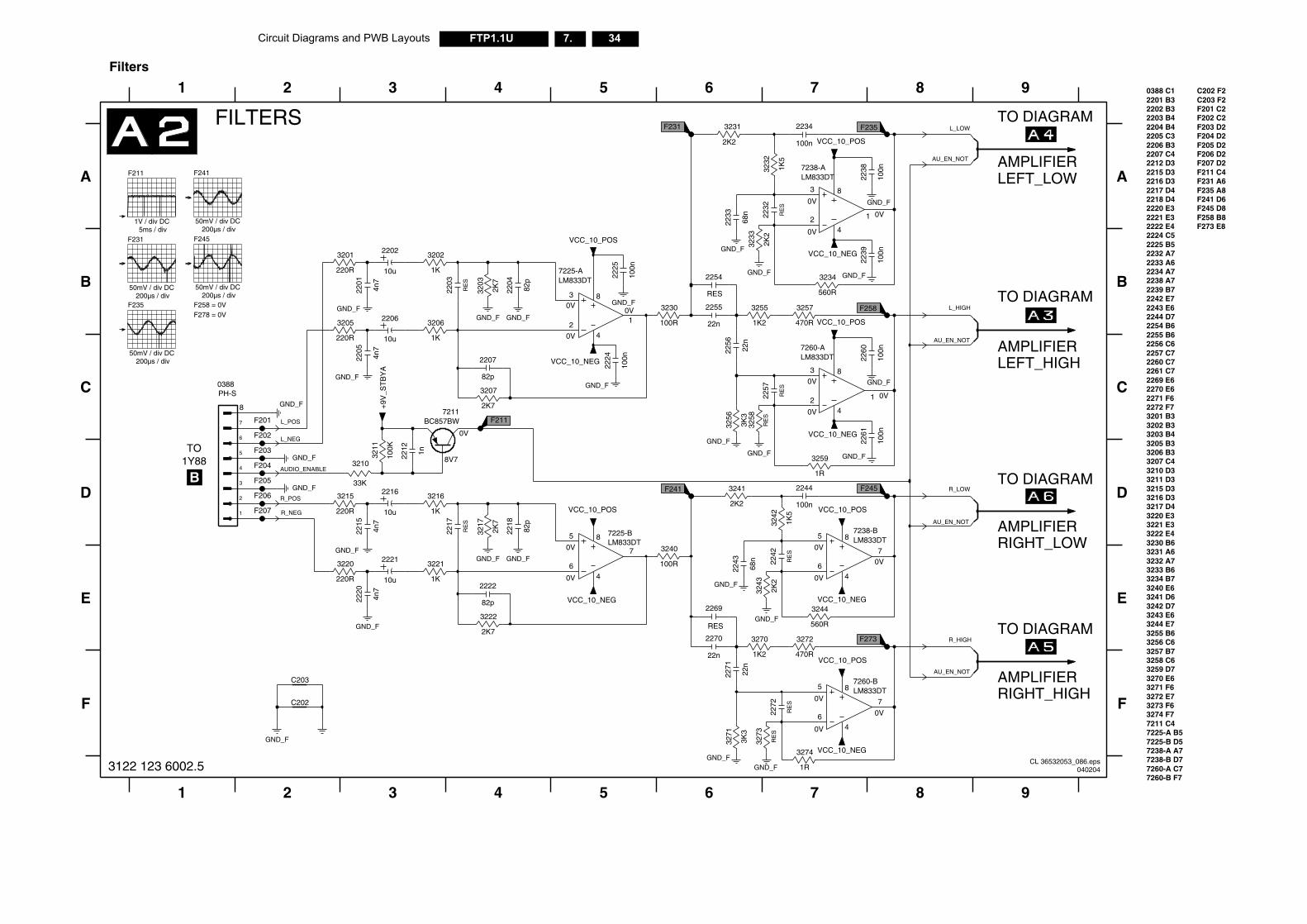
34FTP1.1U 7.Circuit Diagrams and PWB Layouts
2270 E62271 F6
TO DIAGRAM
7225-B D5
2217 D42218 D42220 E32221 E32222 E42224 C52225 B5
A
B
F
D
8 9
E
2202 B3
RIGHT_LOW
RIGHT_HIGH
2203 B4
3240 E6
3217 D4
8 9
2215 D3
F203 D2
2234 A7
2257 C7
2261 C7
2205 C3
2269 E6
2244 D72254 B62255 B6
TO DIAGRAM
3205 B33206 B3
F231 A6F235 A8F241 D6
TO DIAGRAM
2232 A72233 A6
3216 D3
F245 D8
3220 E33221 E33222 E43230 B63231 A63232 A73233 B63234 B7
LEFT_LOW
3241 D6
3255 B63256 C63257 B7
C
3258 C6
2256 C6
2201 B3
2260 C7
3270 E6AMPLIFIER
3273 F63272 E7
2204 B4
2216 D3
2212 D3
7211 C47225-A B5
7238-A A77238-B D77260-A C77260-B F7
C202 F2C203 F2F201 C2F202 C2
F204 D2
2238 A72239 B72242 E72243 E6
F206 D2
TO DIAGRAM
3202 B3
3207 C4
3215 D3
F211 C4AMPLIFIER
3210 D33211 D3
F258 B8F273 E8
2272 F73201 B3
3203 B4
AMPLIFIERLEFT_HIGH
3242 D73243 E63244 E7
3271 F6
3259 D7
0388 C1
AMPLIFIER
2206 B32207 C4
3274 F7
F205 D2
F207 D2
22n 1K2 470R
AU_EN_NOT
AU_EN_NOT
AU_EN_NOT
AU_EN_NOT
R_HIGH
L_HIGH
L_LOW
R_LOW
CL 36532053_086.eps040204
F
1 2 3 4 5 6 7
VCC_10_POS
2271
22n
GND_F
C203
GND_F32
73
RE
S 0V
0V
0VC202
VCC_10_NEG
RE
S
2272
3271
3K3
5
6
7
8
4
LM833DT7260-B
1R
3274
GND_F
3122 123 6002.5
Filters
4
RES
A
RES
2
TO1Y88
6 7
B
C
D
E
FILTERS
3 51
2270
GND_F
GND_F
3270
1K
3216
GND_F
3230
100R
2238
100n
22n
2255
3256
3K3
GND_F
2K7
3217
VCC_10_NEG
VCC_10_POS
2257
RE
S
VCC_10_POS
GND_F
8
4
3220
220R
7225-BLM833DT
5
6
7
220R
3205
F235
F245
2K2
3241
GND_F
82p
220722
20
4n7
1K2
3255
1R
325922
17
RE
S
F258
VCC_10_POS
10u
2206
VCC_10_NEG
3234
560R2201
4n7
10u
2216
2261
100n
2K2
3233
GND_F
4n7
2205
GND_F
3203
2K7
GND_F
GND_F
F207
2221
10u
2233
68n
F201
4n7
2215
5
6
7
8
4
2244
100n
GND_F
7238-BLM833DT
1
2
3
4
5
6
7
8
GND_F
GND_F
RE
S
PH-S0388
LM833DT
3
2 1
8
4
GND_F
3258
3243
2K2
7260-A
BC857BW7211
F273
RE
S
2232
100R
3240
100n
2239
2256
22n
1K5
3242
VCC_10_POS
F204
3232
1K5
F241
82p
2222
GND_F
3257
470R
2224
100n
33K
3210
F231
VCC_10_NEG
3207
2K7
3
2
0V
0V0V
0V
0V
0V
8V7
0V
0V
0V
0V
0V
0V
0V
0V
0V
1
8
4
GND_F
LM833DT7225-A
100n
2260
2K2
GND_F
2242
RE
S
3231
2K7
3222
GND_F
560R
3244
100n
2234
GND_F
RE
S
2203
2204
100K
3211
LM833DT7238-A
3
2 1
8
4
82p
3201
220R
3221
1K
3202
1K
F211
68n
2243
1K
3206
+9V
_ST
BY
A
1n2212
F206GND_F
VCC_10_NEG
2269
GND_F
2218
82p
VCC_10_NEG
VCC_10_POS
3272
2254100n
2225
2202
10u
GND_F
GND_F
220R
3215
F203
F205
F202
R_NEG
R_POS
AUDIO_ENABLE
L_NEG
L_POS
F231
50mV / div DC200µs / div
F211
1V / div DC5ms / div
F235
50mV / div DC200µs / div
F241
50mV / div DC200µs / div
F245
F258 = 0VF278 = 0V
50mV / div DC200µs / div
B
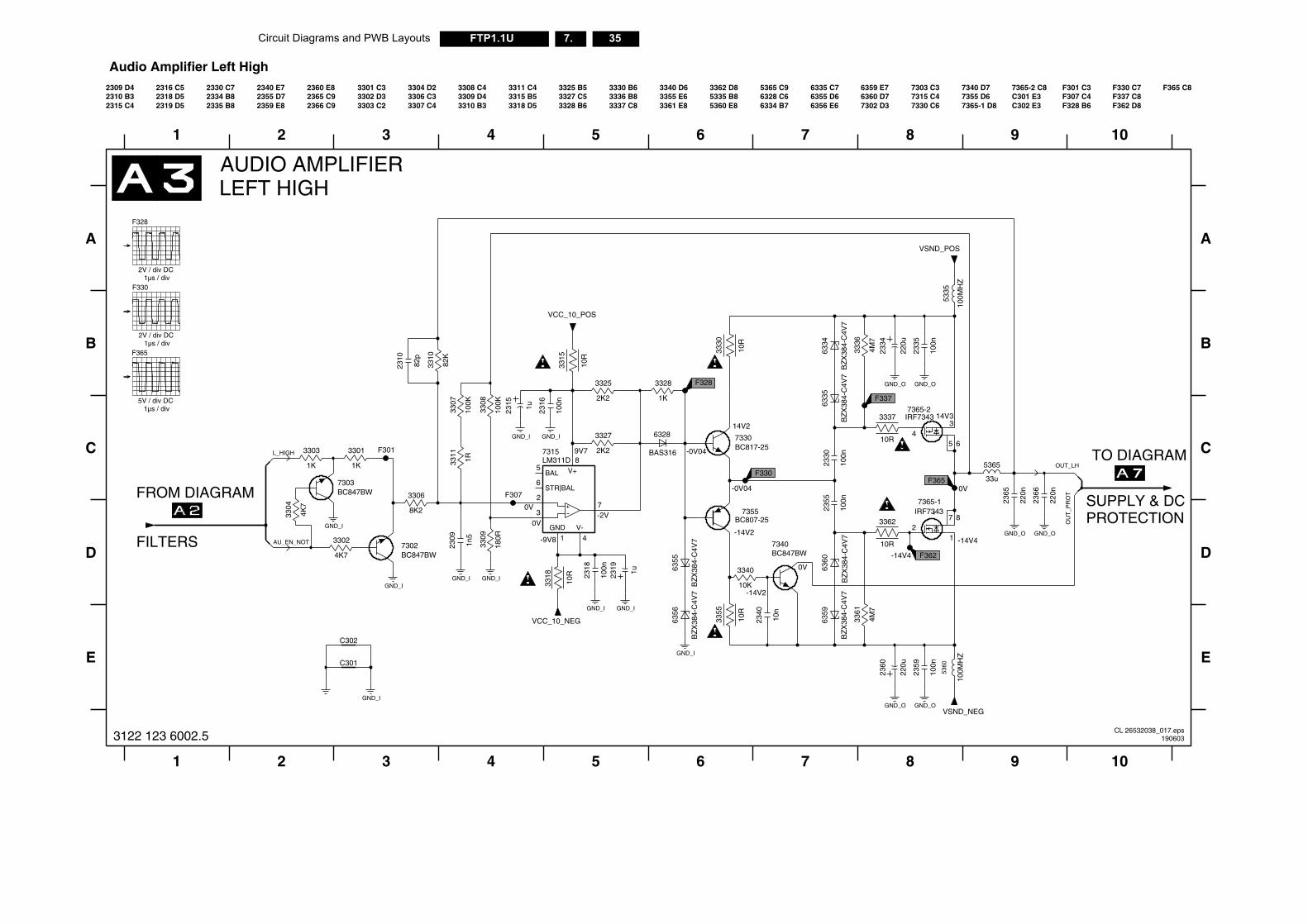
Circuit Diagrams and PWB Layouts 35FTP1.1U 7.
E
8 9 10
7365-2 C8
8 9
F330 C7F337 C8C301 E3
C302 E3
F301 C3F307 C4F328 B6
TO DIAGRAM
B
C
D
10
F362 D8
F365 C8
PROTECTIONSUPPLY & DC
7340 D77355 D67365-1 D8
A
7303 C37315 C47330 C6
100n
2335
2366
220n
2359
100n
220n
2365
GND_O
100M
HZ
5335
GND_O
64
3
F362
7365-2IRF7343
5
220u
100M
HZ
5360
220u
GND_O
IRF73437365-1
7 82
1
O
GND_I
GND_O
VSND_NEGO
33u
5365
F365
VSND_POS
OUT_LH
OU
T_P
RO
T
CL 26532038_017.eps190603
14V3
-14V4
V4
0V
1 2 3 74 5 6
E
2360
GND_IGND_
C301
3122 123 6002.5
Audio Amplifier Left High2360 E82365 C92366 C9
2309 D4 2330 C72334 B82335 B8
1 2 3 4 5 6 7
3315 B53318 D5
3325 B53327 C53328 B6
3330 B63336 B83337 C8
3340 D63355 E63361 E8
3362 D85335 B8
2340 E72355 D72359 E8 6334 B7
6335 C76355 D6
3301 C33302 D32310 B3
2315 C4
2316 C52318 D52319 D5
LEFT HIGHAUDIO AMPLIFIER
A
FILTERS
FROM DIAGRAM
3309 D43310 B3
3311 C4
5360 E8
5365 C96328 C6
6356 E6
6359 E7
3303 C2
3304 D23306 C33307 C4
3308 C4
B
C
D
6360 D77302 D3
F307
10K
F301
GND_I3340
8K2
3306
GND_I
GND_I
2315 1u
GND_I
6328
BAS316
3362
10R
GND_I
BC817-257330
10R
3315
6359
BZ
X38
4-C
4V7
3327
2K2
10R
3355
2K2
3325
3308
100K
3330
10R
7315LM311D
5BAL
1GND
2
37
6STR|BAL
8V+
4V-
2318
100n
2334
C302
100n
2355
VCC_10_NEG 4M7
3361
GND_I
VCC_10_POS
BZ
X38
4-C
4V7
6360
10R
3337
6335
BZ
X38
4-C
4V7
3302
4K7
6356
BZ
X38
4-C
4V7
BC847BW7302
3304
4K7
7303BC847BW
3303
1K
GND_
3301
1K
82p
2310
82K
3310
BC807-257355
GND_I
BZ
X38
4-C
4V7
6355
1K
3328
BZ
X38
4-C
4V7
6334
2309
1n5
100n
2316
BC847BW7340
100n
2340
10n
3336
4M7
2330
100K
3307
3318
10R
GND_I23
19 1u
F328
180R
3309
F3301R33
11
AU_EN_NOT
F337
L_HIGH
F328
2V / div DC1µs / div
F330
2V / div DC1µs / div
F365
5V / div DC1µs / div
0V
0V
0V
-9V8
-0V049V7
-0V04
14V2
-14V2
-14
-14V2
-2V
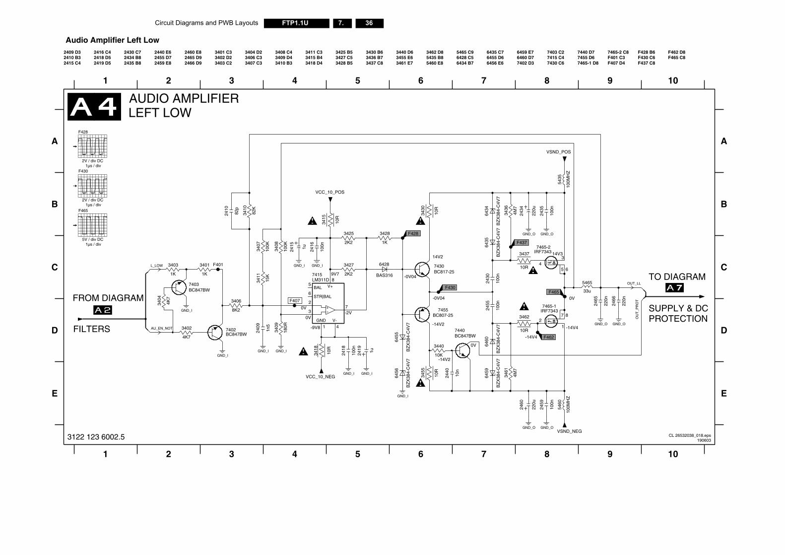
36FTP1.1U 7.Circuit Diagrams and PWB Layouts
F407 D4
9 10
E
A
B
C
D
E
7465-2 C8F401 C3
7430 C6
7440 D77455 D67465-1 D8
F428 B6F430 C6F437 C8
F462 D8F465 C8
SUPPLY & DC
TO DIAGRAM
8 9
8
10
PROTECTION
7403 C27415 C4
3
65-27343
5 6
GND_O
100n
2459
33u
5465
VSND_POS
100M
HZ
5435
F465
F462
GND_O
220n
2465
100n
2435
2466
220n
VSND_NEG
GND_O
5460
100M
HZ
IRF73437465-1
7 8
1
GND_O
OUT_LL
OU
T_P
RO
T
CL 26532038_018.eps190603
14V3
-14V4
0V
2 3 4 5 6 71
220u
2460
GND_O
GND_I
3122 123 6002.5
Audio Amplifier Left Low
3428 B5
3430 B63436 B73437 C8
3440 D63455 E63461 E7
3462 D85435 B85460 E8
5465 C96428 C56434 B7
6435 C76455 D66456 E6
6459 E7
A
3410 B3
3411 C33415 B43418 D4
3425 B53427 C5
1 2 3 4 5 6 7
6460 D77402 D32466 D9
3401 C3
B
C
D
2409 D32410 B32415 C4
2416 C42418 D5 3402 D2
3403 C2
3404 D23406 C33407 C3
3408 C43409 D4
LEFT LOW
FILTERS
2419 D5
2430 C72434 B82435 B8
2440 E62455 D72459 E8
2460 E82465 D9
100n
2418
FROM DIAGRAM
AUDIO AMPLIFIER
GND_I
VCC_10_POS
GND_I
GND_O
6434
BZ
X38
4-C
4V7
180R
3409
74IRF
4
3402
4K7
3401
1K
GND_I
100K
3407
100n
2455
1u2419
7430BC817-25
3418
10R
82p
2410
1GND
2
37
6STR|BAL
8V+
4V-
BZ
X38
4-C
4V7
6455
BZ
X38
4-C
4V7
7415LM311D
5BAL
BZ
X38
4-C
4V7
6459
6460
GND_I
GND_I
3430
82K
3410
F401
10R
7440BC847BW
3408
100K
F437
BZ
X38
4-C
4V7
6435
3461
10R
3437
4M7
8K2
3406
10n
2440
100n
2416
2415 1u
6428
BAS316
VCC_10_NEG
2434
220u
F407
GND_I
4K7
3404
BC847BW7403
1K
3403
10RBC847BW7402
3462
3436
100n
2430
3425
4M7
BC807-257455
2K2
3455
10R
F430
15K
3411
1K
3428
GND_I
10R
3415
2
10K
3440
GND_I
2409
1n5
3427
2K2
BZ
X38
4-C
4V7
6456
F428
AU_EN_NOT
L_LOW
F428
2V / div DC1µs / div
F430
2V / div DC1µs / div
F465
5V / div DC1µs / div
0V
0V
0V
-9V8
-0V049V7
-0V04
14V2
-14V2
-14V4
-14V2
-2V

Circuit Diagrams and PWB Layouts 37FTP1.1U 7.
E
A
B
C
D
E
SUPPLY & DC
8 10
8 9 10
PROTECTION
9
7565-2 C8F501 C3F507 D4
F528 B6F530 C6F537 C8
F562 D8F565 C8
TO DIAGRAM
7503 C27515 C47530 C6
7540 D77555 D67565-1 D8
GND_O
5565
33u
GND_O
64
3
IRF73437565-2
5
100M
HZ
5560
VSND_POS
2566
220n
100n
2559
F562
2535
100n
GND_O
VSND_NEG
5535
100M
HZ
7565-1IRF7343
7 82
1
GND_O
F565
2565
220n
OUT_RH
OU
T_P
RO
T
CL 26532038_019.eps190603
14V3
-14V4
0V
1 2 3 4 5 6 7
GND_I
GND_O
220u
2560
3122 123 6002.5
Audio Amplifier Right High
C
D FILTERS
1 2 3 4 6 7
A
B
3503 C2
3504 D23506 D33507 C3
3508 C43509 D43510 B3
3511 C33515 B43518 D4
3525 B52509 D3
3528 B5
3530 B63536 B73537 C8
3540 D6
5
AUDIO AMPLIFIER
FROM DIAGRAM
RIGHT HIGH
2510 B32515 C4
2516 C42518 D52519 D5
2534 B82535 B8
2540 E62555 D72559 E8
2560 E82565 D92566 D9
3501 C23502 D2 3527 C5 3555 E6
3561 E7
3562 D85535 B85560 E8
5565 C96528 C56534 B7
6535 C72530 C7
6556 E6
6559 E76560 D77502 D3
6555 D6
4M7
3561
GND_I
3507
100K
6555
BZ
X38
4-C
4V7
BAS316
6528
6534
BZ
X38
4-C
4V7
2555
100n
3510
82K
BC847BW7540
7555BC807-25
2516
100n
8K2
3555
10R
3506
100n
2530
3528
1K
3509
180R
F501
VCC_10_NEG
GND_I
BZ
X38
4-C
4V7
6556
1K
3501 7530BC817-25
2519 1u
3511
6K8
220u
2534
4K7
3502
F528
2518
100n
GND_I
2540
10n
10R
3530
3537
10R
BZ
X38
4-C
4V7
6535
5BAL
1GND
2
37
6STR|BAL
8V+
4V-
GND_I
LM311D7515
3525
2K2
6560
BZ
X38
4-C
4V7
3515
10R
GND_O
2K2
3527
2510
82p
10K
7502BC847BW
GND_I
F537
3540
3504
BC847BW7503
1K
3503
4K7
F507
10R
3562
1u2515
100K
3508
10R
3518
GND_I
GND_I
GND_I
VCC_10_POS
1n5
2509
3536
4M7
BZ
X38
4-C
4V7
6559
F530
R_HIGH
AU_EN_NOT
F528
2V / div DC1µs / div
F530
2V / div DC1µs / div
F565
5V / div DC1µs / div
0V
0V
0V
-9V8
-0V049V7
-0V04
14V2
-14V2
-14V4
-14V2
-2V
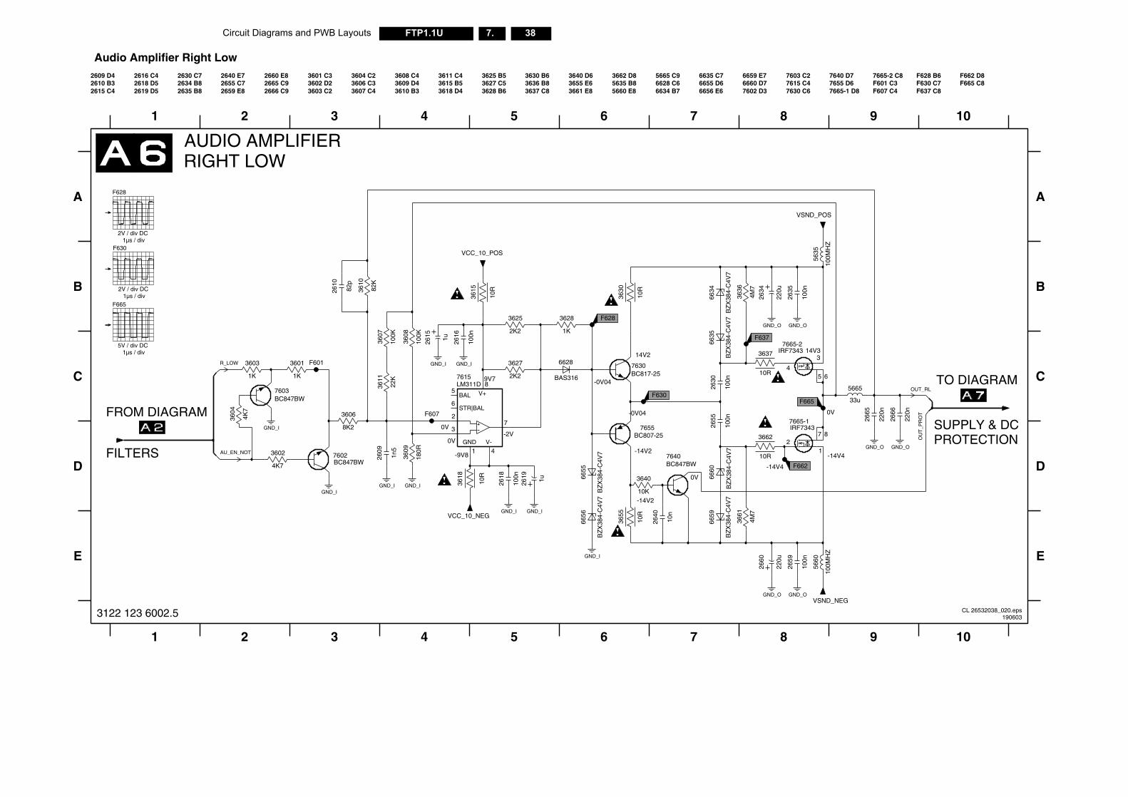
38FTP1.1U 7.Circuit Diagrams and PWB Layouts
7665-2 C87655 D67665-1 D8
9
F601 C3F607 C4
F628 B6F630 C7
E
7603 C27615 C47630 C6
7640 D7
8
F662 D8
10
TO DIAGRAM
A
B
C
D
E
SUPPLY & DC
8 9 10
F637 C8F665 C8
PROTECTION21
IRF73437665-1
7 8
O
100M
HZ
5635
GND_O
O
266
220u
VSND_POS
F662
F665
100n
2635
GND_O
5 64
3
VSND_NEG
7665-2IRF7343
2659
100n
GND_O
220n
2665
2666
220n
33u
5665
5660
100M
HZ
GND_O
220u
OUT_RL
OU
T_P
RO
T
CL 26532038_020.eps190603
14V3
-14V4
V4
0V
71 2 3 4 5 6
GND_
3122 123 6002.5
Audio Amplifier Right Low
3655 E63637 C8
3640 D6
3661 E8
3662 D85635 B85660 E8
5665 C96628 C66634 B7
6635 C76655 D66656 E6
6659 E76660 D77602 D3
A
AUDIO AMPLIFIER
2634 B82635 B8
2640 E72655 C72659 E8
2660 E8
2666 C9
3601 C33602 D23603 C2
3604 C23606 C33607 C4
3608 C43609 D43610 B3
3611 C43615 B53618 D4
3625 B53627 C53628 B6
3630 B63636 B8
C
D
B
2609 D42610 B32615 C4
2616 C42618 D5
2630 C7
1 2 3 4 5 6 7
2619 D5
4K7
2665 C9
FROM DIAGRAM
RIGHT LOW
FILTERS
3611
22K
3602
GND_I
BC847BW7602
GND_
3630
10R
BZ
X38
4-C
4V7
6655
7615LM311D
5BAL
1GND
2
37
6STR|BAL
8V+
4V-
2K2
3625
2618
100n
2630
100n
F628
3607
100K
VCC_10_NEG
BC847BW7640
0
3640
10K
6635
BZ
X38
4-C
4V7
82K
3610
8K2
3606
6659
BZ
X38
4-C
4V7
3618
10R
GND_I
10R
3637
BZ
X38
4-C
4V7
6660
3627
2K2
3661
4M7
2609
1n5
100n
2655
10R
3615
GND_I
6656
BZ
X38
4-C
4V7
BZ
X38
4-C
4V7
6634
GND_I
BC817-257630
10R
3655
1K
3628
2616
100n
GND_I
4M7
3636
180R
3609
2610
2615 1u
82p
F637
GND_IF6013601
1K
BC847BW7603
VCC_10_POS
1K
3603
4K7
3604
3608
100K
GND_I
F607
GND_IGND_I
2640
10n
BC807-257655
3662
10R
F630
2634
6628
BAS316
1u2619
AU_EN_NOT
R_LOW
F628
2V / div DC1µs / div
F630
2V / div DC1µs / div
F665
5V / div DC1µs / div
0V
0V
0V
-9V8
-0V049V7
-0V04
14V2
-14V2
-14
-14V2
-2V
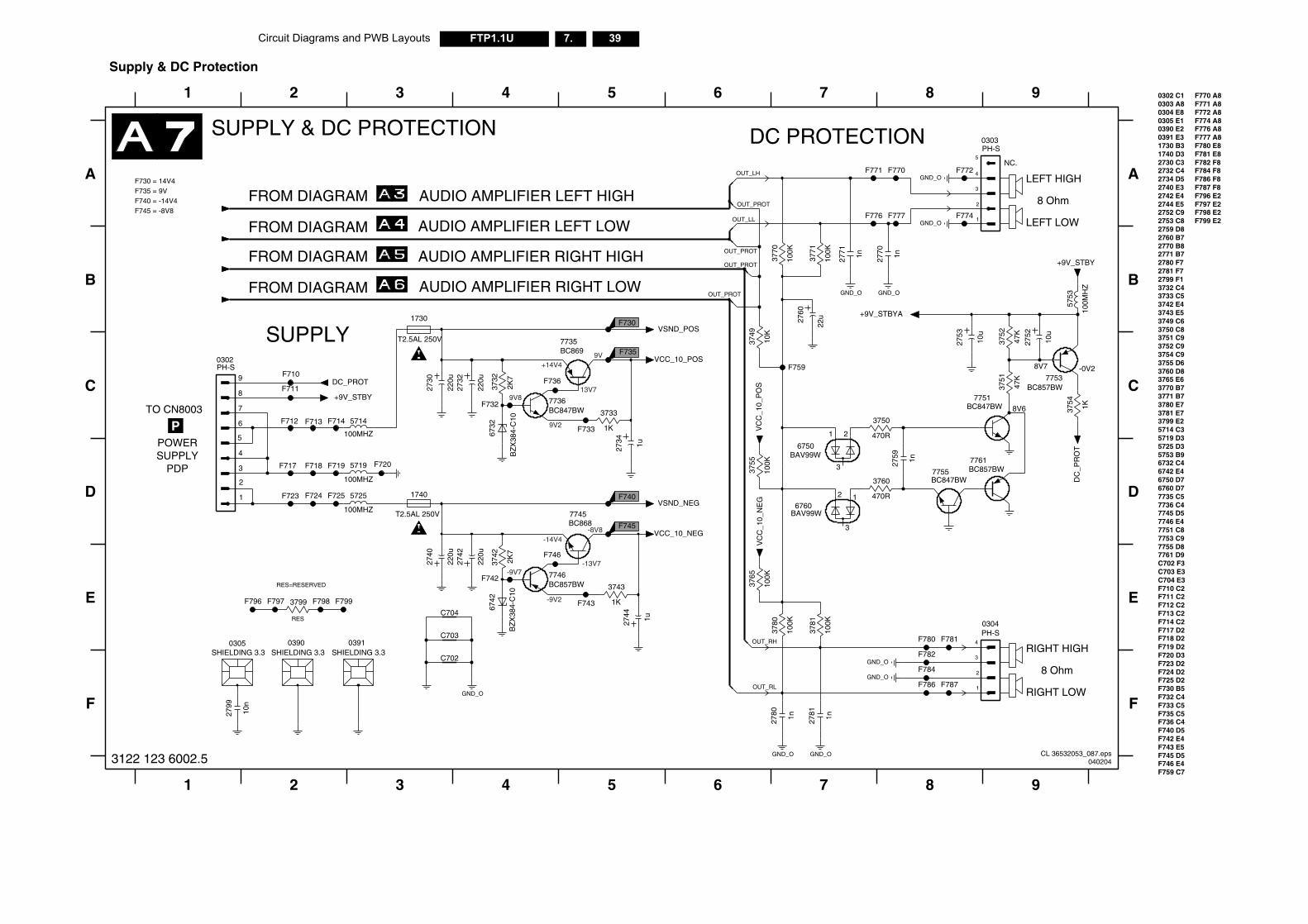
Circuit Diagrams and PWB Layouts 39FTP1.1U 7.
2759 D8
F723 D2
F725 D2F730 B5F732 C4F733 C5F735 C5
F777 A8F780 E8
F796 E2F797 E2F798 E2
2770 B8
8 Ohm
2799 F13732 C43733 C53742 E43743 E53749 C63750 C8
2780 F7
LEFT HIGH
RIGHT HIGH
8 Ohm
LEFT LOW
0302 C10303 A8
F770 A8F771 A8
3781 E73799 E25714 C3
0304 E80305 E10390 E2
2740 E32742 E42744 E52752 C9
F720 D3
2771 B7
F724 D2
2753 C8
8 9
F736 C4F740 D5F742 E4F743 E5
F772 A8F774 A8F776 A8
7761 D9C702 F3
A
F711 C2F712 C2
2734 D5
F714 C2F717 D2F718 D2F719 D2
D
E
F
N
2781 F7
3751 C93752 C93754 C93755 D6
F745 D5F746 E4F759 C7
3765 E63770 B73771 B73780 E7
5753 B9
5719 D35725 D3
F781 E8
6760 D7
8 9
7751 C87753 C97755 D8
B
C
F713 C2
3760 D8
6732 C46742 E46750 D7
1740 D32730 C32732 C4
C703 E3C704 E3
F799 E2
2760 B7
F782 F8F784 F8F786 F8F787 F8
7735 C5
RIGHT LOW
NC.
F710 C2
7736 C47745 D57746 E4
0391 E31730 B3
47K
3752
1n
7755BC847BW
BC847BW7751
2753
10u
F786
1n
100M
HZ
5753
1K3754
DC
_PR
OT
10u
2752
5
PH-S0303
1
2
3
4
47K
3751
GND_O
BC857BW7753
0
F782
8V7
8V6
-0V2
F780
GND_O
SHIELDING 3.3
F772
F774
F787
F781
7
F784
+9V_STBY
SHIELDING 3.3
BC857BW7761
4
PH-S0304
1
2
3SHIELDING 3.3
CL 36532053_087.eps040204
3 4 5 6 7
F
1 2
C702
GND_O
GND_O
1n27811n2780
GND_O
GND_O
2799
10n
GND_OOUT_RL
3122 123 6002.5
Supply & DC Protection
RES=RESERVED
1
FROM DIAGRAM
TO CN8003
E
DC PROTECTIO
FROM DIAGRAM
3 4 5 6 7
A
B
C
D
FROM DIAGRAM
SUPPLY & DC PROTECTION
2
AUDIO AMPLIFIER RIGHT HIGH
T2.5AL 250V
FROM DIAGRAM
SUPPLY
AUDIO AMPLIFIER RIGHT LOW
AUDIO AMPLIFIER LEFT HIGH
AUDIO AMPLIFIER LEFT LOW
22u27
60
T2.5AL 250V
POWERSUPPLY
PDP
F776
F743
BZ
X38
4-C
10
6742
F717 2759
220u
2730
BAV99W
1
3
2
BC8687745
6750
7736BC847BW
7746BC857BW
F711
2770
F735
VC
C_1
0_P
OS22
0u
2732
100MHZ
5714
1740
F719
GND_O
F714
GND_O
F799
BAV99W6760
1
3
2
3755
100K
VCC_10_NEG
3760
470R5725
100MHZ
RES
3799
F724
VC
C_1
0_N
EG
470R
3750
1u2734
F712
DC_PROT
+9V_STBY
F77
6732
BZ
X38
4-C
10
F742
VCC_10_POS
F736
F733
F732
3732
2K7
1K
3733
+9V_STBYA
F740
100K
3781
C704
100K
3771
C703
F710
0305
1730
VSND_NEG
F771
100MHZ
5719
3743
1K
F759PH-S
1
2
3
4
5
6
7
8
9
F718
0302
F723
F745
F798
F730
100K
3770
F77
2744 1u
VSND_POS
3780
100K
F720
0390
3742
2K7
F796
F746
10K
3749
3765
100K
0391
F797
220u
2742
F713
220u
2740
BC8697735
2771 1n
OUT_PROT
OUT_PROT
OUT_PROT
OUT_PROT
OUT_LH
OUT_LL
F725
OUT_RH
F730 = 14V4F735 = 9VF740 = -14V4F745 = -8V8
P
+14V4
13V79V8
9V2
9V
-14V4
-13V7-9V7
-9V2
-8V8
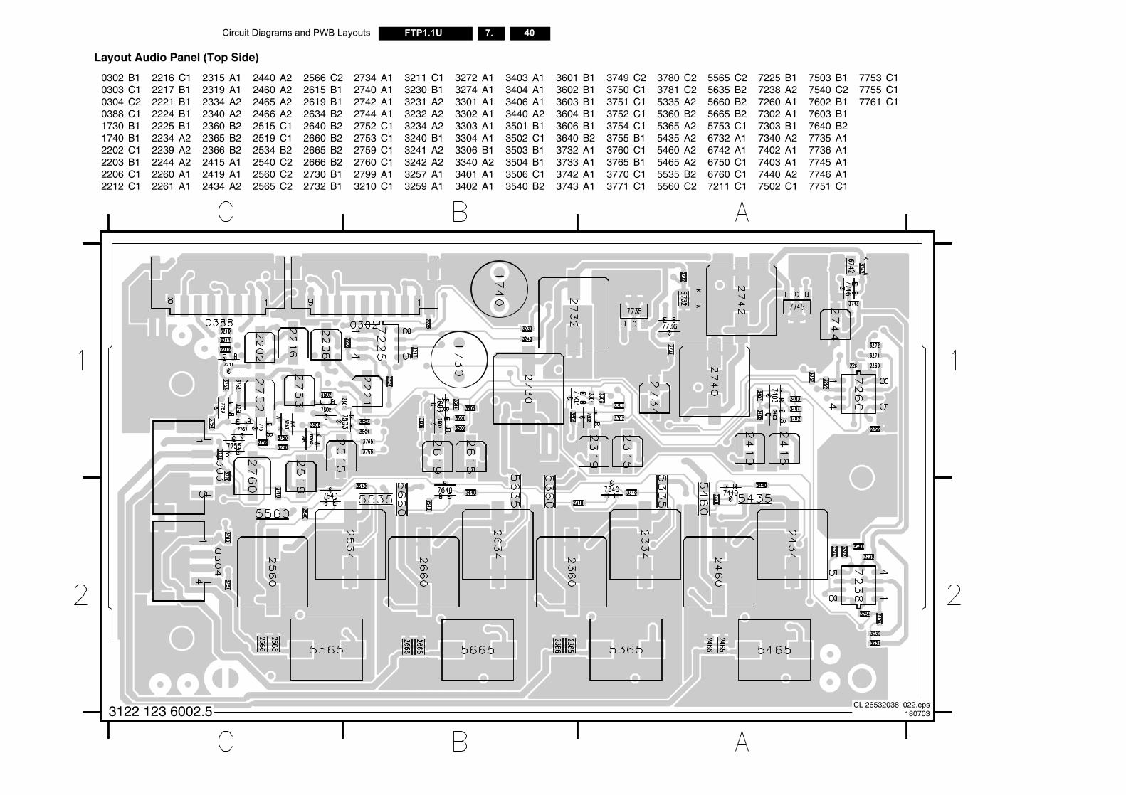
40FTP1.1U 7.Circuit Diagrams and PWB Layouts
5 B18 A20 A12 A13 B10 A22 A13 A10 A22 C1
7503 B17540 C27602 B17603 B17640 B27735 A17736 A17745 A17746 A17751 C1
7753 C17755 C17761 C1
CL 26532038_022.eps180703
3122 123 6002.5Layout Audio Panel (Top Side)
0302 B10303 C10304 C20388 C11730 B11740 B12202 C12203 B12206 C12212 C1
2216 C12217 B12221 B12224 B12225 B12234 A22239 A22244 A22260 A12261 A1
2315 A12319 A12334 A22340 A22360 B22365 B22366 B22415 A12419 A12434 A2
2440 A22460 A22465 A22466 A22515 C12519 C12534 B22540 C22560 C22565 C2
2566 C22615 B12619 B12634 B22640 B22660 B22665 B22666 B22730 B12732 B1
2734 A12740 A12742 A12744 A12752 C12753 C12759 C12760 C12799 A13210 C1
3211 C13230 B13231 A23232 A23234 A23240 B13241 A23242 A23257 A13259 A1
3272 A13274 A13301 A13302 A13303 A13304 A13306 B13340 A23401 A13402 A1
3403 A13404 A13406 A13440 A23501 B13502 C13503 B13504 B13506 C13540 B2
3601 B13602 B13603 B13604 B13606 B13640 B23732 A13733 A13742 A13743 A1
3749 C23750 C13751 C13752 C13754 C13755 B13760 C13765 B13770 C13771 C1
3780 C23781 C25335 A25360 B25365 A25435 A25460 A25465 A25535 B25560 C2
5565 C25635 B25660 B25665 B25753 C16732 A16742 A16750 C16760 C17211 C1
722723726730730734740740744750
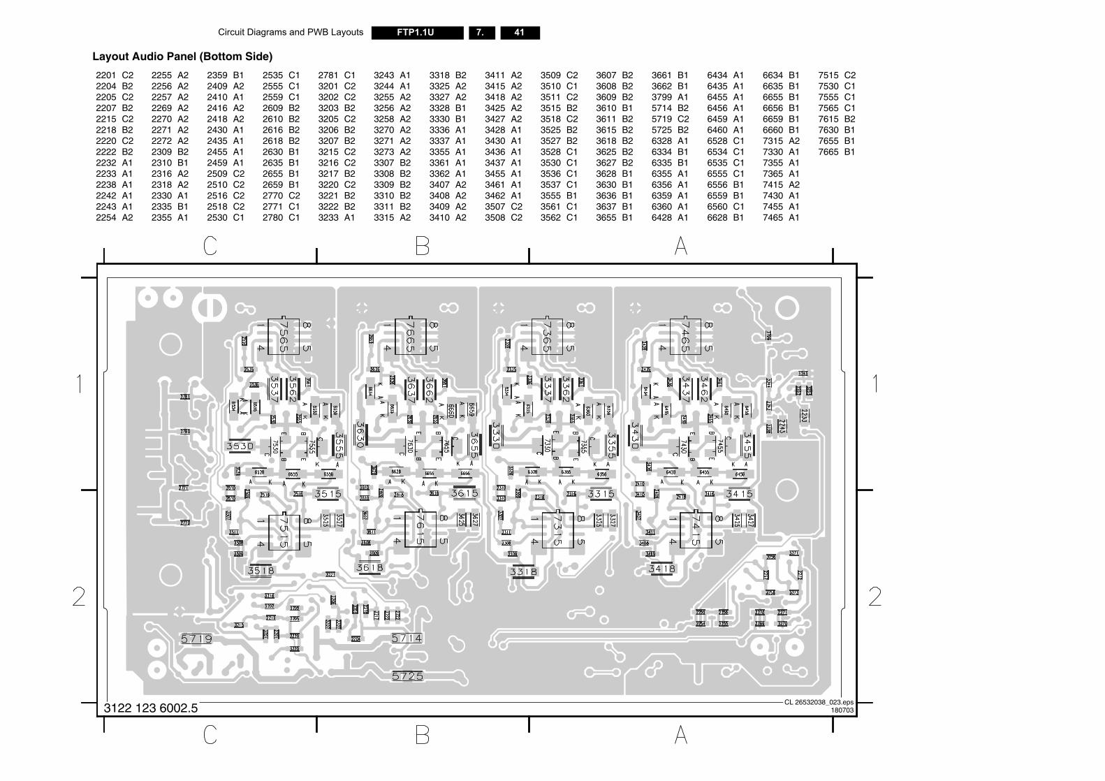
Circuit Diagrams and PWB Layouts 41FTP1.1U 7.
CL 26532038_023.eps180703
6634 B16635 B16655 B16656 B16659 B16660 B17315 A27330 A17355 A17365 A17415 A27430 A17455 A17465 A1
7515 C27530 C17555 C17565 C17615 B27630 B17655 B17665 B1
3122 123 6002.5
Layout Audio Panel (Bottom Side)
2201 C22204 B22205 C22207 B22215 C22218 B22220 C22222 B22232 A12233 A12238 A12242 A12243 A12254 A2
2255 A22256 A22257 A22269 A22270 A22271 A22272 A22309 B22310 B12316 A22318 A22330 A12335 B12355 A1
2359 B12409 A22410 A12416 A22418 A22430 A12435 A12455 A12459 A12509 C22510 C22516 C22518 C22530 C1
2535 C12555 C12559 C12609 B22610 B22616 B22618 B22630 B12635 B12655 B12659 B12770 C22771 C12780 C1
2781 C13201 C23202 C23203 B23205 C23206 B23207 B23215 C23216 C23217 B23220 C23221 B23222 B23233 A1
3243 A13244 A13255 A23256 A23258 A23270 A23271 A23273 A23307 B23308 B23309 B23310 B23311 B23315 A2
3318 B23325 A23327 A23328 B13330 B13336 A13337 A13355 A13361 A13362 A13407 A23408 A23409 A23410 A2
3411 A23415 A23418 A23425 A23427 A23428 A13430 A13436 A13437 A13455 A13461 A13462 A13507 C23508 C2
3509 C23510 C13511 C23515 B23518 C23525 B23527 B23528 C13530 C13536 C13537 C13555 B13561 C13562 C1
3607 B23608 B23609 B23610 B13611 B23615 B23618 B23625 B23627 B23628 B13630 B13636 B13637 B13655 B1
3661 B13662 B13799 A15714 B25719 C25725 B26328 A16334 B16335 B16355 A16356 A16359 A16360 A16428 A1
6434 A16435 A16455 A16456 A16459 A16460 A16528 C16534 C16535 C16555 C16556 B16559 B16560 C16628 B1
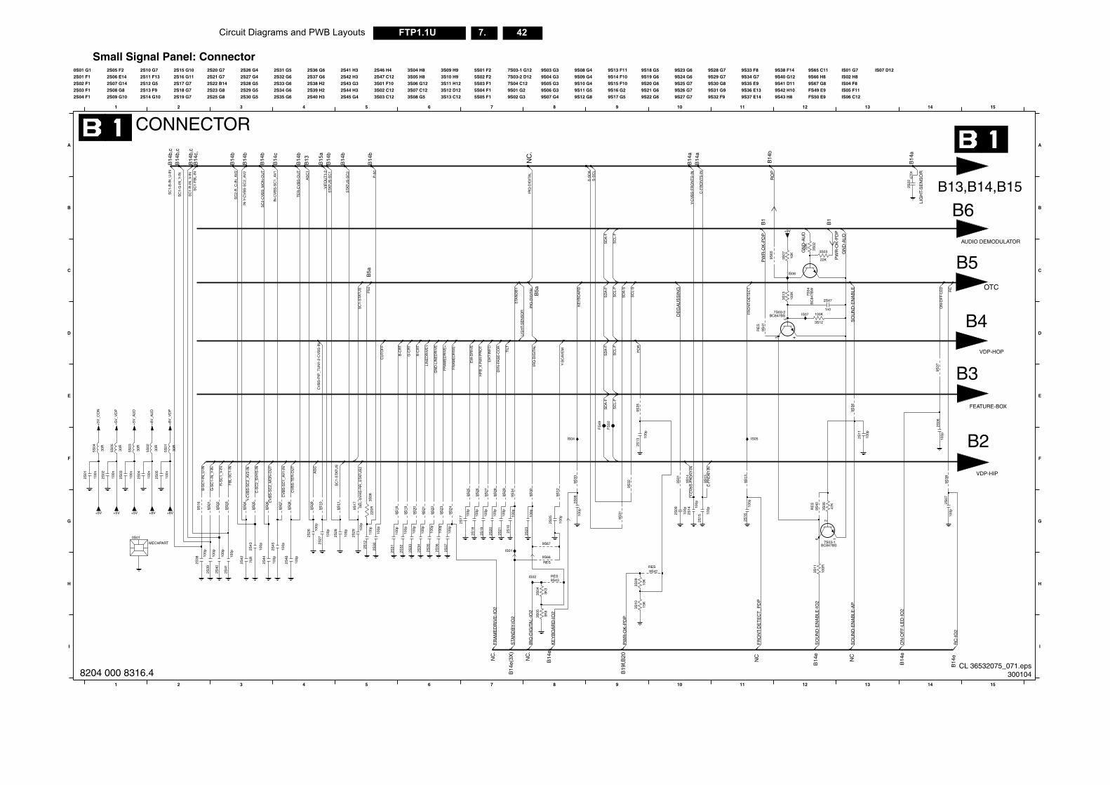
42FTP1.1U 7.Circuit Diagrams and PWB Layouts
B6
B14
a
B1
B14
e
5R
9S67 G8
FS49 E9
FS50 E9
IS01 G7
IS02 H8
IS04 F8
IS05 F11
IS06 C12
IS07 D12
B14
b
B3
B1
9S38 F14
9S40 G12
9S41 D11
9S42 H10
9S43 H8
9S65 C11
9S66 H8
FEATURE-BOX
B4
NC
VDP-HOP
VDP-HIP
B5
B14
e
B14
e
1512 13 14
OTC
AUDIO DEMODULATOR
12 13 14 15
F
G
H
I
B2
B13,B14,B15
A
B
C
D
E
1n0
2S47
9S40
RE
S
BC847BS
5
3 4
47K
3S06
7S03-2
0p46
9S65
IS07
3S13
100K
44 9S660p
3S07
10K
9S38
2
3S03
22K
22K
3S02
2
470n
2S22
2S
100p
42
2S07
7S04
BC
847B
W
+9V
9S41
100p
38
2S
3S11
100R
9S37
9S36
100p
7S03-1
2
6 1
BC847BS
100p
2S11
100p
2S06
100p 22
IS06
100K
3S12
IS01
100p 2
GN
D-A
UD
SO
UN
D-E
NA
BLE
-IO
2
RC
-IO
2
ON
-OF
F-L
ED
-IO
2
GN
D-A
UD
PW
R-O
K-P
DP
PW
R-O
K-P
DP
RO
P
LIG
HT-
SE
NS
OR
SO
UN
D-E
NA
BLE
-AP
SO
UN
D-E
NA
BLE R
C
ON
-OF
F-L
ED
CL 36532075_071.eps300104
B19f,B
20
7 RES
B14
e(3X
)
NC
.
NC
.
NC
B14
e
4 5 6 7 8 9 10 111 2 3
H
I
102S2S 10
3S09
10K
5K6
3S05
9S43RES
9S42RES
2S2S
3K3
3S04
3S10
15K
2S39
2S40
IS02
2S41
FR
ON
T-D
ET
EC
T_P
DP
FR
AM
ED
RIV
E-I
O2
STA
ND
BY-
IO2
KE
YB
OA
RD
-IO
2
PW
R-O
K-P
DP
IRQ
-DIG
ITA
L-IO
2
8204 000 8316.4
Small Signal Panel: Connector
B5a
B5a
9S28 G7
B14
c
CONNECTOR
B14
b
9S29 G7
9S30 G8
9S31 G9
9S32 F9
9S33 F8
9S34 G7
9S35 E9
9S36 E13
9S37 E14
7S04 C12
9S01 G2
9S02 G3
9S03 G3
9S04 G3
9S05 G3
9S06 G3
9S07 G4
9S08 G4
9S09 G4
9S10 G4
9S11 G5
9S12 G8
9S13 F11
9S14 F10
9S15 F10
9S16 G2
9S17 G5
9S18 G5
9S19 G6
9S20 G6
9S21 G6
9S22 G6
9S23 G6
9S24 G6
9S25 G7
9S26 G7
9S27 G7
3S11 H12
B13
3S12 D12
3S13 C12
5S01 F2
5S02 F2
5S03 F1
5S04 F1
5S05 F1
7S03-1 G12
7S03-2 D123S05 H8
NC
.
B14
b
B14
c,
3S06 G12
3S07 C12
3S08 G5
3S09 H9
3S10 H9
2S45 G4
2S46 H4
2S47 C12
3S01 F10
3S02 C12
3S03 C12
3S04 H82S26 G4
B15
a
B14
b
B14
b
B14
aB
14a
2S27 G4
2S28 G5
2S29 G5
2S30 G5
2S31 G5
2S32 G6
2S33 G6
2S34 G6
2S35 G6
2S36 G6
2S37 G6
2S38 H2
2S39 H2
2S40 H3
2S41 H3
2S42 H3
2S43 G3
2S44 H3
B14
b,c
B14
b
B14
b
B14
b
2S08 G8
2S09 G10
2S10 G7
2S11 F13
2S12 G5
2S13 F9
2S14 G10
2S15 G10
2S16 G11
2S17 G7
2S18 G7
2S19 G7
2S20 G7
2S21 G7
2S22 B14
2S23 G8
2S25 G8
B14
b,c
B14
b,c
6 7 8 9 10 11
0S01 G1
2S01 F1
2S02 F1
2S03 F1
2S04 F1
2S05 F2
2S06 E14
2S07 G14
1 2 3 4 5
A
B
C
D
E
F
G
100p
2S45
100p
2S08
9S29
9S03
9S09
9S32
9S31
9S25
5S02
30R
9S07
2S04
100n
9S06
2S02
100n
9S33
+5V
100p
2S25
2S09
100p
3S01
30R
5S01
3S08
220R
9S22
100p
2S28
IS05
30R
5S04
9S12
100p
2S29
9S01
9S21
9S15
+5V
2S18
9S10
100p
100p
S36
5S05
30R
100p
2S14
9S24
9S13
9S20
100p
2S12
9S19
100p
S35
100n
2S01
100p
2S19
9S14
9S30
100p
32100p
2S43
RE
S
100n
2S03
9S16
30R
5S03
MECHPART
0S01
FS
49
100p
31
9S27
+5V
9S05
9S17
9S67
9S35
9S18
100p
2S16
9S34
100p
2S13
100p
2S21
100n
2S05
100p
2S17
100p
2S30
9S02
FS
50
9S08
+8V
100p
S37
+8V
100p
S33
100p
2S20
9S11
IS04
2S10
100p
9S28
9S04
9S26
100p
2S27
9S23
100p
S34
100p
2S23
100p
2S15
100p
2S26
CU
TOF
F
SD
A-S
SC
L-S
DE
GA
US
SIN
G
S-S
DA
S-S
CL
+8V
_AU
D
+8V
_VD
PS
C1-
B-I
N_U
-IN
SC
1-F
BL-
IN
SC
1-G
-IN
_Y-I
N
Y-C
VB
S-F
RO
NT
S-I
N
SC
1-R
-IN
_V-I
N
SC
2-C
VB
S_M
ON
-OU
T
P-5
0
STA
TU
S-S
C2
TE
R-C
VB
S-O
UT
AG
C1
IN-Y
-CV
BS
-SC
2_A
V2
IN-C
VB
S-S
C1_
AV
1
C-F
RO
NT
S-I
N
SC
2-R
_C-I
N_A
V2
VIF
OU
T1-
2
CV
BS
-PIP
_TU
N1-
2-C
VB
S-I
N
STA
TU
S-S
C1
LIG
HT-
SE
NS
OR
IRQ
-DIG
ITA
L
DY
N-F
AS
E-C
OR
AG
C
Y-S
CA
VE
M
C-F
RO
NT-
IN
Y-C
VB
S-F
RO
NT-
IN
FR
ON
T-D
ET
EC
T
B-C
RT
G-C
RT
R-C
RT
LIN
ED
RIV
E1
FR
AM
ED
RIV
E+
FR
AM
ED
RIV
E-
EW
-DR
IVE
HF
B_X
-RAY
-PR
OT
EH
T-IN
FO
TIL
T
IRQ
-DIG
ITA
L
SC
1-S
TAT
US
IRQ
-DIG
ITA
L
+5V
_CO
N
+5V
_VD
P
+5V
_AU
D
SD
A-F
SC
L-F
SD
A-F
SC
L-F
SD
A-F
SC
L-F
SD
A-F
SC
L-F
P50
KE
YB
OA
RD
STA
ND
BY
PO
R
B-S
C1-
IN_U
-IN
G-S
C1-
IN_Y
-IN
R-S
C1_
V-I
N
FB
L-S
C1-
IN
Y-C
VB
S-S
C2_
AV
2-IN
C-S
C2_
SV
HS
-IN
CV
BS
-SC
2_M
ON
-OU
T
CV
BS
-SC
1_A
V1-
IN
CV
BS
-TE
R-O
UT
SC
1-S
TAT
US
SE
L-S
VH
S-R
R_S
TAT
US
2
GN
D-L
INE
DR
IVE
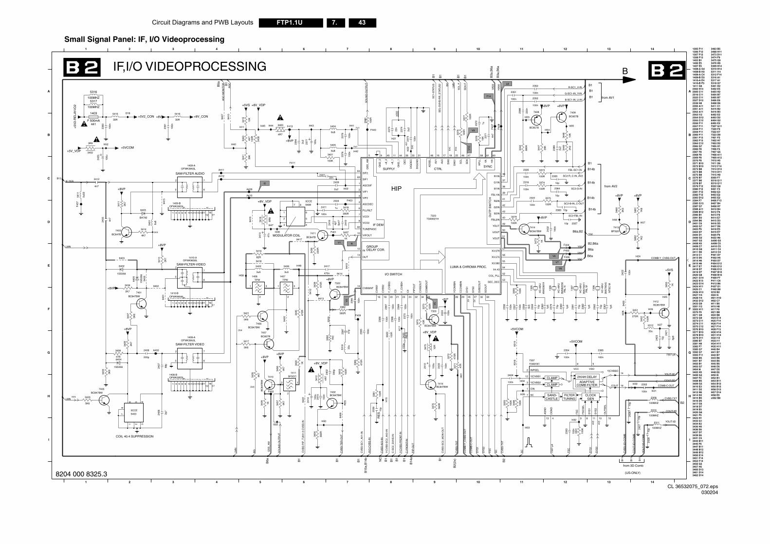
Circuit Diagrams and PWB Layouts 43FTP1.1U 7.
2H/4H DELAY
ADAPTIVECOMB FILTER
FILTERTUNING
CLOCK
CLAMP
GEN
CLAMP
SAND-CASTLE
I425 F14I426 F14I427 F14I428 F13I430 H14I431 H14I432 I12I433 I11I434 H11I435 H11I440 B4I441 B7I442 B7I443 B6I444 B5I445 B5I446 D5I447 D5I448 E6I450 I6I452 B1I453 B11I454 B12I455 B12I456 D13I457 D14I458 E5c002 B8
F408 B10F409 F7F411 C6F413 B6F437 D1F440 B8I318 B2I322 I5I401 H10I402 C7I411 B5I415 H8I417 F8I421 B8I422 B8I424 E14
B1
B1
4V2
PA
L M
B6a,B29418 E59419 E79420 F69422 H6A400 G3A409 C5A410 C5A411 C4A412 C4F401 D7F402 H5
B14b
B14b
F403 D7F404 E12F405 E12F406 E12F407 B10
9406 F139407 B49408 H79410 B49412 F69413 F69414 E79415 D39416 D59417 D6
B6a
B14b
7411 D67412 F147413 D137414 D117415 H99300 F79318 G119319 G119322 G89401 F39402 E39403 E29405 E2
B14b
B1
5V0
PAL
N
B2,B6a
7307 G117320 F97322 E77323 D97401 F27402 H77403 D27405 H17406 F57407 G57408 A117409 A127410 H5
B6a
NT
SC
M
5406 E65408 D65411 C15415 B25416 B36402 E26403 D26404 G26405 E2
B11
B11
3476 H95309 H145310 H145311 I145312 F145316 A15317 A15318 G75401 D25402 E55403 H25404 B75405 B7B1
3448 B123449 B123450 E143451 F143452 F143456 G53457 H53460 D133461 D143462 D14
3463 B53468 H113473 D113474 F93475 G9
B
3417 G53418 D73419 E53420 G63421 F53423 H13433 G13434 E23435 H53436 E63437 D73439 E63441 C53444 B113445 F63447 B11
3393 F113400 B53401 B73402 B13403 G73404 I63405 H53406 G23407 F23408 B53409 G23410 E33411 D23412 H63414 D23415 B5
from AV2
3416 D5
3301 I123303 H113370 F93371 G93372 G93373 C113374 C113375 C123376 B103377 B103378 B103379 D113380 B73381 H83382 F73385 G7
4V2
from 3D Comb
B11
3392 G7
2404 D72405 D12406 G22407 G32408 H32409 C72410 G92411 D62412 C12413 D52414 H62415 H62417 E72418 D72419 D72420 G82421 G142422 E132423 G142424 H112425 C12426 H132427 I142428 I142432 D122433 G9
2370 F82371 B102372 B102373 B82374 B82375 B82376 B72377 B62378 B72379 F122380 F122381 F122382 F122383 D122384 F72385 G13
from AV1
2387 G72388 A112389 B122390 B12391 B32394 B62401 C62402 G72403 F9
1410-A E41410-B F31411 G62302 H142305 C112316 C112322 C112327 D122339 H82350 A112351 A112352 A112353 I122354 G122355 C122356 F112357 F112358 F112359 F112360 F112361 F132362 F132364 C122365 G72366 F82367 F82368 F82369 F8
12 13 14
(US-ONLY)
1307 F121308 F131403 B11406 E51407 E51408-A G41408-B H31409-A C41409-B D3
12 13 14
A
B
C
D
E
F
G
H
I
1305 F111306 F12
B2
2427
10p
10K
3448
10p
2428
1p5
2380
1216
171 184 5 6 9 101314 15 11
3M57
9545
1308
HC
-49/
U
2383 10p
10p 2327
1K3450
150R
3452
100n
2385
100n
I454
10p
2423
33u
5312
2353
100n
9406
100n
2354
13
+5VS
100n
2302
3M57
5611
1307
HC
-49/
U
HC
-49/
U
1306
3M58
2056
7415BC847BW
2350
100n
3461
1K8
I427
3375
F406
100R
F404
100K
3301
10p
2364
2K2
3449
2355
10p
3n3
6p8
2421
3374
+8VP
I424
100R
+8VP
15p
2362
4M43
3619
1305
HC
-49/
U
1p5
2361
39K
3447
I431
+8VP
BC847BW
7414
FS
CS
EL
INPSEL
15
OU
TS
EL
SC
11
SY
S1
10
SY
S2
6
VCC VDD
5
Y|CVBS1
3 Y|CVBS2
14Y|CVBSO
TDA91817307
13
AG
ND
CIN16COUT
4
DG
ND
9
FS
C
8
2382
1p5
I425
5311
2381
15p
100MHZ
2389
2u2
100n
2352
100n
2322
I432
2360
1p5
I457
I455
F405
10p
2426
7409
BC857B
100n
2422
2359
15p
1K2
3462
7412BC857BW
3K3
3460
100R
3373
+5VCOM
15p
2379
I428
847B
W
I456
I430
I426
270R
3451
BFS20
7413
3473
1K
100n
2432
100MHZ
5309
BC857B
+8VP
7408
+8VP
5310
100MHZ
FBL-SC1-IN
R-SC1_V-IN
G-SC1-IN_Y-IN
Y50
V50
U50
CO
UT-
3D-C
OM
B
CVBS-TXT
COUT-3D
YOUT-3D
Y50
SC2-R_C-IN_AV2
SC2-G-IN
SC2-B-IN_C-OUT
SC2-FBL-IN
CV
BS
-3D
-CO
MB
B-SC1-IN_U-IN
SY
S1
SY
S2
7307
-p4
FS
C
7307-p4
COMB-C-OUT
COMB-Y_CVBS-OUT
COUT-3D
YOUT-3D
YO
UT-
3D-C
OM
B
CL 36532075_072.eps030204
V8
V6
V7
RE
S
B14
a
B15
a,B
14b
B2(
2x)
B1
B1 B1
B1 B1
B6a
0V4
RE
S
COIL 40.4 SUPPRESSIONB
1
B1
B1
1 2 3 4 9 10 11
H
I
NC
B2
5 6 7 8
54035CCE
1 2 3456
78
100n
2415
1K3405
100K
3303I4
15
2
I450
I435
2414 10
0u
7402BC847BW
BC847BW
7405
3468
100K
3457
4K7
9408
9422
10p
2339
7
1
3476
560R
5K6
3423
I433
F402
2p7
2408
BC
3381
100R
3404
560R
I322
FS
C
SC
PIP
-OU
T
CO
MB
-C-O
UT
CV
BS
-TX
T
C-F
RO
NT-
IN
CV
BS
-TE
R-O
UT
Y-C
VB
S-F
RO
NT-
IN
CV
BS
-TX
T
CV
BS
-PIP
_TU
N1-
2-C
VB
S-I
N
CV
BS
-SC
2_M
ON
-OU
T
CO
MB
-Y_C
VB
S-O
UT
SY
S2
SY
S1
SO
UN
D-O
UT
PU
T
QS
S_A
M
LMN
LMN
CV
BS
-AV
3-IN
AV
3-C
VB
S-I
N
CV
BS
-SC
1_A
V1-
IN
C-S
C2_
SV
HS
-IN
Y-C
VB
S-S
C2_
AV
2-IN
SC
BG
8204 000 8325.3
Small Signal Panel: IF, I/O Videoprocessing
NCMT
NCMT
NCMT
IF DEM
SUPPLY CTRLSYNC
OU
TP
SW
ITC
H
LUMA & CHROMA PROC.
I/O SWITCH
DELAY COR.GROUP
0V4
B3a
,B6a
0V4
0V 5V
0V4
B13
RE
S
B5a
B1
HIP
5V0
SAW-FILTER VIDEO
B3a
,B6a
7V7
4V1
MODULATOR COIL
IF,I/O VIDEOPROCESSING
B1
7V7
5V0
SAW-FILTER AUDIO
B1
B1
SAW-FILTER-VIDEO
B1
3 4 5 6 7 8 9 10 11
A
B
C
D
E
F
G
100R
1 2
BC847B
7403
33u
5318
9403
6402
1SS356
F409
1408-BOFWK3953L
1406TPW
1
2
3
3380
100R
9413
2374
2u2 F40
8
3418
390R
I452
2356
100n
+8VP
5404
6u8
2413
47u
100n
2369
7320
BC847BW
9414
3419
82R
100n
2384
1
2
3 4
5
6
7 85CCE5408
2424
9410
OFWK9656L1410-A
2
3
7
8
3378
15K
+5VCOM
9416BA792
6403
3393
100K
2420
150p
47p
2387
1K0
3392
9300
9415
3437
1K
2419
0p47
2372 1u
3416
6R8
1408-AOFWK3953L
2
3
7
8
F403
+8VP
9318
4K7
3463
+8VP
+8VP
68p
2407
F440
F411
9405
I422
2404
1u
SFSCC1411
2u2
2394
+8V_VDP
4n7
2412
9 101314 15 1112
1617
F413
OFWK3953L1409-B
1 184 5 6
100R
3377
3409
2K7
+5V_VDP
2417
470n
+8VP
2305
100n
I442
+8V_VDP
4R7
3400
22n2401
9322
0u33
5411
+8V_CON
3434
2K7
10K
3415
A409
9401
47R
3406
3408
100R 23
71
4n7
3436
220R
560R
3382
2370
100n
3379
100R
I441
680K
3444
+8VP
2358
BC847BW
7322
I445
2418
4p7
7407
BC857B
2375
22n
1K3420
2K7
3411
470R
3385
2K7
3410
2367
100n
I447
4 5 6 9 101314 15 1112
1617
OFWK9656L1410-B
1 18
+5VCOM
100n
2368
I443
3474
10R
9419
3372
470R
+8V_VDP
100n
2391
3R9
3402
2390
100n
+5V2_CON
I421
+5V
2-R
ELA
Y-IO
2
9407
3417
5K6
2
12
9420
9319
BC847B
7411
2388
220n
30R
5416
3445
470R
TPW1407
1
2
3
7401
BC847BW
2411
100n
5K6
3421
4K7
3435
9417
100n
2365
100n
2433
3475
10R
I434
4K7
3414
4K7
3456
6u8
5405
I402
7
8
2377
100u
100u
2425
OFWK3953L1409-A
2
3
A412
I446
I444
100n
2351
3441
39K
3376
100R
1SS
356
6405
I440
2409
100R
2u2
100n
2378
3370
+8VP
100K
3401
6404
1SS356
3407
5K6
+8V_VDP
9402
9412
2403
100n
A411
7406
BC847BW
I401
100n
2316
9418
3u9
5402
4n7
2405
F43
7
F40
7
8
VIF12
VIF23
VIFOUT10
VOUT51
X3.57556
X3.57957
X3.58255
X4.4354
YC
OM
BIN
28
YOUT49
Y_C
VB
S3
20 23
Y_C
VB
S4
SC
L
46
SC
OU
T
59
SD
A
47
SEC_DEC53
SIF163
64SIF2
SV
BC
OU
T
30
SW
0
19
SW
01
22
SY
S1
25
SY
S2
27
62TUNERAGC
UOUT50
VA
61
VCO17
VCO2
31
FBL1IN39
FBL2IN40
G1IN37
G2IN42
GN
D_1
44
GN
D_2
9
HA
60
HP
LL
58
IN12
OUT13
PIP
OU
T
32
PLLRILT6
QS
S_A
M
5
R1IN36
R2IN41
15
AV
2
17
B1IN38
B2IN43
C3
21
C4
24
CC
OM
BIN
29
COL_PLL52
CO
MB
OU
T
26
CV
BS
1
16
CV
BS
2
18
CVBSINT14
CV
BS
OU
T
34
DE
C
35
DIG
DE
C
33
DIG
GN
D
7323TDA9321H
+8_
1
1145
+8_
2
AD
SE
L
48
AGCDEC4
AGCSIF1
AV
1
F401
330p
2402
3K9
3433
A410
c002
2366
100n
7410
+8V
220p
2406
+8VP
I458
4R7
3412
+5VS
3371
47R
3403
100R
100u
2410
5401
6u8
5415
30R
5406
3u3
I453
2373
100n
A400
I318
2376
100n
I448
100n
2357
+8VP
I417
5317
100MHZ
5316
100MHZ
F 500mA
1403
441
3439
470R
I411
HA
50
SE
L-S
VH
S-R
R_S
TAT
US
2
SC
1-S
TAT
US
AG
C
SO
UN
D-O
UT
PU
T
VA
50LMN
BG
AG
C-M
ON
ITO
R
LMN
SC
L-F
SD
A-F
IF-TER
V2
V5
V1
I5
I6
V9
V10
L8
F14
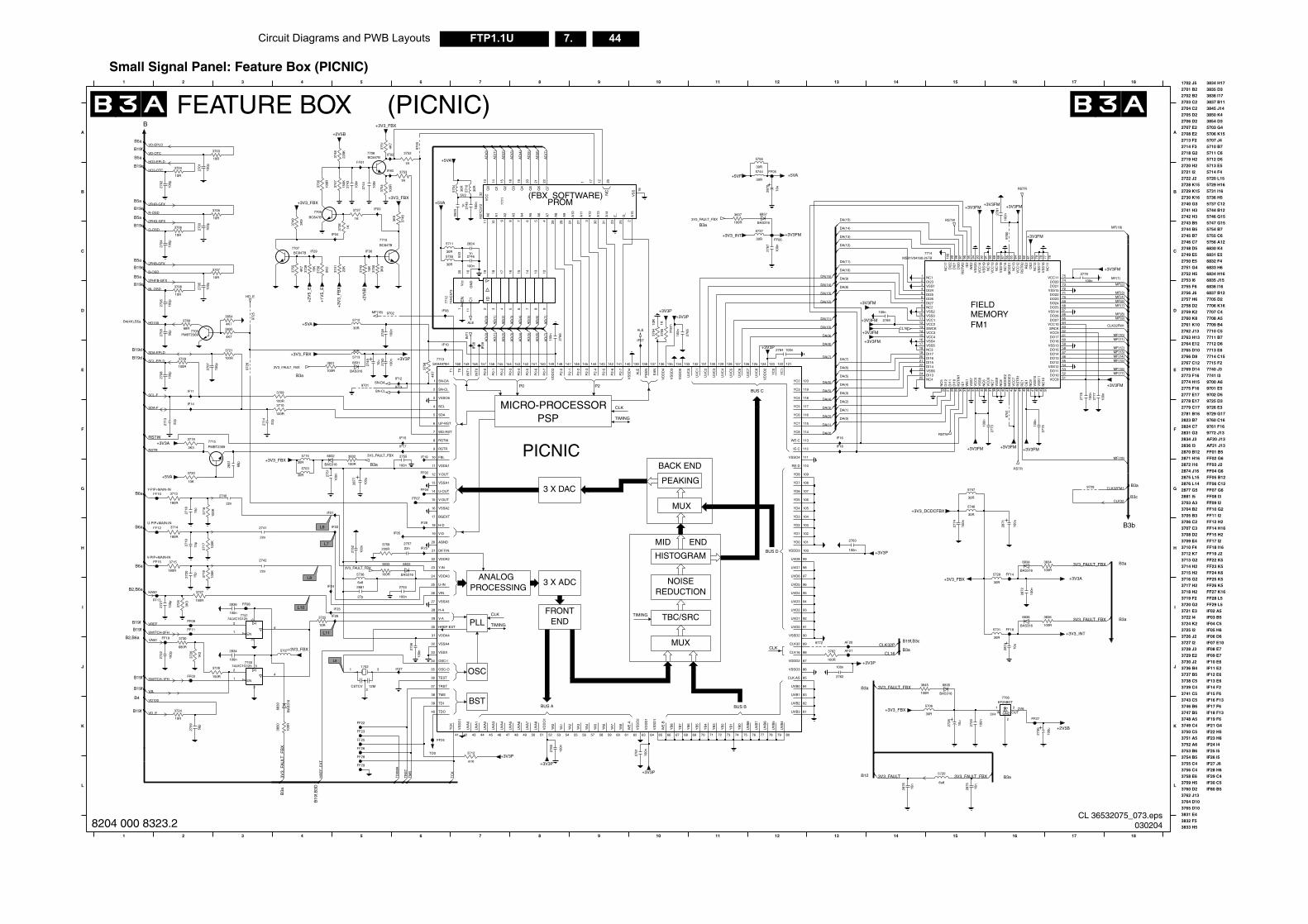
44FTP1.1U 7.Circuit Diagrams and PWB Layouts
CLK
2742 H3
2743 B5
2744 B5
2745 B7
2746 C72748 D5
2749 E5
15 16 17 18
L
1702 J5
2765 D10
2766 D8
2767 C122769 D14
2773 F16
2774 H15
2775 F16
2701 B22702 B2
2703 C2
2704 C2
2705 D2
2706 D22707 E2
3V4
2740 G3
2741 H3
2870 B12
2871 H162872 I16
2874 J16
2875 L15
2876 L142877 G5
FM1
A
B
C
D
E
F
G
H
I
J
K
2763 H13
2764 E12
3714 H2
3715 H2
3716 G23717 H2
3718 H2
3719 F2
3720 G2
B3b
2834 J3
2836 I3
3743 C53746 B6
3747 B5
3748 A5
3749 C4
3750 C53751 A5
15 16 17 18
3712 K7
3713 G2
3764 D10
3765 D10
3831 E4
3832 F53833 H5
3834 H17
3835 D3
2V6
2708 E2
2713 F2
2714 F3
2718 G22719 H2
2720 H2
2721 I2
2722 J22728 K15
2729 K15
2730 K16
3739 C4
3741 C5
5710 B7
5711 C65712 D5
5713 E5
5714 F4
5720 L155729 H16
2750 E5
2751 G4
2752 H52753 I6
2755 F6
2756 J6
2757 H6
2758 D22759 K2
2760 K8
2761 K10
2762 J13
3760 D23762 J13
5756 A126830 K4
6831 E5
6832 F4
6833 H6
6834 H166835 J15
2777 E172778 E17
2779 C17
2781 B16
2823 B7
2824 C72831 G3
5706 K15
5707 J4
6836 I16
6837 B12
7705 D2
7706 K167707 C4
7708 A5
7709 B4
2881 I5
3703 A3
3704 B2
3705 B33706 C2
3707 C3
3708 D2
3709 E4
3710 F4
5754 B7
5755 C6
FF04 G6
FF05 B12
FF06 C12FF07 G6
3721 E33722 I4
3724 K2
3725 I2
3726 J23727 I2
3728 J3
3729 E2
3730 J2
3736 B43737 B5
3738 C5
FF22 K5
FF23 K5
FF24 K6
FF25 K5FF26 K5
FF27 K16
FF28 L5
3836 I17
3837 B11
3845 J14
3850 K4
3854 D35703 G4
IF11 E2IF12 E6
IF13 E6
IF14 F2
IF15 F6
IF16 F13IF17 F6
5731 I16
5736 H5
5737 C12
5744 B125746 G15
5747 G15
FF18 I16FF19 J2
B3a
FF29 L5
IF02 A5IF03 B5
IF04 C5
IF05 H6
IF06 D6IF07 E10
IF08 E7
IF18 F13
IF19 F6
IF09 E7
IF10 E6
FF08 I3
FF09 I2
FF10 G2
FF11 I2FF12 H2
FF14 H16
FF15 H2
FF17 I2
FIELDMEMORY
B3a
B19f,B3c
7712 D6
7713 E6
7714 C15
7715 F27740 J3
7741 I3
9700 A6
9701 E5
9702 D59725 D3
9726 E3
IF23 H6
IF24 I4
IF25 I5
IF26 I5
IF27 J6IF28 H6
IF29 C4
IF30 C5
IF80 B5
IF21 G4
IF22 H5
3752 A6
3753 B6
3754 B5
3755 C43756 C4
3758 E6
3759 H5
9729 G17
9760 C16
9761 F169772 J13
AF20 J13
AF21 J13
FF01 B5
FF02 G6FF03 J2
B3a
B3a
7710 C57711 B7
B3a
B3c
VSSX33 88CLK162834
FF14
VSS417 VSS5
23 VSS6
33V
SS
7
35V
SS
8
39V
SS
9
32W
E1
94W
E2
VCC8
62VCC9
3 VSS1
48V
SS
10
49V
SS
11
54VSS12
59VSS13
67VSS14
72VSS15
VS
S16
7778V
SS
17
87V
SS
18
91V
SS
19
9 VSS2
93V
SS
20
10 VSS3
16
RS
TW
1
96R
ST
W2
63SRCK13 SWCK
11 VCC164VCC10
75VCC11
83V
CC
12
89V
CC
13
92V
CC
14
12 VCC2
14 VCC315 VCC4
34V
CC
5
37V
CC
6
43V
CC
7 51
NC
16
100
NC
17
8 NC2
18 NC3
25 NC4
26N
C5
36N
C6
38N
C7
40N
C8
47N
C9
46O
E1
80O
E2
45R
E1
81R
E2
44R
ST
R1
82R
ST
R2
30
DO2468DO25
66DO2665DO27
31IE
1
95IE
2
85M
OD
E1
41M
OD
E2
42M
OD
E3
1 NC1
50N
C10
76N
C11
79N
C12
84N
C13
86N
C14
88N
C15
90
DI245 DI256 DI267 DI27
52DO10
53DO11
55DO12
56DO13
57DO14
58DO15
60DO16
61DO17
74DO2073DO21
71DO2270DO2369
MS81V04160-25TB7714
29D
I10
28D
I11
27D
I12
24 DI13
22 DI14
21 DI15
20 DI16
19 DI17
97D
I20
98D
I21
99D
I22
2 DI23
4
9729
+3V3FM
10u
277310
0n
2874
BAS316
3726
1K2
6835
2872
100n
5707
2779
100n
FF18
AF21
+3V3FM
+3V3FM
BX
100u
2730
10u
2728
+3V3A
+3V3FM
3836
100R
3845
100R
BAS316
6836
+3V3FM
+3V3FM
9760
5746
30R
+3V3FM
+2V5B
277510
0n
+3V3_DCDCFBX
5706
30R
+3V3_FBX
9761
2729
100n
+3V3FM
6u8
5720
+3V3FM
100n
2778
+3V3_FBX
100R
3834
2777
100n
2
GNDIN1 3
OUT
30R
5747
7706KF25BDT
2774
100n
3762
2875
2876
10n
10n
BAS316
6834
2781
100n
2871
100u
5731
30R
5729
30R
27
100n
2722
100p
+3V3_INT
FF27
3V3_FAULT_FBX
RSTW
CL16
CLK32
CLK32FM1
3V3_FAULT_FBX
3V3_FAULT_FBX
_FBX
MF(1)
MF(2)
MF(3)MF(4)
MF(18)
RSTR
RSTR
RSTW
MF(17)MF(16)
MF(15)MF(14)MF(13)MF(12)
MF(11)MF(10)
MF(9)MF(8)
MF(7)MF(6)
MF(18)
CL16
CLK32FM1
CL 36532075_073.eps030204
BUS A BUS B
OSC
BST
EN
J
1 2 3 4
K
L
5 6 7 8 9 10 11 12 13 14
B19
f,B3D
B19f
B3a
B3a
B12
FF26
B19f
B4
B19f
YB
074
YB
173
YB
2
72
YB
3
71
YB
4
70
YB
5
69
YB
6
68
YB
7
67
YB
8
62
WE
-A
66
WE
-B
53
YA0
54
YA1
55
YA2
56
YA3
57
YA4
58
YA5
59
YA6
60
YA7
61
YA8
75
VS
SD
1
6542
VS
SO
1
63
VS
SO
2
86VSSO3
64
VD
DD
1
87VDDD2
52
VD
DO
1
UV
B8
UV
A1
45
UV
A2
46
UV
A3
47
UV
A4
48
UV
A5
49
UV
A6
50
UV
A7
51
UV
A8
84UVB0
83UVB1
82UVB2
81UVB3
80
UV
B4
79
UV
B5
78
UV
B6
77
UV
B7
76
TC
K
41
39 TDI
40 TDO
TEST36
38 TMS
37 TRST
UV
A0
43 44
34 OSC-I
35 OSC-O
85CLK-AS
100n
BA
S31
6
6830
100R
3850
3728
150R
100n
2762
FF25
FF28
FF03
+3V3P
FF22
47K
3712
74LVC1G1257740
2
3
1
5
4
+3V3_F
2759
56p
1 3
212MCSTCV
1702
FF29
10R
3724
+3V3P
+3V3P
100n
2760
2761
100n
100R
FF24
+3V3P
FF23
IF27
VA
3V3_
FAU
LT_F
BX
3V3_FAULTHR
EF
_EX
T
SWITCH-1FH
VD100
VD_E
3V3_FAULT
TD
0MA
TC
K
TD0
TM
ST
RS
T
8204 000 8323.2
L9
Small Signal Panel: Feature Box (PICNIC)
3 X DAC
P0
BUS D
BUS C
TIMING
CLK
P2
ANALOGPROCESSING
PSPMICRO-PROCESSOR
BACK END
PEAKING
MUX
MID END
HISTOGRAM
NOISEREDUCTION
TBC/SRC
MUX
TIMING
TIMING
CLK
3 X ADC
FRONTENDPLL
NC
PROM
EN
EN
C1
1D
D
E
F
G
H
I
PICNIC
10 11 12 13 14
B
C
B2,B6a
1 2 3 4 5 6 7 8 9
inte
rn
A
B6a
5V2
5V2
B5a
B5a
B5a
B5a
B19d
B19e
B19e
B6a
B19d
FEATURE BOX (PICNIC)B
B4(4X),B5a
B19f
B19e
B19e
B19e
(FBX SOFTWARE)
B6a
B5a
B19f
B5a
B2,B6a
B19f
B3a
B3a
B3a
10u
2870
150R
3K9
3749
FF11
3727
YC7
114YC8
101YD0
YD1 102
103YD2
104YD3
105YD4
106YD5
107YD6
108YD7
YD8 109
122
YC
0
YC
1
121
120YC2
119YC3
118YC4
117YC5
116YC6
115
7 WD-RST
113WE-C
23 Y-IN
Y-OUT12
VD
DO
3
VIN26
13 VSSA1
16 VSSA2
27 VSSA3
32 VSSA4
90VSSD2
134
VS
SD
3
139
VS
SD
4
VSSO4 111
133
VS
SO
5
3 VSSO6
UVD6
98UVD7
99UVD8
29 V-A
19 V-D
15 V-OUT
VDDA111
22 VDDA2
24 VDDA3
31 VDDA4
100VDDD3
VD
DD
4
135 123
VD
DO
2
148 132
UV
C0
131
UV
C1
130
UV
C2
129
UV
C3
128
UV
C4
UV
C5
127 126
UV
C6
125
UV
C7
124
UV
C8
91UVD0
92UVD1
93UVD2
UVD3 94
95UVD4
96UVD5
97
SCL
5 SDA
2 SN-CL
1 SN-DA
159
T0
160
T1
25 U-IN
14 U-OUT
6 UP-RST
P0-
4
151
P0-
5
150
P0-
6
149
P0-
7
147
P2-
0
146
P2-
1
145
P2-
2
P2-
3
144 143
P2-
4
142
P2-
5
141
P2-
6
140
P2-
7
137
PS
EN
110RE-D
9 RSTR
8 RSTW
4
CLK32
21 DIFFIN
136
EA
N
10 FBL
28 H-A
18 H-D
HREF-EXT30
112IE-C
157
INT
0
158
INT
1
156
P0-
0
155
P0-
1
154
P0-
2
153
P0-
3
1527713
SAA4978H
20 AGND
138
ALE
17 BGEXT
89
2749
10u
+5VA
22n
2740
30R
5713
2766
100n
2755
100n
9700
30R
5703
100p
2721
3720
10K
3719
3K3
22K
3741
10R
3708
IF10
3K9
3750
4K7
3835
3K3
3725
BC847B7708
2767
100n
9772
4K7
3854
+2V5B
2765
100n
3707
10R
30R
5744
3715
180R
3714
180R
+5VA
BAS316
6837
22n
2742
IF80
1K37
65
IF02
2758
56p
FF01
IF29
IF19
IF13
7715
PMBT2369
6832
+3V3P
BAS316
3736
100R
+3V3FM
30R
5754
6831
BAS316
100R
3832
100R
3710
100n
2743
100K37
16
3730
680R
+3V3_FBX
30R
5711
10R
3764
5755
30R
3703
10R
+3V3_FBX
2750
100n
+3V3FM
100R
3721
2714
22p
3709
100R
AF20
+3V3FM
150K
3747
2753
100n
100p
2701
3713
180R
15p
2720
2708
100p
22p
2713
+3V3_FBX
IF30
+2V
5_E
+3V3FM
5736
6u8
9702
100R
1R
3753
3831
+5VA
+3V3P
2751
100n
FF06
IF07
IF18
IF15
3743
15K
100p
2707
+1V
5_E
+3V
3_F
BX
+3V3P
275722n
3729
100R
100p
2705
BC847B7707
Q3
19Q
4
20Q
5
21Q
6
22Q
7
32
VC
C
16
VS
S
A3
7A
4
A5
6 5A
6
A7
4
29A
8
28A
9
1 17
E_
23 25G
_
261213Q
0
14Q
1
Q2
15 18
M27
C51
2 7711
11A
0
10A
1
24A
10
A11
27
A12
3
30A
13
31A
14
A15
2
A2
9 8
2
3
1
5
4
+3V3P
774174LVC1G125
2744
100n
IF06
9701
2877
100u
10R
3704
3755
4K7
3738 1K2703
100p
FF09
FF15
FF17
+2V
5B
5737
30R
3754
27p
2881
100R
2824
1n
3K9
3746
IF08
2836
100n
+5VA
2752
100n
4K7
3758
100K
3718
3717
100K
100n
2746
2764 100n
5714
30R
3737
1K
2745
100n
+5VA
15p
2718
7710
BC847B
FF12
FF10
BC847B
7709
2769
100n
PMBT23697705
+3V3A
+3V3P
FF05
2706
100p
9725
1R
3752
220K
3748
3706
10R +3V3_INT
5710
30R
IF25
IF26
IF14
3833
100R
IF03
2823
30R
5756
1n
FF08
IF17
+3V3_FBX
IF23
2702
100p
IF09
10R
3705
6833
BAS316
IF28
FF07
9726
3756
8K2
2748
100n
2831
68p
+5VF
IF12
IF11
3722
10R
30R
5712
56
68R
3760
2763
100n
+3V3_FBX
100p
2704
16
615
714
813
912
11G
ND
10
1V
cc20
7712
74H
C57
3
219
318
417
5
FF02
3739
15K
FF04
4K7
3751
IF22
IF05
IF21
FF19
IF24
220R3759
2741
22n
2719
3837
100R
15p
IF16
IF04
+3V3FM
3V3_FAULT_FBX
3V3_FAULT_FBX
VD-EPLD
2FHB-GFX
B-OSD
2FHFB-GFX
BL-OSD
SDA-EPLD
SCL-EPLD
SDA-F
SCL-F
HD100
DA(1)
DA(0)
DA(4)
DA(1)
DA(3)
DA(2)DA(0)
DA(2)
DA(5)
DA(6)
DA(8)
RSTR
3V3_FAULT_FBX
3V3_FAULT_FBX
HA50
VREF
SWITCH-2FH
G-OSD
R-OSD
2FHG-GFX
2FHR-GFX
HD3-OTC
HD3-EPLD
VD-OTC
AD
(0)
AD
(1)
AD
(2)
AD
(3)
AD
(4)
AD
(5)
AD
(6)
AD
(7)
AD
(0)
AD
(1)
AD
(2)
AD
(3)
AD
(4)
AD
(5)
AD
(6)
AD
(7)
MF(18)
V-PIP+MAIN-IN
HD_E
DA(15)
DA(14)
DA(13)
DA(12)
DA(11)
DA(10)
DA(9)
DA(8)
DA(7)
DA(6)
DA(5)
DA(4)
DA(3)
AD
(0)
AD
(1)
AD
(2)
AD
(3)
AD
(4)
AD
(5)
AD
(6)
AD
(7)
ALE
ALE
INT
1
RSTW
SN-CL
SN-DA
DA(15)
DA(14)
DA(13)
DA(12)
DA(11)
DA(10)
DA(9)
DA(7)
VA50
Y-PIP+MAIN-IN
U-PIP+MAIN-IN
CLK32P
L6
L10
L7
L8
L11
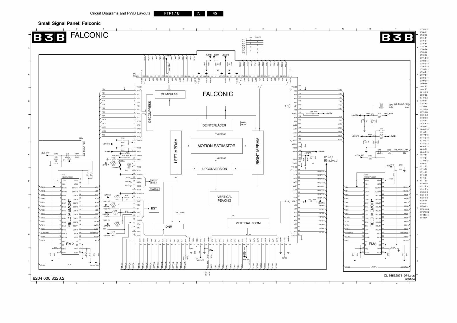
Circuit Diagrams and PWB Layouts 45FTP1.1U 7.
DNRF FIE
LD M
EM
OR
Y
B3a
B3a
B19c,f
3V4
3V4
FF43 E14
FF44 I7
B3 a,b,c,d
FM3
9722 F14
9723 I14
9724 I14
9727 I13
9728 I2
9755 I7
FF40 E2
FF41 C13
FF42 D13
5753 D13
6838 E13
6839 E2
6840 C13
7717 F1
7718 B4
7719 F13
9708 I7
9712 F3
2V6
2800 B8
9713 F2
9714 I2
9715 I2
9716 E4
9717 E3
9720 G4
9721 F14
3782 G4
3783 H4
3838 E14
3839 E2
3840 C14
5716 E1
5717 E13
5718 D13
5719 C13
2786 E4
11 12
2792 E13
2793 D13
2794 D13
2795 G11
2796 E11
2797 E11
2798 C11
2799 E14
2801 B7
2802 B7
2819 I14
2899 B5
3740 G4
3766 E4
3767 E3
3770 I6
3773 G3
3774 H3
3781 G3
A
B
C
D
E
F
G
H
I
2776 I12
2787 F4
2788 E4
2789 I6
2790 I8
2791 E13
2780 I1
2782 I3
2784 E1
2785 D4
11 12 13 14
13 14
0n
9722
2819
100n
+3V3FA
+3V3_INT
+2V5B
2792
10u
+3V3_FBX
+2V5FB
2793
100n
9727
9721
DOUT027
DIN014
30R
5718
5717
30R
YG683
82
UVA138
39
+2V5FB
10u
2794
5753
30R
100n
2776
5719
30R
21VCC2
39VCC3
1VSS1
22VSS2
40VSS3
17WE
31DOUT4
32DOUT5
33DOUT6
DOUT734
35DOUT8
36DOUT9
18IE
2NC1
19NC2
23OE
24RE
25RSTR
16RSTW
26SRCK
15SWCK
20VCC1
4DIN10
3DIN11
12DIN2
11DIN3
10DIN4
9DIN5
8DIN6
7DIN7
6DIN8
5DIN9
27DOUT0
28DOUT1
37DOUT10
38DOUT11
29DOUT2
30DOUT3
MSM54V12222A7719
14DIN0
13DIN1
100n
100n
2791
9723
9724
6838
BAS316
3838
100R
BAS316
6840
100R
3840
+3V3FA
100n
FF43
FF42
2799
100n
+3V3FAFF41
UV-2FH-7
UV-2FH-0
UV-2FH-1
UV-2FH-2
UV-2FH-3
UV-2FH-4
UV-2FH-5
UV-2FH-6
3V3_FAULT_FBX
WED
UVD3
UVD2
UVD1
UVD0
YD7
YD6
YD5
YD4
YD3
YD2
YD1
YD0
Y-2FH-3
Y-2FH-4
Y-2FH-5
Y-2FH-6
Y-2FH-7
CLK32 CLK32FM3
CLK32FM3
RSTR
CLK32FM3
RSTR
3V3_FAULT_FBX
Y-2FH-0
Y-2FH-1
Y-2FH-2
FB(0)
FE(11)
FE(10)
FE(9)
FE(8)
FE(7)
FE(6)
FE(5)
FE(4)
FE(3)
FE(2)
FE(1)
FE(0)
FE(12)
UVD3
UVD2
YD1
YD0
UVD1
UVD0
YD7
YD6
YD5
YD4
YD3
YD2
WED
TCKUVC3
CL 36532075_074.eps260104
B19
f
B19
f
3V4
FM2
4 5 6 7 8 9 10
I
1 2 3
H
FF44
+3V3FA
9755
47K
3774
+2V5FB
9708
19
OE23
RE24
RSTR25
RSTW16
SRCK26
SWCK15
VCC120
VCC221
VSS222
WE17
IE18
NC2
6867
YF
1
YF
2
66
YF
3
65
YF
4
64
YF
5
63
YF
6
62
YF
7
61
YG7
YF
07859
VS
S-F
L
VSS-G181
YA0
45
YA1
46
YA2
47
YA3
48
YA4
49
YA5
50
YA6
51
YA7
52 55
VS
S-4
58
VS
S-A
2
54
VS
S-C
LK
80
VS
S-F
2
VD
D-3
56
VD
D-4
57V
DD
-F69
VS
S-3
UV
F0
77
UV
F1
76
UV
F2
75
UV
F3
74
UV
F4
73
UV
F5
72
UV
F6
71
UV
F7
7043
UV
A7
44 60
UVA2
UVA340
UV
A4
41
UV
A5
42
UV
A6
79
RE
-A
53
RE
-F
CLK
32
9715 27
89
100n
100R
3770
2790
100n
+3V3FA
100n
2782
2780
100n
9728
9714
MF
(18)
UV
F(4
)
UV
F(3
)
UV
F(2
)
UV
F(1
)
UV
F(0
)
CLK32
MF
(6)
MF
(7)
MF
(8)
MF
(9)
MF
(10)
MF
(11)
MF
(12)
MF
(13)
MF
(14)
MF
(15)
MF
(16)
MF
(17)
YF
(7)
YF
(6)
YF
(5)
YF
(4)
YF
(3)
YF
(2)
YF
(1)
YF
(0) U
VF
(7)
UV
F(6
)
UV
F(5
)
CLK32 CLK32FM2
MF
(1)
MF
(2)
MF
(3)
MF
(4)
RE
F
FALR
EF
FB(12)
CLK32FM2CLK32FM2
RSTR RSTR
REC
8204 000 8323.2
Small Signal Panel: Falconic
RIG
HT
MP
RA
M
VECTORS
VERTICAL
FALCONIC
LEF
T M
PR
AM
COMPRESS
CONTROL
DE
CO
MP
RE
SS
INTERSNERT
BST
DEINTERLACERPIXELPEAK
MOTION ESTIMATOR
UPCONVERSION
VECTORS
VERTICAL ZOOM
PEAKING
VECTORS
IELD
ME
MO
RY
4723
PHILIPS
3V4
4714
X
X
X4722X
4713
4721
B3a
X
4715
4712
FALCONIC OKI
6
X
X
X
4724
1 2 3 4 5 7 8 9 10
A
B
C
D
E
F
G
+2V5FB
2795 10
+3V3FA
+3V3FA
+3V3FA
2800
100n
9716
+3V3FA
+3V3FA
+2V5FB
47K
+3V3FA
3773
VCC339
VSS11 40
VSS3
6
DIN95
DOUT128
DOUT1037
DOUT1138
DOUT229
DOUT330
DOUT431
DOUT532
DOUT633
34DOUT7
35DOUT8
DOUT936
NC12
7717MSM54V12222A
DIN113
DIN104
DIN113
DIN212
DIN311
10DIN4
DIN59
DIN68
DIN77
DIN8
+2V5FB
BAS316
6839
+2V5FB
YG089
YG188
YG287
YG386
YG485
YG584
119
118YD1
YD2117
YD3116
YD4115
YD5114
YD6112
YD7111
YE
0
122
YE
1
123
YE
2
124
YE
3
125
YE
4
126
YE
5
127
YE
6
128
YE
7
129159 158
YB
1
YB
2
157
YB
3
156
YB
4
155
YB
5
154
YB
6
152
YB
7
151
YC02
YC13
YC24
YC35
YC46
YC57
YC68
YC79
YD0
VSS-G299
VS
S-K
143
VSS-S28
WE
-B
146
WE-D106
YB
0
VSS-5100
VSS-6104
VS
S-7
137
VSS-AL36
VS
S-B
1
145
VS
S-B
2
160
VSS-C11
VSS-C215
VSS-D2120
VSS-DI105
VS
S-E
1
121
VS
S-E
2
135
92
UVG791
VDD-118
VDD-222
VDD-5101
VDD-6103
VD
D-7
138
VD
D-B
153
VDD-D113
VDD-G90
VD
D-K
142
VSS-117
VSS-223
132
UV
E3
133
UVG098
UVG197
UVG296
UVG395
UVG494
UVG593
UVG6
UV
B0
150
UV
B1
149
UV
B2
148
UV
B3
147
UVC010
UVC111
UVC212
UVC313
UVD0110
UVD1109
UVD2108
UVD3107
UV
E0
130
UV
E1
131
UV
E2
SN-CL27
SN-DA26
SN-RST25
TCK35
TDI33
TDO34
TEST30
TMS32
TRST31
UVA037
IE-E
134
JUMP019
JUMP120
102
136139140141144
16
21
RAMTST229
RAMTSTL24
RE-C14
7718SAA4992
2899
100n
2786
100n
+3V3_INT
3781
47K
3767
47K
FF40
47K3766
+3V3FA
9712
9717
9720
100n
2801
2798
1K
3740
2784
100n
9713
100R
3839
2785
100n
2796
100n
2787
30R
5716
+3V3FA
47K
3782
100n
2802
3783
47K
+3V3FA
2797
100n
+3V3FA
+3V3FA 2788100n
FB
(1)
FB
(0)
FB
(12)
FE
(12)
FE
(0)
FE
(1)
FE
(2)
FE
(3)
FE
(4)
FE
(5)
FE
(6)
FE
(7)
FE
(8)
FE
(9)
FE
(10)
FE
(11)
FB
(11)
FB
(10)
FB
(9)
FB
(8)
FB
(7)
FB
(6)
FB
(5)
FB
(4)
FB
(3)
FB
(2)
FB(3)
FB(2)
FB(1)
YC1
YC0
UVC1
UVC0
YC7
YC6
YC5
YC4
YC3
YC2
FB(11)
FB(10)
FB(9)
FB(8)
FB(7)
FB(6)
FB(5)
FB(4)
REC
SN-CL
SN-DA
RSTR
TD0
TDOA
TMS
TRST
UVC0
UVC1
UVC2
UVC3
YC0
YC1
YC2
YC3
YC4
YC5
YC6
YC7
3V3_
FAU
LT_F
BX
UVC2
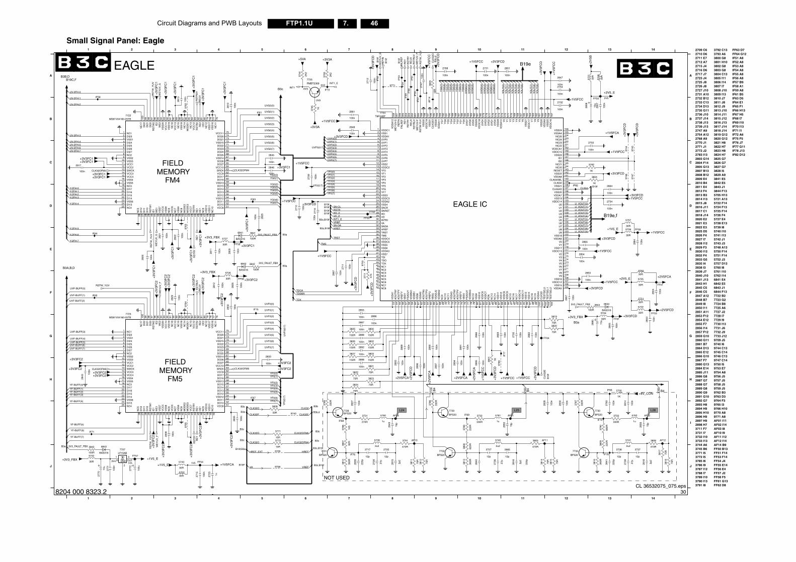
46FTP1.1U 7.Circuit Diagrams and PWB Layouts
IF63 D5IF64 E1IF65 F1IF66 H13IF67 H5IF68 I7IF69 I10IF70 I13IF71 I1
FF50 B13FF51 F14FF53 F14
IF72 A6IF75 F5IF76 J7IF77 G11IF78 J13IF82 D12
FF54 J4FF55 E14FF56 E4FF57 J2FF58 F5FF61 G13FF62 D8
FF63 D7FF64 G12IF51 A8IF52 A8IF53 A8IF54 A8IF55 A8IF56 A8IF57 B9IF58 A1IF59 A8IF61 B5
9745 C149746 C139747 C14
9753 E79754 A89756 J59757 J59758 J59759 J59762 B39763 D39764 F39765 I39766 H109770 A89771 A8AF01 I11AF02 I14AF03 I8AF10 I9AF11 I12AF12 I14AF14 B9
5760 I85761 I105762 I146841 E46842 E56843 J16844 F137722 B27723 G27724 B87725 A67727 J27728 I77729 I97730 I137731 J67732 J97733 J129709 J59740 I69744 C13
3843 J13844 F135705 H13
9750 I5
5721 A135722 F145724 F135725 F145726 F45727 E45728 E135739 I85740 I105741 I135742 J15743 J35748 A135750 F145751 F145752 J35757 D13
3812 J93813 J103814 J113815 J123816 J133817 J143818 J143819 G123820 G123821 H83822 H73823 H83824 H73825 G73826 G73827 G73828 I53829 A93841 E53842 E5
3744 A63745 B63771 I5
3786 I93787 I123788 I73789 I103790 I133791 I8
3792 C133793 A63800 G83801 H103802 G83803 G83804 C133805 I113806 I143807 I73808 J103809 I133810 J73811 J8
2867 F72880 G132884 E14
2V5
2885 J112886 G82887 G72888 G72889 G82890 G92891 G102892 G72893 H82894 H92895 H102896 H92897 H92898 H73711 F73731 I73732 I103733 I13
2839 J72840 J102841 J13
3772 I53785 I6
2843 H12845 C52846 C52847 A122848 B72849 I82850 I112851 A112853 F122854 E122855 F72856 I142857 F122859 G102860 G112861 B72864 D132865 E122866 G10
2812 F42813 B32814 I132815 J82816 J112817 C12818 J142820 E22821 E32822 E32825 D52826 F42827 I72828 I122829 F32830 I122832 F42833 G52835 I42838 I3
2738 J132739 J132747 A92754 A122768 A92770 J12771 J12772 J22783 I132803 G142804 F142805 G132807 B132808 B12
B4
B19e,f
12 13 14
A
B
B19f
C
D
E
F
G
H
I
J
2709 C62710 D62711 E72712 A72715 J42716 D6
13 14
B19
f
2723 J42725 J82726 J82727 J102731 A102732 B122733 C132734 D132735 G112736 J102737 J14
12
B3a
2809 E42810 B42811 E4
2717 J7
+3V
3FC
D
5725
30R
100n
2732
15p
2856
9747
100n
2783
75R
3815
+1V5_E
FF53
9745
2884
100n
IF82
330R
3787
2p2
2818
3844
100R
6844
BAS316
100n
2807
220p
2841
1u
5762
+1V5FCC
2830
100n
IF66
2733
100n 9744
+3V3FCD
+1V
5FC
C10
0n8
1K
3804
27p
2739
+3V3FCD
+2V5_E
BFS20
7730
+2V5_E
9746
+2V5FCD
75R
+8V_CON
575130R
AF12
2853
100n
6 RVSS623VSS12 5422
DI15
DO11 53
DO12DI14
AF02
+2V5FCA
+1V5FCC
155VSSA4
156VSS24
158
VS
S25
106VSS15
108VSS16
118VSS17
122VSS18
134VSS19
136VSS20
138VSS21
142VSS22
148VSS23
150VDDCA1
121VDDA6
135VDDA7
141VDDA8
107VDDC12
117VDDC13
133VDDC14
149VDDC15
157
VD
DC
16
111V7110V8109V9
105VDDA5
120V0119V1
116V2115V3114V4113V5112V6
131U1130U2129U3128U4127U5126U6125U7124U8123U9
103
TE
ST
SE
L1
104
TE
ST
SE
L2
132U0
145NC21
151NC22
152NC23
153NC24
154NC25
143RESET
146IS0
147IS1
144NC20
139CLK64I
137CLK64O
140CLK64SEL
2738
12p
IF70
FF61
100n
2857
2754
100n
5721
30R
3809
4
220R
+3V3_FBX
+1V5FCC
+3V
3FC
D
390R
3816
FF51
+1V5FCC
R5
2805
100n
+1V5FCC
+3V3FCD
10u
2880
FF55
3820
75R
2814
100n
+1V5FCC
75R
3819
10u
2808
+1V5FCA
470R
3806
+2V
5B
100n
3792
1K
3733
330R
2865
30R
5748
+3V3FCD
30R5750
7733
BFS20
+3V3FCD
100n
2854
2u2
5741
30R
5728
FF50
5705
1K
IF7812p
2737
100n
2847
2864
100n
100n
2734
5757
30R
30R
5724
7 n
2803
100n
3818
75R
100n
2804
5722
30R
75R
3817
IF67
680R
3790
V10
0
3V3_FAULT_FBX
CLK64
U_VOUT(7)U_VOUT(8)
U_VOUT(0)U_VOUT(1)U_VOUT(2)U_VOUT(3)
U_VOUT(5)
U_VOUT(9)
U_VOUT(4)
U_VOUT(6)
YF0(6)
(0:7
)YF-BUFF(3)
YF0(7)
CL 36532075_075.eps30
L26
NOT USED
9 10 11
J
1 2 3 4 5 6 7 8
B3aB3c,B19f
3V4
B19F
B3c
B3c
B3c B3c
B3c
B3b
B3b,d
1V5 1V5
B3a
B19f,B3a
B3c,B19f
10u
2770
2840
220p
1K5
3788
+3V3_FBX
IF69
470R
3791
5761
1u
30R
5742
3828
33R
1n2723
282
100n
2715
7731
BFS20
IF68
AF03
3789
220R
100u
2772
100R
3843
BAS316
6843
100n
2835
+1V5FCA
+1V5_E
3814
9758
BFS207728
+3V
3FC
2
12p
2725
378
330
VS
S7
33
VS
S8
35
VS
S9
39
WE
132
VC
C5
34
VC
C6
37
VC
C7
43
VCC8 51
VS
S10
48V
SS
114940
NC
947
OE
146
RE
145
RS
TR
144
RS
TW
130 42
NC
1050
NC425
NC
526
NC
636
NC
738
NC
8
IE1
31
MO
DE
241
MO
DE
3 DO10 52
DI1
029
DI1
128
DI1
227
DI1324
AF019740
100n
2838
30R5752
FF57
IF71
3812
75R
3808
820R
AF11
220p
2839
3805
470R2u2
5740
2717
12p
AF10
7729
BFS20
330
378
2850
15p
5743
30R
+3V
3FC
2
2816
2p2
12p
27279709
27p
2726
3731
270R
3732
330R
2736
27p
390R
3810
1u
5760
+3V
3FC
2
75R
3811
2u2
57393772
15R
15R
3771
IF76
15p
2849
+3V
3FC
2
3813
390R
BFS20
7732
282
100
+1V5_EFF54
9765
2p2
2815
82R
3807
100n
2771
GND
2
IN1
OUT3 +
3V3F
C2
7727LF15AB
2885
12p
3V3_FAULT_FBX
CLK32O
CLK32ECLK32P
CLK32
CLK32OFM4CLK32O
CLK32OFM5CLK32O
VA VREF
HREF_EXT HREF
WE
YU
V_F
RS
TR
YR
EY
RS
TW
_YU
V
YF
0
YF-BUFF(7)
YF-BUFF(6)
YF-BUFF(5)
YF-BUFF(4)
8204 000 8323.2
L25L24
Small Signal Panel: Eagle
B4B4
FIELD
EAGLE IC
FIELDMEMORY
0V2
0V3
FM4
B3a
B3a
B19
f
B3B,D
B19
f
B19
f
A
B
C
D
E
0V9
B19f
G
H
B19e
MEMORY
1 2 6 7 8
B3c
B19fB19f
FM5
F
B19f
B19C,F
3 4 5
EAGLE
9 10 11
B3c
,d
B3c,B19f
B3c,B19f
B3A,B,D3842
100R
100n
2855
2888
100n
2825
+5VA
100n
2832
75R
+3V
3FC
D
100n
3821
2892
100n
+3V3_FBX
+3V3FCD
2812
100n
+3V3FC2
9762
+3V
3FC
1
2711
100n
IF64
100R
3841
+1V5FCC
+2V5FCA
FF63
100n
2846
75R
3822
2833
100n
+3V
3FC
2
IF51
+3V
3FC
2
+3V3FC1
+1V5FCC
100n
2747
100n
2866
3745
1K
+3V3FC1+3V3FC1
150R
3825
+1V
5FC
C
+3V
3FC
1
100n
2829
3826
150R
+3V
3FC
D
IF58
FF58
IF77
3744
2K2
1K3801
+3V
3FC
1
FF56
IF54
IF53
+1V5FCC+1V
5FC
C
100n
2822
IF72
100n
2712
IF61
2817
100n
2893
100n
+3V
3FC
D
+3V
3FC
1
AF
14
100n
2810
100n
2861
+2V5FCA
+3V
3FC
2
2K2
3793
150R
3827
100n
2709
2886
100n
+3V
3FC
D
+3V3FC2
72
77V
SS
16V
SS
1778
VS
S18
87
VS
S19
91
VSS29
VS
S20
93
VSS310
VSS416
VSS517
WE
294 89
VC
C14
92
VCC212
VCC314
VCC415VCC9 62
VSS13
VSS13 59
VSS14 67
VSS15
OE
280
RE
281
RS
TR
282
RS
TW
296
SRCK 63SWCK13
VCC111
VCC10 64
VCC11 75
VC
C12
83
VC
C13
NC11
NC
1176
NC
1279
NC
1384
NC
1486
NC
1588
NC
1690
NC
1710
0
NC28
NC31857
DO15 58
DO16 60DO17 61
DO20 74
DO21 73
DO22 71
DO23 70
DO24 69
DO25 68
DO26 66
DO27 65
IE2
95
MO
DE
185
21DI1620DI1719
DI2
097
DI2
198
DI2
299
DI232
DI244
DI255
DI266
DI277
55DO13 56DO14
7723MS81V04160-25TB
+3V
3FC
1
+3V
3FC
1
100n
2843
100n
2811
14 YF015 YF116 YF217 YF318 YF419 YF520 YF621 YF7
185
YG
018
6Y
G1
187
YG
218
8Y
G3
189
YG
419
0Y
G5
191
YG
619
2Y
G7
53V
SS
A1
62V
SS
A2
72V
SS
A3
200
WE
YU
V-F
207
WE
YU
V-G
172
Y0
171
Y1
170
Y2
169
Y3
168
Y4
167
Y5
166
Y6
163
Y7
162
Y8
161
Y9
160
VS
S26
165
VS
S27
174
VS
S28
181
VS
S29
22 VSS3
194
VS
S30
196
VS
S31
198
VS
S32
25 VSS4
38 VSS539 VSS6
41 VSS7
61V
SS
8
80V
SS
9
2 VSS1
81V
SS
10
87V
SS
11
88V
SS
12
96V
SS
13
97V
SS
14
12 VSS2
164
VD
DC
17
180
VD
DC
18
197
VD
DC
19
13 VDDC2
23 VDDC3
36 VDDC437 VDDC5
82V
DD
C6
83V
DD
C7
89V
DD
C8
90V
DD
C9
65V
RE
FU
75V
RE
FV
56V
RE
FY
67V
SA
DJU
159
VD
DA
9
60V
DD
B1
59V
DD
BA
1
68V
DD
BA
2
78V
DD
BA
3
1 VDDC1
94V
DD
C10
95V
DD
C11
31 VA
66V
BS
U
76V
BS
V
57V
BS
Y
29 VD
3 VDDA1
173
VD
DA
10
193
VD
DA
11
208
VD
DA
12
24 VDDA2
40 VDDA3
100
VD
DA
4
11 UVF7
175
UV
G0
176
UV
G1
177
UV
G2
178
UV
G3
179
UV
G4
182
UV
G5
183
UV
G6
184
UV
G7
4 UVF05 UVF16 UVF27 UVF38 UVF49 UVF5
10 UVF6
204
RE
Y
201
RS
TR
UV
203
RS
TR
Y
199
RS
TW
-YU
V
26 SNCK
32 SNDA
27 SNRST
44 TCK
42 TDI43 TDO
102
TE
ST
SE
L0
35 TMS
34 TRST
47 NC348 NC449 NC550 NC651 NC752 NC8
69N
C9
84P
DN
206
RE
FIN
202
RE
UV
30 INTR1
45 NC1
70N
C10
71N
C11
79N
C12
85N
C13
86N
C14
91N
C15
92N
C16
93N
C17
98N
C18
99N
C19
46 NC2
63A
OU
TN
U
73A
OU
TN
V
54A
OU
TN
Y
64A
OU
TP
U
74A
OU
TP
V
55A
OU
TP
Y
101
CLK
32I
195
CLK
32O
205
FALR
EF
77F
SA
DJV
58F
SA
DJY
28 HD
33 HREF
T8F24EF7724
IF55
100n
2894
IF59
IF56
2768
100n
+3V3FC2
+3V
3FC
1
9763
+3V3FCD
150R
3803
100n
100n
2821
100n
2716
2860
5726
30R
2889
100n
VS
S20
10 VSS3
16 VSS417 VSS5
23 VSS6
33V
SS
7
35V
SS
8
39V
SS
9
32W
E1
94W
E2
+3V3FC2
VC
C6
43V
CC
7 51VCC8
62VCC9
3 VSS1
48V
SS
10
49V
SS
11
54VSS12
59VSS13
67VSS14
72VSS15
VS
S16
7778V
SS
17
87V
SS
18
91V
SS
19
9 VSS2
93
RS
TR
1
82R
ST
R2
30R
ST
W1
96R
ST
W2
63SRCK13 SWCK
11 VCC164VCC10
75VCC11
83V
CC
12
89V
CC
13
92V
CC
1412 VCC2
14 VCC315 VCC4
34V
CC
5
37
NC
14
88N
C15
90N
C16
100
NC
17
8 NC2
18 NC3
25 NC4
26N
C5
36N
C6
38N
C7
40N
C8
47N
C9
46O
E1
80O
E2
45R
E1
81R
E2
44
DO2270DO2369DO2468DO25
66DO2665DO27
31IE
1
95IE
2
85M
OD
E1
41M
OD
E2
42M
OD
E3
1 NC1
50N
C10
76N
C11
79N
C12
84N
C13
86
DI2
2
2 DI23
4 DI245 DI256 DI267 DI27
52DO10
53DO11
55DO12
56DO13
57DO14
58DO15
60DO16
61DO17
74DO2073DO21
71
29D
I10
28D
I11
27D
I12
24 DI13
22 DI14
21 DI15
20 DI16
19 DI17
97D
I20
98D
I21
99
100n
2896
MS81V04160-25TB7722
+3V3FC2
FF6
+1V5FCC
9766
100n
2826
+1V5FCC
2731
100n
100n
2848
100n
+2V
5FC
D
2898
+3V
3FC
D
2897
100n
+3V3FC2
75R
3823
+3V
3FC
1
100n
2813
+3V3FCD
+3V3FC1+3V3FC1
FF62
IF57
IF52
+3V
3FC
2
BAS316
6841
100n
2859
+3V
3FC
1
+1V5FCC+
3V3F
C1
+3V3FC1
3802
150R
30R
5727
+1V5FCC
+3V3A
9771
2851
100n
+3V3_FBX
2809
100n
2710
100n
47K
3711
2895
100n
+2V
5FC
A
9764
100n
2845
+3V
3FC
D
+3V
3FC
1
+2V
5FC
A
100n
2890
2735
100n
100n
2820
2891
100n
+3V
3FC
D
3824
75R
3829
15R
2867
100n
+3V
3FC
2
+3V
3FC
2
6842
BAS316
9753
+3V3FC2
IF75
IF63
IF65
150R
3800
+3V3A
100n
2887
WE
YU
V_G
7725
PMBT2369
3V3_FAULT_FBX
3V3_FAULT_FBX
Y10
0
U10
0
TD0MATDOA
TMS
TRST
YG0(1)
CLK
32O
INT1_E
INT1
TCK
RE
UV
CLK
32E
YG
0(6)
YG
0(2)
UVF0(5)
RS
TW
_YU
V
UVF0(4)
RS
TR
Y
YG
0(5)
UV
G0(
7)U
VG
0(6)
YG
0(0)
YG
0(1)
YG
0(4)
YG
0(3)
YG
0(7)
UV
G0(
0)U
VG
0(1)
UV
G0(
2)U
VG
0(3)
HREF
UV
G0(
5)
UV
G0(
4)
INT1_EVD_EHD_E
VREF
YF0(7)YF0(6)YF0(5)YF0(4)YF0(3)YF0(2)YF0(1)YF0(0)
YF0(0:7)
UVF0(7)UVF0(6)
UVF0(3)UVF0(2)UVF0(1)UVF0(0)
UVF0(0:7)
RSTR
RE
FIN
FALR
EF
RE
Y
RS
TR
UV
WE
YU
V_F
WE
YU
V_F
YO
UT
(9)
YO
UT
(8)
YO
UT
(7)
YO
UT
(6)
YO
UT
(5)
YO
UT
(4)
YO
UT
(3)
YO
UT
(0)
YO
UT
(2)
YO
UT
(1)
SN-DA
SN-CL
YF0(5)YF0(4)YF0(3)YF0(2)
YF0(1)YF0(0)
UVF0(0)
UVF0(1)
UVF0(2)
UVF0(3)
UVF0(4)
UVF0(5)
UVF0(6)
UVF0(7)
RE
UV
RS
TR
UV
RSTW_YUV
CLK32OFM5CLK32OFM5
UVF-BUFF(7)
UV
F0(
0:7)
UVG0(7)
RE
YR
EU
V
RS
TR
YR
ST
RU
V
RS
TW
_YU
VR
ST
W_Y
UV
CLK32OFM4CLK32OFM4
WE
YU
V_G
WE
YU
V_G
UV-2FH-7
YF-BUFF(2)YF-BUFF(1)
YF-BUFF(0)
UVF-BUFF(0)
UVF-BUFF(1)
UVF-BUFF(2)
UVF-BUFF(3)
UVF-BUFF(4)
UVF-BUFF(5)UVF-BUFF(6)
Y-2FH-7
Y-2FH-6
Y-2FH-5
Y-2FH-4
Y-2FH-3Y-2FH-2Y-2FH-1Y-2FH-0
UV-2FH-0
UV-2FH-1
UV-2FH-2
UV-2FH-3
UV-2FH-4UV-2FH-5UV-2FH-6
YG0(7)YG0(6)
YG0(5)YG0(4)YG0(3)YG0(2)
YG0(0)
UVG0(0)
UVG0(1)
UVG0(2)
UVG0(3)
UVG0(4)
UVG0(5)
UVG0(6)
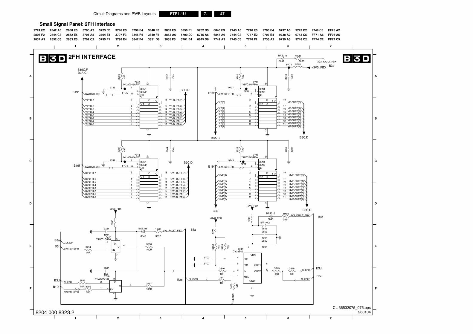
Circuit Diagrams and PWB Layouts 47FTP1.1U 7.
7
7
A
B
C
D
E
F
FF75 A2
FF76 A5
FF77 C5
B3a
7747 6846 3852100n
100n
ULT_FBX
CL 36532075_076.eps260104
EN
EN
1 2 6
B3a
B19f
3 4 5
B3c
E
F
B3f
B3d
B3d
B3c
9703
2
3
1
5
4
2
3
1
5
4
74LVC1G126
74LVC1G1257748
10R
3794
56R
3856
3849
56R
10R
3855
10R
3848
9707
3798
3796
4K7
100R
2862
100n
2806
100n
3846
4K7
3799
10R
10R
3795
10R
3847
4FS0
5FS1
3
GND
2IN
6OUT1
8OUT2
7
VDD
CY23S027746
1FBIN
3797
CLK32E
CLK
32I
CLK32I
100R
CLK32P
SWITCH-2FH
SWITCH-2FH
CLK32O
CLK32I
8204 000 8323.2
Small Signal Panel: 2FH Interface
G3
12
3EN23EN1
G3
12
3EN23EN1
G3
12
3EN23EN1
G3
12
3EN23EN1
6
2844 C3
2724 E2
FF71 A6
FF74 C2
2806 F2
2837 A3
B3a
B3C,D
B3C,D
B3C,D
5
B3C,D
41 2 3
2842 A6
B3a
2852 C6
B3A,CB19C,F
B19f
9743 C5
9748 C2
9749 C5
3847 F4
3848 F6
3849 F6
3851 D6
3852 E3
B19f
B19f
B19f
5700 D2
5701 E4
5702 D5 7746 E5
7747 E2
7748 F2
9703 E4
9707 E4
9736 A2
9737 A5
9738 A2
9739 A5
9742 C23796 E3
3797 F3
3798 E4 7745 C5
3799 E4
3846 F4 3853 A6
3855 F5
3856 F1
5715 A6
6845 D6
6846 E3
6847 A6
7742 A3
7743 A5
7744 C3
2858 E5
2862 E5
2863 E5
3700 A2
3701 A5
3702 C2
3723 C5
A
B
C
D
3794 E1
3795 F1
B3A,B
2FH INTERFACE
B3B57
01
5700
3723
4K7
4K7
3702
+3V3_FBX
100RBAS316
3701
100n
2852
9737
4K7
FF77FF74
16V 100u
2858
17161514131211
1
10
19
20
2
3456789
18
74LVC245APW7743
100n
2837
9736
+3V3_FBX
2844
100n
9743
FF76FF75
5715
10
19
20
2842
100n
9
18
17161514131211
1
2
345678
+3V3_FBX
774574LVC245APW
2724
6847
BAS316
BAS316
6845 3851
100R
3853
100R
FF71
4K7
1
10
19
20
+3V3_FBX
3700
789
18
17161514131211
74LVC245APW7744
2
3456
9742
14131211
1
10
19
20
3456789
18
171615
774274LVC245APW
2
5702
2863
3V3_FAULT_FBX
3V3_FAULT_FBX
3V3_FA
UV-2FH-0UV-2FH-1UV-2FH-2UV-2FH-3UV-2FH-4UV-2FH-5UV-2FH-6
UV-2FH-7
Y-2FH-0Y-2FH-1Y-2FH-2Y-2FH-3Y-2FH-4Y-2FH-5Y-2FH-6
Y-2FH-7
SWITCH-2FH
UVF(6)UVF(5)UVF(4)UVF(3)UVF(2)UVF(1)
UVF(0)
UVF-BUFF(7)UVF-BUFF(6)UVF-BUFF(5)UVF-BUFF(4)UVF-BUFF(3)UVF-BUFF(2)UVF-BUFF(1)
UVF-BUFF(0)
SWITCH-1FH
UVF-BUFF(7)
UVF-BUFF(6)UVF-BUFF(5)UVF-BUFF(4)UVF-BUFF(3)UVF-BUFF(2)UVF-BUFF(1)UVF-BUFF(0)
YF(7)YF(6)YF(5)YF(4)YF(3)YF(2)YF(1)
YF(0)
YF-BUFF(7)YF-BUFF(6)YF-BUFF(5)YF-BUFF(4)YF-BUFF(3)YF-BUFF(2)YF-BUFF(1)
YF-BUFF(0)
SWITCH-1FH
YF-BUFF(7)
YF-BUFF(6)YF-BUFF(5)YF-BUFF(4)YF-BUFF(3)YF-BUFF(2)YF-BUFF(1)YF-BUFF(0)
SWITCH-2FH
UVF(7)
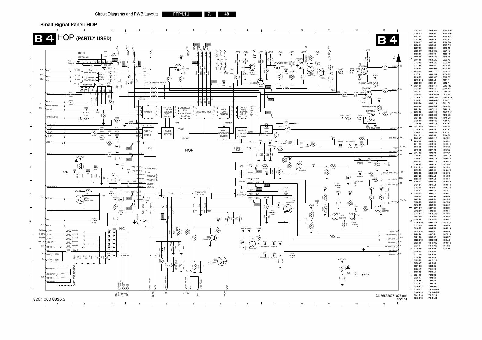
48FTP1.1U 7.Circuit Diagrams and PWB Layouts
I371 I12
c200 F3
I330 B4
I331 B4
I332 B3
B
I333 C2
I338 E3
I339 E4
I357 E8
I358 D4
I359 F4
I361 F12
I363 H5
I365 E10
I366 B3
I367 D10
I368 B7
I369 A8
I370 B10
I306 G5
I307 G7
I308 A12
B1
B4(2X)
I309 B11
I310 B12
I311 D8
I312 E3
I313 C11
I314 C9
I315 D8
I316 D9
I317 C12
I319 B11
I320 A11
I321 F3
I326 B7
9311 I1
9312 I1
9313 F13
9314 H1
9315 H1
9421 B9
C001 H12
F309 D11
F311 C2
F312 E9
F329 H9
F347 D12
F348 G3
B1
RE
S O
NLY
PT
V
B1
F349 G3
F350 H3
F351 H3
F352 H3
F353 H3
F362 H3
F364 F4
I302 E2
I303 E4
I304 B11
I305 G5
7317 B12
7318 E10
7319 C12
7340 A6
7361 H7
7362 H7
7375 B8
9302 A3
9303 A4
9304 A4
9305 A4
9308 B5
9309 B5
9310 B5
6313 H9
6314 H9
6316 C9
6317 E12
6319 D9
6334 H5
7301 B4
7302 A1
7303 H8
7304 F2
7305 B9
7306 A9
7309 G13
7310-A G11
B1
B5b
7310-B G12
7312 F10
7313 A11
7314 A10
7315 B10
7316 A12
5304 H1
5305 H1
5306 H1
5307 H1
5308 H1
5313 A12
5314 B12
5315 C12
6301 E12
6303 H9
6304 H9
6306 I5
6307 I5
6308 C2
5V2
6309 D11
6310 D10
6311 D12
6312 H8
3390 D9
3391 F12
3394 E9
3395 C3
3396 D3
3397 D2
3398 D3
3399 B5
3442 E12
3443 E13
3453 C2
3454 B1
3455 C1
3459 B11
B1
B1
B1
3465 A9
3467 A8
3470 B8
3471 A8
3472 I6
5301 E2
5302 E2
5303 G1
3363 F3
3364-A F11
3364-B G11
3364-C G10
3364-D G10
3365 F13
3366 H11
3367 F11
3368 E13
3369 B12
3383 B13
3384 C12
3386 F13
3387 G2
UL ONLY
3388 B5
3389 C13
3342 C13
3343 D12
3344 D10
3345 D9
3346 C9
3347 D9
3348 D9
3349 F2
3350 B10
3351 B9
3352 A10
3353 A10
3354 A10
3355 B7
B1,B4
B1
B1
B1
3356 G12
3357 F12
3358 A11
3359 B10
3360 A8
3361 G7
3362 F11
3326 G5
3327 G6
3328 F9
3329 E2
3330 A7
3331 G3
3332 A7
3333 F3
3334 H5
3335 A7
3336 H6
3337 A11
3338 A12
3339 C3
B1
3340 A13
3341 B13
3307 E9
3308 E9
3310 E9
3311 G7
3312 E11
3313 E11
3314 G8
3315 H8
3316 H10
3317 G9
3318 F9
3319 E13
3320 D3
3321 D3
3322 D12
3323 H5
3324 I5
3325 A9
2345 H2
2346 H2
2347 H2
2348 H2
2349 H2
2363 F3
2386 F12
2393 E13
2395 D3
2396 D3
2397 D3
2398 A3
2429 A4
2431 B4
3302 C4
3304 I11
3305 C3
3306 E9
2321 B3
2323 B4
2324 I6
2325 G5
2326 E12
2328 B7
2329 B6
2330 A6
2331 B6
2332 E2
2333 D10
2334 E8
2335 F11
2336 E9
2337 B12
2338 B12
2340 I11
2341 C12
2342 A7
2343 A9
2344 H3
12 13
2319 G10
2320 G3
12 13
2303 E9
2304 G7
2306 H9
2307 F4
2308 G9
2309 D3
2310 E3
2311 H5
2312 F9
2313 F9
2314 E2
2315 E3
2317 E3
2318 E3
B5a,B4
B5a
B1
B1
A
B
C
D
E
F
G
H
I
1301 G4
1304 G3
2301 B2
7317BC857BW
I310
BC857BW7319
5u6
5313
+8VS
+8VS
I361
3342
47R
I308
I313
3338
680R
5314
5u6820R
3369
BAS316
6301
6317
BAS316
7303
+8VS
C001
47R
3341
3356
2K2
3
+8VS
3443
220K 1u 2393
9313
3357
3K9
F351
+8VS
3343
68K
2K2
2340
100u
BC847BW7309
F347
5305
3322
1K
1n
2386
3442
22K
100R
3319
309
3386
100K
10n
2326
6304
13
100MHZ5306
BC847BS7310-B
53
4
3K9
3362
BC847BW
6311
BZX384-C22
3391
10K
6309
BAS316
2338
6p8
I319
3 1
5u6
5315
3365
4K7
3368
1M
3304
3R9
+8VS
220R
3367
GND-RGB-CRT
+5V_VDP
BC857BW7316
312
6p8
2337
I371
47R
3340
6
1
F329
BC847BS
7310-A
3389
680R
+8VS
00K
313
6303
GND-RGB-CRT
+5VS
I309
I317
680R
3383
3384
820R
GND-RGB-CRT
6p8
2341
336620R
1K8
3337
820R
VSYNC
HD@HOME
NOHOP1B
304
FRAMEDRIVE-
ANTI-MOIRE
B_2FH
FBL_2FH
FRAMEDRIVE+
LINEDRIVE1
HFB_X-RAY-PROT
CUTOFF
TILT
EHT-INFO
NOHOP2B
B-CRT
G-CRT
R-CRT
EHT-INFO
EW-DRIVE
GND-LINEDRIVE
EHT-INFO
CL 36532075_077.eps300104
NC B
1
B14
b
B3a
B1
B4,
B1
B14
b
B4,
B5a
ON
LY F
OR
NO
HO
P
B1
8 9 10 11
H
1
B5a
B3a
B4
2 3 4 5 6 7
B4
NC
NC
NC
I
BC857BW
4
5
6
7
22K
3472
BZ
X38
4-C
5V6
6306
100MHZ5308
47K
3316
I363
2344
10p
2346
10p
9312
F362
F353
9314
7361
PDTC144EU
9315
9311
470p
2306
F352
6313
BZX384-C22
100K
3323
RE
S
10p
2349
10p
2347
BAS316
BA
S31
6
6334
3334
1K
RE
S
68p
2311
10p
2345 BAS316
6314
2348
10p
2324
10n
BAT
54 C
OL
6307
BA
S31
6
6
BZX384-C47
4K7
3324
5307 100MHZ
PO
R
HFB
VSYNC
2FH
-FB
L2F
H-B
2FH
-G2F
H-R
PO
R_F
LAS
H
HD100
VD
2FH
-HD
100
2FH
-VD
100
NOHOP1A
NOHOP1B
HD100
NOHOP2B
TIL
T
SA
ND
CA
ST
LE
HF
B_X
-RAY
-PR
OT
HF
B
DY
N-F
AS
E-C
OR
8204 000 8325.3
Small Signal Panel: HOP
LUMA
NC
TRAL
DOWWIN-
ADC
PROC
SPEC-
CONTROL
PROCESSINGCHROMA
PROCESSING
CONTR
BRIGHT
SAT
BLACK
STRETCH
RGB-INSERTIONWHITEPOINT
CONTROL
OUTPUT
+ BUFFER+ BLUESTRETCH
WHITE P.
PWL +BEAM CURR
LIMITER
CONTIN’S
CATHODE
CALIBR’N
I 2C
SU
PP
LY
1PHI-
PHI-2 START/STOPH-DRIVE
6-BITSDAC
EW
FRAME
RAMP
GENERATOR
R
B
G
R
B
G
R
V
U
Y
YVUY
DIGGND
DIGSUP
ANAGND
BANDGAP
RGB
SYNC+GEO
SC
Hsel
SWITCH
SATUR’NCONTROLCOLOUR
MATRIX
CONTRAST
BRIGHTNESS
CONTROL
RGB-YUV
MATRIX
AMPL
DIFF
AND
R
G
BB
G
B5a
B5a
HOP (PARTLY USED)
B3c
B3c
1V3
B3a
7V9
1V1
7V9
2V5
0V2
0V
B3c
B3c
ONLY FOR NO HOP
B3c
TOPIC
(OPTIONAL)
B3a
B5a
B5a B
1
N.C.
B1
B3a
HOP
B3c
1V1
0V8
B5a
1V5
0V2
A
B
C
D
E
F
G
4V0
1 2 3 4 5 6 7 8 9 10 11
B4(2X)
B4(2X)
B4(2X)
NC
2331
100n
100n
2321
10p
2320
33K
3453
+8VS
1K
3302
BC857BW
7318
+8VS
3467
10K
3364
-C
680K
36
13041
2
I320
I359
2315
100n
10p
2304
c200
I331
7305
BC847BW
100R
3387
9421
2398
100n
2328
22p
2310
10p
+8VS
PMBT23697315
3394
4K7
+8VS+8VS+8VS
100K
3311
3332
1K
I338
9308
2395
100n
100n
2332
10p
2309
3359
100K
+8VS +8VS
UOUT
20
VCC
9 VIN 16VOUT
6 YIN19YOUT
9302
AD
R
22 CF
15D
EC
18
GND
13 12 2 10 23 24
1
SC
11
SC
L
14
SD
A
21SOUT
8 UIN 17
TDA91787302
3A
D1
4
AD
2
5
AD
3
7
3465
33K
1n
2335
100n
2325
100R
3454
3355
33K
22n
2318
68K
3305
2307
100n
+8VS
9304
33K
3470
100K
3471
3317
220R
3345
10K
7304
PDTC144EU
I321
100u
2314
F348
3459
47K
3361
+8VS
+8VS
100n
2313
3321
100R
3396
100R
+8VS
100MHZ
3390
220R
2333
2u2
F311
I312
+8VS
F36
4 2312
33n
6u8
I365
10R
3388
5302I3
05
I303
3328
39K
I326
10p
2308
3348
2K2
1K3318
10K
3314
6K8
3339
10K
3351
+8VS+8VS
+8VS
I332
2397
100n
+8VS
3310
47K
BC847BW7314
100n
2343
F
3307
18K
3330
1K
3326 10
0K
RE
S
2303 1u
F350
+8VS
I316
+5VS
100MHZ5304
I3156310
BZM55-C6V8
K336
7306
BC847BW
+8V_VDP
6R8
3329
+8VS
I366
BC847BW7375
13
2
3306
220R
12M
CS
TC
V
1301
100n
2396
F349
6308
MCL4148
7362
100R
3397
3360
100K
6319
BAS316
1K3353
100n
2323
BAS316
6316
100R
3320
3399
10K
3333
1K
3350 1K
100K
3312
I357
I339
5301
9310
6u8
I370
100K
3327
F312
1K
3363
7340
BC847BW
100R
3395
3354
2K293
03
2334
2u2
7312
PDTC144EU
18
3335
1K
3364
-A
680K
3325
100K
315
K
I367
3398
100R
I314
9309
9
SDA11
UIN27
VD23
VDOA 1
VDOB 2
VIN26
VP117
VP239
VSC 15
XTA
LI
20
XTA
LO
21
YIN28
31
GI2
36
GND16
GND219
GO 41
HD24
HF
B
13
HOUT 8HSEL12
IREF 16
LPS
U
22
PW
L
34
RI130
RI2
35
RO 40
SCL10
SC
O
BCL 43
BI132
BI2
37
BL133
BL2
38
BLKIN 44
BO 42
DACOUT 25
DECBG18
DECVD7
DP
C
14
EHTIN 4
EWO 3
FB
CS
O
29
FLA
SH
5
GI1
I333
7301TDA9330
100n
2330
+5VS
54
2431
100n
2363
470p
3364
-D
680K
3344
2K2
3349
4K7
2319
1n
100n
2301
2329
100n
I330
I306
5303 100MHZ
I311
3346
33K
100K
3352
I368
2u2
2336
3455
100R
7313
PMBT2369
9305
+8VS
3331
1K
100n
2342
I358
2
1u2317
1
3
I369
3364
-B
680K
72
I307
3308
220K
3347
22K
2429
100n
2
3358
I302
I
HD100
FB
L-T
XT
Y-S
CA
VE
M
Yltp
G_2
FH
B_2
FH
R_2
FH
FB
L_2F
HYltp
NOHOP1A
VD100
R_2FH
G_2FH
GND-RGB-CRT
U100
V100
Y100
SDA-F
SCL-F
HD100
SANDCASTLE
Y10
0
U10
0
V10
0
VD
LIGHT-SENSOR
FB
L-T
XT
SCL-F
SDA-F
B-T
XT
G-T
XT
R-T
XT
R_2FH
G_2FH
B_2FH
FBL_2FH
BC
L
V23
V31
V25V21
F20
L13
V30
F17
V20
V29
V24
V19
F18
F19
V28
V26
L12
V22
V27
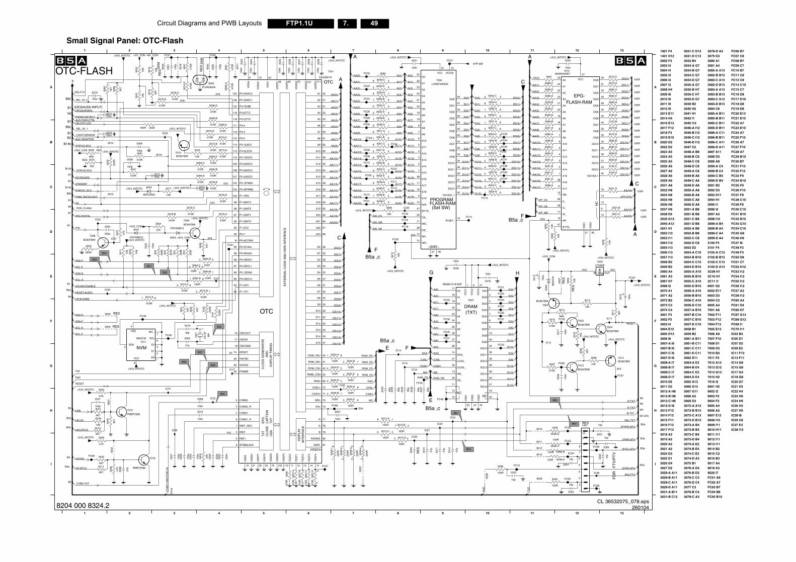
Circuit Diagrams and PWB Layouts 49FTP1.1U 7.
NC
NC
IC05 D1
IC07 D2
IC09 E2
IC11 F13
IC13 F11
IC14 G8
IC15 G8
5V3FC52 H12
FC53 I12
FC54 I12
FC55 I12
FC56 I12
FC57 A3
FC58 I12
FC60 A4
FC61 D4
FC66 H7
FLASH-RAM
IC23 H9
IC26 H3
IC27 H9
IC28 I8
IC29 C8
IC37 E4
IC38 I12
A
B4 (2X)
FC43 G10
FC44 C10
FC45 G8
FC46 H9
IC17 G4
IC18 G8
IC21 H3
IC22 H4
FC23 E10
FC24 A7
FC25 F10
FC26 A7
FC27 F10
FC28 A7
FC29 B10
FC30 B7
FC31 F10
FC32 F12
FC33 F9
FC34 B10
FC35 F9
FC36 F10
FC37 F9
FC67 G13
FC68 G12
IC24 H9
FC70 I11
IC03 B3
3V4
B4
B4
FC05 B10
FC06 B7
FC07 C8
FC08 B7
FC09 C7
FC10 B7
FC11 C8
FC12 C8
FC13 C10
FC47 I6
FC48 F2
IC20 G7
FC50 D8
FC51 C7
RE
S
FC20 E13
FC21 E10
FC22 A7
9004 F2
9005 A4
9006 A3
9007 E12
9008 I10
9009 I11
9010 H11
9011 I11
9012 I11
9013 I11
9014 B2
9015 C2
9016 B3
9017 A4
9018 A3
FC38 C10
FC39 F9
FC69 I1
FC41 B10
FC42 B10
FO
R
FT
V/P
TV
B3a
B3a
6005 A4
7001 A6
7002 F11
7003 F12
7004 F13
7005 E13
7006 A9
7007 F10
FC15 C7
FC16 D8
FC49 F3
FC18 D8
FC19 D8
7013 G12
7014 G13
7015 H2
7016 I2
9001 H2
9002 I2
9003 F2
3091 B2
3092 D3
3093 D11
3094 H1
3095 I1
3096 I2
3097 A3
3098 I10
3099-A B4
3099-B A4
3099-C A4
3099-D A4
3100 F4
3101 F4
3102-A C13
9020 I7
FC01 A9
FC40 C10
FC03 B7
FC04 B8
RE
S
6004 C2
3083-B B13
3083-C A13
3083-D B13
3084 C8
3085-A B11
3085-B B11
3085-C B11
3085-D B11
3086-A C11
3086-B B11
3086-C A11
3086-D A11
7008 D1
7009 D3
FC17 D10
7011 F2
7012 A12
3087 A11
3088 D3
3089 A8
3090-A C4
3090-B C4
3090-C B4
3090-D B4
3073-B B4
3073-C B4
3073-D B4
3074-A E2
3074-B E4
3074-C E3
3074-D A3
3075 B1
3076-A D4
3076-B D3
3076-C C3
3076-D C4
3102-B B13
3102-C C13
FC02 A7
3C09 H1
3C10 H1
3C11 I1
6001 D2
6002 E11
6003 D3
3079 D3
3080 A1
3081 A4
3082-A A13
3082-B B13
3082-C A13
3082-D B13
3083-A A13
3057-C B10
3057-D C10
3058 B1
3059 B2
3061-A B11
3061-B C11
3061-C C11
3061-D C11
3062 D11
3064-A E3
3064-B E4
3064-C E3
7010 B3
EPG-
3067 G11
3068 A2
3069 D3
3072-A A13
3072-B B13
3072-C A13
3072-D B13
3073-A B4
3050-D A8
3051-A B8
3051-B B8
3051-C B8
3051-D B8
3052-A B8
3052-B B8
3052-C C8
3052-D C8
3053 D2
3054-A C10
3054-B B10
3102-D A13
3077 C3
3078-B C4
3078-C A3
3078-D A3
3055-C A10
3055-D B10
3056-A A10
3056-B B10
3056-C A10
3056-D C10
3057-A B10
3057-B C10
3035-D G7
3039 B2
3040 H2
3041 H1
3042 I1
3045 I12
3046-A I12
3046-B I12
3046-C I12
3046-D I12
3047 C2
3048-A B8
3064-D E4
3065 G12
3066 G12
3048-D C8
3049-A C8
3049-B A8
3049-C A8
3049-D A8
3050-A A8
3050-B A8
3050-C A8
3020 A2
3021 A2
3024 D3
3025 D1
3026 D4
3027 D2
3029-A A11
3029-B A11
3029-C A11
3029-D A11
3031-A B11
3031-B C13
3054-C C10
3054-D B10
3055-A A10
3055-B B10
3033 B4
3034-A G7
3034-B G7
3034-C G7
3034-D G7
3035-A G7
3035-B H7
3035-C H7
3007-D I6
3008-A I7
3008-B I7
3008-C I7
3008-D I7
3010 E8
3011 D2
3012-A H8
3012-B H8
3012-C H8
3012-D I8
3013 F12
3048-B C8
3048-C C8
3014 F12
3015 F11
3016 F12
3017 F13
3018 A2
3019 A2
2040 A12
2041 H1
2052 I12
2053 I11
2054 I12
2055 I13
2056 I13
2057 I13
2058 B2
2059 B2
2060 A4
2061 A3
3031-C D13
3031-D C13
3002 F3
3003 I4
3004 E12
3005 D13
3006 I6
3007-A I6
3007-B I6
3007-C I6
A
B
C
D
E
F
G
H
I
B4
2031 A8
2033 H8
2034 H8
2035 H8
2036 H8
2037 H9
2038 E9
2039 G12
12 13
2067 H7
C
2070 A1
2071 A2
2072 B2
2073 C3
2074 C4
3001 F3
12 13
2013 E11
2014 H4
2016 E13
2017 F12
2018 F3
2019 E10
2020 D2
2022 D2
2023 A5
2024 A5
2025 A5
2026 A6
2027 A6
2028 A6
2029 A6
1001 F4
1401 H12
2002 F3
2003 I4
2004 I4
2068 I2
B3a
2005 I3
2006 I3
2007 I3
2008 H4
2009 I8
2010 I9
2011 I9
2012 I9
B3a
3V4
RES
100R
2 7
2008
29-B
3072-D100R
2
3
4
5
6
7
8
9
100R3082-B
1401
1
10
2039
100n
+3V3_INTOTC
29-C
2041
+3V3_INTOTC
+3V3_INTOTC
FC68
3062
10K
29-A
IC38
100R3102-D
100R3031-D
29-D
3083-D100R
087
470K
3015 FC32
85-D
4K7
3065
2055
10p
3046-A100R
+3V3_INTOTC
31-A
85-B
86-A
FC53
100R
3046-D
+3V3_INTOTC13
FC54
FC58
100R3083-B
10K
3013
+3V3_INTOTC
7003
FC46
BC847BW
100n
2040
6K8
3014
FC56
3082-D100R
10K
86-B
7014BC857BW
FC67
BA
S31
6
6002
3031-B100R
3067
470K
47K
3066
2052
10p
7013
BC847BW
100R 3046-B
61-C
61-D
85-A
3102-B100R
VS
S1
VS
S2
VS
S3
15 32
3083-C100R
10p
2057
1K5
3016
100R3072-C
100R
3045
85-C
61-B
47K
FC55
100R3082-A
3031-C100R
IC22
GNDIN OUT
LF33AB7005
70WEn
71CASHn
5 CVBS0
RB_
12RP_
37
VCC
27
VS
S1
46
VS
S2
11W_
45
33DQ2
35DQ3
38DQ4
40DQ5
42DQ6
44DQ7
30DQ8
32DQ9
26E_
28G_
10
9
14
13
1615
A2
22A3
21A4
20A5
19A6
18A7
8A8
7A9
47BYTE_
29DQ0
31DQ1
34DQ10
36DQ11
39DQ12
41DQ13
43DQ14
DQ15|A-1
M29W400BT7012
25A0
24A1
6A10
5A11
4A12
3A13
2A14
1A15
48A16
17A17
23
3017
4K7
100R3083-A
100R3072-B
2054
10p
10p
2056
1
3082-C100R
BC847BW
7004
3005
10K
86-D
3035-C3 6
3046-C
100R
IC11
FC52
3072-A100R
2016
100u
FC20
2017
100n
15K
3004
9007
61-A
3102-A100R
100R3102-C
86-C
IRQ-FTV
FBL-TXT
B-TXT
R-TXT
G-TXT
RESET
_CON
2FHG-GFX
2FHB-GFX
2FHFB-GFX
2FHR-GFX
VPP-EPG
DD(12)
DD(11)
DD(10)
DD(9)
DD(8)
DD(7)
DD(6)
DD(5)
DD(4)
DD(3)
DD(2)
DD(1)
DD(0)
AA(20)
AA(19)
AA(18)
DD(15)
DD(14)
DD(13)
CASH
WE
CL 36532075_078.eps260104
B63
B62
B60
US
AC
LOS
ET
XT
INT
ER
FAC
ED
ISP
LAY
VIDEOn
TX
TC
AP
TIO
NE
PG
E
1V3
B4 B5a ,c
B3a
B2
B4
H
I
1 2 3 4 5 6 7 8
B14
a
RE
SB3a
B3a
9 10 11
100n
2005
100n
100n
2007
2006
100n
3007
-D47
0R 54
150p
+3V3_INTOTC
3C10
4K7
4K7
3C11
36
220R
3008
-3
2004
220n3042
4K7
IC26
2011
47p
3007
-B47
0R 72
5 4
100R
3012-D
3041
4K7
47p
2012
470R
3006
9020
47p
2010
24K
3003
2n2
2068
2067
100n
100R
3098
3008
-2
220R
27
100n
2014
FC66
45
3008
-4
220R
PMBT2369
7015
IC283095
47K
22 37 42
7016
PMBT2369
9011
9010
VS
SD
1
76
VS
SD
2
102
VS
SD
3
39
VS
SP
1
50
VS
SP
2
112
VS
SP
3
STN|BLACK
11
TE
ST
0
12
TE
ST
1
13
TE
ST
2
14
TE
ST
3
15
TE
ST
4
10
VS
SA
21
77R
3 REF+
8
1 IREF_DEC
81DATA
73EAn
80FADING
78G
2 IREF 79B
4 CVBS0_R
7 CVBS1
6 CVBS1_R
3008
-11
8
220R90
02
10p
2053
9013
9008
220n
2003
2009
81
470R
3007
-A
FC70
47K
3096
IC23
900
FC69
3012-C
100R
36
100R
8 3012-A
100R
1
FC47
3007
-C6
347
0R
IC24
IC27
3C09
10K
3040
4K7
9012
7
100R
3012-B 2
9009
CV
BS
-Y-R
EC
OR
D-I
N
HD100
HD3-EPLD
VD-EPLD
RxD
TxD
HFB
VSYNC
CVBS-TXT
EAn
8204 000 8324.2
B61
B64
Small Signal Panel: OTC-Flash
NC
GND
EX
TE
RN
AL
CO
DE
AN
D D
ATA
INT
ER
FAC
E
DIS
PLA
Y T
IMIN
GA
ND
CLO
CK
GE
NE
RAT
OR
B1
A
B6c
B14b
B2
B14b
NVM
B1
B4
A
RES
0V2
3V4
0V
B1
(DEGAUSS-INPUT)
RES
FLASH-RAM
F
OTC-FLASH
2V9
2V8
B5a ,cE
B1
OTC
B6a
NC
B5b
B1
B5a ,c
DRAM
B5a ,c
C
B4
(Set SW)
B1
RES
RE
SS
AM
B6c
F
RAM_CSn
H
C
PROGRAM
F
OTC
RE
S
RES
SD
M
B1
G
0V2
B1
B14b
G
10 11
B1
A
B
C
D
E
F
2 3 4 5 6 7 8 91
B
3V4
A
3V4
(TXT)
27p
2002
470R
3076-B
3076-C
470R
FC37
2034
82p
+3V3_INTOTC
FC363001
4K7
4K7
3002
3035-B
FC06
3074
-D
470R
FC02
3097
470R
+3V3_INTOTC
30
7 2
3078-D
470R
3049-B
IC37
3089
3051-B7 2
FC18
1 8
+3V3_INTOTC
3057-A
2073100n
100n2072
100R
3034-D4 5
3059
620R
FC39
3048-D5 4
FC48
3055-D5 4
FC28
2060
100p
30
FC25
3 6
+3V3_INTOTC
FC08
3056-C
5
FC51
3035-D
100R
4
9016
E1
3E2
6SCL
5SDA
8
VCC
4
VSS7
WC_
FC10
2 7
M24C327011
1E0
2
3054-B
+3V3_INTOTC
3053
10K
3074-B
470R
2 7
470R
3081
30
30
FC22
3
2028
100n
+3V3_INTOTC
1 8
3051-A8 1
3055-B7 2
470R
3074-A
100n
2023
100R
3035-A1 8
+3V3_INTOTC
2K2
3079
3088
2K2
2K2
3092
27K
3024
FC11
470R
3073-C
FC42
3068
2K7
+3V3_INTOTC
BC847BW
7009
10K
3075470R
3090-D
6
30
3034-C
100R
3
IC21
3050-D5 4
10K
3021
IC29
FC61
3010
10K
FC43
3099
-C
470R
FC57
3039180R
220R
3025
100n
2038
3073-D
470R
30
30
+3V3_INTOTC
30
3020
10K
FC44
IC15
3 6
100n
2019
3054-D4 5
3054-C
3054-A1 8
3078-B
470R
4K7
3026
FC45
6K8
3058
IC
BC857BW
7002
100u
2013
4K7
3019
FC31
2036
82p
3084
10K+3V3_INTOTC
470R
3073-A
9018
9017
100n
2029
100p
2061
IC05
+3V3_INTOTC
3048-B7 2
BC857BW7010
6003
1PS76SB10
3 6
FC13
3057-C
10K
3018
IC18
470R
3078-C
FC05
FC19
+3V3_INTOTC
8 13048-A
100p
2059
470R
3076-D
3048-C6 3
100n
2027
470R
3090-B
FC23
7008
BC847BW
2058
100p
3052-B7 2
6005
PLVA2650A
3034-B
100R
2 7
2074100n
470R
3099-B
FC17
3093
470R
3091
220p
2020
30
83056-A1
3055-A8 1
1PS76SB10
6001
4K7
3080
47K
3027
30
30
100n
2070
9005
100R
3064-A1 810
0n20
25
FC07
30
FC24
FC33
DQ8
32DQ9
27 46
28OE_
12RP_
15RY|BY_
37
VCC VCCW
13
11WE_
14WP_
BYTE_
26CE_
29DQ0
31DQ1
34DQ10
36DQ11
39DQ12
41DQ13
43DQ14
DQ15|A_145
33DQ2
DQ335
38DQ4
40DQ5
42DQ6
44DQ7
30
A14
1A15
48A16
17A17
16A18
9A19
23A2
10A20
22A3
21A4
A520
19A6
18A7
8A8
7A9
47
LH28F320BJE
7006A0
25
24A1
6A10
5A11
4A12
3A13
2
30
VC
C1
1
VC
C2
6
VC
C3
21
WE_13
3
DQ34
DQ45
DQ57
DQ68
DQ79
DQ810
DQ933
LCAS_31
11
12 16
OE_29
RAS_14
UCAS_
19
A320
A423
A524
A625
A726
A827
A928
DQ12
DQ1034
DQ1135
DQ1236
DQ1338
DQ1439
DQ1540
DQ1641
DQ2
FC03
7007
MSM51V18165F
A017
A118
A2
3057-B2 7
2026
100n
FC01
3033
10K
FC15
82p
2035
3073-B
470R
FC04
3056-B2 7
82p
2033
2024
100n
IC14
30
30
3094
CX
-5F
1001
6M
3076-A
470R
IC09
FC35
6 33049-C
IC03
FC09
2031
100n
FC34
84 VSYNC
FC27
20
VD
D1
9
VD
DA 75
VD
DD
2 101
VD
DD
3
19
VD
DN
1 38
VD
DP
1 49
VD
DP
2 111
VD
DP
3
P3-1|LED1
115 P3-2
116 P3-3
117 P3-4
118 P3-5|TTD
119 P3-6|TTC
120 P3-7|CBB
42
41RAM_OEn
69RASn
74 RESET
43ROM_CSn
40ROM_OEn
P1-2|T2
96 P1-3|INT0
97 P1-4|INT1
98 P1-5|INT2
99 P1-6|INT3
100 P1-7|RC
103 P2-0|PWM0
104 P2-1|PWM1
105 P2-2|ADC0
106 P2-3|ADC1
107 P2-4|ADC2
108 P2-5|ADC3
109 P2-6|ADC4
110 P2-7|ADC5
113 P3-0|LED0
114
18 OSCGND
17 OSCIN
16 OSCOUT
85 P0-0|SCL0
86 P0-1|SDA0
87 P0-2|SCL1
88 P0-3|SDA1
89 P0-4|RxDo
90 P0-5|TxDo
91 P0-6|CORN
92 P0-7
93 P1-0|T0
94 P1-1|T1
95
28D2
24D3
23D4
27D5
31D6
35D7
34D8
30D9
82 FRAME
83 HSYNC
62A9
72CASLn
36D0
32D1
26D10
22D11
25D12
29D13
33D14
37D15
A15
46A16
44A17
63A18
65A19
47A2
64A20
66A21
67A22
68A23
51A3
53A4
55A5
57A6
59A7
61A8
SAA5801H
7001
45A1
60A10
58A11
56A12
54A13
52A14
48
3064-B
100R
2 7
3056-D4 5
9003
9015
82p
2037
IC20
FC60
FC41
5 4
3050-A8 1
3052-D
100n
2022
3049-D5 4
3077
10K
33p
2018
FC26470R
3099-D
FC40
9004
3051-D5 4
3051-C6 3
3057-D4 5
+3V3_INTOTC
2071100n
3099-A
470R
3049-A8 1
220R
3101
IC17
30
1 8
10K
3011
100R
3034-A
FC12
9006
3050-C6 3
3052-A8 1
3052-C6 3
3050-B7 23
470R
3047
3055-C6
3090-C
470R
FC49
FC29
220R
3100
IC07
100R
4 53064-D
30
FC30
3 6
FC16
100R
3064-C
+3V3_INTOTC
470R
3074-C3 6
3069
2K2
FC38
9014
FC50
FC21
3090-A
470R
+3V3_INTOTC
30
BAT54WS
6004
IRQ-FTV
D(5)
D(4)
D(3)
A(4)
A(0)
D(7)
D(10)
SOUND-ENABLE
RESET-AUDIO
SEL_IN_2
FRONT-DETECT
LIGHT-SENSOR
KEYBOARD
STANDBY
A(10)
A(16)
DD(6)
D(0)
DD(7)
AA(7)
AA(2)
AA(4)
AA(6)
AA(8)
A(0)AA(0)
A(2)
A(1)
A(7)
A(3)
A(5)
A(9)
D(8)
D(2)
D(15)
A(11)
A(15)
D(9)
SW_OE
SW_CS
AA(0)
A(17)
A(18)
D(9)
D(0)
D(1)
D(10)
D(11)
D(12)
D(13)
D(14)
D(2)
D(3)
D(4)
D(5)
D(6)
D(7)
D(8)
D(15)
A(8)
D(12)
D(11)
D(10)
D(1)
D(0)
A(9)
A(8)
A(7)
A(6)
A(5)
A(4)
A(3)
A(20)
A(2)
A(19)
A(18)
A(17)
A(16)
A(15)
A(14)
A(13)
A(12)
A(11)
A(10)
A(1)
A(0)
SW_WE
A(4)
A(6)
A(3)AA(3)
A(5)AA(5)
AA(17)
A(1)AA(1)
A(7)
A(2)
A(8)
AA(18)
A(19)AA(19)
A(20)AA(20)
VPP-SW
D(8)
D(7)
D(6)
D(5)
D(4)
D(3)
D(2)
D(14)
D(13)
DD(12)
DD(11)
DD(2)
DD(3)
DD(10)
DD(1)
DD(9)
DD(0)
DD(8)
DD(14)
DD(15)
A(14)AA(14)
A(13)AA(13)
AA(15)
AA(16)
AA(10)
A(12)AA(12)
AA(11)
EP_WE
EP_OE
EP_CS
+5V2
AA(2)
A(9)AA(9)
DD(4)
DD(13)
DD(5)
AA(5)
AA(4)
AA(3)
AA(1)
AA(17)
AA(16)
AA(15)
AA(14)
AA(13)
AA(12)
AA(11)
AA(10)
AA(9)
AA(8)
AA(7)
AA(6)
TxD
RxD
STATUS-SC3
STATUS-SC4
AGC-MONITOR
DEGAUSSING
AUD-PWR-CTRL
STATUS_SC3
PWM_BACKLIGHT
SDA-S
SCL-F
+5V2_CON
SDA-F
SCL-S
CASH
CASL
RAS
POR_FLASH
P50
ROM_OE
RAM_OE
ROM_CS
RAM_CS
HD@HOME
SCL-F
SCL-S
SDA-F
SDA-S
RAM_OE
CASL
D(15)
D(6)
D(1)
D(12)
D(11)
D(13)
D(9)
D(14)
AA(14)
AA(18)
A(6)
SEL_IN_1
+5V2_CON
RC
CASL
WE
AA(7)
AA(8)
AA(9)
AA(11)
AA(13)
AA(15)
AA(17)
AA(19)
AA(16)
AA(12)
AA(10)
AA(6)
AA(4)
AA(20)
DD(15)
DD(14)
DD(13)
DD(9)
DD(7)
DD(5)
DD(3)
ON-OFF-LED
RAS
RAM_OE
WE
CASH
RAS
DD(1)
DD(10)
DD(11)
DD(12)
DD(2)
DD(4)
DD(6)
DD(8)
IRQ-DIGITAL
DD(0)
AA(3)
RESET
+5V2_CON
+8V_CON+5V_CON
AA(2)
AA(1)
AA(0)
AA(5)
B52
B51
B54
B58
B57
B55
B53
B56
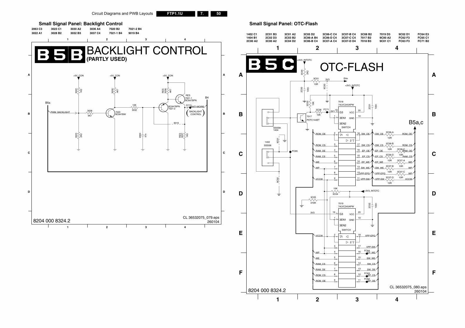
50FTP1.1U 7.Circuit Diagrams and PWB Layouts
2
1
3EN2
3EN1
G3
2
1
3EN2
3EN1
G3
7018 B3
7019 D39C00 A29C01 C1
9C02 D1FC62 F3FC63 F3
FC64 E3FC65 C1FC71 B2
SWITCH
SWITCH
0V1
3C06-C C43C06-D C43C07-A C4
3C07-B C43C07-C C43C07-D D4
3C08 B27017 B2
E
F
B5a,c
OTC-FLASH3V3
3 4
3 4
A
B
C
D
FC71
3C07-A
10R
8
10K
3C04
8
9
18
17
16
15
14
13
12
11
10GND
19
1
20VCC
1
20VCC
74LVC245APW7019
2
3
4
5
6
7
4
5
6
7
8
9
18
17
16
15
14
13
12
11
10GND
19
74LVC245APW7018
2
3
10R
3C06-D
10R
3C06-A
3C06-C
10R
10R
3C06-B
FC64
+3V3_INTOTC
3C07-C
10R
10R
3C07-D
10R
3C07-B
FC63
+3V3_INTOTC
9C00
100n
2C01
FC62
100n
2C02
EP_OE
SW_CS
SW_OE
_CS
_OE
_CS
_OE
SW_OE
SW_CS
EP_OE
EP_CS
SW_WE
EP_WE
VPP-SW
VPP-EPG
VPP-SW
SW_WE
EP_WE
EP_CS
EP_OE
SW_CS
SW_OE
VPP-SW
VPP-EPG
SW_WE
EP_WE
EP_CS
EAn
VPP-EPG
VCCW
WP
WP
WE
RAM_CS
RAM_OE
ROM_CS
ROM_OE
_CS
_OE
_CS
_OE
W
W
CL 36532075_080.eps260104
1 2
E
F
WE
RAM
RAM
ROM
ROM
VCC
WP
8204 000 8324.2
Small Signal Panel: Backlight Control
3028 B2
3030 A2
3037 C4
7020 B2
7021-1 B4
32
9019 B4
BACKLIGHT
3036 A4
3032 B3
D
2063 C3
3022 A1
3023 C1
BACKLIGHT CONTROL(PARTLY USED)
D
A
B
C
7021-2 B4
1
4
A
B
C
CONTROL( )
2 3 4
1
B4
B5aFC72
9019
+5V_CON +5V_CON +5V_CON
1K0
3037
RE
S
BC847BPN7021-2
BC847BPN7021-1RES
2063
47n
10K
3032
RE
S30
36
4K7
BC847BW4K
7
3030
7020
4K7
3028
2K2
3023
1K2
3022
PWM_BACKLIGHT
ANTI-MOIRE
CL 36532075_079.eps2601048204 000 8324.2
Small Signal Panel: OTC-Flash
3C00 A2
3C01 A23C03 B23C04 D2
3C05 D23C06-A B43C06-B C4
3V3
1402 C11404 B12C00 A2
2C01 B32C02 D3
1 2
A
B
C
D
+3V3_INTOTC
9C02
9C01
PDTC144ET
7017
100n
2C00
10R
3C01
10K
3C0
2K2
3C00
470R
3C05
1402
SSSS8
FC65
10K
3C03
SSSS81404
WP
WE
RAM
RAM
ROM
ROM
VCC
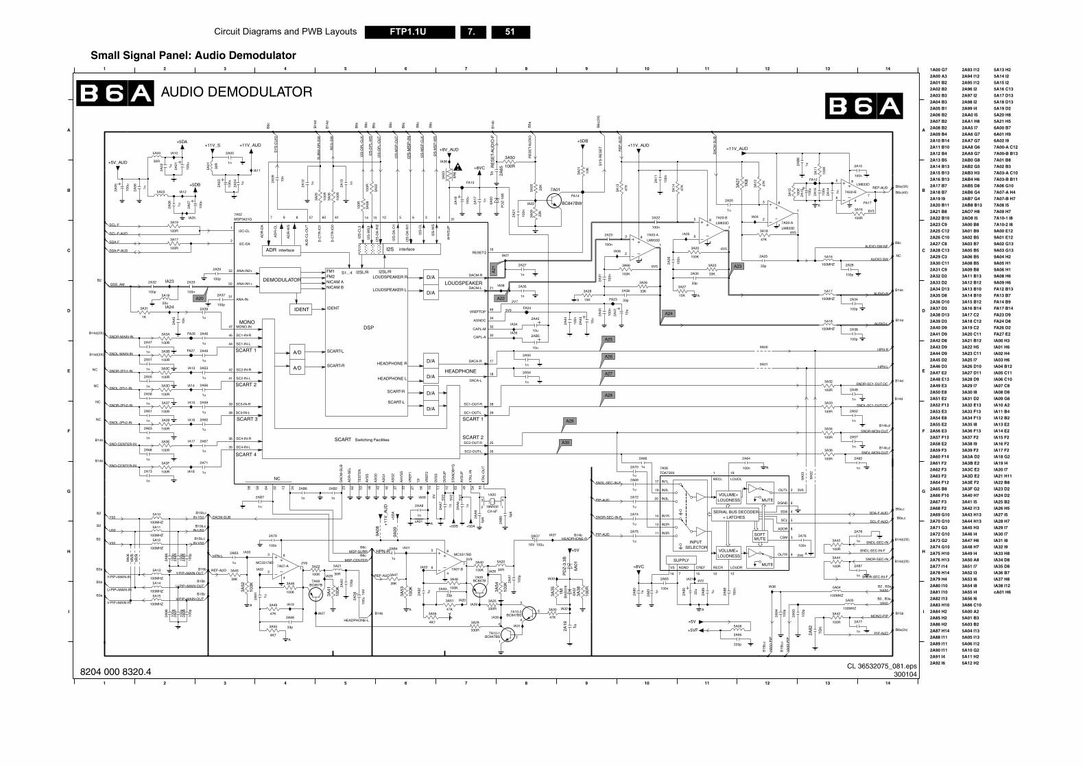
Circuit Diagrams and PWB Layouts 51FTP1.1U 7.
MUTESOFT
ODER
INPUT
MUTE
MUTEIA34 D8
IA35 D8
IA36 B7
IA37 H8
IA38 I12
cA01 H6
6V5
IA16 F2
IA17 F2
IA18 G2
6V3
IA19 I4
IA20 I7
IA21 H11
IA22 B8
IA23 D2
IA24 D2
IA25 B2
IA26 H5
IA27 I5
IA28 H7
IA29 I7
IA30 I7
IA31 I8
IA32 I9
IA33 H8
B6a,c
NC
FA17 B14
FA23 D9
FA24 D8
FA26 D2
FA27 E2
IA00 H3
IA01 H6
IA02 H4
IA03 H6
IA04 B12
IA05 C11
IA06 C10
IA07 C8
IA08 D8
IA09 G6
IA10 A2
IA11 B4
IA12 B2
IA13 E2
IA14 E2
IA15 F2
B15b,c
7A01 B8
7A02 B3
7A03-A C10
7A03-B B11
7A06 G10
7A07-A H4
7A07-B H7
7A08 I5
7A09 H7
7A10-1 I8
7A10-2 I8
9A00 E12
9A01 E12
9A02 G13
9A03 G13
9A04 H2
9A05 H1
9A06 H1
9A08 H6
9A09 H6
FA12 B13
FA13 B7
FA14 B9
B6a,c
B6a(2x)
3A66 C10
5A00 A2
5A01 B3
5A03 B2
5A04 I13
5A05 I13
5A06 I12
5A10 G2
5A11 H2
5A12 H2
5A13 H2
5A14 I2
5A15 I2
5A16 C13
5A17 D13
5A18 D13
5A19 D2
5A20 H8
5A21 H5
6A00 B7
6A01 H9
6A02 I9
7A00-A C12
B14b,d
B2 , B3a
7A00-B B13
3A39 F2
3A3A D2
3A3B E2
3A3C E2
3A3D E2
3A3E F2
3A3F G2
3A40 H7
3A41 I5
3A42 I13
3A43 H13
3A44 H13
3A45 H3
3A46 I4
3A47 H6
3A48 H7
3A49 I4
3A50 A8
3A51 I7
3A52 I3
3A53 I6
B2 , B3a 3A54 I8
3A55 I4
3A56 I6
B15
b,c
3A18 C12
3A19 C2
3A20 C11
3A21 B12
3A22 H5
3A23 C11
3A25 I7
3A26 D10
3A27 D11
3A28 D9
3A29 I7
3A30 I8
3A31 D2
3A32 E13
3A33 F13
3A34 F13
3A35 I8
3A36 F13
3A37 F2
3A38 I9
B14d
2AB3 H3
2AB4 H6
2AB5 D8
2AB6 G4
2AB7 G4
2AB8 B13
2AO7 H8
2AO8 I5
3A00 B8
3A01 B9
3A02 B5
3A03 B7
3A05 B5
3A06 B5
3A08 B5
3A09 B8
3A11 B13
3A12 B12
3A13 B10
3A14 B10
3A15 B12
3A16 B14
3A17 C2
2A90 I11
2A91 I4
2A92 I6
2A93 I12
2A94 I12
2A95 I12
2A96 I2
2A97 I2
2A98 I2
2A99 I4
2AA0 I5
2AA1 H8
2AA5 I7
2AA6 G7
2AA7 G7
2AA8 G6
2AA9 G7
2AB0 G8
2AB2 G5
B6a(3X)
2A67 F3
2A68 F2
2A69 G10
2A70 G10
2A71 G3
2A72 G10
2A73 G2
2A74 G10
2A75 H10
2A76 H13
2A77 I14
2A78 H14
2A79 H4
2A80 I10
2A81 I10
2A82 I13
2A83 H10
2A84 H2
2A85 H2
2A86 H2
2A87 H14
2A88 I11
2A89 I11
B14b,d
B15
b,c
2A48 E13
2A49 E3
2A50 E8
2A51 E2
2A52 F13
2A53 E3
2A54 E8
2A55 E2
2A56 E3
2A57 F13
2A58 E2
2A59 F3
2A60 F14
2A61 F2
2A62 F3
2A63 F2
2A64 F12
2A65 B8
2A66 F10
2A25 C12
2A26 C10
2A27 C8
2A28 C13
2A29 C3
2A30 C11
2A31 C9
2A32 D2
2A33 D2
2A34 D13
2A35 D8
2A36 D10
2A37 D3
2A38 D13
2A39 D3
2A40 D9
2A41 D9
2A42 D8
2A43 D9
2A44 D9
2A45 D2
2A46 D3
2A47 E2
2A05 B1
2A06 B2
2A07 B2
2A08 B2
2A09 B4
2A10 B14
2A11 B10
2A12 B4
2A13 B5
2A14 B13
2A15 B13
2A16 B13
2A17 B7
2A18 B7
2A19 I9
2A20 B11
2A21 B8
2A22 B10
2A23 C9
B6c
B14d
B14e
A
B
C
D
E
12 13 14
B14e
B14d(2X)
B6c(4X)
12 13 14
3V6
3V6
B14d(2X)B2
B15b
F
G
H
I
1A00 G7
2A00 A3
2A01 B2
2A02 B2
2A03 B3
2A04 B3
9A02
100R
3A44
1n
2A48
47K
3A12
FA12
1K8
2A76
100n
2A94
100p
2A87
1n
2A38
100p
16V 100u
100MHZ
5A18
3A32
A
100R
A 1n
2A60
IA04
1u2AB
8
1n
2A57
9A03
4
1n
2A14
LM833D
7A00-A
3
2
1
8
3A11
FA17
100K
47K
9A00
3A18
0n
64
33p
2A25
2A82
10n
2A16
100n
1n
2A78
100MHZ
5A17
2A93
100p
9A01
2OUTL
9OUTR
5SCL
4SDA
8ADDR
3CSM
6DGND
100K
3A15
2A15
100u
100MHZ
5A16
5A12
1n
2A52
100R
3A16
100R
3A431u
A
100n
100MHZ
5A05
100n
2A10
2A28
100p
100R
3A42
1n
2A77
100R
3A33
100p
2A34
5A04
100MHZ
3A36
100R
100R
3A34
7A00-B
LM833D5
67
8
4
IA38
AUDIO-SW-NF
HEADPHONE-R
HPN-L
AUDIO-R
PIP-AUD
HA
50-P
IP
HA50
VA50
VA
50-P
IP
HPN-R
SNDR-SEC-IN-F
SNDL-MON-OUT
SNDR-MON-OUT
SCL-F-AUD
SDA-F-AUD
AUDIO-L
AUDIO-SW
SNDR-SC1-OUT-DC
SNDL-SC1-OUT-DC
MONO-PIP
SNDL-SEC-IN-F
SNDL-SEC-IN
SNDR-SEC-IN
REF-AUD
V50 IN-V50
CL 36532075_081.eps300104
LOUDNESSVOLUME+
SUPPLY
SELECTOR
B15b
B6c
B14b
B15b
B3a
B3a
2V9
4V2
B15b
2V9
H
I
B3a
6 7 8 9 10 11
B6c
1 2 3 4 5
100p
2A84
2
6
1BC847BS
7A10-1
2A81 1n
3A38
100R
47K
3A30
1u
2A19
30R
5A21 +8VC
2A86
100p
6A01
6A02
PD
Z-3
.3B
BA
S31
6
100K
100MHZ
5A15
3A40
100K
3A22
9A04
7A08BC857B
16V
100u2A
O8
47K
3A49
2A92
1u
+5VF
3A35
1M
3A25
330R
330R
3A29
1u
2A91
A
3A53
100K10
0K
3A52
100p
2A97
5A064K7
3A56
5A13
100MHZ
7A10-2BC847BS
5
3
4
7A09BC857B
A
IA00
5A20
30R
9A06
9A05
2AB3
1u
A
IA20
A
2A80
1u
100p
2A85
3A55
4K7
2AA5
33p
3A46
100K
A
1u
2AB4
3A47
39K
IA03
2A95
220p
12
LOUDR
10
RECR
16
VS
7
AGND
15
CREF
100MHZ
5A14
2A98
100p
100p
2AA
0
33p
2A99
100n
2A88
100MHZ
3A54
100K
39K
3A45
MC33178D7A07-A
3
21
8
4 2A83
100n
+5V
2AA
1
100p
7A07-B
MC33178D5
67
8
4
IA19
IA21
22u
2A90
100K
3A41
+5V
100p
2A96 IA27
IA26
IA02
IA33
IA31
IA30
IA32
2A89
1u
IA01
47K
3A51
100K
3A48
IA29
IA28
HPN-R
REF-AUD
REF-AUD
HPN-LMSP-CENTER
MSP-SURR
HEADPHONE-L
Y-PIP+MAIN-IN
U-PIP+MAIN-IN
V-PIP+MAIN-OUT
Y-PIP+MAIN-OUT
U-PIP+MAIN-OUT
V-PIP+MAIN-IN
8204 000 8320.4
Small Signal Panel: Audio Demodulator
I2SL/R
NICAM BNICAM AFM2FM1 S1...4
interfaceI2SinterfaceADR
DEMODULATOR
D/A
D/A
D/A
D/A
A/D
A/D
SCART 1
SCART 2
MONO
SCART 2
SCART 3
SCART 1 SCART-L
SCART-R
SCART-R
SCART-L
HEADPHONE L
NC
HEADPHONE R
HEADPHONE
IDENT
DSP
IDENT
LOUDSPEAKER
SCART 4
Switching FacilitiesSCART
LOUDSPEAKER R
LOUDSPEAKER LD/A
D/AI2SL/R
+ LATCHESSERIAL BUS DEC
LOUDNESSVOLUME+
B6c
B15b,c
B6c
B14b
B14b
B14d(2X)
NC
NC
NC
NC
B14
d
B15b,c
B6c
B5a
B6c
3V9
B6c
B2
B6c
(2X
)
B6c B6c B6c
AUDIO DEMODULATOR
B14d(2X)
A
B
C
D
E
F
G
2V7
5V2
5V2
5V2
0V
B14b
1 2 3 4 5 6 7 8 9 10 11
B14
b
B2
B2
6V5
6V5
B14
d
IA15
3A02+5DB
3A3D
100R
100R
100u
2A01
IA09
IA36
1u
2A70
IA14
100n
2A31
1u
A
2A46
15K
3A27
3A08
100R
10u
2A41
3A21
IA17
47K
3A14
1n
2A12
IA11
2A54
1n
2A27
1n
1n
2A63
IA34
IA35
2AO7
2A59
1u
3A66
100K
10n
2A09
+11
V_A
UD
1u
2A20
10K
3A01
7A01
BC847BW
33K
3A26
3A06
100R
100n
2A21
XTA
L-O
UT
55
28SC1-OUT-R
41 SC2-IN-L
42 SC2-IN-R
26SC2-OUT-L
SC2-OUT-R 25
SC3-IN-L38
39 SC3-IN-R
35 SC4-IN-L
36 SC4-IN-R
STA
ND
BY
Q63
TE
ST
EN
53
TP
5627V
RE
F1
VR
EF
219
46VREFTOP
XTA
L-IN
54
I2S
-DA
-IN
1
6
I2S
-DA
-IN
2
12
I2S
-DA
-O1
5
I2S
-WS
4
I2S
-WS
3
15
47 MONO-IN
58 59 64 22 13 24
RESETQ16
44 SC1-IN-L
45 SC1-IN-R
29SC1-OUT-L
AV
SU
P49
CAPL-A 30
32CAPL-M
61
D-C
TR
-IO
0
D-C
TR
-IO
1
60
18
DACA-L
17DACA-R
21DACM-L
DACM-R
DA
CM
-SU
B23
DV
SS
11
DV
SU
P10
I2C-CL1
2I2C-DA
I2S
-CL
3
I2S
-CL3
149
AD
R-C
L
7
AD
R-D
A
AD
R-S
EL
62
AD
R-W
S
8
34AGNDC
AH
VS
S33
31
AH
VS
UP
51ANA-IN-
50 ANA-IN1+
52 ANA-IN2+
AS
G0
43 40A
SG
1
37A
SG
2
57
AU
D-C
L-O
UT
AV
SS
48
MSP3421G 7A02
9A08
IA06
100u
2A03
2A68
1n
1n
2AB2
1n
2AA
7
1u
2A67
+11V_AUD
9A09
3A3B
100R
IA24
2A55
1n
47K
100R
3A17
3A13
1n
2A58
2A35
1n
1n
2A06
10
2A
IA05
5A19
22u
FA26
1n
2A51
100u
2A18
22K
100n
2A22
FA24
3A09
2A23
100n
IA10
100MHZ
5A11
30R
5A01
+8V_AUD
2AA
6
1n
IA125A03
3A20
+11V_AUD
100K
18M432
1A00
CX-5F1
4
2
3
100n
2A11
IN1R
18 IN2L
13 IN2R
20 IN3L
11 IN3R
19
LOUDL
1
RECL
TDA73097A06
17 IN1L
14
2A17
1n
2A45
10n
2A33
100n
1n 2A65
100u
2A07
2A39
1u
100n
2A44
2A61
1n
+11V_S
2A50
1n
IA23
IA22
5A00
30R
3A3C
100R
100R
3A39
3A37
100R
FA27
2A32
100p
2AA
9
5p6
2A74
6R8
3A03
1u
3A50
100R
+11V_AUD
1u
2A56
2A75
1u
2A712A66
1u
2A36
33p
2A47
1n
FA13
FA14
2A62
1u
2A08
1u
2A79
3A3F
100R
3A3E
100R
2AB
0 5p6
1n
2A73
2A26
100n
IA08
1u
2A29
100p
2A04
1u
2A72
2A40
100n
5A10
100MHZ
IA13
2A00
1n
+8VC
22K
3A00
2A69
1u
1n
2AB6
IA25
+5DB
100R
3A19
2A49
1u
2A30
33p
100R
3A05
10u
2A42
2AA8
1n
2A02 1u
2A53
1u
2A05
100u
+5DA
IA16
+5V_AUD
3A3A
100R
A
IA18
A
1K
3A31
6
7
8
4
7A03-B
LM833D5
2A43
10u
8
4
33K
3A23
7A03-A
LM833D3
2
1
cA01
100p
2A37
2AB5
FA23
10u
IA37
1n
2AB7
3A28
15K
IA07
PD
Z-1
0B
6A00
RE
SE
T-A
UD
IO-F
DACM-SUB
SY
S-R
ES
ET
I2S
-MS
P-I
N
2A13
1n
RE
G-S
W
SU
BW
-SP
I-S
W
SND-CENTER-IN
SND-CENTER-IN
SNDL-2Fh1-IN
SNDR-2Fh1-IN
SNDL-SEC-IN-F
SCL-F
SDA-F-AUD
SCL-F-AUD
+5D
A
RE
SE
T-A
UD
IO
IN-Y50
IN-U50
SNDR-MAIN-IN
DA
CM
-SU
B
SNDL-MAIN-IN
+5DA+5DB
I2S
-DP
L-O
UT
SDA-F
QSS_AM
I2S
-MS
P-W
S
I2S
-MS
P-O
UT
I2S
-MS
P-C
LK
SY
S-C
LK0
SNDR-2Fh2-IN
SNDL-2Fh2-IN
PIP-AUD
SNDR-SEC-IN-F
PIP-AUD
RE
F-A
UD
I2S
-DP
L-C
LK
I2S
-DP
L-W
S
Y50
U50
A21
A20
A27
A28
A29
A22
A30
A26
A24
A25
A23
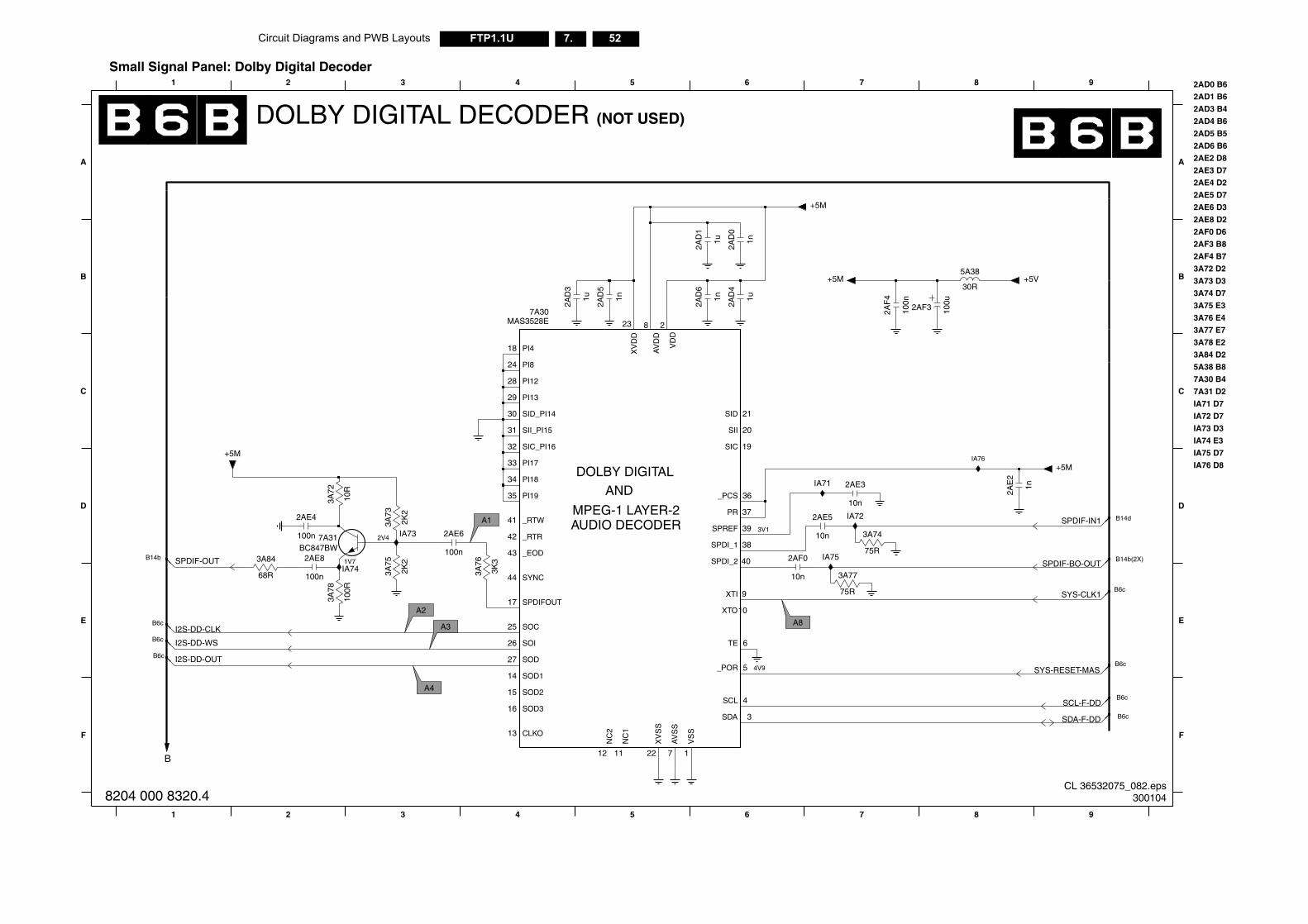
52FTP1.1U 7.Circuit Diagrams and PWB Layouts
3A76 E4
3A77 E7
3A78 E2
3A84 D2
5A38 B8
7A30 B4
7A31 D2
IA71 D7
IA72 D7
IA73 D3
IA74 E3
IA75 D7
B6c
B6c
B14d
2AD6 B6
2AE2 D8
2AE3 D7
2AE4 D2
2AE5 D7
2AE6 D3
2AE8 D2
2AF0 D6
2AF3 B8
2AF4 B7
3A72 D2
3A73 D3
3A74 D7
3A75 E3
B14b(2X)
B6c
B6c
8 9
A
B
C
D
E
F
2AD0 B6
2AD1 B6
2AD3 B4
2AD4 B6
2AD5 B5
B6c
IA76 D8
8 9
100n
+5M
1n
2AE
2
5A38
30R
IA76
+5V
100u
2AF3
SYS-CLK1
SCL-F-DD
SDA-F-DD
SYS-RESET-MAS
SPDIF-IN1
SPDIF-BO-OUT
CL 36532075_082.eps300104
B
1 2
4V9
F
3 4 5 6 7
_POR 5
15
SOD316
VS
S
1
XV
SS
22
SCL 4
SDA 3
SOD27
SOD114
SOD2
AV
SS
7
CLKO13
NC
1
11
NC
2
12
I2S-DD-OUT
8204 000 8320.4
A4
Small Signal Panel: Dolby Digital Decoder
MPEG-1 LAYER-2
DOLBY DIGITAL DECODER (NOT USED)
B6c
3V1AUDIO DECODER2V4
1 2 3 4 5 6 7
AND
1V7B14b
D
E B6c
DOLBY DIGITAL
A
B
C
2AD
4
3K3
3A76
2AF
41u
10n
2AE5
2K2
3A75
75R
3A77
100R
3A78
IA71
1n
2AD
0
+5M
+5M
2AE3
10n
2K2
3A73
2AD
1
1u
+5M
10R
3A72
2AE4
100n
36
_RTR42
_RTW41
100n
2AE8
SOI26
SPDIFOUT17
SPDI_1 38
SPDI_2 40
SPREF 39
SYNC44
TE 6
VD
D
2
XTI 9
XTO10
XV
DD
23
43 _EOD
_PCS
34
PI1935
PI418
PI824
PR 37
SIC 19SIC_PI1632
SID 21SID_PI1430
SII 20SII_PI1531
SOC25
7A30MAS3528E
AV
DD
8
PI1228
PI1329
PI1733
PI18
1n
2AD
6
1u
2AD
3
IA72
3A84
68R
1n
IA75
2AD
5
2AF0
10n
BC847BW7A31 3A74
75R
IA73 2AE6
100n
IA74
I2S-DD-CLK
I2S-DD-WS
SPDIF-OUT
A3
A1
A2
A8
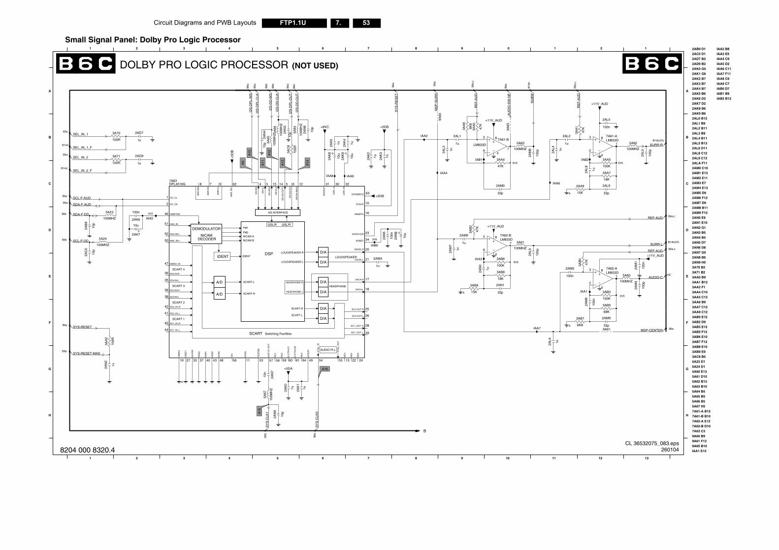
Circuit Diagrams and PWB Layouts 53FTP1.1U 7.
NC
7A62-A E12
7A62-B D10
7A63 C3
9A60 B9
9A61 F12
9A65 B10
IAA1 E12
IAA2 B8
IAA3 E9
IAA4 C9
IAA5 D2
IAA6 C11
IAA7 F11
IAA8 C6
IAA9 C7
IAB0 D7
IAB1 B9
IAB2 B12
5A63 B10
5A64 B5
5A65 B5
5A66 B5
5A67 H5
7A61-A B12
7A61-B B10
3AA5 C12
3AA6 B9
3AA7 C12
3AA9 C12
3AB0 E12
3AB2 D9
3AB3 E12
3AB5 F12
3AB6 E10
3AB7 F12
3AB8 E10
3AB9 E9
3AC8 B5
5A23 D1
5A24 D1
5A60 E13
5A61 D10
5A62 B13
2AN4 B5
2AN5 D7
2AN6 D8
2AN7 G5
2AN8 B6
2AN9 H5
3A70 B2
3A71 B2
3AA0 B9
3AA1 B12
3AA2 F1
3AA4 C10
2ALA F11
2AM0 C10
2AM1 E13
2AM2 E11
2AM3 E7
2AM4 E13
2AM5 D9
2AM6 F12
2AM7 D9
2AM8 B11
2AM9 F12
2AN0 E9
2AN1 E10
2AN2 G1
2AN3 B5
6V5
6V5
2AK5 B6
2AK6 D2
2AK7 D2
2AK8 B6
2AK9 B6
2AL0 B12
2AL1 B9
2AL2 B11
2AL3 B9
2AL4 B11
2AL5 B13
2AL6 D11
2AL8 C12
2AL9 C12
B14b(2X)
B6a
,c
B6a,c
B6a,c
A
B
C
D
11 12 1
1 2 1
3
B14b(2X)
E
F
G
H
2AB9 D1
2AC0 D1
2AD7 B2
2AD9 B2
2AK0 G5
2AK1 G6
2AK2 B7
2AK3 B7
2AK4 B7
B6a
IAB2
100n
2AL0
+11V_AUD
2AK 1u
3AB3
100K
IAA1
2AL9
47K
3AA
1
33p
2AL5
100p
2AM2
100n
2ALA 1n
2AK 1n
100MHZ
5A62
47K
3AB
0
3AB5
68K
2
1
8
4
100K
3AA5
LM833D7A62-A3
18K
3AA7
2AM
1
100n
1u
2AL2
100p
2AM
4
IAA6
2AM9
33p
100p
7A61-ALM833D
3
2
1
8
4
100n
2AM
6
3AB7
6K89A61
A
A
100p 1n
2AL4
+11V_AUD
5A60
100MHZ
3AA9
15K
2AL8
1u
A7
7 HZ
REF-AUD
SURR-L
SURR-R
RE
F-A
UD
REF-AUD
AUDIO-C
MSP-CENTER
CL 36532075_083.eps260104
B6a
B6b
H
1 2 3 4 5 6 7 8 9 10
B
2AN
9
10p
5A6
100M
SY
S-C
LK1
SY
S-C
LK0
8204 000 8320.4
A15
Small Signal Panel: Dolby Pro Logic Processor
A/D
DECODERNICAM
Switching Facilities
IDENT
HEADPHONE R
SCART-L
SCART-R
SCART-R
SCART-L
D/A
D/A
LOUDSPEAKER R
SCART
D/A
SCART 4
A/D
SCART 2
D/ALOUDSPEAKER L
D/ADSP
I2SL/R
I2S INTERFACE
I2SL/RFM1
HEADPHONE L
FM2
SCART 3
D/A
IDENT LOUDSPEAKER
DEMODULATOR
NICAM B
NICAM A
HEADPHONE
SCART 1
AUDIO PLL
B14
b
B6a
B6b
B6a
B6a
B6a
B6a
0V2
B6b B6a
3V8
6V5
6V5
B14d
B6a
,c
B6a
B6b
DOLBY PRO LOGIC PROCESSOR (NOT USED)
B6a
B5a
B14d
C
D
E
F
G
B5a
1 2 3 4 5 6 7 8 9 0
A
B
B6a
B6b
B6b
B6b
IAB1
IAA9IAA8
100MHZ
5A63
IAA3
0
TP
1
27
VR
EF
1
19
VR
EF
2
46 VREFTOP
54
XT
AL_
IN
55
XT
AL_
OU
T
NC
6
16RESETQ
44 SC1_IN_L
45 SC1_IN_R
29SC1_OUT_L
28SC1_OUT_R
26SC2-OUT-L
25SC2-OUT-R
41 SC2_IN_L
42 SC2_IN_R
38 SC3-IN-L
39 SC3-IN-R
35 SC4-IN-L
36 SC4-IN-R
STANDBYQ 63
53
TE
ST
EN
56
DVSUP
1 I2C_CL
2 I2C_DA
3
I2S
-CL
I2S
-CL3
14
I2S
-DA
-IN
1
6
I2S
-DA
-IN
2|3
12
I2S
-DA
-OU
T1
54
I2S
-WS
I2S
-WS
3
15
47 MONO_IN
58
NC
1
59
NC
2
64
NC
3
13
NC
4
22
NC
5
24
AS
G0
AS
G1
4037
AS
G2
57
AU
D-C
L-O
UT
48
AV
SS
49
AV
SU
P
CA
PL-
A
30
CA
PL-
M
32
61
D-C
TR
-IO
0
60
D-C
TR
-IO
118DACA-L
17DACA-R
23DACM-SUB
21DACM_L
DACM_R 20
11
DV
SS
10
AD
R-C
L
9
AD
R-D
A
7
AD
R-W
S
8
AD
R_S
EL
62
34AGNDC
33
AH
VS
S
31
AH
VS
UP
52 ANA-IN2+
51 ANA_IN-
50 ANA_IN1+
43
10u
2AK7
7A63DPL4519G
2AK
9
10u
100M
HZ
5A64
1
2AM5
1u
3AB6
100K
9A60
1n
2AK
5
10u
2AN
6
10u
2AK
8
2AK6
100n
+5DB
2AN
3
10p
2AN
2
1n10
0R
3AA
2
3A71
100R
3AB
2
47K
A
6K8
3AA
6
47K
3AA4
100n
2AN
5A
2AM
7
1n
10p
2AN
8
3AB9
15K
10p
2AC
0
3AB8
18K
1n
2AK
3
2AB
9
10p
2AL6
1u
2AK
4
+5DB
IAA2
IAA5
100R 7
8
43AC
8 LM833D
7A61-B5
6
10n
2AN
7
+8VC
9A65
100MHZ
5A24
5A23
100MHZ
5A66
100M
HZ
100M
HZ
5A65
2AM
8
10p
2AN
4
2AN1
33p
1u
2AN
0
5
6
7
8
4
47K
3AA
0
LM833D7A62-B
IAA4
1u
2AK
2
2AD9
1n
+11V_AUD
5A61
100MHZ
+5D
B
IA
2AM3
1n
1n
2AD7
1n
2AL3
IAB0
3A70
100R
+5DA
2AM0
1u
2AL1SEL_IN_1
SEL_IN_2
SEL_IN_1_F
SEL_IN_2_F
SYS-RESET-MAS
SYS-RESET
I2S
-DD
-OU
T
I2S
-DD
-WS
I2S
-DD
-CLK
SDA-F-DD
SCL-F-DD
33pSCL-F-AUD
SDA-F-AUD
RE
F-A
UD
SU
BW
I2S
-DP
L-O
UT
+11V_AUD
MS
P-S
UR
R
AU
DIO
-SW
-NF
I2S
-DP
L-C
LK
I2S
-DP
L-W
S
SY
S-R
ES
ET
A16
A14
A13
A10
A11A9
A12
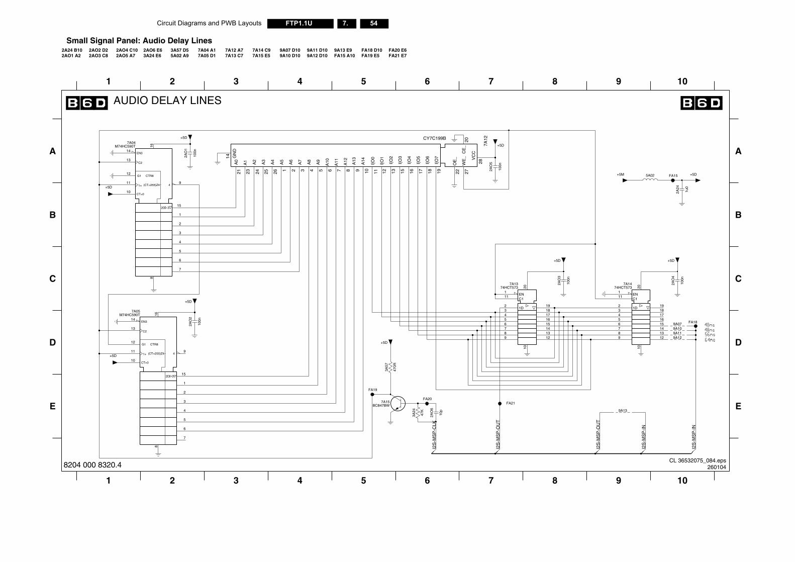
54FTP1.1U 7.Circuit Diagrams and PWB Layouts
ENC1
1D
8 9 10
A
D
E
8 9 10
B
C
FA20
9A13
FA18
9A109A07
9A129A11
+5D
100n
2AO
4
98765432
141312
20
789
10
111
1918171615
23456
74HCT5737A14
2A24
1u0
+5DFA155A02+5M
2AO
3
100n
+5D
I2S
-MS
P-O
UT
I2S
-MS
P-I
N
I2S
-MS
P-I
N
CL 36532075_084.eps260104
1 2 3 4 5 6 7
E
2AO
6
10p
3A24
47K
7A15BC847BW
4
5
6
7
8
3 FA21
I2S
-MS
P-C
LK
I2S
-MS
P-O
UT
8204 000 8320.4
Small Signal Panel: Audio Delay Lines
ENC1
1D
C2
G1
1+
CT=0
CTR8
(CT=255)Z4
2D 3
4
EN3
C2
G1
1+
CT=0
CTR8
(CT=255)Z4
2D 3
4
EN3
A
B
C
D
AUDIO DELAY LINES
9A11 D109A12 D10
9A13 E9FA15 A10
FA18 D10FA19 E5
FA20 E6FA21 E7
2A24 B102AO1 A2
2AO2 D22AO3 C8
2AO4 C102AO5 A7
2AO6 E63A24 E6
3A57 D55A02 A9
7A04 A17A05 D1
7A12 A77A13 C7
7A14 C97A15 E5
9A07 D109A10 D10
1 2 3 4 5 6 7
FA19
+5D
1
2
3
4
5
6
7
13
9
16
7A04
11
12
10
814
15
M74HC590T
111
11111111
20
23456789
10
74HCT5737A13
GN
D
11I|O
0
12I|O
1
13I|O
2
15I|O
3
16I|O
4
17I|O
5
18I|O
6
19I|O
7
22O
E_
28
VC
C
27W
E_
A0
23A
1
6A
10
7A
11
8A
12
9A
13
10A
14
24A
2
25A
3
26A
4
1A
5
2A
6
3A
7
4A
8
5A
9
20C
E_
14
CY7C199B
7A12
21
+5D
470R
3A57
100n
2AO
22A
O1
100n
+5D
+5D
+5D
+5D
2AO
5
100n
13
9
16
11
12
10
14
15
1
2
M74HC590T7A05
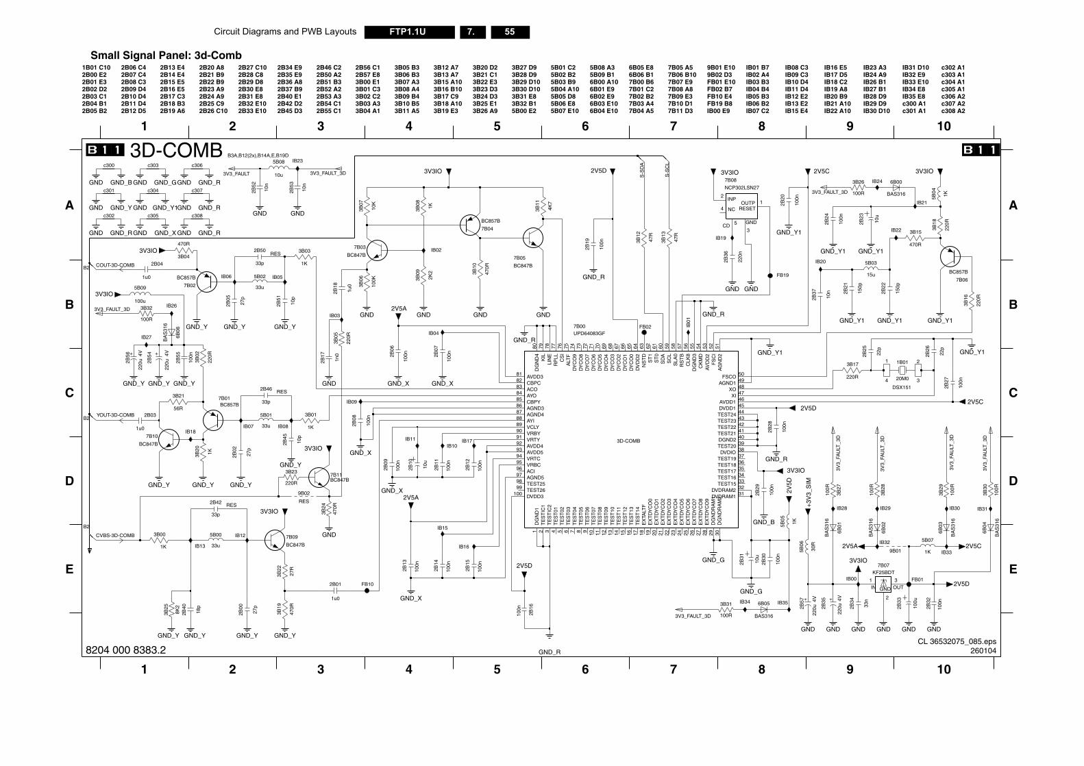
Circuit Diagrams and PWB Layouts 55FTP1.1U 7.
SET
9 10
9 10
8
A
B
C
D
E
8
IB06 B2IB07 C2
IB08 C3IB09 C3IB10 D4IB11 D4IB12 E2
IB15 E4
IB17 D5IB18 C2IB19 A8
IB31 D10IB32 E9IB33 E10IB34 E8IB35 E8c300 A1c301 A1
c302 A1c303 A1c304 A1c305 A1c306 A2
IB16 E5IB24 A9IB26 B1IB27 B1IB28 D9IB29 D9IB30 D10
IB01 B7IB02 A4IB03 B3IB04 B4IB05 B3 IB20 B9
IB21 A10IB22 A10
IB23 A3
IB13 E2 c307 A2c308 A2
ND
9B01
FB19
GND
GND_Y1
ND_G
10u
GND_Y1
3
GND_Y1
20M0
1B01
DSX151
1
4
2
2B21
150p
2B20
100n
3B18
220R
2B34
33n
1K5B04
2B22
22p
2B26
150p
+3V
3_S
IM
100u
2B33
2V5A
100n
2B28
IB00
GND
2V5C
3B16
220R
GND_Y1
100R
3B28
6B04
BA
S31
6
7B06
BC857B
100n
2B24
100R
3B26 6B00
BAS316
3V3IO
6B05
BAS316
6B02
BA
S31
6
GND
2
IN1
OUT3
BA
S31
6
6B03
GND_Y1
7B07KF25BDT
GND_Y1
3V3IO
2V5D
2B29
100n
GND
BC847B
7B09
2V5C
IB20
IB21
IB22
2V5C33u
2V5D
3B30
100R
GND_Y1
2B37
10n
GND_Y1
100n
2B30
UTP 1
SN27
GND
3
3B29
100R
3B27
100R
2B32
100n
2B27
100n
BA
S31
6
6B01
3B15
470R
GND_R
3B17
220R
2V5D
30R
5B06
GND
1K
5B07
2B57
GND
4V22
0u
10u
2B23
2B25
22p
FB01
2B35
220u
4V
5B05
1K
15u
5B03
GND
3V3IO
GND_B
IB24
IB28
IB32
IB31IB29 IB30
IB33
IB35
3V3_
FAU
LT_3
D
3V3_
FAU
LT_3
D
3V3_FAULT_3D
3V3_
FAU
LT_3
D
3V3_
FAU
LT_3
D
4
CL 36532075_085.eps260104
1 2 4 5 6 7
E
3
GND_Y
G
2B31GND_G
GND_R
2B00
27p
GND_X
2V5D
FB10
IB16
3B31
100R
GND_Y
2B01
1u0
2B15
100n
1K
100n
2B13
8K2
3B25
470R
3B19
3B22
27R
100n
2B16
GND_Y
18p
2B40
100n
2B14
IB13
GND_Y
3V3_FAULT_3D
IB3
8204 000 8383.2
Small Signal Panel: 3d-Comb
NC REA
B
C
D
B3A,B12(2x),B14A,E,B19D
3 4 5
2B09 D42B10 D42B11 D42B12 D5
2B13 E42B14 E42B00 E2
2B01 E3
2B06 C42B07 C42B08 C3
1B01 C10
2B19 A6
2B20 A82B21 B9
2B02 D22B03 C12B04 B12B05 B2
2B25 C92B26 C10
2B27 C102B28 C82B29 D82B30 E82B31 E8
2B33 E10
B2
B2
1 2
2B37 B92B40 E12B42 D2
6 7
2B51 B32B52 A22B53 A32B54 C12B55 C1
2B56 C12B57 E8
3B01 C32B15 E52B16 E52B17 C32B18 B3
3B02 C23B03 A3
2B22 B92B23 A92B24 A9
3B07 A33B08 A43B09 B43B10 B53B11 A5
3B12 A73B13 A7
2B32 E10
3B16 B10
B2
2B34 E92B35 E92B36 A8
3B18 A103B19 E3
3B20 D2
2B45 D3
2B46 C22B50 A2
3B24 D33B25 E13B26 A9
3B27 D93B28 D93B29 D103B30 D10
3B00 E1
3B32 B1
5B09 B16B00 A106B01 E9
3B04 A1
3B05 B33B06 B3
6B05 E86B06 B17B00 B67B01 C27B02 B27B03 A47B04 A5
3B15 A107B06 B10
3D-COMB
3B17 C9FB02 B7FB10 E4FB19 B8
3B21 C13B22 E33B23 D3
3B31 E8
3D-COMB
5B00 E2
5B01 C25B02 B25B03 B95B04 A105B05 D85B06 E85B07 E10
5B08 A3
6B02 E96B03 E106B04 E10
7B05 A5
FB01 E107B07 E97B08 A87B09 E37B10 D1
IB00 E9
GND_X
7B11 D3
9B01 E109B02 D3
470R
3B04
IB04
GND_R
33u
5B02
3V3IO
2B51
10p
G
GND_Y GND_Y
c307
GND_Y
3B05
220R
GND_Y
IB06
2B07
100n
IB02
IB03
GND_Y
2B08
100n
100n
2B55
GND_X
100n
2B19
5B09
100u
c304
GND
100K
10p
2B45
GND_Y1
2V5A
3B06
7B04
BC857B
10u
2B10
220u
4V2V5D
2B54
2V5A
c305
IB15
IB17IB11
GND
7B05
BC847B
3V3IO
2B36
220n
GND_Y10
0n
2B12
GND_R
GND_RGND
GND_Y
GND GND_R
GND_R
1u0
2B033B
08
1K
2B17
1n0
IB19
IB07 IB08
IB01
IB12
33p
2B42 RES
IB09
IB10
IB05
IB18
3B09
2K2
3B12
47R
10n
2B52
56R
3B21
GND_Y
3V3IO
2B05
27p
1K
3B03
GND
BC847B
7B10
RES
GND
33p
2B46
3B07
10K
c306
3B00
c301
2B18
1u0
5B00
FB02
GND
GND
3V3IO
2B06
100n
GND
100n
2B09
GND
INP2
4O
GND
3B10
470R
7B08
NCP302L
CD 5
470R
3B24
220R
3B23
3V3IO
GND_X
2B50
33p
RES
7B02
BC857B
GND_R
GND_G
RES
2B04
1u0
9B02
3B20
1K
2T
ES
TIC
13
TE
ST
IC2
89 VCLY
95 VRBC
VRBY90
94 VRTC
91 VRTY
47XI
48XO
14T
ES
T11
15T
ES
T12
16T
ES
T13
17T
ES
T14
33TEST15
34TEST16
35TEST17
36TEST18
37TEST19
39TEST20
41TEST21
42TEST22
43TEST23
44TEST24
98 TEST2599 TEST26
57R
ST
B
59S
CL
60S
DA
58S
LA0
61S
T0
62S
T1
4T
ES
T01
5T
ES
T02
6T
ES
T03
7T
ES
T04
8T
ES
T05
9T
ES
T06
10T
ES
T07
11T
ES
T08
12T
ES
T09
13T
ES
T10
19E
XT
DY
CO
020
EX
TD
YC
O1
21E
XT
DY
CO
222
EX
TD
YC
O3
23E
XT
DY
CO
424
EX
TD
YC
O5
25E
XT
DY
CO
626
EX
TD
YC
O7
27E
XT
DY
CO
828
EX
TD
YC
O9
52F
SC
I
50FSCO
79K
IL78
LIN
E
63N
ST
D
77R
PLL
64D
VD
D2
100 DVDD3
38DVDIO
31DVDRAM1
32DVDRAM2
65D
YC
O0
66D
YC
O1
67D
YC
O2
68D
YC
O3
69D
YC
O4
70D
YC
O5
71D
YC
O6
72D
YC
O7
73D
YC
O8
74D
YC
O9
18E
XTA
LTF
92 AVDD493 AVDD5
88 AYI
84 AYO
82 CBPC
85 CBPY
54C
KM
D
56C
LK8
76C
SI
1D
GN
D1
40DGND2
55D
GN
D3
80D
GN
D4
29D
GN
DR
AM
130
DG
ND
RA
M2
45DVDD1
7B00UPD64083GF
96 ACI
83 ACO
49AGND1
51A
GN
D2
86 AGND387 AGND4
97 AGND5
75A
LTF
46AVDD1
53A
VD
D2
81 AVDD3
GND
GND
3B13
BC857B7B01
4V
GND_R
47R
2B56
220u
c300
c308
GND
IB27
2B11
100n
GND_Y
IB23
GND_Y
GND_X
BC847B7B11
5B08
10u
2B53
10n
IB26
GND
100R
3B32
BA
S31
6
6B06
3V3IO
GND_B
3B02
220R
GND_Y
1K
GND
GND_X
3B01
c302
c303
5B01
33u
27p
2B02
GND
3B11
4K7
GND
BC847B
7B03
3V3_FAULT
COUT-3D-COMB
3V3_FAULT_3D
3V3_FAULT_3D
YOUT-3D-COMB
S-S
CL
S-S
DA
CVBS-3D-COMB
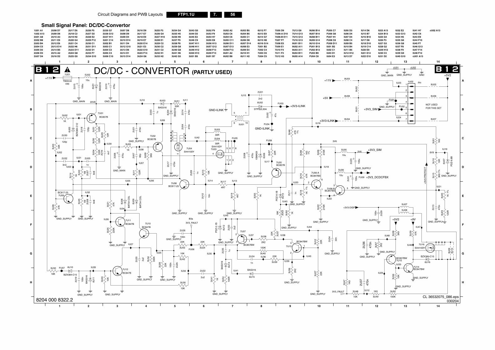
56FTP1.1U 7.Circuit Diagrams and PWB Layouts
+3V
3-P
RO
TE
CT
11 12 13 14
6V9
11 12 13 14
A
B
C
D
E
F
G
H
3V6
1%
NOT USED
FOR THIS SET
IU05 D3IU06 D4IU07 D4IU08 C4IU09 B5IU10 B4IU11 B5IU12 H12IU13 D7
IU14 D6IU15 B7IU16 B10IU17 D8IU18 D10IU19 C14IU20 E9
1%
IU21 E14IU22 E10
IU23 A13IU24 B13IU25 G4IU26 F3IU27 G3IU28 G2IU29 H12IU30 C3IU31 D2
IU32 E2IU33 G13IU34 H5IU35 G6IU36 G8IU37 F8IU38 F9IU39 G9IU40 G10
IU41 H7IU42 C6IU43 E9IU44 F10IU45 F7IU46 G13IU47 F14IU48 F12cU01 A13
cU02 A13
9U09
SI4410DY
7U16
6U16
BZX384-C15
3U59
47K
+9V
2U36
470n
GND_SUPPLY
3U58
3K9
+5V2
2K2
GND_SUPPLY
GND_SUPPLY
3U57
GND_SUPPLY
7U14BC847BW
10K
3U56
BC857BW7U15
3U50
100K
470n
2U37
3U47
1K0
1K0
3U49
3U48
10K
GND_SUPPLY
IU46
IU33
IU29
IU47
IU48
IU12
cU02
GND_SUPPLY
IU21
3U23
120R
IU24
GND_SUPPLY
9U08
GNDGND_SUPPLY
9U03GND_MAIN
BC857BW
6U07
PD
Z-6
.8B
10u
5U05
PH1U021
2
3
4
5
6
7
FU06
+3V3_SIM
9U05
9U04
5
9U01
IU19
17U13
9U02
3U10
10R
9U06
3U01
1K0
9U07
+3V3_DCDCFBX
GND_SUPPLY
2U31
100u
GND_SUPPLY
1K3U20
FU01
IU23
cU01
GND_SUPPLY
3U43
FU02
150K
+5V2
100u
2U23
3U24
FU09
06
0u
2U29
100n
+3V3_SIM
+3V3-DISP5U08
5U07
2U13
470n
GND_SUPPLY
3U15
3K9
5
ULT
CL 36532075_086.eps030204
9U10
1 2 3 4 5 6 7 8 9 10
G
H
2u2
2U22
3U33
10K
IU36
3U35
10K
GND_SUPPLY
GND_SUPPLY
18K
3U32
IU35
3U26
22K
100n
2U25
GND_SUPPLY
GND_SUPPLY
2K2
3U36
IU28
IU40
2U19
100n
3U41
1K
IU25 2
GND_SUPPLY
GND_SUPPLY
IU34FU07
3U42
10K2U24
1n 3U39
22K
3U27
22K
3U40
6U10
BZX384-C15
6U11
BA
S31
6
330K
3U34
GND_SUPPLY
IU41BC847B
7U12
GND_SUPPLY
IU392U20
2u2
3U54
100R
6U15
BAS316BA
S31
6
6U14
1u
2U3
3V3_FA
8204 000 8322.2
Small Signal Panel: DC/DC-Convertor
3V6
DC/DC - CONVERTOR (PARTLY USED)
1%
20V8
1U01 A11U02 A132U01 A82U02 B82U03 B42U04 C52U05 D22U06 D32U07 D4
2U08 D72U09 D62U10 A32U11 E92U12 E62U13 E142U14 B52U15 A22U16 D2
2U17 D52U18 C22U19 H2
446
1 2 3 4 5 6 7 8 9 10
A
B
C
D
E
F
2U20 G42U21 C42U22 H62U23 D112U24 G82U25 G5
2U26 F52U27 D22U28 E22U29 F122U30 C12U31 D112U32 D12U33 F72U34 G10
2U35 G72U36 G122U37 H113U01 C143U02 B13U03 C13U04 C23U05 C33U06 C10
3U07 D83U08 D93U09 D43U10 D143U11 D43U12 G103U13 D63U14 D13U15 D14
3U16 D93U17 E73U18 E93U19 E73U20 E143U21 E33U22 E10
1%
3U23 F143U24 G6
3U25 F33U26 G43U27 H103U28 E13U29 C23U30 C23U31 C23U32 H13U33 H2
3U34 G43U35 H53U36 H93U37 F93U38 F83U39 G83U40 G83U41 H63U42 G5
3U43 G53U44 D23U45 E23U46 C93U47 H113U48 H113U49 H123U50 H133U51 B5
3U52 F93U53 F93U54 H73U55 E83U56 H133U57 G123U58 F133U59 F135U01 B7
5U02 A25U03 C65U04 C65U05 C115U06 D115U07 E135U08 F136U01 A26U02 B8
6U03 B56U04 B56U05 C16U06 D86U07 D146U08 E36U09 E46U10 H16U11 H2
6U12 F76U13 E96U14 G76U15 H86U16 G147U01 B27U02 C47U03 C67U04 C5
7U05 D97U06-A D107U06-B E117U07 F77U08 E5
1%
7U09 E17U10 F47U11 F37U12 H3
7U13 G97U14 G137U15 G137U16 G139U01 B119U02 A119U03 A119U04 B119U05 A14
9U06 B149U07 B149U08 B119U09 G149U10 G14FU01 B13FU02 B13FU03 B9FU04 C8
B3a
FU05 C7FU06 G6FU07 H1FU08 C8FU09 D11IU01 B2IU02 C1IU03 D1IU04 E3
GND-ILINK
82p
1n
2U05
3U22
270R
2U07
6U12
PD
Z-5
.1B
IU31
2U02
47u
120p
2U30
BAT
54 C
OL
6U09
1K
3U02
GND_MAIN
7U01
BC857B
6n8
2U27
IU32
BAS316
6U03
1K3U18
3U07
22R
GND_SUPPLY
IU20
IU01
IU02
GND_SUPPLY
+5V3U51
33R
GND_SUPPLY
IU37 3U38
2K2
GND_SUPPLY
47K
3U46
GND_SUPPLY
2n2
2U01
4R7
3U17
BC847B
7U11
7U07
13
2
47K
3U28
10u
5U02
IU03
120R
3U11
30R
5U04
IU26
FU05FU08
3U44
1M
IU22
GND_MAIN
BC847B
7U10
2U03
1u
GND_SUPPLY
+3V3-ILINK
BA
S31
6
6U01
2U26
100n
470R
3U06
GND_SUPPLY
1U01
T800mA
IU10
IU38
GND_SUPPLYIU45
3
4
BC847BS7U06-B
IU18
IU15
3
IU11
10K
3U13
BC847BW
BAT
54 C
OL
6U08
3U30
120R
IU08
+11V
IU07
33K
3U03
3U09
470n
2U14
5K6
IU13
2U17
470n
IU17
IU14
3U08
1K51K
3U05
IU16
2U33
2u2
IU42
IU44
2U21
470n
3U37
22K
470u
2U08
1K3U14
3U25
220K
2U16
4n7
BC817-257U08
6U02
STPS2L30A
FU03
3U19
4K7
30R
5U03
1n
2U11
BZ
X38
4-C
12
6U05
+3V3-ILINK
8
4
1 2 3
470u
2U10
SI4410DY7U03 5 6 7
7U09BC817-25
22K
IU06
7U04SI4410DY
56
78
4
12
3
47R
3U16
22K
3U12
IU27
GND-ILINK
120R
3U31
BC857B7U02
GND_SUPPLY
GND_MAIN
GND_SUPPLY
6U04
BA
S31
6
1n
2U09
GND_SUPPLY
2U04
+11V
120R
3U04
1M3U45
470n
6U06
1SM
A59
2U28
6n8
3U21
47K
IU30
FU04
2U32
3n3
22K
IU43
1
IU05
5 1
6 10
7U06-ABC847BS
26
5U01
10n
2U12
GND_SUPPLY
100u
2U15
5U
1
2U18
120p
IU04
GND_SUPPLY
10R
3U29
7U05BC857B
GND_SUPPLY
IU09
2U06
470u
2U34
22n
3U53
18K
6U13
PD
Z-9
.1B
1K3U52
3U55
1K
3V3_FAULT
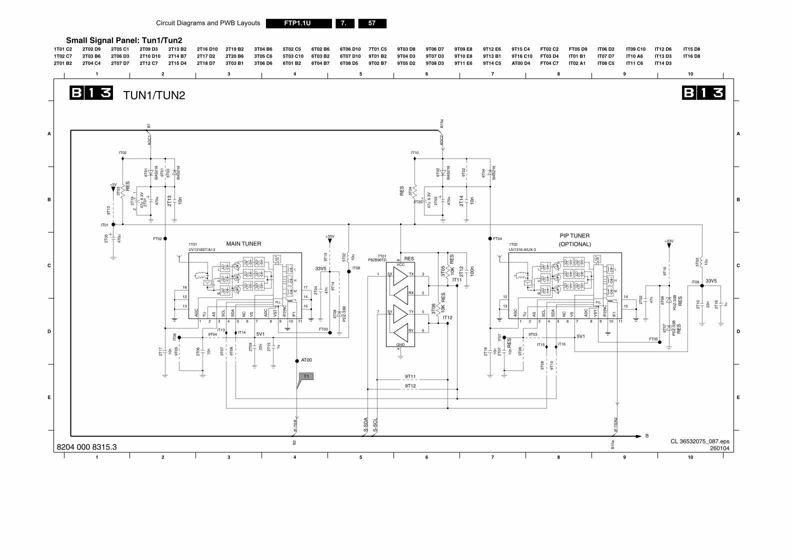
Circuit Diagrams and PWB Layouts 57FTP1.1U 7.
L
H
M
PLL
IT11 C6
IT12 D6IT06 D2
IT13 D3
IT14 D3
IT15 D8
IT16 D803 D4
04 C7
FT05 D9
IT01 B1
IT02 A1
RE
S
33V5
5V1
IT07 D7
IT08 C5
IT09 C10
IT10 A6
8
02 C2
E
A
B
C
8 9 10
B
(OPTIONAL)
PIP TUNER
9 10
RE
S
B15
a
D
E
9T09
9T10
11
IF1
IF2|
NC
10
14
15
NC
64
SC
L
5
SD
A
7
VS
9
VS
T
+33V
8
AD
C
2T10
22n
5T03
10u
2T16
1u
6T07
PD
Z-3
3B
2T02
47n
IT16FT05
9T16
6T06
PD
Z-3
3B
IT09
IF-T
ER
2
CL 36532075_087.eps260104
B2
3 4 5 6 71 2
IF-T
ER
S-S
DA
S-S
CL
8204 000 8315.3
Small Signal Panel: Tun1/Tun2
M
PLL
L
H
M
L
H
L
H
M
6T08 D5
7T01 C5
9T01 B2
9T02 B7
3T04 B6
3T05 C6
3T06 D6
5T02 C5
5T03 C10
6T01 B2
RE
S
B15
a
9T03 D86T02 B6
6T03 B2
6T04 B7
6T06 D10
6T07 D10 9T10 E8
9T11 E6
9T12 E6
9T13 B1
9T14 C5
FT
FT
5V1
2T13 B2
2T14 B7
2T15 D4
2T16 D10
2T17 D2 9T04 D3
9T05 D2
9T06 D7
9T07 D3
9T08 D3
9T09 E8 9T15 C4
9T16 C10
AT00 D4
FT
C
D
33V5
RE
S
TUN1/TUN2
2T18 D7
2T19 B2
2T20 B6
3T03 B1
7
MAIN TUNER
2T02 D9
2T03 B6
2T04 C4
2T05 C1
2T06 D3
2T07 D7
A
B
RE
S
1 2 3
RE
S
RES
RE
S
2T09 D3
2T10 D10
2T12 C7
4 5 6
B1
1T01 C2
1T02 C7
2T01 B2
RY 6
SX1
SY7
TX 3
5TY
VCC
8
7T01P82B96TD
GND
4
RX 2
AS
12
13
2
TU
UV1316-AIUX-31T02
1
AG
C
3
BA
S21
6
6T03
VS
T
2T03
470u
AD
C
1
AG
C
3
AS
11
IF1
IF2|
NC
10
12
13
14
15
16 17
NC
64
SC
L
5
SD
A
2
TU
7
VS
9
UV1318ST/AI-31T01
8 PD
Z-3
3B
6T08
3T04
3T03
BA
S21
6
6T02
2T17
10n
47n
2T04
9T03
9T07
+5V
21
IT13
6.3V
47u2T
19
IT15
9T11
6T01
BA
S21
6
10K
3T06
3T05
10K
47u
6.3V
10n
2T06
2T20
9T02
9T15
2T12
100n
9T06
9T05
6T04
BA
S21
6
FT04
9T01
IT14
IT12
IT11
IT02
AT00
IT10
2T07
10n
IT08
IT07
FT02
FT03
IT06
IT01
22n
2T09
470u
2T05
10u
5T02
470u
2T01
+33V
9T13
2T15
1u
9T08
9T049T
14
10n
9T12
10n
2T13
2T14
AG
C1
10n
2T18
AG
C2
T1
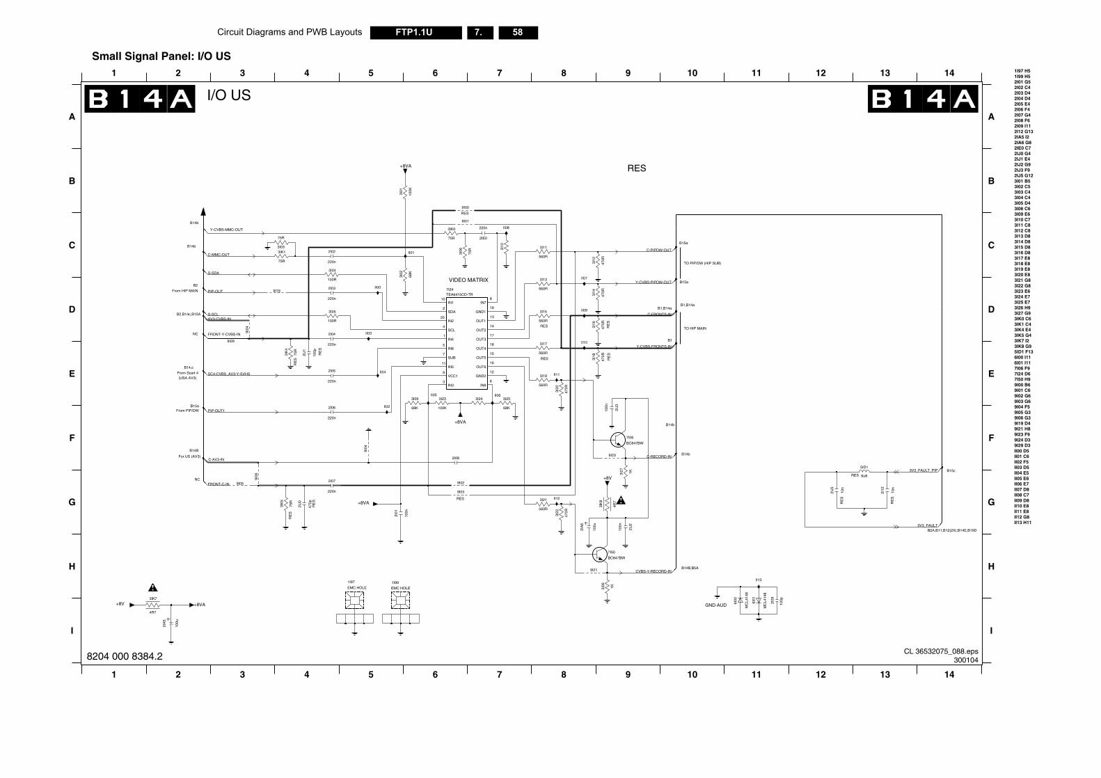
58FTP1.1U 7.Circuit Diagrams and PWB Layouts
G
H
I
1I97 H51I99 H52I01 G52I02 C42I03 D42I04 D42I05 E42I06 F42I07 G42I08 F6
2IE0 C72IJ0 G42IJ1 E42IJ2 G9
12 13 14
F
1 12 13 14
2I09 I112I12 G132IA5 I22IA6 G8
A
B
C
2IJ3 F92IJ5 G123I01 B53I02 C53I03 C43I04 C43I05 D43I06 C63I09 E63I10 C73I11 C83I12 C83I13 D83I14 D83I15 D8
1
3I20 E83I21 G83I22 G83I23 E6
3IK4 E43IK5 G43IK7 I23IK8 G9
D
E
B2A,B11,B12(2X),B14E,B19D
9I00 B69I01 C69I02 G69I03 G69I04 F59I05 G39I06 G39I19 D49I21 H89I23 F99I24 D3
3I26 H93I27 G93IK0 C63IK1 C4
3I24 E73I25 E7
9I29 D3II00 D5II01 C6II02 F5II03 D5II04 E5II05 E6II06 E7II07 D8II08 C7II09 D8
7I24 D67I50 H9
3I16 D83I17 E83I18 E83I19 E8
5ID1 F136I00 I11
B15c
6I01 I117I06 F9
II10 E8II11 E8II12 G8II13 H11
2I09
100p
2IJ5
10n
RE
S
7I50
MC
L414
8
I13
2I12
10n
RE
S
5ID1
6u8RES
3V3_FAULT
3V3_FAULT_PIP
CL 36532075_088.eps300104
1 4 5 6 7 8 9 10 1
I
2 3
H B14B,B5A
GND-AUD+8V
1K3I26
6I00
MC
L414
8
9I21
2IA
5
100u
BC847BW
3IK7
4R7
6I01
I
+8VA
1I97
EMC HOLE1I99
EMC HOLE
CVBS-Y-RECORD-IN
8204 000 8384.2
Small Signal Panel: I/O US
RE
S
RES
RES RE
SR
ES
1 2 3 4 5 6 7
A
B
C
D
B14b
8 9 10 1
RE
S
B1,B14a
B15a
B14,c
From PIP/DW
NC
E
F
G
B1
(USA AV3)
I/O US
For US (AV3)B14b
VIDEO MATRIX
From HIP MAIN
B14b
NC
B15a
TO HIP MAIN
B15a
B1,B14a
B14b
B2,B14c,B15A
From Scart 4
B2
RES
B14B
TO PIP/DW (HIP SUB)
3I10
II04
560R
3I21
+8VA
68K
3I09
II01
II10
100n
2IJ3
7I06
BC847BW
9I19
220n
2I06
2I08
3I02
68K
9I01
2IE0
220n
II00
2I02
220n
220n
560R
3I13
2I05
9I29
9I24
100n
2I01
9I06
RE
S
3I15
560R
3IK
4
75R
3I01
100K
II12
470R
3I18
II02
470R
3I14
3I05
100R
4R7
3IK
8
9I05
3I19
560R
100R
3I04
2IJ2
100n
220n
2I04
470p
2IJ0
2I03
220n
3I27 1K
100u
2IA
6
+8VA
75R
3IK1
VCC1
IN2
3IN3
1IN4
11IN5
5IN6
8IN7
6IN8
13OUT1
14OUT2
17OUT3
18OUT4
15OUT5
16OUT6
4SCL
2SDA
7SUB
9
TEA6415CD-TR7I24
19GND1
12GND2
10IN1
20
3I12
470R
+8V
RES
II07
9I03
560R
3I17
9I23
3I25
68K
3I24II05
3I16
75R
3IK
5
RE
S
RES
470R
220n
2I07
9I00
3I03
75R
3I06
75R
3I23
75R
3IK0
100K
9I02
II09
II08
3I20
470R
+8VA
100p
2IJ1
9I04
II06
3I11
560R
3I22
470R
II11
FRONT-Y-CVBS-IN II03
Y-CVBS-MMC-OUT
FRONT-C-IN
C-RECORD-INC-AV3-IN
AV3-CVBS-IN
PIP-OUT1
SC4-CVBS_AV3-Y-SVHS
S-SCL
PIP-OUT
S-SDA
C-FRONTS-IN
C-PIPDW-OUT
Y-CVBS-FRONTS-IN
Y-CVBS-PIPDW-OUT
C-MMC-OUT
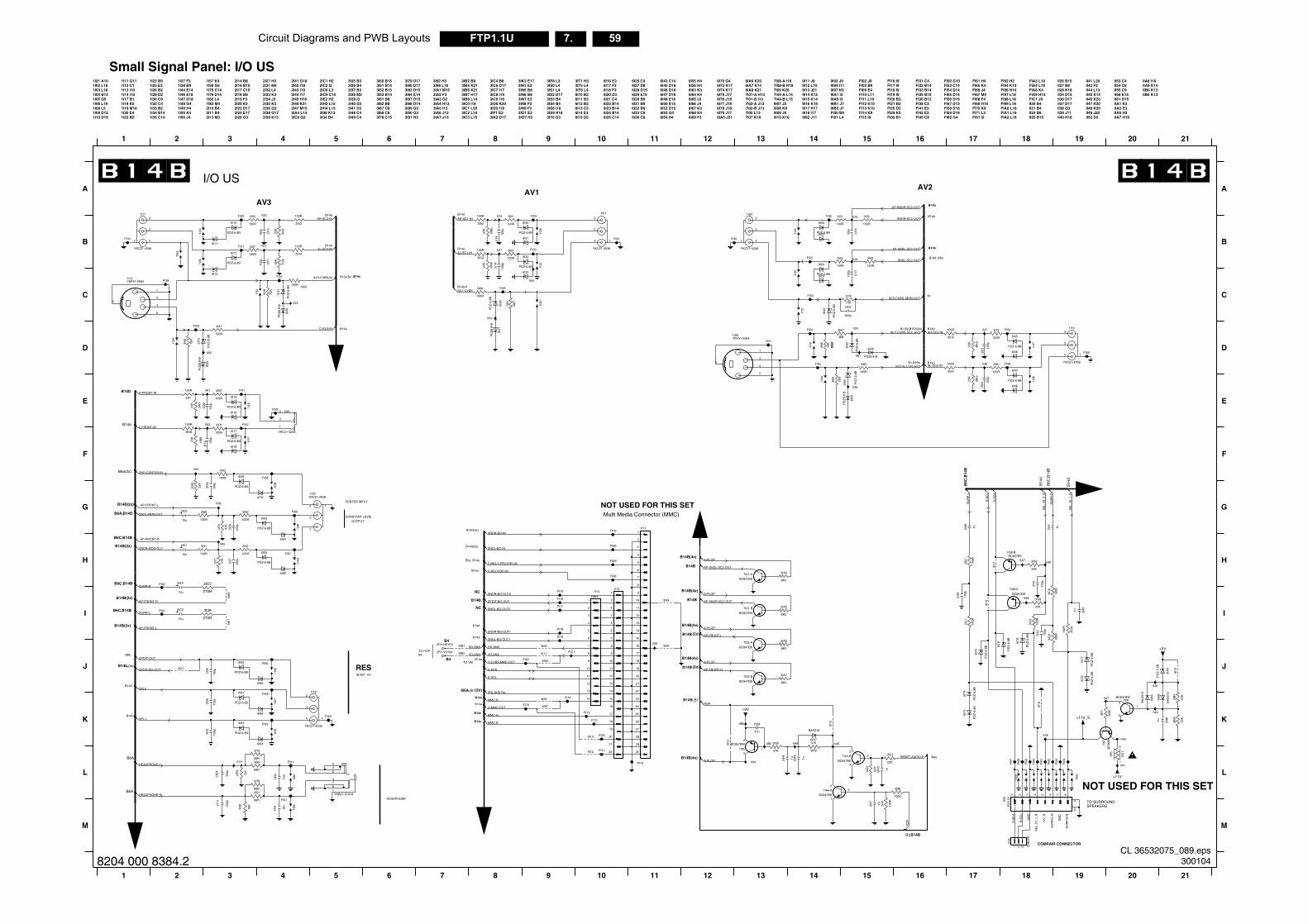
Circuit Diagrams and PWB Layouts 59FTP1.1U 7.
IIA7 H18
TO HOP
II28 K18II34 D15II36 D17II37 D17II38 G3II39 J11II40 H18
II41 L20II43 F2II44 L13II45 K14II46 K20II47 K20II48 K20II49 J20II52 D3
II53 C4II54 C8II55 C9II56 E15II61 D15IIA1 E3IIA2 E3IIA5 H3
FI69 H10FI70 K9FI71 L3FI91 I2
FI92 H2FI94 K10FI96 H10FI97 L18FI98 L18FI99 L18FIA0 L18FIA1 L18FIA2 L18
FIA3 L19FIA4 L19FIA8 K4FIA9 H10FIC1 J9II20 B4II21 B4II24 B8II25 B15
II26 B15II27 B8
FI56 D19FI57 D13FI58 D18FI59 D18FI60 G4
FI61 H4FI65 K4FI66 J4FI67 M4FI68 F4
B14B(4x)
33251
FI31 C4FI32 B14FI33 B14FI35 B10FI36 B12FI38 C2FI41 E3FI42 E3FI45 C8
FI50 G10FI53 C14FI54 D14FI55 D14
COMPAIR CONNECTOR
B1
B14
d
GN
D
B14d ,B6a
GN
D
SU
RR
-R-B
B6C
,B14
B
B1,B15a
S-S
DA
SU
RR
-L-B
11V
_S
B1
B4
,
B14a
AV2
TO SURROUND
B14d
B6b
NOT USED FOR THIS SET
B14
d
SE
L_IN
_1_B
B14d
B4
S-S
CL
B14b
B14b
B6a
19 20 21
B14B
16 17 18 19 20 21
16 17 18
B6C
,B14
B
SPEAKERS
IIA9 K14IIB0 K13IIB5 K13
B1,B2,B15A(2x)
B14d
A
B
C
D
E
F
G
H
I
J
K
L
M
IIA7
IIA8 I18
150R
3IC
8
100p
2I44
8
K
BC857BS
7I08-A
II40
FI56
9I13
FI9
7
7I08-BBC857BS
BA
S31
6
6IA
8
100p
1
2I45
1I10
YKC21-4038
2
3
4
3IS8
22K
II28
PD
Z-6
.8B
6I75
3IK
2
22K
6I47
PDZ-6.8B
6I48
FI9
9
8
8K2
1n 2I43
150R
3IC
7
9I11
1I47
4K7
3ID
0
1 2 3
II47
S3B
-EH
1I19
FI9
8
2I42
100p
+5V
2I461n
100R
3I80
3IC
0
150R
1u2I41
FIA
0
17
PD
Z-6
.8B
6I78
9IB2
6I79
PD
Z-6
.8B
IIA8
3IB
5
22K
100p
2I24
3I79
100R
910
1 2 3 4 5 6 7 8
6I76
PD
Z-6
.8B
1I03
5551
53
1I02
FIC1
PD
Z-3
.3B
6IA
5
BA
S31
6
6IA
6
3IC
9
150R
6I46
3IC
1
1R5
12
100R
3IS2
13
2
BC847BW7I09
II46
FIA
1
FIA
4
II48
22K
3IK
3
FI59
II36
100R
3IC6
PD
Z-6
.8B
6I77
9I18
9I17
+11V_S
3IS9
22K
FI58
6I74
PD
Z-6
.8B
FI02
II37
2I23
100p
22K
3IB
4
9I16
9
FIA
3
BC
869
7I07
+11V
100R
3ID
3
II49
3IB
7
150R
2I38 1u
II41
1I06
1I46
PD
Z-6
.8B
6I73
FIA
2
PDZ-6.8B
6I45VBS-SC2_AV2
SPDIF-OUT
BS_MON-OUT
NDL-SC2-OUT
NDL-SC2-OUT
NDR-SC2-OUT
NDR-SC2-OUT
2-R_C-IN_AV2 AL-SC2-IN
AR-SC2-IN
RESET-AUDIO-F
S-S
DA
S-S
CL
RO
P
SE
L_IN
_2_B
VD-ANA
SU
RR
-L
SU
RR
-R
SE
L_IN
_1_B
VD-ANA2FH-VD100
CL 36532075_089.eps300104
TO VMB14b,
(2x)B5A,
B14B
HEADPHONE
B14d
B6A
B6A
B14d
B14a
B6b
SPDIF I/O
,
RES
B1
B14c
B1
(2x)
B14B
B14B(4x)
B14c
B14c
1 2 3 4 5 6 7 8 9 10 11 12 13 14 15
J
K
L
M
2I34
100p
47K
3IB9
3I9
100
26
1
100p
2I33
7I44-A
BC847BS
1I55 BAS316
6IA7
9I12
2I31 10
n
FI29
FI65
3IC3
22K
3IC
2
22K
2IH
4
1u1
2
3
45
78
1I08
YKB21-5101A
100p
2I35
2I47 1n
9I93
1n2IH
3
FI10 II44
9
10
11
12
13
14
IIB0
FIA8
6I63
PDZ-6.8B
FI13
FI14
3I38
10K2I
13
330p
68R
3IT6
3IS1
68R
6I64 II45
13
2
7I05
BC857BW
FI11
FI12
9I15
28
29
30
18
19
20
21
22
23
24
25
26
27
3IA
1
100K
2IA
4
1u
9I07
BC847BS
7I44-B 53
4
9I10
6I68
9I08
9I14
9I97
IIA9
1I57
6I66
PDZ-6.8B
6I65
YKC21-4038
1I182
3
4 1
3IA7
8K2
3IT5
68R
10K
3IP
8
1I56
FI70
330p
2IC
6
12
13
14
15
16
17
18
19
20
21
22
10
11
68R
3IS0
+9V
3I08
47K
6I67
PDZ-6.8B
FI01FI71
1I83
1I82
10n
2I32
FI67
FI94
IIB5
7I02-B
BC847BS
47n
2I39
FI66
MMC-R
MMC-G
MMC-B
HEADPHONE-L
HEADPHONE-R
SPDIF-BO-OUT
SPI-2
SPI-1
ROP
A-PLOP
C-MMC-OUT
IRQ-DIGITAL
S-SCL
S-SDA
A-PLOP
AP-FRONT-R
Y-CVBS-MMC-OUT
8204 000 8384.2
Small Signal Panel: I/O US
B6a(2x)
B6C,B14B
B14a
B14B(4x)
,c
,B14cB15a,B2
B14B
B14B(2x)
RE
S
FI17 I9FI18 I9FI19 I9FI20 BFI21 BFI25 DFI29 KFI30 B
OR
B14d
B14d(2x)
FI00 B9FI01 L4
FI02 J9FI03 B9FI09 E4FI10 L11FI11 L10FI12 K10FI13 K10FI14 K9FI15 I9
FI16 I9
CENTER INPUT
9I13 J219I14 K129I15 K149I16 K189I17 H179I18 I179I92 J11
9I93 J99I94 I119I97 K99IA1 I39IA9 I39IB1 J79IB2 J7
6IA5 J21
6IA6 K206IA7 K146IA8 K217I01-A H137I01-B I137I02-A J137I02-B J137I05 L137I07 K19
7I08-A I187I08-B H187I09 K207I44-A L147I44-B L159I07 J29I08 K99I09 J99I10 K10
9I11 J99I12 L10
B5a, B14a
B6A,B14D
B14d
B14d
6I45 D186I46 D186I47 D186I48 E186I50 E156I52 D156I53 G46I54 H4
6I55 H46I56 H46I63 K36I64 K46I65 J36I66 J46I67 K36I68 K46I69 F3
6I70 G46I73 K176I74 K176I75 J176I76 J196I77 J196I78 J186I79 J17
B6C,B14B
B14B(2x)
B14B(2x)
I/O US
NC
6I16 E36I17 F36I18 F36I20 D36I21 C46I22 B146I23 B146I24 B146I25 C14
6I26 C46I27 D86I28 D156I29 E156I30 B96I31 B96I32 B96I33 C96I36 C8
6I43 C14
3IN6 B83IN7 E33IN8 F23IN9 F23IO1 E33IO7 H3
3IP8 L33IS0 L43IS1 L43IS2 D173IS3 B43IS4 B43IS8 I183IS9 H183IT0 G3
3IT1 H33IT5 L43IT6 L46I10 B36I11 B36I12 B36I13 C36I14 E36I15 D2
B14B(2x) B14d
AV1
3IC4 B83IC6 D173IC7 I173IC8 I193IC9 I183ID0 K203ID3 I183IF1 E23IK2 D17
3IK3 E173IN1 E23IN5 B8
3I87 D153I88 D143I89 G33I90 G33I91 H3
3I92 H33I98 L163IA1 M153IA2 F33IA3 G23IA4 H133IA5 I133IA6 J133IA7 J13
3IB2 B83IB4 K213IB5 K213IB7 H173IB9 L143IC0 I183IC1 L203IC2 L153IC3 L15
(2x)
B14B(4x)
B14B
B14B(4x)
B14d
3I50 B153I51 B143I52 B153I53 B143I61 B83I62 B83I67 C83I68 C83I78 C15
3I79 D173I80 D173I83 D153I84 E14
2IC1 H22IC2 I22IC6 L32IC9 C152IE2 H22IH3 L152IH4 L133I08 K133I34 B4
3I35 B33I36 B43I37 B33I38 M33I39 I33I40 D23I41 D33I48 C43I49 C4
NOT USED FOR THIS SET
AV3
2I33 K32I34 J32I35 K32I36 G32I38 G172I39 K13
2I41 G182I42 I182I43 I192I44 I172I45 H182I46 K212I47 M152IA4 L142IC0 G2
CONSTANT LEVEL
B14d(2x)
1I83 M42I10 B42I11 B42I13 M3
2I14 B82I16 B152I17 C152I18 B82I19 F32I20 E32I23 D172I24 E172I26 G3
2I27 H32I31 M42I32 L4
B14a
B14d
Multi Media Connector (MMC)
1I34 B141I35 C14
1I37 F31I38 B91I44 E141I46 E181I47 D181I48 G41I49 H41I55 K41I56 J4
1I57 K41I58 G41I75 C141I76 D141I82 L4
1I09 D121I10 D19
1I11 G111I12 C11I13 I101I14 I101I17 B11I18 K51I19 M181I20 E41I22 B2
1I23 B91I25 E31I26 B21I28 D21I30 C91I32 C41I33 B2
OUTPUT
NC
B14B,
B4
A
B
C
D
E
F
G
H
I
B14B
B14D
B6C,B14B
B14b
14 15
1I05 G51I06 L191I08 L5
1 2 3 4 5 6 7 8 9 10 11 12 13
B14d
1I01 A101I02 L181I03 L181I04 B13
1I49
2
3
4 1
YKC21-4038
1I01
FI54
FI20
22K
3IN
6
FI96
1I32
2I17
150R
3I89
100p
PDZ-6.8B
6I14
6I16
II25
1I37
FI25
FI35
FI32
6I28
PDZ6.8-B
PD
Z6.
8-B
6I29
6I27
PD
Z6.
8-B
PD
Z6.
8-B
6I26
6I20
PD
Z6.
8-B
FI30 6I31
3I90
100R
6I54
2I26
100p
FI15
3IA4
8K2
PDZ-6.8B
6I24
6I25
1I23
1I48
100p
2I16
5
1
3
4
2
3I50
150R
YKF51-55641I12
100p
2I18
3I48
75R
6I11
1I25
3I37
100R
FI55
1I22
4
2
YKF51-55641I09
5
1
3
FI19
2IC9
390p
5
6
7
1I38
1I14
FMN1
2
3
4
1I26
FI21
3IA6
6I10
PDZ-6.8B
100R
3I61
100p
2I19
6I33
2I14
100p
1I44
FI18
IIA2
FIA9
FI00
2IC1
10u FI61100R
3I92
150R
3I91
100p
2I27
1I20
YKC21-3226
3
1
2
3IN8
100R
3IF1
100R
3IN
9
22K
100R
3I51
100p
2I10
II27
6I50 PD
Z-6
.8B
75R
3I78
100R
3IS3
3
4
5
6
7
8
9
13
14
15
16
2
1I111
10
11
12
II39
FI53
II34
6I30
PDZ-6.8B
FI57
II24
100R
3I68
100R
3IS4
FI16
PDZ-6.8B
6I32
1I30
II20
1I75
3IN
1
2I11
100p
FI38
22K
6I55
PDZ-6.8B
6I56
6I43
PD
Z-6
.8B
6I13
100R
3I41
75R
3I67
FI45
1I34
FI69
FI60
22K
3I34
3I62
100R FI33
100R
3I83
1I33
FI03
3I36
22K
150R
3I52
6I36
PD
Z-6
.8B
FI50
IIA1
1I04
YKC21-4038
2
3
41
FI17
8K2
3IA5
75R
3I40
FI31
6I18
3IO1
BC847BS
7I02-A
6I52
PD
Z-6
.8B
PDZ-6.8B
6I53
100R
3IN7
100R
PDZ-6.8B
6I12
41
YKC21-4038
1I172
3
9I94
3IB2
100R
3IC4
6I15
PD
Z-6
.8B
100R
II26
6I22
PDZ-6.8B
9I09
3I87
75R
3I88
6I17
PDZ-6.8B
7
8
2
3
4
5
6
1I131
7I01-A
BC847BS
1I35
9IB1
FI42
2I20
100p
II21
3I49100R
75R
3I84
6I23
FI68
1I761I
28
FI41
BC847BS
7I01-B
3IN
5
22K
100R
3I35
FI91
FI92
FI36
PD
Z-6
.8B
6I21
3I53
100R
9I92
6I70
1I58
9IA
9
6I69
PDZ-6.8B
2IE2
10u
9IA
110u
2IC2
FI09
2
3
4 1
1I05YKC21-4038
3IT
1
47K
47K
3IT
0
II43
II38
IIA5
270R
3IO7
3I39
270R
II61
II55
II56
II53
II54
2IC0
II52
10u
100p
2I36
22K
3IA
3
100R
3IA2
L-FRONT-IN
SNDL-MON-OUT
SND-CENTER-IN
SNDR-MON-OUT
AP-FRONT-R
AP-FRONT-L
AP-FRONT-L
SURR-L
SURR-R
AP-FRONT-R
R-FRONT-IN
IN-Y-CC-AV3-IN
AV3-CVBS-IN
SC2-CV
S
AP-S
SC1-CVBS
AR-SC1-IN
AL-SC1-IN
AP-S
S
SC
AR-SC3-IN
AL-SC3-IN
HD-ANA
SNDR-BO-OUT2
C-RECORD-IN
SNDL-BO-IN
SNDL-BO-OUT1
SNDR-BO-OUT1
SNDL-BO-OUT2
SPDIF-BO-OUT
SNDR-BO-IN
A-PLOP
AP-SNDR-SC2-OUT
A-PLOP
AP-SNDL-SC2-OUT
A-PLOP
AP-FRONT-L
HD-ANA2FH-HD100
CVBS-Y-RECORD-IN
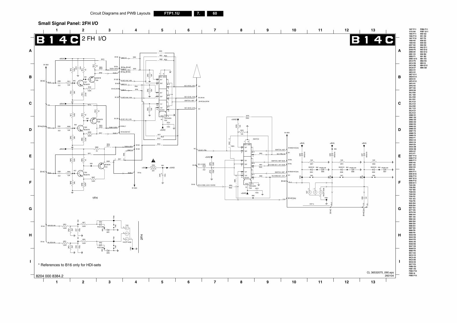
60FTP1.1U 7.Circuit Diagrams and PWB Layouts
II62 E11II63 E12II64 E13II90 B2II91 B2IIB1 E5IIB2 H3IIB3 I3IIB4 E12IIB6 G8
FIB1 H3FIB2 F10FIB3 I4FIB5 F13
FIB6 F11FIB7 G11II50 G2II51 H2II57 F2II58 E2II59 D2II60 D2
9I89 F99IA2 E89IA3 D59IA4 E59IA5 A59IA6 B39IA7 D39IA8 E39IB0 F89IC1 E29IC2 C29IC3 A39IC5 B39IC6 D39IC7 E3FIB0 G3
7I29 D27I30 F27I31 E37I32 F89I25 B49I26 B49I27 E39I77 D59I79 C89I80 A49I81 A59I82 A59I84 B49I85 E99I86 E49I87 E99I88 F8
3IO6 D83IR5 E73IT2 F76I87 F136I88 F126I89 F116I90 H36I91 H36I92 H36I93 I36I94 F116I95 E106I96 F136I97 E136I98 F126I99 E117I25 D57I26 B27I27 B27I28 D3
3IL1 B23IL2 B23IL3 B13IL4 C23IL5 C23IL6 B23IL7 C23IL8 C23IL9 C23IM0 D13IM1 D23IM2 D23IM3 D23IM4 E23IM5 E23IM6 E33IM7 F23IM8 F23IM9 F23IN0 F13IN2 C43IN3 C43IN4 E53IO5 D8
2IB0 B12IB1 D12IB2 F12IB5 G132IC3 F92IC4 D52IC5 B22IC8 E73IE2 H13IE3 H13IE7 E113IE8 E133IE9 H13IF0 E123IF5 H13IF6 H23IF7 H23IK9 B43IL0 B2
B14
C(2
x)
11 12 13
A
B
C
11 12 13
B14
C
B14d
D
E
F
G
H
I
1I07 F111I15 H41I65 F111I66 F131I67 F121I68 H31I69 H32I57 H22I58 H22IA9 F5
75R
3IF0
FIB
5
3IE8
75R
6I98
BAS316
1u0
2IB
5
IB2
1I67
BAS316
6I96
FIB7
+8VA
1 YK
C21
-403
83 4
2
6I97
BA
S31
6
100R
1I66
FIB
6
BA
S31
6
6I99
+8VA
00p
I57
2KIE9
II64II62 II63 PDZ6.8-B
6I876I88
PDZ6.8-BPDZ6.8-B
6I89
100R
IIB4
1IPDZ-6.8B
Y-2
Y3
Pb-
2
CL 36532075_090.eps260104
B14d
H
I
2FH
* References to B16 only for HDI-sets
2 3 4 5 6 7 8 9 101
FIB
1
IIB3
I
2I58
100p
PDZ-6.8B
6I92
4 1
YKC21-4038
3
3IE2
100R
II51
3IF
5
22K
6I93
3IF6
100R
1I69
FIB
3
1223
6I91
AL-SC4-IN
8204 000 8384.2
Small Signal Panel: 2FH I/O
MUXDX
MUXDX
B15a
NC
B1
SWITCH
B15A,B,B14C
,B14C(2x),B15b
B1
B1,B15A
B19a
B1,B2
B1-B20
B15b
B15a
B14b
2 FH I/O
270R
A
B
C
D
E
F
G
B1,B2
EXT 5
B14C
B14c(2x)
B14C
,
1FH
220R
B14C(2x)
B14C,B15A
B19A,C
B14B
4 5 6 7 8 9 10
560R
B14C
B15a B14C,
B1,B2
B19A
B14B
B15B,B14C(2x)
B14b
B14b
B15a
1 2 3
B1-B20
B1-B20
B1
B1
B14C
B15B,B14C(2x)
9I84
+8VA
9IA3
3IM
8
RES
9I77
100K
3IM
5
9IA7
9I80
3IT
2
100K
+5VIO
100K
3IR
5
FIB
2
2u2
2IC8
9I85
II59
3IL5
3IL8 1K
100u
2IA
9
7I28
BC857B
VEE
11
10
9
II60
121y0
131y1
14
22y0
12y1
15
53y0
33y1
4
6G3
8
GND
16
VCC
7
7I26
BC857B
74HC40537I32
BC847B
7I30
3IL1
2IB0
2u21K
IIB1II58
1K3IL9
100R
3IM7
RES
9IB0
39K
3IL4
100n
2IC
5
2IB1
2u2
1I07
2
10R
3IN0
+8VA
3IM
1
39K
RES9IC6
RES9IC5
9IC2
9IC3
1I15
3IO5
10K
3IM0
10R
4R7
3IN4
100n
2IC3
39K
3IM
9
9I86
9I25
RES
9I87
7
11
10
9
+5VIO
1y012
1y113
14
2y02
2y11
15
3y05
3y13
4
G36
GND
8
VCC
16
VEE
7I29
BC847B
7I2574HC4053
9IA5
3IE3
3IM6
1K
1K3IM
4
+8VA
3IM
2
470R
RES
9I79
7I27
BC847B
9I89
3IL7
100K
9IA8
FIB
0
II57
II50
12
RES9I82
RES
9IA
2
75R
3IE7
1K3IL2
75R
3IN
2
3IM3
9I26
3IN
3
75R
II90
3IL0
100K
+8VA
2u2
2IB2
6I95
BA
S31
6
II91
3IO
6
10K
9IA6
10R
3IL3
9IA4
+5VIO
9I88
+5VIO+5V
RES9I81
9I271 2
2IC4
100n
7I31
+5VIO
BC857B
6I94
BAS316
3IL6
100R
9IC1
RES9IC7
3IK
9
75R
1I65
3IF7
IIB6
68
6I90
AR-SC4-IN
Y-2
Y3
IN-CVBS-SC1_AV1-SUB
IN-CVBS-SC1_AV1
SUB-V
SUB-Y
SUB-V
SUB-Y
SUB-U
SUB-V-2FH
SUB-Y-2FH
SUB-U-2FH
Pr-2
Pb-2
B-SC1-IN_U-IN
R-SC1-IN_V-IN
SC1-R-IN_V-IN
SWITCH_HEF
SC1-G-IN_Y-IN
SC4-CVBS_AV3-Y-SVHS
SWITCH_HEF
SWITCH_HEF-SUB
SC1-CVBS
SC1-B-IN_U-IN
G-SC1-IN_Y-IN
Y-2
SWITCH_HEFMMC-B
MMC-GPr-2
MMC-R
IN-SC1-FBL
SC1-FBL-IN
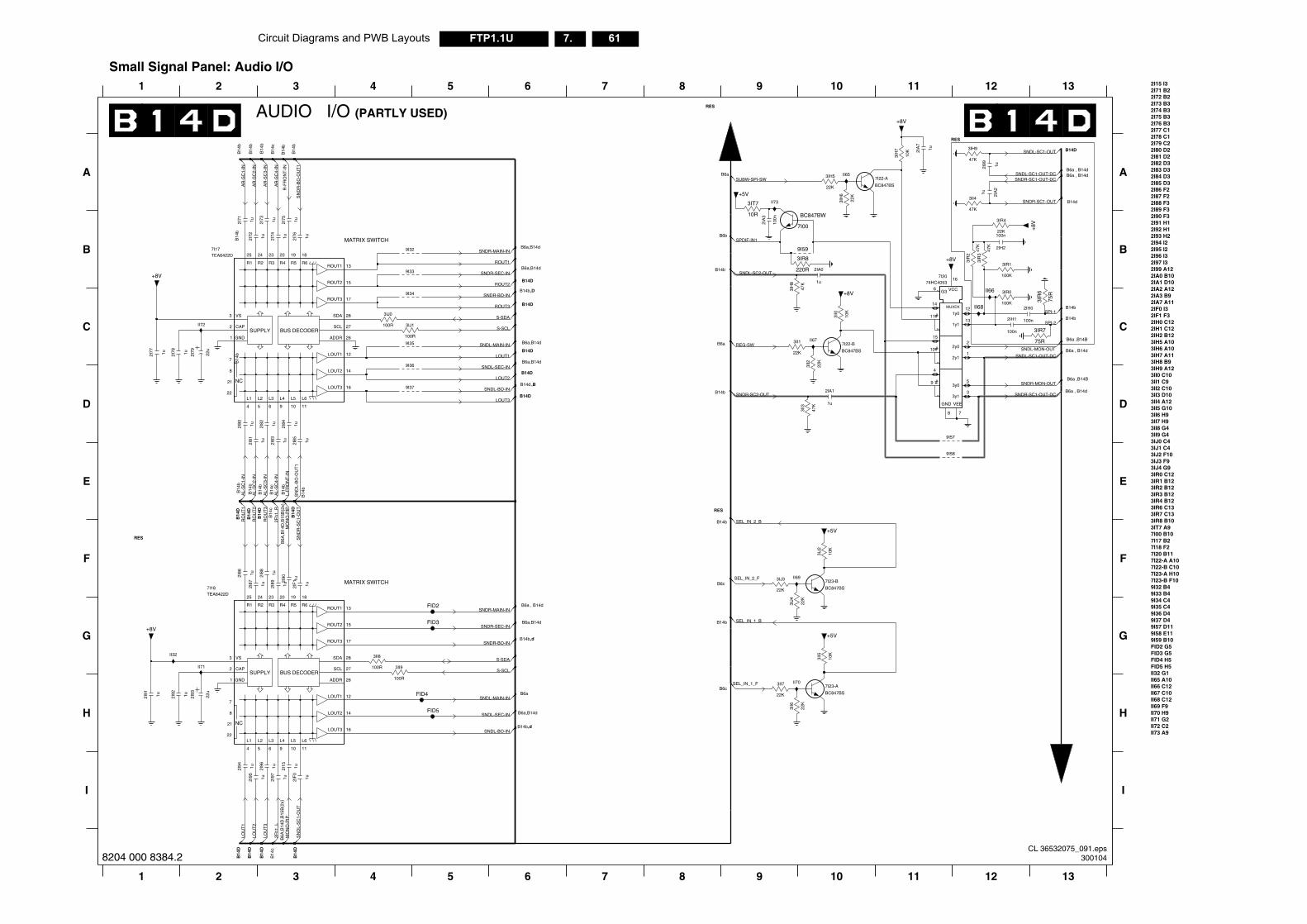
Circuit Diagrams and PWB Layouts 61FTP1.1U 7.
MUXDX
FID4 H5FID5 H5II32 G1
B6a , B14d
II65 A10II66 C12II67 C10II68 C12II69 F9II70 H9II71 G2II72 C2II73 A9
3IT7 A97I00 B107I17 B2
B6a , B14d
B6a ,B14B
3IR2 B123IR3 B123IR4 B123IR6 C133IR7 C133IR8 B10
3IH9 A123II0 C103II1 C9
B14b
3II2 C103II3 D103II4 A123II5 G103II6 H93II7 H93II8 G43II9 G43IJ0 C43IJ1 C43IJ2 F103IJ3 F9
2I99 A122IA0 B102IA1 D10
B14D
B6a ,B14B
2IA2 A122IA3 B92IA7 A112IF0 I32IF1 F32IH0 C122IH1 C122IH2 B123IH5 A103IH6 A103IH7 A113IH8 B9
2I81 D22I82 D32I83 D32I84 D32I85 D32I86 F22I87 F22I88 F32I89 F32I90 F32I91 H12I92 H12I93 H22I94 I22I95 I22I96 I32I97 I3
A
B
B6a , B14d
B6a , B14d
2I73 B32I74 B32I75 B32I76 B32I77 C12I78 C12I79 C22I80 D2
RES
11 12 13
2I15 I32I71 B22I72 B2
B14d
11 12 13
C
D
E
F
G
H
I
3IR0 C123IR1 B12
B14b
7I18 F27I20 B117I22-A A107I22-B C107I23-A H107I23-B F109I32 B49I33 B49I34 C49I35 C49I36 D49I37 D49I57 D119I58 E119I59 B10FID2 G5FID3 G5
3IJ4 G9
15
3y05
3y13
4
G36
GND
8
VCC
16
VEE
7
11
10
9
7I2074HC4053
1y012
1y113
14
22y0
2y11
47K
3IR
3
II32
100n
2IH0
10K
3IH
7
SDA 28VS3 3II8
1u2IA
7
75R
3IR
6II66
II68
100K
3IR1+8V
1u2I99
9I58
75R
3IR7
3IR0
100K
3IH9
47K
9I57
3II4
47K
2IA
2
1u
3II5
10K
+8V
22K
3IR4
2IH1
100n
8V
3IR
2
47K
100n
2IH2
SPI-2
SNDR-MON-OUT
SNDL-MON-OUT
SNDL-SC1-OUT-DC
SNDR-SC1-OUT-DC
SPI-1
SNDR-SC1-OUT-DCSNDL-SC1-OUT-DC
SNDL-SC1-OUT
SNDR-SC1-OUT
CL 36532075_091.eps300104
NC
SUPPLY BUS DECODER
B14
c
B14
D
I
B6c
7 8 9 10
,dB14b
B6a,B14d
1 2 3 6
B6a
B14
D
B14
D
B14
D
H
4 5
B6A
,B14
D,B
15B
(2x)
3II9
100R
22K
3II6
8
21
22
SCL 27
ADDR 26
CAP2
GND1
L1
4
L2
5
L3
6
L4
9
L5
10
L6
11
LOUT1 12
LOUT2 14
LOUT3 16
7
100R
2I15
2I97 1u
1u
FID5
FID4 22K
3II7
2IF
0
1u
2I91 1u 2I93
22u
II71
2I95 1u
1u2I92
1u2I94
7I23-A
BC847BS
2I96 1u
II70
2Fh1
_L
SNDL-MAIN-IN
SNDL-SEC-IN
SN
DL-
SC
1-O
UT
SEL_IN_1_F
SNDL-BO-IN
LOU
T1
LOU
T2
LOU
T3
MO
NO
-PIP
S-SDA
S-SCL
8204 000 8384.2
Small Signal Panel: Audio I/O
NC
SUPPLY BUS DECODER
B14b
B6A
,B14
D,B
15B
(2x)
B6c
B14
D
B6a,B14d
B14b
B14b,d
B14b
RES
B6a,B14d
B14
c
B6a
B14b
RES
B6a , B14d
B14
b
B6b
MATRIX SWITCH
B14d
B14
b
B14b
B14
b
B6aA
B
C
AUDIO I/O (PARTLY USED)
B6a,B14d
B14
b
B6a,B14d
B14
b
B14D
B14D
RES
1 2 3 4 5 6 7 8 9 10
MATRIX SWITCH
,B
,D
B14
b
B14
b
B14D
B14
b
B14D
B14D
B14
b
B14
D
B14
D
B14
D
B6a,B14d
B14
c
B14
b
B14
b
D
E
F
G
+5V
B14
c
B14
b
2I74
2I85 1u
10K
3IJ2
1u
9I37
22u
2I79
2I88 1u
2I73 1u
2I84 1u
R1
25
R2
24
R3
23
R4
20
R5
19
R6
18
ROUT1 13
ROUT2 15
ROUT3 17
TEA6422D
2I89 1u
7I18
3II0
10K
II72
22K
FID3
+5V
3IJ4
9I35
9I34
+8V
2I81 1u
1u2I90
100n
2IA
3
II73
FID2
BC847BW
7I00
+8V
2I77 1u
9I32
2I78 1u
3IH
8
47K
2I75
2I76 1u
1u
220R
3IR8
+8V
7I22-A
BC847BS
22K
3IH
6
1u2IF
1
2I82 1u
II65
7
8
21
22
25
R1 R2
24 23
R3
20
R4
19
R5
18
R6ROUT1 13
15ROUT2
17ROUT3
27SCL
28SDA3 VS
TEA6422D
26ADDR
2 CAP
1 GND
4
L1
5
L2
6
L3
9
L4 L5
10 11
L6
12LOUT1
LOUT2 14
16LOUT3
7I23-B
BC847BS
7I17
7I22-B
BC847BS
9I36
9I33
100R
3IJ1
1u9I59
2I80
II67
2IA1
1u
2IA0
2I86 1u
1u
1u2I87
3IT7
3II1
10R
+5V
22K
22K
3II2
II69
22K
3IH5
2I83
+
1u
3IJ0
100R
2I72 1u
3II3
47K
1u2I71
3IJ3
22K
SPDIF-IN1
SN
DR
-SC
1-O
UT
2Fh1
_R
SN
DR
-BO
-OU
T1
R-F
RO
NT
-IN
AR
-SC
4-IN
AL-
SC
4-IN
SNDR-MAIN-IN
SNDR-SEC-IN
SNDR-MAIN-IN
SNDR-SEC-IN
SNDR-BO-IN
SNDL-MAIN-IN
SNDL-SEC-IN
SNDL-BO-IN
SEL_IN_2_B
SN
DL-
BO
-OU
T1
SNDR-BO-IN
REG-SW
SNDL-SC2-OUT
SNDR-SC2-OUT
SEL_IN_2_F
SEL_IN_1_B
RO
UT
1
RO
UT
2
RO
UT
3
MO
NO
-PIP
LOUT1
ROUT1
LOUT2
ROUT2
LOUT3
ROUT3
AL-
SC
1-IN
AL-
SC
2-IN
AL-
SC
3-IN
L-F
RO
NT
-IN
AR
-SC
1-IN
AR
-SC
2-IN
AR
-SC
3-IN
S-SDA
S-SCL
SUBW-SPI-SW
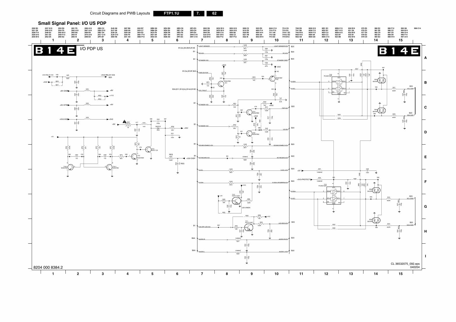
62FTP1.1U 7.Circuit Diagrams and PWB Layouts
A
B
B1
12 13 14 15
E
F
G
H
I
12 13 14
C
D
15II79 C9
1213
9
9ID1 B19ID2 B19ID3 C39ID4 C39ID5 C13
9ID6 C13
B20
B20
B20
B20
II99 C149ID7 A139ID8 A13II22 B7II23 B8
II30 B10II31 D9II33 B10II35 B1II42 B10
II75 E5II76 E3II77 D4II78 E2
II86 C5II87 C6II88 D9II89 H14
II92 H8II94 B14II95 G14II96 F14II97 A14
II80 E2II81 E8II82 C9II83 E4II84 E3
II85 F12
139
5I00
600R
p
100n
2I28
9I39
9I38
100n
2I59
3IB
3
10K
9ID7
II95
600R
5I01
6IA4BAV99
II85
9ID5
100MHZ
5I02
9ID
8
II94
II97
4
NC1
SCL02 SCL1 7
SDA03 SDA1 6
VCC
8
7I10PCA9515DP
EN5GND
9ID6
9I28
BAV996I04
100R
II99
p
II96
BAV996IA3
2I40
100p
RE
S
3IO
3
10K
10K
3IO
2
2I55
100n
100p
2I37
2 SCL0 7SCL1
3 SDA0 6SDA1
8
VCC
RE
S
5 EN
4
GND1
NC
PCA9515DP7I19
II89
10K
3IB
1
10K
3I00
100MHZ
5I07
RE
S2I
30
100p
RE
S
100p
2I29
9I20
5I03
600R
600R
5I04
6I03BAV99
SDA-SUP
SCL-SUP
ON-OFF-LED-IO2SDA-DISP
SCL-DISP
CL 36532075_092.eps040204
B6A
9 10 11
B6A
2 3 4 5 6 7 81
B20
B20
100
2I62
100MHZ
5I22
2I64
100p
100p
2I65
100
2IJ7
100MHZ
5I21
AUDIO-R-IO3AUDIO-R
AUDIO-L-IO3AUDIO-L
8204 000 8384.2
Small Signal Panel: I/O US PDP
B1
B1
B1
B1
B1
1 2 3 4 5 6 7 8
B3A,B11,B12(2x),B14A,B19D
B20
2I28 F142I29 D152I30 B15
2I37 G152I40 H152I48 E32I51 D22I52 D5
2I53 E62I54 F92I55 B132I59 F132I60 E2
2I61 F92I00 B22I21 D6
B20
B20
9 10 11
B1
B1(3x),B19F,B20
2I62 H102I63 B22I64 I92I65 I9
2I66 A102I67 A10
2I98 E9
2IB3 C22IB4 D102IB7 D42IC7 C102IF3 B7
2IJ6 G8
I/O PDP US B1(2x),B4,B5A,B14E
B20
2IJ7 H92IJ8 C82IJ9 C10
3I28 H93I29 G83I30 F93I31 A9
3I32 B73I33 C73I54 E23IB1 F143IB3 F13
3IB6 G93IB8 G93IC5 F82I69 E9
2I70 A10
3ID4 B93ID5 E63ID6 D63ID7 A93ID8 A9
3IE0 C83IE1 C8
5I03 G155I04 H155I05 B25I06 C25I07 F12
5I09 C25I10 D55I20 B25I21 H85I22 I83I00 H8
3I07 B8
3IE5 F83IF2 E23IF3 E3
3IF4 E3 7I40 D93IF8 D43IF9 E43IH0 C103IH1 C10
3IH2 D8
3ID1 E93ID2 D4
3IJ5 D103IJ6 B10
3IO2 B133IO3 B145I00 C155I01 B155I02 F12
5I23 E96I03 F146I04 H146I05 D56IA3 B14
6IA4 C14
7I12 G87I13 E5
7I14 C97I15 E47I16-1 E37I16-2 E27I19 B12
7I41 B87I42 B109I20 H129I22 G8
9I28 H9I38 F3IH3 D8
3IH4 D9
9ID0 G
B20
B20
B20
B20
B20
7I10 F127I11 H9
B20
B20
9I39 F9I99 D
RES
RESII78
II23 BC857BW1
3
2
100n
2I51
7I4210
0nII30
2IB
3
+3V3-PROTECT
II22
3IH0
1K0
7I14BC847BW
II31
9ID4
II33
3IH
3
1K
3IH2
3K3
+5V2
+5V2-DISP
3IB8
10K+5V2
6K8
3I33
2IB
7
100n
+5V
9I22
5I09
II80
18K
3I29
II86
1K0
3ID4
1n0
2I53
2IF3
1n0
+5V2
2IJ9
1n0
5I20
30R
3ID6
2K2
220n
2IB
4
BC847BW7I40
3IJ5
100R
3K3
3IF9
+5V2
100R
3IB6
2I48
1n21n2
2I60
9ID1
100K
3IE
1
+5V2-RELAY-IO3
9ID2
100p
2IJ6
+8V
3IJ6
1K0
5I05
1n0
2IJ8
II75
II76
3ID1
100R
9I99
4
+5V
II81
1
7I16-2BC847BS
5
3
7I16-1BC847BS
2
6
7I13
6I05
BAS316
BC817-25
2I52
220p3ID2
1R
+8V
100R
3I31 100p
2I70
+5V
100p
2I61
II77
II84
+33V
3ID5
100R
+11V
II87
II88
+5V2
II79
II82
10K
3I30
10K
3IF
3
2
2K2
3IF
8
7I15
BC847BW
13
2I69
100p
3I28
9ID3
3I07
10K
+9V-STBY
2I21
100n
5I06
470R
3I54
5I23
100MHZ
2K7
3IF
2
+33V-DISP
2I66
100p
100p
100p
2I67
II92
2IC
7
II83
+5V2-RELAY-IO2
+5V2
10K
3IE0
2K2
3IH
4
1m0
5I10
2I63
100p
+5V2
100R
3IC5
2I54
100p
3IE5
100R
PDTC144ET7I11
100R
3ID8
BC847BW7I41
9ID0
+8V-DISP
100n
2I00
+9V
PDTC144ET7I12
3ID7
100R
2I98
3IF
4
470R
100p
3I32
100R
3IH1
10K
II42
II35
3V3_FAULT
+5V2
SOUND-ENABLE-IO3SOUND-ENABLE-IO2
PWR-OK-PDP
S-SCL
S-SDA
KEYBOARD-IO2
RC-IO2
KEYBOARD-IO3
RC-IO3
LIGHT-SENSOR LIGHT-SENSOR-IO3
STANDBY-DISPSTANDBY-IO2
STANDBY-IO2
PDP-GO
STANDBY-IO2
VS-ON
S-SDA
LED-RED-IO3
S-SCL
S-SDA
LED-GREEN
S-SDA-LEDGREEN-IO3
S-SCL S-SCL-IO3
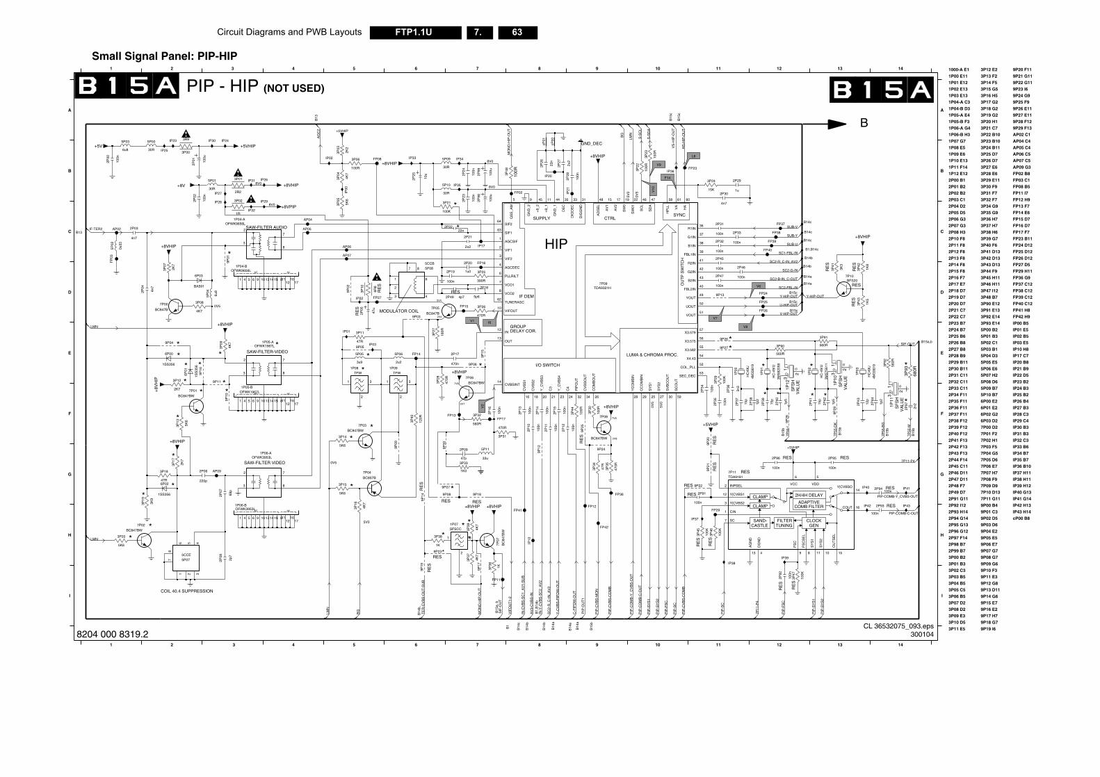
Circuit Diagrams and PWB Layouts 63FTP1.1U 7.
2H/4H DELAY
ADAPTIVECOMB FILTER
FILTERTUNING
CLOCK
LAMP
GEN
LAMP
AND-STLE
FP25 D12
FP26 D12
FP27 D5
FP29 H11
FP36 G9
FP37 C12
9P12 G8
9P14 G6
9P20 F11
9P22 G11
9P23 I6
9P25 F9
9P26 E11
IP03 E5
7P03 F5
3P32 F7
6P02 G2
1P00 E11
1P03 E13
*
B14c
*
7P02 H1
7P04 G5
IP10 H8
9P00 B4
FP15 D7
FP16 D7
IP34 B7
IP35 B7
FP24 D12
AP09 G3
FP13 F7
3P29 E11
3P30 F9
1P04-A C3
1P01 E12
3P91 E13
1P02 E13
3P93 E14
5P00 B2
1P07 G7
1P08 E5
5P01 B3
9P13 D11
5P03 B1
9P15 E7
B15
b
B15
b
B15
b
9P17 H7
RE
S
3P22 B10
3P25 D7
3P24 B11
3P27 E6
3P28 E6
3P31 F7
12 13
1P04-B D3
1P05-A E4
3P92 E14
1P06-A G4
1P06-B H3
2P24 B7
2P25 B6
1P09 E6
RES
3P47 I12
7P05 D6
9P29 F13
AP02 C1
AP04 C4
AP05 C4
AP06 C5
AP07 C5
*
14
3P26 D7
5P02 C1
5P04 D3
9P16 E2
B15
b
B15a,b
B14a
B14c
3P34 G9
G
H
I
2P20 D7
1P05-B F3
2P22 C7
2P23 B7
2P26 B8
1P10 E13
2P28 B9
3P48 B7
7P06 E7
RES
RE
S
RES
*
RE
S
2P93 H14
2P94 G14
2P96 G12
B
3P02 C3
3P03 B5
12
5P05 E5
R
B14b
B14c
6P01 E2
C
D
E
F
2P21 C7
2P27 B8
2P29 B11
3P90 E12
1000-A E1
3P23 B10
*
*
2P95 G13
2P97 F14
2P98 B7
3P00 B2
3P01 B3
3P04 B5
3P06 B5
2P38 F12
13
5P06 E6
5P07 H2
5P08 D6
5P09 B7
5P10 B7
6P00 E2
B
2P30 B11
B14a
B15c
RES
7P07 H7
7P09 D9
2P99 B7
9P03 D6
9P04 E2
3P35 G9
3P05 C5
3P37 H7
3P07 D2
2P39 F12
14
A
2P19 D7
9P18 G7
9P19 I6
9P21 G11
*
9P27 E11
9P28 F12
2P31 C11
2P32 C11
2P37 F11
7P08 F9
B14b
7P10 D13
7P11 G11
9P01 C3
9P02 D5
FP17 F7
FP23 B11
9P05 E5
3P36 H7
9P07 G7
3P38 H6
3P08 D2
2P40 F12
2P41 F13
2P15 F8
2P16 F7
2P17 E7
2P18 D7
2P46 D11
R
2P01 B2
2P02 B2
2P04 D2
9P24 G9
IP01 E5
IP02 B5
2P11 F8
2P12 F8
IP17 C7
IP21 B9
2P33 C11
2P34 F11
2P35 F11
2P36 F11
2P92 I12
*
B1,B14c
FP14 E6
IP32 C3
IP33 B6
RE
S
IP36 B10
9P06 E7
IP39 H12
9P08 G7
3P39 G7
3P09 E3
3P10 D5
2P42 F13
2P43 F13
2P44 F14
2P45 C11
3P15 G5
B15c
B15c
1P12 E12
2P00 B1
2P03 C1
2P06 G3
2P05 D5
2P07 G3
IP00 B5
2P08 H3
2P10 F8
1P11 F14
2P13 F8
IP20 B8
FP41 H8
IP22 D5
6P03 D2
3P16 H5
2P47 D11
2P48 F7
2P49 D7
2P91 G11
3P21 C7
RES
IP28 C3
IP29 C4
IP30 B3
RE
S
IP37 H11
IP38 H11
IP41 G14
IP40 G13
9P09 G6
3P40 F6
3P41 D13
3P11 E5
3P12 E2
3P13 F2
3P14 F5
3P46 H11
IP31 B3
2P14 F8
*
FP39 C12
FP40 C12
IP24 B3
IP25 B2
FP02 B8
FP03 C1
FP08 B5
FP11 I7
FP12 H9
IP43 H14
cP00 B8
FP42 H9
IP23 B2
7P00 D2
7P01 F2
3P17 G2
3P18 G2
3P19 G2
3P20 H1
IP26 B4
IP27 B3
IP42 H13
FP38 C12
9P10 F3
9P11 E3
3P42 D13
3P43 D13
3P44 F9
3P45 H11
VA
LUE
2G1
I3
O
12p
2P43
SF
SH
1P12
2
IP42
FP37
100n
2P93
9P28
2n2
2P97
G2
I1
O3
VA
LUE
1P10
SF
SH
9P29
IP43
SF
SH
1P11
VA
LUE
2G1
I3
O56
0R
3P92
FP40
BFS207P10
5K6
560R
3P91
560R
3P90
3P47
100K
15p
2P39
+5VHIP
1K5
3P43
100n
2P92
1p5
2P40
+8VHIP
3M57
5611
1P02
HC
-49/
U
B7
3K3
3P41
8
FP38
1K8
3P42
1K
IP40 IP41
1p2
2P44
FP25
HC
-49/
U
1P01
3M58
2056
2P41
15p
FP39
7
FP24
11
SY
S1
10
SY
S2
6
VCC VDD
5
14Y|CVBSO
9P23 13
A
16COUT
4
DG
ND
9
FS
C
8
FS
CS
EL
15
OU
TS
EL
2P94100n
IP39
2P42
1p5
2P95
100n100n
2P96
680R
3P93
FP26
1p2
4M33
619
1P03
HC
49U
7P55
-I
7P55
-DK
7P55
-BG
7P55
-M
SIF-OUT
PIP-COMB-C-OUT
PIP-COMB-Y_CVBS-OUT
SC2-R_C-IN_AV2
SC2-G-IN
SC2-B-IN_C-OUT
7P11
-P4
PIP
-SY
S1
PIP
-SY
S2
7P11-P4
PIP
-FS
C
SUB-Y
SUB-U
SC1-FBL-IN
U-HIP-OUT
V-HIP-OUT
Y-HIP-OUT Y-HIP-OUT
SUB-V
SC2-FBL-IN
CL 36532075_093.eps300104
V6
B1
RES
1
B14
a
2 53 6 7 8 9 114 10
B14
b
B1,
B14
b
B15
b
B14
a
B14
a
B14
c
B14
b
I
B14
b,
B15
a, b
RE
S
COIL 40.4 SUPPRESSION
9P19
9P17 IP38
2p7
2P08
FP11
7 5P075CCE
1 2 3
1K3P36
3P3
4K7
SIF
-OU
T
MO
NO
-HIP
-OU
T
TE
R-C
VB
S-O
UT
-SU
B
PIP
-CV
BS
-CO
MB
PIP
-CO
MB
-Y_C
VB
S-O
UT
PIP
-CV
BS
-MO
N
VIF
OU
T1-
2
PIP
-OU
T1
PIP
-CV
BS
-CO
MB
PIP
-SC
PIP
-SY
S1
PIP
-SY
S2
C-P
IPD
W-O
UT
SC
2-R
_C-I
N_A
V2
AV
3-C
VB
S-I
N
IN-Y
-CV
BS
-SC
2_A
V2
LMN
PIP
-CO
MB
-C-O
UT
PIP
-SC
PIP
-FS
C
IN-C
VB
S-S
C1_
AV
1-S
UB
Y-C
VB
S-P
IPD
W-O
UT
BG
8204 000 8319.2
Small Signal Panel: PIP-HIP
NCMT
IF DEM
SUPPLY CTRLSYNC
OU
TP
SW
ITC
H
LUMA & CHROMA PROC.
I/O SWITCH
DELAY COR.GROUP
NCMT
NCMT
C
C
SCA
*
8V0
8V0
5V0
0V5
8V0
B15
c
*
SAW-FILTER AUDIO *
2V8
RE
S
5V0
**
B13
1
RES
RE
S
MODULATOR COIL
RE
S
11
RE
S
RES
7V6
2
RES
RES
B13
5 6 7 8 94
HIP
ES
*
3
*
*
*
*
*
**
**
10
2V7
*
A
G
H
*
*
*
SAW-FILTER-VIDEO
PIP - HIP (NOT USED)
*
*
*
7V6
*
*
*
RES
5V4
ES
*
*
RE
S
RES
D
E
*
*
8V0
SAW-FILTER VIDEO
*
0V5
RE
S
*
B15
c
B
5V0
C
F
*
2V4
0V5
0V5
30R
5P01
9P08
7P02
BC847BW
5P04
6u8
3P3347p
2P09
1K0
9P30
AP060u33
5P02
100n
2P47
FP14
1 3
30R
5P10
SFSCC1P07
5P06
2u2
IP30
2R2
3P01
9P21
+5V
9P04
47R
3P18
9P06
+8VHIP
4K7
3P16
3P17
2K7
FP29
+5VHIP
BA591
6P03
FP36
BC847B
7P05
100K
3P21
IP22
100n
2P35
470R
3P31
100n
2P02
IP02
33u
5P11
9 10 131415 1112
1617
OFWK1967L1P05-B
1 1 84 5 6
FP42
4p72P49
FP12
7P08
BC847BW
BC847B
7P00
22n2P22
3P24
15K
FP08
9P22
9P20
2
3
7
8
9P18
OFWK9656L1P04-A
cP01
4K7
3P39
2K2
3P03
IP34
+8V
3P20
IP17
4K7
3P04
9P26
5K6
3P14
2P32
100n
3P29
100K
3P45
100K
9P27
VIF12
VIF23
VIFOUT10
VOUT51
56X3.575
X3.57957
X3.58255
X4.4354
YC
OM
BIN
28
YOUT49
Y_C
VB
S3
20
Y_C
VB
S4
23
SC
L
46
SC
OU
T
59
SD
A
47
SEC_DEC53
63SIF1
SIF264
SV
BC
OU
T
30
SW
0
19
SW
01
22
SY
S1
25
SY
S2
27
TUNERAGC62
UOUT50
VA
61
VCO17
VCO28
DIG
GN
D
31
FBL1IN39
FBL2IN40
G1IN37
42G2IN
GN
D_1
44
GN
D_2
9
HA
60
HP
LL
58
IN12
OUT13
PIP
OU
T
32
PLLRILT6
QS
S_A
M
5
R1IN36
R2IN41
AGCSIF1
AV
1
15
AV
2
17
B1IN38
43B2IN
C3
21
C4
24
CC
OM
BIN
29
COL_PLL52
CO
MB
OU
T
26
CV
BS
1
16
CV
BS
2
18
CVBSINT14
CV
BS
OU
T
34
DE
C
35
DIG
DE
C
33
7P09TDA9321H
+8_
1
11
+8_
2
45
AD
SE
L
48
AGCDEC4
6P02
1SS356
2K7
3P07
9P15
9P02
+8V
HIP
100n
2P16
IP37
3P13
5K6
3P34
47R
IP03IP
00
3u9
5P05
2
3
7
8
IP10
OFWK1967L1P05-A
6u8
5P03
2P37
15p
TPW
1
2
3
+8VPIP
9P13
1P08
+8VHIP
3P40
120R
3P27
180R
2P19
100n
4K7
3P08
4n7
2P03
4n7
2P04
100u
2P98
4K7
3P09
FP15
100K
3P46
2P17
470n
2P30
4n7
AP07
2P36
3n3
6P00
1SS356
IP25
3P35
470R
3P25
390R
22n
FP13
+5VHIP
2P26
IP28
IP27
4 5 6 9 10 131415 1112
1617
+8VHIP
OFWK9656L1P04-B
1 1 8
C84
7BW
P07
3P06
100R+8VHIP
6
2P23
100n
45
3P28
470R
AP09
+8VHIP
1112
1617
FP16
1P06-BOFWK3953L
1 1 84 5 6 9 10 131415
220p
2P06
+8VHIP
100R
3P23
9P07
560R
3P32
IP21
3K9
3P19
3P38
2P29
1u
100n
2P24
FP
03
cP00
9P01
2P12
100n
100n
7P04
BC857B
5P09
30R
2P00
2P25
10u
1R
3P02
100n
2P13
IP01
IP29
FP23
IP26
100n
2P33
7P01
BC847BW
100n
2P45
3P10
6R8
100n
2P11
100u
2P01
3P12
2K7
+8VHIP
9P16
2u2
2P21
IP24
2P05
47u
FP41
2P46
100n
IP23
AP02
2P10
100n
2P31
100n
2P91
100n
+5VHIP
2P20
1u0
5K6
3P30
100R
30R
3P05
+8VHIP
5P00
FP02
9P10
BC847BW
7P069P11
IP35
IP32
9P24
+8VHIP
IP33
7P03
BC847BW
3R9
3P00
9P09
IP31
7
8
3P26
470R
1P06-AOFWK3953L
2
3
3P22
100R
9P14
SC
12 Y|CVBS1
3 Y|CVBS2
TDA91817P11
GN
D
1 CIN
2 INPSEL
7
IP36
2P28
100n
FP27
3P15
5K6
9P03
3P48
100R
1
2
3 4
6
7 85CCB5P08
2P34
100n
9P12
2P99
100u
3P11
47R
4M33
619
1P00
HC
49U
2P18
5p6
+8VHIP
100R
3P44
2P27
2u2
100n
FP17
9P05
2P14
GND_DEC
9P25
1SS
356
6P01
100n
2P15
68p
2P07
2P38
IP20
TPW1P09
1
2
3
AP04
AP05
MO
NO
-HIP
-OU
T
HS
-HIP
-OU
T
VS
-HIP
-OU
T
AG
C2
S-S
CL
LMN
BG
LMN
LMN
S-S
DA
IF-TER2
V8
V1V7
F14
V9
V2
I6
L8
V10
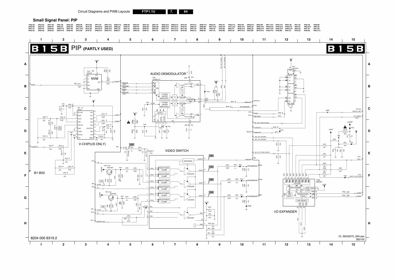
64FTP1.1U 7.Circuit Diagrams and PWB Layouts
CLAMP
MUXDX
88
888
CHIP SELECT
I2C BUSTRANSCEIVER
I/O PORT
DATA LATCHESPWRRES
OUTI/OIN
SHIFTREG
8
12 13
C
H
0V1
0V1
0V1
0V1
12
IP61 D8
F
B15c
14 15
E
B
G
15
B14c(3x)
IP55 G5IP56 D14IP57 D7IP58 D6
IP59 B8IP60 C6
IP62 C14
A
13
*
*
10 FP56 B8 IP54 D2
0V1
5V2
IP52 F5IP53 D210
FP53 F10FP54 D12FP55 E15
FP57 G6FP59 F15FP60 G10IP50 C2
13 IP51 D3
I/O EXPANDER
0V1
0V1
0V1
G
14 15
B14c
B15c
D
30R
5P51
3P66 100R
+5VD
FP55
+5VD
4K7
3P85
3P69
4K7
FP59
+5V
+5V
IP62
100u
2P80
3P65 100R
FP50
VIDOcIP55
4K7
3P67
9P69
2P79
100n
+5VPIP
D7
12
GND 8
SCL 2
SDA 3SO
1
VDD 13
47n
7P56M62320
CS
0
16
CS
1
15
CS
2
14
D0
4
D1
5
D2
6
D3
7
D4
9
D5
10
D6
11
9P71
11
10
9
1y012
1y113
14
2y02
2y11
15
3y05
3y13
4
G36
GND
8
VCC
16
VEE
7
7P5774HC4053
FP54
100R
10u
2P71
100n
2P81
2P57
IP56
3P72
4K7
9P57
9P70
3P58
3P70
4K7
3P68
4K7
+5VD
9P58
9P56
9P55
100n
2P78
2R2
3P74
FBLK
S-SDA
SWITCH_HEF-SUB
PIP_RESET
SWITCH_HEF
V-PIP+MAIN-OUT S-SCL
CL 36532075_094.eps300104
SELECTABLECLAMP
3-STATE
3-STATE
31 2 10986R
ES
RE
S
4 5 7
RE
S
0V
HB15c
B15c
B6a
11
+8VPIP
RES
47p
2P68
220R
3P56
1K
3P55
RES
680R
3P57
FP572P56
47p
RE
S
100u
2P65
9P54
15 FBI1
14 FBI2
13FBO
9GND
5 SEL
8 VIDIc2
1Vp
FP60
47p
2P67RES
RES
47p
2P69
V35
2P66
100n
47n 100R
47p
2P82
9P53
DV
IN-V50
MUPPET_BLK
8204 000 8319.2
Small Signal Panel: PIP
UNITCONTROL
SUPPLY
VCO2
AMPLIFIER 2LIMITER7 STAGE
AMPLIFIER 1LIMITER7 STAGE
VCO1
IN1
M
B|G
I
D|K
SELECTABLECLAMP
SELECTABLECLAMP
SELECTABLECLAMP
SELECTABLE
3-STATE
SELECTABLE
DECODING
CLAMP
3-STATE
10
*
1P50 D2
B15c
*
RES
2P67 H9
*
2P68 H9
2P70 D62P63 F102P64 F10
2P65 G92P66 H9
*
*
*
RES
B
RE
S
PIP (PARTLY USED)
*
2P82 G102P83 G102P84 F10
2P85 F102P86 A4 3P62 G9
2P69 H9
3P64 F9
2P50 D42P51 E12P52 E2
2P53 E22P54 F22P55 F2
*
2P62 F53P57 G53P58 G53P59 F53P60 F5
3P61 D7
3P81 D42P88 C1
3P85 F14
RES
2P56 G5
2P57 G52P58 F5
2P61 E6
3P56 G4 3P88 D5
5P50 D45P51 E157P50 A37P51 C3
7P52 F4
3P63 F9 7P54 E6
RE
S
2P71 D152P72 D6
3P65 G152P74 C62P75 A82P76 D1
2P77 D4
2P80 E14
3P75 E5
9P60 C89P63 B9
9P64 B99P65 C109P69 H139P70 H133P82 C2
FP50 D
B15a
B14c
B15a
3P50 D13P51 D13P52 D4
2P59 E52P60 E5
3P55 H5 3P87 B97P53 G4
RES
RES
B6a
B6a
RE
S
7P57 A123P66 G153P67 F143P68 F14
3P69 E142P78 E122P79 E12
3P74 D15
9P59 C9
4 5 6 7 8
*
*
FP52 F
3P53 E23P54 F2 3P86 B9
4V47V9
B15c
B6a
B6a,B14d
B6a
7P55 B6
7P56 F13
9P52 F49P53 G4
9P54 H59P55 C123P70 E14
3P72 E14
9P58 D11
3
*
B6a
*
**
FP51 G
*
9P71 H
11
*
2V5
0V10V1
**
*
B6a
AUDIO DEMODULATOR
VIDEO SWITCH
NVM
V-CHIP(US ONLY)
B1-B20
9P56 C129P57 D12
C
D
E
F
*
*
1 2
2V5
A
RE
S
RE
S
2P81 E143P76 F4
*
9
**
2P90 D52P73 D8
RE
S
3P77 B33P78 B4
3P79 C43P80 C2
2P87 C2
B15a
B15a
B15a
B15a
B6a,B14d
E12
E23
SCL6
SDA5
VCC
8
VSS
4
WC_7
FP53
2P59
47p
7P50M24C32
E01
IP54
2P62
47p
100R
3P59
2u2
2P72
RE
S
C1
9
C2
10
CS
TA
B
12
GN
D
13
16
1
2
3
IN215
NC1
4
S1 5
S2 6
VAF1 8
VAF2 7
VC
OR
EF
1114
VP
7P55TDA9820T/V1
3P61
27K
9P593P
76
220R
9P65
2P50
100n
6K8
3P80
100u
2P90
+8VPIP
FP56
BC847BW7P53
10K
3P52
PIP
22p
2P88
IP51
2P70
100n
100n
2P74
9P52
3R9
3P88
16IOCNTR
2 VIDIa1
6 VIDIa2
3 VIDIb1
7 VIDIb2
4 VIDIc1
12VIDOa
11VIDOb
10
7P54
TDA8601T
1u
2P87
2P85
47n
+5VPIP
FP51
100R
IP52
3P63
IP59
2P75
IP50
2P83
1u
3P87
10K
IP58
8p2
2P76
IP53
9P63
100n
2P51
+5V
PIP
47p
2P63
V34
3P62
3P77
100R
+5VD
3P60
680R
IP60
2P58
47n
3P86
10K
6n8
2P55
6u8
5P50
7P52
BC847BW
3P51
10M
DS
X84
0
1P50
18M
432
9P64
2P60
1u
47p
2P61
RE
S
68n
2P54
3P78
100R
1u
2P64
3P75
100R
IP57
+8VPIP
2P53
100n
2HSEL
1I2C-SEL
9LPF
NC117
NC218
RREF10
SCK15
SDA14
SDO16
4SEN
6SMS
VDD127
VIDEO
VIN-INTRO13
VSS11
3XOUT
7P51Z86130
8CSYNC
5HIN-XIN
6K8
3P54
470R
3P53
2P86
100n
3P64
100R
10M
3P50
3P82
470K
FP52
9P60
2P84
47p
100R
3P79
2P52
56p
1u
3P81
100R
2P73
IP61
SEL_PIP_SOUND1
7P55-BG
7P55-M
7P55-DK
100n
2P77
MONO-PIP
V-CHIP_IN
SEL_PIP_CVBS_SOUND
7P55-I
SEL_PIP_SOUND2
MONO-PIP
SEL_PIP_CVBS_SOUND
SE
L_P
IP_S
OU
ND
1
SE
L_P
IP_S
OU
ND
2
U-PIP+MAIN-OUT
DY
DU
IN-Y50
IN-U50
Y-PIP+MAIN-OUT
V-CHIP_IN
S-SDA
S-SCL
S-SCL
S-SDA
SUB-Y
SIF-OUT
PIP-CVBS-MON
HA50-PIP
V36
V37
V38
V39
V33
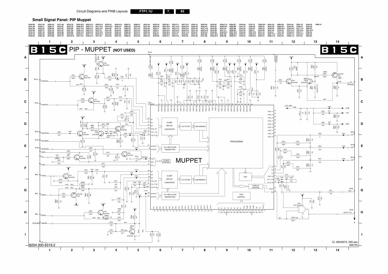
Circuit Diagrams and PWB Layouts 65FTP1.1U 7.
PLL AND CLOCK TEST
B
C
I
RE
S
IPB5 F3
IPB4 B4IPB3 D4IPB2 D2IPB1 B13IPB0 G5IPA9 G5
B15c(2x)
B
11
IPA6 G11IPA7 D5
IPA8 D5
A
D
E
F
G
H
0V2
0V
ES
12 13 14
B15b
B15b
RE
S
11 12 13 14
RES
RE
S
RES
RE
S
RE
S
RE
S
RE
S
B15b
B15b
B15b
9PA5 G29PA6 H3
RE
S
1V2
B6a
RES
FPA9 F14FPB0 C14
FPB1 F5FPB2 F5IPA1 C14IPA3 D14IPA5 F11
B15
b,B
6a
RE
S
9PA4 G2
9PA7 H49PA8 I59PB1 C139PB2 C12
9PB3 B39PB4 D39PB5 B12FPA0 E5FPA1 D5FPA2 F5FPA3 F5
FPA4 G5FPA5 G5FPA6 B14FPA7 D14FPA8 E14
IPA1
9PB2
FPA6
100n
2PE
6
+3.3V
3PE0
1K5
2PE
4
100n
3PG1
68R
3PF9
120R
13
Vref_T_DA11
VSSD_T118
VSSD_T219
30VSSD_T3
VSSD_T448
VSSD_T549
VSSD_T650
VSSD_T751
VSSD_T862
VSSD_T963
Vbias_DA9
Vref_B_DA
PKOFF69
94DHSYNC
DU12
DV10
DY8
FBL68
IPA6
2PF
6
100n
1K5
3PF1
FPA8
FPA7
BC847BW
9K
47p
2PE
1
PC
9
3PF
0
120R
3PF8
820R
IPA5
2PF
1
10u
560R
3PF6
9PB1
3PF4
22K
RE
S47
0R
3PE
1
RES
220R
3PA5
3K3
3PF
3
3PF7
100R
2PE
3
47p
5PB0
30R
220R
3PE4
330R
3PE
9
7PB2
BC847BW
+3V3_SIM
1K3PE
5
3PG0
560R
2PE
2
47p
2PB
6
100n
3n3
2PE
0
2PF
9
10u
16
9PB
5
IPB1
2PE8
100n
100n
2PE7
100n
2PF
5
2PE9
1u
+3V
100n
2PE5
BZ
X38
4-C
3V9
6PA
2
FPA9
30R
5PA9
+3.3V
2P
10u
3PE
2
1K5
3PC7
FPB0
7PB4
BC857BW
BC847BW
7PB3
270R
3PF
2
IPA3
+5VPIP
FPA5
74HC1G32GW7PB1
2
14
5
3
+3VD
100n
2PF
2
1K5
3PE
3
HA
50-P
IP
FBLK
IN-U50
MUPPET_BLK
HA
DU
DV
DY
CL 36532075_095.eps300104
GENERATION CONTROL
RES
3 4 5 6
H
I
9 10
RE
S
R
1 2 7 8
B6a
RES
RE
S
B15b,B6a
38
TC
BC
46
TC
BD
45
TC
BR
47
TC
LK
43
TM
44
T0
37
T1
36
T2
35
T3
34
T4
33
T5
32
T6
88 93
T7 TC
23
NC
14
24
NC
15
25
NC
16
26
NC
17
27
NC
18
28N
C19
29
NC
2
53
NC
3
54
NC
4
55
NC
5
56
NC
6
57
NC
7
58
NC
8
59
NC
9
60
DC
LK
71
DVSYNC70
NC
1
52
NC
10
31
NC
11
21
NC
12
22
NC
13
3K3
3PD5
680R
3PG6
+3.3V
3PD
7
1K2
7PA8 33
3PD3
1K8
3PD1
39K
RES3PD6
10K
RE
S
9PA
8
220R
3PD0
7PB0
BC847BW
+5VPIP
150p
2PB4
+5VPIP
3PD
4
4K7
BC847BW
7PA9
220R
3PD2
100R
9PA6 RES
3PD
8
3K3
2PB
5
47p
9PA7
2PB
7
100n
IN-V50
HA
VA50-PIP
8204 000 8319.2
Small Signal Panel: PIP Muppet
LINE MEMORY
DISPLAYCONTROL
PROCESSING
CLAMP
AND A/D
CONVERTER
H/V FILTER LINE MEMORY
DAC
GENERATION
PLL AND CLOCK
CONVERTER
AND A/D
IIC BUSCONTROL
CLAMP
H/V FILTER
2PA0 B42PA1 B42PA2 B4
B15a
B14a
MUPPET
10
2V7
RES
RES
RES
F
G
B
C
D
E
RE
S
1V0
1V0
2V7
1 2 3 4 5 6 7 8 9
2PA9 E52PB0 F3
2PB6 G52PB7 H42PB8 B62PB9 B6
3V2
RE
S
2PC9 C82PD0 B9
A
2PD6 B102PD7 C102PD8 C102PD9 C10
RE
S
2PA3 B52PA4 C42PA5 C52PA6 E5
2PA7 D42PA8 F1
2PE5 F122PE6 H132PB1 G4
2PB2 G42PB3 G5
2PB4 G42PB5 H1
2PF3 F32PF5 D142PF6 D142PF7 D42PC0 B6
2PC1 B62PC2 B72PC3 B72PC4 B72PC5 B82PC6 B82PC7 C7
2PC8 C8
3PA7 C43PA8 C22PD1 B9
2PD2 B92PD3 B92PD4 B10
2PD5 B10
3PB4 E23PB5 E43PB6 D43PB7 E2
B15
a
2PE0 B112PE1 E13
2PE2 E132PE3 F132PE4 G11
3PC4 G13PC5 E4
2PE7 F132PE8 E13
2PE9 D132PF1 D122PF2 D13
3PD1 H43PD2 H4
3PD3 H43PD4 H5
RE
S
RES
2PF8 G52PF9 G123PA0 B23PA1 B43PA2 B43PA3 B43PA4 B4
3PA5 H123PA6 C4 3PE1 B12
3PE2 C12
3PA9 C53PB0 D33PB1 D2
3PB2 D13PB3 D3 3PF1 G14
3PF2 F123PF3 G133PF4 F12
B15a
B15a
3PB8 E3
3PB9 F23PC0 E33PC1 F33PC2 F33PC3 F3
3PG4 C33PG5 G2
3PC6 G43PC7 G23PC8 G23PC9 G33PD0 H3
3PH5 A83PH6 A93PH7 A103PH8 A10
B6a
PIP - MUPPET (NOT USED)
RE
S
3PD5 I43PD6 I43PD7 I63PD8 I63PD9 E5
3PE0 B11 5PA9 C135PB0 D13
3PE3 A133PE4 B133PE5 B143PE9 E11
3PF0 F11 6PB3 B76PB4 B86PB5 B86PB6 B9
B15a
B15a
3PF5 F43PF6 E12
3PF7 E123PF8 E123PF9 E123PG0 F123PG1 F123PG2 B33PG3 B3 6PB9 B11
7PA0 B3
3PG6 H43PH1 A63PH2 A73PH3 A73PH4 A8 7PA6 C5
7PA7 F27PA8 G27PA9 H3
RES
3PH9 A115PA0 B65PA1 B6
5PA2 B75PA3 B75PA4 B95PA5 B95PA6 B95PA7 B105PA8 B10
6PA0 D46PA1 E16PA2 B136PB1 B66PB2 B6
6PB7 B106PB8 B10
7PA1 C37PA2 D27PA3 D37PA4 D47PA5 E2
7PB0 I57PB1 H127PB2 B127PB3 B13
7PB4 B147PB5 E47PB6 A39PA0 B29PA1 C29PA2 E49PA3 F3
2PD4
100n
3PH
4
47R
BC847BW
7PA7
5PA
0
6PB
4
BA
S31
6
0u82
47R
3PH
2
4u7
5PA
3
FPB2
10u
2PD2RES
150p
2PF
3
100n
2PC
2
2PA8
5PA
2
4u7
100n
6PB
5
2PC
8
100n
2PA
5
150p
BA
S31
6
100n
+5VPIP
47R
3PH
5
3PH
6
47R
+3V
2PB2
5PA
8
12u
3PC
3
39K
Vref_B_MA1
Vref_B_SA80
Vref_T_MA99
Vref_T_SA82
100R
3PC8
40
VS
SD
_RM
41
VS
SD
_RP
61
VS
SD
_SA
85
Vbias_MA97
Vbias_SA84
17
VD
DD
_P2
64
VD
DD
_RL
39
VD
DD
_RM
42
VD
DD
_RP
20
VD
DD
_SA
86
VS
SA
_DA
7
VS
SA
_DP
91
VS
SA
_MA
4
VS
SA
_SA
77
VS
SA
_SP
90
VS
SD
_D
66
VS
SD
_DA
15
VS
SD
_MA
96
VS
SD
_P1
16 65
VS
SD
_P2
VS
SD
_RL
VD
DA
_DA
6
VD
DA
_DP
92
VD
DA
_MA
5
VD
DA
_MF
3
VD
DA
_SA
76
VD
DA
_SF
78
VD
DA
_SP
89
VD
DD
_D
67
VD
DD
_DA
14 95
VD
DD
_MA
VD
DD
_P1
75
SCL73
SDA74
SHSYNC87
SU79
SV81
SVSYNC72
SY83
POR
MU2
MV100
MY98
IPB5
7PA6SAB9081H
IPB4
+3V
BA
S31
6
6PB
2
47R
3PH
3B
AS
316
6PB
3
47R
3PH
7B
AS
316
6PB
7
9PB
3
RE
S
2PB9
100n
BA
S31
6
6PB
1
3PA3
100R
+3V +3V
+5VPIP
+5VPIP
+3VD
100n
2PD3
5PA
4
0u82
3PG
4
680R
3K3
3PB9
9PA5 RES
RES
10u
2PC0
9PA1
3PC
6
39K
2PD5
10u100n
2PC1
IPB2
2PB8
1K5
3PB0
10u
12u
5PA
6
100n
2PD7
IPB0
IPA8
47R
3PH
1
3PF
5
1K
3PC5
4K7
9PA4 RES
10u
2PD6
BC847BW
7PA3
3PA0
220R
5PA
7
12u
3PA
6220R
3PA8
39K
FPA1
+5VPIP
680R
3PC4
100n
2PB3
100n
2PA7
+3VD
7PB5
BC847BW
100n
2PA2
100n
2PC
7
3PB2
1K5
100n
2PC
5
FPA4
100R
3PC2
7PA1
+3VD
BC847BW
+5VPIP
5PA
1
12u
FPA3
10u2P
F7
680R
3PG
3
16
2PA4
100n
9PB
4
BC847BW
7PA2
12u
5PA
5
FPA0
7PA4
BC857BW
3PC
0
3K3
9PA2
3K3
3PD
9
2PA9
10u16
7PA0
BC847BW
IPA9
3PB3
220R
150p
2PA
3 100n
2PD1
3PA7
100R
+3V
BAS316
6PA1
IPB3
BA
S31
6
6PA0
BZX384-C3V9
6PB
8
2PD
9
100n
BC847BW
2PD
8
10u
RE
S
7PA5
RES
2PC
4
100n
3PB
1
470R
RE
S
9PA0
3PA
4
39K
RE
S
IPA7
F8 16
2PA
1
150p
10u
2PD0
2PB0
1u
1K5
3PB
4
3PB7
100R
39K
3PA9
2PB1
150p
+3VD
2PC
3
10u
RE
S
3PB
5
1K
3PA
2
39K
3PB6
1K2
3PC1
100R
10u
2PC
6 RE
S
2PA0
1u
3PA1
100R
3PG5
680R
100n
2PC
9
9PA
3
47R
BA
S31
6
6PB
9
3PH
8
6PB
6
BA
S31
6
47R
3PH
9
2PA
6
100n
FPA2
1K8
3PB8
FPB1
3PG
2
680R
BC847BW
7PB6
PIP_RESET
3V3_
FA
ULT
_PIP
V-HIP-OUT
Y-H
IP-O
UT
S-SDA
HA
U-HIP-OUT
S-SCL
IN-Y50
VS-HIP-OUT
HS-HIP-OUT
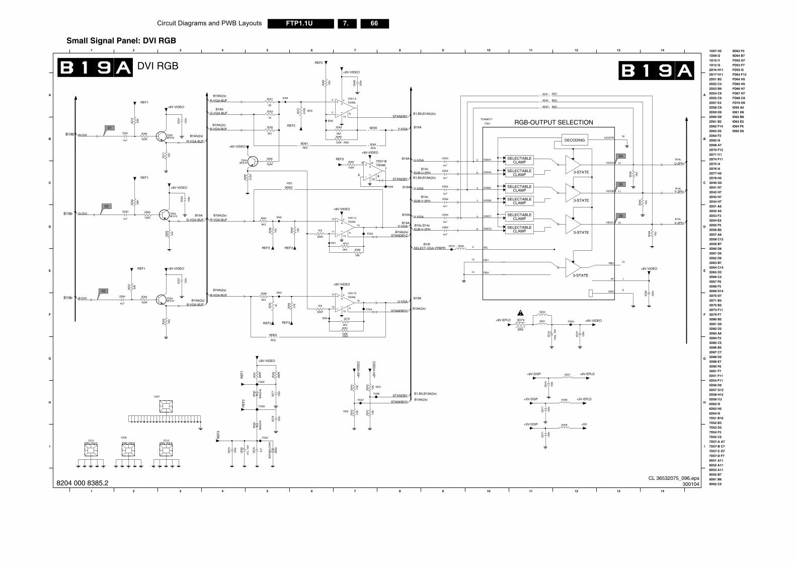
66FTP1.1U 7.Circuit Diagrams and PWB Layouts
B19c
UT SELECTION
2D54 C9
2D55 C9
B19c
2D53 B9
B19A(2x)
RES
RES
G
2D57 E3
2D58 C9
B19c
H
I
1D07 H2
2D60 D9
2D61 B2
2D62 F14
2D63 D2
2D64 F2
3D51 A5
3D52 A5
3D53 F3
3D54 E2
3D55 F5
1D09 I2
1D10 I1
1D12 I3
2D16 H11
2D17 H11
2D51 B3
2D52 C3
3D67 F6
3D68 F5
2D59 D9
3D73 F11
3D79 F7
3D80 B2
3D81 G5
3D82 D2
2D65 I4
5D56 D9
5D57 G12
5D58 H12
5D59 I12
6D62 I5
6D63 H5
6D64 I5
7D51 B10
7D52 B3
RES
3D42 H7
3D43 H7
3D44 H7
7D57-B C7
7D57-C D7
7D57-D F7
9D51 A11
9D52 A11
3D56 B5
12
FD65 H5
FD66 H7
3D69 D14
3D70 D7
3D71 B3
3D72 B2
ID61 D6
ID62 B6
ID63 E5
ID64 F6
ID65 D5
3D83 A6
2D68 A7
2D70 F12
2D71 I11
13 14
12 13 14
3D88 D5
3D89 E7
3D90 F6
3D91 F7
5D51 F11
5D54 F11
9D53 A11
9D55 B7
7D53 D3
7D54 F3
7D55 C5
7D57-A A7
9D64 B7
FD52 D7
FD53 F7
FD55 I5
FD63 F12
FD64 H5
3D57 A6
3D58 C13
A
B
C
D
E
F
3D59 B7
3D60 D6
3D61 D5
3D62 D6
3D63 B7
3D64 C14
3D65 D3
3D66 C2
3D84 F2
3D85 C5
3D86 B5
FD67 H7
FD69 C8
FD70 D9
ID59 A53
2D74 F11
2D75 I4
2D76 I5
2D77 H5
2D78 H5
3D40 G5
3D41 H7
3D87 C7
9D61 B6
9D62 C5
9D63 F5
+8V-VIDEO
12
VIDOB 11
VIDOC 10
VP 1
16
VIDOA
FBO 13
GND 9
IOCNTRDECODING
3-STATE
3-STATE
3-STATE
3-STATE
3D58
1K0
FD63
+5V
220n
2D62
3D69
1K0
FD67
100n
102D
16V
100u2D
74
2
+8V-VIDEO
BA6D
5D59
100n
+5V-DISP +5V-EPLD1D07
1
2
100n
2D70
3D64
1K0
5D58
100n
5D57 +8V-EPLD
STANDBY
U-2FH
Y-2FH
V-2FH
CL 36532075_096.eps300104
D5
D4
D6
RES
H
98 7654321 10 11
I
+5V-DISP
1D12EMC HOLE
BZ
X38
4-C
3V9
6D62
2D71
6D64
BA
S31
6
1D10EMC HOLE
16V
47u2D
65
RE
F3
FD551D09
EMC HOLE
4u7
2D76
2D78
100n
FD65RE
F
3D41
10K 2D
17
100n
2D75
3D42
10K
STANDBY2
8204 000 8385.2
Small Signal Panel: DVI RGB
B19f
RGB-OUTP
DVI RGB
B19b
B19A(2x)
B1,B5,B19A(2x)
B1,B5,B19A(2x)
B19A(2x)
B19AB1,B5,B19A(2x)
B19A
B19c,
B19A(2x)
B19A(2x)
B19A(2x)
B19A(2x)
RES
C
D
B14c
B19b
B14c
B19A
B19A(2x)
B19A
B19A
B19A
B19A
B19A
B19A(2x)
RES
B19b
B14c
E
RES
RES
RES
RES
RES
RES
F
G
98 7654321 10 11
A
B
9D5
REF3
SEL5
VIDIA12
VIDIA26
VIDIB13
VIDIB27
VIDIC14
VIDIC28
SELECTABLECLAMP
FBI115
FBI214
2D59
SELECTABLECLAMP
SELECTABLECLAMP
SELECTABLECLAMP
SELECTABLECLAMP
SELECTABLECLAMP
TDA8601T
7D51
4u7
+8V-VIDEO
FD70
2D55
4u7
2D61
4u7
BF5707D54
REF1
9D55
9D61
REF1
2D60
4u7
18K
3D89
3D55
1K
REF2
3D67
1K2
3D84
100R
FD52
BF5707D53
3D70
3K3
2D52
100n
4u7
2D53
0n77
680R
3D40
3
2
1
8
4
13
FD53
TSH95
7D57-A
220n
2D68
+8V-VIDEO
+8V-VIDEO
9D64
3D62
+8V-VIDEO
10K
4u7
2D58
1K2
3D60
9D62
ID64
4u7
2D63
ID65
FD64
4u7
2D54
3D79
2K2
3D57
470R
3D63
2K2
REF3
22K
3D72
ID61
22K
3D54
3K3
3D61
+8V
-VID
EO
RE
F1
3D83
1K0
REF2
REF3
+8V-EPLD
FD66
+8V-VIDEO
ID63
BF5707D55
3D68
100n
2D57
3K3
100R
3D86
REF2
5D54
+8V-VIDEO
5K1
3D56
10K
680R
3D81
3D52
1K
3D44
3D65
1K0
1K0
3D71
9D63
S31
6
63
+8V-VIDEO
3D87
100K
5D56
REF3
1K2
3D88
47K
3D90
FD69
7D57-C
TSH9512
11
10
9
4
13
ID62
3D66
22K
3D80
100R
2K
3D51 ID59
1K0
3D53 5D51
100n
2D51
15
16
9
4
13
TSH95
7D57-D14
+8V-VIDEO
3D82
100R
10K
3D43
3D59
100K
470R
+8V-VIDEO
REF1
3D85
9D5
BF5707D52
9D5
100K
3D91
2D64
4u7
5
6
7
8
4
13
+8V
-VID
EO
TSH957D57-B
2D16
+8V-DISP
3D73
2R2
U-VGA
STANDBY2
SELECT-VGA-YPBPR
U-VGA
SUB-U-2FH
Y-VGA
SUB-Y-2FH
V-VGA
SUB-V-2FH
Y-VGA
R-VGA-BUF
V-VGA
R-VGA-BUF
STANDBY
B-VGA-BUF
G-VGA-BUF
B-VGA-BUF
STANDBY2
R-VGA-BUF
G-VGA-BUF
B-VGA-BUF
R-DVI
G-DVI
B-DVI
STANDBY
D3
D2
D1
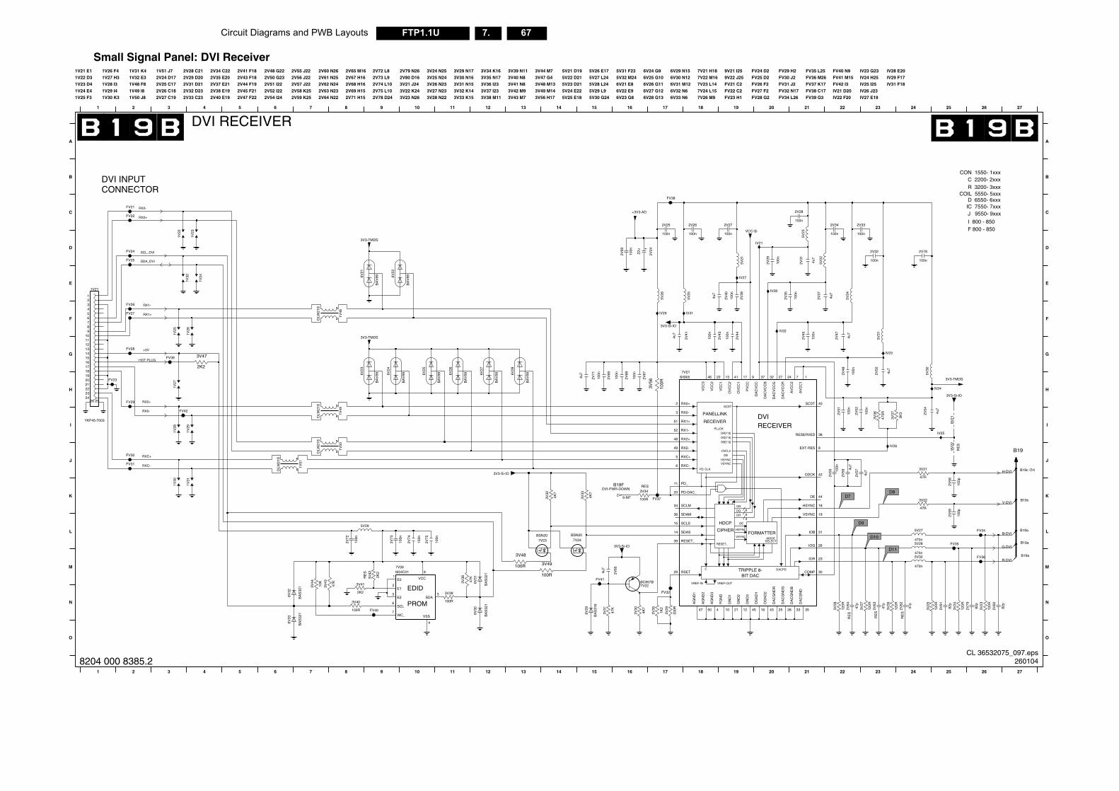
Circuit Diagrams and PWB Layouts 67FTP1.1U 7.
ERODELECT
DACPD
FV42 I3
IV21 D20
IV22 F20
RE
S
RE
S
CON 1550- 1xxx
IV23 G23
IV24 H25
IV25 I25
IV26 J23
IV27 E19
IV28 E20
IV29 F17
FV29 H2
IV31 F18
FV30 J2
FV31 J2
FV32 N17
FV34 L26
FV35 L25
FV36 M26
FV37 K17
FV38 C17
FV39 G3
FV40 N9
FV41 M15
IC 7550- 7xxxD 6550- 6xxx
F 800 - 850I 800 - 850
B19
R 3200- 3xxx
(2x)
RE
S
C 2200- 2xxx
COIL 5550- 5xxx
EIVER
A
B
C
D
E
F
B19c
B19a
B19a
B19a
B19c
20 21 22 23 24 25 26 27
20 21 22 23 24 25 26 27
J 9550- 9xxx
RE
S
G
H
I
J
K
L
M
N
O
47p
2V64
2V48
100n
5V24
3K3
3V37
2V34
100n
120R
3V24
470n
5V27
2V78
100n
47R
3V21
2V54
4u7
100n
2V35
100n
2V55
47p
2V63
3V27
120R
3V3-Si-IO
82p
2V60
470n
5V32
5V28
470n
82p
2V61
3V36
470R
100p
2V58
2V57
4u7
2V47
4u7
IV28
IV24
5V23
3V22
47R
9V21
IV23
IV22
2V56
4u7
IV25
IV26
120R
3V25
19VSYNC
38
40SCDT
18HSYNC
31IOB
IOG 26
23IOR
42ODCK
43
RESERVED
1
AV
CC
1
7
AV
CC
2
30COMP
DA
CG
ND
3533
DA
CG
ND
B
28
DA
CG
ND
G
25
DA
CG
ND
R
32 27
DA
CV
CC
G
24
DA
CV
CC
R
44DE
8EXT-RES
4u7
2V31
2V59
100p
5V31
2V50
4u7
9V22
3V49
2V29
100n
5V22
2V45
100n
FV36
FV35
100n
2V33
2V52
100n
47p
2V62
3V26
120R
120R
3V28
100n
2V28
100n
2V32
3V48
2V37
4u7
2V51
100n
5V30
82p
2V79
3V23
120R
FV34
3V3-TMDS
H-DVI
V-DVI
B-DVI
G-DVI
R-DVI
CL 36532075_097.eps260104
D7
D11
D10
D8
D9
BIT DAC
C
VREF-IN VREF-OUT
TRIPPLE 8-
EDID
PROM
M
N
O
5 6 7 9 10 11 12 13 14 15
RE
S
16 17 18 191 2 3 4 8
FV41
6V29
BA
S31
6
10K
3V44
4u7
2V65
FV32
1K2
3V35
6V32
BA
S32
1
330R
3V29
6V30
BA
S32
1
FV40
47K
3V43
29 RSET
GN
D1
12
GN
D2
45
GN
D3
16
OG
ND
1
OG
ND
2
10
PG
ND
AG
ND
1
50
AG
ND
2
4
AG
ND
3
2147
2K2
3V41
2K2
3V42
VCC
4
VSS7
WC_
M24C017V26
1E0
2E1
3E2
6SCL
5SDA
8100R
4K7
3V30
3V31
BA
S32
1
6V31
47K
3V38
47K
BC857B7V22
100R
3V39
100R3V40
100R
BA
S32
1
6V33
8204 000 8385.2
Small Signal Panel: DVI Receiver
RESET_
PD CLK
VSYNCHSYNC
DE
CNTL3
DB[7:0]
DG[7:0]
DR[7:0]
DR
DG
DB
8
8
8
PLLCK
FORMATT
DE
HSYNC
VSYNC MSE
HDCP
PANELLINK
SCDT
RECEIVER
CIPHER
RES
FV27 F2
FV28 G2
7V24 L15
7V26 M9
9V21 I25
9V22 J25
FV21 C2
FV22 C2
FV23 H1
FV24 D2
FV25 D2
FV26 F2
5V29 L9
5V30 G24
5V31 F23
5V32 M24
6V21 E8
6V22 E9
6V23 G8
6V24 G9
6V25 G10
6V26 G11
6V27 G12
6V28 G13
6V29 N15
B19F
6V30 N12
6V31 M12
6V32 N6
6V33 N6
7V21 H18
7V22 M16
7V23 L143V41 N8
3V42 M9
3V43 M7
3V44 M7
3V47 G4
3V48 M13
3V49 M14
3V56 H17
5V21 D19
5V22 D21
5V23 D21
5V24 E22
5V25 E18
5V26 E17
5V27 L24
5V28 L24
RX1+
RX1-
DVI
3V22 K24
3V23 N26
3V24 N25
3V25 N24
3V26 N23
3V27 N23
3V28 N22
3V29 N17
3V30 N16
3V31 N15
3V32 K14
3V33 K15
3V34 K16
3V35 N17
3V36 I23
3V37 I23
3V38 M11
3V39 N11
3V40 N8
RX2+
RX0+
2V67 H16
2V68 H16
2V69 H15
2V71 H15
2V72 L8
2V73 L9
2V74 L10
2V75 L10
2V78 D24
2V79 N26
2V80 D16
3V21 J24
+5V
SCL_DVI
2V44 F19
2V45 F21
2V47 F22
2V48 G22
2V50 G23
2V51 I22
2V52 I22
2V54 I24
2V55 J22
2V56 J22
2V57 J22
2V58 K25
2V59 K25
2V60 N26
2V61 N25
2V62 N24
2V63 N23
2V64 N22
2V65 M16
DVI INPUT
REC
RXC-
CONNECTOR
RXC+
1V48 F8
1V49 I8
1V50 J8
1V51 J7
2V24 D17
2V25 C17
2V26 C18
2V27 C19
2V28 C21
2V29 D20
2V31 D21
2V32 D23
2V33 C23
2V34 C22
2V35 E20
2V37 E21
2V38 E19
2V40 E19
2V41 F18
SDA_DVI
A
B
C
2V43 F18
E
F
G
H
I
J
K
L
1V32 E3
RX0-
11 12 13
D
15 16 17 18 19
1V22 D3
1V23 D4
1V24 E4
1V25 F3
1V26 F4
1V27 H3
1V28 I3
1V29 I4
1V30 K3
1V31 K4
1 2 3 4 5 6 7 8 9 10 14
RX2-
DVI RECEIVER
HOT PLUG
1V21 E1
3V3-Si-IO
4K7
3V33
100n
2V68
BA
V996V
26
100R
3V34
DLW
21S
1V48
100n
2V69
2K2
3V47FV39
FV28
24
3456789
2526
141516171819
2
20212223
1V21
1
10111213
YKF45-7003
FV30
2V75
100n
FV29
IV21
FV42
100n
2V72
FV37
BA
V996V
23
5V25
2V41
4u7
1V28
1V29
2V25
100n
3V32
4K7
BA
V996V
25
100n
2V44
2V24
IV27
22u
DLW
21S
1V50
1V23
DLW
21S
1V49
FV38
FV21
7V23BSN20
100n
6-M7
1322
VC
C2
46
VC
C3
2V73
39 RESET_
RX0+2
3 RX0-
51 RX1+
52 RX1-
48 RX2+
49 RX2-
5 RXC+
6 RXC-
34 SCLM
15 SCLS
36 SDAM
14 SDAS
VC
C1
17
OV
CC
1
41
OV
CC
2
20 PD-DAC_
11 PD_
9
PV
CC
37
DA
CV
CC
DA
CV
CC
B
SII9057V21
2V67
100n
2V40
4u7
2V43
100n
FV27
FV31
1V30
BSN207V24
6V22
BA
V99
2V27
100n100n
2V26
IV29
FV22
FV23
5V21
3V3-Si-IO
3V3-Si-IO
1V22
1V25
1V26
6V27
BA
V99 6V
28
BA
V99
DLW
21S
1V51
6V24
1V27 B
AV
99
1V24
FV26
FV24
5V26
2V71
4u7
2V38
100n
6V21
BA
V99
5V29
100n
2V74
IV31
2V80
100n
FV25
1V31
3V56
100R
1V32
VCC-Si
+3V3-AD
DVI-PWR-DOWN
3V3-TMDS
3V3-TMDS
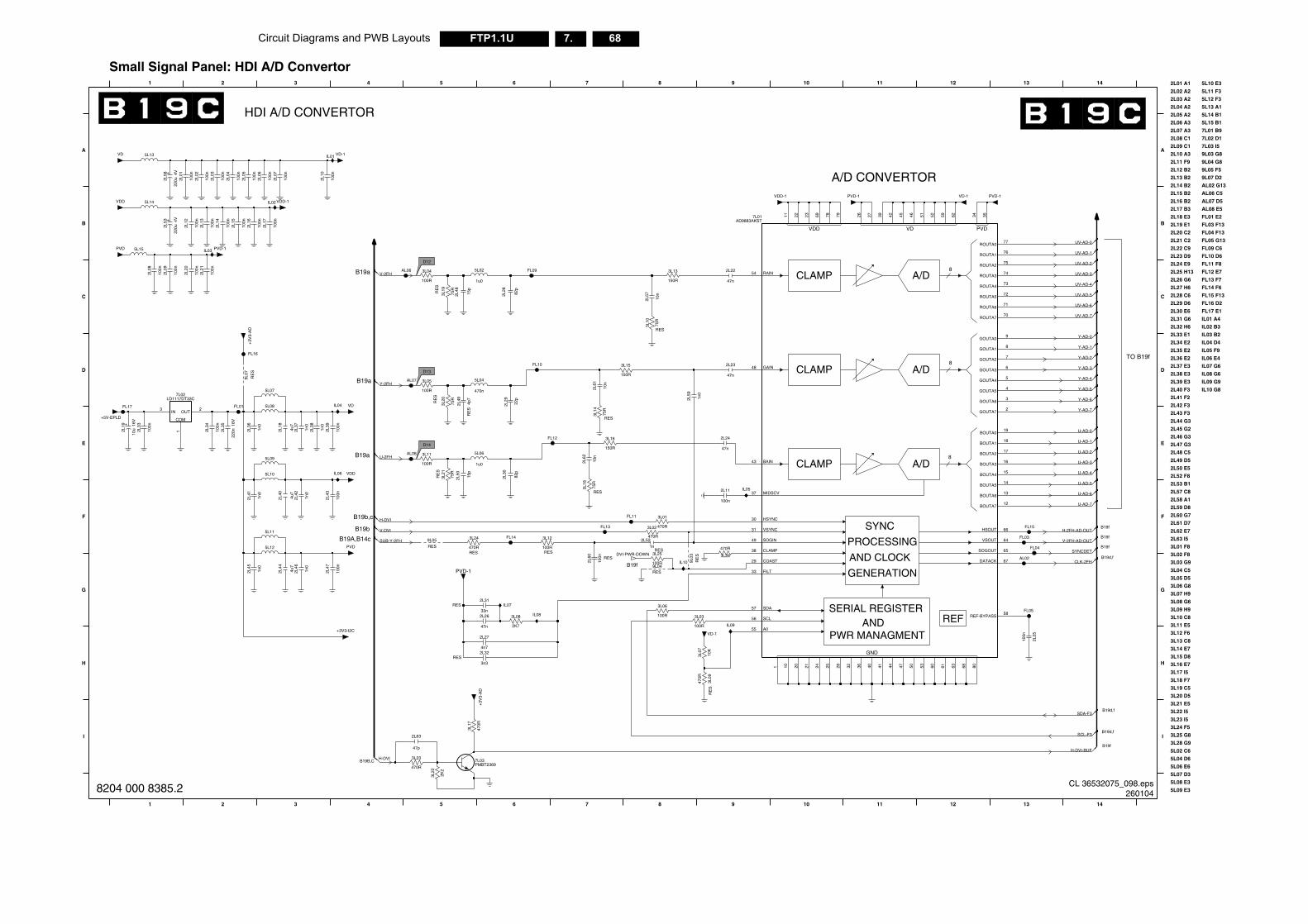
68FTP1.1U 7.Circuit Diagrams and PWB Layouts
TERREF
8
A/D8
ING
K
ON
PVD
ENT
VD
8
GND
A/D
A/D
B19f
B19d,f
RES
TO B19f
IL03 B2
IL04 D4
IL05 F9
IL06 E4
IL07 G6
IL08 G6
IL09 G9
IL10 G8
AL08 E5
FL01 E2
FL03 F13
FL04 F13
FL05 G13
FL09 C6
FL10 D6
FL11 F8
FL12 E7
FL13 F7
FL14 F6
FL15 F13
FL16 D2
FL17 E1
IL01 A4
IL02 B3
3L28 G9
5L02 C6
5L04 D6
5L06 E6
5L07 D3
5L08 E3
5L09 E3
5L10 E3
5L11 F3
5L12 F3
5L13 A1
5L14 B1
5L15 B1
7L01 B9
7L02 D1
7L03 I5
9L03 G8
9L04 G8
9L05 F5
9L07 D2
AL02 G13
AL06 C5
AL07 D5
B19d,f
B19f
3L15 D8
3L16 E7
3L17 I5
3L18 F7
3L19 C5
3L20 D5
3L21 E5
3L22 I5
3L23 I5
3L24 F5
3L25 G8
B19f
RTOR
B19d,f
B19f
2L63 I5
3L01 F8
3L02 F8
3L03 G9
3L04 C5
3L05 D5
3L06 G8
3L07 H9
3L08 G6
3L09 H9
3L10 C8
3L11 E5
3L12 F6
3L13 C8
3L14 E7
2L44 G3
2L45 G2
2L46 G3
2L47 G3
2L48 C5
2L49 D5
2L50 E5
2L52 F8
2L53 B1
2L57 C8
2L58 A1
2L59 D8
2L60 G7
2L61 D7
2L62 E7
2L18 E3
2L19 E1
2L20 C2
2L21 C2
2L22 C9
2L23 D9
2L24 E9
2L25 H13
2L26 G6
2L27 H6
2L28 C6
2L29 D6
2L30 E6
2L31 G6
2L32 H6
2L33 E1
2L34 E2
2L35 E2
2L36 E2
2L37 E3
2L38 E3
2L39 E3
2L40 F3
2L41 F2
2L42 F3
2L43 F3
12 13 14
12 13 14
A
B
C
D
E
F
G
H
I
2L01 A1
2L02 A2
2L03 A2
2L04 A2
2L05 A2
2L06 A3
2L07 A3
2L08 C1
2L09 C1
2L10 A3
2L11 F9
2L12 B2
2L13 B2
2L14 B2
2L15 B2
2L16 B2
2L17 B3
VD-1
FL04
59
VSOUT 64
SOGOUT 65
6245 46 51 52
ROUTA374
ROUTA473
ROUTA572
ROUTA671
ROUTA770
34 35
REF-BYPASS58
ROUTA077
ROUTA176
ROUTA275
8
GOUTA27
GOUTA36
GOUTA45
GOUTA54
GOUTA63
GOUTA72
HSOUT 66
80
GOUTA09
GOUTA1
47 50 53 60 61 63 68
14
BOUTA613
BOUTA712
DATACK 67
BOUTA019
BOUTA118
BOUTA217
BOUTA316
BOUTA415
BOUTA5
FL15
FL03
AL02
4n72L32
3L07
10K
FL05
PVD-1
2L25
100n
H-DVI-BUF
UV-AD-6
UV-AD-5
UV-AD-4
UV-AD-3
UV-AD-2
UV-AD-1
UV-AD-0
SCL-F3
U-AD-7
U-AD-6
U-AD-5
U-AD-4
U-AD-3
U-AD-2
U-AD-1
U-AD-0
Y-AD-7
Y-AD-6
Y-AD-5
Y-AD-4
Y-AD-3
Y-AD-2
Y-AD-1
Y-AD-0
UV-AD-7
SYNCDET
V-2FH-AD-OUT
SDA-F3
CLK-2FH
H-2FH-AD-OUT
CL 36532075_098.eps260104
RE
S
B19B,C
87654321 9 10 11
H
I
3L22
2K2
3L23
470R
470R
3L17
+3V
3-A
D
47p
2L63
10 20 21 24 25 28 32 361 40 41 44
3L09
470R
PMBT23697L03
3n3
H-DVI
8204 000 8385.2
Small Signal Panel: HDI A/D Convertor
COM
OUTIN
SERIAL REGIS
VDD
SYNC
PROCESS
AND CLOC
GENERATI
ANDPWR MANAGM
CLAMP
CLAMP
CLAMP
RE
SR
ES
RES
RES
RES
RE
S
RESRESRES
RES
RE
S
RES
B19a
HDI A/D CONVERTOR
B19a
A/D CONVE
RE
S
B19a
B19b,c
B19A,B14c
B19b
87654321 9 10 11
A
B
C
D
E
F
G
B19fRES
RES
FL14
75R
3L20
IL08
2L29
22p
PVD-1
2L60
100n
3L04
100R
100R
3L11
3L05
100R
100n
2L03
IL07
5L06
PVD-1
150R
3L15
1u0
150R
3L13
100n
2L13
+3V
3-A
D
2L12
100n
2L02
100n
PVD-1
100n
2L43
FL16
+3V3-I2C
2L57
10n
FL01
3L08
2K7
3L28
470R
75R
3L18
4u7
2L44
IL03
5L12
3L24
470R
150R
3L16
5L09
2L22
47n
47n
2L23
5L10
75R
3L21
2L31
33n
1n0
2L41
2L10
100n
75R
11 22 23 69 78 79
VSYNC31
3L14
26 27 39 42
SCL56
SDA57
SOGIN49
30
MIDSCV37
RAIN54
HSYNC
CLAMP38
COAST29
FILT33
GAIN48
A055
BAIN43
AD9883AKST7L01
47n
FL13
2L26
LD1117DT33C7L02
1
3 2
2L19
10u
16V
2L04
100n
5L11
100n
2L11
2L36
1n0
FL12
VDD
2L09
100n
100n
2L07
100n
100n
2L06
PVD
2L05
VD
VDD
AL07
IL09
4u7
2L18
2L39
100n
FL17
2L40
4u7
5L13 VD-1
PVD
2L27
75R
82p
2L28
3L19
100n
2L53
220u
2L01
4V
5L15
5L14
2L45
1n0
2L58
220u
4V
100n
2L34
VD-1
2L33
100n
2L38
1n0
VDD-1
IL02
2L08
100n
2L35
220n
16V
2L16
100n
2L21
100n
VDD-1
9L04
2L14
100n
2L15
100n
FL11
100R
3L06
470n
5L04
2L20
100n AL06
100R
3L12
RE
S
2L49
4p7
2L62
10n
1n0
2L59
75R
1n0
2L37
3L10
5L07
3L01
3L02 470R
470R
2L42
1n0
100R
3L25
FL09
3L03
100R
100n
2L17
FL10
10n
2L61
9L05
2L50
15p
15p
2L48
IL10
2L30
+5V-EPLD
82p
AL08
2L47
100n
1n
2L52
9L03
IL01
2L24
47n
IL05
VD
9L07
IL04
IL06
1n0
2L46
5L08
5L02
1u0
V-DVI
H-DVI
DVI-PWR-DOWN
V-2FH
Y-2FH
U-2FH
SUB-Y-2FH
D13
D12
D14
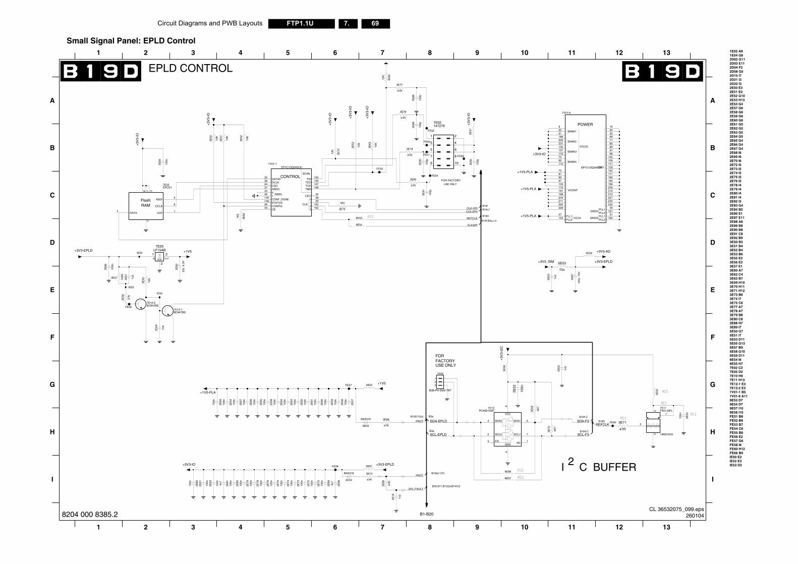
Circuit Diagrams and PWB Layouts 69FTP1.1U 7.
BANK2
BANK3
BANK4
VCCINT
VCCA
GNDA
GNDG
GND
PLL2
BANK1
PLL2PLL1
PLL1
VCCIO
PLL1PLL2
B19A,C
A
B
C
D
E
F
G
H
I
1E02 A81E04 G8
FE52 B8FE53 B7FE54 C8FE55 B8FE56 E2FE57 G6FE58 I6FE60 H12
2D02 G112D03 E112D04 F22D08 G52D15 I72D21 I32D22 I32E50 E32E51 E2
I C BUFFER
B19D
7E05 D27E10 H97E11 H137E12-1 E37E12-2 E27V01-1 B57V01-6 A119E53 D79E54 D7
IE53 D2
3E79 B83E80 C83E88 H73E89 I75E50 G75E51 I75E53 D115E55 G135E57 B95E58 G105E59 D11
FE66 B9IE50 E2IE52 E2
2E92 B93E50 B33E51 B43E52 B43E53 B63E55 E23E56 E23E57 E13E60 A73E62 C43E63 B73E69 H103E70 H113E71 H123E73 B63E74 I7
9E57 I109E58 I10FE51 B8
2E74 I52E75 I52E76 I52E78 I42E79 I42E80 I42E81 I42E82 I32E83 G42E84 B22E86 E12E87 E11
6E54 I66E55 H77E02 C2
2E91 C8
2E52 G102E53 H132E54 G42E57 G62E58 G62E59 G62E60 G62E61 G52E62 G52E63 G52E64 G52E65 G42E66 G42E67 G42E68 I62E69 I6
3E75 C63E77 A73E78 A7
B19A,C
11 12 13
2E88 A82E89 B82E90 B8
11 12 13
2E70 I62E72 I52E73 I5
2
0n 08
5E59
IM
670n 0n 62
FE60
5E55
830n 0n 61 570n
1301571727092112
103110191198204
92251189209231
15027154
72
211220229
819097
232
52697180899196
30151
31
142171190192199205
40
210212221230
POWER
EP1C12Q240C8
7V01-6
10
102109111129
10u
5E53
16V
100u2E
87
+3V3-EPLD
0n 54
2
1
4
3
FXO-34FL
14M31818
7E11
630n
2E53
100n
1n0
2D02
47R
3E71
4K7
3E70
650n 590n 0n 580n 600n 640n 66
1n0
2D03
+3V3-AD
REFCLKSDA-F3
SCL-F3
CL 36532075_099.eps260104
B3a
B1-B20
B19D,F(2x)
(2x)B19d,f
8 9 101 2 3 4
B3a
B3A,B11,B12(2x)B14A,E
H
I
5 6 7
10 2D
SCL1
3 SDA0 6SDA1
8
VCC
5 EN
4
GND1
NC
2 SCL0 7
PCA9515DP7E10
100n
2E73
2E82
100n
2E10 10 2E
3E88
47R
6E54
BAS316
6E55
BAS316
2E10 10 2E
47R
3E89
1n0
2D15
2E10
2E70
100n
10 2E
100n
2E76
2E10
2E68
4u7
9E57
100n
2E78
5E51FE58
9E58
2E10
+3V3-IO
2E10 10 2E
3E69
4K7
2E74
100n
47R
3E74
10 2E
2E72
100n
10 2E
100n
2E69
100n
2D22
2D21
100n
10 2E
+3V3-EPLD
100n
2E80
2E79
100n
2E81
4u7
3V3_FAULT
PROT
100n
2E75
PROT
SDA-EPLD
SCL-EPLD
8204 000 8385.2
Small Signal Panel: EPLD Control
DATA nCS
ASDI
DCLK
SCAN
CLK
MSEL
3
ASDOCSODCLKDATA0
10
CECONFIG
CONF_DONESTATUS
210
CEO
TMSTCKTDOTDI
FOR
USE ONLY
FACTORYUSE ONLY
B19D
A
B
C
D
E
F
B19f
2 3 4 5 6 7 8 9 10
FOR FACTORY
B19c,f
G
B19f,B3a,c,d
1
IE50
EPLD CONTROL
5
2
6
4378
1
EPCS17E02
RAMFlash
10K
3E52
100n
7E05
GND
2
1IN
3OUT
2E86
+3V3-EPLD +1V5
+3V3_S
LF15AB
+1V5-PLA
+3V3-IO
5E57
47R
3E77
3E80
47R
+1V5-PLA
100p
2E88
IE53
100p
2E91
FE52
FE66
+1V5-PLA
5E58
2D04
1n0
FE54
FE55
10K
3E5510
0K3E57
27K
3E56
+1V5
+3V
3-IO
IE52
FE56
B3B-PH-SM3-TBT
1E04
123
10K
3E73
FE53
3E75
1K0
1
10
2
3 4
5 6
7 8
9
1E02147279
3E53
10K
6.3V
22u2E
50
+3V
3-IO
10K
3E50
7E12-1BC847BS
5E50
+3V
3-IO
100p
2E90
+3V
3-IO
+3V
3-IO
9E54
9E53
FE57
3E51
10K
+3V
3-IO
3E79
47R
3E78
47R
100p
2E89
FE51
2E51
1u0
BC847BS7E12-2
100p
2E92
100n
2E84
+1V5-PLA
10K
3E60
3E63
10K
1K0
3E62
149
148
15226
145
24
2536
3435
146
147
155
EP1C12Q240C87V01-1
37
32
33
2829
153
CONTROL
100n
2E52
+3V
3-I2
C
CLK-2FH
REFCLK
CLK32P
CLK-VID
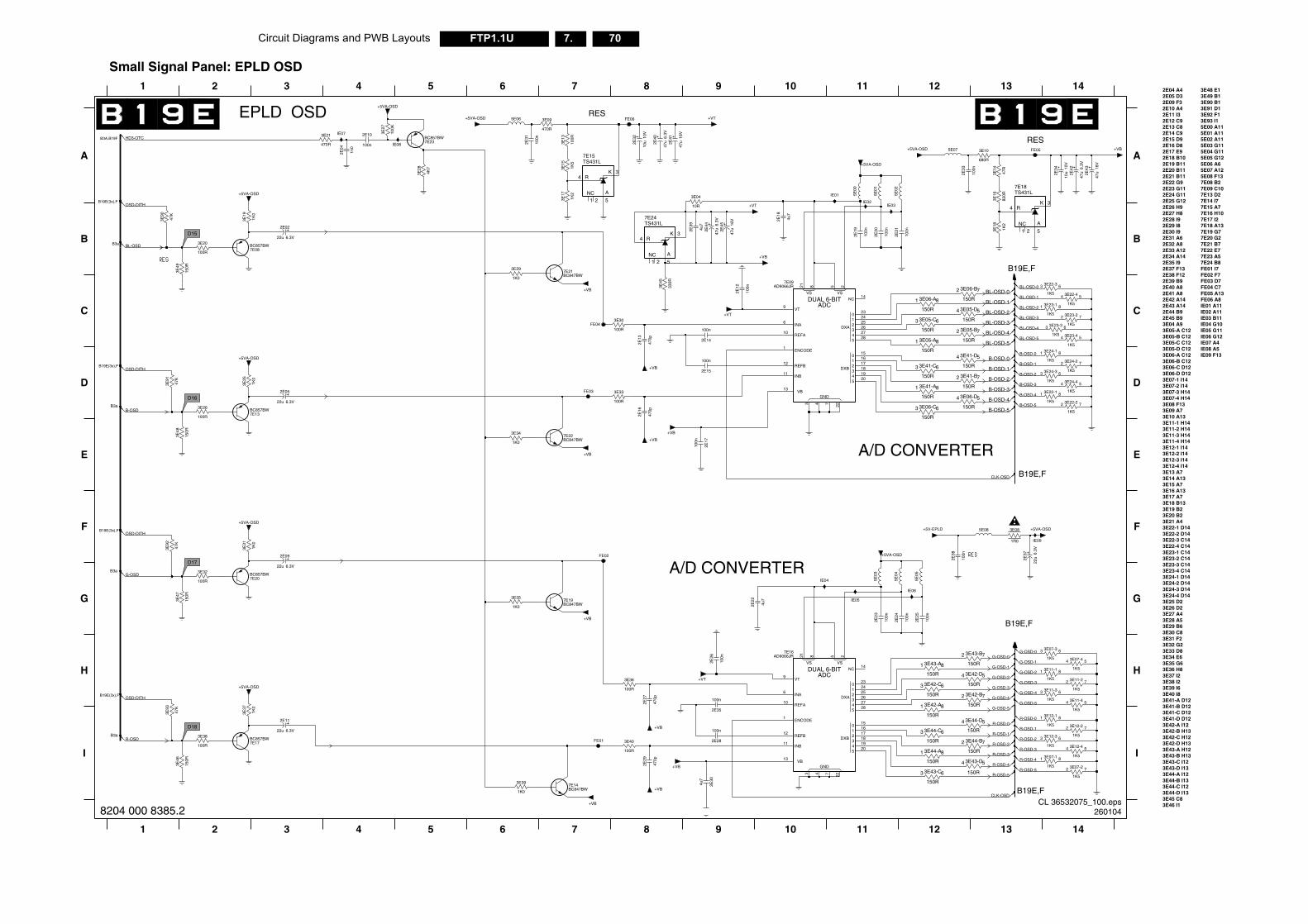
70FTP1.1U 7.Circuit Diagrams and PWB Layouts
NC
12
2E15 D9
12 13 14
B19E,F
B19E,F
B19E,F
IE08 A5IE09 F13
2E30 I9
13 14
A
2E14 C9
2E45 B9
2E16 D82E17 E92E18 B102E19 B112E20 B112E21 B112E22 G92E23 G112E24 G112E25 G122E26 H92E27 H82E28 I92E29 I8
3E10 A13
2E31 A62E32 A82E33 A122E34 A142E35 I92E37 F132E38 F122E39 B92E40 A82E41 A82E42 A142E43 A14
ONVERTER
2E44 B9
3E23-2 C14
3E04 A93E05-A C123E05-B C123E05-C C123E05-D C123E06-A C123E06-B C123E06-C D123E06-D D123E07-1 I143E07-2 I143E07-3 H14
B19E,F
3E08 F133E09 A7
3E41-A D12
3E11-1 H143E11-2 H143E11-3 H143E11-4 H143E12-1 I143E12-2 I143E12-3 I143E12-4 I143E13 A73E14 A133E15 A73E16 A13
3E22-4 C143E23-1 C14
3E49 B1
3E23-3 C143E23-4 C143E24-1 D143E24-2 D143E24-3 D143E24-4 D143E25 D23E26 D23E27 A43E28 A53E29 B63E30 C8
3E07-4 H14
3E39 I63E40 I8
7E23 A5
3E41-B D123E41-C D123E41-D D123E42-A I123E42-B H133E42-C H123E42-D H133E43-A H123E43-B H133E43-C I123E43-D I133E44-A I12
3E17 A73E18 B133E19 B23E20 B23E21 A43E22-1 D143E22-2 D143E22-3 C14
3E48 E1
2E12 C9
3E90 B13E91 D13E92 F13E93 I15E00 A115E01 A115E02 A115E03 G115E04 G115E05 G125E06 A65E07 A12
3E31 F23E32 G23E33 D83E34 E63E35 G63E36 H83E37 I23E38 I2
7E21 B77E22 E7
7E24 B8FE01 I7FE02 F7FE03 D7FE04 C7
FE06 A8IE01 A11IE02 A11IE03 B11IE04 G10IE05 G11IE06 G12IE07 A4
3E44-B I133E44-C I123E44-D I133E45 C83E46 I1
2E09 F32E10 A42E11 I3
2E13 C8
FE05 A13
RES
5E08 F137E08 B27E09 C107E13 D27E14 I77E15 A77E16 H107E17 I27E18 A137E19 G77E20 G2B
C
D
E
F
G
H
I
2E04 A42E05 D3
3 6
1 8 150R
3E43-B2 7
150R
3E43-C
3E42-D4 5150R
3E43-A
7150R
3E42-C3 6 150R
1 8 150R
3E42-B2
150R
3E42-A
3E05-A
150R
1 8
47u
16V
2E43
2E42
47u
6.3V
+5V-EPLD
+5VA-OSD
IE06
100n
7
3E06-C
150R
3 6
3E06-A
150R
1 8
3E06-B
150R
2
3E05-D
150R
4 5
3E05-B
150R
2 7
3E05-C
150R
3 6
680R
3E105E07
5
2E37
22u
6.3V
3 6 150R
3E41-D4
+5VA-OSD
150R
3E41-C
3E08
1R0
1 2
4 R
TS431L7E18
5
A
3K
3E44-D
150R
4 50n26
IE09
5E05
2E25
100n
100n
FE05
2 7
1 8
3E22-2
1K5
4 5
3E22-1
1K5
3 6
3E24-4
1K5
2 7
3E24-3
1K5
1 8
3E24-2
1K5
5
3E24-1
1K5
3E23-4
1K5
4
2E34
10u
10V
820R
3E16
3E18
1K2
2 7
1 8
1K5
3E12-2
4 5
1K5
3E12-1
3 6
1K5
3E11-41K5
3E11-3 1K5
3E11-22 71K5
3E11-11 8
3E44-C
150R
3 6
8
3E44-B
150R
2 7
4 5
3E44-A
150R
1
150R
3E43-D
2E38
100n
5E08
3E07-44 5
1 8
1K5
1K5
3E07-1
+VB
4 5
3E14
47R
3 6
1K5
3E12-41K5
3E12-3
2 7
8
3E23-2
1K5
5
3E23-1
1K5
1
6
3E22-4
1K5
4
3E22-3
1K5
3
D
2 7
3 6
1K5
3E07-2
2 7
1K5
3E07-3
5150R
3E41-A1 8 150R
3E41-B
3E06-D
150R
4
25821AD9066JR7E16
2E33
100n
63E23-3
1K5
3
G-OSD-1
G-OSD-2
G-OSD-3
G-OSD-4
G-OSD-5
R-OSD-1
R-OSD-2
R-OSD-3
R-OSD-4
R-OSD-5
G-OSD-0
R-OSD-0
CLK-OSD
CLK-OSD
BL-OSD-0
BL-OSD-1
BL-OSD-2
BL-OSD-3
BL-OSD-4
BL-OSD-5
B-OSD-0
B-OSD-1
B-OSD-2
B-OSD-3
B-OSD-4
B-OSD-5
BL-OSD-3
BL-OSD-2
BL-OSD-1
B-OSD-5
B-OSD-4
B-OSD-3
B-OSD-2
B-OSD-1
B-OSD-0
G-OSD-5
G-OSD-4
G-OSD-3
G-OSD-2
G-OSD-1
G-OSD-0
BL-OSD-5
BL-OSD-4
BL-OSD-0
R-OSD-5
R-OSD-4
R-OSD-3
R-OSD-2
R-OSD-1
R-OSD-0
CL 36532075_100.eps260104
DXB
VS VS
VT
INA
ENCODE
INB
VB
NC
01234
5
10
432
DXA
GND
5
REFB
REFA
B19E(3x),F
10 11
H
I
1 2 3 4 5 6 7 8 9
B3a
7E17BC857BW
2E30
4u7
47K
3E93
150R
3E46
1K0
3E37
+VB
2E28
100n
102E
FE01 3E40
100R
3E36
100R
6.3V22u
2E11
+VB
2E29
470p
+VB
1K0
3E39
BC847BW7E14
+VT9
1
3 4 7 22
6
11
14
10
12
13
15
24
16
25
17
26
18
27
19
28
20
ADCDUAL 6-BIT
23
+VB
470p
2E27
+5VA-OSD
100R
3E38
100n
2E35
OSD-DITH
R-OSD
8204 000 8385.2
D18
Small Signal Panel: EPLD OSD
NC
DXB
VS VS
VT
INA
ENCODE
INB
VB
NC
01234
5
10
432
DXA
GND
5
REFB
REFA
NC
A/D CONVERTER
86 7 9 10 11
B19E(3x),F
B19E(3x),F
A
B
C
D
E
F
G
EPLD OSD RES
1 2 3 4 5
A/D C
B3a
B3A,B19F
B19E(3x),F
B3a
B3a
2E32 10
V10
u
2E09
22u 6.3V
+5VA-OSD
16V
47u2E
45
5
A
3K
1 2
4 R
6.3V
47u2E
44
+VB
TS431L7E15
2E21
100n
2E20
16V
47u2E
41
2E40 6.
3V47
u
1K5
3E15
+5VA-OSD +VT
5E02
+5VA-OSD
3E13
5E01
100R
3E92
47K
47K
3E91
3E90
47K
150R
3E47
150R
3E48
14
10
12
13
25821
9
19
28
20
1
3 4 7 22
6
11
23
15
24
16
25
17
26
18
27
ADC
AD9066JR7E09
DUAL 6-BIT
BC857BW7E20
2E05
22u 6.3V
+5VA-OSD
3E26
100R
+5VA-OSD
+VT
5E04
2E24
5E03
100n
2E23
IE01
IE02
FE06
3E25
1K0
1K0
3E19
100R
3E20
IE07
3E04
10R
FE04
FE02
FE03
BC857BW7E13
6.3V22u
2E02
1K2
3E17
3E35
1K0BC847BW
+VB
7E19
IE04
IE05
IE03
3E49
150R
7E08BC857BW
100n
2E19
5E00
2E18
4u7
2E12
3E31
1K0
100n
BC847BW7E22
3E29
1K0
7E21BC847BW
+VB
+5VA-OSD
470R
3E09
3E27
100K
+5VA-OS
100n
2E15
2E39
4u7TS431L
7E24
5
A
3K
1 2
4 R
3E30
100R
3E33
100R
+VB
+VB
470p
2E13
2E16
470p
2E31
IE08 100n
3E21
470R
2E04
1n0
2E10
100n
3E32
100R
5E06
2E14
100n
3E34
+VB
1K0
4u7
2E22
100n
3E28
4K7
2E17
BC857BW7E23
3E45
330R
BL-OSD
OSD-DITH
OSD-DITH
OSD-DITH
+VT
+VB
HD3-OTC
B-OSD
G-OSD
D16
D17
D15
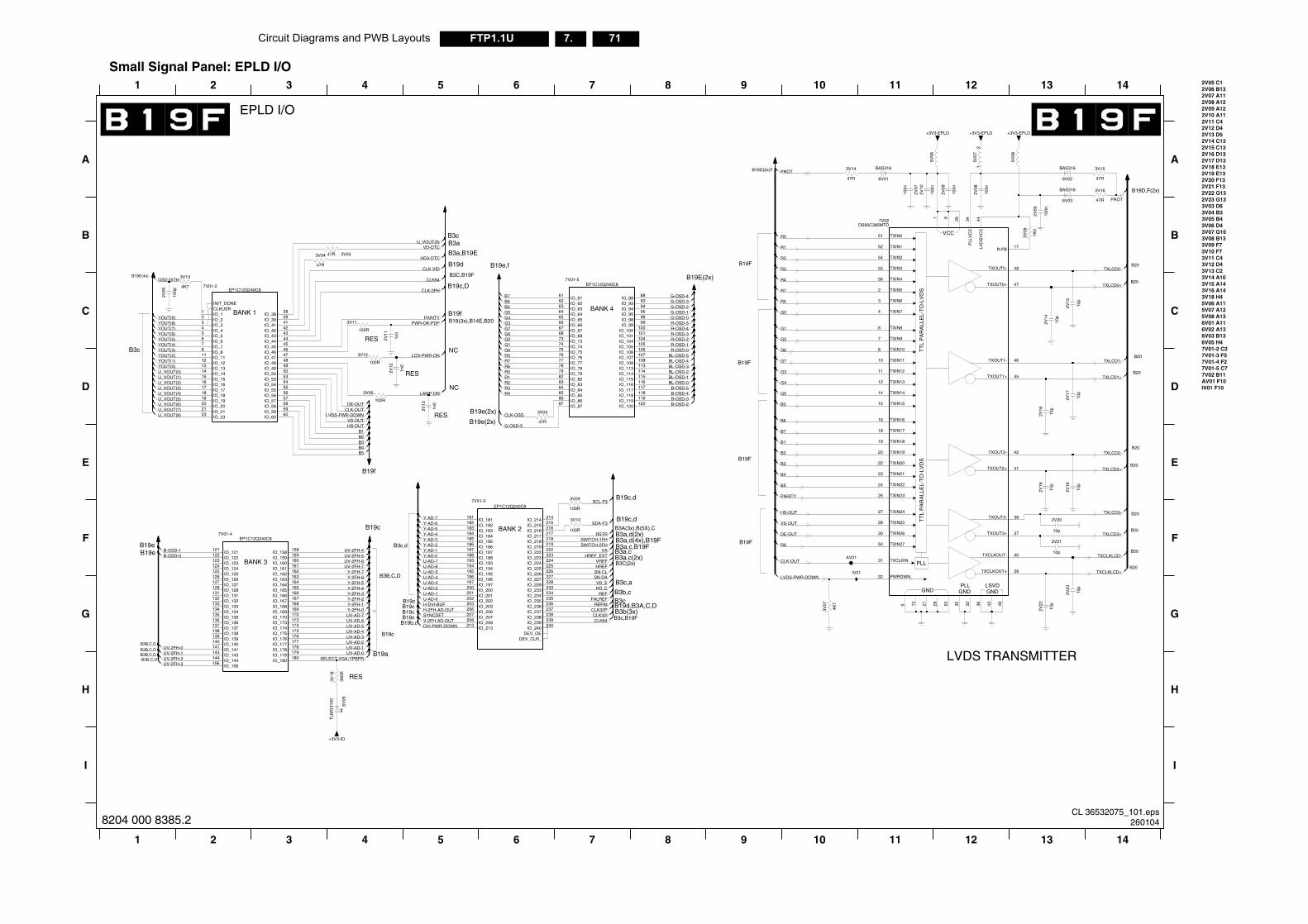
Circuit Diagrams and PWB Layouts 71FTP1.1U 7.
IO_141IO_143 IO_179
IO_178
PLL
TT
L P
AR
ALL
EL-
TO
-LV
DS
TT
L P
AR
ALL
EL-
TO
-LV
DS
GNDPLL
GNDLSVD
VCC
GND
B20
B20
B19a LVDS TRANSMITTER
G
2V10 A112V11 C42V12 D42V13 D52V14 C132V15 C132V16 D13
3V10 F73V11 C43V12 D43V13 C23V14 A103V15 A14
2V22 G132V23 G13
3V05 B43V06 D4
7V01-3 F57V01-4 F2
B20
B20
B20
5V06 A115V07 A12
6V02 A136V03 B13
3V03 D63V04 B3
AV01 F10IV01 F10
3V07 G103V08 B133V09 F7
12
B3B,C,DB3B,C,D
B19D,F(2x)
6V05 H47V01-2 C2
A
B
C
D
E
F
2V20 F132V21 F13
7V01-5 C77V02 B11
13 14
2V17 D132V18 E132V19 E13
B20
3V16 A143V18 H4
5V08 A136V01 A11
2V05 C12V06 B132V07 A112V08 A122V09 A12
12 13 14
B20
B20
B20
B20
H
I
+3V3-EPLD
5V08
5V07
12
179180
143144
+3V3-EPLD +3V3-EPLD
5V06
1K0
3V08
BAS316
6V02
47R
3V16BAS316
6V03
3V15
47R
2V09
100n
100n
2V08
100n
2V10
10p
2V15
2691
47TXOUT0+
48TXOUT0-
45TXOUT1+
46TXOUT1-
41TXOUT2+
42TXOUT2-
37TXOUT3+
38TXOUT3-
27
3
4
5
6
7
8
9
2
20
21
22
23
24
25
26
12
13
14
15
16
17
18
19
17R-FB
LKIN
39TXCLKOUT+
40TXCLKOUT-
0
1
10
11
53 36 43 49
44LV
DS
VC
C
35 3334
PLL
VC
C
DWN_
5 13 21 29
100n
2V06
2V07
100n
10p
10p
2V19
2V18
2V17
10p
2V16
10p
2V14
10p
10p
2V20
2V21
10p
2V23
10p
10p
2V22
UV-2FH-0UV-2FH-1UV-2FH-2
UV-AD-1UV-AD-0
PROT
SELECT-VGA-YPBPR
TXLCD0+
TXLCD0-
TXLCD1+
TXLCD1-
TXLCD2+
TXLCD2-
TXLCD3+
TXLCD3-
TXCLKLCD+
TXCLKLCD-
CL 36532075_101.eps260104
IO_144IO_156
IO_180
4 5
B3B,C,D
H
I
6 7 8 9 10 111 2 3
RES
156
6V05
TLM
G31
003V
18
390R
+3V3-IO
UV-2FH-3
8204 000 8385.2
Small Signal Panel: EPLD I/O
IO_134IO_135IO_136IO_137IO_138IO_139IO_140 IO_177
IO_176IO_175IO_174IO_173IO_170IO_169IO_168IO_167IO_166IO_165IO_164IO_163IO_162IO_161IO_160IO_159IO_158
IO_133IO_132IO_131IO_128IO_127IO_126IO_125IO_124IO_123IO_122IO_121
DEV_CLR_DEV_OE
IO_201IO_200IO_197IO_196IO_195IO_194IO_193IO_188IO_187IO_186IO_185IO_184IO_183IO_182IO_181
IO_202IO_203IO_206IO_207IO_208IO_213 IO_240
IO_239IO_238IO_237IO_236IO_235IO_234IO_233IO_228IO_227IO_226IO_225IO_224IO_223IO_222IO_219IO_218IO_217IO_216IO_215IO_214
IO_20IO_21IO_23 IO_60
IO_59IO_58IO_57IO_56IO_55IO_54IO_53IO_50IO_49IO_48
IO_46IO_45IO_44IO_43IO_42IO_41IO_39IO_38
INIT_DONECLKUSRIO_1
IO_47
IO_2IO_3IO_4IO_5IO_6IO_7IO_8IO_11IO_12IO_13IO_14IO_15IO_16IO_17IO_18IO_19
IO_79IO_78IO_77IO_76IO_75IO_74IO_73IO_68IO_67IO_66IO_65IO_64IO_63IO_62IO_61
IO_82IO_83IO_84IO_85IO_86IO_87 IO_120
IO_119IO_118IO_117IO_116IO_115IO_114IO_113IO_108IO_107IO_106IO_105IO_104IO_101IO_100
IO_99IO_98IO_95IO_94IO_93IO_88
B3c,d
B3a,c(2x)
RES
B19e
EPLD I/O
B19f
B3a,B19E
B19d
B19c,D
RES
B3b(3x)B3c,B19F
2 3 4 5 6
B19cB19c
B19E(4x)
B3B,C,D
B3C,B19F
B19(3x),B14E,B20
B19e,f
B19E(2x)
B19e(2x)
B3a,c,B19FB19e
B19e(2x)
B3c
B19F
B19F
B19F
B19c
B19c
1
D
E
F
G
B3C(2x)
B3B,C,D
B19c
B19F
B19D(2x)F
A
B
C
B3a
B19b,c
B3A(3x),B(5X),C
9 10 11
B19d,B3A,C,D
B3a,c
B19f
NC
7 8
RES
B3cB3b,c
B3a,d(2x)
B3c,a
B3a,d(4x),B19F
B19c
B3c
NC
B19c,d
B19c,d
1n0
2V12
2V11
1n0
3V14
47R 6V01
BAS316
3V06
100R
100R
3V12
235236237238239240
219222223224225226227228233234
202203206207208213
214215216217218185
186187188193194195196197200201
BANK 2
7V01-3EP1C12Q240C8
181182183184
175176177178
163164165166167168169170173174
139140141
158159160161162
126127128131132133134135136137138
EP1C12Q240C87V01-4
121122123124125
BANK 3
2V13
1n0
3V04
47R
3V09
100R
889394959899
76777879828384858687
6162636465666768737475
107108113114115116117118119120
BANK 4
7V01-5EP1C12Q240C8
100101104105106
5859
6
60
78
474849
5
505354555657
23
3839
34
414243444546
141516171819
12
2021
BANK 1
7V01-2EP1C12Q240C8
111213
3V03
47R
3V0547R
3V10
AV01
100R
50 TXIN
55 TXIN
56 TXIN
2 TXIN
3 TXIN
4 TXIN
6 TXIN
7 TXIN
54 TXIN
22 TXIN
23 TXIN
24 TXIN
25 TXIN
27 TXIN
28 TXIN
30 TXIN
11 TXIN
12 TXIN
14 TXIN
15 TXIN
16 TXIN
18 TXIN
19 TXIN
20 TXIN
31 TXC
51 TXIN
52 TXIN
8 TXIN
10 TXIN
32 PWR
7V02DS90C385MTD
100R
3V11
4K7
3V07
IV01
100p
2V05
4K7
3V13
B-OSD-1B-OSD-0
OSD-DITH
DVI-PWR-DOWN
U_VOUT(8)
Y-2FH-4Y-2FH-3Y-2FH-2Y-2FH-1Y-2FH-0UV-AD-7UV-AD-6UV-AD-5UV-AD-4UV-AD-3UV-AD-2
PWR-OK-PDP
PROT
H-DVI-BUF
SN-CLSN-DAVD_EHD_E
REFFALREF
REFINCLK32PCLK32ICLK64
CLK64
CLK-2FH
PARITY
DE-OUT
LVDS-PWR-DOWN
HS-OUTB1
B3
VS-OUT
CLK-OUT
B4
B2
UV-2FH-4UV-2FH-5UV-2FH-6UV-2FH-7
Y-2FH-7Y-2FH-6Y-2FH-5
Y-AD-7Y-AD-6Y-AD-5Y-AD-4Y-AD-3Y-AD-2Y-AD-1Y-AD-0U-AD-7U-AD-6U-AD-5U-AD-4U-AD-3U-AD-2U-AD-1U-AD-0
H-2FH-AD-OUTSYNCDETV-2FH-AD-OUT
RSTRSWITCH-1FHSWITCH-2FH
VAHREF_EXT
VREFHREF
R5R7R6R0R1R2R3R4
G-OSD-5
G-OSD-4G-OSD-3
R-OSD-3R-OSD-2R-OSD-1R-OSD-0
BL-OSD-5BL-OSD-4
G-OSD-2G-OSD-1G-OSD-0R-OSD-5R-OSD-4
BL-OSD-3BL-OSD-2BL-OSD-1BL-OSD-0
B-OSD-5B-OSD-4B-OSD-3B-OSD-2
YOUT(1)YOUT(0)U_VOUT(0)U_VOUT(1)U_VOUT(2)U_VOUT(3)U_VOUT(4)U_VOUT(5)U_VOUT(6)U_VOUT(7)
U_VOUT(9)
CLK-VID
LCD-PWR-ON
LAMP-ON
B5
B7B6B0G5G4G3G7G6G2G1G0
DE-OUT
R6
R3
R4
R7
R5
G0
G1
G2
SCL-F3
SDA-F3
LVDS-PWR-DOWN
CLK-OUT
R0
R1
G6
G7
G3
G4
G5
B0
B6
B7
B1
B2
R2
B3
B4
B5
PARITY
HS-OUT
VS-OUT
YOUT(3)YOUT(2)
YOUT(9)YOUT(8)YOUT(7)YOUT(6)YOUT(5)YOUT(4)
VD-OTC
HD3-OTC
CLK-OSD
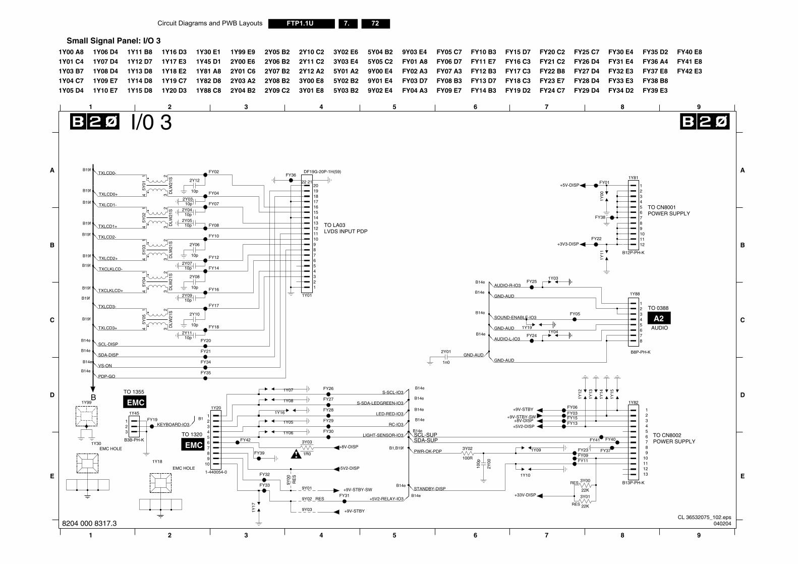
72FTP1.1U 7.Circuit Diagrams and PWB Layouts
TO CN8001POWER SUPPLY
TO CN8002POWER SUPPLY
A2TO 0388
AUDIO
FY36 A4
FY37 E8
FY38 B8
FY39 E3
FY40 E8
FY41 E8
FY42 E3
0 C2
1 C2
2 B8
3 E7
4 C7
FY25 C7
FY26 D4
FY27 D4
FY28 D4
FY29 D4
FY30 E4
FY31 E4
FY32 E3
FY33 E3
FY34 D2
FY35 D2
B14eB
8 9
8 9
D
A
B
C
D
E
678
RES
RES
1Y88
B8P-PH-K
12345
FY22
FY23
FY01
FY41 FY40
FY11
1Y14
789
1
101112
23456
B12P-PH-K
1Y81
FY27
FY13
FY09
1Y15
56789
1Y13
1Y82
B13P-PH-K
1
10111213
234
FY06
1Y08
+3V3-DISP
22K
3Y00
FY38
FY37
1Y03
FY15
1Y00
FY05
1Y12
3Y01
22K
1Y11
1Y04
FY03
+5V-DISP
CL 36532075_102.eps040204
EMC
EMCTO 1320
B1
B14e
B1,B19f
B14e
B14e
B14e
B14e
61 2 3 4 5 7
E
+8V-DISP
+8V-DISP
FY29
9Y01
FY42
1R0
3Y03
1Y06
+9V-STBY
9Y03
RES
+9V-STBY-SW
9Y02
+9V-STBY-SW1Y051
23
B3B-PH-K
1Y45
FY30
1Y10
1Y09
FY31 +33V-DISP
1Y17
1Y16
+5V2-DISP
FY19
FY28
9Y00
RE
S
9
1
10
2345678
1Y20
1-440054-0
FY39
2Y00
100p
3Y02
100R
+5V2-DISP
1Y30EMC HOLE
1Y99
EMC HOLE
1Y18
+9V-STBY
FY33
FY32
LIGHT-SENSOR-IO3
RC-IO3
LED-RED-IO3
S-SDA-LEDGREEN-IO3
SCL-SUP
PWR-OK-PDP
STANDBY-DISP
SDA-SUP
KEYBOARD-IO3
+5V2-RELAY-IO3
8204 000 8317.3
Small Signal Panel: I/O 3
TO LA03LVDS INPUT PDP
TO 1355
B19f
FY19 D2
FY2
FY2
FY2
FY2
FY29Y02 E4
9Y03 E4
FY01 A8
FY02 A3
FY03 D7
FY04 A3
B19f
B19f
FY05 C7
FY06 D7
FY07 A3
FY08 B3
FY09 E7
FY10 B3
FY11 E7
FY12 B3
FY13 D7
FY14 B3
FY15 D7
FY16 C3
FY17 C3
FY18 C3
I/0 3
B19f
2Y10 C2
2Y11 C2
2Y12 A2
3Y00 E8
3Y01 E8
3Y02 E6
3Y03 E4
5Y01 A2
5Y02 B2
5Y03 B2
5Y04 B2
5Y05 C2
9Y00 E4
9Y01 E4
B14e
B19f
B19f
1Y19 C7
1Y20 D3
1Y30 E1
1Y45 D1
1Y81 A8
1Y82 D8
1Y88 C8
1Y99 E9
2Y00 E6
2Y01 C6
2Y03 A2
2Y04 B2
2Y05 B2
2Y06 B2
2Y07 B2
2Y08 B2
2Y09 C2
B19f
B19f
B14e
B14e
B14e
B14e
B14e
B14e
B14e
B14e
1Y11 B8
1Y12 D7
1Y13 D8
1Y14 D8
1Y15 D8
1Y16 D3
1Y17 E3
1Y18 E2
B19f
61 2 3 4 5 7
A
B
C
1Y00 A8
1Y01 C4
1Y03 B7
1Y04 C7
1Y05 D4
1Y06 D4
1Y07 D4
1Y08 D4
1Y09 E7
1Y10 E7
B19f
2Y0910p
2Y08
10p
2Y0710p
2Y06
10p FY12
2Y01
1n0
FY26
1 2
4 3 DLW
21S
5Y05
FY36
FY25
FY14
FY16
FY02
10p
10p
2Y11
2Y10
1Y07
10p
2Y0410p
2Y05
456789
2122
13141516171819
2
20
3
DF19G-20P-1H(59)
1Y01
1
101112
FY17
1Y19FY18
FY34
FY35
FY24
FY21
10p
2Y0310p
2Y12
5Y04
DLW
21S
1 2
4 3
FY10
1 2
4 3
5Y02
DLW
21S
1 2
4 3
FY08
DLW
21S
5Y01
FY07
FY20
FY04
1 2
4 3
5Y03
DLW
21S
VS-ON
SDA-DISP
SCL-DISP
S-SCL-IO3
AUDIO-L-IO3
SOUND-ENABLE-IO3
AUDIO-R-IO3
GND-AUD
GND-AUD
GND-AUD
GND-AUD
TXLCD0-
TXLCD0+
TXLCD1-
TXLCD1+
TXLCD2+
TXLCD2-
TXCLKLCD+
TXCLKLCD-
PDP-GO
TXLCD3+
TXLCD3-
Circuit Diagrams and PWB Layouts 73FTP1.1U 7.
CL 36532075_103.eps060204
t 25_103b.eps
Part 4CL 36532075_103d.eps
3104 303 3896.2
Layout Small Signal Panel (Top Side Overview)
Part 3CL 36532075_103c.eps
ParCL 3653207
Part 1CL 36532075_103a.eps
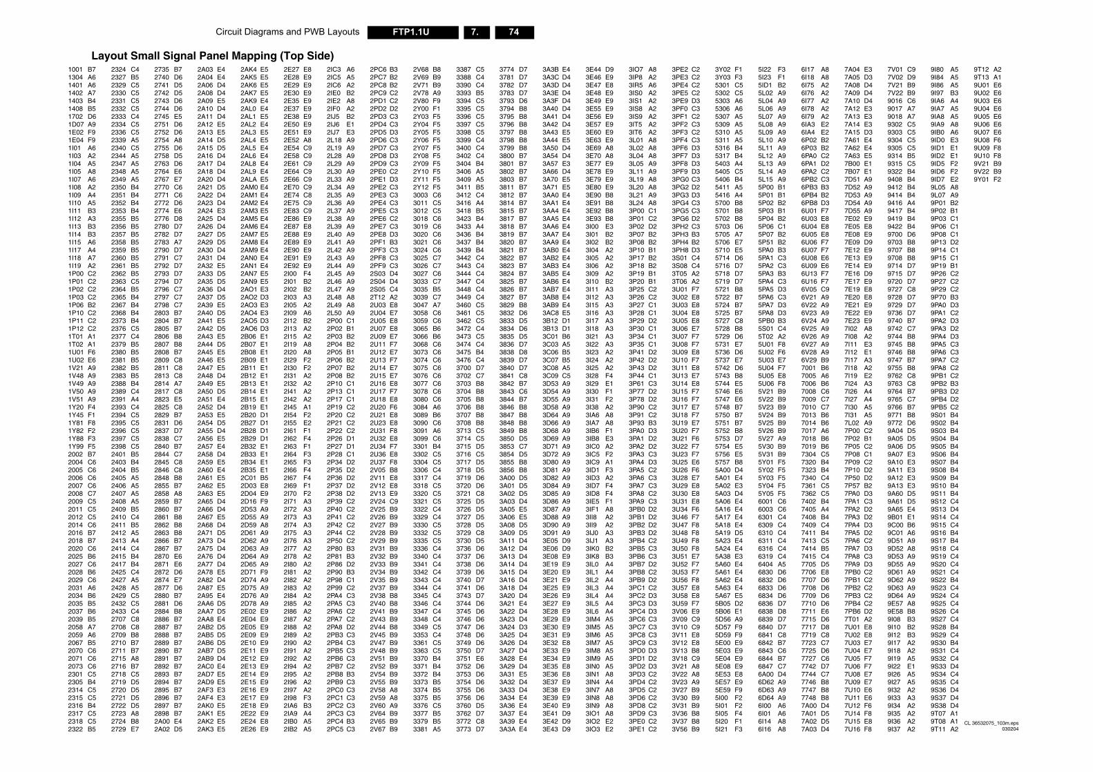
74FTP1.1U 7.Circuit Diagrams and PWB Layouts
2018 B72020 C6
2413 A42414 C4
2866 B72867 B7
2A73 D42A75 D4
2D62 A92D63 A9
2I76 A32I77 A2
2P50 C22P80 B3
2V29 B92V31 B9
3335 C53336 C4
3730 D53736 D6
3A11 D43A12 D4
3E05 D93E06 D9
3IJ1 A33IK0 B2
3PB4 C23PB5 C3
3U49 F83U50 F8
5A23 E45A24 E4
5I22 F35I23 F15ID1 B25L02 A95L04 A95L06 A95L07 A95L08 A95L09 A95L10 A95L11 A95L12 A95L13 A95L14 A95L15 A95P00 B15P01 B15P02 B25P03 B15P04 B25P06 C15P07 B25P51 B25PA0 B35PA1 C35PA2 C35PA3 B35PA4 C35PA5 D35PA6 C35PA7 D35PA8 D35PB0 B35S01 C45T02 A25U01 F85U02 F65U03 E75U04 F75U05 E85U06 F85V21 B95V22 B95V23 B95V24 B95V25 B95V26 B95V27 A95V30 B95V31 B95Y01 F55Y02 F55Y03 F55Y04 F55Y05 F56001 C66003 C66301 C46309 C46310 C46311 C46316 C46319 C46404 A56830 D66832 D66833 D66834 D66836 D76838 D86839 D76840 D76841 C86842 B76843 C66844 B76847 C76A00 D46D62 A96D63 A96D64 A96I00 A66I01 A66I14 A86I16 A8
6I17 A86I18 A86I75 A26I76 A26I77 A26I78 A26I79 A26IA3 E26IA4 E26P02 B26P03 B26PA0 C26PA1 D26PA2 C26PB2 C36PB3 B36PB4 B26PB8 D36U01 F76U03 E86U04 E86U05 E86U06 F76U07 F76U08 E66U09 E66U13 F76U16 F76V05 C96V21 A96V22 A96V23 A96V24 A96V25 A96V26 A96V27 A96V28 A96V29 B97001 B67005 A67006 B67008 C67009 C77010 C77013 B67014 B67017 A67018 B67019 B67304 C57320 B47323 B47340 C47361 C57362 C57402 B47405 A47408 B47409 C47411 B47413 C57414 B57415 C47705 D57706 E87707 D67708 D67709 D67710 D67711 E67715 D67717 D87719 C87723 C77725 D67727 C67742 D77744 C77746 B87747 B87748 B87A00 D47A01 D57A02 D57A03 D4
7A04 E37A05 D37A08 D47A09 D47A10 D47A12 E37A13 E37A14 E37A15 D37A61 E47A62 E47A63 E57B00 E17B07 E17D51 A97D52 A97D53 A97D54 A97D55 A97E02 E97E05 E87E08 E97E09 D97E12 E97E13 E97E14 E97E16 D97E17 E97E19 E87E20 E87E21 E97E22 E97E23 E97I02 A87I08 A27I11 E37I12 E17I17 A37I18 A27I19 E27I24 A37I26 A47I27 A47I30 A57I31 A57L02 A97P00 C27P02 B17P05 C27P08 C17P09 C27P10 D27P50 D27P57 B27PA0 D37PA1 C37PA2 D27PA3 D27PA4 D37PA5 D27PA6 C27PA7 D37PA8 C37PA9 D37PB0 C27PB1 C27PB2 C27PB3 C27PB4 C27PB6 D27T01 A27U01 E87U02 E87U03 E77U04 E77U05 F77U06 F77U08 E77U09 E77U10 E67U11 E67U12 F67U14 F87U15 E87U16 F8
7V01 C97V02 D97V21 B97V22 B99016 C69017 A79018 A79302 C59303 C59304 C59305 C59314 B59315 C59322 B49408 B49412 B49414 B49416 A49417 B49419 B49422 B49700 D69703 B89707 B89708 B89714 D79715 D79720 D79727 C89728 D79729 D79736 D79740 B79742 C79744 B89745 B89746 B89747 B79755 B89762 C89763 C89764 B79765 C79766 B79771 B89772 D69A04 D59A05 D59A06 D59A07 E39A10 E39A11 E39A12 E39A13 E39A60 D59A61 D59A65 E49B01 E19C00 B69C01 A69D51 A99D52 A89D53 A99D55 A99D61 A99D62 A99D63 A99D64 A99E57 A89E58 B89I08 B39I10 B29I12 B39I17 A29I18 A29I19 A59I22 E19I26 A59I27 A59I32 A29I33 A39I34 A29I35 A29I36 A29I37 A2
9I80 A59I84 A59I86 A59I97 B39IA6 A49IA7 A59IA8 A59IA9 A89IB0 A69ID0 E39ID1 E19ID2 E19ID5 F29ID6 F29ID7 E29L05 A89L07 A99P01 B29P02 B19P03 C19P06 C19P08 C19P13 D29P14 C19P15 C19P19 B19P26 C29P27 C29P29 C29P70 B39PA0 D39PA1 C29PA2 D39PA3 D29PA4 D39PA5 C39PA6 C39PA7 C29PA8 C29PB1 C29PB2 B39PB3 D29PB4 D29PB5 C29S01 B49S02 B49S03 B49S04 B49S05 B49S06 B49S07 B49S08 B49S09 B49S10 B49S11 B49S12 C49S13 D49S14 C49S15 C49S16 B49S17 B49S18 C49S19 C49S20 C49S21 C49S22 B49S23 C49S24 C49S25 C49S26 C49S27 C49S28 B49S29 C49S30 B49S31 C49S32 C49S33 D49S34 C49S35 C49S36 D49S37 D49S38 D49T07 A19T08 A19T11 A2
9T12 A29T13 A19U01 E69U02 E69U03 E69U04 E69U05 E69U06 E69U07 E69U08 F69U09 F89U10 F89V21 B99V22 B99Y01 F2
CL 36532075_103m.eps030204
2025 B62027 C62028 B62029 C62031 A62034 B62035 B52037 B62039 B52058 A72059 A62067 B52070 C62071 C62073 C62301 C52305 B42314 C52315 C52316 B42317 C52318 C52322 B5
2415 B42417 B42425 C42427 A52428 A52429 C52432 C52433 C42707 C82708 C82709 B82710 B72711 B72715 A82716 B72718 C52719 D52720 D52721 D52722 D52723 A82724 B82729 E7
2870 E62871 E62872 D62874 E72877 D62880 B72881 D62884 B82886 B72887 B72888 B72889 B72890 B72891 B72892 B72893 B72894 B72895 B72896 B72897 B72898 B72A00 E42A02 D5
2A76 D42A77 D42A78 E52A82 D42A87 E52A95 E42AA6 D52AA7 D52AA8 E42AB2 D52AB5 D52AB6 D52AB7 D52AB9 D42AC0 E42AD7 E52AD9 E52AF3 E32AF4 E32AK0 E52AK1 E52AK2 E52AK3 E5
2D64 A92D65 A92D71 F92D74 A92D75 A92D76 A92D78 A92E02 E92E04 E92E05 E92E09 E92E10 E92E11 E92E12 E92E13 E92E14 E92E15 E92E16 E92E17 E92E18 E92E22 E92E24 E82E26 E9
2I78 A22I80 A22I81 A22I82 A22I83 A22I84 A22I85 A22I86 A22I87 A22I88 A22I89 A22I90 A22I91 A22I92 A22I94 A22I95 A22I96 A22I97 A22I98 F32IA6 B32IA9 A42IB0 A52IB2 A5
2P81 B32P86 D22P90 B32P98 C12P99 C22PA4 C32PA5 C32PA6 C22PA7 C22PA8 D22PB3 C32PB4 C32PB5 C32PB6 C32PB7 C22PB8 B32PB9 C32PC0 C32PC1 C32PC2 C32PC3 C32PC4 B32PC5 C3
2V32 B92V33 B92V34 B92V35 B92V37 B92V38 B82V40 B82V41 B92V43 B92V44 B82V45 B92V47 B92V48 B92V51 B92V52 B92V54 B92V55 B92V58 A82V59 A82V60 A92V64 B92V65 B92V67 B9
3340 C43341 C43342 C43343 C43344 C43345 C43346 C43347 C43348 C43349 C53353 C43361 C53363 C53370 B43371 B43372 B43373 B53374 B53375 B53376 C53377 B53379 B53381 A5
3737 D63738 D63739 D63740 D73741 D63743 D73744 D63745 D63746 D63747 D63748 D63749 D63750 D73751 E63752 D63753 D63754 D63755 D63756 D63760 D53762 D73772 C83773 D7
3A13 D43A14 D43A15 D43A16 D43A18 D43A20 D43A21 E43A22 D43A23 D43A24 D33A25 D43A26 D43A27 D43A28 E43A29 D43A31 E53A32 D43A33 D43A34 E43A36 E43A37 E43A39 E43A3A E4
3E08 E93E19 E93E20 E93E21 E93E25 E93E26 E93E27 E93E28 E93E29 E93E30 E93E31 E93E32 E83E33 E93E34 E93E35 E83E36 E83E37 E93E38 E93E39 E93E40 E93E41 D93E42 D93E43 D9
3IK8 B33IL0 A43IL1 A43IL2 A43IL3 A43IL4 A43IL5 A43IL6 A43IM4 A53IM5 A53IM6 A53IM7 A53IM8 A53IM9 A53IN0 A53IN1 A83IN4 A43IN7 A83IN8 A83IN9 A83IO1 A83IO2 E23IO3 E2
3PB6 C33PB7 D23PB8 C23PB9 D23PC1 C23PC2 D33PC3 D33PC4 D33PC6 C33PC7 C33PC8 C33PC9 C33PD0 D33PD1 D23PD2 D33PD3 C23PD4 C23PD5 C23PD6 C23PD8 C23PD9 C33PE0 C23PE1 C2
3U51 E73U52 F73U53 F73U56 F83U57 E83U58 E83U59 F73V06 E93V09 C93V10 C93V11 E83V12 E83V13 B83V18 C93V21 A83V22 A83V23 A93V27 B93V30 B93V31 B93V36 B83V37 B83V56 B9
5A38 E35A60 E45A61 E45A62 E45A63 E45A67 E55B05 D25B06 E15D56 A95D57 F95D59 F95E00 E95E03 E95E04 E95E08 E95E53 E85E57 E95E59 F95I00 F25I01 F25I05 F45I20 F15I21 F3
Layout Small Signal Panel Mapping (Top Side)1001 B71304 A61401 A61402 A71403 B41408 B51702 D61D07 A91E02 F91E04 F91I01 A61I03 A21I04 A51I05 A81I07 A61I08 A21I09 A41I10 A51I11 B31I12 A31I13 B31I14 B31I15 A61I17 A41I18 A71I19 A21P00 C21P01 C21P02 C21P03 C21P06 B21P10 C21P11 C21P12 C21T01 A11T02 A11U01 F61U02 E61V21 A91V48 A91V49 A91V50 A91V51 A91Y20 F41Y45 F11Y81 F81Y82 F21Y88 F31Y99 F52002 B72004 C62005 C62006 C62007 C62008 C72009 C52011 C52012 C52014 C62016 B7
2324 C42327 B52329 C52330 C52331 C52332 C52333 C42334 C52336 C52339 A52340 C52344 A52347 A52348 A52349 A52350 B42351 B42352 B42353 B42355 B52356 B52357 B52358 B52359 B52360 B52361 B52362 B52363 C52364 B52365 B42367 B42368 B42373 B42376 C52377 C42379 B52380 B52381 B52382 B52383 B52388 B42389 C42391 A42393 C42394 C52395 C52396 C52397 C52398 C52401 B52403 B42404 B52405 A52406 A52407 A52408 A52409 B52410 C42411 B52412 A5
2735 B72740 D62741 D52742 D52743 D62744 D62745 E52751 D62752 D62754 A82755 D62758 D52763 D62764 E62767 E72770 C62771 C62772 D62774 E62776 D82780 D72782 D72783 A72790 D72791 C72792 D72793 D72794 D72796 C72797 C72798 C72803 B72804 B72805 B72806 B82807 B82808 B72809 C82811 C82813 C82814 A72817 C82823 E52825 C82829 B72831 D62837 D72838 C72840 B72844 C72845 C82846 C82848 B82855 B72858 A82859 B72860 B72861 B82862 B82863 B8
2A03 E42A04 E42A06 D42A08 D42A09 E52A10 D42A11 D42A12 E52A13 E52A14 D52A15 D52A16 D42A17 D42A18 D42A20 D42A21 D52A22 D42A23 D42A24 E32A25 D42A26 D42A27 D52A29 D52A30 D42A31 D42A32 E52A33 D52A35 D52A36 D42A37 D52A39 E52A40 D52A41 E52A42 D52A43 E52A44 D52A45 E52A46 E52A47 E52A48 D42A49 E52A50 D52A51 E42A52 D42A53 E52A54 D52A55 D42A56 E52A57 E42A58 D42A59 E52A60 E42A61 E52A62 E52A63 E52A65 D42A66 D42A67 E52A68 D42A71 D5
2AK4 E52AK5 E52AK6 E52AK7 E52AK9 E42AL0 E42AL1 E52AL2 E42AL3 E52AL4 E52AL5 E42AL6 E42AL8 E42AL9 E42ALA E52AM0 E42AM1 E42AM2 E42AM3 E52AM5 E42AM6 E42AM7 E52AM8 E42AM9 E42AN0 E42AN1 E42AN7 E52AN9 E52AO1 E32AO2 D32AO3 E32AO4 E32AO5 D32AO6 D32B06 E12B07 E12B08 E12B09 E12B11 E12B12 E12B13 E12B14 E12B15 E12B19 E12B20 D12B27 D12B28 D12B29 D12B32 E12B33 E12B34 E12B35 E12C01 B52D03 E82D04 E92D16 F92D53 A92D55 A92D59 A82D61 A9
2E27 E82E28 E92E29 E92E30 E92E35 E92E37 E92E38 E92E50 E92E51 E92E52 A82E54 C92E58 C92E61 C92E64 C92E66 C92E70 C92E74 C82E75 C92E83 C92E86 E92E87 E82E88 E92E89 E92E90 E92E91 E92E92 E92I00 F42I01 B22I02 B22I03 A32I05 A22I09 A62I12 B22I13 A22I15 A22I19 A82I20 A82I29 F22I30 F22I31 A22I32 A22I41 A22I42 A22I45 A12I54 F22I55 E22I61 F12I62 F42I63 F12I64 F32I65 F32I66 F42I67 F42I69 F12I70 F22I71 A32I72 A32I73 A32I74 A32I75 A3
2IC3 A62IC5 A52IC6 A22IE0 B22IE2 A82IF0 A22IJ5 B22IJ6 E12IJ7 E32L18 A92L19 A92L28 A92L29 A92L30 A92L33 A92L34 A92L35 A92L36 A92L37 A92L38 A92L39 A92L40 A92L41 A92L42 A92L43 A92L44 A92L45 A92L46 A92L47 A92L48 A82L49 A82L50 A92P00 C12P02 B12P03 B22P04 B22P05 B12P06 B22P07 B22P08 B22P10 C12P13 C12P17 C12P19 C22P20 C22P21 C22P22 C22P26 D12P27 D12P28 C12P34 D22P35 D22P36 D22P37 D22P38 D22P39 C22P40 C22P41 C22P42 C22P44 C2
2PC6 B32PC7 B22PC8 B22PC9 C22PD1 C22PD2 D22PD3 C32PD4 C32PD5 D32PD6 C32PD7 C32PD8 D32PD9 C32PE0 C22PE1 D32PE2 C32PE3 C32PE4 C32PE5 C32PE6 C22PE7 C32PE8 D32PF1 B32PF3 C32PF8 C32PF9 C32S03 D42S04 D42S05 C42T12 A22U03 E82U04 E72U05 E82U07 E82U09 E72U11 F72U12 E72U13 F72U14 E72U15 E72U16 E82U17 F72U18 E82U20 F62U21 E82U23 E82U31 F82U32 E82U34 F72U36 E82U37 F82V05 B82V11 E82V12 E82V13 E92V24 C92V25 B92V26 B92V27 B92V28 B9
2V68 B82V69 B92V71 B92V78 A92V80 F92Y00 F12Y03 F52Y04 F52Y05 F52Y06 F52Y07 F52Y08 F52Y09 F52Y10 F52Y11 F52Y12 F53003 C63011 C53012 C53018 C63019 C63020 C63021 C63024 C63025 C73026 C73027 C63033 C73035 B53039 C73047 A73058 C63059 C63065 B63066 B63068 C63073 C63074 C63075 C63076 C63077 C63078 C63080 C63084 A63089 B63090 C63091 A63099 C63301 B43302 C53304 C53306 C43317 C43318 C53320 C53321 C53322 C43329 C43330 C53332 C5
3387 C53388 C43390 C43393 B53394 C53395 C53396 C53397 C53398 C53399 C43400 C43402 C43404 B43406 A53409 A53411 B53412 C43416 A43418 B53423 B43433 A43436 B43437 B43439 B43442 C43443 C43444 C43447 C43448 C43449 C43460 C53461 C53462 C53472 C43473 C53474 C43475 B43476 C43700 D73702 C73703 B83704 B83705 B83706 B83707 B83708 B83713 C53714 C53715 D53716 C53717 D53718 D53719 D63720 D63721 C83725 D53726 D53727 D53728 D53729 C8
3774 D73781 D73782 D73783 D73793 D63794 B83795 B83796 B83797 B83798 B83799 B83800 B73801 B73802 B73803 B73811 B73812 B73814 B73815 B73817 B73818 B73819 B73820 B73821 B73822 B73823 B73824 B73825 B73826 B73827 B73829 B83832 D63833 D53834 D63835 D53836 D73838 D83839 D73840 D73841 C83842 B73843 C63844 B73846 B83847 B83848 B83849 B83850 D53853 C73854 D53855 B83856 B83A00 D53A01 D53A02 D53A03 D43A05 E53A06 E53A08 D53A09 D5
3A3B E43A3C D43A3D D43A3E D43A3F D43A40 D43A41 D43A42 D43A43 E53A44 E53A50 D43A54 D43A57 E33A66 D43A70 E53A71 E53AA0 E43AA1 E43AA4 E43AA5 E43AA6 E43AA7 E43AA9 E43AB0 E43AB2 E43AB3 E43AB5 E43AB6 E43AB7 E43AB8 E43AB9 E43AC8 E53B12 D13B13 D13C01 B63C03 A53C06 B53C07 B53C08 A53C09 C53D53 A93D54 A93D55 A93D58 A93D64 A93D66 A93D68 A93D69 A93D71 A93D72 A93D80 A93D81 A93D82 A93D84 A93D85 A93D86 A93D87 A93D88 A93D90 A93D91 A9
3E44 D93E46 E93E47 E83E48 E93E49 E93E55 E93E56 E93E57 E93E60 E93E63 E93E69 A83E70 A83E77 E93E78 E93E79 E93E80 E93E90 B83E91 B83E92 B83E93 B83I00 E33I01 B23I02 B23I04 A23I05 A23I06 A23I09 A23I10 B23I11 A33I12 A33I15 A33I16 A33I17 A33I18 A33I21 A33I22 A33I23 A23I24 A23I25 A23I28 F43I29 E13I30 F13I31 F23I38 A23IA6 A83IA7 A83IB6 F13IB8 E33IC0 A23IC5 F23IC9 A13ID1 F33ID3 A23ID7 F43ID8 F43IE5 F13IF1 A83II8 A23II9 A23IJ0 A3
3IO7 A83IP8 A23IR5 A63IS0 A23IS1 A23IS8 A23IS9 A23IT5 A23IT6 A23L01 A83L02 A83L04 A83L05 A93L11 A93L19 A83L20 A83L21 A93L24 A83P00 C13P01 C23P02 D23P07 B23P08 B23P10 B13P17 B23P18 B23P19 B13P20 B13P25 C23P26 C23P27 C13P28 C13P29 D23P30 C13P34 C13P35 C13P41 D23P42 D23P43 D23P44 C13P61 C33P77 D23P78 D23P90 C23P91 C23P93 B33PA0 D33PA1 D23PA2 D23PA3 C33PA4 D33PA5 C23PA6 C33PA7 C33PA8 C23PA9 C33PB0 D23PB1 D23PB2 D23PB3 D2
3PE2 C23PE3 C23PE4 C23PE5 C23PE9 D33PF0 C33PF1 C23PF2 C33PF3 C23PF4 C33PF6 D33PF7 D33PF8 D33PF9 D33PG0 C33PG2 D23PG3 D33PG4 C33PG5 C33PG6 D23PH2 C33PH3 B33PH4 B23PH8 D33S01 C43S08 C43T05 A23T06 A23U01 F73U02 E83U03 E83U04 E83U05 E83U06 E73U07 F73U08 F73U09 E83U10 F73U11 E83U13 E73U14 E83U15 F73U16 F73U17 E73U18 F73U19 E73U20 F73U21 F63U22 F73U23 F73U25 E63U26 F63U28 E73U29 E83U30 E83U31 E83U34 F63U46 F73U47 F83U48 F8
3Y02 F13Y03 F35301 C55302 C55303 A65306 A65307 A55309 A55310 A55311 A55316 B45317 B45403 A45405 C55406 B45411 A55416 A45700 B85701 B85702 B85703 D65705 A75706 E75710 E55714 D65716 D75718 D75719 D75721 B85722 B75724 B75725 B75727 C85728 B85729 D65731 E75736 D65737 E75742 D65743 B85744 E55746 E65747 E65748 B75750 B75751 B75752 B85753 D75754 E55756 E55757 B85A00 D45A01 E45A02 E35A03 D45A06 E45A16 E45A17 E45A18 E45A19 D5
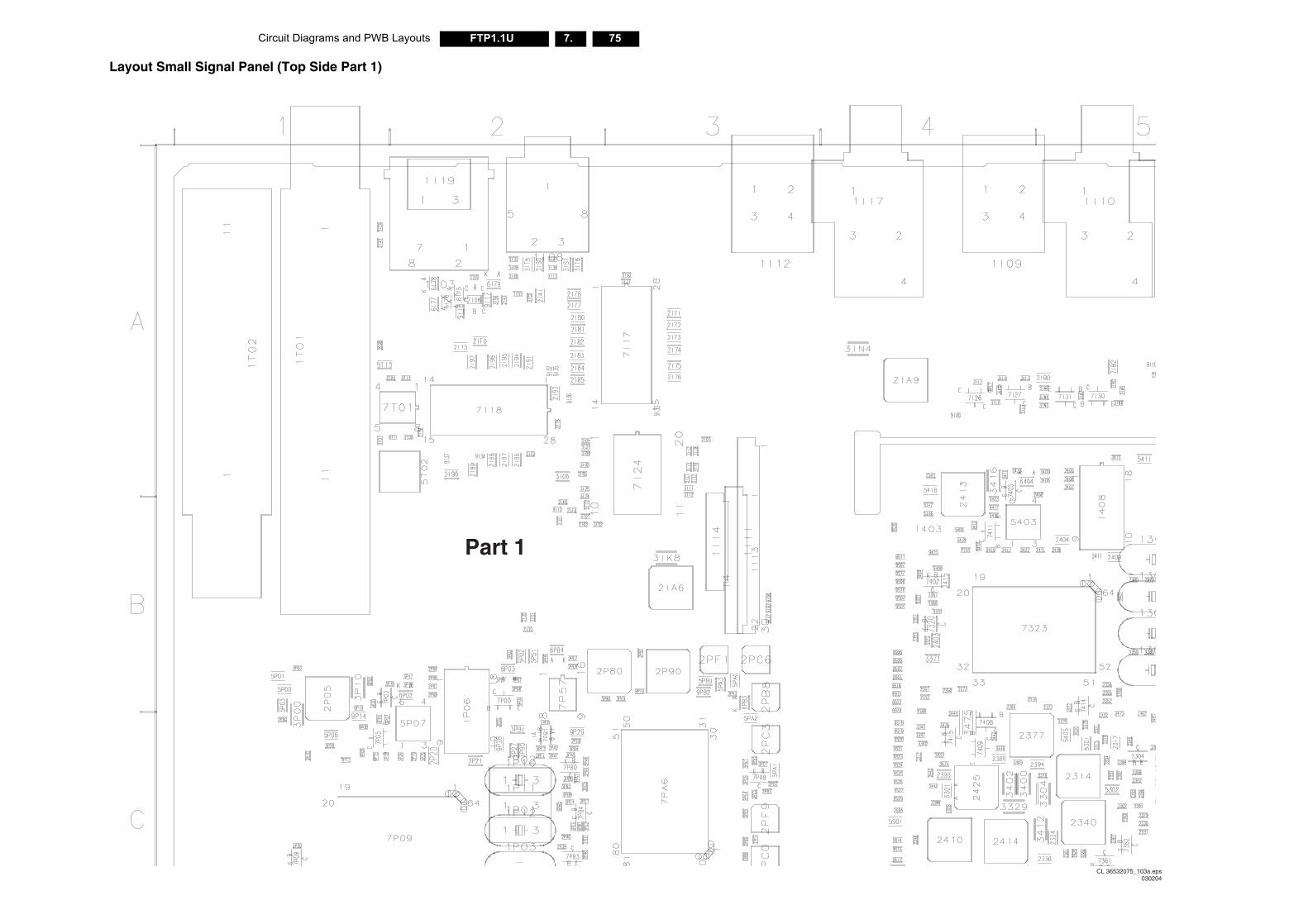
Circuit Diagrams and PWB Layouts 75FTP1.1U 7.
CL 36532075_103a.eps030204
Layout Small Signal Panel (Top Side Part 1)
Part 1
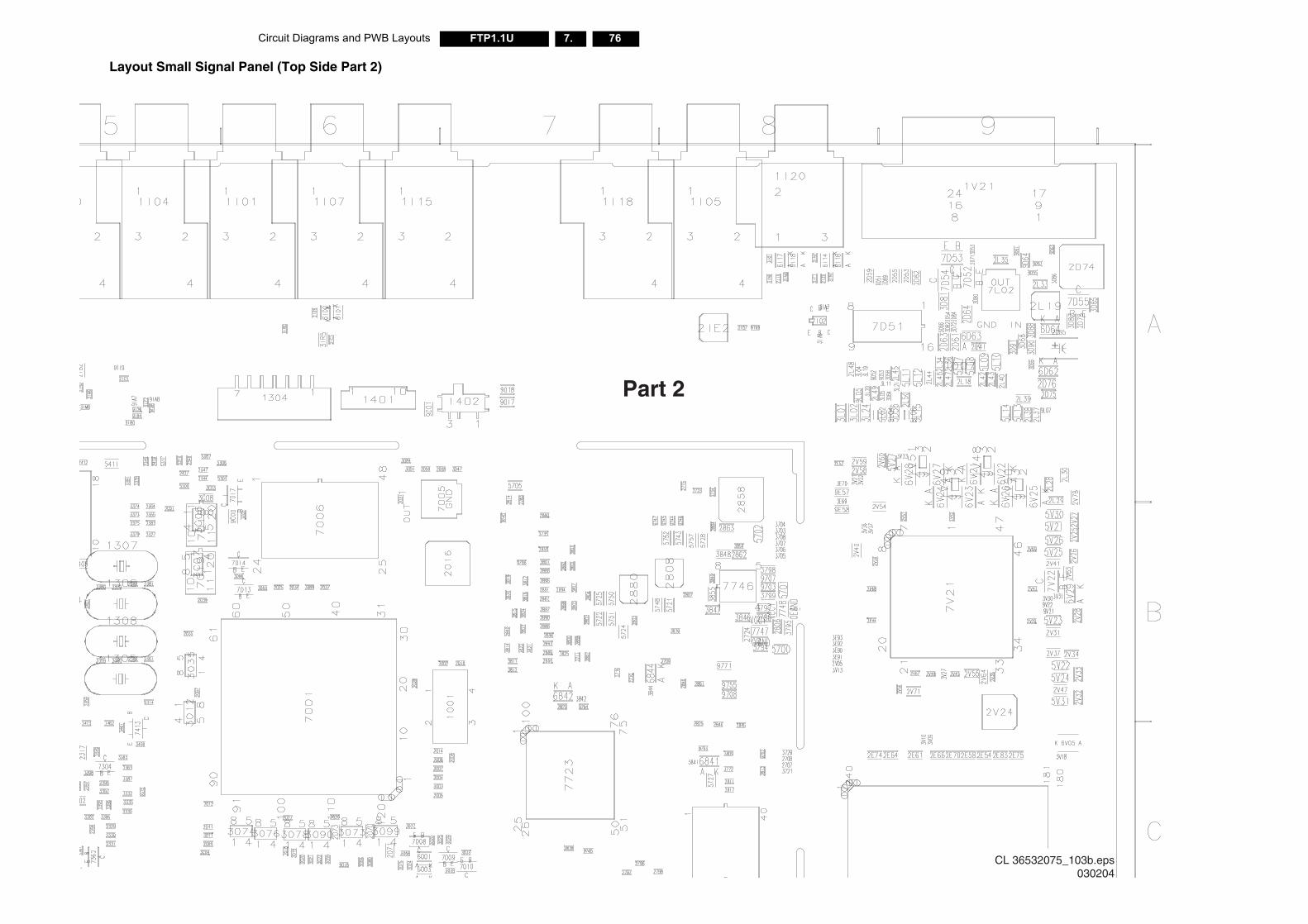
76FTP1.1U 7.Circuit Diagrams and PWB Layouts
CL 36532075_103b.eps030204
Layout Small Signal Panel (Top Side Part 2)
Part 2
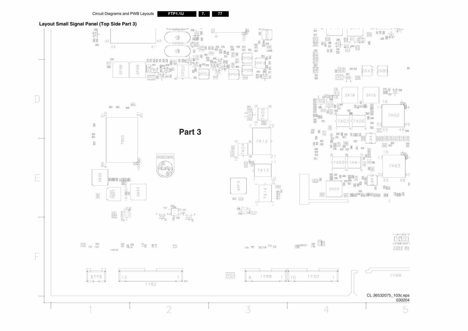
Circuit Diagrams and PWB Layouts 77FTP1.1U 7.
CL 36532075_103c.eps030204
Layout Small Signal Panel (Top Side Part 3)
Part 3
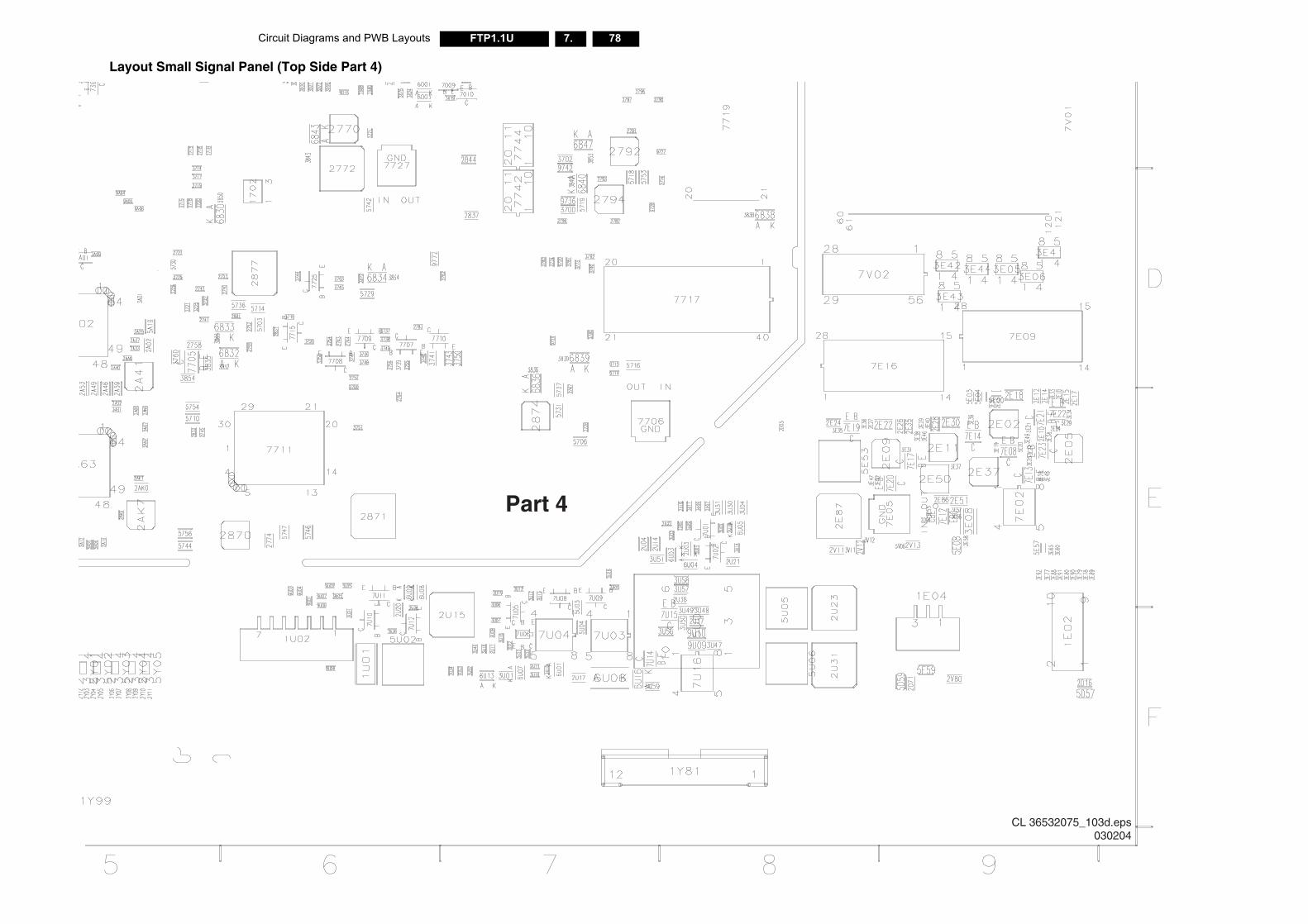
78FTP1.1U 7.Circuit Diagrams and PWB Layouts
CL 36532075_103d.eps030204
Layout Small Signal Panel (Top Side Part 4)
Part 4
Circuit Diagrams and PWB Layouts 79FTP1.1U 7.
CL 36532075_104.eps060204
04b.eps
Part 3CL 36532075_104c.eps
Part 4CL 36532075_104d.eps
3104 303 3896.2
Layout Small Signal Panel (Bottom Side Overview)
Part 2CL 36532075_1
Part 1CL 36532075_104a.eps
80FTP1.1U 7.Circuit Diagrams and PWB Layouts
CL 36532075_104m.eps030204
2325 B5 2786 D3 2AB3 D5 2E33 E1 2IC4 A5 2P59 C7 2S39 B6 3022 C4 3360 C6 3810 C3 3D65 A1 3IB3 E8 3IR7 A8 3P86 C7 5401 B5
5A05 E65A10 E65A11 E65A12 E55A13 E55A14 E55A15 E55A20 D65A21 D65A64 E65A65 E65A66 E65B00 E95B01 E95B02 E95B03 D95B04 D95B07 D95B08 E95B09 E95D51 A15D54 A15D58 F15E01 D15E02 D15E05 D15E06 E15E07 E15E50 D15E51 C25E55 B25E58 B15I02 E85I03 F55I04 F55I06 F75I07 E85I09 F85I10 F95P05 B95P08 C85P09 D85P10 D85P11 C95P50 C75PA9 B75S02 D65S03 D65S04 B65S05 C65T03 A95U01 F25U07 F25U08 F25V06 D15V07 D25V08 D15V28 A15V29 B15V32 A16002 A46004 C46005 B36303 B66304 C66306 B56307 B56308 C66312 B66313 C66314 C66317 C66334 B66402 A56403 B56405 A56831 C46835 D26837 E36845 B26846 B26A01 D6
6A02 D66B00 D96B01 D96B02 E86B03 D96B04 D96B05 D86B06 E96E54 D16E55 C16I03 E86I04 E86I05 F96I10 A66I11 A66I12 A66I13 A66I15 A76I20 A76I21 A76I22 A56I23 A56I24 A56I25 A56I26 A76I27 A46I28 A66I29 A66I30 A46I31 A46I32 A46I33 A56I36 A46I43 A56I45 A56I46 A56I47 A56I48 A56I50 A66I52 A66I53 A26I54 A26I55 A26I56 A26I63 A26I64 A36I65 A36I66 A36I67 A36I68 A36I69 A26I70 A26I73 A86I74 A86I87 A46I88 A46I89 A46I90 A36I91 A36I92 A46I93 A46I94 A46I95 A46I96 A46I97 A46I98 A46I99 A46IA5 A86IA6 A86IA7 A66IA8 A86P00 B86P01 B86PB1 B76PB5 D76PB6 D76PB7 D76PB9 D76T01 A96T02 A96T03 A96T04 A9
6T06 A96T07 A96T08 A96U02 F36U10 E26U11 F46U12 F46U14 F46U15 F46V01 D16V02 D26V03 D16V30 B16V31 B16V32 B16V33 B17002 B57003 B57004 B57007 A47011 C47012 C47015 C57016 C57020 C47021 C47301 C57302 C57303 C67305 C67306 C67307 B67309 C67310 C67312 B57313 C67314 C67315 C67316 C67317 C67318 C67319 C67322 B67375 C67401 A57403 B57406 B67407 A67410 B67412 B67712 E47713 D37714 D37718 C27722 B27724 A37728 C37729 B37730 A37731 C37732 B37733 B37740 D57741 D57743 D37745 C37A06 D57A07 D57A30 E77A31 E77B01 E97B02 E97B03 E87B04 E97B05 E97B06 D97B08 D97B09 E97B10 E97B11 E87D57 A17E10 B1
7E11 A27E15 D17E18 E17E24 D17I00 A87I01 A57I05 A67I06 B77I07 A87I09 A87I10 E87I13 F97I14 F67I15 F97I16 F97I20 A87I22 B87I23 A87I25 A57I28 A57I29 A57I32 A47I40 F57I41 F67I42 F67I44 A67I50 B77L01 C17L03 B17P01 B87P03 C97P04 B97P06 C97P07 C97P11 C97P51 C77P52 C77P53 C77P54 D77P55 C77P56 B77PB5 B77S03 C67S04 D77U07 F47U13 F47V23 B17V24 B17V26 B19001 C59002 C59003 C49004 C49005 A49006 A49007 A49008 C49009 C49010 C49011 C49012 C49013 C49014 B59015 C49019 C49020 C49300 B69308 C59309 C59310 C59311 C59312 C59313 C69318 B69319 C69401 A59402 A59403 A59405 A59406 B69407 B59410 B6
9413 B69415 B59418 A69420 B69421 C69701 E59702 E49709 C39712 D29713 D29716 D39717 D39721 C29722 C29723 D29724 D29725 E49726 D59737 C49743 C49753 B39758 C39760 E39761 E39A00 D59A01 D59A02 D69A03 D69A08 D59A09 D59B02 E89C02 A49E53 C19E54 C19I00 A79I01 A79I02 A79I03 A79I04 A89I05 A79I06 A79I07 A39I09 A79I11 A79I13 A89I14 A59I15 A59I16 A89I20 F89I21 B79I23 B79I24 A79I25 A69I28 E89I29 A79I38 E89I39 E89I57 A89I58 A89I59 A89I77 A59I79 A49I81 A59I82 A69I85 A49I87 A49I88 A49I89 A49I92 A79I93 A79I94 A89I99 F69IA1 A29IA2 A49IA3 A59IA4 A59IA5 A69IB1 A79IB2 A79IC1 A49IC2 A49IC3 A4
9IC5 A49IC6 A49IC7 A49ID3 F99ID4 F99ID8 E89L03 B19L04 B19P04 B89P05 B99P07 C99P09 C99P10 B89P11 B89P12 C99P16 B89P17 C89P18 C99P20 C89P21 C89P22 C99P23 C89P24 C99P25 C99P28 C89P30 C99P52 C79P53 C79P54 C79P55 C89P56 C89P57 B89P58 B89P59 C99P60 B89P63 C79P64 B89P65 B89P69 C79P71 B79S40 C69S41 C69S42 C69S43 E79S65 A69S66 E69S67 E69T01 A99T02 A99T03 A99T04 A99T05 A99T06 A99T09 A99T10 A99T14 A99T15 A99T16 A99Y00 F89Y02 F89Y03 F8
2326 C62328 C52335 C62337 C62338 C62341 C62342 C62343 C62345 A52346 A52354 B62366 B62369 C62370 C62371 B52372 B52374 B62375 B62378 B62384 B6
2787 D32788 D32789 D32795 C32799 D22800 C22801 D22802 D22810 B22812 C32815 B32816 B32818 B32819 C22820 C32821 C32822 C32824 E42826 C32827 B3
2AB4 D52AB8 D62AD0 E72AD1 E72AD3 E72AD4 D72AD5 E72AD6 D72AE2 E72AE3 E72AE4 E72AE5 E72AE6 E72AE8 E72AF0 D72AK8 E52AM4 E62AN2 E62AN3 E62AN4 E6
2E34 E12E39 D12E40 E12E41 E22E42 D12E43 D12E44 E12E45 E12E53 B22E57 D12E59 D12E60 D12E62 C12E63 D12E65 D12E67 D12E68 D12E69 C12E72 D12E73 D1
2IC7 F62IC8 A42IC9 A52IF1 A82IF3 F62IH0 A82IH1 A82IH2 B82IH3 A62IH4 A62IJ0 A72IJ1 A72IJ2 B72IJ3 B82IJ8 F62IJ9 F62L01 C12L02 C12L03 C12L04 C1
2P60 C72P61 C72P62 C72P63 D72P64 D72P65 C82P66 C72P67 D72P68 D72P69 D72P70 B72P71 C72P72 C72P73 C72P74 C72P75 C72P76 C82P77 C72P78 B82P79 B8
2S40 B62S41 B62S42 B62S43 B62S44 B62S45 B62S46 B62S47 C62T01 A92T02 A92T03 B82T04 A92T05 A92T06 A92T07 A92T09 A92T10 A92T13 A92T14 A92T15 A9
3023 C43028 C43029 B43030 C43031 B43032 C43034 B43036 C43037 C43040 B53041 B53042 C53045 A43046 B33048 B43049 B43050 B43051 B43052 B43053 C4
3362 C63364 C63365 C63366 C53367 C63368 C63369 C53378 B53380 B63382 B63383 C63384 C63385 B63386 C63389 C63391 C63392 B63401 B53403 B63405 B6
3813 B33816 B33828 C33831 C43837 E33845 D33851 B23852 B23A17 D53A19 D53A30 D63A35 D63A38 D63A45 D53A46 D53A47 D53A48 D53A49 D53A51 D53A52 D5
3D67 A13D70 A13D73 A13D79 A13D83 A13D89 A13E04 E13E07 D13E09 E13E10 E13E11 D13E12 D13E13 E13E14 E13E15 E13E16 D13E17 E13E18 D13E22 D13E23 D1
3IB4 A83IB5 A83IB7 A83IB9 A63IC1 A83IC2 A63IC3 A63IC4 A53IC6 A53IC7 A83IC8 A93ID0 A83ID2 F93ID4 F63ID5 F93ID6 F93IE0 F63IE1 F63IE2 A43IE3 A3
3IR8 A83IS2 A53IS3 A63IS4 A63IT0 A23IT1 A23IT2 A43IT7 A73L03 C13L06 C13L07 C13L08 B13L09 C13L10 C13L12 C13L13 C13L14 C13L15 C13L16 C13L17 B1
3P87 C73P88 C73P92 C83PC0 C83PC5 B73PD7 C83PF5 B73PG1 C73PH1 B73PH5 D73PH6 D73PH7 D73PH9 D73S02 D73S03 D73S04 E63S05 E63S06 D63S07 A63S09 C6
5402 A65404 B65408 B55415 B65707 D55711 E45712 E45713 C45715 D45717 D25720 E45726 C35739 B35740 B35741 B35755 E45760 C55761 D55762 D55A04 E6
Layout Small Signal Panel Mapping (Bottom Side)1301 B51305 B51306 B51307 B51308 B51404 A31406 A61407 B61409 B51410 B51411 B51A00 D51B01 D81P04 B81P05 C81P07 C81P08 B91P09 C91P50 C81Y01 F52003 C42010 C52013 B32017 B52019 B42022 C42023 B42024 C42026 B42033 B42036 B42038 B42040 B42041 B52052 A42053 A32054 A32055 A32056 A32057 A32060 B32061 A32063 C42068 C42072 C42074 C42302 B62303 C62304 C62306 B62307 C52308 C62309 C52310 C52311 B52312 B52313 C52319 C62320 C52321 C52323 C5
2385 B62386 C62387 B62390 B62402 B62418 B52419 B52420 C62421 B62422 B62423 B62424 C62426 A52431 C52701 B22702 B22703 B22704 B22705 B22706 B22712 B22713 E52714 D52717 C32725 B32726 C32727 B32728 D22730 D22731 B22732 B22733 A22734 A32736 B32737 B32738 B32739 B32746 E42747 B22748 E52749 C42750 C42753 D52756 D52757 D52759 C42760 D42761 D42762 D32765 E42766 E42768 B22769 E32773 E32775 D32777 D32778 D32779 D32781 E32784 D22785 D3
2828 C32830 A32832 C32833 C32834 D52835 C32836 D52839 C32841 B32842 C42843 C32847 A22849 C52850 C52851 B22852 C42853 A32854 A32856 D52857 A32864 A32865 A32875 E42876 E42885 B32899 D22A01 D62A05 D52A07 D62A19 D62A28 E62A34 E62A38 E62A64 D62A69 D62A70 D62A72 D62A74 D62A79 D52A80 D62A81 D62A83 D62A84 E52A85 E52A86 E62A88 D62A89 D62A90 D52A91 D52A92 D52A93 E62A94 E62A96 E52A97 E52A98 E52A99 D52AA0 E62AA1 E62AA5 D52AA9 D52AB0 D5
2AN5 E52AN6 E62AN8 E62AO7 E62AO8 E62B00 E92B01 E92B02 E92B03 E92B04 E92B05 E92B10 E92B16 E82B17 E82B18 E82B21 D92B22 D92B23 D92B24 D92B25 D92B26 D92B30 D82B31 D82B36 D92B37 D92B40 E92B42 E92B45 E92B46 E92B50 E92B51 E92B52 D82B53 D82B54 E92B55 E92B56 E92B57 E82C00 B52C02 B52D02 B12D08 C22D15 E22D17 F12D21 C22D22 D12D51 A12D52 A12D54 A22D57 A12D58 A22D60 A22D68 A12D70 A12D77 A12E19 D12E20 D12E21 D12E23 E22E25 D12E31 E12E32 E1
2E76 D22E78 C22E79 C12E80 D12E81 E12E82 E12E84 E12I04 A72I06 B72I07 A72I08 A82I10 A62I11 A62I14 A42I16 A52I17 A52I18 A42I21 F92I23 A52I24 A52I26 A22I27 A22I28 E82I33 A32I34 A32I35 A32I36 A22I37 F52I38 A82I39 A62I40 F52I43 A82I44 A82I46 A82I47 A62I48 F92I51 F82I52 F92I53 F92I57 A32I58 A42I59 E82I60 F92I79 A82I93 A82I99 A82IA0 A82IA1 A82IA2 A82IA3 A72IA4 A62IA5 B82IA7 B82IB1 A52IB3 F72IB4 F62IB5 A42IB7 F92IC0 A22IC1 A22IC2 A2
2L05 B12L06 C12L07 C12L08 B12L09 B12L10 C12L11 B12L12 B12L13 B12L14 C12L15 C12L16 C12L17 C12L20 B12L21 B12L22 C12L23 C12L24 C12L25 C12L26 B12L27 B12L31 B12L32 B12L52 C12L53 B12L57 C12L58 B12L59 C12L60 C12L61 C12L62 C12L63 B12P01 C82P09 C92P11 C92P12 C92P14 C92P15 C92P16 C92P18 C82P23 D82P24 C82P25 C92P29 C82P30 C82P31 D92P32 D92P33 D92P43 C82P45 D92P46 D92P47 D82P49 C82P51 C82P52 C72P53 C72P54 C72P55 C72P56 C72P57 C72P58 C7
2P82 D72P83 D72P84 D72P85 D72P87 C82P88 C82P91 C92P92 C92P93 C92P94 C92P95 C82P96 C82P97 C72PA0 C72PA1 C72PA2 C72PA3 C82PA9 C82PB0 C72PB1 C72PB2 C72PD0 D82PE9 D72PF2 B72PF5 B72PF6 B72PF7 C82S01 B62S02 C62S06 D62S07 D62S08 D62S09 C62S10 C62S11 D62S12 C62S13 C62S14 C62S15 C62S16 D62S17 C62S18 C62S19 C62S20 C62S21 C62S22 C62S23 B62S25 C62S26 B62S27 B62S28 B62S29 B62S30 C62S31 C62S32 C62S33 C62S34 C62S35 B62S36 C62S37 C62S38 B6
2T16 A92T17 A92T18 A92T19 A92T20 A82U01 F32U02 E32U06 F32U08 F22U10 E32U19 F42U22 F42U24 F42U25 F42U26 F42U27 E22U28 E22U29 F22U30 E22U33 F42U35 F42V06 D22V07 D22V08 D22V09 D12V10 D12V14 D12V15 D12V16 D12V17 D12V18 D22V19 D12V20 D22V21 D22V22 D22V23 D22V50 B12V56 B12V57 B12V61 A12V62 B12V63 B12V72 B12V73 B12V74 B12V75 B12V79 A12Y01 F73001 C43002 C43004 B53005 B43006 C33007 B33008 B53010 B43013 B53014 B53015 B53016 B53017 B5
3054 B43055 B43056 B43057 B33061 B43062 C43064 C53067 B53069 C43072 B43079 C43081 B33082 B43083 B43085 B43086 B43087 B43088 C43092 C43093 B43094 C53095 C53096 C53097 A33098 A43100 C43101 C43102 B43303 B63305 C63307 C63308 C63310 C63311 C53312 C63313 C63314 C63315 C63316 C63319 C63323 B53324 B63325 C63326 B53327 B53328 B53331 C53333 C53334 C53337 C53338 C63339 C63350 C63351 C63352 C63354 C63355 C63356 C63357 C63358 C63359 C6
3407 A53408 B53410 A53414 B53415 B53417 B63419 A63420 B63421 B63434 A53435 B63441 B53445 B63450 B63451 B63452 B63453 C63454 C63455 C53456 B63457 B53459 C63463 B53465 C63467 C63468 B63470 C63471 C63701 C43709 E53710 D53711 B33712 C43722 D53723 C43724 C43731 C53732 D53733 D53758 E53759 D53764 E43765 E43766 D33767 D33770 D33771 C33785 C33786 B33787 A33788 C33789 B33790 A33791 B33792 A23804 A33805 B33806 B33807 C33808 B33809 A3
3A53 D53A55 D53A56 D53A72 E73A73 E73A74 E73A75 E73A76 E73A77 D73A78 E73A84 E73AA2 E63B00 E93B01 E93B02 E93B03 E93B04 E93B05 E83B06 E83B07 E83B08 E83B09 E83B10 E93B11 E93B15 D93B16 D93B17 D93B18 D93B19 E93B20 E93B21 E93B22 E93B23 E83B24 E83B25 E93B26 D93B27 D93B28 E93B29 D93B30 D93B31 D83B32 E93C00 B53C04 B53C05 B53C10 B53C11 C53D40 A13D41 A13D42 A13D43 A13D44 A13D51 A13D52 A13D56 A13D57 A13D59 A13D60 A13D61 A13D62 A13D63 A1
3E24 D13E45 D13E50 E13E51 E13E52 C13E53 C13E62 C23E71 B13E73 C13E74 C13E75 C23E88 C13E89 E23I03 B83I07 F63I08 A63I13 A73I14 A73I19 A73I20 A73I26 B73I27 B83I32 F63I33 F63I34 A63I35 A63I36 A63I37 A63I39 A23I40 A73I41 A73I48 A73I49 A73I50 A53I51 A53I52 A53I53 A53I54 F93I61 A43I62 A43I67 A43I68 A43I78 A53I79 A53I80 A53I83 A63I84 A63I87 A63I88 A63I89 A23I90 A23I91 A23I92 A23I98 A63IA1 A63IA2 A23IA3 A23IA4 A53IA5 A53IB1 E83IB2 A4
3IE7 A43IE8 A43IE9 A33IF0 A43IF2 F93IF3 F93IF4 F93IF5 A43IF6 A43IF7 A33IF8 F93IF9 F93IH0 F63IH1 F63IH2 F53IH3 F53IH4 F63IH5 A83IH6 A83IH7 B83IH8 A83IH9 A83II0 A83II1 B83II2 B83II3 A83II4 A83II5 A83II6 A83II7 A83IJ2 A83IJ3 A83IJ4 A83IJ5 F53IJ6 F63IK1 B83IK2 A53IK3 A53IK4 A73IK5 A73IK7 B83IK9 A63IL7 A53IL8 A53IL9 A53IM0 A53IM1 A53IM2 A53IM3 A53IN2 A53IN3 A53IN5 A43IN6 A43IO5 A43IO6 A43IR0 A83IR1 A83IR2 A83IR3 A83IR4 A83IR6 B8
3L18 C13L22 B13L23 B13L25 B13L28 B13P03 C83P04 C83P05 C83P06 C83P09 B83P11 B93P12 B83P13 B83P14 C93P15 B83P16 C83P21 C83P22 C83P23 C83P24 C83P31 C93P32 C93P33 C83P36 C93P37 C83P38 C93P39 C93P40 B93P45 C83P46 C83P47 C93P48 C83P50 C83P51 C83P52 C73P53 C83P54 C73P55 C73P56 C73P57 C73P58 C73P59 C73P60 C73P62 D73P63 D73P64 D73P65 B83P66 B83P67 B73P68 B73P69 B73P70 B73P72 B83P74 C73P75 C73P76 C73P79 C83P80 C83P81 C73P82 C83P85 B8
3S10 C63S11 D63S12 C73S13 D73T03 A93T04 A93U12 F43U24 F43U27 F43U32 E23U33 E23U35 F43U36 F43U37 F43U38 F43U39 F43U40 F43U41 E43U42 F43U43 F43U44 E23U45 E23U54 F43U55 F43V03 D13V04 C23V05 C23V07 D23V08 D23V14 D13V15 D13V16 D13V24 A23V25 A13V26 B13V28 B13V29 B13V32 B23V33 B23V34 B23V35 B13V38 B13V39 B13V40 B13V41 B13V42 B13V43 B13V44 B13V47 A13V48 B13V49 B13Y00 F93Y01 F95304 A55305 A45308 A55312 B65313 C65314 C65315 C65318 B6
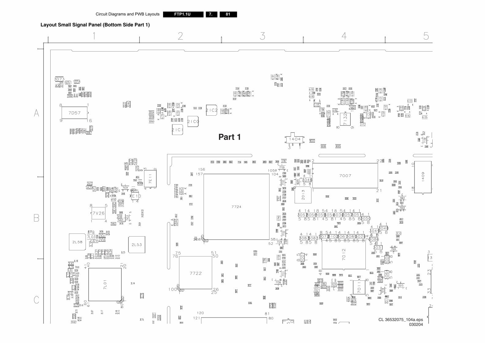
Circuit Diagrams and PWB Layouts 81FTP1.1U 7.
CL 36532075_104a.eps030204
Layout Small Signal Panel (Bottom Side Part 1)
Part 1
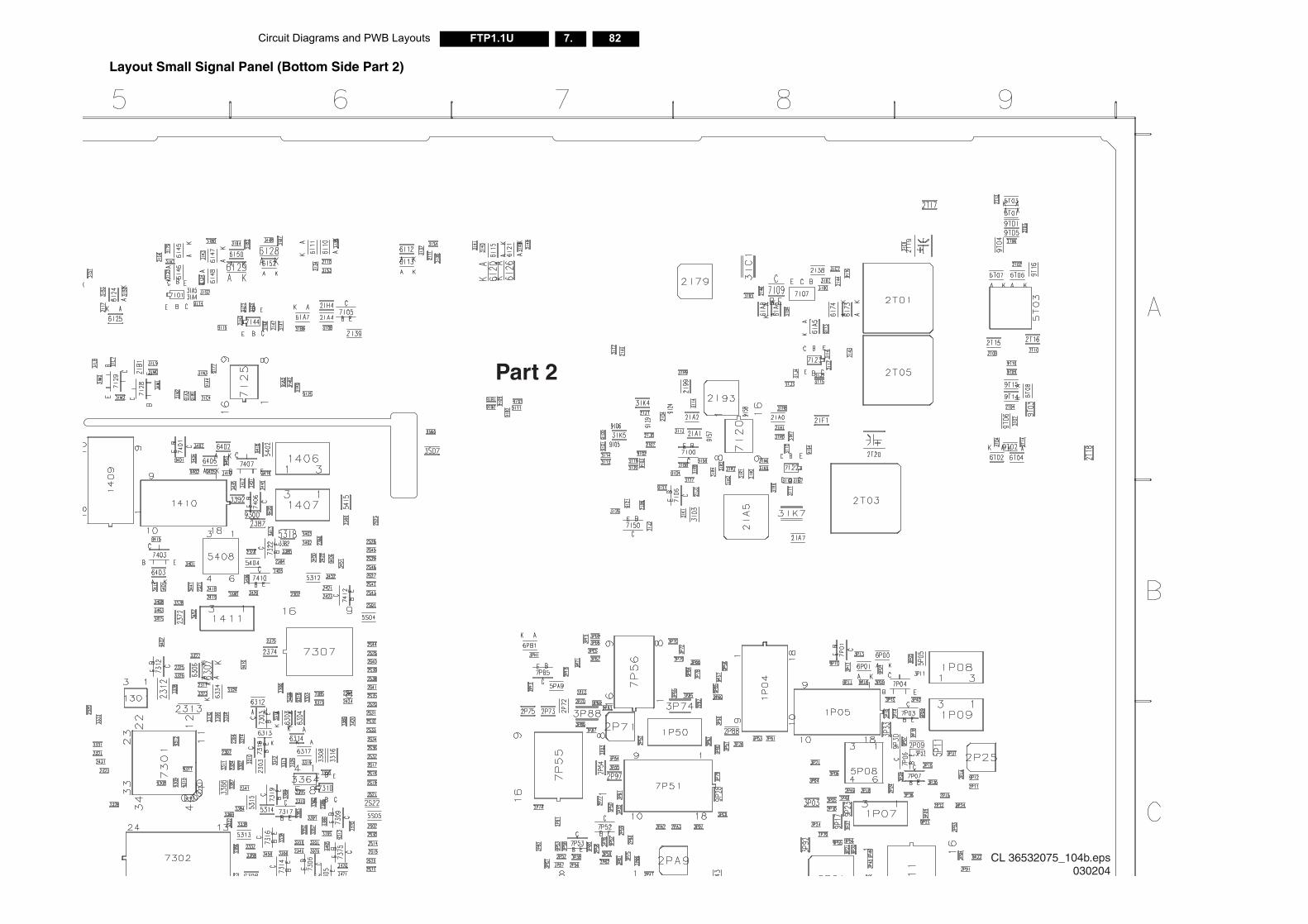
82FTP1.1U 7.Circuit Diagrams and PWB Layouts
CL 36532075_104b.eps030204
Layout Small Signal Panel (Bottom Side Part 2)
Part 2
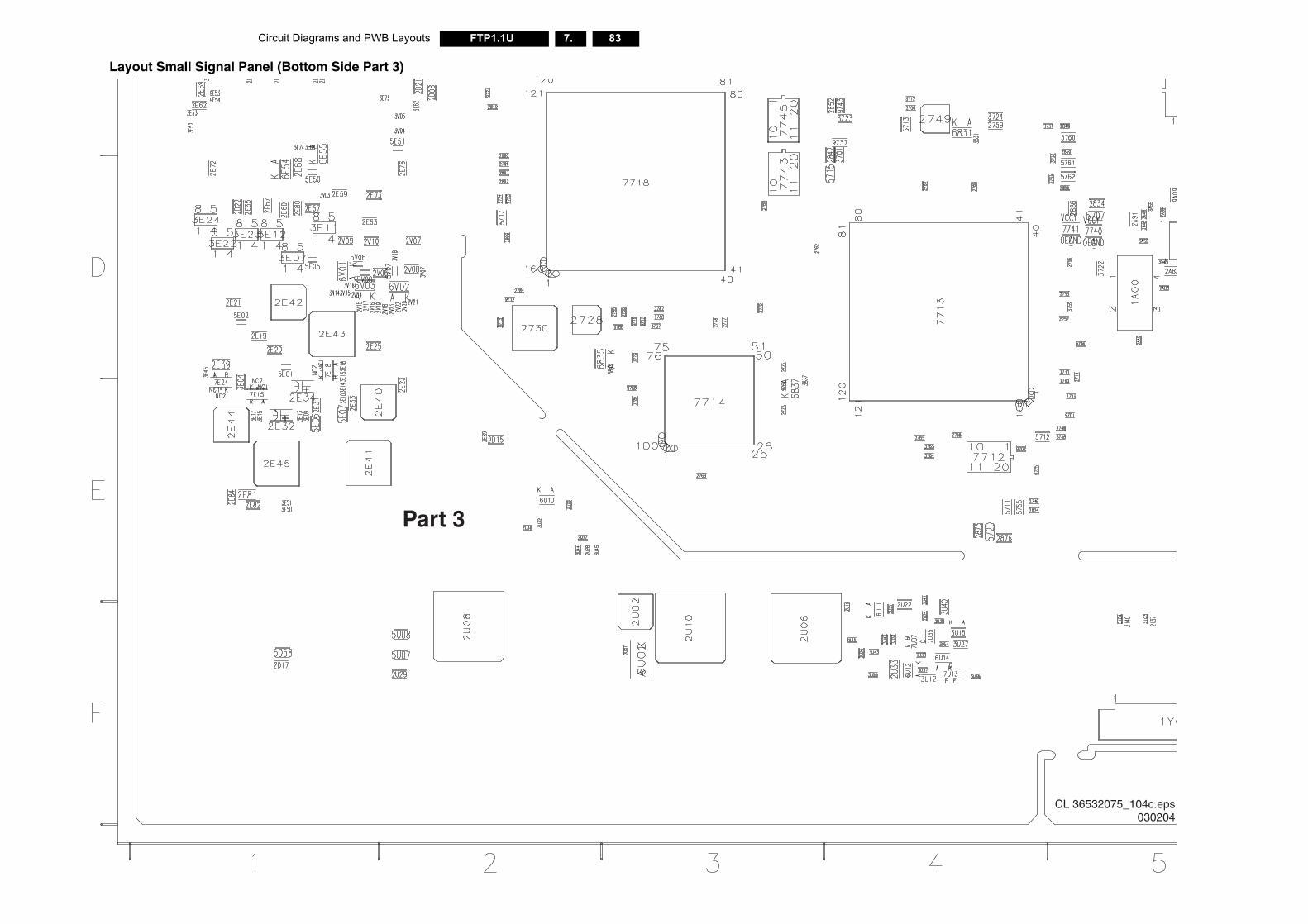
Circuit Diagrams and PWB Layouts 83FTP1.1U 7.
CL 36532075_104c.eps030204
Layout Small Signal Panel (Bottom Side Part 3)
Part 3
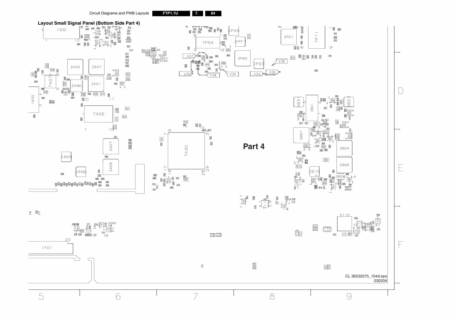
84FTP1.1U 7.Circuit Diagrams and PWB Layouts
CL 36532075_104d.eps030204
Layout Small Signal Panel (Bottom Side Part 4)
Part 4
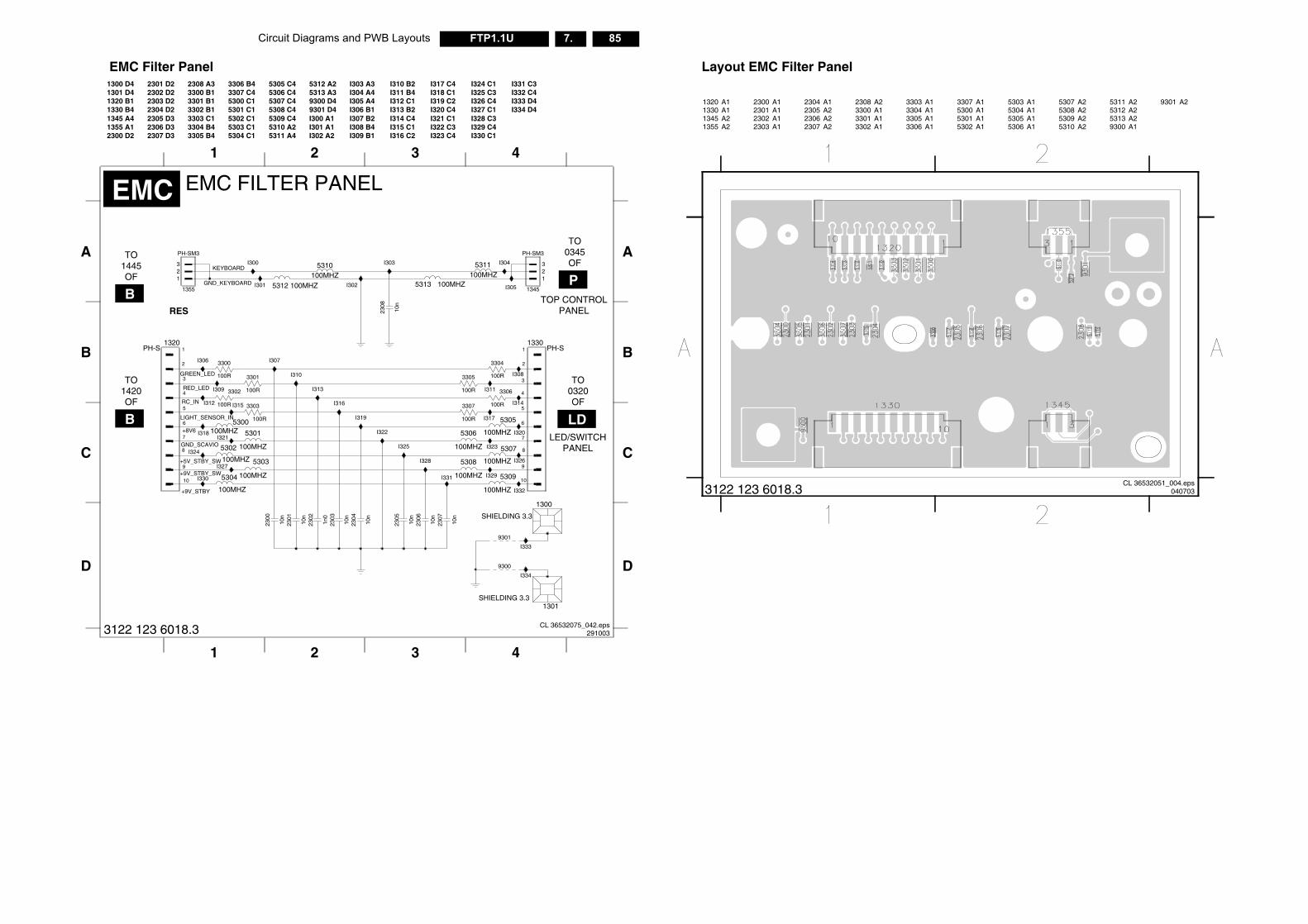
Circuit Diagrams and PWB Layouts 85FTP1.1U 7.
1 2 3 4
CL 36532051_004.eps040703
3303 A13304 A13305 A13306 A1
3307 A15300 A15301 A15302 A1
5303 A15304 A15305 A15306 A1
5307 A25308 A25309 A25310 A2
5311 A25312 A25313 A29300 A1
9301 A2
EMC Filter Panel
TO1420OF
B
TO1445OF
B
TO0345OF
P
LED/SWITCHPANEL
TOP CONTROLPANEL
TO0320OF
LD
1 2 3 4
C
D
A
B
C
D
A
B
10n
2300
1n0
2302
3307
100R
100R
3306
3305
100R
9301
100R
3304
9300
3300
100R
100R
3301
3302
100R
1355
PH-SM3
123
100R
3303
123
PH-SM3
1345
10n
2303
5313 100MHZ
5310100MHZ
100MHZ5312
5309
100MHZ
100MHZ5311
100MHZ
5308
1
10
2
3
4
5
6
7
8
9I328
1320PH-S
I330 I331
I332
I329
I323
I326
I317
I320
I314
I311
I310 I308
I316
I313
I319
I322
I327
I325I324
I318I321
I312 I315
I307
I309
I305
I306
I302
I304
I301
I303I300
2304
10n
2301
10n
1
10
2
3
4
5
6
7
8
9
1301SHIELDING 3.3
PH-S1330
5307
100MHZ
5305
100MHZ
100MHZ
5306
5303
100MHZ
100MHZ
5304
100MHZ
5302
5301
100MHZ
2308
10n
100MHZ5300
2307
2306
10n
10n SHIELDING 3.3
1300
10n
2305
I333
I334
LIGHT_SENSOR_IN
GND_KEYBOARD
KEYBOARD
+9V_STBY
RED_LED
RC_IN
+8V6
GND_SCAVIO
+5V_STBY_SW
+9V_STBY_SW
GREEN_LED
3122 123 6018.3 CL 36532075_042.eps291003
RES
EMC EMC FILTER PANEL
I311 B4I312 C1I313 B2I314 C4I315 C1I316 C2
I317 C4I318 C1
I321 C1I322 C3I323 C4
I324 C1I325 C3I326 C4I327 C1I328 C3I329 C4I330 C1
I331 C3I332 C4I333 D4I334 D4
5311 A4
5312 A25313 A39300 D49301 D4I300 A1I301 A1I302 A2
I303 A3I304 A4I305 A4I306 B1I307 B2I308 B4I309 B1
I310 B2
2300 D2
2301 D22302 D22303 D22304 D22305 D32306 D32307 D3
I319 C2I320 C4
5303 C15304 C1
5305 C45306 C45307 C45308 C45309 C45310 A2
1300 D41301 D41320 B11330 B41345 A41355 A1
2308 A33300 B13301 B13302 B13303 C13304 B43305 B4
3306 B43307 C45300 C15301 C15302 C1
Layout EMC Filter Panel
3122 123 6018.3
1320 A11330 A11345 A21355 A2
2300 A12301 A12302 A12303 A1
2304 A12305 A22306 A22307 A2
2308 A23300 A13301 A13302 A1
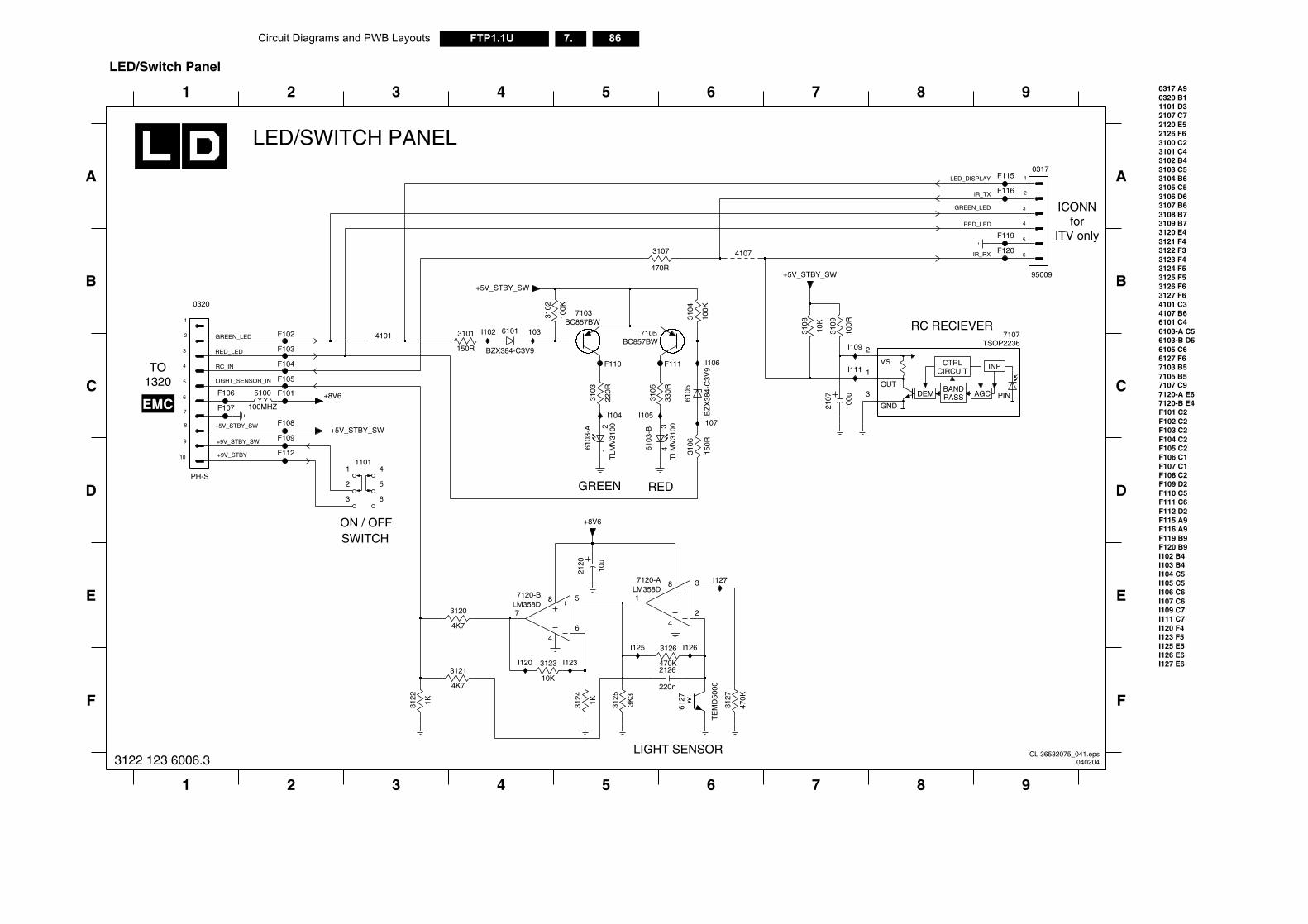
86FTP1.1U 7.Circuit Diagrams and PWB Layouts
DEMBANDPASS
CTRLCIRCUIT
AGC
INP
PIN
F106 C1F107 C1F108 C2F109 D2F110 C5F111 C6F112 D2F115 A9F116 A9F119 B9F120 B9I102 B4
8 9
A
B
C
D
ICONNfor
ITV only
RC RECIEVER
6105 C66127 F67103 B57105 B57107 C97120-A E67120-B E4F101 C2F102 C2F103 C2F104 C2F105 C2
3107 B63108 B73109 B73120 E43121 F43122 F33123 F43124 F53125 F53126 F63127 F64101 C34107 B66101 C46103-A C56103-B D5
8 9
I103 B4I104 C5I105 C5I106 C6I107 C6I109 C7I111 C7I120 F4I123 F5I125 E5I126 E6I127 E6
E
F
0317 A90320 B11101 D32107 C72120 E52126 F63100 C23101 C43102 B43103 C53104 B63105 C53106 D6
F120
F115
F116
F119
TSOP22367107
1
2
3
4
5
6
0317
95009
3126I125 I126
IR_RX
RED_LED
GREEN_LED
IR_TX
LED_DISPLAY
CL 36532075_041.eps040204
4 5 6 7
F
LIGHT SENSOR
1 2 3
3127
470K
3122
1K
I120 I1232126
220n
1K3124
6127
TE
MD
5000
470K3121
4K7
3123
10K
3125
3K3
3122 123 6006.3
LED/Switch Panel
TO1320
EMC
A
B
D
E
C
GREEN
SWITCH
RED
ON / OFF
LED/SWITCH PANEL
1 2 3 4 5 6 7
F106
6105
BZ
X38
4-C
3V9
F107
3101
150R
F110
F112
8
4
7120-ALM358D
3
2
1
I127
+5V_STBY_SW
I103I102
2120
10u
100K
3102
I111I106
100R
3109
3106
150R
BC857BW
+8V6
BC857BW
7105
7120-BLM358D
5
6
7
8
4
7103
GND
3
1
OUT
2
VS
2 5
1 4
3 6
4101
1101
F105
1
10
2
3
4
5
6
7
8
9
PH-S
0320
I104
+8V6
+5V_STBY_SW
3103
220R
I109
3105
330R
F111
100u
2107
F103
F104
3120
4K7
100MHZ
5100 F101
F108
F109
I105
4107
100K
3104
I107
+5V_STBY_SW
3108
10K
F102
TLM
V31
00
6103
-B
34
TLM
V31
00
6103
-A
21
BZX384-C3V9
6101
3107
470R
RC_IN
RED_LED
GREEN_LED
LIGHT_SENSOR_IN
+5V_STBY_SW
+9V_STBY
+9V_STBY_SW
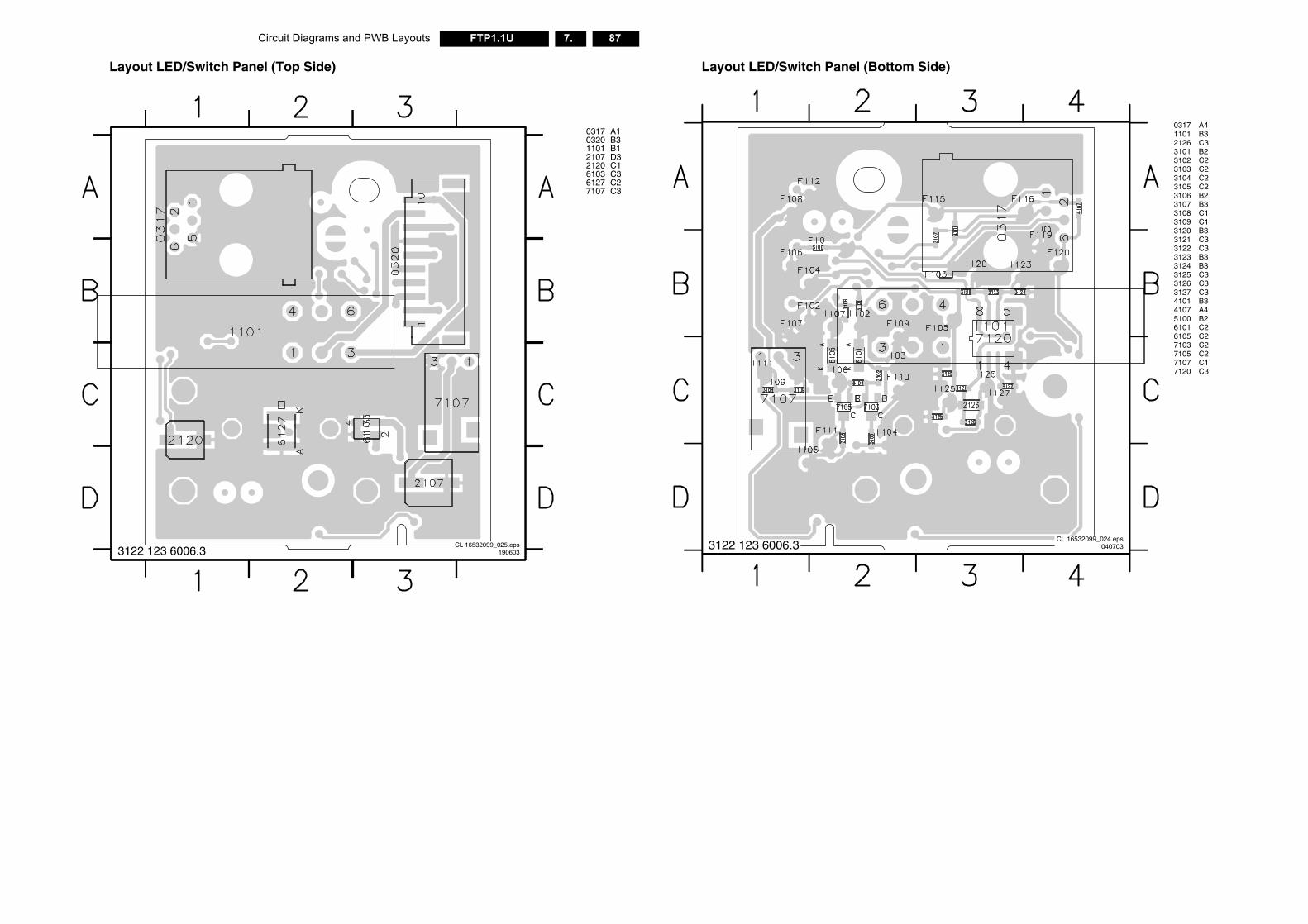
Circuit Diagrams and PWB Layouts 87FTP1.1U 7.
m Side)
0317 A41101 B32126 C33101 B23102 C23103 C23104 C23105 C23106 B23107 B33108 C13109 C13120 B33121 C33122 C33123 B33124 B33125 C33126 C33127 C34101 B34107 A45100 B26101 C26105 C27103 C27105 C27107 C17120 C3
CL 16532099_024.eps040703
Layout LED/Switch Panel (Top Side)
CL 16532099_025.eps190603
0317 A10320 B31101 B12107 D32120 C16103 C36127 C27107 C3
3122 123 6006.3
Layout LED/Switch Panel (Botto
3122 123 6006.3
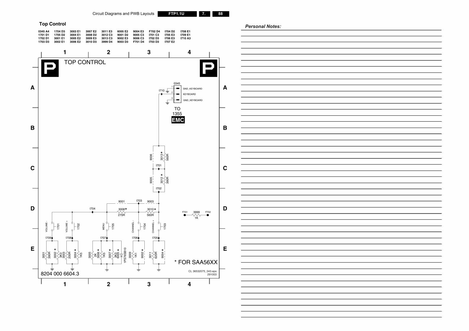
88FTP1.1U 7.Circuit Diagrams and PWB Layouts
V CC
E
1 2 3 4
E
1K5
3004
*
* FOR SAA56XX
200R
3003
I709 I707I708 I706 I705
390R
3001
3K3
3002
*
9004
620R
3011
9002
* *
1K1
3009
3007
3K3
6005
1PS
76S
B10**
3006
1K5 *
2K3005
8204 000 6604.3CL 36532075_043.eps
291003
Top Control
1355TO
EMC
C
D
0345 A41701 D11702 D11703 D3
1704 D31705 D23001 E13002 E1
3003 E13004 E13005 E23006 E2
3007 E23008 D23009 E33010 D3
3011 E33012 C33013 C33999 D4
GND_KEYBOARD
KEYBOARD
1 2 3 4
A
B
C
D
A
B
TOP CONTROL
6005 E29001 D29002 E39003 D3
9004 E39005 C39006 C3F701 D4
F702 D4I701 C3I702 D3I703 D3
I704 D2I705 E3I706 E3I707 E2
I708 E1I709 E1I710 A3
GND_KEYBOARD
1702
F702
OLU
ME
+
1K
3999F701
I710
I704
I703
I701
I702
VO
LUM
E -
1705
ME
NU
1701
03451
2
3
*
*30
13
560R
9006
3012
390R
9005
9003
560R
3010*270R
3008*
9001
HA
NN
EL
+
HA
NN
EL
-
1704
1703
Personal Notes:
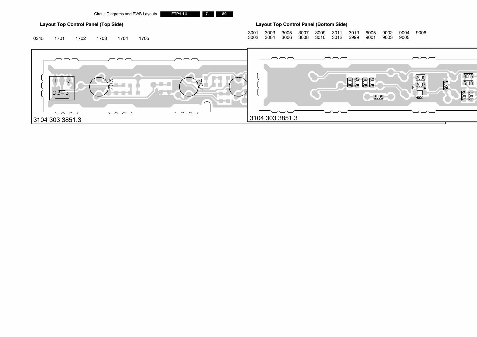
Circuit Diagrams and PWB Layouts 89FTP1.1U 7.
CL 36532053_036.eps180703
m Side)
30113012
30133999
60059001
90029003
90049005
9006
Layout Top Control Panel (Top Side)
3104 303 3851.3
0345 1701 1702 1703 1704 1705
Layout Top Control Panel (Botto
3104 303 3851.3
30013002
30033004
30053006
30073008
30093010
90FTP1.1U 7.Circuit Diagrams and PWB Layouts
Personal Notes:
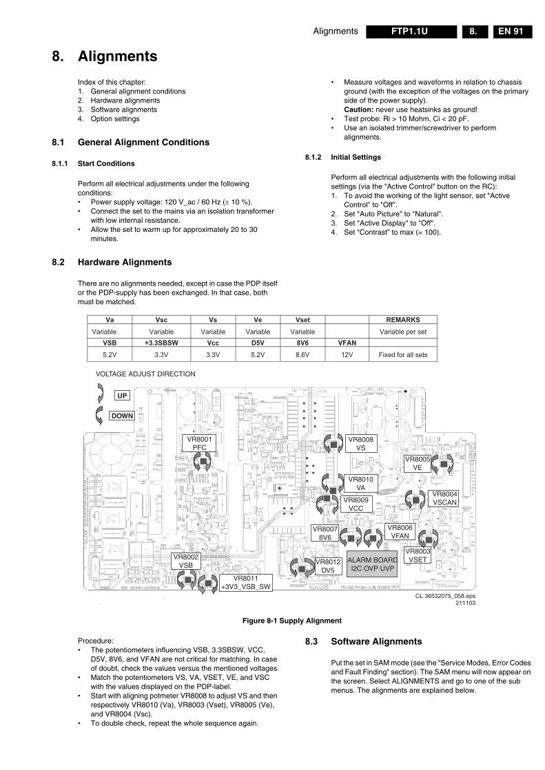
Alignments EN 91FTP1.1U 8.
8. Alignments
Index of this chapter:1. General alignment conditions2. Hardware alignments3. Software alignments4. Option settings
8.1 General Alignment Conditions
8.1.1 Start Conditions
Perform all electrical adjustments under the following conditions:• Power supply voltage: 120 V_ac / 60 Hz (± 10 %). • Connect the set to the mains via an isolation transformer
with low internal resistance.• Allow the set to warm up for approximately 20 to 30
minutes.
• Measure voltages and waveforms in relation to chassis ground (with the exception of the voltages on the primary side of the power supply). Caution: never use heatsinks as ground!
• Test probe: Ri > 10 Mohm, Ci < 20 pF.• Use an isolated trimmer/screwdriver to perform
alignments.
8.1.2 Initial Settings
Perform all electrical adjustments with the following initial settings (via the "Active Control" button on the RC):1. To avoid the working of the light sensor, set "Active
Control" to "Off".2. Set "Auto Picture" to "Natural".3. Set "Active Display" to "Off".4. Set “Contrast” to max (= 100).
8.2 Hardware Alignments
There are no alignments needed, except in case the PDP itself or the PDP-supply has been exchanged. In that case, both must be matched.
Figure 8-1 Supply Alignment
Procedure:• The potentiometers influencing VSB, 3.3SBSW, VCC,
D5V, 8V6, and VFAN are not critical for matching. In case of doubt, check the values versus the mentioned voltages.
• Match the potentiometers VS, VA, VSET, VE, and VSC with the values displayed on the PDP-label.
• Start with aligning potmeter VR8008 to adjust VS and then respectively VR8010 (Va), VR8003 (Vset), VR8005 (Ve), and VR8004 (Vsc).
• To double check, repeat the whole sequence again.
8.3 Software Alignments
Put the set in SAM mode (see the "Service Modes, Error Codes and Fault Finding" section). The SAM menu will now appear on the screen. Select ALIGNMENTS and go to one of the sub menus. The alignments are explained below.
UP
DOWN
VR8001PFC
VR8002VSB
VR8009VCC
VR8004VSCAN
VR8003VSET
VR8006VFAN
VR8010VA
VR8008VS
VR8012DV5
VR8005VE
VR80078V6
VOLTAGE ADJUST DIRECTION
ALARM BOARDI2C OVP UVP
VR8011+3V3_VSB_SW
CL 36532075_058.eps211103
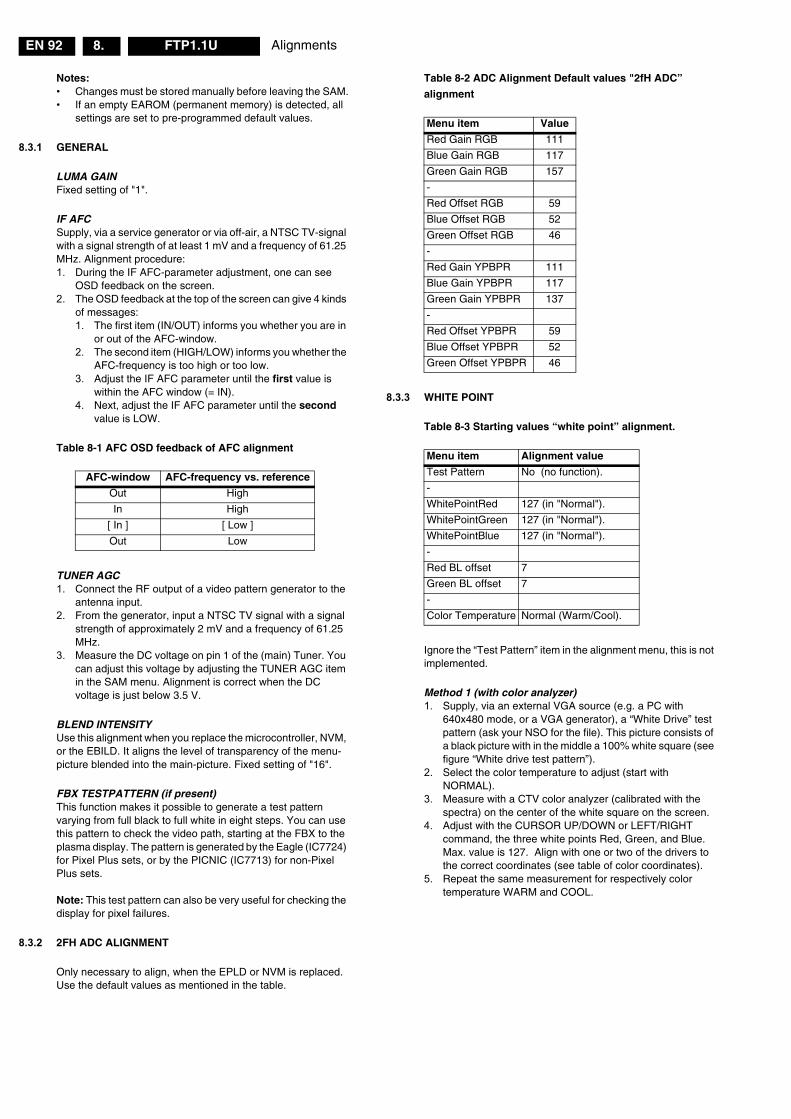
AlignmentsEN 92 FTP1.1U8.
Notes:• Changes must be stored manually before leaving the SAM.• If an empty EAROM (permanent memory) is detected, all
settings are set to pre-programmed default values.
8.3.1 GENERAL
LUMA GAINFixed setting of "1".
IF AFCSupply, via a service generator or via off-air, a NTSC TV-signal with a signal strength of at least 1 mV and a frequency of 61.25 MHz. Alignment procedure:1. During the IF AFC-parameter adjustment, one can see
OSD feedback on the screen.2. The OSD feedback at the top of the screen can give 4 kinds
of messages:1. The first item (IN/OUT) informs you whether you are in
or out of the AFC-window.2. The second item (HIGH/LOW) informs you whether the
AFC-frequency is too high or too low.3. Adjust the IF AFC parameter until the first value is
within the AFC window (= IN).4. Next, adjust the IF AFC parameter until the second
value is LOW.
Table 8-1 AFC OSD feedback of AFC alignment
TUNER AGC1. Connect the RF output of a video pattern generator to the
antenna input.2. From the generator, input a NTSC TV signal with a signal
strength of approximately 2 mV and a frequency of 61.25 MHz.
3. Measure the DC voltage on pin 1 of the (main) Tuner. You can adjust this voltage by adjusting the TUNER AGC item in the SAM menu. Alignment is correct when the DC voltage is just below 3.5 V.
BLEND INTENSITYUse this alignment when you replace the microcontroller, NVM, or the EBILD. It aligns the level of transparency of the menu-picture blended into the main-picture. Fixed setting of "16".
FBX TESTPATTERN (if present)This function makes it possible to generate a test pattern varying from full black to full white in eight steps. You can use this pattern to check the video path, starting at the FBX to the plasma display. The pattern is generated by the Eagle (IC7724) for Pixel Plus sets, or by the PICNIC (IC7713) for non-Pixel Plus sets. Note: This test pattern can also be very useful for checking the display for pixel failures.
8.3.2 2FH ADC ALIGNMENT
Only necessary to align, when the EPLD or NVM is replaced. Use the default values as mentioned in the table.
Table 8-2 ADC Alignment Default values "2fH ADC”
alignment
8.3.3 WHITE POINT
Table 8-3 Starting values “white point” alignment.
Ignore the “Test Pattern” item in the alignment menu, this is not implemented.
Method 1 (with color analyzer)1. Supply, via an external VGA source (e.g. a PC with
640x480 mode, or a VGA generator), a “White Drive” test pattern (ask your NSO for the file). This picture consists of a black picture with in the middle a 100% white square (see figure “White drive test pattern”).
2. Select the color temperature to adjust (start with NORMAL).
3. Measure with a CTV color analyzer (calibrated with the spectra) on the center of the white square on the screen.
4. Adjust with the CURSOR UP/DOWN or LEFT/RIGHT command, the three white points Red, Green, and Blue. Max. value is 127. Align with one or two of the drivers to the correct coordinates (see table of color coordinates).
5. Repeat the same measurement for respectively color temperature WARM and COOL.
AFC-window AFC-frequency vs. reference
Out High
In High
[ In ] [ Low ]
Out Low
Menu item Value
Red Gain RGB 111
Blue Gain RGB 117
Green Gain RGB 157
-
Red Offset RGB 59
Blue Offset RGB 52
Green Offset RGB 46
-
Red Gain YPBPR 111
Blue Gain YPBPR 117
Green Gain YPBPR 137
-
Red Offset YPBPR 59
Blue Offset YPBPR 52
Green Offset YPBPR 46
Menu item Alignment value
Test Pattern No (no function).
-
WhitePointRed 127 (in "Normal").
WhitePointGreen 127 (in "Normal").
WhitePointBlue 127 (in "Normal").
-
Red BL offset 7
Green BL offset 7
-
Color Temperature Normal (Warm/Cool).
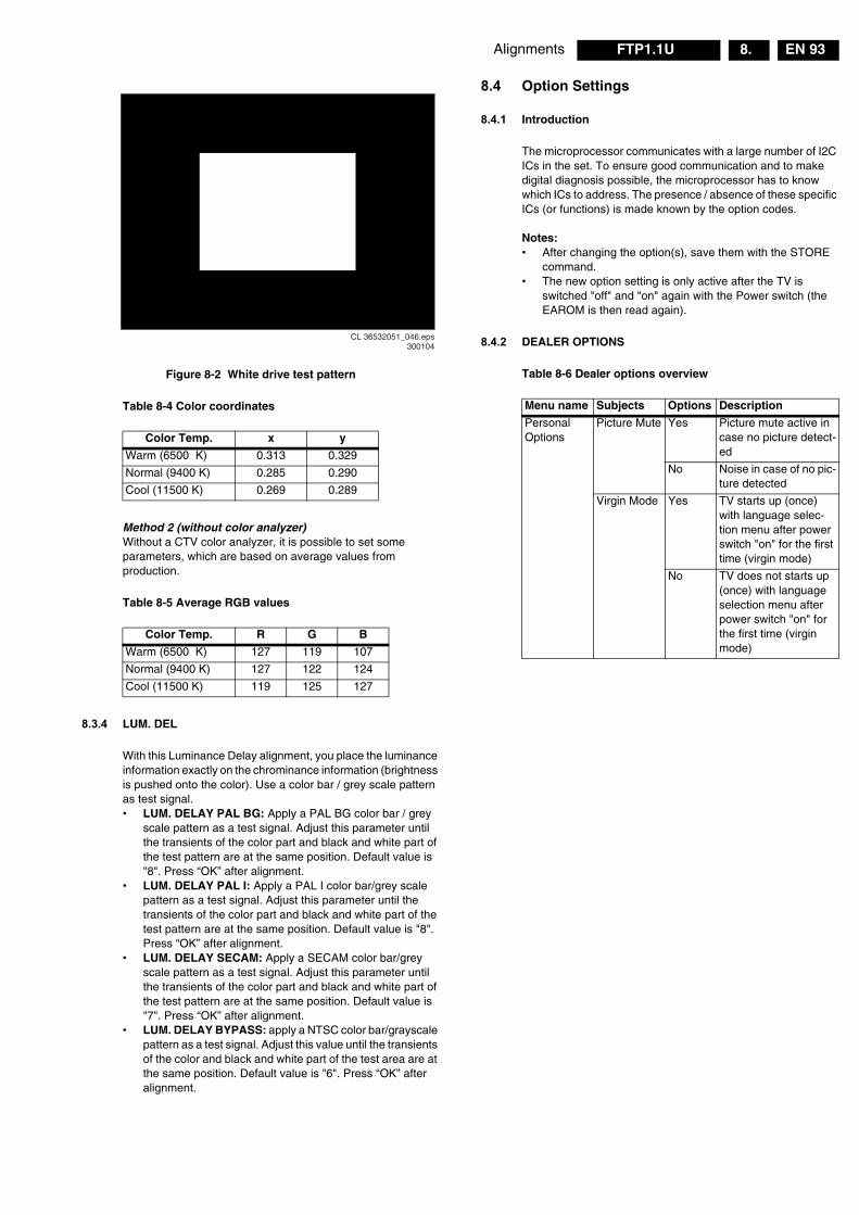
Alignments EN 93FTP1.1U 8.
Figure 8-2 White drive test pattern
Table 8-4 Color coordinates
Method 2 (without color analyzer)Without a CTV color analyzer, it is possible to set some parameters, which are based on average values from production.
Table 8-5 Average RGB values
8.3.4 LUM. DEL
With this Luminance Delay alignment, you place the luminance information exactly on the chrominance information (brightness is pushed onto the color). Use a color bar / grey scale pattern as test signal.• LUM. DELAY PAL BG: Apply a PAL BG color bar / grey
scale pattern as a test signal. Adjust this parameter until the transients of the color part and black and white part of the test pattern are at the same position. Default value is "8". Press “OK” after alignment.
• LUM. DELAY PAL I: Apply a PAL I color bar/grey scale pattern as a test signal. Adjust this parameter until the transients of the color part and black and white part of the test pattern are at the same position. Default value is "8". Press “OK” after alignment.
• LUM. DELAY SECAM: Apply a SECAM color bar/grey scale pattern as a test signal. Adjust this parameter until the transients of the color part and black and white part of the test pattern are at the same position. Default value is "7". Press “OK” after alignment.
• LUM. DELAY BYPASS: apply a NTSC color bar/grayscale pattern as a test signal. Adjust this value until the transients of the color and black and white part of the test area are at the same position. Default value is "6". Press “OK” after alignment.
8.4 Option Settings
8.4.1 Introduction
The microprocessor communicates with a large number of I2C ICs in the set. To ensure good communication and to make digital diagnosis possible, the microprocessor has to know which ICs to address. The presence / absence of these specific ICs (or functions) is made known by the option codes. Notes: • After changing the option(s), save them with the STORE
command.• The new option setting is only active after the TV is
switched "off" and "on" again with the Power switch (the EAROM is then read again).
8.4.2 DEALER OPTIONS
Table 8-6 Dealer options overview
Color Temp. x y
Warm (6500 K) 0.313 0.329
Normal (9400 K) 0.285 0.290
Cool (11500 K) 0.269 0.289
Color Temp. R G B
Warm (6500 K) 127 119 107
Normal (9400 K) 127 122 124
Cool (11500 K) 119 125 127
CL 36532051_046.eps300104
Menu name Subjects Options Description
Personal Options
Picture Mute Yes Picture mute active in case no picture detect-ed
No Noise in case of no pic-ture detected
Virgin Mode Yes TV starts up (once) with language selec-tion menu after power switch "on" for the first time (virgin mode)
No TV does not starts up (once) with language selection menu after power switch "on" for the first time (virgin mode)
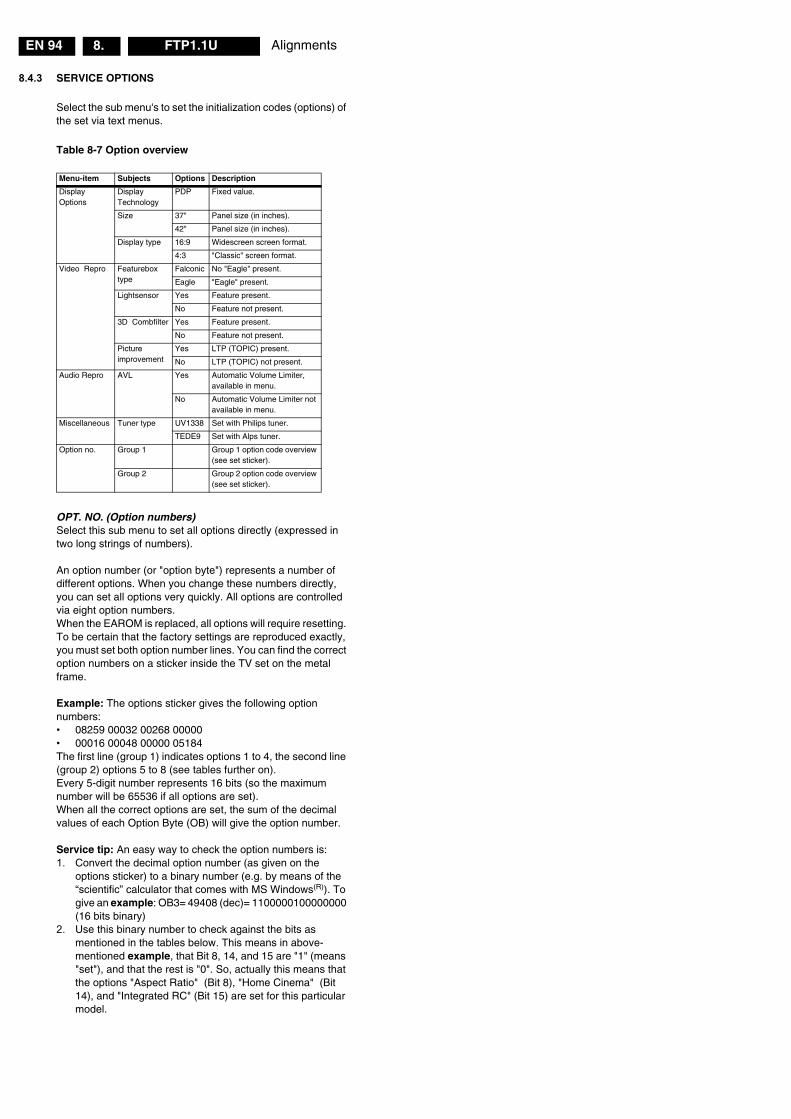
AlignmentsEN 94 FTP1.1U8.
8.4.3 SERVICE OPTIONS
Select the sub menu's to set the initialization codes (options) of the set via text menus.
Table 8-7 Option overview
OPT. NO. (Option numbers)Select this sub menu to set all options directly (expressed in two long strings of numbers). An option number (or "option byte") represents a number of different options. When you change these numbers directly, you can set all options very quickly. All options are controlled via eight option numbers.When the EAROM is replaced, all options will require resetting. To be certain that the factory settings are reproduced exactly, you must set both option number lines. You can find the correct option numbers on a sticker inside the TV set on the metal frame. Example: The options sticker gives the following option numbers:• 08259 00032 00268 00000• 00016 00048 00000 05184The first line (group 1) indicates options 1 to 4, the second line (group 2) options 5 to 8 (see tables further on).Every 5-digit number represents 16 bits (so the maximum number will be 65536 if all options are set).When all the correct options are set, the sum of the decimal values of each Option Byte (OB) will give the option number. Service tip: An easy way to check the option numbers is:1. Convert the decimal option number (as given on the
options sticker) to a binary number (e.g. by means of the “scientific” calculator that comes with MS Windows(R)). To give an example: OB3= 49408 (dec)= 1100000100000000 (16 bits binary)
2. Use this binary number to check against the bits as mentioned in the tables below. This means in above-mentioned example, that Bit 8, 14, and 15 are "1" (means "set"), and that the rest is "0". So, actually this means that the options "Aspect Ratio" (Bit 8), "Home Cinema" (Bit 14), and "Integrated RC" (Bit 15) are set for this particular model.
Menu-item Subjects Options Description
Display Options
Display Technology
PDP Fixed value.
Size 37" Panel size (in inches).
42" Panel size (in inches).
Display type 16:9 Widescreen screen format.
4:3 "Classic" screen format.
Video Repro Featurebox type
Falconic No "Eagle" present.
Eagle "Eagle" present.
Lightsensor Yes Feature present.
No Feature not present.
3D Combfilter Yes Feature present.
No Feature not present.
Picture improvement
Yes LTP (TOPIC) present.
No LTP (TOPIC) not present.
Audio Repro AVL Yes Automatic Volume Limiter, available in menu.
No Automatic Volume Limiter not available in menu.
Miscellaneous Tuner type UV1338 Set with Philips tuner.
TEDE9 Set with Alps tuner.
Option no. Group 1 Group 1 option code overview (see set sticker).
Group 2 Group 2 option code overview (see set sticker).
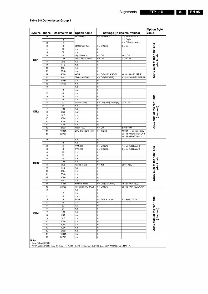
Alignments EN 95FTP1.1U 8.
Table 8-8 Option bytes Group 1
Byte nr. Bit nr. Decimal value Option name Settings (in decimal values)Option Byte value
OB1
0 1 Featurebox 0 = None (n.a.) 2 = Prozonic (n.a.)3 = Eagle4 = Falconic (n.a.)
OB
1= s
um
of
the
"on
" b
its
(dec
imal
)
1 2
2 4
3 8 2D Comb Filter 0 = Off (US) 8 = On
4 16 n.a. 0
5 32 n.a. 0
6 64 Light Sensor 0 = Off 64 = On
7 128 Luma Trans. Proc. 0 = Off 128 = On
8 256 n.a. 0
9 512 n.a. 0
10 1024 n.a. 0
11 2048 n.a. 0
12 4096 WSS 0 = Off (US/LA/AP-N) 4096 = On (EU/AP-P)
13 8192 3D Comb Filter 0 = Off (EU/AP-P) 8192 = On (US/LA/AP-N)
14 16384 n.a. 0
15 32768 n.a. 0
OB2
0 1 n.a. 0
OB
2= s
um
of
the
"on
" b
its
(dec
imal
)
1 2 n.a. 0
2 4 n.a. 0
3 8 n.a. 0
4 16 n.a. 0
5 32 Virtual Dolby 0 = Off (Dolby prologic) 32 = On
6 64 n.a. 0
7 128 n.a. 0
8 256 n.a. 0
9 512 n.a. 0
10 1024 n.a. 0
11 2048 n.a. 0
12 4096 n.a. 0
13 8192 Flash RAM 0 = Off 8192 = On
14 16384 EPG Type (EU only) 0 = Type2 16384 = Textguide only32768 = NextTView 2C349152 = NexTView 2
15 32768
OB3
0 1 n.a. 0
OB
3= s
um
of
the
"on
" b
its
(dec
imal
)
1 2 n.a. 0
2 4 AV4 2fH 0 = Off (EU) 4 = On (US/LA/AP)
3 8 AV3 2fH 0 = Off (EU) 8 = On (US/LA/AP)
4 16 n.a. 0
5 32 n.a. 0
6 64 n.a. 0
7 128 n.a. 0
8 256 Aspect Ratio 0 = 4:3 256 = 16:9
9 512 n.a. 0
10 1024 n.a. 0
11 2048 n.a. 0
12 4096 n.a. 0
13 8192 n.a. 0
14 16384 Home Cinema 0 = Off (US/LA/AP) 16384 = On (EU)
15 32768 Integrated RC (P50) 0 = Off (US) 32768 = On (EU/LA/AP)
OB4
0 1 n.a. 0
OB
4= s
um
of
the
"on
" b
its
(dec
imal
)
1 2 n.a. 0
2 4 n.a. 0
3 8 Tuner 0 = Philips UV316 8 = Alps TEDE9
4 16 n.a. 0
5 32 n.a. 0
6 64 n.a. 0
7 128 n.a. 0
8 256 n.a. 0
9 512 n.a. 0
10 1024 n.a. 0
11 2048 n.a. 0
12 4096 n.a. 0
13 8192 n.a. 0
14 16384 n.a. 0
15 32768 n.a. 0
Notes:- n.a.= not applicable.- AP-P= Asian Pacific PAL-multi, AP-N= Asian Pacific NTSC, EU= Europe, LA= Latin America, US= NAFTA.
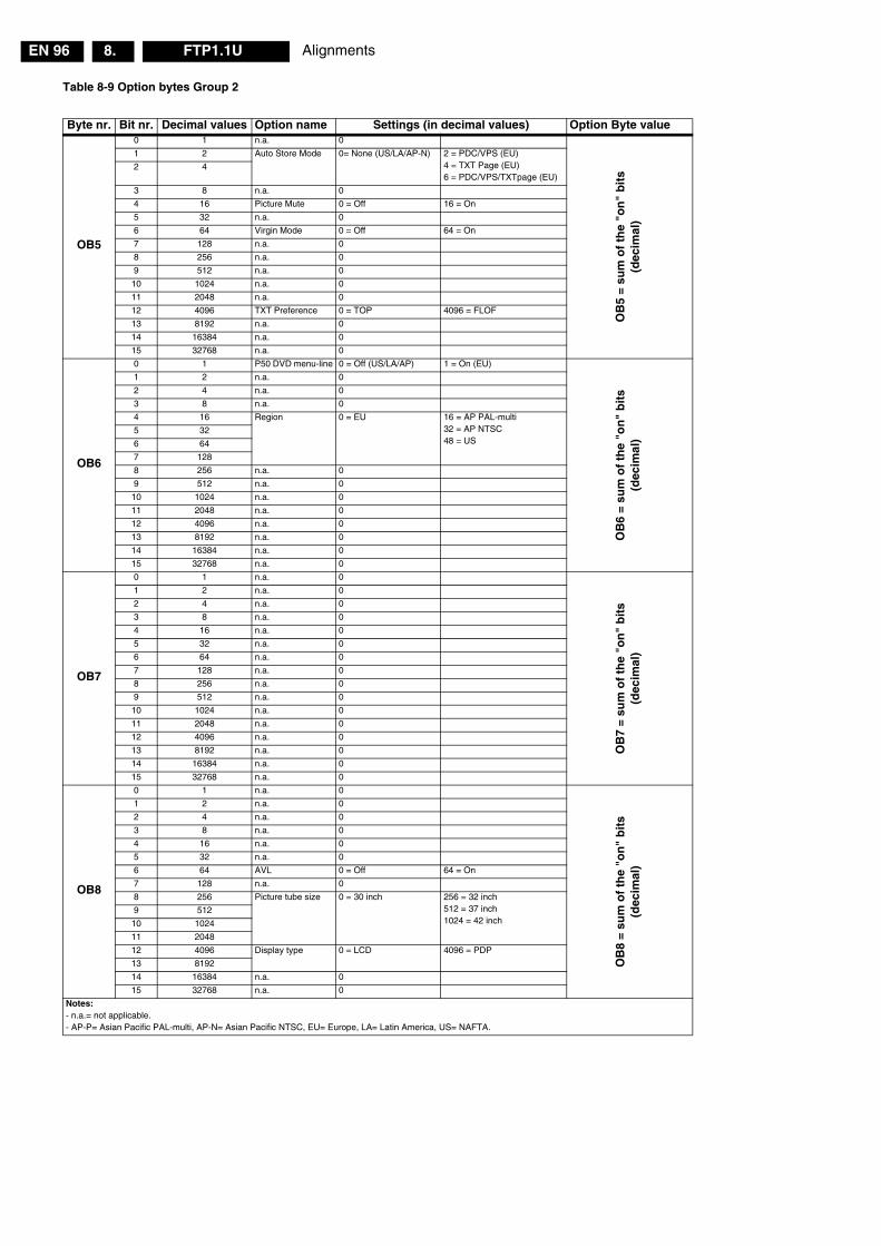
AlignmentsEN 96 FTP1.1U8.
Table 8-9 Option bytes Group 2
Byte nr. Bit nr. Decimal values Option name Settings (in decimal values) Option Byte value
OB5
0 1 n.a. 0
OB
5 =
sum
of
the
"on
" b
its
(dec
imal
)
1 2 Auto Store Mode 0= None (US/LA/AP-N) 2 = PDC/VPS (EU)4 = TXT Page (EU)6 = PDC/VPS/TXTpage (EU)
2 4
3 8 n.a. 0
4 16 Picture Mute 0 = Off 16 = On
5 32 n.a. 0
6 64 Virgin Mode 0 = Off 64 = On
7 128 n.a. 0
8 256 n.a. 0
9 512 n.a. 0
10 1024 n.a. 0
11 2048 n.a. 0
12 4096 TXT Preference 0 = TOP 4096 = FLOF
13 8192 n.a. 0
14 16384 n.a. 0
15 32768 n.a. 0
OB6
0 1 P50 DVD menu-line 0 = Off (US/LA/AP) 1 = On (EU)
OB
6 =
sum
of
the
"on
" b
its
(dec
imal
)
1 2 n.a. 0
2 4 n.a. 0
3 8 n.a. 0
4 16 Region 0 = EU 16 = AP PAL-multi 32 = AP NTSC 48 = US
5 32
6 64
7 128
8 256 n.a. 0
9 512 n.a. 0
10 1024 n.a. 0
11 2048 n.a. 0
12 4096 n.a. 0
13 8192 n.a. 0
14 16384 n.a. 0
15 32768 n.a. 0
OB7
0 1 n.a. 0
OB
7 =
sum
of
the
"on
" b
its
(dec
imal
)
1 2 n.a. 0
2 4 n.a. 0
3 8 n.a. 0
4 16 n.a. 0
5 32 n.a. 0
6 64 n.a. 0
7 128 n.a. 0
8 256 n.a. 0
9 512 n.a. 0
10 1024 n.a. 0
11 2048 n.a. 0
12 4096 n.a. 0
13 8192 n.a. 0
14 16384 n.a. 0
15 32768 n.a. 0
OB8
0 1 n.a. 0
OB
8 =
sum
of
the
"on
" b
its
(dec
imal
)
1 2 n.a. 0
2 4 n.a. 0
3 8 n.a. 0
4 16 n.a. 0
5 32 n.a. 0
6 64 AVL 0 = Off 64 = On
7 128 n.a. 0
8 256 Picture tube size 0 = 30 inch 256 = 32 inch512 = 37 inch1024 = 42 inch
9 512
10 1024
11 2048
12 4096 Display type 0 = LCD 4096 = PDP
13 8192
14 16384 n.a. 0
15 32768 n.a. 0
Notes:- n.a.= not applicable.- AP-P= Asian Pacific PAL-multi, AP-N= Asian Pacific NTSC, EU= Europe, LA= Latin America, US= NAFTA.
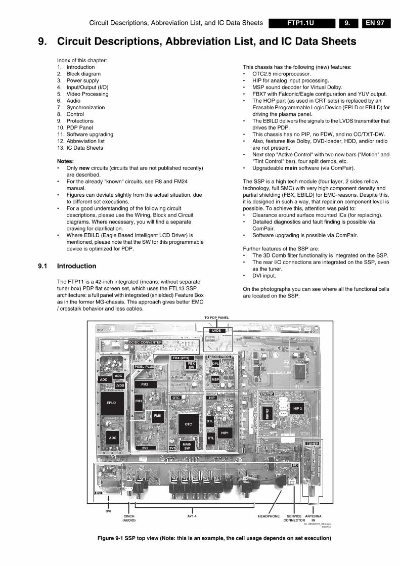
Circuit Descriptions, Abbreviation List, and IC Data Sheets EN 97FTP1.1U 9.
9. Circuit Descriptions, Abbreviation List, and IC Data Sheets
Index of this chapter:1. Introduction2. Block diagram3. Power supply4. Input/Output (I/O)5. Video Processing6. Audio7. Synchronization8. Control9. Protections10. PDP Panel11. Software upgrading12. Abbreviation list13. IC Data Sheets Notes: • Only new circuits (circuits that are not published recently)
are described. • For the already "known" circuits, see R8 and FM24
manual.• Figures can deviate slightly from the actual situation, due
to different set executions.• For a good understanding of the following circuit
descriptions, please use the Wiring, Block and Circuit diagrams. Where necessary, you will find a separate drawing for clarification.
• Where EBILD (Eagle Based Intelligent LCD Driver) is mentioned, please note that the SW for this programmable device is optimized for PDP.
9.1 Introduction
The FTP11 is a 42-inch integrated (means: without separate tuner box) PDP flat screen set, which uses the FTL13 SSP architecture: a full panel with integrated (shielded) Feature Box as in the former MG-chassis. This approach gives better EMC / crosstalk behavior and less cables.
This chassis has the following (new) features:• OTC2.5 microprocessor.• HIP for analog input processing.• MSP sound decoder for Virtual Dolby.• FBX7 with Falconic/Eagle configuration and YUV output.• The HOP part (as used in CRT sets) is replaced by an
Erasable Programmable Logic Device (EPLD or EBILD) for driving the plasma panel.
• The EBILD delivers the signals to the LVDS transmitter that drives the PDP.
• This chassis has no PIP, no FDW, and no CC/TXT-DW. • Also, features like Dolby, DVD-loader, HDD, and/or radio
are not present.• Next step "Active Control" with two new bars ("Motion" and
"Tint Control" bar), four split demos, etc.• Upgradeable main software (via ComPair). The SSP is a high tech module (four layer, 2 sides reflow technology, full SMC) with very high component density and partial shielding (FBX, EBILD) for EMC-reasons. Despite this, it is designed in such a way, that repair on component level is possible. To achieve this, attention was paid to:• Clearance around surface mounted ICs (for replacing).• Detailed diagnostics and fault finding is possible via
ComPair.• Software upgrading is possible via ComPair. Further features of the SSP are:• The 3D Comb filter functionality is integrated on the SSP.• The rear I/O connections are integrated on the SSP, even
as the tuner.• DVI input. On the photographs you can see where all the functional cells are located on the SSP:
Figure 9-1 SSP top view (Note: this is an example, the cell usage depends on set execution)
LVDS
2V5
PIXEL PLUS
FM5
I/O
FBX (2FH) AUDIO PROC.
OTC HIP
TUNER
XTL
HIP1
DW/PIP
OTC
MAINSW
DVI
CINCH(AUDIO)
SERVICECONNECTOR
HEADPHONE ANTENNAIN
CL 36532075_064.eps050204
TO PDP PANEL
DVI
ADC
3V3
FM3EPLD
FM2
DC/DC CONVERTER
ADC
LVDS
ADC
FBXSW
MSP
DPL
XTL
MUP
PET HIP 2
AV1-4
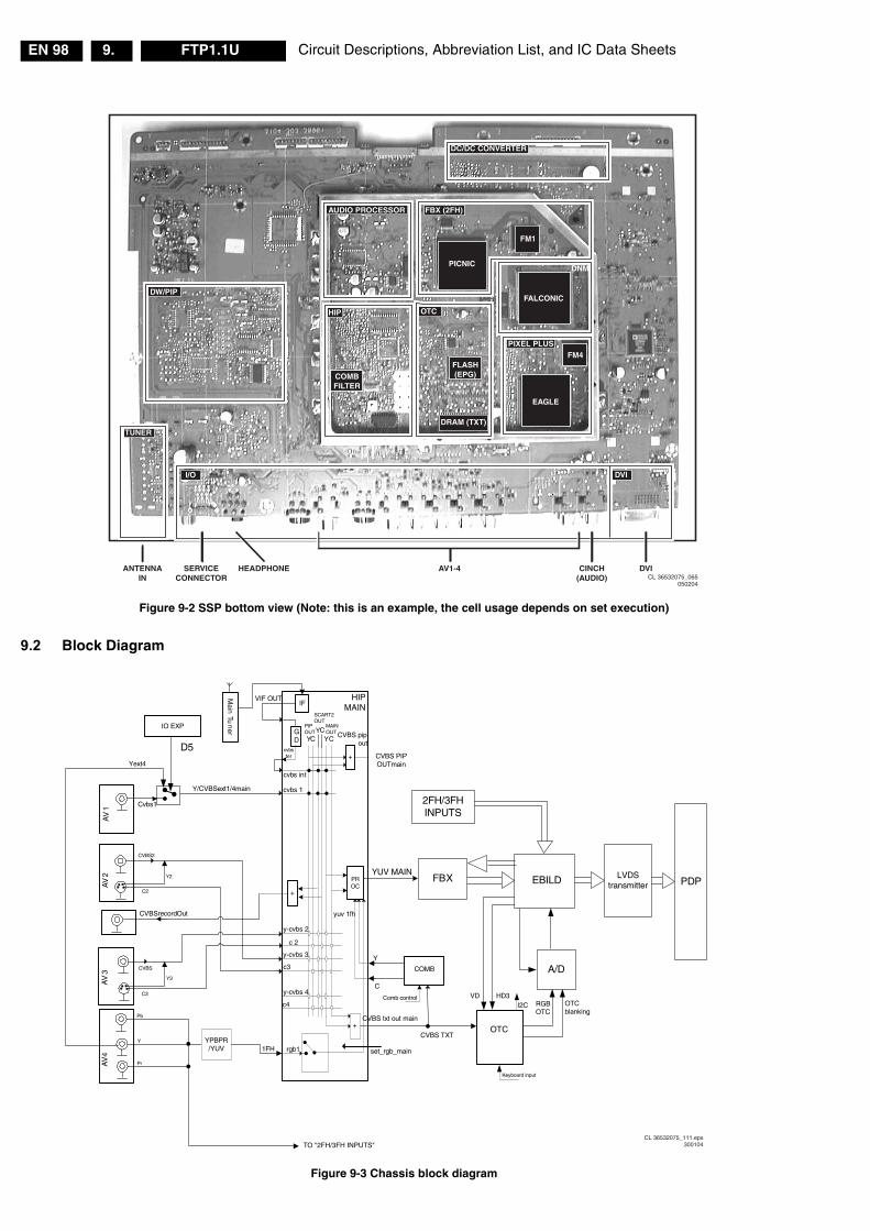
Circuit Descriptions, Abbreviation List, and IC Data SheetsEN 98 FTP1.1U9.
Figure 9-2 SSP bottom view (Note: this is an example, the cell usage depends on set execution)
9.2 Block Diagram
Figure 9-3 Chassis block diagram
DC/DC CONVERTER
DW/PIP
AUDIO PROCESSOR FBX (2FH)
HIP OTC
EAGLE
FM4
DRAM (TXT)
FLASH(EPG)COMB
FILTER
FALCONIC
PICNIC
FM1
PIXEL PLUS
DNM
I/O DVI
TUNER
CL 36532075_065050204
DVICINCH(AUDIO)
HEADPHONE AV1-4SERVICECONNECTOR
ANTENNAIN
+
+
PROC
IF
GD
+ CVBS txt out main
Y
cvbster
cvbs int
YY
YCC
CCVBS pip out
HIPMAIN
y-cvbs 3
c3
y-cvbs 4
c4
rgb1 set_rgb_main
VIF OUT
PIPOUT
SCART2OUT
MAINOUT
AV
3
cvbs 1
c 2
AV
1A
V2
COMB
yuv 1fh
Comb control
Keyboard input
I2C OTCblanking
RGBOTC
C
CVBSrecordOut
CVBS PIPOUTmain
CVBS TXT
Main
Tun
er
YUV MAIN
Cvbs1
PDP
A/D
VD HD3
EBILD
2FH/3FHINPUTS
FBX LVDStransmitter
OTC
CVBS2
CVBS
Y2
C2
AV
4
Y
Pb
Pr
TO "2FH/3FH INPUTS"
1FHYPBPR/YUV
D5
IO EXP
Yext4
Y/CVBSext1/4main
Y3
y-cvbs 2
C3
CL 36532075_111.eps300104
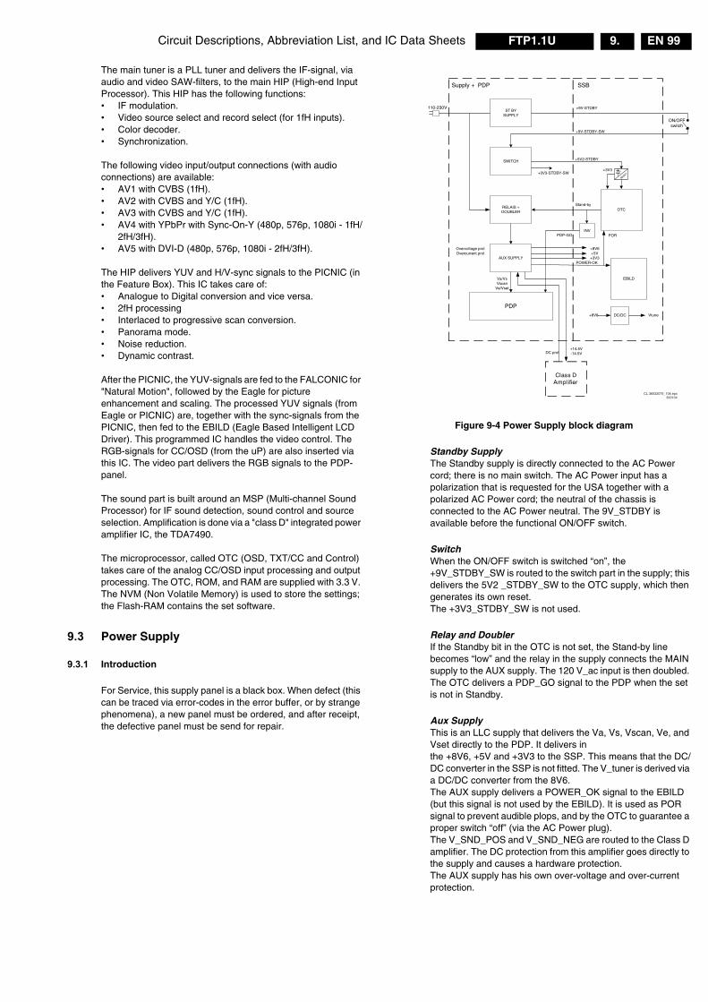
Circuit Descriptions, Abbreviation List, and IC Data Sheets EN 99FTP1.1U 9.
The main tuner is a PLL tuner and delivers the IF-signal, via audio and video SAW-filters, to the main HIP (High-end Input Processor). This HIP has the following functions:• IF modulation.• Video source select and record select (for 1fH inputs).• Color decoder.• Synchronization. The following video input/output connections (with audio connections) are available: • AV1 with CVBS (1fH).• AV2 with CVBS and Y/C (1fH).• AV3 with CVBS and Y/C (1fH).• AV4 with YPbPr with Sync-On-Y (480p, 576p, 1080i - 1fH/
2fH/3fH).• AV5 with DVI-D (480p, 576p, 1080i - 2fH/3fH). The HIP delivers YUV and H/V-sync signals to the PICNIC (in the Feature Box). This IC takes care of:• Analogue to Digital conversion and vice versa.• 2fH processing• Interlaced to progressive scan conversion.• Panorama mode.• Noise reduction.• Dynamic contrast. After the PICNIC, the YUV-signals are fed to the FALCONIC for "Natural Motion", followed by the Eagle for picture enhancement and scaling. The processed YUV signals (from Eagle or PICNIC) are, together with the sync-signals from the PICNIC, then fed to the EBILD (Eagle Based Intelligent LCD Driver). This programmed IC handles the video control. The RGB-signals for CC/OSD (from the uP) are also inserted via this IC. The video part delivers the RGB signals to the PDP-panel. The sound part is built around an MSP (Multi-channel Sound Processor) for IF sound detection, sound control and source selection. Amplification is done via a "class D" integrated power amplifier IC, the TDA7490. The microprocessor, called OTC (OSD, TXT/CC and Control) takes care of the analog CC/OSD input processing and output processing. The OTC, ROM, and RAM are supplied with 3.3 V. The NVM (Non Volatile Memory) is used to store the settings; the Flash-RAM contains the set software.
9.3 Power Supply
9.3.1 Introduction
For Service, this supply panel is a black box. When defect (this can be traced via error-codes in the error buffer, or by strange phenomena), a new panel must be ordered, and after receipt, the defective panel must be send for repair.
Figure 9-4 Power Supply block diagram
Standby SupplyThe Standby supply is directly connected to the AC Power cord; there is no main switch. The AC Power input has a polarization that is requested for the USA together with a polarized AC Power cord; the neutral of the chassis is connected to the AC Power neutral. The 9V_STDBY is available before the functional ON/OFF switch.
SwitchWhen the ON/OFF switch is switched “on”, the +9V_STDBY_SW is routed to the switch part in the supply; this delivers the 5V2 _STDBY_SW to the OTC supply, which then generates its own reset. The +3V3_STDBY_SW is not used.
Relay and DoublerIf the Standby bit in the OTC is not set, the Stand-by line becomes “low” and the relay in the supply connects the MAIN supply to the AUX supply. The 120 V_ac input is then doubled. The OTC delivers a PDP_GO signal to the PDP when the set is not in Standby.
Aux SupplyThis is an LLC supply that delivers the Va, Vs, Vscan, Ve, and Vset directly to the PDP. It delivers in the +8V6, +5V and +3V3 to the SSP. This means that the DC/DC converter in the SSP is not fitted. The V_tuner is derived via a DC/DC converter from the 8V6.The AUX supply delivers a POWER_OK signal to the EBILD (but this signal is not used by the EBILD). It is used as POR signal to prevent audible plops, and by the OTC to guarantee a proper switch “off” (via the AC Power plug).The V_SND_POS and V_SND_NEG are routed to the Class D amplifier. The DC protection from this amplifier goes directly to the supply and causes a hardware protection.The AUX supply has his own over-voltage and over-current protection.
ST BYSUPPLY
SWITCH
RELAIS +DOUBLER
AUX SUPPLY
PDP
ON/OFFswitch
+9V-STDBY
+9V-STDBY-SW
RESET
+3V3
OTC
+5V2-STDBY
Stand-by
+8V6+5V+3V3
+3V3-STDBY-SW
EBILD
POWER-OK
POR
DC/DC Vtune+8V6
PDP-GO
Va/VsVscan
Ve/Vset
Class DAmpl ifier
+14.5V-14.5VDC prot
Supply + PDP SSB
Overvoltage protOvercurrent prot
110-230V
INV
CL 36532075_106.eps300104
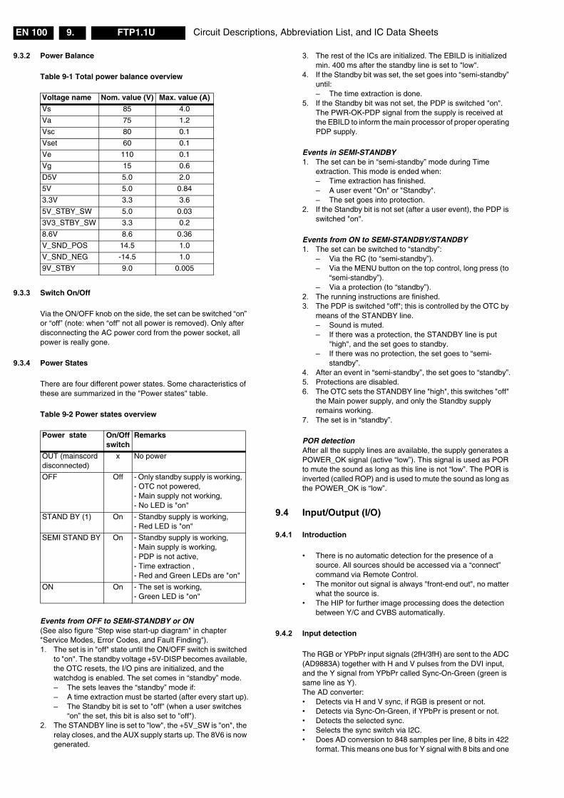
Circuit Descriptions, Abbreviation List, and IC Data SheetsEN 100 FTP1.1U9.
9.3.2 Power Balance
Table 9-1 Total power balance overview
9.3.3 Switch On/Off
Via the ON/OFF knob on the side, the set can be switched “on” or “off” (note: when “off” not all power is removed). Only after disconnecting the AC power cord from the power socket, all power is really gone.
9.3.4 Power States
There are four different power states. Some characteristics of these are summarized in the "Power states" table.
Table 9-2 Power states overview
Events from OFF to SEMI-STANDBY or ON(See also figure "Step wise start-up diagram" in chapter "Service Modes, Error Codes, and Fault Finding").1. The set is in "off" state until the ON/OFF switch is switched
to "on". The standby voltage +5V-DISP becomes available, the OTC resets, the I/O pins are initialized, and the watchdog is enabled. The set comes in “standby” mode. – The sets leaves the “standby” mode if:– A time extraction must be started (after every start up).– The Standby bit is set to "off" (when a user switches
“on” the set, this bit is also set to "off").2. The STANDBY line is set to "low", the +5V_SW is "on", the
relay closes, and the AUX supply starts up. The 8V6 is now generated.
3. The rest of the ICs are initialized. The EBILD is initialized min. 400 ms after the standby line is set to "low".
4. If the Standby bit was set, the set goes into “semi-standby” until:– The time extraction is done.
5. If the Standby bit was not set, the PDP is switched "on". The PWR-OK-PDP signal from the supply is received at the EBILD to inform the main processor of proper operating PDP supply.
Events in SEMI-STANDBY1. The set can be in “semi-standby” mode during Time
extraction. This mode is ended when:– Time extraction has finished.– A user event "On" or "Standby". – The set goes into protection.
2. If the Standby bit is not set (after a user event), the PDP is switched "on".
Events from ON to SEMI-STANDBY/STANDBY1. The set can be switched to “standby”:
– Via the RC (to “semi-standby”).– Via the MENU button on the top control, long press (to
“semi-standby”).– Via a protection (to “standby”).
2. The running instructions are finished.3. The PDP is switched "off"; this is controlled by the OTC by
means of the STANDBY line.– Sound is muted.– If there was a protection, the STANDBY line is put
"high", and the set goes to standby.– If there was no protection, the set goes to “semi-
standby”.4. After an event in “semi-standby”, the set goes to “standby”.5. Protections are disabled.6. The OTC sets the STANDBY line "high", this switches "off"
the Main power supply, and only the Standby supply remains working.
7. The set is in “standby”.
POR detectionAfter all the supply lines are available, the supply generates a POWER_OK signal (active “low”). This signal is used as POR to mute the sound as long as this line is not “low”. The POR is inverted (called ROP) and is used to mute the sound as long as the POWER_OK is “low”.
9.4 Input/Output (I/O)
9.4.1 Introduction
• There is no automatic detection for the presence of a source. All sources should be accessed via a “connect” command via Remote Control.
• The monitor out signal is always "front-end out", no matter what the source is.
• The HIP for further image processing does the detection between Y/C and CVBS automatically.
9.4.2 Input detection
The RGB or YPbPr input signals (2fH/3fH) are sent to the ADC (AD9883A) together with H and V pulses from the DVI input, and the Y signal from YPbPr called Sync-On-Green (green is same line as Y). The AD converter:• Detects via H and V sync, if RGB is present or not.• Detects via Sync-On-Green, if YPbPr is present or not.• Detects the selected sync.• Selects the sync switch via I2C.• Does AD conversion to 848 samples per line, 8 bits in 422
format. This means one bus for Y signal with 8 bits and one
Voltage name Nom. value (V) Max. value (A)
Vs 85 4.0
Va 75 1.2
Vsc 80 0.1
Vset 60 0.1
Ve 110 0.1
Vg 15 0.6
D5V 5.0 2.0
5V 5.0 0.84
3.3V 3.3 3.6
5V_STBY_SW 5.0 0.03
3V3_STBY_SW 3.3 0.2
8.6V 8.6 0.36
V_SND_POS 14.5 1.0
V_SND_NEG -14.5 1.0
9V_STBY 9.0 0.005
Power state On/Off switch
Remarks
OUT (mainscord disconnected)
x No power
OFF Off - Only standby supply is working, - OTC not powered, - Main supply not working, - No LED is "on"
STAND BY (1) On - Standby supply is working, - Red LED is "on"
SEMI STAND BY On - Standby supply is working, - Main supply is working, - PDP is not active, - Time extraction , - Red and Green LEDs are "on"
ON On - The set is working, - Green LED is "on"
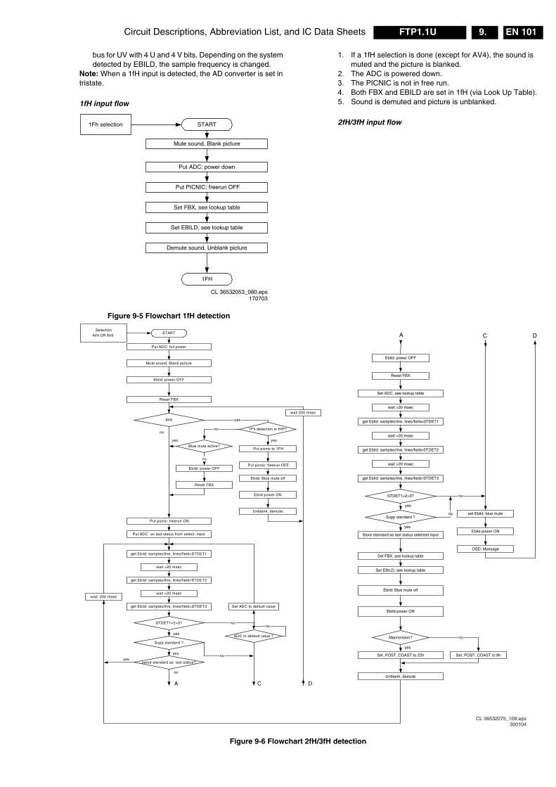
Circuit Descriptions, Abbreviation List, and IC Data Sheets EN 101FTP1.1U 9.
bus for UV with 4 U and 4 V bits. Depending on the system detected by EBILD, the sample frequency is changed.
Note: When a 1fH input is detected, the AD converter is set in tristate.
1fH input flow
Figure 9-5 Flowchart 1fH detection
1. If a 1fH selection is done (except for AV4), the sound is muted and the picture is blanked.
2. The ADC is powered down.3. The PICNIC is not in free run.4. Both FBX and EBILD are set in 1fH (via Look Up Table).5. Sound is demuted and picture is unblanked.
2fH/3fH input flow
Figure 9-6 Flowchart 2fH/3fH detection
CL 36532053_080.eps170703
Put PICNIC: freerun OFF
Put ADC: power down
START1Fh selection
Demute sound, Unblank picture
1FH
Set FBX, see lookup table
Set EBILD, see lookup table
Mute sound, Blank picture
Put ADC: full power
STARTSelection
AV4 OR AV5
Reset FBX
AV4
wait 200 msec
1Fh detection in HIP?
yes
Put picnic: freerun OFF
Put picnic: freerun ON
Put ADC on last status from select. input
get Ebild: samples/line, lines/field=STDET1
get Ebild: samples/line, lines/field=STDET2
wait >20 msec
wait >20 msec
get Ebild: samples/line, lines/field=STDET3
STDET1=2=3?
Supp standard ?
same standard as last status?
no
yes
yes
no
Put picnic to 1FH
Set ADC to default value
Unblank, demute
ADC to default value ?
no
no
no
Blue mute active?
Ebild: power OFF
Reset FBX
no
no
yes yes
Mute sound, Blank picture
Ebild: power OFF
Ebild: Blue mute off
Ebild power ON
A C D
wait: 200 msec
yes
CL 36532075_109.eps300104
Set FBX, see lookup table
Set EBILD, see lookup table
Set ADC, see tookup table
get Ebild: samples/line, lines/field=STDET1
get Ebild: samples/line, lines/field=STDET2
wait >20 msec
wait >20 msec
get Ebild: samples/line, lines/field=STDET3
STDET1=2=3?
yes
OSD: Message
no
Supp standard ?no
yes
wait >20 msec
Store standard as last status selected input
set Ebild: blue mute
Ebild: power OFF
Reset FBX
A
Ebild power ON
C D
Unblank, demute
Ebild: Blue mute off
Ebild power ON
Macrovision?
Set_POST_COAST to 22h Set_POST_COAST to 8h
no
yes
Circuit Descriptions, Abbreviation List, and IC Data SheetsEN 102 FTP1.1U9.
1. The standard detection starts with a 2fH/3fH selection on AV4 or AV5.
2. The ADC is full powered (it was powered down in 1fH).3. The sound is muted and the picture is blanked.4. When the input clock for the EBILD disappears and
appears again, the EBILD clock can go wrong. Therefore, the EBILD must be in “Power Off” mode before standard detection, and in “Power On” mode after standard detection.
5. On AV4, a 1fH and 2fH/3fH signal can enter. This detection is done by the HIP. When 1fH is detected, the FBX is set to 1fH, the PICNIC is not in free run, the picture is unblanked, and the sound is demuted. The set is in 1fH state. This state is continues checked, because the input can change from 1fH to 2fH/3fH.
6. If the input is 2fH/3fH, the PICNIC is set to free run.7. The ADC is set to the last status from this selected input,
because there is a big chance that the same standard is wanted.
8. The number of samples per line and lines per field is collected from the EBILD. The check is done three times. If the same value is measured within some tolerances (via SW Look Up Table) the standard is valid. The time between two measurements must be at least one frame or 20 ms.
9. If the ADC has not the correct settings, the PLL does not lock, and the "STDET" measurements do not give the same results. The ADC is set to its default value; this value is able to catch all supported standards. If the ADC is already in the default value and no standard detection is possible, the set changes to picture mute.
10. If the standard is not supported, the set changes to picture mute via the EBILD, and a message is displayed.
11. If the standard is the same as the last status, the ADC is in the correct state, and both FBX and EBILD are set (via Look Up Table).
12. If the standard is changed, the ADC is set to the detected standard and a new check is done. If the standard is valid and supported, the new standard is stored in NVM as last status.
13. The FBX and EBILD are set (via SW Look Up Table).14. Picture is unblanked and sound demuted.
9.5 Video Processing
9.5.1 Introduction
Notes: • The FBX processing part is (almost) equal as described in
the R8 manual (see section “Circuit Description, ...” paragraph “Video: Feature Box 7”). Therefore, it is not described here (except for some basics).
• As the used plasma is a “low res” VGA type, the “Pixel Plus” feature (generation of extra horizontal pixels and vertical lines) is not implemented in this chassis. However, the other picture improvement features of the Eagle IC (like CTI, peaking, and color enhancement) are used.
There are four AV inputs (AV4 can be 1fH or 2fH/3fH YPbPr), and one DVI 2fH/3fH input (see also figure "Chassis block diagram" in paragraph "Block Diagram"). The video processing is based on four key functions, being:• The HIP + comb filter (for simple source select and video/
chroma processing).• The EBILD that takes over the video control functions of
the HOP (as used in CRT based sets).• The FBX configuration consisting of a PICNIC (100 Hz
featuring), a FALCONIC (motion compensation and Auto TV featuring), and an EAGLE (used for scaling and picture improvements).
• A 2fH/3fH source selection. Additionally, the following features are added• One-chip NEC 3D comb filter: this comb filter uses spatial
and temporal filtering for the elimination of cross color and cross luminance components. Not only for vertical lines, but also for stationary diagonal lines. This comb filter only supports the NTSC standard.
• The light sensor measurement required for "Active Control" is done by the OTC.
Basic functionality of HIP
I/O functionality• The HIP selects the signals entering on 1fH base band.
The HIP contains a source select matrix in order to handle a Tuner, three CVBS sources, two Y/C sources, and two RGB inputs (this in fact means one VIF input for tuner, four CVBS inputs with among them two Y/C inputs, and two RGB inputs). The HIP detects by itself whether the source is Y/C or CVBS, and decides how to handle the signal for further image processing.
• The HIP delivers the main video output (YUV- 1fH signal) for further image processing and three CVBS outputs, being: CVBS PIP/DS, CVBS_TXT_OUT for comb filter (always following YUV main!) and CC processing, and the CVBS/Y_RECORD_OUT for AV2.
IF functionality• The HIP contains a multi standard IF circuit for video
demodulation with AFC (Automatic Frequency Control) functionality, a sound IF amplifier, and an AM demodulator. An extra group delay correction is included.
• Chroma demodulation and video processing• Sync acquisition, delivering H_A/V_A (Horizontal/Vertical
Acquisition) towards FBX.
Basic functionality of EBILDThe EBILD is the interface between the FBX and the PDP screen. Its principal functions are:• Video control functions of the HOP (Saturation, Contrast,
Brightness).• OSD insertion with blending.• Video Matrix (NTSC, ATSC, PAL).• For matrix displays additional functions like:
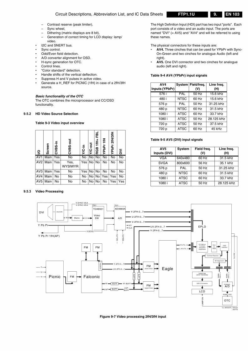
Circuit Descriptions, Abbreviation List, and IC Data Sheets EN 103FTP1.1U 9.
– Contrast reserve (peak limiter), – Sync wheel, – Dithering (matrix displays are 8 bit), – Generation of correct timing for LCD display: lamp/
video.• I2C and SNERT bus.• Sync control.• Odd/Even field detection.• A/D converter alignment for OSD.• H-sync generation for OTC.• Control lines.• “Color standard” detection.• Handle shifts of the vertical deflection.• Suppress H and V pulses in active video.• Generate a H_REF for PICNIC (1fH) in case of a 2fH/3fH
source.
Basic functionality of the OTCThe OTC combines the microprocessor and CC/OSD functionality.
9.5.2 HD Video Source Selection
Table 9-3 Video input overview
The High Definition Input (HDI) part has two input "ports". Each port consists of a video and an audio input. The ports are named "DVI" (= AV5) and "AV4" and will be referred to using these names. The physical connectors for these inputs are:• AV4. Three cinches that can be used for YPbPr with Sync-
On-Green and two cinches for analogue Audio (left and right).
• AV5. One DVI connector and two cinches for analogue audio (left and right).
Table 9-4 AV4 (YPbPr) input signals
Table 9-5 AV5 (DVI) input signals
9.5.3 Video Processing
Figure 9-7 Video processing 2fH/3fH input
I/O Scr
een
CV
BS
-in
CV
BS
-ou
t
Y/C
-in
Y/C
-ou
t
RG
B 1
fH+
FB
L
YP
bP
r 1f
H
YP
bP
r 2f
H/3
fH
DV
I
AV1 Main Yes No No No No No No No
AV2 Main Yes Yes, WYSIWYR
Yes No No No No No
AV3 Main Yes No Yes No No No No No
AV4 Main No No No No No Yes Yes No
AV5 Main No No No No No No Yes Yes
AV4 Inputs (YPbPr)
System Field freq. (V)
Line freq. (H)
576 i PAL 50 Hz 15.6 kHz
480 i NTSC 60 Hz 15.6 kHz
576 p PAL 50 Hz 31.25 kHz
480 p NTSC 60 Hz 31.5 kHz
1080 i ATSC 60 Hz 33.7 kHz
1080 i ATSC 50 Hz 28.125 kHz
720 p ATSC 50 Hz 37.5 kHz
720 p ATSC 60 Hz 45 kHz
AV5 Inputs (DVI)
System Field freq. (V)
Line freq.(H)
VGA 640x480 60 Hz 31.5 kHz
SVGA 800x600 56 Hz 35.1 kHz
576 p PAL 50 Hz 31.25 kHz
480 p NTSC 60 Hz 31.5 kHz
1080 i ATSC 60 Hz 33.7 kHz
1080 i ATSC 50 Hz 28.125 kHz
H-SYNC-VG A V- SYNC-VG A
Y Pb Pr
Matrix YUV
Y(SOG)
TDA8601 AD9883A
VideoSW A/D
SC
L-F
3
SD
A-F
3
Y- 2FH-0...7
U-2FH-0...7
UV demuxContrast
saturationbrightness
YUVto
RGB
OSDinsertion
EPLD
Contrast Reserve
AD Alignment
YO UT(0...9)
U_VO UT(0...9)
LVD S Transmitter
LVD S Connector
LCD
OTC
A/D
RGBBL-OSD
LAM
P-O
N
TDA9805
DS90C385
CLK
-OS
D
FM(lower lines)
FM(upper lines)
FalconicPicnic FM
UV- 2FH-0...7
Y- 2FH-0...7
UVF-BUFF
YF-BUFF
Y
U
V
BUFF
BUFF
YF
UVF
Y- 2FH-0...7
FM
BU
FF
BU
FF R
GB
BL-
FD
B-0
...3
RG
BB
L-O
SD
-0...
5
TR
ISTA
TE
FM
Eagle
DVI RGB
SILICON
V- 2FH-0...7
UV- 2FH-0...7
Y Pb Pr 1fH(AP)
CL 36532075_108.eps300104
7D51 7L01
H/VCLK
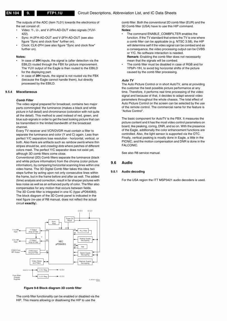
Circuit Descriptions, Abbreviation List, and IC Data SheetsEN 104 FTP1.1U9.
The outputs of the ADC (item 7L01) towards the electronics of the set consist of:• Video: Y-, U-, and V-2FH-AD-OUT video signals (YUV-
422).• Sync: H-2FH-AD-OUT and V-2FH-AD-OUT (see also
figure "Sync and clock flow" further on).• Clock: CLK-2FH (see also figure "Sync and clock flow"
further on).
Notes: • In case of 2fH inputs, the signal is (after detection via the
EBILD) routed through the FBX for picture improvement. The YUV output of the Eagle is then routed to the EBILD for the displaying part.
• In case of 3fH inputs, the signal is not routed via the FBX (because the Eagle cannot handle them), but directly processed by the EBILD.
9.5.4 Miscellaneous
Comb FilterThe video signal prepared for broadcast, contains two major parts commingled: the luminance (makes a black and white picture in full detail) and chrominance (coloration with not quite all the detail). This method is used instead of red, green, and blue sub-signals in order to get the best looking picture that can be transmitted in the limited bandwidth of the broadcast channel. Every TV receiver and VCR/DVDR must contain a filter to separate the luminance and color (Y and C) again. Less than perfect Y/C separators lose resolution - horizontal, vertical, or both. Also there are artifacts such as rainbow swirls where thin stripes should be, and crawling dots where patches of different colors meet. The perfect Y/C separator does not exist yet, although 3D comb filters come close.Conventional (2D) Comb filters separate the luminance (black and white picture information) from the chroma (color picture information), by comparing horizontal scanning lines within one video frame. The 3D Digital Comb filter takes this idea two steps further by acting upon not only consecutive lines within the frame, but in the frame before and after as well. The added (time) analysis and correction, result in far sharper pictures with less noise as well as an enhanced purity of color. The filter also compensates for any motion that occurs between fields.The 3D Comb filter is integrated in one IC (type uPD64083). The block diagram of the 3D Comb panel is indicated in the next figure (re-use of R8 manual, does not reflect the actual circuit exactly).
Figure 9-8 Block diagram 3D comb filter
The comb filter functionality can be enabled or disabled via the HIP. This means allowing or disallowing the HIP to use the
comb filter. Both the conventional 2D comb filter (EUR) and the 3D Comb filter (USA) have to use this HIP command.Notes:• The command ENABLE_COMBFILTER enables the
function. If the TV standard that enters the TV is one where a comb filter can be applicable (e.g. NTSC 3.58), the HIP will determine self if the video signal can be combed and as a consequence, the video processing output can be CVBS or Y/C. No software interaction is needed. Remark: Enabling the comb filter does not necessarily mean that the signals will be combed.
• The comb filter must be disabled in case of RGB and for YPbPr-1fH, to avoid big horizontal shifts of the picture caused by the comb filter processing.
Auto TVThe Auto Picture Control or in short AutoTV, aims at providing the customer the best possible picture performance at any time. Therefore, it performs real time processing of the video signal and because of that, it decides to adapt several video parameters throughout the whole chassis. The total effect of Auto Picture Control on the screen can be selected by the use of the remote control. The commercial name for the feature is "Active Control". The basic component for AutoTV is the FBX. It measures the picture content and it has the most video control parameters on board, like peaking, coring, DNR, and so on. With the presence of the Eagle, additionally the color enhancement functions are controlled. Also, the light sensor is supported via the OTC. Finally, vertical peaking is mostly done in Eagle, a little in the PICNIC, and the motion compensation and DNR is done in the FALCONIC. See also R8 service manual.
9.6 Audio
9.6.1 Audio decoding
For the USA region the ITT MSP3421 audio decoders is used.
!
"#
$ %
&
''
(" "#)
) "#)
) "#)
*+, %)
!+! %)
-*+,
-!+!
-,+
-*+, -!+!
.
.
.
(/
,
,*
0
0 ,0
!
CL 36532075_068.eps300104
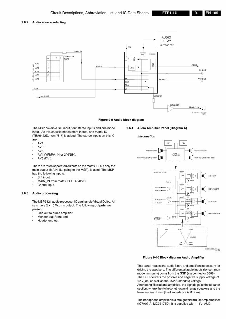
Circuit Descriptions, Abbreviation List, and IC Data Sheets EN 105FTP1.1U 9.
9.6.2 Audio source selecting
Figure 9-9 Audio block diagram
The MSP covers a SIF input, four stereo inputs and one mono input. As this chassis needs more inputs, one matrix IC (TEA6422D, item 7I17) is added. The stereo inputs on this IC are:• AV1.• AV2.• AV3.• AV4 (YPbPr/1fH or 2fH/3fH).• AV5 (DVI). There are three separated outputs on the matrix IC, but only the main output (MAIN_IN, going to the MSP), is used. The MSP has the following inputs:• SIF input.• MAIN_IN from matrix IC TEA6422D. • Centre input.
9.6.3 Audio processing
The MSP3421 audio processor IC can handle Virtual Dolby. All sets have 2 x 10 W_rms output. The following outputs are present:• Line out to audio amplifier.• Monitor out: Front-end.• Headphone out.
9.6.4 Audio Amplifier Panel (Diagram A)
Introduction
Figure 9-10 Block diagram Audio Amplifier
This panel houses the audio filters and amplifiers necessary for driving the speakers. The differential audio inputs (for common mode immunity) come from the SSP (via connector 0388). The PSU delivers the positive and negative supply voltage of 12 V_dc, as well as the +5V2 (standby) voltage.After being filtered and amplified, the signals go to the speaker section, where the (twin cone) low/mid range speakers and the tweeters are driven (load impedance is 8 ohm). The headphone amplifier is a straightforward OpAmp amplifier (IC7A07-A, MC33178D). It is supplied with +11V_AUD.
DE
C
DEC
DEC
ENC
MON OUT
L/R LSAV5
AV4
AV2
AV3
AV1
MAIN IN
TEA6422D0X98
1 2 36
5
4
3
2
1 SC1
SC2
SC3
SC4
SIF/AM
NSM4556Headphone
MSP3421
AUX OUT
I2S
MAIN HIP
C in
AV2 OUT
CL OUT
AUDIODELAY
ONY FOR PDP
CL 36532075_107.eps300104
CL36532053_081.eps170703
AUDIOAMPLIFIER
AUDIO AMPLIFIER
SSP
TWEETER RIGHT
TWIN-CONE SPEAKER RIGHT
PSU
HIGH LEFT
L
MUTE
7260-A
7225-A
7225-B
L-POS
L-NEG
HPFL-HIGH
TWEETER LEFT
TWIN-CONE SPEAKER LEFT
MID/LOW LEFT
7238-A
LPFL-LOW
HIGH RIGHT
7260-B
HPFR-HIGH
MID/LOW RIGHT
63Hz
LOW(LPF)
HIGH(HPF)
1kHz 3kHz
6dB/OCT
MUTE
7238-B
LPFR-LOW
RR-POS
R-NEG
AUDIOENABLE
MUTE
MUTE
MUTE
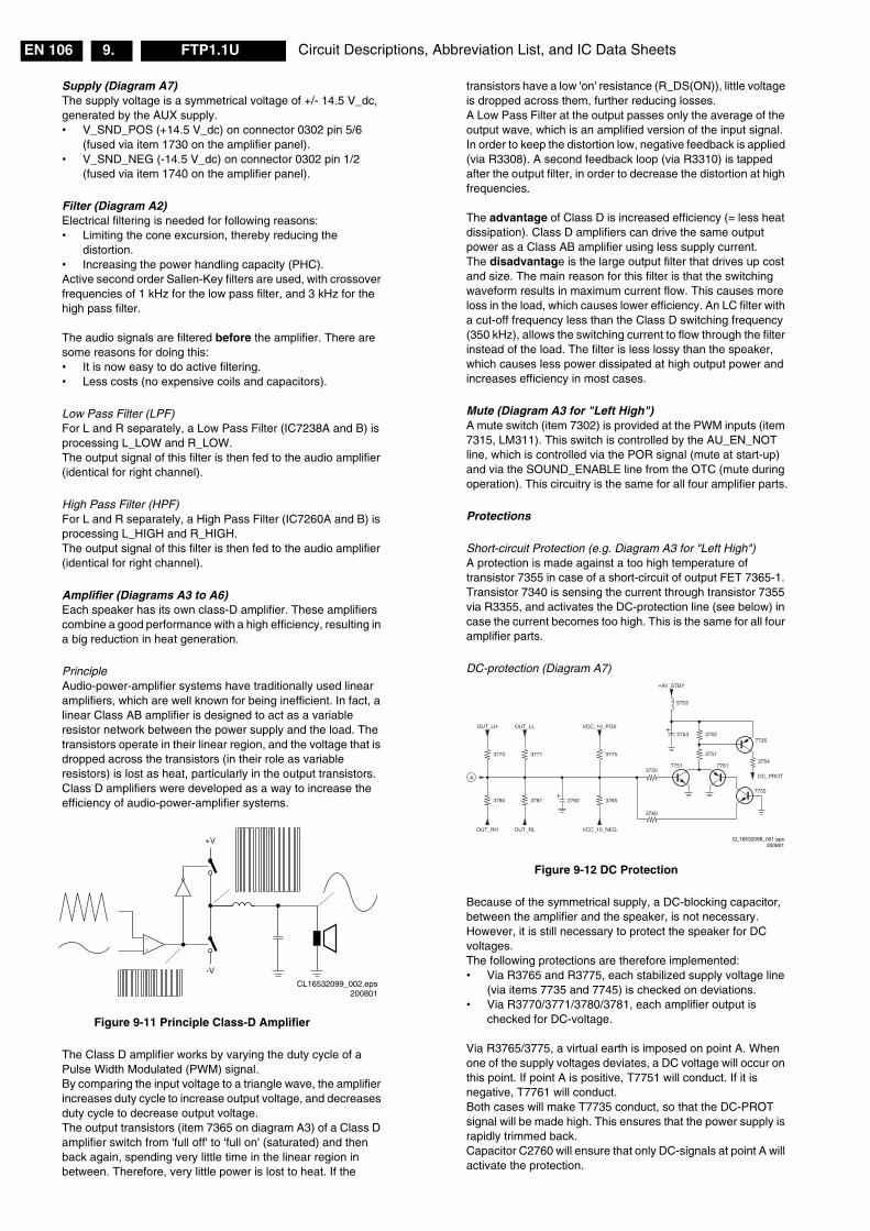
Circuit Descriptions, Abbreviation List, and IC Data SheetsEN 106 FTP1.1U9.
Supply (Diagram A7)The supply voltage is a symmetrical voltage of +/- 14.5 V_dc, generated by the AUX supply.• V_SND_POS (+14.5 V_dc) on connector 0302 pin 5/6
(fused via item 1730 on the amplifier panel).• V_SND_NEG (-14.5 V_dc) on connector 0302 pin 1/2
(fused via item 1740 on the amplifier panel).
Filter (Diagram A2)Electrical filtering is needed for following reasons:• Limiting the cone excursion, thereby reducing the
distortion.• Increasing the power handling capacity (PHC).Active second order Sallen-Key filters are used, with crossover frequencies of 1 kHz for the low pass filter, and 3 kHz for the high pass filter. The audio signals are filtered before the amplifier. There are some reasons for doing this: • It is now easy to do active filtering. • Less costs (no expensive coils and capacitors).
Low Pass Filter (LPF)For L and R separately, a Low Pass Filter (IC7238A and B) is processing L_LOW and R_LOW.The output signal of this filter is then fed to the audio amplifier (identical for right channel).
High Pass Filter (HPF)For L and R separately, a High Pass Filter (IC7260A and B) is processing L_HIGH and R_HIGH.The output signal of this filter is then fed to the audio amplifier (identical for right channel).
Amplifier (Diagrams A3 to A6)Each speaker has its own class-D amplifier. These amplifiers combine a good performance with a high efficiency, resulting in a big reduction in heat generation.
PrincipleAudio-power-amplifier systems have traditionally used linear amplifiers, which are well known for being inefficient. In fact, a linear Class AB amplifier is designed to act as a variable resistor network between the power supply and the load. The transistors operate in their linear region, and the voltage that is dropped across the transistors (in their role as variable resistors) is lost as heat, particularly in the output transistors.Class D amplifiers were developed as a way to increase the efficiency of audio-power-amplifier systems.
Figure 9-11 Principle Class-D Amplifier
The Class D amplifier works by varying the duty cycle of a Pulse Width Modulated (PWM) signal. By comparing the input voltage to a triangle wave, the amplifier increases duty cycle to increase output voltage, and decreases duty cycle to decrease output voltage.The output transistors (item 7365 on diagram A3) of a Class D amplifier switch from 'full off' to 'full on' (saturated) and then back again, spending very little time in the linear region in between. Therefore, very little power is lost to heat. If the
transistors have a low 'on' resistance (R_DS(ON)), little voltage is dropped across them, further reducing losses.A Low Pass Filter at the output passes only the average of the output wave, which is an amplified version of the input signal.In order to keep the distortion low, negative feedback is applied (via R3308). A second feedback loop (via R3310) is tapped after the output filter, in order to decrease the distortion at high frequencies. The advantage of Class D is increased efficiency (= less heat dissipation). Class D amplifiers can drive the same output power as a Class AB amplifier using less supply current. The disadvantage is the large output filter that drives up cost and size. The main reason for this filter is that the switching waveform results in maximum current flow. This causes more loss in the load, which causes lower efficiency. An LC filter with a cut-off frequency less than the Class D switching frequency (350 kHz), allows the switching current to flow through the filter instead of the load. The filter is less lossy than the speaker, which causes less power dissipated at high output power and increases efficiency in most cases.
Mute (Diagram A3 for "Left High")A mute switch (item 7302) is provided at the PWM inputs (item 7315, LM311). This switch is controlled by the AU_EN_NOT line, which is controlled via the POR signal (mute at start-up) and via the SOUND_ENABLE line from the OTC (mute during operation). This circuitry is the same for all four amplifier parts.
Protections
Short-circuit Protection (e.g. Diagram A3 for "Left High")A protection is made against a too high temperature of transistor 7355 in case of a short-circuit of output FET 7365-1. Transistor 7340 is sensing the current through transistor 7355 via R3355, and activates the DC-protection line (see below) in case the current becomes too high. This is the same for all four amplifier parts.
DC-protection (Diagram A7)
Figure 9-12 DC Protection
Because of the symmetrical supply, a DC-blocking capacitor, between the amplifier and the speaker, is not necessary. However, it is still necessary to protect the speaker for DC voltages. The following protections are therefore implemented:• Via R3765 and R3775, each stabilized supply voltage line
(via items 7735 and 7745) is checked on deviations.• Via R3770/3771/3780/3781, each amplifier output is
checked for DC-voltage. Via R3765/3775, a virtual earth is imposed on point A. When one of the supply voltages deviates, a DC voltage will occur on this point. If point A is positive, T7751 will conduct. If it is negative, T7761 will conduct. Both cases will make T7735 conduct, so that the DC-PROT signal will be made high. This ensures that the power supply is rapidly trimmed back. Capacitor C2760 will ensure that only DC-signals at point A will activate the protection.
CL16532099_002.eps200801
+V
-V
OUT_LH
OUT_RH
A
3770
3780
OUT_LL
OUT_RL
3771
3781
VCC_10_POS
+9V_STBY
VCC_10_NEG
3775
5753
37513754
77353752
3765
3750
3760
2760
2753
7751 7761
DC_PROT
7755
CL16532099_001.eps200801
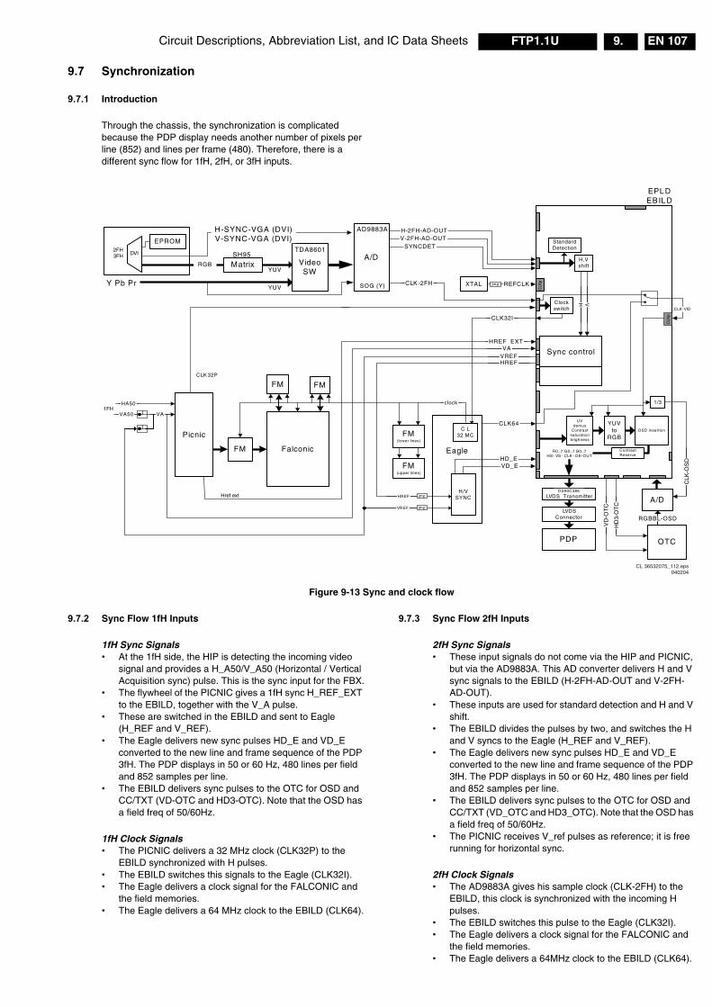
Circuit Descriptions, Abbreviation List, and IC Data Sheets EN 107FTP1.1U 9.
9.7 Synchronization
9.7.1 Introduction
Through the chassis, the synchronization is complicated because the PDP display needs another number of pixels per line (852) and lines per frame (480). Therefore, there is a different sync flow for 1fH, 2fH, or 3fH inputs.
Figure 9-13 Sync and clock flow
9.7.2 Sync Flow 1fH Inputs
1fH Sync Signals• At the 1fH side, the HIP is detecting the incoming video
signal and provides a H_A50/V_A50 (Horizontal / Vertical Acquisition sync) pulse. This is the sync input for the FBX.
• The flywheel of the PICNIC gives a 1fH sync H_REF_EXT to the EBILD, together with the V_A pulse.
• These are switched in the EBILD and sent to Eagle (H_REF and V_REF).
• The Eagle delivers new sync pulses HD_E and VD_E converted to the new line and frame sequence of the PDP 3fH. The PDP displays in 50 or 60 Hz, 480 lines per field and 852 samples per line.
• The EBILD delivers sync pulses to the OTC for OSD and CC/TXT (VD-OTC and HD3-OTC). Note that the OSD has a field freq of 50/60Hz.
1fH Clock Signals• The PICNIC delivers a 32 MHz clock (CLK32P) to the
EBILD synchronized with H pulses.• The EBILD switches this signals to the Eagle (CLK32I).• The Eagle delivers a clock signal for the FALCONIC and
the field memories.• The Eagle delivers a 64 MHz clock to the EBILD (CLK64).
9.7.3 Sync Flow 2fH Inputs
2fH Sync Signals• These input signals do not come via the HIP and PICNIC,
but via the AD9883A. This AD converter delivers H and V sync signals to the EBILD (H-2FH-AD-OUT and V-2FH-AD-OUT).
• These inputs are used for standard detection and H and V shift.
• The EBILD divides the pulses by two, and switches the H and V syncs to the Eagle (H_REF and V_REF).
• The Eagle delivers new sync pulses HD_E and VD_E converted to the new line and frame sequence of the PDP 3fH. The PDP displays in 50 or 60 Hz, 480 lines per field and 852 samples per line.
• The EBILD delivers sync pulses to the OTC for OSD and CC/TXT (VD_OTC and HD3_OTC). Note that the OSD has a field freq of 50/60Hz.
• The PICNIC receives V_ref pulses as reference; it is free running for horizontal sync.
2fH Clock Signals• The AD9883A gives his sample clock (CLK-2FH) to the
EBILD, this clock is synchronized with the incoming H pulses.
• The EBILD switches this pulse to the Eagle (CLK32I).• The Eagle delivers a clock signal for the FALCONIC and
the field memories.• The Eagle delivers a 64MHz clock to the EBILD (CLK64).
VGAor
DVI
Falconic Eagle
FM(lower lines)
FM(upper lines)
FM FM
FM
HA50
VA
HD_E
EPLDEB ILD
Sync control
YUVto
RGB
PDP
A/D
OTC
HD
3-O
TC
VD
-OT
C
CLK64
HREF jmp
StandardDetection
H V
HREF
VR EF jmp
VREF
LVDSConnector
VideoSW
SH95TDA8601
EPROM
VD_E
CLK -2FH
V-2FH-AD-OUTH-2FH-AD-OUTH-SYNC-VGA (DVI)
V-SYNC-VGA (DVI)
MatrixRGB
YUV
YUV
SYNCDET
Clockswitch
CLK
-OS
D
XTAL
CLK
pREFCLK
CLK
p
1/3
DS90C385
LVDS Transmitter
CLK -VID
RGBBL-OSD
UVdemux
Contrastsaturationbrighness
OSD insertion
ContrastReserve
R0..7 G0..7 B0..7HS- VS - CLK - DE-OUT
VA50
Y Pb Pr
C L32 MC
jmp
CLK 32P
CLK32I
H,Vshift
H/VSYNC
HREF_EXTVA
clock
Picnic
A/D
SOG (Y)
AD9883A
CL 36532075_112.eps040204
1FH
2FH3FH DVI
Href ext
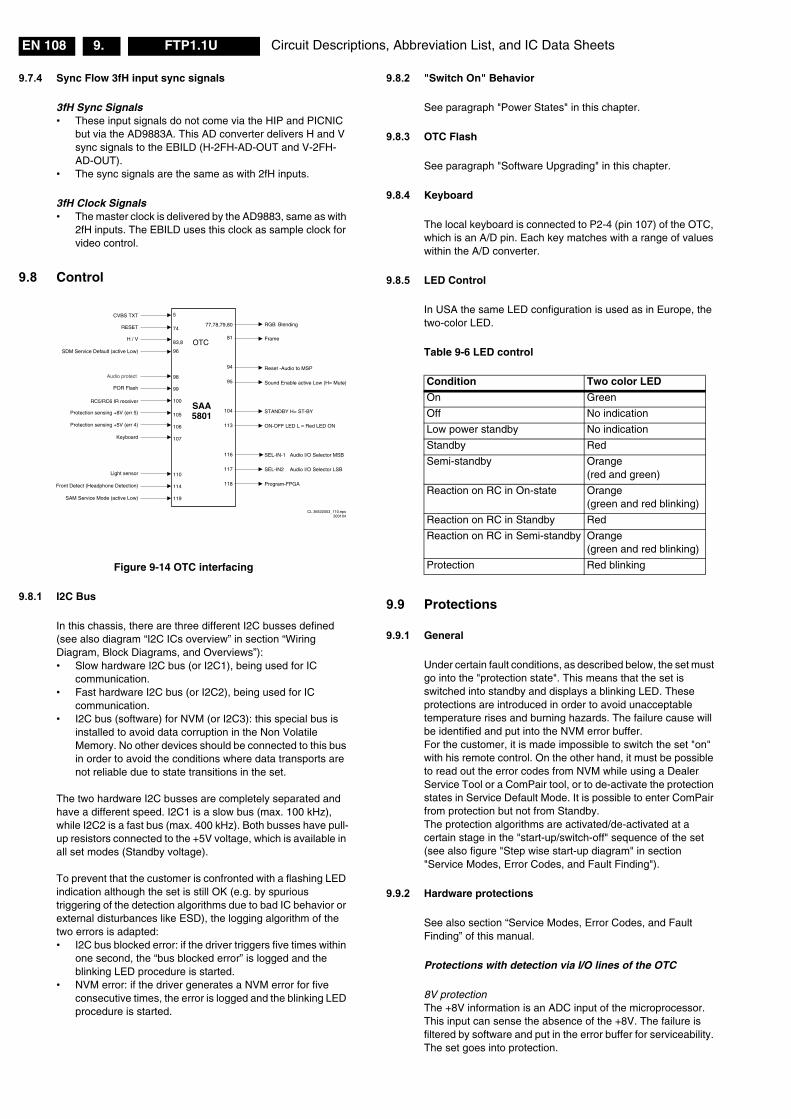
Circuit Descriptions, Abbreviation List, and IC Data SheetsEN 108 FTP1.1U9.
9.7.4 Sync Flow 3fH input sync signals
3fH Sync Signals• These input signals do not come via the HIP and PICNIC
but via the AD9883A. This AD converter delivers H and V sync signals to the EBILD (H-2FH-AD-OUT and V-2FH-AD-OUT).
• The sync signals are the same as with 2fH inputs.
3fH Clock Signals• The master clock is delivered by the AD9883, same as with
2fH inputs. The EBILD uses this clock as sample clock for video control.
9.8 Control
Figure 9-14 OTC interfacing
9.8.1 I2C Bus
In this chassis, there are three different I2C busses defined (see also diagram “I2C ICs overview” in section “Wiring Diagram, Block Diagrams, and Overviews”):• Slow hardware I2C bus (or I2C1), being used for IC
communication. • Fast hardware I2C bus (or I2C2), being used for IC
communication. • I2C bus (software) for NVM (or I2C3): this special bus is
installed to avoid data corruption in the Non Volatile Memory. No other devices should be connected to this bus in order to avoid the conditions where data transports are not reliable due to state transitions in the set.
The two hardware I2C busses are completely separated and have a different speed. I2C1 is a slow bus (max. 100 kHz), while I2C2 is a fast bus (max. 400 kHz). Both busses have pull-up resistors connected to the +5V voltage, which is available in all set modes (Standby voltage). To prevent that the customer is confronted with a flashing LED indication although the set is still OK (e.g. by spurious triggering of the detection algorithms due to bad IC behavior or external disturbances like ESD), the logging algorithm of the two errors is adapted:• I2C bus blocked error: if the driver triggers five times within
one second, the “bus blocked error” is logged and the blinking LED procedure is started.
• NVM error: if the driver generates a NVM error for five consecutive times, the error is logged and the blinking LED procedure is started.
9.8.2 "Switch On" Behavior
See paragraph "Power States" in this chapter.
9.8.3 OTC Flash
See paragraph "Software Upgrading" in this chapter.
9.8.4 Keyboard
The local keyboard is connected to P2-4 (pin 107) of the OTC, which is an A/D pin. Each key matches with a range of values within the A/D converter.
9.8.5 LED Control
In USA the same LED configuration is used as in Europe, the two-color LED.
Table 9-6 LED control
9.9 Protections
9.9.1 General
Under certain fault conditions, as described below, the set must go into the "protection state". This means that the set is switched into standby and displays a blinking LED. These protections are introduced in order to avoid unacceptable temperature rises and burning hazards. The failure cause will be identified and put into the NVM error buffer. For the customer, it is made impossible to switch the set "on" with his remote control. On the other hand, it must be possible to read out the error codes from NVM while using a Dealer Service Tool or a ComPair tool, or to de-activate the protection states in Service Default Mode. It is possible to enter ComPair from protection but not from Standby.The protection algorithms are activated/de-activated at a certain stage in the "start-up/switch-off" sequence of the set (see also figure "Step wise start-up diagram" in section "Service Modes, Error Codes, and Fault Finding").
9.9.2 Hardware protections
See also section “Service Modes, Error Codes, and Fault Finding” of this manual.
Protections with detection via I/O lines of the OTC
8V protectionThe +8V information is an ADC input of the microprocessor. This input can sense the absence of the +8V. The failure is filtered by software and put in the error buffer for serviceability. The set goes into protection.
CL 36532053_110.eps300104
ON-OFF LED L = Red LED ON
STANDBY H= ST-BY
Sound Enable active Low (H= Mute)
SEL-IN2
Reset -Audio to MSP
Protection sensing +8V (err 5)
Protection sensing +5V (err 4)
Light sensor
SAM Service Mode (active Low)
RGB Blending
Frame
SEL-IN-1
Front Detect (Headphone Detection) Program-FPGA
OTC
SAA5801
104
113
117
94
95
81
77,78,79,80
116
118
100
96
119
110
107
105
106
5
83,8
74
99
98
114
Audio I/O Selector LSB
Audio I/O Selector MSB
SDM Service Default (active Low)
CVBS TXT
H / V
RESET
Audio protect
RC5/RC6 IR receiver
POR Flash
Keyboard
Condition Two color LED
On Green
Off No indication
Low power standby No indication
Standby Red
Semi-standby Orange (red and green)
Reaction on RC in On-state Orange (green and red blinking)
Reaction on RC in Standby Red
Reaction on RC in Semi-standby Orange (green and red blinking)
Protection Red blinking
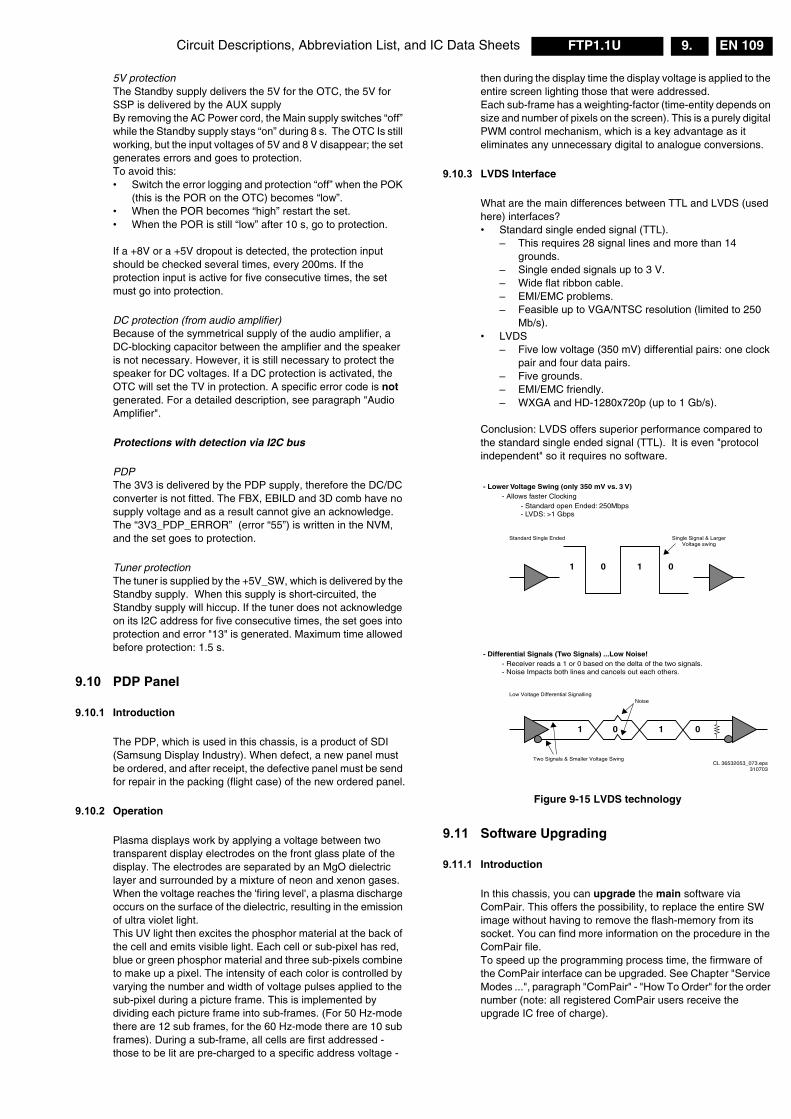
Circuit Descriptions, Abbreviation List, and IC Data Sheets EN 109FTP1.1U 9.
5V protectionThe Standby supply delivers the 5V for the OTC, the 5V for SSP is delivered by the AUX supplyBy removing the AC Power cord, the Main supply switches “off” while the Standby supply stays “on” during 8 s. The OTC Is still working, but the input voltages of 5V and 8 V disappear; the set generates errors and goes to protection.To avoid this: • Switch the error logging and protection “off” when the POK
(this is the POR on the OTC) becomes “low”.• When the POR becomes “high” restart the set.• When the POR is still “low” after 10 s, go to protection. If a +8V or a +5V dropout is detected, the protection input should be checked several times, every 200ms. If the protection input is active for five consecutive times, the set must go into protection.
DC protection (from audio amplifier)Because of the symmetrical supply of the audio amplifier, a DC-blocking capacitor between the amplifier and the speaker is not necessary. However, it is still necessary to protect the speaker for DC voltages. If a DC protection is activated, the OTC will set the TV in protection. A specific error code is not generated. For a detailed description, see paragraph "Audio Amplifier".
Protections with detection via I2C bus
PDPThe 3V3 is delivered by the PDP supply, therefore the DC/DC converter is not fitted. The FBX, EBILD and 3D comb have no supply voltage and as a result cannot give an acknowledge. The “3V3_PDP_ERROR” (error “55”) is written in the NVM, and the set goes to protection.
Tuner protection The tuner is supplied by the +5V_SW, which is delivered by the Standby supply. When this supply is short-circuited, the Standby supply will hiccup. If the tuner does not acknowledge on its I2C address for five consecutive times, the set goes into protection and error "13" is generated. Maximum time allowed before protection: 1.5 s.
9.10 PDP Panel
9.10.1 Introduction
The PDP, which is used in this chassis, is a product of SDI (Samsung Display Industry). When defect, a new panel must be ordered, and after receipt, the defective panel must be send for repair in the packing (flight case) of the new ordered panel.
9.10.2 Operation
Plasma displays work by applying a voltage between two transparent display electrodes on the front glass plate of the display. The electrodes are separated by an MgO dielectric layer and surrounded by a mixture of neon and xenon gases. When the voltage reaches the 'firing level', a plasma discharge occurs on the surface of the dielectric, resulting in the emission of ultra violet light. This UV light then excites the phosphor material at the back of the cell and emits visible light. Each cell or sub-pixel has red, blue or green phosphor material and three sub-pixels combine to make up a pixel. The intensity of each color is controlled by varying the number and width of voltage pulses applied to the sub-pixel during a picture frame. This is implemented by dividing each picture frame into sub-frames. (For 50 Hz-mode there are 12 sub frames, for the 60 Hz-mode there are 10 sub frames). During a sub-frame, all cells are first addressed - those to be lit are pre-charged to a specific address voltage -
then during the display time the display voltage is applied to the entire screen lighting those that were addressed.Each sub-frame has a weighting-factor (time-entity depends on size and number of pixels on the screen). This is a purely digital PWM control mechanism, which is a key advantage as it eliminates any unnecessary digital to analogue conversions.
9.10.3 LVDS Interface
What are the main differences between TTL and LVDS (used here) interfaces?• Standard single ended signal (TTL).
– This requires 28 signal lines and more than 14 grounds.
– Single ended signals up to 3 V.– Wide flat ribbon cable.– EMI/EMC problems.– Feasible up to VGA/NTSC resolution (limited to 250
Mb/s).• LVDS
– Five low voltage (350 mV) differential pairs: one clock pair and four data pairs.
– Five grounds.– EMI/EMC friendly.– WXGA and HD-1280x720p (up to 1 Gb/s).
Conclusion: LVDS offers superior performance compared to the standard single ended signal (TTL). It is even "protocol independent" so it requires no software.
Figure 9-15 LVDS technology
9.11 Software Upgrading
9.11.1 Introduction
In this chassis, you can upgrade the main software via ComPair. This offers the possibility, to replace the entire SW image without having to remove the flash-memory from its socket. You can find more information on the procedure in the ComPair file. To speed up the programming process time, the firmware of the ComPair interface can be upgraded. See Chapter "Service Modes ...", paragraph "ComPair" - "How To Order" for the order number (note: all registered ComPair users receive the upgrade IC free of charge).
CL 36532053_073.eps310703
1 0 1 0
Standard Single Ended Single Signal & LargerVoltage swing
Low Voltage Differential Signalling
Two Signals & Smaller Voltage Swing
Noise
- Lower Voltage Swing (only 350 mV vs. 3 V)
- Standard open Ended: 250Mbps- LVDS: >1 Gbps
- Allows faster Clocking
- Differential Signals (Two Signals) ...Low Noise!- Receiver reads a 1 or 0 based on the delta of the two signals.- Noise Impacts both lines and cancels out each others.
1 0 1 0
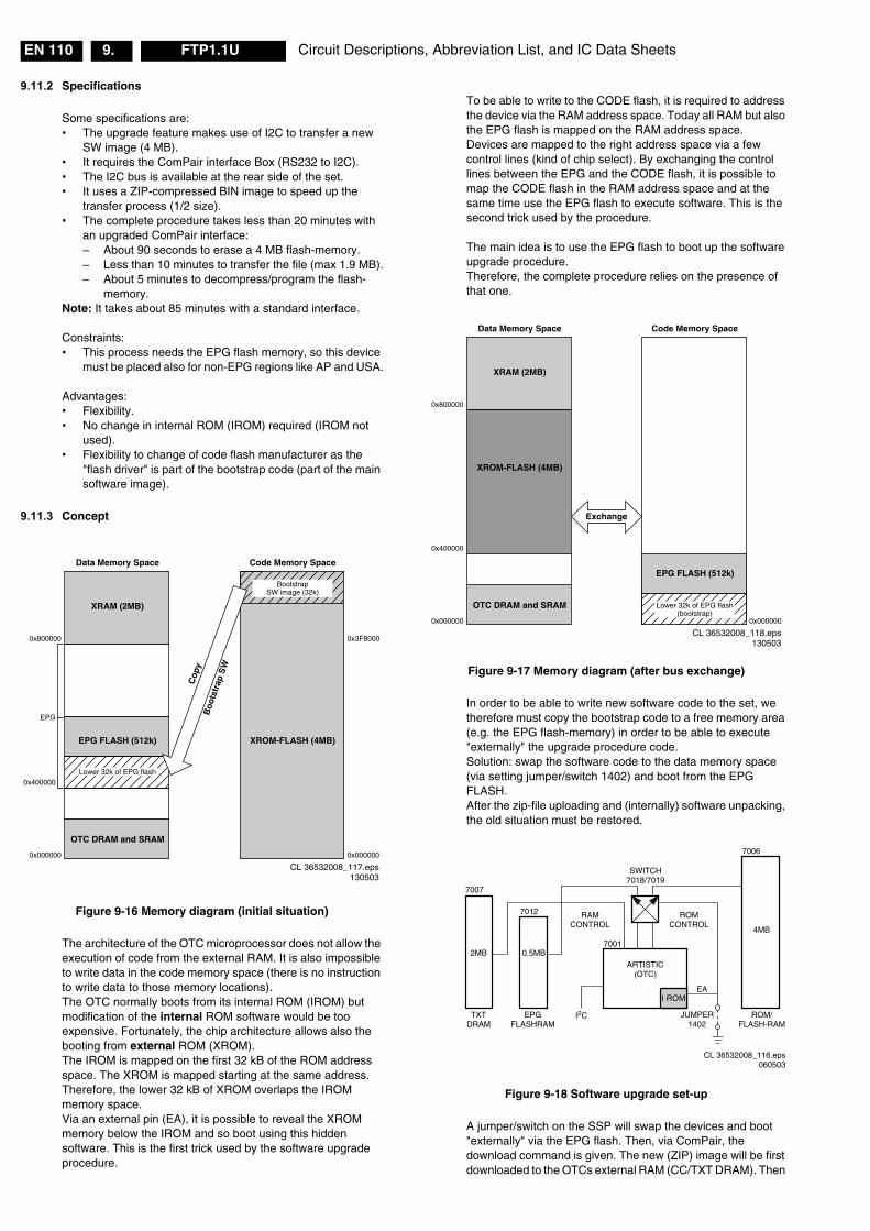
Circuit Descriptions, Abbreviation List, and IC Data SheetsEN 110 FTP1.1U9.
9.11.2 Specifications
Some specifications are:• The upgrade feature makes use of I2C to transfer a new
SW image (4 MB).• It requires the ComPair interface Box (RS232 to I2C).• The I2C bus is available at the rear side of the set.• It uses a ZIP-compressed BIN image to speed up the
transfer process (1/2 size).• The complete procedure takes less than 20 minutes with
an upgraded ComPair interface:– About 90 seconds to erase a 4 MB flash-memory.– Less than 10 minutes to transfer the file (max 1.9 MB).– About 5 minutes to decompress/program the flash-
memory.Note: It takes about 85 minutes with a standard interface. Constraints:• This process needs the EPG flash memory, so this device
must be placed also for non-EPG regions like AP and USA. Advantages:• Flexibility.• No change in internal ROM (IROM) required (IROM not
used).• Flexibility to change of code flash manufacturer as the
"flash driver" is part of the bootstrap code (part of the main software image).
9.11.3 Concept
Figure 9-16 Memory diagram (initial situation)
The architecture of the OTC microprocessor does not allow the execution of code from the external RAM. It is also impossible to write data in the code memory space (there is no instruction to write data to those memory locations). The OTC normally boots from its internal ROM (IROM) but modification of the internal ROM software would be too expensive. Fortunately, the chip architecture allows also the booting from external ROM (XROM).The IROM is mapped on the first 32 kB of the ROM address space. The XROM is mapped starting at the same address. Therefore, the lower 32 kB of XROM overlaps the IROM memory space.Via an external pin (EA), it is possible to reveal the XROM memory below the IROM and so boot using this hidden software. This is the first trick used by the software upgrade procedure.
To be able to write to the CODE flash, it is required to address the device via the RAM address space. Today all RAM but also the EPG flash is mapped on the RAM address space.Devices are mapped to the right address space via a few control lines (kind of chip select). By exchanging the control lines between the EPG and the CODE flash, it is possible to map the CODE flash in the RAM address space and at the same time use the EPG flash to execute software. This is the second trick used by the procedure. The main idea is to use the EPG flash to boot up the software upgrade procedure.Therefore, the complete procedure relies on the presence of that one.
Figure 9-17 Memory diagram (after bus exchange)
In order to be able to write new software code to the set, we therefore must copy the bootstrap code to a free memory area (e.g. the EPG flash-memory) in order to be able to execute "externally" the upgrade procedure code.Solution: swap the software code to the data memory space (via setting jumper/switch 1402) and boot from the EPG FLASH.After the zip-file uploading and (internally) software unpacking, the old situation must be restored.
Figure 9-18 Software upgrade set-up
A jumper/switch on the SSP will swap the devices and boot "externally" via the EPG flash. Then, via ComPair, the download command is given. The new (ZIP) image will be first downloaded to the OTCs external RAM (CC/TXT DRAM). Then
CL 36532008_117.eps130503
Data Memory Space
XRAM (2MB)
0x800000
0x400000
EPG
0x000000
0x3F8000
0x000000
EPG FLASH (512k)
Cop
y
Code Memory Space
XROM-FLASH (4MB)
OTC DRAM and SRAM
Lower 32k of EPG flash
BootstrapSW image (32k)
Boo
tstr
ap S
W
CL 36532008_118.eps130503
Data Memory Space
XRAM (2MB)
0x800000
0x400000
0x000000 0x000000
Code Memory Space
XROM-FLASH (4MB)
OTC DRAM and SRAM Lower 32k of EPG flash(bootstrap)
EPG FLASH (512k)
Exchange
CL 36532008_116.eps060503
2MB
4MB
ARTISTIC(OTC)
TXTDRAM
7007
7006
SWITCH7018/7019
0.5MB
EPGFLASHRAM
ROM/FLASH-RAM
JUMPER1402
I2C
EA
RAMCONTROL
ROMCONTROL
7012
7001
I ROM
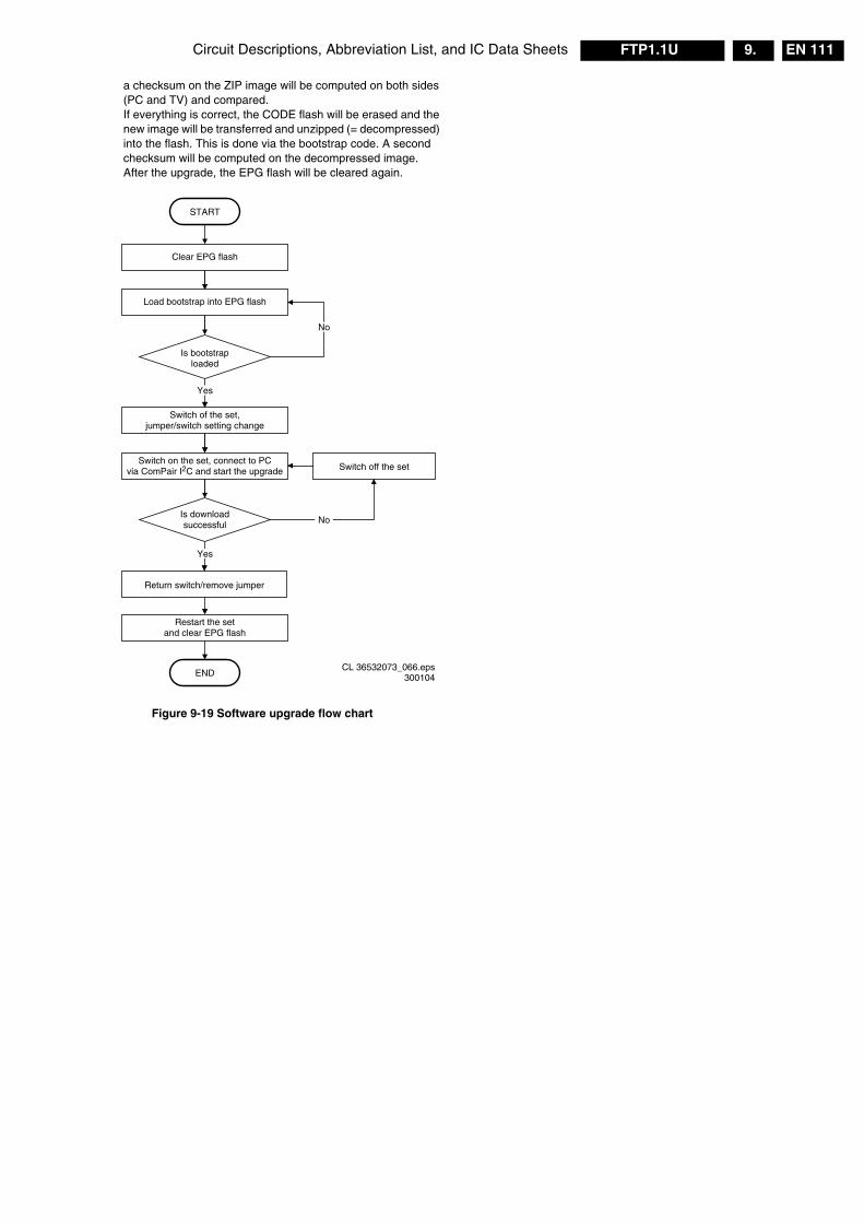
Circuit Descriptions, Abbreviation List, and IC Data Sheets EN 111FTP1.1U 9.
a checksum on the ZIP image will be computed on both sides (PC and TV) and compared. If everything is correct, the CODE flash will be erased and the new image will be transferred and unzipped (= decompressed) into the flash. This is done via the bootstrap code. A second checksum will be computed on the decompressed image.After the upgrade, the EPG flash will be cleared again.
Figure 9-19 Software upgrade flow chart
CL 36532073_066.eps300104
Load bootstrap into EPG flash
START
END
Clear EPG flash
No
Yes
Is bootstraploaded
Switch on the set, connect to PCvia ComPair I2C and start the upgrade
Switch of the set,jumper/switch setting change
Restart the setand clear EPG flash
Return switch/remove jumper
No
Yes
Is downloadsuccessful
Switch off the set
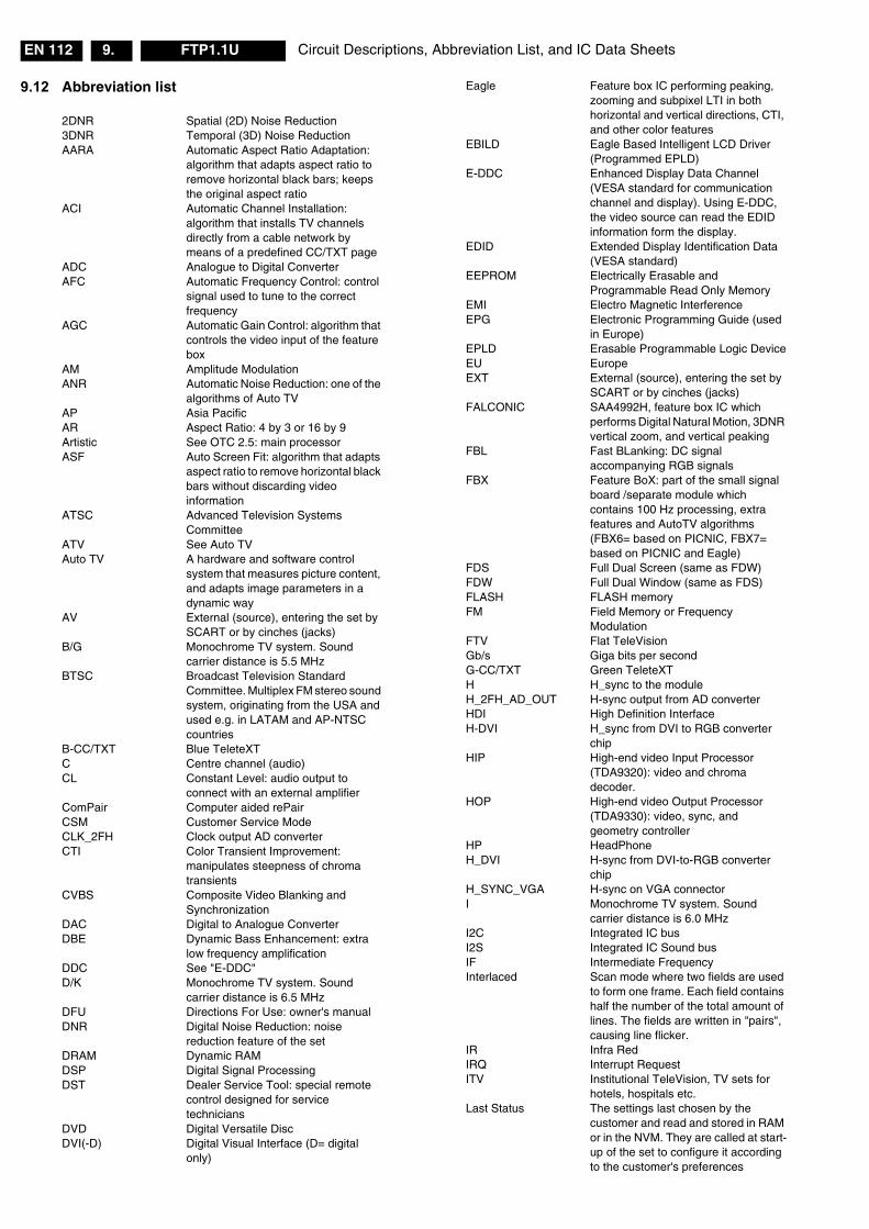
Circuit Descriptions, Abbreviation List, and IC Data SheetsEN 112 FTP1.1U9.
9.12 Abbreviation list
2DNR Spatial (2D) Noise Reduction3DNR Temporal (3D) Noise ReductionAARA Automatic Aspect Ratio Adaptation:
algorithm that adapts aspect ratio to remove horizontal black bars; keeps the original aspect ratio
ACI Automatic Channel Installation: algorithm that installs TV channels directly from a cable network by means of a predefined CC/TXT page
ADC Analogue to Digital ConverterAFC Automatic Frequency Control: control
signal used to tune to the correct frequency
AGC Automatic Gain Control: algorithm that controls the video input of the feature box
AM Amplitude ModulationANR Automatic Noise Reduction: one of the
algorithms of Auto TVAP Asia PacificAR Aspect Ratio: 4 by 3 or 16 by 9Artistic See OTC 2.5: main processorASF Auto Screen Fit: algorithm that adapts
aspect ratio to remove horizontal black bars without discarding video information
ATSC Advanced Television Systems Committee
ATV See Auto TVAuto TV A hardware and software control
system that measures picture content, and adapts image parameters in a dynamic way
AV External (source), entering the set by SCART or by cinches (jacks)
B/G Monochrome TV system. Sound carrier distance is 5.5 MHz
BTSC Broadcast Television Standard Committee. Multiplex FM stereo sound system, originating from the USA and used e.g. in LATAM and AP-NTSC countries
B-CC/TXT Blue TeleteXTC Centre channel (audio)CL Constant Level: audio output to
connect with an external amplifierComPair Computer aided rePairCSM Customer Service ModeCLK_2FH Clock output AD converterCTI Color Transient Improvement:
manipulates steepness of chroma transients
CVBS Composite Video Blanking and Synchronization
DAC Digital to Analogue ConverterDBE Dynamic Bass Enhancement: extra
low frequency amplificationDDC See "E-DDC"D/K Monochrome TV system. Sound
carrier distance is 6.5 MHzDFU Directions For Use: owner's manualDNR Digital Noise Reduction: noise
reduction feature of the setDRAM Dynamic RAMDSP Digital Signal ProcessingDST Dealer Service Tool: special remote
control designed for service technicians
DVD Digital Versatile DiscDVI(-D) Digital Visual Interface (D= digital
only)
Eagle Feature box IC performing peaking, zooming and subpixel LTI in both horizontal and vertical directions, CTI, and other color features
EBILD Eagle Based Intelligent LCD Driver (Programmed EPLD)
E-DDC Enhanced Display Data Channel (VESA standard for communication channel and display). Using E-DDC, the video source can read the EDID information form the display.
EDID Extended Display Identification Data (VESA standard)
EEPROM Electrically Erasable and Programmable Read Only Memory
EMI Electro Magnetic InterferenceEPG Electronic Programming Guide (used
in Europe)EPLD Erasable Programmable Logic DeviceEU EuropeEXT External (source), entering the set by
SCART or by cinches (jacks)FALCONIC SAA4992H, feature box IC which
performs Digital Natural Motion, 3DNR vertical zoom, and vertical peaking
FBL Fast BLanking: DC signal accompanying RGB signals
FBX Feature BoX: part of the small signal board /separate module which contains 100 Hz processing, extra features and AutoTV algorithms (FBX6= based on PICNIC, FBX7= based on PICNIC and Eagle)
FDS Full Dual Screen (same as FDW)FDW Full Dual Window (same as FDS)FLASH FLASH memoryFM Field Memory or Frequency
ModulationFTV Flat TeleVisionGb/s Giga bits per secondG-CC/TXT Green TeleteXTH H_sync to the module H_2FH_AD_OUT H-sync output from AD converterHDI High Definition InterfaceH-DVI H_sync from DVI to RGB converter
chipHIP High-end video Input Processor
(TDA9320): video and chroma decoder.
HOP High-end video Output Processor (TDA9330): video, sync, and geometry controller
HP HeadPhoneH_DVI H-sync from DVI-to-RGB converter
chipH_SYNC_VGA H-sync on VGA connectorI Monochrome TV system. Sound
carrier distance is 6.0 MHzI2C Integrated IC busI2S Integrated IC Sound busIF Intermediate FrequencyInterlaced Scan mode where two fields are used
to form one frame. Each field contains half the number of the total amount of lines. The fields are written in "pairs", causing line flicker.
IR Infra RedIRQ Interrupt RequestITV Institutional TeleVision, TV sets for
hotels, hospitals etc.Last Status The settings last chosen by the
customer and read and stored in RAM or in the NVM. They are called at start-up of the set to configure it according to the customer's preferences
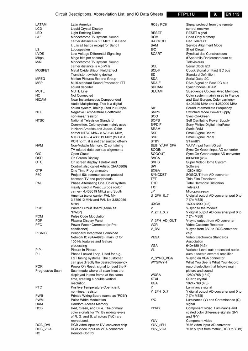
Circuit Descriptions, Abbreviation List, and IC Data Sheets EN 113FTP1.1U 9.
LATAM Latin AmericaLCD Liquid Crystal DisplayLED Light Emitting DiodeL/L' Monochrome TV system. Sound
carrier distance is 6.5 MHz. L' is Band I, L is all bands except for Band I
LS LoudspeakerLVDS Low Voltage Differential SignalingMbps Mega bits per secondM/N Monochrome TV system. Sound
carrier distance is 4.5 MHzMOSFET Metal Oxide Silicon Field Effect
Transistor, switching deviceMPEG Motion Pictures Experts GroupMSP Multi-standard Sound Processor: ITT
sound decoderMUTE MUTE LineNC Not ConnectedNICAM Near Instantaneous Compounded
Audio Multiplexing. This is a digital sound system, mainly used in Europe.
NTC Negative Temperature Coefficient, non-linear resistor
NTSC National Television Standard Committee. Color system mainly used in North America and Japan. Color carrier NTSC M/N= 3.579545 MHz, NTSC 4.43= 4.433619 MHz (this is a VCR norm, it is not transmitted off-air)
NVM Non-Volatile Memory: IC containing TV related data such as alignments
O/C Open CircuitOSD On Screen DisplayOTC On screen display Teletext and
Control; also called Artistic (SAA5800)OTP One Time ProgrammableP50 Project 50: communication protocol
between TV and peripheralsPAL Phase Alternating Line. Color system
mainly used in West Europe (color carrier= 4.433619 MHz) and South America (color carrier PAL M= 3.575612 MHz and PAL N= 3.582056 MHz)
PCB Printed Circuit Board (same as "PWB")
PCM Pulse Code ModulationPDP Plasma Display PanelPFC Power Factor Corrector (or Pre-
conditioner)PICNIC Peripheral Integrated Combined
Network IC (SAA4978): main IC for 100 Hz features and feature processing
PIP Picture In PicturePLL Phase Locked Loop. Used for e.g.
FST tuning systems. The customer can give directly the desired frequency
POR Power On Reset, signal to reset the PProgressive Scan Scan mode where all scan lines are
displayed in one frame at the same time, creating a double vertical resolution.
PTC Positive Temperature Coefficient, non-linear resistor
PWB Printed Wiring Board (same as "PCB")PWM Pulse Width ModulationRAM Random Access MemoryRGB Red, Green, and Blue. The primary
color signals for TV. By mixing levels of R, G, and B, all colors (Y/C) are reproduced.
RGB_DVI RGB video input on DVI converter chipRGB_VGA RGB video input on VGA connectorRC Remote Control
RC5 / RC6 Signal protocol from the remote control receiver
RESET RESET signalROM Read Only MemoryR-CC/TXT Red TeleteXTSAM Service Alignment ModeS/C Short CircuitSCART Syndicat des Constructeurs
d'Appareils Radiorecepteurs et Televisieurs
SCL Serial Clock I2CSCL-F CLock Signal on Fast I2C busSD Standard DefinitionSDA Serial Data I2CSDA-F DAta Signal on Fast I2C busSDRAM Synchronous DRAMSECAM SEequence Couleur Avec Memoire.
Color system mainly used in France and East Europe. Color carriers= 4.406250 MHz and 4.250000 MHz
SIF Sound Intermediate FrequencySMPS Switched Mode Power SupplySOG Sync-On-GreenSOPS Self Oscillating Power SupplyS/PDIF Sony Philips Digital InterFaceSRAM Static RAMSSP Small Signal BoardSSP Small Signal PanelSTBY STandBYSUB_Y/U/V_2FH Y/U/V input from I/O celSOGIN Sync-On-Green input AD converterSOGOUT Sync-On-Green output AD converterSVGA 800x600 (4:3)SVHS Super Video Home SystemSW SoftwareSXGA 1280x1024SYNCDET SOGOUT from AD converterTFT Thin Film TransistorTHD Total Harmonic DistortionTXT TeleteXTuP MicroprocessorU_2FH_0..7 U digital output AD converter port 0 to
7 (7= MSB)UXGA 1600x1200 (4:3)V V-sync to the module V_2FH_0..7 V digital output AD converter port 0 to
7 (7= MSB)V_2FH_AD_OUT V-sync output from AD converterVCR Video Cassette RecorderV_DVI V-sync from DVI-to-RGB converter
chipVESA Video Electronics Standards
AssociationVGA 640x480 (4:3)VL Variable Level out: processed audio
output toward external amplifierV_SYNC_VGA V-sync on VGA connectorWYSIWYR What You See Is What You Record:
record selection that follows main picture and sound
WXGA 1280x768 (15:9)XTAL Quartz crystalXGA 1024x768 (4:3)Y Luminance signalY_2FH_0..7 Y digital output AD converter port 0 to
7 (7= MSB)Y/C Luminance (Y) and Chrominance (C)
signalYPbPr Component video. Luminance and
scaled color difference signals (B-Y and R-Y)
YUV Component videoYUV_2FH YUV video input AD converterYUV_VGA YUV output from matrix (RGB to YUV)
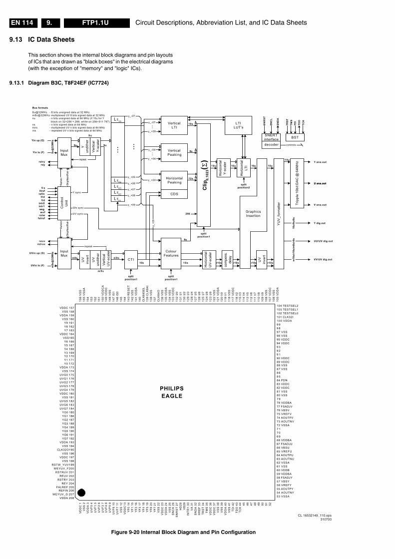
Circuit Descriptions, Abbreviation List, and IC Data SheetsEN 114 FTP1.1U9.
9.13 IC Data Sheets
This section shows the internal block diagrams and pin layouts of ICs that are drawn as "black boxes" in the electrical diagrams (with the exception of "memory" and "logic" ICs).
9.13.1 Diagram B3C, T8F24EF (IC7724)
Figure 9-20 Internal Block Diagram and Pin Configuration
!
!
"
#$%&'()
*+'()#$
,-.&%/#$
000
#$%&'()
*+'()#$
#$%&'()
#$%&'()
#(1&-2
!3$&43-%()
#(1&-2
Σ
3)3,$
#(%,$#+
000
τ01
τ02
τ03
τ04
τ16
5 6
5 6
5 6
5 6
5 6
5 *
5 6
5 *
5 6
5 *
5 6
000
!3$&43-%()
*+'()#$
!3$&43-%()
$&77)#8&%9
"!4
:3$;
(%%#$
!"
#
000
$%
3-%$3)
-&%
5 6
$#7#(%
& "
!'
& '
$#7#(%
&
&
#
+5-'
!(
)!
&)
( !(
+5-'
!(
&
&
&
&
&
&
:< +5-'!3$&43-%()
*+'()#$
'3;7#-+0
.#)(5
*+
,
-
* .
&
*&
&
.
/*&
/*&+
,
-
/.&
& & & & &
.
*
/
& &/
*& *&
)! (
-7,%
",<
-7,%
",<
,-.&%/#$
.
/.&
#$)-
#$)-
1&7#<%+%$
1&7#<%+%$
&-=#$%
&
$(7/&'+
-+#$%&3-
&-=#$%
0& ( /&
,9"!4 * 8&%+ ,-+&2-#. .(%( (% "!4
-, * - 8&%+ ,-+&2-#. .(%( (% "!4 >&: , :3$
8)('1 3- 6 ? @ A/&%# 3- 6 B
-+ * - 8&%+ +&2-#. .(%( (% "!4
;-+ * ;,)%&7)#<#. - 8&%+ +&2-#. .(%( (% "!4
$-+ * $#7#(%#. - 8&%+ +&2-#. .(%( (% "!4
;+9"!4* ;,)%&7)#<#. 8&%+ +&2-#. .(%( (% "!4
.#'3.#$
1
23
&-%#$:('#
1
14
'3-%$3)+
323
34
345
3,
3
6
C+
CL 16532149_110.eps310703
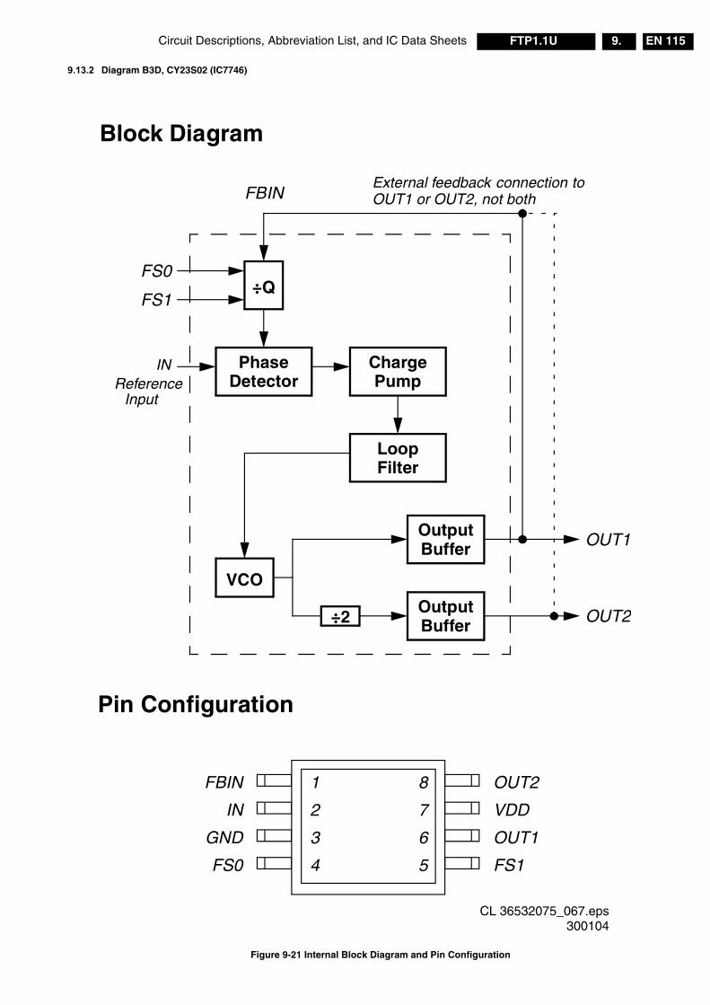
Circuit Descriptions, Abbreviation List, and IC Data Sheets EN 115FTP1.1U 9.
9.13.2 Diagram B3D, CY23S02 (IC7746)
Figure 9-21 Internal Block Diagram and Pin Configuration
Block Diagram
Pin Configuration
÷QFS0
FS1
Reference
FBIN
PhaseDetector
ChargePump
LoopFilter
VCO
÷2
OutputBuffer OUT1
OUT2OutputBuffer
External feedback connection to OUT1 or OUT2, not both
Input
IN
OUT2
VDD
OUT1
FS1
8
7
6
5
FBIN
IN
GND
FS0
1
2
3
4
CL 36532075_067.eps300104
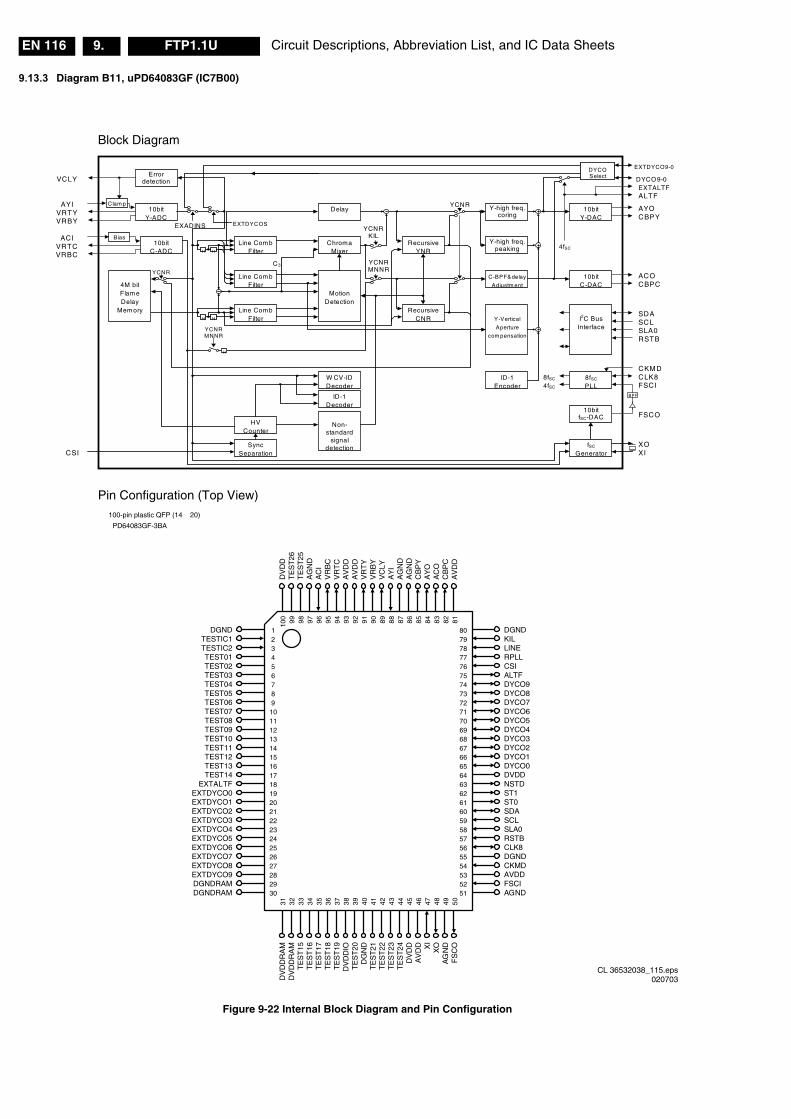
Circuit Descriptions, Abbreviation List, and IC Data SheetsEN 116 FTP1.1U9.
9.13.3 Diagram B11, uPD64083GF (IC7B00)
Figure 9-22 Internal Block Diagram and Pin Configuration
BPF
DYCO9-0
ACO
ACI
CSI
VRBY
VCLY
VRTYAYI
XOXI
FSCO
CKM DCLK8FSCI
RSTBSLA0SCLSDA
ALTF
CBPC
CBPYAYO
Bias
Y-Vertical
Aperture
com pensation
Y-high freq.peaking
RecursiveCNR
Delay
RecursiveYNR
Y-high freq.coring
C-BPF&delay
Adjustm ent
ID-1Encoder
SyncSeparation
Non-standard
signaldetection
HVCounter
W CV-IDDecoder
I2C BusInterface
MotionDetection
ChromaMixer
Line Com bFilter
10bitC-ADC
10bitY-ADC
Line Com bFilter
Line Com bFilter
10bitY-DAC
fSC
Generator
10bitfSC-DAC
8fSC
PLL
10bitC-DAC
Errordetection
4fSC
4fSC
8fSC
EXADINS
YCNR
H
HH
HH
YCNRKIL
YCNR
C3
YCNRMNNR
YCNRMNNR
4M bitFlam eDelay
Mem ory
VRBCVRTC
ID-1Decoder
EXTDYCOS
Clam p
DYCOSelect
EXTDYCO9-0
EXTALTF
Block Diagram
Pin Configuration (Top View) 100-pin plastic QFP (14 20)
PD64083GF-3BA
DV
DD
RA
MD
VD
DR
AM
TE
ST
15T
ES
T16
TE
ST
17T
ES
T18
TE
ST
19D
VD
DIO
TE
ST
20D
GN
DT
ES
T21
TE
ST
22T
ES
T23
TE
ST
24D
VD
DA
VD
D XI
XO
AG
ND
FS
CO
DV
DD
T
ES
T26
T
ES
T25
A
GN
D
AC
I V
RB
C
VR
TC
A
VD
D
AV
DD
V
RT
Y
VR
BY
V
CLY
A
YI
AG
ND
A
GN
D
CB
PY
A
YO
A
CO
C
BP
C
AV
DD
DGND TESTIC1 TESTIC2 TEST01 TEST02 TEST03 TEST04 TEST05 TEST06 TEST07 TEST08 TEST09 TEST10 TEST11 TEST12 TEST13 TEST14
EXTALTF EXTDYCO0 EXTDYCO1 EXTDYCO2 EXTDYCO3 EXTDYCO4 EXTDYCO5 EXTDYCO6 EXTDYCO7 EXTDYCO8 EXTDYCO9 DGNDRAM DGNDRAM
DGND KIL LINE RPLL CSI ALTF DYCO9 DYCO8 DYCO7 DYCO6 DYCO5 DYCO4 DYCO3 DYCO2 DYCO1 DYCO0 DVDD NSTD ST1 ST0 SDA SCL SLA0 RSTB CLK8 DGND CKMD AVDD FSCI AGND
100 99 98 97 96 95 94 93 92 91 90 89 88 87 86 85 84 83 82 81
31
32
33
34
35
36
37
38
39
40
41
42
43
44
45
46
47
48
49
50
80 79 78 77 76 75 74 73 72 71 70 69 68 67 66 65 64 63 62 61 60 59 58 57 56 55 54 53 52 51
1 2 3 4 5 6 7 8 9 10 11 12 13 14 15 16 17 18 19 20 21 22 23 24 25 26 27 28 29 30
CL 36532038_115.eps020703
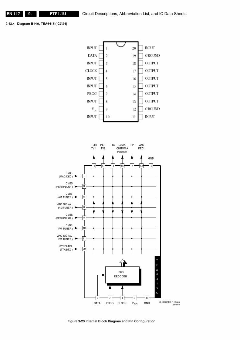
Circuit Descriptions, Abbreviation List, and IC Data SheetsEN 117 FTP1.1U9.
9.13.4 Diagram B14A, TEA6415 (IC7I24)
Figure 9-23 Internal Block Diagram and Pin Configuration
9 19
18 17 16 15 14 13 12
1
3
5
6
8
10
11
20
2 7 4
BUS
DECODER
DATA GNDCLOC K VCC
TTX LUMACHROM APOWER
PIP MACDEC.
GND
CVBS(AM TUNER )
MAC SIGNAL(AM TUNER )
CVBS(FM TUNER )
MAC SIGNAL(FM TUNER )
SYNCHRO(TTX/BTX )
PERITV1
PERITV2
CVBS(PERI PLUG2 )
P ROG
CVBS(PERI PLUG1 )
CVBS(MAC/DEC )
T
E
A
6
4
1
5
C
6415C
-02.E
PS
BLOCK DIAGRAM
CL 36532008_144.eps211003
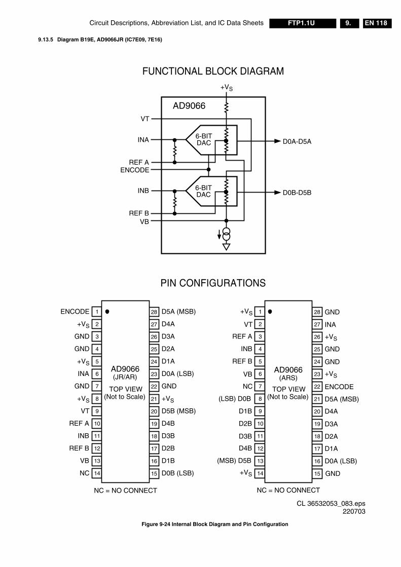
Circuit Descriptions, Abbreviation List, and IC Data Sheets EN 118FTP1.1U 9.
9.13.5 Diagram B19E, AD9066JR (IC7E09, 7E16)
Figure 9-24 Internal Block Diagram and Pin Configuration
FUNCTIONAL BLOCK DIAGRAM
6-BITDAC
6-BITDAC
AD9066
D0A-D5A
D0B-D5B
+VS
VT
INA
REF AENCODE
INB
REF BVB
PIN CONFIGURATIONS
TOP VIEW(Not to Scale)
28
27
26
25
24
23
22
21
20
19
18
17
16
15
1
2
3
4
5
6
7
8
9
10
11
12
13
14
AD9066(JR/AR)
ENCODE D5A (MSB)
+VS D4A
GND D3A
GND D2A
+VS D1A
INA D0A (LSB)
GND GND
+VS +VS
VT D5B (MSB)
REF A D4B
INB D3B
REF B D2B
VB D1B
NC D0B (LSB)
NC = NO CONNECT
TOP VIEW(Not to Scale)
28
27
26
25
24
23
22
21
20
19
18
17
16
15
1
2
3
4
5
6
7
8
9
10
11
12
13
14
AD9066(ARS)
ENCODE
D5A (MSB)
+VS
D4A
D3A
D2A
D1A
INA
D0A (LSB)
GND+VS
+VS
VT
(MSB) D5B
REF A
D4B
INB
D3B
REF B
D2B
VB
D1B
NC
(LSB) D0B
GND
GND
+VS
GND
NC = NO CONNECT
CL 36532053_083.eps220703
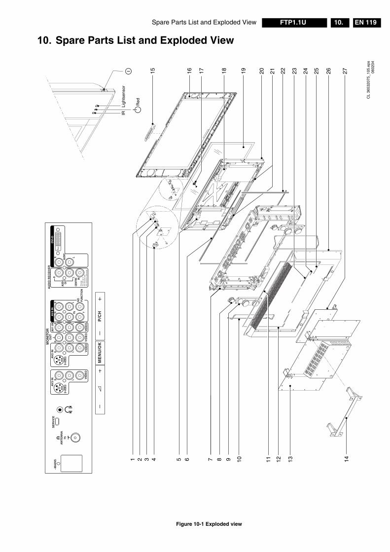
Spare Parts List and Exploded View EN 119FTP1.1U 10.
10. Spare Parts List and Exploded View
Figure 10-1 Exploded view
CL
3653
2075
_105
.eps
0602
04
P/C
HM
EN
U/O
K
~MA
INS
AN
TE
NN
A75
SE
RV
ICE
VID
EO
VID
EO
S-VI
DEO
S-VI
DEO
AV
3 IN
AV
2 IN
OU
TM
ON
ITO
R AV
1 IN
VID
EO
VID
EO
AUDI
OAU
DIO
OUT
CENT
RE IN
AV
4 IN
DV
I-D
R L
R L
R L
R L
R LLR
LRPr Pb Y
NO
FUN
CTI
ON
AU
DIO
RE
CE
IVE
R
18
916
1724
C5
14
1615 17 1918 20 21 26 27
1312108 97651 32 11
23 2524
4
22
Red
IRLi
ghts
enso
r
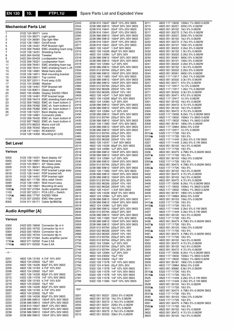
Spare Parts List and Exploded ViewEN 120 FTP1.1U10.
Mechanical Parts List
1 3122 124 36071 Lens2 3122 124 36271 Light guide3 3122 124 36081 Day light filter4 3122 128 13901 On/off knob5 3122 128 14451 PDP Bracket right6 3122 358 76463 EMC shielding foam long7 3122 128 14231 Shielding frame8 2422 264 00432 Tweeter9 2422 264 00433 Loudspeaker twin10 3122 358 76221 Loudspeaker foam11 3122 358 76451 EMC shielding foam top12 3122 358 76441 EMC shielding foam L+R13 3122 128 14891 Metal back plate14 3122 128 14811 Wall mounting bracket15 3104 328 29811 Top control16 3122 357 22511 Front assy (US)17 3122 124 35682 Washer18 3122 128 14451 PDP Bracket left19 3122 124 90811 Glass plate20 9322 195 45682 Display S42SD-YB0421 3122 128 14461 PDP bracket large22 3122 358 76474 EMC shielding foam short23 3122 358 76822 EMC sh. foam bottom 324 3122 358 76392 EMC sh. foam bottom 225 3122 358 76382 EMC sh. foam bottom 126 3122 128 14221 Back display assy27 3122 128 14861 Connector plate
3122 358 76432 EMC sh. foam bottom 63122 587 76822 EMC sh. foam bottom 42422 070 98223 Mains cord US3122 358 76342 Mains inlet3128 147 14461 RC4305/013122 128 14302 Mounting kit (US)
Set Level
Various
0002 3122 128 14221 Back display 42"0005 3122 128 14891 Metal back assy0007 3122 124 90811 42" Glass plate0009 3122 121 36241 Mounting plate0017 3122 128 14461 PDP bracket Large assy0018 3122 128 14441 PDP bracket left0019 3122 128 14451 PDP bracket right0033 4822 401 11795 Wire relief 15mm0095 3122 128 14951 Wall mount assy0098 3122 128 13921 Mounting kit assy1050 3122 357 21064 Audio amplifier panel1103 3122 357 22511 PCA LED + Switch1104 9965 000 17797 S42SD-YB041105 3122 357 22052 EMC filter panel8302 3104 311 05171 Cable 9p/860/9p
Audio Amplifier [A]
Various
0302 2422 025 16846 Connector 9p m h0303 2422 025 16702 Connector 5p m h0304 2422 025 16543 Connector 4p m0388 2422 025 16704 Connector 8p m1050 3122 357 21064 Audio amplifier panel1730 4822 071 52502 Fuse 2.5A1740 4822 071 52502 Fuse 2.5A
2201 4822 126 13193 4.7nF 10% 63V2202 4822 124 23002 10µF 16V2204 4822 126 14226 82pF 5% 50V 06032205 4822 126 13193 4.7nF 10% 63V2206 4822 124 23002 10µF 16V2207 4822 126 14226 82pF 5% 50V 06032212 5322 126 11578 1nF 10% 50V 06032215 4822 126 13193 4.7nF 10% 63V2216 4822 124 23002 10µF 16V2218 4822 126 14226 82pF 5% 50V 06032220 4822 126 13193 4.7nF 10% 63V2221 4822 124 23002 10µF 16V2222 4822 126 14226 82pF 5% 50V 06032224 2238 586 59812 100nF 20% 50V 06032225 2238 586 59812 100nF 20% 50V 06032233 2238 910 15647 68nF 10% 25V 08052234 2238 586 59812 100nF 20% 50V 06032238 2238 586 59812 100nF 20% 50V 06032239 2238 586 59812 100nF 20% 50V 0603
2243 2238 910 15647 68nF 10% 25V 08052244 2238 586 59812 100nF 20% 50V 06032255 2238 916 15641 22nF 10% 25V 06032256 2238 916 15641 22nF 10% 25V 06032260 2238 586 59812 100nF 20% 50V 06032261 2238 586 59812 100nF 20% 50V 06032270 2238 916 15641 22nF 10% 25V 06032271 2238 916 15641 22nF 10% 25V 06032309 4822 126 14247 1.5nF 50V 06032310 4822 126 14226 82pF 5% 50V 06032315 4822 124 12084 1µF 20% 50V2316 2238 586 59812 100nF 20% 50V 06032318 2238 586 59812 100nF 20% 50V 06032319 4822 124 12084 1µF 20% 50V2330 2238 586 59812 100nF 20% 50V 06032334 2020 012 93764 220µF 20% 35V2335 2238 586 59812 100nF 20% 50V 06032340 5322 126 11583 10nF 10% 50V 06032355 2238 586 59812 100nF 20% 50V 06032359 2238 586 59812 100nF 20% 50V 06032360 2020 012 93764 220µF 20% 35V2365 2020 552 96326 220nF 10% 16V2366 2020 552 96326 220nF 10% 16V2409 4822 126 14247 1.5nF 50V 06032410 4822 126 14226 82pF 5% 50V 06032415 4822 124 12084 1µF 20% 50V2416 2238 586 59812 100nF 20% 50V 06032418 2238 586 59812 100nF 20% 50V 06032419 4822 124 12084 1µF 20% 50V2430 2238 586 59812 100nF 20% 50V 06032434 2020 012 93764 220µF 20% 35V2435 2238 586 59812 100nF 20% 50V 06032440 5322 126 11583 10nF 10% 50V 06032455 2238 586 59812 100nF 20% 50V 06032459 2238 586 59812 100nF 20% 50V 06032460 2020 012 93764 220µF 20% 35V2465 2020 552 96326 220nF 10% 16V2466 2020 552 96326 220nF 10% 16V2509 4822 126 14247 1.5nF 50V 06032510 4822 126 14226 82pF 5% 50V 06032515 4822 124 12084 1µF 20% 50V2516 2238 586 59812 100nF 20% 50V 06032518 2238 586 59812 100nF 20% 50V 06032519 4822 124 12084 1µF 20% 50V2530 2238 586 59812 100nF 20% 50V 06032534 2020 012 93764 220µF 20% 35V2535 2238 586 59812 100nF 20% 50V 06032540 5322 126 11583 10nF 10% 50V 06032555 2238 586 59812 100nF 20% 50V 06032559 2238 586 59812 100nF 20% 50V 06032560 2020 012 93764 220µF 20% 35V2565 2020 552 96326 220nF 10% 16V2566 2020 552 96326 220nF 10% 16V2609 4822 126 14247 1.5nF 50V 06032610 4822 126 14226 82pF 5% 50V 06032615 4822 124 12084 1µF 20% 50V2616 2238 586 59812 100nF 20% 50V 06032618 2238 586 59812 100nF 20% 50V 06032619 4822 124 12084 1µF 20% 50V2630 2238 586 59812 100nF 20% 50V 06032634 2020 012 93764 220µF 20% 35V2635 2238 586 59812 100nF 20% 50V 06032640 5322 126 11583 10nF 10% 50V 06032655 2238 586 59812 100nF 20% 50V 06032659 2238 586 59812 100nF 20% 50V 06032660 2020 012 93764 220µF 20% 35V2665 2020 552 96326 220nF 10% 16V2666 2020 552 96326 220nF 10% 16V2730 2020 012 93764 220µF 20% 35V2732 2020 012 93764 220µF 20% 35V2734 4822 124 12084 1µF 20% 50V2740 2020 012 93764 220µF 20% 35V2742 2020 012 93764 220µF 20% 35V2744 4822 124 12084 1µF 20% 50V2752 4822 124 23002 10µF 16V2753 4822 124 23002 10µF 16V2759 5322 126 11578 1nF 10% 50V 06032760 5322 124 41945 22µF 20% 35V2770 5322 126 11578 1nF 10% 50V 06032771 5322 126 11578 1nF 10% 50V 06032780 5322 126 11578 1nF 10% 50V 06032781 5322 126 11578 1nF 10% 50V 06032799 5322 126 11583 10nF 10% 50V 0603
3201 4822 051 30221 220Ω 5% 0.062W3202 4822 051 30102 1kΩ 5% 0.062W3203 4822 051 30272 2.7kΩ 5% 0.062W3205 4822 051 30221 220Ω 5% 0.062W3206 4822 051 30102 1kΩ 5% 0.062W3207 4822 051 30272 2.7kΩ 5% 0.062W3210 4822 051 30333 33kΩ 5% 0.062W
3211 4822 117 13632 100kΩ 1% 0603 0.62W3215 4822 051 30221 220Ω 5% 0.062W3216 4822 051 30102 1kΩ 5% 0.062W3217 4822 051 30272 2.7kΩ 5% 0.062W3220 4822 051 30221 220Ω 5% 0.062W3221 4822 051 30102 1kΩ 5% 0.062W3222 4822 051 30272 2.7kΩ 5% 0.062W3230 4822 051 30101 100Ω 5% 0.062W3231 4822 051 30222 2.2kΩ 5% 0.062W3232 4822 051 30152 1.5Ω 5% 0.062W3233 4822 051 30222 2.2kΩ 5% 0.062W3234 4822 051 30561 560Ω 5% 0.062W3240 4822 051 30101 100Ω 5% 0.062W3241 4822 051 30222 2.2kΩ 5% 0.062W3242 4822 051 30152 1.5Ω 5% 0.062W3243 4822 051 30222 2.2kΩ 5% 0.062W3244 4822 051 30561 560Ω 5% 0.062W3255 4822 117 11817 1.2kΩ 1% 0.0625W3256 4822 051 30332 3.3Ω 5% 0.062W3257 4822 051 30471 47Ω 5% 0.062W3259 4822 117 12917 1Ω 5% 0.062W3270 4822 117 11817 1.2kΩ 1% 0.0625W3271 4822 051 30332 3.3Ω 5% 0.062W3272 4822 051 30471 47Ω 5% 0.062W3274 4822 117 12917 1Ω 5% 0.062W3301 4822 051 30102 1kΩ 5% 0.062W3302 4822 051 30472 4.7Ω 5% 0.062W3303 4822 051 30102 1kΩ 5% 0.062W3304 4822 051 30472 4.7Ω 5% 0.062W3306 5322 117 13056 8.2kΩ 1% 0.063W 06033307 4822 117 13632 100kΩ 1% 0603 0.62W3308 4822 117 13632 100kΩ 1% 0603 0.62W3309 4822 051 30181 180Ω 5% 0.062W3310 4822 117 12864 82kΩ 5% 0.6W3311 4822 117 12917 1Ω 5% 0.062W3315 5322 117 11726 10Ω 5%3318 5322 117 11726 10Ω 5%3325 4822 117 11449 2.2kΩ 5% 0.1W 08053327 4822 117 11449 2.2kΩ 5% 0.1W 08053328 4822 051 30102 1kΩ 5% 0.062W3330 5322 117 11726 10Ω 5%3336 4822 051 30475 4.7MΩ 5% 0.062W 06033337 5322 117 11726 10Ω 5%3340 4822 051 30103 10kΩ 5% 0.062W3355 5322 117 11726 10Ω 5%3361 4822 051 30475 4.7MΩ 5% 0.062W 06033362 5322 117 11726 10Ω 5%3401 4822 051 30102 1kΩ 5% 0.062W3402 4822 051 30472 4.7Ω 5% 0.062W3403 4822 051 30102 1kΩ 5% 0.062W3404 4822 051 30472 4.7Ω 5% 0.062W3406 5322 117 13056 8.2kΩ 1% 0.063W 06033407 4822 117 13632 100kΩ 1% 0603 0.62W3408 4822 117 13632 100kΩ 1% 0603 0.62W3409 4822 051 30181 180Ω 5% 0.062W3410 4822 117 12864 82kΩ 5% 0.6W3411 4822 051 30153 15kΩ 5% 0.062W3415 5322 117 11726 10Ω 5%3418 5322 117 11726 10Ω 5%3425 4822 117 11449 2.2kΩ 5% 0.1W 08053427 4822 117 11449 2.2kΩ 5% 0.1W 08053428 4822 051 30102 1kΩ 5% 0.062W3430 5322 117 11726 10Ω 5%3436 4822 051 30475 4.7MΩ 5% 0.062W 06033437 5322 117 11726 10Ω 5%3440 4822 051 30103 10kΩ 5% 0.062W3455 5322 117 11726 10Ω 5%3461 4822 051 30475 4.7MΩ 5% 0.062W 06033462 5322 117 11726 10Ω 5%3501 4822 051 30102 1kΩ 5% 0.062W3502 4822 051 30472 4.7Ω 5% 0.062W3503 4822 051 30102 1kΩ 5% 0.062W3504 4822 051 30472 4.7Ω 5% 0.062W3506 5322 117 13056 8.2kΩ 1% 0.063W 06033507 4822 117 13632 100kΩ 1% 0603 0.62W3508 4822 117 13632 100kΩ 1% 0603 0.62W3509 4822 051 30181 180Ω 5% 0.062W3510 4822 117 12864 82kΩ 5% 0.6W3511 4822 051 30682 6.8Ω 5% 0.062W3515 5322 117 11726 10Ω 5%3518 5322 117 11726 10Ω 5%3525 4822 117 11449 2.2kΩ 5% 0.1W 08053527 4822 117 11449 2.2kΩ 5% 0.1W 08053528 4822 051 30102 1kΩ 5% 0.062W3530 5322 117 11726 10Ω 5%3536 4822 051 30475 4.7MΩ 5% 0.062W 06033537 5322 117 11726 10Ω 5%3540 4822 051 30103 10kΩ 5% 0.062W3555 5322 117 11726 10Ω 5%3561 4822 051 30475 4.7MΩ 5% 0.062W 06033562 5322 117 11726 10Ω 5%3601 4822 051 30102 1kΩ 5% 0.062W3602 4822 051 30472 4.7Ω 5% 0.062W3603 4822 051 30102 1kΩ 5% 0.062W
Spare Parts List and Exploded View EN 121FTP1.1U 10.
3562 5322 117 11726 10Ω 5%3601 4822 051 30102 1kΩ 5% 0.062W3602 4822 051 30472 4.7Ω 5% 0.062W3603 4822 051 30102 1kΩ 5% 0.062W3604 4822 051 30472 4.7Ω 5% 0.062W3606 5322 117 13056 8.2kΩ 1% 0.063W 06033607 4822 117 13632 100kΩ 1% 0603 0.62W3608 4822 117 13632 100kΩ 1% 0603 0.62W3609 4822 051 30181 180Ω 5% 0.062W3610 4822 117 12864 82kΩ 5% 0.6W3611 4822 051 30223 22kΩ 5% 0.062W3615 5322 117 11726 10Ω 5%3618 5322 117 11726 10Ω 5%3625 4822 117 11449 2.2kΩ 5% 0.1W 08053627 4822 117 11449 2.2kΩ 5% 0.1W 08053628 4822 051 30102 1kΩ 5% 0.062W3630 5322 117 11726 10Ω 5%3636 4822 051 30475 4.7MΩ 5% 0.062W 06033637 5322 117 11726 10Ω 5%3640 4822 051 30103 10kΩ 5% 0.062W3655 5322 117 11726 10Ω 5%3661 4822 051 30475 4.7MΩ 5% 0.062W 06033662 5322 117 11726 10Ω 5%3732 4822 051 30272 2.7kΩ 5% 0.062W3733 4822 051 30102 1kΩ 5% 0.062W3742 4822 051 30272 2.7kΩ 5% 0.062W3743 4822 051 30102 1kΩ 5% 0.062W3749 4822 051 30103 10kΩ 5% 0.062W3750 4822 051 30471 47Ω 5% 0.062W3751 4822 117 12925 47kΩ 1% 0.063W 06033752 4822 117 12925 47kΩ 1% 0.063W 06033754 4822 051 30102 1kΩ 5% 0.062W3755 4822 117 13632 100kΩ 1% 0603 0.62W3760 4822 051 30471 47Ω 5% 0.062W3765 4822 117 13632 100kΩ 1% 0603 0.62W3770 4822 117 13632 100kΩ 1% 0603 0.62W3771 4822 117 13632 100kΩ 1% 0603 0.62W3780 4822 117 13632 100kΩ 1% 0603 0.62W3781 4822 117 13632 100kΩ 1% 0603 0.62W
5335 4822 157 11717 Bead 50Ω 100MHz5360 4822 157 11717 Bead 50Ω 100MHz5365 2422 536 00338 33µH 10% SMD 10mm5435 4822 157 11717 Bead 50Ω 100MHz5460 4822 157 11717 Bead 50Ω 100MHz5465 2422 536 00338 33µH 10% SMD 10mm5535 4822 157 11717 Bead 50Ω 100MHz5560 4822 157 11717 Bead 50Ω 100MHz5565 2422 536 00338 33µH 10% SMD 10mm5635 4822 157 11717 Bead 50Ω 100MHz5660 4822 157 11717 Bead 50Ω 100MHz5665 2422 536 00338 33µH 10% SMD 10mm5714 4822 157 11717 Bead 50Ω 100MHz5719 4822 157 11717 Bead 50Ω 100MHz5725 4822 157 11717 Bead 50Ω 100MHz5753 2422 549 43769 Bead 30Ω 100MHz
6328 4822 130 11397 BAS3166334 4822 130 11148 UDZ4.7B6335 4822 130 11148 UDZ4.7B6355 4822 130 11148 UDZ4.7B6356 4822 130 11148 UDZ4.7B6359 4822 130 11148 UDZ4.7B6360 4822 130 11148 UDZ4.7B6428 4822 130 11397 BAS3166434 4822 130 11148 UDZ4.7B6435 4822 130 11148 UDZ4.7B6455 4822 130 11148 UDZ4.7B6456 4822 130 11148 UDZ4.7B6459 4822 130 11148 UDZ4.7B6460 4822 130 11148 UDZ4.7B6528 4822 130 11397 BAS3166534 4822 130 11148 UDZ4.7B6535 4822 130 11148 UDZ4.7B6555 4822 130 11148 UDZ4.7B6556 4822 130 11148 UDZ4.7B6559 4822 130 11148 UDZ4.7B6560 4822 130 11148 UDZ4.7B6628 4822 130 11397 BAS3166634 4822 130 11148 UDZ4.7B6635 4822 130 11148 UDZ4.7B6655 4822 130 11148 UDZ4.7B6656 4822 130 11148 UDZ4.7B6659 4822 130 11148 UDZ4.7B6660 4822 130 11148 UDZ4.7B6732 4822 130 11551 UDZS10B6742 4822 130 11551 UDZS10B6750 4822 130 10328 BAV99W
6760 4822 130 10328 BAV99W
7211 3198 010 42320 BC857BW7225 4822 209 30095 LM833D7238 4822 209 30095 LM833D7260 4822 209 30095 LM833D7302 3198 010 42310 BC847BW7303 3198 010 42310 BC847BW7315 9338 028 20668 LM311D7330 4822 130 42804 BC817-257340 3198 010 42310 BC847BW7355 5322 130 60845 BC807-257365 9322 161 86668 IRF73437402 3198 010 42310 BC847BW7403 3198 010 42310 BC847BW7415 9338 028 20668 LM311D7430 4822 130 42804 BC817-257440 3198 010 42310 BC847BW7455 5322 130 60845 BC807-257465 9322 161 86668 IRF73437502 3198 010 42310 BC847BW7503 3198 010 42310 BC847BW7515 9338 028 20668 LM311D7530 4822 130 42804 BC817-257540 3198 010 42310 BC847BW7555 5322 130 60845 BC807-257565 9322 161 86668 IRF73437602 3198 010 42310 BC847BW7603 3198 010 42310 BC847BW7615 9338 028 20668 LM311D7630 4822 130 42804 BC817-257640 3198 010 42310 BC847BW7655 5322 130 60845 BC807-257665 9322 161 86668 IRF73437735 4822 130 60142 BC8697736 3198 010 42310 BC847BW7745 5322 130 61569 BC8687746 3198 010 42320 BC857BW7751 3198 010 42310 BC847BW7753 3198 010 42320 BC857BW7755 3198 010 42310 BC847BW7761 3198 010 42320 BC857BW
Small Signal Panel [B]
Various
0002 3122 121 36311 Click stud0004 3122 121 36151 Standoff stud0020 3122 128 14631 Connector plate USA0072 3104 301 24451 Frame SSB A-side0073 3104 301 24461 Cover SSB A-side0074 3104 301 24221 Cover SSB Z-side0075 3104 301 24201 Frame SSB Z-side0076 3104 301 24481 Cover Z-side VGA-EPLD0079 3104 308 11161 Shielding cover0080 3104 301 24471 Frame SSB Z-side0103 3104 303 10871 EMC foam tuner0105 3104 303 10822 EMC foam VGA-LCD0166 3122 128 14661 Connector plate FTY370167 3122 121 36161 Connector plate0168 3122 121 36171 Connector plate bracket0201 3122 358 76431 EMC foam rear BOT60202 3122 358 76701 EMC foam0203 3122 358 76701 EMC foam0251 4822 404 31443 Relief0308 3104 304 23841 Xtal grommet0356 2422 034 21798 Screwlock0604 3104 317 05651 Software (check
Prod.Surv.)1001 2422 543 89022 Xtal 6MHz 20P1001 3104 328 29701 SSB PDP US1061 3122 358 76371 Mains inlet delta1063 3104 328 32351 SSB assy US PDP1102 3122 357 21931 Connector plate US1308 2422 543 01183 Xtal 3.579545MHz 16p1403 2422 086 11092 Fuse 500mA 50V F SMD1404 2422 127 00543 Switch 1p 2pos1406 2422 549 44043 Filt. 4.5MHz TPSCC*MB1410 2422 549 44377 SAW 45.75MHz M1967L1411 2422 549 44534 Filt. 4.5MHz1702 2422 540 98456 Resonator 12MHz1A00 2422 543 89019 Xtal 18.432MHz 12p1B01 2422 543 01288 Xtal 20MHz1E02 2422 025 17274 Connector 10p m1E04 2422 025 17103 Connector 3p m SMD1I01 2422 026 05201 Soc CINCH 3p f rdwhye1I04 2422 026 05201 Soc CINCH 3p f rdwhye1I05 2422 026 05213 Soc CINCH 3p bkwhrd
1I07 2422 026 05541 Soc CINCH 3p f grburd1I08 4822 267 31014 Socket headphone1I09 2422 026 05133 Connector SVHS 4p f1I10 2422 026 05201 Soc CINCH 3p f rdwhye1I12 2422 026 05133 Connector SVHS 4p f1I15 2422 026 05213 Soc CINCH 3p bkwhrd1I17 2422 026 05201 Soc CINCH 3p f rdwhye1I19 4822 267 10748 Connector 3p1I20 2422 026 05054 Soc CINCH 2P f whrd1T01 3139 147 21131 Tuner UV1338/A F S-41V21 2422 033 00484 Soc DVI 24p f1V48 2422 549 45325 Bead 67Ω at 100MHz.1V49 2422 549 45325 Bead 67Ω at 100MHz.1V50 2422 549 45325 Bead 67Ω at 100MHz.1V51 2422 549 45325 Bead 67Ω at 100MHz.1Y01 2422 025 17706 Connector 20p m1Y20 2422 025 10771 Connector 10p m1Y45 2422 025 10768 Connector 3p m1Y81 2422 025 10772 Connector 12p m1Y82 4822 267 10636 Conn 13p1Y88 4822 265 11352 Connector 8p8303 3104 311 03611 Cable 12p/280/12p8305 3104 311 06201 Cable 8p/480/8p8307 3104 311 06701 Cable 10P/480/10P8308 3104 311 06521 Cable 13P/340/13P8309 3104 311 00351 Coax cable for service8311 8204 000 76372 Cable TW.p 13/280/DF198391 3122 358 76331 Tree assy M91-CP91
2002 4822 126 11669 27pF2003 4822 126 13879 220nF +80-20% 16V2004 4822 126 13879 220nF +80-20% 16V2005 2238 586 59812 100nF 20% 50V 06032006 2238 586 59812 100nF 20% 50V 06032007 2238 586 59812 100nF 20% 50V 06032008 2238 586 59812 100nF 20% 50V 06032010 4822 126 11785 47pF 5% 50V 06032011 4822 126 11785 47pF 5% 50V 06032012 4822 126 11785 47pF 5% 50V 06032013 2020 021 91557 100µF 20% 16V2016 2020 021 91557 100µF 20% 16V2017 2238 586 59812 100nF 20% 50V 06032018 2222 867 15339 33pF 5% 50V 06032019 2238 586 59812 100nF 20% 50V 06032020 4822 126 13883 220pF 5% 50V2022 2238 586 59812 100nF 20% 50V 06032023 2238 586 59812 100nF 20% 50V 06032024 2238 586 59812 100nF 20% 50V 06032025 2238 586 59812 100nF 20% 50V 06032026 2238 586 59812 100nF 20% 50V 06032027 2238 586 59812 100nF 20% 50V 06032028 2238 586 59812 100nF 20% 50V 06032029 2238 586 59812 100nF 20% 50V 06032031 2238 586 59812 100nF 20% 50V 06032033 4822 126 14226 82pF 5% 50V 06032034 4822 126 14226 82pF 5% 50V 06032035 4822 126 14226 82pF 5% 50V 06032036 4822 126 14226 82pF 5% 50V 06032037 4822 126 14226 82pF 5% 50V 06032038 2238 586 59812 100nF 20% 50V 06032039 2238 586 59812 100nF 20% 50V 06032040 2238 586 59812 100nF 20% 50V 06032063 3198 017 34730 47nF 16V 06032067 2238 586 59812 100nF 20% 50V 06032073 2238 586 59812 100nF 20% 50V 06032074 2238 586 59812 100nF 20% 50V 06032302 2238 586 59812 100nF 20% 50V 06032305 2238 586 59812 100nF 20% 50V 06032316 2238 586 59812 100nF 20% 50V 06032322 2238 586 59812 100nF 20% 50V 06032340 2020 021 91557 100µF 20% 16V2350 2238 586 59812 100nF 20% 50V 06032351 2238 586 59812 100nF 20% 50V 06032352 2238 586 59812 100nF 20% 50V 06032356 2238 586 59812 100nF 20% 50V 06032357 2238 586 59812 100nF 20% 50V 06032358 5322 126 11579 3.3nF 10% 63V2361 3198 016 31280 1.2pF 0.25pF 50V 06032362 4822 126 11663 12pF2365 2238 586 59812 100nF 20% 50V 06032366 2238 586 59812 100nF 20% 50V 06032367 2238 586 59812 100nF 20% 50V 06032368 2238 586 59812 100nF 20% 50V 06032369 2238 586 59812 100nF 20% 50V 06032370 2238 586 59812 100nF 20% 50V 06032371 4822 126 13193 4.7nF 10% 63V2372 2020 552 96448 1µF 10% 16V 08052373 2238 586 59812 100nF 20% 50V 06032374 4822 126 14491 2.2µF 10V 08052375 2238 916 15641 22nF 10% 25V 06032376 2238 586 59812 100nF 20% 50V 0603
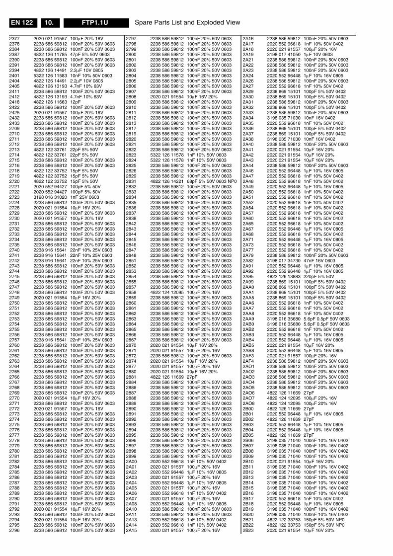
Spare Parts List and Exploded ViewEN 122 FTP1.1U10.
2377 2020 021 91557 100µF 20% 16V2378 2238 586 59812 100nF 20% 50V 06032384 2238 586 59812 100nF 20% 50V 06032387 4822 126 11785 47pF 5% 50V 06032390 2238 586 59812 100nF 20% 50V 06032391 2238 586 59812 100nF 20% 50V 06032394 4822 126 14491 2.2µF 10V 08052401 5322 126 11583 10nF 10% 50V 06032404 4822 126 14491 2.2µF 10V 08052405 4822 126 13193 4.7nF 10% 63V2411 2238 586 59812 100nF 20% 50V 06032412 4822 126 13193 4.7nF 10% 63V2418 4822 126 11663 12pF2422 2238 586 59812 100nF 20% 50V 06032425 2020 021 91557 100µF 20% 16V2432 2238 586 59812 100nF 20% 50V 06032433 2238 586 59812 100nF 20% 50V 06032709 2238 586 59812 100nF 20% 50V 06032710 2238 586 59812 100nF 20% 50V 06032711 2238 586 59812 100nF 20% 50V 06032712 2238 586 59812 100nF 20% 50V 06032713 4822 122 33761 22pF 5% 50V2714 4822 122 33761 22pF 5% 50V2715 2238 586 59812 100nF 20% 50V 06032716 2238 586 59812 100nF 20% 50V 06032718 4822 122 33752 15pF 5% 50V2719 4822 122 33752 15pF 5% 50V2720 4822 122 33752 15pF 5% 50V2721 2020 552 94427 100pF 5% 50V2722 2020 552 94427 100pF 5% 50V2723 3198 016 31020 1nF 25V 06032724 2238 586 59812 100nF 20% 50V 06032728 2020 021 91554 10µF 16V 20%2729 2238 586 59812 100nF 20% 50V 06032730 2020 021 91557 100µF 20% 16V2731 2238 586 59812 100nF 20% 50V 06032732 2238 586 59812 100nF 20% 50V 06032733 2238 586 59812 100nF 20% 50V 06032734 2238 586 59812 100nF 20% 50V 06032735 2238 586 59812 100nF 20% 50V 06032740 2238 916 15641 22nF 10% 25V 06032741 2238 916 15641 22nF 10% 25V 06032742 2238 916 15641 22nF 10% 25V 06032743 2238 586 59812 100nF 20% 50V 06032744 2238 586 59812 100nF 20% 50V 06032745 2238 586 59812 100nF 20% 50V 06032746 2238 586 59812 100nF 20% 50V 06032747 2238 586 59812 100nF 20% 50V 06032748 2238 586 59812 100nF 20% 50V 06032749 2020 021 91554 10µF 16V 20%2750 2238 586 59812 100nF 20% 50V 06032751 2238 586 59812 100nF 20% 50V 06032752 2238 586 59812 100nF 20% 50V 06032753 2238 586 59812 100nF 20% 50V 06032754 2238 586 59812 100nF 20% 50V 06032755 2238 586 59812 100nF 20% 50V 06032756 2238 586 59812 100nF 20% 50V 06032757 2238 916 15641 22nF 10% 25V 06032760 2238 586 59812 100nF 20% 50V 06032761 2238 586 59812 100nF 20% 50V 06032762 2238 586 59812 100nF 20% 50V 06032763 2238 586 59812 100nF 20% 50V 06032764 2238 586 59812 100nF 20% 50V 06032765 2238 586 59812 100nF 20% 50V 06032766 2238 586 59812 100nF 20% 50V 06032767 2238 586 59812 100nF 20% 50V 06032768 2238 586 59812 100nF 20% 50V 06032769 2238 586 59812 100nF 20% 50V 06032770 2020 021 91554 10µF 16V 20%2771 2238 586 59812 100nF 20% 50V 06032772 2020 021 91557 100µF 20% 16V2773 2238 586 59812 100nF 20% 50V 06032774 2238 586 59812 100nF 20% 50V 06032775 2238 586 59812 100nF 20% 50V 06032776 2238 586 59812 100nF 20% 50V 06032777 2238 586 59812 100nF 20% 50V 06032778 2238 586 59812 100nF 20% 50V 06032779 2238 586 59812 100nF 20% 50V 06032780 2238 586 59812 100nF 20% 50V 06032781 2238 586 59812 100nF 20% 50V 06032782 2238 586 59812 100nF 20% 50V 06032784 2238 586 59812 100nF 20% 50V 06032785 2238 586 59812 100nF 20% 50V 06032786 2238 586 59812 100nF 20% 50V 06032787 2238 586 59812 100nF 20% 50V 06032788 2238 586 59812 100nF 20% 50V 06032789 2238 586 59812 100nF 20% 50V 06032790 2238 586 59812 100nF 20% 50V 06032791 2238 586 59812 100nF 20% 50V 06032792 2020 021 91554 10µF 16V 20%2793 2238 586 59812 100nF 20% 50V 06032794 2020 021 91554 10µF 16V 20%2795 2238 586 59812 100nF 20% 50V 06032796 2238 586 59812 100nF 20% 50V 0603
2797 2238 586 59812 100nF 20% 50V 06032798 2238 586 59812 100nF 20% 50V 06032799 2238 586 59812 100nF 20% 50V 06032800 2238 586 59812 100nF 20% 50V 06032801 2238 586 59812 100nF 20% 50V 06032802 2238 586 59812 100nF 20% 50V 06032803 2238 586 59812 100nF 20% 50V 06032804 2238 586 59812 100nF 20% 50V 06032805 2238 586 59812 100nF 20% 50V 06032806 2238 586 59812 100nF 20% 50V 06032807 2238 586 59812 100nF 20% 50V 06032808 2020 021 91554 10µF 16V 20%2809 2238 586 59812 100nF 20% 50V 06032810 2238 586 59812 100nF 20% 50V 06032811 2238 586 59812 100nF 20% 50V 06032812 2238 586 59812 100nF 20% 50V 06032813 2238 586 59812 100nF 20% 50V 06032817 2238 586 59812 100nF 20% 50V 06032819 2238 586 59812 100nF 20% 50V 06032820 2238 586 59812 100nF 20% 50V 06032821 2238 586 59812 100nF 20% 50V 06032822 2238 586 59812 100nF 20% 50V 06032823 5322 126 11578 1nF 10% 50V 06032824 5322 126 11578 1nF 10% 50V 06032825 2238 586 59812 100nF 20% 50V 06032826 2238 586 59812 100nF 20% 50V 06032829 2238 586 59812 100nF 20% 50V 06032831 4822 126 14221 68pF 5% 50V 0603 NP02832 2238 586 59812 100nF 20% 50V 06032833 2238 586 59812 100nF 20% 50V 06032834 2238 586 59812 100nF 20% 50V 06032835 2238 586 59812 100nF 20% 50V 06032836 2238 586 59812 100nF 20% 50V 06032837 2238 586 59812 100nF 20% 50V 06032838 2238 586 59812 100nF 20% 50V 06032842 2238 586 59812 100nF 20% 50V 06032843 2238 586 59812 100nF 20% 50V 06032844 2238 586 59812 100nF 20% 50V 06032845 2238 586 59812 100nF 20% 50V 06032846 2238 586 59812 100nF 20% 50V 06032847 2238 586 59812 100nF 20% 50V 06032848 2238 586 59812 100nF 20% 50V 06032851 2238 586 59812 100nF 20% 50V 06032852 2238 586 59812 100nF 20% 50V 06032853 2238 586 59812 100nF 20% 50V 06032854 2238 586 59812 100nF 20% 50V 06032855 2238 586 59812 100nF 20% 50V 06032857 2238 586 59812 100nF 20% 50V 06032858 4822 124 12095 100µF 20% 16V2859 2238 586 59812 100nF 20% 50V 06032860 2238 586 59812 100nF 20% 50V 06032861 2238 586 59812 100nF 20% 50V 06032862 2238 586 59812 100nF 20% 50V 06032863 2238 586 59812 100nF 20% 50V 06032864 2238 586 59812 100nF 20% 50V 06032865 2238 586 59812 100nF 20% 50V 06032866 2238 586 59812 100nF 20% 50V 06032867 2238 586 59812 100nF 20% 50V 06032870 2020 021 91554 10µF 16V 20%2871 2020 021 91557 100µF 20% 16V2872 2238 586 59812 100nF 20% 50V 06032874 2020 021 91554 10µF 16V 20%2877 2020 021 91557 100µF 20% 16V2880 2020 021 91554 10µF 16V 20%2881 4822 126 11669 27pF2884 2238 586 59812 100nF 20% 50V 06032886 2238 586 59812 100nF 20% 50V 06032887 2238 586 59812 100nF 20% 50V 06032888 2238 586 59812 100nF 20% 50V 06032889 2238 586 59812 100nF 20% 50V 06032890 2238 586 59812 100nF 20% 50V 06032891 2238 586 59812 100nF 20% 50V 06032892 2238 586 59812 100nF 20% 50V 06032893 2238 586 59812 100nF 20% 50V 06032894 2238 586 59812 100nF 20% 50V 06032895 2238 586 59812 100nF 20% 50V 06032896 2238 586 59812 100nF 20% 50V 06032897 2238 586 59812 100nF 20% 50V 06032898 2238 586 59812 100nF 20% 50V 06032899 2238 586 59812 100nF 20% 50V 06032A00 2020 552 96618 1nF 10% 50V 04022A01 2020 021 91557 100µF 20% 16V2A02 2020 552 96448 1µF 10% 16V 08052A03 2020 021 91557 100µF 20% 16V2A04 2020 552 96448 1µF 10% 16V 08052A05 2020 021 91557 100µF 20% 16V2A06 2020 552 96618 1nF 10% 50V 04022A07 2020 021 91557 100µF 20% 16V2A08 2020 552 96448 1µF 10% 16V 08052A10 2238 586 59812 100nF 20% 50V 06032A11 2238 586 59812 100nF 20% 50V 06032A13 2020 552 96618 1nF 10% 50V 04022A14 2020 552 96618 1nF 10% 50V 04022A15 2020 021 91557 100µF 20% 16V
2A16 2238 586 59812 100nF 20% 50V 06032A17 2020 552 96618 1nF 10% 50V 04022A18 2020 021 91557 100µF 20% 16V2A19 3198 017 41050 1µF 10V 06032A21 2238 586 59812 100nF 20% 50V 06032A22 2238 586 59812 100nF 20% 50V 06032A23 2238 586 59812 100nF 20% 50V 06032A24 2020 552 96448 1µF 10% 16V 08052A26 2238 586 59812 100nF 20% 50V 06032A27 2020 552 96618 1nF 10% 50V 04022A29 2238 869 15101 100pF 5% 50V 04022A30 2238 869 15101 100pF 5% 50V 04022A31 2238 586 59812 100nF 20% 50V 06032A32 2238 869 15101 100pF 5% 50V 04022A33 2238 586 59812 100nF 20% 50V 06032A34 3198 035 71030 10nF 16V 04022A35 2020 552 96618 1nF 10% 50V 04022A36 2238 869 15101 100pF 5% 50V 04022A37 2238 869 15101 100pF 5% 50V 04022A38 3198 035 71030 10nF 16V 04022A40 2238 586 59812 100nF 20% 50V 06032A41 2020 021 91554 10µF 16V 20%2A42 2020 021 91554 10µF 16V 20%2A43 2020 021 91554 10µF 16V 20%2A44 2238 586 59812 100nF 20% 50V 06032A46 2020 552 96448 1µF 10% 16V 08052A47 2020 552 96618 1nF 10% 50V 04022A48 2020 552 96618 1nF 10% 50V 04022A49 2020 552 96448 1µF 10% 16V 08052A50 2020 552 96618 1nF 10% 50V 04022A51 2020 552 96618 1nF 10% 50V 04022A52 2020 552 96618 1nF 10% 50V 04022A54 2020 552 96618 1nF 10% 50V 04022A57 2020 552 96618 1nF 10% 50V 04022A60 2020 552 96618 1nF 10% 50V 04022A65 2020 552 96618 1nF 10% 50V 04022A67 2020 552 96448 1µF 10% 16V 08052A68 2020 552 96618 1nF 10% 50V 04022A71 2020 552 96448 1µF 10% 16V 08052A73 2020 552 96618 1nF 10% 50V 04022A77 2020 552 96618 1nF 10% 50V 04022A79 2238 586 59812 100nF 20% 50V 06032A82 3198 017 34730 47nF 16V 06032A91 2020 552 96448 1µF 10% 16V 08052A92 2020 552 96448 1µF 10% 16V 08052A95 4822 126 13883 220pF 5% 50V2A99 2238 869 15101 100pF 5% 50V 04022AA0 2238 869 15101 100pF 5% 50V 04022AA1 2238 869 15101 100pF 5% 50V 04022AA5 2238 869 15101 100pF 5% 50V 04022AA6 2020 552 96618 1nF 10% 50V 04022AA7 2020 552 96618 1nF 10% 50V 04022AA8 2020 552 96618 1nF 10% 50V 04022AA9 3198 016 35680 5.6pF 0.5pF 50V 06032AB0 3198 016 35680 5.6pF 0.5pF 50V 06032AB2 2020 552 96618 1nF 10% 50V 04022AB3 2020 552 96448 1µF 10% 16V 08052AB4 2020 552 96448 1µF 10% 16V 08052AB5 2020 021 91554 10µF 16V 20%2AB8 2020 552 96448 1µF 10% 16V 08052AF3 2020 021 91557 100µF 20% 16V2AF4 2238 586 59812 100nF 20% 50V 06032AO1 2238 586 59812 100nF 20% 50V 06032AO2 2238 586 59812 100nF 20% 50V 06032AO3 2238 586 59812 100nF 20% 50V 06032AO4 2238 586 59812 100nF 20% 50V 06032AO5 2238 586 59812 100nF 20% 50V 06032AO6 4822 126 11669 27pF2AO7 4822 124 12095 100µF 20% 16V2AO8 4822 124 12095 100µF 20% 16V2B00 4822 126 11669 27pF2B01 2020 552 96448 1µF 10% 16V 08052B02 4822 126 11669 27pF2B03 2020 552 96448 1µF 10% 16V 08052B04 2020 552 96448 1µF 10% 16V 08052B05 4822 126 11669 27pF2B06 3198 035 71040 100nF 10% 16V 04022B07 3198 035 71040 100nF 10% 16V 04022B08 3198 035 71040 100nF 10% 16V 04022B09 3198 035 71040 100nF 10% 16V 04022B10 2020 021 91554 10µF 16V 20%2B11 3198 035 71040 100nF 10% 16V 04022B12 3198 035 71040 100nF 10% 16V 04022B13 3198 035 71040 100nF 10% 16V 04022B14 3198 035 71040 100nF 10% 16V 04022B15 3198 035 71040 100nF 10% 16V 04022B16 3198 035 71040 100nF 10% 16V 04022B17 2020 552 96618 1nF 10% 50V 04022B18 2020 552 96448 1µF 10% 16V 08052B19 3198 035 71040 100nF 10% 16V 04022B20 3198 035 71040 100nF 10% 16V 04022B21 4822 122 33753 150pF 5% 50V NP02B22 4822 122 33753 150pF 5% 50V NP02B23 2020 021 91554 10µF 16V 20%
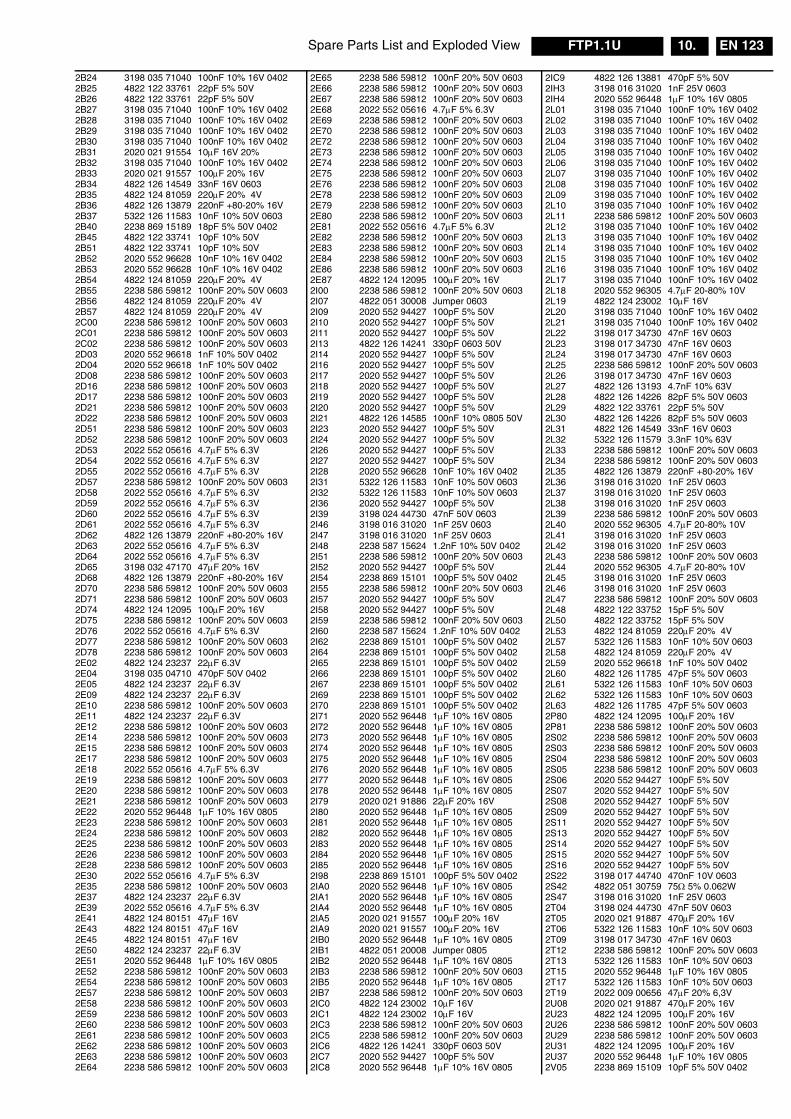
Spare Parts List and Exploded View EN 123FTP1.1U 10.
2B24 3198 035 71040 100nF 10% 16V 04022B25 4822 122 33761 22pF 5% 50V2B26 4822 122 33761 22pF 5% 50V2B27 3198 035 71040 100nF 10% 16V 04022B28 3198 035 71040 100nF 10% 16V 04022B29 3198 035 71040 100nF 10% 16V 04022B30 3198 035 71040 100nF 10% 16V 04022B31 2020 021 91554 10µF 16V 20%2B32 3198 035 71040 100nF 10% 16V 04022B33 2020 021 91557 100µF 20% 16V2B34 4822 126 14549 33nF 16V 06032B35 4822 124 81059 220µF 20% 4V2B36 4822 126 13879 220nF +80-20% 16V2B37 5322 126 11583 10nF 10% 50V 06032B40 2238 869 15189 18pF 5% 50V 04022B45 4822 122 33741 10pF 10% 50V2B51 4822 122 33741 10pF 10% 50V2B52 2020 552 96628 10nF 10% 16V 04022B53 2020 552 96628 10nF 10% 16V 04022B54 4822 124 81059 220µF 20% 4V2B55 2238 586 59812 100nF 20% 50V 06032B56 4822 124 81059 220µF 20% 4V2B57 4822 124 81059 220µF 20% 4V2C00 2238 586 59812 100nF 20% 50V 06032C01 2238 586 59812 100nF 20% 50V 06032C02 2238 586 59812 100nF 20% 50V 06032D03 2020 552 96618 1nF 10% 50V 04022D04 2020 552 96618 1nF 10% 50V 04022D08 2238 586 59812 100nF 20% 50V 06032D16 2238 586 59812 100nF 20% 50V 06032D17 2238 586 59812 100nF 20% 50V 06032D21 2238 586 59812 100nF 20% 50V 06032D22 2238 586 59812 100nF 20% 50V 06032D51 2238 586 59812 100nF 20% 50V 06032D52 2238 586 59812 100nF 20% 50V 06032D53 2022 552 05616 4.7µF 5% 6.3V2D54 2022 552 05616 4.7µF 5% 6.3V2D55 2022 552 05616 4.7µF 5% 6.3V2D57 2238 586 59812 100nF 20% 50V 06032D58 2022 552 05616 4.7µF 5% 6.3V2D59 2022 552 05616 4.7µF 5% 6.3V2D60 2022 552 05616 4.7µF 5% 6.3V2D61 2022 552 05616 4.7µF 5% 6.3V2D62 4822 126 13879 220nF +80-20% 16V2D63 2022 552 05616 4.7µF 5% 6.3V2D64 2022 552 05616 4.7µF 5% 6.3V2D65 3198 032 47170 47µF 20% 16V2D68 4822 126 13879 220nF +80-20% 16V2D70 2238 586 59812 100nF 20% 50V 06032D71 2238 586 59812 100nF 20% 50V 06032D74 4822 124 12095 100µF 20% 16V2D75 2238 586 59812 100nF 20% 50V 06032D76 2022 552 05616 4.7µF 5% 6.3V2D77 2238 586 59812 100nF 20% 50V 06032D78 2238 586 59812 100nF 20% 50V 06032E02 4822 124 23237 22µF 6.3V2E04 3198 035 04710 470pF 50V 04022E05 4822 124 23237 22µF 6.3V2E09 4822 124 23237 22µF 6.3V2E10 2238 586 59812 100nF 20% 50V 06032E11 4822 124 23237 22µF 6.3V2E12 2238 586 59812 100nF 20% 50V 06032E14 2238 586 59812 100nF 20% 50V 06032E15 2238 586 59812 100nF 20% 50V 06032E17 2238 586 59812 100nF 20% 50V 06032E18 2022 552 05616 4.7µF 5% 6.3V2E19 2238 586 59812 100nF 20% 50V 06032E20 2238 586 59812 100nF 20% 50V 06032E21 2238 586 59812 100nF 20% 50V 06032E22 2020 552 96448 1µF 10% 16V 08052E23 2238 586 59812 100nF 20% 50V 06032E24 2238 586 59812 100nF 20% 50V 06032E25 2238 586 59812 100nF 20% 50V 06032E26 2238 586 59812 100nF 20% 50V 06032E28 2238 586 59812 100nF 20% 50V 06032E30 2022 552 05616 4.7µF 5% 6.3V2E35 2238 586 59812 100nF 20% 50V 06032E37 4822 124 23237 22µF 6.3V2E39 2022 552 05616 4.7µF 5% 6.3V2E41 4822 124 80151 47µF 16V2E43 4822 124 80151 47µF 16V2E45 4822 124 80151 47µF 16V2E50 4822 124 23237 22µF 6.3V2E51 2020 552 96448 1µF 10% 16V 08052E52 2238 586 59812 100nF 20% 50V 06032E54 2238 586 59812 100nF 20% 50V 06032E57 2238 586 59812 100nF 20% 50V 06032E58 2238 586 59812 100nF 20% 50V 06032E59 2238 586 59812 100nF 20% 50V 06032E60 2238 586 59812 100nF 20% 50V 06032E61 2238 586 59812 100nF 20% 50V 06032E62 2238 586 59812 100nF 20% 50V 06032E63 2238 586 59812 100nF 20% 50V 06032E64 2238 586 59812 100nF 20% 50V 0603
2E65 2238 586 59812 100nF 20% 50V 06032E66 2238 586 59812 100nF 20% 50V 06032E67 2238 586 59812 100nF 20% 50V 06032E68 2022 552 05616 4.7µF 5% 6.3V2E69 2238 586 59812 100nF 20% 50V 06032E70 2238 586 59812 100nF 20% 50V 06032E72 2238 586 59812 100nF 20% 50V 06032E73 2238 586 59812 100nF 20% 50V 06032E74 2238 586 59812 100nF 20% 50V 06032E75 2238 586 59812 100nF 20% 50V 06032E76 2238 586 59812 100nF 20% 50V 06032E78 2238 586 59812 100nF 20% 50V 06032E79 2238 586 59812 100nF 20% 50V 06032E80 2238 586 59812 100nF 20% 50V 06032E81 2022 552 05616 4.7µF 5% 6.3V2E82 2238 586 59812 100nF 20% 50V 06032E83 2238 586 59812 100nF 20% 50V 06032E84 2238 586 59812 100nF 20% 50V 06032E86 2238 586 59812 100nF 20% 50V 06032E87 4822 124 12095 100µF 20% 16V2I00 2238 586 59812 100nF 20% 50V 06032I07 4822 051 30008 Jumper 06032I09 2020 552 94427 100pF 5% 50V2I10 2020 552 94427 100pF 5% 50V2I11 2020 552 94427 100pF 5% 50V2I13 4822 126 14241 330pF 0603 50V2I14 2020 552 94427 100pF 5% 50V2I16 2020 552 94427 100pF 5% 50V2I17 2020 552 94427 100pF 5% 50V2I18 2020 552 94427 100pF 5% 50V2I19 2020 552 94427 100pF 5% 50V2I20 2020 552 94427 100pF 5% 50V2I21 4822 126 14585 100nF 10% 0805 50V2I23 2020 552 94427 100pF 5% 50V2I24 2020 552 94427 100pF 5% 50V2I26 2020 552 94427 100pF 5% 50V2I27 2020 552 94427 100pF 5% 50V2I28 2020 552 96628 10nF 10% 16V 04022I31 5322 126 11583 10nF 10% 50V 06032I32 5322 126 11583 10nF 10% 50V 06032I36 2020 552 94427 100pF 5% 50V2I39 3198 024 44730 47nF 50V 06032I46 3198 016 31020 1nF 25V 06032I47 3198 016 31020 1nF 25V 06032I48 2238 587 15624 1.2nF 10% 50V 04022I51 2238 586 59812 100nF 20% 50V 06032I52 2020 552 94427 100pF 5% 50V2I54 2238 869 15101 100pF 5% 50V 04022I55 2238 586 59812 100nF 20% 50V 06032I57 2020 552 94427 100pF 5% 50V2I58 2020 552 94427 100pF 5% 50V2I59 2238 586 59812 100nF 20% 50V 06032I60 2238 587 15624 1.2nF 10% 50V 04022I62 2238 869 15101 100pF 5% 50V 04022I64 2238 869 15101 100pF 5% 50V 04022I65 2238 869 15101 100pF 5% 50V 04022I66 2238 869 15101 100pF 5% 50V 04022I67 2238 869 15101 100pF 5% 50V 04022I69 2238 869 15101 100pF 5% 50V 04022I70 2238 869 15101 100pF 5% 50V 04022I71 2020 552 96448 1µF 10% 16V 08052I72 2020 552 96448 1µF 10% 16V 08052I73 2020 552 96448 1µF 10% 16V 08052I74 2020 552 96448 1µF 10% 16V 08052I75 2020 552 96448 1µF 10% 16V 08052I76 2020 552 96448 1µF 10% 16V 08052I77 2020 552 96448 1µF 10% 16V 08052I78 2020 552 96448 1µF 10% 16V 08052I79 2020 021 91886 22µF 20% 16V2I80 2020 552 96448 1µF 10% 16V 08052I81 2020 552 96448 1µF 10% 16V 08052I82 2020 552 96448 1µF 10% 16V 08052I83 2020 552 96448 1µF 10% 16V 08052I84 2020 552 96448 1µF 10% 16V 08052I85 2020 552 96448 1µF 10% 16V 08052I98 2238 869 15101 100pF 5% 50V 04022IA0 2020 552 96448 1µF 10% 16V 08052IA1 2020 552 96448 1µF 10% 16V 08052IA4 2020 552 96448 1µF 10% 16V 08052IA5 2020 021 91557 100µF 20% 16V2IA9 2020 021 91557 100µF 20% 16V2IB0 2020 552 96448 1µF 10% 16V 08052IB1 4822 051 20008 Jumper 08052IB2 2020 552 96448 1µF 10% 16V 08052IB3 2238 586 59812 100nF 20% 50V 06032IB5 2020 552 96448 1µF 10% 16V 08052IB7 2238 586 59812 100nF 20% 50V 06032IC0 4822 124 23002 10µF 16V2IC1 4822 124 23002 10µF 16V2IC3 2238 586 59812 100nF 20% 50V 06032IC5 2238 586 59812 100nF 20% 50V 06032IC6 4822 126 14241 330pF 0603 50V2IC7 2020 552 94427 100pF 5% 50V2IC8 2020 552 96448 1µF 10% 16V 0805
2IC9 4822 126 13881 470pF 5% 50V2IH3 3198 016 31020 1nF 25V 06032IH4 2020 552 96448 1µF 10% 16V 08052L01 3198 035 71040 100nF 10% 16V 04022L02 3198 035 71040 100nF 10% 16V 04022L03 3198 035 71040 100nF 10% 16V 04022L04 3198 035 71040 100nF 10% 16V 04022L05 3198 035 71040 100nF 10% 16V 04022L06 3198 035 71040 100nF 10% 16V 04022L07 3198 035 71040 100nF 10% 16V 04022L08 3198 035 71040 100nF 10% 16V 04022L09 3198 035 71040 100nF 10% 16V 04022L10 3198 035 71040 100nF 10% 16V 04022L11 2238 586 59812 100nF 20% 50V 06032L12 3198 035 71040 100nF 10% 16V 04022L13 3198 035 71040 100nF 10% 16V 04022L14 3198 035 71040 100nF 10% 16V 04022L15 3198 035 71040 100nF 10% 16V 04022L16 3198 035 71040 100nF 10% 16V 04022L17 3198 035 71040 100nF 10% 16V 04022L18 2020 552 96305 4.7µF 20-80% 10V2L19 4822 124 23002 10µF 16V2L20 3198 035 71040 100nF 10% 16V 04022L21 3198 035 71040 100nF 10% 16V 04022L22 3198 017 34730 47nF 16V 06032L23 3198 017 34730 47nF 16V 06032L24 3198 017 34730 47nF 16V 06032L25 2238 586 59812 100nF 20% 50V 06032L26 3198 017 34730 47nF 16V 06032L27 4822 126 13193 4.7nF 10% 63V2L28 4822 126 14226 82pF 5% 50V 06032L29 4822 122 33761 22pF 5% 50V2L30 4822 126 14226 82pF 5% 50V 06032L31 4822 126 14549 33nF 16V 06032L32 5322 126 11579 3.3nF 10% 63V2L33 2238 586 59812 100nF 20% 50V 06032L34 2238 586 59812 100nF 20% 50V 06032L35 4822 126 13879 220nF +80-20% 16V2L36 3198 016 31020 1nF 25V 06032L37 3198 016 31020 1nF 25V 06032L38 3198 016 31020 1nF 25V 06032L39 2238 586 59812 100nF 20% 50V 06032L40 2020 552 96305 4.7µF 20-80% 10V2L41 3198 016 31020 1nF 25V 06032L42 3198 016 31020 1nF 25V 06032L43 2238 586 59812 100nF 20% 50V 06032L44 2020 552 96305 4.7µF 20-80% 10V2L45 3198 016 31020 1nF 25V 06032L46 3198 016 31020 1nF 25V 06032L47 2238 586 59812 100nF 20% 50V 06032L48 4822 122 33752 15pF 5% 50V2L50 4822 122 33752 15pF 5% 50V2L53 4822 124 81059 220µF 20% 4V2L57 5322 126 11583 10nF 10% 50V 06032L58 4822 124 81059 220µF 20% 4V2L59 2020 552 96618 1nF 10% 50V 04022L60 4822 126 11785 47pF 5% 50V 06032L61 5322 126 11583 10nF 10% 50V 06032L62 5322 126 11583 10nF 10% 50V 06032L63 4822 126 11785 47pF 5% 50V 06032P80 4822 124 12095 100µF 20% 16V2P81 2238 586 59812 100nF 20% 50V 06032S02 2238 586 59812 100nF 20% 50V 06032S03 2238 586 59812 100nF 20% 50V 06032S04 2238 586 59812 100nF 20% 50V 06032S05 2238 586 59812 100nF 20% 50V 06032S06 2020 552 94427 100pF 5% 50V2S07 2020 552 94427 100pF 5% 50V2S08 2020 552 94427 100pF 5% 50V2S09 2020 552 94427 100pF 5% 50V2S11 2020 552 94427 100pF 5% 50V2S13 2020 552 94427 100pF 5% 50V2S14 2020 552 94427 100pF 5% 50V2S15 2020 552 94427 100pF 5% 50V2S16 2020 552 94427 100pF 5% 50V2S22 3198 017 44740 470nF 10V 06032S42 4822 051 30759 75Ω 5% 0.062W2S47 3198 016 31020 1nF 25V 06032T04 3198 024 44730 47nF 50V 06032T05 2020 021 91887 470µF 20% 16V2T06 5322 126 11583 10nF 10% 50V 06032T09 3198 017 34730 47nF 16V 06032T12 2238 586 59812 100nF 20% 50V 06032T13 5322 126 11583 10nF 10% 50V 06032T15 2020 552 96448 1µF 10% 16V 08052T17 5322 126 11583 10nF 10% 50V 06032T19 2022 009 00656 47µF 20% 6,3V2U08 2020 021 91887 470µF 20% 16V2U23 4822 124 12095 100µF 20% 16V2U26 2238 586 59812 100nF 20% 50V 06032U29 2238 586 59812 100nF 20% 50V 06032U31 4822 124 12095 100µF 20% 16V2U37 2020 552 96448 1µF 10% 16V 08052V05 2238 869 15109 10pF 5% 50V 0402
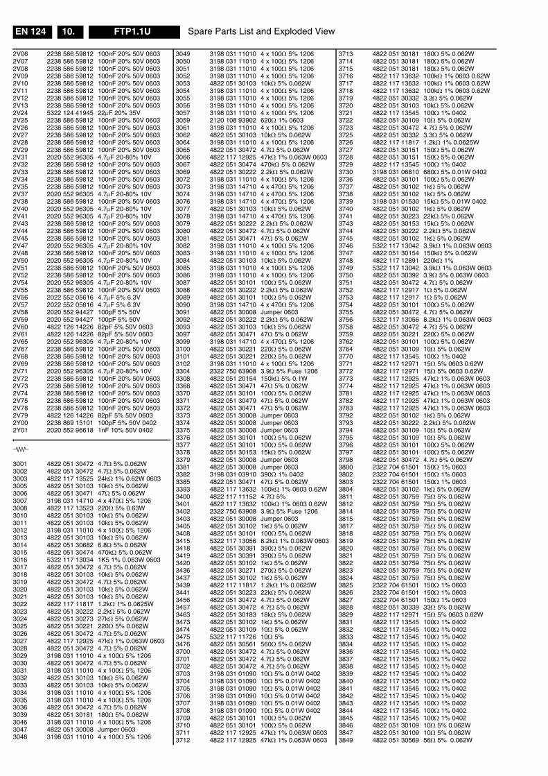
Spare Parts List and Exploded ViewEN 124 FTP1.1U10.
2V06 2238 586 59812 100nF 20% 50V 06032V07 2238 586 59812 100nF 20% 50V 06032V08 2238 586 59812 100nF 20% 50V 06032V09 2238 586 59812 100nF 20% 50V 06032V10 2238 586 59812 100nF 20% 50V 06032V11 2238 586 59812 100nF 20% 50V 06032V12 2238 586 59812 100nF 20% 50V 06032V13 2238 586 59812 100nF 20% 50V 06032V24 5322 124 41945 22µF 20% 35V2V25 2238 586 59812 100nF 20% 50V 06032V26 2238 586 59812 100nF 20% 50V 06032V27 2238 586 59812 100nF 20% 50V 06032V28 2238 586 59812 100nF 20% 50V 06032V29 2238 586 59812 100nF 20% 50V 06032V31 2020 552 96305 4.7µF 20-80% 10V2V32 2238 586 59812 100nF 20% 50V 06032V33 2238 586 59812 100nF 20% 50V 06032V34 2238 586 59812 100nF 20% 50V 06032V35 2238 586 59812 100nF 20% 50V 06032V37 2020 552 96305 4.7µF 20-80% 10V2V38 2238 586 59812 100nF 20% 50V 06032V40 2020 552 96305 4.7µF 20-80% 10V2V41 2020 552 96305 4.7µF 20-80% 10V2V43 2238 586 59812 100nF 20% 50V 06032V44 2238 586 59812 100nF 20% 50V 06032V45 2238 586 59812 100nF 20% 50V 06032V47 2020 552 96305 4.7µF 20-80% 10V2V48 2238 586 59812 100nF 20% 50V 06032V50 2020 552 96305 4.7µF 20-80% 10V2V51 2238 586 59812 100nF 20% 50V 06032V52 2238 586 59812 100nF 20% 50V 06032V54 2020 552 96305 4.7µF 20-80% 10V2V55 2238 586 59812 100nF 20% 50V 06032V56 2022 552 05616 4.7µF 5% 6.3V2V57 2022 552 05616 4.7µF 5% 6.3V2V58 2020 552 94427 100pF 5% 50V2V59 2020 552 94427 100pF 5% 50V2V60 4822 126 14226 82pF 5% 50V 06032V61 4822 126 14226 82pF 5% 50V 06032V65 2020 552 96305 4.7µF 20-80% 10V2V67 2238 586 59812 100nF 20% 50V 06032V68 2238 586 59812 100nF 20% 50V 06032V69 2238 586 59812 100nF 20% 50V 06032V71 2020 552 96305 4.7µF 20-80% 10V2V72 2238 586 59812 100nF 20% 50V 06032V73 2238 586 59812 100nF 20% 50V 06032V74 2238 586 59812 100nF 20% 50V 06032V75 2238 586 59812 100nF 20% 50V 06032V78 2238 586 59812 100nF 20% 50V 06032V79 4822 126 14226 82pF 5% 50V 06032Y00 2238 869 15101 100pF 5% 50V 04022Y01 2020 552 96618 1nF 10% 50V 0402
3001 4822 051 30472 4.7Ω 5% 0.062W3002 4822 051 30472 4.7Ω 5% 0.062W3003 4822 117 13525 24kΩ 1% 0.62W 06033005 4822 051 30103 10kΩ 5% 0.062W3006 4822 051 30471 47Ω 5% 0.062W3007 3198 031 14710 4 x 470Ω 5% 12063008 4822 117 13523 220Ω 5% 0.63W3010 4822 051 30103 10kΩ 5% 0.062W3011 4822 051 30103 10kΩ 5% 0.062W3012 3198 031 11010 4 x 100Ω 5% 12063013 4822 051 30103 10kΩ 5% 0.062W3014 4822 051 30682 6.8Ω 5% 0.062W3015 4822 051 30474 470kΩ 5% 0.062W3016 5322 117 13034 1K5 1% 0.063W 06033017 4822 051 30472 4.7Ω 5% 0.062W3018 4822 051 30103 10kΩ 5% 0.062W3019 4822 051 30472 4.7Ω 5% 0.062W3020 4822 051 30103 10kΩ 5% 0.062W3021 4822 051 30103 10kΩ 5% 0.062W3022 4822 117 11817 1.2kΩ 1% 0.0625W3023 4822 051 30222 2.2kΩ 5% 0.062W3024 4822 051 30273 27kΩ 5% 0.062W3025 4822 051 30221 220Ω 5% 0.062W3026 4822 051 30472 4.7Ω 5% 0.062W3027 4822 117 12925 47kΩ 1% 0.063W 06033028 4822 051 30472 4.7Ω 5% 0.062W3029 3198 031 11010 4 x 100Ω 5% 12063030 4822 051 30472 4.7Ω 5% 0.062W3031 3198 031 11010 4 x 100Ω 5% 12063032 4822 051 30103 10kΩ 5% 0.062W3033 4822 051 30103 10kΩ 5% 0.062W3034 3198 031 11010 4 x 100Ω 5% 12063035 3198 031 11010 4 x 100Ω 5% 12063036 4822 051 30472 4.7Ω 5% 0.062W3039 4822 051 30181 180Ω 5% 0.062W3046 3198 031 11010 4 x 100Ω 5% 12063047 4822 051 30008 Jumper 06033048 3198 031 11010 4 x 100Ω 5% 1206
3049 3198 031 11010 4 x 100Ω 5% 12063050 3198 031 11010 4 x 100Ω 5% 12063051 3198 031 11010 4 x 100Ω 5% 12063052 3198 031 11010 4 x 100Ω 5% 12063053 4822 051 30103 10kΩ 5% 0.062W3054 3198 031 11010 4 x 100Ω 5% 12063055 3198 031 11010 4 x 100Ω 5% 12063056 3198 031 11010 4 x 100Ω 5% 12063057 3198 031 11010 4 x 100Ω 5% 12063059 2120 108 93902 620Ω 1% 06033061 3198 031 11010 4 x 100Ω 5% 12063062 4822 051 30103 10kΩ 5% 0.062W3064 3198 031 11010 4 x 100Ω 5% 12063065 4822 051 30472 4.7Ω 5% 0.062W3066 4822 117 12925 47kΩ 1% 0.063W 06033067 4822 051 30474 470kΩ 5% 0.062W3069 4822 051 30222 2.2kΩ 5% 0.062W3072 3198 031 11010 4 x 100Ω 5% 12063073 3198 031 14710 4 x 470Ω 5% 12063074 3198 031 14710 4 x 470Ω 5% 12063076 3198 031 14710 4 x 470Ω 5% 12063077 4822 051 30103 10kΩ 5% 0.062W3078 3198 031 14710 4 x 470Ω 5% 12063079 4822 051 30222 2.2kΩ 5% 0.062W3080 4822 051 30472 4.7Ω 5% 0.062W3081 4822 051 30471 47Ω 5% 0.062W3082 3198 031 11010 4 x 100Ω 5% 12063083 3198 031 11010 4 x 100Ω 5% 12063084 4822 051 30103 10kΩ 5% 0.062W3085 3198 031 11010 4 x 100Ω 5% 12063086 3198 031 11010 4 x 100Ω 5% 12063087 4822 051 30101 100Ω 5% 0.062W3088 4822 051 30222 2.2kΩ 5% 0.062W3089 4822 051 30101 100Ω 5% 0.062W3090 3198 031 14710 4 x 470Ω 5% 12063091 4822 051 30008 Jumper 06033092 4822 051 30222 2.2kΩ 5% 0.062W3093 4822 051 30103 10kΩ 5% 0.062W3097 4822 051 30471 47Ω 5% 0.062W3099 3198 031 14710 4 x 470Ω 5% 12063100 4822 051 30221 220Ω 5% 0.062W3101 4822 051 30221 220Ω 5% 0.062W3102 3198 031 11010 4 x 100Ω 5% 12063304 2322 750 63908 3.9Ω 5% Fuse 12063308 4822 051 20154 150kΩ 5% 0.1W3368 4822 051 30471 47Ω 5% 0.062W3370 4822 051 30101 100Ω 5% 0.062W3371 4822 051 30479 47Ω 5% 0.062W3372 4822 051 30471 47Ω 5% 0.062W3373 4822 051 30008 Jumper 06033374 4822 051 30008 Jumper 06033375 4822 051 30008 Jumper 06033376 4822 051 30101 100Ω 5% 0.062W3377 4822 051 30101 100Ω 5% 0.062W3378 4822 051 30153 15kΩ 5% 0.062W3379 4822 051 30008 Jumper 06033381 4822 051 30008 Jumper 06033382 3198 031 03910 390Ω 1% 04023385 4822 051 30471 47Ω 5% 0.062W3393 4822 117 13632 100kΩ 1% 0603 0.62W3400 4822 117 11152 4.7Ω 5%3401 4822 117 13632 100kΩ 1% 0603 0.62W3402 2322 750 63908 3.9Ω 5% Fuse 12063403 4822 051 30008 Jumper 06033405 4822 051 30102 1kΩ 5% 0.062W3408 4822 051 30101 100Ω 5% 0.062W3415 5322 117 13056 8.2kΩ 1% 0.063W 06033418 4822 051 30391 390Ω 5% 0.062W3419 4822 051 30391 390Ω 5% 0.062W3420 4822 051 30102 1kΩ 5% 0.062W3436 4822 051 30271 270Ω 5% 0.062W3437 4822 051 30102 1kΩ 5% 0.062W3439 4822 117 11817 1.2kΩ 1% 0.0625W3441 4822 051 30223 22kΩ 5% 0.062W3456 4822 051 30472 4.7Ω 5% 0.062W3457 4822 051 30472 4.7Ω 5% 0.062W3463 4822 051 30183 18kΩ 5% 0.062W3473 4822 051 30102 1kΩ 5% 0.062W3474 4822 051 30109 10Ω 5% 0.062W3475 5322 117 11726 10Ω 5%3476 4822 051 30561 560Ω 5% 0.062W3700 4822 051 30472 4.7Ω 5% 0.062W3701 4822 051 30472 4.7Ω 5% 0.062W3702 4822 051 30472 4.7Ω 5% 0.062W3703 3198 031 01090 10Ω 5% 0.01W 04023704 3198 031 01090 10Ω 5% 0.01W 04023705 3198 031 01090 10Ω 5% 0.01W 04023706 3198 031 01090 10Ω 5% 0.01W 04023707 3198 031 01090 10Ω 5% 0.01W 04023708 3198 031 01090 10Ω 5% 0.01W 04023709 4822 051 30101 100Ω 5% 0.062W3710 4822 051 30101 100Ω 5% 0.062W3711 4822 117 12925 47kΩ 1% 0.063W 06033712 4822 117 12925 47kΩ 1% 0.063W 0603
3713 4822 051 30181 180Ω 5% 0.062W3714 4822 051 30181 180Ω 5% 0.062W3715 4822 051 30181 180Ω 5% 0.062W3716 4822 117 13632 100kΩ 1% 0603 0.62W3717 4822 117 13632 100kΩ 1% 0603 0.62W3718 4822 117 13632 100kΩ 1% 0603 0.62W3719 4822 051 30332 3.3Ω 5% 0.062W3720 4822 051 30103 10kΩ 5% 0.062W3721 4822 117 13545 100Ω 1% 04023722 4822 051 30109 10Ω 5% 0.062W3723 4822 051 30472 4.7Ω 5% 0.062W3725 4822 051 30332 3.3Ω 5% 0.062W3726 4822 117 11817 1.2kΩ 1% 0.0625W3727 4822 051 30151 150Ω 5% 0.062W3728 4822 051 30151 150Ω 5% 0.062W3729 4822 117 13545 100Ω 1% 04023730 3198 031 06810 680Ω 5% 0.01W 04023736 4822 051 30101 100Ω 5% 0.062W3737 4822 051 30102 1kΩ 5% 0.062W3738 4822 051 30102 1kΩ 5% 0.062W3739 3198 031 01530 15kΩ 5% 0.01W 04023740 4822 051 30102 1kΩ 5% 0.062W3741 4822 051 30223 22kΩ 5% 0.062W3743 4822 051 30153 15kΩ 5% 0.062W3744 4822 051 30222 2.2kΩ 5% 0.062W3745 4822 051 30102 1kΩ 5% 0.062W3746 5322 117 13042 3.9kΩ 1% 0.063W 06033747 4822 051 30154 150kΩ 5% 0.062W3748 4822 117 12891 220kΩ 1%3749 5322 117 13042 3.9kΩ 1% 0.063W 06033750 4822 051 30392 3.9Ω 5% 0.063W 06033751 4822 051 30472 4.7Ω 5% 0.062W3752 4822 117 12917 1Ω 5% 0.062W3753 4822 117 12917 1Ω 5% 0.062W3754 4822 051 30101 100Ω 5% 0.062W3755 4822 051 30472 4.7Ω 5% 0.062W3756 5322 117 13056 8.2kΩ 1% 0.063W 06033758 4822 051 30472 4.7Ω 5% 0.062W3759 4822 051 30221 220Ω 5% 0.062W3762 4822 051 30101 100Ω 5% 0.062W3764 4822 051 30109 10Ω 5% 0.062W3770 4822 117 13545 100Ω 1% 04023771 4822 117 12971 15Ω 5% 0603 0.62W3772 4822 117 12971 15Ω 5% 0603 0.62W3773 4822 117 12925 47kΩ 1% 0.063W 06033774 4822 117 12925 47kΩ 1% 0.063W 06033781 4822 117 12925 47kΩ 1% 0.063W 06033782 4822 117 12925 47kΩ 1% 0.063W 06033783 4822 117 12925 47kΩ 1% 0.063W 06033792 4822 051 30102 1kΩ 5% 0.062W3793 4822 051 30222 2.2kΩ 5% 0.062W3794 4822 051 30109 10Ω 5% 0.062W3795 4822 051 30109 10Ω 5% 0.062W3796 4822 051 30101 100Ω 5% 0.062W3797 4822 051 30101 100Ω 5% 0.062W3798 4822 051 30472 4.7Ω 5% 0.062W3800 2322 704 61501 150Ω 1% 06033802 2322 704 61501 150Ω 1% 06033803 2322 704 61501 150Ω 1% 06033804 4822 051 30102 1kΩ 5% 0.062W3811 4822 051 30759 75Ω 5% 0.062W3812 4822 051 30759 75Ω 5% 0.062W3814 4822 051 30759 75Ω 5% 0.062W3815 4822 051 30759 75Ω 5% 0.062W3817 4822 051 30759 75Ω 5% 0.062W3818 4822 051 30759 75Ω 5% 0.062W3819 4822 051 30759 75Ω 5% 0.062W3820 4822 051 30759 75Ω 5% 0.062W3821 4822 051 30759 75Ω 5% 0.062W3822 4822 051 30759 75Ω 5% 0.062W3823 4822 051 30759 75Ω 5% 0.062W3824 4822 051 30759 75Ω 5% 0.062W3825 2322 704 61501 150Ω 1% 06033826 2322 704 61501 150Ω 1% 06033827 2322 704 61501 150Ω 1% 06033828 4822 051 30339 33Ω 5% 0.062W3829 4822 117 12971 15Ω 5% 0603 0.62W3831 4822 117 13545 100Ω 1% 04023832 4822 117 13545 100Ω 1% 04023833 4822 117 13545 100Ω 1% 04023834 4822 117 13545 100Ω 1% 04023836 4822 117 13545 100Ω 1% 04023837 4822 117 13545 100Ω 1% 04023838 4822 117 13545 100Ω 1% 04023839 4822 117 13545 100Ω 1% 04023840 4822 117 13545 100Ω 1% 04023841 4822 117 13545 100Ω 1% 04023842 4822 117 13545 100Ω 1% 04023843 4822 117 13545 100Ω 1% 04023844 4822 117 13545 100Ω 1% 04023845 4822 117 13545 100Ω 1% 04023846 4822 051 30109 10Ω 5% 0.062W3847 4822 051 30109 10Ω 5% 0.062W3849 4822 051 30569 56Ω 5% 0.062W
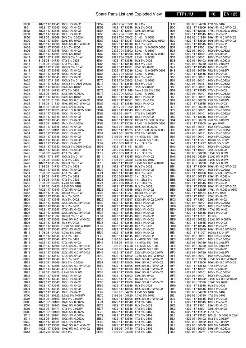
Spare Parts List and Exploded View EN 125FTP1.1U 10.
3850 4822 117 13545 100Ω 1% 04023851 4822 117 13545 100Ω 1% 04023852 4822 117 13545 100Ω 1% 04023853 4822 117 13545 100Ω 1% 04023856 4822 051 30569 56Ω 5% 0.062W3A00 4822 117 13601 22kΩ 5% 04023A01 4822 117 13606 10kΩ 5% 0.01W 04023A03 4822 117 13568 6.8Ω 5% 12063A06 4822 117 13545 100Ω 1% 04023A09 4822 117 13601 22kΩ 5% 04023A11 4822 117 11297 100kΩ 5% 0.1W3A13 3198 031 04730 47Ω 5% 04023A14 3198 031 04730 47Ω 5% 04023A15 4822 117 11297 100kΩ 5% 0.1W3A16 4822 117 13545 100Ω 1% 04023A17 4822 117 13545 100Ω 1% 04023A19 4822 117 13545 100Ω 1% 04023A20 4822 117 11297 100kΩ 5% 0.1W3A22 4822 117 13632 100kΩ 1% 0603 0.62W3A23 4822 117 13603 33kΩ 5% 04023A24 3198 031 04730 47Ω 5% 04023A25 4822 051 30331 330Ω 5% 0.062W3A26 4822 117 13603 33kΩ 5% 04023A27 3198 031 01530 15kΩ 5% 0.01W 04023A28 3198 031 01530 15kΩ 5% 0.01W 04023A29 4822 051 30331 330Ω 5% 0.062W3A30 4822 117 12925 47kΩ 1% 0.063W 06033A32 4822 117 13545 100Ω 1% 04023A33 4822 117 13545 100Ω 1% 04023A34 4822 117 13545 100Ω 1% 04023A35 4822 051 30105 1MΩ 5% 0.062W3A36 4822 117 13545 100Ω 1% 04023A38 4822 051 30101 100Ω 5% 0.062W3A3A 4822 117 13545 100Ω 1% 04023A3B 4822 117 13545 100Ω 1% 04023A3E 4822 117 13545 100Ω 1% 04023A3F 4822 117 13545 100Ω 1% 04023A40 4822 117 13632 100kΩ 1% 0603 0.62W3A42 4822 117 13545 100Ω 1% 04023A45 3198 031 04730 47Ω 5% 04023A46 4822 117 11297 100kΩ 5% 0.1W3A47 3198 031 04730 47Ω 5% 04023A48 4822 117 11297 100kΩ 5% 0.1W3A49 3198 031 04730 47Ω 5% 04023A50 4822 117 13545 100Ω 1% 04023A51 3198 031 04730 47Ω 5% 04023A52 3198 031 04730 47Ω 5% 04023A53 3198 031 04730 47Ω 5% 04023A55 3198 031 04720 4.7kΩ 5% 04023A56 3198 031 04720 4.7kΩ 5% 04023A57 4822 117 13543 470Ω 5% 04023A66 4822 117 11297 100kΩ 5% 0.1W3B00 4822 117 13548 1kΩ 5% 04023B01 4822 117 13548 1kΩ 5% 04023B02 4822 117 13596 220Ω 5% 0.01W 04023B03 4822 117 13548 1kΩ 5% 04023B04 4822 117 13543 470Ω 5% 04023B05 4822 117 13596 220Ω 5% 0.01W 04023B06 4822 117 11297 100kΩ 5% 0.1W3B07 4822 117 13606 10kΩ 5% 0.01W 04023B08 4822 117 13548 1kΩ 5% 04023B09 4822 117 13602 2.2kΩ 5% 0.01W 04023B10 4822 117 13543 470Ω 5% 04023B11 3198 031 04720 4.7kΩ 5% 04023B12 4822 117 13546 47Ω 5% 04023B13 4822 117 13546 47Ω 5% 04023B15 4822 117 13543 470Ω 5% 04023B16 4822 117 13596 220Ω 5% 0.01W 04023B17 4822 117 13596 220Ω 5% 0.01W 04023B18 4822 117 13596 220Ω 5% 0.01W 04023B19 4822 117 13543 470Ω 5% 04023B20 4822 117 13548 1kΩ 5% 04023B21 4822 051 30569 56Ω 5% 0.062W3B23 4822 117 13596 220Ω 5% 0.01W 04023B24 4822 117 13543 470Ω 5% 04023B25 3198 031 08220 8.2kΩ 5% 0.5W3B26 4822 117 13545 100Ω 1% 04023B27 4822 117 13545 100Ω 1% 04023B29 4822 117 13545 100Ω 1% 04023B30 4822 117 13545 100Ω 1% 04023B31 4822 117 13545 100Ω 1% 04023B32 4822 117 13545 100Ω 1% 04023C00 4822 051 30222 2.2kΩ 5% 0.062W3C01 4822 051 30109 10Ω 5% 0.062W3C03 4822 051 30103 10kΩ 5% 0.062W3C04 4822 051 30103 10kΩ 5% 0.062W3C05 4822 051 30471 47Ω 5% 0.062W3C08 4822 051 30103 10kΩ 5% 0.062W3C10 4822 051 30101 100Ω 5% 0.062W3C11 4822 051 30101 100Ω 5% 0.062W3D40 4822 117 10361 680Ω 1% 0.1W3D41 4822 117 13606 10kΩ 5% 0.01W 04023D44 4822 117 13606 10kΩ 5% 0.01W 04023D51 2322 704 62002 2kΩ 1%
3D52 2322 704 61002 1kΩ 1%3D53 4822 117 13548 1kΩ 5% 04023D54 4822 117 13601 22kΩ 5% 04023D55 2322 704 61002 1kΩ 1%3D56 2322 704 65102 5.1kΩ 1% 06033D57 5322 117 13047 330Ω 1% 0.063W 06033D58 4822 117 13548 1kΩ 5% 04023D60 5322 117 13036 1.2kΩ 1% 0.063W 06033D61 2322 704 63302 3.3kΩ 1% 06033D62 4822 117 12706 10kΩ 1% 0.063W 06033D63 2322 704 62202 2.2kΩ 1% 06033D64 4822 117 13548 1kΩ 5% 04023D65 4822 117 13548 1kΩ 5% 04023D66 4822 117 13601 22kΩ 5% 04023D67 5322 117 13036 1.2kΩ 1% 0.063W 06033D68 2322 704 63302 3.3kΩ 1% 06033D69 4822 117 13548 1kΩ 5% 04023D70 2322 704 63302 3.3kΩ 1% 06033D71 4822 117 13548 1kΩ 5% 04023D72 4822 117 13601 22kΩ 5% 04023D73 4822 117 11748 Fuse 2.2Ω 5% 12063D79 2322 704 62202 2.2kΩ 1% 06033D80 4822 117 13545 100Ω 1% 04023D81 4822 117 10361 680Ω 1% 0.1W3D82 4822 117 13545 100Ω 1% 04023D83 2322 704 61002 1kΩ 1%3D84 4822 117 13545 100Ω 1% 04023D85 4822 051 30471 47Ω 5% 0.062W3D86 4822 117 13545 100Ω 1% 04023D87 4822 117 13632 100kΩ 1% 0603 0.62W3D88 5322 117 13036 1.2kΩ 1% 0.063W 06033D89 4822 051 30183 18kΩ 5% 0.062W3D90 4822 117 12925 47kΩ 1% 0.063W 06033E04 4822 051 30479 47Ω 5% 0.062W3E05 3198 031 14710 4 x 470Ω 5% 12063E06 3198 031 14710 4 x 470Ω 5% 12063E07 2350 035 10152 4 x 1.5kΩ 5%3E08 4822 117 11151 1Ω 5%3E11 2350 035 10152 4 x 1.5kΩ 5%3E12 2350 035 10152 4 x 1.5kΩ 5%3E14 4822 117 13545 100Ω 1% 04023E16 3198 031 03320 3.3kΩ 5% 04023E18 4822 117 13602 2.2kΩ 5% 0.01W 04023E19 4822 117 13548 1kΩ 5% 04023E20 4822 117 13545 100Ω 1% 04023E21 4822 117 13548 1kΩ 5% 04023E22 2350 035 10152 4 x 1.5kΩ 5%3E23 2350 035 10152 4 x 1.5kΩ 5%3E24 2350 035 10152 4 x 1.5kΩ 5%3E25 4822 117 13548 1kΩ 5% 04023E26 4822 117 13545 100Ω 1% 04023E27 4822 117 11297 100kΩ 5% 0.1W3E28 4822 117 13548 1kΩ 5% 04023E29 4822 117 13597 330Ω 5% 0402 0.01W3E30 4822 117 13545 100Ω 1% 04023E31 4822 117 13548 1kΩ 5% 04023E32 4822 117 13545 100Ω 1% 04023E33 4822 117 13545 100Ω 1% 04023E34 4822 117 13545 100Ω 1% 04023E35 4822 117 13545 100Ω 1% 04023E36 4822 117 13545 100Ω 1% 04023E37 4822 117 13548 1kΩ 5% 04023E38 4822 117 13545 100Ω 1% 04023E39 4822 117 13545 100Ω 1% 04023E40 4822 117 13545 100Ω 1% 04023E41 3198 031 14710 4 x 470Ω 5% 12063E42 3198 031 14710 4 x 470Ω 5% 12063E43 3198 031 14710 4 x 470Ω 5% 12063E44 3198 031 14710 4 x 470Ω 5% 12063E45 4822 117 13597 330Ω 5% 0402 0.01W3E49 4822 117 13602 2.2kΩ 5% 0.01W 04023E50 4822 117 13606 10kΩ 5% 0.01W 04023E51 4822 117 13606 10kΩ 5% 0.01W 04023E52 4822 117 13606 10kΩ 5% 0.01W 04023E53 4822 117 13606 10kΩ 5% 0.01W 04023E55 4822 117 13606 10kΩ 5% 0.01W 04023E56 4822 117 13603 33kΩ 5% 04023E57 4822 117 11297 100kΩ 5% 0.1W3E60 4822 117 13606 10kΩ 5% 0.01W 04023E62 4822 117 13548 1kΩ 5% 04023E63 4822 117 13606 10kΩ 5% 0.01W 04023E69 3198 031 04720 4.7kΩ 5% 04023E70 3198 031 04720 4.7kΩ 5% 04023E73 4822 117 13606 10kΩ 5% 0.01W 04023E74 4822 117 13546 47Ω 5% 04023E75 4822 117 13548 1kΩ 5% 04023E77 4822 117 13546 47Ω 5% 04023E78 4822 117 13546 47Ω 5% 04023E79 4822 117 13546 47Ω 5% 04023E80 4822 117 13546 47Ω 5% 04023E88 4822 117 13546 47Ω 5% 04023E89 4822 117 13546 47Ω 5% 04023E91 3198 031 04730 47Ω 5% 04023E92 3198 031 04730 47Ω 5% 0402
3E93 3198 031 04730 47Ω 5% 04023I00 4822 117 13606 10kΩ 5% 0.01W 04023I08 4822 117 12925 47kΩ 1% 0.063W 06033I28 4822 117 13545 100Ω 1% 04023I29 3198 031 01830 18kΩ 5% 0.01W 04023I30 4822 117 13606 10kΩ 5% 0.01W 04023I31 4822 117 13545 100Ω 1% 04023I34 4822 117 13601 22kΩ 5% 04023I35 4822 051 30101 100Ω 5% 0.062W3I36 4822 117 13601 22kΩ 5% 04023I37 4822 051 30101 100Ω 5% 0.062W3I38 4822 051 30103 10kΩ 5% 0.062W3I40 4822 051 30759 75Ω 5% 0.062W3I41 4822 117 13545 100Ω 1% 04023I48 4822 051 30759 75Ω 5% 0.062W3I49 4822 117 13545 100Ω 1% 04023I50 4822 051 30151 150Ω 5% 0.062W3I51 4822 051 30101 100Ω 5% 0.062W3I52 4822 051 30151 150Ω 5% 0.062W3I53 4822 051 30101 100Ω 5% 0.062W3I54 4822 117 13543 470Ω 5% 04023I61 4822 051 30101 100Ω 5% 0.062W3I62 4822 051 30101 100Ω 5% 0.062W3I67 4822 051 30759 75Ω 5% 0.062W3I68 4822 117 13545 100Ω 1% 04023I78 4822 051 30759 75Ω 5% 0.062W3I79 4822 051 30101 100Ω 5% 0.062W3I80 4822 051 30101 100Ω 5% 0.062W3I83 4822 117 13545 100Ω 1% 04023I84 4822 051 30759 75Ω 5% 0.062W3I87 4822 117 13605 Jumper 04023I89 4822 051 30151 150Ω 5% 0.062W3I90 4822 051 30101 100Ω 5% 0.062W3I91 4822 051 30151 150Ω 5% 0.062W3I92 4822 051 30101 100Ω 5% 0.062W3I98 4822 117 11297 100kΩ 5% 0.1W3IA1 4822 117 11297 100kΩ 5% 0.1W3IA2 4822 051 30101 100Ω 5% 0.062W3IA3 4822 117 13601 22kΩ 5% 04023IA4 3198 031 08220 8.2kΩ 5% 0.5W3IA5 3198 031 08220 8.2kΩ 5% 0.5W3IA6 3198 031 08220 8.2kΩ 5% 0.5W3IA7 3198 031 08220 8.2kΩ 5% 0.5W3IB1 4822 117 13606 10kΩ 5% 0.01W 04023IB2 4822 051 30101 100Ω 5% 0.062W3IB3 4822 117 13606 10kΩ 5% 0.01W 04023IB4 4822 051 30223 22kΩ 5% 0.062W3IB5 4822 051 30103 10kΩ 5% 0.062W3IB6 4822 117 13545 100Ω 1% 04023IB8 4822 117 13606 10kΩ 5% 0.01W 04023IB9 4822 117 12925 47kΩ 1% 0.063W 06033IC1 4822 117 13574 1.5Ω 5% 12063IC2 4822 117 13601 22kΩ 5% 04023IC3 4822 117 13601 22kΩ 5% 04023IC4 4822 051 30101 100Ω 5% 0.062W3IC6 4822 051 30101 100Ω 5% 0.062W3ID0 3198 031 04720 4.7kΩ 5% 04023ID1 4822 117 13545 100Ω 1% 04023ID2 4822 117 11151 1Ω 5%3ID6 4822 051 30222 2.2kΩ 5% 0.062W3ID7 4822 117 13545 100Ω 1% 04023ID8 4822 117 13545 100Ω 1% 04023IE0 4822 117 13606 10kΩ 5% 0.01W 04023IE1 4822 117 11297 100kΩ 5% 0.1W3IE2 4822 051 30101 100Ω 5% 0.062W3IE3 4822 051 30101 100Ω 5% 0.062W3IE7 4822 051 30759 75Ω 5% 0.062W3IE8 4822 051 30759 75Ω 5% 0.062W3IE9 4822 117 13601 22kΩ 5% 04023IF0 4822 051 30759 75Ω 5% 0.062W3IF1 4822 051 30101 100Ω 5% 0.062W3IF2 3198 031 02720 2.7kΩ 5% 0.01W 04023IF3 4822 117 13606 10kΩ 5% 0.01W 04023IF4 4822 117 13543 470Ω 5% 04023IF5 4822 117 13601 22kΩ 5% 04023IF6 4822 051 30101 100Ω 5% 0.062W3IF7 4822 051 30101 100Ω 5% 0.062W3IF8 4822 117 13602 2.2kΩ 5% 0.01W 04023IF9 3198 031 03320 3.3kΩ 5% 04023IH0 4822 117 13548 1kΩ 5% 04023IH1 4822 117 13545 100Ω 1% 04023IH8 3198 031 04730 47Ω 5% 04023II3 3198 031 04730 47Ω 5% 04023IJ0 4822 117 13545 100Ω 1% 04023IJ1 4822 117 13545 100Ω 1% 04023IK2 4822 117 13601 22kΩ 5% 04023IK3 4822 117 13601 22kΩ 5% 04023IK7 4822 117 11152 4.7Ω 5%3IL0 4822 117 13632 100kΩ 1% 0603 0.62W3IL1 4822 051 30102 1kΩ 5% 0.062W3IL2 4822 051 30102 1kΩ 5% 0.062W3IL3 4822 051 30109 10Ω 5% 0.062W3IL4 4822 051 30393 39kΩ 5% 0.062W3IL5 4822 051 30271 270Ω 5% 0.062W
Spare Parts List and Exploded ViewEN 126 FTP1.1U10.
3IL6 4822 051 30101 100Ω 5% 0.062W3IL7 4822 117 13632 100kΩ 1% 0603 0.62W3IL8 4822 051 30102 1kΩ 5% 0.062W3IL9 4822 051 30102 1kΩ 5% 0.062W3IM0 4822 051 30109 10Ω 5% 0.062W3IM1 4822 051 30393 39kΩ 5% 0.062W3IM2 4822 051 30471 47Ω 5% 0.062W3IM3 4822 051 30561 560Ω 5% 0.062W3IM4 4822 051 30102 1kΩ 5% 0.062W3IM5 4822 117 13632 100kΩ 1% 0603 0.62W3IM6 4822 051 30102 1kΩ 5% 0.062W3IM7 4822 051 30101 100Ω 5% 0.062W3IM8 4822 051 30221 220Ω 5% 0.062W3IM9 4822 051 30393 39kΩ 5% 0.062W3IN0 4822 051 30109 10Ω 5% 0.062W3IN1 4822 117 13601 22kΩ 5% 04023IN4 2322 750 63908 3.9Ω 5% Fuse 12063IN5 4822 117 13601 22kΩ 5% 04023IN6 4822 117 13601 22kΩ 5% 04023IN7 4822 051 30101 100Ω 5% 0.062W3IN8 4822 051 30101 100Ω 5% 0.062W3IN9 4822 117 13601 22kΩ 5% 04023IO1 4822 051 30101 100Ω 5% 0.062W3IO2 4822 117 13606 10kΩ 5% 0.01W 04023IO3 4822 117 13606 10kΩ 5% 0.01W 04023IO5 4822 117 13606 10kΩ 5% 0.01W 04023IO6 4822 117 13606 10kΩ 5% 0.01W 04023IP8 4822 051 30103 10kΩ 5% 0.062W3IR5 4822 117 12925 47kΩ 1% 0.063W 06033IS0 4822 117 12521 68Ω 1% 0.1W3IS1 4822 117 12521 68Ω 1% 0.1W3IS2 4822 051 30101 100Ω 5% 0.062W3IS3 4822 051 30101 100Ω 5% 0.062W3IS4 4822 051 30101 100Ω 5% 0.062W3IT0 4822 117 12925 47kΩ 1% 0.063W 06033IT1 4822 117 12925 47kΩ 1% 0.063W 06033IT2 4822 117 13632 100kΩ 1% 0603 0.62W3IT5 4822 117 12521 68Ω 1% 0.1W3IT6 4822 117 12521 68Ω 1% 0.1W3L01 4822 051 20471 470Ω 5% 0.1W3L02 4822 051 20471 470Ω 5% 0.1W3L03 4822 117 13545 100Ω 1% 04023L04 4822 117 13545 100Ω 1% 04023L05 4822 117 13545 100Ω 1% 04023L06 4822 117 13545 100Ω 1% 04023L07 4822 117 13606 10kΩ 5% 0.01W 04023L08 3198 031 02720 2.7kΩ 5% 0.01W 04023L11 4822 117 13545 100Ω 1% 04023L12 4822 051 30471 47Ω 5% 0.062W3L13 4822 051 30151 150Ω 5% 0.062W3L15 4822 051 30151 150Ω 5% 0.062W3L16 4822 051 30151 150Ω 5% 0.062W3L17 4822 051 30471 47Ω 5% 0.062W3L22 4822 117 13602 2.2kΩ 5% 0.01W 04023L23 4822 051 30471 47Ω 5% 0.062W3L24 4822 051 20471 470Ω 5% 0.1W3L25 4822 117 13545 100Ω 1% 04023L28 4822 051 30471 47Ω 5% 0.062W3P65 4822 117 13545 100Ω 1% 04023P66 4822 117 13545 100Ω 1% 04023P67 3198 031 04720 4.7kΩ 5% 04023P69 3198 031 04720 4.7kΩ 5% 04023S01 4822 051 30008 Jumper 06033S02 4822 051 30223 22kΩ 5% 0.062W3S03 4822 051 30223 22kΩ 5% 0.062W3S04 3198 031 03320 3.3kΩ 5% 04023S05 3198 031 05620 5.6 kΩ 5% 0.01W 04023S06 4822 117 12925 47kΩ 1% 0.063W 06033S07 4822 051 30103 10kΩ 5% 0.062W3S08 4822 051 30221 220Ω 5% 0.062W3S09 4822 117 13606 10kΩ 5% 0.01W 04023S10 3198 031 01530 15kΩ 5% 0.01W 04023S11 4822 051 30101 100Ω 5% 0.062W3S12 4822 117 11297 100kΩ 5% 0.1W3S13 4822 117 11297 100kΩ 5% 0.1W3U47 4822 051 30103 10kΩ 5% 0.062W3U48 4822 051 30103 10kΩ 5% 0.062W3U49 4822 051 30102 1kΩ 5% 0.062W3U50 4822 051 30474 470kΩ 5% 0.062W3U56 4822 051 30103 10kΩ 5% 0.062W3U57 4822 051 30222 2.2kΩ 5% 0.062W3U58 4822 051 30392 3.9Ω 5% 0.063W 06033U59 4822 117 12925 47kΩ 1% 0.063W 06033V00 4822 051 30472 4.7Ω 5% 0.062W3V03 4822 117 13546 47Ω 5% 04023V04 4822 117 13546 47Ω 5% 04023V05 4822 117 13546 47Ω 5% 04023V06 4822 117 13545 100Ω 1% 04023V07 3198 031 04720 4.7kΩ 5% 04023V08 4822 117 13548 1kΩ 5% 04023V09 4822 117 13545 100Ω 1% 04023V10 4822 117 13545 100Ω 1% 04023V11 4822 117 13545 100Ω 1% 04023V12 4822 117 13545 100Ω 1% 0402
3V13 4822 117 13548 1kΩ 5% 04023V14 4822 117 13546 47Ω 5% 04023V15 4822 117 13546 47Ω 5% 04023V16 4822 117 13546 47Ω 5% 04023V21 4822 117 13546 47Ω 5% 04023V22 4822 117 13546 47Ω 5% 04023V23 2322 706 71201 120Ω 1% 04023V24 2322 706 71201 120Ω 1% 04023V25 2322 706 71201 120Ω 1% 04023V26 2322 706 71201 120Ω 1% 04023V27 2322 706 71201 120Ω 1% 04023V28 2322 706 71201 120Ω 1% 04023V29 4822 117 13597 330Ω 5% 0402 0.01W3V30 3198 031 04720 4.7kΩ 5% 04023V31 3198 031 04730 47Ω 5% 04023V32 3198 031 04720 4.7kΩ 5% 04023V33 3198 031 04720 4.7kΩ 5% 04023V35 4822 117 13548 1kΩ 5% 04023V36 4822 117 13543 470Ω 5% 04023V37 3198 031 03320 3.3kΩ 5% 04023V38 4822 117 12925 47kΩ 1% 0.063W 06033V39 4822 051 30101 100Ω 5% 0.062W3V40 4822 051 30101 100Ω 5% 0.062W3V41 4822 051 30222 2.2kΩ 5% 0.062W3V43 4822 117 12925 47kΩ 1% 0.063W 06033V44 4822 051 30103 10kΩ 5% 0.062W3V47 4822 051 30222 2.2kΩ 5% 0.062W3V48 4822 051 30101 100Ω 5% 0.062W3V49 4822 051 30101 100Ω 5% 0.062W3V56 4822 117 13545 100Ω 1% 04023Y02 4822 117 13545 100Ω 1% 04023Y03 4822 117 11151 1Ω 5%9001 4822 051 30008 Jumper 06039002 4822 051 30008 Jumper 06039010 4822 051 30008 Jumper 06039011 4822 051 30008 Jumper 06039012 4822 051 30008 Jumper 06039013 4822 051 30008 Jumper 06039016 4822 051 30008 Jumper 06039019 4822 051 30008 Jumper 06039020 4822 051 30008 Jumper 06039300 4822 051 30008 Jumper 06039322 4822 051 30101 100Ω 5% 0.062W9401 4822 051 30008 Jumper 06039403 4822 051 30008 Jumper 06039406 4822 051 30008 Jumper 06039407 4822 051 30008 Jumper 06039410 4822 051 30008 Jumper 06039413 4822 051 30008 Jumper 06039414 4822 051 30008 Jumper 06039416 4822 051 30008 Jumper 06039417 4822 051 30008 Jumper 06039702 4822 051 30008 Jumper 06039703 4822 051 30008 Jumper 06039708 4822 051 30008 Jumper 06039712 4822 051 30008 Jumper 06039714 4822 051 30008 Jumper 06039716 4822 051 30008 Jumper 06039717 4822 051 30008 Jumper 06039721 4822 051 30008 Jumper 06039723 4822 051 30008 Jumper 06039725 4822 051 30008 Jumper 06039727 4822 051 30008 Jumper 06039728 4822 051 30008 Jumper 06039729 4822 051 30008 Jumper 06039744 4822 051 30008 Jumper 06039747 4822 051 30008 Jumper 06039760 4822 051 30008 Jumper 06039761 4822 051 30008 Jumper 06039762 4822 051 30008 Jumper 06039763 4822 051 30008 Jumper 06039764 4822 051 30008 Jumper 06039765 4822 051 30008 Jumper 06039766 4822 051 30008 Jumper 06039772 4822 051 30008 Jumper 06039A00 4822 117 13605 Jumper 04029A01 4822 117 13605 Jumper 04029A04 4822 117 13605 Jumper 04029A05 4822 117 13605 Jumper 04029A06 4822 117 13605 Jumper 04029A09 4822 051 20008 Jumper 08059A12 4822 117 13605 Jumper 04029B01 4822 051 30008 Jumper 06039C02 4822 051 30008 Jumper 06039D55 4822 051 30008 Jumper 06039E54 4822 117 13605 Jumper 04029I00 4822 117 13605 Jumper 04029I02 4822 117 13605 Jumper 04029I06 4822 117 13605 Jumper 04029I13 4822 051 30008 Jumper 06039I17 4822 051 30008 Jumper 06039I18 4822 051 30008 Jumper 06039I24 4822 117 13605 Jumper 04029I25 4822 117 13605 Jumper 0402
9I26 4822 117 13605 Jumper 04029I27 4822 117 13605 Jumper 04029I32 4822 117 13605 Jumper 04029I33 4822 117 13605 Jumper 04029I34 4822 117 13605 Jumper 04029I35 4822 117 13605 Jumper 04029I36 4822 117 13605 Jumper 04029I37 4822 117 13605 Jumper 04029I38 4822 117 13605 Jumper 04029I57 4822 117 13605 Jumper 04029I58 4822 117 13605 Jumper 04029I85 4822 117 13605 Jumper 04029I89 4822 117 13605 Jumper 04029IA3 4822 117 13605 Jumper 04029IA4 4822 117 13605 Jumper 04029IA5 4822 117 13605 Jumper 04029IA6 4822 117 13605 Jumper 04029IA7 4822 117 13605 Jumper 04029IA8 4822 117 13605 Jumper 04029IC1 4822 117 13605 Jumper 04029IC2 4822 117 13605 Jumper 04029IC3 4822 117 13605 Jumper 04029ID1 4822 051 30008 Jumper 06039ID2 4822 051 30008 Jumper 06039ID3 4822 051 30008 Jumper 06039ID4 4822 051 30008 Jumper 06039ID8 4822 117 13605 Jumper 04029P69 4822 117 13605 Jumper 04029P70 4822 117 13605 Jumper 04029P71 4822 117 13605 Jumper 04029S01 4822 051 30008 Jumper 06039S02 4822 051 30008 Jumper 06039S03 4822 051 30008 Jumper 06039S04 4822 051 30008 Jumper 06039S05 4822 051 30008 Jumper 06039S06 4822 051 30008 Jumper 06039S07 4822 051 30008 Jumper 06039S08 4822 051 30008 Jumper 06039S09 4822 051 30008 Jumper 06039S11 4822 051 30008 Jumper 06039S13 4822 051 30008 Jumper 06039S14 4822 051 30008 Jumper 06039S15 4822 051 30008 Jumper 06039S16 4822 051 30008 Jumper 06039S17 4822 051 30008 Jumper 06039S30 4822 051 30008 Jumper 06039S31 4822 051 30008 Jumper 06039S32 4822 051 30008 Jumper 06039S33 4822 051 30008 Jumper 06039S34 4822 051 30008 Jumper 06039S35 4822 051 30008 Jumper 06039S36 4822 051 30008 Jumper 06039S37 4822 051 30008 Jumper 06039S38 4822 051 30008 Jumper 06039S65 4822 051 30008 Jumper 06039T01 4822 051 30008 Jumper 06039T02 4822 051 30008 Jumper 06039T04 4822 051 30008 Jumper 06039T07 4822 051 30008 Jumper 06039T08 4822 051 30008 Jumper 06039T11 4822 051 30008 Jumper 06039T12 4822 051 30008 Jumper 06039T13 4822 051 30008 Jumper 06039T14 4822 051 20008 Jumper 08059T15 4822 051 30008 Jumper 06039U99 2038 035 13207 1000µF 20% 16V9V21 4822 117 13605 Jumper 04029V23 4822 320 12423 Speaker cable9Y01 4822 117 13605 Jumper 04029Y03 4822 117 13605 Jumper 0402
5309 4822 051 30008 Jumper 06035310 4822 051 30008 Jumper 06035311 4822 051 30008 Jumper 06035318 2422 535 94092 33µH 10% 08055402 3198 018 38280 8.2µH 10% 08055404 2422 535 95427 Bead 120Ω at 100MHz5405 2422 535 95427 Bead 120Ω at 100MHz5406 4822 051 30008 Jumper 06035408 2422 549 44875 Trimmer 91MHz 5CCB5411 3198 018 33370 0.33µH 10% 08055415 4822 157 11716 Bead 30Ω 100MHz5416 4822 157 11716 Bead 30Ω 100MHz5700 4822 157 11716 Bead 30Ω 100MHz5701 4822 157 11716 Bead 30Ω 100MHz5702 4822 157 11716 Bead 30Ω 100MHz5703 4822 157 71206 Bead 600Ω 100MHz5706 4822 157 11716 Bead 30Ω 100MHz5707 4822 157 11716 Bead 30Ω 100MHz5710 4822 157 11716 Bead 30Ω 100MHz5711 4822 157 11716 Bead 30Ω 100MHz
Spare Parts List and Exploded View EN 127FTP1.1U 10.
5712 4822 156 21729 Bead 1kΩ 100MHz 08055713 4822 157 11716 Bead 30Ω 100MHz5714 4822 157 71206 Bead 600Ω 100MHz5715 4822 157 11716 Bead 30Ω 100MHz5716 4822 156 21729 Bead 1kΩ 100MHz 08055717 4822 156 21729 Bead 1kΩ 100MHz 08055718 4822 157 11716 Bead 30Ω 100MHz5719 4822 156 21729 Bead 1kΩ 100MHz 08055720 4822 157 11876 6.8µH 10% 08055721 4822 157 11716 Bead 30Ω 100MHz5722 4822 157 11716 Bead 30Ω 100MHz5724 4822 156 21729 Bead 1kΩ 100MHz 08055725 4822 157 11716 Bead 30Ω 100MHz5726 4822 156 21729 Bead 1kΩ 100MHz 08055727 4822 156 21729 Bead 1kΩ 100MHz 08055728 4822 157 11716 Bead 30Ω 100MHz5729 4822 157 11716 Bead 30Ω 100MHz5731 4822 156 21729 Bead 1kΩ 100MHz 08055736 4822 157 11876 6.8µH 10% 08055737 4822 156 21729 Bead 1kΩ 100MHz 08055742 4822 157 11716 Bead 30Ω 100MHz5743 4822 157 11716 Bead 30Ω 100MHz5744 4822 157 11716 Bead 30Ω 100MHz5746 4822 157 11716 Bead 30Ω 100MHz5747 4822 157 11716 Bead 30Ω 100MHz5748 4822 157 11716 Bead 30Ω 100MHz5750 4822 157 11716 Bead 30Ω 100MHz5751 4822 157 11716 Bead 30Ω 100MHz5752 4822 157 11716 Bead 30Ω 100MHz5753 4822 157 11716 Bead 30Ω 100MHz5754 4822 157 11716 Bead 30Ω 100MHz5755 4822 157 11716 Bead 30Ω 100MHz5756 4822 157 11716 Bead 30Ω 100MHz5757 4822 157 11716 Bead 30Ω 100MHz5A00 4822 157 11716 Bead 30Ω 100MHz5A01 4822 157 11716 Bead 30Ω 100MHz5A02 4822 157 11716 Bead 30Ω 100MHz5A03 4822 157 11716 Bead 30Ω 100MHz5A06 4822 157 11716 Bead 30Ω 100MHz5A17 4822 051 30151 150Ω 5% 0.062W5A18 4822 051 30151 150Ω 5% 0.062W5A19 4822 157 11828 22µH 20% 08055A20 4822 157 11716 Bead 30Ω 100MHz5A21 4822 157 11716 Bead 30Ω 100MHz5A38 4822 157 11716 Bead 30Ω 100MHz5B00 2422 535 94092 33µH 10% 08055B01 2422 535 94092 33µH 10% 08055B02 2422 535 94092 33µH 10% 08055B03 4822 157 11134 15µF5B04 4822 156 21729 Bead 1kΩ 100MHz 08055B05 4822 156 21729 Bead 1kΩ 100MHz 08055B06 4822 157 11716 Bead 30Ω 100MHz5B07 4822 156 21729 Bead 1kΩ 100MHz 08055B08 3198 018 51090 10µH 10% 06035B09 2422 536 00747 100µH 10% 12105D51 4822 157 11716 Bead 30Ω 100MHz5D54 4822 157 11716 Bead 30Ω 100MHz5D56 4822 156 21729 Bead 1kΩ 100MHz 08055D57 4822 157 11716 Bead 30Ω 100MHz5D58 4822 157 11716 Bead 30Ω 100MHz5D59 4822 157 11716 Bead 30Ω 100MHz5E00 2422 549 42896 Bead 120Ω 100MHz5E01 2422 549 42896 Bead 120Ω 100MHz5E02 2422 549 42896 Bead 120Ω 100MHz5E03 2422 549 42896 Bead 120Ω 100MHz5E04 2422 549 42896 Bead 120Ω 100MHz5E05 2422 549 42896 Bead 120Ω 100MHz5E08 4822 157 11716 Bead 30Ω 100MHz5E50 2422 549 43062 Bead 600Ω at 100MHz5E51 2422 549 43062 Bead 600Ω at 100MHz5E53 2422 535 94134 10µH 20% 08055E57 2422 549 43062 Bead 600Ω at 100MHz5E58 2422 549 43062 Bead 600Ω at 100MHz5E59 4822 157 11716 Bead 30Ω 100MHz5I00 2422 549 43062 Bead 600Ω at 100MHz5I01 2422 549 43062 Bead 600Ω at 100MHz5I02 2422 549 43769 Bead 30Ω 100MHz5I03 2422 549 43062 Bead 600Ω at 100MHz5I04 2422 549 43062 Bead 600Ω at 100MHz5I05 4822 157 11716 Bead 30Ω 100MHz5I06 4822 157 11716 Bead 30Ω 100MHz5I07 2422 549 43769 Bead 30Ω 100MHz5I09 4822 157 11716 Bead 30Ω 100MHz5I10 2422 536 00667 1000µF 20% 70325I21 2422 549 43769 Bead 30Ω 100MHz5I22 2422 549 43769 Bead 30Ω 100MHz5I23 2422 549 43769 Bead 30Ω 100MHz5L02 3198 018 51080 1µH 10% 06035L04 3198 018 54770 0.47µF 10% 06035L06 3198 018 51080 1µH 10% 06035L07 4822 157 11716 Bead 30Ω 100MHz5L08 4822 157 11716 Bead 30Ω 100MHz5L09 4822 157 11716 Bead 30Ω 100MHz5L10 4822 157 11716 Bead 30Ω 100MHz
5L11 4822 157 11716 Bead 30Ω 100MHz5L12 4822 157 11716 Bead 30Ω 100MHz5L13 4822 156 21729 Bead 1kΩ 100MHz 08055L14 4822 156 21729 Bead 1kΩ 100MHz 08055L15 4822 156 21729 Bead 1kΩ 100MHz 08055P51 4822 157 11716 Bead 30Ω 100MHz5S01 4822 157 11716 Bead 30Ω 100MHz5S02 4822 157 11716 Bead 30Ω 100MHz5S03 4822 157 11716 Bead 30Ω 100MHz5S04 4822 157 11716 Bead 30Ω 100MHz5S05 4822 157 11716 Bead 30Ω 100MHz5T02 2422 535 94134 10µH 20% 08055U05 2422 535 94134 10µH 20% 08055U06 2422 535 94134 10µH 20% 08055U07 4822 157 11716 Bead 30Ω 100MHz5U08 4822 157 11716 Bead 30Ω 100MHz5V06 3198 018 90050 Bead 1kΩ at 100MHz5V07 3198 018 90050 Bead 1kΩ at 100MHz5V08 3198 018 90050 Bead 1kΩ at 100MHz5V21 4822 157 11716 Bead 30Ω 100MHz5V22 4822 157 11716 Bead 30Ω 100MHz5V23 4822 157 11716 Bead 30Ω 100MHz5V24 4822 157 11716 Bead 30Ω 100MHz5V25 4822 157 11716 Bead 30Ω 100MHz5V26 4822 157 11716 Bead 30Ω 100MHz5V27 3198 018 34770 0.47µH 10% 08055V28 3198 018 34770 0.47µH 10% 08055V29 4822 157 11716 Bead 30Ω 100MHz5V30 4822 157 11716 Bead 30Ω 100MHz5V31 4822 157 11716 Bead 30Ω 100MHz5V32 3198 018 34770 0.47µH 10% 08055Y01 2422 549 45325 Bead 67Ω at 100MHz.5Y02 2422 549 45325 Bead 67Ω at 100MHz.5Y03 2422 549 45325 Bead 67Ω at 100MHz.5Y04 2422 549 45325 Bead 67Ω at 100MHz.5Y05 2422 549 45325 Bead 67Ω at 100MHz.
6001 4822 130 80622 BAT546002 4822 130 11397 BAS3166003 4822 130 80622 BAT546004 4822 130 80622 BAT546005 4822 130 11422 PLVA2650A6830 4822 130 11397 BAS3166831 4822 130 11397 BAS3166832 4822 130 11397 BAS3166833 4822 130 11397 BAS3166834 4822 130 11397 BAS3166835 4822 130 11397 BAS3166836 4822 130 11397 BAS3166837 4822 130 11397 BAS3166838 4822 130 11397 BAS3166839 4822 130 11397 BAS3166840 4822 130 11397 BAS3166841 4822 130 11397 BAS3166842 4822 130 11397 BAS3166843 4822 130 11397 BAS3166844 4822 130 11397 BAS3166845 4822 130 11397 BAS3166846 4822 130 11397 BAS3166847 4822 130 11397 BAS3166A00 4822 130 11551 UDZS10B6A01 4822 130 10838 UDZ3.3B6A02 4822 130 11397 BAS3166B00 4822 130 11397 BAS3166B01 4822 130 11397 BAS3166B03 4822 130 11397 BAS3166B04 4822 130 11397 BAS3166B05 4822 130 11397 BAS3166B06 4822 130 11397 BAS3166D62 4822 130 11564 UDZ3.9B6D63 4822 130 11397 BAS3166D64 4822 130 11397 BAS3166E54 4822 130 11397 BAS3166E55 4822 130 11397 BAS3166I03 5322 130 34337 BAV996I04 5322 130 34337 BAV996I05 4822 130 11397 BAS3166I10 4822 130 11416 PDZ6.8B6I11 4822 130 11416 PDZ6.8B6I12 4822 130 11416 PDZ6.8B6I13 4822 130 11416 PDZ6.8B6I14 4822 130 11416 PDZ6.8B6I15 4822 130 11416 PDZ6.8B6I16 4822 130 11416 PDZ6.8B6I17 4822 130 11416 PDZ6.8B6I18 4822 130 11416 PDZ6.8B6I20 4822 130 11416 PDZ6.8B6I21 4822 130 11416 PDZ6.8B6I22 4822 130 11416 PDZ6.8B6I23 4822 130 11416 PDZ6.8B6I24 4822 130 11416 PDZ6.8B
6I25 4822 130 11416 PDZ6.8B6I26 4822 130 11416 PDZ6.8B6I27 4822 130 11416 PDZ6.8B6I28 4822 130 11416 PDZ6.8B6I29 4822 130 11416 PDZ6.8B6I30 4822 130 11416 PDZ6.8B6I31 4822 130 11416 PDZ6.8B6I32 4822 130 11416 PDZ6.8B6I33 4822 130 11416 PDZ6.8B6I36 4822 130 11416 PDZ6.8B6I43 4822 130 11416 PDZ6.8B6I45 4822 130 11416 PDZ6.8B6I46 4822 130 11416 PDZ6.8B6I47 4822 130 11416 PDZ6.8B6I48 4822 130 11416 PDZ6.8B6I50 4822 130 11416 PDZ6.8B6I52 4822 130 11416 PDZ6.8B6I53 4822 130 11416 PDZ6.8B6I54 4822 130 11416 PDZ6.8B6I55 4822 130 11416 PDZ6.8B6I56 4822 130 11416 PDZ6.8B6I69 4822 130 11416 PDZ6.8B6I70 4822 130 11416 PDZ6.8B6I87 4822 130 11416 PDZ6.8B6I88 4822 130 11416 PDZ6.8B6I89 4822 130 11416 PDZ6.8B6I90 4822 130 11416 PDZ6.8B6I91 4822 130 11416 PDZ6.8B6I92 4822 130 11416 PDZ6.8B6I93 4822 130 11416 PDZ6.8B6I94 4822 130 11397 BAS3166I95 4822 130 11397 BAS3166I96 4822 130 11397 BAS3166I97 4822 130 11397 BAS3166I98 4822 130 11397 BAS3166I99 4822 130 11397 BAS3166IA3 5322 130 34337 BAV996IA4 5322 130 34337 BAV996IA6 4822 130 11397 BAS3166IA7 4822 130 11397 BAS3166T08 9340 548 71115 PDZ33B6U16 4822 130 11522 UDZ15B6V01 4822 130 11397 BAS3166V02 4822 130 11397 BAS3166V03 4822 130 11397 BAS3166V21 5322 130 34337 BAV996V22 5322 130 34337 BAV996V23 5322 130 34337 BAV996V24 5322 130 34337 BAV996V25 5322 130 34337 BAV996V26 5322 130 34337 BAV996V27 5322 130 34337 BAV996V28 5322 130 34337 BAV996V29 4822 130 11397 BAS3166V30 9340 553 52115 BAS3216V31 9340 553 52115 BAS3216V32 9340 553 52115 BAS3216V33 9340 553 52115 BAS321
7001 9352 684 81557 SAA5801H/0157002 3198 010 42320 BC857BW7003 3198 010 42310 BC847BW7004 3198 010 42310 BC847BW7005 9322 172 45668 LF33ABDT7006 9322 181 49668 M29W320DT-90N17007 9322 157 20668 MSM51V18165F-60J7008 3198 010 42310 BC847BW7009 3198 010 42310 BC847BW7010 3198 010 42320 BC857BW7011 9322 156 81668 M24C32-WMN6TNKSA7012 9322 156 72668 M29W400BT-90N17013 3198 010 42310 BC847BW7014 3198 010 42320 BC857BW7017 4822 130 10255 MUN22137018 9352 115 40118 74LVC245APW7019 9352 115 40118 74LVC245APW7020 3198 010 42310 BC847BW7066 3104 317 05411 Software (check
Prod.Surv.)7070 3104 317 06291 Software (check
Prod.Surv.)7320 3198 010 42310 BC847BW7322 3198 010 42310 BC847BW7323 9352 625 24518 TDA9321H/N27410 3198 010 42310 BC847BW7411 5322 130 60159 BC846B7414 3198 010 42310 BC847BW7415 3198 010 42310 BC847BW7706 9322 142 88668 LF25CDT7707 5322 130 60159 BC846B7708 5322 130 60159 BC846B
Spare Parts List and Exploded ViewEN 128 FTP1.1U10.
7709 5322 130 60159 BC846B7710 5322 130 60159 BC846B7711 2422 486 80938 Socket 32p f7712 9351 870 00118 74HC573PW7713 9352 688 09557 SAA4978H/V2047714 9965 000 02179 MS81V04160-25TB7715 4822 209 73852 PMBT23697717 9322 183 81668 MSM54V12222B-25JS7718 9352 695 58557 SAA4993H/V17719 9322 183 81668 MSM54V12222B-25JS7722 9965 000 02179 MS81V04160-25TB7723 9965 000 02179 MS81V04160-25TB7724 9322 188 08702 T8F24EF-00027725 4822 209 73852 PMBT23697727 9322 170 14668 LF15ABDT7740 9352 687 20125 74LVC1G125GW7741 9352 687 20125 74LVC1G125GW7742 9352 115 40118 74LVC245APW7743 9352 115 40118 74LVC245APW7744 9352 115 40118 74LVC245APW7745 9352 115 40118 74LVC245APW7746 9322 190 24668 CY2302SC-17747 9352 687 21165 74LVC1G126GW7748 9352 687 20125 74LVC1G125GW7999 3104 317 45521 Software (check
Prod.Surv.)7A00 4822 209 30095 LM833D7A01 3198 010 42310 BC847BW7A02 9322 199 42702 MSP3421G-Q1-B8V37A03 4822 209 30095 LM833D7A04 9322 199 16668 M74HC590T7A05 9322 199 16668 M74HC590T7A07 9322 183 05668 TS482ID7A08 4822 130 60373 BC856B7A09 4822 130 60373 BC856B7A10 9340 425 20115 BC847BS7A12 9322 153 66668 CY7C199-15ZC7A13 9351 869 80118 74HCT573DB7A14 9351 869 80118 74HCT573DB7A15 3198 010 42310 BC847BW7B00 9322 170 65671 UPD64083GF7B01 4822 130 60373 BC856B7B02 4822 130 60373 BC856B7B03 5322 130 60159 BC846B7B04 4822 130 60373 BC856B7B05 5322 130 60159 BC846B7B06 4822 130 60373 BC856B7B07 9322 142 88668 LF25CDT7B08 9322 173 45685 NCP302LSN277B09 5322 130 60159 BC846B7B10 5322 130 60159 BC846B7B11 5322 130 60159 BC846B7D51 4822 209 12776 TDA8601T/C17D52 4822 130 62755 BF5707D53 4822 130 62755 BF5707D54 4822 130 62755 BF5707D55 4822 130 62755 BF5707D57 9322 131 22668 TSH95D7E02 9322 196 51668 EPCS1SI87E05 9322 170 14668 LF15ABDT7E08 3198 010 42320 BC857BW7E09 9322 195 65668 AD9066JR7E10 9352 686 35118 PCA9515DP7E12 9340 425 20115 BC847BS7E13 3198 010 42320 BC857BW7E14 3198 010 42310 BC847BW7E16 9322 195 65668 AD9066JR7E17 3198 010 42320 BC857BW7E18 9322 146 75685 TS431L7E19 3198 010 42310 BC847BW7E20 3198 010 42320 BC857BW7E21 3198 010 42310 BC847BW7E22 3198 010 42310 BC847BW7E23 3198 010 42320 BC857BW7E24 9322 146 75685 TS431L7I01 9340 425 20115 BC847BS7I02 9340 425 20115 BC847BS7I05 3198 010 42320 BC857BW7I07 4822 130 60142 BC8697I09 3198 010 42310 BC847BW7I10 9352 686 35118 PCA9515DP7I11 4822 130 10255 MUN22137I12 4822 130 10255 MUN22137I13 4822 130 42804 BC817-257I14 3198 010 42310 BC847BW7I15 3198 010 42310 BC847BW7I16 9340 425 20115 BC847BS7I17 9322 116 87668 TEA6422D7I19 9352 686 35118 PCA9515DP7I26 4822 130 60373 BC856B7I27 5322 130 60159 BC846B7I28 4822 130 60373 BC856B7I29 5322 130 60159 BC846B7I30 5322 130 60159 BC846B
7I31 4822 130 60373 BC856B7I32 9351 869 40118 74HC4053PW7I44 9340 425 20115 BC847BS7L01 9322 181 72671 AD9883AKST-1107L02 4822 209 17398 LD1117DT337L03 4822 209 73852 PMBT23697P56 4822 209 17345 M62320FP7S03 9340 425 20115 BC847BS7S04 3198 010 42310 BC847BW7U14 3198 010 42310 BC847BW7U15 3198 010 42320 BC857BW7U16 9322 091 04668 SI4410DY7V01 9322 196 44671 EP1C6Q240C87V02 9322 159 45668 DS90C385MTD7V21 9322 183 61682 SII907BCQ527V22 4822 130 60373 BC856B7V23 9965 000 04199 Connector 2p7V24 9965 000 04199 Connector 2p7V26 9322 145 26668 M24C02-WMN6
EMC Interface Panel [EMC]
Various
0002 3122 358 76831 EMC foam fiter panel1105 3122 357 22052 EMC filter panel1320 2422 025 16545 Connector 10p m1330 2422 025 16545 Connector 10p m1345 2422 025 16835 Connector 3p m1355 2422 025 16835 Connector 3p m
2300 5322 126 11583 10nF 10% 50V 06032301 5322 126 11583 10nF 10% 50V 06032302 3198 016 31020 1nF 25V 06032303 5322 126 11583 10nF 10% 50V 06032304 5322 126 11583 10nF 10% 50V 06032305 5322 126 11583 10nF 10% 50V 06032306 5322 126 11583 10nF 10% 50V 06032307 5322 126 11583 10nF 10% 50V 06032308 5322 126 11583 10nF 10% 50V 0603
3300 4822 051 30101 100Ω 5% 0.062W3301 4822 051 30101 100Ω 5% 0.062W3302 4822 051 30101 100Ω 5% 0.062W3303 4822 051 30101 100Ω 5% 0.062W3304 4822 051 30101 100Ω 5% 0.062W3305 4822 051 30101 100Ω 5% 0.062W3306 4822 051 30101 100Ω 5% 0.062W3307 4822 051 30101 100Ω 5% 0.062W
5300 2422 549 43062 Bead 600Ω at 100MHz5301 2422 549 43062 Bead 600Ω at 100MHz5302 2422 549 43062 Bead 600Ω at 100MHz5303 2422 549 43062 Bead 600Ω at 100MHz5304 2422 549 43062 Bead 600Ω at 100MHz5305 2422 549 43062 Bead 600Ω at 100MHz5306 2422 549 43062 Bead 600Ω at 100MHz5307 2422 549 43062 Bead 600Ω at 100MHz5308 2422 549 43062 Bead 600Ω at 100MHz5309 2422 549 43062 Bead 600Ω at 100MHz5310 2422 549 43062 Bead 600Ω at 100MHz5311 2422 549 43062 Bead 600Ω at 100MHz5312 2422 549 43062 Bead 600Ω at 100MHz5313 2422 549 43062 Bead 600Ω at 100MHz
LED Switch Panel [LD]
Various
0320 2422 025 16545 Connector 10p m1072 3122 357 22322 PCA LED + Switch1101 2422 128 03123 Swi 2P 2pos 30V8306 3104 311 06691 Cable 10P/340/10P
2107 4822 124 12095 100µF 20% 16V2120 3198 030 71090 10µF 20% 35V2126 4822 126 14583 470nF 10% 16V 0805
3101 4822 051 30151 150Ω 5% 0.062W3102 4822 117 13632 100kΩ 1% 0603 0.62W3103 4822 051 30561 560Ω 5% 0.062W3104 4822 117 13632 100kΩ 1% 0603 0.62W3105 4822 051 30102 1kΩ 5% 0.062W3106 4822 051 30151 150Ω 5% 0.062W3107 4822 051 30471 47Ω 5% 0.062W3108 4822 051 30103 10kΩ 5% 0.062W3109 4822 051 30101 100Ω 5% 0.062W3120 4822 051 30472 4.7Ω 5% 0.062W3121 4822 051 30103 10kΩ 5% 0.062W3122 4822 051 30332 3.3Ω 5% 0.062W3123 4822 051 30332 3.3Ω 5% 0.062W3124 4822 051 30102 1kΩ 5% 0.062W3126 2322 702 60335 3.3MΩ 5% 06033127 2322 702 60335 3.3MΩ 5% 06034101 4822 051 30008 Jumper 06034107 4822 051 30008 Jumper 0603
5100 2422 549 43769 Bead 30Ω 100MHz
6101 4822 130 11564 UDZ3.9B6103 4822 130 83915 TLMV31006105 4822 130 11564 UDZ3.9B6127 9322 140 63685 TEMD5000
7103 3198 010 42320 BC857BW7105 3198 010 42320 BC857BW7107 9322 178 03667 TSOP2136YA17120 5322 209 82941 LM358D
Top Control Panel [P]
Various
0053 3104 308 10551 TC assy knob R LCD 30"0055 3104 308 10561 TC assy knob L LCD 30"0057 3104 304 25831 TC frame LCD 30"0058 3104 308 10571 TC assy knob M LCD 30"0345 4822 267 10459 Connector 3p1114 3104 328 29811 Top Control Assy1701 2422 128 02778 Tact switch1702 2422 128 02778 Tact switch1703 2422 128 02778 Tact switch1704 2422 128 02778 Tact switch1705 2422 128 02778 Tact switch
3001 4822 051 20391 390Ω 5% 0.1W3003 4822 117 13528 200Ω 1% 0.125W 08053005 4822 117 11951 2kΩ 1% 0.1W3009 4822 117 11534 1.1kΩ 1% 0.1W3011 4822 117 10845 620Ω 1% 0.1W3999 4822 051 20471 470Ω 5% 0.1W9001 4822 051 20008 Jumper 08059003 4822 051 20008 Jumper 08059005 4822 051 20008 Jumper 08059006 4822 051 20008 Jumper 0805

Revision List EN 129FTP1.1U 11.
11. Revision List
Manual xxxx xxx xxxx.0• First release. Manual xxxx xxx xxxx.1• Chapter: Technical Specifications, Connections, and
Chassis Overview, some layout issues fixed.• Chapter: Wiring Diagram, Block Diagrams and Overviews
– Supply Lines Overview, layout issue fixed.• Chapter: Spare Parts List:
– Updated and completed.– Exploded view with mechanical parts added.
Related Documents