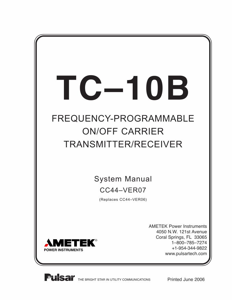
TC–10B FREQUENCY-PROGRAMMABLE ON/OFF CARRIER TRANSMITTER/RECEIVER System Manual CC44–VER07 (Replaces CC44–VER06) AMETEK Power Instruments 4050 N.W. 121st Avenue Coral Springs, FL 33065 1–800–785–7274 +1-954-344-9822 www.pulsartech.com Printed June 2006 THE BRIGHT STAR IN UTILITY COMMUNICATIONS

Welcome message from author
This document is posted to help you gain knowledge. Please leave a comment to let me know what you think about it! Share it to your friends and learn new things together.
Transcript
TC–10BFREQUENCY-PROGRAMMABLE
ON/OFF CARRIER
TRANSMITTER/RECEIVER
System Manual
CC44–VER07(Replaces CC44–VER06)
AMETEK Power Instruments4050 N.W. 121st AvenueCoral Springs, FL 33065
1–800–785–7274+1-954-344-9822
www.pulsartech.com
Printed June 2006THE BRIGHT STAR IN UTILITY COMMUNICATIONS

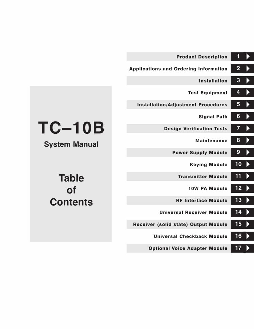
1Product Description
2Applications and Ordering Information
3Installation
4Test Equipment
5Installation/Adjustment Procedures
6Signal Path
7Design Verification Tests
8Maintenance
9Power Supply Module
10Keying Module
11Transmitter Module
1210W PA Module
13RF Interface Module
14Universal Receiver Module
15Receiver (solid state) Output Module
16Universal Checkback Module
17Optional Voice Adapter Module
TC–10BSystem Manual
Tableof
Contents
Page ii June 2006
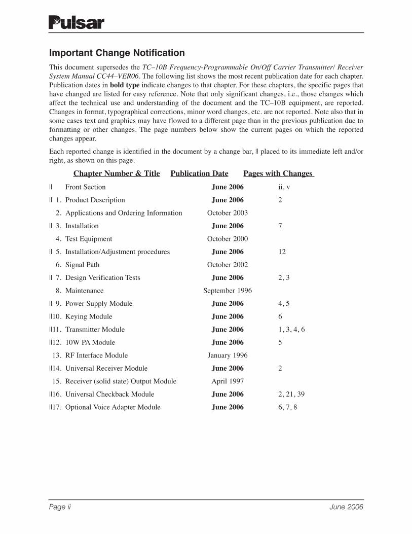
Important Change NotificationThis document supersedes the TC–10B Frequency-Programmable On/Off Carrier Transmitter/ ReceiverSystem Manual CC44–VER06. The following list shows the most recent publication date for each chapter.Publication dates in bold type indicate changes to that chapter. For these chapters, the specific pages thathave changed are listed for easy reference. Note that only significant changes, i.e., those changes whichaffect the technical use and understanding of the document and the TC–10B equipment, are reported.Changes in format, typographical corrections, minor word changes, etc. are not reported. Note also that insome cases text and graphics may have flowed to a different page than in the previous publication due toformatting or other changes. The page numbers below show the current pages on which the reportedchanges appear.
Each reported change is identified in the document by a change bar, || placed to its immediate left and/orright, as shown on this page.
Chapter Number & Title Publication Date Pages with Changes
|| Front Section June 2006 ii, v
|| 1. Product Description June 2006 2
2. Applications and Ordering Information October 2003
|| 3. Installation June 2006 7
4. Test Equipment October 2000
|| 5. Installation/Adjustment procedures June 2006 12
6. Signal Path October 2002
|| 7. Design Verification Tests June 2006 2, 3
8. Maintenance September 1996
|| 9. Power Supply Module June 2006 4, 5
||10. Keying Module June 2006 6
||11. Transmitter Module June 2006 1, 3, 4, 6
||12. 10W PA Module June 2006 5
13. RF Interface Module January 1996
||14. Universal Receiver Module June 2006 2
15. Receiver (solid state) Output Module April 1997
||16. Universal Checkback Module June 2006 2, 21, 39
||17. Optional Voice Adapter Module June 2006 6, 7, 8
June 2006 Page iii
TC–10B System Manual
We recommend that you become acquainted with the information in this manual before ener-gizing your TC–10B system. Failure to do so may result in injury to personnel or damage tothe equipment, and may affect the equipment warranty. If you mount the carrier set in a
cabinet, it must be bolted to the floor or otherwise secured before you swing out the equipment, toprevent the installation from tipping over.
You should not remove or insert printed circuit modules while the TC–10B is energized. Failure toobserve this precaution can result in undesired tripping output and can cause component damage.
AMETEKdoes not assume liability arising out of the application or use of any product or circuitdescribed herein. AMETEKreserves the right to make changes to any products herein to improve reli-ability, function or design. Specifications and information herein are subject to change without notice.All possible contingencies which may arise during installation, operation, or maintenance, and alldetails and variations of this equipment do not purport to be covered by this manual. If you desirefurther information regarding a particular installation, operation, or maintenance of equipment, pleasecontact your local AMETEKrepresentative.
Copyright ©By AMETEKU.S.A.ALL RIGHTS RESERVEDAMETEKdoes not convey any license under its patent rights nor the rights of others.
! IMPORTANT
ESD Warning!
YOU MUST BE PROPERLY GROUNDED, TO PREVENT DAMAGE FROMSTATIC ELECTRICITY, BEFORE HANDLING ANY AND ALL MODULES OREQUIPMENT FROM PULSAR.
All semiconductor components used, are sensitive to and can be damaged by thedischarge of static electricity. Be sure to observe all Electrostatic Discharge (ESD)precautions when handling modules or individual components.
PREFACE
ScopeThis manual describes the functions and features of the TC–10B Power Line Carrier Transmitter/Receiver.It is intended primarily for use by engineers and technicians involved in the installation, alignment,operation, and maintenance of the TC–10B.
Equipment IdentificationThe TC–10B equipment is identified by the Catalog Number on the TC–10B chassis nameplate. You candecode the Catalog Number using the information in Chapter 2.
Production ChangesWhen engineering and production changes are made to the TC–10B equipment, a revision notation(Sub number) is reflected on the style number and related schematic diagram. A summary of all Subnumbers for the particular release is shown on the following page.
WarrantyOur standard warranty extends for 60 months after shipment. For all repaired modules or advance replace-ments, the standard warranty is 90 days or the remaining warranty time, whichever is longer. Damageclearly caused by improper application, repair, or handling of the equipment will void the warranty.
Equipment Return & Repair ProcedureTo return equipment for repair or replacement:
1. Call your AMETEK representative at 1–800–785–7274.
2. Request an RMA number for proper authorization and credit.
3. Carefully pack the equipment you are returning.
Repair work is done most satisfactorily at the factory. When returning any equipment, pack it inthe original shipping containers if possible. Be sure to use anti-static material when packing theequipment. Any damage due to improperly packed items will be charged to the customer, evenwhen under warranty.
AMETEKalso makes available interchangeable parts to customers who are equipped to do repairwork. When ordering parts (components, modules, etc.), always give the complete AMETEKstylenumber(s).
4. Make sure you include your return address and the RMA number on the package.
5. Ship the package(s) to:
AMETEKPower Instruments4050 N.W. 121st AvenueCoral Springs, FL U.S.A. 33065
Page iv June 2006
June 2006 Page v
TC–10B System Manual
Overview of this PublicationChapter 1 – Product Description and specifications
Chapter 2 – Applications and related catalog numbers for ordering
Chapter 3 – Installation
Chapter 4 – Test equipment
Chapter 5 – Installation/adjustment procedures
Chapter 6 – Signal path
Chapter 7 – Design verification tests
Chapter 8 – Maintenance procedures
Chapters 9-17 – Module circuit descriptions and troubleshooting procedures
The TC–10B circuitry is divided into seven (7) standard modules. In addition, Universal Checkback, TTLTransmitter and Voice Adapter modules are available as options. (See Figure 6-1, for a Functional BlockDiagram.)
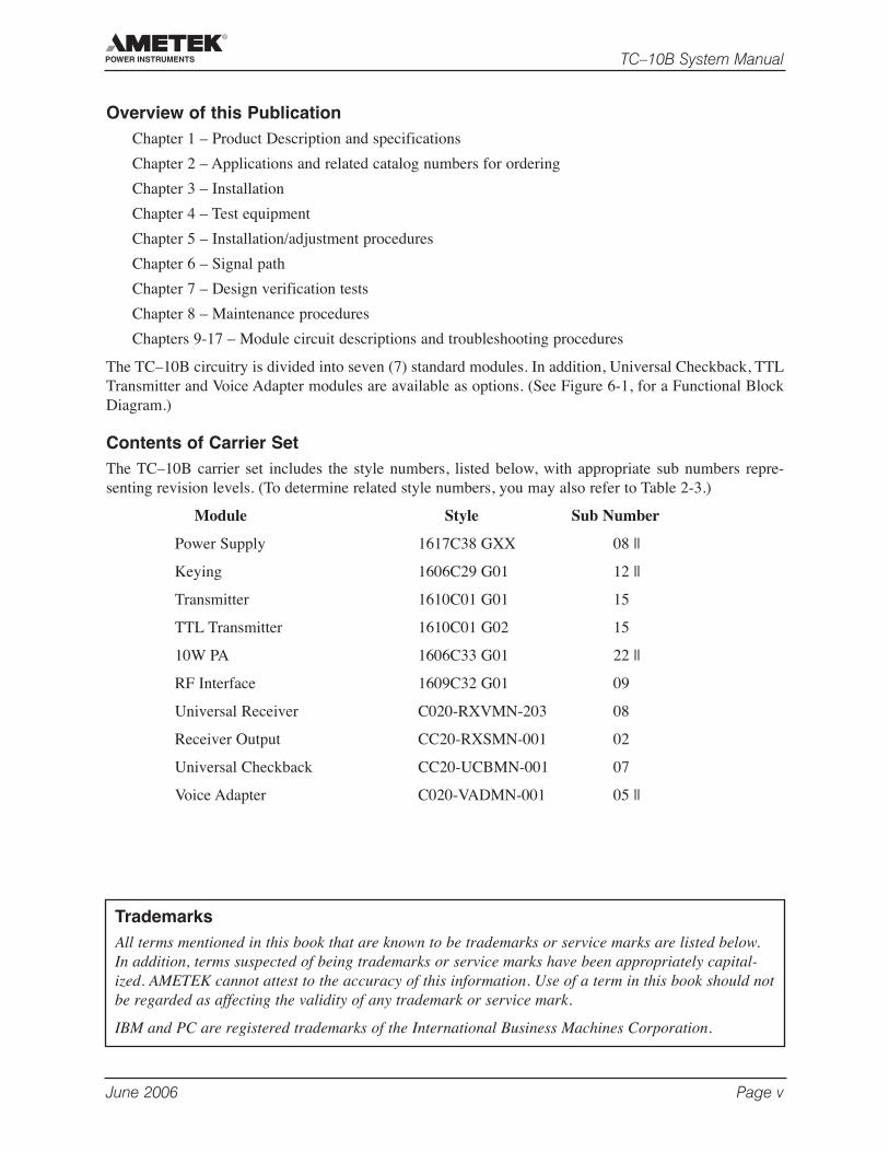
Contents of Carrier SetThe TC–10B carrier set includes the style numbers, listed below, with appropriate sub numbers repre-senting revision levels. (To determine related style numbers, you may also refer to Table 2-3.)
Module Style Sub Number
Power Supply 1617C38 GXX 08 ||
Keying 1606C29 G01 12 ||
Transmitter 1610C01 G01 15
TTL Transmitter 1610C01 G02 15
10W PA 1606C33 G01 22 ||
RF Interface 1609C32 G01 09
Universal Receiver C020-RXVMN-203 08
Receiver Output CC20-RXSMN-001 02
Universal Checkback CC20-UCBMN-001 07
Voice Adapter C020-VADMN-001 05 ||
TrademarksAll terms mentioned in this book that are known to be trademarks or service marks are listed below.In addition, terms suspected of being trademarks or service marks have been appropriately capital-ized. AMETEK cannot attest to the accuracy of this information. Use of a term in this book should notbe regarded as affecting the validity of any trademark or service mark.
IBM and PC are registered trademarks of the International Business Machines Corporation.
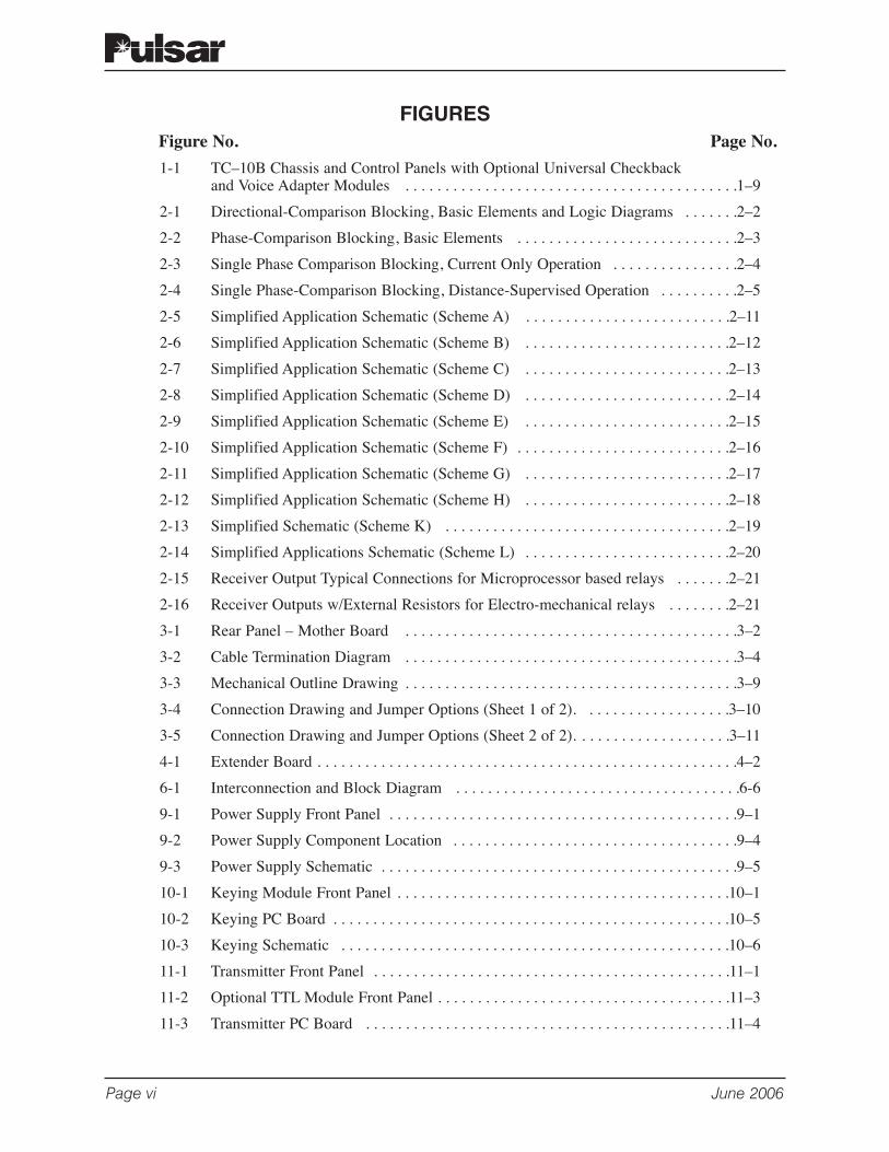
FIGURESFigure No. Page No.
1-1 TC–10B Chassis and Control Panels with Optional Universal Checkback and Voice Adapter Modules . . . . . . . . . . . . . . . . . . . . . . . . . . . . . . . . . . . . . . . . . .1–9
2-1 Directional-Comparison Blocking, Basic Elements and Logic Diagrams . . . . . . .2–2
2-2 Phase-Comparison Blocking, Basic Elements . . . . . . . . . . . . . . . . . . . . . . . . . . . .2–3
2-3 Single Phase Comparison Blocking, Current Only Operation . . . . . . . . . . . . . . . .2–4
2-4 Single Phase-Comparison Blocking, Distance-Supervised Operation . . . . . . . . . .2–5
2-5 Simplified Application Schematic (Scheme A) . . . . . . . . . . . . . . . . . . . . . . . . . .2–11
2-6 Simplified Application Schematic (Scheme B) . . . . . . . . . . . . . . . . . . . . . . . . . .2–12
2-7 Simplified Application Schematic (Scheme C) . . . . . . . . . . . . . . . . . . . . . . . . . .2–13
2-8 Simplified Application Schematic (Scheme D) . . . . . . . . . . . . . . . . . . . . . . . . . .2–14
2-9 Simplified Application Schematic (Scheme E) . . . . . . . . . . . . . . . . . . . . . . . . . .2–15
2-10 Simplified Application Schematic (Scheme F) . . . . . . . . . . . . . . . . . . . . . . . . . . .2–16
2-11 Simplified Application Schematic (Scheme G) . . . . . . . . . . . . . . . . . . . . . . . . . .2–17
2-12 Simplified Application Schematic (Scheme H) . . . . . . . . . . . . . . . . . . . . . . . . . .2–18
2-13 Simplified Schematic (Scheme K) . . . . . . . . . . . . . . . . . . . . . . . . . . . . . . . . . . . .2–19
2-14 Simplified Applications Schematic (Scheme L) . . . . . . . . . . . . . . . . . . . . . . . . . .2–20
2-15 Receiver Output Typical Connections for Microprocessor based relays . . . . . . .2–21
2-16 Receiver Outputs w/External Resistors for Electro-mechanical relays . . . . . . . .2–21
3-1 Rear Panel – Mother Board . . . . . . . . . . . . . . . . . . . . . . . . . . . . . . . . . . . . . . . . . .3–2
3-2 Cable Termination Diagram . . . . . . . . . . . . . . . . . . . . . . . . . . . . . . . . . . . . . . . . . .3–4
3-3 Mechanical Outline Drawing . . . . . . . . . . . . . . . . . . . . . . . . . . . . . . . . . . . . . . . . . .3–9
3-4 Connection Drawing and Jumper Options (Sheet 1 of 2). . . . . . . . . . . . . . . . . . .3–10
3-5 Connection Drawing and Jumper Options (Sheet 2 of 2). . . . . . . . . . . . . . . . . . . .3–11
4-1 Extender Board . . . . . . . . . . . . . . . . . . . . . . . . . . . . . . . . . . . . . . . . . . . . . . . . . . . . .4–2
6-1 Interconnection and Block Diagram . . . . . . . . . . . . . . . . . . . . . . . . . . . . . . . . . . . .6-6
9-1 Power Supply Front Panel . . . . . . . . . . . . . . . . . . . . . . . . . . . . . . . . . . . . . . . . . . . .9–1
9-2 Power Supply Component Location . . . . . . . . . . . . . . . . . . . . . . . . . . . . . . . . . . . .9–4
9-3 Power Supply Schematic . . . . . . . . . . . . . . . . . . . . . . . . . . . . . . . . . . . . . . . . . . . . .9–5
10-1 Keying Module Front Panel . . . . . . . . . . . . . . . . . . . . . . . . . . . . . . . . . . . . . . . . . .10–1
10-2 Keying PC Board . . . . . . . . . . . . . . . . . . . . . . . . . . . . . . . . . . . . . . . . . . . . . . . . . .10–5
10-3 Keying Schematic . . . . . . . . . . . . . . . . . . . . . . . . . . . . . . . . . . . . . . . . . . . . . . . . .10–6
11-1 Transmitter Front Panel . . . . . . . . . . . . . . . . . . . . . . . . . . . . . . . . . . . . . . . . . . . . .11–1
11-2 Optional TTL Module Front Panel . . . . . . . . . . . . . . . . . . . . . . . . . . . . . . . . . . . . .11–3
11-3 Transmitter PC Board . . . . . . . . . . . . . . . . . . . . . . . . . . . . . . . . . . . . . . . . . . . . . .11–4
Page vi June 2006
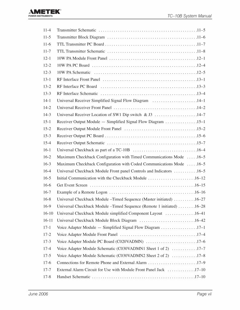
11-4 Transmitter Schematic . . . . . . . . . . . . . . . . . . . . . . . . . . . . . . . . . . . . . . . . . . . . . .11–5
11-5 Transmitter Block Diagram . . . . . . . . . . . . . . . . . . . . . . . . . . . . . . . . . . . . . . . . . .11–6
11-6 TTL Transmitter PC Board . . . . . . . . . . . . . . . . . . . . . . . . . . . . . . . . . . . . . . . . . . .11–7
11-7 TTL Transmitter Schematic . . . . . . . . . . . . . . . . . . . . . . . . . . . . . . . . . . . . . . . . . .11–8
12-1 10W PA Module Front Panel . . . . . . . . . . . . . . . . . . . . . . . . . . . . . . . . . . . . . . . . .12–1
12-2 10W PA PC Board . . . . . . . . . . . . . . . . . . . . . . . . . . . . . . . . . . . . . . . . . . . . . . . . .12–4
12-3 10W PA Schematic . . . . . . . . . . . . . . . . . . . . . . . . . . . . . . . . . . . . . . . . . . . . . . . .12–5
13-1 RF Interface Front Panel . . . . . . . . . . . . . . . . . . . . . . . . . . . . . . . . . . . . . . . . . . . .13–1
13-2 RF Interface PC Board . . . . . . . . . . . . . . . . . . . . . . . . . . . . . . . . . . . . . . . . . . . . .13–3
13-3 RF Interface Schematic . . . . . . . . . . . . . . . . . . . . . . . . . . . . . . . . . . . . . . . . . . . . .13–4
14-1 Universal Receiver Simplified Signal Flow Diagram . . . . . . . . . . . . . . . . . . . . .14–1
14-2 Universal Receiver Front Panel . . . . . . . . . . . . . . . . . . . . . . . . . . . . . . . . . . . . . . .14–2
14-3 Universal Receiver Location of SW1 Dip switch & J3 . . . . . . . . . . . . . . . . . . . .14–7
15-1 Receiver Output Module — Simplified Signal Flow Diagram . . . . . . . . . . . . . . .15–1
15-2 Receiver Output Module Front Panel . . . . . . . . . . . . . . . . . . . . . . . . . . . . . . . . . .15–2
15-3 Receiver Output PC Board . . . . . . . . . . . . . . . . . . . . . . . . . . . . . . . . . . . . . . . . . . .15–6
15-4 Receiver Output Schematic . . . . . . . . . . . . . . . . . . . . . . . . . . . . . . . . . . . . . . . . . .15–7
16-1 Universal Checkback as part of a TC-10B . . . . . . . . . . . . . . . . . . . . . . . . . . . . . .16–4
16-2 Maximum Checkback Configuration with Timed Communications Mode . . . . .16–5
16-3 Maximum Checkback Configuration with Coded Communications Mode . . . . .16–5
16-4 Universal Checkback Module Front panel Controls and Indicators . . . . . . . . . . .16–5
16-5 Initial Communication with the Checkback Module . . . . . . . . . . . . . . . . . . . . . .16–12
16-6 Get Event Screen . . . . . . . . . . . . . . . . . . . . . . . . . . . . . . . . . . . . . . . . . . . . . . . . .16–15
16-7 Example of a Remote Logon . . . . . . . . . . . . . . . . . . . . . . . . . . . . . . . . . . . . . . . .16–16
16-8 Universal Checkback Module –Timed Sequence (Master initiated) . . . . . . . . . .16–27
16-9 Universal Checkback Module –Timed Sequence (Remote 1 initiated) . . . . . . . .16–28
16-10 Universal Checkback Module simplified Component Layout . . . . . . . . . . . . . .16–41
16-11 Universal Checkback Module Block Diagram . . . . . . . . . . . . . . . . . . . . . . . . . .16–42
17-1 Voice Adapter Module — Simplified Signal Flow Diagram . . . . . . . . . . . . . . . . .17–1
17-2 Voice Adapter Module Front Panel . . . . . . . . . . . . . . . . . . . . . . . . . . . . . . . . . . . .17–4
17-3 Voice Adapter Module PC Board (C020VADMN) . . . . . . . . . . . . . . . . . . . . . . . .17–6
17-4 Voice Adapter Module Schematic (C030VADMN1 Sheet 1 of 2) . . . . . . . . . . . .17–7
17-5 Voice Adapter Module Schematic (C030VADMN2 Sheet 2 of 2) . . . . . . . . . . . .17–8
17-6 Connections for Remote Phone and External Alarm . . . . . . . . . . . . . . . . . . . . . . .17–9
17-7 External Alarm Circuit for Use with Module Front Panel Jack . . . . . . . . . . . . .17–10
17-8 Handset Schematic . . . . . . . . . . . . . . . . . . . . . . . . . . . . . . . . . . . . . . . . . . . . . . . .17–10
June 2006 Page vii
TC–10B System Manual
TABLES
Table No. Page No.
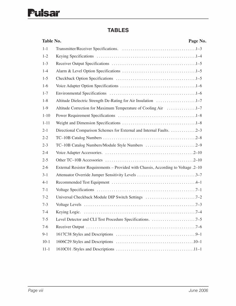
1-1 Transmitter/Receiver Specifications. . . . . . . . . . . . . . . . . . . . . . . . . . . . . . . . . . . .1–3
1-2 Keying Specifications . . . . . . . . . . . . . . . . . . . . . . . . . . . . . . . . . . . . . . . . . . . . . . .1–4
1-3 Receiver Output Specifications . . . . . . . . . . . . . . . . . . . . . . . . . . . . . . . . . . . . . . . .1–5
1-4 Alarm & Level Option Specifications . . . . . . . . . . . . . . . . . . . . . . . . . . . . . . . . . . .1–5
1-5 Checkback Option Specifications . . . . . . . . . . . . . . . . . . . . . . . . . . . . . . . . . . . . . .1–5
1-6 Voice Adapter Option Specifications . . . . . . . . . . . . . . . . . . . . . . . . . . . . . . . . . . . .1–6
1-7 Environmental Specifications . . . . . . . . . . . . . . . . . . . . . . . . . . . . . . . . . . . . . . . . .1–6
1-8 Altitude Dielectric Strength De-Rating for Air Insulation . . . . . . . . . . . . . . . . . . .1–7
1-9 Altitude Correction for Maximum Temperature of Cooling Air . . . . . . . . . . . . . .1–7
1-10 Power Requirement Specifications . . . . . . . . . . . . . . . . . . . . . . . . . . . . . . . . . . . . .1–8
1-11 Weight and Dimension Specifications . . . . . . . . . . . . . . . . . . . . . . . . . . . . . . . . . . .1–8
2-1 Directional Comparison Schemes for External and Internal Faults. . . . . . . . . . . . .2–3
2-2 TC–10B Catalog Numbers . . . . . . . . . . . . . . . . . . . . . . . . . . . . . . . . . . . . . . . . . . . .2–8
2-3 TC–10B Catalog Numbers/Module Style Numbers . . . . . . . . . . . . . . . . . . . . . . . .2–9
2-4 Voice Adapter Accessories. . . . . . . . . . . . . . . . . . . . . . . . . . . . . . . . . . . . . . . . . . .2–10
2-5 Other TC–10B Accessories . . . . . . . . . . . . . . . . . . . . . . . . . . . . . . . . . . . . . . . . . .2–10
2-6 External Resistor Requirements – Provided with Chassis, According to Voltage .2–10
3-1 Attenuator Override Jumper Sensitivity Levels . . . . . . . . . . . . . . . . . . . . . . . . . . . .3–7
4-1 Recommended Test Equipment . . . . . . . . . . . . . . . . . . . . . . . . . . . . . . . . . . . . . . . .4–1
7-1 Voltage Specifications . . . . . . . . . . . . . . . . . . . . . . . . . . . . . . . . . . . . . . . . . . . . . . .7–1
7-2 Universal Checkback Module DIP Switch Settings . . . . . . . . . . . . . . . . . . . . . . . .7–2
7-3 Voltage Levels . . . . . . . . . . . . . . . . . . . . . . . . . . . . . . . . . . . . . . . . . . . . . . . . . . . . .7–3
7-4 Keying Logic. . . . . . . . . . . . . . . . . . . . . . . . . . . . . . . . . . . . . . . . . . . . . . . . . . . . . .7–4
7-5 Level Detector and CLI Test Procedure Specifications. . . . . . . . . . . . . . . . . . . . . .7–5
7-6 Receiver Output . . . . . . . . . . . . . . . . . . . . . . . . . . . . . . . . . . . . . . . . . . . . . . . . . . . .7–6
9-1 1617C38 Styles and Descriptions . . . . . . . . . . . . . . . . . . . . . . . . . . . . . . . . . . . . . .9–1
10-1 1606C29 Styles and Descriptions . . . . . . . . . . . . . . . . . . . . . . . . . . . . . . . . . . . . .10–1
11-1 1610C01 /Styles and Descriptions . . . . . . . . . . . . . . . . . . . . . . . . . . . . . . . . . . . . .11–1
Page viii June 2006
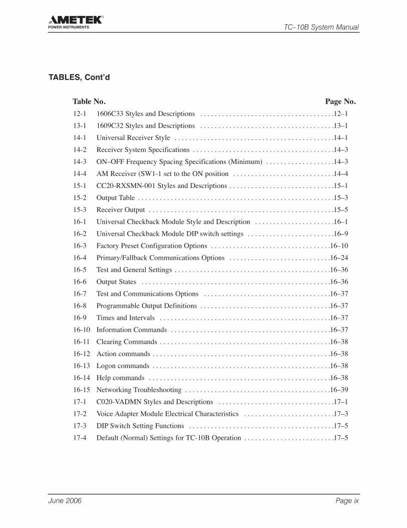
TABLES, Cont’d
Table No. Page No.
12-1 1606C33 Styles and Descriptions . . . . . . . . . . . . . . . . . . . . . . . . . . . . . . . . . . . . .12–1
13-1 1609C32 Styles and Descriptions . . . . . . . . . . . . . . . . . . . . . . . . . . . . . . . . . . . . .13–1
14-1 Universal Receiver Style . . . . . . . . . . . . . . . . . . . . . . . . . . . . . . . . . . . . . . . . . . . .14–1
14-2 Receiver System Specifications . . . . . . . . . . . . . . . . . . . . . . . . . . . . . . . . . . . . . . .14–3
14-3 ON–OFF Frequency Spacing Specifications (Minimum) . . . . . . . . . . . . . . . . . . .14–3
14-4 AM Receiver (SW1-1 set to the ON position . . . . . . . . . . . . . . . . . . . . . . . . . . . .14–4
15-1 CC20-RXSMN-001 Styles and Descriptions . . . . . . . . . . . . . . . . . . . . . . . . . . . . .15–1
15-2 Output Table . . . . . . . . . . . . . . . . . . . . . . . . . . . . . . . . . . . . . . . . . . . . . . . . . . . . . .15–3
15-3 Receiver Output . . . . . . . . . . . . . . . . . . . . . . . . . . . . . . . . . . . . . . . . . . . . . . . . . . .15–5
16-1 Universal Checkback Module Style and Description . . . . . . . . . . . . . . . . . . . . . .16–1
16-2 Universal Checkback Module DIP switch settings . . . . . . . . . . . . . . . . . . . . . . . .16–9
16-3 Factory Preset Configuration Options . . . . . . . . . . . . . . . . . . . . . . . . . . . . . . . . .16–10
16-4 Primary/Fallback Communications Options . . . . . . . . . . . . . . . . . . . . . . . . . . . .16–24
16-5 Test and General Settings . . . . . . . . . . . . . . . . . . . . . . . . . . . . . . . . . . . . . . . . . . .16–36
16-6 Output States . . . . . . . . . . . . . . . . . . . . . . . . . . . . . . . . . . . . . . . . . . . . . . . . . . . .16–36
16-7 Test and Communications Options . . . . . . . . . . . . . . . . . . . . . . . . . . . . . . . . . . .16–37
16-8 Programmable Output Definitions . . . . . . . . . . . . . . . . . . . . . . . . . . . . . . . . . . . .16–37
16-9 Times and Intervals . . . . . . . . . . . . . . . . . . . . . . . . . . . . . . . . . . . . . . . . . . . . . . .16–37
16-10 Information Commands . . . . . . . . . . . . . . . . . . . . . . . . . . . . . . . . . . . . . . . . . . . .16–37
16-11 Clearing Commands . . . . . . . . . . . . . . . . . . . . . . . . . . . . . . . . . . . . . . . . . . . . . . .16–38
16-12 Action commands . . . . . . . . . . . . . . . . . . . . . . . . . . . . . . . . . . . . . . . . . . . . . . . . .16–38
16-13 Logon commands . . . . . . . . . . . . . . . . . . . . . . . . . . . . . . . . . . . . . . . . . . . . . . . . .16–38
16-14 Help commands . . . . . . . . . . . . . . . . . . . . . . . . . . . . . . . . . . . . . . . . . . . . . . . . . .16–38
16-15 Networking Troubleshooting . . . . . . . . . . . . . . . . . . . . . . . . . . . . . . . . . . . . . . . .16–39
17-1 C020-VADMN Styles and Descriptions . . . . . . . . . . . . . . . . . . . . . . . . . . . . . . . .17–1
17-2 Voice Adapter Module Electrical Characteristics . . . . . . . . . . . . . . . . . . . . . . . . .17–3
17-3 DIP Switch Setting Functions . . . . . . . . . . . . . . . . . . . . . . . . . . . . . . . . . . . . . . . .17–5
17-4 Default (Normal) Settings for TC-10B Operation . . . . . . . . . . . . . . . . . . . . . . . . .17–5
June 2006 Page ix
TC–10B System Manual

1.1 Standard FeaturesThe TC–10B frequency-programmable power-line-carrier set offers the following features as standard:
• Programmable over 30–535kHz (in 0.5kHz steps) with direct frequency readout
• Frequencies are easily field-selectable by rotary switches (transmitter) -or- push button (receiver)
• Wideband (1,600Hz) receiver for use with all blocking systems
• Narrow band (800Hz) receiver for use with directional-comparison blocking systems where thereis a need to improve signal-to-noise ratio (SNR)
• High receiver sensitivity: 22.5mV....(Standard setting)5mV....(High-sensitivity setting)
• Universal keying/receiver output
• 300-2,000Hz range audio channel for maintenance Voice Channel
• Built-in low/high level carrier test switches
• dc-to-dc isolated power supply
• 48, 125, and 250Vdc versions available
1.2 Standard NomenclatureThe standard nomenclature for AMETEKcarrier protection equipment is as follows:
Cabinet – contains fixed-racks, swing-racks, or open racks
Rack – contains one or more chassis (e.g., the TC–10B)
Chassis – contains several printed circuit boards, called modules (e.g., Transmitter or Receiver)
Module – contains a number of functional circuits (e.g., Oscillator or Synthesizer)
Circuit – a complete function on a printed circuit board
1.3 TC–10B ChassisThe TC–10B chassis specifications include standard dimensions of:
Height – 5.25” (133.35 mm), requiring 3 rack units, each measuring 1.75” (44.45 mm)
Width – 19.00” (482.6 mm) Depth – 13.50” (342.9 mm)
Each chassis is notched for mounting in a standard relay rack.
Copyright © AMETEK
Chapter 1. Product Description
1
1.4 TC–10B ModulesThe TC–10B circuitry is divided into standard modules with optional Voice Adapter, TTL Transmitter andUniversal Checkback modules available, as shown on the Functional Block Diagram (Fig. 6-1). Circuitdescriptions, complete with schematic diagrams, are shown in Chapters 9 through 17 with Sub Numbersthat indicate appropriate revisions for each module, as follows:
Chapter Module Schematic
9. Power Supply 1617C38-8 ||
10. Keying 1606C29-12 ||
11. Transmitter 1355D71-8
12. 10W PA 1606C33-22 ||
13. RF Interface 1609C32-8
14. Universal Receiver not user serviceable
15. Receiver Output (Solid State) CC30-RXSMN
16. (Optional) Universal Checkback not user serviceable
17. (Optional) Voice Adapter C030-VADMN-5 ||
Page 1–2 June 2006
TC–10B System Manual
NOTE
See Chapter 2, Applications and Ordering Information, for ordering information. See Chapter 3,Installation, for a summary of jumper controls.
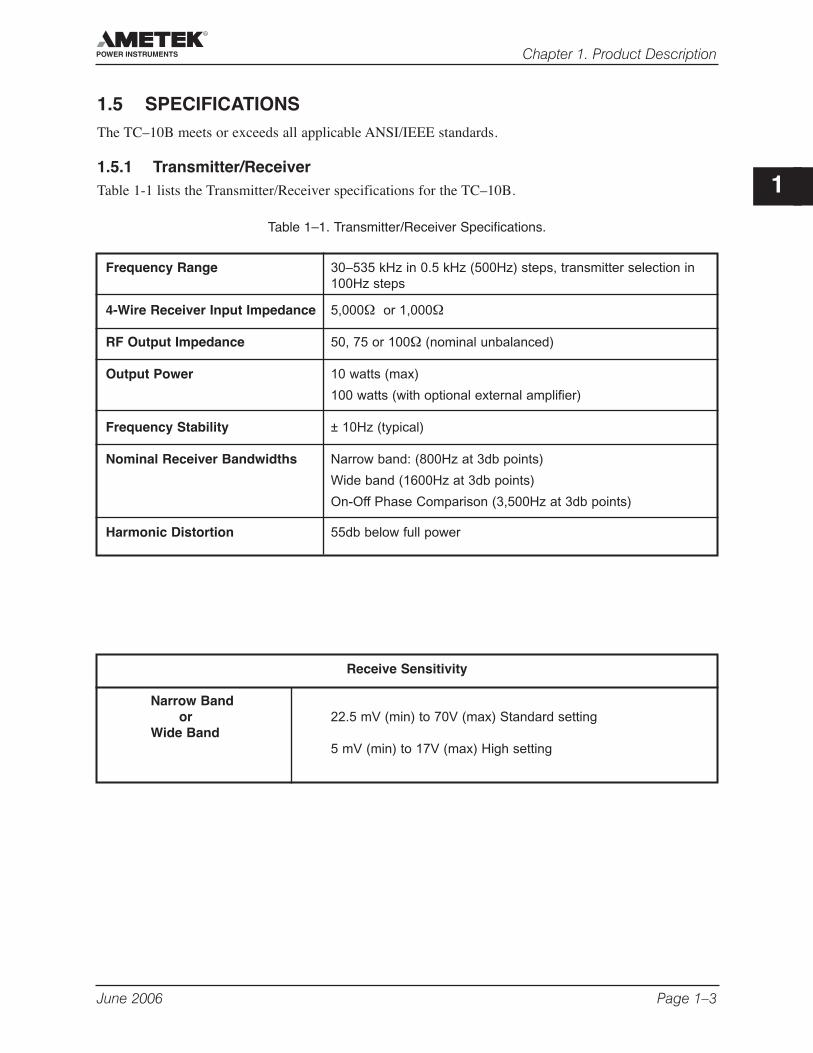
1.5 SPECIFICATIONSThe TC–10B meets or exceeds all applicable ANSI/IEEE standards.
1.5.1 Transmitter/ReceiverTable 1-1 lists the Transmitter/Receiver specifications for the TC–10B.
June 2006 Page 1–3
Chapter 1. Product Description
1
Table 1–1. Transmitter/Receiver Specifications.
Frequency Range 30–535 kHz in 0.5 kHz (500Hz) steps, transmitter selection in100Hz steps
4-Wire Receiver Input Impedance 5,000Ω or 1,000Ω
RF Output Impedance 50, 75 or 100Ω (nominal unbalanced)
Output Power 10 watts (max)
100 watts (with optional external amplifier)
Frequency Stability ± 10Hz (typical)
Nominal Receiver Bandwidths Narrow band: (800Hz at 3db points)
Wide band (1600Hz at 3db points)
On-Off Phase Comparison (3,500Hz at 3db points)
Harmonic Distortion 55db below full power
Receive Sensitivity
Narrow Band or 22.5 mV (min) to 70V (max) Standard setting
Wide Band5 mV (min) to 17V (max) High setting
Page 1–4 June 2006
TC–10B System Manual
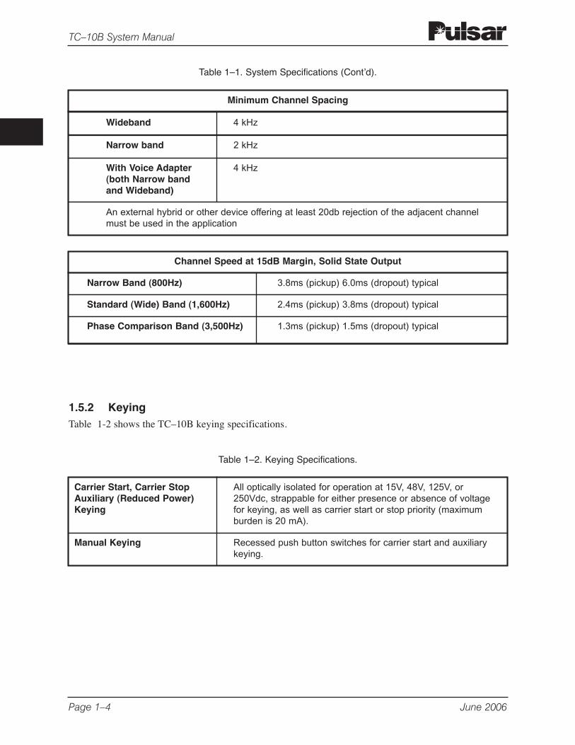
Channel Speed at 15dB Margin, Solid State Output
Narrow Band (800Hz) 3.8ms (pickup) 6.0ms (dropout) typical
Standard (Wide) Band (1,600Hz) 2.4ms (pickup) 3.8ms (dropout) typical
Phase Comparison Band (3,500Hz) 1.3ms (pickup) 1.5ms (dropout) typical
Minimum Channel Spacing
1.5.2 KeyingTable 1-2 shows the TC–10B keying specifications.
Carrier Start, Carrier Stop All optically isolated for operation at 15V, 48V, 125V, or Auxiliary (Reduced Power) 250Vdc, strappable for either presence or absence of voltage Keying for keying, as well as carrier start or stop priority (maximum
burden is 20 mA).
Manual Keying Recessed push button switches for carrier start and auxiliarykeying.
Table 1–1. System Specifications (Cont’d).
Table 1–2. Keying Specifications.
Wideband 4 kHz
Narrow band 2 kHz
With Voice Adapter 4 kHz(both Narrow bandand Wideband)
An external hybrid or other device offering at least 20db rejection of the adjacent channelmust be used in the application
June 2006 Page 1–5
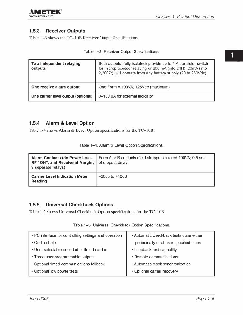
Chapter 1. Product Description
1
1.5.4 Alarm & Level OptionTable 1-4 shows Alarm & Level Option specifications for the TC–10B.
1.5.3 Receiver OutputsTable 1-3 shows the TC–10B Receiver Output Specifications.
Two independent relaying Both outputs (fully isolated) provide up to 1 A transistor switch outputs for microprocessor relaying or 200 mA (into 24Ω), 20mA (into
2,200Ω); will operate from any battery supply (20 to 280Vdc)
One receive alarm output One Form A 100VA, 125Vdc (maximum)
One carrier level output (optional) 0–100 µA for external indicator
Table 1–3. Receiver Output Specifications.
Alarm Contacts (dc Power Loss, Form A or B contacts (field strappable) rated 100VA; 0.5 secRF “ON”, and Receive at Margin; of dropout delay3 separate relays)
Carrier Level Indication Meter –20db to +10dBReading
Table 1–4. Alarm & Level Option Specifications.
Table 1–5. Universal Checkback Option Specifications.
• PC interface for controlling settings and operation • Automatic checkback tests done either
• On-line help periodically or at user specified times
• User selectable encoded or timed carrier • Loopback test capability
• Three user programmable outputs • Remote communications
• Optional timed communications fallback • Automatic clock synchronization
• Optional low power tests • Optional carrier recovery
1.5.5 Universal Checkback OptionsTable 1-5 shows Universal Checkback Option specifications for the TC–10B.
Page 1–6 June 2006
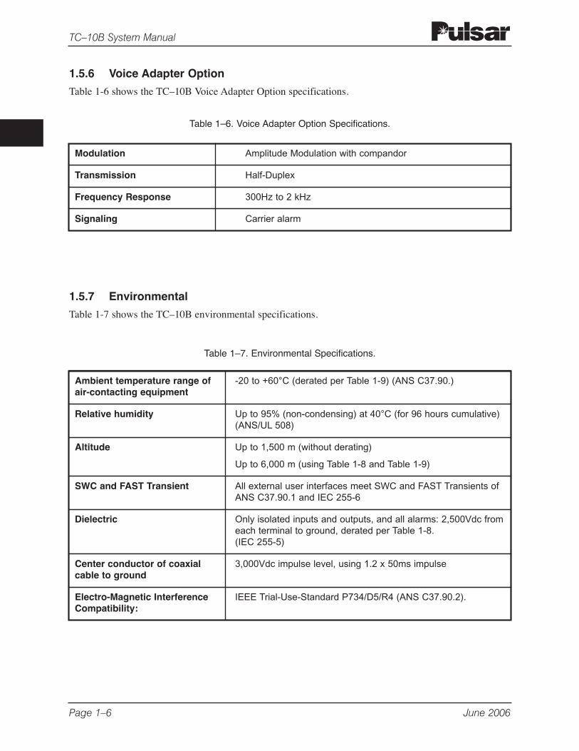
TC–10B System Manual
Ambient temperature range of -20 to +60°C (derated per Table 1-9) (ANS C37.90.)air-contacting equipment
Relative humidity Up to 95% (non-condensing) at 40°C (for 96 hours cumulative)(ANS/UL 508)
Altitude Up to 1,500 m (without derating)
Up to 6,000 m (using Table 1-8 and Table 1-9)
SWC and FAST Transient All external user interfaces meet SWC and FAST Transients ofANS C37.90.1 and IEC 255-6
Dielectric Only isolated inputs and outputs, and all alarms: 2,500Vdc fromeach terminal to ground, derated per Table 1-8. (IEC 255-5)
Center conductor of coaxial 3,000Vdc impulse level, using 1.2 x 50ms impulsecable to ground
Electro-Magnetic Interference IEEE Trial-Use-Standard P734/D5/R4 (ANS C37.90.2).Compatibility:
Table 1–7. Environmental Specifications.
Modulation Amplitude Modulation with compandor
Transmission Half-Duplex
Frequency Response 300Hz to 2 kHz
Signaling Carrier alarm
Table 1–6. Voice Adapter Option Specifications.
1.5.6 Voice Adapter Option
Table 1-6 shows the TC–10B Voice Adapter Option specifications.
1.5.7 Environmental
Table 1-7 shows the TC–10B environmental specifications.
June 2006 Page 1–7
Chapter 1. Product Description
1
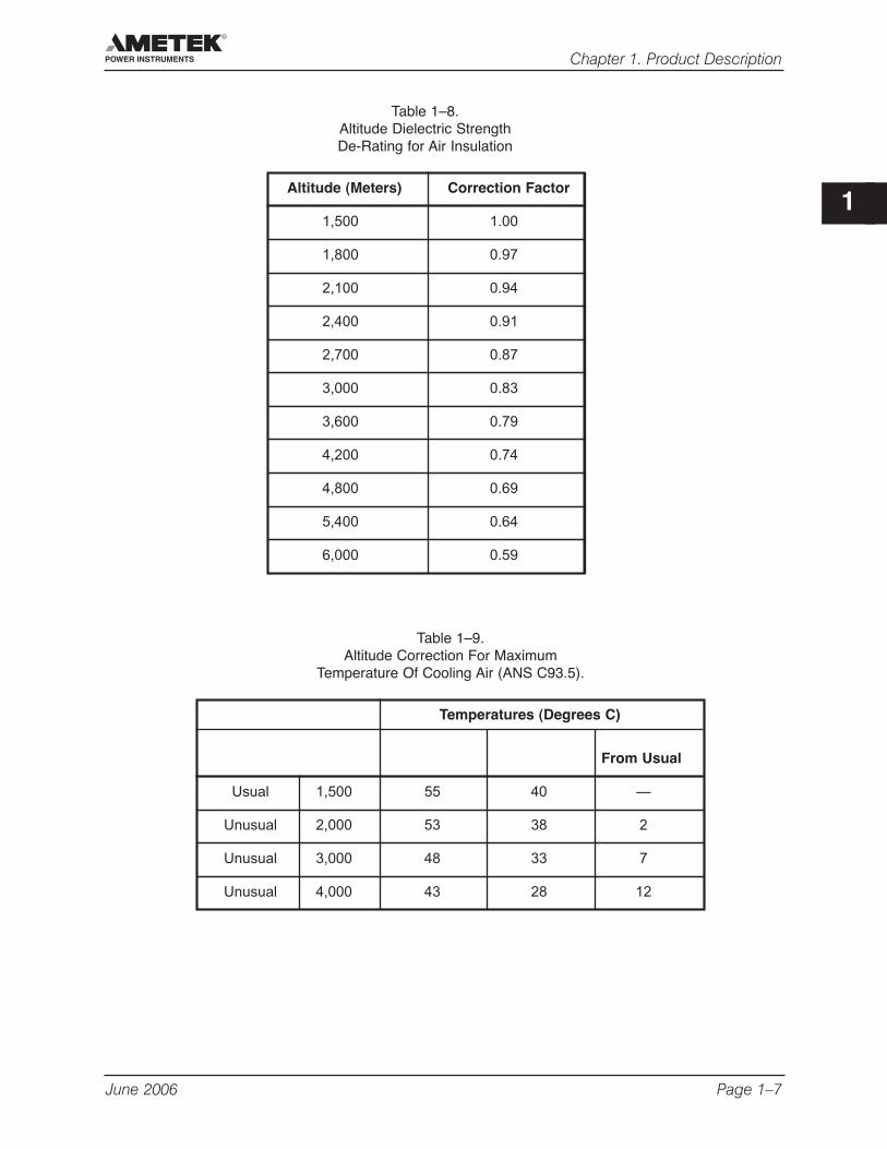
Temperatures (Degrees C)
Altitude (Meters) Short-Time Long-Time DifferenceFrom Usual
Usual 1,500 55 40 —
Unusual 2,000 53 38 2
Unusual 3,000 48 33 7
Unusual 4,000 43 28 12
Table 1–9. Altitude Correction For Maximum
Temperature Of Cooling Air (ANS C93.5).
Altitude (Meters) Correction Factor
1,500 1.00
1,800 0.97
2,100 0.94
2,400 0.91
2,700 0.87
3,000 0.83
3,600 0.79
4,200 0.74
4,800 0.69
5,400 0.64
6,000 0.59
Table 1–8. Altitude Dielectric Strength De-Rating for Air Insulation
Page 1–8 June 2006
TC–10B System Manual
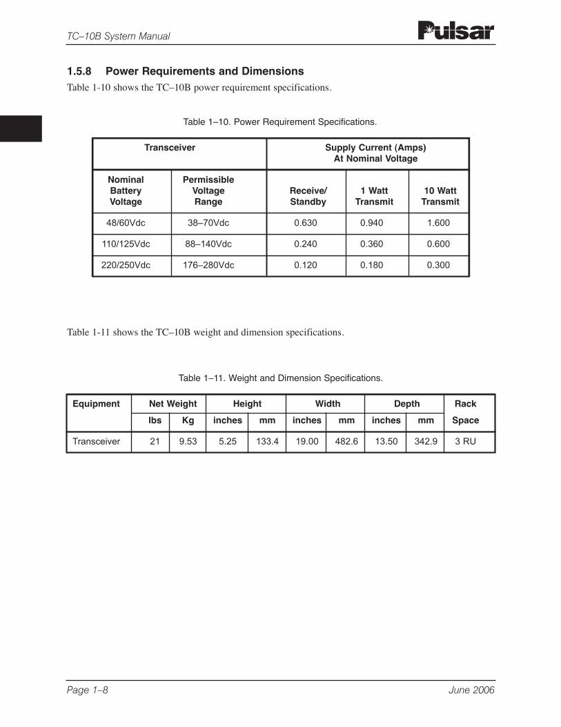
1.5.8 Power Requirements and DimensionsTable 1-10 shows the TC–10B power requirement specifications.
Table 1-11 shows the TC–10B weight and dimension specifications.
Transceiver Supply Current (Amps) At Nominal Voltage
Nominal PermissibleBattery Voltage Receive/ 1 Watt 10 Watt Voltage Range Standby Transmit Transmit
48/60Vdc 38–70Vdc 0.630 0.940 1.600
110/125Vdc 88–140Vdc 0.240 0.360 0.600
220/250Vdc 176–280Vdc 0.120 0.180 0.300
Table 1–10. Power Requirement Specifications.
Equipment Net Weight Height Width Depth Rack
lbs Kg inches mm inches mm inches mm Space
Transceiver 21 9.53 5.25 133.4 19.00 482.6 13.50 342.9 3 RU
Table 1–11. Weight and Dimension Specifications.
1
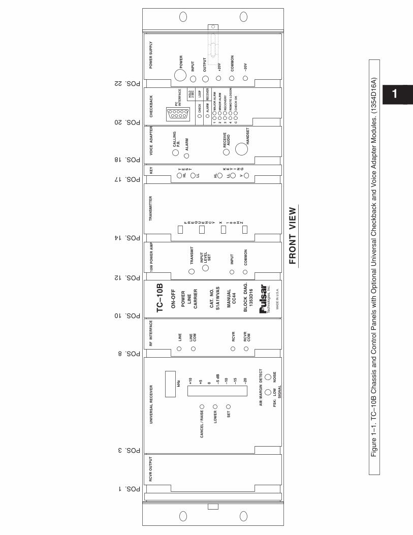
Fig
ure
1–1.
TC
–10B
Cha
ssis
and
Con
trol
Pan
els
with
Opt
iona
l Uni
vers
al C
heck
back
and
Voi
ce A
dapt
er M
odul
es.
(135
4D16
A)
RF
INT
ER
FAC
E10
WP
OW
ER
AM
P
LIN
E
LIN
EC
OM
TR
AN
SM
IT
INP
UT
LE
VE
LS
ET
INP
UT
CO
MM
ON
RC
VR
RC
VR
CO
M
FR
ON
TV
IEW
POS.1
POS.3
POS.8
POS.10
POS.12
POS.14
POS.17
POS.18
POS.20
POS.22
PR
GM
SE
T
TS
T
RS
T
UN
IVE
RS
AL
RE
CE
IVE
R
CA
NC
EL
/RA
ISE
LO
WE
R
SE
T
AM
:MA
RG
IND
ET
EC
T
FS
K:
LO
WN
OIS
ES
IGN
AL
RC
VR
OU
TP
UT
TC
–10B
ON
-OF
F
PO
WE
RL
INE
CA
RR
IER
CA
T.N
O.
S1A
1WVA
S
MA
NU
AL
CC
44
BL
OC
KD
IAG
.13
53D
16
MA
DE
INU
.S.A
.
Technolo
gie
s,In
c.
F R E Q U E N C Y X 1 0 0 H Z
TR
AN
SM
ITT
ER
KE
Y
HL
LL
HL
LL V
T E S T K E Y I N G
VO
ICE
AD
AP
TE
R
CA
LL
ING
P.B
.
AL
AR
M
RE
CE
IVE
AU
DIO
HA
ND
SE
T
LO
OP
HO
LD
2S
EC
CH
EC
K
AL
AR
M
MA
JO
RA
LR
M1
MIN
OR
AL
RM
2
RE
CO
VE
RY
3
RE
MO
TE
LO
GO
N4 C
CH
EC
KO
K
PC
INT
ER
FA
CE
RE
CO
VE
R
PO
WE
R
INP
UT
OU
TP
UT
+20V
CO
MM
ON
–20VPO
WE
RS
UP
PLY
CH
EC
KB
AC
K
kH
z
+1
0
+5
–1
0
–1
5
–2
0
–5
dB
0

Page 1–10 June 2006
TC–10B System Manual
USER NOTES
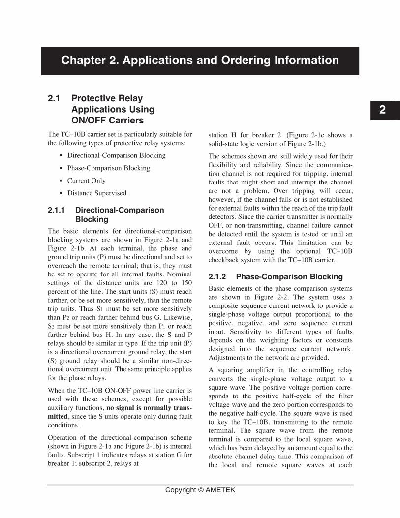
2.1 Protective RelayApplications Using ON/OFF Carriers
The TC–10B carrier set is particularly suitable forthe following types of protective relay systems:
• Directional-Comparison Blocking
• Phase-Comparison Blocking
• Current Only
• Distance Supervised
2.1.1 Directional-ComparisonBlocking
The basic elements for directional-comparisonblocking systems are shown in Figure 2-1a andFigure 2-1b. At each terminal, the phase andground trip units (P) must be directional and set tooverreach the remote terminal; that is, they mustbe set to operate for all internal faults. Nominalsettings of the distance units are 120 to 150percent of the line. The start units (S) must reachfarther, or be set more sensitively, than the remotetrip units. Thus S1 must be set more sensitivelythan P2 or reach farther behind bus G. Likewise,S2 must be set more sensitively than P1 or reachfarther behind bus H. In any case, the S and Prelays should be similar in type. If the trip unit (P)is a directional overcurrent ground relay, the start(S) ground relay should be a similar non-direc-tional overcurrent unit. The same principle appliesfor the phase relays.
When the TC–10B ON-OFF power line carrier isused with these schemes, except for possibleauxiliary functions, no signal is normally trans-mitted, since the S units operate only during faultconditions.
Operation of the directional-comparison scheme(shown in Figure 2-1a and Figure 2-1b) is internalfaults. Subscript 1 indicates relays at station G forbreaker 1; subscript 2, relays at
station H for breaker 2. (Figure 2-1c shows asolid-state logic version of Figure 2-1b.)
The schemes shown are still widely used for theirflexibility and reliability. Since the communica-tion channel is not required for tripping, internalfaults that might short and interrupt the channelare not a problem. Over tripping will occur,however, if the channel fails or is not establishedfor external faults within the reach of the trip faultdetectors. Since the carrier transmitter is normallyOFF, or non-transmitting, channel failure cannotbe detected until the system is tested or until anexternal fault occurs. This limitation can beovercome by using the optional TC–10Bcheckback system with the TC–10B carrier.
2.1.2 Phase-Comparison BlockingBasic elements of the phase-comparison systemsare shown in Figure 2-2. The system uses acomposite sequence current network to provide asingle-phase voltage output proportional to thepositive, negative, and zero sequence currentinput. Sensitivity to different types of faultsdepends on the weighting factors or constantsdesigned into the sequence current network.Adjustments to the network are provided.
A squaring amplifier in the controlling relayconverts the single-phase voltage output to asquare wave. The positive voltage portion corre-sponds to the positive half-cycle of the filtervoltage wave and the zero portion corresponds tothe negative half-cycle. The square wave is usedto key the TC–10B, transmitting to the remoteterminal. The square wave from the remoteterminal is compared to the local square wave,which has been delayed by an amount equal to theabsolute channel delay time. This comparison ofthe local and remote square waves at each
Copyright © AMETEK
Chapter 2. Applications and Ordering Information
2
Page 2–2 June 2006
TC–10B System Manual
Breaker 1 ChannelStart Fault Detectors (S1)
Breaker 2 ChannelStart Fault Detectors (S2)
Breaker 1 TripFault Detector (P1)
Breaker 2 Trip Fault Detector (P2)
Protected Line
G H
FI
FE
Power Line CarrierChannel
1 2
RR
P
CS
ChannelSignal
ReceiverRR
TripCoil
52a
Stop ChannelSignal ifInitiatedLocally Initiate
ChannelSignal
S
Pick-upApproximately13–16 Ms
CS
Stop Channel Signal ifInitiated Locally
TimerP
TripS FromRemote TerminalVia Channel
Note: (P) Operation or (S) SignalProvides an Input 1 on Circuit.
ANDX
O
S Initiate Channel Signal
X – Nominally Between 6–16 Ms
Figure 2-1a. – Basic Elements for directional-comparison blocking systems.
Figure 2-1c. – Solid State Logic (per Terminal).
Figure 2–1. Directional-Comparison Blocking, Basic Elements and Logic Diagrams.
Figure 2-1b. – Contact Logic (per Terminal).
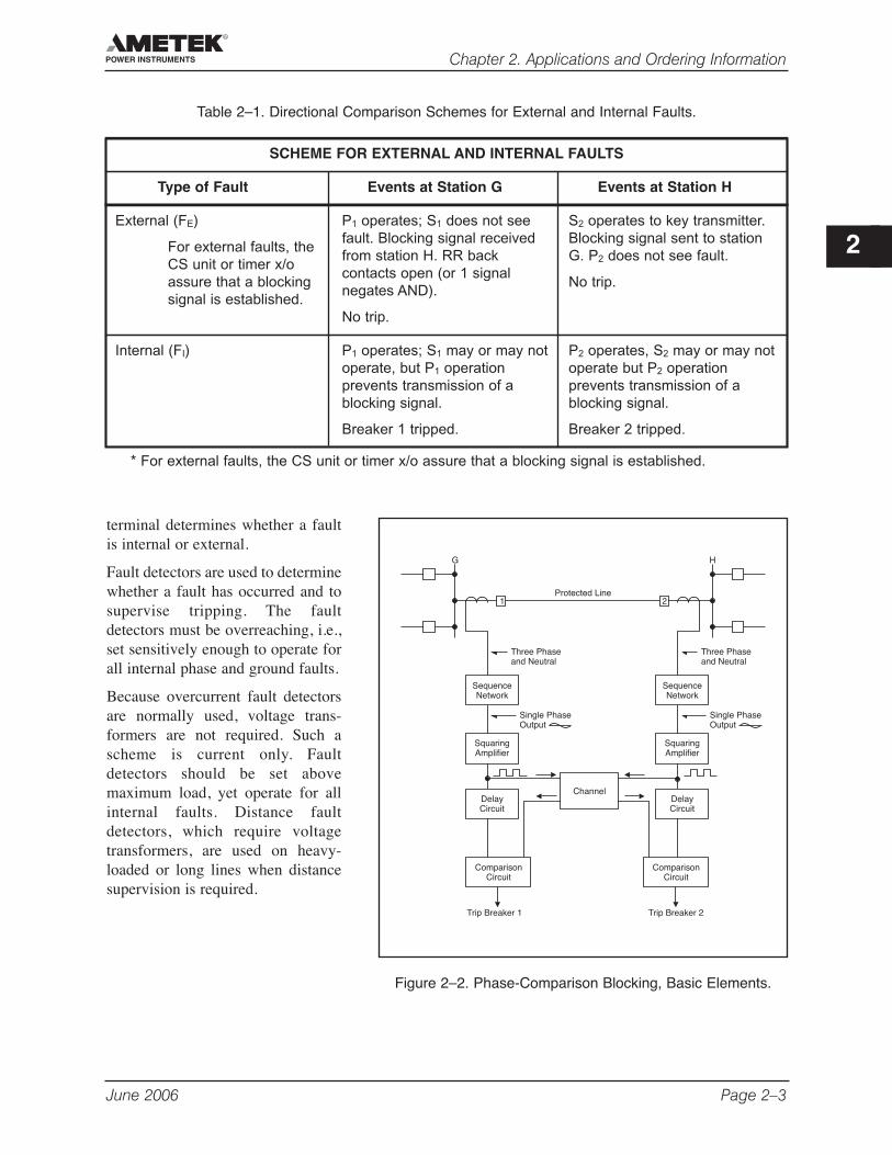
terminal determines whether a faultis internal or external.
Fault detectors are used to determinewhether a fault has occurred and tosupervise tripping. The faultdetectors must be overreaching, i.e.,set sensitively enough to operate forall internal phase and ground faults.
Because overcurrent fault detectorsare normally used, voltage trans-formers are not required. Such ascheme is current only. Faultdetectors should be set abovemaximum load, yet operate for allinternal faults. Distance faultdetectors, which require voltagetransformers, are used on heavy-loaded or long lines when distancesupervision is required.
June 2006 Page 2–3
Chapter 2. Applications and Ordering Information
2
Table 2–1. Directional Comparison Schemes for External and Internal Faults.
* For external faults, the CS unit or timer x/o assure that a blocking signal is established.
SCHEME FOR EXTERNAL AND INTERNAL FAULTS
Type of Fault Events at Station G Events at Station H
External (FE)
For external faults, theCS unit or timer x/oassure that a blockingsignal is established.
P1 operates; S1 does not seefault. Blocking signal receivedfrom station H. RR backcontacts open (or 1 signalnegates AND).
No trip.
S2 operates to key transmitter.Blocking signal sent to stationG. P2 does not see fault.
No trip.
Internal (FI) P1 operates; S1 may or may notoperate, but P1 operationprevents transmission of ablocking signal.
Breaker 1 tripped.
P2 operates, S2 may or may notoperate but P2 operationprevents transmission of ablocking signal.
Breaker 2 tripped.
Protected Line
G H
1 2
Trip Breaker 1 Trip Breaker 2
SequenceNetwork
SquaringAmplifier
DelayCircuit
ComparisonCircuit
Three Phaseand Neutral
Single PhaseOutput
SequenceNetwork
SquaringAmplifier
DelayCircuit
ComparisonCircuit
Three Phaseand Neutral
Single PhaseOutput
Channel
Figure 2–2. Phase-Comparison Blocking, Basic Elements.
Page 2–4 June 2006
TC–10B System Manual
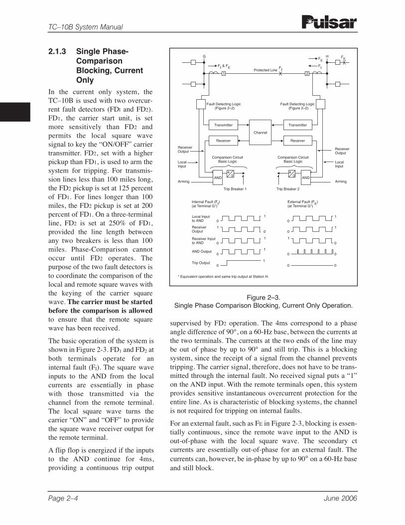
2.1.3 Single Phase-ComparisonBlocking, CurrentOnly
In the current only system, theTC–10B is used with two overcur-rent fault detectors (FDl and FD2).FD1, the carrier start unit, is setmore sensitively than FD2 andpermits the local square wavesignal to key the “ON/OFF” carriertransmitter. FD2, set with a higherpickup than FD1, is used to arm thesystem for tripping. For transmis-sion lines less than 100 miles long,the FD2 pickup is set at 125 percentof FD1. For lines longer than 100miles, the FD2 pickup is set at 200percent of FD1. On a three-terminalline, FD2 is set at 250% of FD1,provided the line length betweenany two breakers is less than 100miles. Phase-Comparison cannotoccur until FD2 operates. Thepurpose of the two fault detectors isto coordinate the comparison of thelocal and remote square waves withthe keying of the carrier squarewave. The carrier must be startedbefore the comparison is allowedto ensure that the remote squarewave has been received.
The basic operation of the system isshown in Figure 2-3. FD1 and FD2 atboth terminals operate for aninternal fault (FI). The square waveinputs to the AND from the localcurrents are essentially in phasewith those transmitted via thechannel from the remote terminal.The local square wave turns thecarrier “ON” and “OFF” to providethe square wave receiver output forthe remote terminal.
A flip flop is energized if the inputsto the AND continue for 4ms,providing a continuous trip output
supervised by FD2 operation. The 4ms correspond to a phaseangle difference of 90°, on a 60-Hz base, between the currents atthe two terminals. The currents at the two ends of the line maybe out of phase by up to 90° and still trip. This is a blockingsystem, since the receipt of a signal from the channel preventstripping. The carrier signal, therefore, does not have to be trans-mitted through the internal fault. No received signal puts a “1”on the AND input. With the remote terminals open, this systemprovides sensitive instantaneous overcurrent protection for theentire line. As is characteristic of blocking systems, the channelis not required for tripping on internal faults.
For an external fault, such as FE in Figure 2-3, blocking is essen-tially continuous, since the remote wave input to the AND isout-of-phase with the local square wave. The secondary ctcurrents are essentially out-of-phase for an external fault. Thecurrents can, however, be in-phase by up to 90° on a 60-Hz baseand still block.
Protected Line
G H
1 2
Transmitter
Receiver
Channel
Fault Detecting Logic(Figure 2–2)
Fault Detecting Logic(Figure 2–2)
ReceiverOutput
ReceiverOutput
LocalInput
LocalInput
Comparison CircuitBasic Logic
Arming Arming
Internal Fault (FI)(at Terminal G*)
External Fault (FE)(at Terminal G*)
Local Inputto AND
ReceiverOutput
Receiver Inputto AND
AND Output
Trip Output
* Equivalent operation and same trip output at Station H.
0
0
0
0
0
0
0
0
0
0
0
0
1
1
1
11
1
1
1
40
Comparison CircuitBasic Logic
40
Trip Breaker 1 Trip Breaker 2
Transmitter
Receiver
FI & FE
FEFE
FIFI
AND AND
Figure 2–3. Single Phase Comparison Blocking, Current Only Operation.
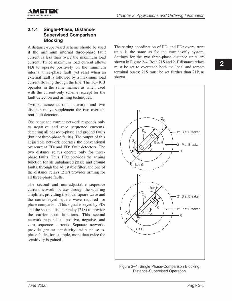
2.1.4 Single-Phase, Distance-Supervised ComparisonBlocking
A distance-supervised scheme should be usedif the minimum internal three-phase faultcurrent is less than twice the maximum loadcurrent. Twice maximum load current allowsFDl to operate positively on the minimuminternal three-phase fault, yet reset when anexternal fault is followed by a maximum loadcurrent flowing through the line. The TC–10Boperates in the same manner as when usedwith the current-only scheme, except for thefault detection and arming techniques.
Two sequence current networks and twodistance relays supplement the two overcur-rent fault detectors.
One sequence current network responds onlyto negative and zero sequence currents,detecting all phase-to-phase and ground faults(but not three-phase faults). The output of thisadjustable network operates the conventionalovercurrent FDl and FD2 fault detectors. Thetwo distance relays operate only for three-phase faults. Thus, FD2 provides the armingfunction for all unbalanced phase and groundfaults, through the adjustable filter, and one ofthe distance relays (21P) provides arming forall three-phase faults.
The second and non-adjustable sequencecurrent network operates through the squaringamplifier, providing the local square wave andthe carrier-keyed square wave required forphase comparison. This signal is keyed by FD1
and the second distance relay (21S) to providethe carrier start functions. This secondnetwork responds to positive, negative, andzero sequence currents. Separate networksprovide greater sensitivity: with phase-to-phase faults, for example, more than twice thesensitivity is gained.
June 2006 Page 2–5
Chapter 2. Applications and Ordering Information
2
1
2
X
Bus H
Bus G
21 S at Breaker
21 P at Breaker
R
ZC
ZC
ZA
ZA
1
2
X
Bus H
Bus G
21 S at Breaker
21 P at Breaker
R
ZCZC
ZA
ZA
Figure 2–4. Single Phase-Comparison Blocking,Distance-Supervised Operation.
The setting coordination of FDl and FD2 overcurrentunits is the same as for the current-only system.Settings for the two three-phase distance units areshown in Figure 2-4. Both 21S and 21P distance relaysmust be set to overreach both the local and remoteterminal buses; 21S must be set further than 21P, asshown.
2.1.5 Phase Comparison Relayingand 20V Auxilliary PowerSupply
When ordering a TC-10B for use with phasecomparison relaying, a 20V auxilliary powersupply is provided.
The majority of interfaces between the relay andthe communications equipment are done at thestation battery. If the control battery is 125Vdc,then the carrier output will be powered up with125Vdc to provide station battery voltage to therelay. However, in phase comparison relaysystems, the ratio, of the on and off state, of thecarrier circuit ouptut and the on and off state of therelay’s keying circuit is critical to provide a squarewave that closely represents the power system acwave. Therefore, based on the type of inputs usedon the relay system at the point it interfaces withthe carrier system, this will determine whatvoltage level is acceptable. This criticality is onthe order of 500 or less microseconds.
Due to the capacitors typically applied to outputcircuits to dampen surges, the higher the voltageapplied, the longer it will take to dissipate theenergy. Therefore, to dissipate this energy quickly,to adhere to the timing requirements for a securephase comparison relay system, the use of theauxilliary 20V power supply is necessary.Different relay manufacturers’ input circuits mayvary and can conceivably decay fast enough not tohinder the security of the relay system operation.However, the energy dissipated will also generatea significant amount of heat. By utilizing theauxilliary supply, mounted on the rear of thecarrier unit, it will allow that heat to be outside ofeither unit.
AMETEKstrongly recommends the application ofthe auxilliary power supply for two reasons; decaytime of the energy, and the heating caused by thedissipation of energy.
2.2 Special ApplicationConsiderations
Because the TC–10B is “ON/OFF” modulated,only one frequency (fC) is required for line protec-tion. When applied to three terminal lines, phase
cancellation will occur when two or more trans-mitters are keyed simultaneously. To prevent this,you should offset transmitters by ±100Hz, usingthe thumbwheel frequency programmingswitches. The three frequencies should be:
• fC
• fC - 100Hz
• fC + 100Hz
When using the TC–10B with the SKBU-1 Phase-Comparison, you must offset the transmitterfrequencies from the center frequency by 100 Hzfor all applications. In a two-terminal application,set the transmitter at one end 100Hz above thecenter frequency, and the transmitter at the otherend 100Hz below the center frequency. Thus, thetwo transmitters are spaced 200Hz from eachother. For a three terminal line, you should offsetthe transmitter as described in the aboveparagraph.
The TC–10B does not have an adjustable filter orhybrid attached to the output of the transmitter.
If you are using the TC–10B in an applicationwhere no other power line carrier equipment isattached to the power line, then no further actionis required. However, in the application ofSingle Comparator Phase Comparisonrelaying, the TC–10B is to be operated in thefour-wire mode (see RF Interface Module),with an external skewed hybrid between trans-mitter and receiver.
If you are applying the carrier set with other trans-mitters, coupled through the same tuningequipment, you must apply a hybrid or a series LCunit to the transmitter output to isolate the othertransmitters from the TC–10B transmitter. Thiswill avoid the problems of intermodulation distor-tion. We suggest that you use a hybrid if thefrequency spacing between all transmitters iswithin the bandwidth of the hybrid (usually 6%).Check the manufacturers instructions for theactual spacing limitations of the hybrid you areusing. If you cannot use a hybrid, then you mayuse a series LC unit to isolate the transmitters. Inthis case, the transmitters must have spacing suchthat the LC you are using will attenuate the
Page 2–6 June 2006
TC–10B System Manual
external frequencies by at least 20dB (if the otherfrequency is a 10 watt transmitter), and 30dB (ifthe other frequency is a 100 watt transmitter).
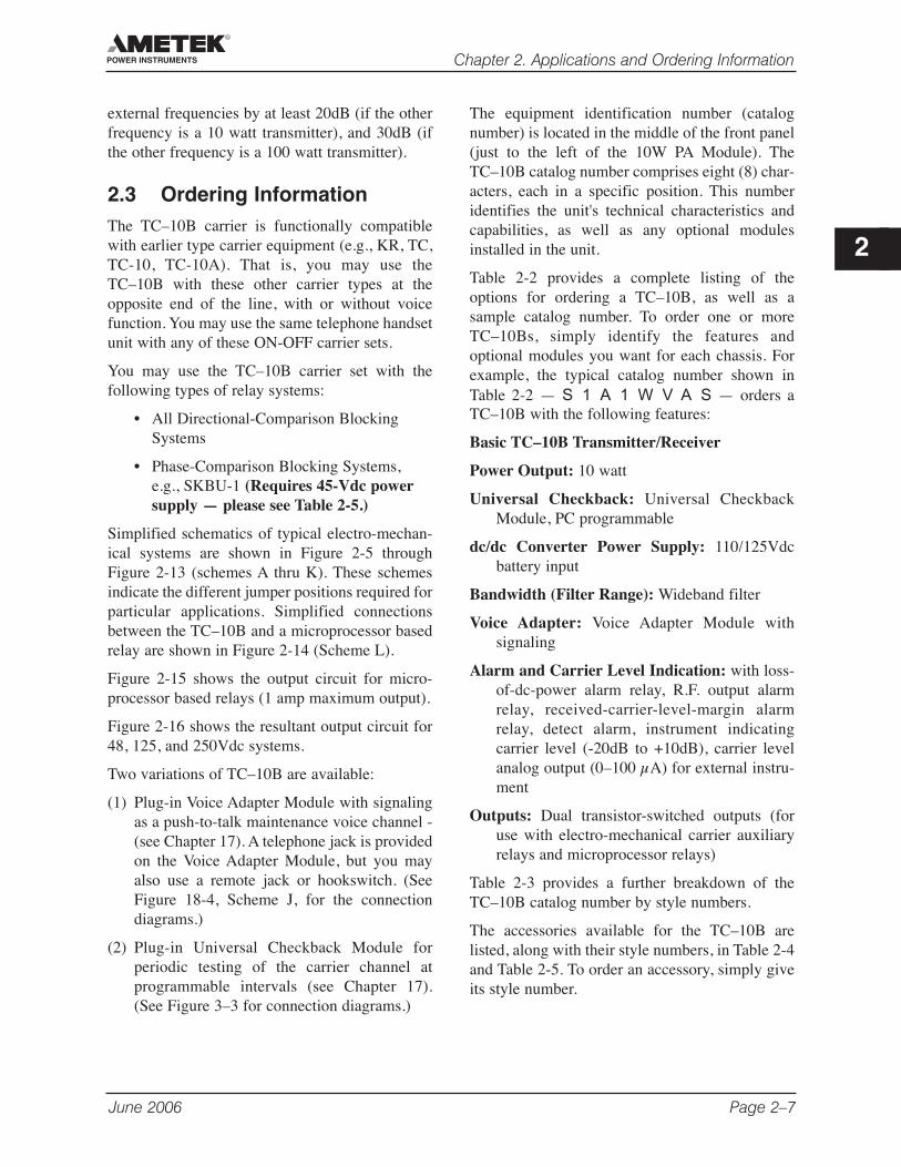
2.3 Ordering InformationThe TC–10B carrier is functionally compatiblewith earlier type carrier equipment (e.g., KR, TC,TC-10, TC-10A). That is, you may use theTC–10B with these other carrier types at theopposite end of the line, with or without voicefunction. You may use the same telephone handsetunit with any of these ON-OFF carrier sets.
You may use the TC–10B carrier set with thefollowing types of relay systems:
• All Directional-Comparison BlockingSystems
• Phase-Comparison Blocking Systems,e.g., SKBU-1 (Requires 45-Vdc powersupply — please see Table 2-5.)
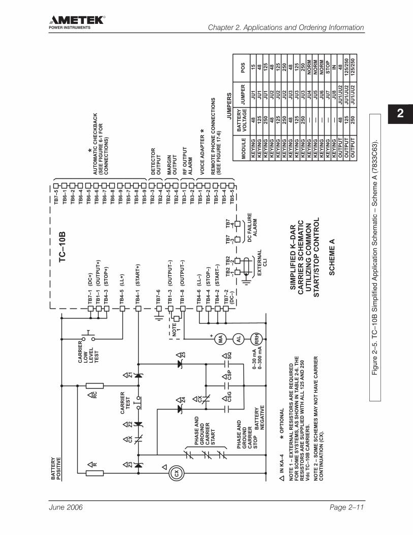
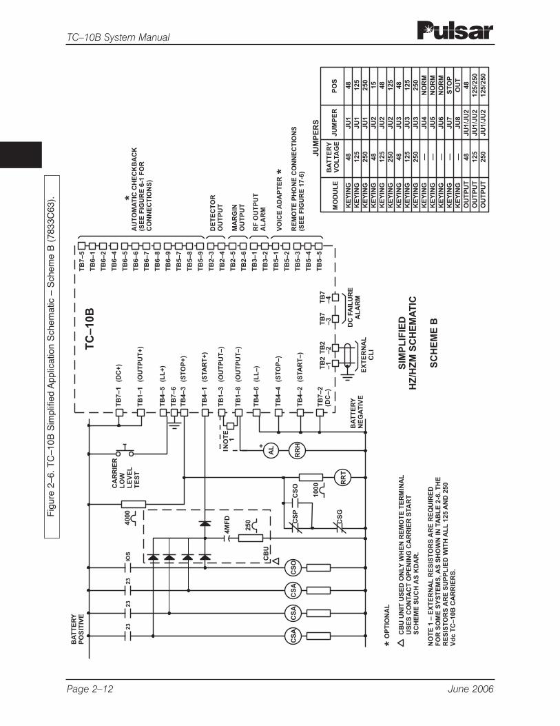
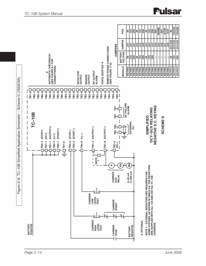
Simplified schematics of typical electro-mechan-ical systems are shown in Figure 2-5 throughFigure 2-13 (schemes A thru K). These schemesindicate the different jumper positions required forparticular applications. Simplified connectionsbetween the TC–10B and a microprocessor basedrelay are shown in Figure 2-14 (Scheme L).
Figure 2-15 shows the output circuit for micro-processor based relays (1 amp maximum output).
Figure 2-16 shows the resultant output circuit for48, 125, and 250Vdc systems.
Two variations of TC–10B are available:
(1) Plug-in Voice Adapter Module with signalingas a push-to-talk maintenance voice channel -(see Chapter 17). A telephone jack is providedon the Voice Adapter Module, but you mayalso use a remote jack or hookswitch. (SeeFigure 18-4, Scheme J, for the connectiondiagrams.)
(2) Plug-in Universal Checkback Module forperiodic testing of the carrier channel atprogrammable intervals (see Chapter 17).(See Figure 3–3 for connection diagrams.)
The equipment identification number (catalognumber) is located in the middle of the front panel(just to the left of the 10W PA Module). TheTC–10B catalog number comprises eight (8) char-acters, each in a specific position. This numberidentifies the unit's technical characteristics andcapabilities, as well as any optional modulesinstalled in the unit.
Table 2-2 provides a complete listing of theoptions for ordering a TC–10B, as well as asample catalog number. To order one or moreTC–10Bs, simply identify the features andoptional modules you want for each chassis. Forexample, the typical catalog number shown inTable 2-2 — S 1 A 1 W V A S — orders aTC–10B with the following features:
Basic TC–10B Transmitter/Receiver
Power Output: 10 watt
Universal Checkback: Universal CheckbackModule, PC programmable
dc/dc Converter Power Supply: 110/125Vdcbattery input
Bandwidth (Filter Range): Wideband filter
Voice Adapter: Voice Adapter Module withsignaling
Alarm and Carrier Level Indication: with loss-of-dc-power alarm relay, R.F. output alarmrelay, received-carrier-level-margin alarmrelay, detect alarm, instrument indicatingcarrier level (-20dB to +10dB), carrier levelanalog output (0–100 µA) for external instru-ment
Outputs: Dual transistor-switched outputs (foruse with electro-mechanical carrier auxiliaryrelays and microprocessor relays)
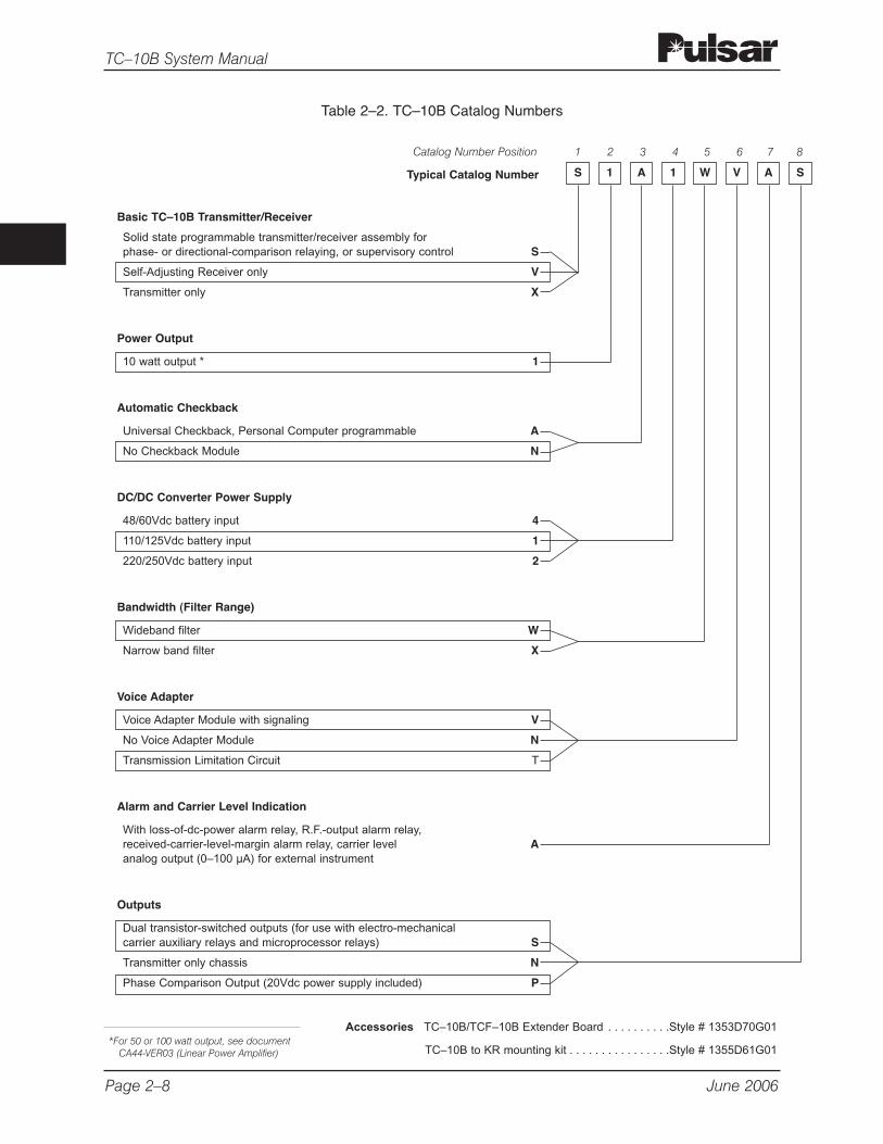
Table 2-3 provides a further breakdown of theTC–10B catalog number by style numbers.
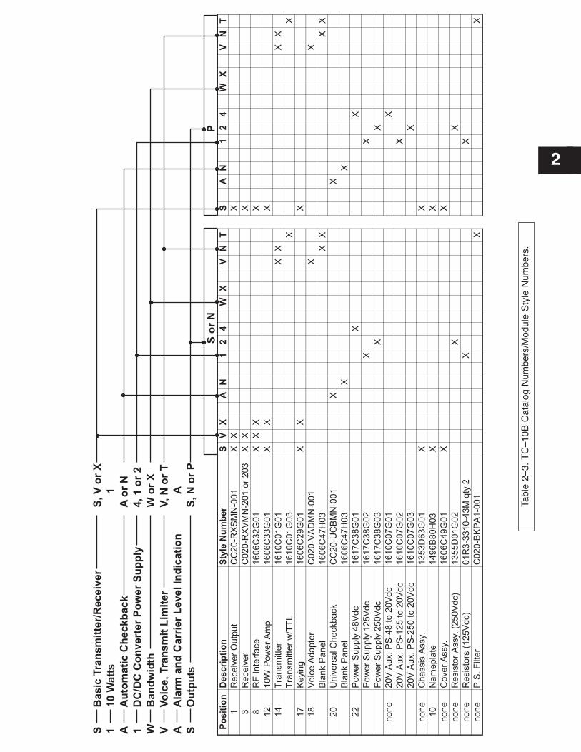
The accessories available for the TC–10B arelisted, along with their style numbers, in Table 2-4and Table 2-5. To order an accessory, simply giveits style number.
June 2006 Page 2–7
Chapter 2. Applications and Ordering Information
2
Page 2–8 June 2006
TC–10B System Manual
Table 2–2. TC–10B Catalog Numbers
Typical Catalog Number S 1 A 1 W V A S
Catalog Number Position 1 2 3 4 5 6 7 8
Basic TC–10B Transmitter/Receiver
Solid state programmable transmitter/receiver assembly for phase- or directional-comparison relaying, or supervisory control S
Self-Adjusting Receiver only V
Transmitter only X
Power Output
10 watt output * 1
Automatic Checkback
Universal Checkback, Personal Computer programmable A
No Checkback Module N
DC/DC Converter Power Supply
48/60Vdc battery input 4
110/125Vdc battery input 1
220/250Vdc battery input 2
Bandwidth (Filter Range)
Wideband filter W
Narrow band filter X
Voice Adapter
Voice Adapter Module with signaling V
No Voice Adapter Module N
Transmission Limitation Circuit T
Alarm and Carrier Level Indication
With loss-of-dc-power alarm relay, R.F.-output alarm relay, received-carrier-level-margin alarm relay, carrier level Aanalog output (0–100 µA) for external instrument
Outputs
Dual transistor-switched outputs (for use with electro-mechanicalcarrier auxiliary relays and microprocessor relays) S
Transmitter only chassis N
Phase Comparison Output (20Vdc power supply included) P
Accessories TC–10B/TCF–10B Extender Board . . . . . . . . . .Style # 1353D70G01
TC–10B to KR mounting kit . . . . . . . . . . . . . . . .Style # 1355D61G01*For 50 or 100 watt output, see document
CA44-VER03 (Linear Power Amplifier)
2
Tabl
e 2–
3. T
C–1
0B C
atal
og N
umbe
rs/M
odul
e S
tyle
Num
bers
.
So
rN
S,N
or
P
A
AS 1 1 W V A S
V,N
or
T
Wo
rX
4,1
or
2
Ao
rN
10
Watt
s
Au
tom
ati
cC
heckb
ack
DC
/DC
Co
nvert
er
Po
wer
Su
pp
ly
Ban
dw
idth
Vo
ice,Tra
nsm
itL
imit
er
Ala
rman
dC
arr
ier
LevelIn
dic
ati
on
Ou
tpu
ts
1
S,V
or
X
P
Basic
Tra
nsm
itte
r/R
eceiv
er
Po
sit
ion
Descri
pti
on
Sty
leN
um
ber
SV
XA
N1
24
WX
VN
TS
AN
12
4W
XV
NT
1R
eceiv
er
Outp
ut
CC
20-R
XS
MN
-001
XX
X
3R
eceiv
er
C020-R
XV
MN
-201
or
203
XX
X
8R
FIn
terf
ace
1606C
32G
01
XX
XX
12
10W
Pow
er
Am
p1606C
33G
01
XX
X
14
Tra
nsm
itte
r1610C
01G
01
XX
XX
Tra
nsm
itte
rw
/TT
L1610C
01G
03
XX
17
Keyi
ng
1606C
29G
01
XX
X
18
Voic
eA
dapte
rC
020-V
AD
MN
-001
XX
Bla
nk
Panel
1606C
47H
03
XX
XX
20
Univ
ers
alC
heckback
CC
20-U
CB
MN
-001
XX
Bla
nk
Panel
1606C
47H
03
XX
22
Pow
er
Supply
48V
dc
1617C
38G
01
XX
Pow
er
Supply
125V
dc
1617C
38G
02
XX
Pow
er
Supply
250V
dc
1617C
38G
03
XX
none
20V
Aux.P
S-4
8to
20V
dc
1610C
07G
01
X
20V
Aux.P
S-1
25
to20V
dc
1610C
07G
02
X
20V
Aux.P
S-2
50
to20V
dc
1610C
07G
03
X
none
Chassis
Assy.
1353D
63G
01
XX
10
Nam
epla
te1496B
80H
03
XX
none
Cover
Assy.
1606C
49G
01
XX
none
Resis
tor
Assy.
(250V
dc)
1355D
01G
02
XX
none
Resis
tors
(125V
dc)
01R
3-3
310-4
3M
qty
2X
X
none
P.S
.F
ilter
C020-B
KP
A1-0
01
XX
Page 2–10 June 2006
TC–10B System Manual
Accessories for Voice Adapter Style Number
Sonalert (2,900Hz, 60–250Vdc) SC250J
Telephone Hookswitch 205C266G05Assembly (panel mounting) with Noise Canceling Handset
Telephone Handset, Push to Talk, 1353D88G01Noise Canceling (single prong plug)
Telephone Jack, remote panel 715B674G03mounting (single prong plug)
Other Accessories Style Number
45V power supply for use with SKBU-1 Relaying System
48V to 45V 5303D49G05
125V to 45V 5303D49G06
250V to 45V 5303D49G07
Table 2–4. TC–10B Voice Adapter Accessories.
Table 2–5. Other TC–10B Accessories
Carrier Aux. Battery ResistorRelay Voltage
20 mA (220Ω) 48 Not Required
20 mA (220Ω) 125 3500Ω, 5W
20 mA (220Ω) 250 9200Ω, 10W & 500Ω, 40W
200 mA (25Ω) 48 Not Required
200 mA (25Ω) 125 Not Required
200 mA (25Ω) 250 500Ω, 40W
Table 2–6. External Resistor Requirements — Provided with Chassis, According to Battery Voltage.
June 2006 Page 2–11
Chapter 2. Applications and Ordering Information
2
Fig
ure
2–5.
TC
–10B
Sim
plifi
ed A
pplic
atio
n S
chem
atic
– S
chem
e A
(783
3C63
).
KE
YIN
G4
8J
U1
15
KE
YIN
G1
25
JU
14
8
KE
YIN
G2
50
JU
11
25
KE
YIN
G4
8J
U2
48
KE
YIN
G1
25
JU
21
25
KE
YIN
G2
50
JU
22
50
KE
YIN
G4
8J
U3
48
KE
YIN
G1
25
JU
31
25
KE
YIN
G2
50
JU
32
50
KE
YIN
G—
JU
4N
OR
M
KE
YIN
G—
JU
5N
OR
M
KE
YIN
G—
JU
6N
OR
M
KE
YIN
G—
JU
7S
TO
P
KE
YIN
G—
JU
8IN
OU
TP
UT
48
JU
1/J
U2
48
OU
TP
UT
12
5J
U1
/JU
21
25
/25
0
OU
TP
UT
25
0J
U1
/JU
21
25
/25
0
MO
DU
LE
JU
MP
ER
PO
SB
AT
TE
RY
VO
LTA
GE
JU
MP
ER
S
TB
6–
1
TB
6–
2
TB
6–
4
TB
6–
5
TB
6–
6
TB
6–
7
TB
6–
8
TB
6–
9
TB
5–
7
TB
5–
8
TB
5–
9
TB
2–
3
TB
2–
4
TB
2–
5
TB
2–
6
TB
3–
1
TB
3–
2
TB
5–
1
TB
5–
2
TB
5–
3
TB
5–
4
TB
5–
5
TC
–1
0B
TB
2–
1T
B2
–2
PH
AS
EA
ND
GR
OU
ND
CA
RR
IER
STA
RT
PH
AS
EA
ND
GR
OU
ND
CA
RR
IER
ST
OP
BA
TT
ER
YN
EG
AT
IVE
BA
TT
ER
YP
OS
ITIV
E
0–
30
mA
0–
30
0m
A
CA
RR
IER
LO
WL
EV
EL
TE
ST
CA
RR
IER
TE
ST
TB
7–
3T
B7
–4
TB
7–
1(D
C+
)
TB
1–
1(O
UT
PU
T+
)
TB
4–
3(S
TO
P+
)
TB
4–
5(L
L+
)
TB
4–
1(S
TA
RT
+)
TB
7–
6
TB
1–
8(O
UT
PU
T–
)
TB
1–
3(O
UT
PU
T–
)
TB
4–
6(L
L–
)
TB
4–
4(S
TO
P–
)
TB
4–
2(S
TA
RT
–)
TB
7–
2(D
C–
)
Z3
CX
CX
CS
GC
SP
SQ
Z2
Z1
Z4
Z5
RC
R
INK
A–
4
SIM
PL
IFIE
DK
–D
AR
CA
RR
IER
SC
HE
MA
TIC
UT
ILIZ
ING
CO
MM
ON
STA
RT
/ST
OP
CO
NT
RO
L
SC
HE
ME
A
+NO
TE
1
MA
AL
RR
H
NO
TE
1–
EX
TE
RN
AL
RE
SIS
TO
RS
AR
ER
EQ
UIR
ED
FO
RS
OM
ES
YS
TE
MS
,A
SS
HO
WN
INTA
BL
E2
-6.
TH
ER
ES
IST
OR
SA
RE
SU
PP
LIE
DW
ITH
AL
L1
25
AN
D2
50
Vd
cT
C–
10
BC
AR
RIE
RS
.
NO
TE
2–
SO
ME
SC
HE
ME
SM
AY
NO
TH
AV
EC
AR
RIE
RC
ON
TIN
UA
TIO
N(C
X).
CX
OP
TIO
NA
L
DC
FA
ILU
RE
AL
AR
ME
XT
ER
NA
LC
LI
RF
OU
TP
UT
AL
AR
M
MA
RG
INO
UT
PU
T
VO
ICE
AD
AP
TE
R
AU
TO
MA
TIC
CH
EC
KB
AC
K(S
EE
FIG
UR
E6
-1F
OR
CO
NN
EC
TIO
NS
)
DE
TE
CT
OR
OU
TP
UT
RE
MO
TE
PH
ON
EC
ON
NE
CT
ION
S(S
EE
FIG
UR
E1
7-6
)
TB
7–
5
Page 2–12 June 2006
TC–10B System ManualF
igur
e 2–
6. T
C–1
0B S
impl
ified
App
licat
ion
Sch
emat
ic –
Sch
eme
B (
7833
C63
).
TB
6–
1
TB
6–
2
TB
6–
4
TB
6–
5
TB
6–
6
TB
6–
7
TB
6–
8
TB
6–
9
TB
5–
7
TB
5–
8
TB
5–
9
TB
2–
3
TB
2–
4
TB
2–
5
TB
2–
6
TB
3–
1
TB
3–
2
TB
5–
1
TB
5–
2
TB
5–
3
TB
5–
4
TB
5–
5
TC
–1
0B
TB
2–
1T
B2
–2
BA
TT
ER
YN
EG
AT
IVE
BA
TT
ER
YP
OS
ITIV
E
CA
RR
IER
LO
WL
EV
EL
TE
ST
TB
7–
3T
B7
–4
TB
7–
1(D
C+
)
TB
1–
1(O
UT
PU
T+
)
TB
4–
3(S
TO
P+
)
TB
4–
5(L
L+
)
TB
4–
1(S
TA
RT
+)
TB
1–
3(O
UT
PU
T–
)
TB
4–
6(L
L–
)
TB
4–
4(S
TO
P–
)
TB
4–
2(S
TA
RT
–)
TB
7–
2(D
C–
)
TB
7–
6
CS
G
CS
PC
SO
4M
FD
CB
U
SIM
PL
IFIE
DH
Z/H
ZM
SC
HE
MA
TIC
SC
HE
ME
B
+
AL
RR
H
CB
UU
NIT
US
ED
ON
LY
WH
EN
RE
MO
TE
TE
RM
INA
LU
SE
SC
ON
TA
CT
OP
EN
ING
CA
RR
IER
STA
RT
SC
HE
ME
SU
CH
AS
KD
AR
.
40
00
10
00
25
0
RR
T
CS
AC
SA
CS
AC
SO
23
23
23
IOS
NO
TE
1–
EX
TE
RN
AL
RE
SIS
TO
RS
AR
ER
EQ
UIR
ED
FO
RS
OM
ES
YS
TE
MS
,A
SS
HO
WN
INTA
BL
E2
-6.
TH
ER
ES
IST
OR
SA
RE
SU
PP
LIE
DW
ITH
AL
L1
25
AN
D2
50
Vd
cT
C–
10
BC
AR
RIE
RS
.
TB
1–
8(O
UT
PU
T–
)
NO
TE
1
DC
FA
ILU
RE
AL
AR
ME
XT
ER
NA
LC
LI
OP
TIO
NA
L
RF
OU
TP
UT
AL
AR
M
MA
RG
INO
UT
PU
T
VO
ICE
AD
AP
TE
R
AU
TO
MA
TIC
CH
EC
KB
AC
K(S
EE
FIG
UR
E6
-1F
OR
CO
NN
EC
TIO
NS
)
DE
TE
CT
OR
OU
TP
UT
RE
MO
TE
PH
ON
EC
ON
NE
CT
ION
S(S
EE
FIG
UR
E1
7-6
)
KE
YIN
G4
8J
U1
48
KE
YIN
G1
25
JU
11
25
KE
YIN
G2
50
JU
12
50
KE
YIN
G4
8J
U2
15
KE
YIN
G1
25
JU
24
8
KE
YIN
G2
50
JU
21
25
KE
YIN
G4
8J
U3
48
KE
YIN
G1
25
JU
31
25
KE
YIN
G2
50
JU
32
50
KE
YIN
G—
JU
4N
OR
M
KE
YIN
G—
JU
5N
OR
M
KE
YIN
G—
JU
6N
OR
M
KE
YIN
G—
JU
7S
TO
P
KE
YIN
G—
JU
8O
UT
OU
TP
UT
48
JU
1/J
U2
48
OU
TP
UT
12
5J
U1
/JU
21
25
/25
0
OU
TP
UT
25
0J
U1
/JU
21
25
/25
0
MO
DU
LE
JU
MP
ER
PO
SB
AT
TE
RY
VO
LTA
GE
JU
MP
ER
S
TB
7–
5
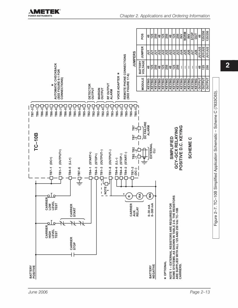
June 2006 Page 2–13
Chapter 2. Applications and Ordering Information
2
Fig
ure
2–7.
TC
–10B
Sim
plifi
ed A
pplic
atio
n S
chem
atic
– S
chem
e C
(78
33C
63).
KE
YIN
G4
8J
U1
48
KE
YIN
G1
25
JU
11
25
KE
YIN
G2
50
JU
12
50
KE
YIN
G4
8J
U2
48
KE
YIN
G1
25
JU
21
25
KE
YIN
G2
50
JU
22
50
KE
YIN
G4
8J
U3
48
KE
YIN
G1
25
JU
31
25
KE
YIN
G2
50
JU
32
50
KE
YIN
G—
JU
4IN
V
KE
YIN
G—
JU
5N
OR
M
KE
YIN
G—
JU
6IN
V
KE
YIN
G—
JU
7S
TO
P
KE
YIN
G—
JU
8O
UT
OU
TP
UT
48
JU
1/J
U2
48
MO
DU
LE
JU
MP
ER
PO
SB
AT
TE
RY
VO
LTA
GE
JU
MP
ER
S
TB
6–
1
TB
6–
2
TB
6–
4
TB
6–
5
TB
6–
6
TB
6–
7
TB
6–
8
TB
6–
9
TB
5–
7
TB
5–
8
TB
5–
9
TB
2–
3
TB
2–
4
TB
2–
5
TB
2–
6
TB
3–
1
TB
3–
2
TB
5–
1
TB
5–
2
TB
5–
3
TB
5–
4
TB
5–
5
TC
–1
0B
TB
2–
1T
B2
–2
CA
RR
IER
AU
X.
RE
LA
Y
BA
TT
ER
YN
EG
AT
IVE
BA
TT
ER
YP
OS
ITIV
E
0–
30
mA
0–
30
0m
A
CA
RR
IER
LO
WL
EV
EL
TE
ST
CA
RR
IER
HIG
HL
EV
EL
TE
ST
CA
RR
IER
ST
OP
CA
RR
IER
STA
RT
TB
7–
3T
B7
–4
TB
7–
1(D
C+
)
TB
1–
1(O
UT
PU
T+
)
TB
4–
5(L
L+
)
TB
4–
1(S
TA
RT
+)
TB
4–
3(S
TO
P+
)
TB
7–
6
TB
1–
3(O
UT
PU
T–
)
TB
4–
6(L
L–
)
TB
4–
4(S
TO
P–
)
TB
4–
2(S
TA
RT
–)
TB
7–
2(D
C–
)
SIM
PL
IFIE
DG
CY
–G
CX
RE
LA
YIN
GP
OS
ITIV
ED
.C.K
EY
ING
SC
HE
ME
C
+
R RA
MA
NO
TE
1–
EX
TE
RN
AL
RE
SIS
TO
RS
AR
ER
EQ
UIR
ED
FO
RS
OM
ES
YS
TE
MS
,A
SS
HO
WN
INTA
BL
E2
-6.
TH
ER
ES
IST
OR
SA
RE
SU
PP
LIE
DW
ITH
AL
L1
25
AN
D2
50
Vd
cT
C–
10
BC
AR
RIE
RS
.
TB
1–
8(O
UT
PU
T–
)
NO
TE
1
DC
FA
ILU
RE
AL
AR
ME
XT
ER
NA
LC
LI
OP
TIO
NA
L
RF
OU
TP
UT
AL
AR
M
MA
RG
INO
UT
PU
T
VO
ICE
AD
AP
TE
R
AU
TO
MA
TIC
CH
EC
KB
AC
K(S
EE
FIG
UR
E6
-1F
OR
CO
NN
EC
TIO
NS
)
DE
TE
CT
OR
OU
TP
UT
RE
MO
TE
PH
ON
EC
ON
NE
CT
ION
S(S
EE
FIG
UR
E1
7-6
)
OU
TP
UT
OU
TP
UT
12
5
25
0
JU
1/J
U2
JU
1/J
U2
12
5/2
50
12
5/2
50
TB
7–
5
Page 2–14 June 2006
TC–10B System ManualF
igur
e 2–
8. T
C–1
0B S
impl
ified
App
licat
ion
Sch
emat
ic –
Sch
eme
D (
7833
C63
). K
EY
ING
48
JU
14
8
KE
YIN
G1
25
JU
11
25
KE
YIN
G2
50
JU
12
50
KE
YIN
G4
8J
U2
48
KE
YIN
G1
25
JU
21
25
KE
YIN
G2
50
JU
22
50
KE
YIN
G4
8J
U3
48
KE
YIN
G1
25
JU
31
25
KE
YIN
G2
50
JU
32
50
KE
YIN
G—
JU
4IN
V
KE
YIN
G—
JU
5N
OR
M
KE
YIN
G—
JU
6IN
V
KE
YIN
G—
JU
7S
TO
P
KE
YIN
G—
JU
8O
UT
OU
TP
UT
48
JU
1/J
U2
48
MO
DU
LE
JU
MP
ER
PO
SB
AT
TE
RY
VO
LTA
GE
JU
MP
ER
S
TB
6–
1
TB
6–
2
TB
6–
4
TB
6–
5
TB
6–
6
TB
6–
7
TB
6–
8
TB
6–
9
TB
5–
7
TB
5–
8
TB
5–
9
TB
2–
3
TB
2–
4
TB
2–
5
TB
2–
6
TB
3–
1
TB
3–
2
TB
5–
1
TB
5–
2
TB
5–
3
TB
5–
4
TB
5–
5
TC
–1
0B
TB
2–
1T
B2
–2
CA
RR
IER
AU
X.
RE
LA
Y
BA
TT
ER
YN
EG
AT
IVE
BA
TT
ER
YP
OS
ITIV
E
0–
30
mA
0–
30
0m
A
CA
RR
IER
LO
WL
EV
EL
TE
ST
CA
RR
IER
HIG
HL
EV
EL
TE
ST
CA
RR
IER
ST
OP
CA
RR
IER
STA
RT
TB
7–3
TB
7–
4
TB
7–
1(D
C+
)
TB
1–
1(O
UT
PU
T+
)
TB
4–
5(L
L+
)
TB
4–
1(S
TA
RT
+)
TB
4–
3(S
TO
P+
)
TB
1–
3(O
UT
PU
T–
)
TB
4–
6(L
L–
)
TB
4–
4(S
TO
P–
)
TB
4–
2(S
TA
RT
–)
TB
7–
2(D
C–
)
TB
7–
6
SIM
PL
IFIE
DG
CY
–G
CX
RE
LA
YIN
GN
EG
AT
IVE
D.C
.K
EY
ING
SC
HE
ME
D
+
R RA
NO
TE
1–
EX
TE
RN
AL
RE
SIS
TO
RS
AR
ER
EQ
UIR
ED
FO
RS
OM
ES
YS
TE
MS
,A
SS
HO
WN
INTA
BL
E2
-6.T
HE
RE
SIS
TO
RS
AR
ES
UP
PL
IED
WIT
HA
LL
12
5A
ND
25
0V
dc
TC
–1
0B
CA
RR
IER
S.
MA
R
TB
1–
8(O
UT
PU
T–
)
NO
TE
1
DC
FA
ILU
RE
AL
AR
ME
XT
ER
NA
LC
LI
OP
TIO
NA
L
RF
OU
TP
UT
AL
AR
M
MA
RG
INO
UT
PU
T
VO
ICE
AD
AP
TE
R
AU
TO
MA
TIC
CH
EC
KB
AC
K(S
EE
FIG
UR
E6
-1F
OR
CO
NN
EC
TIO
NS
)
DE
TE
CT
OR
OU
TP
UT
RE
MO
TE
PH
ON
EC
ON
NE
CT
ION
S(S
EE
FIG
UR
E1
7-6
)
OU
TP
UT
OU
TP
UT
12
5
25
0
JU
1/J
U2
JU
1/J
U2
12
5/2
50
12
5/2
50
TB
7–
5
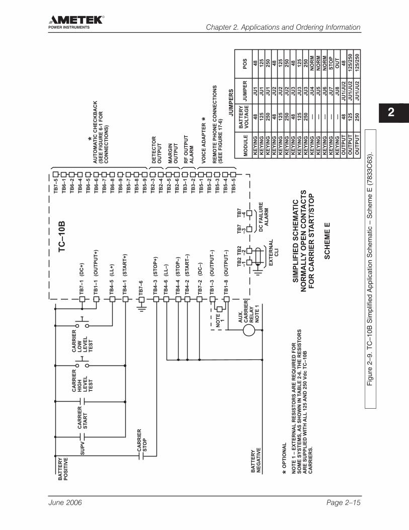
June 2006 Page 2–15
Chapter 2. Applications and Ordering Information
2
Fig
ure
2–9.
TC
–10B
Sim
plifi
ed A
pplic
atio
n S
chem
atic
– S
chem
e E
(78
33C
63).
KE
YIN
G4
8J
U1
48
KE
YIN
G1
25
JU
11
25
KE
YIN
G2
50
JU
12
50
KE
YIN
G4
8J
U2
48
KE
YIN
G1
25
JU
21
25
KE
YIN
G2
50
JU
22
50
KE
YIN
G4
8J
U3
48
KE
YIN
G1
25
JU
31
25
KE
YIN
G2
50
JU
32
50
KE
YIN
G—
JU
4N
OR
M
KE
YIN
G—
JU
5N
OR
M
KE
YIN
G—
JU
6N
OR
M
KE
YIN
G—
JU
7S
TO
P
KE
YIN
G—
JU
8O
UT
OU
TP
UT
48
JU
1/J
U2
48
MO
DU
LE
JU
MP
ER
PO
SB
AT
TE
RY
VO
LTA
GE
JU
MP
ER
S
TB
6–
1
TB
6–
2
TB
6–
4
TB
6–
5
TB
6–
6
TB
6–
7
TB
6–
8
TB
6–
9
TB
5–
7
TB
5–
8
TB
5–
9
TB
2–
3
TB
2–
4
TB
2–
5
TB
2–
6
TB
3–
1
TB
3–
2
TB
5–
1
TB
5–
2
TB
5–
3
TB
5–
4
TB
5–
5
TC
–1
0B
TB
2–
1T
B2
–2
AU
X.
CA
RR
IER
RE
LA
YN
OT
E1
BA
TT
ER
YN
EG
AT
IVE
BA
TT
ER
YP
OS
ITIV
E
CA
RR
IER
LO
WL
EV
EL
TE
ST
CA
RR
IER
HIG
HL
EV
EL
TE
ST
CA
RR
IER
ST
OP
CA
RR
IER
STA
RT
SU
PV
TB
7–
3T
B7
–4
TB
7–
1(D
C+
)
TB
1–
1(O
UT
PU
T+
)
TB
4–
5(L
L+
)
TB
4–
1(S
TA
RT
+)
TB
4–
3(S
TO
P+
)
TB
1–
3(O
UT
PU
T–
)
TB
4–
6(L
L–
)
TB
4–
4(S
TO
P–
)
TB
4–
2(S
TA
RT
–)
TB
7–
2(D
C–
)
TB
7–
6 SIM
PL
IFIE
DS
CH
EM
AT
ICN
OR
MA
LLY
OP
EN
CO
NTA
CT
SF
OR
CA
RR
IER
STA
RT
/ST
OP
SC
HE
ME
E
NO
TE
1–
EX
TE
RN
AL
RE
SIS
TO
RS
AR
ER
EQ
UIR
ED
FO
RS
OM
ES
YS
TE
MS
,A
SS
HO
WN
INTA
BL
E2
-6.
TH
ER
ES
IST
OR
SA
RE
SU
PP
LIE
DW
ITH
AL
L1
25
AN
D2
50
Vd
cT
C–
10
BC
AR
RIE
RS
.
TB
1–
8(O
UT
PU
T–
)
NO
TE
1
DC
FA
ILU
RE
AL
AR
ME
XT
ER
NA
LC
LI
OP
TIO
NA
L
RF
OU
TP
UT
AL
AR
M
MA
RG
INO
UT
PU
T
VO
ICE
AD
AP
TE
R
AU
TO
MA
TIC
CH
EC
KB
AC
K(S
EE
FIG
UR
E6
-1F
OR
CO
NN
EC
TIO
NS
)
DE
TE
CT
OR
OU
TP
UT
RE
MO
TE
PH
ON
EC
ON
NE
CT
ION
S(S
EE
FIG
UR
E1
7-6
)
OU
TP
UT
OU
TP
UT
12
5
25
0
JU
1/J
U2
JU
1/J
U2
12
5/2
50
12
5/2
50
TB
7–
5
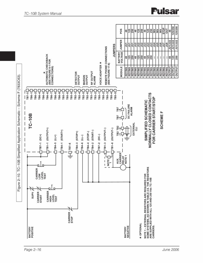
Page 2–16 June 2006
TC–10B System ManualF
igur
e 2–
10.
TC
–10B
Sim
plifi
ed A
pplic
atio
n S
chem
atic
– S
chem
e F
(783
3C63
).
KE
YIN
G4
8J
U1
48
KE
YIN
G1
25
JU
11
25
KE
YIN
G2
50
JU
12
50
KE
YIN
G4
8J
U2
48
KE
YIN
G1
25
JU
21
25
KE
YIN
G2
50
JU
22
50
KE
YIN
G4
8J
U3
48
KE
YIN
G1
25
JU
31
25
KE
YIN
G2
50
JU
32
50
KE
YIN
G—
JU
4IN
V
KE
YIN
G—
JU
5IN
V
KE
YIN
G—
JU
6IN
V
KE
YIN
G—
JU
7S
TO
P
KE
YIN
G—
JU
8O
UT
OU
TP
UT
48
JU
1/J
U2
48
MO
DU
LE
JU
MP
ER
PO
SB
AT
TE
RY
VO
LTA
GE
JU
MP
ER
S
TB
6–
1
TB
6–
2
TB
6–
4
TB
6–
5
TB
6–
6
TB
6–
7
TB
6–
8
TB
6–
9
TB
5–
7
TB
5–
8
TB
5–
9
TB
2–
3
TB
2–
4
TB
2–
5
TB
2–
6
TB
3–
1
TB
3–
2
TB
5–
1
TB
5–
2
TB
5–
3
TB
5–
4
TB
5–
5
TC
–1
0B
TB
2–
1T
B2
–2
AU
X.
CA
RR
IER
RE
LA
YN
OT
E1
BA
TT
ER
YN
EG
AT
IVE
BA
TT
ER
YP
OS
ITIV
E
CA
RR
IER
LO
WL
EV
EL
TE
ST
CA
RR
IER
HIG
HL
EV
EL
TE
ST
CA
RR
IER
ST
OP
CA
RR
IER
STA
RT
SU
PV
TB
7–
3T
B7
–4
TB
7–
1(D
C+
)
TB
1–
1(O
UT
PU
T+
)
TB
4–
5(L
L+
)
TB
4–
1(S
TA
RT
+)
TB
4–
3(S
TO
P+
)
TB
1–
3(O
UT
PU
T–
)
TB
4–
6(L
L–
)
TB
4–
4(S
TO
P–
)
TB
4–
2(S
TA
RT
–)
TB
7–
2(D
C–
)
TB
7–
6
SIM
PL
IFIE
DS
CH
EM
AT
ICN
OR
MA
LLY
CL
OS
ED
CO
NTA
CT
SF
OR
CA
RR
IER
STA
RT
/ST
OP
SC
HE
ME
F
NO
TE
1–
EX
TE
RN
AL
RE
SIS
TO
RS
AR
ER
EQ
UIR
ED
FO
RS
OM
ES
YS
TE
MS
,A
SS
HO
WN
INTA
BL
E2
-6.
TH
ER
ES
IST
OR
SA
RE
SU
PP
LIE
DW
ITH
AL
L1
25
AN
D2
50
Vd
cT
C–
10
BC
AR
RIE
RS
.
TB
1–
8(O
UT
PU
T–
)
NO
TE
1
DC
FA
ILU
RE
AL
AR
ME
XT
ER
NA
LC
LI
OP
TIO
NA
L
RF
OU
TP
UT
AL
AR
M
MA
RG
INO
UT
PU
T
VO
ICE
AD
AP
TE
R
AU
TO
MA
TIC
CH
EC
KB
AC
K(S
EE
FIG
UR
E6
-1F
OR
CO
NN
EC
TIO
NS
)
DE
TE
CT
OR
OU
TP
UT
RE
MO
TE
PH
ON
EC
ON
NE
CT
ION
S(S
EE
FIG
UR
E1
7-6
)
OU
TP
UT
OU
TP
UT
12
5
25
0
JU
1/J
U2
JU
1/J
U2
12
5/2
50
12
5/2
50
TB
7–
5
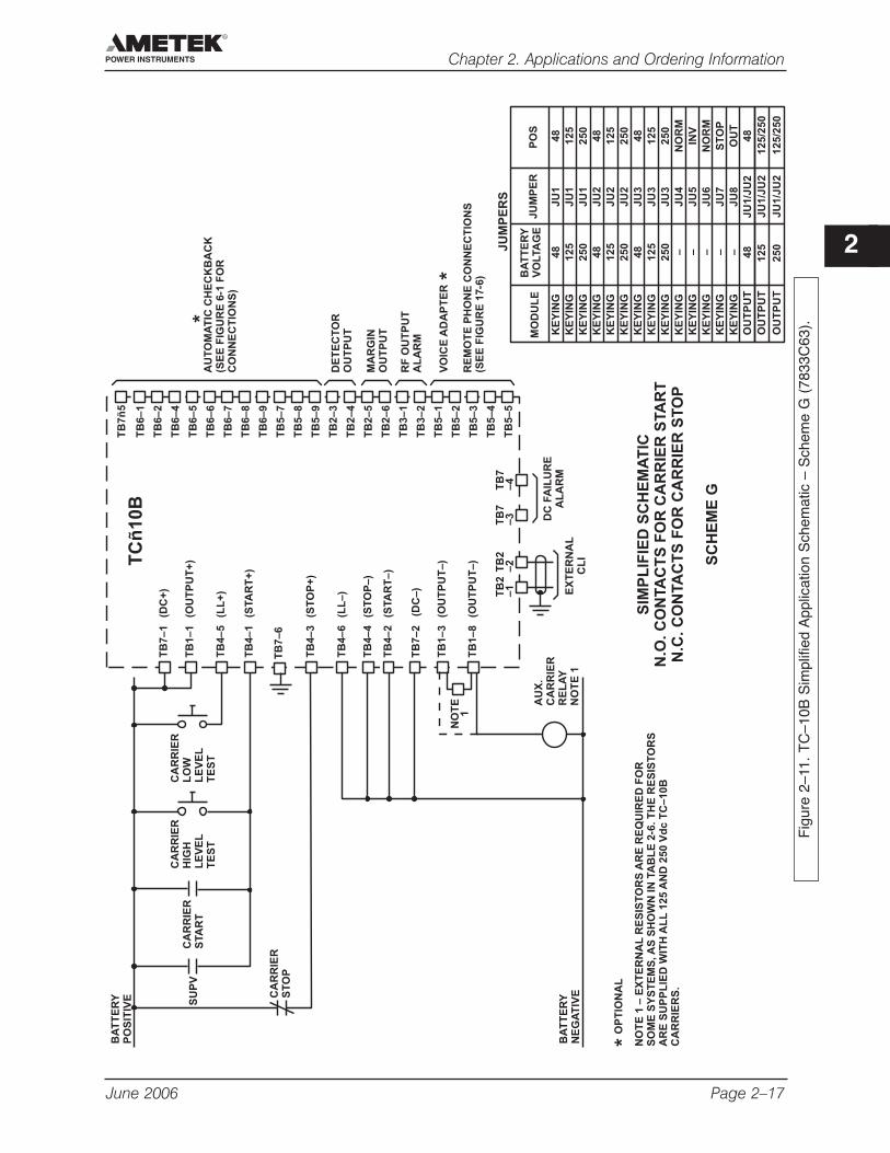
June 2006 Page 2–17
Chapter 2. Applications and Ordering Information
2
Fig
ure
2–11
. T
C–1
0B S
impl
ified
App
licat
ion
Sch
emat
ic –
Sch
eme
G (
7833
C63
).
KE
YIN
G48
JU
148
KE
YIN
G125
JU
1125
KE
YIN
G250
JU
1250
KE
YIN
G48
JU
248
KE
YIN
G125
JU
2125
KE
YIN
G250
JU
2250
KE
YIN
G48
JU
348
KE
YIN
G125
JU
3125
KE
YIN
G250
JU
3250
KE
YIN
G–
JU
4N
OR
M
KE
YIN
G–
JU
5IN
V
KE
YIN
G–
JU
6N
OR
M
KE
YIN
G–
JU
7S
TO
P
KE
YIN
G–
JU
8O
UT
OU
TP
UT
48
JU
1/J
U2
48
MO
DU
LE
JU
MP
ER
PO
SB
AT
TE
RY
VO
LTA
GE
JU
MP
ER
S
TB
6–1
TB
6–2
TB
6–4
TB
6–5
TB
6–6
TB
6–7
TB
6–8
TB
6–9
TB
5–7
TB
5–8
TB
5–9
TB
2–3
TB
2–4
TB
2–5
TB
2–6
TB
3–1
TB
3–2
TB
5–1
TB
5–2
TB
5–3
TB
5–4
TB
5–5
TC
ñ1
0B
TB
2–1
TB
2–2
AU
X.
CA
RR
IER
RE
LA
YN
OT
E1
BA
TT
ER
YN
EG
AT
IVE
BA
TT
ER
YP
OS
ITIV
E
CA
RR
IER
LO
WL
EV
EL
TE
ST
CA
RR
IER
HIG
HL
EV
EL
TE
ST
CA
RR
IER
ST
OP
CA
RR
IER
STA
RT
SU
PV
TB
7–3
TB
7–4
TB
7–1
(DC
+)
TB
1–1
(OU
TP
UT
+)
TB
4–5
(LL
+)
TB
4–1
(STA
RT
+)
TB
4–3
(ST
OP
+)
TB
1–3
(OU
TP
UT
–)
TB
4–6
(LL
–)
TB
4–4
(ST
OP
–)
TB
4–2
(STA
RT
–)
TB
7–2
(DC
–)
TB
7–6
SIM
PL
IFIE
DS
CH
EM
AT
ICN
.O.
CO
NTA
CT
SF
OR
CA
RR
IER
STA
RT
N.C
.C
ON
TA
CT
SF
OR
CA
RR
IER
ST
OP
SC
HE
ME
G
NO
TE
1–
EX
TE
RN
AL
RE
SIS
TO
RS
AR
ER
EQ
UIR
ED
FO
RS
OM
ES
YS
TE
MS
,A
SS
HO
WN
INTA
BL
E2-6
.T
HE
RE
SIS
TO
RS
AR
ES
UP
PL
IED
WIT
HA
LL
125
AN
D250
Vd
cT
C–10B
CA
RR
IER
S.
TB
1–8
(OU
TP
UT
–)
NO
TE
1
RF
OU
TP
UT
AL
AR
M
MA
RG
INO
UT
PU
T
VO
ICE
AD
AP
TE
R
AU
TO
MA
TIC
CH
EC
KB
AC
K(S
EE
FIG
UR
E6-1
FO
RC
ON
NE
CT
ION
S)
DE
TE
CT
OR
OU
TP
UT
RE
MO
TE
PH
ON
EC
ON
NE
CT
ION
S(S
EE
FIG
UR
E17-6
)
DC
FA
ILU
RE
AL
AR
ME
XT
ER
NA
LC
LI
OP
TIO
NA
L
OU
TP
UT
OU
TP
UT
125
250
JU
1/J
U2
JU
1/J
U2
125/2
50
125/2
50
TB
7ñ
5

Page 2–18 June 2006
TC–10B System ManualF
igur
e 2–
12.
TC
–10B
Sim
plifi
ed A
pplic
atio
n S
chem
atic
– S
chem
e H
(78
33C
63).
KE
YIN
G4
8J
U1
48
KE
YIN
G1
25
JU
11
25
KE
YIN
G2
50
JU
12
50
KE
YIN
G4
8J
U2
48
KE
YIN
G1
25
JU
21
25
KE
YIN
G2
50
JU
22
50
KE
YIN
G4
8J
U3
48
KE
YIN
G1
25
JU
31
25
KE
YIN
G2
50
JU
32
50
KE
YIN
G—
JU
4IN
V
KE
YIN
G—
JU
5N
OR
M
KE
YIN
G—
JU
6IN
V
KE
YIN
G—
JU
7S
TO
P
KE
YIN
G—
JU
8O
UT
OU
TP
UT
48
JU
1/J
U2
48
MO
DU
LE
JU
MP
ER
PO
SB
AT
TE
RY
VO
LTA
GE
JU
MP
ER
S
TB
6–
1
TB
6–
2
TB
6–
4
TB
6–
5
TB
6–
6
TB
6–
7
TB
6–
8
TB
6–
9
TB
5–
7
TB
5–
8
TB
5–
9
TB
2–
3
TB
2–
4
TB
2–
5
TB
2–
6
TB
3–
1
TB
3–
2
TB
5–
1
TB
5–
2
TB
5–
3
TB
5–
4
TB
5–
5
TC
–1
0B
TB
2–
1T
B2
–2
AU
X.
CA
RR
IER
RE
LA
YN
OT
E1
BA
TT
ER
YN
EG
AT
IVE
BA
TT
ER
YP
OS
ITIV
E
CA
RR
IER
LO
WL
EV
EL
TE
ST
CA
RR
IER
HIG
HL
EV
EL
TE
ST
CA
RR
IER
ST
OP
CA
RR
IER
STA
RT
SU
PV
TB
7–
3T
B7
–4
TB
7–
1(D
C+
)
TB
1–
1(O
UT
PU
T+
)
TB
4–
5(L
L+
)
TB
4–
1(S
TA
RT
+)
TB
4–
3(S
TO
P+
)
TB
1–
3(O
UT
PU
T–
)
TB
4–
6(L
L–
)
TB
4–
4(S
TO
P–
)
TB
4–
2(S
TA
RT
–)
TB
7–
2(D
C–
)
TB
7–
6
SIM
PL
IFIE
DS
CH
EM
AT
ICN
.C.C
ON
TA
CT
SF
OR
CA
RR
IER
STA
RT
N.O
.C
ON
TA
CT
SF
OR
CA
RR
IER
ST
OP
SC
HE
ME
H
NO
TE
1–
EX
TE
RN
AL
RE
SIS
TO
RS
AR
ER
EQ
UIR
ED
FO
RS
OM
ES
YS
TE
MS
,A
SS
HO
WN
INTA
BL
E2
-6.
TH
ER
ES
IST
OR
SA
RE
SU
PP
LIE
DW
ITH
AL
L1
25
AN
D2
50
Vd
cT
C–
10
BC
AR
RIE
RS
.
TB
1–
8(O
UT
PU
T–
)
NO
TE
1
RF
OU
TP
UT
AL
AR
M
MA
RG
INO
UT
PU
T
VO
ICE
AD
AP
TE
R
AU
TO
MA
TIC
CH
EC
KB
AC
K(S
EE
FIG
UR
E6
-1F
OR
CO
NN
EC
TIO
NS
)
DE
TE
CT
OR
OU
TP
UT
RE
MO
TE
PH
ON
EC
ON
NE
CT
ION
S(S
EE
FIG
UR
E1
7-6
)
DC
FA
ILU
RE
AL
AR
ME
XT
ER
NA
LC
LI
OP
TIO
NA
L
OU
TP
UT
OU
TP
UT
12
5
25
0
JU
1/J
U2
JU
1/J
U2
12
5/2
50
12
5/2
50
TB
7–
5
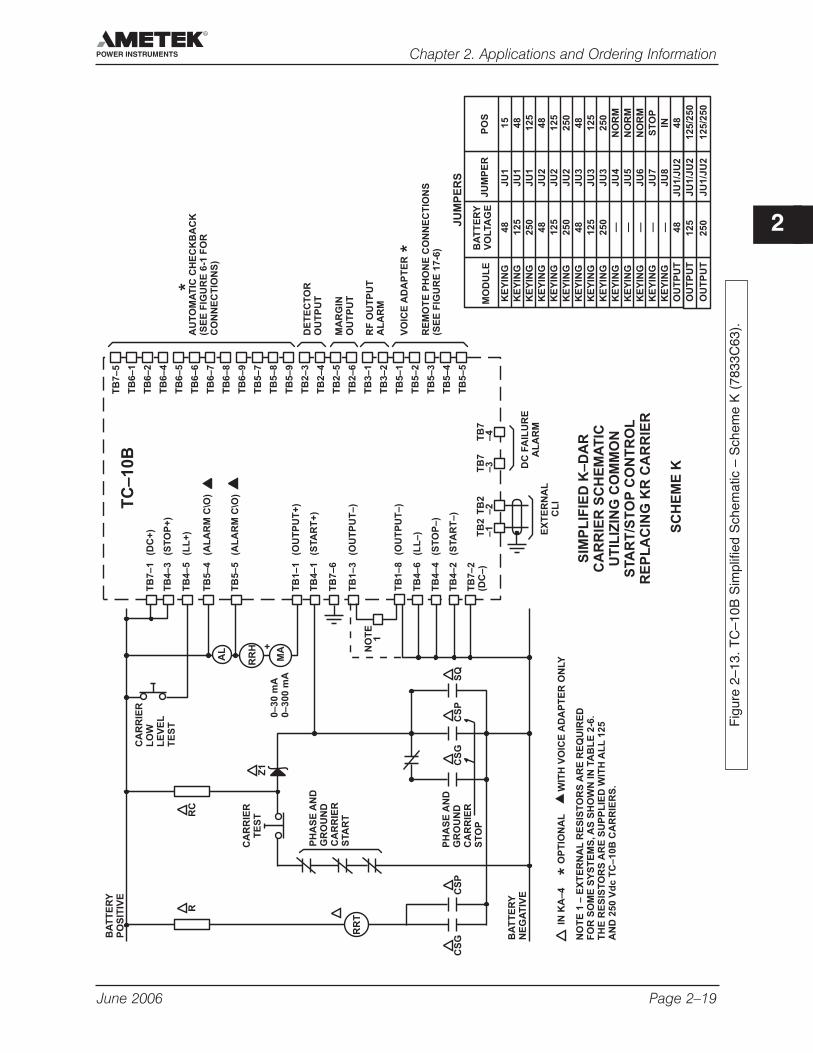
June 2006 Page 2–19
Chapter 2. Applications and Ordering Information
2
Fig
ure
2–13
. T
C–1
0B S
impl
ified
Sch
emat
ic –
Sch
eme
K (
7833
C63
).
KE
YIN
G48
JU
115
KE
YIN
G125
JU
148
KE
YIN
G250
JU
1125
KE
YIN
G48
JU
248
KE
YIN
G125
JU
2125
KE
YIN
G250
JU
2250
KE
YIN
G48
JU
348
KE
YIN
G125
JU
3125
KE
YIN
G250
JU
3250
KE
YIN
G—
JU
4N
OR
M
KE
YIN
G—
JU
5N
OR
M
KE
YIN
G—
JU
6N
OR
M
KE
YIN
G—
JU
7S
TO
P
KE
YIN
G—
JU
8IN
OU
TP
UT
48
JU
1/J
U2
48
MO
DU
LE
JU
MP
ER
PO
SB
AT
TE
RY
VO
LTA
GE
JU
MP
ER
S
TB
6–1
TB
6–2
TB
6–4
TB
6–5
TB
6–6
TB
6–7
TB
6–8
TB
6–9
TB
5–7
TB
5–8
TB
5–9
TB
2–3
TB
2–4
TB
2–5
TB
2–6
TB
3–1
TB
3–2
TB
5–1
TB
5–2
TB
5–3
TB
5–4
TB
5–5
TC
–10B
TB
2–1
TB
2–2
WIT
HV
OIC
EA
DA
PT
ER
ON
LY
PH
AS
EA
ND
GR
OU
ND
CA
RR
IER
STA
RT
PH
AS
EA
ND
GR
OU
ND
CA
RR
IER
ST
OP
BA
TT
ER
YN
EG
AT
IVE
BA
TT
ER
YP
OS
ITIV
E
0–30
mA
0–300
mA
CA
RR
IER
LO
WL
EV
EL
TE
ST
CA
RR
IER
TE
ST
TB
7–3
TB
7–4
TB
4–3
(ST
OP
+)
TB
4–5
(LL
+)
TB
5–4
(AL
AR
MC
\O)
TB
5–5
(AL
AR
MC
\O)
TB
1–3
(OU
TP
UT
–)
TB
4–6
(LL
–)
TB
4–4
(ST
OP
–)
TB
4–2
(STA
RT
–)
TB
7–2
(DC
–)
TB
7–1
(DC
+)
CS
GC
SG
CS
PC
SP
SQ
Z1
RC
R
INK
A–4
SIM
PL
IFIE
DK
–D
AR
CA
RR
IER
SC
HE
MA
TIC
UT
ILIZ
ING
CO
MM
ON
STA
RT
/ST
OP
CO
NT
RO
LR
EP
LA
CIN
GK
RC
AR
RIE
R
SC
HE
ME
K
+
AL
MA
RR
H
RR
T
NO
TE
1–
EX
TE
RN
AL
RE
SIS
TO
RS
AR
ER
EQ
UIR
ED
FO
RS
OM
ES
YS
TE
MS
,A
SS
HO
WN
INTA
BL
E2-6
.T
HE
RE
SIS
TO
RS
AR
ES
UP
PL
IED
WIT
HA
LL
125
AN
D250
Vd
cT
C–10B
CA
RR
IER
S.
TB
1–8
(OU
TP
UT
–)
NO
TE
1
TB
1–1
(OU
TP
UT
+)
TB
4–1
(STA
RT
+)
TB
7–6
RF
OU
TP
UT
AL
AR
M
MA
RG
INO
UT
PU
T
VO
ICE
AD
AP
TE
R
AU
TO
MA
TIC
CH
EC
KB
AC
K(S
EE
FIG
UR
E6-1
FO
RC
ON
NE
CT
ION
S)
DE
TE
CT
OR
OU
TP
UT
RE
MO
TE
PH
ON
EC
ON
NE
CT
ION
S(S
EE
FIG
UR
E17-6
)
DC
FA
ILU
RE
AL
AR
ME
XT
ER
NA
LC
LI
OP
TIO
NA
L
OU
TP
UT
OU
TP
UT
125
250
JU
1/J
U2
JU
1/J
U2
125/2
50
125/2
50
TB
7–5
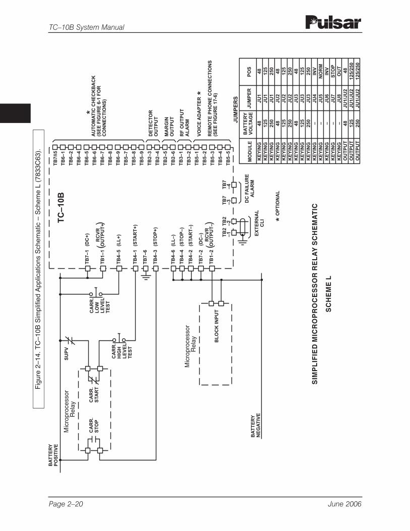
Page 2–20 June 2006
TC–10B System ManualF
igur
e 2–
14.
TC
–10B
Sim
plifi
ed A
pplic
atio
ns S
chem
atic
– S
chem
e L
(783
3C63
).
KE
YIN
G4
8J
U1
48
KE
YIN
G1
25
JU
11
25
KE
YIN
G2
50
JU
12
50
KE
YIN
G4
8J
U2
48
KE
YIN
G1
25
JU
21
25
KE
YIN
G2
50
JU
22
50
KE
YIN
G4
8J
U3
48
KE
YIN
G1
25
JU
31
25
KE
YIN
G2
50
JU
32
50
KE
YIN
G–
JU
4IN
V
KE
YIN
G–
JU
5N
OR
M
KE
YIN
G–
JU
6IN
V
KE
YIN
G–
JU
7S
TO
P
KE
YIN
G–
JU
8O
UT
OU
TP
UT
48
JU
1/J
U2
48
OU
TP
UT
12
5J
U1
/JU
21
25
/25
0
OU
TP
UT
25
0J
U1
/JU
21
25
/25
0
MO
DU
LE
JU
MP
ER
PO
SB
AT
TE
RY
VO
LTA
GE
JU
MP
ER
S
TB
6–
1
TB
6–
2
TB
6–
4
TB
6–
5
TB
6–
6
TB
6–
7
TB
6–
8
TB
6–
9
TB
5–
7
TB
5–
8
TB
5–
9
TB
2–
3
TB
2–
4
TB
2–
5
TB
2–
6
TB
3–
1
TB
3–
2
TB
5–
1
TB
5–
2
TB
5–
3
TB
5–
4
TB
5–
5
TC
–10B
TB
2–
1T
B2
–2
BA
TT
ER
YN
EG
AT
IVE
BA
TT
ER
YP
OS
ITIV
E
CA
RR
.L
OW
LE
VE
LT
ES
T
CA
RR
.H
IGH
LE
VE
LT
ES
T
CA
RR
.S
TO
P
BL
OC
KIN
PU
T
CA
RR
.S
TA
RT
SU
PV
TB
7–
3T
B7
–4
TB
7–
1(D
C+
)
TB
1–
1O
UT
PU
T+
RC
VR
RC
VR
TB
4–
5(L
L+
)
TB
4–
1(S
TA
RT
+)
TB
4–
3(S
TO
P+
)
TB
1–
2O
UT
PU
T–
TB
4–
6(L
L–
)
TB
4–
4(S
TO
P–
)
TB
4–
2(S
TA
RT
–)
TB
7–
2(D
C–
)
TB
7–
6
Mic
ropr
oces
sor
Rel
ay
Mic
ropr
oces
sor
Rel
ay
SIM
PL
IFIE
DM
ICR
OP
RO
CE
SS
OR
RE
LA
YS
CH
EM
AT
IC
SC
HE
ME
L
RF
OU
TP
UT
AL
AR
M
MA
RG
INO
UT
PU
T
VO
ICE
AD
AP
TE
R
AU
TO
MA
TIC
CH
EC
KB
AC
K(S
EE
FIG
UR
E6
-1F
OR
CO
NN
EC
TIO
NS
)
DE
TE
CT
OR
OU
TP
UT
RE
MO
TE
PH
ON
EC
ON
NE
CT
ION
S(S
EE
FIG
UR
E1
7-6
)
DC
FA
ILU
RE
AL
AR
ME
XT
ER
NA
LC
LI
OP
TIO
NA
L
(
(
((
TB
7ñ
5
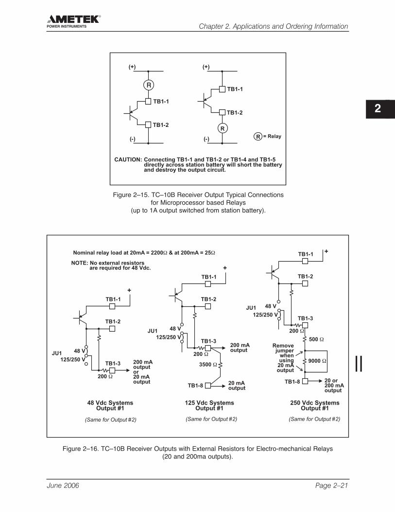
June 2006 Page 2–21
Chapter 2. Applications and Ordering Information
2
Figure 2–15. TC–10B Receiver Output Typical Connectionsfor Microprocessor based Relays
(up to 1A output switched from station battery).
Figure 2–16. TC–10B Receiver Outputs with External Resistors for Electro-mechanical Relays(20 and 200ma outputs).
(+)
(-)
TB1-1
TB1-2
R
R
(+)
(-)
TB1-1
TB1-2
R
= Relay
CAUTION: Connecting TB1-1 and TB1-2 or TB1-4 and TB1-5directly across station battery will short the batteryand destroy the output circuit.
125 Vdc SystemsOutput #1
48 Vdc SystemsOutput #1
(Same for Output #2) (Same for Output #2)
Nominal relay load at 20mA = 2200 & at 200mA = 25W W
250 Vdc SystemsOutput #1
(Same for Output #2)
NOTE: No external resistorsare required for 48 Vdc. +
TB1-1
TB1-2
TB1-3
TB1-8
JU1 48 V
125/250 V
200 mAoutput
20 mAoutput
3500 W
200 W
)
+
200 W
20 or200 mAoutput
9000 W
Removejumper
whenusing
20 mAoutput
TB1-1
TB1-2
TB1-3
TB1-8
JU1 48 V
125/250 V
500 W
)
+
TB1-1
TB1-2
TB1-3
JU1 48 V
125/250 V 200 mAoutputor20 mAoutput
200 W
)
||

Page 2–22 June 2006
TC–10B System Manual
USER NOTES
3.1 UnpackingIf the TC–10B is shipped unmounted, it is inspecial cartons that are designed to protect theequipment against damage.
3.2 StorageIf you are setting the equipment aside before use,be sure to store it in its special cartons (in amoisture-free area) away from dust and otherforeign matter.
3.3 Installation LocationInstall the TC–10B in an area which is free from:
• Temperature exceeding environmentallimits (See “Environmental Requirements”in Chapter 1)
• Corrosive fumes
• Dust
• Vibration
3.4 AssemblyYou can assemble the TC–10B for use in any ofthe following configurations:
• Mounted in a fixed-rack cabinet.
• Mounted in a swing-rack cabinet
• Mounted on an open rack.
or in your own, customer-specified configuration.Refer to Figure 3-3 for mounting dimensions.
3.5 TC–10B Rear PanelConnectors
The following connectors are accessible from theRear Panel (See Figure 3-1):
• Terminal Blocks
• Cable Jacks
• Jumpers
• Input/Output Pins
• RS-232 DB9 female (for future use)
Copyright © AMETEK
3
! CAUTIONUNPACK EACH PIECE OF EQUIPMENT CARE-FULLY SO THAT NO PARTS ARE LOST.INSPECT THE CONDITION OF THE TC-10B AS ITIS REMOVED FROM ITS CARTONS. ANYDAMAGE TO THE TC-10B MUST BE REPORTEDTO THE CARRIER. DAMAGES ARE THERESPONSIBILITY OF THE CARRIER AND ALLDAMAGE CLAIMS ARE MADE GOOD BY THECARRIER. SEND A COPY OF ANY CLAIM TOPulsar.
! CAUTIONIF YOU ARE USING THE TC-10B WITH A SWING-RACK CABINET, MAKE SURE THAT THECABINET IS FIRMLY FASTENED BEFOREOPENING THE RACK (TO PREVENT TIPPING).
Chapter 3. Installation
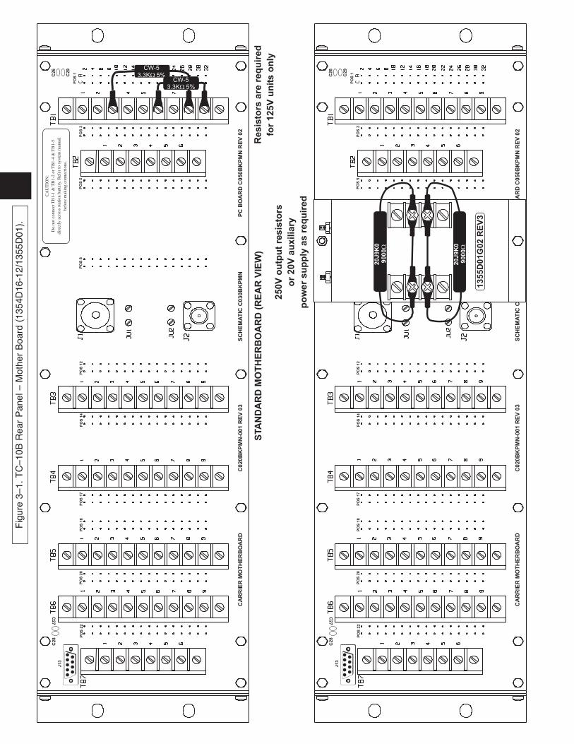
Fig
ure
3–1.
TC
–10B
Rea
r P
anel
– M
othe
r B
oard
(13
54D
16-1
2/13
55D
01).
PO
S22
PO
S20
PO
S18
PO
S17
PO
S14
PO
S12
PO
S8
PO
S5
PO
S3
PO
S1
J13
C2
8
C2
7
C2
9
C2
6
CA
RR
IER
MO
TH
ER
BO
AR
DC
02
0B
KP
MN
-00
1R
EV
03
SC
HE
MA
TIC
C0
30
BK
PM
NP
CB
OA
RD
C0
50
BK
PM
NR
EV
02
PO
S22
PO
S20
PO
S18
PO
S17
PO
S14
PO
S12
PO
S8
PO
S5
PO
S3
PO
S1
J13
C2
8
C2
7
C2
9
C2
6
CA
RR
IER
MO
TH
ER
BO
AR
DC
02
0B
KP
MN
-00
1R
EV
03
SC
HE
MA
TIC
C0
30
BK
PM
NP
CB
OA
RD
C0
50
BK
PM
NR
EV
02
250V
ou
tpu
tre
sis
tors
or
20V
au
xilia
ry
po
wer
su
pp
lyas
req
uir
ed
Resis
tors
are
req
uir
ed
for
125V
un
its
on
ly
STA
ND
AR
DM
OT
HE
RB
OA
RD
(RE
AR
VIE
W)
1355D
01G
02
RE
V3
20
J9
K0
90
00
20
J9
K0
90
00
CA
UT
ION
:
Do
not
connec
tT
B1-1
&T
B1-2
or
TB
1-4
&T
B1-5
dir
ectl
yac
ross
stat
ion
bat
tery
.R
efer
tosy
stem
man
ual
bef
ore
mak
ing
connec
tions.
CW-53.3K 5%
CW-53.3K 5%
3.5.1 Terminal Blocks (Refer to Figure 3-4 for further explanation.)
TB7 Power Supply (Terminals 1–4, 6)
TB7 Universal (Terminal 5)Checkback
TB6 Universal (Terminals 1–9)Checkback
TB5 Voice Adapter (Terminals 1–6)
TB5 Universal (Terminals 7–9)Checkback
TB4 Keying (Terminals 1–6)
TB3 10W PA (Terminals 1–6)
TB2 Level Detector (Terminals 1–6)
TB1 Receiver Output (Terminals 1–9)
3.5.2 Cable JacksJ1 RF Interface Module, RF line, thru 2-
wire coaxial cable (UHF)
J2 RF Interface Module Receiver, RF inputline through 4-wire coaxial cable(BNC), when transmitter and receiverare separated.
3.5.3 Jumpers JU1 Not Included
JU2 Not Included
3.5.4 Input/Output Pins of ModulesPins labeled C and A provide 16 input/outputconnections per module (using even numbers 2through 32 for all modules) as follows:
• Power Supply (pins are to the right of TB7)
• Automatic Checkback (pins are to the rightof TB6)
• Voice Adapter (pins are to the right of TB5)
• Keying (pins are to the left of TB4)
• Transmitter (pins are to the left of TB3)
• 10W PA (pins are to the right of TB3)
• RF Interface (pins are to the right of cablejacks and jumpers)
• Receiver (pins are to the left of TB2)
• Level Detector (pins are to the left of TB1)
• Receiver Output (pins are to the right ofTB1)
3.6 Connections
3.6.1 Safety Precautions Read this Installation chapter thoroughly beforemaking any connections to the TC–10B. No oneshould be permitted to handle any of theequipment that is supplied with high voltage, orconnect any external apparatus to theequipment, unless that person is thoroughlyfamiliar with the hazards involved.
Types of connections made:
• TC–10B equipment ground
• DC power supply and other connections
• Coaxial cables
• RS-232 (reserved for future use)
3.6.2 TC–10B Equipment GroundIn addition to the TC–10B chassis ground connec-tion that is made through the cabinet or rack, aground connection is provided at the Rear PanelTerminal Block TB7. (See Figure 3-1.) A connec-tion should be made between TB7 Terminal 6 andthe earth ground connection at the TC–10Bcabinet location.
June 2006 Page 3–3
Chapter 3. Installation
3
! CAUTIONPRIOR TO MAKING CONNECTIONS, CLOSETHE RF GROUNDING KNIFE SWITCH IN THECABINET THAT IS CONNECTED TO THEINCOMING COAXIAL CABLE.
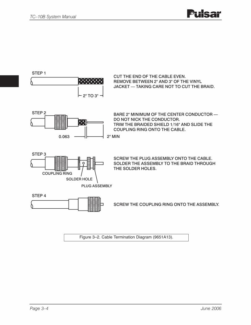
Page 3–4 June 2006
TC–10B System Manual
Figure 3–2. Cable Termination Diagram (9651A13).
3.6.3 DC Power Supply and OtherConnections
Input terminals TB7-1 and TB7-2, on the rear ofthe TC–10B chassis, provide the connectionpoints for the power supply (48, 125 and 250Vdc)and customer inter-connections. (See Figure 3-1).The terminal blocks can accept up to a 12 AWGwire with a ring lug type Burndy YAV1DL36/YAV10 or equivalent.
Any lead coming to or from the switchyard shouldbe shielded twisted pair to reduce transients tobelow the Surge Withstand Capability of ANSIC37.90.1.
3.6.4 Coaxial CableA coaxial cable is required for a low-impedancepath between the TC–10B (Transmitter andReceiver modules) and the Line Tuner (in theswitchyard). Connection jack J1, on the RearPanel, provides the point for coaxial cable connec-tion from the TC–10B to the switchyard.
• Single-conductor
• #12 AWG
• 7 strand #21 copper
• Polyethylene insulator
• Copper shield
• Vinyl jacket (nominal O.D. 0.405 inch)
If the coaxial cable is to connect to relatedcabinets en route to the switchyard, werecommend RG-58A/U cable from J1 to therelated cabinets and RG-213/U from the cabinetsto the switchyard. For connection to J1 using RG-
58A/U cable, use a male UHF connector(Amphenol #83-58FCP or equivalent). Install thecoaxial cable according to the following guide-lines:
1. Attach both ends of the coaxial cable in accor-dance with the Cable Termination Diagram(see Figure 3-2, terminal block lugs, asrequired).
2. To hold carrier loss to a minimum, keep thecable the shortest possible length.
The minimum cable bending diameter is sixtimes the cable diameter.
3. The copper braid of the cable must begrounded at the end which connects to theTC–10B.
4. Without grounding the copper braid of thecable, connect the cable to the groundterminal of the Line Tuner, at either of thefollowing:
• Impedance Matching Transformer
• Wideband Filter
If you are connecting the cable directly to theline tuner, the cable connector can enter theline tuner base either through the side or thebottom of the base.
3.6.5 RS-232 ConnectorThis RS-232 DB9 female connector is reservedfor future use.
June 2006 Page 3–5
Chapter 3. Installation
3
NOTE
The type of coaxial cable we recommend isRG-213/U (52Ω, 29.5 PF/FOOT) with thefollowing characteristics:
! CAUTIONDO NOT GROUND TO THE END OF THE CABLETHAT IS CONNECTED TO THE LINE TUNER.
Page 3–6 June 2006
TC–10B System Manual
3.7 Disconnections
3.8 Jumper ControlsJumpers are set during installation, depending onthe particular TC–10B features and applications(see Figure 3-5).
3.8.1 Power Supply PC BoardJumper JU1 for optional Alarm Relay establishescontact type during loss of power condition(NO/NC).
3.8.2 Keying PC BoardFor proper selection of jumpers, refer to Figures2-5 through 2-14.
JU1 Carrier Start 15V, 48V, 125V, 250V
JU2 Carrier Stop 15V, 48V, 125V, 250V
JU3 Low-Level 15V, 48V, 125V, 250VKey
JU7 Carrier Start/ START,STOPStop Priority
JU6 Carrier Start NORM (+), INVERT (-)
JU5 Carrier Stop NORM (+), INVERT (-)
JU4 Low-Level NORM (+), INVERT (-)Test
JU8 Carrier Stop (KA-4, SKBU-1)
3.8.3 Transmitter PC BoardThere are no jumpers on the standard TransmitterPC Board.
Optional Transmit Time Limiter Aux. Board
JMP1 Alarm Contacts (NO/NC)
When jumper is set in “NO” position,and relay is de-energized, the alarmcontacts will be “OPEN”. Whenjumper is in “NC” position, and relayis de-energized, the alarm contacts willbe “CLOSED”.
3.8.4 10W PA PC BoardJumper JU1 for the RF Output Monitor Relay canbe set for a NO or NC contact. It is not used as analarm but instead just monitors if a signal is beingtransmitted.
3.8.5 RF Interface PC BoardMatching Impedance Jumpers:
• JU4 50Ω
• JU3 75Ω
• JU2 100Ω
2-wire or 4-wire RF Termination
• JU1/JU5 “IN” (2-wire)
• JU1/JU5 “OUT” (4-wire)
Attenuator Override Jumper (JU6) (See Table 3-1.)
NOTE
JU1 is shipped in the “NC” state.
! CAUTIONNEVER DISCONNECT THE CARRIER LEAD-INBETWEEN THE LINE TUNER AND THECOUPLING CAPACITOR UNLESS THE LOWPOTENTIAL END OF THE COUPLINGCAPACITOR IS GROUNDED.
BEFORE DISCONNECTING THE CARRIERLEAD-IN CONDUCTORS, CLOSE THE RFGROUNDING SWITCH AT THE BASE OF THECOUPLING CAPACITOR.
WARNING: IF THIS GROUND IS NOTPROVIDED, DANGEROUS VOLTAGES CANBUILD UP BETWEEN THE LINE TUNER ANDCOUPLING CAPACITOR.
NOTE
JU1/JU5 are is shipped in the “IN” (2-wire) state.JU4 is shipped in the “50Ω” state.
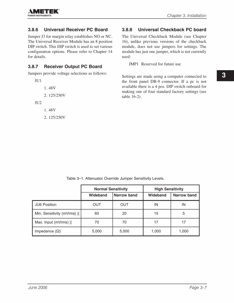
3.8.6 Universal Receiver PC BoardJumper J3 for margin relay establishes NO or NC.The Universal Receiver Module has an 8 positionDIP switch. This DIP switch is used to set variousconfiguration options. Please refer to Chapter 14for details.
3.8.7 Receiver Output PC BoardJumpers provide voltage selections as follows:
JU1
1. 48V
2. 125/250V
JU2
1. 48V
2. 125/250V
3.8.8 Universal Checkback PC boardThe Universal Checkback Module (see Chapter16), unlike previous versions of the checkbackmodule, does not use jumpers for settings. Themodule has just one jumper, which is not currentlyused:
JMP1 Reserved for future use
Settings are made using a computer connected tothe front panel DB-9 connector. If a pc is notavailable there is a 4 pos. DIP switch onboard formaking one of four standard factory settings (seetable 16-2).
June 2006 Page 3–7
Chapter 3. Installation
3
Normal Sensitivity High Sensitivity
Wideband Narrow band Wideband Narrow band
JU6 Position OUT OUT IN IN
Min. Sensitivity (mVrms) || 60 20 15 5
Max. Input (mVrms) || 70 70 17 17
Impedance (Ω) 5,000 5,000 1,000 1,000
Table 3–1. Attenuator Override Jumper Sensitivity Levels.
Page 3–8 June 2006
TC–10B System Manual
3.8.9 Voice Adapter PC Board
A jumper and a DIP switch are provided, asfollows:
JMP1 Alarm Contacts (NO/NC)
When jumper is set in “NO” position,and relay is de-energized, the alarmcontacts will be “OPEN”. Whenjumper is in “NC” position, and relayis de-energized, the alarm contacts willbe “CLOSED”.
SW1 User Functions
In the closed/down position the DIPswitch functions as follows;
• 1 Tone gives Alarm (TCF-10B)
• 2 Carrier gives Alarm (TC-10B)
• 3 Handset key mutes ear (TC-10B)
• 4 Beeper enabled
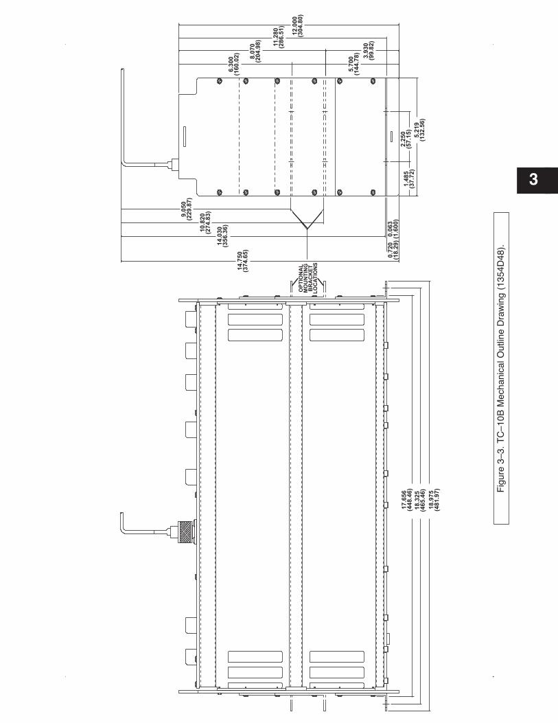
3
Fig
ure
3–3.
TC
–10B
Mec
hani
cal O
utlin
e D
raw
ing
(135
4D48
).
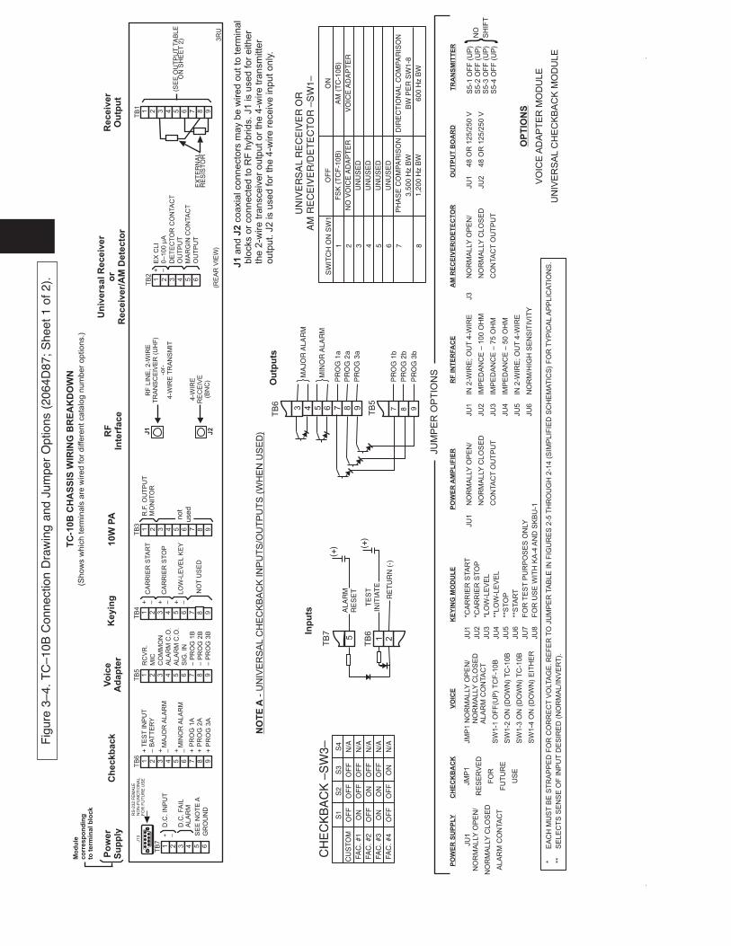
Fig
ure
3–4.
TC
–10B
Con
nect
ion
Dra
win
g an
d Ju
mpe
r O
ptio
ns (
2064
D87
; S
heet
1 o
f 2)
.
4-W
IRE
RE
CE
IVE
(BN
C)
TB
7
TB
2
TB
1
RF
LIN
E,2-W
IRE
TR
AN
SC
EIV
ER
(UH
F)
-or-
4-W
IRE
TR
AN
SM
IT+
+
–
–D
.C.IN
PU
T
D.C
.FA
ILA
LA
RM
SE
EN
OT
EA
GR
OU
ND
1 2 3 4 5 6 7 8 9
TB
5
RC
VR
.
MIC
CO
MM
ON
ALA
RM
C.O
.
ALA
RM
C.O
.
SIG
.IN
–P
RO
G1B
–P
RO
G2B
–P
RO
G3B
1 2 3 4 5 6 7 8 9
1 2 3 4 5 6
1 2 3 4 5 6
(RE
AR
VIE
W)
TB
41 2 3 4 5 6 7 8 9
CA
RR
IER
STA
RT
CA
RR
IER
ST
OP
LO
W-L
EV
EL
KE
Y
NO
TU
SE
D
TB
3
7 8 91 2 3 4 5 6
R.F
.O
UT
PU
TM
ON
ITO
RJ1
J2
EX
CLI
0–100
µA
DE
TE
CT
OR
CO
NTA
CT
OU
TP
UT
MA
RG
INC
ON
TA
CT
OU
TP
UT
3R
U
(SE
EO
UT
PU
TTA
BLE
ON
SH
EE
T2)
EX
TE
RN
AL
RE
SIS
TO
R
TB
6+
TE
ST
INP
UT
–B
AT
TE
RY
–
–
–
– –
MA
JO
RA
LA
RM
MIN
OR
ALA
RM
+P
RO
G1A
+P
RO
G2A
+P
RO
G3A
1 2 3 4 5 6 7 8 9
+
+
+
+ +
TC
-10B
CH
AS
SIS
WIR
ING
BR
EA
KD
OW
N
NO
TE
A-
UN
IVE
RS
AL
CH
EC
KB
AC
KIN
PU
TS
/OU
TP
UT
S(W
HE
NU
SE
D)
OP
TIO
NS
VO
ICE
AD
AP
TE
RM
OD
ULE
UN
IVE
RS
AL
CH
EC
KB
AC
KM
OD
ULE
(Sh
ow
sw
hic
hte
rmin
als
are
wire
dfo
rd
iffe
ren
tca
talo
gn
um
be
ro
ptio
ns.)
Mo
du
leco
rresp
on
din
gto
term
inalb
lock
Po
wer
Su
pp
lyC
heckb
ack
Vo
ice
Ad
ap
ter
Keyin
g
Inp
uts
Ou
tpu
ts
10W
PA
RF
Inte
rface
Un
ivers
alR
eceiv
er
or
Receiv
er/
AM
Dete
cto
r
Receiv
er
Ou
tpu
t
RS
-232
FE
MA
LE
NO
N-F
UN
CT
ION
AL
FO
RF
UT
UR
EU
SE
J1
3
and
coaxia
lconnecto
rsm
ay
be
wired
outto
term
inal
blo
cks
or
connecte
dto
RF
hybrids.J1
isused
for
either
the
2-w
ire
transceiv
er
outp
utor
the
4-w
ire
transm
itte
routp
ut.
J2
isused
for
the
4-w
ire
receiv
ein
putonly
.
J1
J2
not
used
JU
MP
ER
OP
TIO
NS
JM
P1
RE
SE
RV
ED
FO
R
FU
TU
RE
US
E
CH
EC
KB
AC
KP
OW
ER
SU
PP
LY
JU
1N
OR
MA
LLY
OP
EN
/
NO
RM
ALLY
CLO
SE
D
ALA
RM
CO
NTA
CT
PO
WE
RA
MP
LIF
IER
JU
1N
OR
MA
LLY
OP
EN
/
NO
RM
ALLY
CLO
SE
D
CO
NTA
CT
OU
TP
UT
AM
RE
CE
IVE
R/D
ET
EC
TO
R
J3
NO
RM
ALLY
OP
EN
/
NO
RM
ALLY
CLO
SE
D
CO
NTA
CT
OU
TP
UT
OU
TP
UT
BO
AR
DT
RA
NS
MIT
TE
R
JU
148
OR
125/2
50
V
JU
248
OR
125/2
50
V
S5-1
OF
F(U
P)
S5-2
OF
F(U
P)
S5-3
OF
F(U
P)
S5-4
OF
F(U
P)
RF
INT
ER
FA
CE
JU
1IN
2-W
IRE
;O
UT
4-W
IRE
JU
2IM
PE
DA
NC
E–
100
OH
M
JU
3IM
PE
DA
NC
E–
75
OH
M
JU
4IM
PE
DA
NC
E–
50
OH
M
JU
5IN
2-W
IRE
;O
UT
4-W
IRE
JU
6N
OR
M/H
IGH
SE
NS
ITIV
ITY
VO
ICE
JM
P1
NO
RM
ALLY
OP
EN
/N
OR
MA
LLY
CLO
SE
DA
LA
RM
CO
NTA
CT
SW
1-1
OF
F(U
P)
TC
F-1
0B
SW
1-2
ON
(DO
WN
)T
C-1
0B
SW
1-3
ON
(DO
WN
)T
C-1
0B
SW
1-4
ON
(DO
WN
)E
ITH
ER
KE
YIN
GM
OD
UL
E
JU
1*C
AR
RIE
RS
TA
RT
JU
2*C
AR
RIE
RS
TO
P
JU
3*L
OW
-LE
VE
L
JU
4**
LO
W-L
EV
EL
JU
5**
ST
OP
JU
6**
STA
RT
JU
7F
OR
TE
ST
PU
RP
OS
ES
ON
LY
JU
8F
OR
US
EW
ITH
KA
-4A
ND
SK
BU
-1
*E
AC
HM
US
TB
ES
TR
AP
PE
DF
OR
CO
RR
EC
TV
OLTA
GE
.RE
FE
RT
OJU
MP
ER
TA
BLE
INF
IGU
RE
S2-5
TH
RO
UG
H2-1
4(S
IMP
LIF
IED
SC
HE
MA
TIC
S)
FO
RT
YP
ICA
LA
PP
LIC
AT
ION
S.
**S
ELE
CT
SS
EN
SE
OF
INP
UT
DE
SIR
ED
(NO
RM
AL/IN
VE
RT
).
NO
SH
IFT
5 1 2
TB
7
TB
6
ALA
RM
RE
SE
T
TE
ST
INIT
IAT
E
RE
TU
RN
(-)
(+) (+
)
5 6 7 8 943
TB
5
TB
6
PR
OG
1b
PR
OG
1a
MA
JOR
ALA
RM
MIN
OR
ALA
RM
PR
OG
2aP
RO
G3a
PR
OG
3b
PR
OG
2b987
S
1O
FF
ON
OF
FO
NO
FF
S2
OF
FO
FF
ON
ON
OF
F
S3
OF
FO
FF
OF
FO
FF
ON
S4
N/A
N/A
N/A
N/A
N/A
CU
ST
OM
FAC
. #1
FAC
. #2
FAC
. #3
FAC
. #4
CH
EC
KB
AC
K–S
W3–
UN
IVE
RS
AL
RE
CE
IVE
RO
RA
MR
EC
EIV
ER
/DE
TE
CT
OR
–SW
1–
OF
FF
SK
(TC
F-1
0B)
NO
VO
ICE
AD
AP
TE
RU
NU
SE
DU
NU
SE
DU
NU
SE
DU
NU
SE
DP
HA
SE
CO
MP
AR
ISO
N3,
500
Hz
BW
1,20
0H
zB
W
ON
AM
(TC
-10B
)V
OIC
EA
DA
PT
ER
DIR
EC
TIO
NA
LC
OM
PA
RIS
ON
BW
PE
RS
W1-
860
0H
zB
W
SW
ITC
HO
NS
W1
1 2 3 4 5 6 7 8
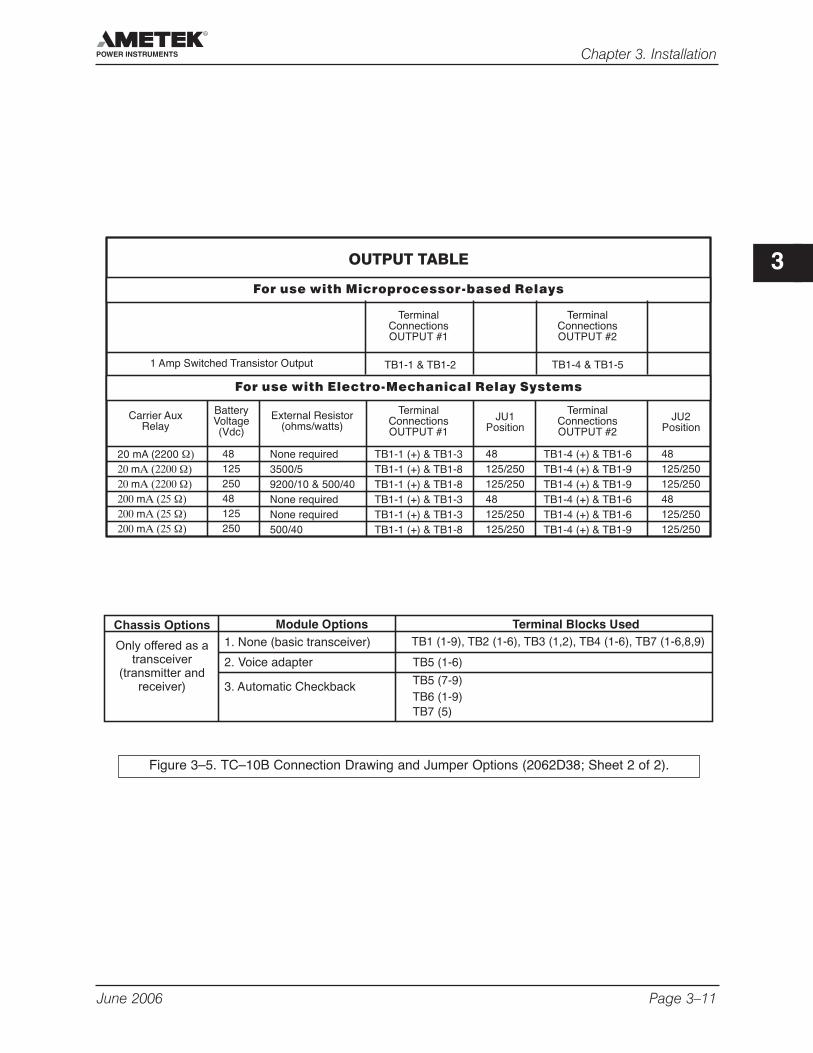
June 2006 Page 3–11
Chapter 3. Installation
3
20 mA (2200mmmmm
W)
20 A (2200 W)
20 A (2200 W)
200 A (25 W)
200 A (25 W)
200 A (25 W)
Carrier AuxRelay
4812525048125250
BatteryVoltage(Vdc)
None required3500/59200/10 & 500/40None requiredNone required500/40
External Resistor(ohms/watts)
TB1-1 (+) & TB1-3TB1-1 (+) & TB1-8TB1-1 (+) & TB1-8TB1-1 (+) & TB1-3TB1-1 (+) & TB1-3TB1-1 (+) & TB1-8
TerminalConnectionsOUTPUT #1
48125/250125/25048125/250125/250
JU1Position
TerminalConnectionsOUTPUT #2
TB1-4 (+) & TB1-6TB1-4 (+) & TB1-9TB1-4 (+) & TB1-9TB1-4 (+) & TB1-6TB1-4 (+) & TB1-6TB1-4 (+) & TB1-9
TerminalConnectionsOUTPUT #2
TerminalConnectionsOUTPUT #1
48125/250125/25048125/250125/250
JU2Position
TB1-1 & TB1-2 TB1-4 & TB1-51 Amp Switched Transistor Output
OUTPUT TABLE
Chassis Options
Only offered as atransceiver
(transmitter andreceiver)
TB1 (1-9), TB2 (1-6), TB3 (1,2), TB4 (1-6), TB7 (1-6,8,9)
TB5 (1-6)
TB5 (7-9)TB6 (1-9)TB7 (5)
Module Options Terminal Blocks Used1. None (basic transceiver)
2. Voice adapter
3. Automatic Checkback
Figure 3–5. TC–10B Connection Drawing and Jumper Options (2062D38; Sheet 2 of 2).

Page 3–12 June 2006
TC–10B System Manual
USER NOTES
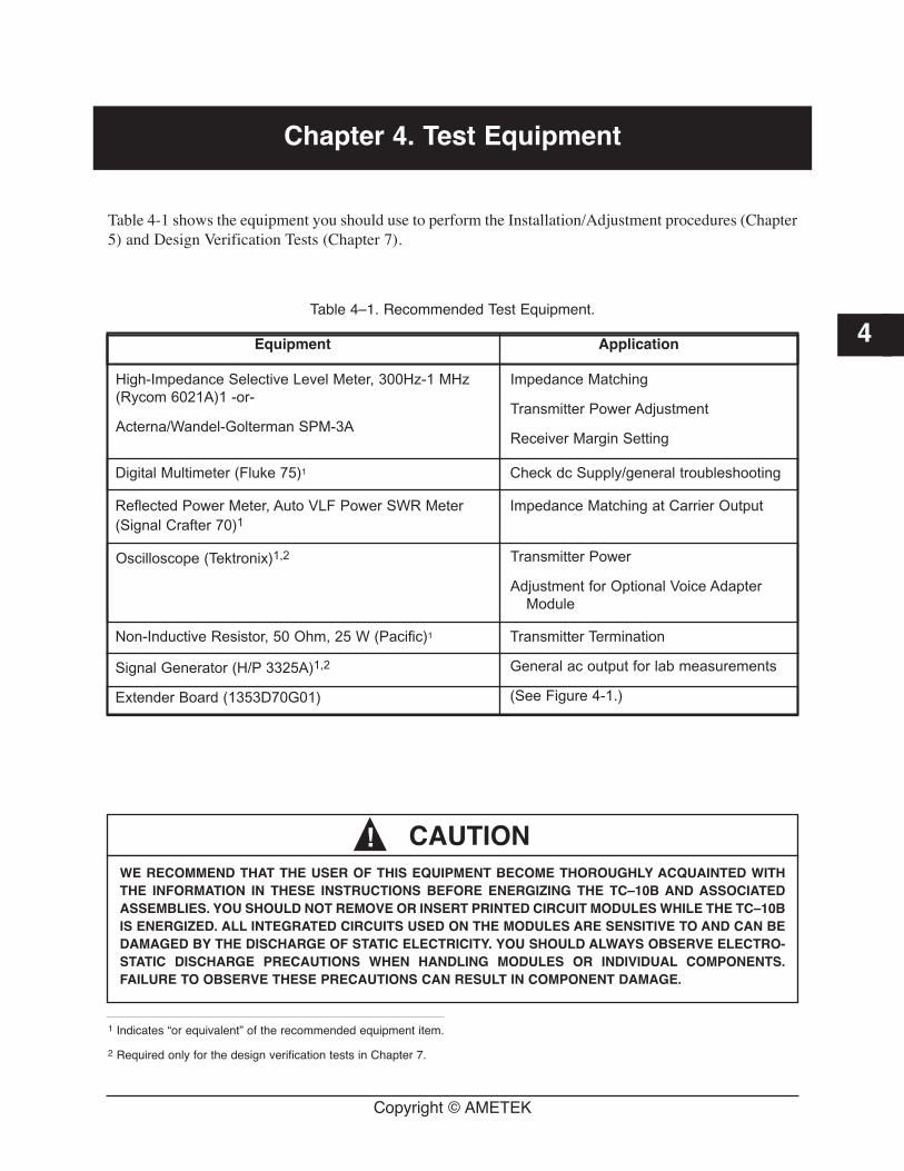
Equipment Application
Copyright © AMETEK
Chapter 4. Test Equipment
4
Non-Inductive Resistor, 50 Ohm, 25 W (Pacific)1
Signal Generator (H/P 3325A)1,2
Extender Board (1353D70G01)
Transmitter Termination
General ac output for lab measurements
(See Figure 4-1.)
Digital Multimeter (Fluke 75)1 Check dc Supply/general troubleshooting
Reflected Power Meter, Auto VLF Power SWR Meter(Signal Crafter 70)1
Impedance Matching at Carrier Output
Oscilloscope (Tektronix)1,2 Transmitter Power
Adjustment for Optional Voice AdapterModule
Table 4-1 shows the equipment you should use to perform the Installation/Adjustment procedures (Chapter5) and Design Verification Tests (Chapter 7).
Table 4–1. Recommended Test Equipment.
! CAUTIONWE RECOMMEND THAT THE USER OF THIS EQUIPMENT BECOME THOROUGHLY ACQUAINTED WITHTHE INFORMATION IN THESE INSTRUCTIONS BEFORE ENERGIZING THE TC–10B AND ASSOCIATEDASSEMBLIES. YOU SHOULD NOT REMOVE OR INSERT PRINTED CIRCUIT MODULES WHILE THE TC–10BIS ENERGIZED. ALL INTEGRATED CIRCUITS USED ON THE MODULES ARE SENSITIVE TO AND CAN BEDAMAGED BY THE DISCHARGE OF STATIC ELECTRICITY. YOU SHOULD ALWAYS OBSERVE ELECTRO-STATIC DISCHARGE PRECAUTIONS WHEN HANDLING MODULES OR INDIVIDUAL COMPONENTS.FAILURE TO OBSERVE THESE PRECAUTIONS CAN RESULT IN COMPONENT DAMAGE.
1 Indicates “or equivalent” of the recommended equipment item.
2 Required only for the design verification tests in Chapter 7.
High-Impedance Selective Level Meter, 300Hz-1 MHz(Rycom 6021A)1 -or-
Acterna/Wandel-Golterman SPM-3A
Impedance Matching
Transmitter Power Adjustment
Receiver Margin Setting
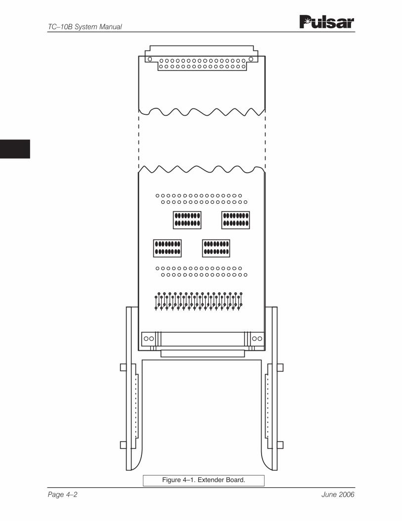
Page 4–2 June 2006
TC–10B System Manual
Figure 4–1. Extender Board.
Copyright © AMETEK
Chapter 5. Installation / Adjustment Procedures
5
• Verifying initial TC–10B factory adjustments.
• Installing the TC–10B for your application.
• Changing the TC–10B operating frequencies.
• Periodic maintenance.
You perform routine adjustments inthe field for the following purposes:
• Review the Test Equipment (Chapter 4).
• Review the Adjustment Data Sheets (at the end of thischapter); you should complete the data sheets as youperform the Adjustment Steps.
• Review the TC–10B Block Diagram as described underSignal Path (Chapter 6).
• Remove the cover from the front of the chassis. Afterremoving the cover, set it in a safe place.
To prepare the TC–10B for installa-tion or routine adjustment tests,perform the following:
1. Select the TC–10B Operating Frequency.
2. Review the Adjustment Data Sheets (at the end of thischapter); you should complete the data sheets as youperform the Adjustment Steps.
3. Select the TC–10B Keying Conditions.
4. Select the TC–10B Receiver Output.
5. Select the TC–10B Transmitter RF Output Impedance.
6. Check the Line Tuning and Matching Equipment.
7. Check the TC–10B Transmitter Power Levels.
8. Offset the TC–10B Transmitter Frequency. (3 terminal lineapplication)
9. Set the TC–10B Receiver using the Remote Carrier signal &then Local Carrier signal.
10. Select the optimal Universal Checkback Module conditions.
Be sure to run the adjustment tests inthe following order:
If you are using the Alarm Relay, set jumper JU1on the Power Supply Module.
5.1 Select the TC–10BOperating Frequency
1. Remove the Transmitter Module from theTC–10B chassis and select the operatingfrequency.
a) Using the module extractors, remove theTransmitter Module.
b) Select the Transmitter operating frequency(between 30 and 535kHz), by turning thefour Transmitter rotary programmingswitches (in 0.1kHz steps), with a smallscrewdriver until the desired operatingfrequency appears through the (four)windows in the Transmitter control panel.
c) Using module extractors, insert themodule back into the TC–10B chassis, byseating it with firm pressure.
2. Power up the TC-10B unit with the appro-priate dc power. With a small screwdriver,depress the “SET” button on the front of thereceiver module. The frequency display willbegin to flash. Depress the raise or lowerbutton until the desired frequency isdisplayed. Depress “SET” again to select thisfrequency. If you are not ready to set thesensitivity, depress the “CANCEL” button. Ifyou are ready to set the sensitivity, depress the“SET” button andproceed with stepslisted in section 6.8.
5.2 Select TC–10B KeyingConditions
5.2.1 Keying MechanismsKeying mechanisms for the TC–10B are of twotypes:
• Control Panel source (e.g., using test push-buttons)
• Printed Circuit Board (PCB) source (e.g.,using jumpers)
5.2.2 Keying Module Jumpers1. Remove the Keying Module from the chassis
and set jumpers JU1 through JU8 as desired(refer to Figures 2-5 through 2-16):
JU1 – Keying Voltage Carrier Start
• 15V
• 48V
• 125V
• 250V
JU2 – Keying Voltage Carrier Stop
• 15V
• 48V
• 125V
• 250V
JU3 – Keying Voltage Low-Level Key
• 18V
• 48V
• 125V
• 250V
Page 5–2 June 2006
TC–10B System Manual
! CAUTIONMAKE SURE THAT THE POWER HAS BEENTURNED “OFF” USING THE POWER SWITCH(S1) ON THE POWER SUPPLY MODULE; THEINPUT (D3) AND OUTPUT (D11) LEDS SHOULDNOT SHOW RED LIGHTS.
NOTE
You may use the “INVERT’ positions on JU4 (LOW-LEVEL KEYING) and JU6 (HIGH-LEVEL KEYING)when it is impractical to hold down the(RECESSED) push-buttons (“HL” and “LL”) on theKeying Module control panel.
JU4 – Sense of Input Low-Level
• NORM (+)
• INVERT(-)
JU5 – Sense of Input Carrier Stop
• NORM (+)
• INVERT(-)
JU6 – Sense of Input Carrier Start
• NORM (+)
• INVERT (-)
JU7 – Priority Start or Stop
• STOP
• START
JU8 – Carrier Stop Circuit
OUT Normally in this position
IN When used with KDAR orSKBU or applications that usea common start/stop keyingcircuit.
2. Two push button switches are provided fortest purposes:
• The top push button is marked “HL” forHigh-Level power (10W typical)
• The bottom push button is marked “LL” forLow-Level power (1W typical)
Each push button is recessed, and can beactivated by sliding an object (e.g., a pen orpencil) through each push button accesslocation on the Keying Module front panel.
3. Check the LEDs at the bottom of the KeyingModule control panel for indication of thekeying condition: “HL” (High-Level keyoutput), “LL” (Low-Level key output), and“V” (Voice-Level key output).
The JU7 STOP position inhibits the High-Level output, Low-Level output, and theVoice-Level output.
Both the Low-Level and High-Level outputsinhibit the Voice-Level output.
4. Insert the Keying Module back into theTC–10B chassis.
5.3 Select TC–10B ReceiverOutput
1. Remove the Receiver Output Module fromthe TC–10B chassis and set jumpers JU1 andJU2 according to the following options:
JU1
1) 48V
2) 125/250V
JU2
1) 48V
2) 125/250V
2. Insert the Receiver Output Module back intothe TC–10B chassis.
5.4 Select TC–10B RF OutputImpedance
1. Configure the RF Interface 2-Wireimpedance. Remove the RF Interface Modulefrom the TC–10B chassis and configure theoutput impedance by setting the jumpers asfollows:
• JU4, when set, provides 50Ω
• JU3, when set, provides 75Ω
• JU2, when set, provides 100Ω
2. Select 2- or 4-wire Receiver input, usingjumpers JU1 and JU5 as follows: IN positionfor 2-wire; OUT position for 4-wire. Thenormal configuration for the TC-10B is 2-wire.
3. Set jumper JU6 to the desired Receiver sensi-tivity range.
4. Insert the RF Interface Module back into theTC–10B chassis.
June 2006 Page 5–3
Chapter 5. Installation / Adjustment Procedures
5
5.5 Check Line Tuning AndMatching Equipment
1. Refer to the appropriate instructions for linetuning equipment.
2. Perform the required adjustments.
5.6 Check TC–10B TransmitterPower Levels
With power “OFF”, remove the coaxial cableconnection to the Hybrids or line tuningequipment and substitute a 50, 75 or 100Ω resistortermination (in accordance with the jumpersettings in 5.3-1), at the output of the TC-10B (J1,UHF connector).
5.6.1 Check High-Level Output
1. Connect the Selective Level Meter to the 10WPA Module control panel at the test jacks:
TJ1 Input (top jack)
TJ2 Common (bottom jack)
2. Tune the meter to the Transmitter frequency.
3. Turn power “ON” at the Power SupplyModule.
4. On the Keying Module control panel, pressand hold the top push button (marked “HL”),to key the Transmitter at High Level power.
5. Record the Selective Level Meter reading (atTJ1, TJ2). The meter should measure0.224Vrms (0dBm at 50Ω reference) for fullHigh-Level keying (10W power). If the metermeasures 0dBm, skip to Step 8.
6. If the meter does not measure 0dBm, turnpower “OFF” at the Power Supply Moduleand remove the Transmitter Module from thechassis. Place the extender board into theTransmitter Module position of the chassis.Then plug the Transmitter Module onto theextender board.
7. Adjust the 10W potentiometer (R13) on theTransmitter Module until the Selective LevelMeter (at the 10W PA TJ1, TJ2) reads0.224Vrms (0dBm at 50Ω reference). Thenplace the Transmitter Module back in thechassis.
8. On the Keying Module control panel, releasethe “HL” push button to un-key theTransmitter Module.
5.6.2 Check Low-Level Output
With the conditions the same as for the High-Level output check, i.e.,
• Selective Level Meter at 10W PA Modulecontrol panel (TJ1, TJ2)
• Meter tuned to XMTR frequency
• Power “ON”
do the following:
Page 5–4 June 2006
TC–10B System Manual
! CAUTIONDO NOT ALLOW INEXPERIENCED PERSONNELTO MAKE THESE ADJUSTMENTS. PERSONNELMAKING THE ADJUSTMENTS MUST BECOMPLETELY FAMILIAR WITH THE HAZARDSINVOLVED.
NOTE
The INPUT and OUTPUT LEDs should show red.
NOTE
The “HL” LED should show red.
NOTE
The “HL” LED should not be red.
NOTE
For the optional Transmit Time Limiter Transmittermodule, you must hold the Alarm ResetPushbutton in while doing these tests or it will turnoff.
1. On the Keying Module control panel, pressthe bottom push button (marked “LL”), to keythe Transmitter at Low Level power.
2. Record the Selective Level Meter reading (atTJ1, TJ2). The meter should measure0.0707Vrms (-10dBm at 50Ω reference) forLow-Level keying (1W power). If the metermeasures -10dBm, skip to Step 5.
3. If the meter does not measure -10dBm, turnpower “OFF” at the Power Supply Module,and remove the Transmitter Module from thechassis. Place the extender board into theTransmitter Module position of the chassis.Then plug the Transmitter Module onto theextender board.
4. Adjust the 1W potentiometer (R12) on theTransmitter Module, until the Selective LevelMeter (at the 10W PA TJ1, TJ2) reads0.0707 Vrms (-10dBm at 50Ω reference).Then place the Transmitter Module back inthe chassis.
5. On the Keying Module control panel, releasethe “LL” push button to un-key theTransmitter Module.
5.6.3 Check Voice-Level Output
Perform this procedure only if you are using theVoice Level Option.
With the conditions the same as for the High-Level output check, i.e.,
• Selective Level Meter at 10W PA Modulecontrol panel (TJ1, TJ2)
• Meter tuned to XMTR frequency
• Power “ON”
do the following:
1. Key the carrier set with the Push-to-Talkswitch (on the handset), while muting themicrophone, to key the Transmitter at Voice-Level (4.3W power, when High-Level is 10Wpower).
2. Record the Selective Level Meter reading (atTJ1, TJ2). The meter should measure0.148Vrms (-3.6dBm at 50Ω reference) forVoice Keying. If the meter measures -3.6dBm,skip to Step 5.
3. If the meter does not measure -3.6dBm, turnpower “OFF” at the Power Supply Moduleand remove the Transmitter Module from thechassis. Place the extender board into theTransmitter Module position of the chassis.Then plug the Transmitter Module onto theextender board.
4. Turn the Voice Adjust potentiometer (R14), onthe Transmitter Module, until the SelectiveLevel Meter (TJ1, TJ2) reads 0.148Vrms (-3.6dBm at 50Ω reference). Then place theTransmitter back in the chassis.
5. Monitor the output of the carrier set with anoscilloscope at the 10W PA Module test jacks:
• TJ1
• TJ2
6. Voice key the Transmitter by pushing thePush-to-Talk switch (on handset) and usingthe signal generator at 1 kHz (TB5/2 and 3) toset the level to achieve the following voltages:
June 2006 Page 5–5
Chapter 5. Installation / Adjustment Procedures
5
NOTE
We recommended that you set the low level power10dB below full power. However, you may use anypower level between 10W and 50mW.
NOTE
The “V” LED should show red.
NOTE
The “LL” LED should not be red.
NOTE
If a full power level (other than 10W) is used, theVF level should be set accordingly, i.e., 3.6dBbelow the High-Level value.
• ∪ 62V p-p (at peak modulation)
• ∪ 20V p-p (valley)
7. If the ratio of the voltages (0.62/0.20) do notapproximate a value of 3, adjust poten-tiometer R11 on the Transmitter, as follows:
• Clockwise if not enough signal (a valueless than 3).
• Counterclockwise if too much signal (avalue significantly greater than 3).
8. Un-key the Push-to-Talk switch (on handset).
5.6.4 Adjust the Transmitter Power Output Levels
1. Move the Selective Level Meter to the testjacks marked “LINE” (on the RF Interfacecontrol panel): TJ1 (Line – top jack) and TJ2(Common – bottom jack)
2. On the Keying Module control panel, pressand hold the bottom (“LL”) push button tokey the Transmitter at Low-Level power.
3. On the RF Interface Module control panel,configure the output impedance by setting aJumper. The Selective Level Meter (TJ1, TJ2)should show a maximum reading (Vrms) for 1W (+30dBm) power, as follows:
• JU4, when set, provides 50Ω (7.07Vrms)
• JU3, when set, provides 75Ω (8.6Vrms)
• JU2, when set, provides 100Ω (10.0Vrms)
4. If the above (Vrms) values are not achieved,adjust the “INPUT LEVEL SET” poten-tiometer (R53) on the 10W PA Module controlpanel to obtain 7.07Vrms (for 50Ωreference).
5. On the Keying Module control panel, releasethe “LL” push button to unkey the TransmitterModule.
6. Check the High-Level key for 10W output.
7. Turn power “OFF” at the Power SupplyModule.
8. Remove the 50, 75, or 100Ω resistor termina-tion and replace the coaxial cable connectionto the Line Tuner.
5.7 Offset TC–10B TransmitterFrequency
It the Transmitter frequency needs to be offset(for- three-terminal line applications), monitor theTransmitter frequency with a Frequency Counter.
1. Make sure that the power is “OFF” at thePower Supply Module and remove theTransmitter Module from the chassis.
2. On the Transmitter Module, turn rotary switchS4 to raise or lower the Transmitter frequency(in 100Hz steps) as follows:
a) At Transmitter #1 (near end), turn rotaryswitch S4 clockwise to raise the frequency(center frequency +100Hz).
b) At Transmitter #2 (far end), turn rotaryswitch S4 counterclockwise to lower thefrequency (center frequency –100Hz).
Page 5–6 June 2006
TC–10B System Manual
NOTE
The “LL” LED should show red.
NOTEIf you want a final output power of less than 10 W,reduce power by adjusting the input level poten-tiometer (R53) on the 10W PA Module for the lowerpower. If a sufficiently low level is not obtainableusing R53, repeat the above alignment proceduresusing the reduced level.
NOTE
Customer personnel should use voice communi-cations while working simultaneously, withtransmitter #1 (near end) and transmitter #2 (farend), to perform the following procedure:
NOTE
The third terminal’s transmitter should remain atcenter frequency.
3. Replace the transmitter module into thechassis and proceed to the next step.
5.8 Check TC–10B ReceiverMargin Setting using RemoteCarrier Signal
1. At the Power Supply Module, turn the power“ON”.
2. Arrange for a received signal from the remoteend.
3. Sensitivity setting:
On the Receiver module perform the following tocomplete the setting:
a) Hit “SET” twice until the display reads“SET SENS?”
b) With the remote signal being received (atthe remote end, push the “HL button onthe keying module), depress “SET” again.
c) If you’re not adjusting the 15dB margin,depress “SET” again. If you are, thendepress “RAISE” or “LOWER” asrequired to adjust it up or down 5dB, thenpress set.
d) If you are not going to adjust an externalcarrier level meter, depress “SET”.
Otherwise, press “RAISE” or “LOWER”as required, then press set.
e) Unkey the remote carrier set & key thelocal carrier set by depressing the HLTEST button on the keying module andpressing the “SET” button on the receivermodule.
f) This completes the setting of the receivermargin.
4. If you are just checking the sensitivity setting,read the Tri-color bar graph CLI whilereceiving a remote signal.
5.9 Select Optional CheckbackModule Conditions
If you are using the optional Universal CheckbackModule, select the desired conditions for themodule’s operation.
5.10 Prepare TC–10B forOperation
1. Be sure that power is “ON” at the PowerSupply Module.
2. Replace the cover on the TC–10B controlpanel. Secure both latches by pushing inwardand sideways until the cover is secure. Youmay lock the latches in place using meterseals.
This completes the “Routine Alignment”procedure. The TC–10B is ready to be put intooperation.
June 2006 Page 5–7
Chapter 5. Installation / Adjustment Procedures
5
NOTES:
1. The foregoing procedure adjusts the Receivermargin to the recommended 15dB value.
2. The Receiver bargraph CLI meter readingshould be 0dB at this time.
3. In three-terminal line applications, the marginadjustment procedure should use the weaker ofthe two received signals.
4. When applying the TC–10B with a phasecomparison relay, do not readjust the Receiverlevel when keying with a square wave signal.The CLI will read around -10dB, but this is anaverage reading of the on and off square wave.The receiver will still maintain the 15dB margin.The CLI reading is only accurate for a non-amplitude modulated signal.
NOTE
When placing the TC–10B into service, refer to theSystem manual that is appropriate for the relaysystem you are using with the TC–10B system.
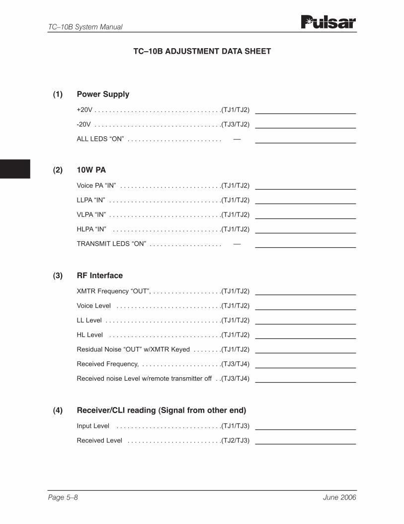
Page 5–8 June 2006
TC–10B System Manual
TC–10B ADJUSTMENT DATA SHEET
(1) Power Supply
+20V . . . . . . . . . . . . . . . . . . . . . . . . . . . . . . . . . . .(TJ1/TJ2)
-20V . . . . . . . . . . . . . . . . . . . . . . . . . . . . . . . . . . .(TJ3/TJ2)
ALL LEDS “ON” . . . . . . . . . . . . . . . . . . . . . . . . . . ––
(2) 10W PA
Voice PA “IN” . . . . . . . . . . . . . . . . . . . . . . . . . . . .(TJ1/TJ2)
LLPA “IN” . . . . . . . . . . . . . . . . . . . . . . . . . . . . . . .(TJ1/TJ2)
VLPA “IN” . . . . . . . . . . . . . . . . . . . . . . . . . . . . . . .(TJ1/TJ2)
HLPA “IN” . . . . . . . . . . . . . . . . . . . . . . . . . . . . . .(TJ1/TJ2)
TRANSMIT LEDS “ON” . . . . . . . . . . . . . . . . . . . . ––
(3) RF Interface
XMTR Frequency “OUT”, . . . . . . . . . . . . . . . . . . .(TJ1/TJ2)
Voice Level . . . . . . . . . . . . . . . . . . . . . . . . . . . . .(TJ1/TJ2)
LL Level . . . . . . . . . . . . . . . . . . . . . . . . . . . . . . . .(TJ1/TJ2)
HL Level . . . . . . . . . . . . . . . . . . . . . . . . . . . . . . .(TJ1/TJ2)
Residual Noise “OUT” w/XMTR Keyed . . . . . . . .(TJ1/TJ2)
Received Frequency, . . . . . . . . . . . . . . . . . . . . . .(TJ3/TJ4)
Received noise Level w/remote transmitter off . .(TJ3/TJ4)
(4) Receiver/CLI reading (Signal from other end)
Input Level . . . . . . . . . . . . . . . . . . . . . . . . . . . . .(TJ1/TJ3)
Received Level . . . . . . . . . . . . . . . . . . . . . . . . . .(TJ2/TJ3)
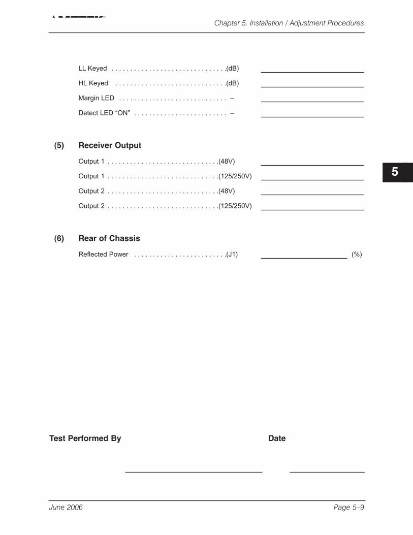
June 2006 Page 5–9
5
LL Keyed . . . . . . . . . . . . . . . . . . . . . . . . . . . . . . .(dB)
HL Keyed . . . . . . . . . . . . . . . . . . . . . . . . . . . . . .(dB)
Margin LED . . . . . . . . . . . . . . . . . . . . . . . . . . . . . –
Detect LED “ON” . . . . . . . . . . . . . . . . . . . . . . . . . –
(5) Receiver Output
Output 1 . . . . . . . . . . . . . . . . . . . . . . . . . . . . . .(48V)
Output 1 . . . . . . . . . . . . . . . . . . . . . . . . . . . . . .(125/250V)
Output 2 . . . . . . . . . . . . . . . . . . . . . . . . . . . . . .(48V)
Output 2 . . . . . . . . . . . . . . . . . . . . . . . . . . . . . .(125/250V)
(6) Rear of Chassis
Reflected Power . . . . . . . . . . . . . . . . . . . . . . . . .(J1) (%)
Test Performed By Date
Chapter 5. Installation / Adjustment Procedures
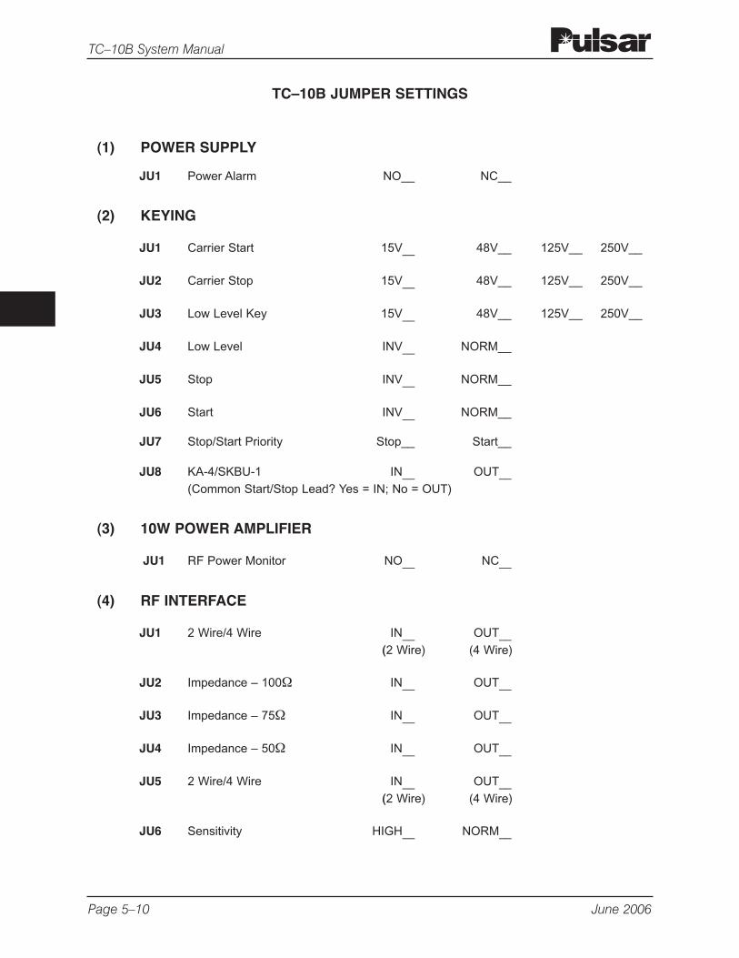
Page 5–10 June 2006
TC–10B System Manual
TC–10B JUMPER SETTINGS
(1) POWER SUPPLY
JU1 Power Alarm NO__ NC__
(2) KEYING
JU1 Carrier Start 15V__ 48V__ 125V__ 250V__
JU2 Carrier Stop 15V__ 48V__ 125V__ 250V__
JU3 Low Level Key 15V__ 48V__ 125V__ 250V__
JU4 Low Level INV__ NORM__
JU5 Stop INV__ NORM__
JU6 Start INV__ NORM__
JU7 Stop/Start Priority Stop__ Start__
JU8 KA-4/SKBU-1 IN__ OUT__
(Common Start/Stop Lead? Yes = IN; No = OUT)
(3) 10W POWER AMPLIFIER
JU1 RF Power Monitor NO__ NC__
(4) RF INTERFACE
JU1 2 Wire/4 Wire IN__ OUT__
(2 Wire) (4 Wire)
JU2 Impedance – 100Ω IN__ OUT__
JU3 Impedance – 75Ω IN__ OUT__
JU4 Impedance – 50Ω IN__ OUT__
JU5 2 Wire/4 Wire IN__ OUT__
(2 Wire) (4 Wire)
JU6 Sensitivity HIGH__ NORM__
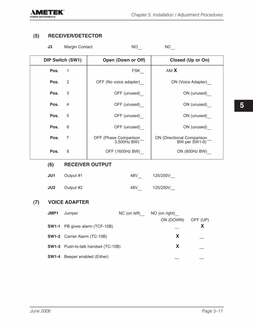
June 2006 Page 5–11
5
(5) RECEIVER/DETECTOR
J3 Margin Contact NO__ NC__
(6) RECEIVER OUTPUT
JU1 Output #1 48V__ 125/250V__
JU2 Output #2 48V__ 125/250V__
(7) VOICE ADAPTER
JMP1 Jumper NC (on left)__ NO (on right)__
ON (DOWN) OFF (UP)
SW1-1 PB gives alarm (TCF-10B) __ X
SW1-2 Carrier Alarm (TC-10B) X __
SW1-3 Push-to-talk handset (TC-10B) X __
SW1-4 Beeper enabled (Either) __ __
Chapter 5. Installation / Adjustment Procedures
DIP Switch (SW1) Open (Down or Off) Closed (Up or On)
Pos. 1 FSK__ AM X
Pos. 2 OFF (No voice adapter)__ ON (Voice Adapter)__
Pos. 3 OFF (unused)__ ON (unused)__
Pos. 4 OFF (unused)__ ON (unused)__
Pos. 5 OFF (unused)__ ON (unused)__
Pos. 6 OFF (unused)__ ON (unused)__
Pos. 7 OFF (Phase Comparison__ ON (Directional Comparison__3,500Hz BW) BW per SW1-8)
Pos. 8 OFF (1600Hz BW)__ ON (800Hz BW)__
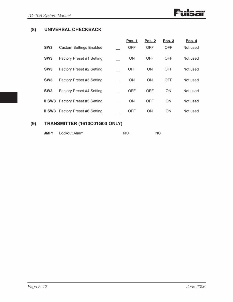
Page 5–12 June 2006
TC–10B System Manual
(8) UNIVERSAL CHECKBACK
Pos. 1 Pos. 2 Pos. 3 Pos. 4
SW3 Custom Settings Enabled __ OFF OFF OFF Not used
SW3 Factory Preset #1 Setting __ ON OFF OFF Not used
SW3 Factory Preset #2 Setting __ OFF ON OFF Not used
SW3 Factory Preset #3 Setting __ ON ON OFF Not used
SW3 Factory Preset #4 Setting __ OFF OFF ON Not used
|| SW3 Factory Preset #5 Setting __ ON OFF ON Not used
|| SW3 Factory Preset #6 Setting __ OFF ON ON Not used
(9) TRANSMITTER (1610C01G03 ONLY)
JMP1 Lockout Alarm NO__ NC__
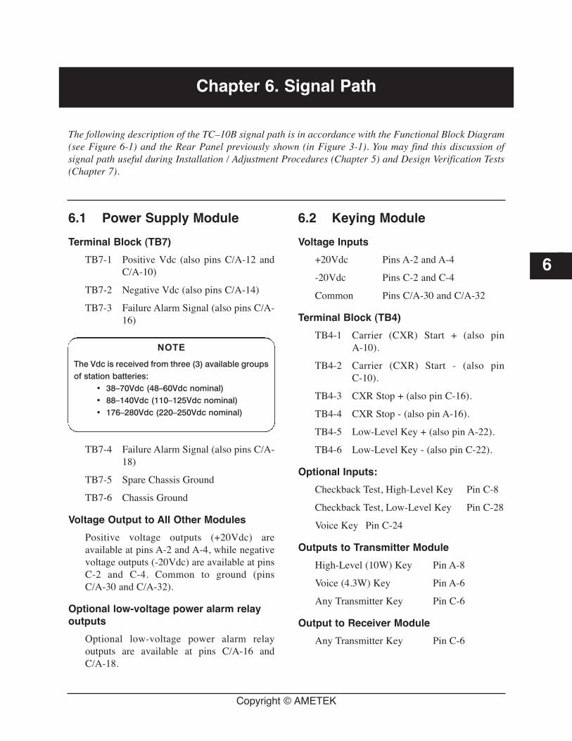
6.1 Power Supply Module
Terminal Block (TB7)
TB7-1 Positive Vdc (also pins C/A-12 andC/A-10)
TB7-2 Negative Vdc (also pins C/A-14)
TB7-3 Failure Alarm Signal (also pins C/A-16)
TB7-4 Failure Alarm Signal (also pins C/A-18)
TB7-5 Spare Chassis Ground
TB7-6 Chassis Ground
Voltage Output to All Other Modules
Positive voltage outputs (+20Vdc) areavailable at pins A-2 and A-4, while negativevoltage outputs (-20Vdc) are available at pinsC-2 and C-4. Common to ground (pinsC/A-30 and C/A-32).
Optional low-voltage power alarm relayoutputs
Optional low-voltage power alarm relayoutputs are available at pins C/A-16 andC/A-18.
6.2 Keying Module
Voltage Inputs
+20Vdc Pins A-2 and A-4
-20Vdc Pins C-2 and C-4
Common Pins C/A-30 and C/A-32
Terminal Block (TB4)
TB4-1 Carrier (CXR) Start + (also pin A-10).
TB4-2 Carrier (CXR) Start - (also pin C-10).
TB4-3 CXR Stop + (also pin C-16).
TB4-4 CXR Stop - (also pin A-16).
TB4-5 Low-Level Key + (also pin A-22).
TB4-6 Low-Level Key - (also pin C-22).
Optional Inputs:
Checkback Test, High-Level Key Pin C-8
Checkback Test, Low-Level Key Pin C-28
Voice Key Pin C-24
Outputs to Transmitter Module
High-Level (10W) Key Pin A-8
Voice (4.3W) Key Pin A-6
Any Transmitter Key Pin C-6
Output to Receiver Module
Any Transmitter Key Pin C-6
Copyright © AMETEK
Chapter 6. Signal Path
6
The following description of the TC–10B signal path is in accordance with the Functional Block Diagram(see Figure 6-1) and the Rear Panel previously shown (in Figure 3-1). You may find this discussion ofsignal path useful during Installation / Adjustment Procedures (Chapter 5) and Design Verification Tests(Chapter 7).
NOTE
The Vdc is received from three (3) available groupsof station batteries:
• 38–70Vdc (48–60Vdc nominal)• 88–140Vdc (110–125Vdc nominal)• 176–280Vdc (220–250Vdc nominal)
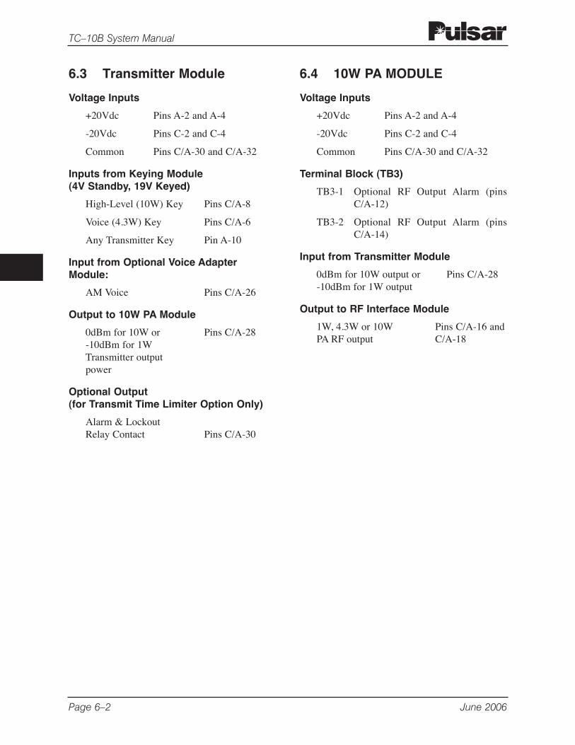
6.3 Transmitter Module
Voltage Inputs
+20Vdc Pins A-2 and A-4
-20Vdc Pins C-2 and C-4
Common Pins C/A-30 and C/A-32
Inputs from Keying Module (4V Standby, 19V Keyed)
High-Level (10W) Key Pins C/A-8
Voice (4.3W) Key Pins C/A-6
Any Transmitter Key Pin A-10
Input from Optional Voice AdapterModule:
AM Voice Pins C/A-26
Output to 10W PA Module
0dBm for 10W or Pins C/A-28-10dBm for 1WTransmitter output power
Optional Output(for Transmit Time Limiter Option Only)
Alarm & LockoutRelay Contact Pins C/A-30
6.4 10W PA MODULE
Voltage Inputs
+20Vdc Pins A-2 and A-4
-20Vdc Pins C-2 and C-4
Common Pins C/A-30 and C/A-32
Terminal Block (TB3)
TB3-1 Optional RF Output Alarm (pinsC/A-12)
TB3-2 Optional RF Output Alarm (pinsC/A-14)
Input from Transmitter Module
0dBm for 10W output or Pins C/A-28-10dBm for 1W output
Output to RF Interface Module
1W, 4.3W or 10W Pins C/A-16 and PA RF output C/A-18
Page 6–2 June 2006
TC–10B System Manual
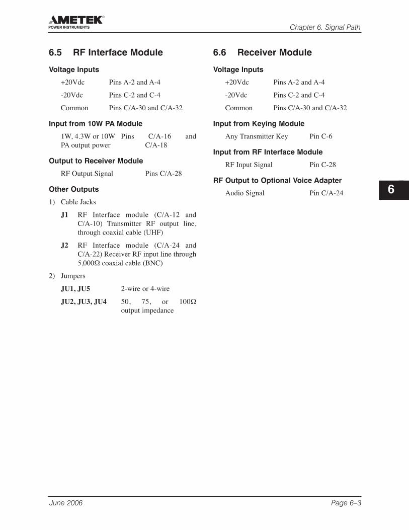
6.5 RF Interface Module
Voltage Inputs
+20Vdc Pins A-2 and A-4
-20Vdc Pins C-2 and C-4
Common Pins C/A-30 and C/A-32
Input from 10W PA Module
1W, 4.3W or 10W Pins C/A-16 and PA output power C/A-18
Output to Receiver Module
RF Output Signal Pins C/A-28
Other Outputs
1) Cable Jacks
J1 RF Interface module (C/A-12 andC/A-10) Transmitter RF output line,through coaxial cable (UHF)
J2 RF Interface module (C/A-24 andC/A-22) Receiver RF input line through5,000Ω coaxial cable (BNC)
2) Jumpers
JU1, JU5 2-wire or 4-wire
JU2, JU3, JU4 50, 75, or 100Ωoutput impedance
6.6 Receiver Module
Voltage Inputs
+20Vdc Pins A-2 and A-4
-20Vdc Pins C-2 and C-4
Common Pins C/A-30 and C/A-32
Input from Keying Module
Any Transmitter Key Pin C-6
Input from RF Interface Module
RF Input Signal Pin C-28
RF Output to Optional Voice Adapter
Audio Signal Pin C/A-24
June 2006 Page 6–3
Chapter 6. Signal Path
6
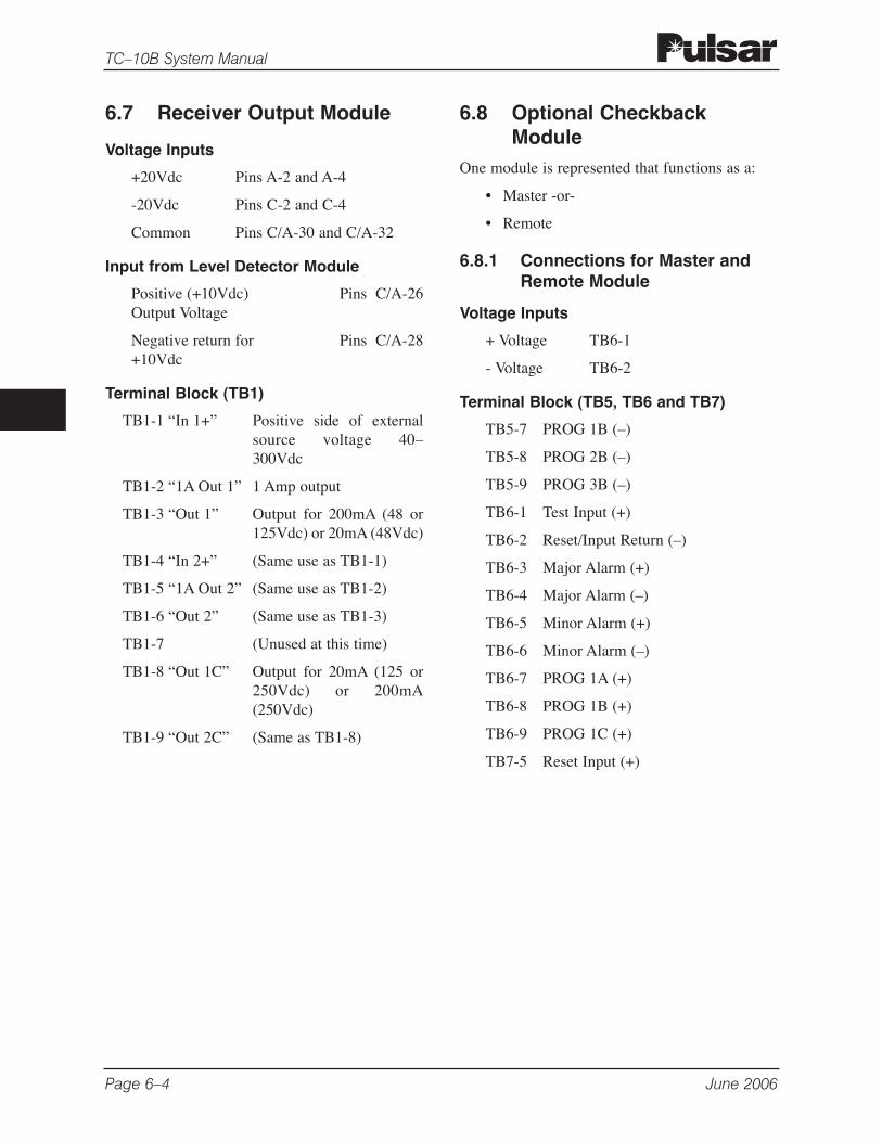
6.7 Receiver Output Module
Voltage Inputs
+20Vdc Pins A-2 and A-4
-20Vdc Pins C-2 and C-4
Common Pins C/A-30 and C/A-32
Input from Level Detector Module
Positive (+10Vdc) Pins C/A-26Output Voltage
Negative return for Pins C/A-28+10Vdc
Terminal Block (TB1)
TB1-1 “In 1+” Positive side of externalsource voltage 40–300Vdc
TB1-2 “1A Out 1” 1 Amp output
TB1-3 “Out 1” Output for 200mA (48 or125Vdc) or 20mA (48Vdc)
TB1-4 “In 2+” (Same use as TB1-1)
TB1-5 “1A Out 2” (Same use as TB1-2)
TB1-6 “Out 2” (Same use as TB1-3)
TB1-7 (Unused at this time)
TB1-8 “Out 1C” Output for 20mA (125 or250Vdc) or 200mA(250Vdc)
TB1-9 “Out 2C” (Same as TB1-8)
6.8 Optional CheckbackModule
One module is represented that functions as a:
• Master -or-
• Remote
6.8.1 Connections for Master andRemote Module
Voltage Inputs
+ Voltage TB6-1
- Voltage TB6-2
Terminal Block (TB5, TB6 and TB7)
TB5-7 PROG 1B (–)
TB5-8 PROG 2B (–)
TB5-9 PROG 3B (–)
TB6-1 Test Input (+)
TB6-2 Reset/Input Return (–)
TB6-3 Major Alarm (+)
TB6-4 Major Alarm (–)
TB6-5 Minor Alarm (+)
TB6-6 Minor Alarm (–)
TB6-7 PROG 1A (+)
TB6-8 PROG 1B (+)
TB6-9 PROG 1C (+)
TB7-5 Reset Input (+)
Page 6–4 June 2006
TC–10B System Manual
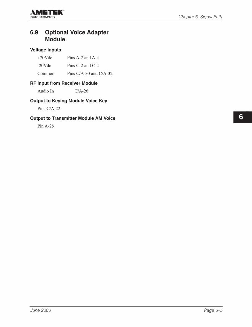
6.9 Optional Voice AdapterModule
Voltage Inputs
+20Vdc Pins A-2 and A-4
-20Vdc Pins C-2 and C-4
Common Pins C/A-30 and C/A-32
RF Input from Receiver Module
Audio In C/A-26
Output to Keying Module Voice Key
Pins C/A-22
Output to Transmitter Module AM Voice
Pin A-28
June 2006 Page 6–5
Chapter 6. Signal Path
6
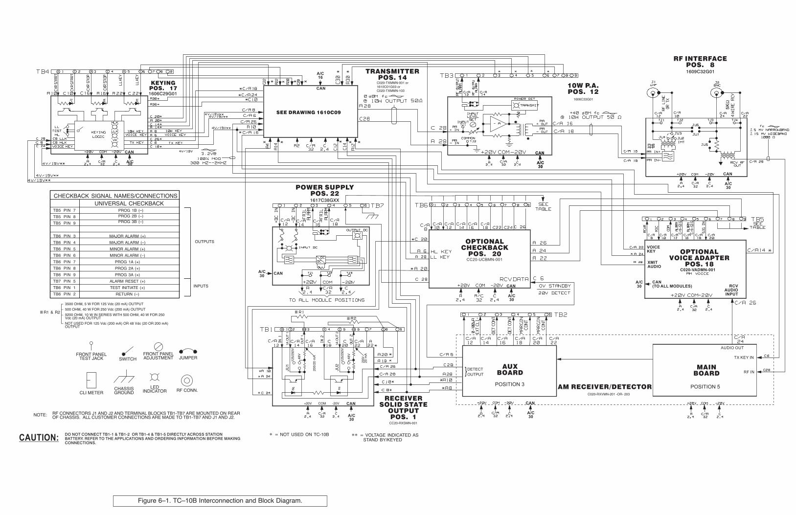
+20V -20VCOM
1AO
UT
1
1AO
UT
2
OU
T1
125/
250V
48V
JU1
JU2
125/
250V
48V
TB5 PIN 7
TB5 PIN 8
TB5 PIN 9
TB6 PIN 3
TB6 PIN 4
TB6 PIN 5
TB6 PIN 6
TB6 PIN 7
TB6 PIN 8
TB6 PIN 9
TB7 PIN 5
TB6 PIN 1
TB6 PIN 2
PROG 1B (–)PROG 2B (–)PROG 3B (–)
OUTPUTS
INPUTS
R1 & R2
MAJOR ALARM (+)
MINOR ALARM (+)
MAJOR ALARM (–)
MINOR ALARM (–)
PROG 1A (+)
PROG 2A (+)
PROG 3A (+)
ALARM RESET (+)
TEST INITIATE (+)
RETURN (–)
CHECKBACK SIGNAL NAMES/CONNECTIONSUNIVERSAL CHECKBACK
** = VOLTAGE INDICATED ASSTAND BY/KEYED
* = NOT USED ON TC-10B
NOTE: RF CONNECTORS J1 AND J2 AND TERMINAL BLOCKS TB1-TB7 ARE MOUNTED ON REAROF CHASSIS. ALL CUSTOMER CONNECTIONS ARE MADE TO TB1-TB7 AND J1 AND J2.
FRONT PANELTEST JACK SWITCH
FRONT PANELADJUSTMENT
CLI METERCHASSISGROUND
LEDINDICATOR
JUMPER
RF CONN.
TRANSMITTERPOS. 14
POWER SUPPLYPOS. 22
KEYINGPOS. 17
RECEIVERSOLID STATE
OUTPUTPOS. 1
OPTIONALVOICE ADAPTER
POS. 18
MAINBOARD
AUXBOARD
AM RECEIVER/DETECTOR
AUDIO OUT
TX KEY IN
RF IN
RF INTERFACEPOS. 8
10W P.A.POS. 12
OPTIONALCHECKBACK
POS. 20CC20-UCBMN-001
SEE DRAWING 1610C09
200/
20m
A
200/
20m
A
– 3500 OHM, 5 W FOR 125 Vdc (20 mA) OUTPUT
– 500 OHM, 40 W FOR 250 Vdc (200 mA) OUTPUT
– 9200 OHM, 10 W IN SERIES WITH 500 OHM, 40 W FOR 250Vdc (20 mA) OUTPUT
– NOT USED FOR 125 Vdc (200 mA) OR 48 Vdc (20 OR 200 mA)OUTPUT
CC20-RXSMN-001
DETECT
OUTPUT
POSITION 3POSITION 5
C020-RXVMN-201 -OR- 203
C020-TXMMN-001 or1610C01G03 orC020-TXMMN-103
1606C33G01
A/C30
CAN
A/C30
CAN
A/C30
CAN
A/C30
CAN
A/C30
CAN
A/C16
CAN
DO NOT CONNECT TB1-1 & TB1-2 OR TB1-4 & TB1-5 DIRECTLY ACROSS STATIONBATTERY. REFER TO THE APPLICATIONS AND ORDERING INFORMATION BEFORE MAKINGCONNECTIONS.
CAUTION:
A/C30
CAN
A/C30
CAN
A/C30
CAN
A/C30
CAN(TO ALL MODULES)
XMITAUDIO
VOICEKEY
RCVAUDIOINPUT
C020-VADMN-001
1606C29G01
1609C32G01
5K
W
1617C38GXX
Figure 6–1. TC–10B Interconnection and Block Diagram.

Page 6–6 June 2006
TC–10B System Manual
USER NOTES
7.1 Preliminary Checks
7.1.1 Check Chassis Nameplate.Verify that the proper dc supply voltage andmodule options are on the chassis nameplate.
Check to ensure that all required modules aresupplied and are installed in the proper chassisslots. The slots are labeled on the top edge of thechassis.
7.1.2 Check for Band-pass FilterType on Receiver Module
Check SW1 for correct setting for AM.
7.1.3 Inspecting for the Correct dcVoltage
With the power “OFF,” remove the Power SupplyModule and inspect it for the correct dc voltage, asspecified in Table 7-1.
7.2 Preliminary SettingsBefore starting the test, set the jumpers on thevarious modules according to the instructions inthe sections below.
7.2.1 Power Supply ModuleJUl N.C. (loss of power condition)
7.2.2 Keying ModuleJU1 Set to dc supply voltage
JU2 Set to dc supply voltage
JU3 Set to dc supply voltage
JU4 NORM
JU5 NORM
JU6 NORM
JU7 STOP
JU8 OUT
7.2.3 Transmitter ModuleSet the four rotary switches to 250kHz or desiredfrequency.
7.2.4 10W PA ModuleJUl N.C. (loss of power condition)
7.2.5 RF Interface Module
Matching Impedance Jumper
JU4 (50Ω)
2-Wire or 4-Wire RF Termination
JU1/JU5 (out, 4 wire)
Attenuator Override Jumper
JU6 (NORM Sensitivity)
Copyright © AMETEK
Chapter 7. Design Verification Tests
7
It is not intended to perform the Design Verification tests at installation. If you need to verify the designof the TC-10B, you should perform the following Verification Test (See Test Equipment in Chapter 4 andSignal Path in Chapter 6). Otherwise See Chapter 5.
Table 7–1. Voltage Specifications.
Style #Specified 1617C38GXX
48V with Alarm Relay G01
125V with Alarm Relay G02
250V with Alarm Relay G03
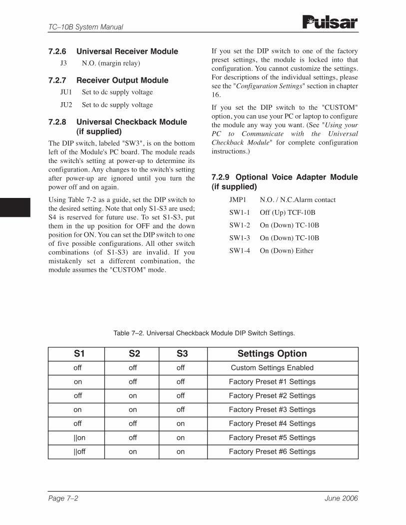
Page 7–2 June 2006
TC–10B System Manual
7.2.6 Universal Receiver ModuleJ3 N.O. (margin relay)
7.2.7 Receiver Output ModuleJU1 Set to dc supply voltage
JU2 Set to dc supply voltage
7.2.8 Universal Checkback Module (if supplied)
The DIP switch, labeled "SW3", is on the bottomleft of the Module's PC board. The module readsthe switch's setting at power-up to determine itsconfiguration. Any changes to the switch's settingafter power-up are ignored until you turn thepower off and on again.
Using Table 7-2 as a guide, set the DIP switch tothe desired setting. Note that only S1-S3 are used;S4 is reserved for future use. To set S1-S3, putthem in the up position for OFF and the downposition for ON. You can set the DIP switch to oneof five possible configurations. All other switchcombinations (of S1-S3) are invalid. If youmistakenly set a different combination, themodule assumes the "CUSTOM" mode.
If you set the DIP switch to one of the factorypreset settings, the module is locked into thatconfiguration. You cannot customize the settings.For descriptions of the individual settings, pleasesee the "Configuration Settings" section in chapter16.
If you set the DIP switch to the "CUSTOM"option, you can use your PC or laptop to configurethe module any way you want. (See "Using yourPC to Communicate with the UniversalCheckback Module" for complete configurationinstructions.)
7.2.9 Optional Voice Adapter Module(if supplied)
JMP1 N.O. / N.C.Alarm contact
SW1-1 Off (Up) TCF-10B
SW1-2 On (Down) TC-10B
SW1-3 On (Down) TC-10B
SW1-4 On (Down) Either
S1 S2 S3 Settings Optionoff off off Custom Settings Enabled
on off off Factory Preset #1 Settings
off on off Factory Preset #2 Settings
on on off Factory Preset #3 Settings
off off on Factory Preset #4 Settings
||on off on Factory Preset #5 Settings
||off on on Factory Preset #6 Settings
Table 7–2. Universal Checkback Module DIP Switch Settings.
7.3 ELECTRICAL TESTS1. Refer to Figure 3-4 or Figure 7-1 for keying
and output connections.
2. Connect the dc supply to the appropriateterminals on the rear panel (see Figure 3-4 orFigure 7-1).
3. Terminate the Transmitter output with anoninductive 50Ω, 10W resistor.
4. Connect the Selective Level Meter (Rycom6021A) across the 50Ω resistor load.
5. Allow a one-hour warm-up period beforemaking the final frequency adjustments.
7.3.1 Power Supply Module Tests1. Remove all modules except for the Power
Supply Module.
2. Turn “ON” the dc power; measure the dcvoltage at the Power Supply test jacks withthe meter reference connected to TJ2:
• TJ1/TJ2 (+20Vdc ± 1Vdc).
• TJ3/TJ2 (-20Vdc ± 1Vdc).
3. Turn “OFF” the dc power.Insert all modules into their appropriate slotsin the chassis.
4. Repeat Step 2 (above). Both LEDs (D3, Input,and Dl1, Output) on the Power SupplyModule must be “ON”.
5. Place the current meter (Fluke 75 or equiva-lent) in series with the dc supply, and checkthe standby (unkeyed) current for the appro-priate voltage source, as follows:
VOLTAGE CURRENT
48Vdc 0.6A to 0.8A
125Vdc 0.2A to 0.3A ||
250Vdc 0.1A to 0.2A
7.3.2 Transmitter Module Tests
Levels
1. Using the appropriate voltage (15V, 48V,125V, or 250V), key the carrier start andobserve that the level across the 50Ω load isapproximately 10W per Table 7-3.
2. Using the Keying Module push buttonswitches, key the Transmitter (XMTR)Module for low-level (LL/1 W) and high-level (HL/10 W) power, as shown in the tablebelow. If the voltage across the 50Ω load isnot approximately equal to the value shown inTable 7-3, place the Transmitter (XMTR)Module on an extender board and makeadjustments (using R13 for 10W and R12 for1W, respectively).
3. Using the keying inputs on the rear of thechassis, key the Transmitter using the combi-nations listed below. Observe the output levelsand logic per Table 7-4:
June 2006 Page 7–3
Chapter 7. Design Verification Tests
7
! CAUTIONALWAYS TURN “OFF’ dc POWER WHENEVERREMOVING OR INSTALLING MODULES.
NOTE
Prolonged operation with no load can cause thepower supply to shut down (see Chapter 9,Section 9.2.2).
NOTE
For the optional Transmit Time Limiter Transmittermodule, you must hold the Alarm ResetPushbutton in while doing these tests or it will turnoff.
Keyed Volts Across XMTR dBm REFLevel 50Ω Load Adjust
(V rms)
LL – 1 W 7.07 R12 +30dBm
HL – 10 W 22.4 R13 +40dBm
Table 7–3. Voltage Levels.
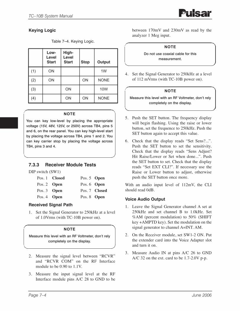
Keying Logic
7.3.3 Receiver Module TestsDIP switch (SW1)
Pos. 1 Closed Pos. 5 Open
Pos. 2 Open Pos. 6 Open
Pos. 3 Open Pos. 7 Closed
Pos. 4 Open Pos. 8 Open
Received Signal Path
1. Set the Signal Generator to 250kHz at a levelof 1.0Vrms (with TC-10B power on).
2. Measure the signal level between “RCVR”and “RCVR COM” on the RF Interfacemodule to be 0.90 to 1.1V.
3. Measure the input signal level at the RFInterface module pins A/C 28 to GND to be
between 170mV and 230mV as read by theanalyzer 1 Meg input.
4. Set the Signal Generator to 250kHz at a levelof 112 mVrms (with TC-10B power on).
5. Push the SET button. The frequency displaywill begin flashing. Using the raise or lowerbutton, set the frequence to 250kHz. Push theSET button again to accept this value.
6. Check that the display reads “Set Sens?...”.Push the SET button to set the sensitivity.Check that the display reads “Sens Adjust?Hit Raise/Lower or Set when done...”. Pushthe SET button to set. Check that the displayreads “Set EXT CLI?”. If necessary use theRaise or Lower button to adjust, otherwisepush the SET button once more.
With an audio input level of 112mV, the CLIshould read 0dB.
Voice Audio Output
1. Leave the Signal Generator channel A set at250kHz and set channel B to 1.0kHz. Set%AM (percent modulation) to 50% (SHIFTkey +AMPTD key). Set the modulation on thesignal generator to channel A=INT. AM.
2. On the Receiver module, set SW1-2 ON. Putthe extender card into the Voice Adapter slotand turn it on.
3. Measure Audio IN at pins A/C 26 to GNDA/C 32 on the ext. card to be 1.7-2.0V p-p.
Page 7–4 June 2006
TC–10B System Manual
Low- High- Level Level Start Start Stop Output
(1) ON 1W
(2) ON ON NONE
(3) ON 10W
(4) ON ON NONE
Table 7–4. Keying Logic.
NOTE
You can key low-level by placing the appropriatevoltage (15V, 48V, 125V, or 250V) across TB4, pins 5and 6, on the rear panel. You can key high-level startby placing the voltage across TB4, pins 1 and 2. Youcan key carrier stop by placing the voltage acrossTB4, pins 3 and 4.
NOTE
Measure this level with an RF Voltmeter, don’t relycompletely on the display.
NOTE
Do not use coaxial cable for this measurement.
NOTE
Measure this level with an RF Voltmeter, don’t relycompletely on the display.
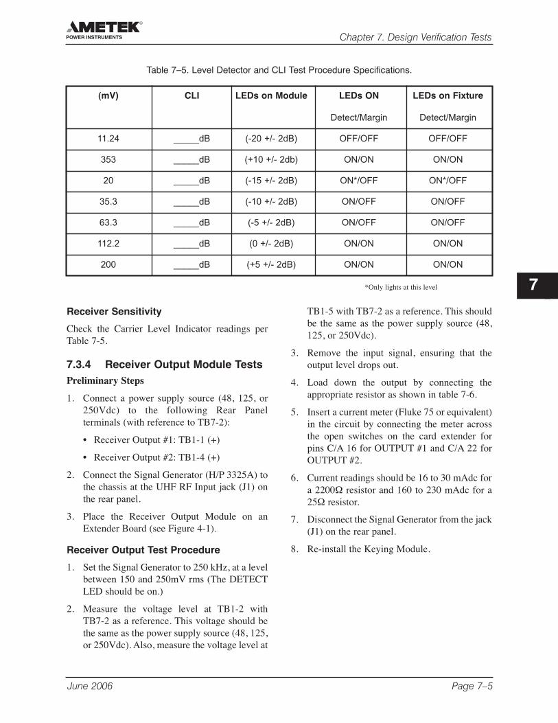
Receiver Sensitivity
Check the Carrier Level Indicator readings perTable 7-5.
7.3.4 Receiver Output Module TestsPreliminary Steps
1. Connect a power supply source (48, 125, or250Vdc) to the following Rear Panelterminals (with reference to TB7-2):
• Receiver Output #1: TB1-1 (+)
• Receiver Output #2: TB1-4 (+)
2. Connect the Signal Generator (H/P 3325A) tothe chassis at the UHF RF Input jack (J1) onthe rear panel.
3. Place the Receiver Output Module on anExtender Board (see Figure 4-1).
Receiver Output Test Procedure
1. Set the Signal Generator to 250 kHz, at a levelbetween 150 and 250mV rms (The DETECTLED should be on.)
2. Measure the voltage level at TB1-2 withTB7-2 as a reference. This voltage should bethe same as the power supply source (48, 125,or 250Vdc). Also, measure the voltage level at
TB1-5 with TB7-2 as a reference. This shouldbe the same as the power supply source (48,125, or 250Vdc).
3. Remove the input signal, ensuring that theoutput level drops out.
4. Load down the output by connecting theappropriate resistor as shown in table 7-6.
5. Insert a current meter (Fluke 75 or equivalent)in the circuit by connecting the meter acrossthe open switches on the card extender forpins C/A 16 for OUTPUT #1 and C/A 22 forOUTPUT #2.
6. Current readings should be 16 to 30 mAdc fora 2200Ω resistor and 160 to 230 mAdc for a25Ω resistor.
7. Disconnect the Signal Generator from the jack(J1) on the rear panel.
8. Re-install the Keying Module.
June 2006 Page 7–5
Chapter 7. Design Verification Tests
7
(mV) CLI LEDs on Module LEDs ON LEDs on Fixture
Detect/Margin Detect/Margin
11.24 _____dB (-20 +/- 2dB) OFF/OFF OFF/OFF
353 _____dB (+10 +/- 2db) ON/ON ON/ON
20 _____dB (-15 +/- 2dB) ON*/OFF ON*/OFF
35.3 _____dB (-10 +/- 2dB) ON/OFF ON/OFF
63.3 _____dB (-5 +/- 2dB) ON/OFF ON/OFF
112.2 _____dB (0 +/- 2dB) ON/ON ON/ON
200 _____dB (+5 +/- 2dB) ON/ON ON/ON
Table 7–5. Level Detector and CLI Test Procedure Specifications.
*Only lights at this level
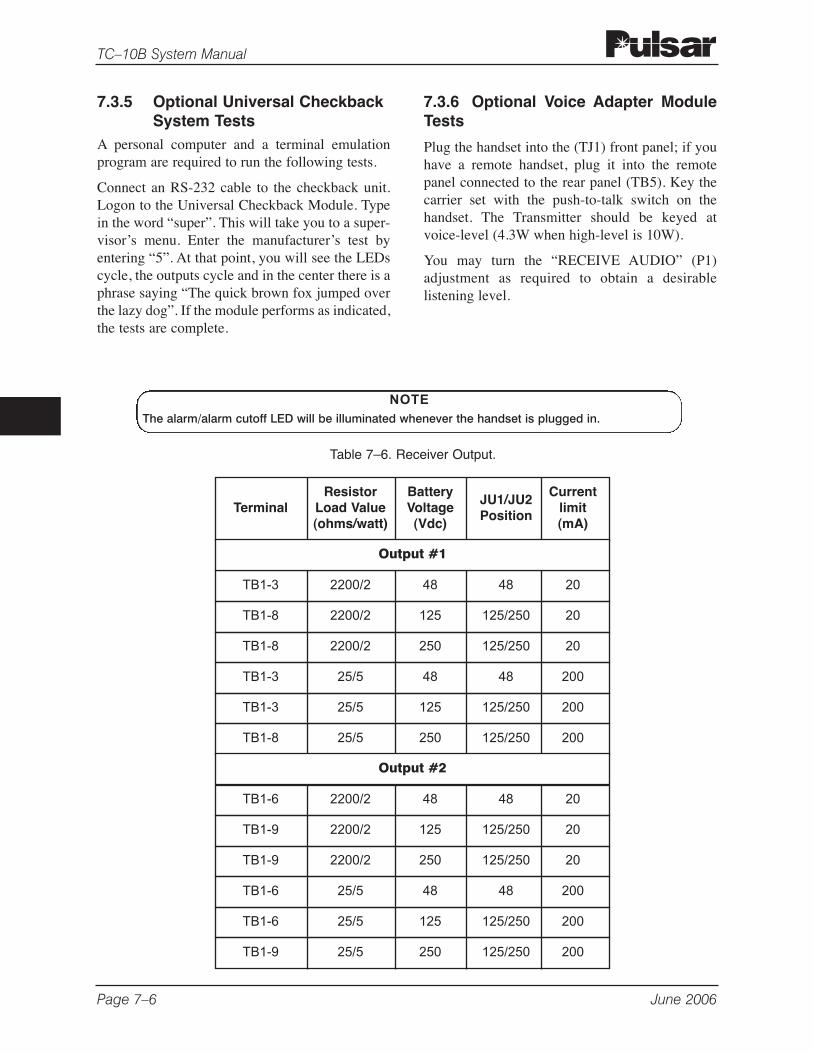
Page 7–6 June 2006
TC–10B System Manual
7.3.5 Optional Universal CheckbackSystem Tests
A personal computer and a terminal emulationprogram are required to run the following tests.
Connect an RS-232 cable to the checkback unit.Logon to the Universal Checkback Module. Typein the word “super”. This will take you to a super-visor’s menu. Enter the manufacturer’s test byentering “5”. At that point, you will see the LEDscycle, the outputs cycle and in the center there is aphrase saying “The quick brown fox jumped overthe lazy dog”. If the module performs as indicated,the tests are complete.
7.3.6 Optional Voice Adapter ModuleTests
Plug the handset into the (TJ1) front panel; if youhave a remote handset, plug it into the remotepanel connected to the rear panel (TB5). Key thecarrier set with the push-to-talk switch on thehandset. The Transmitter should be keyed atvoice-level (4.3W when high-level is 10W).
You may turn the “RECEIVE AUDIO” (P1)adjustment as required to obtain a desirablelistening level.
Resistor Battery JU1/JU2
Current Terminal Load Value Voltage
Positionlimit
(ohms/watt) (Vdc) (mA)
TB1-3 2200/2 48 48 20
TB1-8 2200/2 250 125/250 20
TB1-8 2200/2 125 125/250 20
TB1-3 25/5 125 125/250 200
TB1-3 25/5 48 48 200
TB1-8 25/5 250 125/250 200
TB1-6 2200/2 48 48 20
TB1-9 2200/2 250 125/250 20
TB1-9 2200/2 125 125/250 20
TB1-6 25/5 125 125/250 200
TB1-6 25/5 48 48 200
TB1-9 25/5 250 125/250 200
Table 7–6. Receiver Output.
Output #2
Output #1
NOTEThe alarm/alarm cutoff LED will be illuminated whenever the handset is plugged in.
8.1 Precautions WhenSelecting Test Equipment
(See Chapter 4 for test equipment specifications.)
To prevent damage to solid-state components andcircuits:
1) Use transformer-type signal generators,VTVMs and signal tracers, which isolatethe test equipment from the power line.Whenever the test equipment uses a trans-formerless power supply, use an isolationtype transformer. The test equipmentground should be isolated from the acsource ground.
2) Use multi-meters with at least 20,000Ohms-per-volt sensitivity.
8.2 Precautions When UsingTest Equipment
1. Use a common ground between the chassis ofthe test equipment and the transistorequipment.
2. When testing transistors and diodes, givespecial attention to the polarity of the meterleads.
For example: When measuring the forwardresistance of a diode using a meter that has theinternal battery connected to the meteringcircuit, be sure that:
• The lead marked ( + ) touches the diodeanode.
• The lead marked ( – ) touches the diodecathode.
3. When checking circuits with an oscillographicprobe, be sure to discharge any built-upcapacitive voltage by touching the probe to aground before touching the circuit.
When individual module maintenance is required, either at the factory or at the customer installation(beyond the scope of routine alignment), the following procedures are applicable.
Copyright © AMETEK
Chapter 8. Maintenance
8
! CAUTIONHIGH CURRENTS FROM A LOW-SENSITIVITYMETER CAN DAMAGE SOLID STATE DEVICES.
! CAUTIONMETERING TRANSISTOR CIRCUITS CANCAUSE DAMAGE. FOR EXAMPLE: A BASE-TO-COLLECTOR SHORT DURING TRANSISTOROPERATION CAN DESTROY THE TRANSISTOR.
8.3 Periodic ChecksEvery six months, take the following readings onthe TC–10B Test Jacks (at the control panel).
We recommend that you keep a log book as avisible record of periodic checks, as well as asource for indicating any gradual degradation in amodule’s performance.
8.3.1 Power Supply ModuleTJ1 +20Vdc
TJ2 Common
TJ3 -20Vdc
8.3.2 Keying ModuleNone.
8.3.3 Transmitter ModuleNone.
8.3.4 10W PA ModuleTJ1 Input
TJ2 Common
8.3.5 RF Interface ModuleTJ1 Line In
TJ2 Line Common
TJ3 Receiver In
TJ4 Receiver Common
8.3.6 Receiver ModuleTJ1 Input
TJ2 Receive
TJ3 Common
8.3.7 Level Detector and CLI ModuleNone.
8.3.8 Receiver Output ModuleNone.
8.3.9 Optional Universal CheckbackModule
None.
8.3.10 Optional Voice Adapter ModuleNone.
8.4 InspectionA program of routine visual inspection shouldinclude:
• Condition of cabinet or other housing
• Tightness of mounting hardware and fuses
• Proper seating of plug-in relays and sub-assemblies
• Condition of internal and external wiring(the location where external wiring entersthe cabinet should be sealed)
• Appearance of printed circuit boards andcomponents
• Signs of overheating in equipment:
• Interference with proper heat dissipationfrom surfaces
• Clogged air vents (air filters should beremoved and washed out)
• Dust which may cause short-circuits
Page 8–2 June 2006
TC–10B System Manual
8.5 Solid-State MaintenanceTechniques
Use the following techniques when servicing solidstate equipment.
8.5.1 Preliminary Precautions1. To avoid damage to circuits and components
from a current surge, disconnect power beforereplacing or removing components or circuits.
2. Before placing new components into adefective circuit, check the circuit so that itcannot damage the new components.
8.5.2 Trouble-Detection Sequence1. Evaluate test jack readings and other records
of routine alignment.
2. Evaluate any symptoms detected audibly orvisually.
3. Replace suspected plug-in components.
4. Further isolation of faults includes:
• Voltage readings
• Resistance readings
• Signal injection
• Re-alignment
• Sensitivity measurements
• Gain measurements
5. Replace suspected faulty components.
6. Check-out and adjust affected circuits.
June 2006 Page 8–3
Chapter 8. Maintenance
8
! CAUTIONWE RECOMMEND THAT THE USER OF THISEQUIPMENT BECOME ACQUAINTED WITH THEINFORMATION IN THESE INSTRUCTIONSBEFORE ENERGIZING THE TC–10B AND ASSO-CIATED ASSEMBLIES. FAILURE TO OBSERVETHIS PRECAUTION MAY RESULT IN DAMAGETO THE EQUIPMENT.
YOU SHOULD NEITHER REMOVE OR INSERTPRINTED CIRCUIT MODULES WHILE THETC–10B IS ENERGIZED. FAILURE TO OBSERVETHIS PRECAUTION CAN RESULT INCOMPONENT DAMAGE.
ALL INTEGRATED CIRCUITS USED ON THEMODULES ARE SENSITIVE TO AND CAN BEDAMAGED BY THE DISCHARGE OF STATICELECTRICITY. BE SURE TO OBSERVE ELEC-TROSTATIC DISCHARGE PRECAUTIONS WHENHANDLING MODULES OR INDIVIDUAL COMPO-NENTS.
8.5.3 Servicing ComponentsSoldered Directly to Terminals
1. Avoid overheating from soldering by using alow-wattage soldering iron (i.e., 60Wmaximum).
2. Make sure there is no current leakage from thesoldering iron.
3. When soldering leads from transistors ordiodes, use heat sinks, e.g., alligator clips.
4. You can remove molten solder from the boardwith a desoldering tool.
5. When removing a multi-lead component froma printed circuit board, first cut all leads andthen remove the leads individually (to preventoverheating). If there are only a few leads,you can use a broad-tip soldering iron.
8.5.4 Servicing ComponentsMounted Directly on HeatSinks
1. Remove the heat sink and bracket from thechassis by loosening the securing devices.
2. Remove the transistor, diode, or other devicefrom the heat sink.
3. When replacing the transistor, diode, or otherdevice, make certain that the device and theheat sink make secure contact for good heatdissipation. Mount a device first on the heatsink, and then on the board. Also, make surethat you replace all insulators, washers, spring
washers and other mounting hardware as youoriginally found them.
8.5.5 Servicing Metal OxideSemiconductor (MOS) Devices
MOS devices may be vulnerable to static changes.Be sure to observe the special precautionsdescribed below both before and during assembly.
Precautions to take before assembly
• Avoid wearing silk or nylon clothing, asthis contributes to static buildup.
• Avoid carpeted areas and dry environ-ments.
• Discharge body static by placing bothhands on a metal, earth-grounded surface.
Precautions to take during assembly
• Wear a ground strap during assembly
• Avoid touching electrically conductivecircuit parts by hand
• When removing a module from the chassis,always place it on a conductive surfacewhich is grounded through a resistance ofapproximately 100KΩ
• Make sure that all electrically powered testequipment is properly grounded.
Page 8–4 June 2006
TC–10B System Manual
NOTE
You may use an isolation transformer to preventcurrent leakage.
NOTE
We recommend a very light coating of DC-4 (Dow-Corning 4 Compound Silicon Lubricant) fortransistors and diodes that are mounted on heatsinks.
! CAUTIONAVOID THE POSSIBILITY OF ELECTROSTATICDISCHARGE.
NOTE
Before touching a module with a test probe,connect the ground lead from the test equipmentto the module. Always disconnect the test probebefore removing the ground lead equipment.

9.1 Power Supply ModuleDescription
The Power Supply Module for theTC–10B/TCF–10B has dual dc/dc high-frequencyswitching regulators which generate regulatedvoltage outputs of ±20Vdc (between 1.5A and2.0A for operation of the TC–10B/TCF–10Bmodules. It also provides protection from batterysurge, transients, short circuits, and reversevoltage. The Power Supply Module can receiveinputs from three available groups of stationbatteries: 38-70Vdc, 88-140Vdc, and 176-280Vdc.
9.1.1 Power Supply Control Panel (This panel is shown in Figure 9-1.)
Front panel controls are as follows:
1) Push button Switch (with power-onindicator), ON/OFF (S1).
2) LEDs for indicating power:
• INPUT, Red (LED1)
• OUTPUT, Red (LED2)
3) Test Jacks:
• +20Vdc, Red (TP3)
• Common, Green (TP2)
• -20Vdc, Black (TP1)
An optional low-voltage alarm relay indicatingloss of power is available. When the alarm isactivated, LED2 is “OFF”. LED1 may be “OFF”if input power is lost.
Schematic 1617C38-2
Parts List 1617C38-2
Copyright © AMETEK
Chapter 9. Power Supply Module
9
Table 9–1. 1617C38 Styles and Descriptions.
Group Description
G01 48V WITH ALARM RELAY
G02 125V WITH ALARM RELAY
G03 250V WITH ALARM RELAY
POWER
INPUT
OUTPUT
+20V
COMMON
–20V
POWER SUPPLY
Figure 9–1. Power Supply Module Front Panel.
9.1.2 Power Supply PC BoardFigure 9-2 shows component locations for thePower Supply Module.
Control is as follows:
Jumper J1 for optional Alarm Relay; estab-lishes loss of power condition (NO/NC).
9.2 Power Supply CircuitDescription
The module comprises the following circuits:
• Fuses
• ON/OFF Switch
• Input Filter
• Power Alarm Failure Relay
• dc/dc Converter (2)
• Output Filter
Fuses
48V 125V 250V
F1, F2 3A 1.6A 3/4A
ON/OFF Switch
S1 - Push button Switch (DPDT)
When in the “ON” position (pins 1 and 4), dccurrent flows through the input filter to the dc/dcconverter.
Input Filter
The input filter (C1, C2, C3) contains zener diodes(Z1, Z2) that provide protection against surges, adiode (D1) that provides protection againstreverse polarity, a differential choke XFMR (L1),and the Red Input LED1.
Power Alarm Failure Relay
This circuit includes:
• K1 - Alarm Relay
• J1 - Jumper (NO/NC)
In versions G01, G02, and G03 the field-selec-table option can change the alarm contactde-energized state to NO or NC. (It is currentlyshipped in the NC de-energized state, and can bechanged to NO if desired.)
DC/DC Converter
The two dc/dc converters (PS1 and PS2) operateat a maximum of 1MHz and, as a result, switchingnoise is outside the 30-535kHz range of theTC–10B/TCF–10B. The converter outputs,+20Vdc and -20Vdc, is fed to the output filter.(See Figure 9-3.)
Output Filter
The output filter for the +20V consists of C4, C6,C8, and Z4. The output filter for the -20V consistsof C5, C7, C9, and Z3.
Page 9–2 June 2006
TC–10B System Manual
NOTE
When the alarm is part of the system, JU1 isshipped in the NC state.
9.3 Power SupplyTroubleshooting
The three test jacks on the control panel:
• TP3 (+20Vdc)
• TP2 (Common)
• TP1 (-20Vdc)
can be used to determine if the two voltages(+20Vdc, -20Vdc) are present. In addition, LED2output indicates that the dc/dc converters aregenerating voltage. LED1 input indicates thatvoltage is present at the input of the dc/dcconverter.
For basic troubleshooting, perform the followingprocedure:
1. If LED1 is not on with the module energized,turn off switch S1, remove and check thefuses (F1, F2) with an ohmmeter.
2. With the module de-energized, check theON/OFF switch (S1) with an ohmmeter to besure it opens and closes accordingly.
3. If LED2 is not on with the module energized,check the +20V and -20V outputs at TP3 andTP1, respectively. The one with voltageabsent will require replacement of the associ-ated dc/dc converter.
June 2006 Page 9–3
Chapter 9. Power Supply Module
9
! CAUTIONBE CAREFUL NOT TO MISPLACE SCREWS,SPRING WASHER OR INSULATING WASHERUSED FOR MOUNTING TRANSISTORS.
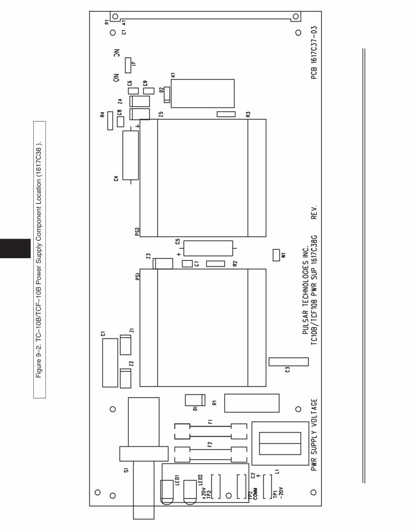
Fig
ure
9–2.
TC
–10B
/TC
F–1
0B P
ower
Sup
ply
Com
pone
nt L
ocat
ion
(161
7C38
).
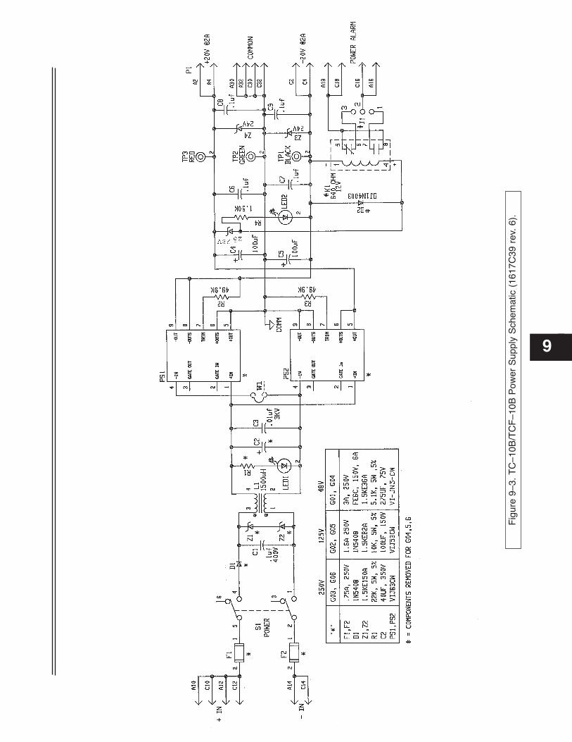
9
Fig
ure
9–3.
TC
–10B
/TC
F–1
0B P
ower
Sup
ply
Sch
emat
ic (
1617
C39
rev
. 6)
.

Page 9–6 June 2006
TC–10B System Manual
USER NOTES
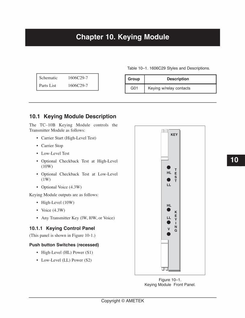
10.1 Keying Module DescriptionThe TC–10B Keying Module controls theTransmitter Module as follows:
• Carrier Start (High-Level Test)
• Carrier Stop
• Low-Level Test
• Optional Checkback Test at High-Level(10W)
• Optional Checkback Test at Low-Level(1W)
• Optional Voice (4.3W)
Keying Module outputs are as follows:
• High-Level (10W)
• Voice (4.3W)
• Any Transmitter Key (lW, l0W, or Voice)
10.1.1 Keying Control Panel(This panel is shown in Figure 10-1.)
Push button Switches (recessed)
• High-Level (HL) Power (S1)
• Low-Level (LL) Power (S2)
Copyright © AMETEK
Chapter 10. Keying Module
10
Schematic 1606C29-7
Parts List 1606C29-7
Group Description
G01 Keying w/relay contacts
Table 10–1. 1606C29 Styles and Descriptions.
KEY
HL
LL
HL
LL
V
TEST
KEYING
Figure 10–1. Keying Module Front Panel.
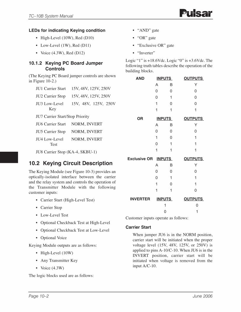
LEDs for indicating Keying condition
• High-Level (10W), Red (D10)
• Low-Level (1W), Red (D11)
• Voice (4.3W), Red (D12)
10.1.2 Keying PC Board JumperControls
(The Keying PC Board jumper controls are shownin Figure 10-2.)
JU1 Carrier Start 15V, 48V, 125V, 250V
JU2 Carrier Stop 15V, 48V, 125V, 250V
JU3 Low-Level 15V, 48V, 125V, 250VKey
JU7 Carrier Start/Stop Priority
JU6 Carrier Start NORM, INVERT
JU5 Carrier Stop NORM, INVERT
JU4 Low-Level NORM, INVERTTest
JU8 Carrier Stop (KA-4, SKBU-1)
10.2 Keying Circuit DescriptionThe Keying Module (see Figure 10-3) provides anoptically-isolated interface between the carrierand the relay system and controls the operation ofthe Transmitter Module with the followingcustomer inputs:
• Carrier Start (High-Level Test)
• Carrier Stop
• Low-Level Test
• Optional Checkback Test at High-Level
• Optional Checkback Test at Low-Level
• Optional Voice
Keying Module outputs are as follows:
• High-Level (10W)
• Any Transmitter Key
• Voice (4.3W)
The logic blocks used are as follows:
• “AND” gate
• “OR” gate
• “Exclusive OR” gate
• “Inverter”
Logic “1” is +18.6Vdc. Logic “0” is +3.6Vdc. Thefollowing truth tables describe the operation of thebuilding blocks.
AND INPUTS OUTPUTS
A B Y
0 0 0
0 1 0
1 0 0
1 1 1
OR INPUTS OUTPUTS
A B Y
0 0 0
1 0 1
0 1 1
1 1 1
Exclusive OR INPUTS OUTPUTS
A B Y
0 0 0
0 1 1
1 0 1
1 1 0
INVERTER INPUTS OUTPUTS
1 0
0 1
Customer inputs operate as follows:
Carrier Start
When jumper JU6 is in the NORM position,carrier start will be initiated when the propervoltage level (15V, 48V, 125V, or 250V) isapplied to pins A-10/C-10. When JU6 is in theINVERT position, carrier start will beinitiated when voltage is removed from theinput A/C-10.
Page 10–2 June 2006
TC–10B System Manual
Carrier Stop
When jumper JU5 is in the NORM position,carrier stop will initiate when jumper JU2(pins A-16/C-16) is set at the appropriatevoltage level (15V, 48V, 125V, or 250V);when JU5 is in the INVERT position, carrierstop will initiate when voltage is removed.
Low-Level Test
When jumper JU4 is in the NORM position, aLow-Level test will initiate when jumper JU3(pins A-22/C-22) is set at the appropriatevoltage level (15V, 48V, 125V, or 250V);when JU4 is in the INVERT position, a Low-Level test will initiate when voltage isremoved.
When the appropriate jumper is in place on theboard, jumpers JU1, JU2, and JU3 provide logic“1” or “0” inputs. (Proper polarity of these inputcommands must be observed.)
You can manually initiate a Low-Level test bypressing the (recessed) push button switch (S2) onthe front panel. You can manually initiate a High-Level test by pressing the (recessed) push buttonswitch (S1).
You can initiate an optional High-Levelcheckback key through pin C-8. You can initiatean optional Low-Level checkback key through pinC-28. A voice key can be initiated through pinC-24.
Keying Module outputs are as follows:
High-Level (10W) Key Pin A-8
Any Transmitter Key Pin C-6(1-W, 4.3W, or l0W)
Voice (4.3W) Key Pin A-6
Front panel LEDs are illuminated as follows:
D10 High-Level
D11 Low-Level
D12 Voice
You can make the STOP command inhibit theHigh-Level (10W) output by using jumper JU7.The STOP command also inhibits the Voice Keyoutput. The Voice Key is inhibited by the High-Level and Low-Level Keys.
Zener diodes (D1, D2, D3) limit the input voltageto the optical isolators (I7, I8, I9), while alsoproviding reverse voltage protection. Zener diodes(D14, D13) regulate primary power (pinsA-2/A-4, pins A-30/A-32, pins C-30/C-32) downto 15V, while also providing reverse voltageprotection.
Transistor (Q1), JU8, R40, D15, D16, D17, andR41 are used for special applications with KDARand SKBU type keying circuits. These particularrelay applications have a single line input forcarrier start. The line has a tri-state condition, i.e.,it is active high, active low, or open circuit. Forexample, as shown in Figure 2-13 in theApplications chapter, under normal operatingconditions, the input to TB4-1 is an open circuit(while looking back into Z1). CSB, CSP, and SQare open, and zener diode (Z1) is much larger than20Vdc. When the carrier test switch is depressed,or the phase and ground carrier start contactsopen, the line going to TB4-1 goes active high. Ifthe phase and ground carrier stop contacts close,the line going to TB4-1 is active low.
As shown in the schematic of the keying load(Figure 10-3) and Q1 circuitry, when A-10 is high(same as TB4-1), carrier start is initiated andcarrier stop is inhibited. This is caused by R40 andD15 saturating Q1 and shorting out the stopvoltage applied to D7. C-16 is connected to thebattery so that D2 ALWAYS has 20V across it.When TB4-1 (A-10) goes active low, Diode D17shorts out the drive voltage to Q1, and internaldiode I8 conducts, causing a STOP function to begenerated. The following TRUTH table illustratesthe operation:
June 2006 Page 10–3
Chapter 10. Keying Module
10
NOTE
Carrier start will initiate a High-Level test.
A10 CXR START CXR STOP
HIGH YES NO
LOW NO YES
OPEN NO NO
When operating with systems other than KDARor SKBU, normally J8 is left out, and threeseparate command lines (START, STOP, and LL)are used.
10.3 Keying TroubleshootingShould a fault occur in the Keying Module, placethe module on an extender board. Six jumpers(JU1 through JU6) are used to select input keyingvoltages and the sense required. A seventh jumper(JU7) governs start/stop priority. The three opticalisolators (I7, I8, I9) may be tested using the on-board +18.6Vdc source (D13 cathode). When alogic “1” is applied to any of the 15V inputs (R4,R9, or R14), with the jumper removed, pin 5 ofthe selected optical isolator (I7, I8, or I9) will golow.
You can check other components on the PC Boardby conventional means.
Page 10–4 June 2006
TC–10B System Manual
! CAUTIONDO NOT ATTEMPT TO FORCE A LOGIC “1”(+18.6VDC) ON ANY OUTPUTS OR INPUTSCONNECTED TO OUTPUTS. THIS COULDDAMAGE AN INTEGRATED CIRCUIT (IC).
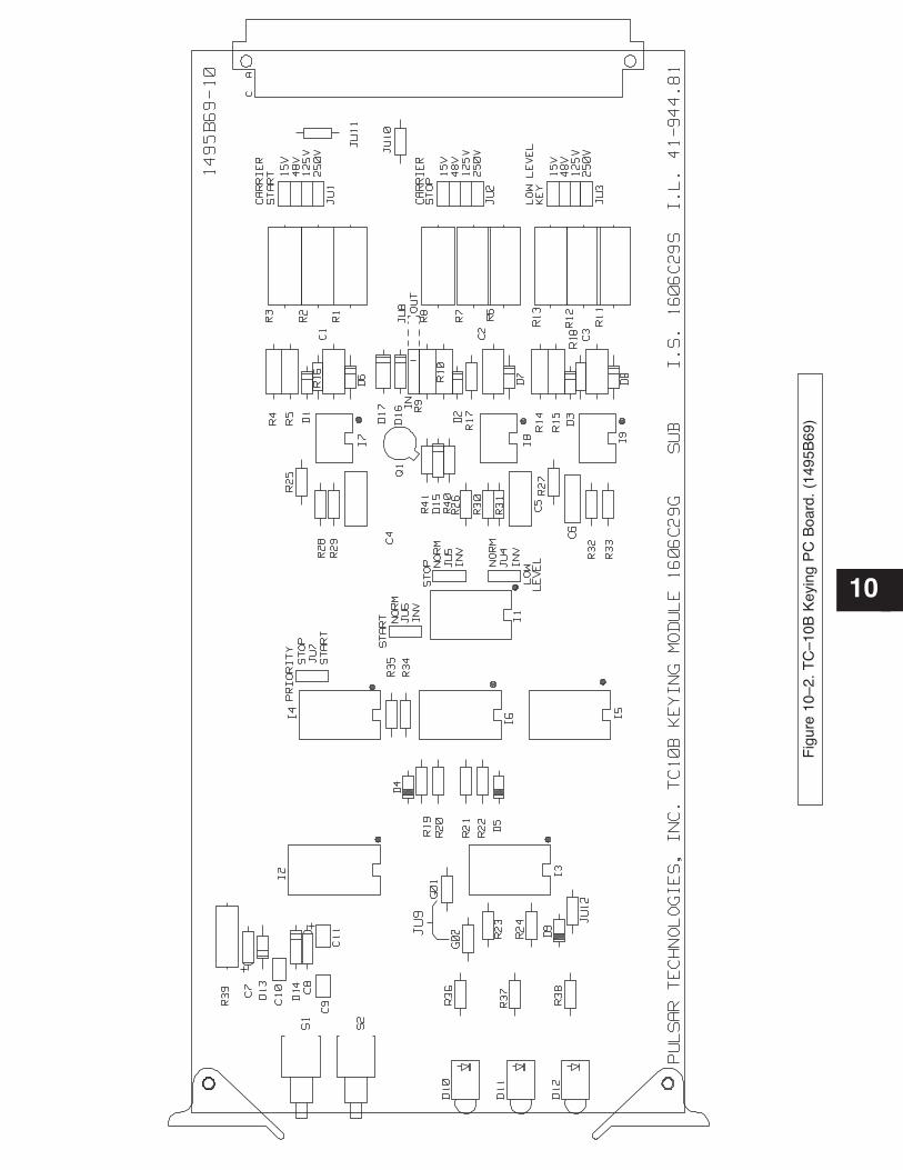
10
Fig
ure
10–2
. T
C–1
0B K
eyin
g P
C B
oard
. (1
495B
69)
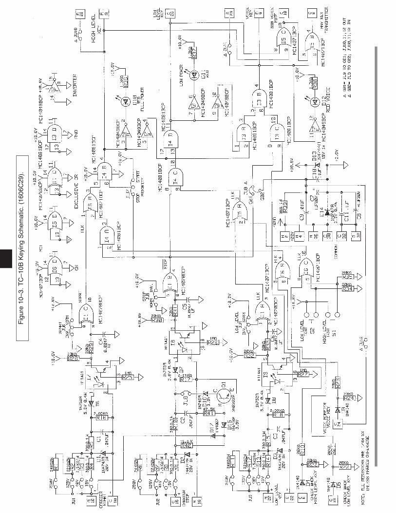
Fig
ure
10–3
. T
C–1
0B K
eyin
g S
chem
atic
. (1
606C
29).
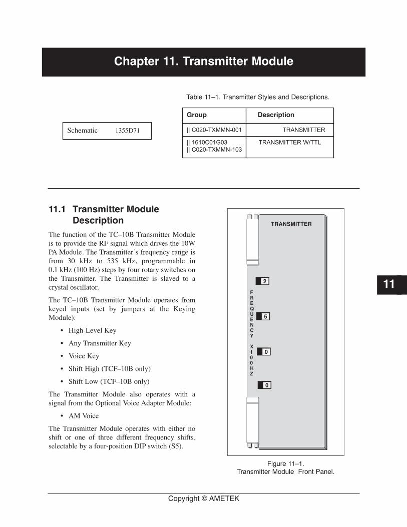
11.1 Transmitter ModuleDescription
The function of the TC–10B Transmitter Moduleis to provide the RF signal which drives the 10WPA Module. The Transmitter’s frequency range isfrom 30 kHz to 535 kHz, programmable in0.1 kHz (100 Hz) steps by four rotary switches onthe Transmitter. The Transmitter is slaved to acrystal oscillator.
The TC–10B Transmitter Module operates fromkeyed inputs (set by jumpers at the KeyingModule):
• High-Level Key
• Any Transmitter Key
• Voice Key
• Shift High (TCF–10B only)
• Shift Low (TCF–10B only)
The Transmitter Module also operates with asignal from the Optional Voice Adapter Module:
• AM Voice
The Transmitter Module operates with either noshift or one of three different frequency shifts,selectable by a four-position DIP switch (S5).
Copyright © AMETEK
Chapter 11. Transmitter Module
11
Group Description
|| C020-TXMMN-001 TRANSMITTER
|| 1610C01G03 TRANSMITTER W/TTL|| C020-TXMMN-103
Table 11–1. Transmitter Styles and Descriptions.
TRANSMITTER
FREQUENCY
X100HZ
2
5
0
0
Figure 11–1. Transmitter Module Front Panel.
Schematic 1355D71
11.1.1 Transmitter Control Panel (see Fig. 11-1.)
Operator controls consist of four thumbwheelswitches (with indicator windows), representingthe frequency range:
• SW1 (x 100 kHz)
• SW2 (x 10 kHz)
• SW3 (x 1 kHz)
• SW4 (x 0.1 kHz)
After pulling the module, use a screw driver to setthe thumbwheel switches: CW for higherfrequency, CCW for lower frequency.
11.1.2 Transmitter PC Board (See Fig. 11-3.)
Operator controls are as described below.
Potentiometers
R13 Adjusts high-level (10W) output
R12 Adjusts low-level (1W) output
R14 Adjusts voice (4.3W) output level
R11 Adjusts modulation of transmittersignal (peak-to-valley ratio of signalenvelope)||
Switch
S5 Frequency-shift select
11.2 Optional Transmit TimeLimiter (TTL) TransmitterModule
The Transmit Time Limiter Transmitter Module isan optional transmitter module for the TC-10B.(see Fig. 11-2). The main board is the same as thestandard transmitter with the exception of an addi-tional wire. The auxiliary board is the difference(see Fig. 11-6). Some applications may require atime limit on RF output. The TTL Transmittermodule limits RF transmission time to amaximum of between 2 and 13 seconds. Afterwhich, it will energize an alarm relay, an LED onthe front panel and force the transmitter off. Thetransmitter is then latched off and must be reset bypressing the front panel push-button, labeled“Alarm & Lockout Reset”
11.2.1 Adjusting the TTL TransmitterUsing a universal counter or timer, i.e. HP5315AUniversal Counter or equivalent:
1. Connect the timer/counter start input acrossTB3-1 and TB3-2 (RF Transmit output relay)and verify that JU1 on the 10W Power Ampmodule is set to NO.
2. Connect the stop input of the timer/counteracross TB3-7 and TB3-8 (alarm & lockoutrelay output) and verify that JMP1 on the TTLmodule is set to NO.
3. Press and hold either the “LL” or “HL” buttonon the keying module until the TTL moduleLED indicates “ALARM & LOCKOUT”.
4. Check the start and stop time on thetimer/counter.
5. Press the “ALARM & LOCKOUT RESET”button on the transmitter. Turn the “ON TIME
Page 11–2 June 2006
TC–10B System Manual
NOTE:
Setup both channels of the timercounter for dry contact operation.
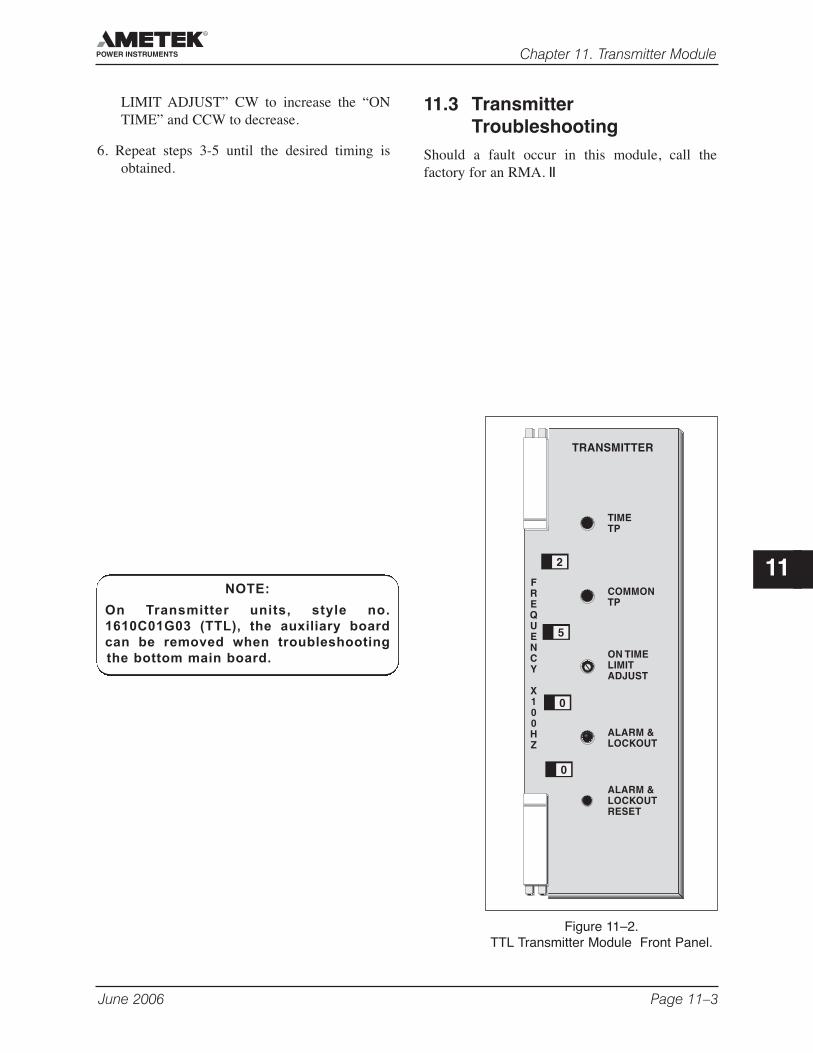
LIMIT ADJUST” CW to increase the “ONTIME” and CCW to decrease.
6. Repeat steps 3-5 until the desired timing isobtained.
11.3 TransmitterTroubleshooting
Should a fault occur in this module, call thefactory for an RMA. ||
June 2006 Page 11–3
Chapter 11. Transmitter Module
11
TRANSMITTER
TIMETP
FREQUENCY
X100HZ
COMMONTP
ON TIMELIMITADJUST
ALARM &LOCKOUT
ALARM &LOCKOUTRESET
2
5
0
0
Figure 11–2. TTL Transmitter Module Front Panel.
NOTE:
On Transmitter units, style no.1610C01G03 (TTL), the auxiliary boardcan be removed when troubleshootingthe bottom main board.
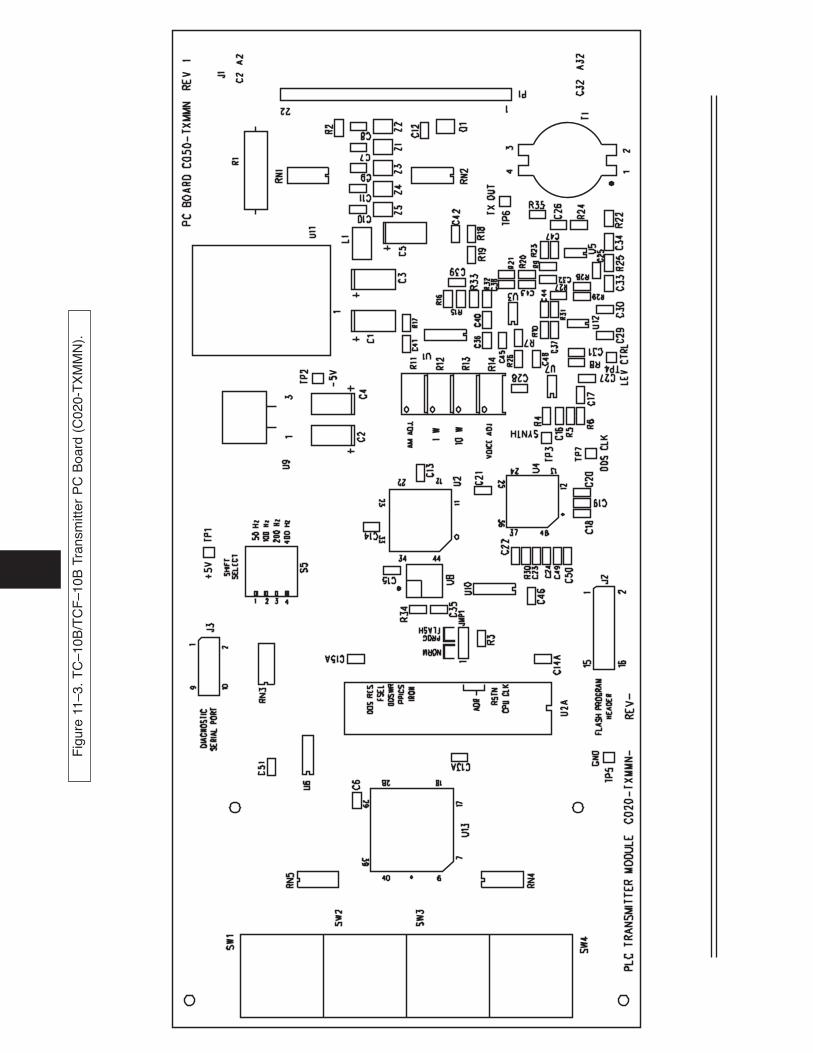
Fig
ure
11–3
. T
C–1
0B/T
CF
–10B
Tra
nsm
itter
PC
Boa
rd (
C02
0-T
XM
MN
).
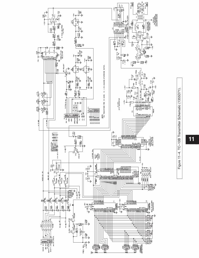
11
Fig
ure
11–4
. T
C–1
0B T
rans
mitt
er S
chem
atic
(13
55D
71).
OU
TP
UT
AM
P(D
IFF
ER
EN
TIA
LV
IDE
OA
MP
) TO
P1-2
0O
NO
PT
ION
AL
TT
LT
RA
NS
MIT
TE
RA
UX
ILIA
RY
BO
AR
D
100KW
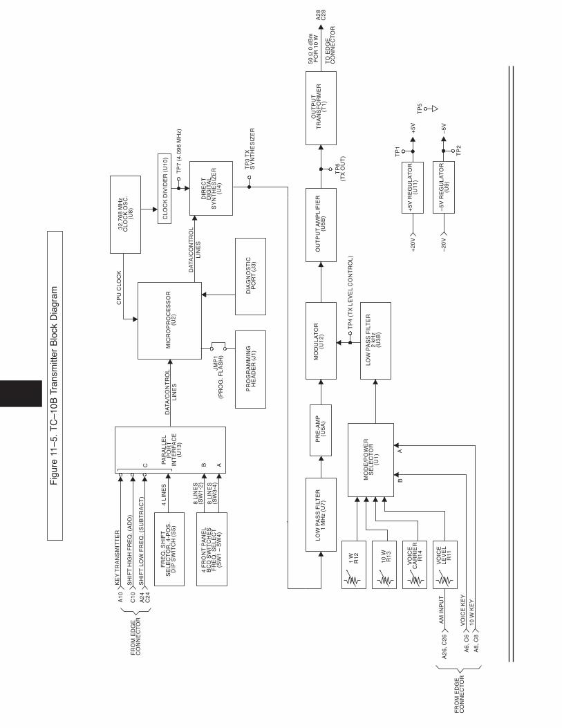
Fig
ure
11–5
. T
C–1
0B T
rans
mitt
er B
lock
Dia
gram
FR
OM
ED
GE
CO
NN
EC
TO
R
SH
IFT
HIG
HF
RE
Q. (
AD
D)
SH
IFT
LO
WF
RE
Q. (
SU
BT
RA
CT
)
C1
0
A1
0
A2
4C
24
8L
INE
S(S
W1
-2)
8L
INE
S(S
W3
-4)
FR
EQ
. SH
IFT
SE
LE
CT
OR
, 4-P
OS
.D
IPS
WIT
CH
(S5
)
PA
RA
LL
EL
PO
RT
INT
ER
FA
CE
(U1
3)
4L
INE
SM
ICR
OP
RO
CE
SS
OR
(U2
)
CP
UC
LO
CK
DIR
EC
TD
IGIT
AL
SY
NT
HE
SIZ
ER
(U4
)
C B A
4F
RO
NT
PA
NE
LB
CD
SW
ITC
HE
SF
RE
Q. S
EL
EC
T(S
W1
–S
W4
)
DA
TA/C
ON
TR
OL
LIN
ES
DA
TA/C
ON
TR
OL
LIN
ES
OU
TP
UT
AM
PL
IFIE
R(U
5B
)
OU
TP
UT
TR
AN
SF
OR
ME
R(T
1)
50
0d
Bm
FO
R1
0W
W
TO
ED
GE
CO
NN
EC
TO
R
A2
8C
28
MO
DU
LA
TO
R(U
12
)
PR
OG
RA
MM
ING
HE
AD
ER
(J1
)D
IAG
NO
ST
ICP
OR
T(J
3)
32
.76
8M
Hz
CL
OC
KO
SC
.(U
8)
CL
OC
KD
IVID
ER
(U1
0)
LO
WP
AS
SF
ILT
ER
2kH
z(U
3B
)
TP
4(T
XL
EV
EL
CO
NT
RO
L)
TP
6(T
XO
UT
)
TP
7(4
.09
6M
Hz)
TP
3T
XS
YN
TH
ES
IZE
R
JMP
1(P
RO
G. F
LA
SH
)
TP
1
TP
5+
5V
–5
V
TP
2
LO
WP
AS
SF
ILT
ER
1M
Hz
(U7
)P
RE
-AM
P(U
5A
)
+5
VR
EG
UL
AT
OR
(U11
)
–5
VR
EG
UL
AT
OR
(U9
)
MO
DE
/PO
WE
RS
EL
EC
TO
R(U
1) A
B
KE
YT
RA
NS
MIT
TE
R
1W
R1
2
10
WR
13
VO
ICE
CA
RR
IER
R1
4
FR
OM
ED
GE
CO
NN
EC
TO
R
VO
ICE
LE
VE
LR
11A
26
, C2
6–
20
V
+2
0V
A6
, C6
A8
,C8
AM
INP
UT
VO
ICE
KE
Y
10
WK
EY
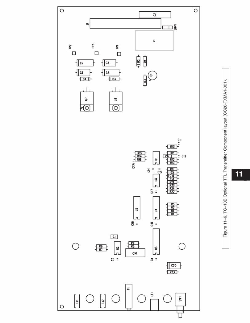
11
Fig
ure
11–6
. T
C–1
0B O
ptio
nal T
TL
Tran
smitt
er C
ompo
nent
layo
ut (
CC
20-T
XM
A1-
001)
.
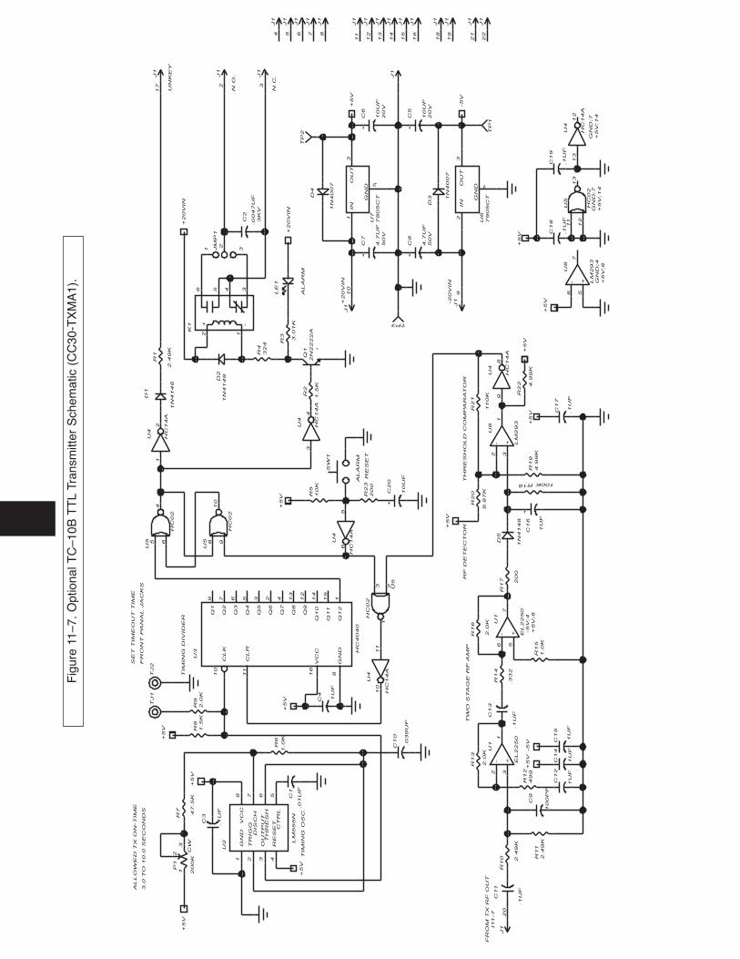
Fig
ure
11–7
. O
ptio
nal T
C–1
0B T
TL
Tran
smitt
er S
chem
atic
(C
C30
-TX
MA
1).
+
+
CW
HC
14A
HC
02
HC
02
HC
4040
+
+
HC
02
HC
14A
HC
14A
HC
14A
HC
14A
HC
02
- + EL2250
HC
14
A
- + EL2250
- + LM
293
- + LM
293
+
+
AL
AR
M
FR
ON
TP
AN
AL
JA
CK
S
SE
TT
IM
EO
UT
TIM
EA
LL
OW
ED
TX
ON
-T
IM
E
20V
20V
50V
50V
3K
V
AL
AR
M
RE
SE
T
TW
OS
TA
GE
RF
AM
P
TIM
IN
GO
SC
.
TIM
IN
GD
IV
ID
ER
N.O
.
UN
KE
Y
N.C
.
FR
OM
TX
RF
OU
T
I11-7
3.0
TO
10
.0
SE
CO
ND
S
RF
DE
TE
CT
OR
TH
RE
SH
OL
DC
OM
PA
RA
TO
R
1N
4007
1N
4007
2N
2222A
4.7U
F
C7
1U
F
C16
1
2
3
U7
7805C
T
2 3
1
U8
7
56U
8
GN
D;4
+5V
;8
200
R23
8.87K
R20
R15
1.0K
R14
332
R12
499
R13
2.0K
R16
2.0K
1
32U
1
89
U4
6 5
7
U1
-5V
;4
+5V
;8
23
1
U5
11
10
U4
56
U4
43
U4
12
13
U4
GN
D;7
+5V
;14
13
12
11
U5
+5V
;14
GN
D;7
.039U
F
C10
C2
.0047U
F
10U
F
C20
10U
F
C5
1.5K
R2
R22 4.99K
TP
1
TP
2
D1
1N
4148
LE
1
9 7 6 5 2 4 12
14
15
3 1
11
10
816
13
U3
8 7 6
4321
5
U2 L
M555N
J1
SW
1
4
65
U5 8 9
10
U5
12
U4
R1
2.49K
R21
110K
R19
4.99K
R18 100K
D5
1N
4148
R17 200
R11
2.49K
R10 2.49K
1
2
3JM
P1
3456
2 1
K1
D2
1N
4148
R4
324
3.01K
R3
Q1
10K
R5
TJ1
2.0K
R9
1.5K
R8
1.0K
R6
47.5K
R7
1
2
3
200K
P1
C3
.1U
F
3J1
2J1
17
J1
20
J1
22
J1
C19
.1U
F
C18
.1U
F
.1U
F
C17
.1U
F
C12
.1U
FC13
.1U
F
C11
C4
.1U
F
C9
100P
F
C6
10U
F
10
J1
9J1
D3
2
1
3
U6
7905C
T
TJ2
21
J1
4J1
5J1
6J1
7J1
8J1
11
J1
12
J1
13
J1
14
J1
15
J1
16
J1
18
J1
19
J1
D4
.1U
F
C14
.1U
F
C15
TP3
4.7U
F
C8
C1
.01U
F
IN
GN
D
OU
T
+ -
CT
RL
DIS
CH
GN
D
OU
TP
UT
RE
SE
T
TH
RE
SH
TR
IG
G
VC
C
Q1
Q2
Q3
Q4
Q6
Q7
Q9
Q10
Q11
Q5
Q12
CLR
CLK
GN
D
VC
C
Q8
IN
GN
D
OU
T
+5V
+5V
+5V
-5V
-20V
IN
+20V
IN
+20V
IN
+20V
IN
+5V
+5V
+5V
+5V
+5V
-5V
+5V
+5V
+5V
+5V
+5V
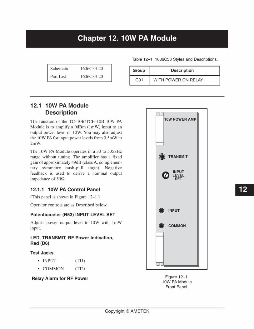
12.1 10W PA ModuleDescription
The function of the TC–10B/TCF–10B 10W PAModule is to amplify a 0dBm (1mW) input to anoutput power level of 10W. You may also adjustthe 10W PA for input power levels from 0.5mW to2mW.
The 10W PA Module operates in a 30 to 535kHzrange without tuning. The amplifier has a fixedgain of approximately 49dB (class A, complemen-tary symmetry push-pull stage). Negativefeedback is used to derive a nominal outputimpedance of 50Ω.
12.1.1 10W PA Control Panel(This panel is shown in Figure 12–1.)
Operator controls are as Described below.
Potentiometer (R53) INPUT LEVEL SET
Adjusts power output level to 10W with 1mWinput.
LED, TRANSMIT, RF Power Indication,Red (D6)
Test Jacks
• INPUT (TJ1)
• COMMON (TJ2)
Relay Alarm for RF Power
Copyright © AMETEK
Chapter 12. 10W PA Module
12
Schematic 1606C33-20
Part List 1606C33-20Group Description
G01 WITH POWER ON RELAY
Table 12–1. 1606C33 Styles and Descriptions.
10W POWER AMP
TRANSMIT
INPUTLEVEL
SET
INPUT
COMMON
Figure 12–1. 10W PA Module
Front Panel.
12.1.2 10W PA PC Board (The 10W PA PC Board is shown in Figure 12-2.)
Operator controls consist of a Jumper (JU1) forthe RF Power Relay (NO/NC). The relay isenergized if RF power (1W or more) is present.
12.2 10W PA Circuit DescriptionThe function of the 10W PA Module (see Figure12-3, Schematic 1606C33S) is to amplify a 0dBm(1mW) input to an output power level of 10W.The input from pins C28/A28 passes thru a700kHz low pass filter (LPF) consisting of L1 andC1. Potentiometer (R53), labeled “INPUTLEVEL SET” on the front panel, is used to adjustthe power level to 10W output with 1mW appliedat the input.
The 10W PA Module operates in a 30 to 535kHzrange without tuning. The amplifier has amaximum gain of approximately 49dB (class A,complementary symmetry push-pull stage).Negative feedback is used to derive a nominaloutput impedance of 50Ω.
All bypassing is done to common (pins A30/C30,A32/C32). Transistors QN1, QN2 and QN3 are 14pin DIPs, each containing four individual transis-tors; QN1 is PNP, while QN2 and QN3 are NPN.
The LPF output drives the amplifier QN1 andQN2. QN1A/QN1B and QN2A/QN2B are config-ured as a differential amplifier, while QN1C andQN2C are constant current sources. The inputsignal is applied to the bases of QN1A and QN2A.Negative feedback is applied to the bases ofQN1B and QN2B. At the positive side (QN2), thedifferential output from QN2A and QN2B isamplified by QN2D and Q2. At the negative side(QN1), the differential output from QN1A andQN1B is amplified by QN1D and Q1. Thepositive side power output transistor (Q6) isdriven by Q5; the negative side power output tran-sistor (Q7) is driven by Q4.
The no-load feedback is from transformer (T1)back thru the RC network of R21, C7, C2, C5 andR18 to the junction of R16 and R17, for thepurpose of stability. The loaded feedback isderived from a sampling resistor (R33, R35, R36,
R37, R38, and R39, all in parallel) and fed backthru C28, C29 and R23. The overall no-loadvoltage gain is approximately 282. The overallloaded voltage gain is approximately 141. Thepartial loaded gain, between C28/A28 and theprimary of T1, is approximately 38.
The alarm circuit (RF Power) consists of QN3,Q8, K1 and associated components. The RF signalis monitored by C22, at T1 pin 1. The signalsample is amplified in QN3A and fed to QN3Band QN3C (QN3B and QN3C are configured asdiodes). A voltage doubler is formed from C30,QN3C and QN3B. The output of QN3B drivesQN3D, via R44 and R45. QN3D is saturated foran input of 1W to C22 (with reference to T1secondary). As QN3D saturates, Q8 conducts,driving the front panel LED (D6, power monitor),causing K1 to energize (or de-energize), indi-cating loss of signal condition. Jumper JU1 allowsthe selection of an open circuit or a closed circuitfor the loss of signal condition.
The +20Vdc line (leading to the alarm circuit,etc.) is filtered by C10, C11, L2, L4, C19, C20 andC21. The -20Vdc (leading to C2/C4) is filtered byC12, C13, L3, C16, C17, C18 and L5.
12.3 10W PA TroubleshootingTo check individual transistors, e.g., Q1 thru Q8,QN1, QN2 and QN3, remove them first from thePC Board. Ohmmeter measurements of the tran-sistors while in the PC Board are misleadingbecause of other paths on the board.
You may remove the heat sink by unscrewing thefour (4) corner screws and the hold-down screwsfor Q1 thru Q8. The 10W PA Module can operateat no-load conditions without the heat sink forshort periods of time while you are trou-bleshooting.
Page 12–2 June 2006
TC–10B System Manual
June 2006 Page 12–3
Chapter 12. 10W PA Module
12
! CAUTIONTHE 10W PA IS, BASICALLY, AN OP-AMPPROVIDING VERY HIGH GAIN WITH NEGATIVEFEEDBACK. TRANSISTORS Q1 THROUGH Q5,Q6, AND Q7 ARE THERMALLY CONNECTED,I.E., THEY ARE MOUNTED ON THE SAME PARTOF THE HEAT SINK. ANY FAILING TRANSISTORMAY AFFECT OTHER TRANSISTORS. CHECKEACH TRANSISTOR SEPARATELY. IF NOFAULTS ARE FOUND, CHECK OTHER COMPO-NENTS.
BE CAREFUL NOT TO MISPLACE THESCREWS, SPRING WASHER OR INSULATINGWASHER USED TO MOUNT Q1 THROUGH Q8.DAMAGED SCREWS OR INSULATORS SHOULDNOT BE USED.
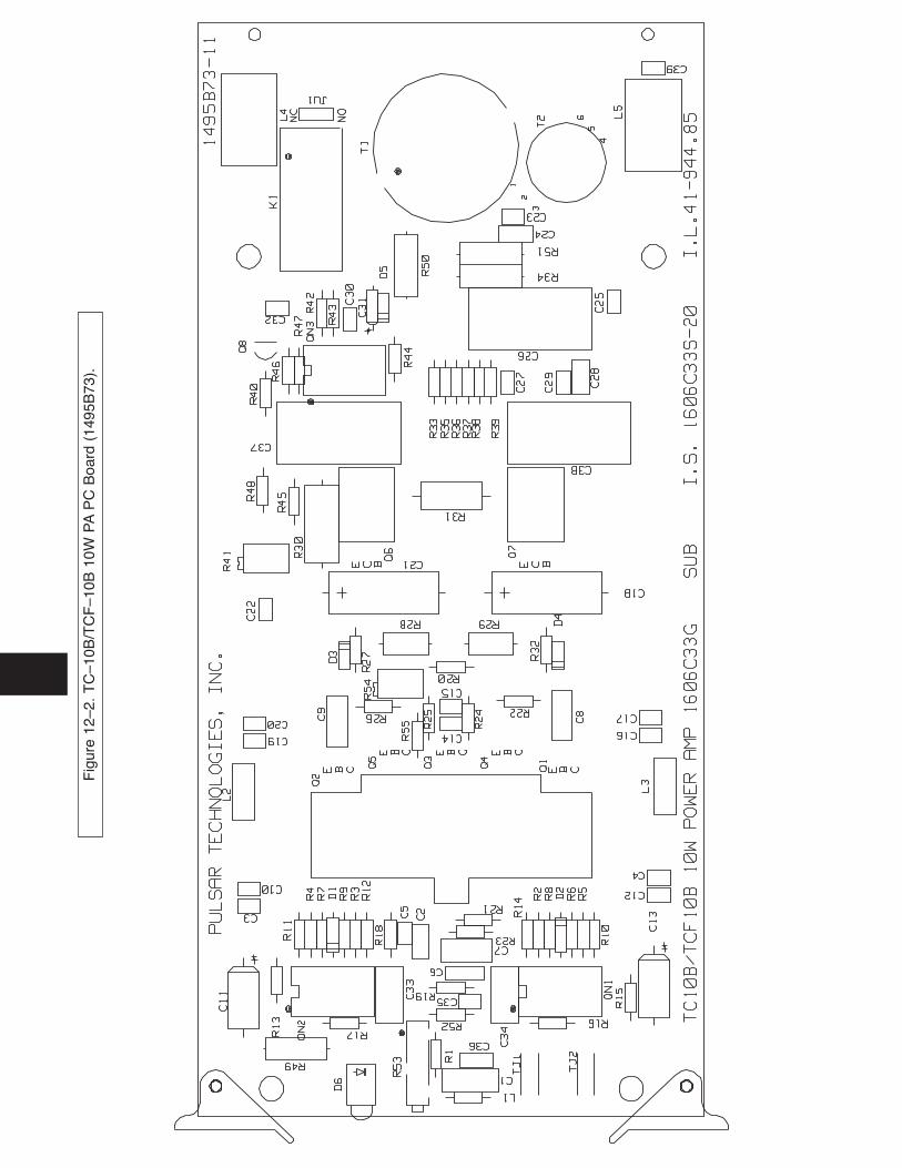
Fig
ure
12–2
. T
C–1
0B/T
CF
–10B
10W
PA
PC
Boa
rd (
1495
B73
).
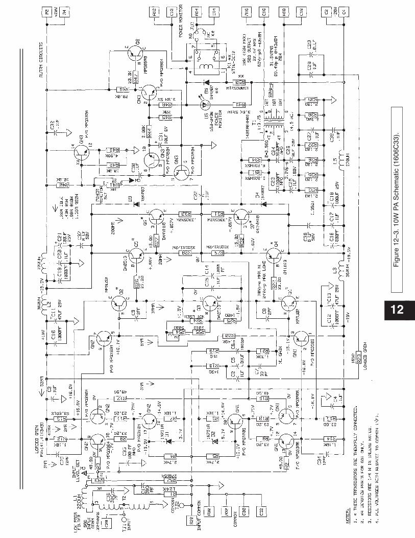
12
Fig
ure
12–3
. 10
W P
AS
chem
atic
(16
06C
33).

Page 12–6 June 2006
TC–10B System Manual
USER NOTES
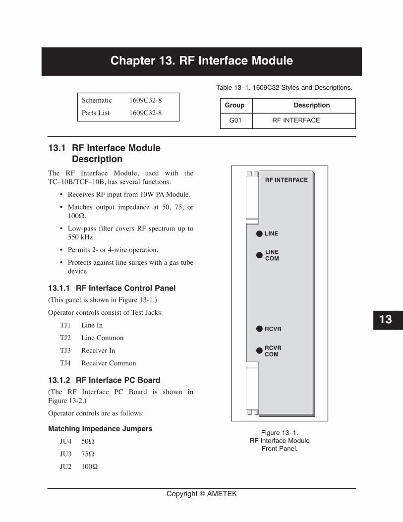
13.1 RF Interface ModuleDescription
The RF Interface Module, used with theTC–10B/TCF–10B, has several functions:
• Receives RF input from 10W PA Module.
• Matches output impedance at 50, 75, or100Ω.
• Low-pass filter covers RF spectrum up to550 kHz.
• Permits 2- or 4-wire operation.
• Protects against line surges with a gas tubedevice.
13.1.1 RF Interface Control Panel(This panel is shown in Figure 13-1.)
Operator controls consist of Test Jacks:
TJ1 Line In
TJ2 Line Common
TJ3 Receiver In
TJ4 Receiver Common
13.1.2 RF Interface PC Board(The RF Interface PC Board is shown inFigure 13-2.)
Operator controls are as follows:
Matching Impedance Jumpers
JU4 50Ω
JU3 75Ω
JU2 100Ω
Copyright © AMETEK
Chapter 13. RF Interface Module
13
Schematic 1609C32-8
Parts List 1609C32-8Group Description
G01 RF INTERFACE
Table 13–1. 1609C32 Styles and Descriptions.
RF INTERFACE
LINE
LINECOM
RCVR
RCVRCOM
Figure 13–1. RF Interface Module
Front Panel.
2-wire or 4-wire RF Termination
JU1/JU5 “IN” 2-wire
JU1/JU5 “OUT” 4-wire
Attenuator Override Jumper (JU6)
NORM Sensitivity 70Vrms at 5,000Ω
HIGH Sensitivity 17Vrms at 1,000Ω
13.2 RF Interface CircuitDescription
This module receives RF input from the 10W PAModule at pins A16/C16 and A18/C18, and feedsthe power through a balanced low-pass filter witha 550kHz cutoff (L3, L4, L1, L2 and associatedcomponents). RF is fed through transformer T1,for matching 50Ω (JU4), 75Ω (JU3), or 100Ω(JU2) resistance to the RF line output (45Vrmsmaximum) at pins 12A/12C and 10A/10C, whichprovide the two-wire UHF (J1) connection on theRear Panel.
Four-Wire Receiver input is provided at pins 24A/C and 22 A/C via the 4-wire BNC (J2)connector on the Rear Panel. Jumpers JU1 andJU5 simultaneously connect the four-wireReceiver input to RF line output:
• IN settings for 2-wire operation
• OUT settings for 4-wire operation
Isolation transformer T2, together with seriesresistor R1, forms an attenuator with 13dB loss.Receiver input (at pins 28 A/C) is adjusted byjumper JU6:
• When in the NORM position, Receivermaximum input is 70Vrms at 5,000Ω
• When in the HIGH position, JU6 overridesthe attenuator, providing lower inputimpedance (Receiver maximum input is17Vrms at 1,000Ω).
13.3 RF InterfaceTroubleshooting
With the PC Board plugged into the chassis, youcan monitor the voltage output to the RF line atTJ1 and TJ2. You can monitor receiver input atTJ3 and TJ4.
Should a fault occur in the RF Interface Module,you can remove the PC board and check thecomponents by conventional means.
13.3.1 CapacitorsRemove from the circuit with jumpers JU2, JU3and JU4 and check for shorts, dissipation factor,and capacitance. (Perform checks using a signal of10kHz or higher.)
13.3.2 InductorsCheck with an ohmmeter.
13.3.3 TransformersCheck for open circuits.
Page 13–2 June 2006
TC–10B System Manual
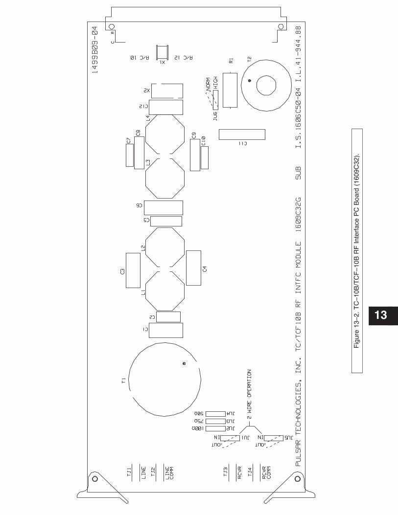
13
Fig
ure
13–2
. T
C–1
0B/T
CF
–10B
RF
Inte
rfac
e P
C B
oard
(16
09C
32).
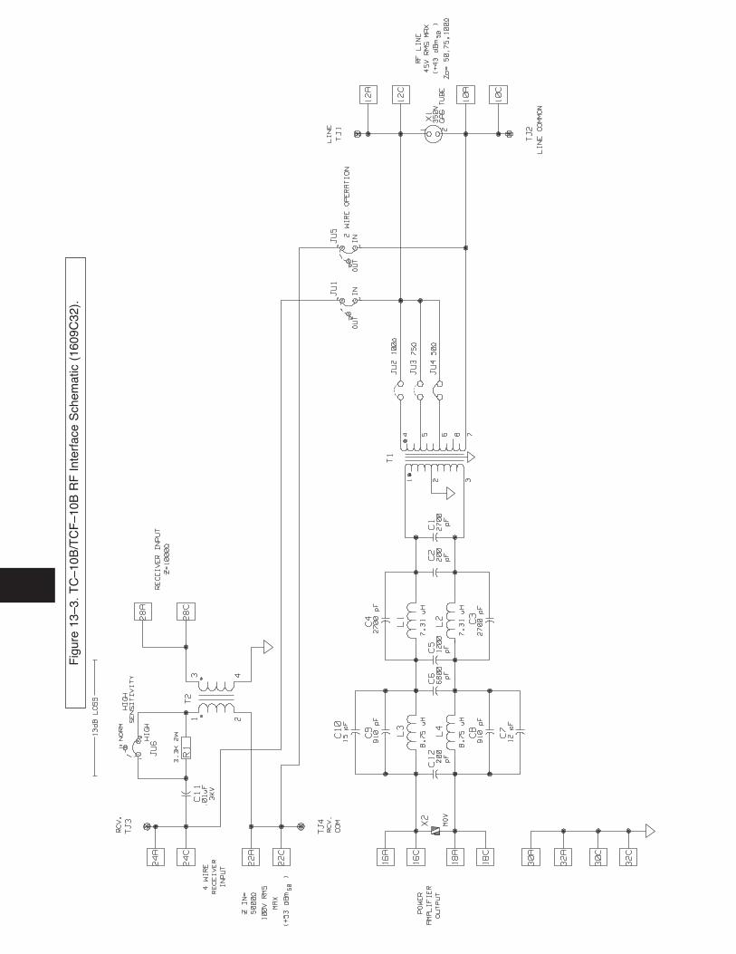
Fig
ure
13–3
. T
C–1
0B/T
CF
–10B
RF
Inte
rfac
e S
chem
atic
(16
09C
32).
2
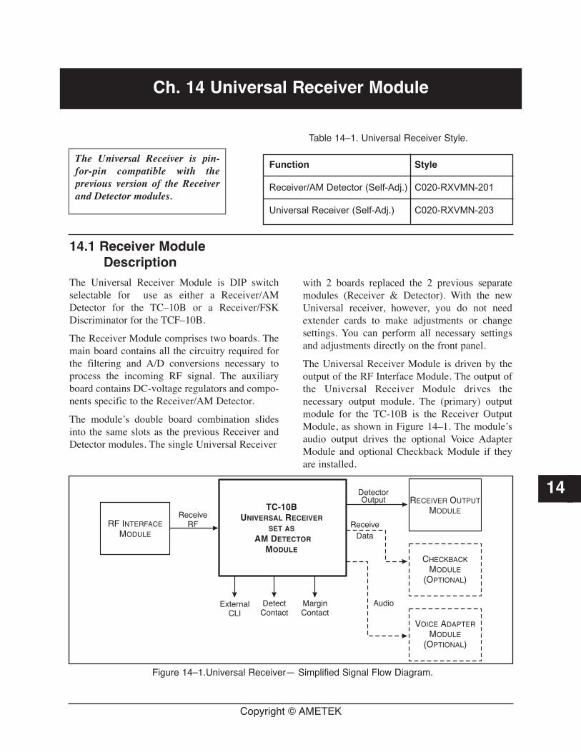
14.1 Receiver ModuleDescription
The Universal Receiver Module is DIP switchselectable for use as either a Receiver/AMDetector for the TC–10B or a Receiver/FSKDiscriminator for the TCF–10B.
The Receiver Module comprises two boards. Themain board contains all the circuitry required forthe filtering and A/D conversions necessary toprocess the incoming RF signal. The auxiliaryboard contains DC-voltage regulators and compo-nents specific to the Receiver/AM Detector.
The module’s double board combination slidesinto the same slots as the previous Receiver andDetector modules. The single Universal Receiver
with 2 boards replaced the 2 previous separatemodules (Receiver & Detector). With the newUniversal receiver, however, you do not needextender cards to make adjustments or changesettings. You can perform all necessary settingsand adjustments directly on the front panel.
The Universal Receiver Module is driven by theoutput of the RF Interface Module. The output ofthe Universal Receiver Module drives thenecessary output module. The (primary) outputmodule for the TC-10B is the Receiver OutputModule, as shown in Figure 14–1. The module’saudio output drives the optional Voice AdapterModule and optional Checkback Module if theyare installed.
Copyright © AMETEK
Ch. 14 Universal Receiver Module
14
The Universal Receiver is pin-for-pin compatible with theprevious version of the Receiverand Detector modules.
Function Style
Receiver/AM Detector (Self-Adj.) C020-RXVMN-201
Universal Receiver (Self-Adj.) C020-RXVMN-203
Table 14–1. Universal Receiver Style.
ExternalCLI
DetectContact
MarginContact
Audio
DetectorOutput
ReceiveData
ReceiveRF
TC-10BUNIVERSAL RECEIVER
SET AS
AM DETECTOR
MODULE
RF INTERFACEMODULE
RECEIVER OUTPUTMODULE
CHECKBACKMODULE
(OPTIONAL)
VOICE ADAPTERMODULE
(OPTIONAL)
Figure 14–1.Universal Receiver— Simplified Signal Flow Diagram.
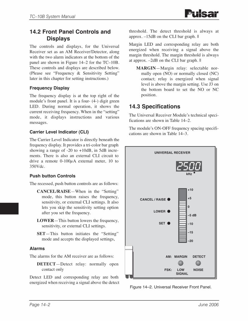
Page 14–2 June 2006
TC–10B System Manual
14.2 Front Panel Controls andDisplays
The controls and displays, for the UniversalReceiver set as an AM Receiver/Detector, alongwith the two alarm indicators at the bottom of thepanel are shown in Figure 14–2 for the TC–10B.These controls and displays are described below.(Please see “Frequency & Sensitivity Setting”later in this chapter for setting instructions.)
Frequency Display
The frequency display is at the top right of themodule’s front panel. It is a four- (4-) digit greenLED. During normal operation, it shows thecurrent receiving frequency. When in the “setting”mode, it displays instructions and variousmessages.
Carrier Level Indicator (CLI)
The Carrier Level Indicator is directly beneath thefrequency display. It provides a tri-color bar graphshowing a range of -20 to +10dB, in 5dB incre-ments. There is also an external CLI circuit todrive a remote 0-100µA external meter, 10 to350Vdc.
Push button Controls
The recessed, push button controls are as follows:
CANCEL/RAISE—When in the “Setting”mode, this button raises the frequency,sensitivity, or external CLI settings. It alsolets you skip the sensitivity setting optionafter you set the frequency.
LOWER—This button lowers the frequency,sensitivity, or external CLI settings.
SET—This button initiates the “Setting”mode and accepts the displayed settings,
Alarms
The alarms for the AM receiver are as follows:
DETECT—Detect relay: normally opencontact only
Detect LED and corresponding relay are bothenergized when receiving a signal above the detect
threshold. The detect threshold is always atapprox. –15dB on the CLI bar graph. ||
Margin LED and corresponding relay are bothenergized when receiving a signal above themargin threshold. The margin threshold is alwaysat approx. –2dB on the CLI bar graph. ||
MARGIN—Margin relay: selectable nor-mally open (NO) or normally closed (NC)contact; relay is energized when signallevel is above the margin setting. Use J3 onthe bottom board to set the NO or NCposition.
14.3 SpecificationsThe Universal Receiver Module’s technical speci-fications are shown in Table 14–2.
The module’s ON-OFF frequency spacing specifi-cations are shown in Table 14–3.
UNIVERSAL RECEIVER
CANCEL / RAISE
LOWER
SET
AM: MARGIN DETECT
FSK: LOW NOISESIGNAL
kHz
+10
+5
0
–5 dB
–10
–15
–20
2500
Figure 14–2. Universal Receiver Front Panel.
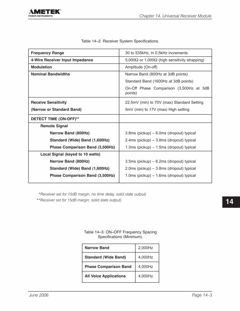
June 2006 Page 14–3
Chapter 14. Universal Receiver Module
14
Frequency Range 30 to 535kHz, in 0.5kHz increments
4-Wire Receiver Input Impedance 5,000Ω or 1,000Ω (high sensitivity strapping)
Modulation Amplitude (On-off)
Nominal Bandwidths Narrow Band (800Hz at 3dB points)
Standard Band (1600Hz at 3dB points)
On-Off Phase Comparison (3,500Hz at 3dBpoints)
Receive Sensitivity 22.5mV (min) to 70V (max) Standard Setting
(Narrow or Standard Band) 5mV (min) to 17V (max) High setting
DETECT TIME (ON-OFF)**
Remote Signal
Narrow Band (800Hz) 3.8ms (pickup) – 6.0ms (dropout) typical
Standard (Wide) Band (1,600Hz) 2.4ms (pickup) – 3.8ms (dropout) typical
Phase Comparison Band (3,500Hz) 1.3ms (pickup) – 1.5ms (dropout) typical
Local Signal (keyed to 10 watts)
Narrow Band (800Hz) 3.5ms (pickup) – 6.2ms (dropout) typical
Standard (Wide) Band (1,600Hz) 2.0ms (pickup) – 3.8ms (dropout) typical
Phase Comparison Band (3,500Hz) 1.0ms (pickup) – 1.6ms (dropout) typical
Table 14–2. Receiver System Specifications.
*Receiver set for 15dB margin, no time delay, solid state output)
**Receiver set for 15dB margin, solid state output)
Narrow Band 2,000Hz
Standard (Wide Band) 4,000Hz
Phase Comparison Band 4,000Hz
All Voice Applications 4,000Hz
Table 14–3. ON–OFF Frequency SpacingSpecifications (Minimum).
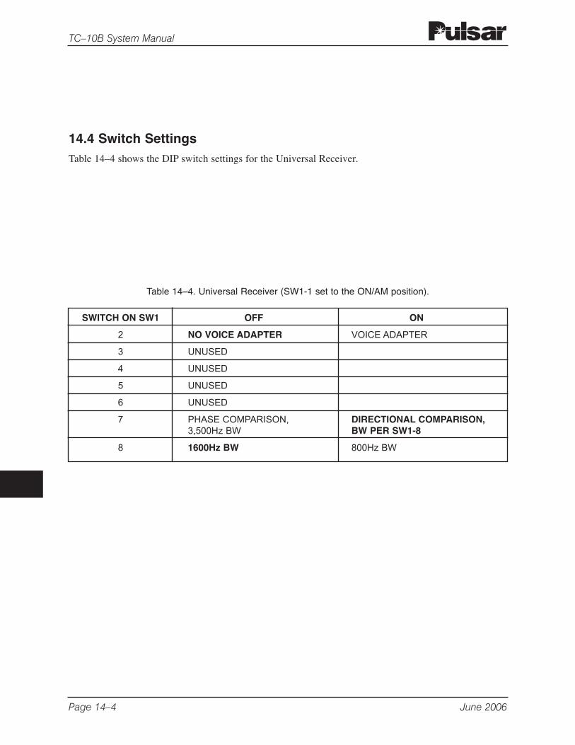
Page 14–4 June 2006
TC–10B System Manual
14.4 Switch SettingsTable 14–4 shows the DIP switch settings for the Universal Receiver.
SWITCH ON SW1 OFF ON
2 NO VOICE ADAPTER VOICE ADAPTER
3 UNUSED
4 UNUSED
5 UNUSED
6 UNUSED
7 PHASE COMPARISON, DIRECTIONAL COMPARISON,3,500Hz BW BW PER SW1-8
8 1600Hz BW 800Hz BW
Table 14–4. Universal Receiver (SW1-1 set to the ON/AM position).
June 2006 Page 14–5
Chapter 14. Universal Receiver Module
14
14.5 Frequency & SensitivitySetting
To change settings on the Universal Receiver,
complete the following sequence:
14.5.1. Push the SET button.
This causes the frequency display to beginflashing, indicating that the receiver is in the“setting” mode.
If you do not touch any of the buttons forapproximately three minutes, the receiverexits the setting mode and reverts to theprevious settings.
14.5.2. Set the frequency.
To keep the displayed frequency, press theSET button again.
To increase the frequency, push the CANCEL/RAISE button; to decrease it, push theLOWER button. Pushing either button onceand releasing it raises or lowers the frequencyby the minimum increment, 0.5kHz. Holdingdown either button for more than two secondsincreases the incrementing speed. If youexceed the maximum of 535kHz, the displayrolls over to the lower end, 30kHz, andcontinues scrolling.
After you have the desired frequencydisplayed, release the button. The displayonce again flashes, indicating that it is still inthe “setting” mode and has not yet acceptedthe new setting. Press the SET button toaccept the frequency setting.
14.5.3. Set the sensitivity.
After you set the frequency, the display scrollsthis message: "Set Sens?… – Hit Set orCancel…".
To keep the current sensitivity setting, pressthe CANCEL/RAISE button.
To tell the receiver to automatically set thesensitivity based on an incoming remotesignal, press the SET button. This sets thereceiver for a 15dB margin and calibrates theCLI meter to 0dB. While the receiver issetting the sensitivity, the display scrolls themessage: "Working…"
At first the bar graph is blank. Then itgradually ramps up until it reaches approxi-mately 0dB. The display then tells youwhether the sensitivity level is okay or if thereis a problem, such as a signal too weak to setfor a minimum pickup level.
After the display gives the "–OK–" message,it then scrolls the message "Sens Adjust? – HitRaise/Lower or Set when done...” Here, youcan either accept the current setting ormanually adjust the receiver sensitivity.
To accept the current setting, press the SETbutton. The receiver is now set for a 15dBmargin, and the CLI reads approximately 0dB.
To manually adjust the receiver sensitivity upor down 10dB, push the CANCEL/RAISE orLOWER button. The CLI will track accord-ingly and remain at that level to indicate thesensitivity is set that much below or above the15dB setting.
NOTE
Catalog no. S1A1WTAP or S1N1WTAP, units with Transmitterstyle 1610C01G03 only:
Prior to setting frequency and sensitivity levels, C16, (or R18) on the TTLTransmitter needs to be shorted out on both ends in order to disable the TTLfunction.
– or –
Press and hold the “ALARM & LOCKOUT RESET” button while setting thereceiver frequency and sensitivity levels. After completion of receiver setup,remove jumpers on C16 and R18.
Page 14–6 June 2006
TC–10B System Manual
Sometimes the incoming signal may not bestrong enough to raise the margin the full10dB. If this happens, the display says"Warning: signal too low for more gain - hitSet to continue.." When this happens, push theSET button. This lowers the sensitivity to anacceptable level and flashes the bar graph toremind you that you are still in the “setting”mode.
To accept the displayed level, push the SETbutton.
14.5.4. Set the external CLI.
Once you have completed the sensitivitysetting, the display scrolls this message: "SetExt CLI? – Hit Raise/Lower or Set whendone...”
To calibrate the external CLI push theCANCEL/RAISE or LOWER button. Theexternal CLI meter will move up and downaccordingly. The external meter is a 100µAinstrument. If it is calibrated in µA, the meter
should be set to read 67µA (this is equivalentto 0dB on the internal meter). The settingshould be varied 3.3µA for each dB themargin adjustment has been raised or loweredfrom the 15kB margin. If the meter is cali-brated in dB, set the meter to read equal to theinternal CLI meter.
To accept the displayed level, push the SETbutton.
14.5.5. Set the local sensitivity.
“Hit Set to get Local Sens” appears after youhave completed the external CLI calibration.Key on the local transmitter by pressing therecessed push button marked “HL” on thekeying module.
Then hit the SET button. This sets the receiversensitivity to the local 10W transmitter signal.
This completes the AM setting procedure.
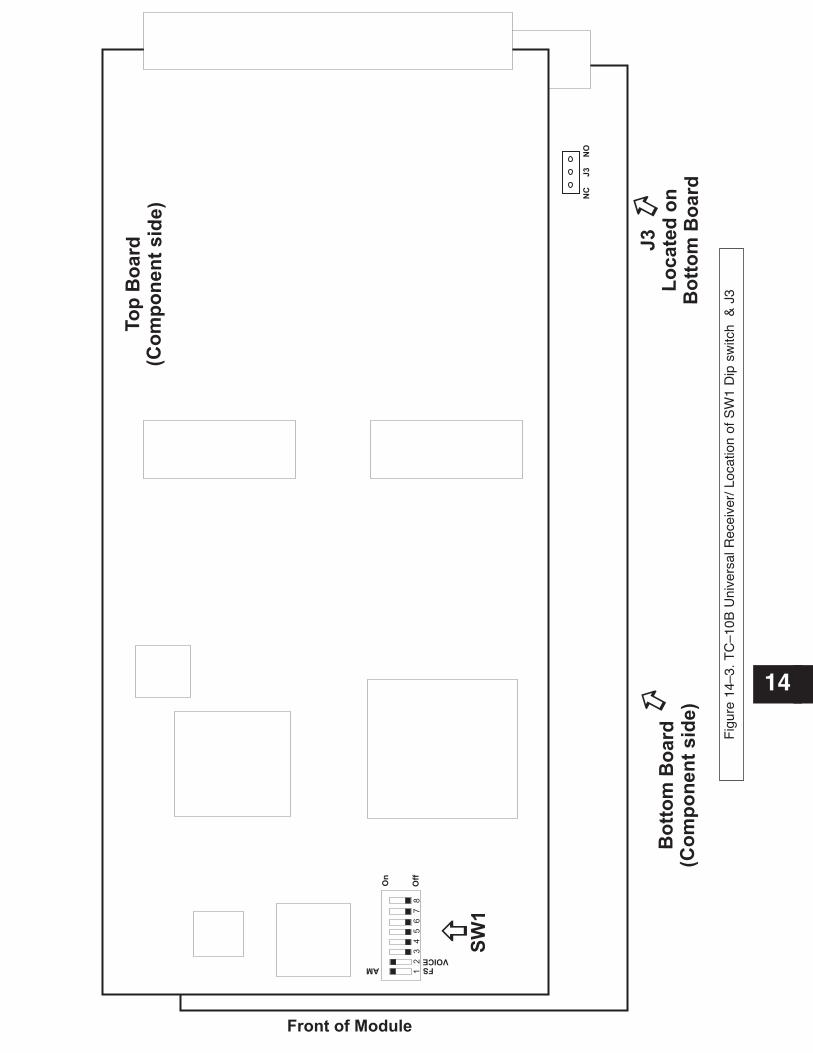
14B
ott
om
Bo
ard
(Co
mp
on
en
tsid
e)
J3
Lo
cate
do
nB
ott
om
Bo
ard
Front of Module
NO
J3
NC
To
pB
oa
rd(C
om
po
nen
tsid
e)
SW
1
12
34
56
78
On
AM FSVOICE
Off
Fig
ure
14–3
. T
C–1
0B U
nive
rsal
Rec
eive
r/ L
ocat
ion
of S
W1
Dip
sw
itch
& J
3

Page 14–8 June 2006
TC–10B System Manual
USER NOTES
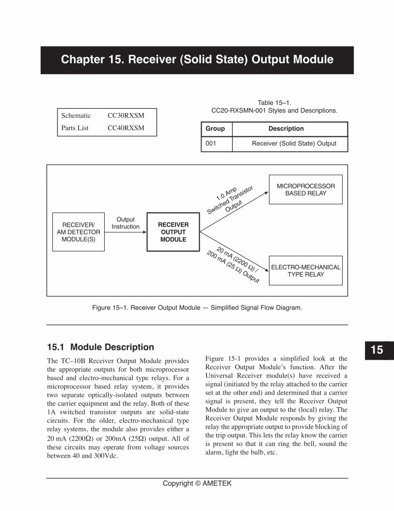
Copyright © AMETEK
Chapter 15. Receiver (Solid State) Output Module
1515.1 Module DescriptionThe TC–10B Receiver Output Module providesthe appropriate outputs for both microprocessorbased and electro-mechanical type relays. For amicroprocessor based relay system, it providestwo separate optically-isolated outputs betweenthe carrier equipment and the relay. Both of these1A switched transistor outputs are solid-statecircuits. For the older, electro-mechanical typerelay systems, the module also provides either a20 mA (2200Ω) or 200mA (25Ω) output. All ofthese circuits may operate from voltage sourcesbetween 40 and 300Vdc.
Figure 15-1 provides a simplified look at theReceiver Output Module’s function. After theUniversal Receiver module(s) have received asignal (initiated by the relay attached to the carrierset at the other end) and determined that a carriersignal is present, they tell the Receiver OutputModule to give an output to the (local) relay. TheReceiver Output Module responds by giving therelay the appropriate output to provide blocking ofthe trip output. This lets the relay know the carrieris present so that it can ring the bell, sound thealarm, light the bulb, etc.
Group Description
001 Receiver (Solid State) Output
Table 15–1. CC20-RXSMN-001 Styles and Descriptions.
Schematic CC30RXSM
Parts List CC40RXSM
Figure 15–1. Receiver Output Module — Simplified Signal Flow Diagram.
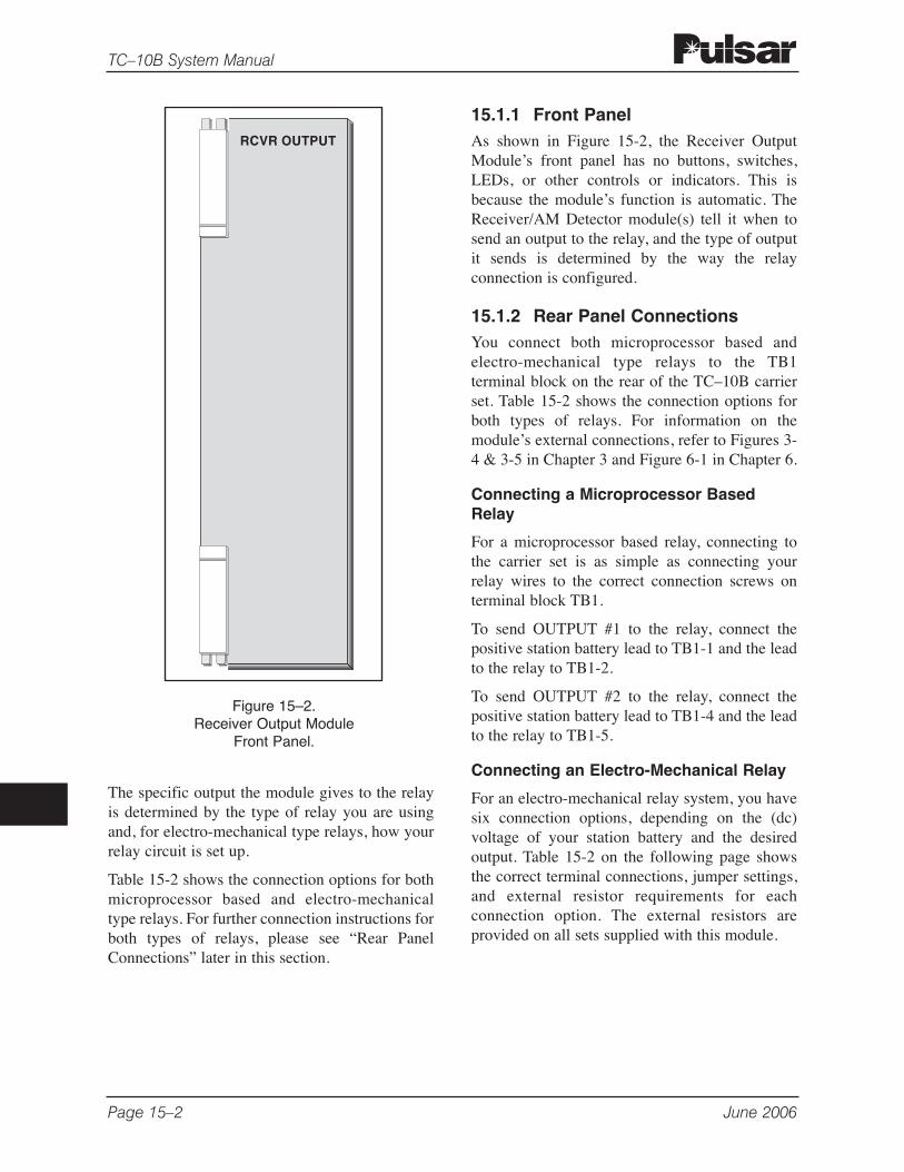
Page 15–2 June 2006
TC–10B System Manual
The specific output the module gives to the relayis determined by the type of relay you are usingand, for electro-mechanical type relays, how yourrelay circuit is set up.
Table 15-2 shows the connection options for bothmicroprocessor based and electro-mechanicaltype relays. For further connection instructions forboth types of relays, please see “Rear PanelConnections” later in this section.
15.1.1 Front PanelAs shown in Figure 15-2, the Receiver OutputModule’s front panel has no buttons, switches,LEDs, or other controls or indicators. This isbecause the module’s function is automatic. TheReceiver/AM Detector module(s) tell it when tosend an output to the relay, and the type of outputit sends is determined by the way the relayconnection is configured.
15.1.2 Rear Panel ConnectionsYou connect both microprocessor based andelectro-mechanical type relays to the TB1terminal block on the rear of the TC–10B carrierset. Table 15-2 shows the connection options forboth types of relays. For information on themodule’s external connections, refer to Figures 3-4 & 3-5 in Chapter 3 and Figure 6-1 in Chapter 6.
Connecting a Microprocessor BasedRelay
For a microprocessor based relay, connecting tothe carrier set is as simple as connecting yourrelay wires to the correct connection screws onterminal block TB1.
To send OUTPUT #1 to the relay, connect thepositive station battery lead to TB1-1 and the leadto the relay to TB1-2.
To send OUTPUT #2 to the relay, connect thepositive station battery lead to TB1-4 and the leadto the relay to TB1-5.
Connecting an Electro-Mechanical Relay
For an electro-mechanical relay system, you havesix connection options, depending on the (dc)voltage of your station battery and the desiredoutput. Table 15-2 on the following page showsthe correct terminal connections, jumper settings,and external resistor requirements for eachconnection option. The external resistors areprovided on all sets supplied with this module.
RCVR OUTPUT
Figure 15–2. Receiver Output Module
Front Panel.
June 2006 Page 15–3
Chapter 15. Receiver (Solid State) Output Module
15
15.1.3 PC Board The schematic for the Receiver Output Module’sPC board is shown in Figure 15-4. The board hastwo jumpers labeled JU1 and JU2. If you are usingelectro-mechanical type relays, these jumpersmust be set to match the station battery voltage forthe relay circuit(s), see figure 15-3 for thejumpers’ locations.
The options for jumpers JU1 & JU2, which youset as part of the circuit for OUTPUT #1 & #2,are:
• 48Vdc
• 125/250Vdc
Both jumpers have the same options.
15.2 Circuit DescriptionThe Receiver Output Module provides the appro-priate outputs from the carrier set to bothmicroprocessor based and electro-mechanicaltype relays. The relay circuits may operate fromvoltage sources between 40 and 300Vdc.
This module is driven by the Universal Receivermodule(s) at pins A/C-26 (+) and A/C-28 (–). Themodule’s two optical isolators (U1 and U2)provide the following outputs, which are availabledepending on the output connection (see Table 15-2):
• 20mA
• 200mA
• 1A switched
For use with Microprocessor-based Relays
For use with Electro-Mechanical Relay Systems
Terminal Terminal1 Amp Switched Transistor Output Connections Connections
OUTPUT #1 OUTPUT #2
TB1-1 (+) & TB1-2 TB1-4 (+) & TB1-5
Carrier Aux Battery External Resistor Terminal JU1 Terminal JU2 Relay Voltage (Ω/watts) Connections Pos. Connections Pos.
(Vdc) OUTPUT #1 OUTPUT #2
20mA (2200Ω) 48 none required TB1-1 (+) & TB1-3 48 TB1-4 (+) & TB1-6 48
20mA (2200Ω) 125 3500/5 TB1-1 (+) & TB1-8 125/250 TB1-4 (+) & TB1-9 125/250
20mA (2200Ω) 250 9200/10 & 500/40 TB1-1 (+) & TB1-8 125/250 TB1-4 (+) & TB1-9 125/250
200mA (25Ω) 48 none required TB1-1 (+) & TB1-3 48 TB1-4 (+) & TB1-6 48
200mA (25Ω) 125 none required TB1-1 (+) & TB1-3 125/250 TB1-4 (+) & TB1-6 125/250
200mA (25Ω) 250 500/40 TB1-1 (+) & TB1-8 125/250 TB1-4 (+) & TB1-9 125/250
Table 15–2. Output Table.
Optical isolators U1 and U2 turn on together andshare the following characteristics:
Isolation voltage: 7,500Vdc
Transistor rating: 400Vdc
The input from A-26 and A-28 energizes bothoptical isolators (U1 and U2). This initiates thecircuit flow for both of the module’s outputs. Asdescribed below, the two output circuits arevirtually the same.
OUTPUT #1 Circuit Flow
The output from optical isolator U1 drives tran-sistor Q1 to the ON state, which in turn drivestransistor Q3 to the ON state. Transistor Q3provides a 1A output on A-14 and C-14 and a20mA/200mA output on A-16 and C-16, with thestation battery tied to A-12 and C-12.
Resistor R2, capacitor C1, and metal oxidevaristors M02 and M03 provide circuit protectionagainst surges coming in from the outside world.Diode D1 provides reverse voltage protection —in case the outputs are connected backwards.
OUTPUT #2 Circuit Flow
The output from optical isolator U2 drives tran-sistor Q2 to the ON state, which in turn drivestransistor Q4 to the ON state. Transistor Q4provides a 1A output on C-20 and a 20mA/200mA output on A-22 and C-22, with the stationbattery tied to C-18.
Resistor R1, capacitor C2, and metal oxidevaristors M01 and M04 provide circuit protectionagainst surges coming in from the outside world.Diode D2 provides reverse voltage protection —in case the outputs are connected backwards.
15.3 TroubleshootingYou can ensure the Receiver Output Module isgetting the proper input from the Receiver/AMDetector module(s) by using the “Input Test”procedure described here. To make sure themodule’s outputs are correct, use the “OutputTests” procedure. To isolate and check faultycomponents, you can use your normal trou-bleshooting techniques.
15.3.1 Input TestUse this procedure to verify that the ReceiverOutput Module is getting the proper input fromthe Receiver/AM Detector module(s). You willneed the following:
• Extender board
• Digital volt meter
Preliminary Steps
1. Connect a power supply source (48, 125, or250Vdc) to the following rear panel terminalsattached to the Receiver Output Module (withreference to TB7-2):
• OUTPUT #1: TB1-1 (+)
• OUTPUT #2: TB1-4 (+)
2. Place the Receiver Output Module on anextender board (see Figure 4-1).
3. Connect the digital volt meter to pins A/C-26(+) and C-28 (–).
Input Test Procedure
Check the input coming from the Receiver/AMDetector module(s) at pins A/C-26 (+) and C-28(–); potential voltage should be +10Vdc.
1. Using the digital volt meter, measure thevoltage level at pins A/C-26 (+) and C-28 (–).The potential voltage should be +10Vdc.
2. Disconnect the digital volt meter.
3. Re-install the Receiver Output Module.
Page 15–4 June 2006
TC–10B System Manual
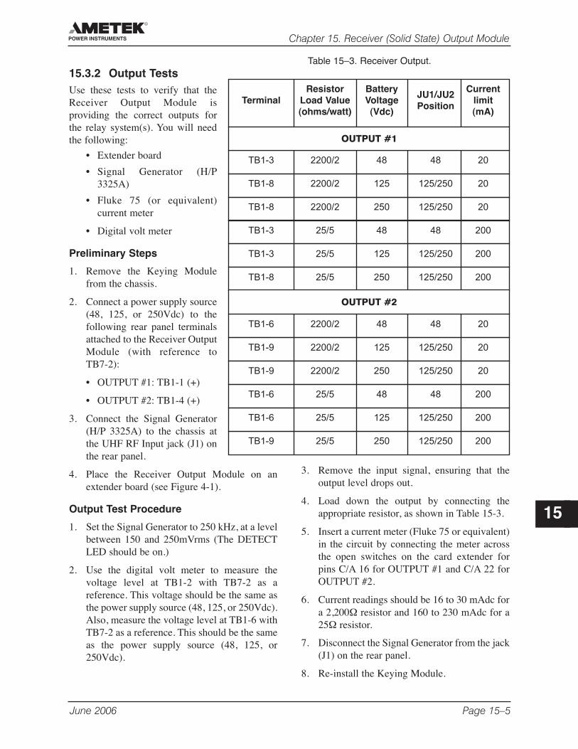
15.3.2 Output TestsUse these tests to verify that theReceiver Output Module isproviding the correct outputs forthe relay system(s). You will needthe following:
• Extender board
• Signal Generator (H/P3325A)
• Fluke 75 (or equivalent)current meter
• Digital volt meter
Preliminary Steps
1. Remove the Keying Modulefrom the chassis.
2. Connect a power supply source(48, 125, or 250Vdc) to thefollowing rear panel terminalsattached to the Receiver OutputModule (with reference toTB7-2):
• OUTPUT #1: TB1-1 (+)
• OUTPUT #2: TB1-4 (+)
3. Connect the Signal Generator(H/P 3325A) to the chassis atthe UHF RF Input jack (J1) onthe rear panel.
4. Place the Receiver Output Module on anextender board (see Figure 4-1).
Output Test Procedure
1. Set the Signal Generator to 250 kHz, at a levelbetween 150 and 250mVrms (The DETECTLED should be on.)
2. Use the digital volt meter to measure thevoltage level at TB1-2 with TB7-2 as areference. This voltage should be the same asthe power supply source (48, 125, or 250Vdc).Also, measure the voltage level at TB1-6 withTB7-2 as a reference. This should be the sameas the power supply source (48, 125, or250Vdc).
3. Remove the input signal, ensuring that theoutput level drops out.
4. Load down the output by connecting theappropriate resistor, as shown in Table 15-3.
5. Insert a current meter (Fluke 75 or equivalent)in the circuit by connecting the meter acrossthe open switches on the card extender forpins C/A 16 for OUTPUT #1 and C/A 22 forOUTPUT #2.
6. Current readings should be 16 to 30 mAdc fora 2,200Ω resistor and 160 to 230 mAdc for a25Ω resistor.
7. Disconnect the Signal Generator from the jack(J1) on the rear panel.
8. Re-install the Keying Module.
June 2006 Page 15–5
Chapter 15. Receiver (Solid State) Output Module
15
Resistor Battery JU1/JU2
Current Terminal Load Value Voltage
Positionlimit
(ohms/watt) (Vdc) (mA)
TB1-3 2200/2 48 48 20
TB1-8 2200/2 250 125/250 20
TB1-8 2200/2 125 125/250 20
TB1-3 25/5 125 125/250 200
TB1-3 25/5 48 48 200
TB1-8 25/5 250 125/250 200
TB1-6 2200/2 48 48 20
TB1-9 2200/2 250 125/250 20
TB1-9 2200/2 125 125/250 20
TB1-6 25/5 125 125/250 200
TB1-6 25/5 48 48 200
TB1-9 25/5 250 125/250 200
Table 15–3. Receiver Output.
OUTPUT #1
OUTPUT #2
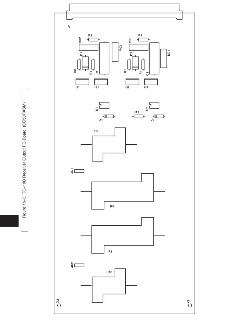
Fig
ure
15–3
. T
C–1
0B R
ecei
ver
Out
put
PC
Boa
rd.
(CC
50R
XS
M)
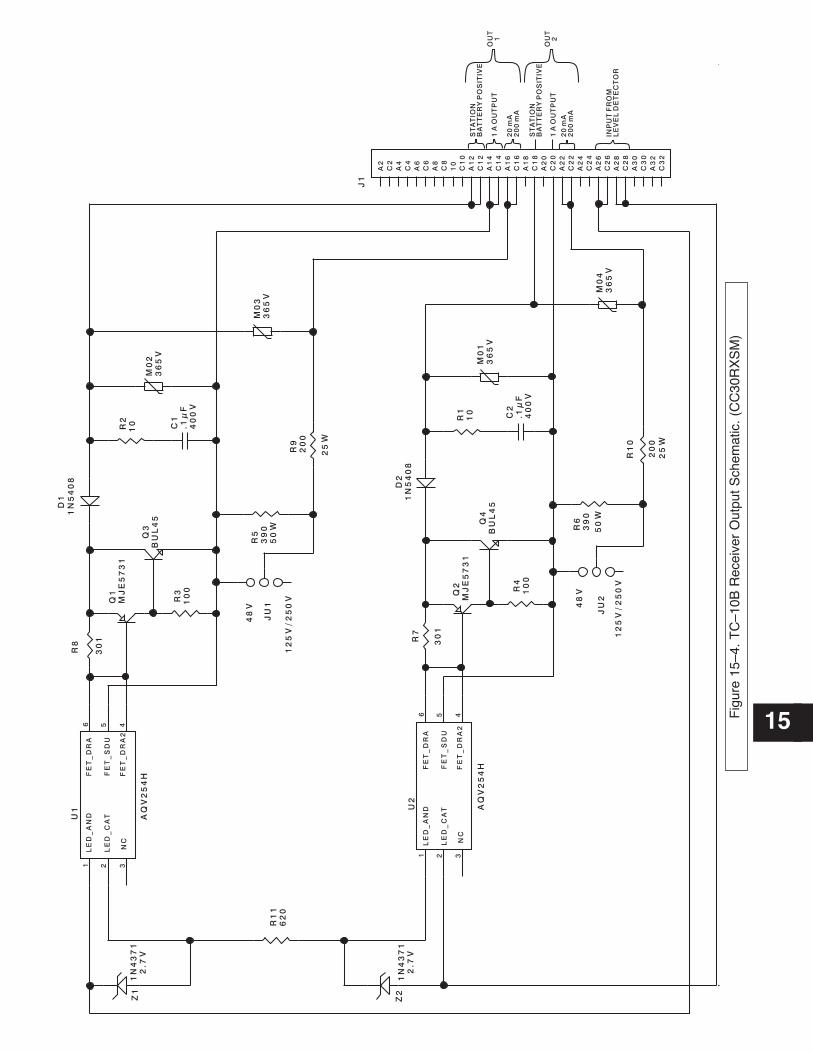
15Fig
ure
15–4
. T
C–1
0B R
ecei
ver
Out
put
Sch
emat
ic.
(CC
30R
XS
M)

Page 15–8 June 2006
TC–10B System Manual
USER NOTES
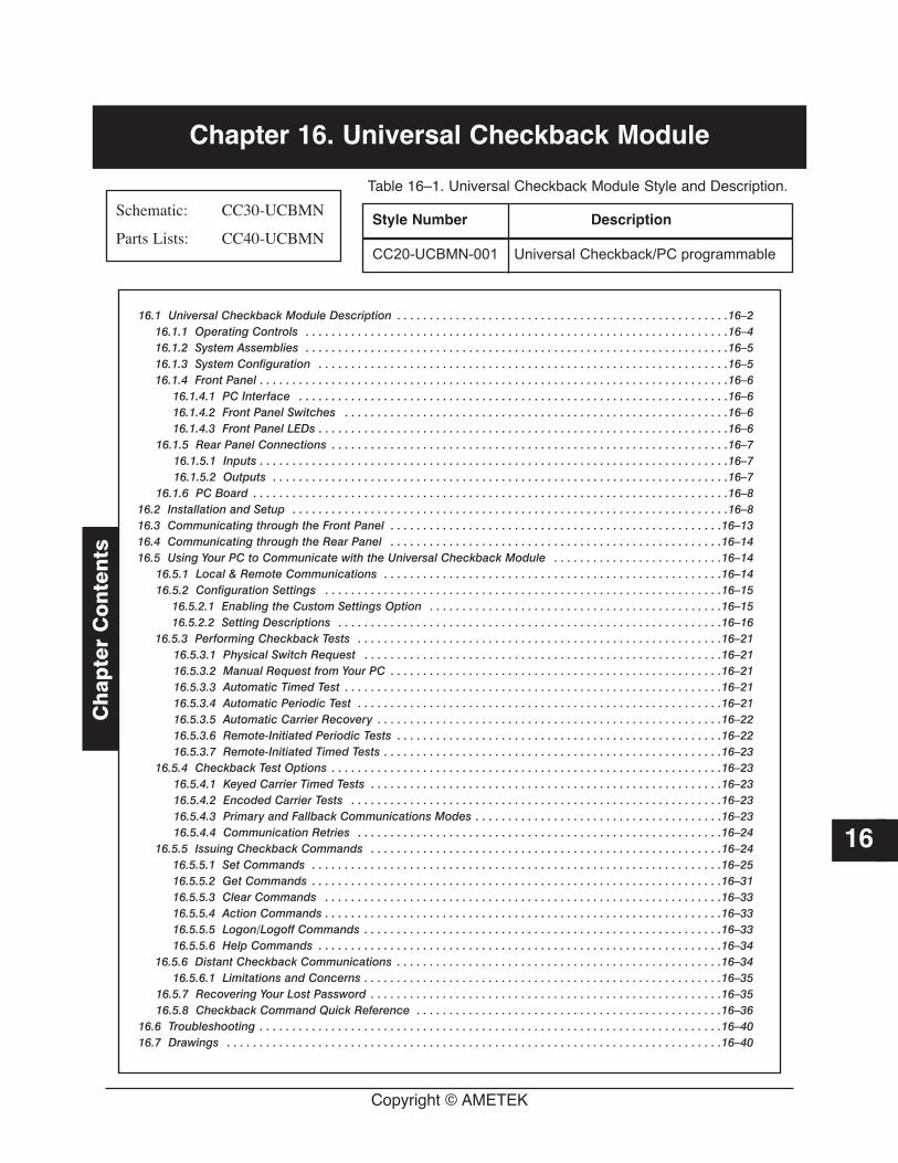
Copyright © AMETEK
Chapter 16. Universal Checkback Module
16
16.1 Universal Checkback Module Description . . . . . . . . . . . . . . . . . . . . . . . . . . . . . . . . . . . . . . . . . . . . . . . . . . .16–216.1.1 Operating Controls . . . . . . . . . . . . . . . . . . . . . . . . . . . . . . . . . . . . . . . . . . . . . . . . . . . . . . . . . . . . . . . . .16–416.1.2 System Assemblies . . . . . . . . . . . . . . . . . . . . . . . . . . . . . . . . . . . . . . . . . . . . . . . . . . . . . . . . . . . . . . . . .16–516.1.3 System Configuration . . . . . . . . . . . . . . . . . . . . . . . . . . . . . . . . . . . . . . . . . . . . . . . . . . . . . . . . . . . . . . .16–516.1.4 Front Panel . . . . . . . . . . . . . . . . . . . . . . . . . . . . . . . . . . . . . . . . . . . . . . . . . . . . . . . . . . . . . . . . . . . . . . . .16–6
16.1.4.1 PC Interface . . . . . . . . . . . . . . . . . . . . . . . . . . . . . . . . . . . . . . . . . . . . . . . . . . . . . . . . . . . . . . . . . .16–616.1.4.2 Front Panel Switches . . . . . . . . . . . . . . . . . . . . . . . . . . . . . . . . . . . . . . . . . . . . . . . . . . . . . . . . . . .16–616.1.4.3 Front Panel LEDs . . . . . . . . . . . . . . . . . . . . . . . . . . . . . . . . . . . . . . . . . . . . . . . . . . . . . . . . . . . . . . .16–6
16.1.5 Rear Panel Connections . . . . . . . . . . . . . . . . . . . . . . . . . . . . . . . . . . . . . . . . . . . . . . . . . . . . . . . . . . . . .16–716.1.5.1 Inputs . . . . . . . . . . . . . . . . . . . . . . . . . . . . . . . . . . . . . . . . . . . . . . . . . . . . . . . . . . . . . . . . . . . . . . . .16–716.1.5.2 Outputs . . . . . . . . . . . . . . . . . . . . . . . . . . . . . . . . . . . . . . . . . . . . . . . . . . . . . . . . . . . . . . . . . . . . . .16–7
16.1.6 PC Board . . . . . . . . . . . . . . . . . . . . . . . . . . . . . . . . . . . . . . . . . . . . . . . . . . . . . . . . . . . . . . . . . . . . . . . . .16–816.2 Installation and Setup . . . . . . . . . . . . . . . . . . . . . . . . . . . . . . . . . . . . . . . . . . . . . . . . . . . . . . . . . . . . . . . . . . .16–816.3 Communicating through the Front Panel . . . . . . . . . . . . . . . . . . . . . . . . . . . . . . . . . . . . . . . . . . . . . . . . . . .16–1316.4 Communicating through the Rear Panel . . . . . . . . . . . . . . . . . . . . . . . . . . . . . . . . . . . . . . . . . . . . . . . . . . .16–1416.5 Using Your PC to Communicate with the Universal Checkback Module . . . . . . . . . . . . . . . . . . . . . . . . . .16–14
16.5.1 Local & Remote Communications . . . . . . . . . . . . . . . . . . . . . . . . . . . . . . . . . . . . . . . . . . . . . . . . . . . .16–1416.5.2 Configuration Settings . . . . . . . . . . . . . . . . . . . . . . . . . . . . . . . . . . . . . . . . . . . . . . . . . . . . . . . . . . . . .16–15
16.5.2.1 Enabling the Custom Settings Option . . . . . . . . . . . . . . . . . . . . . . . . . . . . . . . . . . . . . . . . . . . . .16–1516.5.2.2 Setting Descriptions . . . . . . . . . . . . . . . . . . . . . . . . . . . . . . . . . . . . . . . . . . . . . . . . . . . . . . . . . . .16–16
16.5.3 Performing Checkback Tests . . . . . . . . . . . . . . . . . . . . . . . . . . . . . . . . . . . . . . . . . . . . . . . . . . . . . . . .16–2116.5.3.1 Physical Switch Request . . . . . . . . . . . . . . . . . . . . . . . . . . . . . . . . . . . . . . . . . . . . . . . . . . . . . . .16–2116.5.3.2 Manual Request from Your PC . . . . . . . . . . . . . . . . . . . . . . . . . . . . . . . . . . . . . . . . . . . . . . . . . . .16–2116.5.3.3 Automatic Timed Test . . . . . . . . . . . . . . . . . . . . . . . . . . . . . . . . . . . . . . . . . . . . . . . . . . . . . . . . . .16–2116.5.3.4 Automatic Periodic Test . . . . . . . . . . . . . . . . . . . . . . . . . . . . . . . . . . . . . . . . . . . . . . . . . . . . . . . .16–2116.5.3.5 Automatic Carrier Recovery . . . . . . . . . . . . . . . . . . . . . . . . . . . . . . . . . . . . . . . . . . . . . . . . . . . . .16–2216.5.3.6 Remote-Initiated Periodic Tests . . . . . . . . . . . . . . . . . . . . . . . . . . . . . . . . . . . . . . . . . . . . . . . . . .16–2216.5.3.7 Remote-Initiated Timed Tests . . . . . . . . . . . . . . . . . . . . . . . . . . . . . . . . . . . . . . . . . . . . . . . . . . . .16–23
16.5.4 Checkback Test Options . . . . . . . . . . . . . . . . . . . . . . . . . . . . . . . . . . . . . . . . . . . . . . . . . . . . . . . . . . . .16–2316.5.4.1 Keyed Carrier Timed Tests . . . . . . . . . . . . . . . . . . . . . . . . . . . . . . . . . . . . . . . . . . . . . . . . . . . . . .16–2316.5.4.2 Encoded Carrier Tests . . . . . . . . . . . . . . . . . . . . . . . . . . . . . . . . . . . . . . . . . . . . . . . . . . . . . . . . .16–2316.5.4.3 Primary and Fallback Communications Modes . . . . . . . . . . . . . . . . . . . . . . . . . . . . . . . . . . . . . .16–2316.5.4.4 Communication Retries . . . . . . . . . . . . . . . . . . . . . . . . . . . . . . . . . . . . . . . . . . . . . . . . . . . . . . . .16–24
16.5.5 Issuing Checkback Commands . . . . . . . . . . . . . . . . . . . . . . . . . . . . . . . . . . . . . . . . . . . . . . . . . . . . . .16–2416.5.5.1 Set Commands . . . . . . . . . . . . . . . . . . . . . . . . . . . . . . . . . . . . . . . . . . . . . . . . . . . . . . . . . . . . . . .16–2516.5.5.2 Get Commands . . . . . . . . . . . . . . . . . . . . . . . . . . . . . . . . . . . . . . . . . . . . . . . . . . . . . . . . . . . . . . .16–3116.5.5.3 Clear Commands . . . . . . . . . . . . . . . . . . . . . . . . . . . . . . . . . . . . . . . . . . . . . . . . . . . . . . . . . . . . .16–3316.5.5.4 Action Commands . . . . . . . . . . . . . . . . . . . . . . . . . . . . . . . . . . . . . . . . . . . . . . . . . . . . . . . . . . . . .16–3316.5.5.5 Logon/Logoff Commands . . . . . . . . . . . . . . . . . . . . . . . . . . . . . . . . . . . . . . . . . . . . . . . . . . . . . . .16–3316.5.5.6 Help Commands . . . . . . . . . . . . . . . . . . . . . . . . . . . . . . . . . . . . . . . . . . . . . . . . . . . . . . . . . . . . . .16–34
16.5.6 Distant Checkback Communications . . . . . . . . . . . . . . . . . . . . . . . . . . . . . . . . . . . . . . . . . . . . . . . . . .16–3416.5.6.1 Limitations and Concerns . . . . . . . . . . . . . . . . . . . . . . . . . . . . . . . . . . . . . . . . . . . . . . . . . . . . . . .16–35
16.5.7 Recovering Your Lost Password . . . . . . . . . . . . . . . . . . . . . . . . . . . . . . . . . . . . . . . . . . . . . . . . . . . . . .16–3516.5.8 Checkback Command Quick Reference . . . . . . . . . . . . . . . . . . . . . . . . . . . . . . . . . . . . . . . . . . . . . . .16–36
16.6 Troubleshooting . . . . . . . . . . . . . . . . . . . . . . . . . . . . . . . . . . . . . . . . . . . . . . . . . . . . . . . . . . . . . . . . . . . . . . .16–4016.7 Drawings . . . . . . . . . . . . . . . . . . . . . . . . . . . . . . . . . . . . . . . . . . . . . . . . . . . . . . . . . . . . . . . . . . . . . . . . . . . .16–40
Ch
apte
r C
on
ten
ts
Schematic: CC30-UCBMN
Parts Lists: CC40-UCBMNStyle Number Description
Table 16–1. Universal Checkback Module Style and Description.
CC20-UCBMN-001 Universal Checkback/PC programmable
Page 16–2 June 2006
TC–10B System Manual
16.1 Description|| Since the ON-OFF channel is normally operatedin the OFF state, the status of the channel is notknown until it is called on to function. With theuse of an automated checkback system, thechannel can be checked on a regular basis. Thesystem provided either as integral to the TC-10Bor in a stand-alone system (the UCBS) can providethis regular testing.
The checkback system can be programmed to testas certain times of the day (ie 7 am, 2 pm etc) or“every so often” or periodic (every 24 hours), perthe setting you make. This should be based onyour company’s work schedule, as you may wantto run the test prior to the field people’s beginningshift time.
The type of carrier test operation is also selectable.If you chose a simple Timed check, the systemwill send out a pulse that is associated with theoriginating module’s address (ie the Master willsend a 5 second pulse, remote 1 a 10 second pulse,etc.) The encoded tests are more intelligent asthey send five-byte messages (on and off pulses)back and forth between each terminal to commu-nicate acknowledgements from master to remoteand remote to master as well as other information.This is the preferred method. Sometimes theencoded message may be corrupted by noisebursts and utilizing the “fallback” setting allowsthe module to send a timed check should it fail theencoded message.
The checkback system first tests the system athigh power levels and then will test at low power,if the option is selected. The system will indicatea minor alarm should it fail the low power test butpasses the high power test.
The checkback system is intelligent enough forthe remote end to know that the master has failedto send a request for checkback. Should theremote end not hear from the master end within itsdesignated time (approximately with 15 minutesof when it was due) the remote end will initiate thetests to see if it can get a response. It will then setthe appropriate alarms. In order to accommodatethis, the Master end will “broadcast” a “set time”command every day around 12:15 am. If you do
not enable “AutoSync” on the checkback, it willnot be able to reliable perform this operation.
An additional feature of the checkback system isthe loopback test. This allows the checkbacksystem to signal to the other end of the line to senda sustained carrier per the duration setting (ie 20seconds, etc). This will allow the local end to setit’s receiver sensitivity or to read the receive level.This test is done at both the high power and thelow power levels.
Once connected to a local unit, you may commu-nicate to any of the remote units on the samesystem to view events, counts, settings , etc. Itwill be a bit slow (30 bps) but may be faster thandriving to the other end(s) of the line.
Following are more details on the specifics of howto communicate with and set the checkbacksystem. ||
All TC-10B terminals require a UniversalCheckback Module to operate correctly. TheUniversal Checkback Module provides variousways to automatically or manually test the carrierchannel. This new version of the module is amicroprocessor-based design that can functioneither as a master or remote unit. It replaces themaster (style numbers 1606C37G01 and1606C37G02) and remote (style number1606C38G01) Checkback Modules used in oldersystems. The module is designed for use both withthe TC-10B "ON/OFF" carrier system and withother "ON/OFF" carrier systems using a UCBS.Its major features include:
• PC interface for controlling settings andoperation
• On-line help
• User selectable encoded or timed carrieroperation
• Three user programmable outputs
• Optional timed communication fallback
• Optional low power tests
• Optional carrier recovery
• Automatic checkback tests done either period-ically or at user-specified times
• Loopback test capability
June 2006 Page 16–3
Chapter 16. Universal Checkback Module
16
• Remote communications
• Automatic clock synchronization
Encoded or Timed Carrier Operation
The Universal Checkback Module lets you setyour communication to a simple keyed on/offtimed carrier or a more powerful encoded datamessage.
Optional Timed Communication Fallback
The Primary Communication mode is initiallyused for checkback tests. If the primary mode is"encoded" and it fails and Timed FallbackCommunication is enabled, the module attemptsone more try using a simple timed communicationmode. If that succeeds, the module only issues aminor alarm.
Optional Low Power Tests
When enabled, the Universal Checkback Moduleperforms checkback tests at both high and lowpower. The module issues a minor alarm if onlythe low power test fails, and a major alarm if thehigh power test fails.
Optional Carrier Recovery
This mode is to verify that any checkback testfailures were legitimate hardware failures andwere not caused by a brief noise burst. Whenenabled, the Universal Checkback Module starts"carrier recovery mode" after a failed checkbacktest. In carrier recovery mode, the "master"module initiates a checkback test using a morefrequent user interval, for example, every 15minutes. After three consecutive successfulcheckback tests, the "master" reverts to normaloperation and sets the "successful carrierrecovery” output. If three successful consecutivecheckback tests fail, the “delayed alarm” output isset. Remotes in carrier recovery mode suspend allcheckback tests and wait until they receive threegood checkback tests from the "master". At thattime they also resume normal operation.
Automatic Checkback Tests donePeriodically or at User-Specified Times
You can set the "master" checkback module toperform automatic checkback tests after theinterval you specify has elapsed (e.g., six hours),or up to four specific times each day (e.g., 1:00,13:00, 5:00, and 23:00). These four times specifythe hour during which you want an automaticcheckback test to occur.
Loopback Test Capability
You can command a distant checkback module tokey its carrier for a duration you specify (e.g., 30seconds), giving you time to set your localreceiver's sensitivity or perform other tasks.Loopback tests are performed at both high and lowpower. If loopback duration is set to 30 seconds,the carrier is keyed on high power for 30 seconds,then low power for 30 seconds.
Remote Communications
You can access a distant checkback module whileconnected to any checkback module in thenetwork. This lets you get settings, events andcounts, and allows you to change a module'ssettings, clear events, etc. from a module manymiles away.
Automatic Clock Synchronization
When enabled, the "master" checkback modulesynchronizes the clocks of all remotes in thenetwork starting at 12:30 a.m.
PC Interface for Controlling Settings andOperation
You can control the module (and any otherUniversal Checkback Module in the network) byconnecting your PC or laptop to the RS-232interface on the module's front panel. If a PC orlaptop is unavailable to the user then the on-boardDIP switch can be used to select the standardfactory settings.
On-line Help
Valid commands and features are displayed whenyou enter "help" on the command line. You can get
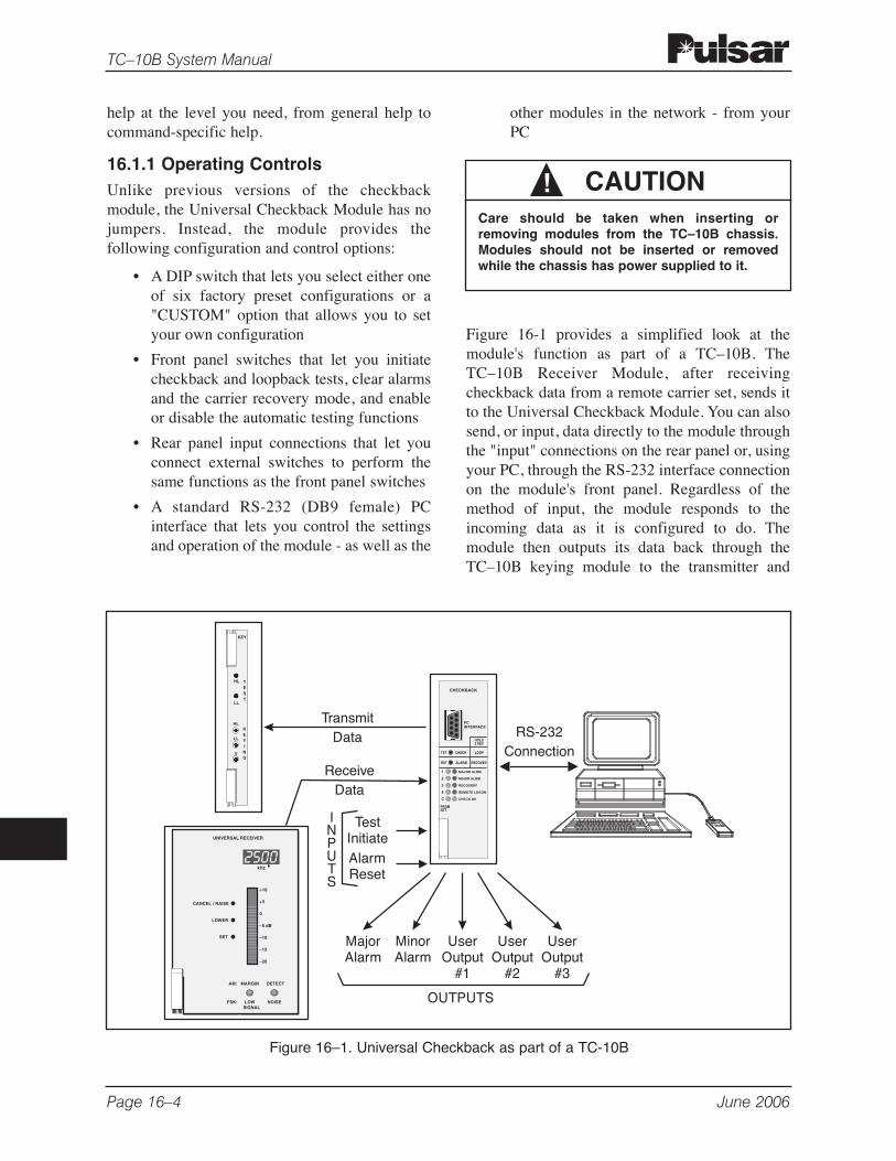
Page 16–4 June 2006
TC–10B System Manual
help at the level you need, from general help tocommand-specific help.
16.1.1 Operating ControlsUnlike previous versions of the checkbackmodule, the Universal Checkback Module has nojumpers. Instead, the module provides thefollowing configuration and control options:
• A DIP switch that lets you select either oneof six factory preset configurations or a"CUSTOM" option that allows you to setyour own configuration
• Front panel switches that let you initiatecheckback and loopback tests, clear alarmsand the carrier recovery mode, and enableor disable the automatic testing functions
• Rear panel input connections that let youconnect external switches to perform thesame functions as the front panel switches
• A standard RS-232 (DB9 female) PCinterface that lets you control the settingsand operation of the module - as well as the
other modules in the network - from yourPC
Figure 16-1 provides a simplified look at themodule's function as part of a TC–10B. TheTC–10B Receiver Module, after receivingcheckback data from a remote carrier set, sends itto the Universal Checkback Module. You can alsosend, or input, data directly to the module throughthe "input" connections on the rear panel or, usingyour PC, through the RS-232 interface connectionon the module's front panel. Regardless of themethod of input, the module responds to theincoming data as it is configured to do. Themodule then outputs its data back through theTC–10B keying module to the transmitter and
MajorAlarm
AlarmReset
TestInitiate
UserOutput
#1
UserOutput
#2
UserOutput
#3
MinorAlarm
OUTPUTS
INPUTS
ReceiveData
TransmitData RS-232
Connection
KEY
HL
HL
LL
LL
T
E
S
T
K
E
Y
I
N
GV
UNIVERSAL RECEIVER
CANCEL / RAISE
LOWER
SET
AM: MARGIN DETECT
FSK: LOW NOISESIGNAL
kHz
+10
+5
0
–5 dB
–10
–15
–20
2500
RECOVER
LOOP
HOLD2 SEC
PRGMSET
TST CHECK
RST ALARM
MAJOR ALRM1
MINOR ALRM2
RECOVERY3
REMOTE LOGON
CHECKBACK
4
C CHECK OK
PCINTERFACE
Figure 16–1. Universal Checkback as part of a TC-10B
! CAUTIONCare should be taken when inserting orremoving modules from the TC–10B chassis.Modules should not be inserted or removedwhile the chassis has power supplied to it.
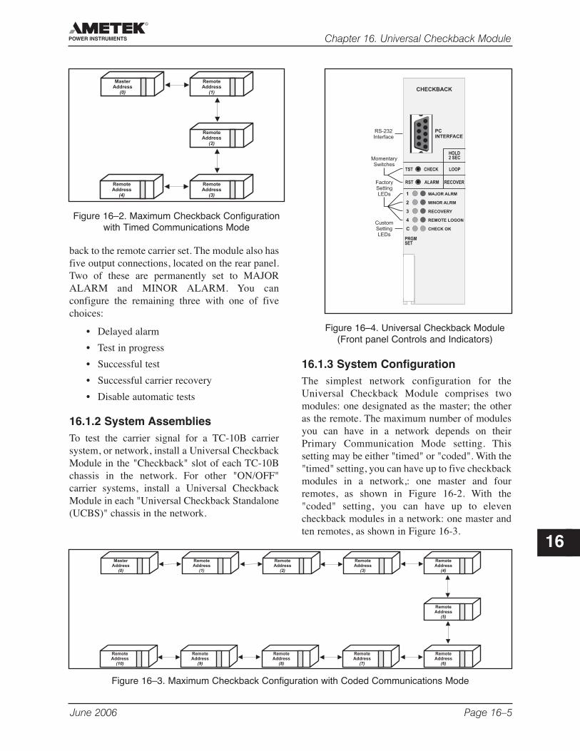
June 2006 Page 16–5
Chapter 16. Universal Checkback Module
16
back to the remote carrier set. The module also hasfive output connections, located on the rear panel.Two of these are permanently set to MAJORALARM and MINOR ALARM. You canconfigure the remaining three with one of fivechoices:
• Delayed alarm
• Test in progress
• Successful test
• Successful carrier recovery
• Disable automatic tests
16.1.2 System AssembliesTo test the carrier signal for a TC-10B carriersystem, or network, install a Universal CheckbackModule in the "Checkback" slot of each TC-10Bchassis in the network. For other "ON/OFF"carrier systems, install a Universal CheckbackModule in each "Universal Checkback Standalone(UCBS)" chassis in the network.
16.1.3 System ConfigurationThe simplest network configuration for theUniversal Checkback Module comprises twomodules: one designated as the master; the otheras the remote. The maximum number of modulesyou can have in a network depends on theirPrimary Communication Mode setting. Thissetting may be either "timed" or "coded". With the"timed" setting, you can have up to five checkbackmodules in a network,: one master and fourremotes, as shown in Figure 16-2. With the"coded" setting, you can have up to elevencheckback modules in a network: one master andten remotes, as shown in Figure 16-3.
MasterAddress
(0)
RemoteAddress
(1)
RemoteAddress
(2)
RemoteAddress
(3)
RemoteAddress
(4)
Figure 16–2. Maximum Checkback Configurationwith Timed Communications Mode
Figure 16–3. Maximum Checkback Configuration with Coded Communications Mode
MasterAddress
(0)
RemoteAddress
(1)
RemoteAddress
(2)
RemoteAddress
(3)
RemoteAddress
(4)
RemoteAddress
(5)
RemoteAddress
(6)
RemoteAddress
(7)
RemoteAddress
(8)
RemoteAddress
(9)
RemoteAddress
(10)
Figure 16–4. Universal Checkback Module (Front panel Controls and Indicators)
RECOVER
LOOP
HOLD2 SEC
PRGMSET
TST CHECK
RST ALARM
MAJOR ALRM1
MINOR ALRM2
RECOVERY3
REMOTE LOGON
CHECKBACK
4
C CHECK OK
PCINTERFACE
FactorySettingLEDs
MomentarySwitches
RS-232Interface
CustomSettingLEDs
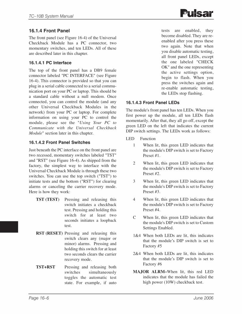
Page 16–6 June 2006
TC–10B System Manual
16.1.4 Front PanelThe front panel (see Figure 16-4) of the UniversalCheckback Module has a PC connector, twomomentary switches, and ten LEDs. All of theseare described later in this chapter.
16.1.4.1 PC Interface
The top of the front panel has a DB9 femaleconnector labeled "PC INTERFACE" (see Figure16-4). This connector is provided so that you canplug in a serial cable connected to a serial commu-nication port on your PC or laptop. This should bea standard cable without a null modem. Onceconnected, you can control the module (and anyother Universal Checkback Modules in thenetwork) from your PC or laptop. For completeinformation on using your PC to control themodule, please see the "Using Your PC toCommunicate with the Universal CheckbackModule" section later in this chapter.
16.1.4.2 Front Panel Switches
Just beneath the PC interface on the front panel aretwo recessed, momentary switches labeled "TST"and "RST" (see Figure 16-4). As shipped from thefactory, the simplest way to interface with theUniversal Checkback Module is through these twoswitches. You can use the top switch ("TST") toinitiate tests and the bottom ("RST") for clearingalarms or canceling the carrier recovery mode.Here is how they work:
TST (TEST) Pressing and releasing thisswitch initiates a checkbacktest. Pressing and holding thisswitch for at least twoseconds initiates a loopbacktest.
RST (RESET) Pressing and releasing thisswitch clears any (major orminor) alarms. Pressing andholding this switch for at leasttwo seconds clears the carrierrecovery mode.
TST+RST Pressing and releasing bothswitches simultaneouslytoggles the automatic teststate. For example, if auto
tests are enabled, theybecome disabled. They are re-enabled after you press thesetwo again. Note that whenyou disable automatic testing,all front panel LEDs, exceptthe one labeled "CHECKOK" and the one representingthe active settings option,begin to flash. When youpress the switches again andre-enable automatic testing,the LEDs stop flashing.
16.1.4.3 Front Panel LEDs
The module's front panel has ten LEDs. When youfirst power up the module, all ten LEDs flashmomentarily. After that, they all go off, except thegreen LED on the left that indicates the currentDIP switch settings. The LEDs work as follows:
LED Function
1 When lit, this green LED indicates thatthe module's DIP switch is set to FactoryPreset #1.
2 When lit, this green LED indicates thatthe module's DIP switch is set to FactoryPreset #2.
3 When lit, this green LED indicates thatthe module's DIP switch is set to FactoryPreset #3.
4 When lit, this green LED indicates thatthe module's DIP switch is set to FactoryPreset #4.
C When lit, this green LED indicates thatthe module's DIP switch is set to CustomSettings Enabled.
1&4 When both LEDs are lit, this indicatesthat the module’s DIP switch is set toFactory #5
2&4 When both LEDs are lit, this indicatesthat the module’s DIP switch is set toFactory #6
MAJOR ALRM–When lit, this red LEDindicates that the module has failed thehigh power (10W) checkback test.
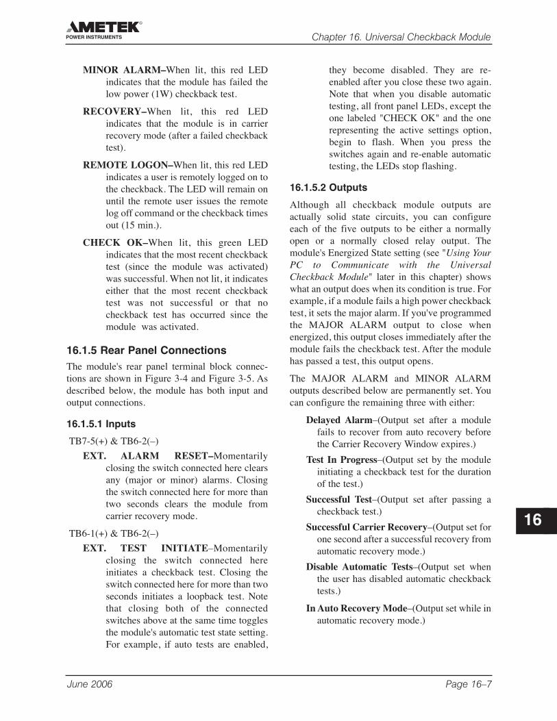
June 2006 Page 16–7
Chapter 16. Universal Checkback Module
16
MINOR ALARM–When lit, this red LEDindicates that the module has failed thelow power (1W) checkback test.
RECOVERY–When lit, this red LEDindicates that the module is in carrierrecovery mode (after a failed checkbacktest).
REMOTE LOGON–When lit, this red LEDindicates a user is remotely logged on tothe checkback. The LED will remain onuntil the remote user issues the remotelog off command or the checkback timesout (15 min.).
CHECK OK–When lit, this green LEDindicates that the most recent checkbacktest (since the module was activated)was successful. When not lit, it indicateseither that the most recent checkbacktest was not successful or that nocheckback test has occurred since themodule was activated.
16.1.5 Rear Panel ConnectionsThe module's rear panel terminal block connec-tions are shown in Figure 3-4 and Figure 3-5. Asdescribed below, the module has both input andoutput connections.
16.1.5.1 Inputs
TB7-5(+) & TB6-2(–)
EXT. ALARM RESET–Momentarilyclosing the switch connected here clearsany (major or minor) alarms. Closingthe switch connected here for more thantwo seconds clears the module fromcarrier recovery mode.
TB6-1(+) & TB6-2(–)
EXT. TEST INITIATE–Momentarilyclosing the switch connected hereinitiates a checkback test. Closing theswitch connected here for more than twoseconds initiates a loopback test. Notethat closing both of the connectedswitches above at the same time togglesthe module's automatic test state setting.For example, if auto tests are enabled,
they become disabled. They are re-enabled after you close these two again.Note that when you disable automatictesting, all front panel LEDs, except theone labeled "CHECK OK" and the onerepresenting the active settings option,begin to flash. When you press theswitches again and re-enable automatictesting, the LEDs stop flashing.
16.1.5.2 Outputs
Although all checkback module outputs areactually solid state circuits, you can configureeach of the five outputs to be either a normallyopen or a normally closed relay output. Themodule's Energized State setting (see "Using YourPC to Communicate with the UniversalCheckback Module" later in this chapter) showswhat an output does when its condition is true. Forexample, if a module fails a high power checkbacktest, it sets the major alarm. If you've programmedthe MAJOR ALARM output to close whenenergized, this output closes immediately after themodule fails the checkback test. After the modulehas passed a test, this output opens.
The MAJOR ALARM and MINOR ALARMoutputs described below are permanently set. Youcan configure the remaining three with either:
Delayed Alarm–(Output set after a modulefails to recover from auto recovery beforethe Carrier Recovery Window expires.)
Test In Progress–(Output set by the moduleinitiating a checkback test for the durationof the test.)
Successful Test–(Output set after passing acheckback test.)
Successful Carrier Recovery–(Output set forone second after a successful recovery fromautomatic recovery mode.)
Disable Automatic Tests–(Output set whenthe user has disabled automatic checkbacktests.)
In Auto Recovery Mode–(Output set while inautomatic recovery mode.)
Page 16–8 June 2006
TC–10B System Manual
You can program the two alarm outputs to seal orjust momentarily toggle when an alarm occurs.When you select sealed operation, the alarmoutputs stay in their true, or energized, states aslong as the alarm exists. If you select momentary,the outputs go to their true states for only fiveseconds, then return to their previous states. Forexample, assume alarms are set to momentaryaction and the major alarm active state is closed.Normally this output is open. When a major alarmoccurs, the MAJOR ALARM output closes forfive seconds then opens again. The MAJORALARM output does not change (again) when themajor alarm is cleared.
TB6-3(+) & TB6-4(–)
MAJOR ALARM–This output is energized(i.e., opened or closed) when the modulefails a high power (10W) checkbacktest. If it is set for sealed operation, theoutput returns to its un-energized statewhen the module passes a high powercheckback test. If it is set for momentaryoperation, it returns to its un-energizedstate after five seconds.
TB6-5(+) & TB6-6(–)
MINOR ALARM–This output is energized(i.e., opened or closed) when the modulefails a low power (1W) checkback test.If it is set for sealed operation, theoutput returns to its un-energized statewhen the module passes a low powercheckback test. If it is set for momentaryoperation, it returns to its un-energizedstate after five seconds.
TB6-7(+) & TB5-7(–)
USER DEFINED 1–This output is energizedwhen the condition (one of the fivelisted above) you have programmed it tomonitor becomes true. It remainsenergized until the condition is nolonger true. It then reverts to its formerstate.
TB6-8(+) & TB5-8(–)
USER DEFINED 2–This output is energizedwhen the condition (one of the fivelisted earlier) you have programmed it to
monitor becomes true. It remainsenergized until the condition is nolonger true. It then reverts to its formerstate.
TB6-9(+) & TB5-9(–)
USER DEFINED 3–This output is energizedwhen the condition (one of the fivelisted earlier) you have programmed it tomonitor becomes true. It remainsenergized until the condition is nolonger true. It then reverts to its formerstate.
16.1.6 PC BoardThe component layout for the UniversalCheckback Module's PC board is shown in Figure16-11. The module's PC board does not have anyoperator controls. The only "user" settings arethose on the DIP switch labeled "SW3." Thisswitch lets you select either one of four factorypreset configurations or a "CUSTOM" option thatallows you to set your own configuration, using aconnected PC or laptop. For complete instructionson setting the DIP switch, please see the"Installation and Setup" section later in thischapter.
16.2 Installation and SetupTypically, the Universal Checkback Module isalready installed in the TC-10B Carrier set orUCBS chassis when you receive it from thefactory. By default, the module's DIP switch(SW3) is set to the Factory Preset #1 setting (seeTable 16-3). If your Universal Checkback Moduleis already installed and the Factory Preset #1setting is the configuration you want, skip the firstthree steps.
To install and configure a new UniversalCheckback Module, complete the followingsteps.
Step 1. Unpack the module.
Open the carton and remove the UniversalCheckback Module. Check the software versionsof all checkback modules working together tomake sure they are the same basic revision, espe-
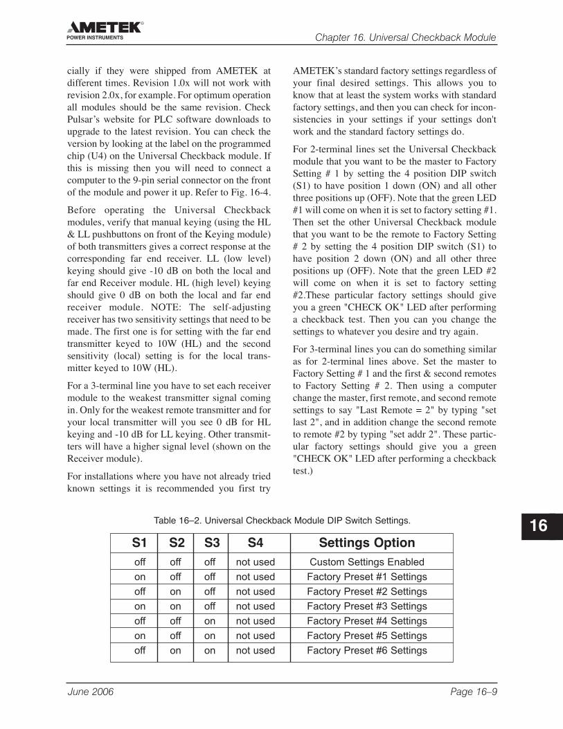
June 2006 Page 16–9
Chapter 16. Universal Checkback Module
16
cially if they were shipped from AMETEK atdifferent times. Revision 1.0x will not work withrevision 2.0x, for example. For optimum operationall modules should be the same revision. CheckPulsar’s website for PLC software downloads toupgrade to the latest revision. You can check theversion by looking at the label on the programmedchip (U4) on the Universal Checkback module. Ifthis is missing then you will need to connect acomputer to the 9-pin serial connector on the frontof the module and power it up. Refer to Fig. 16-4.
Before operating the Universal Checkbackmodules, verify that manual keying (using the HL& LL pushbuttons on front of the Keying module)of both transmitters gives a correct response at thecorresponding far end receiver. LL (low level)keying should give -10 dB on both the local andfar end Receiver module. HL (high level) keyingshould give 0 dB on both the local and far endreceiver module. NOTE: The self-adjustingreceiver has two sensitivity settings that need to bemade. The first one is for setting with the far endtransmitter keyed to 10W (HL) and the secondsensitivity (local) setting is for the local trans-mitter keyed to 10W (HL).
For a 3-terminal line you have to set each receivermodule to the weakest transmitter signal comingin. Only for the weakest remote transmitter and foryour local transmitter will you see 0 dB for HLkeying and -10 dB for LL keying. Other transmit-ters will have a higher signal level (shown on theReceiver module).
For installations where you have not already triedknown settings it is recommended you first try
AMETEK’s standard factory settings regardless ofyour final desired settings. This allows you toknow that at least the system works with standardfactory settings, and then you can check for incon-sistencies in your settings if your settings don'twork and the standard factory settings do.
For 2-terminal lines set the Universal Checkbackmodule that you want to be the master to FactorySetting # 1 by setting the 4 position DIP switch(S1) to have position 1 down (ON) and all otherthree positions up (OFF). Note that the green LED#1 will come on when it is set to factory setting #1.Then set the other Universal Checkback modulethat you want to be the remote to Factory Setting# 2 by setting the 4 position DIP switch (S1) tohave position 2 down (ON) and all other threepositions up (OFF). Note that the green LED #2will come on when it is set to factory setting#2.These particular factory settings should giveyou a green "CHECK OK" LED after performinga checkback test. Then you can you change thesettings to whatever you desire and try again.
For 3-terminal lines you can do something similaras for 2-terminal lines above. Set the master toFactory Setting # 1 and the first & second remotesto Factory Setting # 2. Then using a computerchange the master, first remote, and second remotesettings to say "Last Remote = 2" by typing "setlast 2", and in addition change the second remoteto remote #2 by typing "set addr 2". These partic-ular factory settings should give you a green"CHECK OK" LED after performing a checkbacktest.)
Table 16–2. Universal Checkback Module DIP Switch Settings.
S1 S2 S3 S4 Settings Optionoff off off not used Custom Settings Enabled
on off off not used Factory Preset #1 Settings
off on off not used Factory Preset #2 Settings
on on off not used Factory Preset #3 Settings
off off on not used Factory Preset #4 Settings
on off on not used Factory Preset #5 Settings
off on on not used Factory Preset #6 Settings
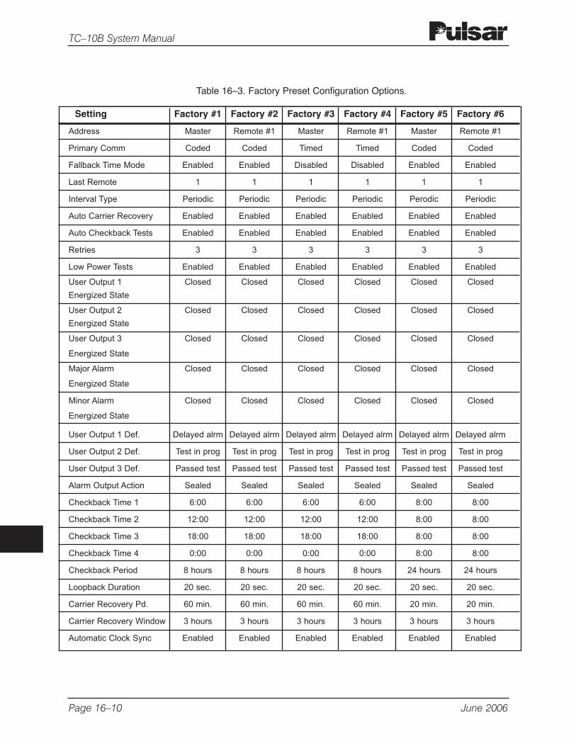
Page 16–10 June 2006
TC–10B System Manual
Setting Factory #1 Factory #2 Factory #3 Factory #4 Factory #5 Factory #6
Address Master Remote #1 Master Remote #1 Master Remote #1
Primary Comm Coded Coded Timed Timed Coded Coded
Fallback Time Mode Enabled Enabled Disabled Disabled Enabled Enabled
Last Remote 1 1 1 1 1 1
Interval Type Periodic Periodic Periodic Periodic Perodic Periodic
Auto Carrier Recovery Enabled Enabled Enabled Enabled Enabled Enabled
Auto Checkback Tests Enabled Enabled Enabled Enabled Enabled Enabled
Retries 3 3 3 3 3 3
Low Power Tests Enabled Enabled Enabled Enabled Enabled Enabled
User Output 1 Closed Closed Closed Closed Closed Closed
Energized State
User Output 2 Closed Closed Closed Closed Closed Closed
Energized State
User Output 3 Closed Closed Closed Closed Closed Closed
Energized State
Major Alarm Closed Closed Closed Closed Closed Closed
Energized State
Minor Alarm Closed Closed Closed Closed Closed Closed
Energized State
User Output 1 Def. Delayed alrm Delayed alrm Delayed alrm Delayed alrm Delayed alrm Delayed alrm
User Output 2 Def. Test in prog Test in prog Test in prog Test in prog Test in prog Test in prog
User Output 3 Def. Passed test Passed test Passed test Passed test Passed test Passed test
Alarm Output Action Sealed Sealed Sealed Sealed Sealed Sealed
Checkback Time 1 6:00 6:00 6:00 6:00 8:00 8:00
Checkback Time 2 12:00 12:00 12:00 12:00 8:00 8:00
Checkback Time 3 18:00 18:00 18:00 18:00 8:00 8:00
Checkback Time 4 0:00 0:00 0:00 0:00 8:00 8:00
Checkback Period 8 hours 8 hours 8 hours 8 hours 24 hours 24 hours
Loopback Duration 20 sec. 20 sec. 20 sec. 20 sec. 20 sec. 20 sec.
Carrier Recovery Pd. 60 min. 60 min. 60 min. 60 min. 20 min. 20 min.
Carrier Recovery Window 3 hours 3 hours 3 hours 3 hours 3 hours 3 hours
Automatic Clock Sync Enabled Enabled Enabled Enabled Enabled Enabled
Table 16–3. Factory Preset Configuration Options.
June 2006 Page 16–11
Chapter 16. Universal Checkback Module
16
Step 2. Set the DIP switch.
The DIP switch, labeled "SW3", is on the bottomleft of the Module's PC board. The module readsthe switch's setting at power-up to determine itsconfiguration. Any changes to the switch's settingafter power-up are ignored until you turn thepower off and on again.
Using Table 16-2 & Fig. 16-9 as guides, set theDIP switch to the desired setting. Note that onlyS1-S3 are used; S4 is reserved for future use. Toset S1-S3, put them in the up position for OFF andthe down position for ON. You can set the DIPswitch to one of five possible configurations. Allother switch combinations (of S1-S3) are invalid.If you mistakenly set a different combination, themodule assumes the "CUSTOM" mode.
If you set the DIP switch to one of the factorypreset settings, the module is locked into thatconfiguration. You cannot then customize thesettings. The factory preset configurations areshown in Table 16-3. For descriptions of the indi-vidual settings, please see the "ConfigurationSettings" section later in this chapter.
If you set the DIP switch to the "CUSTOM"option, you can use your PC or laptop to configurethe module any way you want. (See "Using yourPC to Communicate with the UniversalCheckback Module" for complete configurationinstructions.)
Step 3. Insert the module into the carrierchassis.
Power down your TC–10B chassis. Carefullyinsert the Universal Checkback Module into thetop and bottom grooves of the slot labeled"CHECKBACK". Lock it into place using thewhite inject/eject lever on the front of the module.Power up the chassis. During the first 3 secondsafter power up, the module’s address is displayedusing a combination of the five green LEDs. TheLEDs use the code listed here.
• Master = CUSTOM LED on
• Remote 1 = LED 1 on
• Remote 2 = LED 2 on
• Remote 3 = LED 3 on
• Remote 4 = LED 4 on
After four seconds, all Checkback LEDs come onfor one second, and then they all turn off exceptfor one of the five DIP switch LEDs. This LEDindicates which configuration the DIP switch is setto (see "Front Panel LEDs" earlier in this chapter).
Step 4. Connect your computer andestablish communications.
Connect one end of a standard serial cable to theserial communications port on your computer andthe other end to the DB9 (female) connectorlabeled "PC INTERFACE" on the module's front
panel (see Figure 16-4). You don't need a nullmodem here, just a simple, straight cable.
Start a terminal emulation communicationprogram (e.g., "Hyper Terminal" in Windows'95/98/NT, "Winterm" in Windows 3.1, or"Procomm" in DOS). Set the program's communi-cation parameters as follows:
• Bits per second (data rate) = 9600
• Data bits (per word) = 8
• Stop bits = 1
• Parity = none
• Flow control (handshaking) = none
• Terminal/Telnet Terminal ID=ANSI
Because these are very common settings, you mayonly have to set the first one, bits per second (datarate).
Once you are connected, the module should returnthe password prompt.
If your screen seems to display garbled informa-tion first check your communication programsettings to make sure “Emulation” and “TelnetTerminal ID” are both set to “ANSI”. You mayhave also started your communication program
NOTE:
Note: If you are not doing a custom setting andare using one of the DIP switch factory presets,then you can skip to step 9.
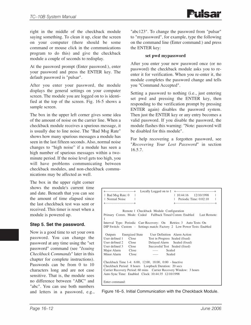
Page 16–12 June 2006
TC–10B System Manual
right in the middle of the checkback modulesaying something. To clean it up, clear the screenon your computer (there should be somecommand or mouse click in the communicationsprogram to do this) and give the checkbackmodule a couple of seconds to redisplay.
At the password prompt (Enter password:), enteryour password and press the ENTER key. Thedefault password is "pulsar".
After you enter your password, the moduledisplays the general settings on your computerscreen. The module you are logged on to is identi-fied at the top of the screen. Fig. 16-5 shows asample screen.
The box in the upper left corner gives some ideaof the amount of noise on the carrier line. When acheckback module receives a spurious message, itis usually due to line noise. The "Bad Msg Rate"shows how many spurious messages a module hasseen in the last fifteen seconds. Also, normal noisechanges to “high noise” if a module has seen ahigh number of spurious messages within a two-minute period. If the noise level gets too high, youwill have problems communicating betweencheckback modules, and non-checkback commu-nications may be affected as well.
The box in the upper right cornershows the module's current timeand date. Beneath that you can seethe amount of time elapsed sincethe last checkback test was sent orreceived. This timer is reset when amodule is powered up.
Step 5. Set the password.
Now is a good time to set your ownpassword. You can change thepassword at any time using the "setpassword" command (see "IssuingCheckback Commands" later in thischapter for complete instructions).Passwords can be from 0 to 10characters long and are not casesensitive. That is, the module seesno difference between "ABC" and"abc". You can use both numbersand letters in a password, e.g.,
"abc123". To change the password from "pulsar"to "mypassword", for example, type the followingon the command line (Enter command:) and pressthe ENTER key:
set pwd mypassword
After you enter your new password once (or nopassword) the checkback module asks you to re-enter it for verification. When you re-enter it, themodule completes the password change and tellsyou "Command Accepted".
Setting a password to nothing (i.e., just enteringset pwd and pressing the ENTER key, thenresponding to the verification prompt by pressingENTER again) disables the password system.Then just the ENTER key or any entry becomes avalid password. If you disable the password, themodule flashes this warning: "Note: password willbe disabled for this module".
For help recovering a forgotten password, see"Recovering Your Lost Password" in section16.5.7.
+--------------------------+ Locally Logged on to 1 +-----------------------------------+| Bad Msg Rate: 0 | | 10:44:16 12/10/1998 || Normal Noise | | Periodic Time: 0:02:10 |
+--------------------------+ +------------------------------------+
Remote 1 Checkback Module ConfigurationPrimary Comm. Mode: Coded Fallback Timed Comm: Enabled Last Remote:1Interval Type: Periodic Carr Recovery: On Retries: 3 Auto Tests: OnDIP Switch: Custom - Settings match: Factory 2 Low Power Tests: Enabled
Outputs Energized State User Definition Alarm ActionUser defined 1 Close Test in Progress Sealed (fixed)User defined 2 Close Delayed Alarm Sealed (fixed)User defined 3 Close Successful Test Sealed (fixed)Major Alarm Close ----- SealedMinor Alarm Close ----- Sealed
Checkback Time 1-4: 6:00, 12:00, 18:00, 0:00 - InactiveCheckback Period: 8 hours Loopback Duration: 20 secsCarrier Recovery Period: 60 mins Carrier Recovery Window: 3 hoursAuto Sync Time: Enabled Clock: 10:44:35 12/10/1998
Enter command:
Figure 16–5. Initial Communication with the Checkback Module.
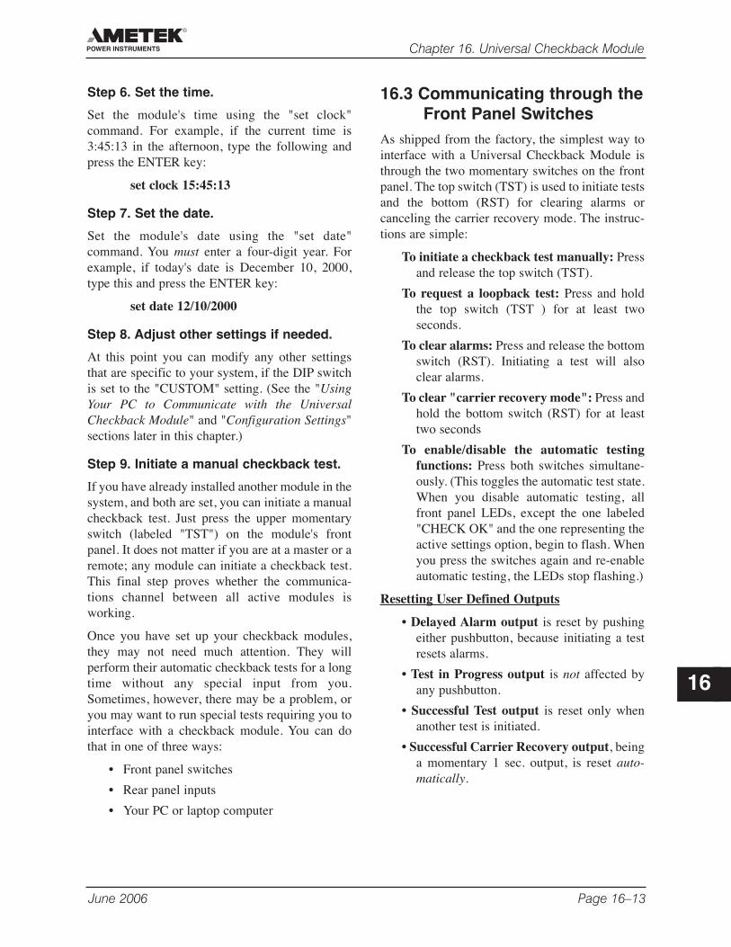
June 2006 Page 16–13
Chapter 16. Universal Checkback Module
16
Step 6. Set the time.
Set the module's time using the "set clock"command. For example, if the current time is3:45:13 in the afternoon, type the following andpress the ENTER key:
set clock 15:45:13
Step 7. Set the date.
Set the module's date using the "set date"command. You must enter a four-digit year. Forexample, if today's date is December 10, 2000,type this and press the ENTER key:
set date 12/10/2000
Step 8. Adjust other settings if needed.
At this point you can modify any other settingsthat are specific to your system, if the DIP switchis set to the "CUSTOM" setting. (See the "UsingYour PC to Communicate with the UniversalCheckback Module" and "Configuration Settings"sections later in this chapter.)
Step 9. Initiate a manual checkback test.
If you have already installed another module in thesystem, and both are set, you can initiate a manualcheckback test. Just press the upper momentaryswitch (labeled "TST") on the module's frontpanel. It does not matter if you are at a master or aremote; any module can initiate a checkback test.This final step proves whether the communica-tions channel between all active modules isworking.
Once you have set up your checkback modules,they may not need much attention. They willperform their automatic checkback tests for a longtime without any special input from you.Sometimes, however, there may be a problem, oryou may want to run special tests requiring you tointerface with a checkback module. You can dothat in one of three ways:
• Front panel switches
• Rear panel inputs
• Your PC or laptop computer
16.3 Communicating through theFront Panel Switches
As shipped from the factory, the simplest way tointerface with a Universal Checkback Module isthrough the two momentary switches on the frontpanel. The top switch (TST) is used to initiate testsand the bottom (RST) for clearing alarms orcanceling the carrier recovery mode. The instruc-tions are simple:
To initiate a checkback test manually: Pressand release the top switch (TST).
To request a loopback test: Press and holdthe top switch (TST ) for at least twoseconds.
To clear alarms: Press and release the bottomswitch (RST). Initiating a test will alsoclear alarms.
To clear "carrier recovery mode": Press andhold the bottom switch (RST) for at leasttwo seconds
To enable/disable the automatic testingfunctions: Press both switches simultane-ously. (This toggles the automatic test state.When you disable automatic testing, allfront panel LEDs, except the one labeled"CHECK OK" and the one representing theactive settings option, begin to flash. Whenyou press the switches again and re-enableautomatic testing, the LEDs stop flashing.)
Resetting User Defined Outputs
• Delayed Alarm output is reset by pushingeither pushbutton, because initiating a testresets alarms.
• Test in Progress output is not affected byany pushbutton.
• Successful Test output is reset only whenanother test is initiated.
• Successful Carrier Recovery output, beinga momentary 1 sec. output, is reset auto-matically.
Page 16–14 June 2006
TC–10B System Manual
16.4 Communicating through theRear Panel Terminal Block
An alternative method of communicating with theUniversal Checkback Module is through its rearpanel. You can connect two external "input"switches to the rear panel (see "Rear PanelConnections" earlier in this chapter). You can usethese switches to perform the same functions asthe module's own front panel switches. Here ishow:
To initiate a checkback test manually:Close and quickly open the switchconnected to TB6-1 & TB6-2.
To request a loopback test: Close for at leasttwo seconds the switch connected to TB6-1& TB6-2.
To clear alarms: Close and quickly open theswitch connected to TB7-5 & TB6-2.
To clear "carrier recovery mode": Close forat least two seconds the switch connectedto TB7-5 & TB6-2.
To enable/disable the automatic testingfunctions: Close both switches simultane-ously. (This toggles the automatic test state.When you disable automatic testing, allfront panel LEDs, except the one labeled"CHECK OK" and the one representing theactive settings option, begin to flash. Whenyou press the switches again and re-enableautomatic testing, the LEDs stop flashing.)
16.5 Using Your PC toCommunicate with theUniversal CheckbackModule
The most comprehensive method of communi-cating with the Universal Checkback Module isthrough the PC interface on its front panel. Theamount of control you have over the module withthis method of communication depends on themodule's DIP switch setting. As noted earlier (see"Installation and Setup" earlier in this chapter), theDIP switch setting can be one of the factory
presets or a "CUSTOM" option. (See "Installationand Setup" earlier in this chapter for more detail.)
If you select one of the factory presets, you canstill issue all the "non-setting" commands to themodule (e.g., checkback tests, clearing alarms). Asfor the setting commands themselves, you willonly be able to use the following:
• Set password
• Set date
• Set clock
Selecting the "CUSTOM" option, on the otherhand, allows you to change any setting at will.
The following sections tell you how to establishcommunications with the checkback modules inyour network, configure their settings, performcheckback tests, issue checkback commands, andeven recover your password if you forget it.
If this is the first time you are communicating withthe module, it is a good idea to set the password,time, and date, as well as any other settings thatrequire changing. (See "Set the Password” in the“Installation & Setup” section for completeinstructions).
For a complete list of commands, see "IssuingCheckback Commands" and "CheckbackCommand Quick Reference" later in this chapter.
You will remain logged on to the module as longas you continue communicating with it. Afterfifteen minutes of inactivity, the module automat-ically logs you off. You can also log offdeliberately with the "logoff" command; thisprevents unauthorized access to the checkbackmodule.
16.5.1 Local & RemoteCommunications
Each Checkback Module in the carrier networkshould have a unique address. By definition,remote #1's address is "1", remote #2's address is"2", and so on. The master is always assignedaddress "0". These addresses are used to definehow a checkback module behaves, as well as toallow distant communication between modules(see "Distant Checkback Communications" laterin this chapter). You assign module addresses with
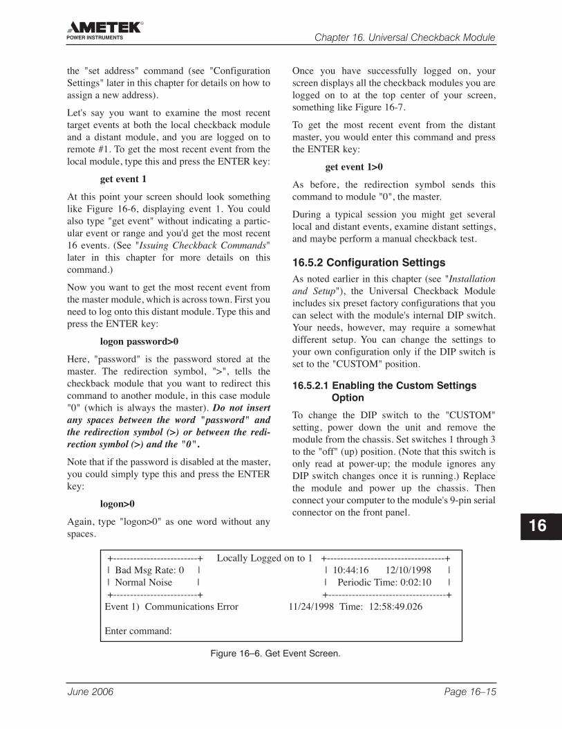
June 2006 Page 16–15
Chapter 16. Universal Checkback Module
16
the "set address" command (see "ConfigurationSettings" later in this chapter for details on how toassign a new address).
Let's say you want to examine the most recenttarget events at both the local checkback moduleand a distant module, and you are logged on toremote #1. To get the most recent event from thelocal module, type this and press the ENTER key:
get event 1
At this point your screen should look somethinglike Figure 16-6, displaying event 1. You couldalso type "get event" without indicating a partic-ular event or range and you'd get the most recent16 events. (See "Issuing Checkback Commands"later in this chapter for more details on thiscommand.)
Now you want to get the most recent event fromthe master module, which is across town. First youneed to log onto this distant module. Type this andpress the ENTER key:
logon password>0
Here, "password" is the password stored at themaster. The redirection symbol, ">", tells thecheckback module that you want to redirect thiscommand to another module, in this case module"0" (which is always the master). Do not insertany spaces between the word "password" andthe redirection symbol (>) or between the redi-rection symbol (>) and the "0".
Note that if the password is disabled at the master,you could simply type this and press the ENTERkey:
logon>0
Again, type "logon>0" as one word without anyspaces.
Once you have successfully logged on, yourscreen displays all the checkback modules you arelogged on to at the top center of your screen,something like Figure 16-7.
To get the most recent event from the distantmaster, you would enter this command and pressthe ENTER key:
get event 1>0
As before, the redirection symbol sends thiscommand to module "0", the master.
During a typical session you might get severallocal and distant events, examine distant settings,and maybe perform a manual checkback test.
16.5.2 Configuration SettingsAs noted earlier in this chapter (see "Installationand Setup"), the Universal Checkback Moduleincludes six preset factory configurations that youcan select with the module's internal DIP switch.Your needs, however, may require a somewhatdifferent setup. You can change the settings toyour own configuration only if the DIP switch isset to the "CUSTOM" position.
16.5.2.1 Enabling the Custom Settings Option
To change the DIP switch to the "CUSTOM"setting, power down the unit and remove themodule from the chassis. Set switches 1 through 3to the "off" (up) position. (Note that this switch isonly read at power-up; the module ignores anyDIP switch changes once it is running.) Replacethe module and power up the chassis. Thenconnect your computer to the module's 9-pin serialconnector on the front panel.
+-------------------------+ Locally Logged on to 1 +-----------------------------------+| Bad Msg Rate: 0 | | 10:44:16 12/10/1998 || Normal Noise | | Periodic Time: 0:02:10 |+-------------------------+ +-----------------------------------+
Event 1) Communications Error 11/24/1998 Time: 12:58:49.026
Enter command:
Figure 16–6. Get Event Screen.
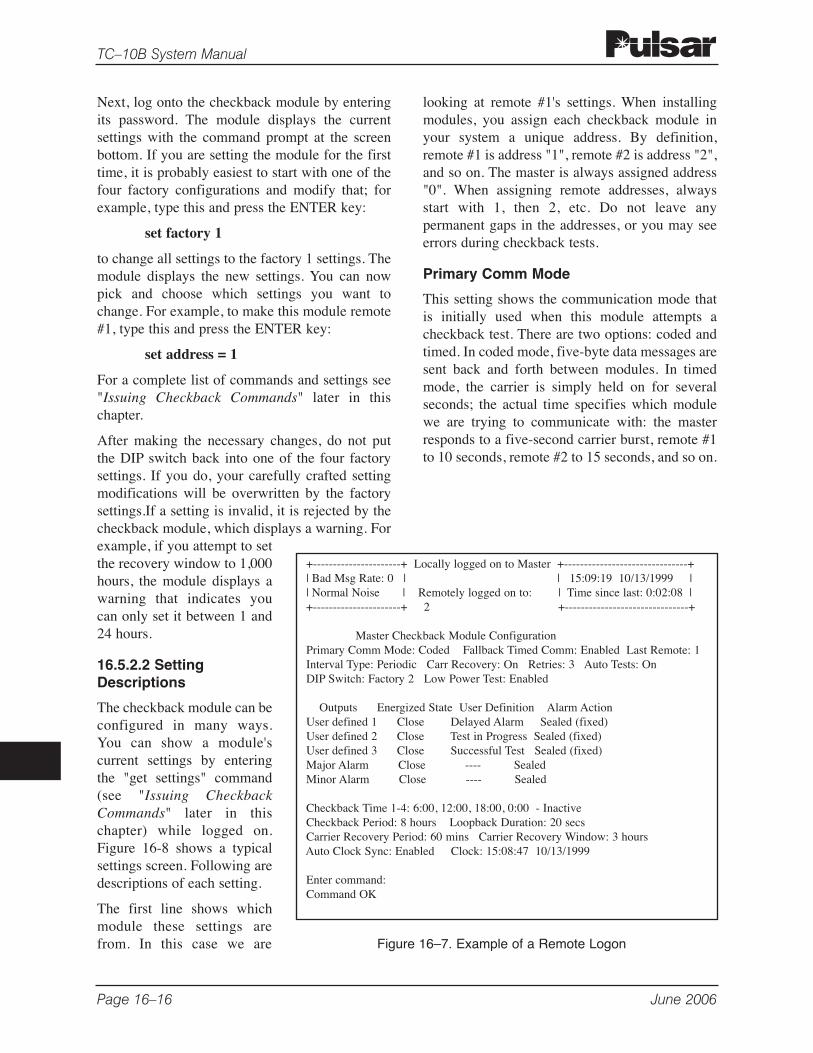
Page 16–16 June 2006
TC–10B System Manual
Next, log onto the checkback module by enteringits password. The module displays the currentsettings with the command prompt at the screenbottom. If you are setting the module for the firsttime, it is probably easiest to start with one of thefour factory configurations and modify that; forexample, type this and press the ENTER key:
set factory 1
to change all settings to the factory 1 settings. Themodule displays the new settings. You can nowpick and choose which settings you want tochange. For example, to make this module remote#1, type this and press the ENTER key:
set address = 1
For a complete list of commands and settings see"Issuing Checkback Commands" later in thischapter.
After making the necessary changes, do not putthe DIP switch back into one of the four factorysettings. If you do, your carefully crafted settingmodifications will be overwritten by the factorysettings.If a setting is invalid, it is rejected by thecheckback module, which displays a warning. Forexample, if you attempt to setthe recovery window to 1,000hours, the module displays awarning that indicates youcan only set it between 1 and24 hours.
16.5.2.2 SettingDescriptions
The checkback module can beconfigured in many ways.You can show a module'scurrent settings by enteringthe "get settings" command(see "Issuing CheckbackCommands" later in thischapter) while logged on.Figure 16-8 shows a typicalsettings screen. Following aredescriptions of each setting.
The first line shows whichmodule these settings arefrom. In this case we are
looking at remote #1's settings. When installingmodules, you assign each checkback module inyour system a unique address. By definition,remote #1 is address "1", remote #2 is address "2",and so on. The master is always assigned address"0". When assigning remote addresses, alwaysstart with 1, then 2, etc. Do not leave anypermanent gaps in the addresses, or you may seeerrors during checkback tests.
Primary Comm Mode
This setting shows the communication mode thatis initially used when this module attempts acheckback test. There are two options: coded andtimed. In coded mode, five-byte data messages aresent back and forth between modules. In timedmode, the carrier is simply held on for severalseconds; the actual time specifies which modulewe are trying to communicate with: the masterresponds to a five-second carrier burst, remote #1to 10 seconds, remote #2 to 15 seconds, and so on.
+----------------------+ Locally logged on to Master +-------------------------------+| Bad Msg Rate: 0 | | 15:09:19 10/13/1999 || Normal Noise | Remotely logged on to: | Time since last: 0:02:08 |+----------------------+ 2 +-------------------------------+
Master Checkback Module ConfigurationPrimary Comm Mode: Coded Fallback Timed Comm: Enabled Last Remote: 1Interval Type: Periodic Carr Recovery: On Retries: 3 Auto Tests: OnDIP Switch: Factory 2 Low Power Test: Enabled
Outputs Energized State User Definition Alarm ActionUser defined 1 Close Delayed Alarm Sealed (fixed)User defined 2 Close Test in Progress Sealed (fixed)User defined 3 Close Successful Test Sealed (fixed)Major Alarm Close ---- SealedMinor Alarm Close ---- Sealed
Checkback Time 1-4: 6:00, 12:00, 18:00, 0:00 - InactiveCheckback Period: 8 hours Loopback Duration: 20 secsCarrier Recovery Period: 60 mins Carrier Recovery Window: 3 hoursAuto Clock Sync: Enabled Clock: 15:08:47 10/13/1999
Enter command:Command OK
Figure 16–7. Example of a Remote Logon
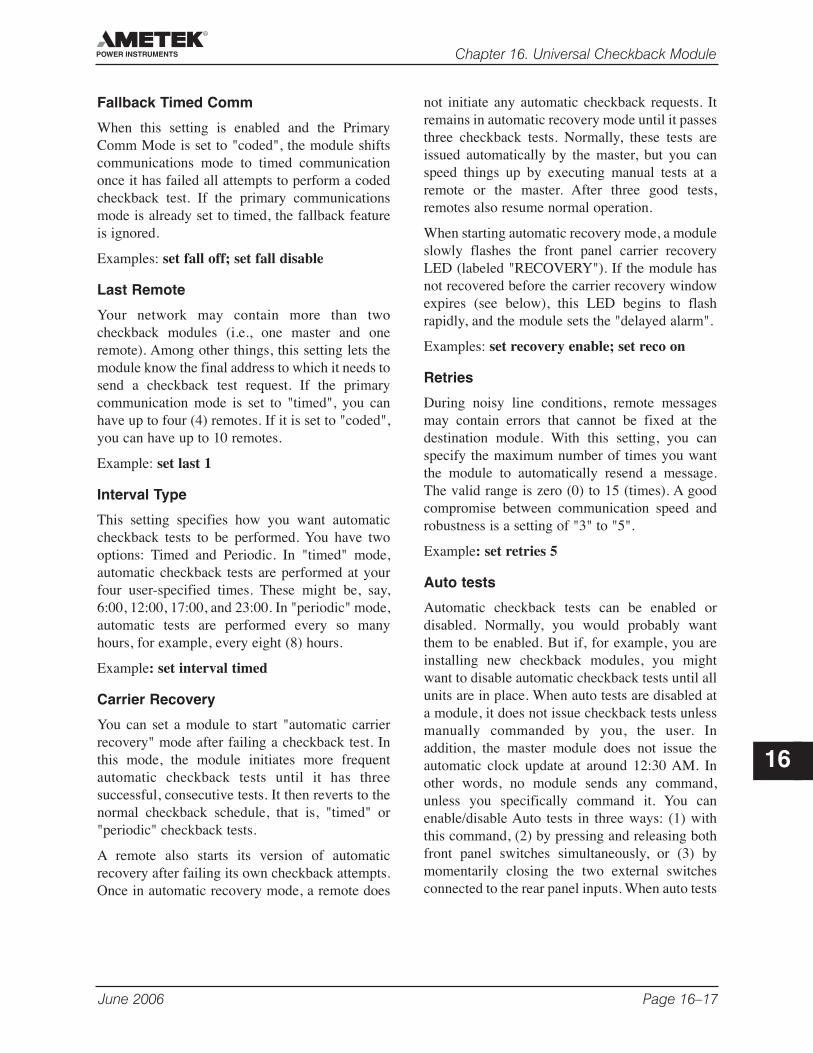
June 2006 Page 16–17
Chapter 16. Universal Checkback Module
16
Fallback Timed Comm
When this setting is enabled and the PrimaryComm Mode is set to "coded", the module shiftscommunications mode to timed communicationonce it has failed all attempts to perform a codedcheckback test. If the primary communicationsmode is already set to timed, the fallback featureis ignored.
Examples: set fall off; set fall disable
Last Remote
Your network may contain more than twocheckback modules (i.e., one master and oneremote). Among other things, this setting lets themodule know the final address to which it needs tosend a checkback test request. If the primarycommunication mode is set to "timed", you canhave up to four (4) remotes. If it is set to "coded",you can have up to 10 remotes.
Example: set last 1
Interval Type
This setting specifies how you want automaticcheckback tests to be performed. You have twooptions: Timed and Periodic. In "timed" mode,automatic checkback tests are performed at yourfour user-specified times. These might be, say,6:00, 12:00, 17:00, and 23:00. In "periodic" mode,automatic tests are performed every so manyhours, for example, every eight (8) hours.
Example: set interval timed
Carrier Recovery
You can set a module to start "automatic carrierrecovery" mode after failing a checkback test. Inthis mode, the module initiates more frequentautomatic checkback tests until it has threesuccessful, consecutive tests. It then reverts to thenormal checkback schedule, that is, "timed" or"periodic" checkback tests.
A remote also starts its version of automaticrecovery after failing its own checkback attempts.Once in automatic recovery mode, a remote does
not initiate any automatic checkback requests. Itremains in automatic recovery mode until it passesthree checkback tests. Normally, these tests areissued automatically by the master, but you canspeed things up by executing manual tests at aremote or the master. After three good tests,remotes also resume normal operation.
When starting automatic recovery mode, a moduleslowly flashes the front panel carrier recoveryLED (labeled "RECOVERY"). If the module hasnot recovered before the carrier recovery windowexpires (see below), this LED begins to flashrapidly, and the module sets the "delayed alarm".
Examples: set recovery enable; set reco on
Retries
During noisy line conditions, remote messagesmay contain errors that cannot be fixed at thedestination module. With this setting, you canspecify the maximum number of times you wantthe module to automatically resend a message.The valid range is zero (0) to 15 (times). A goodcompromise between communication speed androbustness is a setting of "3" to "5".
Example: set retries 5
Auto tests
Automatic checkback tests can be enabled ordisabled. Normally, you would probably wantthem to be enabled. But if, for example, you areinstalling new checkback modules, you mightwant to disable automatic checkback tests until allunits are in place. When auto tests are disabled ata module, it does not issue checkback tests unlessmanually commanded by you, the user. Inaddition, the master module does not issue theautomatic clock update at around 12:30 AM. Inother words, no module sends any command,unless you specifically command it. You canenable/disable Auto tests in three ways: (1) withthis command, (2) by pressing and releasing bothfront panel switches simultaneously, or (3) bymomentarily closing the two external switchesconnected to the rear panel inputs. When auto tests
Page 16–18 June 2006
TC–10B System Manual
are disabled, all the module's LEDs flash on andoff every second.
Example: set auto on
DIP Switch
This shows the current DIP switch setting. Thiscan be "CUSTOM" or one of the six factorypresets. If this switch is set to CUSTOM, but thecurrent settings are identical to one of the factorypresets, it shows the matching preset. In Figure16-7, this module's settings matched those wewould get if the DIP switch were set to factorypreset #2.
Low Power Tests
Here, you can enable or disable the low powersetting during checkback tests. When enabled, allcheckback tests initiated by this module are firstperformed on low power, then high power. Whendisabled, only the high-power test is performed.
Examples: set low enable; set low on
Outputs
Each checkback module has five outputs. Two ofthese are permanently set to major and minoralarms. You can configure the remaining threewith one of five choices:
"recover" (Successful Carrier Recovery):Output set for one second after a successfulrecovery from automatic recovery mode
"delay" (Delayed Alarm): Output set after amodule fails to recover from auto recoverybefore the carrier recovery window expires
"testing" (Test In Progress): Output set by thecheckback test-initiating module for theduration of the test
"pass" (Successful Test): Output set after initi-ating and passing a checkback test
"disable" (Disable Automatic Tests): Output setwhen the user has disabled automaticcheckback tests.
“in recovery” (In Auto Recovery Mode): Outputset while in automatic recovery mode.
As with most settings, you can only change thesesettings if the DIP switch is set to "CUSTOM".
Examples:
set def1 test–Sets user output 1 to show whena checkback test is in progress.
set def3 recover–Sets output 3 to showsuccessful automatic carrier recovery.
set def2 pass–Sets output 2 to show asuccessful checkback test.
set def1 delay–Sets output 1 to activate whena delayed alarm is initiated.
set def2 disable–Sets output 2 to activatewhen users disables auto tests.
Although all checkback module outputs areactually solid state circuits, each the five outputscan be set to act as either a normally open or anormally closed relay output. The Energized Stateshows how an output acts when its condition istrue. For example, if a module fails a checkbacktest, it sets the major alarm. If you haveprogrammed the major alarm output to close whenenergized, this output closes immediately afterfailing the checkback test. After the module haspassed a test, this output opens.
Conversely, if you had programmed the majoralarm output to open when energized, this outputwould open immediately after the module failed acheckback test and would close after it passed.
Examples:
set state1 open–Set user output 1 to openwhen the condition it is set to monitorbecomes true.
set state2 close–Set user output 2 to closewhen the condition it is set to monitorbecomes true.
set major open–Set the major output to openwhen the major alarm is active.
set minor close–Set the minor output to closewhen the minor alarm is active.
You can also program the two alarm outputs toseal or just momentarily toggle when an alarmoccurs. When you select "sealed" operation, thealarm outputs stay in their "true" states as long as
June 2006 Page 16–19
Chapter 16. Universal Checkback Module
16
the alarm exists. If you select "momentary", theoutputs go to their true states for only fiveseconds, then return to their previous states. Forexample, assume alarms are set to momentaryaction and the major alarm active state is closed.Normally this output is open. When a major alarmoccurs, the major alarm output closes for fiveseconds, then opens again. The major alarm outputdoes not change when the major alarm is cleared.
Examples:
set alarm sealed - Sets the major and minoralarms to remain in their active, or true,states as long as a major/minor alarmcondition exists.
set alarm momentary–Sets the major andminor alarms to shift to their active, or true,states for five seconds when a major/minoralarm condition occurs.
Checkback Time 1-4
These settings let you set the four times at whichyou want to execute automatic checkback tests fortimed checkback tests. When you set the IntervalType to "timed", the master initiates a checkbacktest at each of these times. You can set these timesonly to the nearest hour, using a 24-hour format.The master actually executes a timed test fiveminutes after the hour (e.g. 4:05). This delayprovides some "fudge" room to compensate forunsynchronized checkback module clocks.Remotes that have their Interval Types set toTimed also use these times to initiate their owncheckback tests, if they do not hear from the
master within a grace period. The grace period isten minutes after the hour for remote #1, fifteenminutes for remote #2, and so on.
If you do not want to use all four times, say youare only interested in three tests per day, you cansimply set one of the times equal to another. Forexample, you could set time 1 to 12:00, time 2 to6:00, time 3 to 18:00, and time 4 to 18:00 as well.
Example:
set time1 4–The module executes a checkback testat 4:05 a.m. if it is a master. If it is remote #1,it executes a test at 4:10, if it does not receive acheckback request from the master before thistime.
If the current Interval Type is Periodic, the word"Inactive" is displayed next to the checkbacktimes. This means that these times are disabledand checkback tests occur according to theperiodic interval (e.g., in the above example, every8 hours). When you set the Interval Type to"timed", these times become active and thePeriodic time is inactive.
Page 16–20 June 2006
TC–10B System Manual
Checkback Period
As mentioned above, the checkback period isenabled when the Interval Type is set to"periodic". If you wanted three tests per day andreally did not care about the time of day when theyoccurred, you could set this time to, say, 8 hours.Masters attempt periodic checkback tests atexactly this time, in our case eight hours since thelast test. Remotes have a grace period before they,too, attempt a checkback test, if they have notheard from the master. For example, remote #1would do a checkback test after eight hours andfive minutes, if it did not receive a checkback testfrom another module.
Example:
set period 8–The module executes acheckback test eight hours after the lasttest, if it is a master. If it is remote #1, itexecutes a test at 8:05, if it does not receivea checkback request from the master beforethis time.
Loopback Duration
The loopback duration specifies how long amodule holds the carrier on during a loopback test.Loopback tests are performed at both high and lowpower. If you are at remote #1 and request aloopback test at the master, it turns the carrier onhigh power then on low power for the duration ofthe time. You can use loopback tests to set thesensitivity of your local receiver or other suchtasks. The range of times is four to 60 seconds.You can request loopback tests in three ways: (1)with this command (e.g., do loop > 1 requestsremote #1 to do a loopback test), (2) by pressingand holding the top front panel switch, or (3) byclosing the switch connected to the rear inputTB6-1/TB6-2 for five seconds.
Example:
set loop 25–Sets the loopback duration to 25seconds.
Carrier Recovery Period
When the master is in carrier recovery mode afterfailing a checkback test, it begins initiatingcheckback tests according to the carrier recoveryperiod. For example, if the carrier recovery periodis 15 minutes, the master tries another checkbacktest every 15 minutes. It remains in carrierrecovery mode and continues to initiate tests every15 minutes, until it has successfully completedthree consecutive checkback tests. At that time, itshifts back to the normal mode, either periodic ortimed checkback tests.
Example:
set carrier 45–Sets the carrier recoveryperiod to 45 minutes
Carrier Recovery Window
The carrier recovery window is a time limit for thedelayed alarm. If a module goes into carrierrecovery mode and does not recover before thistime limit, it sets the delayed alarm. If any user-programmable output is set to delayed alarm, itbecomes active. The main reason for having acarrier recovery window and delayed alarm is tocut down on nuisance alarms. With this windowand the delayed alarm, you can design a systemthat only alerts you when a true, long-termproblem exists. The valid range for this window is1 to 24 hours.
Example:
set window 3–Sets the window to three hours.
Auto Clock Sync
When the auto clock sync is enabled, the mastersynchronizes all remote clocks to its own time,starting at 12:30 a.m. In practice, the synchroniza-tion is rough, within about +/- 2 seconds. But thatis sufficiently accurate for Timed checkbacktesting.
Examples:
set sync off (or)
set sync disable
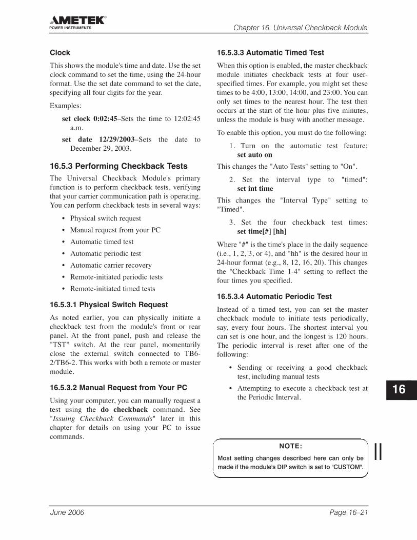
June 2006 Page 16–21
Chapter 16. Universal Checkback Module
16
Clock
This shows the module's time and date. Use the setclock command to set the time, using the 24-hourformat. Use the set date command to set the date,specifying all four digits for the year.
Examples:
set clock 0:02:45–Sets the time to 12:02:45a.m.
set date 12/29/2003–Sets the date toDecember 29, 2003.
16.5.3 Performing Checkback TestsThe Universal Checkback Module's primaryfunction is to perform checkback tests, verifyingthat your carrier communication path is operating.You can perform checkback tests in several ways:
• Physical switch request
• Manual request from your PC
• Automatic timed test
• Automatic periodic test
• Automatic carrier recovery
• Remote-initiated periodic tests
• Remote-initiated timed tests
16.5.3.1 Physical Switch Request
As noted earlier, you can physically initiate acheckback test from the module's front or rearpanel. At the front panel, push and release the"TST" switch. At the rear panel, momentarilyclose the external switch connected to TB6-2/TB6-2. This works with both a remote or mastermodule.
16.5.3.2 Manual Request from Your PC
Using your computer, you can manually request atest using the do checkback command. See"Issuing Checkback Commands" later in thischapter for details on using your PC to issuecommands.
16.5.3.3 Automatic Timed Test
When this option is enabled, the master checkbackmodule initiates checkback tests at four user-specified times. For example, you might set thesetimes to be 4:00, 13:00, 14:00, and 23:00. You canonly set times to the nearest hour. The test thenoccurs at the start of the hour plus five minutes,unless the module is busy with another message.
To enable this option, you must do the following:
1. Turn on the automatic test feature:set auto on
This changes the "Auto Tests" setting to "On".
2. Set the interval type to "timed":set int time
This changes the "Interval Type" setting to"Timed".
3. Set the four checkback test times: set time[#] [hh]
Where "#" is the time's place in the daily sequence(i.e., 1, 2, 3, or 4), and "hh" is the desired hour in24-hour format (e.g., 8, 12, 16, 20). This changesthe "Checkback Time 1-4" setting to reflect thefour times you specified.
16.5.3.4 Automatic Periodic Test
Instead of a timed test, you can set the mastercheckback module to initiate tests periodically,say, every four hours. The shortest interval youcan set is one hour, and the longest is 120 hours.The periodic interval is reset after one of thefollowing:
• Sending or receiving a good checkbacktest, including manual tests
• Attempting to execute a checkback test atthe Periodic Interval.
NOTE:
Most setting changes described here can only bemade if the module's DIP switch is set to "CUSTOM".
||
Page 16–22 June 2006
TC–10B System Manual
To enable this option:
1. Turn on the automatic test feature:set auto on
This changes the "Auto Tests" setting to "On".
2. Set the interval type to "periodic":set int period
This changes the "Interval Type" setting to"Periodic".
3. Set the interval for the checkback tests:set period[#]
Where "#" is the number of hours between tests.This changes the "Checkback Period" setting tothe time you specified.
16.5.3.5 Automatic Carrier Recovery
Using the set recovery command, you can set amodule to begin more frequent tests after failingany of the above checkback tests. With the carrierrecovery mode enabled, the master module, afterfailing a test, switches to carrier recovery mode. Incarrier recovery mode, checkback tests areperformed periodically, but much more frequentlythan otherwise, for example, every 20 minutes.You can set this time from five minutes to onehour. After three consecutive successful tests, thecarrier recovery output is set, and the masterreverts to the normal automatic tests.
You can accelerate recovery by performingmanual tests at the master module. After youexecute three successful manual checkback tests,the master module counts these as carrier recoverytests and reverts to normal mode. Note that whilein recovery mode, the master only sends low-power checkback tests. This ensures that the lineconditions are good before resuming normaloperation.
The module's local carrier recovery LED flasheswhile in carrier recovery mode. After passing thethree tests, this LED changes to solidly on, andany user defined outputs set to carrier recovery areset for five seconds.
To enable the automatic carrier recovery mode,use the set recovery command:
set recovery on
This changes the "Carr Recovery" setting to"On".
16.5.3.6 Remote-Initiated Periodic Tests
In some cases, a remote module initiates its owncheckback test. Obviously, you can alwaysmanually request a test by pressing the remote'stest switch (TST), closing the external switchconnected to the rear panel's TB6-1/TB6-2, orentering the do checkback command. But theremote automatically does a checkback test if itdetects the master is late. When a remote is set todo automatic periodic tests, it determines themaster is late if it does not receive a checkbackrequest within the user period plus some delay, orgrace period. For remote #1, this grace period isfive minutes.
For example, let's say your remote is set forautomatic periodic testing, with a period of eighthours. If it does not receive a checkback testwithin eight hours and five minutes, it executes acheckback test. If this test is successful, both themaster and the remote's periodic timers arerestarted at roughly the same time, and the mastertakes over for subsequent checkback tests, if bothmodules are set for the same periodic interval.Note that this situation can occur when you arefirst installing the checkback modules. Theperiodic timer starts as soon as the module ispowered, so that one module will have a head starton the others. After the first successful checkbacktest, all the periodic timers in the network aresynchronized, and the master initiates any futuretests.
If you have more than one remote in your system,each has its own unique grace period. Remote #1waits five (5) minutes, remote #2 waits 10minutes, remote #3 waits 15 minutes, and so on.
For example, if neither remote #1 nor the masterhas initiated a checkback test for the interval plus10 minutes, remote #2 executes a test.
June 2006 Page 16–23
Chapter 16. Universal Checkback Module
16
For this scheme to work properly, it is important tokeep all the module settings similar. If the masteris set for automatic periodic testing, all remotesshould also be set this way. If not, you may havemore checkback tests occurring than you wouldexpect at equally unexpected times. Also, the fourexecution times should be the same for allmodules in the system.
16.5.3.7 Remote-Initiated Timed Tests
Just as with remote-initiated periodic testing,remotes set to timed testing initiate their owncheckback tests if the master does not do a test intime. The "grace" period is longer for this mode:user time + 10 minutes for remote #1, user time +15 minutes for remote #2, etc. That allows thisscheme to work even when there is up to fiveminutes difference between the checkbackmodules' clocks.
For automatic timed testing, the clocks in themaster and the remotes should be fairly close.
You can enable the automatic clock synchroniza-tion feature to keep your clocks synchronized (setsync on). When enabled, the master synchronizesall remote clocks to its own time starting at 12:30a.m. In practice, the synchronization is rough,within about +/- 2 seconds, but that is sufficientlyaccurate for timed checkback testing.
16.5.4 Checkback Test OptionsA single checkback test is a set of encoded datamessages, a simple keyed carrier signal, or amixture of both. You have several options forperforming this test:
• Keyed carrier timed test
• Encoded carrier test
• Primary and fallback communicationmodes
• Communication retries
16.5.4.1 Keyed Carrier Timed Tests
This is the classic method where the checkbackmodule simply turns on the carrier for a specificinterval of time. Each module in the system isassigned a unique time and can recognize whenthe carrier has been on for the correct interval. The
correct module responds by keying the carrier fora predetermined interval.
The module identifying times are:
• Master module recognizes a five-secondcarrier
• Remote #1- recognizes a 10-second carrier
• Remote #2- recognizes a 15-second carrier
• Remote #3- recognizes a 20-second carrier
• Remote #4- recognizes a 25-second carrier
In older systems, the first remote was assigned afive-second carrier. Universal Checkback Moduleremotes, however, are able to initiate checkbacktests themselves. Thus, they must have a way ofsignaling the master module. For a graphicalrepresentation of the Carrier timed tests, pleasesee Figures 16-8 & 16-9.
16.5.4.2 Encoded Carrier Tests
Encoded tests involve sending serial datamessages back and forth between checkbackmodules. This method has two advantages overthe keyed carrier method: (1) it is usually fasterand (2) you can communicate with more modules.The disadvantage with this method is that it ismore vulnerable to noisy line conditions that mayresult in a failure to send a good message. Toprevent errors in the received data, the modulesends a 16-bit CRC code with each message. Thiserror detecting code enables the module to detectbad messages and, in some cases, repair them.
16.5.4.3 Primary and Fallback Communications Modes
A Universal Checkback Module first uses theprimary communications mode when performinga checkback test. It makes several attempts tocommunicate, up to the number in the "Retries"setting. If all attempts fail, it switches to the timedcommunication mode, if "Fallback Timed Comm"is enabled and the "Primary Comm Mode" iscoded.
Once in timed communication mode, the modulemakes one final attempt to get through. If thatfails, it sets a major alarm. If it passes, no alarm is
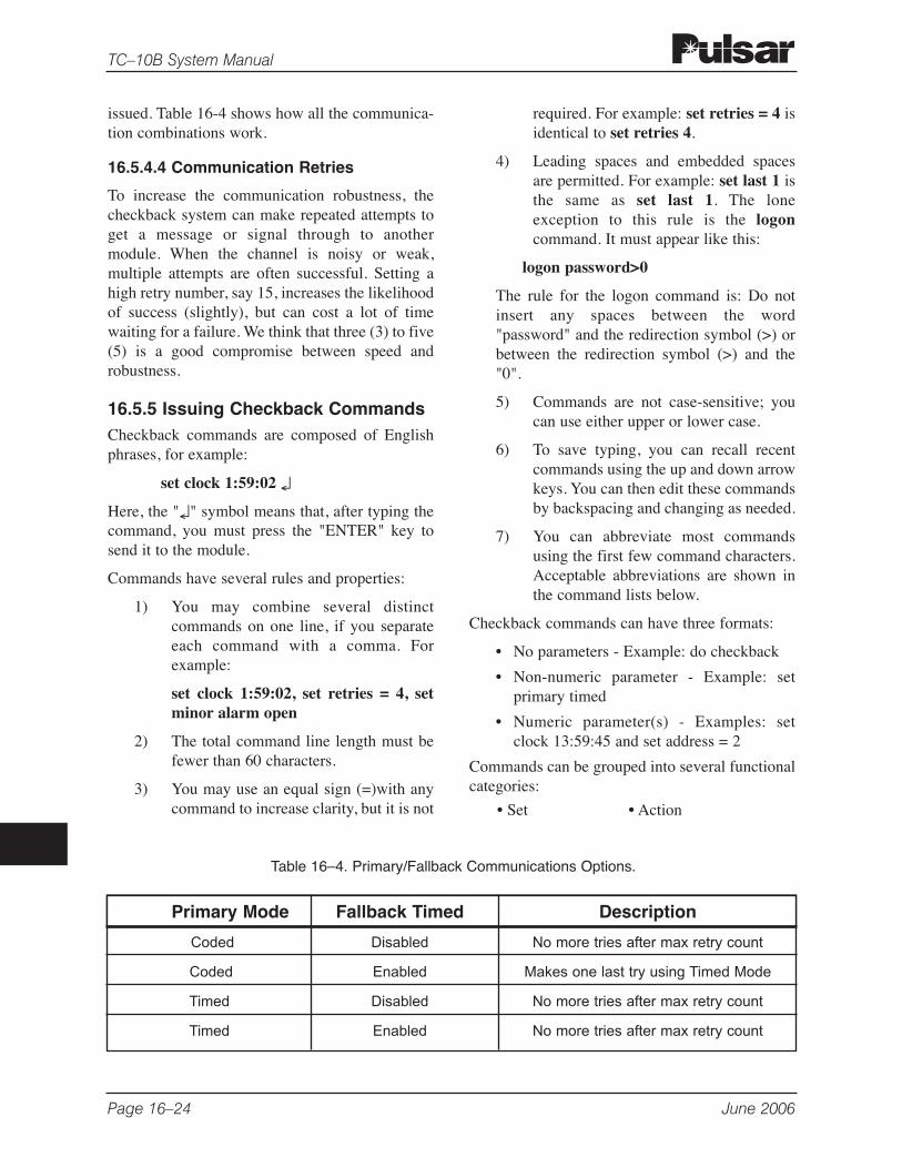
Page 16–24 June 2006
TC–10B System Manual
issued. Table 16-4 shows how all the communica-tion combinations work.
16.5.4.4 Communication Retries
To increase the communication robustness, thecheckback system can make repeated attempts toget a message or signal through to anothermodule. When the channel is noisy or weak,multiple attempts are often successful. Setting ahigh retry number, say 15, increases the likelihoodof success (slightly), but can cost a lot of timewaiting for a failure. We think that three (3) to five(5) is a good compromise between speed androbustness.
16.5.5 Issuing Checkback CommandsCheckback commands are composed of Englishphrases, for example:
set clock 1:59:02 ↵
Here, the "↵" symbol means that, after typing thecommand, you must press the "ENTER" key tosend it to the module.
Commands have several rules and properties:
1) You may combine several distinctcommands on one line, if you separateeach command with a comma. Forexample:
set clock 1:59:02, set retries = 4, setminor alarm open
2) The total command line length must befewer than 60 characters.
3) You may use an equal sign (=)with anycommand to increase clarity, but it is not
required. For example: set retries = 4 isidentical to set retries 4.
4) Leading spaces and embedded spacesare permitted. For example: set last 1 isthe same as set last 1. The loneexception to this rule is the logoncommand. It must appear like this:
logon password>0
The rule for the logon command is: Do notinsert any spaces between the word"password" and the redirection symbol (>) orbetween the redirection symbol (>) and the"0".
5) Commands are not case-sensitive; youcan use either upper or lower case.
6) To save typing, you can recall recentcommands using the up and down arrowkeys. You can then edit these commandsby backspacing and changing as needed.
7) You can abbreviate most commandsusing the first few command characters.Acceptable abbreviations are shown inthe command lists below.
Checkback commands can have three formats:
• No parameters - Example: do checkback
• Non-numeric parameter - Example: setprimary timed
• Numeric parameter(s) - Examples: setclock 13:59:45 and set address = 2
Commands can be grouped into several functionalcategories:
• Set • Action
Primary Mode Fallback Timed Description
Coded Disabled No more tries after max retry count
Coded Enabled Makes one last try using Timed Mode
Timed Disabled No more tries after max retry count
Timed Enabled No more tries after max retry count
Table 16–4. Primary/Fallback Communications Options.
June 2006 Page 16–25
Chapter 16. Universal Checkback Module
16
• Get • Help
• Clear • Logon/Logoff
In the following command lists, "" bracketsindicate an optional parameter and "|" indicatesthat you must include either the parameter beforethe "|" symbol or the one after. For example, setprimary time | coded means that you enter eitherset primary time or set primary coded.Remember that after typing any command, youmust press the ENTER key to send it to themodule.
16.5.5.1 Set Commands
These commands configure the checkbackmodule for service. Settings include communica-tion modes, active output states, and clock timeand date.
Set Address
Minimum abbreviation: set addr n
Sets a module's address. Addresses are used todirect a command into a specific checkbackmodule. To specify the master module, assign itaddress "0". Set remote addresses sequentiallywith no gaps, starting with address "1". Forexample, in a three-module system, you wouldhave address "0" at the master module, and remote#1 and #2 at the two remotes.
In coded communication mode, up to ten remotesare allowed, permitting a maximum address of"10". In timed communication mode, only fourremotes are allowed, limiting the highest addressto "4".
Examples:
set address 0–The local module becomes themaster.
set address 2–The local module becomesremote #2.
set addr 2 > 1–Remote #2's address changesto "1".
Set Primary Communication Mode
Minimum abbreviation: set prim time | code
Sets a module's primary communication mode.The primary mode is the default format for
module to module communication. You can setthis mode to either "timed" or "coded". Codedmode is slightly less reliable than timed mode, butadds more communication features.
Examples:
set prim timed–Sets the local module'sprimary communications mode to timed.
set primary code > 1–Sets remote #1'sprimary communications mode to coded.
Enable Fallback Timed CommunicationMode
Minimum abbreviation: set fall on | off
Enables/disables a module's fallback timedcommunication mode for checkback tests. Thismode is automatically invoked if communicationproblems occur during checkback testing.
Examples:
set fall on–Enables the local module'sfallback timed communications.
set fall off > 0–Disables the master's fallbacktimed communications mode.
Set Interval Type for AutomaticCheckback
Minimum abbreviation: set int peri | time
Checkback modules perform automaticcheckback tests either periodically or at user-specified times (see "Set Time1-4 for TimedCheckback" and "Set Period for AutomaticCheckback" below). This setting lets you specifywhich mode you want to use.
Examples:
set check periodic–Sets automatic checkbacktests to occur periodically using the intervalspecified in the "Checkback Period"setting.
set chec time–Sets automatic checkback teststo occur at the four times specified in the"Checkback Time 1-4" setting.
Page 16–26 June 2006
TC–10B System Manual
Enable Automatic Carrier Recovery Mode
Minimum abbreviation: set reco on | off
You can set the master module to start automaticcarrier recovery mode after failing a checkbacktest. In this mode, the master initiates morefrequent checkback tests until it gets three consec-utive successful tests. It then reverts to the normalautomatic test mode. You can set the frequency forthese tests with the set carrier recovery periodcommand. Successful manual tests while in thismode count toward recovering and can be used tospeed up carrier recovery.
Example:
set recovery on–Enables the automatic carrierrecovery mode.
Enable Automatic Checkback Tests
Minimum abbreviation: set auto on | off
You can enable or disable a module's ability toautomatically initiate checkback tests. When autotests are disabled, a module only sends checkbacktests when you manually command it to, eitherthrough a do checkback command or through thefront or rear panel switches. In addition, themaster module does not send the clock synchro-nization command at 12:30 a.m. This means thatwhen auto tests are disabled, a module does notsend any commands unless you specificallycommand it. This feature might be useful whenyou are installing checkback modules and thesystem is not complete. You can also toggle thissetting by pressing both front panel switchessimultaneously.
Example:
set auto on–Enables automatic checkbacktests.
Set Factory Preset
Minimum abbreviation: set fact n
There are four factory defined preset configura-tions which you can select. Using this commandreplaces your current settings with the factoryconfiguration you specify. After this command,you can edit this configuration to your needs orleave it alone and use the factory defaults.
Note that you can also select one of the factorypresets by changing the internal DIP switch from"CUSTOM" to Factory 1, 2, 3, or 4, and then ener-gizing the module. Changes with this method,however, are blocked until you put the DIP switchback to the "CUSTOM" position.
Example:
set fact 2–Replaces all settings with factorypreset 2 settings.
Set Password
Minimum abbreviation: set pwd pppppppppp
Passwords can be from one to ten characters; youcan include both numbers and letters in yourpassword. Letters are not case sensitive. Eachcheckback module can have a unique password, oryou can set them all the same. As usual, it is agood idea to write new passwords down, as youwill be unable to log on without the correctpassword. If you do lose your password, you canrecover it using the procedure described in"Recovering Your Lost Password" later in thischapter.
Unlike most settings, you can change thepassword no matter which setting the DIP switchis on.
Examples:
set pwd hello–Sets the local module'spassword to "hello".
set pwd bigdarnpwd–Sets the local module'spassword to the maximum size.
set pwd 9–Sets the local module's password tojust "9".
set pwd pass1 > 1–Sets remote #1's passwordto "pass1".
Set Major Alarm Relay State
Minimum abbreviation: set majo open | close
Sets a module's major alarm relay state. You canset relays to either open or close on a major alarmcondition.
As with most settings, you can only change thisone if the DIP switch is set to "CUSTOM".
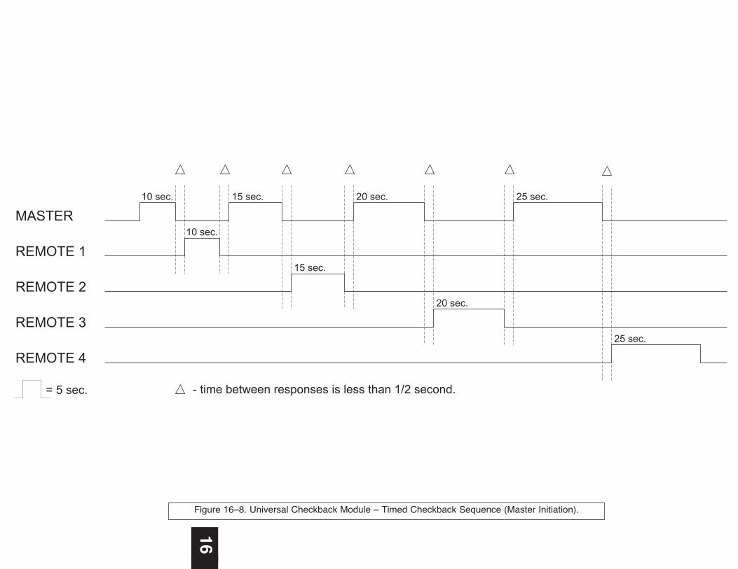
16
MASTER
REMOTE 1
REMOTE 2
REMOTE 3
REMOTE 4
= 5 sec.
10 sec.
10 sec.
15 sec.
15 sec.
20 sec.
20 sec.
25 sec.
25 sec.
- time between responses is less than 1/2 second.
Figure 16–8. Universal Checkback Module – Timed Checkback Sequence (Master Initiation).
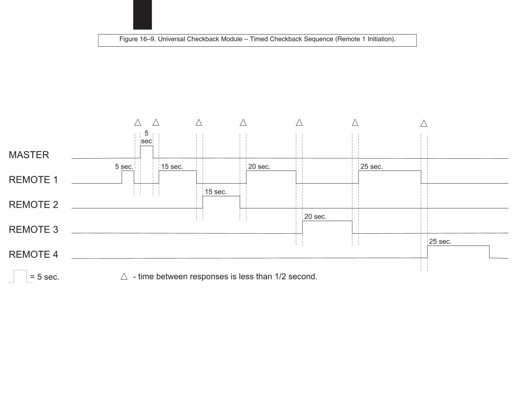
Figure 16–9. Universal Checkback Module – Timed Checkback Sequence (Remote 1 Initiation).
MASTER
REMOTE 1
REMOTE 2
REMOTE 3
REMOTE 4
= 5 sec.
15 sec.
20 sec.
5 sec. 15 sec. 20 sec. 25 sec.
25 sec.
5sec
- time between responses is less than 1/2 second.
Examples:
set major closed–Closes the major alarmrelay upon a major alarm.
set majo open>1–Opens remote #1's majoralarm relay upon a major alarm.
Set Minor Alarm Relay State
Minimum abbreviation: set mino open | close
Sets a module's minor alarm relay state. You canset relays to either open or close on a minor alarmcondition.
Examples:
set mino open–Opens the minor alarm relayupon a minor alarm.
set mino close>0–Closes the master module'sminor alarm relay upon a minor alarm.
Set Output State 1-3
Minimum abbreviation: set state# open | close
Similar to the above major and minor relay outputstates, you can set the active state of each of thethree user-programmable outputs. The active stateof each user output is independent of what youhave defined it to monitor. For example, let's sayyou have programmed output 2 to monitor "test inprogress." Then you set the output 2's active stateto close. Now when this module initiates acheckback test, output 2's contacts closes. If youthen changed the definition of output 2 to "passedtest", then this output contact closes when themodule passes a checkback test.
Examples:
set state1 close–Closes output 1 contact whenit is active.
set state3 open>2–Opens output 3 at remote#2 when it is active.
Set Output Definition 1-3
Minimum abbreviation:set def# reco|delay|test|pass|disab|in reco
Checkback modules include three user-program-mable outputs. You can set each of these tomonitor one of six items:
"recover" (Successful Carrier Recovery):Output set for one second after a successfulrecovery from automatic recovery mode
"delay" (Delayed Alarm): Output set after amodule fails to recover from auto recoverybefore the carrier recovery window expires
"testing" (Test In Progress): Output set by thecheckback test-initiating module for theduration of the test
"pass" (Successful Test): Output set after initi-ating and passing a checkback test
"disable" (Disable Automatic Tests): Output setwhen the user has disabled automaticcheckback tests.
“in recovery” (In Auto Recovery Mode): Outputset while in automatic recovery mode.
Examples:
set def1 test–Sets user output 1 to show whena checkback test is in progress.
set def3 recover–Sets output 3 to showsuccessful automatic carrier recovery.
set def2 pass–Sets output 2 to show asuccessful checkback test.
set def1 delay–Sets output 1 to activate whena delayed alarm is initiated.
set def2 disable–Sets output 2 to activatewhen users disables auto tests.
Set Alarm Outputs Sealed/Momentary
Minimum abbreviation: set alar seal | mome
You can set the major and minor alarm outputs toremain sealed after an alarm condition or to closefor five seconds and then release.
Examples:
set test open–Opens "test in progress" relayduring a checkback test.
set testing close>0–Closes the mastermodule's "test in progress" relay during acheckback test.
Set Retries Before Reporting a Failure
Minimum abbreviation: set retr nn
June 2006 Page 16–29
Chapter 16. Universal Checkback Module
16
The retry number sets the number of times thecheckback module attempts to communicate withanother module after failing a message. If themodule fails all the retry attempts, it logs acommunications error. The default value is "3",but in a noisy system, you probably want to crankthis number up. A maximum of "20" is allowed.
Examples:
set retries 5–Allows five retries beforelogging an error.
set retr 0–Disables all retries.
set retries 20–Sets the module to themaximum number of retries.
Set Low Power Test On|Off
Minimum abbreviation: set low on | off
You can run low power checkback tests todetermine system margins. When enabled, lowpower checkback tests precede the full powercheckback tests.
Examples:
set low on > 1–Enables low power tests atremote #1.
set low power off–Disables low power tests.
Set Time1-4 for Timed Checkback
Minimum abbreviation: set time# hh
You can set automatic checkback tests to executeup to four specific times during the day. Thesetimes, time1-time4, indicate the hour to perform atest. Tests are performed near the start of the hour,unless the carrier system is busy with some othertask.
If you do not want to use all four times, set theextra times the same as those already set. Forexample, if you want time1 to be 1:00 and time2to be 15:00, but do not want to use time3 andtime4, set time3 and time4 to 15:00 or 1:00.
Examples:
set time1 3–Sets time1 to execute an autocheckback test at 3:00 a.m.
set time2 2, time4 2–Sets time2 to execute anauto checkback test at 2:00, and disabletime4.
set time1 = 13>1–Sets remote #1's time to13:00 (note the optional equal sign forclarity).
Set Period for Automatic Checkback
Minimum abbreviation: set peri hh
Sets the interval or elapsed time betweenautomatic checkback tests when they are set toexecute periodically. This time is specified to thehour, and zero (0) hours are rejected.
Example:
set period 4–Executes periodic autocheckback tests every four hours.
Set Loopback Duration
Minimum abbreviation: set loop ss
Loopback duration specifies in seconds how longa module keeps the carrier on during a loopbacktest. You can set this time from four (4) to 60seconds. You start loopback tests either with thedo loopback command (see "Do Loopback Test")or with the front and rear panel loopback switches.
Examples:
set loopback duration 5–Sets the localmodule's duration to five (5) seconds.
set loop 60 > 2–Sets remote #2's loopbackduration to 60 seconds.
Set Carrier Recovery Period
Minimum abbreviation: set carrier mm
You can set how often checkback tests are runduring the Carrier Recovery window to retest thecarrier at an expedited rate once it has failed. If thecheckback is successful for three consecutivetests, the system resets or “recovers”. If thecheckback is not successful during the recoverywindow, the Delayed Alarm is set.
Example:
Page 16–30 June 2006
TC–10B System Manual
set carrier 15-Sets the local checkback toexpedite the checkback interval to every 15min.
set carrier 20 > 1-Sets the checkback withaddress 1 to expedite the checkbackinterval to every 20 min.
Set Carrier Recovery Window
Minimum abbreviation: set wind hh
You can set the recovery window from 1 to 24hours. This is the timeframe in which thecheckback must receive 3 consecutive successfulcheckbacks. If this fails, the Delayed Alarm is set.
Example:
set wind 3-Sets the local checkbackrecovery window to 3 hours.
set wind 1 > 3-Sets the recovery windowof remote checkback, with address 3, to 1hour.
Set Automatic Clock Synchronization
Minimum abbreviation: set sync on | off
When enabled, the master module synchronizesthe clocks of all remotes in the network starting at12:30 a.m.
Example:
set sync on–Enables automatic clocksynchronization by the master.
Set Clock
Minimum abbreviation: set cloc hh:mm:ss
Updates the checkback module's clock. With thiscommand, you can set the clock to the nearestsecond. Remember to enter times in 24-hourformat.
Unlike most settings, you can set the clock nomatter which setting the DIP switch is on.
Examples:
set clock 1:02:56–Sets the local module'sclock to 1:02:56 a.m.
set cloc 13:00:00 > 1–Sets remote #1's clockto 1:00 p.m.
set cloc 3–Sets the local module's clock to3:00:00 a.m.
Set Date
Minimum abbreviation: set date mm/dd/yyyy
Updates the date setting for the checkbackmodule's clock. You must enter all four digits forthe year, e.g., 2005, or the command is rejected.
Unlike most settings, you can change the date nomatter which setting the DIP switch is on.
Examples:
set date 1/2/2000–Sets the local module's dateto January 2, 2000.
set date 1/2/2000 > 1–Sets remote #1's date toJanuary 2, 2000.
Set All
Minimum abbreviation: set all > n
Set all allows you to update all of a distantmodule's settings at once with the local module'ssettings. Thus, it should always be directed tosome other node (e.g., set all > 2). All settingsexcept address, password, time, and date are setidentical to the module making this command.
For example, if you're at remote #1 and you enterset all > 0, the master changes all its settings, likenumber of retries, and primary communicationmode, to match remote #1's, but it remains amaster because the address is not changed.
Examples:
set all > 1–Sets remote #1 to match the localmodule's settings.
set all > 0–Sets the master to match the localmodule's settings.
16.5.5.2 Get Commands
Get commands read a checkback module's currentsettings, events, status, or counts.
Get Settings
Minimum abbreviation: get set
Displays a checkback module's current settings.This includes its address, primary and fallback
June 2006 Page 16–31
Chapter 16. Universal Checkback Module
16
communication modes, alarm output control, andvarious times.
Examples:
get set–Gets and displays the local module'ssettings.
get set > 1–Gets and displays remote #1settings.
Get Events
Minimum abbreviation: get eve nn -mm
Displays a module's stored events. Up to 250events are stored in a Universal CheckbackModule. You can call this command with a rangeof events (e.g., 10-45), a single event (e.g., 2), oryou can supply no events. If you supply no events,the module displays the next event each time yourequest distant events or the next 10 events eachtime you request local events. When you enter acommand to a distant module other than getevents, the event display counter is reset to event1 for that module.
Examples:
get event 100-107–Gets and displays localevents 100 through 107.
get event 6–Gets and displays local event 6.
get event–Gets and displays the next 10 localevents.
get eve 4 > 1–Get and displays remote #1'sevent 4.
get eve 1-10 > 1–Gets and displays remote#1's events 1 through 10.
get eve >1–Gets and displays remote #1's nextevent.
Get Status
Minimum abbreviation: get sta
Displays the status of a module's front panelLEDs.
Examples:
get status–Gets and displays the status of thelocal module's LEDs.
get status > 1–Get and displays the status ofremote #1's LEDs
Get Counts
Minimum abbreviation: get cou
Displays a module's event counts. This shows thenumber of major and minor alarms, communica-tion errors, checkback retries, checkback testsperformed, successful checkback tests, and theelapsed time since these counts were reset (see"Clear Event Counts" and "Set Retries BeforeReporting a Failure").
Examples:
get count–Gets and displays the localmodule's event counts.
get count > 2–Gets and displays remote #2'sevent counts.
Get All
Minimum abbreviation: get all > n
Get all compliments set all and allows you toreplace all your local module's settings with thoseof a distant module. Like Set All, this commandshould always be redirected to some othermodule, e.g., get all > 1. All settings exceptaddress, password, time, and date are set identicalto the distant module.
Examples:
get all > 1–Sets the local module's settings tomatch remote #1's.
get all > 0–Sets the local settings to match themaster's.
Page 16–32 June 2006
TC–10B System Manual
16.5.5.3 Clear Commands
Clear commands let you clear the stored events orcounts, or reset the alarm outputs
Clear alarms
Minimum abbreviation: clr a or clear a
Clears the alarm relays and display LEDs.
Examples:
clear alarms–Clears local alarms.
clr alarm > 1–Clears remote #1's alarms.
clr a>1–Clears remote #1's alarms.
Clear Events
Minimum abbreviation: clr e or clear e
Clears all stored events from the non-volatilememory. Make sure you really want to do thiscommand before you actually do it, because youmay delete a considerable amount of data.
Examples:
clr events–Clears all locally stored targetevents.
clear eve> 1–Clears remote #1's events.
clr e>1–Clears remote #1's events.
Clear Event Counts
Minimum abbreviation: clr c or clear c;
Clears the event counts which show the number ofmajor and minor alarms, communication errors,communication retries, and the number ofcheckback test attempts and successes.
Examples:
clr c–Clears local counts.
clr c> 2–Clears remote #2's counts.
16.5.5.4 Action Commands
You can command a Universal CheckbackModule to execute a loopback or checkback testwith an action command.
Do Loopback Test
Minimum abbreviation: do loop
You can instruct a module to initiate a loopbackmode for several seconds. During this time, themodule's carrier remains on. The duration of thistransmission is specified by the module's"Loopback Duration" setting (see "Set LoopbackDuration").
Examples:
do loopback–Turns on the local carrier for thespecified time.
do loop >1–Turns on remote #1's carrier forthe specified time.
Do Checkback Test
Minimum abbreviation: do chec
You can initiate a manual checkback test with thiscommand. As with automatic checkback tests, thelast module in the system should be specifiedbefore executing this command - this tells theinitiating Checkback Module which distantmodules it needs to test.
Example:
do checkback–Performs a manual checkbacktest on all the other checkback modules inthe network.
16.5.5.5 Logon/Logoff Commands
Checkback access is controlled by the logon andlogoff commands. Before you can change or viewsettings, you must log onto a checkback module.When done, you can log off manually or waitfifteen minutes, when the system logs off auto-matically if there has been no activity.
Logon
Minimum abbreviation: logon pwd
Logon commands enable you to access aUniversal Checkback Module to change settingsor perform various tests. Logons are passwordprotected (see "Set Password"), preventing unau-thorized access.
June 2006 Page 16–33
Chapter 16. Universal Checkback Module
16
Page 16–34 June 2006
TC–10B System Manual
Before communicating with a local checkbackmodule, you must first log on. You then must logonto any distant module you want to access.
When entering any password, the characters youtype are shown only as asterisks, e.g.,logon ****.
When logging onto distant modules, do not insertany spaces between the "password" and the redi-rection symbol (>) or between the redirectionsymbol (>) and the distant module's address.
Examples:
logon mypass–Logs onto the local checkbackmodule using password "mypass".
logon city1>1–Logs onto remote #1 withpassword "city1". Again, do not insert anyspaces after you begin typing the password.
Note that "mypass" is displayed as "******" and"city1" as "*****" when you enter them.
Logoff
Minimum abbreviation: logoff
The logoff command ends a session with acheckback module (see "Logon"). Logging offprevents unauthorized changes to the checkbackmodule's configuration. The checkback modulealso automatically logs off all modules afterfifteen minutes of no user activity.
Examples:
logoff–Logs off local and all distantcheckback modules.
logoff > 2–Logs off remote #2 only; remainslocally logged on.
16.5.5.6 Help Commands
Online help is available when you enter a helpcommand. The checkback module can provideboth general and command-specific help tosimplify field use.
Help
Minimum abbreviation: help
Online help goes from general to specific.
Examples:
help–General help, lists all commands briefly.
help set–Discusses all the setting commandsin more detail.
help retries–Gives examples and specificusage for the set retries command.
All commands are summarized in Tables 16-5through 16-13 (see "Checkback Command QuickReference" on the following page).
16.5.6 Distant CheckbackCommunications
Universal Checkback Modules can communicatewith any others on the same network. Anycommand that you can execute at the module youare connected to can also be redirected to somedistant module. For example, if you are at remote#2 and you want to change remote #1's majoralarm output state to "closed" on alarm, you couldtype the following and press the ENTER key:
set major = closed > 1
The redirection character (>) tells the localcheckback module to send this command on toremote #1, rather than execute this commandlocally. The master and all remote modules havethe same communication privileges. That is, anymodule can redirect a command to any othermodule.
To communicate with a distant module, you mustfirst log onto that module. This is a securitymeasure designed to limit access. A checkbackmodule's distant logon password is always thesame as its local logon password, although everycheckback module can have a unique password.
For example, let's say you are at remote #1. Youwant to log onto the master and its password is"dilbert". You type: logon dilbert > 0 and pressthe ENTER key.
Note that this appears on the screen as: logon******>0
Remember that address "0" is reserved for themaster checkback module.
The distant logon remains in effect until you doone of the following:
• Log off the distant module
• Log off locally
• Do not communicate with the remotemodule for 15 minutes
If you want, you can log onto all checkbackmodules in the network at once. To remain loggedon, however, you have to talk to each modulebefore it times out.
16.5.6.1 Limitations and Concerns
1. The data rate is slow, 60 bits per second. Along command like get settings from a distantcheckback module takes 30 seconds or moreto complete, depending on the quality of thecommunication channel.
2. The system is only intended to support onemodule communicating at a time. If multiplemodules attempt to talk, commands may fail,although any data that gets through will beaccurate.
3. Changing a distant module's address ispermitted, but avoid assigning it an addressthat is already in use - or you will not be ableto talk to either module at that address untilyou can locally change one or the other'saddress.
16.5.7 Recovering Your LostPassword
Checkback modules are inaccessible when you donot know the correct password. If you somehowlose or forget yours, there is a way to recover it.From the "enter password" prompt, type superand press the ENTER key. This identifies you as a"super user". These letters (s u p e r) are displayedas asterisks, just as a normal password would be.This pops up the Super User Menu. Press "1" andthe module displays ten four-character, hexadec-imal numbers. For example:
d203 f659 26ac b4ed 1158 53021bf4 1d86 8ab3 98e9
Following the screen directions, contact Pulsar,and we can decode these numbers and determineyour current password.
June 2006 Page 16–35
Chapter 16. Universal Checkback Module
16
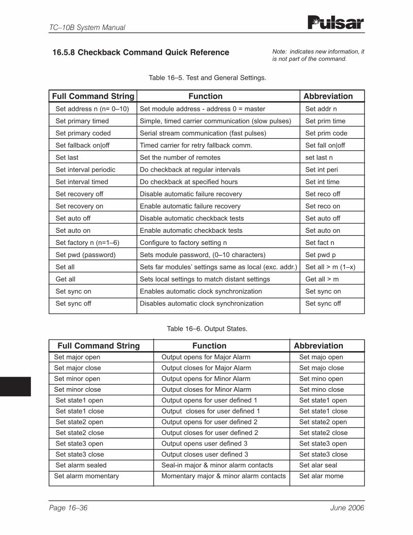
Page 16–36 June 2006
TC–10B System Manual
16.5.8 Checkback Command Quick Reference
Full Command String Function Abbreviation
Set address n (n= 0–10) Set module address - address 0 = master Set addr n
Set primary timed Simple, timed carrier communication (slow pulses) Set prim time
Set primary coded Serial stream communication (fast pulses) Set prim code
Set fallback on|off Timed carrier for retry fallback comm. Set fall on|off
Set last Set the number of remotes set last n
Set interval periodic Do checkback at regular intervals Set int peri
Set interval timed Do checkback at specified hours Set int time
Set recovery off Disable automatic failure recovery Set reco off
Set recovery on Enable automatic failure recovery Set reco on
Set auto off Disable automatic checkback tests Set auto off
Set auto on Enable automatic checkback tests Set auto on
Set factory n (n=1–6) Configure to factory setting n Set fact n
Set pwd (password) Sets module password, (0–10 characters) Set pwd p
Set all Sets far modules’ settings same as local (exc. addr.) Set all > m (1–x)
Get all Sets local settings to match distant settings Get all > m
Set sync on Enables automatic clock synchronization Set sync on
Set sync off Disables automatic clock synchronization Set sync off
Table 16–5. Test and General Settings.
Table 16–6. Output States.
Full Command String Function AbbreviationSet major open Output opens for Major Alarm Set majo open
Set major close Output closes for Major Alarm Set majo close
Set minor open Output opens for Minor Alarm Set mino open
Set minor close Output closes for Minor Alarm Set mino close
Set state1 open Output opens for user defined 1 Set state1 open
Set state1 close Output closes for user defined 1 Set state1 close
Set state2 open Output opens for user defined 2 Set state2 open
Set state2 close Output closes for user defined 2 Set state2 close
Set state3 open Output opens user defined 3 Set state3 open
Set state3 close Output closes user defined 3 Set state3 close
Set alarm sealed Seal-in major & minor alarm contacts Set alar seal
Set alarm momentary Momentary major & minor alarm contacts Set alar mome
Note: indicates new information, itis not part of the command.
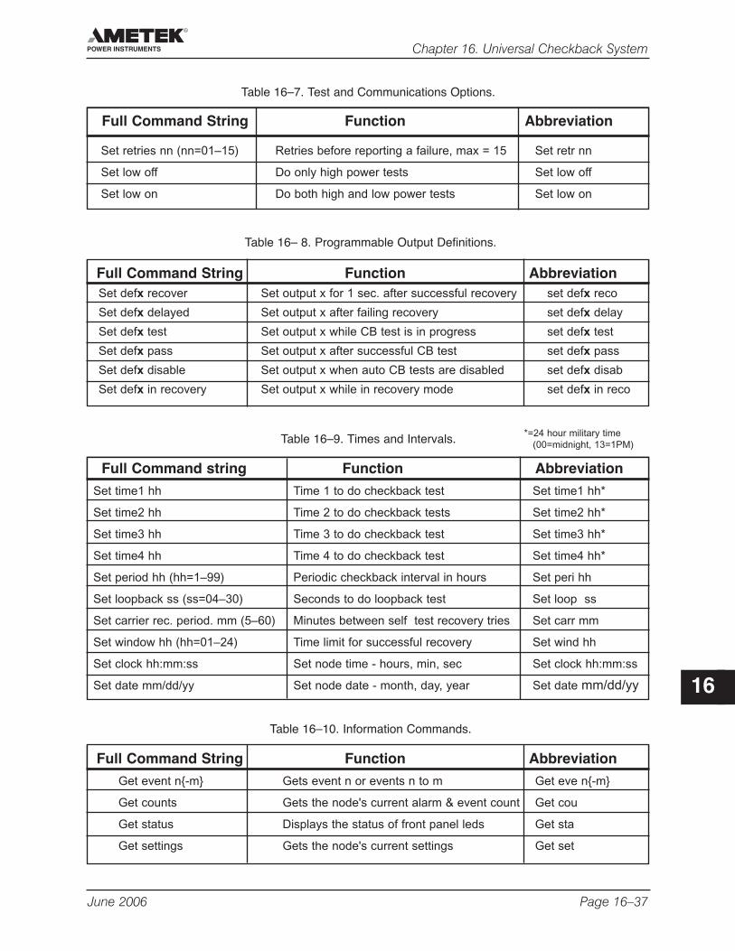
June 2006 Page 16–37
Chapter 16. Universal Checkback System
16
Full Command String Function Abbreviation
Set retries nn (nn=01–15) Retries before reporting a failure, max = 15 Set retr nn
Set low off Do only high power tests Set low off
Set low on Do both high and low power tests Set low on
Table 16–7. Test and Communications Options.
Table 16–9. Times and Intervals.
Full Command string Function Abbreviation
Set time1 hh Time 1 to do checkback test Set time1 hh*
Set time2 hh Time 2 to do checkback tests Set time2 hh*
Set time3 hh Time 3 to do checkback test Set time3 hh*
Set time4 hh Time 4 to do checkback test Set time4 hh*
Set period hh (hh=1–99) Periodic checkback interval in hours Set peri hh
Set loopback ss (ss=04–30) Seconds to do loopback test Set loop ss
Set carrier rec. period. mm (5–60) Minutes between self test recovery tries Set carr mm
Set window hh (hh=01–24) Time limit for successful recovery Set wind hh
Set clock hh:mm:ss Set node time - hours, min, sec Set clock hh:mm:ss
Set date mm/dd/yy Set node date - month, day, year Set date mm/dd/yy
Full Command String Function Abbreviation
Get event n-m Gets event n or events n to m Get eve n-m
Get counts Gets the node's current alarm & event count Get cou
Get status Displays the status of front panel leds Get sta
Get settings Gets the node's current settings Get set
Table 16–10. Information Commands.
Full Command String Function AbbreviationSet defx recover Set output x for 1 sec. after successful recovery set defx reco
Set defx delayed Set output x after failing recovery set defx delay
Set defx test Set output x while CB test is in progress set defx test
Set defx pass Set output x after successful CB test set defx pass
Set defx disable Set output x when auto CB tests are disabled set defx disab
Set defx in recovery Set output x while in recovery mode set defx in reco
Table 16– 8. Programmable Output Definitions.
*=24 hour military time(00=midnight, 13=1PM)
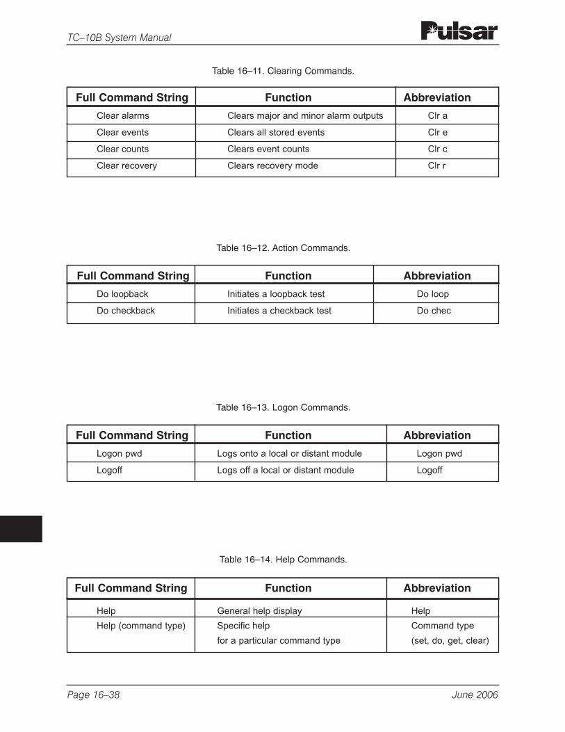
Page 16–38 June 2006
TC–10B System Manual
Full Command String Function Abbreviation
Help General help display Help
Help (command type) Specific help Command type
for a particular command type (set, do, get, clear)
Full Command String Function Abbreviation
Do loopback Initiates a loopback test Do loop
Do checkback Initiates a checkback test Do chec
Full Command String Function Abbreviation
Clear alarms Clears major and minor alarm outputs Clr a
Clear events Clears all stored events Clr e
Clear counts Clears event counts Clr c
Clear recovery Clears recovery mode Clr r
Table 16–11. Clearing Commands.
Table 16–12. Action Commands.
Full Command String Function Abbreviation
Logon pwd Logs onto a local or distant module Logon pwd
Logoff Logs off a local or distant module Logoff
Table 16–13. Logon Commands.
Table 16–14. Help Commands.
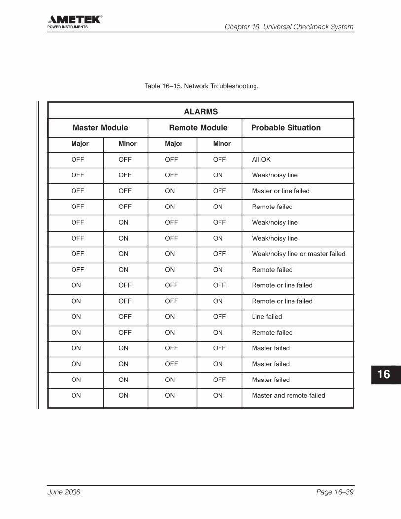
June 2006 Page 16–39
Chapter 16. Universal Checkback System
16
ALARMS
Master Module Remote Module Probable Situation
Major Minor Major Minor
OFF OFF OFF OFF All OK
OFF OFF OFF ON Weak/noisy line
OFF OFF ON OFF Master or line failed
OFF OFF ON ON Remote failed
OFF ON OFF OFF Weak/noisy line
OFF ON OFF ON Weak/noisy line
OFF ON ON OFF Weak/noisy line or master failed
OFF ON ON ON Remote failed
ON OFF OFF OFF Remote or line failed
ON OFF OFF ON Remote or line failed
ON OFF ON OFF Line failed
ON OFF ON ON Remote failed
ON ON OFF OFF Master failed
ON ON OFF ON Master failed
ON ON ON OFF Master failed
ON ON ON ON Master and remote failed
Table 16–15. Network Troubleshooting.
Page 16–40 June 2006
TC–10B System Manual
16.6 TroubleshootingYou can identify and solve many checkbacknetwork problems by examining the major andminor alarms. If both high and low powercheckback tests are enabled, the major and minoralarms work like this:
• If a module fails only the low power test, itsets the minor alarm
• If a module fails the high power test, it setsthe major alarm
• If a module fails the high power test andcan not receive its own messages, it setsboth major and minor alarms
Armed with this information, you can usuallyidentify a failed module or line problem. Table 16-14 lists all combinations for a two-module systemand the probable situation.
To get the complete picture, you must wait longenough for all remotes to initiate their owncheckback tests. For example, if the master has amajor alarm, but the remote has no alarms, youcan not determine if it failed to receive thecommand due to a bad line or because its receiveris dead. By waiting for the remote to initiate acheckback, you can tell if it is the line (majoralarm) or the module (both alarms).
16.7 DrawingsThe Universal Checkback Module's simplifiedcomponent layout is shown in Figure 16-10. Theschematics are available upon request. Figure 16-11 shows a simplified schematic with labeledinputs and outputs.
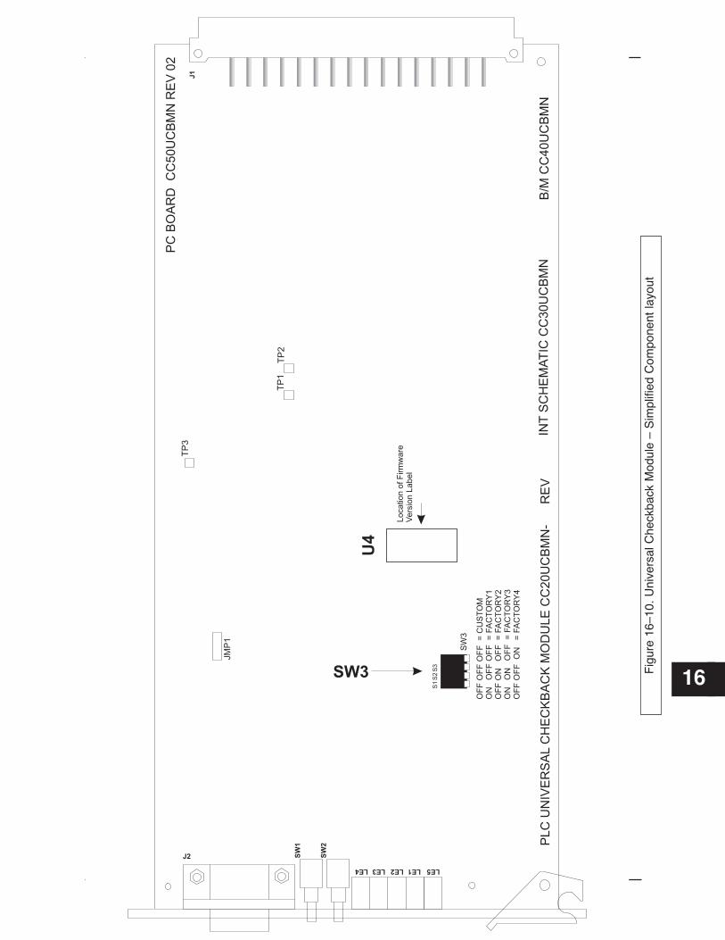
16
PL
CU
NIV
ER
SA
LC
HE
CK
BA
CK
MO
DU
LE
CC
20
UC
BM
N-
RE
VIN
TS
CH
EM
AT
ICC
C3
0U
CB
MN
B/M
CC
40
UC
BM
N
PC
BO
AR
DC
C5
0U
CB
MN
RE
V0
2
LE4
SW
1
J2
J1
SW
2
LE3 LE2 LE1 LE5
TP
1T
P2
TP
3
JM
P1
SW
3
S1
S2
S3
OF
FO
FF
OF
F=
CU
ST
OM
ON
OF
FO
FF
=FA
CT
OR
Y1
OF
FO
NO
FF
=FA
CT
OR
Y2
ON
ON
OF
F=
FA
CT
OR
Y3
OF
FO
FF
ON
=FA
CT
OR
Y4
Lo
ca
tio
no
fF
irm
wa
reV
ers
ion
La
be
l
SW3
U4
Fig
ure
16–1
0. U
nive
rsal
Che
ckba
ck M
odul
e –
Sim
plifi
ed C
ompo
nent
layo
ut
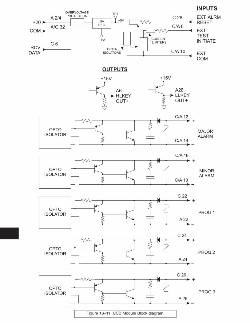
A 2/4
OVERVOLTAGEPROTECTION
+20
COM
RCVDATA
A/C 32
C 6
MAJORALARM
MINORALARM
PROG 1
PROG 2
PROG 3
C/A 12
C/A 14
C/A 16
C/A 18
C 22
A 22
C 24
A 24
C 26
A 26
C 28
C/A 8
C/A 10 EXT.COM
EXT.TESTINITIATE
EXT. ALRMRESET
INPUTS
OUTPUTS
OPTOISOLATOR
+
–
OPTOISOLATOR
+
–
OPTOISOLATOR
+
–
OPTOISOLATOR
+
–
OPTOISOLATOR
+
–
5VREG.
TP2
OPTO-ISOLATORS
CURRENTLIMITERS
TP1
+5V
+15V
A6HLKEYOUT+
+15V
A28LLKEYOUT+
Figure 16–11. UCB Module Block diagram.
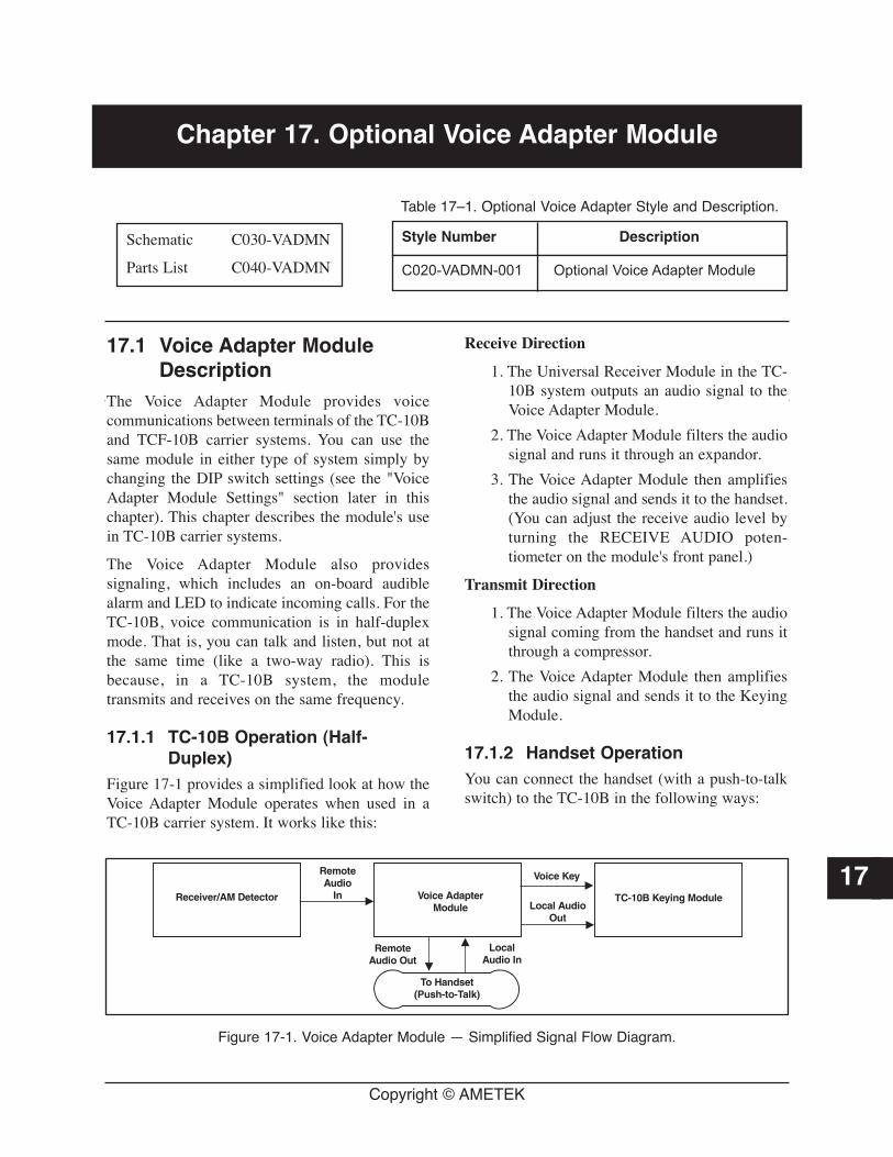
Copyright © AMETEK
Chapter 17. Optional Voice Adapter Module
17
Schematic C030-VADMN
Parts List C040-VADMN
17.1 Voice Adapter ModuleDescription
The Voice Adapter Module provides voicecommunications between terminals of the TC-10Band TCF-10B carrier systems. You can use thesame module in either type of system simply bychanging the DIP switch settings (see the "VoiceAdapter Module Settings" section later in thischapter). This chapter describes the module's usein TC-10B carrier systems.
The Voice Adapter Module also providessignaling, which includes an on-board audiblealarm and LED to indicate incoming calls. For theTC-10B, voice communication is in half-duplexmode. That is, you can talk and listen, but not atthe same time (like a two-way radio). This isbecause, in a TC-10B system, the moduletransmits and receives on the same frequency.
17.1.1 TC-10B Operation (Half-Duplex)
Figure 17-1 provides a simplified look at how theVoice Adapter Module operates when used in aTC-10B carrier system. It works like this:
Receive Direction
1. The Universal Receiver Module in the TC-10B system outputs an audio signal to theVoice Adapter Module.
2. The Voice Adapter Module filters the audiosignal and runs it through an expandor.
3. The Voice Adapter Module then amplifiesthe audio signal and sends it to the handset.(You can adjust the receive audio level byturning the RECEIVE AUDIO poten-tiometer on the module's front panel.)
Transmit Direction
1. The Voice Adapter Module filters the audiosignal coming from the handset and runs itthrough a compressor.
2. The Voice Adapter Module then amplifiesthe audio signal and sends it to the KeyingModule.
17.1.2 Handset OperationYou can connect the handset (with a push-to-talkswitch) to the TC-10B in the following ways:
Figure 17-1. Voice Adapter Module — Simplified Signal Flow Diagram.
Style Number Description
Table 17–1. Optional Voice Adapter Style and Description.
C020-VADMN-001 Optional Voice Adapter Module
Option 1: Local Connection
Plug the handset into the Voice AdapterModule at the front panel "HANDSET"jack.
Option 2: Remote Connection
Connect the handset through a remote jack tothe TC-10B rear panel (see Figure 17-6).
Option 3: Combination Remote Hookswitch - Telephone Jack Connection
Remotely connect a telephone jack and ahookswitch assembly to the TC-10B rearpanel (see Figure 17-6).
Option 1: Using the Local HandsetConfiguration
To configure your system for this option, set theDIP switch (SW1) to the normal, or default,settings as shown in Table 17-3.
To initiate signaling with this option:
1. Plug the handset into the Voice AdapterModule at the front panel "HANDSET"jack.
2. Press the push-to-talk switch on thehandset.
This rings the other end of the system.
To answer a ring (at the receiving end) with thisoption, plug a handset into the Voice AdapterModule at the front panel "HANDSET" jack. Thisstops the ringing by turning off the internal alarmcircuit. (The internal alarm circuit includes anaudible beeping alarm, an alarm LED, and a relaycontact output.)
To configure for external ringing, disable theinternal beeper by setting SW1-4 to the UP(OPEN) position (see "DIP Switch Settings" laterin this chapter). Then connect an external alarm,as shown in Figure 17-6.
Option 2: Using the Remote HandsetConfiguration
To configure your system for this option:
1. Disable the internal beeper by setting SW1-4 to the UP (OPEN) position.
2. Connect a remote handset jack and anexternal alarm circuit in series with the
TB5 terminal block on the TC-10B rearpanel. Use the wiring diagram in Figure 17-6 as a guide.
To initiate signaling with this option:
1. Plug the handset into the remote handsetjack.
2. Press the push-to-talk switch on thehandset.
This rings the other end of the system.
To answer a ring (at the receiving end) with thisoption, plug the handset into the remote handsetjack. The remote jack stops the ringing by inter-rupting the external alarm circuit.
Page 17–2 June 2006
TC–10B System Manual
NOTE
Whenever you are using a remote handset, youshould disable the internal beeper and replace itwith an external alarm.
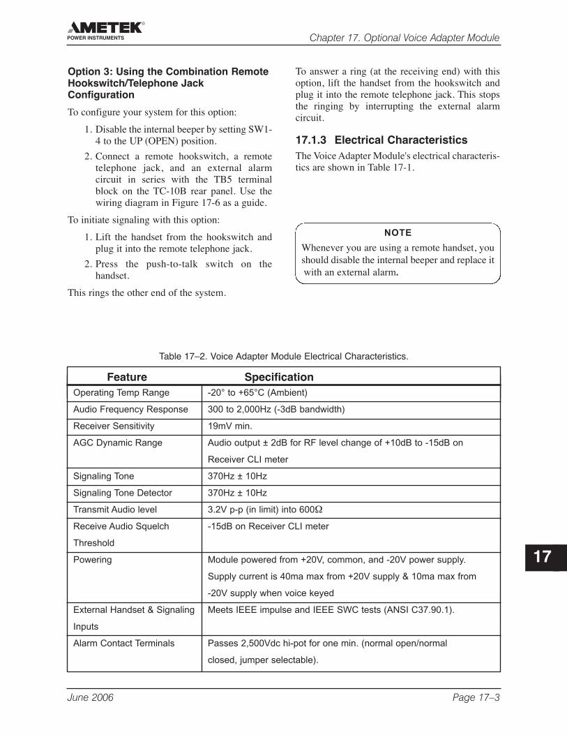
June 2006 Page 17–3
Chapter 17. Optional Voice Adapter Module
17
Option 3: Using the Combination RemoteHookswitch/Telephone JackConfiguration
To configure your system for this option:
1. Disable the internal beeper by setting SW1-4 to the UP (OPEN) position.
2. Connect a remote hookswitch, a remotetelephone jack, and an external alarmcircuit in series with the TB5 terminalblock on the TC-10B rear panel. Use thewiring diagram in Figure 17-6 as a guide.
To initiate signaling with this option:
1. Lift the handset from the hookswitch andplug it into the remote telephone jack.
2. Press the push-to-talk switch on thehandset.
This rings the other end of the system.
To answer a ring (at the receiving end) with thisoption, lift the handset from the hookswitch andplug it into the remote telephone jack. This stopsthe ringing by interrupting the external alarmcircuit.
17.1.3 Electrical CharacteristicsThe Voice Adapter Module's electrical characteris-tics are shown in Table 17-1.
Feature SpecificationOperating Temp Range -20° to +65°C (Ambient)
Audio Frequency Response 300 to 2,000Hz (-3dB bandwidth)
Receiver Sensitivity 19mV min.
AGC Dynamic Range Audio output ± 2dB for RF level change of +10dB to -15dB on
Receiver CLI meter
Signaling Tone 370Hz ± 10Hz
Signaling Tone Detector 370Hz ± 10Hz
Transmit Audio level 3.2V p-p (in limit) into 600Ω
Receive Audio Squelch -15dB on Receiver CLI meter
Threshold
Powering Module powered from +20V, common, and -20V power supply.
Supply current is 40ma max from +20V supply & 10ma max from
-20V supply when voice keyed
External Handset & Signaling Meets IEEE impulse and IEEE SWC tests (ANSI C37.90.1).
Inputs
Alarm Contact Terminals Passes 2,500Vdc hi-pot for one min. (normal open/normal
closed, jumper selectable).
Table 17–2. Voice Adapter Module Electrical Characteristics.
NOTE
Whenever you are using a remote handset, youshould disable the internal beeper and replace itwith an external alarm.
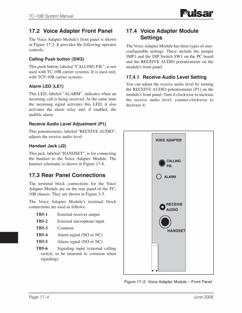
17.2 Voice Adapter Front PanelThe Voice Adapter Module's front panel is shownin Figure 17-2. It provides the following operatorcontrols:
Calling Push button (SW2)
This push button, labeled "CALLING P.B.", is notused with TC-10B carrier systems. It is used onlywith TCF-10B carrier systems.
Alarm LED (LE1)
This LED, labeled "ALARM", indicates when anincoming call is being received. At the same timethe incoming signal activates this LED, it alsoactivates the alarm relay and, if enabled, theaudible alarm.
Receive Audio Level Adjustment (P1)
This potentiometer, labeled "RECEIVE AUDIO",adjusts the receive audio level.
Handset Jack (J2)
This jack, labeled "HANDSET", is for connectingthe handset to the Voice Adapter Module. Thehandset schematic is shown in Figure 17-8.
17.3 Rear Panel ConnectionsThe terminal block connections for the VoiceAdapter Module are on the rear panel of the TC-10B chassis. They are shown in Figure 3-5.
The Voice Adapter Module's terminal blockconnections are used as follows:
TB5-1 External receiver output
TB5-2 External microphone input
TB5-3 Common
TB5-4 Alarm signal (NO or NC)
TB5-5 Alarm signal (NO or NC)
TB5-6 Signaling input (external callingswitch, to be returned to common whensignaling).
17.4 Voice Adapter ModuleSettings
The Voice Adapter Module has three types of user-configurable settings. These include the jumperJMP1 and the DIP Switch SW1 on the PC boardand the RECEIVE AUDIO potentiometer on themodule's front panel.
17.4.1 Receive Audio Level SettingYou can adjust the receive audio level by turningthe RECEIVE AUDIO potentiometer (P1) on themodule's front panel. Turn it clockwise to increasethe receive audio level; counter-clockwise todecrease it.
Page 17–4 June 2006
TC–10B System Manual
VOICE ADAPTER
CALLINGP.B.
ALARM
HANDSET
RECEIVEAUDIO
Figure 17–2. Voice Adapter Module – Front Panel.
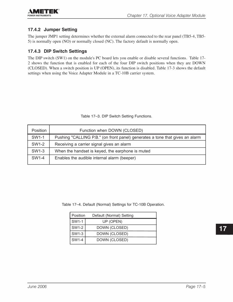
June 2006 Page 17–5
Chapter 17. Optional Voice Adapter Module
17
17.4.2 Jumper SettingThe jumper JMP1 setting determines whether the external alarm connected to the rear panel (TB5-4, TB5-5) is normally open (NO) or normally closed (NC). The factory default is normally open.
17.4.3 DIP Switch SettingsThe DIP switch (SW1) on the module's PC board lets you enable or disable several functions. Table 17-2 shows the function that is enabled for each of the four DIP switch positions when they are DOWN(CLOSED). When a switch position is UP (OPEN), its function is disabled. Table 17-3 shows the defaultsettings when using the Voice Adapter Module in a TC-10B carrier system.
Position Default (Normal) Setting
SW1-1 UP (OPEN)
SW1-2 DOWN (CLOSED)
SW1-3 DOWN (CLOSED)
SW1-4 DOWN (CLOSED)
Table 17–4. Default (Normal) Settings for TC-10B Operation.
Table 17–3. DIP Switch Setting Functions.
Position Function when DOWN (CLOSED)
SW1-1 Pushing "CALLING P.B." (on front panel) generates a tone that gives an alarm
SW1-2 Receiving a carrier signal gives an alarm
SW1-3 When the handset is keyed, the earphone is muted
SW1-4 Enables the audible internal alarm (beeper)
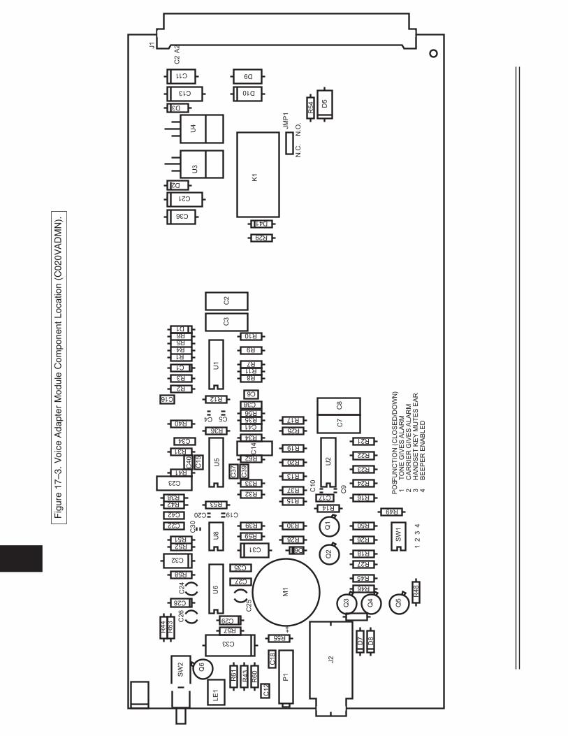
PO
SFU
NC
TIO
N(C
LO
SE
D/D
OW
N)
1 2 3
TO
NE
GIV
ES
AL
AR
MC
AR
RIE
RG
IVE
SA
LA
RM
HA
ND
SE
TK
EY
MU
TE
SE
AR
12
3
N.O
.N
.C.
+
4B
EE
PE
RE
NA
BL
ED
4
+
D2
D3
C13
C11
Q1
Q2
Q3
Q4
LE
1
J2
C1
8
C9
C1
0
C30
A2
C2
J1
K1
JM
P1
U8
P1
SW
1Q
5
C2
6C
24
C2
5
C1
2
D5
D9
D10
R29
D41
U1
U2
U5
U6
D7
D8
U4
U3
M1
C29
SW
2
R6
3
Q6
C1
4
C1
5
C2
C3
C3
7
C38
C7
C8
C39C
40
C41
R6
0
R4
3
R61
R4
4
C28
C33
R57R55
C27
C35
C31 D6
R28
R46
R45
R27
R18
R26
R50
R16
R14R49
C17
R24
R23
R22
R21
R30
R15
R37
R13
R20
R19
R25
R17
R59
R39
R32
R33
R62
R34
R35R56
R8R11R7
R9
R10
C6
R58
C32
R52R51
C22
C20 C19
R53
R36
C5
R12
C4
C42
R42R38
C23
R41
R31
C34
R40
C16
R2
R3
C1
R1R4R5R6D1
C36
C21
R5
4
R4
8
Fig
ure
17–3
. V
oice
Ada
pter
Mod
ule
Com
pone
nt L
ocat
ion
(C02
0VA
DM
N).
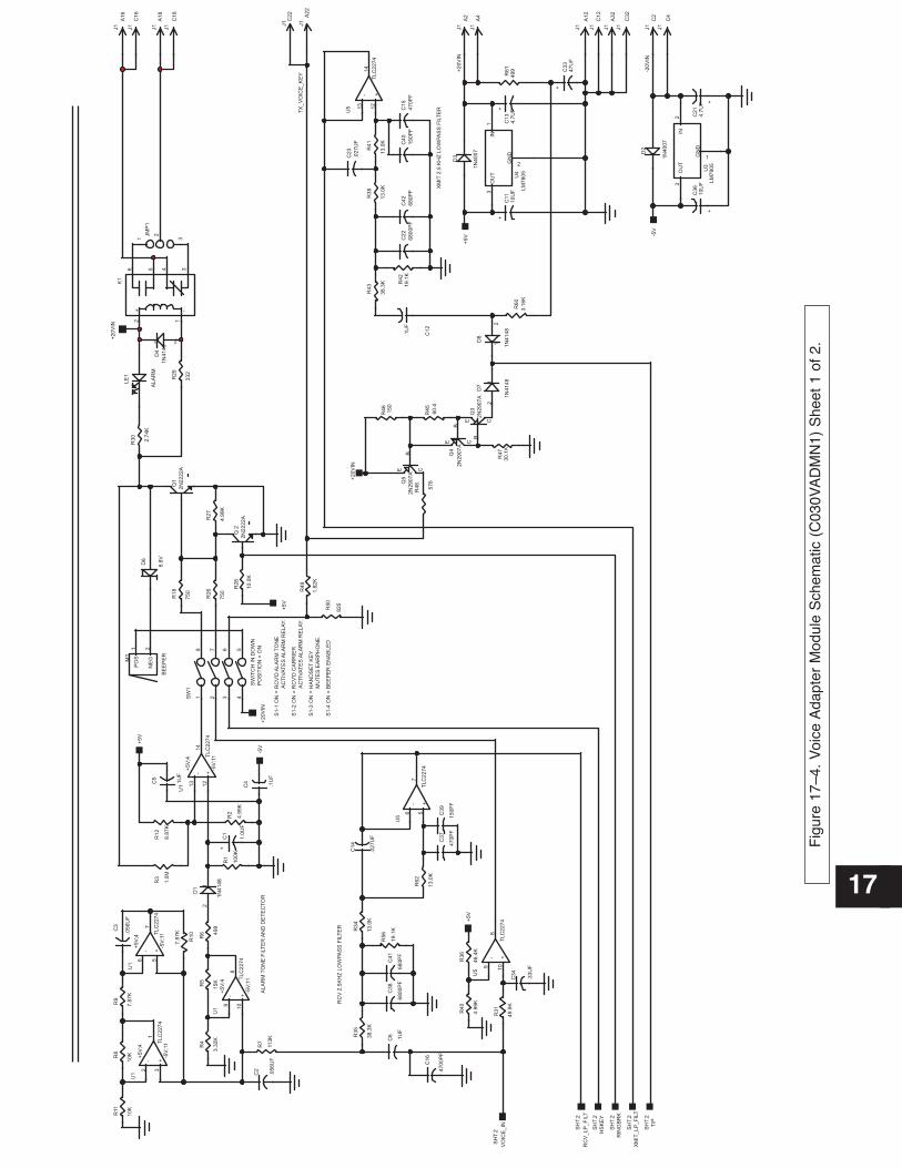
+
1N
40
07
+ -
2N
29
07
AB
E C
2N
29
07
AB
E C
2N
29
07
AB
E C
1N
40
07
++
IN
GN
D
OU
T
+
+-
TL
C2
27
4
+-
TL
C2
27
4
+-
TL
C2
27
4-5V
;11
+5
V;4
+-
TL
C2
27
4
+-
TL
C2
27
4
-5V
;11
+5
V;4
+-
TL
C2
27
4
-5V
;11
+5
V;4
+-
TL
C2
27
4
IN
GN
D
OU
T
++
SH
T.2
SH
T.2
C1
8
A1
8
C1
6
A1
6
AL
AR
M
SH
T.2
RC
V2
.5K
HZ
LO
WP
AS
SF
ILT
ER
SH
T.2
SH
T.2
SH
T.2
C4
C2
C3
2
A3
2
C1
2
A1
2
A4
A2A
22
C2
2
AL
AR
MT
ON
EF
ILT
ER
AN
DD
ET
EC
TO
R
XM
IT2
.5K
HZ
LO
WP
AS
SF
ILT
ER
R3
6
46
.4K
R1
0
R9
7.8
7K
C1
5
47
0P
F
LE
1
10
UF
C3
64
.7U
FC
21
2
31
U4
LM
78
05
2 3
1
U1
6 5
7
U1
9
10
8
+5
V;4
-5V
;11
U1
13
12
14
U1
C4
0
15
0P
F
C4
2
68
0P
F
C2
2
68
00
PF
38
.3K
R4
3
C2
3
.02
7U
F
XM
IT_
LP
_F
ILT
15
0P
F
C3
9
47
0P
F
C3
7
R6
2
13
.0K
R3
4
13
.0K
C4
1
68
0P
F
C3
8
68
00
PF
19
.1K
R5
6
C1
4
.02
7U
F
RC
V_
LP
_F
ILT
6 5
7
U5
C2
.05
6U
F
C3
.05
6U
F
HS
KE
Y
J1
TX
_V
OIC
E_
KE
Y
J1
21
D8
1N
41
48
TIP
RIN
GB
RK
13
12
14
U5
8
109
U5
J1
J1
J1
J1
J1
47
UF
C3
3
1
32
U3
LM
79
05
4.7
UF
C1
31
0U
FC
11
C3
4
.33
UF
VO
ICE
_IN
47
00
PF
C1
6
.1U
F
C638
.3K
R3
5
10
0K
R1
11
3K
R7
57
6
R4
8
21
D7
1N
41
48
3.1
6K
R6
0
R4
9
1.8
2K
-20
VIN
-5V
+5
V
49
9R
61
19
.1K
R4
2
D2
82
5
R5
0
D6
6.8
V
1 2
M1
Q3
Q4
Q5
1 2 3 45678
SW
1
10
.0K
R2
8
R3
0
2.7
4K
21
D4
1N
41
48
J1
J1
J1
J1
J1
J1
J1
R4
5
60
.4
R4
61
50
R2
9
33
23456
2 1
K1
1
2
3
JM
P1
D3
4.9
9K
R2
7
75
0
R1
8
R4
73
0.1
K
R3
8
13
.0K
13
.0K
R4
1
.1U
F
C4
R3
1
49
.9K
4.9
9K
R4
0
21
D1
1N
41
48
R6 49
9
R5
15
K
R4
3.3
2K
10
KR8
R11
10
K
.1U
F
C5
R3
1.0
M
R1
2
8.8
7K
R2
4.9
9K
Q2
R2
6
75
0
Q1 +
20
VIN
+2
0V
IN
+5
V
-5V
+5
V
.1U
F
C1
2
C1
1.0
UF
7.8
7K
2N
22
22
A
2N
22
22
A
+2
0V
IN
+5
V
SW
ITC
HIN
DO
WN
PO
SIT
ION
=O
N
AC
TIV
AT
ES
AL
AR
MR
EL
AY.
AC
TIV
AT
ES
AL
AR
MR
EL
AY.
S1
-3O
N=
HA
ND
SE
TK
EY
S1
-4O
N=
BE
EP
ER
EN
AB
LE
D
MU
TE
SE
AR
PH
ON
E.
S1
-1O
N=
RC
V'D
AL
AR
MT
ON
E
S1
-2O
N=
RC
V'D
CA
RR
IER
+2
0V
IN
NE
G
PO
S
BE
EP
ER
Fig
ure
17–4
. V
oice
Ada
pter
Mod
ule
Sch
emat
ic (
C03
0VA
DM
N1)
She
et 1
of
2.
17
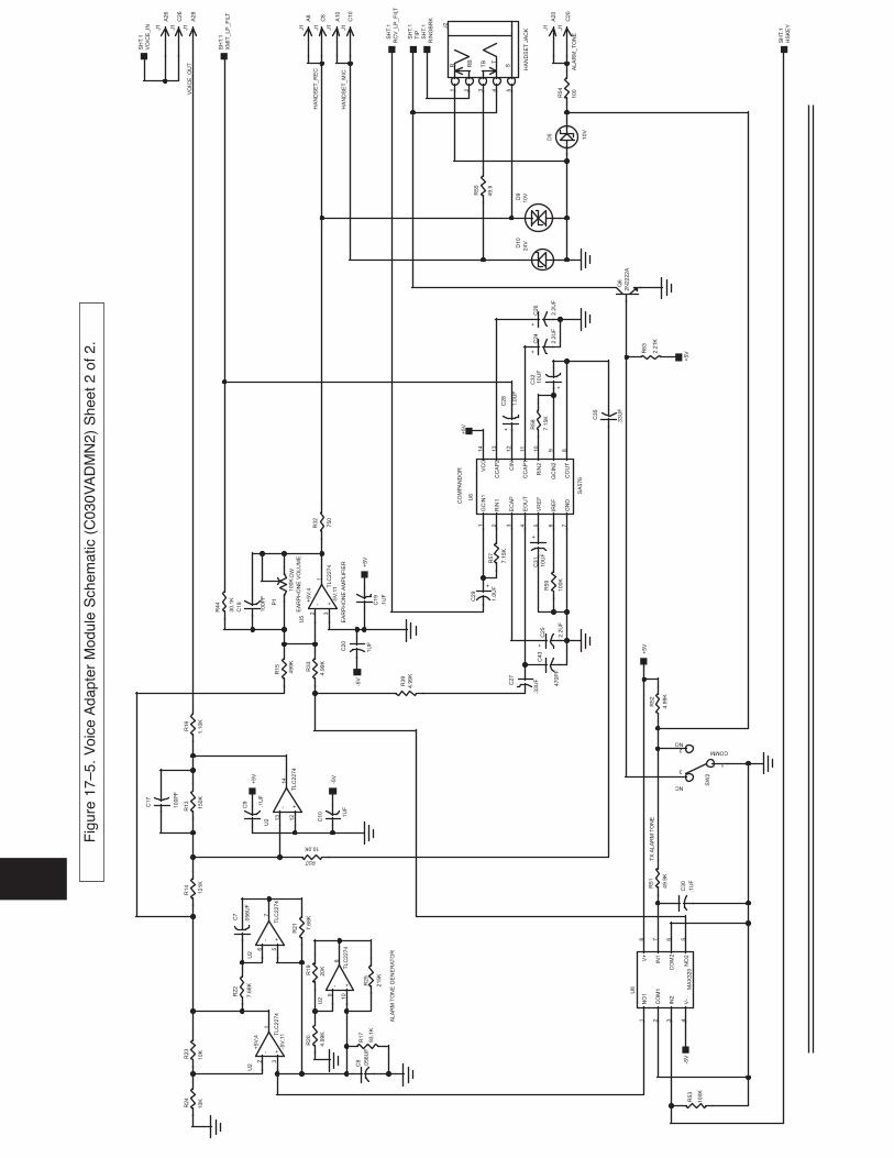
NO
1
CO
M1
IN2
V-
NO
2
CO
M2
IN1
V+
MA
X3
20
+
++
+
R RB
TB T
S
+-
TL
C2
27
4
+-
TL
C2
27
4
+-
TL
C2
27
4
CC
AP
1
CC
AP
2
CIN
CO
UT
EC
AP
EO
UT
GC
IN1
GC
IN2
GN
D
IRE
F
RIN
1
RIN
2
VC
C
VR
EF
+
+
NO
NC
COMM
2N
22
22
A
+-
TL
C2
27
4
CW
+-
TL
C2
27
4
+
CO
MP
AN
DO
R
SH
T.1
SH
T.1 S
HT.1
SH
T.1
TX
AL
AR
MT
ON
E
SH
T.1
SH
T.1
AL
AR
MT
ON
EG
EN
ER
AT
OR
EA
RP
HO
NE
VO
LU
ME
EA
RP
HO
NE
AM
PL
IFIE
R
A8
C8
A1
0
C1
0
A2
6
C2
6
A2
8
HA
ND
SE
TJA
CK
A2
0
C2
0
R2
2
7.6
8K
R2
1
7.6
8K
C2
7
.33
UF
C4
3
47
0P
F
C2
5
2.2
UF
R1
4
12
1K
R1
3
15
0K
R1
5
49
9K
R37
10.0K
1
32
U5
-5V
;11
+5
V;4
P1
10
0K
1
32+
5V
;4
-5V
;11
U2 C
8
.05
6U
F
C7
.05
6U
F
+5
VR6
3
2.2
1K
TIP
Q6
2
3
1
SW
2
HA
ND
SE
T_
MIC
D1
0
24
V1
0V
D9
D5
10
V
C2
9
1.0
UF
1.0
UF
C2
8
RIN
GB
RK
HS
KE
Y
RC
V_
LP
_F
ILT
VO
ICE
_IN
XM
IT_
LP
_F
ILT
VO
ICE
_O
UT
J1
R5
5
49
.9
HA
ND
SE
T_
RE
C
+5
V
10
0
R5
4
J1
J1
.33
UF
C3
5
2 3 4 5 6 7891
0
11
12
13
14
1
U6
SA
57
6
4.9
9K
R3
9
C1
7
10
0P
F
13
12
14
U2
8
109
U2
6 5
7
U2
R4
4
30
.1K
1 2 3 4 5
J2
2.2
UF
C2
4
2.2
UF
C2
6
J1
J1
C3
1
10
UF
7.1
5K
R5
7
C3
21
0U
F
J1
J1
J1
J1
R5
8
7.1
5K
R3
2
75
0
.1U
F
C2
0
C1
9
.1U
F
R5
2
4.9
9K
10
0K
R5
9
R5
3
10
0K
49
.9K
R5
1
1 2 3 45678
U8
C3
0
.1U
F
R2
5
21
5K
R1
6
1.1
0K
93
.1K
R1
7
20
K
R1
9
4.9
9K
R2
0
10
K
R2
3R
24
10
K
.1U
F
C1
0
.1U
F
C9
R3
3
4.9
9K
C1
8
10
0P
F
AL
AR
M_
TO
NE
+5
V
+5
V
-5V
-5V
-5V
+5
V
Fig
ure
17–5
. V
oice
Ada
pter
Mod
ule
Sch
emat
ic (
C03
0VA
DM
N2)
She
et 2
of
2.
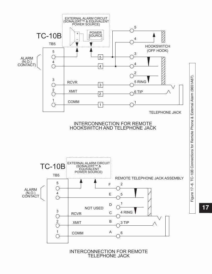
5
4
3
2
1
TB5
ALARM(N.O.)
CONTACT
TC-10B
INTERCONNECTION FOR REMOTEHOOKSWITCH AND TELEPHONE JACK
INTERCONNECTION FOR REMOTETELEPHONE JACK
I I I
2
6
3 TIP
4 RING
5
1
F
E
D
C
B
A
NOT USED
RCVR
XMIT
COMM
REMOTE TELEPHONE JACK ASSEMBLY
EXTERNAL ALARM CIRCUIT(SONALERT™ &
EQUIVALENTPOWER SOURCE)
I
I I
COMM
XMIT
RCVR
2
4
5 RING
6 TIP
1
3
TC-10B
ALARM(N.O.)
CONTACT)
TB5
1
2
3
4
5
4
5
5
4
3
2
1
HOOKSWITCH
(OFF HOOK)
TELEPHONE JACK
EXTERNAL ALARM CIRCUIT(SONALERT™ & EQUIVALENT
POWER SOURCE)
POWERSOURCE+
+
––
Fig
ure
17–6
. T
C-1
0B C
onne
ctio
ns f
or R
emot
e P
hone
& E
xter
nal A
larm
(96
51A
87).
17
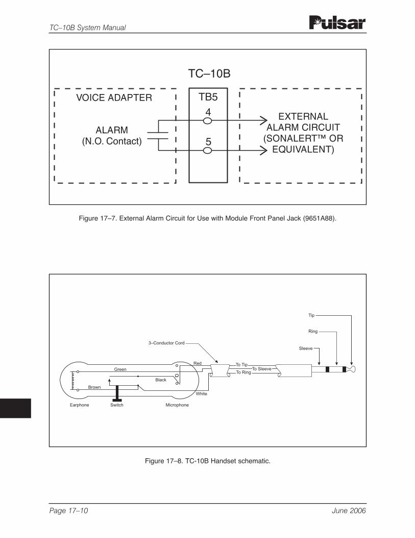
Page 17–10 June 2006
TC–10B System Manual
TC–10B
TB5
5
4
ALARM(N.O. Contact)
VOICE ADAPTER
EXTERNALALARM CIRCUIT
(SONALERT™ OREQUIVALENT)
Figure 17–7. External Alarm Circuit for Use with Module Front Panel Jack (9651A88).
Figure 17–8. TC-10B Handset schematic.


Related Documents