Frequency Domain Algorithms For Simulating Large Signal Distortion in Semiconductor Devices A DISSERTATION SUBMITTED TO THE DEPARTMENT OF ELECTRICAL ENGINEERING AND THE COMMITTEE ON GRADUATE STUDIES OF STANFORD UNIVERSITY IN PARTIAL FULFILLMENT OF THE REQUIREMENTS FOR THE DEGREE OF DOCTOR OF PHILOSOPHY By Boris Troyanovsky November 1997

Welcome message from author
This document is posted to help you gain knowledge. Please leave a comment to let me know what you think about it! Share it to your friends and learn new things together.
Transcript

Frequency Domain Algorithms For Simulating
Large Signal Distortion in Semiconductor Devices
A DISSERTATION
SUBMITTED TO THE DEPARTMENT OF ELECTRICAL ENGINEERING
AND THE COMMITTEE ON GRADUATE STUDIES
OF STANFORD UNIVERSITY
IN PARTIAL FULFILLMENT OF THE REQUIREMENTS
FOR THE DEGREE OF
DOCTOR OF PHILOSOPHY
By
Boris Troyanovsky
November 1997

ii
© Copyright by Boris Troyanovsky 1998
All Rights Reserved

iii
I certify that I have read this dissertation and that inmy opinion it is fully adequate, in scope and quality, asa dissertation for the degree of Doctor of Philosophy.
Robert W. Dutton (Principal Advisor)
I certify that I have read this dissertation and that inmy opinion it is fully adequate, in scope and quality, asa dissertation for the degree of Doctor of Philosophy.
Zhiping Yu (Associate Advisor)
I certify that I have read this dissertation and that inmy opinion it is fully adequate, in scope and quality, asa dissertation for the degree of Doctor of Philosophy.
Abbas El-Gamal
Approved for the University Committeeon Graduate Studies:

iv
Abstract
The rapid growth of wireless communication systems has placed increasing demands
on the design of semiconductor devices for analog applications. In particular, large signal
distortion effects are of critical importance in microwave and RF communication circuitry.
Physics-based device-level simulation of these effects can be an important aid in the
analog device design process. However, the transient analysis capability present in
traditional semiconductor device simulators is inadequate for large signal distortion
analysis. The most notable shortcomings of conventional transient analysis are its inability
to directly capture the steady state response of systems driven by quasiperiodic inputs,
along with its poor performance in the presence of widely separated spectral components.
To address the aforementioned shortcomings of traditional time domain methods, a
harmonic balance analysis capability was added to the PISCES-II device simulator.
Harmonic balance, a frequency domain steady state solution technique for analyzing
nonlinear systems, is well-suited for high-frequency analog applications such as RF and
microwave communication systems. Algorithms for applying the harmonic balance
method to large-scale systems of semiconductor device equations are presented, and the
suitability of the techniques for practical problems is demonstrated. In particular, Krylov
subspace solution techniques with special-purpose preconditioners are introduced to solve
the large systems of equations that arise. Algorithms for reduced memory usage are
presented. Device-level harmonic balance analysis is applied to simulating harmonic and
intermodulation distortion in industrial device structures, and the simulation results are
compared to experimental measurements. Competing algorithms, such as the circuit
envelope technique and the shooting method, are briefly reviewed and compared to
harmonic balance.

v

vi
Acknowledgments
I would like to express my deepest gratitude to Professor Robert W. Dutton, my
advisor, for his guidance, advice, and support throughout the course of my graduate
studies. The thesis topic and the direction of this work are direct products of his
suggestions and ideas. I would also like to thank Professor Zhiping Yu, my associate
advisor, for providing constant encouragement, technical advice, and countless valuable
suggestions during the course of this research.
I would like to acknowledge the support I’ve received during the past two years from
many co-workers at Hewlett-Packard’s EEsof Division. Dr. Niranjan Kanaglekar, my
project manager, and Jeffrey W. Meyer, my section manager, have both been extremely
supportive. I’d like to thank David D. Sharrit for the many clear, concise technical
explanations he’s supplied over the years on numerous topics in circuit simulation. Dr.
Marek Mierzwinski’s advice and assistance is also gratefully acknowledged. During the
early portion of my graduate studies, I benefited greatly from summers spent at Hewlett-
Packard Laboratories. I would like to express my appreciation to Dr. Norman Chang, Dr.
Gregory Gibbons, Dr. Lee Barford, Dr. Richard Dowell, Randy Coverstone, Dr. Ken Lee,
and Al Barber for the valuable learning experience.
During my graduate studies at Stanford, I was fortunate enough to collaborate with
several very talented industrial partners. I would like to especially thank Ms. Junko Sato-
Iwanaga of Matsushita Electronics Corporation for providing numerous simulation
examples and critically important feedback regarding this research. Dr. Torkel Arnborg of
Ericsson Components provided additional examples and some much-appreciated
enthusiasm and motivation. Toward the latter stages of this work, it has been a pleasure to
work with Francis M. Rotella in integrating the harmonic balance module into his mixed-
level circuit / device PISCES simulator. Many thanks go to Alvin Loke, Anthony Chou,

vii
Freddy Sugihwo, Adrian Ong, Maria Perea, and Fely Barrera for helping to make my
Stanford experience an enjoyable one.
I would like to thank Professor Abbas El-Gamal for being a member of my oral thesis
defense committee, and for being a 3rd reader of this manuscript. I would also like to
thank Professor David A. B. Miller for serving as the oral defense chairman.
Most of all, I would like to express my appreciation to my parents, Alex and Inna, for
their overwhelming love and kindness during these first twenty-seven years of my life.
This thesis is dedicated to them.

viii
To my parents

ix
Chapter 1
Introduction..................................................................................................................1
1.1 Background ...........................................................................................................2
1.2 Motivation.............................................................................................................2
1.3 Overview and Outline ...........................................................................................6
Chapter 2
Nonlinear State Equations and Large Signal Distortion..........................................9
2.1 Large Signal Distortion.......................................................................................102.1.1 Nonlinearities, Power Series, and Distortion..........................................102.1.2 Multi-Tone Distortion and Intermodulation............................................112.1.3 Characterizing Large Signal Distortion ..................................................132.1.4 Gain Compression and Intercept Points..................................................15
2.2 The Large Signal Steady State ............................................................................172.2.1 The Various Types of Steady State .........................................................172.2.2 Distributed Linear Elements in the Sinusoidal Steady State ..................18
2.3 Circuit-Level Modeling ......................................................................................20
2.4 Physics-Level Modeling of Semiconductor Devices..........................................232.4.1 The Drift-Diffusion Equations ................................................................232.4.2 Discretizing the Drift-Diffusion Equations.............................................242.4.3 Boundary Conditions ..............................................................................282.4.4 Terminal Current Evaluation...................................................................312.4.5 Mixed Level Circuit and Device Simulation ..........................................33
2.5 Solving the State Equations By Transient Analysis............................................34
2.6 Summary .............................................................................................................36
Chapter 3
Harmonic Balance Fundamentals ............................................................................37
3.1 The Discrete Fourier Transform — Some Definitions and Notation..................393.1.1 The Double-Sided DFT...........................................................................393.1.2 The Single-Sided DFT ............................................................................40
3.2 The Quasiperiodic Steady State ..........................................................................433.2.1 Representing Quasiperiodic Signals .......................................................43
x
3.2.2 Harmonic Truncation ..............................................................................44
3.3 Quasiperiodic Transforms...................................................................................483.3.1 The Frequency-Remapped DFT/FFT .....................................................493.3.2 Remapping Functions .............................................................................513.3.3 A Remapping Example ...........................................................................533.3.4 The Multi-Dimensional DFT/FFT ..........................................................55
3.4 Formulating the Harmonic Balance Equations ...................................................583.4.1 The HB ‘‘Right Hand Side’’ (RHS) Residual .........................................593.4.2 The HB Jacobian.....................................................................................62
3.5 Solving The Harmonic Balance Equations With Direct Methods ......................643.5.1 Newton’s Method....................................................................................643.5.2 Explicitly Forming the Harmonic Balance Jacobian ..............................653.5.3 Factoring The Harmonic Balance Jacobian ............................................703.5.4 The Harmonic Balance Jacobian at Low Distortion Levels ...................73
3.6 Summary .............................................................................................................75
Chapter 4
Solving the Harmonic Balance Equations with Newton-Iterative Methods.........77
4.1 Krylov Subspace Solution Techniques ...............................................................784.1.1 Generalized Minimum Residual (GMRES)............................................784.1.2 Other Krylov Subspace Algorithms........................................................81
4.2 Matrix-Vector Products Involving the Harmonic Balance Jacobian...................81
4.3 Preconditioning ...................................................................................................844.3.1 The Block-Diagonal Preconditioner .......................................................844.3.2 The Sectioned Preconditioner for Multi-Tone Problems ........................874.3.3 Other Preconditioners .............................................................................92
4.4 Further Memory Reduction Strategies................................................................924.4.1 Approximate Compact Spectral Storage.................................................924.4.2 Approximate GMRES Vector Storage ....................................................944.4.3 Impact of Memory Reduction Strategies on Performance......................95
4.5 Iterative Linear Solvers in the Newton Loop......................................................96
4.6 Convergence Issues.............................................................................................99
4.7 Summary ...........................................................................................................102

xi
Chapter 5
Competing Approaches ...........................................................................................103
5.1 Envelope Simulation.........................................................................................1045.1.1 Envelope Representation in the Presence of Nonlinearities .................1045.1.2 The Circuit Envelope Algorithm ..........................................................1065.1.3 Application to the Semiconductor Device Simulation Problem...........107
5.2 The Shooting Method .......................................................................................1085.2.1 The Basic Algorithm.............................................................................1095.2.2 The Matrix-Implicit Variant..................................................................1105.2.3 Strengths and Weaknesses ....................................................................111
5.3 Summary ...........................................................................................................112
Chapter 6
Examples and Results ..............................................................................................115
6.1 A GaAs MESFET Example ..............................................................................115
6.2 Distortion Analysis of an SOI BJT ...................................................................118
6.3 A High-Q Single-BJT Mixer Example .............................................................123
6.4 An LDMOS Device for RF Applications .........................................................124
6.5 Summary ...........................................................................................................126
Chapter 7
Conclusion ................................................................................................................129
7.1 Summary ...........................................................................................................129
7.2 Future Work ......................................................................................................130

xii

xiii
List of Tables
Table 3.1 Correspondence between remapped and physical frequencies. ...........54
Table 4.1 A comparison of simulator performance under various memoryreduction options..................................................................................96
Table 5.1 A comparison of simulation algorithms.............................................113
Table 6.1 Summary of simulation results for the examples of Chapter 6..........127

xiv

xv
List of Figures
Figure 1.1 A single-transistor downconverting mixer circuit. The resonant filter istuned to the difference of the RF and LO frequencies...........................3
Figure 1.2 Simulation results for Q=100. The two plots on the left side show theIF output spectrum at steady state. The top plot on the right side illus-trates the time domain IF waveform once steady state has been reached,while the bottom right plot shows the transient build-up. .....................4
Figure 1.3 Simulation results for Q=40. The two plots on the left side show the IFoutput spectrum at steady state. The top plot on the right side illustratesthe time domain IF waveform once steady state has been reached, whilethe bottom right plot shows the transient build-up. ...............................5
Figure 2.1 Inverting BJT amplifier biased in the forward active region ofoperation. .............................................................................................10
Figure 2.2 A two-tone test of a (hypothetical) bandpass amplifier. The two-toneinput signal (top) generates a spectrum of harmonics at the output (bot-tom). Note the third order terms landing within the passband — unlikethe second order terms, they cannot be easily filtered out. ..................14
Figure 2.3 Input-output power curves for the first-, second-, and third-orderdistortion terms for a typical amplifier.................................................16
Figure 2.4 Formulating the state equations in the presence of current-controlledstate elements. ......................................................................................22
Figure 2.5 A bipolar transistor structure (top) and its triangular mesh (bottom). .25

xvi
Figure 2.6 Control volume around node k, determined by the perpendicularbisectors (dashed).................................................................................26
Figure 2.7 A boundary grid node. .........................................................................29
Figure 2.8 Grid near an electrode. The electrode segment is denoted by thethick bold line. .....................................................................................31
Figure 2.9 A semiconductor device interfaced to a circuit network. ....................33
Figure 3.1 The two-tone box truncation of order P = 4 in the(a) double-sided formulation and the (b) single-sided formulation. ....45
Figure 3.2 The two-tone diamond truncation of order P = 4 in the (a) double-sidedformulation and the (b) single-sided formulation using constraint(3.19)....................................................................................................46
Figure 3.3 The two-tone modified diamond truncation of orders P1=4, P2=5, andPmax=3 and in the (a) double-sided formulation and the (b) single-sided formulation. ................................................................................47
Figure 3.4 Remapping for diamond truncation of order P = 4. The shaded binsrepresent complex-conjugate ‘‘image’’ slots that are absent from thesingle-sided formulation. .....................................................................53
Figure 3.5 The physical and remapped spectral representations of x(t) (not toscale). Note how the effective transform size is reduced. The dashedline above corresponds to the (-1,2) mixing product which must be con-jugated because its bin corresponds to the negative physical frequency-98 Hz...................................................................................................55
Figure 3.6 In forming the explicit harmonic balance Jacobian, each structurallynon-zero entry in the DC/time-domain Jacobian (left) inflates into adense conversion matrix, or ‘‘block,’’ (right). ....................................67
Figure 3.7 LU factorization of a banded harmonic balance pivot block. Note thatthe bandwidth of the L and U factors is equivalent to that of theoriginal pivot block. .............................................................................72
Figure 4.1 An example of the block-diagonal preconditioner matrix structure forN=3, H=3. Each block within the matrix corresponds to a singleJacobian entry in the time domain Jacobian. .......................................85
Figure 4.2 The block diagonal preconditioner of Figure 4.1 after a permutationoperation which groups blocks on the basis of frequencies rather thannodes. Each of the H diagonal blocks has dimension and retains thesparsity structure of the original time domain Jacobian. .....................86
Figure 4.3 An illustration of tightly spaced frequency ‘‘bands’’ that occur when issmall in a two-tone stimulus. The dashed lines and the frequenciesabove them indicate the center of each ‘‘band’’ in the spectrum.........88

xvii
Figure 4.4 Memory usage comparison between the sectioned and non-sectionedpreconditioners for the single-BJT mixer example..............................91
Figure 4.5 Convergence rate comparison between the sectioned and non-sectionedpreconditioners for the single-BJT mixer example..............................91
Figure 4.6 Three device configurations to illustrate when harmonic balance con-vergence problems can occur. The two leftmost configurations will notexhibit convergence difficulties. The rightmost configuration may, ifthe input RF power is large. ...............................................................100
Figure 4.7 Steady-state time domain diode current in response to a 0.8V drivingsinusoid. The results were computed with the harmonic balancePISCES device simulator. ..................................................................101
Figure 6.1 Cross-section of GaAs MESFET power device.................................116
Figure 6.2 External circuit configuration for the GaAs MESFET poweramplifier. ............................................................................................116
Figure 6.3 Bird’s eye plot of distortion in electron concentration inside theMESFET of Figure 6.1. .....................................................................117
Figure 6.4 Comparison between experimental measurements and simulatedresults. ................................................................................................118
Figure 6.5 Power SOI BJT structure. The 3D rendering (top) is not to scale. The2-D cross-section (bottom) is oriented such that it is consistent withsubsequent contour and mesh plots....................................................119
Figure 6.6 Formation of electron accumulation layer at the Si-SiO2 interfaceinduced by the positive substrate bias................................................120
Figure 6.7 Improvement in fT at Vsub = 10V (dashed line) over that at Vsub = 0V(solid line). .........................................................................................120
Figure 6.10 Logarithmic contour (left) and perspective (right) plots for the 2ndharmonic of electron concentration. ..................................................121
Figure 6.11 Logarithmic contour (left) and perspective (right) plots for the 2ndharmonic of electrostatic potential.....................................................121
Figure 6.8 Harmonic distortion in collector current as a function of substratebias. ....................................................................................................122
Figure 6.9 Collector current spectrum for one-tone (left) and two-tone (right)simulations. ........................................................................................122
Figure 6.12 A single-device BJT mixer. The resonant circuit at the output is tunedto either the sum or the difference frequency of the LO and RF,depending on the application. ............................................................123

xviii
Figure 6.13 Baseband spectrum of the collector current (left) and output voltage(right). Note the suppression of distortion components by the resonantcircuit in the output waveform...........................................................124
Figure 6.14 LDMOS device cross-section (top) and its simulated-vs-measuredgain/PAE curves (bottom). .................................................................125

1
Chapter 1
Introduction
Semiconductor device simulation has played a key role in the design and development
of novel device structures and technologies. Although analog device designs have
benefited greatly from physics-based device simulation, the important area of large signal
steady-state analysis has been somewhat neglected by the device simulation community.
With the rapid growth of wireless communication systems and other analog designs where
harmonic distortion is critical, there has been an ever-increasing need for such analysis
capabilities at the device simulation level.
This work presents algorithms, results, and application examples aimed at solving
nonlinear frequency domain steady-state device simulation problems. Stanford
University’s popular device simulator, PISCES-II [10], is extended to support a harmonic
balance analysis capability. Harmonic balance, a frequency domain steady state analysis
method for nonlinear systems, is well-suited for high-frequency analog applications such
as RF and microwave communication systems. Algorithms for applying the harmonic
balance method to large scale systems of semiconductor device equations are presented,
and the suitability of the techniques for practical problems is demonstrated.

Chapter 1 Introduction 2
1.1 Background
Analog circuit designers have long recognized the drawbacks and limitations of
SPICE-like [12] transient analysis. Although extremely effective on many problems,
traditional time domain approaches often fall short when applied to simulating the steady
state response of systems with long time constants or widely separated spectral
components. Many analog designs require the simulation of steady-state quantities such as
harmonic distortion, and fall precisely into the aforementioned domain. The presence of
stiff bias elements (such as RF chokes and blocking capacitors) along with potentially
narrowband high-Q filters introduces the long time constants, and thus necessitates
simulation over a prohibitively large number of periods to reach steady state. In addition,
many high-frequency linear elements accounting for dispersion, loss, and parasitic
components are extremely difficult to model in the time domain.
The recognition of these difficulties by high-frequency circuit designers has led to
demand for and the development of alternate circuit simulators over the past decade.
Harmonic balance [21][22][27], a nonlinear frequency domain analysis technique, has
emerged as a widely accepted solution to many of the shortcomings that conventional time
domain simulators have in the high-frequency analog arena. With the introduction of UC
Berkeley’s nonlinear frequency domain Spectre simulator [27], and the development of
commercial harmonic balance simulators by Hewlett-Packard, EEsof1, and Compact
Software, nonlinear frequency domain analysis has assumed its current position as the
method of choice for simulating most nonlinear microwave designs, and for analyzing a
large number of the RF designs as well.
1.2 Motivation
To demonstrate the inherent limitations of transient analysis in the context of RF
simulation, we present an illustrative example. The example is a small mixer circuit which
highlights the major problem areas associated with standard time domain simulation
algorithms. In this section, we will approach the example from a circuit-level perspective,
1. Subsequently acquired by Hewlett-Packard.
Motivation 3
since the points made are equally applicable to both the circuit and device simulation
areas. Subsequent chapters will focus on the problem from a device-level perspective, and
the example will be revisited in the context of device simulation in Section 6.3.
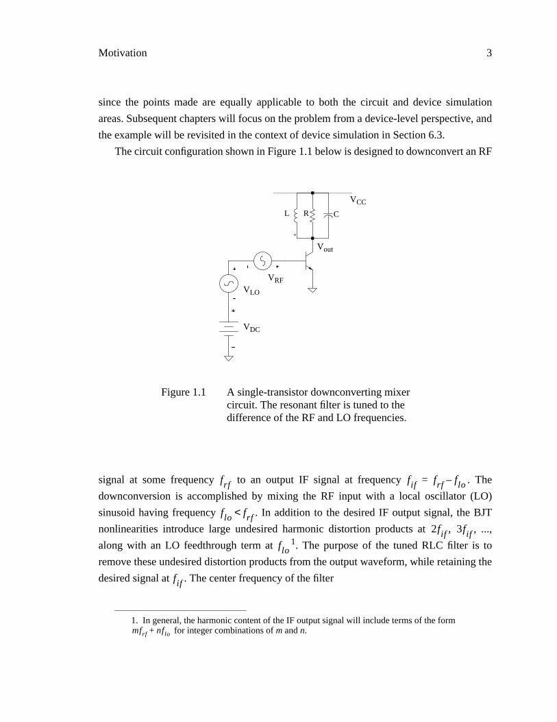
The circuit configuration shown in Figure 1.1 below is designed to downconvert an RF
signal at some frequency to an output IF signal at frequency . The
downconversion is accomplished by mixing the RF input with a local oscillator (LO)
sinusoid having frequency . In addition to the desired IF output signal, the BJT
nonlinearities introduce large undesired harmonic distortion products at , , ...,
along with an LO feedthrough term at 1. The purpose of the tuned RLC filter is to
remove these undesired distortion products from the output waveform, while retaining the
desired signal at . The center frequency of the filter
1. In general, the harmonic content of the IF output signal will include terms of the form for integer combinations of m and n.
Figure 1.1 A single-transistor downconverting mixercircuit. The resonant filter is tuned to thedifference of the RF and LO frequencies.
VCC
VRFVLO
VDC
RL C
Vout
frf fif frf flo–=
flo frf<2fif 3fif
flo
mfrf nflo+
fif

Chapter 1 Introduction 4
(1.1)
must be chosen such that , and the quality factor
(1.2)
needs to be selected so that the bandwidth of the filter ( ) is tight enough to
remove the distortion components at frequencies of and above.
f01
2π LC------------------=
f0 fif=
Q RCL----=
fbw f0 Q⁄=
2fif
Figure 1.2 Simulation results for Q=100. The two plots on the left side show theIF output spectrum at steady state. The top plot on the right sideillustrates the time domain IF waveform once steady state has beenreached, while the bottom right plot shows the transient build-up.
Motivation 5
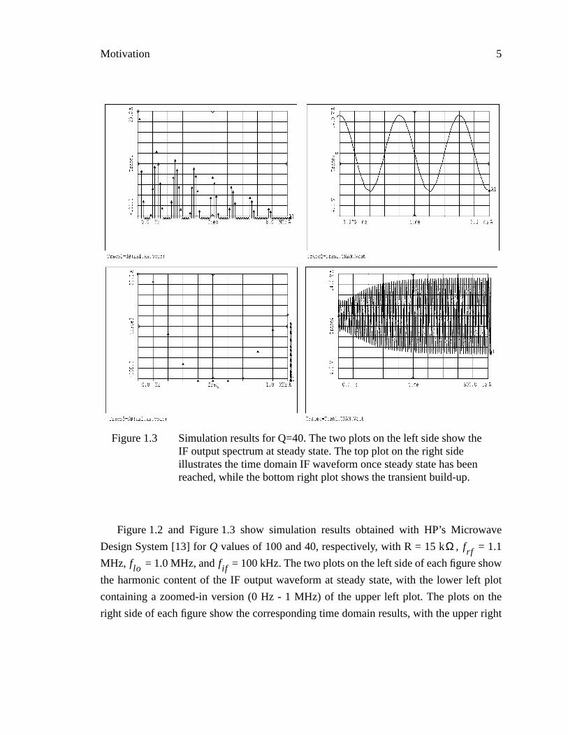
Figure 1.2 and Figure 1.3 show simulation results obtained with HP’s Microwave
Design System [13] for Q values of 100 and 40, respectively, with R = 15 k , = 1.1
MHz, = 1.0 MHz, and = 100 kHz. The two plots on the left side of each figure show
the harmonic content of the IF output waveform at steady state, with the lower left plot
containing a zoomed-in version (0 Hz - 1 MHz) of the upper left plot. The plots on the
right side of each figure show the corresponding time domain results, with the upper right
Figure 1.3 Simulation results for Q=40. The two plots on the left side show theIF output spectrum at steady state. The top plot on the right sideillustrates the time domain IF waveform once steady state has beenreached, while the bottom right plot shows the transient build-up.
Ω frfflo fif

Chapter 1 Introduction 6
plot showing the IF waveform after steady state has been reached, and the lower right plot
showing the transient build-up to steady state.
Transient analysis faces two major difficulties in coping with examples such the one
presented here. The first of these difficulties has to do with the potentially long time
constants introduced by passive components like high-Q (narrowband) filters. Because
analog circuit designers are typically interested in the steady state response of nonlinear
systems, a conventional time domain simulator must integrate over the start up transients
until they decay to the point where they are negligible. The lower-right plot of Figure 1.2
shows the initial transient behavior when the Q of the RLC filter is 100. As expected, the
corresponding plot of Figure 1.3 shows that the transient region is smaller when the Q is
reduced to 40. Long time constants are not restricted solely to narrow bandwidth filtering
circuitry; they also arise in connection with other passive elements (such as RF chokes and
DC blocks) critical to many RF circuits.
A second major difficulty faced by standard transient simulators has to do with the
wide range of frequencies present in many practical RF and microwave circuits. For
example, the IF frequency of the example in this section is 100 kHz, which corresponds to
a period of 10 s. The RF frequency, on the other hand, is at 1.1 MHz, corresponding to a
period of less than 1 s. Furthermore, harmonics of the RF and LO must be accounted for,
potentially pushing the associated period to around 0.1 s if, for example, 9 harmonics
are needed. This wide disparity in the length of the periods means that transient simulators
must integrate over a large number of time points to cover a full IF period (see the lower
right plots of the figures above for an illustration). Furthermore, as we saw in the
preceding paragraph, the simulator must cover many periods of the IF signal in order to
reach steady state. It should be pointed out that the example frequencies chosen in this
section actually understate the problems faced by transient analysis. In reality, it is very
common to encounter microwave systems having signals that include spectral components
ranging from the kHz to the GHz range. We picked a relatively low RF frequency only for
ease of plotting and presenting the data.
1.3 Overview and Outline
The shortcomings of conventional transient analysis at the RF/microwave circuit level
have led to the development of nonlinear frequency domain simulation techniques such as
µµ
µ

Overview and Outline 7
harmonic balance. The goal of this work is to extend the applicability of harmonic balance
to the semiconductor device simulation level. By far the largest obstacle to employing
harmonic balance for device simulation problems is the extremely large size and relatively
high density of the semiconductor device Jacobian when compared to its circuit
counterpart. We will demonstrate that this obstacle can be overcome through use of
algorithms that carefully exploit the special structure of the device Jacobian.
This thesis consists of seven chapters. The current chapter presents the background
and motivation for this work, and outlines the organization of the thesis. Chapter 2 then
proceeds to give an overview of the kinds of nonlinear state equations that arise in circuit
and device simulation, along with a discussion of how the nonlinearities lead to large
signal distortion. Some standard metrics and figures of merit (e.g., gain compression and
intercept points) commonly used by RF and microwave designers are briefly discussed.
The details of formulating the constitutive equations for both circuit and semiconductor
device simulation problems are then presented, including a subsection on how mixed
circuit- and device-level simulation matrices may be formulated. The chapter concludes
with a brief discussion of standard transient methods that can be used for solving the
nonlinear state equations.
The harmonic balance algorithm is presented in Chapter 3. Solution methods based on
direct factorization techniques are discussed, and shown to be inadequate for handling the
large Jacobians encountered in HB-based device analysis. Algorithms to successfully cope
with these kinds of problems are developed in Chapter 4. Linear iterative solvers (in
particular, the GMRES algorithm) are employed in conjunction with special-purpose
preconditioners developed specifically for semiconductor device applications. Specific
techniques for efficiently applying Krylov subspace solution methods to the device-level
harmonic balance problem are discussed.
The algorithms of Chapter 4 are the foundation on which this work is based; Chapter 5
provides an overview of two competitive algorithms that have unique strengths and
weaknesses relative to the methods of Chapter 4. The algorithms reviewed are circuit
envelope simulation and the matrix-implicit shooting method. These are compared to the
harmonic balance algorithms chosen as the foundation of this work.
Chapter 6 provides several practical examples originating from both industrial and
academic sources. These provide valuable benchmark data, and serve as testimonials to
the code’s applicability to solving realistic problems. Examples include both amplifiers

Chapter 1 Introduction 8
and mixers, with device technologies ranging from silicon BJTs and MOSFETs to GaAs
MESFET structures. The thesis concludes with Chapter 7, which summarizes the work
and discusses directions for future research.

9
Chapter 2
Nonlinear State Equations and Large SignalDistortion
Nonlinearities are absolutely critical to the proper operation of analog communication
circuits. In some applications, such as in highly linear amplifier design, the goal is to
generate an amplified replica of the input signal, and minimize any nonlinear effects that
lead to distortion of the waveform. In other designs, such as mixers or frequency-doublers,
nonlinearities are purposely used to introduce desired frequency-translated components
into the output signal. In the latter case, undesired spurious products are minimized
through careful design and the use of balancing and/or linear filtering techniques.
In this chapter, we review the static and dynamic mechanisms responsible for
nonlinear distortion, as well as several ‘‘figures of merit’’ related to characterizing the
levels of distortion present in a given system. There are several levels of hierarchy that can
be used in modeling nonlinear components — the behavioral (or system) level, the circuit
level, and the physical device level. At the circuit and system level, a given ‘‘compact
model’’ typically consists of less than a dozen or so state variables, and is based on either
phenomenological or approximate physics-based analysis [17][18]. In this work, we
primarily concentrate our efforts at the physical device level, where the model is based on
solution of partial differential equations, and the number of time domain state variables is
in the thousands.

Chapter 2 Nonlinear State Equations and Large Signal Distortion 10
2.1 Large Signal Distortion
2.1.1 Nonlinearities, Power Series, and DistortionAs a simple but illustrative example, we consider the inverting single-transistor BJT
amplifier of Figure 2.1. At low frequencies, the device can be modeled to first order by the
equations accompanying the schematic below:
By inspection, the unloaded response of the amplifier under large signal ac drive is
, (2.1)
and the incremental voltage (the instantaneous voltage minus the quiescent value) is
. (2.2)
Letting and for notational convenience,
and using the standard Taylor series expansion for , we obtain
. (2.3)
IC IS
qVBE
kT-------------
exp=
IB
IS
β----
qVBE
kT-------------
exp=
IE 1 1β---+
– IS
qVBE
kT-------------
exp=
R
Vdc
Vacejωt
Vcc
Vo
Figure 2.1 Inverting BJT amplifier biased in the forwardactive region of operation.
V0 Vcc ISRqVdc
kT------------
qVac ωt( )cos
kT----------------------------------
expexp–=
v0 ISRqVdc
kT------------
1
qVac ωt( )cos
kT----------------------------------
exp–
exp=
a0 ISR qVdc kT⁄( )exp–= Vac qVac kT⁄=
x( )exp
v0 a01n!----- Vac ωt( )cos( )
n
n 1=
∞
∑=

Large Signal Distortion 11
Assuming the input signal is small enough such that only the first three terms of (2.3) are
significant, can be approximated as
. (2.4)
In the limit of infinitesimally small AC input, the terms involving and become
negligibly small, and the amplifier responds with an output incremental voltage at the
fundamental frequency only:
. (2.5)
As the AC drive level is increased, distortion components begin to appear at harmonics of
the fundamental, and at DC. The level of distortion that can be tolerated in a given circuit
depends on the specific application involved, and must be weighed by the designer against
other design priorities.
An interesting and important characteristic to observe in (2.4) is that the amplitudes of
the various harmonics are completely independent of input frequency. As we will see in
more detail later, this is a general property of resistive nonlinearities — i.e., nonlinearities
that are not frequency dependent.
2.1.2 Multi-Tone Distortion and IntermodulationIn the preceding section, the large signal AC input was restricted to a single
fundamental frequency. As is evident from (2.4), the distortion components produced by
this single-tone stimulus are all harmonics of the fundamental frequency. When the input
consists of two or more independent tones, additional distortion components are produced.
Such distortion terms arise from nonlinear ‘‘mixing’’ of the independent input tones, and
are often referred to as intermodulation products, spurious harmonics, or mixing terms.
Referring back to the example of Figure 2.1, we consider the case where the input AC
signal is composed of two sinusoids at independent frequencies and :
(2.6)
Introducing the normalized amplitudes , , and using the
power series (2.3) allows us to write the amplifier’s incremental output voltage as
v0
v0
a0----- 1
4---Vac
2Vac
18---Vac
3+
ωt( )cos14---Vac
22ωt( )cos
124------Vac
33ωt( )cos+ + +≈
Vac2
Vac3
v0
Vac-------- q
kT------a
0ωt( )cos→
ωA ωB
vin t( ) VA ωAt( )cos VB ωBt( )cos+=
VA qVA kT⁄= VB qVB kT⁄=

Chapter 2 Nonlinear State Equations and Large Signal Distortion 12
. (2.7)
If, as before, the power series is approximated by its first three terms,1 we obtain the
following rather unwieldy but informative expression:
(2.8)
Thus, in addition to harmonic distortion components at and
, there are also new intermodulation product terms at the frequencies
. More generally, input sources at M independent
fundamentals can be expected to introduce distortion components at integer combinations
of the independent driving frequencies (see (3.14)).
An intermodulation component at a given frequency is said to have
order . For example, the distortion terms at frequencies and are
second-order products, whereas the components at , , and are
third-order. From equation (2.8) (which we stress again is valid only for low AC drive
levels), we see that distortion products of order m are polynomials of order m. This is a
1. Symbolic analysis packages such as Mathematica [73] can conveniently simplify complex alge-braic expressions. Equation (2.8) was obtained with Mathematica’s Expand[ , Trig->True] function.
v0 a01n!----- VA ωAt( )cos VB ωBt( )cos+
n
n 1=
∞
∑=
v0
a0----- 1
4---VA
2 14---VB
2+
VA18---VA
3 14---VAVB
2+ +
ωAt( )cos VB18---VB
3 14---VA
2VB+ +
ωBt( )cos
14---VA
22ωAt( )cos
14---VB
22ωBt( )cos
124------VA
33ωAt( )cos
124------VB
33ωBt( )cos
18---VAVB
2ωAt 2ωBt–( )cos
18---VA
2VB 2ωAt ωBt–( )cos
12---VAVB ωAt ωBt–( )cos
12---VAVB ωAt ωBt+( )cos
18---VA
2VB 2ωAt ωBt+( )cos
18---VAVB
2ωAt 2ωBt+( )cos
+ +
+ +
+ +
+ +
+ +
+ +
≈
ωA 2ωA 3ωA …, , ,ωB 2ωB 3ωB …, , ,ωA ωB± 2ωA ωB± ωA 2ωB± …, , ,
kAωA kBωB+
kA kB+ 2ωA ωA ωB±3ωB 2ωA ωB± ωA 2ωB±

Large Signal Distortion 13
general property which is used in the subsequent section to compute so-called intercept
points, a widely used metric for distortion in nonlinear systems.
2.1.3 Characterizing Large Signal DistortionThere are several commonly used metrics, or figures of merit, for quantifying the
levels of distortion present in a given waveform. For single-tone distortion measurements,
the nth harmonic distortion factors are widely employed. Given a waveform with
Fourier expansion
, (2.9)
is defined to be the magnitude of the ratio of the nth harmonic to the fundamental:
, . (2.10)
For example, the amplifier response of (2.4) has a second-harmonic distortion factor of
(2.11)
To characterize the level of distortion in the entire waveform (as opposed to the distortion
at a given harmonic), the total harmonic distortion (THD) is defined to be
(2.12)
The values of THD that can be tolerated in a given design are highly application-
dependent. In audio applications, for example, the THD must typically be kept well below
0.01, or 1%.
When the driving signal is multi-tone, intermodulation terms are introduced into the
response. For these spurious terms, the nth order intermodulation distortion factors
are defined analogously to the . A key difference in the multi-tone case, however, is
that there are, in general, several different frequency components having the same order.
For example, we see from (2.8) that there are 6 distinct third-order terms at frequencies
, , , , , and . Four of these are
intermodulation, or mixing, products, with the remaining two being harmonics of a
HDn
v t( ) ℜ e V0 V1 jωt( )exp V2 j2ωt( )exp V3 j3ωt( )exp …+ + + + =
HDn
HDn
Vn
V1------= n 2≥
HD2
Vac
412---Vac
2+
---------------------=
THD
Vn2
n 2=
∞
∑V1
----------------------------=
IMnHDn
3ωA 3ωB 2ωA ωB+ 2ωA ωB– ωA 2ωB+ ωA 2ωB–

Chapter 2 Nonlinear State Equations and Large Signal Distortion 14
fundamental. Thus, in specifying a value for , it is also necessary to state which
particular third-order harmonic is being used, along with which fundamental is intended as
the ‘‘real output’’ for use in the ratio.
The choice of frequencies used to define , along with the distortion order n of
interest, is application-dependent. Consider a narrowband amplifier, for instance. A
common distortion test in this case is to apply two very closely spaced input signals of
equal amplitude at frequencies and , such that both are within the amplifier
passband. The third-order distortion products falling at frequencies and
are of primary interest in this example, since they fall directly in the passband
(Figure 2.2). Letting , and using the approximate low-distortion model
of (2.8), we obtain
IMn
IMn
ωA ωB2ωA ωB–
2ωB ωA–
Figure 2.2 A two-tone test of a (hypothetical) bandpass amplifier. Thetwo-tone input signal (top) generates a spectrum ofharmonics at the output (bottom). Note the third order termslanding within the passband — unlike the second orderterms, they cannot be easily filtered out.
ωA ωB
ωA ωB
2ωA ωB– 2ωB ωA–
Pout
Pin
2ωA 2ωB
VA VB Vtst= =

Large Signal Distortion 15
(2.13)
In this example, the numerical value of is the same regardless of whether
or is used. In general, however, the value may be different for these two
frequencies, in which case an explicit distinction must be made. For instance, another
common test used for receiver design employs a small ‘‘desired’’ signal at a frequency
, while a large ‘‘interfering’’ (sometimes called blocking, or jamming) signal is applied
at a nearby frequency to determine the third-order distortion that is introduced. In this
case, the asymmetry in input signals will produce different values of at the various
third-order terms. Similarly, linear and nonlinear frequency dependent elements may
introduce such asymmetries even in the case of identical input amplitudes.
2.1.4 Gain Compression and Intercept PointsThe simplified transistor model of Figure 2.1 is valid only in the forward active region
of operation, and even then only in the low-distortion regime. As AC power is increased,
the collector voltage will swing low enough at the peak of the input sinusoid to send the
transistor into saturation. In addition to introducing even more distortion components, this
phenomenon will also compress the gain of the amplifier. Gain compression is an effect
that is of significant interest to the analog designer, and is an important metric for
determining the distortion properties of nonlinear systems.
Figure 2.3 shows the general shape of input-output power curves for a typical
amplifier. is defined to be the available power of the fundamental input tone
(2.14)
where is the source resistance; is defined to be the rms power dissipated in the
load. Depending on the application, the second- and third-order distortion components
plotted in the figure may correspond either to harmonics of the fundamental, or to specific
intermodulation components (Section 2.1.3).
As equations (2.4) and (2.8) indicate, the slopes of the first-, second-, and third-order
components in the low-power linear region on a log-log plot are 1 dB/dB, 2 dB/dB, and 3
dB/dB, respectively. In Figure 2.3, dashed lines are used to extrapolate the slopes to higher
IM3
Vtst2
8 3Vtst2
+---------------------=
IM3 2ωA ωB–
2ωB ωA– IM3
ωAωB
IM3
Pin
Pin
Vac2
8Rs--------------=
Rs Pout

Chapter 2 Nonlinear State Equations and Large Signal Distortion 16
power levels. The gain compression at a given input power level is defined to be the value
of the extrapolated (dashed) extension of the first-order distortion term divided by its
actual compressed value (solid line). The 2nd-order intercept point (sometimes referred to
as SOI, for ‘‘second-order intercept’’) is the intersection of the first- and second-order
linear extrapolations. Similarly, the 3rd-order intercept point (TOI) is defined to be the
intersection of the first- and third-order extrapolations. Arbitrary nth order intercept points
may be defined in an analogous manner.
Before concluding this section, we point out a few implicit assumptions regarding
intercept-point measurements. The first of these assumptions is that the input amplitudes
in the multi-tone input case must track each other during the power sweep for the slope
relations of the preceding paragraph to hold true. The second assumption is that the linear
low-power region is identifiable in the general case. While this is certainly true in the
simulation domain, actual physical measurements of real-world systems may show some
Figure 2.3 Input-output power curves for the first-, second-,and third-order distortion terms for a typicalamplifier.
Pin (dBm)
P out
(dB
m)
1st order
2nd order3rd order
IP2
IP3

The Large Signal Steady State 17
ripple and curvature all the way down to the noise floor. Nevertheless, most practical
systems do have identifiable linear regions, and the definition of intercept points can be
made such that the concept has validity.
2.2 The Large Signal Steady State
The purely resistive nonlinearities examined in Section 2.1 are not adequate for
representing realistic systems operating under time-varying inputs.1 Additional dynamic
effects arising from linear and nonlinear capacitors and inductors, filtering circuitry,
parasitics, and transmission lines are critical to proper modeling, and must be carefully
accounted for by any accurate simulation tool. Some dynamic elements, especially linear
components such as large inductors (RF chokes), large capacitors (DC blocks), and
narrowband filters can introduce extremely long time constants into a circuit network.
Since the analog designer is usually most interested in steady state quantities, time domain
transient simulators must be run until all the start-up transients have died out. In the
subsections below, we define the meaning of steady state solutions and briefly examine
some dynamic effects that illustrate the usefulness of steady state solution algorithms like
harmonic balance.
2.2.1 The Various Types of Steady StateA steady state solution of a system of differential equations is a solution that is
asymptotically approached as the effect of the initial conditions dies out [27][33]. In
general, a given system of differential equations can have no steady-state solutions, a
single steady state solution, or several such solutions. In the latter case, the actual solution
seen will depend upon the initial conditions. Most practical analog designs will have at
least one steady state solution.
There are several types of steady state problems which are of interest in analog
applications. The first of these is the DC steady state, where both the stimulus and the
solution are constant in time. Strictly linear systems2 driven by sinusoidal inputs will
1. At very low frequencies, however, purely resistive models can be adequate in the absence ofvery large capacitors and inductors.

Chapter 2 Nonlinear State Equations and Large Signal Distortion 18
reach an AC steady state, which consists of a sinusoid superposed on a DC offset term.
Similarly, it is possible to assume that the AC input is infinitesimally small, linearize a
nonlinear system of differential equations, and compute the small-signal AC response
from this linearization. Both the DC and small-signal AC steady state problems are
addressed by existing device simulation codes, and will not be discussed at length in this
work.
The periodic large signal steady state results either from an external periodic stimulus
(for non-autonomous systems such as amplifiers and mixers) or from a self-oscillation (for
autonomous systems such as oscillators). In the periodic steady state, the solution state
vector satisfies the periodicity condition
(2.15)for for some period T. Consequently, can be represented in the
frequency domain by a countable (though possibly infinite) number of Fourier series
terms. In practice, a finite number of Fourier harmonics is adequate for representing
to any required degree of accuracy.
The quasiperiodic large signal steady state is similar to the periodic steady state of the
preceding paragraph, with the exception that the stimulus and response frequencies need
not be harmonically related. For instance, a nonlinear system driven by multiple sinusoids
at harmonically unrelated frequencies will typically respond at the sum and difference
frequencies of the driving tones. The resulting spectrum will consist of a countable
number of spectral lines, corresponding to the quasi-Fourier components of the response.
It is possible for nonlinear systems to have steady-state responses that do not fit in any
of the categories presented above (e.g., chaotic circuits [33]). Such systems are not
representative of most practical analog designs, and are not considered in this work.
2.2.2 Distributed Linear Elements in the Sinusoidal Steady StateDistributed linear elements are a category of linear components that can be difficult to
simulate outside the steady state, and can make the transient ‘‘settling time’’ (the time to
reach steady state) prohibitively long. Distributed elements include transmission line
components (possibly with dispersion or loss) to model high-frequency interconnects such
2. We assume here that the linear system is ‘‘passive’’ — i.e., that its eigenvalues lie exclusively inthe left half plane.
x t( )
x t T+( ) x t( )=∞– t ∞< < x t( )
x t( )

The Large Signal Steady State 19
as microstrip transmission lines, non-ideal power planes, and distributed filters. These
distributed linear elements are best characterized in the frequency domain, where network
analyzers or electromagnetic simulation tools can be used to extract S-parameter matrix
descriptions as a function of frequency. Assuming a constant reference impedance for
all measurement ports, the S-parameter description of an N-port linear device takes the
form [16]
(2.16)
where the incident voltage waves are defined as
(2.17)
and the reflected voltage waves are defined as
(2.18)
In the periodic or quasiperiodic steady state, it is trivial to operate with such frequency
domain descriptions. Given a spectrum corresponding to, say, as a sequence of
phasors at the quasiperiodic frequencies of interest, the corresponding spectrum of
can be computed from (2.16) through complex-valued multiplications.
In the time domain, operations with constitutive equations of the form (2.16) are
potentially much more problematic. The frequency domain products of the preceding
paragraph become convolution integrals
(2.19)
where is the impulse response (i.e., inverse Fourier transform) of .
Because the measured spectrum of consists of only a finite number of samples
over a limited frequency range, construction of a passive and causal can prove to
be non-trivial. In addition, the long transients associated with some impulse responses
(such as those of high-Q narrowband filters) can make both the integration in (2.19) and
the overall transient simulation very time consuming if it has to be run until steady state is
reached.
Z0
V1- ω( )
|
VN- ω( )
S11 ω( ) … S1N ω( )
| \ |
SN1 ω( ) … SNN ω( )
V1+ ω( )
|
VN+ ω( )
=
Vn+ ω( )
Vn+ ω( ) 1
2--- Vn ω( ) Z0In ω( )+( )=
Vn- ω( )
Vn- ω( ) 1
2--- Vn ω( ) Z0In ω( )–( )=
Vn+ ω( )
Vm- ω( )
vm- t( ) smn t τ–( ) vn
+ τ( ) τd∞–
t
∫n 1=
N
∑=
smn t( ) Smn ω( )Smn ω( )
smn t( )

Chapter 2 Nonlinear State Equations and Large Signal Distortion 20
2.3 Circuit-Level Modeling
Compact models used in circuit simulation typically consist of linear and nonlinear
resistors, capacitors, and inductors. In time domain simulators capable of convolution-
based analysis, distributed linear models (such as lossy, dispersive transmission lines) can
also be described through impulse response matrices. A number of methods have been
used to formulate the state equations in nonlinear circuit simulators. The most prominent
of these methods include the sparse tableau approach and the modified nodal analysis
(MNA) approach [35]. Because our ultimate focus is on device level simulation, we
consider only the latter approach here, as it is more relevant to our needs. The reader is
referred to [36] for a detailed exposition of the sparse tableau formulation.
An N-terminal device is a nonlinear resistive element if its constitutive equations take
the form
. (2.20)
In the two-terminal case, a nonlinear resistor’s constitutive relation can be written as
. (2.21)At a given voltage across the resistor, the associated small-signal conductance is
. For the N-terminal resistive element, the small-signal admittance matrix is the
Jacobian of (2.20).
The constitutive equations for an N-terminal nonlinear capacitor are
, (2.22)
i1 g1 v1 v2 … vN, , ,( )=
i2 g2 v1 v2 … vN, , ,( )=
|
iN gN v1 v2 … vN, , ,( )=
i g v( )=v0
g ′ v0( )N N×
i1 tdd
q1
v1 v2 … vN, , ,( )=
i2 tdd
q2
v1 v2 … vN, , ,( )=
|
iN tdd
qN
v1 v2 … vN, , ,( )=
Circuit-Level Modeling 21
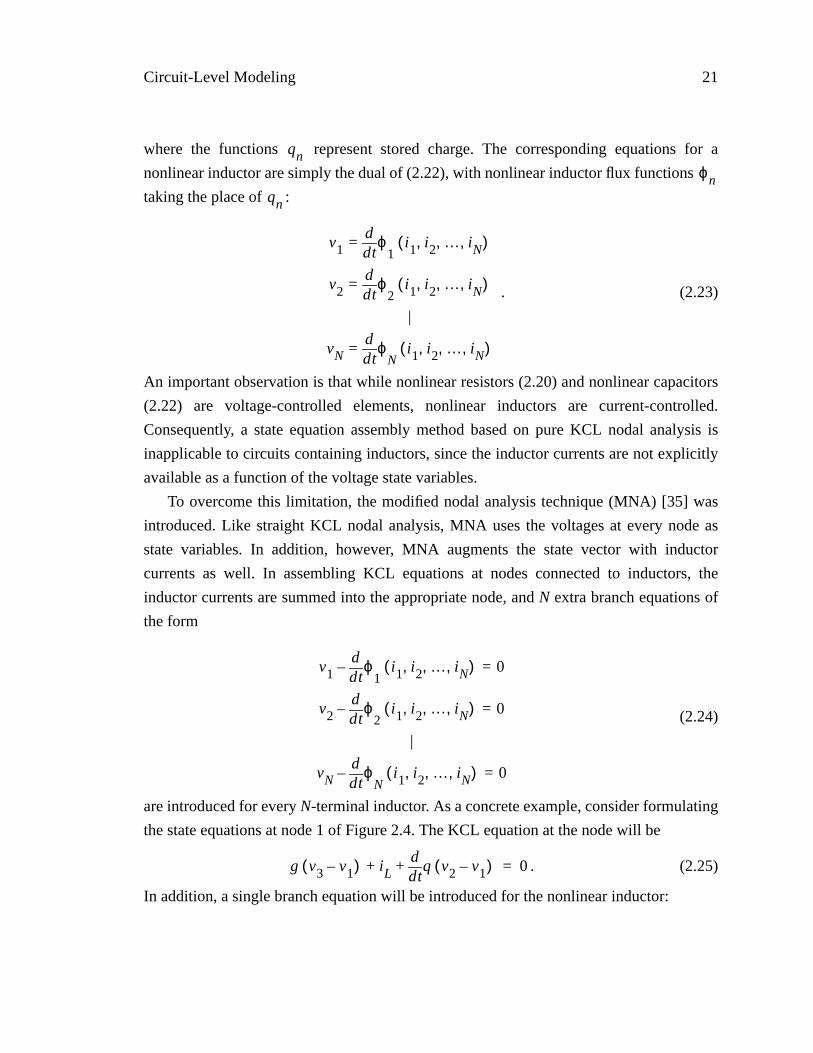
where the functions represent stored charge. The corresponding equations for a
nonlinear inductor are simply the dual of (2.22), with nonlinear inductor flux functions
taking the place of :
. (2.23)
An important observation is that while nonlinear resistors (2.20) and nonlinear capacitors
(2.22) are voltage-controlled elements, nonlinear inductors are current-controlled.
Consequently, a state equation assembly method based on pure KCL nodal analysis is
inapplicable to circuits containing inductors, since the inductor currents are not explicitly
available as a function of the voltage state variables.
To overcome this limitation, the modified nodal analysis technique (MNA) [35] was
introduced. Like straight KCL nodal analysis, MNA uses the voltages at every node as
state variables. In addition, however, MNA augments the state vector with inductor
currents as well. In assembling KCL equations at nodes connected to inductors, the
inductor currents are summed into the appropriate node, and N extra branch equations of
the form
(2.24)
are introduced for every N-terminal inductor. As a concrete example, consider formulating
the state equations at node 1 of Figure 2.4. The KCL equation at the node will be
. (2.25)
In addition, a single branch equation will be introduced for the nonlinear inductor:
qnϕn
qn
v1 tdd ϕ
1i1 i2 … iN, , ,( )=
v2 tdd ϕ
2i1 i2 … iN, , ,( )=
|
vN tdd ϕ
Ni1 i2 … iN, , ,( )=
v1 tdd ϕ
1i1 i2 … iN, , ,( )– 0=
v2 tdd ϕ
2i1 i2 … iN, , ,( )– 0=
|
vN tdd ϕ
Ni1 i2 … iN, , ,( )– 0=
g v3 v1–( ) iL tdd
q v2 v1–( )+ + 0=

Chapter 2 Nonlinear State Equations and Large Signal Distortion 22
. (2.26)
Constant current sources are readily incorporated by simply adding their values to the
right hand side. Voltage sources are typically handled by introducing an additional
auxiliary equation.1 Assuming that a voltage source of value is connected between
nodes and , a branch equation of the form
(2.27)
is added to the system of equations, and a new state variable (representing the current
through the voltage source) is summed into node and out of node .
Taken together, the preceding steps in the MNA methodology result in systems of
circuit state equations having form
, (2.28)
where is a state vector of node voltages and inductor/voltage (branch) currents,
is the sum of nonlinear resistive and branch currents at each node, is
the vector of capacitor charges and inductor fluxes, and is a vector of voltage/
1. Optionally, voltage sources may be added by removing one of the voltage state variables that thevoltage source is attached to, and symbolically setting the removed state variable to be equal to thesum of the remaining state variable and the voltage source. This approach has the disadvantage ofnot explicitly allowing the current through the source to be computed. However, it does have theadvantage of reducing the number of state variables by 2.
V1
V2
V3
V4
IL
Figure 2.4 Formulating the state equations in thepresence of current-controlled stateelements.
iL tdd ϕ v4 v1–( )– 0=
Vappn1 n2
vn1vn2
– Vapp– 0=
isrcn1 n2
g x t( )( )td
d q x t( )( ) y t( ) x t( )⊗ w t( )–+ + 0=
x t( )g x t( )( ) q x t( )( )
w t( )

Physics-Level Modeling of Semiconductor Devices 23
current source excitations. The term is the nodal contribution of distributed
devices handled through a convolution operation; is a sparse matrix of
time domain impulse responses which characterize the distributed devices present in the
network.
2.4 Physics-Level Modeling of SemiconductorDevices
In the previous two sections, the large signal nonlinear steady state problem was
examined from a circuit-level, compact model perspective. In this section, we show that
the discretized partial differential equations modeling the physics of semiconductor
devices have the same form (2.28) as the circuit equations. Furthermore, we will see that
modified nodal analysis can be used to form the mixed-level circuit and device equations,
while still retaining the basic form (2.28).
2.4.1 The Drift-Diffusion EquationsThe drift-diffusion system of semiconductor equations takes the form
(2.29)
where in addition we have
(2.30)
In the preceding equations, represents the electrostatic potential, and are the
electron and hole carrier concentrations, respectively, is the recombination rate,
and are the ionized donor and acceptor concentrations, and and are the electron
and hole current densities. External circuit elements (either lumped or distributed) may be
included through the introduction of additional KCL/MNA equations, as will be shown in
Section 2.4.5.
y t( ) x t( )⊗y t( ) ℜ N N×∈
ε ψ∇–( )∇• q p n– ND+
NA–
–+
t∂∂n 1
q--- ∇ Jn U–•
t∂∂p 1
q---– ∇ Jp U–•=
=
=
Jn qDn∇ n qµnn∇ψJp q– Dp∇ p qµpp∇ψ–=
–=
ψ n p
U ND+
NA–
Jn Jp

Chapter 2 Nonlinear State Equations and Large Signal Distortion 24
To numerically solve (2.29), we must first discretize the partial differential equations
over the device domain, and convert them to a finite number of nonlinear differential-
algebraic equations. For the drift-diffusion system of equations, each grid node k inside
the device has three state variables associated with it: , , and . In transient
analysis, the time dimension is handled by a discretization as well. The focus of this thesis
is on frequency domain simulation, where the time axis is not discretized (Chapter 3).
Consequently, we review only the spatial discretization here, and defer handling the time
dependencies until later.
2.4.2 Discretizing the Drift-Diffusion EquationsNumerous techniques exist for the spatial discretization of the semiconductor drift-
diffusion equations. A detailed survey of these is beyond the scope of this work, which is
focused more on the temporal dimension of the equations. Consequently, we present here
only the most common algorithms for two-dimensional spatial discretization — those that
are used by the PISCES simulator on which we base our work. Our goal is to establish a
general mathematical form for the discretized system of algebraic equations, so that this
form may be exploited in the derivations of subsequent chapters.
PISCES uses a spatial discretization scheme known as the ‘‘generalized box’’
(sometimes called ‘‘control volume’’ or ‘‘finite box’’) method [45]. The scheme is based
on a finite-difference formulation, and is applied in the context of triangular grids. An
example of such gridding applied to a bipolar device structure is shown in Figure 2.5. It is
clear that a given rectangular grid can be transformed to a triangular grid by suitable
partitioning of each rectangle into two triangular regions. As shown in the aforementioned
figure, however, the grid need not in general be rectangular.
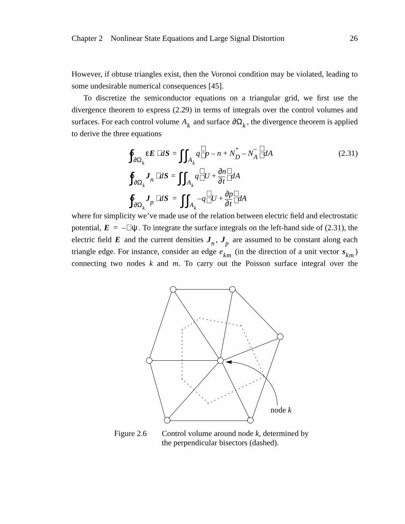
After a triangular mesh has been formed, the entire device domain is partitioned into
non-overlapping ‘‘control volumes.’’ These are polygons, each corresponding to some
node k, ideally having the property that the points within them fall into an area closer to
node k than to any other node in the device domain. Given a triangular grid, a control
volume partitioning may be readily established by splitting each triangle into three regions
defined by the perpendicular bisectors of each side. As long as each triangle is acute (i.e.,
no angle is greater than ), the partitioning satisfies the Voronoi condition that the
control volume corresponding to a given node is closer to that node than to any other.
ψk nk pk
90°

Physics-Level Modeling of Semiconductor Devices 25
Epi-collector
Buried-Collector
Emitter
Base
Oxide
0.000 0.100 0.200 0.300 0.400 0.500 0.600 0.700 0.800 0.900Distance (Microns)
0.00
0.20
0.40
0.60
0.80
1.00
Distance (Microns)
Figure 2.5 A bipolar transistor structure (top) and its triangular mesh(bottom).
Chapter 2 Nonlinear State Equations and Large Signal Distortion 26
However, if obtuse triangles exist, then the Voronoi condition may be violated, leading to
some undesirable numerical consequences [45].
To discretize the semiconductor equations on a triangular grid, we first use the
divergence theorem to express (2.29) in terms of integrals over the control volumes and
surfaces. For each control volume and surface , the divergence theorem is applied
to derive the three equations
(2.31)
where for simplicity we’ve made use of the relation between electric field and electrostatic
potential, . To integrate the surface integrals on the left-hand side of (2.31), the
electric field and the current densities , are assumed to be constant along each
triangle edge. For instance, consider an edge (in the direction of a unit vector )
connecting two nodes k and m. To carry out the Poisson surface integral over the
node k
Figure 2.6 Control volume around node k, determined bythe perpendicular bisectors (dashed).
Ak Ωk∂
εE dS⋅Ωk∂∫° q
Ak∫∫ p n– ND
+NA
––+
dA
Jn dS⋅Ωk∂∫° q U
t∂∂n+
Ak∫∫
=
= dA
Jp dS⋅Ωk∂∫° q– U
t∂∂p+
Ad
Ak∫∫=
E ψ∇–=
E Jn Jpekm skm
Physics-Level Modeling of Semiconductor Devices 27
perpendicular bisector corresponding to this edge, a finite-difference approximation is
used for the dot product:
. (2.32)
The situation is somewhat more complicated for the continuity equations. These could, in
principle, be evaluated along each edge through use of (2.30) with simple first-order finite-
difference approximations for and . As pointed out by Scharfetter and Gummel
[14], however, it turns out that such an approach results in numerical instability when the
potential difference along an edge exceeds . To remedy this situation, the
Scharfetter-Gummel discretization scheme was proposed. We leave the detailed derivation
to [14] [45], and merely state the result here:
, (2.33)
where is the Bernoulli function
, (2.34)
is the effective average mobility along the edge, and
with . (2.35)
A result directly analogous to (2.33) applies to the hole continuity equation. By evaluating
(2.32) and (2.33) for each side of the control volume polygon and summing the results, all
the surface integrals (i.e., the left-hand sides) of (2.31) can be computed.
The area integrals on the right-hand side of (2.31) are evaluated by assuming that the
integrand is approximately constant across the control volume. Since the control volume
around node k has area , the area integrals are computed as
(2.36)
E skm⋅ψm ψk–
dkm--------------------=
∇ n ψ∇
2kBT q⁄
Jn skm⋅qµkmβkm
dkm----------------------- nkB
ψk ψm–
βkm
--------------------
nmBψm ψk–
βkm
--------------------
–=
B x( )
B x( ) x
ex 1–--------------=
µkm
βkm
βk βm–
βk βm⁄( )ln-----------------------------= β
Dn
µn-------=
Ak
qAk∫∫ p n– ND
+NA
––+
dA q pk nk– NDk
+NAk
––+
Ak
q Ut∂
∂n+
AdAk∫∫ q Uk t∂
∂nk+
Ak
q– Ut∂
∂p+
AdAk∫∫ q– Uk t∂
∂pk+
Ak
=
=
=
Chapter 2 Nonlinear State Equations and Large Signal Distortion 28
From (2.32), (2.33), and (2.36) we see that the system of semiconductor equations at an
internal device node k takes the form
(2.37)
where the state vector contains the electrostatic potential and carrier concentration
variables1
. (2.38)
2.4.3 Boundary ConditionsThe preceding section discussed the discretization and assembly procedures for nodes
which are strictly within the interior of the device domain. Grid nodes at the
semiconductor device boundary, however, must be handled differently depending on the
type of boundary condition (BC) present at a given boundary node. In general, the
boundary conditions in semiconductor device problems are either homogeneous
Neumann, non-homogeneous Neumann, or Dirichlet, and can be different for any one of
the three drift-diffusion equations. As an example, the surface recombination boundary
condition used to model Schottky contacts places a Dirichlet BC on the Poisson equation,
and a non-homogeneous Neumann BC on the continuity equations.
We begin by considering the contour of integration around a node on the device
boundary (Figure 2.7). The line integrals can be split into two integrations over two
disjoint sets — , the internal portion of the contour, and , the external portion:
1. In general, the state vector may also contain additional variables if the semiconductor device isembedded in an external circuit network (Section 2.4.5). The state equations at the internal devicenodes, however, will not be a function of these additional variables, and (2.37)-(2.38) remain valid.
g3k 2–ψ
x t( )( ) 0
td
dx3k 1– g3k 1–n
x t( )( )+ 0
td
dx3k g3kp
x t( )( )+ 0
=
=
=
x t( )
x ψ1 n1 p1 … ψK nK pK, , , , , ,[ ]=
Ωint∂ Ωext∂

Physics-Level Modeling of Semiconductor Devices 29
(2.39)
The integrals over (i.e., , , and ) can still be
evaluated in the same manner as before, via equations (2.32) and (2.33). On the boundary
edges and , however, the integration must be carried out in a different manner,
subject to the boundary conditions present on that edge.
For a homogeneous Neumann boundary condition, the current flux relation at a
relevant edge is
. (2.40)
Such boundary conditions exist at the edges of the device, where no current flux is
allowed to pass. Implementation of homogeneous Neumann boundary conditions is
εE dS⋅Ωk∂∫° εE dS⋅
Ωk int,∂∫ εE dS⋅Ωk ext,∂∫+=
Jn dS⋅Ωk∂∫° Jn dS⋅
Ωk int,∂∫ Jn dS⋅Ωk ext,∂∫+=
Jp dS⋅Ωk∂∫° Jp dS⋅
Ωk int,∂∫ Jp dS⋅Ωk ext,∂∫+=
Ωk int,∂ εE dS⋅Ωk∂∫° Jn dS⋅Ωk∂∫° Jp dS⋅Ωk∂∫°ekm ekn
node k
Figure 2.7 A boundary grid node.
node m
node n
J dS⋅edge∫ 0=

Chapter 2 Nonlinear State Equations and Large Signal Distortion 30
immediate, since the integration over the boundary edge is simply omitted. Non-
homogeneous Neumann BCs, on the other hand, have the form
(2.41)
when applied to a half-edge touching node k, and are handled by a discretized
approximation at each half-edge. For instance, integration over half-edge yields
(2.42)
In the case of Schottky contacts (the primary situation for using non-homogeneous
Neumann BCs), the flux functions are given by
, (2.43)
where and are the electron and hole surface recombination velocities, respectively.
Equation (2.42) is applied for each boundary edge about a given boundary node, with the
results summed to yield the total value of the integration about . Thus, for the
example of Figure 2.7, we would have
. (2.44)
Dirichlet boundary conditions are present on the Poisson and continuity equations for
ohmic contacts. Dirichlet BCs fix the given boundary node at some constant value, and are
thus implemented through removal of the relevant differential equation and its
replacement with for a Dirichlet Poisson BC, or ,
for appropriate continuity equation BCs. It is understood that in the above equations,
, , and are constants which are fixed for the duration of the simulation
run.
In the case of the Dirichlet boundary conditions, equations (2.31) and (2.39) must still
hold physically, and flux conservation must be satisfied. Although the boundary contour
integrals are never evaluated explicitly in the Dirichlet case, their values may be computed
once the relevant Dirichlet node values have been fixed. For instance, in the Poisson case,
we have the relation
J dS⋅dS
-------------- φ ψk nk pk, ,( )=
ekn
J dS⋅ekn∫ φ ψk nk pk, ,( ) 1
2---dkn=
φ
φn σn nk neq–( )⋅= φp σp pk peq–( )⋅=
σn σp
Ωk int,∂
Jn dS⋅Ωk ext,∂∫ φn ψk nk pk, ,( ) 1
2---dkn φn ψk nk pk, ,( ) 1
2---dkm+=
Jp dS⋅Ωk ext,∂∫ φp ψk nk pk, ,( ) 1
2---dkn φp ψk nk pk, ,( ) 1
2---dkm+=
ψk ψBC k,= nk nBC k,= pk pBC k,=
ψBC k, nBC k, pBC k,
Physics-Level Modeling of Semiconductor Devices 31
, (2.45)
where is evaluated through repeated application of (2.32) for each
internal polygon edge. This allows the convenient computation of electric field fluxes and
free carrier currents at the electrode contacts, a topic which is the subject of the next
section.
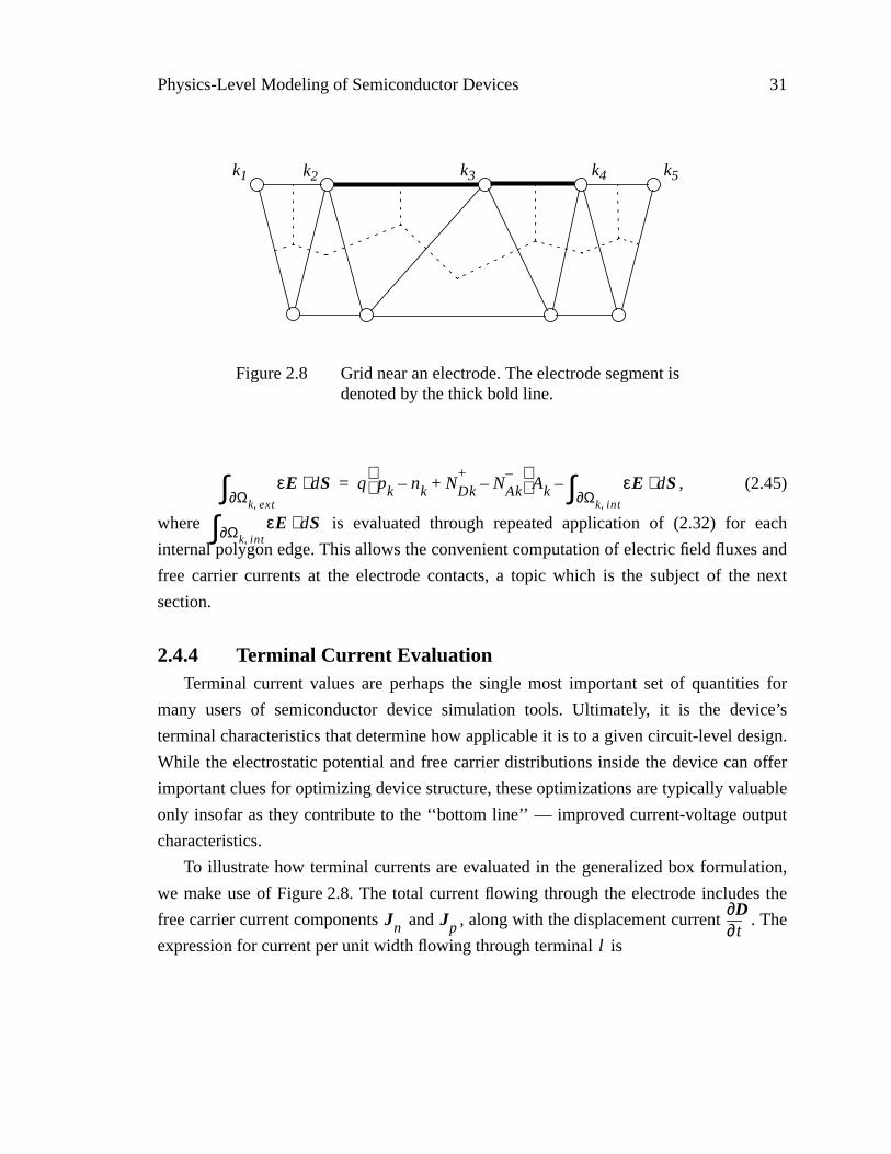
2.4.4 Terminal Current EvaluationTerminal current values are perhaps the single most important set of quantities for
many users of semiconductor device simulation tools. Ultimately, it is the device’s
terminal characteristics that determine how applicable it is to a given circuit-level design.
While the electrostatic potential and free carrier distributions inside the device can offer
important clues for optimizing device structure, these optimizations are typically valuable
only insofar as they contribute to the ‘‘bottom line’’ — improved current-voltage output
characteristics.
To illustrate how terminal currents are evaluated in the generalized box formulation,
we make use of Figure 2.8. The total current flowing through the electrode includes the
free carrier current components and , along with the displacement current . The
expression for current per unit width flowing through terminal is
εE dS⋅Ωk ext,∂∫ q pk nk– NDk
+NAk
––+
Ak εE dS⋅
Ωk int,∂∫–=
εE dS⋅Ωk int,∂∫
Figure 2.8 Grid near an electrode. The electrode segment isdenoted by the thick bold line.
k2 k3 k4k1 k5
Jn Jp t∂∂D
l

Chapter 2 Nonlinear State Equations and Large Signal Distortion 32
(2.46)
The integration above is carried out over the boundary edges comprising the electrode of
interest. In our example of Figure 2.8, this boundary would consist of the two edges
and .
Application of equation (2.45) over each point of the electrode boundary domain
already gives us the integral of the electrostatic displacement over the electrode.
The current density integrals may be taken in an analogous manner —
(2.47)
where the notation refers to nodes k that are on the electrode , and the
integral is taken by repeated application of (2.33). The hole current
density integral is evaluated by a directly analogous expression. We point out that (2.47)
holds in the non-homogeneous Neumann, as well as in the Dirichlet, case. The non-
homogeneous term doesn’t appear in (2.47), but is used in setting up the
appropriate discretization to satisfy the continuity equations on the electrode boundary.
We also note that (2.44) offers an alternate method for evaluating the current through
purely Schottky contacts once the simulation has converged.
Before closing out this section, we take the important step of symbolically expressing
the total current per unit area at a given electrode l as
(2.48)
The function represents the electron and hole currents, and is a scalar algebraic
function of the state variable vector x. Similarly, is an algebraic function
representing the flux of electrostatic displacement through the electrode. It is clear that
both functions are (loosely speaking) ‘‘structurally sparse’’ in the sense that they directly
depend only on the values of the boundary node state variables, and not on the state
variables associated with internal nodes.
ITl Jn Jp t∂∂D+ +
dS⋅
ΩTl∂∫Jn Jp+( ) dS⋅
ΩTl∂∫ tdd εE dS⋅
ΩTl∂∫+
=
=
ΩTl∂ek2k3
ek3k4
D εE=
Jn dS⋅ΩTl∂∫ Jn dS⋅
Ωk ext,∂∫k ΩTl∂∈∑
q Uk t∂∂nk+
Ak Jn dS⋅Ωk int,∂∫–
k ΩTl∂∈∑
=
=
k ΩTl∂∈ Ω Tl∂Jn dS⋅Ωk int,∂∫
φ ψk nk pk, ,( )
Il t( ) glcond x t( )( )
tdd
gldisp x t( )( )+=
glcond x( )
gldisp x( )
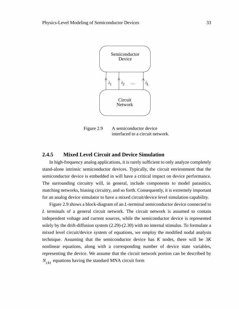
Physics-Level Modeling of Semiconductor Devices 33
2.4.5 Mixed Level Circuit and Device SimulationIn high-frequency analog applications, it is rarely sufficient to only analyze completely
stand-alone intrinsic semiconductor devices. Typically, the circuit environment that the
semiconductor device is embedded in will have a critical impact on device performance.
The surrounding circuitry will, in general, include components to model parasitics,
matching networks, biasing circuitry, and so forth. Consequently, it is extremely important
for an analog device simulator to have a mixed circuit/device level simulation capability.
Figure 2.9 shows a block-diagram of an L-terminal semiconductor device connected to
L terminals of a general circuit network. The circuit network is assumed to contain
independent voltage and current sources, while the semiconductor device is represented
solely by the drift-diffusion system (2.29)-(2.30) with no internal stimulus. To formulate a
mixed level circuit/device system of equations, we employ the modified nodal analysis
technique. Assuming that the semiconductor device has K nodes, there will be 3K
nonlinear equations, along with a corresponding number of device state variables,
representing the device. We assume that the circuit network portion can be described by
equations having the standard MNA circuit form
SemiconductorDevice
CircuitNetwork
i1 i2 iL....
Figure 2.9 A semiconductor deviceinterfaced to a circuit network.
Nckt

Chapter 2 Nonlinear State Equations and Large Signal Distortion 34
(2.49)
where is the state vector for the circuit network, is
the vector of independent voltage/current source excitations, and is a
vector containing in the mth position if device current flows into circuit node m.
To join the circuit and device systems, the L state variables , , ..., are
introduced into the overall state vector. Likewise, the overall system is augmented with L
additional coupling equations of the form
(2.50)
The overall circuit-device system of equations has dimensionality 3K+ +L.
2.5 Solving the State Equations By TransientAnalysis
Transient analysis is by far the most commonly used method for simulating nonlinear
circuits and semiconductor devices driven by large signal sources. The standard versions
of tools such as PISCES and SPICE include only transient capability for analyzing
systems under large signal time-varying input. In this section, we briefly review the
standard time domain algorithms used in solving the systems of circuit/device equations
formulated in the preceding sections. The overview is provided as a basis for comparing
general-purpose transient analysis with special-purpose algorithms like harmonic balance,
which are geared specifically toward solving the large signal sinusoidal steady-state
problems arising in analog communication system design.
Transient analysis is based on approximating the operator in (2.28) by a finite-
difference formula. Assuming that the state vector is known at time instants , ,
, , standard transient analysis approximates the derivative of the charge/flux
vector at time by formulas such as
(Backward Euler) (2.51)
or
g xckt t( )( ) ddt-----q xckt t( )( ) y t( ) xckt t( ) ickt t( )–⊗+ + w t( )=
xckt t( ) ℜ Nckt 1×∈ w t( ) ℜ Nckt 1×∈ickt t( ) ℜ Nckt 1×∈
il ili1 i2 iL
glcond xdev t( )( )
tdd
gldisp xdev t( )( ) il t( )–+ 0=
Nckt
d dt⁄x t( ) t0 t1
… tk 1–tk
ddt-----q x tk( )( )
q x tk( )( ) q x tk 1–( )( )–
tk tk 1––--------------------------------------------------------------≈

Solving the State Equations By Transient Analysis 35
(Trapezoidal) (2.52)
The above are two examples of first-order finite-difference schemes; there exist many
other schemes of various orders [33][34], including Forward Euler, Gear’s formulas,
Adams-Bashforth and Adams-Moulton algorithms, and the TR-BDF2 algorithm [19]. For
simplicity, we restrict ourselves to the Backward Euler formulation in this section. The
state equations (2.28) are then discretized to have the form
(2.53)
The convolution integral in the above equation can be approximated as
(2.54)
by straightforward integration, as is shown in [15]. With this formula, (2.53) becomes a
system of nonlinear equations which is to be solved for the unknown vector
. (2.55)
The solution step is almost always carried out using the Newton-Raphson iterative
process.
One fact that is immediately apparent from the above discussion is that the time step
(2.56)
must be selected small enough so that the finite-difference scheme in (2.53) is a good
approximation to the actual derivative. This can be particularly problematic in the case
where multi-tone signals are present at widely separated frequencies, as is common in
many RF and microwave designs. For instance, consider the function
, (2.57)
which represents the superposition of a 1 GHz sinusoid and a 1 kHz sinusoid. Because of
the presence of the fast sinusoid, the time step should be less than a hundredth of a
nanosecond to achieve decent accuracy. At the same time, the presence of the slow 1 kHz
sinusoid means that the overall period is 1 millisecond. Thus, hundreds of millions of time
steps would need to be taken, resulting in an extremely expensive simulation.
ddt-----q x tk( )( )
q x tk( )( ) q x tk 1–( )( )–( )12--- tk tk 1––( )
---------------------------------------------------------------------ddt-----q x tk 1–( )( )–≈
g x tk( )( )q x tk( )( ) q x tk 1–( )( )–
tk tk 1––-------------------------------------------------------------- y tk τ–( ) x τ( ) τd
0
tk
∫ w tk( )–+ + 0=
y tk τ–( ) x τ( ) τd0
tk
∫ y tk τ–( ) x τ( ) τd0
tk 1–
∫ y tk τ–( ) x τ( ) τdtk 1–
tk
∫+=
Ak Bkx tk( )+≈
xk x tk( )=
∆tk tk tk 1––=
f t( ) 2π 103⋅ t
cos 2π 10
9⋅ t
cos+=
∆tk

Chapter 2 Nonlinear State Equations and Large Signal Distortion 36
2.6 Summary
The nonlinear constitutive equations for both semiconductor devices and circuit
networks share a common form. In analog applications, the steady state response of these
nonlinear systems to large signal sinusoidal drive is of key interest. This chapter began
with some background material on single- and multi-tone distortion effects, along with a
discussion of several figures of merit requiring steady state analysis. Some common
methodologies for formulating circuit and device equations were discussed, and a concise
treatment of the spatial discretization algorithms used in PISCES-II was presented. The
chapter ended with a brief discussion of conventional transient simulation algorithms,
with some attention being given to their shortcomings in analog applications. Subsequent
chapters will present frequency domain algorithms designed to overcome these
shortcomings.
37
Chapter 3
Harmonic Balance Fundamentals
Harmonic balance (HB) is a nonlinear frequency domain analysis technique which is
well-suited for handling multi-tone steady state distortion problems. For many high
frequency (RF and microwave) applications, the solution of the state equations by
standard transient methods can be prohibitively expensive. The difficulties faced by time
domain methods stem from several causes:
• The applied voltage sources are typically sinusoids which may have very narrowly
or very widely spaced frequencies. It is not uncommon for the highest frequency
present in the response to be many orders of magnitude greater than the lowest
frequency. This necessitates an integration over an enormous number of periods of
the highest frequency sinusoid. To complicate matters further, if the input
frequencies are not commensurate, then (in principle) a nearly infinite number of
periods must be used to accurately resolve the distortion products.
• Designers are usually most interested in the system’s steady state behavior. The
presence of stiff linear bias and filtering circuitry around the semiconductor device
can introduce extremely long time constants. This requires conventional transient
methods to integrate over many periods of the lowest-frequency sinusoid to reach
steady state, further exacerbating the problems brought about by very wide or very
narrow frequency spacings.

Chapter 3 Harmonic Balance Fundamentals 38
• Many linear models at high frequencies are best represented in the frequency
domain. Simulating such elements in the time domain via convolution often results
in accuracy, causality, or stability problems.
• Many RF/microwave applications require very accurate resolution of low-level
distortion products. Transient methods can have difficulties achieving the required
levels of accuracy unless time points are spaced extremely close together, and all
transients have decayed to negligible levels [25].
The harmonic balance technique addresses the above problems by solving the state
equations in the frequency domain. It directly captures the large signal steady state
response of nonlinear systems, and is almost completely insensitive to widely-varying
time constants, tone spacings, and incommensurate frequencies. In addition, it exhibits
excellent dynamic range for resolving low-level distortion products, and is ideal for
handling linear circuit models characterized in the frequency domain. Highly nonlinear
large signal problems do increase the computational resources that HB requires, and can
greatly reduce its speed of convergence. However, we will demonstrate that harmonic
balance is robust enough to routinely handle the levels of nonlinearity typically seen in the
majority of RF/microwave applications.
Before proceeding towards a detailed description of the harmonic balance algorithm,
we first take a moment to outline the basic idea. As we have seen before, the state
equations describing semiconductor devices and circuit networks generally take the form
. (3.1)
In the HB technique, the state vector is assumed to be a Fourier series of sines and
cosines, with unknown coefficients that the harmonic balance method will solve for. The
state equations (3.1) are Fourier transformed into the frequency domain, with the
transformation resulting in an algebraic set of nonlinear equations. During the solution
process, the unknown Fourier coefficients are iteratively adjusted until the nonlinear
system is satisfied to within some predetermined tolerance. Once finally obtained, the
coefficients effectively characterize the system’s steady state response for all time. We
note that the choice of basis functions for effectively guarantees that the response
we capture is indeed the steady state response, assuming that a steady state solution exists.
g x t( )( )td
d q x t( )( ) y t( ) x t( )⊗ w t( )–+ + 0=
x t( )
x t( )

The Discrete Fourier Transform — Some Definitions and Notation 39
3.1 The Discrete Fourier Transform — SomeDefinitions and Notation
Since much of the work in subsequent sections will involve the Discrete Fourier
Transform (DFT), we will take some time here to define the particular forms of the DFT
that are used, and to establish some notational conventions. Because our formulation of
the harmonic balance equations involves strictly real-valued time domain waveforms, a
straightforward variant of the standard Discrete Fourier Transform, called the single-sided
DFT, will typically be employed. Establishing a consistent notation and pointing out some
subtleties in the transform’s application will considerably simplify the presentation in
subsequent sections.
3.1.1 The Double-Sided DFTConsider the periodic waveform
, (3.2)
where , and is real to ensure that the resulting signal is strictly real-valued
when sampled at the time points . We assume an even number of Fourier
coefficients ( ) to make our formulation consistent with power-of-2
Fast Fourier Transform (FFT) algorithms. This choice of an even rather than odd DFT
length forces the presence of the somewhat ‘‘artificial’’ component . As mentioned
above, this coefficient is forced to be real to ensure that the resulting time domain
waveform is real, and thus cannot contain completely accurate information about the
spectrum at that frequency bin. When transforming arbitrary waveforms from the time
domain to the frequency domain, we must ensure that S is large enough so that only
negligible energy due to aliasing lands in .
The Fourier Transform Theorem guarantees that by sampling the periodic waveform
(3.2) at the 2S time points , , we can recover the coefficients
from the waveform samples (and vice-versa) through the analysis and synthesis
formulas
x t( ) Xh jhω0t( )exp
h S 1+–=
S
∑=
Xh X h–*= XS
ts πs Sω0⁄=
X S– 1+ … XS 1– XS, , ,
XS
XS
ts πs Sω0⁄= 0 s 2S 1–≤ ≤Xh x ts( )

Chapter 3 Harmonic Balance Fundamentals 40
(3.3)
. (3.4)
These relations can be cast into matrix form by defining the complex matrix
, (3.5)
where . The Fourier Transform analysis and synthesis equations,
(3.3) and (3.4), respectively, become
and . (3.6)
3.1.2 The Single-Sided DFTWhen dealing exclusively with real-valued time domain waveforms, it is redundant to
store both the negative and positive sides of the spectrum, since these are simply complex
conjugates of each other. An alternate representation of the periodic Fourier series is the
so-called single-sided, or trigonometric, form involving only the positive-frequency
coefficients:
Xh1
2S------ x ts( ) j2πsh
2S--------------–
exp
s 0=
2S 1–
∑=
x ts( ) Xhj2πsh
2S--------------
exp
h S– 1+=
S
∑=
2S 2S×
Γ 12S------
1 1 … 1
W2S1 0⋅
W2S1 1⋅ … W2S
1 2S 1–( )⋅
| | \ |
W2S2S 1–( ) 0⋅
W2S2S 1–( ) 1⋅ … W2S
2S 1–( ) 2S 1–( )⋅
=
W2S2πj2S--------–
exp=
X0
X1
|
XS
X S 1+–
|
X 1–
Γ
x0
x1
|
xS
xS 1+
|
x2S 1–
=
x0
x1
|
xS
xS 1+
|
x2S 1–
Γ 1–
X0
X1
|
XS
X S 1+–
|
X 1–
=

The Discrete Fourier Transform — Some Definitions and Notation 41
(3.7)
where for , , , and , are the real and
imaginary parts, respectively, of . These single-sided coefficients are consistent with
conventional phasors used in AC analysis1.
In the single-sided formulation, the forward (i.e., ‘‘analysis’’) part of the DFT simply
becomes
, . (3.8)
This is readily expressed in matrix form through use of an complex
transform matrix which maps the 2S real samples to the S+1 complex
Fourier coefficients :
. (3.9)
The reverse (i.e., synthesis) transform operator, however, cannot be represented as a single
complex-valued matrix which maps the complex coefficients to real
samples . This problem occurs because the time samples are no longer
an analytic function of the Fourier coefficients:
. (3.10)
The presence of the conjugated terms in (3.10) leads to the aforementioned loss of
analyticity, and has important implications for solving the harmonic balance system of
1. Except for the purely real ‘‘non-physical’’ phasor XS.
x t( ) ℜ e Xh jhω0t( )exph 0=
S
∑
X0R Xh
R hω0t( )cos XhI hω0t( )sin–
h 1=
S
∑+
=
=
Xh 2Xh= 1 h S 1–≤ ≤ X0 X0= XS XS= XhR Xh
I
Xh
Xh
2 δh δh S–––
2S--------------------------------- x ts( ) j2πsh
2S--------------–
exp
s 0=
2S 1–
∑= 0 h S≤ ≤
S 1+( ) 2S×x0 x1 … x2S 1–, , ,
X0 X1 … XS, , ,
X0
X1
|
XS
1S---
12--- 1
2--- … 1
2---
W2S1 1⋅
W2S1 2⋅ … W2S
1 2S 1–( )⋅
| | \ |
12---W2S
S 1⋅ 12---W2S
S 2⋅… 1
2---W2S
S 2S 1–( )⋅
x0
x1
|
x2S 1–
=
X0 X1 … XS, , ,x0 x1 … x2S 1–, , ,
x ts( ) X012--- Xh
j2πsh2S
-------------- exp Xh
* j2πsh2S
--------------– exp+
h 1=
S 1–
∑ XS jπs–( )exp+ +=

Chapter 3 Harmonic Balance Fundamentals 42
equations. Briefly, it implies that the use of single-sided transforms and single-sided
spectral representations leads to a system of nonlinear HB equations which is not analytic.
Such systems must effectively be solved in the real number field, by separating the real
and complex parts. This issue will be addressed more fully in Section 3.5.
Given the non-analytic nature of the single-sided transform operators, we abandon the
complex field and define our vector of frequency domain coefficients as the purely real
array . The Fourier Transform relationships of
equations (3.7) and (3.8) become, in matrix form,
and . (3.11)
Here, and are real matrices containing the sine and cosine terms of the
trigonometric Discrete Fourier Transform:
, (3.12)
, . This is the transform relation that we will use in
all subsequent work.
X X0R X1
R X1I … XS 1–
R XS 1–I, XS
R, , , , , T=
X0R
X1R
X1I
|
XS 1–R
XS 1–I
XSR
Γ
x0
x1
x2
|
x2S 3–
x2S 2–
x2S 1–
=
x0
x1
x2
|
x2S 3–
x2S 2–
x2S 1–
Γ 1–
X0R
X1R
X1I
|
XS 1–R
XS 1–I
XSR
=
Γ Γ 1– 2S 2S×
Γ 1–
C00 C01 S01 C02 S02 … C0 S,
C10 C11 S11 C12 S12 … C1 S,
C20 C21 S21 C22 S22 … C2 S,
| | | | | \ |
C2S 1– 0, C2S 1– 1, S2S 1– 1, C2S 1– 2, S2S 1– 2, … C2S 1– S,
=
Crs2πrs2S
------------ cos= Srs
2πrs2S
------------ sin–=

The Quasiperiodic Steady State 43
3.2 The Quasiperiodic Steady State
3.2.1 Representing Quasiperiodic SignalsA quasiperiodic waveform is defined to be one which consists of a linear combination
of a finite number of sinusoids. Consider the set of M linearly independent (i.e.,
incommensurate1) fundamental frequencies . Then is a
quasiperiodic waveform with M fundamentals if it can be expressed as
(3.13)
where
(3.14)
Each frequency in the M-quasiperiodic waveform is an integral combination of the
fundamentals . To each frequency component in the set (3.14), we assign
an order equal to the absolute sum of its fundamental indices. That is, the component
has an order of corresponding to
it. Intuitively, for a system with finite energy, the spectral components at high enough
orders should have vanishingly low amplitudes.
If a quasiperiodic signal is passed through a resistive nonlinearity , the
resulting waveform will also be quasiperiodic. This becomes apparent if the
nonlinearity is expanded in a Taylor series around , and the multinomial
theorem [23] is applied:
1. Two frequencies are said to be incommensurate if their ratio is not a rational number.
Ω1 Ω2 … ΩM, , , x t( )
x t( ) X0 XhR ωht( )cos Xh
I ωht( )sin–
h 1=
H
∑+
ℜ e Xh jωht( )exph 0=
H
∑
=
=
ωh ωk1k2…kMωk1k2…kM
k1Ω1 k2Ω2 … kMΩM for integer ki+ + += ∈
x t( )Ω1 Ω2 … ΩM, , ,
ω k1Ω1 k2Ω2 … kMΩM+ + += k1 k2 … kM+ + +
x t( ) g x( )g x t( )( )
x X0=

Chapter 3 Harmonic Balance Fundamentals 44
(3.15)
Since the frequencies present in the response waveform are integer combinations of those
present in the M-quasiperiodic stimulus, we see that the response is also M-quasiperiodic.
3.2.2 Harmonic TruncationIn principle, there are an infinite number of frequencies present in the set (3.14). In
practice, only a finite number of these spectral components contain significant energy. To
represent a quasiperiodic waveform for simulation on a computer, the frequencies present
in (3.14) must be truncated to some finite set, thus neglecting the energy present in the
excluded components. For accurate results, the truncation must be chosen such that the
excluded energy is negligible.
Two common methods for harmonic truncation are the so-called box and diamond
truncations. In the box technique, a truncation of order P results in a set of frequencies
where the index of each fundamental in a given frequency is less than P:
. (3.16)
Since real-valued waveforms can be represented by single-sided spectra, it is redundant to
include both the positive- and negative- valued frequencies in the set above. To ensure that
such image frequencies don’t occur, it is necessary to add to (3.16) the constraint that the
first non-zero coefficient be positive:
, (3.17)
Figure 3.1 illustrates the box truncation in the case, for both the double- and
single-sided forms. The single-sided form generates a total of
frequencies, which reduces to for two-tone problems.
In the diamond truncation, the set of included frequencies is chosen such that the
absolute sum of the indices is less than or equal to the truncation order:
g x t( )( ) ℜ eg k( ) X0( )
k!------------------------ Xh jωht( )exp
h 1=
H
∑ k
k 0=
∞
∑
ℜ eg k( ) X0( )
k!------------------------ k!
h1!…hH!-----------------------X1
h1…XH
hHj h1ω1 …hHωH+( )( )exp
h1 … hH+ + k=∑
k 0=
∞
∑
=
=
BP ω ω k1Ω1 k2Ω2 … kMΩM+ + += k1 P≤ k2 P … kM, ,≤, P≤, =
km
k1 0≥ km 0 if k1≥ k2 … km 1– 0= = = =
M 2=12--- 2P 1+( ) M
1+
2P2
2P 1+ +

The Quasiperiodic Steady State 45
. (3.18)
To avoid image frequencies and employ the single-sideband waveform representation, the
additional constraint
(3.19)
must be invoked.1 This latter constraint is perhaps somewhat less intuitive than its analog
for box truncation; a detailed explanation of the rationale for this constraint is presented in
Section 3.3.2. Figure 3.2 illustrates the diamond truncation graphically in the case of two-
fundamentals, and shows why the diamond truncation yields roughly a factor of
savings in the number of harmonics over its box counterpart. The diamond truncation is
usually more efficient than box truncation, since the harmonics it neglects have a higher
order than the largest harmonic of any fundamental, and should typically contain only
negligible energy when the truncation order is chosen properly.
1. The constraint is given here for the case M=2.
k1
k2
k1
k2
Figure 3.1 The two-tone box truncation of order P = 4 in the(a) double-sided formulation and the (b) single-sided formulation.
a) b)
DP ω ω k1Ω1 k2Ω2 … kMΩM+ + += k1 k2 … kM+ + + P≤, =
k1 k2 0 or k1 0 and k2 k1–=≥( )>+
2M 1–

Chapter 3 Harmonic Balance Fundamentals 46
A somewhat more flexible truncation scheme than either the box or the diamond is
used by HP’s commercial simulators [13]. This variant can be viewed as a hybrid of the
two standard truncations outlined above, and will be referred to as the ‘‘modified diamond
truncation.’’ In this scheme, each fundamental m is assigned a separate order . A
harmonic of fundamental m is included in the truncated set if and only if its order is less
than . Mixing products (i.e., frequencies that are not harmonically related to a single
fundamental) are included only if their order is less than an overall diamond truncation
order . The resulting set of frequencies may be formally specified by defining the
two sets
(3.20)
and then taking the union of the two to obtain the modified diamond truncation
k1
k2
a)
Figure 3.2 The two-tone diamond truncation of order P = 4 inthe (a) double-sided formulation and the (b) single-sided formulation using constraint (3.19).
k1
k2
b)
Pm
Pm
Pmax
T1 ω ω kmΩm= 1 m M km, Pm≤ ≤ ≤, =
T2 ω ω k1Ω1 … kMΩM+ += k1 … kM+ + Pma x≤ k1 P1≤ … kM PM≤, , , , =

The Quasiperiodic Steady State 47
(3.21)
In direct analogy to the diamond and box truncations, the modified diamond scheme can
be purged of image frequencies by application of the additional constraint (3.17).
Graphical illustrations for both the double-sided truncation and the single-sided (image-
free) truncation are provided in Figure 3.3.
Thus far, we’ve focused on fundamental frequencies that are purely incommensurate.
In practice, it is common to have fundamentals which are harmonically related, but which
nevertheless have a prohibitively large common period. For instance, if one fundamental
is at 30 kHz and the other is at 1 GHz, then the two frequencies are commensurate because
they are both harmonics of 10 kHz. In principle, then, the analysis can be carried out as a
one-tone (M = 1) simulation with a fundamental frequency of 10 kHz. However, this
would require a minimum of 105 harmonics (and likely several times more), because that
many periods of 1 GHz fit into a single period of 10 kHz. Clearly, such large transform
sizes are inefficient, and border on the impractical. The problem is easily avoided by
treating the simulation as a two-tone analysis (i.e., M = 2), with fundamentals at 30 kHz
MD T1 T2∪=
k1
k2
a) b)
k1
k2
Figure 3.3 The two-tone modified diamond truncation of ordersP1=4, P2=5, and Pmax=3 and in the (a) double-sidedformulation and the (b) single-sided formulation.
Chapter 3 Harmonic Balance Fundamentals 48
and 1 GHz. In doing so, one must be careful to ensure that the truncated frequencies do not
overlap. For example, given a simulation with fundamentals of 10 Hz and 50 Hz, it would
not permissible to use a truncation scheme of order 3. If such a scheme was used, multiple
frequencies would land on the same bin — we would have = 30 Hz as a (0,
3) entry, along with = 30 Hz as a (1, -2) entry. To avoid such colliding
harmonics in the case above, the problem should be formulated as a single-tone analysis at
a fundamental frequency of 10 Hz.
3.3 Quasiperiodic Transforms
Given a periodic waveform , we can use the standard Discrete Fourier Transform
to obtain a frequency-domain (Fourier series) representation of for “well-
behaved” algebraic functions g. Assuming that the waveform is periodic with period T,
and that we can evaluate both g and x over their respective domains, there is the well-
known Discrete Fourier Transform relationship for obtaining the harmonic coefficients:
, (3.22)
where . Assuming that H, the total number of non-DC harmonics, is large
enough to adequately represent with minimal aliasing, we have the relationship
. (3.23)
For quasiperiodic waveforms, however, the standard Discrete Fourier Transform
cannot be directly applied. Consider, for example, the quasiperiodic waveform
. Although it is the sum of two periodic signals, it is not
periodic, because it consists of two separate waveforms with incommensurate periods of
and 1. Since is irrational, it is clear that the there does not exist a common period, and
that the DFT is not directly applicable to finding the Fourier representation of .
One approach to solving the problem would be to operate ‘‘symbolically’’ on the
waveform in the manner of equation (3.15). Unfortunately, this requires the availability of
0 50⋅ 3 10⋅+
1 50 2 10⋅–⋅
x t( )g x t( )( )
GhR
2 δh–
2H 2+----------------- g x ts( )( ) 2πhs
2H 2+-----------------
cos
s 0=
2H 1+
∑=
GhI
2 δh–
2H 2+----------------- g x ts( )( ) 2πhs
2H 2+-----------------
sin
s 0=
2H 1+
∑–=
0 h H≤ ≤
tssT
2H 2+-----------------=
g x t( )( )
g x t( )( ) G0 GhR 2πh
T----------t
cos GhI 2πh
T----------t
sin–
h 1=
H
∑+≈
x t( ) 2t( )cos 2πt( )cos+=
π πg x t( )( )
Quasiperiodic Transforms 49
a potentially arbitrary number of derivatives of g, and is thus not practical for
semiconductor device simulation. We note that such approaches have indeed been tried in
the area of circuit simulation, where they are somewhat more practical. However, the need
for such symbolic approaches has been effectively obsoleted by quasiperiodic transform
algorithms which are presented below.
3.3.1 The Frequency-Remapped DFT/FFTIn examining equation (3.15), a key observation emerges: the amplitude of the
sinusoidal component is independent of the frequencies
, and thus independent of the actual values of the fundamentals .
To illustrate this phenomenon in a less abstract fashion, we introduce the following
example. Consider a two-tone signal , and the simple
quadratic nonlinearity . Then, after some straightforward algebraic
manipulation, we have
. (3.24)
The spectral coefficients (i.e., the coefficients of the cosines) are dependent only on the
amplitudes A and B, and not on the fundamental frequencies and .
Since the exact numerical value of the fundamental frequencies is unimportant,1 they
can be remapped to multiples of a single fundamental for purposes of computing the
Fourier coefficients. This is the key idea of the frequency-remapping technique. Although
the new set of response frequencies will be different than the original set, the Fourier
coefficients of each spectral component will be the same. Consequently, it is possible to
use the harmonically related set of artificial frequencies to find the Fourier coefficients,
and then switch back to the original frequency set once the coefficients have been
obtained. This idea can work only if there exists a one-to-one relationship between the
original and the remapped frequency set, and the remapping scheme must be chosen such
that this is the case.
1. The exact values are unimportant provided that the truncation is such that collisions between thevarious frequencies don’t occur; see the last paragraph of Section 3.2.2.
j h1ω1 …hHωH+( ) t( )exp
ω1 … ωH, , Ω1 … ΩM, ,
x t( ) A ΩAt( )cos B ΩBt( )cos+=
g x( ) x2
=
g x t( )( ) A2
B2
+2
-------------------A
2
2------ 2ΩAt( )cos
B2
2------ 2ΩBt( )cos
AB ΩA ΩB–( ) t( )cos AB ΩA ΩB+( ) t( )cos
+ +
+ +
=
ΩA ΩB

Chapter 3 Harmonic Balance Fundamentals 50
In remapping the original frequency set to multiples of a single fundamental, we are
free to arbitrarily pick the new fundamental frequency. For convenience, it can be chosen
to be 1, allowing all remapped frequency values to be integers. Rigorously, then, our
problem is as follows: given a set of frequencies , , and a truncated
frequency set such as (3.16), (3.18), or (3.21), we need to generate M artificial integer
frequencies with the following properties:
• Given that , the corresponding remapped
frequency will be . is an integer-to-integer
function which we will call the remapping function.
• must have the property that whenever . Put another
way, no two remapped frequencies can correspond to the same .
With the proper mapping set up, it becomes possible to obtain the Fourier coefficients of
for quasiperiodic waveforms . Assuming that
, (3.25)
the artificial waveform is defined to have the same Fourier coefficients, but at the
remapped frequencies:
. (3.26)
Because is now periodic with period , (3.22) can be applied to obtain the Fourier
coefficients of , assuming that H is large enough to make aliasing insignificant:
. (3.27)
By the arguments at the beginning of this section, we conclude that
, (3.28)
and consequently that the are indeed the Fourier coefficients of .
ωh 0 h H≤ ≤
Ω1 Ω2 … ΩM, , ,
ωh k1Ω1 k2Ω2 … kMΩM+ + +=
µ h( ) k1Ω1 k2Ω2 … kMΩM+ + += µ
µ µ h1( ) µ h2( )≠ h1 h2≠ωh
g x t( )( ) x t( )
x t( ) X0 XhR ωht( )cos Xh
I ωht( )sin–
h 1=
H
∑+=
x t( )
x t( ) X0 XhR µ h( ) t( )cos Xh
I µ h( ) t( )sin–
h 1=
H
∑+=
x t( ) 2πg x t( )( )
g x t( )( ) G0 GhR µ h( ) t( )cos Gh
I µ h( ) t( )sin–
h 1=
H
∑+≈
g x t( )( ) G0 GhR ωht( )cos Gh
I ωht( )sin–
h 1=
H
∑+≈
Gh g x t( )( )

Quasiperiodic Transforms 51
3.3.2 Remapping FunctionsHaving established the basic theory underlying the multi-tone frequency remap
technique, we now present actual remapping functions to handle the box, diamond, and
modified diamond truncations. For the two-tone diamond and box schemes, there exist
remapping functions which are optimal in the sense that the remapped spectrum is
‘‘densely packed’’ — i.e., each remapped spectral line corresponds to a frequency in the
truncation. For other truncations, the remapped spectrum is not densely packed in general,
and the size of the DFT must be larger than the number of frequencies present in the
truncation.1
We first consider the two-tone box truncation (3.16), which has the most
straightforward remapping function. Letting and denote the integer-valued
remapped fundamentals, a densely packed remapping function may be obtained by setting
(3.29)
where P is the order of the truncation. Thus, a given frequency having indices
and such that
(3.30)
is remapped into the integer valued frequency
(3.31)
If in addition the constraint (3.17) is applied to and , becomes strictly non-
negative, and a single-sideband formulation is achieved.
The two-tone diamond truncation (3.18) may be densely packed through a remapping
scheme presented by Hente and Jansen [26]. For a truncation of order P, the suitable
remapping is achieved by setting
1. In addition, it is necessary to round the transform size up to nearest power of 2 to use efficientpower-of-2 FFT algorithms.
µ
Ω1 Ω2
Ω1 2P 1+=
Ω2 1=
ωh BP∈k1 k2
ωh k1Ω1 k2Ω2+=
µBPh( ) k1Ω1 k2Ω2+
k1 2P 1+( ) k2+
=
=
k1 k2 µ h( )

Chapter 3 Harmonic Balance Fundamentals 52
. (3.32)
A given frequency having indices and such that
(3.33)
will be assigned by to the integer bin
. (3.34)
To constrain these remapped values to be non-negative, we proceed as follows. Since the
diamond truncation of order P mandates that , must always satisfy the
inequality . Thus, for , will always be positive. For
, will be positive if and only if . For the case where ,
will always be negative. Consequently, invoking the constraint (3.19) ensures that
only a single sideband is generated, and that it falls to strictly positive remapped
frequencies.
The remapping strategies for the diamond and box truncations can be used as a basis
for other truncation schemes, such as the modified diamond method. The remapping
strategies may also be readily extended to more than two fundamental tones through
recursive application of the two-tone scheme. It should be noted, however, that the
remappings for the aforementioned truncations are not densely packed, and so require
more remapped frequencies than are present in the truncation.
Ω1 P 1+=
Ω2 P=
ωh DP∈ k1 k2
ωh k1Ω1 k2Ω2+=
µ
µDPh( ) k1Ω1 k2Ω2+
k1 k2+( ) P k1+
=
=
k1 k2+ P≤ k1P k1 P≤ ≤– k1 k2 0>+ µDP
k1 k2+ 0= µDPk1 0> k1 k2 0<+
µDP

Quasiperiodic Transforms 53
3.3.3 A Remapping ExampleTo provide a concrete frequency remapping example, let’s consider a diamond
truncation of order P = 3 for a problem with fundamental frequencies Hz and
Hz. Following (3.32), the remapped frequencies are and . A
frequency mixing term falling at the physical frequency
(3.35)
is thus remapped to an integer frequency bin:
(3.36)
The diamond pattern showing the remapped integer bin values corresponding to each
(k1,k2) mixing term is shown in Figure 3.4.
12840-12 -8 -4
51-3-11 -7
1173-5 -1
1062
-2-6-10
-9
9
k1
k2
Figure 3.4 Remapping for diamond truncation of order P = 4.The shaded bins represent complex-conjugate‘‘image’’ slots that are absent from the single-sidedformulation.
f1 100=
f2 1= Ω1 4= Ω2 3=
k1f1 k2f2+
k1f1 k2f2+ k1Ω1 k1Ω1+→ 4k1 3k2+=

Chapter 3 Harmonic Balance Fundamentals 54
Table 3.1 above shows the correspondence between the physical and remapped
frequencies. For purposes of evaluating the semiconductor device nonlinearities, each
physical waveform
(3.37)
is represented by a remapped waveform
(3.38)
which has a far more manageable spectrum. In this example, both the physical and the
remapped waveforms are periodic. However, the number of samples needed by DFT/FFT
transforms to explicitly compute the spectral representation of is much larger
than that needed to compute the transform of . Figure 3.5 illustrates the situation
for our example. In cases where the two fundamentals are incommensurate, the DFT/FFT
approach cannot be used at all without resorting to a remapping1 or a multi-tone
k1 k2 (Hz)
0 0 0 0
1 1 -1 99
2 -1 2 98
3 0 1 1
4 1 0 100
5 2 -1 199
6 0 2 2
7 1 1 102
8 2 0 200
9 0 3 3
10 1 2 102
11 2 1 201
12 3 0 300
Table 3.1 Correspondence between remapped and physicalfrequencies.
µ h( ) fh
x t( ) X0 XhR ωht( )cos Xh
I ωht( )sin–
h 1=
H
∑+=
x t( ) X0 XhR µ h( ) t( )cos Xh
I µ h( ) t( )sin–
h 1=
H
∑+=
g x t( )( )g x t( )( )

Quasiperiodic Transforms 55
transform. Although not used in this work, the latter approach is outlined in the next
section below for the sake of completeness.
3.3.4 The Multi-Dimensional DFT/FFTAn alternate approach to multi-tone quasiperiodic transforms is the use of a multi-
dimensional Discrete Fourier Transform [31]. This transform has been widely used in the
1. In practice, of course, incommensurate frequencies can be approximated arbitrarily closely bycommensurate frequencies. However, the common period may become prohibitively long.
f
DFT bin
Figure 3.5 The physical and remapped spectral representations of x(t)(not to scale). Note how the effective transform size isreduced. The dashed line above corresponds to the (-1,2)mixing product which must be conjugated because its bincorresponds to the negative physical frequency -98 Hz.
Chapter 3 Harmonic Balance Fundamentals 56
harmonic balance literature [32][30], and does not require the frequency remappings of
Section 3.3.1. Before proceeding to describe its application to harmonic balance, we
briefly review the basics of the M-dimensional DFT.
Suppose we have a scalar function of M time variables, which is
periodic with period in each dimension 1, 2, ..., M. In direct analogy to the
1-dimensional case, each of the M time dimensions of y may be sampled over its period to
obtain an M-dimensional hypercube of samples
. (3.39)
The M-dimensional Discrete Fourier Transform Theorem establishes the existence of the
forward and backward DFT relations
(3.40)
and
, (3.41)
where
(3.42)
is the total number of samples present in (3.39). The Fourier coefficients which
were computed in (3.40) allow the M-dimensional waveform y to be represented as
. (3.43)
Exact equality in the relation above is prevented only by aliasing errors introduced by
inadequate sampling. These errors can be minimized to an arbitrarily low level by
increasing the sampling orders . At time points corresponding to the time
samples in (3.39), the relationship holds ‘‘exactly’’ (i.e., to floating point precision).
y t1 … tM, ,( )Tm 2π Ωm⁄=
yn1…nMy
n1T1
N1------------ …
nMTM
NM---------------, ,
= 0 nm Nm for 1 m M≤ ≤ ≤ ≤,
Yk1…kM
1Ntot---------- … yn1…nM
2πj–k1n1
N1----------- …
kM nM
NM--------------+
exp
nM 0=
NM
∑n1 0=
N1
∑=
yn1…nM… Yk1…kM
2πjk1n1
N1----------- …
kM nM
NM--------------+
exp
kM 0=
NM
∑k1 0=
N1
∑=
Ntot 2Pm 1+( )m 1=
M
∏=
Yk1…kM
y t1 … tM, ,( ) … Yk1…kMj k1Ω1t1 …kMΩMtM+( )[ ]exp
kM 0=
NM
∑k1 0=
N1
∑≈
N1 … NM, ,

Quasiperiodic Transforms 57
Recall that our goal is to compute the quasi-Fourier coefficients of for
quasiperiodic waveforms . The quasiperiodicity of allows the waveform to be
expressed as
(3.44)
where M fundamentals have been assumed, and a dual-sided representation of the
waveform has been used for notational convenience. Corresponding to this waveform, we
define the M-variable function
(3.45)
and observe that . Defining the M-dimensional sets of samples
(3.46)
and
(3.47)
allows the application of an M-dimensional Discrete Fourier Transform to calculate the
Fourier coefficients of :
(3.48)
Following the discussion of the preceding paragraph, the spectral representation of
can be written as
, (3.49)
and so
g x t( )( )x t( ) x t( )
x t( ) … Xk1…kMj k1Ω1 …kMΩM+( ) t[ ]exp
kM PM–=
PM
∑k1 P1–=
P1
∑=
x t1 … tM, ,( ) … Xk1…kMj k1Ω1t1 …kMΩMtM+( )[ ]exp
kM PM–=
PM
∑k1 P1–=
P1
∑=
x t( ) x t … t, ,( )=
xn1…nMx
2πn1
Ω1 2P1 1+( )--------------------------------- …
2πnM
ΩM 2PM 1+( )-------------------------------------, ,
= Pm nm Pm≤ ≤– for 1 m M≤ ≤,
gn1…nMg xn1…nM = Pm nm Pm≤ ≤– for 1 m M≤ ≤,
g x t1 … tM, ,( )( )
Gk1…kM
1Ntot---------- … gn1…nM
2– πjk1n1
2P1 1+------------------- …
k1nM
2PM 1+--------------------+
exp
nM PM–=
PM
∑n1 P1–=
P1
∑=
g x t1 … tM, ,( )( )
g x t1 … tM, ,( )( ) … Gk1…kMj k1Ω1t1 …kMΩMtM+( )[ ]exp
kM PM–=
PM
∑k1 P1–=
P1
∑≈

Chapter 3 Harmonic Balance Fundamentals 58
(3.50)
Thus, the spectral coefficients computed in (3.48) are in fact the actual spectral
coefficients of , as desired. We reiterate that for accurate simulations, the orders
must be chosen such that aliasing errors are negligible, in which case the approximate
equality above becomes numerically exact.
3.4 Formulating the Harmonic Balance Equations
The transforms described in the previous section are central to formulating the
harmonic balance equations. In the single-tone (i.e., one fundamental) case, the DFT/FFT
is used to transform between the time and frequency domains. For multi-tone problems,
the frequency-remapping technique is employed in our work, rather than the multi-
dimensional DFT.
Harmonic balance analysis is applicable when the state equations
(3.51)
are driven by a quasiperiodic stimulus vector , as is assumed here. Thus, we
consider an M-tone stimulus of the form
, (3.52)
where and are the real (cosine) and the imaginary (negative sine) portion of the
stimulus vectors, respectively, for the m-th tone.1 As discussed in Section 3.2.2, the
steady state response to such an input will contain spectral components at the set of
frequencies
1. In practice, the stimulus vector can also include spectral tones at mixing frequencies. This is notshown for notational simplicity.
g x t( )( ) g x t … t, ,( )( )
… Gk1…kMj k1Ω1 …kMΩM+( ) t[ ]exp
kM PM–=
PM
∑k1 P1–=
P1
∑≈
=
Gk1…kMg x t( )( )
Pm
g x t( )( )td
d q x t( )( ) y t( ) x t( )⊗ w t( )–+ + 0=
w t( )
w t( ) W0 WmR Ωmt( )cos Wm
I Ωmt( )sin–
m 1=
M
∑+=
WmR Wm
I

Formulating the Harmonic Balance Equations 59
. (3.53)
Truncating this frequency set to a total of H harmonics allows us to expand each state
variable as a quasi-Fourier series
, (3.54)
where . P, and thus H, must be chosen large enough so that the
contribution from the neglected frequencies is insignificant. The goal of the harmonic
balance analysis is to determine the quasi-Fourier coefficients and such that
(3.51) is satisfied for the given stimulus.
3.4.1 The HB ‘‘Right Hand Side’’ (RHS) ResidualTo proceed toward solving the system, we define the time domain right-hand side
(RHS) residual vector as
. (3.55)
In general, since there are only degrees of freedom in the quasiperiodic expansion
(3.54), we can expect to drive the residual vector to zero only at time points,
which are sometimes referred to as ‘‘collocation points.’’ A variant of harmonic balance,
dubbed waveform balance [28], formulates the nonlinear problem by using frequency
domain state vectors (such as (3.54)) while representing the residual in the time domain at
a finite number of collocation points. Four straightforward variants on harmonic balance
are possible, since both the state vector and the residual can be represented either in the
time or frequency domains. Although any of the four choices should have very similar
nonlinear solve properties, their Jacobian matrices would at first glance appear to be quite
different. However, because each of these four Jacobians are related to each other through
pre- or post-multiplication with Fourier Transform matrices, the choice of which
formulation to use should have minimal repercussions in practice.
In the standard harmonic balance algorithm [27], both the state vector and the residual
are represented in the frequency domain. The convolution term becomes a
simple frequency domain product. The nonlinearities g and q, on the other hand, must be
sampled in the time domain, and then transformed into the frequency domain through
application of a quasiperiodic transform. For this purpose, we use the artificially remapped
ωk1k2…kMk1Ω1 k2Ω2 … kMΩM+ + +=
xn t( ) Xn0 XnhR ωht( )cos Xnh
I ωht( )sin–
h 1=
H
∑+=
ωh WP 0 h H≤ ≤,∈
XnhR Xnh
I
f x t( ) t;( ) g x t( )( )td
d q x t( )( ) y t( ) x t( )⊗ w t( )–+ +=
2H 1+
2H 1+
y t( ) x t( )⊗
Chapter 3 Harmonic Balance Fundamentals 60
waveforms , as in (3.26). Assuming that 2S samples are enough to adequately
represent and , the desired quasi-Fourier coefficients at the nth state
equation can be computed through , the single-sided DFT operator of Section 3.1.2:
and (3.56)
where . A suitable mapping function allows us to form the frequency
domain residual from the above coefficients:
, (3.57)
where , , and . This is the nonlinear system of
harmonic balance equations which is to be solved for X.
As mentioned in Section 3.1.1, the Fourier component in the highest bin of an even-
order DFT (i.e., and ) is “artificial’’ in the sense that it does not accurately
represent the true spectral energy present in that bin. The constraint on in the preceding
paragraph guarantees that harmonic balance residual equations will never be formed at
this ‘‘non-physical’’ frequency. This implies that 2S, the number of time samples, needs to
satisfy the inequality .
The system (3.57) is written as a set of HN complex nonlinear equations in as many
unknowns. Because the system is not analytic, we reformulate it by splitting it into real
and imaginary parts. Since the DC sine component is always zero, the system can be
represented as a set of real equations in as many unknowns:
(3.58)
x t( )g x t( )( ) q x t( )( )
Γ
Gn0R
Gn1R
Gn1I
|
Gn S, 1–R
Gn S, 1–I
Gn S,R
Γ
gn x t0( )( )
gn x t1( )( )
gn x t2( )( )
|
gn x t2S 3–( )( )
gn x t2S 2–( )( )
gn x t2S 1–( )( )
=
Qn0R
Qn1R
Qn1I
|
Qn S, 1–R
Qn S, 1–I
Qn S,R
Γ
qn x t0( )( )
qn x t1( )( )
qn x t2( )( )
|
qn x t2S 3–( )( )
qn x t2S 2–( )( )
qn x t2S 1–( )( )
=
ts2πs2S---------= µ h( )
Fnh X( ) Gn µ h( ), X( ) jωhQn µ h( ), X( ) Ynl ωh( ) Xlhl 1=
N
∑ Wnh–+ +=
0 h H≤ ≤ 1 n N≤ ≤ 0 µ h( ) S 1–≤ ≤
Gn S,R Qn S,
R
µ
S 1– H≥
2H 1+( ) N
FnhR Gn µ h( ),
R ωhQn µ h( ),I– Ynl
R ωh( ) XlhR Ynl
I ωh( ) XlhI–
l 1=
N
∑ WnhR–+=

Formulating the Harmonic Balance Equations 61
(3.59)
In compact notation, we write
, (3.60)where and denote the vectors of and ,
respectively:
, (3.61)
and
, . (3.62)
Some authors prefer, instead, to write down the harmonic balance equations in the
complex domain, with an assumed complex-conjugate relationship between the positive-
and negative-frequency components [39]. The two formulations are equivalent when
matrix-implicit solution methods are brought to bear, but Jacobian storage for the real-
only formulation is only half the size of the complex-conjugate formulation when direct
methods are employed [27].
Although equations (3.58)-(3.59) are rigorously correct, they can be somewhat
cumbersome to write down and work with (particularly when developing expressions for
the Jacobian matrix). The notational difficulty comes largely from the presence of the
remapping function , and can be removed by assuming a one-tone analysis where
. With this simplification, the residual vector can be written in compact
operator notation as
, (3.63)
where is a block-diagonal matrix of DFT blocks1
(3.64)
and is a block-diagonal matrix representing the derivative
operation:
1. This is not to be confused with an N-point DFT transform.
FnhI Gn µ h( ),
I ωhQn µ h( ),R Ynl
R ωh( ) Xlhl Ynl
I ωh( ) XlhR+
l 1=
N
∑ WnhI–+ +=
F X( ) 0=F ℜ N 2H 1+( ) 1×∈ X ℜ N 2H 1+( ) 1×∈ Fnh Xnh
F F1 F2 … FN, , ,[ ] T= Fn Fn0R Fn1
R Fn1I … FnH
R FnHI, , , , , T=
X X1 X2 … XN, , ,[ ] T= Xn Xn0R Xn1
R Xn1I … XnH
R XnHI, , , , , T=
µ h( )µ h( ) h=
F X( ) ΓNg ΓN1– X
ΩNΓNq ΓN1– X
YX+ +=
ΓN ℜ N 2H 1+( ) N 2H 1+( )×∈
ΓN
Γ\
Γ
=
ΩN ℜ N 2H 1+( ) N 2H 1+( )×∈

Chapter 3 Harmonic Balance Fundamentals 62
, (3.65)
where and .
In the simplified notation of the preceding paragraph, an odd DFT size of
was assumed. Practical implementations of the HB algorithm utilize a power-of-2
transform matrix to exploit the speed of the FFT. Remapping functions are applied to
discard ‘‘unmapped’’ frequency bins, thus reducing the total number of harmonics for the
nonlinear solve to . From here on out, unless specifically noted otherwise, we
will use the simplified HB formulation of the preceding paragraph in deriving results. The
extension of these results to scenarios with real-life remapping functions is
straightforward in practice, though perhaps somewhat inconvenient notationally.
3.4.2 The HB JacobianThe harmonic balance Jacobian can be derived by applying the chain rule to
differentiate (3.63):
. (3.66)
In the equation above, the derivative matrices and
take the block form
, (3.67)
ΩN
Ω\
Ω
= Ωϖ0
\
ϖH
=
ϖh
0 ω– h
ωh 0= ϖ0 0=
2H 1+( )
2H 1+( )
F ′ X( )X∂
∂FX( ) ΓN x∂
∂g ΓN1–X
ΓN1– ΩNΓ
N x∂∂q ΓN
1–X
ΓN1–
Y+⋅ ⋅+⋅ ⋅= =
g∂ x∂⁄ ℜ N 2H 1+( ) N 2H 1+( )×∈q∂ x∂⁄ ℜ N 2H 1+( ) N 2H 1+( )×∈ N N×
x∂∂g
x1∂∂g1
x2∂∂g1 …
xN∂∂g1
x1∂∂g2
x2∂∂g2 …
x1∂∂g2
| | \ |
x1∂∂gN
x2∂∂gN …
xN∂∂gN
=

Formulating the Harmonic Balance Equations 63
where in turn each block is a diagonal matrix
, where . (3.68)
A completely analogous relationship holds for the charge derivative matrix . We
reiterate that the time domain block size is used here strictly for
notational simplicity, in order to avoid cumbersome remapping functions. In practice, the
block size would be , with being a power-of-2 for FFT compatibility.
From the above discussion, it is apparent that the frequency domain Jacobian can be
viewed as an block matrix of blocks.1 That is, the Jacobian
structure takes the form
, (3.69)
where each block is written as
. (3.70)
1. These frequency domain blocks truly are 2H+1 by 2H+1, regardless of the dimensionality of thetime domain blocks.
xm∂∂gn ℜ 2H 1+( ) 2H 1+( )×∈
xm∂∂gn
λ0
λ1
\
λ2H
= λs
g∂ n
xm∂--------- x ts( )( )=
q∂ x∂⁄2H 1+( ) 2H 1+( )×
2S 2S× S
N N× 2H 1+( ) 2H 1+( )×
X∂∂F
X( )
X1∂∂F1
X2∂∂F1 …
XN∂∂F1
X1∂∂F2
X2∂∂F2 …
XN∂∂F2
| | \ |
X1∂∂FN
X2∂∂FN …
XN∂∂FN
=
Fn∂ Xm∂⁄
Xm∂∂Fn
Xm∂∂Gn Ω
Xm∂∂Qn Ynm+ +
Γx∂
∂g ΓN1–X
Γ 1– ΩΓx∂
∂q ΓN1–X
Γ 1–Ynm+⋅ ⋅+⋅ ⋅
=
=

Chapter 3 Harmonic Balance Fundamentals 64
Each such block is sometimes referred to as a conversion matrix. We point out that
although each such conversion matrix may be structurally dense, the block
structure retains the sparsity pattern of the original scalar time domain Jacobian.
3.5 Solving The Harmonic Balance Equations WithDirect Methods
Historically, numerous approaches have been taken to solve the nonlinear system of
harmonic balance equations. These have included the Newton-Raphson method (using
both direct and iterative linear solvers), nonlinear programming techniques [21], and
many different nonlinear relaxation schemes. Whether or not a given solution algorithm is
optimal depends on several factors, the most important of which include the size of the
problem and the levels of nonlinear distortion present in the system. In this section, we
will focus on the direct Newton-Raphson method [24], which is perhaps the most widely
used nonlinear solution technique in existence today. Although this technique is not
directly applicable to large scale semiconductor device simulation problems, a good
understanding of it is essential to developing more suitable algorithms. The two
subsequent chapters will present such algorithms.
3.5.1 Newton’s MethodThe lth iteration ( ) of Newton-Raphson applied to (3.60) is
, (3.71)
where is the state vector at iteration l, with being the initial guess. The key
step in this procedure is the accurate construction and factorization of the harmonic
balance Jacobian . When this step is done with no approximations, the iterative
process (3.71) will exhibit locally quadratic convergence under assumptions which are
usually satisfied in practice.
As shown in the previous section, the HB Jacobian can be viewed as a sparse matrix of
dense blocks. When direct LU-factorization methods are applied, the memory needed to
store the factored matrix scales as , while the time needed to factor the matrix
scales as ( and are problem-specific constants which depend on the
N N×N N×
l 1≥
Xl( )
Xl 1–( )
X∂∂F
X l 1–( )( )1–F X
l 1–( )
–=
X l( ) X 0( )
F∂ X∂⁄
O NαH2( )O NβH3( ) α β

Solving The Harmonic Balance Equations With Direct Methods 65
sparsity of the time domain Jacobian, with and .) To appreciate the
extremely rapid growth that occurs as the number of harmonics is increased, we consider a
device structure that requires 10MB of RAM to simulate at DC. If this same structure
were to be simulated via harmonic balance at only 15 harmonics, the memory required
would top 9.5 GB. A two-tone analysis at 100 harmonics would require over 400 GB of
RAM. To make matters worse, this quadratic growth in memory requirements is
overshadowed by the cubic growth in simulation time.
Clearly, Newton’s method based on direct LU-factorization is unsuitable for
simulating large-scale semiconductor device structures. It is thoroughly impractical to
explicitly form, much less factor, the harmonic balance Jacobian for realistic device
simulation problems. Nevertheless, an understanding of the sparse matrix techniques and
data structures used to directly factor ‘‘small’’ HB Jacobians is useful for a number of
reasons. Some nonlinear relaxation-based methods [3], for example, make use of smaller
Jacobians, and consequently can utilize direct LU factorization techniques. More
importantly, the Krylov subspace solution methods described in Chapter 4 require direct
factorization of preconditioning matrices which approximate the Jacobian. Valuable
insight into their structure and decomposition can be gained by examining the algorithms
for the explicit formation and factorization of the HB Jacobian. The subsequent two
sections seek to offer concise coverage of these topics. For more detail from a slightly
different perspective, the reader is referred to [27].
3.5.2 Explicitly Forming the Harmonic Balance JacobianThe sine (or imaginary) part of the DC Fourier coefficient is always zero for real
waveforms. Consequently, it is left out of our HB formulation (3.61) — (3.62). In those
equations, each of the residual ( ) and state variable ( ) spectral expansions have
dimensionality , rather than . However, for the purpose of direct LU
factorization of the Jacobian , it is convenient to use a dimensionality of
(i.e., to include the DC sine component) in order to avoid special-case handling of the DC
harmonic. For the linear solution step, then, a ‘‘padded’’ right hand side residual vector of
the form
(3.72)
1 α 2≤ ≤ 1 β 3≤ ≤
Fn Xn2H 1+ 2H 2+
F∂ X∂⁄ 2H 2+
Fn Fn0R 0 Fn1
R Fn1I … FnH
R FnHI, , , , , , T=

Chapter 3 Harmonic Balance Fundamentals 66
will be used to match the increased dimensionality of the augmented matrix . The
augmentation will be such that the update contains identically zero
entries for all DC sine components.
The entries of the explicit harmonic balance Jacobian
consist of the terms , , , and for
, . Each such collection corresponds to a quad, which is a
matrix of the form
(3.73)
representing the derivative of the complex function1
with respect to the complex variable . These quads are grouped into
blocks (sometimes referred to as conversion matrices) having quad dimensionality
(or if measured in reals as opposed to quads).
There is a structurally non-zero harmonic balance block corresponding to every
structurally non-zero time domain Jacobian entry (Figure 3.6). The conversion
matrix associated with this (n, m) entry has the form
. (3.74)
To compute the value of each quad, we differentiate (3.58)-(3.59) to obtain
(3.75)
1. Quads, rather than complex numbers, are necessary to represent the derivative because Fnh isnot in general analytic in our formulation.
F∂ X∂⁄F∂ X∂⁄( ) 1–– F X( )
N 2H 2+( ) N 2H 2+( )×Fnh
R∂ XmiR∂⁄ Fnh
R∂ XmiI∂⁄ Fnh
I∂ XmiR∂⁄ Fnh
I∂ XmiI∂⁄
1 n N≤ ≤ 0 h H≤ ≤ 2 2×
Φnmhi
FnhR∂
XmiR∂
------------Fnh
R∂
XmiI∂
------------
FnhI∂
XmiR∂
------------Fnh
I∂
XmiI∂
------------
=
Fnh X( ) FnhR X( ) jFnh
I X( )+=
Xmi XmiR jXmi
I+=
H 1+( ) H 1+( )× 2H 2+( ) 2H 2+( )×
fn∂ xm∂⁄
Xm∂∂Fn
Φnm00 Φnm
01 … Φnm0H
Φnm10 Φnm
11 … Φnm1H
| | \ |
ΦnmH0 Φnm
H1 … ΦnmHH
=
FnhR∂
XmiR∂
------------Gnh
R∂
XmiR∂
------------- ωh
QnhI∂
XmiR∂
-------------– YnmR ωh( )+=
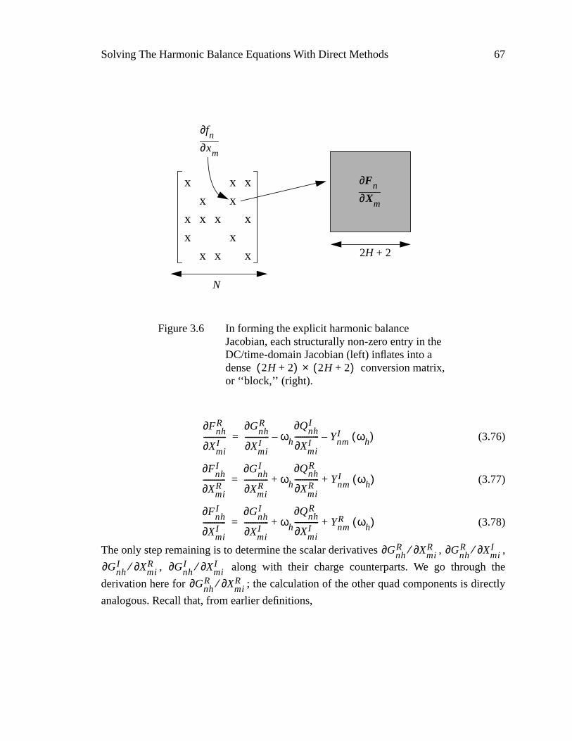
Solving The Harmonic Balance Equations With Direct Methods 67
(3.76)
(3.77)
(3.78)
The only step remaining is to determine the scalar derivatives , ,
, along with their charge counterparts. We go through the
derivation here for ; the calculation of the other quad components is directly
analogous. Recall that, from earlier definitions,
x x x
x x
x x x x
x x
x x x
Xm∂∂Fn
xm∂∂fn
N
2H + 2
Figure 3.6 In forming the explicit harmonic balanceJacobian, each structurally non-zero entry in theDC/time-domain Jacobian (left) inflates into adense conversion matrix,or ‘‘block,’’ (right).
2H 2+( ) 2H 2+( )×
FnhR∂
XmiI∂
------------Gnh
R∂
XmiI∂
------------- ωh
QnhI∂
XmiI∂
-------------– YnmI ωh( )–=
FnhI∂
XmiR∂
------------Gnh
I∂
XmiR∂
------------- ωh
QnhR∂
XmiR∂
------------- YnmI ωh( )+ +=
FnhI∂
XmiI∂
------------Gnh
I∂
XmiI∂
------------- ωh
QnhR∂
XmiI∂
------------- YnmR ωh( )+ +=
GnhR∂ Xmi
R∂⁄ GnhR∂ Xmi
I∂⁄Gnh
I∂ XmiR∂⁄ Gnh
I∂ XmiI∂⁄
GnhR∂ Xmi
R∂⁄

Chapter 3 Harmonic Balance Fundamentals 68
, (3.79)
and
(3.80)
Applying the chain rule to the above equations results in
(3.81)
Note that a naive application of (3.81) results in floating point operations per quad
entry. Since there are quads per block, the total workload would appear to be
at first glance. Although this computational expense would be partially masked
by the fact that the matrix factorization algorithms themselves are , it would
nevertheless pose a significant burden.
Kundert et al. [27] have presented an algorithm for explicitly forming the
harmonic balance blocks. The approach is based on Fourier transforming the samples
(3.82)
into the frequency domain, and splitting each Jacobian block into a sum of Toeplitz and
Hankel matrices.1 This algorithm may be derived from (3.81) by multiplying out the
matrices and using the sine and cosine product identities
(3.83)
1. Toeplitz matrices have entries given by aij=ti-j. Hankel matrices have entries given by aij=hi+j.See [48] for more details.
GnhR
2 δh–
2S-------------- gn x ts( )( ) 2πhs
2S------------
cos
s 0=
2S 1–
∑=
xm ts( ) Xm0R Xmh
R 2πhs2S
------------ cos Xmh
I 2πhs2S
------------ sin–
h 1=
H
∑+=
GnhR∂
XmiR∂
-------------2 δh–
2S--------------
xm∂∂
gn x ts( )( )Xmi
R∂
∂xm⋅ 2πhs
2S------------
cos
s 0=
2S 1–
∑2 δh–
2S--------------
xm∂∂
gn x ts( )( ) 2πis
2S-----------
2πhs2S
------------ coscos
s 0=
2S 1–
∑
=
=
O S( )H
2
O H2S
O H3
O H2( )
λs
g∂ n
xm∂--------- x ts( )( )=
α( ) β( )coscos12--- α β+( )cos α β–( )cos+( )=
α( )sin β( )sin12--- α β–( )cos α β+( )cos–( )
α( )sin β( )cos12--- α β+( )sin α β–( )sin+( )
=
=
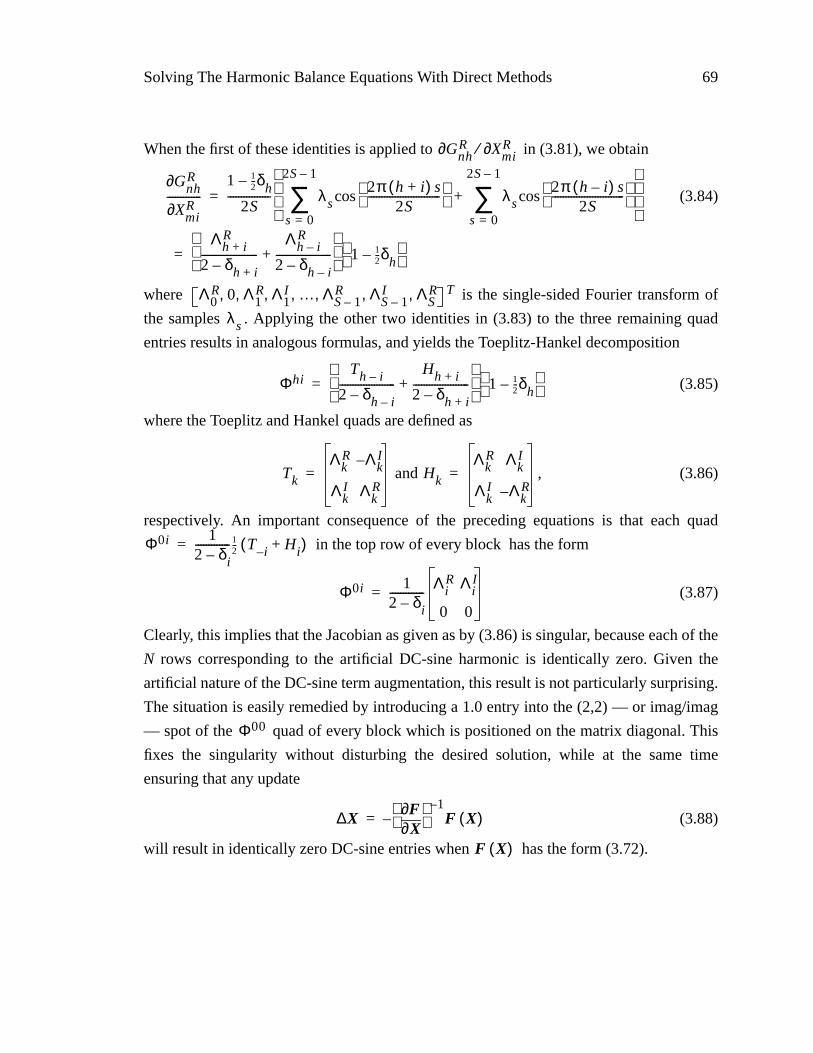
Solving The Harmonic Balance Equations With Direct Methods 69
When the first of these identities is applied to in (3.81), we obtain
(3.84)
where is the single-sided Fourier transform of
the samples . Applying the other two identities in (3.83) to the three remaining quad
entries results in analogous formulas, and yields the Toeplitz-Hankel decomposition
(3.85)
where the Toeplitz and Hankel quads are defined as
and , (3.86)
respectively. An important consequence of the preceding equations is that each quad
in the top row of every block has the form
(3.87)
Clearly, this implies that the Jacobian as given as by (3.86) is singular, because each of the
N rows corresponding to the artificial DC-sine harmonic is identically zero. Given the
artificial nature of the DC-sine term augmentation, this result is not particularly surprising.
The situation is easily remedied by introducing a 1.0 entry into the (2,2) — or imag/imag
— spot of the quad of every block which is positioned on the matrix diagonal. This
fixes the singularity without disturbing the desired solution, while at the same time
ensuring that any update
(3.88)
will result in identically zero DC-sine entries when has the form (3.72).
GnhR∂ Xmi
R∂⁄
GnhR∂
XmiR∂
-------------1 1
2---δh–
2S---------------- λs
2π h i+( ) s2S
--------------------------- cos
s 0=
2S 1–
∑ λs2π h i–( ) s
2S---------------------------
cos
s 0=
2S 1–
∑+
Λh i+R
2 δh i+–---------------------
Λh i–R
2 δh i––---------------------+
1 12---δh–
=
=
Λ0R 0 Λ, 1
R Λ1I … ΛS 1–
R ΛS 1–I, ΛS
R, , , , , T
λs
ΦhiTh i–
2 δh i––---------------------
Hh i+
2 δh i+–---------------------+
1 12---δh–
=
Tk
ΛkR Λk
I–
ΛkI Λk
R= Hk
ΛkR Λk
I
ΛkI Λk
R–=
Φ0i 12 δi–-------------1
2--- T i– Hi+( )=
Φ0i 12 δi–------------- Λi
R ΛiI
0 0=
Φ00
∆XX∂
∂F 1–
F X( )–=
F X( )

Chapter 3 Harmonic Balance Fundamentals 70
3.5.3 Factoring The Harmonic Balance JacobianLU factorization of the HB Jacobian is most effectively performed using block
operations. Consider the block matrix
, (3.89)
where Bij are all square blocks of identical dimensions. In direct analogy with standard LU
factorization algorithms, the block variant of the decomposition finds a permutation
matrix and block matrices L and U such that
, (3.90)
where Lij and Uij are square blocks having the same dimension as the Bij. The diagonal
blocks Lii / Uii are lower- and upper- triangular, respectively, while the remaining Lij / Uij
are potentially full. The permutation matrix represents the pivoting operations
performed during the decomposition to preserve sparsity and maintain numerical stability.
Conceptually, the factorization process may be presented as follows. Assuming that
the B11 block is the first pivot1, the matrix is partitioned as
(3.91)
where A11 = B11 is the pivot block. By inspection, the block-LU decomposition is then
1. Otherwise, a permutation of the rows/columns would be performed to (conceptually) move thepivot block into the upper left-hand corner.
J
B11 B12 … B1N
B21 B22 … B2N
| | \ |
BN1 BN2 … BNN
=
Π
J Π 1–LU Π 1–
L11 …
L21 L22 …
| | \ |
LN1 LN2 … LNN
U11 U12 … U1N
0 U22 … U2N
| | \ |
0 0 … UNN
= =
Π
B11 B12 … B1N
B21 B22 … B2N
| | \ |
BN1 BN2 … BNN
A11 A12
A21 A22
=

Solving The Harmonic Balance Equations With Direct Methods 71
, (3.92)
and the first column of L, along with the first row of U, may be determined:
, (3.93)
. (3.94)
The above decomposition procedure is then applied recursively to the resultant matrix
to obtain the remaining rows and columns of L and U.
When applied to factoring the HB Jacobian, sparse solvers based on the block-oriented
algorithm presented above have several advantages over standard packages. One such
advantage is memory usage — typically, each non-zero entry in standard sparse data
structures takes up several extra bytes of overhead due to the need to establish its position
within the matrix. This cost is avoided when block-oriented algorithms are used, since the
overhead is incurred only once for each block (that is, once per elements).
Furthermore, the block-oriented structure improves factorization speed substantially.
Since the elements are stored in dense arrays, they can be accessed efficiently for block
operations such as dense block multiplications, additions, and subtractions. An additional
benefit is a dramatic speed-up of the ‘‘symbolic factorization’’ stage — i.e., the
determination of the pivoting order. Pivoting is done on a block-by-block basis, and since
the number of blocks is times smaller than the total number of structurally non-
zero entries, the improvement can be quite sizeable for large H.
When exact Jacobians are being used, each block is either structurally full or diagonal.
In circuit simulation, the block at position (n,m) is diagonal if only linear components are
connected between nodes n and m, and structurally full if at least one nonlinear device is
connected. In semiconductor device simulation, the vast of majority of the blocks are full,
since the models used in the constitutive equations typically imply at least weakly
nonlinear interaction between the state variables at the grid nodes. Although strictly
speaking a block becomes structurally full when it corresponds to a nonlinearity of any
strength, the off-diagonal entries tend to become extremely small as the level of
A11 A12
A21 A22
L11 0
A21U111– I
U11 L111– A
12
0 A22 A21U111–
L11
1– A12
–=
L21
|
LN1
A21=
U12 … U1NA12=
A22 A21A111– A12–
O H2( )
O H2( )

Chapter 3 Harmonic Balance Fundamentals 72
nonlinearity is decreased (see Section 3.5.4). Furthemore, in the one-tone case, the
magnitude of the off-diagonal terms decreases gradually as a function of their distance
from the diagonal.1 This leads to a natural approximation of structurally full Jacobian
blocks by banded matrices. Kundert’s Harmonic-Relaxation-Newton scheme [27], for
example, selects the bandwidth BW for each block through a heuristic of the form
for . (3.95)
Ideally, the threshold constant is picked small enough (10-4 is a typical value) such that
nonlinear convergence remains robust.
Block-oriented matrix factorization algorithms are extremely effective in handling the
aforementioned combination of diagonal, banded, and full blocks. To see why, we first
note that the LU factorization of a banded block of bandwidth b results in L and U
matrices having bandwidths b (see Figure 3.7). Subsequent elimination operations
involve block products with and . These matrices are structurally diagonal if the
pivot is structurally diagonal, and so (in the diagonal case) do not increase the
1. In the multi-tone case, the situation is similar, but the stripes are spaced at constant intervals.
Λh µΛ0≤ h BW≤µ
x x x x
x x x x x
x x x x x x
x x x x x x x
x x x x x x x
x x x x x x
x x x x x
x x x x
x
x x
x x x
x x x x
x x x x
x x x x
x x x x
x x x x
x x x x
x x x x
x x x x
x x x x
x x x x
x x x
x x
x
=
Figure 3.7 LU factorization of a banded harmonic balancepivot block. Note that the bandwidth of the L and Ufactors is equivalent to that of the original pivotblock.
L111– U11
1–
B11

Solving The Harmonic Balance Equations With Direct Methods 73
bandwidths of the blocks that they pre- or post-multiply. When the pivot is not purely
diagonal, and become lower/upper triangular (respectively) and structurally
full. Nevertheless, in harmonic balance applications the magnitude of the entries will
decrease with distance from the diagonal, and a numerical bandwidth can be set. In
general, when a block with bandwidth b1 multiplies a block with bandwidth b2, the
resulting block will have a (structural) bandwidth b1 + b2 - 1. As the elimination process
proceeds, the matrix blocks become more and more full. The pivoting algorithm should be
chosen such that this level of fill is minimized. In particular, it is advantageous to pivot on
those blocks which are diagonal, or, in the case where that’s not possible, those that have a
very small bandwidth.
3.5.4 The Harmonic Balance Jacobian at Low Distortion LevelsStudying the harmonic balance equations in the limiting case of low distortion is
important for both practical and theoretical reasons. It is in the low distortion regime
where harmonic balance exhibits its most significant performance advantages over
transient simulation. There are numerous applications, such as highly linear single-
transistor amplifier device design, where a very low level of distortion is precisely what
the designer is trying to achieve. To analyze such problems, transient simulators must still
place sample points closely enough to capture the sinusoidal waveforms, regardless of
how few harmonics are being generated. Harmonic balance, on the other hand, can get
away with expanding the waveforms into a small number of sinusoidal basis functions.
Just as importantly, the harmonic balance Jacobian begins to assume a block diagonally-
dominant form — a fact which can greatly speed its factorization, and provide an effective
preconditioner for iterative linear solvers. This latter topic will be more fully explored in
Chapter 4.
The non-autonomous systems of equations considered in this work have, by definition,
zero AC response under DC-only stimulus (i.e., at zero AC input). We consider the case
where the AC input is small enough such that the quasi-Fourier coefficients at each state
variable
(3.96)
satisfy the condition that
L111– U11
1–
xn t( ) Xn0 XnhR ωht( )cos Xnh
I ωht( )sin–
h 1=
H
∑+=

Chapter 3 Harmonic Balance Fundamentals 74
(3.97)
is ‘‘extremely small.’’ Letting denote the state vector DC
components, the nonlinear resistive functions can be approximated through a Taylor
expansion as
(3.98)
which (by direct inspection) has the spectral representation
(3.99)
, . (3.100)
In a directly analogous fashion, the spectral coefficients of the nonlinear charge functions
can be approximated as
(3.101)
, . (3.102)
For notational convenience, we let denote the spectral
resistive derivative DC coefficient, with being the analogous
capacitive DC term. Differentiating the equations (3.99) — (3.102) yields the result
(3.103)
where is the Kronecker delta function — unity when h = i, and zero otherwise.
Thus, we see that under the low distortion approximation of (3.98), differentiating the
harmonic balance equations yields1
1. Here, we explicitly include the contribution from the convolution term of the constitutive equa-tions.
Xnhh 1=
H
∑X* 0, X10 X20 … XN0, , ,[ ] T=
gn x t( )( ) gn X* 0,( )g∂ n
xm∂---------
m 1=
N
∑ X* 0,( ) XmhR ωht( )cos Xmh
I ωht( )sin–
h 1=
H
∑+≈
Gn0 gn X* 0,( )=
Gnh
g∂ n
xm∂---------
m 1=
N
∑ X* 0,( ) Xmh= h 0>
qn
Qn0 qn X* 0,( )=
Qnh
q∂ n
xm∂---------
m 1=
N
∑ X* 0,( ) Xmh= h 0>
Λ0nm g∂ n xm∂⁄( ) X* 0,( )=
Θ0nm q∂ n xm∂⁄( ) X* 0,( )=
Gnh∂Xmi∂
------------ δh i– Λ0nm=
Qnh∂Xmi∂
------------ δh i– Θ0nm=
δh i–

Summary 75
, (3.104)
for . (3.105)
Written in matrix form, each Jacobian block has the representation
(3.106)
There are two key points regarding the above relationships. The first is that the equations
become analytic — that is, the Jacobian entries are complex numbers, rather than quads.
The second point is that each Jacobian block (now an complex sub-
matrix) is purely diagonal. This latter point is critical to fast and efficient factorization of
the approximate low-distortion Jacobian matrix.
3.6 Summary
This chapter has presented an overview of harmonic balance algorithm fundamentals.
When compared to transient analysis in the context of analog RF simulation, harmonic
balance offers numerous advantages. These include the ability to directly capture the
steady state response of nonlinear systems, almost complete insensitivity to wide
frequency spacings of multi-tone spectral inputs, excellent handling of distributed linear
elements, and good dynamic range for accurate resolution of low-distortion products.
Much of HB’s advantage over standard time domain methods is due to quasiperiodic
transforms and remapping functions that are utilized in lieu of finite-difference methods or
brute-force one-dimensional Fourier transforms. A survey of these was presented, and the
Fnh∂Xmh∂
------------- Λ0nm jωhΘ0
nm Ynm ωh( )+ +=
Fnh∂Xmi∂
------------ 0= i h≠
Xm∂∂Fn
Λ0nm 0 … 0
0 Λ0nm … 0
| | \ |
0 0 … Λ0nm
jω0Θ0nm 0 … 0
0 jω1Θ0nm … 0
| | \ |
0 0 … jωHΘ0nm
Ynm ω0( ) 0 … 0
0 Ynm ω1( ) … 0
| | \ |
0 0 … Ynm ωH( )
+
+
=
H 1+( ) H 1+( )×

Chapter 3 Harmonic Balance Fundamentals 76
choice to use remapping functions instead of the multidimensional Fourier transform was
made.
The formulation of the harmonic balance equations was discussed next. The
formulation of both the right hand side residual and the Jacobian matrix was discussed.
Given the large size of semiconductor device problems, direct solution methods are
clearly impractical. Nevertheless, a section on direct solution methods was included, with
some emphasis placed on the role that direct matrix factorization techniques play in the
more suitable algorithmic approaches of the next two chapters.

77
Chapter 4
Solving the Harmonic Balance Equationswith Newton-Iterative Methods
The Newton-Raphson algorithm is perhaps the most widely used technique for solving
nonlinear systems of algebraic equations. Its chief strength lies in its locally quadratic
convergence behavior when starting from sufficiently good initial guesses. When
combined with continuation methods such as source-stepping or arclength continuation,
Newton-Raphson is a robust and reliable method for solving the harmonic balance
equations.
The first generation of practical harmonic balance circuit simulators relied primarily
on Newton-Raphson with direct LU factorization as the central workhorse algorithm. As
shown in Chapter 3, however, direct LU factorization methods result in memory usage and
CPU time growth rates that are thoroughly impractical for large-scale systems of
equations. As early as 1991, Newton-Iterative methods (also known as Inexact Newton
methods) based on Krylov subspace linear solvers were proposed for solving the harmonic
balance system of circuit equations [38]. Since then, other authors have successfully
applied Krylov subspace solvers to large scale systems of HB circuit [39][42][44] and
device [1][2] equations.
In this chapter, we present the basic theory of Krylov subspace solution methods,
along with their application to solving systems of harmonic balance device equations.
Standard preconditioners are reviewed, and novel preconditioners for solving multi-tone
device distortion problems are presented. In addition, approximate spectral storage
Chapter 4 Solving the Harmonic Balance Equations with Newton-Iterative Methods 78
schemes are developed for further reducing the memory required in large-scale device
simulation problems.
4.1 Krylov Subspace Solution Techniques
Krylov subspace methods attempt to solve the linear problem
(4.1)by iteratively adjusting to minimize some measure of error. In general, at the kth
iteration, Krylov subspace methods minimize the error over the affine space
, (4.2)
where is the initial iterate, and
(4.3)
is the kth Krylov subspace of matrix A, with initial residual of . Krylov
solution methods have shown themselves to be superior to their stationary iterative
counterparts such as SOR, Gauss-Seidel, etc. [48][50], and are the methods we focus on in
this section.
A common aspect of all the Krylov subspace algorithms is their need to carry out
matrix-vector products of the form (and possibly ) at each iteration k. The
matrix A itself need never be explicitly stored so long as the matrix-vector products can be
computed. It turns out that when A is a harmonic balance Jacobian, a compact
representation for forming such products is readily available. We defer a description of
harmonic balance matrix-vector products to Section 4.2, and first briefly present the basic
theory underlying GMRES, our Krylov subspace algorithm of choice.
4.1.1 Generalized Minimum Residual (GMRES)The Generalized Minimum RESidual Algorithm (GMRES) [46] was developed in
1986 as a general-purpose Krylov subspace method for nonsymmetric linear systems. The
key idea behind GMRES is to minimize at the kth iteration the residual in
the 2-norm over the space . Formally, this amounts to solving the least squares
problem
(4.4)
Ax b=x
x0 Kk+
x0
Kk span r0 Ar0 A2r0 … A
k 1–r0, , , ,
=
r0 b Ax0–=
Avk ATvk
rk b Axk–=
x0 Kk+
minxk x0 Kk+∈ b Axk–2
Krylov Subspace Solution Techniques 79
at each iteration k. Since the kth Krylov subspace contains k basis vectors, the least
squares problem has k degrees of freedom.
If we let denote an orthonormal basis for , the kth iterate can be
written as
, (4.5)
where is to be determined by the least squares equation(4.4):
. (4.6)
The orthonormal basis is constructed via the Arnoldi process, which is the Gram-
Schmidt process applied to a given Krylov subspace. The k orthonormal columns of
are given by for the first column, and
(4.7)
for subsequent columns ( ). In practice, the classical Gram-Schmidt algorithm as
presented above suffers from numerical stability problems which cause the columns of
to lose their orthogonality [48]. In actual implementations, either modified Gram-Schmidt
orthogonalization [48] or Householder reflections [47] are used to carry out the Arnoldi
process. In theory, the Householder-Arnoldi algorithm is regarded as numerically more
stable. In our experience, however, there is virtually no difference between the two
approaches as far as harmonic balance device simulation is concerned.
The orthonormality of the basis matrix allows the least squares problem (4.6) to be
solved efficiently. From equation (4.7), one can readily derive the relationship [51]
, (4.8)
where is upper Hessenberg — that is, upper triangular with a single stripe
right below the diagonal. For example, at k = 5, would have the structure
Vk ℜ N k×∈ Kk
xk x0 Vkyk+=
yk ℜ k∈
minyk ℜ k∈
b A x0 Vkyk+( )–2
minyk ℜ k∈
r0 AVkyk–2
=
Vk
Vk v1 v2 …vk, ,[ ]= v1 r0 r0⁄=
vi 1+
Avi vlTAvi
vll 1=
i
∑–
Avi vlTAvi
vll 1=
i
∑–
-------------------------------------------------------=
i 1≥Vk
Vk
AVk Vk 1+ Hk=
Hk ℜ k 1+ k×∈H5

Chapter 4 Solving the Harmonic Balance Equations with Newton-Iterative Methods 80
. (4.9)
Taking advantage of the fact that is the first column of , we can re-write
the least squares problem as
(4.10)
where is a unit basis vector along the first dimension, and . Furthermore,
because is orthonormal, it has no impact on the 2-norm, and may thus be removed
from the relation above to yield the upper Hessenberg least squares problem
. (4.11)
The QR factorization of the upper Hessenberg matrix is readily performed through k
Givens rotations [48]. Because Givens rotation matrices are orthonormal, they also do not
affect the 2-norm in the least squares problem. For instance, applying the first two Givens
rotations and to the example matrix in (4.9) would eliminate two of the
lower-diagonal entries as follows:
. (4.12)
When all k Givens rotations are applied (let’s write ), the resulting
matrix assumes an upper triangular form, and the least squares problem
(4.13)
becomes easy to solve.
One serious drawback of the GMRES algorithm as presented above is the storage cost
associated with the orthonormal basis1 . Because an extra basis vector of size N has to
be stored for each GMRES iteration, the storage cost can become prohibitive if many
H5
x x x x x
x x x x x
x x x x
x x x
x x
x
=
v1 r0 r0⁄= Vk
minyk ℜ k∈
b A x0 Vkyk+( )–2
minyk ℜ k∈
Vk 1+ βe1 Hkyk–( )2
=
e1 β r0=
Vk 1+
minyk ℜ k∈
βe1 Hkyk–2
Hk
G1 G2 H5
G2G1H5
x x x x x
0 x x x x
0 x x x
x x x
x x
x
=
G Gk … G⋅ ⋅1
=
R GHk=
minyk ℜ k∈
βe1 Hkyk–2
minyk ℜ k∈
βGe1 Ryk–2
=
Vk
Matrix-Vector Products Involving the Harmonic Balance Jacobian 81
iterations need to be taken. Consequently, it is necessary in practice to use a ‘‘restarted’’
variant of GMRES, where the iterative process begins anew after a fixed number of
iterations. In practice, we have found a restart value of 10 to be more than enough for
harmonic balance applications.
4.1.2 Other Krylov Subspace AlgorithmsIn addition to GMRES, several other Krylov subspace methods for solving indefinite
non-symmetric systems exist. These include algorithms such Quasi-Minimal Residual
(QMR) [53], Transpose-Free Quasi-Minimal Residual (TFQMR) [54], and Biconjugate
Gradient Stabilized (BICGSTAB) [55]. In particular, the QMR family of algorithms are
sometimes preferred over GMRES because they can execute in a fixed amount of storage
which doesn’t increase with the iteration count. In some applications, restarted variants of
GMRES are known to ‘‘stall’’ at a given value of the residual, and are not able to reduce
the norm unless the restart value is increased. Because QMR algorithms do not need to be
restarted, they are sometimes able to converge when GMRES cannot.
In this work, we have found restarted GMRES to be superior to QMR/TFQMR, both
in terms of speed and in terms of robust convergence behavior. This is in all likelihood due
to the relatively good preconditioners that are available for the harmonic balance problem.
Because GMRES works so well relative to its alternatives for low values of the restart
parameter, we use it exclusively in this work. All the results presented in subsequent
sections are based on the Householder-Arnoldi variant of GMRES [47] using a restart
value of 10, unless explicitly stated otherwise.
4.2 Matrix-Vector Products Involving the HarmonicBalance Jacobian
As we’ve seen, matrix-vector products are central to Krylov subspace solution
algorithms. Fast computation of these products, along with efficient storage of the
harmonic balance Jacobian representation, is essential for practical application of the
1. In the Householder variant of GMRES, it is the Householder vectors that are explicitly stored,rather than the orthonormal basis. The storage cost between the two methods is virtually identicalfor large problems.

Chapter 4 Solving the Harmonic Balance Equations with Newton-Iterative Methods 82
algorithms to solving large-scale HB equations. In this section, we outline an FFT-based
algorithm [39] that carries out the matrix-vector products in floating point
operations and storage requirements, where S is the number of time samples used
in the HB analysis. In Section 4.4, we will present algorithms which further reduce
memory storage requirements, at the cost of slowing down the matrix-vector multiplies by
a constant factor which is independent of the number of harmonics H or time samples S.
Recall from Section 3.4.2 that the harmonic balance Jacobian can be written as
, (4.14)
where is a block diagonal matrix of DFT operators defined by equation (3.64), and
is a block-diagonal matrix representing the derivative operation (see equation (3.65)).
Our goal is to carry out matrix-vector products of the form
(4.15)
where V is an arbitrary real vector that, like X, can be written in block
form as
, (4.16)
, . (4.17)
Consider first the resistive portion of the product. The operation
(4.18)
may be carried out efficiently in three steps. First, is computed using N FFT
operations. Because each block in
O S S( )log( )O S( )
F ′ X( )X∂
∂FX( ) ΓN x∂
∂g ΓN1–X
ΓN1– ΩNΓ
N x∂∂q ΓN
1–X
ΓN1–
Y+⋅ ⋅+⋅ ⋅= =
ΓNΩN
F ′ X( ) V⋅
ΓN x∂∂g ΓN
1–X
ΓN1–V ΩNΓ
N x∂∂q ΓN
1–X
ΓN1–V YV+⋅ ⋅+⋅ ⋅
=
2H 1+( ) N 1×
V V1 V2 … VN, , ,[ ] T=
Vm Vm0 Vm1R Vm1
I … VmHR VmH
I, , , , , T= 1 m N≤ ≤
ΓN x∂∂g ΓN
1–X
ΓN1–V⋅ ⋅
ΓN1–V
g∂ n xm∂⁄
Matrix-Vector Products Involving the Harmonic Balance Jacobian 83
(4.19)
is strictly diagonal (see (3.68)), the product can then be carried out in
floating point operations. An additional N FFTs complete the steps required to
compute (4.18). The corresponding evaluation of the capacitive product
(4.20)
proceeds in an exactly analogous manner, with the additional (cheap) multiplication by the
derivative operator . Lastly, the product
(4.21)can be computed efficiently by noting that each structurally non-zero block of Y is
diagonal.
Because the semiconductor device equations are of the form (2.29)-(2.30), there are no
nonlinear capacitive terms present within the drift diffusion state equations themselves.
Consequently, within the semiconductor device domain, the Jacobian reduces to
, (4.22)
and the corresponding matrix vector product
(4.23)
contains no nonlinear capacitive multiplies (4.20). Of course, if nonlinear capacitors or
linear distributed elements are present outside the semiconductor device domain, then the
corresponding products (4.20) and (4.21), respectively, would need to be carried out over
the circuit portion of the matrix.
x∂∂g
x1∂∂g1
x2∂∂g1 …
xN∂∂g1
x1∂∂g2
x2∂∂g2 …
x1∂∂g2
| | \ |
x1∂∂gN
x2∂∂gN …
xN∂∂gN
=
x∂∂g ΓN
1–X
ΓN1–V⋅
O H( )
ΩNΓN x∂
∂q ΓN1–X
ΓN1–V⋅ ⋅
ΩN
YV
F ′ X( )X∂
∂FX( ) ΓN x∂
∂g ΓN1–X
ΓN1–
diag 0 Ω Ω 0 Ω Ω …, , , , , ,( )–⋅ ⋅= =
X∂∂F
V⋅ ΓN x∂∂g ΓN
1–X
ΓN1–V diag 0 Ω Ω 0 Ω Ω …, , , , , ,( ) V–⋅ ⋅=

Chapter 4 Solving the Harmonic Balance Equations with Newton-Iterative Methods 84
4.3 Preconditioning
The performance of linear iterative solvers can be improved dramatically through the
use of preconditioners. Instead of solving the linear system , we instead solve the
preconditioned system
. (4.24)
is called the left-preconditioner, and is referred to as the right-preconditioner. In
this work, we restrict ourselves to applying either the left or the right preconditioner, but
not both simultaneously.
Preconditioning modifies some aspect of the original matrix (e.g., an improved
condition number or a better clustering of eigenvalues) that allows a given iterative linear
solver to take fewer iterations. Since the preconditioner must be applied on every iteration,
the trade-off must be such that the reduction in iteration count more than offsets the
increased work necessary on every iteration. Ideally, a preconditioning matrix M should
be a good approximation to the original matrix A, while also being fast and easy to factor.
Many general-purpose preconditioning schemes have been documented in the
literature ([49], [50], and references therein). Being general in nature, these turn out to be
sub-optimal for preconditioning the harmonic balance Jacobian. As we saw in
Section 3.5.4, the HB Jacobian at low distortion levels reduces to a block-diagonal form.
It turns out that this matrix is an excellent preconditioner for the harmonic balance
problem, and typically continues to perform well even at relatively high distortion levels.
In the rest of this section, we will present problem-specific preconditioners for the HB
device equations. In addition to the aforementioned block-diagonal preconditioner, we
will introduce the so-called sectioned preconditioner for large multi-tone distortion
problems, and briefly discuss future work that remains to be done on the problem.
4.3.1 The Block-Diagonal PreconditionerAs was shown in Section 3.5.4, the harmonic balance Jacobian assumes a complex-
valued block-diagonal form under the low-level distortion approximation. This block-
diagonal matrix is a natural candidate for preconditioning the harmonic balance equations.
We can expect such a preconditioner to be outstanding at low power levels, with its
effectiveness gradually diminishing as the distortion levels increase. The usefulness of the
Ax b=
ML1– AMR
1– MRx( ) ML
1– b=
ML MR
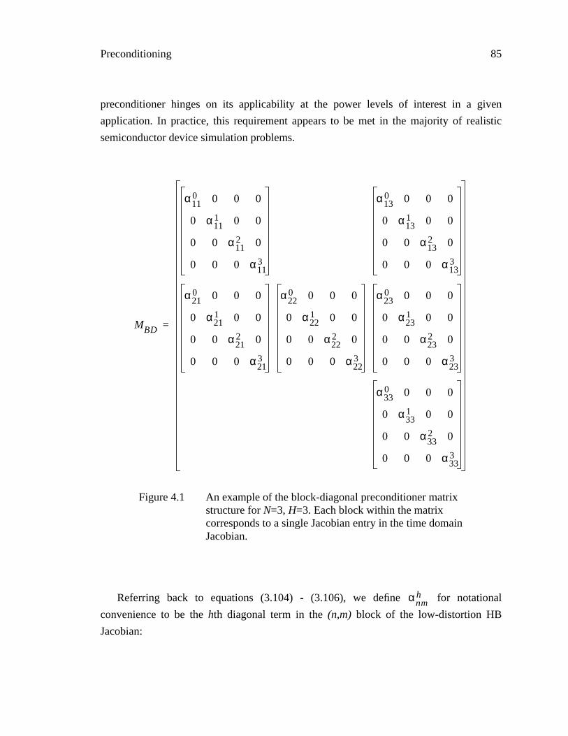
Preconditioning 85
preconditioner hinges on its applicability at the power levels of interest in a given
application. In practice, this requirement appears to be met in the majority of realistic
semiconductor device simulation problems.
Referring back to equations (3.104) - (3.106), we define for notational
convenience to be the hth diagonal term in the (n,m) block of the low-distortion HB
Jacobian:
MBD
α110 0 0 0
0 α111 0 0
0 0 α112 0
0 0 0 α113
α130 0 0 0
0 α131 0 0
0 0 α132 0
0 0 0 α133
α210 0 0 0
0 α211 0 0
0 0 α212 0
0 0 0 α213
α220 0 0 0
0 α221 0 0
0 0 α222 0
0 0 0 α223
α230 0 0 0
0 α231 0 0
0 0 α232 0
0 0 0 α233
α330 0 0 0
0 α331 0 0
0 0 α332 0
0 0 0 α333
=
Figure 4.1 An example of the block-diagonal preconditioner matrixstructure for N=3, H=3. Each block within the matrixcorresponds to a single Jacobian entry in the time domainJacobian.
αnmh
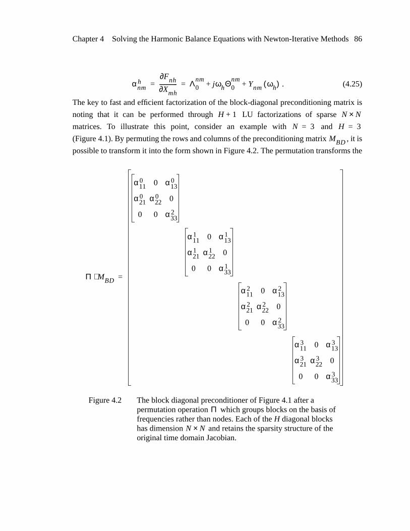
Chapter 4 Solving the Harmonic Balance Equations with Newton-Iterative Methods 86
. (4.25)
The key to fast and efficient factorization of the block-diagonal preconditioning matrix is
noting that it can be performed through LU factorizations of sparse
matrices. To illustrate this point, consider an example with and
(Figure 4.1). By permuting the rows and columns of the preconditioning matrix , it is
possible to transform it into the form shown in Figure 4.2. The permutation transforms the
αnmh
Fnh∂Xmh∂
------------- Λ0nm
jωhΘ0nm
Ynm ωh( )+ += =
H 1+ N N×N 3= H 3=
MBD
Π MBD⋅
α110 0 α13
0
α210 α22
0 0
0 0 α332
α111 0 α13
1
α211 α22
1 0
0 0 α331
α112 0 α13
2
α212 α22
2 0
0 0 α332
α113 0 α13
3
α213 α22
3 0
0 0 α333
=
Figure 4.2 The block diagonal preconditioner of Figure 4.1 after apermutation operation which groups blocks on the basis offrequencies rather than nodes. Each of the H diagonal blockshas dimension and retains the sparsity structure of theoriginal time domain Jacobian.
Π
N N×

Preconditioning 87
matrix into a set of decoupled blocks, each having the sparsity pattern of the
original Jacobian. That is, the permuted Jacobian takes on the form
, (4.26)
where can be viewed as an AC matrix [57] at harmonic balance
frequency . This is in contrast with the unpermuted structure, which is an block
matrix having the sparsity pattern of the original Jacobian, with each entry being a
diagonal block of dimension .
As readily seen from the preceding paragraph, both the memory requirements and the
execution time for employing the block-diagonal preconditioner scale as with the
number of harmonics. Unfortunately, in multi-tone semiconductor device simulation
problems, the number of harmonics can still be so large that it is impractical to store the
entire preconditioner . Even in two-tone simulation, where the number of harmonics
rises as with the truncation order P, it is not particularly uncommon to have
values of H exceeding 100 for high-distortion problems. Given a device structure whose
AC Jacobian storage takes 10MB, for example, the storage of would require a
gigabyte of RAM for . Clearly, such storage requirements can become
prohibitive for large multi-tone simulations.
4.3.2 The Sectioned Preconditioner for Multi-Tone ProblemsTo overcome the problems posed by block-diagonal preconditioner storage in multi-
tone analysis, we note that most multi-tone problems have distinct ‘‘bands’’ of harmonics
that are very tightly spaced in frequency. For instance, a common two-tone input signal
used for intermodulation distortion analysis is
, (4.27)
where the tone spacing is very small relative to the magnitudes of
and . Figure 4.3 illustrates the frequency ‘‘bunches’’ or ‘‘bands’’ that result from this
type of stimulus.
It is possible to exploit this frequency-grouping phenomenon by noting (Section 2.4.2)
that inside the semiconductor device, each state equation has the form
H 1+ N N×
Π MBD⋅
Jac ω0( )
Jac ω1( )
\
Jac ωH( )
=
Jac ωh( ) CN N×∈ωh N N×
H 1+( ) H 1+( )×
O H( )
MBDO P2( )
MBDH 100=
V t( ) A1 Ω1t( )cos A2 Ω2t( )cos+=
∆Ω Ω2 Ω1–= Ω1Ω2

Chapter 4 Solving the Harmonic Balance Equations with Newton-Iterative Methods 88
, (4.28)
where , and is zero for the Poisson equations (n=1,4,7, ...) while being
unity for the continuity equations (n=2,3,5,6,8,9, ...). Each AC Jacobian matrix
can be partitioned as
, (4.29)
where represents the portion of the Jacobian corresponding to the
derivative over the semiconductor domain (i.e., derivatives of the semiconductor
equations (4.28) with respect to the semiconductor state variables), while
represents the admittance matrix of the circuitry surrounding the
semiconductor device. The remaining two sub-matrices represent the coupling between
the circuit and semiconductor domains, taking on the dimensionalities
and .
Because the derivative operator in the time domain equations (4.28) varies linearly
with frequency (i.e., ), the drift-diffusion sub-matrix varies linearly
ω
Ω1 Ω2 2Ω1 2Ω2 3Ω1 3Ω2Ω2 Ω1–
12--- Ω1 Ω2+( ) Ω1 Ω2+( ) 3
2--- Ω1 Ω2+( )
Figure 4.3 An illustration of tightly spaced frequency ‘‘bands’’ thatoccur when is small in a two-tone stimulus.The dashed lines and the frequencies above them indicate thecenter of each ‘‘band’’ in the spectrum.
∆Ω Ω2 Ω1–=
32--- Ω2 Ω1–( )
δcont td
dxn gn x t( )( ) wn t( )–+ 0=
1 n 3K≤ ≤ δcontJac ωh( )
Jac ωh( )Jdd ωh( ) J12 ωh( )
J21 ωh( ) Yckt ωh( )=
Jdd ωh( ) C3K 3K×∈
Yckt ωh( ) CE E×∈
J12 ωh( ) C3K E×∈ J21 ωh( ) CE 3K×∈
d dt⁄ jω→ Jdd ωh( )

Preconditioning 89
as is varied. The circuit sub-matrix , on the other hand, can vary quite
rapidly with frequency when, for example, the external circuit network contains high-Q
resonant circuitry or filters with sharp transitions. A key observation is that the
dimensionality of the circuit sub-matrix is rather small (typically or less), while the
dimensionality of the drift-diffusion sub-matrix is very large (typically in the thousands).
To efficiently factor the matrices in the presence of tightly-spaced bands
of harmonics (Figure 4.3), we make the approximation
, (4.30)
where the frequency represents the center of the ‘‘band’’ containing . In general,
the number of such bands is — much smaller than , the total number of
harmonic balance frequencies. The large drift-diffusion portion of the Jacobian need only
be stored at these band frequencies, while the small circuit portion can be stored at
all frequencies very cheaply. Dramatic reductions in memory usage and
improvements in factorization speed result as a consequence.
The actual factorization of (4.30) is accomplished by standard block-LU factorization
algorithms. A block system of the form
(4.31)
can be solved by defining the Schur complement matrix , and then
obtaining the solution as
(4.32)
When applied to solving a sequence of matrices , the lion’s share of the
CPU and memory resources is taken up by the need to factor and store large sparse
matrices , corresponding to in the notation of (4.31) above. The cost for
storing and factoring Schur complement matrices S is negligible in our application,
given the small size of the surrounding circuit network.1 Storage of the rectangular
matrices and is likewise small in comparison.
ωh Yckt ωh( )
3 3×
H 1+ Jac ωh( )
Jac ωh( )Jdd ωh( ) J12 ωh( )
J21 ωh( ) Yckt ωh( )≈
ωh ωhP 1+ H 1+
P 1+
H 1+
A11 A12
A21 A22
x1
x2
b1
b2
=
S A22 A21A111–A12–=
x2 S1–
b2 A21A111–b1–
x1 A111–b1 A11
1–A12x2–
=
=
H 1+ Jac ωh( )P 1+
Jdd ωh( ) A11H 1+
H 1+
A111–A12 A21A11
1–

Chapter 4 Solving the Harmonic Balance Equations with Newton-Iterative Methods 90
To illustrate the large advantage to be gained through the use of sectioned
preconditioners in multi-tone device-level HB simulation, we offer an example. Consider
the high-Q single-BJT mixer configuration (Figure 6.12) which will be more fully
discussed in Section 6.3. For good accuracy, the two tone mixer simulation should be done
at a diamond truncation order of P=10, which corresponds to H=110 harmonics. Although
the BJT mesh is relatively small by semiconductor device simulation standards (704
internal grid points, and N = 2114) the size and density of the Jacobian is such that
utilizing non-sectioned preconditioning is prohibitive. The memory reduction obtained by
using the sectioned preconditioner is even more significant for devices having larger mesh
sizes. Figure 4.4 shows the preconditioner memory usage as a function of the truncation
order P for both the sectioned and non-sectioned cases, while Figure 4.5 shows the
GMRES convergence behavior in factoring the Jacobian at the solution point. The
relatively modest decrease in the linear convergence rate is more than compensated for by
the large memory reduction that is obtained. The decrease in preconditioner factorization
time typically compensates the slight increase in the number of linear iterations. For linear
solutions in the context of Newton’s method, relative residual accuracies tighter than 10-3
are rarely called for, and Figure 4.5 shows the convergence behavior past this point merely
for the sake of completeness.
1. External linear networks with large numbers of internal circuit nodes are collapsed into muchsmaller admittance matrices, having a dimensionality corresponding to the number of transistor ter-minals connected to the linear network.

Preconditioning 91
0 5 10 150
50
100
150
200
250
300
350
400
450
500
Diamond Truncation Order P
Mem
ory
Usa
ge (
MB
)
Figure 4.4 Memory usage comparison between thesectioned and non-sectioned preconditionersfor the single-BJT mixer example.
Standard
Sectioned
0 5 10 15 20 25 3010
−8
10−7
10−6
10−5
10−4
10−3
10−2
10−1
100
GMRES Iteration
(Ax−
b)/|b
|
Figure 4.5 Convergence rate comparison between thesectioned and non-sectioned preconditionersfor the single-BJT mixer example.
Standard
Sectioned

Chapter 4 Solving the Harmonic Balance Equations with Newton-Iterative Methods 92
4.3.3 Other PreconditionersThe preconditioners discussed in the preceding sections are effective for a wide range
of harmonic balance device simulation problems. There are two possible paths to follow
for further improving their performance. In the low distortion regime, special-purpose
matrix solvers geared specifically to the form of the drift-diffusion equations can be
employed to reduce the memory requirements necessary for preconditioner storage [58].
In practice, however, because the sectioned preconditioner storage requirements are
already relatively low, this approach is truly useful only in the case where the spectrum is
such that a very large number of sections exist. This does not typically occur in
semiconductor device simulation.
A far more useful improvement to the preconditioner is to incorporate additional off-
diagonal elements in the harmonic balance Jacobian blocks. This is crucial to solving
some highly nonlinear problems — indeed, as Section 4.6 will discuss, the block-diagonal
preconditioner is typically adequate only up to gain compression levels of a few dB.
Block-oriented incomplete-factorization solvers based on the techniques presented in
Section 3.5.3 have been developed to incorporate some off-diagonal Jacobian stripes on a
block-by-block basis [58], and have been used with some success in the context of circuit
and small device simulation problems. However, because of the large Jacobian sizes and
densities encountered in mainstream semiconductor device simulation examples, the
methods developed by us to date have thus far fallen short of being practical. Clearly,
more work is called for in this area.
4.4 Further Memory Reduction Strategies
4.4.1 Approximate Compact Spectral StorageWe saw in Section 4.2 that carrying out matrix-vector products involving the HB
Jacobian requires storing samples
, (4.33)
at the structurally non-zero Jacobian entries (n, m) over the semiconductor device domain.
For large numbers of harmonics H, this storage cost can become quite substantial. As an
example, typical ‘‘medium-size’’ meshes used in this work contain about 50,000 non-zero
2S
xm∂∂gn ts( ) 0 s 2S 1–≤ ≤

Further Memory Reduction Strategies 93
Jacobian entries1 prior to factorization. For a two-tone harmonic balance analysis at 100
frequencies, the memory cost of storing the samples (4.33) is almost 80 MB. For an
analysis at 200 frequencies, the cost is almost 160 MB. Although this cost is bearable
given the memory capacity of modern workstations, it nevertheless makes sense to
examine algorithms for reducing the aforementioned memory usage.
Consider the set of samples
, (4.34)
along with their Fourier transform
, . (4.35)
Ordinarily, the set of all time domain samples is stored. The key to reducing
storage requirements is to note that the spectrum of these samples is quite sparse for
most Jacobian entries (n, m). This sparsity comes about because of the relatively low
levels of harmonic distortion in many regions within the device. By Fourier transforming
the samples (4.34), discarding those Fourier coefficients that fall below a certain
threshold, and storing the remaining coefficients, an accurate approximation of the
original Jacobian is retained. To perform matrix-vector multiplications during the GMRES
process, the stored spectral coefficients are inverse-FFT’ed into the time domain element-
by-element, at which point the algorithms of Section 4.2 can be applied.
An important consideration in implementing the above memory reduction scheme is
determining the proper threshold for sparsifying the spectral samples . Choosing too
high a threshold will result in an inaccurate Jacobian, and thus a degradation in the rate of
convergence. Choosing too low a value will result in very little sparsification of the
spectrum, thus negating the benefits of the approach. For this work, the following simple
heuristic has shown itself to be effective. Given a spectrum , the threshold is
chosen to be
1. In actuality, many industrial users employ much larger mesh sizes.
λs xm∂∂gn ts( )= 0 s 2S 1–≤ ≤
Λh λs2πj
2S 2+--------------- hs⋅
exp
s 0=
2S 1–
∑= 0 h S≤ ≤
2S λsΛh
Λh
Λh εthresh

Chapter 4 Solving the Harmonic Balance Equations with Newton-Iterative Methods 94
(4.36)
and all values such that are discarded and effectively approximated as
zero for the matrix-vector multiplies to follow. The purpose of the parameter is to
discard spectral components that fall below a certain ‘‘dynamic range.’’ For instance,
typical values of to would ensure that spectral components that are 80-100 dB
down are viewed as being insignificant to the accurate representation of the time domain
waveform samples . The parameter ensures that spectral components that fall
below a certain absolute value (say, ) are discarded as ‘‘noise’’ which is unimportant
to the overall Jacobian representation. For example, a set of spectral components that
range in value from to would all be included if only the relative dynamic
range criterion was used, even though the Jacobian entry could very accurately be
represented by zero for typical device problems.
An additional consideration in invoking the compact spectral storage option is the
penalty in CPU time for carrying out the inverse FFT operation for each Jacobian entry
during each matrix-vector multiplication. As shown in Section 4.2, FFT operations1
are necessary for each Jacobian-vector product when standard (time domain) storage is
used. When spectral representations are utilized, however, an additional inverse FFT must
be performed during each such Jacobian-vector product for every non-zero Jacobian entry.
Before concluding the section, we point out that a very similar memory reduction
scheme was proposed in the context of circuit simulation by Long et al. [41]. The
techniques presented above were developed independently, and implemented in our
simulator before publication of the aforementioned work.
4.4.2 Approximate GMRES Vector StorageAnother potentially large source of memory consumption is the storage of the Krylov
subspace basis vectors (for Gram-Schmidt GMRES) or Householder reflection vectors
(for Householder-Arnoldi GMRES). For a simulation problem having a million
unknowns, each such vector would occupy 8 MB of RAM if standard double-precision
1. Actually, N FFT operations and N inverse FFTs.
εthresh max εmin εrel
Λ0max
0 h H≤ ≤Λh+
2-----------------------------------,
=
Λh Λh εthresh≤εrel
104–
105–
λs εmin10
20–
1025–
1027–
2N

Further Memory Reduction Strategies 95
storage was used. Thus, for a restart value of 10, about 80 MB of additional storage would
be required. While this may not seem like much relative to other storage requirements
inherent in HB device simulation, it is nevertheless significant.
The memory usage associated with the GMRES vectors can be reduced by following
an approach similar to the one taken in the previous section [41]. It turns out that the
GMRES vectors in both the Gram-Schmidt and Householder variants are numerically
sparse, and that convergence rates are not significantly affected by discarding entries
below a certain threshold. Furthermore, Long et al. [41] have observed that the vectors can
be stored in single precision without adversely affecting the quality of the linear solve.
The GMRES sparsification option was implemented in our simulator. We have
noticed, however, that for some ill-conditioned semiconductor device simulation
problems1 the threshold must be set far lower than the value of 10-6 suggested in [41].
Consequently, we’ve made the decision that the benefits gained are not worth the extra
heuristics inherent in having a user-specified threshold parameter. While the option is
available, we discourage its use until such time as the code is improved to remove the
source of potential ill-conditioning. Storing the GMRES vectors in single-precision format
does seem to work well even in the ill-conditioned case, and use of this option (without
sparsification) is encouraged.
4.4.3 Impact of Memory Reduction Strategies on PerformanceGiven the size and density of the device-level Jacobian, using the reduced
preconditioner of Section 4.3.2 is crucial for efficient analysis of large two-tone problems.
However, employing the additional memory reduction techniques of the preceding two
sections can be quite beneficial as well. We quantify these choices by applying them to the
high-Q single-BJT mixer example of Section 6.3 for an analysis at H = 110 harmonics,
which corresponds to an HB problem with 467,194 unknowns.
Table 4.1 shows simulation results when the various memory reduction options are
turned on or off. The Jacobian memory reduction utilized an of 10-4. The GMRES
memory reduction option simply switched between single and double precision storage of
the GMRES vectors, without actually sparsifying them. From the results below, it is
1. The ill-conditioning can arise from the small resistors that some mixed-level circuit/devicePISCES variants insert in series with each terminal.
εrel

Chapter 4 Solving the Harmonic Balance Equations with Newton-Iterative Methods 96
apparent that usage of the sectioned preconditioner yields the biggest memory savings (a
full 194 MB), while also speeding up the simulation by about 10%. (The computer used
for the benchmark had 900MB of RAM; the speed-up obtained would be much more
significant on machines with, say, only 250MB of RAM available.) Using single-precision
GMRES storage saves an additional 20MB, without any noticeable loss in speed.
Invoking compact Jacobian spectral storage saves an additional 20MB, albeit at a 50%
performance penalty.
We point out that slightly over 40MB of memory is used by the static arrays in the
Fortran-based core PISCES code. The harmonic balance module itself allocates anywhere
from under 119MB with all memory-saving options turned on to 373MB with all options
disabled. Before concluding this section, we mention that the memory reduction due to the
sectioned preconditioner is more dramatic for larger devices, and that the reductions seen
in Jacobian memory usage are more significant as the number of harmonics is increased
and/or as the input power level is decreased. In this particular example, the BJT has no
source resistance, and is driven by a local oscillator sinusoid with a 0.7V DC bias and a
0.15V amplitude.
4.5 Iterative Linear Solvers in the Newton Loop
Recall that the lth iteration ( ) of Newton-Raphson applied to (3.60) is
, (4.37)
Sectionedprecond.
Jacobianmemoryreduction
GMRESsingle prec.
storage
MemoryUsage
Simulation Time
yes yes yes 159 MB 95 min. 27 sec.
yes yes no 179 MB 91 min. 45 sec.
yes no yes 199 MB 64 min. 54 sec.
yes no no 219 MB 64 min. 11 sec.
no no no 413 MB 70 min. 50 sec.
Table 4.1 A comparison of simulator performance under various memoryreduction options.
l 1≥
Xl( )
Xl 1–( ) ∆X
l( )+=
Iterative Linear Solvers in the Newton Loop 97
where is the solution of the linear system
. (4.38)
If the equation is solved to infinite precision, and if the nonlinear system
satisfies certain (commonly encountered in practice) conditions [24], then the convergence
is quadratic for initial guesses which are arbitrarily close to the solution. In finite-precision
floating point arithmetic, however, there will always be some error in solving the linear
Newton update equation. That is, the absolute and relative errors
(4.39)
(4.40)
will in practice always be non-zero, regardless of whether direct or iterative methods are
used to solve the linear system.
Given that some level of error during the linear solve is unavoidable, it is prudent to
study its effect on nonlinear convergence regardless of whether direct or iterative methods
are employed. With iterative methods, however, the subject becomes particularly
significant, because there is an important trade-off to be made. On the one hand, a
particular implementation could choose to take many iterations during the linear stage,
solving (4.38) to a high degree of accuracy in the hope of minimizing the number of
nonlinear steps (4.37). On the other hand, it is conceivable that such an implementation
would ‘‘over-solve’’ the linear system — that is, solve it to a much higher degree of
accuracy at every nonlinear step than is necessary to assure adequately sharp nonlinear
convergence. Because the linear solution time often dominates the overall CPU time,
oversolving can lead to serious inefficiency. Consequently, Newton methods relying on
iterative linear solvers make use of a sequence of ‘‘forcing terms’’ satisfying
. (4.41)
During the lth Newton-Raphson step, the linear problem is solved to a relative tolerance of
— i.e.,
. (4.42)
Ideally, the sequence of forcing terms must be chosen to yield a good compromise
between spending an excessive amount of time in the linear phase and spending an
∆Xl( )
F ′ Xl 1–( )
∆Xl( )⋅ F– X
l 1–( )
=
F X( ) 0=
εabs F ′ Xl 1–( )
∆Xl( )⋅ F X
l 1–( )
+=
εrel
εabs
F Xl 1–( )
----------------------------------
F ′ Xl 1–( )
∆Xl( )⋅ F X
l 1–( )
+
F Xl 1–( )
--------------------------------------------------------------------------------------------= =
η l
0 η l 1< <
εrell( ) η l≤
F ′ Xl 1–( )
∆Xl( )⋅ F X
l 1–( )
+ η l F Xl 1–( )
⋅≤

Chapter 4 Solving the Harmonic Balance Equations with Newton-Iterative Methods 98
excessive amount of time by taking too many nonlinear Newton steps. Furthermore, a
critically important question arises: what level of accuracy is necessary in the linear
solution step to prevent flat-out divergence of the Newton-Raphson process?
To lay the groundwork for further discussion, and to partially answer the preceding
question, a pair of theorems from [52] are introduced. Suppose that is the solution
point1 (i.e., ), and that the initial iterate is very close to the solution
. Define the error at the lth iteration as
. (4.43)
Then, under assumptions which are in practice met in our work,
(4.44)
for some positive constant K. We immediately see that for the case where (i.e.,
no error in the linear solve),
, (4.45)
and so the convergence is quadratic. For a finite value of , linear (or possibly
superlinear) convergence will be obtained if the condition is
satisfied. In general, however, even linear convergence cannot be assured using the
Euclidean norm of (4.43). [51]
Somewhat surprisingly, however, the constraint (4.41) does guarantee at least linear
convergence if the error is monitored in the weighted norm
, (4.46)
and if the forcing terms don’t accumulate at unity (i.e., if there exists such that
). This result is significant because it provides assurance that for initial
guesses close enough to the solution, convergence will be obtained even for a very
‘‘loose’’ sequence of forcing terms. Although quadratic convergence of the outer Newton
loop may be lost, linear convergence in the weighted norm will always be obtained.
Furthermore, because
(4.47)
1. In the context of this discussion, the ‘*’ symbol should not be confused with conjugation.
X∗
F X∗( ) 0= X0( )
X∗
el Xl( )
X∗–=
el K el 1– εrell( )+
el 1–≤εrel 0=
el Kel 1–2≤
εrell( )
K el 1– εrell( )+
1<
el∗ X
l( )X∗– * F ′ X∗( ) X
l( )X∗–
⋅= =
ηmax 1<0 η l ηmax< <
F Xl( )
F ′ X∗( ) Xl( )
X∗–
⋅≈

Convergence Issues 99
by Taylor’s theorem, we see that linear convergence of the error in the weighted norm
(4.46) is equivalent to linear convergence of the residual in the Euclidean norm
.
In practical implementations of the inexact Newton method, the forcing sequence
is chosen such that the tolerance is relatively loose during the initial portion of the Newton
solve, where convergence is typically slow. As the Newton method proceeds, the tolerance
is tightened as a function of the decrease in the nonlinear residual. Ideally, the forcing
terms will be small enough to ensure quadratic convergence toward the latter part of the
iterative process. In our work, we use a variant of the technique presented in [51][52].
Initially, a forcing term of is used. Subsequently, the forcing sequence is
adjusted according to the formula
. (4.48)
The constants are chosen to bound the forcing sequence and prevent
under- or over-solving. In between these upper and lower bounds, the equation (4.48)
attempts to reduce the forcing terms gradually as the Newton residual drops during the
nonlinear solution process. Typical constants used by the simulator are ,
, and .
4.6 Convergence Issues
The harmonic balance algorithm is very fast, efficient, and robust for problems with
low input power levels. As the power levels are gradually increased, harmonic balance
requires more memory (since the number of harmonics due to distortion increases) and
more Newton iterations to reach convergence.1 A much more serious problem that occurs
when Krylov subspace methods are employed is the appearance of strong off-diagonal
elements within the HB Jacobian blocks. Because these are not accounted for by the
block-diagonal preconditioners of Section 4.3, GMRES converges at a slower and slower
1. Source stepping or arc-length continuation must be used, with RF input power as the continua-tion parameter.
F Xl( )
η l
η0 ηmax 1<=
η l max ηmin minγ F X
l( ) 2
F Xl 1–( )
2
------------------------------------- ηmax,
,
=
0 ηmin ηmax 1< < <
ηmin 104–
=
ηmax 0.1= γ 0.9=

Chapter 4 Solving the Harmonic Balance Equations with Newton-Iterative Methods 100
rate as the level of distortion is increased. Eventually, convergence can become so slow
that the code cannot complete the simulation within a practical amount of time.
The discussion of the preceding paragraph would seem to imply that convergence
difficulties will plague any harmonic balance device simulation when the nonlinear device
is driven hard enough. Somewhat surprisingly, however, this is not the case. We have
found, for example, that diode simulations can be carried out to absurdly high levels of
rectification without any convergence problems. Similarly, simulations of bipolar
transistors that don’t saturate1 are likewise easily handled for extremely high values of RF
input power. Unfortunately, all practical transistor configurations are subject to some
loading on the collector. If this load is such that the RF voltage swing on the collector
node causes the device to enter saturation during some portion of the period, convergence
degradation can result.
Consider the three device configurations in Figure 4.6. As discussed in the preceding
paragraph, neither the diode circuit (left) nor the non-saturating BJT arrangement (center)
1. Or, equivalently, MOSFETs that don’t enter the triode region.
VCC VCC
RC
Figure 4.6 Three device configurations to illustrate when harmonicbalance convergence problems can occur. The two leftmostconfigurations will not exhibit convergence difficulties. Therightmost configuration may, if the input RF power is large.

Convergence Issues 101
will have any convergence problems, even for very large driving voltages. As an example,
we show the simulated response of a diode structure to an input sinusoid of the form
(4.49)in Figure 4.7 below. The harmonic balance code had absolutely no problems converging
on this extremely nonlinear example. Exactly the same type of robust convergence
behavior is observed when bipolar transistors are driven by large-amplitude RF signals, so
long as the collector voltage is fixed and the device is not allowed to saturate.
In practical amplifier configurations, the collector is attached to a non-negligible load.
For instance, consider the rightmost circuit in Figure 4.6. It turns out that for situations
such as this, the Krylov solver in the harmonic balance code will experience convergence
degradation as the amplifier is driven into compression. As the input RF amplitude is
increased, the swing of the collector voltage will increase as well. Eventually, the BJT will
be in saturation for a portion of the period. We have found that the GMRES convergence
will degrade as the amplifier exhibits more and more gain compression. Typically, the
harmonic balance code will simulate to the 3dB compression point relatively easily, and
have some difficulty beyond that point. We have, however, simulated gain compression
V 0.8V( ) ωt( )sin=
0 0.5 1 1.5 2 2.5
x 10−6
−1
0
1
2
3
4
5
6
7x 10
−6
sec
Am
ps/
um
Figure 4.7 Steady-state time domain diode current in responseto a 0.8V driving sinusoid. The results werecomputed with the harmonic balance PISCESdevice simulator.

Chapter 4 Solving the Harmonic Balance Equations with Newton-Iterative Methods 102
levels up to about 10dB in some industrial-grade examples (see Figure 6.14 on page 125,
for instance). The various convergence issues are not yet fully understood by us; in
particular, it is not entirely clear why some strong nonlinearities (such as diode junctions)
can be simulated so easily, while others (amplifiers in compression) seem to cause quite a
bit more difficulty. Clearly, further study is called for here.
4.7 Summary
The algorithms presented in this chapter make device-level harmonic balance analysis
feasible on standard desktop workstations. GMRES, a Krylov subspace solution technique
for linear systems, is used to solve the large matrix problems arising from Newton-
Raphson iteration. Techniques for compact storage of the harmonic balance Jacobian are
discussed, and algorithms for efficient computation of matrix-vector products involving
the HB Jacobian are presented. After discussing standard block-diagonal preconditioners
already used in circuit-level harmonic balance, the chapter proceeds to develop one of the
main contributions of this thesis — the sectioned preconditioner, which is crucial to the
efficient simulation of multi-tone device-level HB problems. Further memory reduction
techniques based on frequency domain sparsification of the HB Jacobian samples are
examined, along with sparsification and single-precision storage of the GMRES vectors.
After a brief overview of some heuristics associated with inexact Newton methods, a
few comments on simulator convergence issues are given. In general, diode nonlinearities
and forward-active BJTs simulate very well, even for extremely large levels of distortion.
Amplifiers in compression, partially saturated BJTs, and MOSFETs whose operation takes
them into the triode region have more convergence difficulties for large input powers.
Gain compression levels of several dB are readily simulated, and although some examples
continue to converge well for gain compression levels up to 10dB, others begin to have
convergence difficulties when the 3dB compression point is reached.

103
Chapter 5
Competing Approaches
The preceding chapters have provided a detailed description of the harmonic balance
algorithm, with most of the emphasis placed on Krylov subspace solution methods used in
conjunction with the Newton-Raphson technique. In this chapter, we provide an overview
of two competing simulation algorithms that are useful for analyzing nonlinear systems
under large-signal drive. Although both algorithms have certain advantages over harmonic
balance, they also have weaknesses which make them less suitable for many device-level
simulation problems.
The first algorithm considered is circuit envelope, developed by Sharrit [59][60] for
analyzing nonlinear systems in the presence of modulated sinusoids. Unlike harmonic
balance, envelope is not a steady state analysis. Rather, it captures transient behavior in
the presence of modulated carrier signals by expressing the state vector as a sum of time-
varying phasors. It is ideal for simulation of phase lock loops, automatic gain control
circuits, and digital communication systems. At the single-device (physics-based) level,
however, its application is somewhat more limited.
The second competing algorithm discussed in this chapter is the matrix-implicit
shooting method developed by Telichevesky, Kundert, et al. [65]. The shooting method is
a steady state time domain simulation technique that, unlike harmonic balance, is very
robust even in the presence of extremely nonlinear behavior. Its chief disadvantages
relative to harmonic balance are its inability to economically handle true large signal

Chapter 5 Competing Approaches 104
multi-tone inputs at widely spaced or incommensurate frequencies, along with its
difficulties in handling convolution-based distributed linear components.
The chapter concludes with a comparison of the strengths and weaknesses of transient,
harmonic balance, circuit envelope, and shooting method algorithms. We point out here
that in the course of this work only harmonic balance was actually implemented in the
PISCES-II device simulator.1 Consequently, our comments regarding the other algorithms
are of necessity somewhat speculative in nature, and should in the future be verified in
actual implementations.
5.1 Envelope Simulation
The harmonic balance algorithm is based on representing the state variables as sums of
sinusoidal basis functions. A direct consequence of this fact is that harmonic balance may
be a sub-optimal algorithm for systems whose response is not most naturally expressed as
a sum of sinusoids. For example, in applications where digitally modulated signals are
present, the response vector is perhaps more effectively expanded in basis functions of the
form
, (5.1)
where the envelopes represent modulation on top of ‘‘carrier’’ sinusoids at
frequencies . Furthermore, in some situations, the designer may be interested in
capturing transient behavior of systems containing modulated carriers.2 Because harmonic
balance is inherently a steady state simulation technique, it is by definition unsuitable for
such applications. In this section, we present a brief overview of the circuit envelope
simulation algorithm [59][60] developed to handle such problems efficiently.
5.1.1 Envelope Representation in the Presence of NonlinearitiesBefore proceeding with a description of the circuit envelope algorithm, we first
analyze what happens when a signal with an envelope representation is processed by an
1. The simulator already had standard transient analysis capability, however.
2. Examples of such application areas include analysis of automatic gain control circuits and simu-lation of capture transients in phase-locked loops.
x t( ) Xh t( ) jωht( )exph∑=
Xh t( )ωh

Envelope Simulation 105
algebraic nonlinearity. This approach is consistent with our previous treatment of
harmonic balance, and is taken here to simplify subsequent algorithmic development. For
notational convenience, the carrier frequencies will be assumed to all be multiples of a
single fundamental , and only a single-variable (i.e., single-node) system will be
considered. Extensions to non-harmonically related frequencies and multi-node systems
are straightforward given the algorithms developed in Chapter 3.
Recall that Section 3.3 presented transform algorithms for obtaining the waveform
generated by quasiperiodic signals passing through purely resistive (i.e., algebraic)
nonlinearities. Following along the same lines, consider the waveform that results when
the envelope-based signal
(5.2)
is processed by some well-behaved algebraic nonlinearity . Assuming that the
envelope coefficients are known, let us define the
function
(5.3)
and note that . Now consider the function . If
is held fixed while samples are taken along the axis, we can compute Fourier
coefficients
(5.4)
such that, by the Fourier Transform Theorem, the relationship
(5.5)
is satisfied. The approximate equality above is due only to aliasing, and becomes exact if
the order H is large enough to make aliasing effects insignificant. By setting ,
recalling that , and ignoring aliasing, we see that (5.4) - (5.5) imply
that can be expressed in the envelope representation as
ωhω0
x t( ) ℜ e Xh t( ) jωht( )exp
h 0=
H
∑
=
g x t( )( )X t( ) X0 t( ) X1 t( ) … XH t( ), , ,[ ] T=
x X τ1( ) τ2,( ) ℜ e Xh τ1( ) jωhτ2( )exp
h 0=
H
∑
=
x t( ) x X t( ) t,( )= g x X τ1( ) τ2,( )( ) τ1τ2
Gh X τ1( )( ) 12H 2+----------------- g x X τ1( ) 2πhs
2H 2+-----------------,
j
2πhs2H 2+-----------------
exp
s 0=
2H 1+
∑=
g x X τ1( ) τ2,( )( ) ℜ e Gh X τ1( )( ) jωhτ2( )exp
h 0=
H
∑
≈
τ1 τ2 t= =
x t( ) x X t( ) t,( )=
g x t( )( ) g x X t( ) t,( )( )=

Chapter 5 Competing Approaches 106
, (5.6)
where the envelope functions are computed by the transform
. (5.7)
To recap and clarify the treatment in this section, the key points are summarized in this
final paragraph. Suppose we are given a waveform
(5.8)
with known envelope coefficient functions and
carrier frequencies . When this waveform is processed by some algebraic nonlinearity
, the resulting waveform can be expressed in the envelope representation (5.6).
Furthermore, the time-varying envelope coefficients can be computed at each
time instance through the Fourier Transform relation (5.7).
5.1.2 The Circuit Envelope AlgorithmHaving established the behavior of envelope-based signals in the presence of algebraic
nonlinearities, we now present the circuit envelope algorithm for solving the prototype
circuit/device equation
(5.9)
when is a stimulus of the form
. (5.10)
When the state vector is expanded into the envelope representation (5.2), both
and assume the envelope form (5.6) by the discussion of the
preceding section. Inserting this into the constitutive equation (5.9) results in
(5.11)
or equivalently
g x t( )( ) ℜ e Gh X t( )( ) jωht( )exp
h 0=
H
∑
=
Gh X t( )( ) 12H 2+----------------- g x X t( ) 2πhs
2H 2+-----------------,
j
2πhs2H 2+-----------------
exp
s 0=
2H 1+
∑=
x t( ) ℜ e Xh t( ) jωht( )exp
h 0=
H
∑
=
X t( ) X0 t( ) X1 t( ) … XH t( ), , ,[ ] T=
ωhg x t( )( )
G X t( )( )
g x t( )( ) ddt-----q x t( )( )+ w t( )=
w t( )
w t( ) Wh t( ) jωht( )exph∑=
x t( )g x t( )( ) q x t( )( )
Gh X t( )( ) jωht( )exph∑ d
dt----- Qh X t( )( ) jωht( )exp
h∑+ Wh t( ) jωht( )exp
h∑=

Envelope Simulation 107
. (5.12)
For notational simplicity, define , with
analogous vector definitions for and . To solve the system (5.12), we
must thus solve the system of ordinary differential equations
. (5.13)for the waveform envelopes . As in ordinary transient analysis, the system of ODEs
can be readily converted into a system of algebraic equations by applying finite-difference
methods. For example, using the Backward Euler method, we obtain
. (5.14)
This is a system of harmonic balance equations which can be solved for at every
time step . The inherent advantage of the envelope approach is that the time step spacing
need only be small enough to resolve the envelopes around each carrier, without
regard to the actual values of the carrier frequencies themselves. The harmonic balance
algorithms developed in the preceding two chapters apply directly to the solution of
(5.14).
5.1.3 Application to the Semiconductor Device Simulation ProblemSemiconductor device designers who develop transistors for power amplifier
applications are typically most interested in the amplifier’s response to modulated signals.
In particular, as adoption of digital modulation schemes for wireless communication
systems gains momentum, there is an increasing need to simulate the amplifiers using
realistic digitally modulated inputs. While the single- and multi-tone harmonic balance
capability presented in this work can be quite useful for semiconductor device design, it is
not truly applicable to the computation of several important quantities that arise in the
context of digital modulation. For example, a key concern is the spectral regrowth caused
by amplifier nonlinearities. The adjacent channel power ratio (ACPR) [61] is a quantity
which measures the extent to which distortion causes the spectral power in one channel to
spill over into another. As we discuss below, this computation is currently beyond the
reach of the harmonic balance device simulation algorithms presented in this work.
Gh X t( )( ) Qh ′ X t( )( ) jωhQh X t( )( ) Wh t( )–+ +[ ] jωht( )exph∑ 0=
G X t( )( ) G0 X t( )( ) … GH X t( )( ), ,[ ] T=
Q X t( )( ) W t( )
G X t( )( ) Q ′ X t( )( ) ΩQ X t( )( )+ + W t( )=X t( )
G X tk( )( )Q X tk( )( ) Q X tk 1–( )( )–
tk tk 1––------------------------------------------------------------------- ΩQ X tk( )( )+ + W tk( )=
X tk( )tk
tk tk 1––

Chapter 5 Competing Approaches 108
Let’s assume a (relatively typical) modulation format with a 1 GHz carrier and 30 kHz
channel spacing. It has been shown [61] that a spectral resolution of roughly 50 Hz is
desirable for accurate computation of ACPR. To include the ratios for both the lower and
upper channels, a total simulation bandwidth of 90 kHz (3 channels) is required around
the carrier. Thus, 18,000 spectral lines per carrier harmonic are necessary. If compact
transistor models were to be used, such simulations could be readily carried out with
Krylov-based harmonic balance algorithms. In physics-based semiconductor device
simulation, however, where time domain problem sizes typically range from 3000 to
10,000 unknowns, attempting a direct harmonic balance analysis would result in a
problem size of hundreds of millions, if not billions, of equations. Simply storing the
solution vector or the right hand side residual would require Gigabytes of RAM. Clearly,
such an approach would not be practical.
The envelope analysis technique could in theory be applied to the above problem,
though in practice the simulation times would be prohibitive. Because there are 18,000
spectral lines within the ‘‘envelope’’ around each carrier frequency, at least 18,000 time
samples would need to be taken. Assuming that the harmonic balance analysis at each
time step takes about 5 minutes1 (the number of HB harmonics would now be relatively
small), it would take roughly 63 days to compute a solution, even though the memory
requirements would be quite modest. Without resorting to supercomputers or parallel
machines, solution of such problems is beyond the scope of current capabilities.
5.2 The Shooting Method
Recall that three key strengths of harmonic balance relative to standard time domain
methods are its ability to directly capture a system’s steady state response, its insensitivity
to spectral tone input spacings, and its efficient handling of distributed linear components.
A weakness of harmonic balance relative to time domain methods is its potentially poorer
handling of strongly nonlinear responses that are difficult to represent efficiently with
sinusoidal basis functions. The shooting method [63][64][27] is a time domain simulation
technique used to directly capture the steady state response of nonlinear systems. Unlike
1. This is in fact somewhat optimistic in the context of device simulation.

The Shooting Method 109
harmonic balance, it relies on numerical integration in the time domain, and is very robust
for extremely nonlinear problems. Unfortunately, its reliance on time domain integration
means that the shooting method suffers the same drawbacks as standard transient analysis
with regards to handling multi-tone inputs with very narrow or very wide frequency
spacing, and with regards to simulating systems containing convolution-based distributed
passive components.
5.2.1 The Basic AlgorithmConsider once again the equation
, (5.15)
where w(t) is a driving function of period T. The periodic steady state solution must satisfy
the governing equation (5.15), along with the two-point boundary condition
. (5.16)As in Section 2.5, the time axis can be discretized over a given period into a collection of
points , , , , where in this case and . A suitable discretization,
such as the Backward Euler scheme
(5.17)
allows us to compute the solution points for m ranging from 0 to M. For a
one-step method, a given point for m > 0 is a function only of the preceding point —
i.e., . In general, any solution point can be viewed as a
function of the initial guess :
(5.18)
The goal of the shooting method is to find a value of such that (5.16) is satisfied. In the
context of the preceding discussion, this means that we must solve the nonlinear algebraic
problem
. (5.19)
The function is sometimes referred to as the state transition function.
In classical implementations of the shooting method, (5.19) is solved by using the
Newton-Raphson algorithm with direct LU factorization. To obtain the analytic form of
the relevant Jacobian, the chain rule can be used to obtain
g x t( )( ) ddt-----q x t( )( )+ w t( )=
x T( ) x 0( )– 0=
t0 t1 … tM t0 0= tM T=
g x tm( )( )q x tm( )( ) q x tm 1–( )( )–
tm tm 1––----------------------------------------------------------------- w tm( )–+ 0=
xm x tm( )=
xmxm ϕm m 1–, xm 1–( )= xm
x0
xm ϕm0 x0( )=
x0
ϕM0 x0( ) x0– 0=
ϕ

Chapter 5 Competing Approaches 110
. (5.20)
To obtain each of the intermediate derivatives in the product above, we differentiate (5.17)
with respect to to find that
, (5.21)
or equivalently
. (5.22)
The shooting Jacobian may now be written in product form as
. (5.23)
Like the standard transient Jacobian, the shooting matrix has dimensionality .
However, standard transient Jacobians are sparse, because the derivative matrices
and are sparse. The shooting Jacobian, on the other hand, is structurally dense,
since the product of the inverses of sparse matrices is in general structurally dense. The
cost to assemble and factor is very expensive when compared to the
factorization of conventional transient Jacobians — a fact that makes the shooting method
with direct LU factorization impractical for large problems.
5.2.2 The Matrix-Implicit VariantTo apply the shooting method to large problems, a matrix-implicit variant of the
algorithm was developed [65]. Krylov subspace algorithms are used to solve the linear
matrix problem involving the shooting Jacobian, and the dense matrix is not be explicitly
computed or stored. As in this work, GMRES is used as the solution method of choice.
The authors report order-of-magnitude improvements over non-matrix-implicit shooting
methods for moderately sized (< 400 nodes) circuit problems.
One serious drawback, present even in the matrix-implicit algorithm, is the large
amount of storage required for simulation. To carry out the matrix-vector products needed
by GMRES, the (sparse) factored Jacobian
x0d
dϕM0
x0d
dxM
xM 1–d
dxM
xM 2–d
dxM 1– …x0d
dx1⋅ ⋅ ⋅= =
xm 1–
g ′ xm( )xm 1–d
dxm 1tm tm 1––------------------------ q ′ xm( )
xm 1–d
dxm q ′ xm 1–( )–
+ 0=
xm 1–d
dxm tm tm 1––( ) g ′ xm( ) q ′ xm( )+[ ] 1–q ′ xm 1–( )=
x0d
dϕM0 tm tm 1––( ) g ′ xm( ) q ′ xm( )+[ ] 1–q ′ xm 1–( )
m 1=
M
∏=
N N×g ′ xm( )
q ′ xm( )
dϕM0 dx0⁄
The Shooting Method 111
(5.24)
along with the capacitive matrix must be stored in memory or written to disk at
each time point m. Once this has been done at each time point of the shooting interval, the
GMRES matrix-vector products can be computed efficiently as
(5.25)
The products can be carried out quickly because of the sparsity of
. The remainder of the operation can be accomplished by backsolving with the
factored matrices (5.24) residing in storage. As a point of comparison, we remark that a
device simulation problem with a 10 MB DC Jacobian would require over a GB of storage
if 100 time points were used over the shooting period.
5.2.3 Strengths and WeaknessesWhen compared to harmonic balance, the shooting method’s biggest (and perhaps
only) appeal lies in its robust behavior for highly nonlinear problems. Unlike the Krylov-
based harmonic balance technique, where high levels of nonlinearity cause the HB
Jacobian to lose its diagonally dominant form and become difficult to precondition, the
shooting method is not particularly sensitive to high levels of distortion. This can be a key
advantage for some highly nonlinear applications.
In our attempt to develop a steady state solver for device-level applications, however,
time domain shooting appears, on the whole, to be a less satisfactory technique than
harmonic balance. One serious drawback of the shooting method is its inability to
adequately handle large signal multi-tone inputs. For instance, consider applying a two-
tone distortion test to a bandpass amplifier, where the two tones have equal amplitude and
are spaced 30 kHz apart around a 1 GHz center frequency. The shooting period in this case
would be 0.2 ms, whereas the time step would need to be well under 1 ns. Clearly, the
million or so time points that are required by the shooting method for this type of
simulation are well beyond the capability of any desktop workstation. The harmonic
balance algorithms of the preceding chapter, however, are able to handle such problems
routinely. We should point out that in cases where the amplitude of one of the input tones
can be regarded as small-signal (as in the case of a low-amplitude RF mixer input, for
example) a large-signal/small-signal analysis on top of the shooting method [67][68] is
tm tm 1––( ) g ′ xm( ) q ′ xm( )+
q ′ xm( )
x0d
dϕM0 v⋅ tm tm 1––( ) g ′ xm( ) q ′ xm( )+[ ] 1–q ′ xm 1–( ) v⋅
m 1=
M
∏=
q ′ xm 1–( ) v⋅q ′ xm 1–( )

Chapter 5 Competing Approaches 112
available. However, in the common scenario where multiple tones are truly large-signal,
the analysis of this paragraph holds.
Another area where time domain shooting runs into difficulty is in the simulation of
distributed elements requiring use of the convolution integral . In addition to
the standard problems of passivity and causality1 encountered by conventional time
domain simulators, the shooting method runs into difficulties caused by the introduction of
each time point’s dependence on a potentially long past history. This dependence is
introduced by long impulse responses in , and, at a minimum, presents moderately
serious complications to the preconditioning scheme put forth in [66]. Harmonic balance,
of course, faces no such problems — indeed, it excels at handling arbitrary linear circuitry,
regardless of whether the associated impulse responses correspond to lumped or
distributed elements.
5.3 Summary
The choice between transient analysis, harmonic balance, circuit envelope, or the
shooting method depends on both the application and the problem to be simulated. In
some cases, a given method is simply inapplicable for the problem at hand. For example,
if a simulation of transient behavior is called for, neither harmonic balance nor the
shooting method is applicable, because they’re both steady state analysis techniques. In
other cases, any of the four methods could be used in principle, although in practice their
use could result in prohibitively expensive or inaccurate simulations, or even serious
convergence problems.
The focus of this work is on large signal steady state analysis of semiconductor
devices for RF and microwave applications, and thus the four aforementioned simulation
algorithms are evaluated in this light. Table 5.1 presents a comparison illustrating the
strengths, weaknesses, and areas of application for the various techniques. In practical
terms, harmonic balance is the most realistic approach for handling multi-tone device-
level RF simulation problems with a moderate number of harmonics (i.e., a couple
1. Passivity and causality arise as issues when measured frequency domain data is used in transientsimulations.
y t( ) x t( )⊗
y t( )

Summary 113
hundred or less). As we’ve seen, transient analysis is entirely unsuitable for the task, both
because it handles multi-tone inputs poorly, and because it requires lengthy integrations to
reach steady state. The shooting method is a very robust simulation technique that is
superior to harmonic balance in single-tone analysis of amplifiers driven into severe
compression (Krylov-based HB with standard preconditioners typically begins to have
some difficulties at 3dB of gain compression or so, although some amplifiers have been
successfully simulated at significantly higher levels of compression). Unfortunately, the
computational expense incurred for multi-tone shooting method simulation is thoroughly
impractical for physics-based device simulation.
The important area of device-level simulation with digitally modulated signal inputs is
also beyond the reach of our tools at the moment. Clearly, the circuit envelope algorithm,
in conjuction with Krylov-based harmonic balance, brings the memory requirements
down to a reasonable level. It is not clear, however, that the resulting simulation can be
completed in a reasonable amount of time, and the envelope analysis was not
implemented in the course of this research. Future work in this area will no doubt shed
light on the practicality of such simulations.
a. Assuming that the amplitudes are large-signal.
TransientAnalysis
HarmonicBalance
CircuitEnvelope
ShootingMethod
Steady state solver? no yes no yes
Ability to deal with widely-spaced carrier frequencies
poor excellent excellent poora
Handling of highlynonlinear problems
excellent fair fair togood
excellent
Handling of distributedlinear elements
poor to fair excellent fair togood
poor
Ability to simulate highlycomplex modulated signals
poor fair togood
excellent poor
Efficient periodic large-sig-nal / small-signal analysis?
no yes no yes
Table 5.1 A comparison of simulation algorithms.

Chapter 5 Competing Approaches 114

115
Chapter 6
Examples and Results
The harmonic balance device simulator developed during the course of this work has
been used to analyze a number of practical device structures from both industrial and
academic sources. Silicon bipolar, MOS, SOI, and diode devices have been simulated in
RF amplifier, mixer, and rectifier applications. GaAs MESFETs for use in microwave
power amplifier circuits have been analyzed as well. In this chapter, these examples are
presented in conjunction with simulator benchmark data, and, where possible, comparison
with actual experimental results.
All simulation results reported in this section were obtained on an HP-J210
workstation with 190MB of RAM. The memory usage quoted in these examples includes
an additional 40MB of PISCES static arrays which are not used by the harmonic balance
engine. In principle, the memory usage quoted below could be reduced by 40MB with the
same algorithms applied to a suitably modified PISCES code. The two-tone simulations
quoted below were performed with sectioned preconditioners. No other memory reduction
features were turned on, as all the examples fit quite comfortably into the available RAM.
6.1 A GaAs MESFET Example
This example focuses on the design a GaAs FET amplifier with low levels of harmonic
distortion [7][2]. A key goal is the design of an impurity profile which keeps

Chapter 6 Examples and Results 116
Figure 6.1 Cross-section of GaAs MESFET power device.
S
330 Ohm
1000 pF
50 Ohm
50 Ohm RFC
RFC Vdd
Vrf Vgg
DCB
DCB
Figure 6.2 External circuit configuration for the GaAs MESFETpower amplifier.
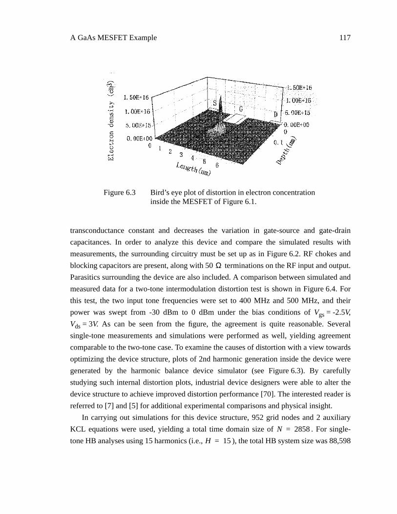
A GaAs MESFET Example 117
transconductance constant and decreases the variation in gate-source and gate-drain
capacitances. In order to analyze this device and compare the simulated results with
measurements, the surrounding circuitry must be set up as in Figure 6.2. RF chokes and
blocking capacitors are present, along with 50 terminations on the RF input and output.
Parasitics surrounding the device are also included. A comparison between simulated and
measured data for a two-tone intermodulation distortion test is shown in Figure 6.4. For
this test, the two input tone frequencies were set to 400 MHz and 500 MHz, and their
power was swept from -30 dBm to 0 dBm under the bias conditions of Vgs = -2.5V,
Vds = 3V. As can be seen from the figure, the agreement is quite reasonable. Several
single-tone measurements and simulations were performed as well, yielding agreement
comparable to the two-tone case. To examine the causes of distortion with a view towards
optimizing the device structure, plots of 2nd harmonic generation inside the device were
generated by the harmonic balance device simulator (see Figure 6.3). By carefully
studying such internal distortion plots, industrial device designers were able to alter the
device structure to achieve improved distortion performance [70]. The interested reader is
referred to [7] and [5] for additional experimental comparisons and physical insight.
In carrying out simulations for this device structure, 952 grid nodes and 2 auxiliary
KCL equations were used, yielding a total time domain size of . For single-
tone HB analyses using 15 harmonics (i.e., ), the total HB system size was 88,598
Ω
Figure 6.3 Bird’s eye plot of distortion in electron concentrationinside the MESFET of Figure 6.1.
N 2858=
H 15=

Chapter 6 Examples and Results 118
unknowns. Solution times varied from under 11 min. per HB analysis at RF source levels
less than 100mV, to about an hour near 1V. Total memory usage was 121MB.
A larger GaAs FET was analyzed under two-tone excitation to illustrate the code’s
effectiveness on large-scale problems. A two-tone RF input was applied (2GHz and
1.9GHz), with both tone magnitudes at 100mV. The device had 1406 grid points and two
auxiliary equations, for a time domain system size of . For a two-tone analysis
with , the total number of unknowns came to 932,620. Total execution time was
2hr. 8 min., with memory usage at 360MB.
6.2 Distortion Analysis of an SOI BJT
Figure 6.5 shows a Silicon-On-Insulator bipolar device, where the active region is
isolated by a 0.5µm oxide layer. While the original structure [71] has an n+ floating
collector layer underneath the vertical npn transistor at the Si-SiO2 interface, this structure
relies on the back gate (i.e. the substrate) bias to form a high electron concentration layer
at the interface. When the substrate bias is increased positively with respect to the emitter,
an electron accumulation layer is formed as shown in Figure 6.6. This high concentration
layer helps reduce the transit time for electrons to cross the collector region as is evident in
Figure 6.4 Comparison between experimental measurementsand simulated results.
N 4220=
H 110=

Distortion Analysis of an SOI BJT 119
Figure 6.7, where the cutoff frequency (fT) is plotted vesus the collector current density.
The improvement in fT is about 10% for Vsub=10V. Furthermore, as our simulation shows,
the overall distortion level in the output (i.e. collector) current is reduced by as much as
n+
n
n+p
Emitter CollectorBase
Substrate
oxide
n+ Emitterp Base
n Collector
Oxide Region
0.8 µm
0.5 µm
VSUB
VE VB VC
1.7 µm
n+
Figure 6.5 Power SOI BJT structure. The 3D rendering (top) is not toscale. The 2-D cross-section (bottom) is oriented such that itis consistent with subsequent contour and mesh plots.

Chapter 6 Examples and Results 120
20% when compared to zero substrate bias. The physical explanation for this reduction is
as follows.
One key contributor to distortion is the nonlinearity of the base-collector junction
capacitance, which is modulated by the large swing of the output signal. When a high
electron concentration layer is present at the Si-SiO2 interface, the potential at this layer is
essentially clamped (or “locked”), limiting the AC voltage swing across the base-collector
1e+12
1e+13
1e+14
1e+15
1e+16
1e+17
1e+18
1e+19
1e+20
0 0.1 0.2 0.3 0.4 0.5 0.6 0.7 0.8
Net Doping
Vbe=0.7V & Vce=4.0V
Vsub=80V
Vsub=10V
Distance
Con
cent
ratio
n (c
m-3
)
Figure 6.6 Formation of electron accumulation layer at the Si-SiO2 interface induced by the positive substrate bias.
0
1
2
3
4
5
6
7
8
10-10 10-9 10-8 10-7 10-6 10-5 10-4
Jcol (amps/µm)
F t (
GH
z)
Vsub=10V
Vsub=0V
Figure 6.7 Improvement in fT at Vsub = 10V (dashed line) overthat at Vsub = 0V (solid line).

Distortion Analysis of an SOI BJT 121
junction. This phenomenon causes a reduction in the distortion levels present throughout
the transistor.
0 0.2 0.4 0.6 0.8 1 1.2 1.4 1.6
x 10−4
0
1
2
3
4
5
6
7
8x 10
−5 Log of 2nd Harmonic Distortion in Electron Conc.
0
0.5
1
1.5x 10⁻⁴
0
2
4
6
8
x 10−5
0
5
10
15
Log of 2nd Harmonic Distortion in Electron Conc.
Figure 6.10 Logarithmic contour (left) and perspective (right) plots forthe 2nd harmonic of electron concentration.
0 0.2 0.4 0.6 0.8 1 1.2 1.4 1.6
x 10−4
0
1
2
3
4
5
6
7
8x 10
−5 2nd Harmonic Distortion in Potential
0
0.5
1
1.5x 10⁻⁴
0
2
4
6
8
x 10−5
0
0.5
1
1.5
2
2nd Harmonic Distortion in Potential
Figure 6.11 Logarithmic contour (left) and perspective (right) plots forthe 2nd harmonic of electrostatic potential.

Chapter 6 Examples and Results 122
The grid size for simulating this device was 1190 nodes. An one-tone
simulation at a 50mV drive level with a base-emitter bias of 0.7V took 52 min. and 150
MB of RAM. The total number of unknowns for this simulation was 110,670. For a two-
tone intermodulation distortion analysis with 20mV tones and , the total number
−20 −10 0 10 20 30 400.145
0.15
0.155
0.16
0.165
0.17
0.175
0.18
0.185
Vsub (V)
HD
2
Figure 6.8 Harmonic distortion in collector current as afunction of substrate bias.
0 1 2 3 4 5 6 7 8 9 10
x 109
0
10
20
30
40
50
60
70
80
90
100
Hz
dB
Collector Current Spectrum
0 5 10 15
x 109
0
10
20
30
40
50
60
70
80
90
100
Hz
dB
Collector Current Spectrum
Figure 6.9 Collector current spectrum for one-tone (left) and two-tone (right)simulations.
H 15=
H 90=

A High-Q Single-BJT Mixer Example 123
of unknowns was 646,170, the run-time was 3hr. 32 min., and the memory usage was 305
MB. Figure 6.8 shows the 2nd harmonic distortion as a function of substrate bias, while
Figure 6.9 shows spectral plots of the collector current for both the one- and two-tone
simulations. As in the GaAs MESFET example of the preceding section, we note that the
simulator can compute harmonic distributions of fundamental variables inside the device.
As an illustration, plots of the 2nd harmonic of electron concentration (Figure 6.10) and
electrostatic potential (Figure 6.11) are shown. In the hands of an experienced device
designer, such information can help to identify the origins of distortion, and assist in
improving the device design.
6.3 A High-Q Single-BJT Mixer Example
A single-BJT mixer circuit is taken directly from [69], p. 445. The configuration is
shown in Figure 6.12 of this paper. The goal of the mixer circuit is to downconvert a 500.1
MHz RF signal down to a 100 kHz IF, using a 500 MHz LO. A resonant RLC circuit
having Q= is used (R = 15 k , C = 66.667 nF, L = 37.995 H). The resonant
Figure 6.12 A single-device BJT mixer. The resonantcircuit at the output is tuned to either thesum or the difference frequency of the LOand RF, depending on the application.
VCC
VRFVLO
VDC
RL C
Vout
2π100 Ω µ

Chapter 6 Examples and Results 124
frequency is 100 kHz, and the high Q effectively filters out the IF-band distortion
products. The voltage source parameters used are , ,
at 500.1 MHz, and at 500 MHz. A silicon BJT from [72]
was employed, resulting in a total (DC) system size of . A harmonic balance
analysis at frequencies was carried out, for a total harmonic balance problem
size of . The simulation required 64 min. and 219 MB of RAM.
The results are presented in Figure 6.13. Only the relevant baseband portions of the
spectrum are shown in the figure, due to the very large differential in the frequencies
present. The large levels of distortion present in the BJT’s collector current are effectively
filtered out using the RLC resonator. Consequently, the 200 kHz distortion component is
over 70 dB down relative to the desired IF signal at 100 kHz. The distortion level could be
further reduced by using a resonator with a higher Q, or by reducing the relatively high RF
drive level.
6.4 An LDMOS Device for RF Applications
There has been growing interest in the use of silicon MOS transistors, and in particular
laterally-diffused (LDMOS) devices, for RF power amplification. Rotella has performed
VCC 10V= VDC 0.7V=
VRF 0.05V= VLO 0.15V=
N 2114=
H 110=
2H 1+( ) N 467 194,=
Figure 6.13 Baseband spectrum of the collector current (left) and outputvoltage (right). Note the suppression of distortion componentsby the resonant circuit in the output waveform.
0 1 2 3 4 5 6 7 8 9 10
x 105
10−12
10−11
10−10
10−9
10−8
10−7
10−6
10−5
freq (Hz)
Ic (
Am
ps/
um
)
0 1 2 3 4 5 6 7 8 9 10
x 105
10−8
10−7
10−6
10−5
10−4
10−3
10−2
10−1
100
101
102
freq (Hz)
Vo
ut
(V)

An LDMOS Device for RF Applications 125
Figure 6.14 LDMOS device cross-section (top) and itssimulated-vs-measured gain/PAE curves (bottom).
Chapter 6 Examples and Results 126
detailed harmonic balance PISCES simulations of an RF LDMOS device [6]. The
transistor cross-section and parasitic packaging components, along with a comparison of
the simulated vs. measured results, are shown in Figure 6.14. Several unique features are
incorporated into the structure to improve the RF and power performance characteristics
of the device [5]. Among these is a laterally diffused, graded channel that enhances the RF
performance through a drift region and prevents punch-through, thus increasing the
device’s transconductance. A p+ sinker, not shown in the figure but modeled by a side
contact to the device for simulation purposes, connects the source and substrate together
to eliminate extra bonding wires. An n-type LDD region decreases the electric field at the
drain end of the channel, and improves BVdss and Cdg.
For accurate RF simulation, proper modeling of parasitic components such as gate/
source resistances and interconnect capacitances can be as important as the modeling of
the intrinsic device structure itself. The comparison between simulated and measured
power gain and power added efficiency in Figure 6.14 shows a reasonable level of
agreement, especially considering the sensitivity of the results to parasitic components. A
detailed discussion of all the results is beyond the scope and aim of the present section; for
a more thorough treatment which includes the effect of device parameters on RF
performance, the interested reader is referred to [6] and [5].
6.5 Summary
This chapter has presented several examples in order to demonstrate the simulator’s
applicability to practical problems, and to give the reader an indication of the kinds of
computing resource requirements needed by the code. Below, we present a table
summarizing the results. Due to the proprietary nature of the LDMOS example, the
PISCES input deck for the device was not available to the author, and thus the benchmarks
for the example are not supplied below.

Summary 127
ExampleGrid
Nodes
KCL
EqnsH
TotalSize
CPU Time RAM
GaAsFET (50mV) (medium-size grid)
952 2 15 88,598 6min 40sec 121MB
GaAsFET (100mV) (medium-size grid)
952 2 15 88,598 8min 27 sec 121MB
GaAsFET (100mV)(large grid)
1406 2 110 932,620 1hr 45min 360MB
SOI BJT(1-tone, 50 mV)
1190 0 15 110,670 29min 27sec 150MB
SOI BJT(2-tone, 20mV)
1190 0 90 646,170 3hr 10min 305MB
High-Q mixer(2-tone,
0.15V LO, 0.05 V RF)
704 2 110 467,194 64min 11sec 219MB
Table 6.1 Summary of simulation results for the examples of Chapter 6.

Chapter 6 Examples and Results 128

129
Chapter 7
Conclusion
7.1 Summary
The primary goal of this work was to develop algorithms for practical two-
dimensional device-level harmonic balance simulation, and to implement these algorithms
in a prototype code based on the PISCES-II simulator. Recent advances in large-scale
harmonic balance circuit simulation provide an excellent starting point for solving the
corresponding problem at the device level. However, the size, structure, and density of the
semiconductor device Jacobian necessitates development of special-purpose techniques
for solving device-level harmonic balance problems, particularly in the multi-tone case.
The algorithms presented in this work are geared towards enabling physics-based HB
device simulation on ordinary mid-range workstations. The prototype code developed
during the course of this research has been successfully applied to a number of device
structures from both industrial and academic sources, and has shown itself to be a
practical tool for investigating large signal distortion effects at the physical level.
The primary contributions of this work can be summarized as follows:
• A practical harmonic balance device simulator was developed based on the
PISCES-II code. To our knowledge, this is the first true harmonic balance based
semiconductor device simulation tool. All of the standard PISCES models and
Chapter 7 Conclusion 130
features are available — the HB analysis extension places no additional restrictions
on the device being simulated.
• Krylov subspace techniques were applied to solve the large-scale systems of
equations that arise in HB device simulation. An investigation of the various
Krylov subspace solver variants showed that GMRES was superior to the
alternatives in the context of semiconductor device simulation.
• A sectioned preconditioner was developed to cope with device-level multi-tone
distortion analyses. The preconditioner provides dramatic reductions in memory
usage when compared to the block-diagonal preconditioners commonly employed
in circuit-level harmonic balance simulators.
• Techniques for reducing memory usage associated with storage of the HB Jacobian
representation were developed.1
• One unique advantage of harmonic balance device simulation is the availability of
internal state variables within the device structure. Plots of distortion in internal
device quantities such as electrostatic potential, free carrier concentration, and
conduction and displacement current densities have been presented in the course of
this research for various device structures.
7.2 Future Work
Several areas of investigation should be pursued in the future to improve on the
algorithms presented in this work, and to maximize the benefits of device-level HB
analysis. Further research is suggested in the following areas:
• Better preconditioners, particularly in the high-distortion regime, need to be
developed.
• Currently, the harmonic balance truncation orders are specified by the user. Ideally,
the simulator should adjust the truncation scheme during the course of a simulation
to provide sufficient accuracy.
1. These techniques were also independently developed by other groups working in the area of cir-cuit simulation.

Future Work 131
• Although the spectral content of internal device quantities has been plotted, and in
some cases used by industrial device designers to optimize transistor structure, the
physical insight provided by the distortion plots is not fully understood. Future
work by device designers to exploit this information is called for.
• A parallel version of the simulator would speed simulation times considerably, as
most of the time-consuming operations used by the code are readily parallelizable.
• Multiple device capability, particularly in the context of a parallel version of the
code, would be useful for physics-based simulation of designs that require a small
number of physically modeled transistors simulated in conjunction with circuit-
based compact models.

Chapter 7 Conclusion 132

133
References
[1] B. Troyanovsky, F. Rotella, Z. Yu, R. W. Dutton, and T. Arnborg, ‘‘Efficient multi-tone harmonic balance simulation of semiconductor devices in the presence oflinear high-Q circuitry,’’ Proc. SASIMI ’97, Dec. 1997.
[2] B. Troyanovsky, F. Rotella, Z. Yu, R. W. Dutton, and J. Sato-Iwanaga, ‘‘Largesignal analysis of RF/microwave devices with parasitics using harmonic balancedevice simulation,’’ Proc. SASIMI ’96, Nov. 1996.
[3] B. Troyanovsky, Z. Yu, L. So, and R. W. Dutton, ‘‘Relaxation-based harmonicbalance technique for semiconductor device simulation,” Proc. IEEE/ACMInternational Conf. on Computer-Aided Design, pp. 700-703, Nov. 1995.
[4] B. Troyanovsky, Z. Yu, and R. W. Dutton, “Large signal frequency domain deviceanalysis via the harmonic balance technique,” Simulation of SemiconductorDevices and Processes, Vol. 6, pp.114-117, Sep. 1995.
[5] R. W. Dutton, B. Troyanovsky, Z. Yu, T. Arnborg, F. Rotella, G. Ma, and J. Sato-Iwanaga, ‘‘Device simulation for RF applications,’’ to appear in Proc. IEDM, Dec.1997.
134
[6] F. M. Rotella, B. Troyanovsky, Z. Yu, R. W. Dutton, and G. Ma, “Harmonicbalance device analysis of an LDMOS RF power amplifier with parasitics andmatching network,” Proc. SISPAD `97, p. 157, Sept. 1997.
[7] J. Sato-Iwanaga, K. Fujimoto, H. Masato, Y. Ota, K. Inoue, B. Troyanovsky, Z. Yu,and R. W. Dutton, ‘‘Distortion analysis of GaAs MESFETs based on physicalmodel using PISCES-HB,’’ Proc. IEDM, pp. 163-166, Dec. 1996.
[8] R. W. Dutton, B. Troyanovsky, Z. Yu, E.C. Kan, K. Wang, T. Chen, and T.Arnborg, “TCAD for analog circuit applications: virtual devices and instruments,”Proc. IEEE International Solid-State Circuits Conference, pp. 78-79, 422, Feb.1996.
[9] R. W. Dutton, Z. Yu, F. Rotella, S. Beebe, B. Troyanovsky, and L. So, ‘‘Virtualinstruments for development of high performance circuit technologies,’’ Proc. ofthe IEEE Custom Integrated Circuits Conference, pp. 225-228, May 1995.
[10] M. R. Pinto, C. S. Rafferty, and R. W. Dutton, “PISCES II: Poisson and continuityequation solver,” Stanford Electronics Lab., Tech. Report, Sept. 1984.
[11] Z. Yu, D. Chen, L. So, and R.W. Dutton, PISCES-2ET --- Two-DimensionalDevice Simulation for Silicon And Heterostructures, Stanford University, 1994.
[12] L. W. Nagel, SPICE2: A Computer Program to Simulate Semiconductor Circuits,Ph. D. Thesis, University of California at Berkeley, May 1975.
[13] Hewlett-Packard Microwave Design System (MDS), Hewlett-Packard Co.,Santa Rosa, CA.
[14] D. L. Scharfetter and H. K. Gummel, ‘‘Large-signal analysis of a Silicon Readdiode oscillator,’’ IEEE Transactions on Electron Devices, vol. ED-16, pp. 66-77,1969.
[15] B. Troyanovsky, N. Chang, and R. Dowell, ‘‘Integration of Transient S-ParameterSimulation Into HPSPICE,’’ Proc. of the 1994 Design Technology Conference,pp. 231-236, May 1994.
[16] S. Ramo, J. R. Whinnery, and T. Van Duzer, Fields and Waves in CommunicationElectronics, 2nd ed. New York: Wiley, 1984.
[17] G. Massobrio and P. Antognetti, Semiconductor Device Modeling with SPICE, 2nded., New York: McGraw-Hill, 1993.

135
[18] L. C. de Vreede, H. C. de Graaff, K. Mouthaan, M. de Kok, J. L. Tauritz, and R. G.Baets, ‘‘Advanced modeling of distortion effects in bipolar transistors using theMEXTRAM model,’’ IEEE Journal on Solid-State Circuits, vol. 31, pp. 114-121,Jan. 1996.
[19] R. E. Bank, W. M. Coughran, W. Fichtner, E. H. Grosse, D. J. Rose, and R. K.Smith, ‘‘Transient simulation of silicon devices and circuits,’’ IEEE Transactionson Electron Devices, vol. 32, pp. 1992-2007, Oct. 1985.
[20] A. Brambilla and D. D’Amore, ‘‘The simulation errors introduced by the SPICEtransient analysis,’’ IEEE Transactions on Circuits and Systems — I: FundamentalTheory and Applications, vol. 40, pp. 57-60, Jan. 1993.
[21] M. S. Nakhla and J. Vlach, ‘‘A piecewise harmonic balance technique fordetermination of the periodic response of nonlinear systems,’’ IEEE Transactionson Circuits and Systems, vol. 23, pp. 85-91, Feb. 1976.
[22] K. S. Kundert and A. Sangiovanni-Vincentelli, ‘‘Simulation of nonlinear circuitsin the frequency domain,’’ IEEE Transactions on Microwave Theory andTechniques, vol. 5, pp. 521-535, Oct. 1986.
[23] M. H. Protter and C. B. Morrey, A First Course in Real Analysis, New York:Springer-Verlag, 1977.
[24] J. Ortega and W. Rheinboldt, Iterative Solution of Nonlinear Equations in SeveralVariables, Orlando: Academic Press, 1970.
[25] K. S. Kundert, ‘‘Accurate Fourier analysis for circuit simulators,’’ Proc. of theIEEE Custom Integrated Circuits Conference, pp. 25-28, May 1994.
[26] D. Hente and R.H. Jansen, ‘‘Frequency domain continuation method for theanalysis and stability investigation of nonlinear microwave circuits,’’ IEEProceedings, part H, vol. 133, no.5, pp. 351-362, Oct. 1986.
[27] K. S. Kundert, J.K. White, and A. Sangiovanni-Vincentelli, Steady-State Methodsfor Simulating Analog and Microwave Circuits, Kluwer Academic Publishers,1990.
[28] V. D.Hwang and T. Itoh, ‘‘Waveform-balance method for nonlinear MESFETamplifier simulation,’’ IEEE 1989 MTT-S International Microwave SymposiumDigest, June 1989.

136
[29] V. Rizzoli and A. Neri, ‘‘State of the art and present trends in nonlinear microwaveCAD techniques,’’ IEEE Transactions on Microwave Theory and Techniques, vol.36, pp. 343-365, Feb. 1988.
[30] V. Rizzoli, C. Cecchetti, A. Lipparini, and F. Mastri, ‘‘General-purpose harmonicbalance analysis of nonlinear microwave circuits under multitone excitation,’’IEEE Transactions on Microwave Theory and Techniques, pp. 1650-1659, Dec.1988.
[31] R. B. Bracewell, The Fourier Transform and Its Applications, 2nd ed., New York:McGraw-Hill, 1986.
[32] P. L. Heron and M. B. Steer, ‘‘Jacobian calculation using the multidimensionalFast Fourier Transform in the harmonic balance analysis of nonlinear circuits,’’IEEE Transactions on Microwave Theory and Techniques, vol. 38, pp. 429-431,April 1990.
[33] T. S. Parker and L. O. Chua, Practical Numerical Algorithms for Chaotic Circuits,New York: Springer-Verlag, 1989.
[34] L. O. Chua and P. M. Lin, Computer-Aided Analysis of Electronic Circuits:Algorithms and Computational Techniques, Englewood Cliffs, N.J.: Prentice-Hall,1975.
[35] C. Ho, A. Ruehli, and P. A. Brennan, ‘‘The modified nodal approach to networkanalysis,’’ IEEE Transactions on Circuits and Systems, vol. CAS-32, pp. 504-509,June 1975.
[36] G. D. Hachtel, R. K. Brayton, and F. G. Gustafson, ‘‘The sparse tableau approachto network analysis and design,’’ IEEE Transacations on Circuit Theory, vol. CT-18, pp. 101-113, Jan. 1971.
[37] K. S. Kundert, ‘‘Sparse matrix techniques,’’ in Circuit Analysis, Simulation, andDesign, North-Holland Publishing, pp. 281-324, 1986.
[38] P. Heikkila, M. Valtonen, and T. Veijola, ‘‘Harmonic balance of nonlinear circuitswith multitone excitation,’’ Proc. of the 10th European Conference on CircuitTheory and Design, Copenhagen, Denmark, 1991.
[39] R. Melville, P. Feldmann, and J. Roychowdhury, ‘‘Efficient multi-tone distortionanalysis of analog integrated circuits,‘’ Proc. of the IEEE Custom IntegratedCircuits Conference, pp. 241-244, May 1995.
137
[40] P. Feldmann, R. Melville, and D. Long, ‘‘Efficient frequency domain analysis oflarge nonlinear analog circuits,‘’ Proc. of the IEEE Custom Integrated CircuitsConference, pp. 461-464, May 1996.
[41] D. Long, R. Melville, K. Ashby, and B. Horton, ‘‘Full-chip harmonic balance,’’Proc. of the IEEE Custom Integrated Circuits Conference, pp. 379-382, May1997.
[42] H. G. Brachtendorf, G. Welsch, and R. Laur, ‘‘Fast simulation of the steady-stateof circuits by the harmonic balance technique,’’ Proc. of the IEEE InternationalSymposium on Circuits and Systems, pp. 1388-1391, May 1995.
[43] H. G. Brachtendorf, G. Welsch, R. Laur, and A. Bunse-Gerstner, ‘‘Numericalsteady state analysis of electronic circuits driven by multi-tone signals,’’ ElectricalEngineering, vol. 79, pp. 103-112, April 1996.
[44] V. Rizzoli, F. Mastri, F. Sgallari, and G. Spaletta, ‘‘Harmonic balance simulation ofstrongly nonlinear very large-size microwave circuits by inexact Newtonmethods,’’ IEEE MTT-S International Microwave Symposium Digest, pp. 1357-1360, June 1996.
[45] M. R. Pinto, Comprehensive Semiconductor Device Simulation for Silicon ULSI,Ph.D. Thesis, Stanford University, Stanford, CA, Aug. 1990.
[46] Y. Saad and M.H. Schultz, ‘‘GMRES: a generalized minimal residual method forsolving nonsymmetric linear systems,’’ SIAM Journal on Scientific and StatisiticalComputing, vol. 7, pp. 856-869, July 1986.
[47] H. F. Walker, ‘‘Implementation of the GMRES method using Householdertransformations,’’ SIAM Journal on Scientific and Statisitical Computing, vol. 9,pp. 152-163, Jan. 1988.
[48] G. H. Golub and C. F. Van Loan, Matrix Computations, Baltimore: The JohnsHopkins University Press, 1996.
[49] O. Axelsson, Iterative Solution Methods, New York: Cambridge University Press,1996.
[50] Y. Saad, Iterative Methods for Sparse Linear Systems, Boston: PWS PublishingCompany, 1996.
[51] C. T. Kelley, Iterative Methods for Linear and Nonlinear Equations, Philardelphia:SIAM, 1995.

138
[52] R. S. Dembo, S. C. Eisenstat, and T. Steihaug, ‘‘Inexact Newton methods,’’ SIAMJournal on Numerical Analysis, vol. 19, pp. 400-408, April 1982.
[53] R. W. Freund and N. M. Nachtigal, ‘‘QMR: a quasi-minimal residual method fornon-Hermitian linear systems,’’ Numerische Mathematik, vol. 60, pp. 315-339,1991.
[54] R. W. Freund, ‘‘A transpose-free quasi-minimal residual algorithm for non-Hermitian linear systems,’’ SIAM Journal on Scientific and Statisitical Computing,vol. 14, pp. 470-482, March 1993.
[55] R. Barrett, M. Berry, T. F. Chan, J. Demmel, J. M. Donato, J. Dongarra, V.Eijkhout, R. Pozo, C. Romine, and H. Van der Vorst, Templates for the Solution ofLinear Systems: Building Blocks for Iterative Methods, Philadelphia: SIAM, 1994.
[56] P. N. Brown, A. C. Hindmarsh, and L. R. Petzold, ‘‘Using Krylov subspacemethods in the solution of large-scale differential-algebraic systems,’’ SIAMJournal on Scientific and Statisitical Computing, vol. 15, pp. 1467-1488, Nov.1994.
[57] S. E. Laux, ‘‘Techniques for small-signal analysis of semiconductor devices,’’IEEE Transactions on Electron Devices, vol. 32, pp. 2028-2037, Oct. 1986.
[58] B. Troyanovsky et al., ‘‘Preconditioning the harmonic balance equations,’’ inpreparation.
[59] D. Sharrit, ‘‘New Method of Analysis of Communication Systems,’’ in IEEEMicrowave Theory and Techniques Symposium WMFA: Nonlinear CAD Workshop,June 1996.
[60] D. Sharrit, ‘‘Method For Simulating a Circuit,” US Patent No. 5,588,142, grantedDec. 1996.
[61] J. F. Sevic, M. B. Steer, and A. M. Pavio, ‘‘Nonlinear Analysis Methods for theSimulation of Digital Wireless Communication Systems,’’ International Journalof Microwave and Millimeter-Wave Computer-Aided Engineering, vol. 6, pp. 197-216, May 1996.
[62] P. Feldmann and J. Roychowdhury, ‘‘Computation of waveform envelopes usingan efficient, matrix-decomposed harmonic balance algorithm,’’ Proc. of the IEEE/ACM Internation Conference on Computer-Aided Design, pp. 295-300, Nov. 1996.
[63] H. Keller, Numerical Solution of Two Point Boundary-Value Problems, SIAM,1976.

139
[64] T. J. Aprille and T. N. Trick, ‘‘Steady-state analysis for nonlinear circuits withperiodic inputs,’’ Proc. of the IEEE, pp. 108-114, Jan. 1972.
[65] R. Telichevesky, K. Kundert, and J. White, ‘‘Efficient steady-state analysis basedon matrix-free Krylov subspace methods,’’ Proc. of the 32nd Design AutomationConference, pp. 480-484, June 1995.
[66] R. Telichevesky, K. Kundert, I. Elfadel, and J. White, ‘‘Fast simulation algorithmsfor RF circuits,’’ Proc. of the IEEE Custom Integrated Circuits Conference, pp.437-444, May 1996.
[67] R. Telichevesky, K. Kundert, and J. White, ‘‘Efficient AC and noise analysis oftwo-tone RF circuits,’’ Proc. of the 33rd Design Automation Conference, pp. 292-297, June 1996.
[68] R. Telichevesky, K. Kundert, and J. White, ‘‘Receiver characterization usingperiodic small-signal analysis,’’ Proc. of the IEEE Custom Integrated CircuitsConference, pp. 449-452, May 1996.
[69] D. O. Pederson and K Mayaram, Analog Integrated Circuits for Communication,Kluwer Academic Publishers, 1991.
[70] J. Sato-Iwanaga, private communication.
[71] T. Arnborg, “Modeling and simulation of high speed, high voltage bipolar SOItransistor with fully depleted collector,” Proc. IEDM, pp. 743-746, Dec. 1994.
[72] P. Vande Voorde, D. Pettengill, and S.Y. Oh, ‘‘Hybrid simulation and sensitivityanalysis for advanced bipolar device design and process development,’’ Proc. ofthe IEEE Bipolar Circuits and Technology Meeting, pp. 114-117, Sep. 1990.
[73] Mathematica, Wolfram Research.
Related Documents


![Computational Environment for Simulating Lightning Strokes in a Power Substation … · 2012-11-02 · finite-difference time-domain method (FDTD) [1,2] and the finite element method](https://static.cupdf.com/doc/110x72/5e67c35014d9c9284352a2fa/computational-environment-for-simulating-lightning-strokes-in-a-power-substation.jpg)