Document Number: MC33395 Rev 4.0, 2/2007 Freescale Semiconductor Technical Data * This document contains certain information on a new product. Specifications and information herein are subject to change without notice. © Freescale Semiconductor, Inc., 2007. All rights reserved. ARCHIVE INFORMATION ARCHIVE INFORMATION Three-Phase Gate Driver IC The 33395 simplifies the design of high-power BLDC motor control design by combining the gate drive, charge pump, current sense, and protection circuitry necessary to drive a three-phase bridge configuration of six N-channel power MOSFETs. Mode logic is incorporated to route a pulse width modulation (PWM) or a complementary PWM output signal to either low-side or high-side MOSFETs of the bridge. Detection and drive circuitry are also incorporated to control a reverse battery protection high-side MOSFET switch. PWM frequencies up to 28 kHz are possible. Built-in protection circuitry prevents damage to the MOSFET bridge as well as the drive IC and includes overvoltage shutdown, overtemperature shutdown, overcurrent shutdown, and undervoltage shutdown. The device is parametrically specified over ambient temperature range of -40°C ≤ T A ≤ 125°C and 5.5 V ≤ V IGN ≤ 24 V supply. Features • Drives Six N-Channel Low R DS(ON) Power MOSFETs • Built-In Charge Pump Circuitry • Built-In Current Sense Comparator and Output Drive Current Limiting • Built-In PWM Mode Control Logic • Built-In Circuit Protection • Designed for Fractional to Integral HP BLDC Motors • 32-Pin SOIC Wide Body Surface Mount Package • 33395 Incorporates a <5.0 μs Shoot-Through Suppression Timer • 33395T Incorporates a <1.0 μs Shoot-Through Suppression Timer • Pb-Free Packaging Designated by Suffix Code EW Figure 1. 33395 Simplified Application Diagram THREE-PHASE GATE DRIVER IC DWB SUFFIX EW SUFFIX (Pb-FREE) 98ARH99137A 32-PIN SOICW 33395 33395T ORDERING INFORMATION Device Temperature Range (T A ) Package MC33395DWB/R2 - 40°C to 125°C 32 SOICW MC33395EW/R2 32 SOICW (Pb-Free) MCZ33395EW/R2 MC33395TDWB/R2 32 SOICW MC33395TEW/R2 32 SOICW (Pb-Free) 3 3 2 V DD V PWR MCU V DD H H H N S S N VGDH VIGN VDD CP1L CP2H CP2L CP1H CRES HSE1–3 MODE0–1 PWM AGND LSE1–3 PGND VIGNP GDH1 GDH2 GDH3 SRC1 SRC2 SRC3 GDL1 GDL2 GDL3 -ISENS +ISENS 33395

Welcome message from author
This document is posted to help you gain knowledge. Please leave a comment to let me know what you think about it! Share it to your friends and learn new things together.
Transcript

Document Number: MC33395Rev 4.0, 2/2007
Freescale Semiconductor Technical Data
AR
CH
IVE
INFO
RM
ATI
ON
AR
CH
IVE
INFO
RM
ATI
ON
Three-Phase Gate Driver ICThe 33395 simplifies the design of high-power BLDC motor control
design by combining the gate drive, charge pump, current sense, and protection circuitry necessary to drive a three-phase bridge configuration of six N-channel power MOSFETs. Mode logic is incorporated to route a pulse width modulation (PWM) or a complementary PWM output signal to either low-side or high-side MOSFETs of the bridge.
Detection and drive circuitry are also incorporated to control a reverse battery protection high-side MOSFET switch. PWM frequencies up to 28 kHz are possible. Built-in protection circuitry prevents damage to the MOSFET bridge as well as the drive IC and includes overvoltage shutdown, overtemperature shutdown, overcurrent shutdown, and undervoltage shutdown.
The device is parametrically specified over ambient temperature range of -40°C ≤ TA ≤ 125°C and 5.5 V ≤ VIGN ≤ 24 V supply.
Features• Drives Six N-Channel Low RDS(ON) Power MOSFETs• Built-In Charge Pump Circuitry• Built-In Current Sense Comparator and Output Drive Current
Limiting• Built-In PWM Mode Control Logic• Built-In Circuit Protection• Designed for Fractional to Integral HP BLDC Motors• 32-Pin SOIC Wide Body Surface Mount Package• 33395 Incorporates a <5.0 μs Shoot-Through Suppression Timer• 33395T Incorporates a <1.0 μs Shoot-Through Suppression Timer• Pb-Free Packaging Designated by Suffix Code EW
Figure 1. 33395 Simplified Application Diagram
THREE-PHASEGATE DRIVER IC
DWB SUFFIXEW SUFFIX (Pb-FREE)
98ARH99137A32-PIN SOICW
33395 33395T
ORDERING INFORMATION
Device Temperature Range (TA) Package
MC33395DWB/R2
- 40°C to 125°C
32 SOICW
MC33395EW/R2 32 SOICW(Pb-Free)MCZ33395EW/R2
MC33395TDWB/R2 32 SOICW
MC33395TEW/R2 32 SOICW(Pb-Free)
3
3
2
VDD
VPWR
MCU
VDD
H
H
H
N
S S
N
VGDHVIGNVDD
CP1L CP2H CP2L
CP1H
CRES
HSE1–3MODE0–1PWM
AGNDLSE1–3
PGND
VIGNP
GDH1GDH2
GDH3SRC1SRC2SRC3
GDL1GDL2GDL3
-ISENS
+ISENS
33395
* This document contains certain information on a new product. Specifications and information herein are subject to change without notice.
© Freescale Semiconductor, Inc., 2007. All rights reserved.

INTERNAL BLOCK DIAGRAMA
RC
HIV
E IN
FOR
MA
TIO
N
AR
CH
IVE
INFO
RM
ATI
ON
INTERNAL BLOCK DIAGRAM
Figure 2. 33395 Simplified Internal Block Diagram
Low VoltageReset
OvervoltageShutdown
Osc.
ChargePump
Drive Limiting
GateDrive
Circuits
ControlLogic
Shutdown
+-
L H
CP1HCP1LCP2HCP2L
CPRES
VGDH
GDH1
GDH2GDH3SRC1SRC2SRC3
GDL1GDL2
GDL3
VIGNP
VIGN
VDD
+ISENS
-ISENS
MODE0MODE1
PWMHSE1HSE2HSE3LSE1LSE2LSE3
AGND
PGND
LowOvervoltage
Osc.
Charge
Drive Limiting
Gate
Control
Overtemperature
+-
L H
Logic
DriveCircuits
Pump
ShutdownVoltageReset
ShutdownTEST
Analog Integrated Circuit Device Data 2 Freescale Semiconductor
33395

PIN CONNECTIONSA
RC
HIV
E IN
FOR
MA
TIO
N
AR
CH
IVE
INFO
RM
ATI
ON
PIN CONNECTIONS
Figure 3. 33395 Pin Connections Table 1. 33395 Pin Definitions
A functional description of each pin can be found in the Functional Pin Description section beginning on page 9.
Pin Number Pin Name Pin Function Formal Name Definition
1 CP2H Charge Pump Cap High potential pin connection for secondary charge pump capacitor
2 CPRES Input Charge Pump Reserve Cap
Input from external reservoir capacitor for charge pump
3 VIGN Input Input Voltage Input from ignition level supply voltage for power functions
4 VGDH Output High-Side Gate Voltage
Output full-time gate drive for auxiliary high-side power MOSFET switch
5 VIGNP Input Input Voltage Protected
Input from protected ignition level supply for power functions
6 SRC1 Sensor High-Side Sense Sense for high-side source voltage, phase 1
7 GDH1 Output Gate Drive High Output for gate high-side, phase 1
8 GDL1 Output Output for Gate Output for gate drive low-side, phase 1
9 SRC2 Sensor High-Side Sense Sense for high-side source voltage, phase 2
10 GDH2 Output Gate Drive High Output for gate high-side, phase 2
11 GDL2 Output Output for Gate Output for gate drive low-side, phase 2
12 SRC3 Sensor High-Side Sense Sense for high-side source voltage, phase 3
13 GDH3 Output Gate Drive High Output for gate drive high-side, phase 3
14 GDL3 Output Gate Drive Low Output for gate drive low-side, phase 3
15 PGND Ground Power Ground Ground pins for power functions
16 Test N/A Test Pin This should be connected to ground or left open
17 -ISENS Input IS Minus Inverting input for current limit comparator
18 +ISENS Input IS Plus Non-inverting input for current limit comparator
19 AGND Ground Analog Ground Ground pin for logic functions
20 VDD Power Logic Supply Voltage Supply voltage for logic functions
21 PWM Input Pulse Width Modulator Input for pulse width modulated driver duty cycle
CP2L1
LSE2LSE3HSE1HSE2HSE3MODE0MODE1PWMVDD
+ISENS-ISENS
AGND
LSE1
CP1HCP1L
CP2H
VIGNPSRC1GDH1GDL1SRC2GDH2GDL2SRC3GDH3
PGNDTEST
GDL3
VGDH
CPRESVIGN
8910111213141516
34567
232
252423222120191817
3029282726
31
Analog Integrated Circuit Device Data Freescale Semiconductor 3
33395

PIN CONNECTIONSA
RC
HIV
E IN
FOR
MA
TIO
N
AR
CH
IVE
INFO
RM
ATI
ON
22 MODE1 Input Mode Control Bit 1 Input for mode control selection
23 MODE0 Input Mode Control Bit 0 Input for mode control selection
24 HSE3 Input High-Side Enable Input for high-side enable logic, phase 3
25 HSE2 Input High-Side Enable Input for high-side enable logic, phase 2
26 HSE1 Input High-Side Enable Input for high-side enable logic, phase 1
27 LSE3 Input Low-Side Enable Input for low-side enable logic, phase 3
28 LSE2 Input Low-Side Enable Input for low-side enable logic, phase 2
29 LSE1 Input Low-Side Enable Input for low-side enable logic, phase 1
30 CP1L Input External Pump Capacitor
Input from external pump capacitor for charge pump and secondary pins
31 CP1H Input External Pump Capacitor
Input from external pump capacitor for charge pump and secondary pins
32 CP2L Input Charge Pump Capacitor
Input from external reservoir, external pump capacitors for charge pump, and secondary pins
Table 1. 33395 Pin Definitions (continued)A functional description of each pin can be found in the Functional Pin Description section beginning on page 9.
Pin Number Pin Name Pin Function Formal Name Definition
Analog Integrated Circuit Device Data 4 Freescale Semiconductor
33395

ELECTRICAL CHARACTERISTICSMAXIMUM RATINGS
AR
CH
IVE
INFO
RM
ATI
ON
AR
CH
IVE
INFO
RM
ATI
ON
ELECTRICAL CHARACTERISTICS
MAXIMUM RATINGS
Table 2. Maximum RatingsAll voltages are with respect to ground unless otherwise noted.
Rating Symbol Value Unit
VIGN Supply Voltage VIGN -15.5 to 40 VDC
VIGNP Load Dump Survival VIGNPLD -0.3 to 65 VDC
VDD Logic Supply Voltage (Fail Safe) VDD -0.3 to 7.0 VDC
Logic Input Voltage (LSEn, HSEn, PWM, and MODEn) VIN 0.3 to 7.0 VDC
Start Up Current VIGNP IVIGNSTARTUP 100 mA
ESD Voltage (1)
Human Body Model Machine Model
VESD1
VESD2
±500±200
V
Storage Temperature TSTG -65 to 160 °C
Operating Ambient Temperature TA -40 to 125 °C
Operating Case Temperature TC -40 to 125 °C
Maximum Junction Temperature TJ 150 °C
Power Dissipation (TA = 25°C) PD 1.5 W
Peak Package Reflow Temperature During Reflow (2), (3) TPPRT Note 3 °C
Thermal Resistance, Junction-to-Ambient RΘJA 65 °C/ W
Notes1. ESD1 testing is performed in accordance with the Human Body Model (CZAP = 100 pF, RZAP = 1500 Ω), ESD2 testing is performed in
accordance with the Machine Model (CZAP = 200 pF, RZAP = 0 Ω).2. Pin soldering temperature limit is for 10 seconds maximum duration. Not designed for immersion soldering. Exceeding these limits may
cause malfunction or permanent damage to the device.3. Freescale’s Package Reflow capability meets Pb-free requirements for JEDEC standard J-STD-020C. For Peak Package Reflow
Temperature and Moisture Sensitivity Levels (MSL), Go to www.freescale.com, search by part number [e.g. remove prefixes/suffixes and enter the core ID to view all orderable parts. (i.e. MC33xxxD enter 33xxx), and review parametrics.
Analog Integrated Circuit Device Data Freescale Semiconductor 5
33395

ELECTRICAL CHARACTERISTICSSTATIC ELECTRICAL CHARACTERISTICS
AR
CH
IVE
INFO
RM
ATI
ON
AR
CH
IVE
INFO
RM
ATI
ON
STATIC ELECTRICAL CHARACTERISTICS
Table 3. Static Electrical Characteristics Characteristics noted under conditions -40°C ≤ TA ≤ 125°C, 5.5 V ≤ VIGNP ≤ 24 V unless otherwise noted. Typical values reflect
approximate parameter mean at TA = 25°C under normal conditions unless otherwise noted.
Characteristic Symbol Min Typ Max Unit
POWER INPUT
VIGN Current @ 5.5 V – 24 V, VDD = 5.5 V IIGN – 0.2 1.0 mA
VIGNP Current @ 5.5 V – 24 V, VDD = 5.5 V IIGNP – – 100 mA
VIGNP Overvoltage Shutdown VIGNPSD 25 33 36.5 V
VIGNP Voltage VIGNP 5.5 – 24 V
VDD Current @ 5.5 VDC, 5.5 V ≤ VIGNP ≤ 24 V IVDD – 1.8 4.0 mA
VDD Low-Voltage Reset Level VDD(RESET) 2.5 3.2 4.0 V
VDD One-Time Fuse (Logic Supply) – 7.0 – – V
INPUT / OUTPUT
Input Current at VDD = 5.5 VLSEn, HSEn, PWM, and MODEn = 3.0 V
IIN5.0 12 25
μA
Input Threshold at VDD = 5.5 V
LSEn, HSEn, PWM, and MODEn (4)
VTH
1.0 2.0 3.0V
VSCRn Source Sense VoltageSRC1, SRC2, SRC3
VSCRn-0.3 VIGNP 24
V
Comparator Input Offset Voltage VINP(OFFSET) 5.0 14 20 mV
Comparator Input Bias Current VINP(BIAS) -500 -170 500 nA
Comparator Input Offset Current IINP(OFFSET) -300 -3.0 300 nA
Common Mode Voltage (5) VCMR 0 – VDD - 2.0 VDC
Comparator Differential Input Voltage (5) VINPdiff -VDD – +VDD V
Charge Pump Voltage VIGN (6)
VIGNP = 5.5 V, ICRES = 1.0 mA
VIGNP = 9.0 V, ICRES = 1.0 mA
VIGNP = 12 V, ICRES = 5.0 mA
VIGNP = 24 V, ICRES = 1.0 mA
VIGNP = 24 V, ICRES = 5.0 mA
VCRES - VIGNP
4.04.04.58.04.5
6.07.5101612
1818181818
V
VGDH Output Voltage with GDHn in ON StateVIGNP = 5.5 V, IGDHn = 1.0 mA
VIGNP = 12 V, IGDHn = 5.0 mA
VIGNP = 24 V, IGDHn = 5.0 mA
VGDHn(on) - V SRCn
4.04.04.5
5.29.011
181818
V
VGDH Output Voltage with GDHn in OFF StateVIGNP = SRCn = 14 V, IGDHn = 1.0 mA
VGDHn(off)-1.0 0.6 1.0
V
Notes4. Logic inputs LSEn, HSEn, PWM, and MODEn have internal 20 μA internal sinks.5. Guaranteed by design and characterization. Not production tested.6. The Charge Pump has a positive temperature coefficient. Therefore the Min’s occur at -40°C, Typ’s at 25°C, and Max’s at 125°C.
Analog Integrated Circuit Device Data 6 Freescale Semiconductor
33395

ELECTRICAL CHARACTERISTICSSTATIC ELECTRICAL CHARACTERISTICS
AR
CH
IVE
INFO
RM
ATI
ON
AR
CH
IVE
INFO
RM
ATI
ON
33395
INPUT / OUTPUT (CONTINUED)
VGDL Low-Side Output Voltage GDHn in ON StateVIGNP = 5.5 V, IGDLn = 1.0 mA
VIGNP = 12 V, IGDLn = 5.0 mA
VIGNP = 24 V, IGDLn = 0.0 mA
VIGNP = 24 V, IGDLn = 5.0 mA
VGDL(on)
5.08.08.08.0
8.0141716
18181919
V
VGDL Output Voltage GDHn in OFF StateVIGNP = 14 V, IGDLn = 1.0 mA
VGDL(off)
-1.0 0.3 1.0V
Thermal Shutdown (7) TLIM 160 – 190 °C
Notes7. Guaranteed by design and characterization. Not production tested.
Table 3. Static Electrical Characteristics (continued)Characteristics noted under conditions -40°C ≤ TA ≤ 125°C, 5.5 V ≤ VIGNP ≤ 24 V unless otherwise noted. Typical values reflect
approximate parameter mean at TA = 25°C under normal conditions unless otherwise noted.
Characteristic Symbol Min Typ Max Unit
Analog Integrated Circuit Device Data Freescale Semiconductor 7

ELECTRICAL CHARACTERISTICSDYNAMIC ELECTRICAL CHARACTERISTICS
AR
CH
IVE
INFO
RM
ATI
ON
AR
CH
IVE
INFO
RM
ATI
ON
DYNAMIC ELECTRICAL CHARACTERISTICS
TIMING DIAGRAM
Figure 4. Shoot-Through Suppression
Table 4. Dynamic Electrical CharacteristicsCharacteristics noted under conditions -40°C ≤ TA ≤ 125°C, 5.5 V ≤ VIGNP ≤ 24 V unless otherwise noted. Typical values
reflect approximate parameter mean at TA = 25°C under normal conditions unless otherwise noted.
Characteristic Symbol Min Typ Max Unit
High-Side (GDHn) and Low-Side Drivers (GDHn) Rise Time
(25% to 75%), CISS Value = 2000 pF (8)
t RH – 0.35 1.5
μs
High-Side (GDHn) and Low-Side Drivers (GDHn) Fall Time
(75% to 25%), CISS Value = 2000 pF (8)
t FH
– 0.25 1.5μs
Shoot-Through Suppression Time Delay (33395) (8), (9)
3339533395T
t D1, t D2
1.00.2
3.00.65
5.51.0
μs
Current Limit Time Delay (10) t ILIMDELAY 1.5 2.8 5.0 μs
Notes8. See Figure 4, page 8.9. Shoot-Through Suppression Time Delay is provided to prevent directly connected high- and low-side MOSFETs from being on
simultaneously.10. Current Limit Time Delay: The internal comparator places the device in the current limit mode when the comparator output goes LOW
and sets an internal logic bit. This takes a finite amount of time and is stated as the Current Limit Time Delay.
100
75
25
0
100
75
25
0
tRH tFH
tFL tRL
TIME
GD
Ln, G
ate
V (%
)G
DH
nS
RC
n (%
)
tD2tD1
Analog Integrated Circuit Device Data 8 Freescale Semiconductor
33395

FUNCTIONAL DESCRIPTIONINTRODUCTION
AR
CH
IVE
INFO
RM
ATI
ON
AR
CH
IVE
INFO
RM
ATI
ON
33395
FUNCTIONAL DESCRIPTION
INTRODUCTION
The 33395 and 33395T devices are designed to provide the necessary drive and control signal buffering and amplification to enable a DSP or MCU to control a three-phase array of power MOSFETs such as would be required to energize the windings of powerful brushless DC (BLDC)
motors. It contains built-in charge pump circuitry so that the MOSFET array may consist entirely of N-Channel MOSFETs. It also contains feedback sensing circuitry and control circuitry to provide a robust overall motor control design.
FUNCTIONAL PIN DESCRIPTION
CHARGE PUMP CAPACITOR (CP2H)High potential pin connection for secondary charge pump
capacitor
CHARGE PUMP RESERVE CAPACITOR (CPRES)Input from external reservoir capacitor for charge pump
INPUT VOLTAGE (VIGN)Input from ignition level supply voltage for power functions
HIGH-SIDE GATE VOLTAGE (VGDH)Output full-time gate drive for auxiliary high-side power
MOSFET switch
INPUT VOLTAGE PROTECTED (VIGNP)Input from protected ignition level supply for power
functions
HIGH-SIDE SENSE (SRC1, SRC2, SRC3)Sense for high-side source voltage, phase 1/2/3
GATE DRIVE HIGH (GDH1, GDH2, GDH3)Output for gate high-side, phase 1/2/3
OUTPUT FOR GATE (GDL1, GDL2, GDL3)Output for gate drive low-side, phase 1
POWER GROUND (PGND)Ground pins for power functions
TEST PIN (TEST)This should be connected to ground or left open
IS MINUS (-ISENS)Inverting input for current limit comparator
IS PLUS (+ISENS)Non-Inverting input for current limit comparator
ANALOG GROUND (AGND)Ground pin for logic functions
LOGIC SUPPLY VOLTAGE (VDD)Supply voltage for logic functions
PULSE WIDTH MODULATOR (PWM)Input for pulse width modulated driver duty cycle
MODE CONTROL BIT 1 (MODE1)Input for mode control selection
MODE CONTROL BIT 0 (MODE0)Input for mode control selection
HIGH-SIDE ENABLE (HSE3, HSE2, HSE1)Input for high-side enable logic, phase 1/2/3
LOW-SIDE ENABLE (LSE3, LSE2, LSE1)Input for low-side enable logic, phase 1/2/3
EXTERNAL PUMP CAPACITOR (CP1L, CP1H)Input from external pump capacitor for charge pump and
secondary pins
CHARGE PUMP CAPACITOR (CP2L)Input from external reservoir, external pump capacitors for
charge pump, and secondary pins
Analog Integrated Circuit Device Data Freescale Semiconductor 9

FUNCTIONAL DESCRIPTIONFUNCTIONAL INTERNAL BLOCK DESCRIPTION
AR
CH
IVE
INFO
RM
ATI
ON
AR
CH
IVE
INFO
RM
ATI
ON
33395
FUNCTIONAL INTERNAL BLOCK DESCRIPTION
GATE DRIVE CIRCUITS The gate drive outputs (GDH1, GDH2, etc.) supply the
peak currents required to turn ON and hold ON the MOSFETs, as well as turn OFF and hold OFF the MOSFETs.
CHARGE PUMPThe current capability of the charge pump is sufficient to
supply the gate drive circuit’s demands when PWMing at up to 28 kHz. Two external charge pump capacitors and a reservoir capacitor are required to complete the charge pump’s circuitry.
Charge reservoir capacitance is a function of the total MOSFET gate charge (QG) gate drive voltage level relative to the source (VGS) and the allowable sag of the drive level during the turn-on interval (VSAG). CRES can be expressed by the following formula:
For example, for QG = 60 nC, VGS = 14 V, VSAG = 0.2 V:
Proper charge pump capacitance is required to maintain, and provide for, adequate gate drive during high demand turn-ON intervals. Use the following formula to determine values for CP1 and CP2:
For example, for the above determination of CRES = 0.15 μF:
By averaging these two values, the proper CPn value can be determined:
CP1 and CP2 =(0.0075 μF + 0.015 μF) ÷ 2 = 0.01 μF
THERMAL SHUTDOWN FUNCTIONThe device has internal temperature sensing circuitry
which activates a protective shutdown function should the die reach excessively elevated temperatures. This function effectively limits power dissipation and thus protects the device.
OVERVOLTAGE SHUTDOWN FUNCTIONWhen the supply voltage (VIGN) exceeds the specified
over- voltage shutdown level, the part will automatically shut down to protect both internal circuits as well as the load. Operation will resume upon return of VIGN to normal operating levels.
LOW VOLTAGE RESET FUNCTIONWhen the logic supply voltage (VDD) drops below the
minimum voltage level or when the part is initially powered up, this function will turn OFF and hold OFF the external MOSFETs until the voltage increases above the minimum voltage level required for normal operation.
CONTROL LOGICThe control logic block controls when the low-side and
high-side drivers are enabled. The logic implements the Truth Table found in the specification and monitors the M0, M1, PWM, CL, OT, OV, LSE, and HSE pins. Note that the drivers are enabled 3 μs after the PWM edge. During complimentary chop mode the high-side and low-side drives are alternatively enabled and disabled during the PWM cycle. To prevent shoot-through current, the high-side drive turn-on is delayed by tD1, and the low-side drive turn on is delayed by tD2 (see Figure 4, page 8).
Note that the drivers are disabled during an overtemperature or overvoltage fault. A flip-flop keeps the drive off until the following PWM cycle. This prevents erratic operation during fault conditions. The current limit circuit also uses a flip-flop for latching the drive off until the following PWM cycle.
Note PWM must be toggled after POR, Thermal Limit, or overvoltage faults to re-enable the gate drivers.
VGDHThe VGDH pin is used to provide a gate drive signal to a
reverse battery protection MOSFET. If reverse battery protection is desired, VIGN would be applied to the source of an external MOSFET, and the drain of the MOSFET would then deliver a "protected" supply voltage (VIGNP) to the three phase array of external MOSFETs as well as the supply voltage to the VIGNP pin of the IC.
In a reverse polarity event (e.g., an erroneous installation of the system battery), the VGDH signal will not be supplied to the external protection MOSFET, and the MOSFET will remain off and thus prevent reverse polarity from being applied to the load and the VIGNP supply pin of the IC.
HIGH-SIDE GATE DRIVE CIRCUITSOutputs GDH1, GDH2, and GDH3 provide the elevated
drive voltage to the high-side external MOSFETs (HS1, HS2, and HS3; see Figure 5, page 13). These gate drive outputs supply the peak currents required to turn ON and hold ON the high-side MOSFETs, as well as turn OFF the MOSFETs. These gate drive circuits are powered from an internal charge pump, and therefore compensate for voltage dropped across the load that is reflected to the source-gate circuits of the high-side MOSFETs.
LOW-SIDE GATE DRIVE CIRCUITSOutputs GDL1, GDL2, and GDL3 provide the drive voltage
to the low-side external MOSFETs (LS1, LS2, and LS3; see
CRES = QG x VGS
2 x VGS x VSAG - VSAG2
CRES = (60 nC) x (14 V)2 x (14 V) x (0.2 V) - (0.2)2
= 0.15 μF
CRES
20< CP1 = CP2 <
10CRES
0.15 μF20
= 0.075 μF, lower limit; and 10
0.15 μF = .015 μF, upper lim
Analog Integrated Circuit Device Data 10 Freescale Semiconductor

FUNCTIONAL DESCRIPTIONFUNCTIONAL INTERNAL BLOCK DESCRIPTION
AR
CH
IVE
INFO
RM
ATI
ON
AR
CH
IVE
INFO
RM
ATI
ON
33395
Figure 5). These gate drive outputs supply the peak currents required to turn ON and hold ON the low-side MOSFETs, as well as turn OFF the MOSFETs.
VDD FUSEThe VDD supply of the 33395 IC has an internal fuse, which
will blow and set all outputs of the device to OFF, if the VDD voltage exceeds that stated in the maximum rating section of the data sheet. When this fuse blows, the device is permanently disabled.
ISENS INPUTSThe +Isens and -Isens pins are inputs to the internal
current sense comparator. In a typical application, these would receive a a low-pass filtered voltage derived from a current sense resistor placed in series with the ground return of the three-phase output bridge. When triggered by the comparator, the CL (current limit) bit of the internal error register is set, and the output gate drive pairs (i.e., GDH1 and GDL1, GDH2 and GDL2, GDH3 and GDL3), are controlled such that current will cease flowing through the load (refer to Table 5, Truth Table, page 12).
OVERTEMPERATURE AND OVERVOLTAGE SHUTDOWN CIRCUITS
Internal monitoring is provided for both over temperature conditions and over voltage conditions. When any of these conditions presents itself to the IC, the corresponding internally set bits of the error register are set, and the output gate drive pairs (i.e., GDH1 and GDL1, GDH2 and GDL2, GDH3 and GDL3), are controlled such that current will cease flowing through the load (refer to Table 5).
LSE AND HSE INPUT CIRCUITSThe low-side enable input pins (LSE1, LSE2, LSE3) and
high-side enable input pins (HSE1, HSE2, HSE3) form the input pairs (HSE1 and LSE1, HSE2 and LSE2, HSE3 and LSE3) which set the logic states of the output gate drive pairs (i.e., GDH1 and GDL1, GDH2 and GDL2, GDH3 and GDL3) in accordance with the logic set forth in the Truth Table (page 12). Typically these inputs are supplied from an MCU or DSP to provide the phasing of the currents applied to a brushless dc motor's stator coils via the output MOSFET pairs.
PWM INPUTThe pulse width modulation input provides a single input
pin to accomplish PWM modulation of the output pairs in accordance with the states of the Mode 0 and Mode 1 inputs as set forth in the Truth Table (page 12).
MODE SELECTION INPUTSThe mode selection inputs (Mode 0 and Mode 1)
determine the PWM implementation of the output pairs in accordance with the logic set forth in the Truth Table (page 12). PWMing can thus be set to occur either on the high-side MOSFETs or the low-side MOSFETs, or can be set
to occur on both the high-side and low-side MOSFETs as "complementary chopping".
TEST PINThis pin should be grounded or left floating (i.e., do not
connect it to the printed circuit board). It is used by the automated test equipment to verify proper operation of the internal overtemperature shut down circuitry. This pin is susceptible to latch-up and therefore may cause erroneous operation or device failure if connected to external circuitry.
Analog Integrated Circuit Device Data Freescale Semiconductor 11

FUNCTIONAL DEVICE OPERATIONOPERATIONAL MODES
AR
CH
IVE
INFO
RM
ATI
ON
AR
CH
IVE
INFO
RM
ATI
ON
FUNCTIONAL DEVICE OPERATION
OPERATIONAL MODES
Table 5. Truth Table The logic state of each output pair, GDLn and GDHn (n = 1, 2, 3), is a function of its corresponding input pair, LSEn and HSEn
(n = 1, 2, 3), along with the logic states of the MODEn and PWM inputs and the internally set overtemperature shutdown (OT), overvoltage (OV), and current limit (CL) bits provided in this table.
NORMAL OPERATION
Switching Modes Internally Set Bits Input Pairs(e.g., LSE2 and HSE2)
Output Pairs(e.g., GDL2 and GDH2)
MODE1 MODE0 OT OV CL LSEn HSEn GDLn GDHn0 0 0 0 0 0 0 0 00 0 0 0 0 0 1 0 10 0 0 0 0 1 0 PWM 00 0 0 0 0 1 1 0 00 1 0 0 0 0 0 0 00 1 0 0 0 0 1 0 10 1 0 0 0 1 0 PWM PWM0 1 0 0 0 1 1 0 01 0 0 0 0 0 0 0 01 0 0 0 0 0 1 0 PWM1 0 0 0 0 1 0 1 01 0 0 0 0 1 1 0 01 1 0 0 0 0 0 0 01 1 0 0 0 0 1 PWM PWM1 1 0 0 0 1 0 1 01 1 0 0 0 1 1 0 0
FAULT MODE OPERATION
Switching Modes Internally Set Bits Input Pairs(e.g., LSE2 and HSE2)
Output Pairs(e.g., GDL2 and GDH2)
MODE1 MODE0 OT OV CL LSEn HSEn GDLn GDHn0 0 0 0 1 0 0 0 00 0 0 0 1 0 1 0 10 0 0 0 1 1 0 0 00 0 0 0 1 1 1 0 00 1 0 0 1 0 0 0 00 1 0 0 1 0 1 0 10 1 0 0 1 1 0 0 10 1 0 0 1 1 1 0 01 0 0 0 1 0 0 0 01 0 0 0 1 0 1 0 01 0 0 0 1 1 0 1 01 0 0 0 1 1 1 0 01 1 0 0 1 0 0 0 01 1 0 0 1 0 1 1 01 1 0 0 1 1 0 1 01 1 0 0 1 1 1 0 0x x x 1 x x x 0 0x x 1 x x x x 0 0
Analog Integrated Circuit Device Data 12 Freescale Semiconductor
33395

TYPICAL APPLICATIONSOPERATIONAL MODES
AR
CH
IVE
INFO
RM
ATI
ON
AR
CH
IVE
INFO
RM
ATI
ON
TYPICAL APPLICATIONS
Figure 5. Typical Application Diagram
LSE3LSE2LSE1CP1LCP1HCP2L
HSE2HSE1
AGNDVDDPWMMODE1MODE0HSE3
-ISENS+ISENS
SRC1
VIGNPVGDHVIGNCPRESCP2H
GDL1GDH1
GDL3GDH3SRC3GDL2GDH2SRC2
TESTPGND
654321
87
14131211109
1615
272829303132
2526
192021222324
1718
MCU
+-
TO M
OTO
R
LS3LS2LS1
HS1 HS2 HS3
RS
EN
SE
5.0 V
12 V+
+
Analog Integrated Circuit Device Data Freescale Semiconductor 13
33395

PACKAGINGPACKAGE DIMENSIONS
AR
CH
IVE
INFO
RM
ATI
ON
AR
CH
IVE
INFO
RM
ATI
ON
PACKAGING
PACKAGE DIMENSIONS
For the most current package revision, visit www.freescale.com and perform a keyword search using the 98ARH99137A listed below.
DWB SUFFIXEW SUFFIX (PB-FREE)
32-PIN PLASTIC PACKAGE
98ARH99137AISSUE A
NOTES:1. ALL DIMENSIONS ARE IN MILLIMETERS.2. DIMENSIONING AND TOLERANCING PER ASME
Y14.5M, 1994.3. DATUMS B AND C TO BE DETERMINED AT THE
PLANE WHERE THE BOTTOM OF THE LEADS EXIT THE PLASTIC BODY.
4. THIS DIMENSION DOES NOT INCLUDE MOLD FLASH, PROTRUSION OR GATE BURRS. MOLD FLASH, PROTRUSION OR GATE BURRS SHALL NOT EXCEED 0.15 MM PER SIDE. THIS DIMENSION IS DETERMINED AT THE PLANE WHERE THE BOTTOM OF THE LEADS EXIT THE PLASTIC BODY.
5. THIS DIMENSION DOES NOT INCLUDE INTERLEAD FLASH OR PROTRUSIONS. INTERLEAD FLASH AND PROTRUSIONS SHALL NOT EXCEED 0.25 MM PER SIDE. THIS DIMENSION IS DETERMINED AT THE PLANE WHERE THE BOTTOM OF THE LEADS EXIT THE PLASTIC BODY.
6. THIS DIMENSION DOES NOT INCLUDE DAMBAR PROTRUSION. ALLOWABLE DAMBAR PROTRUSION SHALL NOT CAUSE THE LEAD WIDTH TO EXCEED 0.4 MM PER SIDE. DAMBAR CANNOT BE LOCATED ON THE LOWER RADIUS OR THE FOOT. MINIMUM SPACE BETWEEN PROTRUSION AND ADJACENT LEAD SHALL NOT LESS THAN 0.07 MM.
7. EXACT SHAPE OF EACH CORNER IS OPTIONAL.8. THESE DIMENSIONS APPLY TO THE FLAT
SECTION OF THE LEAD BETWEEN 0.10 MM AND 0.3 MM FROM THE LEAD TIP.
9. THE PACKAGE TOP MAY BE SMALLER THAN THE PACKAGE BOTTOM. THIS DIMENSION IS DETERMINED AT THE OUTERMOST EXTREMES OF THE PLASTIC BODY EXCLUSIVE OF MOLD FLASH, TIE BAR BURRS, GATE BURRS AND INTER-LEAD FLASH, BUT INCLUDING ANY MISMATCH BETWEEN THE TOP AND BOTTOM OF THE PLASTIC BODY.
CL10.9
7.4
1
16 17
32
0.10
A
2.35
SEATINGPLANE
0.9
SECTION B-B
0.65
R0.08 MIN
B
A
PIN 1 ID
(0.29)
0.38
0.25 (0.203)
PLATING
BASE METAL
SECTION A-AROTATED 90 CLOCKWISE°
8
0.19
0.22
95
0.13 M C A M B
6
A
C7.6
11.19
4
10.3
5.15
A32X
30X
2.65
0.3 A2X 16 TIPS
B C
B
0.290.13
0.50°8°
0°0.25GAUGE PLANE MIN
Analog Integrated Circuit Device Data 14 Freescale Semiconductor
33395
REVISION HISTORYA
RC
HIV
E IN
FOR
MA
TIO
N
AR
CH
IVE
INFO
RM
ATI
ON
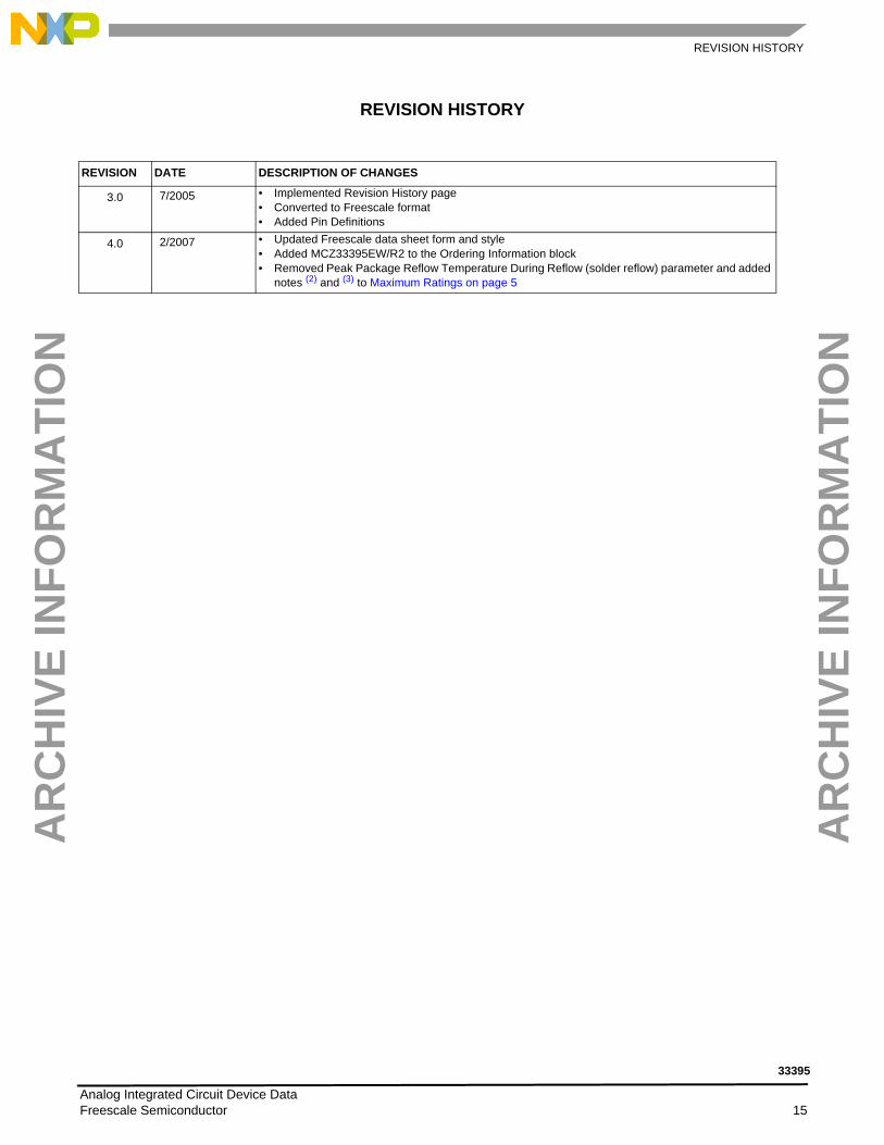
REVISION HISTORY
REVISION DATE DESCRIPTION OF CHANGES
3.0 7/2005 • Implemented Revision History page• Converted to Freescale format• Added Pin Definitions
4.0 2/2007 • Updated Freescale data sheet form and style• Added MCZ33395EW/R2 to the Ordering Information block• Removed Peak Package Reflow Temperature During Reflow (solder reflow) parameter and added
notes (2) and (3) to Maximum Ratings on page 5
Analog Integrated Circuit Device Data Freescale Semiconductor 15
33395

MC33395Rev 4.02/2007
Information in this document is provided solely to enable system and software implementers to use Freescale Semiconductor products. There are no express or implied copyright licenses granted hereunder to design or fabricate any integrated circuits or integrated circuits based on the information in this document.
Freescale Semiconductor reserves the right to make changes without further notice to any products herein. Freescale Semiconductor makes no warranty, representation or guarantee regarding the suitability of its products for any particular purpose, nor does Freescale Semiconductor assume any liability arising out of the application or use of any product or circuit, and specifically disclaims any and all liability, including without limitation consequential or incidental damages. “Typical” parameters that may be provided in Freescale Semiconductor data sheets and/or specifications can and do vary in different applications and actual performance may vary over time. All operating parameters, including “Typicals”, must be validated for each customer application by customer’s technical experts. Freescale Semiconductor does not convey any license under its patent rights nor the rights of others. Freescale Semiconductor products are not designed, intended, or authorized for use as components in systems intended for surgical implant into the body, or other applications intended to support or sustain life, or for any other application in which the failure of the Freescale Semiconductor product could create a situation where personal injury or death may occur. Should Buyer purchase or use Freescale Semiconductor products for any such unintended or unauthorized application, Buyer shall indemnify and hold Freescale Semiconductor and its officers, employees, subsidiaries, affiliates, and distributors harmless against all claims, costs, damages, and expenses, and reasonable attorney fees arising out of, directly or indirectly, any claim of personal injury or death associated with such unintended or unauthorized use, even if such claim alleges that Freescale Semiconductor was negligent regarding the design or manufacture of the part.
Freescale™ and the Freescale logo are trademarks of Freescale Semiconductor, Inc. All other product or service names are the property of their respective owners.© Freescale Semiconductor, Inc., 2007. All rights reserved.
How to Reach Us:
Home Page:www.freescale.com
Web Support:http://www.freescale.com/support
USA/Europe or Locations Not Listed:Freescale Semiconductor, Inc.Technical Information Center, EL5162100 East Elliot Road Tempe, Arizona 85284 +1-800-521-6274 or +1-480-768-2130www.freescale.com/support
Europe, Middle East, and Africa:Freescale Halbleiter Deutschland GmbHTechnical Information CenterSchatzbogen 781829 Muenchen, Germany+44 1296 380 456 (English)+46 8 52200080 (English)+49 89 92103 559 (German)+33 1 69 35 48 48 (French)www.freescale.com/support
Japan:Freescale Semiconductor Japan Ltd. Headquarters ARCO Tower 15F 1-8-1, Shimo-Meguro, Meguro-ku, Tokyo 153-0064Japan0120 191014 or +81 3 5437 [email protected]
Asia/Pacific:Freescale Semiconductor Hong Kong Ltd.Technical Information Center 2 Dai King Street Tai Po Industrial Estate Tai Po, N.T., Hong Kong +800 2666 [email protected]
For Literature Requests Only:Freescale Semiconductor Literature Distribution CenterP.O. Box 5405Denver, Colorado 802171-800-441-2447 or 303-675-2140Fax: [email protected]
RoHS-compliant and/or Pb-free versions of Freescale products have the functionality and electrical characteristics of their non-RoHS-compliant and/or non-Pb-free counterparts. For further information, see http://www.freescale.com or contact your Freescale sales representative.
For information on Freescale’s Environmental Products program, go to http://www.freescale.com/epp.
AR
CH
IVE
INFO
RM
ATI
ON
AR
CH
IVE
INFO
RM
ATI
ON
RoHS-compliant and/or Pb-free versions of Freescale products have the functionality and electrical characteristics of their non-RoHS-compliant and/or non-Pb-free counterparts. For further information, see http://www.freescale.com or contact your Freescale sales representative.
For information on Freescale’s Environmental Products program, go to http://www.freescale.com/epp.
Related Documents