Jia Nan Technology K210 FreeRTOS SDK Programming Guide Translate by Sipeed KENDRYTE KENDRYTE.COM

Welcome message from author
This document is posted to help you gain knowledge. Please leave a comment to let me know what you think about it! Share it to your friends and learn new things together.
Transcript

Jia Nan Technology
Copyright ©2019
K210FreeRTOS SDK
Programming Guide
Translate by Sipeed
KENDRYTE
KENDRYTE.COM

i
About this manual
This document provides users with programming guidelines based on the FreeRTOS SDK development.
Corresponding to the sdk version
Kendryte FreeRTOS SDK v0.4.0 (9c7b0e0d23e46e87a2bfd4dd86d1a1f0d3c899e9)
Release notes
date version Release notes
2018-10-12 V0.1.0 initial version
Disclaimer
The information in this document, including the referenced url address, is subject
to change without notice.The Documentation is provided "as is" without warranty of
any kind, including any warranties of merchantability, fitness for a particular
purpose, or non-infringement, and any warranties referred to elsewhere by any
proposal, specification or sample.This document is not responsible for any
infringement of any patent rights arising out of the use of the information in this
document.No license, express or implied, by estoppel or otherwise, is hereby
granted.All trademark names, trademarks and registered trademarks mentioned are the
property of their respective owners and are hereby acknowledged.
Copyright notice
Copyright © 2018 Jia Nan Technology.all rights reserved.

ii
table of Contents
About this manual i
Corresponding to the sdk version ....................................................................................................................... i
Release notes ...........................................................................................................................................i
Disclaimer ..................................................................................................................................................i
Copyright notice .....................................................................................................................................i
Chapter 1 FreeRTOS extension 1
1.1 Overview .................................................................................................................................... 1
1.2 Functional description ..................................................................................................... 1
1.3 Api reference ....................................................................................................................... 1
chapter 2 Device List 3
Chapter 3 Pin configuration 5
3.1 Overview .................................................................................................................................... 5
3.2 Functional description ..................................................................................................... 5
3.3 type of data ........................................................................................................................... 5
Chapter 4 System control 23
4.1 Overview ............................................................................................................................................. 23
4.2 Functional description ................................................................................................... 23
4.3 Api reference ..................................................................................................................... 23
4.4 type of data ......................................................................................................................... 24
Chapter 5 Programmable interrupt controller (pic) 27
5.1 Overview ............................................................................................................................................. 27
5.2 Functional description ............................................................................................................... 27

iii 目录
. . . . . . . . . . . . . . . . . . . . . . . . 27
. . . . . . . . . . . . . . . . . . . . . . . . 29
30
. . . . . . . . . . . . . . . . . . . . . . . . 30
. . . . . . . . . . . . . . . . . . . . . . . . 30
. . . . . . . . . . . . . . . . . . . . . . . . 30
. . . . . . . . . . . . . . . . . . . . . . . . 34
36
. . . . . . . . . . . . . . . . . . . . . . . . 36
. . . . . . . . . . . . . . . . . . . . . . . . 36
. . . . . . . . . . . . . . . . . . . . . . . . 36
40
8.1 Overview ............................................................................................................................................. 40
8.2 Functional description ................................................................................................... 40
8.3 Api reference ..................................................................................................................... 40
8.4 type of data ......................................................................................................................... 41
Chapter 9 General purpose
input/output (gpio) 43
9.1 Overview ............................................................................................................................................. 43
9.2 Functional description ................................................................................................... 43
9.3 Api reference ..................................................................................................................... 43
9.4 type of data ......................................................................................................................... 47
Chapter 10 Integrated Circuit Built-in Bus (i2c) 50
10.1 Overview ..................................................................................................................................... 50
10.2 Functional description ................................................................................................... 50
10.3 Api reference ..................................................................................................................... 50
10.4 type of data ......................................................................................................................... 54
Chapter 11 Integrated Circuit Built-in Audio Bus (i2s) 56
11.1 Overview ..................................................................................................................................... 56
11.2 Functional description ................................................................................................... 56
11.3 Api reference ..................................................................................................................... 56
11.4 type of data ......................................................................................................................... 60
Chapter 12 Serial Peripheral Interface (spi) 63
5.3 Api reference
. . . .
. . .
5.4 type of data
. . . . . . .
Chapte
r 6
6.1
Direct storage
access (dma)
Overview
. . . . . .
. . .
6.2 Functional
description
. . . .
. . .
6.3 Api reference
. . . .
. . .
6.4 type of data
. . . . . . .
Chapte
r 7
7.1
Standard io
Overview
. . . . . .
. . .
7.2 Functional
description
. . . .
. . .
7.3 Api reference
. . . .
. . .
Chapte
r 8 Universal
asynchronous transceiver
(UART)

iv 目录
. . . . . . . . . . . . . . . . . . . . . . . . 63
. . . . . . . . . . . . . . . . . . . . . . . . 63
. . . . . . . . . . . . . . . . . . . . . . . . 63
. . . . . . . . . . . . . . . . . . . . . . . . 67
70
. . . . . . . . . . . . . . . . . . . . . . . . 70
. . . . . . . . . . . . . . . . . . . . . . . . 70
. . . . . . . . . . . . . . . . . . . . . . . . 70
. . . . . . . . . . . . . . . . . . . . . . . . 75
78
. . . . . . . . . . . . . . . . . . . . . . . . . . 78
. . . . . . . . . . . . . . . . . . . . . . . . . . 78
. . . . . . . . . . . . . . . . . . . . . . . . . . 78
81
. . . . . . . . . . . . . . . . . . . . . . . . . . 81
. . . . . . . . . . . . . . . . . . . . . . . . . . 81
. . . . . . . . . . . . . . . . . . . . . . . . . . 81
. . . . . . . . . . . . . . . . . . . . . . . . . . 83
85
. . . . . . . . . . . . . . . . . . . . . . . . . . 85
. . . . . . . . . . . . . . . . . . . . . . . . . . 85
. . . . . . . . . . . . . . . . . . . . . . . . . . 85
Chapter 17 Watchdog Timer (wdt) 89
17.1 Overview ..................................................................................................................................... 89
17.2 Functional description .............................................................................................. 89
17.3 Api reference ................................................................................................................. 89
17.4 type of data .................................................................................................................... 92
95
. . . . . . . . . . . . . . . . . . . . . . . 95
. . . . . . . . . . . . . . . . . . . . . . . 95
. . . . . . . . . . . . . . . . . . . . . . . 95
. . . . . . . . . . . . . . . . . . . . . . . 97
12.1 Overview
. .
. . . . . . .
12.2 Functional
descriptio
n
. . . . . . .
12.3 Api
reference
. . . . . . .
12.4 type of data
. . . . . . .
Chapter 13. Digital Camera
Interface (dvp)
13.1 Overview
. . . . . .
. . .
13.2 Functional
description
. . . .
. . .
13.3 Api reference
. . . .
. . .
13.4 type of data
. . . . . . .
Chapter
14 Serial camera control bus
(SCCB)
14.1 Overview
. . . .
. . .
14.2 Functional
description
. .
. . .
14.3 Api reference
. .
. . .
Chapter
15
15.1
Timer
Overview
. . . .
. . .
15.2 Functional
description
. .
. . .
15.3 Api reference
. .
. . .
15.4 type of data
. . . . .
Chapter
16
Pulse width
modulator
(PWM)
16.1 Overview
. . . .
. . .
16.2 Functional
description
. .
. . .
16.3 Api reference . .
. . .
Chapter
18
Fast Fourier
Transform Accelerator
(FFT)
18.1 Overview
. . . . . . .
. . .
18.2 Functional
description
. . . . .
. . .
18.3 Api
reference . . .
. . .
. . .
18.4 type of data
. . . . . . . .

v 目录
Chapter
19
Secure Hash Algorithm Accelerator (sha256) 99
19.1 Overview
. . . . . . . . . . . . . . . . . . . . . . . . . . . . . . . . .
99
19.2 Functional description
. . . . . . . . . . . . . . . . . . . . . . . . . . . . . . .
99
19.3 Api
reference . . . . . . . . . . . . . . . . . . . . . . . . . .
. . . . . .
99
Chapter
20
Advanced crypto accelerator (aes) 101
20.1 Overview
. . . . . . . . . . . . . . . . . . . . . . . . . . . . . . . . .
101
20.2 Functional description
. . . . . . . . . . . . . . . . . . . . . . . . . . . . . . .
101
20.3 Api
reference . . . . . . . . . . . . . . . . . . . . . . . . . .
. . . . . .
101
20.4 type of data
. . . . . . . . . . . . . . . . . . . . . . . . . . . . . . . 112

1
Chapter 1
FreeRTOS Expansion
1.1 Overview
FreeRTOS is a lightweight real-time operating system.This SDK adds some new features for K210.
1.2 Functional description
The FreeRTOS extension has the following features:
• Get the logical processor ID of the current task
• Create a task at a specified logical processor
The K210 contains 2 logical processors with Ids of 0 and 1, respectively.
1.3 Api reference
Corresponding header file task.h
Provide users with the following interfaces:
• uxTaskGetProcessorId
• xTaskCreateAtProcessor
1.3.1 uxTaskGetProcessorId
1.3.1.1 description
Get the current logical processor ID.

第 1 章 FreeRTOS 扩 展 2
1.3.1.2 Function prototype
1.3.1.3 return value
Current logical processor Id.
1.3.2 xTaskCreateAtProcessor
1.3.2.1 description
Create a task at the specified logical processor.
1.3.2.2 Function prototype
1.3.2.3 Parameters
parameter name description input
Output
uxProcessor Logical
processor Id
Input
pxTaskCode Task entry
point
Input
pcName mission name Input usStackDepth Stack space Input pvParameters parameter Input uxPriority priority Input pxCreatedTask Created task
handle
Input
1.3.2.4 Return value
return value description
pdPASS
Succ
ess other
fail
ure
U B aseT ype_ t u x T ask G etP ro cesso rId ( void );
B aseT ype_ t x T ask C reateA tP ro cesso r ( U B aseT ype_ t uxProcessor , T ask F unction_ t pxTaskCode ,
const char ∗ const pcName , const co n fig S T A C K _ D E P T H _ T Y P E usStackDepth , void ∗ const
pvParameters , U B aseT ype_ t uxPriority , T ask H andle_ t ∗ const px C reated T ask );

3
chapter 2
Device List
path Types
of
Remarks
/dev/uart1 UART
/dev/uart2 UART
/dev/uart3 UART
/dev/gpio0 GPIO High speed gpio
/dev/gpio1 GPIO
/dev/i2c0 I2C
/dev/i2c1 I2C
/dev/i2c2 I2C
/dev/i2s0 I2S
/dev/i2s1 I2S
/dev/i2s2 I2S
/dev/spi0 SPI
/dev/spi1 SPI
/dev/spi3 SPI
/dev/sccb0 SCCB
/dev/dvp0 DVP
/dev/fft0 FFT
/dev/aes0 AES
/dev/sha256 SHA256
/dev/timer0 TIMER Cannot be used with /dev/pwm0
/dev/timer1 TIMER Cannot be used with /dev/pwm0
/dev/timer2 TIMER Cannot be used with /dev/pwm0

第 2 章 设备列表 4
path Types
of
Remark
s
/dev/timer3 TIMER Not
availa
ble
/dev/pwm0 is used at
the same time
/dev/timer4 TIMER Not
availa
ble
/dev/pwm1 is used at
the same time
/dev/timer5 TIMER Not
availa
ble
/dev/pwm1 is used at
the same time
/dev/timer6 TIMER Not
availa
ble
/dev/pwm1 is used at
the same time
/dev/timer7 TIMER Not
availa
ble
/dev/pwm1 is used at
the same time
/dev/timer8 TIMER Not
availa
ble
/dev/pwm2 is used at
the same time
/dev/timer9 TIMER Not
availa
ble
/dev/pwm2 is used at
the same time
/dev/timer10 TIMER Not
availa
ble
/dev/pwm2 is used at
the same time
/dev/timer11 TIMER Not
availa
ble
/dev/pwm2 is used at
the same time
/dev/pwm0 PWM Not
availa
ble
/dev/timer[0-3] Use
at the same time
/dev/pwm1 PWM Not
availa
ble
/dev/timer[4-7] Also
use
/dev/pwm2 PWM Not
availa
ble
/dev/timer[8-11]
Simultaneous use
/dev/wdt0 WDT
/dev/wdt1 WDT
/dev/rtc0 RTC

5
Chapter 3
Pin configuration
3.1 Overview
The pin configuration includes fpioa and power domain configuration.
3.2 Functional description
• Support for io's programmable function selection
• Configuring the power domain
3.3 type of data
Corresponding header file pin_cfg.h
The relevant data types and data structures are defined as follows:
• Fpioa_function_t: The function number of the pin.
• Fpioa_cfg_item_t: FPIOA pin configuration.
• Fpioa_cfg_t: FPIOA configuration.
• Sysctl_power_bank_t: Power domain number.
• Sysctl_io_power_mode_t: IO output voltage value.
• Power_bank_item_t: A single power domain configuration.
• Power_bank_cfg_t: Power domain configuration.
• Pin_cfg_t: Pin configuration.

第 3 章 管脚配置 6
typedef enum _ fpioa_ function {
3.3.1 fpioa_function_t
3.3.1.1 description
The function number of the pin.
3.3.1.2 definition
F U N C _ JT A G _ T C L K = 0 , /∗ ! < JTAG Test Clock ∗/
F U N C _ JT A G _ T D I = 1 , /∗ ! < JTAG Test Data In ∗/
F U N C _ JT A G _ T M S = 2 , /∗ ! < JTAG Test Mode Select ∗/
F U N C _ JT A G _ T D O = 3 , /∗ ! < JTAG Test Data Out ∗/
F U N C _ S P I0_ D 0 = 4 , /∗ ! < SPI0 Data 0 ∗/
F U N C _ S P I0_ D 1 = 5 , /∗ ! < SPI0 Data 1 ∗/
F U N C _ S P I0_ D 2 = 6 , /∗ ! < SPI0 Data 2 ∗/
F U N C _ S P I0_ D 3 = 7 , /∗ ! < SPI0 Data 3 ∗/
F U N C _ S P I0_ D 4 = 8 , /∗ ! < SPI0 Data 4 ∗/
F U N C _ S P I0_ D 5 = 9 , /∗ ! < SPI0 Data 5 ∗/
F U N C _ S P I0_ D 6 = 10 , /∗ ! < SPI0 Data 6 ∗/
F U N C _ S P I0_ D 7 = 11 , /∗ ! < SPI0 Data 7 ∗/
F U N C _ S P I0_ S S 0 = 12 , /∗ ! < SPI0 Chip Select 0 ∗/
F U N C _ S P I0_ S S 1 = 13 , /∗ ! < SPI0 Chip Select 1 ∗/
F U N C _ S P I0_ S S 2 = 14 , /∗ ! < SPI0 Chip Select 2 ∗/
F U N C _ S P I0_ S S 3 = 15 , /∗ ! < SPI0 Chip Select 3 ∗/
F U N C _ S P I0_ A R B = 16 , /∗ ! < SPI0 A r b i t r a t i o n ∗/
F U N C _ S P I0_ S C L K = 17 , /∗ ! < SPI0 Serial Clock ∗/
F U N C _ U A R T H S _ R X = 18 , /∗ ! < UART High speed I 2 S _ R E C E I V E R ∗/
F U N C _ U A R T H S _ T X = 19 , /∗ ! < UART High speed I 2 S _ T R A N S M I T T E R ∗/
F U N C _ R E S V 6 = 20 , /∗ ! < Reser ved function ∗/
F U N C _ R E S V 7 = 21 , /∗ ! < Reser ved function ∗/
F U N C _ C L K _ S P I1 = 22 , /∗ ! < Clock SPI1 ∗/
F U N C _ C L K _ I2C 1 = 23 , /∗ ! < Clock I2C1 ∗/
F U N C _ G P IO H S 0 = 24 , /∗ ! < GPIO High speed 0 ∗/
F U N C _ G P IO H S 1 = 25 , /∗ ! < GPIO High speed 1 ∗/
F U N C _ G P IO H S 2 = 26 , /∗ ! < GPIO High speed 2 ∗/
F U N C _ G P IO H S 3 = 27 , /∗ ! < GPIO High speed 3 ∗/
F U N C _ G P IO H S 4 = 28 , /∗ ! < GPIO High speed 4 ∗/
F U N C _ G P IO H S 5 = 29 , /∗ ! < GPIO High speed 5 ∗/
F U N C _ G P IO H S 6 = 30 , /∗ ! < GPIO High speed 6 ∗/
F U N C _ G P IO H S 7 = 31 , /∗ ! < GPIO High speed 7 ∗/
F U N C _ G P IO H S 8 = 32 , /∗ ! < GPIO High speed 8 ∗/
F U N C _ G P IO H S 9 = 33 , /∗ ! < GPIO High speed 9 ∗/
F U N C _ G P IO H S 10 = 34 , /∗ ! < GPIO High speed 10 ∗/
F U N C _ G P IO H S 11 = 35 , /∗ ! < GPIO High speed 11 ∗/
F U N C _ G P IO H S 12 = 36 , /∗ ! < GPIO High speed 12 ∗/
F U N C _ G P IO H S 13 = 37 , /∗ ! < GPIO High speed 13 ∗/
F U N C _ G P IO H S 14 = 38 , /∗ ! < GPIO High speed 14 ∗/
F U N C _ G P IO H S 15 = 39 , /∗ ! < GPIO High speed 15 ∗/
F U N C _ G P IO H S 16 = 40 , /∗ ! < GPIO High speed 16 ∗/
F U N C _ G P IO H S 17 = 41 , /∗ ! < GPIO High speed 17 ∗/

第 3 章 管脚配置 7
F U N C _ G P IO H S 18 = 42 , /∗ ! < GPIO High speed 18 ∗/
F U N C _ G P IO H S 19 = 43 , /∗ ! < GPIO High speed 19 ∗/
F U N C _ G P IO H S 20 = 44 , /∗ ! < GPIO High speed 20 ∗/
F U N C _ G P IO H S 21 = 45 , /∗ ! < GPIO High speed 21 ∗/
F U N C _ G P IO H S 22 = 46 , /∗ ! < GPIO High speed 22 ∗/
F U N C _ G P IO H S 23 = 47 , /∗ ! < GPIO High speed 23 ∗/
F U N C _ G P IO H S 24 = 48 , /∗ ! < GPIO High speed 24 ∗/
F U N C _ G P IO H S 25 = 49 , /∗ ! < GPIO High speed 25 ∗/
F U N C _ G P IO H S 26 = 50 , /∗ ! < GPIO High speed 26 ∗/
F U N C _ G P IO H S 27 = 51 , /∗ ! < GPIO High speed 27 ∗/
F U N C _ G P IO H S 28 = 52 , /∗ ! < GPIO High speed 28 ∗/
F U N C _ G P IO H S 29 = 53 , /∗ ! < GPIO High speed 29 ∗/
F U N C _ G P IO H S 30 = 54 , /∗ ! < GPIO High speed 30 ∗/
F U N C _ G P IO H S 31 = 55 , /∗ ! < GPIO High speed 31 ∗/
F U N C _ G P IO 0 = 56 , /∗ ! < GPIO pin 0 ∗/
F U N C _ G P IO 1 = 57 , /∗ ! < GPIO pin 1 ∗/
F U N C _ G P IO 2 = 58 , /∗ ! < GPIO pin 2 ∗/
F U N C _ G P IO 3 = 59 , /∗ ! < GPIO pin 3 ∗/
F U N C _ G P IO 4 = 60 , /∗ ! < GPIO pin 4 ∗/
F U N C _ G P IO 5 = 61 , /∗ ! < GPIO pin 5 ∗/
F U N C _ G P IO 6 = 62 , /∗ ! < GPIO pin 6 ∗/
F U N C _ G P IO 7 = 63 , /∗ ! < GPIO pin 7 ∗/
F U N C _ U A R T 1_ R X = 64 , /∗ ! < UART1 I 2 S _ R E C E I V E R ∗/
F U N C _ U A R T 1_ T X = 65 , /∗ ! < UART1 I 2 S _ T R A N S M I T T E R ∗/
F U N C _ U A R T 2_ R X = 66 , /∗ ! < UART2 I 2 S _ R E C E I V E R ∗/
F U N C _ U A R T 2_ T X = 67 , /∗ ! < UART2 I 2 S _ T R A N S M I T T E R ∗/
F U N C _ U A R T 3_ R X = 68 , /∗ ! < UART3 I 2 S _ R E C E I V E R ∗/
F U N C _ U A R T 3_ T X = 69 , /∗ ! < UART3 I 2 S _ T R A N S M I T T E R ∗/
F U N C _ S P I1_ D 0 = 70 , /∗ ! < SPI1 Data 0 ∗/
F U N C _ S P I1_ D 1 = 71 , /∗ ! < SPI1 Data 1 ∗/
F U N C _ S P I1_ D 2 = 72 , /∗ ! < SPI1 Data 2 ∗/
F U N C _ S P I1_ D 3 = 73 , /∗ ! < SPI1 Data 3 ∗/
F U N C _ S P I1_ D 4 = 74 , /∗ ! < SPI1 Data 4 ∗/
F U N C _ S P I1_ D 5 = 75 , /∗ ! < SPI1 Data 5 ∗/
F U N C _ S P I1_ D 6 = 76 , /∗ ! < SPI1 Data 6 ∗/
F U N C _ S P I1_ D 7 = 77 , /∗ ! < SPI1 Data 7 ∗/
F U N C _ S P I1_ S S 0 = 78 , /∗ ! < SPI1 Chip Select 0 ∗/
F U N C _ S P I1_ S S 1 = 79 , /∗ ! < SPI1 Chip Select 1 ∗/
F U N C _ S P I1_ S S 2 = 80 , /∗ ! < SPI1 Chip Select 2 ∗/
F U N C _ S P I1_ S S 3 = 81 , /∗ ! < SPI1 Chip Select 3 ∗/
F U N C _ S P I1_ A R B = 82 , /∗ ! < SPI1 A r b i t r a t i o n ∗/
F U N C _ S P I1_ S C L K = 83 , /∗ ! < SPI1 Serial Clock ∗/
F U N C _ S P I_ S L A V E _ D 0 = 84 , /∗ ! < SPI Slave Data 0 ∗/
F U N C _ S P I_ S L A V E _ S S = 85 , /∗ ! < SPI Slave Select ∗/
F U N C _ S P I_ S L A V E _ S C L K = 86 , /∗ ! < SPI Slave Serial Clock ∗/
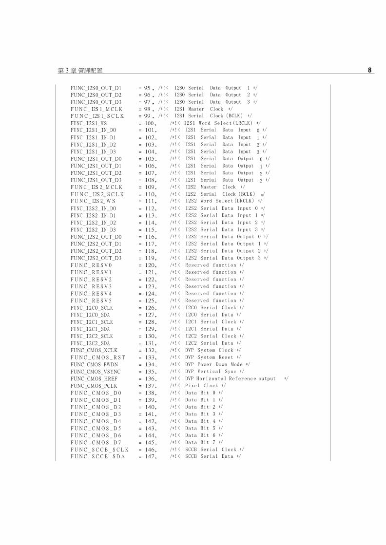
F U N C _ I2S 0_ M C L K = 87 , /∗ ! < I2S0 Master Clock ∗/
F U N C _ I2S 0_ S C L K = 88 , /∗ ! < I2S0 Serial Clock ( BCLK ) ∗/
F U N C _ I2S 0_ W S = 89 , /∗ ! < I2S0 Word Select ( LRCLK ) ∗/
F U N C _ I2S 0_ IN _ D 0 = 90 , /∗ ! < I2S0 Serial Data Input 0 ∗/ F
U N C _ I2S 0_ IN _ D 1 = 91 , /∗ ! < I2S0 Serial Data Input 1 ∗/ F
U N C _ I2S 0_ IN _ D 2 = 92 , /∗ ! < I2S0 Serial Data Input 2 ∗/ F
U N C _ I2S 0_ IN _ D 3 = 93 , /∗ ! < I2S0 Serial Data Input 3 ∗/ F
U N C _ I2S 0_ O U T _ D 0 = 94 , / ∗ ! < I2S0 Serial Data Output 0 ∗/
第 3 章 管脚配置 8
0
1
2
3
0
1
2
3
∗
F U N C _ I2S 0_ O U T _ D 1 = 95 , /∗ ! < I2S0 Serial Data Output 1 ∗/
F U N C _ I2S 0_ O U T _ D 2 = 96 , /∗ ! < I2S0 Serial Data Output 2 ∗/
F U N C _ I2S 0_ O U T _ D 3 = 97 , /∗ ! < I2S0 Serial Data Output 3 ∗/
F U N C _ I2S 1_ M C L K = 98 , /∗ ! < I2S1 Master Clock ∗/
F U N C _ I2S 1_ S C L K = 99 , /∗ ! < I2S1 Serial Clock ( BCLK ) ∗/
F U N C _ I2S 1_ W S = 100 , /∗ ! < I2S1 Word Select ( LRCLK ) ∗/
F U N C _ I2S 1_ IN _ D 0 = 101 , /∗ ! < I2S1 Serial Data Input ∗/
F U N C _ I2S 1_ IN _ D 1 = 102 , /∗ ! < I2S1 Serial Data Input ∗/
F U N C _ I2S 1_ IN _ D 2 = 103 , /∗ ! < I2S1 Serial Data Input ∗/
F U N C _ I2S 1_ IN _ D 3 = 104 , /∗ ! < I2S1 Serial Data Input ∗/
F U N C _ I2S 1_ O U T _ D 0 = 105 , /∗ ! < I2S1 Serial Data Output ∗/
F U N C _ I2S 1_ O U T _ D 1 = 106 , /∗ ! < I2S1 Serial Data Output ∗/
F U N C _ I2S 1_ O U T _ D 2 = 107 , /∗ ! < I2S1 Serial Data Output ∗/
F U N C _ I2S 1_ O U T _ D 3 = 108 , /∗ ! < I2S1 Serial Data Output ∗/
F U N C _ I2S 2_ M C L K = 109 , /∗ ! < I2S2 Master Clock ∗/
F U N C _ I2S 2_ S C L K = 110 , /∗ ! < I2S2 Serial Clock ( BCLK ) /
F U N C _ I2S 2_ W S = 111 , /∗ ! < I2S2 Word Select ( LRCLK ) ∗/
F U N C _ I2S 2_ IN _ D 0 = 112 , /∗ ! < I2S2 Serial Data Input 0 ∗/
F U N C _ I2S 2_ IN _ D 1 = 113 , /∗ ! < I2S2 Serial Data Input 1 ∗/
F U N C _ I2S 2_ IN _ D 2 = 114 , /∗ ! < I2S2 Serial Data Input 2 ∗/
F U N C _ I2S 2_ IN _ D 3 = 115 , /∗ ! < I2S2 Serial Data Input 3 ∗/
F U N C _ I2S 2_ O U T _ D 0 = 116 , /∗ ! < I2S2 Serial Data Output 0 ∗/
F U N C _ I2S 2_ O U T _ D 1 = 117 , /∗ ! < I2S2 Serial Data Output 1 ∗/
F U N C _ I2S 2_ O U T _ D 2 = 118 , /∗ ! < I2S2 Serial Data Output 2 ∗/
F U N C _ I2S 2_ O U T _ D 3 = 119 , /∗ ! < I2S2 Serial Data Output 3 ∗/
F U N C _ R E S V 0 = 120 , /∗ ! < Reserved function ∗/
F U N C _ R E S V 1 = 121 , /∗ ! < Reserved function ∗/
F U N C _ R E S V 2 = 122 , /∗ ! < Reserved function ∗/
F U N C _ R E S V 3 = 123 , /∗ ! < Reserved function ∗/
F U N C _ R E S V 4 = 124 , /∗ ! < Reserved function ∗/
F U N C _ R E S V 5 = 125 , /∗ ! < Reserved function ∗/
F U N C _ I2C 0_ S C L K = 126 , /∗ ! < I2C0 Serial Clock ∗/
F U N C _ I2C 0_ S D A = 127 , /∗ ! < I2C0 Serial Data ∗/
F U N C _ I2C 1_ S C L K = 128 , /∗ ! < I2C1 Serial Clock ∗/
F U N C _ I2C 1_ S D A = 129 , /∗ ! < I2C1 Serial Data ∗/
F U N C _ I2C 2_ S C L K = 130 , /∗ ! < I2C2 Serial Clock ∗/
F U N C _ I2C 2_ S D A = 131 , /∗ ! < I2C2 Serial Data ∗/
F U N C _ C M O S _ X C L K = 132 , /∗ ! < DVP System Clock ∗/
F U N C _ C M O S _ R S T = 133 , /∗ ! < DVP System Reset ∗/
F U N C _ C M O S _ P W D N = 134 , /∗ ! < DVP Power Down Mode ∗/
F U N C _ C M O S _ V S Y N C = 135 , /∗ ! < DVP Vertical Sync ∗/
F U N C _ C M O S _ H R E F = 136 , /∗ ! < DVP H o r i z o n t a l R e f e r e n c e output ∗/
F U N C _ C M O S _ P C L K = 137 , /∗ ! < Pixel Clock ∗/
F U N C _ C M O S _ D 0 = 138 , /∗ ! < Data Bit 0 ∗/
F U N C _ C M O S _ D 1 = 139 , /∗ ! < Data Bit 1 ∗/
F U N C _ C M O S _ D 2 = 140 , /∗ ! < Data Bit 2 ∗/
F U N C _ C M O S _ D 3 = 141 , /∗ ! < Data Bit 3 ∗/
F U N C _ C M O S _ D 4 = 142 , /∗ ! < Data Bit 4 ∗/
F U N C _ C M O S _ D 5 = 143 , /∗ ! < Data Bit 5 ∗/
F U N C _ C M O S _ D 6 = 144 , /∗ ! < Data Bit 6 ∗/
F U N C _ C M O S _ D 7 = 145 , /∗ ! < Data Bit 7 ∗/
F U N C _ S C C B _ S C L K = 146 , /∗ ! < SCCB Serial Clock ∗/
F U N C _ S C C B _ S D A = 147 , /∗ ! < SCCB Serial Data ∗/

第 3 章 管脚配置 9
F U N C _ U A R T 1_ C T S = 148 , /∗ ! < UART1 Clear To Send ∗/
F U N C _ U A R T 1_ D S R = 149 , /∗ ! < UART1 Data Set Ready ∗/
F U N C _ U A R T 1_ D C D = 150 , /∗ ! < UART1 Data Carrier Detect ∗/
F U N C _ U A R T 1_ R I = 151 , /∗ ! < UART1 Ring I n d i c a t o r ∗/
F U N C _ U A R T 1_ S IR _ IN = 152 , /∗ ! < UART1 Serial Infrared Input ∗/
F U N C _ U A R T 1_ D T R = 153 , /∗ ! < UART1 Data Terminal Ready ∗/
F U N C _ U A R T 1_ R T S = 154 , /∗ ! < UART1 Request To Send ∗/
F U N C _ U A R T 1_ O U T 2 = 155 , /∗ ! < UART1 User - d e s i g n a t e d Output 2 ∗/
F U N C _ U A R T 1_ O U T 1 = 156 , /∗ ! < UART1 User - d e s i g n a t e d Output 1 ∗/
F U N C _ U A R T 1 _ S IR _ O U T = 157 , /∗ ! < UART1 Serial Infrared Output ∗/
F U N C _ U A R T 1_ B A U D = 158 , /∗ ! < UART1 Transmit Clock Output ∗/
F U N C _ U A R T 1_ R E = 159 , /∗ ! < UART1 I 2 S _ R E C E I V E R Output Enable ∗/
F U N C _ U A R T 1_ D E = 160 , /∗ ! < UART1 Driver Output Enable ∗/
F U N C _ U A R T 1 _ R S 4 8 5 _ E N = 161 , /∗ ! < UART1 RS485 Enable ∗/
F U N C _ U A R T 2_ C T S = 162 , /∗ ! < UART2 Clear To Send ∗/
F U N C _ U A R T 2_ D S R = 163 , /∗ ! < UART2 Data Set Ready ∗/
F U N C _ U A R T 2_ D C D = 164 , /∗ ! < UART2 Data Carrier Detect ∗/
F U N C _ U A R T 2_ R I = 165 , /∗ ! < UART2 Ring I n d i c a t o r ∗/
F U N C _ U A R T 2_ S IR _ IN = 166 , /∗ ! < UART2 Serial Infrared Input ∗/
F U N C _ U A R T 2_ D T R = 167 , /∗ ! < UART2 Data Terminal Ready ∗/
F U N C _ U A R T 2_ R T S = 168 , /∗ ! < UART2 Request To Send ∗/
F U N C _ U A R T 2_ O U T 2 = 169 , /∗ ! < UART2 User - d e s i g n a t e d Output 2 ∗/
F U N C _ U A R T 2_ O U T 1 = 170 , /∗ ! < UART2 User - d e s i g n a t e d Output 1 ∗/
F U N C _ U A R T 2 _ S IR _ O U T = 171 , /∗ ! < UART2 Serial Infrared Output ∗/
F U N C _ U A R T 2_ B A U D = 172 , /∗ ! < UART2 Transmit Clock Output ∗/
F U N C _ U A R T 2_ R E = 173 , /∗ ! < UART2 I 2 S _ R E C E I V E R Output Enable ∗/
F U N C _ U A R T 2_ D E = 174 , /∗ ! < UART2 Driver Output Enable ∗/
F U N C _ U A R T 2 _ R S 4 8 5 _ E N = 175 , /∗ ! < UART2 RS485 Enable ∗/
F U N C _ U A R T 3_ C T S = 176 , /∗ ! < UART3 Clear To Send ∗/
F U N C _ U A R T 3_ D S R = 177 , /∗ ! < UART3 Data Set Ready ∗/
F U N C _ U A R T 3_ D C D = 178 , /∗ ! < UART3 Data Carrier Detect ∗/
F U N C _ U A R T 3_ R I = 179 , /∗ ! < UART3 Ring I n d i c a t o r ∗/
F U N C _ U A R T 3_ S IR _ IN = 180 , /∗ ! < UART3 Serial Infrared Input ∗/
F U N C _ U A R T 3_ D T R = 181 , /∗ ! < UART3 Data Terminal Ready ∗/
F U N C _ U A R T 3_ R T S = 182 , /∗ ! < UART3 Request To Send ∗/
F U N C _ U A R T 3_ O U T 2 = 183 , /∗ ! < UART3 User - d e s i g n a t e d Output 2 ∗/
F U N C _ U A R T 3_ O U T 1 = 184 , /∗ ! < UART3 User - d e s i g n a t e d Output 1 ∗/
F U N C _ U A R T 3 _ S IR _ O U T = 185 , /∗ ! < UART3 Serial Infrared Output ∗/
F U N C _ U A R T 3_ B A U D = 186 , /∗ ! < UART3 Transmit Clock Output ∗/
F U N C _ U A R T 3_ R E = 187 , /∗ ! < UART3 I 2 S _ R E C E I V E R Output Enable ∗/
F U N C _ U A R T 3_ D E = 188 , /∗ ! < UART3 Driver Output Enable ∗/
F U N C _ U A R T 3 _ R S 4 8 5 _ E N = 189 , /∗ ! < UART3 RS485 Enable ∗/
F U N C _ T IM E R 0 _ T O G G L E 1 = 190 , /∗ ! < TIMER0 Toggle Output 1 ∗/
F U N C _ T IM E R 0 _ T O G G L E 2 = 191 , /∗ ! < TIMER0 Toggle Output 2 ∗/
F U N C _ T IM E R 0 _ T O G G L E 3 = 192 , /∗ ! < TIMER0 Toggle Output 3 ∗/
F U N C _ T IM E R 0 _ T O G G L E 4 = 193 , /∗ ! < TIMER0 Toggle Output 4 ∗/
F U N C _ T IM E R 1 _ T O G G L E 1 = 194 , /∗ ! < TIMER1 Toggle Output 1 ∗/
F U N C _ T IM E R 1 _ T O G G L E 2 = 195 , /∗ ! < TIMER1 Toggle Output 2 ∗/
F U N C _ T IM E R 1 _ T O G G L E 3 = 196 , /∗ ! < TIMER1 Toggle Output 3 ∗/
F U N C _ T IM E R 1 _ T O G G L E 4 = 197 , /∗ ! < TIMER1 Toggle Output 4 ∗/
F U N C _ T IM E R 2 _ T O G G L E 1 = 198 , /∗ ! < TIMER2 Toggle Output 1 ∗/
F U N C _ T IM E R 2 _ T O G G L E 2 = 199 , /∗ ! < TIMER2 Toggle Output 2 ∗/
F U N C _ T IM E R 2 _ T O G G L E 3 = 200 , /∗ ! < TIMER2 Toggle Output 3 ∗/

第 3 章 管脚配置 10
F U N C _ T IM E R 2 _ T O G G L E 4 = 201 , /∗ ! < TIMER2 Toggle Output 4 ∗/
F U N C _ C L K _ S P I2 = 202 , /∗ ! < Clock SPI2 ∗/
F U N C _ C L K _ I2C 2 = 203 , /∗ ! < Clock I2C2 ∗/
F U N C _ IN T E R N A L 0 = 204 , /∗ ! < Internal function signal 0 ∗/
F U N C _ IN T E R N A L 1 = 205 , /∗ ! < Internal function signal 1 ∗/
F U N C _ IN T E R N A L 2 = 206 , /∗ ! < Internal function signal 2 ∗/
F U N C _ IN T E R N A L 3 = 207 , /∗ ! < Internal function signal 3 ∗/
F U N C _ IN T E R N A L 4 = 208 , /∗ ! < Internal function signal 4 ∗/
F U N C _ IN T E R N A L 5 = 209 , /∗ ! < Internal function signal 5 ∗/
F U N C _ IN T E R N A L 6 = 210 , /∗ ! < Internal function signal 6 ∗/
F U N C _ IN T E R N A L 7 = 211 , /∗ ! < Internal function signal 7 ∗/
F U N C _ IN T E R N A L 8 = 212 , /∗ ! < Internal function signal 8 ∗/
F U N C _ IN T E R N A L 9 = 213 , /∗ ! < Internal function signal 9 ∗/
F U N C _ IN T E R N A L 10 = 214 , /∗ ! < Internal function signal 10 ∗/
F U N C _ IN T E R N A L 11 = 215 , /∗ ! < Internal function signal 11 ∗/
F U N C _ IN T E R N A L 12 = 216 , /∗ ! < Internal function signal 12 ∗/
F U N C _ IN T E R N A L 13 = 217 , /∗ ! < Internal function signal 13 ∗/
F U N C _ IN T E R N A L 14 = 218 , /∗ ! < Internal function signal 14 ∗/
F U N C _ IN T E R N A L 15 = 219 , /∗ ! < Internal function signal 15 ∗/
F U N C _ IN T E R N A L 16 = 220 , /∗ ! < Internal function signal 16 ∗/
F U N C _ IN T E R N A L 17 = 221 , /∗ ! < Internal function signal 17 ∗/
F U N C _ C O N S T A N T = 222 , /∗ ! < Constant function ∗/
F U N C _ IN T E R N A L 18 = 223 , /∗ ! < Internal function signal 18 ∗/
F U N C _ D E B U G 0 = 224 , /∗ ! < Debug function 0 ∗/
F U N C _ D E B U G 1 = 225 , /∗ ! < Debug function 1 ∗/
F U N C _ D E B U G 2 = 226 , /∗ ! < Debug function 2 ∗/
F U N C _ D E B U G 3 = 227 , /∗ ! < Debug function 3 ∗/
F U N C _ D E B U G 4 = 228 , /∗ ! < Debug function 4 ∗/
F U N C _ D E B U G 5 = 229 , /∗ ! < Debug function 5 ∗/
F U N C _ D E B U G 6 = 230 , /∗ ! < Debug function 6 ∗/
F U N C _ D E B U G 7 = 231 , /∗ ! < Debug function 7 ∗/
F U N C _ D E B U G 8 = 232 , /∗ ! < Debug function 8 ∗/
F U N C _ D E B U G 9 = 233 , /∗ ! < Debug function 9 ∗/
F U N C _ D E B U G 10 = 234 , /∗ ! < Debug function 10 ∗/
F U N C _ D E B U G 11 = 235 , /∗ ! < Debug function 11 ∗/
F U N C _ D E B U G 12 = 236 , /∗ ! < Debug function 12 ∗/
F U N C _ D E B U G 13 = 237 , /∗ ! < Debug function 13 ∗/
F U N C _ D E B U G 14 = 238 , /∗ ! < Debug function 14 ∗/
F U N C _ D E B U G 15 = 239 , /∗ ! < Debug function 15 ∗/
F U N C _ D E B U G 16 = 240 , /∗ ! < Debug function 16 ∗/
F U N C _ D E B U G 17 = 241 , /∗ ! < Debug function 17 ∗/
F U N C _ D E B U G 18 = 242 , /∗ ! < Debug function 18 ∗/
F U N C _ D E B U G 19 = 243 , /∗ ! < Debug function 19 ∗/
F U N C _ D E B U G 20 = 244 , /∗ ! < Debug function 20 ∗/
F U N C _ D E B U G 21 = 245 , /∗ ! < Debug function 21 ∗/
F U N C _ D E B U G 22 = 246 , /∗ ! < Debug function 22 ∗/
F U N C _ D E B U G 23 = 247 , /∗ ! < Debug function 23 ∗/
F U N C _ D E B U G 24 = 248 , /∗ ! < Debug function 24 ∗/
F U N C _ D E B U G 25 = 249 , /∗ ! < Debug function 25 ∗/
F U N C _ D E B U G 26 = 250 , /∗ ! < Debug function 26 ∗/
F U N C _ D E B U G 27 = 251 , /∗ ! < Debug function 27 ∗/
F U N C _ D E B U G 28 = 252 , /∗ ! < Debug function 28 ∗/
F U N C _ D E B U G 29 = 253 , /∗ ! < Debug function 29 ∗/

第 3 章 管脚配置 11
} fpioa_ function_ t ;
F U N C _ D E B U G 30 = 254 , /∗ ! < Debug function 30 ∗/
F U N C _ D E B U G 31 = 255 , /∗ ! < Debug function 31 ∗/
FUNC_MAX = 256 , /∗ ! < Function numbers ∗/
3.3.1.3 member
Member name description
FUNC_JTAG_TCLK Jtag clock interface
FUNC_JTAG_TDI Jtag data input
interface func_jtag_tms Jtag controls
the conversion of the tap state machine
func_jtag_tdo Jtag data output
interface
FUNC_SPI0_D0 Spi0 data line 0
FUNC_SPI0_D1 Spi0 data line 1
FUNC_SPI0_D2 Spi0 data line 2
FUNC_SPI0_D3 Spi0 data line 3
FUNC_SPI0_D4 Spi0 data line 4
FUNC_SPI0_D5 Spi0 data line 5
FUNC_SPI0_D6 Spi0 data line 6
FUNC_SPI0_D7 Spi0 data line 7
FUNC_SPI0_SS0 Spi0 chip select signal 0
FUNC_SPI0_SS1 Spi0 chip select signal 1
FUNC_SPI0_SS2 Spi0 chip select signal 2
FUNC_SPI0_SS3 Spi0 chip select signal 3
FUNC_SPI0_ARB Spi0 arbitration signal
FUNC_SPI0_SCLK Spi0 clock
FUNC_UARTHS_RX Uart high speed receiving data interface
FUNC_UARTHS_TX Uart high speed send data interface
FUNC_RESV6 Reserved function
FUNC_RESV7 Reserved function
FUNC_CLK_SPI1 Spi1 clock
FUNC_CLK_I2C1 I2c1 clock
FUNC_GPIOHS0 High speed gpio0
FUNC_GPIOHS1 High speed gpio1
FUNC_GPIOHS2 High speed gpio2
FUNC_GPIOHS3 High speed gpio3
FUNC_GPIOHS4 High speed gpio4

第 3 章 管脚配置 12
Member name description
FUNC_GPIOHS5 High speed gpio5
FUNC_GPIOHS6 High speed gpio6
FUNC_GPIOHS7 High speed gpio7
FUNC_GPIOHS8 High speed gpio8
FUNC_GPIOHS9 High speed gpio9
FUNC_GPIOHS10 High speed gpio10
FUNC_GPIOHS11 High speed gpio11
FUNC_GPIOHS12 High speed gpio12
FUNC_GPIOHS13 High speed gpio13
FUNC_GPIOHS14 High speed gpio14
FUNC_GPIOHS15 High speed gpio15
FUNC_GPIOHS16 High speed gpio16
FUNC_GPIOHS17 High speed gpio17
FUNC_GPIOHS18 High speed gpio18
FUNC_GPIOHS19 High speed gpio19
FUNC_GPIOHS20 High speed gpio20
FUNC_GPIOHS21 High speed gpio21
FUNC_GPIOHS22 High speed gpio22
FUNC_GPIOHS23 High speed gpio23
FUNC_GPIOHS24 High speed gpio24
FUNC_GPIOHS25 High speed gpio25
FUNC_GPIOHS26 High speed gpio26
FUNC_GPIOHS27 High speed gpio27
FUNC_GPIOHS28 High speed gpio28
FUNC_GPIOHS29 High speed gpio29
FUNC_GPIOHS30 High speed gpio30
FUNC_GPIOHS31 High speed gpio31
FUNC_GPIO0 GPIO0
FUNC_GPIO1 GPIO1
FUNC_GPIO2 GPIO2
FUNC_GPIO3 GPIO3
FUNC_GPIO4 GPIO4
FUNC_GPIO5 GPIO5
FUNC_GPIO6 GPIO6
FUNC_GPIO7 GPIO7

第 3 章 管脚配置 13
Member name description
FUNC_UART1_RX Uart1 receive data interface
FUNC_UART1_TX Uart1 send data interface
FUNC_UART2_RX Uart2 receive data interface
FUNC_UART2_TX Uart2 send data interface
FUNC_UART3_RX Uart3 receive data interface
FUNC_UART3_TX Uart3 send data interface
FUNC_SPI1_D0 Spi1 data line 0
FUNC_SPI1_D1 Spi1 data line 1
FUNC_SPI1_D2 Spi1 data line 2
FUNC_SPI1_D3 Spi1 data line 3
FUNC_SPI1_D4 Spi1 data line 4
FUNC_SPI1_D5 Spi1 data line 5
FUNC_SPI1_D6 Spi1 data line 6
FUNC_SPI1_D7 Spi1 data line 7
FUNC_SPI1_SS0 Spi1 chip select signal 0
FUNC_SPI1_SS1 Spi1 chip select signal 1
FUNC_SPI1_SS2 Spi1 chip select signal 2
FUNC_SPI1_SS3 Spi1 chip select signal 3
FUNC_SPI1_ARB Spi1 arbitration signal
FUNC_SPI1_SCLK Spi1 clock
Func_spi_slave_d0 spi slave mode data
line 0 func_spi_slave_ss spi slave
mode chip select signal
func_spi_slave_sclk spi slave mode
clock
FUNC_I2S0_MCLK I2s0 master clock
(system clock) func_i2s0_sclk I2s0 serial
clock (bit clock) func_i2s0_ws I2s0
frame clock
FUNC_I2S0_IN_D0 I2s0 serial input
data interface 0 func_i2s0_in_d1 I2s0
serial input data interface 1
func_i2s0_in_d2 I2s0 serial input
data interface 2 func_i2s0_in_d3 I2s0
serial input data interface 3
func_i2s0_out_d0 i2s0 serial output data
interface 0 func_i2s0_out_d1 i2s0 serial
output data interface 1 func_i2s0_out_d2
i2s0 serial output data interface 2
func_i2s0_out_d3 i2s0 serial output data
interface 3 func_i2s1_mclk I2s1 master
clock (system clock)

第 3 章 管脚配置 14
Member name description
FUNC_I2S1_SCLK I2s1 serial clock (bit clock)
FUNC_I2S1_WS I2s1 frame clock
FUNC_I2S1_IN_D0 I2s1 serial input
data interface 0 func_i2s1_in_d1 I2s1
serial input data interface 1
func_i2s1_in_d2 I2s1 serial input
data interface 2 func_i2s1_in_d3 I2s1
serial input data interface 3
func_i2s1_out_d0 i2s1 serial output data
interface 0 func_i2s1_out_d1 i2s1 serial
output data interface 1 func_i2s1_out_d2
i2s1 serial output data interface 2
func_i2s1_out_d3 i2s1 serial output data
interface 3 func_i2s2_mclk I2s2 master
clock (system clock) func_i2s2_sclk
I2s2 serial clock
(bit clock) func_i2s2_ws I2s2 frame
clock
FUNC_I2S2_IN_D0 I2s2 serial input
data interface 0 func_i2s2_in_d1 I2s2
serial input data interface 1
func_i2s2_in_d2 I2s2 serial input
data interface 2 func_i2s2_in_d3 I2s2
serial input data interface 3
func_i2s2_out_d0 i2s2 serial output data
interface 0 func_i2s2_out_d1 i2s2 serial
output data interface 1 func_i2s2_out_d2
i2s2 serial output data interface 2
func_i2s2_out_d3 i2s2 serial output data
interface 3
FUNC_RESV0 Reserved function
FUNC_RESV1 Reserved function
FUNC_RESV2 Reserved function
FUNC_RESV3 Reserved function
FUNC_RESV4 Reserved function
FUNC_RESV5 Reserved function
FUNC_I2C0_SCLK I2c0 serial clock
FUNC_I2C0_SDA I2c0 serial data interface
FUNC_I2C1_SCLK I2c1 serial clock
FUNC_I2C1_SDA I2c1 serial data interface
FUNC_I2C2_SCLK I2c2 serial clock
FUNC_I2C2_SDA I2c2 serial data interface
FUNC_CMOS_XCLK Dvp system clock
FUNC_CMOS_RST Dvp system reset signal

第 3 章 管脚配置 15
Member name description
FUNC_CMOS_PWDN Dvp enable signal
FUNC_CMOS_VSYNC Dvp field sync
FUNC_CMOS_HREF Dvp line reference signal
FUNC_CMOS_PCLK Pixel clock
FUNC_CMOS_D0 Pixel data 0
FUNC_CMOS_D1 Pixel data 1
FUNC_CMOS_D2 Pixel data 2
FUNC_CMOS_D3 Pixel data 3
FUNC_CMOS_D4 Pixel data 4
FUNC_CMOS_D5 Pixel data 5
FUNC_CMOS_D6 Pixel data 6
FUNC_CMOS_D7 Pixel data 7
FUNC_SCCB_SCLK Sccb clock
FUNC_SCCB_SDA Sccb serial data
signal func_uart1_cts Uart1 clears the
send signal func_uart1_dsr Uart1 data
device preparation signal func_uart1_dcd
Uart1 data carrier
detection func_uart1_ri Uart1
ringing indication
FUNC_UART1_SIR_IN Uart1 serial infrared
input signal func_uart1_dtr Uart1 data
terminal preparation signal func_uart1_rts
Uart1 sends request
signal func_uart1_out2 Uart1 user specified
output signal 2 func_uart1_out1 Uart1
user specified output signal 1
func_uart1_sir_out Uart1 serial infrared
output signal func_uart1_baud Uart1 clock
FUNC_UART1_RE Uart1 receive enable
FUNC_UART1_DE Uart1 send enable
FUNC_UART1_RS485_EN Uart1 enable rs485
FUNC_UART2_CTS Uart2 clears the
send signal func_uart2_dsr Uart2 data
device preparation signal func_uart2_dcd
Uart2 data carrier
detection func_uart2_ri Uart2
ringing indication
Func_uart2_sir_in uart2 serial infrared
input signal func_uart2_dtr Uart2 data
terminal preparation signal func_uart2_rts
Uart2 sends a
request signal

第 3 章 管脚配置 16
Member name description
FUNC_UART2_OUT2 Uart2 user specified
output signal 2 func_uart2_out1 Uart2 user
specified output signal 1 func_uart2_sir_out
Uart2 serial infrared
output signal func_uart2_baud Uart2 clock
FUNC_UART2_RE Uart2 receive enable
FUNC_UART2_DE Uart2 send enable
FUNC_UART2_RS485_EN Uart2 enable rs485
FUNC_UART3_CTS Clear send signal
FUNC_UART3_DSR Data device
preparation signal func_uart3_dcd
Uart3 data carrier
detection func_uart3_ri Uart3 ringing
indication
FUNC_UART3_SIR_IN Uart3 serial infrared
input signal func_uart3_dtr Uart3 data
terminal preparation signal func_uart3_rts
Uart3 sends request
signal func_uart3_out2 Uart3 user specified
output signal 2 func_uart3_out1 Uart3 user
specified output signal 1 func_uart3_sir_out
Uart3 serial infrared
output signal func_uart3_baud Uart3 clock
FUNC_UART3_RE Uart3 receive enable
FUNC_UART3_DE Uart3 send enable
func_uart3_rs485_en Uart3 enable
rs485 func_timer0_toggle1 Timer0
output signal 1 func_timer0_toggle2
Timer0 output
signal 2 func_timer0_toggle3 Timer0
output signal 3 func_timer0_toggle4
Timer0 output
signal 4 func_timer1_toggle1 Timer1
output signal 1 func_timer1_toggle2
Timer1 output
signal 2 func_timer1_toggle3 Timer1
output signal 3 func_timer1_toggle4
Timer1 output
signal 4 func_timer2_toggle1 Timer2
output signal 1 func_timer2_toggle2
Timer2 output
signal 2 func_timer2_toggle3 Timer2
output signal 3 func_timer2_toggle4
Timer2 output
signal 4 func_clk_spi2 Spi2 clock
FUNC_CLK_I2C2 I2c2 clock

第 3 章 管脚配置 17
Member name description
FUNC_INTERNAL0 Internal function 0
FUNC_INTERNAL1 Internal function 1
FUNC_INTERNAL2 Internal function 2
FUNC_INTERNAL3 Internal function 3
FUNC_INTERNAL4 Internal function 4
FUNC_INTERNAL5 Internal function 5
FUNC_INTERNAL6 Internal function 6
FUNC_INTERNAL7 Internal function 7
FUNC_INTERNAL8 Internal function 8
FUNC_INTERNAL9 Internal function 9
FUNC_INTERNAL10 Internal function 10
FUNC_INTERNAL11 Internal function 11
FUNC_INTERNAL12 Internal function 12
FUNC_INTERNAL13 Internal function 13
FUNC_INTERNAL14 Internal function 14
FUNC_INTERNAL15 Internal function 15
FUNC_INTERNAL16 Internal function 16
FUNC_INTERNAL17 Internal function 17
FUNC_CONSTANT constant
FUNC_INTERNAL18 Internal function 18
FUNC_DEBUG0 Debug function 0
FUNC_DEBUG1 Debug function 1
FUNC_DEBUG2 Debugging function 2
FUNC_DEBUG3 Debugging function 3
FUNC_DEBUG4 Debugging function 4
FUNC_DEBUG5 Debugging function 5
FUNC_DEBUG6 Debugging function 6
FUNC_DEBUG7 Debugging function 7
FUNC_DEBUG8 Debugging function 8
FUNC_DEBUG9 Debugging function 9
FUNC_DEBUG10 Debugging function 10
FUNC_DEBUG11 Debugging function 11
FUNC_DEBUG12 Debugging function 12
FUNC_DEBUG13 Debugging function 13
FUNC_DEBUG14 Debugging function 14

第 3 章 管脚配置 18
Member name description
FUNC_DEBUG15 Debugging function 15
FUNC_DEBUG16 Debugging function 16
FUNC_DEBUG17 Debugging function 17
FUNC_DEBUG18 Debugging function 18
FUNC_DEBUG19 Debugging function 19
FUNC_DEBUG20 Debugging function 20
FUNC_DEBUG21 Debugging function 21
FUNC_DEBUG22 Debugging function 22
FUNC_DEBUG23 Debugging function 23
FUNC_DEBUG24 Debugging function 24
FUNC_DEBUG25 Debugging function 25
FUNC_DEBUG26 Debugging function 26
FUNC_DEBUG27 Debugging function 27
FUNC_DEBUG28 Debugging function 28
FUNC_DEBUG29 Debugging function 29
FUNC_DEBUG30 Debugging function 30
FUNC_DEBUG31 Debugging function 31
3.3.2 fpioa_cfg_item_t
3.3.2.1 description
Fpioa pin configuration.
3.3.2.2 definition
typedef struct _ fpioa_ cfg_ item
{
int number ;
fpioa_ fu nction_ t function ;
} fpioa_ cfg_ item _ t ;
3.3.2.3 Members
Member
name
description
number
function
Pin
number
function
number

第 3 章 管脚配置 19
3.3.3 fpioa_cfg_t
3.3.3.1 description
Fpioa configuration.
3.3.3.2 definition
3.3.3.3 member
Member name description
version Configuration version, must be set to fpioa_cfg_version
functions_count Number of function configurations
functions Feature configuration list
3.3.4 sysctl_power_bank_t
3.3.4.1 Desc
ribe the
power domain
number.
3.3.4.2 definition
3.3.4.3 member
typedef struct _fpioa_ cfg
{ uint32_t version ;
uint32_t functions_ count ;
fpioa_ cfg_ item _ t functions [];
} fpioa_ cfg_ t ;
typedef enum _ sy sctl_ p o w er_ b an k
{ S Y S C T L _P O W E R _B A N K 0 ,
S Y S C T L _P O W E R _B A N K 1 ,
S Y S C T L _P O W E R _B A N K 2 ,
S Y S C T L _P O W E R _B A N K 3 ,
S Y S C T L _P O W E R _B A N K 4 ,
S Y S C T L _P O W E R _B A N K 5 ,
S Y S C T L _P O W E R _B A N K 6 ,
S Y S C T L _P O W E R _B A N K 7 ,
S Y S C T L _ P O W E R _ B A N K _ M A X ,
} sy sctl_ p o w er_ b an k _ t ;

第 3 章 管脚配置 20
Member name description
SYSCTL_POWER_BANK0 Power domain 0, control io0-io5
SYSCTL_POWER_BANK1 Power domain 0, control io6-io11
SYSCTL_POWER_BANK2 Power domain 0, control io12-io17
SYSCTL_POWER_BANK3 Power domain 0, control io18-io23
SYSCTL_POWER_BANK4 Power domain 0, control io24-io29
SYSCTL_POWER_BANK5 Power domain 0, control io30-io35
SYSCTL_POWER_BANK6 Power domain 0, control io36-io41
SYSCTL_POWER_BANK7 Power domain 0, control io42-io47
3.3.5 sysctl_io_power_mode_t
3.3.5.1 description
Io Output voltage value.
3.3.5.2 definition
3.3.5.3 member
Member name description
SYSCTL_POWER_V33 Set to 3.3v
SYSCTL_POWER_V18 Set to 1.8v
3.3.6 power_bank_item_t
3.3.6.1 description
Single power domain configuration.
3.3.6.2 definition
typedef enum _ sy sctl_ io _ p o w er_ m o d e
{ SYSCTL_POWER_V33 ,
S Y S C T L _ P O W E R _ V 18
} sy sctl_ io _ p o w er_ m o d e_ t ;
typedef struct _ pow er_ b ank_ item
{ sy sctl_ p o w er_ b an k _ t pow er_ bank ;
sy sctl_ io _ p o w er_ m o d e_ t io_ pow er_ m ode ;

第 3 章 管脚配置 21
3.3.6.3 member
Member name description
power_bank Power domain number
iopowermode Io output voltage value
3.3.7 power_bank_cfg_t
3.3.7.1 Desc
ribe the
power domain
configuratio
n.
3.3.7.2 definition
3.3.7.3 member
Member name description
version Configuration version, must be set to fpioa_cfg_version
powerbankscount Number of power domain configurations
power_banks Power domain configuration list
3.3.8 pin_cfg_t
3.3.8.1 Desc
ribe the pin
configuratio
n.
3.3.8.2 definition
} po w er_ bank_ item _ t ;
typedef struct _ pow er_ bank_ cfg
{
uint32_t version ; uint32_t p ow er_ bank s_ cou nt ; po w
er_ b an k_ item _ t pow er_ banks [];
} pow er_ b ank_ cfg_ t ;
typedef struct _pin_cfg
{
uint32_t version ;
bool set_ sp i0 _ d vp_ data ;

第 3 章 管脚配置 22
3.3.8.3 member
Member name description
version Configuration version, must be set to fpioa_cfg_version
setspi0dvp_data Whether to set spi0d0-d7 dvpd0-d7 for spi0 or dvp data
input
3.3.9 Example
} pin_cfg_t ;
/∗ Configure io 6 and io7 functions as gpiohs0 and gpiohs1 ∗/
const fpioa_ cfg_ t g_ fpioa_ cfg =
{
. version = F PIOA _CF G_VE RS IO N ,
. functions_ count = 2 ,
. functions =
{
{ . number = 6 , . function = F U N C _ G P IO H S 0 } ,
{ . number = 7 , . function = F U N C _ G P IO H S 1 }
}
};

23
Chapter 4
System control
4.1 Overview
The system control module provides configuration functions for the operating system.
4.2 Functional description
The system control module has the following features:
• Set cpu frequency
• Install a custom driver
4.3 Api reference
Corresponding header file hal.h
Provide users with the following interfaces:
• system_set_cpu_frequency
• system_install_custom_driver
4.3.1 system_set_cpu_frequency
4.3.1.1 description
Set the cpu frequency.
4.3.1.2 Function prototype

第 4 章 系统控制 24
4.3.1.3 parameter
parameter name description input Output
frequency Frequency to be set (Hz) input
4.3.1.4 return value
The actual frequency (Hz) after setting.
4.3.2 system_install_custom_driver
4.3.2.1 description
Install a custom driver.
4.3.2.2 Function prototype
4.3.2.3 parameter
parameter name description input Output
name Specify the path to access the device Input
driver Custom driver implementation Input
4.3.2.4 The
return value
is none.
4.3.3 Example
4.4 type of data
The relevant data types and data structures are defined as follows:
uint32_t sy stem _ set_ cp u _ freq u en cy ( uint32_t frequency );
void sy stem _ in stall_ cu sto m _ d riv er ( const char ∗ name , const custom _ driver_ t ∗ driver );
/∗ Set the CPU frequency to 400 MHz ∗/
sy stem _ set_ cp u _ freq u en cy (400000000);

第 4 章 系统控制 25
• Driver_base_t: The driver implements the base class.
• Custom_driver_t: Custom driver implementation.
4.4.1 driver_base_t
4.4.1.1 Descri
be the driver
implementation
base class.
4.4.1.2 definition
4.4.1.3 member
Member name description
userdata User data
install Called during installation
open Called when opened
close Called when closed
4.4.2 custom_driver_t
4.4.2.1 description
Custom drive implementation.
4.4.2.2 definition
4.4.2.3 member
typedef struct _ driver_ base
{
void ∗ userdata ;
void (∗ install )( void ∗ userdata );
int (∗ open )( void ∗ userdata );
void (∗ close )( void ∗ userdata );
} driver_ base_ t ;
typedef struct _ custom _ driver
{
driver_ base_ t base ;
int (∗ io_control )( uint32_t control_code , const uint8_t ∗ write_buffer , size_t
write_len , uint8_t ∗ read_buffer , size_t read_len , void ∗ userdata );
} custom _ driver_ t ;

第 4 章 系统控制 26
Member name description
base Driver implementation base class
io_control Called when control information is received

27
Chapter 5
Programmable interrupt controller (PIC)
5.1 Overview
Any external interrupt source can be individually assigned to an external interrupt on
each CPU.This provides great flexibility to adapt to different application needs.
5.2 Functional description
The pic module has the following features:
• Enable or disable interrupts
• Set interrupt handler
• Configure interrupt priority
5.3 Api reference
Corresponding header file hal.h
Provide users with the following interfaces:
• pic_set_irq_enable
• pic_set_irq_handler
• pic_set_irq_priority

第 5 章 可编程中断控制器 (PIC) 28
5.3.1 pic_set_irq_enable
5.3.1.1 description
Set whether irq is enabled.
5.3.1.2 Function prototype
5.3.1.3 parameter
parameter name description input Output
irq Irq number Input
enable Whether to enable Input
5.3.1.4 The
return value
is none.
5.3.2 pic_set_irq_handler
5.3.2.1 description
Set up the irq handler.
5.3.2.2 Function prototype
5.3.2.3 parameter
parameter name description input Output
irq Irq number Input
handler Handler Input
userdata Handler user data Input
5.3.2.4 The
return value
is none.
void pic_ set_ irq _ en able ( uint32_t irq , bool enable );
void p ic_ set_ irq _ h an d ler ( uint32_t irq , p ic_ irq_ hand ler_ t handler , void ∗ userdata );

第 5 章 可编程中断控制器 (PIC) 29
5.3.3 pic_set_irq_priority
5.3.3.1 description
Set the irq priority.
5.3.3.2 Function prototype
5.3.3.3 Parameters
parameter
name
descripti
on
input
Output
irq
priority
Irq
number
priority
Inpu
t
inpu
t
5.3.3.4 Return value
no.
5.4 type of data
The relevant data types and data structures are defined as follows:
• Pic_irq_handler_t: IRQ handler.
5.4.1 pic_irq_handler_t
5.4.1.1 description
Irq handler.
5.4.1.2 definition
5.4.1.3 parameter
parameter name description input Output
userdata User data Input
void p ic_ set_ irq _ p rio rity ( uint32_t irq , uint32_t priority );
typedef void (∗ p ic_ irq _ hand ler_ t )( void ∗ userdata );

30
Chapter 6
Direct storage access (DMA)
6.1 Overview
Direct Memory Access (DMA) is used to provide high-speed data transfer between peripherals
and memory and between memory and memory.CPU efficiency can be improved by quickly moving
data through DMA without any CPU operation.
6.2 Functional description
The dma module has the following features:
• Automatically select an idle dma channel for transmission
• Automatically select software or hardware handshake protocol based on source and destination addresses
• Supports element sizes of 1, 2, 4, and 8 bytes, source and destination sizes do not have to be consistent
• Asynchronous or synchronous transfer function
• Loop transmission function, often used to refresh scenes such as screen or audio recording and playback
6.3 Api reference
Corresponding header file hal.h
Provide users with the following interfaces:
• dma_open_free
• dma_close
• dma_set_request_source
• dma_transmit_async

第 6 章 直接存储访问 (DMA) 31
• dma_transmit
• dma_loop_async
6.3.1 dma_open_free
6.3.1.1 description
Open an available dma device.
6.3.1.2 Function prototype
6.3.1.3 return value
Dma device handle.
6.3.2 dma_close
6.3.2.1 description
Turn off the dma device.
6.3.2.2 Function prototype
6.3.2.3 parameter
parameter name description input Output
file Dma device handle Input
6.3.2.4 The
return value
is none.
6.3.3 dma_set_request_source
6.3.3.1 description
Set the dma request source.
6.3.3.2 Function prototype
handle_t dm a_ open_ free ();
void dm a_close ( handle_t file );

第 6 章 直接存储访问 (DMA) 32
6.3.3.3 parameter
parameter name description input Output
file Dma device handle Input
request Request source number Input
6.3.3.4 The
return value
is none.
6.3.4 dma_transmit_async
6.3.4.1 description
Perform dma asynchronous transfer.
6.3.4.2 Function prototype
6.3.4.3 parameter
parameter name description input Output
file Dma device handle Input
src source address Input
dest target address Output
src_inc Whether the source address is increasing Input
dest_inc Whether the target address is increasing Input
element_size Element size (bytes) Input
count Number of elements Input
burst_size Burst transmission quantity Input
completion_event Transfer completion event Input
void d m a_ set_ req u est_ so u rce ( handle_t file , uint32_t request );
void dm a_ transm it_ asyn c ( handle_t file , const volatile void ∗ src , volatile void ∗ dest ,
int src_inc , int dest_inc , size_t element_size , size_t count , size_t burst_size , S em ap ho reH andle_ t co m pletion _ event );

第 6 章 直接存储访问 (DMA) 33
6.3.4.4 The
return value
is none.
6.3.5 dma_transmit
6.3.5.1 description
Perform dma synchronous transmission.
6.3.5.2 Function prototype
6.3.5.3 parameter
parameter name description input
Output
file
src
dest
src_inc
dest_inc
element_size
count
burst_size
Dma device
handle source
address
target address
Whether the
source address
is incremented
by the target
address, whether
it is self-
incrementing
element size
(bytes)
Burst
transmission
quantity
Inpu
t
inpu
t,
outp
ut,
inpu
t,
inpu
t,
inpu
t,
inpu
t
6.3.5.4
return value
no.
6.3.6 dma_loop_async
6.3.6.1 description
Perform dma asynchronous loop transfer.
6.3.6.2 Function prototype
void dm a_ transm it ( handle_t file , const volatile void ∗ src , volatile void ∗ dest , int
src_inc , int dest_inc , size_t element_size , size_t count , size_t burst_ size );
void dm a_ loop_ async ( handle_t file , const volatile void ∗∗ srcs , size_t src_num , volatile void ∗∗
dests , size_t dest_num , int src_inc , int dest_inc , size_t element_size , size_t count , size_t
burst_size , d m a_ stag e_ co m p letio n _ h an d ler_ t stage_ com pletion_ handler , void ∗ stage_
com pletion_ handler_ data , S em aph oreH an dle_ t completion_event , int ∗ stop_ signal );

第 6 章 直接存储访问 (DMA) 34
6.3.6.3 parameter
parameter name description input
Output
file Dma device handle Input
srcs Source address list Input
src_num Number of source
addresses
Input
dests Destination address list Output
dest_num Number of destination
addresses
Input
src_inc Whether the source
address is increasing
Input
dest_inc Whether the target
address is increasing
Input
element_size Element size (bytes) Input
count Number of elements Input
burst_size Burst transmission
quantity
Input
stage_completion_handler Stage completion handler Input
stage_completion_handler_data Stage completion handler
user data
Input
completion_event Transfer completion event Input
stop_signal Stop signal Input
Note: Phase completion refers to the completion of the transfer of a single source to the
target count element.
6.3.6.4 The
return value
is none.
6.3.7 Example
6.4 type of data
The relevant data types and data structures are defined as follows:
• Dma_stage_completion_handler_t: The DMA stage completes the handler.
int src [256] = { [0 ... 255] = 1 };
int dest [256];
handle_t dma = dm a_ open_ free ();
dm a_ transm it ( dma , src , dest , true , true , sizeof ( int ), 256 , 4);
assert ( dest [0] == src [0]);
dm a_close ( dma );

第 6 章 直接存储访问 (DMA) 35
6.4.1 dma_stage_completion_handler_t
6.4.1.1 description
The dma stage completes the handler.
6.4.1.2 definition
6.4.1.3 parameter
parameter name description input Output
userdata User data Input
typedef void (∗ d m a_ stag e_ co m p letio n _ h an d ler_ t )( void ∗ userdata );

36
Chapter 7
standard IO
7.1 Overview
The standard io module is the basic interface for accessing peripherals.
7.2 Functional description
The standard io module has the following features:
• Find peripherals based on path
• Unified read and write and control interface
7.3 Api reference
Corresponding header file devices.h
Provide users with the following interfaces:
• io_open
• io_close
• io_read
• io_write
• io_control

第 7 章 标 准 IO 37
7.3.1 io_open
7.3.1.1 Descri
ption Open a
device.
7.3.1.2 Function prototype
7.3.1.3 parameter
parameter name description input Output
name Device path Input
7.3.1.4 return value
return value description
0 failure
other Device handle
7.3.2 io_close
7.3.2.1 Descri
ption Turns
off a device.
7.3.2.2 Function prototype
7.3.2.3 parameter
parameter name description input Output
file Device handle Input
7.3.2.4 return value
handle_t io_open ( const char ∗ name );
int io_close ( handle_t file );

第 7 章 标 准 IO 38
return
value
desc
ript
ion
0
other
succ
ess
fail
ure
7.3.3 io_read
7.3.3.1 Description
Read from the device.
7.3.3.2 Function prototype
7.3.3.3 parameter
parameter name description input Output
file Device handle Input
buffer Target buffer Output
len Maximum number of bytes read Input
7.3.3.4 return value
The number of bytes actually read.
7.3.4 io_write
7.3.4.1 Desc
ription
Write to the
device.
7.3.4.2 Function prototype
7.3.4.3 parameter
parameter name description input Output
file Device handle Input
buffer Source buffer Input
int io_read ( handle_t file , uint8_t ∗ buffer , size_t len );
int io_write ( handle_t file , const uint8_t ∗ buffer , size_t len );

第 7 章 标 准 IO 39
parameter name description input Output
len The number of bytes to write Input
7.3.4.4 return value
return value description
len success
other failure
7.3.5 io_control
7.3.5.1 description
Send control information to the device.
7.3.5.2 Function prototype
7.3.5.3 Parameters
parameter name description input
Output
file
control_code
write_buffer
write_len
read_buffer
read_len
Device
handle
control
code
source
buffer
Number of
bytes to write
to the target
buffer
Maximum number of
bytes read
Inpu
t
inpu
t,
inpu
t,
inpu
t
and
outp
ut
7.3.5.4 Return value
The number of bytes actually read.
7.3.6 Example
int io_ control ( handle_t file , uint32_t control_code , const uint8_t ∗ write_buffer , size_t
write_len , uint8_t ∗ read_buffer , size_t read_len );
handle_t uart = io_open ("/ dev / uart1 " );
io_write ( uart , " hello \n " , 6);
io_close ( uart );

40
Chapter 8
Universal asynchronous transceiver
(UART)
8.1 Overview
Embedded applications typically require a simple method that consumes less system resources to
transfer data.Universal Asynchronous Transceiver (uart)
To meet these requirements, it has the flexibility to perform full-duplex data exchange with external
devices.
8.2 Functional description
The uart module has the following features:
• Configuring uart parameters
• Automatically collect data into the buffer
8.3 Api reference
Corresponding header file devices.h
Provide users with the following interfaces:
• uart_config
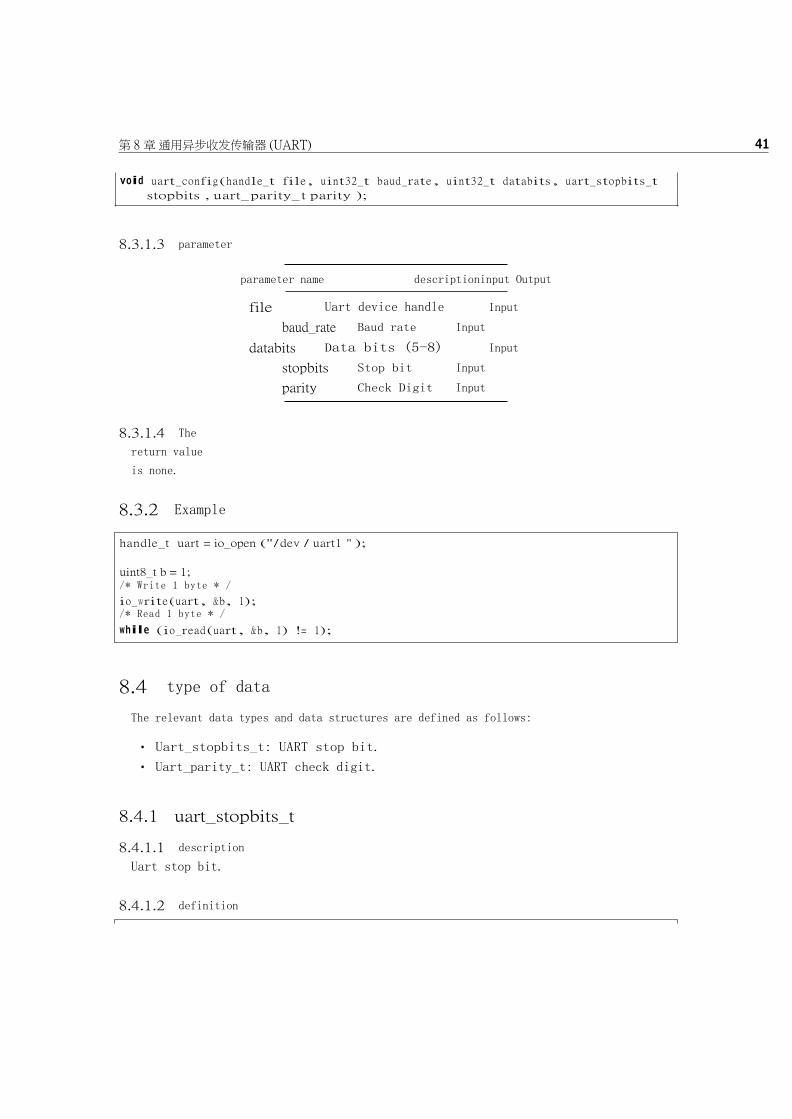
8.3.1 uart_config
8.3.1.1 description
Configure the uart device.
8.3.1.2 Function prototype
第 8 章 通用异步收发传输器 (UART) 41
8.3.1.3 parameter
parameter name descriptioninput Output
file Uart device handle Input
baud_rate Baud rate Input
databits Data bits (5-8) Input
stopbits Stop bit Input
parity Check Digit Input
8.3.1.4 The
return value
is none.
8.3.2 Example
8.4 type of data
The relevant data types and data structures are defined as follows:
• Uart_stopbits_t: UART stop bit.
• Uart_parity_t: UART check digit.
8.4.1 uart_stopbits_t
8.4.1.1 description
Uart stop bit.
8.4.1.2 definition
void uart_ config ( handle_t file , uint32_t baud_rate , uint32_t databits , uart_ stopbits_ t
stopbits , uart_ parity_ t parity );
handle_t uart = io_open ("/ dev / uart1 " );
uint8_t b = 1;
/∗ Write 1 byte ∗ /
io_write ( uart , &b , 1); /∗ Read 1 byte ∗ /
while ( io_read ( uart , &b , 1) != 1);

第 8 章 通用异步收发传输器 (UART) 42
8.4.1.3 member
Member name description
UART_STOP_1 1 stop bit
UART_STOP_1_5 1.5 stop bits
UART_STOP_2 2 stop bits
8.4.2 uart_parity_t
8.4.2.1 description
Uart check digit.
8.4.2.2 definition
typedef enum _ uart_ parity
{ UART_PARITY_N ONE ,
UART_PARITY_O DD ,
U A R T _ P A R IT Y _ E V E N
} uart_ parity_ t ;
8.4.2.3 Members
Member name description
UART_PARITY_NONE
UART_PARITY_ODD
UART_PARITY_EVEN
No
parity
check
parity
check
typedef enum _ uart_ stopbits
{ UART_STOP_1 ,
UART_STOP_1_5 ,
U A R T _ S T O P _ 2
} uart_ stopbits_ t ;

43
Chapter 9
General purpose input/output (GPIO)
9.1 Overview
The chip has 32 high-speed gpio and 8 universal gpio.
9.2 Functional description
The gpio module has the following features:
• Configurable up and down drive mode
• Support for rising edge, falling edge and double edge trigger
9.3 Api reference
Corresponding header file devices.h
Provide users with the following interfaces:
• gpio_get_pin_count
• gpio_set_drive_mode
• gpio_set_pin_edge
• gpio_set_on_\changed
• gpio_get_pin_value
• gpio_set_pin_value

第 9 章 通用输入/输出 (GPIO) 44
9.3.1 gpio_get_pin_count
9.3.1.1 description
Get the number of gpio pins.
9.3.1.2 Function prototype
9.3.1.3 parameter
parameter name description input Output
file Gpio controller handle Input
9.3.1.4 The
number of
return value
pins.
9.3.2 gpio_set_drive_mode
9.3.2.1 description
Set the gpio pin drive mode.
9.3.2.2 Function prototype
9.3.2.3 Parameters
parameter
name
description input
Output
file
pin
mode
Gpio controller
handle pin
number
Drive mode
Inpu
t
inpu
t
9.3.2.4 Return value
no.
uint32_t g p io_ g et_ p in_ co un t ( handle_t file );
void g p io _ set_ d riv e_ m o d e ( handle_t file , uint32_t pin , g pio_ drive_ m od e_ t mode );

Chapter 9. General Purpose
Input/Output (gpio)
45
9.3.3 gpio_set_pin_edge
9.3.3.1 description
Set the gpio pin edge trigger mode.
Note: /dev/gpio1 is not supported at this time.
9.3.3.2 Function prototype
9.3.3.3 parameter
parameter name description input Output
file Gpio controller handle Input
pin Pin number Input
edge Edge trigger mode Input
9.3.3.4 The
return
value is
none.
9.3.4 gpio_set_on_changed
9.3.4.1 description
Set the gpio pin edge trigger handler.
Note: /dev/gpio1 is not supported at this time.
9.3.4.2 Function prototype
9.3.4.3 Parameters
parameter name
description input Output
file
pin
callback
Gpio controller
handle pin
number
Handler
Inpu
t
inpu
t
void g p i o _ s e t _ p i n _ e d g e ( handle_ t file , uint32_ t pin , g p i o _ p i n _ e d g e _ t edge );
void g p i o _ s e t _ o n _ c h a n g e d ( handle_ t file , uint32_ t pin , g p i o _ o n _ c h a n g e d _ t callback , void ∗ userdata );

Chapter 9. General Purpose
Input/Output (gpio)
46
parameter name description input Output
userdata Handler user data Input
9.3.4.4 Return
value None.
9.3.5 gpio_get_pin_value
9.3.5.1 description
Get the value of the gpio pin.
9.3.5.2 Function prototype
9.3.5.3 Parameters
parameter name
description input Output
file
pin
Gpio controller
handle pin
number
Inpu
t
inpu
t
9.3.5.4 Return value
The value of the gpio pin.
9.3.6 gpio_set_pin_value
9.3.6.1 description
Set the value of the gpio pin.
9.3.6.2 Function prototype
9.3.6.3 parameter
parameter name description input Output
file Gpio controller handle Input
g p i o _ p i n _ v a l u e _ t g p i o _ g e t _ p i n _ v a l u e ( handle_ t file , uint32_ t pin );
void g p i o _ s e t _ p i n _ v a l u e ( handle_ t file , uint32_ t pin , g p i o _ p i n _ v a l u e _ t value );

Chapter 9. General Purpose
Input/Output (gpio)
47
parameter name description input Output
pin Pin number Input
value The value to set
Input
9.3.6.4 Return value
no.
9.3.7 Example
9.4 type of data
The relevant data types and data structures are defined as follows:
• Gpio_drive_mode_t: GPIO drive mode.
• Gpio_pin_edge_t: GPIO edge trigger mode.
• Gpio_pin_value_t: GPIO value.
• Gpio_on_changed_t: GPIO edge trigger handler.
9.4.1 gpio_drive_mode_t
9.4.1.1 description
Gpio drive mode.
9.4.1.2 definition
9.4.1.3 member
handle_ t gpio = io_ open ( " / dev / gpio0 " );
g p i o _ s e t _ d r i v e _ m o d e ( gpio , 0 , G P I O _ D M _ O U T P U T );
g p i o _ s e t _ p i n _ v a l u e ( gpio , 0 , G P I O _ P V _ L O W );
typedef enum _ g p i o _ d r i v e _ m o d e
{ GPIO_ DM_
INPUT , G P I O _ D M _ I N P
U T _ P U L L _ D O W N , G P I O _ D
M _ I N P U T _ P U L L _ U P , G P I O
_ D M _ O U T P U T } g p i o _ d r i v e _ m o d e _ t ;

Chapter 9. General Purpose
Input/Output (gpio)
48
Member name description
GPIO_DM_INPUT Input
GPIO_DM_INPUT_PULL_DOWN Input drop down
GPIO_DM_INPUT_PULL_UP Input pull up
GPIO_DM_OUTPUT Output
9.4.2 gpio_pin_edge_t
9.4.2.1 description
Gpio edge trigger mode.
9.4.2.2 definition
9.4.2.3 member
Member name description
GPIO_PE_NONE Do not trigger
GPIO_PE_FALLING Falling edge trigger
GPIO_PE_RISING Rising edge trigger
GPIO_PE_BOTH Double edge trigger
9.4.3 gpio_pin_value_t
9.4.3.1 description
Gpio value.
9.4.3.2 definition
typedef enum _ g p i o _ p i n _ e d g e
{ GPIO_
PE_NONE ,
GPIO_ PE_
FALLING ,
GPIO_ PE_
RISING , G P I O _ P
E _ B O T H
} g p i o _ p i n _ e d g e _ t ;
typedef enum _ g p i o _ p i n _ v a l u e
{ GPIO_PV_L
OW , G P I O _ P
V _ H I G H
} g p i o _ p i n _ v a l u e _ t ;

Chapter 9. General Purpose
Input/Output (gpio)
49
9.4.3.3 member
Member name description
GPIO_PV_LOW low
GPIO_PV_HIGH high
9.4.4 gpio_on_changed_t
9.4.4.1 description
The gpio edge trigger handler.
9.4.4.2 definition
9.4.4.3 Parameters
parameter name
description
input Output
pin userdata Pin
number
user
data
Inpu
t
inpu
t
typedef void (∗ g p i o _ o n _ c h a n g e d _ t )( uint32_ t pin , void ∗ userda ta );

50
Chapter 10
Integrated circuit built-in bus (i2c)
10.1 Overview
The i2c bus is used to communicate with multiple external
devices.Multiple external devices can share an i2c bus.
10.2 Functional description
The i2c module has the following features:
• Independent i2c device package peripheral related parameters
• Automatic processing of multi-device bus contention
• Support slave mode
10.3 Api reference
Corresponding header file devices.h
Provide users with the following interfaces:
• i2c_get_device
• i2c_dev_set_clock_rate
• i2c_dev_transfer_sequential
• i2c_config_as_slave
• i2c_slave_set_clock_rate

Chapter 10 Integrated Circuit Built-in Bus
(i2c)
51
10.3.1 i2c_get_device
10.3.1.1 description
Register and open an i2c device.
10.3.1.2 Function prototype
10.3.1.3 parameter
parameter name description input Output
file I2c controller handle Input
name Specify the path to access the device Input
slave_address Slave address Input
address_width Slave address width Input
10.3.1.4 return value
I2c device handle.
10.3.2 i2c_dev_set_clock_rate
10.3.2.1 description
Configure the clock rate of the i2c device.
10.3.2.2 Function prototype
10.3.2.3 Parameters
parameter name
description input Output
file clock_rate I2c device
handle
expected clock
rate
Inpu
t
inpu
t
handle_ t i 2 c _ g e t _ d e v i c e ( handle_ t file , const char ∗ name , uint32_ t slave_ address , uint32_ t a d
d r e s s _ w i d t h );
double i 2 c _ d e v _ s e t _ c l o c k _ r a t e ( handle_ t file , double c l o c k _ r a t e );

Chapter 10 Integrated Circuit Built-in Bus
(i2c)
52
10.3.2.4 Return value
The actual rate after setting.
10.3.3 i2c_dev_transfer_sequential
10.3.3.1 description
Read and write to the i2c device first.
10.3.3.2 Function prototype
10.3.3.3 parameter
parameter name description input Output
file I2c device handle
Input
write_buffer Source buffer Input
write_len The number of bytes to write
Input
read_buffer Target buffer Output
read_len Maximum number of bytes read
Input
10.3.3.4 return value
The number of bytes actually read.
10.3.4 i2c_config_as_slave
10.3.4.1 description
Configure the i2c controller to be in slave mode.
10.3.4.2 Function prototype
10.3.4.3 parameter
parameter name description input Output
file I2c controller handle Input
int i 2 c _ d e v _ t r a n s f e r _ s e q u e n t i a l ( handle_ t file , const uint8_ t ∗ write_ buffer , size_t write_len , uint8_
t ∗ read_buffer , size_ t read_ len );
void i 2 c _ c o n f i g _ a s _ s l a v e ( handle_ t file , uint32_ t slave_ address , uint32_ t address_ width , i 2 c _ s l a v e _
h a n d l e r _ t ∗ handler );

Chapter 10 Integrated Circuit Built-in Bus
(i2c)
53
parameter name description input
Output
slave_address
address_width
handler
Slave address
Slave device
address width
from device
handler
Inpu
t
inpu
t
10.3.4.4
return value
no.
10.3.5 spi_dev_set_clock_rate
10.3.5.1 description
Configure the clock rate for the i2c slave mode.
10.3.5.2 Function prototype
10.3.5.3 Parameters
parameter name
description input Output
file clock_rate I2c controller
handle
expected clock
rate
Inpu
t
inpu
t
10.3.5.4 Return value
The actual rate after setting.
10.3.6 Example
double i 2 c _ s l a v e _ s e t _ c l o c k _ r a t e ( handle_ t file , double c l o c k _ r a t e );
handle_ t i2c = io_ open ( " / dev / i2c0 " ); /∗ i2c Peripheral address is 0x32, 7-bit address, rate 200K ∗/
handle_ t dev0 = i 2 c _ g e t _ d e v i c e ( i2c , " / dev / i2c0 / dev0 " , 0 x32 , 7); i 2 c _ d e v _ s e
t _ c l o c k _ r a t e ( dev0 , 200000);
uint8_ t reg = 0;
uint8_ t data_ buf [2] = { 0 x00 ,0 x01 }; data_
buf [0] = reg ;
/∗ Write 0x01 to the 0 register ∗/
io_ write ( dev0 , data_buf , 2); /∗ Read 1 byte of data from the 0 register∗/
i 2 c _ d e v _ t r a n s f e r _ s e q u e n t i a l ( dev0 , & reg , 1 , data_buf , 1);

Chapter 10 Integrated Circuit Built-in Bus
(i2c)
54
10.4 type of data
The relevant data types and data structures are defined as
follows:
• I2c_event_t: I2C event.
• I2c_slave_handler_t: I2C slave handler.
10.4.1 i2c_event_t
10.4.1.1 description
I2c event.
10.4.1.2 definition
10.4.1.3 member
Member name description
I2C_EV_START Received Start signal
I2C_EV_RESTART Received a Restart signal
I2C_EV_STOP Received a Stop signal
10.4.2 i2c_slave_handler_t
10.4.2.1 description
I2c slave device handler.
10.4.2.2 definition
typedef enum _ i 2 c _ e v e n t
{ I2C_EV_
START , I2C_
EV_ RESTART ,
I 2 C _ E V _ S T O P
} i 2 c _ e v e n t _ t ;
typedef struct _ i 2 c _ s l a v e _ h a n d l e r
{
void (∗ o n _ r e c e i v e )( uint32_ t data ); uint32_ t (∗
o n _ t r a n s m i t )();
void (∗ on_ event )( i 2 c _ e v e n t _ t event ); } i 2 c _ s l a v e _ h a n d l e r _ t ;

Chapter 10 Integrated Circuit Built-in Bus
(i2c)
55
10.4.2.3 member
Member name description
on_receive Called when data is received
on_transmit Called when data needs to be sent
on_event Called when an event occurs

56
Chapter 11
Integrated circuit built-in audio bus
(i2s)
11.1 Overview The i2s standard bus defines three types of signals: the clock signal bck, the channel selection signal ws, and the serial data signal sd.a basic
The i2s data bus has one master and one slave.The roles of the master
and slave remain unchanged during the communication process.The i2s
module includes separate transmit and receive channels for excellent
communication performance.
11.2 Functional description
The i2s module has the following features:
• Automatically configure the device according to the audio format (supports 16, 24, 32 bit depth, 44100 sample rate, 1 - 4 channels)
• Configurable for playback or recording mode
• Automatically manage audio buffers
11.3 Api reference
Corresponding header file devices.h
Provide users with the following interfaces:
• i2s_config_as_render
• i2s_config_as_capture
• i2s_get_buffer
• i2s_release_buffer
• i2s_start
• i2s_stop

Chapter 11 Integrated Circuit Built-in Audio
Bus (i2s)
57
11.3.1 i2s_config_as_render
11.3.1.1 description
Configure the i2s controller to output mode.
11.3.1.2 Function prototype
11.3.1.3 parameter
parameter name description input
Output
file format
delay_ms
align_mode
channels_mask
I2s controller
handle audio
format
Buffer
length
alignment
mode
Channel mask
Inpu
t
inpu
t
inpu
t
inpu
t
11.3.1.4
return value
no.
11.3.2 i2s_config_as_capture
11.3.2.1 description
Configure the i2s controller to capture mode.
11.3.2.2 Function prototype
11.3.2.3 Parameters
parameter name
description input Output
file format
delay_ms
I2s controller
handle audio
format
Buffer length
Inpu
t
inpu
t
void i 2 s _ c o n f i g _ a s _ r e n d e r ( handle_ t file , const a u d i o _ f o r m a t _ t ∗ format , size_ t delay_ms , i 2 s _ a l i g n
_ m o d e _ t align_mode , size_ t c h a n n e l s _ m a s k );
void i 2 s _ c o n f i g _ a s _ c a p t u r e ( handle_ t file , const a u d i o _ f o r m a t _ t ∗ format , size_ t delay_ms , i 2 s _ a l i g n _ m o d e _ t align_mode , size_ t c h a n n e l s _ m a s k );
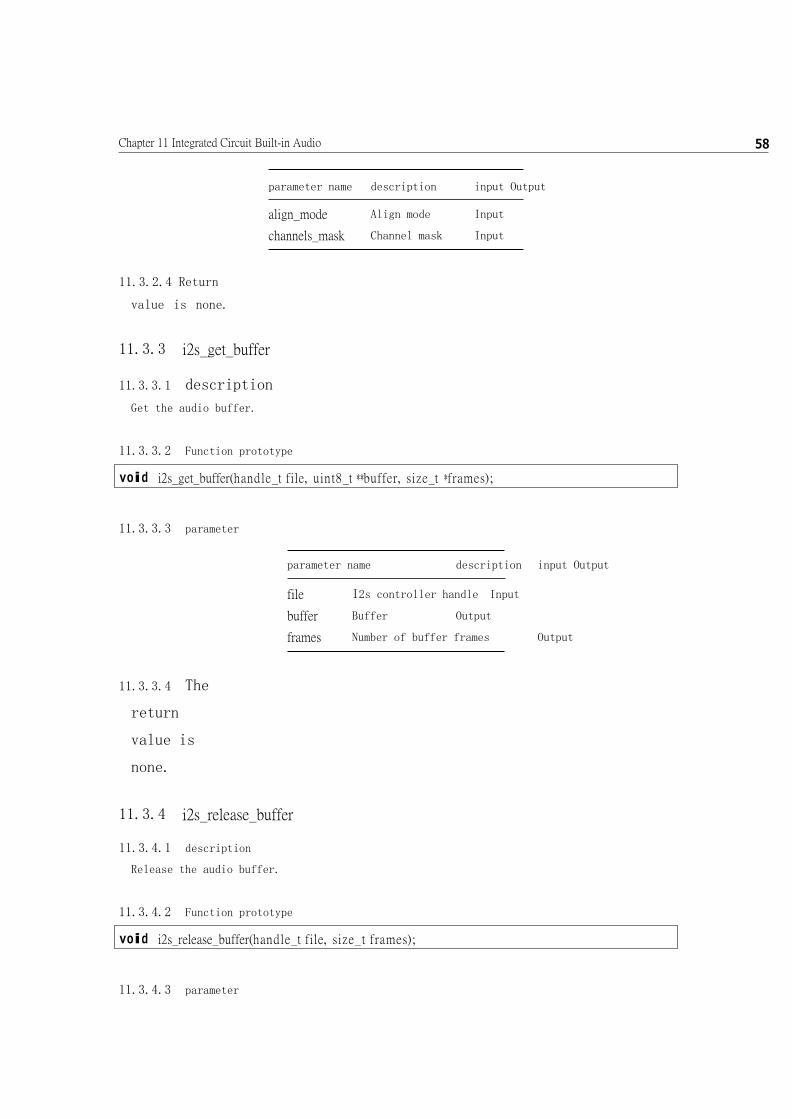
Chapter 11 Integrated Circuit Built-in Audio
Bus (i2s)
58
parameter name description input Output
align_mode Align mode Input
channels_mask Channel mask Input
11.3.2.4 Return
value is none.
11.3.3 i2s_get_buffer
11.3.3.1 description
Get the audio buffer.
11.3.3.2 Function prototype
11.3.3.3 parameter
parameter name description input Output
file I2s controller handle Input
buffer Buffer Output
frames Number of buffer frames Output
11.3.3.4 The
return
value is
none.
11.3.4 i2s_release_buffer
11.3.4.1 description
Release the audio buffer.
11.3.4.2 Function prototype
11.3.4.3 parameter
void i 2 s _ g e t _ b u f f e r ( handle_ t file , uint8_ t ∗∗ buffer , size_ t ∗ frames );
void i 2 s _ r e l e a s e _ b u f f e r ( handle_ t file , size_t frames );

Chapter 11 Integrated Circuit Built-in Audio
Bus (i2s)
59
parameter name description input Output
file I2s controller handle Input
frames Confirm the number of frames that have been read or written
Input
11.3.4.4 The
return
value is
none.
11.3.5 i2s_start
11.3.5.1 description
Start playing or recording.
11.3.5.2 Function prototype
11.3.5.3 parameter
parameter name description input Output
file I2s controller handle Input
11.3.5.4 The
return
value is
none.
11.3.6 i2s_stop
11.3.6.1 description
Stop playing or recording.
11.3.6.2 Function prototype
11.3.6.3 parameter
parameter name description input Output
file I2s controller handle Input
void i 2 s _ s t a r t ( handle_ t file );
void i2s_ stop ( handle_ t file );

Chapter 11 Integrated Circuit Built-in Audio
Bus (i2s)
60
11.3.6.4 The
return
value is
none.
11.3.7 Example
11.4 type of data
The relevant data types and data structures are defined as follows:
• Audio_format_type_t: The audio format type.
• Audio_format_t: Audio format.
• I2s_align_mode_t: I2S alignment mode.
11.4.1 audio_format_type_t
11.4.1.1 Desc
ribe the
audio
format
type.
11.4.1.2 definition
/∗ Loop the pcm audio∗/
handle_ t i2s = io_ open ( " / dev / i2s0 " );
a u d i o _ f o r m a t _ t a u d i o _ f m t = { . type = AUDIO_ FMT_ PCM , . b i t s _ p e r _ s a m p l e = 16 , . s a m p l e _ r a t e
= 44100 , . channels = 2 };
i 2 s _ c o n f i g _ a s _ r e n d e r ( i2s , & audio_fmt , 100 , I2S_ AM_RIGHT , 0 b11 ); i 2 s _ s
t a r t ( i2s );
while (1)
{
uint8_ t ∗ buffer ;
size_ t frames ;
i 2 s _ g e t _ b u f f e r ( i2s , & buffer , & frames );
memcpy ( buffer , pcm , 4 ∗ frames ); i 2 s
_ r e l e a s e _ b u f f e r ( i2s , frames ); pcm += frames ;
if ( pcm >= pcm_ end )
pcm = p c m _ s t a r t ;
}
typedef enum _ a u d i o _ f o r m a t _ t y p e
{ A U D I O _ F M T _
P C M
} a u d i o _ f o r m a t _ t y p e _ t ;

Chapter 11 Integrated Circuit Built-in Audio
Bus (i2s)
61
11.4.1.3 member
Member name description
AUDIO_FMT_PCM PCM
11.4.2 audio_format_t
11.4.2.1 Desc
ribe the
audio format.
11.4.2.2 definition
11.4.2.3 member
Member name description
type bits_per_sample
sample_rate
channels
Audio format
type
sampling
depth
Sampling Rate
Number of channels
11.4.3
i2s_align_mode_t
11.4.3.1 description
I2s alignment mode.
11.4.3.2 definition
typedef struct _ a u d i o _ f o r m a t
{ a u d i o _ f o r m a t _ t y p e _ t type ;
uint32_ t b i t s _ p e r _ s a m p l e ;
uint32_ t s a m p l e _ r a t e ; uint32_ t
channels ; } a u d i o _ f o r m a t _ t ;
typedef enum _ i 2 s _ a l i g n _ m o d e
{
I2S_ AM_
STANDARD ,
I2S_AM_ RIGHT , I
2 S _ A M _ L E F T
} i 2 s _ a l i g n _ m o d e _ t ;

Chapter 11 Integrated Circuit Built-in Audio
Bus (i2s)
62
11.4.3.3 member
Member name description
I2S_AM_STANDARD Standard mode
I2S_AM_RIGHT Align right
I2S_AM_LEFT Align left

63
Chapter 12
Serial peripheral interface (spi)
12.1 Overview
Spi is a high speed, full duplex, synchronous
communication bus.
12.2 Functional description
The spi module has the following features:
• Independent spi device package peripheral related parameters
• Automatic processing of multi-device bus contention
• Support standard, two-wire, four-wire, eight-wire mode
• Supports write-before-read and full-duplex read and write
• Supports sending a series of identical data frames, often used for clearing screens,
filling storage sectors, etc.
12.3 Api reference
Corresponding header file devices.h
Provide users with the following interfaces:
• spi_get_device
• spi_dev_config_non_standard
• spi_dev_set_clock_rate
• spi_dev_transfer_full_duplex
• spi_dev_transfer_sequential
• spi_dev_fill

Chapter 12 Serial Peripheral
Interface (spi)
64
12.3.1 spi_get_device
12.3.1.1 description
Register and open a spi device.
12.3.1.2 Function prototype
12.3.1.3
Parameters
parameter name description input
Output file Spi controller handle Input
name Specify the path to access the device
Input
mode Spi mode Input
frame_format Frame format Input
chip_select_mask Chip select mask Input
data_bit_length Data bit length Input
12.3.1.4 Return value
Sp device handle.
12.3.2 spi_dev_config_non_standard
12.3.2.1 description
Configure non-standard frame format parameters for the spi device.
12.3.2.2 Function prototype
12.3.2.3 parameter
parameter name description input Output
file Spi device handle Input
handle_ t s p i _ g e t _ d e v i c e ( handle_ t file , const char ∗ name , spi_ mode mode , s p i _ f r a
m e _ f o r m a t frame_ format , uint32_ t chip_ select_ mask , uint32_ t d a t a _ b i t _ l e n g t h
);
void s p i _ d e v _ c o n f i g _ n o n _ s t a n d a r d ( handle_ t file , uint32_ t i n s t r u c t i o n _ l e n g t h , uint32_ t address_
length , uint32_ t wait_cycles , s p i _ i n s t _ a d d r _ t r a n s _ m o d e _ t t r a n s _ m o d e );

Chapter 12 Serial Peripheral
Interface (spi)
65
parameter name description input
Output
instruction_length
address_length
wait_cycles trans_mode
Instructio
n length
address
length
waiting
period
Command and address transfer mode
Inpu
t
inpu
t
inpu
t
12.3.2.4
return value
no.
12.3.3 spi_dev_set_clock_rate
12.3.3.1 description
Configure the clock rate of the spi device.
12.3.3.2 Function prototype
12.3.3.3 parameter
parameter name description input Output
file Spi device handle Input
clock_rate Expected clock rate Input
12.3.3.4 return value
The actual rate after setting.
12.3.4 spi_dev_transfer_full_duplex
12.3.4.1 description
Full-duplex transmission of spi devices.
Note: Only standard frame formats are supported.
12.3.4.2 Function prototype
double s p i _ d e v _ s e t _ c l o c k _ r a t e ( handle_ t file , double c l o c k _ r a t e );
int s p i _ d e v _ t r a n s f e r _ f u l l _ d u p l e x ( handle_ t file , const uint8_ t ∗ write_ buffer , size_t write_len ,
uint8_ t ∗ read_buffer , size_ t read_ len );

Chapter 12 Serial Peripheral
Interface (spi)
66
12.3.4.3 Parameters
parameter name description input
Output
file write_buffer
write_len
read_buffer
read_len
Spi device
handle
source
buffer
Number of
bytes to write
to the target
buffer
Maximum number of bytes read
Inpu
t
inpu
t,
inpu
t
and
outp
ut
12.3.4.4 Return value
The number of bytes actually read.
12.3.5 spi_dev_transfer_sequential
12.3.5.1 description
Write the spi device first and then read it.
Note: Only standard frame formats are supported.
12.3.5.2 Function prototype
12.3.5.3 parameter
parameter name description input Output
file Spi device handle
Input
write_buffer Source buffer Input
write_len The number of bytes to write
Input
read_buffer Target buffer Output
read_len Maximum number of bytes read
Input
12.3.5.4 return value
The number of bytes actually read.
int s p i _ d e v _ t r a n s f e r _ s e q u e n t i a l ( handle_ t file , const uint8_ t ∗ write_ buffer , size_t write_len , uint8_
t ∗ read_buffer , size_ t read_ len );

Chapter 12 Serial Peripheral
Interface (spi)
67
12.3.6 spi_dev_fill
12.3.6.1 description
Fill the spi device with a string of identical frames.
Note: Only standard frame formats are supported.
12.3.6.2 Function prototype
12.3.6.3 parameter
parameter name description input Output
file Spi device handle Input
instruction Instruction (ignored in standard frame format) input
address Address (ignored in standard frame format) input
value Frame data Output
count Number of frames Input
12.3.6.4 The
return
value is
none.
12.3.7 Example
12.4 type of data
The relevant data types and data structures are defined as follows:
• Spi_mode_t: SPI mode.
void s p i _ d e v _ f i l l ( handle_ t file , uint32_ t instruction , uint32_ t address , uint32_ t value , size_ t count );
handle_ t spi = io_ open ( " / dev / spi0 " ); /∗ dev0 works in MODE0 mode Standard SPI mode Single -send 8-bit data using chip select 0 ∗/
handle_ t dev0 = s p i _ g e t _ d e v i c e ( spi , " / dev / spi0 / dev0 " , SPI_MODE_0 , SPI_ FF_ STANDARD , 0 b1 , 8);
uint8_ t data_ buf [] = { 0 x06 , 0 x01 , 0 x02 , 0 x04 , 0 , 1 , 2 , 3 }; /∗ Send instruction 0 x06 Send 0, 1 , 2 , 3 four bytes of data to address 0 x010204 ∗ /
io_ write ( dev0 , data_buf , sizeof ( data_ buf )); /∗ Send instruction 0 x06 Address 0 x010204 Receive four bytes of data ∗/
s p i _ d e v _ t r a n s f e r _ s e q u e n t i a l ( dev0 , data_buf , 4 , data_buf , 4);

Chapter 12 Serial Peripheral
Interface (spi)
68
• Spi_frame_format_t: SPI frame format.
• Spi_inst_addr_trans_mode_t: Transmission mode of the SPI instruction and
address.
12.4.1 spi_mode_t
12.4.1.1 description
Spi mode.
12.4.1.2 definition
12.4.1.3 member
Member name descriptio
n
SPI_MODE_
0
SPI_MODE_
1
SPI_MODE_
2
SPI_MODE_
3
Spi mode 0
Spi mode 1
Spi mode 2
Spi mode 3
12.4.2
spi_frame_format_t
12.4.2.1 description
Spi frame format.
12.4.2.2 definition
typedef enum _ s p i _ m o d e
{ SPI_MODE_
0 ,
SPI_MODE_
1 ,
SPI_MODE_
2 ,
SPI_MODE_
3 ,
} s p i _ m o d e _ t ;
typedef enum _ s p i _ f r a m e _ f o r m a t
{ SPI_ FF_
STANDARD ,
SPI_FF_DUAL ,
SPI_FF_QUAD ,
S P I _ F F _ O C T A L
} s p i _ f r a m e _ f o r m a t _ t ;

Chapter 12 Serial Peripheral
Interface (spi)
69
12.4.2.3 member
Member name description
SPI_FF_STANDARD standard
SPI_FF_DUAL Double line
SPI_FF_QUAD Four lines
SPI_FF_OCTAL Eight lines (not supported by /dev/spi3)
12.4.3 spi_inst_addr_trans_mode_t
12.4.3.1 description
The transmission mode of the spi instruction and address.
12.4.3.2 definition
12.4.3.3 member
Member name description
SPI_AITM_STANDARD Use standard frame format
SPI_AITM_ADDR_STANDARD The instruction uses the configured value and the
address uses the standard frame format
SPI_AITM_AS_FRAME_FORMAT Use configured values
typedef enum _ s p i _ i n s t _ a d d r _ t r a n s _ m o d e
{ SPI _ A IT M_ ST AN DA
RD , S P I _ A I T M _ A D D R _ S T
A N D A R D , S P I _ A I T M _ A S _
F R A M E _ F O R M A T } s p i _ i n s t _ a d d r _ t r a n s _ m o d e _ t ;

70
Chapter 13
Digital camera interface (dvp)
13.1 Overview
Dvp is a camera interface module that supports forwarding
camera input image data to the ai module or memory.
13.2 Functional description
The dvp module has the following features:
• 2 video data output ports for RGB565 and RGB24Planar
• Support for dropping frames that do not need to be processed
13.3 Api reference
Corresponding header file devices.h
Provide users with the following interfaces:
• dvp_config
• dvp_enable_frame
• dvp_get_output_num
• dvp_set_signal
• dvp_set_output_enable
• dvp_set_output_attributes
• dvp_set_frame_event_enable
• dvp_set_on_frame_event
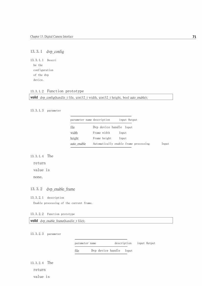
Chapter 13. Digital Camera Interface
(dvp)
71
13.3.1 dvp_config
13.3.1.1 Descri
be the
configuration
of the dvp
device.
13.3.1.2 Function prototype
13.3.1.3 parameter
parameter name description input Output
file Dvp device handle Input
width Frame width Input
height Frame height Input
auto_enable Automatically enable frame processing Input
13.3.1.4 The
return
value is
none.
13.3.2 dvp_enable_frame
13.3.2.1 description
Enable processing of the current frame.
13.3.2.2 Function prototype
13.3.2.3 parameter
parameter name description input Output
file Dvp device handle Input
13.3.2.4 The
return
value is
void d v p _ c o n f i g ( handle_ t file , uint32_ t width , uint32_ t height , bool a u t o _ e n a b l e );
void d v p _ e n a b l e _ f r a m e ( handle_ t file );

Chapter 13. Digital Camera Interface
(dvp)
72
none.

Chapter 13. Digital Camera Interface
(dvp)
73
13.3.3 dvp_get_output_num
13.3.3.1 description
Get the number of outputs of the dvp device.
13.3.3.2 Function prototype
13.3.3.3 parameter
parameter name description input Output
file Dvp device handle Input
13.3.3.4 Retu
rns the
number of
output.
13.3.4 dvp_set_signal
13.3.4.1 description
Set the dvp signal status.
13.3.4.2 Function prototype
13.3.4.3 Parameters
parameter name
description input Output
file
type
value
Dvp device
handle
signal type
Status value
Inpu
t
inpu
t
13.3.4.4 Return value
no.
uint32_ t d v p _ g e t _ o u t p u t _ n u m ( handle_ t file );
void d v p _ s e t _ s i g n a l ( handle_ t file , d v p _ s i g n a l _ t y p e _ t type , bool value );

Chapter 13. Digital Camera Interface
(dvp)
74
13.3.5 dvp_set_output_enable
13.3.5.1 description
Set whether dvp output is enabled.
13.3.5.2 Function prototype
13.3.5.3 parameter
parameter name description input Output
file Dvp device handle Input
index Output index Input
enable Whether to enable Input
13.3.5.4 The
return
value is
none.
13.3.6 dvp_set_output_attributes
13.3.6.1 description
Set the dvp output characteristics.
13.3.6.2 Function prototype
13.3.6.3 Parameters
parameter name description input
Output
file index
format
output_buffer
Dvp device
handle
output index
Video format
Output buffer
Inpu
t
inpu
t
and
outp
ut
void d v p _ s e t _ o u t p u t _ e n a b l e ( handle_ t file , uint32_ t index , bool enable );
void d v p _ s e t _ o u t p u t _ a t t r i b u t e s ( handle_ t file , uint32_ t index , v i d e o _ f o r m a t _ t format , void ∗ o u t p u t _ b u f f e r );

Chapter 13. Digital Camera Interface
(dvp)
75
13.3.6.4 Return
value None.
13.3.7 dvp_set_frame_event_enable
13.3.7.1 description
Sets whether dvp frame events are enabled.
13.3.7.2 Function prototype
13.3.7.3 parameter
parameter name description input Output
file Dvp device handle Input
event Frame event Input
enable Whether to enable Input
13.3.7.4 The
return
value is
none.
13.3.8 dvp_set_on_frame_event
13.3.8.1 description
Set the dvp frame event handler.
13.3.8.2 Function prototype
13.3.8.3 Parameters
parameter name
description input Output
file handler
userdata
Dvp device
handle
handler
Handler user data
Inpu
t
inpu
t
void d v p _ s e t _ f r a m e _ e v e n t _ e n a b l e ( handle_ t file , d v p _ f r a m e _ e v e n t _ t event , bool enable );
void d v p _ s e t _ o n _ f r a m e _ e v e n t ( handle_ t file , d v p _ o n _ f r a m e _ e v e n t _ t handler , void ∗ userdata );

Chapter 13. Digital Camera Interface
(dvp)
76
13.3.8.4 Return
value None.
13.3.9 Example
13.4 type of data
The relevant data types and data structures are defined as
follows:
• Video_format_t: Video format.
• Dvp_frame_event_t: DVP frame event.
• Dvp_signal_type_t: DVP signal type.
• Dvp_on_frame_event_t: DVP frame event handler.
13.4.1 video_format_t
13.4.1.1 Des
cribe the
video
format.
13.4.1.2 definition
13.4.1.3 member
Member name description
VIDEO_FMT_RGB565 RGB565
VIDEO_FMT_RGB24_PLANAR
RGB24 Planar
handle_ t dvp = io_ open ( " / dev / dvp0 " );
d v p _ c o n f i g ( dvp , 320 , 240 , false ); d v p _ s e t _ o n
_ f r a m e _ e v e n t ( dvp , on_ frame_ isr , NULL ); d v p _ s e t _ f r a m e _ e v e
n t _ e n a b l e ( dvp , VIDEO_ FE_ BEGIN , true );
d v p _ s e t _ o u t p u t _ a t t r i b u t e s ( dvp , 0 , VIDEO_ FMT_ RGB565 , l c d _ g r a m 0 ); d v
p _ s e t _ o u t p u t _ e n a b l e ( dvp , 0 , true );
typedef enum _ v i d e o _ f o r m a t
{ VIDEO_ FMT_
RGB565 , V I D E O _ F M T
_ R G B 2 4 _ P L A N A R
} v i d e o _ f o r m a t _ t ;

Chapter 13. Digital Camera Interface
(dvp)
77
13.4.2 dvp_frame_event_t
13.4.2.1 description
Dvp frame event.
13.4.2.2 definition
13.4.2.3 member
Member name description
VIDEO_FE_BEGIN Frame start
VIDEO_FE_END End of frame
13.4.3 dvp_signal_type_t
13.4.3.1 description
Dvp signal type.
13.4.3.2 definition
typedef enum _ d v p _ s i g n a l _ t y p e
{
D V P _ S I G _ P O W E R _ D O W N ,
D V P _ S I G _ R E S E T
} d v p _ s i g n a l _ t y p e _ t ;
13.4.3.3 Members
Member name description
DVP_SIG_POWER_DO
WN DVP_SIG_RESET
Powe
r
down
rese
t
typedef enum _ v i d e o _ f r a m e _ e v e n t
{ VIDEO_ FE_
BEGIN , V I D E O _
F E _ E N D
} d v p _ f r a m e _ e v e n t _ t ;

Chapter 13. Digital Camera Interface
(dvp)
78
13.4.4 dvp_on_frame_event_t
13.4.4.1 description
The handler when the timer is triggered.
13.4.4.2 definition
13.4.4.3 parameter
parameter name description input Output
userdata User data Input
typedef void (∗ d v p _ o n _ f r a m e _ e v e n t _ t )( d v p _ f r a m e _ e v e n t _ t event , void ∗ userdata );

79
Chapter 14
Serial camera control bus (sccb)
14.1 Overview Sccb is a serial camera control bus.
14.2 Functional description The sccb module has the following features:
• Independent sccb device package peripheral related parameters
• Automatic processing of multi-device bus contention
14.3 Api reference
Corresponding header file devices.h
Provide users with the following interfaces:
• sccb_get_device
• sccb_dev_read_byte
• sccb_dev_write_byte
14.3.1 sccb_get_device
14.3.1.1 description
Register and open an sccb device.

Chapter 14 Serial Camera Control Bus (sccb)
80
14.3.1.2 Function prototype
14.3.1.3
Parameters
parameter name description input
Output
file
name
slave_address
reg_address_width
Sccb controller handle
Specify the path
from the device to
access the device
Register address width
Inpu
t
inpu
t
inpu
t
14.3.1.4 Return value
Sccb device handle.
14.3.2 sccb_dev_read_byte
14.3.2.1 description
Read a byte from the scbb device.
14.3.2.2 Function prototype
14.3.2.3 parameter
parameter name description input Output
file Sccb device handle Input
reg_address Register address Input
14.3.2.4 Retu
rns the
byte read
by the
value.
handle_ t s c c b _ g e t _ d e v i c e ( handle_ t file , const char ∗ name , size_ t slave_ address , size_ t r e g _ a d d r e
s s _ w i d t h );
uint8_ t s c c b _ d e v _ r e a d _ b y t e ( handle_ t file , uint16_ t r e g _ a d d r e s s );

Chapter 14 Serial Camera Control Bus (sccb)
81
14.3.3 sccb_dev_write_byte
14.3.3.1 description
Write a byte to the sccc device.
14.3.3.2 Function prototype
14.3.3.3 parameter
parameter name description input Output
file Sccb device handle Input
reg_address Register address Input
value The byte to be written Input
14.3.3.4 The
return
value is
none.
14.3.4 Example
void s c c b _ d e v _ w r i t e _ b y t e ( handle_ t file , uint16_ t reg_address , uint8_ t value );
handle_ t sccb = io_ open ( " / dev / sccb0 " );
handle_ t dev0 = s c c b _ g e t _ d e v i c e ( sccb , " / dev / sccb0 / dev0 " , 0 x60 , 8);
s c c b _ d e v _ w r i t e _ b y t e ( dev0 , 0 xFF , 0);
uint8_ t value = s c c b _ d e v _ r e a d _ b y t e ( dev0 , 0 xFF );

82
Chapter 15
Timer
15.1 Overview The timer provides high-precision timing.
15.2 Functional description The timer module has the following features:
• Enable or disable the timer
• Configure the timer trigger interval
• Configuring the timer trigger handler
15.3 Api reference
Corresponding header file devices.h
Provide users with the following interfaces:
• timer_set_interval
• timer_set_on_tick
• timer_set_enable
15.3.1 timer_set_interval
15.3.1.1 description
Set the timer trigger interval.

Chapter 15 Timer
83
15.3.1.2 Function prototype
15.3.1.3 Parameters
parameter name
description input Output
file nanoseconds Timer device
handle
interval
(nanoseconds)
Inpu
t
inpu
t
15.3.1.4 Return value
Actual trigger interval (nanoseconds).
15.3.2 timer_set_on_tick
15.3.2.1 description
Set the handler when the timer fires.
15.3.2.2 Function prototype
15.3.2.3 parameter
parameter name description input Output
file Timer device handle Input
on_tick Handler Input
userdata Handler user data Input
15.3.2.4 The
return
value is
none.
15.3.3 timer_set_enable
15.3.3.1 description
Set whether timer is enabled.
size_ t t i m e r _ s e t _ i n t e r v a l ( handle_ t file , size_t n a n o s e c o n d s );
void t i m e r _ s e t _ o n _ t i c k ( handle_ t file , t i m e r _ o n _ t i c k _ t on_tick , void ∗ userdata );

Chapter 15 Timer
84
15.3.3.2 Function prototype
15.3.3.3 parameter
parameter name description input Output
file Timer device handle Input
enable Whether to enable Input
15.3.3.4 The
return
value is
none.
15.3.4 Example
15.4 type of data
The relevant data types and data structures are defined as follows:
• Timer_on_tick_t: The handler when TIMER is triggered.
15.4.1 timer_on_tick_t
15.4.1.1 description
The handler when the timer is triggered.
15.4.1.2 definition
void t i m e r _ s e t _ e n a b l e ( handle_ t file , bool enable );
/∗ Timer 0 Print Time OK at 1 second! ∗/
void on_ tick ( void ∗ unused )
{ printf ( " Time ␣OK !\ n " );
}
handle_ t timer = io_ open ( " / dev / timer0 " );
t i m e r _ s e t _ i n t e r v a l ( timer , 1 e9 ); t i m e r _ s e t _
o n _ t i c k ( timer , on_tick , NULL ); t i m e r _ s e t _ e n a
b l e ( timer , true );

Chapter 15 Timer
85
15.4.1.3 parameter
parameter name description input Output
userdata User data Input
typedef void (∗ t i m e r _ o n _ t i c k _ t )( void ∗ userda ta );

86
Chapter 16
Pulse width modulator (pwm)
16.1 Overview Pwm is used to control the duty cycle of the pulse output.
16.2 Functional description The pwm module has the following features:
• Configure the pwm output frequency
• Configure the output duty cycle of each pin of pwm
16.3 Api reference
Corresponding header file devices.h
Provide users with the following interfaces:
• pwm_get_pin_count
• pwm_set_frequency
• pwm_set_active_duty_cycle_percentage
• pwm_set_enable
16.3.1 pwm_get_pin_count
16.3.1.1 description
Get the number of pwm pins.

Chapter 16 Pulse Width Modulator
(pwm)
87
16.3.1.2 Function prototype
16.3.1.3 parameter
parameter name description input Output
file Pwm device handle Input
16.3.1.4 return value
The number of pwm pins.
16.3.2 pwm_set_frequency
16.3.2.1 Descri
ption Sets the
pwm frequency.
16.3.2.2 Function prototype
16.3.2.3 Parameters
parameter name
description input Output
file frequency Pwm device
handle
Expected frequency (Hz)
Inpu
t
inpu
t
16.3.2.4 Return value
The actual frequency (Hz) after setting.
16.3.3 pwm_set_active_duty_cycle_percentage
16.3.3.1 description
Set the pwm pin duty cycle.
16.3.3.2 Function prototype
uint32_ t p w m _ g e t _ p i n _ c o u n t ( handle_ t file );
double p w m _ s e t _ f r e q u e n c y ( handle_ t file , double f r e q u e n c y );

Chapter 16 Pulse Width Modulator
(pwm)
88
16.3.3.3 Parameters
parameter name description input
Output
file
pin
duty_cycle_percentage
Pwm device
handle pin
number
Expected duty cycle
Inpu
t
inpu
t
16.3.3.4 Return value
The actual duty cycle after setting.
16.3.4 pwm_set_enable
16.3.4.1 description
Set whether the pwm pin is enabled.
16.3.4.2 Function prototype
16.3.4.3 Parameters
parameter name
description input Output
file pin
enable
Pwm device
handle pin
number
Whether to enable
Inpu
t
inpu
t
16.3.4.4 Return value
The actual duty cycle after setting.
16.3.5 Example
double p w m _ s e t _ a c t i v e _ d u t y _ c y c l e _ p e r c e n t a g e ( handle_ t file , uint32_ t pin , double
d u t y _ c y c l e _ p e r c e n t a g e );
void p w m _ s e t _ e n a b l e ( handle_ t file , uint32_ t pin , bool enable );
/∗ pwm0 pin0 outputs 200 KHZ square wave with duty
cycle of 0.5 / handle_ t pwm = io_ open ( " / dev /
pwm0 " ); pwm _ set _ frequency ( pwm , 200000); pwm
_ set _ active _ duty _ cycle _ percentage ( pwm ,
0 , 0.5);

Chapter 16 Pulse Width Modulator
(pwm)
89
p w m _ s e t _ e n a b l e ( pwm , 0 , true );

90
Chapter 17
Watchdog timer (wdt)
17.1 Overview
Wdt provides recovery when the system is in error or not
responding.
17.2 Functional description
The wdt module has the following features:
• Configuration timeout
• Manual restart timing
• Configured to reset or enter interrupt after timeout
• Clear the interrupt after entering the interrupt to cancel the reset, otherwise wait for the second timeout after reset
17.3 Api reference
Corresponding header file devices.h
Provide users with the following interfaces:
• wdt_set_response_mode
• wdt_set_timeout
• wdt_set_on_timeout
• wdt_restart_counter
• wdt_set_enable

Chapter 17 Watchdog Timer (wdt)
91
17.3.1 wdt_set_response_mode
17.3.1.1 description
Set the wdt response mode.
17.3.1.2 Function prototype
17.3.1.3 parameter
parameter name description input Output
file Wdt device handle Input
mode Response mode Input
17.3.1.4 The
return
value is
none.
17.3.2 wdt_set_timeout
17.3.2.1 description
Set the wdt timeout.
17.3.2.2 Function prototype
17.3.2.3 parameter
parameter name description input Output
file Wdt device handle Input
nanoseconds Expected timeout (nanoseconds) input
17.3.2.4 return value
The actual timeout (nanoseconds) after setting.
void w d t _ s e t _ r e s p o n s e _ m o d e ( handle_ t file , w d t _ r e s p o n s e _ m o d e _ t mode );
size_ t w d t _ s e t _ t i m e o u t ( handle_ t file , size_t n a n o s e c o n d s );

Chapter 17 Watchdog Timer (wdt)
92
17.3.3 wdt_set_on_timeout
17.3.3.1 description
Set the wdt timeout handler.
17.3.3.2 Function prototype
17.3.3.3 parameter
parameter name description input Output
file Wdt device handle Input
handler Handler Input
userdata Handler user data Input
17.3.3.4 The
return
value is
none.
17.3.4 wdt_restart_counter
17.3.4.1 description
Cause wdt to restart counting.
17.3.4.2 Function prototype
17.3.4.3 parameter
parameter name description input Output
file Wdt device handle Input
17.3.4.4 The
return
value is
none.
void w d t _ s e t _ o n _ t i m e o u t ( handle_ t file , w d t _ o n _ t i m e o u t _ t handler , void ∗ userdata );
void w d t _ r e s t a r t _ c o u n t e r ( handle_ t file );

Chapter 17 Watchdog Timer (wdt)
93
17.3.5 wdt_set_enable
17.3.5.1 description
Set whether wdt is enabled.
17.3.5.2 Function prototype
17.3.5.3 parameter
parameter name description input Output
file Wdt device handle Input
enable Whether to enable Input
17.3.5.4 The
return
value is
none.
17.3.6 Example
17.4 type of data
The relevant data types and data structures are defined as follows:
• Wdt_response_mode_t: WDT response mode.
• Wdt_on_timeout_t: WDT timeout handler.
void w d t _ s e t _ e n a b l e ( handle_ t file , bool enable );
/∗ After 2 seconds, enter the watchdog interrupt function to print the imeout, and then reset it in 2 seconds.
void o n _ t i m e o u t ( void ∗ unused )
{ printf ( " Timeout \ n " );
}
handle_ t wdt = io_ open ( " / dev / wdt0 " );
w d t _ s e t _ r e s p o n s e _ m o d e ( wdt , W D T _ R E S P _ I N T E R R U P
T ); w d t _ s e t _ t i m e o u t ( wdt , 2 e9 );
w d t _ s e t _ o n _ t i m e o u t ( wdt , on_timeout , NULL ); w
d t _ s e t _ e n a b l e ( wdt , true );

Chapter 17 Watchdog Timer (wdt)
94
17.4.1 wdt_response_mode_t
17.4.1.1 description
Wdt response mode.
17.4.1.2 definition
17.4.1.3 member
Member name description
WDT_RESP_RESET Reset system after timeout
WDT_RESP_INTERRUPT Enter the interrupt after timeout, reset the
system again after timeout
17.4.2 wdt_on_timeout_t
17.4.2.1 description
Wdt timeout handler.
17.4.2.2 definition
17.4.2.3 parameter
parameter name description input Output
userdata User data Input
17.4.2.4 return value
return value description
0 The system will reset if the interrupt is not cleared.
typedef enum _ w d t _ r e s p o n s e _ m o d e
{ WDT_ RESP_
RESET , W D T _ R E S
P _ I N T E R R U P T
} w d t _ r e s p o n s e _ m o d e _ t ;
typedef int (∗ w d t _ o n _ t i m e o u t _ t )( void ∗ userda ta );

Chapter 17 Watchdog Timer (wdt)
95
return value description
1 Clear interrupt, system does not reset

96
Chapter 18
Fast Fourier Transform Accelerator
(fft)
18.1 Overview The fft module is hardware-based to implement the base 2 time-division acceleration of fft.
18.2 Functional description The module currently supports 64-point, 128-point, 256-point, and 512-point FFTs as well as
IFFT.Inside the FFT, there are two SRAMs with a size of 512 * 32 bits. After the configuration
is completed, the FFT sends a TX request to the DMA, and the DMA sent the data is placed in one
of the SRAMs until the current FFT operation is satisfied. The amount of data starts and the FFT
operation begins. The butterfly unit reads the data from the SRAM containing the valid data.
After the operation ends, the data is written to another SRAM, and the next butterfly operation
is performed from the SRAM just written. The data is read out, and after the operation is
completed, another SRAM is written, and thus iteratively repeats until the entire FFT operation
is completed.
18.3 Api reference
Corresponding header file fft.h
Provide users with the following interfaces:
• fft_complex_uint16
18.3.1 fft_complex_uint16
18.3.1.1 description
Fft operation.
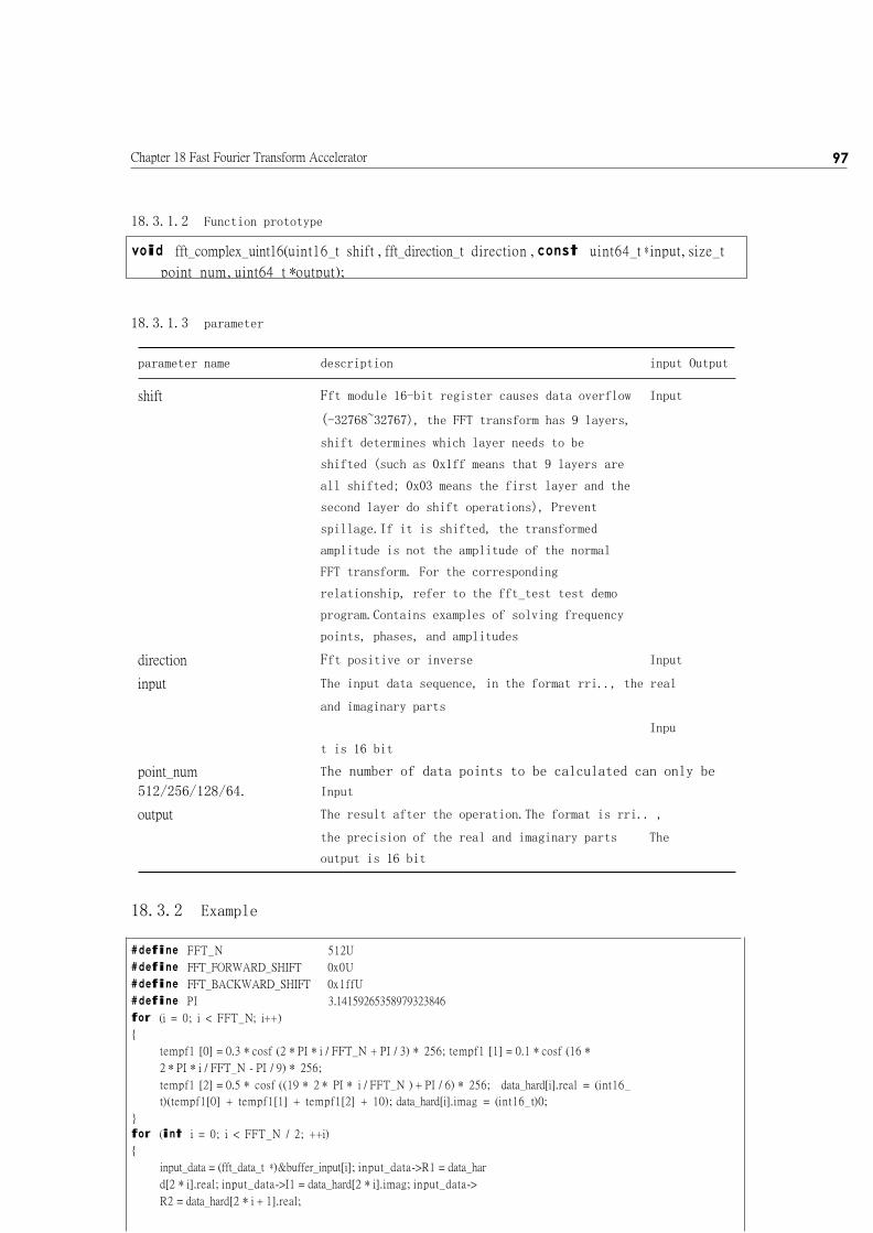
Chapter 18 Fast Fourier Transform Accelerator
(fft)
97
18.3.1.2 Function prototype
18.3.1.3 parameter
parameter name description input Output
shift Fft module 16-bit register causes data overflow Input
(-32768~32767), the FFT transform has 9 layers,
shift determines which layer needs to be
shifted (such as 0x1ff means that 9 layers are
all shifted; 0x03 means the first layer and the
second layer do shift operations), Prevent
spillage.If it is shifted, the transformed
amplitude is not the amplitude of the normal
FFT transform. For the corresponding
relationship, refer to the fft_test test demo
program.Contains examples of solving frequency
points, phases, and amplitudes
direction Fft positive or inverse Input
input The input data sequence, in the format rri.., the real
and imaginary parts
Inpu
t is 16 bit
point_num The number of data points to be calculated can only be
512/256/128/64. Input
output The result after the operation.The format is rri.. ,
the precision of the real and imaginary parts The
output is 16 bit
18.3.2 Example
void f f t _ c o m p l e x _ u i n t 1 6 ( uint16_ t shift , f f t _ d i r e c t i o n _ t direction , const uint64_ t ∗ input , size_t
point_num , uint64_ t ∗ output );
# define FFT_N 512 U
# define F F T _ F O R W A R D _ S H I F T 0 x0U
# define F F T _ B A C K W A R D _ S H I F T 0 x1ffU
# define PI 3 . 1 4 1 5 9 2 6 5 3 5 8 9 7 9 3 2 3 8 4 6
for ( i = 0; i < FFT_N ; i ++)
{
tempf1 [0] = 0.3 ∗ cosf (2 ∗ PI ∗ i / FFT_N + PI / 3) ∗ 256; tempf1 [1] = 0.1 ∗ cosf (16 ∗
2 ∗ PI ∗ i / FFT_N - PI / 9) ∗ 256;
tempf1 [2] = 0.5 ∗ cosf ((19 ∗ 2 ∗ PI ∗ i / FFT_N ) + PI / 6) ∗ 256; d a t a _ h a r d [ i ]. real = ( int16_
t )( tempf1 [0] + tempf1 [1] + tempf1 [2] + 10); d a t a _ h a r d [ i ]. imag = ( int16_ t )0;
}
for ( int i = 0; i < FFT_N / 2; ++ i )
{
i n p u t _ d a t a = ( f f t _ d a t a _ t ∗)& b u f f e r _ i n p u t [ i ]; input_data - > R1 = d a t a _ h a r
d [2 ∗ i ]. real ; input_data - > I1 = d a t a _ h a r d [2 ∗ i ]. imag ; input_data - >
R2 = d a t a _ h a r d [2 ∗ i + 1]. real ;

Chapter 18 Fast Fourier Transform Accelerator
(fft)
98
18.4 type of data
The relevant data types and data structures are defined as follows:
• fft_data_t:fft Operates the incoming data format.
• fft_direction_t:fft operation mode.
18.4.1 fft_data_t
18.4.1.1 description
Fft computes the incoming data format.
18.4.1.2 definition
input_data - > I2 = d a t a _ h a r d [2 ∗ i + 1]. imag ;
}
f f t _ c o m p l e x _ u i n t 1 6 ( F FT _ F OR WA RD _ S HI FT , FFT_ DIR_ FORWARD , buffer_ input , FFT_N , b u f f e r _ o u t p u t );
for ( i = 0; i < FFT_N / 2; i ++)
{
o u t p u t _ d a t a = ( f f t _ d a t a _ t ∗)& b u f f e r _ o u t p u t [ i ]; d a t a _ h a r d [2 ∗ i ]. imag
= output_data - > I1 ; d a t a _ h a r d [2 ∗ i ]. real = output_data - >
R1 ; d a t a _ h a r d [2 ∗ i + 1]. imag = output_data - > I2 ; d a t a _ h a r d [2
∗ i + 1]. real = output_data - > R2 ;
}
for ( int i = 0; i < FFT_N / 2; ++ i )
{
i n p u t _ d a t a = ( f f t _ d a t a _ t ∗)& b u f f e r _ i n p u t [ i ]; input_data - > R1 = d a t a _ h a r
d [2 ∗ i ]. real ; input_data - > I1 = d a t a _ h a r d [2 ∗ i ]. imag ; input_data - >
R2 = d a t a _ h a r d [2 ∗ i + 1]. real ; input_data - > I2 = d a t a _ h a r d [2 ∗ i + 1].
imag ;
}
f f t _ c o m p l e x _ u i n t 1 6 ( F F T _ B A C K W A R D _ S H I F T , FFT_ DIR_ BACKWARD , buffer_ input , FFT_N , b u f f e r _ o u t p u t );
for ( i = 0; i < FFT_N / 2; i ++)
{
o u t p u t _ d a t a = ( f f t _ d a t a _ t ∗)& b u f f e r _ o u t p u t [ i ]; d a t a _ h a r d [2 ∗ i ]. imag
= output_data - > I1 ; d a t a _ h a r d [2 ∗ i ]. real = output_data - >
R1 ; d a t a _ h a r d [2 ∗ i + 1]. imag = output_data - > I2 ; d a t a _ h a r d [2
∗ i + 1]. real = output_data - > R2 ;
}
typedef struct t a g _ f f t _ d a t a
{
int16_ t I1 ;

Chapter 18 Fast Fourier Transform Accelerator
(fft)
99
18.4.1.3 member
Member name description
I1 The imaginary part of the first data
R1 The real part of the first data
I2 The imaginary part of the second data
R2 The real part of the second data
18.4.2 fft_direction_t
18.4.2.1 description
Fft operation mode
18.4.2.2 definition
18.4.2.3 member
Member name description
FFT_DIR_BACKWARD Fft inverse transform
FFT_DIR_FORWARD Fft positive transform
int16_ t R1 ;
int16_ t I2 ;
int16_ t R2 ;
} f f t _ d a t a _ t ;
typedef enum t a g _ f f t _ d i r e c t i o n
{
FFT_ DIR_
BACKWARD , FFT_
DIR_ FORWARD ,
FFT_DIR_MAX ,
} f f t _ d i r e c t i o n _ t ;

100
Chapter 19
Secure Hash Algorithm Accelerator
(sha256)
19.1 Overview The sha256 module uses hardware to implement the time division operation acceleration of sha256.
19.2 Functional description • Support for sha-256 calculations
19.3 Api reference
Corresponding header file sha256.h
Provide users with the following interfaces:
• sha256_hard_calculate
19.3.1 sha256_hard_calculate
19.3.1.1 description
Shabrating the data
19.3.1.2 Function prototype
19.3.1.3 parameter
void s h a 2 5 6 _ h a r d _ c a l c u l a t e ( const uint8_ t ∗ input , size_ t input_len , uint8_ t ∗ output );

Chapter 19. Secure Hash Algorithm Accelerator
(sha256)
101
parameter name
description input Output
input Data to be calculated by sha256 Input
input_len Waiting for sha256 to calculate the length of the data Input
output To store the result of the SHA256 calculation, ensure that the size of the incoming buffer is 32 bytes.
Output
19.3.2 Example
uint8_ t hash [32];
s h a 2 5 6 _ h a r d _ c a l c u l a t e (( uint8_ t ∗) " abc " , 3 , hash );

102
Chapter 20
Advanced crypto accelerator (aes)
20.1 Overview The aes module is hardware-based to implement the time-division acceleration of aes.
20.2 Functional description The k210 has built-in aes (Advanced Encryption Accelerator), which can greatly improve the
speed of aes operation compared to software.The aes accelerator supports multiple
encryption/decryption modes (ecb, cbc, gcm) and multiple length keys (128, 192, 256).
20.3 Api reference
Corresponding header file aes.h
Provide users with the following interfaces:
• aes_ecb128_hard_encrypt
• aes_ecb128_hard_decrypt
• aes_ecb192_hard_encrypt
• aes_ecb192_hard_decrypt
• aes_ecb256_hard_encrypt
• aes_ecb256_hard_decrypt
• aes_cbc128_hard_encrypt
• aes_cbc128_hard_decrypt
• aes_cbc192_hard_encrypt
• aes_cbc192_hard_decrypt
• aes_cbc256_hard_encrypt

Chapter 20. Advanced Encryption
Accelerator (aes)
103
• aes_cbc256_hard_decrypt
• aes_gcm128_hard_encrypt
• aes_gcm128_hard_decrypt
• aes_gcm192_hard_encrypt
• aes_gcm192_hard_decrypt
• aes_gcm256_hard_encrypt
• aes_gcm256_hard_decrypt
20.3.1 aes_ecb128_hard_encrypt
20.3.1.1 description
Aes-ecb-128 encryption operation
20.3.1.2 Function prototype
20.3.1.3 parameter
parameter name
description input Output
input_key Aes-ecb-128 encrypted key Input
input_data Aes-ecb-128 plaintext data to be encrypted Input
input_len Aes-ecb-128 Length of plaintext data to be encrypted
Input
output_data The result of the AES-ECB-128 encryption operation is stored in this buffer.
Output
20.3.1.4 The
return value is
none.
20.3.2 aes_ecb128_hard_decrypt
20.3.2.1 description
Aes-ecb-128 decryption operation
20.3.2.2 Function prototype
void a e s _ e c b 1 2 8 _ h a r d _ e n c r y p t ( uint8_ t ∗ input_key , uint8_ t ∗ input_data , size_t input_len , uint8_ t ∗
o u t p u t _ d a t a )
void a e s _ e c b 1 2 8 _ h a r d _ d e c r y p t ( uint8_ t ∗ input_key , uint8_ t ∗ input_data , size_t input_len , uint8_ t ∗
o u t p u t _ d a t a )

Chapter 20. Advanced Encryption
Accelerator (aes)
104
20.3.2.3 parameter
parameter name
description input Output
input_key
input_data
input_len
output_data
Aes-ecb-128 decrypted key
Aes-ecb-128 ciphertext data to be decrypted
Aes-ecb-128 Length of ciphertext data to be decrypted
The result of the AES-ECB-128 decryption operation is stored in this buffer.
Inpu
t
inpu
t
and
outp
ut
20.3.2.4
return value
no.
20.3.3 aes_ecb192_hard_encrypt
20.3.3.1 description
Aes-ecb-192 encryption operation
20.3.3.2 Function prototype
20.3.3.3 parameter
parameter name
description input Output
input_key
input_data
input_len
output_data
Aes-ecb-192 encrypted key
Aes-ecb-192 plaintext data to be encrypted
Aes-ecb-192 Length of plaintext data to be encrypted
The result of AES-ECB-192 encryption operation is stored in this buffer.
Inpu
t
inpu
t
and
outp
ut
20.3.3.4
return value
no.
20.3.4 aes_ecb192_hard_decrypt
20.3.4.1 description
Aes-ecb-192 decryption operation
void a e s _ e c b 1 9 2 _ h a r d _ e n c r y p t ( uint8_ t ∗ input_key , uint8_ t ∗ input_data , size_t input_len , uint8_ t ∗
o u t p u t _ d a t a )

Chapter 20. Advanced Encryption
Accelerator (aes)
105
20.3.4.2 Function prototype
20.3.4.3 parameter
parameter name
description input Output
input_key
input_data
input_len
output_data
Aes-ecb-192 decrypted key
Aes-ecb-192 ciphertext data to be decrypted
Aes-ecb-192 Length of ciphertext data to be decrypted
The result of the AES-ECB-192 decryption operation is stored in this buffer.
Inpu
t
inpu
t
and
outp
ut
20.3.4.4
return value
no.
20.3.5 aes_ecb256_hard_encrypt
20.3.5.1 description
Aes-ecb-256 encryption operation
20.3.5.2 Function prototype
20.3.5.3 parameter
parameter name
description input Output
input_key Aes-ecb-256 encrypted key Input
input_data Aes-ecb-256 plaintext data to be encrypted Input
input_len Aes-ecb-256 Length of plaintext data to be encrypted
Input
output_data The result of the AES-ECB-256 encryption operation is stored in this buffer.
Output
20.3.5.4 The
return value is
none.
void a e s _ e c b 1 9 2 _ h a r d _ d e c r y p t ( uint8_ t ∗ input_key , uint8_ t ∗ input_data , size_t input_len , uint8_ t ∗
o u t p u t _ d a t a )
void a e s _ e c b 2 5 6 _ h a r d _ e n c r y p t ( uint8_ t ∗ input_key , uint8_ t ∗ input_data , size_t input_len , uint8_ t ∗
o u t p u t _ d a t a )

Chapter 20. Advanced Encryption
Accelerator (aes)
106
20.3.6 aes_ecb256_hard_decrypt
20.3.6.1 description
Aes-ecb-256 decryption operation
20.3.6.2 Function prototype
20.3.6.3 parameter
parameter name
description input Output
input_key
input_data
input_len
output_data
Aes-ecb-256 decrypted key
Aes-ecb-256 ciphertext data to be decrypted
Aes-ecb-256 Length of ciphertext data to be decrypted
The result of the AES-ECB-256 decryption operation is stored in this buffer.
Inpu
t
inpu
t
and
outp
ut
20.3.6.4
return value
no.
20.3.7 aes_cbc128_hard_encrypt
20.3.7.1 description
Aes-cbc-128 encryption operation
20.3.7.2 Function prototype
20.3.7.3
Parameters
parameter name
description input Output
context Aes-cbc-128 Encrypted computed structure containing encryption key and offset vector
Input
input_data Aes-cbc-128 plaintext data to be encrypted Input
input_len Aes-cbc-128 Length of plaintext data to be encrypted
Input
void a e s _ e c b 2 5 6 _ h a r d _ d e c r y p t ( uint8_ t ∗ input_key , uint8_ t ∗ input_data , size_t input_len , uint8_ t ∗
o u t p u t _ d a t a )
void a e s _ c b c 1 2 8 _ h a r d _ e n c r y p t ( c b c _ c o n t e x t _ t ∗ context , uint8_ t ∗ input_data , size_t input_len , uint8_ t
∗ o u t p u t _ d a t a )

Chapter 20. Advanced Encryption
Accelerator (aes)
107
parameter name description input Output
output_data The result of AES-CBC-128 encryption operation is stored in this
buffer. Output
20.3.7.4 Return
value None.
20.3.8 aes_cbc128_hard_decrypt
20.3.8.1 description
Aes-cbc-128 decryption operation
20.3.8.2 Function prototype
20.3.8.3
Parameters
parameter name
description input Output
context Aes-cbc-128 decrypts the computed structure, including the decryption key and offset vector
Input
input_data Aes-cbc-128 ciphertext data to be decrypted Input
input_len Aes-cbc-128 Length of ciphertext data to be decrypted
Input
output_data The result of the AES-CBC-128 decryption operation is stored in this buffer.
Output
20.3.8.4 Return
value None.
20.3.9 aes_cbc192_hard_encrypt
20.3.9.1 description
Aes-cbc-192 encryption operation
20.3.9.2 Function prototype
20.3.9.3 parameter
void a e s _ c b c 1 2 8 _ h a r d _ d e c r y p t ( c b c _ c o n t e x t _ t ∗ context , uint8_ t ∗ input_data , size_t input_len , uint8_ t
∗ o u t p u t _ d a t a )
void a e s _ c b c 1 9 2 _ h a r d _ e n c r y p t ( c b c _ c o n t e x t _ t ∗ context , uint8_ t ∗ input_data , size_t input_len , uint8_ t
∗ o u t p u t _ d a t a )

Chapter 20. Advanced Encryption
Accelerator (aes)
108
parameter name
description input Output
context Aes-cbc-192 Encrypted computed structure containing encryption key and offset vector
Input
input_data Aes-cbc-192 plaintext data to be encrypted Input
input_len Aes-cbc-192 Length of plaintext data to be encrypted
Input
output_data The result of AES-CBC-192 encryption operation is stored in this buffer.
Output
20.3.9.4 The
return value is
none.
20.3.10 aes_cbc192_hard_decrypt
20.3.10.1 description
Aes-cbc-192 decryption operation
20.3.10.2 Function prototype
20.3.10.3 parameter
parameter name
description input Output
context Aes-cbc-192 Decrypted computed structure containing decryption key and offset vector
Input
input_data Aes-cbc-192 ciphertext data to be decrypted Input
input_len Aes-cbc-192 Length of ciphertext data to be decrypted
Input
output_data The result of the AES-CBC-192 decryption operation is stored in this buffer.
Output
20.3.10.4 The
return value is
none.
20.3.11 aes_cbc256_hard_encrypt
20.3.11.1 description
Aes-cbc-256 encryption operation
20.3.11.2 Function prototype
void a e s _ c b c 1 9 2 _ h a r d _ d e c r y p t ( c b c _ c o n t e x t _ t ∗ context , uint8_ t ∗ input_data , size_t input_len , uint8_ t
∗ o u t p u t _ d a t a )
void a e s _ c b c 2 5 6 _ h a r d _ e n c r y p t ( c b c _ c o n t e x t _ t ∗ context , uint8_ t ∗ input_data , size_t input_len , uint8_ t ∗ o u t p u t _ d a t a )

Chapter 20. Advanced Encryption
Accelerator (aes)
109
20.3.11.3 parameter
parameter name
description input Output
context Aes-cbc-256 Encrypted computed structure containing encryption key and offset vector
Input
input_data Aes-cbc-256 plaintext data to be encrypted Input
input_len Aes-cbc-256 Length of plaintext data to be encrypted
Input
output_data The result of the AES-CBC-256 encryption operation is stored in this buffer.
Output
20.3.11.4 The
return value is
none.
20.3.12 aes_cbc256_hard_decrypt
20.3.12.1 description
Aes-cbc-256 decryption operation
20.3.12.2 Function prototype
20.3.12.3 parameter
parameter name
description input Output
context Aes-cbc-256 Decrypted computed structure containing decryption key and offset vector
Input
input_data Aes-cbc-256 ciphertext data to be decrypted Input
input_len Aes-cbc-256 Length of ciphertext data to be decrypted
Input
output_data The result of the AES-CBC-256 decryption operation is stored in this buffer.
Output
20.3.12.4 The
return value is
none.
void a e s _ c b c 2 5 6 _ h a r d _ d e c r y p t ( uint8_ t ∗ input_key , uint8_ t ∗ input_data , size_t input_len , uint8_ t ∗
o u t p u t _ d a t a )

Chapter 20. Advanced Encryption
Accelerator (aes)
110
20.3.13 aes_gcm128_hard_encrypt
20.3.13.1 description
Aes-gcm-128 encryption operation
20.3.13.2 Function prototype
20.3.13.3 parameter
parameter name description input
Output
context AES-GCM-128 Encrypted computed structure containing encryption
key/offset vector/aad/aad length Input
input_data Aes-gcm-128 plaintext data to be encrypted Input
input_len Aes-gcm-128 Length of plaintext data to be encrypted Input
output_data The result of the AES-GCM-128 encryption operation is stored in this
buffer. Output
gcm_tag The tag after AES-GCM-128 encryption operation is stored in this buffer.
Output
20.3.13.4 The
return value is
none.
20.3.14 aes_gcm128_hard_decrypt
20.3.14.1 description
Aes-gcm-128 decryption operation
20.3.14.2 Function prototype
20.3.14.3 parameter
parameter name description input
Output
context AES-GCM-128 decrypts the computed structure, including the decryption
key/offset vector/aad/aad length Input
input_data Aes-gcm-128 ciphertext data to be decrypted Input
input_len Aes-gcm-128 Length of ciphertext data to be decrypted Input
void a e s _ g c m 1 2 8 _ h a r d _ e n c r y p t ( g c m _ c o n t e x t _ t ∗ context , uint8_ t ∗ input_data , size_t input_len ,
uint8_ t ∗ output_data , uint8_ t ∗ gcm_ tag )
void a e s _ g c m 1 2 8 _ h a r d _ d e c r y p t ( g c m _ c o n t e x t _ t ∗ context , uint8_ t ∗ input_data , size_t input_len ,
uint8_ t ∗ output_data , uint8_ t ∗ gcm_ tag )

Chapter 20. Advanced Encryption
Accelerator (aes)
110
parameter name
description input Output
output_data The result of the AES-GCM-128 decryption operation is stored in this buffer.
Output
gcm_tag The tag after the decryption operation of AES-GCM-128 is stored in this buffer.
Output
20.3.14.4 The
return value is
none.
20.3.15 aes_gcm192_hard_encrypt
20.3.15.1 description
Aes-gcm-192 encryption operation
20.3.15.2 Function prototype
20.3.15.3 parameter
parameter name description input
Output
context AES-GCM-192 Encrypted computed structure containing encryption
key/offset vector/aad/aad length Input
input_data Aes-gcm-192 plaintext data to be encrypted Input
input_len Aes-gcm-192 Length of plaintext data to be encrypted Input
output_data The result of the AES-GCM-192 encryption operation is stored in this
buffer. Output
gcm_tag The AES-GCM-192 encryption operation tag is stored in this buffer.
Output
20.3.15.4 The
return value is
none.
20.3.16 aes_gcm192_hard_decrypt
20.3.16.1 description
Aes-gcm-192 decryption operation
20.3.16.2 Function prototype
void a e s _ g c m 1 9 2 _ h a r d _ e n c r y p t ( g c m _ c o n t e x t _ t ∗ context , uint8_ t ∗ input_data , size_t input_len ,
uint8_ t ∗ output_data , uint8_ t ∗ gcm_ tag )
void a e s _ g c m 1 9 2 _ h a r d _ d e c r y p t ( g c m _ c o n t e x t _ t ∗ context , uint8_ t ∗ input_data , size_t input_len ,
uint8_ t ∗ output_data , uint8_ t ∗ gcm_ tag )

Chapter 20. Advanced Encryption
Accelerator (aes)
112
20.3.16.3 parameter
parameter name description input
Output
context AES-GCM-192 decrypts the computed structure, including the decryption
key/offset vector/aad/aad length Input
input_data Aes-gcm-192 ciphertext data to be decrypted Input
input_len Aes-gcm-192 Length of ciphertext data to be decrypted Input
output_data The result of the AES-GCM-192 decryption operation is stored in this
buffer. Output
gcm_tag AES-GCM-192 decrypted operation of the tag stored in this buffer
Output
20.3.16.4 The
return value is
none.
20.3.17 aes_gcm256_hard_encrypt
20.3.17.1 description
Aes-gcm-256 encryption operation
20.3.17.2 Function prototype
20.3.17.3 parameter
parameter name description input
Output
context AES-GCM-256 Encrypted computed structure containing encryption
key/offset vector/aad/aad length Input
input_data Aes-gcm-256 plaintext data to be encrypted Input
input_len Aes-gcm-256 Length of plaintext data to be encrypted Input
output_data The result of AES-GCM-256 encryption operation is stored in this buffer.
Output
gcm_tag The tag after AES-GCM-256 encryption operation is stored in this buffer.
Output
20.3.17.4 The
return value is
none.
void a e s _ g c m 2 5 6 _ h a r d _ e n c r y p t ( g c m _ c o n t e x t _ t ∗ context , uint8_ t ∗ input_data , size_t input_len ,
uint8_ t ∗ output_data , uint8_ t ∗ gcm_ tag )

Chapter 20. Advanced Encryption
Accelerator (aes)
113
20.3.18 aes_gcm256_hard_decrypt
20.3.18.1 description
Aes-gcm-256 decryption operation
20.3.18.2 Function prototype
20.3.18.3 parameter
parameter name description input
Output
context AES-GCM-256 decrypted computed structure containing decryption
key/offset vector/aad/aad length Input
input_data Aes-gcm-256 ciphertext data to be decrypted Input
input_len Aes-gcm-256 Length of ciphertext data to be decrypted Input
output_data The result of the AES-GCM-256 decryption operation is stored in this
buffer. Output
gcm_tag The tag after the AES-GCM-256 decryption operation is stored in this
buffer. Output
20.3.18.4 The
return value is
none.
20.3.19 Example
20.4 type of data
The relevant data types and data structures are defined as follows:
• aes_cipher_mode_t:aes The way to encrypt/decrypt.
void a e s _ g c m 2 5 6 _ h a r d _ d e c r y p t ( g c m _ c o n t e x t _ t ∗ context , uint8_ t ∗ input_data , size_t input_len ,
uint8_ t ∗ output_data , uint8_ t ∗ gcm_ tag )
c b c _ c o n t e x t _ t c b c _ c o n t e x t ; c b c _ c o n t
e x t . i n p u t _ k e y = cbc_ key ; c b c _ c o n t e x
t . iv = cbc_ iv ;
a e s _ c b c 1 2 8 _ h a r d _ e n c r y p t (& cbc_context , aes_ input_ data , 16 L , a e s _ o u t p u t _ d a t a ); memcpy
( aes_ input_ data , aes_ output_ data , 16 L );
a e s _ c b c 1 2 8 _ h a r d _ d e c r y p t (& cbc_context , aes_ input_ data , 16 L , a e s _ o u t p u t _ d a t a );

Chapter 20. Advanced Encryption
Accelerator (aes)
114
20.4.1 aes_cipher_mode_t
20.4.1.1 description
Aes The way to encrypt/decrypt.
20.4.1.2 definition
typedef enum _ a e s _ c i p h e r _ m o d e
{
AES_ ECB = 0 ,
AES_ CBC = 1 ,
AES_ GCM = 2 , A
E S _ C I P H E R _ M A X
} a e s _ c i p h e r _ m o d e _ t ;
20.4.1.3 Members
Member name
description
AES_EC
B
AES_CB
C
AES_GC
M
Ecb encryption/decryption
Cbc encryption/decryption
Gcm encryption/decryption
Related Documents