Appl Phys A (2009) 95: 955–965 DOI 10.1007/s00339-009-5144-z Free-space optical links for board-to-board interconnects Huei Pei Kuo · Paul Rosenberg · Robert Walmsley · Sagi Mathai · Lennie Kiyama · Joseph Straznicky · Moray Mclaren · Michael Tan · Shih-Yuan Wang Received: 25 August 2008 / Accepted: 16 December 2008 / Published online: 5 March 2009 © Springer-Verlag 2009 Abstract We describe two free-space optical links for mul- tichannel optical interconnects. The targeted aggregate data rate is 240 Gb/s. In one implementation we use a unique implementation of telecentric optics and achieved an opti- cal link that is simple, robust, and modular. We describe a simple, inexpensive telecentric lens that can accommodate all optical channels within a 1-mm-diameter sweet zone. We also describe the performance of an optical link with a4 × 4 array of VCSELs and matching detectors. The in- tegrity of the optical link is not significantly degraded with a> ±2 mm translational misalignment between the VC- SEL and detector arrays. With the telecentric optical link, we need only two low-bandwidth, single-axis active ser- vomechanisms to compensate for static tilt and possibly low-frequency thermally-driven shift between the transmit- ter and receiver arrays. In the other implementaion we use two matching arrays of 1 × 12 optical fibers. Data are cou- pled optically through an air gap of 2 mm by means of a pair of collimating microlens arrays that are aligned to one an- other via precision mechanical subassemblies. We describe a simple, inexpensive, and robust mechanical coupling for the optical link achieved by using miniature high-flux mag- nets. Keywords Optical interconnect · Free-space optics · Telecentric lenses · Board to board optical link · Proximity coupler · Proximity interconnect · Magnetic coupling · Misalignment tolerant · Parallel optics · Lenslet arrays H.P. Kuo ( ) · P. Rosenberg · R. Walmsley · S. Mathai · L. Kiyama · J. Straznicky · M. Mclaren · M. Tan · S.-Y. Wang HP Labs, Hewlett Packard, 1501 Page Mill Road, Palo Alto, CA 94304, USA e-mail: [email protected] 1 Introduction Optical interconnects have the promise of exceptional bandwidth, low propagation loss, EMI immunity, and low power consumption [1]. Free-space optical link has the added potential of providing a building block for board-to- board (B2B) interconnects and to enable novel interconnect topologies not practical for conventional copper intercon- nect. Presently, blades and I/O devices in computer server racks are interconnected via high-speed electrical connec- tors attached to a backplane, or midplane, PC board (PCB). These electrical connectors are also used to provide con- nectivity between blades through a crossbar switch that is attached to the other side of the backplane. This architec- ture creates signal integrity challenges since electrical sig- nals may need to transit tens of inches of lossy copper traces on FR-4, multiple PCB vias, and 2–3 electrical connec- tors before reaching their destination. In addition, the back- plane/midplane significantly blocks the flow of cooling air through the server enclosure. This increases power required to cool sensitive electronic circuits. Perhaps most impor- tantly, transmission of high-speed data through copper traces and electrical connectors limit server design flexibility since blades must be inserted parallel to the axis of the connector pins, that is, in a direction from front to back. This precludes direct data transmission between adjacent blades that may be separated by just a few centimeters. Figure 1 shows a diagram of a blade enclosure where tra- ditional electrical interfaces are replaced with optical links. The optical link is made by attaching a transmitter engine component, consisting of an array of VCSELs and high- speed electrical-to-optical conversion electronics at selected locations on the PCB where a high-bandwidth connection is required. A receiver engine component consisting of a

Welcome message from author
This document is posted to help you gain knowledge. Please leave a comment to let me know what you think about it! Share it to your friends and learn new things together.
Transcript
Appl Phys A (2009) 95: 955–965DOI 10.1007/s00339-009-5144-z
Free-space optical links for board-to-board interconnects
Huei Pei Kuo · Paul Rosenberg · Robert Walmsley ·Sagi Mathai · Lennie Kiyama · Joseph Straznicky ·Moray Mclaren · Michael Tan · Shih-Yuan Wang
Received: 25 August 2008 / Accepted: 16 December 2008 / Published online: 5 March 2009© Springer-Verlag 2009
Abstract We describe two free-space optical links for mul-tichannel optical interconnects. The targeted aggregate datarate is 240 Gb/s. In one implementation we use a uniqueimplementation of telecentric optics and achieved an opti-cal link that is simple, robust, and modular. We describe asimple, inexpensive telecentric lens that can accommodateall optical channels within a 1-mm-diameter sweet zone.We also describe the performance of an optical link witha 4 × 4 array of VCSELs and matching detectors. The in-tegrity of the optical link is not significantly degraded witha > ±2 mm translational misalignment between the VC-SEL and detector arrays. With the telecentric optical link,we need only two low-bandwidth, single-axis active ser-vomechanisms to compensate for static tilt and possiblylow-frequency thermally-driven shift between the transmit-ter and receiver arrays. In the other implementaion we usetwo matching arrays of 1 × 12 optical fibers. Data are cou-pled optically through an air gap of 2 mm by means of a pairof collimating microlens arrays that are aligned to one an-other via precision mechanical subassemblies. We describea simple, inexpensive, and robust mechanical coupling forthe optical link achieved by using miniature high-flux mag-nets.
Keywords Optical interconnect · Free-space optics ·Telecentric lenses · Board to board optical link · Proximitycoupler · Proximity interconnect · Magnetic coupling ·Misalignment tolerant · Parallel optics · Lenslet arrays
H.P. Kuo (�) · P. Rosenberg · R. Walmsley · S. Mathai ·L. Kiyama · J. Straznicky · M. Mclaren · M. Tan · S.-Y. WangHP Labs, Hewlett Packard, 1501 Page Mill Road, Palo Alto,CA 94304, USAe-mail: [email protected]
1 Introduction
Optical interconnects have the promise of exceptionalbandwidth, low propagation loss, EMI immunity, and lowpower consumption [1]. Free-space optical link has theadded potential of providing a building block for board-to-board (B2B) interconnects and to enable novel interconnecttopologies not practical for conventional copper intercon-nect.
Presently, blades and I/O devices in computer serverracks are interconnected via high-speed electrical connec-tors attached to a backplane, or midplane, PC board (PCB).These electrical connectors are also used to provide con-nectivity between blades through a crossbar switch that isattached to the other side of the backplane. This architec-ture creates signal integrity challenges since electrical sig-nals may need to transit tens of inches of lossy copper traceson FR-4, multiple PCB vias, and 2–3 electrical connec-tors before reaching their destination. In addition, the back-plane/midplane significantly blocks the flow of cooling airthrough the server enclosure. This increases power requiredto cool sensitive electronic circuits. Perhaps most impor-tantly, transmission of high-speed data through copper tracesand electrical connectors limit server design flexibility sinceblades must be inserted parallel to the axis of the connectorpins, that is, in a direction from front to back. This precludesdirect data transmission between adjacent blades that maybe separated by just a few centimeters.
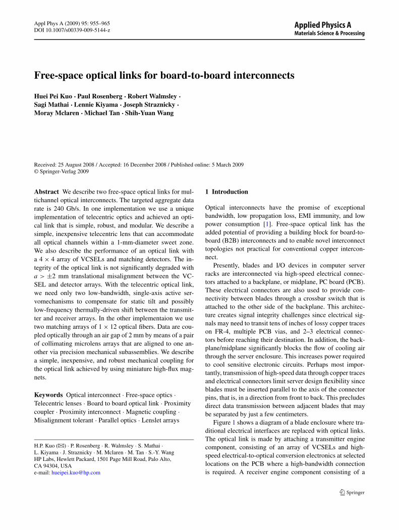
Figure 1 shows a diagram of a blade enclosure where tra-ditional electrical interfaces are replaced with optical links.The optical link is made by attaching a transmitter enginecomponent, consisting of an array of VCSELs and high-speed electrical-to-optical conversion electronics at selectedlocations on the PCB where a high-bandwidth connectionis required. A receiver engine component consisting of a
956 H.P. Kuo et al.
Fig. 1 Blade enclosure with free-space interconnections (red arrows)between adjacent blades and switch
matching array of photodetectors and optical-to-electricalconversion electronics is placed at a location opposite thetransmitting engine on the adjacent PCB. The transmitterand the receiver engines (the OE engines) can be placedat arbitrary locations to help optimize the system architec-ture. As for an example, the OE engines shown in Fig. 1 areplaced to form a 3-dimensional mesh of optical links.
2 Our solution
In this paper we present two implementations of the free-space optical links: an optical module for the free-spacecoupling of optical signal using a double telecentric lenswith unity magnification (1X) and a blind mate, free-spaceproximity optical interconnect to provide high-bandwidthconnectivity between adjacent PCBs wherever it is neededwithin a computer server.
The telecentric lens with unity magnification (1X) hasthe same magnification at all object/image distances andis free of field distortion. This makes it attractive for free-space multichannel optical link. Leyva et al. [2] incorpo-rated a light-valve with telecentric optics to compensatefor misalignment. Their implementation is complex and didnot exploit fully the characteristics of the telecentric lens.The telecentric lenses for commercial applications, such asmetrology and optical projection lithography, are typicallybulky and expensive. In this paper, we describe a double-telecentric optical system that can be fabricated using twosingle-element plano-convex lenses. We are targeting a free-space B2B optical link with an aggregate bandwidth of240 Gb/s that requires a minimal number of actuators tocompensate for B2B misalignments of up to ±1 mm in-plane offset, ±5 mm B2B spacing variation, and ±4◦ ofangular offset (pitch/yaw). The optical link is modular foreasy integration into systems.
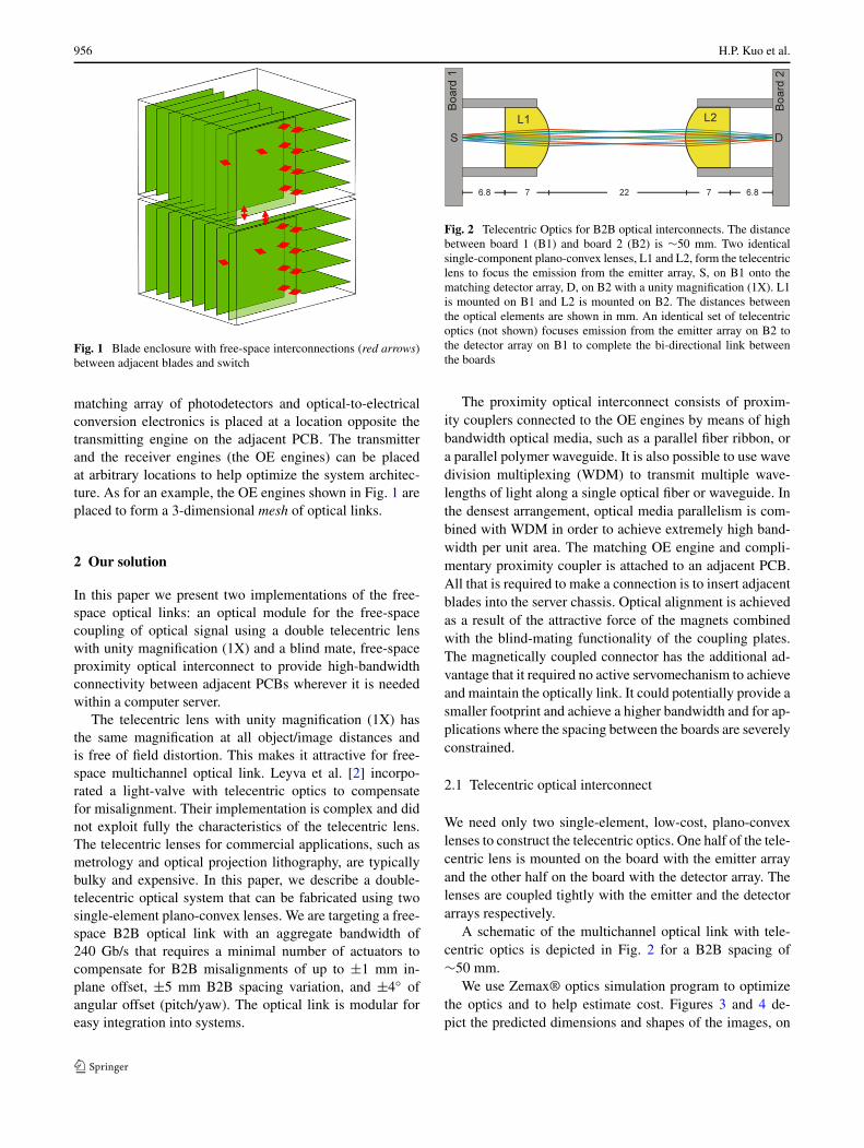
Fig. 2 Telecentric Optics for B2B optical interconnects. The distancebetween board 1 (B1) and board 2 (B2) is ∼50 mm. Two identicalsingle-component plano-convex lenses, L1 and L2, form the telecentriclens to focus the emission from the emitter array, S, on B1 onto thematching detector array, D, on B2 with a unity magnification (1X). L1is mounted on B1 and L2 is mounted on B2. The distances betweenthe optical elements are shown in mm. An identical set of telecentricoptics (not shown) focuses emission from the emitter array on B2 tothe detector array on B1 to complete the bi-directional link betweenthe boards
The proximity optical interconnect consists of proxim-ity couplers connected to the OE engines by means of highbandwidth optical media, such as a parallel fiber ribbon, ora parallel polymer waveguide. It is also possible to use wavedivision multiplexing (WDM) to transmit multiple wave-lengths of light along a single optical fiber or waveguide. Inthe densest arrangement, optical media parallelism is com-bined with WDM in order to achieve extremely high band-width per unit area. The matching OE engine and compli-mentary proximity coupler is attached to an adjacent PCB.All that is required to make a connection is to insert adjacentblades into the server chassis. Optical alignment is achievedas a result of the attractive force of the magnets combinedwith the blind-mating functionality of the coupling plates.The magnetically coupled connector has the additional ad-vantage that it required no active servomechanism to achieveand maintain the optically link. It could potentially provide asmaller footprint and achieve a higher bandwidth and for ap-plications where the spacing between the boards are severelyconstrained.
2.1 Telecentric optical interconnect
We need only two single-element, low-cost, plano-convexlenses to construct the telecentric optics. One half of the tele-centric lens is mounted on the board with the emitter arrayand the other half on the board with the detector array. Thelenses are coupled tightly with the emitter and the detectorarrays respectively.
A schematic of the multichannel optical link with tele-centric optics is depicted in Fig. 2 for a B2B spacing of∼50 mm.
We use Zemax® optics simulation program to optimizethe optics and to help estimate cost. Figures 3 and 4 de-pict the predicted dimensions and shapes of the images, on
Free-space optical links for board-to-board interconnects 957
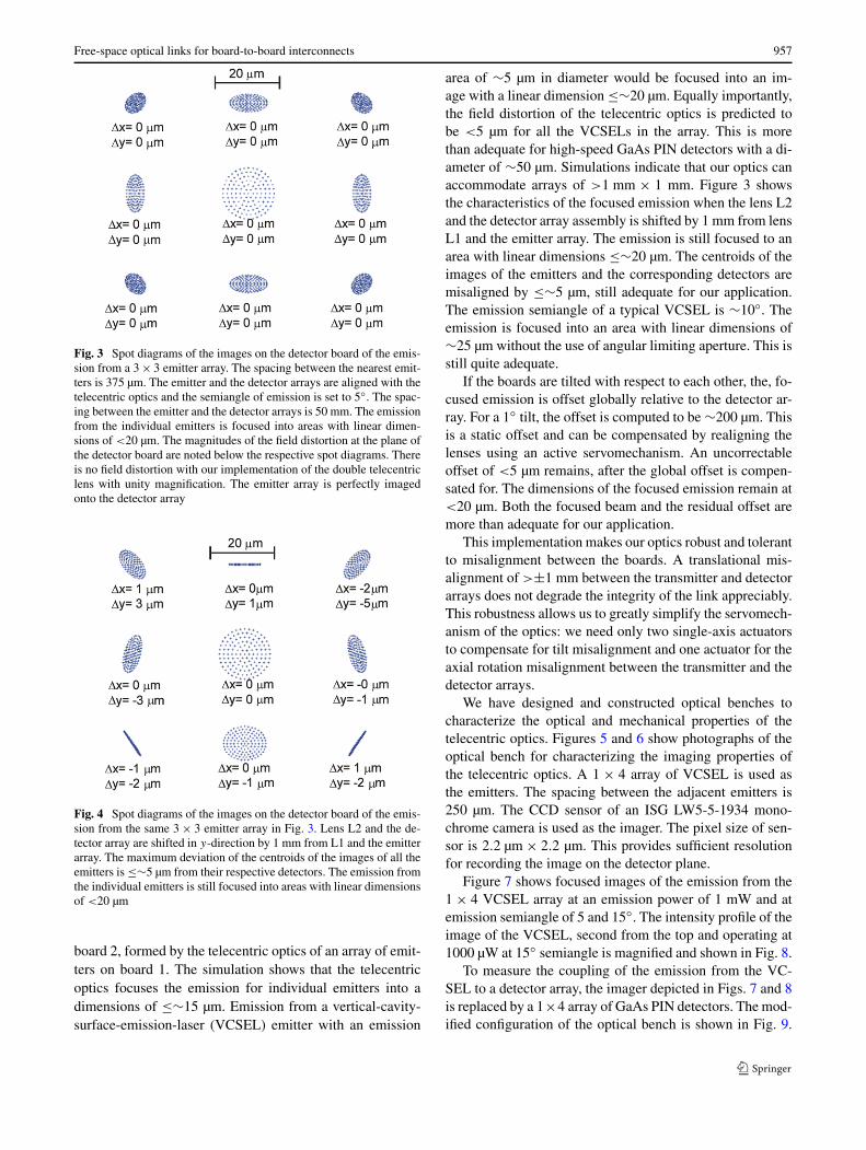
Fig. 3 Spot diagrams of the images on the detector board of the emis-sion from a 3 × 3 emitter array. The spacing between the nearest emit-ters is 375 µm. The emitter and the detector arrays are aligned with thetelecentric optics and the semiangle of emission is set to 5◦. The spac-ing between the emitter and the detector arrays is 50 mm. The emissionfrom the individual emitters is focused into areas with linear dimen-sions of <20 µm. The magnitudes of the field distortion at the plane ofthe detector board are noted below the respective spot diagrams. Thereis no field distortion with our implementation of the double telecentriclens with unity magnification. The emitter array is perfectly imagedonto the detector array
Fig. 4 Spot diagrams of the images on the detector board of the emis-sion from the same 3 × 3 emitter array in Fig. 3. Lens L2 and the de-tector array are shifted in y-direction by 1 mm from L1 and the emitterarray. The maximum deviation of the centroids of the images of all theemitters is ≤∼5 µm from their respective detectors. The emission fromthe individual emitters is still focused into areas with linear dimensionsof <20 µm
board 2, formed by the telecentric optics of an array of emit-ters on board 1. The simulation shows that the telecentricoptics focuses the emission for individual emitters into adimensions of ≤∼15 µm. Emission from a vertical-cavity-surface-emission-laser (VCSEL) emitter with an emission
area of ∼5 µm in diameter would be focused into an im-age with a linear dimension ≤∼20 µm. Equally importantly,the field distortion of the telecentric optics is predicted tobe <5 µm for all the VCSELs in the array. This is morethan adequate for high-speed GaAs PIN detectors with a di-ameter of ∼50 µm. Simulations indicate that our optics canaccommodate arrays of >1 mm × 1 mm. Figure 3 showsthe characteristics of the focused emission when the lens L2and the detector array assembly is shifted by 1 mm from lensL1 and the emitter array. The emission is still focused to anarea with linear dimensions ≤∼20 µm. The centroids of theimages of the emitters and the corresponding detectors aremisaligned by ≤∼5 µm, still adequate for our application.The emission semiangle of a typical VCSEL is ∼10◦. Theemission is focused into an area with linear dimensions of∼25 µm without the use of angular limiting aperture. This isstill quite adequate.
If the boards are tilted with respect to each other, the, fo-cused emission is offset globally relative to the detector ar-ray. For a 1◦ tilt, the offset is computed to be ∼200 µm. Thisis a static offset and can be compensated by realigning thelenses using an active servomechanism. An uncorrectableoffset of <5 µm remains, after the global offset is compen-sated for. The dimensions of the focused emission remain at<20 µm. Both the focused beam and the residual offset aremore than adequate for our application.
This implementation makes our optics robust and tolerantto misalignment between the boards. A translational mis-alignment of >±1 mm between the transmitter and detectorarrays does not degrade the integrity of the link appreciably.This robustness allows us to greatly simplify the servomech-anism of the optics: we need only two single-axis actuatorsto compensate for tilt misalignment and one actuator for theaxial rotation misalignment between the transmitter and thedetector arrays.
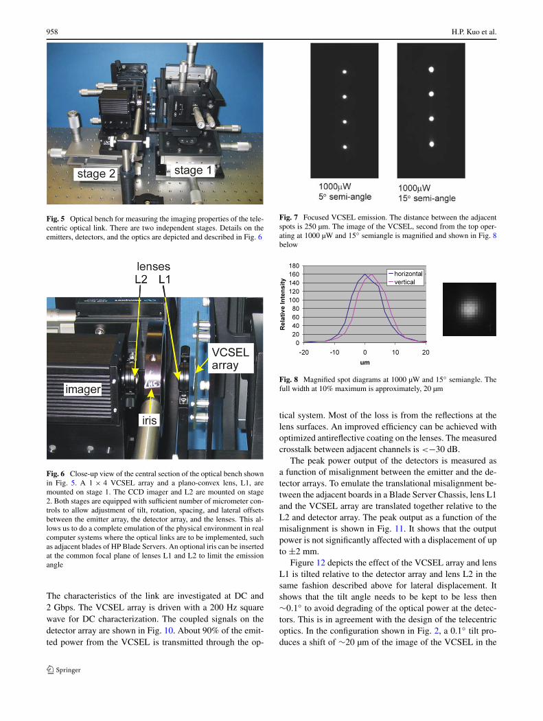
We have designed and constructed optical benches tocharacterize the optical and mechanical properties of thetelecentric optics. Figures 5 and 6 show photographs of theoptical bench for characterizing the imaging properties ofthe telecentric optics. A 1 × 4 array of VCSEL is used asthe emitters. The spacing between the adjacent emitters is250 µm. The CCD sensor of an ISG LW5-5-1934 mono-chrome camera is used as the imager. The pixel size of sen-sor is 2.2 µm × 2.2 µm. This provides sufficient resolutionfor recording the image on the detector plane.
Figure 7 shows focused images of the emission from the1 × 4 VCSEL array at an emission power of 1 mW and atemission semiangle of 5 and 15◦. The intensity profile of theimage of the VCSEL, second from the top and operating at1000 µW at 15◦ semiangle is magnified and shown in Fig. 8.
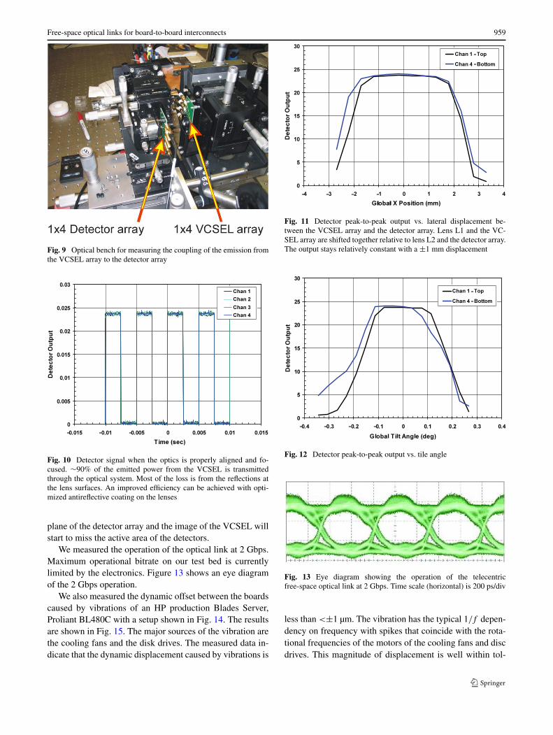
To measure the coupling of the emission from the VC-SEL to a detector array, the imager depicted in Figs. 7 and 8is replaced by a 1×4 array of GaAs PIN detectors. The mod-ified configuration of the optical bench is shown in Fig. 9.
958 H.P. Kuo et al.
Fig. 5 Optical bench for measuring the imaging properties of the tele-centric optical link. There are two independent stages. Details on theemitters, detectors, and the optics are depicted and described in Fig. 6
Fig. 6 Close-up view of the central section of the optical bench shownin Fig. 5. A 1 × 4 VCSEL array and a plano-convex lens, L1, aremounted on stage 1. The CCD imager and L2 are mounted on stage2. Both stages are equipped with sufficient number of micrometer con-trols to allow adjustment of tilt, rotation, spacing, and lateral offsetsbetween the emitter array, the detector array, and the lenses. This al-lows us to do a complete emulation of the physical environment in realcomputer systems where the optical links are to be implemented, suchas adjacent blades of HP Blade Servers. An optional iris can be insertedat the common focal plane of lenses L1 and L2 to limit the emissionangle
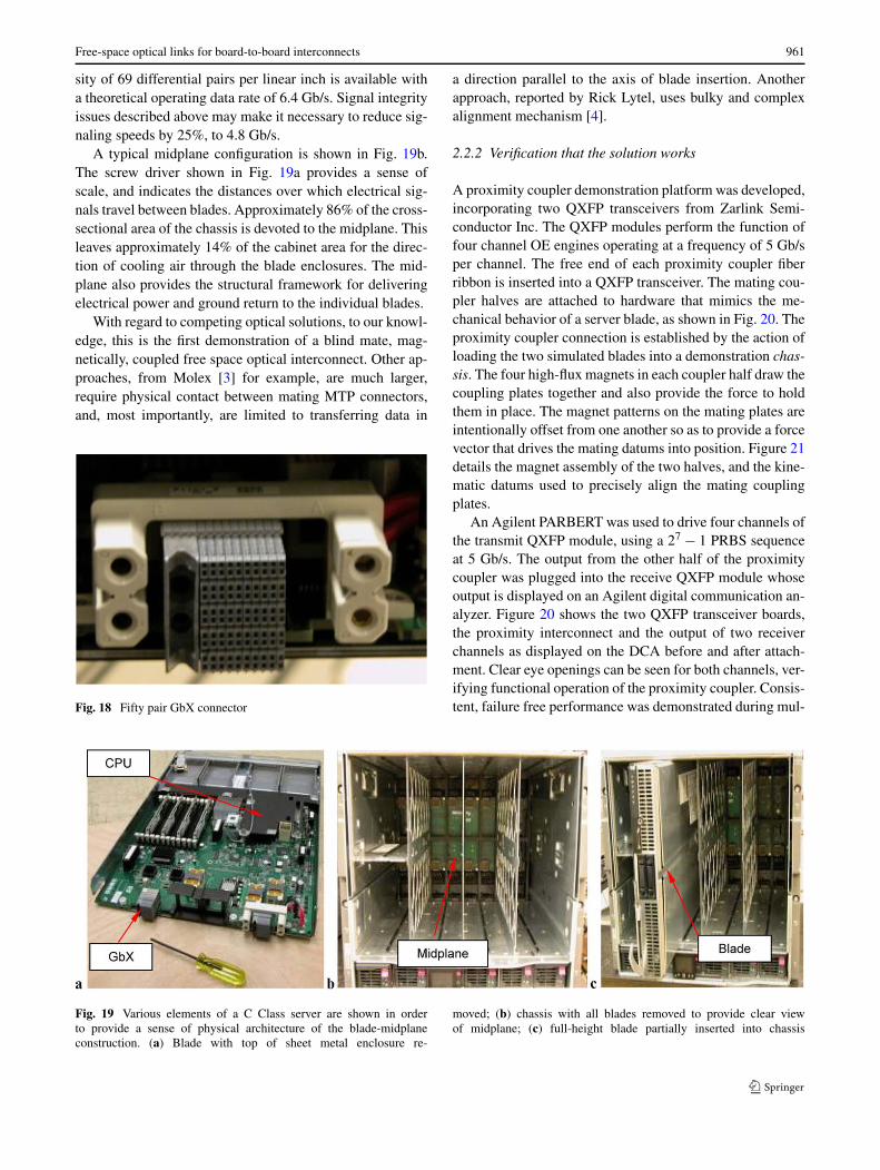
The characteristics of the link are investigated at DC and2 Gbps. The VCSEL array is driven with a 200 Hz squarewave for DC characterization. The coupled signals on thedetector array are shown in Fig. 10. About 90% of the emit-ted power from the VCSEL is transmitted through the op-
Fig. 7 Focused VCSEL emission. The distance between the adjacentspots is 250 µm. The image of the VCSEL, second from the top oper-ating at 1000 µW and 15◦ semiangle is magnified and shown in Fig. 8below
Fig. 8 Magnified spot diagrams at 1000 µW and 15◦ semiangle. Thefull width at 10% maximum is approximately, 20 µm
tical system. Most of the loss is from the reflections at thelens surfaces. An improved efficiency can be achieved withoptimized antireflective coating on the lenses. The measuredcrosstalk between adjacent channels is <−30 dB.
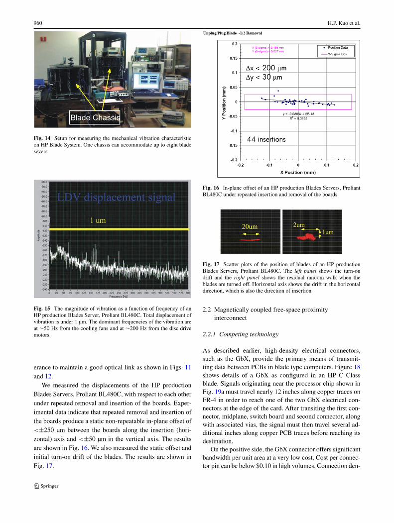
The peak power output of the detectors is measured asa function of misalignment between the emitter and the de-tector arrays. To emulate the translational misalignment be-tween the adjacent boards in a Blade Server Chassis, lens L1and the VCSEL array are translated together relative to theL2 and detector array. The peak output as a function of themisalignment is shown in Fig. 11. It shows that the outputpower is not significantly affected with a displacement of upto ±2 mm.
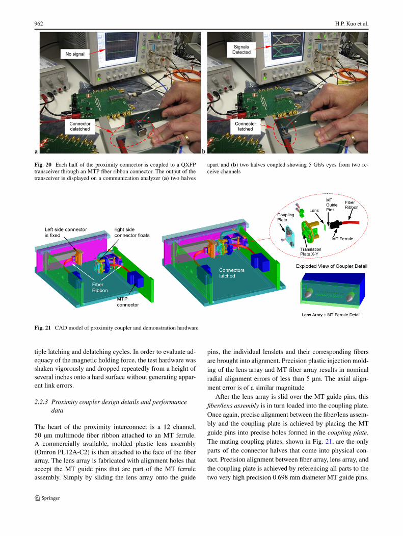
Figure 12 depicts the effect of the VCSEL array and lensL1 is tilted relative to the detector array and lens L2 in thesame fashion described above for lateral displacement. Itshows that the tilt angle needs to be kept to be less then∼0.1◦ to avoid degrading of the optical power at the detec-tors. This is in agreement with the design of the telecentricoptics. In the configuration shown in Fig. 2, a 0.1◦ tilt pro-duces a shift of ∼20 µm of the image of the VCSEL in the
Free-space optical links for board-to-board interconnects 959
Fig. 9 Optical bench for measuring the coupling of the emission fromthe VCSEL array to the detector array
Fig. 10 Detector signal when the optics is properly aligned and fo-cused. ∼90% of the emitted power from the VCSEL is transmittedthrough the optical system. Most of the loss is from the reflections atthe lens surfaces. An improved efficiency can be achieved with opti-mized antireflective coating on the lenses
plane of the detector array and the image of the VCSEL willstart to miss the active area of the detectors.
We measured the operation of the optical link at 2 Gbps.Maximum operational bitrate on our test bed is currentlylimited by the electronics. Figure 13 shows an eye diagramof the 2 Gbps operation.
We also measured the dynamic offset between the boardscaused by vibrations of an HP production Blades Server,Proliant BL480C with a setup shown in Fig. 14. The resultsare shown in Fig. 15. The major sources of the vibration arethe cooling fans and the disk drives. The measured data in-dicate that the dynamic displacement caused by vibrations is
Fig. 11 Detector peak-to-peak output vs. lateral displacement be-tween the VCSEL array and the detector array. Lens L1 and the VC-SEL array are shifted together relative to lens L2 and the detector array.The output stays relatively constant with a ±1 mm displacement
Fig. 12 Detector peak-to-peak output vs. tile angle
Fig. 13 Eye diagram showing the operation of the telecentricfree-space optical link at 2 Gbps. Time scale (horizontal) is 200 ps/div
less than <±1 µm. The vibration has the typical 1/f depen-dency on frequency with spikes that coincide with the rota-tional frequencies of the motors of the cooling fans and discdrives. This magnitude of displacement is well within tol-
960 H.P. Kuo et al.
Fig. 14 Setup for measuring the mechanical vibration characteristicon HP Blade System. One chassis can accommodate up to eight bladesevers
Fig. 15 The magnitude of vibration as a function of frequency of anHP production Blades Server, Proliant BL480C. Total displacement ofvibration is under 1 µm. The dominant frequencies of the vibration areat ∼50 Hz from the cooling fans and at ∼200 Hz from the disc drivemotors
erance to maintain a good optical link as shown in Figs. 11and 12.
We measured the displacements of the HP productionBlades Servers, Proliant BL480C, with respect to each otherunder repeated removal and insertion of the boards. Exper-imental data indicate that repeated removal and insertion ofthe boards produce a static non-repeatable in-plane offset of<±250 µm between the boards along the insertion (hori-zontal) axis and <±50 µm in the vertical axis. The resultsare shown in Fig. 16. We also measured the static offset andinitial turn-on drift of the blades. The results are shown inFig. 17.
Fig. 16 In-plane offset of an HP production Blades Servers, ProliantBL480C under repeated insertion and removal of the boards
Fig. 17 Scatter plots of the position of blades of an HP productionBlades Servers, Proliant BL480C. The left panel shows the turn-ondrift and the right panel shows the residual random walk when theblades are turned off. Horizontal axis shows the drift in the horizontaldirection, which is also the direction of insertion
2.2 Magnetically coupled free-space proximityinterconnect
2.2.1 Competing technology
As described earlier, high-density electrical connectors,such as the GbX, provide the primary means of transmit-ting data between PCBs in blade type computers. Figure 18shows details of a GbX as configured in an HP C Classblade. Signals originating near the processor chip shown inFig. 19a must travel nearly 12 inches along copper traces onFR-4 in order to reach one of the two GbX electrical con-nectors at the edge of the card. After transiting the first con-nector, midplane, switch board and second connector, alongwith associated vias, the signal must then travel several ad-ditional inches along copper PCB traces before reaching itsdestination.
On the positive side, the GbX connector offers significantbandwidth per unit area at a very low cost. Cost per connec-tor pin can be below $0.10 in high volumes. Connection den-
Free-space optical links for board-to-board interconnects 961
sity of 69 differential pairs per linear inch is available witha theoretical operating data rate of 6.4 Gb/s. Signal integrityissues described above may make it necessary to reduce sig-naling speeds by 25%, to 4.8 Gb/s.
A typical midplane configuration is shown in Fig. 19b.The screw driver shown in Fig. 19a provides a sense ofscale, and indicates the distances over which electrical sig-nals travel between blades. Approximately 86% of the cross-sectional area of the chassis is devoted to the midplane. Thisleaves approximately 14% of the cabinet area for the direc-tion of cooling air through the blade enclosures. The mid-plane also provides the structural framework for deliveringelectrical power and ground return to the individual blades.
With regard to competing optical solutions, to our knowl-edge, this is the first demonstration of a blind mate, mag-netically, coupled free space optical interconnect. Other ap-proaches, from Molex [3] for example, are much larger,require physical contact between mating MTP connectors,and, most importantly, are limited to transferring data in
Fig. 18 Fifty pair GbX connector
a direction parallel to the axis of blade insertion. Anotherapproach, reported by Rick Lytel, uses bulky and complexalignment mechanism [4].
2.2.2 Verification that the solution works
A proximity coupler demonstration platform was developed,incorporating two QXFP transceivers from Zarlink Semi-conductor Inc. The QXFP modules perform the function offour channel OE engines operating at a frequency of 5 Gb/sper channel. The free end of each proximity coupler fiberribbon is inserted into a QXFP transceiver. The mating cou-pler halves are attached to hardware that mimics the me-chanical behavior of a server blade, as shown in Fig. 20. Theproximity coupler connection is established by the action ofloading the two simulated blades into a demonstration chas-sis. The four high-flux magnets in each coupler half draw thecoupling plates together and also provide the force to holdthem in place. The magnet patterns on the mating plates areintentionally offset from one another so as to provide a forcevector that drives the mating datums into position. Figure 21details the magnet assembly of the two halves, and the kine-matic datums used to precisely align the mating couplingplates.
An Agilent PARBERT was used to drive four channels ofthe transmit QXFP module, using a 27 − 1 PRBS sequenceat 5 Gb/s. The output from the other half of the proximitycoupler was plugged into the receive QXFP module whoseoutput is displayed on an Agilent digital communication an-alyzer. Figure 20 shows the two QXFP transceiver boards,the proximity interconnect and the output of two receiverchannels as displayed on the DCA before and after attach-ment. Clear eye openings can be seen for both channels, ver-ifying functional operation of the proximity coupler. Consis-tent, failure free performance was demonstrated during mul-
Fig. 19 Various elements of a C Class server are shown in orderto provide a sense of physical architecture of the blade-midplaneconstruction. (a) Blade with top of sheet metal enclosure re-
moved; (b) chassis with all blades removed to provide clear viewof midplane; (c) full-height blade partially inserted into chassis
962 H.P. Kuo et al.
Fig. 20 Each half of the proximity connector is coupled to a QXFPtransceiver through an MTP fiber ribbon connector. The output of thetransceiver is displayed on a communication analyzer (a) two halves
apart and (b) two halves coupled showing 5 Gb/s eyes from two re-ceive channels
Fig. 21 CAD model of proximity coupler and demonstration hardware
tiple latching and delatching cycles. In order to evaluate ad-equacy of the magnetic holding force, the test hardware wasshaken vigorously and dropped repeatedly from a height ofseveral inches onto a hard surface without generating appar-ent link errors.
2.2.3 Proximity coupler design details and performancedata
The heart of the proximity interconnect is a 12 channel,50 µm multimode fiber ribbon attached to an MT ferrule.A commercially available, molded plastic lens assembly(Omron PL12A-C2) is then attached to the face of the fiberarray. The lens array is fabricated with alignment holes thataccept the MT guide pins that are part of the MT ferruleassembly. Simply by sliding the lens array onto the guide
pins, the individual lenslets and their corresponding fibersare brought into alignment. Precision plastic injection mold-ing of the lens array and MT fiber array results in nominalradial alignment errors of less than 5 µm. The axial align-ment error is of a similar magnitude
After the lens array is slid over the MT guide pins, thisfiber/lens assembly is in turn loaded into the coupling plate.Once again, precise alignment between the fiber/lens assem-bly and the coupling plate is achieved by placing the MTguide pins into precise holes formed in the coupling plate.The mating coupling plates, shown in Fig. 21, are the onlyparts of the connector halves that come into physical con-tact. Precision alignment between fiber array, lens array, andthe coupling plate is achieved by referencing all parts to thetwo very high precision 0.698 mm diameter MT guide pins.
Free-space optical links for board-to-board interconnects 963
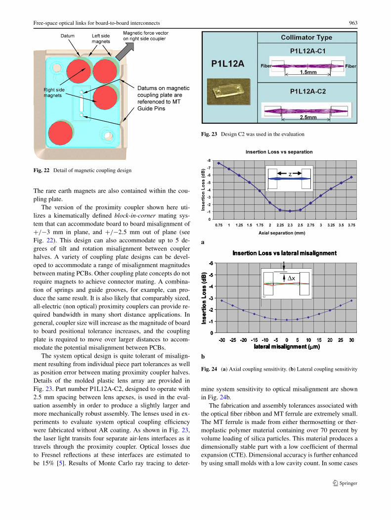
Fig. 22 Detail of magnetic coupling design
The rare earth magnets are also contained within the cou-pling plate.
The version of the proximity coupler shown here uti-lizes a kinematically defined block-in-corner mating sys-tem that can accommodate board to board misalignment of+/−3 mm in plane, and +/−2.5 mm out of plane (seeFig. 22). This design can also accommodate up to 5 de-grees of tilt and rotation misalignment between couplerhalves. A variety of coupling plate designs can be devel-oped to accommodate a range of misalignment magnitudesbetween mating PCBs. Other coupling plate concepts do notrequire magnets to achieve connector mating. A combina-tion of springs and guide grooves, for example, can pro-duce the same result. It is also likely that comparably sized,all-electric (non optical) proximity couplers can provide re-quired bandwidth in many short distance applications. Ingeneral, coupler size will increase as the magnitude of boardto board positional tolerance increases, and the couplingplate is required to move over larger distances to accom-modate the potential misalignment between PCBs.
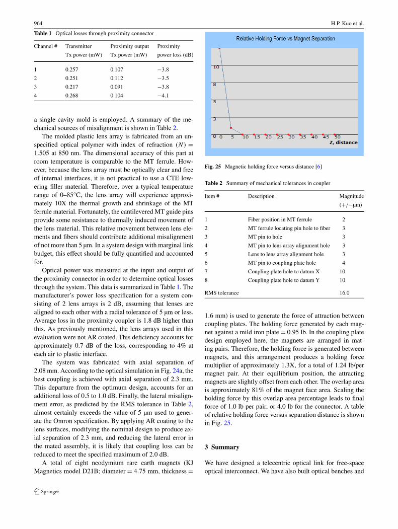
The system optical design is quite tolerant of misalign-ment resulting from individual piece part tolerances as wellas position error between mating proximity coupler halves.Details of the molded plastic lens array are provided inFig. 23. Part number P1L12A-C2, designed to operate with2.5 mm spacing between lens apexes, is used in the eval-uation assembly in order to produce a slightly larger andmore mechanically robust assembly. The lenses used in ex-periments to evaluate system optical coupling efficiencywere fabricated without AR coating. As shown in Fig. 23,the laser light transits four separate air-lens interfaces as ittravels through the proximity coupler. Optical losses dueto Fresnel reflections at these interfaces are estimated tobe 15% [5]. Results of Monte Carlo ray tracing to deter-
Fig. 23 Design C2 was used in the evaluation
a
b
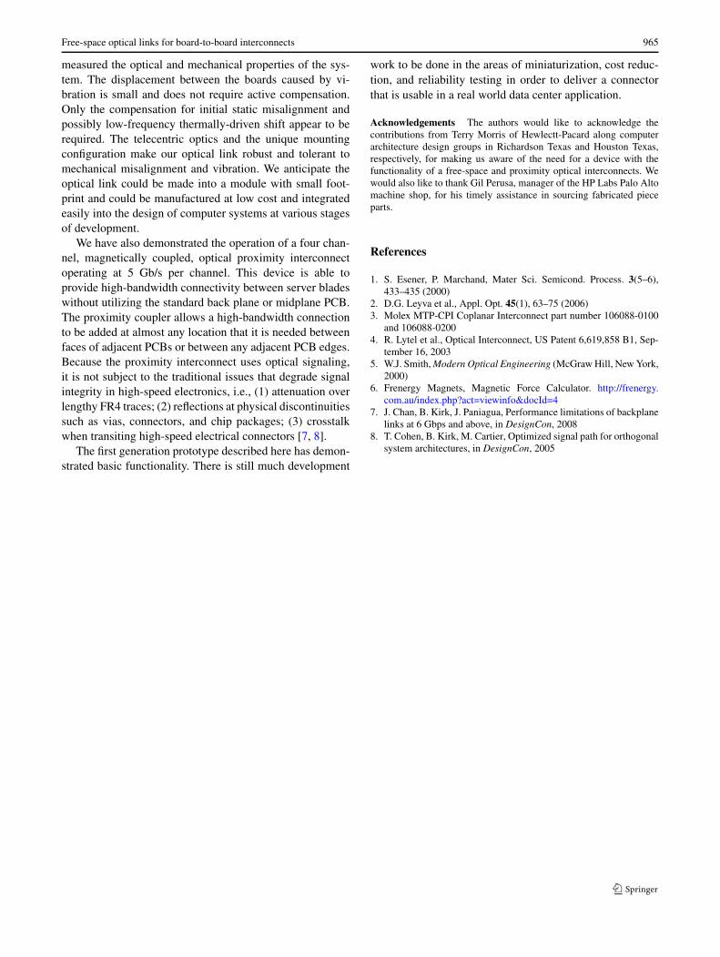
Fig. 24 (a) Axial coupling sensitivity. (b) Lateral coupling sensitivity
mine system sensitivity to optical misalignment are shownin Fig. 24b.
The fabrication and assembly tolerances associated withthe optical fiber ribbon and MT ferrule are extremely small.The MT ferrule is made from either thermosetting or ther-moplastic polymer material containing over 70 percent byvolume loading of silica particles. This material produces adimensionally stable part with a low coefficient of thermalexpansion (CTE). Dimensional accuracy is further enhancedby using small molds with a low cavity count. In some cases
964 H.P. Kuo et al.
Table 1 Optical losses through proximity connector
Channel # Transmitter Proximity output Proximity
Tx power (mW) Tx power (mW) power loss (dB)
1 0.257 0.107 −3.8
2 0.251 0.112 −3.5
3 0.217 0.091 −3.8
4 0.268 0.104 −4.1
a single cavity mold is employed. A summary of the me-chanical sources of misalignment is shown in Table 2.
The molded plastic lens array is fabricated from an un-specified optical polymer with index of refraction (N) =1.505 at 850 nm. The dimensional accuracy of this part atroom temperature is comparable to the MT ferrule. How-ever, because the lens array must be optically clear and freeof internal interfaces, it is not practical to use a CTE low-ering filler material. Therefore, over a typical temperaturerange of 0–85°C, the lens array will experience approxi-mately 10X the thermal growth and shrinkage of the MTferrule material. Fortunately, the cantilevered MT guide pinsprovide some resistance to thermally induced movement ofthe lens material. This relative movement between lens ele-ments and fibers should contribute additional misalignmentof not more than 5 µm. In a system design with marginal linkbudget, this effect should be fully quantified and accountedfor.
Optical power was measured at the input and output ofthe proximity connector in order to determine optical lossesthrough the system. This data is summarized in Table 1. Themanufacturer’s power loss specification for a system con-sisting of 2 lens arrays is 2 dB, assuming that lenses arealigned to each other with a radial tolerance of 5 µm or less.Average loss in the proximity coupler is 1.8 dB higher thanthis. As previously mentioned, the lens arrays used in thisevaluation were not AR coated. This deficiency accounts forapproximately 0.7 dB of the loss, corresponding to 4% ateach air to plastic interface.
The system was fabricated with axial separation of2.08 mm. According to the optical simulation in Fig. 24a, thebest coupling is achieved with axial separation of 2.3 mm.This departure from the optimum design, accounts for anadditional loss of 0.5 to 1.0 dB. Finally, the lateral misalign-ment error, as predicted by the RMS tolerance in Table 2,almost certainly exceeds the value of 5 µm used to gener-ate the Omron specification. By applying AR coating to thelens surfaces, modifying the nominal design to produce ax-ial separation of 2.3 mm, and reducing the lateral error inthe mated assembly, it is likely that coupling loss can bereduced to meet the specified maximum of 2.0 dB.
A total of eight neodymium rare earth magnets (KJMagnetics model D21B; diameter = 4.75 mm, thickness =
Fig. 25 Magnetic holding force versus distance [6]
Table 2 Summary of mechanical tolerances in coupler
Item # Description Magnitude
(+/−µm)
1 Fiber position in MT ferrule 2
2 MT ferrule locating pin hole to fiber 3
3 MT pin to hole 3
4 MT pin to lens array alignment hole 3
5 Lens to lens array alignment hole 3
6 MT pin to coupling plate hole 4
7 Coupling plate hole to datum X 10
8 Coupling plate hole to datum Y 10
RMS tolerance 16.0
1.6 mm) is used to generate the force of attraction betweencoupling plates. The holding force generated by each mag-net against a mild iron plate = 0.95 lb. In the coupling platedesign employed here, the magnets are arranged in mat-ing pairs. Therefore, the holding force is generated betweenmagnets, and this arrangement produces a holding forcemultiplier of approximately 1.3X, for a total of 1.24 lb/permagnet pair. At their equilibrium position, the attractingmagnets are slightly offset from each other. The overlap areais approximately 81% of the magnet face area. Scaling theholding force by this overlap area percentage leads to finalforce of 1.0 lb per pair, or 4.0 lb for the connector. A tableof relative holding force versus separation distance is shownin Fig. 25.
3 Summary
We have designed a telecentric optical link for free-spaceoptical interconnect. We have also built optical benches and
Free-space optical links for board-to-board interconnects 965
measured the optical and mechanical properties of the sys-tem. The displacement between the boards caused by vi-bration is small and does not require active compensation.Only the compensation for initial static misalignment andpossibly low-frequency thermally-driven shift appear to berequired. The telecentric optics and the unique mountingconfiguration make our optical link robust and tolerant tomechanical misalignment and vibration. We anticipate theoptical link could be made into a module with small foot-print and could be manufactured at low cost and integratedeasily into the design of computer systems at various stagesof development.
We have also demonstrated the operation of a four chan-nel, magnetically coupled, optical proximity interconnectoperating at 5 Gb/s per channel. This device is able toprovide high-bandwidth connectivity between server bladeswithout utilizing the standard back plane or midplane PCB.The proximity coupler allows a high-bandwidth connectionto be added at almost any location that it is needed betweenfaces of adjacent PCBs or between any adjacent PCB edges.Because the proximity interconnect uses optical signaling,it is not subject to the traditional issues that degrade signalintegrity in high-speed electronics, i.e., (1) attenuation overlengthy FR4 traces; (2) reflections at physical discontinuitiessuch as vias, connectors, and chip packages; (3) crosstalkwhen transiting high-speed electrical connectors [7, 8].
The first generation prototype described here has demon-strated basic functionality. There is still much development
work to be done in the areas of miniaturization, cost reduc-tion, and reliability testing in order to deliver a connectorthat is usable in a real world data center application.
Acknowledgements The authors would like to acknowledge thecontributions from Terry Morris of Hewlectt-Pacard along computerarchitecture design groups in Richardson Texas and Houston Texas,respectively, for making us aware of the need for a device with thefunctionality of a free-space and proximity optical interconnects. Wewould also like to thank Gil Perusa, manager of the HP Labs Palo Altomachine shop, for his timely assistance in sourcing fabricated pieceparts.
References
1. S. Esener, P. Marchand, Mater Sci. Semicond. Process. 3(5–6),433–435 (2000)
2. D.G. Leyva et al., Appl. Opt. 45(1), 63–75 (2006)3. Molex MTP-CPI Coplanar Interconnect part number 106088-0100
and 106088-02004. R. Lytel et al., Optical Interconnect, US Patent 6,619,858 B1, Sep-
tember 16, 20035. W.J. Smith, Modern Optical Engineering (McGraw Hill, New York,
2000)6. Frenergy Magnets, Magnetic Force Calculator. http://frenergy.
com.au/index.php?act=viewinfo&docId=47. J. Chan, B. Kirk, J. Paniagua, Performance limitations of backplane
links at 6 Gbps and above, in DesignCon, 20088. T. Cohen, B. Kirk, M. Cartier, Optimized signal path for orthogonal
system architectures, in DesignCon, 2005
Related Documents