HAL Id: hal-02398358 https://hal.archives-ouvertes.fr/hal-02398358 Submitted on 7 Dec 2019 HAL is a multi-disciplinary open access archive for the deposit and dissemination of sci- entific research documents, whether they are pub- lished or not. The documents may come from teaching and research institutions in France or abroad, or from public or private research centers. L’archive ouverte pluridisciplinaire HAL, est destinée au dépôt et à la diffusion de documents scientifiques de niveau recherche, publiés ou non, émanant des établissements d’enseignement et de recherche français ou étrangers, des laboratoires publics ou privés. Free-Space Micro-Graphics with Electrically Driven Levitated Light Scatterers Johann Berthelot, Nicolas Bonod To cite this version: Johann Berthelot, Nicolas Bonod. Free-Space Micro-Graphics with Electrically Driven Levitated Light Scatterers. Optics Letters, Optical Society of America - OSA Publishing, 2019, 44 (6), pp.1476-1479. 10.1364/OL.44.001476. hal-02398358

Welcome message from author
This document is posted to help you gain knowledge. Please leave a comment to let me know what you think about it! Share it to your friends and learn new things together.
Transcript
HAL Id: hal-02398358https://hal.archives-ouvertes.fr/hal-02398358
Submitted on 7 Dec 2019
HAL is a multi-disciplinary open accessarchive for the deposit and dissemination of sci-entific research documents, whether they are pub-lished or not. The documents may come fromteaching and research institutions in France orabroad, or from public or private research centers.
L’archive ouverte pluridisciplinaire HAL, estdestinée au dépôt et à la diffusion de documentsscientifiques de niveau recherche, publiés ou non,émanant des établissements d’enseignement et derecherche français ou étrangers, des laboratoirespublics ou privés.
Free-Space Micro-Graphics with Electrically DrivenLevitated Light Scatterers
Johann Berthelot, Nicolas Bonod
To cite this version:Johann Berthelot, Nicolas Bonod. Free-Space Micro-Graphics with Electrically Driven Levitated LightScatterers. Optics Letters, Optical Society of America - OSA Publishing, 2019, 44 (6), pp.1476-1479.10.1364/OL.44.001476. hal-02398358

HAL Id: hal-02398358https://hal.archives-ouvertes.fr/hal-02398358
Submitted on 7 Dec 2019
HAL is a multi-disciplinary open accessarchive for the deposit and dissemination of sci-entific research documents, whether they are pub-lished or not. The documents may come fromteaching and research institutions in France orabroad, or from public or private research centers.
L’archive ouverte pluridisciplinaire HAL, estdestinée au dépôt et à la diffusion de documentsscientifiques de niveau recherche, publiés ou non,émanant des établissements d’enseignement et derecherche français ou étrangers, des laboratoirespublics ou privés.
Free-Space Micro-Graphics with Electrically DrivenLevitated Light Scatterers
Johann Berthelot, Nicolas Bonod
To cite this version:Johann Berthelot, Nicolas Bonod. Free-Space Micro-Graphics with Electrically Driven Levitated LightScatterers. Optics Letters, Optical Society of America, 2019, 44 (6), pp.1476. 10.1364/OL.44.001476.hal-02398358
Letter Optics Letters 1
Free-Space Micro-Graphics with Electrically DrivenLevitated Light ScatterersJOHANN BERTHELOT1,* AND NICOLAS BONOD1,*
1Aix Marseille Univ, CNRS, Centrale Marseille, Institut Fresnel, Marseille, France*Corresponding author: [email protected], [email protected]
Compiled January 25, 2019
Levitation of optical scatterers provides a new mean to develop free-space volumetric displays. The prin-ciple is to illuminate a levitating particle displaced at high velocity in three dimensions (3D) to create images based on persistence of vision (POV). Light scattered by the particle can be observed all around the volumet-ric display and therefore provides a true 3D image that does not rely on interference effects and remains insen-sitive to the angle of observation. The challenge is to control with a high accuracy and at high speed the tra-jectory of the particle in three dimensions. Here we use electrically driven planar Paul traps (PPTs) to control the trajectory of electrically charged particles. A sin-gle gold particle colloid is manipulated in three dimen-sions through AC and DC electrical voltages applied to a PPT. Electric voltages can be modulated at high frequencies (150 kHz) and allow for a high speed dis-placement of particles without moving any other sys-tem component. The optical scattering of the particle in levitation yields free-space images that are imaged with conventional optics. The trajectory of the particle is entirely encoded in the electric voltage and driven through stationary planar electrodes. We show in this paper, the proof-of-concept for the generation of 3D free space graphics with a single electrically scanned particle.
http://dx.doi.org/10.1364/ao.XX.XXXXXX
1. INTRODUCTION
Levitation of nano-objects is a fascinating area of science thataims at trapping and manipulating nano-objects without physi-cal contact. Different techniques can be used to trap nano-objects,among which optical tweezers [1–5] or acoustic traps [6–8].
Recently, optical scatterers in levitation reveal as competingalternative to holography to yield volumetric images. Differentsystems have been proposed to provide free-space 3D imaging[9–12]. A major breakthrough was achieved in 2018 by the use ofphotophoretic traps [13]. Such traps use strong gradients in tem-perature around a lossy particle illuminated by a tightly focusedlaser beam. This trapping mechanism allows to trap particles in
the range of a few micrometers up to hundreds of micrometers.This technique was shown to yield high quality centimeter-sizedimages. The optical trap is scanned with galvanometric mirrorsthat rely on a mechanical displacement of optical components.Here we show that immobilized planar point Paul traps can scanparticles in a 3D space with AC and DC voltages only. The parti-cle trajectory can be fully driven electrically without requiringany physical displacement of any component of the system.
Radio-frequency (RF) traps have been widely investigatedto trap and control ions [14] and they are emerging in nanoand microsciences as versatile tools to manipulate nano/micro-objects [15–21]. They rely on the use of a time varying electricalfield applied on a special arrangement of electrodes forming anelectrostatic potential featuring a saddle shape. RF traps oper-ate with electrically charged nano/micro objects. This step isusually performed with the use of an electrospray ionizationsystem (ESI) [22]. Conventional RF traps are bulky systemsthat offer low optical access, require high voltages and specificmachining facilities. In the 2000’s, the extension of this trapconfiguration into planar geometry has offered novel oppor-tunities with levitation of electrically charged objects [23–25].Besides weaker electric voltages required to trap objects, planarelectrodes printed on the same plane offer an open access toeasily detect and excite the levitated object with optical beams.Another advantage is related to the fabrication. Such systemsare easily fabricated with conventional optical lithography orlaser etching. The high stability of PPTs was unveiled in 2016 bytranslating and rotating PPTs while keeping particles trapped inlevitation in air [26]. We show in this study that PPTs are highlysuited to yield free-space images by manipulating and displac-ing individual optical scatterers by plugging the trajectory ofparticles into AC and DC voltages applied to stationary PPTs.
2. RESULTS AND DISCUSSION
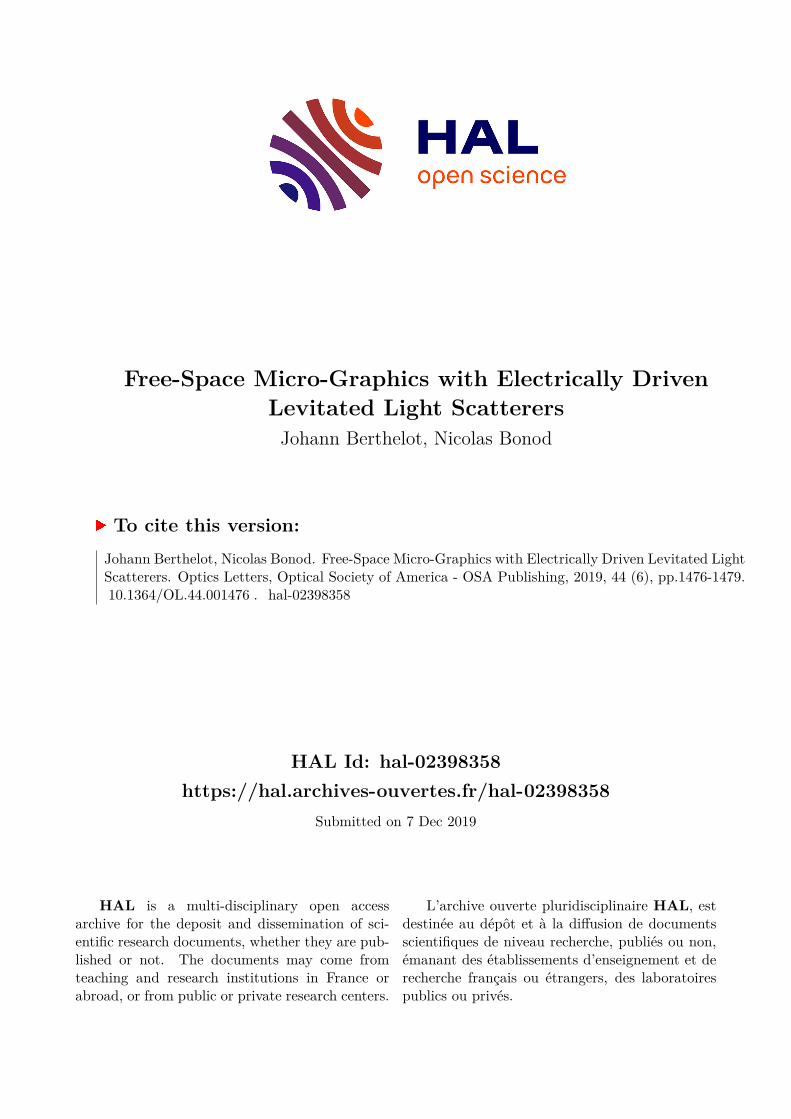
A typical example of PPT is presented in Fig.1(a). The dimen-sions of the different electrodes are 0.7 mm in diameter for theinner electrode and 3 mm in diameter for the outer electrode.They were fabricated on a commercial Printed Circuit Board(PCB). It consists of two inner and outer ring electrodes sur-rounded by four compensation DC electrodes. The whole PPThas a size of 10 × 10 mm2. Typically this PPT geometry requiresoscillating fields in the kHz range with an amplitude of hun-dreds of volts. Connections are made underneath the planarPCB. By polarizing the different electrodes, either with DC or
Letter Optics Letters 2
Fig. 1. Planar Paul traps. (a) Photography of a surface elec-trode trap used in this study. It is composed of different elec-trodes: inner electrode, RF electrode and 4 compensation DCelectrodes. (b) Photography of a 100nm gold particle put inlevitation with the PPT presented in (a). (c) Schematic illus-tration of the electrically driven motion of the particles. Eachcompensation electrode is used to control a −Ox, +Ox, −Oy,+Oy direction. The displacement value is related to the ampli-tude of the applied electric field. The trajectory along the z axisis controlled with the inner electrode. Insert on the right is afree-space 2D image of a star obtained with our PPT.
AC voltage, it is possible to trap a single nano-object with a highstability (cf. Fig.1(b)). The four compensation electrodes addexternal parameters to displace the object in the plane while theinner electrode controls the out-of-plane displacement. The mo-tion of the object is then driven depending of the configurationand the applied voltage amplitude of the different fields, i.e. ACor DC voltage. An important point is that all the AC voltagesmust be applied with the same frequency [26]. The circuit con-figuration used in this study is illustrated in Fig.1c. Thanks tothis system, the trajectory of the particle can therefore be drivenby directly encoding the amplitude in function of the positionand applied to the electrodes by analog outputs. The speed andthe precision of the driven motion are then strictly dependent ofthe electronic systems, i.e. bandwidth and resolution. In our ex-periments we used an electronic card from National Instrument(NI PCIe-7841R).
In the case where no driven electric field is applied, andtaking into account the background pressure, the motion ofthe trapped particle can be predicted by solving the Mathieuequations [27]:
d2udy2 + µ
dudy
+ (au − 2qu cos 2y)u = 0, (1)
where u denotes either the z or the r coordinate of the trappedparticle. The dimensionless parameters au, qu and µ are definedas follows:
au = 16 QM
VDCΩ2 f (r, z), qu = 8 Q
MVACΩ2 f (r, z), µ = 36 η
ρd2Ω . (2)
. The dimensionless parameter y is related to time by y = Ωt/2,where Ω is the frequency of the electrical field. By solving nu-merically Eq.1 for each direction of space, i.e. r and z, we can
obtain the solutions depending on the dimensionless parametersau and qu leading to a stable trap. A stable 3D trapping occurswhen the different solutions in r and z overlap.
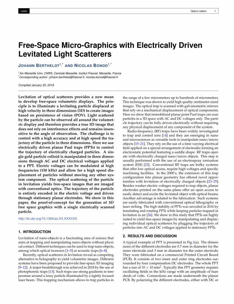
The function f (r, z) depends on the geometry of the elec-trodes, d is the diameter of the particle, ρ is the density of thematerial and η the viscosity of the medium. We can remark thatboth parameters au and bu depend on the charge-to-mass ratioQ/M and that au depends on a static voltage applied on theelectrode. Particles are commonly trapped with a pure oscillat-ing field, Vac, without any static field Vdc, meaning that au = 0.au and qu depend on the spatial parameter u = r, z but due tothe symmetry of the electrode, az and ar are linked via the rela-tion az = −2ar. The same relation occurs for the qu parameters,qz = −2qr. Solving Eq.1 provides the r or z coordinates leadingto a stable position of the particle in the trap. For that purpose, asecond-order Runge-Kutta method is implemented. This allowsus to plot the stability diagram of the PPT as a function of thedimensionless parameters au, qu for a given µ. µ is taken equalto 30 in air and equal to 0 in vacuum. We consider the case of anAC voltage with 1kHz frequency, 70 V amplitude and a 100 nmdiameter gold particle (typical value used in the experiment).The solutions r and z are calculated with respect to au, qu and theresulting stable 3D trapping solutions are plotted in Fig.2(a) asfunctions of a and q. We can clearly see that the domain of stabil-
Fig. 2. Stability Diagram. Calculated stability diagram for acharged particle in an oscillating electrical field under vacuum(orange area) and in air (blue area) conditions. a and q arethe solutions of the equation of motion of the particle. Forthis calculation we use a particle of 100 nm diameter of goldplaced in air and vacuum conditions.
ity is much larger in air (in blue) than under vacuum (in orange).This result highlights the interest of electrostatic traps to operatein ambient conditions. We can observe in Fig.2 a large range ofstable solutions for a wide range of a and q values, i.e. for a widerange of object sizes with different charge-to-mass ratio Q/m,for the same field applied. This also means that RF traps canoperate for an even wider range of object sizes by tuning thevoltage amplitude and frequency. This numerical study allowsto find the voltage parameters that lead to an efficient trap ofthe gold nanoparticles. It was shown in [28] that an additionalDC voltage in the radial or axial direction shifts the node of thepotential in the radial or axial direction. This property shall beused to shift the position of the node in the radial direction rabove the planar electrodes. For that purpose, we use additional
Letter Optics Letters 3
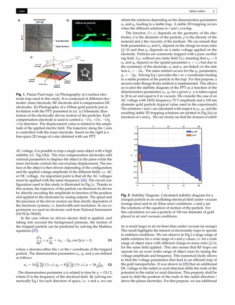
Fig. 3. Electric field maps above the PPT electrode and influ-ence of the DC compensation electrodes. a) Schematic view ofthe trapping geometry and the different electrodes with the3 axis definition. b-e) 2D cross sections in the plane XoZ (leftrow) and YoZ (right row) of the simulated electric field mapfor 3 different voltage conditions applied on the different elec-trodes of the PPT :(b,c) RF voltage only, (d,e) RF voltage andone DC electrode at 10V.
DC voltages applied to compensation electrodes. The positionof the node in the axial direction can be tuned thanks to the ACvoltage. For the radial displacement, the x and y coordinateshave first to be discriminated. 4 DC electrodes are placed inthe (0, x, y) cartesian coordinates, 2 along the Ox axis at (−X, 0)and (+X, 0), and 2 along the Oy axis at (0,−Y) and (0,+Y)(see Fig.3a). Before manipulating the particles, we study withfinite elements method (COMSOL Multiphysics) the possibil-ity to tailor the position of the node of the electric field withvoltages, without displacing the electrode. We start with theclassical configuration used to trap individual particles abovethe planar electrode with AC voltage applied to the outer cir-cular electrode (70V, 1kHz). We clearly observe the node of theelectric field 0.5mm above the circular electrode, centered on thez axis (Fig.3b,c). On a second step, an additional DC voltageof 10V is applied on a DC electrode along the Ox axis and wecan see that the node is displaced along the Ox axis by around100µm (the scale is in mm) (fgr:fig3d). The height of the nodeis very slightly increased to 0.6 mm while the distribution ofthe electric field in the YoZ plane is slightly modified (fgr:fig3e).These simulations confirm the possibility to tailor position ofthe trap with additional DC voltages without modifying theposition of the electrode.
This electronic system allows for a 3D positioning of the parti-cle with a nanometer precision. Our system provides maximummodulation frequencies up to 180 kHz meaning that the timeseparating two successive points can be as short as 5.5 µsec. Wefirst generate trajectory with a maximum of 4000 points thatwill behave as pixels of the graphics. The frequency of 100 kHz
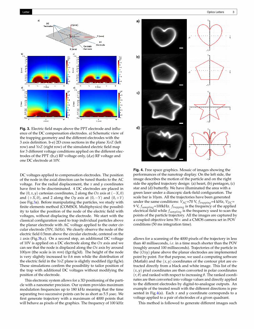
Fig. 4. Free space graphics. Mosaic of images showing theperformances of the nanotrap display. On the left side, theimage describes the motion of the particle and on the rightside the applied trajectory design: (a) heart, (b) pentagon, (c)star and (d) butterfly. We have illuminated the area with agreen laser under a diascopic dark-field configuration. Thescale bar is 10µm. All the trajectories have been generatedunder the same conditions: VAC=70 V, ftrapping=4 kHz, VDC=9 V, fsampling=100kHz. ftrapping is the frequency of the appliedelectrical field while fsampling is the frequency used to scan thepoints of the particle trajectory. All the images are captured bya coupled objective lens 50× and a CMOS camera set in POVconditions (50 ms integration time).
allows for a scanning of the 4000 pixels of the trajectory in lessthan 40 milliseconds, i.e. in a time much shorter than the POV(roughly around 100 milliseconds). Trajectories of the particle inthe (Oxy) plane above the planar electrodes are implementedpoint by point. For that purpose, we used a computing software(Matlab) and the (x, y) coordinates of the contour plot are ex-tracted directly from a black and white image. This list of the(x, y) pixel coordinates are then converted in polar coordinates(r, θ) and ranked with respect to increasing θ. The ranked coordi-nates are then converted into voltage values and directly appliedto the different electrodes by digital-to-analogue outputs. Anexample of the treated result with the different directions is pre-sented in Fig.4(a). Each x and y coordinate corresponds to avoltage applied to a pair of electrodes of a given quadrant.
This method is followed to generate different images such
Letter Optics Letters 4
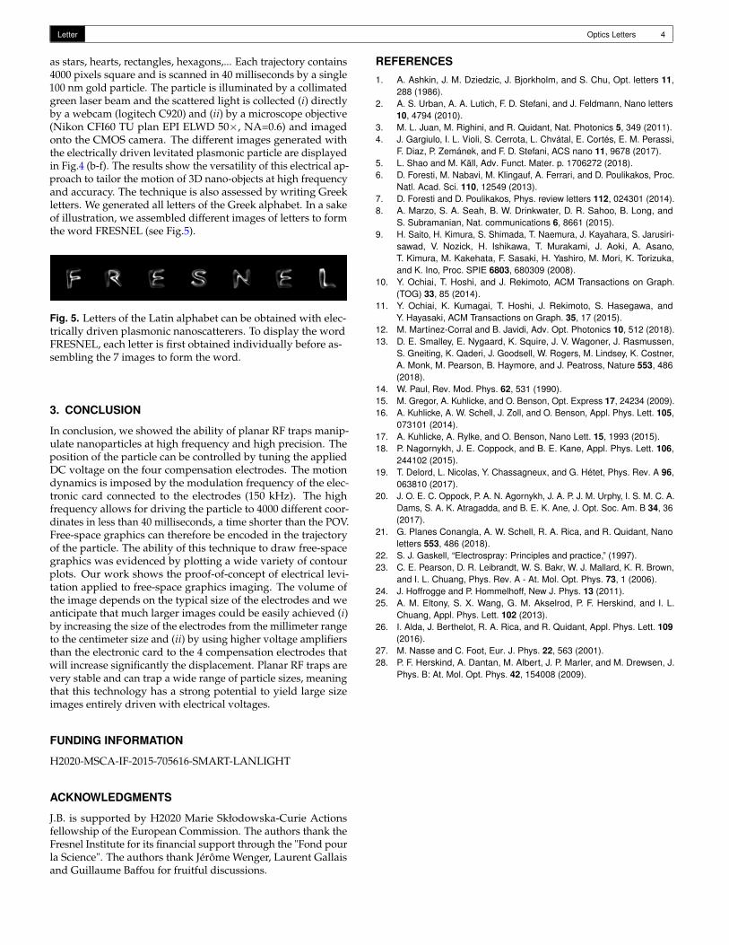
as stars, hearts, rectangles, hexagons,... Each trajectory contains4000 pixels square and is scanned in 40 milliseconds by a single100 nm gold particle. The particle is illuminated by a collimatedgreen laser beam and the scattered light is collected (i) directlyby a webcam (logitech C920) and (ii) by a microscope objective(Nikon CFI60 TU plan EPI ELWD 50×, NA=0.6) and imagedonto the CMOS camera. The different images generated withthe electrically driven levitated plasmonic particle are displayedin Fig.4 (b-f). The results show the versatility of this electrical ap-proach to tailor the motion of 3D nano-objects at high frequencyand accuracy. The technique is also assessed by writing Greekletters. We generated all letters of the Greek alphabet. In a sakeof illustration, we assembled different images of letters to formthe word FRESNEL (see Fig.5).
Fig. 5. Letters of the Latin alphabet can be obtained with elec-trically driven plasmonic nanoscatterers. To display the wordFRESNEL, each letter is first obtained individually before as-sembling the 7 images to form the word.
3. CONCLUSION
In conclusion, we showed the ability of planar RF traps manip-ulate nanoparticles at high frequency and high precision. Theposition of the particle can be controlled by tuning the appliedDC voltage on the four compensation electrodes. The motiondynamics is imposed by the modulation frequency of the elec-tronic card connected to the electrodes (150 kHz). The highfrequency allows for driving the particle to 4000 different coor-dinates in less than 40 milliseconds, a time shorter than the POV.Free-space graphics can therefore be encoded in the trajectoryof the particle. The ability of this technique to draw free-spacegraphics was evidenced by plotting a wide variety of contourplots. Our work shows the proof-of-concept of electrical levi-tation applied to free-space graphics imaging. The volume ofthe image depends on the typical size of the electrodes and weanticipate that much larger images could be easily achieved (i)by increasing the size of the electrodes from the millimeter rangeto the centimeter size and (ii) by using higher voltage amplifiersthan the electronic card to the 4 compensation electrodes thatwill increase significantly the displacement. Planar RF traps arevery stable and can trap a wide range of particle sizes, meaningthat this technology has a strong potential to yield large sizeimages entirely driven with electrical voltages.
FUNDING INFORMATION
H2020-MSCA-IF-2015-705616-SMART-LANLIGHT
ACKNOWLEDGMENTS
J.B. is supported by H2020 Marie Skłodowska-Curie Actionsfellowship of the European Commission. The authors thank theFresnel Institute for its financial support through the "Fond pourla Science". The authors thank Jérôme Wenger, Laurent Gallaisand Guillaume Baffou for fruitful discussions.
REFERENCES
1. A. Ashkin, J. M. Dziedzic, J. Bjorkholm, and S. Chu, Opt. letters 11,288 (1986).
2. A. S. Urban, A. A. Lutich, F. D. Stefani, and J. Feldmann, Nano letters10, 4794 (2010).
3. M. L. Juan, M. Righini, and R. Quidant, Nat. Photonics 5, 349 (2011).4. J. Gargiulo, I. L. Violi, S. Cerrota, L. Chvátal, E. Cortés, E. M. Perassi,
F. Diaz, P. Zemánek, and F. D. Stefani, ACS nano 11, 9678 (2017).5. L. Shao and M. Käll, Adv. Funct. Mater. p. 1706272 (2018).6. D. Foresti, M. Nabavi, M. Klingauf, A. Ferrari, and D. Poulikakos, Proc.
Natl. Acad. Sci. 110, 12549 (2013).7. D. Foresti and D. Poulikakos, Phys. review letters 112, 024301 (2014).8. A. Marzo, S. A. Seah, B. W. Drinkwater, D. R. Sahoo, B. Long, and
S. Subramanian, Nat. communications 6, 8661 (2015).9. H. Saito, H. Kimura, S. Shimada, T. Naemura, J. Kayahara, S. Jarusiri-
sawad, V. Nozick, H. Ishikawa, T. Murakami, J. Aoki, A. Asano,T. Kimura, M. Kakehata, F. Sasaki, H. Yashiro, M. Mori, K. Torizuka,and K. Ino, Proc. SPIE 6803, 680309 (2008).
10. Y. Ochiai, T. Hoshi, and J. Rekimoto, ACM Transactions on Graph.(TOG) 33, 85 (2014).
11. Y. Ochiai, K. Kumagai, T. Hoshi, J. Rekimoto, S. Hasegawa, andY. Hayasaki, ACM Transactions on Graph. 35, 17 (2015).
12. M. Martínez-Corral and B. Javidi, Adv. Opt. Photonics 10, 512 (2018).13. D. E. Smalley, E. Nygaard, K. Squire, J. V. Wagoner, J. Rasmussen,
S. Gneiting, K. Qaderi, J. Goodsell, W. Rogers, M. Lindsey, K. Costner,A. Monk, M. Pearson, B. Haymore, and J. Peatross, Nature 553, 486(2018).
14. W. Paul, Rev. Mod. Phys. 62, 531 (1990).15. M. Gregor, A. Kuhlicke, and O. Benson, Opt. Express 17, 24234 (2009).16. A. Kuhlicke, A. W. Schell, J. Zoll, and O. Benson, Appl. Phys. Lett. 105,
073101 (2014).17. A. Kuhlicke, A. Rylke, and O. Benson, Nano Lett. 15, 1993 (2015).18. P. Nagornykh, J. E. Coppock, and B. E. Kane, Appl. Phys. Lett. 106,
244102 (2015).19. T. Delord, L. Nicolas, Y. Chassagneux, and G. Hétet, Phys. Rev. A 96,
063810 (2017).20. J. O. E. C. Oppock, P. A. N. Agornykh, J. A. P. J. M. Urphy, I. S. M. C. A.
Dams, S. A. K. Atragadda, and B. E. K. Ane, J. Opt. Soc. Am. B 34, 36(2017).
21. G. Planes Conangla, A. W. Schell, R. A. Rica, and R. Quidant, Nanoletters 553, 486 (2018).
22. S. J. Gaskell, “Electrospray: Principles and practice,” (1997).23. C. E. Pearson, D. R. Leibrandt, W. S. Bakr, W. J. Mallard, K. R. Brown,
and I. L. Chuang, Phys. Rev. A - At. Mol. Opt. Phys. 73, 1 (2006).24. J. Hoffrogge and P. Hommelhoff, New J. Phys. 13 (2011).25. A. M. Eltony, S. X. Wang, G. M. Akselrod, P. F. Herskind, and I. L.
Chuang, Appl. Phys. Lett. 102 (2013).26. I. Alda, J. Berthelot, R. A. Rica, and R. Quidant, Appl. Phys. Lett. 109
(2016).27. M. Nasse and C. Foot, Eur. J. Phys. 22, 563 (2001).28. P. F. Herskind, A. Dantan, M. Albert, J. P. Marler, and M. Drewsen, J.
Phys. B: At. Mol. Opt. Phys. 42, 154008 (2009).

Letter Optics Letters 5
REFERENCES
1. A. Ashkin, J. M. Dziedzic, J. Bjorkholm, and S. Chu, “Observation ofa single-beam gradient force optical trap for dielectric particles,” Opt.letters 11, 288 (1986).
2. A. S. Urban, A. A. Lutich, F. D. Stefani, and J. Feldmann, “Laser printingsingle gold nanoparticles,” Nano letters 10, 4794 (2010).
3. M. L. Juan, M. Righini, and R. Quidant, “Plasmon nano-optical tweez-ers,” Nat. Photonics 5, 349 (2011).
4. J. Gargiulo, I. L. Violi, S. Cerrota, L. Chvátal, E. Cortés, E. M. Perassi,“Accuracy and Mechanistic Details of Optical Printing of Single Au andAg Nanoparticles,” F. Diaz, P. Zemánek, and F. D. Stefani, ACS nano11, 9678 (2017).
5. L. Shao and M. Käll, “Light-Driven Rotation of Plasmonic Nanomotors,”Adv. Funct. Mater. p. 1706272 (2018).
6. D. Foresti, M. Nabavi, M. Klingauf, A. Ferrari, and D. Poulikakos,“Acoustophoretic contactless transport and handling of matter in air,”Proc. Natl. Acad. Sci. 110, 12549 (2013).
7. D. Foresti and D. Poulikakos, “Acoustophoretic contactless elevation,orbital transport and spinning of matter in air,” Phys. review letters 112,024301 (2014).
8. A. Marzo, S. A. Seah, B. W. Drinkwater, D. R. Sahoo, B. Long, andS. Subramanian, “coustophoretic contactless elevation, orbital trans-port and spinning of matter in air,” Nat. communications 6, 8661 (2015).
9. H. Saito, H. Kimura, S. Shimada, T. Naemura, J. Kayahara, S. Jarusiri-sawad, V. Nozick, H. Ishikawa, T. Murakami, J. Aoki, A. Asano,T. Kimura, M. Kakehata, F. Sasaki, H. Yashiro, M. Mori, K. Torizuka, andK. Ino, “Laser-plasma scanning 3D display for putting digital contentsin free space,” Proc. SPIE 6803, 680309 (2008).
10. Y. Ochiai, T. Hoshi, and J. Rekimoto, “Pixie dust: graphics generatedby levitated and animated objects in computational acoustic-potentialfield” ACM Transactions on Graph. (TOG) 33, 85 (2014).
11. Y. Ochiai, K. Kumagai, T. Hoshi, J. Rekimoto, S. Hasegawa, andY. Hayasaki, “Fairy Lights in Femtoseconds: Aerial and VolumetricGraphics Rendered by Focused Femtosecond Laser Combined withComputational Holographic Fields,” ACM Transactions on Graph. 35,17 (2015).
12. M. Martínez-Corral and B. Javidi, “Fundamentals of 3D imaging and dis-plays: a tutorial on integral imaging, light-field, and plenoptic systems,”Adv. Opt. Photonics 10, 512 (2018).
13. D. E. Smalley, E. Nygaard, K. Squire, J. V. Wagoner, J. Rasmussen,S. Gneiting, K. Qaderi, J. Goodsell, W. Rogers, M. Lindsey, K. Costner,A. Monk, M. Pearson, B. Haymore, and J. Peatross, “A photophoretic-trap volumetric display,” Nature 553, 486 (2018).
14. W. Paul, “Electromagnetic traps for charged and neutral particles,” Rev.Mod. Phys. 62, 531 (1990).
15. M. Gregor, A. Kuhlicke, and O. Benson, “Soft-landing and optical char-acterization of a preselected single fluorescent particle on a taperedoptical fiber,” Opt. Express 17, 24234 (2009).
16. A. Kuhlicke, A. W. Schell, J. Zoll, and O. Benson, “Nitrogen vacancycenter fluorescence from a submicron diamond cluster levitated in alinear quadrupole ion trap,” Appl. Phys. Lett. 105, 073101 (2014).
17. A. Kuhlicke, A. Rylke, and O. Benson, “On-demand electrostatic cou-pling of individual precharacterized nano- and microparticles in a seg-mented Paul trap,” Nano Lett. 15, 1993 (2015).
18. P. Nagornykh, J. E. Coppock, and B. E. Kane, “Cooling of levitatedgraphene nanoplatelets in high vacuum,” Appl. Phys. Lett. 106, 244102(2015).
19. T. Delord, L. Nicolas, Y. Chassagneux, and G. Hétet, “Strong couplingbetween a single nitrogen-vacancy spin and the rotational mode ofdiamonds levitating in an ion trap,” Phys. Rev. A 96, 063810 (2017).
20. J. O. E. C. Oppock, P. A. N. Agornykh, J. A. P. J. M. Urphy, I. S. M.C. A. Dams, S. A. K. Atragadda, and B. E. K. Ane, “Dual-trap systemto study charged graphene nanoplatelets in high vacuum,” J. Opt. Soc.Am. B 34, 36 (2017).
21. G. Planes Conangla, A. W. Schell, R. A. Rica, and R. Quidant, “Motioncontrol and optical interrogation of a levitating single NV in vacuum,”Nano letters 553, 486 (2018).
22. S. J. Gaskell, “Electrospray: Principles and practice,” (1997).
23. C. E. Pearson, D. R. Leibrandt, W. S. Bakr, W. J. Mallard, K. R. Brown,and I. L. Chuang, “Experimental investigation of planar ion traps,” Phys.Rev. A - At. Mol. Opt. Phys. 73, 1 (2006).
24. J. Hoffrogge and P. Hommelhoff, “Planar microwave structures forelectron guiding,” New J. Phys. 13 (2011).
25. A. M. Eltony, S. X. Wang, G. M. Akselrod, P. F. Herskind, and I. L.Chuang, “Transparent ion trap with integrated photodetector,” Appl.Phys. Lett. 102 (2013).
26. I. Alda, J. Berthelot, R. A. Rica, and R. Quidant, “Trapping and manipu-lation of individual nanoparticles in a planar Paul trap,” Appl. Phys. Lett.109 (2016).
27. M. Nasse and C. Foot, “Influence of background pressure on thestability region of a Paul trap,” Eur. J. Phys. 22, 563 (2001).
28. P. F. Herskind, A. Dantan, M. Albert, J. P. Marler, and M. Drewsen,“Positioning of the rf potential minimum line of a linear Paul trap withmicrometer precision,” J. Phys. B: At. Mol. Opt. Phys. 42, 154008(2009).
Related Documents