S¯ adhan¯ a Vol. 33, Part 5, October 2008, pp. 591–613. © Printed in India Vector control of three-phase AC/DC front-end converter J S SIVA PRASAD, TUSHAR BHAVSAR, RAJESH GHOSH and G NARAYANAN Department of Electrical Engineering, Indian Institute of Science, Bangalore 560 012 e-mail: [email protected]; [email protected]; [email protected]; [email protected] Abstract. A vector control scheme is presented for a three-phase AC/DC con- verter with bi-directional power flow capability. A design procedure for selection of control parameters is discussed. A simple algorithm for unit-vector generation is presented. Starting current transients are studied with particular emphasis on high-power applications, where the line-side inductance is low. A starting proce- dure is presented to limit the transients. Simulation and experimental results are also presented. Keywords. Ac-dc conversion; controlled rectification; power factor correction; PWM converter; synchronous reference frame control; vector control. 1. Introduction A three-phase AC to DC converter is an essential part of many power electronic systems such as uninterruptible power supplies (UPS), battery chargers and motor drives. The battery charger needs ac–dc conversion, while UPS and motor drives typically have an ac–dc conversion stage followed by dc–ac conversion. Traditionally diode rectifiers are used for ac–dc conversion. These rectifiers can only pro- duce a constant DC voltage, which is a function of the system voltage. A thyristor rectifier can be used to produce variable dc output voltage. But, both these rectifiers behave as non- linear loads. The currents drawn by the rectifiers include a fundamental (or line frequency) component and harmonic components. The voltage drop across the line inductance due to the harmonic currents distorts the mains voltage. Consequently, the other loads connected to the mains are also fed with a distorted voltage. Figure 1 illustrates such harmonic pollution of the mains considering a single-phase rectifier load. This is true for a three-phase system also. Figure 1b shows an oscillogram of the distorted mains voltage, which is typical when non-linear loads are connected. Note that the waveform is flat close to the peaks, unlike a sinusoidal waveform. The distortion will be higher, if the non-linear load is of higher rating or several such non-linear loads are connected in parallel. A pulse width modulated (PWM) rectifier, such as the one shown in figure 2, draws near sinusoidal currents from the ac mains. Also, the dc output voltage can be regulated, and the 591

Welcome message from author
This document is posted to help you gain knowledge. Please leave a comment to let me know what you think about it! Share it to your friends and learn new things together.
Transcript

Sadhana Vol. 33, Part 5, October 2008, pp. 591–613. © Printed in India
Vector control of three-phase AC/DC front-end converter
J S SIVA PRASAD, TUSHAR BHAVSAR, RAJESH GHOSH andG NARAYANAN
Department of Electrical Engineering, Indian Institute of Science,Bangalore 560 012e-mail: [email protected]; [email protected];[email protected]; [email protected]
Abstract. A vector control scheme is presented for a three-phase AC/DC con-verter with bi-directional power flow capability. A design procedure for selectionof control parameters is discussed. A simple algorithm for unit-vector generationis presented. Starting current transients are studied with particular emphasis onhigh-power applications, where the line-side inductance is low. A starting proce-dure is presented to limit the transients. Simulation and experimental results arealso presented.
Keywords. Ac-dc conversion; controlled rectification; power factor correction;PWM converter; synchronous reference frame control; vector control.
1. Introduction
A three-phase AC to DC converter is an essential part of many power electronic systems such asuninterruptible power supplies (UPS), battery chargers and motor drives. The battery chargerneeds ac–dc conversion, while UPS and motor drives typically have an ac–dc conversionstage followed by dc–ac conversion.
Traditionally diode rectifiers are used for ac–dc conversion. These rectifiers can only pro-duce a constant DC voltage, which is a function of the system voltage. A thyristor rectifiercan be used to produce variable dc output voltage. But, both these rectifiers behave as non-linear loads. The currents drawn by the rectifiers include a fundamental (or line frequency)component and harmonic components. The voltage drop across the line inductance due to theharmonic currents distorts the mains voltage. Consequently, the other loads connected to themains are also fed with a distorted voltage.
Figure 1 illustrates such harmonic pollution of the mains considering a single-phase rectifierload. This is true for a three-phase system also. Figure 1b shows an oscillogram of the distortedmains voltage, which is typical when non-linear loads are connected. Note that the waveformis flat close to the peaks, unlike a sinusoidal waveform. The distortion will be higher, if thenon-linear load is of higher rating or several such non-linear loads are connected in parallel.
A pulse width modulated (PWM) rectifier, such as the one shown in figure 2, draws nearsinusoidal currents from the ac mains. Also, the dc output voltage can be regulated, and the
591

592 J S Siva Prasad et al
Figure 1. Harmonic pollu-tion due to a non-linear load(a) a typical circuit connection,(b) distorted mains voltage.
input power factor is adjustable. For the converter shown in figure 2, the power can also flowin either direction, which is required in many motor drive applications. Since the converteris typically connected in the line-side of a motor drive, this is called a line-side converter orfront-end converter (FEC).
The converter consists of a three-phase bridge, a high capacitance on the dc side and athree-phase inductor in the line-side. The voltage at the mid point of a leg or the pole voltagevi is pulse width modulated (PWM) in nature. The pole voltage consists of a fundamentalcomponent (at line frequency) besides harmonic components around the switching frequencyof the converter. Being at high frequencies, these harmonic components are well filtered bythe line inductor. Hence the current is near sinusoidal. The fundamental component of vi
controls the flow of real and reactive power.
Figure 2. Schematic diagram ofa front-end converter (FEC).

Vector control of three-phase AC/DC front-end converter 593
Figure 3. Phasor diagrams ofan FEC under different operatingmodes (a) unity pf, (b) lagging pf,(c) leading pf and (d) regenerationat unity pf.
It is well known that the active power flows from the leading voltage to the lagging voltageand the reactive power flows from the higher voltage to the lower voltage. Therefore, bothactive and reactive power can be controlled by controlling the phase and magnitude of theconverter voltage fundamental component with respect to the grid voltage. Figure 3 showsthe phasor diagrams of the converter under different modes of operation. In this figure, thesubscript ‘f ’ indicates the fundamental component of that particular quantity. Figure 3aillustrates the operation at unity power factor. As the grid voltage leads the converter polevoltage, real power flows from the ac side to the dc side. Figure 3b corresponds lagging powerfactor operation. The real power flows from the ac to the dc side. Since Vs is greater than Vi ,the reactive power flows from the mains to the converter side. In figure 3c (leading powerfactor), the real power flows from the ac to the dc side, while the reactive power flows fromthe converter to the grid. Figure 3d shows the operation under regenerative mode with thereal power flowing from the dc to the ac side and at unity power factor.
Apart from control of real and reactive power flow, an FEC should also have a fastdynamic response. Several control schemes have been reported in the literature for FEC(Chattopadhyay & Ramanarayanan 2005; Ghosh 2007; Noguchi et al 1998). This paper dis-cusses vector control of the FEC.
Vector control is a popular method for control of three-phase induction motors. The basicidea of this scheme is to control the flux producing and the torque-producing componentsof motor current in a decoupled manner to achieve fast dynamic response (Leonhard 2001;Ranganathan 2007). The outer control loop controls the speed of the motor, while the innerloop controls the components of current vector, which correspond to torque and flux.
Similar control approach can be used for FEC also. Here, the three-phase grid voltages andline currents are converted into an equivalent two-phase system, called stationary referenceframe. These quantities are further transformed into a reference frame called synchronousreference frame, which revolves at the grid frequency. These transformations are explainedin § 2. In synchronous reference frame, the components of current corresponding to activeand reactive power are controlled in an independent manner similar to the torque and fluxproducing components in a motor drive. The outer loop controls the dc bus voltage and theinner loop controls the line currents. The control method is presented in § 2. The selection ofcontroller parameters is discussed in § 3. Section 4 presents the simulation and experimentalresults of FEC. Section 5 discusses the problems associated with the starting process ofan FEC, particularly at high power levels and the proposed solutions. Section 6 gives theconclusions.

594 J S Siva Prasad et al
Figure 4. Stationary and syn-chronously revolving frames ofreference.
2. Vector control of FEC
The FEC, shown in figure 2 is fed from the ac mains. Mains voltages vs1, vs2 and vs3 aredefined in (1), where Vs is the rms value of phase to neutral voltage. The three-phase volt-ages can be transformed into two-phase quantities vsa and vsb, which are the componentsof voltage vector Vs along a-axis and b-axis, respectively, in the stationary reference frame(figure 4).
vs1 =√
2Vs cos ωt (1)
vs2 =√
2Vs cos(ωt − 1200)
vs3 =√
2Vs cos(ωt − 2400)
vsa = 3
2vs1 = 3
2
√2Vs cos ωt vsb =
√3
2(vs2 − vs3) = 3
2
√2Vs sin ωt. (2)
These voltages can further be transformed into a synchronously revolving d–q referenceframe, where q-axis is aligned with the voltage vector Vs and the d-axis lags the q-axis by 90◦as shown in figure 4. This transformation is performed using (3), where θ is the angle of thed-axis measured from the a-axis. The other three-phase quantities, namely line currents (is1,is2 and is3) and the converter pole voltages (vi1, vi2 and vi3), can also be similarly transformed

Vector control of three-phase AC/DC front-end converter 595
Figure 5. Unit vector generation.
to the d–q reference frame.
vsq = (−vsa sin θ + vsb cos θ)
vsd = (vsa cos θ + vsb sin θ).(3)
The voltage equations of the FEC in the d–q reference frame are given by (4), where Rs
and Ls are the resistance and inductance, respectively, of the line inductor.
Rsisd + Ls
disd
dt− ωLsisq + vid = 0
Rsisq + Ls
disq
dt+ ωLsisd + viq = vsq . (4)
2.1 Unit vector generation
In order to transform any vector from stationary reference frame into d–q reference frame, thequantities sin θ and cos θ , which are the components of a revolving unit vector are required(see equation 3). These quantities should have the same frequency as that of the systemvoltage.
The voltage vector Vs is at an angle ωt (see equation (1)) with respect to the a-axis. Thecomponents vsa and vsb of the vector are as shown in (2). A low-pass filter, whose cornerfrequency equals the mains frequency, delays vsa (or vsb) by 45◦. Two such filters in cascadedelay vsa (or vsb) by 90◦ as shown in (5). Figure 5 illustrates such a filter arrangementfollowed by normalization as given by (6). Such filtering and normalization yields cos θ
and sin θ , where θ is the angle between a-axis and d-axis required for the transformationin (3).
Such a method of unit vector generation [equations (5)–(6) and figure 5] is more straight-forward than the use of phase-locked loops (PLL) (Chung 2000).
x = 3
4
√2Vs cos
(ωt − π
2
)= 3
4
√2Vs cos θ
y = 3
4
√2Vs sin
(ωt − π
2
)= 3
4
√2Vs sin θ
(5)
cos θ = x√x2 + y2
sin θ = y√x2 + y2
. (6)
In the above discussion, it is assumed that the grid voltages are free from harmonics, gridfrequency remains unchanged at 50 Hz and grid voltages are balanced. The performance of

596 J S Siva Prasad et al
Table 1. Effect of frequency variation on unit vector generation.
LineFrequency Magnitude of Phase vsq = vsd =(Hz) unit-vector error (δ) cos δ (p.u) sin δ (p.u)
48 1 −2·34 0·99 −0·0449 1 −1·157 0·99 −0·0250 1 0 1 051 1 1·1345 0·99 0·0252 1 2·246 0·99 0·04
unit vector generation scheme under the presence of harmonics in grid voltage, grid frequencyvariation and unbalance in grid voltages is studied below.
2.1a Grid voltage harmonics: In unit-vector generation algorithm, vsa and vsb are passedthrough two cascaded low-pass filters with 50 Hz corner frequency. Ignoring any variation inthe line frequency, the combined gain of the two-cascaded filters for nth harmonic voltage isgiven by
An =∣∣∣∣
1
1 + jn
∣∣∣∣2
= 1
1 + n2. (7)
The 5th and 7th harmonics are attenuated to 3·85% and 2% respectively, of their originalvalues. The attenuation is still higher for harmonics such as 11th, 13th, 17th, etc. Thus, thecomponents of the unit vector are practically devoid of any harmonic content. The unit vec-tor generation algorithm works satisfactorily even in the presence of harmonics in the gridvoltage.
2.1b Grid frequency variation: The gain and the phase of the low-pass filters used in unitvector generation (figure 5) change with the supply frequency. The normalization (6) ensuresthat the magnitude of unit vector generated is unaffected by line frequency variation. However,the phase angle between vsa and x, and that between vsb and y are no longer equal to 90◦. Theerrors in the phase angle are as tabulated in table 1, for line frequencies in the range of 48 to52 Hz. The corresponding errors in vsq and vsd are also shown in table 1. It can be observedthat the error in vsq is less than 1%, while the error in vsd is less than 4%. Hence, it can beconcluded that variation of grid frequency within the given range only has a marginal effecton unit vector generation.
2.1c Grid voltage unbalance: With unbalance in grid voltages, vs1, vs2 and vs3 of figure 2,can be expressed as shown in (8), where A is the amplitude of positive sequence voltage, B isthe amplitude of the negative sequence voltage, C is the amplitude of zero sequence voltage,and λ is the phase angle of the zero-sequence component.
vs1 = A cos ωt + B cos ωt + C cos(ωt − λ)
vs2 = A cos(ωt − 120◦) + B cos(ωt − 240◦) + C cos(ωt − λ)
vs3 = A cos(ωt − 240◦) + B cos(ωt − 120◦) + C cos(ωt − λ).
(8)

Vector control of three-phase AC/DC front-end converter 597
The components of the voltage vector along a and b axes are given by
vsa =(
3
2
)[(A + B) cos ωt + C cos(ωt − λ)]
vsb =(
3
2
)(A − B) sin ωt.
(9)
The outputs of cascaded low-pass filters, namely x and y (figure 5), can be expressed as
x =(
3
4
)[(A + B) sin ωt + C sin(ωt − λ)]
y = −(
3
4
)(A − B) cos ωt.
(10)
For generating the unit-vector, x and y are normalized as shown in figure 5. The quantityx2 + y2 can be expressed as
x2 + y2 =(
3
4
)2 (A2 + B2 + C2
2+ [(A + B)C cos λ]
)
−(
3
4
)2
[2AB cos 2ωt + {(A + B)C cos(2ωt + λ)}]. (11)
The unit vector can be expressed as
Fu = x√x2 + y2
+ jy√
x2 + y2(12)
|Fu| = 1, ∠Fu = tan−1(y
x
). (13)
The magnitude of the unit vector generated is equal to one. However, the phase angle ofthe unit vector, which must be equal to ωt (in stationary reference frame), does not changelinearly with time under steady state due to voltage imbalance. The deviation between thephase of the unit vector and ωt is low only when B and C [(8)–(11)] are low.
Thus, the performance of unit vector generation scheme is satisfactory in the presence ofline harmonics and over a range of line frequencies. However, in the presence of voltageimbalance, its performance is satisfactory only when the imbalance is marginal. The proposedcontrol scheme itself is mainly suited for operation under balanced input voltages. Controlof PWM rectifier under voltage imbalance conditions requires modification in the controlscheme and has been discussed in literature (Chattopadhyay & Ramanarayanan 2005; Ghosh2007).
2.2 Vector control approach
The overall block diagram of a vector controlled FEC is shown in figure 6. The mains voltagesand the line currents are transformed into d–q reference frame, and are used as feedbackvariables for the controller as shown in the figure. The control calculations are performed inthe d–q reference frame.

598 J S Siva Prasad et al
Figure 6. Block diagram of a vec-tor controlled front-end converter.
The vector controller has an outer voltage loop to control Vdc. The voltage controller setsthe reference to the inner q-axis current controller as shown in figure 7. The q-axis currentloop controls the flow of real power p, since isq is a measure of p as shown in (14a). Thereis an independent loop for the control of isd , which controls reactive power as per (14b).
p = 2
3(vsqisq + vsdisd) = 2
3(vsqisq) (14a)
q = 2
3(vsqisd − vsdisq) = 2
3(vsqisd). (14b)
2.3 Feedforward terms
A cross coupling exists between the d-axis and the q-axis quantities as seen from (4). Toensure decoupled control of isd and isq , feedforward terms vdff and vqff respectively, areadded to the outputs of the d-axis controller (v′′
id ) and the q-axis controller (v′′iq) as given in
(15) and illustrated in figure 7. The converter gain G is defined in (16), where Vc is the peak
Figure 7. Voltage and currentcontrollers in a vector controlledfront-end converter.

Vector control of three-phase AC/DC front-end converter 599
Figure 8. Current controller.
of the triangular carrier used in sine-triangle PWM.
v∗d = −v′′
id + vdff = −v′′id + ωLsisq
G
v∗q = −v′′
iq + vqff = −v′′iq + vsq
G− ωLsisd
G
(15)
G = Vdc
2Vc
. (16)
The above controller ensures that the current loop has a first order response as given by (17).
Rsisd + Ls
disd
dt= Gv′′
id
Rsisq + Ls
disq
dt= Gv′′
iq .
(17)
The voltage references, v∗q and v∗
d are transformed into three-phase references (v∗1 , v
∗2 , v
∗3)
using the inverse of the transformations in (3) and (2).
3. Design of controllers
This section explains the selection of controller parameters for the voltage and current loops.
3.1 Current controller
The converter is modelled using its gain G and the delay time Td as shown in figure 8. Thedelay Td is equal to half the time period of the carrier signal. A block diagram of the q-axiscurrent loop is shown in figure 8, where Ts is the time constant of the inductor (Ts = Ls/Rs),and K2 and T2 are the gain and time constant, respectively, of the current sensor.
The open loop transfer function between Isq−f b and v∗q can be approximated as shown in
(18), since TdT2 is very small. Here Tσ = Td + T2.
Isq−f b(s)
v∗q(s)
= GK2
Rs
1
(1 + sTs)(1 + sTd)(1 + sT2)∼= GK2
Rs
1
(1 + sTs)(1 + sTσ ).
(18)
Since Ts is much higher than Tσ , this pole at (1/Ts) is cancelled using the controller zeroby choosing controller parameter Tc as shown in (19).
Tc = Ts. (19)

600 J S Siva Prasad et al
The resulting closed loop transfer function is given by (20), where TdT2 is neglected onceagain.
Isq(s)
I ∗sq(s)
= KcG
RsTsTσ
(1 + sT2)(s2 + s
Tσ+ KcGK2
RsTsTσ
) . (20)
Comparing the denominator of R.H.S of (20) with the standard form of second order transferfunction
2ξωn = 1
Tσ
; ω2n = KcGK2
RsTsTσ
. (21)
Choosing ξ = 0·707, the controller gain is determined as shown in (22). This leads to acurrent loop of bandwidth equal to (0·707/Tσ )
Kc = RsTs
2GK2Tσ
. (22)
The d-axis controller is designed in a similar fashion.
3.2 Voltage controller
With the current controller parameters Tc and Kc chosen as in (19) and (22), the closed looptransfer function of q-axis current loop is as shown below.
Isq(s)
I ∗sq(s)
= 1
K2
(1 + sT2)
(1 + 2Tσ s + 2T 2σ s2)
. (23)
The zero at (1/T2) due to the current sensor is at a frequency higher than the current loopbandwidth. Hence, this zero can be ignored. Further, the desired voltage loop bandwidth ismuch lower than the current loop bandwidth. Hence, for the design of voltage controller, thesecond order term in the denominator polynomial in (23) can also be neglected. Thus, thecurrent loop can be approximated by a first order transfer function shown in (24).
Isq(s)
I ∗sq(s)
= 1
K2
1
(1 + 2Tσ s). (24)
The input–output power balance gives the relationship between Idc and isq as shown in (25).
Idc = 2
3
vsq
Vdc
isq = Kisq (say). (25)
Figure 9. Voltage controller.

Vector control of three-phase AC/DC front-end converter 601
Figure 10. Illustrative bode plot for voltage controller design.
The voltage loop can be represented by a block diagram shown in figure 9. Here K1 andT1 are the gain and time constant, respectively, of the voltage sensor; Kv and Tv are thevoltage controller parameters. The open loop transfer function of the voltage loop is definedin (26). Similar to the approximation in (18), the voltage loop transfer function can also beapproximated as shown in (26), where Tδ is as defined in (27). Here, 2TσT1 is ignored, as itis quite small.
Vdc−f b(s)
V ∗dc(s)
= Ke(1 + sTv)
sTv(1 + 2Tσ s)(1 + sT1)C0s∼= Ke(1 + sTv)
s2TvC0(1 + sTδ). (26)
Ke =(
KvKK1
K2
)and Tδ = 2Tσ + T1. (27)
Since there are two poles at the origin, the magnitude plot of this transfer function has aslope of −40 dB/decade at low frequencies as shown in figure 10. For system stability, thecontroller zero (ω1 = 1/Tv) should be located before the unit gain crossover (ωc) and the pole(ω2 = 1/Tδ) should be located after unit gain crossover such that the slope is −20 dB/decadeat the crossover as shown in figure 10.
The crossover frequency ωc could be the geometric mean of the two corner frequencies(1/TV ) and (1/Tδ) as shown in (28), where a is any number greater than 1 (Leonhard 2001).Considering a suitable value of a, the parameter Tv can be chosen as given in (29).
ωc = 1√TvTδ
= 1
aTδ
(say) (28)
Tv = a2Tδ. (29)

602 J S Siva Prasad et al
Table 2. System and controller parameters.
S. No. Symbol Value S. No. Symbol Value
1 Vs 168 (V) 10 K1 0·00112 Ls 660 μH 11 T1 10 μs3 Rs 2 m 12 K2 0·0024 Ts 330 ms 13 T2 10 μs5 C0 6750 μF 14 Kc 56 G 300 15 Tc 330 ms7 fsw 5 kHz 16 Kv 678 Td 100 μs 17 Tv 920 μs9 K 0·396 18 a 2
The gain at crossover frequency ωc is equal to one as shown in (30). Using equations (27–30),the parameter Kv can be selected as given in (31).
∣∣∣∣Vdc−f b(s)
V ∗dc(s)
∣∣∣∣ωx=ωc
= 1 = Ke
√1 + (ωcTv)2
ω2cC0Tv
√1 + (ωcTδ)2
(30)
Kv = C0K2
K1KaTδ
. (31)
Considering a = 2, the phase margin is given by (32).
Phase margin = (tan−1(ωcTv) − tan−1(ωcTδ)) =(
tan−1 a − tan−1 1
a
)= 37◦.
(32)
The system parameters are presented in table 2. The controller parameters are calculatedas explained earlier. They are also listed in the table.
In order to verify the validity of the approximations in (18), the bode plots of the actual aswell as approximated open loop transfer functions of the current loop are plotted as shown infigure 11.
Similarly, to verify the validity of the approximations in (24) and (26) while designing thevoltage controller, the bode plots of the actual and approximate open loop transfer functionsof the voltage loop are plotted as shown in figure 12.
As seen, the approximations, which simplify the design calculations, do not introduce anysignificant error in the gain and/or phase angle over frequencies of interest.
4. Simulation and experimental results
A 250-kVA vector-controlled FEC is simulated with MATLAB/SIMULINK. The systemparameters are shown in table 2. Sine-triangle PWM method is employed with a carrierfrequency of 5 kHz.
Figure 13 shows the dynamic response of line current during a change in load from 10%to 30% at t = 1·1 s. The steady state power factor is close to unity and the dynamic responseis found to be good. The transient response for a change in the reactive power reference (i∗sd)

Vector control of three-phase AC/DC front-end converter 603
Figure 11. Bode plots of actualand approximate open loop trans-fer functions of the current loop.
from 0 to 10% is also fast as seen from figure 14. For t > 0·8 s, the power factor is close tozero since only reactive power is drawn.
The experimental set-up consists of a 250-kVA IGBT converter with TMS320LF2407 DSPbased digital controller (Texas Instruments 1990). The parameters of the system are the sameas those for the simulation. Figure 15 shows the line current and the mains voltage with a6 kW resistive load. The current is highly distorted, since the load on the converter is less than2·5% of full load. When the reactive power reference is set to 25 kVA, the wave shape of linecurrent is better, since the current is close to 10% of the rated value as shown in figure 16.
It is difficult to load the converter up to the rated load of 250 kVA due to limitations of thesource as well as the loading arrangement. Testing at full load requires connecting two suchconverters in a back-back fashion, one sourcing power from the mains and the other feedingthe power back to the mains (Ghosh 2007). This converter is proposed to be employed in acirculating power network of converters and electrical machines with only the losses drawnfrom the mains.
Figure 12. Bode plots of actualand approximate open loop trans-fer functions of the voltage loop.

604 J S Siva Prasad et al
Figure 13. Transient response ofline current for a step change inload (active power).
Figure 14. Transient response ofline current for a step change inreactive power reference.
5. Starting process of FEC
The ac side per-phase fundamental equivalent circuit of an FEC is shown in figure 17. Theconverter pole voltage averaged over a carrier cycle can be represented by a sinusoidal voltageVi at grid frequency. From figure 17 it is clear that the line currents are decided by the voltage
Figure 15. Mains voltage(125 V/division) and line current(25 A/divison) with a 6 kW resis-tive load: experimental result.

Vector control of three-phase AC/DC front-end converter 605
Figure 16. Mains voltage(125 V/division) and line current(50 A/division) with 10% reac-tive power (25 kVA): experimen-tal result.
Figure 17. AC side per-phase fundamental equivalentcircuit of an FEC.
across the filter inductor and also by the value of filter inductor (Ls) itself. During starting,there could be a large difference between the supply voltage and the average pole voltage ofthe converter. This results in high starting currents.
This problem of high starting currents is more pronounced for high power FEC. At thesame voltage level, as the power level of converter increases, the rated current increases. So,the base impedance decreases. Hence, for a given percentage of filter reactance, Ls decreasesas the power rating increases. So, the starting current problems become more severe at highpower levels. Different methods to reduce the starting currents are discussed below.
5.1 Pre-charging of DC bus
During start-up, the dc bus voltage is equal to zero. Hence, the pole voltages of the converterare also equal to zero. So, total supply voltage is applied across the line inductors, and theline currents increase abnormally.
To mitigate this problem, the dc bus is usually pre-charged to peak line-line voltage byoperating the converter as a diode rectifier. In this process pre-charging resistors are connected
Figure 18. Starting current tran-sient of FEC.

606 J S Siva Prasad et al
Figure 19. Transients in unit vec-tor generation.
in series with the line inductors to limit the currents (Finney 1988; Gilmore & Skibiniski 1996;Wijenayake et al 1997). Once pre-charging is completed, the series resistances are by-passed.
Since the dc bus is pre-charged, the average pole voltage applied can be considerably high.This reduces the starting currents significantly when gate pulses to the devices are released.Figure 18 shows the starting currents of FEC with DC bus pre-charged to peak line-line ofsupply voltage. Sine-triangle PWM method is employed. It can be observed that the peakvalue of starting current is abnormally high (close to 700 A) despite pre-charging. The reasonsare analysed and solutions are explained in the following sections.
5.2 Unit-vector dynamics
The control scheme requires transformations between stationary and revolving referenceframes. This, in turn requires cos θ and sin θ values as described in § 2. The unit vectorgeneration involves low-pass filters, and hence considerable dynamics and settling time. Thisis brought out by the simulation result in figure 19. If the controller is initiated before unit-vector reaches steady state, the angle θ (see figure 4) is erroneous. Consequently, controllergenerates references that are inappropriate, leading to high starting currents as shown infigure 18. Hence, to limit the starting currents, the control algorithm is to be initiated onlyafter the unit-vector reaches steady state. With this modification in starting process, the linecurrents are as shown in figure 20. While the peak starting current has reduced, it is stillunacceptably high (close to 600 A).
5.3 Low-pass filter in voltage reference path
As seen from the block diagram of the controller shown in figure 7, the error between the dcbus reference and the measured dc voltage is fed to the voltage controller, which provides thecurrent reference i∗sq . When the control algorithm is initiated, the reference voltage is equal tothe set value and the measured voltage is equal to the peak line-line voltage. Voltage error isquite high. Hence the current reference is also high. The controller may even saturate becauseof this large error, causing large transient current.
To overcome this problem, the dc bus reference is increased gradually from its initial value(essentially equal to the peak line-line voltage) to its final value over a period of time. Thisduration is much larger than the voltage loop time constant. To meet the above objective, thedc bus reference signal is passed through a low-pass filter as shown in figure 21 before feeding

Vector control of three-phase AC/DC front-end converter 607
Figure 20. Starting current tran-sient: Controller initiated afterunit-vector reached steady state.
Figure 21. Low-pass filteringof dc voltage reference to reducestarting current transients.
it to the controller. With this filter, the reference to the voltage controller changes slowly.The voltage controller tracks the reference closely and the error is quite low throughout thestart-up process. As the error is low, starting currents are also low. But, the low-pass filterslows down the response time of FEC with changes in DC bus reference. Throughout thisstarting process, the reactive power reference is kept at zero. The starting currents are reducedsignificantly (peak value around 60 A) as seen from figure 22. The peak starting current ismuch higher than the steady-state peak no-load current.
Figure 22. Starting current tran-sient: Controller initiated afterunit-vector reached steady state,LPF inserted in V ∗
dc path.

608 J S Siva Prasad et al
Figure 23. Starting current tran-sient: Controller initiated afterunit-vector reached steady state,LPF inserted in V ∗
dc path, G varieddynamically.
5.4 Dynamic variation of inverter gain
To limit the starting current, the average pole voltage is required to be close to the mainsvoltage through out the start-up process. The average pole voltage applied is determined bythe references v∗
q and v∗d as shown in figure 7. In addition to the outputs of current controllers,
these references also depend on the feed-forward terms (vqff and vdff ) as seen from figure 7.The feed-forward terms depend on the inverter gain G as shown by (15). While the gain G
is a constant during steady state, it actually varies during starting process due to variation inVdc. Hence, instead of holding G constant at its nominal steady state value as in figure 22,it could be varied dynamically using the measured value of Vdc. This leads to reduction instarting current (peak value < 40 A) as shown in figure 23.
5.5 Modulation methods
Pre-charging ensures that the initial dc bus voltage is equal to peak line-line voltage i.e.√
6Vs .Now, just after pre-charging, the highest average phase voltage that can be applied is 0·5∗Vdc
or√
32Vs with sine-triangle PWM (Varma & Narayanan 2006). This is less than the peak
value of mains voltage, i.e.√
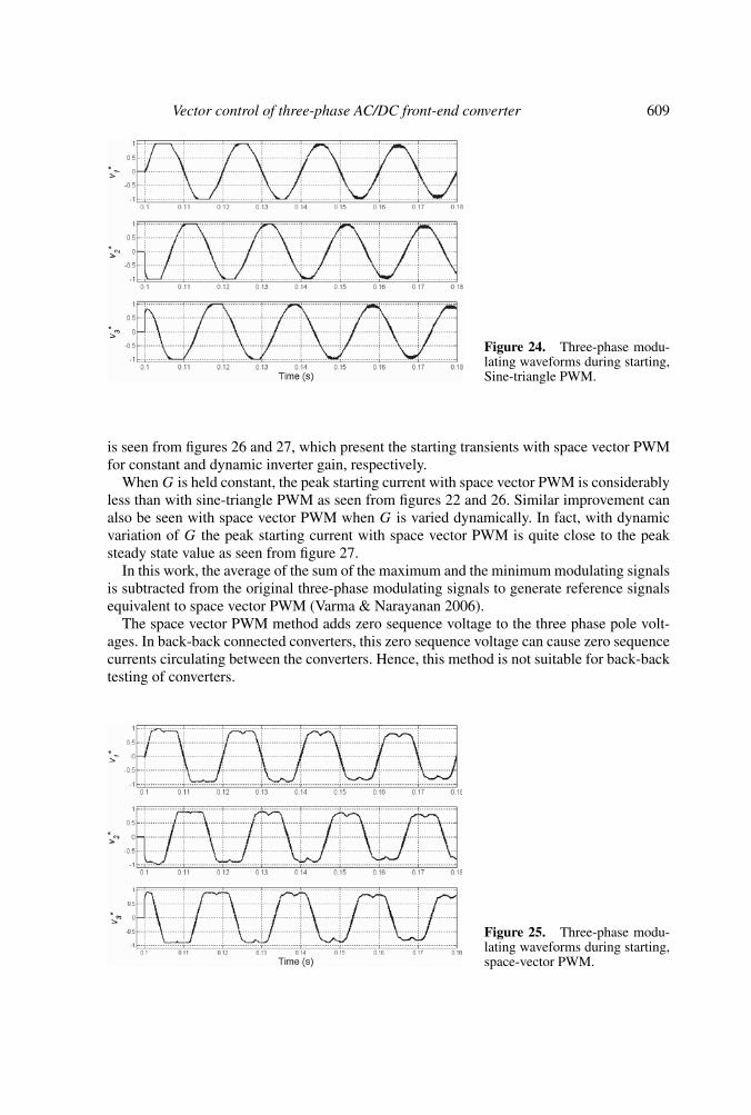
2Vs . Hence, whenever a phase voltage is close to its peak, theconverter average pole voltage is significantly less than the mains voltage. In other words theaverage applied voltage vector has lesser magnitude than the mains voltage vector. Hence,the modulator saturates and goes into over modulation as demonstrated by the three-phasereference voltages during starting, presented in figure 24.
Instead of sine-triangle PWM, if space vector pulse width modulation (SVPWM) is used,the highest average phase voltage that can be applied is equal to Vdc/
√3 (Varma & Narayanan
2006). This is equal to the peak value of supply voltage. Hence, without going into overmod-ulation, the required average phase voltage can be applied. In space vector terms, the averageapplied voltage vector could equal the mains voltage vector in any carrier cycle since the startof control execution. Figure 25 shows the three-phase reference voltages with space vectorPWM during starting. It is clear from this figure that the modulator is not landing into overmodulation and is almost in linear modulation.
The average pole voltage applied being close to the mains voltage over the entire line cyclethroughout the starting process is likely to ensure that the starting currents are quite low. This
Vector control of three-phase AC/DC front-end converter 609
Figure 24. Three-phase modu-lating waveforms during starting,Sine-triangle PWM.
is seen from figures 26 and 27, which present the starting transients with space vector PWMfor constant and dynamic inverter gain, respectively.
When G is held constant, the peak starting current with space vector PWM is considerablyless than with sine-triangle PWM as seen from figures 22 and 26. Similar improvement canalso be seen with space vector PWM when G is varied dynamically. In fact, with dynamicvariation of G the peak starting current with space vector PWM is quite close to the peaksteady state value as seen from figure 27.
In this work, the average of the sum of the maximum and the minimum modulating signalsis subtracted from the original three-phase modulating signals to generate reference signalsequivalent to space vector PWM (Varma & Narayanan 2006).
The space vector PWM method adds zero sequence voltage to the three phase pole volt-ages. In back-back connected converters, this zero sequence voltage can cause zero sequencecurrents circulating between the converters. Hence, this method is not suitable for back-backtesting of converters.
Figure 25. Three-phase modu-lating waveforms during starting,space-vector PWM.

610 J S Siva Prasad et al
Figure 26. Starting current tran-sient: Controller initiated afterunit-vector reached steady state,LPF inserted in V ∗
dc path, Spacevector PWM.
5.6 Variation of filter inductance
In order to verify the effectiveness of the starting process for various values of line inductance,simulations are repeated with a filter inductor Ls = 330 μH. Figures 28 and 29 present thestarting currents with sine-triangle and space vector PWM, respectively, and with dynamicvariation of inverter gain G. These two figures can be compared with figures 23 and 27respectively. The peak currents are increased as the filter inductor value is reduced. But stillthey are within acceptable limits.
5.7 Experimental verification
Figure 30 shows the experimental results of starting transients in the line current with thecontrol initiated after the unit vector generation attains steady state (Ls = 660 μH). As seenin this figure, the peak currents are quite low (peak ≈ 45 A). Dynamic adjustment of theinverter gain G leads to further reduction in transients, though marginal, as shown in figure 31with same Ls (peak ≈ 30 A).
Figure 27. Starting current tran-sient: Controller initiated afterunit-vector reached steady state,LPF inserted in V ∗
dc path, G varieddynamically, Space vector PWM.

Vector control of three-phase AC/DC front-end converter 611
Figure 28. Starting current tran-sient: Controller initiated afterunit-vector reached steady state,LPF inserted in V ∗
dc path, G var-ied dynamically, Sine - trianglePWM, Ls = 330 μH.
Figure 29. Starting current tran-sient: Controller initiated afterunit-vector reached steady state,LPF inserted in V ∗
dc path, G varieddynamically, Space vector PWM,Ls = 330 μH.
The measured starting current transients for Ls = 330 μH with constant G and dynamicallyadjusted G are presented in figures 32 and 33, respectively. Due to small filter inductance,the starting transients in these figures are higher than those in figures 30 and 31. However,the starting procedure ensures that the transient currents are within the acceptable limits.
Figure 30. Starting current tran-sient with G maintained constant(25 A/division) (Ls = 660 μH):experimental result.

612 J S Siva Prasad et al
Figure 31. Starting current tran-sient with G varied dynamically(25 A/division). (Ls = 660 μH):experimental result.
Figure 32. Starting current tran-sient with Gmaintained constant(50 A/division) (Ls = 330 μH):experimental result.
From the above results it can be observed that pre-charging of dc bus, starting the controlexecution only after unit-vector reaches steady state and inserting a low-pass filter in the dcvoltage reference path are essential to reduce the peak of starting current to an acceptablelevel. The peak of the starting current can be reduced further by dynamically varying theinverter gain G. When injection of common mode voltage is acceptable, space vector PWMcan be employed for further reduction in starting current.
6. Conclusion
Vector control was implemented on a 250 kVA front-end converter. Simulation and experi-mental results were presented. A simple and straightforward algorithm for unit vector genera-tion was proposed, and the results were satisfactory. The problem of starting current transientwas more pronounced for high power FEC, where the value of filter inductor was very small.A safe starting procedure to limit the starting current transients was evolved. The starting
Figure 33. Starting current tran-sient with G varied dynamically(50 A/division) (Ls = 330 μH):experimental result.

Vector control of three-phase AC/DC front-end converter 613
procedure included pre-charging of the dc bus, beginning the control execution after the unitvector generation reached steady state and inserting a low-pass filter in the dc bus referencepath. The work has resulted in an improved understanding of the starting transient and itsmitigation in line-side converter.
References
Chattopadhyay S, Ramanarayanan V 2005 A voltage-sensorless control method to balance the inputcurrents of a three-wire boost rectifier under unbalanced voltage condition. IEEE Trans. Ind. Elec-tron. IE-52: 386–398
Chung S K 2000 Phase locked loop for grid-connected three-phase power conversion system. Proc.IEE Electr. Power Appl. 147(3): 213–219
Finney D 1988 Variable Frequency AC Motor Drive System. London: Peter Peregrinus Ltd.Ghosh R 2007 Modelling, Analysis and Control of Single-phase and Three-phase PWM Rectifiers.
Ph.D Thesis, Indian Institute of Science, Bangalore, May 2007Gilmore W, Skibiniski G 1996 Pre-charge circuit utilizing non-linear firing angle control. Conf. Rec.
IEEE-IAS Annu. Meeting 2: 1099–1105Leonhard W 2001 Control of Electrical Drives. 3rd ed., Springer International EditionNoguchi T, Tomki H, Kondo S, Takahashi I 1998 Direct power control of PWM converter without
power-source sensors. IEEE Trans. Ind. Appl. 52: 476–479Ranganathan V T 2007 Lecture Notes on Electric Drives. Electrical Engineering Dept., Indian Institute
of Science, BangaloreTexas Instruments 1990 TMS320LF/LC240X DSP Controllers Reference Guide (SPRU357)Varma P S, Narayanan G 2006 Space vector PWM as a modified form of sine-triangle PWM for
simple analog/digital implementation. IETE Journal of Research 52(6): 435–449Wijenayake A H, Gilmore T, Lukaszewski R, Anderson D, Waltersdorf G 1997 Modelling and analysis
of shared/common DC bus operation of AC drives. Conf. Rec. IEEE-IAS Annu. Meeting 1: 599–604
Related Documents


![3XW - sekretarijat-za-plurzs.podgorica.me · '(7$/-1, 85%$1,67,ý., 3/$1 NACRT PLANA JUDQLFH 8UEDQLVWLþNLK ]RQD 10/0.4kV 630kVA TS Donja Gorica 1 10/0.4kV 250kVA TS Donja Gorica](https://static.cupdf.com/doc/110x72/5e1ff98cd01aa448633cc8de/3xw-sekretarijat-za-7-1-85167-31-nacrt-plana-judqlfh-8uedqlvwlnlk.jpg)


