FPGA & Verilog FPGA & Verilog A short course on Hosted @ School of Electrical and Electronic Engineering; Uni. of Johannesburg presented by Dr. Simon Winberg Software Defined Radio Research Group (SDRG), UCT John-Philip Taylor Pelindaba Laboratory for Accelerator and Beam-line Sciences (PLABS) at NECSA November 2014 Day #1 Today’s lecture: Staring out with FPGAs and Verilog

FPGA & Verilog A short course on Hosted @ School of Electrical and Electronic Engineering; Uni. of Johannesburg presented by Dr. Simon Winberg Software.
Dec 19, 2015
Welcome message from author
This document is posted to help you gain knowledge. Please leave a comment to let me know what you think about it! Share it to your friends and learn new things together.
Transcript

FPGA & VerilogA short course on
Hosted @
School of Electrical and Electronic Engineering; Uni. of Johannesburg
presented by
Dr. Simon WinbergSoftware Defined
Radio Research Group (SDRG), UCT
John-Philip TaylorPelindaba Laboratory for
Accelerator and Beam-line Sciences (PLABS) at NECSA
November 2014
Day #1
Today’s lecture: Staring out with FPGAs and Verilog

FPGA &Verilog
Thanks and Acknowledgements
Project MeerKAT DBE Skills Development Initiative, funded by SKA SA
Pelindaba Laboratory for Accelerator and Beam-line
Sciences (PLABS) at NECSA
University of Cape Town
Square KilometreArray (SKA) South Africa project
School of Electrical and Electronic Engineering; Uni. of Johannesburg

FPGA &Verilog
Mission BriefKnow about FPGAs (uses + limitations)
Verilog HDL coding fundamentals
Be able to write your own Verilog programs
Use Altera Quartus II™ tools
Develop, Simulate & Test on hardware
Learn effective HDL development practices
Complete sequence of mini-project
Have some fun!
FPGA &Verilog
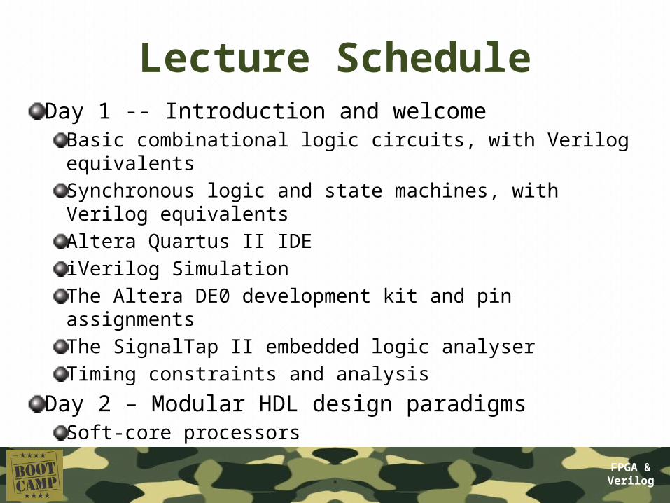
Lecture ScheduleDay 1 -- Introduction and welcome
Basic combinational logic circuits, with Verilog equivalentsSynchronous logic and state machines, with Verilog equivalentsAltera Quartus II IDEiVerilog SimulationThe Altera DE0 development kit and pin assignmentsThe SignalTap II embedded logic analyserTiming constraints and analysis
Day 2 – Modular HDL design paradigmsSoft-core processors
FPGA &Verilog
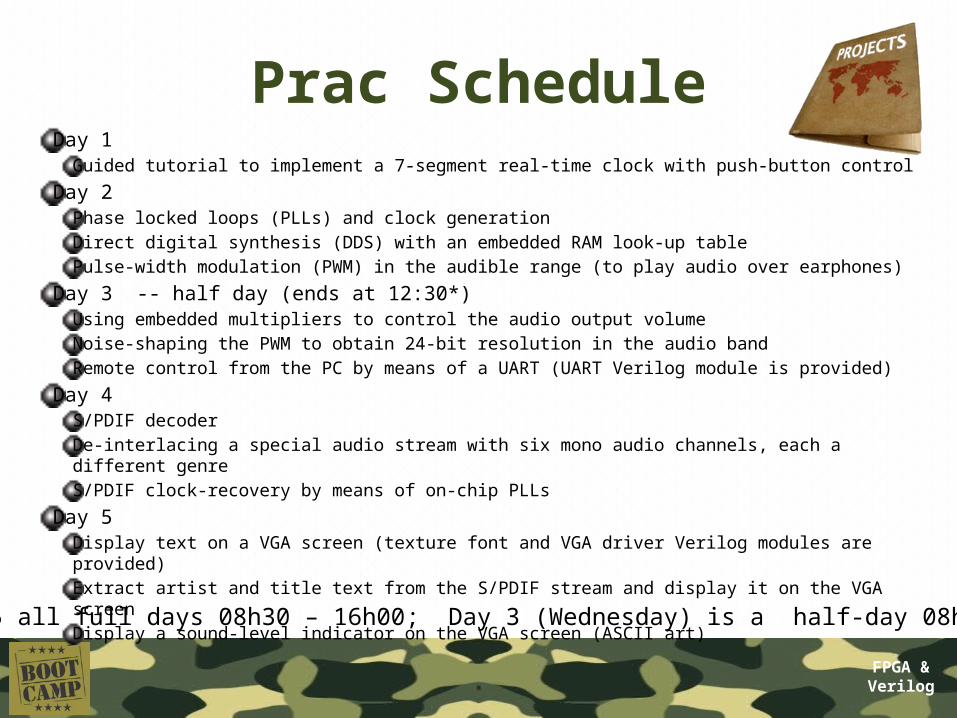
Prac ScheduleDay 1
Guided tutorial to implement a 7-segment real-time clock with push-button control
Day 2Phase locked loops (PLLs) and clock generation
Direct digital synthesis (DDS) with an embedded RAM look-up table
Pulse-width modulation (PWM) in the audible range (to play audio over earphones)
Day 3 -- half day (ends at 12:30*)Using embedded multipliers to control the audio output volume
Noise-shaping the PWM to obtain 24-bit resolution in the audio band
Remote control from the PC by means of a UART (UART Verilog module is provided)
Day 4S/PDIF decoder
De-interlacing a special audio stream with six mono audio channels, each a different genre
S/PDIF clock-recovery by means of on-chip PLLs
Day 5Display text on a VGA screen (texture font and VGA driver Verilog modules are provided)
Extract artist and title text from the S/PDIF stream and display it on the VGA screen
Display a sound-level indicator on the VGA screen (ASCII art)* Days 1,2,4,5 all full days 08h30 – 16h00; Day 3 (Wednesday) is a half-day 08h30 – 12h30
FPGA &Verilog
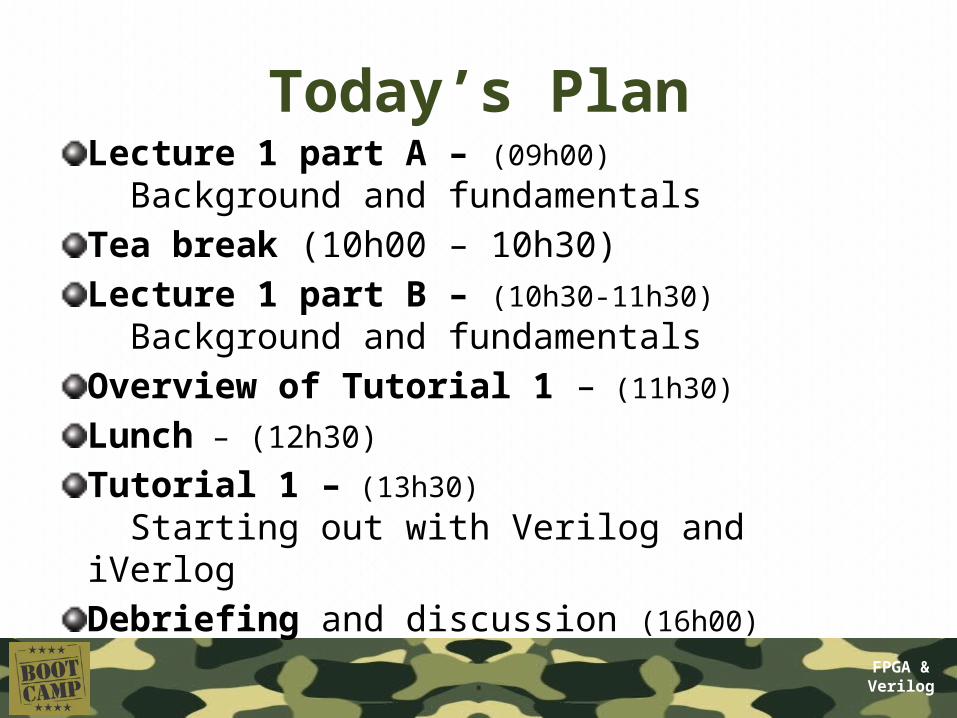
Today’s PlanLecture 1 part A – (09h00)
Background and fundamentals
Tea break (10h00 – 10h30)
Lecture 1 part B – (10h30-11h30)
Background and fundamentals
Overview of Tutorial 1 – (11h30)
Lunch – (12h30)
Tutorial 1 – (13h30)
Starting out with Verilog and iVerlog
Debriefing and discussion (16h00)
FPGA & VerilogA short course on
presented by
Simon WinbergSoftware Defined Radio Group (SDRG)
University of Cape Town
November 2014
LECTURE 1
Hosted @
School of Electrical and Electronic Engineering; Uni. of Johannesburg
FPGA &Verilog
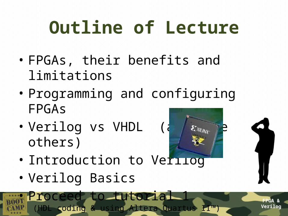
Outline of Lecture
• FPGAs, their benefits and limitations• Programming and configuring FPGAs• Verilog vs VHDL (and some others)• Introduction to Verilog• Verilog Basics• Proceed to tutorial 1
(HDL coding & using Altera Quartus II™)
FPGA &Verilog
Programmable Chips• In comparison to hard-wired chips, a
programmable chip can be configured according to user needs, providing a means to use the same chip(s) for a variety of different applications.
• This facility makes programmable chips attractive for use in many products, including prototyping situations and final systems.
• Further benefits are: low starting cost (eg. Web pack + dev kit), risk reduction, quick turnaround time
FPGA &Verilog
ASICs vs. Programmable Chips• Application Specific Integrated Circuit (or
ASICs) have a longer design cycle and higher engineering cost than using programmable chips.
• There is still a need for ASIC – such as faster performance and lower cost for high volume
• Generally, programmable chips are suited to low to medium product production. (e.g. product runs needing under 10,000 chips)

FPGA &Verilog
PLAs, CPLDs and FPGAs• Programmable logic chips variety in terms
simplecomplex cheapexpensive• PLA = Programmable Logic Array
– Simple: just AND and OR gates; but Cheap
• CPLA = Complex PLA– Midrange: compose interconnected PLAs
• FPGAs = Field Programmable Gate Array– Complex: programmable logic blocks and
programmable interconnects; but ExpensiveFPGA orders of
magnitude larger than CPLD
FPGA &Verilog
Impressiveness of FPGAs
1 Million+ Polygon Real Time Ray Tracing in Altera FPGA
High Resolution Real-Time Stereo Depth Map Estimation Using FPGA
+- 8 min
FPGA &Verilog
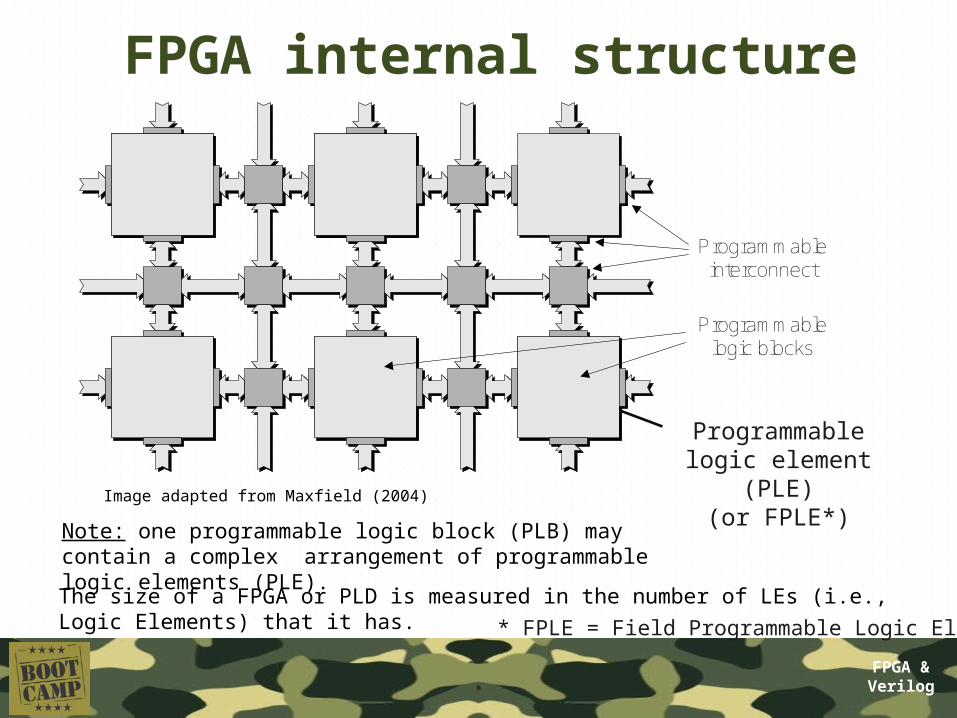
FPGA internal structure
Programmableinterconnect
Programmablelogic blocks
Image adapted from Maxfield (2004)
Programmable logic element (PLE)
(or FPLE*)
* FPLE = Field Programmable Logic Element
Note: one programmable logic block (PLB) may contain a complex arrangement of programmable logic elements (PLE).
The size of a FPGA or PLD is measured in the number of LEs (i.e., Logic Elements) that it has.
FPGA &Verilog
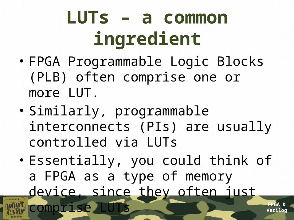
LUTs – a common ingredient
• FPGA Programmable Logic Blocks (PLB) often comprise one or more LUT.
• Similarly, programmable interconnects (PIs) are usually controlled via LUTs
• Essentially, you could think of a FPGA as a type of memory device, since they often just comprise LUTs
• But what is a LUT??
FPGA &Verilog
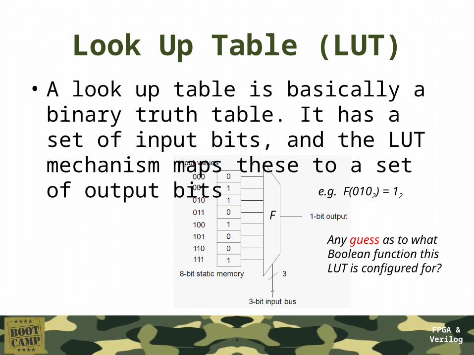
Look Up Table (LUT)• A look up table is basically a binary truth
table. It has a set of input bits, and the LUT mechanism maps these to a set of output bits
Any guess as to whatBoolean function this LUT is configured for?
e.g. F(0102) = 12
F
FPGA &Verilog
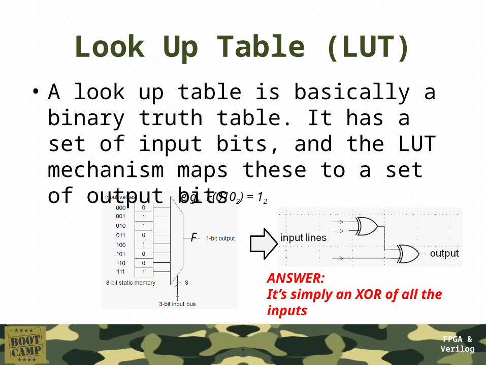
Look Up Table (LUT)• A look up table is basically a binary truth
table. It has a set of input bits, and the LUT mechanism maps these to a set of output bits
ANSWER:It’s simply an XOR of all the inputs
e.g. F(0102) = 12
F

FPGA &Verilog
Programmable Interconnect to PLB I/O as: LUT or MUXes
A
B
C
D
A
B
C
D
PLB. . .
Programming lines
InputsLUTor
MUX
LUTor
MUX
Hopefully you can now easily see how the programming is going to happen…
Programmableinterconnect
Programmablelogic blocks
PLB
FPGA &Verilog
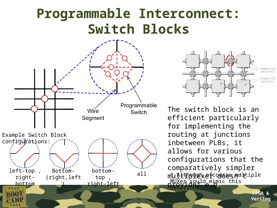
Programmable Interconnect:Switch Blocks
Programmableinterconnect
Programmablelogic blocks
PLB
The switch block is an efficient particularly for implementing the routing at junctions inbetween PLBs, it allows for various configurations that the comparatively simpler multiplexer doesn’t provide* e.g.
* Although ofcourse multiple MUXes could mimic this behaviour.
Example Switch Block configurations:
left-top ,right-bottom
Bottom- (right,left)
bottom-top , right-left
all

FPGA &Verilog
Programming FPGAs (simplified)
ABCD Inputs
en
ABCD Inputs ABCD Inputs
. . .ConfigurationData
. . .
en en
ConfigurationControl
. . .
. . . PLBPLB
000001
010
100011101
110
111

FPGA &Verilog
Configuration Architectures
Configuration architecture =The underlying circuitry that loads configuration data and places it at the correct locations

FPGA &Verilog
Configuration Architectures• Configuration architecture =
The underlying circuitry that loads configuration data and keeps it at the correct locations
CPU/ PC
Configuration
Controller
PROM (storesbit file)
Configurationhardware
FPGA
Configurationdata
Configurationcontrol
Configurationprotocol
Adapted from Hauck and Dehon Ch4 (2008)
Can store pre-configured bitmaps in memoryon the platform without having to send it each timefrom the CPU. Include hardware for programmingthe hardware (instead of the slower process of e.g.,programming devices via JTAG from the host)
createsbit file

FPGA &Verilog
Configuration ArchitectureConceptual view of the DE0 configuration architecture
DE0 board
run/prog switch
run
Generate pof file,Serializes the file to send over USB
verifyprog
Programming…
CPLD that convertsfrom USB stream to relevant protocol for JTAG/Flash

FPGA &Verilog
…?
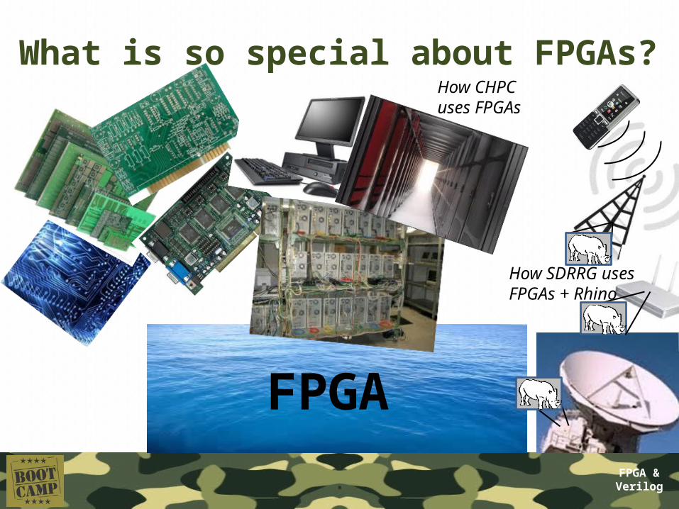
So what?What is so special about FPGAs?
FPGAA sea of possibilities…
01001010101000100101001010010100 10010010010100100101101001 100100110101011010011101
FPGA &Verilog
What is so special about FPGAs?
FPGA
How CHPC uses FPGAs
How SDRRG uses FPGAs + Rhino

FPGA &Verilog
What is so special about FPGAs?
FPGA
How CHPC uses FPGAs
How SDRRG uses FPGAs + Rhino
Can put lots of electronicstuff together in one place

FPGA &Verilog
Any Drawbacks?
Things can get rather… muddy
• Only does the digital part – still need analogue components, user interface, and interfacing circuitry that interacts with the outside world.
• Has a limited number of IO pins that can connect up with external signals.
•Susceptible to EM disturbances, PCB and other components needs to be suitably placed to avoid interfering with functioning of FPGA.• Typically a slower clock
than most fast CPUs nowadays (e.g. 100MHz clock speed).• Typically has lots of pins that need to be soldered on, needing small track width and multilayer PCBs
• Often can’t achieve full utilization of PLBs
• Place & route can take a long time to run
• Limitations of interconnects
Here’s
just a few
drawbacks
• A specialized form of development, combines the challenges of both s/w and h/w
Eeek!
FPGA &Verilog
Onwards towards… FPGA Development Flow Verilog Basics and Altera Quartus II™ *
Since most of you have probably used Quartus II we won’t spent much time on that; but do let us know if Quartus II is new to you and would like help familiarizing yourself with it.
FPGA &Verilog28
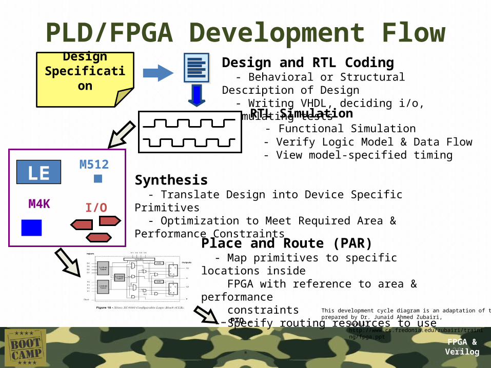
PLD/FPGA Development Flow
Synthesis - Translate Design into Device Specific Primitives - Optimization to Meet Required Area & Performance Constraints
Place and Route (PAR) - Map primitives to specific locations inside FPGA with reference to area & performance constraints - Specify routing resources to use
Design and RTL Coding - Behavioral or Structural Description of Design - Writing VHDL, deciding i/o, formulating tests
RTL Simulation - Functional Simulation - Verify Logic Model & Data Flow - View model-specified timing LE
M512
M4K I/O
DesignSpecification
This development cycle diagram is an adaptation of thatprepared by Dr. Junaid Ahmed Zubairi, Avail: http://www.cs.fredonia.edu/zubairi/training/fpga.ppt… PTO …

FPGA &Verilog29
Development FlowTiming Analysis - Verify performance specifications - Static timing analysis
Gate Level Simulation - Timing simulation - Verify design will work on target platform
Program and test on hardware- Generate bit file- Program target device- Activate the system
tclk
Place and Route (PAR)

FPGA &Verilog
Development Flow:Where is most time spent?
Design and RTL Coding - Behavioral or Structural Description of Design - Writing HDL, deciding i/o, formulating tests
Every development project is different. In my own experience,most of the time is probably spent…
Engineer’stime
Timing Analysis - Verify performance specifications - Static timing analysis
tclk
PC’s time
Eish!
Eish!
Place and Route (PAR) - Map primitives inside FPGA - Specify routing resources to use

FPGA &Verilog
Tea break
FPGA &Verilog
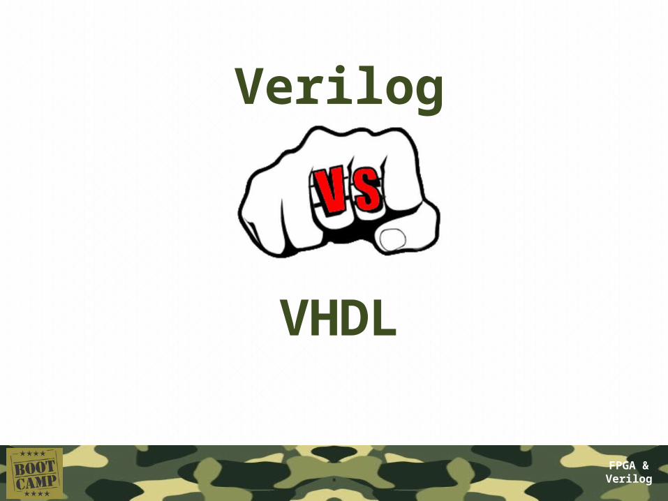
Verilog
VHDL

FPGA &Verilog
But first: the game of the names
Verilog VHDL

FPGA &Verilog
VHDL Stands for…
a) VHDL =VHSIC Hardware Description Language
b) VHDL =Verifiable Hardware Description Language
c) VHDL = Very High-level Description Language
(although you would be right to say that VHDL is a kind of veryhigh-level description language)
Choose option below…
Take a few seconds to think…VHSIC = Very-High-Speed Integrated Circuit
FPGA &Verilog
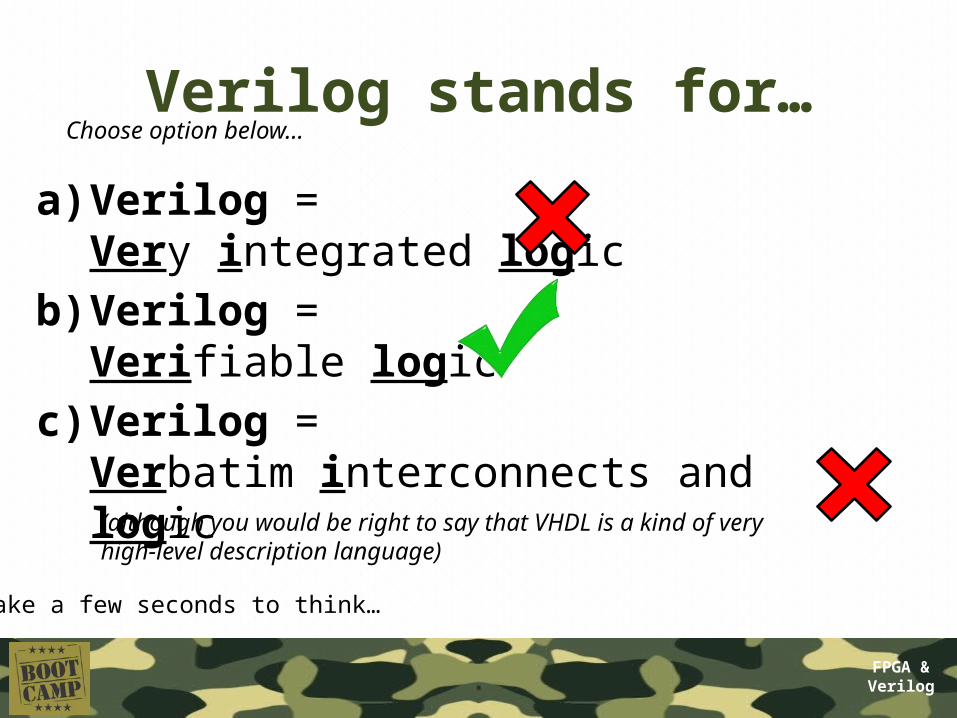
Verilog stands for…
a) Verilog =Very integrated logic
b) Verilog =Verifiable logic
c) Verilog = Verbatim interconnects and logic
(although you would be right to say that VHDL is a kind of veryhigh-level description language)
Choose option below…
Take a few seconds to think…

FPGA &Verilog
HDL Terms• Entity / module* – a basic building block of a design
• Port – a connection or interface (argument list sometimes)
• Behavior – description of operation of an entity
• Structure – describes components/parts of an entity
• Synthesis – conversion from HDL to gate level
• Analysis – check design can be satisfied on device
• Test Bench – tests to be done on entities
• Simulation – validate design on simulated systemVHDL / Verilog equivalent terms
FPGA &Verilog
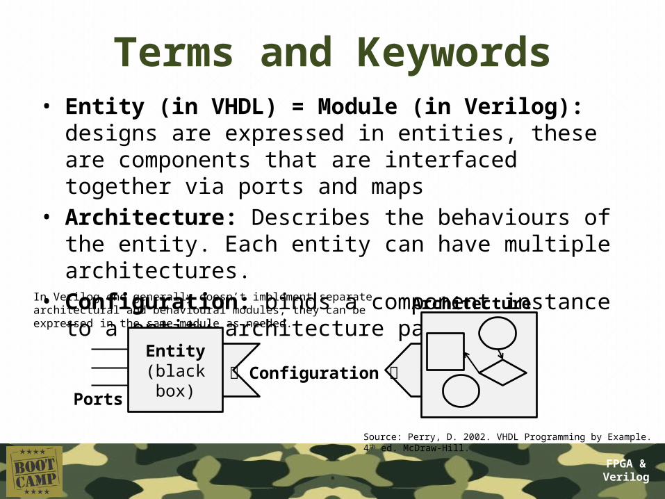
Terms and Keywords• Entity (in VHDL) = Module (in Verilog):
designs are expressed in entities, these are components that are interfaced together via ports and maps
• Architecture: Describes the behaviours of the entity. Each entity can have multiple architectures.
• Configuration: binds a component instance to a entity-architecture pair
Entity(black box)
Ports
Architecture
Configuration
Source: Perry, D. 2002. VHDL Programming by Example. 4th ed. McDraw-Hill.
In Verilog one generally doesn’t implement separate architectural and behavioural modules, they can be expressed in the same module as needed.

FPGA &Verilog
Important Terms• Top-level module: module at the top of the hierarchy• Package: collection of commonly used data types,
subroutines, for implementing architectures• Driver: source on a signal• Bus: a signal that can have its sources turned off• Signal vector: what we usually think of as a bus• Attribute: data attached to VHDL objects (e.g., event
status)• Generic: a parameter to pass information to an entity• Process: a basic unit of execution. Multiple processes
are usually active at a time.Source: Perry, D. 2002. VHDL Programming by Example. 4th ed. McDraw-Hill.

FPGA &Verilog
VHDL Example
• Let’s implement this combinational logic circuit:
A
BCAND2
1-bit inputs
1-bit output
AND2 operation: C = A AND B
FPGA &Verilog
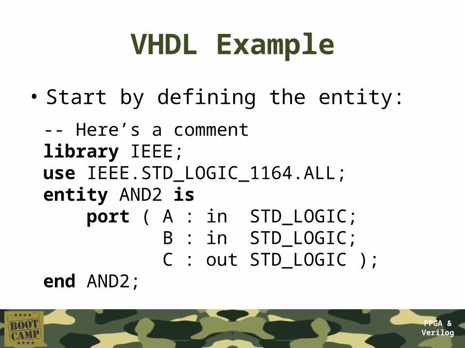
VHDL Example
• Start by defining the entity:
-- Here’s a commentlibrary IEEE;use IEEE.STD_LOGIC_1164.ALL;entity AND2 is port ( A : in STD_LOGIC; B : in STD_LOGIC; C : out STD_LOGIC );end AND2;

FPGA &Verilog
VHDL Example
• Then add an architecture:
…architecture AND2bhv of AND2 isbegin C <= A and B; -- The <= links signals and ports
end architecture;
As is the program should compile in Xilinx ISE; the system will create aninstance of AND2 as it is the top level module, so no need to add an explicit configuration statement.
Name of this architecture

FPGA &Verilog
Verilog equivalent code
module AND2(A,B,C); input A,B; output C; assign C = and(A,B);endmodule
module AND2( input A,B, output C); // start the implementation: assign C = A & B;endmodule
Alternatively:

FPGA &Verilog
Concurrent operation
• Each statement in a HDL architecture block executes concurrently, whenever there is a change / event
• e.g. C <= and(A,B); -- executes when A or B changes
D <= or(A,B); -- executes when A or B changes
If A were to change (e.g. A changes from 0 to 1) then both the lines will execute at once)

FPGA &Verilog
Sequential operation (VHDL recap)
-- single bit adder using sequential operation in VHDLLibrary ieee; use ieee.std_logic_1164.all;
entity fulladder is port (A1, A2, Cin: in std_logic; sum, Cout : out std_logic );end fulladder;
architecture arch1 of fulladder isbegin process(A1,A2,Cin) -- define a sequential operation begin sum <= Cin xor A1 xor A2; Cout <= (A1 and A2) or (Cin and (A1 xor A2)); end process;end arch1;
This line runs firstThen this line runs
Note: two process blocks in the same architectureblock run concurrently
Sequential operation is described within a PROCESS block. Example:
Sensitivity list (note not sensitive to Cout)
VHDLStyle:

FPGA &Verilog
Sequential operation in Verilog
// single bit adder using sequential operation in Verilogmodule fulladder (input A1, A2, Cin, output sum, Cout);
always @(A1,A2,Cin) begin sum = xor(Cin,A1,A2); Cout = or(and(A1,A2,and(Cin,xor(A1,A2)))); end
endmodule
This line runs firstThen this line runs
Note: two always blocks in the same modulewill run concurrently
Sequential operation is described within a PROCESS block. Example:
Sensitivity list (note not sensitive to Cout)
VerilogStyle:
See how much less code in Verilog

FPGA &Verilog
Verilog coding
Best way to learn HDL is to practice coding with it.That’s what the tutorials are for.
See the Verilog Cheat Sheet included in resources

FPGA &Verilog
Verilog vs VHDL SyntaxVerilog• More ‘concise’• Loosely typed• More susceptible to inadvertent
bugs• Verilog signals and types:
wire a,b;wire [31:0]c;assign a = and(b,c);// saves some typing
• Verilog sequential block:• always @ (a,b)
begin …end
• etc…
VHDL• More ‘verbose’• Strongly typed• Less susceptible to inadvertent bugs• VHDL signals and types:
signal a, b : std_logic;signal c : ieee_int_ bla bla;
begin
a <= b and c;
end;
• VHDL sequential block:• process (a, b)
begin …end
• etc…

FPGA &Verilog
End ofVHDL vs Verilog

FPGA &Verilog
Verilog
Taking something of a bottom-up approach, from hardware and RTL to top-level entity

FPGA &Verilog
Recommended Steps forHDL Design
1. Plan dataflow and code entities
2. Implement behaviours
3. Structural modelling (build complex entities using lower level ones)
Recommended online VHDL support:
http://esd.cs.ucr.edu/labs/tutorial/This site provides a collection of useful VHDL example code and tutorials
http://www.asic-world.com/
Useful tutorials and examples on Verilog, System Verilog, SystemC, VHDL, others
FPGA &Verilog
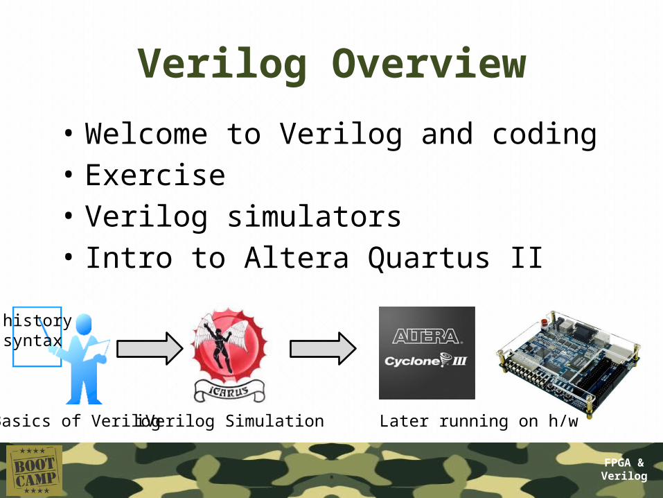
Verilog Overview
• Welcome to Verilog and coding• Exercise• Verilog simulators• Intro to Altera Quartus II
historysyntax
iVerilog Simulation Later running on h/wBasics of Verilog

FPGA &Verilog
Why consider Verilog?
• VHDL and Verilog are both used as industry standards, sometimes interchangeably
• VHDL is used quite widely in Europe (so is Verilog). Verilog used mostly in USA.
• Easier to learn the syntax if you know C
Verilog is concise; but beware that it isn’t as strongly typed as VHDL so bugs can creep in

FPGA &Verilog
Lead in to Verilog…
• History of Verilog– 1980 Verilog developed by Gateway Design
Automation (was initially their ‘secret weapon’)– 1990 Verilog was made public– 1995 adopted as IEEE standard 1364-1995– 2001 enhanced version: Verilog 2001– 2005: SystemVerilog– 2009: New SystemVerilog standard
FPGA &Verilog
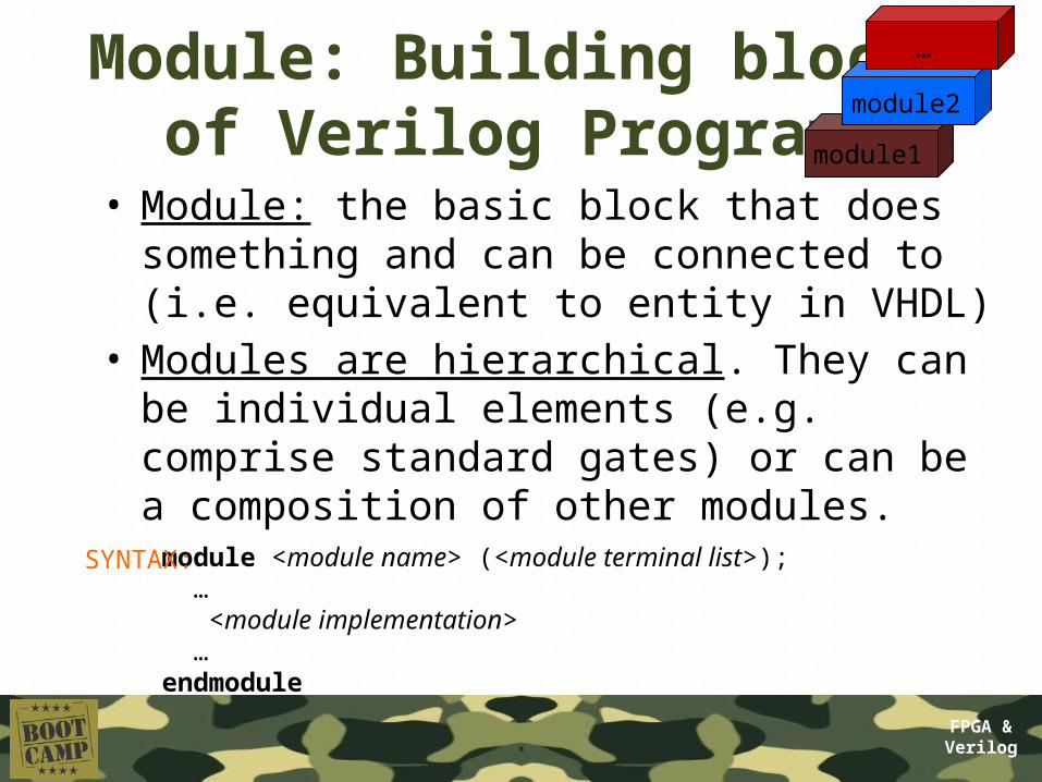
Module: Building block of Verilog Programs
• Module: the basic block that does something and can be connected to (i.e. equivalent to entity in VHDL)
• Modules are hierarchical. They can be individual elements (e.g. comprise standard gates) or can be a composition of other modules.
module <module name> (<module terminal list>); … <module implementation> …endmodule
SYNTAX:
module1
module2
…
FPGA &Verilog
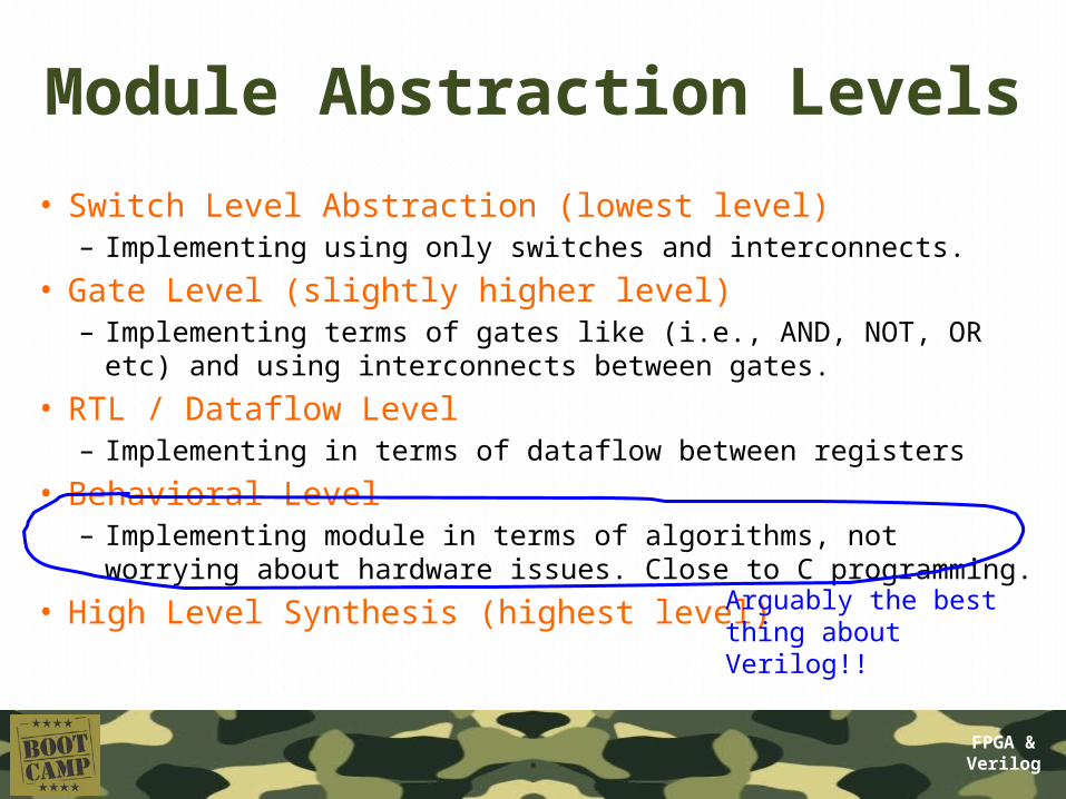
Module Abstraction Levels
• Switch Level Abstraction (lowest level)– Implementing using only switches and interconnects.
• Gate Level (slightly higher level)– Implementing terms of gates like (i.e., AND, NOT, OR etc) and
using interconnects between gates.
• RTL / Dataflow Level– Implementing in terms of dataflow between registers
• Behavioral Level– Implementing module in terms of algorithms, not worrying about
hardware issues. Close to C programming.
• High Level Synthesis (highest level)
Arguably the best thing about Verilog!!

FPGA &Verilog
Syntactic issues:Constant Values in Verilog
• Number format:
<size>’<base><number>• Some examples:
– 3’b111 – a three bit number (i.e. 710)
– 8’hA1 – a hexadecimal (i.e. A116 = 16110)
– 24’d165 – a decimal number (i.e. 16510)Defaults:
100 – 32-bit decimal by default if you don’t have a ‘‘hab – 32-bit hexadecimal unsigned value
‘o77 – 32-bit octal unsigned value (778 = 6310)
FPGA &Verilog
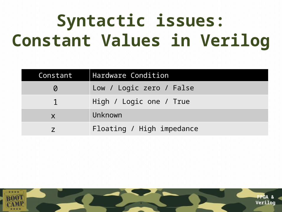
Syntactic issues:Constant Values in Verilog
Constant Hardware Condition
0 Low / Logic zero / False
1 High / Logic one / True
x Unknown
z Floating / High impedance
FPGA &Verilog
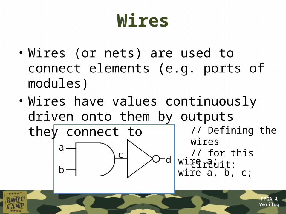
Wires
• Wires (or nets) are used to connect elements (e.g. ports of modules)
• Wires have values continuously driven onto them by outputs they connect to
a
b
c d wire a;wire a, b, c;
// Defining the wires// for this circuit:

FPGA &Verilog
Registers
• Registers store data• Registers retain their data until another
value is put into them (i.e. works like a FF or latch)
• A register needs no driver
reg myregister; // declare a new register (defaults to 1 bit)
myregister = 1'b1; // set the value to 1

FPGA &Verilog
Vectors of wires and registers
// Define some wires:
wire a; // a bit wire
wire [7:0] abus; // an 8-bit bus
wire [15:0] bus1, bus2; // two 16-bit busses
// Define some registers
reg active; // a single bit register
reg [0:17] count; // a vector of 18 bits
FPGA &Verilog
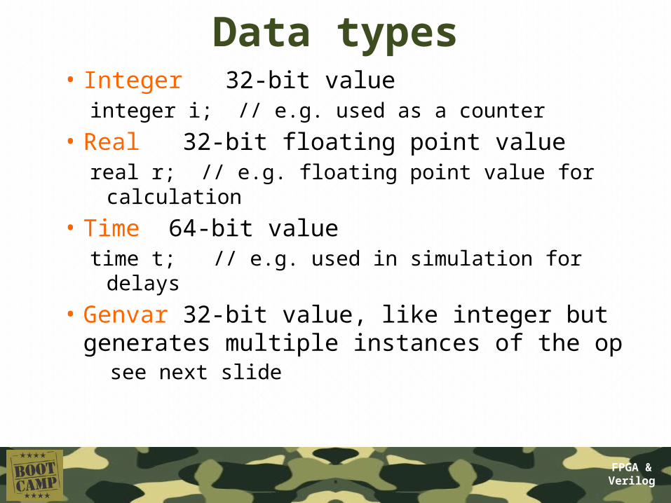
Data types• Integer 32-bit value
integer i; // e.g. used as a counter
• Real 32-bit floating point valuereal r; // e.g. floating point value for calculation
• Time 64-bit valuetime t; // e.g. used in simulation for delays
• Genvar 32-bit value, like integer but generates multiple instances of the op see next slide

FPGA &Verilog
GenVar
genvar j;wire [12:0]Output[19:0];generate for(j = 0; j < 20; j = j+1) begin: Gen_Modules MyModule MyModule_Instance ( Reset, Clk, Output[j] ); endendgenerate
MyModule MyModule_Instance (Reset,Clk,Output[0]);MyModule MyModule_Instance (Reset,Clk,Output[1]);MyModule MyModule_Instance (Reset,Clk,Output[2]);MyModule MyModule_Instance (Reset,Clk,Output[3]);MyModule MyModule_Instance (Reset,Clk,Output[4]);MyModule MyModule_Instance (Reset,Clk,Output[5]);MyModule MyModule_Instance (Reset,Clk,Output[6]);MyModule MyModule_Instance (Reset,Clk,Output[7]);MyModule MyModule_Instance (Reset,Clk,Output[8]);MyModule MyModule_Instance (Reset,Clk,Output[9]);MyModule MyModule_Instance (Reset,Clk,Output[10]);MyModule MyModule_Instance (Reset,Clk,Output[11]);MyModule MyModule_Instance (Reset,Clk,Output[12]);MyModule MyModule_Instance (Reset,Clk,Output[13]);MyModule MyModule_Instance (Reset,Clk,Output[14]);MyModule MyModule_Instance (Reset,Clk,Output[15]);MyModule MyModule_Instance (Reset,Clk,Output[16]);MyModule MyModule_Instance (Reset,Clk,Output[17]);MyModule MyModule_Instance (Reset,Clk,Output[18]);MyModule MyModule_Instance (Reset,Clk,Output[19]);
FPGA &Verilog
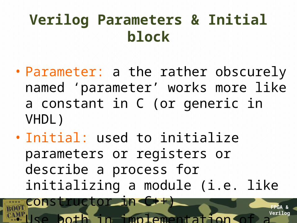
Verilog Parameters & Initial block
• Parameter: a the rather obscurely named ‘parameter’ works more like a constant in C (or generic in VHDL)
• Initial: used to initialize parameters or registers or describe a process for initializing a module (i.e. like constructor in C++)
• Use both in implementation of a module
FPGA &Verilog
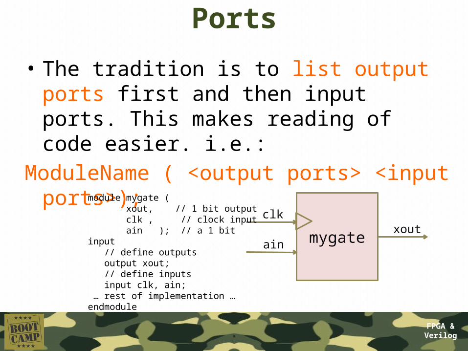
Ports
• The tradition is to list output ports first and then input ports. This makes reading of code easier. i.e.:
ModuleName ( <output ports> <input ports>);
module mygate ( xout, // 1 bit output clk , // clock input ain ); // a 1 bit input // define outputs output xout; // define inputs input clk, ain; … rest of implementation …endmodule
mygate
clk
ainxout

FPGA &Verilog
Register Output Ports
• These are output port that hold their value. An essential feature needed to construct things like timers and flip flops
module mycounter ( count_out, // 8 bit vector output of the clk ); // Clock input of the design // Outputs: output [7:0] count_out; // 8-bit counter output // All the outputs are registers reg [7:0] count_out; // Inputs: input clk;…endmodule
FPGA &Verilog
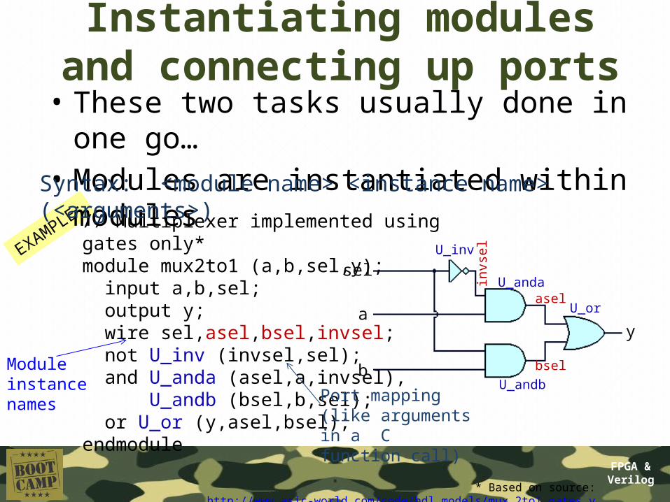
EXAMPLE:
Instantiating modules and connecting up ports
• These two tasks usually done in one go…• Modules are instantiated within modules
// Multiplexer implemented using gates only*module mux2to1 (a,b,sel,y); input a,b,sel; output y; wire sel,asel,bsel,invsel; not U_inv (invsel,sel); and U_anda (asel,a,invsel), U_andb (bsel,b,sel); or U_or (y,asel,bsel);endmodule
Syntax: <module name> <instance name> (<arguments>)
sel
a
b
y
U_inv
U_or
U_anda
U_andb
invs
el
bsel
asel
Module instance names Port mapping (like
arguments in a C function call)
* Based on source: http://www.asic-world.com/code/hdl_models/mux_2to1_gates.v

FPGA &Verilog
Instantiating modules
• Why give instances names?– In Verilog 2001 you can do:
module mux2to1 (input a, input b, input sel, output y);
…
and (asel,a,invsel), // can have unnamed instance
…
endmodule
Major reason for putting a name in is when it comes to debugging: Xilinx tends to assign instance names arbitrarily, like the and above might be called XXYY01 and then you might get a error message saying something like cannot connect signals to XXYY01 and then you spend ages trying to track down which gate is giving the problem.

FPGA &Verilog
Verilog Primitive Gates
and or not
nand nor xor
Buffer (i.e. 1-bit FIFO or splitter)
buf
Examples:
and a1 (OUT,IN1,IN2);not n1 (OUT,IN);
Example:
buf onelinkbuf (OUT, IN);
buf twolinkbuf (OUT1, OUT2, IN);
& | ~Can alsoUse symbols:
~& ~| ^Can alsoUse symbols:

FPGA &Verilog
BufIf (hardware if gate)
in out
ctrbufif1 (out, in, ctr)
bufif1 operation
0 1 x z0 z 0 L L1 z 1 H Hx z x x xz z x x x
ctr in
Tri-state buffer. Can choose to drive out with value of in (if ctr = 1) or don’t drive anything to out (i.e. if ctr = 0 connect high impedance to out)
See also notif (works in the apposite way: if ctr=0 then drive out with in)

FPGA &Verilog
Verilog Recommended Coding Styles
• Consistent indentation• Align code vertically on the = operator• Use meaningful variable names• Include comments (i.e. C-style // or /**/ )
– brief descriptions, reference to documents– Can also be used to assist in separating parts
of the code (e.g. indicate row of /*****/ to separate different module implementations)
Source: Coram: Verilog-A Introduction for Compact Modelers (MOS-AK Montreux 2006)

FPGA &Verilog
LEARNING VERILOG BY EXAMPLE
FPGA &Verilog
Where to go from here…• The preceding slides have given a very
brief look at Verilog, but has covered much of the major things that are used most commonly.
• It’s best to get stuck into experimenting and testing code in order to learn this language
Some thoughts for experimenting to do…

FPGA &Verilog
Learning VerilogOne approach is using a block diagram and converting to Verilog HDL.E.g. using Altera Quartus II (See test1.zip for example Quartus project)
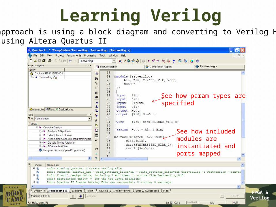
FPGA &Verilog
Learning VerilogOne approach is using a block diagram and converting to Verilog HDL.E.g. using Altera Quartus II
See how param types arespecified
See how included modules are instantiated and ports mapped

FPGA &Verilog
Checking syntax
I find a handy tool is the file analyser tool in Quartus II. This can be used to check the syntax of the file without having to go through the whole build process.

FPGA &Verilog
Testing
Load the Test2 file, if using Quartus make sure that mynand is the top level Entity
Running the simulation should allow you to verify the design is working as planned (i.e. NANDing)
FPGA &Verilog
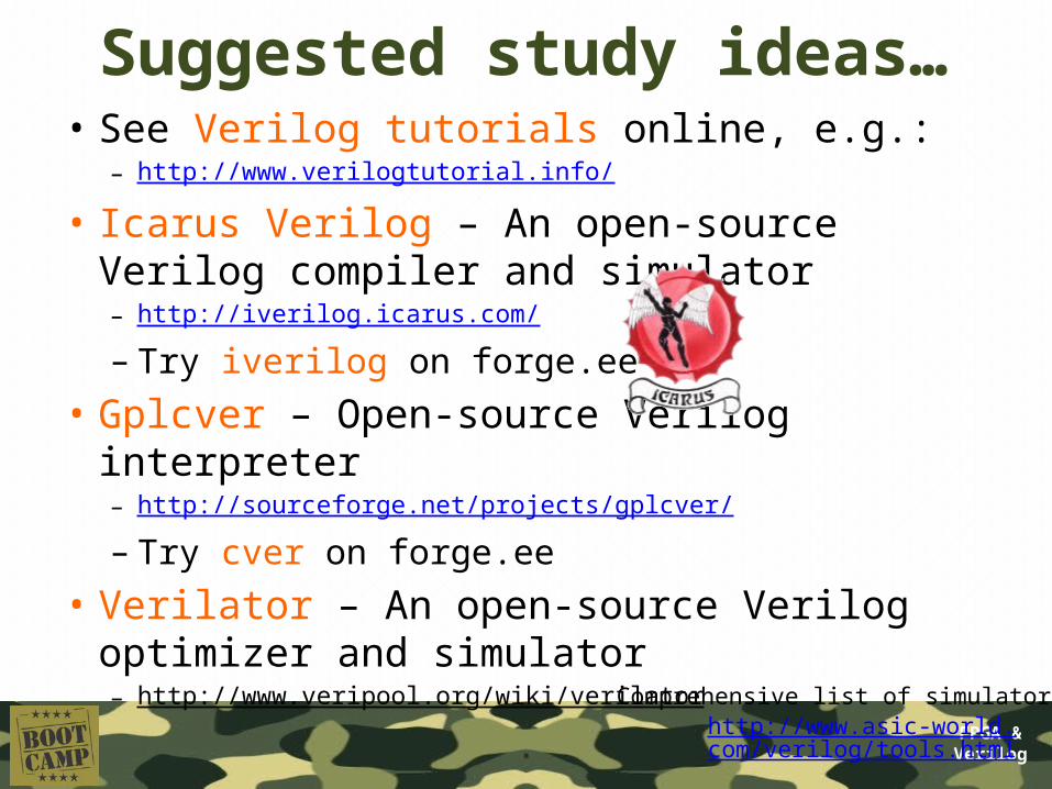
Suggested study ideas…• See Verilog tutorials online, e.g.:
– http://www.verilogtutorial.info/
• Icarus Verilog – An open-source Verilog compiler and simulator – http://iverilog.icarus.com/
– Try iverilog on forge.ee
• Gplcver – Open-source Verilog interpreter– http://sourceforge.net/projects/gplcver/
– Try cver on forge.ee
• Verilator – An open-source Verilog optimizer and simulator– http://www.veripool.org/wiki/verilator http://www.asic-world.com/veril
og/tools.html
Comprehensive list of simulators:
FPGA &Verilog
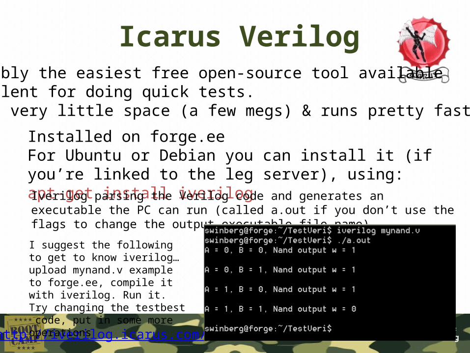
Icarus VerilogProbably the easiest free open-source tool availableExcellent for doing quick tests.Takes very little space (a few megs) & runs pretty fast.
http://iverilog.icarus.com/
Installed on forge.eeFor Ubuntu or Debian you can install it (if you’re linked to the leg server), using: apt-get install iverilogIverilog parsing the Verilog code and generates an executable the PC can run (called a.out if you don’t use the flags to change the output executable file name)
I suggest the following to get to know iverilog… upload mynand.v example to forge.ee, compile it with iverilog. Run it. Try changing the testbest code, put in some more operations

FPGA &Verilog
More ExperimentingExperiment with using both Altera Qauartus II, Icarus Verilog, and Xilinx ISE ISim
Try test3 or mycounter.v as a more involved program and test

FPGA &Verilog
Tutorial
Related Documents