ISSN (Print) : 2320 – 3765 ISSN (Online): 2278 – 8875 International Journal of Advanced Research in Electrical, Electronics and Instrumentation Engineering (A High Impact Factor, Monthly, Peer Reviewed Journal) Website: www.ijareeie.com Vol. 9, Issue 3, March 2020 Copyright to IJAREEIE DOI:10.15662/IJAREEIE.2020.0903004 310 FPGA Implementation of Optimized Comparator for Image Median Filtering V Jeya Ramya 1 , R Sandhiya 2 , S Sinega 3 , K S Sneha 4 Associate Professor, Dept. of Electronics and Communication Engineering, Panimalar Institute of Technology, Chennai, India 1 UG Students, Dept. of Electronics and Communication Engineering Panimalar Institute of Technology, Chennai, India 2,3,4 ABSTRACT: The proposed work is used to give a practical solution for sorting based on its speed, power, memory and area. It comprises of designing existing four comparators and overcome the disadvantage of these comparators by modifying two data comparators based on minimum area and memory efficient design. The performance of these comparators were designed using VERILOG MODULE and were targeted on XC3S400-4pq208 using Xilinx 9.1i compiler. The Altered Decoder based Comparator (ADBC) and Altered Two’s Complement based Comparator (ATCBC) uses less memory. The proposed sorting technique is implemented as Pipelined and Parallel Architecture. KEYWORD: Verilog, Pipelined Architecture, VLSI, parallel Architecture, Sorting. I. INTRODUCTION In Digital Image Processing sorting is important in real time image in order to arrange the pixels orderly. The main operation in sorting is compare and swap function. The compare and swap function is carried out by comparators by comparing two values and then swapping them to get results, that is equal to, less than or greater than. Sorting is costly because it occupies large area, high speed, high power. This can be minimized by using various comparators, ”VLSI architecture for 8bit comparator for rank ordering image applications[1]”.Median filtering is non -linear digital filtering technique, that is used to remove noise from a digital image. This is used in digital image because it preserves edge while removing noise from digital image.”An efficient VLSI architecture for removal of impulse noise in image [3]”.”VLSI architecture for decision based modifies selection sort filter for salt and pepper noise removal [4]”. Comparator is a circuit that compares two numbers and finds out which is greater than, equal to or lesser than the other. It receives two 8 bit numbers A and B as inputs and the outputs are A greater than B, A equal to B, A lesser than B. Depending upon the relative magnitudes of the two number, one of the outputs will high and corresponding other will be low. The Magnitude Comparator has to be designed in such a way that it uses less area, consumes low power and operates at high speed hence, it can be implemented in different architectures. The proposed architecture is suitable for VLSI implementation. Modified Shear Sorting is an algorithm which is performed using Compare and Swap operation in order to find Median Value of certain elements.A three cell sorter is made up of three comparators to find the maximum, minimum, median values. The first comparator receives two values as input and compares those two values in order to give maximum and minimum values. The second comparator receives the minimum value of the first comparator and another third value as input, which gives maximum value and final minimum output. The third comparator receives maximum value of second comparator and the maximum value of first comparator as input, which gives the final maximum and median output. Thus the entire structure comprises three input values and three output values.

Welcome message from author
This document is posted to help you gain knowledge. Please leave a comment to let me know what you think about it! Share it to your friends and learn new things together.
Transcript

ISSN (Print) : 2320 – 3765
ISSN (Online): 2278 – 8875
International Journal of Advanced Research in Electrical,
Electronics and Instrumentation Engineering
(A High Impact Factor, Monthly, Peer Reviewed Journal)
Website: www.ijareeie.com
Vol. 9, Issue 3, March 2020
Copyright to IJAREEIE DOI:10.15662/IJAREEIE.2020.0903004 310
FPGA Implementation of Optimized
Comparator for Image Median Filtering
V Jeya Ramya 1, R Sandhiya
2, S Sinega
3, K S Sneha
4
Associate Professor, Dept. of Electronics and Communication Engineering, Panimalar Institute of
Technology, Chennai, India1
UG Students, Dept. of Electronics and Communication Engineering Panimalar Institute of Technology,
Chennai, India2,3,4
ABSTRACT: The proposed work is used to give a practical solution for sorting based on its speed, power, memory
and area. It comprises of designing existing four comparators and overcome the disadvantage of these comparators by
modifying two data comparators based on minimum area and memory efficient design. The performance of these
comparators were designed using VERILOG MODULE and were targeted on XC3S400-4pq208 using Xilinx 9.1i
compiler. The Altered Decoder based Comparator (ADBC) and Altered Two’s Complement based Comparator
(ATCBC) uses less memory. The proposed sorting technique is implemented as Pipelined and Parallel Architecture.
KEYWORD: Verilog, Pipelined Architecture, VLSI, parallel Architecture, Sorting.
I. INTRODUCTION
In Digital Image Processing sorting is important in real time image in order to arrange the pixels orderly. The main
operation in sorting is compare and swap function. The compare and swap function is carried out by comparators by
comparing two values and then swapping them to get results, that is equal to, less than or greater than. Sorting is costly
because it occupies large area, high speed, high power. This can be minimized by using various comparators, ”VLSI
architecture for 8bit comparator for rank ordering image applications[1]”.Median filtering is non-linear digital filtering
technique, that is used to remove noise from a digital image. This is used in digital image because it preserves edge
while removing noise from digital image.”An efficient VLSI architecture for removal of impulse noise in image
[3]”.”VLSI architecture for decision based modifies selection sort filter for salt and pepper noise removal [4]”.
Comparator is a circuit that compares two numbers and finds out which is greater than, equal to or lesser than the other.
It receives two 8 bit numbers A and B as inputs and the outputs are A greater than B, A equal to B, A lesser than B.
Depending upon the relative magnitudes of the two number, one of the outputs will high and corresponding other will
be low. The Magnitude Comparator has to be designed in such a way that it uses less area, consumes low power and
operates at high speed hence, it can be implemented in different architectures. The proposed architecture is suitable for
VLSI implementation. Modified Shear Sorting is an algorithm which is performed using Compare and Swap operation
in order to find Median Value of certain elements.A three cell sorter is made up of three comparators to find the
maximum, minimum, median values. The first comparator receives two values as input and compares those two values
in order to give maximum and minimum values. The second comparator receives the minimum value of the first
comparator and another third value as input, which gives maximum value and final minimum output. The third
comparator receives maximum value of second comparator and the maximum value of first comparator as input, which
gives the final maximum and median output. Thus the entire structure comprises three input values and three output
values.

ISSN (Print) : 2320 – 3765
ISSN (Online): 2278 – 8875
International Journal of Advanced Research in Electrical,
Electronics and Instrumentation Engineering
(A High Impact Factor, Monthly, Peer Reviewed Journal)
Website: www.ijareeie.com
Vol. 9, Issue 3, March 2020
Copyright to IJAREEIE DOI:10.15662/IJAREEIE.2020.0903004 311
II. COMPARATORS
Comparators are the useful combinational circuits which are used to determine whether the first number is greater or
lesser when compared with the second. The comparators are classified into magnitude comparator and data comparator.
Magnitude comparator finds out whether the number is greater or lesser. The data comparator finds out the greater
value or lesser value.
A. 8 bit Magnitude Comparator (8BMC)
Fig. 1 Structure of 8-bit Magnitude Comparator
An 8 bit Magnitude Comparator is a circuit that compares two eight bit numbers in order to find whether the inputs are
greater than or equal to or lesser than the other. The block diagram consists of two 2:1 multiplexer and one 8 bit
conventional comparator. To determine whether one input is greater or less than other, check the next digit in LSB. If
the two digits of a pair are equal, compare the next lower significant pair of digits. The comparison continues until a
pair of unequal digits is reached. If corresponding digits of one input is low and that of other is high, then one input is
less than other. If the corresponding digit of one input is high and that of other is low, then one input is greater than
other. The output of 8 bit magnitude comparator is given as input to the first multiplexer and inverted input of the first
multiplexer is given as input to the second multiplexer.
B. Carry Select Logic Comparator (CSLC)
Fig. 2 Structure of Carry Select Logic Comparator
The basic operation of this comparator is subtraction. The High and Low values of this comparator are obtained using

ISSN (Print) : 2320 – 3765
ISSN (Online): 2278 – 8875
International Journal of Advanced Research in Electrical,
Electronics and Instrumentation Engineering
(A High Impact Factor, Monthly, Peer Reviewed Journal)
Website: www.ijareeie.com
Vol. 9, Issue 3, March 2020
Copyright to IJAREEIE DOI:10.15662/IJAREEIE.2020.0903004 312
compare and swap function .In the above design, An and Bn are the inputs given to the carry select logic circuit to
perform subtraction and to obtain output as borrow. The Carry Select Logic Comparator consists of a half subtractor
and set of full subtractors.The inputs A and B are given as inputs to half subtractor then corresponding output borrow
is given as the input to the set of full subtractors , this borrow along with inputs A and B is given as input to the full
subtractor then the corresponding output borrow of full subtractors is given as the input to the first multiplexer and
inverted input of the first multiplexer is given as the input to the second 2:1 multiplexer. Both half subtractor and full
subtractor selects the output of multiplexer using borrow equations, this shows that borrow ripples to next stage. Hence,
there arises borrow dependency problem.
C. Borrow Look Ahead Logic Comparator (BLALC)
Fig. 3 Structure of Borrow Look Ahead Logic Comparator
The Borrow Look Logic Comparator is used in 8 bit comparator inorder to eliminate the borrow dependency problem
that arises in previous stage. In this the borrow value depends on initial carry only. This architecture consists of set of
full subtractors as functional element and two 2:1 multiplexer and a NOT gate. The output borrow of one subtractor is
given as an input to the next subtractor and so on. The output from the last full subtractor is given as input to the first
multiplexer and the inverted input of the first multiplexer is given as input to the second multiplexer in order to find the
higher and lower values.
D. Multiplexer Based Comparator(MBC)
Fig. 4 Structure of Multiplexer Based Comparator

ISSN (Print) : 2320 – 3765
ISSN (Online): 2278 – 8875
International Journal of Advanced Research in Electrical,
Electronics and Instrumentation Engineering
(A High Impact Factor, Monthly, Peer Reviewed Journal)
Website: www.ijareeie.com
Vol. 9, Issue 3, March 2020
Copyright to IJAREEIE DOI:10.15662/IJAREEIE.2020.0903004 313
The Multiplexer Based Comparator has eight functional elements and two 2:1 multiplexer with a NOT gate. The
Functional Element (FE) consists of AND, OR, MULTIPLEXER. In this Multiplexer Based Comparator, one input
will act as selection line and other two values are fed as the input data. The output of the last Functional Element (FE)
is given as the input to one multiplexer and the inverted value of this is given as input to the second multiplexer in
order to find the lower and higher values respectively.
E. Decoder Based Comparator(DBC)
Fig. 5 Structure of Decoder Based Comparator
The Decoder Based Comparator is used for data transfer. It compares most significant bit of first 8 bit with the most
significant bit of another 8 bit binary number and provides the output. This output is given as input to the decoder, the
decoder is disabled if the bits are identical and the decoder is enabled if the bits are different. This comparator consists
of decoder, XOR gates, OR gates and two 2:1 multiplexer. The output of the decoder is given as the input to the first
multiplexer and inverted input of the first multiplexer is given as the input to the second multiplexer in order to obtain
high and low values respectively.
F. Twos Complement Based Comparator(TCBC)
Fig.6 Structure of Two’s Complement Based Comparator
This Comparator uses two’s complement operation. This design is based on the formula A+B’+1.In the above formula,
it describes that two inputs are taken such as A and B, then 2’s complement of B is taken and it is then added with 1 in
order to show binary to excess one logic converter and then it is finally added with input A in order to perform the
comparator operation. This Two’s Complement Based Comparator consists of eight full adders, seven XOR gates, six
ISSN (Print) : 2320 – 3765
ISSN (Online): 2278 – 8875
International Journal of Advanced Research in Electrical,
Electronics and Instrumentation Engineering
(A High Impact Factor, Monthly, Peer Reviewed Journal)
Website: www.ijareeie.com
Vol. 9, Issue 3, March 2020
Copyright to IJAREEIE DOI:10.15662/IJAREEIE.2020.0903004 314
AND gates, seven NOT gates and two 2:1 multiplexers. The carry from the previous stage is given as input to the next
full adder and the final carry is given as the input to the multiplexer to determine the high and low values.
III. ALTERED DATA COMPARATORS
A. Altered Two’s Complement Based Comparator(ATCBC)
Fig.7 Structure of Altered Two’s Complement Based Comparator
The Altered Two’s Complement Based Comparator is build up from a series of seven full adders, eight XOR gates
followed by two 2:1 multiplexer. As it is two’s complement based comparator excess one logic is used (i.e.) B’+1 is
given as input to the set of eight XOR gates. The output of this set of XOR gates is given as one of the inputs to the full
adder. The first full adder receives excess one as the one of the input and the next full adder receives the carry of the
previous stage as its input. In order to determine the high and low values, the final carry from the last full adder is given
as input to one multiplexer and the inverted input of the first multiplexer is given as input to the other multiplexer.
B. Altered Decoder Based Comparator (ADBC)
Fig. 8 Structure of Altered Decoder Based Comparator
The Altered Decoder Based Comparator consists of eight functional elements. The functional element consists of a 3:8

ISSN (Print) : 2320 – 3765
ISSN (Online): 2278 – 8875
International Journal of Advanced Research in Electrical,
Electronics and Instrumentation Engineering
(A High Impact Factor, Monthly, Peer Reviewed Journal)
Website: www.ijareeie.com
Vol. 9, Issue 3, March 2020
Copyright to IJAREEIE DOI:10.15662/IJAREEIE.2020.0903004 315
decoder and OR gate. The output of the OR gate is fed as input to the next functional element. The set of functional
element is followed by two 2:1 multiplexer .Thus, the output of the last functional element is fed as input to the first
multiplexer and the inverted input of the first multiplexer is given as input to the second multiplexer in order to
determine the high and low values.
IV. ARCHITECTURE
A. Parallel Architecture
Fig. 9 Block Diagram of Parallel Architecture
This design is implemented to determine the median value for the below given nine input pixels. This architecture
consists of seven Three Cell Sorter. The first three cell sorter receives first three values as input and compares those
three values and gives the corresponding max, mid, min values. The second three cell sorter receives next three values
as input and compares those three values and gives the second max, mid, min values. The third three cell sorter receives
next three values as input and compares those three values and gives the third max, mid, min values. The fourth three
cell sorter receives the maximum value of first,second,third three cell sorter as input and compares those three values
and gives the fourth max, mid, min values. The fifth three cell sorter receives the median value of first,second,third
three cell sorter as input and compares those three values and gives the fifth max, mid, min values. The sixth three cell
sorter receives the minimum value of first,second,third three cell sorter as input and compares those three values and
gives the sixth max, mid, min values. The seventh three cell sorter receives minimum value of the fourth three cell
sorter, median value of the fifth three cell sorter and maximum value of the sixth three cell sorter as input and gives the
final median value as output.

ISSN (Print) : 2320 – 3765
ISSN (Online): 2278 – 8875
International Journal of Advanced Research in Electrical,
Electronics and Instrumentation Engineering
(A High Impact Factor, Monthly, Peer Reviewed Journal)
Website: www.ijareeie.com
Vol. 9, Issue 3, March 2020
Copyright to IJAREEIE DOI:10.15662/IJAREEIE.2020.0903004 316
B. Pipelined Architecture
Fig. 10 Block Diagram of Pipelined Architecture
This design is implemented to determine the median value for the below given three input pixels. This architecture
consists of six three cell sorter and d-flip flop. For the first clock cycle the one input is fed into first threeflip flops
which are arranged in series and for the next clock cycle input is fed into the next three flip flops which are arranged in
series. For the last clock cycle input is fed into the last three flip flops which are arranged in series. Outputs from these
flip flops are fed as input to the three cell sorter. The output of the three cell sorter is given as input to next three TCS
via three pairs of three different flip flops. The output from the three TCS is fed as input to three d-flip flops. The
output of these flip flops is given as input to three cell sorter which determines the final median output.
OUTPUT SIMULATION WAVEFORM
A. Waveform Results of Comparators
Fig. 11 Output waveform of Altered Two’s Complement Based Comparator
The Output waveform of Altered Two’s Complement Based Comparator has been executed as shown in above Fig. 11.
In this High and Low are the output values, A, B and Z are input values and Cout is the carry output.

ISSN (Print) : 2320 – 3765
ISSN (Online): 2278 – 8875
International Journal of Advanced Research in Electrical,
Electronics and Instrumentation Engineering
(A High Impact Factor, Monthly, Peer Reviewed Journal)
Website: www.ijareeie.com
Vol. 9, Issue 3, March 2020
Copyright to IJAREEIE DOI:10.15662/IJAREEIE.2020.0903004 317
Fig. 12 Output waveform of Altered Decoder Based Comparator
The Output waveform of Altered Decoder Based Comparator has been obtained as shown in above Fig. 12. In this High
and Low are the output values, A, B and Z are input values and Cout is the carry output.
SIMULATION TABLE
Fig.13 Simulation Table of Comparators
B. Waveform Results of Architectures
Fig. 14 Output Waveform of Parallel Architecture
ISSN (Print) : 2320 – 3765
ISSN (Online): 2278 – 8875
International Journal of Advanced Research in Electrical,
Electronics and Instrumentation Engineering
(A High Impact Factor, Monthly, Peer Reviewed Journal)
Website: www.ijareeie.com
Vol. 9, Issue 3, March 2020
Copyright to IJAREEIE DOI:10.15662/IJAREEIE.2020.0903004 318
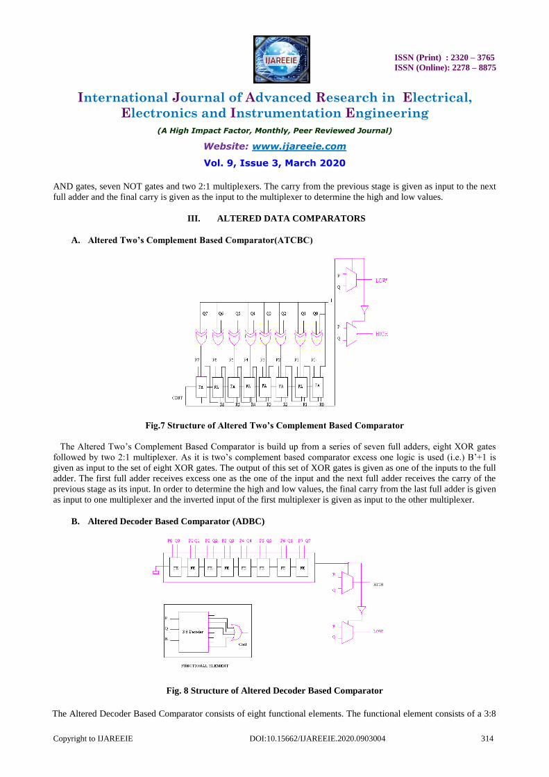
The Output waveform of Parallel Architecture has been obtained as shown in the Fig. 14. In this Waveform X1-X9 are
the inputs and Median is the only output.
Fig. 15 Output Waveform of Pipelined Architecture
The Output waveform of Pipelined Architecture has been obtained as shown in the Fig. 15. In this Waveform A, B, C
and reset are the inputs and Median is the only output.
SIMULATION TABLE
Fig.16 Simulation Table of Architecture
V. CONCLUSION
Thus simulation is done for existing four comparators and for also two modified comparators. These comparators are
then implemented in parallel and pipelined architecture and then simulation result have been taken. These comparators
are targeted using device XC3S400-4pq208 on Xilinx 9.1i compiler tool using VERILOG module. The drawbacks of
existing Decoder Based Data comparator and Two’s Complement Based Comparator is overcome and Altered Decoder
Based Comparator(ADBC) with suitable for memory efficient design and Altered Two’s Complement Based
Comparator(ATCBC) with less area has been designed. Thus these comparators are designed on the basis of speed, area
and power.
ISSN (Print) : 2320 – 3765
ISSN (Online): 2278 – 8875
International Journal of Advanced Research in Electrical,
Electronics and Instrumentation Engineering
(A High Impact Factor, Monthly, Peer Reviewed Journal)
Website: www.ijareeie.com
Vol. 9, Issue 3, March 2020
Copyright to IJAREEIE DOI:10.15662/IJAREEIE.2020.0903004 319
REFERENCES
[1] Vasanth.K and Sindhu.E “VLSI Architecture for 8 Bit Data Comparators for Rank Ordering Image Applications” April 4-6, 2019, India.
[2] Vasanth.k, Kavirajan A.A.F, Ravi.T, NirmalRaj.S, “ A Novel 8 bit digital comparator for 3x3 fixed kernel based modified shear sorting”, Indian journal of science and technology, vol 7 ,issue 4, pp 452- 462, April 2014.
[3]Karpagaabirami.S.P. Ramamoorthy, “An Efficient VLSI Architecture for Removal of Impulse Noise in Images”, International Journal of Computer Science and Mobile Computing, Vol. 3, Issue. 5, pp 567 – 574, May 2014.
[4] K.Vasanth, “VLSI Architecture of Decision based Modified Selection sort filter for Salt and pepper noise removal”, International Journal on
Intelligent Electronic System, Vol 13,no.4, Pages 41-56, August 2014. [5] Mehmoodul Hassan, Rajesh Mehra, “Design Analysis of 1-bit CMOS comparator”, Proceedings of InternationalJournal of Scientific Research
Engineering & Technology, Vol. , Issue. , pp 68 – 72, 14-15 March 2015 .
[6] Bharat H. Nagpara, GodhakiyaSantosh M, Nagar Jay V, Design and Implementation of Different types of Comparator”,International Journal of Science, Engineering and Technology Research , Vol. 4, Issue. 5, pp 1321-1324, May 2015.
[7] K.Vasanth, V Elanangai, S Saravanan, G Nagarajan, “FSM-Based VLSI Architecture for the 3× 3 Window-Based DBUTMPF Algorithm”,
Proceedings of the International Conference on Soft Computing Systems: ICSCS 2015, Springer, Vol no 2, pp 234- 245, 2015. [8] AayisaBanu S, Ms. Divya R, Mr. Ramesh .K, “Design and Simulation of Low Power and High Speed Comparator using VLSI Technique”,
International Journal of Advanced Research in Computer and Communication Engineering, Vol. 6, Issue. 1, pp 119 – 122, January 2017.
[9] V.Geetha and G.Murugesan, “Performance Analysis of Horner’s Rule Based Canonical Signed Digit Lifting Architecture for Two Dimensional
Discrete Wavelet Transform”, International Journal of Biomedical Engineering and Technology, vol. 23, no. 2/3/4, pp.123-136, 2017.
[10]V.Geetha and G.Murugesan, “High performance VLSI architecture to improve contras tin digital mammography’s using discrete wavelet
transform”, Biomedical Research –India 2017, Special Section: Artificial Intelligent Techniques for Bio-Medical Signal Processing, Special Issue:
pp. S141-S146, 2017. [11] M.HassanNajafi, David J. Lilja, Marc Riedel and Kia Bazargan,“Power and Area Efficient Sorting Networks using Unary Processing”,
Proceedings of IEEE International Conference on Computer Design, pp 125-128, 2017.
[12] MurlidharVerma and K.R.Chowdhary, “Analysis of Energy Consumption of Sorting Algorithms on Smart phones”, Proceedings of International Conference on Advances in Internet of Things and Connected Technologies (ICIOTCT-2018), pp 472-475, 2018.
Related Documents