FPGA ARCHITECTURE, TIMING, SOFTWARE Mose Wahlstrom Lattice Research & Development Team May 16, 2014

FPGA Architecture, timing, Software
Feb 26, 2016
FPGA Architecture, timing, Software. Mose Wahlstrom Lattice Research & Development Team May 16, 2014. Overview. Mose Wahlstrom, BSEE OSU 1992 At Lattice for last 22 years Excited to enhance partnership between Lattice and OSU Will continue to give to OSU (hardware, software, time) - PowerPoint PPT Presentation
Welcome message from author
This document is posted to help you gain knowledge. Please leave a comment to let me know what you think about it! Share it to your friends and learn new things together.
Transcript
FPGA ARCHITECTURE, TIMING, SOFTWARE
Mose WahlstromLattice Research & Development TeamMay 16, 2014

Page: 2 Lattice Semiconductor
OVERVIEW
Mose Wahlstrom, BSEE OSU 1992 At Lattice for last 22 years
Excited to enhance partnership between Lattice and OSU Will continue to give to OSU (hardware, software, time) Will continue to hire (interns and permanent positions) Will entertain other guest lectures
Here to focus on FPGA architecture, software, and timing Not here to pitch Lattice or recruit. (That comes later!)
Ask questions (And yell if I use acronyms or unknown terms)
This will go fast and I don’t expect 100% of it to stick. Just a general background you can build on.
Page: 3 Lattice Semiconductor
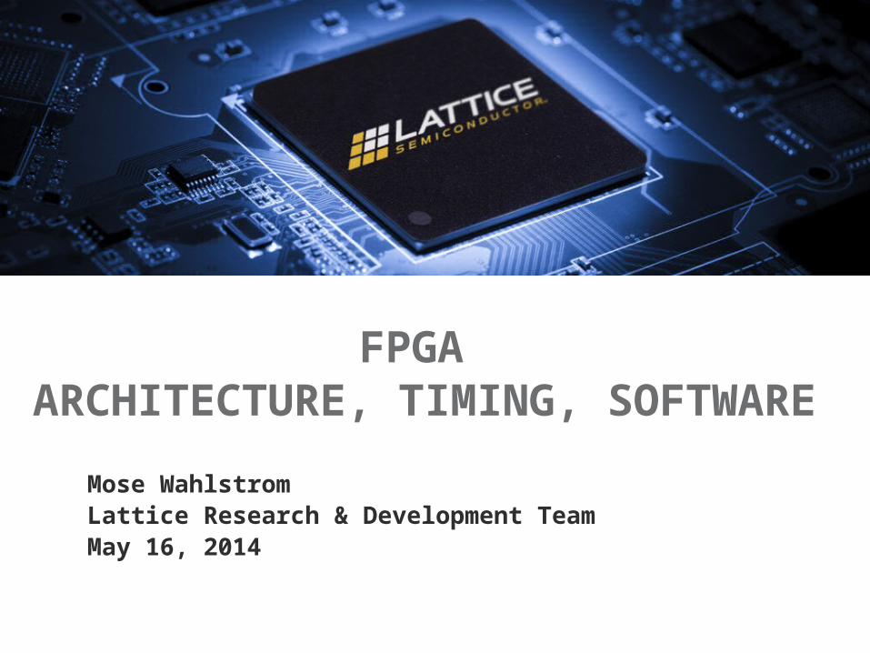
TOPICS
Field Programmable Gate Array (FPGA) Architecture (~25 min) Top level block diagrams Logic building blocks Signal routing
Timing and Power (~15 min) Clocking and control signals Typical path Operating frequency and timing constraints Static timing analysis (setup/hold and clock-to-out) Power consumption
Software Flow (~10 min) Design capture in Verilog, IPexpress Synthesis into ‘standard’ cells Cell placement and routing in the FPGA Bitstream generation and device configuration

Page: 4 Lattice Semiconductor
BLOCK DIAGRAM
IO Ring
LOGIC LOGIC LOGIC LOGIC LOGIC
LOGIC LOGIC LOGIC LOGIC LOGIC
LOGIC LOGIC LOGIC LOGIC LOGIC
LOGIC LOGIC LOGIC LOGIC LOGIC
LOGIC LOGIC LOGIC LOGIC LOGIC
Programmable Logic Cell (PLC)
- Field Programmable Gate Arrays are built from a grid of tiled, simple cells.
- Cell counts from ~256 to 100k- PLCs align by abutment; can build
any reasonably sized array.
- Includes both ROUTING and LOGIC
- ROUTING tracks cross boundaries- LOGIC is self-contained in the PLC
- The IO ring contains the Input/Outputs
- The IO ring also contains other dedicated ‘value added’ logic
NOTE: PLC drawn to approximate scale- ROUTING comprises ~70% of area- LOGIC comprises ~30% of area
FPGAs: An array of PLCs

Page: 5 Lattice Semiconductor
MACHXO2 BLOCK DIAGRAM (XO2-1200)
sysIO Buffers Support LVCMOS/LVTTL, and
DDR Memory Interfaces
Programmable Function Units (PFUs) with RAM
Flexible RoutingOptimized for Speed, Low-
Cost and Routability
sysMEM Block RAM 9Kbit Dual Port
sysCLOCK PLLsFrequency Synthesis &
Clock Alignment
On-chip Flash Memory Provides Instant-on, High
Security & Single Chip Solution
sysIO Buffers Support LVCMOS/LVTTL, LVDS
Outputs. I/O Logic Supports 7:1 Output Gearing
sysIO Buffers Support LVCMOS/LVTTL, LVDS
inputs and PCI. I/O Logic Supports 7:1 Input Gearing
Embedded Function Block Hardened SPI,
I2C, Timer/Counter
User Flash Memory
‘Value added’ features in and around the core

Page: 6 Lattice Semiconductor
BRIEF OVERVIEW OF THE PLC
The Programmable Logic Cell (PLC) is the fundamental building block of the FPGA Fabric.The PLC consists of 2 components: PFU – Programmable Function Unit (Very simple logic!) Programmable Routing Block or Big Switch Box (BSB) (Lots of Muxes)
The routing wires are an integral part of the BSB, but pass over the PLC from tile to tile.
BSB(BigSwitchBox) PFU/PFF
PLC
X6X2
X6 X2 BSB(BigSwitchBox) PFU/PFF
PLC
X6X2
X6 X2 PFU
Page: 7 Lattice Semiconductor
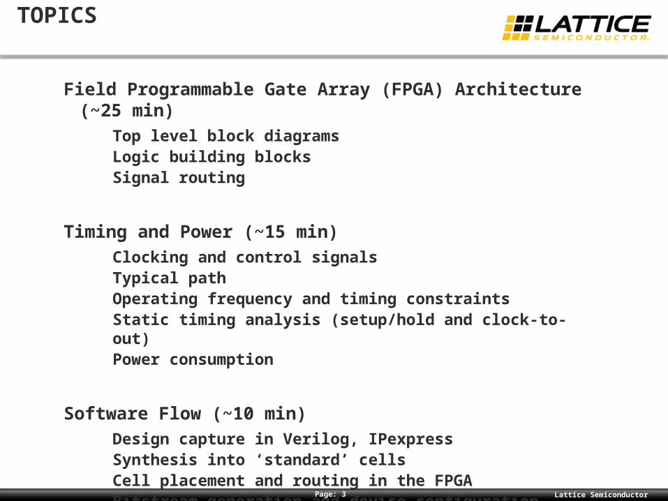
PFU – THE LOOK-UP-TABLE (LUT)
Building the PFU from the inside out… Nearly all FPGAs are based on a Look-Up-Table plus Register. Most are a LUT4.
Aka LUT4+REG. A 4-input LUT is just a 16-bit ROM, with 4 ‘address’ bits (ABCD) and a ‘data’ bit (F). By programming the ROM, any 4 input logic functions can be formed. Or it can be a simple ROM.
q0
q2q1
q3LU
T M
emor
yq4
q6q5
q7q8
q10q9
q11
q12
q14q13
q15
A B
C
D
F
(‘q’ values are programmable SRAM memory bits that are determined through the design synthesis process)
Page: 8 Lattice Semiconductor
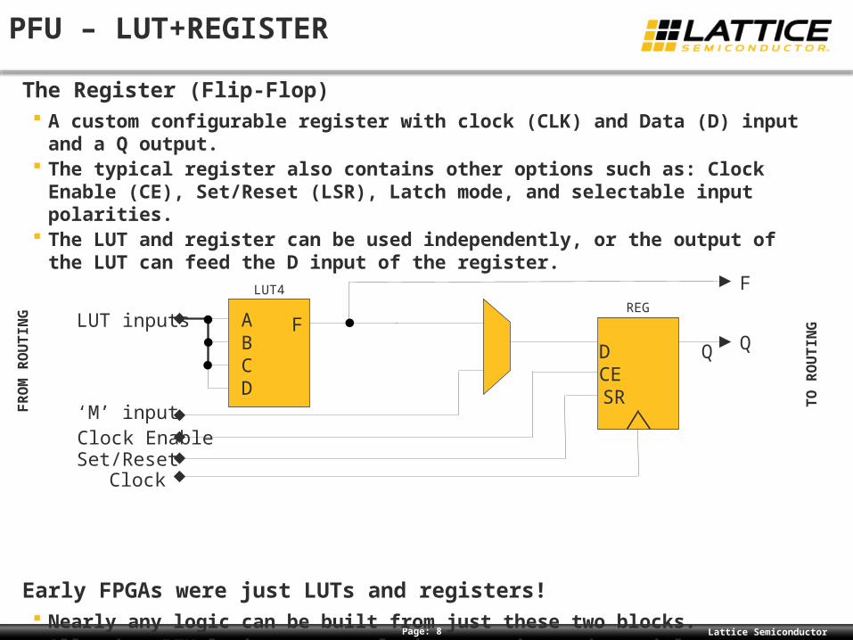
PFU – LUT+REGISTER
The Register (Flip-Flop) A custom configurable register with clock (CLK) and Data (D) input and a Q output. The typical register also contains other options such as: Clock Enable (CE),
Set/Reset (LSR), Latch mode, and selectable input polarities. The LUT and register can be used independently, or the output of the LUT can feed
the D input of the register.
Early FPGAs were just LUTs and registers! Nearly any logic can be built from just these two blocks. All other PFU logic supports logic expansion and special enhancements to the
LUT+REG.
A B C D
F
LUT4
TO R
OU
TIN
G
D QCESR
REG
F
Q
FRO
M R
OU
TIN
G
Clock
LUT inputs
Set/Reset
‘M’ inputClock Enable
Page: 9 Lattice Semiconductor
PFU – ENHANCEMENTS
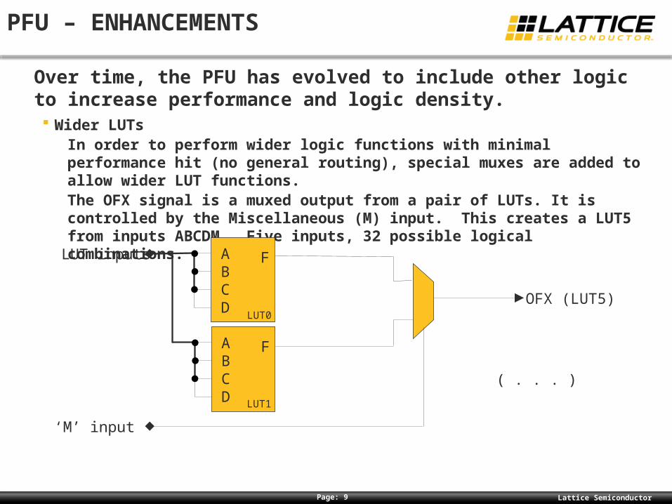
Over time, the PFU has evolved to include other logic to increase performance and logic density. Wider LUTs In order to perform wider logic functions with minimal performance hit (no general
routing), special muxes are added to allow wider LUT functions. The OFX signal is a muxed output from a pair of LUTs. It is controlled by the
Miscellaneous (M) input. This creates a LUT5 from inputs ABCDM. Five inputs, 32 possible logical combinations.
Additional OFX muxes support LUT6, LUT7, and LUT8. A LUT7 consumes 8 LUT4s (128 memory bits) .
A B C D
F
LUT0
LUT inputs
‘M’ input
OFX (LUT5)
A B C D
F
LUT1
( . . . )

Page: 10 Lattice Semiconductor
PFU – ENHANCEMENTS (CONT)
RAM mode RAM mode can be implemented by adding some ‘write’ logic to the LUT. This
allows the LUT to implement a small 16 bit RAM. The ‘read’ just functions similar to ROM/LUT mode.
Implementing the write operation requires ‘borrowed’ signals and logic.
Ripple mode Ripple Mode is implemented by adding some additional logic and re-purposing
the LUT bits to function as a carry-look-ahead adder. Ripple mode supports configurable options for implementing adders, subtractors, and comparators.
Now we can put it all together to construct a typical PFU. Wide LUT, RAM, and Ripple mode don’t really have any practical uses with a single
LUT. Only when LUTs are grouped together can we build wide logic functions and multi-bit adders and RAMs. Thus the minimal building blocks need to be more than just a single LUT+REG.
Page: 11 Lattice Semiconductor
PFU – BUILDING ‘SLICES’
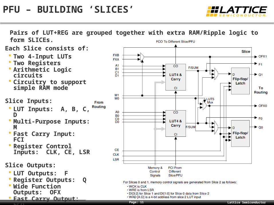
Each Slice consists of: Two 4-Input LUTs Two Registers Arithmetic Logic circuits Circuitry to support simple
RAM mode
Slice Inputs: LUT Inputs: A, B, C, D Multi-Purpose Inputs: M Fast Carry Input: FCI Register Control Inputs:
CLK, CE, LSR
Slice Outputs: LUT Outputs: F Register Outputs: Q Wide Function Outputs:
OFX Fast Carry Output: FCO
Pairs of LUT+REG are grouped together with extra RAM/Ripple logic to form SLICEs.
Page: 12 Lattice Semiconductor
PFU – BUILDING THE PLC
The ‘SLICE’ Multiple slices are bolted together to form the PLC. Ripple and RAM mode are superset slice options. RAM mode requires ‘stealing’ logic and ports from adjacent slices. All slices can be used as a LUT and/or a REG.
A Typical PFU contains 4 slices. This would contain/support the following: 8 LUT4s or up to a single LUT7, up to a 16x8bit pseudo dual port RAM, an 8 bit
register or shift register, a full 8bit adder/subtractor/comparator, or other combinations.

Page: 13 Lattice Semiconductor
PLC – TOP LEVEL VIEW
LUT4 LUT4
Arithmetic Logic
FF/Latch
FF/Latch
Slice 0
F0Q0
OFX0
F1Q1
OFX1
A0B0C0D0M0
A1B1C1D1M1
CLK0/1LSR0/1
CE0
LUT4 LUT4
Arithmetic Logic
FF/Latch
FF/Latch
Slice 1
F2Q2
OFX2
F3Q3
OFX3
A2B2C2D2M2
A3B3C3D3M3
CLK0/1LSR0/1
CE1
LUT4 LUT4
Arithmetic Logic
FF/Latch
FF/Latch
Slice 2
F4Q4
OFX4
F5Q5
OFX5
A4B4C4D4M4
A5B5C5D5M5
CLK0/1LSR0/1
CE2
LUT4 LUT4
Arithmetic Logic
FF/Latch
FF/Latch
Slice 3
F6Q6
OFX6
F7Q7
OFX7
A6B6C6D6M6
A7B7C7D7M7
CLK0/1LSR0/1
CE3
FCI FCO
Page: 14 Lattice Semiconductor
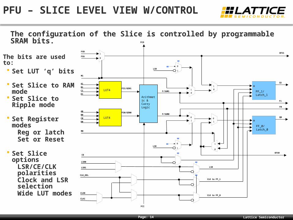
PFU – SLICE LEVEL VIEW W/CONTROL
10
LUT4
LUT4
Arithmetic&CarryLogic
M1
FS1/GEN1F/SUM1
01
F/SUM0
M0
0
1
10
LSR
FXB
FXA
OFX1
0
1
01
LSR
D
FF_0/Latch_0
F1
F0
Q1
D
Q0
OFX0
0
1
0
1
A0
B0
C0
D0
A1B1
C1
D1
LSR
CLK to FF_1
CE
FCO
FCI
FS0/GEN0
LSR0
LSR1
CLK0
CLK1
CLK_DEL
CLK to FF_0
FF_1/Latch_1
The bits are used to: Set LUT ‘q’ bits
Set Slice to RAM mode
Set Slice to Ripple mode
Set Register modes Reg or latch Set or Reset
Set Slice options LSR/CE/CLK
polarities Clock and LSR
selection Wide LUT modes
The configuration of the Slice is controlled by programmable SRAM bits.

Page: 15 Lattice Semiconductor
ADDITIONAL PLC DETAIL
Wide LUTs revisited The OFX muxes and the FX/OFX IO signals are dedicated to wider LUT functions.
OFX0 is always a LUT5. OFX1 performs a different function in each slice. Two of the slices use the OFX1 mux to generate LUT6s from a pair of LUT5s. One slice can then use OFX1 to generate a LUT7 from the pair of LUT6s. The final OFX1 can be used to generate a LUT8 from its own LUT7 and that of a neighboring PFU.
The neighboring LUT7 output/input is one of the few special directly connected signals that span PFUs.
RAM mode revisited Implementing RAM mode requires more signals than are present in a single slice. At
a minimum, a Write Enable (WRE) and a Data Input (DI) are needed. However in order to support Pseudo Dual Port (PDP) mode, an additional Write Address (WAD) bus is needed as well as a Write Clock (WCK) for the write port.
In a typical implementation, these signals come from one of the other slices. For example, slice 0 and 1 may be used to implement a 16x4 PDP RAM. Slice 2 is ‘burned’ to generate the control signals, which are sent to slice 0/1. And slice 3 doesn’t support RAM mode.
Thus there are special RAM mode signals sent between slices. These signals are dedicated for RAM mode and do not leave the PFU.

Page: 16 Lattice Semiconductor
ADDITIONAL PFU DETAIL (CONT.)
Ripple mode revisited Ripple mode repurposes a pair of LUTs to implement a full 2-bit Carry Look-Ahead
(CLA) adder. The LUT is programmed as a ROM and slightly modified to produce Propagate and Generate signals from the (4) inputs and the carry input signal.
By adding dedicated Fast Carry Input/Output (FCI/FCO) signals, performance is greatly improved when compared to arithmetic functions using LUT logic and general routing resources.
Ripple mode is not a full CLA, but rather a chain of 2-bit CLAs with a dedicated, rippling fast carry chain.
Every slice has a FCI and FCO port that connect adjoining slices. At the PFU boundary, the FCI and FCO connect between neighboring PFUs (typically L to R).

Page: 17 Lattice Semiconductor
PROGRAMMABLE ROUTING BLOCK
ROUTING: (The other three-quarters of the PLC) The general purpose routing is not deterministic. It is a collection of
pseudo-random paths. The design software, user preferences, design congestion, and random seeding all affect the signal routing.
The routing portion of the PLC can be divided into the signal wires and the switch boxes that feed them. The wires carry signals from one PLC to another. The switch boxes are the programmable source connections. The wires are the roads, the switch boxes are the intersections. Once again, the programmable connections are controlled by SRAM bits. The muxes are typically two-stage, one-hot pass-gate muxes.
Page: 18 Lattice Semiconductor
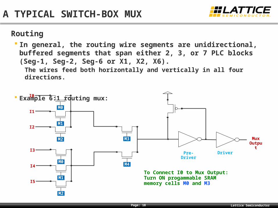
A TYPICAL SWITCH-BOX MUX
Routing In general, the routing wire segments are unidirectional, buffered segments
that span either 2, 3, or 7 PLC blocks (Seg-1, Seg-2, Seg-6 or X1, X2, X6). The wires feed both horizontally and vertically in all four directions.
Example 6:1 routing mux:
M0
M1
M2
M4
M3
M0
M1
M2
I0
I1
I2
I3
I4
I5
Mux Output
Pre-Driver Driver
To Connect I0 to Mux Output:Turn ON progammable SRAM memory cells M0 and M3
Page: 19 Lattice Semiconductor
PROGRAMMABLE ROUTING BLOCK
There are two distinct categories of switch boxes. Input Switch Boxes (ISBs) are muxes that feed the inputs to the PFU.
Output Switch Boxes (OSBs), are muxes that feed the routing wires out of the PLC.
The source for each ISB and OSB is a programmable mux. The inputs to the mux determine what subset of signal sources can drive that particular wire or PFU input. A typical routing mux contains about 20 inputs.
Using these ISB and OSB mux connections, routing paths can be found to connects any PLC output to any other PLC input.
Page: 20 Lattice Semiconductor
PROGRAMMABLE ROUTING BLOCK
The BSB contains hundreds of programmable muxes. The ISBs feed into the PFU to drive: LUT and M inputs Clock inputs CE and Local Set/Reset inputs
The OSBs feed out of the PLC: OSBs drive all the segment wires (X1, X2, X6) The sources for OSB muxes are a pseudo-random selection of both PFU
outputs and other routing wires.
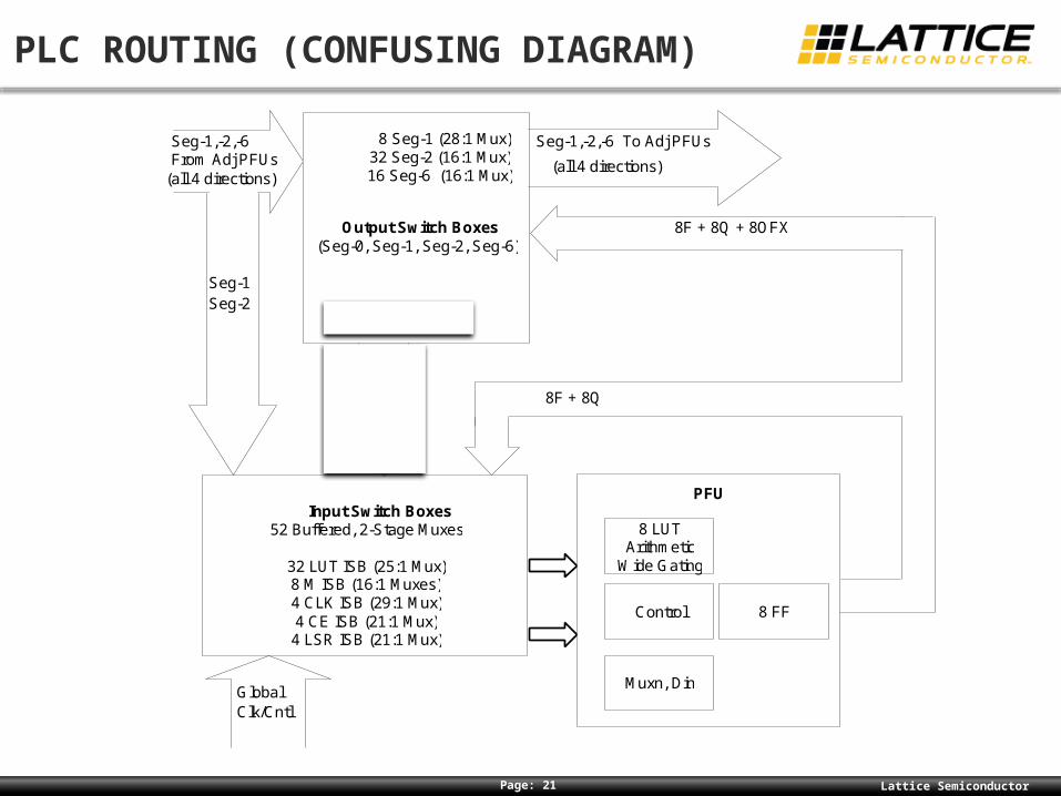
The following horribly confusing diagram illustrates a high level view of the routing structure. In general, the routing muxes are sparsely populated. Only a small
fraction of the possible wires feeds each ISB or OSB. The software must search many possible options to find a route. This
includes swapping LUT inputs, moving logic drivers, and duplicating logic.
Page: 21 Lattice Semiconductor
PLC ROUTING (CONFUSING DIAGRAM)
Output Switch Boxes (Seg-0, Seg-1, Seg-2, Seg-6)
8 Seg-0 (20:1 Mux)
8 Seg-1 (28:1 Mux) 32 Seg-2 (16:1 Mux) 16 Seg-6 (16:1 Mux)
Input Switch Boxes 52 Buffered, 2-Stage Muxes
32 LUT ISB (25:1 Mux) 8 M ISB (16:1 Muxes) 4 CLK ISB (29:1 Mux) 4 CE ISB (21:1 Mux) 4 LSR ISB (21:1 Mux)
8F + 8Q + 8OFX
PFU
8 FF
8 LUT Arithmetic
Wide Gating
Control
Muxn, Din
8F + 8Q
Seg-1,-2,-6 To Adj PFUs Seg-1,-2,-6
(all 4 directions) (all 4 directions) From Adj PFUs
Seg-1 Seg-2
Seg-0
Global Clk/Cntl
Page: 22 Lattice Semiconductor
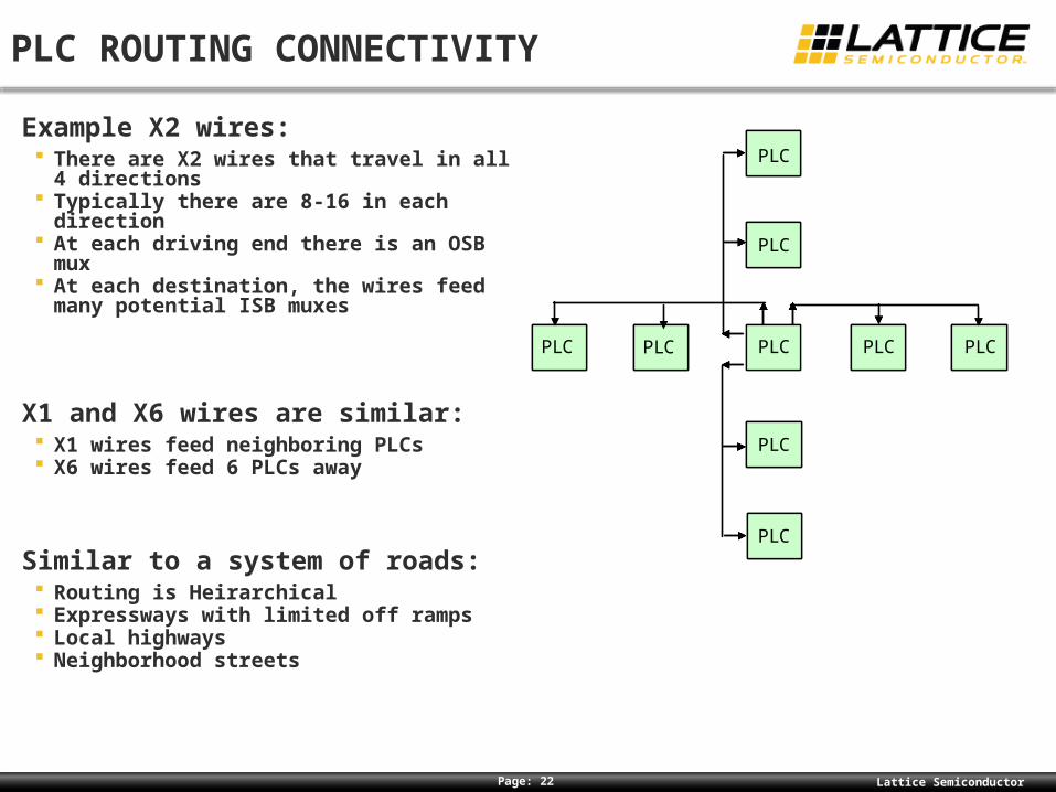
PLC ROUTING CONNECTIVITY
Example X2 wires: There are X2 wires that travel in all 4 directions Typically there are 8-16 in each direction At each driving end there is an OSB mux At each destination, the wires feed many
potential ISB muxes
X1 and X6 wires are similar: X1 wires feed neighboring PLCs X6 wires feed 6 PLCs away
Similar to a system of roads: Routing is Heirarchical Expressways with limited off ramps Local highways Neighborhood streets
Note:
1. Eachdirection,8banks[ oo :o7] 2. Eachbankofwireisstaggered 3. Eachbankhas3bits
a. Bit00 – output b. Bit01 – segment - 2midtapinput c. Bit02 – segment - 2endtappoint
Example 1. Totheeast8banksofwireare
H02E0000toH02E0700 2. Eachbanks,3bits
H02E0000(output) H02E0001(midtapinput) H02E0002(END - input)
PLC PLC PLC PLC PLC
PLC
PLC
PLC
PLC
Note:
1. Eachdirection,8banks[ oo :o7] 2. Eachbankofwireisstaggered 3. Eachbankhas3bits
a. Bit00 – output b. Bit01 – segment - 2midtapinput c. Bit02 – segment -
Example 1. Totheeast8banksofwireare
H02E0000toH02E0700 2. Eachbanks,3bits
H02E0000(output) H02E0001(midtapinput) H02E0002(END - input)
PLC PLC PLC PLC PLC
PLC
PLC
PLC
PLC
Page: 23 Lattice Semiconductor
PLC ROUTING CONNECTIVITY
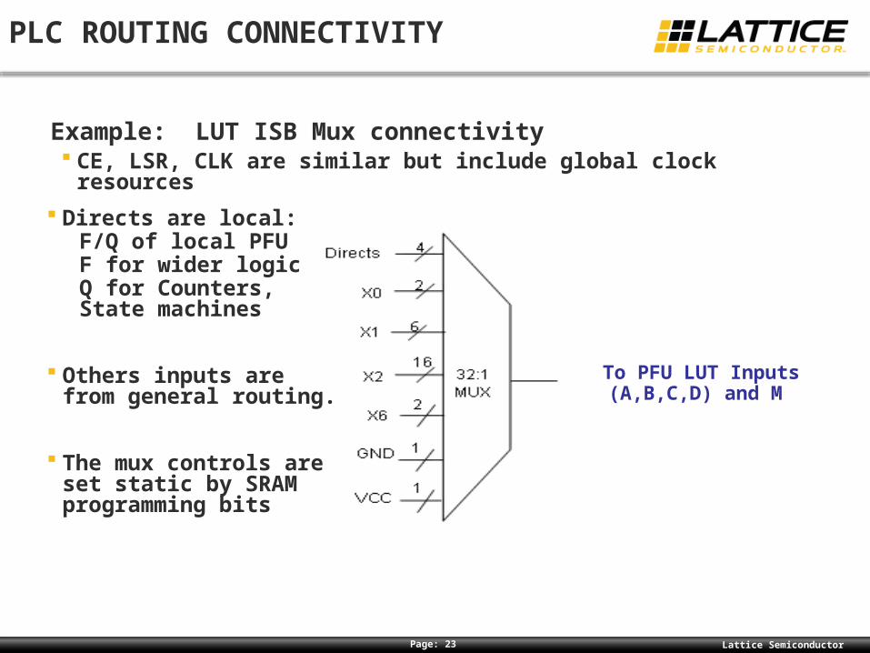
Directs are local: F/Q of local PFU F for wider logic Q for Counters, State
machines
Others inputs are from general routing.
The mux controls are set static by SRAM programming bits
To PFU LUT Inputs (A,B,C,D) and M
Example: LUT ISB Mux connectivity CE, LSR, CLK are similar but include global clock resources
Page: 24 Lattice Semiconductor
PLC ROUTING CONNECTIVITY
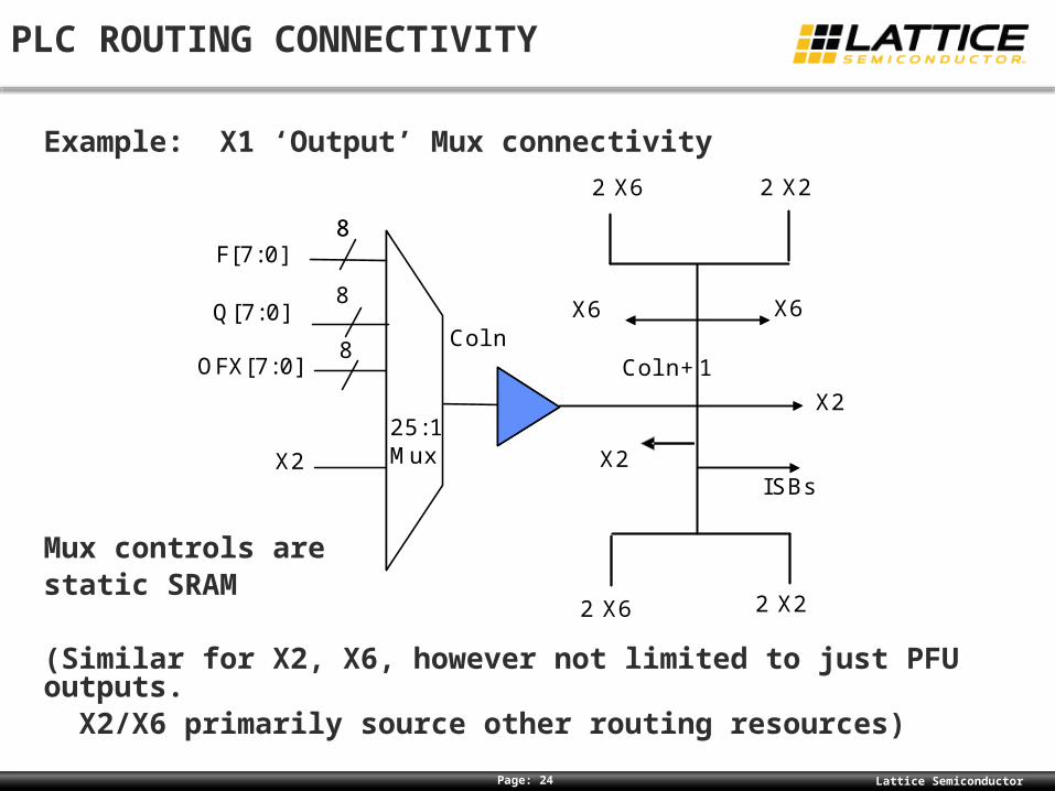
Example: X1 ‘Output’ Mux connectivity
Mux controls arestatic SRAM
(Similar for X2, X6, however not limited to just PFU outputs. X2/X6 primarily source other routing resources)
25:1
Mux
8
8
2X6 2X2
2X6 2X2
X2
ISBs
X6
25:1Mux
OFX[7:0]
F[7:0] 8
8 Q[7:0]
X2
Coln Coln+1
X6
X2
Page: 25 Lattice Semiconductor
GLOBAL ROUTING (CLOCK TIMING)
In addition to the general purpose routing, there are some global control signals that feed the entire PLC array and the peripheral logic in the IO ring. The most important global signals are the clock signals. (Synchronous logic) All FPGA devices contain clock ‘trees’ to guarantee all registers receive the clock at
essentially the same time to provide deterministic setup and hold times between registers. This is known as the primary clock tree, which has many branches and programmable options for clock gating, switching, and power control.
All clock signal trees have special routing mux resources to choose their sources. These muxes are located in the central clock switch.
The sources for the clocking resources are a mix of general purpose routing, dedicated IO pins, Phase Lock Loop (PLL) outputs, and other clock resources. This allows the implementation of complex clock systems with both internal and external clocks, multiple clock frequencies, and various clock phases.
All devices have a Global Set Reset (GSR). This signal fans out to every register in the device, both in the PLC array and in the IO ring. This provides a system reset.
From a user’s perspective, these are the only significant global signals. However there are lots of other global signals dedicated to programming, power control, etc.
Page: 26 Lattice Semiconductor
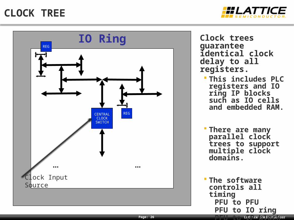
CLOCK TREE
Clock trees guarantee identical clock delay to all registers. This includes PLC
registers and IO ring IP blocks such as IO cells and embedded RAM.
There are many parallel clock trees to support multiple clock domains.
The software controls all timing PFU to PFU PFU to IO ring PFU to IP block IP block to PFU
IO Ring
CENTRALCLOCKSWITCH
……
REG
REG
Clock Input Source

Page: 27 Lattice Semiconductor
TYPICAL SIGNAL PATH
Typical Path: A 4-logic-level deep register-to-register path
Path Delay = (CLK2Q + LUT4 delays + FF_Setup) + (OSB Routing + ISB)
The routing delays could represent local intra-PLC delays, or they could be inter-PLC delays crossing the entire PLC array.
(Not shown is the clock signal, which also has a delay.)
PFU
A
LUT
PFU
FF
PFU
D
LUT
PFU
A
LUT
PFU
D
LUT FF
Q Routing+ ISB
Routing+ ISB
Routing+ ISB
Routing+ ISB
CLK2Q LUT4 delay LUT4 delay LUT4_delay+
FF Setup
Routing delay Routing delay
LUT4 delay
Routing delayRouting delay
Page: 28 Lattice Semiconductor
SOFTWARE TIMING CONTROL
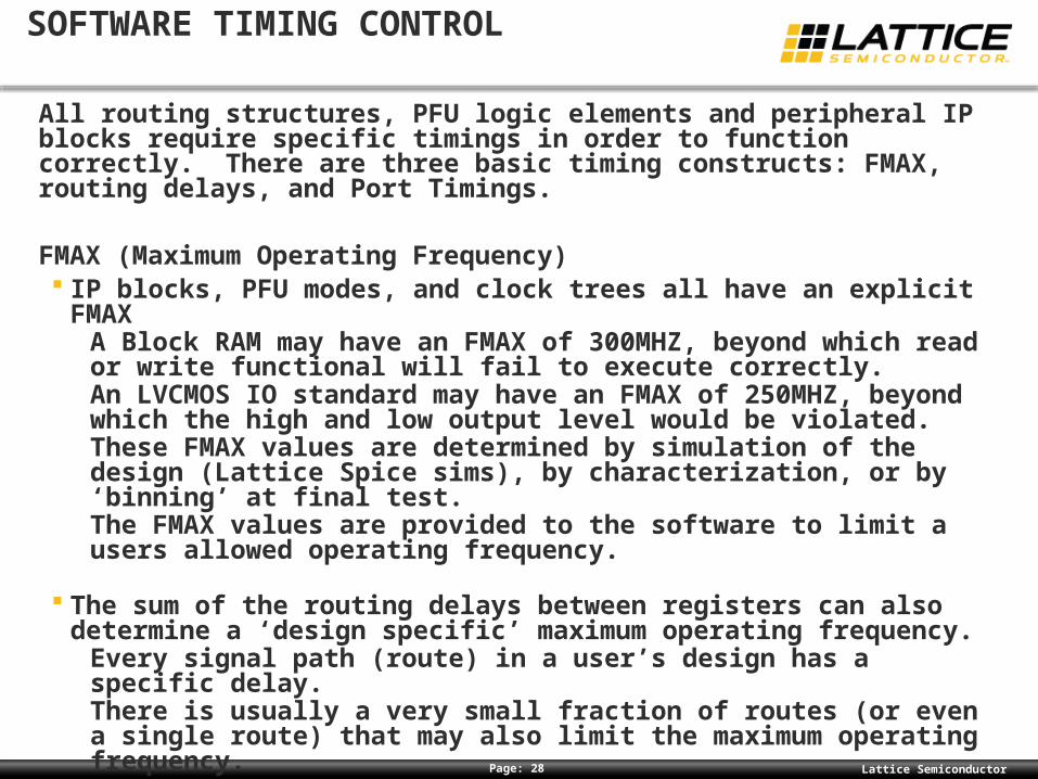
All routing structures, PFU logic elements and peripheral IP blocks require specific timings in order to function correctly. There are three basic timing constructs: FMAX, routing delays, and Port Timings.
FMAX (Maximum Operating Frequency) IP blocks, PFU modes, and clock trees all have an explicit FMAX A Block RAM may have an FMAX of 300MHZ, beyond which read or write
functional will fail to execute correctly. An LVCMOS IO standard may have an FMAX of 250MHZ, beyond which
the high and low output level would be violated. These FMAX values are determined by simulation of the design (Lattice
Spice sims), by characterization, or by ‘binning’ at final test. The FMAX values are provided to the software to limit a users allowed
operating frequency.
The sum of the routing delays between registers can also determine a ‘design specific’ maximum operating frequency. Every signal path (route) in a user’s design has a specific delay. There is usually a very small fraction of routes (or even a single route)
that may also limit the maximum operating frequency.
Users enter their desired operating frequency and the software checks to make sure that all blocks and resources meet the FMAX constraints.

Page: 29 Lattice Semiconductor
SOFTWARE TIMING CONTROL (CONT.)
Routing Delays and Port Timings All synchronous blocks require specific Setup/Hold time (TSU/TH) on IN
ports and they provide specific Clock To Out (TCO) on OUT ports. These TSU/TH/TCO values are determined by simulation of the device,
by characterization, or by ‘binning’ at final test. The routing delays of each wire and mux type (X2, X6, ISB, OSB) are also
simulated and characterized. All these port and routing timings are integrated into the software so that it
can determine timing closure on every signal path between register.
For the software to be effective, users must enter timing ‘constraints’. This sets FMAX and prioritizes internal requirements (general goals).
External IO requirements must also be provided (TSU/TH/TCO). These are determined by off-chip clock and data alignments, such as
from an external memory, interface chip, or processor.
With all of the above information, the software attempts to meet all static timing requirements. It has many options such as: Moving logic (registers) closer together to fix a Setup time violation. Intentionally adding delay to a route to fix a Hold time violation. Duplicating logic closer to a destination to fix a setup time violation. Giving up.
Page: 30 Lattice Semiconductor
FPGA POWER CONSUMPTION
The software can also estimate power consumption. Similar to the timing, the power data comes from many sources such as:
Spice simulations, characterization, and final test ‘binning’.
Power data is integrated into the software for each routing element, PFU mode, and IP block. There are two basic components of power, DC and AC power.
DC power consumption: DC power is comprised of static bias currents and leakage. The leakage currents are calculated from a curve fit equation based on
supply voltage (VCC), Temperature, and process variation (typical or worst-case). The software provides users the means to enter VCC and temperature as well as select the process.
Every LUT, Block RAM, routing wire, etc. has different bias and leakage. There are also different calculations based on if an element is used or
unused in a particular user’s design. The software will also generate statistical averages when logic values
affect DC bias or leakage current (a ‘1’ and ‘0’ may be different).
Page: 31 Lattice Semiconductor
FPGA POWER CONSUMPTION (CONT.)
AC power consumption: For routing, only a function of: Capacitance (extracted from layout, technology, and simulation) Voltage (Provided by customer’s design) Frequency (average switching frequency of each ‘wire’)
Every ‘wire’ will switch at different rates depending on the design, activity, and time slice.
Activity Factor (AF) is provided by the customer as an average indicator of switching rates (0%-100%)
For the PFU logic and other IP blocks The same CVF method can be used. ‘Capacitance’ values are provided in
the software for each IP block. Users must enter the clock frequency for each clock that feeds the PFUs
and IP blocks.
Total Power: Total power is the summation of ‘used’ DC, ‘unused’ DC, and AC CVF. Every routing, PFU, and IP element is separately calculated and summed
together to produce the total power for the entire FPGA. Every supply is analyzed separately.
Page: 32 Lattice Semiconductor
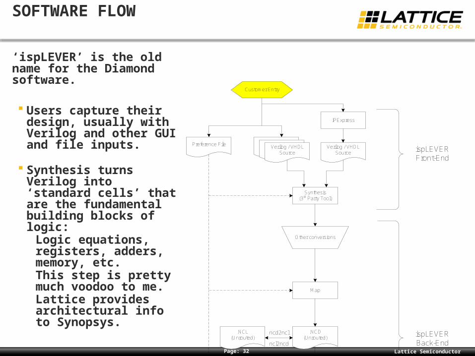
SOFTWARE FLOW
‘ispLEVER’ is the old name for the Diamond software.
Users capture their design, usually with Verilog and other GUI and file inputs.
Synthesis turns Verilog into ‘standard cells’ that are the fundamental building blocks of logic: Logic equations,
registers, adders, memory, etc.
This step is pretty much voodoo to me.
Lattice provides architectural info to Synopsys.
.NCD(Routed)
Place and Route(PAR)
.NCD(Unrouted)
Map
Bitgen
.RBT(or .JED or .BIT)
Other conversions
Verilog / VHDLSource
Verilog / VHDL Source
IPExpress
Preference File
Synthesis(3rd Party Tool)
.NCL(Unrouted)
.NCL(Routed)
ncd2ncl
ncl2ncd
ncd2ncl
ncl2ncd
Customer Entry
ispLEVERFront-End
ispLEVERBack-End
Page: 33 Lattice Semiconductor
SOFTWARE FLOW (CONT.)
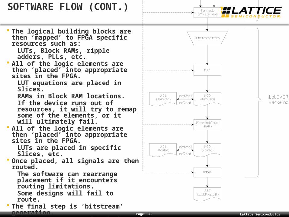
The logical building blocks are then
‘mapped’ to FPGA specific resources such as: LUTs, Block RAMs, ripple adders, PLLs,
etc. All of the logic elements are then ‘placed’
into appropriate sites in the FPGA. LUT equations are placed in Slices. RAMs in Block RAM locations. If the device runs out of resources, it
will try to remap some of the elements, or it will ultimately fail.
All of the logic elements are then ‘placed’ into appropriate sites in the FPGA. LUTs are placed in specific Slices, etc.
Once placed, all signals are then routed. The software can rearrange placement
if it encounters routing limitations. Some designs will fail to route.
The final step is ‘bitstream’ generation. This process sets all of the
programmable SRAM bits to implement the logic and routing in the design
The bitstream is then loaded into the device SRAM bits to implement the user’s function. (Or into Flash Memory)
.NCD(Routed)
Place and Route(PAR)
.NCD(Unrouted)
Map
Bitgen
.RBT(or .JED or .BIT)
Other conversions
Verilog / VHDLSource
Verilog / VHDL Source
IPExpress
Preference File
Synthesis(3rd Party Tool)
.NCL(Unrouted)
.NCL(Routed)
ncd2ncl
ncl2ncd
ncd2ncl
ncl2ncd
Customer Entry
ispLEVERFront-End
ispLEVERBack-End

Page: 34 Lattice Semiconductor
OTHER SW RESOURCES
I believe all of these tools are available in the free software.
EPIC (don’t know this acronym) EPIC is a GUI tool included in the software that can be used to view,
analyze and design nearly every aspect of the FPGA. It shows every routing segment, LUT, IP block, etc. It is very cumbersome and difficult to learn.
NCL The software can also generate an NCL (NeoCad Listing?), which is a text
version of the design files that the Map, Place, and Route tools operate on. Once again, very cryptic and difficult to learn. But it is a text
representation of an entire user’s design with all routing and logic.
Power Calculator Can be used to estimate FPGA power consumption.
Related Documents