9/22/2010 1 FPGA and ASIC How to implement a digital system No two applications are identical and every one needs certain amount of customization Basic methods for customization a) “General-purpose hardware” with custom software • General purpose processor: e.g., performance-oriented processor (e.g., Pentium), cost-oriented processor (e.g., PIC micro-controller) • Special purpose processor: architecture with a specific set of functions: e.g., DSP processor (to do multiplication-addition), network processor (to do buffering and routing), “graphic engine” (to do 3D rendering) b) Custom hardware (no software) c) Custom software on a custom platform (CPU+other hardware), known as hardware-software co-design TKT-1426 Lecture 3 2

Welcome message from author
This document is posted to help you gain knowledge. Please leave a comment to let me know what you think about it! Share it to your friends and learn new things together.
Transcript
9/22/2010
1
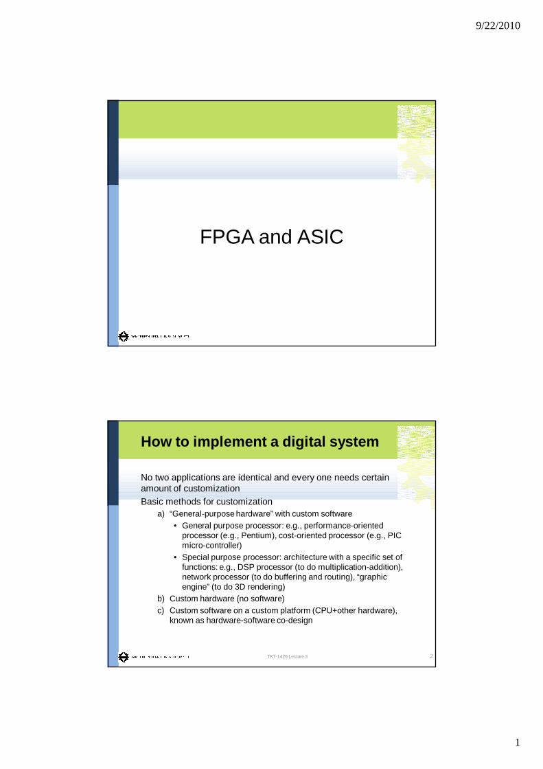
FPGA and ASIC
How to implement a digital system
No two applications are identical and every one needs certain amount of customizationBasic methods for customization
a) “General-purpose hardware” with custom software• General purpose processor: e.g., performance-oriented
processor (e.g., Pentium), cost-oriented processor (e.g., PIC micro-controller)
• Special purpose processor: architecture with a specific set of functions: e.g., DSP processor (to do multiplication-addition), network processor (to do buffering and routing), “graphic engine” (to do 3D rendering)
b) Custom hardware (no software)c) Custom software on a custom platform (CPU+other hardware),
known as hardware-software co-design
TKT-1426 Lecture 3 2
9/22/2010
2
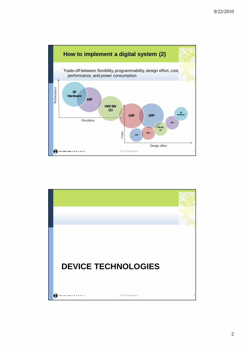
How to implement a digital system (2)
Trade-off between flexibility, programmability, design effort, cost, performance, and power consumption
TKT-1426 Lecture 3 3
Perfo
rman
ce
FlexibilityGPPDSP
HW/SW CO
ASP
SP Hardware
Cos
ts
Design effort
GPPDSP
HW/SW
CO
ASP
SP Hardware
DEVICE TECHNOLOGIES
TKT-1426 Lecture 3 4
9/22/2010
3
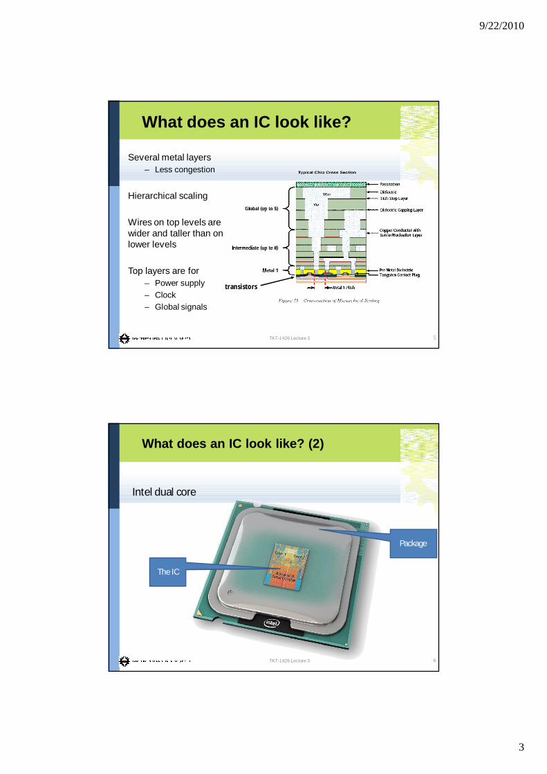
What does an IC look like?
Several metal layers– Less congestion
Hierarchical scaling
Wires on top levels are wider and taller than on lower levels
Top layers are for– Power supply– Clock– Global signals
transistors
TKT-1426 Lecture 3 5
What does an IC look like? (2)
Intel dual core
The IC
Package
TKT-1426 Lecture 3 6
9/22/2010
4
What does an IC look like? (3)
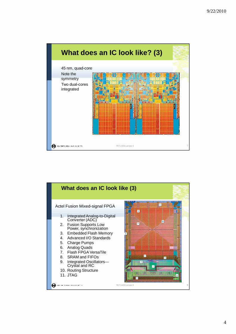
45 nm, quad-coreNote the symmetryTwo dual-cores integrated
TKT-1426 Lecture 3 7
What does an IC look like (3)
Actel Fusion Mixed-signal FPGA
1. Integrated Analog-to-Digital Converter (ADC)
2. Fusion Supports Low Power, synchronization
3. Embedded Flash Memory4. Advanced I/O Standards5. Charge Pumps6. Analog Quads7. Flash FPGA VersaTile8. SRAM and FIFOs9. Integrated Oscillators—
Crystal and RC10. Routing Structure11. JTAG
TKT-1426 Lecture 3 8
9/22/2010
5
Classification of device technologiesWhere customization is done:
– In the fab (fabrication facility): ASIC (Application Specific IC)
• Full-custom ASIC• Standard cell ASIC• Gate array ASIC
– Lower density and performance than other ASICs, but more expensive than non-ASIC => obsolete
– In the “field”: non-ASIC• Complex field-programmable logic device• Simple field-programmable logic device
– Replaced by CPLD/FPGA• Off-the-shelf SSI (Small Scaled IC)/MSI (Medium Scaled IC)
components– No longer a viable option!
TKT-1426 Lecture 3 9
ASIC
Full-custom– All aspects (e.g., size of a transistor) of a circuit are tailored for a
particular application.– Circuit fully optimized– Design extremely complex– Very time consuming design (typically only feasible for small
components)– Intel and AMD are partly full-custom
Standard-cell– Circuit made of a set of pre-defined logic, known as standard cells– Layout of a cell is pre-determined, but layout of the complete circuit
is customized– Eg. Mobile phone digital ICs
TKT-1426 Lecture 3 10
9/22/2010
6
Complex Field Programmable Logic DeviceDevice consists of an array of generic logic cells and general interconnect structureLogic cells and interconnect can be “programmed” by utilizing “semiconductor fuses” or “switches”Customization is done “in the field”Two categories:
– CPLD (Complex Programmable Logic Device)• sea-of-gates to implement logic
– FPGA (Field Programmable Gate Array)• Look-up tables to implement logic
No custom mask neededFor example, Cisco 2600 series routers
TKT-1426 Lecture 3 11
Comparison of technology
Area (Size): silicon real-estate: [mm2], [eq. gates]
Speed (Performance): [MHz], [op/s]– Operations/second– i.e. Time required to perform a task
Power consumption [mW]
Cost [€]
Design effort [person-month]
TKT-1426 Lecture 3 12
9/22/2010
7
Comparison of technology
Area: ASIC (sc) vs FPGA– Standard cell is the smallest since the cells and interconnect are
customized– FPGA is the largest
• Overhead for programmability• Capacity cannot be completely utilized
– Roughly: FPGA is approximately 35 times larger using the LUT-based logic elements [1]
• However, that is not seen by FPGA end users – high volume compensates some costs ($$)
Performance: ASIC (sc) vs FPGA– Roughly: FPGA is between 3.4 to 4.6 times slower, MHz [1]
TKT-1426 Lecture 3
[1] I. Kuon and J. Rose, "Measuring the Gap between FPGAs and ASICs" in IEEE Transactions on Computer-Aided Design of Integrated Circuits and Systems, Vol. 26, NO. 2, FEBRUARY 2007, pp. 203 - 215.
13
Cost
Types of cost:– Chip design costs
• NRE (Non-Recurring Engineering) cost: one-time, per-design cost
• Part cost: per-unit cost– Indirect design costs
• Lead time: time to get the chip out of the factory• Time-to-market “cost” loss of revenue
Standard cell: high NRE, small part cost and large lead time– Good for large volumes
FPGA: low NRE, large part cost and small lead time– Good for prototypes and small volumes
TKT-1426 Lecture 3 14

9/22/2010
8
Trend of break-even point shifting when choosing ASIC or FPGA
TKT-1426 Lecture 3
FPGA
concept-to-prototype
82%
prototype to production
76%
ASIC
cheaper
FPGA cheaper
cost
[$]
#chips
break even, 100K units
ASIC
FPGA
trend
~$20M
~$6M
ASIC % of projects finished in less than 6 months
concept-to-prototype
54%
prototype to production
57%
15
Summary of technologies
Trade-off between optimal use of hardware resource and design effort/cost
No single best technology
TKT-1426 Lecture 3 16
FPGA ASIC
Tailored Masks 15 or more
Area Best (smallest)
Speed Best (fastest)
Power Best (minimal)
NRE Cost Best (smallest)
Per-part Cost Best (smallest)
Design cost Best (easiest)
Time-to-market Best (shortest)
Related Documents