ANU College of Engineering and Computer Science Assignment 02: ATmega8 for automatic Morse Code translation ENGN3213/6213 Digital Systems and Microprocessors Semester 1, 2014 Copyright © 2014, The Australian National University

FPGA Activity
Dec 25, 2015
An FPGA challenge
Welcome message from author
This document is posted to help you gain knowledge. Please leave a comment to let me know what you think about it! Share it to your friends and learn new things together.
Transcript
ANU College of Engineering and Computer Science
Assignment 02: ATmega8 for automatic Morse Code translation ENGN3213/6213 Digital Systems and Microprocessors
Semester 1, 2014 Copyright © 2014, The Australian National University
ENGN 3213/6213 D ig i t a l Sys tems and Mic roproces sors
ANU College of Engineering and Computer Science Page 2 / 1 4
TABLE OF CONTENTS
1. GENERAL PROJECT DESCRIPTION ............................................................................................... 3
2. BACKGROUND INFORMATION ........................................................................................................ 3
2.1 The Morse code ......................................................................................................................... 3
2.2 Relevance of Morse Code ......................................................................................................... 4
2.3 Morse code signal information ................................................................................................... 5
2.4 Basic signal processing concepts and mehods ......................................................................... 5
2.5 Hardware ................................................................................................................................... 7
2.5.1 The preamplifier/offset unit ............................................................................................. 7
2.5.2 The ATmega8 development board ................................................................................. 8
2.6 The waveforms .......................................................................................................................... 9
3. PROJECT DETAILS ........................................................................................................................... 9
4. RECOMMENDED WORKFLOW ...................................................................................................... 10
5. DELIVERABLES AND ASSESSMENT............................................................................................. 10
5.1 Assessment process ................................................................................................................ 10
5.2 Due dates ................................................................................................................................. 11
5.3 Marking Criteria ........................................................................................................................ 11
6. OPEN-LAB TIMES AND ACCESS TO HARDWARE ....................................................................... 12
7. TIPS .................................................................................................................................................. 13
8. ADDITIONAL QUESTION FOR MASTER STUDENTS ONLY ........................................................ 14

ENGN 3213/6213 D ig i t a l Sys tems and Mic roproces sors
ANU College of Engineering and Computer Science Page 3 / 1 4
1. GENERAL PROJECT DESCRIPTION
You will develop an embedded program to utilise the ATmega8 microcontroller as a signal processor
for an incoming Morse Code signal. The key tasks which your system will need to achieve are:
Conversion to digital of the analogue Morse Code sound provided as an input
Real time processing (recognition of signal activity and timing of signal duration)
Decoding the incoming signal into text
Generation of a text output (LCD screen)
2. BACKGROUND INFORMATION
2.1 The Morse code
The Morse Code was invented by Samuel F.B Morse in the mid-1800's. The code was designed to
facilitate the transfer of information across telegraph lines by creating a commonly understood
language between sender and receiver, based on aptly timed ON-OFF signals, which a trained
operator could either create through a tap-switch (sender) or decipher from a recorded paper roll
(receiver). With the advent of radio communication, the typical "dots and dashes" pattern of Morse
Code symbols started becoming transmitted as sound pulses of different duration. Although human-
based Morse Code transmission is still commonplace in some applications, softwares have been
developed which allow automated transmission and high(er)-speed communication.
The basic Morse Code encoding is shown below (this is named ITU and it is the currently accepted
international standard version). Note that different letters can have different numbers of symbols
(variable-length encoding).
Figure 1: Standard letters and numbers and corresponding Morse Code
(source: Wikimedia Commons)

ENGN 3213/6213 D ig i t a l Sys tems and Mic roproces sors
ANU College of Engineering and Computer Science Page 4 / 1 4
Morse Code was not originally designed as a binary code, although it is based on ON-OFF signals
(and as such can certainly be translated into binary). It has five types of basic elements, based on
different ON-OFF values and durations, as follows:
- "dots", i.e., ON periods of 1 time unit in length
- "dashes", i.e., ON periods of 3 time units in length
- "intra-character gaps" (between dots and/or dashes), i.e., OFF periods of 1 time unit in length
- "short gaps" (between letters), i.e., OFF periods of 3 time units in length
- "long gaps" (between words), i.e., OFF periods of 7 time units in length
So, for example, the words HELLO WORLD will be translated as follows
Words: H E L L O W O R L D
Morse: .... . .−.. .−.. −−− .−− −−− .−. .−.. −..
Binary: 1010101 000 1 000 101110101 000 101110101 000 11101110111 0000000 101110111 000 11101110111 000 1011101 000 101110101 000 1110101
If you would like to hear Morse Code in action you can check out the following links
http://en.wikipedia.org/wiki/File:Wikipedia-Morse.ogg
http://en.wikipedia.org/wiki/File:A_through_Z_in_Morse_code.ogg
Other two meaningful sequences we will consider are "start of transmission" and "end of message"
- Start of transmission: − . − . −
- End of message: . − . − . –
These are transmitted as stand-alone words and allow a receiver to "synchronise" their listening with
the sender's data stream.
2.2 Relevance of Morse Code
Morse Code has been used for over 160 years in a wide range of fields of application. These include
land telegraph and radio communication, sea and air navigation, military communication and even as
a language for assisted communication devices used by people with severe disabilities. Even non-
experts would recognise the SOS code (three dots, three dashes, three dots) as a universal call for
help.
Wikipedia has an interesting series of stories about Morse code, including one in which the German
Army during WW1 decided to change their transmitted code in order to fool the enemy but their
alternative code was quickly broken by a team of English and Australian operators.
The advent of pervasive digital technologies and broad-band telecommunications has seen a decline
in the use of Morse Code signals for commercial purposes in recent years. However, it still retains
historical, educational and amateur interest worldwide.
ENGN 3213/6213 D ig i t a l Sys tems and Mic roproces sors
ANU College of Engineering and Computer Science Page 5 / 1 4
From a telecommunication perspective, Morse Code transmitted via radio is a narrow-band signal
based on amplitude modulation (AM). The use of a single audible frequency allows easy filtering
using a well designed receiver filter, which simplifies the use in environments with poor signal-to-
noise ratio.
2.3 Morse code signal information
The following details about the signal are of interest when it comes to a receiver. As we are engaging
in an academic yet reasonably realistic exercise, you should ensure that you are acquiring this
information. This is normally used to assess the quality of a transmission.
- "dit" time [dT], i.e., the duration of a timing unit (may be used for example to assess the level
of skill of the operator – a better operator can usually transmit faster)
- Signal to noise ratio [SNR]: the ratio between the power of the Morse Code sound wave and
the amplitude of the background noise
- Number of letters transmitted [NL] (may be used for example to study the degree of
contraction of the language shared: in practical Morse code abbreviated expressions are
often used, similarly to what is done in text messages, resulting in a lower letter to word ratio)
- Number of words transmitted [NW] (may be used in conjunction with the previous figure to
compute a letter per word ratio, or as a way to check/count the length of a message)
2.4 Basic signal processing concepts and mehods
Since we deal with a basic signal processing problem but signal processing is not a prerequisite for
ENGN3213, below are a few ideas you may wish to consider as you approach your design task. You
do not have to use these methods, nor it is implied that these are the best methods. You can conduct
your own research and implement your own favourite strategies. The concepts below are intended to
be basic enough for you to understand without any background, whilst being readily useful. Use them
as a starting point for your own thinking.
Sampling
Before a signal can be used by a digital system, it must be digitised. To do so, samples are taken at a
regular frequency, called sampling frequency. For further information on sampling and digitising, refer
to the lecture describing the operation of the Atmega's Analog-to-Digital Converter.
The key concept to remember when sampling a signal is that sampling should occur at least at twice
the rate of the highest frequency component present in the signal. If this rule (known as Shannon's
sampling theorem) is not adhered to, your digitised signal may not reflect the original.
Keep in mind that every time you sample, the reading, storing and processing of that sample puts a
burden on your processor, so make sure you do not task your microprocessor with too many things to
do or your program will not run very well. There is a trade-off between sampling frequency and data
processing performance.

ENGN 3213/6213 D ig i t a l Sys tems and Mic roproces sors
ANU College of Engineering and Computer Science Page 6 / 1 4
Thresholding
Thresholding involves matching a signal value against a pre-determined threshold value, as shown below.
Figure 2: Tresholding a signal
The operation, in its most basic interpretation, can be seen as a way to turn a multi-value signal into
binary, i.e., TRUE when the value of the signal exceeds the threshold and FALSE otherwise. This can
be useful when the informative part of the signal lies entirely above (or below) a certain threshold.
Multiple thresholds can be used to create more complex algorithms, for example with two thresholds
it is possible to isolate the part of a signal which sits within an interval (e.g., higher than the lower
threshold and lower than the higher threshold). There are many ways of combining thresholds to
one's advantage. Time-varying thresholds can also be considered.
For signals having peaks and troughs which are known to exceed a certain magnitude, thresholding
can be used as a tool to identify these peaks. Unfortunately, when signals are noisy (i.e. suffer from
interference from other signals and/or random electrical noise), depending on the nature of the noise,
thresholding may not always be effective in separating the "good" part of the signal (information) from
the bad part (noise).
Signal energy/power Signal energy deals with computing the integral of the square value of a signal over time i.e., given a
signal u(t), the total energy of a signal is given by
.
For periodic signals, the amount of energy delivered in each period of length T is the same, so it is
possible to evaluate the average power of the signal P as
, for any i.
In a signal, such as the Morse Code, which alternates sections of sinusoidal wave (ON) of known
period and sections of silence (OFF), power calculations can be used to determine the level of activity
on the transmission line and thus discriminate between active and inactive periods.
Where the noise floor (i.e. the amount of noise present on a supposedly quiet line) is constant, the
use of power-based methods to detect line activity can allow the identification of the presence of
meaningful information.
Beware: signal processing is a very broad field and if you do some research you will find many
options available to you. Others not mentioned here are filtering and spectral tools. Ensure that you
only use tools you understand the complexity of. Consider also the limitations of the Atmega in terms
of limited computing power and memory storage space, which will reduce the range of viable options.
Signal, with threshold shown
Threshold applied to signal

ENGN 3213/6213 D ig i t a l Sys tems and Mic roproces sors
ANU College of Engineering and Computer Science Page 7 / 1 4
The solution to your Morse Code decoding problem requires you to use your creativity but it does not
require you to know advanced signal processing. Keep it simple!
2.5 Hardware
You will be provided with a custom development board which is equipped with an ATmega8
microcontroller, a LCD screen, a hard-wired programming interface and two LEDs. Your kit also
includes an AVRISP mkII USB programmer and a preamplifier/offset generator, as well as some
connection cables and a power pack. All hardware components belonging to a kit are marked with a
number and we have about 40 kits available, which must be shared between the various groups.
Please be considerate in sharing the resources with other students during open-lab times.
The analogue Morse Code waveforms for your project will come from the sound card of the lab
computers. This is to ensure that you are working with reliable and repeatable signals. A separate
document (Connection Information) prepared by our lab assistant shows how to connect the
hardware to the PCs. Please read it carefully. In order to view the analogue output of the preamplifier
(i.e. what is actually being fed to the microcontroller), you may wish to connect an oscilloscope.
In addition to the brief description provided below, there are two documents (online) prepared by our
lab assistants which describe the operation of the custom hardware units used for this project.
2.5.1 The preamplifier/offset unit
The preamplifier unit is shown in Figure 3. There are two knobs on the top panel, which allow you to
adjust offset and gain of your waveform. The reason why this component is required is that the AVR
analogue-to-digital converter can convert input voltages in the range 0-5V while the computer's sound
card generates outputs in the interval -2.5–2.5V. You should adjust your knobs in order to achieve a
good match between the analogue output range and the ADC range (Figure 4).
Figure 3: top face of the preamplifier/offset box

ENGN 3213/6213 D ig i t a l Sys tems and Mic roproces sors
ANU College of Engineering and Computer Science Page 8 / 1 4
AT
ME
GA
8
RST
GND VCC
VCC
5V
5V
5V
SCK
MISO
MOSI
1 MISO Vcc 2
3 SCK MOSI 4
5 RST GND 6
GND
AVRISP mkII programmer
connection
PB1
620Ω LED_g
620Ω LED_r
PB0
PD0
PD1
PD2
PD3
PD4
PD5
PD6
PD7
ADC0
5V
Figure 4: effect of gain (top) and offset (bottom) knobs on waveform
2.5.2 The ATmega8 development board
Below is a block diagram of the essential features of the development board. These should assist you
when writing your embedded program in identifying what ports to use for the various functions.
Figure 5: Summary of interconnections on development board
LCD
SCREEN
RCA analogue in
ENGN 3213/6213 D ig i t a l Sys tems and Mic roproces sors
ANU College of Engineering and Computer Science Page 9 / 1 4
A very detailed wiring diagram is available in one of the additional documents. You will need to refer
to it to acquire the exact pinout for the LCD screen.
2.6 The waveforms
The signals are provided as sound files (.wav) of 30 to 60 second duration each. The sound
frequency used in the Morse code signals is 400Hz. The maximum frequency contained in the signals
provided is 1kHz. The signals have been generated using Matlab so a text version of the signals is
available if you want to plot them or do anything else on your PC before implementing your solution
on the Atmega8.
The waveforms which will be used for assessment purposes will be the same as the ones you are
given. The following waveforms will be available:
1. 3x Low-noise short Morse Code messages (30 sec approximately). Code timing may be
slightly different between the three cases.
2. 1x Low-noise long Morse Code message (60 sec approximately).
3. 1x Short message with superimposed random white noise (the white noise is band-limited at
1kHz)
4. 1x Low-noise short message generated by a realistic human operator, i.e. one who is slightly
imprecise in producing the right timing for the dots, dashes and pauses.
All waveforms start with a "beginning of message" special sequence and end with an "end of
message" sequence as described in Section 2.1.
3. PROJECT DETAILS
With all the background information now covered, you can finally understand the project details. Your
embedded program should:
Acquire the analogue signal by sampling and digitising it at a reasonable frequency.
Apply a suitable algorithm to detect the incoming Morse Code signal and its timing
Compute
o The morse code message
o The morse code statistics dT, NL, NW, SNR (note that there will be some noise even
for signals other than case 3)
Output the results to the LCD screen.
Operate well for a variety of signals, including when irregular timing (case 4) and electrical
background noise (case 3) are present
More specifications:
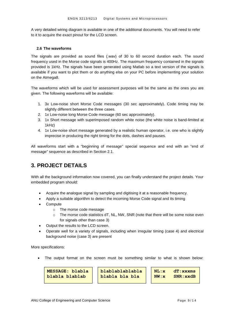
The output format on the screen must be something similar to what is shown below:
MESSAGE: blabla
blabla blablab
blablablablabla
blabla bla bla
NL:x dT:xxxms
NW:x SNR:xxdB
ENGN 3213/6213 D ig i t a l Sys tems and Mic roproces sors
ANU College of Engineering and Computer Science Page 1 0 / 1 4
The screen should advance (either on a scrolling basis or on a "new page" basis) as required
to show the full message.
The statistics about the message can be shown after reception of the message is completely
received, and shown on a rotating basis
The dT statistic will not matter for the signal with imprecise timing in case 4
4. RECOMMENDED WORKFLOW
The following is not a prescriptive set of instructions, but simply a list of suggested steps to find your
way through to the end of the project.
1. Make sure you know how to generate an output on your LCD screen. This will be helpful for
debugging as you can ask your program to show you the value of variables you may be
interested in. Also, it will be very hard for the examiners to mark your design if it has no
meaningful output.
2. You should then move on to making sure that your analogue-to-digital conversion and signal
recognition algorithms are working as intended.
3. The next issue to address is that of timing, which will be crucial to this application since you
will need to discriminate between dots and dashes, letters and words.
4. Then you will need to work out how to map the recorded data to a message and how to
compute the basic signal statistics
5. Finally you will put it all together and output your results to the LCD and test it in-lab.
5. DELIVERABLES AND ASSESSMENT
5.1 Assessment process
For this project students will work in groups of 2. I have recommended that you work with your lab
partner but this is not a strict requirement. The groups can be different from the groups you
participated in for assignment 1. The work will be assessed as group work, with the same mark
awarded to both members. Only in exceptional cases will individual marks be differentiated, for
example where one of the group members has not contributed to the project in a fair manner. Given
that there is no group presentation, the quality of team work will be tested through an honesty system
based on individual declarations (more on this later).
The assessment will be performed on two elements: the program code and a short accompanying
document. Master students also have an additional question for which they will be marked
individually.
The assessment of the work will be done by testing the code and using the report as support to
ensure that all design choices have been well thought out and justified. Testing will probably be
conducted sometime in June.
Your code
Your code should be well written and commented. When testing your system the code will be
compiled, so you should make sure that any references (multiple files, libraries, etc.) are all attached
and verified to work in a computer that is not your own.

ENGN 3213/6213 D ig i t a l Sys tems and Mic roproces sors
ANU College of Engineering and Computer Science Page 1 1 / 1 4
Short written report
A 3-4 page report should accompany your code and explain your approach. The purpose of this
document is to assist the markers in evaluating the quality of your work. Some examples of useful
content:
A summary of your algorithm(s) (text explanation and/or flow charts where informative)
How you configured particular ports to achieve a desired result
Motivation of design choices (e.g., variable types and/or sizes, functions, libraries, …)
Independent and/or innovative design choices made to address problems identified
during the design process
Mathematical calculations if relevant
Anything else you may deem useful…
Group work declaration
Regardless of the overall joint submission, every student will submit a one-page group work report.
This will be a form where you will describe your own contribution and your partner's. The content of
the form will not be disclosed to the other group member. The markers may compare the two and
where significant discrepancies are observed, a penalty may be imposed. Failure to submit this
component will result in a penalty of 10% on the overall mark.
5.2 Due dates
The project is due at the end of the day (11.55pm) on Tuesday 3rd of June. While this is done to
allow you as much time as possible to complete the task, the due date is in fact 2 days into the exam
preparation period. In order not to impact on your other subjects, it is strongly recommended that you
finish your work by Sunday 1st
of June. The deliverables should be prepared as a single compressed
file (e.g., ZIP) and submitted through Wattle.
Late submissions will be accepted until Friday 6th of June with a penalty of 10% per day. Similarly,
this will be the maximum allowable period for extensions (only for extenuating circumstances), the
main reason being that assignments should not disrupt your preparation time during examination
weeks. It cannot be stressed enough that you should try to finish your project ahead of time.
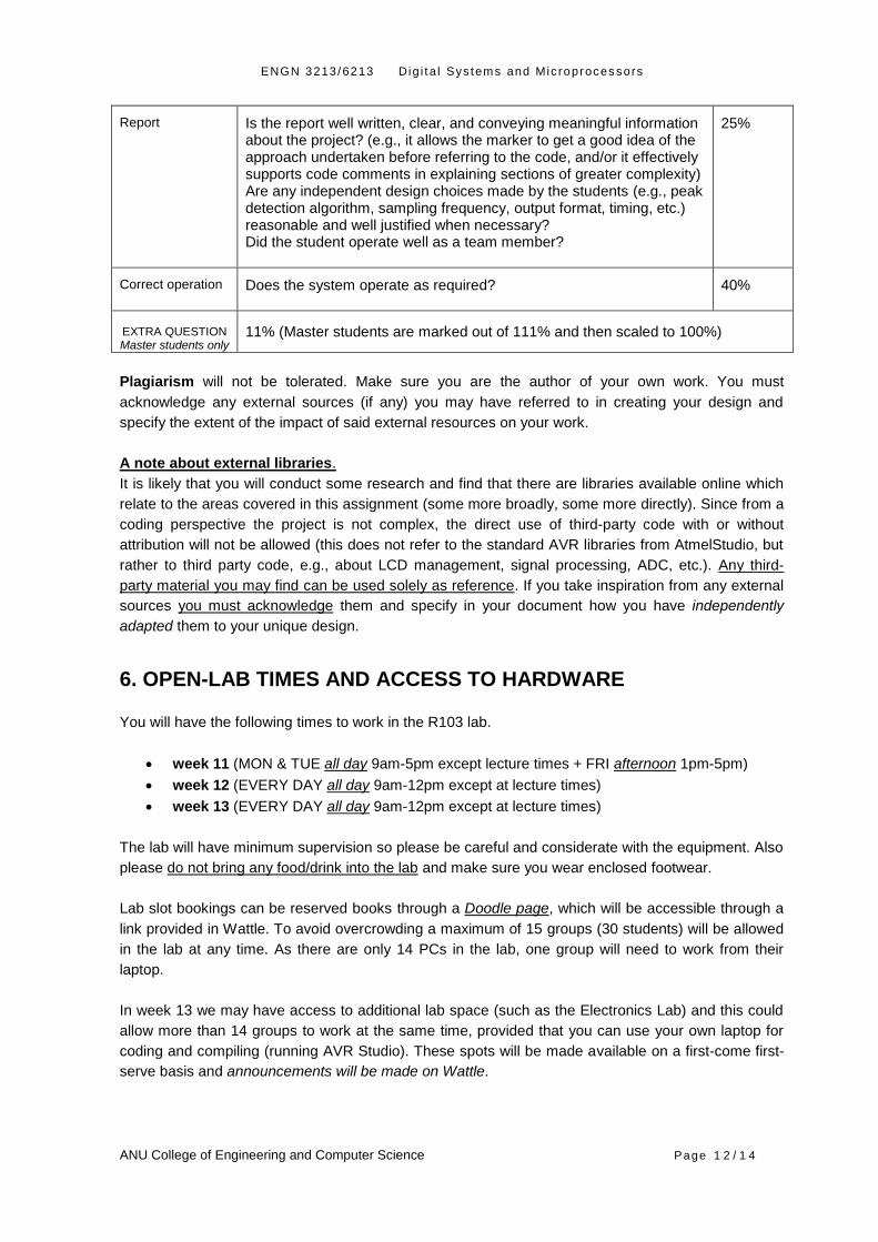
5.3 Marking Criteria
The project will be marked as follows. For each item, further description is provided.
ASSESSMENT CRITERION
DESCRIPTION WEIGHT
Clarity of programming code
Is the code well written, properly indented and commented, such that functions are clearly identifiable and understandable in their structure? Are meaningful names used for variables and functions? Where complex sections are encountered is there sufficient assistance to the reader?
15%
Quality of programming code
Is the design structured in a clear and logical manner? Are sections of code which carry out distinct operations clearly identified as functions? Have the students paid attention in creating code which operates efficiently? (avoiding redundant instructions, unnecessary function calls, inefficient memory usage, …) Does the program demonstrate competency in the use of AVR-specific coding options?
20%
ENGN 3213/6213 D ig i t a l Sys tems and Mic roproces sors
ANU College of Engineering and Computer Science Page 1 2 / 1 4
Report
Is the report well written, clear, and conveying meaningful information about the project? (e.g., it allows the marker to get a good idea of the approach undertaken before referring to the code, and/or it effectively supports code comments in explaining sections of greater complexity) Are any independent design choices made by the students (e.g., peak detection algorithm, sampling frequency, output format, timing, etc.) reasonable and well justified when necessary? Did the student operate well as a team member?
25%
Correct operation
Does the system operate as required?
40%
EXTRA QUESTION Master students only
11% (Master students are marked out of 111% and then scaled to 100%)
Plagiarism will not be tolerated. Make sure you are the author of your own work. You must
acknowledge any external sources (if any) you may have referred to in creating your design and
specify the extent of the impact of said external resources on your work.
A note about external libraries.
It is likely that you will conduct some research and find that there are libraries available online which
relate to the areas covered in this assignment (some more broadly, some more directly). Since from a
coding perspective the project is not complex, the direct use of third-party code with or without
attribution will not be allowed (this does not refer to the standard AVR libraries from AtmelStudio, but
rather to third party code, e.g., about LCD management, signal processing, ADC, etc.). Any third-
party material you may find can be used solely as reference. If you take inspiration from any external
sources you must acknowledge them and specify in your document how you have independently
adapted them to your unique design.
6. OPEN-LAB TIMES AND ACCESS TO HARDWARE
You will have the following times to work in the R103 lab.
week 11 (MON & TUE all day 9am-5pm except lecture times + FRI afternoon 1pm-5pm)
week 12 (EVERY DAY all day 9am-12pm except at lecture times)
week 13 (EVERY DAY all day 9am-12pm except at lecture times)
The lab will have minimum supervision so please be careful and considerate with the equipment. Also
please do not bring any food/drink into the lab and make sure you wear enclosed footwear.
Lab slot bookings can be reserved books through a Doodle page, which will be accessible through a
link provided in Wattle. To avoid overcrowding a maximum of 15 groups (30 students) will be allowed
in the lab at any time. As there are only 14 PCs in the lab, one group will need to work from their
laptop.
In week 13 we may have access to additional lab space (such as the Electronics Lab) and this could
allow more than 14 groups to work at the same time, provided that you can use your own laptop for
coding and compiling (running AVR Studio). These spots will be made available on a first-come first-
serve basis and announcements will be made on Wattle.
ENGN 3213/6213 D ig i t a l Sys tems and Mic roproces sors
ANU College of Engineering and Computer Science Page 1 3 / 1 4
Anyone who is unable to access to the equipment within these times due to legitimate and
exceptional circumstances should contact the lecturer so that suitable arrangements can be made.
DO NOT remove the hardware kits from the lab.
7. TIPS
Have you considered whether over subsequent tests the level you set your knobs to (on your
preamp/offset box) is going to affect the result of your system? If that is the case, your system may
risk malfunctioning on the day of the final test. On the day of the test the analogue wave will be
centred with the baseline (flat section with no signal) at 2.5V and the gain adjusted to use as much of
the voltage range as possible. We will not be changing those settings between waveforms.
You have two onboard LEDs: a red one and a green one. Their use is not required by the specs, but
you could use them for debugging purposes or as additional information for the user if you wish to do
so. There are also designated spots on the kit where you can connect an oscilloscope if you want to
observe fast debugging signals which cannot be interpreted effectively as a blinking LED. Be creative
and use these to your advantage!
If you plan on using your laptop, be advised that the quality of the waveform produced by the output
of your laptop sound card cannot be predicted. We have tested the R103 computers and found them
satisfactory but different soundcard hardware may yield different results, so if in doubt always check
with an oscilloscope what the input to the Atmega8 ADC actually is.
If you need information on operating the LCD display, I can recommend these two pages which
feature some code examples and walkthroughs (note that you will have to adapt it to your
circumstances as our wiring is different):
http://www.protostack.com/blog/2010/03/character-lcd-displays-part-1/
http://www.protostack.com/blog/2010/04/character-lcd-displays-part-2/
There are also these two introductory articles to LCDs which could be helpful:
http://www.wizard.org/auction_support/lcd1.pdf, http://www.wizard.org/auction_support/lcd2.pdf
If at any point you are struggling to code without the physical microprocessor, you can consider using
the AVR simulator tool. It comes as a standard in AtmelStudio and allows you to set breakpoints in
your code and check the values of the internal registers, I/O buses, etc, during the execution of your
program (a bit like what we did with MU0 in GTKwave, but a much more professional tool). A tutorial
video from Atmel can be found at http://www.youtube.com/watch?v=9QlDSNeuAdY
If computations of means and standard deviations on a "rolling" basis are a thing you wish to look at
in your design I can recommend this discussion as a starting point
http://johnthemathguy.blogspot.com.au/2012/08/deviant-ways-to-compute-deviation.html
This project is deliberately designed to be challenging. This is done in order to cater for all levels
of skill in our very varied student cohort. Rather than running out of time, if you lack confidence, you
could work on the simpler aspects of the system first (maybe focus on HR alone, or only on the
simpler waveforms) and tackle the more complex parts later, time permitting.

ENGN 3213/6213 D ig i t a l Sys tems and Mic roproces sors
ANU College of Engineering and Computer Science Page 1 4 / 1 4
8. ADDITIONAL QUESTION FOR MASTER STUDENTS ONLY
Imagine that this system were to be utilised in a long-term, battery-operated monitoring application where Morse Signals originating from a radio beacon are received for 1 minute once every hour for 24 hours a day for 2 weeks. The collected data is reviewed at the end of this period. Disregarding for a moment the issue of how the signal is received (this would involve some type of radio receiver equipment), in a short exposition (up to 500 words or thereabouts) discuss potential issues in terms of power consumption and reliable data storage and explain what changes (if any) you would make to your hardware set-up and/or code to address any critical aspects you may have identified. Your answer should explain how you would do things but you don’t have to provide new code or hardware schematics (unless they're essential to your explanation. Focus mainly on the concepts!).
Related Documents