Four Phase Switch-Mode Inverter Construction and Evaluation Master of Science Thesis KRISTOFFER BERNTSSON Department of Energy and Environment Division of Electric Power Engineering CHALMERS UNIVERSITY OF TECHNOLOGY Göteborg, Sweden, 2010

Welcome message from author
This document is posted to help you gain knowledge. Please leave a comment to let me know what you think about it! Share it to your friends and learn new things together.
Transcript

Four Phase Switch-Mode Inverter Construction and Evaluation Master of Science Thesis
KRISTOFFER BERNTSSON
Department of Energy and Environment
Division of Electric Power Engineering
CHALMERS UNIVERSITY OF TECHNOLOGY
Göteborg, Sweden, 2010

ii

i
Abstract
In this project a four phase switch-mode DC/AC inverter was designed, built and
evaluated. From Etteplantech and Chalmers University of Technology a common
need for a well behaving and versatile inverter in the medium power range was
found. The final product was targeted to be able to deliver up to 7 kW of power, with
an input DC voltage of 600 V.
The finished product managed to operate a 4 kW induction machine to its limits, with
a maximum tested switching frequency of 18 kHz. This must be seen as a success. A
larger strain on the inverter was not done due to lack of a larger machine, but
individually the 600 V supply voltage and the 10 A per phase output current was
tested successfully.
The resulting inverter is very versatile; with the right control system it’s capable of
operating any electrical machine. The input control logic can handle both 3.3 and 5 V
signals, while the input DC voltage can be in the 25 to 600 V range.
Basic simulations done during the project shows that an RC-snubber would be able
to lower the EMI by lowering the dv/dt during switching, while introducing extra
losses in the snubber circuit without lowering the losses in the IGBTs, only moving
them from turn-off to turn-on. In the finished hardware, the snubber circuit was
therefore only prepared for, not implemented.

ii

iii
Acknowledgements
I would like to thank Mikael Duvander at Etteplantech and Professor Torbjörn
Thiringer at the Department of Electrical Engineering for developing the idea for the
project and aiding in its completion.
Big thanks to Etteplantech for their support throughout the project, and especially to
Mikael Duvander, Leif Hidesjö and Sebastian Witkowski.
Also, I would like to thank the staff at the Department of Electrical Engineering for
their help, especially my tutor Oskar Josefsson.

iv

v
Contents
1 Introduction ................................................................................................. 1
1.1 Purpose .............................................................................................................. 1
1.2 Terminology and Definitions ............................................................................. 1
2 General three phase DC/AC inverter theory .............................................. 2
2.1 Schematics ......................................................................................................... 2
2.2 PWM .................................................................................................................. 2
2.3 Harmonics .......................................................................................................... 3
2.4 Electric machines and motor drive basics .......................................................... 3
2.5 Power transistors ................................................................................................ 3 2.5.1 Metal-Oxide-Semiconductor Field Effect Transistor (MOSFET) ................................ 3 2.5.2 Gate-Turn-Off Thyristors (GTO) .................................................................................. 4 2.5.3 Insulated Gate Bipolar Transistor (IGBT) .................................................................... 5
3 The hardware ............................................................................................... 7
3.1 Overview ............................................................................................................ 7
3.2 Requirement specification ................................................................................. 7 3.2.1 General .......................................................................................................................... 7 3.2.2 Product perspective ....................................................................................................... 7 3.2.3 Typical users ................................................................................................................. 7 3.2.4 Market requirements ..................................................................................................... 7 3.2.5 Functional requirements ............................................................................................... 8 3.2.6 Man-machine requirements .......................................................................................... 8 3.2.7 Interface requirements .................................................................................................. 8 3.2.8 Performance requirements ............................................................................................ 9 3.2.9 Rules and regulations .................................................................................................... 9 3.2.10 Component and material requirements ....................................................................... 9 3.2.11 Mechanical requirements .......................................................................................... 10 3.2.12 Cost requirements ..................................................................................................... 10 3.2.13 Size requirements ...................................................................................................... 10 3.2.14 Reliability requirements ............................................................................................ 10 3.2.15 Testability requirements ........................................................................................... 10 3.2.16 Environmental requirements ..................................................................................... 10 3.2.17 Availability requirements ......................................................................................... 10 3.2.18 Safety requirements .................................................................................................. 10 3.2.19 Production requirements ........................................................................................... 10 3.2.20 Start of operation requirements ................................................................................. 10 3.2.21 Maintenance requirements ........................................................................................ 11 3.2.22 Educational requirements ......................................................................................... 11 3.2.23 Equipment needed to use the product ....................................................................... 11
3.3 DC supply circuitry .......................................................................................... 11 3.3.1 Capacitor ..................................................................................................................... 11 3.3.2 Soft starter ................................................................................................................... 12 3.3.3 Protection .................................................................................................................... 13 3.3.4 Separate low voltage supply ....................................................................................... 13
3.4 Logic interface ................................................................................................. 14 3.4.1 Interface ...................................................................................................................... 14 3.4.2 Voltage level ............................................................................................................... 14 3.4.3 Ground plane .............................................................................................................. 14 3.4.4 Galvanic isolation ....................................................................................................... 14 3.4.5 Protection against simultaneous turn on of both high-side and low-side switch ........ 16
3.5 Power Transistor .............................................................................................. 17 3.5.1 MOSFET and IGBT comparison ................................................................................ 17 3.5.2 Requirements on the drive circuit ............................................................................... 19 3.5.3 Required cooling capability ........................................................................................ 20
3.6 Drive circuit ..................................................................................................... 20 3.6.1 Available options ........................................................................................................ 20 3.6.2 IC for each leg ............................................................................................................ 21

vi
3.6.3 High-side voltage supply options ................................................................................ 23
3.7 Snubber circuit ................................................................................................. 24 3.7.1 Snubber introduction................................................................................................... 24 3.7.2 RC snubber ................................................................................................................. 24
3.8 Measurement instruments ................................................................................ 25 3.8.1 Measurement topology ............................................................................................... 25 3.8.2 Input voltage measurement ......................................................................................... 25 3.8.3 Input current measurement ......................................................................................... 25 3.8.4 Phase leg current measurement ................................................................................... 25
3.9 Safety requirements ......................................................................................... 26 3.9.1 LVD ............................................................................................................................ 26 3.9.2 RoHS .......................................................................................................................... 26 3.9.3 Insulation standards .................................................................................................... 26
3.10 PCB .................................................................................................................. 26 3.10.1 Board requirements ................................................................................................... 26 3.10.2 Layout ....................................................................................................................... 27 3.10.3 Size ........................................................................................................................... 27 3.10.4 Layers ....................................................................................................................... 27 3.10.5 Connections .............................................................................................................. 27 3.10.6 Test points ................................................................................................................. 28 3.10.7 Minimizing leakage inductances ............................................................................... 28 3.10.8 Cooling solution ........................................................................................................ 28
3.11 Description of User Interface ........................................................................... 28
3.12 Assembly ......................................................................................................... 28
3.13 Test and Maintenance ...................................................................................... 28
4 Analysis ..................................................................................................... 29
4.1 Simulation environment ................................................................................... 29
4.2 Hardware verification environment ................................................................. 29
4.3 Verification Objects ......................................................................................... 29
4.4 Conclusion ....................................................................................................... 29
4.5 Test overview ................................................................................................... 29
4.6 Simulation test 1 .............................................................................................. 31 4.6.1 Test setup with one MOSFET and one ideal diode ..................................................... 31 4.6.2 Results ........................................................................................................................ 32
4.7 Simulation test 2 .............................................................................................. 34 4.7.1 Test setup with one IGBT and one ideal diode ........................................................... 34 4.7.2 Results ........................................................................................................................ 34
4.8 Simulation test 3 .............................................................................................. 36 4.8.1 Test setup with two MOSFETs ................................................................................... 36 4.8.2 Results ........................................................................................................................ 37 4.8.3 Modification by adding a SiC diode anti-parallel to the upper MOSFET .................. 39
4.9 Simulation test 4 .............................................................................................. 40 4.9.1 Test setup with two IGBTs ......................................................................................... 40 4.9.2 Results ........................................................................................................................ 41
4.10 Simulation test 5 .............................................................................................. 43 4.10.1 One legged converter with snubber circuit ............................................................... 43 4.10.2 Results ...................................................................................................................... 44
4.11 Initial hardware tests ........................................................................................ 47 4.11.1 Low voltage supply short circuit test ........................................................................ 47 4.11.2 Voltage measurement of low voltage circuit ............................................................ 47 4.11.3 Test of control signal optocouplers ........................................................................... 48 4.11.4 Relay test .................................................................................................................. 49 4.11.5 Short circuit test of DC supply circuit ...................................................................... 49 4.11.6 Calibration of voltage measurement circuit .............................................................. 49 4.11.7 Calibration of current measurement modules ........................................................... 50 4.11.8 Test of bootstrap capacitor ........................................................................................ 50

vii
4.12 Current test ....................................................................................................... 51
4.13 Running an induction machine ........................................................................ 52
4.14 Thermal analysis of the inverter ...................................................................... 52
4.15 Measuring the switch curves for the high side switch ..................................... 55
4.16 Wire bound EMI analysis ................................................................................ 57
4.17 Efficiency calculation ...................................................................................... 58
5 Conclusion ................................................................................................. 59
6 Future work ................................................................................................ 60
7 Sources ...................................................................................................... 61

viii

1
1 Introduction
1.1 Purpose
The aim of the project is to design, build and evaluate a four phase switch-mode
inverter in the medium power range, suitable as an electric motor drive. Behind the
development of the project is a desire from the two partners, Etteplantech and
Chalmers University of Technology, to have a well behaving and versatile inverter
that can be used as a basis for future developments in the electric machine drive.
The product is designed to convert power from a DC source in order to drive an
electric machine in a laboratory or test setup. As such it’s important for the product
to be easily connectable to different power supplies and machines. Moreover, it’s
desirable for the product to be easily accessible and that parts are replaceable or even
exchangeable.
The product is not a fully operational motor drive. It will not have a built in
controller of any kind, but shall easily be connected to a separate one, either a
microprocessor or a dSPACE system.
As a test platform it’s intended to be used by people with skills in electrical
engineering. Further it’s supposed to be an open test bed, without an enclosure.
1.2 Terminology and Definitions
PCB Printed Circuit board (no components)
PBA Printed Board Assembly (PCB with components)
TBD To Be Defined
TBP To Be Proposed
DC Direct Current
AC Alternating Current
PMSM Permanent Magnet Synchronous Machine
LVD Low Voltage Directive
MOSFET Metal-Oxide-Semiconductor Field Effect Transistor. The
MOSFET used in the tests is Infineon’s CoolMOS transistor
IPW90R120C3 (models and samples provided by Infineon)1.
CoolMOS A type of MOSFET developed to have a much lower Rds(on) than
comparable MOSFETs.
IGBT Insulated Gate Bipolar Transistor. The IGBT used in the
simulations is Infineon’s IKW15N120T2 with built in anti-parallel
diode (model and samples provided by Infineon)2.
Gate Driver IC used to provide the needed gate voltages and currents. The
driver used in the tests is International Rectifier’s Driver IC
IR2214SSPbF3.
SiC Schottky Diode
Silicon Carbide Schottky Diode. The model used in the
simulations is Infineon’s SDT12S604.
1 (Infineon Technologies AG, 2008)
2 (Infineon Technologies AG, 2008)
3 (International Rectifier, 2007)
4 (Infineon Technologies AG, 2008)

2
2 General three phase DC/AC inverter theory In this section the basic theory behind a general three phase inverter is covered. All
discrete parts in this theory section are assumed to be ideal.
2.1 Schematics
In Figure 2-1 an overview of the three-phase inverter is shown. Three legs, consisting
of two switches and two freewheeling diodes each, makes up for the main parts of
the inverter5. The upper transistor/diode pair is called the high side, and the lower the
low side.
+
Vdc
-
Figure 2-1 Basic schematics of a three phase inverter
When the high side switch is on, the output phase voltage equals the DC bus voltage,
while the output phase voltage is zero with respect to the negative DC bus voltage
when the low side switch is turned on. By switching the six switches in a controlled
manner, almost any voltage waveform can be achieved. The most common control
scheme when driving an electric machine is the pulse-width-modulated (PWM)
scheme, covered below.
2.2 PWM
The foundation of the PWM technique is the modulation of the pulse width,
accomplished with the help of a triangular wave. The triangular wave, which
frequency sets the switching frequency, fs, of the inverter, is compared with another
waveform, the control waveform. The control waveform modulates the duty-ratio of
one inverter leg and has the so-called fundamental frequency f1. The output from the
inverter is not perfectly comparable to the control waveform, since the output is
either the full DC voltage or zero voltage. The ratio between the switching frequency
and the fundamental frequency is called the frequency modulation ratio mf, and is
defined as
2-1
The amplitude modulation ratio ma is defined as
2-2
where is the control signal peak amplitude and is the triangular wave
peak amplitude, which is generally kept constant.
A good design consideration is to let mf be an integer with a multiple of 3. This will
eliminate the even harmonics as well as the most dominant harmonics in the line-to-
line voltage.
5 (Mohan, Undeland, & Robbins, 2003)

3
Normally ma is kept at less than or equal to 1, where the output voltage varies
linearly with the amplitude modulation ratio. The peak value of the output voltage in
one leg is then
2-3
With a sinusoidal output voltage, the line-to-line rms value of the output can be
written as
2-4
If the amplitude modulation ratio exceeds 1, the overmodulation region is entered,
where the amplitude of the output voltage no longer increase proportionally with ma,
causing greater difficulties to control the inverter. The maximum output voltage that
can be reached is
2-5
when the inverter enters the square-wave mode of operation at ma = 3.24, for a
sinusoidal vcontrol.
2.3 Harmonics
Due to the design of the inverter, where it outputs full voltage or zero voltage, the
output curve will have harmonics at multiples of mf, the higher the value, the higher
frequency of the harmonics. High frequency harmonics are more suppressed by an
inductive load, while low frequency harmonics will cause greater losses in an electric
machine. The important consideration that has to be made is the one between higher
losses in the inverter or higher losses in the machine.
2.4 Electric machines and motor drive basics
The PWM switched inverter described above provides the foundation to drive a wide
range of electric machines; induction machines, brushless DC-machines and
permanent magnet synchronous machines.
Different control techniques are needed for different types of motors, for example an
induction machine works best with a sinusoidal voltage and current curve, while a
BLDC-machine wants a square waved current, achieved by either a sine wave
voltage curve or a trapezoidal curve.
2.5 Power transistors
2.5.1 Metal-Oxide-Semiconductor Field Effect Transistor (MOSFET)
MOSFETs are popular because of their fast switching speeds in the range of a few
tens of nanoseconds to a few hundred nanoseconds depending on the device type.
Because of the fast switching speeds they can have low switching losses and
therefore higher switching frequencies can be used. For a PWM controlled motor
drive, a higher switching frequency is desired because of the harmonic components
in the output signal as discussed in Section 2.3 above. When you push the harmonics
to a higher frequency, they will be suppressed more by the motor that acts as an
inductive load. If a filter is to be implemented it can be made with smaller
component values since it’s easier to filter out higher frequency components.
4
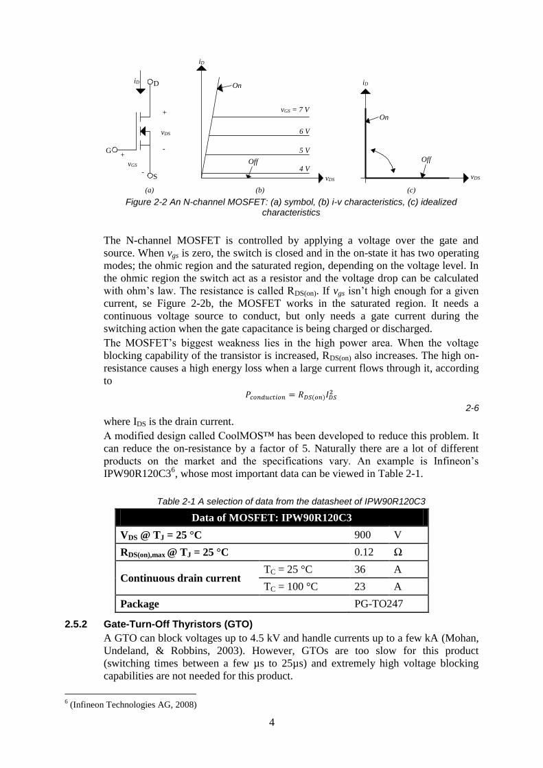
Figure 2-2 An N-channel MOSFET: (a) symbol, (b) i-v characteristics, (c) idealized
characteristics
The N-channel MOSFET is controlled by applying a voltage over the gate and
source. When vgs is zero, the switch is closed and in the on-state it has two operating
modes; the ohmic region and the saturated region, depending on the voltage level. In
the ohmic region the switch act as a resistor and the voltage drop can be calculated
with ohm’s law. The resistance is called RDS(on). If vgs isn’t high enough for a given
current, se Figure 2-2b, the MOSFET works in the saturated region. It needs a
continuous voltage source to conduct, but only needs a gate current during the
switching action when the gate capacitance is being charged or discharged.
The MOSFET’s biggest weakness lies in the high power area. When the voltage
blocking capability of the transistor is increased, RDS(on) also increases. The high on-
resistance causes a high energy loss when a large current flows through it, according
to
2-6
where IDS is the drain current.
A modified design called CoolMOS™ has been developed to reduce this problem. It
can reduce the on-resistance by a factor of 5. Naturally there are a lot of different
products on the market and the specifications vary. An example is Infineon’s
IPW90R120C36, whose most important data can be viewed in Table 2-1.
Table 2-1 A selection of data from the datasheet of IPW90R120C3
Data of MOSFET: IPW90R120C3
VDS @ TJ = 25 °C 900 V
RDS(on),max @ TJ = 25 °C 0.12 Ω
Continuous drain current TC = 25 °C 36 A
TC = 100 °C 23 A
Package PG-TO247
2.5.2 Gate-Turn-Off Thyristors (GTO)
A GTO can block voltages up to 4.5 kV and handle currents up to a few kA (Mohan,
Undeland, & Robbins, 2003). However, GTOs are too slow for this product
(switching times between a few µs to 25µs) and extremely high voltage blocking
capabilities are not needed for this product.
6 (Infineon Technologies AG, 2008)
D
G
S
vGS
vDS
+
-
+
-
iD
iD
vDS
On
Off
vGS = 7 V
6 V
5 V
4 V
On
Off
vDS
iD
(a) (b) (c)
5
2.5.3 Insulated Gate Bipolar Transistor (IGBT)
According to (Mohan, Undeland, & Robbins, 2003) the “IGBTs have some of the
advantages of the MOSFET, the BJT, and the GTO combined. Similar to the
MOSFET, the IGBT has a high impedance gate, which requires only a small amount
of energy to switch the device. Like the BJT, the IGBT has a small on-state voltage
even in devices with large blocking voltage ratings (for example, VON is 2-3 V in a
1000-V device). Similar to the GTO, IGBTs can be designed to block negative
voltages, as their idealized switch characteristics is shown in Fig. 2.12c (Note: the
figure is named Figure 2-4 in this document) indicate”.
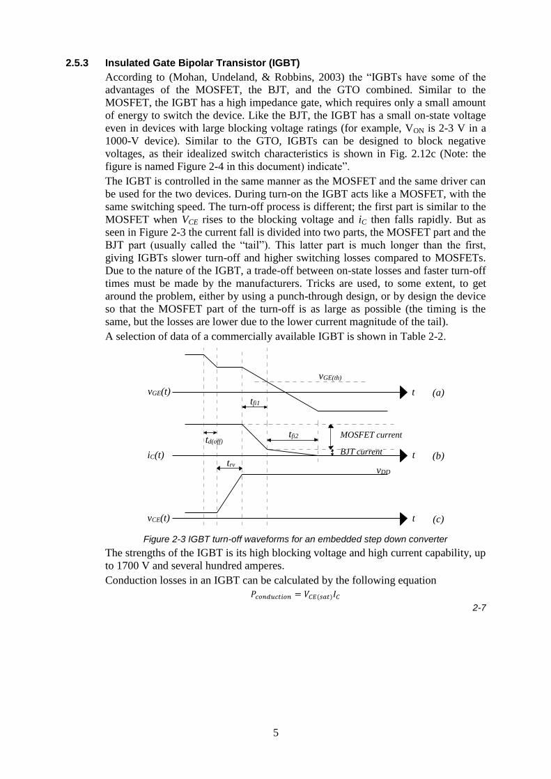
The IGBT is controlled in the same manner as the MOSFET and the same driver can
be used for the two devices. During turn-on the IGBT acts like a MOSFET, with the
same switching speed. The turn-off process is different; the first part is similar to the
MOSFET when VCE rises to the blocking voltage and iC then falls rapidly. But as
seen in Figure 2-3 the current fall is divided into two parts, the MOSFET part and the
BJT part (usually called the “tail”). This latter part is much longer than the first,
giving IGBTs slower turn-off and higher switching losses compared to MOSFETs.
Due to the nature of the IGBT, a trade-off between on-state losses and faster turn-off
times must be made by the manufacturers. Tricks are used, to some extent, to get
around the problem, either by using a punch-through design, or by design the device
so that the MOSFET part of the turn-off is as large as possible (the timing is the
same, but the losses are lower due to the lower current magnitude of the tail).
A selection of data of a commercially available IGBT is shown in Table 2-2.
Figure 2-3 IGBT turn-off waveforms for an embedded step down converter
The strengths of the IGBT is its high blocking voltage and high current capability, up
to 1700 V and several hundred amperes.
Conduction losses in an IGBT can be calculated by the following equation
2-7
t
t
t
vGE(t)
iC(t)
vCE(t)
vGE(th)
MOSFET current
BJT current
vDD
td(off)
trv
tfi1
tfi2
(a)
(b)
(c)

6
Figure 2-4 An IGBT: (a) symbol, (b) i-v characteristics, (c) idealized characteristics
Table 2-2 A selection of data from the datasheet of the IKW15N120T2
Data of IGBT: IKW15N120T2
VCE @ TJ = 25 °C 1200 V
VCE(sat) @ TJ = 25 °C 1.7 V
Continuous collector
current
TC = 25 °C 30 A
TC = 110 °C 15 A
Total switching energy @ TJ = 25 °C, IC = 15 A 2.05 mJ
Package PG-TO247-3
C
G
E
vGS
vDS
+
-
+
-
iC
(a)
G
C
E
vGSOn
Off
(c)(b)
vDS
iDiD
vDS
7
3 The hardware
3.1 Overview
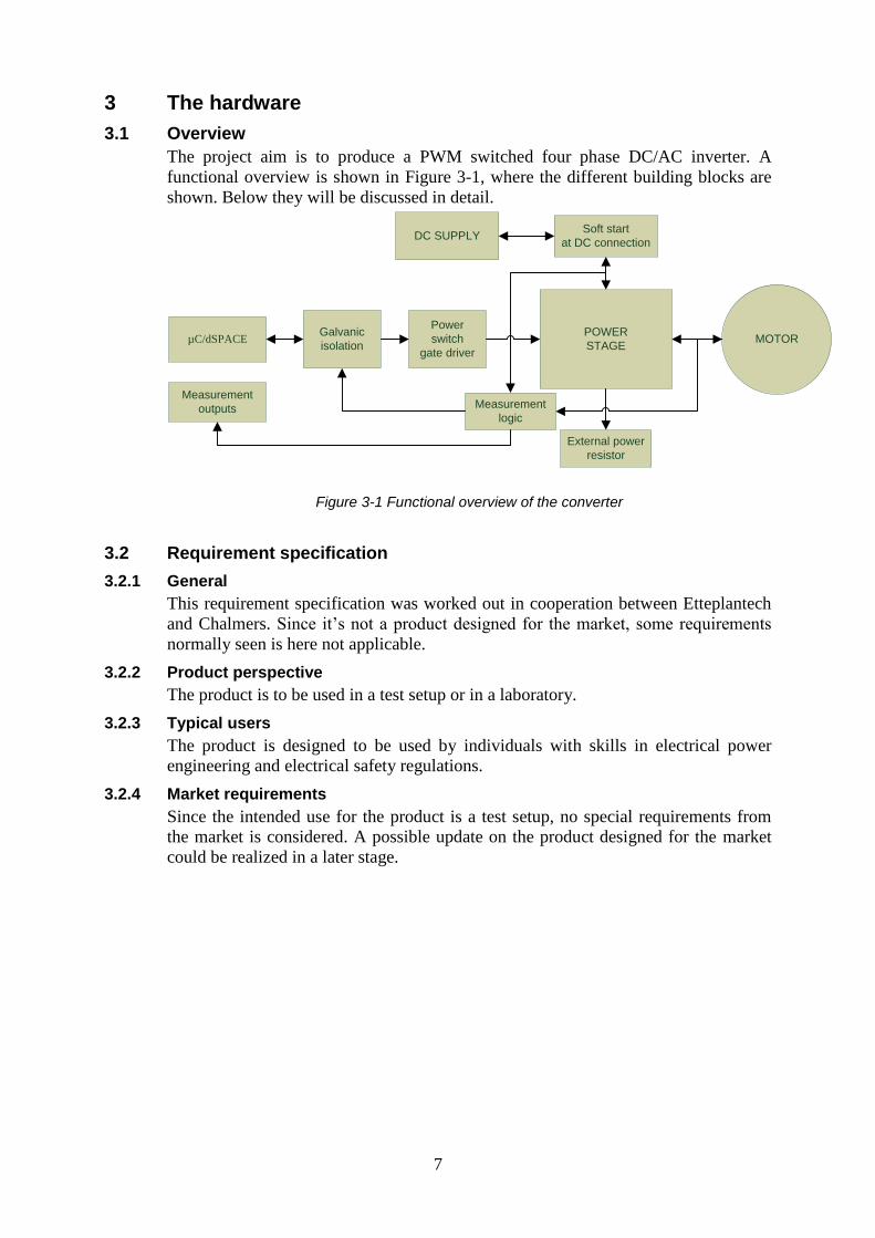
The project aim is to produce a PWM switched four phase DC/AC inverter. A
functional overview is shown in Figure 3-1, where the different building blocks are
shown. Below they will be discussed in detail.
µC/dSPACEGalvanic
isolation
Power
switch
gate driver
POWER
STAGEMOTOR
DC SUPPLYSoft start
at DC connection
Measurement
logic
External power
resistor
Measurement
outputs
Figure 3-1 Functional overview of the converter
3.2 Requirement specification
3.2.1 General
This requirement specification was worked out in cooperation between Etteplantech
and Chalmers. Since it’s not a product designed for the market, some requirements
normally seen is here not applicable.
3.2.2 Product perspective
The product is to be used in a test setup or in a laboratory.
3.2.3 Typical users
The product is designed to be used by individuals with skills in electrical power
engineering and electrical safety regulations.
3.2.4 Market requirements
Since the intended use for the product is a test setup, no special requirements from
the market is considered. A possible update on the product designed for the market
could be realized in a later stage.

8
DC
SOURCE
DC/AC
CONVERTER
ELECTRIC
MACHINE
CONTROL
LOGIC
MEASUREMENT
SIGNALS
Figure 3-2 Functional overview of the product
3.2.5 Functional requirements
Convert power from a DC source to an AC load
Drive a general balanced three phase load (for instance a PMSM)
Be able to brake a general balanced three phase machine
Ability to be controlled by either a microcontroller (e.g. Cortex M3) or a
dSPACE system
Be able to measure current in all phases
Be able to measure voltage on the supply side
Possibility to exchange the power electronic components through re-soldering
Provide 4 output phases
General connections to supply and load for easy connection to different
sources and machines, see Section 3.2.7 for specifications
Passively air cooled
Separated voltage level for logic signals, galvanicly isolated
Safety blanking times in hardware
Functional wish list
Be able to measure the temperature of the power electronic components
Automatic overvoltage protection
Possibility to remove the hardware blanking times
3.2.6 Man-machine requirements
The product is intended for a laboratory setup and hence only qualified users are
working with the product. Further it’s not intended for the market. Therefore the
requirements on “looks” are limited. Instead it’s important that components and
measurement points are easily accessible to the user.
3.2.7 Interface requirements
Galvanicly separated low voltage and high voltage side, with logic and power
circuitry respectively
Exchangeable power electronic components through re-soldering

9
Connections to a microprocessor or a dSPACE system. The two different
controllers should be switchable. The controller signals should work with
CMOS signals
The DC source should be connected through M6 screws
The load should be connected through M6 screws
Galvanic isolation between logic and drive and measurement circuits
Possibility to add capacitances parallel to power switches
Possibility to add an RC snubber over each power switch
Control logic and drive circuit power supply are separated from the main DC
supply
For connection to the dSPACE system:
17 BNC connections (5V logic)
3.2.8 Performance requirements
Handle input voltages between 0 and 600 VDC
Provide up to 10 Arms per phase of output current
Switching frequencies up to 20 kHz
Handle maximum currents of up to 15 A per phase
Target: 7 kW of output power (note that when driving an inductive electric
machine that draws a lot of reactive power, the output current to be about 25
% higher for the same active power)
Measure phase currents with an accuracy of 1 % and a bandwidth of 50 kHz
Measure input DC voltage with resistive voltage divider, using jumpers to
change divide ratio for different DC inputs. A linear optocoupler to transfer
the downscaled voltage to the low voltage side
Soft start at DC connection
Large input capacitance to hold a steady DC voltage. It should be able to
maintain the voltage level above 80% for 2 ms in the event of a loss of the
DC source
Powerful drive circuits to make fast switching possible
3.2.9 Rules and regulations
Wish list:
Comply with the LVD
Comply with the RoHS directive
ISO6469-3
3.2.10 Component and material requirements
The product must not include any of the banned substances in the RoHS
directive
The power transistors should be exchangeable, therefore a standard case style
such as TO220/247 should be used

10
3.2.11 Mechanical requirements
The PCB should be mounted on a stand or plate that serves as a foundation for the
product, so that it can be placed on different surfaces. The foundation should also
provide the BNC connectors for the dSPACE system to relieve the PCB for the
physical strain when connecting and disconnecting the cables. A further requirement
on the ground plate is that it should provide a layer of electrical isolation between the
PCB and the surface it’s placed on.
3.2.12 Cost requirements
The prototype nature of the product leads to a performance over cost thinking.
3.2.13 Size requirements
Because of the prototype stage of the product the size requirements are loose.
3.2.14 Reliability requirements
The product should be able to handle the testing and laboratory environment for
which it is intended.
3.2.15 Testability requirements
Measurement points should be available as pins on the board
3.2.16 Environmental requirements
3.2.16.1 Electrical environment
As good EMI performance as possible with a standard inverter design
3.2.16.2 Climate environment
The product should be able to work in the temperature range between 10 and
50 °C, in an environment where the air is standing still
3.2.17 Availability requirements
The prototype nature of the product limits the availability to a single unit.
3.2.18 Safety requirements
3.2.18.1 Safety standards
Comply with the LVD
Wish list:
Follow the highest insulation classification according to the ISO6469-3
standard (Class II: Double or reinforced insulation a.c.).
3.2.18.2 Safety devices
A light to signal that the device is on
Wish list:
Overvoltage protection. In the case that energy flows to the DC source and
that source doesn’t have the capability to absorb the energy, a device burning
the excess energy through a load resistor is to be implemented. The resistor
has to be supplied externally.
3.2.18.3 Marking
Marked with logo and warnings
3.2.19 Production requirements
Manual assembly required
3.2.20 Start of operation requirements
Soft start when connected to DC source

11
3.2.21 Maintenance requirements
The product is to be used in an open test bed; hence it shouldn’t be put under a lot of
physical stress. If the temperatures stay within the specified limits the only
maintenance required is to keep the components free from dust.
3.2.22 Educational requirements
Operating instructions should be, describing the functions, uses and
limitations of the product
3.2.23 Equipment needed to use the product
DC voltage supply, one for power plus one for the drive circuit (15 V)
Balanced one, two, three or four phase inductive or resistive load
Control logic (3.3 or 5 V)
3.3 DC supply circuitry
3.3.1 Capacitor
The input capacitor has the task of keeping the supply voltage stable to ease the
control of the power transistors. According to the requirement specification the input
capacitor should be able to hold the voltage above 80 % during 2 ms if the supply
voltage is lost. Considering the case with a motor load, the current is assumed to be
constant during the 2 ms. At a maximum load of 7 kW and 600 V input voltage, the
DC load current is 11.7 A. The total charge taken from the capacitor is then
3-1
The charge left in the capacitor after 2 ms should be 80 %, then the charge taken
from the capacitor is 20 %. The charge stored in the capacitor is
3-2
With V = 20 % of 600 V and Q = 23.4 mC, the capacitance equals 195 µF.
The worst case ripple current going through the capacitor is a square wave signal
with an amplitude of 10 A at a frequency equal to the switching frequency of the
system. The actual ripple current during normal operation of the converter (three
phase motor drive) will be less due to the nature of the three phase system where
always two legs are conducting in opposite direction and hence cancel each other out
seen from the supply.
To handle the voltage and ripple current requirement a bank of eight 100 µF, 400 V
capacitors were chosen, two in series and four legs in parallel. Each can handle ripple
current of 1.3 A at 10 kHz and 105 °C. The worst case 2.5 A per leg can be handled
by the capacitors at the much lower anticipated temperature of 25 °C. Also a shorter
life span is acceptable in this project.
To keep each capacitor within its voltage limits a voltage divider was implemented;
two 1 MΩ resistors in parallel with the capacitors, see Figure 3-3. To make sure that
the current is spread out evenly over the bank, the negative side is connected in one
point on the PCB.

12
Figure 3-3. DC supply capacitor bank setup.
The capacitor choice: 8 x 100 µF, 400 V, Panasonic EETED2G101BA
Voltage divider: 2 x 1 MΩ, from stock (SMD, 1206)
3.3.2 Soft starter
To prevent large surge currents when the DC source is connected to the large DC
side capacitor, a soft starter is implemented. The soft starter is shown in Figure 3-4.
When the supply is connected to the terminals, a resistor is connected in series with
the capacitor. A relay controlled by the control logic connects the capacitor directly
to the DC supply terminals when Vin has reached the voltage level of the DC source.
The soft starter resistor should be large enough to prevent current spikes and small
enough to charge the capacitor within a reasonable timeframe. The time constant of
the RC-circuit present when connecting the DC source is calculated by
3-3
A time constant of 1 second is suitable for this project. With a capacitor of
approximately 200 µF, a resistance of 5 kΩ is needed. The maximum current flowing
through the resistor is calculated as follows
3-4
and the maximum power dissipated in the resistor can be found as
3-5
These numbers are easily managed by a power resistor since the duration of the
power spike is less than a second (the time constant is 1 second).
Choice of relay: Panasonic ALE1PB12; 16 A, 12 V
Choice of soft starter resistor: 4.7 kΩ

13
RelayVsoft
Rsoft Vin
Cin
VDC
Figure 3-4 Schematics of the soft starter
3.3.3 Protection
To make sure that the capacitors in the circuit are discharged, a discharge resistor is
connected in parallel to the input capacitor. Since it’s always connected it will
always be conducting current, introducing a constant loss of power.
The discharge current is used to drive an indicator LED connected in series with the
resistor to alert the user that the system is energized. A LED with a forward voltage
of 1.9 V and an average current of 2 mA is used. With a maximum voltage of 600 V
the resistor should be 300 kΩ to limit the current to 2 mA. The time constant of the
resulting RC-circuit is 60 seconds, and the average power loss at 600 V is 1.2 W.
Since the product is to be able to work with a wide range of input voltages, a simple
setup with 4 series connected resistors were chosen, to safely scale down the voltage.
The four base levels are 600 V, 300 V, 100 V and 25 V. Around these levels the LED
will glow close to its optimum and the capacitors will discharge in a timely manner.
LED choice: Vishay TLLG5400; 5 mm, 2 mA
Discharge/LED resistor choice: 4 x 75 kΩ, 1 W; 2 x 75 kΩ, 1 W; 51 kΩ, 1 W; 12
kΩ, 1 W
3.3.4 Separate low voltage supply
Separate input connectors to supply the drive circuits are implemented. This solution
was made to facilitate a broad DC voltage working range. Since the product is to be
used in a test setup, a separate voltage source should be available. A voltage of
approximately 15 V is needed to drive the low voltage circuits.
To supply the drive circuit, an isolated DC/DC converter is used with an output of 15
V. This ensures that the low voltage supply isn’t stressed with a large voltage offset
with respect to ground. The low voltage supply is also connected directly to the
current measurement module whose output is relative to ground. A total of 67 mA
can be taken from the converter. Each gate driver can an estimated current of 3.6
mA, giving a total of 14.4 mA, see Section 3.6.2.3 below for details. This current can
easily be handled by the converter.
A second isolated DC/DC converter is used to provide +/- 5 V to the high voltage
side of the converter, driving five optocouplers and one OP-amp. A total of 100 mA
can be taken from each leg of the converter. The optocouplers take a total of 25 mA
and the OP-amp about 12 mA, 6 mA on each leg, maxing out at around 30 mA, well
within the converter’s limits.

14
To provide 5 V to the low voltage side of the optocouplers, a non-isolating voltage
regulator was chosen. The unit can deliver a maximum of 1 A, well above the needs
of the system.
Isolated DC/DC converter choice: Murata NMV1515, 15 V, 1 W, 1 kVDC
isolation; Murata NMA1505, +/- 5 V, 1 W, 1 kVDC isolation
Non-isolated voltage regulator choice: On Semiconductor MC7805CDTG, 5 V, 1
A
3.4 Logic interface
3.4.1 Interface
The interface should be able to handle two separate control systems, both a
microprocessor and a dSPACE system. They should not be connected
simultaneously.
The microprocessor PBA should be connected with a 25-pole D-SUB.
The dSPACE system will be connected through 17 BNC connectors, mounted on the
base plate for improved ruggedness. On the base plate wires connect the BNC
connectors with a 25 pole D-SUB connector that can be easily connected to the
Power PBA. The D-SUB can be seen in Figure 3-5 and the BNC panel in Figure 3-6,
while its connections can be viewed in Table 3-1.
By using the same connector for both control options it’s impossible to connect both
the microprocessor and the dSPACE system simultaneously.
Figure 3-5 The 25-pin D-SUB connector seen from above
Figure 3-6 The BNC panel
3.4.2 Voltage level
The logic signals to the drive circuits works at a voltage level of 3.3 or 5 V.
3.4.3 Ground plane
Two ground planes are implemented on the PCB, one for the high voltage side and
one for the low voltage side. The two has galvanic isolation between them; the
isolation is further presented in Section 3.4.4 below.
3.4.4 Galvanic isolation
To facilitate easy connections and protection to the control circuit, the control signals
are galvanicly isolated with optocouplers. This ensures that the control circuit and
drive circuit is electrically separated and can use separate ground planes and power
supply (the isolated power supplies are presented in section 3.3.4 above). To further
enhance the separation the PCB is divided into two areas, a high voltage side and a
low voltage side, creating two clearly defined zones.
1 13
14 25
1 9
10 17

15
Table 3-1 Connection scheme for the D-SUB and BNC connectors
25-pin D-SUB BNC panel
1 Relay 1 1H
2 Fault 2 2H
3 SD 3 3H
4 FLT_CLR 4 4H
5 4L 5 FLT_CLR
6 4H 6 Fault
7 3L 7 I1
8 3H 8 I3
9 I3 9 Vdc
10 2L 10 1L
11 2H 11 2L
12 1L 12 3L
13 1H 13 4L
14 GND 14 SD
15 GND 15 Relay
16 GND 16 I2
17 GND 17 I4
18 GND
19 GND
20 I4
21 GND
22 I2
23 I1
24 Vin
25 GND
Transmission of the logic signals over the barrier is made by optocouplers. The
chosen ones are called digital isolators and can work at frequencies up to 50 MHz
and can be driven directly from the microprocessor, since a very low current of only
10 µA is needed to change the state of the digital isolator. It’s also compatible with
both 3.3 V and 5 V systems. The optocoupler needs 5 V on both sides of the isolation
barrier in order to work and they typically consume 0.018 mA on the low voltage
side and 5 mA on the high voltage side. Each optocoupler can transmit two signals
and one unit is used for each gate driver, resulting in four units. A fifth unit, capable
of transmitting two signals in each direction, is used to send and receive fault signals
to the gate drive system. This unit needs 5 mA on both sides of the voltage barrier.
16
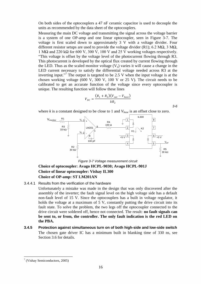
On both sides of the optocouplers a 47 nF ceramic capacitor is used to decouple the
units as recommended by the data sheet of the optocouplers.
Measuring the main DC voltage and transmitting the signal across the voltage barrier
is a system of one OP-amp and one linear optocoupler, seen in Figure 3-7. The
voltage is first scaled down to approximately 3 V with a voltage divider. Four
different resistor setups are used to provide the voltage divider (R1); 6.2 MΩ, 3 MΩ,
1 MΩ and 220 kΩ for 600 V, 300 V, 100 V and 25 V working voltages respectively.
“This voltage is offset by the voltage level of the photocurrent flowing through R3.
This photocurrent is developed by the optical flux created by current flowing through
the LED. Thus as the scaled monitor voltage (Va) varies it will cause a change in the
LED current necessary to satisfy the differential voltage needed across R3 at the
inverting input.”7 The output is targeted to be 2.5 V when the input voltage is at the
chosen working voltage (600 V, 300 V, 100 V or 25 V). The circuit needs to be
calibrated to get an accurate function of the voltage since every optocoupler is
unique. The resulting function will follow these lines
3-6
where k is a constant designed to be close to 1 and Vbase is an offset close to zero.
1
2
3
4 5
6
7
8
K1K2
IL300
+5 V+5 V
+
-
LM201
R4
100 Ω
R5
30 kΩ
R3
33 kΩ
R2
30 kΩ
R1Vmonitor Va
Vb
Vout
12
3
6
8
100 pF
Figure 3-7 Voltage measurement circuit
Choice of optocoupler: Avago HCPL-9030; Avago HCPL-901J
Choice of linear optocoupler: Vishay IL300
Choice of OP-amp: ST LM201AN
3.4.4.1 Results from the verification of the hardware
Unfortunately a mistake was made in the design that was only discovered after the
assembly of the inverter; the fault signal level on the high voltage side has a default
non-fault level of 15 V. Since the optocouplers has a built in voltage regulator, it
holds the voltage at a maximum of 5 V, constantly putting the drive circuit into its
fault state. To solve the problem, the two legs off the optocoupler connected to the
drive circuit were soldered off, hence not connected. The result: no fault signals can
be sent to, or from, the controller. The only fault indication is the red LED on
the PBA.
3.4.5 Protection against simultaneous turn on of both high-side and low-side switch
The chosen gate driver IC has a minimum built in blanking time of 330 ns, see
Section 3.6 for details.
7 (Vishay Semiconductors, 2005)
17
3.5 Power Transistor
3.5.1 MOSFET and IGBT comparison
Given the above discussion about the different transistor options, the choice stands
between the MOSFET and the IGBT. Both switches are controlled by the applied
gate voltage, and they can both manage the required switching frequencies for the
product at hand. The choice will therefore mainly come down to price and energy
losses produced in the device. There are two main components to consider when
calculating the power loss in the device; switching losses and conduction losses.
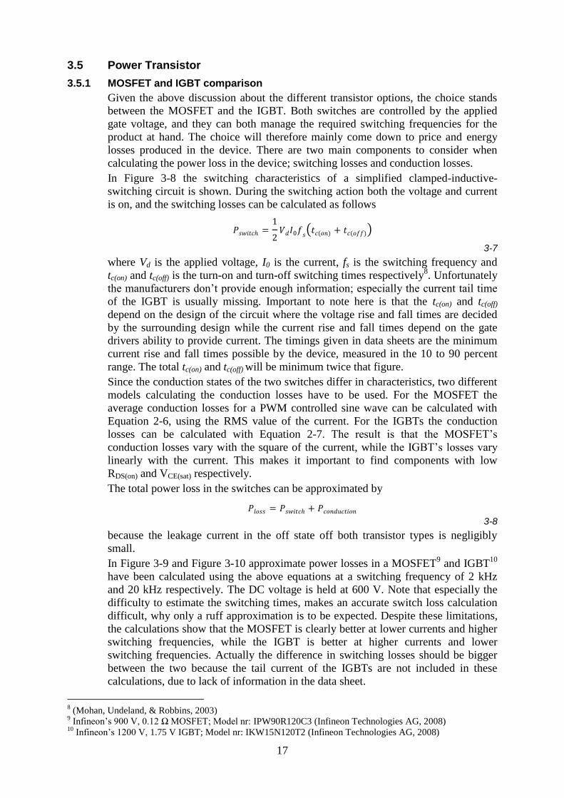
In Figure 3-8 the switching characteristics of a simplified clamped-inductive-
switching circuit is shown. During the switching action both the voltage and current
is on, and the switching losses can be calculated as follows
3-7
where Vd is the applied voltage, I0 is the current, fs is the switching frequency and
tc(on) and tc(off) is the turn-on and turn-off switching times respectively8. Unfortunately
the manufacturers don’t provide enough information; especially the current tail time
of the IGBT is usually missing. Important to note here is that the tc(on) and tc(off)
depend on the design of the circuit where the voltage rise and fall times are decided
by the surrounding design while the current rise and fall times depend on the gate
drivers ability to provide current. The timings given in data sheets are the minimum
current rise and fall times possible by the device, measured in the 10 to 90 percent
range. The total tc(on) and tc(off) will be minimum twice that figure.
Since the conduction states of the two switches differ in characteristics, two different
models calculating the conduction losses have to be used. For the MOSFET the
average conduction losses for a PWM controlled sine wave can be calculated with
Equation 2-6, using the RMS value of the current. For the IGBTs the conduction
losses can be calculated with Equation 2-7. The result is that the MOSFET’s
conduction losses vary with the square of the current, while the IGBT’s losses vary
linearly with the current. This makes it important to find components with low
RDS(on) and VCE(sat) respectively.
The total power loss in the switches can be approximated by
3-8
because the leakage current in the off state off both transistor types is negligibly
small.
In Figure 3-9 and Figure 3-10 approximate power losses in a MOSFET9 and IGBT
10
have been calculated using the above equations at a switching frequency of 2 kHz
and 20 kHz respectively. The DC voltage is held at 600 V. Note that especially the
difficulty to estimate the switching times, makes an accurate switch loss calculation
difficult, why only a ruff approximation is to be expected. Despite these limitations,
the calculations show that the MOSFET is clearly better at lower currents and higher
switching frequencies, while the IGBT is better at higher currents and lower
switching frequencies. Actually the difference in switching losses should be bigger
between the two because the tail current of the IGBTs are not included in these
calculations, due to lack of information in the data sheet.
8 (Mohan, Undeland, & Robbins, 2003)
9 Infineon’s 900 V, 0.12 Ω MOSFET; Model nr: IPW90R120C3 (Infineon Technologies AG, 2008)
10 Infineon’s 1200 V, 1.75 V IGBT; Model nr: IKW15N120T2 (Infineon Technologies AG, 2008)
18
During an AC motor drive operation the current flows through the diode
approximately half of the time (a very rough estimation), giving rise to lower
switching losses as the diode is already “turned on”. The extra switching losses
produced by the reverse-recovery current are not included in the calculation either,
why the losses should be higher. Since these two effects are not included in the
calculation, they can only be viewed as a general comparison.
Unfortunately the good performance of the CoolMOS MOSFETs cannot be utilized
in the chosen invert design because of the limitations of the built in body diode. The
body diode produces a very large reverse-recovery current. The large current gives
rise to huge switching losses, as discovered in the simulations results below. Because
the body diode starts to conduct at a low 0.7 V and because of the high voltage
requirements, no discrete diode with a low enough forward voltage can be found on
the market that could be used to bypass the problem.
Figure 3-8 Generic-switch switching device characteristics (linearized): (a) simplified clamped-inductive-switching circuit, (b) switch waveforms, (c) instantaneous switch power loss.
+-
Vd
I0
t
t
t
ton toff
Ts=1/fs
I0
Von
Vd
Switch control signal
tri tfvtd(on) td(off) trv tfi
Won
Wc(off)=0.5VdI0tc(off)Wc(on)=0.5VdI0tc(on)
VdId
(a)
(c)
(b)

19
Figure 3-9 Transistor losses at different current levels when switching at 2 kHz
Figure 3-10 Transistor losses at different current levels when switching at 20 kHz
Chosen power transistor: Infineon IKW15N120T2, 1200 V, 15 A @ 150 °C
3.5.2 Requirements on the drive circuit
To switch the transistor the gate voltage Vgs should be controlled between 0 and
approximately 15 V. A maximum voltage of ±20 V is tolerated by the IGBTs
(IKW15N120T2). To make sure they can output the required 10 A, a minimum
voltage of 10 V is needed on the gate. The drive circuit should be able to output 1 A
of gate current to provide fast switching.
The switching speed of the transistors depends on the gate resistors by controlling the
current flowing in and out of the gate during turn-on and turn-off. The drive circuit
covered in Section 3.6 below has three different gate resistors for each gate, a turn-
on, a turn-off and a soft shut down resistor.
0
10
20
30
40
50
60
70
80
0 5 10 15 20 25
Po
we
r lo
ss in
tra
nsi
sto
r (W
)
Current (A)
Losses at 2 kHz switch frequency
MOS…IGBT
0
10
20
30
40
50
60
70
80
90
0 5 10 15 20 25
Po
we
r lo
ss in
tra
nsi
sto
r (W
)
Current (A)
Losses at 20 kHz switch frequency
MOS…IGBT
20
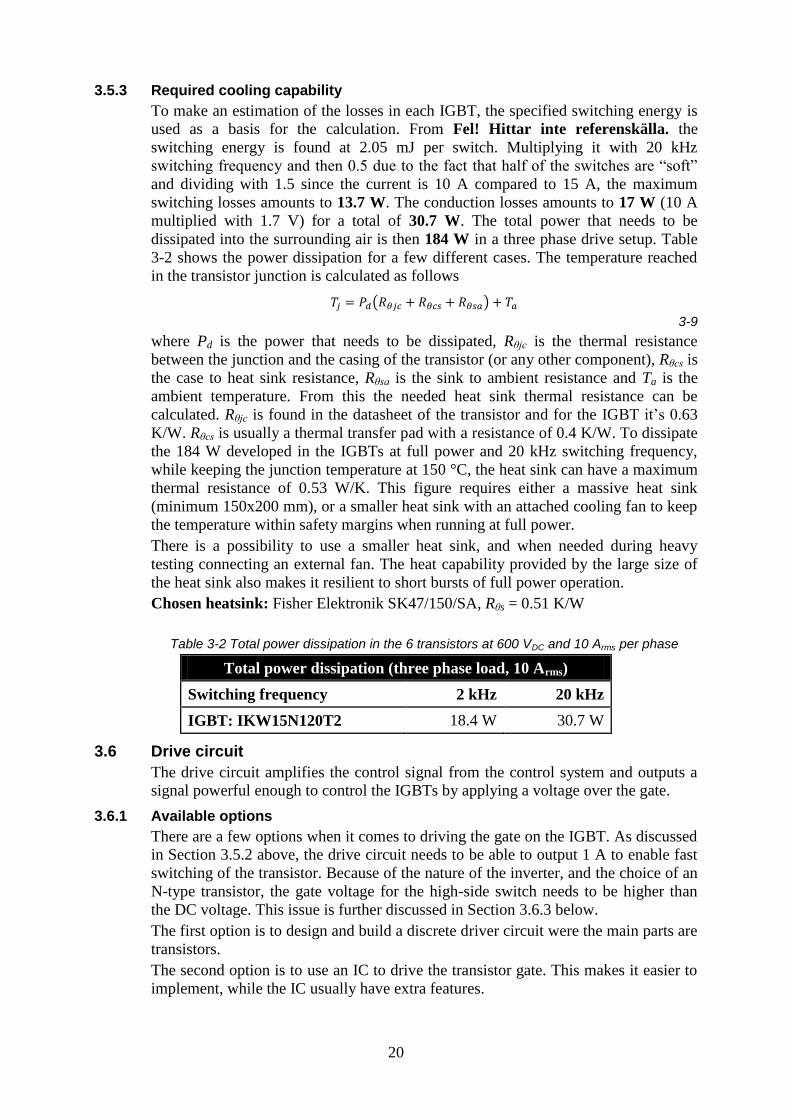
3.5.3 Required cooling capability
To make an estimation of the losses in each IGBT, the specified switching energy is
used as a basis for the calculation. From Fel! Hittar inte referenskälla. the
switching energy is found at 2.05 mJ per switch. Multiplying it with 20 kHz
switching frequency and then 0.5 due to the fact that half of the switches are “soft”
and dividing with 1.5 since the current is 10 A compared to 15 A, the maximum
switching losses amounts to 13.7 W. The conduction losses amounts to 17 W (10 A
multiplied with 1.7 V) for a total of 30.7 W. The total power that needs to be
dissipated into the surrounding air is then 184 W in a three phase drive setup. Table
3-2 shows the power dissipation for a few different cases. The temperature reached
in the transistor junction is calculated as follows
3-9
where Pd is the power that needs to be dissipated, Rθjc is the thermal resistance
between the junction and the casing of the transistor (or any other component), Rθcs is
the case to heat sink resistance, Rθsa is the sink to ambient resistance and Ta is the
ambient temperature. From this the needed heat sink thermal resistance can be
calculated. Rθjc is found in the datasheet of the transistor and for the IGBT it’s 0.63
K/W. Rθcs is usually a thermal transfer pad with a resistance of 0.4 K/W. To dissipate
the 184 W developed in the IGBTs at full power and 20 kHz switching frequency,
while keeping the junction temperature at 150 °C, the heat sink can have a maximum
thermal resistance of 0.53 W/K. This figure requires either a massive heat sink
(minimum 150x200 mm), or a smaller heat sink with an attached cooling fan to keep
the temperature within safety margins when running at full power.
There is a possibility to use a smaller heat sink, and when needed during heavy
testing connecting an external fan. The heat capability provided by the large size of
the heat sink also makes it resilient to short bursts of full power operation.
Chosen heatsink: Fisher Elektronik SK47/150/SA, Rθs = 0.51 K/W
Table 3-2 Total power dissipation in the 6 transistors at 600 VDC and 10 Arms per phase
Total power dissipation (three phase load, 10 Arms)
Switching frequency 2 kHz 20 kHz
IGBT: IKW15N120T2 18.4 W 30.7 W
3.6 Drive circuit
The drive circuit amplifies the control signal from the control system and outputs a
signal powerful enough to control the IGBTs by applying a voltage over the gate.
3.6.1 Available options
There are a few options when it comes to driving the gate on the IGBT. As discussed
in Section 3.5.2 above, the drive circuit needs to be able to output 1 A to enable fast
switching of the transistor. Because of the nature of the inverter, and the choice of an
N-type transistor, the gate voltage for the high-side switch needs to be higher than
the DC voltage. This issue is further discussed in Section 3.6.3 below.
The first option is to design and build a discrete driver circuit were the main parts are
transistors.
The second option is to use an IC to drive the transistor gate. This makes it easier to
implement, while the IC usually have extra features.
21
The third option is a drive IC for each leg of the inverter; one IC driving both the
high-side and the low-side switch. This has the added benefit of fewer components
and even more features, since the IC have control over the entire leg.
A forth option is a single drive IC for the entire inverter, driving six IGBTs. The
benefits with this approach is even less components and ease of implementation. The
drawbacks are less flexibility and difficulty to physically place all the IGBTs close to
the drive circuit. Also, no single drive circuit exists to drive all eight IGBTs
demanded by the requirement specification.
3.6.2 IC for each leg
With a single IC designed to drive two MOSFETs/IGBTs in a high-side/low-side
setup (one half bridge), less components is needed (in this case four drive ICs). Since
the high-side gate and source is floating up and down during the switching cycle, the
control signals needs to be level-shifted up and down with the source voltage. The
gate voltage must also be higher than the VDC supply to keep the transistor open, a
topic covered in Section 3.6.3 below.
The chosen driver IC is IR’s IR2214SSPbF. It’s capable of working with up to 1200
V and provide up to 2 A of turn-on current and 3 A of sinking current (during turn-
off). Another feature is the desaturation detection that measures the voltage over the
conducting transistor and compares it to a threshold voltage of 8 V (typical). If a
short circuit occurs, either phase to ground or phase to phase, the large current that
flows through the transistor will cause the voltage over it to increase and eventually
trigger the desaturation detector (after a built in blanking time of 3 µs), which then
initializes a soft shut down of the transistor and communicates the fault to the other
drive ICs through the SY_FLT pin. A soft shut down is made through the soft shut
down resistor instead of the regular turn-off resistor in order to limit the stresses on
the rest of the system (over-voltages due to large di/dt plus electromagnetic
emissions).
The drive IC is also equipped with three separate outputs for the gate signals to
facilitate three different gate resistors, for turn-on, turn-off and soft shut down
respectively. This makes it possible to more closely fine tune the switching
characteristics of the transistors in order to control speed, voltage spikes and EMC.
3.6.2.1 Gate resistors
The gate resistors control the switching speed by controlling the current in and out of
the gate. The resistor values were calculated from the recommendations in the drive
IC’s datasheet as follows. In the required data is shown, taken from the datasheets of
the drive IC and the IGBT.
Table 3-3 The required data for the calculation of the gate resistors
Collection of data for gate resistor calculation
Gate charge Qgate 93 nC
Drive IC output first stage IO1+ 2 A
Drive IC output second stage IO2+ 1 A
Drive IC output low IO- 3 A
Desired turn-on time tsw 200 ns
Drive IC supply voltage Vcc 15 V
Gate intermediate voltage Vge* 9 V
Gate-emitter threshold voltage VGE(th) 5.2 V

22
Turn-on resistor
3-10
3-11
3-12
3-13
Choice of turn-on resistor: 5.6 Ω, 0.25 W
Turn-off resistor
3-14
3-15
Choice of turn-off resistor: 12 Ω, 0.25 W
Soft shut-down resistor
The soft shut-down resistor should be much bigger than the other two, since it should
slowly shut down the IGBT in case of an extreme current flowing through it. No
calculation is made to support the decision, only a qualified guess.
Choice of soft shut-down resistor: 330 Ω, 0.25 W
3.6.2.2 Supporting components
Protecting the driver Vs-pin from under-voltage
A zener diode makes sure that the Vs-pin of the drive IC cannot go more than 10 V
below the Vss supply voltage. A diode connected in series protects the zener diode
when Vs is in its high state.
Protecting the driver from low side IGBT emitter under-voltage spikes
A capacitor between Vcc and COM together with a small resistor between the low
side IGBT emitter and COM protects the drive IC’s COM-pin from under-voltage
spikes.
Protecting the IGBTs against gate over-voltage
A 20 V zener diode between the gate and the emitter of each IGBT protects it from a
fatal over-voltage. A voltage spike on the gate can cause the IGBT to fail.
3.6.2.3 Power draw from Vcc
Required power from Vcc at 4 kHz: quiescent (max 2.5 mA), dynamic (11.2 mW,
0.75 mA), dynamic CMOS (1 mW, 0.07 mA), high voltage static losses (max 2.25
mW, 0.15 mA), HV switching losses (1.7 mW, 0.11 mA).
Total: 3.6 mA.

23
3.6.3 High-side voltage supply options
3.6.3.1 Bootstrap
The bootstrap option uses a capacitor connected between Vb and Vs as seen in Figure
3-11. This method is not optimal since it requires constant switching in order to keep
the capacitor charged, because when the upper transistor is conducting the capacitor
will discharge. When the lower transistor is conducting the capacitor will be charged
up to the drive supply voltage. The bootstrap setup is working satisfactory in the
range of tens of Hz to hundreds of kHz11
. If the converter is required to output DC
voltages, the bootstrap option will not work. The main advantages with choosing a
bootstrap setup is the ease of use and low cost, the capacitor will also easily follow
the voltage up and down through cycles without causing issues to other circuits.
The bootstrap capacitor is charged through a diode, since the high voltage at VS has
to be blocked from VCC, as seen in Figure 3-11. The diode should be able to block
the 1200 V used as a design norm in the switching circuit. It should also have a fast
recovery time to minimize the charge fed back from the bootstrap circuit to the VCC
capacitor.
IR2214SSPbF
VCC
VSS
VB
VS
+15V
Cboot
Figure 3-11 Schematics over the bootstrap circuit
The value of the bootstrap capacitor was calculated from the recommendations in the
drive IC datasheet as follows
3-16
where VF is the forward voltage of the diode, VGEmin is the minimum acceptable gate
voltage and VCEon,max is the maximum IGBT forward voltage drop.
3-17
where QG is the gate charge, QLS is the drive IC charge, ILK_GE is the gate leakage
current, IQBS is the drive IC quiescent current, ILK is the drive IC leakage current,
ILK_diode is the diode leakage current, ILK_cap is the capacitor leakage current, IDS- is the
desaturation diode bias current and THON is the desired maximum on time of the
high-side switch, here assumed to be 20 ms or a full 50 Hz wave.
11
(International Rectifier, 2007)

24
The final value of the bootstrap capacitor then needs to meet the following criteria
3-18
Choice of bootstrap capacitor: Sanyo 25TQC22M, 22 µF, 25 V, 90 mΩ ESR
3.6.3.2 Floating power supply
The power supply should supply the voltage needed by the drive on top of the phase
leg voltage Vs. Since Vs is constantly switching during normal operation between 0
and Vdc, the power supply must float up and down together with Vs. This puts a large
stress on the power supply, making it difficult to implement this solution.
3.6.3.3 Bootstrap with backup battery
A third, unexplored, solution is to use the bootstrap circuit for normal switching
operation and then use an external 15 V battery for the rare case DC output is
required. The battery should be connected in parallel with the bootstrap capacitor. A
great deal of care in the placement and connection of the battery has to take place
since it will float to high voltage levels, making sure the high voltage side and low
voltage side is still physically separated as much as possible. Every drive IC needs its
own battery, since they usually works at different switching patterns.
3.7 Snubber circuit
3.7.1 Snubber introduction
A snubber circuit’s purpose is to reduce switching stresses and EMI, by limiting
voltage and current peaks and dv/dt and di/dt. There are many different options
available, but the simplest one will be explored here; the RC snubber.
3.7.2 RC snubber
The RC snubber consists of a resistor and capacitor in series, connected in parallel to
each transistor, as seen in Figure 3-12. The capacitor will be charged by the current
running through the transistor at turn-off, thus lowering the losses in the transistor
while limiting the turn-off voltage spike. The downside is that the capacitor will
discharge at transistor turn-on, pushing an extra current through the transistor that
will increase the turn-on losses. The use of a resistor will cause a loss in the snubber
circuit at each switching instance.
Rs
Cs
Figure 3-12 Schematics over the RC snubber
The capacitor was chosen by setting the energy lost during turn-off equal to the
energy stored in the snubber capacitor according to
3-19
where tfi is the current fall time of the transistor, Vd the DC voltage and I0 is the
average current.
25
The snubber resistance was calculated with the following equation
3-20
where Irr is the reverse-recovery current of the freewheeling diode.
For the simulations a 2 nF snubber capacitor were chosen, in series with a snubber
resistor of 100 Ω or 500 Ω, testing two different values.
According to the simulations made, the snubber circuit is not helpful in the current
implementation. It’s important to note that the real world implementation will have
more parasitic elements that are very difficult to estimate which will influence the
currents and voltages in the circuit. For this reason a test area for a possible snubber
installation is a positive thing, in the unlikely case any component will run outside of
its specifications.
A negative consequence of the RC-snubber is the increase in total losses. The results
show that the losses in the power transistors are about the same while extra losses in
the snubber resistor are introduced. The energy stored in the capacitor is dissipated
through the resistor each time it’s charged or discharged. At a switching frequency of
2 kHz and with a 2 nF capacitor, a total power loss of 1.5 W is dissipated in the
snubber resistor, approximately 50 % of the switching losses of the IGBT at a 10 A
load. The switching losses are therefore increased by 50 % by adding the proposed
RC-snubber. A much more elaborate snubber is needed to avoid these issues.
3.8 Measurement instruments
3.8.1 Measurement topology
Since the product will be used in a laboratory environment, the testability of it is
important. Test pins for easy connectivity of probes and such are described in
Section 3.10.6. Furthermore, the input voltage and each output phase current is
measured on board, producing analog outputs.
3.8.2 Input voltage measurement
The input voltage is measured by a voltage divider connected to an analog
optocoupler to bridge the galvanic barrier. The setup is described in detail in Section
3.4.4.
3.8.3 Input current measurement
An input current measurement circuit was not implemented in the design due to
space and usability considerations. To know the input current is simply not important
to control an electric machine.
3.8.4 Phase leg current measurement
To efficiently control an electric machine it’s crucial to know the current through it,
therefore a current measurement module has been place on every output phase. The
modules lets the current go through them and the current is then measured by the use
of the hall effect, which makes for an accurate and most importantly galvanicly
isolated measurement. The chosen device needs 15 V to function and then outputs a
voltage signal centered around 2.5 V. A linear relationship between the input current
and the output voltage makes for a simple implementation, the following equation
describes the relationship
Choice of current transducer: LEM HX 10-P/SP2, ± 30 A, +15 V supply, 1 %
accuracy, 3 µs response time, 50 kHz bandwidth

26
3.9 Safety requirements
3.9.1 LVD
Due to the prototype nature of the equipment, it might not be fully compliant with
the LVD directive. To make it fully compliant, some form of enclosure of the unit is
needed, since the PBA itself is compliant, as well as the documentation.
3.9.2 RoHS
All components on the PBA are RoHS compliant, but the parts were soldered to the
PCB with non-RoHS soldering paste.
3.9.3 Insulation standards
During the layout design, the IPC-2221 standard was followed to make sure no
creepage currents or flashovers could occur on the PBA.
For the internal layers, the minimum distance between all high voltage conductors
was 2 mm at 1200 V.
For the external layers, the components and the component’s pads were kept at a
minimum distance from each other of 3.635 mm at 1200 V.
3.10 PCB
3.10.1 Board requirements
A large freedom in size and shape of the product is given by the Requirement
specification. Other considerations constrict the layout and look more.
1. The board should if possible have a physically separated high voltage and
low voltage side.
2. The components around the drive IC should be located as physically close as
possible, with special attention on the bootstrap capacitor and the distance to
the power transistors.
3. The path running from the drive IC to the gate and back through the emitter
leg into the IC creates a loop, which covered area must be kept as small as
possible to push the generated inductive circuit to a minimum. Rapid changes
in current will induce voltages in this loop that is not wanted, since they can
slow the switching speed down and introduce other problems.
4. The connection between the emitter of the high side switch and the collector
of the low side switch must be kept as short as possible in order to minimize
induced voltages. The very rapid changes in current through this connection
will give rise to induced voltages that can cause problems; the output voltage
will spike at high side turn-on and drop below negative DC voltage at low
side turn-on.
5. If possible, the DC supply lines to the transistors should be made up of
copper planes physically located on top of each other to create a capacitor
that can counteract the leakage inductances in the circuit and keep the voltage
as stable as possible.
6. A large cooler is needed to dissipate the energy lost in the transistors,
placement and fixation of the heat sink is important for the structure and
usability of the converter.
7. Enough copper in the traces leading the power to and from the converter
stages to ensure safe operation within thermal limits.
8. Input and output connectors suitable for lab environment and capable of
transmitting the maximum current of the converter (10 A).

27
3.10.2 Layout
The finished layout is shown in a picture of the PBA in Figure 3-13. The first bullet
is address by placing all the low voltage part on the lower half of the card and all the
high voltage parts on the upper half of the card. A separation of XX mm is
maintained throughout the card. Bridging the gap is optocouplers for control signals
to and from the drive ICs and from the voltage measurement circuit. Isolated DC/DC
converters are used to transfer energy over the barrier and current transducers
measures the output currents with galvanic isolation from the output.
Four identical blocks where built up on the board, facilitating the four channels of the
converter. Care was made to place all the components in each block as tight as
possible to minimize leakage inductances and provide stable supply voltages. The
package with drive IC, support components and high and low side switches, fits
within 45 x 40 mm.
3.10.3 Size
The PBA has a size of 300 x 150 mm and a vertical height of 180 mm with the heat
sink mounted vertically and the current transducers on the back of the card.
3.10.4 Layers
A four-layer card was chosen to accommodate all the needed wiring, with the middle
two layers made with 105 m thick copper and the outer layers from 35 m copper.
The thick copper in the middle layers are used to rout the power and ground layers,
while the thinner copper on the outer layers is used for low voltage power and small
signals.
Figure 3-13 Picture of the inverter seen from above
3.10.5 Connections
The PBA has four main connections; two banana contacts for the low voltage input
to supply the low voltage circuits (15 V), one 25-pin DSUB connector for all the
signals to and from the card, two 6 mm holes for the positive and negative DC power
supply and four 6 mm holes for the output.

28
3.10.6 Test points
To facilitate easy testing, test pins were placed around the board, connected to the
following points:
VB, VS, DesatH, DsatL, VCC and VSS for each IGBT-pair
Fault/SD, SY_FLT
Control signals to each IGBT
3.10.7 Minimizing leakage inductances
Due to the rapid change in voltages and currents, it’s very important to keep leakage
inductances to a minimum. By following the recommendations in the data sheet of
the drive IC and the points 2-5 in Section 3.10.1 above, the loops and high current
paths were minimized.
3.10.8 Cooling solution
Cooling of the IGBTs is covered in Section 3.5.3 above. The other components need
no extra cooling. The unit should be able to output 10 Arms without any additional
external equipment (i.e. fan) at normal room temperature.
3.11 Description of User Interface
The user interface consists of the various connectors covered in Section 3.4.1, while
further description of the measurement circuits is found in Section 3.8. A brief
operation instruction follows:
1. Connect all necessary cables (+15 V, DC supply, control system and the
load) while keeping the voltage sources turned off
2. Turn on the control system
3. Turn on the low voltage supply
4. Turn on the high voltage supply
5. Start the control system, following these basic steps
a. When the voltage across the DC bus has reached the desired level
(takes approximately 1 s), turn on the relay
b. Set FLT_CLR high
c. Start switching (preferably the low side switch first to charge the
bootstrap capacitor)
d. Set FLT_CLR low
e. The inverter is now ready for operation
3.12 Assembly
The design of the product was chosen to facilitate an open and accessible solution
that makes the product easy to move, modify and measure on. Everything on the
product is replaceable and customizable by skilled engineers.
The final assembly of the PBA was done by Etteplantech.
3.13 Test and Maintenance
Since the product is a prototype intended for testing purposes, thorough testing is to
be done, but maintenance will not be needed, as it will only be used in lab
environment and it’s highly likely that it will be subject to experiments with different
components and therefore maintained.

29
4 Analysis
4.1 Simulation environment
OrCAD 16.2
Simulation models by Infineon
4.2 Hardware verification environment
The hardware verification was done in a laboratory at Chalmers, where DC sources
and different loads were readily available.
4.3 Verification Objects
The verified object covered in this report is the printed board assembly, MK1523.
During simulation, two different transistor models were used; a MOSFET model
who’s most important data is displayed in Fel! Hittar inte referenskälla., and an
IGBT with its data displayed in Table 2-2.
4.4 Conclusion
The inverter managed to push a 4 kW induction machine to its limits, both at 4.5 kHz
and 18 kHz switching frequency, without any additional cooling. Due to the
inductive nature of the machine, the total output energy was 4.9 kVA during testing.
Each phase of the inverter were tested at a continuous output current of 10 A.
Although the voltage was only 25 V, it’s the current that stresses the IGBTs the most.
The goal of 7 kW of output power was not tested, due to lack of a suitable load.
Only one problem occurred during the hardware testing; the fault sensing signal
could not be transmitted to the control system.
4.5 Test overview
The verification starts with the results from computer simulations that were done in
order to get a basic understanding of the main components and their operating
conditions.
The second phase of the verification was done on the finished hardware, where initial
tests to check for errors were done first, followed by calibration of measurement
units and finally testing the functionality of the inverter. A summary of the tests and
results is shown in Table 4-1.
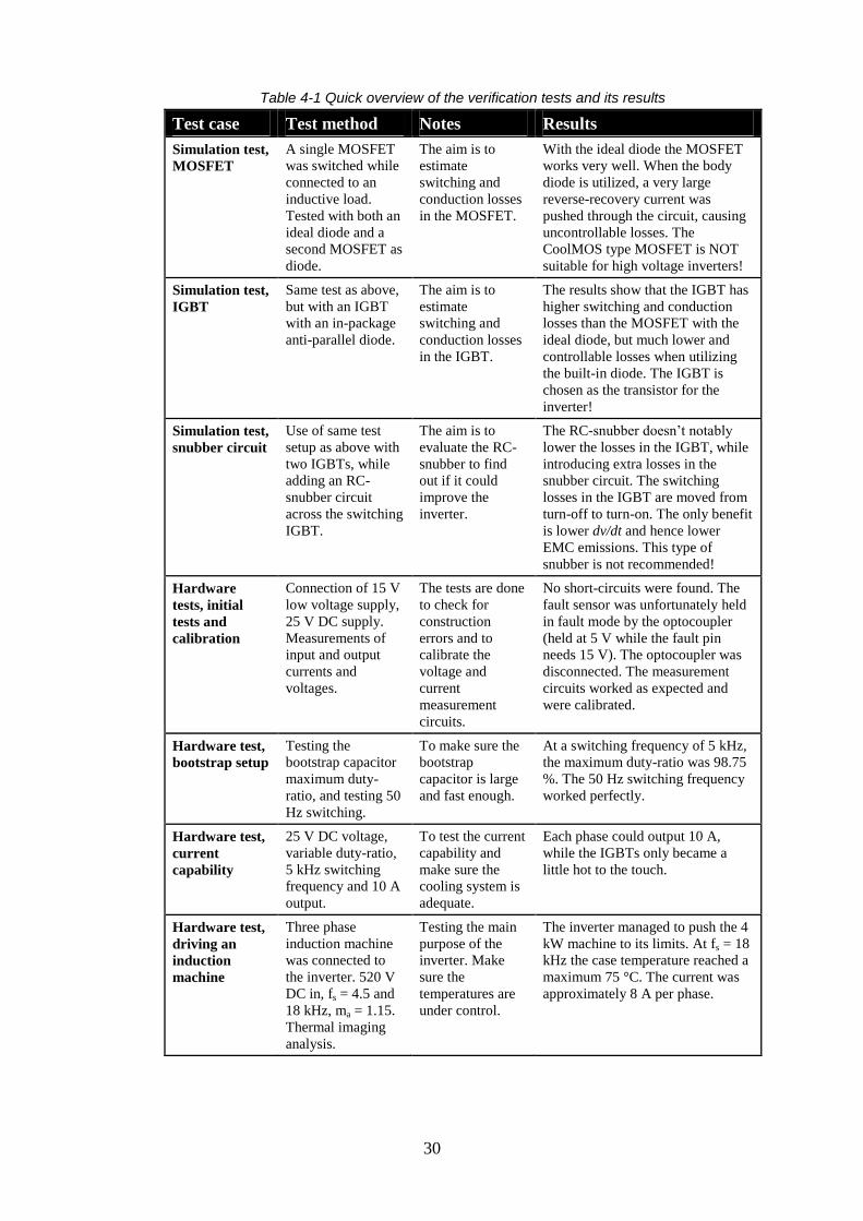
30
Table 4-1 Quick overview of the verification tests and its results
Test case Test method Notes Results
Simulation test,
MOSFET
A single MOSFET
was switched while
connected to an
inductive load.
Tested with both an
ideal diode and a
second MOSFET as
diode.
The aim is to
estimate
switching and
conduction losses
in the MOSFET.
With the ideal diode the MOSFET
works very well. When the body
diode is utilized, a very large
reverse-recovery current was
pushed through the circuit, causing
uncontrollable losses. The
CoolMOS type MOSFET is NOT
suitable for high voltage inverters!
Simulation test,
IGBT
Same test as above,
but with an IGBT
with an in-package
anti-parallel diode.
The aim is to
estimate
switching and
conduction losses
in the IGBT.
The results show that the IGBT has
higher switching and conduction
losses than the MOSFET with the
ideal diode, but much lower and
controllable losses when utilizing
the built-in diode. The IGBT is
chosen as the transistor for the
inverter!
Simulation test,
snubber circuit
Use of same test
setup as above with
two IGBTs, while
adding an RC-
snubber circuit
across the switching
IGBT.
The aim is to
evaluate the RC-
snubber to find
out if it could
improve the
inverter.
The RC-snubber doesn’t notably
lower the losses in the IGBT, while
introducing extra losses in the
snubber circuit. The switching
losses in the IGBT are moved from
turn-off to turn-on. The only benefit
is lower dv/dt and hence lower
EMC emissions. This type of
snubber is not recommended!
Hardware
tests, initial
tests and
calibration
Connection of 15 V
low voltage supply,
25 V DC supply.
Measurements of
input and output
currents and
voltages.
The tests are done
to check for
construction
errors and to
calibrate the
voltage and
current
measurement
circuits.
No short-circuits were found. The
fault sensor was unfortunately held
in fault mode by the optocoupler
(held at 5 V while the fault pin
needs 15 V). The optocoupler was
disconnected. The measurement
circuits worked as expected and
were calibrated.
Hardware test,
bootstrap setup
Testing the
bootstrap capacitor
maximum duty-
ratio, and testing 50
Hz switching.
To make sure the
bootstrap
capacitor is large
and fast enough.
At a switching frequency of 5 kHz,
the maximum duty-ratio was 98.75
%. The 50 Hz switching frequency
worked perfectly.
Hardware test,
current
capability
25 V DC voltage,
variable duty-ratio,
5 kHz switching
frequency and 10 A
output.
To test the current
capability and
make sure the
cooling system is
adequate.
Each phase could output 10 A,
while the IGBTs only became a
little hot to the touch.
Hardware test,
driving an
induction
machine
Three phase
induction machine
was connected to
the inverter. 520 V
DC in, fs = 4.5 and
18 kHz, ma = 1.15.
Thermal imaging
analysis.
Testing the main
purpose of the
inverter. Make
sure the
temperatures are
under control.
The inverter managed to push the 4
kW machine to its limits. At fs = 18
kHz the case temperature reached a
maximum 75 °C. The current was
approximately 8 A per phase.
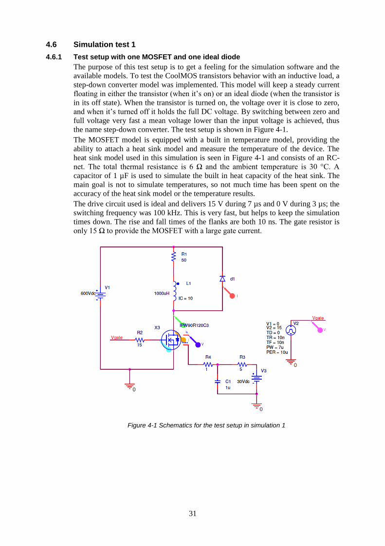
31
4.6 Simulation test 1
4.6.1 Test setup with one MOSFET and one ideal diode
The purpose of this test setup is to get a feeling for the simulation software and the
available models. To test the CoolMOS transistors behavior with an inductive load, a
step-down converter model was implemented. This model will keep a steady current
floating in either the transistor (when it’s on) or an ideal diode (when the transistor is
in its off state). When the transistor is turned on, the voltage over it is close to zero,
and when it’s turned off it holds the full DC voltage. By switching between zero and
full voltage very fast a mean voltage lower than the input voltage is achieved, thus
the name step-down converter. The test setup is shown in Figure 4-1.
The MOSFET model is equipped with a built in temperature model, providing the
ability to attach a heat sink model and measure the temperature of the device. The
heat sink model used in this simulation is seen in Figure 4-1 and consists of an RC-
net. The total thermal resistance is 6 Ω and the ambient temperature is 30 °C. A
capacitor of 1 µF is used to simulate the built in heat capacity of the heat sink. The
main goal is not to simulate temperatures, so not much time has been spent on the
accuracy of the heat sink model or the temperature results.
The drive circuit used is ideal and delivers 15 V during 7 µs and 0 V during 3 µs; the
switching frequency was 100 kHz. This is very fast, but helps to keep the simulation
times down. The rise and fall times of the flanks are both 10 ns. The gate resistor is
only 15 Ω to provide the MOSFET with a large gate current.
Figure 4-1 Schematics for the test setup in simulation 1
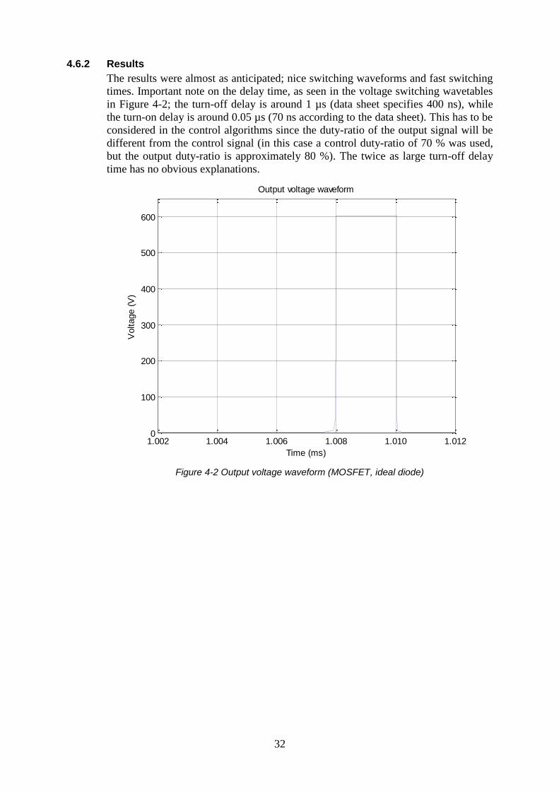
32
4.6.2 Results
The results were almost as anticipated; nice switching waveforms and fast switching
times. Important note on the delay time, as seen in the voltage switching wavetables
in Figure 4-2; the turn-off delay is around 1 µs (data sheet specifies 400 ns), while
the turn-on delay is around 0.05 µs (70 ns according to the data sheet). This has to be
considered in the control algorithms since the duty-ratio of the output signal will be
different from the control signal (in this case a control duty-ratio of 70 % was used,
but the output duty-ratio is approximately 80 %). The twice as large turn-off delay
time has no obvious explanations.
Figure 4-2 Output voltage waveform (MOSFET, ideal diode)
1.002 1.004 1.006 1.008 1.010 1.0120
100
200
300
400
500
600
Output voltage waveform
Voltage (
V)
Time (ms)
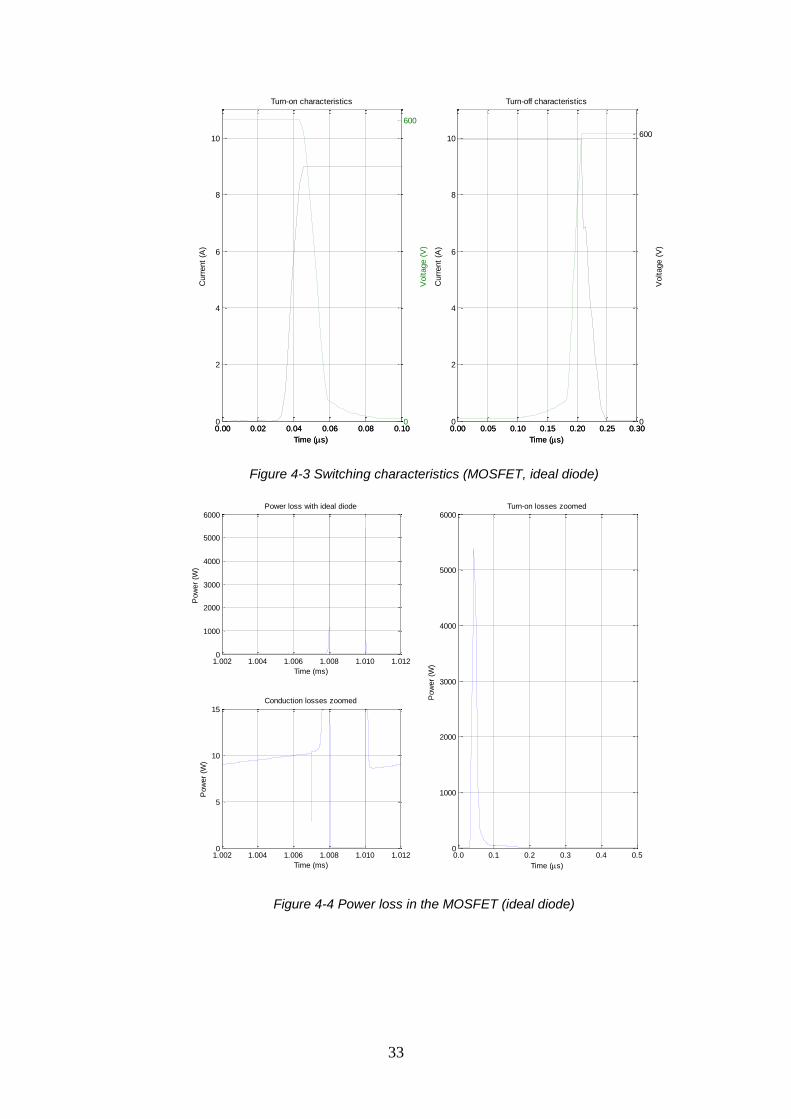
33
Figure 4-3 Switching characteristics (MOSFET, ideal diode)
Figure 4-4 Power loss in the MOSFET (ideal diode)
0.00 0.02 0.04 0.06 0.08 0.100
2
4
6
8
10
Turn-on characteristics
Curr
ent
(A)
Time (s)
0.00 0.05 0.10 0.15 0.20 0.25 0.300
2
4
6
8
10
Turn-off characteristics
Curr
ent
(A)
Time (s)
0.00 0.02 0.04 0.06 0.08 0.100
600
Voltage (
V)
Time (s)
0.00 0.05 0.10 0.15 0.20 0.25 0.300
600
Voltage (
V)
Time (s)
1.002 1.004 1.006 1.008 1.010 1.0120
1000
2000
3000
4000
5000
6000Power loss with ideal diode
Pow
er
(W)
Time (ms)
1.002 1.004 1.006 1.008 1.010 1.0120
5
10
15Conduction losses zoomed
Time (ms)
Pow
er
(W)
0.0 0.1 0.2 0.3 0.4 0.50
1000
2000
3000
4000
5000
6000Turn-on losses zoomed
Time (s)
Pow
er
(W)

34
The switching characteristics can be seen in Figure 4-3. Both turn-on and turn-off are
according to the data sheet of the CoolMOS. The power produced (and hence lost) in
the transistor is shown in Figure 4-4, and the total power loss was calculated to 33.9
W with the following equation
4-1
The losses are quite high due to the very fast switching frequency of 100 kHz, since
the switching losses vary linearly with the switching frequency, the losses at lower
frequencies will be much lower. From the power loss figure, the conduction losses
can be approximated to be 9.5 W, and with a duty-ratio of 70% the total conduction
losses measures 6.7 W. This shows that from the total losses of 33.9 W, 27.2 W is
switching losses (33.9 W – 6.7 W = 27.2 W). Assuming a switching frequency of 2
kHz would instead lead to a total loss of 7.2 W, with switching losses of only 0.5 W.
4.7 Simulation test 2
4.7.1 Test setup with one IGBT and one ideal diode
Same test setup as in Section 4.6 above, with the same duty-ratio, switching
frequency and drive circuit
The IGBT model doesn’t have the temperature model included. A fixed
junction temperature of 32 °C was used.
4.7.2 Results
As in the case with the CoolMOS the results are as expected. The differences
between the IGBT and MOSFET technology are also apparent. As seen in Figure 4-5
the turn-off and turn-on delay is approximately 100 ns and 25 ns respectively, giving
a output voltage duty-ratio close to the gate duty-ratio of 70 %.
Looking at the switching characteristics of the IGBT, Figure 4-6, the difference to
the MOSFET is very apparent at turn-off where the current tail is clearly visible. This
elongated current fall time gives rise to a much larger power loss, as can be seen in
Figure 4-7. Calculating the total power loss in the IGBT according to Equation 4-1, a
total of 137.3 W of power is lost as heat, 305 % more than the MOSFET. With
average conduction losses of (13 W)*70% = 9.1 W, the switching losses account for
128.2 W or 93 % of the total losses. This shows that the IGBT isn’t suited for
switching frequencies in the 100s of kHz. At 2 kHz the total loss in the transistor is
approximately 11.7 W, which is 60 % more than the MOSFET at the same
frequency.

35
Figure 4-5 Output voltage waveform (IGBT, ideal diode)
Figure 4-6 Switching characteristics (IGBT, ideal diode)
0.122 0.124 0.126 0.128 0.130 0.1320
100
200
300
400
500
600
Output voltage waveform
Voltage (
V)
Time (ms)
0.00 0.02 0.04 0.06 0.08 0.100
2
4
6
8
10
Turn-on characteristics
Curr
ent
(A)
Time (s)
0.0 0.5 1.0 1.5 2.00
2
4
6
8
10
Turn-off characteristics
Curr
ent
(A)
Time (s)
0.00 0.02 0.04 0.06 0.08 0.100
600
Voltage (
V)
Time (s)
0.0 0.5 1.0 1.5 2.00
600
Voltage (
V)
Time (s)

36
Figure 4-7 Power loss in the IGBT (ideal diode)
4.8 Simulation test 3
4.8.1 Test setup with two MOSFETs
This test setup is to simulate the behavior of the built in body diode of the MOSFET
by replacing the ideal diode in Simulation test 1 by a CoolMOS transistor with the
gate directly connected to the source (to keep it in its off-state). As seen in Figure 4-8
both MOSFETs are connected to the same heat sink model.
Figure 4-8 Test setup used in simulation test 3
0.122 0.124 0.126 0.128 0.130 0.1320
1000
2000
3000
4000
5000
6000Power loss with ideal diode
Pow
er
(W)
Time (ms)
0.122 0.124 0.126 0.128 0.130 0.1320
5
10
15Conduction losses zoomed
Time (ms)
Pow
er
(W)
0.0 0.5 1.0 1.5 2.00
1000
2000
3000
4000
5000
6000Turn-off losses zoomed
Time (s)
Pow
er
(W)
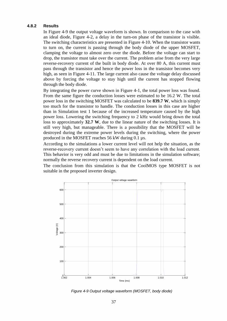
37
4.8.2 Results
In Figure 4-9 the output voltage waveform is shown. In comparison to the case with
an ideal diode, Figure 4-2, a delay in the turn-on phase of the transistor is visible.
The switching characteristics are presented in Figure 4-10. When the transistor wants
to turn on, the current is passing through the body diode of the upper MOSFET,
clamping the voltage to almost zero over the diode. Before the voltage can start to
drop, the transistor must take over the current. The problem arise from the very large
reverse-recovery current of the built in body diode. At over 80 A, this current must
pass through the transistor and hence the power loss in the transistor becomes very
high, as seen in Figure 4-11. The large current also cause the voltage delay discussed
above by forcing the voltage to stay high until the current has stopped flowing
through the body diode.
By integrating the power curve shown in Figure 4-1, the total power loss was found.
From the same figure the conduction losses were estimated to be 16.2 W. The total
power loss in the switching MOSFET was calculated to be 839.7 W, which is simply
too much for the transistor to handle. The conduction losses in this case are higher
than in Simulation test 1 because of the increased temperature caused by the high
power loss. Lowering the switching frequency to 2 kHz would bring down the total
loss to approximately 32.7 W, due to the linear nature of the switching losses. It is
still very high, but manageable. There is a possibility that the MOSFET will be
destroyed during the extreme power levels during the switching, where the power
produced in the MOSFET reaches 56 kW during 0.1 µs.
According to the simulations a lower current level will not help the situation, as the
reverse-recovery current doesn’t seem to have any correlation with the load current.
This behavior is very odd and must be due to limitations in the simulation software;
normally the reverse recovery current is dependent on the load current.
The conclusion from this simulation is that the CoolMOS type MOSFET is not
suitable in the proposed inverter design.
Figure 4-9 Output voltage waveform (MOSFET, body diode)
1.002 1.004 1.006 1.008 1.010 1.0120
100
200
300
400
500
600
Output voltage waveform
Voltage (
V)
Time (ms)
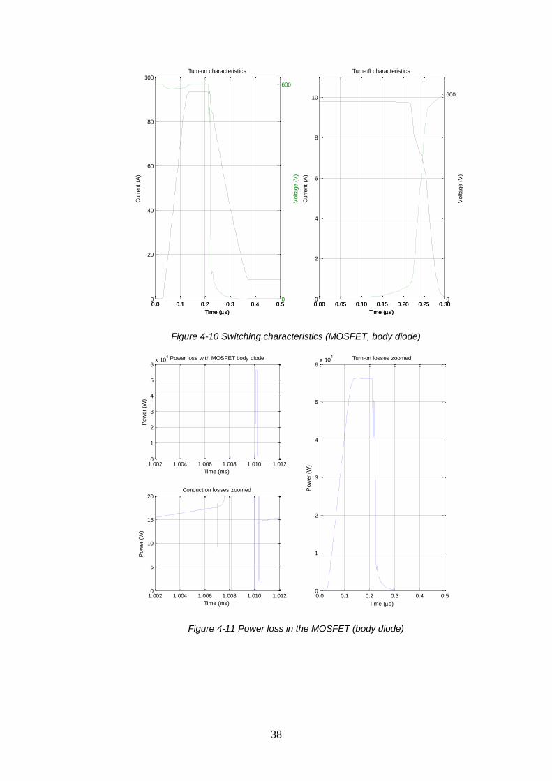
38
Figure 4-10 Switching characteristics (MOSFET, body diode)
Figure 4-11 Power loss in the MOSFET (body diode)
0.0 0.1 0.2 0.3 0.4 0.50
20
40
60
80
100Turn-on characteristics
Curr
ent
(A)
Time (s)
0.00 0.05 0.10 0.15 0.20 0.25 0.300
2
4
6
8
10
Turn-off characteristics
Curr
ent
(A)
Time (s)
0.0 0.1 0.2 0.3 0.4 0.50
600
Voltage (
V)
Time (s)
0.00 0.05 0.10 0.15 0.20 0.25 0.300
600
Voltage (
V)
Time (s)
1.002 1.004 1.006 1.008 1.010 1.0120
1
2
3
4
5
6x 10
4 Power loss with MOSFET body diode
Pow
er
(W)
Time (ms)
1.002 1.004 1.006 1.008 1.010 1.0120
5
10
15
20Conduction losses zoomed
Time (ms)
Pow
er
(W)
0.0 0.1 0.2 0.3 0.4 0.50
1
2
3
4
5
6x 10
4 Turn-on losses zoomed
Time (s)
Pow
er
(W)

39
4.8.3 Modification by adding a SiC diode anti-parallel to the upper MOSFET
A trial to disconnect the built in body diode by connecting a SiC Schottky diode anti-
parallel to the upper MOSFET in Figure 4-8 was done to see if it’s possible to work
around the body diode issues. But as seen in Figure 4-12 this is not possible due to
the very low forward voltage of the CoolMOS body diode displayed in Figure 4-13.
The CoolMOS diode starts to conduct already at 0.7 V, but the SiC Schottky diode
doesn’t turn on until 1.5 V according to its data sheet. Thus the body diode is still
conducting and the same issues as before are still present.
Figure 4-12 Current through the upper MOSFET and SiC diode
Figure 4-13 Voltage over the upper MOSFET and SiC diode
2.6 2.7 2.8 2.9 3 3.1 3.2
x 10-5
-10
-8
-6
-4
-2
0
2
4
6
8
10
Time (s)
Curr
ent
(A)
Current through the MOSFET and SiC diode
MOSFET
SiC diode
18 19 20 21-5
-4
-3
-2
-1
0
1
2
3
4
5Upper MOSFET and SiC diode voltage waveform
Voltage (
V)
Time (s)
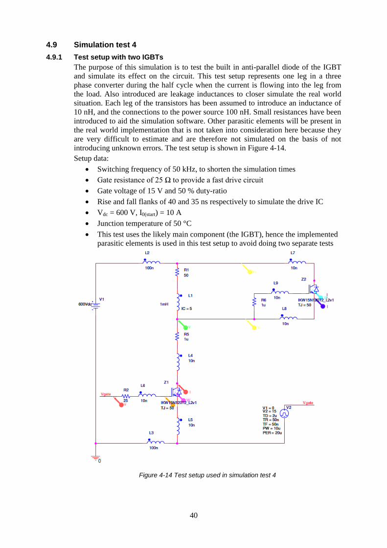
40
4.9 Simulation test 4
4.9.1 Test setup with two IGBTs
The purpose of this simulation is to test the built in anti-parallel diode of the IGBT
and simulate its effect on the circuit. This test setup represents one leg in a three
phase converter during the half cycle when the current is flowing into the leg from
the load. Also introduced are leakage inductances to closer simulate the real world
situation. Each leg of the transistors has been assumed to introduce an inductance of
10 nH, and the connections to the power source 100 nH. Small resistances have been
introduced to aid the simulation software. Other parasitic elements will be present in
the real world implementation that is not taken into consideration here because they
are very difficult to estimate and are therefore not simulated on the basis of not
introducing unknown errors. The test setup is shown in Figure 4-14.
Setup data:
Switching frequency of 50 kHz, to shorten the simulation times
Gate resistance of 25 Ω to provide a fast drive circuit
Gate voltage of 15 V and 50 % duty-ratio
Rise and fall flanks of 40 and 35 ns respectively to simulate the drive IC
Vdc = 600 V, I0(start) = 10 A
Junction temperature of 50 °C
This test uses the likely main component (the IGBT), hence the implemented
parasitic elements is used in this test setup to avoid doing two separate tests
Figure 4-14 Test setup used in simulation test 4
41
4.9.2 Results
As seen in Figure 4-15 the output voltage has some over- and under-shoots at the
switching instances. This behavior is due to the leakage inductances who introduce
voltage drops when the current through them changes rapidly, according to
4-2
where L is the inductance and i is the current through the inductance. The voltages
produced in this simulation are well within the safety margins of the IGBT, one thing
to notice is the negative voltage when the transistor turns on which has to be
considered in a half-bridge inverter setup. Other than that, the waveform looks good.
Other parasitic elements not considered here will influence the result and it has to be
assumed that the waveforms will look worse in the real implementation of the
product.
Figure 4-15 Output voltage waveform with two IGBTs and leakage inductances
The switching characteristics are displayed in Figure 4-16 and compared to the
earlier results without the parasitic elements there’s now some oscillations taking
place. The oscillations here are not in any way dangerous to the circuit or the
components and should be easily managed. With a turn-off time of 400 ns the turn-
off timing is similar to the results in Simulation test 2, even though it should be noted
that a slower driver is used in this simulation test. The turn-on timing is a completely
different story, as the turn-on time has increased from 40 ns with the ideal diode to
100 ns with the built-in anti-parallel diode of the upper IGBT. This is caused by both
the reverse-recovery current of the diode that has to pass through the transistor and
the leakage inductances that keeps the current from changing rapidly.
0 2 4 6 8 10 12 14 16 18 20
0
100
200
300
400
500
600
Output voltage waveform
Voltage (
V)
Time (s)

42
Figure 4-16 Switching characteristics with two IGBTs
The loss waveforms for the switching IGBT are show in Figure 4-17. The total losses
amount to 81.9 W at 50 kHz switching frequency. The conduction losses averages to
(13.5 W * 50 % duty-ratio) = 6.8 W, and the switching losses then equals 75.1 W.
Lowering the switching frequency to 2 kHz would lower the total losses to 9.8 W,
actually lower than with the ideal diode in Simulation test 2. This is due to the use of
a lower duty-ratio and hence lower conduction losses. The switching losses at 2 kHz
are 3 W in this test case and 2.6 W with the ideal diode; 15 % more, due to the
reverse-recovery current that is dissipated through the transistor at turn-on and the
slower turn-on switch time. There is a dampening effect on the losses due to the
parasitic elements causing the voltage at turn-on and current at turn-off to decrease
some 5 percent at the start of each switch.
0.0 0.1 0.2 0.3
0
10
20
Turn-on characteristics
Curr
ent
(A)
Time (s)
0.0 0.1 0.2 0.3
0
600
Voltage (
V)
Time (s)
0.0 0.2 0.4 0.6 0.8 1.00
2
4
6
8
10
Turn-off characteristics
Curr
ent
(A)
Time (s)
0.0 0.2 0.4 0.6 0.8 1.00
600
Voltage (
V)
Time (s)

43
Figure 4-17 Power loss in the IGBT (two IGBTs)
4.10 Simulation test 5
4.10.1 One legged converter with snubber circuit
This test uses the same test setup as in Section 4.9, but adds an RC-snubber over the
switching IGBT. Two different valued capacitors and resistors were used, 2 nF and 5
nF, 100 Ω and 500 Ω, giving a total of four variations. The test setup is shown in
Figure 4-18.
0 5 10 15 200
2000
4000
6000
8000Power loss with two IGBTs
Pow
er
(W)
Time (s)
0 5 10 15 200
5
10
15Conduction losses zoomed
Time (s)
Pow
er
(W)
0.0 0.2 0.4 0.6 0.8 1.00
500
1000
1500
2000
2500
3000
3500
4000
4500
5000
5500Turn-off losses zoomed
Time (s)
Pow
er
(W)
44
Figure 4-18 Test setup for simulation test 5
4.10.2 Results
Only the results from the 2 nF, 100 Ω case is shown in graphs, since the others are
similar in behavior. In Figure 4-19 and Figure 4-20 the power loss during turn-off
and turn-on is shown respectively. They clearly display how the power loss are
moved from the turn-off event to the turn-on.
45
Figure 4-19 Power loss in the switching IGBT during turn-off
Figure 4-20 Power loss in the switching IGBT during turn-on
1.2 1.22 1.24 1.26 1.28 1.3 1.32 1.34 1.36 1.38
x 10-5
0
1000
2000
3000
4000
5000
Power loss during turn-off
Time (s)
Pow
er
(W)
Without snubber
With 2nF + 100ohm snubber
2.2 2.205 2.21 2.215 2.22 2.225 2.23
x 10-5
0
1000
2000
3000
4000
5000
6000
7000
8000
9000
Power loss during turn-on
Time (s)
Pow
er
(W)
Without snubber
With 2nF + 100ohm snubber
46
The power loss in the switching IGBT for the different cases were calculated to be
(using the same method as above):
2 nF - 100 Ω: 83.16 W
2 nF - 500 Ω: 81.48 W
5 nF - 100 Ω: 82.36 W
5 nF - 500 Ω: 81.85 W
In Figure 4-21 the voltage curve during turn-off is shown. The snubber clearly
lowers the dv/dt and shaves of the peak on the voltage spike, as was intended.
Figure 4-21 Voltage over the switching IGBT during turn-off
The current through the snubber circuit is shown in Figure 4-22, where it’s clear how
the snubber absorbs the current during the turn-off phase and then pushes it back
during the turn-on phase.
1.2 1.21 1.22 1.23 1.24 1.25 1.26
x 10-5
0
100
200
300
400
500
600
Voltage during turn-off
Time (s)
Voltage (
V)
Without snubber
With 2nF + 100ohm snubber

47
Figure 4-22 Current through the snubber circuit
To conclude, the snubber moves the losses from turn-off to turn-on while lowering
the dv/dt during switching and shaves of the voltage peak during turn-off.
Unfortunately the total losses in the IGBT remains the same, while extra losses are
introduced in the snubber circuit, reducing the total efficiency of the inverter. Then
the already high current during turn-on is increased even more, possibly causing
greater stress on the IGBT. If a reduction in EMC is required, other measures should
be tried first, for instance to use higher valued gate resistors to slow down the
switching.
4.11 Initial hardware tests
The 25 V-range hardware setup should be used for the initial hardware tests (correct
resistors in the voltage dividers).
4.11.1 Low voltage supply short circuit test
Connect a voltage supply to the terminals of the 15 V circuit and slowly ramp up the
voltage (with a current limiter in place to make sure nothing will burn), while
measuring the current through the circuit. This test is done to make sure that no short
circuit is present in the circuit. An estimated maximum current draw of 200 mA
should be drawn from the supply, mainly from the current sensors.
4.11.1.1 Result
The circuit drew a constant current of approximately 90 mA and the voltage stayed
constant at 15 V. This indicates that the circuit is intact and no short-circuits are
present.
4.11.2 Voltage measurement of low voltage circuit
Apply 15 V to the 15 V terminals of the PBA and measure the voltage level of the
test points specified in Table 4-2.
4.11.2.1 Results
The results of the measurement are found in Fel! Hittar inte referenskälla..
1 1.2 1.4 1.6 1.8 2 2.2 2.4
x 10-5
-4
-3
-2
-1
0
1
2
3
Current through the snubber circuit
Time (s)
Curr
ent
(A)
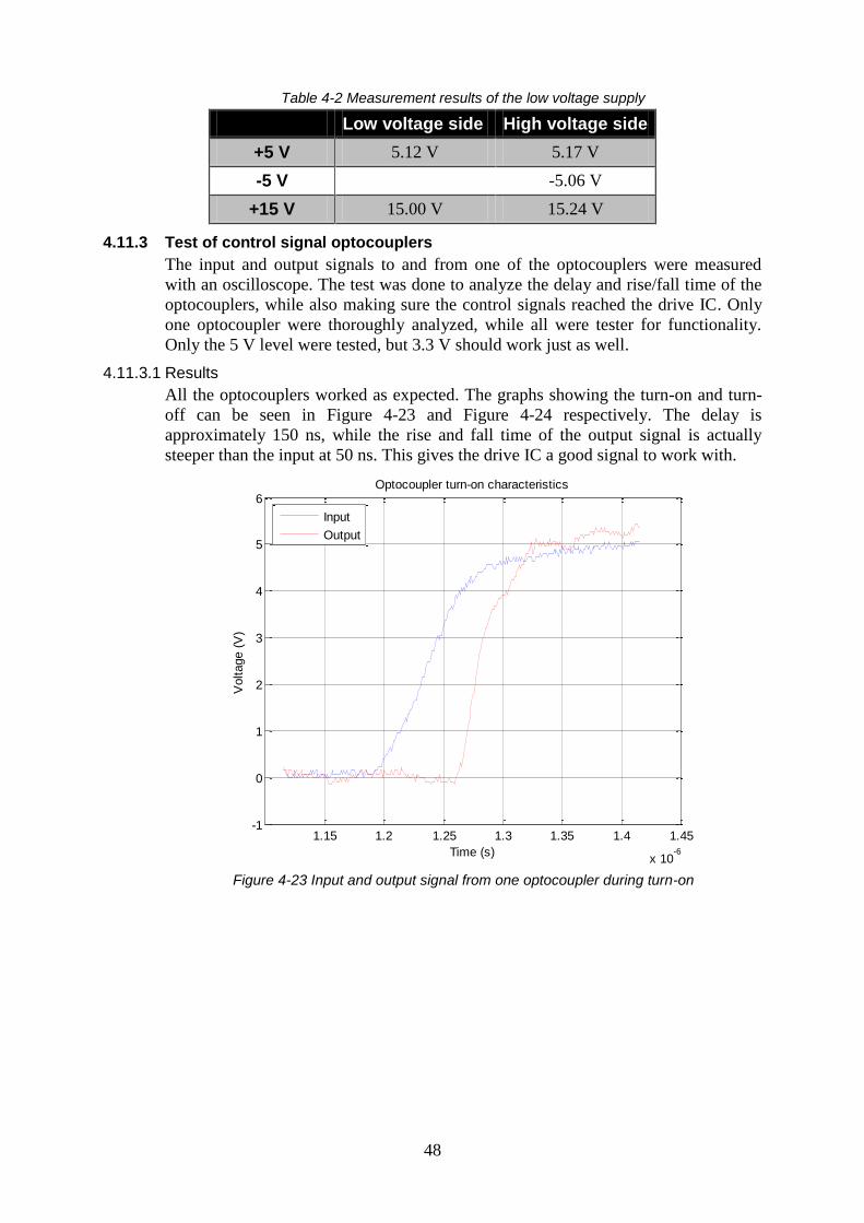
48
Table 4-2 Measurement results of the low voltage supply
Low voltage side High voltage side
+5 V 5.12 V 5.17 V
-5 V -5.06 V
+15 V 15.00 V 15.24 V
4.11.3 Test of control signal optocouplers
The input and output signals to and from one of the optocouplers were measured
with an oscilloscope. The test was done to analyze the delay and rise/fall time of the
optocouplers, while also making sure the control signals reached the drive IC. Only
one optocoupler were thoroughly analyzed, while all were tester for functionality.
Only the 5 V level were tested, but 3.3 V should work just as well.
4.11.3.1 Results
All the optocouplers worked as expected. The graphs showing the turn-on and turn-
off can be seen in Figure 4-23 and Figure 4-24 respectively. The delay is
approximately 150 ns, while the rise and fall time of the output signal is actually
steeper than the input at 50 ns. This gives the drive IC a good signal to work with.
Figure 4-23 Input and output signal from one optocoupler during turn-on
1.15 1.2 1.25 1.3 1.35 1.4 1.45
x 10-6
-1
0
1
2
3
4
5
6Optocoupler turn-on characteristics
Time (s)
Voltage (
V)
Input
Output
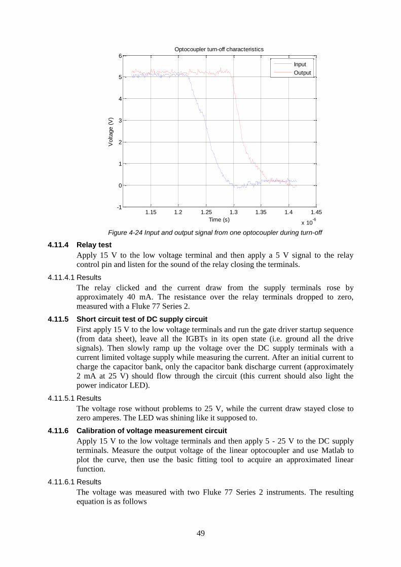
49
Figure 4-24 Input and output signal from one optocoupler during turn-off
4.11.4 Relay test
Apply 15 V to the low voltage terminal and then apply a 5 V signal to the relay
control pin and listen for the sound of the relay closing the terminals.
4.11.4.1 Results
The relay clicked and the current draw from the supply terminals rose by
approximately 40 mA. The resistance over the relay terminals dropped to zero,
measured with a Fluke 77 Series 2.
4.11.5 Short circuit test of DC supply circuit
First apply 15 V to the low voltage terminals and run the gate driver startup sequence
(from data sheet), leave all the IGBTs in its open state (i.e. ground all the drive
signals). Then slowly ramp up the voltage over the DC supply terminals with a
current limited voltage supply while measuring the current. After an initial current to
charge the capacitor bank, only the capacitor bank discharge current (approximately
2 mA at 25 V) should flow through the circuit (this current should also light the
power indicator LED).
4.11.5.1 Results
The voltage rose without problems to 25 V, while the current draw stayed close to
zero amperes. The LED was shining like it supposed to.
4.11.6 Calibration of voltage measurement circuit
Apply 15 V to the low voltage terminals and then apply 5 - 25 V to the DC supply
terminals. Measure the output voltage of the linear optocoupler and use Matlab to
plot the curve, then use the basic fitting tool to acquire an approximated linear
function.
4.11.6.1 Results
The voltage was measured with two Fluke 77 Series 2 instruments. The resulting
equation is as follows
1.15 1.2 1.25 1.3 1.35 1.4 1.45
x 10-6
-1
0
1
2
3
4
5
6Optocoupler turn-off characteristics
Time (s)
Voltage (
V)
Input
Output

50
4-3
and the measurement results is shown in Table 4-3.
Table 4-3 Calibration results for the voltage measurement circuit
Voltage measurements
Vin 5.00 10.00 15.00 20.00 25.03
Vout 0.477 0.957 1.437 1.921 2.410
4.11.7 Calibration of current measurement modules
The current measurement modules are calibrated by connecting a voltage source in
series with a 10 ohm power resistor on each of the outputs. The low side switch was
kept turned on while the high side switch was turned off, 25 V was put on the DC
connectors. A current meter was used to measure the current through the resistor and
a voltage meter was used to measure the voltage over the output terminals of the
current measurement modules, which are rated as follows: Vout = 2.5 + Vin * 0.0625,
with the offset accuracy specified to ±50 mV.
Five different currents were sent through each of the outputs in order to get an
approximated straight line equation by plotting the curve in Matlab and using the
basic fitting tool.
4.11.7.1 Results
Two Fluke 77 Series 2 was used to measure the current and the output voltage. The
results are very close to the manufacturer’s claims, with only slight deviations from
the data sheet values. In Table 4-4 the results are displayed; the approximated
constants to the following equation is also in the table
4-4
Table 4-4 Calibration results for the current measurement modules
I1 V1 I2 V2 I3 V3 I4 V4
-1.29 2.437 -1.41 2.417 -1.41 2.424 -1.41 2.416
-0.92 2.461 -0.94 2.446 -0.90 2.456 -0.90 2.447
0 2.518 0 2.505 0 2.511 0 2.504
0.92 2.575 0.93 2.564 0.92 2.549 0.92 2.562
1.29 2.599 1.41 2.594 1.41 2.600 1.41 2.593
A1 B1 A2 B2 A3 B3 A4 B4
2.518 0.06251 2.505 0.06287 2.512 0.06232 2.504 0.06289
4.11.8 Test of bootstrap capacitor
The bootstrap construction hinders the high side switch to be turned on indefinitely,
hence constant switching is required by the choice of a bootstrap design (the
bootstrap capacitor is charged when the low side switch is on, and discharged when
the high side switch is on).
Two measurements were carried out, one to measure the highest possible duty-ratio,
and one to plot the voltage curve of the bootstrap capacitor.
The first test was done with a single load (a 2 ohm resistor), 5 kHz switching
frequency and a DC voltage of 25 V. The duty-ratio was increased until the high side
switch could no longer turn on. An oscilloscope was used to measure the duty-ratio.
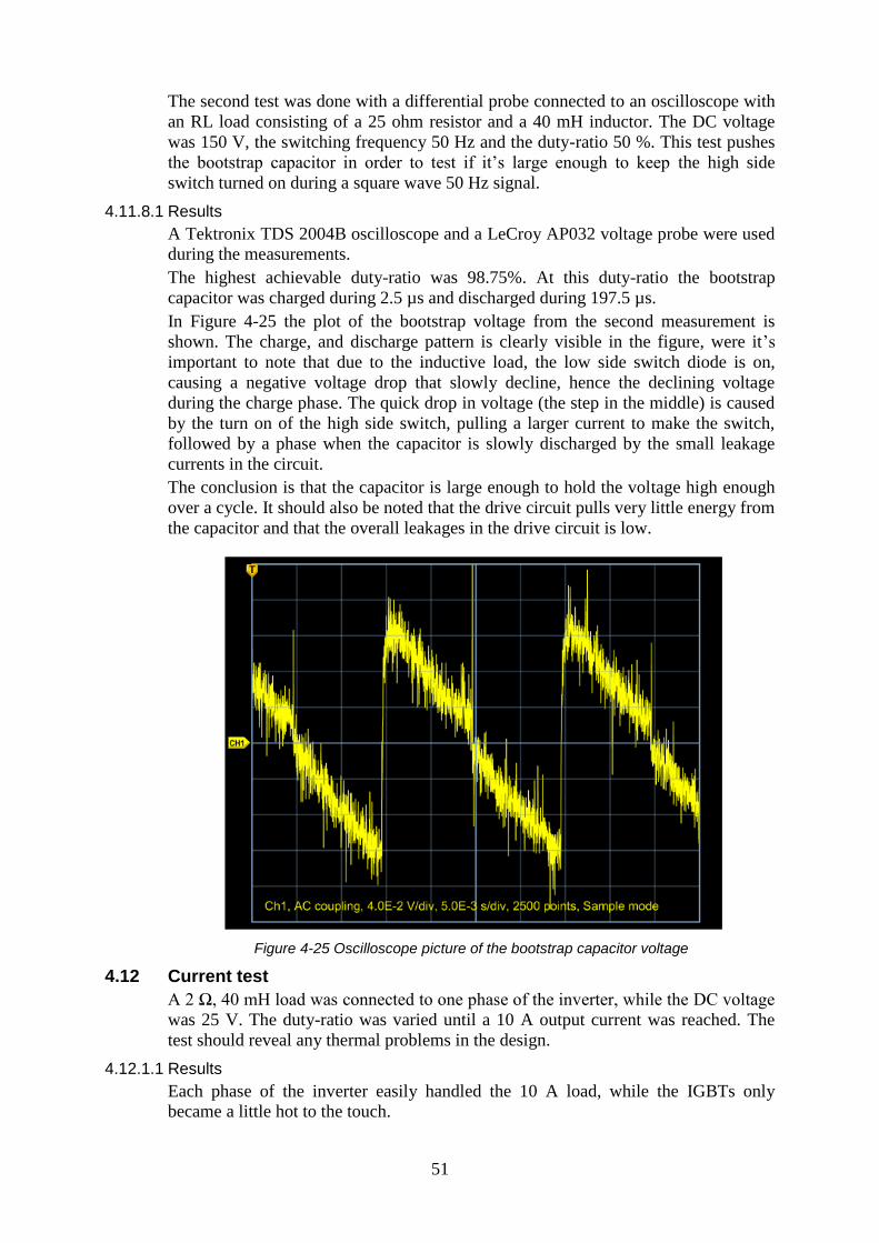
51
The second test was done with a differential probe connected to an oscilloscope with
an RL load consisting of a 25 ohm resistor and a 40 mH inductor. The DC voltage
was 150 V, the switching frequency 50 Hz and the duty-ratio 50 %. This test pushes
the bootstrap capacitor in order to test if it’s large enough to keep the high side
switch turned on during a square wave 50 Hz signal.
4.11.8.1 Results
A Tektronix TDS 2004B oscilloscope and a LeCroy AP032 voltage probe were used
during the measurements.
The highest achievable duty-ratio was 98.75%. At this duty-ratio the bootstrap
capacitor was charged during 2.5 µs and discharged during 197.5 µs.
In Figure 4-25 the plot of the bootstrap voltage from the second measurement is
shown. The charge, and discharge pattern is clearly visible in the figure, were it’s
important to note that due to the inductive load, the low side switch diode is on,
causing a negative voltage drop that slowly decline, hence the declining voltage
during the charge phase. The quick drop in voltage (the step in the middle) is caused
by the turn on of the high side switch, pulling a larger current to make the switch,
followed by a phase when the capacitor is slowly discharged by the small leakage
currents in the circuit.
The conclusion is that the capacitor is large enough to hold the voltage high enough
over a cycle. It should also be noted that the drive circuit pulls very little energy from
the capacitor and that the overall leakages in the drive circuit is low.
Figure 4-25 Oscilloscope picture of the bootstrap capacitor voltage
4.12 Current test
A 2 Ω, 40 mH load was connected to one phase of the inverter, while the DC voltage
was 25 V. The duty-ratio was varied until a 10 A output current was reached. The
test should reveal any thermal problems in the design.
4.12.1.1 Results
Each phase of the inverter easily handled the 10 A load, while the IGBTs only
became a little hot to the touch.
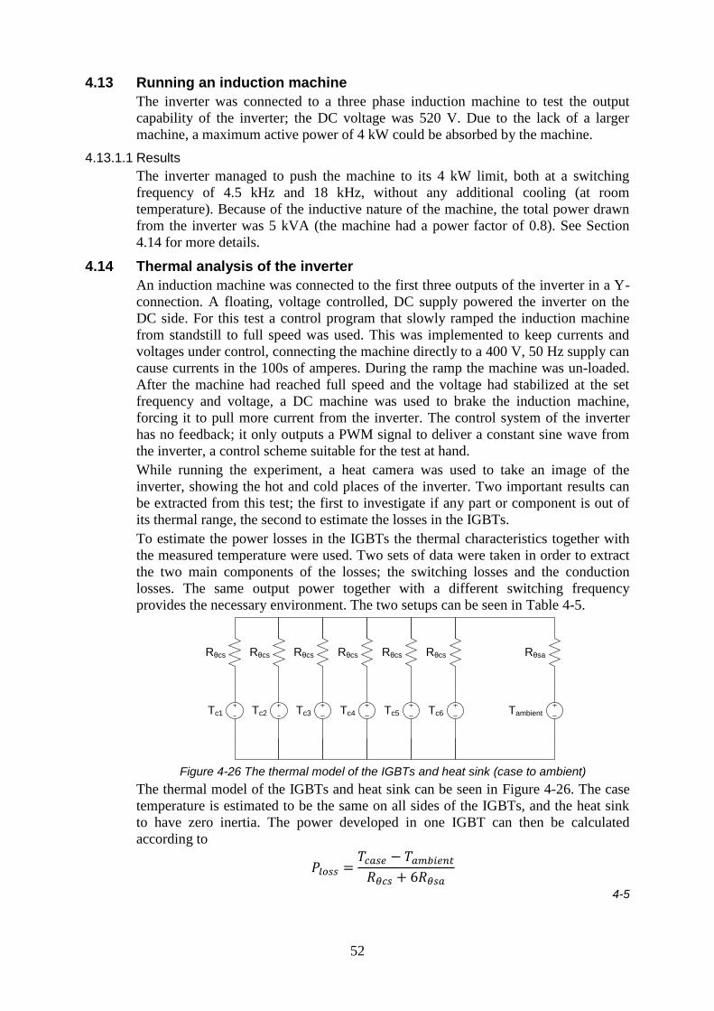
52
4.13 Running an induction machine
The inverter was connected to a three phase induction machine to test the output
capability of the inverter; the DC voltage was 520 V. Due to the lack of a larger
machine, a maximum active power of 4 kW could be absorbed by the machine.
4.13.1.1 Results
The inverter managed to push the machine to its 4 kW limit, both at a switching
frequency of 4.5 kHz and 18 kHz, without any additional cooling (at room
temperature). Because of the inductive nature of the machine, the total power drawn
from the inverter was 5 kVA (the machine had a power factor of 0.8). See Section
4.14 for more details.
4.14 Thermal analysis of the inverter
An induction machine was connected to the first three outputs of the inverter in a Y-
connection. A floating, voltage controlled, DC supply powered the inverter on the
DC side. For this test a control program that slowly ramped the induction machine
from standstill to full speed was used. This was implemented to keep currents and
voltages under control, connecting the machine directly to a 400 V, 50 Hz supply can
cause currents in the 100s of amperes. During the ramp the machine was un-loaded.
After the machine had reached full speed and the voltage had stabilized at the set
frequency and voltage, a DC machine was used to brake the induction machine,
forcing it to pull more current from the inverter. The control system of the inverter
has no feedback; it only outputs a PWM signal to deliver a constant sine wave from
the inverter, a control scheme suitable for the test at hand.
While running the experiment, a heat camera was used to take an image of the
inverter, showing the hot and cold places of the inverter. Two important results can
be extracted from this test; the first to investigate if any part or component is out of
its thermal range, the second to estimate the losses in the IGBTs.
To estimate the power losses in the IGBTs the thermal characteristics together with
the measured temperature were used. Two sets of data were taken in order to extract
the two main components of the losses; the switching losses and the conduction
losses. The same output power together with a different switching frequency
provides the necessary environment. The two setups can be seen in Table 4-5.
Figure 4-26 The thermal model of the IGBTs and heat sink (case to ambient)
The thermal model of the IGBTs and heat sink can be seen in Figure 4-26. The case
temperature is estimated to be the same on all sides of the IGBTs, and the heat sink
to have zero inertia. The power developed in one IGBT can then be calculated
according to
4-5
Tc1 Tc2 Tc3 Tc4 Tc5 Tc6 Tambient
Rθcs Rθcs Rθcs Rθcs Rθcs Rθcs Rθsa
53
4-6
4-7
By combining the equations above, the conduction losses and switching losses of the
IGBTs can be estimated. It’s important to note that this is a rough estimation with
many sources of errors; the thermal model, the large heat sink and the assumptions
made about the switching and conduction losses.
To further analyze the results, a measurement of the currents and voltages were done.
Table 4-5 Test setup for the heat analysis test
Test 1 Test 2
Input voltage VDC 520 520 V
Switching frequency fs 4 500 18 000 Hz
Modulation index ma 1.1 1.1
Output voltage VLL 350 350 V
Fundamental frequency f1 50 50 Hz
Thermal resistance, heat pad Rθcs 0.4 0.4 K/W
Thermal resistance, heat sink Rθsa 0.51 0.51 K/W
4.14.1.1 Results
The resulting thermal images can be seen in Figure 4-27 and Figure 4-28. It’s clear
that the higher switching frequency leads to higher losses, as expected. The
maximum temperature at the 4.5 kHz switching frequency was 54.7 °C, and at 18
kHz it was 74.8 °C. In Table 4-6 the results can be seen from the tests, together with
the calculated switching and conduction losses.
The assumption made that the temperature of the front casing is the same as the case
temperature on the back is most certainly an underestimate of the temperature and
therefore an underestimation of the losses. On the other hand the ratio between the
conduction and switching losses is more accurate due to the two sampled values.
Table 4-6 Results of the thermal analysis
Thermal analysis results Test 1 Test 2
Case temperature Tcase 54.7 74.8 °C
Ambient temperature Tambient 22 22 °C
Total losses Ploss 9.45 15.26 W
Conduction losses Pconduction 7.51 7.51 W
Switching losses Pswitching 1.93 7.75 W
Output current Iout ~8 ~8 A
54
Figure 4-27 Thermal image of the inverter running at 4.5 kHz
Figure 4-28 Thermal image of the inverter running at 18 kHz

55
4.14.1.2 Conclusion
A straightforward comparison of the losses in the real world experiment and in the
simulation above is a little difficult due to slightly different setups. In the simulation
the lower switch is studied; it is hard switching at every switch and the output current
is more or less constant. In the real world test a 50 Hz voltage is produced, so the
current flows in both directions, leading to soft switching in approximately half of
the switches (when the current is flowing in the built-in diode, turn-on or turn-off is
“soft”, since the IGBT is bypassed). This effect could cut the switching losses in half.
The conduction losses are also approximately half from the IGBT and half from the
built in free-wheeling diode, which have a lower voltage drop and therefore lower
losses than the IGBT when conducting. The last hurdle is the average 8 A out of the
real inverter, and approximately 9 A in the simulated setup. Also the voltage level
was higher in the simulation at 600 V, compared to 520 V in the experiment. Only
the current influence the conduction losses, while both current and voltage level
influence the switching losses. A factor was used to correct the simulated results to
the experiment levels. The conduction losses were multiplied by 8/9ths, while the
switching losses were first cut in half due to the “soft switching” and then multiplied
by 8/9ths and then 520/600s.
The comparison results are shown in Table 4-7, showing that the simulation results
were quite accurate. Therefore the conclusion is that the simulation software together
with the manufacturer’s models can form a foundation for estimating the losses, and
hence the needed cooling, in the finished design.
Table 4-7 Comparison between simulation and real life results
Simulation Real life
Current 9 A 8 A
Voltage 600 V 520 V
Conduction losses 6.75 W 7.51 W
Switching losses (4.5 kHz) 6.75 W 1.93 W
Adjusted switching losses 2.6 W 1.93 W
Adjusted conduction losses 6.00 W 7.51 W
4.15 Measuring the switch curves for the high side switch
To see the switching patterns of one of the switches, four things needs to be
measured; current through the IGBT, voltage over the IGBT, gate voltage and output
current. The most difficult to measure is the IGBT current, since the space is very
limited. A small Rogowski type device had to be used, thread around the emitter of
the IGBT.
During the test, the DC voltage was held at 300 V, a three phase inductive load was
used and a 50 Hz sinusoidal voltage was outputted, while the switching frequency
was 5 kHz.
56
4.15.1.1 Results
The following equipment was used to conduct the measurements:
LeCroy WavePro 715Zi – Oscilloscope
LeCroy AP032 – Differential voltage probe
LeCroy AP015 – Current probe
PEM CWT 015B UM – Rogowski current transducer
In Figure 4-29 and Figure 4-30 the switching curves during turn-off and turn-on is
shown. The curves are very similar to the curves from the simulation above, Figure
4-16, and nothing out of the ordinary was to be found. The turn-off time is
approximately 400 ns, including a delay of 100 ns.
The turn-on was much faster at approximately 100 ns. Here the reverse-recovery
current from the low side IGBT module is clearly shown, more than twice the output
current flows through the high side IGBT during approximately 100 ns, causing the
switching losses to increase. The times two ratio is very close to the one found in the
simulations above.
During turn-off the dv/dt is approximately 1 V/ns, while at turn-on it’s 2.5 V/ns. The
change in current, di/dt, at turn-off is approximately 7 A/µs, and at turn-on 50 A/µs.
The results should scale well with voltage and current, though extreme values could
reveal a phenomenon not visible here.
Figure 4-29 Switching curves of the high side IGBT during turn-off
0.5 1 1.5 2
0
0.5
1
1.5
2
2.5
3
Switching curves of high side turn-off
p.u
.
Time (s)
Vce
/100
Vge
/10
ie
iout

57
Figure 4-30 Switching curves of the high side IGBT during turn-on
4.16 Wire bound EMI analysis
To measure the influence of the inverter on the net it’s connected to, the inverter can
be connected to the net through a LISN device (Line Impedance Stabilization
Network). With this device an oscilloscope can be used to measure the EMC, while
making sure that any interference from the net is not influencing the measurements.
Two sets of measurements can be taken to examine the effect of a snubber circuit
over the IGBTs. First a measurement without any snubber circuits and then a
measurement with one of the proposed snubbers from above.
Another possible experiment is to test two different sets of gate resistors, changing
the switching speed and the dv/dt and di/dt of the circuit, thus changing the generated
EMI.
For this test a thermal analysis would also be needed to investigate the influence of
the snubber/gate resistors on the power losses in the IGBTs.
0.2 0.3 0.4 0.5 0.6 0.7 0.8 0.9
0
0.5
1
1.5
2
2.5
3
3.5
4
Switching curves of high side turn-on
p.u
.
Time (s)
Vce
/100
Vge
/10
ie
iout

58
4.17 Efficiency calculation
Knowing the efficiency of the inverter is interesting in order to make a model of it so
that the optimum working point in future uses of the device can more easily be
found.
There are different ways to measure the efficiency of the device. The most
straightforward method is to measure the voltage and current into the device and the
voltage and current out of it. The difficulty with this approach is that the accuracy of
the measurements needs to be very high, because the efficiency of the inverter is so
high, close to 100 %. The waveforms are not ideally formed sine, square or constant
either, causing further problems with accuracy.
Another way to measure the efficiency is to use a known and calibrated load and do a
thermal analysis of the load to accurately acquire the load power. The input power is
then measured with a voltage and current meter, since they are more constant in
nature and therefore easier to accurately measure.
Ideally, four different working points should be used to get an accurate model of the
inverter; two different switching frequencies and two different loads.

59
5 Conclusion The goal of designing and building a four phase inverter was a success. The inverter
managed to drive a 4 kW electric machine with switching a frequency of up to 20
kHz. The inverter worked as expected throughout testing, although the limits of the
inverter was never found since a large enough machine was not readily available for
testing.
During the simulations it was first found that the CoolMOS type MOSFET is not
suitable for the type of inverter used in this project. The second conclusion is that the
proposed RC-snubber isn’t of much help, other than a last stop remedy to reduce
EMI if no other option exists, due to the added losses and complexity while not in
any meaningful way reducing the stresses on the IGBTs.
The choice to use the bootstrap design for the high side switches proved to be a good
one; switching frequencies from 50 to 20 000 Hz were tested successfully. The
chosen capacitor, of a solid electrolytic chip type, also proved to be the right choice;
fast enough and higher reliability compared to ordinary electrolytic capacitors.
Finally the results from the simulations and the hardware tests proved that the
simulation software is a good tool during the design process that could help evaluate
electrical and even thermal characteristics of the design or of specific components.

60
6 Future work Since the main focus of the project was on the design and production of the
hardware, not much time and energy was spent on doing measurements and testing
various cases. For example the produced EMI of the invert would be interesting to
measure, together with the influence of the RC-snubber on the EMI performance and
the total losses.
Further testing to evaluate the robustness of the inverter would also be of interest;
short-circuit tests (to test the built-in fault sensing), over-voltage tests and over-
current tests.
Another big topic is the control of the inverter and of the electric machine, an area
much too wide to be covered in this project.

61
7 Sources
Infineon Technologies AG. (September 2008). Infineon Technologies AG. Hämtat från
http://www.infineon.com/dgdl/IKW15N120T2_Rev2_1.pdf?folderId=db3a304412b40795011
2b408e8c90004&fileId=db3a304412b407950112b426d2d43acd den 27 April 2010
Infineon Technologies AG. (2008, July 30). Infineon Technologies AG. Retrieved April 26,
2010, from
http://www.infineon.com/dgdl/IPW90R120C3_1[1].0_PCN.pdf?folderId=db3a3043156fd573
0115c736bcc70ff2&fileId=db3a3043183a955501185000e1d254f2
International Rectifier. (2007, 03 23). HV Floating MOS-Gate Driver ICs. El Segundo.
Mohan, N., Undeland, T., & Robbins, W. (2003). Power Electronics. John Wiley & Sons, Inc.
Premier Farnell. (n.d.). Farnell Sverige. Retrieved April 27, 2010, from
http://se.farnell.com/infineon/ikw15t120/igbt-n-1200v-15a-to-
247/dp/1471745?Ntt=IKW15T120
Premier Farnell. (n.d.). Farnell Sverige. Retrieved April 27, 2010, from
http://se.farnell.com/infineon/ipw90r120c3/mosfet-n-to-247/dp/1664087?Ntt=IPW90R120C3
Vishay Semiconductors. (2005, March 24). Linear Optocoupler, High Gain Stability, Wide
Bandwidth. Retrieved June 01, 2010, from Vishay Semiconductors:
http://www.vishay.com/docs/83622/83622.pdf
62
Appendix A Layout and PCB figures
Figure 7-1 Schematics over the first inverter leg

63
Figure 7-2 Schematics over the second inverter leg
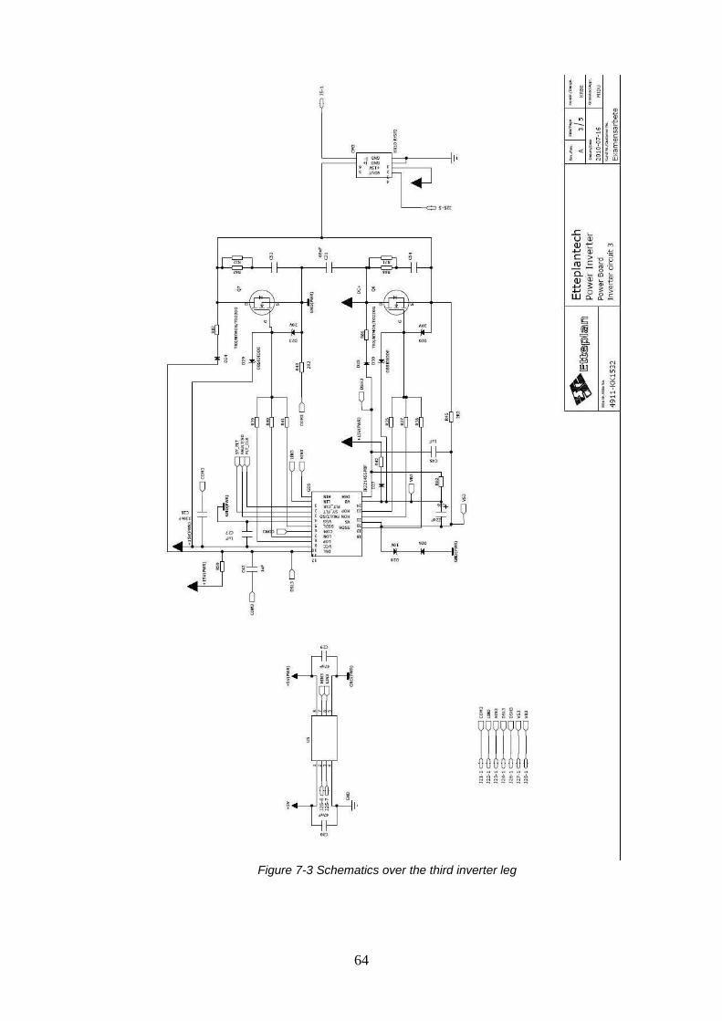
64
Figure 7-3 Schematics over the third inverter leg
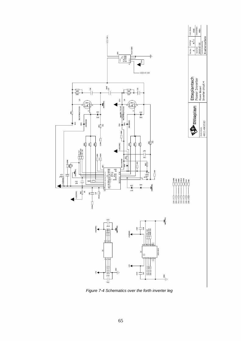
65
Figure 7-4 Schematics over the forth inverter leg

66
Figure 7-5 Schematics over the supply circuits
Related Documents