
Welcome message from author
This document is posted to help you gain knowledge. Please leave a comment to let me know what you think about it! Share it to your friends and learn new things together.
Transcript

Formal Verification of FPGA
Based Systems
By
Honghan Deng, B.Eng.
A Thesis
Submitted to the School of Graduate Studies
in partial ful�lment of the requirements for the degree of
Master of Applied Science
Department of Computing and Software
McMaster University
c© Copyright by Honghan Deng, September 11, 2011
MASTER OF APPLIED SCIENCE(2011) McMaster University
(Software Engineering) Hamilton, Ontario
TITLE: Formal Veri�cation of FPGA Based Systems
AUTHOR: Honghan Deng, B.Eng.(McMaster University)
SUPERVISOR: Dr. Mark Lawford
NUMBER OF PAGES: x, 128
ii

To Michael and Yilang
iii
Abstract
In design veri�cation, although simulation is still a widely used veri�cation
technique in FPGA design, formal veri�cation is obtaining greater acceptance
as the complexity of designs increases. In the simulation method, for a circuit
with n inputs and m registers an exhaustive test vector will have as many as
2(m+n) elements making it impractical for many modern circuits. Therefore
this method is incomplete, i.e., it may fail to catch some design errors due to
the lack of complete test coverage. Formal veri�cation can be introduced as a
complement to traditional veri�cation techniques.
The primary objectives of this thesis are determining: (i) how to for-
malize FPGA implementations at di�erent levels of abstraction, and (ii) how
to prove their functional correctness. This thesis explores two variations of a
formal veri�cation framework by proving the functional correctness of several
FPGA implementations of commonly used safety subsystem components us-
ing the theorem prover PVS. We formalize components at the netlist level and
the Verilog Register Transfer HDL level, preserving their functional semantics.
Based on these formal models, we prove correctness conditions for the com-
ponents using PVS. Finally, we present some techniques which can facilitate
the proving process and describe some general strategies which can be used to
prove properties of a synchronous circuit design.
iv
Acknowledgments
My utmost gratitude to Dr. Mark Lawford whose sincerity and encouragement
I will never forget. He has supported me throughout my graduate study with
his patience and knowledge whilst allowing me the room to work in my own
way. One simply could not wish for a better or friendlier supervisor.
Also, I must thank Yilang Yang, my parents and my in-laws. They
have always supported my studies and encouraged me to complete this thesis.
With my family I have shared every day of this endevour.
v

Contents
Abstract iii
Acknowledgments v
List of Figures viii
1 Introduction 1
1.1 FPGA Based Development . . . . . . . . . . . . . . . . . . . . 2
1.1.1 Typical FPGA Design Process . . . . . . . . . . . . . . 2
1.1.2 Synchronous Circuits and Timing . . . . . . . . . . . . 5
1.1.3 Interfacing Simulink with FPGAs . . . . . . . . . . . . 5
1.2 Motivation . . . . . . . . . . . . . . . . . . . . . . . . . . . . . 5
1.3 Related Work . . . . . . . . . . . . . . . . . . . . . . . . . . . 9
1.3.1 Theorem Proving for Hardware Veri�cation . . . . . . 9
1.4 Contributions . . . . . . . . . . . . . . . . . . . . . . . . . . . 12
1.5 Thesis Outlines . . . . . . . . . . . . . . . . . . . . . . . . . . 13
2 Formalizing Hardware Implementations 15
2.1 Previous Work on Hardware Formalization . . . . . . . . . . . 15
2.2 Assumptions . . . . . . . . . . . . . . . . . . . . . . . . . . . . 17
2.3 Formal Models of the Netlist Level . . . . . . . . . . . . . . . 19
2.3.1 Hardware Signal Representation . . . . . . . . . . . . . 19
2.3.2 Formalization of Combinational components in PVS . . 21
2.4 Formal Models of Sequential Circuits in PVS . . . . . . . . . . 33
2.4.1 Formalizing Finite State Machines in PVS . . . . . . . 35
2.5 Formal Models of the RTL HDL level . . . . . . . . . . . . . . 41
vi

2.5.1 Formal Semantics of a Subset of Verilog . . . . . . . . 45
2.5.2 IF and CASE Statements and Implied Memory . . . . 54
2.5.3 Overriding of Blocking/Non-Blocking Assignments . . . 57
2.5.4 Non-blocking Assignments in Synchronous always Blocks 60
2.5.5 Blocking assignments in Combinational always Blocks . 67
3 Formal Veri�cation of System Components 74
3.1 Correctness Conditions and Environmental Assumptions . . . 74
3.2 HELD_FOR . . . . . . . . . . . . . . . . . . . . . . . . . . . 75
3.2.1 HELD_FOR Netlist Circuit Implementation . . . . . . 76
3.2.2 HELD_FOR Correctness Condition . . . . . . . . . . . 78
3.3 Hysteresis . . . . . . . . . . . . . . . . . . . . . . . . . . . . . 80
3.3.1 Hysteresis Netlist Circuit Implementation . . . . . . . 80
3.3.2 Hysteresis Correctness Condition . . . . . . . . . . . . 82
3.4 Sum of Highest16 sensors/18 inputs . . . . . . . . . . . . . . . 84
3.4.1 Highest16 sensors/18 inputs HDL Implementation . . . 84
3.4.2 Highest16 sensors/18 inputs Correctness Condition . . 89
4 Proof Strategies 92
4.1 General Proving Steps . . . . . . . . . . . . . . . . . . . . . . 92
4.1.1 Instantiate signal names . . . . . . . . . . . . . . . . . 92
4.1.2 Sequential circuit property proving . . . . . . . . . . . 93
4.2 HELD_FOR proving strategy . . . . . . . . . . . . . . . . . . 100
4.3 ishighest16 Proving stragegy . . . . . . . . . . . . . . . . . . . 105
5 Facilitating Proofs 113
5.1 Adding Probes . . . . . . . . . . . . . . . . . . . . . . . . . . 113
5.1.1 The Need for Probes . . . . . . . . . . . . . . . . . . . 113
5.1.2 Types of Probes . . . . . . . . . . . . . . . . . . . . . . 118
5.1.3 Using Probes . . . . . . . . . . . . . . . . . . . . . . . 120
5.2 Constrain the Model . . . . . . . . . . . . . . . . . . . . . . . 124
5.3 Make an Appropriate Assumption in the Correctness Condition 124
6 Future Work 126
vii

List of Figures
1.1 FPGA Iterative Design Process . . . . . . . . . . . . . . . . . 2
1.2 Bluespec Design Flow . . . . . . . . . . . . . . . . . . . . . . . 4
1.3 Two FPGA Formal Veri�cation Frameworks . . . . . . . . . . 6
2.1 PVS Time Theory . . . . . . . . . . . . . . . . . . . . . . . . 16
2.2 Asynchronous Input to Synchronization Circuit . . . . . . . . 18
2.3 Signal Theory . . . . . . . . . . . . . . . . . . . . . . . . . . . 19
2.4 Signal value representation . . . . . . . . . . . . . . . . . . . . 20
2.5 Predicate subtype for 16/32 bitvector in highest16 module . . 21
2.6 TCCs for addition and subtraction . . . . . . . . . . . . . . . 22
2.7 Primitive Adder . . . . . . . . . . . . . . . . . . . . . . . . . 23
2.8 Derivation of HDL_ADDER substraction algorithm . . . . . . 23
2.9 Equivalence operator . . . . . . . . . . . . . . . . . . . . . . . 25
2.10 Unsigned comparator . . . . . . . . . . . . . . . . . . . . . . . 26
2.11 Signed comparator . . . . . . . . . . . . . . . . . . . . . . . . 27
2.12 Generic Multiplexer De�nition . . . . . . . . . . . . . . . . . . 29
2.13 4 to 1 MUX example . . . . . . . . . . . . . . . . . . . . . . . 30
2.14 PVS speci�cation for 4 to 1 MUX application . . . . . . . . . 30
2.15 Generic binary decoder de�nition . . . . . . . . . . . . . . . . 31
2.16 Synchronous D Flip-�op . . . . . . . . . . . . . . . . . . . . . 34
2.17 The sequential circuit with �nite state machine . . . . . . . . 35
2.18 FSM components in State Machine Viewer . . . . . . . . . . . 37
2.19 Disjointness TCC . . . . . . . . . . . . . . . . . . . . . . . . . 39
2.20 Coverage TCC . . . . . . . . . . . . . . . . . . . . . . . . . . 40
2.21 Formalizing FSM Transition Table . . . . . . . . . . . . . . . 42
2.22 FSM and LESS_THAN operators . . . . . . . . . . . . . . . . 43
viii

2.23 FSM_SHELL - the FSM output interface to the surrounding
circuit . . . . . . . . . . . . . . . . . . . . . . . . . . . . . . . 43
2.24 Blocking assignment example . . . . . . . . . . . . . . . . . . 49
2.25 Reversed blocking assignment example . . . . . . . . . . . . . 49
2.26 Non-blocking assignment in an always block . . . . . . . . . . 51
2.27 A D �ip-�op synthesized by a non-blocking assignment . . . . 52
2.28 simulation cycles and clock . . . . . . . . . . . . . . . . . 53
2.29 A synchronous always block example . . . . . . . . . . . . . . 55
2.30 Synchronous always block formalized in PVS . . . . . . . . . . 56
2.31 Transformed decision tree . . . . . . . . . . . . . . . . . . . . 59
2.32 A more complex non-blocking assignment overriding problem . 63
2.33 decision tree transformation process . . . . . . . . . . . . . . . 64
2.34 PVS speci�cation for Verilog in Figure 2.32 . . . . . . . . . . 65
2.35 The circuit before and after the transformation . . . . . . . . 66
2.36 A blocking assignment sequence m<n . . . . . . . . . . . . . . 67
2.37 Blocking assignment decision tree transformation . . . . . . . 68
2.38 blocking assignment block with overriding . . . . . . . . . . . 69
2.39 blocking assignment decision tree . . . . . . . . . . . . . . . . 70
2.40 synthesized circuit for Figure 2.39(a) and (c) . . . . . . . . . . 73
3.1 HELD_FOR operator model in Simulink . . . . . . . . . . . . 76
3.2 HELD_FOR operator netlist circuit implementation . . . . . 76
3.3 The simpli�ed version of HELD_FOR implementation . . . . 77
3.4 the Mux for Adder Input . . . . . . . . . . . . . . . . . . . . . 77
3.5 Formalized increment sub circuit for Figure 3.6 . . . . . . . . 78
3.6 Formalized toplevel circuit of HELD_FOR . . . . . . . . . . . 78
3.7 Simulation result of HELD_FOR operator . . . . . . . . . . . 79
3.8 HELD_FOR operator formal requirement in PVS . . . . . . . 79
3.9 Correctness condition of HELD_FOR implementation . . . . 79
3.10 Deadband functionality of Hysteresis block . . . . . . . . . . . 80
3.11 Formalized requirement of Hysteresis block . . . . . . . . . . . 80
3.12 Hysteresis implementation in Matlab . . . . . . . . . . . . . . 81
3.13 Formalized Hysteresis Module . . . . . . . . . . . . . . . . . . 82
3.14 Simulation Result of Hysteresis Block . . . . . . . . . . . . . . 83
3.15 Formal speci�cation of the Hysteresis Hardware Implementation 83
ix

3.16 Correctness Condition of Hysteresis . . . . . . . . . . . . . . . 84
3.17 highest16 module: Calculates sum of 16 highest of 18 input
sensor values . . . . . . . . . . . . . . . . . . . . . . . . . . . . 85
3.18 formalize highest16 synchronous always block . . . . . . . . . 86
3.19 highest16 decision tree before merged . . . . . . . . . . . . . . 87
3.20 highest16 decision tree after merged . . . . . . . . . . . . . . . 88
3.21 highest16 simulation result . . . . . . . . . . . . . . . . . . . . 89
3.22 predicate is_lowANDlowest . . . . . . . . . . . . . . . . . . . 90
3.23 speci�cation of highest16 . . . . . . . . . . . . . . . . . . . . . 90
3.24 Correctness Condition of highest16 . . . . . . . . . . . . . . . 91
4.1 Final form of the sequence after instantiating simplifying . . . 96
4.2 Induction on time proof diagram . . . . . . . . . . . . . . . . 97
4.3 Induction on n (t=f(n)) proof diagram . . . . . . . . . . . . . 100
4.4 Held_For proof cases . . . . . . . . . . . . . . . . . . . . . . . 101
4.5 increment property . . . . . . . . . . . . . . . . . . . . . . . . 101
4.6 Freeze property . . . . . . . . . . . . . . . . . . . . . . . . . . 102
4.7 counter upper boundary property . . . . . . . . . . . . . . . . 102
4.8 Two cases of t_j!1 . . . . . . . . . . . . . . . . . . . . . . . . 103
4.9 Boundary property 1 of increment sub module . . . . . . . . . 104
4.10 Boundary property 2 of increment sub module . . . . . . . . . 104
4.11 Property reg(ini+m)<ini+m . . . . . . . . . . . . . . . . . . . 104
4.12 Base case proving strategy . . . . . . . . . . . . . . . . . . . . 110
4.13 Induction step . . . . . . . . . . . . . . . . . . . . . . . . . . . 112
5.1 The signal probe in a formal model . . . . . . . . . . . . . . . 114
5.2 Observability of signal X . . . . . . . . . . . . . . . . . . . . . 115
5.3 A case when Speci�cation involve the internal connection . . . 116
5.4 Example: Proof structure for the highest16 module . . . . . . 117
5.5 top_at_tick_3 property of highest16 module . . . . . . . . . 117
5.6 The implementation embedded with probes . . . . . . . . . . . 118
5.7 state �ow example . . . . . . . . . . . . . . . . . . . . . . . . 122
x
Chapter 1
Introduction
FPGA veri�cation can be classi�ed into two categories: Design Veri�cation
and Implementation Veri�cation. Design Veri�cation is focused on �nding
design or coding errors as well as errors in the speci�cation by applying sim-
ulation or formal veri�cation. Implementation Veri�cation is used to locate
translation/synthesis errors.
In design veri�cation, although simulation is still a widely used veri-
�cation technique for FPGA designs, formal veri�cation is obtaining greater
acceptance as an additional veri�cation technique as the complexity of designs
continues to increase. One of the main reasons for this trend is the state ex-
plosion problem. In the simulation method, for a circuit with n (1-bit) inputs
and m (1-bit) registers, an exhaustive test vector will have 2(m+n) elements,
making exhaustive testing impractical for many modern circuits because test
is very slow when performed at low levels of abstraction such as the gate level
or the transistor level. Therefore the simulation veri�cation method is typi-
cally incomplete, i.e., it may fail to catch some design errors due to the lack
of complete test coverage. Therefore formal veri�cation is increasingly being
introduced to complement traditional veri�cation techniques.
1

M.A.Sc Thesis � Honghan Deng � McMaster � Computing and Software
Figure 1.1: FPGA Iterative Design Process
1.1 FPGA Based Development
In this section we provide an overview of the overall FPGA development pro-
cess in order to put the work on formal veri�cation into context.
1.1.1 Typical FPGA Design Process
A typical FPGA design process is shown in Fig. 1.1. For consumer applica-
tions developers typically iterate frequently in the upper half of the diagram,
re�ning requirements after performing simulations based upon behavioral de-
scriptions. Traditionally hardware designs have created their behavioral mod-
els using and HDL such as VHDL or Verilog.
2

M.A.Sc Thesis � Honghan Deng � McMaster � Computing and Software
Hardware Description Languages
A Hardware Description Language (HDL) can be used to describe a hardware
design at di�erent levels of abstraction: the gate level, the data �ow level and
the behavioral level. In addition to specifying hardware that can be synthe-
sized, HDLs can typically also be used to specify test harnesses and may even
make formal assertions about the desired behavior of the circuit.
In specifying hardware the desired functionality and timing may be
described using a hardware description language such as VHDL or Verilog and
then synthesized into the structural level for a speci�ed device. Synthesis of
hardware for an HDL involves:
1. Translation into Boolean equations,
2. Optimization for area/delay, and then
3. Mapping to a FPGA or ASIC process (library).
The physical level is then implemented automatically using a placement and
routing program.
A detailed description of the principles of HDLs is beyond the scope
of this document. Below we brie�y mention the two industry standard HDLs
and a third language that may be more amenable to formal veri�cation.
VHDL: The name VHDL is short for VHSIC HDL = Very High-Speed In-
tegrated Circuit Hardware Description Language. In 1981 VHDL was
developed by the US Department of Defense to standardize documenta-
tion for maintenance or possible redesign. In 1987 IEEE approved the
VHDL standard (1076) and since then Electronic Design Automation
(EDA) companies have been using VHDL, often with enhancements, for
synthesis. The language has evolved since 1987 with the IEEE updating
the standard approximately every 5 years, with the most recent version
approved in 2008.
Verilog: The Verilog hardware description language was originally developed
by Gateway Automation (Cadence) for veri�cation of logic. Cadence
3

M.A.Sc Thesis � Honghan Deng � McMaster � Computing and Software
Figure 1.2: Bluespec Design Flow
and other EDA companies have been using Verilog with enhancements
for synthesis. The original language was proprietary until it was released
as an open standard in 2001. It was updated in 2005 and released as
IEEE Standard 1364. Verilog should not be confused with SystemVer-
ilog (IEEE Standard 1800-2005) which subsumes Verilog and includes
additional features for veri�cation.
Bluespec: Bluespec is a start-up company that provides a proprietary Func-
tional Hardware Description Language based upon the functional pro-
gramming language Haskell. The justi�cation behind writing chip de-
signs in Bluespec is that it leads to shorter, more abstract, and veri�able
(provably correct) source code, as well as type-checked numeric code. In
the design �ow the developer writes a high level Bluespec SystemVerilog
(BSV) description of the hardware. The Blue Spec Compiler (BSC) can
then generate SystemC for simulation or as well as Verilog code that can
then be used with conventional EDA tools.
In this thesis we will use Verilog as it is commonly used, the author is
familiar with it.
4

M.A.Sc Thesis � Honghan Deng � McMaster � Computing and Software
1.1.2 Synchronous Circuits and Timing
Circuit timing, maximal delay path, syncrhonous circuits, and clock frequency
TIMING PROPERTIES OF REQUIREMENTS (functional timing)
1.1.3 Interfacing Simulink with FPGAs
Recently Model Based Design has been making inroads in software engineer-
ing. High level models of the desired system behavior are constructed using
modeling tools and then used to generate code that implements the desired
functionality. Mathworks Matlab/Simulink is the industry standard for mod-
elling control systems and is used in many engineering disciplines for mod-
eling and simulation. The code generation capabilities of Matlab/Simulink
have seen it adopted as a tool for performing model based design of systems.
Simulink is used to design and simulate complex systems using block sets. It
can also be used to target FPGAs. Altera (DSP Builder), Xilinx (System Gen-
erator), and Actel (Synplify DSP) are three manufacturers that supply block
sets to Simulink. Simulink can use the Altera and Xilinx block sets to convert
the system to HDL directly, while Actel outputs to an encrypted RTL �le to
ensure that it can only be downloaded to an Actel device, however it can be
converted to HDL using Actel's Libero IDE software.
1.2 Motivation
Often there is a large gap between the speci�cation and the implementation of
the system. Applying formal methods to close the gap between the speci�ca-
tion and netlist or Hardware Description Language (HDL) implementation is
the main focus of this thesis. We propose two di�erent veri�cation frameworks
depending on the abstraction of implementation.
Figure 1.3 shows two frameworks used in this thesis. In Figure 1.3
(a) there is only a single use of equivalence checking to guarantee the equiva-
lence of the netlist models before and after the place and route tool has been
applied. We use M1[s1, s2, ..., sn] to denote the netlist model before place
and route and M2[s1, s2, ..., sn] denotes the netlist model afterwards, while
5

M.A.Sc Thesis � Honghan Deng � McMaster � Computing and Software
Figure 1.3: Two FPGA Formal Veri�cation Frameworks
s1, . . . , sn are port signals. A theorem prover is applied to verify that the
netlist M1[s1, s2, ..., sn] generated by the synthesis tool correctly implements
the system speci�cation S[s1, s2, ..., sn].
By utilizing equivalence checking we can prove:
`M1[s1, s2, ..., sn] ≡M2[s1, s2, ..., sn]
By utilizing a theorem prover we can show that:
`M1[s1, s2, ..., sn]⇒ S[s1, s2, ..., sn]
From these two results, we can easily derive our desired correctness theorem:
`M2[s1, s2, ..., sn]⇒ S[s1, s2, ..., sn]
Similarly, in Figure 1.3 (b), by utilizing two applications of equivalence
checking, we can prove:
`M1[s1, s2, ..., sn] ≡M2[s1, s2, ..., sn] ∧ M2[s1, s2, ..., sn] ≡M3[s1, s2, ..., sn]
6
M.A.Sc Thesis � Honghan Deng � McMaster � Computing and Software
As before, by utilizing a theorem prover we demonstrate that:
`M1[s1, s2, ..., sn]⇒ S[s1, s2, ..., sn]
Then, we can conclude that:
`M3[s1, s2, ..., sn]⇒ S[s1, s2, ..., sn]
Formal veri�cation can be complicated and time consuming, however it
provides additional con�dence to designers. By building commonly used, pre-
veri�ed functional blocks, designers can use these modules with con�dence
without repeating much of the formal veri�cation process. Alternatively, de-
signers can build their own modules and prove the equivalence relationship
between the pre-veri�ed block and their own module.
By using a pre-veri�ed library, the overall system veri�cation will be
more practical due to the higher level of abstraction used to reason at the
module interconnect level, hence drastically reducing the complexity of the
formal hardware veri�cation task. This is the main idea behind this hierarchi-
cal veri�cation structure described in (Melham, 1990). In this structure, each
hardware module will be abstractly represented by one or more properties. It
is this abstraction that hides the actual hardware module complexity.
Usually, the approach used to formalize the function model of an FPGA
implementation is based on the netlist that is produced by synthesis. A more
e�ective way is to translate the model directly from the Verilog, VHDL, or
other HDL description before synthesis. Ofcourse this requires a formal se-
mantics for the HDL that is being used. In this thesis we consider Verilog. Al-
though the simulation semantics for Verilog based on events is able to describe
asynchronous system, it does not easily support formal veri�cation (Gordon,
2002). On the other hand, a functional semantics for a subset of Verilog will
give us simpler semantics which can be more easily supported by formal meth-
ods.
The theorem proving techniques that we will employ in this thesis will
be greatly simpli�ed if we build our implementation following some key design
principles.
7

M.A.Sc Thesis � Honghan Deng � McMaster � Computing and Software
Similar to other engineering domains, divide and conquer is the �rst
principle we should follow, more speci�cally, we will employ the structural
veri�cation of (Melham, 1990). In this approach, hardware models in lower
levels are abstracted into a set of properties. Instead of composing the actual
hardware models of the lower level component to create the the upper level
model, in structural veri�cation, the properties of the primitive modules form
the top level model. Any properties from the lower level model can be used in
the veri�cation of properties in upper level. The biggest advantage of struc-
tural veri�cation is that it hides the complexity of the lower level components.
The challenge in this approach is to choose properties that not only simplify
the hardware model, but are also strong enough to facilitate the upper level
correctness condition proof.
The second principle is making the timing behaviour of the system as
deterministic as possible. We will see that building a deterministic system
makes the correctness theorem proof much easier. Unlike applications in other
�elds, safety critical systems are typically more focused on the correctness of
the system rather than best case or average case performance. Current hard-
ware platforms are usually able to provide su�cient performance to meet the
system timing constrains so it is worth while exploiting performance margins
to improve the veri�ability of the system.
The third principle is a technique which can be used in building up the
proof. Often when testing hardware implementations of circuits a debugging
interface is provided to allow veri�cation engineers to investigate internal states
of the circuit. Similarly, we can de�ne predicates to make any internal state
observable at an additional signal port of the formalized model. Further, an
instrument, a more complex predicate construct for a particular pourpose, can
be built to facilitate our proof For example, to see if a circuit with 10 registers is
in its initial state, we can introduce a new signal isInInitial = ∧10i=0reg[i] = 0
and add it as a signal port. The newly introduced initial state indicator can be
used not only to determine if the circuit is in its initial state by just observing
isInInitial without considering the values of all 10 registers, but also it can
be easily used to set the system to its initial state. A concrete example will
be given in Section 5.1.
8

M.A.Sc Thesis � Honghan Deng � McMaster � Computing and Software
1.3 Related Work
1.3.1 Theorem Proving for Hardware Veri�cation
In theorem proving environments, verifying the correctness of the system may
be equivalent to proving the corresponding correctness condition theorem. For
example, once the system speci�cation is formalized as a set of formulas φ and
the implementation is formalized as γ, the system correctness is equivalent to
proving γ � φ (Mandayam Srivas and Cyrluk, 1997). Usually this proving pro-
cess is supported by automated theorem proving tools based on �rst-order or
higher-order logic. Automated theorem proving consists of a theorem-proving
program to mechanize a proof system which consists of a set of axioms and a
set of inference rules. The automated proving process often involves guidance
from human experts and typically works in an interactive fashion. Compared
with model checking, which is highly automatic, theorem proving methods give
users greater �exibility and control in doing the proofs. Most of the languages
used in theorem provers are highly expressive and thus can easily express prop-
erties which may be hard or impossible to express in the language of a model
checker. Theorem provers may also avoid the state explosion problem. One of
the major disadvantages of using theorem provers is that if you fail to com-
plete the proof of a property, the tool will not tell you whether the property
is indeed unprovable or the user is not providing it with enough information
to complete the proof (Kern and Greenstreet, 1999).
Using a mechanized theorem-proving system can help to ensure correct
proofs and reduce tedium by automating parts of the proofs.
Automated Theorem Proving Tools
A series of theorem proving systems have been implemented and used in hard-
ware veri�cation distinguished by their supported proof style, the underlying
mathematical logic, and the incorporated automatic-decision procedures (Kern
and Greenstreet, 1999). As the largest industry application of automated the-
orem proving, hardware veri�cation has produced many successful examples
(Kern and Greenstreet, 1999). Three commonly used theorem provers success-
9

M.A.Sc Thesis � Honghan Deng � McMaster � Computing and Software
fully employed in hardware veri�cation are brie�y described below.
• HOL (Higher Order Logic): HOL is a general purpose theorem prover
that supports both forward and goal directed backward proofs in a nat-
ural deduction style calculus. The underlying logic is a variation of
Church's theory of simple types. All theorems in HOL are proven in
terms of the axioms and basic inferences of the calculus. The user in-
teracts with HOL through the functional metalanguage ML (Kern and
Greenstreet, 1999). The HOL system has been applied in Bell Labora-
tories for hardware veri�cation. Harrison has done extensive hardware
veri�cation at Intel using HOL for the veri�cation of double-extended
precision �oating point arithmetic in the Intel IA-64 architecture (Har-
rison, 2000). HOL is also heavily used in HDL semantics formalization
(Gordon, 2002).
• PVS: PVS is an interactive environment for writing formal speci�ca-
tions and checking formal proofs providing an expressive speci�cation
language with a sophisticated type system containing predicate subtype
and dependent types. Its rich types is convenient for speci�cation while
it makes the type checking undecidable and requires the assistance of
the theorem prover and possibly human intervention. PVS has a power-
ful interactive theorem prover/proof checker. The basic deductive steps
in PVS are large, including atomic commands for induction, quanti�er
reasoning, and automatic conditional rewriting, etc (Crow et al., 1995).
PVS supports the speci�c needs of hardware veri�cation because of its
expressive speci�cation language and a bit-vector library and integration
of symbolic model checking (Mandayam Srivas and Cyrluk, 1997). PVS
has been successfully applied in verifying the AAMP5 microprocessor de-
veloped by Rockwell-Collins, NASA and SRI International (Miller and
Srivas, 1995; Srivas and Miller, 1996).
• Boyer-Moore: The Boyer-Moore logic is the underlying logic of ACL2
which is a slight extension of Nqthm. It is a �rst order, quanti�er-
free logic of total, recursive functions with equality and mathematical
10

M.A.Sc Thesis � Honghan Deng � McMaster � Computing and Software
induction (Kern and Greenstreet, 1999). Nqthm is the best known of
the batch-oriented theorem proving system used in hardware veri�cation.
It uses a fast propositional simpli�er, rewriter and a linear arithmetic
package (Mandayam Srivas and Cyrluk, 1997). ACL2 is an industry-
strength version of the theorem prover, Nqthm. Lots of industrially-
relevant result has been obtained with ACL2 such as the veri�cation
of the Motorola CAP digital signal processor (Brock et al., 1996), AMD
Athon's elementary �oating point operations (Russino� et al., 2005), and
AAMP7G microprocessor (Hardin, 2010). The drawback of such fully
automatic batch-oriented theorem prover is to balance e�ciency with
generality since a single proof strategy is being applied to all theorems
(Mandayam Srivas and Cyrluk, 1997).
Formalizing Netlist Circuit Designs Netlist circuit formalization tech-
niques has been published in numerous papers ((Melham, 1990), (Mandayam Sri-
vas and Cyrluk, 1997), (Hunt et al., 1992)). (Melham, 1990) described a hard-
ware abstraction mechanism in HOL based on circuit diagrams and even lower
level models such as transistor models. The hierarchical veri�cation concept
Melham proposed is still popular in this �eld. (Mandayam Srivas and Cyrluk,
1997) provided a concrete example of applying predicate style and functional
style speci�cations of a pipelined CPU veri�cation problem. Predicate style
speci�cation uses predicates to constrain the combinations of values that can
appear on the external ports of the components, while the functional style
speci�cation models the output as a function of the inputs. Functional style
speci�cation made it easier for the speci�er to control over the degree to which
an entity is de�ned. That is, it allows speci�er to selectively introduce proper-
ties of the components as axioms. However, it may introduce inconsistencies
since it introduced axioms for the components. In functional descriptive style
of speci�cation, the burden of checking for the absence of inconsistencies in
the speci�cation falls on the speci�er (Mandayam Srivas and Cyrluk, 1997).
Formalize Hardware Description Language Based Design When the
netlist circuit is too complex, the formalization process process can become
11

M.A.Sc Thesis � Honghan Deng � McMaster � Computing and Software
very ine�cient and therefore impractical. This problem can be solved by
modularizing the netlist circuit implementation carefully and developing some
tools to translate the circuit automatically is instead of formalizing the netlist
circuit, which may involve too many details, we can formalize the HDL model.
The HDL model is above the netlist circuit model in Figure 1.3 which means
it is more abstract since the lower the model in the design process is closer to
the real circuit.
HDL formal semantics can be simulation based or functional based.
Simulation based semantics is using a very �ne grained event driving model
to simulate the behaviour of the HDL model in simulation cycles resolution.
The expressing ability of the simulation semantics is very powerful and can
accurately describe the asynchronous behaviour (Gordon, 2002). However as
the concurrency essence of the hardware, the simulation scheduler is complex
and not suitable to adopt in hardware formal veri�cation.
In this case functional semantics concentrates on the functionality of
the HDL model. It sacri�ces some expressivity and requires extra constraints
to be applied to the HDL model. For example a clock driven sequential circuit
can be viewed in terms of states held in registers. In this view, the internal
transition details between each clock cycle is not observable in such a semantics
and the model can be translated into predicates de�ned at each clock edge.
Obviously, we are not able to descibe a level sensitive latch with this semantics,
but we are capable of accurately describing the synchronous circuit constructs
typically found in FPGAs.
1.4 Contributions
The main contributions of this thesis include:
1. We have formalized some of the basic hardware components (e.g., adders,
relation operators, �nite state machines) that occur at the netlist level
in Altera's Netlist Viewer.
2. We have formalized a small subset of the Verilog HDL based on the
synchronous design assumption. The formal semantics of this Verilog
12
M.A.Sc Thesis � Honghan Deng � McMaster � Computing and Software
subset analyzed from both a synthesis and a simulation perspective. We
also proposed a mechanism that will make the Verilog code easier to
formalize by reconstructing Verilog conditional branch statements.
3. We have formalized and proven the correctness in PVS of two hardware
modules HELD_FOR and HYSTERESIS based on formalized netlist
circuit and a highest16 calculation based on formalization of Verilog
HDL code.
4. We have proposed a general method that can be used to prove a partic-
ular type of properties of a synchronous design.
5. We have proposed a signal probe technique that can be adopted to fa-
cilitate proofs. By introducing signal probes, we can easily access the
internal signals of the system and set the sequential circuit into a partic-
ular state. This is critical whenever the property to be veri�ed involves
the internal signal states of the system. We also showed how a carefully
selected assumption of the property can drastically reduce the complex-
ity of the overall correctness proof.
1.5 Thesis Outlines
Chapter 2 presents the analysis and formalization of the common components
used in the Altera Netlist Viewer, including adders, relation operators, muxes,
decoders, D �ip �ops and FSMs. Besides the formalization of netlist compo-
nents, Chapter 2 also includes the analysis and formalization of a subset of
the Verilog HDL. A mechanism used to pre-process the Verilog code is pro-
posed to make the it easier to translate Verilog code into the PVS speci�cation
language.
Chapter 3 builds the correctness conditions for 3 hardware modules:
HELD_FOR, HYSTERESIS and highest16. The mechanism proposed in
Chapter 2 is used to pre-process the Verilog code before applying the for-
malization techniques to the 16highest example.
13

M.A.Sc Thesis � Honghan Deng � McMaster � Computing and Software
Chapter 4 describes proof strategies for the HELD_FOR and highest16
modules and proposes a general method to prove a particular type of property
of a synchronous system.
Chapter 5 proposes and describes some techniques and principles we
adopted in our design and proof.
14
Chapter 2
Formalizing Hardware
Implementations
In this chapter we �rst review previous research on formal models of hardware.
We then state the simplifying assumptions that we make describe how we use
PVS to model hardware at both the netlist level and the RTL HDL level.
2.1 Previous Work on Hardware Formalization
As a prerequisite for formal veri�cation of hardware, we must be able to for-
malize the implementation by translating the hardware model into a rigorous
mathematical model. As the FPGA design process has many layers from the
top speci�cation to the bottom netlist after place and route, the translation
methodology depends on the abstraction level of the implementation model.
Two commonly used models are the register transfer level hardware description
language (RTL HDL) and netlist schematic circuit diagram.
Referring again to Figure 1.3, the model M1 in approach (a) is based on
the netlist after synthesis and M1 in approach (b) is based on the RTL HDL
model, while both approaches use the same development process. The higher
the implementation model is located in this process, the more abstract it is.
The lower the model in the process, the closer it is to the actual hardware.
Thus the lowest model netlist after place and route contains the most details
15
M.A.Sc Thesis � Honghan Deng � McMaster � Computing and Software
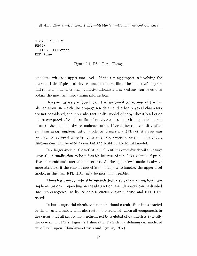
time : THEORY
BEGIN
TIME: TYPE=nat
END time
Figure 2.1: PVS Time Theory
compared with the upper two levels. If the timing properties involving the
characteristic of physical devices need to be veri�ed, the netlist after place
and route has the most comprehensive information needed and can be used to
obtain the most accurate timing information.
However, as we are focusing on the functional correctness of the im-
plementation, in which the propagation delay and other physical characters
are not considered, the more abstract netlist model after synthesis is a better
choice compared with the netlist after place and route, although the later is
closer to the actual hardware implementation. If we decide to use netlists after
synthesis as our implementation model to formalize, a RTL netlist viewer can
be used to represent a netlist by a schematic circuit diagram. This circuit
diagram can then be used as our basis to build up the formal model.
In a larger system, the netlist model contains excessive detail that may
cause the formalization to be infeasible because of the sheer volume of prim-
itives elements and internal connections. As the upper level model is always
more abstract, if the current model is too complex to handle, the upper level
model, in this case RTL HDL, may be more manageable.
There has been considerable research dedicated to formalizing hardware
implementations. Depending on the abstraction level, this work can be divided
into two categories: netlist schematic circuit diagram based and RTL HDL
based.
In both sequential circuit and combinational circuit, time is abstracted
to the natural number. This abstraction is reasonable when all components in
the circuit and all inputs are synchronized by a global clock which is typically
the case in an FPGA. Figure 2.1 shows the PVS theory de�ning our model of
time based upon (Mandayam Srivas and Cyrluk, 1997).
16

M.A.Sc Thesis � Honghan Deng � McMaster � Computing and Software
2.2 Assumptions
Synchronous circuit �Synchronous circuits are easier to design and used
in a vast majority of practical applications � (Brown and Vranesic, 2008). In
safety critical system hardware, a synchronous system is usually preferred.
This is because in an asynchronous sequential circuit, a glitch caused by a
hazard could make the system enter an incorrect state since the latches are
level sensitive and the glitch is able to be captured by the latches. For a
synchronous sequential circuit, the �ip �ops only change state at the clock
edge where the input signals must be stable before and after the clock edge for
the setup and hold times respectively of the �ip �ops (Brown and Vranesic,
2008). Further, it is easier to apply formal methods to synchronous circuits due
to their simple deterministic timing behaviour. In an asynchronous sequential
circuit, time is typically modelled as a real number since we need high timing
resolution to analyze the behaviour of the circuit. In synchronous sequential
circuit, the transition between states at the active clock edge can be ignored,
thereby simplifying our veri�cation model. In the research on RTL HDL level
formalization, there are quite few types of formal semantics of RTL HDL
capable of modelling asynchronous systems based on simulation cycles such as
event semantics. However the underlying mechanism of these semantics is the
use of interleaving execution of concurrent threads to simulate the concurrency
of hardware of HDL (Russiono�, 2005), they may not be suitable application
to the formal veri�cation of functional correctness. If we constrain our system
to be synchronous, the formal semantics of RTL HDL models can be simpli�ed
signi�cantly and reduced to a relative small subset of possible behaviours.
In this thesis, all the models are designed to be synchronous and syn-
chronized by the same clock. Within these systems, only combinational circuit
and and �ip-�ops existed. The input signals can be divided into two types:
signals from other systems and signals from external sensors. In the previous
case, it is obvious that the inputs from other systems must be already synchro-
nized with signals in the current system since all the systems are synchronized
by the same clock (based on the unique clock assumption 2.2).
In the second case, if the signal is representing a sensor process or other
17

M.A.Sc Thesis � Honghan Deng � McMaster � Computing and Software
Figure 2.2: Asynchronous Input to Synchronization Circuit
system which is not synchronized by the same clock, then we assumed there
is a extra circuit to synchronize this signal as shown in Figure 2.2.
In�nite Clock The clock signal in a circuit is generated by crystal oscillator
module, which will start right away after power is on, and will never stop. Thus
the clock is consider to be a nature number. 0 is the time tick when the system
is powered on.
Unique clock We assume there is only one globle clock used in the system.
The clock skew and clock jitter problem is not in our consideration as we focus
on a more abstract level. Under this assumption, the clock can be abstract as a
natural number representing the number of completed clock cycles. The signal
clock will not appear in the formalized model, instead, it has been embedded
into the model implicitly. In such a synchronous circuit driven by a unique
clock, all signals are functions whose domain is the natural numbers.
Perfect gate As we focus on the functional correctness of the circuit, all
gates and internal wires are assumed to be propagation delay free. A D �ip-
�op will have one clock cycle delay between input and output.
18

M.A.Sc Thesis � Honghan Deng � McMaster � Computing and Software
signal [time ,OUTPUT:TYPE]: THEORY
BEGIN
signal :TYPE=[time ->OUTPUT]
bitsignal :TYPE=[time ->bool]
END signal
Figure 2.3: Signal Theory
2.3 Formal Models of the Netlist Level
2.3.1 Hardware Signal Representation
Signal Type In PVS As variant of Signals with di�erent bit width typically
co-exist in circuits. Therefore we will use the parametrizable signal type
de�nition of (Mandayam Srivas and Cyrluk, 1997) to facilitate speci�cation in
PVS (Figure 2.3).
Instead of using a bit-vector representation, the value of a signal at a
particular time tick is represented by a decimal nature number for unsigned
numbers and a decimal integer for signed numbers. This is due to the absence
of bit-vector automatically reasoning strategy in PVS. Although PVS has in-
corporated bitvector library, PVS's decision procedures cannot automatically
decide bitvector equalities (Mandayam Srivas and Cyrluk, 1997). It is also
possible to merge 1 bit and N bit signal data type. However, being looked
as a boolean value, 1 bit signal signal(t) can be directly used in a PVS proof
sequent instead of use signal(t) = 1 to evaluate its state. Also, lots of signal
with 1 bit data width are used for control logic purposes. Bearing a boolean
data type, these signals more accurately re�ect their physical meaning.
Signal Value Representation In PVS The value of a signal at a particular
time tick signal(t) is represented by a natural number for unsigned value
or integer number for signed number in the formalized netlist circuit model,
although these values exist as bit-vectors in the hardware implementations. As
shown in Figure 2.4, the arithmetic operators applied on the natural/integer
numbers are realized by primitive arithmetic elements such as an adder without
the carry out. All the additions will use this primitive adder and all the
19
M.A.Sc Thesis � Honghan Deng � McMaster � Computing and Software
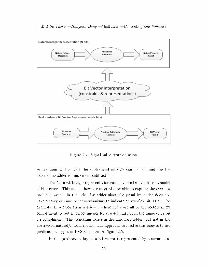
Figure 2.4: Signal value representation
subtractions will convert the subtrahend into 2's complement and use the
exact same adder to implement subtraction.
The Natural/Integer representation can be viewed as an abstract model
of bit vectors. This model, however must also be able to capture the over�ow
problem present in the primitive adder since the primitive adder does not
have a carry out and other mechanisms to indicate an over�ow situation. For
example: In a calculation a + b = c where a, b, c are all 32 bit vectors in 2's
complement, to get a correct answer for c, a+ b must be in the range of 32 bit
2's compliment. This constrain exists in the hardware adder, but not in the
abstracted natural/integer model. One approach to resolve this issue is to use
predicate subtypes in PVS as shown in Figure 2.5.
In this predicate subtype, a bit vector is represented by a natural/in-
20

M.A.Sc Thesis � Honghan Deng � McMaster � Computing and Software
...
%Predicate subtype for 16/32 bits 2's complementary
%bitvecotr representation
BIT16_RANGE_2C: TYPE={t:int|t<=exp2 (15)-1 & t>=-exp2 (15)}
BIT32_RANGE_2C: TYPE={t:int|t<=exp2 (31)-1 & t>=-exp2 (31)}
BIT16_RANGE: TYPE={t:nat|t<=exp2 (16) -1}
BIT32_RANGE: TYPE={t:nat|t<=exp2 (32) -1}
%16/32 bits 2's complentarty signal representation
SIGNAL16_2C :TYPE=[TIME ->BIT16_RANGE_2C]
SIGNAL32_2C :TYPE=[TIME ->BIT32_RANGE_2C]
...
Figure 2.5: Predicate subtype for 16/32 bitvector in highest16 module
teger number constrained by a speci�ed bit width. The over�ow problem can
be captured by automatically generated type correctness conditions (TCC) in
PVS. Figure 2.6 de�nes a primitive adder and a theorem using such an adder.
Two operands and the sum are de�ned as 32 bit 2's complement numbers. As
a result, the sum has a potential over�ow problem and this issue can captured
by the automatically generated over�ow_example1_TCC1. in the bottom
portion of the �gure. The range and value representation of bit vector addition
is accomplished in a similar fashion in PVS' speci�cation language.
2.3.2 Formalization of Combinational components in PVS
Pins and Wires Pins and wires in a schematic diagram are modelled as
signal type (see Figure 2.3).
Constant Constants are de�ned to be lambda functions:
ZERO : [TIME− > BUS_TY PE] = (lambda(t) : 0)
ONE : [TIME− > BUS_TY PE] = (lambda(t) : 1)
BUS_TY PE is de�ned as BUS_TY PE : TY PE = t : nat|t <= exp2(BW )− 1
and BW is the bit width of the bus. In such a way, ONE and ZERO are de-
21

M.A.Sc Thesis � Honghan Deng � McMaster � Computing and Software
sample_OF_ADDER: THEORY
BEGIN IMPORTING time
BIT32_RANGE_2C: TYPE={t:int|t<=exp2 (31)-1 & t>=exp2 (31)}
SIGNAL32_2C :TYPE=[TIME ->BIT32_RANGE_2C]
%============== PRIMITIVE ADDER AND SUB ===========================
HDL_ADDER(bv1 ,bv2 ,sum:BIT32_RANGE_2C ): bool= (sum=(bv1+bv2))
HDL_SUB(bv1 ,bv2 ,sub:BIT32_RANGE_2C ): bool= (sub=(bv1 -bv2))
%============== TWO OVERFLOW EXAMPLES =============================
overflow_example1: THEOREM
FORALL (t:TIME ,bv1 ,bv2 ,sum:SIGNAL32_2C) :
HDL_ADDER(bv1(t),bv2(t),bv1(t)+bv2(t))<=>TRUE
overflow_example2: THEOREM
FORALL (t:TIME ,bv1 ,bv2 ,sub:SIGNAL32_2C) :
HDL_SUB(bv1(t),bv2(t),bv1(t)-bv2(t))<=>TRUE
END sample_OF
%================ Generated TCC ===================================
% Subtype TCC generated (at line 13, column 66) for
bv1(t) + bv2(t)
% expected type BIT32_RANGE_2C
% unfinished overflow_example1_TCC1: OBLIGATION
FORALL (t: TIME , bv1 , bv2 , sum: SIGNAL32_2C ):
bv1(t) + bv2(t) <= exp2 (31) - 1 & bv1(t) + bv2(t) >= exp2 (31);
% Subtype TCC generated (at line 15, column 64) for
bv1(t) - bv2(t)
% expected type BIT32_RANGE_2C
% unfinished overflow_example2_TCC1: OBLIGATION
FORALL (t: TIME , bv1 , bv2 , sub: SIGNAL32_2C ):
bv1(t) - bv2(t) <= exp2 (31) - 1 & bv1(t) - bv2(t) >= exp2 (31);
Figure 2.6: TCCs for addition and subtraction
22
M.A.Sc Thesis � Honghan Deng � McMaster � Computing and Software
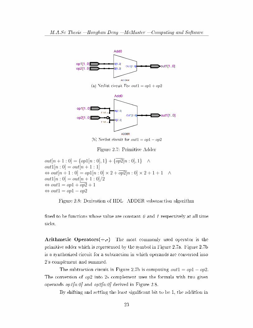
(a) Netlist circuit For out1 = op1 + op2
(b) Netlist circuit for out1 = op1− op2
Figure 2.7: Primitive Adder
out[n+ 1 : 0] = {op1[n : 0], 1}+ {op2[n : 0], 1} ∧out1[n : 0] = out[n+ 1 : 1]⇔ out[n+ 1 : 0] = op1[n : 0]× 2 + op2[n : 0]× 2 + 1 + 1 ∧out1[n : 0] = out[n+ 1 : 0]/2⇔ out1 = op1 + op2 + 1⇔ out1 = op1− op2
Figure 2.8: Derivation of HDL_ADDER substraction algorithm
�ned to be functions whose value are constant 0 and 1 respectively at all time
ticks.
Arithmetic Operators(+,-) The most commonly used operator is the
primitive adder which is represented by the symbol in Figure 2.7a. Figure 2.7b
is a synthesized circuit for a subtraction in which operands are converted into
2's complement and summed.
The subtraction circuit in Figure 2.7b is computing out1 = op1− op2.The conversion of op2 into 2s complement uses the formula with two given
operands op1[n:0] and op2[n:0] derived in Figure 2.8.
By shifting and setting the least signi�cant bit to be 1, the addition in
23

M.A.Sc Thesis � Honghan Deng � McMaster � Computing and Software
op2+1 is avoided. Also, the internal bit width of the adder is 1 extra bit to �t
the expanded width of both operands. It is possible to use primitive addition
to de�ne this algorithm to build the subtraction, however, it is unnecessary
to include these details in the proof. Thus we simply de�ne addition and
subtraction operators as shown in Figure 2.8 with (n=32).
HDL_ADDER(op1, op2, out1 : BIT32_RANGE_2C) : bool
= (out1 = (op1 + op2))
HDL_SUB(op1, op2, out1 : BIT32_RANGE_2C) : bool
= (out1 = (op1− op2))
As the op1 − op2 could also cause an over�ow when the result out1 has the
same bit width as op1 and op2, over�ow_example2_TCC1 in Figure 2.6 will
also be generated to prevent the result from being over�ow.
We can conclude that a bit vector addition and subtraction in Figure
2.7 can be abstract to be out = op1 + op2 and out = op1 − op2 respectively,
where out, op1 and op2 are signal type. If out1 has the same bit width with
op1 and op2, then the generated TCCs cannot be discharged unless op1± op2is within the range of the signal representation. If out has more bits than op1
and op2, then the TCC is easily to be discharged no matter what are the value
of op1 and op2.
Relation Operators The most commonly used relation operators are {=, <,>,6,>}. Both signed and unsigned number equality operators share the
same circuit as shown in Figure 2.9.
24

M.A.Sc Thesis � Honghan Deng � McMaster � Computing and Software
Figure 2.9: Equivalence operator
This comparator can be formalized as the following (N=32):
HDL_EQUAL(op1, op2, out1 : BIT32_RANGE_2C) : bool =
(out1 = (op1 = op2))
Relational operators < and > are implemented by using the same netlist cir-
cuit with switched inputs. The operator <s for signed and <u for unsigned
numbers are the same in the netlist circuit. However the signed operands will
be processed before they are fed into the unsigned comparator.
An unsigned comparator <u in Figure 2.10(a) can be formalized as
below for bitwidth N=32:
HDL_LESS_THAN(op1, op2, out1 : BIT32_RANGE) : bool =
(out1 = (op1 < op2))
Similarly, the 6u operator in Figure 2.10(b) can be formalized as (for N=32):
HDL_LESS_THAN(op1, op2, out1 : BIT32_RANGE) : bool =
(out1 = (op1 <= op2))
Signed comparators are essentially the same as the unsigned compara-
tors with two operands pre-processed. Given two signed operands op1 =
25

M.A.Sc Thesis � Honghan Deng � McMaster � Computing and Software
(a) Unsigned comparator:<u
(b) Unsigned comparator:6u
Figure 2.10: Unsigned comparator
[an, an−1, ... , a0], op2 = [bn, bn−1, ... , b0], from the knowledge of the 2's com-
plement representation, we have the following reasoning (<s and <u represent
signed number and unsigned comparators respectively).
case1:an = bn
[an, an−1, ... , a0] <s [bn, bn−1, ... , b0]
⇐⇒ [an−1, ... , a0] <u [bn−1, ... , b0]
⇐⇒ [bn, an−1, ... , a0] <u [an, bn−1, ... , b0]
case2:an = 1 ∧ bn = 0
[1, an−1, ... , a0] <s [0, bn−1, ... , b0]
⇐⇒ [0, an−1, ... , a0] <u [1, bn−1, ... , b0]
⇐⇒ TRUE
case3: an = 0 ∧ bn = 1
[0, an−1, ... , a0] <s [1, bn−1, ... , b0]
⇐⇒ [1, an−1, ... , a0] <u [0, bn−1, ... , b0]
⇐⇒ FALSE
By this analysis, we can make conclusion that a signed number com-
parator can be built by switching the MSB of two operands and then using an
unsigned comparator to evaluate these processed operands.
26
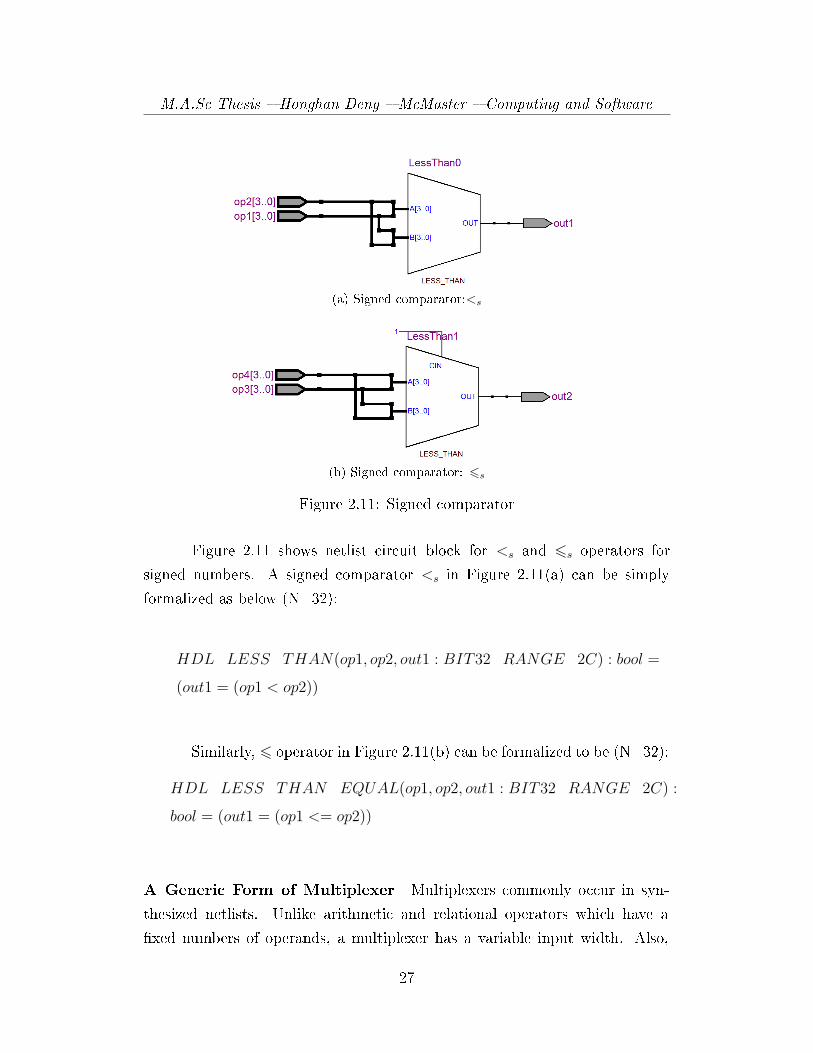
M.A.Sc Thesis � Honghan Deng � McMaster � Computing and Software
(a) Signed comparator:<s
(b) Signed comparator: 6s
Figure 2.11: Signed comparator
Figure 2.11 shows netlist circuit block for <s and 6s operators for
signed numbers. A signed comparator <s in Figure 2.11(a) can be simply
formalized as below (N=32):
HDL_LESS_THAN(op1, op2, out1 : BIT32_RANGE_2C) : bool =
(out1 = (op1 < op2))
Similarly, 6 operator in Figure 2.11(b) can be formalized to be (N=32):
HDL_LESS_THAN_EQUAL(op1, op2, out1 : BIT32_RANGE_2C) :
bool = (out1 = (op1 <= op2))
A Generic Form of Multiplexer Multiplexers commonly occur in syn-
thesized netlists. Unlike arithmetic and relational operators which have a
�xed numbers of operands, a multiplexer has a variable input width. Also,
27

M.A.Sc Thesis � Honghan Deng � McMaster � Computing and Software
a multiplexer input type can be an integer number or a boolean value. An
appropriate de�nition of a multiplexer (MUX, for short) should at least satisfy
the following criteria:
• It should have a generic form which accepts both input width and input
type as its parameters. For example, a 4 bits to 1 bit MUX needs its
input width to be 4 and data type to be boolean. A generic form of a
MUX should be able to accept these two variables to make the de�nition
of such a 4 to 1 bit mux fully speci�ed.
• The parameters used to de�ne types should be separated from the actual
signal port de�nition. A standard MUX will have data to be selected,
selection signals, and one output.
• The MUX components in the circuit should be an instance of MUX
type. The name of the instance can re�ect its input width and data
type, such as bit_MUX_4to1, BIT32_2C_MUX_16to1. The previous
one is a 4 to 1 multiplexer with boolean data type and the later has 16
32 bit 2's complement integers as inputs. This will facilitate formalizing
the netlist circuit since it provides an easy way to build a one to one
correspondence between the netlist circuit and formal speci�cation in
our naming convention.
Figure 2.12 contains the PVS theory de�ning the parameterized form of
a multiplexer. Theory MUX has two formal parameters: MUX_TYPE and N.
MUX_TYPE is used to de�ne the predicate subtype MUX. All muxes have a
common structure de�ned by MUX_SELECTION_TYPE, MUX_INPUT_TYPE
and MUX_TYPE. A mux predicate is a boolean function with the following
type signature:
[MUX_SEL_TYPE,MUX_INPUT_TYPE,MUX_TYPE->bool]
MUX_TYPE is the type passed by the theory formal parameter used
to de�ne the input and output type.
MUX_SEL_TYPE : TYPE+=below(exp2(N)) is a predicate subtype
constrained by the upper boundary of the number of inputs.
28

M.A.Sc Thesis � Honghan Deng � McMaster � Computing and Software
%================== MUX ===========================
%================================================
% This defination of mux is fully generic with it's parameterized
% data chanel type and number of chanels.
% ++++++++++++++++++++++++++++++++++++++++++++++++++
% MUX_TYPE: Data type of the chanel. a mux could be a bit
% selection or data selection.
% N: exp2(N)= upper boudary of the number of input chanels
% ++++++++++++++++++++++++++++++++++++++++++++++++++
MUX[MUX_TYPE:TYPE+,N:posnat ]: THEORY
BEGIN
MUX_SEL_TYPE: TYPE+=below(exp2(N))
%MUX selection input type. Such an input must be <exp(N)
MUX_INPUT_TYPE:TYPE +=[ below(exp2(N))->MUX_TYPE]
%MUX input chanel type.
MUX:TYPE +={mux:[ MUX_SEL_TYPE ,MUX_INPUT_TYPE ,MUX_TYPE ->bool]|
FORALL (sel:MUX_SEL_TYPE ,mux_in:MUX_INPUT_TYPE ,mux_out:MUX_TYPE ):
mux(sel ,mux_in ,mux_out )=( mux_out=mux_in(sel))}
END MUX
Figure 2.12: Generic Multiplexer De�nition
MUX_INPUT_TYPE:TYPE+=[below(exp2(N))->MUX_TYPE] de-
�nes an array such that each element in the input can be accessed by using an
index based upon the selection signals.
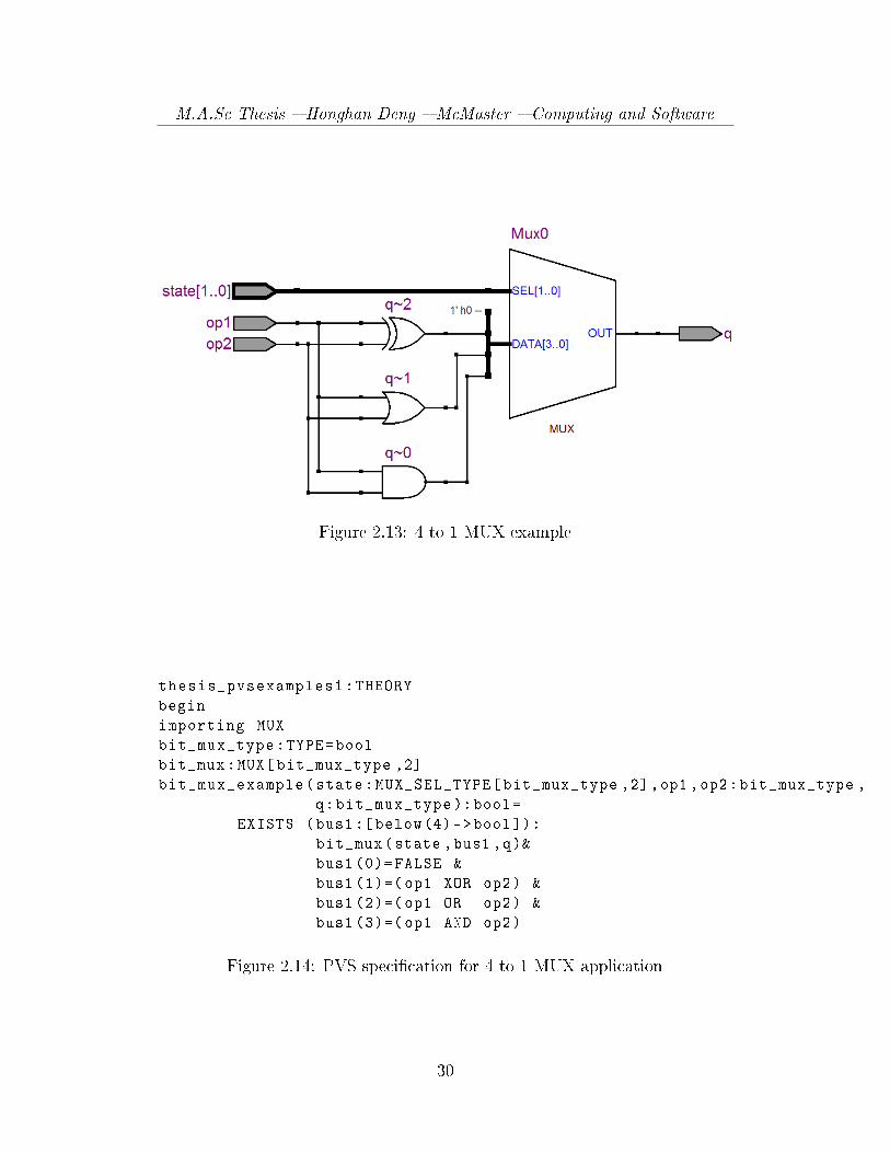
Figure 2.13 is a example use of a 4 to 1 mux with boolean value input
and output. Depending upom the value of the state variable going into the
selection signals, the block outputs either 0, the XOR, OR or AND of the
two operands. A formal speci�cation of such a circuit is de�ned in Figure
2.14. In this example, a MUX instance, bit_mux, is de�ned by bit_mux:MUX
[bit_mux_type,2]. The input and output signal type are de�ned to be boolean
and upper boundary is exp2(N). As the input type is an array, bus1 which is
an assembler is introduced to merge the 4 individual bit inputs into a 4 bit
width data bus. It is possible to avoid this bus1, however, this description
style is more systematic and easier to read.
29
M.A.Sc Thesis � Honghan Deng � McMaster � Computing and Software
Figure 2.13: 4 to 1 MUX example
thesis_pvsexamples1:THEORY
begin
importing MUX
bit_mux_type:TYPE=bool
bit_mux:MUX[bit_mux_type ,2]
bit_mux_example(state:MUX_SEL_TYPE[bit_mux_type ,2],op1 ,op2:bit_mux_type ,
q:bit_mux_type ):bool=
EXISTS (bus1:[below(4)->bool ]):
bit_mux(state ,bus1 ,q)&
bus1 (0)= FALSE &
bus1 (1)=( op1 XOR op2) &
bus1 (2)=( op1 OR op2) &
bus1 (3)=( op1 AND op2)
Figure 2.14: PVS speci�cation for 4 to 1 MUX application
30

M.A.Sc Thesis � Honghan Deng � McMaster � Computing and Software
Generic Form of a Binary Decoder Binary decoders have various input
range and output width, however, unlike multiplexers, the output type of the
binary decoder is always a one-hot encoded bit vector, i.e., there is only one bit
of the n output bits set high at a time. For the de�nition of a binary decoder,
criteria very similar to that used for multiplexers are also applicable . The
parameterized PVS theory for binary decoders is shown in �gure 2.15.
%================= DECODER ===================
%The parameterized N is the used to define the
%size of input as an integer number
%For a decoder output with 2^N bits , the input
%must be a natural number within [0, 2^N-1].
DECODER[N:posnat ]: THEORY
BEGIN
DECODER_INPUT_TYPE: TYPE+=below(exp2(N))
DECODER_OUTPUT_TYPE: TYPE +=[ DECODER_INPUT_TYPE ->bool]
DECODER:TYPE +={
decoder :[ DECODER_INPUT_TYPE ,DECODER_OUTPUT_TYPE ->bool]|
FORALL (
dec_in:DECODER_INPUT_TYPE ,
dec_out:DECODER_OUTPUT_TYPE ):
decoder(dec_in ,dec_out )=
(FORALL (
active: DECODER_INPUT_TYPE ,
inactive: {t:DECODER_INPUT_TYPE|t/= active }):
dec_out(active )=true & dec_out(inactive )=false)}
END DECODER
Figure 2.15: Generic binary decoder de�nition
Theory DECODER has one formal parameter N which is forced to
be positive natural number because the decoder has at least 21 outputs. DE-
CODER_OUTPUT_TYPE is a predicate subtype used to constrain the input
range to be [0, 2N −1]. For example, for a 4-bit binary decoder with N=2, the
input range is [0, 3]. DECODER_OUTPUT_TYPE is de�ned as an array
type to facilitate accessing each bit of the output and its index range is de�ned
by DECODER_INPUT_TYPE which is a natural number in [0, 2N − 1]. By
using this method, the constraint imposed by formal parameter N is intro-
31
M.A.Sc Thesis � Honghan Deng � McMaster � Computing and Software
duced into the de�nition of the decoder. The internal variable active is used
to index the hot bit on the output while dependent typing of inactive is used to
specify the low (false) value of the other bits. inactive is de�ned as a predicate
subtype which covers all the bits other than the active bit.
For the purpose of showing that binary decoder provides the required
one-hot encoding, the following property needs to be proved:
∃x(P (x) ∧ ∀y(P (y) =⇒ (x = y)))
This property can be formalized to as uniqueness_fact in the PVS
theorm below:
DEC_WIDTH: posnat
decoder1: DECODER[DEC_WIDTH]
uniqueness_fact(
dec_in:DECODER_INPUT_TYPE[DEC_WIDTH],
dec_out:DECODER_OUTPUT_TYPE[DEC_WIDTH ]): bool=
EXISTS (active:DECODER_INPUT_TYPE[DEC_WIDTH ]):
(dec_out(active )=true)
AND
(FORALL(inactive:DECODER_INPUT_TYPE[DEC_WIDTH ]) :
dec_out(inactive )=true IMPLIES inactive=active)
DECODER_UNIQUENESS_FACT:THEOREM
FORALL (
dec_in:DECODER_INPUT_TYPE[DEC_WIDTH],
dec_out:DECODER_OUTPUT_TYPE[DEC_WIDTH ]):
decoder1(dec_in ,dec_out) IMPLIES
uniqueness_fact(dec_in ,dec_out)
The property uniqueness_fact de�nes an instance of a generic form of
decoder decoder1. The theory is passed a positive natural number parameter
to constrain its input range and output width. For decoder1, it's input range
is [0, 2DEC_WIDTH − 1].
32
M.A.Sc Thesis � Honghan Deng � McMaster � Computing and Software
2.4 Formal Models of Sequential Circuits in PVS
Since the system is designed to be fully synchronous, D �ip-�ops are the only
sequential component in the netlist circuit for the systems we are dealing with.
A D �ip-�op has the characteristic table as shown in Figure 2.16 (a).
The the netlist view of such a D �ip-�op with a synchronized reset is
shown in �gure 2.16b. All the signals are de�ned to be bitsignal as in Figure
2.3. Obviously when reset=false & clk=true & clk_en=true, Figure 2.16b can
be simpli�ed as in Figure 2.16c. We formalize the characteristic table based
on the two following assumptions:
• The initial state of the D �ip-�op is False (logic 0).
• Signal reset has the highest priority.
The PVS for this formalization is as follows:
REG(D,Q,reset ,clkenable:bitsignal ):bool=
FORALL (t: time):
IF t=0 THEN Q(t)=FALSE
ELSE IF reset(t) THEN Q(t)=FALSE
ELSE IF clkenable(t) THEN Q(t)=D(t-1)
ELSE Q(t)=Q(t-1)
END
END
END
The simpli�ed D Flip-�op in Figure 2.16c can be represented by the
simpli�ed PVS
REG(D,Q:bitsignal ):bool=
FORALL (t):
IF(t=0) THEN Q(t)=FALSE
ELSE Q(t)=D(t-1)
ENDIF
33

M.A.Sc Thesis � Honghan Deng � McMaster � Computing and Software
clk_en clk D Q(t+1)
1 0 x Q(t)1 1 0 01 1 1 10 x x Q(t)
(a) Characteristic Table of syn-chronous D Flip-�op
(b) synchronous D Flip-�op
(c) Simpli�ed Version of (a) when re-
set=false&clk=true&clk_en=true
Figure 2.16: Synchronous D Flip-�op
34
M.A.Sc Thesis � Honghan Deng � McMaster � Computing and Software
Figure 2.17: The sequential circuit with �nite state machine
2.4.1 Formalizing Finite State Machines in PVS
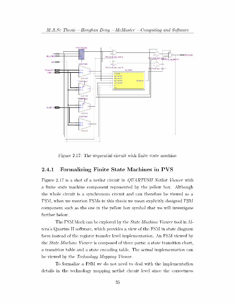
Figure 2.17 is a shot of a netlist circuit in QUARTUSII Netlist Viewer with
a �nite state machine component represented by the yellow box. Although
the whole circuit is a synchronous circuit and can therefore be viewed as a
FSM, when we mention FSMs in this thesis we mean explicitly designed FSM
component such as the one in the yellow box symbol that we will investigate
further below.
The FSM block can be explored by the State Machine Viewer tool in Al-
tera's Quartus II software, which provides a view of the FSM in state diagram
form instead of the register transfer level implementation. An FSM viewed by
the State Machine Viewer is composed of three parts: a state transition chart,
a transition table and a state encoding table. The actual implementation can
be viewed by the Technology Mapping Viewer.
To formalize a FSM we do not need to deal with the implementation
details in the technology mapping netlist circuit level since the correctness
35
M.A.Sc Thesis � Honghan Deng � McMaster � Computing and Software
of such a translation can be veri�ed by equivalence checking tools (Altera,
2011). It is important to realize that in order to utilize equivalence checking
tools such as Cadence Encounter Conformal, the style of the RTL code is of
particular concern because neither tool supports some constructs, leading to po-
tential formal veri�cation mismatches (Altera, 2011). Of course, we can force
the synthesis tool to generate the netlist circuit without extracting a FSM.
In such a case, the circuit will be a sequential circuit without extracted FSM
and the formal model can be constructed by using the components provided
in previous sections.
In the example in Figure 2.17, the design would appear to have two
registers: the PwrCond_Reg (grey) and the state register of the (yellow) state
machine block. However if we check the synthesis report or the technology
mapping, we will actually see that there is only one left: the is_chart register
which is used for state machine. The PwrCond_Reg has been removed by
the optimization process. While we can preserve both registers by adding a
/* synthesis preserve */ comment after the PwrCond_Reg declaration in our
original input �le, typically we would want to take advantage of such optimiza-
tions. This is one of the main reasons why we choose the State Machine Viewer
as the basis for formalize the FSM, since it preserves all the information we
need without introducing all the unnecessary optimization details which can
instead be veri�ed using equivalence checkers.
36

M.A.Sc Thesis � Honghan Deng � McMaster � Computing and Software
(a) FSM state diagram
Name IN_Activated
1 In_Deactivated 0
2 In_Activated 1
(b) FSM Encoding table
Source State Destination State Condition
1 In_Activated In_Activated(!LessThan1)+(LessThan1).(!LessThan0)
.(!clk_enable)+(LessThan1).(LessThan0)
2 In_Activated In_Deactivated (LessThan1).(!LessThan0).(clk_enable)
3 In_Deactivated In_Activated (LessThan1).(!LessThan0).(clk_enable)
4 In_Deactivated In_Deactivated (LessThan1).(!LessThan0).(clk_enable)
(c) FSM transition table
Figure 2.18: FSM components in State Machine Viewer
Formalizing a FSM is equivalent to formalizing the three components
given by the state machine viewer. This process can be standardized to the
following steps:
• Setup the name space.
• Translate the FSM transition table as a state transition predicate called
FSM_TRANSIT and embed enough information to discharge the dis-
joint and coverage TCCs generated by the PVS COND constructs we
will use for this purpose.
• Build a FSM_SHELL to establish the FSM interface and embed the
encoding information.
The following discussion describes an example of formalizing a FSM
from the information given by the state machine viewer, reproduced in Figure
2.18. The �rst step is to de�ne the state space according to the state diagram.
37
M.A.Sc Thesis � Honghan Deng � McMaster � Computing and Software
In Figure 2.18a we see that there are two states named In_Activated and
In_Deactivated. The best way to describe the state space is to use an
enumeration type to de�ne the name space: STATENAME: TYPE= {activated,
deactivated}. State type is a signal that switches its value from tick to tick.
Thus it need to be de�ned as: STATE: TYPE=[TIME->STATENAME].
The most important step is to formalize the transition table. In the
State Machine Viewer, �.� and �+� represent the logical "AND" and "OR"
operators respectively. The general form of the formalized transition table is
state(t)=f(comb(t),state(t-1)), where f is a function de�ned in the transition
table, comb(t) is the current value of all the combinational inputs, state(t-1)
is the previous value of the FSM state. When time is 0, the initial value of the
state is de�ned to be deactivated. The transition condition contains the signal
clock_enable which, to simplify our encoding, we will assume is always true
and thus the transition condition expressions can be simpli�ed accordingly.
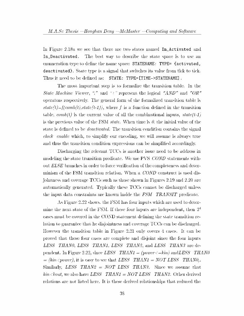
Discharging the relevant TCCs is another issue need to be address in
modeling the state transition predicate. We use PVS COND statements with-
out ELSE branches in order to force veri�cation of the completeness and deter-
minism of the FSM transition relation. When a COND construct is used dis-
jointness and coverage TCCs such as those shown in Figures 2.19 and 2.20 are
automatically generated. Typically these TCCs cannot be discharged unless
the input data constraints are known inside the FSM_TRANSIT predicate.
As Figure 2.22 shows, the FSM has four inputs which are used to deter-
mine the next state of the FSM. If these four inputs are independent, then 24
cases must be covered in the COND statement de�ning the state transition re-
lation to guarantee that he disjointness and coverage TCCs can be discharged.
However the transition table in Figure 2.21 only covers 4 cases. It can be
proved that these four cases are complete and disjoint since the four inputs
LESS_THAN0, LESS_THAN1, LESS_THAN2, and LESS_THAN3 are de-
pendent. In Figure 2.22, since LESS_THAN1 = (power<=kin) andLESS_THAN0
= (kin<power), it is easy to see that LESS_THAN1 = NOT LESS_THAN0,.
Similarly, LESS_THAN2 = NOT LESS_THAN3. Since we assume that
kin<kout, we also have LESS_THAN1 = NOT LESS_THAN2. Other derived
relations are not listed here. It is these derived relationships that reduced the
38

M.A.Sc Thesis � Honghan Deng � McMaster � Computing and Software
% Disjointness TCC generated (at line 55, column 12) for
% COND ((NOT lto1(t)) OR (lto1(t) AND lto0(t))) AND
% state(t - 1) = activated
% -> activated ,
% (lto1(t) AND (NOT lto0(t))) AND state(t - 1) = activated ->
% deactivated ,
% lto2(t) AND state(t - 1) = deactivated -> activated ,
% (NOT lto2(t)) AND state(t - 1) = deactivated -> deactivated
% ENDCOND
% unchecked
FSM_TRANSIT_TCC5: OBLIGATION
FORALL (kin: {x: signal[TIME , BUS_TYPE[N]] | FORALL t: x(t) = KIN},
kout: {x: signal[TIME , BUS_TYPE[N]] | FORALL t: x(t) = KOUT},
pwr: {x: signal[TIME , BUS_TYPE[N]] | x(0) <= KOUT}, state: STATE ,
lto0: bitsignal[TIME , BUS_TYPE[N]],
lto1: bitsignal[TIME , BUS_TYPE[N]],
lto2: bitsignal[TIME , BUS_TYPE[N]],
lto3: bitsignal[TIME , BUS_TYPE[N]], t):
LESS_THEN0(kout(t), pwr(t), lto0(t))
AND LESS_THEN1(pwr(t), kout(t), lto1(t))
AND LESS_THEN2(kin(t), pwr(t), lto2(t))
AND LESS_THEN3(pwr(t), kin(t), lto3(t)) AND NOT t = 0
IMPLIES
NOT ( ((NOT lto1(t)) OR (lto1(t) AND lto0(t)))
AND state(t - 1) = activated AND lto1(t) AND (NOT lto0(t))
AND state(t - 1) = activated)
AND
NOT (((( NOT lto1(t)) OR (lto1(t) AND lto0(t))) AND
state(t - 1) = activated)
AND (NOT lto2(t)) AND state(t - 1) = deactivated) AND
NOT ( lto1(t) AND (NOT lto0(t)) AND state(t - 1) = activated
AND lto2(t) AND state(t - 1) = deactivated)
AND NOT ((lto2(t) AND state(t - 1) = deactivated) AND
(NOT lto2(t)) AND state(t - 1) = deactivated );
Figure 2.19: Disjointness TCC
39
M.A.Sc Thesis � Honghan Deng � McMaster � Computing and Software
% Coverage TCC generated (at line 55, column 12) for
% COND ((NOT lto1(t)) OR (lto1(t) AND lto0(t))) AND
% state(t - 1) = activated % -> activated ,
% (lto1(t) AND (NOT lto0(t))) AND state(t - 1) = activated ->
% deactivated ,
% lto2(t) AND state(t - 1) = deactivated -> activated ,
% (NOT lto2(t)) AND state(t - 1) = deactivated -> deactivated
% ENDCOND % unchecked FSM_TRANSIT_TCC6: OBLIGATION
FORALL (kin: {x: signal[TIME , BUS_TYPE[N]] | FORALL t: x(t) = KIN},
kout: {x: signal[TIME , BUS_TYPE[N]] | FORALL t: x(t) = KOUT},
pwr: {x: signal[TIME , BUS_TYPE[N]] | x(0) <= KOUT}, state: STATE ,
lto0: bitsignal[TIME , BUS_TYPE[N]],
lto1: bitsignal[TIME , BUS_TYPE[N]],
lto2: bitsignal[TIME , BUS_TYPE[N]],
lto3: bitsignal[TIME , BUS_TYPE[N]], t):
LESS_THEN0(kout(t), pwr(t), lto0(t))
AND LESS_THEN1(pwr(t), kout(t), lto1(t))
AND LESS_THEN2(kin(t), pwr(t), lto2(t))
AND LESS_THEN3(pwr(t), kin(t), lto3(t)) AND NOT t = 0
IMPLIES
((NOT lto1(t)) OR (lto1(t) AND lto0(t))) AND state(t - 1) = activated OR
(lto1(t) AND (NOT lto0(t))) AND state(t - 1) = activated OR
lto2(t) AND state(t - 1) = deactivated OR
(NOT lto2(t)) AND state(t - 1) = deactivated;
Figure 2.20: Coverage TCC
40
M.A.Sc Thesis � Honghan Deng � McMaster � Computing and Software
24 cases into four found in the transition table. Therefore, if we want to use
the reduced transition table, we must embed these relation operators and their
connections into the FSM, otherwise the disjointness and conjunction TCCs
will not be discharged.
The way to embedded these relations is to expand the state machine
to include all four LESS_THAN operators as shown in 2.21.
After the state transition relation FSM_TRANSIT has been de�ned,
the last step is to output state encoding to the external circuit. Figure 2.17
shows that the output of the FSM is connected to a multiplexer. According
to Figure 2.18b, when the FSM is in the IN_Activated state, the output to
the multiplexer is a logical 1. In the actual implementation of the FSM, there
are many alternative state assignment method. In our case, we do not need
to consider such details since we can just output a boolean value by using the
predicate in Figure 2.23. Two new variables are introduced: bool_output and
testing_state_name, the boolean output value determine if the current state
is equivalent to the speci�ed state testing_state_name which is assigned to
be IN_Activated. Thus whenever the FSM state is IN_Activated, the boolean
output is a logic 1.
2.5 Formal Models of the RTL HDL level
When the netlist circuit is too complicated, the formalization process could be
very ine�cient and impractical. This problem could be solved by decomposing
the netlist circuit implementation carefully, or by developing some tools to
translate the circuit automatically (Mansouri and Vemuri, 2000). Another
approach is, instead of formalizing the netlist circuit which may involve too
much detail, to formalize the RTL HDL model. The HDL model is above
netlist circuit model in Figure 1.3 which means it is more abstract. The lower
the model is in the design process, the closer it is to the real circuit.
As the name implies, the functional semantics we will employ focus on
the functionality of the HDL model. It sacri�ces some of the expressivity of
the asynchronous simulation sematntics and requires extra constraints to be
applied on the HDL model. As discussed in 2.2, the assumption is that we
41
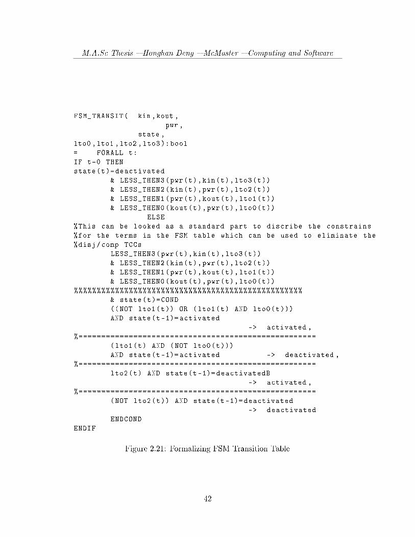
M.A.Sc Thesis � Honghan Deng � McMaster � Computing and Software
FSM_TRANSIT( kin ,kout ,
pwr ,
state ,
lto0 ,lto1 ,lto2 ,lto3):bool
= FORALL t:
IF t=0 THEN
state(t)= deactivated
& LESS_THEN3(pwr(t),kin(t),lto3(t))
& LESS_THEN2(kin(t),pwr(t),lto2(t))
& LESS_THEN1(pwr(t),kout(t),lto1(t))
& LESS_THEN0(kout(t),pwr(t),lto0(t))
ELSE
%This can be looked as a standard part to discribe the constrains
%for the terms in the FSM table which can be used to eliminate the
%disj/comp TCCs
LESS_THEN3(pwr(t),kin(t),lto3(t))
& LESS_THEN2(kin(t),pwr(t),lto2(t))
& LESS_THEN1(pwr(t),kout(t),lto1(t))
& LESS_THEN0(kout(t),pwr(t),lto0(t))
%%%%%%%%%%%%%%%%%%%%%%%%%%%%%%%%%%%%%%%%%%%%%%%%%%
& state(t)=COND
((NOT lto1(t)) OR (lto1(t) AND lto0(t)))
AND state(t-1)= activated
-> activated ,
%====================================================
(lto1(t) AND (NOT lto0(t)))
AND state(t-1)= activated -> deactivated ,
%====================================================
lto2(t) AND state(t-1)= deactivatedB
-> activated ,
%====================================================
(NOT lto2(t)) AND state(t-1)= deactivated
-> deactivated
ENDCOND
ENDIF
Figure 2.21: Formalizing FSM Transition Table
42

M.A.Sc Thesis � Honghan Deng � McMaster � Computing and Software
Figure 2.22: FSM and LESS_THAN operators
FSM_SHELL(kin ,kout ,
pwr ,
testing_state_name ,
bool_output ,
lto0 ,lto1 ,lto2 ,lto3):bool=
EXISTS (state_output:STATE):
FORALL t:
FSM_TRANSIT(kin ,kout ,pwr ,state_output ,lto0 ,lto1 ,lto2 ,lto3)&
bool_output(t)= (state_output(t)= testing_state_name)
Figure 2.23: FSM_SHELL - the FSM output interface to the surroundingcircuit
43

M.A.Sc Thesis � Honghan Deng � McMaster � Computing and Software
are dealing with a synchronous system driven by a unique clock and that all
inputs are synchronized by the same clock. If we applied these assumptions
in the HDL model, then the functional semantics will be powerful enough to
describe the system and neat enough to support formal veri�cation.
In the following sections, a subset of the Verilog HDL semantics will
be discussed and a Verilog implementation will be formalized into PVS spec-
i�cation. More speci�cally, we only discuss a small subset of Verilog used to
construct the synchronous sequential circuit which satisfy the following 5 rules.
1. Non-blocking assignment only occurs within blocks of the form
always @ (posedge clk) begin ... end
2. Blocking assignments occur only within blocks of the form
always @* begin ... end
3. No timing controls are used
4. No signals is assigned values by two distinct processes
5. The program does not contain any set of blocking or continuous assign-
ments v0 = E0 ... , vk = Ek, such that vi occurs in Ei−1 for i = 1 ... , k
and vk = v0.
Note that the last principle is not necessary in a synchronous sequential
circuit design as the last assumption is used to prevent the nondeterministic
behaviour in a simulation in a particular simulation cycle (Russiono�, 2005).
This problem is caused by sequential software execution that cannot simulate
the concurrency of the hardware exactly. However this risk is only observable
at the simulation level and is not observable in actual hardware synthesis and
its formalization.
44

M.A.Sc Thesis � Honghan Deng � McMaster � Computing and Software
2.5.1 Formal Semantics of a Subset of Verilog
Wire and Reg Type De�nition Both wire and reg type are de�ned as a
signal which is a function of time. For example:
reg signed [15:0] low;
reg signed [15:0] lowest;
reg signed [15:0] i;
These reg type variables can be formalized as signals type in PVS as
below:
low , lowest , i : VAR BIT16_RANGE_2C
where BIT16_RANGE_2C is de�ned in Figure 2.5 as a signed integer, in Verilog
they are represented as 16 bit 2's complement.
For the reader unfamiliar with Verilog, please note that that a reg
declaration does not imply that quanties such as low will be synthesized as
an actual hardware register, but rather that its value will be determined by a
procedural block with sequential semantics.
Continuous assignment The continuous assignment statement and always
block are the only procedures we have in the program and these blocks are
concurrent. Thus all the continuous assignment can be rearranged - i.e., the
synthesized hardware is independent of their order of appearance in the Ver-
ilog code. The semantics of continuous assignment is: whenever the value of
the signal on the right hand side changes, the left hand side signal will be up-
dated. As our circuit is designed to be synchronous circuit and all the changes
occurred in the clock edge, we have the following formal semantics.
For a continuous assignment statement:
wire a,b;
assign a=b;
It can be formalized as:
∀t : a(t) = b(t)
where t is a natural number representing the number of positive clock edges.
In PVS, it can be formalized as:
45
M.A.Sc Thesis � Honghan Deng � McMaster � Computing and Software
a,b :VAR bitsignal
FORALL (t:time): a(t)=b(t)
In practice, usually there are more than single continuous assignment
statements in the design. These statements can be formalized individually and
connected by conjunction because the continuous assignments are evaluated
concurrently. Consider the Verilog code:
assign sum = sum_reg_next;
assign done = done_reg_next;
These two continuous assignment will be formalized as:
∀t : sum(t) = sum_reg_next(t) ∧ done(t) = done_reg_next(t)
and in PVS they can be written as:
FORALL (t:time): sum(t)= sum_reg_next(t)
& done(t)= done_reg_next(t)
Blocking assignment We constrain the blocking assignment to only occurr
in an always block of form:
always @*
begin
. . .
end
This block will be synthesized as a combinational circuit if there is no implied
memory occurring in this block. A block is only entered when changes occurred
for the right hand side signals in the blocking assignment. Just as multiple
continuous assignment statements are connected by conjunctions, the blocking
assignment statements are also connected by conjunction. When the blocking
assignments are formalized, their sequence should be maintained. Also, to
make the formalized PVS speci�cation more readable, each always block should
be translated into a boolean function accordingly. Usually in an RTL HDL
design, each always block is designed to implement some functionality. Naming
these always blocks appropriately will greatly facilitate our proof in controlling
46

M.A.Sc Thesis � Honghan Deng � McMaster � Computing and Software
the complexity and following the instantiation steps explained later in this
chapter.
For example, an always block describing the next state logic of a state
machine might be of the form:
always @* begin
v0_next=b0;
v1_next=b1;
...
vk_next=bk;
end
Assuming all signals are bit signals, such a block can be formalized as
a predicate in PVS named FSM_NEXT :
FSM_NEXT(t:time ,v0,v1 ,...,vk,b1 ,...,bk: bitsignal ): bool
FORALL t:
v0_next(t)=b0(t) &
v1_next(t)=b1(t) &
... &
vk_next(t)=bk(t)
It is possible to merge always blocks that are using blocking assign-
ments. However, since each always block is concurrently evaluated, the se-
quence of the always blocks in the Verilog code is irrelevant. For example:
always @* begin
v0=b0;
v1=b1;
...
vk=bk;
end
always @* begin
x1=a0;
x2=a2;
...
xk=ak;
47

M.A.Sc Thesis � Honghan Deng � McMaster � Computing and Software
end
can be formalized as below as long as the internal assignment statement se-
quence within each always block is maintained:
Merged_Block(t:time ,v0,v1 ,...,vk,
a1 ,...,ak,
x1 ,...,xk,
b1 ,...,bk: bitsignal ): bool
FORALL t:
v0(t)=b0(t) &
v1(t)=b1(t) &
... &
vk(t)=bk(t) &
x0(t)=a0(t) &
x1(t)=a1(t) &
... &
xk(t)=ak(t)
An interesting question is: Can the sequence of blocking assignments
be altered in an always block with the following form:
always @*
begin
v0=E0;
v1=E1;
...
vk=Ek;
end
At the moment, there are two cases to discuss (we do not consider
overriding until Section 2.5.3):
• case 1 vi=Ei i=1,2...,k are fully independent
That is, for all vi i=1,2...,k it is not the case that any of the variables
occurring of the left hand side in the always block appears in any of the
expressions Ej on the right hand side, where j=1,...,k. This means all the
blocking assignment statements are fully independent. Obviously, the sequence
48
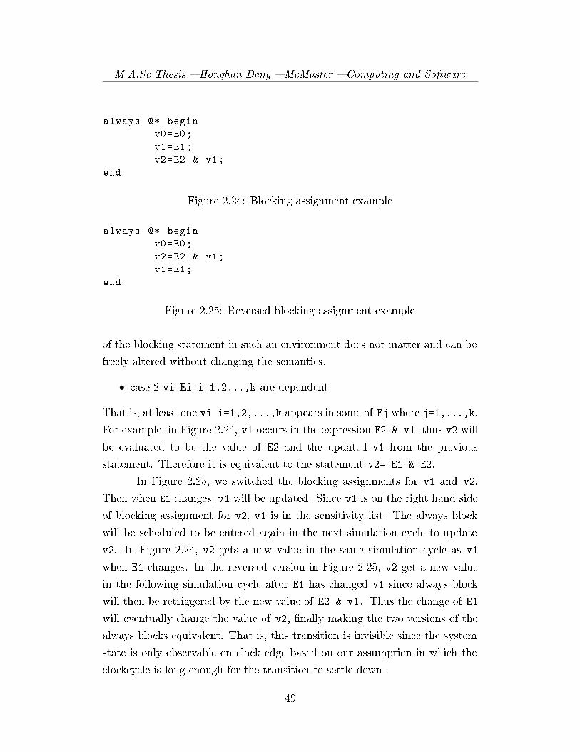
M.A.Sc Thesis � Honghan Deng � McMaster � Computing and Software
always @* begin
v0=E0;
v1=E1;
v2=E2 & v1;
end
Figure 2.24: Blocking assignment example
always @* begin
v0=E0;
v2=E2 & v1;
v1=E1;
end
Figure 2.25: Reversed blocking assignment example
of the blocking statement in such an environment does not matter and can be
freely altered without changing the semantics.
• case 2 vi=Ei i=1,2...,k are dependent
That is, at least one vi i=1,2,...,k appears in some of Ej where j=1,...,k.
For example, in Figure 2.24, v1 occurs in the expression E2 & v1, thus v2 will
be evaluated to be the value of E2 and the updated v1 from the previous
statement. Therefore it is equivalent to the statement v2= E1 & E2.
In Figure 2.25, we switched the blocking assignments for v1 and v2.
Then when E1 changes, v1 will be updated. Since v1 is on the right hand side
of blocking assignment for v2, v1 is in the sensitivity list. The always block
will be scheduled to be entered again in the next simulation cycle to update
v2. In Figure 2.24, v2 gets a new value in the same simulation cycle as v1
when E1 changes. In the reversed version in Figure 2.25, v2 get a new value
in the following simulation cycle after E1 has changed v1 since always block
will then be retriggered by the new value of E2 & v1. Thus the change of E1
will eventually change the value of v2, �nally making the two versions of the
always blocks equivalent. That is, this transition is invisible since the system
state is only observable on clock edge based on our assumption in which the
clockcycle is long enough for the transition to settle down .
49
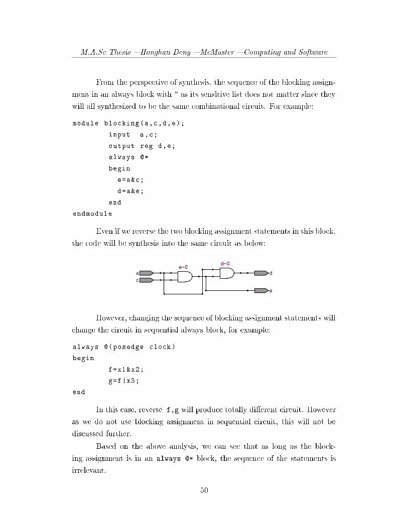
M.A.Sc Thesis � Honghan Deng � McMaster � Computing and Software
From the perspective of synthesis, the sequence of the blocking assign-
ment in an always block with * as its sensitive list does not matter since they
will all synthesized to be the same combinational circuit. For example:
module blocking(a,c,d,e);
input a,c;
output reg d,e;
always @*
begin
e=a&c;
d=a&e;
end
endmodule
Even if we reverse the two blocking assignment statements in this block,
the code will be synthesis into the same circuit as below:
However, changing the sequence of blocking assignment statements will
change the circuit in sequential always block, for example:
always @(posedge clock)
begin
f=x1&x2;
g=f|x3;
end
In this case, reverse f,g will produce totally di�erent circuit. However
as we do not use blocking assignment in sequential circuit, this will not be
discussed further.
Based on the above analysis, we can see that as long as the block-
ing assignment is in an always @* block, the sequence of the statements is
irrelevant.
50
M.A.Sc Thesis � Honghan Deng � McMaster � Computing and Software
Non Blocking Assignment By the assumption state at the start of Sec-
tion 2.5, non blocking assignmentd will only be used in always blocks of the
form:
always @ (posedge clk) begin ... end
Such an always block is used to represent a synchronous sequential
circuit and the variable on the left hand side inside the block will be synthesized
to be registers or internal connecting wires. To focus on the formalization of
non-blocking assignment, we only discuss always blocks of the form show in
Figure 2.26.
always @ (posedge clk)
begin
v0 <=E1;
v1 <=E2;
...
vk <=Ek;
end
Figure 2.26: Non-blocking assignment in an always block
That is no other behaviour control such as IF ELSE statements are
used in the blocks which will be discussed in the next part.
The formal semantics of non-blocking assignment can be analyzed from
two perspectives: the synthesis oriented and simulation oriented. A correct
formal semantics should be consistent in both views. Like other analysis in this
thesis, the formal semantics of the non-blocking assignment is discussed under
some assumptions and conditions. Besides the �ve constrains on Verilog stated
at the begining of Section 2.5, we also assumed that there are no duplicate
names on the left hand side. That is, there is no more than one non-blocking
assignment statement which updates a particular variable anywhere in the
assignment sequence in Figure 2.26.
Under this assumption we examine the formal semantics of a non-
blocking assignment from the following perspective.
• Synthesis perspective
51
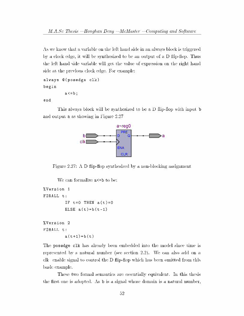
M.A.Sc Thesis � Honghan Deng � McMaster � Computing and Software
As we know that a variable on the left hand side in an always block is triggered
by a clock edge, it will be synthesized to be an output of a D �ip-�op. Thus
the left hand side variable will get the value of expression on the right hand
side at the previous clock edge. For example:
always @(posedge clk)
begin
a<=b;
end
This always block will be synthesized to be a D �ip-�op with input b
and output a as showing in Figure 2.27
Figure 2.27: A D �ip-�op synthesized by a non-blocking assignment
We can formalize a<=b to be:
%Version 1
FORALL t:
IF t=0 THEN a(t)=0
ELSE a(t)=b(t-1)
%Version 2
FORALL t:
a(t+1)=b(t)
The posedge clk has already been embedded into the model since time is
represented by s natural number (see section 2.2). We can also add on a
clk_enable signal to control the D �ip-�op which has been omitted from this
basic example.
These two formal semantics are essentially equivalent. In this thesis
the �rst one is adopted. As b is a signal whose domain is a natural number,
52
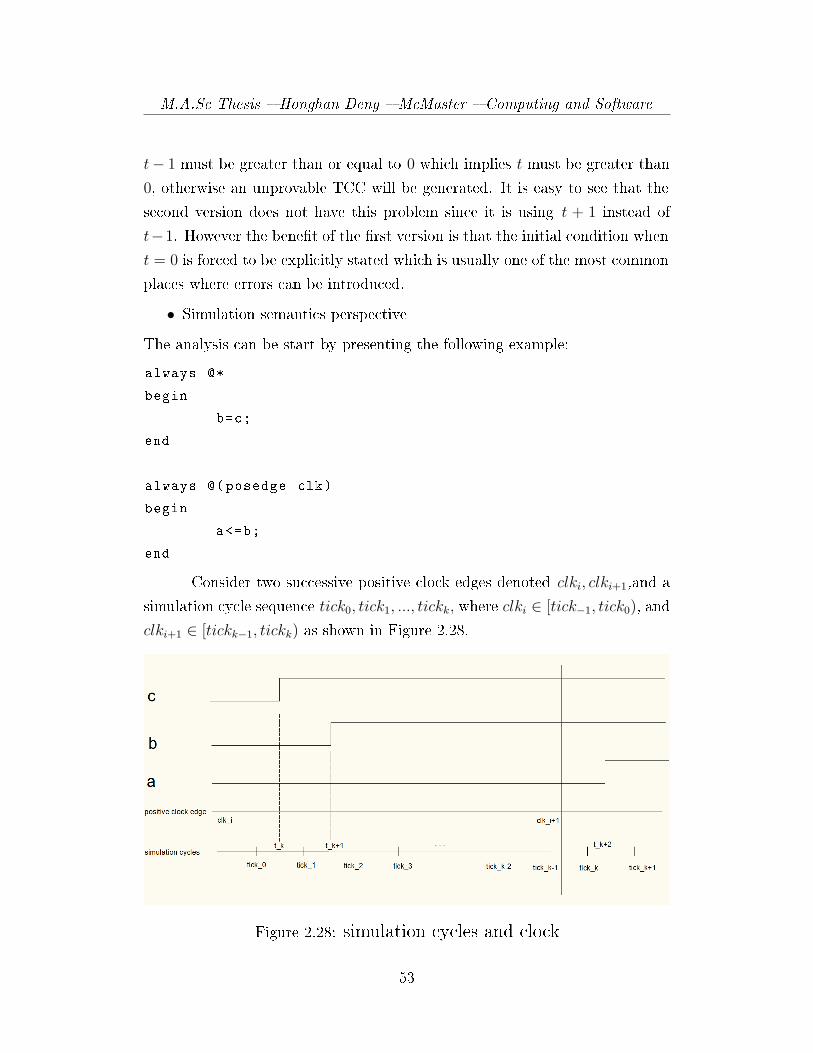
M.A.Sc Thesis � Honghan Deng � McMaster � Computing and Software
t− 1 must be greater than or equal to 0 which implies t must be greater than
0, otherwise an unprovable TCC will be generated. It is easy to see that the
second version does not have this problem since it is using t + 1 instead of
t−1. However the bene�t of the �rst version is that the initial condition when
t = 0 is forced to be explicitly stated which is usually one of the most common
places where errors can be introduced.
• Simulation semantics perspective
The analysis can be start by presenting the following example:
always @*
begin
b=c;
end
always @(posedge clk)
begin
a<=b;
end
Consider two successive positive clock edges denoted clki, clki+1,and a
simulation cycle sequence tick0, tick1, ..., tickk, where clki ∈ [tick−1, tick0), and
clki+1 ∈ [tickk−1, tickk) as shown in Figure 2.28.
Figure 2.28: simulation cycles and clock
53

M.A.Sc Thesis � Honghan Deng � McMaster � Computing and Software
In the timing diagram part of section 2.2, we explained that all the
signals change after the positive clock edge. It is easier to explain it with
reference to Figure 2.28. When clock edge clki occurs, the simulation sched-
uler will update all the outputs of �ip-�ops within the next simulation cycle
[tick0, tick1). This means signal c will be scheduled to update at tk within
[tick0, tick1) (assuming there is no timing control) because the source of c is
either the output of some �ip-�op or it is an input synchronized by the same
clock. As c is in the sensitivity list of the combinational always block, this
block will be scheduled to execute within [tick1, tick2) or later cycles. We do
not need the exact time when b is updated, as long as we know that tk+1 is
later than tick2. All the always blocks triggered by posedge clk have already
been executed within [tick0, tick1). Obviously, the new value of b will not be
assigned to a until next clock edge clki+1 arrives. When clki+1 arrives, all the
synchronous blocks will be scheduled to update the left hand side variables
at tk+2 within [tickk, tickk+1]. Thus, the timing behavior of a and b can be
described as: a(i+ 1) = b(i) or a(i) = b(i− 1).
In real applications, a synchronous block usually contains reset and
clk_enable signals as shown in Figure 2.29. Such a standard synchronous
block can be formalized using the PVS speci�cation language as showing in
Figure 2.30.
It is possible to simplify this PVS speci�cation, however, using this
method makes the formal speci�cation structure consistent with the Verilog
structure which will facilitate reviewing the speci�cation to see if it accurately
models the Verilog code.
2.5.2 IF and CASE Statements and Implied Memory
The syntax of IF and CASE statements are very similar in Verilog and PVS,
except that PVS requires IF statements to have an ELSE branch. Similarly
PVS will check for complete coverage of CASE statements.
Implied memory could be introduced by the designer intentionally or
unintentionally through incomplete IF statements or CASE statements with-
out a default assignment. Unintentionally introduced implied memory in com-
54

M.A.Sc Thesis � Honghan Deng � McMaster � Computing and Software
always @(posedge clk)
begin
if (reset)
begin
low <= 0;
lowest <= 0;
i <= 0;
end
else
if(clk_enable)
begin
low <= low_next;
lowest <= lowest_next;
i<= i_next;
end
end
Figure 2.29: A synchronous always block example
binational blocks can be eliminated by checking warnings from the compiler
and utilizing the forced coverage checking in PVS. The formalization of IF
and CASE statement can be discussed in 2 cases, recalling the constraints in
section 2.5.
We typically only have two types of always block of the forms shown
below:
// combinational block
always @* begin ... end
// synchronous block
always @ (posedge clk) begin ... end
• In combinational always blocks
In this case there will be no latch in the design. Also, as all the HDL compilers
generate a warning if a latch is synthesized, the unintentionally introduced
latch can be easily removed. Thus, a combinational block without a latch must
have a full coverage in all IF-ELSE and CASE branches, possibly through the
55

M.A.Sc Thesis � Honghan Deng � McMaster � Computing and Software
FORALL t:
IF (reset(t)) THEN
low(t)=0&
lowest(t)=0&
i(t)=0
ELSE IF (clk_enable(t)) THEN
IF(t=0) THEN %initial value
low(t)=0&
lowest(t)=0&
i(t)=0
ELSE
low(t)= low_next(t-1) &
lowest(t)= low_next(t-1) &
i(t)= i_next(t-1)
ENDIF
ELSE
IF(t=0) THEN %initial value
low(t)=0&
lowest(t)=0&
i(t)=0
ELSE
low(t)=low(t-1)&
lowest(t)= lowest(t-1)&
i(t)=i(t-1)
ENDIF
ENDIF
ENDIF
Figure 2.30: Synchronous always block formalized in PVS
56
M.A.Sc Thesis � Honghan Deng � McMaster � Computing and Software
use of a default case assignment. The former case can be formalized into PVS
directly, while the later case will be discussed in 2.5.3
• In synchronous always blocks
Synchronous blocks will synthesize all the variables on the left hand side to
be D �ip-�ops, even if there are cases where there is a missing assignment. In
such a case the a memory unit will keep its previous value when the next clock
edge arrives. So for IF-ELSE and CASE statements, if all branch conditions
are fully covered, then the translation into PVS can be done with a direct one
to one correspondence.
Let us consider when this is not the case, such as in the following
example:
always (posedge clk)
begin
if (state) a<=b;
end
In this example, the IF statement is not complete. Since signal a is the output
of an D �ip-�op, its default case will be its value at the previous clock tick.
Thus this code can be formalized as:
FORALL t:
IF(NOT state =0)
THEN a(t)=b(t-1)
ELSE a(t)=a(t-1)
ENDIF
Figure 2.29 is such an example in which the last IF (clk_enable) state-
ment does not have an ELSE branch. Thus signals low, lowest, i are all
assigned their previous value low(t-1), lowest(t-1), i(t-1) respectively.
2.5.3 Overriding of Blocking/Non-Blocking Assignments
If a variable appears more than once on the left hand side in assignment
statements, then the later assignment may override the previous one.
57
M.A.Sc Thesis � Honghan Deng � McMaster � Computing and Software
It is very tricky to formalize blocking/non-blocking assignment over-
riding. In most cases, we have to analyze the execution branch and rearrange
it in the Verilog code before formalization. This is because Verilog HDL an
imperative language. All the blocking assignment are evaluated in order and
thus later assignment will override or replace previous ones. However, the for-
mal speci�cation language in PVS is based on higher order logic. The formal
model of the implementation in PVS is nothing but a complex predicate de-
�ned on natural numbers (in this thesis). As we are focusing on the functional
semantics of Verilog, the execution sequence of the Verilog assignments can
not be supported easily. Thus, to formalize imperative style Verilog code, we
must reorganize the code structure before formalization. For example in the
following Verilog code:
always @*
begin
a=b;
a=c;
end
the second assignment overrides the �rst one. It is obviously that we cannot
translate them into:
FORALL t:
a(t)=b(t)&
a(t)=c(t)
since this could lead to a contradiction.
In other words, we have to reorganize the code and �manually� remove
the �rst assignment a=b. In typical applications, the structure in always
blocks can be quite complicate. The overriding could happen in nested IF-
ELSE branches. The purpose of the discussion in this section is to �nd a
systematic way to perform this transformation. A transformed tree should
have the following form shown in Figure 2.31.
58
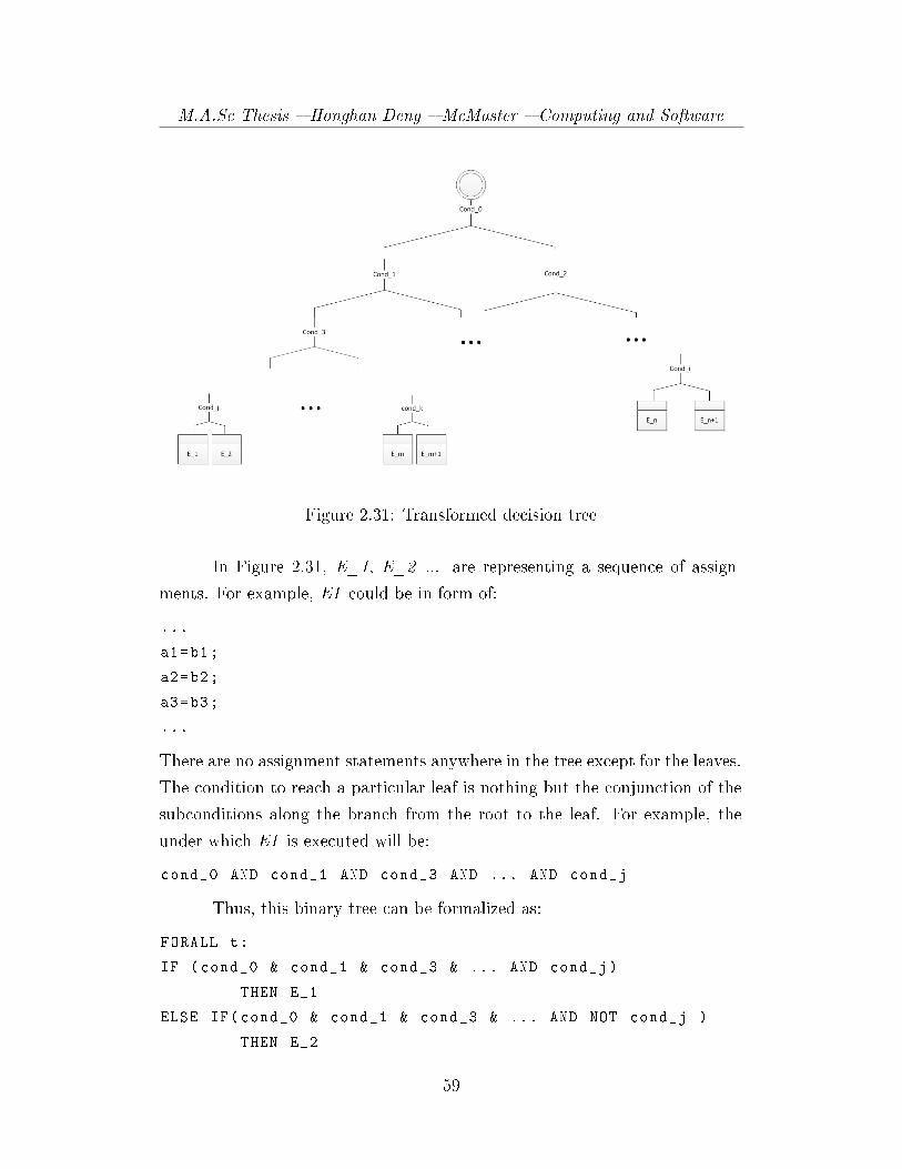
M.A.Sc Thesis � Honghan Deng � McMaster � Computing and Software
Figure 2.31: Transformed decision tree
In Figure 2.31, E_1, E_2 ... are representing a sequence of assign-
ments. For example, E1 could be in form of:
...
a1=b1;
a2=b2;
a3=b3;
...
There are no assignment statements anywhere in the tree except for the leaves.
The condition to reach a particular leaf is nothing but the conjunction of the
subconditions along the branch from the root to the leaf. For example, the
under which E1 is executed will be:
cond_0 AND cond_1 AND cond_3 AND ... AND cond_j
Thus, this binary tree can be formalized as:
FORALL t:
IF (cond_0 & cond_1 & cond_3 & ... AND cond_j)
THEN E_1
ELSE IF(cond_0 & cond_1 & cond_3 & ... AND NOT cond_j )
THEN E_2
59
M.A.Sc Thesis � Honghan Deng � McMaster � Computing and Software
...
ENDIF
It is easy to see that all conditional expressions constructed by con-
junctions of subconditions along each route to di�erent leaves are complete
and disjoint.
As non-blocking assignment statements are evaluated at the end of the
simulation cycle, for duplicate assignments to the same variable, the last one
will be the actual e�ective assignment. All the previous assignment statements
will be overridden. On the other hand blocking assignment overriding is much
more complex since a previous assignment could a�ect a later assignment
before it is overridden. This thesis will discuss the blocking assignment case
after the non-blocking assignment formalization as it can be looked at as an
expanded analysis based on the blocking assignment properties.
2.5.4 Non-blocking Assignments in Synchronous always
Blocks
By assumption the synchronous block only contain non-blocking assignments.
Consider the following Verilog code:
always @(posedge clk) begin
a1 <=b1;
a2 <=b2
if (cond)
a1 <=b2;
else
a2 <=b3;
end
In this example, both a1 and a2 are overridden in the IF − ELSE
branch. It is equivalent to the following code:
always @(posedge clk) begin
if (cond) begin
a1 <=b2;
60

M.A.Sc Thesis � Honghan Deng � McMaster � Computing and Software
a2 <=b2;
end
else begin
a1 <=b1;
a2 <=b3;
end
end
The following binary tree can be used to represent this tranformation:
In this diagram, the decision structure in the always block is translated into
a binary tree. In (a), The root is the initialization part and each node is
represented by a box containing the updating statements. In (b), the original
structure is the rearranged such that all the overridden assignment have been
removed and the �nal equivalent assignment is denoted in the leaves. This
example shows how the initialization assignment statements can be moved
from the root to the leaves.
If there is no ELSE branch for the Verilog code:
always @(posedge clk) begin
if (cond) begin
a1 <=b1;
a2 <=b2;
end
end
The tree can be represented as the following �gure:
61

M.A.Sc Thesis � Honghan Deng � McMaster � Computing and Software
The empty node in (a) represents an empty else branch. The assignment
in empty leaves will simply take the assignment in the parent node, in this
example, the root.
The assignment sequence in (b) is in the �nal form that we can easily
formalize. The remainder of this section will explore a few more example and
try to conclude with some principles to inform the reader in performing this
sort of transformation.
Consider the Verilog always block in Figure 2.32. We apply the trans-
formation process shown in Figure 2.33 by applying following rules:
1. Move all the current assignment statements to the lower level. If there are
overriding non-blocking assignment in the lower level, then remove the
current level assignment and use the assignment statement from lower
level. Otherwise, add the current non-blocking assignment to the lower
level assignment sequence.
2. If there is no ELSE branch, then directly copy the assignment sequence
from the parent node to its negation branch.
3. After all the non-blocking assignment statements are merged into leaves,
creat a list of all the variables that appear on the left hand side of the
assignment statements in the synchronous always block and append de-
fault value assignments of the form signal<=signal in the leaves in which
the variable list is not completely speci�ed. After this, each variable in
the list should have an assignment in each leaf.
62

M.A.Sc Thesis � Honghan Deng � McMaster � Computing and Software
always @(posedge clk) begin
if(cond0) begin
a1 <=b2;
if(cond1) begin
a3 <=b1;
if(cond2) begin
a1 <=b4;
end
end
else begin
a2 <=b1;
end
end
else begin
a4 <=b4;
end
end
Figure 2.32: A more complex non-blocking assignment overriding problem
Figure 2.33(a) is built up exactly corresponding to the given Verilog
code in Figure 2.32. There is no default assignment sequence in the root.
Figure 2.33 (b) is obtained by merging a1<=b2 in E0 to the lower level as-
signment sequence E2, E3 and Figure2.33(c) is the �nal result by merging E2
to E4 and E5. The non-blocking assignment sequence is empty at node E5,
denoted by a circle, since E5 corresponds to the omitted ELSE branch of the if
statement evaluating cond2. As E5 does not have any overriding statements,
E5 copies the assignment from its parent node E2 in (c). In (c), there is no
assignment anywhere but in the leaves and this is the form we described in
Figure 2.31.
The last step from (c) to (d) is to make explicit implicit assignments
to signals in order to facilitate translation to PVS. As all the left hand side
variables in the code for the synchronous circuit will be synthesized to be the
outputs of a D �ip-�op, then if they are not assigned by a value in a particular
branch, then they will keep their value from previous clock tick. We assign a
variable the value it currently holds, for example a1<=a1. This is a dummy
statement in synchronous non-blocking assignment, but it help us to formalize
63

M.A.Sc Thesis � Honghan Deng � McMaster � Computing and Software
Figure 2.33: decision tree transformation process
64

M.A.Sc Thesis � Honghan Deng � McMaster � Computing and Software
FORALL t:
IF (cond_0 & cond_1 & cond_2)
THEN
a1(t)=b4(t-1) &
a2(t)=a2(t-1) &
a3(t)=b1(t-1) &
a4(t)=a4(t-1)
ELSE IF(cond_0 & cond_1 & NOT cond_2)
THEN
a1(t)=b2(t-1) &
a2(t)=a2(t-1) &
a3(t)=b1(t-1) &
a4(t)=a4(t-1)
ELSE IF(cond_0 & NOT cond1)
THEN
a1(t)=b2(t-1) &
a2(t)=b1(t-1) &
a3(t)=a3(t-1) &
a4(t)=a4(t-1)
ELSE
a1(t)=a1(t-1) &
a2(t)=a2(t-1) &
a3(t)=a3(t-1) &
a4(t)=a4(t-1)
ENDIF
ENDIF
ENDIF
Figure 2.34: PVS speci�cation for Verilog in Figure 2.32
this code. By doing so, we can translate the Verilog code according to the
decision tree as shown in Figure 2.32.
In Figure 2.33, both (a) and (d) generate the exact same circuit shown
in Figure 2.35.
65

M.A.Sc Thesis � Honghan Deng � McMaster � Computing and Software
Figure 2.35: The circuit before and after the transformation
66

M.A.Sc Thesis � Honghan Deng � McMaster � Computing and Software
2.5.5 Blocking assignments in Combinational always Blocks
Dealing with blocking assignments that are overridden in combinational always
blocks is more complex. Consider a Verilog code blocking assignment sequence:
1 always @* begin
2 a1=b1;
3 a2=a1;
4 a4=a2;
5 a1=b2;
6 a3=a1;
7 a5=a3;
8 end
Within the block a1 has two assignments at line 2 and 5 respectively.
Unlike the blocking assignment in which the later assignment will be the actual
e�ective assignment, for blocking assignment, each assignment has its valid
domain. In this block, the valid domain of assignment a1=b1 in line 2 is from
line 2 to 4, and the valid domain of a1=b2 in line 5 is from line 6 to 7. From
this example, we conclude the following:
For a blocking assignment sequence S with the following form:
vi=Em; //line m
...
vj=En; //line n
...
vk=Ek; //line p
Figure 2.36: A blocking assignment sequence m<n
If vi and vj are the same variable (i=j), and there is no other overriding
assignment for vi in the sequence S, then the valid domain of vi is from line
m to linen-1 and the active domain of vj is from line n to line p. That
is, the valid domain of a blocking assignment to a variable is the whole the
assignment sequence after this assignment, until another overriding assignment
to this variable occurs.
67
M.A.Sc Thesis � Honghan Deng � McMaster � Computing and Software
This is di�erent from non-blocking assignments, since all the non-
blocking assignments are evaluated at the end of simulation cycle, only the
last overriding assignment is valid and its valid domain is the whole always
block. A blocking assignment with complex conditional branches needs more
analysis compared to the non-blocking version.
To transform a decision tree into the form in Figure 2.31, we can use
the rules in Figure 2.37:
1. Move all of the assignment statements into leaves while insuring thatthe original assignment sequence is maintained - i.e., all the assignmentstatements in upper levels in the tree should be placed before any assign-ment statements from lower levels and the sequence of the assignment ineach also level needs to be preserved.
2. If there is no ELSE branch, then the leaf corresponding to the ELSE casewill contain the empty sequence.
3. For each sequence in leaves where we have an assignment sequence inthe form of Figure 2.36, repeat the following two steps until there is nooverriding.
• step1: If the left hand side variable vj in line n is not an overridingfor any previous assignment, go to next line. Otherwise, if vj=En isoverriding an assignment vi=Em in line m (that is vi and vj are thesame variable), then substitute Em into all the expressions containing vibetween line m+1 and line n-1.
• step2: Remove assignment statement in line m, that is, vi should notappear before line n.
Figure 2.37: Blocking assignment decision tree transformation
Given a Verilog combinational always block as in Figure 2.38, since we
assume there is no latch is synthesized, in every path through the block a value
must be assigned to every signal that is speci�ed by the block (i.e. appears on
the left hand side of an assignment statement). One way to do this is to insure
that a default value must be explicitly assigned. In the example in Figure
2.38, the default value is assigned at the beginning of the always block. The
68

M.A.Sc Thesis � Honghan Deng � McMaster � Computing and Software
transformation process is shown in Figure 2.39.
always @* begin
a1=b1;
a2=b2;
a3=b3;
a4=b4;
a5=b5;
a6=b6;
if(cond0) begin
a1=b4+b5;
a3=a1+b2;
if(cond1) begin
a1=b1+b2;
if(cond2) begin
a3=a1+b3;
end
end
end
else begin
a5=a1+b2;
end
end
Figure 2.38: blocking assignment block with overriding
69

M.A.Sc Thesis � Honghan Deng � McMaster � Computing and Software
Figure 2.39: blocking assignment decision tree
70

M.A.Sc Thesis � Honghan Deng � McMaster � Computing and Software
Figure 2.39(a) is built up directly from the Verilog code in Figure 2.38.
Figure 2.39(b) is an intermediate step which merges the default blocking as-
signment to the lower level by applying the rules in Figure 2.37. Figure 2.39(c)
is the the result of applying rules 1 and 2 in Figure 2.37. Figure 2.39(d) is the
�nal result after apply rule 3 in 2.37.
For Figure 2.39 (c), E1 has an overriding for a5 and the old value is
not been used for any assignment statement before the overriding occurred,
so we simply remove the old assignment a5=b5. Similarly, in E3 both a1 and
a3 are overridden and the old assignment statement is removed. In E5 the
assignment sequence is as shown below:
1 a1=b1
2 a2=b2
3 a3=b3
4 a4=b4
5 a5=b5
6 a6=b6
7 a1=b4&b5
8 a3=a1&b2
9 a1=b1&b2
Line 7 overrides line 1, but there is no expression referring a1 before that, thus
we simply remove line 1. Similarly in line 8, a3 is overridden and then line 3
is removed. In line 9, a1 is overriding again and this time, a1 is referred to
by the assignment to a3 in line 8. By rule 3 in 2.37, a1 in line 8 is replaced
by it old value: b4&b5 and after this substitution, line 7 is removed.
For E4 in Figure 2.39(c), every transform step is the same with E5
except the last assignment a3=a1&b3 simply override the old a3.
Now considering Figure 2.39(d), we can easily formalize it in to PVS
as:
FORALL t:
IF (cond_0 & cond_1 & cond_2)
THEN
a1(t)=b2(t) &
a4(t)=b4(t) &
71

M.A.Sc Thesis � Honghan Deng � McMaster � Computing and Software
a5(t)=b5(t) &
a6(t)=b6(t) &
a1(t)=(b1(t)&b2(t)) &
a3(t)=(a1(t)&b3(t))
ELSE IF(cond_0 & cond_1 & NOT cond_2)
THEN
a1(t)=b2(t) &
a4(t)=b4(t) &
a5(t)=b5(t) &
a6(t)=b6(t) &
a3(t)=(b4(t)&b5(t)&b2(t)) &
a1(t)=(b1(t)&b2(t))
ELSE IF(cond_0 & NOT cond1)
THEN
a2(t)=b2(t) &
a4(t)=b4(t) &
a5(t)=b5(t) &
a6(t)=b6(t) &
a1(t)=(b4(t)&b5(t)) &
a3(t)=(a1(t)&b2(t))
ELSE
a1(t)=b1(t) &
a2(t)=b2(t) &
a3(t)=b3(t) &
a4(t)=b4(t) &
a6(t)=b6(t) &
a5(t)=(a1(t)&b2(t))
ENDIF
ENDIF
ENDIF
Both always block in Figure 2.39(a) and (d) are synthesized to be the
exact same combinational circuit, which is shown in Figure 2.40.
Formalizing imperative RTL HDL into a formal speci�cation language
is non-trivial work. In this thesis we constrained our model to be fully syn-
72

M.A.Sc Thesis � Honghan Deng � McMaster � Computing and Software
Figure 2.40: synthesized circuit for Figure 2.39(a) and (c)
chronous and we only discuss a small subset of Verilog RTL HDL. More com-
prehensive Verilog formal semantics is needed if the RTL model is more com-
plex. However, sometimes in safety critical system design, to apply the formal
veri�cation methods, the designers have to �nd a balance between the system
performance and the complexity of applying formal method on such a model.
73

Chapter 3
Formal Veri�cation of System
Components
In this chapter we brei�y review correctness conditions and show how envi-
ronmental assumptions can be taken into account in verifying the correctness
of system components. The technique is then applied to several components
from a shutdown system.
3.1 Correctness Conditions and Environmental
Assumptions
Recall that a typical correctness condition from (Melham, 1990) has the form:
M [s1, s2, ..., sn] =⇒ S[s1, s2, ..., sn]
In attempting to prove correctness conditions, usually some environmental
assumption is made and thus the correctness condition becomes (Melham,
1990):
C[s1, s2, ..., sn] =⇒ ( M [s1, s2, ..., sn] =⇒ S[s1, s2, ..., sn]) (3.1)
It follow from propositional logic that this correctness condition has the fol-
lowing equivalent form:
M [s1, s2, ..., sn] =⇒ ( C[s1, s2, ..., sn] =⇒ S[s1, s2, ..., sn])
74

M.A.Sc Thesis � Honghan Deng � McMaster � Computing and Software
The above is the form of correctness condition that we will use through-
out this thesis. The actual speci�cation S holds under some assumption C.
For example, for the correctness condition in 3.23, the assumption C is:
(( FORALL(t:{t:TIME|t>= start_time }) : reset(t) = FALSE) &
(FORALL(t:{t:TIME|t>= start_time }) : clk_enable(t) = TRUE) &
(FORALL(t:{t:TIME|t>= start_time }) : start(t)=TRUE)&
is_in_ini(start_time)
The speci�cation S is the part implied by this assumption C. As we
use implication instead of equivalence to construct the correctness condition,
an inconsistent model will satisfy all the speci�cations. Even if we prove
that M [v1, v2, ...vn] is consistent by using the method discussed in (Melham,
1990), it is still possible that C[v1, v2, ..., v2] ∧ M [v1, v2, ...vn] is inconsistent,
which will make the proving trivial since the correctness condition (3.1) is also
equivalent to:
(C[v1, v2, ..., v2] ∧ M [v1, v2, ...vn]) =⇒ S[s1, s2, ..., sn])
For example, a model M and the assumption C is de�ned as:
M(in,out):bool=
out= NOT in
C(in,out):bool=
out= in
M(in, out)∧C(in, out) is inconsistent since no input and output satisfy
these two condition at the same time, even though M(in, out) is consistent.
The solution to this problem is instead of proving M [v1, v2, ...vn] to be con-
sistent, we prove the consistency of C[v1, v2, ..., v2] ∧ M [v1, v2, ...vn].
3.2 HELD_FOR
The HELD_FOR operator of (Wassyng and Lawford, 2005) is used as an in�x
operator, for example, (p)HELD_FOR(duration), to determine if a boolean
signal p has been True for a speci�ed duration. Due to the limitation of counter
75
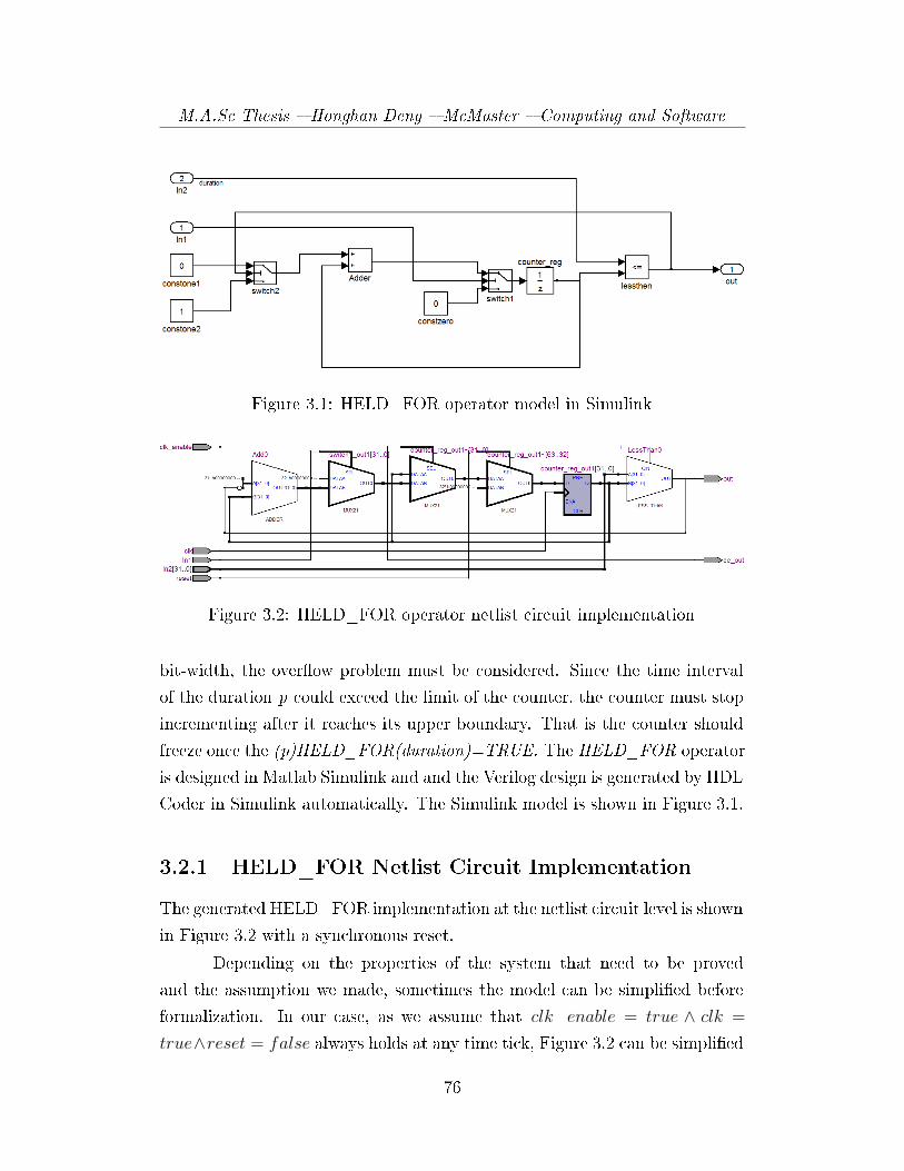
M.A.Sc Thesis � Honghan Deng � McMaster � Computing and Software
Figure 3.1: HELD_FOR operator model in Simulink
Figure 3.2: HELD_FOR operator netlist circuit implementation
bit-width, the over�ow problem must be considered. Since the time interval
of the duration p could exceed the limit of the counter, the counter must stop
incrementing after it reaches its upper boundary. That is the counter should
freeze once the (p)HELD_FOR(duration)=TRUE. The HELD_FOR operator
is designed in Matlab Simulink and and the Verilog design is generated by HDL
Coder in Simulink automatically. The Simulink model is shown in Figure 3.1.
3.2.1 HELD_FOR Netlist Circuit Implementation
The generated HELD_FOR implementation at the netlist circuit level is shown
in Figure 3.2 with a synchronous reset.
Depending on the properties of the system that need to be proved
and the assumption we made, sometimes the model can be simpli�ed before
formalization. In our case, as we assume that clk_enable = true ∧ clk =
true∧reset = false always holds at any time tick, Figure 3.2 can be simpli�ed
76
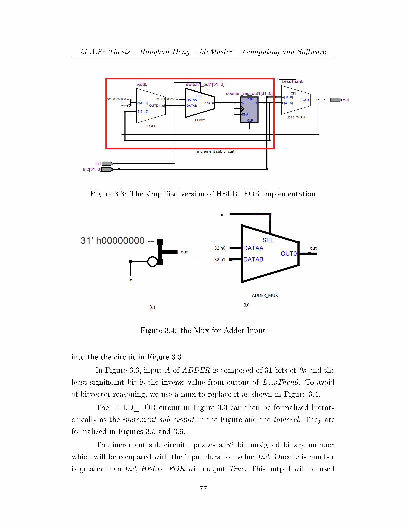
M.A.Sc Thesis � Honghan Deng � McMaster � Computing and Software
Figure 3.3: The simpli�ed version of HELD_FOR implementation
Figure 3.4: the Mux for Adder Input
into the the circuit in Figure 3.3.
In Figure 3.3, input A of ADDER is composed of 31 bits of 0s and the
least signi�cant bit is the inverse value from output of LessThen0. To avoid
of bitvector reasoning, we use a mux to replace it as shown in Figure 3.4.
The HELD_FOR circuit in Figure 3.3 can then be formalized hierar-
chically as the increment sub circuit in the Figure and the toplevel. They are
formalized in Figures 3.5 and 3.6.
The increment sub circuit updates a 32 bit unsigned binary number
which will be compared with the input duration value In2. Once this number
is greater than In2, HELD_FOR will output True. This output will be used
77

M.A.Sc Thesis � Honghan Deng � McMaster � Computing and Software
increment_imp_full(p,reg_out ,one_zero ):bool=
(EXISTS (adder_mux_out ,mux_out ,adder_out:signal ):
FORALL t:
(REG(mux_out ,reg_out)
&HDL_ADDER(reg_out(t),one_zero(t),adder_out(t))
&MUX(ZERO(t),adder_out(t),mux_out(t),p(t))))
Figure 3.5: Formalized increment sub circuit for Figure 3.6
toplevel_imp(p,duration ,bool_output ):bool=
EXISTS increment_out ,adder_mux_out:
FORALL t:
increment_imp_full(p,increment_out ,adder_mux_out)
&LESS_THEN(duration ,increment_out(t),bool_output(t))
&ADDER_MUX(ONE(t),ZERO(t),adder_mux_out(t),bool_output(t))
Figure 3.6: Formalized toplevel circuit of HELD_FOR
to control the incrementing such that when duration interval is longer than
the input setting in In2, the increment subcircuit will stop counting in order
to prevente over�ow from occurring.
3.2.2 HELD_FOR Correctness Condition
An example of the behaviour of the HELD_FOR operator can be seen in
Figure 3.7. The sample time is set to be 2 simulation cycles, and the pulse
width is set to be 50% of total period of 1200 simulation cycles. The duration
is set to be 200 simulation cycles. All the internal data types are set to be 8 bit
unsigned integer uint8, which constrains the maximum value of the counter to
be 255. From Figure 3.7, the output of (p) HELD_FOR(200) becomes true
after 200 sampling periods. HELD_FOR returns to FALSE at simulation time
1,002 which is 1 sampling period after when p dropped to 0. The interval in
which the output is True has lasted 351 sampling periods which exceeds the
representation range without over�ow of an 8 bit unsigned integer. The one
sample delay is caused by the D �ip �op between switch1 and Lessthen in
Figure 3.1.
78
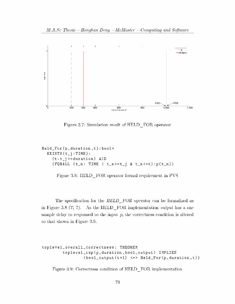
M.A.Sc Thesis � Honghan Deng � McMaster � Computing and Software
Figure 3.7: Simulation result of HELD_FOR operator
Held_For(p,duration ,t):bool=
EXISTS(t_j:TIME):
(t-t_j >= duration) AND
(FORALL (t_n: TIME | t_n >=t_j & t_n <=t):p(t_n))
Figure 3.8: HELD_FOR operator formal requirement in PVS
The speci�cation for the HELD_FOR operator can be formalized as
in Figure 3.8 (?; ?). As the HELD_FOR implementation output has a one
sample delay to responsed to the input p, the correctness condition is altered
to that shown in Figure 3.9.
toplevel_overall_correctness: THEOREM
toplevel_imp(p,duration ,bool_output) IMPLIES
(bool_output(t+1) <=> Held_For(p,duration ,t))
Figure 3.9: Correctness condition of HELD_FOR implementation
79
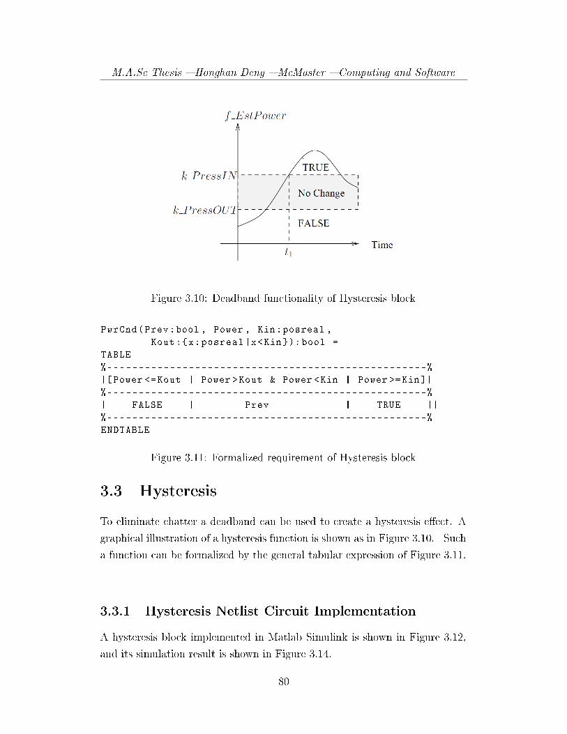
M.A.Sc Thesis � Honghan Deng � McMaster � Computing and Software
Figure 3.10: Deadband functionality of Hysteresis block
PwrCnd(Prev:bool , Power , Kin:posreal ,
Kout:{x:posreal|x<Kin}): bool =
TABLE
%---------------------------------------------------%
|[Power <=Kout | Power >Kout & Power <Kin | Power >=Kin]|
%---------------------------------------------------%
| FALSE | Prev | TRUE ||
%---------------------------------------------------%
ENDTABLE
Figure 3.11: Formalized requirement of Hysteresis block
3.3 Hysteresis
To eliminate chatter a deadband can be used to create a hysteresis e�ect. A
graphical illustration of a hysteresis function is shown as in Figure 3.10. Such
a function can be formalized by the general tabular expression of Figure 3.11.
3.3.1 Hysteresis Netlist Circuit Implementation
A hysteresis block implemented in Matlab Simulink is shown in Figure 3.12,
and its simulation result is shown in Figure 3.14.
80

M.A.Sc Thesis � Honghan Deng � McMaster � Computing and Software
(a) Hysteresis Matlab Model
(b) Hysteresis FSM Chart
Figure 3.12: Hysteresis implementation in Matlab
81

M.A.Sc Thesis � Honghan Deng � McMaster � Computing and Software
hysteresis_imp(kin ,kout ,pwr ,pwrcond ):bool=
EXISTS lto0 ,lto1 ,lto2 ,lto3 ,pmux0 ,pmux1 ,pmux2 ,pmux3 ,pmux4 ,
in_activated ,pwrregout:
FORALL t:
PwrRegNext2(pwrregout(t),ZERO(t),pmux2(t),lto3(t)) &
PwrRegNext0(pwrregout(t),ZERO(t),pmux0(t),lto1(t)) &
PwrRegNext3(pmux2(t),ONE(t),pmux3(t),lto2(t)) &
PwrRegNext1(pmux0(t),ONE(t),pmux1(t),lto0(t)) &
PwrRegNext4(pmux3(t), pmux1(t), pwrcond(t),in_activated(t))&
FSM_SHELL(kin ,kout ,pwr ,activated ,in_activated ,lto0 ,lto1 ,lto2 ,lto3)&
PwrCondReg(pwrcond ,pwrregout)
Figure 3.13: Formalized Hysteresis Module
The Matlab/Simulink model can be used to generate a hardware imple-
mentation via Matlab HDL Coder. The netlist circuit level of the generated
hardware implementation is shown in Figure 2.17 and Figure 2.18. Hysteresis
block then can be formalized as in Figure 3.13, in which FSM_SHELL is de�ned
as in Figure 2.18c and Figure 2.23.
3.3.2 Hysteresis Correctness Condition
Assuming that the initial state of the hysteresis is set to be inactivated, then as
showg in the simulation in Figure 3.14, when the amplitude of the power input
passes 100 at simulation time 20, the output keeps the previous inactivated
state. It maintains this until power passes kin (kin=150) at time 30. Then
the output changes to be activated. The state stays in the activated state until
the power input drops below kout (kout=100) at time 85.
The formal speci�cation of Hysteresis is shown in Figure 3.11 but we
need to modify it to �t our synchronous hardware as shown in Figure3.15.
82

M.A.Sc Thesis � Honghan Deng � McMaster � Computing and Software
Figure 3.14: Simulation Result of Hysteresis Block
hysteresis_spec(kin ,kout ,pwr ,pwrcond ):bool=
FORALL t:
pwrcond(t)=
IF t=0 THEN FALSE
ELSE
TABLE
|[pwr(t)<=kout(t)|pwr(t)>kout(t)&pwr(t)<kin(t)|pwr(t)>=kin(t)]|
| FALSE | pwrcond(t-1) | TRUE ||
ENDTABLE
ENDIF
Figure 3.15: Formal speci�cation of the Hysteresis Hardware Implementation
With this modi�ed speci�cation the correctness condition of the Hys-
teresis module can be formalized as in Figure 3.16.
83

M.A.Sc Thesis � Honghan Deng � McMaster � Computing and Software
...
KIN: {x:BUS_TYPE|x>1}
KOUT:{x:BUS_TYPE|x<KIN}
pwr: VAR {x:signal|x(0)<= KOUT}% initial state is FALSE
kin: VAR {x: signal|FORALL t: x(t)=KIN}
kout: VAR {x: signal|FORALL t: x(t)=KOUT}
pwrcond: VAR bitsignal
...
toplevel_general_correctness: THEOREM
hysteresis_imp(kin ,kout ,pwr ,pwrcond)
IMPLIES
hysteresis_spec(kin ,kout ,pwr ,pwrcond)
Figure 3.16: Correctness Condition of Hysteresis
This condition has been veri�ed in PVS.
3.4 Sum of Highest16 sensors/18 inputs
The Highest16 module is designed to sum the highest 16 sensors out of 18
inputs. This model is designed in Matlab/Simulink State�ow as shown in
Figure 3.17. Instead of sorting the 18 inputs, this algorithm subtract 2 lowest
inputs from the sum of all 18 inputs.
3.4.1 Highest16 sensors/18 inputs HDL Implementation
Matlab HDL Coder can automatically generate the HDL implementation from
a model based design in State�ow. The synthesized netlist circuit is quite
large and impractical to formalize manually. Therefore this implementation
is formalized based on the HDL model. The correctness of HDL model can
propagate to lower level such as the netlist circuit before and after place and
route using equivalence checking tools.
As discussed in earlier sections, the highest16.v modeule can be formal-
ized by applying the corresponding rules in 2.5.1. One of the most important
steps is to formalize the IF-ELSE and CASE statements in the always block
as shown in Figures 3.18, 3.19 and 3.20.
84
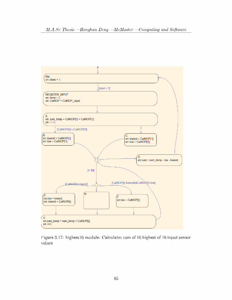
M.A.Sc Thesis � Honghan Deng � McMaster � Computing and Software
Figure 3.17: highest16 module: Calculates sum of 16 highest of 18 input sensorvalues
85
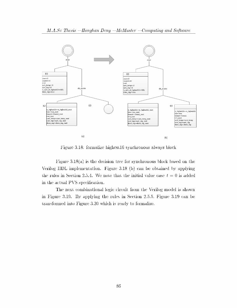
M.A.Sc Thesis � Honghan Deng � McMaster � Computing and Software
Figure 3.18: formalize highest16 synchronous always block
Figure 3.18(a) is the decision tree for synchronous block based on the
Verilog HDL implementation. Figure 3.18 (b) can be obtained by applying
the rules in Section 2.5.4. We note that the initial value case t = 0 is added
in the actual PVS speci�cation.
The next combinational logic circuit from the Verilog model is shown
in Figure 3.19. By applying the rules in Section 2.5.5, Figure 3.19 can be
transformed into Figure 3.20 which is ready to formalize.
86
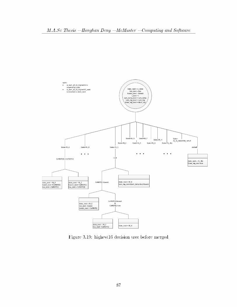
M.A.Sc Thesis � Honghan Deng � McMaster � Computing and Software
Figure 3.19: highest16 decision tree before merged
87

M.A.Sc Thesis � Honghan Deng � McMaster � Computing and Software
Figure 3.20: highest16 decision tree after merged
88
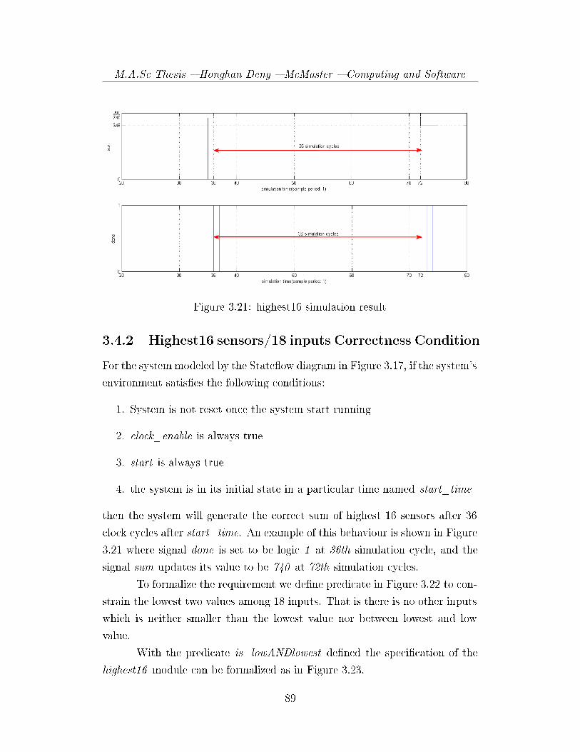
M.A.Sc Thesis � Honghan Deng � McMaster � Computing and Software
Figure 3.21: highest16 simulation result
3.4.2 Highest16 sensors/18 inputs Correctness Condition
For the system modeled by the State�ow diagram in Figure 3.17, if the system's
environment satis�es the following conditions:
1. System is not reset once the system start running
2. clock_enable is always true
3. start is always true
4. the system is in its initial state in a particular time named start_time
then the system will generate the correct sum of highest 16 sensors after 36
clock cycles after start_time. An example of this behaviour is shown in Figure
3.21 where signal done is set to be logic 1 at 36th simulation cycle, and the
signal sum updates its value to be 740 at 72th simulation cycles.
To formalize the requirement we de�ne predicate in Figure 3.22 to con-
strain the lowest two values among 18 inputs. That is there is no other inputs
which is neither smaller than the lowest value nor between lowest and low
value.
With the predicate is_lowANDlowest de�ned the speci�cation of the
highest16 module can be formalized as in Figure 3.23.
89
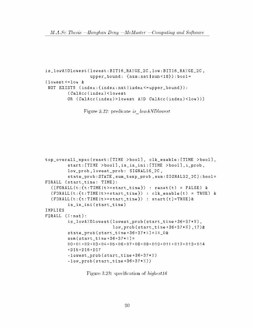
M.A.Sc Thesis � Honghan Deng � McMaster � Computing and Software
is_lowANDlowest(lowest:BIT16_RANGE_2C ,low:BIT16_RANGE_2C ,
upper_bound: {num:nat|num <18}): bool=
(lowest <=low &
NOT EXISTS (index:{index:nat|index <= upper_bound }):
(CalAcc(index)<lowest
OR (CalAcc(index)>lowest AND CalAcc(index)<low)))
Figure 3.22: predicate is_lowANDlowest
top_overall_spec(reset:[TIME ->bool], clk_enable :[TIME ->bool],
start:[TIME ->bool],is_in_ini :[TIME ->bool],i_prob ,
low_prob ,lowest_prob: SIGNAL16_2C ,
state_prob:STATE ,sum_temp_prob ,sum:SIGNAL32_2C ):bool=
FORALL (start_time: TIME):
(( FORALL(t:{t:TIME|t>= start_time }) : reset(t) = FALSE) &
(FORALL(t:{t:TIME|t>= start_time }) : clk_enable(t) = TRUE) &
(FORALL(t:{t:TIME|t>= start_time }) : start(t)=TRUE)&
is_in_ini(start_time)
IMPLIES
FORALL (N:nat):
is_lowANDlowest(lowest_prob(start_time +36+37*N),
low_prob(start_time +36+37*N),17)&
state_prob(start_time +36+37*N)=IN_D&
sum(start_time +36+37*N)=
D0+D1+D2+D3+D4+D5+D6+D7+D8+D9+D10+D11+D12+D13+D14
+D15+D16+D17
-lowest_prob(start_time +36+37*N)
-low_prob(start_time +36+37*N))
Figure 3.23: speci�cation of highest16
90
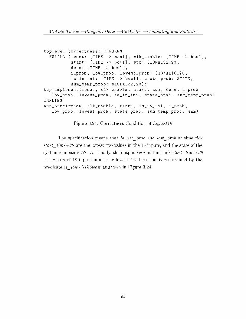
M.A.Sc Thesis � Honghan Deng � McMaster � Computing and Software
toplevel_correctness: THEOREM
FORALL (reset: [TIME -> bool], clk_enable: [TIME -> bool],
start: [TIME -> bool], sum: SIGNAL32_2C ,
done: [TIME -> bool],
i_prob , low_prob , lowest_prob: SIGNAL16_2C ,
is_in_ini: [TIME -> bool], state_prob: STATE ,
sum_temp_prob: SIGNAL32_2C ):
top_implement(reset , clk_enable , start , sum , done , i_prob ,
low_prob , lowest_prob , is_in_ini , state_prob , sum_temp_prob)
IMPLIES
top_spec(reset , clk_enable , start , is_in_ini , i_prob ,
low_prob , lowest_prob , state_prob , sum_temp_prob , sum)
Figure 3.24: Correctness Condition of highest16
The speci�cation means that lowest_prob and low_prob at time tick
start_time+36 are the lowest two values in the 18 inputs, and the state of the
system is in state IN_D. Finally, the output sum at time tick start_time+36
is the sum of 18 inputs minus the lowest 2 values that is constrained by the
predicate is_lowANDlowest as shown in Figure 3.24.
91

Chapter 4
Proof Strategies
In this chapter we provide some insight into how best to tackle the proof of
correctness conditions. We �rst describe some general proof techniques in
Section 4.1 and then provide details of proof techniques that were e�ective
in proving parts of the examples from the previous chapter. In particular,
Section 4.2 describes the strategies applied to the HELD_FOR module and
Section 4.3 those used for the highest16 module.
4.1 General Proving Steps
4.1.1 Instantiate signal names
The �rst step is instantiate the signal name in the implementation model
correctly. The correctness condition usually has the form:
M [s1, s2, ..., sn] =⇒ ( C[s1, s2, ..., sn] =⇒ S[s1, s2, ..., sn])
In PVS, considering the use of probes and that the property is de�ned
over time t, the above correctness condition becomes:
FORALL(s1 ,...,sn,probe1 ,..., proben ):
M(s1 ,...,sn,probe1 ,..., proben)
|------------------------------------
FORALL(s1 ,...,sn,probe1 ,..., proben ):
92

M.A.Sc Thesis � Honghan Deng � McMaster � Computing and Software
FORALL t:
C(s1 ,...,sn,probe1 ,..., proben)
IMPLIES
S(s1 ,...,sn,probe1 ,..., proben)
We �rst need to skolemize the consequent which will generate something
like:
FORALL(s1 ,...,sn,probe1 ,..., proben ):
M(s1 ,...,sn,probe1 ,..., proben)
|------------------------------------
FORALL t:
C(s1!1,...,sn!1,probe1 !1,..., proben !1)
IMPLIES
S(s1!1,...,sn!1,probe1 !1,..., proben !1)
The �nal step is instantiate the signal names in the implementation
model M with the corresponding names in the speci�cation. The �nal form
of the sequent with all signals instantiated is then:
M(s1!1,...,sn!1,probe1 !1,..., proben !1)
|------------------------------------
FORALL t:
C(s1!1,...,sn!1,probe1 !1,..., proben !1)
IMPLIES
S(s1!1,...,sn!1,probe1 !1,..., proben !1)
4.1.2 Sequential circuit property proving
As the system is designed and modelled as a synchronous circuit, proof by
induction is the most commonly used approach in proving sequential circuit
properties. Depending on how the properties are de�ned, the induction could
have the following types:
1. Induct on time tick t, or
2. Induct on a variable n and time tick t is a function of n, i.e., t = f(n).
93

M.A.Sc Thesis � Honghan Deng � McMaster � Computing and Software
Type I: Induction on time tick t
• Step1: induct on time tick t
After we induct on t and �atten the sequent, it has the following form (to high-
light the relevant variables, s1!1, ..., sn!1, probe1!1, ..., proben!1
are not shown):
M
C(t!1) IMPLIES S(t!1)
C(t!1+1)
|------------------------------------
S(t!1+1)
• Step2: expand implementation model
As we assume that all the combinational circuits and �ip �op circuits are
separately coded in di�erent always block under the assumption at the start
of Section 2.5. In netlists for synchronous circuits, typically all the components
other than D �ip �ops are combinational. Thus our synchronous circuit has
the following form after instantiating signal names and expanding the model:
FORALL t:
probe1 !1(t)=...
...
proben !1(t)=...
COMB(s1!1,...,sn !1...)
FF(s1!1,...,sn !1...)
C(t!1) IMPLIES S(t!1)
C(t!1+1)
|------------------------------------
S(t!1+1)
Note that in a real application, COMB could be a conjunction of many sub
modules).
• Step3: Instantiate implementation model at t!1 and t!1+1
94

M.A.Sc Thesis � Honghan Deng � McMaster � Computing and Software
As we need the probe values at time tick t!1 andt!1+1, the quanti�er on
the implementation model needs to be eliminated by instantiating t with the
skolem constant values t!1 and t!1+1. We then get the following sequent after
simpli�cation:
%========= at t!1 ===========
probe1 !1(t!1)=...
...
proben !1(t!1)=...
COMB(s1!1(t!1),...,sn!1(t!1))
FF(s1!1,...,sn !1...)
%========== at t!1+1===========
probe1 !1(t!1+1)=...
...
proben !1(t!1+1)=...
COMB(s1!1(t!1+1) ,... ,sn!1(t!1+1)...)
FF(s1!1,...,sn !1...)
%==============================
C(t!1) IMPLIES S(t!1)
C(t!1+1)
|------------------------------------
S(t!1+1)
• Step4: Since the Flip �op module (FF ) has its own quanti�er for t we
need to expand FF and instantiate it at t!1+1.
95

M.A.Sc Thesis � Honghan Deng � McMaster � Computing and Software
%========= at t!1 ===========
probe1 !1(t!1)=...
...
proben !1(t!1)=...
COMB(s1!1(t!1),...,sn!1(t!1)...)
FF(s1!1(t!1),...,sn!1(t!1)...)
%========== at t!1+1===========
probe1 !1(t!1+1)=...
...
proben !1(t!1+1)=...
COMB(s1!1(t!1+1) ,... ,sn!1(t!1+1)...)
FF(s1!1(t!1+1) ,... ,sn!1(t!1+1)...)
%==============================
C(t!1) IMPLIES S(t!1)
C(t!1+1)
|------------------------------------
S(t!1+1)
Figure 4.1: Final form of the sequence after instantiating simplifying
Figure 4.1 is the �nal form to prove property S where all the avail-
able conditions are ready. The following step is to derive S(t!1+1) from the
antecedents. This typically involves a lot of case based reasoning and sub-
stitutions. Figure 4.2 shows the relationship between antecedents and subse-
quent in Figure 4.1. Usually C(t!1+1) can be used to derive C(t!1). Then
C(t!1) can be used to derive S(t!1) since the induction assumption is given as
C(t!1)⇒ S(t!1). For example, in increment in the HELD_FOR model:
C(t!1 + 1) : t!1 + 1 > 0
|��������
C(t!1) : t!1 > 0
To derive t!1>0 from given t!1+1>0, we must exclude the case t!1=0
which is nothing but the base case.
96
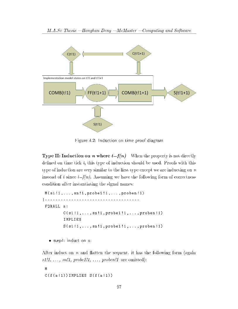
M.A.Sc Thesis � Honghan Deng � McMaster � Computing and Software
Figure 4.2: Induction on time proof diagram
Type II: Induction on n where t=f(n) When the property is not directly
de�ned on time tick t, this type of induction should be used. Proofs with this
type of induction are very similar to the �rst type except we are inducting on n
instead of t since t=f(n). Assuming we have the following form of correctness
condition after instantiating the signal names:
M(s1!1,...,sn!1,probe1 !1,..., proben !1)
|------------------------------------
FORALL n:
C(s1!1,...,sn!1,probe1 !1,..., proben !1)
IMPLIES
S(s1!1,...,sn!1,probe1 !1,..., proben !1)
• step1: induct on n:
After induct on n and �atten the sequent, it has the following form (again
s1!1, . . . , sn!1, probe1!1, . . . , proben!1 are omitted):
M
C(f(n!1)) IMPLIES S(f(n!1))
97

M.A.Sc Thesis � Honghan Deng � McMaster � Computing and Software
C(f(n!1+1))
|------------------------------------
S(f(n!1+1))
• Step2: expand implementation model
FORALL t:
probe1 !1(t)=...
...
proben !1(t)=...
COMB(s1!1,...,sn !1...)
FF(s1!1,...,sn !1...)
C(f(n!1)) IMPLIES S(f(n!1))
C(f(n!1+1))
|------------------------------------
S(f(n!1+1))
• Step3: Instantiate implementation model on all ticks in [f(n!1), f(n!1+1)]
Instead of instantiating the model at t!1 and t!1+1, we need to instantiate the
implementation model from f(n!1) to f(n!1+1). For example, if t = f(n) = 2n,
then M needs to be instantiated at all time ticks within [f(n!1), f(n!1+1)],
that is [2*n!1, 2*n!1+2] (to simplify the sequent we ignored the probe signals):
%========= at f(n!1) ===========
COMB(s1!1(2*n!1),...,sn!1(2*n!1))
FF(s1!1,...,sn !1...)
%========= at f(n!1)+1 ===========
COMB(s1!1(2*n!1+1) ,... ,sn!1(2*n!1+1))
FF(s1!1,...,sn !1...)
%========= at f(n!1)+2 ===========
COMB(s1!1(2*n!1+2) ,... ,sn!1(2*n!1+2))
FF(s1!1,...,sn !1...)
%==============================
C(2*n!1) IMPLIES S(2*n!1)
C(2*n!1+2)
98
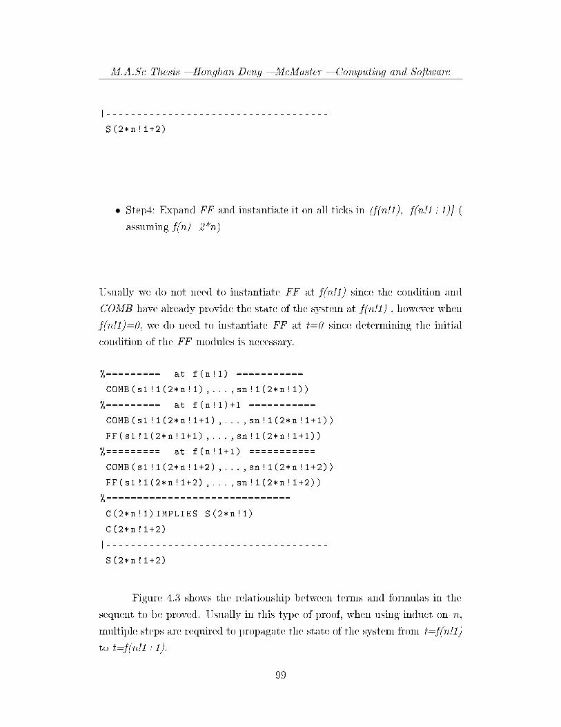
M.A.Sc Thesis � Honghan Deng � McMaster � Computing and Software
|------------------------------------
S(2*n!1+2)
• Step4: Expand FF and instantiate it on all ticks in (f(n!1), f(n!1+1)] (
assuming f(n)=2*n)
Usually we do not need to instantiate FF at f(n!1) since the condition and
COMB have already provide the state of the system at f(n!1) , however when
f(n!1)=0, we do need to instantiate FF at t=0 since determining the initial
condition of the FF modules is necessary.
%========= at f(n!1) ===========
COMB(s1!1(2*n!1),...,sn!1(2*n!1))
%========= at f(n!1)+1 ===========
COMB(s1!1(2*n!1+1) ,... ,sn!1(2*n!1+1))
FF(s1!1(2*n!1+1) ,... ,sn!1(2*n!1+1))
%========= at f(n!1+1) ===========
COMB(s1!1(2*n!1+2) ,... ,sn!1(2*n!1+2))
FF(s1!1(2*n!1+2) ,... ,sn!1(2*n!1+2))
%==============================
C(2*n!1) IMPLIES S(2*n!1)
C(2*n!1+2)
|------------------------------------
S(2*n!1+2)
Figure 4.3 shows the relationship between terms and formulas in the
sequent to be proved. Usually in this type of proof, when using induct on n,
multiple steps are required to propagate the state of the system from t=f(n!1)
to t=f(n!1+1).
99

M.A.Sc Thesis � Honghan Deng � McMaster � Computing and Software
Figure 4.3: Induction on n (t=f(n)) proof diagram
4.2 HELD_FOR proving strategy
Figure 4.4 represents the behaviour of the Held_For implementation. The
bool_output at t+1 indicates if the formal speci�cation held_for shown in
Figure 3.8 has been satis�ed at t. The counter starts to increment from 0 to
duration+1 when P is True and holds this value until P becomes False.
The correctness condition used to verify the hardware implementation
of Held_For is:
toplevel_imp_with_probe(p, duation, bool_output, reg_out_prob,
add_mux_out_prob)
=⇒ (bool_output(t+ 1)⇐⇒ Held_For(p, duration, t))
This correctness condition can be decomposed into two subgoals:
Part I:
toplevel_imp =⇒ (Held_For(p, duration, t) =⇒ bool_output(t+ 1))
This property can be proved by 3 basic properties of the implementa-
tion. The �rst property is shown in Figure 4.5:
100

M.A.Sc Thesis � Honghan Deng � McMaster � Computing and Software
Figure 4.4: Held_For proof cases
toplevel_imp_with_probe(p,duration ,bool_output ,reg_out_prob ,
add_mux_out_prob) IMPLIES
(FORALL (ini:TIME):
FORALL(t:TIME|t<=duration -reg_out_prob(ini)):
(FORALL (t_n: TIME | t_n >=ini & t_n <=ini+t):p(t_n))
IMPLIES
reg_out_prob(ini+t)= reg_out_prob(ini)+t)
Figure 4.5: increment property
In Figure 4.4, assuming the counter value at t_j!1 is reg(t_j!1) and
reg(t_j!1) is less than duration+1, as long as P is True within [ini, ini+dt],
the counter value at ini+dt must be reg_out_prob(ini)+dt.
The second property is that the implementation will freeze its counter
value once it reaches duration+1, providing P is True in this time interval.
This property can be described as in Figure 4.6.
The third property is that at all time ticks the counter value can not be
greater than duration+1. This property can be formalized as shown in Figure
4.7.
In the correctness condition:
toplevel_imp =⇒ (Held_For(p, duration, t) =⇒ bool_output(t+ 1)),
101
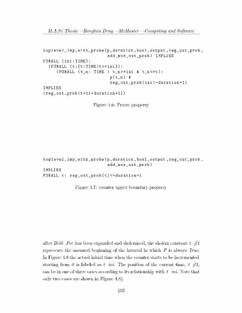
M.A.Sc Thesis � Honghan Deng � McMaster � Computing and Software
toplevel_imp_with_probe(p,duration ,bool_output ,reg_out_prob ,
add_mux_out_prob) IMPLIES
FORALL (ini:TIME):
(FORALL (t:{t:TIME|t>=ini}):
(FORALL (t_n: TIME | t_n >=ini & t_n <=t):
p(t_n) &
reg_out_prob(ini)= duration +1)
IMPLIES
(reg_out_prob(t+1)= duration +1))
Figure 4.6: Freeze property
toplevel_imp_with_probe(p,duration ,bool_output ,reg_out_prob ,
add_mux_out_prob)
IMPLIES
FORALL t: reg_out_prob(t)<=duration +1
Figure 4.7: counter upper boundary property
after Held_For has been expanded and skolemized, the skolem constant t_j!1
represents the assumed beginning of the interval in which P is always True.
In Figure 4.8 the actual initial time when the counter starts to be incremented
starting from 0 is labeled as t_ini. The position of the current time, t_j!1,
can be in one of three cases according to its relationship with t_ini. Note that
only two cases are shown in Figure 4.8).
102

M.A.Sc Thesis � Honghan Deng � McMaster � Computing and Software
Figure 4.8: Two cases of t_j!1
• case 1: reg(t_j!1)=duration+1
In this case, t_j!1 is within [t_ini+duration+1, t]. The counter and bool_output
will hold their value until time t. This case can be proved by using the freeze
property of Figure 4.6.
• case 2: reg(t_j!1)<duration+1
In this case t_j!1 is within [t_ini, t+duration]. The counter value will incre-
ment �rst and then hold. This case can be proved by using increment property
in Figure 4.5 and freeze property in Figure 4.6.
• case 3: reg(t_j!1)>duration+1
This case can be proved by introducing the counter upper boundary property of
Figure 4.7 which assert there is no time ticks at which counter value is greater
than duration+1.
Part II:
toplevel_imp =⇒ (bool_output(t+ 1) =⇒ Held_For(p, duration, t))
The proof of this property requires the following lemma in Figure 4.9:
103

M.A.Sc Thesis � Honghan Deng � McMaster � Computing and Software
increment_full_counter_truth3: THEOREM
increment_imp_full(p,reg_out ,one_zero) IMPLIES
FORALL (ini:TIME):
FORALL (m:{m:TIME|m>0}):
NOT p(ini) IMPLIES reg_out(m+ini)<m
Figure 4.9: Boundary property 1 of increment sub module
The Lemma in Figure 4.9 asserts that if P is False at time tick ini,
then the counter value at any tick at ini+m, where m is an arbitrary time
increment, must be less than ini+m. That is reg(ini+m)<ini+m.
We use another lemma, shown in Figure 4.10, which assert that reg_out(t) 6
t at all time ticks.
increment_full_couner_truth2: THEOREM
increment_imp_full(p,reg_out ,one_zero) IMPLIES
FORALL t: reg_out(t)<=t
Figure 4.10: Boundary property 2 of increment sub module
Figure 4.11: Property reg(ini+m)<ini+m
Figure 4.11 shows the basic strategy to prove this property: when
bool_out is True, there is no time tick in the last duration interval at which
p is false since that will make the counter value smaller than duration which
104
M.A.Sc Thesis � Honghan Deng � McMaster � Computing and Software
contradicts the premise that bool_out is True. More speci�cally, it is easy to
see that (bool_out(t!1 + 1)∧ p!1(t!1 + 1)) =⇒ reg_out(t!1 + 1) = duation+ 1,
where t!1 is representing current time tick. It is also possible to prove that
NOT p1(t_n!1) =⇒ reg_out(t_n!1 + (t!1 − t_n!1)) < (t!1 − t_n!1) by
using the lemma in Figure 4.9. Since t!1 − t_n!1 6 duration, we can con-
clude that reg_out(t!1) < duation, and with p(t!1) = True, we can see that
reg_out(t!1 + 1) < duation + 1. Thus, this property can be proved by the
following contradiction:
toplevel_imp
reg_out(t!1+1)= duration +1
reg_out(t!1+1)< duration +1
|--------------
4.3 ishighest16 Proving stragegy
The highest16 module's overall correctness condition was originally given in
Figure 3.23. We use the following lemmas, described in detail below, to support
its proof:
• top_at_tick_3
• top_relationship_EHFG_state_cycles
• top_EHFG_maintain_low_lowest
• top_G_sum
• top_G_sum_extended( the closed form of top_G_sum)
top_at_tick_3
The behaviour pattern of the algorithm is that it will loop between state
E/H/F and G, until state D is entered. State B and C are the places where
this internal loop starts, so properties that hold in these two states can be
viewed as the precondition of the internal loop. These properties are de�ned
105

M.A.Sc Thesis � Honghan Deng � McMaster � Computing and Software
in top_at_tick_3 which means it holds at the third tick after state IDLE is
entered:
top_at_tick_3(
reset: [TIME -> bool], clk_enable: [TIME -> bool],
start: [TIME -> bool], is_in_ini: [TIME -> bool],
i_prob , low_prob , lowest_prob: SIGNAL16_2C ,
state_prob: STATE , sum_temp_prob: SIGNAL32_2C ):
bool =
FORALL (start_time: TIME):
(FORALL(t:{t:TIME|t>= start_time }): reset(t) = FALSE) &
(FORALL(t:{t:TIME|t>= start_time }): clk_enable(t)=TRUE) &
(FORALL(t:{t:TIME|t>= start_time }): start(t)=TRUE)&
state_prob(start_time )= IN_IDEL
IMPLIES
(i_prob(start_time + 3) = 2 &
sum_temp_prob(start_time + 3) = CalAcc (0) + CalAcc (1) &
IF CalAcc (0) <= CalAcc (1)
THEN lowest_prob(start_time + 3) = CalAcc (0) &
low_prob(start_time + 3) = CalAcc (1) &
state_prob(start_time + 3) = IN_B
ELSE lowest_prob(start_time + 3) = CalAcc (1) &
low_prob(start_time + 3) = CalAcc (0) &
state_prob(start_time + 3) = IN_C
ENDIF)
This property can be proved by simply instantiating the implementa-
tion model at all four time ticks within [start_time, start_time+3].
top_relationship_EHFG_state_cycles
top_relationship_EHFG_state_cycles is asserting the relationship between
time ticks, states and the index of the input signals. That is, at tick start_time+3+N*2+1,
the state must be in one of the three states: E, H or F, and the index can only
be N+2. At the following time tick, the state must be G and index equal to
N+3. By this property, the state of the FSM and the index of the input can be
determined easily which dramatically reduces the e�ort to complete the proof.
106

M.A.Sc Thesis � Honghan Deng � McMaster � Computing and Software
top_relationship_EHFG_state_cycles
(reset: [TIME -> bool], clk_enable: [TIME -> bool],
start: [TIME -> bool], is_in_ini: [TIME -> bool],
i_prob , low_prob , lowest_prob: SIGNAL16_2C ,
state_prob: STATE , sum_temp_prob: SIGNAL32_2C ):bool=
FORALL (start_time: TIME):
FORALL(N:{n:nat|n <=15}):(
(FORALL(t:{t:TIME|t>= start_time }) :reset(t)=FALSE)&
(FORALL(t:{t:TIME|t>= start_time }) :clk_enable(t)=TRUE)&
(FORALL(t:{t:TIME|t>= start_time }) :start(t)=TRUE)&
state_prob(start_time )= IN_IDEL
IMPLIES
(( state_prob(start_time +3+N*2+1)= IN_E&
i_prob(start_time +3+N*2+1)=N+2)
OR
(state_prob(start_time +3+N*2+1)= IN_H&
i_prob(start_time +3+N*2+1)=N+2)
OR
(state_prob(start_time +3+N*2+1)= IN_F&
i_prob(start_time +3+N*2+1)=N+2))&
(state_prob(start_time +3+N*2+2)= IN_G&
i_prob(start_time +3+N*2+2)=N+3))
top_EHFG_maintain_low_lowest
top_EHFG_maintain_low_lowest is an important property which asserts
that in all four states E, H, F and G, the variable low and lowest are holding
the lowest two values from the inputs scanned so far. At tick start_time+3+N*2+1,
if the state is E or H or F, then variables lowest and low are holding the low-
est two elements in the input signal array, whose index is up to N+2. This
property also holds at the following tick when the state is G.
top_EHFG_maintain_low_lowest(
reset: [TIME -> bool], clk_enable: [TIME -> bool],
start: [TIME -> bool], is_in_ini: [TIME -> bool],
107

M.A.Sc Thesis � Honghan Deng � McMaster � Computing and Software
i_prob , low_prob , lowest_prob: SIGNAL16_2C ,
state_prob: STATE , sum_temp_prob: SIGNAL32_2C ):bool=
FORALL (start_time: TIME):
FORALL(N:{n:nat|n <=15}):(
(FORALL(t:{t:TIME|t>= start_time }) : reset(t) = FALSE) &
(FORALL(t:{t:TIME|t>= start_time }) : clk_enable(t) = TRUE) &
(FORALL(t:{t:TIME|t>= start_time }) : start(t)=TRUE)&
state_prob(start_time )= IN_IDEL
IMPLIES
(state_prob(start_time +3+N*2+1)= IN_E=>
is_lowANDlowest(lowest_prob(start_time +3+N*2+1),
low_prob(start_time +3+N*2+1),N+2))
&
(state_prob(start_time +3+N*2+1)= IN_H=>
is_lowANDlowest(lowest_prob(start_time +3+N*2+1),
low_prob(start_time +3+N*2+1),N+2))
&
(state_prob(start_time +3+N*2+1)= IN_F=>
is_lowANDlowest(lowest_prob(start_time +3+N*2+1),
low_prob(start_time +3+N*2+1),N+2))
&
(state_prob(start_time +3+N*2+2)= IN_G=>
is_lowANDlowest(lowest_prob(start_time +3+N*2+2),
low_prob(start_time +3+N*2+2),N+2)))
top_G_sum/top_G_sum_extended
top_G_sum de�nes one of the most important properties: the sum_temp_prob
at tick start_time+3+N*2+2 is the sum of CalAcc(N+2) and the previous
value of sum_temp_prob at start_time+3+(N-1)*2+2 :
(state_prob(start_time +3+N*2+2)= IN_G =>
sum_temp_prob(start_time +3+N*2+2)=
sum_temp_prob(start_time +3+(N -1)*2+2)+ CalAcc(N+2)
top_G_sum_extended is the closed form of the property top_G_sum
asserting sum_temp is holding the sum of the elements of the input signals
108

M.A.Sc Thesis � Honghan Deng � McMaster � Computing and Software
with index up to N+2 whenever state G is entered at tick start_time+3+N*2+2 :
state_prob(start_time +3+N*2+2)= IN_G =>
sum_temp_prob(start_time +3+N*2+2)= sum(N+2)
To prove the overall correctness condition we �rst need to prove the
base case in which N=0 in Figure 3.23. Since this base case can be reused in
the induction step, it is better to build an independent base case lemma:
base_case_lemma
top_spec(reset:[TIME ->bool], clk_enable :[TIME ->bool],
start:[TIME ->bool],is_in_ini :[TIME ->bool],i_prob ,
low_prob ,lowest_prob: SIGNAL16_2C ,
state_prob:STATE ,sum_temp_prob ,sum:SIGNAL32_2C ):bool=
FORALL (start_time: TIME):
(( FORALL(t:{t:TIME|t>= start_time }): reset(t)=FALSE)&
(FORALL(t:{t:TIME|t>= start_time }): clk_enable(t)=TRUE)&
(FORALL(t:{t:TIME|t>= start_time }): start(t)=TRUE)&
is_in_ini(start_time)
IMPLIES
is_lowANDlowest(lowest_prob(start_time +36),
low_prob(start_time +36) ,17)&
state_prob(start_time +36)= IN_D&
sum(start_time +36)=D0+D1+D2+D3+D4+D5+D6+D7+D8+D9
+D10+D11+D12+D13+D14+D15+D16+D17
-lowest_prob(start_time +36) -low_prob(start_time +36))
Such a lemma can be proved by the strategy shown in Figure 4.12. Sup-
porting lemma top_EHFG_maintain_low_lowest and top_G_sum_extended
can be instantiate with N=15 and thus we know that the state must be G at
i=18. In the next tick, the state will be D and sum=sum_temp-low-lowest.
Since low and lowest are proved to be the smallest two values in the lemma
top_EHFG_maintain_low_lowest, and sum_temp is the sum of the total 18
input signal values in top_G_sum, the base_case_lemma can be proved. The
propagation from G to D is achieved by instantiating implementation model
at tick start_time+35 and start_time+36.
109

M.A.Sc Thesis � Honghan Deng � McMaster � Computing and Software
Figu
re4.12:
Base
caseprov
ingstrategy
110

M.A.Sc Thesis � Honghan Deng � McMaster � Computing and Software
Once we have proved the base case lemma, the overall correctness con-
dition can be proved by applying the strategy as shown in Figure 4.13.
The proving assumption is given at start_time+36+t_j!1*37. By in-
stantiating the implementation model at start_time+36+t_j!1*37 and start_time+
36+t_j!1*37+1 the given induction assumption can propagate to the IDLE
state. As long as the state is IDLE, the Base Case Lemma can directly prove
the property at start_time+36+(t_j!1+1)*37 by instantiate the start_time
with start_time+
36+t_j!1*37+1 as shown in Figure 4.13. Actually, we only use the condition
state=D in the induction assumption, because the base case lemma is very
strong, only assuming an arbitrary starting time and state=IDLE.
111
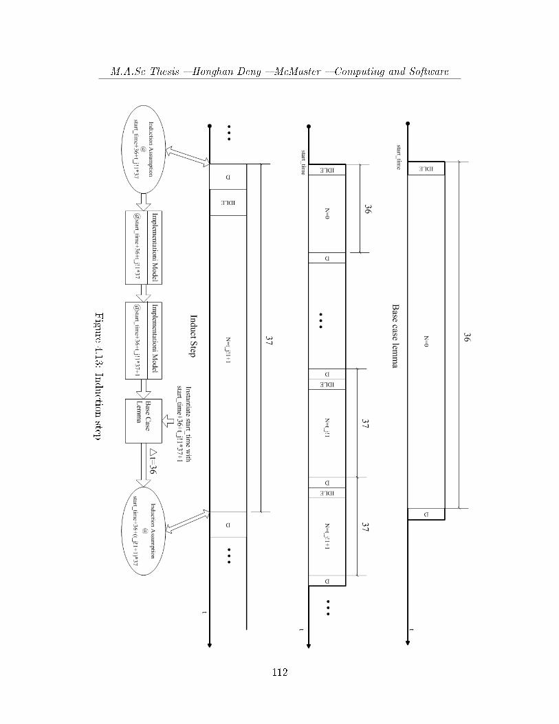
M.A.Sc Thesis � Honghan Deng � McMaster � Computing and Software
Figu
re4.13:
Induction
step
112
Chapter 5
Facilitating Proofs
The proof process of the correctness condition is complicated. Although PVS
theorem prover is largely mechanized, it still requires a signi�cant amount of
human interaction. In the proof process, the veri�cation engineer must be
very familiar with the system's expected behaviour. Even for an experienced
veri�cation engineer, some proof methods to facilitate veri�cation have to be
adopted to make the proof process more practical and e�ective.
5.1 Adding Probes
5.1.1 The Need for Probes
The need for a signal probe comes from the correctness condition we used:
M [s1, s2, ..., sn] =⇒ ( C[s1, s2, ..., sn] =⇒ S[s1, s2, ..., sn])
Usually, the implementation model M, environmental assumption C and spec-
i�cation S share the same interface [s1,s2,...sn]. That is the assumption and
the speci�cation only constrain the interface signals of the implementation
model. However, in a lot of cases we need to know the internal state of a
circuit in order to derive a particular property of it. For example, to prove a
sequential circuit model M can always jump from a state F to a new state G in
a given condition in the next clock tick, we need to assume the current state of
M to be F and then prove the next state of M is G under the given condition.
113

M.A.Sc Thesis � Honghan Deng � McMaster � Computing and Software
In this case, the internal registers of the implementation need to be accessed.
However, they are not available at the interface of the model so a signal probe
is needed. In the remainder of this section C[s1, s2, ..., sn] =⇒ S[s1, s2, ..., sn]
is simply represented by S unless it needs to be explicitly mentioned.
It is very common that the circuit under test provides a debugging
interface to allow the veri�cation engineer to investigate the internal state of
the circuit. This debugging interface may be implemented by a variety of
techniques to provide access to the internal state of the system. For example,
it can be as simple as an LED on the board indicating the status of a particular
internal register, or it can be a connection port for a scope. Similar techniques
are also useful and may be necessary to prove the correctness condition.
Figure 5.1: The signal probe in a formal model
114

M.A.Sc Thesis � Honghan Deng � McMaster � Computing and Software
Since the formalized implementation in this thesis is constructed by
using the external quanti�er to hide the internal connections, internal connec-
tions are thus not observable outside of the model. For example, system M1
in Figure 5.1 can be formalized as follows:
M1(a,b:bool):bool = EXISTS (x:bool): P1(a,x) & P2(x,b)
The interface of M1 only contains input and output signal a,b. The intercon-
nection wire x is observable in proving the correctness condition M1[a,b]=>S1[a,b]
as shown in Figure 5.2. After x is skolemized, its status can be tracked by
observing x!1 in the proof sequent.
{-1} EXISTS (x: bool): P1(a!1, x) & P2(x, b!1)
|-------
[1] S1(a!1, b!1)
Rule? (skosimp)
Skolemizing and flattening ,
this simplifies to:
Correctness1 :
{-1} P1(a!1, x!1)
{-2} P2(x!1, b!1)
|-------
[1] S1(a!1, b!1)
Figure 5.2: Observability of signal X
115

M.A.Sc Thesis � Honghan Deng � McMaster � Computing and Software
Figure 5.3: A case when Speci�cation involve the internal connection
However, since x is not an external signal port, it can not be accessed
from outside this model - which is necessary when the speci�cation involves
probing this signal. In Figure 5.3, speci�cation S is a predicate based on a,b,
and internal state x. Model M is a predicate on a,b without x. The correctness
condition will be:
M(a, b) ⇒ S(a, b, x)
By universal closure, such a formula equivalent to:
∀a, b : M(a, b) ⇒ ∀x : S(a, b, x)
It is obvious that this correctness condition is not correctly formed since the
expected correctness condition should be:
∀a, b, x : M(a, b, x) ⇒ S(a, b, x)
It is very common that a property of a model involves the internal
state of the system. A concrete example is given below. Figure 5.4, shows the
hierarchical structure of the highest16 model.
116

M.A.Sc Thesis � Honghan Deng � McMaster � Computing and Software
Figure 5.4: Example: Proof structure for the highest16 module
Shadowed boxes represent lemmas which are properties of the sys-
tem used to prove the overall correctness condition. For example, lemma
top_at_tick3 is representing the property of the system at the 3rd tick after
when system is in its initial state. It needs the internal signals i, sum_temp
and state to de�ne such property as in Figure 5.5:
top_at_tick_3(reset ,start ,i_prob ,state_prob ,sum_temp_prob)
FORALL (start_time: TIME):
(FORALL(t:{t:TIME|t>= start_time }) : reset(t) = FALSE) &
(FORALL(t:{t:TIME|t>= start_time }) : clk_enable(t) = TRUE) &
(FORALL(t:{t:TIME|t>= start_time }) : start(t)=TRUE)&
is_in_ini(start_time)
IMPLIES
(i_prob(start_time + 3) = 2 &
sum_temp_prob(start_time + 3) = CalAcc (0) + CalAcc (1) &
IF CalAcc (0) <= CalAcc (1)
THEN lowest_prob(start_time + 3) = CalAcc (0) &
...
Figure 5.5: top_at_tick_3 property of highest16 module
117
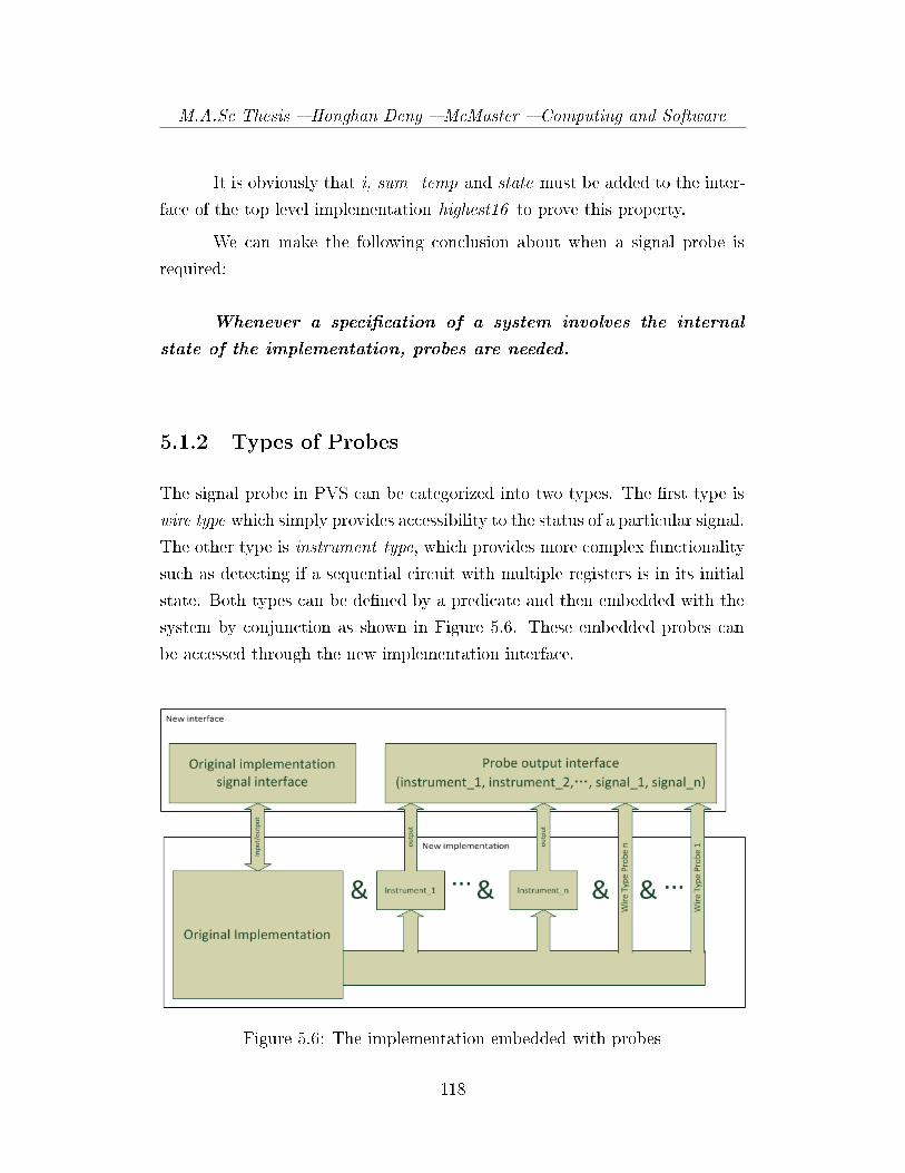
M.A.Sc Thesis � Honghan Deng � McMaster � Computing and Software
It is obviously that i, sum_temp and state must be added to the inter-
face of the top level implementation highest16 to prove this property.
We can make the following conclusion about when a signal probe is
required:
Whenever a speci�cation of a system involves the internal
state of the implementation, probes are needed.
5.1.2 Types of Probes
The signal probe in PVS can be categorized into two types. The �rst type is
wire type which simply provides accessibility to the status of a particular signal.
The other type is instrument type, which provides more complex functionality
such as detecting if a sequential circuit with multiple registers is in its initial
state. Both types can be de�ned by a predicate and then embedded with the
system by conjunction as shown in Figure 5.6. These embedded probes can
be accessed through the new implementation interface.
Figure 5.6: The implementation embedded with probes
118

M.A.Sc Thesis � Honghan Deng � McMaster � Computing and Software
Wire Type Probe
A wire type probe simply provides a connection between the internal signal
state and a new added signal in the signal port. It can be added by the 2 steps
described below:
1. Add the probe name in the signal port. For the example in Figure 5.1
concerning M1, the new signal port is M1(a,b,x_probe).
2. For an internal signal S add predicate ∀t S(t) = S_probe(t) to original
PVS implementation and connected by conjunction. The internal con-
nection between S and S_probe is built by assuming the signal S and
S_probe are equivalent whenever a positive clock edge arrives.
For example in Figure 5.1 module M1, probe X_probe can be added by adding
the following predicates to the PVS implementations of M1 :
M1(a,b,X_probe ):bool=
EXISTS x:
FORALL t:
P1(a(t),x(t))&
P2(b(t),x(t))&
%%% NEW ADDED PROBE FOR X %%%
X_probe(t)=X(t)
Instrument Type Probe
Instrument type probes provide more complicated functionality to let the
prover determine the status of the system or set the system to a particu-
lar state. Similar to the steps to de�ne a wire type probe, an instrument type
probe can also be added by the 2 following steps:
1. Add the instrument probe name to the signal port.
2. Add a predicate in the de�nition of the implementation that expresses
the functionality that the instrument is to provide. Assuming the im-
plementation model has the form: M(s1, ..., sn) = ∀t E1(t) and the
119

M.A.Sc Thesis � Honghan Deng � McMaster � Computing and Software
instrument probe is de�ned as ∀t instrument_probe(t) = E2(t), where
E1 and E2 is a formula of free variable t. The implementation model
embedded with instrument probe will be:
M(s1 ,...,sn,instrument_probe ):bool=
FORALL (t):
E1 &
instrument_probe(t)=E2(t)
An instrument to detect if the system with two registers is in its initial
state can be added as:
M1(s1 ,...,sn,is_in_ini ):bool=
==== ORIGINAL IMPLEMENTATION =========
FORALL (t):
E1 &
==== NEW ADDED INSTRUMENT ===========
is_in_ini(t)=reg0(t)=0 & reg1(t)=0
5.1.3 Using Probes
A standard correctness condition with probes embedded has the form:
M [v1, v2, ...vn, probe1, ..., proben] =⇒(C[v1, v2, ..., vn, probe1, ..., proben] =⇒ S[v1, v2, ..., vn, probe1, ..., proben])
It is equivalent to :
(C[v1, v2, ..., vn, probe1, ..., proben] ∧ M [v1, v2, ...vn, probe1, ..., proben])
=⇒ S[v1, v2, ..., vn, probe1, ..., proben]
This means the internal state of M will be set by C through probes. A concrete
example is given below to illustrate this e�ect.
In Figure 5.5, the instrument probe is_in_ini(start_time) is set to be
True with assumption of the property top_at_tick_3. In PVS, it is equivalent
to:
120

M.A.Sc Thesis � Honghan Deng � McMaster � Computing and Software
highest16 (..., is_in_ini(start_time )) AND is_in_ini(start_time)
IMPLIES
specification (..., is_in_ini(start_time ))
The implementation highest16 embedded with is_in_ini probe has the form:
highest16 (..., is_in_ini(start_time )): bool=
...
is_in_ini(start_time )=
(state=IDLE & sum=0 & i=0 &...)
In the proof process, after the highest16 implementation model is ex-
panded, the sequent has the following form:
is_in_ini(start_time !1)= state(start_time !1)= IDLE AND
sum(start_time !1)=0 AND
i(start_time !1)=0...
...
is_in_ini(start_time !1)
|-----------------------
....
This is equivalent to:
state(start_time !1)= IDLE
sum(start_time !1)=0
i(start_time !1)=0
...
is_in_ini(start_time !1)
|-----------------------
....
The implementation model is then set to be in its initial state.
The expanded interface and revised implementation model is give as
shown in Figure 5.6. It gives us the power to set the internal state freely.
However this accessibility could introduce an inconsistency in the correctness
condition proof.
If we examine this problem from the perspective of encapsulation, the
probe can be looked at as the added accessors to the internal state of the
121

M.A.Sc Thesis � Honghan Deng � McMaster � Computing and Software
Figure 5.7: state �ow example
hardware which is originally invisible to the outside. The attempt to set the
system state by probes without using the original implementation input signals
could make the system inconsistent. This inconsistency is not caused by the
original implementation model but is result of the direct access to the internal
states.
For example, in a sequential circuit model M(in,out), as shown in Figure
5.7, the internal register state can only have 3 values: 0, 1, 2. If the condition is
state_probe=4 then added to the correctness conditionM(in, out, state_probe)∧C(in, out, state_probe) will set the model to be an illegal state and make the
proof trivial by introducing an inconsistency.
We should realize that this inconsistency is caused by the incorrect
setting of the system state through the probe. If we only use the signals
provided by the original implementation, the system will never reach the state
4. This is somehow similar to the concept in Object Oriented Programming,
in which we should only read the object data through the accessor. In the
example of highest16, we use the is_in_ini probe to put the system in its
122
M.A.Sc Thesis � Honghan Deng � McMaster � Computing and Software
initial state. Another way, which is safer, is to use the reset signal to set the
system to its initial state. However this will constrain the application of
the property, since the initial state may not necessarily be entered
only by triggering the reset, event but also could be entered by
jumping to the next state from IN_D. If we use is_in_ini instead
of reset, this property can be used for both cases.
To solve this potential problem in using probes, two things need to be
examined. First the probe logic itself should not change the behaviour of the
original implementation model.
In Figure 5.6, the added logic should only output internal state to
probes. This can be done by following the rules:
• Any probe logic (instrument and wire type probe) can only have
the form probe=f(v1,...,vn), where v1 to vn are the internal
signals of the original implementation. That is the logic operation
on v1,...,vn should only change values of the probe.
• The original implementation should not be changed and should
not refer any newly added probe signals.
These two principles guarantee the newly added probe logic is isolated from
the original implementation.
The second thing is that newly introduced probes should not make
the system inconsistent. Consider the correctness condition after introduced
probes:
(C[v1, v2, ..., vn, probe1, ..., proben] ∧ M [v1, v2, ...vn, probe1, ..., proben])
=⇒ S[v1, v2, ..., vn, probe1, ..., proben]
To guarantee its consistency, we must prove:
∃v1, ..., vn, probe1, ..., proben :
C[v1, ..., vn, probe1, ..., proben] ∧ M [v1, ...vn, probe1, ..., proben]
123

M.A.Sc Thesis � Honghan Deng � McMaster � Computing and Software
5.2 Constrain the Model
The properties of a synchronous system are usually proved by induction. The
pattern of the induction step directly a�ects the complexity of the proof.
For example in the highest16 StateFlow module of Figure 3.17, the
internal loop consists of 4 states: E, H, F and G. Properties in these 4 states
can be proved by induction. Assuming the algorithm does not have the idle
state H, the induction step will become much more complex as the previous
state of G can be E, F, G, B or C. Especially when the previous state of G is
itself, the proof will be very complex due to the change of index i. However,
by introducing an idle state H, the previous state of G can only be E, H or F,
which is much easier as these three states will not change the index i.
The essential reason behind this is the determinism of the timing be-
haviour of the model. Since the model is implemented by a synchronous circuit
in which time is represented by a natural number corresponding to the number
of clock cycles, the more deterministic the system is, the easier the property is
to de�ne and prove. In the example of the highest16 model, with the idle state
H inserted the timing behaviour of the system is much more deterministic and
thus it is easier to de�ne the property as a function of time tick t.
5.3 Make an Appropriate Assumption in the Cor-
rectness Condition
In the highest16 module (Figure 3.17), the overall correctness condition we
want to prove is that the �rst time when sum outputs a correct result is 36
clock cycles after reset, and after that it outputs the correct result every other
37 clock cycles. Usually two properties with di�erent conditions need two
independent proofs. The two di�erent condition means that state IDLE can
be entered when either the system is reset, or state D is quit. However in
both cases, the behaviour in state IDLE is the same, and only variable done
is set and all the variables will be overwritten. That means both cases have
the exact same behaviour in the whole process as long as the initial state is
124
M.A.Sc Thesis � Honghan Deng � McMaster � Computing and Software
IDLE. Thus these two conditions can be merged into a common condition:
state=IDLE.
More speci�cally, the original properties based on the reset condition
have the form:
FORALL (start_time: TIME):
(( FORALL(t:{t:TIME|t>= start_time }): reset(t) = FALSE) &
(FORALL(t:{t:TIME|t>= start_time }): clk_enable(t) = TRUE) &
(FORALL(t:{t:TIME|t>= start_time }): start(t)=TRUE)&
is_in_ini(start_time)
IMPLIES
PROPERTIES
Any proved properties in such a form can only be used when all four
conditions in the antecedent are satis�ed, which means it can only be used
when the system is reset at start_time. It can not be used in the case when
system is returned from state D, as none of the variables is in initial except
state. After merging the two condition into state=IDLE, the properties have
the form:
FORALL (start_time: TIME):
(( FORALL(t:{t:TIME|t>= start_time }): reset(t) = FALSE) &
(FORALL(t:{t:TIME|t>= start_time }): clk_enable(t) = TRUE) &
(FORALL(t:{t:TIME|t>= start_time }): start(t)=TRUE)&
state_prob(start_time )=IDLE
IMPLIES
PROPERTIES
For a particular property, the later version is much stronger since it
minimized the assumption. The stronger version property can be applied not
only in the case when system is reset but also when the system returns from
D. Of course, the stronger version is usually harder to prove. However, once
it is proved, it will signi�cantly reduce the complexity of other proofs.
125
Chapter 6
Future Work
The list below is suggested future work arising from this thesis.
• All gates are considered to be perfect in this thesis which make timing
requirement veri�cation infeasible in such an environment. By introduc-
ing the propagation delay and modelling time by real number instead
of natural number, we will be able to verify timing requirement and
asynchronous circuit properties.
• It will be more e�cient if the netlist circuit can be translated into a
formal language automatically instead of doing this manually, as was
done in all the examples of this thesis. A prerequisite of such an au-
tomated translation is a complete library containing all the formalized
logic elements used in the FPGA tools.
• Some properties of the circuits can be proved by following a particular
pattern. Thus some degree of automated proving of these type of proper-
ties can be realized by carefully constructing PVS proof strategies which
will dramatically reduce the manual e�ort required in the proof process.
• This thesis does not discuss equivalence checking issues which will make
the top to bottom veri�cation framework complete. As equivalence
checking is highly automated and there are lot of mature commercial
tools available, design veri�cation, which is the focus of this thesis, is
still the most important part in these two frameworks.
126
Bibliography
Altera (2011). Quartus II handbook Version 11.0 Volume 3: Section V. Formal
Veri�cation. Altera Corporation.
Brock, B., Kaufmann, M., and Moore, J. S. (1996). Acl2 theorems about com-
mercial microprocessors. In Proceedings of Formal Methods in Computer-
Aided Design (FMCAD'96), pages 275�293. Springer-Verlag.
Brown, S. and Vranesic, Z. (2008). Fundamentals of Digital Logic with Verilog
Design. McGraw Hill.
Crow, J., Owre, S., Rushby, J., Shankar, N., , and Srivas, M. (1995). A
tutorial introduction to PVS. In Workshop on Industrial-Strength Formal
Speci�cation Techniques, Boca Raton, Florida.
Gordon, M. J. C. (2002). Relating event and trace semantics of hardware
description languages. The Computer Journal, 45:27�36.
Hardin, D. S., editor (2010). Design and Veri�cation of Microprocessor Sys-
tems for High-Assurance Applications. Springer.
Harrison, J. (2000). Formal veri�cation of �oating point trigonometric func-
tions. In Hunt, W. and Johnson, S., editors, Formal Methods in Computer-
Aided Design, volume 1954 of Lecture Notes in Computer Science, pages
254�270. Springer Berlin / Heidelberg.
Hunt, W. A., Jr., Brock, B. C., and Note, I. P. I. (1992). A formal hdl and its
use in the fm9001 veri�cation.
Kern, C. and Greenstreet, M. R. (1999). Formal veri�cation in hardware
design: a survey. Technical report, Univ. of British Columbia, Vancouver.
Lawford, M., Froebel, P., and Moum, G. (2004). Application of tabular meth-
ods to the speci�cation and veri�cation of a nuclear reactor shutdown sys-
tem. Submitted to Formal Methods in System Design.
127

M.A.Sc Thesis � Honghan Deng � McMaster � Computing and Software
Mandayam Srivas, H. R. and Cyrluk, D. (1997). Hardware veri�cation using
PVS. Lecture Notes in Computer Science.
Mansouri, N. and Vemuri, R. (2000). Automated correctness condition gener-
ation for formal veri�cation of synthesized RTL designs. Formal Methods
in Systems Design, 16(1):59�91.
Melham, T. F. (1990). Formalizing abstraction mechanisms for hardware ver-
i�cation in higher order logic. Technical report, Univerisity of Cambridge
Computer Liboratory.
Miller, S. P. and Srivas, M. (1995). Formal veri�cation of the AAMP5 mi-
croprocessor: Acase study in the industrial use of formal methods. In
WIFT '95: Workshop on Industrial-Strength FormalSpeci�cation Tech-
niques, pages 2�16, Boca Raton, FL. IEEE Computer Society.
Russino�, D., Kaufmann, M., Smith, E., and Sumners, R. (2005). Formal ver-
i�cation of �oating-point RTL at AMD using the ACL2 theorem prover. In
Proceedings of the 17th IMACS World Congress on Scienti�c Computation,
Applied Mathematics and Simulation, July.
Russiono�, D. M. (2005). A note on the ieee verilog simulation cycle.
Srivas, M. K. and Miller, S. P. (1996). Applying formal veri�cation to the
AAMP5 microprocessor:a case study in the industrial use of formal meth-
ods. Formal Methods in Systems Design, 8(2):153�188.
Wassyng, A. and Lawford, M. (2005). Software tools for safety-critical software
development. Springer-Verlag.
128
Related Documents


