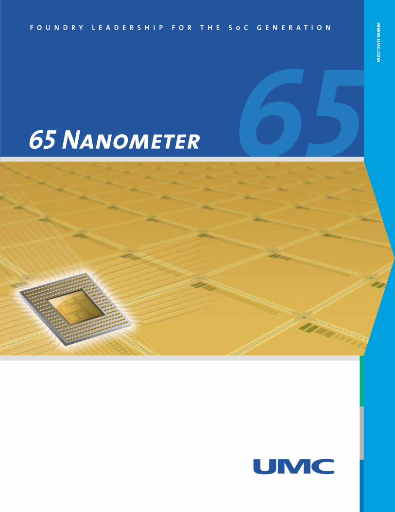
65 FOUNDRY LEADERSHIP FOR THE SoC GENERATION www.umc.com 65 Nanometer

Welcome message from author
This document is posted to help you gain knowledge. Please leave a comment to let me know what you think about it! Share it to your friends and learn new things together.
Transcript
65F O U N D R Y L E A D E R S H I P F O R T H E S o C G E N E R A T I O N
ww
w.um
c.com
65 Nanometer

65 Nanometer
UMC is the foundry leader in 65nm process technology, having delivered the foundry industry’s first 65nm customer products in June
of 2005. UMC's 65-nanometer SoC solution begins with a flexible technology design platform. Customers are able to choose the process device options that are optimized for their specific application, such as Standard Performance (SP), Low Power(LP) or Low Leakage (LL) transistors. The high performance characteristics of UMC’s 65nm SP process enable designers to utilize the technology to power a broad range of applications from consumer products to graphics ICs. Technology options can then be implemented including mixed signal/RFCMOS and embedded memories to further customize the process.
• Integrated flows for logic, Mixed-Signal/RF
• 6T/8T e-SRAM bit cells; URAMTM option (0.12um2)
• e-Fuse option
• Shallow trench isolation
• Retrograde twin well (Triple well option)
• 193nm litho for all critical layers
• Enhanced nitrided gate oxide
• 40nm min. poly length
• Multiple Vt options
• NiSi process
• Mobility enhancement techniques
• 1P10M Cu/Low K (K=2.9)
• BOAC (Bonding Over Active Circuit)
• Wire Bond/Flip Chip option
Technology to Meet Broad Applications
65nm Key Features
Standard Performance (L65SP)Low Leakage (L65LL) / Low Power (L65LP)
UMC 65nm Technology
Portable • Wireless ASIC • Consumer • Graphics • Network
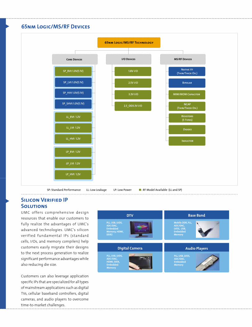
65nm Logic/MS/RF Devices
Silicon Verified IP SolutionsUMC offers comprehensive design resources that enable our customers to fully realize the advantages of UMC's advanced technologies. UMC's silicon verified fundamental IPs (standard cells, I/Os, and memory compilers) help customers easily migrate their designs to the next process generation to realize significant performance advantages while also reducing die size.
Customers can also leverage application specific IPs that are specialized for all types of mainstream applications such as digital TVs, cellular baseband controllers, digital cameras, and audio players to overcome time-to-market challenges.
Mobile DDR, PLL, ADC/DAC,LVDS, USB, Embedded Memory
PLL, USB, LVDS, ADC/DAC,Embedded Memory, HDMI, DDR2
PLL, USB, LVDS, ADC/DAC, Embedded Memory
PLL, USB, LVDS, ADC/DAC, HDMI, SATA, Embedded Memory
DTV Base Band
Audio PlayersDigital Camera
SP: Standard Performance LL: Low Leakage LP: Low Power : RF Model Available (LL and SP)
I/O Devices Core Devices MS/RF Devices
Native Vt(Thin/Thick Ox.)
Bipolar
MIM/MOM Capacitor
1.8V I/O
2.5V I/O
3.3V I/O
NCAP(Thin/Thick Ox.)
Resistors(5 Types)
Diodes
SP_RVt 1.0V(1.1V)
SP_LVt 1.0V(1.1V)
SP_HVt 1.0V(1.1V)
LP_RVt 1.2V
LP_LVt 1.2V
LP_HVt 1.2V
LL_RVt 1.2V
LL_LVt 1.2V
Inductor
65nm Logic/MS/RF Technology
2.5_OD3.3V I/O
LL_HVt 1.2V
SP_SHVt 1.0V(1.1V)

Fundamental IP Support for SoC Designs UMC offers comprehensive design resources that support our 65nm process technology. Silicon verified fundamental IPs (standard cells, I/Os, and memory compilers) optimized to UMC technologies are available free-of-charge from several leading vendors. Customers can also leverage application specific IPs for DTV, video/audio, etc. IPs available through UMC are DFM (Design for Manufacturing) compliant for better manufacturability.
Library Provider65nm
Faraday VIRAGE ARM UMC
Library LL SP LP SP SP LL LP
Standard Cells
LVT
RVT
HVT
I/O
1.8Vdd
3.3Vdd
2.5V / 3.3V
1.8V / 2.5V / 3.3V
Single Port SRAM Compiler
Dual Port SRAM Compiler
Single Port Register File
Dual Port Register File
ROM Compiler
Type Support FeaturesSupport
28nm 40nm 65nm 90nm 0.13um
Operating Power
Voltage Island & Scaling
Level Shifters w / Insulator
Power & Timing Model @ 80% of Vdd
Þ Þ Þ Þ Þ
Clock Gating & Frequency Scaling
Clock Gated F/F Þ Þ Þ Þ Þ
Leakage Power
Multi-Vt Multi-Vt cells Þ Þ Þ Þ Þ
Power Gating Isolation cells, Retention F/FHeaders / Footers, etc. Þ Þ Þ Þ Þ
Body Bias Tapless cells Timing / Power Model Þ Þ Þ Þ Þ
With today's proliferation of low power applications, lowering energy consumption without sacrificing performance has become a critical concern for designers of power management chips for portable electronics. UMC supports its standard cell library with low power design features, including multiple Vt, clock-gating, level shifter and other features to complement UMC’s complete low power solution.
Low Power Features of Standard Cell Library
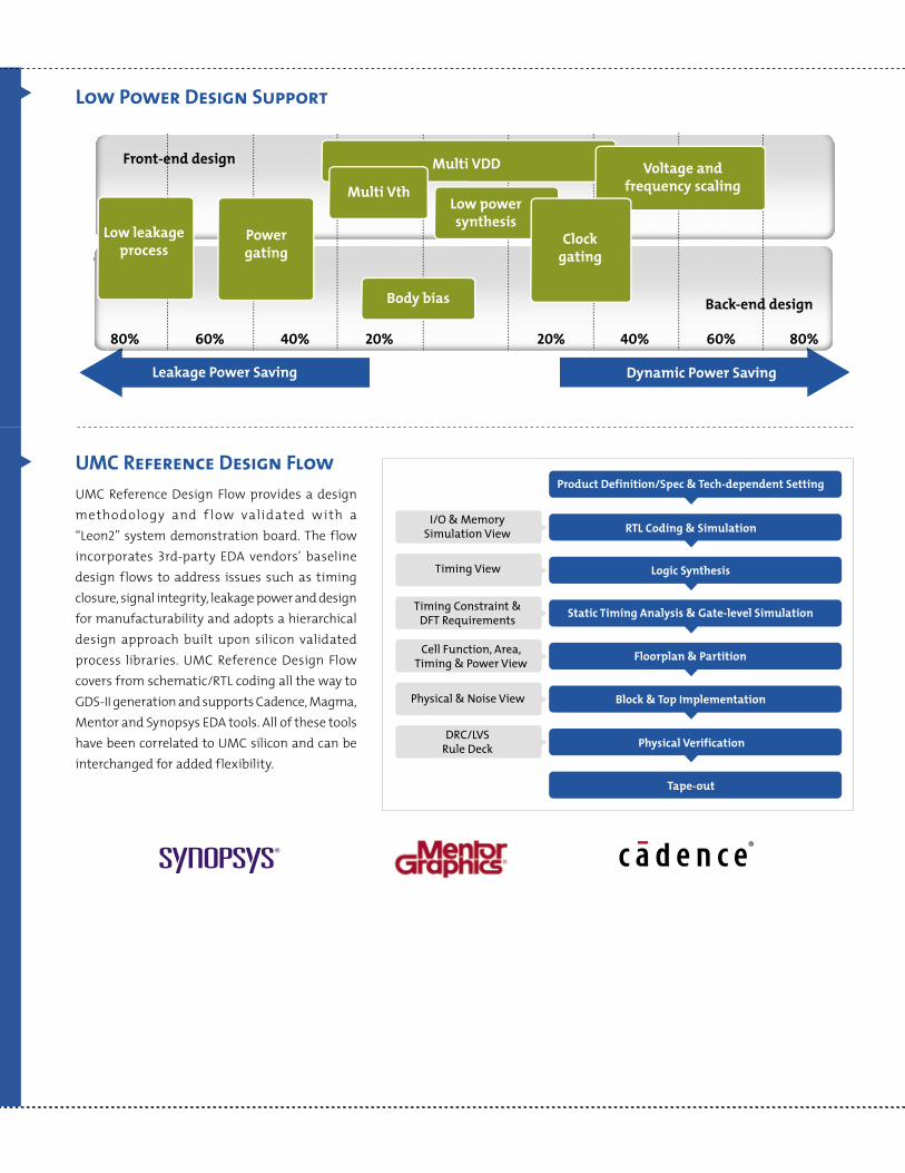
Low Power Design Support
Voltage and frequency scaling
Low leakage process
Body bias
20%20% 40%40% 60%60% 80%80%
Leakage Power Saving Dynamic Power Saving
Clockgating
Front-end design
Back-end design
Power gating
Multi VthLow powersynthesis
Multi VDD
UMC Reference Design Flow UMC Reference Design Flow provides a design methodology and f low validated w ith a “Leon2” system demonstration board. The flow incorporates 3rd-party EDA vendors’ baseline design flows to address issues such as timing closure, signal integrity, leakage power and design for manufacturability and adopts a hierarchical design approach built upon silicon validated process libraries. UMC Reference Design Flow covers from schematic/RTL coding all the way to GDS-II generation and supports Cadence, Magma, Mentor and Synopsys EDA tools. All of these tools have been correlated to UMC silicon and can be interchanged for added flexibility.
Product Definition/Spec & Tech-dependent Setting
RTL Coding & Simulation
Physical Verification
Logic Synthesis
Block & Top Implementation
Static Timing Analysis & Gate-level Simulation
Floorplan & Partition
Tape-out
I/O & MemorySimulation View
Timing View
Timing Constraint &DFT Requirements
DRC/LVSRule Deck
Physical & Noise View
Cell Function, Area, Timing & Power View
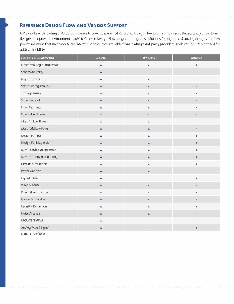
Features of Design Flow Cadence Synopsys Mentor
Functional Logic Simulation
Schematic Entry - -
Logic Synthesis -
Static Timing Analysis -
Timing Closure -
Signal Integrity -
Floor Planning -
Physical Synthesis -
Multi-Vt Low Power -
Multi-Vdd Low Power -
Design For Test
Design For Diagnosis
DFM - double via insertion
DFM - dummy metal filling
Circuits Simulation
Power Analysis -
Layout Editor -
Place & Route -
Physical Verification
Formal Verification -
Parasitic Extraction
Noise Analysis -
RFCMOS/EMDM - -
Analog/Mixed Signal -
Note: Available
Reference Design Flow and Vendor SupportUMC works with leading EDA tool companies to provide a verified Reference Design Flow program to ensure the accuracy of customer designs in a proven environment. UMC Reference Design Flow program integrates solutions for digital and analog designs and low power solutions that incorporate the latest DFM resources available from leading third-party providers. Tools can be interchanged for added flexibility.
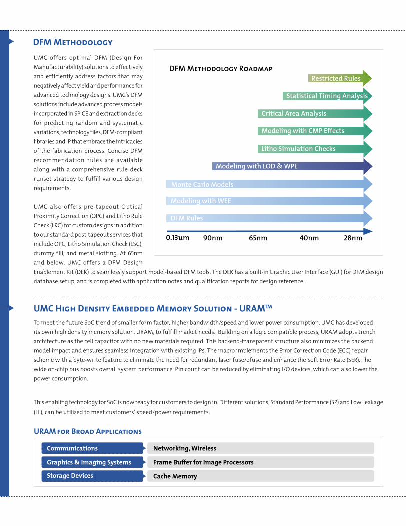
UMC offers optimal DFM (Design For Manufacturability) solutions to effectively and efficiently address factors that may negatively affect yield and performance for advanced technology designs. UMC’s DFM solutions include advanced process models incorporated in SPICE and extraction decks for predicting random and systematic variations, technology files, DFM-compliant libraries and IP that embrace the intricacies of the fabrication process. Concise DFM recommendation rules are available along with a comprehensive rule-deck runset strategy to fulfill various design requirements.
UMC also offers pre-tapeout Optical Proximity Correction (OPC) and Litho Rule Check (LRC) for custom designs in addition to our standard post-tapeout services that include OPC, Litho Simulation Check (LSC), dummy fill, and metal slotting. At 65nm and below, UMC offers a DFM Design
DFM Methodology
0.13um 90nm 65nm 40nm 28nm
DFM Methodology Roadmap
DFM Rules
Modeling with WEE
Monte Carlo Models
Modeling with LOD & WPE
Modeling with CMP Effects
Critical Area Analysis
Statistical Timing Analysis
Restricted Rules
Litho Simulation Checks
Enablement Kit (DEK) to seamlessly support model-based DFM tools. The DEK has a built-in Graphic User Interface (GUI) for DFM design database setup, and is completed with application notes and qualification reports for design reference.
UMC High Density Embedded Memory Solution - URAMTM
To meet the future SoC trend of smaller form factor, higher bandwidth/speed and lower power consumption, UMC has developed its own high density memory solution, URAM, to fulfill market needs. Building on a logic compatible process, URAM adopts trench architecture as the cell capacitor with no new materials required. This backend-transparent structure also minimizes the backend model impact and ensures seamless integration with existing IPs. The macro implements the Error Correction Code (ECC) repair scheme with a byte-write feature to eliminate the need for redundant laser fuse/efuse and enhance the Soft Error Rate (SER). The wide on-chip bus boosts overall system performance. Pin count can be reduced by eliminating I/O devices, which can also lower the power consumption.
This enabling technology for SoC is now ready for customers to design in. Different solutions, Standard Performance (SP) and Low Leakage (LL), can be utilized to meet customers’ speed/power requirements.
URAM for Broad Applications
Communications
Graphics & Imaging Systems
Storage Devices
Networking, Wireless
Frame Buffer for Image Processors
Cache Memory
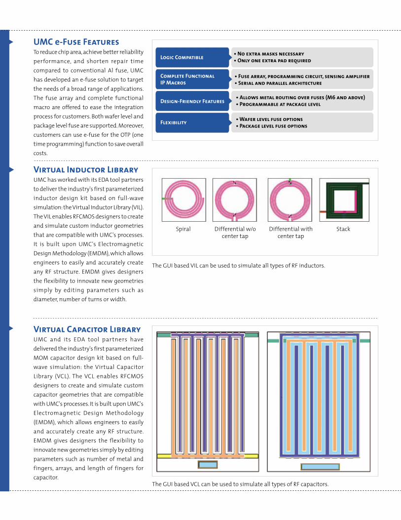
UMC e-Fuse FeaturesTo reduce chip area, achieve better reliability performance, and shorten repair time compared to conventional Al fuse, UMC has developed an e-fuse solution to target the needs of a broad range of applications. The fuse array and complete functional macro are offered to ease the integration process for customers. Both wafer level and package level fuse are supported. Moreover, customers can use e-fuse for the OTP (one time programming) function to save overall costs.
•Noextramasks necessary•Onlyoneextrapad required
•Fusearray, programming circuit, sensing amplifier•Serialandparallel architecture
•Allowsmetal routing over fuses (M6 and above)•Programmableat packagelevel
Logic Compatible
Complete Functional IP Macros
Design-Friendly Features
•Wafer level fuse options•Packagelevel fuse optionsFlexibility
Virtual Inductor LibraryUMC has worked with its EDA tool partners to deliver the industry's first parameterized inductor design kit based on full-wave simulation: the Virtual Inductor Library (VIL). The VIL enables RFCMOS designers to create and simulate custom inductor geometries that are compatible with UMC's processes. It is built upon UMC's Electromagnetic Design Methodology (EMDM), which allows engineers to easily and accurately create any RF structure. EMDM gives designers the flexibility to innovate new geometries simply by editing parameters such as diameter, number of turns or width.
Spiral Differential w/o center tap
Differential with center tap
Stack
The GUI based VIL can be used to simulate all types of RF inductors.
Virtual Capacitor LibraryUMC and its EDA tool partners have delivered the industry's first parameterized MOM capacitor design kit based on full-wave simulation: the Virtual Capacitor Library (VCL). The VCL enables RFCMOS designers to create and simulate custom capacitor geometries that are compatible with UMC's processes. It is built upon UMC's Electromagnetic Design Methodology (EMDM), which allows engineers to easily and accurately create any RF structure. EMDM gives designers the flexibility to innovate new geometries simply by editing parameters such as number of metal and fingers, arrays, and length of fingers for capacitor.
The GUI based VCL can be used to simulate all types of RF capacitors.

Vi rt ua l Tr a n s f o r m e r Library UMC has also worked with its EDA tool partners to deliver the industry's first parameterized transformer design kit based on full-wave simulation: the Virtual Transformer Library (VTL). The VTL enables RFCMOS designers to create and simulate custom transformer geometries that are compatible with UMC's processes. It is built upon UMC's Electromagnetic Design Methodology (EMDM), which allows engineers to easily and accurately create any RF structure. EMDM gives designers the flexibility to innovate new geometries simply by editing parameters such as primary impedance, secondary impedance, number of turns, mode, and frequency for transformer.
CT on primary coilWithout Center Tape
CT on both coilsCT on secondary coil
The GUI based VTL can be used to simulate all types of RF transformers.
MS/RF Design Flow and FDKThe FDK (Foundry Design Kit) provides IC designers with an automatic design environment. The methodology provides access to circuit-level design and simulation, circuit layout, and layout verification with accurate RF device models. In the front-end, fundamental components of UMC's MS/RF process are implemented in common design environments and simulation tools. The back-end includes parameterized cells (P Cell), which include a schematic driven layout to provide an automatic and complete design flow. Callback functions are also provided in the design flow to minimize data entry. EDA tools for MS/RF designs are also supported.
Schematic (Composer)(Symbols & CDF)
Virtual Inductor/Capacitor/Transformer
Library
Cadence
Spectre / Spectre RF
Spectre / Spectre RF
Simulation with VerifiedRF/Mixed Signal Models
Virtual Inductor/Capacitor/Transformer Spec.
Virtual Inductor/Capacitor/Transformer Library
Tape Out
Circuit LayoutVirtuoso(P-cell)
Verification & Extraction(DRC/LVS/LPE)
Calibre/XRC
Assura
SchematicDriven Layout
Artist
Spectre / Spectre RF
Optimum Inductor Finder (OIF)UMC offers the Optimum Inductor Finder (OIF) in the FDK package. The OIF gives designers the ability to quickly access a large library
of inductors calibrated to UMC's silicon. It also allows users to perform inductor optimization through just a few simple steps with the
user-friendly interface. For instance, customers can define a desired inductor and make trade-offs between Q-factor and area. The OIF
will select a design that best fits the specifications in a matter of seconds.
Optimum Capacitor Finder (OCF)UMC offers the Optimum Capacitor Finder (OCF) in the FDK package. The OCF gives designers the ability to quickly access a large library
of capacitors calibrated to UMC's silicon. It also allows users to perform capacitor optimization through just a few simple steps with
the user-friendly interface. For instance, customers can define a desired capacitor and make trade-offs between Q-factor and area. The
OCF will select a design that best fits the specifications in a matter of seconds.
Optimum Transformer Finder (OTF)UMC offers the Optimum Transformer Finder (OTF) in the FDK package. The OTF gives designers the ability to quickly access a large
library of transformers calibrated to UMC's silicon. It also allows users to perform transformer optimization through just a few simple
steps with the user-friendly interface. For instance, customers can define a desired transformer and make trade-offs between impedance
and area. The OTF will select a design that best fits the specifications in a matter of seconds.
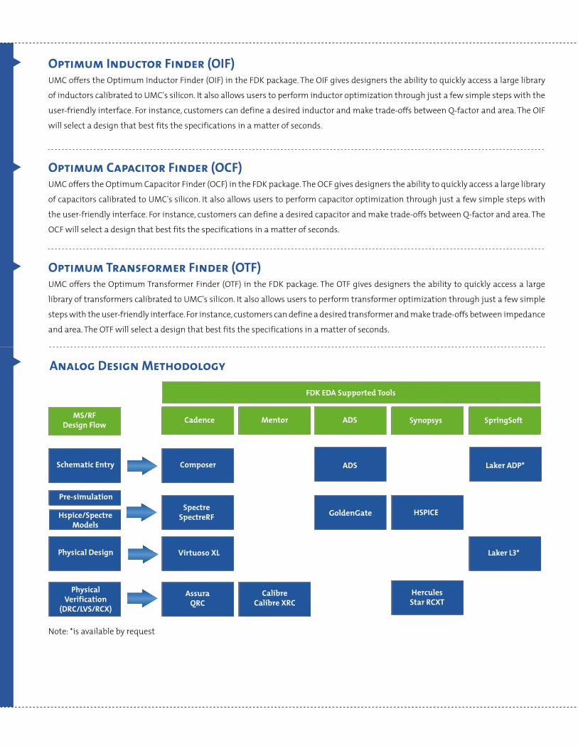
Analog Design Methodology
Physical Design
Physical Verification
(DRC/LVS/RCX)
SpectreSpectreRF HSPICE
HerculesStar RCXT
Cadence Mentor ADS Synopsys
FDK EDA Supported Tools
CalibreCalibre XRC
AssuraQRC
Virtuoso XL
ADS Laker ADP*
GoldenGate
Composer
MS/RFDesign Flow
Hspice/SpectreModels
Pre-simulation
Schematic Entry
Laker L3*
SpringSoft
EldoEldoRF
IC Station
DA-IC
Note: *is available by request

MEMO:

ww
w.um
c.com
F O U N D R Y L E A D E R S H I P F O R T H E S o C G E N E R A T I O N
1410 For more information: visit www.umc.com or e-mail [email protected]
New CustomersFor new customer inquiries, please direct all questions to [email protected]
Worldwide ContactsHeadquarters:UMCNo. 3, Li-Hsin 2nd Road,Hsinchu Science Park, Hsinchu, Taiwan, R.O.C.Tel: 886-3-578-2258Fax: 886-3-577-9392Email: [email protected]
In China:UMC Beijing:Room #512, 5F, South Block, Raycom InfoTech Park, No.2, Kexueyuan South Road, Zhongguancun, Haidian District, Beijing 100190, ChinaTel: 86-10-59822250 86-18913138053Fax: 86-10-59822588
HeJian Technology (Suzhou):No. 333, Xinghua Street, Suzhou Industrial Park, Suzhou, Jiangsu Province 215025, ChinaTel: 86-512-65931299Fax: 86-512-62530172
In Japan:UMC Group Japan15F Akihabara Centerplace Bldg.,1 Kanda Aioi-Cho Chiyoda-Ku Tokyo 101-0029 JapanTel : 81-3-5294-2701Fax: 81-3-5294-2707
In Singapore:UMC-SGNo. 3, Pasir Ris Drive 12,Singapore 519528Tel: 65-6213-0018Fax: 65-6213-0005
In Korea:UMC Korea1117, Hanshin Intervally24, 322, Teheran-ro, Gangnam-gu, Seoul, Korea Tel: 82-2-2183-1790 Fax: 82-2-2183-1794 Email:[email protected]
In North America:UMC USA488 De Guigne Drive,Sunnyvale, CA 94085, USATel: 1-408-523-7800Fax: 1-408-733-8090
In Europe:UMC Europe BVDe entree 771101 BH Amsterdam ZuidoostThe NetherlandsTel: 31-(0)20-5640950Fax: 31-(0)20-6977826
Related Documents