Welcome message from author
This document is posted to help you gain knowledge. Please leave a comment to let me know what you think about it! Share it to your friends and learn new things together.
Transcript


Power Dissipation In ICs
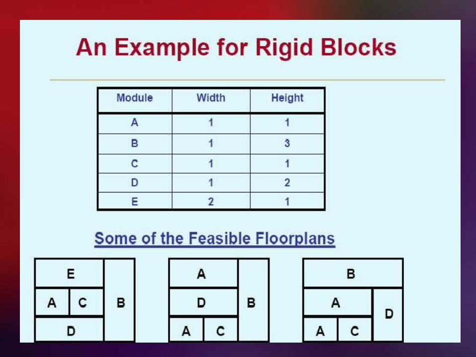
What is Floor Planning ?
Power Optimization Through Floor Planning
Why Low Power ICs ?
Current Trends and Future Research
Conclusion
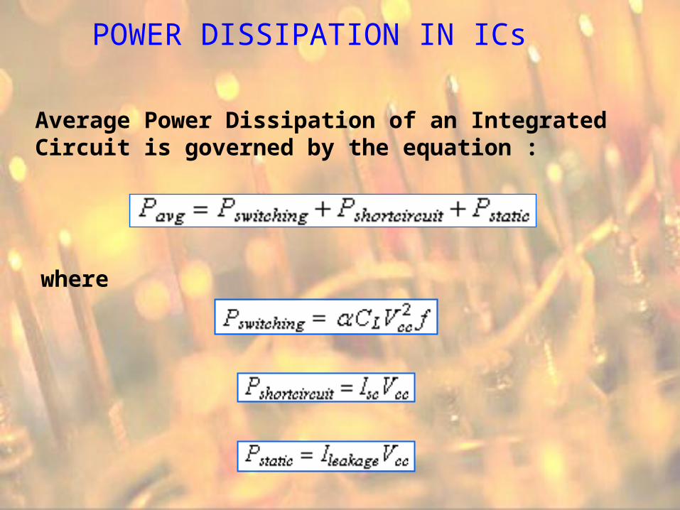
POWER DISSIPATION IN ICs
Average Power Dissipation of an Integrated Circuit is governed by the equation :
where
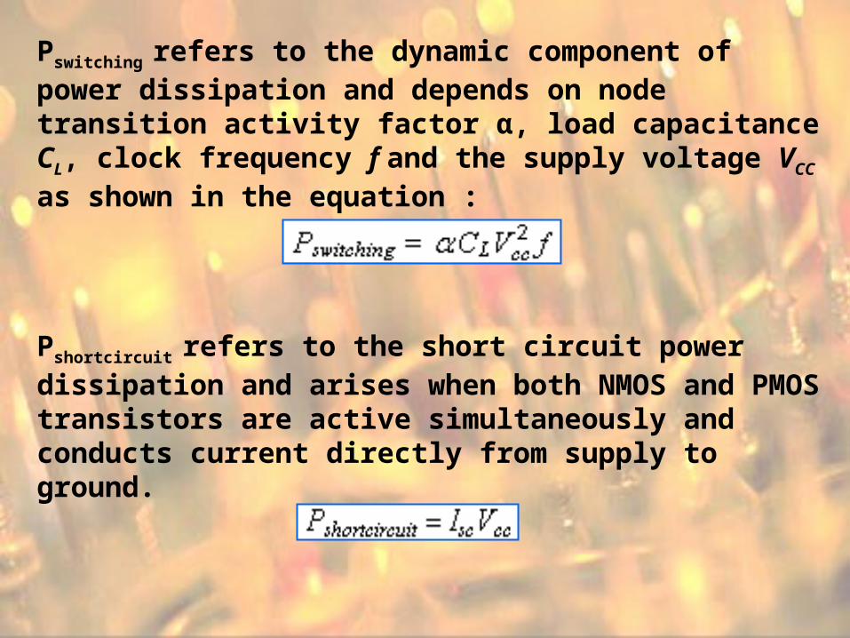
Pswitching refers to the dynamic component of power dissipation and depends on node transition activity factor α, load capacitance CL, clock frequency f and the supply voltage VCC as shown in the equation :
Pshortcircuit refers to the short circuit power dissipation and arises when both NMOS and PMOS transistors are active simultaneously and conducts current directly from supply to ground.
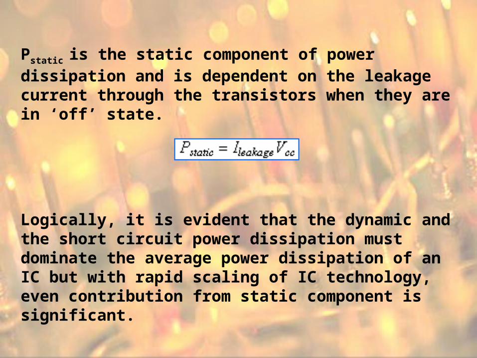
Pstatic is the static component of power dissipation and is dependent on the leakage current through the transistors when they are in ‘off’ state.
Logically, it is evident that the dynamic and the short circuit power dissipation must dominate the average power dissipation of an IC but with rapid scaling of IC technology, even contribution from static component is significant.
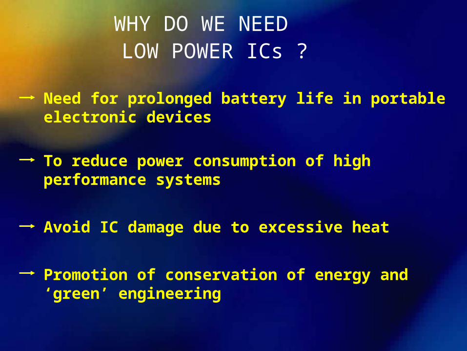
WHY DO WE NEEDLOW POWER ICs ?
Need for prolonged battery life in portable electronic devices
To reduce power consumption of high performance systems
Avoid IC damage due to excessive heat
Promotion of conservation of energy and ‘green’ engineering
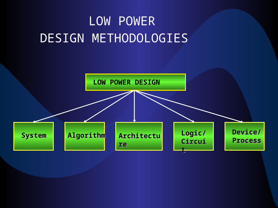
LOW POWER DESIGN
SystemSystem AlgorithAlgorithmm
ArchitecturArchitecturee
Logic/Logic/CircuitCircuit
Device/Device/ProcesProcesss
LOW POWERDESIGN METHODOLOGIES
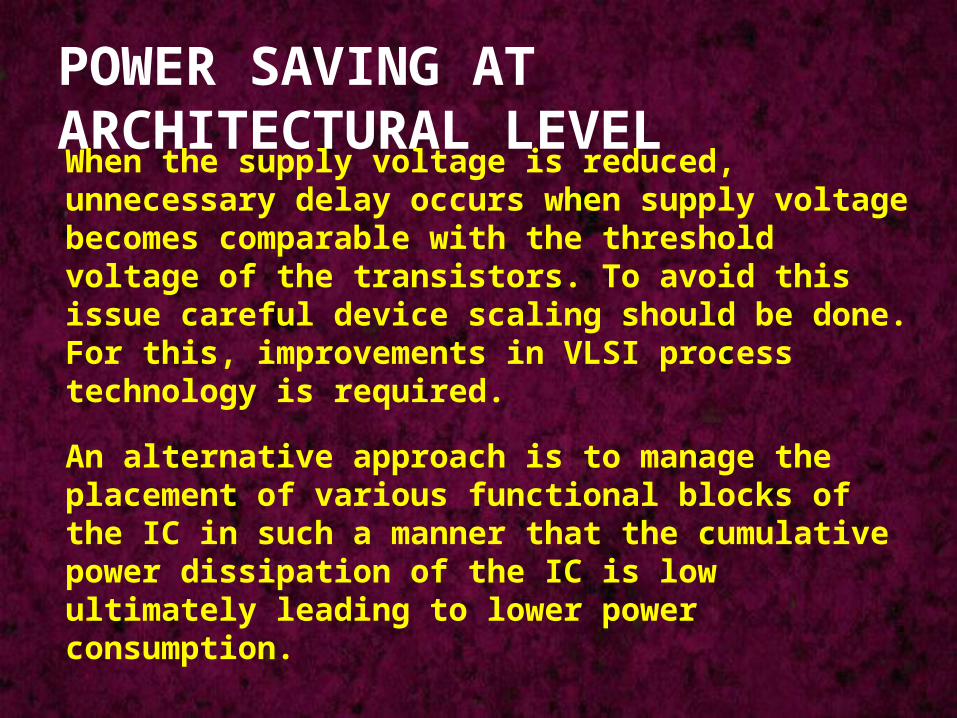
POWER SAVING AT ARCHITECTURAL LEVELWhen the supply voltage is reduced, unnecessary delay occurs when supply voltage becomes comparable with the threshold voltage of the transistors. To avoid this issue careful device scaling should be done. For this, improvements in VLSI process technology is required.
An alternative approach is to manage the placement of various functional blocks of the IC in such a manner that the cumulative power dissipation of the IC is low ultimately leading to lower power consumption.
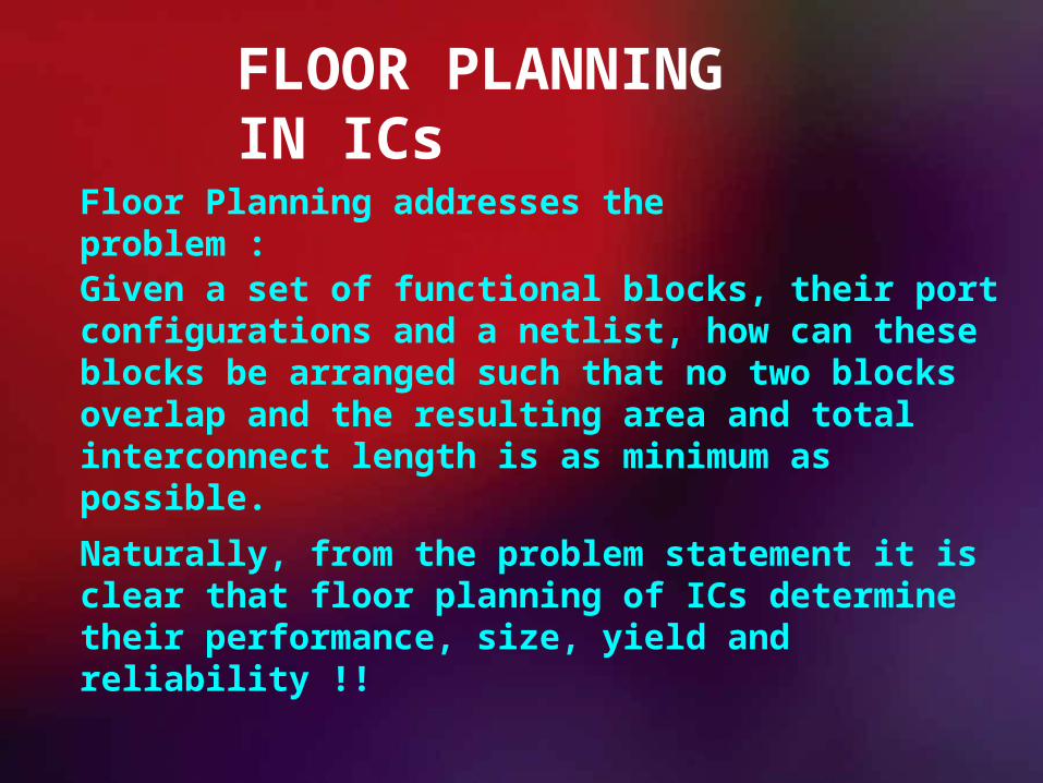
FLOOR PLANNING IN ICs
Floor Planning addresses the problem :Given a set of functional blocks, their port configurations and a netlist, how can these blocks be arranged such that no two blocks overlap and the resulting area and total interconnect length is as minimum as possible. Naturally, from the problem statement it is clear that floor planning of ICs determine their performance, size, yield and reliability !!
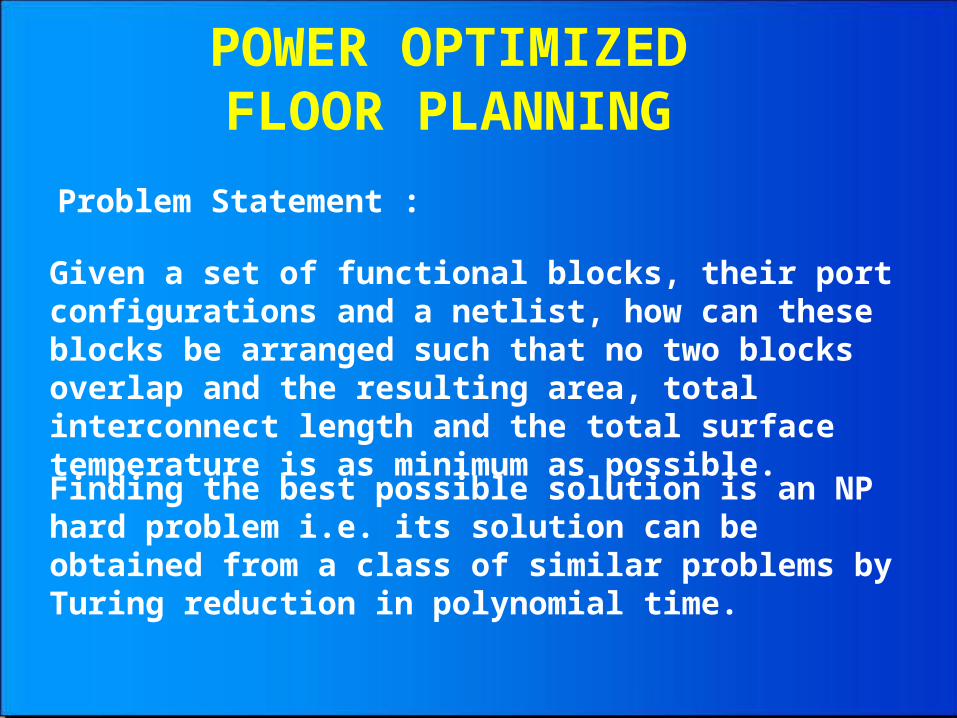
POWER OPTIMIZEDFLOOR PLANNINGProblem Statement :
Given a set of functional blocks, their port configurations and a netlist, how can these blocks be arranged such that no two blocks overlap and the resulting area, total interconnect length and the total surface temperature is as minimum as possible. Finding the best possible solution is an NP hard problem i.e. its solution can be obtained from a class of similar problems by Turing reduction in polynomial time.
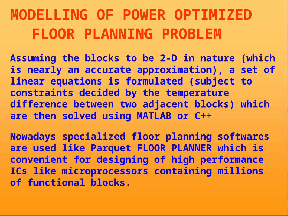
MODELLING OF POWER OPTIMIZED FLOOR PLANNING
PROBLEMAssuming the blocks to be 2-D in nature (which is nearly an accurate approximation), a set of linear equations is formulated (subject to constraints decided by the temperature difference between two adjacent blocks) which are then solved using MATLAB or C++
Nowadays specialized floor planning softwares are used like Parquet FLOOR PLANNER which is convenient for designing of high performance ICs like microprocessors containing millions of functional blocks.
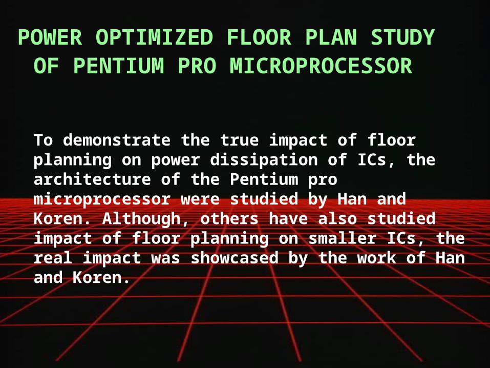
POWER OPTIMIZED FLOOR PLAN STUDYOF PENTIUM PRO
MICROPROCESSOR
To demonstrate the true impact of floor planning on power dissipation of ICs, the architecture of the Pentium pro microprocessor were studied by Han and Koren. Although, others have also studied impact of floor planning on smaller ICs, the real impact was showcased by the work of Han and Koren.
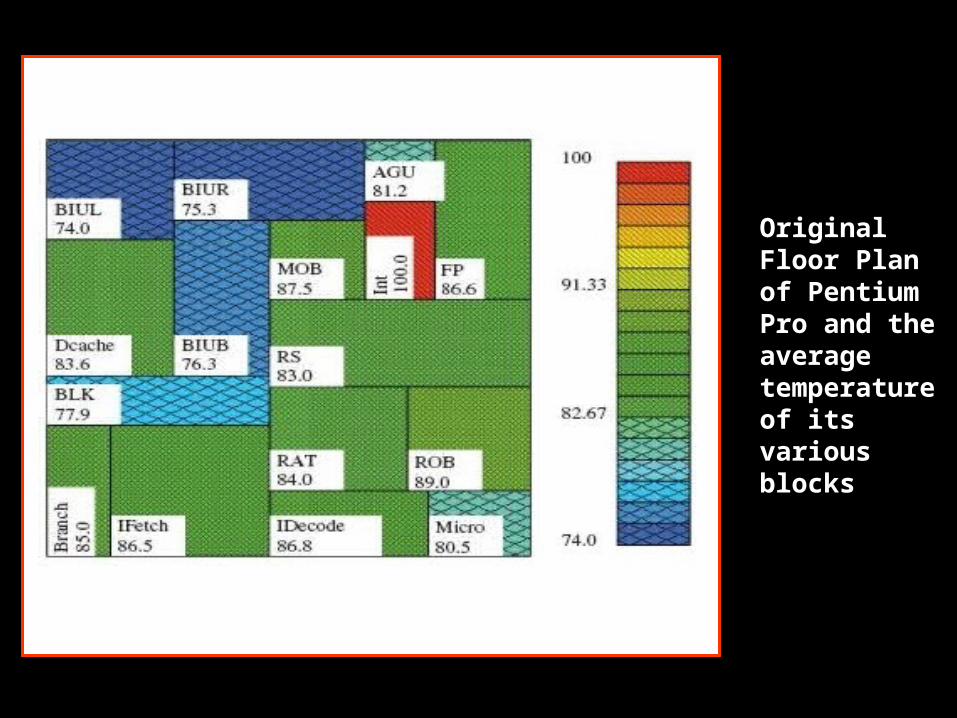
Original Floor Plan of Pentium Pro and the average temperature of its various blocks
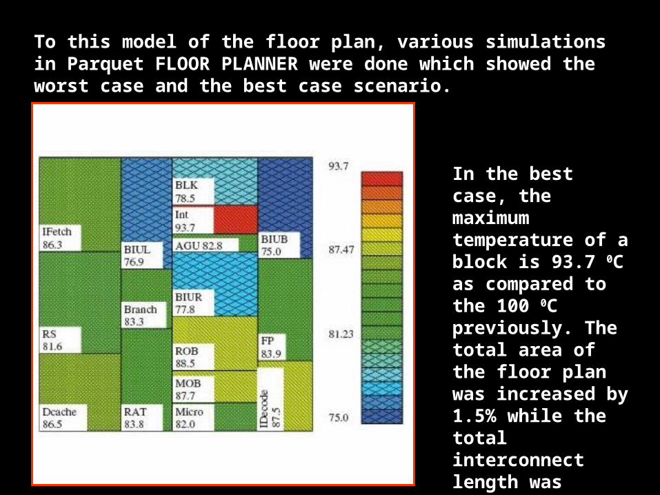
To this model of the floor plan, various simulations in Parquet FLOOR PLANNER were done which showed the worst case and the best case scenario.
In the best case, the maximum temperature of a block is 93.7 0C as compared to the 100 0C previously. The total area of the floor plan was increased by 1.5% while the total interconnect length was increased by 13%.
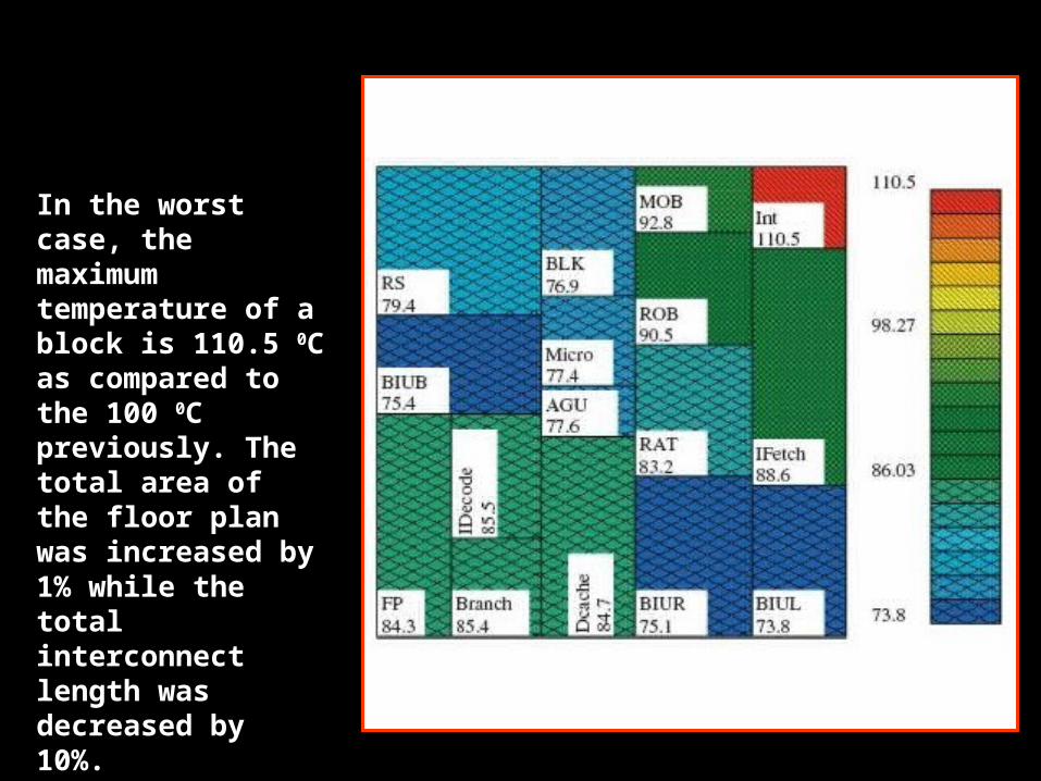
In the worst case, the maximum temperature of a block is 110.5 0C as compared to the 100 0C previously. The total area of the floor plan was increased by 1% while the total interconnect length was decreased by 10%.
Conclusion - IThe result shows that power optimized floor planning can yield us
different results depending on the final placement of the blocks on the chip.
While the best case of our floor plan simulation yielded us a maximum temperature of 93.7 0C, the worst case simulation yielded a maximum temperature of 110.5 0C. A power optimized floor plan for Pentium Pro would then lie somewhere between this range.
Even though the best case scenario gave us a reduced maximum temperature of 6.3 0C, the interconnect length and the area were substantially increased. This shows that power optimization may not always lead the best floor plan design and should rather be governed by client imposed constraints.
Power optimized floor planning is now widespread and prevalent in 90 nm process technology
Sometimes power optimized floor planning also yields best result in terms of area and interconnect lengths as well
This technique of floor planning is also a better algorithm for 3-D IC placement technology and can help them become much faster in operation (Research going on)
This technology will herald a new age of consumer electronics with long battery life and provide better power management ICs required in Power Electronics
Conclusion - II
Power optimized floor planning is a viable alternative technology that can be used and is in fact used for producing low power ICs which is the need of the hour to be able to make electronics and associated technology feasible enough in the coming decade when power is going to be much more costly than now.
Switching to power optimized floor planning will also ensure environment friendly ICs and hence devices and help indirectly reduce global warming which is the need of the hour !

THANK YOU
Related Documents