PhD Dissertations and Master's Theses 12-2020 Flexible Strain Detection Using Surface Acoustic Waves: Flexible Strain Detection Using Surface Acoustic Waves: Fabrication and Tests Fabrication and Tests Rishikesh Srinivasaraghavan Govindarajan Follow this and additional works at: https://commons.erau.edu/edt Part of the Aerospace Engineering Commons Scholarly Commons Citation Scholarly Commons Citation Govindarajan, Rishikesh Srinivasaraghavan, "Flexible Strain Detection Using Surface Acoustic Waves: Fabrication and Tests" (2020). PhD Dissertations and Master's Theses. 557. https://commons.erau.edu/edt/557 This Thesis - Open Access is brought to you for free and open access by Scholarly Commons. It has been accepted for inclusion in PhD Dissertations and Master's Theses by an authorized administrator of Scholarly Commons. For more information, please contact [email protected].

Welcome message from author
This document is posted to help you gain knowledge. Please leave a comment to let me know what you think about it! Share it to your friends and learn new things together.
Transcript
PhD Dissertations and Master's Theses
12-2020
Flexible Strain Detection Using Surface Acoustic Waves: Flexible Strain Detection Using Surface Acoustic Waves:
Fabrication and Tests Fabrication and Tests
Rishikesh Srinivasaraghavan Govindarajan
Follow this and additional works at: https://commons.erau.edu/edt
Part of the Aerospace Engineering Commons
Scholarly Commons Citation Scholarly Commons Citation Govindarajan, Rishikesh Srinivasaraghavan, "Flexible Strain Detection Using Surface Acoustic Waves: Fabrication and Tests" (2020). PhD Dissertations and Master's Theses. 557. https://commons.erau.edu/edt/557
This Thesis - Open Access is brought to you for free and open access by Scholarly Commons. It has been accepted for inclusion in PhD Dissertations and Master's Theses by an authorized administrator of Scholarly Commons. For more information, please contact [email protected].

FLEXIBLE STRAIN DETECTION USING SURFACE ACOUSTIC WAVES:
FABRICATION AND TESTS
By
Rishikesh Srinivasaraghavan Govindarajan
A Thesis Submitted to the Faculty of Embry-Riddle Aeronautical University
In Partial Fulfillment of the Requirements for the Degree of
Master of Science in Aerospace Engineering
December 2020
Embry-Riddle Aeronautical University
Daytona Beach, Florida
ii
FLEXIBLE STRAIN DETECTION USING SURFACE ACOUSTIC WAVES: FABRICATION AND TESTS
By
Rishikesh Srinivasaraghavan Govindarajan
This Thesis was prepared under the direction of the candidate’s Thesis Committee Chair, Dr. Daewon Kim, Department of Aerospace Engineering, and has been approved by the members of Thesis Committee. It was submitted to the Office of the Senior Vice
President for Academic Affairs and Provost, and was accepted in the partial fulfillment of the requirements for the Degree of Master of Science in Aerospace Engineering.
THESIS COMMITTEE
Chairman, Dr. Daewon Kim
Member, Dr. Marwan Al-Haik
Member, Dr. Eduardo Rojas
Graduate Program Coordinator, Dr. Marwan Al-Haik
Date
Dean of the College of Engineering, Dr. Maj Mirmirani
Date
Associate Provost of Academic Support, Dr. Christopher Grant
Date
Daewon KimDigitally signed by Daewon Kim Date: 2020.12.03 11:46:45 -05'00'
Maj
Stamp
srinivr1
Stamp

iii
ACKNOWLEDGEMENTS
I would like to express my sincere gratitude to my advisor, Dr. Daewon Kim, for
supporting, motivating and guiding me to the correct direction continuously with his
impeccable insights throughout my research work. His patience and gentleness always
brought a positive vibe on me to proceed optimistically. I would like to thank Dr.
Eduardo Rojas for being a constant source of encouragement and valuable inputs
especially in RF testing. I also want to thank Dr. Marwan Al-Haik, who always allowed
me to use lab equipment without any hesitation.
I would like to thank Dr. Foram Madiyar, for helping me in my research especially
for characterization techniques by arranging sources of facility and her timely response
whenever I needed. I really appreciate Mr. Mike Potash for helping me in setting up and
dealing electrical connections with his welcoming availability.
I would like to extend my appreciation to my research group Stan, Cedric and my
friends Sandeep and Suma who all constantly supported and giving encouragement with
useful discussions in various stages of my research. I would like to thank Hanson and
Justin for their assistance in the VNA measurements.
Finally, I thank my parents and brother who always encouraged me to reach my
dreams. Without their care and support, I would have not made it. I feel happy that I took
a right decision in choosing Embry-Riddle Aeronautical University to pursue my Master
of Science in Aerospace Engineering.
iv
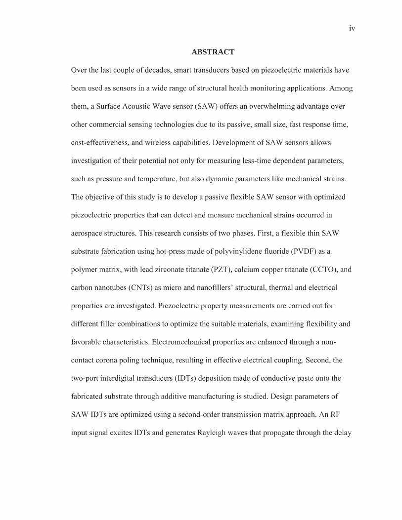
ABSTRACT
Over the last couple of decades, smart transducers based on piezoelectric materials have
been used as sensors in a wide range of structural health monitoring applications. Among
them, a Surface Acoustic Wave sensor (SAW) offers an overwhelming advantage over
other commercial sensing technologies due to its passive, small size, fast response time,
cost-effectiveness, and wireless capabilities. Development of SAW sensors allows
investigation of their potential not only for measuring less-time dependent parameters,
such as pressure and temperature, but also dynamic parameters like mechanical strains.
The objective of this study is to develop a passive flexible SAW sensor with optimized
piezoelectric properties that can detect and measure mechanical strains occurred in
aerospace structures. This research consists of two phases. First, a flexible thin SAW
substrate fabrication using hot-press made of polyvinylidene fluoride (PVDF) as a
polymer matrix, with lead zirconate titanate (PZT), calcium copper titanate (CCTO), and
carbon nanotubes (CNTs) as micro and nanofillers’ structural, thermal and electrical
properties are investigated. Piezoelectric property measurements are carried out for
different filler combinations to optimize the suitable materials, examining flexibility and
favorable characteristics. Electromechanical properties are enhanced through a non-
contact corona poling technique, resulting in effective electrical coupling. Second, the
two-port interdigital transducers (IDTs) deposition made of conductive paste onto the
fabricated substrate through additive manufacturing is studied. Design parameters of
SAW IDTs are optimized using a second-order transmission matrix approach. An RF
input signal excites IDTs and generates Rayleigh waves that propagate through the delay

v
line. By analyzing the changes in wave characteristics, such as frequency shift and phase
response, the developed passive strain sensor can measure mechanical strains.

vi
TABLE OF CONTENTS
ACKNOWLEDGEMENTS ........................................................................................... iii ABSTRACT ................................................................................................................... iv LIST OF FIGURES ....................................................................................................... viii LIST OF TABLES ......................................................................................................... xi SYMBOLS ..................................................................................................................... xii ABBREVIATIONS ...................................................................................................... xiv 1. Introduction ................................................................................................................ 1
1.1. Significance ...................................................................................................... 1 1.2. Mechanical and Electromechanical Sensors ..................................................... 1 1.3. Acoustic Wave Sensor ...................................................................................... 3 1.4. Surface Acoustic Wave Sensor ......................................................................... 5 1.5. Piezoelectric Effect ........................................................................................... 9 1.6. Crystallographic Classifications ....................................................................... 10 1.7. Piezoelectric Composites .................................................................................. 11 1.8. Piezoelectric Composite Materials ................................................................... 12 1.9. Phase Information of PVDF ............................................................................. 15 1.10. SAW Sensing System ..................................................................................... 16 1.11. Research Objective ......................................................................................... 18
2. Fabrication Process and Experimental Setup of SAW Sensor .................................. 19
2.1. Piezoelectric Substrate Development ............................................................... 19 2.1.1. Materials .................................................................................................. 19 2.1.2. Preparation of Piezocomposite with Hot Press Method .......................... 20 2.1.3. Polar Phase Enhancement through Corona Poling .................................. 25
2.2. Design and Modeling of Two Port IDTs .......................................................... 27 2.2.1. Transmission Matrix Approach ............................................................... 27
2.3. Direct Digital Manufacturing of IDTs .............................................................. 32 3. SAW Sensor Property Measurement ......................................................................... 36
3.1. Dielectric and Piezoelectric Properties ............................................................. 36 3.2. Thermal Analysis using DSC ........................................................................... 39 3.3. Viscoelastic Analysis using DMA .................................................................... 40 3.4. Morphological Analysis using SEM ................................................................. 41
4. Results and Discussions ............................................................................................. 42
4.1. Material Spectral Analysis ................................................................................ 42 4.1.1. Chemical Characterization using FTIR ................................................... 42 4.1.2. Thermal Characterization ........................................................................ 46

vii
4.1.3. Raman Shift Analysis .............................................................................. 47 4.1.4. EDX Analysis .......................................................................................... 50
4.2. SEM Analysis ................................................................................................... 51 4.3. Effect of Micro and Nano fillers in Dielectric Properties of PVDF Polymer ... 53 4.4. Effect of Micro and Nano fillers in PVDF Elastic Performance ...................... 56 4.5. SAW Sensor Response using RF Testing ......................................................... 58
4.5.1. VNA Response ........................................................................................ 58 4.6. Strain Quantification using DIC ....................................................................... 64
4.6.1. Vic-3D Software for Quantitative Strain Post Processing ....................... 64 5. Conclusion ................................................................................................................ 67
5.1. Summary ........................................................................................................... 67 5.2. Future Work ...................................................................................................... 68 5.3. Recommendations ............................................................................................. 69
REFERENCES .............................................................................................................. 71 APPENDIX .................................................................................................................... 79
viii
LIST OF FIGURES
Figure Page 1.1 Rayleigh wave surface grid diagram .................................................................. 4 1.2 Heckmann diagram showing coupling relation .................................................. 5 1.3 SAW sensor (a) Schematic of two-port IDTs and (b) wave generation due to
voltage supply through input IDTs ..................................................................... 6 1.4 Direct and inverse piezoelectric mechanism representation .............................. 10 1.5 Flow chart of crystal groups ............................................................................... 11 1.6 0-3 and 1-3 composite configuration.................................................................. 12 1.7 Lattice structure of selected micro and nano fillers (a) PZT, (b) CCTO and (c)
SWCNT .............................................................................................................. 14
1.8 PVDF chemical structure ................................................................................... 15 1.9 Method of transition from different conformation to obtain polar phase ....... 16 1.10 SAW sensor overall operation ............................................................................ 17 2.1 Materials used (a) PVDF, (b) PZT, (c) SWCNTs and (d) DMSO ..................... 20 2.2 Wabash hot-press used to cast the sample ......................................................... 21 2.3 ARM 310 THINKY centrifugal mixer used to mix polymer, fillers and
solvent ................................................................................................................ 22
2.4 DMSO chemical structure .................................................................................. 22 2.5 Fabrication process of piezo-composite using hot-press technique ................... 24 2.6 Dipole orientation before (a) and after (b) poling .............................................. 25 2.7 Corona poling process (a) Schematic and (b) Actual image .............................. 26 2.8 Different IDT configurations ............................................................................. 28 2.9 Transmission ABCD matrix ............................................................................... 28 2.10 Center frequency and phase response of designed two-port IDTs ..................... 29
ix
Figure Page 2.11 Additive manufacturing (a) 3Dn series tabletop printer and (b)
Microdispensing schematic of printing conductive electrodes .......................... 33 2.12 Design of IDT (a) CAD model and (b) Printed IDT with dimensions ............... 34 2.13 3D printed IDTs (a) PVDF/PZT, (b) PVDF/CCTO, (c) PVDF/CNTs and (d)
PVDF/PZT/CNTs ............................................................................................... 35 3.1 Schematic of piezoelectric strain coefficient (d33) ............................................ 37 3.2 Schematic of Parallel plate capacitor ................................................................. 38 3.3 DSC calorimeter with zoomed in figure showing sample and reference
crucible ............................................................................................................... 39 3.4 DMA tensile fixture with sample dimensions .................................................... 41 3.5 SEM microscope ................................................................................................ 41 4.1 Agilent FTIR spectrometer ................................................................................. 43 4.2 FTIR absorbance spectra of different fillers with PVDF polymer ..................... 45 4.3 Relative fraction of calculated polar phase ..................................................... 46 4.4 DSC curve of PVDF sample showing endothermic peaks ................................. 47 4.5 Raman spectra of PVDF/CNTs .......................................................................... 48 4.6 Raman spectra of PVDF/PZT/CNTs .................................................................. 49 4.7 Raman spectra of PVDF/CCTO; zoomed in figure shows the major peaks of
CCTO ................................................................................................................. 50 4.8 EDX spectra of PVDF/CCTO composite ........................................................... 51 4.9 SEM images with different PVDF/PZT concentration (a) 20:80, (b) 40:60, (c)
60:40 and (d) 80:20 ............................................................................................ 52 4.10 SEM images (a) PVDF/PZT/CNTs (40:50.75:0.25); zoomed in picture shows
CNTs and (b) PVDF/CCTO (40:60), showing a homogenous distribution of powder with less agglomeration ......................................................................... 53
x
Figure Page 4.11 d33 measurement of fabricated piezoelectric samples ......................................... 54 4.12 Frequency-dependent dielectric constant of PVDF mixed with different micro
and nano fillers ................................................................................................... 56 4.13 Storage modulus temperature sweep of PVDF polymer with different micro
and nano fillers ................................................................................................... 58 4.14 RF testing (a) VNA test setup with SAW sensor attached to a steel plate bent
with angle and (b) probes setup connected to the SAW sensor terminal ........ 59 4.15 Electrical equipment (a) VNA used for RF testing and (b) Probes station for
S21 measurement ................................................................................................. 60 4.16 S-parameter circuit diagram in ADS software ................................................... 60 4.17 Frequency shift response of PVDF/PZT types (a) Frequency plot and (b)
Phase plot; zoomed in box shows the peak shift in normalized frequency response when the SAW sensor is under bending in different angles ............... 61
4.18 Frequency shift response of PVDF/PZT/CNTs type (a) Frequency and (b)
Phase plot ........................................................................................................... 62 4.19 Response of PVDF/CNTs type (a) Frequency and (b) Phase plot ..................... 63 4.20 Response of PVDF/CCTO type (a) Frequency and (b) Phase plot .................... 63 4.21 DIC technique measuring strain ......................................................................... 65 4.22 Range of interest area under SAW sensor to be analyzed in a selected host
structure .............................................................................................................. 65 4.23 DIC measurement for different bending angles with correlation of
displacement in Y direction; contour ranges from pink as low to red as high strains ................................................................................................................. 66

xi
LIST OF TABLES
Table Page 1.1 Major categories of commercially available sensors ......................................... 2 2.1 PVDF polymer with different micro and nano fillers ratio used in the
nanocomposite process. DMSO solvent is same for all the combinations (30 wt. %) ................................................................................................................. 25
2.2 Dimensions of the fabricated SAW design ........................................................ 31 4.1 Wavenumber assignment of FTIR analysis ....................................................... 44 4.2 Measured piezoelectric and dielectric properties for different piezocomposite
combinations ...................................................................................................... 54 4.3 Effect of polarization in enhancing piezoelectric strain and voltage coefficient
of the piezocomposites ....................................................................................... 55 4.4 Young’s modulus of PVDF with fillers ............................................................. 57 4.5 Frequency shift data for different type of fillers in PVDF matrix ..................... 64
xii
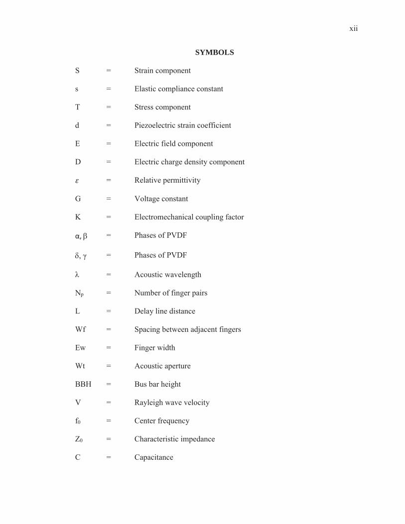
SYMBOLS
S = Strain component
s = Elastic compliance constant
T = Stress component
d = Piezoelectric strain coefficient
E = Electric field component
D = Electric charge density component
= Relative permittivity
G = Voltage constant
K = Electromechanical coupling factor
α, = Phases of PVDF
, γ = Phases of PVDF
λ = Acoustic wavelength
Np = Number of finger pairs
L = Delay line distance
Wf = Spacing between adjacent fingers
Ew = Finger width
Wt = Acoustic aperture
BBH = Bus bar height
V = Rayleigh wave velocity
f0 = Center frequency
Z0 = Characteristic impedance
C = Capacitance

xiii
A = Area
T = Thickness
F( ) = Fraction of polar phase
Aα, A = Absorption peak intensity
kα, k = Absorption coefficient
V = Voltage

xiv
ABBREVIATIONS
SAW Surface Acoustic Wave
BAW Bulk Acoustic Wave
MEMS Microelectromechanical System
SH-SAW Shear-horizontal surface acoustic wave
IDT Inter Digital Transducer
RF Radio Frequency
DAQ Data Acquisition
DDM Direct digital manufacturing
CAD Computer aided design
DSC Differential scanning calorimeter
DMA Dynamic mechanical analysis
SEM Scanning electron microscope
FTIR Fourier Transform Infrared Spectroscopy
EDX Energy Dispersive X-Ray
VNA Vector Network Analyzer
COM Coupling of Modes
IL Insertion Loss
FDM Fused Deposition Modeling
EBL Electron beam lithography
ADS Advanced Design system
DIC Digital image correlation
PVDF Polyvinylidene fluoride
xv
PZT Lead zirconate titanate
CCTO Copper calcium titanate
CNT Carbon nanotube
LiNbO3 Lithium niobate
LiTaO3 Lithium tantalite
BaTiO3 Barium titanate
DMSO Dimethyl sulfoxide
DMF Dimethylformamide
TEP Triethylphospate

1
1. Introduction
In this section, the significance, brief introduction about surface wave based sensors,
piezoelectric composite material, literature review of selected SAW sensor and finally,
research objective carried out in this research are discussed.
1.1. Significance
Structural health monitoring (SHM) is a class of damage detection and condition
monitoring have been developed rapidly in recent days to detect damages on time, which
could prevent catastrophic failure of structures with increased human safety. Commonly
used SHM methods such as vibration, impedance, and guided wave based methods are
used for different damage assessment in the modern community. Evaluation of aerospace
structure’s strain concentration due to various loads such as aerodynamic, thermal and
defects necessitates a monitoring sensor system that can provide real time beneficial
information. Mechanical strains for aerospace applications were commonly measured
using strain gauges or piezoelectric sensors, which are commercially available sensors in
the past. With the rapid development in aerospace structures, there is indeed a monitoring
technique is required to guarantee the security of advanced concepts to maintain integrity,
which prevents catastrophic damages.
1.2. Mechanical and Electromechanical Sensors
The mechanical sensor works based on the principle of detecting and measuring
changes in response to input data causing the mechanical deformation in the intended
host structure. The sensor that converts the input data into an electrical output then the
sensor is named as an electromechanical sensor. The most common mechanical and

2
electromechanical sensors (McGrath et al., 2013) as described by the IEEE council, are
listed in Table 1.1.
Table 1.1
Major categories of commercially available sensors.
The major sensor types are piezoresistive, capacitive, piezoelectric, and photoelectric.
Among them, the most commonly used commercially available mechanical sensor is a
strain gauge, which measures the strains based on the change in resistance. The key
problem with the strain gauges and other commercially available sensors are their thermal
effects and drift errors at higher frequencies over time. An acoustic sensor, one of the
major types, is proposed to overcome these issues, which senses the measurands through
acoustic wave generation. Microelectromechanical systems (MEMS), owing to their
advantages such as micro-scale size, easy integration with the system, and less power
Sensor Type
Strain gauge Thin and thick film Metallic Foil Resistance
Acoustic wave Surface Bulk
Displacement Capacitive Resistive Inductive
Pressure Capacitive Piezoelectric Inductive
3
consumption, offer integration of sensors, actuators, and electrical devices that can
measure mechanical, thermal, and chemical phenomena.
1.3. Acoustic Wave Sensor
Acoustic wave sensor is a class of microelectromechanical systems (MEMS) that is
capable of sensing various parameters using wave propagation. They are classified into
Surface acoustic wave (SAW) and Bulk acoustic wave (BAW) sensor (Rickert et al.,
1999). The difference between both is that BAW travels through the piezoelectric
substrate, but SAW travels along the piezoelectric substrate's surface. Based on the
moving pattern, surface waves are classified into Rayleigh, Love, Lamb and Shear
Horizontal waves (SH-SAW).
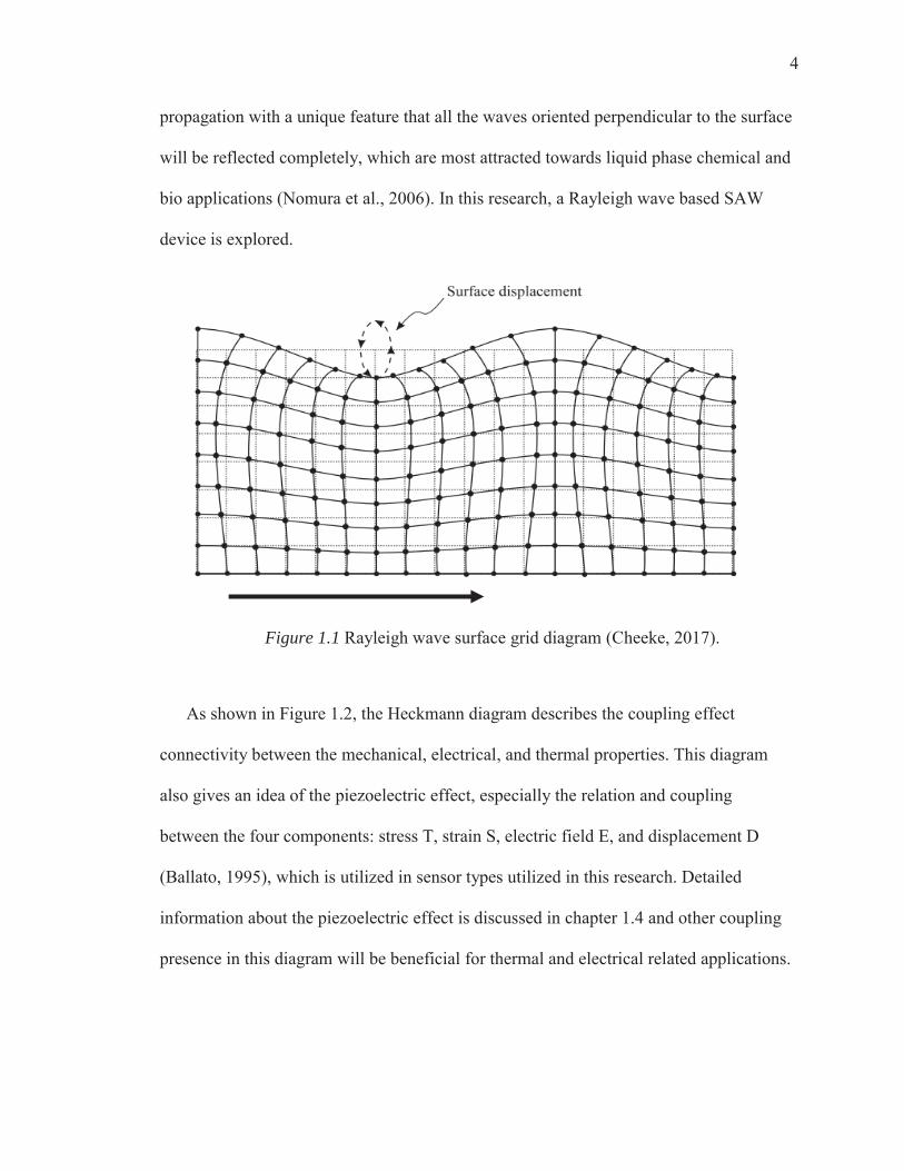
Rayleigh wave, a combination of two particle displacement components: longitudinal
and transverse motion, is a two-dimensional elliptical anticlockwise particle motion
wave, which propagates along the surface of an isotropic solid substrate, as shown in
Figure 1.1. This wave is the simplest form of a guided wave in which amplitude
decreases with an increase in depth and the reduction rate depends on the wavelength.
The velocity of this wave depends on the piezoelectric material.
Lamb wave signifies a guided wave generated in plates and shell components
comprising free boundaries and has two fundamental modes: symmetric and anti-
symmetric. Lamb wave is similar to the Rayleigh wave, where the velocity depends on
the excitation frequency and thickness of the substrate. A surface wave having a
horizontal motion transverse or perpendicular to the direction in which the wave travels is
a Love wave occurring with less acoustic shear velocity in the layer compared to the
substrate. SH-SAW mode has particle displacement only in the normal direction to the
4
propagation with a unique feature that all the waves oriented perpendicular to the surface
will be reflected completely, which are most attracted towards liquid phase chemical and
bio applications (Nomura et al., 2006). In this research, a Rayleigh wave based SAW
device is explored.
Figure 1.1 Rayleigh wave surface grid diagram (Cheeke, 2017).
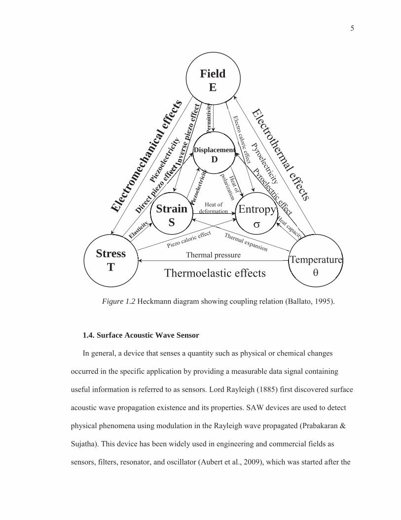
As shown in Figure 1.2, the Heckmann diagram describes the coupling effect
connectivity between the mechanical, electrical, and thermal properties. This diagram
also gives an idea of the piezoelectric effect, especially the relation and coupling
between the four components: stress T, strain S, electric field E, and displacement D
(Ballato, 1995), which is utilized in sensor types utilized in this research. Detailed
information about the piezoelectric effect is discussed in chapter 1.4 and other coupling
presence in this diagram will be beneficial for thermal and electrical related applications.
5
Figure 1.2 Heckmann diagram showing coupling relation (Ballato, 1995).
1.4. Surface Acoustic Wave Sensor
In general, a device that senses a quantity such as physical or chemical changes
occurred in the specific application by providing a measurable data signal containing
useful information is referred to as sensors. Lord Rayleigh (1885) first discovered surface
acoustic wave propagation existence and its properties. SAW devices are used to detect
physical phenomena using modulation in the Rayleigh wave propagated (Prabakaran &
Sujatha). This device has been widely used in engineering and commercial fields as
sensors, filters, resonator, and oscillator (Aubert et al., 2009), which was started after the
Field E
Stress
T Temperature
Thermoelastic effects
Strain
S
Entropy
Displacement D
Thermal pressure
n
DD
Str
Fie
EnEEHeat of deformation
ntt
Perm
ittiv
ity
S py
6
IDT (Interdigital transducer) invention by R.M. White and F. W. Voltmer (1965). SAW
sensor is well known for its advantages such as passive nature, fast response time, and
cost effectiveness, as well as, its extensive applications to measure phenomena such as
pressure, temperature, strain, torque, and gas (Devkota et al., 2017; Fan et al., 2018;
Nicolay et al., 2018). SAW sensor mainly consists of the piezoelectric substrate, metallic
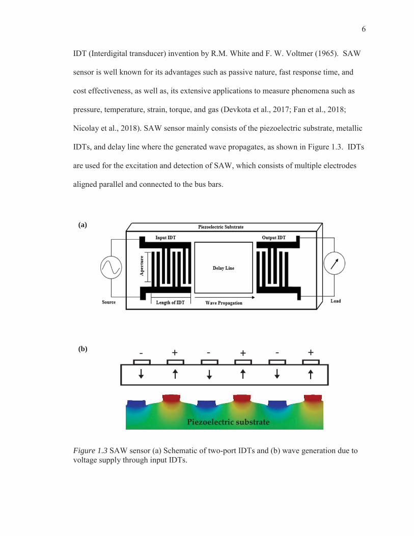
IDTs, and delay line where the generated wave propagates, as shown in Figure 1.3. IDTs
are used for the excitation and detection of SAW, which consists of multiple electrodes
aligned parallel and connected to the bus bars.
Figure 1.3 SAW sensor (a) Schematic of two-port IDTs and (b) wave generation due to voltage supply through input IDTs.
+ - - - + +
Piezoelectric substrate
(a)
(b)
7
When an external force or change occurs, there will be a change in propagation path
length and the density of the substrate, which changes the SAW propagation velocity.
Meaning, when the strain is applied, the delay line distance between the IDTs increases,
change in SAW propagation time occurs, and on the other hand, with an elliptical motion
of the particles, the electric field among the particles will also be reduced. This change in
SAW velocity affects the excitation of frequency. The magnitude of strain can be
measured by measuring the frequency shift caused by the mechanical strains (Q. Li et al.,
2019). Besides sensing the mechanical strain, SAW devices can also measure other
parameters such as temperature and pressure by attaching a sensitive material in the delay
line region. Commonly used sensing layers are semiconducting metal oxides and
conducting/ non-conducting polymers (Ghosh et al., 2019). In the following paragraphs,
the SAW sensor applications in measuring different measurands are explored.
Previously, commercially available traditional sensors such as strain gauge and
thermocouple were used to measure strain and temperature occurred in aircraft engine
parts (Stowell & Weise, 1983). Fiber optic grating sensor with its multi-axial capability
has been utilized to measure strain in aircraft and spacecraft wings and fuselage (Udd et
al., 2000). But due to their limitation such as wired setup and power supply requirements
reduced the range of applications, which can be avoided by using SAW device. A two-
port SAW pressure sensor made of ST-Cut quartz was fabricated, which can be operated
under high temperature and pressure with 14 Hz/psi sensitivity (Della Lucia et al., 2014).
Using the SAW ID tags and wired SAW Sensor principle, a passive sensor for
temperature measurement with accuracy of ±0.2°C was developed within a temperature
range more than 200°C distance up to 6m (Reindl et al., 1996). LGS SAW wireless
8
sensor suitable for higher temperature under applied strain were discussed with fewer
hysteresis errors (Shu et al., 2015). SAW sensor applications based on Rayleigh wave
have been developed even in the detection of a wide range of chemicals such as H2, O2,
and CO2. To name a few, a wireless oxygen detection SAW device made of langasite
with tin oxide as a sensing layer was developed (Greve et al., 2013). A hydrogen
detection method at room temperature made of LiNbO3 coated with thin palladium film
limited to 50 ppm was discussed (d’AMICO et al., 1982). The ability of CO2 detection
using 250 MHz ST-Quartz SAW resonator was investigated and examined a 1 kHz
frequency shift with 240 ppm of CO2 (Korsah et al., 1998).
For SAW strain measurement, the capability of SAW sensor made of LiNbO3 to
measure temperature and strain through radio frequency identification with a temperature
and strain sensitivity of 77ppm/°C and 1 ppm/μ was demonstrated (F. Li et al., 2011).
LiNbO3 SAW sensor using shear horizontal wave (SH-SAW) generated through split
IDT was fabricated with a 2.5 kHz/% sensitivity to monitor tire deformation (Eun et al.,
2016). A single port wireless Surface acoustic wave resonator (SAWR) made of AT-X
quartz to monitor strain in CNC machining tool was reported, that expands the
application in condition and process monitoring applications (Stoney et al., 2012).
The longitudinal and lateral strain sensitivity measured by SAW sensor mounted on
to a wafer stripe of about -0.987 ppm/μ and 0.190 ppm/μ was explored (Hempel et al.,
2013). The surface transverse and Rayleigh wave modes behavior on a ST-quartz crystal
was compared and addressed Rayleigh wave has better stability with positive frequency
shift to perpendicular strains than STW (Fu et al., 2016). SAW sensor made of AlN film
with a maximum strain sensitivity of 1.26 ppm/μ was reported (Shu et al., 2019).

9
Though these works provided a significant insight about strain sensing based on SAW,
due to the substrate material nature, they are not suitable for high frequency range large
strain applications, curved surface, and harsh environments due to their less sensitivity
and drift errors over time.
1.5. Piezoelectric Effect
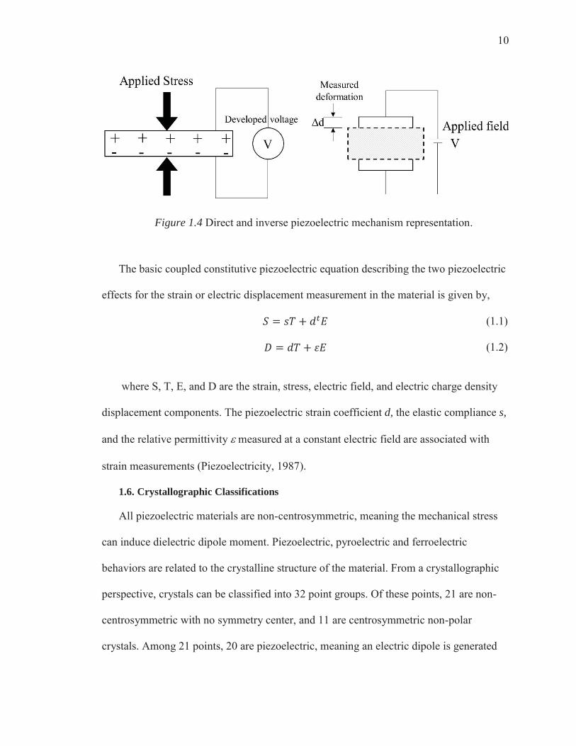
SAW sensor works based on the principle of piezoelectric effect. Piezoelectricity, an
ability of the material to generate electric charge due to mechanical deformation. This has
two effects, namely direct and inverse, which allows conversion between electrical and
mechanical energy, as shown in Figure 1.4. When the piezoelectric material is subjected
to mechanical deformation, the shift in positive and negative charge creates an electrical
polarization resulting in electric charge generation, which is termed as the direct
piezoelectric effect.
This has a secondary effect named inverse piezoelectric effect in which the
mechanical wave is generated with an input electric field. Piezoelectricity comes from
Greek word piezo, meaning press and this effect was discovered in 1880 by Curie
brothers, who demonstrated in crystals like Quartz, Topaz, and Rochelle salt (Mould,
2007). Especially for a two port SAW device, the input IDT works under the inverse
effect that generates mechanical wave in the piezoelectric substrate propagating through
the delay line, and the output IDT works under the direct effect that senses the intended
measurands.
10
Figure 1.4 Direct and inverse piezoelectric mechanism representation.
The basic coupled constitutive piezoelectric equation describing the two piezoelectric
effects for the strain or electric displacement measurement in the material is given by,
(1.1) (1.2)
where S, T, E, and D are the strain, stress, electric field, and electric charge density
displacement components. The piezoelectric strain coefficient d, the elastic compliance s,
and the relative permittivity measured at a constant electric field are associated with
strain measurements (Piezoelectricity, 1987).
1.6. Crystallographic Classifications
All piezoelectric materials are non-centrosymmetric, meaning the mechanical stress
can induce dielectric dipole moment. Piezoelectric, pyroelectric and ferroelectric
behaviors are related to the crystalline structure of the material. From a crystallographic
perspective, crystals can be classified into 32 point groups. Of these points, 21 are non-
centrosymmetric with no symmetry center, and 11 are centrosymmetric non-polar
crystals. Among 21 points, 20 are piezoelectric, meaning an electric dipole is generated

11
when a mechanical stress is applied, which exhibits polar axis with a net separation
between positive and negative charges. The remaining is one a 432 group point, which
eliminates piezoelectricity.
Figure 1.5 Flow chart of crystal groups (Panda, 2017).
Of the 20 piezoelectric points, 10 crystals are impulsively polarizable with variation
in the direction of dipole moment due to temperature changes. Among these 10 crystals, a
subset called ferroelectric with reversible polarization is capable of remaining polarized
even in the absence of an electric field (Defaÿ, 2013). Ferroelectric property disappears
above the materials’ Curie temperature TC. The relation between piezo-, pyro- and
ferroelectric property with crystallographic groups is shown in Figure 1.5.
1.7. Piezoelectric Composites
Piezoelectric composite, a combination of constituent phases exhibiting excellent
properties, is developing as a new material, which can be tailored on demand for specific
applications. The two phase composite geometry can be classified into 10 structures
based on each phase's connectivity (Newnham et al., 1978), which is defined as the
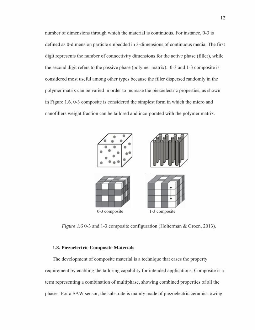
12
number of dimensions through which the material is continuous. For instance, 0-3 is
defined as 0-dimension particle embedded in 3-dimensions of continuous media. The first
digit represents the number of connectivity dimensions for the active phase (filler), while
the second digit refers to the passive phase (polymer matrix). 0-3 and 1-3 composite is
considered most useful among other types because the filler dispersed randomly in the
polymer matrix can be varied in order to increase the piezoelectric properties, as shown
in Figure 1.6. 0-3 composite is considered the simplest form in which the micro and
nanofillers weight fraction can be tailored and incorporated with the polymer matrix.
Figure 1.6 0-3 and 1-3 composite configuration (Holterman & Groen, 2013).
1.8. Piezoelectric Composite Materials
The development of composite material is a technique that eases the property
requirement by enabling the tailoring capability for intended applications. Composite is a
term representing a combination of multiphase, showing combined properties of all the
phases. For a SAW sensor, the substrate is mainly made of piezoelectric ceramics owing
1-3 composite 0-3 composite

13
to its higher piezoelectric property nature. The selection of an appropriate piezoelectric
substrate material plays a vital role, which depends on its compatibility, durability,
molecular structure, and electrical properties during sensor development. Major
piezoelectric materials used for SAW sensor includes single crystals: lithium niobate
(LiNbO3), lithium tantalite (LiTaO3) and ceramics such as lead zirconate titanate (PZT)
(Araújo & Eiras, 1999), barium titanate (BaTiO3) (Gao et al., 2007) and calcium copper
titanate (CCTO) (Zhang et al., 2007).
Among these materials, commonly used fillers such as PZT, a combination of
antiferroelectric lead zirconate, and ferroelectric lead titanate and CCTO are well known
for their excellent dielectric constants and piezoelectric coefficients. Additionally, carbon
nanotubes (CNTs) are considered as an ideal candidate as nano-fillers because of its
exceptional mechanical, electrical, and thermal properties (Kumar et al., 2016). However,
excessive addition of CNT fillers could reduce the breakdown strength and reaches a
percolation threshold (Ferreira et al., 2013) with more than 2 wt. % influencing the
piezoelectric electric field. The percolation threshold is the range of filler content in the
polymer matrix, which end up showing no significant change in the piezoelectric
property of the composite.
Even though these fillers exhibit higher dielectric properties they may not be suitable
for flexible structures owing to their brittleness and rigid fabrication process. The
crystalline lattice structure of the selected micro and nano fillers such as PZT exhibiting a
perovskite structure, CCTO and SWCNTs are show in Figure 1.7. SWCNT is nothing but
the rolled up version of graphene sheet.
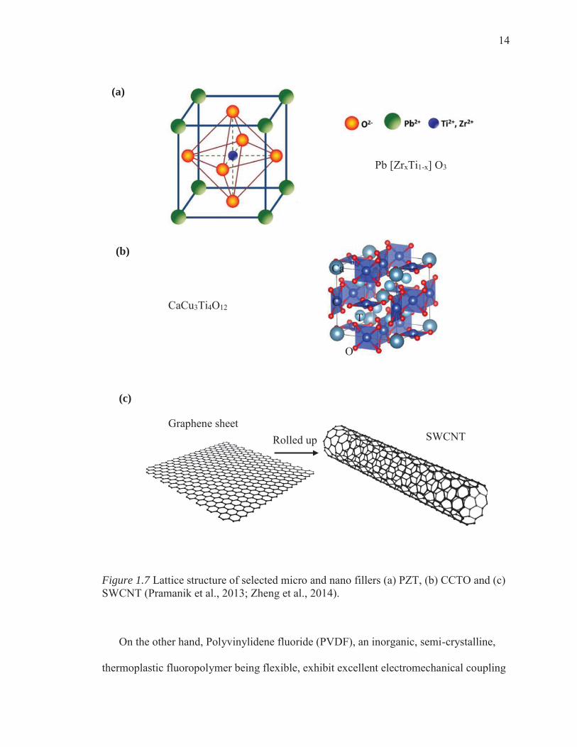
14
Figure 1.7 Lattice structure of selected micro and nano fillers (a) PZT, (b) CCTO and (c) SWCNT (Pramanik et al., 2013; Zheng et al., 2014).
On the other hand, Polyvinylidene fluoride (PVDF), an inorganic, semi-crystalline,
thermoplastic fluoropolymer being flexible, exhibit excellent electromechanical coupling
CaCu3Ti4O12
Pb [ZrxTi1-x] O3
Graphene sheet SWCNT Rolled up
(a)
(b)
(c)
Ca
CT
O
15
with five distinct crystalline forms of different chain arrangements, as shown in Figure
1.8 (Ruan et al., 2018). However, polymer based piezoelectric materials shows less
dielectric constants and piezoelectric charge coefficients values, which limits their wave
generation efficiency. All the above mentioned challenges of polymer and ceramics
separately can be circumvented by integrating the polymer with inorganic micro- and
nano-scale fillers resulting in polymer-based composites, a new type of materials
exhibiting both flexibility and favorable piezoelectric properties that can expand the
range of applications.
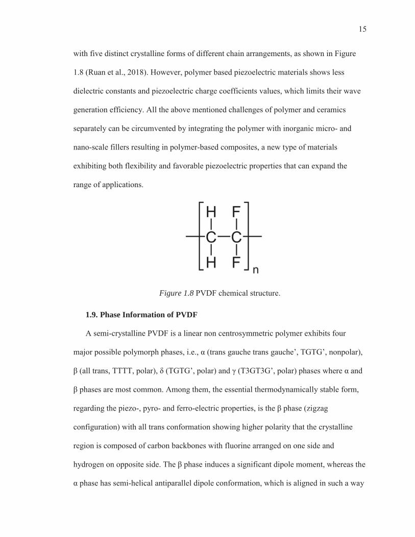
1.9. Phase Information of PVDF
A semi-crystalline PVDF is a linear non centrosymmetric polymer exhibits four
major possible polymorph phases, i.e., α (trans gauche trans gauche’, TGTG’, nonpolar),
β (all trans, TTTT, polar), δ (TGTG’, polar) and γ (T3GT3G’, polar) phases where α and
β phases are most common. Among them, the essential thermodynamically stable form,
regarding the piezo-, pyro- and ferro-electric properties, is the β phase (zigzag
configuration) with all trans conformation showing higher polarity that the crystalline
region is composed of carbon backbones with fluorine arranged on one side and
hydrogen on opposite side. The β phase induces a significant dipole moment, whereas the
α phase has semi-helical antiparallel dipole conformation, which is aligned in such a way
Figure 1.8 PVDF chemical structure.
16
that all dipole moment cancels each other. Materials spectrum measurements using
Fourier transform infrared spectroscopy (FTIR) and differential scanning calorimetry
(DSC) are used to study PVDF crystalline phases' contribution.
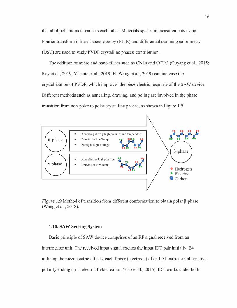
The addition of micro and nano-fillers such as CNTs and CCTO (Ouyang et al., 2015;
Roy et al., 2019; Vicente et al., 2019; H. Wang et al., 2019) can increase the
crystallization of PVDF, which improves the piezoelectric response of the SAW device.
Different methods such as annealing, drawing, and poling are involved in the phase
transition from non-polar to polar crystalline phases, as shown in Figure 1.9.
Figure 1.9 Method of transition from different conformation to obtain polar phase (Wang et al., 2018).
1.10. SAW Sensing System
Basic principle of SAW device comprises of an RF signal received from an
interrogator unit. The received input signal excites the input IDT pair initially. By
utilizing the piezoelectric effects, each finger (electrode) of an IDT carries an alternative
polarity ending up in electric field creation (Yao et al., 2016). IDT works under both
Hydrogen Fluorine Carbon
Annealing at very high pressure and temperature
Drawing at low Temp
Poling at high Voltage α-phase
-phase Annealing at high pressure
Drawing at low Temp
-phase
17
direct and inverse piezoelectric effect where the wave is converted back to an electrical
signal with useful information for measuring the desired quantity (Mujahid & Dickert,
2017). The interrogator with the received signal is connected to the respective acquisition
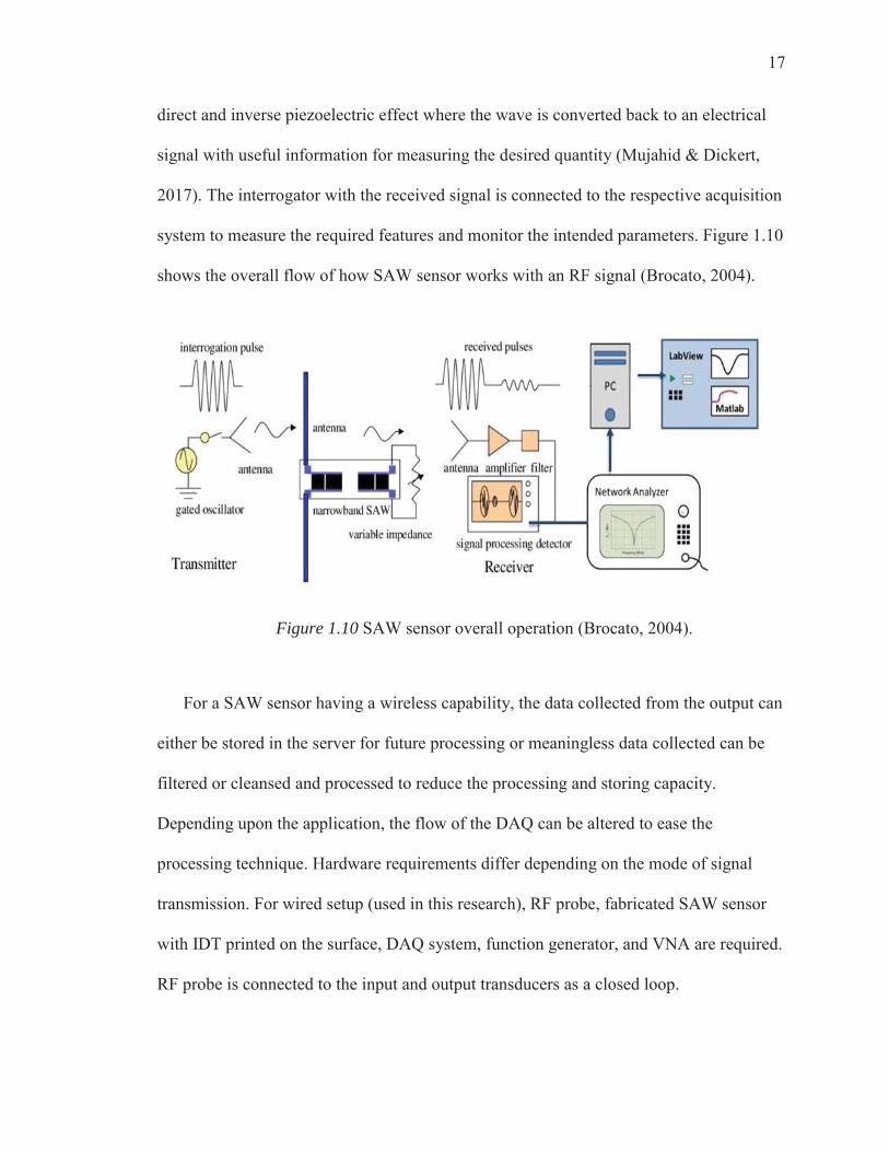
system to measure the required features and monitor the intended parameters. Figure 1.10
shows the overall flow of how SAW sensor works with an RF signal (Brocato, 2004).
Figure 1.10 SAW sensor overall operation (Brocato, 2004).
For a SAW sensor having a wireless capability, the data collected from the output can
either be stored in the server for future processing or meaningless data collected can be
filtered or cleansed and processed to reduce the processing and storing capacity.
Depending upon the application, the flow of the DAQ can be altered to ease the
processing technique. Hardware requirements differ depending on the mode of signal
transmission. For wired setup (used in this research), RF probe, fabricated SAW sensor
with IDT printed on the surface, DAQ system, function generator, and VNA are required.
RF probe is connected to the input and output transducers as a closed loop.

18
This research aims to develop a SAW sensor device in which the integral parts are
piezoelectric substrate, input, output IDTs, and sensing layer or delay line region. The
research starts with the piezoelectric substrate fabrication following by IDT design and
optimization which is utilized to measure mechanical strains.
1.11. Research Objective
The primary motivation is to develop a new structural health monitoring system to
sense and detect mechanical strains occurring in aerospace structures by using the
developed SAW sensor. This thesis explores and studies the potential of piezoelectric
composite-based SAW sensor and their applications in strain measurement by tracking
shift in peak frequency through a novel experimental approach. Experiments include the
fabrication and testing of the sensor properties with and without strains to characterize
the developed strain sensor. The major research objectives are identified as follows:
a) Fabrication of piezoelectric composite substrate exhibiting flexibility through
hot-press method.
b) Piezoelectric property measurement and enhancement through corona poling
technique under a high electric field.
c) Deposition of designed IDT using transmission matrix approach through
direct digital manufacturing.
d) Scattering parameter measurement to characterize the frequency response of
the fabricated sensor attached to the host structure and correlation to the
commercially used DIC.
19
2. Fabrication Process and Experimental Setup of SAW Sensor
In this section the two main integral parts of SAW sensor namely piezoelectric
substrate with discussion about selected materials along with the fabrication process and
IDT design, optimization and printing process throughout microdispensing techniques are
explained.
2.1. Piezoelectric Substrate Development
The fabrication process of the piezocomposite sensor, including the solution
preparation and enhancement of dipole arrangement through the corona poling technique,
are discussed.
2.1.1 Materials
To fabricate a thin piezo-composite substrate, selected PVDF powder (Sigma Aldrich,
USA) having an average particle size of 3-10 μm, average molecular weight Mw
~534,000 g/mol, and density of 1.74 g/ml is used to make a polymer matrix. The fillers
used are PZT powder (American Elements, CA, USA, # 12626-81-2) with APS ≤ 5 μm,
molecular weight Mw~ 426.29 g/mol and density of 7.5-8 g/ml, SWCNT (US research
Nanomaterials, TX, USA) with an average diameter of 1.1 nm and lengths of 5-30 μm,
and CCTO (Bonding chemicals, TX, USA, #535616) with a particle size of 1~5 μm, Mw
~614.18 g/mol, and density of 4.7 g/ml, due to their high dielectric constant nature and
unique characteristics.
As PVDF is insoluble in water, DMSO is used to dissolve PVDF with selected fillers
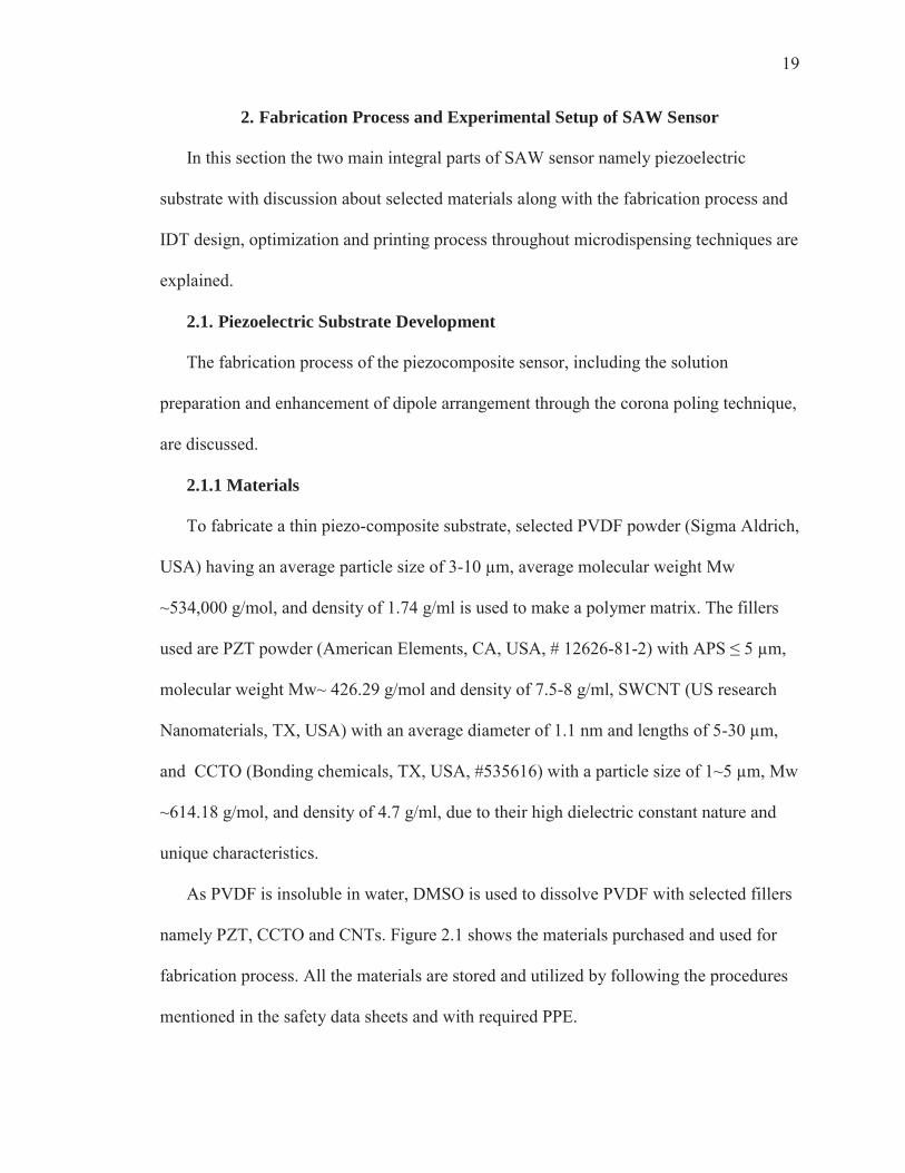
namely PZT, CCTO and CNTs. Figure 2.1 shows the materials purchased and used for
fabrication process. All the materials are stored and utilized by following the procedures
mentioned in the safety data sheets and with required PPE.
20
Figure 2.1 Materials used, (a) PVDF, (b) PZT, (c) SWCNTs and (d) DMSO.
2.1.2 Preparation of Piezocomposite with Hot Press Method
To fabricate a piezoelectric substrate, the polymer and ceramic are combined in the
form of 0-3 composite connectivity, which is the simplest and has the capability of
enhancing piezoelectric properties. PVDF, a thermoplastic fluoropolymer, has good
flexibility with desirable mechanical properties. In order to circumvent the challenges to
make the substrate exhibiting both flexibility and higher piezoelectric property, the
selected polymer is combined with distinct micro and nano-fillers. The fillers-added
polymer composites has the 0-3 pattern in which the fillers are uniformly dispersed in a
three-dimensional continuous polymer matrix.
In addition, this specific configuration can be tailored as per specific requirements
with ease of fabrication (Arlt & Wegener, 2010; Thongsanitgarn et al., 2010), which
helps in the property and structural integrity enhancement process. These are fabricated
in general through various manufacturing processes such as compression molding,
extrusion, tape casting, spin coating, and hot-press. In this research, the piezoelectric
substrate is fabricated using hot-press, chosen among others as it combines both the
(a) (b) (c)
(d)

21
melting and stretching techniques. The hydraulic compression press supplied by Wabash,
as shown in Figure 2.2, features steel plates, a programmable controller for curing time,
analog pressure, and digital temperature control.
Figure 2.2 Wabash hot-press used to cast the sample.
To fabricate the substrate, PVDF polymer with different selected ceramics and nano-
fillers such as PZT, CCTO, and CNTs with respective wt. % proportions are mixed using
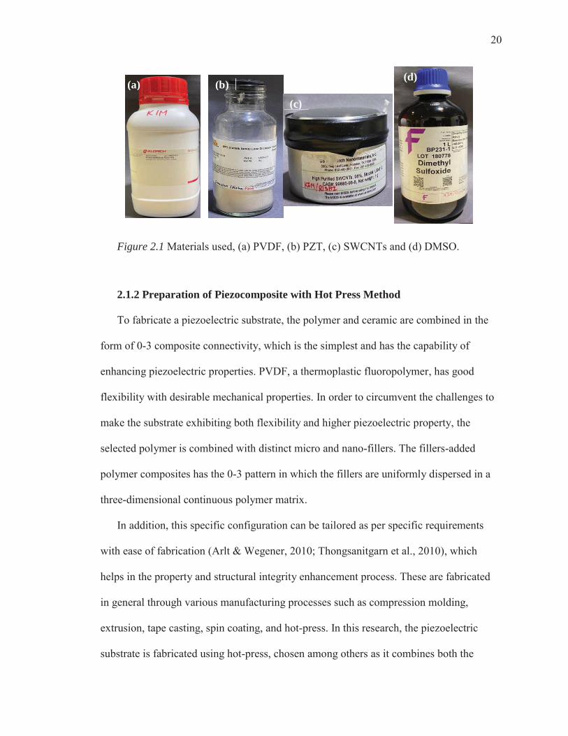
a centrifugal planetary THINKY mixer (ARM-310), combination of both rotational and
revolution axis motion maintaining homogeneity in the mixture, as shown in Figure 2.3 at
2,000 rpm for 5 minutes. As the substrate is a piezoelectric composite, the piezoelectric
properties are purely based on the wt. % composition of each polymer and fillers type. In
this research, different wt. % combination of PVDF and PZT has been analyzed to figure
22
out the optimized quantity that can meet the preferred requirements. Because too much
PZT could lead to brittle nature or excessive PVDF lack in the piezoelectric property.
Figure 2.3 ARM 310 THINKY centrifugal mixer used to mix polymer, fillers and solvent.
SEM analysis has been investigated with the purpose of selecting the best mixture of
polymer and ceramic. The proportion of other fillers such as CNTs and CCTO, are
decided based on the percolation threshold and agglomeration criteria.
Figure 2.4 DMSO chemical structure.
23
The weighted powder mix is then dissolved in 30 wt. % of DMSO solvent based on
the formation of a coagulated blend after mixing to get uniform dispersion. The solvent
used to disperse the micro and nano-fillers and to dissolve PVDF is dimethyl sulfoxide
(DMSO) (Sigma-Aldrich, USA) as PVDF is insoluble in water. Figure 2.4 shows the
chemical structure of DMSO. DMSO, a polar solvent, is selected among other
counterparts, such as dimethylformamide (DMF) and triethylphospate (TEP), due to its
high boiling point and distinct dielectric constant (contributing to the overall electrical
response), while others are hazardous in nature and a little expensive (Gonçalves et al.,
2013; Gregorio Jr, 2006).
Furthermore, the coagulated mass is subjected to vacuum to eliminate air bubbles,
causing a surface defect. As mentioned earlier, the hot press technique is used owing to
its ease in fabrication with its capability of optimized temperature and pressure control,
resulting in a denser composite with less porosity (Jain et al., 2015; Seema et al., 2007).
The glutinous slurry is subjected to hot pressing at a temperature of 355° F maintained
for 20 minutes curing, attaining a flat substrate that is further dried to remove the solvent.
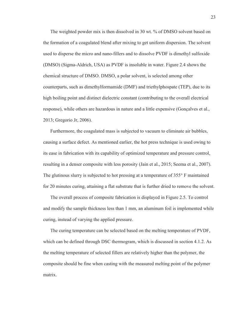
The overall process of composite fabrication is displayed in Figure 2.5. To control
and modify the sample thickness less than 1 mm, an aluminum foil is implemented while
curing, instead of varying the applied pressure.
The curing temperature can be selected based on the melting temperature of PVDF,
which can be defined through DSC thermogram, which is discussed in section 4.1.2. As
the melting temperature of selected fillers are relatively higher than the polymer, the
composite should be fine when casting with the measured melting point of the polymer
matrix.
24
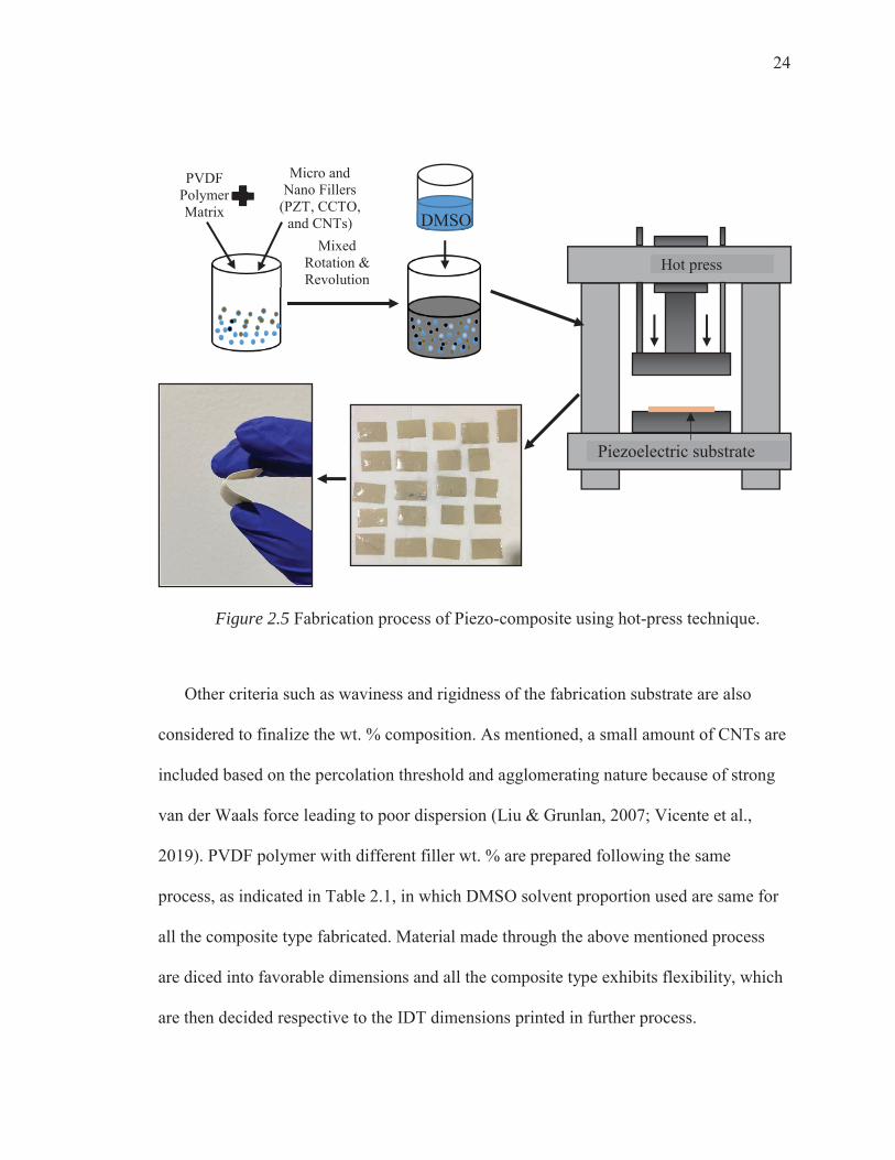
Figure 2.5 Fabrication process of Piezo-composite using hot-press technique.
Other criteria such as waviness and rigidness of the fabrication substrate are also
considered to finalize the wt. % composition. As mentioned, a small amount of CNTs are
included based on the percolation threshold and agglomerating nature because of strong
van der Waals force leading to poor dispersion (Liu & Grunlan, 2007; Vicente et al.,
2019). PVDF polymer with different filler wt. % are prepared following the same
process, as indicated in Table 2.1, in which DMSO solvent proportion used are same for
all the composite type fabricated. Material made through the above mentioned process
are diced into favorable dimensions and all the composite type exhibits flexibility, which
are then decided respective to the IDT dimensions printed in further process.
Hot press
Piezoelectric substrate
Micro and Nano Fillers
(PZT, CCTO, and CNTs) DMSO
PVDF Polymer Matrix
Mixed Rotation & Revolution

25
Table 2.1
PVDF polymer with different micro and nanofillers ratio used in the nanocomposite process. DMSO solvent content is same for all combinations (30 wt. %).
Sample Thickness (mm)
PVDF (wt. %)
PZT (wt. %)
CNT (wt. %)
CCTO (wt. %)
PVDF 0.25 100 - - -
PVDF/PZT 0.51 40 60 - -
PVDF/PZT/CNTs 0.82 40 59.75 0.25 -
PVDF/CNTs 0.72 98 - 2 -
PVDF/CCTO 0.60 40 - - 60
2.1.3 Polar Phase Enhancement through Corona Poling
In order to activate the non-polar conformation to polar active phase, it is necessary
to stretch and polarize the sample under a high electric field. In our research, the
stretching is already done through the hot press technique. The stretching process alone is
not considered as a complete conversion of α to phase. Electrical polarization is
required to align the dipoles in the fabricated piezo-composite substrate that becomes
piezoelectrically active, as shown in Figure 2.6.
(a)
(b)
Figure 2.6 Dipole orientation before (a) and after (b) poling.

26
Fundamentally, there are two major poling methods, namely contact and non-contact
techniques. Corona poling, a non-contact technique, presents significant advantages as it
eliminates surface defect through electrode contact with the sample, where the occurrence
of arcing at very high voltages is less likely, and uniform voltage distribution is
attainable. In this technique, the electric charge is applied to the corona needle that acts as
field intensifiers to ionize the gas molecules around the sample’s top surface (unelectrode
surface) to create an electric field (Kim et al., 2017; Waller & Safari, 1988).
Variables influencing the poling efficiencies are the amount of voltage supply, poling
time, and distance between the corona tip as well as the sample surface (Mahadeva et al.,
2013). A high voltage of 12 kV - 15 kV is applied to the sample placed 2~3 cm distance
from the needle tip for 30 minutes. Piezoelectric property measurement is compared
before and after poling of the different combinations selected. After the poling process,
the randomly distributed dipoles are aligned along the direction of applied external
electric field. Figure 2.7 shows the corona poling schematic with real setup used.
Figure 2.7 Corona poling process (a) Schematic and (b) Actual image.
Corona needle
High Voltage Supply High Voltage Amplifier
Piezoelectric substrate
(a) H(b)
27
2.2. Design and Modeling of Two port IDTs
In this chapter, the design and modeling of two port IDTs using a theoretical
approach are discussed with attained center frequency response along with phase plot
which dictates SAW sensor performance and is fabricated with the optimized dimensions
through microdispensing process that utilizes the CAD model designed.
2.2.1 Transmission Matrix Approach
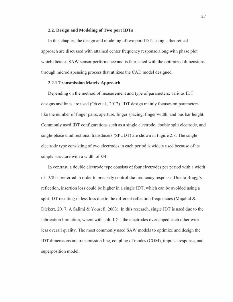
Depending on the method of measurement and type of parameters, various IDT
designs and lines are used (Oh et al., 2012). IDT design mainly focuses on parameters
like the number of finger pairs, aperture, finger spacing, finger width, and bus bar height.
Commonly used IDT configurations such as a single electrode, double split electrode, and
single-phase unidirectional transducers (SPUDT) are shown in Figure 2.8. The single
electrode type consisting of two electrodes in each period is widely used because of its
simple structure with a width of λ/4.
In contrast, a double electrode type consists of four electrodes per period with a width
of λ/8 is preferred in order to precisely control the frequency response. Due to Bragg’s
reflection, insertion loss could be higher in a single IDT, which can be avoided using a
split IDT resulting in less loss due to the different reflection frequencies (Mujahid &
Dickert, 2017; A Salimi & Yousefi, 2003). In this research, single IDT is used due to the
fabrication limitation, where with split IDT, the electrodes overlapped each other with
less overall quality. The most commonly used SAW models to optimize and design the
IDT dimensions are transmission line, coupling of modes (COM), impulse response, and
superposition model.
28
Figure 2.8 Different IDT configurations (Oh et al., 2012).
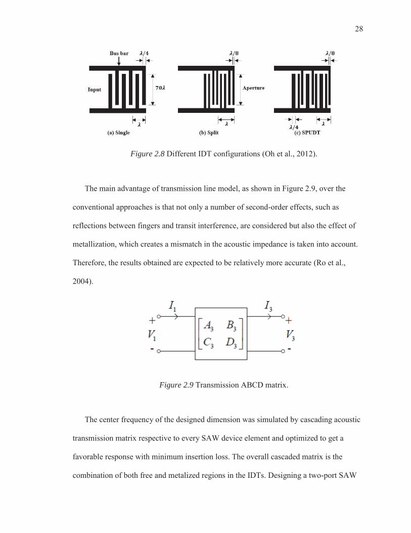
The main advantage of transmission line model, as shown in Figure 2.9, over the
conventional approaches is that not only a number of second-order effects, such as
reflections between fingers and transit interference, are considered but also the effect of
metallization, which creates a mismatch in the acoustic impedance is taken into account.
Therefore, the results obtained are expected to be relatively more accurate (Ro et al.,
2004).
Figure 2.9 Transmission ABCD matrix.
The center frequency of the designed dimension was simulated by cascading acoustic
transmission matrix respective to every SAW device element and optimized to get a
favorable response with minimum insertion loss. The overall cascaded matrix is the
combination of both free and metalized regions in the IDTs. Designing a two-port SAW
29
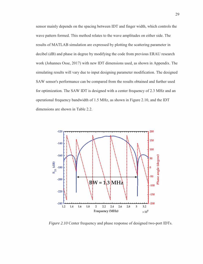
sensor mainly depends on the spacing between IDT and finger width, which controls the
wave pattern formed. This method relates to the wave amplitudes on either side. The
results of MATLAB simulation are expressed by plotting the scattering parameter in
decibel (dB) and phase in degree by modifying the code from previous ERAU research
work (Johannes Osse, 2017) with new IDT dimensions used, as shown in Appendix. The
simulating results will vary due to input designing parameter modification. The designed
SAW sensor's performance can be compared from the results obtained and further used
for optimization. The SAW IDT is designed with a center frequency of 2.3 MHz and an
operational frequency bandwidth of 1.5 MHz, as shown in Figure 2.10, and the IDT
dimensions are shown in Table 2.2.
Figure 2.10 Center frequency and phase response of designed two-port IDTs.
BW = 1.3 MHz
30
The effectiveness of the sensor system can be identified by a various electrical feature
such as insertion loss (IL), which is the loss of power that occurs as a signal travels
through components or devices due to different reasons such as impedance mismatch,
reflection, and power dissipated after the insertion of objects. Lower insertion loss makes
detection more reliable, which reduces signal noise and increases the signal-to-noise ratio
(S. Li et al., 2017). Insertion loss can be determined by frequency response analysis,
measured from the transmission model and network analyzer. The phase of the output
signal is influenced by any perturbation of the SAW system. A common expression of IL
is shown in Equation 2.1 and is measured in decibels (dB).
(2.1)
IDT with less insertion loss can be obtained by optimizing few parameters such as
IDT type, IDT length, acoustic aperture, electrode type, electrode thickness, and delay
line distance. The IDT metal thickness has an effect on the amplitude of the velocity shift
in which thicker the metal, lower the velocity, and lesser coupling coefficient that
increases the insertion loss. The ripple effect and insertion loss can be reduced by using
optimal impedance matching and different IDT types to minimize reflections.
Change in delay line and finger spacing results in frequency shift. Change in length of
the substrate alters the IDT finger spacing. The relation between center frequency f0 and
wavelength λ is related as 0 = vp/ λ, determining the center frequency, where vp is the
velocity of the propagated wave that varies with different materials, the wavelength λ is
the distance between two adjacent fingers of the same side, respectively.
31
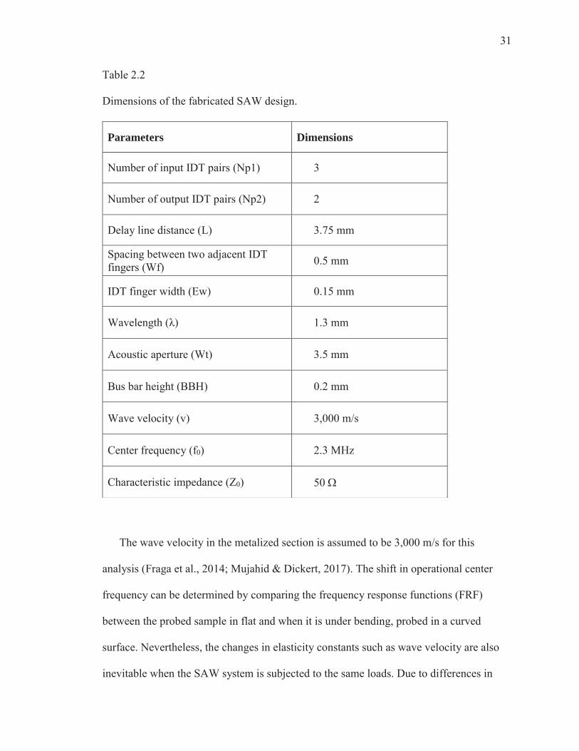
Table 2.2
Dimensions of the fabricated SAW design.
The wave velocity in the metalized section is assumed to be 3,000 m/s for this
analysis (Fraga et al., 2014; Mujahid & Dickert, 2017). The shift in operational center
frequency can be determined by comparing the frequency response functions (FRF)
between the probed sample in flat and when it is under bending, probed in a curved
surface. Nevertheless, the changes in elasticity constants such as wave velocity are also
inevitable when the SAW system is subjected to the same loads. Due to differences in
Parameters Dimensions
Number of input IDT pairs (Np1) 3
Number of output IDT pairs (Np2) 2
Delay line distance (L) 3.75 mm
Spacing between two adjacent IDT fingers (Wf) 0.5 mm
IDT finger width (Ew) 0.15 mm
Wavelength (λ) 1.3 mm
Acoustic aperture (Wt) 3.5 mm
Bus bar height (BBH) 0.2 mm
Wave velocity (v) 3,000 m/s
Center frequency (f0) 2.3 MHz
Characteristic impedance (Z0) 50
32
both velocity and distance, the shift rate and magnitude of center frequency may be non-
linear.
2.3. Direct Digital Manufacturing of IDTs
Additive manufacturing (AM) technology has recently developed to the level where
even micro and nano scale structures, which are limited in the past to fabricate are
presently achievable for components in the field of aerospace communication and sensor
fields. It has multiple benefits, such as low cost to fabricate complex structures, freedom
of design, and automation by minimizing waste and time.
Commonly used additive manufacturing techniques are fusion deposition modeling,
superfine inkjet printing, and powder bed fusion (Kirbus et al., 2018; Ngo et al., 2018).
But due to their challenges, such as weak mechanical properties and limitations in
selecting materials, they are not well suitable for the effective printing of IDTs.
Especially, for IDT patterning, traditional techniques such as photolithography and
electron beam lithography (EBL) (Hu et al., 2019) are used. Their cleanroom necessity
and the development of complex photomask are the major limitations of traditional
lithographic techniques, which can be avoided through additive manufacturing
techniques.
In this research, a new production paradigm manufacturing technique, direct digital
manufacturing (DDM), which leads to high-quality electrode printing (Chen et al., 2015).
DDM is the process of printing the product directly from the user-defined CAD model,
which can be modified anytime by minimizing the waste in a cost-effective manner. A
DuPont CB028 conductive silver paste is used as an electrode material. The conductive
paste exhibits good adhesion to the piezoelectric substrate with higher sustainability over
33
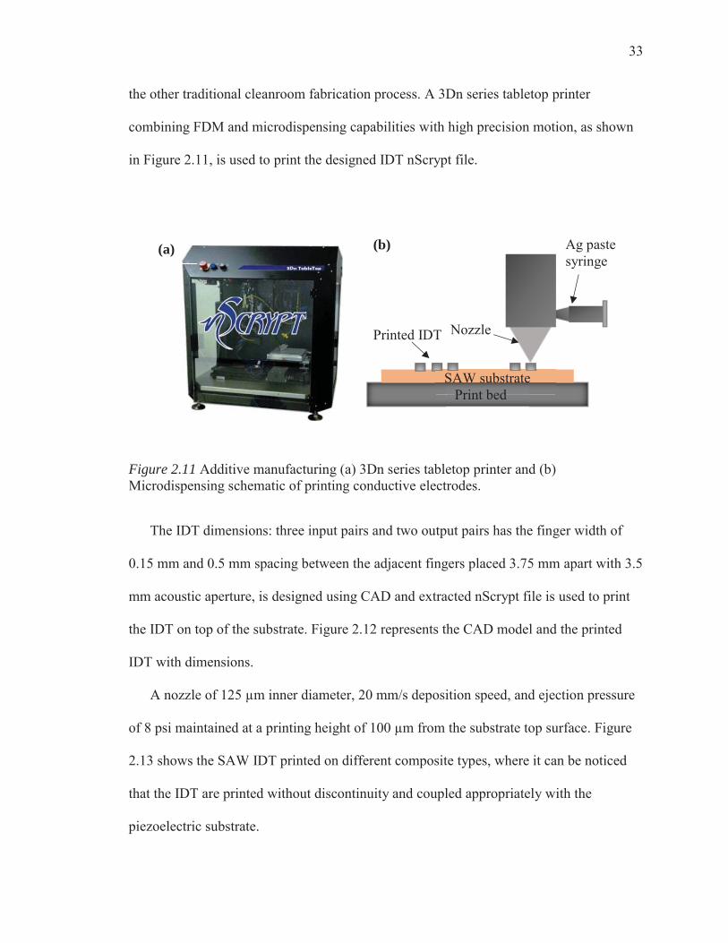
the other traditional cleanroom fabrication process. A 3Dn series tabletop printer
combining FDM and microdispensing capabilities with high precision motion, as shown
in Figure 2.11, is used to print the designed IDT nScrypt file.
Figure 2.11 Additive manufacturing (a) 3Dn series tabletop printer and (b) Microdispensing schematic of printing conductive electrodes.
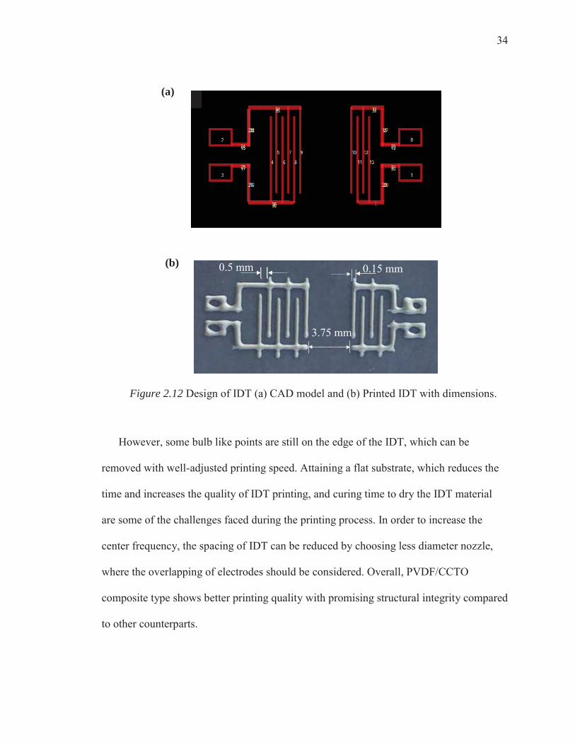
The IDT dimensions: three input pairs and two output pairs has the finger width of
0.15 mm and 0.5 mm spacing between the adjacent fingers placed 3.75 mm apart with 3.5
mm acoustic aperture, is designed using CAD and extracted nScrypt file is used to print
the IDT on top of the substrate. Figure 2.12 represents the CAD model and the printed
IDT with dimensions.
A nozzle of 125 μm inner diameter, 20 mm/s deposition speed, and ejection pressure
of 8 psi maintained at a printing height of 100 μm from the substrate top surface. Figure
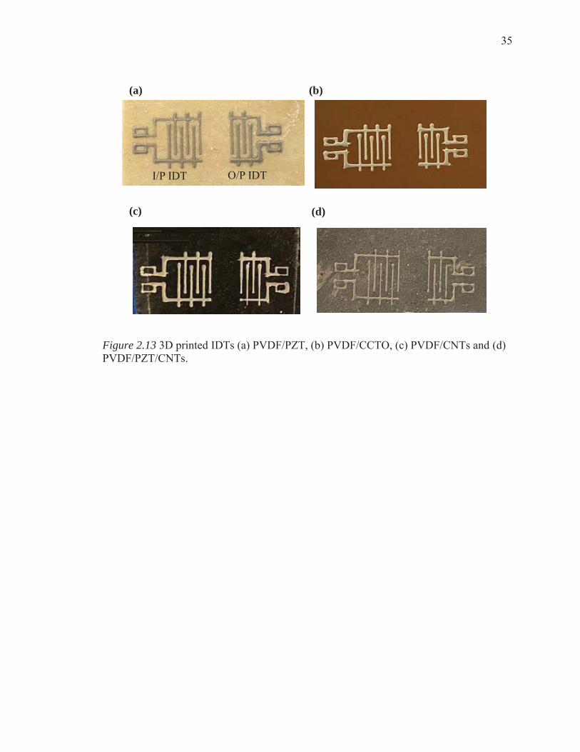
2.13 shows the SAW IDT printed on different composite types, where it can be noticed
that the IDT are printed without discontinuity and coupled appropriately with the
piezoelectric substrate.
Print bed
Ag paste syringe
Nozzle
Print bedSAW substrate
NPrinted IDT
(b) (a)
34
Figure 2.12 Design of IDT (a) CAD model and (b) Printed IDT with dimensions.
However, some bulb like points are still on the edge of the IDT, which can be
removed with well-adjusted printing speed. Attaining a flat substrate, which reduces the
time and increases the quality of IDT printing, and curing time to dry the IDT material
are some of the challenges faced during the printing process. In order to increase the
center frequency, the spacing of IDT can be reduced by choosing less diameter nozzle,
where the overlapping of electrodes should be considered. Overall, PVDF/CCTO
composite type shows better printing quality with promising structural integrity compared
to other counterparts.
(b) 0.5 mm 0.15 mm
3.75 mm
(a)
35
Figure 2.13 3D printed IDTs (a) PVDF/PZT, (b) PVDF/CCTO, (c) PVDF/CNTs and (d) PVDF/PZT/CNTs.
I/P IDT O/P IDT
(a) (b)
(d) (c)
36
3. SAW Sensor Property Measurement
Different techniques to measure piezoelectric, thermal, viscoelastic, and
morphological properties are presented in this chapter. As a quick outline, piezoelectric
properties such as dielectric constant, piezoelectric strain coefficient and piezoelectric
voltage constant are measured and relation in between mentioned properties are
discussed. Thermal properties are measured using DSC, DMA is used to measure the
storage modulus and SEM is utilized to analyze the homogeneity of different composite
combinations.
3.1. Dielectric and Piezoelectric Properties
As mentioned in the constitutive Equations 1.1 and 1.2, there are some important
terminologies that relates variable for certain functional applications. The piezoelectric
materials can be characterized based on the significant properties such as piezoelectric
stain coefficient ( ), voltage ( ) constant, dielectric constant ( ), elastic compliance
( ) and electromechanical coupling factor (k).
Piezoelectric strain coefficient is the ratio of electric charge generated per unit area to
applied mechanical stress or alternatively, is the mechanical strain experienced by a
piezoelectric material per unit of an electric field applied, as shown in Equation 3.1.
Especially, represents polarization induced in direction 3 per unit stress applied in
direction 3, as shown in Figure 3.1 and as well as d31 represents polarization induced in
direction 3 per unit stress applied in direction 1 (direction perpendicular to poling of
piezoelectric element). It is desired to have large constants since it showcase the
mechanical displacements, which turns out to be a huge motivation have effective
transducer applications.
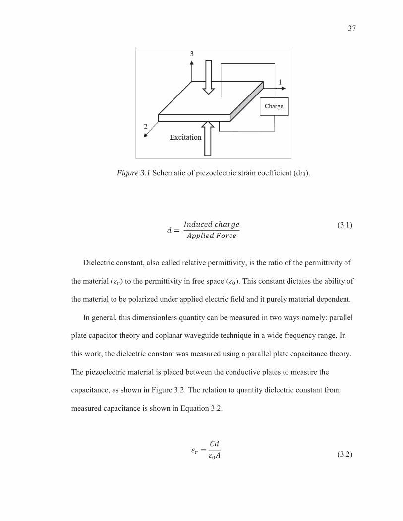
37
Figure 3.1 Schematic of piezoelectric strain coefficient (d33).
(3.1)
Dielectric constant, also called relative permittivity, is the ratio of the permittivity of
the material ( ) to the permittivity in free space ( ). This constant dictates the ability of
the material to be polarized under applied electric field and it purely material dependent.
In general, this dimensionless quantity can be measured in two ways namely: parallel
plate capacitor theory and coplanar waveguide technique in a wide frequency range. In
this work, the dielectric constant was measured using a parallel plate capacitance theory.
The piezoelectric material is placed between the conductive plates to measure the
capacitance, as shown in Figure 3.2. The relation to quantity dielectric constant from
measured capacitance is shown in Equation 3.2.
(3.2)

38
where C is the capacitance (farads), is the dielectric constant value of free space
(8.854x10⁻¹² F/m), A is the area of the capacitor electrode (m2), and d is the thickness of
the piezoelectric substrate.
Figure 3.2 Schematic of Parallel plate capacitor.
Piezoelectric voltage constant is the electric field generated by a piezoelectric
material per stress applied or the mechanical strain experienced per unit displacement
applied. Particularly, denotes electric field induced in direction 3 per unit stress
applied in direction 3. This property can be calculated by using the ratio between
measured piezoelectric strain coefficient and dielectric constant, as shown in Equation
3.3.
(3.3)
Electromechanical coupling coefficient is an important factor in validating energy
conversion efficiency from electrical to mechanical or vice versa. It can be calculated
using other parameters mentioned as, where is the elastic compliance of the
piezoelectric material, as shown in Equation 3.4.
(3.4)
Conductive Plate
Dielectric material
d

39
3.2. Thermal Analysis using DSC
Differential Scanning Calorimeter (DSC) is a thermal analytical technique used to
study the enthalpy changes and thermal transitions in the polymer and ceramic mix due to
the change in their chemical properties as a function of temperature or time. DSC 3
Mettler Toledo, with an operating temperature range of -150 °C to 700 °C, as shown in
Figure 3.3, is used in which the heat transfer rate and energy required to maintain zero
difference between the sample and reference are analyzed.
Figure 3.3 DSC calorimeter with zoomed in figure showing sample and reference crucible.
40
In general, properties such as melting point, glass transition temperature, degree of
cure are measured. Melting temperature (Tm) , a major thermal transition is analyzed
where the arrangements inside the polymer chain begin to move freely with an extra heat
flow showing an endothermic peak. In order to get a thermogram, the first step is to
switch on the DSC with the chiller and adjust the flow rate of nitrogen to 10 mL/min. To
measure only the coagulated mass of PVDF with solvent, an aluminum crucible is zeroed
using a balance, and PVDF was encapsulated using the punching machine. The sample
was then placed in the sample holder next to the reference crucible to go through the
isothermal and dynamic test.
3.3. Viscoelastic Analysis using DMA
The Dynamic mechanical analysis (DMA) is a technique used to characterize
materials especially viscoelastic behavior of polymers and ceramics. DMA 8000
PerkinElmer apparatus is used to characterize the material stiffness for the different
composite configuration with a temperature sweep at constant pressure. A sinusoidal
deformation is applied to the sample with a known geometry where the sine wave is
transmitted to the sample through drive shaft.
In general DMA has multiple fixtures such as compression, three point bending,
tensile and single cantilever respective to the structure of the sample and by knowing the
fabricated composite samples are thin and flexible, tensile fixture is used. As shown in
Figure 3.4, the sample with known dimensions are clamped in the fixture and mechanical
analysis were carried out with respective temperature sweep.
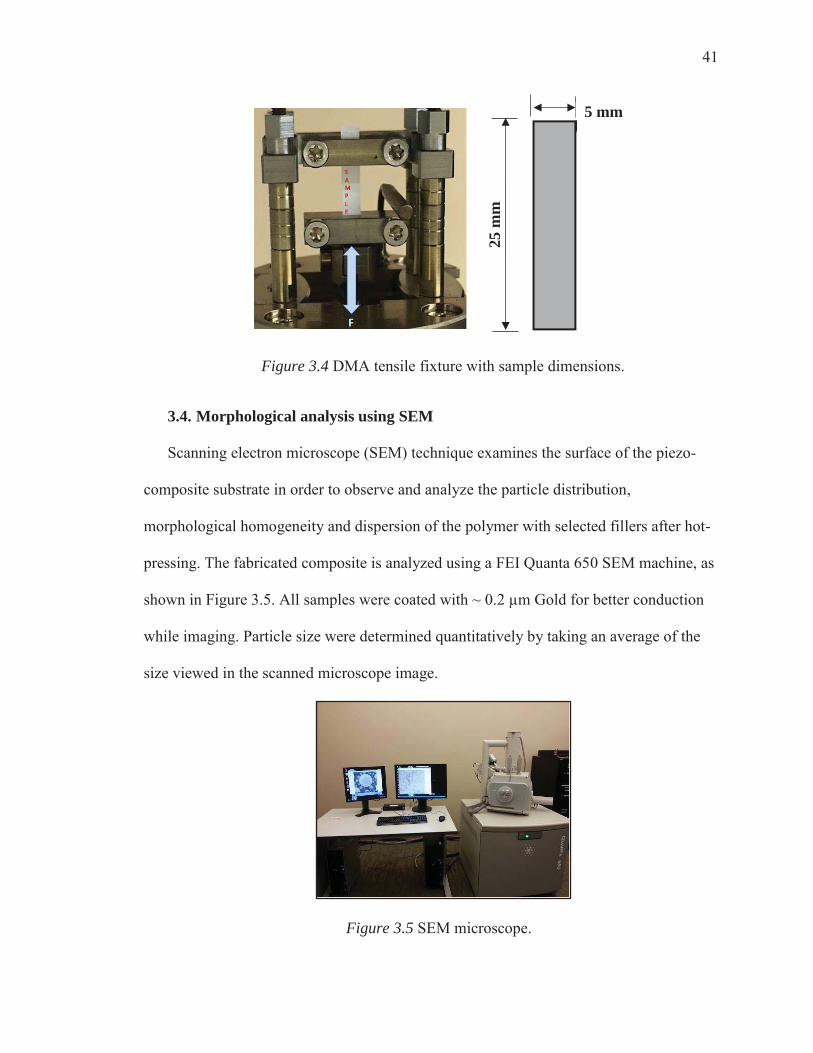
41
Figure 3.4 DMA tensile fixture with sample dimensions.
3.4. Morphological analysis using SEM
Scanning electron microscope (SEM) technique examines the surface of the piezo-
composite substrate in order to observe and analyze the particle distribution,
morphological homogeneity and dispersion of the polymer with selected fillers after hot-
pressing. The fabricated composite is analyzed using a FEI Quanta 650 SEM machine, as
shown in Figure 3.5. All samples were coated with ~ 0.2 μm Gold for better conduction
while imaging. Particle size were determined quantitatively by taking an average of the
size viewed in the scanned microscope image.
25 m
m
5 mm
Figure 3.5 SEM microscope.

42
4. Results and Discussions
Using the previously defined experimental techniques, various results including
crystalline phase, morphological, piezoelectric, dielectric, mechanical properties, and
strain measurements through RF testing of the fabricated composites, and strain
quantification and correlation with DIC are presented and discussed in this section. In
order to validate the efficiency of the selected substrate material, knowing the above
mentioned properties will be beneficial.
4.1. Material Spectral Analysis
PVDF polymer are semi crystalline in nature in which its behavior with selected
fillers needs to be validated through spectral analysis such as FTIR, Raman and EDX.
These information will gives a supporting information of how the crystalline phase and
functional group presence contributes to the piezoelectric properties are discussed.
4.1.1. Chemical Characterization using FTIR
FTIR is a technique used to obtain an infrared spectrum of absorption and crystalline
structure elucidation to identify the functional group of the molecules of a material with
phase information. An IR spectrum is passed through the sample in which some of the
radiation is absorbed by the bonds between different elements at different frequencies
resulting in a spectrum representing the molecular structures. By identifying the spectrum
against a database of reference spectra, materials can be determined especially when a
polymer is incorporated with micro and nanofillers. As PVDF polymer exhibits distinct
crystalline phases, it is important to analyze the crystalline structure, supporting to
distinguish between the different phases with their unique characteristics. The sample

43
should be thin enough for the IR to pass through, and as the fabricated composite was
thin, it was well suited for the desired technique.
FTIR allows to identify the molecular structure and dynamics of a polymer in which
the peak phases are classified into three major categories, i.e., 1) common peaks that
appear in all crystalline phases; 2) peaks exclusive for one of the phases; 3) dual peak
combining different phases. As fillers are added to the base polymer in this research, in
order to analyze the effect of different fillers, FTIR spectra are compared for the different
composite types. An Agilent Cary 630 FTIR spectrometer with a diamond crystal, as
shown in Figure 4.1, is operated in the wavenumber of 650-1550 cm-1 measured with a
resolution of 4 cm-1 and 16 scans followed with automatic background correction.
From the collected FTIR spectra, as shown in Figure 4.2, the corresponding bands
confirm the presence of α phase in the sample at 762 cm-1 (CF2 bending and rocking, 873
cm-1 (C-F stretching), and 1069 cm-1 (C-C-C bonding). In contrast, the characteristics
bands of β phase are at 835 cm-1 (trans chain sequence CF2 stretching and CH2 rocking),
Figure 4.1 Agilent FTIR spectrometer.
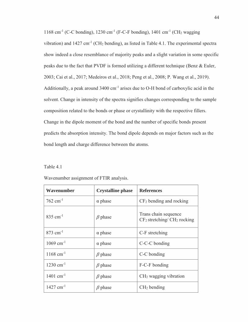
44
1168 cm-1 (C-C bonding), 1230 cm-1 (F-C-F bonding), 1401 cm-1 (CH2 wagging
vibration) and 1427 cm-1 (CH2 bending), as listed in Table 4.1. The experimental spectra
show indeed a close resemblance of majority peaks and a slight variation in some specific
peaks due to the fact that PVDF is formed utilizing a different technique (Benz & Euler,
2003; Cai et al., 2017; Medeiros et al., 2018; Peng et al., 2008; P. Wang et al., 2019).
Additionally, a peak around 3400 cm-1 arises due to O-H bond of carboxylic acid in the
solvent. Change in intensity of the spectra signifies changes corresponding to the sample
composition related to the bonds or phase or crystallinity with the respective fillers.
Change in the dipole moment of the bond and the number of specific bonds present
predicts the absorption intensity. The bond dipole depends on major factors such as the
bond length and charge difference between the atoms.
Table 4.1
Wavenumber assignment of FTIR analysis.
Wavenumber Crystalline phase References
762 cm-1 α phase CF2 bending and rocking
835 cm-1 phase Trans chain sequence CF2 stretching/ CH2 rocking
873 cm-1 α phase C-F stretching
1069 cm-1 α phase C-C-C bonding
1168 cm-1 phase C-C bonding
1230 cm-1 phase F-C-F bonding
1401 cm-1 phase CH2 wagging vibration
1427 cm-1 phase CH2 bending
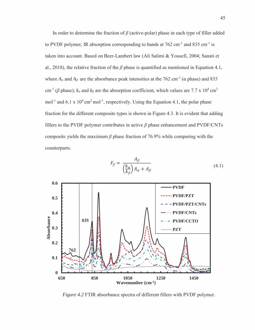
45
In order to determine the fraction of β (active-polar) phase in each type of filler added
to PVDF polymer, IR absorption corresponding to bands at 762 cm-1 and 835 cm-1 is
taken into account. Based on Beer-Lambert law (Ali Salimi & Yousefi, 2004; Sanati et
al., 2018), the relative fraction of the β phase is quantified as mentioned in Equation 4.1,
where Aα and Aβ are the absorbance peak intensities at the 762 cm-1 (α phase) and 835
cm-1 (β phase); kα and kβ are the absorption coefficient, which values are 7.7 x 104 cm2
mol-1 and 6.1 x 104 cm2 mol-1, respectively. Using the Equation 4.1, the polar phase
fraction for the different composite types is shown in Figure 4.3. It is evident that adding
fillers to the PVDF polymer contributes in active β phase enhancement and PVDF/CNTs
composite yields the maximum β phase fraction of 76.9% while comparing with the
counterparts.
(4.1)
Figure 4.2 FTIR absorbance spectra of different fillers with PVDF polymer.
0
0.1
0.2
0.3
0.4
0.5
0.6
650 850 1050 1250 1450
Abs
orba
nce
Wavenumber (cm-1)
PVDF
PVDF/PZT
PVDF/PZT/CNTs
PVDF/CNTs
PVDF/CCTO
PZT
835
762

46
This quantification helped to scientifically prove that through the hot press
(stretching) and applying a high electric field with corresponding fillers, the other
crystalline phases can be converted into a polar phase. But in order to characterize the
presence of specific functional groups in CNTs and CCTO, additional technique such as
Raman spectroscopy is recommended.
Figure 4.3 Relative fraction of calculated polar β phase.
4.1.2. Thermal Characterization
To evaluate the thermal properties of PVDF polymer, DSC is carried out using a
Mettler Toledo calorimeter in the temperature range from 0 °C to 180 °C at a heating rate
of 1°C/min. Figure 4.4 thermogram shows PVDF is strongly influenced by the
temperature during the melting process from 145 °C to 170 °C. It is noticed that double
endothermic fusion peak occurred with 5 °C difference at 156 °C and 161 °C due to the

47
melt recrystallization whereas the peak belongs to α and β phases (García-Zaldívar et al.,
2017; Peng et al., 2008).
Figure 4.4 DSC curve of PVDF sample showing endothermic peaks.
4.1.3. Raman Shift Analysis
Raman analysis is preferred to detect the presence of CNTs as they are a black body
that absorbs all lights and ending up with a lot of noises in the spectra. The main
noticeable bands for CNTs through Raman analysis are the high frequency D
(disordered), G (graphite), and radial breathing modes (RBM) modes. G mode is a
tangential shear mode of carbon atoms, D band is a defect mode requires while elastic
scattering to conserve momentum and RBM is associated with the symmetrical
movement of carbon atoms.

48
Figure 4.5 Raman spectra of PVDF/CNTs.
From the Figure 4.5 and 4.6, the peak below 300 cm-1 is due to the symmetric radial
vibrations of carbon atoms, D-line ranges between 1300 and 1400 cm-1 in which the peak
at 1343 cm-1 is due to the surface and structural defects, the G-band ranges from 1500 to
1700 cm-1 in which peak at 1594 cm-1 is due to the longitudinal and transversal in-plane
phonon, and 2D-band peak at 2658 cm-1, which is the symmetry overtone of D band
(Kharlamova et al., 2018; Yan et al., 2013). Raman spectra with a laser wavelength of
532 nm excitation is used to examine all the four main regions in CNTs. From the D/G
ratio, purity and defects in SWCNTs can be quantified (Miyata et al., 2011; Tsentalovich
et al., 2017). Even though knowing the defect percent information will be beneficial, the
main idea of Raman analysis is to characterize the presence of SWCNTs incorporated
with PVDF and PZT, respective composite types.
0 500 1000 1500 2000 2500 3000 3500 4000 45000
100
200
300
400
500
600
Inte
nsity
(a.u
)
Raman Shift (cm-1)
PVDF/CNTs
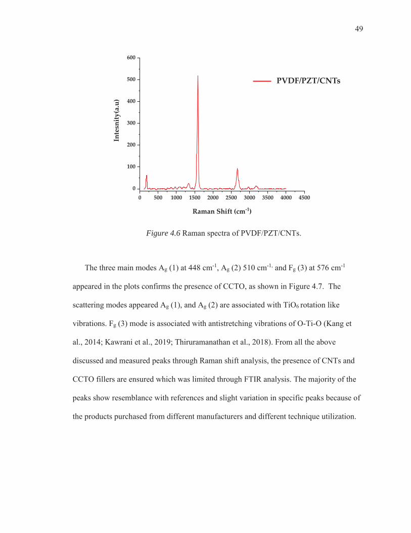
49
Figure 4.6 Raman spectra of PVDF/PZT/CNTs.
The three main modes Ag (1) at 448 cm-1, Ag (2) 510 cm-1, and Fg (3) at 576 cm-1
appeared in the plots confirms the presence of CCTO, as shown in Figure 4.7. The
scattering modes appeared Ag (1), and Ag (2) are associated with TiO6 rotation like
vibrations. Fg (3) mode is associated with antistretching vibrations of O-Ti-O (Kang et
al., 2014; Kawrani et al., 2019; Thiruramanathan et al., 2018). From all the above
discussed and measured peaks through Raman shift analysis, the presence of CNTs and
CCTO fillers are ensured which was limited through FTIR analysis. The majority of the
peaks show resemblance with references and slight variation in specific peaks because of
the products purchased from different manufacturers and different technique utilization.
0 500 1000 1500 2000 2500 3000 3500 4000 45000
100
200
300
400
500
600
Inte
snity
(a.u
)
Raman Shift (cm-1)
PVDF/PZT/CNTs
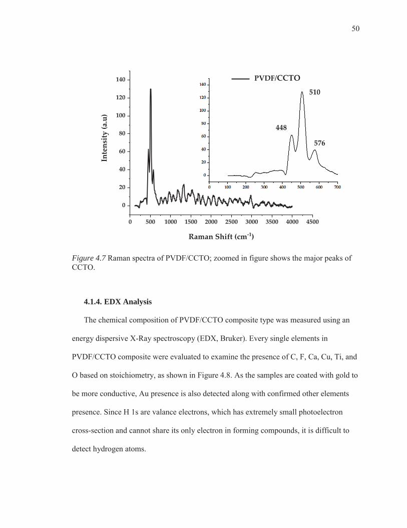
50
Figure 4.7 Raman spectra of PVDF/CCTO; zoomed in figure shows the major peaks of CCTO.
4.1.4. EDX Analysis
The chemical composition of PVDF/CCTO composite type was measured using an
energy dispersive X-Ray spectroscopy (EDX, Bruker). Every single elements in
PVDF/CCTO composite were evaluated to examine the presence of C, F, Ca, Cu, Ti, and
O based on stoichiometry, as shown in Figure 4.8. As the samples are coated with gold to
be more conductive, Au presence is also detected along with confirmed other elements
presence. Since H 1s are valance electrons, which has extremely small photoelectron
cross-section and cannot share its only electron in forming compounds, it is difficult to
detect hydrogen atoms.
0 500 1000 1500 2000 2500 3000 3500 4000 4500
0
20
40
60
80
100
120
140
Inte
nsity
(a.u
)
Raman Shift (cm-1)
PVDF/CCTO
448
510
576
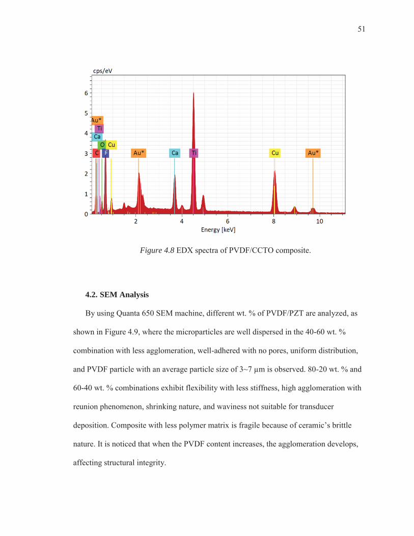
51
Figure 4.8 EDX spectra of PVDF/CCTO composite.
4.2. SEM Analysis
By using Quanta 650 SEM machine, different wt. % of PVDF/PZT are analyzed, as
shown in Figure 4.9, where the microparticles are well dispersed in the 40-60 wt. %
combination with less agglomeration, well-adhered with no pores, uniform distribution,
and PVDF particle with an average particle size of 3~7 μm is observed. 80-20 wt. % and
60-40 wt. % combinations exhibit flexibility with less stiffness, high agglomeration with
reunion phenomenon, shrinking nature, and waviness not suitable for transducer
deposition. Composite with less polymer matrix is fragile because of ceramic’s brittle
nature. It is noticed that when the PVDF content increases, the agglomeration develops,
affecting structural integrity.
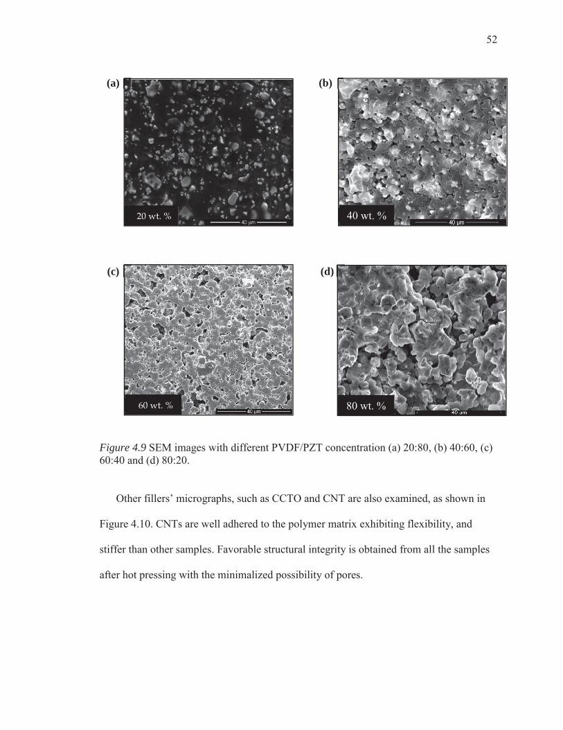
52
Figure 4.9 SEM images with different PVDF/PZT concentration (a) 20:80, (b) 40:60, (c) 60:40 and (d) 80:20.
Other fillers’ micrographs, such as CCTO and CNT are also examined, as shown in
Figure 4.10. CNTs are well adhered to the polymer matrix exhibiting flexibility, and
stiffer than other samples. Favorable structural integrity is obtained from all the samples
after hot pressing with the minimalized possibility of pores.
20 wt. %
60 wt. % 80 wt. %
40 wt. %
(a) (b)
(c) (d)

53
Figure 4.10 SEM images (a) PVDF/PZT/CNTs (40:59.75:0.25), zoomed in picture shows CNTs and (b) PVDF/CCTO (40:60), showing a homogenous distribution of powder with less agglomeration.
4.3. Effect of Micro and Nano fillers in Dielectric Properties of PVDF polymer
From the major piezoelectric and dielectric properties mentioned in section 3.1, few
vital properties such as piezoelectric stain coefficient ( ), voltage ( ) constant, and
dielectric constant ( ) are analyzed for different composite types fabricated. The
piezoelectric strain coefficient ( ) is measured through electric charge generated in
response to 0.25N force applied in thickness direction using a YE2730A piezometer, as
shown in Figure 4.11. All the properties discussed in this section are measured and
calculated using the previously defined methods and numbers are normalized in default
given by the equipment utilized. The major factor to be noticed is the relation and trend
among each properties which depends on the nature of filler added to the sample
showcasing its distinct behavior.
(a) (b)
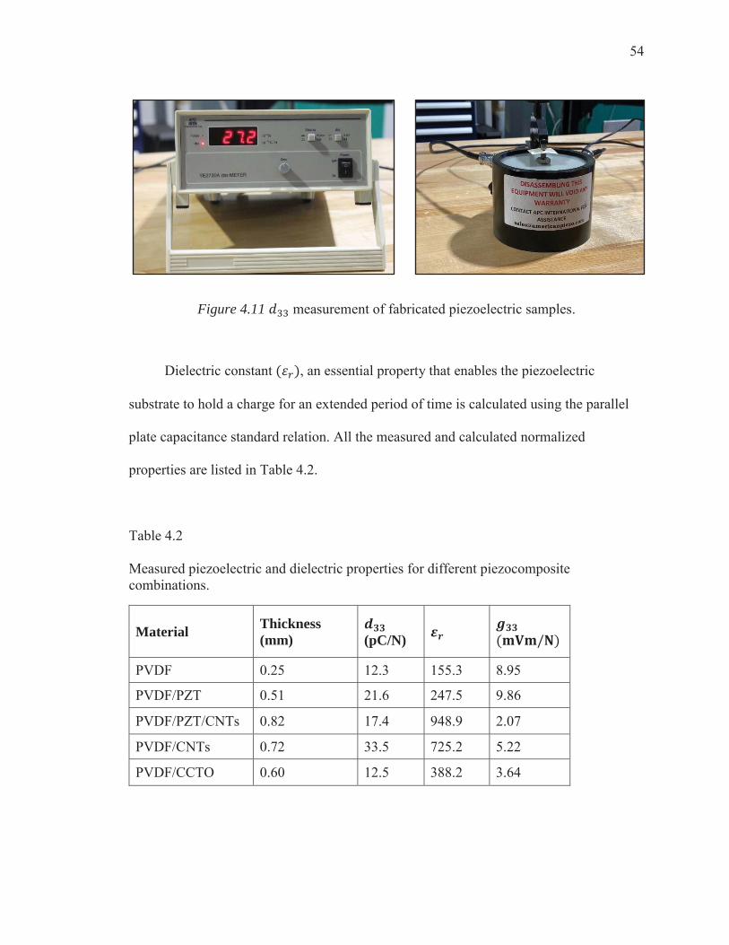
54
Figure 4.11 measurement of fabricated piezoelectric samples.
Dielectric constant , an essential property that enables the piezoelectric
substrate to hold a charge for an extended period of time is calculated using the parallel
plate capacitance standard relation. All the measured and calculated normalized
properties are listed in Table 4.2.
Table 4.2
Measured piezoelectric and dielectric properties for different piezocomposite combinations.
Material Thickness (mm)
(pC/N)
PVDF 0.25 12.3 155.3 8.95
PVDF/PZT 0.51 21.6 247.5 9.86
PVDF/PZT/CNTs 0.82 17.4 948.9 2.07
PVDF/CNTs 0.72 33.5 725.2 5.22
PVDF/CCTO 0.60 12.5 388.2 3.64
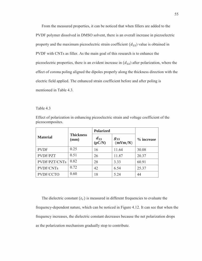
55
From the measured properties, it can be noticed that when fillers are added to the
PVDF polymer dissolved in DMSO solvent, there is an overall increase in piezoelectric
property and the maximum piezoelectric strain coefficient ) value is obtained in
PVDF with CNTs as filler. As the main goal of this research is to enhance the
piezoelectric properties, there is an evident increase in ) after polarization, where the
effect of corona poling aligned the dipoles properly along the thickness direction with the
electric field applied. The enhanced strain coefficient before and after poling is
mentioned in Table 4.3.
Table 4.3
Effect of polarization in enhancing piezoelectric strain and voltage coefficient of the piezocomposites.
Material Thickness (mm)
Polarized % increase
(pC/N)
PVDF 0.25 16 11.64 30.08 PVDF/PZT 0.51 26 11.87 20.37 PVDF/PZT/CNTs 0.82 28 3.33 60.91 PVDF/CNTs 0.72 42 6.54 25.37 PVDF/CCTO 0.60 18 5.24 44
The dielectric constant is measured in different frequencies to evaluate the
frequency-dependent nature, which can be noticed in Figure 4.12. It can see that when the
frequency increases, the dielectric constant decreases because the net polarization drops
as the polarization mechanism gradually stop to contribute.
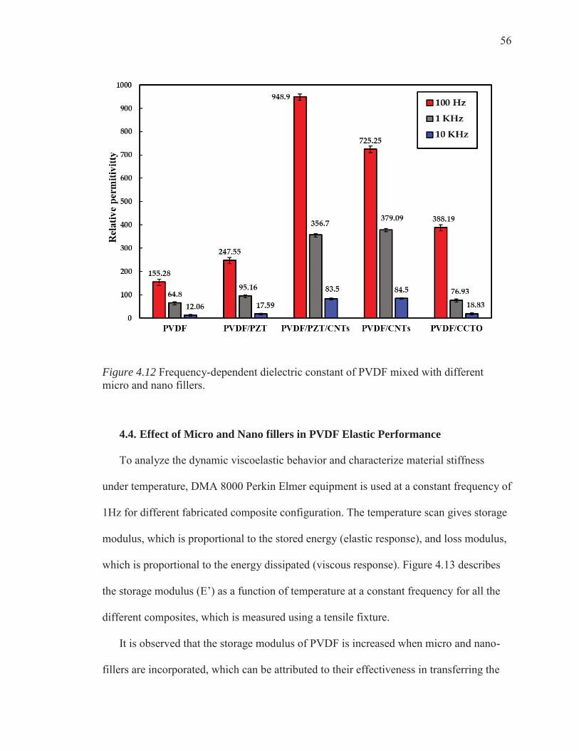
56
Figure 4.12 Frequency-dependent dielectric constant of PVDF mixed with different micro and nano fillers.
4.4. Effect of Micro and Nano fillers in PVDF Elastic Performance
To analyze the dynamic viscoelastic behavior and characterize material stiffness
under temperature, DMA 8000 Perkin Elmer equipment is used at a constant frequency of
1Hz for different fabricated composite configuration. The temperature scan gives storage
modulus, which is proportional to the stored energy (elastic response), and loss modulus,
which is proportional to the energy dissipated (viscous response). Figure 4.13 describes
the storage modulus (E’) as a function of temperature at a constant frequency for all the
different composites, which is measured using a tensile fixture.
It is observed that the storage modulus of PVDF is increased when micro and nano-
fillers are incorporated, which can be attributed to their effectiveness in transferring the
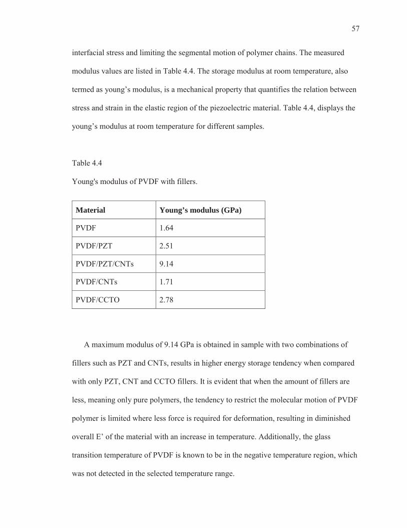
57
interfacial stress and limiting the segmental motion of polymer chains. The measured
modulus values are listed in Table 4.4. The storage modulus at room temperature, also
termed as young’s modulus, is a mechanical property that quantifies the relation between
stress and strain in the elastic region of the piezoelectric material. Table 4.4, displays the
young’s modulus at room temperature for different samples.
Table 4.4
Young's modulus of PVDF with fillers.
A maximum modulus of 9.14 GPa is obtained in sample with two combinations of
fillers such as PZT and CNTs, results in higher energy storage tendency when compared
with only PZT, CNT and CCTO fillers. It is evident that when the amount of fillers are
less, meaning only pure polymers, the tendency to restrict the molecular motion of PVDF
polymer is limited where less force is required for deformation, resulting in diminished
overall E’ of the material with an increase in temperature. Additionally, the glass
transition temperature of PVDF is known to be in the negative temperature region, which
was not detected in the selected temperature range.
Material Young’s modulus (GPa)
PVDF 1.64
PVDF/PZT 2.51
PVDF/PZT/CNTs 9.14
PVDF/CNTs 1.71
PVDF/CCTO 2.78
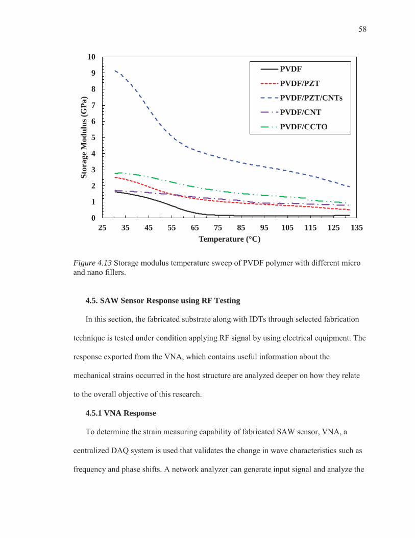
58
Figure 4.13 Storage modulus temperature sweep of PVDF polymer with different micro and nano fillers.
4.5. SAW Sensor Response using RF Testing
In this section, the fabricated substrate along with IDTs through selected fabrication
technique is tested under condition applying RF signal by using electrical equipment. The
response exported from the VNA, which contains useful information about the
mechanical strains occurred in the host structure are analyzed deeper on how they relate
to the overall objective of this research.
4.5.1 VNA Response
To determine the strain measuring capability of fabricated SAW sensor, VNA, a
centralized DAQ system is used that validates the change in wave characteristics such as
frequency and phase shifts. A network analyzer can generate input signal and analyze the
0
1
2
3
4
5
6
7
8
9
10
25 35 45 55 65 75 85 95 105 115 125 135
Stor
age
Mod
ulus
(GPa
)
Temperature (°C)
PVDF
PVDF/PZT
PVDF/PZT/CNTs
PVDF/CNT
PVDF/CCTO
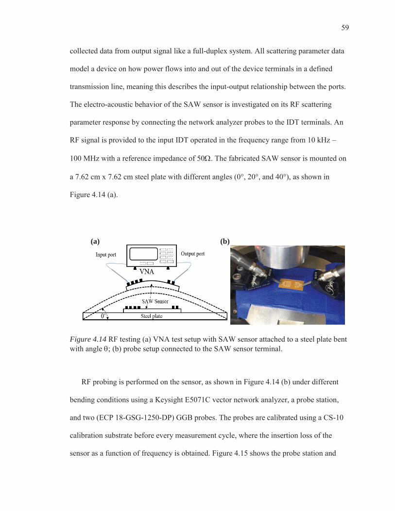
59
collected data from output signal like a full-duplex system. All scattering parameter data
model a device on how power flows into and out of the device terminals in a defined
transmission line, meaning this describes the input-output relationship between the ports.
The electro-acoustic behavior of the SAW sensor is investigated on its RF scattering
parameter response by connecting the network analyzer probes to the IDT terminals. An
RF signal is provided to the input IDT operated in the frequency range from 10 kHz –
100 MHz with a reference impedance of 50 . The fabricated SAW sensor is mounted on
a 7.62 cm x 7.62 cm steel plate with different angles (0°, 20°, and 40°), as shown in
Figure 4.14 (a).
Figure 4.14 RF testing (a) VNA test setup with SAW sensor attached to a steel plate bent with angle ; (b) probe setup connected to the SAW sensor terminal.
RF probing is performed on the sensor, as shown in Figure 4.14 (b) under different
bending conditions using a Keysight E5071C vector network analyzer, a probe station,
and two (ECP 18-GSG-1250-DP) GGB probes. The probes are calibrated using a CS-10
calibration substrate before every measurement cycle, where the insertion loss of the
sensor as a function of frequency is obtained. Figure 4.15 shows the probe station and
(a) (b)
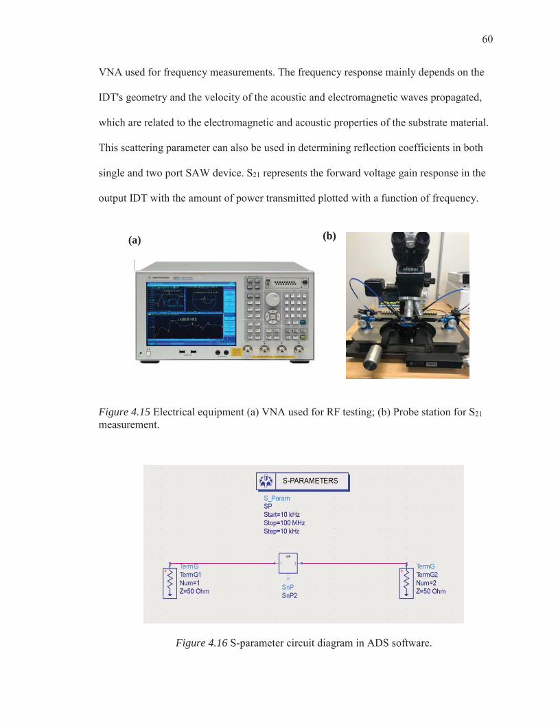
60
VNA used for frequency measurements. The frequency response mainly depends on the
IDT's geometry and the velocity of the acoustic and electromagnetic waves propagated,
which are related to the electromagnetic and acoustic properties of the substrate material.
This scattering parameter can also be used in determining reflection coefficients in both
single and two port SAW device. S21 represents the forward voltage gain response in the
output IDT with the amount of power transmitted plotted with a function of frequency.
Figure 4.15 Electrical equipment (a) VNA used for RF testing; (b) Probe station for S21 measurement.
Figure 4.16 S-parameter circuit diagram in ADS software.
(a) (b)

61
When the SAW sensor is bent, due to the deformation of the host structure, the
composite substrate stretches, extending the delay line distance and finger spacing, which
can be proportional to the shift in frequency response. The measured S-parameter is
exported as .snp files that are used for post processing techniques. ADS software is used
for simulating the extracted VNA data under different strain conditions. Figure 4.16
shows the circuit diagram that mimics the working of VNA for frequency response
measurement in the ADS tool. Instead of being represented in decibel, S-parameter is
transformed to phase angle in degree in which it is noticed that the frequency sweep is in
phase influenced by perturbation with better transmission characteristics and fewer ripple
disturbances.
Figure 4.17 Frequency shift response of PVDF/PZT type (a) Frequency plot; (b) Phase plot; zoomed in box shows the peak shift in normalized frequency response when the SAW sensor is under bending in different angles.
Frequency (MHz)
S 21 (d
B)
(Normalized scale)
0° 20° 40°
Frequency (MHz)
(a) (b)
Phas
e an
gle
(deg
ree)
0° 20° 40°

62
Figure 4.18 Frequency shift response of PVDF/PZT/CNTs type (a) Frequency; (b) Phase plot.
From the response of different fabricated SAW sensor, as shown from Figure 4.17 to
4.20, it is evident that each sensor type has its own resonance peak frequency
corresponding to the wave characteristics of the substrate material. Each SAW sensor has
fundamental and harmonic frequencies that are in phase and can be tuned to high
frequency, which expands the range of applications.
The predominant peak is detected with the lower frequency range, but the
fundamental frequency is not detected, which could be due to the impedance mismatch at
2.3 MHz, and the next close harmonic mode peak is tracked. Even with the lower
frequency range, this VNA gives us almost noise under 10 MHz, which can be optimized
further.
Frequency (MHz) Frequency (MHz)
S 21 (d
B)
(Normalized scale)
Phas
e an
gle
(deg
ree)
(a) (b) 0° 20° 40°
0° 20° 40°
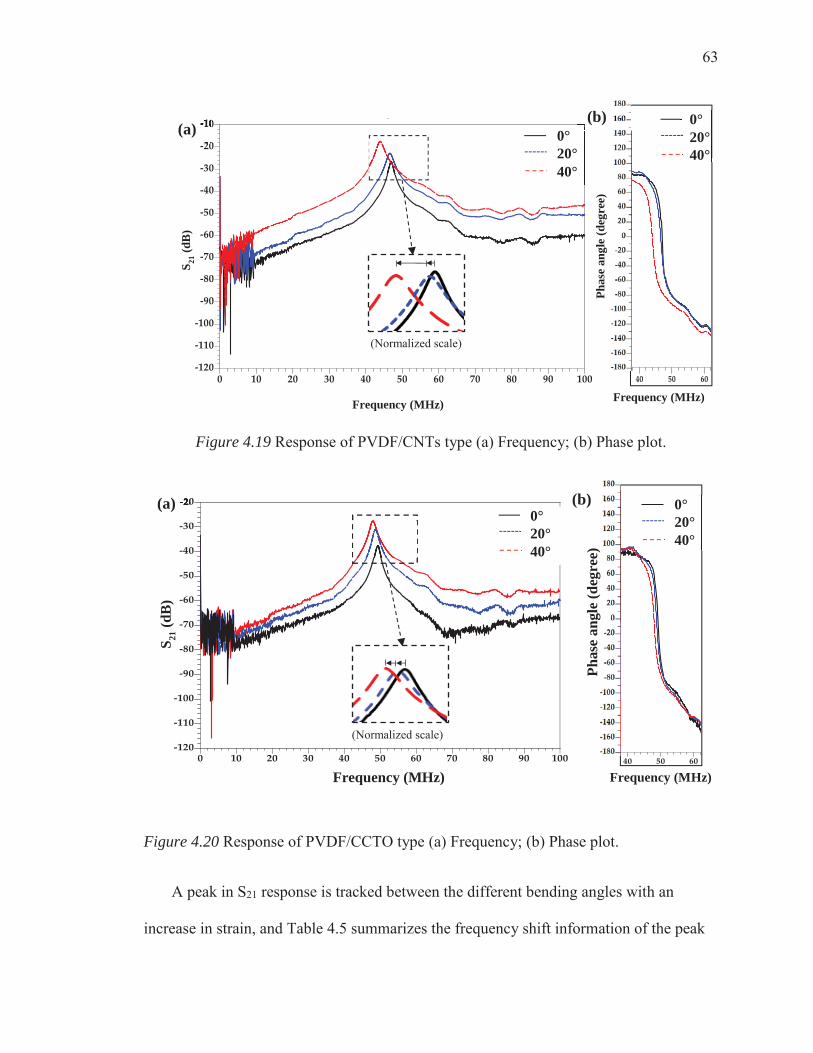
63
Figure 4.19 Response of PVDF/CNTs type (a) Frequency; (b) Phase plot.
Figure 4.20 Response of PVDF/CCTO type (a) Frequency; (b) Phase plot.
A peak in S21 response is tracked between the different bending angles with an
increase in strain, and Table 4.5 summarizes the frequency shift information of the peak
Frequency (MHz)
S 21 (d
B)
(Normalized scale)
Frequency (MHz)
Phas
e an
gle
(deg
ree)
(a) (b) 0° 20° 40°
0° 20° 40°
Frequency (MHz)
S 21 (d
B)
(Normalized scale)
Frequency (MHz)
Phas
e an
gle
(deg
ree)
(a) (b) 0° 20° 40°
0° 20° 40°
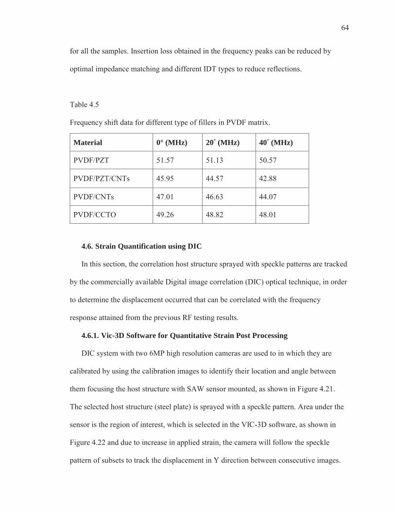
64
for all the samples. Insertion loss obtained in the frequency peaks can be reduced by
optimal impedance matching and different IDT types to reduce reflections.
Table 4.5
Frequency shift data for different type of fillers in PVDF matrix.
Material 0° (MHz) 20° (MHz) 40° (MHz)
PVDF/PZT 51.57 51.13 50.57
PVDF/PZT/CNTs 45.95 44.57 42.88
PVDF/CNTs 47.01 46.63 44.07
PVDF/CCTO 49.26 48.82 48.01
4.6. Strain Quantification using DIC
In this section, the correlation host structure sprayed with speckle patterns are tracked
by the commercially available Digital image correlation (DIC) optical technique, in order
to determine the displacement occurred that can be correlated with the frequency
response attained from the previous RF testing results.
4.6.1. Vic-3D Software for Quantitative Strain Post Processing
DIC system with two 6MP high resolution cameras are used to in which they are
calibrated by using the calibration images to identify their location and angle between
them focusing the host structure with SAW sensor mounted, as shown in Figure 4.21.
The selected host structure (steel plate) is sprayed with a speckle pattern. Area under the
sensor is the region of interest, which is selected in the VIC-3D software, as shown in
Figure 4.22 and due to increase in applied strain, the camera will follow the speckle
pattern of subsets to track the displacement in Y direction between consecutive images.
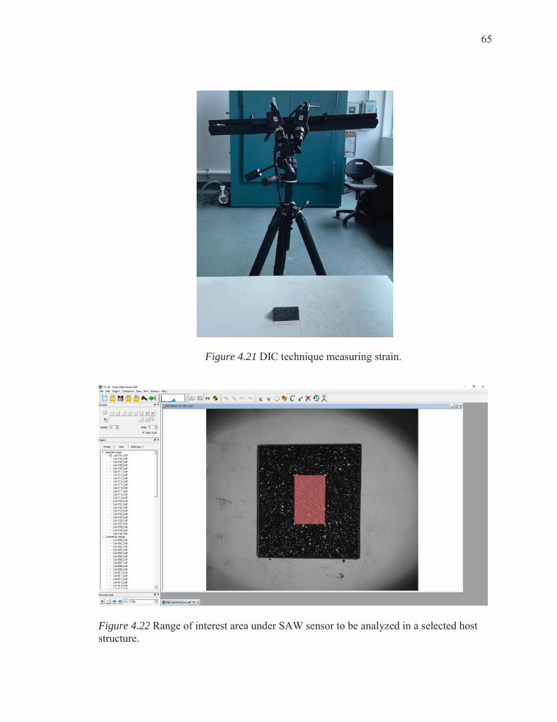
65
Figure 4.21 DIC technique measuring strain.
Figure 4.22 Range of interest area under SAW sensor to be analyzed in a selected host structure.
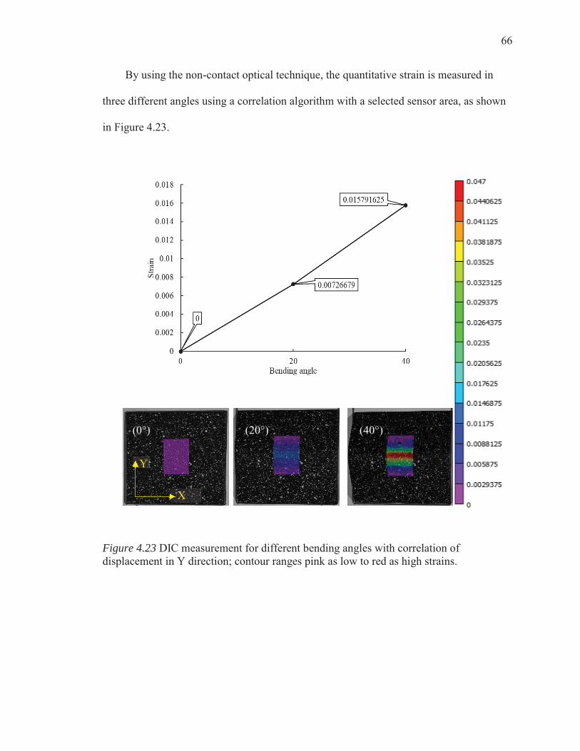
66
By using the non-contact optical technique, the quantitative strain is measured in
three different angles using a correlation algorithm with a selected sensor area, as shown
in Figure 4.23.
Figure 4.23 DIC measurement for different bending angles with correlation of displacement in Y direction; contour ranges pink as low to red as high strains.
X
Y
(0°) (20°) (40°)
67
5. Conclusion
The main objective and focus of this research was to develop a SAW sensor capable
of detecting and measuring mechanical strain occurred in aerospace structures. It is
observed that the fabricated substrate successfully detect mechanical strain and the
substrate exhibiting higher piezoelectric properties along with flexibility. Summary
collected throughout the research with recommendations and future works will be
presented below.
5.1. Summary
In this research the fabrication and design of a piezoelectric composite sensor
exhibiting flexibility made of PVDF as polymer matrix and different micro- and nano-
fillers such as PZT, CCTO, and CNTs by a hot-press process is demonstrated. The
different composites structural, morphological, thermal, and electrical properties are
investigated through Fourier-transform infrared spectroscopy (FTIR), scanning electron
microscope (SEM), differential scanning calorimetry (DSC), and dynamic mechanical
analysis (DMA).
The printing of optimized IDTs design using the transmission matrix approach
through direct digital manufacturing technique is described. Adding fillers to the polymer
had a great impact on the piezoelectric property, especially the polar β phase and
structural properties of the piezocomposite. For the composite, polar phase is enhanced
by both stretching the piezoelectric material through hot-press and applying higher
electric voltage, which the corona poling will reorient the dipole direction. The
piezoelectric strain coefficient, voltage constant, and dielectric constant values are
68
enhanced significantly when the PVDF polymer is incorporated with both PZT (micro)
and CNT nano-fillers while comparing with the counterparts.
PVDF/CNTs composite yields a maximum β phase fraction of 76.9 as well as the
maximum piezoelectric strain coefficient ( ) of 42 pC/N. Other composite types also
yield maximum property values, i.e., 948.9 dielectric constant ) by PVDF/PZT/CNTs
and 11.87 piezoelectric voltage constant with PVDF/PZT. Mechanical strains
are detected and measured by utilizing the change in wave characteristics such as
frequency shifts in the fabricated SAW sensor response. Results show a correlation
between the measured frequency response and the quantitatively measured mechanical
strains up to 15,800 μ at 40° bending angle, which is relatively high for this specific
application.
5.2. Future Work
This research presented, mainly focuses on the fabrication of a flexible SAW sensor
that can measure strain. With the fabricated sensor that can detect mechanical strains,
there are some imminent works to be addressed. The frequency response obtained in the
transmission model is with assumed wave velocity from the previous works. The velocity
of the fabricated sample has to be measured using appropriate equipment in order to get
the exact center frequency response. From the RF testing with the assumed velocity, it is
uncertain that whether the wave generated is due to electromagnetic coupling or purely
an acoustic coupling between the IDT and the piezoelectric substrate, which needs to be
identified and is under analysis.
Further optimization of IDT design with less insertion loss should be designed and
compared with ANSYS HFSS simulation responses. With the wired setup, there are few

69
limitations, such as real time measurement in the aircraft structure and embedding
multiple sensors in a structure. By knowing the wireless capability, an antenna needs to
be designed with the intended frequency range, which enables to measure strain with
multiple sensors that could increase the measuring range area.
5.3. Recommendations
Due to the complex probing station, the plate bending technique is followed for strain
measurement. By changing the probe setup, the sensor can be mounted in the cantilever
beam and compared with another commercial product like strain gages. With the
traditional techniques hot-press used in this research, there is always a separate technique
is required after the substrate fabrication, especially for IDT deposition. This can be
overcome by using additive manufacturing to the production of SAW device. Using a
small diameter nozzle will allow increasing the number of fingers and reduce the spacing
between them, which will results in increasing the fundamental frequency.
To achieve a higher precision frequency response, IDT design can be optimized using
commercial FEA analysis tool such as COMSOL, ANSYS for a better understanding of
the frequency response before fabrication. Insertion loss obtained with the present design
is a little high and can be reduced by optimal impedance matching and different IDT
types to reduce reflections. In this work, the fundamental frequency is not detected using
the VNA, and we track the frequency peak of harmonic modes. Instead, the admittance
can be measured in the required frequency range by using the BVD model. By tracking
the shift in impedance plot, it will contain useful information about strain measurement.
Material wise, PVDF-TrFE, a co-polymer of PVDF, looks promising in achieving higher
piezoelectric strain and dielectric constant with a higher polar phase, and this avoids the

70
necessity of stretching. Fabrication using additive manufacturing can be studied in detail
and implemented to elude the limitations of used technique in this research.
71
REFERENCES
Araújo, E., & Eiras, J. (1999). Structural, electric and ferroelectric properties of PZT films obtained using oxide precursors. Journal of Physics: Condensed Matter, 11(8), 1975.
Arlt, K., & Wegener, M. (2010). Piezoelectric PZT/PVDF-copolymer 0-3 composites:
aspects on film preparation and electrical poling. IEEE Transactions on Dielectrics and Electrical Insulation, 17(4), 1178-1184.
Aubert, T., Elmazria, O., & Assouar, M. (2009). Wireless and batteryless surface
acoustic wave sensors for high temperature environments. Paper presented at the 2009 9th International Conference on Electronic Measurement & Instruments.
Ballato, A. (1995). Piezoelectricity: old effect, new thrusts. IEEE transactions on
ultrasonics, ferroelectrics, and frequency control, 42(5), 916-926. Benz, M., & Euler, W. B. (2003). Determination of the crystalline phases of poly
(vinylidene fluoride) under different preparation conditions using differential scanning calorimetry and infrared spectroscopy. Journal of applied polymer science, 89(4), 1093-1100.
Brocato, R. W. (2004). Passive microwave tags. Sandia National Laboratories. Cai, X., Lei, T., Sun, D., & Lin, L. (2017). A critical analysis of the α, β and γ phases in
poly (vinylidene fluoride) using FTIR. RSC advances, 7(25), 15382-15389. Cheeke, J. D. N. (2017). Fundamentals and applications of ultrasonic waves: CRC press. Chen, D., Heyer, S., Ibbotson, S., Salonitis, K., Steingrímsson, J. G., & Thiede, S. (2015).
Direct digital manufacturing: definition, evolution, and sustainability implications. Journal of Cleaner Production, 107, 615-625.
d’AMICO, A., Palma, A., & Verona, E. (1982). Palladium‐surface acoustic wave
interaction for hydrogen detection. Applied Physics Letters, 41(3), 300-301. Defaÿ, E. (2013). Integration of ferroelectric and piezoelectric thin films: concepts and
applications for microsystems: John Wiley & Sons. Della Lucia, F., Zambrozi Jr, P., Frazatto, F., Piazzetta, M., & Gobbi, A. (2014). Design,
fabrication and characterization of saw pressure sensors for extreme operation conditions. Procedia Engineering, 87, 540-543.
Devkota, J., Ohodnicki, P. R., & Greve, D. W. (2017). SAW sensors for chemical vapors
and gases. Sensors, 17(4), 801.
72
Eun, K., Lee, K. J., Lee, K. K., Yang, S. S., & Choa, S.-H. (2016). Highly sensitive surface acoustic wave strain sensor for the measurement of tire deformation. International Journal of Precision Engineering and Manufacturing, 17(6), 699-707.
Fan, Y., Kong, P., Qi, H., Liu, H., & Ji, X. (2018). A surface acoustic wave response
detection method for passive wireless torque sensor. AIP Advances, 8(1), 015321. Ferreira, A., Martínez, M., Ansón-Casaos, A., Gómez-Pineda, L., Vaz, F., & Lanceros-
Mendez, S. (2013). Relationship between electromechanical response and percolation threshold in carbon nanotube/poly (vinylidene fluoride) composites. Carbon, 61, 568-576.
Fraga, M. A., Furlan, H., Pessoa, R., & Massi, M. (2014). Wide bandgap semiconductor
thin films for piezoelectric and piezoresistive MEMS sensors applied at high temperatures: an overview. Microsystem technologies, 20(1), 9-21.
Fu, C., Lee, K. J., Eun, K., Choa, S.-H., Lee, K., & Yang, S. S. (2016). Performance
comparison of Rayleigh and STW modes on quartz crystal for strain sensor application. Journal of Applied Physics, 120(2), 024501.
Gao, L., Huang, Y., Hu, Y., & Du, H. (2007). Dielectric and ferroelectric properties of
(1− x) BaTiO3–xBi0. 5Na0. 5TiO3 ceramics. Ceramics International, 33(6), 1041-1046.
García-Zaldívar, O., Escamilla-Díaz, T., Ramírez-Cardona, M., Hernández-Landaverde,
M., Ramírez-Bon, R., Yañez-Limón, J., & Calderón-Piñar, F. (2017). Ferroelectric-paraelectric transition in a membrane with quenched-induced δ-phase of PVDF. Scientific Reports, 7(1), 1-8.
Ghosh, A., Zhang, C., Shi, S., & Zhang, H. (2019). High temperature CO2 sensing and its
cross-sensitivity towards H2 and CO gas using calcium doped ZnO thin film coated langasite SAW sensor. Sensors and Actuators B: Chemical, 301, 126958.
Gonçalves, R., Lopes, A., Botelho, G., Neves, I. C., & Lanceros-Mendez, S. (2013).
Influence of solvent properties on the electrical response of poly (vinylidene fluoride)/NaY composites. Journal of Polymer Research, 20(5), 143.
Gregorio Jr, R. (2006). Determination of the α, β, and γ crystalline phases of poly
(vinylidene fluoride) films prepared at different conditions. Journal of applied polymer science, 100(4), 3272-3279.
Greve, D. W., Chin, T.-L., Zheng, P., Ohodnicki, P., Baltrus, J., & Oppenheim, I. J.
(2013). Surface acoustic wave devices for harsh environment wireless sensing. Sensors, 13(6), 6910-6935.
73
Hempel, J., Finke, D., Steiert, M., Zeiser, R., Berndt, M., Wilde, J., & Reindl, L. (2013). SAW strain sensors-high precision strain sensitivity investigation on chip-level. Paper presented at the 2013 IEEE International Ultrasonics Symposium (IUS).
Holterman, J., & Groen, P. (2013). An Introduction to piezoelectric materials and
applications: Stichting Applied Piezo. Hu, B., Zhang, S., Zhang, H., Lv, W., Zhang, C., Lv, X., & San, H. (2019). Fabrications
of L-Band LiNbO3-Based SAW Resonators for Aerospace Applications. Micromachines, 10(6), 349.
Jain, A., KJ, P., Sharma, A. K., Jain, A., & PN, R. (2015). Dielectric and piezoelectric
properties of PVDF/PZT composites: a review. Polymer Engineering & Science, 55(7), 1589-1616.
Kang, H. M., Baek, S.-H., Song, J. H., Cho, Y. S., & Choi, J.-W. (2014). Full range
dielectric characteristics of calcium copper titanate thin films prepared by continuous composition-spread sputtering. ACS Combinatorial Science, 16(9), 478-484.
Kawrani, S., Boulos, M., Cornu, D., & Bechelany, M. (2019). From synthesis to
applications: copper calcium titanate (CCTO) and its magnetic and photocatalytic properties. ChemistryOpen, 8(7), 922-950.
Kharlamova, M. V., Kramberger, C., Domanov, O., Mittelberger, A., Yanagi, K., Pichler,
T., & Eder, D. (2018). Fermi level engineering of metallicity-sorted metallic single-walled carbon nanotubes by encapsulation of few-atom-thick crystals of silver chloride. Journal of Materials Science, 53(18), 13018-13029.
Kim, H., Torres, F., Wu, Y., Villagran, D., Lin, Y., & Tseng, T.-L. B. (2017). Integrated
3D printing and corona poling process of PVDF piezoelectric films for pressure sensor application. Smart Materials and Structures, 26(8), 085027.
Kirbus, B., Brachmann, E., Hengst, C., & Menzel, S. (2018). Additive manufacturing of
96 MHz surface acoustic wave devices by means of superfine inkjet printing. Smart Materials and Structures, 27(7), 075042.
Korsah, K., Ma, C., & Dress, B. (1998). Harmonic frequency analysis of SAW resonator
chemical sensors: application to the detection of carbon dioxide and humidity. Sensors and Actuators B: Chemical, 50(2), 110-116.
Kumar, G. S., Vishnupriya, D., Chary, K. S., & Patro, T. U. (2016). High dielectric
permittivity and improved mechanical and thermal properties of poly (vinylidene fluoride) composites with low carbon nanotube content: effect of composite processing on phase behavior and dielectric properties. Nanotechnology, 27(38), 385702.
74
Li, F., Xiang, D., Chiang, S., Tittmann, B. R., & Searfass, C. (2011). Wireless surface acoustic wave radio frequency identification (SAW-RFID) sensor system for temperature and strain measurements. Paper presented at the 2011 IEEE International Ultrasonics Symposium.
Li, Q., Liu, J., Yang, B., Lu, L., Yi, Z., Tian, Y., & Liu, J. (2019). Highly sensitive
surface acoustic wave flexible strain sensor. IEEE Electron Device Letters, 40(6), 961-964.
Li, S., Sankaranarayanan, S. K., Fan, C., Su, Y., & Bhethanabotla, V. R. (2017).
Achieving lower insertion loss and higher sensitivity in a SAW biosensor via optimization of waveguide and microcavity structures. IEEE Sensors Journal, 17(6), 1608-1616.
Liu, L., & Grunlan, J. C. (2007). Clay assisted dispersion of carbon nanotubes in
conductive epoxy nanocomposites. Advanced Functional Materials, 17(14), 2343-2348.
Mahadeva, S. K., Berring, J., Walus, K., & Stoeber, B. (2013). Effect of poling time and
grid voltage on phase transition and piezoelectricity of poly (vinyledene fluoride) thin films using corona poling. Journal of Physics D: Applied Physics, 46(28), 285305.
McGrath, M. J., Ni Scanaill, C., & Nafus, D. (2013). Sensor technologies: healthcare,
wellness, and environmental applications: Springer Nature. Medeiros, K. A. R., Rangel, E. Q., Sant’Anna, A. R., Louzada, D. R., Barbosa, C. R. H.,
& d’Almeida, J. R. M. (2018). Evaluation of the electromechanical behavior of polyvinylidene fluoride used as a component of risers in the offshore oil industry. Oil & Gas Science and Technology–Revue d’IFP Energies nouvelles, 73, 48.
Miyata, Y., Mizuno, K., & Kataura, H. (2011). Purity and defect characterization of
single-wall carbon nanotubes using Raman spectroscopy. Journal of Nanomaterials, 2011.
Mould, R. F. (2007). Pierre Curie, 1859–1906. Current oncology, 14(2), 74. Mujahid, A., & Dickert, F. L. (2017). Surface acoustic wave (SAW) for chemical sensing
applications of recognition layers. Sensors, 17(12), 2716. Newnham, R., Skinner, D., & Cross, L. (1978). Connectivity and piezoelectric-
pyroelectric composites. Materials Research Bulletin, 13(5), 525-536. Ngo, T. D., Kashani, A., Imbalzano, G., Nguyen, K. T., & Hui, D. (2018). Additive
manufacturing (3D printing): A review of materials, methods, applications and challenges. Composites Part B: Engineering, 143, 172-196.

75
Nicolay, P., Chambon, H., Bruckner, G., Gruber, C., Ballandras, S., Courjon, E., & Stadler, M. (2018). A LN/Si-Based SAW Pressure Sensor. Sensors, 18(10), 3482.
Nomura, T., Kosaka, T., Saitoh, A., & Furukawa, S. (2006). Passive strain sensor using
SH-SAW reflective delay line. Ferroelectrics, 333(1), 121-129. Oh, H., Lee, K., Eun, K., Choa, S.-H., & Yang, S. S. (2012). Development of a high-
sensitivity strain measurement system based on a SH SAW sensor. Journal of Micromechanics and Microengineering, 22(2), 025002.
Osse, J. (2017). Development of a flexible saw sensor for strain sensing. Ouyang, X., Cao, P., Zhang, W., Liu, Z., Huang, Z., & Gao, W. (2015). CaCu 3 Ti 4 O
12–PVDF polymeric composites with enhanced capacitive energy density. International Journal of Modern Physics B, 29(10n11), 1540003.
Panda, P. (2017). Piezoceramic materials and devices for aerospace applications. In
Aerospace Materials and Material Technologies (pp. 501-518): Springer. Peng, Y., Sun, B., & Wu, P. (2008). Two-dimensional correlation infrared spectroscopic
study on the crystallization and gelation of poly (vinylidene fluoride) in cyclohexanone. Applied spectroscopy, 62(3), 295-301.
Piezoelectricity, I. S. o. (1987). ANSI/IEEE Std 176–1987. In: American Standards
National Institute New York, USA, NY. Prabakaran, K., & Sujatha, L. Study of Surface Acoustic Wave Sensor. Pramanik, S., Pingguan-Murphy, B., & Osman, N. A. (2013). Developments of
immobilized surface modified piezoelectric crystal biosensors for advanced applications. Int. J. Electrochem. Sci, 8, 8863-8892.
Rayleigh, L. (1885). On wave propagated along the plane surface of an elastic solid.
Proceesings of the London mathematical Soceity, 1(1), 4-11. Reindl, L., Scholl, G., Ostertag, T., Ruppel, C., Bulst, W.-E., & Seifert, F. (1996). SAW
devices as wireless passive sensors. Paper presented at the 1996 IEEE Ultrasonics Symposium. Proceedings.
Rickert, J., Göpel, W., Hayward, G. L., Cavic, B. A., & Thompson, M. (1999).
Biosensors based on acoustic wave devices. Sensors Update, 5(1), 105-139. Ro, R., Tung, H.-Y., & Wu, S.-J. (2004). Design of two-track surface acoustic wave
filters with width-controlled reflectors. Japanese journal of applied physics, 43(2R), 688.
76
Roy, R. E., Vijayalakshmi, K., Bhuvaneswari, S., & Rajeev, R. (2019). Influence of process conditions and effect of functionalization in inducing time dependent polymorphic states in single walled carbon nanotube incorporated poly (vinylidene fluoride). SN Applied Sciences, 1(9), 978.
Ruan, L., Yao, X., Chang, Y., Zhou, L., Qin, G., & Zhang, X. (2018). Properties and
Applications of the β Phase Poly (vinylidene fluoride). Polymers, 10(3), 228. Salimi, A., & Yousefi, A. (2003). Analysis method: FTIR studies of β-phase crystal
formation in stretched PVDF films. Polymer Testing, 22(6), 699-704. Salimi, A., & Yousefi, A. A. (2004). Conformational changes and phase transformation
mechanisms in PVDF solution‐cast films. Journal of Polymer Science Part B: Polymer Physics, 42(18), 3487-3495.
Sanati, M., Sandwell, A., Mostaghimi, H., & Park, S. S. (2018). Development of
Nanocomposite-Based Strain Sensor with Piezoelectric and Piezoresistive Properties. Sensors, 18(11), 3789.
Seema, A., Dayas, K., & Varghese, J. M. (2007). PVDF‐PZT‐5H composites prepared by
hot press and tape casting techniques. Journal of applied polymer science, 106(1), 146-151.
Shu, L., Peng, B., Yang, Z., Wang, R., Deng, S., & Liu, X. (2015). High-temperature
SAW wireless strain sensor with langasite. Sensors, 15(11), 28531-28542. Shu, L., Wang, X., Li, L., Yan, D., Peng, L., Fan, L., & Wu, W. (2019). The investigation
of integrated SAW strain sensor based on AlN/TC4 structure. Sensors and Actuators A: Physical, 293, 14-20.
Stoney, R., Donohoe, B., Geraghty, D., & O’Donnell, G. (2012). The development of
surface acoustic wave sensors (SAWs) for process monitoring. Procedia Cirp, 1, 569-574.
Stowell, W., & Weise, R. (1983). Application of thin film strain gages and thermocouples
for measurement on aircraft engine parts. Paper presented at the 19th Joint Propulsion Conference.
Thiruramanathan, P., Marikani, A., Ravi, S., Madhavan, D., & Hikku, G. (2018).
Fabrication of miniaturized high bandwidth dielectric resonator on patch (DRoP) antenna using high dielectric CaCu3Ti4O12 nanoparticles. Journal of Alloys and Compounds, 747, 1033-1042.
Thongsanitgarn, P., Watcharapasorn, A., & Jiansirisomboon, S. (2010). Electrical and
mechanical properties of PZT/PVDF 0–3 composites. Surface review and letters, 17(01), 1-7.
77
Tsentalovich, D. E., Headrick, R. J., Mirri, F., Hao, J., Behabtu, N., Young, C. C., & Pasquali, M. (2017). Influence of carbon nanotube characteristics on macroscopic fiber properties. ACS applied materials & interfaces, 9(41), 36189-36198.
Udd, E., Schulz, W. L., Seim, J. M., Trego, A., Haugse, E. D., & Johnson, P. E. (2000).
Transversely loaded fiber optic grating strain sensors for aerospace applications. Paper presented at the Nondestructive Evaluation of Aging Aircraft, Airports, and Aerospace Hardware IV.
Vicente, J., Costa, P., Lanceros-Mendez, S., Abete, J. M., & Iturrospe, A. (2019).
Electromechanical properties of PVDF-based polymers reinforced with nanocarbonaceous fillers for pressure sensing applications. Materials, 12(21), 3545.
Waller, D., & Safari, A. (1988). Corona poling of PZT ceramics and flexible
piezoelectric composites. Ferroelectrics, 87(1), 189-195. Wang, H., Cai, H., Zhou, W., & Liu, S. (2019). Poly (Vinylidene Fluoride)/Mg Doped
CaCu 3 Ti 4 O 12 Composites with Improved Dielectric Properties. MS&E, 472(1), 012008.
Wang, P., Pan, Z., Wang, M., Huang, S., Liu, J., & Zhai, J. (2019). Polypyrrole random-
coil induced permittivity from negative to positive in all-organic composite films. Journal of Materiomics.
Wang, X., Sun, F., Yin, G., Wang, Y., Liu, B., & Dong, M. (2018). Tactile-sensing based
on flexible PVDF nanofibers via electrospinning: A review. Sensors, 18(2), 330. White, R. M., & Voltmer F. W. (1965). Direct piezoelectric coupling to surface elastic
waves. Applied Physics Letters, 7(12), 314-316. Yan, X., Suzuki, T., Kitahama, Y., Sato, H., Itoh, T., & Ozaki, Y. (2013). A study on the
interaction of single-walled carbon nanotubes (SWCNTs) and polystyrene (PS) at the interface in SWCNT–PS nanocomposites using tip-enhanced Raman spectroscopy. Physical Chemistry Chemical Physics, 15(47), 20618-20624.
Yao, X., Luan, C., & Fu, J. (2016). Transmission and measurement characteristics
evaluation of surface acoustic wave sensor on rotating spindle in machine tools. Advances in Mechanical Engineering, 8(11), 1687814016676782.
Zhang, J., Zheng, P., Shao, S., Su, W., & Wang, C. (2007). Dielectric and electrical
properties of CaCu3Ti4O12 ceramics at high temperatures. Ferroelectrics, 356(1), 85-89.

78
Zheng, P., Zhang, R.-z., Chen, H.-y., & Hao, W.-t. (2014). Thermoelectric Properties and Conduction Mechanism of CaCu 3 Ti 4 O 12 Ceramics at High Temperatures. Journal of electronic materials, 43(6), 1645-1649.
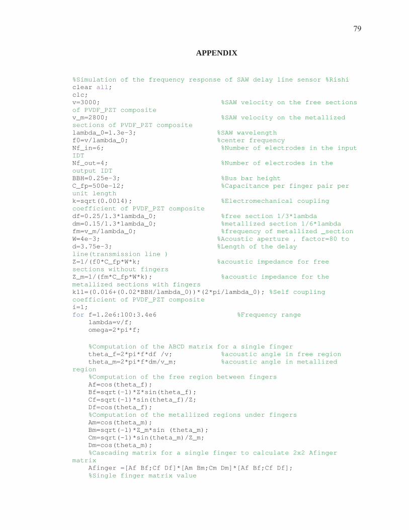
79
APPENDIX
%Simulation of the frequency response of SAW delay line sensor %Rishi clear all; clc; v=3000; %SAW velocity on the free sections of PVDF_PZT composite v_m=2800; %SAW velocity on the metallized sections of PVDF_PZT composite lambda_0=1.3e-3; %SAW wavelength f0=v/lambda_0; %center frequency Nf_in=6; %Number of electrodes in the input IDT Nf_out=4; %Number of electrodes in the output IDT BBH=0.25e-3; %Bus bar height C_fp=500e-12; %Capacitance per finger pair per unit length k=sqrt(0.0014); %Electromechanical coupling coefficient of PVDF_PZT composite df=0.25/1.3*lambda_0; %free section 1/3*lambda dm=0.15/1.3*lambda_0; %metallized section 1/6*lambda fm=v_m/lambda_0; %frequency of metallized _section W=4e-3; %Acoustic aperture , factor=80 to d=3.75e-3; %Length of the delay line(transmission line ) Z=1/(f0*C_fp*W*k; %acoustic impedance for free sections without fingers Z_m=1/(fm*C_fp*W*k); %acoustic impedance for the metallized sections with fingers k11=(0.016+(0.02*BBH/lambda_0))*(2*pi/lambda_0); %Self coupling coefficient of PVDF_PZT composite i=1; for f=1.2e6:100:3.4e6 %Frequency range lambda=v/f; omega=2*pi*f; %Computation of the ABCD matrix for a single finger theta_f=2*pi*f*df /v; %acoustic angle in free region theta_m=2*pi*f*dm/v_m; %acoustic angle in metallized region %Computation of the free region between fingers Af=cos(theta_f); Bf=sqrt(-1)*Z*sin(theta_f); Cf=sqrt(-1)*sin(theta_f)/Z; Df=cos(theta_f); %Computation of the metallized regions under fingers Am=cos(theta_m); Bm=sqrt(-1)*Z_m*sin (theta_m); Cm=sqrt(-1)*sin(theta_m)/Z_m; Dm=cos(theta_m); %Cascading matrix for a single finger to calculate 2x2 Afinger matrix Afinger =[Af Bf;Cf Df]*[Am Bm;Cm Dm]*[Af Bf;Cf Df]; %Single finger matrix value

80
A_se=Afinger (1,1); B_se=Afinger (1,2); C_se=Afinger (2,1); D_se=Afinger (2,2); theta_d=2*pi*f*d/v; %delay path theta_e=acos(A_se); Ze=B_se/(sqrt(-1)*sin(theta_e)); %2x2 transmission matrix for a single finger of the IDT t11 =0.5*(2*A_se+(B_se/Z)+Z*C_se); t12 =0.5*(Z*C_se-(B_se/Z)); t13 =((sqrt (-1)*tan(theta_e/2)*(Z^0.5))/(2*Ze))*(-A_se-1-(B_se/Z)); t21=-t12; t22=conj(t11); t23=sqrt(-1)*tan(theta_e/2)*(Z^0.5)*(1+A_se-(B_se/Z))/(2*Ze); t31=2*t13; t32=-2*t23; t33=sqrt(-1)*omega*C_fp*W*0.5+ sqrt(-1)*2*(tan(theta_e/2)/Ze)-sqrt(-1)*(sin(theta_e )*(tan(theta_e/2)^2))/Ze; %computing the 2x2 IDT matrix t1 =[t11 t12;t21 t22]^Nf_in; %2x2 scattering matrix T_p^N_input (N finger pairs ) t3 =[t11 t12;t21 t22]^Nf_out; %2x2 scattering matrix T_p^N_output(N finger pairs ) t111=t1(1,1); t121=t1(1,2); t211=t1(2,1); t221=t1(2,2); t123=t3(1,2); t113=t3(1,1); t213=t3(2,1); t223=t3(2,2); Bp=[t13;t23]+[t11 t12;t21 t22]*[-t13;-t23]; Cp=[t31 t32]*[t11 t12;t21 t22]+[-t31 -t32]; t33p=2*t33 +[t31 t32]*[-t13;-t23]; Tp=[t11 t12;t21 t22]^2; B_Nin=[0;0]; C_Nin=[0 0]; B_Nout=[0;0]; C_Nout=[0 0]; t333=(Nf_out/2)*t33p ; %Initial value for t333 t331=(Nf_in/2)*t33p ; %Initial value for t331 %computing t13, t23, t31, t32, t33 values for the whole IDT %Input IDT for i1=1:(Nf_in/2) B_Nin=B_Nin+(Tp^(i1-1))*Bp; C_Nin=C_Nin+Cp*Tp^(i1-1); t331=t331+((Nf_in/2)-i1)*Cp*Tp^(i1-1)*Bp; end %Reflector&output IDT for i2=1:(Nf_out/2) B_Nout=B_Nout+(Tp^(i2-1))*Bp; C_Nout=C_Nout+Cp*Tp^(i2-1);

81
t333=t333+((Nf_out/2)-i2)*Cp*Tp^(i2-1)*Bp; end t131=B_Nin(1,1); t133=B_Nout(1,1); t231=B_Nin(2,1); t233=B_Nout(2,1); t311=C_Nin(1,1); t313=C_Nout(1,1); t321=C_Nin(1,2); t323=C_Nout(1,2); %ABCD matrix of delay path Ad=cos(theta_d); Bd=sqrt(-1)*Z*sin (theta_d); Cd=sqrt(-1)*sin(theta_d)/Z; Dd=cos(theta_d); %Computation of transmission matrix for delay path d11=0.5*(2*Ad+(Bd/Z)+Z*Cd); d12=0.5*(Z*Cd-(Bd/Z)); d21=-d12; d22=0.5*(2*Ad-(Bd/Z)-Z*Cd); d2=[d11 d12;d21 d22]; %Used substitutions for convenience M=t1*d2*t3; K=t1*d2*[t133;t233]; P=[t311 t321]*d2*t3; L=[t311 t321]*d2*[t133;t233]; %computing Y parameter ( Admittance ) for the SAW delay line y11(i)=t331-(P(1,1)*t131/M(1,1)); y12(i)=L(1,1)-(P(1,1)*K(1,1)/M(1,1)); y21(i)=-t313*t131/M(1,1); y22(i)=t333-(t313*K(1,1)/M(1,1)); %Computing frequency response S21 using the Y parameter s11(i)=((1-y11(i))*(1+y22(i))+y12(i)*y21(i))/((1+y11(i))*(1+y22(i))-y12(i)*y21(i)); s12(i)=-2*y12(i)/((1+y11(i))*(1+y22(i))-y12(i)*y21(i)); s21(i)=-2*y21(i)/((1+y11(i))*(1+y22(i))-y12(i)*y21(i)); s22(i)=((1+y11(i))*(1-y22(i))+y12(i)*y21(i))/((1+y11(i))*(1+y22(i))-y12(i)*y21(i)); %Computing Z parameter as impedance z11=((1+s11(i))*(1-s22(i))+s12(i)*s21(i))/((1-s11(i))*(1-s22(i))-s12(i)*s21(i)); z12=2*s12(i)/((1-s11(i))*(1-s22(i))-s12(i)*s21(i)); z21=2*s21(i)/((1-s11(i))*(1-s22(i))-s12(i)*s21(i)); z22=((1-s11(i))*(1+ s22(i))+s12(i)*s21(i))/((1-s11(i))*(1-s22(i))-s12(i)*s21(i)); %modified S°parameter including source and load impedance s21_n(i)=-50*z12/(z12^2-(z11+50)*(z22+50)); i=i+1; end figure(1); f=1.2e6:100:3.4e6; y1=20*log10(abs(s21_n));
82
y2=angle(s21_n)*180/pi; yyaxis left plot(f,y1,'b') % title('Frequency Response','FontSize',18); xlabel('Frequency/Hz','fontweight','bold','FontSize',16); ylabel('S21/dB','fontweight','bold','FontSize',16) set(findall(gca,'type','line'),'linewidth',1) % grid on yyaxis right plot(f,y2,'-.r') ylabel('Phase angle/degrees','FontSize',14) ylim([-200 200] )
Related Documents