Flexible Electronics: Materials and Applications

Welcome message from author
This document is posted to help you gain knowledge. Please leave a comment to let me know what you think about it! Share it to your friends and learn new things together.
Transcript

Flexible Electronics: Materials and Applications
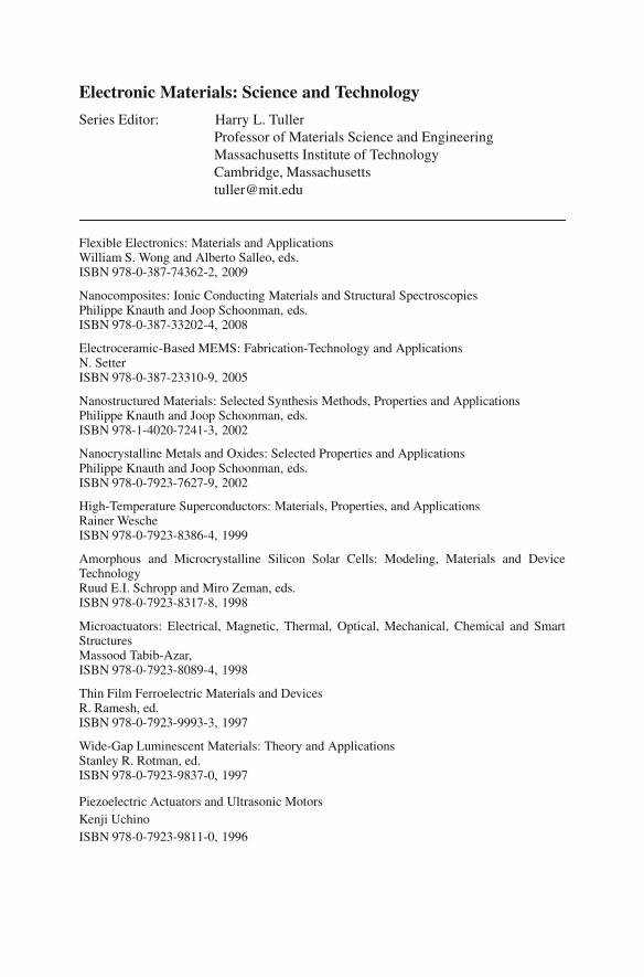
Electronic Materials: Science and Technology
Series Editor: Harry L. TullerProfessor of Materials Science and EngineeringMassachusetts Institute of TechnologyCambridge, [email protected]
Flexible Electronics: Materials and ApplicationsWilliam S. Wong and Alberto Salleo, eds.ISBN 978-0-387-74362-2, 2009
Nanocomposites: Ionic Conducting Materials and Structural SpectroscopiesPhilippe Knauth and Joop Schoonman, eds.ISBN 978-0-387-33202-4, 2008
Electroceramic-Based MEMS: Fabrication-Technology and ApplicationsN. SetterISBN 978-0-387-23310-9, 2005
Nanostructured Materials: Selected Synthesis Methods, Properties and ApplicationsPhilippe Knauth and Joop Schoonman, eds.ISBN 978-1-4020-7241-3, 2002
Nanocrystalline Metals and Oxides: Selected Properties and ApplicationsPhilippe Knauth and Joop Schoonman, eds.ISBN 978-0-7923-7627-9, 2002
High-Temperature Superconductors: Materials, Properties, and ApplicationsRainer WescheISBN 978-0-7923-8386-4, 1999
Amorphous and Microcrystalline Silicon Solar Cells: Modeling, Materials and DeviceTechnologyRuud E.I. Schropp and Miro Zeman, eds.ISBN 978-0-7923-8317-8, 1998
Microactuators: Electrical, Magnetic, Thermal, Optical, Mechanical, Chemical and SmartStructuresMassood Tabib-Azar,ISBN 978-0-7923-8089-4, 1998
Thin Film Ferroelectric Materials and DevicesR. Ramesh, ed.ISBN 978-0-7923-9993-3, 1997
Wide-Gap Luminescent Materials: Theory and ApplicationsStanley R. Rotman, ed.ISBN 978-0-7923-9837-0, 1997
Piezoelectric Actuators and Ultrasonic MotorsKenji UchinoISBN 978-0-7923-9811-0, 1996
William S. Wong · Alberto SalleoEditors
Flexible Electronics:Materials and Applications
123
EditorsWilliam S. Wong Alberto SalleoPalo Alto Research Center Stanford University3333 Coyote Hill Road Department of Materials Science &Palo Alto, CA 94304 [email protected] Stanford, CA 94305-2205
ISBN 978-0-387-74362-2 e-ISBN 978-0-387-74363-9DOI 10.1007/978-0-387-74363-9
Library of Congress Control Number: PCN applied for
c© Springer Science+Business Media, LLC 2009All rights reserved. This work may not be translated or copied in whole or in part without the writtenpermission of the publisher (Springer Science+Business Media, LLC, 233 Spring Street, New York,NY 10013, USA), except for brief excerpts in connection with reviews or scholarly analysis. Use inconnection with any form of information storage and retrieval, electronic adaptation, computer software,or by similar or dissimilar methodology now known or hereafter developed is forbidden.The use in this publication of trade names, trademarks, service marks and similar terms, even if they arenot identified as such, is not to be taken as an expression of opinion as to whether or not they are subjectto proprietary rights.
Printed on acid-free paper.
springer.com
Preface
The advancement of flexible electronics has spanned the past forty years rangingfrom the development of flexible solar cell arrays made from very thin single-crystalsilicon to flexible organic light-emitting diode displays on plastic substrates. Therecent rapid development of this field has been spurred by the continuing evolu-tion of large-area electronics with applications in flat-panel displays, medical imagesensors, and electronic paper. Many factors contribute to the allure of flexible elec-tronics; they are typically more rugged, lighter, portable, and less expensive to man-ufacture compared to their rigid substrate counterparts. Demonstrations of flexibleelectronics promise the availability of robust, lightweight, and low-cost electronicsin the near future and this book is arranged to give the reader a survey of the mate-rials that are used to fabricate these devices on flexible media. Subsequent chaptersare organized to provide an overview of the different applications that can be createdwith a wide variety of materials systems. The range of polymeric to inorganic mate-rials encompasses a wide array of performance benchmarks. It is these benchmarksof device characteristics (both electrical and mechanical) and performance, and theprocesses involved to make the device that will ultimately determine the suitableapplications. It is not the intent of this book to give an exhaustive review of thetechnology but rather to provide a starting reference for a wide array of materials andapplications; the chapters presented are also intended to augment existing literaturein the field of flexible electronics.
The materials, processes, and applications for flexible electronics cover manydifferent areas and we begin the book with a general overview of the field and theevolution of the technology. The mechanical stability of thin films on foil substratesis an area of active study and the understanding of these characteristics needs tobe developed in order to fabricate multilayer structures with minimum offset inlayer-to-layer alignment (Chapter 2). A review of processing conventional inorganicthin-film materials at low temperatures is given in Chapter 3. The chapter pro-vides an overview of the materials and device characteristics for low-temperaturesilicon-based thin-film dielectrics and semiconductors. Chapter 4 describes howthe understanding of the mechanical stability of thin films on foil substrates andlow-temperature processing of conventional inorganic materials, such as amor-phous silicon (a-Si:H), can be used for integration onto low melting point plasticplatforms. These semiconductor materials have already been optimized for flat panel
v
vi Preface
display applications and the transition to flexible electronics enables integration withorganic light emitters to create applications in flexible emissive displays. The transi-tion metal oxides (TMO) have the potential for creating high-performance thin-filmtransistor (TFT) devices beyond the performance offered by a-Si:H or poly-siliconTFTs. Chapter 5 provides an overview of the TMOs and demonstrates a novelnano-imprint lithography approach that can be used to fabricate flexible backplanesin a roll-to-roll process. Applications towards large-area flexible image sensors areanother active area of research. Chapter 6 reviews ink-jet patterning techniques forfabricating a-Si:H based x-ray image sensors for medical imaging applications andink-jet patterning for all-additive processing of backplane arrays.
The development of organic and polymeric materials for flexible electronicsis progressing at a rapid rate with organic semiconductor materials producingdevices that rival the performance of conventional a-Si:H TFTs. Small moleculesemiconductors such as pentacene have been used to make organic TFTs andhave shown performance exceeding silicon-based TFTs. Chapter 7 discusses twoapplications, image sensing and micro-electro-mechanical systems (MEMS), whereorganic materials compete well with silicon-based devices in flexible applications.In Chapter 8, the impact of materials and device physics on device and circuit designis discussed in the context of specific applications (displays and radio-frequencyidentification tags) based on pentacene active layers.
The transition to solution processable materials provides a potentially limitlesschoice of flexible electronics applications and processes (Chapter 9). These mate-rials offer low-cost processing capabilities from simple spin casting to jet printingfor device fabrication. The major limitation of the materials system is its relativelylow performance for TFT applications. As these materials continue to improve,the appeal of low fabrication cost is also a catalyst for using polymeric semicon-ductors in photovoltaic applications. A review of excitonic solar cell propertiesand characteristics is presented in Chapter 11 along with an assessment of theapplications for low-cost large-area power sources based on polymeric “green”technologies (Chapter 12).
Nano-scale materials are also suitable for flexible electronic applications. Thesize scale and electrical characteristics of randomly oriented carbon nanotubes(CNTs) mats provide a material that is highly compliant, conductive, and trans-parent in the visible spectrum. These three attributes give CNTs an advantage foruse as transparent conductors for applications in solar cells and flexible displays(Chapter 10). Finally, none of these materials will have much functionality if asuitable substrate is unavailable. Chapter 13 reviews the characteristics required forflexible platforms for use in electronic applications and the processes and barriermaterials that are required in order to make the plastic films optimal for deviceapplications.
Lastly, we would like to thank all the contributing authors for their time and effortin preparing the manuscripts presented in this book. It is the work of these peopleand all the scientist, researchers, and engineers in the field that make the technologyof flexible electronics exciting and challenging. We are also grateful to the Palo Alto

Preface vii
Research Center and Stanford University for providing support of the project andthe many colleagues whom we worked with in making this book a reality.
Palo Alto, CA, USA William S. WongJanuary 2009 Alberto Salleo
Contents
1 Overview of Flexible Electronics Technology . . . . . . . . . . . . . . . . . . . . . . 1I-Chun Cheng and Sigurd Wagner1.1 History of Flexible Electronics . . . . . . . . . . . . . . . . . . . . . . . . . . . . . . . 11.2 Materials for Flexible Electronics . . . . . . . . . . . . . . . . . . . . . . . . . . . . 3
1.2.1 Degrees of Flexibility . . . . . . . . . . . . . . . . . . . . . . . . . . . . . . . 31.2.2 Substrates . . . . . . . . . . . . . . . . . . . . . . . . . . . . . . . . . . . . . . . . . 51.2.3 Backplane Electronics . . . . . . . . . . . . . . . . . . . . . . . . . . . . . . 81.2.4 Frontplane Technologies . . . . . . . . . . . . . . . . . . . . . . . . . . . . 121.2.5 Encapsulation . . . . . . . . . . . . . . . . . . . . . . . . . . . . . . . . . . . . . 16
1.3 Fabrication Technology for Flexible Electronics . . . . . . . . . . . . . . . . 181.3.1 Fabrication on Sheets by Batch Processing . . . . . . . . . . . . . 181.3.2 Fabrication on Web by Roll-to-Roll Processing . . . . . . . . . 191.3.3 Additive Printing . . . . . . . . . . . . . . . . . . . . . . . . . . . . . . . . . . . 20
1.4 Outlook . . . . . . . . . . . . . . . . . . . . . . . . . . . . . . . . . . . . . . . . . . . . . . . . . . 20References . . . . . . . . . . . . . . . . . . . . . . . . . . . . . . . . . . . . . . . . . . . . . . . . . . . . . 20
2 Mechanical Theory of the Film-on-Substrate-Foil Structure:Curvature and Overlay Alignment in Amorphous SiliconThin-Film Devices Fabricated on Free-Standing Foil Substrates . . . . . 29Helena Gleskova, I-Chun Cheng, Sigurd Wagner, and Zhigang Suo2.1 Introduction . . . . . . . . . . . . . . . . . . . . . . . . . . . . . . . . . . . . . . . . . . . . . . 292.2 Theory . . . . . . . . . . . . . . . . . . . . . . . . . . . . . . . . . . . . . . . . . . . . . . . . . . . 32
2.2.1 The Built-in Strain εbi . . . . . . . . . . . . . . . . . . . . . . . . . . . . . . 352.3 Applications . . . . . . . . . . . . . . . . . . . . . . . . . . . . . . . . . . . . . . . . . . . . . . 36
2.3.1 Strain in the Substrate, εs(Td ), and the Film, ε f (Td ),at the Deposition Temperature Td . . . . . . . . . . . . . . . . . . . . 36
2.3.2 Strain in the Substrate, εs(Tr ), and the Film, ε f (Tr ),at Room Temperature Tr . . . . . . . . . . . . . . . . . . . . . . . . . . . . 38
2.3.3 Radius of Curvature R of the Workpiece . . . . . . . . . . . . . . . 422.3.4 Strain of the Substrate and the Curvature of the
Workpiece for a Three-Layer Structure . . . . . . . . . . . . . . . . 462.3.5 Experimental Results for a-Si:H TFTs Fabricated on
Kapton . . . . . . . . . . . . . . . . . . . . . . . . . . . . . . . . . . . . . . . . . . 47
ix
x Contents
2.4 Conclusions . . . . . . . . . . . . . . . . . . . . . . . . . . . . . . . . . . . . . . . . . . . . . . 50References . . . . . . . . . . . . . . . . . . . . . . . . . . . . . . . . . . . . . . . . . . . . . . . . . . . . . 50
3 Low-temperature Amorphous and Nanocrystalline SiliconMaterials and Thin-film Transistors . . . . . . . . . . . . . . . . . . . . . . . . . . . . . . 53Andrei Sazonov, Denis Striakhilev, and Arokia Nathan3.1 Introduction . . . . . . . . . . . . . . . . . . . . . . . . . . . . . . . . . . . . . . . . . . . . . . 533.2 Low-temperature Amorphous and Nanocrystalline
Silicon Materials . . . . . . . . . . . . . . . . . . . . . . . . . . . . . . . . . . . . . . . . . . 553.2.1 Fundamental Issues for Low-temperature Processing . . . . . 553.2.2 Low-temperature Amorphous Silicon . . . . . . . . . . . . . . . . . . 563.2.3 Low-temperature Nanocrystalline Silicon . . . . . . . . . . . . . . 56
3.3 Low-temperature Dielectrics . . . . . . . . . . . . . . . . . . . . . . . . . . . . . . . . 573.3.1 Characteristics of Low-temperature Dielectric
Thin-film Deposition . . . . . . . . . . . . . . . . . . . . . . . . . . . . . . . 573.3.2 Low-temperature Silicon Nitride Characteristics . . . . . . . . 573.3.3 Low-temperature Silicon Oxide Characteristics . . . . . . . . . 58
3.4 Low-temperature Thin-film Transistor Devices . . . . . . . . . . . . . . . . . 593.4.1 Device Structures and Materials Processing . . . . . . . . . . . . 603.4.2 Low-temperature a-Si:H Thin-Film Transistor
Device Performance . . . . . . . . . . . . . . . . . . . . . . . . . . . . . . . 613.4.3 Contacts to a-Si:H Thin-film Transistors . . . . . . . . . . . . . . . 623.4.4 Low-temperature Doped nc-Si Contacts . . . . . . . . . . . . . . . 643.4.5 Low-temperature nc-Si TFTs . . . . . . . . . . . . . . . . . . . . . . . . 66
3.5 Device Stability . . . . . . . . . . . . . . . . . . . . . . . . . . . . . . . . . . . . . . . . . . . 673.6 Conclusions and Future Prospective . . . . . . . . . . . . . . . . . . . . . . . . . . 70References . . . . . . . . . . . . . . . . . . . . . . . . . . . . . . . . . . . . . . . . . . . . . . . . . . . . . 70
4 Amorphous Silicon: Flexible Backplane and Display Application . . . . 75Kalluri R. Sarma4.1 Introduction . . . . . . . . . . . . . . . . . . . . . . . . . . . . . . . . . . . . . . . . . . . . . . 754.2 Enabling Technologies for Flexible Backplanes and Displays . . . . . 76
4.2.1 Flexible Substrate Technologies . . . . . . . . . . . . . . . . . . . . . . 764.2.2 TFT Technologies for Flexible Backplanes . . . . . . . . . . . . . 824.2.3 Display Media for Flexible Displays (LCD,
Reflective-EP, OLED) . . . . . . . . . . . . . . . . . . . . . . . . . . . . . . 894.2.4 Barrier Layers . . . . . . . . . . . . . . . . . . . . . . . . . . . . . . . . . . . . . 90
4.3 Flexible Active Matrix Backplane Requirementsfor OLED Displays . . . . . . . . . . . . . . . . . . . . . . . . . . . . . . . . . . . . . . . . 914.3.1 Active Matrix Addressing . . . . . . . . . . . . . . . . . . . . . . . . . . . 92
4.4 Flexible AMOLED Displays Using a-Si TFT Backplanes . . . . . . . . 954.4.1 Backplane Fabrication Using PEN Plastic Substrates . . . . . 954.4.2 Flexible OLED Display Fabrication . . . . . . . . . . . . . . . . . . . 984.4.3 Flexible AMOLED Display Fabrication
with Thin-film Encapsulation . . . . . . . . . . . . . . . . . . . . . . . . 100
Contents xi
4.5 Flexible Electrophoretic Displays Fabricatedusing a-Si TFT Backplanes . . . . . . . . . . . . . . . . . . . . . . . . . . . . . . . . . 102
4.6 Outlook for Low-Temperature a-Si TFT for FlexibleElectronics Manufacturing . . . . . . . . . . . . . . . . . . . . . . . . . . . . . . . . . . 102
References . . . . . . . . . . . . . . . . . . . . . . . . . . . . . . . . . . . . . . . . . . . . . . . . . . . . . 105
5 Flexible Transition Metal Oxide Electronics and ImprintLithography . . . . . . . . . . . . . . . . . . . . . . . . . . . . . . . . . . . . . . . . . . . . . . . . . . . 107Warren B. Jackson5.1 Introduction . . . . . . . . . . . . . . . . . . . . . . . . . . . . . . . . . . . . . . . . . . . . . . 1075.2 Previous Work . . . . . . . . . . . . . . . . . . . . . . . . . . . . . . . . . . . . . . . . . . . . 1085.3 Properties of Transistor Materials . . . . . . . . . . . . . . . . . . . . . . . . . . . . 113
5.3.1 Semiconductors . . . . . . . . . . . . . . . . . . . . . . . . . . . . . . . . . . . . 1135.3.2 Dielectrics . . . . . . . . . . . . . . . . . . . . . . . . . . . . . . . . . . . . . . . . 1155.3.3 Contact Materials . . . . . . . . . . . . . . . . . . . . . . . . . . . . . . . . . . 116
5.4 Device Structures . . . . . . . . . . . . . . . . . . . . . . . . . . . . . . . . . . . . . . . . . . 1175.5 Fabrication on Flexible Substrates . . . . . . . . . . . . . . . . . . . . . . . . . . . . 119
5.5.1 Imprint Lithography . . . . . . . . . . . . . . . . . . . . . . . . . . . . . . . . 1205.5.2 Self-Aligned Imprint Lithography . . . . . . . . . . . . . . . . . . . . 1225.5.3 SAIL Transistor Results . . . . . . . . . . . . . . . . . . . . . . . . . . . . . 1265.5.4 Summary of Imprint Lithography . . . . . . . . . . . . . . . . . . . . . 127
5.6 Flexible TMO Device Results . . . . . . . . . . . . . . . . . . . . . . . . . . . . . . . 1285.7 Future Problems and Areas of Research . . . . . . . . . . . . . . . . . . . . . . . 133
5.7.1 Carrier Density Control . . . . . . . . . . . . . . . . . . . . . . . . . . . . . 1345.7.2 Low-Temperature Dielectrics . . . . . . . . . . . . . . . . . . . . . . . . 1355.7.3 Etching of TMO Materials . . . . . . . . . . . . . . . . . . . . . . . . . . . 1355.7.4 P-type TMO . . . . . . . . . . . . . . . . . . . . . . . . . . . . . . . . . . . . . . 1365.7.5 Stability . . . . . . . . . . . . . . . . . . . . . . . . . . . . . . . . . . . . . . . . . . 1365.7.6 Flexure and Adhesion of TMO . . . . . . . . . . . . . . . . . . . . . . . 1375.7.7 Flexible Fabrication Method Yields . . . . . . . . . . . . . . . . . . . 137
5.8 Summary . . . . . . . . . . . . . . . . . . . . . . . . . . . . . . . . . . . . . . . . . . . . . . . . 138References . . . . . . . . . . . . . . . . . . . . . . . . . . . . . . . . . . . . . . . . . . . . . . . . . . . . . 139
6 Materials and Novel Patterning Methods for FlexibleElectronics . . . . . . . . . . . . . . . . . . . . . . . . . . . . . . . . . . . . . . . . . . . . . . . . . . . . 143William S. Wong, Michael L. Chabinyc, Tse-Nga Ng,and Alberto Salleo6.1 Introduction . . . . . . . . . . . . . . . . . . . . . . . . . . . . . . . . . . . . . . . . . . . . . . 1436.2 Materials Considerations for Flexible Electronics . . . . . . . . . . . . . . . 145
6.2.1 Overview . . . . . . . . . . . . . . . . . . . . . . . . . . . . . . . . . . . . . . . . . 1456.2.2 Inorganic Semiconductors and Dielectrics . . . . . . . . . . . . . . 1456.2.3 Organic Semiconductors and Dielectrics . . . . . . . . . . . . . . . 1466.2.4 Conductors . . . . . . . . . . . . . . . . . . . . . . . . . . . . . . . . . . . . . . . 149
6.3 Print-Processing Options for Device Fabrication . . . . . . . . . . . . . . . . 1506.3.1 Overview . . . . . . . . . . . . . . . . . . . . . . . . . . . . . . . . . . . . . . . . . 150
xii Contents
6.3.2 Control of Feature Sizes of Jet-Printed Liquids . . . . . . . . . . 1516.3.3 Jet-Printing for Etch-Mask Patterning . . . . . . . . . . . . . . . . . 1536.3.4 Methods for Minimizing Feature Size . . . . . . . . . . . . . . . . . 1546.3.5 Printing Active Materials . . . . . . . . . . . . . . . . . . . . . . . . . . . . 156
6.4 Performance and Characterization of Electronic Devices . . . . . . . . . 1576.4.1 Overview . . . . . . . . . . . . . . . . . . . . . . . . . . . . . . . . . . . . . . . . . 1576.4.2 Bias Stress in Organic Thin-Film Transistors . . . . . . . . . . . 1586.4.3 Nonideal Scaling of Short-Channel Organic TFTs . . . . . . . 1636.4.4 Low-Temperature a-Si:H TFT Device Stability . . . . . . . . . . 1656.4.5 Low-temperature a-Si:H p–i–n Devices . . . . . . . . . . . . . . . . 167
6.5 Printed Flexible Electronics . . . . . . . . . . . . . . . . . . . . . . . . . . . . . . . . . 1706.5.1 Overview . . . . . . . . . . . . . . . . . . . . . . . . . . . . . . . . . . . . . . . . . 1706.5.2 Digital Lithography for Flexible Image Sensor
Arrays . . . . . . . . . . . . . . . . . . . . . . . . . . . . . . . . . . . . . . . . . . . 1706.5.3 Printed Organic Backplanes . . . . . . . . . . . . . . . . . . . . . . . . . . 172
6.6 Conclusions and Future Prospects . . . . . . . . . . . . . . . . . . . . . . . . . . . . 176References . . . . . . . . . . . . . . . . . . . . . . . . . . . . . . . . . . . . . . . . . . . . . . . . . . . . . 176
7 Sheet-Type Sensors and Actuators . . . . . . . . . . . . . . . . . . . . . . . . . . . . . . . 183Takao Someya7.1 Introduction . . . . . . . . . . . . . . . . . . . . . . . . . . . . . . . . . . . . . . . . . . . . . . 1837.2 Sheet-type Image Scanners . . . . . . . . . . . . . . . . . . . . . . . . . . . . . . . . . . 184
7.2.1 Imaging Methods . . . . . . . . . . . . . . . . . . . . . . . . . . . . . . . . . . 1857.2.2 Device Structure and Manufacturing Process . . . . . . . . . . . 1867.2.3 Electronic Performance of Organic Photodiodes . . . . . . . . . 1907.2.4 Organic Transistors . . . . . . . . . . . . . . . . . . . . . . . . . . . . . . . . . 1917.2.5 Photosensor Cells . . . . . . . . . . . . . . . . . . . . . . . . . . . . . . . . . . 1937.2.6 Issues Related to Device Processes: Pixel Stability
and Resolution . . . . . . . . . . . . . . . . . . . . . . . . . . . . . . . . . . . . 1957.2.7 A Hierarchal Approach for Slow Organic Circuits . . . . . . . 1967.2.8 The Double-Wordline and Double-Bitline Structure . . . . . . 1967.2.9 A New Dynamic Second-Wordline Decoder . . . . . . . . . . . . 1997.2.10 Higher Speed Operation with Lower Power
Consumption . . . . . . . . . . . . . . . . . . . . . . . . . . . . . . . . . . . . . 1997.2.11 New Applications and Future Prospects . . . . . . . . . . . . . . . . 200
7.3 Sheet-Type Braille Displays . . . . . . . . . . . . . . . . . . . . . . . . . . . . . . . . . 2017.3.1 Manufacturing Process . . . . . . . . . . . . . . . . . . . . . . . . . . . . . . 2017.3.2 Electronic Performance of Braille Cells . . . . . . . . . . . . . . . . 2047.3.3 Organic Transistor-based SRAM . . . . . . . . . . . . . . . . . . . . . 2107.3.4 Reading Tests . . . . . . . . . . . . . . . . . . . . . . . . . . . . . . . . . . . . . 2117.3.5 Future Prospects . . . . . . . . . . . . . . . . . . . . . . . . . . . . . . . . . . . 212
7.4 Summary . . . . . . . . . . . . . . . . . . . . . . . . . . . . . . . . . . . . . . . . . . . . . . . . 212References . . . . . . . . . . . . . . . . . . . . . . . . . . . . . . . . . . . . . . . . . . . . . . . . . . . . . 213
Contents xiii
8 Organic and Polymeric TFTs for Flexible Displays and Circuits . . . . . 215Michael G. Kane8.1 Introduction . . . . . . . . . . . . . . . . . . . . . . . . . . . . . . . . . . . . . . . . . . . . . . 2158.2 Important Organic TFT Parameters for Electronic Systems . . . . . . . 216
8.2.1 Field-Effect Mobility . . . . . . . . . . . . . . . . . . . . . . . . . . . . . . . 2168.2.2 Threshold Voltage . . . . . . . . . . . . . . . . . . . . . . . . . . . . . . . . . . 2198.2.3 Subthreshold Swing . . . . . . . . . . . . . . . . . . . . . . . . . . . . . . . . 2208.2.4 Leakage Currents . . . . . . . . . . . . . . . . . . . . . . . . . . . . . . . . . . 2228.2.5 Contact Resistance . . . . . . . . . . . . . . . . . . . . . . . . . . . . . . . . . 2228.2.6 Capacitances and Frequency Response . . . . . . . . . . . . . . . . 2238.2.7 TFT Nonuniformity . . . . . . . . . . . . . . . . . . . . . . . . . . . . . . . . 2258.2.8 Bias-Stress Instability and Hysteresis . . . . . . . . . . . . . . . . . . 225
8.3 Active Matrix Displays . . . . . . . . . . . . . . . . . . . . . . . . . . . . . . . . . . . . . 2278.3.1 Introduction . . . . . . . . . . . . . . . . . . . . . . . . . . . . . . . . . . . . . . . 2278.3.2 Liquid Crystal and Electrophoretic Displays . . . . . . . . . . . . 228
8.4 Active Matrix OLED Displays . . . . . . . . . . . . . . . . . . . . . . . . . . . . . . . 2368.4.1 Introduction . . . . . . . . . . . . . . . . . . . . . . . . . . . . . . . . . . . . . . . 236
8.5 Using Organic TFTs for Electronic Circuits . . . . . . . . . . . . . . . . . . . . 2428.5.1 Thin-Film Transistor Circuits . . . . . . . . . . . . . . . . . . . . . . . . 2428.5.2 Frequency Limitations of OTFTs . . . . . . . . . . . . . . . . . . . . . 2468.5.3 Integrated Display Drivers . . . . . . . . . . . . . . . . . . . . . . . . . . . 2478.5.4 Radio Frequency Identification Tags . . . . . . . . . . . . . . . . . . 248
8.6 Conclusion . . . . . . . . . . . . . . . . . . . . . . . . . . . . . . . . . . . . . . . . . . . . . . . 256References . . . . . . . . . . . . . . . . . . . . . . . . . . . . . . . . . . . . . . . . . . . . . . . . . . . . . 256
9 Semiconducting Polythiophenes for Field-Effect TransistorDevices in Flexible Electronics: Synthesis and Structure PropertyRelationships . . . . . . . . . . . . . . . . . . . . . . . . . . . . . . . . . . . . . . . . . . . . . . . . . . 261Martin Heeney and Iain McCulloch9.1 Introduction . . . . . . . . . . . . . . . . . . . . . . . . . . . . . . . . . . . . . . . . . . . . . . 2619.2 Polymerization of Thiophene Monomers . . . . . . . . . . . . . . . . . . . . . . 264
9.2.1 General Considerations . . . . . . . . . . . . . . . . . . . . . . . . . . . . . 2649.2.2 Synthetic Routes for the Preparation of Thiophene
Polymers . . . . . . . . . . . . . . . . . . . . . . . . . . . . . . . . . . . . . . . . . 2649.3 Poly(3-Alkylthiophenes) . . . . . . . . . . . . . . . . . . . . . . . . . . . . . . . . . . . . 273
9.3.1 Electrical Properties . . . . . . . . . . . . . . . . . . . . . . . . . . . . . . . . 2759.3.2 Thin-film Device Processing and Morphology . . . . . . . . . . 2769.3.3 Doping and Oxidative Stability . . . . . . . . . . . . . . . . . . . . . . . 277
9.4 Polythiophene Structural Analogues . . . . . . . . . . . . . . . . . . . . . . . . . . 2799.5 Thienothiophene Polymers . . . . . . . . . . . . . . . . . . . . . . . . . . . . . . . . . . 286
9.5.1 Poly(Thieno(2,3-b)Thiophenes) . . . . . . . . . . . . . . . . . . . . . . 2869.5.2 Poly(Thieno(3,2-b)Thiophenes) . . . . . . . . . . . . . . . . . . . . . . 288
9.6 Summary . . . . . . . . . . . . . . . . . . . . . . . . . . . . . . . . . . . . . . . . . . . . . . . . 292References . . . . . . . . . . . . . . . . . . . . . . . . . . . . . . . . . . . . . . . . . . . . . . . . . . . . . 293
xiv Contents
10 Solution Cast Films of Carbon Nanotubes for TransparentConductors and Thin Film Transistors . . . . . . . . . . . . . . . . . . . . . . . . . . . 297David Hecht and George Gruner10.1 Introduction: Nanoscale Carbon for Electronics,
the Value Proposition . . . . . . . . . . . . . . . . . . . . . . . . . . . . . . . . . . . . . . 29710.2 Carbon NT Film Properties . . . . . . . . . . . . . . . . . . . . . . . . . . . . . . . . . 298
10.2.1 Carbon Nanotubes: The Building Blocks . . . . . . . . . . . . . . . 29810.2.2 Carbon Nanotube Network as an Electronic Material . . . . . 29810.2.3 Electrical and Optical Properties of NT Films . . . . . . . . . . . 30010.2.4 Doping and Chemical Functionalization . . . . . . . . . . . . . . . 304
10.3 Fabrication Technologies . . . . . . . . . . . . . . . . . . . . . . . . . . . . . . . . . . . 30510.3.1 Solubilization . . . . . . . . . . . . . . . . . . . . . . . . . . . . . . . . . . . . . 30610.3.2 Deposition . . . . . . . . . . . . . . . . . . . . . . . . . . . . . . . . . . . . . . . . 306
10.4 Carbon NT Films as Conducting and OpticallyTransparent Material . . . . . . . . . . . . . . . . . . . . . . . . . . . . . . . . . . . . . . . 30910.4.1 Network Properties: Sheet Conductance and Optical
Transparency . . . . . . . . . . . . . . . . . . . . . . . . . . . . . . . . . . . . . 30910.4.2 Applications: ITO Replacement . . . . . . . . . . . . . . . . . . . . . . 31210.4.3 Challenges and the Path Forward . . . . . . . . . . . . . . . . . . . . . 312
10.5 TFTs with Carbon Nanotube Conducting Channels . . . . . . . . . . . . . 31310.5.1 Device Characteristics . . . . . . . . . . . . . . . . . . . . . . . . . . . . . . 31410.5.2 Device Parameters . . . . . . . . . . . . . . . . . . . . . . . . . . . . . . . . . 31610.5.3 Challenges and the Path Forward . . . . . . . . . . . . . . . . . . . . . 323
10.6 Conclusions . . . . . . . . . . . . . . . . . . . . . . . . . . . . . . . . . . . . . . . . . . . . . . 324References . . . . . . . . . . . . . . . . . . . . . . . . . . . . . . . . . . . . . . . . . . . . . . . . . . . . . 325
11 Physics and Materials Issues of Organic Photovoltaics . . . . . . . . . . . . . . 329Shawn R. Scully and Michael D. McGehee11.1 Introduction . . . . . . . . . . . . . . . . . . . . . . . . . . . . . . . . . . . . . . . . . . . . . . 32911.2 Basic Operation . . . . . . . . . . . . . . . . . . . . . . . . . . . . . . . . . . . . . . . . . . . 329
11.2.1 Photocurrent . . . . . . . . . . . . . . . . . . . . . . . . . . . . . . . . . . . . . . 33111.2.2 Dark Current . . . . . . . . . . . . . . . . . . . . . . . . . . . . . . . . . . . . . . 331
11.3 Organic and Hybrid Solar Cell Architectures . . . . . . . . . . . . . . . . . . . 33211.4 Materials . . . . . . . . . . . . . . . . . . . . . . . . . . . . . . . . . . . . . . . . . . . . . . . . . 33411.5 Light Absorption . . . . . . . . . . . . . . . . . . . . . . . . . . . . . . . . . . . . . . . . . . 33411.6 Exciton Harvesting . . . . . . . . . . . . . . . . . . . . . . . . . . . . . . . . . . . . . . . . 338
11.6.1 Effects of Disorder . . . . . . . . . . . . . . . . . . . . . . . . . . . . . . . . . 34011.6.2 Extrinsic Defects . . . . . . . . . . . . . . . . . . . . . . . . . . . . . . . . . . . 34411.6.3 Measuring Exciton Harvesting . . . . . . . . . . . . . . . . . . . . . . . 34411.6.4 Approaches to Overcome Small Diffusion Lengths . . . . . . 347
11.7 Exciton Dissociation . . . . . . . . . . . . . . . . . . . . . . . . . . . . . . . . . . . . . . . 34911.8 Dissociating Geminate Pairs . . . . . . . . . . . . . . . . . . . . . . . . . . . . . . . . . 35111.9 Heterojunction Energy Offsets . . . . . . . . . . . . . . . . . . . . . . . . . . . . . . . 35511.10 Charge Transport and Recombination . . . . . . . . . . . . . . . . . . . . . . . . . 357
11.10.1 Diffusion-Limited Recombination . . . . . . . . . . . . . . . . . . . . 359
Contents xv
11.10.2 Interface-Limited (Back Transfer Limited)Recombination . . . . . . . . . . . . . . . . . . . . . . . . . . . . . . . . . . . . 360
11.10.3 Measurements Relevant for Extracting Charge . . . . . . . . . . 36311.11 Nanostructures . . . . . . . . . . . . . . . . . . . . . . . . . . . . . . . . . . . . . . . . . . . . 36411.12 Efficiency Limits and Outlook . . . . . . . . . . . . . . . . . . . . . . . . . . . . . . . 367References . . . . . . . . . . . . . . . . . . . . . . . . . . . . . . . . . . . . . . . . . . . . . . . . . . . . . 368
12 Bulk Heterojunction Solar Cells for Large-Area PV Fabricationon Flexible Substrates . . . . . . . . . . . . . . . . . . . . . . . . . . . . . . . . . . . . . . . . . . 373C. Waldauf, G. Dennler, P. Schilinsky, and C. J. Brabec12.1 Introduction and Motivation . . . . . . . . . . . . . . . . . . . . . . . . . . . . . . . . . 373
12.1.1 Photovoltaics . . . . . . . . . . . . . . . . . . . . . . . . . . . . . . . . . . . . . . 37312.1.2 Technology Overview . . . . . . . . . . . . . . . . . . . . . . . . . . . . . . 37412.1.3 Motivation for Large-Area, Solution-Processable
Photovoltaics . . . . . . . . . . . . . . . . . . . . . . . . . . . . . . . . . . . . . 37512.2 The Concept of Bulk Heterojunction Solar Cells . . . . . . . . . . . . . . . . 377
12.2.1 Basics of Organic Solar Cell Materials . . . . . . . . . . . . . . . . . 37712.2.2 Fundamentals of Photovoltaics . . . . . . . . . . . . . . . . . . . . . . . 37812.2.3 Understanding and Optimization of BHJ Composites . . . . 385
12.3 Challenges for Large-Area Processing . . . . . . . . . . . . . . . . . . . . . . . . 40112.3.1 Production Scheme . . . . . . . . . . . . . . . . . . . . . . . . . . . . . . . . . 40112.3.2 Encapsulation of Flexible Solar Cells . . . . . . . . . . . . . . . . . . 404
12.4 Conclusions . . . . . . . . . . . . . . . . . . . . . . . . . . . . . . . . . . . . . . . . . . . . . . 408References . . . . . . . . . . . . . . . . . . . . . . . . . . . . . . . . . . . . . . . . . . . . . . . . . . . . . 409
13 Substrates and Thin-Film Barrier Technology for FlexibleElectronics . . . . . . . . . . . . . . . . . . . . . . . . . . . . . . . . . . . . . . . . . . . . . . . . . . . . 413Ahmet Gun Erlat, Min Yan, and Anil R. Duggal13.1 Introduction . . . . . . . . . . . . . . . . . . . . . . . . . . . . . . . . . . . . . . . . . . . . . . 41313.2 Barrier Requirements . . . . . . . . . . . . . . . . . . . . . . . . . . . . . . . . . . . . . . 414
13.2.1 Generic Requirements . . . . . . . . . . . . . . . . . . . . . . . . . . . . . . 41613.2.2 Substrate-Specific Requirements . . . . . . . . . . . . . . . . . . . . . . 417
13.3 Thin-Film Barrier Technology . . . . . . . . . . . . . . . . . . . . . . . . . . . . . . . 41913.3.1 Historical Background . . . . . . . . . . . . . . . . . . . . . . . . . . . . . . 41913.3.2 Permeation Measurement Techniques . . . . . . . . . . . . . . . . . 42013.3.3 Permeation Through Thin-Film Barriers . . . . . . . . . . . . . . . 426
13.4 Barrier–Device Integration . . . . . . . . . . . . . . . . . . . . . . . . . . . . . . . . . . 43713.4.1 Substrate and Barrier Compatibility with OLEDs . . . . . . . . 43713.4.2 Thin-Film Encapsulation . . . . . . . . . . . . . . . . . . . . . . . . . . . . 440
13.5 Concluding Remarks . . . . . . . . . . . . . . . . . . . . . . . . . . . . . . . . . . . . . . . 442References . . . . . . . . . . . . . . . . . . . . . . . . . . . . . . . . . . . . . . . . . . . . . . . . . . . . . 442
Index . . . . . . . . . . . . . . . . . . . . . . . . . . . . . . . . . . . . . . . . . . . . . . . . . . . . . . . . . . . . . 451
Contributors
C. J. Brabec Konarka Technologies GmbH, Altenbergerstrasse 69, A-4040 Linz,Austria, [email protected]
Michael L. Chabinyc Materials Department, University of California, SantaBarbara, USA, [email protected]
I-Chun Cheng Department of Electrical Engineering and Graduate Institute ofPhotonics and Optoelectronics, National Taiwan University, Taipei, 10617 Taiwan,[email protected]
G. Dennler Konarka Technologies GmbH, Altenbergerstrasse 69, A-4040 Linz,Austria
Anil R. Duggal General Electric Global Research Center, 1 Research Circle,KWD 272, Niskayuna, NY 12309, USA, [email protected]
Ahmet Gun Erlat General Electric Global Research Center, 1 Research Circle,KWC 331, Niskayuna, NY 12309, USA, [email protected]
Helena Gleskova Department of Electronic and Electrical Engineering,University of Strathclyde, Royal College Building, Glasgow, G1 1XW, UK,[email protected]
George Gruner Department of Physics and Astronomy, University of California,Los Angeles, CA 90095-01547, USA, [email protected]
David Hecht Department of Physics and Astronomy, University of California,Los Angeles, CA 90095-01547, USA, [email protected]
Martin Heeney Department of Materials, Queen Mary, University of London,London, E1 4NS, UK, [email protected]
Warren B. Jackson Hewlett-Packard Laboratories, Mail Stop 1198, Palo Alto,CA 94304, USA, [email protected]
Michael G. Kane Sarnoff Corporation, CN5300, Princeton, NJ 08543, USA,[email protected]
xvii
xviii Contributors
Iain McCulloch Department of Chemistry, Imperial College London, LondonSW7 2AZ, UK, [email protected]
Michael D. McGehee Department of Materials Science and Engineering,Stanford University, Stanford, CA, USA, [email protected]
Arokia Nathan London Centre for Nanotechnology, London, UK
Tse-Nga Ng Palo Palo Alto Research Center, Palo Alto, CA 94304, USA
Alberto Salleo Stanford University, Stanford, CA 94305, USA,[email protected]
Kalluri R. Sarma Honeywell International, Phoenix, AZ 85036, USA,[email protected]
Andrei Sazonov The Department of Electrical and Computer Engineering,University of Waterloo, Ontario, Canada, [email protected]
P. Schilinsky Konarka Technologies GmbH, Landgrabenstrasse 94, D-90443Nurnberg, Germany
Shawn R. Scully Department of Materials Science and Engineering, StanfordUniversity, Stanford, CA, USA
Takao Someya School of Engineering, Quantum-Phase Electronics Center,The University of Tokyo, 7-3-1 Hongo, Bunkyo-ku, Tokyo 113-8656 Japan,[email protected]
Denis Striakhilev The Department of Electrical and Computer Engineering,University of Waterloo, Canada
Zhigang Suo Division of Engineering and Applied Science, Harvard University,Cambridge, MA 02139, USA
Sigurd Wagner Department of Electrical Engineering, Princeton Institute for theScience and Technology of Materials, Princeton University, Princeton, NJ 08544,USA, [email protected]
C. Waldauf Konarka Technologies GmbH, Altenbergerstrasse 69, A-4040 Linz,Austria
William S. Wong Palo Alto Research Center, Palo Alto, CA 94304, USA,[email protected]
Min Yan General Electric Global Research Center, 1 Research Circle, KWC 335,Niskayuna, NY 12309, USA, [email protected]
Chapter 1Overview of Flexible Electronics Technology
I-Chun Cheng and Sigurd Wagner
Abstract This chapter provides an overview of the history, concepts, and possibleapplications of flexible electronics from the perspectives of materials and fabrica-tion technology. The focus is on large-area capable electronic surfaces. These aremade of backplane and frontplane optoelectronics that are fabricated as fully inte-grated circuits on flexible substrates. The discussion covers flexible electronics, andreaches back to rigid-substrate precursor technology where appropriate. Flexibleelectronics is a wide-open and rapidly developing field of research, development,pilot production, and field trials. The chapter puts a perspective on the technologyby systematizing it and by describing representative examples.
1.1 History of Flexible Electronics
Flexible electronics has a long history. Anything thin is flexible. Forty years agosingle-crystalline silicon solar cells were thinned to raise their power/weight ratiofor use in extraterrestrial satellites. Because these cells were thin, they were flex-ible and warped like corn flakes. Today, silicon-integrated circuits are thinned tobecome compliant so that the owner of a smart card does not break it when hesits on it. Flexible can mean many qualities: bendable, conformally shaped, elastic,lightweight, nonbreakable, roll-to-roll manufacturable, or large-area. The field hasopen boundaries that move with its development and application. In this chapter wecover a newly emerging segment of flexible electronics that is largely connectedwith active thin-film transistor (TFT) circuits. Therefore, this survey is representa-tive but incomplete. To the industrial community today, flexible electronics meansflexible displays and X-ray sensor arrays. To researchers flexible means conformallyshaped displays and sensors, electronic textiles, and electronic skin.
I-Chun Cheng (B)Department of Electrical Engineering, and Graduate Institute of Photonics and Optoelectronics,National Taiwan University, Taipei, 10617 Taiwane-mail: [email protected]
W.S. Wong, A. Salleo (eds.), Flexible Electronics: Materials and Applications, ElectronicMaterials: Science & Technology, DOI 10.1007/978-0-387-74363-9 1,C© Springer Science+Business Media, LLC 2009
1
2 I-C. Cheng and S. Wagner
The development of flexible electronics dates back to the 1960s. The first flexiblesolar cell arrays were made by thinning single crystal silicon wafer cells to ∼100 μmand then assembling them on a plastic substrate to provide flexibility [1, 2]. The energycrisis in 1973 stimulated work on thin-film solar cells as a path to reducing the costof photovoltaic electricity. Because of their relatively low deposition temperature,hydrogenated amorphous silicon (a-Si:H) cells lend themselves to fabrication on flex-ible metal or polymer substrates. In 1976, Wronski, Carlson, and Daniel at RCALaboratories reported a Pt/a-Si:H Schottky barrier solar cell made on a stainless steelsubstrate, which also served as the back contact [3]. In the early 1980s, n+–i a-Si:H/PtSchottky barrier and p+–i–n+ a-Si:H/ITO solar cells were made on organic polymer(“plastic”) film substrates by Plattner et al. [4] and by Okaniwa et al. [5–7], respec-tively. Okaniwa and coworkers also studied the flexibility of their solar cells. Aroundthe same time, the CdS that had been developed for CdS/Cu2S solar cells on glasssubstrates was made by continuous deposition on a moving flexible substrate in areel-to-reel vacuum coater [8]. Beginning in the early 1980s, the roll-to-roll fabrica-tion of a-Si:H solar cells on flexible steel [9] and organic polymer substrates [10] wasintroduced. Today, a-Si:H solar cells routinely are made by roll-to-roll processes.
The first flexible TFT dates back to 1968, when Brody and colleagues made aTFT of tellurium on a strip of paper and proposed using TFT matrices for displayaddressing. In the following years, Brody’s group made TFTs on a wide range offlexible substrates, including Mylar, polyethylene, and anodized aluminum wrap-ping foil. The TFTs could be bent to a 1/16′′ radius and continued to function. Theycould be cut in half along the channel direction, and both halves remained opera-tional [11, 12].
In the mid-1980s, the active-matrix liquid-crystal display (AMLCD) industrystarted in Japan by adopting the large-area plasma enhanced chemical vapor depo-sition (PECVD) machines that had been developed for a-Si:H solar cell fabrica-tion. The success of the a-Si:H TFT backplane-based AMLCD industry and thedemonstration of a-Si:H solar cells on flexible substrates stimulated research onsilicon-based thin-film circuits on novel substrates. In 1994, Constant et al. at IowaState University demonstrated a-Si:H TFT circuits on flexible polyimide substrates[13]. Their demonstration included two approaches to achieving overlay registra-tion in photolithography: (1) the edge of the polyimide substrate was affixed toa rigid silicon wafer by using vacuum compatible epoxy resin and (2) a confor-mal coating of polyimide was applied to a silicon wafer to form a polyimide film;after the TFT circuitry had been fabricated on top of the polyimide film, it wasdetached from the wafer. In 1996, a-Si:H TFTs were made on flexible stainlesssteel foil [14]. In 1997, polycrystalline silicon (poly-Si) TFTs made on plastic sub-strates using laser-annealing were reported [15, 16]. Since then, research on flexibleelectronics has expanded rapidly, and many research groups and companies havedemonstrated flexible displays on either steel or plastic foil substrates. For example,in 2005 Philips demonstrated a prototype rollable electrophoretic display [17] andSamsung announced a 7′′ flexible liquid crystal panel [18]. In 2006, Universal Dis-play Corporation and the Palo Alto Research Center presented a prototype flexibleorganic light-emitting diode (OLED) display with full-color and full-motion with apoly-Si TFT backplane made on steel foil [19].
1 Overview of Flexible Electronics Technology 3
1.2 Materials for Flexible Electronics
A generic large-area electronic structure is composed of (1) a substrate, (2) back-plane electronics, (3) a frontplane, and (4) encapsulation. To make the structureflexible, all components must comply with bending to some degree without losingtheir function. Two basic approaches have been employed to make flexible elec-tronics: (1) transfer and bonding of completed circuits to a flexible substrate and(2) fabrication of the circuits directly on the flexible substrate.
In the transfer-and-bond approach, the whole structure is fabricated by standardmethods on a carrier substrate like a Si wafer or a glass plate. Then it is transferred to[20–23] or fluidic self-assembled on [24] a flexible substrate. The transfer-and-bondapproach has been extended to the bonding of ribbons of Si and GaAs devices to astretched elastomer, which upon relaxation forms a “wavy” semiconductor that canbe stretched and relaxed reversibly [25, 26]. The transfer approaches have the advan-tage of providing high-performance devices on flexible substrates. These processesare sophisticated advances over the original flexible wafer-based solar cell arrays[1, 2]. Their drawbacks are small surface area coverage and high cost. Bonded cir-cuits will likely be added to large-area electronic surfaces at low density for high-speed communication and computation, lasing, and similarly demanding functions.
In many applications, the majority of the surface will be covered with electron-ics fabricated directly on the substrate. There are many approaches to integratingdisparate materials and oftentimes flexible substrates are not fully compatible withexisting planar silicon microfabrication processes. Direct fabrication may require(1) relying on polycrystalline or amorphous semiconductors because these can begrown on foreign substrates, (2) developing new process techniques, (3) introduc-ing new materials, and (4) striking a compromise between device performance andlow process temperatures tolerated by polymer foil substrates. Direct fabrication onflexible substrates is a hotbed of process research. New process techniques includethe printing of etch masks [27, 28], the additive printing of active device materi-als [29–31], and the introduction of electronic functions by local chemical reaction[32]. Nanocrystalline silicon and printable polymers for OLEDs [33] are also mate-rials of intense research. We will concentrate on the direct fabrication on flexiblesubstrates, as it is the most direct, and sometimes more innovative, approach to themanufacturing of large-area electronic surfaces.
1.2.1 Degrees of Flexibility
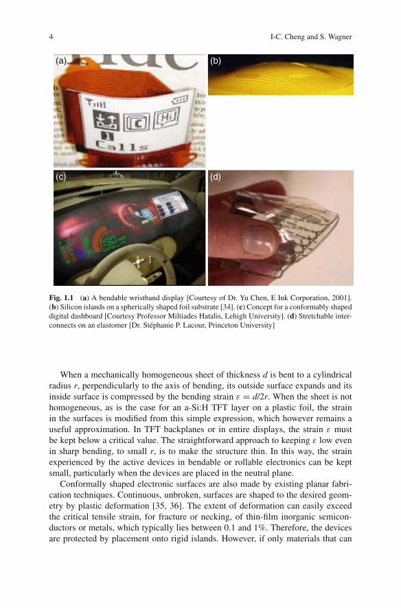
Flexibility can mean many different properties to manufacturers and users. As amechanical characteristic, it is conveniently classified in the three categories illus-trated by Fig. 1.1 : (1) bendable or rollable, (2) permanently shaped, and (3) elas-tically stretchable. The tools for microfabrication have been developed for flat sub-strates. Therefore, at present all manufacturing is done on a flat workpiece thatis shaped only as late as possible in the process. This approach benefits from thetremendous technology base established by the planar integrated circuit and displayindustries.
4 I-C. Cheng and S. Wagner
(a) (b)
(c) (d)
Fig. 1.1 (a) A bendable wristband display [Courtesy of Dr. Yu Chen, E Ink Corporation, 2001].(b) Silicon islands on a spherically shaped foil substrate [34]. (c) Concept for a conformably shapeddigital dashboard [Courtesy Professor Miltiades Hatalis, Lehigh University]. (d) Stretchable inter-connects on an elastomer [Dr. Stephanie P. Lacour, Princeton University]
When a mechanically homogeneous sheet of thickness d is bent to a cylindricalradius r, perpendicularly to the axis of bending, its outside surface expands and itsinside surface is compressed by the bending strain ε = d/2r. When the sheet is nothomogeneous, as is the case for an a-Si:H TFT layer on a plastic foil, the strainin the surfaces is modified from this simple expression, which however remains auseful approximation. In TFT backplanes or in entire displays, the strain ε mustbe kept below a critical value. The straightforward approach to keeping ε low evenin sharp bending, to small r, is to make the structure thin. In this way, the strainexperienced by the active devices in bendable or rollable electronics can be keptsmall, particularly when the devices are placed in the neutral plane.
Conformally shaped electronic surfaces are also made by existing planar fabri-cation techniques. Continuous, unbroken, surfaces are shaped to the desired geom-etry by plastic deformation [35, 36]. The extent of deformation can easily exceedthe critical tensile strain, for fracture or necking, of thin-film inorganic semicon-ductors or metals, which typically lies between 0.1 and 1%. Therefore, the devicesare protected by placement onto rigid islands. However, if only materials that can
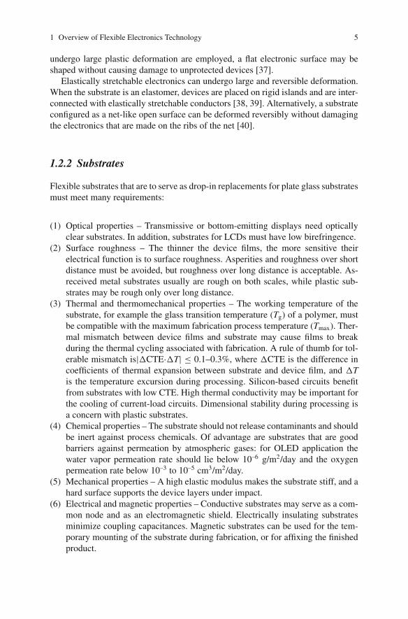
1 Overview of Flexible Electronics Technology 5
undergo large plastic deformation are employed, a flat electronic surface may beshaped without causing damage to unprotected devices [37].
Elastically stretchable electronics can undergo large and reversible deformation.When the substrate is an elastomer, devices are placed on rigid islands and are inter-connected with elastically stretchable conductors [38, 39]. Alternatively, a substrateconfigured as a net-like open surface can be deformed reversibly without damagingthe electronics that are made on the ribs of the net [40].
1.2.2 Substrates
Flexible substrates that are to serve as drop-in replacements for plate glass substratesmust meet many requirements:
(1) Optical properties – Transmissive or bottom-emitting displays need opticallyclear substrates. In addition, substrates for LCDs must have low birefringence.
(2) Surface roughness – The thinner the device films, the more sensitive theirelectrical function is to surface roughness. Asperities and roughness over shortdistance must be avoided, but roughness over long distance is acceptable. As-received metal substrates usually are rough on both scales, while plastic sub-strates may be rough only over long distance.
(3) Thermal and thermomechanical properties – The working temperature of thesubstrate, for example the glass transition temperature (Tg) of a polymer, mustbe compatible with the maximum fabrication process temperature (Tmax). Ther-mal mismatch between device films and substrate may cause films to breakduring the thermal cycling associated with fabrication. A rule of thumb for tol-erable mismatch is|ΔCTE·ΔT| ≤ 0.1–0.3%, where ΔCTE is the difference incoefficients of thermal expansion between substrate and device film, and ΔTis the temperature excursion during processing. Silicon-based circuits benefitfrom substrates with low CTE. High thermal conductivity may be important forthe cooling of current-load circuits. Dimensional stability during processing isa concern with plastic substrates.
(4) Chemical properties – The substrate should not release contaminants and shouldbe inert against process chemicals. Of advantage are substrates that are goodbarriers against permeation by atmospheric gases: for OLED application thewater vapor permeation rate should lie below 10–6 g/m2/day and the oxygenpermeation rate below 10–3 to 10–5 cm3/m2/day.
(5) Mechanical properties – A high elastic modulus makes the substrate stiff, and ahard surface supports the device layers under impact.
(6) Electrical and magnetic properties – Conductive substrates may serve as a com-mon node and as an electromagnetic shield. Electrically insulating substratesminimize coupling capacitances. Magnetic substrates can be used for the tem-porary mounting of the substrate during fabrication, or for affixing the finishedproduct.
6 I-C. Cheng and S. Wagner
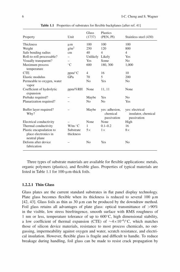
Table 1.1 Properties of substrates for flexible backplanes [after ref. 41]
Property UnitGlass(1737)
Plastics(PEN, PI) Stainless steel (430)
Thickness μm 100 100 100Weight g/m2 250 120 800Safe bending radius cm 40 4 4Roll-to-roll processable? – Unlikely Likely YesVisually transparent? – Yes Some NoMaximum process
temperature
◦C 600 180, 300 1,000
CTE ppm/◦C 4 16 10Elastic modulus GPa 70 5 200Permeable to oxygen, water
vaporNo Yes No
Coefficient of hydrolyticexpansion
ppm/%RH None 11, 11 None
Prebake required? – Maybe Yes NoPlanarization required? – No No Yes
Buffer layer required?Why?
– Maybe yes: adhesion,chemicalpassivation
yes: electricalinsulator, chemicalpassivation
Electrical conductivity – None None HighThermal conductivity W/m·◦C 1 0.1–0.2 16Plastic encapsulation to
place electronics inneutral plane
Substratethickness
5× 1× 8×
Deform after devicefabrication
– No Yes No
Three types of substrate materials are available for flexible applications: metals,organic polymers (plastics), and flexible glass. Properties of typical materials arelisted in Table 1.1 for 100-μm-thick foils.
1.2.2.1 Thin Glass
Glass plates are the current standard substrates in flat panel display technology.Plate glass becomes flexible when its thickness is reduced to several 100 μm[42, 43]. Glass foils as thin as 30 μm can be produced by the downdraw method.Foil glass retains all advantages of plate glass: optical transmittance of >90%in the visible, low stress birefringence, smooth surface with RMS roughness of1 nm or less, temperature tolerance of up to 600◦C, high dimensional stability,a low coefficient of thermal expansion (CTE) of ∼4×10⁻⁶/◦C, which matchesthose of silicon device materials, resistance to most process chemicals, no out-gassing, impermeability against oxygen and water, scratch resistance, and electri-cal insulation. However, flexible glass is fragile and difficult to handle. To reducebreakage during handling, foil glass can be made to resist crack propagation by
1 Overview of Flexible Electronics Technology 7
(1) laminating it with plastic foil, (2) applying a thin hard coat, or (3) applying athick polymer coat.
1.2.2.2 Plastic Film
Polymer foil substrates are highly flexible, can be inexpensive, and permit roll-to-roll processing. However, they are thermally and dimensionally less stable than glasssubstrates and are easily permeated by oxygen and water. A glass transition temper-ature, Tg, compatible with the device process temperature is essential. However, ahigh Tg alone is not sufficient. Dimensional stability and a low CTE are also impor-tant factors. Typical polymer films are shrunk by heating and cooling cycles. Theyshrink less if prestabilized by prolonged annealing [44]. Because the elastic mod-ulus of polymer substrates is a factor of 10–50 lower than that of inorganic devicematerials, a small thermal mismatch stress can make the free-standing workpiececurve and cause misalignment during the overlay registration of the flattened piece.A large CTE mismatch coupled with a large temperature excursion during process-ing can break a device film [45]. Polymer substrates with CTE below 20 ppm/◦C arepreferred as substrates for silicon-based device materials.
Candidate polymers for flexible substrates include (1) the thermoplasticsemicrystalline polymers: polyethylene terephthalate (PET) and polyethylene naph-thalate (PEN), (2) the thermoplastic noncrystalline polymers: polycarbonate (PC)and polyethersulphone (PES), and (3) high-Tg materials: polyarylates (PAR), poly-cyclic olefin (PCO), and polyimide (PI). PC, PES, PAR, and PCO are opticallyclear and have relatively high Tg compared to PET and PEN, but their CTEs are50 ppm/◦C or higher, and their resistance to process chemicals is poor. Muchresearch has been conducted with PET, PEN, and PI, with their relatively smallCTEs of 15, 13, and 16 ppm/◦C (Kapton E), respectively, relatively high elastic mod-uli, and acceptable resistance to process chemicals. Both PET and PEN are opticallyclear with transmittance of >85% in the visible. They absorb relatively little water(∼0.14%), but their process temperatures are only ∼150 and ∼200◦C, even afterprestabilization by annealing. In contrast, PI has a high glass transition temperatureof ∼350◦C, but it is yellow because it absorbs in the blue, and it absorbs as much as1.8% moisture [46, 47]. No polymer meets the extremely demanding requirementfor low permeability in OLED applications. The typical water and oxygen perme-ation rates of flexible plastic substrates are 1–10 g/m2/day and 1–10 cm3/m2/day,respectively, instead of the required 10−6 g/m2/day and 10−5 cm3/m2/day [48]. Bar-rier layer coatings can reduce absorption and permeability by gas, raise resistance toprocess chemicals, strengthen adhesion of device films, and reduce surface rough-ness.
1.2.2.3 Metal Foil
Metal foil substrates less than ∼125 μm thick are flexible and are attractive sub-strates for emissive or reflective displays, which do not need transparent substrates.Stainless steel has been most commonly used in research because of its high
8 I-C. Cheng and S. Wagner
resistance to corrosion and process chemicals, and its long record of applicationin amorphous silicon solar cells. Stainless steel substrates can tolerate process tem-perature as high as 1,000◦C, are dimensionally stable, present a perfect permeationbarrier against moisture and oxygen, can serve as heat sink, and can provide electro-magnetic shielding. Certain magnetic steels lend themselves to magnetic mountingand handling. In general, stainless steel substrates are more durable than plastic andglass foils.
A typical stainless steel foil comes with sharp rolling marks and micrometer-sizeinclusions, which may cause devices to fail. The most carefully rolled steel has asurface roughness of ∼100 nm, in contrast to display glass with less than 1 nm. Toensure the electrical integrity of the thin-film devices made on them, steel foil sub-strates must be either polished well [49, 50] or planarized with a film [14, 51, 52].The planarization layer may be organic, inorganic, or a combination. Commerciallyavailable materials for planarization include (1) organic polymers, (2) methylsilox-ane spin-on-glass, and (3) silicate spin-on-glass. The higher the organic content ofthe planarizing material, the thicker the film that can be applied without formingcracks and the smoother the resulting surface. This is particularly important forOLEDs, which need a surface roughness of less than 5-nm RMS. However, theorganic content imposes a ceiling on any subsequent, sustained process tempera-ture. An organic polymer-planarizing layer can be protected against excessive tran-sient heating with an inorganic overlayer by pulsed-laser processing. The typicalprocess steps for applying the planarization layer include spin-on, hot-plate bake,and high-temperature cure. As a rule of thumb, the final curing temperature sets theupper temperature limit for the subsequent device process. Incorporation of gettermaterials, for example phosphorus in a spin-on silicate film, enhances the barrierproperties against possible contaminants that may originate in the steel substrate.
Metal substrates are electrically conducting. In some applications they can serveas back contact, as in solar cells. For other applications metal must be coated withan insulating layer to provide circuit isolation. SiNx or SiO2 layers are commonlyused for this purpose on steel substrates. The electrical insulation also functions asadhesion layer and as barrier against process chemicals. SiNx:H, a standard materialin the a-Si:H TFT process, is also an excellent diffusion barrier. However, the highhydrogen content of SiNx:H may cause the film to crack or ablate during subsequentprocessing at high temperature or during laser annealing. In such cases, an SiO2 filmis deposited instead and provides the added advantage of a lower dielectric constantthan that of SiNx:H, which helps reduce the capacitive coupling between the sub-strate and the electronics. A barrier layer of 0.2–0.4 μm suffices for electrical insu-lation as it reduces the leakage current at a potential difference of 50 V to 1 nA/cm2.An active-matrix circuit driven at video rate may require a thicker layer to reducethe coupling capacitance to 1 nF/cm2.
1.2.3 Backplane Electronics
Backplanes provide or collect power and signal to or from frontplanes. Backplanesmay be passive or active. The ideal flexible active-matrix backplane should be
1 Overview of Flexible Electronics Technology 9
rugged, rollable or bendable, capable of CMOS operation, and should lend itselfto low-cost manufacturing. Today’s TFT backplane technologies are best describedby their active semiconductor, which may be amorphous, nanocrystalline, or poly-crystalline silicon, a II–VI compound semiconductor, or an organic semiconductorin polymer or molecular form. As thin-film semiconductor technologies developaway from glass substrates and toward flexible substrates, the backplanes differen-tiate further by the type of substrate. The substrate material defines a region of TFTfabrication conditions in temperature–time space. The maximum tolerable processtemperature is set by the type of substrate materials: <300, <600, and <1,000◦Cfor organic polymer, glass, and steel substrates, respectively. We now briefly reviewthe active materials for TFT backplanes and the associated fabrication technologies.
1.2.3.1 Silicon Thin-Film Transistors
Silicon-based materials benefit from the advantages of a well-established technol-ogy and a native oxide that is a high-quality insulator. Three approaches can betaken to preparing TFT-grade silicon on foil substrates: (1) direct deposition of thechannel semiconductor, (2) deposition of a precursor film followed by crystalliza-tion, and (3) physical transfer of separately fabricated circuits. Techniques (1) and(2) are explored for large-area display applications. Direct deposition can providethe full range of devices, from low OFF current amorphous silicon (a-Si:H) TFTs toCMOS capable TFTs of nanocrystalline silicon (nc-Si:H). The highest ON currentis obtained in TFTs of both polarities in polycrystalline silicon (poly-Si) made bythe crystallization of an amorphous silicon precursor film.
a-Si:H made from a glow discharge was first reported in the late 1960s and thefirst a-Si:H TFT was demonstrated by Snell and coworkers in 1981 [53]. Sincethe mid-1990s, a-Si:H TFTs have been made on flexible substrates, including PIfilms [13] and stainless steel foil [14]. Today’s baseline growth process for a-Si:HTFTs is PECVD at a substrate temperature of 250–350◦C. a-Si:H is a material withreproducible optoelectronic properties that provides TFTs with electron field-effectmobilities of ∼0.5–1 cm2V−1s−1. The a-Si:H growth process has been adapted tolow-temperature polymer substrates with process temperatures of 150◦C or less[54]. The only useful a-Si:H TFTs are n-channel devices as the hole mobility of∼0.003 cm2V−1s−1 is too low to be useful.
nc-Si:H is a promising candidate material for fully integrated electronics onplastic because it is CMOS capable and can be made by PECVD at low substratetemperature. The top-gate geometry has produced the highest mobilities to date.However, the nc-Si:H TFT fabrication process needs considerably more research.The nc-Si:H growth schedule (direct or prenucleation), the location of source/draincontacts (in-plane or staggered), efficient source/drain doping (particularly p+), thetype of gate dielectric (SiO2 or SiNx), and the techniques for post-process annealingare not settled.
Poly-Si can be either directly deposited by low-pressure chemical vapor deposi-tion (LPCVD) or formed by the crystallization of a precursor film, typically a-Si:H.Crystallization produces the superior material, with larger grain sizes and smoothersurface than obtained by LPCVD. a-Si:H can be crystallized by furnace anneal at
10 I-C. Cheng and S. Wagner
600◦C or higher, or at ∼550◦C by silicide-mediated crystallization (also known asmetal-induced crystallization), and by pulsed excimer laser annealing. Poly-Si TFTshave been made on steel foil substrates since the late 1990s [55, 56]. While furnacecrystallization is not compatible with organic polymer substrates, the spatial andtemporal confinement of heat in excimer laser annealing permits making poly-Si onplastic, as first demonstrated with poly-Si TFTs made on plastic in 1997 [16]. Con-trolling the geometry of the laser spot produces large grain sizes [57], and poly-SiTFTs with high performance have been made on flexible steel substrates [58, 59].
1.2.3.2 Organic Thin-Film Transistors
The first demonstration of the field effect in a small-molecule organic material datesback to 1964 [60]. In 1983, the field effect in a polymer structure made by a solutionprocess was reported [61]. Since then the performance of organic thin-film transis-tors (OTFTs) has been raised impressively by the introduction of new organic chan-nel materials and by improved fabrication [62]. In the late 1990s, OTFTs with ONcurrents comparable to those of a-Si:H TFT were reported [63]. In 2000, pentaceneTFTs with a hole field-effect mobility of 3.2 cm2V−1s−1 and an ON/OFF ratio of>109 were demonstrated [64]. Because in most organic materials the hole mobilityis higher than the electron mobility, most OTFTs are p-channel devices.
Organic polymers are soluble, and small molecules can be derivatized to solubleprecursors. Therefore, OTFTs can be fabricated by solution processing near roomtemperature [31], compatible with low-temperature plastic substrates. Since the late1990s, OTFTs and circuits have been made on flexible plastic substrates, includingPI [32, 65], PEN[66], PET [67–69], PC [70, 71], and on paper [72]. More recently,displays have been made on OTFT backplanes on flexible polymeric substrates. Thedisplays include reflective LCDs [73, 74], electrophoretic displays [75], and OLEDdisplays [76–79].
1.2.3.3 Transparent Thin-Film Transistors
TFTs made of transparent materials [80, 81] may not need shielding from visiblelight to suppress photoconductance, and can raise the pixel aperture of transmissivedisplays, for example on windscreens of cars. They have been developed from theconventional wide-bandgap compound semiconductors: GaN or SiC, and from thetransparent oxide semiconductors: ZnO [82], In2O3 [83, 84], and SnO2 [85]. Thefirst flexible transparent TFT was made by Nomura et al. in 2004 from the amor-phous In–Ga–Zn–O system on PET. Saturation mobilities reached 6–9 cm2V−1s−2,and device characteristics were stable under mechanical bending [86].
More recently, flexible transparent TFTs have been demonstrated with organicchannel materials, including a conductive polymer [69] and single-walled carbonnanotubes (SWNT). SWNTs have enabled flexible transparent organic TFTs withmobilities comparable to that of a-Si:H TFTs [87–89].
1 Overview of Flexible Electronics Technology 11
1.2.3.4 Materials for Interconnects and Contacts
Transparent Conductive Oxides
Typical electrode and contact materials are metallic. Displays and thin-film solarcells, however, need electrodes that are transparent electrical conductors. To date,these have been metal oxides [90–92]. The first transparent conducting oxide (TCO),CdO, was reported by Baedeker in 1907 [93]. Transparent conducting tin-dopedindium oxide (ITO), originally developed for the defrosting of aircraft windshields,is the most widely used TCO. It is the transparent electrode in flat panel displays,is used for electromagnetic shielding, and is deposited on optical grade polyester(PET) substrates by roll-to-roll dc sputtering for touch screens. In the trade-offbetween electrical conductivity and optical transparency, ITO has reached a perfor-mance plateau at a resistivity of ∼10−4 Ω·cm. New TCO materials based on ZnOand SnO2, and mixed ternary and quaternary oxides are under development.
Depositing ITO on organic polymer foil substrates presents two challenges: opto-electronic quality and mechanical integrity. The best-quality display grade ITO onglass is dc-magnetron sputtered at a substrate temperature of 300–400◦C, or firstsputtered on the cold substrate and then annealed at 200◦C in a controlled oxy-gen environment. Because polymeric substrate materials are heat sensitive, ITO isdeposited on them at low temperature as an amorphous phase. Fortunately, amor-phous ITO films deposited at room temperature have an optical transparency and anelectrical conductivity that is adequate for present display technologies. The mis-match in mechanical properties between the ITO and the polymeric substrate is achallenge. ITO is stiff and brittle with an elastic modulus of ∼118 GPa. Depositingit on a compliant substrate may cause cracks and delamination during fabrication orin use. The mechanisms of cracking and the effect of cracking on the electrical prop-erties of ITO films on PET substrates have been investigated by Cairns et al. Thecritical strain for cracking is reciprocal to the square root of film thickness, simi-lar to what observed in a typical ceramic film [94]. ITO cracks at a strain of ∼1%.Prior to electrical failure, small cracks form and may grow by fatigue under cyclicloading. The onset of ITO conductivity loss in tension can be delayed by reducingthe ITO layer thickness, by using a high-modulus but nonbrittle undercoat for theITO, or by introducing compressive prestress into the ITO layer. Under compressiveload, the brittle ITO film may delaminate and then buckle and crack. The strain atwhich buckling occurs depends on the strength of adhesion between the ITO andthe substrate [95].
Conducting Organic Polymers
We just described how the mismatch of mechanical properties between inorganicdevice films and polymeric substrates can break the films during processing anduse. These risks of film fracture provide one motive for using conductive polymersas contact and interconnect materials as part of all-organic flexible electronics [96].In 1976, Heeger, MacDiarmid, and Shirakawa made the discovery that polyacety-lene exhibits a high electrical conductivity when doped with the oxidant iodine.
12 I-C. Cheng and S. Wagner
Today, such “self-doped” conductive polymers are available commercially. Polyani-line (PANI) and polypyrrole (PPY) are used as antistatic materials, polythiophenederivatives, e.g., polyethylene dioxythiophene (PEDOT) replace inorganic ITO insome device applications and also function as hole injectors and transport layersin OLEDs, and polyphenylene vinylene (PPV) derivatives are active materials inpolymer light-emitting diodes (PLEDs). Conductive polymers need much furtherresearch as they are not yet well defined and have suboptimal device properties.
Stretchable Interconnects
Flexible electronic surfaces that undergo large plastic deformation need stretch-able interconnects. One-time deformation, for example to a conformally shapedsurface, needs interconnects that can be deformed plastically. Under certain condi-tions, metal films can be deformed once and remain electrically conducting [35–37].Repeated deformation, as experienced by electronic skin, requires elastic intercon-nects. Several approaches have been demonstrated to realizing elastically stretchableinterconnects. They include making “filled” elastomers conducting by blending inconductive polymers [97–99] or by embedding metal particles [100]. Conductor-filled elastomers are used mainly for forming interconnects between rigid compo-nents. [101, 102]. Often the electrical conductivities of these conducting elastomersare insufficient for electrical interconnects. Because the filled-elastomer conductorsare applied with thick-film techniques, they are not directly compatible with thin-film circuits. The search for elastic thin-film interconnects has focused on metalfilms deposited on or encased in elastomers. Microfabricated gold-film serpentinesencased in a silicone elastomer conduct up to 54% tensile strain [103]. Stripes ofthin gold film patterned on prestretched or flat elastomeric membranes remain elec-trically conducting when the membranes are stretched up to twice their initial length.Such stretchable interconnects were used in the demonstration of an inverter circuitmade of a-Si:H TFTs on a silicone membrane [38, 104, 105].
1.2.4 Frontplane Technologies
Frontplanes carry the specific optoelectronic application. The frontplane materialsof displays include liquid crystals for transmissive displays, reflective-mode liquidcrystals and electrophoretic foils for reflective displays, and OLEDs for emissivedisplays. The frontplane might also be an X-ray sensor, an image sensor, a pressuresensor, a chemical sensor, an actuator or an artificial muscle in a smart textile.
1.2.4.1 Liquid Crystal Displays
The LCD is a light intensity filter that is controlled by the electric field betweentwo transparent electrodes. These are fabricated on glass plates that are held ∼5 μmapart by transparent spacers [106]. To make the LCD flexible, the liquid is encap-sulated in a polymer foil. The first examples were the polymer-dispersed liquid
1 Overview of Flexible Electronics Technology 13
crystal (PDLC) [107] and the nematic curvilinear aligned phase (NCAP) [108, 109].The phase separation procedure developed for PDLCs can also be used for bistablecholesteric liquid crystal [110]. Today, the term PDLC is used to describe liquidcrystal droplets in encapsulated form. The PDLC dispersion techniques do notrequire alignment layers or polarizers, and large devices are relatively simple tofabricate.
The first LCDs fabricated on flexible plastic substrates date back to 1981[111, 112]. In the meantime, full-color reflective cholesteric displays on plasticsubstrates have been developed [113–116], and twisted nematic LCDs made on atransparent flexible plastic substrate were demonstrated with low-voltage operationand high contrast [117]. A paintable LCD technology, a sequence of coating andUV curing, is under development for making flexible LCDs [118].
1.2.4.2 Electrophoretic Displays
Electrophoretic displays are reflective-type bistable devices. Bistable displaysconsume power only when they are overwritten. Because they combine low-powerconsumption with adequate contrast and full viewing angle, they are particularlysuitable for electronic books. In electrophoretic displays, the electric field acrossthe electrophoretic material controls the location and orientation of charged objectsthat are suspended in a liquid. Metcalfe and Wright first used electrophoresis forcreating an image in 1956 [119]. In the early 1970s, displays using electrophore-sis to create reversible images were demonstrated [120, 121]. These electrophoreticdisplays suffered from sticking particles, discoloration of dyes, and migration of par-ticles to electrode edges. To limit the lateral migration of the particles, microcellularelectrophoretic films were developed in the late 1970s and early 1980s, by usingphotoresist to create a square grid of confining ribs [122, 123]. In the late 1990s,microencapsulated electrophoretic display films were developed by E-Ink Corpora-tion [124] and by NOK Corporation [125]. Instead of filling the electrophoretic fluidinto microcellular structures, the fluid is microencapsulated by means of polycon-densation of urea and formaldehyde, which produces discrete, mechanically strongand optically clear, microcapsules. These microcapsules are subsequently spread onITO-coated polyester foil, and then rear electrodes are printed. Microencapsulationnot only solves the problem of particle clustering, agglomeration, and lateral migra-tion, but also maintains the cell gap during deformation. Normally, electrophoreticdisplays are bicolor (black and white). Schemes for obtaining full color include(1) using three combinations of two-color electrophoretic fluids in a subpixellatedscheme to form various combinations of red, green, and blue, (2) combining anexternal color filter over a black and white electrophoretic film, and (3) stackingthree imaging films over each other [126].
The current electrophoretic film produced by E Ink Corporation is a dual-particleformulation. It contains positively charged white particles and negatively chargedblack particles that are suspended in a clear fluid. It has a black-to-white updatetime of less than 30 ms at 15 V drive voltage, and gray tones are obtained by par-tial addressing between black and white states [127]. Active-matrix electrophoreticdisplays with a-Si:H TFTs on steel foil substrates have been demonstrated by E Ink
14 I-C. Cheng and S. Wagner
[128, 129]. E Ink’s microencapsulated electrophoretic films have been integratedwith Plastic Logic Limited’s active-matrix organic TFT backplane made by solu-tion processing on a plastic substrate. Paper-like displays and prototypes of rollabledisplays based on E Ink’s electrophoretic films have been demonstrated by Philips[130, 17].
1.2.4.3 Organic Light-Emitting Displays
Since the discovery of OLEDs in the late 1980s, the technology has developedrapidly and OLED displays encapsulated in glass are commercially available.OLEDs have wider viewing angles, faster response time, lower voltage operation,and possibly lower power consumption than backlit AMLCDs. Because of theirthin-film structure, OLEDs are a natural choice for flexible displays. The two typesof OLED materials are small-molecule, with the higher efficiency, and conjugatedpolymers. Small-molecule OLEDs are usually prepared by thermal evaporation, andpolymer OLED by solution processing. The latter enables many potentially inex-pensive fabrication steps, such as spin coating, ink-jet printing, and spraying, and iseasily compatible with roll-to-roll manufacturing. Therefore, efforts are underwayto develop solution-processable precursors for small-molecule OLED fabrication,as mentioned earlier.
Electroluminescence in organic materials was first studied in the 1960s[131–133]. Interest in organic electroluminescence was revived by Tang andVanSlyke’s discovery of electroluminescence in small-molecule organic thin-filmdiodes made by thermal evaporation [134]. Visible light emission from poly-mer organic light-emitting diodes (PLEDs) reported by Burroughes et al. in 1990attracted further attention. The PLED was deposited by spin coating a solution-processable precursor polymer, which then was converted to a conjugated polymerby heating to 250◦C [135]. A year later, in 1991, Braun and Heeger reported the useof a soluble conjugated polymer that eliminated the need for high-temperature pro-cessing [136]. Soon thereafter a flexible OLED display on PET was demonstratedby Gustafsson et al., who employed solution-processable MEH–PPV as the activematerial and the conductive polymer PANI as the hole-injecting contact [137]. In1997, a-Si:H TFTs on steel foil were integrated with a printed top-emitting OLED[33]. Many research groups now have demonstrated active-matrix OLEDs on flexi-ble plastic or steel substrates [138–140]. A typical pixel cross section of an active-matrix bottom-emitting OLED on a clear plastic substrate is shown in Fig. 1.2 .
In OLEDs and PLEDs, an ∼100-nm-thick organic stack is sandwiched betweenan anode and a cathode. In bottom-emitting (through-the-substrate) OLEDs, theanode is usually ITO with high work function, and the cathode is a metal with lowwork function, such as Ca or Mg, which is covered by an interconnect metal likeAl. Because top-emitting OLEDs need a transparent cathode, they are coated with avery thin layer of the cathode metal, which is then covered with ITO. Electrons andholes injected under forward bias combine to bound polaron–excitons. These radia-tively decay via electron–hole recombination to produce the electroluminescence.

1 Overview of Flexible Electronics Technology 15
Plastic SubstrateCr gate metal
Passivation SiNx
Gate SiNx
Intrinsic a-Si
S/D metal
S/D n+ a-Si
Organiclayers ofOLEDCathode
Gate of another
TFT
Thin filmtransistor
(TFT)
IC-Cr-ITO Organic lightemitting diode
(OLED)
IC-ITO
Passivation SiNx
Fig. 1.2 Schematic cross section through an a-Si:H TFT and an OLED on a clear plastic substrate[Dr. Ke Long, Princeton University]
The OLED stack contains charge injection and transport layers that serve to keep theexcitons away from nonradiatively recombining at the contacts. The injection andtransport layers are also made of organic materials, for example PEDOT/polystyrenesulfonate or PANI [142]. Alternative OLED architectures include inverted top-emitting OLEDs that have the cathode in contact with the substrate, and transparentOLEDs whose anodes and cathodes both are transparent [143, 144]. The biggestchallenge to making flexible OLED display is the demand for extremely low ratesof permeation of moisture and oxygen to ensure acceptably long OLED lifetime.Oxidation at the organic–cathode interface can inhibit charge injection and resultsin black spots.
1.2.4.4 Sensors
Flexible sensors have captured the imagination for applications in biomedicine, arti-ficial skin, and wearable electronics. We describe some recent examples. The shear-stress sensor skin by Xu et al. integrates microelectromechanical systems (MEMS)and ICs onto a flexible Parylene (poly-para-xylylene) “skin,” which can be affixedto the human body like a Band-Aid [145]. A hand posture and gesture monitoringglove has been made by integrating strain sensors with fabric [146]. The electricalcharacteristics of resistive, capacitive, or field-effect devices made of conducting orsemiconducting polymers change upon gas absorption. This is the operating princi-ple of chemical sensing transistors made on fibers for wearable electronics. [147]. Aconformal H2-sensing skin for the safety monitoring of H2 fuel tanks is based on apiezoelectrically driven sound resonance cavity. The skin itself consists of a porousPVDF polymer layer that allows leaked H2 to diffuse freely, and an impermeablesilicone rubber that serves as the seal for the porous polymer [148]. Electronic skindeveloped by Someya and coworkers is made flexible and conformable by a net-like
16 I-C. Cheng and S. Wagner
structure that carries thermal and pressure sensors made of organic materials onits filaments. Conductive rubber functions as pressure sensor and organic diodes asthermal sensors [149–151, 40]. A plastic film with pentacene TFT-based electroniccircuits is processed to form the net-like structure that allows the large deforma-tion of the electronic skin. For ultra-high flexibility, the OTFTs are embedded at aneutral strain position [152]. A pressure sensor and microphone based on a ferro-electric polymer foil have been combined with an a-Si:H TFT on a PI foil substrate.Depending on the function, the TFT is used as a switch or amplifier [153].
1.2.4.5 Actuators
A soft electrically insulating polymer functions as dielectric in a capacitor withmechanically compliant electrodes. This electroactive polymer is compressed whenthe electrodes are charged and, by conservation of volume, expands parallel to theplanes of the electrodes. Large deformation has been demonstrated in appropriatelydesigned dielectric elastomer actuators [154, 155]. Electroactive polymer actuationhas been switched by thin films on polymer foil, pointing to a possible technologyfor large-area actuation [156]. Potential applications include artificial muscles forbiologically inspired robots, animatronics, prosthetics, conformally shaped loud-speakers, and smart skin which can modulate electromagnetic properties, control ofairflow and heat transfer, and control of the texture of large surfaces.
1.2.4.6 Electronic Textiles
Low stiffness is inherent in textile fabric. E-textiles, or smart textiles, have electroniccircuitry woven into or integrated onto the fabric [157, 158]. A circuit has beenwoven of yarns that carried a-Si:H TFTs or conductors, or functioned as insulatingspacers [159]. Figure 1.3 illustrates the concept of an e-suit. E-textiles have beendeveloped and test-marketed for wireless communication, entertainment, health, andsafety. Electrically conducting fibers are a prerequisite. They can be made of wireor by coating fibers with metals, metallic salts, or conductive polymer. Input andoutput devices, sensors, actuators, and power supplies are integrated by applicationor weaving. One particular goal is a power supply obtained by integrating photo-voltaics into the fabric. Nanotechnology and MEMS are expected to increasinglyenable the direct integration of electronic devices. A number of practical issues thatinclude conformal encapsulation of active-device yarn remain to be addressed.
1.2.5 Encapsulation
Thin-film encapsulation has been researched and applied for decades. Single-layermetallic barrier coatings [160–162] were followed by single-layer transparent bar-rier coatings [163–166] and now multilayer composite (oxide or nitride/polymer)barrier coatings. Since the early 1970s, thin aluminum films evaporated onto poly-meric substrates have been applied commercially as gas barriers in food packaging.
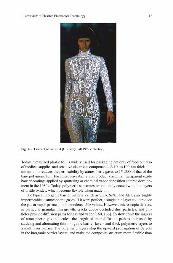
1 Overview of Flexible Electronics Technology 17
Fig. 1.3 Concept of an e-suit [Givenchy Fall 1999 collection]
Today, metallized plastic foil is widely used for packaging not only of food but alsoof medical supplies and sensitive electronic components. A 10- to 100-nm-thick alu-minum film reduces the permeability by atmospheric gases to 1/1,000 of that of thebare polymeric foil. For microwaveability and product visibility, transparent oxidebarrier coatings applied by sputtering or chemical vapor deposition entered develop-ment in the 1980s. Today, polymeric substrates are routinely coated with thin layersof brittle oxides, which become flexible when made thin.
The typical inorganic barrier materials such as SiO2, SiNx, and Al2O3 are highlyimpermeable to atmospheric gases. If it were perfect, a single thin layer could reducethe gas or vapor permeation to nondetectable values. However, microscopic defects,in particular granular film growth, cracks above occluded dust particles, and pin-holes provide diffusion paths for gas and vapor [160, 166]. To slow down the ingressof atmospheric gas molecules, the length of their diffusion path is increased bystacking and alternating thin inorganic barrier layers and thick polymeric layers toa multilayer barrier. The polymeric layers stop the upward propagation of defectsin the inorganic barrier layers, and make the composite structure more flexible than
18 I-C. Cheng and S. Wagner
a single thick inorganic barrier structure would be. The entire multilayer barrier istypically several micrometers thick. In 1994, aluminum layers as barriers alternat-ing with acrylate polymer layers were found to reduce the oxygen permeation ratethrough a polypropylene substrate by four orders of magnitude [167]. In 1996, oxy-gen and water permeation rates below the detection limit of <0.015 cm3/m2/daywere obtained by using a three-layer barrier structure of 1-μm acrylate/25-nmAlOx/0.24-μm acrylate on a PET substrate [168].
Making impermeable thin-film barrier coatings has become the major challengeto making flexible OLED displays. Polymeric substrates needed a barrier on thesubstrate side (“passivation”) and on top (“encapsulation”) of the device to ensurelong life. The barrier through which the light is emitted needs to meet the addi-tional criteria of high optical transparency of 85–90% over the visible spectrum,control of optical microcavity effects, and, if on top of the OLED, low stress toavoid shear damage to the OLED, dense and conformal coating to avoid through-layer and edge leakage, and low process temperature. Multilayer organic/inorganicbarrier coats have been proven to extend the operating life of OLEDs [48, 169–173].For the purpose of reducing the cost and barrier complexity, single, dense, inorganicbarrier layers of aluminum oxide made by atomic-layer deposition remain understudy [174, 175].
An important complement to the development of the barrier technology itself isimproved techniques for the evaluation of barrier quality, and with sufficient sen-sitivity for relevance to OLEDs. Direct identification and characterization of thedefects that cause permeation are parts of this task in the development of flexibleOLEDs.
1.3 Fabrication Technology for Flexible Electronics
1.3.1 Fabrication on Sheets by Batch Processing
Electronic devices and circuits and display panels are made by batch processing.Flexible foil substrates, cut to sheets, will be the drop-in replacement for the rigidglass plates or silicon wafers.
Flexible sheet substrates may be handled in several ways during processing:
• on a rigid carrier, facing up and loose;• on a rigid carrier, facing up or down and bonded to the carrier for the duration of
processing;• in a tensioning frame, facing up or down;• in a frame, facing down and loose;• electrostatically bonded to a rigid carrier;• magnetically attached to a rigid carrier.
Rigid substrates are best suited to free standing and loose mounting. The flexi-bility of the substrate is given by its flexural rigidity D = Et3/12(1–ν2), where E isYoung’s modulus, t is the thickness of the substrate, and ν is its Poisson ratio.
1 Overview of Flexible Electronics Technology 19
a-Si TFTs have been made on polymeric substrates held loosely in a frame [54].The substrate was flattened and temporarily bonded with water to plate glass forphotolithography. However, holding the substrate loosely is a technique confinedto the laboratory, because device films may crack or the sample may curve frommismatch strain between the deposited films and the substrate. Since varying curva-ture corresponds to varying size of the flattened sample, any variation of the stress-induced curvature between alignment steps is synonymous with misalignment inmask overlay [45].
Temporarily bonding the foil substrate to a rigid carrier for processing canimprove the substrate’s dimensional stability. Bonding may be particularly advis-able if inorganic device materials are deposited on compliant polymer substrates,because of the large strain this combination may generate. The adhesive must pro-vide sufficient shear strength between the substrate and the carrier, resist the pro-cess chemicals, degas little and release few contaminants. At the end of processingit must be removed without damaging the electronics. Thermoplastic adhesives pro-vide the necessary resistance against solvents and can be detached by heating. How-ever, they impose a ceiling on the process temperature that necessarily is lower thanthe highest working temperature of the substrate. This requirement makes the pro-cess window narrow and therefore may degrade device performance. Because themechanical force needed for debonding may cause damage to the devices and mayreduce the yield, special equipment will be needed for debonding in a manufacturingsetting.
1.3.2 Fabrication on Web by Roll-to-Roll Processing
Flexible electronics are naturally associated with roll-to-roll processing [174].Roll-to-roll fabrication of large-area electronics, including solar cells, is desirablefor cost reduction. Indeed, amorphous silicon solar cells are manufactured on flex-ible steel [177] and PI foils [178] by roll-to-roll processes. The solar cells on PIeven take advantage of the easy through-substrate connection that can be had bypunching holes into the plastic foil substrate. In contrast to solar cell manufacture,making displays and other active electronic circuitry requires a large number ofpatterning steps. The device layers can be patterned by the additive processes ofdirectly printing the active materials, shadow masking, or subtractive patterning byphotolithography. All of these techniques can be adapted to web processing. Thebig challenge is that backplane circuits need high precision, accuracy, and yield.The roll-to-roll photolithography and etching tools available today are not capableof 2-μm resolution and overlay registration, particularly when combined with thetensioning applied for winding and with process cycles at elevated temperature, bothof which cause substrate deformation. The goal of roll-to-roll fabrication of flexi-ble electronics is stimulating innovations in equipment and process design [179],process recipes, and system integration. Tools for roll-to-roll processing that areavailable today include web cleaner, PECVD, sputtering, plasma etcher, developetch strip line (for printed circuit boards with high-density interconnects), die punch
20 I-C. Cheng and S. Wagner
(which can be modified for control of alignment and winding/unwinding), evapora-tor (with linear source to improve film uniformity in roll-to-roll applications), laserwriter, inkjet printer, screen printer, and inspection devices.
1.3.3 Additive Printing
If flexible electronics could be fabricated by additive printing, their cost couldbecome as low as a few dollars per square meter [180]. Additive printing is roll-to-roll process compatible, is a high-throughput process, uses device materialsefficiently, may not require vacuum, and may provide a solution to overlay registra-tion problem through digital compensation. Noble-metal conductors, organic con-ductors, semiconductors, and insulators can be printed. The printability of organicmaterials has stimulated experiments on the printing of TFTs [29, 31]. Masks foretching or lift-off patterns, as well as certain inorganic materials [30, 181], can beprinted [27, 28]. Printing metallic conductors from nanoparticles may reduce therequired sintering temperature to values acceptable for plastic substrates. The print-ing of high-quality gate dielectrics and the operational stability of printed devicesare issues that remain to be resolved.
1.4 Outlook
Most of the present industrial development of flexible electronics is for flexibledisplays and X-ray sensor arrays. Conformally shaped electronics are perhaps fiveyears away from industrial development, and elastically stretchable electronic sur-faces, ten years. Research laboratories are inventing many new flexible technologiesthat range from elastically conforming sensor surfaces to electronic nets. The taskof the researcher is to offer the industrialist a choice of new applications and showthe path to them by developing the necessary architecture, circuits, materials, andfabrication technology.
Acknowledgments The authors gratefully acknowledge support of their research by the UnitedStates Army Research Laboratory, the United States Display Consortium, Universal DisplayCorporation, Hewlett-Packard Laboratories, the DuPont Company, the National Institutes ofHealth, DARPA, the Eastman Kodak Company, and the New Jersey Commission for Science andTechnology.
References
1. Crabb RL, Treble FC (Mar 25, 1967) Thin silicon solar cells for large flexible arrays. Nature1223–1224
2. Ray KA (Jan, 1967) Flexible solar cell arrays for increased space power. IEEE Trans AerospElectron Syst v AES-3, n 107–115
3. Wronski CR, Carlson DE, Daniel RE (1976) Schottky-barrier characteristics of metal-amorphous-silicon diodes. Appl Phys Lett 29:602–604
1 Overview of Flexible Electronics Technology 21
4. Plattner PD, Kruhler WW, Juergens W, Moller M (1980) ’80 Photovoltaic Solar Energy Confp 121
5. Okaniwa H, Nakatani K, Asano M, Yano M, Hamakawa Y (1982) Production and propertiesof a-Si:H solar cell on organic polymer film substrate. In: Conference record of the sixteenthIEEE photovoltaic specialists conference – 1982, San Diego, CA, USA, Sep. 27–30, SanDiego, CA, USA, 1982, pp 1111–1116
6. Okaniwa H, Nakatani K, Yano M, Asano M, Suzuki K (1982) Preparation and properties ofa-Si:H solar cells on organic polymer film substrate. Jpn J Appl Phys 21:239–244
7. Okaniwa H, Nakatani K (1983) Flexible substrate solar cells. In: Hamakawa Y (ed) JARECTvol. 6. Amorphous Semiconductor Technologies & Devices. Ohusha, Tokyo, pp 239–250
8. Russell TWF, Rocheleau RE, Lutz PJ, Brestovansky DF, Baron BN (1982) Propertiesof continuously-deposited photovoltaic-grade CdS. In: Conference record of the sixteenthIEEE photovoltaic specialists conference – 1982, San Diego, CA, USA, Sep. 27–30, SanDiego, CA, USA, pp 743–747
9. Nath P, Izu M (1985) Performance of large area amorphous Si-based single and multiplejunction solar cells. In: Rec 18th IEEE Photovoltaic Specialists Conference. Las Vegas, NV,Oct 21–25, p 939
10. Yano M, Suzuki K, Nakatani K, Okaniwa H (1987) Roll-to-roll preparation of a hydro-genated amorphous silicon solar cell on a polymer substrate. Thin Solid Films 146:75–81
11. Brody TP (1984) The thin-film transistor – A late flowering boom. IEEE Trans ElectronDevices ED-31:1614–1628
12. Brody TP (1996) The birth and early childhood of active matrix – A personal memoir. J SocInf Disp 4(3):113–127
13. Constant A, Burns SG, Shanks H, Gruber C, Landin A, Schmidt D, Thielen C, Olympie F,Schumacher T, Cobbs J (1995) Development of thin film transistor based circuits on flexiblepolyimide substrates. Electrochem Soc Proc 94-35:392–400
14. Theiss SD, Wagner S (1996) Amorphous silicon thin-film transistors on steel foil substrates.IEEE Electron Device Lett 17:578–580
15. Yang ND, Harkin G, Bunn RM, McCulloch DJ, Wilks RW, Knapp AG (1997) Novel fin-gerprint scanning arrays using polysilicon TFT’s on glass and polymer substrates. IEEEElectron Device Lett 18:19–20
16. Smith PM, Carey PG, Sigmon TW (1997) Excimer laser crystallization and doping of siliconfilms on plastic substrates. Appl Phys Lett 70:342–344
17. http://www.research.philips.com/newscenter/archive/2005/050902-rolldisp.html18. http://www.samsung.com/PressCenter/PressRelease/PressRelease.asp?seq=20051128
000021787919. http://www.universaldisplay.com/press/press-2006-2-7.htm20. Inoue S, Utsunomiya S, Saeki T, Shimoda T (2002) Surface-free technology by laser anneal-
ing and its application to poly-Si TFT–LCDs on plastic film with integrated drivers. IEEETrans Electron Devices 49:1353–1360
21. Lee Y, Li H, Fonash SJ (2003) High-performance poly-Si TFTs on plastic substrates usinga nano-structured separation layer approach. IEEE Electron Device Lett 24:19–21
22. Asano A, Kinoshita T (2002) Low-temperature polycrystalline-silicon TFT color LCDpanel made of plastic substrates. Soc Inf Display Symp Digest Tech Papers 33:1196–1199
23. Berge C, Wagner T, Brendle W, Craff-Castillo C, Schubert MB, Werner JH (2003) Flexiblemonocrystalline Si films for thin film device from transfer process. Mat Res Soc Symp Proc769, H. 2.7:53–58
24. Stewart R, Chiang A, Hermanns A, Vicentini F, Jacobsen J, Atherton J, Boiling E, Cuomo F,Drzaic P, Pearson S (2002) Rugged low-cost display systems. Proc SPIE – Int Soc Opt Eng4712:350–356
25. Khang DY, Jiang H, Huang Y, Rogers JA (2006) A stretchable form of single-crystal siliconfor high-performance electronics on rubber substrates. Science 311:208–212
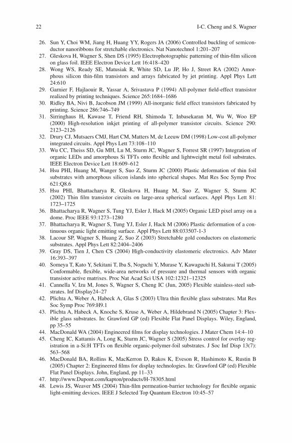
22 I-C. Cheng and S. Wagner
26. Sun Y, Choi WM, Jiang H, Huang YY, Rogers JA (2006) Controlled buckling of semicon-ductor nanoribbons for stretchable electronics. Nat Nanotechnol 1:201–207
27. Gleskova H, Wagner S, Shen DS (1995) Electrophotographic patterning of thin-film siliconon glass foil. IEEE Electron Device Lett 16:418–420
28. Wong WS, Ready SE, Matusiak R, White SD, Lu JP, Ho J, Street RA (2002) Amor-phous silicon thin-film transistors and arrays fabricated by jet printing. Appl Phys Lett24:610
29. Garnier F, Hajlaouir R, Yassar A, Srivastava P (1994) All-polymer field-effect transistorrealized by printing techniques. Science 265:1684–1686
30. Ridley BA, Nivi B, Jacobson JM (1999) All-inorganic field effect transistors fabricated byprinting. Science 286:746–749
31. Sirringhaus H, Kawase T, Friend RH, Shimoda T, Inbasekaran M, Wu W, Woo EP(2000) High-resolution inkjet printing of all-polymer transistor circuits. Science 290:2123–2126
32. Drury CJ, Mutsaers CMJ, Hart CM, Matters M, de Leeuw DM (1998) Low-cost all-polymerintegrated circuits. Appl Phys Lett 73:108–110
33. Wu CC, Theiss SD, Gu MH, Lu M, Sturm JC, Wagner S, Forrest SR (1997) Integration oforganic LEDs and amorphous Si TFTs onto flexible and lightweight metal foil substrates.IEEE Electron Device Lett 18:609–612
34. Hsu PHI, Huang M, Wanger S, Suo Z, Sturm JC (2000) Plastic deformation of thin foilsubstrates with amorphous silicon islands into spherical shapes. Mat Res Soc Symp Proc621:Q8.6
35. Hsu PHI, Bhattacharya R, Gleskova H, Huang M, Suo Z, Wagner S, Sturm JC(2002) Thin film transistor circuits on large-area spherical surfaces. Appl Phys Lett 81:1723–1725
36. Bhattacharya R, Wagner S, Tung YJ, Esler J, Hack M (2005) Organic LED pixel array on adome. Proc IEEE 93:1273–1280
37. Bhattacharya R, Wagner S, Tung YJ, Esler J, Hack M (2006) Plastic deformation of a con-tinuous organic light emitting surface. Appl Phys Lett 88:033507-1-3
38. Lacour SP, Wagner S, Huang Z, Suo Z (2003) Stretchable gold conductors on elastomericsubstrates. Appl Phys Lett 82:2404–2406
39. Gray DS, Tien J, Chen CS (2004) High-conductivity elastomeric electronics. Adv Mater16:393–397
40. Someya T, Kato Y, Sekitani T, Iba S, Noguchi Y, Murase Y, Kawaguchi H, Sakurai T (2005)Conformable, flexible, wide-area networks of pressure and thermal sensors with organictransistor active matrixes. Proc Nat Acad Sci USA 102:12321–12325
41. Cannella V, Izu M, Jones S, Wagner S, Cheng IC (Jun, 2005) Flexible stainless-steel sub-strates. Inf Display24–27
42. Plichta A, Weber A, Habeck A, Glas S (2003) Ultra thin flexible glass substrates. Mat ResSoc Symp Proc 769:H9.1
43. Plichta A, Habeck A, Knoche S, Kruse A, Weber A, Hildebrand N (2005) Chapter 3: Flex-ible glass substrates. In: Grawford GP (ed) Flexible Flat Panel Displays. Wiley, England,pp 35–55
44. MacDonald WA (2004) Engineered films for display technologies. J Mater Chem 14:4–1045. Cheng IC, Kattamis A, Long K, Sturm JC, Wagner S (2005) Stress control for overlay reg-
istration in a-Si:H TFTs on flexible organic-polymer-foil substrates. J Soc Inf Disp 13(7):563–568
46. MacDonald BA, Rollins K, MacKerron D, Rakos K, Eveson R, Hashimoto K, Rustin B(2005) Chapter 2: Engineered films for display technologies. In: Grawford GP (ed) FlexibleFlat Panel Displays. John, England, pp 11–33
47. http://www.Dupont.com/kapton/products/H-78305.html48. Lewis JS, Weaver MS (2004) Thin-film permeation-barrier technology for flexible organic
light-emitting devices. IEEE J Selected Top Quantum Electron 10:45–57
1 Overview of Flexible Electronics Technology 23
49. Haruki H, Uchida Y (1983) Stainless steel substrate amorphous silicon solar cell. In:Hamakawa Y (ed) JARECT, Amorphous Semiconductor Technologies & Devices. Ohusha,Tokyo, pp 216–227
50. Afentakis T, Hatalis M, Voutsas AT, Hartzell J (2006) Design and fabrication of high-performance polycrystalline silicon thin-film transistor circuits on flexible steel foils. IEEETrans Electron Devices 53:815–822
51. Ma EY, Wagner S (1999) Amorphous silicon transistors on ultrathin steel foil substrates.Appl Phys Lett 74:2661–2662
52. Wu M, Bo XZ, Sturm JC, Wagner S (2002) Complementary metal–oxide–semiconductorthin-film transistor circuits from a high-temperature polycrystalline silicon process on steelfoil substrates. IEEE Trans Electron Devices 49:1993–2000
53. Snell AJ, Mackenzie KD, Spear WE, LeComber PG, Hughes AJ (1981) Application of amor-phous silicon field effect transistors in addressable liquid crystal display panels. Appl Phys24:357–362
54. Gleskova H, Wagner S, Suo Z (1998) a-Si:H TFTs made on polyimide foil by PE-CVD at150◦C. Proc Mater Res Soc 508:73–78
55. Wu M, Pangal K, Sturm JC, Wagner S (1999) High electron mobility polycrystalline siliconthin-film transistors on steel foil substrates. Appl Phys Lett 75:2244–2246
56. Howell R, Stewart M, Karnik S, Saha S, Hatalis M (2000) Poly-Si thin-film transistors onsteel substrates. IEEE Electron Device Lett 21:70–72
57. Sposili RS, Im JS (1996) Sequential lateral solidification of thin silicon films on SiO2. ApplPhys Lett 69:2864–2866
58. Serikawa T, Omata F (1999) High-mobility poly-Si TFTs fabricated on flexible stainlesssteel substrates. IEEE Electron Device Lett 20:572–576
59. Afentakis T, Hatalis M, Voutsas T, Hartzell J (2003) High performance polysilicon circuitson thin metal foils. Proc SPIE 5004:122–126
60. Heilmeier GH, Zanoni LA (1964) Surface studies of α-copper phthalocyanine films. J PhysChem Solids 25:603–611
61. Ebisawa F, Kurokawa T, Nara S (1983) Electrical properties of polyacetylene/polysiloxaneinterface. J Appl Phys 54:3255–3259
62. Dimitrakopoulos CD, Malenfant PRL (2002) Organic thin film transistors for large areaelectronics. Adv Mater 2:99–117
63. Lin YY, Gundlach DJ, Nelson S, Jackson TN (1997) Stacked pentacene layer organicthin-film transistors with improved characteristics. IEEE Electron Device Lett 18:606–608
64. Schon JH, Kloc C, Batlogg B (2000) On the intrinsic limits of pentacene field-effect transis-tors. Org Electron 1:57–64
65. Gelinck GH, Geuns TCT, de Leeuw DM (2000) High-performance all-polymer integratedcircuits. Appl Phys Lett 77:1487–1489
66. Kane MG, Campi J, Hammond MS, Cuomo FP, Greening B, Sheraw CD, Nichols JA, Gund-lach DJ, Huang JR, Kuo CC, Jia L, Klauk H, Jackson TN (2000) Analog and digital cir-cuits using organic thin-film transistors on polyester substrates. IEEE Electron Device Lett21:534–536
67. Rogers JA, Bao Z, Dodabalapur A, Makhija A (2000) Organic smart pixels and comple-mentary inverter circuits formed on plastic substrates by casting and rubber stamping. IEEEElectron Device Lett 21:100–103
68. Fix W, Ullmann A, Ficker J, Clemens W (2002) Fast polymer integrated circuits. Appl PhysLett 81:1735–1737
69. Lee MS, Kang HS, Kang HS, Joo J, Epstein AJ, Lee JY (2005) Flexible all-polymer fieldeffect transistors with optical transparency using electrically conducting polymers. ThinSolid Films 477:169–173
70. Dimitrakopoulos CD, Mascaro DJ (2001) Organic thin-film transistors: A review of recentadvances. IBM J Res Dev 45:11–27
24 I-C. Cheng and S. Wagner
71. Park SK, Kim YH, Han JI, Moon DG, Kim WK (2002) High-performance polymer TFTsprinted on a plastic substrate. IEEE Trans Electron Devices 49:2008–2015
72. Eder F, Klauk H, Halik M, Zschieschang U, Schmid G, Dehm C (2004) Organic electronicson paper. Appl Phys Lett 84:2673–2675
73. Mach P, Rodriguez SJ, Nortrup R, Wiltzius P, Rogers JA (2001) Monolithically integrated,flexible display of polymer-dispersed liquid crystal driven by rubber-stamped organic thin-film transistors. Appl Phys Lett 78:3592–3594
74. Sherwa CD, Zhou L, Huang JR, Gundlach DJ, Jackson TN, Kane MG, Hill IG, HammondMS, Campi J, Greening BK, Francl J, West J (2002) Organic thin-film transistor-drivenpolymer-dispersed liquid crystal displays on flexible polymeric substrates. Appl Phys Lett80:1088–1090
75. Rogers JA, Bao Z, Baldwin K, Dodabalapur A, Crone B, Raju VR, Kuck V, Katz H, Amund-son K, Ewing J, Drzaic P (2001) Paper-like electronic displays: Large-area rubber-stampedplastic sheets of electronics and microencapsulated electrophoretic inks. Proc Nat Acad SciUSA 98:4835–4840
76. Inoue Y, Fujisaki Y, Suzuki T, Tokito S, Kurita T, Mizukami M, Hirohata N, Tada T, Yagyu S(2004) Active-matrix OLED panel driven by organic TFTs. In: Proc Int Display Workshops(IDW), Niigata, Japan, pp 355–358
77. Zhou L, Wanga A, Wu SC, Sun J, Park S, Jackson TN (2006) All-organic active matrixflexible display. Appl Phys Lett 88:083502
78. Mizukami M, Hirohata N, Iseki T, Ohtawara K, Tada T, Yagyu S, Abe T, Suzuki T, FujisakiY, Inoue Y, Tokito S, Kurita T (2006) Flexible AM OLED panel driven by bottom-contactOTFTs. IEEE Electron Device Lett 27:249–251
79. Lee S, Koo B, Park JG, Moon H, Hahn J, Kim JM (2006) Development of high-performanceorganic thin-film transistors for large-area displays. MRS Bull 31:455–459
80. Thomas G (1997) Invisible circuits. Nature 389:907–90881. Wager JF (2003) Transparent electronics. Science 300:1245–124682. Hoffman RL, Norris BJ, Wager JF (2003) ZnO-based transparent thin-film transistors. Appl
Phys Lett 82:733–73583. Seager CH, McIntyre DC, Warren WL, Tuttle BA (1996) Charge trapping and device behav-
ior in ferroelectric memories. Appl Phys Lett 68:2660–266284. Lavareda G, de Caryalho CN, Fortunato E, Ramos AR, Alves E, Conde O, Amaral A (2006)
Transparent thin film transistors based on indium oxide semiconductor. J Non-CrystallineSolids 352:23–25
85. Prins MWJ, Gross-Holz KO, Muller G, Cillessen JFM, Giesbers JB, Weening RP, Wolf RM(1996) A ferroelectric transparent thin-filn transistor. Appl Phys Lett 68:3650–3652
86. Nomura K, Ohta H, Takagi A, Kamiya T, Hirano M, Hosono H (2004) Room-temperaturefabrication of transparent flexible thin-film transistors using amorphous oxide semiconduc-tors. Nature 432:488–492
87. Hur SH, Park OO, Rogers JA (2005) Extreme bendability of single-walled carbon nanotubenetworks transferred from high-temperature growth substrates to plastic and their use inthin-film transistors. Appl Phys Lett 86:243502
88. Artukovic E, Kaempgen M, Hecht DS, Roth S, Gruner G (2005) Transparent and flexiblecarbon nanotube transistors. Nano Lett 5:757–760
89. Takenobu T, Takahashi T, Kanbara T, Tsukaqoshi K, Aoyaqi Y, Iwasa Y (2006) High-performance transparent flexible transistors using carbon nanotube films. Appl Phys Lett88:33511
90. Ginley DS, Bright C (2000) Transparent conducting oxides. MRS Bull 25:15–1891. Lewis BG, Paine DC (2000) Applications and processing of transparent conducting oxides.
MRS Bull 25:22–2792. Paine DC, Yeom HY, Yaglioglu B (2005) Chapter 5: Transparent conducting oxide mate-
rials and technology. In: Grawford GP (ed) Flexible Flat Panel Displays. Wiley, England,pp 80–98
1 Overview of Flexible Electronics Technology 25
93. Baedeker K (1907) Uber die elektrische Leitfahigkeit und die thermoelektrische Krafteiniger Schwermetallverbindungen. Ann Phys 22:749–766
94. Cairns DR, Witte RP II, Sparacin DK, Sachsman SM, Paine DC, Crawford GP, Newton RR(2000) Strain-dependent electrical resistance of tin-doped indium oxide on polymer sub-strates. Appl Phys Lett 76:1425–1427
95. Bouten PCP, Slikkerveer PJ, Leterrier Y (2005) Chapter 6: Mechanics of ITO on plasticsubstrates for flexible displays. In: Grawford GP (ed) Flexible Flat Panel Displays. Wiley,England, p 117
96. “Bert” Groenendaal L (2005) Chapter 8: Conductive polymers. In: Grawford GP (ed) Flexi-ble Flat Panel Displays. Wiley, England, p 157
97. Rubner M, Lee K, Tripathy S, Morris P, Georger J Jr, Jopson H (1984) Electrically conduc-tive polyacetylene/elastomer blends. Mol Crystals Liquid Crystals 106:408
98. Chiang LY, Wang LY, Kuo CS, Lin JG, Huang CY (1997) Synthesis of novel conductingelastomers as polyaniline-interpenetrated networks of fullerenol-polyurethanes. Synth Met84:721–724
99. EI-Tantawy F (2005) Development of novel functional conducting elastomer blends con-taining butyl rubber and low-density polyethylene for current switching, temperature sensor,and EMI shielding effectiveness applications. J Appl Polym Sci 97:1125–1138
100. Xie J, Pecht M, DeDonato D, Hassanzadeh A (2001) An investigation of the mechanicalbehavior of conductive elastomer interconnects. Microelectron Reliab 41:281–286
101. Tamai T (1982) Electrical properties of conductive elastomer as electrical contact material.IEEE Trans Compon Hybrids Manuf Technol 5:56–61
102. Lanotte L, Ausanio G, Barone AC, Campana C, Lannotti V, Luponio C, Pepe GP (2006)Giant resistivity change induced by strain in a composite of conducting particles in an elas-tomer matrix. Sens Actuators A (Phys) 127:56–62
103. Gary DS, Tien J, Chen CS (2004) High-conductivity elastomeric electronics. Adv Mater16:393–397
104. Lacour SP, Tsay C, Wagner S (2004) An elastically stretchable TFT circuit. IEEE ElectronDevice Lett 25:792–794
105. Lacour SP, Wagner S (2005) Thin film transistor circuits integrated onto elastomeric sub-strates for elastically stretchable electronics. IEEE IEDM 2005 Tech. Digest, IEEE, NewYork, paper 5.2
106. Crawford GP (2005) Chapter 16: Encapsulated liquid crystal materials for flexible dis-play applications. In: Grawford GP (ed) Flexible Flat Panel Displays. Wiley, England,pp 313–330
107. Doane JW, Vaz NA, Wu BG, Zumer S (1986) Field controlled light scattering from nematicmicrodroplets. Appl Phys Lett 48:269–271
108. Fergason JL (1985) Polymer encapsulated nematic liquid crystals for display and light con-trol applications. SID Digest Tech Papers XVI:68–71
109. Drzaic PS (1986) Polymer-dispersed nematic liquid crystal for large area displays and lightvalves. J Appl Phys 60:2142–2148
110. Doane JW (1990) Chapter 14: Polymer dispersed liquid crystal displays. In: Bahadur B(ed) Chapter 14, Liquid Crystals: Applications and Uses. World Scientific, Singapore,pp 361–395
111. Penz PA, Surtani K, Wen W, Johnson MR, Kane D, Sanders L, Culley B, Fish J (1981)Plastic substrate LCD. Proc SID XII:116–117
112. Takahashi S, Shimokawa O, Inoue H, Uehara K, Hirose T, Kikuyama A (1981) A liquidcrystal display panel using polymer films. SID Digest Papers XII:86–87
113. Okada M, Hatano T, Hashimoto K (1997) Reflective multicolor display using cholestericliquid crystals. SID Digest 28:1019–1022
114. Hashimoto K, Okada M, Nishiguchi K, Masazumi N, Yamakawa E, Taniguchi T (1998)Reflective color display using cholesteric liquid crystals. SID Digest 29:897–900
26 I-C. Cheng and S. Wagner
115. Khan A, Huang XY, Doane JW (2004) Low power cholesteric LCD and electronic book.Proceedings of the SPIE Defence and Securities Symposium, Orlando, FL
116. Stephenson S (2004) Development of flexible displays using photographic technology. SIDDigest 35:774–777
117. Kim J, Vorflusev V, Kumar S (1999) Flexible display prepared using phase separated com-posite organic films of liquid crystals. Proc SID 30:880–885
118. Vogels JPA, Klink SI, Penterman R, de Koning H, Huitema EEA, Broer DJ (2004) Robustflexible LCDs with paintable technology. J SID 12:411–416
119. Metcalfe KA, Wright RJ (1956) Fine grain development in xerography. J Sci Instrum33:194–195
120. Evans PF, Lees H, Maltz M, Dailey J (1971) Color display devices. US Patent 3,612,758121. Ota I, Ohnishi J, Yoshiyama M (1973) Electrophoretic image display panel. Proc IEEE
61:832–836122. Hopper MA, Novotny V (1979) An electrophoretic display, its properties, model and
addressing. IEEE Trans Electron Devices 26:1148–1151123. Blazo SF (1982) High resolution electrophoretic display with photoconductor addressing.
SID Digest 82:92–93124. Comiskey B, Albert JD, Yoshizawa H, Jacobson J (1998) An electrophoretic ink for all-
printed reflective electronic displays. Nature 394:253–255125. Kawai H, Kanae N (1999) Microencapsulated electrophoretic rewritable sheet. SID Digest
30:1102–1105126. Amundson K (2005) Chapter 19: Electrophoretic imaging films for electronic paper display.
In: Grawford GP (ed) Flexible Flat Panel Displays Wiley, England, pp 381–382127. Whitesides T, Walls M, Paolini R, Sohn S, Gates H, McCreary M, Jacobson J (2004) Towards
video-rate microencapsulated dual-particle electrophoretic displays. SID Symp Digest TechPapers 35:133–135
128. Chen Y, Au J, Kazlas P, Ritenour A, Gates H, Coodman J (2002) Ultra-thin, high-resolution,flexible electronic ink displays addressed by a-Si active-matrix TFT backplanes on stainlesssteel foil. In: Technical Digest of IEDM, pp 389–392
129. Chen Y, Au J, Kazlas P, Ritenour A, Gates H, McCreary M (2003) Flexible actrive-matrixelectronic ink display. Nature 423:136
130. www.research.philips.com/technologies/display/ov˙elpap.html131. Pope M, Kallmann HP, Magnante P (1963) Electroluminescence in organic crystals. J Chem
Phys 38:2042–2043132. Mehl W, Buchner W (1965) Durch elektrochemische Doppelinjektion angeregte Elektrolu-
mineszenz in Anthracen-Kristallen. Z. Krist Phys Chem 47:76133. Helfrich W, Schneider WG (1965) Recombination radiation in anthracene crystals. Phys Rev
Lett 14:229–231134. Tang CW, VanSlyke SA (1987) Organic electroluminescent diodes. Appl Phys Lett 51:
913–915135. Burroughes JH, Bradley DDC, Brown AR, Marks RN, Mackay K, Friend RH, Burns
PL, Holmes AB (1990) Light-emitting diodes based on conjugated polymers. Nature 347:539–541
136. Braun D, Heeger AJ (1991) Visible-light emission from semiconducting polymer diodes.Appl Phys Lett 58:1982–1984
137. Gustafsson G, Cao Y, Treacy GM, Klavetter F, Colaneri N, Heeger AJ (1992) Flexible light-emitting diodes made from soluble conducting polymers. Nature 357:477–479
138. Sarma KR, Schmidt J, Roush J, Chanley C, Dodd SR (2004) AMOLED using a-Si TFTbackplane on flexible plastic substrate. Proc SPIE – Inter Soc Optical Eng 5443:165–176
139. Chuang TK, Roudbari AJ, Troccoli MN, Chang YL, Reed G, Hatalis M, Spirko J, KlierK, Preis S, Pearson R, Najafov H, Biaggio I, Afentakis T, Voutsas A, Forsythe E, Shi J,Blomquist S (2005) Active-matrix organic light-emitting displays on flexible metal foils.Proc SPIE – Inter Soc Optical Eng 5801:234–248
1 Overview of Flexible Electronics Technology 27
140. Chwang AB, Hack M, Brown JJ (2005) Flexible OLED display development: Strategy andstatus. J SID 13(6):481–486
141. Long K (2005) Flexible full-color active matrix organic light-emitting displays: Dry dyeprinting for OLED integration and 280◦C amorphous-silicon thin-film transistors on clearplastic substrates. Princeton University Ph. D. Thesis
142. Hildner ML (2005) Chapter 15: OLED displays on plastic. In: Grawford GP (ed) FlexibleFlat Panel Displays. Wiley, England, pp 285–312
143. Bulovic V, Gu G, Burrows PE, Forrest SR, Thompson ME (1996) Transparent light-emittingdevices. Nature 380:29
144. Lee KH, Ryu SY, Kwon JH, Kim SW, Chung HK (2003) QCIF full color transparentAMOLED display. Proc Soc Inform Display Symp Dig Tech Papers 34:104–107
145. Xu Y, Tai YC, Huang A, Ho CM (2002) IC-integrated flexible shear-stress sensor skin. Solid-State Sensor, Actuator and Microsystems Workshop, Hilton Head Island, SC, pp 354–357
146. Lorussi F, Scilingo EP, Tesconi M, Tognetti A, Rossi DD (2005) Strain sensing fabric forhand posture and gesture monitoring. IEEE Trans Inf Technol Biomed 9:372–381
147. Collins GP (Aug, 2004) Next stretch for plastic electronics. Sci Am 291(2):76–81148. Dong S, Cao H, Bai F, Yan L, Li JF, Viehland D (2004) Conformal sensor skin approach to
the safety-monitoring of H2 fuel tanks. Appl Phys Lett 84:4153–4154149. Someya T, Sakurai T (2003) Integration of organic field-effect transistors and rubbery pres-
sure sensors for artificial skin applications. 2003. IEEE International Electron Devices Meet-ing (IEDM), 8.4, Washington DC, Dec 8–10, pp 203–206
150. Someya T, Sekitani T, Iba S, Kato Y, Kawaguchi H, Sakurai T (2004) A large-area, flexiblepressure sensor matrix with organic field-effect transistors for artificial skin applications.Proc Nat Acad Sci USA 101(27):9966–9970
151. Someya T, Kawaguchi H, Sakurai T (2004) Cut-and-Paste Organic FET Customized ICsfor Application to Artificial Skin. 2004. IEEE International Solid-State Circuits Conference(ISSCC 2004), 16.2, San Francisco Marriott, San Francisco, CA, Feb 14–19, pp 288–289
152. Sekitani T, Iba S, Kato Y, Noguchi Y, Someya T, Sakurai T (2005) Ultraflexible organicfield-effect transistors embedded at a neutral strain position. Appl Phys Lett 87:173502
153. Graz I, Keplinger Ch, Schwodiauer R, Bauer S, Lacour SP, Wagner S (2006) Flexible fer-roelectret field-effect transistor for large-area sensor skins and microphones. Appl Phys Lett88:073501-1-3
154. Pelrine R, Sommer-Larsen P, Kornbluh R, Heydt R, Kofod G, Pei Q, Gravesen P (2001)Applications of dielectric elastomer actuators. Proc SPIE 4329:335–349
155. Ashley S (Oct, 2003) Artificial muscles. Sci Am 289:52–59156. Lacour SP, Prahlad H, Pelrine R, Wagner S (2004) Mechatronic system of dielectric elas-
tomer actuators addressed by thin film photoconductors on plastic. Sensors Actuators A Phys111:288–292
157. Moeli D, May-Plumlee T (2002) Interactive electronic textile development. J TextileApparel, Technol Manage 2:1–12
158. Gould P (Oct, 2003) Textiles gain intelligence. Mater Today 10:38–43159. Bonderover E, Wagner S (2004) A woven inverter circuit for e-textile applications. IEEE
Electron Device Lett 25:295–297160. Prins W, Hermans J (1959) Theory of permeation through metal coated polymer films. J
Phys Chem 63:716–719161. Jamieson EHH, Windle AH (1983) Structure and oxygen-barrier properties of metallized
polymer film. J Mater Sci 18:64–80162. Weiss J, Leppin C, Mader W, Salzberger U (1989) Aluminum metallization of polyester
and polypropylene films: Properties and transmission electron microscopy microstructureinvestigations. Thin Solid Film 174:155
163. Klemberg-Sapiepha JE, Martinu L, Kuttel OM, Wertheimer M (1993) Transparent gas bar-rier coatings by dual-frequency PECVD. 36th Annual Technical Conference Proceedings ofthe Society of Vacuum Coaters, p 445
28 I-C. Cheng and S. Wagner
164. Philips RW, Markantes TM, LeGallee C (1993) Evaporated dielectric colorless films onPET and OPP exhibiting high barriers towards moisture and oxygen. 36th Annual TechnicalConference Proceedings of the Society of Vacuum Coaters, pp 293–301
165. Brody AL (Feb, 1994) Glass-coated flexible films for packaging: An overview. PackagingTechnol Eng 44
166. Chatham H (1996) Review oxygen diffusion barrier properties of transparent oxide coatingson polymeric substrates. Surf Coatings Technol 78:1–9
167. Shaw DG, Langlois MG (1994) Use of vapor deposited acrylate coatings to improve thebarrier properties of metallized film. 37th Annual Technical Conference Proceedings of theSociety of Vaccum Coaters, p 240
168. Affinito JD, Gross ME, Coronado CA, Graff GL, Greenwell EN, Martin PM (1996) A newmethod for fabricating transparent barrier layers. Thin Solid Films 290/291:63–67
169. Weaver MS, Michalski LA, Rajan K, Rothman MA, Silvernail JA, Burrows PE, Graff GL,Gross ME,. Martin PE, Hall M, Mast E, Bonham C, Bennett W, Zumhoff M (2002) Organiclight-emitting devices with extended operating lifetimes on plastic substrates. Appl PhysLett 81:2929–2931
170. Chwang AB, Rothman MA, Mao SY, Hewitt RH, Weaver MS, Silvernail JA, Rajan K, HackM, Brown JJ, Chu X, Moro L, Krajewski T, Rutherford N (2003) Thin film encapsulatedflexible OLED display. Appl Phys Lett 83:413–415
171. Yoshida A, Fujimura S, Miyake T, Yoshizawa T, Ochi H, Sugimoto A, Kubota H, MiyaderaT, Ishizuka S, Tsuchida M, Nakada H (2003) 3-inch Full-color OLED display using a plasticsubstrate. Proc Soc Inform Display Symp Dig Tech Papers 34:856–859
172. Graff GL, Williford RE, Burrows PE (2004) Mechanisms of vapor permeation through mul-tilayer barrier films: Lag time versus equilibrium permeation. J Appl Phys 96:1840–1849
173. Kim TW, Yan M, Erlat AG, McConnelee PA, Pellow M, Deluca J, Feost TP, DuggalAR, Schaepkens M (2005) Transparent hybrid inorganic/organic barrier coatings for plas-tic organic light-emitting diode substrates. J Vac Sci Technol A 23:971–977
174. Ghosh AP, Gerenser LJ, Jarman CM, Fornalik JE (2005) Thin-film encapsulation of organiclight-emitting devices. Appl Phys Lett 86:223503
175. Carcia PF, McLean RS, Reilly MH, Groner MD, George SM (2006) Ca test of Al2O3 gasdiffusion barriers grown by atomic layer deposition on polymers. Appl Phys Lett 89:031915
176. Crawford GP (2005) Chapter 21: Roll-to-roll manufacturing of flexible displays. In: Graw-ford GP (ed) Flexible Flat Panel Displays. Wiley, England, pp 409–445
177. Yang J, Banerjee A, Guha S (2003) Amorphous silicon based photovoltaics – From earth tothe “final frontier”. Solar Energy Mater Solar Cells 78:597–612
178. Takano A, Tabuchi K, Uno M, Tanda M, Wada T, Shimosawa M, Sakakibara Y, Kiyofuji S,Nishihara H, Enomoto H, Kamoshita T (2006) Production technologies of film solar cell.Mater Res Soc Symp Proc 910:0910-A25-04
179. Mei P, Jackson WB, Taussig CP, Jeans A (Jun 6, 2006) Forming a plurality of thin-filmdevices using imprint lithography. US Patent 7056834
180. Wagner S, Gleskova H, Sturm JC, Suo Z (2000) Novel processing technology for macro-electronics. In: Street RA (ed) Technology and Applications of Hydrogenated AmorphousSilicon. Springer, Berlin, pp 222–251
181. Shimoda T, Matsuki Y, Furusawa M, Aoki T, Yudasaka I, Tanaka H, Iwasawa H, Wang D,Miyasaka M, Takeuchi Y (2006) Solution-processed silicon films and transistors. Nature440:783–786
Chapter 2Mechanical Theory of theFilm-on-Substrate-Foil Structure: Curvatureand Overlay Alignment in Amorphous SiliconThin-Film Devices Fabricated on Free-StandingFoil Substrates
Helena Gleskova, I-Chun Cheng, Sigurd Wagner, and Zhigang Suo
Abstract Flexible electronics will have inorganic devices grown at elevatedtemperatures on free-standing foil substrates. The thermal contraction mismatchbetween the substrate and the deposited device films, and the built-in stresses in thesefilms, cause curving and a change in the in-plane dimensions of the workpiece. Thischange causes misalignment between the device layers. The thinner and more compli-ant the substrate, the larger the curvature and the misalignment. We model this situa-tion with the theory of a bimetallic strip, which suggests that the misalignment can beminimized by tailoring the built-in stress introduced during film growth. Amorphoussilicon thin-film transistors (a-Si:H TFTs) fabricated on stainless steel or polyimide(PI) (Kapton E®) foils need tensile built-in stress to compensate for the differentialthermal contraction between the silicon films and the substrate. Experiments show thatby varying the built-in stress in just one device layer, the gate silicon nitride (SiNx),one can reduce the misalignment between the source/drain and the gate levels from∼400 parts-per-million to ∼100 parts-per-million.
2.1 Introduction
Flexible displays built on metallic or plastic foil substrates are becoming a reality.Many flat panel display companies around the world have manufactured flexibledisplay prototypes using a variety of thin-film technologies [1].
The inorganic device films are typically grown at an elevated temperature whilethe substrate is held flat. Upon cooling, a stress field arises due to the difference
H. Gleskova (B)Department of Electronic and Electrical Engineering, University of Strathclyde, Royal CollegeBuilding, Room 3.06A, 204 George Street, Glasgow, G1 1XW, UKe-mail: [email protected]
W.S. Wong, A. Salleo (eds.), Flexible Electronics: Materials and Applications, ElectronicMaterials: Science & Technology, DOI 10.1007/978-0-387-74363-9 2,C© Springer Science+Business Media, LLC 2009
29
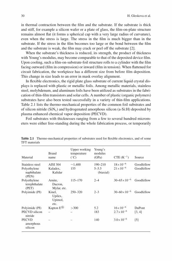
30 H. Gleskova et al.
in thermal contraction between the film and the substrate. If the substrate is thickand stiff, for example a silicon wafer or a plate of glass, the film-on-plate structureremains almost flat (it forms a spherical cap with a very large radius of curvature),even when the stress is large. The stress in the film is much bigger than in thesubstrate. If the stress in the film becomes too large or the bond between the filmand the substrate is weak, the film may crack or peel off the substrate [2].
When the substrate’s thickness is reduced, its strength, the product of thicknesswith Young’s modulus, may become comparable to that of the deposited device film.Upon cooling, such a film-on-substrate-foil structure rolls to a cylinder with the filmfacing outward (film in compression) or inward (film in tension). When flattened forcircuit fabrication, the workpiece has a different size from before film deposition.This change in size leads to an error in mask overlay alignment.
In flexible electronics, the rigid plate glass substrate of current liquid crystal dis-plays is replaced with plastic or metallic foils. Among metallic materials, stainlesssteel, molybdenum, and aluminum foils have been utilized as substrates in the fabri-cation of thin-film transistors and solar cells. A number of plastic (organic polymers)substrates have also been tested successfully in a variety of thin-film applications.Table 2.1 lists the thermo-mechanical properties of the common foil substrates andof silicon nitride (SiNx) and hydrogenated amorphous silicon (a-Si:H) deposited byplasma enhanced chemical vapor deposition (PECVD).
Foil substrates with thicknesses ranging from a few to several hundred microm-eters were either free-standing during the whole fabrication process, or temporarily
Table 2.1 Thermo-mechanical properties of substrates used for flexible electronics, and of someTFT materials
Upper working Young’sBrand temperature modulus
Material name (◦C) (GPa) CTE (K−1) Source
Stainless steel AISI 304 ∼1,400 190–210 18×10−6 GoodfellowPolyethylene
naphthalate(PEN)
Kaladex,Kalidar
155 5–5.5(biaxial)
21×10−6 Goodfellow
Polyethyleneterephthalate(PET)
Arnite,Dacron,Mylar, etc.
115–170 2–4 30–65×10−6 Goodfellow
Polyimide (PI) Kinel,Upilex,Upimol,etc.
250–320 2–3 30–60×10−6 Goodfellow
Polyimide (PI) Kapton E® >300 5.2 16×10−6 DuPontPECVD silicon
nitride– – 183 2.7×10⁻⁶ [3, 4]
PECVDamorphoussilicon
– – 140 3.0×10⁻⁶ [5]
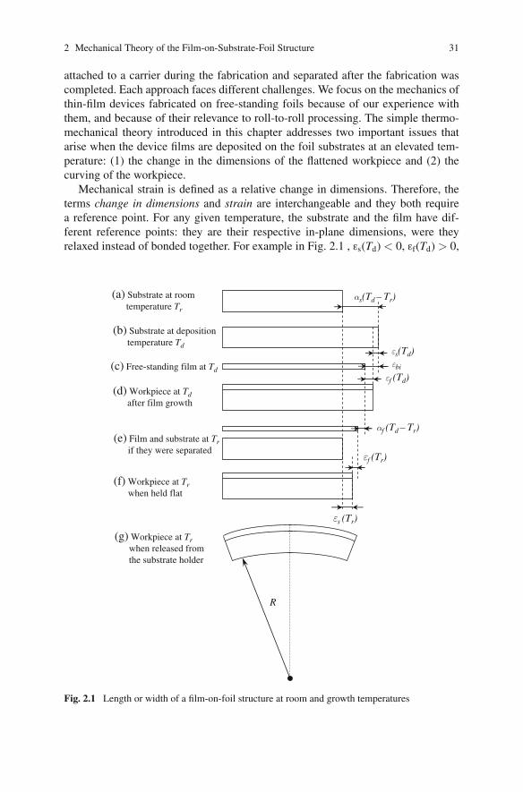
2 Mechanical Theory of the Film-on-Substrate-Foil Structure 31
attached to a carrier during the fabrication and separated after the fabrication wascompleted. Each approach faces different challenges. We focus on the mechanics ofthin-film devices fabricated on free-standing foils because of our experience withthem, and because of their relevance to roll-to-roll processing. The simple thermo-mechanical theory introduced in this chapter addresses two important issues thatarise when the device films are deposited on the foil substrates at an elevated tem-perature: (1) the change in the dimensions of the flattened workpiece and (2) thecurving of the workpiece.
Mechanical strain is defined as a relative change in dimensions. Therefore, theterms change in dimensions and strain are interchangeable and they both requirea reference point. For any given temperature, the substrate and the film have dif-ferent reference points: they are their respective in-plane dimensions, were theyrelaxed instead of bonded together. For example in Fig. 2.1 , εs(Td) < 0, εf(Td) > 0,
(a) Substrate at room temperature Tr
(b) Substrate at deposition temperature Td
(d) Workpiece at Tdafter film growth
(e) Film and substrate at Trif they were separated
(f) Workpiece at Trwhen held flat
(g) Workpiece at Trwhen released from the substrate holder
εs(Td)εbi(c) Free-standing film at Td
αs(Td – Tr)
R
εf (Td)
αf (Td – Tr)
εf (Tr)
εs (Tr)
Fig. 2.1 Length or width of a film-on-foil structure at room and growth temperatures
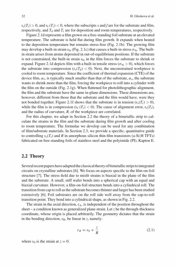
32 H. Gleskova et al.
εs(Tr) > 0, and εf (Tr) < 0, where the subscripts s and f are for the substrate and film,respectively, and Td and Tr are for deposition and room temperatures, respectively.
Figure 2.1d represents a film grown on a free-standing foil substrate at an elevatedtemperature. The substrate is held flat during film growth. It expands when heatedto the deposition temperature but remains stress-free (Fig. 2.1b). The growing filmmay develop a built-in strain εbi (Fig. 2.1c) that causes a built-in stress σ bi. The built-in strain arises from atoms deposited in out-of-equilibrium positions. If the substrateis not constrained, the built-in strain εbi in the film forces the substrate to shrink orexpand. Figure 2.1d depicts film with a built-in tensile stress (σ bi > 0), which forcesthe substrate into compression (εs(Td) < 0). Next, the unconstrained workpiece iscooled to room temperature. Since the coefficient of thermal expansion (CTE) of thedevice film, αf, is typically much smaller than that of the substrate, αs, the substratewants to shrink more than the film, forcing the workpiece to roll into a cylinder withthe film on the outside (Fig. 2.1g). When flattened for photolithographic alignment,the film and the substrate have the same in-plane dimensions. These dimensions are,however, different from those that the substrate and the film would have, were theynot bonded together. Figure 2.1f shows that the substrate is in tension (εs(Tr) > 0),while the film is in compression (εf (Tr) < 0). The cause of alignment error, εs(Tr),and the radius of curvature, R, of the workpiece are correlated.
For this chapter, we adapt in Section 2.2 the theory of a bimetallic strip to cal-culate the strains in the film and the substrate during film growth and after coolingto room temperature. The formulae we develop can be used for any combinationof film/substrate materials. In Section 2.3, we provide a specific, quantitative guideto controlling εs(Tr) and R in amorphous silicon thin-film transistors (a-Si:H TFTs)fabricated on free-standing foils of stainless steel and the polyimide (PI), Kapton E.
2.2 Theory
Several recentpapershaveadapted theclassical theoryofbimetallic strips to integratedcircuits on crystalline substrates [6]. We focus on aspects specific to the film-on-foilstructure [7]. The stress field due to misfit strains is biaxial in the plane of the filmand the substrate. A small, stiff wafer bends into a spherical cap with an equal andbiaxial curvature. However, a film-on-foil structure bends into a cylindrical roll. Thetransition from cap to roll as the substrate becomes thinner and larger has been studiedextensively [6]. Foil substrates are on the roll side well away from the cap-to-rolltransition point. They bend into a cylindrical shape, as shown in Fig. 2.2.
The strain in the axial direction, εA, is independent of the position throughout thesheet – a condition known as generalized plane strain. Let z be the through-thicknesscoordinate, whose origin is placed arbitrarily. The geometry dictates that the strainin the bending direction, εB, be linear in z, namely:
εB = ε0 + z
R(2.1)
where ε0 is the strain at z = 0.
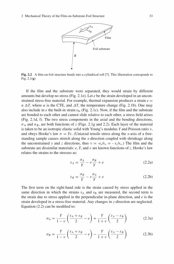
2 Mechanical Theory of the Film-on-Substrate-Foil Structure 33
εA
εB
R
Film
Foil substrate
Fig. 2.2 A film-on-foil structure bends into a cylindrical roll [7]. This illustration corresponds toFig. 2.1(g)
If the film and the substrate were separated, they would strain by differentamounts but develop no stress (Fig. 2.1e). Let e be the strain developed in an uncon-strained stress-free material. For example, thermal expansion produces a strain e =α ΔT, where α is the CTE, and ΔT, the temperature change (Fig. 2.1b). One mayalso include in e the built-in strain εbi (Fig. 2.1c). Now, if the film and the substrateare bonded to each other and cannot slide relative to each other, a stress field arises(Fig. 2.1d, f). The two stress components in the axial and the bending directions,σA and σB, are both functions of z (Figs. 2.1g and 2.2). Each layer of the materialis taken to be an isotropic elastic solid with Young’s modulus Y and Poisson ratio ν,and obeys Hooke’s law σ = Yε. (Uniaxial tensile stress along the x-axis of a free-standing sample causes stretch along the x-direction coupled with shrinkage alongthe unconstrained y and z directions, thus ν = -εy/εx = - εz/εx.) The film and thesubstrate are dissimilar materials: e, Y, and ν are known functions of z. Hooke’s lawrelates the strains to the stresses as:
εA = σA
Y− ν
σB
Y+ e (2.2a)
εB = σB
Y− ν
σA
Y+ e (2.2b)
The first term on the right-hand side is the strain caused by stress applied in thesame direction in which the strains εA and εB are measured, the second term isthe strain due to stress applied in the perpendicular in-plane direction, and e is thestrain developed in a stress-free material. Any changes in z-direction are neglected.Equation (2.2) can be modified to:
σA = Y
1 − ν
(εA + εB
2− e
)+ Y
1 + ν
(εA − εB
2
)(2.3a)
σB = Y
1 − ν
(εA + εB
2− e
)− Y
1 + ν
(εA − εB
2
)(2.3b)
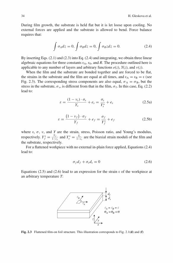
34 H. Gleskova et al.
During film growth, the substrate is held flat but it is let loose upon cooling. Noexternal forces are applied and the substrate is allowed to bend. Force balancerequires that:
∫σAdz = 0,
∫σBdz = 0,
∫σB zdz = 0. (2.4)
By inserting Eqs. (2.1) and (2.3) into Eq. (2.4) and integrating, we obtain three linearalgebraic equations for three constants εA, ε0, and R. The procedure outlined here isapplicable to any number of layers and arbitrary functions e(z), Y(z), and ν(z).
When the film and the substrate are bonded together and are forced to be flat,the strains in the substrate and the film are equal at all times, and εA = εB = ε (seeFig. 2.3). The corresponding stress components are also equal, σA = σB, but thestress in the substrate, σ s, is different from that in the film, σ f. In this case, Eq. (2.2)lead to:
ε = (1 − νs) · σs
Ys+ es = σs
Y ∗s
+ es (2.5a)
ε =(1 − ν f
) · σ f
Y f+ e f = σ f
Y ∗f
+ e f (2.5b)
where ε, σ , ν, and Y are the strain, stress, Poisson ratio, and Young’s modulus,respectively. Y ∗
f = Y f
1−ν fand Y ∗
s = Ys1−νs
are the biaxial strain moduli of the film andthe substrate, respectively.
For a flattened workpiece with no external in-plain force applied, Equations (2.4)lead to:
σ f d f + σsds = 0 (2.6)
Equations (2.5) and (2.6) lead to an expression for the strain ε of the workpiece atan arbitrary temperature T:
A
B
xyz
dfds
A = B =
A = B =ε
ε
ε
ε εσ σ σ
Fig. 2.3 Flattened film-on foil structure. This illustration corresponds to Fig. 2.1(d) and (f)
2 Mechanical Theory of the Film-on-Substrate-Foil Structure 35
ε(T ) =es(T ) + Y ∗
f d f
Y ∗s ds
· e f (T )
1 + Y ∗f d f
Y ∗s ds
(2.7)
where ef = αf (T – Td) + εbi and es = αs (T – Td). Td is the deposition temperature,and αf and αs are the CTEs of the film and the substrate, respectively.
The in-plane strain in the substrate coated with a film (strain in the substrate of aflattened workpiece) with respect to the uncoated substrate at the same temperature,at any temperature T, can be expressed as:
εs(T ) = ε (T ) − es(T ) =[(Td − T )
(αs − α f
) + εbi]
1 + Y ∗s ds
Y ∗f d f
(2.8a)
Similarly, the in-plane strain in the film (strain in the film of a flattened workpiece)with respect to the free-standing film at the same temperature, at any temperature T,can be expressed as:
ε f (T ) = ε (T ) − e f (T ) = −[(Td − T )
(αs − α f
) + εbi]
1 + Y ∗f d f
Y ∗s ds
(2.8b)
2.2.1 The Built-in Strain εbi
The built-in strain εbi that develops in the film during its deposition manifests itselfby the built-in stress σ bi. At T = Td, the only stress in the film is the built-in stressσ bi and Eqs. (2.5) and (2.6) lead to:
εbi = − σbi
Y ∗f
·(
1 + Y ∗f d f
Y ∗s ds
)(2.9)
The minus sign indicates that, at the deposition temperature, a film with built-intensile stress (σbi > 0) forces the substrate to shrink, while a film with built-in com-pressive stress (σbi < 0) forces the substrate to expand. (If the deposition is doneat room temperature, the film with built-in tensile stress forces the substrate intocompression. If released, it will curve such that the film lies on the concave side.)The term in the parentheses is the modification for a compliant substrate: when thefilm strength, Y ∗
f d f , becomes comparable to the substrate strength, Y ∗s ds , the sub-
strate changes its dimension in response to film deposition. For stiff substrates whenY ∗
f d f << Y ∗s ds , this term equals 1.
Both εbi and σ bi can be complicated functions of the film’s through-thicknesscoordinate z. Typically, neither εbi (z) nor σbi (z) is known. Therefore, an averagestrain value εbi is extracted from experiments for a given film/substrate couple, forexample from the radius of curvature of the relaxed workpiece [8].
36 H. Gleskova et al.
For the remainder of this chapter, we will use the built-in strain εbi. Rememberthat, following Eq. (2.9), the built-in strain is negative if tensile built-in stress isgrown into the film, and it is positive for compressive built-in stress.
2.3 Applications
2.3.1 Strain in the Substrate, εs(Td), and the Film, εf(Td),at the Deposition Temperature Td
A growing film typically builds in strain εbi. This built-in strain arises from atomsdeposited in out-of-equilibrium positions. If the substrate is thin and/or compliantand unconstrained, the growing film will relieve some of its built-in strain/stress byforcing the substrate to shrink (tensile built-in stress in the film) or expand (com-pressive built-in stress in the film). The change in the substrate’s in-plane dimen-sions (strain in the substrate of a flattened workpiece) at the deposition temperatureTd can be calculated from Eq. (2.8a) by setting T = Td:
εs(Td ) = εbi
1 + Y ∗s ds
Y ∗f d f
(2.10)
Equation (2.10) compares the in-plane substrate’s dimensions at the deposition tem-perature Td after and before film growth. Tensile built-in strain (εbi < 0) leads to anegative εs (Td), indicating substrate shrinkage during film growth (see Fig. 2.1d).Compressive built-in strain (εbi > 0) leads to a positive εs (Td), indicating substrateexpansion during film growth.
Setting T = Td in Eq. (2.8b) expresses the change in the in-plane film’s dimen-sions (strain in the film of a flattened workpiece) at the deposition temperature Td:
ε f (Td ) = − εbi
1 + Y ∗f d f
Y ∗s ds
(2.11)
Equation (2.11) describes the in-plane strain in the film at the deposition temperatureTd when the built-in strain εbi is present (compared to the absence of εbi). Tensilebuilt-in strain (εbi < 0) leads to a positive εf (Td), indicating that the film is stretched(see Fig. 2.1d). Compressive built-in strain (εbi > 0) leads to a negative εf (Td),indicating compression in the growing film.
εs (Td) and εf (Td) both equal zero if the film has no built-in strain/stress. For εbi
�= 0 and a thick and rigid substrate (Y ∗f d f << Y ∗
s ds), all strain/stress is taken up bythe film, εf (Td) = –εbi, leaving the substrate free of strain and stress, εs (Td) → 0.For compliant substrates, the denominator in Eqs. (2.10) and (2.11) becomes a finitenumber larger than 1, indicating that the built-in strain is now divided between the
film and the substrate depending on their relative strengths,Y ∗
f d f
Y ∗s ds
.
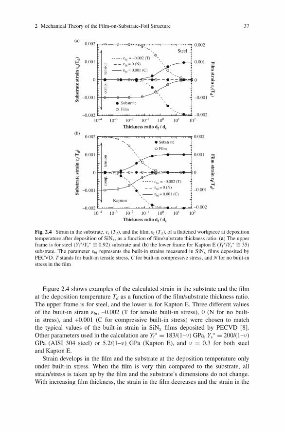
2 Mechanical Theory of the Film-on-Substrate-Foil Structure 37
–0.002
–0.001
0
0.001
0.002
–0.002
–0.001
0
0.001
0.002
10–4 10–3 10–2 10–1 100 101 102
Substrate
Film
εbi = –0.002 (T)
εbi = 0.001 (C)
εbi = 0 (N)
Subs
trat
e st
rain
εs(
Td) F
ilm strain ε
f (Td )
Thickness ratio df / ds
Steel
tens
ion
com
p.
–0.002
–0.001
0
0.001
0.002
–0.002
–0.001
0
0.001
0.002Substrate
Film
Kapton
tens
ion
com
p.
(a)
(b)
Subs
trat
e st
rain
εs(
Td)
10–4 10–3 10–2 10–1 100 101 102
Thickness ratio df / ds
Film
strain εf (T
d )
εbi = –0.002 (T)
εbi = 0.001 (C)
εbi = 0 (N)
Fig. 2.4 Strain in the substrate, εs (Td), and the film, εf (Td), of a flattened workpiece at depositiontemperature after deposition of SiNx, as a function of film/substrate thickness ratio. (a) The upperframe is for steel (Yf
∗/Ys∗ ∼= 0.92) substrate and (b) the lower frame for Kapton E (Yf
∗/Ys∗ ∼= 35)
substrate. The parameter εbi represents the built-in strains measured in SiNx films deposited byPECVD. T stands for built-in tensile stress, C for built-in compressive stress, and N for no built-instress in the film
Figure 2.4 shows examples of the calculated strain in the substrate and the filmat the deposition temperature Td as a function of the film/substrate thickness ratio.The upper frame is for steel, and the lower is for Kapton E. Three different valuesof the built-in strain εbi, –0.002 (T for tensile built-in stress), 0 (N for no built-in stress), and +0.001 (C for compressive built-in stress) were chosen to matchthe typical values of the built-in strain in SiNx films deposited by PECVD [8].Other parameters used in the calculation are Yf
∗ = 183/(1–ν) GPa, Ys∗ = 200/(1–ν)
GPa (AISI 304 steel) or 5.2/(1–ν) GPa (Kapton E), and ν = 0.3 for both steeland Kapton E.
Strain develops in the film and the substrate at the deposition temperature onlyunder built-in stress. When the film is very thin compared to the substrate, allstrain/stress is taken up by the film and the substrate’s dimensions do not change.With increasing film thickness, the strain in the film decreases and the strain in the
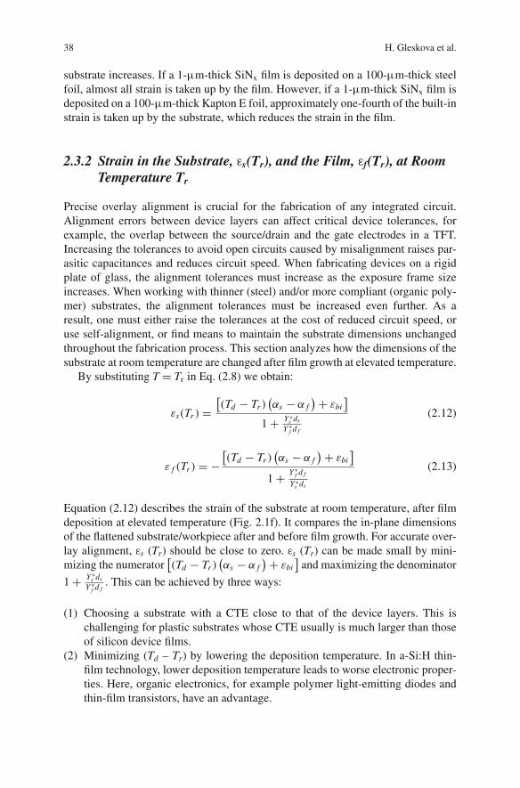
38 H. Gleskova et al.
substrate increases. If a 1-μm-thick SiNx film is deposited on a 100-μm-thick steelfoil, almost all strain is taken up by the film. However, if a 1-μm-thick SiNx film isdeposited on a 100-μm-thick Kapton E foil, approximately one-fourth of the built-instrain is taken up by the substrate, which reduces the strain in the film.
2.3.2 Strain in the Substrate, εs(Tr), and the Film, εf(Tr), at RoomTemperature Tr
Precise overlay alignment is crucial for the fabrication of any integrated circuit.Alignment errors between device layers can affect critical device tolerances, forexample, the overlap between the source/drain and the gate electrodes in a TFT.Increasing the tolerances to avoid open circuits caused by misalignment raises par-asitic capacitances and reduces circuit speed. When fabricating devices on a rigidplate of glass, the alignment tolerances must increase as the exposure frame sizeincreases. When working with thinner (steel) and/or more compliant (organic poly-mer) substrates, the alignment tolerances must be increased even further. As aresult, one must either raise the tolerances at the cost of reduced circuit speed, oruse self-alignment, or find means to maintain the substrate dimensions unchangedthroughout the fabrication process. This section analyzes how the dimensions of thesubstrate at room temperature are changed after film growth at elevated temperature.
By substituting T = Tr in Eq. (2.8) we obtain:
εs(Tr ) =[(Td − Tr )
(αs − α f
) + εbi]
1 + Y ∗s ds
Y ∗f d f
(2.12)
ε f (Tr ) = −[(Td − Tr )
(αs − α f
) + εbi]
1 + Y ∗f d f
Y ∗s ds
(2.13)
Equation (2.12) describes the strain of the substrate at room temperature, after filmdeposition at elevated temperature (Fig. 2.1f). It compares the in-plane dimensionsof the flattened substrate/workpiece after and before film growth. For accurate over-lay alignment, εs (Tr) should be close to zero. εs (Tr) can be made small by mini-mizing the numerator
[(Td − Tr )
(αs − α f
) + εbi]
and maximizing the denominator
1 + Y ∗s ds
Y ∗f d f
. This can be achieved by three ways:
(1) Choosing a substrate with a CTE close to that of the device layers. This ischallenging for plastic substrates whose CTE usually is much larger than thoseof silicon device films.
(2) Minimizing (Td – Tr) by lowering the deposition temperature. In a-Si:H thin-film technology, lower deposition temperature leads to worse electronic proper-ties. Here, organic electronics, for example polymer light-emitting diodes andthin-film transistors, have an advantage.
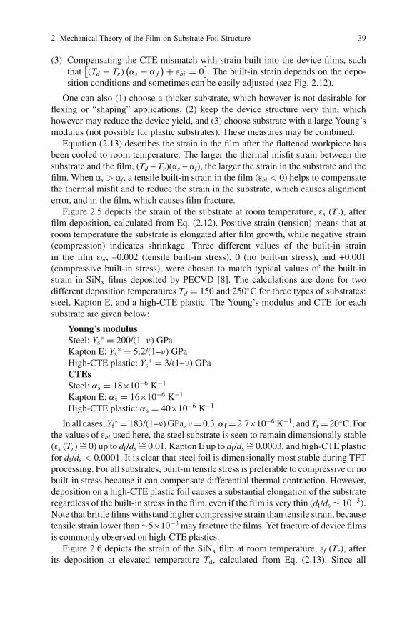
2 Mechanical Theory of the Film-on-Substrate-Foil Structure 39
(3) Compensating the CTE mismatch with strain built into the device films, suchthat
[(Td − Tr )
(αs − α f
) + εbi = 0]. The built-in strain depends on the depo-
sition conditions and sometimes can be easily adjusted (see Fig. 2.12).
One can also (1) choose a thicker substrate, which however is not desirable forflexing or “shaping” applications, (2) keep the device structure very thin, whichhowever may reduce the device yield, and (3) choose substrate with a large Young’smodulus (not possible for plastic substrates). These measures may be combined.
Equation (2.13) describes the strain in the film after the flattened workpiece hasbeen cooled to room temperature. The larger the thermal misfit strain between thesubstrate and the film, (Td – Tr)(αs – αf), the larger the strain in the substrate and thefilm. When αs > αf, a tensile built-in strain in the film (εbi < 0) helps to compensatethe thermal misfit and to reduce the strain in the substrate, which causes alignmenterror, and in the film, which causes film fracture.
Figure 2.5 depicts the strain of the substrate at room temperature, εs (Tr), afterfilm deposition, calculated from Eq. (2.12). Positive strain (tension) means that atroom temperature the substrate is elongated after film growth, while negative strain(compression) indicates shrinkage. Three different values of the built-in strainin the film εbi, –0.002 (tensile built-in stress), 0 (no built-in stress), and +0.001(compressive built-in stress), were chosen to match typical values of the built-instrain in SiNx films deposited by PECVD [8]. The calculations are done for twodifferent deposition temperatures Td = 150 and 250◦C for three types of substrates:steel, Kapton E, and a high-CTE plastic. The Young’s modulus and CTE for eachsubstrate are given below:
Young’s modulusSteel: Ys
∗ = 200/(1–ν) GPaKapton E: Ys
∗ = 5.2/(1–ν) GPaHigh-CTE plastic: Ys
∗ = 3/(1–ν) GPaCTEsSteel: αs = 18×10−6 K−1
Kapton E: αs = 16×10−6 K−1
High-CTE plastic: αs = 40×10−6 K−1
In all cases, Yf∗ = 183/(1–ν) GPa, ν= 0.3,αf = 2.7×10⁻⁶ K−1, and Tr = 20◦C. For
the values of εbi used here, the steel substrate is seen to remain dimensionally stable(εs (Tr) ∼= 0) up to df/ds
∼= 0.01, Kapton E up to df/ds∼= 0.0003, and high-CTE plastic
for df/ds < 0.0001. It is clear that steel foil is dimensionally most stable during TFTprocessing. For all substrates, built-in tensile stress is preferable to compressive or nobuilt-in stress because it can compensate differential thermal contraction. However,deposition on a high-CTE plastic foil causes a substantial elongation of the substrateregardless of the built-in stress in the film, even if the film is very thin (df/ds ∼ 10−3).Note that brittle films withstand higher compressive strain than tensile strain, becausetensile strain lower than ∼5×10⁻³ may fracture the films. Yet fracture of device filmsis commonly observed on high-CTE plastics.
Figure 2.6 depicts the strain of the SiNx film at room temperature, εf (Tr), afterits deposition at elevated temperature Td, calculated from Eq. (2.13). Since all
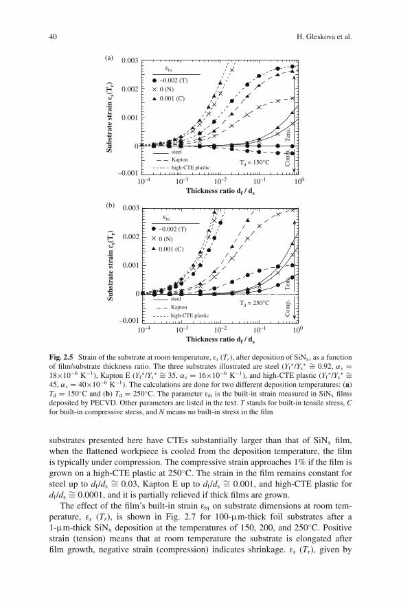
40 H. Gleskova et al.
–0.001
0
0.001
0.002
0.003
10–4 10–3 10–2 10–1 100
–0.002 (T)0 (N)
0.001 (C)
steel
Kapton
high-CTE plasticTd = 150°C
εbi
Subs
trat
e st
rain
εs(
Tr)
Thickness ratio df / ds
Ten
s.C
omp.
–0.002 (T)
0 (N)
0.001 (C)
steel
Kapton
high-CTE plastic
Ten
s.C
omp.
(a)
–0.001
0
0.001
0.002
0.003
Subs
trat
e st
rain
εs(
Tr)
(b)
10–4 10–3 10–2 10–1 100
Thickness ratio df / ds
εbi
Td = 250°C
Fig. 2.5 Strain of the substrate at room temperature, εs (Tr), after deposition of SiNx, as a functionof film/substrate thickness ratio. The three substrates illustrated are steel (Yf
∗/Ys∗ ∼= 0.92, αs =
18×10−6 K−1), Kapton E (Yf∗/Ys
∗ ∼= 35, αs = 16×10−6 K−1), and high-CTE plastic (Yf∗/Ys
∗ ∼=45, αs = 40×10−6 K−1). The calculations are done for two different deposition temperatures: (a)Td = 150◦C and (b) Td = 250◦C. The parameter εbi is the built-in strain measured in SiNx filmsdeposited by PECVD. Other parameters are listed in the text. T stands for built-in tensile stress, Cfor built-in compressive stress, and N means no built-in stress in the film
substrates presented here have CTEs substantially larger than that of SiNx film,when the flattened workpiece is cooled from the deposition temperature, the filmis typically under compression. The compressive strain approaches 1% if the film isgrown on a high-CTE plastic at 250◦C. The strain in the film remains constant forsteel up to df/ds
∼= 0.03, Kapton E up to df/ds∼= 0.001, and high-CTE plastic for
df/ds∼= 0.0001, and it is partially relieved if thick films are grown.
The effect of the film’s built-in strain εbi on substrate dimensions at room tem-perature, εs (Tr), is shown in Fig. 2.7 for 100-μm-thick foil substrates after a1-μm-thick SiNx deposition at the temperatures of 150, 200, and 250◦C. Positivestrain (tension) means that at room temperature the substrate is elongated afterfilm growth, negative strain (compression) indicates shrinkage. εs (Tr), given by
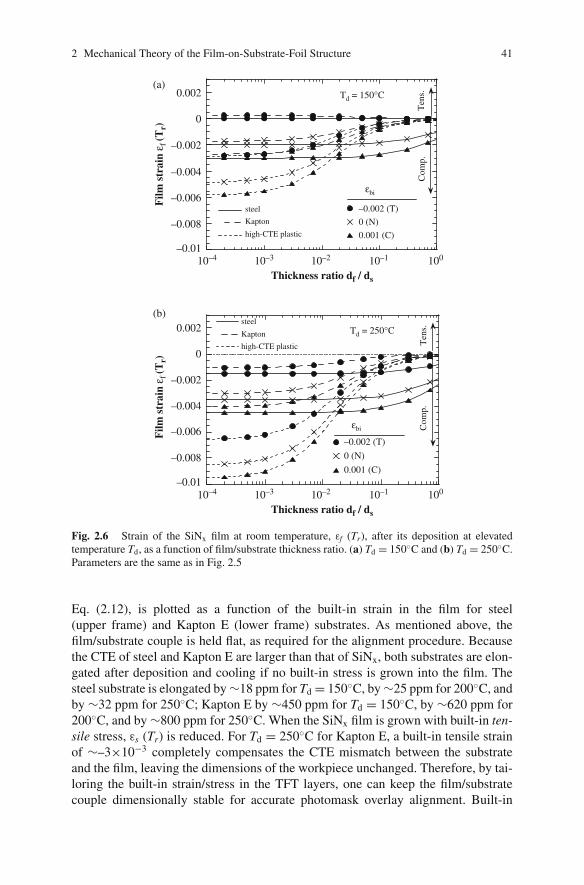
2 Mechanical Theory of the Film-on-Substrate-Foil Structure 41
–0.01
–0.008
–0.006
–0.004
–0.002
0
0.002
10–4 10–3 10–2 10–1 100
–0.002 (T)
0 (N)
0.001 (C)
steel
Kapton
high-CTE plastic
εbi
Td = 150°C
Film
str
ain
ε f (T
r)
Thickness ratio df / ds
Ten
s.C
omp.
–0.01
–0.008
–0.006
–0.004
–0.002
0
0.002
–0.002 (T)
0 (N)
0.001 (C)
steel
Kapton
high-CTE plastic
εbiT
ens.
Com
p.
(a)
(b)
Td = 250°C
Film
str
ain
ε f (T
r)
10–4 10–3 10–2 10–1 100
Thickness ratio df / ds
Fig. 2.6 Strain of the SiNx film at room temperature, εf (Tr), after its deposition at elevatedtemperature Td, as a function of film/substrate thickness ratio. (a) Td = 150◦C and (b) Td = 250◦C.Parameters are the same as in Fig. 2.5
Eq. (2.12), is plotted as a function of the built-in strain in the film for steel(upper frame) and Kapton E (lower frame) substrates. As mentioned above, thefilm/substrate couple is held flat, as required for the alignment procedure. Becausethe CTE of steel and Kapton E are larger than that of SiNx, both substrates are elon-gated after deposition and cooling if no built-in stress is grown into the film. Thesteel substrate is elongated by ∼18 ppm for Td = 150◦C, by ∼25 ppm for 200◦C, andby ∼32 ppm for 250◦C; Kapton E by ∼450 ppm for Td = 150◦C, by ∼620 ppm for200◦C, and by ∼800 ppm for 250◦C. When the SiNx film is grown with built-in ten-sile stress, εs (Tr) is reduced. For Td = 250◦C for Kapton E, a built-in tensile strainof ∼–3×10⁻³ completely compensates the CTE mismatch between the substrateand the film, leaving the dimensions of the workpiece unchanged. Therefore, by tai-loring the built-in strain/stress in the TFT layers, one can keep the film/substratecouple dimensionally stable for accurate photomask overlay alignment. Built-in
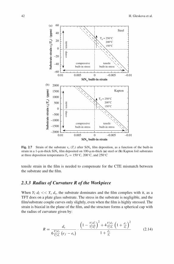
42 H. Gleskova et al.
–60
–40
–20
0
20
40
60
–0.01–0.00500.0050.01
200°C
tensilebuilt-in stress
compressivebuilt-in stress
com
p.te
nsil
e
Steel
Td = 250°C
150°C
Subs
trat
e st
rain
εs(
Tr)
(pp
m)
SiNx built-in strain
–2000
–1500
–1000
–500
0
500
1000
1500
2000
tensilebuilt-in stress
compressivebuilt-in stress
com
p.te
nsil
e
Kapton
Subs
trat
e st
rain
εs(
Tr)
(pp
m)
(a)
(b)
–0.01–0.00500.0050.01SiNx built-in strain
200°CTd = 250°C
150°C
Fig. 2.7 Strain of the substrate εs (Tr) after SiNx film deposition, as a function of the built-instrain in a 1-μm-thick SiNx film deposited on 100-μm-thick (a) steel or (b) Kapton foil substratesat three deposition temperatures Td = 150◦C, 200◦C, and 250◦C
tensile strain in the film is needed to compensate for the CTE mismatch betweenthe substrate and the film.
2.3.3 Radius of Curvature R of the Workpiece
When Yf df << Ys ds, the substrate dominates and the film complies with it, as aTFT does on a plate glass substrate. The stress in the substrate is negligible, and thefilm/substrate couple curves only slightly, even when the film is highly stressed. Thestrain is biaxial in the plane of the film, and the structure forms a spherical cap withthe radius of curvature given by:
R = ds
6Y ∗
f d f
Y ∗s ds
(e f − es
) ·(
1 − Y ∗f d2
f
Y ∗s d2
s
)2+ 4
Y ∗f d f
Y ∗s ds
(1 + d f
ds
)2
1 + d f
ds
(2.14)
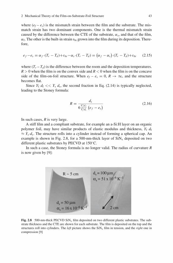
2 Mechanical Theory of the Film-on-Substrate-Foil Structure 43
where (ef – es) is the mismatch strain between the film and the substrate. The mis-match strain has two dominant components. One is the thermal mismatch straincaused by the difference between the CTE of the substrate, αs, and that of the film,αf. The other is the built-in strain εbi grown into the film during its deposition. There-fore,
e f −es = α f ·(Tr − Td )+εbi −αs ·(Tr − Td ) = (α f − αs
)·(Tr − Td )+εbi (2.15)
where (Tr – Td) is the difference between the room and the deposition temperatures.R > 0 when the film is on the convex side and R < 0 when the film is on the concaveside of the film-on-foil structure. When ef – es = 0, R → ∞, and the structurebecomes flat.
Since Yf df << Ys ds, the second fraction in Eq. (2.14) is typically neglected,leading to the Stoney formula:
R = ds
6Y ∗
f d f
Y ∗s ds
(e f − es
) (2.16)
In such cases, R is very large.A stiff film and a compliant substrate, for example an a-Si:H layer on an organic
polymer foil, may have similar products of elastic modulus and thickness, Yf df
≈ Ys·ds. The structure rolls into a cylinder instead of forming a spherical cap. Anexample is shown in Fig. 2.8, for a 500-nm-thick layer of SiNx deposited on twodifferent plastic substrates by PECVD at 150◦C.
In such a case, the Stoney formula is no longer valid. The radius of curvature Ris now given by [9]:
2 cm
R ~ 5 cm ds = 100 μm αs = 51 x 10–6
K–1
αs = 16 x 10–6 K
–1ds = 50 μm
Fig. 2.8 500-nm-thick PECVD SiNx film deposited on two different plastic substrates. The sub-strate thickness and the CTE are shown for each substrate. The film is deposited on the top and thestructures roll into cylinders. The left picture shows the SiNx film in tension, and the right one incompression [9]
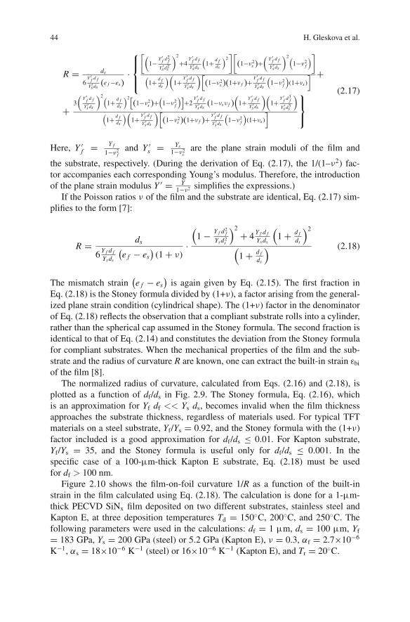
44 H. Gleskova et al.
R = ds
6Y ′
f d f
Y ′s ds
(e f −es)·
⎧⎪⎨⎪⎩
[(1− Y ′
f d2f
Y ′s d2
s
)2
+4Y ′
f d f
Y ′s ds
(1+ d f
ds
)2][
(1−ν2s )+
(Y ′
f d f
Y ′s ds
)2(1−ν2
f
)]
(1+ d f
ds
)(1+ Y ′
f d f
Y ′s ds
)[(1−ν2
s )(1+ν f )+Y ′
f d f
Y ′s ds
(1−ν2
f
)(1+νs )
] +
+3
(Y ′
f d f
Y ′s ds
)2(1+ d f
ds
)2[(1−ν2
s )+(
1−ν2f
)]+2
Y ′f d f
Y ′s ds
(1−νsν f )(
1+ Y ′f d f
Y ′s ds
)(1+ Y ′
f d3f
Y ′s d3
s
)(
1+ d fds
)(1+ Y ′
f d f
Y ′s ds
)[(1−ν2
s )(1+ν f )+Y ′
f d f
Y ′s ds
(1−ν2
f
)(1+νs )
]⎫⎬⎭
(2.17)
Here, Y ′f = Y f
1−ν2f
and Y ′s = Ys
1−ν2s
are the plane strain moduli of the film and
the substrate, respectively. (During the derivation of Eq. (2.17), the 1/(1–ν2) fac-tor accompanies each corresponding Young’s modulus. Therefore, the introductionof the plane strain modulus Y ′ = Y
1−ν2 simplifies the expressions.)If the Poisson ratios ν of the film and the substrate are identical, Eq. (2.17) sim-
plifies to the form [7]:
R = ds
6 Y f d f
Ys ds
(e f − es
)(1 + ν)
·(
1 − Y f d2f
Ys d2s
)2+ 4 Y f d f
Ys ds
(1 + d f
ds
)2
(1 + d f
ds
) (2.18)
The mismatch strain(e f − es
)is again given by Eq. (2.15). The first fraction in
Eq. (2.18) is the Stoney formula divided by (1+ν), a factor arising from the general-ized plane strain condition (cylindrical shape). The (1+ν) factor in the denominatorof Eq. (2.18) reflects the observation that a compliant substrate rolls into a cylinder,rather than the spherical cap assumed in the Stoney formula. The second fraction isidentical to that of Eq. (2.14) and constitutes the deviation from the Stoney formulafor compliant substrates. When the mechanical properties of the film and the sub-strate and the radius of curvature R are known, one can extract the built-in strain εbi
of the film [8].The normalized radius of curvature, calculated from Eqs. (2.16) and (2.18), is
plotted as a function of df/ds in Fig. 2.9. The Stoney formula, Eq. (2.16), whichis an approximation for Yf df << Ys ds, becomes invalid when the film thicknessapproaches the substrate thickness, regardless of materials used. For typical TFTmaterials on a steel substrate, Yf/Ys = 0.92, and the Stoney formula with the (1+ν)factor included is a good approximation for df/ds ≤ 0.01. For Kapton substrate,Yf/Ys = 35, and the Stoney formula is useful only for df/ds ≤ 0.001. In thespecific case of a 100-μm-thick Kapton E substrate, Eq. (2.18) must be usedfor df > 100 nm.
Figure 2.10 shows the film-on-foil curvature 1/R as a function of the built-instrain in the film calculated using Eq. (2.18). The calculation is done for a 1-μm-thick PECVD SiNx film deposited on two different substrates, stainless steel andKapton E, at three deposition temperatures Td = 150◦C, 200◦C, and 250◦C. Thefollowing parameters were used in the calculations: df = 1 μm, ds = 100 μm, Yf
= 183 GPa, Ys = 200 GPa (steel) or 5.2 GPa (Kapton E), ν = 0.3, αf = 2.7×10⁻⁶
K−1, αs = 18×10−6 K−1 (steel) or 16×10−6 K−1 (Kapton E), and Tr = 20◦C.
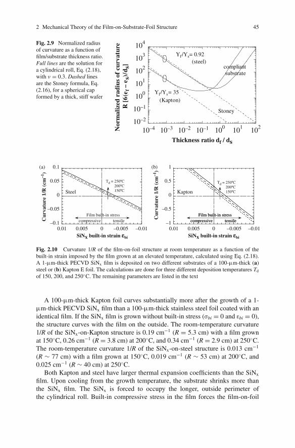
2 Mechanical Theory of the Film-on-Substrate-Foil Structure 45
10–1
10–2
100
101
102
103
104
10–4 10–3 10–2 10–1 100 101 102Nor
mal
ized
rad
ius
of c
urva
ture
R
[6 (
e f –
e s)
/ ds]
Thickness ratio df / ds
Stoney
compliant substrate
Yf /Ys
= 35
Yf /Ys= 0.92
(steel)
(Kapton)
Fig. 2.9 Normalized radiusof curvature as a function offilm/substrate thickness ratio.Full lines are the solution fora cylindrical roll, Eq. (2.18),with ν = 0.3. Dashed linesare the Stoney formula, Eq.(2.16), for a spherical capformed by a thick, stiff wafer
–0.1
–0.05
0
0.05
0.1
–0.01–0.00500.0050.01
Cur
vatu
re 1
/R (
cm–1
)
SiNx built-in strain εbi SiNx built-in strain εbi
Steel
tensile compressive Film built-in stress
(a)
Td = 250ºC200ºC150ºC
Cur
vatu
re 1
/R (
cm–1
)
–1
–0.5
0
0.5
1
–0.01–0.00500.0050.01
Kapton
tensile compressive Film built-in stress
(b)
Td = 250ºC200ºC150ºC
tensile compressive Film built-in stress
Fig. 2.10 Curvature 1/R of the film-on-foil structure at room temperature as a function of thebuilt-in strain imposed by the film grown at an elevated temperature, calculated using Eq. (2.18).A 1-μm-thick PECVD SiNx film is deposited on two different substrates of a 100-μm-thick (a)steel or (b) Kapton E foil. The calculations are done for three different deposition temperatures Td
of 150, 200, and 250◦C. The remaining parameters are listed in the text
A 100-μm-thick Kapton foil curves substantially more after the growth of a 1-μm-thick PECVD SiNx film than a 100-μm-thick stainless steel foil coated with anidentical film. If the SiNx film is grown without built-in stress (σbi = 0 and εbi = 0),the structure curves with the film on the outside. The room-temperature curvature1/R of the SiNx-on-Kapton structure is 0.19 cm−1 (R = 5.3 cm) with a film grownat 150◦C, 0.26 cm−1 (R = 3.8 cm) at 200◦C, and 0.34 cm−1 (R = 2.9 cm) at 250◦C.The room-temperature curvature 1/R of the SiNx-on-steel structure is 0.013 cm−1
(R ∼ 77 cm) with a film grown at 150◦C, 0.019 cm−1 (R ∼ 53 cm) at 200◦C, and0.025 cm−1 (R ∼ 40 cm) at 250◦C.
Both Kapton and steel have larger thermal expansion coefficients than the SiNx
film. Upon cooling from the growth temperature, the substrate shrinks more thanthe SiNx film. The SiNx is forced to occupy the longer, outside perimeter ofthe cylindrical roll. Built-in compressive stress in the film forces the film-on-foil
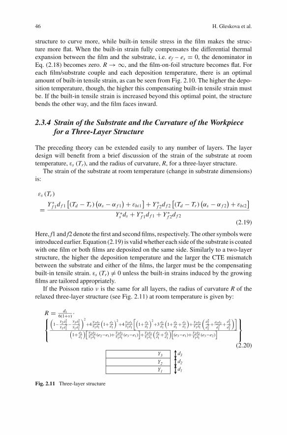
46 H. Gleskova et al.
structure to curve more, while built-in tensile stress in the film makes the struc-ture more flat. When the built-in strain fully compensates the differential thermalexpansion between the film and the substrate, i.e. ef – es = 0, the denominator inEq. (2.18) becomes zero. R → ∞, and the film-on-foil structure becomes flat. Foreach film/substrate couple and each deposition temperature, there is an optimalamount of built-in tensile strain, as can be seen from Fig. 2.10. The higher the depo-sition temperature, though, the higher this compensating built-in tensile strain mustbe. If the built-in tensile strain is increased beyond this optimal point, the structurebends the other way, and the film faces inward.
2.3.4 Strain of the Substrate and the Curvature of the Workpiecefor a Three-Layer Structure
The preceding theory can be extended easily to any number of layers. The layerdesign will benefit from a brief discussion of the strain of the substrate at roomtemperature, εs (Tr), and the radius of curvature, R, for a three-layer structure.
The strain of the substrate at room temperature (change in substrate dimensions)is:
εs (Tr )
= Y ∗f 1d f 1
[(Td − Tr )
(αs − α f 1
) + εbi1] + Y ∗
f 2d f 2[(Td − Tr )
(αs − α f 2
) + εbi2]
Y ∗s ds + Y ∗
f 1d f 1 + Y ∗f 2d f 2
(2.19)
Here, f1 and f2 denote the first and second films, respectively. The other symbols wereintroduced earlier. Equation (2.19) is valid whether each side of the substrate is coatedwith one film or both films are deposited on the same side. Similarly to a two-layerstructure, the higher the deposition temperature and the larger the CTE mismatchbetween the substrate and either of the films, the larger must be the compensatingbuilt-in tensile strain. εs (Tr) �= 0 unless the built-in strains induced by the growingfilms are tailored appropriately.
If the Poisson ratio ν is the same for all layers, the radius of curvature R of therelaxed three-layer structure (see Fig. 2.11) at room temperature is given by:
R = d16(1+ν) ·⎧⎨
⎩(
1− Y2d22
Y1d21− Y3d2
3Y1d2
1
)2
+4 Y2d2Y1d1
(1+ d2
d1
)2+4 Y3d3Y1d1
[(1+ d3
d1
)2+3 d2d1
(1+ d2
d1+ d3
d1
)+ Y2d2
Y1d1
(d2
2d2
1+ d2d3
d21
+ d23
d21
)](
1+ d2d1
)[Y2d2Y1d1
(e2−e1)+ Y3d3Y1d1
(e3−e1)]+ Y3d3
Y1d1
(d2d1
+ d3d1
)[(e3−e1)+ Y2d2
Y1d1(e3−e2)
]⎫⎬⎭
(2.20)d3d2d1
Y3
Y1
Y2
Fig. 2.11 Three-layer structure
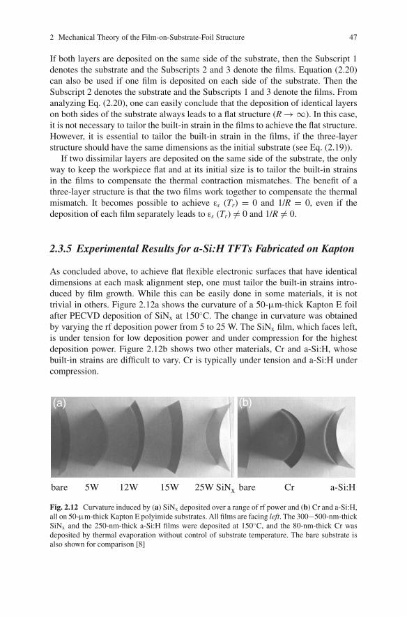
2 Mechanical Theory of the Film-on-Substrate-Foil Structure 47
If both layers are deposited on the same side of the substrate, then the Subscript 1denotes the substrate and the Subscripts 2 and 3 denote the films. Equation (2.20)can also be used if one film is deposited on each side of the substrate. Then theSubscript 2 denotes the substrate and the Subscripts 1 and 3 denote the films. Fromanalyzing Eq. (2.20), one can easily conclude that the deposition of identical layerson both sides of the substrate always leads to a flat structure (R → ∞). In this case,it is not necessary to tailor the built-in strain in the films to achieve the flat structure.However, it is essential to tailor the built-in strain in the films, if the three-layerstructure should have the same dimensions as the initial substrate (see Eq. (2.19)).
If two dissimilar layers are deposited on the same side of the substrate, the onlyway to keep the workpiece flat and at its initial size is to tailor the built-in strainsin the films to compensate the thermal contraction mismatches. The benefit of athree-layer structure is that the two films work together to compensate the thermalmismatch. It becomes possible to achieve εs (Tr) = 0 and 1/R = 0, even if thedeposition of each film separately leads to εs (Tr) �= 0 and 1/R �= 0.
2.3.5 Experimental Results for a-Si:H TFTs Fabricated on Kapton
As concluded above, to achieve flat flexible electronic surfaces that have identicaldimensions at each mask alignment step, one must tailor the built-in strains intro-duced by film growth. While this can be easily done in some materials, it is nottrivial in others. Figure 2.12a shows the curvature of a 50-μm-thick Kapton E foilafter PECVD deposition of SiNx at 150◦C. The change in curvature was obtainedby varying the rf deposition power from 5 to 25 W. The SiNx film, which faces left,is under tension for low deposition power and under compression for the highestdeposition power. Figure 2.12b shows two other materials, Cr and a-Si:H, whosebuilt-in strains are difficult to vary. Cr is typically under tension and a-Si:H undercompression.
bare Cr a-Si:H25W SiNxbare 5W 12W 15W
(b)(a)
Fig. 2.12 Curvature induced by (a) SiNx deposited over a range of rf power and (b) Cr and a-Si:H,all on 50-μm-thick Kapton E polyimide substrates. All films are facing left. The 300−500-nm-thickSiNx and the 250-nm-thick a-Si:H films were deposited at 150◦C, and the 80-nm-thick Cr wasdeposited by thermal evaporation without control of substrate temperature. The bare substrate isalso shown for comparison [8]
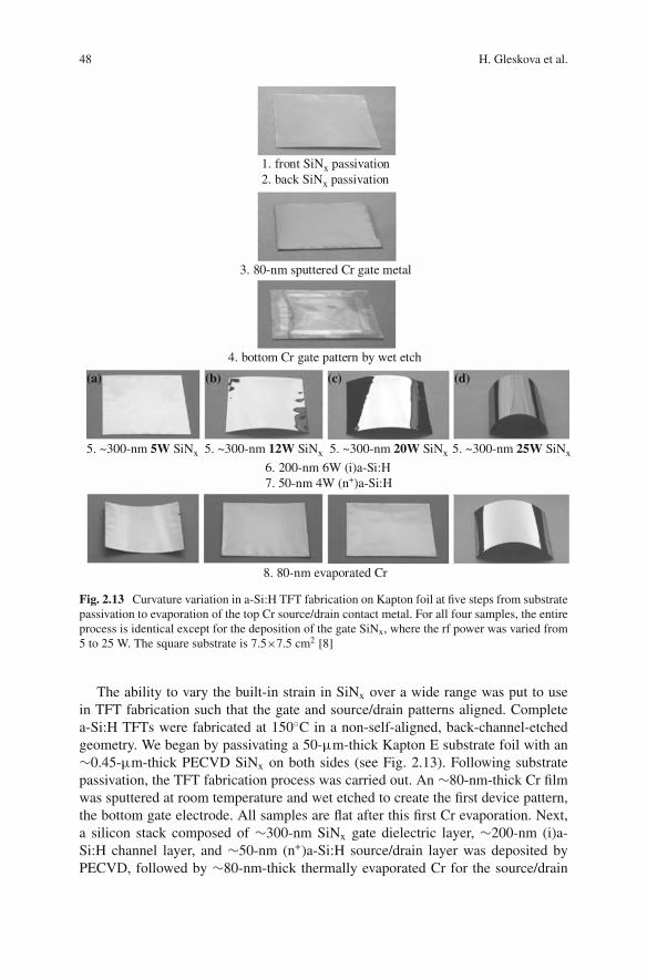
48 H. Gleskova et al.
1. front SiNx passivation 2. back SiNx passivation
3. 80-nm sputtered Cr gate metal
4. bottom Cr gate pattern by wet etch
5. ~300-nm 5W SiNx 5. ~300-nm 12W SiNx 5. ~300-nm 20W SiNx 5. ~300-nm 25W SiNx
8. 80-nm evaporated Cr
(a) (b) (c) (d)
6. 200-nm 6W (i)a-Si:H 7. 50-nm 4W (n+)a-Si:H
Fig. 2.13 Curvature variation in a-Si:H TFT fabrication on Kapton foil at five steps from substratepassivation to evaporation of the top Cr source/drain contact metal. For all four samples, the entireprocess is identical except for the deposition of the gate SiNx, where the rf power was varied from5 to 25 W. The square substrate is 7.5×7.5 cm2 [8]
The ability to vary the built-in strain in SiNx over a wide range was put to usein TFT fabrication such that the gate and source/drain patterns aligned. Completea-Si:H TFTs were fabricated at 150◦C in a non-self-aligned, back-channel-etchedgeometry. We began by passivating a 50-μm-thick Kapton E substrate foil with an∼0.45-μm-thick PECVD SiNx on both sides (see Fig. 2.13). Following substratepassivation, the TFT fabrication process was carried out. An ∼80-nm-thick Cr filmwas sputtered at room temperature and wet etched to create the first device pattern,the bottom gate electrode. All samples are flat after this first Cr evaporation. Next,a silicon stack composed of ∼300-nm SiNx gate dielectric layer, ∼200-nm (i)a-Si:H channel layer, and ∼50-nm (n+)a-Si:H source/drain layer was deposited byPECVD, followed by ∼80-nm-thick thermally evaporated Cr for the source/drain
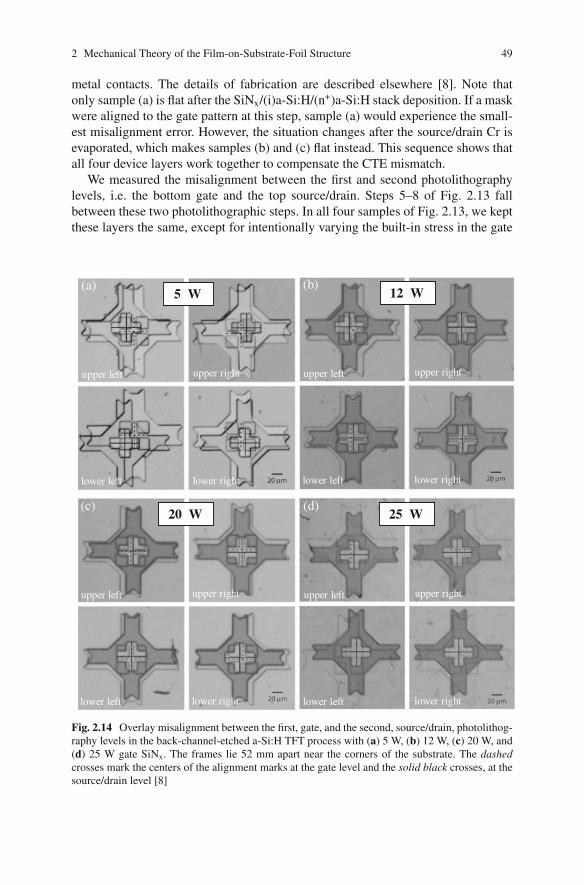
2 Mechanical Theory of the Film-on-Substrate-Foil Structure 49
metal contacts. The details of fabrication are described elsewhere [8]. Note thatonly sample (a) is flat after the SiNx/(i)a-Si:H/(n+)a-Si:H stack deposition. If a maskwere aligned to the gate pattern at this step, sample (a) would experience the small-est misalignment error. However, the situation changes after the source/drain Cr isevaporated, which makes samples (b) and (c) flat instead. This sequence shows thatall four device layers work together to compensate the CTE mismatch.
We measured the misalignment between the first and second photolithographylevels, i.e. the bottom gate and the top source/drain. Steps 5–8 of Fig. 2.13 fallbetween these two photolithographic steps. In all four samples of Fig. 2.13, we keptthese layers the same, except for intentionally varying the built-in stress in the gate
(a)
upper left upper right
lower left lower right
(b)
upper left upper right
lower left lower right
upper left upper right
lower left lower right
upper left upper right
lower left lower right
12 W5 W
20 W 25 W(c) (d)
Fig. 2.14 Overlay misalignment between the first, gate, and the second, source/drain, photolithog-raphy levels in the back-channel-etched a-Si:H TFT process with (a) 5 W, (b) 12 W, (c) 20 W, and(d) 25 W gate SiNx. The frames lie 52 mm apart near the corners of the substrate. The dashedcrosses mark the centers of the alignment marks at the gate level and the solid black crosses, at thesource/drain level [8]
50 H. Gleskova et al.
SiNx by tuning the rf deposition power from low to high, 5, 12, 20, and 25 W (22,53, 89, and 111 mW/cm2).
Figure 2.14 shows the corresponding alignment marks for the gate and thesource/drain for all four samples. Both the gate and the source/drain patterns werealigned at the center of the substrate, and the misalignment was measured on align-ment marks in four corners of a 52-mm × 52-mm square. These marks are shownin Fig. 2.14. The centers of the alignment marks are indicated by dashed crossesfor the gate level and solid crosses for the source/drain. On average, sample (a)shrunk substantially, by ∼480 ppm, sample (b) shrunk slightly, by ∼96 ppm, sam-ple (c) expanded slightly, by ∼115 ppm, and sample (d) expanded substantially, by∼385 ppm. As expected, the dimensions for the flat samples (b) and (c) changed theleast. As fabricated, TFTs of all samples had similar electrical performance.
2.4 Conclusions
When inorganic devices are grown at elevated temperature on a rigid plate substrate,the device films’ built-in stresses may affect the device performance, but have littleor no effect on the alignment error between device layers. The device films simplyare too weak compared to the substrate. However, if the devices are grown on aflexible free-standing foil, built-in stresses in the films may cause substantial mis-alignment between device layers and unmanageable curving of the workpiece. Thethinner and more compliant the substrate, the larger the misalignment and the tighterthe curvature. With the help of theory of a bimetallic strip, the misalignment can beminimized by adjusting the built-in strain in the device films during growth. a-Si:HTFTs fabricated on foil substrates of stainless steel or Kapton E need tensile built-in strain to compensate for the differential thermal contraction between the devicefilms and the substrate.
Misalignment and curvature obtained in a-Si:H TFTs fabricated on 50-μm-thickKapton E foil prove that this approach is effective. By varying the built-in strain inonly the gate SiNx layer, one can reduce the misalignment from ∼400 to ∼100 ppm.Further optimization of the a-Si:H TFT growth process is possible for lowering thisvalue even further.
Future work will address second-order misalignment effects caused by viscoelas-tic flow and nonreversible shrinkage of plastic substrate, and by modulation of localmechanics caused by device patterns. To which extend the electrical and the mechani-cal properties may be varied independently of each other also remains to be explored.
Acknowledgment The work at Princeton University was supported by the United States DisplayConsortium.
References
1. Crawford GP (ed) (2005) Flexible Flat Panel Displays. Wiley, Chichester2. Hutchinson JW, Suo Z (1991) Mixed-mode cracking in layered materials. Adv Appl Mech
29:63–191

2 Mechanical Theory of the Film-on-Substrate-Foil Structure 51
3. Jansen F, Machonkin MA (1988) Thermomechanical properties of glow discharge depositedsilicon and silicon oxide films. J Vac Sci Technol A6:1696–1698
4. Maeda M, Ikeda K (1998) Stress evaluation of radio-frequency-biased plasma-enhanced chem-ical vapor deposited silicon nitride films. J Appl Phys 83:3865–3870
5. Witvrouw A, Spaepen F (1993) Viscosity and elastic constants of amorphous Si and Ge. J ApplPhys 74:7154–7161
6. Freund LB, Suresh S (2003) Thin film materials. Cambridge University Press, New York7. Suo Z, Ma EY, Gleskova H, Wagner S (1999) Mechanics of rollable and foldable film-on-foil
electronics. Appl Phys Lett 74:1177–11798. Cheng I-C, Kattamis A, Long K, Sturm JC, Wagner S (2005) Stress control for overlay regis-
tration in a-Si:H TFTs on flexible organic polymer foil substrates. J SID 13:563–5689. Gleskova H, Cheng I-C, Wagner S, Sturm JC, Suo Z (2006) Mechanics of thin-film transistors
and solar cells on flexible substrates. Solar Energy 80:687–693
Chapter 3Low-temperature Amorphousand Nanocrystalline Silicon Materialsand Thin-film Transistors
Andrei Sazonov, Denis Striakhilev, and Arokia Nathan
Abstract Low-temperature processing and characterization of amorphous silicon(a-Si:H) and nanocrystalline silicon (nc-Si) materials and devices are reviewed. Anoverview of silicon-based low-temperature thin-film dielectrics is given in the con-text of thin-film transistor (TFT) device operation. The low-temperature growth andsynthesis of these materials are also presented and compared to conventionally fab-ricated high-temperature processed devices. The effect of using nc-Si contacts ona-Si:H TFTs and the stability of nc-Si TFTs is reviewed.
3.1 Introduction
Electronic devices and systems fabricated on flexible substrates are the subjects ofgrowing attention within both the research and the industrial community [1]. Rapiddevelopment of wireless telecommunications increases demand in portable, low-power, and inexpensive electronics. Here, the use of flexible substrates enables thedevelopment of such new products as rollable light-weight displays, flexible solarcells integrated into clothing, or cylindrical and spherical cameras for security appli-cations. Furthermore, the fabrication cost of electronic devices on flexible substratescan be reduced compared to existing planar or flat-panel technology due to imple-mentation of high-throughput roll-to-roll technology. Here, a roll of thin plastic ormetal foil used as the substrate can be kilometers long and meters wide comparedto a silicon wafer diameter of 10–12′′ in integrated circuit technology, or a glasssheet size of about 2 m×2 m in a flat-panel display (FPD) manufacturing process[2, 3]. Based on this technology, a number of commercial products are already beingproduced (such as solar cells [4]), and several others are in the prototyping stage
A. Sazonov (B)The Department of Electrical and Computer Engineering, University of Waterloo, Ontario, Canadae-mail: [email protected]
W.S. Wong, A. Salleo (eds.), Flexible Electronics: Materials and Applications, ElectronicMaterials: Science & Technology, DOI 10.1007/978-0-387-74363-9 3,C© Springer Science+Business Media, LLC 2009
53
54 A. Sazonov et al.
(active-matrix organic light-emitting diode (AMOLED) displays, thin-film batter-ies, imaging arrays) [5–7], with more products to be developed.
Unlike traditional electronics, where the value is added by downscaling thedevices, the value is added by increasing the fabrication area in flexible electron-ics. The device size requirements are more relaxed. Therefore, the capital equip-ment cost in flexible electronics is lower, and a larger part of the product costs fallsonto the materials with a wide variety of electronic materials that can be used inflexible electronics: organic semiconductors, high-temperature inorganic semicon-ductors, and low-temperature materials [8] in addition to the substrate materials thatreplace conventional glass substrates.
Organic semiconductors are attractive due to low-temperature and large-area fab-rication process compatibility. In particular, polymers can be deposited at roomtemperature by low-cost spin coating, or by roll-to-roll technology compatible withink-jet printing. The carrier mobility in organic semiconductors is already compa-rable to that of amorphous silicon (a-Si:H) (∼1 cm2 V−1 s−1) [7]. These materials,however, degrade in air and, therefore, need encapsulation, which is inorganic thin-film based [9]. Thus, inorganic thin-film technology still has to be used in organicelectronics fabrication process, increasing its cost. Furthermore, the carrier transportin organic semiconductors, such as pentacene, is sensitive to contamination and isstrongly interface-dependent, thus demanding very smooth substrates and variousinterface preparation procedures [10]. The need for low-cost fabrication processesand the nonuniformity of materials and device characteristics over large substrateareas make the applications for organic semiconductors in large-scale flexible elec-tronics a matter for the future. These areas of development are discussed in separatechapters.
Another option is to transfer the existing high-temperature semiconductor tech-nology to flexible substrates with high maximum working temperatures (e.g., high-temperature plastics such as polyimide (PI) [11], flexible glass, and metal foils [12,13]) or by transferring the devices prefabricated on rigid substrates onto plastic foils[14, 15]. This approach facilitates the utilization of high fabrication temperatureand electronic materials with improved device performance (e.g., polycrystalline Si(poly-Si) with the carrier mobility exceeding 100 cm2 V−1 s−1). However, high sub-strate and process costs restrict this technology to a limited number of applications,mainly very high added-value products (such as high-resolution flexible displaysand high-end radio frequency (RF) ID tags).
A more direct approach to integrate high-performance devices on low-meltingpoint platforms is to reduce the maximum fabrication temperature of inorganic thin-film transistors (TFTs) to a level compatible with the thermal budget of the low-costsubstrates. This approach has several advantages:
– wider variety of substrate materials available, including low-cost plastics, paper,or tissue;
– lower thermal budget materials can be integrated in the process, such as adhe-sives, polymers, and biomaterials;
3 Nanocrystalline Silicon Materials 55
– thermal deformations of the substrate are reduced, and so is mechanical stressoccurring due to mismatch between thermal expansion coefficients of the sub-strate and the films;
– materials science, device physics, fabrication process, and equipment are alreadywell established, for example, in a-Si:H technology.
Therefore, accommodation of existing inorganic amorphous, nanocrystalline, orpolycrystalline thin-film technology to flexible substrates achievable by the reduc-tion of deposition temperature seems to be the most promising approach to enableflexible electronics in the near future.
3.2 Low-temperature Amorphous and NanocrystallineSilicon Materials
Due to the low maximum working temperatures of most low-cost plastics (the glasstransition temperatures, Tg, in the range of 80–150◦C), the thermal budget in thefabrication process is limited by 100–150◦C. Process temperatures are too low toenable the manufacturing techniques developed for crystalline silicon, such as ther-mal oxidation, diffusion, or epitaxy. Moreover, low thermal budget severely restrictsthe process parameters of plasma deposition, sputtering, and photolithography.
Consider an example of hydrogenated a-Si:H. a-Si:H films with predominantlymonohydride bonding have been deposited at substrate temperature as low as 35◦Cby use of hydrogen or helium dilution followed by postdeposition annealing at150◦C [16]. More recently, there have been reports of TFT fabrication at 150◦C onKapton® E [17] and at 110◦C on polyethylene terephthalate (PET) [18], showingperformance characteristics close to those fabricated at 250–300◦C.
3.2.1 Fundamental Issues for Low-temperature Processing
In traditional plasma enhanced chemical vapor deposition (PECVD), thin-film sil-icon process used in FPD manufacturing, the substrate temperature, Ts, is in therange of 200–300◦C. Its reduction below 150◦C leads to the change in depositionmechanisms. The concentration of defects (dangling Si bonds) increases, the con-centration of di- and polyhydride-bonded hydrogen in the films increases, the massdensity decreases, and the doping efficiency drops [19]. The films have low massdensity and high charge trapping, and their electronic properties are generally poor.This change is usually attributed to reduced surface mobility of the film-buildingradicals due to lower thermal energy on the growth surface [20]. The thermal energyloss can be compensated by using “soft” ion bombardment by light ions (H+, He+)with the energy less than 50 eV, or by producing exothermic chemical reactions[20, 21]. Following this approach, the deposition parameters can be adjusted at lowsubstrate temperature to increase the surface energy and thus to provide the growth
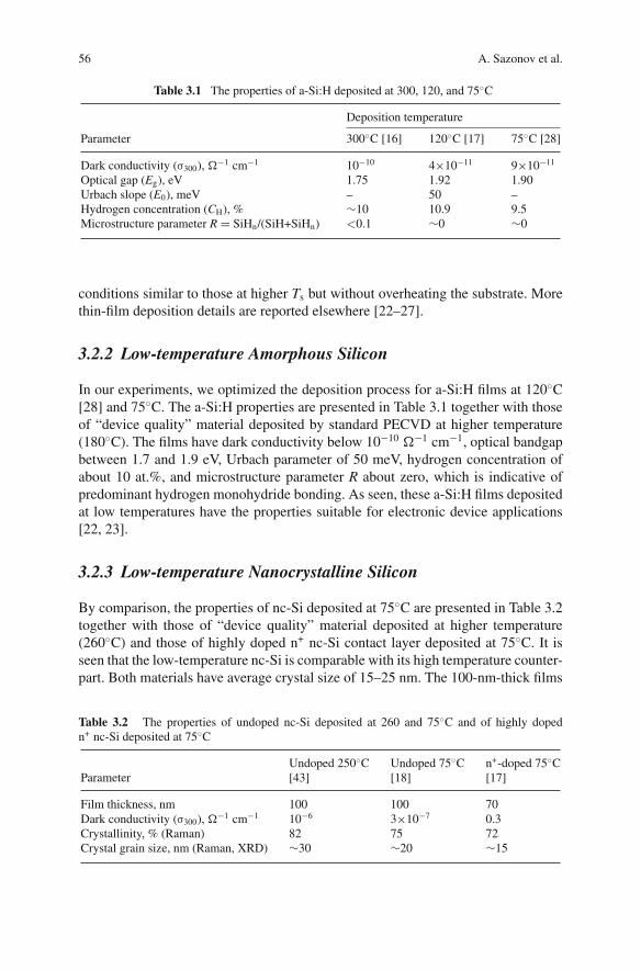
56 A. Sazonov et al.
Table 3.1 The properties of a-Si:H deposited at 300, 120, and 75◦C
Deposition temperature
Parameter 300◦C [16] 120◦C [17] 75◦C [28]
Dark conductivity (σ300), Ω−1 cm−1 10−10 4×10⁻¹¹ 9×10⁻¹¹
Optical gap (Eg), eV 1.75 1.92 1.90Urbach slope (E0), meV – 50 –Hydrogen concentration (CH), % ∼10 10.9 9.5Microstructure parameter R = SiHn/(SiH+SiHn) <0.1 ∼0 ∼0
conditions similar to those at higher Ts but without overheating the substrate. Morethin-film deposition details are reported elsewhere [22–27].
3.2.2 Low-temperature Amorphous Silicon
In our experiments, we optimized the deposition process for a-Si:H films at 120◦C[28] and 75◦C. The a-Si:H properties are presented in Table 3.1 together with thoseof “device quality” material deposited by standard PECVD at higher temperature(180◦C). The films have dark conductivity below 10−10 Ω−1 cm−1, optical bandgapbetween 1.7 and 1.9 eV, Urbach parameter of 50 meV, hydrogen concentration ofabout 10 at.%, and microstructure parameter R about zero, which is indicative ofpredominant hydrogen monohydride bonding. As seen, these a-Si:H films depositedat low temperatures have the properties suitable for electronic device applications[22, 23].
3.2.3 Low-temperature Nanocrystalline Silicon
By comparison, the properties of nc-Si deposited at 75◦C are presented in Table 3.2together with those of “device quality” material deposited at higher temperature(260◦C) and those of highly doped n+ nc-Si contact layer deposited at 75◦C. It isseen that the low-temperature nc-Si is comparable with its high temperature counter-part. Both materials have average crystal size of 15–25 nm. The 100-nm-thick films
Table 3.2 The properties of undoped nc-Si deposited at 260 and 75◦C and of highly dopedn+ nc-Si deposited at 75◦C
Undoped 250◦C Undoped 75◦C n+-doped 75◦CParameter [43] [18] [17]
Film thickness, nm 100 100 70Dark conductivity (σ300), Ω−1 cm−1 10−6 3×10⁻⁷ 0.3Crystallinity, % (Raman) 82 75 72Crystal grain size, nm (Raman, XRD) ∼30 ∼20 ∼15
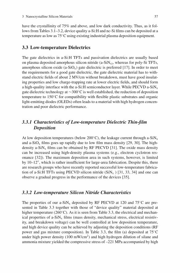
3 Nanocrystalline Silicon Materials 57
have the crystallinity of 75% and above, and low dark conductivity. Thus, as it fol-lows from Tables 3.1–3.2, device quality a-Si:H and nc-Si films can be deposited at atemperature as low as 75◦C using existing industrial plasma deposition equipment.
3.3 Low-temperature Dielectrics
The gate dielectrics in a-Si:H TFTs and passivation dielectrics are usually basedon plasma deposited amorphous silicon nitride (a-SiNx), whereas for poly-Si TFTs,amorphous silicon oxide (a-SiOx) gate dielectric is preferred [17]. In order to meetthe requirements for a good gate dielectric, the gate dielectric material has to with-stand electric fields of about 2 MV/cm without breakdown, must have good insulat-ing properties and low charge-trapping rate at lower electric fields, and should forma high-quality interface with the a-Si:H semiconductor layer. While PECVD a-SiNx
gate dielectric technology at ∼300◦C is well established, the reduction of depositiontemperature to 150◦C for compatibility with flexible plastic substrates and organiclight-emitting diodes (OLEDs) often leads to a material with high hydrogen concen-tration and poor dielectric performance.
3.3.1 Characteristics of Low-temperature Dielectric Thin-filmDeposition
At low deposition temperatures (below 200◦C), the leakage current through a-SiNx
and a-SiOx films goes up rapidly due to low film mass density [29, 30]. The high-density a-SiNx films can be obtained by RF PECVD [31]. The oxide mass densitycan be increased using high-density plasma systems (e.g., electron cyclotron res-onance [32]). The maximum deposition area in such systems, however, is limitedby 10–12′′, which is rather insufficient for large-area fabrication. Despite this, thereare research groups who have recently reported successful low-temperature fabrica-tion of a-Si:H TFTs using PECVD silicon nitride (SiNx ) [31, 33, 34] and one canobserve a gradual progress in the performance of the devices [35].
3.3.2 Low-temperature Silicon Nitride Characteristics
The properties of our a-SiNx deposited by RF PECVD at 120 and 75◦C are pre-sented in Table 3.3 together with those of “device quality” material deposited athigher temperature (260◦C). As it is seen from Table 3.3, the electrical and mechan-ical properties of a-SiNx films (mass density, mechanical stress, electrical resistiv-ity, and breakdown voltage) can be well controlled at low deposition temperature,and high device quality can be achieved by adjusting the deposition conditions (RFpower and gas mixture composition). In Table 3.3, the film (a) deposited at 75◦Cunder high power density (100 mW/cm2) and high hydrogen dilution of silane andammonia mixture yielded the compressive stress of –221 MPa accompanied by high
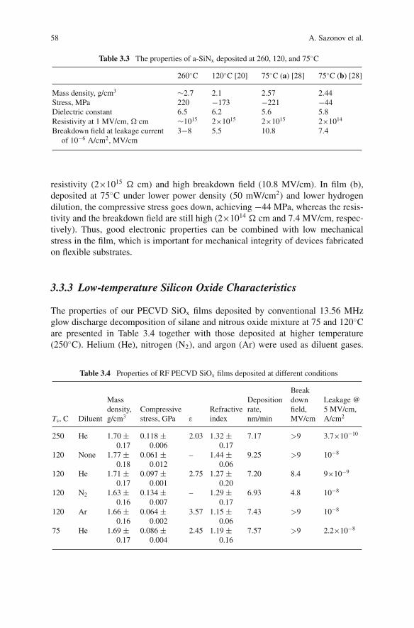
58 A. Sazonov et al.
Table 3.3 The properties of a-SiNx deposited at 260, 120, and 75◦C
260◦C 120◦C [20] 75◦C (a) [28] 75◦C (b) [28]
Mass density, g/cm3 ∼2.7 2.1 2.57 2.44Stress, MPa 220 −173 −221 −44Dielectric constant 6.5 6.2 5.6 5.8Resistivity at 1 MV/cm, Ω.cm ∼1015 2×10¹⁵ 2×10¹⁵ 2×10¹⁴
Breakdown field at leakage current 3−8 5.5 10.8 7.4of 10−6 A/cm2, MV/cm
resistivity (2×10¹⁵ Ω cm) and high breakdown field (10.8 MV/cm). In film (b),deposited at 75◦C under lower power density (50 mW/cm2) and lower hydrogendilution, the compressive stress goes down, achieving −44 MPa, whereas the resis-tivity and the breakdown field are still high (2×10¹⁴ Ω cm and 7.4 MV/cm, respec-tively). Thus, good electronic properties can be combined with low mechanicalstress in the film, which is important for mechanical integrity of devices fabricatedon flexible substrates.
3.3.3 Low-temperature Silicon Oxide Characteristics
The properties of our PECVD SiOx films deposited by conventional 13.56 MHzglow discharge decomposition of silane and nitrous oxide mixture at 75 and 120◦Care presented in Table 3.4 together with those deposited at higher temperature(250◦C). Helium (He), nitrogen (N2), and argon (Ar) were used as diluent gases.
Table 3.4 Properties of RF PECVD SiOx films deposited at different conditions
Ts, C Diluent
Massdensity,g/cm3
Compressivestress, GPa ε
Refractiveindex
Depositionrate,nm/min
Breakdownfield,MV/cm
Leakage @5 MV/cm,A/cm2
250 He 1.70 ±0.17
0.118 ±0.006
2.03 1.32 ±0.17
7.17 >9 3.7×10⁻¹⁰
120 None 1.77 ±0.18
0.061 ±0.012
– 1.44 ±0.06
9.25 >9 10−8
120 He 1.71 ±0.17
0.097 ±0.001
2.75 1.27 ±0.20
7.20 8.4 9×10⁻⁹
120 N2 1.63 ±0.16
0.134 ±0.007
– 1.29 ±0.17
6.93 4.8 10−8
120 Ar 1.66 ±0.16
0.064 ±0.002
3.57 1.15 ±0.06
7.43 >9 10−8
75 He 1.69 ±0.17
0.086 ±0.004
2.45 1.19 ±0.16
7.57 >9 2.2×10⁻⁸
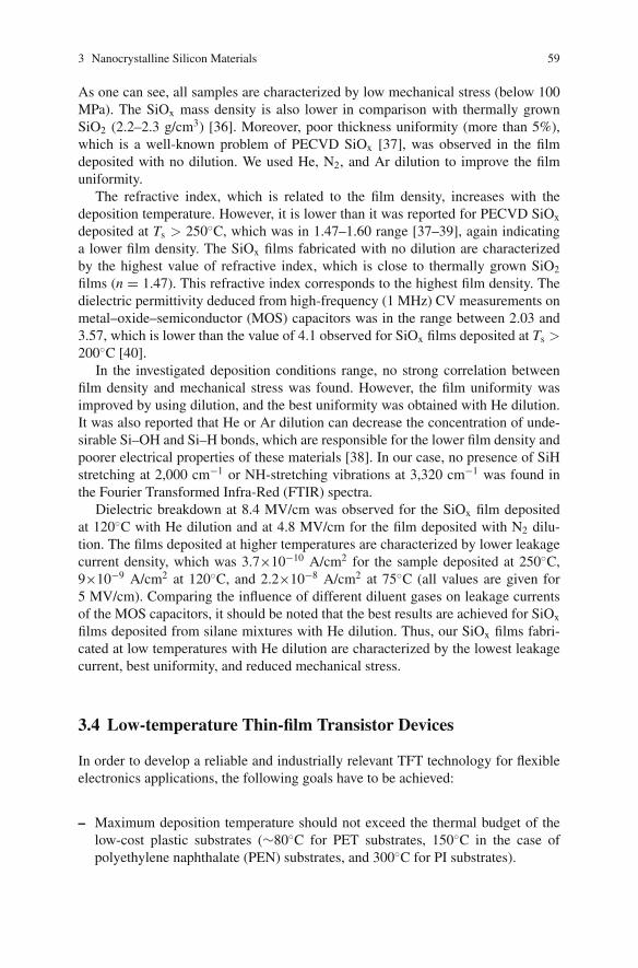
3 Nanocrystalline Silicon Materials 59
As one can see, all samples are characterized by low mechanical stress (below 100MPa). The SiOx mass density is also lower in comparison with thermally grownSiO2 (2.2–2.3 g/cm3) [36]. Moreover, poor thickness uniformity (more than 5%),which is a well-known problem of PECVD SiOx [37], was observed in the filmdeposited with no dilution. We used He, N2, and Ar dilution to improve the filmuniformity.
The refractive index, which is related to the film density, increases with thedeposition temperature. However, it is lower than it was reported for PECVD SiOx
deposited at Ts > 250◦C, which was in 1.47–1.60 range [37–39], again indicatinga lower film density. The SiOx films fabricated with no dilution are characterizedby the highest value of refractive index, which is close to thermally grown SiO2
films (n = 1.47). This refractive index corresponds to the highest film density. Thedielectric permittivity deduced from high-frequency (1 MHz) CV measurements onmetal–oxide–semiconductor (MOS) capacitors was in the range between 2.03 and3.57, which is lower than the value of 4.1 observed for SiOx films deposited at Ts >200◦C [40].
In the investigated deposition conditions range, no strong correlation betweenfilm density and mechanical stress was found. However, the film uniformity wasimproved by using dilution, and the best uniformity was obtained with He dilution.It was also reported that He or Ar dilution can decrease the concentration of unde-sirable Si–OH and Si–H bonds, which are responsible for the lower film density andpoorer electrical properties of these materials [38]. In our case, no presence of SiHstretching at 2,000 cm−1 or NH-stretching vibrations at 3,320 cm−1 was found inthe Fourier Transformed Infra-Red (FTIR) spectra.
Dielectric breakdown at 8.4 MV/cm was observed for the SiOx film depositedat 120◦C with He dilution and at 4.8 MV/cm for the film deposited with N2 dilu-tion. The films deposited at higher temperatures are characterized by lower leakagecurrent density, which was 3.7×10⁻¹⁰ A/cm2 for the sample deposited at 250◦C,9×10−9 A/cm2 at 120◦C, and 2.2×10⁻⁸ A/cm2 at 75◦C (all values are given for5 MV/cm). Comparing the influence of different diluent gases on leakage currentsof the MOS capacitors, it should be noted that the best results are achieved for SiOx
films deposited from silane mixtures with He dilution. Thus, our SiOx films fabri-cated at low temperatures with He dilution are characterized by the lowest leakagecurrent, best uniformity, and reduced mechanical stress.
3.4 Low-temperature Thin-film Transistor Devices
In order to develop a reliable and industrially relevant TFT technology for flexibleelectronics applications, the following goals have to be achieved:
– Maximum deposition temperature should not exceed the thermal budget of thelow-cost plastic substrates (∼80◦C for PET substrates, 150◦C in the case ofpolyethylene naphthalate (PEN) substrates, and 300◦C for PI substrates).
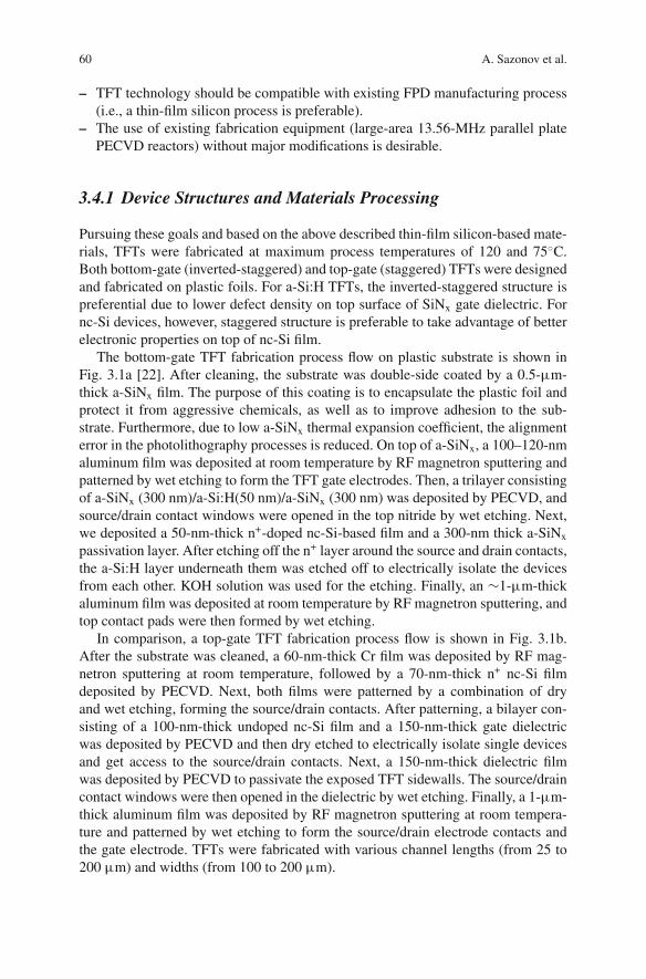
60 A. Sazonov et al.
– TFT technology should be compatible with existing FPD manufacturing process(i.e., a thin-film silicon process is preferable).
– The use of existing fabrication equipment (large-area 13.56-MHz parallel platePECVD reactors) without major modifications is desirable.
3.4.1 Device Structures and Materials Processing
Pursuing these goals and based on the above described thin-film silicon-based mate-rials, TFTs were fabricated at maximum process temperatures of 120 and 75◦C.Both bottom-gate (inverted-staggered) and top-gate (staggered) TFTs were designedand fabricated on plastic foils. For a-Si:H TFTs, the inverted-staggered structure ispreferential due to lower defect density on top surface of SiNx gate dielectric. Fornc-Si devices, however, staggered structure is preferable to take advantage of betterelectronic properties on top of nc-Si film.
The bottom-gate TFT fabrication process flow on plastic substrate is shown inFig. 3.1a [22]. After cleaning, the substrate was double-side coated by a 0.5-μm-thick a-SiNx film. The purpose of this coating is to encapsulate the plastic foil andprotect it from aggressive chemicals, as well as to improve adhesion to the sub-strate. Furthermore, due to low a-SiNx thermal expansion coefficient, the alignmenterror in the photolithography processes is reduced. On top of a-SiNx, a 100–120-nmaluminum film was deposited at room temperature by RF magnetron sputtering andpatterned by wet etching to form the TFT gate electrodes. Then, a trilayer consistingof a-SiNx (300 nm)/a-Si:H(50 nm)/a-SiNx (300 nm) was deposited by PECVD, andsource/drain contact windows were opened in the top nitride by wet etching. Next,we deposited a 50-nm-thick n+-doped nc-Si-based film and a 300-nm thick a-SiNx
passivation layer. After etching off the n+ layer around the source and drain contacts,the a-Si:H layer underneath them was etched off to electrically isolate the devicesfrom each other. KOH solution was used for the etching. Finally, an ∼1-μm-thickaluminum film was deposited at room temperature by RF magnetron sputtering, andtop contact pads were then formed by wet etching.
In comparison, a top-gate TFT fabrication process flow is shown in Fig. 3.1b.After the substrate was cleaned, a 60-nm-thick Cr film was deposited by RF mag-netron sputtering at room temperature, followed by a 70-nm-thick n+ nc-Si filmdeposited by PECVD. Next, both films were patterned by a combination of dryand wet etching, forming the source/drain contacts. After patterning, a bilayer con-sisting of a 100-nm-thick undoped nc-Si film and a 150-nm-thick gate dielectricwas deposited by PECVD and then dry etched to electrically isolate single devicesand get access to the source/drain contacts. Next, a 150-nm-thick dielectric filmwas deposited by PECVD to passivate the exposed TFT sidewalls. The source/draincontact windows were then opened in the dielectric by wet etching. Finally, a 1-μm-thick aluminum film was deposited by RF magnetron sputtering at room tempera-ture and patterned by wet etching to form the source/drain electrode contacts andthe gate electrode. TFTs were fabricated with various channel lengths (from 25 to200 μm) and widths (from 100 to 200 μm).
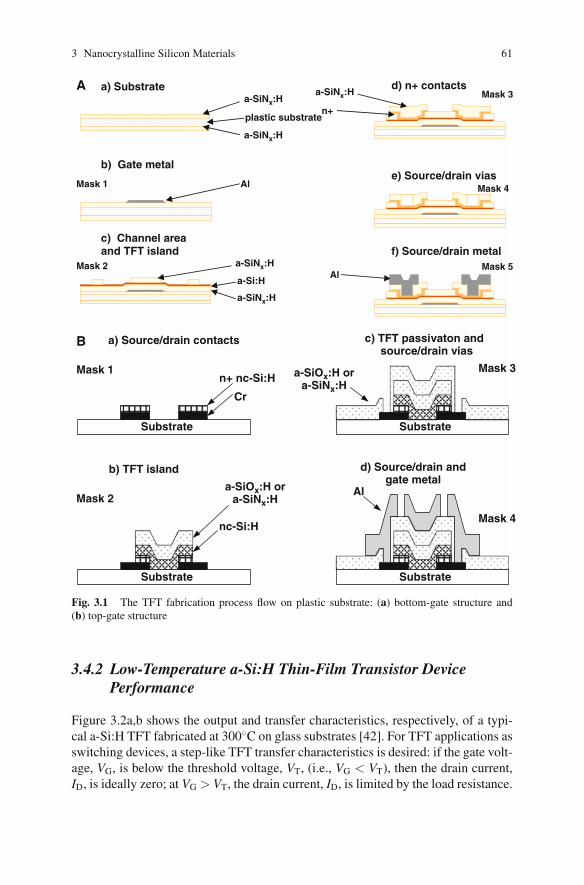
3 Nanocrystalline Silicon Materials 61
a) Substrate
B
A
b) Gate metal
Al Mask 1
c) Channel areaand TFT island
a-SiNx:Ha-SiNx:H
a-SiNx:H
a-SiNx:H
a-SiNx:H
a-Si:H
plastic substrate
Mask 2
Mask 3
n+
Mask 4
Mask 5 Al
d) n+ contacts
e) Source/drain vias
f) Source/drain metal
b) TFT island
nc-Si:H
Mask 2
Substrate
c) TFT passivaton and source/drain vias
Mask 3a-SiOx:H ora-SiNx:H
a-SiOx:H ora-SiNx:H
Al
d) Source/drain andgate metal
Mask 4
n+ nc-Si:H
Cr
a) Source/drain contacts
Mask 1
Substrate Substrate
Substrate
Fig. 3.1 The TFT fabrication process flow on plastic substrate: (a) bottom-gate structure and(b) top-gate structure
3.4.2 Low-Temperature a-Si:H Thin-Film Transistor DevicePerformance
Figure 3.2a,b shows the output and transfer characteristics, respectively, of a typi-cal a-Si:H TFT fabricated at 300◦C on glass substrates [42]. For TFT applications asswitching devices, a step-like TFT transfer characteristics is desired: if the gate volt-age, VG, is below the threshold voltage, VT, (i.e., VG < VT), then the drain current,ID, is ideally zero; at VG > VT, the drain current, ID, is limited by the load resistance.
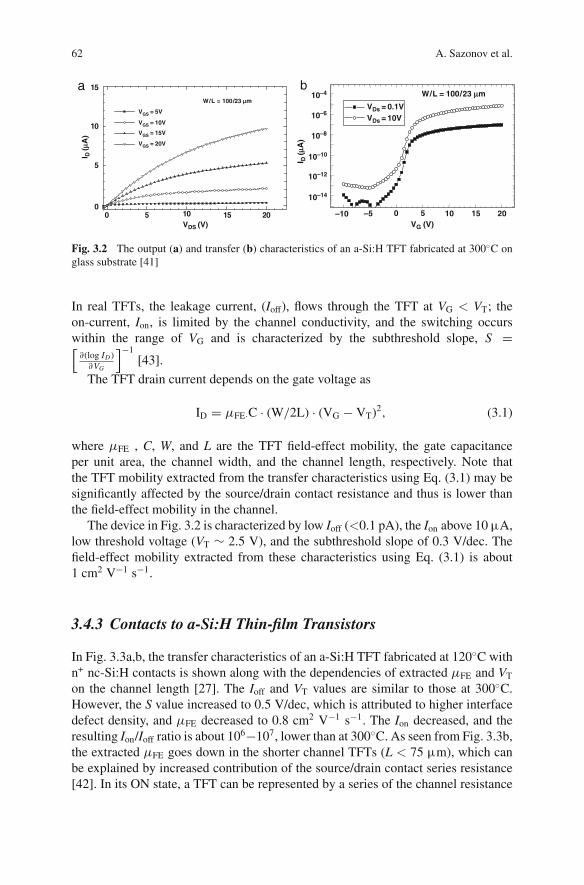
62 A. Sazonov et al.
0 5 10 15 200
5
10
15a bW / L = 100 /23 μm
VGS = 5V
VGS = 10V
VGS = 15V
VGS = 20V
VDS (V)
I D (μ
A)
10–4
10–6
10–8
10–10
10–12
10–14
–10 –5 0 5 10
W / L = 100 / 23 μm
VG (V)
VDs = 0.1VVDs = 10V
15 20
I D (μ
A)
Fig. 3.2 The output (a) and transfer (b) characteristics of an a-Si:H TFT fabricated at 300◦C onglass substrate [41]
In real TFTs, the leakage current, (Ioff), flows through the TFT at VG < VT; theon-current, Ion, is limited by the channel conductivity, and the switching occurswithin the range of VG and is characterized by the subthreshold slope, S =[∂(log ID )∂VG
]−1[43].
The TFT drain current depends on the gate voltage as
ID = μFE·C · (W/2L) · (VG − VT)2, (3.1)
where μFE , C, W, and L are the TFT field-effect mobility, the gate capacitanceper unit area, the channel width, and the channel length, respectively. Note thatthe TFT mobility extracted from the transfer characteristics using Eq. (3.1) may besignificantly affected by the source/drain contact resistance and thus is lower thanthe field-effect mobility in the channel.
The device in Fig. 3.2 is characterized by low Ioff (<0.1 pA), the Ion above 10 μA,low threshold voltage (VT ∼ 2.5 V), and the subthreshold slope of 0.3 V/dec. Thefield-effect mobility extracted from these characteristics using Eq. (3.1) is about1 cm2 V−1 s−1.
3.4.3 Contacts to a-Si:H Thin-film Transistors
In Fig. 3.3a,b, the transfer characteristics of an a-Si:H TFT fabricated at 120◦C withn+ nc-Si:H contacts is shown along with the dependencies of extracted μFE and VT
on the channel length [27]. The Ioff and VT values are similar to those at 300◦C.However, the S value increased to 0.5 V/dec, which is attributed to higher interfacedefect density, and μFE decreased to 0.8 cm2 V−1 s−1. The Ion decreased, and theresulting Ion/Ioff ratio is about 106−107, lower than at 300◦C. As seen from Fig. 3.3b,the extracted μFE goes down in the shorter channel TFTs (L < 75 μm), which canbe explained by increased contribution of the source/drain contact series resistance[42]. In its ON state, a TFT can be represented by a series of the channel resistance
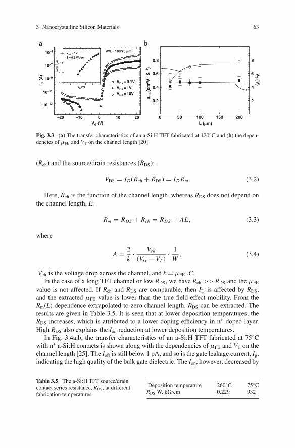
3 Nanocrystalline Silicon Materials 63
W/L = 100/75 μm
–1 0 1 2 3 4–14
–12
–10
–8 VDS = 1V
S = 0.5 V/declo
g10
, (I D
,A)
10–5
10–7
10–9
10–11
10–13
–10–20 0
a b
10VG (V)
VG (V)
VDs = 0.1V
VDs = 1V
VDs = 10V
20
I D, (
A)
0.8
0.6
0.4
0.2
8
6
4
2
500 100L (μm)
μ FE
(cm
2 V–1
S–1
)
150 200
VT (V
)
Fig. 3.3 (a) The transfer characteristics of an a-Si:H TFT fabricated at 120◦C and (b) the depen-dencies of μFE and VT on the channel length [20]
(Rch) and the source/drain resistances (RDS):
VDS = ID(Rch + RDS) = ID Rm . (3.2)
Here, Rch is the function of the channel length, whereas RDS does not depend onthe channel length, L:
Rm = RDS + Rch = RDS + AL , (3.3)
where
A = 2
k· Vch
(VG − VT )· 1
W, (3.4)
Vch is the voltage drop across the channel, and k = μFE .C.In the case of a long TFT channel or low RDS, we have Rch >> RDS and the μFE
value is not affected. If Rch and RDS are comparable, then ID is affected by RDS,and the extracted μFE value is lower than the true field-effect mobility. From theRm(L) dependence extrapolated to zero channel length, RDS can be extracted. Theresults are given in Table 3.5. It is seen that at lower deposition temperatures, theRDS increases, which is attributed to a lower doping efficiency in n+-doped layer.High RDS also explains the Ion reduction at lower deposition temperatures.
In Fig. 3.4a,b, the transfer characteristics of an a-Si:H TFT fabricated at 75◦Cwith n+ a-Si:H contacts is shown along with the dependencies of μFE and VT on thechannel length [25]. The Ioff is still below 1 pA, and so is the gate leakage current, Ig,indicating the high quality of the bulk gate dielectric. The Ion, however, decreased by
Table 3.5 The a-Si:H TFT source/draincontact series resistance, RDS, at differentfabrication temperatures
Deposition temperature 260◦C 75◦CRDS W, kΩ.cm 0.229 932
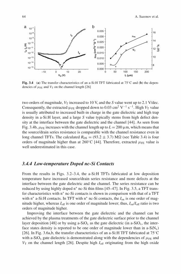
64 A. Sazonov et al.
–10 0 10 20
10–15
10–14
10–13
10–12
10–11
10–10
10–9
10–8
10–7a b
Id
Ig
VG (V)
I d, I
g (
A)
0 50 100 150 200
0.005
0.000
0.010
0.015
0.020
0.025
0.030
0.035
L (μm)
8
10
12
14
16 μFE
VT
μ FE
(cm
2 V–1
S–1
)
VT (V
)
Fig. 3.4 (a) The transfer characteristics of an a-Si:H TFT fabricated at 75◦C and (b) the depen-dencies of μFE and VT on the channel length [26]
two orders of magnitude, VT increased to 10 V, and the S value went up to 2.1 V/dec.Consequently, the extracted μFE dropped down to 0.03 cm2 V−1 s−1. High VT valueis usually attributed to increased built-in charge in the gate dielectric and high trapdensity in a-Si:H layer, and a large S value typically stems from high defect den-sity at the interface between the gate dielectric and the channel [44]. As seen fromFig. 3.4b,μFE increases with the channel length up to L = 200 μm, which means thatthe source/drain series resistance is comparable with the channel resistance even inlong channel TFTs. The calculated RDS = (93.2 ± 3.7) MΩ (see Table 3.4) is fourorders of magnitude higher than at 260◦C [44]. Therefore, extracted μFE value iswell underestimated in this case.
3.4.4 Low-temperature Doped nc-Si Contacts
From the results in Figs. 3.2–3.4, the a-Si:H TFTs fabricated at low depositiontemperature have increased source/drain series resistance and more defects at theinterface between the gate dielectric and the channel. The series resistance can bereduced by using highly doped n+ nc-Si thin films [45–47]. In Fig. 3.5, a TFT trans-fer characteristics with n+ nc-Si contacts is shown in comparison with that of a TFTwith n+ a-Si:H contacts. In TFT with n+ nc-Si contacts, the Ion is one order of mag-nitude higher, whereas Ioff is one order of magnitude lower; thus, Ion/Ioff ratio is twoorders of magnitude higher.
Improving the interface between the gate dielectric and the channel can beachieved by the plasma treatments of the gate dielectric surface prior to the channellayer deposition [48] or by using a-SiOx as the gate dielectric (in a-SiOx, the inter-face states density is reported to be one order of magnitude lower than in a-SiNx)[26]. In Fig. 3.6a,b, the transfer characteristics of an a-Si:H TFT fabricated at 75◦Cwith a-SiOx gate dielectric is demonstrated along with the dependencies of μFE andVT on the channel length [26]. Despite high Ioff originating from the high oxide
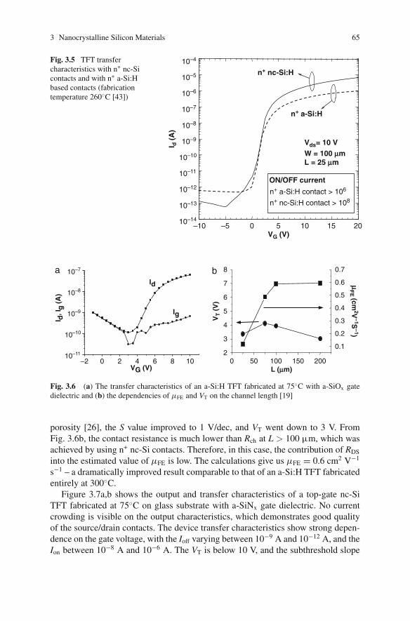
3 Nanocrystalline Silicon Materials 65
–10 –5 0 5 10 15 2010–14
10–13
10–12
10–11
10–10
10–9
10–8
10–7
10–6
10–5
10–4
n+ a-Si:H
n+ a-Si:H contact > 106
n+ nc-Si:H contact > 108
n+ nc-Si:H
Vds= 10 VW = 100 μmL = 25 μm
ON/OFF current
VG (V)
I d (
A)
Fig. 3.5 TFT transfercharacteristics with n+ nc-Sicontacts and with n+ a-Si:Hbased contacts (fabricationtemperature 260◦C [43])
–2 0 2 4 6 8 10
Id
Ig
VG (V)
I d, I
g (
A)
10–11
10–10
10–9
10–8
10–7a b
0 50 100 150 2002
3
4
5
6
7
8
0.1
0.2
0.3
0.4
0.5
0.6
0.7
L (μm)
μF
E (cm
2V–1S
–1)
VT (
V)
Fig. 3.6 (a) The transfer characteristics of an a-Si:H TFT fabricated at 75◦C with a-SiOx gatedielectric and (b) the dependencies of μFE and VT on the channel length [19]
porosity [26], the S value improved to 1 V/dec, and VT went down to 3 V. FromFig. 3.6b, the contact resistance is much lower than Rch at L > 100 μm, which wasachieved by using n+ nc-Si contacts. Therefore, in this case, the contribution of RDS
into the estimated value of μFE is low. The calculations give us μFE = 0.6 cm2 V−1
s−1 – a dramatically improved result comparable to that of an a-Si:H TFT fabricatedentirely at 300◦C.
Figure 3.7a,b shows the output and transfer characteristics of a top-gate nc-SiTFT fabricated at 75◦C on glass substrate with a-SiNx gate dielectric. No currentcrowding is visible on the output characteristics, which demonstrates good qualityof the source/drain contacts. The device transfer characteristics show strong depen-dence on the gate voltage, with the Ioff varying between 10−9 A and 10−12 A, and theIon between 10−8 A and 10−6 A. The VT is below 10 V, and the subthreshold slope
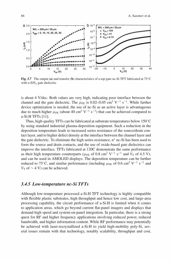
66 A. Sazonov et al.
0 5 10 15 20 25 300.0
0.5
1.0
1.5
2.0
2.5a bW/L = 200 μm / 20 μmVgs = 5, 10, 15, 20, 25, 30
Vds (V)
I d (
μA)
–20 –10 0 10 20 30 4010–12
10–11
10–10
10–9
10–8
10–7
10–6
10–5
VDs = 10VVDs = 1VVDs = 0.1V
W/L = 200 μm / 20 μm
VG (V)
I d (
A)
Fig. 3.7 The output (a) and transfer (b) characteristics of a top-gate nc-Si TFT fabricated at 75◦Cwith a-SiNx gate dielectric
is about 4 V/dec. Both values are very high, indicating poor interface between thechannel and the gate dielectric. The μFE is 0.02–0.05 cm2 V−1 s−1. While furtherdevice optimization is needed, the use of nc-Si as an active layer is advantageousdue to much higher μFE (about 40 cm2 V−1 s−1) that can be achieved compared toa-Si:H TFTs [11].
Thus, high-quality TFTs can be fabricated at substrate temperatures below 150◦Cby using standard industrial plasma-deposition equipment. Such a reduction in thedeposition temperature leads to increased series resistance of the source/drain con-tact layer, and to higher defect density at the interface between the channel layer andthe gate dielectric. To eliminate the high series resistance, n+ nc-Si has been used toform the source and drain contacts, and the use of oxide-based gate dielectrics canimprove the interface. TFTs fabricated at 120C demonstrate the same performanceas their high temperature counterparts (μFE of 0.8 cm2 V−1 s−1 and VT of 4.5 V),and can be used in AMOLED displays. The deposition temperature can be furtherreduced to 75◦C, and similar performance (including μFE of 0.6 cm2 V−1 s−1 andVT of ∼ 4 V) can be achieved.
3.4.5 Low-temperature nc-Si TFTs
Although low-temperature processed a-Si:H TFT technology is highly compatiblewith flexible plastic substrates, high throughput and hence low cost, and large-areaprocessing capability, the circuit performance of a-Si:H is limited when it comesto application areas, which go beyond current flat-panel imagers and displays thatdemand high speed and system-on-panel integration. In particular, there is a strongquest for RF and higher frequency applications involving reduced power, reducedbandwidth, and higher information content. While RF performance may potentiallybe achieved with laser-recrystallized a-Si:H to yield high-mobility poly-Si, sev-eral issues remain with that technology, notably scalability, throughput and cost,
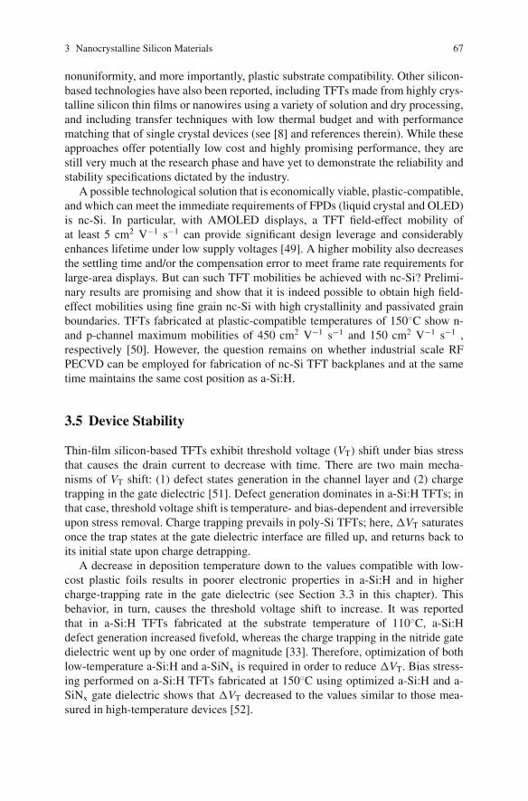
3 Nanocrystalline Silicon Materials 67
nonuniformity, and more importantly, plastic substrate compatibility. Other silicon-based technologies have also been reported, including TFTs made from highly crys-talline silicon thin films or nanowires using a variety of solution and dry processing,and including transfer techniques with low thermal budget and with performancematching that of single crystal devices (see [8] and references therein). While theseapproaches offer potentially low cost and highly promising performance, they arestill very much at the research phase and have yet to demonstrate the reliability andstability specifications dictated by the industry.
A possible technological solution that is economically viable, plastic-compatible,and which can meet the immediate requirements of FPDs (liquid crystal and OLED)is nc-Si. In particular, with AMOLED displays, a TFT field-effect mobility ofat least 5 cm2 V−1 s−1 can provide significant design leverage and considerablyenhances lifetime under low supply voltages [49]. A higher mobility also decreasesthe settling time and/or the compensation error to meet frame rate requirements forlarge-area displays. But can such TFT mobilities be achieved with nc-Si? Prelimi-nary results are promising and show that it is indeed possible to obtain high field-effect mobilities using fine grain nc-Si with high crystallinity and passivated grainboundaries. TFTs fabricated at plastic-compatible temperatures of 150◦C show n-and p-channel maximum mobilities of 450 cm2 V−1 s−1 and 150 cm2 V−1 s−1 ,respectively [50]. However, the question remains on whether industrial scale RFPECVD can be employed for fabrication of nc-Si TFT backplanes and at the sametime maintains the same cost position as a-Si:H.
3.5 Device Stability
Thin-film silicon-based TFTs exhibit threshold voltage (VT) shift under bias stressthat causes the drain current to decrease with time. There are two main mecha-nisms of VT shift: (1) defect states generation in the channel layer and (2) chargetrapping in the gate dielectric [51]. Defect generation dominates in a-Si:H TFTs; inthat case, threshold voltage shift is temperature- and bias-dependent and irreversibleupon stress removal. Charge trapping prevails in poly-Si TFTs; here, ΔVT saturatesonce the trap states at the gate dielectric interface are filled up, and returns back toits initial state upon charge detrapping.
A decrease in deposition temperature down to the values compatible with low-cost plastic foils results in poorer electronic properties in a-Si:H and in highercharge-trapping rate in the gate dielectric (see Section 3.3 in this chapter). Thisbehavior, in turn, causes the threshold voltage shift to increase. It was reportedthat in a-Si:H TFTs fabricated at the substrate temperature of 110◦C, a-Si:Hdefect generation increased fivefold, whereas the charge trapping in the nitride gatedielectric went up by one order of magnitude [33]. Therefore, optimization of bothlow-temperature a-Si:H and a-SiNx is required in order to reduce ΔVT. Bias stress-ing performed on a-Si:H TFTs fabricated at 150◦C using optimized a-Si:H and a-SiNx gate dielectric shows that ΔVT decreased to the values similar to those mea-sured in high-temperature devices [52].
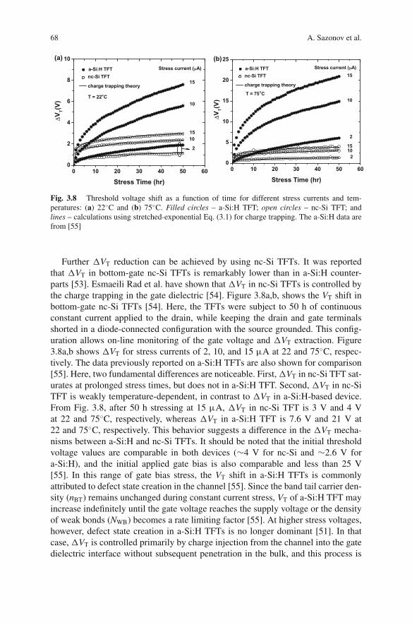
68 A. Sazonov et al.
Fig. 3.8 Threshold voltage shift as a function of time for different stress currents and tem-peratures: (a) 22◦C and (b) 75◦C. Filled circles – a-Si:H TFT; open circles – nc-Si TFT; andlines – calculations using stretched-exponential Eq. (3.1) for charge trapping. The a-Si:H data arefrom [55]
Further ΔVT reduction can be achieved by using nc-Si TFTs. It was reportedthat ΔVT in bottom-gate nc-Si TFTs is remarkably lower than in a-Si:H counter-parts [53]. Esmaeili Rad et al. have shown that ΔVT in nc-Si TFTs is controlled bythe charge trapping in the gate dielectric [54]. Figure 3.8a,b, shows the VT shift inbottom-gate nc-Si TFTs [54]. Here, the TFTs were subject to 50 h of continuousconstant current applied to the drain, while keeping the drain and gate terminalsshorted in a diode-connected configuration with the source grounded. This config-uration allows on-line monitoring of the gate voltage and ΔVT extraction. Figure3.8a,b shows ΔVT for stress currents of 2, 10, and 15 μA at 22 and 75◦C, respec-tively. The data previously reported on a-Si:H TFTs are also shown for comparison[55]. Here, two fundamental differences are noticeable. First, ΔVT in nc-Si TFT sat-urates at prolonged stress times, but does not in a-Si:H TFT. Second, ΔVT in nc-SiTFT is weakly temperature-dependent, in contrast to ΔVT in a-Si:H-based device.From Fig. 3.8, after 50 h stressing at 15 μA, ΔVT in nc-Si TFT is 3 V and 4 Vat 22 and 75◦C, respectively, whereas ΔVT in a-Si:H TFT is 7.6 V and 21 V at22 and 75◦C, respectively. This behavior suggests a difference in the ΔVT mecha-nisms between a-Si:H and nc-Si TFTs. It should be noted that the initial thresholdvoltage values are comparable in both devices (∼4 V for nc-Si and ∼2.6 V fora-Si:H), and the initial applied gate bias is also comparable and less than 25 V[55]. In this range of gate bias stress, the VT shift in a-Si:H TFTs is commonlyattributed to defect state creation in the channel [55]. Since the band tail carrier den-sity (nBT) remains unchanged during constant current stress, VT of a-Si:H TFT mayincrease indefinitely until the gate voltage reaches the supply voltage or the densityof weak bonds (NWB) becomes a rate limiting factor [55]. At higher stress voltages,however, defect state creation in a-Si:H TFTs is no longer dominant [51]. In thatcase, ΔVT is controlled primarily by charge injection from the channel into the gatedielectric interface without subsequent penetration in the bulk, and this process is
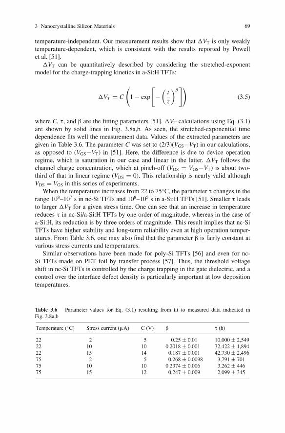
3 Nanocrystalline Silicon Materials 69
temperature-independent. Our measurement results show that ΔVT is only weaklytemperature-dependent, which is consistent with the results reported by Powellet al. [51].
ΔVT can be quantitatively described by considering the stretched-exponentmodel for the charge-trapping kinetics in a-Si:H TFTs:
ΔVT = C
(1 − exp
[−
(t
τ
)β])(3.5)
where C, τ, and β are the fitting parameters [51]. ΔVT calculations using Eq. (3.1)are shown by solid lines in Fig. 3.8a,b. As seen, the stretched-exponential timedependence fits well the measurement data. Values of the extracted parameters aregiven in Table 3.6. The parameter C was set to (2/3)(VGS−VT) in our calculations,as opposed to (VGS−VT) in [51]. Here, the difference is due to device operationregime, which is saturation in our case and linear in the latter. ΔVT follows thechannel charge concentration, which at pinch-off (VDS = VGS−VT) is about two-third of that in linear regime (VDS = 0). This relationship is nearly valid althoughVDS = VGS in this series of experiments.
When the temperature increases from 22 to 75◦C, the parameter τ changes in therange 108–107 s in nc-Si TFTs and 108–105 s in a-Si:H TFTs [51]. Smaller τ leadsto larger ΔVT for a given stress time. One can see that an increase in temperaturereduces τ in nc-Si/a-Si:H TFTs by one order of magnitude, whereas in the case ofa-Si:H, its reduction is by three orders of magnitude. This result implies that nc-SiTFTs have higher stability and long-term reliability even at high operation temper-atures. From Table 3.6, one may also find that the parameter β is fairly constant atvarious stress currents and temperatures.
Similar observations have been made for poly-Si TFTs [56] and even for nc-Si TFTs made on PET foil by transfer process [57]. Thus, the threshold voltageshift in nc-Si TFTs is controlled by the charge trapping in the gate dielectric, and acontrol over the interface defect density is particularly important at low depositiontemperatures.
Table 3.6 Parameter values for Eq. (3.1) resulting from fit to measured data indicated inFig. 3.8a,b
Temperature (◦C) Stress current (μA) C (V) β τ (h)
22 2 5 0.25 ± 0.01 10,000 ± 2,54922 10 10 0.2018 ± 0.001 32,422 ± 1,89422 15 14 0.187 ± 0.001 42,730 ± 2,49675 2 5 0.268 ± 0.0098 3,791 ± 70175 10 10 0.2374 ± 0.006 3,262 ± 44675 15 12 0.247 ± 0.009 2,099 ± 345
70 A. Sazonov et al.
3.6 Conclusions and Future Prospective
A number of parameters for low-temperature growth of silicon materials have beenpresented. Conventional thin-film silicon devices offer a wide range of advantagesincluding entrenched fabrication facilities, known properties, and low barrier forentry into large-area electronics applications. Here, a number of issues need to beaddressed with implications on growth rate, gate dielectric quality and/or pertinentinterface modification, and device stability, in the low-temperature range, all of whichrequire significant further research. One of the key issues that must be addressed hereis the industrial implementation of nc-Si TFTs, in which a high growth rate is imper-ative. nc-Si films can be deposited at 0.01–0.1 nm/s using high dilution of silane withhydrogen; high dilution and high flow rate tend to limit the growth rate. However, ithas been shown [58] that the growth rate can be increased to 2 nm/s at higher pres-sures (7–9 Torr) by increasing the very-high frequency power and moving into thesilane depletion regime. Films deposited at higher pressure have been found to con-sist of denser grains, limiting the oxidation to yield higher short-circuit current insolar cells. Growth rates of 1.5–2 nm/s would be acceptable by the industry; how-ever, further work is needed to achieve the desired growth rates in 13.56-MHz plasmawhile maintaining optimal nc-Si microstructure and transport property.
References
1. Fruehauf N, Chalamala BR, Gnade BE, Jang J (2004) Flexible Electronics 2004 – Materialsand Device Technology, vol 814. Materials Research Society Symposia Proceedings, Pitts-burgh, PA, USA
2. Sheats JR (2002) Roll-to-roll manufacturing of thin film electronics, Proc SPIE 4688:240–248
3. Allen K (2004) Reel to real: Prospects for flexible displays, In: Fruehauf N, Chalamala BR,Gnade BE, Jang J (eds) Flexible Electronics 2004 – Materials and Device Technology, vol 814.Materials Research Society Symposia Proceedings, Pittsburgh, PA, USA, pp I1.1.1–I1.1.3
4. Ichikawa Y et al. (2001) Production technology for amorphous silicon-based flexible solarcells, Solar Energy Mater Solar Cells 66:107–115
5. Kim BS et al. (2004) Developments of transmissive a-Si TFT-LCD using low temperatureprocesses on plastic substrate, In: SID 2004 International Symposium Digest, pp 19–21
6. McDermott J, Brantner PC (2003) Thin-film solid-state lithium battery for body worn elec-tronics, In: Shur MS, Wilson PM, Urban R (eds) Electronics on Unconventional Substrates –Electrotextiles and Giant-Area Flexible Circuits, vol 736. Materials Research Society Sym-posia Proceedings, Pittsburgh, PA, USA, pp D5.1.1–D5.1.9
7. Kelley TW et al. (2003) High performance organic thin film transistors, In: Blom PWM,Greenham NC, Dimitrakopoulos CD, Frisbie CD (eds) Organic and Polymeric Materials andDevices, vol 771. Materials Research Society Symposia Proceedings, Pittsburgh, PA, USA,pp L6.5.1–L6.5.11
8. Reuss R et al. (2005) Macroelectronics: Perspectives on technology and applications, ProcIEEE 93:1239
9. Lewis JS, Weaver MS (2004) Thin-film permeation-barrier technology for flexible organiclight-emitting devices, IEEE J Selected Top Quantum Electron 10:45–57
10. Kelley T (2006) High-performance pentacene transistors, In: Klauk H (ed) Organic Electron-ics, Wiley-VCH, Weinheim, pp 35–57
3 Nanocrystalline Silicon Materials 71
11. Wagner S, Gleskova H, Cheng IC, Wu M (2003) Silicon for thin-film transistors, Thin SolidFilms 430:15–19
12. Plichta A, Weber A, Habeck A (2003) Ultra thin flexible glass substrates, In: Fruehauf N,Chalamala BR, Gnade BE, Jang J (eds) Flexible Electronics – Materials and Device Tech-nology, vol 769. Materials Research Society Symposia Proceedings, Pittsburgh, PA, USA, ppH9.1.1–H9.1.10
13. Afentakis T, Hatalis MK, Voutsas AT, Hartzell JW (2003) High performance polysilicon cir-cuits on thin metal foils, Proc SPIE 5004:122–126
14. Inoue S, Utsunomiya S, Saeki T, Shimoda T (2002) Surface-free technology by laser anneal-ing (SUFTLA) and its application to poly-Si TFT-LCDs on plastic film with integrated drivers,IEEE Trans Electron Dev 49:1353–1360
15. Jongerden GJ (2003) Monolithically series integrated flexible PV modules manufacturedon commodity polymer substrates, Proceeding of Third World Conference on PhotovoltaicEnergy Conversion, pp 2109–2111
16. Srinivasan E, Lloyd DA, Parsons GN (1997) Dominant monohydride bonding in hydrogenatedamorphous silicon thin films formed by plasma enhanced CVD at room temperature, J VacSci Technol A 15:77
17. Gleskova H, Wagner S, Suo Z (1998) a-Si:H TFTs made on polyimide foil by PECVD at150◦C. Mater Res Soc Symp Proc 508:73
18. Parsons GN, Yang CS, Klein TM, Smith L (1999) Surface reactions for low temperature(110◦C) amorphous silicon TFT formation on transparent plastic, Mater Res Soc Symp Proc507:19
19. Robertson J (2000) Deposition mechanism of hydrogenated amorphous silicon, J Appl Phys87:2608–2617
20. Perrin J (1995) Reactor design for a-Si:H deposition, In: Bruno G, Capezzuto P, Madan A(eds) Plasma Deposition of Amorphous-Based Materials, Academic Press, San Diego, CA,pp 177–241
21. Sazonov A, Nathan A (2000) A 120◦C fabrication technology for a-Si:H thin film transistorson flexible polyimide substrates, J Vac Sci Technol A 18:780–782
22. Nathan A, Striakhilev D, Servati P, Sakariya K, Sazonov A, Alexander S, Tao S, Lee CH,Kumar A, Sambandan S, Jafarabadiashtiani S, Vygranenko Y, Chan IW (2004) a-Si AMOLEDdisplay backplanes on flexible substrates, In: Fruehauf N, Chalamala BR, Gnade BE, JangJ (eds) Flexible Electronics 2004 – Materials and Device Technology, vol 814. MaterialsResearch Society Symposia Proceedings, Pittsburgh, PA, USA, pp I3.1.1–I3.1.12
23. Sazonov A, Striakhilev D, Nathan A (2000) Materials optimization for TFTs fabricated at lowtemperature on plastic substrate, J Non-Cryst Solids 266–269:1329–1334
24. Lee CH, Sazonov A, Nathan A (2004) Low temperature (75◦C) hydrogenated nanocrystallinesilicon films grown by conventional plasma enhanced chemical vapor deposition for thin filmtransistors, In: Ganguly G, Kondo M, Schiff EA, Carius R, Biswas R (eds) Amorphous andNanocrystalline Silicon Science and Technology – 2004, vol 808. Materials Research SocietySymposia Proceedings, Pittsburgh, PA, USA, pp A4.17.1–A4.17.6
25. McArthur C, Meitine M, Sazonov A (2003) Optimization of 75◦C amorphous silicon nitridefor TFTs on plastics, In: Fruehauf N, Chalamala BR, Gnade BE, Jang J (eds) Flexible Elec-tronics – Materials and Device Technology, vol 769. Materials Research Society SymposiaProceedings, Pittsburgh, PA, USA, pp 303–308
26. Meitine M, Sazonov A (2003) Low temperature PECVD silicon oxide for devices and circuitson flexible substrates, In: Fruehauf N, Chalamala BR, Gnade BE, Jang J (eds) Flexible Elec-tronics – Materials and Device Technology, vol 769. Materials Research Society SymposiaProceedings, Pittsburgh, PA, USA, pp 165–170
27. Stryahilev D, Sazonov A, Nathan A (2002) Amorphous silicon nitride deposited at 120◦C forOLED-TFT arrays on plastic substrates, J Vac Sci Technol A 20:1087–1090
28. Sazonov A, Nathan A (2000) 120◦C Fabrication technology for a-Si:H thin film transistors onflexible polyimide substrates, J Vac Sci Technol A18:780–782
72 A. Sazonov et al.
29. Kuo Y (2004) Deposition of dielectric thin films for a-Si:H TFT. In: Kuo Y (ed) ThinFilm Transistors, Materials and Processes, vol I. Kluwer Academic Publishers, Boston, MA,pp 241–271
30. Meitine M, Sazonov A (2003) Low temperature PECVD silicon oxide for devices and circuitson flexible substrates, In: Fruehauf N, Chalamala BR, Gnade BE, Jang J (eds) Flexible Elec-tronics – Materials and Device Technology, vol 769. Materials Research Society SymposiaProceedings, Pittsburgh, PA, USA, pp 165–170
31. Kattamis A, Cheng IC, Allen S, Wagner S (2004) Hydrogen in ultralow temperature SiO2
for nanocrystalline silicon thin film transistors, In: Fruehauf N, Chalamala BR, Gnade BE,Jang J (eds) Flexible Electronics 2004 – Materials and Device Technology, vol 814. MaterialsResearch Society Symposia Proceedings, Pittsburgh, PA, USA, pp I10.14.1–I10.14.6
32. Rashid R, Flewitt AJ, Grambole D, Kreibig U, Robertson J, Milne WI (2001) High qualitygrowth of SiO2 at 80◦C by electron cyclotron resonance (ECR) for thin film transistors, In:Im JS, Werner JH, Uchikoga S, Felter T, Voutsas T, Kim HJ (eds) Advanced Materials andDevices for Large-Area Electronics, vol 695E. Materials Research Society Symposia Pro-ceedings, Pittsburgh, PA, USA, pp D13.1.1–D13.1.6
33. Yang CS, Smith LL, Artur CB, Parsons G (2000) Stability of low-temperature amorphoussilicon thin film transistors formed on glass and transparent plastic substrates, J Vac Sci TechB18:683.
34. Sazonov A, Nathan A, Striakhilev D (2000) Materials optimization for thin film transistorsfabricated at low temperature on plastic substrate, J Non-Cryst Solids 266–269:1329
35. Gleskova H, Wagner S, Gasparik V, Kovac P (2001) 150◦C Amorphous silicon thin-film tran-sistor technology for polyimide substrates, J Electrochem Soc 148:G370
36. Revesz AG, Anwand W, Brauer G, Hughes HL, Skorupa W (2002) Density gradient in SiO2
films on silicon as revealed by positron annihilation spectroscopy, Appl Surf Sci 194:10137. Hsieh SW, Chang CY, Hsu SC (1993) Characteristics of low-temperature and low-energy
plasma-enhanced chemical vapor deposited SiO2. J Appl Phys 74:263838. Martinu L, Poitras D (2000) Plasma deposition of optical films and coatings: A review, J Vac
Sci Technol A18:261939. Pereyra I, Alayo MI (1997) High quality low temperature DPECVD silicon dioxide, J Non-
Cryst Solids 212:22540. Han SS, Ceiler M, Bidstrup SA, Kohl P (1994) Modeling the properties of PECVD silicon
dioxide films using optimized back-propagation neural networks, IEEE Trans Comp PackManufac Technol A17:174
41. Street RA (1991) Hydrogenated Amorphous Silicon, Cambridge University Press, Cam-bridge, pp 18–61
42. Nathan A, Servati P, Karim KS, Striakhilev D, Sazonov A (2004) Device physics, compactmodeling, and circuit applications of a-Si:H TFTs, In: Kuo Y (ed) Thin Film Transistors,Materials and Processes, vol I. Kluwer Academic Publishers, Boston, MA, pp 79–181
43. Streetman BG, Banerjee S (2000) Solid State Electronic Devices, Prentice Hall, Upper SaddleRiver, NJ
44. Sazonov A, McArthur C (2004) Sub-100C a-Si:H TFTs on plastic substrates with siliconnitride gate dielectrics, J Vac Sci Technol A22:2052–2055
45. Charania T, Sazonov A, Nathan A (2000) Use of 120◦C n+-μc-Si:H in low temperature TFTfabrication, In: Kuo J (ed) Thin Film Transistor Technologies V, vol 2000-31. Proceeding ofthe Electrochemical Society, Pennington, NJ, pp 4–62
46. Meitine M, Sazonov A (2004) Top gate TFT for large area electronics, In: Fruehauf N,Chalamala BR, Gnade BE, Jang J (eds) Flexible Electronics 2004 – Materials and DeviceTechnology, vol 814. Materials Research Society Symposia Proceedings, Pittsburgh, PA,USA, pp I6.12.1–I6.12.6
47. Lee CH, Stryahilev D, Nathan A (2004) Intrinsic and doped μc-Si:H TFT layers using13.56 MHz PECVD at 250C. In: Ganguly G, Kondo M, Schiff EA, Carius R, Biswas R (eds)
3 Nanocrystalline Silicon Materials 73
Amorphous and Nanocrystalline Silicon Science and Technology – 2004, vol 808. MaterialsResearch Society Symposia Proceedings, Pittsburgh, PA, pp A4.14.1–A4.14.6
48. Umezu I, Kuwamura T, Kitamura K, Tsuchida T, Maeda K (1998) Effect of plasma treatmenton the density of defects at an amorphous Si:H-insulator interface, J Appl Phys 84:1371–1377
49. Nathan A, Striakhilev D, Chaji R, Ashtiani S, Lee CH, Sazonov A, Robertson J, Milne W(2006) Backplane requirements for active matrix organic light-emitting diode displays, MRSSymp Proc 910:373–387
50. Lee CH, Sazonov A, Nathan A, Robertson J (2006) Directly deposited nanocrystalline siliconthin-film transistors with ultra high mobilities, Appl Phys Lett 89:252101–252103
51. Powell MJ, van Berkel C, Hughes JR (1989) Time and temperature dependence of instabilitymechanisms in amorphous silicon thin-film transistors, Appl Phys Lett 54:1323
52. Gleskova H, Wagner S (2001) DC-gate-bias stressing of a-Si :H TFTs fabricated at 150◦C onpolyimide foil, IEEE Trans Electron Dev 48:1667–1671
53. Lee CH, Striakhilev D, Nathan A (2007) Stability of nc-Si:H TFTs with silicon nitride gatedielectric, IEEE Electron Dev Lett 54:45–51
54. Esmaeili-Rad MR, Sazonov A, Nathan A (2007) Absence of defect state creation in nanocrys-talline silicon thin film transistors deduced from constant current stress measurements, ApplPhys Lett 91:113511
55. Jahinuzzaman SM, Sultana A, Sakariya K, Servati P, Nathan A (2005) Threshold voltageinstability of amorphous silicon thin-film transistors under constant current stress, Appl PhysLett 87:023502
56. Jeong Y, Nagashima D, Kuwano H, Nouda1 T, Hamada H (2002) Effects of various hydro-genation processes on bias-stress-induced degradation in p-channel polysilicon thin film tran-sistors, Jpn J Appl Phys 41:5048–5054
57. Yuan HC, Celler GK, Ma Z (2007) Observation of threshold-voltage instability in single-crystal silicon TFTs on flexible plastic substrate, IEEE Electron Dev Lett 28:590–592
58. Matsui T, Matsuda A, Kondo M (2004) High-Rate Plasma Process for MicrocrystallineSilicon: Over 9% Efficiency Single Junction Solar Cells, In: Ganguly G, Kondo M,Schiff EA, Carius R, Biswas R (eds) Amorphous and Nanocrystalline Silicon Science andTechnology – 2004, p.A8.1.1. Materials Research Society Symposia Proceedings 808,Warrendale, PA
Chapter 4Amorphous Silicon: Flexible Backplaneand Display Application
Kalluri R. Sarma
4.1 Introduction
Advances in the science and technology of hydrogenated amorphous silicon (a-Si:H,also referred to as a-Si) and the associated devices including thin-film transistors(TFT) during the past three decades have had a profound impact on the developmentand commercialization of major applications such as thin-film solar cells, digitalimage scanners and X-ray imagers and active matrix liquid crystal displays (AML-CDs). Particularly, during approximately the past 15 years, a-Si TFT-based flat panelAMLCDs have been a huge commercial success. a-Si TFT-LCD has enabled thenote book PCs, and is now rapidly replacing the venerable CRT in the desktop mon-itor and home TV applications. a-Si TFT-LCD is now the dominant technology inuse for applications ranging from small displays such as in mobile phones to largedisplays such as in home TV, as well-specialized applications such as industrial andavionics displays. a-Si TFT-LCDs as large as 108′′ diagonal for TV applicationshave been demonstrated (by Sharp Corporation at CES, Las Vegas, NV, in January2007). While this flat rigid glass substrate-based a-Si TFT backplane and the asso-ciated electronics and display technologies continue to mature, recently over thepast several years, there is a growing interest and investments in the development offlexible a-Si TFT backplanes for large-area electronics and display applications.
The high level of current interest in large-area flexible electronics and displaysfabricated using flexible plastic or metal foil substrates is due to their potential forbeing very thin, light weight, highly rugged with greatly minimized propensity forbreakage, and amenable to low-cost RTR manufacturing, in comparison to devicesbuilt on the conventional rigid glass substrates. In addition, flexible electronics anddisplays can enable a variety of new applications due to their ability to have uniqueform factors and to be curved and conformable. Further, flexible displays can berollable or foldable when not in use during storage or transportation. During the
K.R. Sarma (B)Honeywell International, 21111 N. 19th Avenue, Phoenix, AZ 85036, USAe-mail: [email protected]
W.S. Wong, A. Salleo (eds.), Flexible Electronics: Materials and Applications, ElectronicMaterials: Science & Technology, DOI 10.1007/978-0-387-74363-9 4,C© Springer Science+Business Media, LLC 2009
75
76 K.R. Sarma
recent years, significant progress has been made in the flexible display developmentand the interest and R&D investments in flexible display development continue togrow significantly. At the time of this writing, market studies [1] project that flexibledisplay market will have annual revenue of over $1.9 billion per year by the year2015. Initial flexible display products using monochrome, bistable, electrophoreticdisplay (EPD) media have already been announced for market introduction in 2007by companies such as Polymer Vision [2].
Development of a flexible TFT backplane is a crucial enabler for realizing flex-ible electronic systems and displays properties. In this chapter, we will discuss therecent progress in the development of flexible a-Si TFT backplanes and displayswith a focus on the approach using flexible plastic substrates and organic light-emitting diode (OLED) display media. Flexible OLED displays are believed to bethe holy grail of the flexible display development efforts. In this chapter, we will firstdiscuss the required enabling technologies of flexible backplanes including flexiblesubstrates, barrier layers, and TFT technologies and processes that are compatiblewith flexible substrates. This will be followed by a discussion of the display mediafor flexible substrates. We will then discuss the requirements of the flexible a-SiTFT backplanes for OLED displays. This will be followed by the progress in thefabrication of low-temperature a-Si TFT backplanes and displays. For comparisonpurposes, the recent progress on flexible plastic backplanes with a-Si TFTs for theEPD media will also be discussed. Finally, we will discuss the outlook for futurelow-temperature a-Si TFT backplane and display manufacturing.
4.2 Enabling Technologies for Flexible Backplanes and Displays
Several enabling technologies must be developed to realize flexible TFT back-planes and displays. These enabling technologies include flexible substrates withthe required characteristics, flexible substrate compatible (low-temperature) TFTdesigns and fabrication processes, display media, and appropriate barrier layers forthe protection of the display media from the ambient (oxygen and moisture).
4.2.1 Flexible Substrate Technologies
Thin metal foils such as stainless steel, and thin polymer substrate materials are theleading candidates for use as flexible substrates. In the following, we will discussthe relative advantages and issues in these two approaches.
4.2.1.1 Flexible Stainless Steel Substrates
Metal foil substrates offer the advantages of higher process temperature capabil-ity (for TFT fabrication), dimensional stability (no shrinkage of the substrate dur-ing high-temperature processing associated with the TFT fabrication), and being
4 Amorphous Silicon 77
impervious to oxygen and moisture (inherent barrier for the ambient oxygen andmoisture). The disadvantages and limitations of the metal foil substrates include thefollowing:
(1) Being opaque, it cannot be used for transmissive displays or bottom emissionOLED displays. It can only be used for reflective displays and top emissionOLED displays.
(2) Poor surface smoothness characteristics.(3) Compatibility issues with the TFT process chemicals.
The smoothness of the metal foil substrates must be increased by polishing (forexample, by using chemical-mechanical polishing CMP), and/or by applying addi-tional surface smoothing (planarization) layers, to achieve acceptable yield of theTFT and OLED devices to be fabricated. Compatibility with the TFT process chem-icals can be addressed by using an appropriate protective film at the backside of thestainless steel substrate. Note that a metal foil substrate, by itself, is a good barrier(for oxygen and moisture) and thus it does not require an additional barrier layer.However, the display fabricated using the metal foil substrate would still requirea good barrier (encapsulation) layer to be applied on top of the fabricated TFTand the display media such as OLED. Another consideration in the use of metalfoil substrate is the parasitic coupling capacitance due to coupling of the backplaneelectronics to the conductive substrate. Stainless steel is being actively investigatedas a substrate for the flexible backplanes using low-temperature polysilicon (LTPS)TFT as well as a-Si TFT for reflective [e.g., 3–5] and top emission mode OLED[e.g., 6, 7] display applications.
4.2.1.2 Flexible Plastic Substrates
A transparent plastic substrate has the advantage of being compatible with transmis-sive as well as reflective displays. Thus it is compatible with both top- and bottom-emitting OLED device architectures, thereby making it suitable for a broader rangeof applications.
Table 4.1 shows the properties of some of the common candidate plastic sub-strate materials for flexible backplane and display fabrication. These candidatesubstrates include polyethylene terephthalate (PET – e.g. Melenix® from DuPontTeijin Films), polyethylene naphthalate (PEN, e.g., Teonex® Q65 from DuPont Tei-jin Films), poly carbonate (PC, e.g., Lexan® from GE), polyethersulfone (PES,e.g., Sumilite® from Sumitomo Bakellite), and polyimide (PI, e.g., Kapton® fromDuPont). While Kapton has high glass transition temperature (Tg), it absorbs in thevisible (yellow colour), and thus is not suitable for transmissive displays or bot-tom emission OLED displays. Higher process temperature (>350◦C) capable clearplastic substrates are being developed and investigated [8, 9] for use as a drop-inreplacement for glass with conventional (high-temperature) a-Si TFT fabricationprocess. However, as these high-temperature clear plastic substrates are not com-mercially available at this time, we will not discuss this further.
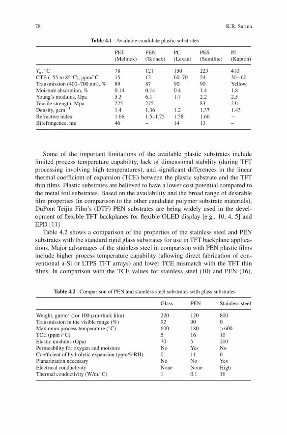
78 K.R. Sarma
Table 4.1 Available candidate plastic substrates
PET PEN PC PES PI(Melinex) (Teonex) (Lexan) (Sumilite) (Kapton)
Tg, ◦C 78 121 150 223 410CTE (–55 to 85◦C), ppm/◦C 15 13 60–70 54 30−60Transmission (400–700 nm), % 89 87 90 90 YellowMoisture absorption, % 0.14 0.14 0.4 1.4 1.8Young’s modulus, Gpa 5.3 6.1 1.7 2.2 2.5Tensile strength, Mpa 225 275 – 83 231Density, gcm−3 1.4 1.36 1.2 1.37 1.43Refractive index 1.66 1.5–1.75 1.58 1.66 −Birefringence, nm 46 – 14 13 –
Some of the important limitations of the available plastic substrates includelimited process temperature capability, lack of dimensional stability (during TFTprocessing involving high temperatures), and significant differences in the linearthermal coefficient of expansion (TCE) between the plastic substrate and the TFTthin films. Plastic substrates are believed to have a lower cost potential compared tothe metal foil substrates. Based on the availability and the broad range of desirablefilm properties (in comparison to the other candidate polymer substrate materials),DuPont Teijin Film’s (DTF) PEN substrates are being widely used in the devel-opment of flexible TFT backplanes for flexible OLED display [e.g., 10, 4, 5] andEPD [11]
Table 4.2 shows a comparison of the properties of the stainless steel and PENsubstrates with the standard rigid glass substrates for use in TFT backplane applica-tions. Major advantages of the stainless steel in comparison with PEN plastic filmsinclude higher process temperature capability (allowing direct fabrication of con-ventional a-Si or LTPS TFT arrays) and lower TCE mismatch with the TFT thinfilms. In comparison with the TCE values for stainless steel (10) and PEN (16),
Table 4.2 Comparison of PEN and stainless steel substrates with glass substrates
Glass PEN Stainless steel
Weight, gm/m2 (for 100-μm-thick film) 220 120 800Transmission in the visible range (%) 92 90 0Maximum process temperature (◦C) 600 180 >600TCE (ppm /◦C) 5 16 10Elastic modulus (Gpa) 70 5 200Permeability for oxygen and moisture No Yes NoCoefficient of hydrolytic expansion (ppm/%RH) 0 11 0Planarization necessary No No YesElectrical conductivity None None HighThermal conductivity (W/m.◦C) 1 0.1 16
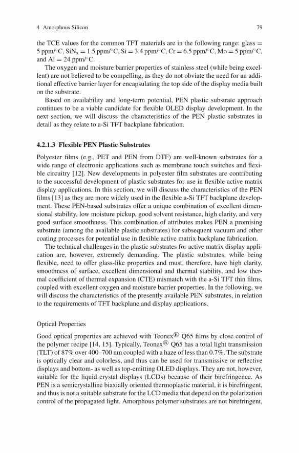
4 Amorphous Silicon 79
the TCE values for the common TFT materials are in the following range: glass =5 ppm/◦C, SiNx = 1.5 ppm/◦C, Si = 3.4 ppm/◦C, Cr = 6.5 ppm/◦C, Mo = 5 ppm/◦C,and Al = 24 ppm/◦C.
The oxygen and moisture barrier properties of stainless steel (while being excel-lent) are not believed to be compelling, as they do not obviate the need for an addi-tional effective barrier layer for encapsulating the top side of the display media builton the substrate.
Based on availability and long-term potential, PEN plastic substrate approachcontinues to be a viable candidate for flexible OLED display development. In thenext section, we will discuss the characteristics of the PEN plastic substrates indetail as they relate to a-Si TFT backplane fabrication.
4.2.1.3 Flexible PEN Plastic Substrates
Polyester films (e.g., PET and PEN from DTF) are well-known substrates for awide range of electronic applications such as membrane touch switches and flexi-ble circuitry [12]. New developments in polyester film substrates are contributingto the successful development of plastic substrates for use in flexible active matrixdisplay applications. In this section, we will discuss the characteristics of the PENfilms [13] as they are more widely used in the flexible a-Si TFT backplane develop-ment. These PEN-based substrates offer a unique combination of excellent dimen-sional stability, low moisture pickup, good solvent resistance, high clarity, and verygood surface smoothness. This combination of attributes makes PEN a promisingsubstrate (among the available plastic substrates) for subsequent vacuum and othercoating processes for potential use in flexible active matrix backplane fabrication.
The technical challenges in the plastic substrates for active matrix display appli-cation are, however, extremely demanding. The plastic substrates, while beingflexible, need to offer glass-like properties and must, therefore, have high clarity,smoothness of surface, excellent dimensional and thermal stability, and low ther-mal coefficient of thermal expansion (CTE) mismatch with the a-Si TFT thin films,coupled with excellent oxygen and moisture barrier properties. In the following, wewill discuss the characteristics of the presently available PEN substrates, in relationto the requirements of TFT backplane and display applications.
Optical Properties
Good optical properties are achieved with Teonex® Q65 films by close control ofthe polymer recipe [14, 15]. Typically, Teonex® Q65 has a total light transmission(TLT) of 87% over 400–700 nm coupled with a haze of less than 0.7%. The substrateis optically clear and colorless, and thus can be used for transmissive or reflectivedisplays and bottom- as well as top-emitting OLED displays. They are not, however,suitable for the liquid crystal displays (LCDs) because of their birefringence. AsPEN is a semicrystalline biaxially oriented thermoplastic material, it is birefringent,and thus is not a suitable substrate for the LCD media that depend on the polarizationcontrol of the propagated light. Amorphous polymer substrates are not birefringent,
80 K.R. Sarma
and thus are suitable for the LCD media. Birefringence is not an issue for the OLEDand EPD media.
Surface Quality
Surface smoothness and cleanliness are essential to prevent pinpricks in subsequentbarrier coatings and to ensure that the defects from the substrate do not deleteri-ously affect the active matrix TFT manufacturing yield. Industrial grade PEN typi-cally has a rough surface with a large (unacceptable) concentration of peaks of upto 0.1 μm high. By control of recipe and film process optimization, DTF achievesa much smoother surface without any 0.1-μm high peaks, but only a small concen-tration of 0.05-μm high peaks in Teonex® Q65. These remaining surface defectsare still detrimental to the performance of the thin films deposited on top and arethen removed by the application of a coating layer, typically comprised of a scratchresistant material. This coating layer acts to smooth over all the underlying PENsurface defects and additionally helps to prevent surface scratches during the subse-quent substrate handling operations. This surface is now smooth without any peaksor protrusions and is acceptable for the TFT active matrix backplane fabricationusing thin films with a thickness of the order of 100 nm.
Dimensional Stability
Dimensional stability during TFT array processing (involving temperature cyclesbetween the room temperature and the TFT process temperatures) is extremely crit-ical to ensure that the features in each layer of the TFT device structure align prop-erly with the corresponding features in the previous layers. Plastic films undergo avariable and undesirable change in dimensions at the glass transition temperature,Tg, due to both molecular relaxation events associated with the increased mobilityof the polymer chains and shrinkage or expansion associated with the relaxation ofresidual strain within the oriented parts of the film structure. This is an artifact ofthe film manufacturing conditions [14]. The dimensional stability of Teonex® Q65produced by biaxial stretching is enhanced by a heat stabilization process where theinternal strain in the film is relaxed by exposure to high temperature while underminimum line tension. Shrinkage at a given temperature is measured by placing thesample in a heated oven for a given period of time. The percent shrinkage is cal-culated as the percent change of dimension of the film in a given direction beforeand after heating. Heat-stabilized films exhibit shrinkage of the order of <0.1% andtypically <0.05% when exposed to temperatures of up to 180◦C for 5 min. OnceTeonex® Q65 is heat stabilized, it remains a dimensionally reproducible substrateup to 200◦C. Its improved thermal resistance provides a dimensionally reproduciblesubstrate over this temperature range and permits a continuous use at a tempera-ture of about 180◦C. It should be noted that shrinkage of 0.05% is not acceptablefor fabricating the TFT backplanes. In Section 4.4, we will discuss this further anddescribe a prestabilization process to reduce the shrinkage to manageable levels tofabricate low-temperature a-Si TFT backplanes and OLED displays.
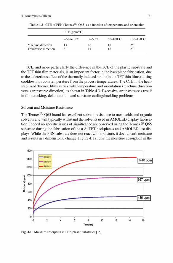
4 Amorphous Silicon 81
Table 4.3 CTE of PEN (Teonex® Q65) as a function of temperature and orientation
CTE (ppm/◦C)
−50 to 0◦C 0−50◦C 50–100◦C 100–150◦C
Machine direction 13 16 18 25Transverse direction 8 11 18 29
TCE, and more particularly the difference in the TCE of the plastic substrate andthe TFT thin film materials, is an important factor in the backplane fabrication, dueto the deleterious effect of the thermally induced strain (in the TFT thin films) duringcooldown to room temperature from the process temperatures. The CTE in the heat-stabilized Teonex films varies with temperature and orientation (machine directionversus transverse direction) as shown in Table 4.3. Excessive strains/stresses resultin film cracking, delamination, and substrate curling/buckling problems.
Solvent and Moisture Resistance
The Teonex® Q65 brand has excellent solvent resistance to most acids and organicsolvents and will typically withstand the solvents used in AMOLED display fabrica-tion. Indeed no specific issues of significance are observed using the Teonex® Q65substrate during the fabrication of the a-Si TFT backplanes and AMOLED test dis-plays. While the PEN substrate does not react with moisture, it does absorb moistureand results in a dimensional change. Figure 4.1 shows the moisture absorption in the
Fig. 4.1 Moisture absorption in PEN plastic substrates [15]

82 K.R. Sarma
PEN substrate as a function of relative humidity (RH) and time [15]. At 40% RH,the equilibrium moisture concentration in the film is expected to be about 957 ppmwhich is very high since for every 100 ppm of moisture absorbed, the film is esti-mated to expand by ∼45 ppm. This is a very significant dimensional change andcan deleteriously affect the TFT backplane process if it is not managed. Moistureabsorption is reversible by heating the substrate in vacuum or in an inert atmosphere.Uncontrolled moisture absorption/desorption during the TFT backplane fabricationcan potentially have far more impact on the substrate dimensional stability than thedimensional instability due to the inherent PEN substrate shrinkage. We will discussthis further in Section 4.4 on backplane fabrication.
Barrier Properties
The inherent barrier properties of PEN films are typically of the order of ca.1 g/m2/day for water vapor transmission rates and an equivalent ca of 3 mL/m2/dayfor oxygen transmission rates. This is still a long way from the levels required forthe protection of OLED displays, which require water vapor transmission rates of<10−6 g/m2/day and oxygen transmission rates of <10−5 mL/m2/day. No poly-mer substrate meets these requirements, and the flexible substrates currently beingdeveloped need to use an effective barrier layer to encapsulate the OLED devices forprotection against oxygen and moisture ingression to enhance the OLED lifetime.Note that the EPDs have far less sensitive to moisture, and thus do not impose suchstringent requirements on the barrier layer performance. The progress in the barrierlayer development is discussed in Section 4.2.1.3 in more detail.
4.2.2 TFT Technologies for Flexible Backplanes
Flexible substrate compatible TFT backplane technology development is a criticalitem for the fabrication of flexible active matrix displays. Both the well-establishedTFT technologies, namely a-Si TFT and LTPS TFT, are being considered for flex-ible display applications. In addition, emerging TFT technologies, namely O-TFT(organic TFT) and oxide semiconductor (such as ZnO) TFT technologies are alsobeing developed for flexible backplane applications. The TFT processes developedfor the flat rigid glass substrates cannot readily be applied for use with the flexible plas-tic substrates, due to reasons such as lower process temperature constraints, thermalstress limitations due to a larger CTE mismatch, and dimensional stability issues.
Currently, there are two main approaches being considered for producing flexibleplastic backplanes:
(1) Standard (high temperature) TFT fabrication on a conventional display glasssubstrate, followed by transfer of the TFT circuit (backplane) on to a flexibleplastic substrate by adhesive bonding at a lower temperature (e.g., <150◦C).This process is referred to as Device Layer Transfer (DLT) process.
(2) Fabrication of TFT array directly on the flexible plastic substrate using lower(plastic substrate compatible) temperature processes.
4 Amorphous Silicon 83
The DLT process [16, 17] can be a viable approach for flexible displays, whenlow cost is not a consideration. This approach can provide the most optimumTFT device performance with respect to mobility, leakage current, stability, anduniformity as the TFTs are fabricated using conventional LTPS (low-temperaturepolysilicon at ∼450◦C) process, and then transferred on to the flexible plasticsubstrate at a low temperature. DLT will be a higher cost approach compared tothe direct fabrication approach, due to wastage of the glass substrate and addi-tional cost of the transfer process. While several companies have demonstrated thisapproach, it is not believed to be solution for the desired low-cost flexible displaysultimately.
Table 4.4 shows a comparison of the various TFT approaches. The conventionalLTPS process used in the current AMLCDs uses a typical process temperature inthe range of ∼450◦C using a polysilicon film produced by Excimer laser recrys-tallization of an a-Si film. Due to the high process temperature requirement, theconventional LTPS TFT approach may be appropriate for use with the stainlesssteel substrates, but not with plastic substrates with a process temperature limitationof less than 200◦C. To overcome this problem using a plastic substrate, ultra low-temperature (<200◦C) polysilicon (ULTPS) TFT processes are being developed[e.g., 18]. The ULTPS TFT approach has the potential for providing high mobilityCMOS TFT devices suitable for driving the OLED pixels, as well as for fabricatingthe row and column drivers directly on the plastic substrate. Good progress has beenmade in producing TFTs with high mobility and satisfactory threshold voltages forthe n- and p-channel devices. However, the leakage currents need to be reducedfurther for fabricating high-quality active matrix displays. The ULTPS technologycontinues to be developed to reduce the leakage currents and to further enhance itsmaturity and increase process yield.
a-Si TFT is currently the workhorse of the well-established AMLCD tech-nology, and thus it will have several advantages if it can be adapted for usein flexible electronics and display manufacturing applications. However, forAMOLED applications, currently, a-Si TFT does have some issues that includethe following:
(1) Low TFT mobility (μfe ∼ 1 cm2 V−1 s−1) which requires use of TFTs with alarge W/L (W and L are the TFT channel width and length, respectively) ratio toachieve the desired pixel drive current. This results in a reduced pixel apertureratio, and thus reduced pixel luminance in bottom emission OLED displays.As OLED materials and devices with improved efficiency are developed, thiswill be less of an issue. Top emission OLED pixel architecture alleviates thisproblem completely.
(2) The low mobility does not allow integration of the row and column drivers onthe display glass.
(3) Only NMOS TFTs are available in a-Si, which restrict the choice of pixel circuitdesigns.
(4) The TFT stability with respect to gate bias is poor. The impact of this is dis-cussed in more detail below.
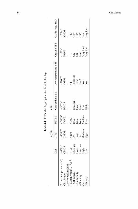
84 K.R. Sarma
Tabl
e4.
4T
FTte
chno
logy
optio
nsfo
rfle
xibl
edi
spla
ys
Poly
-Si
a-Si
DLT
LTPS
ULT
PSC
onve
ntio
nala
-Si
Low
-tem
pera
ture
a-Si
Org
anic
TFT
Oxi
de(e
.g.,
ZnO
)
Proc
ess
tem
pera
ture
(◦ C)
∼450
◦ C∼4
50◦ C
<20
0◦ C∼3
00◦ C
<20
0◦ C<
150◦ C
<20
0◦ CC
ircu
itty
peC
MO
SC
MO
SC
MO
SN
MO
SN
MO
SPM
OS
NM
OS
Dev
ice
perf
orm
ance
––
––
−–
––
Mob
ility
(cm
2V
−1.s
−1)
∼100
∼100
∼100
∼1∼1
∼1∼4
0–
Off
-cur
rent
Exc
elle
ntO
KIs
sue
Exc
elle
ntE
xcel
lent
OK
OK
?–
Uni
form
ityG
ood
Issu
eIs
sue
Goo
dG
ood
OK
OK
?–
Stab
ility
Exc
elle
ntO
KIs
sue
Issu
eIs
sue!
Issu
e!!
OK
?C
ost
Hig
hM
ediu
mM
ediu
mL
owL
owV
ery
low
?L
owM
atur
ityL
owH
igh
Low
Hig
hL
owV
ery
low
Ver
ylo
w
4 Amorphous Silicon 85
The conventional a-Si TFTs used in the current AMLCDs are fabricated at a typ-ical process temperature of 300◦C. Again for the obvious reason of high processtemperature requirement, the conventional a-Si TFT process could not be used withthe candidate plastic substrate with a process temperature limitation of less than200◦C. In recent years, significant advances have been made in the process temper-ature reduction, and a-Si TFTs have been successfully fabricated using low processtemperatures of about 150◦C [e.g., 19–21, 10], with a performance comparable tothe 300◦C process with respect to mobility, threshold voltage, and leakage current.However, the device stability under gate bias stress remains to be one item that needsto be improved particularly for the low-temperature processed a-Si TFTs. a-Si TFTsare known to exhibit threshold voltage, Vt, shifts under prolonged positive gate bias,particularly under higher operating temperature conditions. In AMOLED displayoperation, the drive TFT is typically subjected to positive gate voltage bias for theentire frame time (as opposed to only during the row address time as in an AMLCD).We will discuss this further under the next section on pixel drive electronics. Oneapproach for increasing the a-Si TFT stability and decreasing the propensity for Vt
shift is to reduce the display operating voltages and pixel current drive requirements.The recent progress in OLED materials toward lower drive voltages and pixel cur-rent requirements is very encouraging.
As opposed to fabricating the TFT backplane on a self-supporting flexible sub-strate, an alternate method involves bonding the flexible substrate to a rigid carriersubstrate such as glass using a temporary adhesive, prior to the TFT array fabri-cation, for ease of handling during TFT array fabrication. After the TFT array isfabricated, the flexible substrate with the backplane circuit is separated from thetemporary adhesive (and the carrier substrate). The issues in this approach include(1) temperature constraints imposed by the temporary adhesive, (2) potential chem-ical contamination by the temporary adhesive during the TFT processing, (3) yieldof the bonding and debonding (of the flexible substrate/backplane from the rigid car-rier substrate) operations with complete removal of the temporary adhesive, (4) costof the bonding and debonding operations, and (5) cost of the temporary substrate ifit is not reuseable.
An interesting variation of this approach is being developed by Philips, [22]which involves a-Si TFT backplane fabrication on a polyimide foil (10-μm-thickflexible substrate) that is spin coated on a rigid glass substrate. This process isnamed as the EPLaR (Electronics on Plastic by Laser Release) process. Thisprocess involves two extra process steps compared to a conventional a-Si TFTprocess on a rigid glass substrate. The first is an additive process of spin coatinga 10-μm-thick polyimide layer (which subsequently becomes the self-supportingflexible substrate/backplane). The second is the laser release process. The tempera-ture capability of this polyimide layer exceeds the requirements of the conventionala-Si TFT process; thus it can be processed in conventional a-Si TFT backplanefabrication facilities using standard processes. EPD media is then laminated to theTFT backplane, and the resulting display on the polyimide foil is then separatedfrom the rigid carrier glass substrate, by a laser release process, which relies on the
86 K.R. Sarma
appropriate glass surface treatments prior to the polyimide spin coating, and use ofthe appropriate type of polyimide. Flexible EPDs have been demonstrated using thisprocess. This process has a potential to be adopted for the LTPS backplanes as well,and for other display media such as an OLED as well.
Direct fabrication on the self-supporting flexible substrate (i.e., without the useof a carrier substrate) is expected to have a lower cost, and has the advantage ofa relatively easier transition to a roll-to-roll (RTR) process. However, due to thelimited process temperature capability of the PEN substrate, development of a low-temperature plastic compatible a-Si TFT processes are required, and this is dis-cussed in Section 4.2.2.1.
Currently, there is a lot of interest in the development of organic electronicsinvolving TFTs fabricated using organic semiconductors. O-TFTs have the advan-tage of very low process temperature, and they could be fabricated using low-costsolution processing methods (e.g., spin coating, ink-jet printing, etc.) instead of themore expensive vacuum-based thin-film deposition methods. To date OTFTs fabri-cated using vacuum-deposited pentacene as the organic semiconductor have shownthe best performance [e.g., 23] with a field-effect mobility of over 2 cm2 V−1 s−1,near zero Vt, and “on”–“off” current ratio of over 108. However, the solution pro-cessable organic semiconductor-based O-TFTs have shown a mobility in the rangeof about 0.05 cm2 V−1 s−1. One major advantage of O-TFTs with complete solutionprocessing (e.g., ink-jet printing) is that it is easier to compensate for dimensionalinstability of the plastic substrate during backplane processing [24]. O-TFT back-planes are beginning to be commercialized using the EPD media for some initialapplications. While impressive progress is being made on this approach, this tech-nology is still developing and not yet satisfactory for flexible OLED displays. Thistopic “Organic and Polymeric TFTs for Flexible Displays and Circuits” is discussedin detail in Chapter 8.
Transparent oxide semiconductors such as zinc oxide (ZnO) are beginning tobe actively investigated for use in low-temperature TFT backplanes for displays[25]. ZnO is a wide bandgap (−3.3 eV at 300 K) semiconductor and has theadvantage of being deposited directly in a polycrystalline phase even at room tem-perature (such as by RF magnetron sputtering), and thus is compatible with thecurrently available flexible plastic substrates. Hirao et al. achieved a field-effectmobility and threshold voltage of 50.3 cm2 V−1 s−1 and 1.1 V, respectively, forZnO TFTs and demonstrated an AMLCD display. An additional feature of ZnOTFT is its transmission in the visible range. It has an average optical transmission(including the glass substrate) of about 80% in the visible part of the spectrum.The combination of transparency, high channel mobility, and room temperatureprocessing makes the ZnO TFT very promising for flexible and transparent elec-tronics and display applications.
In the following, we will discuss the recent progress in low-temperature a-Si TFTtechnology for flexible plastic backplanes and displays.
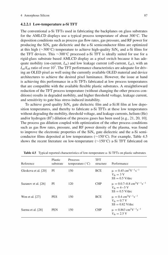
4 Amorphous Silicon 87
4.2.2.1 Low-temperature a-Si TFT
The conventional a-Si TFTs used in fabricating the backplanes on glass substratesfor the AMLCD displays use a typical process temperature of about 300◦C. Thedeposition conditions such as process gas flow rates, gas pressure, and RF power forproducing the SiNx gate dielectric and the a-Si semiconductor films are optimizedat this high (∼300◦C) temperature to achieve high-quality SiNx and a-Si films forthe TFT devices. This ∼300◦C processed a-Si TFT is ideally suited for use for arigid-glass substrate based AMLCD display as a pixel switch because it has ade-quate mobility (on-current, Ion) and low leakage current (off-current, Ioff), with anIon/Ioff ratio of over 107. The TFT performance characteristics are adequate for driv-ing an OLED pixel as well using the currently available OLED material and devicearchitectures to achieve the desired pixel luminance. However, the issue at handis achieving this performance in a-Si TFTs fabricated at low process temperaturesthat are compatible with the available flexible plastic substrates. A straightforwardreduction of the TFT process temperature (without changing the other process con-ditions) results in degraded mobility, and higher threshold voltage, leakage current,and sensitivity to gate bias stress-induced instability.
To achieve good quality SiNx gate dielectric film and a-Si:H film at low depo-sition temperatures, and thereby to fabricate a-Si TFTs at these low temperatureswithout degrading the mobility, threshold voltage, and leakage currents, helium (He)and/or hydrogen (H2) dilution of the process gases has been used [e.g., 21, 20, 10].The process gas dilution coupled with optimization of the other process conditionssuch as gas flow rates, pressure, and RF power density of the plasma, was foundto improve the electronic properties of the SiNx gate dielectric and the a-Si semi-conductor films deposited at low temperatures (∼150◦C). For example, Table 4.5shows the recent literature on low-temperature (∼150◦C) a-Si TFT fabricated on
Table 4.5 Typical reported characteristics of low-temperature a- Si TFTs on plastic substrates
Plastic Processs TFTReference substrate temperature (◦C) structure Performance
Gleskova et al. [20] PI 150 BCE μ = 0.45 cm2V−1s−1
Vth = 3 VSS = 0.5 V/dec
Sazanov et al. [26] PI 120 CHP μ = 0.0.7–0.8 cm2V−1s−1
Vth = 4−5 VSS = 0.5 V/dec
Won et al. [27] PES 150 BCE μ = 0.4 cm2V−1s−1
Vth = 0.7 VSS = 0.82 V/dec
Sarma et al. [28] PEN 150 CHP μ = 0.863 cm2V−1s−1
Vth = 2.5 V
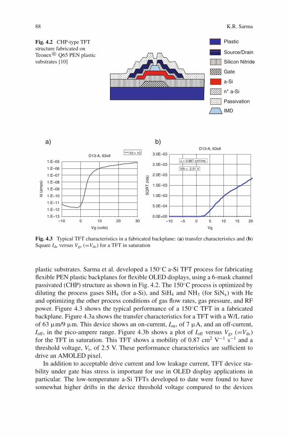
88 K.R. Sarma
Plastic
Source/Drain
Silicon Nitride
Gate
a-Si
n+ a-Si
Passivation
IMD
Fig. 4.2 CHP-type TFTstructure fabricated onTeonex® Q65 PEN plasticsubstrates [10]
1.E–13
1.E–12
1.E–11
1.E–10
1.E–09
1.E–08
1.E–07
1.E–06
1.E–05
Vg (volts)
Id (
amps
)
Vd = 10D13-A, 63x9
–10 0 10 20 30
Vg
D13-A, 63x9
0.0E+00
5.0E–04
1.0E–03
1.5E–03
2.0E–03
2.5E–03
3.0E–03
–10 –5 0 5 10 15 20
SQ
RT
(Id
s)
u = 0.867 cm²/v•s
Vth = 2.51 V
a) b)
Fig. 4.3 Typical TFT characteristics in a fabricated backplane: (a) transfer characteristics and (b)Square Ids versus Vgs (=Vds) for a TFT in saturation
plastic substrates. Sarma et al. developed a 150◦C a-Si TFT process for fabricatingflexible PEN plastic backplanes for flexible OLED displays, using a 6-mask channelpassivated (CHP) structure as shown in Fig. 4.2. The 150◦C process is optimized bydiluting the process gases SiH4 (for a-Si), and SiH4 and NH3 (for SiNx) with Heand optimizing the other process conditions of gas flow rates, gas pressure, and RFpower. Figure 4.3 shows the typical performance of a 150◦C TFT in a fabricatedbackplane. Figure 4.3a shows the transfer characteristics for a TFT with a W/L ratioof 63 μm/9 μm. This device shows an on-current, Ion, of 7 μA, and an off-current,Ioff, in the pico-ampere range. Figure 4.3b shows a plot of Ioff versus Vgs (=Vds)for the TFT in saturation. This TFT shows a mobility of 0.87 cm2 V−1 s−1 and athreshold voltage, Vt, of 2.5 V. These performance characteristics are sufficient todrive an AMOLED pixel.
In addition to acceptable drive current and low leakage current, TFT device sta-bility under gate bias stress is important for use in OLED display applications inparticular. The low-temperature a-Si TFTs developed to date were found to havesomewhat higher drifts in the device threshold voltage compared to the devices
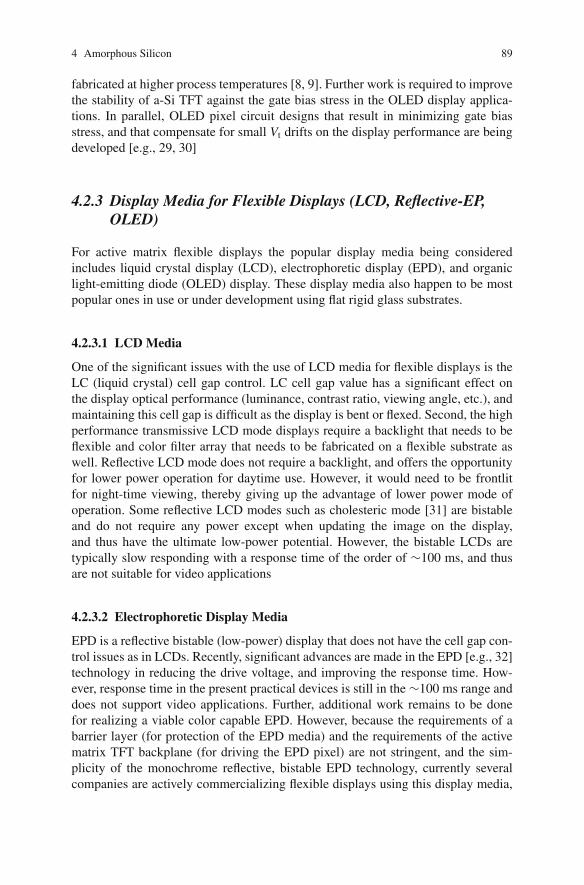
4 Amorphous Silicon 89
fabricated at higher process temperatures [8, 9]. Further work is required to improvethe stability of a-Si TFT against the gate bias stress in the OLED display applica-tions. In parallel, OLED pixel circuit designs that result in minimizing gate biasstress, and that compensate for small Vt drifts on the display performance are beingdeveloped [e.g., 29, 30]
4.2.3 Display Media for Flexible Displays (LCD, Reflective-EP,OLED)
For active matrix flexible displays the popular display media being consideredincludes liquid crystal display (LCD), electrophoretic display (EPD), and organiclight-emitting diode (OLED) display. These display media also happen to be mostpopular ones in use or under development using flat rigid glass substrates.
4.2.3.1 LCD Media
One of the significant issues with the use of LCD media for flexible displays is theLC (liquid crystal) cell gap control. LC cell gap value has a significant effect onthe display optical performance (luminance, contrast ratio, viewing angle, etc.), andmaintaining this cell gap is difficult as the display is bent or flexed. Second, the highperformance transmissive LCD mode displays require a backlight that needs to beflexible and color filter array that needs to be fabricated on a flexible substrate aswell. Reflective LCD mode does not require a backlight, and offers the opportunityfor lower power operation for daytime use. However, it would need to be frontlitfor night-time viewing, thereby giving up the advantage of lower power mode ofoperation. Some reflective LCD modes such as cholesteric mode [31] are bistableand do not require any power except when updating the image on the display,and thus have the ultimate low-power potential. However, the bistable LCDs aretypically slow responding with a response time of the order of ∼100 ms, and thusare not suitable for video applications
4.2.3.2 Electrophoretic Display Media
EPD is a reflective bistable (low-power) display that does not have the cell gap con-trol issues as in LCDs. Recently, significant advances are made in the EPD [e.g., 32]technology in reducing the drive voltage, and improving the response time. How-ever, response time in the present practical devices is still in the ∼100 ms range anddoes not support video applications. Further, additional work remains to be donefor realizing a viable color capable EPD. However, because the requirements of abarrier layer (for protection of the EPD media) and the requirements of the activematrix TFT backplane (for driving the EPD pixel) are not stringent, and the sim-plicity of the monochrome reflective, bistable EPD technology, currently severalcompanies are actively commercializing flexible displays using this display media,
90 K.R. Sarma
for applications such as e-books. We will discuss the recent status of these types offlexible displays in Section 4.5.
4.2.3.3 OLED Display Media
AMOLED display technology offers significant advantages over the current well-entrenched AMLCD with respect to superior image quality with wide viewing angleand fast response time, being lighter and thinner, lower cost (does not need back-light or color filters), and lower power. Because of this, many companies are activelydeveloping and beginning to commercialize the AMOLED displays built using rigidflat glass substrates. Also, OLED media is believed to be natural choice for use ina flexible display as it represents the ultimate flexible display with a rugged solid-state display media and other attributes including full color, superior image qual-ity, full-motion video, and low power. However, the OLED display media has verystringent requirements with respect to both the barrier layer specifications and theactive matrix TFT backplane performance. Due to the long-term potential of flex-ible OLED displays, there is considerable interest in developing this technology.Also, OLED display application for flexible a-Si TFT backplanes is the focus ofthis chapter.
4.2.4 Barrier Layers
Lack of impermeability to moisture and oxygen is a serious deficiency of all theplastic substrates for the flexible display applications. All display media includingLCDs, EPDs, and OLEDs degrade when exposed to oxygen and moisture in theambient, even though at different rates with OLED having the most sensitivity tomoisture and oxygen. For example, for the protection of an OLED display the plasticsubstrate (barrier layer) must have a permeability of less than 10−6 gm/m2/day formoisture and 10−5 mL/m2/day for oxygen. In comparison, LCD displays have abarrier requirement of 10−2 gm/m2/day for both oxygen and moisture, which issignificantly less stringent compared to OLEDs. The base plastic substrates typicallyhave about 10 gm/m2/day transmission rates for both oxygen and moisture, implyingthe need for incorporating a separate barrier layer.
In principle, a thin layer of an inorganic film such as SiO2, SiNx, and Al2O3
deposited on the flexible plastic substrate can serve as a barrier layer with therequired impermeability to oxygen and moisture. However, in practice multilayerbarrier film structures are believed to be required to counter the effects of thepinholes/cracks in single layer deposited barrier layers. Several organizations arecurrently developing optically transparent multilayer barrier coatings for flexibleOLED displays [33]. Vitex Systems [34] uses such kind of an approach for theirbarrier film called BarixTM, which employs alternating layers of a polymer and aceramic inorganic barrier coatings applied in vacuum, as shown in Fig. 4.4. Theinorganic films serve as barrier films for oxygen and moisture, organic layers servethe planarization/smoothing function, and multilayers provide redundancy against
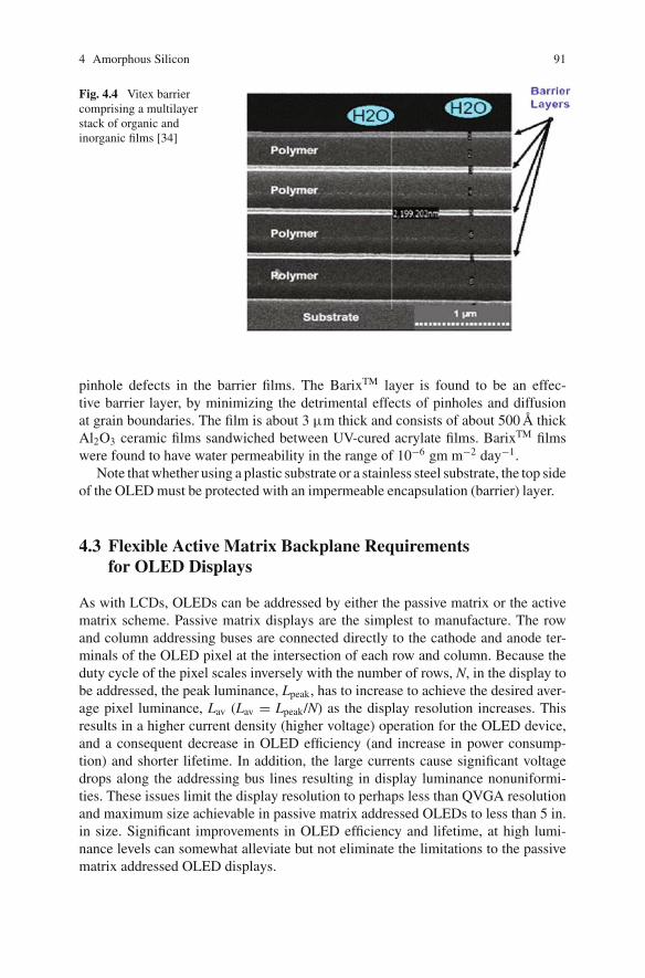
4 Amorphous Silicon 91
Fig. 4.4 Vitex barriercomprising a multilayerstack of organic andinorganic films [34]
pinhole defects in the barrier films. The BarixTM layer is found to be an effec-tive barrier layer, by minimizing the detrimental effects of pinholes and diffusionat grain boundaries. The film is about 3 μm thick and consists of about 500 A thickAl2O3 ceramic films sandwiched between UV-cured acrylate films. BarixTM filmswere found to have water permeability in the range of 10−6 gm m−2 day−1.
Note that whether using a plastic substrate or a stainless steel substrate, the top sideof the OLED must be protected with an impermeable encapsulation (barrier) layer.
4.3 Flexible Active Matrix Backplane Requirementsfor OLED Displays
As with LCDs, OLEDs can be addressed by either the passive matrix or the activematrix scheme. Passive matrix displays are the simplest to manufacture. The rowand column addressing buses are connected directly to the cathode and anode ter-minals of the OLED pixel at the intersection of each row and column. Because theduty cycle of the pixel scales inversely with the number of rows, N, in the display tobe addressed, the peak luminance, Lpeak, has to increase to achieve the desired aver-age pixel luminance, Lav (Lav = Lpeak/N) as the display resolution increases. Thisresults in a higher current density (higher voltage) operation for the OLED device,and a consequent decrease in OLED efficiency (and increase in power consump-tion) and shorter lifetime. In addition, the large currents cause significant voltagedrops along the addressing bus lines resulting in display luminance nonuniformi-ties. These issues limit the display resolution to perhaps less than QVGA resolutionand maximum size achievable in passive matrix addressed OLEDs to less than 5 in.in size. Significant improvements in OLED efficiency and lifetime, at high lumi-nance levels can somewhat alleviate but not eliminate the limitations to the passivematrix addressed OLED displays.
92 K.R. Sarma
Active matrix addressing scheme removes the limitations to the resolution anddisplay size associated with passive matrix OLEDs. With active matrix addressingscheme, the pixel is driven with 100% duty cycle, regardless of the number of rowsin a display. Active matrix addressing allows operation of the OLED devices (pixels)in the efficient regime (in the current density versus optical efficiency curve) andprovides the best image quality. Other advantage of active matrix is that the cathode(which is typically a low-work function reactive material such as Li and Ca) doesnot need to be patterned in the active area of the display. A simple shadow mask canbe used during deposition for patterning the common cathode.
4.3.1 Active Matrix Addressing
LCDs are voltage-controlled devices and involve varying the voltage (data) acrossthe LC pixel to control transmission through the pixel (gray level). On the otherhand, OLEDs are current-controlled devices involving control of the current throughthe OLED pixel to control pixel luminance (gray level). The pixel circuit in anAMLCD typically involves only a switching TFT and a storage capacitor to holdthe pixel electrode node at the data voltage during the frame time. However, in caseof AM OLED, the pixel circuit is required to control the current flow through theOLED pixel, and involves at least two TFTs and a storage capacitor. In the followingsection, we will discuss the two general implementations of a current driven pixelcircuit in an AMOLED display.
4.3.1.1 Voltage Programming
Figure 4.5 shows the basic current driven pixel circuit for an AMOLED. This circuitconsists of a select transistor, T1, a drive transistor (current source element), T2,and a storage capacitor, Cs. During the row select period, select transistor T1 turnson and transfers the voltage (data) signal from the column electrode to the gateof the drive transistor T2. After the addressing period, T1 is switched off, and theprogrammed voltage (data) is held on the gate of T2 for the rest of the frame time.The storage capacitor Cs prevents discharge of the T2 gate node (by leakage throughT1) by any appreciable amount. Thus, Cs allows continuous driving of the OLED byT2, through the common power supply, LDD, while the other rows in the display areaddressed sequentially. When T2 is biased in saturation (|Vd| > |Vgs–Vt|), it behavesas a constant current source, with the current, Isd, given by:
Isd = K · μfe · (Vgs − Vt)2
where K is a constant based on the transistor size (channel length, L, and channelwidth, W) and the gate capacitance per unit area, C, μfe is the field effect mobility,Vgs is the gate-source voltage, and Vt is the threshold voltage.
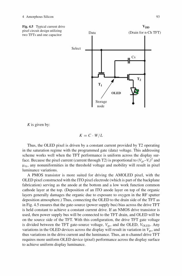
4 Amorphous Silicon 93
VDD
(Drain for n-Ch TFT)
Select
Data
Storagenode
Cs
T2
T1
OLED
Fig. 4.5 Typical current drivepixel circuit design utilizingtwo TFTs and one capacitor
K is given by:
K = C · W/L
Thus, the OLED pixel is driven by a constant current provided by T2 operatingin the saturation regime with the programmed gate (data) voltage. This addressingscheme works well when the TFT performance is uniform across the display sur-face. Because the pixel current (current through T2) is proportional to (Vgs–Vt)2 andμfe, any nonuniformities in the threshold voltage and mobility will result in pixelluminance variations.
A PMOS transistor is more suited for driving the AMOLED pixel, with theOLED pixel constructed with the ITO pixel electrode (which is part of the backplanefabrication) serving as the anode at the bottom and a low work function commoncathode layer at the top. (Deposition of an ITO anode layer on top of the organiclayers generally damages the organic due to exposure to oxygen in the RF sputterdeposition atmosphere.) Thus, connecting the OLED to the drain side of the TFT asin Fig. 4.5 ensures that the gate-source (power supply bus) bias across the drive TFTis held constant to achieve a constant current drive. If an NMOS drive transistor isused, then power supply bus will be connected to the TFT drain, and OLED will beon the source side of the TFT. With this configuration, the drive TFT gate voltageis divided between the TFT gate-source voltage, Vgs, and the OLED, VOLED. Anyvariations in the OLED devices across the display will result in variation in Vgs, andthus variations in the drive current and the luminance. Thus, an n-channel drive TFTrequires more uniform OLED device (pixel) performance across the display surfaceto achieve uniform display luminance.
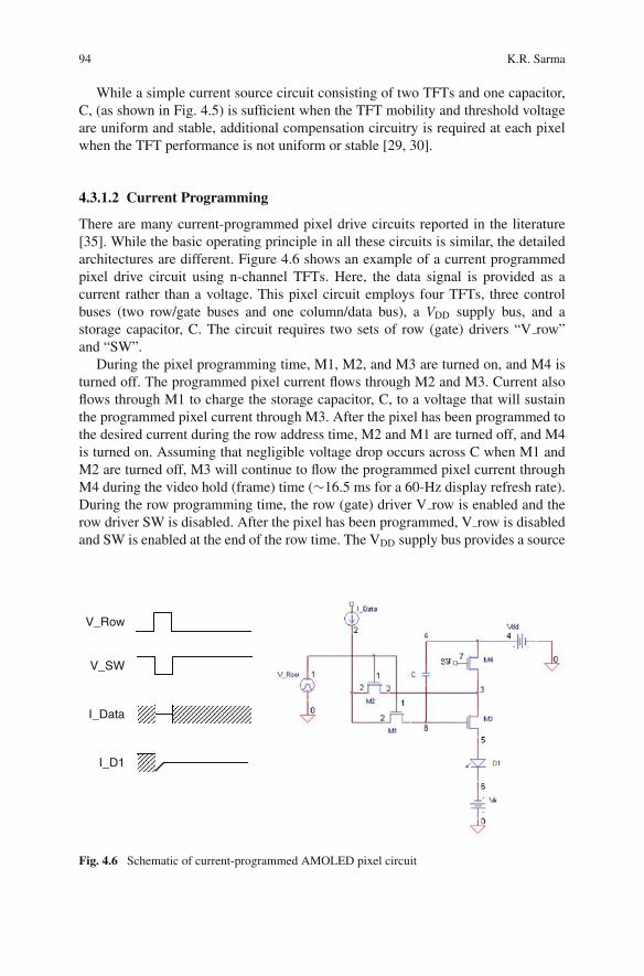
94 K.R. Sarma
While a simple current source circuit consisting of two TFTs and one capacitor,C, (as shown in Fig. 4.5) is sufficient when the TFT mobility and threshold voltageare uniform and stable, additional compensation circuitry is required at each pixelwhen the TFT performance is not uniform or stable [29, 30].
4.3.1.2 Current Programming
There are many current-programmed pixel drive circuits reported in the literature[35]. While the basic operating principle in all these circuits is similar, the detailedarchitectures are different. Figure 4.6 shows an example of a current programmedpixel drive circuit using n-channel TFTs. Here, the data signal is provided as acurrent rather than a voltage. This pixel circuit employs four TFTs, three controlbuses (two row/gate buses and one column/data bus), a VDD supply bus, and astorage capacitor, C. The circuit requires two sets of row (gate) drivers “V row”and “SW”.
During the pixel programming time, M1, M2, and M3 are turned on, and M4 isturned off. The programmed pixel current flows through M2 and M3. Current alsoflows through M1 to charge the storage capacitor, C, to a voltage that will sustainthe programmed pixel current through M3. After the pixel has been programmed tothe desired current during the row address time, M2 and M1 are turned off, and M4is turned on. Assuming that negligible voltage drop occurs across C when M1 andM2 are turned off, M3 will continue to flow the programmed pixel current throughM4 during the video hold (frame) time (∼16.5 ms for a 60-Hz display refresh rate).During the row programming time, the row (gate) driver V row is enabled and therow driver SW is disabled. After the pixel has been programmed, V row is disabledand SW is enabled at the end of the row time. The VDD supply bus provides a source
V_Row
I_Data
I_D1
V_SW
Fig. 4.6 Schematic of current-programmed AMOLED pixel circuit
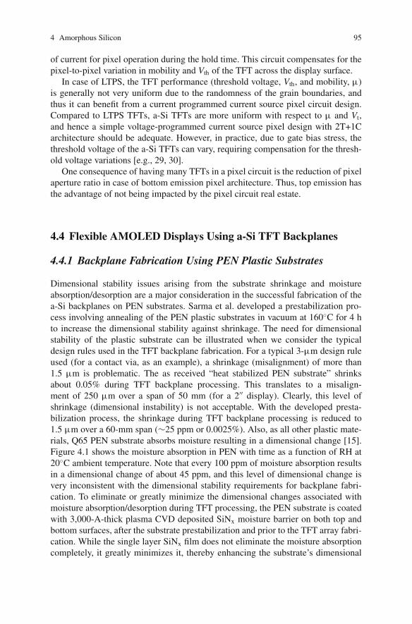
4 Amorphous Silicon 95
of current for pixel operation during the hold time. This circuit compensates for thepixel-to-pixel variation in mobility and Vth of the TFT across the display surface.
In case of LTPS, the TFT performance (threshold voltage, Vth, and mobility, μ)is generally not very uniform due to the randomness of the grain boundaries, andthus it can benefit from a current programmed current source pixel circuit design.Compared to LTPS TFTs, a-Si TFTs are more uniform with respect to μ and Vt,and hence a simple voltage-programmed current source pixel design with 2T+1Carchitecture should be adequate. However, in practice, due to gate bias stress, thethreshold voltage of the a-Si TFTs can vary, requiring compensation for the thresh-old voltage variations [e.g., 29, 30].
One consequence of having many TFTs in a pixel circuit is the reduction of pixelaperture ratio in case of bottom emission pixel architecture. Thus, top emission hasthe advantage of not being impacted by the pixel circuit real estate.
4.4 Flexible AMOLED Displays Using a-Si TFT Backplanes
4.4.1 Backplane Fabrication Using PEN Plastic Substrates
Dimensional stability issues arising from the substrate shrinkage and moistureabsorption/desorption are a major consideration in the successful fabrication of thea-Si backplanes on PEN substrates. Sarma et al. developed a prestabilization pro-cess involving annealing of the PEN plastic substrates in vacuum at 160◦C for 4 hto increase the dimensional stability against shrinkage. The need for dimensionalstability of the plastic substrate can be illustrated when we consider the typicaldesign rules used in the TFT backplane fabrication. For a typical 3-μm design ruleused (for a contact via, as an example), a shrinkage (misalignment) of more than1.5 μm is problematic. The as received “heat stabilized PEN substrate” shrinksabout 0.05% during TFT backplane processing. This translates to a misalign-ment of 250 μm over a span of 50 mm (for a 2′′ display). Clearly, this level ofshrinkage (dimensional instability) is not acceptable. With the developed presta-bilization process, the shrinkage during TFT backplane processing is reduced to1.5 μm over a 60-mm span (∼25 ppm or 0.0025%). Also, as all other plastic mate-rials, Q65 PEN substrate absorbs moisture resulting in a dimensional change [15].Figure 4.1 shows the moisture absorption in PEN with time as a function of RH at20◦C ambient temperature. Note that every 100 ppm of moisture absorption resultsin a dimensional change of about 45 ppm, and this level of dimensional change isvery inconsistent with the dimensional stability requirements for backplane fabri-cation. To eliminate or greatly minimize the dimensional changes associated withmoisture absorption/desorption during TFT processing, the PEN substrate is coatedwith 3,000-A-thick plasma CVD deposited SiNx moisture barrier on both top andbottom surfaces, after the substrate prestabilization and prior to the TFT array fabri-cation. While the single layer SiNx film does not eliminate the moisture absorptioncompletely, it greatly minimizes it, thereby enhancing the substrate’s dimensional
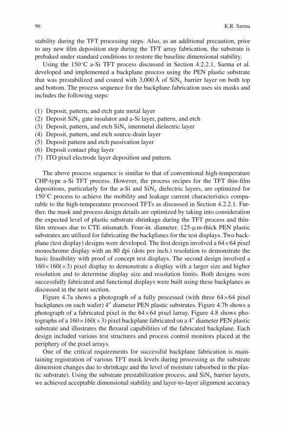
96 K.R. Sarma
stability during the TFT processing steps. Also, as an additional precaution, priorto any new film deposition step during the TFT array fabrication, the substrate isprebaked under standard conditions to restore the baseline dimensional stability.
Using the 150◦C a-Si TFT process discussed in Section 4.2.2.1, Sarma et al.developed and implemented a backplane process using the PEN plastic substratethat was prestabilized and coated with 3,000 A of SiNx barrier layer on both topand bottom. The process sequence for the backplane fabrication uses six masks andincludes the following steps:
(1) Deposit, pattern, and etch gate metal layer(2) Deposit SiNx gate insulator and a-Si layer, pattern, and etch(3) Deposit, pattern, and etch SiNx intermetal dielectric layer(4) Deposit, pattern, and etch source-drain layer(5) Deposit pattern and etch passivation layer(6) Deposit contact plug layer(7) ITO pixel electrode layer deposition and pattern.
The above process sequence is similar to that of conventional high-temperatureCHP-type a-Si TFT process. However, the process recipes for the TFT thin-filmdepositions, particularly for the a-Si and SiNx dielectric layers, are optimized for150◦C process to achieve the mobility and leakage current characteristics compa-rable to the high-temperature processed TFTs as discussed in Section 4.2.2.1. Fur-ther, the mask and process design details are optimized by taking into considerationthe expected level of plastic substrate shrinkage during the TFT process and thin-film stresses due to CTE mismatch. Four-in. diameter, 125-μm-thick PEN plasticsubstrates are utilized for fabricating the backplanes for the test displays. Two back-plane (test display) designs were developed. The first design involved a 64×64 pixelmonochrome display with an 80 dpi (dots per inch.) resolution to demonstrate thebasic feasibility with proof of concept test displays. The second design involved a160×160(×3) pixel display to demonstrate a display with a larger size and higherresolution and to determine display size and resolution limits. Both designs weresuccessfully fabricated and functional displays were built using these backplanes asdiscussed in the next section.
Figure 4.7a shows a photograph of a fully processed (with three 64×64 pixelbackplanes on each wafer) 4′′ diameter PEN plastic substrates. Figure 4.7b shows aphotograph of a fabricated pixel in the 64×64 pixel larray. Figure 4.8 shows pho-tographs of a 160×160(×3) pixel backplane fabricated on a 4′′ diameter PEN plasticsubstrate and illustrates the flexural capabilities of the fabricated backplane. Eachdesign included various test structures and process control monitors placed at theperiphery of the pixel arrays.
One of the critical requirements for successful backplane fabrication is main-taining registration of various TFT mask levels during processing as the substratedimension changes due to shrinkage and the level of moisture (absorbed in the plas-tic substrate). Using the substrate prestabilization process, and SiNx barrier layers,we achieved acceptable dimensional stability and layer-to-layer alignment accuracy
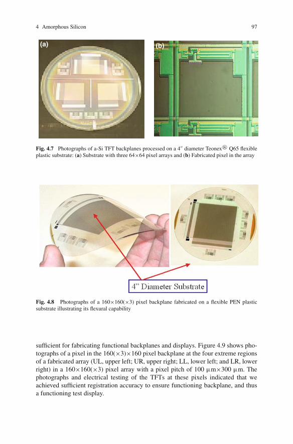
4 Amorphous Silicon 97
(a) (b)
Fig. 4.7 Photographs of a-Si TFT backplanes processed on a 4′′ diameter Teonex® Q65 flexibleplastic substrate: (a) Substrate with three 64×64 pixel arrays and (b) Fabricated pixel in the array
Fig. 4.8 Photographs of a 160×160(×3) pixel backplane fabricated on a flexible PEN plasticsubstrate illustrating its flexural capability
sufficient for fabricating functional backplanes and displays. Figure 4.9 shows pho-tographs of a pixel in the 160(×3)×160 pixel backplane at the four extreme regionsof a fabricated array (UL, upper left; UR, upper right; LL, lower left; and LR, lowerright) in a 160×160(×3) pixel array with a pixel pitch of 100 μm×300 μm. Thephotographs and electrical testing of the TFTs at these pixels indicated that weachieved sufficient registration accuracy to ensure functioning backplane, and thusa functioning test display.
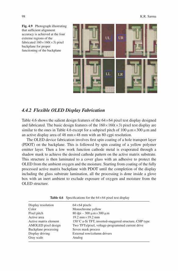
98 K.R. Sarma
LR
URUL
LL
Fig. 4.9 Photograph illustratingthat sufficient alignmentaccuracy is achieved at the fourextreme regions of thefabricated 160×160(×3) pixelbackplane for properfunctioning of the backplane
4.4.2 Flexible OLED Display Fabrication
Table 4.6 shows the salient design features of the 64×64 pixel test display designedand fabricated. The basic design features of the 160×160(×3) pixel test display aresimilar to the ones in Table 4.6 except for a subpixel pitch of 100 μm×300 μm andan active display area of 48 mm×48 mm with an 80 cgpi resolution.
The OLED device fabrication involves first spin coating of a hole transport layer(PDOT) on the backplane. This is followed by spin coating of a yellow polymeremitter layer. Then a low work function cathode metal is evaporated through ashadow mask to achieve the desired cathode pattern on the active matrix substrate.This structure is then laminated to a cover glass with an adhesive to protect theOLED from the ambient oxygen and the moisture. Starting from coating of the fullyprocessed active matrix backplane with PDOT until the completion of the displayincluding the glass substrate lamination, all the processing is done inside a glovebox with an inert ambient to exclude exposure of oxygen and moisture from theOLED structure.
Table 4.6 Specifications for the 64×64 pixel test display
Display resolution 64×64 pixelsColor Monochrome yellowPixel pitch 80 dpi – 300 μm×300 μmActive area 19.2 mm×19.2 mmActive matrix element 150◦C a-Si TFT, inverted-staggered structure, CHP typeAMOLED pixel design Two TFTs/pixel, voltage-programmed current driveBackplane processing Seven mask processDisplay driving External row/column driversGray scale Analog
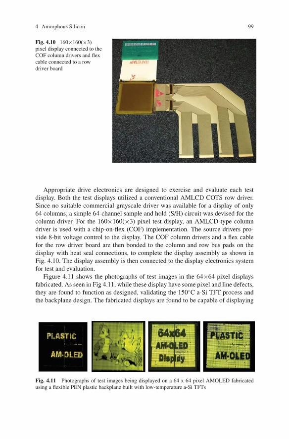
4 Amorphous Silicon 99
Fig. 4.10 160×160(×3)pixel display connected to theCOF column drivers and flexcable connected to a rowdriver board
Appropriate drive electronics are designed to exercise and evaluate each testdisplay. Both the test displays utilized a conventional AMLCD COTS row driver.Since no suitable commercial grayscale driver was available for a display of only64 columns, a simple 64-channel sample and hold (S/H) circuit was devised for thecolumn driver. For the 160×160(×3) pixel test display, an AMLCD-type columndriver is used with a chip-on-flex (COF) implementation. The source drivers pro-vide 8-bit voltage control to the display. The COF column drivers and a flex cablefor the row driver board are then bonded to the column and row bus pads on thedisplay with heat seal connections, to complete the display assembly as shown inFig. 4.10. The display assembly is then connected to the display electronics systemfor test and evaluation.
Figure 4.11 shows the photographs of test images in the 64×64 pixel displaysfabricated. As seen in Fig 4.11, while these display have some pixel and line defects,they are found to function as designed, validating the 150◦C a-Si TFT process andthe backplane design. The fabricated displays are found to be capable of displaying
Fig. 4.11 Photographs of test images being displayed on a 64 x 64 pixel AMOLED fabricatedusing a flexible PEN plastic backplane built with low-temperature a-Si TFTs
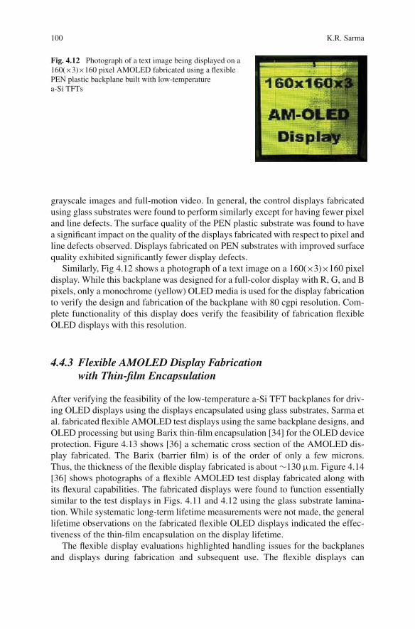
100 K.R. Sarma
Fig. 4.12 Photograph of a text image being displayed on a160(×3)×160 pixel AMOLED fabricated using a flexiblePEN plastic backplane built with low-temperaturea-Si TFTs
grayscale images and full-motion video. In general, the control displays fabricatedusing glass substrates were found to perform similarly except for having fewer pixeland line defects. The surface quality of the PEN plastic substrate was found to havea significant impact on the quality of the displays fabricated with respect to pixel andline defects observed. Displays fabricated on PEN substrates with improved surfacequality exhibited significantly fewer display defects.
Similarly, Fig 4.12 shows a photograph of a text image on a 160(×3)×160 pixeldisplay. While this backplane was designed for a full-color display with R, G, and Bpixels, only a monochrome (yellow) OLED media is used for the display fabricationto verify the design and fabrication of the backplane with 80 cgpi resolution. Com-plete functionality of this display does verify the feasibility of fabrication flexibleOLED displays with this resolution.
4.4.3 Flexible AMOLED Display Fabricationwith Thin-film Encapsulation
After verifying the feasibility of the low-temperature a-Si TFT backplanes for driv-ing OLED displays using the displays encapsulated using glass substrates, Sarma etal. fabricated flexible AMOLED test displays using the same backplane designs, andOLED processing but using Barix thin-film encapsulation [34] for the OLED deviceprotection. Figure 4.13 shows [36] a schematic cross section of the AMOLED dis-play fabricated. The Barix (barrier film) is of the order of only a few microns.Thus, the thickness of the flexible display fabricated is about ∼130 μm. Figure 4.14[36] shows photographs of a flexible AMOLED test display fabricated along withits flexural capabilities. The fabricated displays were found to function essentiallysimilar to the test displays in Figs. 4.11 and 4.12 using the glass substrate lamina-tion. While systematic long-term lifetime measurements were not made, the generallifetime observations on the fabricated flexible OLED displays indicated the effec-tiveness of the thin-film encapsulation on the display lifetime.
The flexible display evaluations highlighted handling issues for the backplanesand displays during fabrication and subsequent use. The flexible displays can
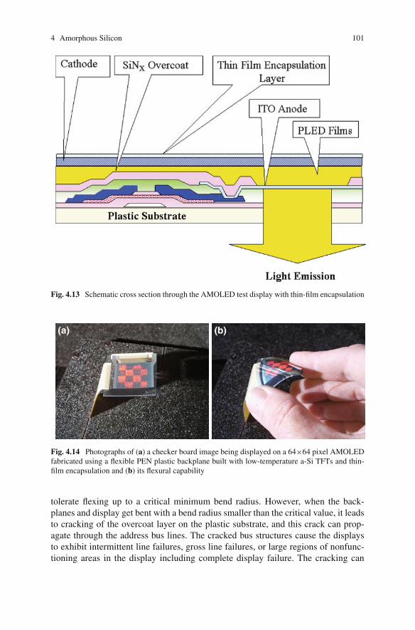
4 Amorphous Silicon 101
Fig. 4.13 Schematic cross section through the AMOLED test display with thin-film encapsulation
(a) (b)
Fig. 4.14 Photographs of (a) a checker board image being displayed on a 64×64 pixel AMOLEDfabricated using a flexible PEN plastic backplane built with low-temperature a-Si TFTs and thin-film encapsulation and (b) its flexural capability
tolerate flexing up to a critical minimum bend radius. However, when the back-planes and display get bent with a bend radius smaller than the critical value, it leadsto cracking of the overcoat layer on the plastic substrate, and this crack can prop-agate through the address bus lines. The cracked bus structures cause the displaysto exhibit intermittent line failures, gross line failures, or large regions of nonfunc-tioning areas in the display including complete display failure. The cracking can
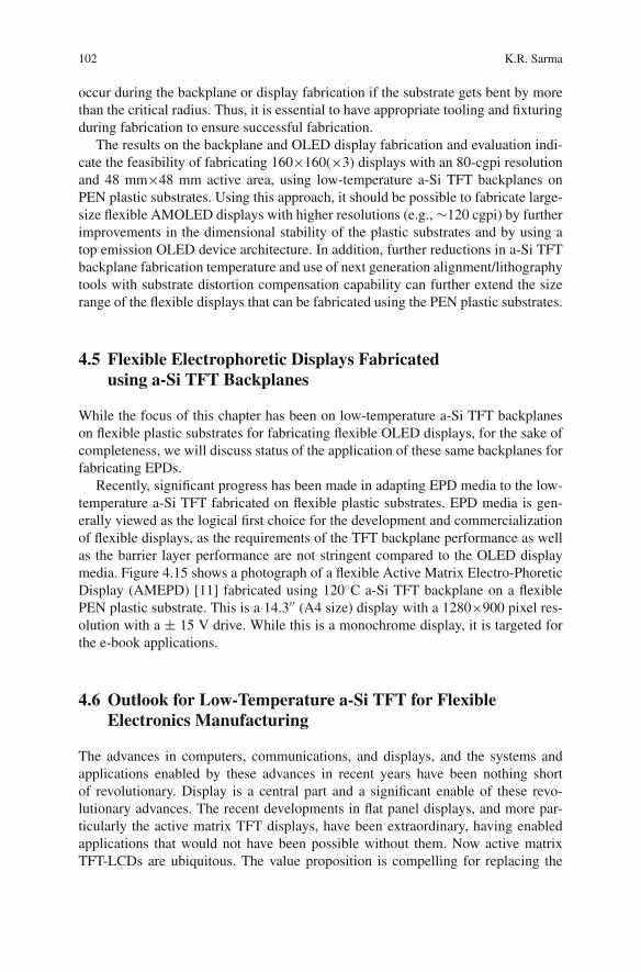
102 K.R. Sarma
occur during the backplane or display fabrication if the substrate gets bent by morethan the critical radius. Thus, it is essential to have appropriate tooling and fixturingduring fabrication to ensure successful fabrication.
The results on the backplane and OLED display fabrication and evaluation indi-cate the feasibility of fabricating 160×160(×3) displays with an 80-cgpi resolutionand 48 mm×48 mm active area, using low-temperature a-Si TFT backplanes onPEN plastic substrates. Using this approach, it should be possible to fabricate large-size flexible AMOLED displays with higher resolutions (e.g., ∼120 cgpi) by furtherimprovements in the dimensional stability of the plastic substrates and by using atop emission OLED device architecture. In addition, further reductions in a-Si TFTbackplane fabrication temperature and use of next generation alignment/lithographytools with substrate distortion compensation capability can further extend the sizerange of the flexible displays that can be fabricated using the PEN plastic substrates.
4.5 Flexible Electrophoretic Displays Fabricatedusing a-Si TFT Backplanes
While the focus of this chapter has been on low-temperature a-Si TFT backplaneson flexible plastic substrates for fabricating flexible OLED displays, for the sake ofcompleteness, we will discuss status of the application of these same backplanes forfabricating EPDs.
Recently, significant progress has been made in adapting EPD media to the low-temperature a-Si TFT fabricated on flexible plastic substrates. EPD media is gen-erally viewed as the logical first choice for the development and commercializationof flexible displays, as the requirements of the TFT backplane performance as wellas the barrier layer performance are not stringent compared to the OLED displaymedia. Figure 4.15 shows a photograph of a flexible Active Matrix Electro-PhoreticDisplay (AMEPD) [11] fabricated using 120◦C a-Si TFT backplane on a flexiblePEN plastic substrate. This is a 14.3′′ (A4 size) display with a 1280×900 pixel res-olution with a ± 15 V drive. While this is a monochrome display, it is targeted forthe e-book applications.
4.6 Outlook for Low-Temperature a-Si TFT for FlexibleElectronics Manufacturing
The advances in computers, communications, and displays, and the systems andapplications enabled by these advances in recent years have been nothing shortof revolutionary. Display is a central part and a significant enable of these revo-lutionary advances. The recent developments in flat panel displays, and more par-ticularly the active matrix TFT displays, have been extraordinary, having enabledapplications that would not have been possible without them. Now active matrixTFT-LCDs are ubiquitous. The value proposition is compelling for replacing the
4 Amorphous Silicon 103
Fig. 4.15 Photograph of an AMEPD display fabricated using a flexible PEN plastic backplanebuilt using low-temperature a-Si TFT [11]
dominant (and bulky) CRT display with a TFT-LCD with its attributes of beingsignificantly thinner, lighter, and having superior image quality and consuming lesspower. The TFT technology is the heart of the active-matrix displays, and more par-ticularly the advances in a-Si TFT technology have been central to the success ofthe TFT-LCD industry.
Having experienced the phenomenal successes in the active-matrix flat-paneldisplay developments, the display industry is now fascinated at the prospects ofrepeating that success with the development of flexible displays. Flexible displaysrepresent a new paradigm in display technology development. First, compared tothe rigid flat glass-based displays, flexible displays have a potential for being sig-nificantly lighter, thinner, more rugged, and rollable or foldable for transportationand storage. Second, flexible displays have a potential for RTR manufacturing forsignificant cost reduction.
The recent progress in flexible backplane electronics and display development todate clearly shows the feasibility of fabricating a-Si TFT backplanes and displaysdirectly on available flexible plastic substrates. Direct fabrication of the TFT back-plane on the flexible plastic substrate (as opposed to using a device layer transferprocess, or by means of a carrier substrate with bond/debond operations) represents
104 K.R. Sarma
an ultimate low-cost manufacturing process that can be adapted in a RTR operation.However, there are several challenges in accomplishing this objective.
First, the flexible plastic substrates must be improved with respect to dimensionalstability (against shrinkage due to high-temperature processing and moisture absorp-tion/desorption), and surface quality (with respect to particulates and other surfaceimperfections), and by reducing the TCE mismatch with the TFT thin films. Thesesubstrate advances will allow fabrication of large-size, high-resolution displays.
Second, improving the low-temperature (<200◦C) a-Si TFT process with respectto device stability against the gate bias stress would be a significant help in the devel-opment of flexible OLED displays. Development and optimization of the OLEDpixel circuits that minimize gate bias stress and provide compensation for somelevel of Vt drift are expected to help achieve this objective as well. TFT gatebias stress is much more of an issue for the OLED display media compared tothe EPD media.
Finally, cost-effective multilayer barrier film technology must be advanced andintegrated with the backplane and display fabrication processes to protect the back-plane and the display media such as OLED from the ambient air. Again, the barrierrequirements for the OLED display are much more stringent than for the EPD media.
Very impressive flexible EPDs built using low-temperature a-Si TFT backplaneshave been demonstrated. An example of these demonstrations includes Samsung’s14.3′′, 1280×900 pixel EPD. These type of flexible displays are expected to becommercialized soon for the e-book and other very low-power display applica-tions. Because a flexible OLED is considered an ultimate display, further devel-opment of various technology elements are expected to continue in order to realizethis potential.
Compared to LTPS (or ULTPS) technology, low-temperature a-Si TFTtechnology has made more progress to date, toward demonstrating proof-of-conceptflexible backplanes and demonstration display using direct fabrication approach. Ifplastic substrate with higher process temperature capability (e.g., that would allowuse of conventional ∼300◦C a-Si TFT process) are developed, that would lowerthe barrier for adaption of a-Si TFT backplanes for flexible displays. However, theflexible plastic substrate industry is not expecting the prospect of developing anynew flexible substrates with a significantly higher process temperature capabilityto be very high. While the emerging O-TFT and ZnO TFT technologies are mak-ing significant progress, and continue to show potential for use in flexible displays,it is expected that they need more time to mature with respect to technology, pro-cess equipment (such as for printing), and infrastructure needed for fabricating theTFT devices and backplanes for high-resolution displays involving small designrules, and OLED display media with stringent requirements. The big advantage oflow-temperature a-Si technology is having the required infrastructure in place andlarge-area capability.
Acknowledgments The contributions of Charles Chanley, Sonia Dodd, Jerry Roush, JohnSchmidt, and other members of the Honeywell Displays and Graphics Group in the developmentof flexible AMOLED displays using low-temperature a-Si TFT Backplanes are acknowledged.
4 Amorphous Silicon 105
References
1. Young B (2007) A roadmap for flexible displays. In: Proceeding of USDC Flexible Displays& Microelectronics Conference & Exhibit, 5–8 Feb 2007
2. McGoldrick K (2007) A rollable display in every device. In: Proceeding of USDC FlexibleDisplays & Microelectronics Conference & Exhibit, 5–8 February
3. Paek SH, Kim KL, Seo HS, Jeong YS, Yi SY, lee SY, Choi NB, Kim SH, Kim CD, Chung IJ(2006) 10.1 inch SVGA ultra thin and flexible active matrix electrophoretic display. SID 06Digest, p 1834
4. Raupp GB, Colaneri N, O’Rourke SM, Kaminski J, Allee DR, Venugopal SM, Bawolek EJ,Loy DE, Moyer C, Angeno SK, O’Brien BP, Bottesch D, Rednour S, Blanchard R, Marrs M,Dailey J, Long K (2006) Flexible display technology in a pilot line manufacturing environ-ment. Army Science Conference, Orlando, FL, 27–30 November
5. Raupp G (2007) Active matrix TFT technology development and pilot line manufacturingfor reflective and emissive flexible displays. In: Proceeding of USDC Flexible Displays &Microelectronics Conference & Exhibit, 5–8 February
6. Jin DU, Jeong JK, Shin HS, Kim MK, Ahn TK, Kwon SY, Kwack JHo, Kim TW, Mo YG,Chung HK (2006) 5.6-inch Flexible full color top emission AM OLED display on stainlesssteel foil. SID 06 Digest, p 1855
7. Chwang A, Hewitt R, Urbanik K, Silvernail J, Rajan K, Hack M, Brown J, Lu JP, Shih C,Ho J, Street R, Ramos T, Moro L, Rutherford N, Tognoni K, Anderson B, Huffman D (2006)Full color 100 dpi AM OLED displays on flexible stainless steel substrates. SID 06 Digest,p 1858
8. Long K, Kattamis AZ, Cheng IC, Gleskova H, Wagner S, Sturm JC, Stevenson M, Yu G,O’Regan M (2006) Active matrix amorphous silicon TFT arrays at 180◦C on clear plasticsubstrates for organic light emitting displays. IEEE Trans Electron Dev 53(8):1789
9. Long K, Kattamis AZ, Cheng IC, Gleskova H, Wagner S, Sturm JC (2006) Stability of amor-phous silicon TFTs deposited on clear plastic substrates at 250◦C to 280◦C. IEEE ElectronDev Lett 27(2):111
10. Sarma KR, Chanley C, Dodd S, Roush J, Schmidt J, Srdanov G, Stevenson M, Yu G, WesselR, Innocenzo J, O’Regan M, MacDonald WA, Eveson R, Long K, Gleskova H, Wagner S,Sturm JC (2003) Flexible active matrix OLED using 150◦C a-Si TFT backplane. CockpitDisplays X, Proceedings of the SPIE 2003, pp 180–191
11. Hwang TH et al. (2007) 14.3 inch Active matrix-based plastic electrophoretic display usinglow temperature processes. SID 07 Digest, p 1684
12. MacDonald WA, Mace JM, Polack NP (2002) 45th Annual Technical Conference Proceedingsof the Society of Vacuum Coaters, p 482
13. Teonex® is registered trademark of Teijin DuPont Films Japan Limited and licensed toDuPont Teijin Films U.S. Limited Partnership
14. MacDonald WA, Rollins K, Rustin RA, Handa M (2003) Plastic displays – New developmentsin polyester films for plastic electronics. SID 03 Digest, p 264
15. MacDonald WA, Eveson R, MacKerron D, Adam R, Rollins K, Rustin R, Looney MK,Hashimoto K (2006) The impact of environment on dimensional reproducibility of polyesterfilm during flexible electronics processing. SID 06 Digest, p 414
16. Utsunomiya S et al. (2003) Flexible color AM OLED display fabricated using surface freetechnology by laser ablation/annealing (SUFTLATM). SID 03 Digest, pp 864–867
17. Asano A, Kinoshita T, Otani N (2003) A plastic 3.8-in low-temperature polycrystalline siliconTFT color LCD panel. SID 03 Digest, pp 988–991
18. Kwon JY, Jung JS, Park KB, Kim JM, Lim H, Lee SY, Kim JM, Noguchi T, Hur JH, Jang J(2006) 2.2 inch qqVGA AM OLED driven by Ultra Low Temperature Poly Silicon (ULTPS)TFT direct fabricated below 200◦C. SID 06 Digest, pp 1358–1361
19. Gleskova H, Wagner S (1999) Amorphous silicon thin-film transistors on compliant polyimidefoil substrates. IEEE Electron Dev Lett 20(9):473
106 K.R. Sarma
20. Gleskova H, Wagner S (2001) DC-gate bias stressing of a-Si:H TFTs fabricated at 150◦C onpolyimide foil. IEEE Trans Electron Dev 48(8):1667
21. He S, Nishiki H, Hartzell J, Nakata Y (2000) Low temperature PECVD a-Si TFT for plasticsubstrate. SID 2000 Digest, pp 278–281
22. French I, George D, Boerefijn I, Chuiton E, Gomez G, Mazel F, Trestour C, Kretz T (2007)Flexible displays made by the EPLARTM process in a factory. In: Proceeding of USDC Flex-ible Displays & Microelectronics Conference & Exhibit, 5–8 February
23. Gundlach DJ, Kuo DJ, Nelson CC, Jackson TN (1999) organic thin film transistors with fieldeffect mobility >2 Cm2/V-s, IEEE Electron device Lett., pp 164–165
24. Burns SE et al. (2006) A flexible plastic SVGA e-paper display. SID 06 Digest, p 7425. Hirao T, Furuta M, Furuta H, Matsuda T, Hiramatsu T, Hokari H, Yoshida M (2006) High
mobility top-gate zinc oxide thin film transistors (ZnO-TFTs) for active matrix liquid crystaldisplays. SID 06 Digest, pp 18–21
26. A. Sazonov A, Stryahilev D, Nathan A, (2002) Low-temperature a-Si:H TFT on plastic films:materials and fabrication aspects, International Conference on Microelectronics, pp 525–528
27. Won SH, Hur JH, Lee CB, Nam HC, Chung JK, Jang J (2004) Hydrogenated amorphous sil-icon thin film transistors on plastic with organic gate insulator, IEEE Electron device Letters,25, pp 132–134
28. Sarma KR (2004) a-Si TFT OLED fabricated on low-temperature flexible plastic substrate.Proceeding of the 2004 MRS Spring Conference, San Francisco, CA
29. Hasumi T, Takasugi S, Kanoh K, Kobayashi Y (2006) New OLED pixel circuit and drivingmethod to suppress threshold voltage shift of a-Si:H TFT. SID 06 Digest, p 1547
30. Chaji GR, Nathan A (2006) A stable voltage programmed pixel circuit for a-Si:H AM OLEDdisplays. J Display Technol 2(4):347
31. Khan A, Shiyanovskaya I, Schneider T, Doane JW (2006) Recent progress in flexible drapablereflective cholesteric displays. SID 06 Digest, p 1728
32. McCreary M (2007) Advances in microencapsulated electrophoretic displays. In: Proceedingof USDC Flexible Displays & Microelectronics Conference & Exhibit, 5–8 February
33. Graff G, Burrows PE, Williford RE, Praino RF (2005) Barrier layer technology for flexibledisplays. In: Crawford GP (ed) Flexible Flat Panel Displays. Wiley, NY
34. Moro M, Chu X, Hirayama H, Krajewski T, Visser RJ (2006) A mass manufacturing processfor Barix encapsulation of OLED displays. IMID/IDMC, 23 August
35. Sanford JL, Libsch FR (2003) TFT AM OLED pixel circuits and driving methods. SID 03Digest, p 10
36. Sarma KR, Roush J, Schmidt J, Chanley C, Dodd S (2006) Flexible active matrix organic lightemitting diode (AM OLED) displays. ASID 06 Digest
Chapter 5Flexible Transition Metal Oxide Electronicsand Imprint Lithography
Warren B. Jackson
5.1 Introduction
The previous chapters have discussed inorganic low-deposition temperature materi-als suitable for flexible applications, such as amorphous and nano-crystalline-silicon(Si) and organic conductors. This chapter presents the results of a recently developedinorganic low-temperature materials system, transition metal oxides (TMOs), thatappears to be a very promising, new high-performance flexible electronic materialssystem. An equally, if not more, important part of this chapter, is the presentationof self-aligned imprint lithography (SAIL) a new fabrication method for flexiblesubstrates that solves the layer-to-layer alignment problem.
The new materials system is TMO based consisting of one or more transitionmetals and oxygen. Some of the more common examples include zinc oxide, zinctin oxide (ZTO), indium gallium zinc oxide (IGZO) and zinc indium oxide (ZIO).These low-temperature amorphous materials can form the active material for transis-tors with a performance that significantly exceeds that of amorphous and nanocrys-talline Si and approaches that of larger grain poly-Si without the complexities anduncontrolled variability of polycrystalline materials. Thus, this technology can beused to drive organic light-emitting diodes (OLEDs) as well as create electronic cir-cuits, such as shift registers, ring oscillators, and multiplexers on chip. An addedfeature is the possibility of creating transparent electronics with such materials sys-tems. The entire transistor including the electrodes and the active material can havevisible transmittances of 70% or greater. Thus, for applications such as displays, theactive electronics would not impact the visual appearance of device and the fill factorof displays with such electronics could approach 100%. Finally, there is the possi-bility of creating p-type transistors that would permit fabrication of complementarymetal oxide semiconductor (CMOS) circuits for flexible applications. Hence, theTMO material system possesses a number of intriguing new possible applications.
W.B. Jackson (B)Hewlett-Packard Laboratories, 1501 Page Mill Road, Mail Stop 1198, Palo Alto, CA 94304, USAe-mail: [email protected]
W.S. Wong, A. Salleo (eds.), Flexible Electronics: Materials and Applications, ElectronicMaterials: Science & Technology, DOI 10.1007/978-0-387-74363-9 5,C© Springer Science+Business Media, LLC 2009
107
108 W.B. Jackson
For the purposes of this chapter, the most remarkable feature of the TMO transis-tors is that these features and performance can be achieved in devices with a max-imum processing temperature that is compatible with flexible polymer substrates,such as polyimide (Glass transition temperature (Tg) = 300◦C) and polyethylenenaphthalate (PEN) (Tg = 200◦C). Although most metal oxide work published thusfar has been accomplished on higher temperature and rigid substrates, such as glassand c-Si, recent work has demonstrated large mobilities for flexible metal oxidetransistors using photolithography and standard batch etching processes. However,flexible substrates are not dimensionally fixed during processing, making it virtuallyimpossible to have precise layer-to-layer micron-scale alignment for large dimen-sionally variable substrates. This important problem of layer-to-layer registrationon flexible substrates has been solved using SAIL, a solution that extends the TMOtechnology as well as amorphous and poly-Si to higher performance short channeldevices.
This chapter presents the results in the field of TMO transistors relevant for theemerging field of flexible electronics in the following sections:
(1) A brief discussion of the history of work and background information in thegeneral area of metal oxide transistors relevant for flexible electronics.
(2) The general properties of some of the leading TMO materials.(3) The device structures used in TMO and flexible electronics along with a descrip-
tion of SAIL(4) One of the most important sections presents SAIL and amorphous silicon (a-Si)
results, indicating that the method can fabricate working devices.(5) Resulting TMO thin-film transistors (TFTs) on rigid substrates using shadow
masks and photolithography on both flexible and rigid substrates along withTMO SAIL results on rigid substrates
(6) Finally, future areas of research for improved large-area flexible electronics.
5.2 Previous Work
TMO materials have been used in transistors for quite some time. One of the firstZnO transistors was made in the 1960s [1]. However, little progress ensued usingTMOs as semiconductors although ZnO found uses in surface acoustic devices [2],varistors [3], transparent PN diodes [4], and as a transparent conductor [5]. Inter-est in ZnO as transistors was revived in about 1997 by Prins et al. [6] and laterin Kawasaki et al. and Ohtomo et al. [7, 8], where transistors with mobilities of100 cm2 V−1 s−1 were fabricated using spin-on glass as the insulator on glasssubstrates. Subsequently, there have been many different experiments investigatingvarious aspects of metal oxide transistors.
The current interest in TMO transistors started with Ohya et al. [9] and in thethesis by R. Hoffman 2002 [10], Masuda [11], Nomura [12], Hoffman [13], Nishii
5 Flexible Transition Metal Oxide Electronics and Imprint Lithography 109
[14], and Carcia [15]. These references led to the current interest in TMO tran-sistors and established convincingly that these materials not only had high Hallmobilities but could actually produce high-performance transistors. Typical mobili-ties for these initial efforts were on the order of 0.1–1 cm2 V−1 s−1 when fabricatedusing low-temperature dielectrics and 80 cm2 V−1 s−1 for high-temperature ther-mal oxide dielectrics on c-Si. The latter work indicated that transistors with perfor-mances approaching that poly-Si were possible using TMO materials as the activelayer. Following this initial group of publications, the field has expanded greatlywith dozens of papers detailing various aspects of TMO transistors. Various meth-ods of deposition, dielectrics, and TMO combinations were investigated. A list ofmany of the various results is summarized in Table 5.1 and in [17].
The primary emphasis of most TMO transistor work is to create transparent semi-conductors. One important result was that high-performance (μ= 20 cm2 V−1 s−1)transparent transistors could be fabricated at room temperature on glass using siliconoxynitride dielectrics [21] and using atomic layer deposition (ALD) of Al2O3/TiO2
superlattice dielectric [36] (Fig. 5.1). The resulting output curves are very flat andthe on–off ratio is very good. This work demonstrated that high-performance TMOtransistors on flexible substrates are possible.
Another theme of research in the TMO field is the expansion of candidate TMOmaterial systems used in transistors. The range of viable transistor materials hasbeen enlarged to include materials such as ZnO, ZnSnO, ZnInO, ZnInGaO, andInGaO among others (see Table 5.1). The oxide systems have achieved differentlevels of performance at a variety of maximum fabrication temperatures and haveunique attributes that make them suitable for various applications. The thrust ofthis work is to decrease the high-temperature annealing step required to reduce thecarrier concentration of the TMO. The initial ZnO transistors had limited perfor-mance unless the samples were subjected to anneal temperatures exceeding 400◦C.The addition of Sn to ZTO has produced stable transistors with reasonable perfor-mance using anneal temperatures of 210–250◦C [13, 21]. This temperature rangeis compatible with polyimide but not typical transparent substrates, such as PENand polyethylene terephthalate (PET). The addition of In into the ZIO devices andIGZO (the addition of Ga) has lowered the temperature needed to produce high-performance devices to below 200◦C [21]. Unfortunately, the addition of In and thelow temperature of annealing appear to introduce instabilities in the devices thatremain poorly understood. A summary of some of the more prevalent material sys-tems and their properties is shown in Table 5.2. A general summary of the trendsis that the inclusion of In, Ga, and Sn lowers the maximum processing temperatureneeded to obtain higher mobilities in part because of the generally higher diffusivi-ties of these metal cations.
Most of the previous TMO work has emphasized the transparency and highmobilities that could be obtained using TMO transistors. For the purposes of thisbook, the work relating to TMO for flexible electronics is more important. Someof the first work that explicitly addressed issues relevant for the application ofTMO to flexible electronics, which reduced the maximum processing tempera-ture of ZnO to 150◦C, is Ref. [20]. Later this group produced ZnO transistors on
110 W.B. Jackson
Tabl
e5.
1Su
mm
ary
ofva
riou
sT
MO
tran
sist
ors
with
prop
ertie
s
Ref
eren
ceN
o.O
xide
Subs
trat
esM
ax.t
emp
(◦ C)
Dep
ositi
onm
etho
dμ
(cm
2V
−1s−1
)O
n–of
fra
tioV
t(V
)G
ate
diel
ectr
icC
onta
cts
[11]
ZnO
c-Si
450
PLD
0.03
–110
5(−
1)−2
.5Si
O2/S
iN[1
3]Z
nO70
0IB
S0.
3–3
107
10–1
5[1
2]In
GaO
3(Z
nO) 5
1,40
0PL
D80
106
3H
fO2
[15]
ZnO
25R
MS
0.3–
210
5–1
060
[16]
ZnO
300
PLD
<4
[18]
ZnS
nOG
lass
600
RM
S14
6×10
6−4
.6A
l 2O
3–T
iO2
[19]
ZnS
nOG
lass
300
RM
S5–
1510
70–
15A
TO
[6]
SnO
2:Sb
PbZ
r 0:2
Ti 0
:8O
3
[10]
ZnO
Gla
ss60
0IB
S0.
3–2.
510
710
–20
AT
O[1
4]Z
nOG
lass
150–
300
PLD
710
7Si
N/C
aHfO
x
[9]
ZnO
[20]
ZnO
Poly
este
rpo
lyim
ide
RT
RM
S0.
410
47.
5flu
orop
olym
erdi
elec
tric
[20]
ZnO
Gla
ssR
TR
MS
283×
105
19Si
ON
GZ
O[2
1]Z
nOG
lass
RT
RM
S20
5×10
51.
8Si
ON
[22]
ZnO
Poly
imid
e<
120
EB
5010
53.
2A
l 2O
3
[23]
ZnO
750
PLD
1210
3–3
SrT
iO3
[24]
ZnO
Si25
0M
OC
VD
/A
LD
0.95
106
1.7
SiO
2/A
lOx
byA
LD
[25]
ZnO
n-c-
Si12
5,20
0,30
0,40
0,45
0R
MS
1710
56
HfO
2,A
l 2O
3
[26]
ZnS
nOPo
lyim
ide
250
RM
S14
106
−17
SiO
N,S
iO2,S
iN[2
7]Z
nSnO
c-Si
300
RM
S20
106
0Si
O2
[28]
ZnS
nOPo
lyim
ide
250
RM
S14
106
−8.5
SiO
N,S
iO2,S
iNIT
O
(con
tinue
d)
5 Flexible Transition Metal Oxide Electronics and Imprint Lithography 111
Tabl
e5.
1(c
ontin
ued)
Ref
eren
ceN
o.O
xide
Subs
trat
esM
ax.t
emp
(◦ C)
Dep
ositi
onm
etho
dμ
(cm
2V
−1s−1
)O
n–of
fra
tioV
t(V
)G
ate
diel
ectr
icC
onta
cts
[29]
IGZ
OPE
TR
T8
103
Y2O
3
[30]
ZIO
c-Si
RT
RM
S20
108
−3.2
SiO
2
[31]
ZnO
Gla
ssR
TR
MS
2010
521
Al 2
O3
TkO
3
[32]
Tetr
acen
eM
ylar
RT
EV
5×10
−4M
ylar
[33]
Org
anic
Myl
arR
TE
V1×
10−4
104
Myl
ar[3
4]O
rgan
icM
ylar
RT
EV
1×10
−410
4M
ylar
self
-alig
ned
[35]
IGZ
OY
SZ35
0R
-SPE
8010
85
HfO
4IZ
O[3
6]Z
nOgl
ass
RT
RF
273×
105
19A
l 2O
3T
iO3
eA
LD
[37]
IGZ
OPE
TR
TPL
D10
106
3.2
Y2O
3IT
O
PLD
,Pul
sed
Las
erD
epos
ition
;IB
S,Io
nB
eam
Sput
teri
ng;
RM
S,R
adio
freq
uenc
yM
agne
tron
Sput
teri
ng;
EB
,Ele
ctro
nB
eam
Sput
teri
ng;
MO
CV
D,M
etal
-O
rgan
icC
hem
ical
Vap
orD
epos
ition
;AL
D,A
tom
icL
ayer
Dep
ositi
on;R
-SPE
,Rea
ctiv
eso
lidph
ase
epita
xy;E
V,e
vapo
ratio
n.
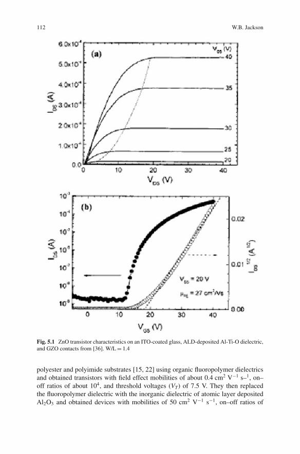
112 W.B. Jackson
Fig. 5.1 ZnO transistor characteristics on an ITO-coated glass, ALD-deposited Al-Ti-O dielectric,and GZO contacts from [36]. W/L = 1.4
polyester and polyimide substrates [15, 22] using organic fluoropolymer dielectricsand obtained transistors with field effect mobilities of about 0.4 cm2 V−1 s–1, on–off ratios of about 104, and threshold voltages (VT) of 7.5 V. They then replacedthe fluoropolymer dielectric with the inorganic dielectric of atomic layer depositedAl2O3 and obtained devices with mobilities of 50 cm2 V−1 s−1, on–off ratios of
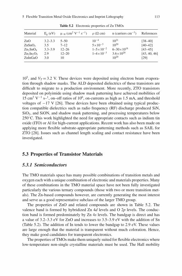
5 Flexible Transition Metal Oxide Electronics and Imprint Lithography 113
Table 5.2 Electronic properties of Zn TMOs
Material Eg (eV) μ H (cm2 V−1 s−1) ρ (Ω cm) n (carriers cm−3) References
ZnO 3.2–3.3 5–50 10−4 1021 [38–40]ZnSnO3 3.5 7–12 5×10⁻³ 1020 [40–42]Zn2SnO4 3.3–3.9 12–26 1–5×10⁻² 6–30×1018 [43–45]Zn2In2O5 2.9 12–20 1–4×10⁻³ 3.6×10²⁰ [43, 40, 46]ZnInGaO 3.0 10 1020 [29]
105, and VT = 3.2 V. These devices were deposited using electron beam evapora-tion through shadow masks. The ALD deposited dielectrics of these transistors aredifficult to migrate to a production environment. More recently, ZTO transistorsdeposited on polyimide using shadow mask patterning have achieved mobilities of15 cm2 V−1 s–1, on–off ratios of 106, on-currents as high as 1.5 mA, and thresholdvoltages of −17 V [26]. These devices have been obtained using typical produc-tion compatible dielectrics such as radio frequency (RF) discharge produced SiN,SiO2, and SiON, and shadow mask patterning, and processing temperatures below250◦C. This work highlighted the need for appropriate contacts such as indium tinoxide (ITO) or Al for high-current applications. Recent work has also been made onapplying more flexible substrate-appropriate patterning methods such as SAIL forZTO [28]. Issues such as channel length scaling and contact resistance have beeninvestigated.
5.3 Properties of Transistor Materials
5.3.1 Semiconductors
The TMO materials space has many possible combinations of transition metals andoxygen each with a unique combination of electronic and materials properties. Manyof these combinations in the TMO material space have not been fully investigatedparticularly the various ternary compounds (those with two or more transition met-als). The Zn-based compounds however, are currently generating the most interestand serve as a good representative subclass of the larger TMO group.
The properties of ZnO and related compounds are shown in Table 5.2. Thevalence band is formed by hybridized Zn 4d levels and O 2p levels. The conduc-tion band is formed predominately by Zn 4s levels. The bandgap is direct and hasa value of 3.2–3.3 eV for ZnO and increases to 3.5–3.9 eV with the addition of Sn(Table 5.2). The addition of In tends to lower the bandgap to 2.9 eV. These valuesare large enough that the material is transparent without much coloration. Hence,they make good candidates for transparent electronics.
The properties of TMOs make them uniquely suited for flexible electronics wherelow-temperature non-single crystalline materials must be used. The Hall mobility
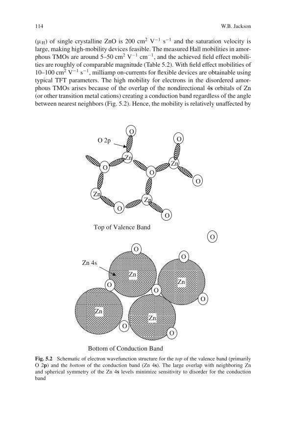
114 W.B. Jackson
(μH) of single crystalline ZnO is 200 cm2 V−1 s−1 and the saturation velocity islarge, making high-mobility devices feasible. The measured Hall mobilities in amor-phous TMOs are around 5–50 cm2 V−1 cm−1, and the achieved field effect mobili-ties are roughly of comparable magnitude (Table 5.2). With field effect mobilities of10–100 cm2 V−1 s−1, milliamp on-currents for flexible devices are obtainable usingtypical TFT parameters. The high mobility for electrons in the disordered amor-phous TMOs arises because of the overlap of the nondirectional 4s orbitals of Zn(or other transition metal cations) creating a conduction band regardless of the anglebetween nearest neighbors (Fig. 5.2). Hence, the mobility is relatively unaffected by
O Zn
Zn
O Zn
O
O O
O
O
Zn
O 2p
Top of Valence Band
Zn
Zn
Bottom of Conduction Band
Zn
Zn
Zn
O
O
O
O
O O
O
O
Zn 4s
Fig. 5.2 Schematic of electron wavefunction structure for the top of the valence band (primarilyO 2p) and the bottom of the conduction band (Zn 4s). The large overlap with neighboring Znand spherical symmetry of the Zn 4s levels minimize sensitivity to disorder for the conductionband
5 Flexible Transition Metal Oxide Electronics and Imprint Lithography 115
Table 5.3 Various miscellaneousproperties of ZnO [50] Density (g cm−3) 5.6
Dielectric constant 8.6Refractive index 2.0Average thermal expansion Coeff. (/K) 4×10⁻⁶
bond angle disorder. Moreover, the ionic nature of the transition metal oxide bondscauses the bonds to be less directional than the typical covalent bonds found in theusual Group IV or III–V semiconductors. Therefore, the large bond angle distortionsfound at grain boundaries are less apt to result in grain boundary gap state defects.The lack of gap states associated with deformed bonds results in large subthresholdslopes and small turn-on voltages in low-temperature transistors.
A further consequence of the lack of bandgap states and high electron mobil-ity is that the materials often can be easily degenerately doped n type yield-ing small resistivities, ρ, below 10−2 (Ω cm) (Table 5.2). The doping of ZnOoccurs by substitutional dopants, Zn interstitials, O vacancies, and/or interstitialH. The typical substitutional dopants include N and P. Oxygen vacancies areused to make the materials highly conductive for use as transparent electrodesfor solar cell and photosensor applications. The oxygen vacancies can readilybe created by sputtering in an O poor atmosphere. In fact, in TMO transis-tor fabrication, care must be taken to keep the O-vacancy concentration low sothat the channel is sufficiently resistive for enhancement mode transistor opera-tion [15, 22]. There is increasing evidence that the O vacancies may be some-what mobile resulting in some long-term device instabilities to be discussedlater.
There also is evidence that H interstitials act as n-type dopants [47–49]. Expo-sure of semiconducting ZTO to an H plasma results in a significant enhancement ofthe conductivity while exposure to an Ar or O plasma does not. Moreover, the H dif-fusion rate is large even at 200◦C. Thus, unintentional H doping during fabricationetching is a concern and must be controlled.
Other useful parameters for ZnO are shown in Table 5.3 [50]. Note that thedielectric constant is somewhat lower than that of a-Si. The values for other TMOare generally similar in magnitude.
5.3.2 Dielectrics
Dielectrics are often one of the most critical materials necessary for a transis-tor technology. In most electronic applications, shorts are extremely undesirabledefects, particularly in array applications. Shorts not only cause the shorted deviceto fail but often result in failure of any connected device and cause an unacceptablepower drain. They also mask failures by other devices. In addition to the highly
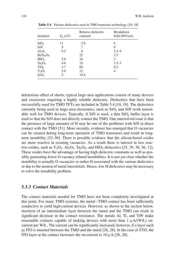
116 W.B. Jackson
Table 5.4 Various dielectrics used in TMO transistor technology [10, 18]
Relative dielectric BreakdownInsulator Eg (eV) constant field (MV/cm)
SiO2 11 3.8 6SiN 9 7 9Al203 9.5 8 3.5–6BaTa2O5 22 3.5HfO2 5.8 16 3Ta2O5 4.6 24 1.5–3TiO2 3.7 60 0.2Y2O3 5.6 12 4ZrO2 5 19.8
deleterious effect of shorts, typical large-area applications consist of many devicesand crossovers requiring a highly reliable dielectric. Dielectrics that have beensuccessfully used for TMO TFTs are included in Table 5.4 [10, 18]. The dielectricscurrently being used in large-area electronics, such as SiO2 and SiN work reason-ably well for TMO devices. Typically, if SiN is used, a thin SiO2 buffer layer isused so that the SiN does not directly contact the TMO. One unresolved issue is thatthe presence of large amounts of H may be one of the problems with SiN in directcontact with the TMO [51]. More recently, evidence has emerged that O vacanciescan be created during long-term operation of TMO transistors and result in long-term instability [52–56]. There is possible evidence that the silicon-based oxidesare more reactive in creating vacancies. As a result there is interest in less reac-tive oxides, such as Y2O3, Al2O3, Ta2O5, and HfO2 dielectrics [25, 29, 30, 36, 12].These oxides have the advantage of having high dielectric constants as well as pos-sibly generating fewer O-vacancy related instabilities. It is not yet clear whether theinstability is actually O vacancies or rather H associated with the various dielectricsor due to the motion of metal interstitials. Hence, low H dielectrics may be necessaryto solve the instability problem.
5.3.3 Contact Materials
The contact materials needed for TMO have not been completely investigated atthis point. For many TMO systems, the metal−TMO contact has been sufficientlyconductive to yield high-current devices. However, as shown in the section below,insertion of an intermediate layer between the metal and the TMO can result insignificant decrease in the contact resistance. The metals Al, Ti, and TiW makereasonable contacts capable of making devices with more than 1 μA/(W/L) on-current per W/L. The current can be significantly increased, however, if a layer suchas ITO is inserted between the TMO and the metal [26, 28]. In the case of ZTO, theITO layer at the contact increases the on-current to 10 μA [26, 28].
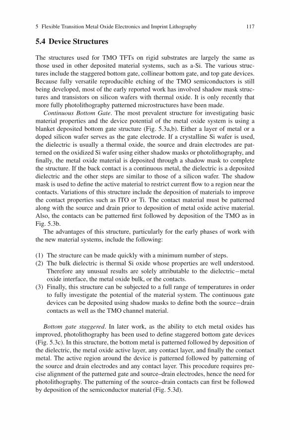
5 Flexible Transition Metal Oxide Electronics and Imprint Lithography 117
5.4 Device Structures
The structures used for TMO TFTs on rigid substrates are largely the same asthose used in other deposited material systems, such as a-Si. The various struc-tures include the staggered bottom gate, collinear bottom gate, and top gate devices.Because fully versatile reproducible etching of the TMO semiconductors is stillbeing developed, most of the early reported work has involved shadow mask struc-tures and transistors on silicon wafers with thermal oxide. It is only recently thatmore fully photolithography patterned microstructures have been made.
Continuous Bottom Gate. The most prevalent structure for investigating basicmaterial properties and the device potential of the metal oxide system is using ablanket deposited bottom gate structure (Fig. 5.3a,b). Either a layer of metal or adoped silicon wafer serves as the gate electrode. If a crystalline Si wafer is used,the dielectric is usually a thermal oxide, the source and drain electrodes are pat-terned on the oxidized Si wafer using either shadow masks or photolithography, andfinally, the metal oxide material is deposited through a shadow mask to completethe structure. If the back contact is a continuous metal, the dielectric is a depositeddielectric and the other steps are similar to those of a silicon wafer. The shadowmask is used to define the active material to restrict current flow to a region near thecontacts. Variations of this structure include the deposition of materials to improvethe contact properties such as ITO or Ti. The contact material must be patternedalong with the source and drain prior to deposition of metal oxide active material.Also, the contacts can be patterned first followed by deposition of the TMO as inFig. 5.3b.
The advantages of this structure, particularly for the early phases of work withthe new material systems, include the following:
(1) The structure can be made quickly with a minimum number of steps.(2) The bulk dielectric is thermal Si oxide whose properties are well understood.
Therefore any unusual results are solely attributable to the dielectric−metaloxide interface, the metal oxide bulk, or the contacts.
(3) Finally, this structure can be subjected to a full range of temperatures in orderto fully investigate the potential of the material system. The continuous gatedevices can be deposited using shadow masks to define both the source−draincontacts as well as the TMO channel material.
Bottom gate staggered. In later work, as the ability to etch metal oxides hasimproved, photolithography has been used to define staggered bottom gate devices(Fig. 5.3c). In this structure, the bottom metal is patterned followed by deposition ofthe dielectric, the metal oxide active layer, any contact layer, and finally the contactmetal. The active region around the device is patterned followed by patterning ofthe source and drain electrodes and any contact layer. This procedure requires pre-cise alignment of the patterned gate and source–drain electrodes, hence the need forphotolithography. The patterning of the source–drain contacts can first be followedby deposition of the semiconductor material (Fig. 5.3d).
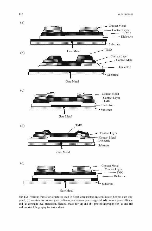
118 W.B. Jackson
Substrate
Dielectric
TMOContact Layer
Contact Metal
Gate Metal
Substrate
Dielectric
TMO
Contact Layer
Contact Metal
Gate Metal
Substrate
Dielectric TMO
Contact Metal
Gate Metal
Substrate
Dielectric
TMO
Contact LayerContact Metal
Gate Metal
(a)
(b)
(c)
(d)
(e)
Contact Layer
Substrate
Dielectric TMO
Contact Metal
Gate Metal
Contact Layer
Fig. 5.3 Various transistor structures used in flexible transistors (a) continuous bottom gate stag-gered, (b) continuous bottom gate collinear, (c) bottom gate staggered, (d) bottom gate collinear,and (e) constant level transistor. Shadow mask for (a) and (b), photolithography for (c) and (d),and imprint lithography for (a) and (e)
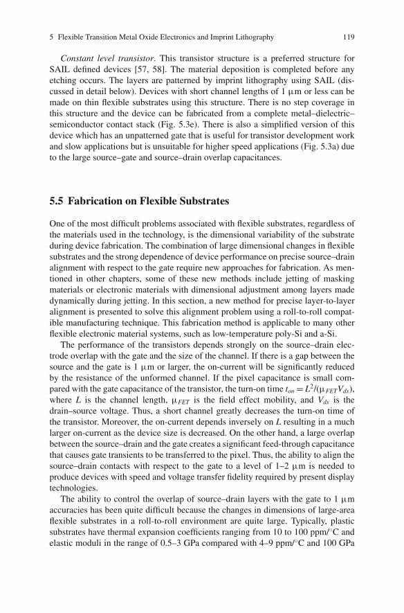
5 Flexible Transition Metal Oxide Electronics and Imprint Lithography 119
Constant level transistor. This transistor structure is a preferred structure forSAIL defined devices [57, 58]. The material deposition is completed before anyetching occurs. The layers are patterned by imprint lithography using SAIL (dis-cussed in detail below). Devices with short channel lengths of 1 μm or less can bemade on thin flexible substrates using this structure. There is no step coverage inthis structure and the device can be fabricated from a complete metal–dielectric–semiconductor contact stack (Fig. 5.3e). There is also a simplified version of thisdevice which has an unpatterned gate that is useful for transistor development workand slow applications but is unsuitable for higher speed applications (Fig. 5.3a) dueto the large source–gate and source–drain overlap capacitances.
5.5 Fabrication on Flexible Substrates
One of the most difficult problems associated with flexible substrates, regardless ofthe materials used in the technology, is the dimensional variability of the substrateduring device fabrication. The combination of large dimensional changes in flexiblesubstrates and the strong dependence of device performance on precise source–drainalignment with respect to the gate require new approaches for fabrication. As men-tioned in other chapters, some of these new methods include jetting of maskingmaterials or electronic materials with dimensional adjustment among layers madedynamically during jetting. In this section, a new method for precise layer-to-layeralignment is presented to solve this alignment problem using a roll-to-roll compat-ible manufacturing technique. This fabrication method is applicable to many otherflexible electronic material systems, such as low-temperature poly-Si and a-Si.
The performance of the transistors depends strongly on the source–drain elec-trode overlap with the gate and the size of the channel. If there is a gap between thesource and the gate is 1 μm or larger, the on-current will be significantly reducedby the resistance of the unformed channel. If the pixel capacitance is small com-pared with the gate capacitance of the transistor, the turn-on time ton = L2/(μFETVds),where L is the channel length, μFET is the field effect mobility, and Vds is thedrain–source voltage. Thus, a short channel greatly decreases the turn-on time ofthe transistor. Moreover, the on-current depends inversely on L resulting in a muchlarger on-current as the device size is decreased. On the other hand, a large overlapbetween the source–drain and the gate creates a significant feed-through capacitancethat causes gate transients to be transferred to the pixel. Thus, the ability to align thesource–drain contacts with respect to the gate to a level of 1–2 μm is needed toproduce devices with speed and voltage transfer fidelity required by present displaytechnologies.
The ability to control the overlap of source–drain layers with the gate to 1 μmaccuracies has been quite difficult because the changes in dimensions of large-areaflexible substrates in a roll-to-roll environment are quite large. Typically, plasticsubstrates have thermal expansion coefficients ranging from 10 to 100 ppm/◦C andelastic moduli in the range of 0.5–3 GPa compared with 4–9 ppm/◦C and 100 GPa
120 W.B. Jackson
for glass. In addition, the flexible plastic substrates are about 50–100 μm thick com-pared with 3 mm for typical glass displays. For electronics fabricated on a 30 cmwide web, a force as small as 1 N will deform the substrate roughly 300 μm whilethe thermal-induced dimension changes are 30 μm/◦C from one side relative to theother. In addition, as the various overlayers are patterned, the overlayer-inducedstrain is nonuniform. Hence, the substrate changes size with respect to the maskof the next layer. As a result, it has been virtually impossible to align successivelayers to better than about 30 μm, unless the substrate held dimensionally stableby bonding to a more rigid substrate. This later approach has all the expenses andlimitations of wafer and glass-based processing, negating the advantage of usinglow-cost substrates in the first place.
The problem of layer-to-layer alignment on flexible substrates has been solvedusing SAIL [57, 58]. This fabrication method uses the ability of imprint lithographyto fabricate polymer masking structures with precise height control. The informa-tion for various layers is encoded within the height of the imprinted structures. Thus,a single imprint step defines all the structures needed to complete the device fabri-cation. Any change in the size of the substrate affects all layers and, therefore, doesnot alter the relative alignment of different layers.
5.5.1 Imprint Lithography
For the past 50+ years, integrated circuit fabrication has proceeded through the useof photolithography and photoresist to define the critical features of ever reduceddevice sizes. As mentioned before, this technology has alignment and cost problemswhen used with free-standing large-area flexible substrates. The comparatively newfabrication technology, imprint lithography, is a promising new approach for low-cost fabrication of submicron feature electronics on large-area flexible substrates[59–61]. Imprint lithography, or more precisely, soft lithography in the present casecreates multilevel patterns that can be used as masks without expensive photolithog-raphy. As presented later, the multilevel capability of imprint lithography can solvethe layer-to-layer alignment problem inherent in flexible electronics and is com-patible with high-throughput batch or roll-to-roll technology. Imprint lithographyis useful not only for TMO devices but also for any flexible electronic technologysuch as a-Si and even has applications for organic electronics if a nonorganic imprintliquid is developed.
The imprint procedure consists of a relatively small number of steps [57, 58].First, a master is fabricated using traditional photolithography and silicon pattern-ing steps (Fig. 5.4a). Second, a replica stamp is made from the master by coatingthe master with a release agent and then with polydimethylsiloxane (PDMS) poly-mer (Fig. 5.4b). The PDMS stamp is compliant and is a remarkably faithful inversereplica of the original master (see Fig. 5.5). This stamp is attached to a flat quartzplate if it is to be used in batch processing or can be attached to quartz roller if roll-to-roll imprint lithography is used (Fig. 5.4c). The substrate plus desired blanket
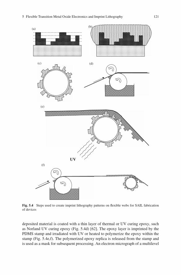
5 Flexible Transition Metal Oxide Electronics and Imprint Lithography 121
(b)(a)
(c) (d)
(e)
(f)
UV
Fig. 5.4 Steps used to create imprint lithography patterns on flexible webs for SAIL fabricationof devices
deposited material is coated with a thin layer of thermal or UV curing epoxy, suchas Norland UV curing epoxy (Fig. 5.4d) [62]. The epoxy layer is imprinted by thePDMS stamp and irradiated with UV or heated to polymerize the epoxy within thestamp (Fig. 5.4e,f). The polymerized epoxy replica is released from the stamp andis used as a mask for subsequent processing. An electron micrograph of a multilevel
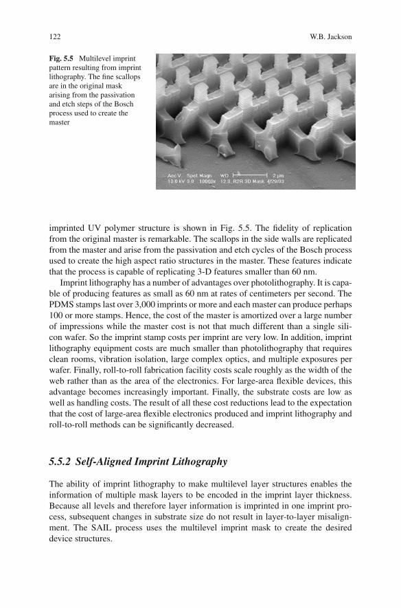
122 W.B. Jackson
Fig. 5.5 Multilevel imprintpattern resulting from imprintlithography. The fine scallopsare in the original maskarising from the passivationand etch steps of the Boschprocess used to create themaster
imprinted UV polymer structure is shown in Fig. 5.5. The fidelity of replicationfrom the original master is remarkable. The scallops in the side walls are replicatedfrom the master and arise from the passivation and etch cycles of the Bosch processused to create the high aspect ratio structures in the master. These features indicatethat the process is capable of replicating 3-D features smaller than 60 nm.
Imprint lithography has a number of advantages over photolithography. It is capa-ble of producing features as small as 60 nm at rates of centimeters per second. ThePDMS stamps last over 3,000 imprints or more and each master can produce perhaps100 or more stamps. Hence, the cost of the master is amortized over a large numberof impressions while the master cost is not that much different than a single sili-con wafer. So the imprint stamp costs per imprint are very low. In addition, imprintlithography equipment costs are much smaller than photolithography that requiresclean rooms, vibration isolation, large complex optics, and multiple exposures perwafer. Finally, roll-to-roll fabrication facility costs scale roughly as the width of theweb rather than as the area of the electronics. For large-area flexible devices, thisadvantage becomes increasingly important. Finally, the substrate costs are low aswell as handling costs. The result of all these cost reductions lead to the expectationthat the cost of large-area flexible electronics produced and imprint lithography androll-to-roll methods can be significantly decreased.
5.5.2 Self-Aligned Imprint Lithography
The ability of imprint lithography to make multilevel layer structures enables theinformation of multiple mask layers to be encoded in the imprint layer thickness.Because all levels and therefore layer information is imprinted in one imprint pro-cess, subsequent changes in substrate size do not result in layer-to-layer misalign-ment. The SAIL process uses the multilevel imprint mask to create the desireddevice structures.
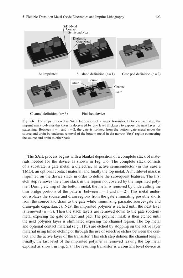
5 Flexible Transition Metal Oxide Electronics and Imprint Lithography 123
As imprinted Gate pad definition (n = 2)Si island definition (n = 1)
Channel definition (n = 3) Finished device
SourceDrain
Gate
Channel
S/D Metal Contact
Semiconductor
DielectricGate Metal
Fig. 5.6 The steps involved in SAIL fabrication of a single transistor. Between each step, theimprint mask polymer thickness is decreased by one level thickness to expose the next layer forpatterning. Between n = 1 and n = 2, the gate is isolated from the bottom gate metal under thesource and drain by undercut removal of the bottom metal in the narrow ‘fuse’ region connectingthe source and drain to other pads
The SAIL process begins with a blanket deposition of a complete stack of mate-rials needed for the device as shown in Fig. 5.6. The complete stack consistsof a substrate, a gate metal, a dielectric, an active semiconductor (in this case aTMO), an optional contact material, and finally the top metal. A multilevel mask isimprinted on the device stack in order to define the subsequent features. The firstetch step removes the entire stack in the region not covered by the imprinted poly-mer. During etching of the bottom metal, the metal is removed by undercutting thethin bridge portions of the pattern (between n = 1 and n = 2). This metal under-cut isolates the source and drain regions from the gate eliminating possible shortsfrom the source and drain to the gate while minimizing parasitic source–gate anddrain–gate capacitances. Next the imprinted polymer is etched until the next levelis removed (n = 3). Then the stack layers are removed down to the gate (bottom)metal exposing the gate contact and pad. The polymer mask is then etched untilthe next polymer layer is eliminated exposing the channel region. The top metaland optional contact material (e.g., ITO) are etched by stopping on the active layermaterial using timed etching or through the use of selective etches between the con-tact and the active layer of the transistor. This etch step defines the channel length.Finally, the last level of the imprinted polymer is removed leaving the top metalexposed as shown in Fig. 5.7. The resulting transistor is a constant level device as
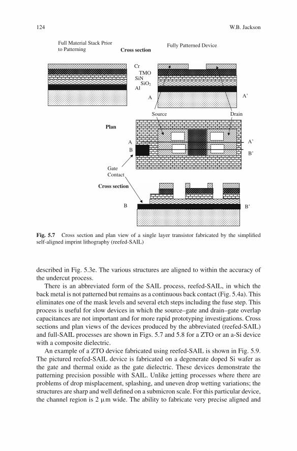
124 W.B. Jackson
A
B
A
Full Material Stack Prior to Patterning
CrTMO
SiNSiO2
Al
Fully Patterned Device
B
GateContact
Source Drain
Plan
Cross section
Cross section
Fig. 5.7 Cross section and plan view of a single layer transistor fabricated by the simplifiedself-aligned imprint lithography (reefed-SAIL)
described in Fig. 5.3e. The various structures are aligned to within the accuracy ofthe undercut process.
There is an abbreviated form of the SAIL process, reefed-SAIL, in which theback metal is not patterned but remains as a continuous back contact (Fig. 5.4a). Thiseliminates one of the mask levels and several etch steps including the fuse step. Thisprocess is useful for slow devices in which the source–gate and drain–gate overlapcapacitances are not important and for more rapid prototyping investigations. Crosssections and plan views of the devices produced by the abbreviated (reefed-SAIL)and full-SAIL processes are shown in Figs. 5.7 and 5.8 for a ZTO or an a-Si devicewith a composite dielectric.
An example of a ZTO device fabricated using reefed-SAIL is shown in Fig. 5.9.The pictured reefed-SAIL device is fabricated on a degenerate doped Si wafer asthe gate and thermal oxide as the gate dielectric. These devices demonstrate thepatterning precision possible with SAIL. Unlike jetting processes where there areproblems of drop misplacement, splashing, and uneven drop wetting variations; thestructures are sharp and well defined on a submicron scale. For this particular device,the channel region is 2 μm wide. The ability to fabricate very precise aligned and
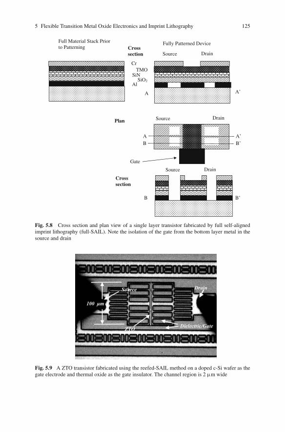
5 Flexible Transition Metal Oxide Electronics and Imprint Lithography 125
AB
A
B
Full Material Stack Prior to Patterning
CrTMO
SiNSiO2
Al
Fully Patterned Device
Gate
Source Drain
Source Drain
Source Drain
Plan
Cross section
Cross section
Fig. 5.8 Cross section and plan view of a single layer transistor fabricated by full self-alignedimprint lithography (full-SAIL). Note the isolation of the gate from the bottom layer metal in thesource and drain
Fig. 5.9 A ZTO transistor fabricated using the reefed-SAIL method on a doped c-Si wafer as thegate electrode and thermal oxide as the gate insulator. The channel region is 2 μm wide
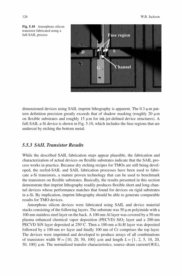
126 W.B. Jackson
Fig. 5.10 Amorphous silicontransistor fabricated using afull-SAIL process
dimensioned devices using SAIL imprint lithography is apparent. The 0.3-μm pat-tern definition precision greatly exceeds that of shadow masking (roughly 20 μmon flexible substrates and roughly 15 μm for ink-jet-defined device structures). Afull-SAIL a-Si device is shown in Fig. 5.10, which includes the fuse regions that areundercut by etching the bottom metal.
5.5.3 SAIL Transistor Results
While the described SAIL fabrication steps appear plausible, the fabrication andcharacterization of actual devices on flexible substrates indicate that the SAIL pro-cess works in practice. Because dry etching recipes for TMOs are still being devel-oped, the reefed-SAIL and SAIL fabrication processes have been used to fabri-cate a-Si transistors, a mature proven technology that can be used to benchmarkthe transistors on flexible substrates. Basically, the results presented in this sectiondemonstrate that imprint lithography readily produces flexible short and long chan-nel devices whose performance matches that found for devices on rigid substratesin a-Si. By implication, imprint lithography should be able to generate comparableresults for TMO devices.
Amorphous silicon devices were fabricated using SAIL and device materialstacks consisting of the following layers. The substrate was 50 μm polyimide with a100-nm stainless steel layer on the back. A 100-nm Al layer was covered by a 50-nmplasma enhanced chemical vapor deposition (PECVD) SiO2 layer and a 200-nmPECVD SiN layer deposited at 250◦C. Then a 100-nm a-Si:H layer was depositedfollowed by a 100-nm n+ layer and finally 100 nm of Cr comprises the top layer.The devices were imprinted and developed to produce arrays of all combinationsof transistors width W = {10, 20, 50, 100} μm and length L = {1, 2, 5, 10, 20,50, 100} μm. The normalized transfer characteristics, source–drain current/(W/L),
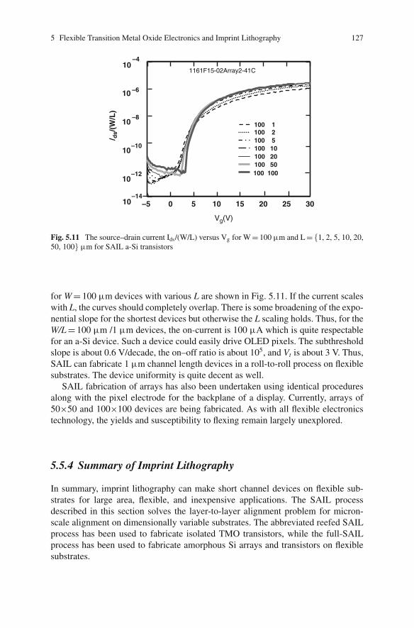
5 Flexible Transition Metal Oxide Electronics and Imprint Lithography 127
Vg(V)
–14
10–12
10–10
10–8
10 –6
10–4
–5 0 5 10 15 20 25 3010
1161F15-02Array2-41C
/ ds/
(W/L
)
100 1100 2100 5100 10100 20100 50100 100
Fig. 5.11 The source–drain current Ids/(W/L) versus Vg for W = 100 μm and L = {1, 2, 5, 10, 20,50, 100} μm for SAIL a-Si transistors
for W = 100 μm devices with various L are shown in Fig. 5.11. If the current scaleswith L, the curves should completely overlap. There is some broadening of the expo-nential slope for the shortest devices but otherwise the L scaling holds. Thus, for theW/L = 100 μm /1 μm devices, the on-current is 100 μA which is quite respectablefor an a-Si device. Such a device could easily drive OLED pixels. The subthresholdslope is about 0.6 V/decade, the on–off ratio is about 105, and Vt is about 3 V. Thus,SAIL can fabricate 1 μm channel length devices in a roll-to-roll process on flexiblesubstrates. The device uniformity is quite decent as well.
SAIL fabrication of arrays has also been undertaken using identical proceduresalong with the pixel electrode for the backplane of a display. Currently, arrays of50×50 and 100×100 devices are being fabricated. As with all flexible electronicstechnology, the yields and susceptibility to flexing remain largely unexplored.
5.5.4 Summary of Imprint Lithography
In summary, imprint lithography can make short channel devices on flexible sub-strates for large area, flexible, and inexpensive applications. The SAIL processdescribed in this section solves the layer-to-layer alignment problem for micron-scale alignment on dimensionally variable substrates. The abbreviated reefed SAILprocess has been used to fabricate isolated TMO transistors, while the full-SAILprocess has been used to fabricate amorphous Si arrays and transistors on flexiblesubstrates.
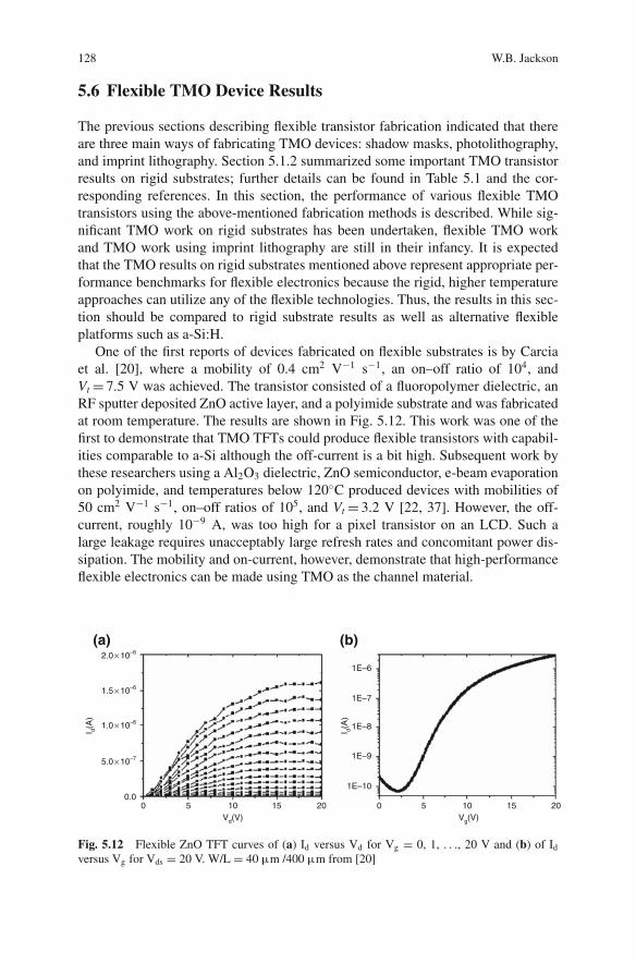
128 W.B. Jackson
5.6 Flexible TMO Device Results
The previous sections describing flexible transistor fabrication indicated that thereare three main ways of fabricating TMO devices: shadow masks, photolithography,and imprint lithography. Section 5.1.2 summarized some important TMO transistorresults on rigid substrates; further details can be found in Table 5.1 and the cor-responding references. In this section, the performance of various flexible TMOtransistors using the above-mentioned fabrication methods is described. While sig-nificant TMO work on rigid substrates has been undertaken, flexible TMO workand TMO work using imprint lithography are still in their infancy. It is expectedthat the TMO results on rigid substrates mentioned above represent appropriate per-formance benchmarks for flexible electronics because the rigid, higher temperatureapproaches can utilize any of the flexible technologies. Thus, the results in this sec-tion should be compared to rigid substrate results as well as alternative flexibleplatforms such as a-Si:H.
One of the first reports of devices fabricated on flexible substrates is by Carciaet al. [20], where a mobility of 0.4 cm2 V−1 s−1, an on–off ratio of 104, andVt = 7.5 V was achieved. The transistor consisted of a fluoropolymer dielectric, anRF sputter deposited ZnO active layer, and a polyimide substrate and was fabricatedat room temperature. The results are shown in Fig. 5.12. This work was one of thefirst to demonstrate that TMO TFTs could produce flexible transistors with capabil-ities comparable to a-Si although the off-current is a bit high. Subsequent work bythese researchers using a Al2O3 dielectric, ZnO semiconductor, e-beam evaporationon polyimide, and temperatures below 120◦C produced devices with mobilities of50 cm2 V−1 s−1, on–off ratios of 105, and Vt = 3.2 V [22, 37]. However, the off-current, roughly 10−9 A, was too high for a pixel transistor on an LCD. Such alarge leakage requires unacceptably large refresh rates and concomitant power dis-sipation. The mobility and on-current, however, demonstrate that high-performanceflexible electronics can be made using TMO as the channel material.
00.0
1E–10
1E–9
1E–8
1E–7
1E–6
5.0 × 10⁻⁷
1.0 × 10⁻⁶
1.5 × 10⁻⁶
(a) (b)2.0 × 10⁻⁶
5 10Vd(V)
I d(A
)
I d(A
)
15 20 0 5 10Vg(V)
15 20
Fig. 5.12 Flexible ZnO TFT curves of (a) Id versus Vd for Vg = 0, 1, . . ., 20 V and (b) of Id
versus Vg for Vds = 20 V. W/L = 40 μm /400 μm from [20]
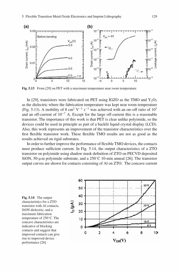
5 Flexible Transition Metal Oxide Electronics and Imprint Lithography 129
00
0.01
0.02
Before bending
0.03
10–9
10–8
10–7
10–6
10–5
10–4
10–9
10–8
10–7
10–6
10–5
10–4
(a) (b)
5 10
1.02.0
3.0
4.0
5.0
Dra
in c
urre
nt, I
DS
(mA
)
Dra
in c
urre
nt, I
DS
(A)
Leak
age
curr
ent,
I G(A
)VGS(V)
VDS = 4V
15 0 5 10–5
Fig. 5.13 From [29] on PET with a maximum temperature near room temperature
In [29], transistors were fabricated on PET using IGZO as the TMO and Y2O3
as the dielectric where the fabrication temperature was kept near room temperature(Fig. 5.13). A mobility of 8 cm2 V−1 s−1 was achieved with an on–off ratio of 103
and an off-current of 10−7 A. Except for the large off-current this is a reasonabletransistor. The importance of this work is that PET is clear unlike polyimide, so thedevices could be used in principle as part of a backlit liquid crystal display (LCD).Also, this work represents an improvement of the transistor characteristics over thefirst flexible transistor work. These flexible TMO results are not as good as theresults achieved on rigid substrates.
In order to further improve the performance of flexible TMO devices, the contactsmust produce sufficient current. In Fig. 5.14, the output characteristics of a ZTOtransistor on polyimide using shadow mask definition of ZTO on PECVD depositedSiON, 50-μm polyimide substrate, and a 250◦C 10-min anneal [26]. The transistoroutput curves are shown for contacts consisting of Al on ZTO. The concave current
Fig. 5.14 The outputcharacteristics for a ZTOtransistor with Al contacts,SiON dielectric, and amaximum fabricationtemperature of 250◦C. Theconcave characteristics areindicative of blockingcontacts and suggest thatimproved contacts can giverise to improved deviceperformance [26]
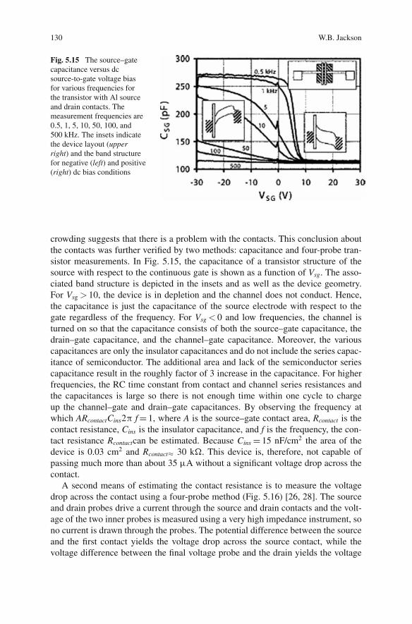
130 W.B. Jackson
Fig. 5.15 The source–gatecapacitance versus dcsource-to-gate voltage biasfor various frequencies forthe transistor with Al sourceand drain contacts. Themeasurement frequencies are0.5, 1, 5, 10, 50, 100, and500 kHz. The insets indicatethe device layout (upperright) and the band structurefor negative (left) and positive(right) dc bias conditions
crowding suggests that there is a problem with the contacts. This conclusion aboutthe contacts was further verified by two methods: capacitance and four-probe tran-sistor measurements. In Fig. 5.15, the capacitance of a transistor structure of thesource with respect to the continuous gate is shown as a function of Vsg. The asso-ciated band structure is depicted in the insets and as well as the device geometry.For Vsg > 10, the device is in depletion and the channel does not conduct. Hence,the capacitance is just the capacitance of the source electrode with respect to thegate regardless of the frequency. For Vsg < 0 and low frequencies, the channel isturned on so that the capacitance consists of both the source–gate capacitance, thedrain–gate capacitance, and the channel–gate capacitance. Moreover, the variouscapacitances are only the insulator capacitances and do not include the series capac-itance of semiconductor. The additional area and lack of the semiconductor seriescapacitance result in the roughly factor of 3 increase in the capacitance. For higherfrequencies, the RC time constant from contact and channel series resistances andthe capacitances is large so there is not enough time within one cycle to chargeup the channel–gate and drain–gate capacitances. By observing the frequency atwhich ARcontactCins2π f = 1, where A is the source–gate contact area, Rcontact is thecontact resistance, Cins is the insulator capacitance, and f is the frequency, the con-tact resistance Rcontactcan be estimated. Because Cins = 15 nF/cm2 the area of thedevice is 0.03 cm2 and Rcontact≈ 30 kΩ. This device is, therefore, not capable ofpassing much more than about 35 μA without a significant voltage drop across thecontact.
A second means of estimating the contact resistance is to measure the voltagedrop across the contact using a four-probe method (Fig. 5.16) [26, 28]. The sourceand drain probes drive a current through the source and drain contacts and the volt-age of the two inner probes is measured using a very high impedance instrument, sono current is drawn through the probes. The potential difference between the sourceand the first contact yields the voltage drop across the source contact, while thevoltage difference between the final voltage probe and the drain yields the voltage
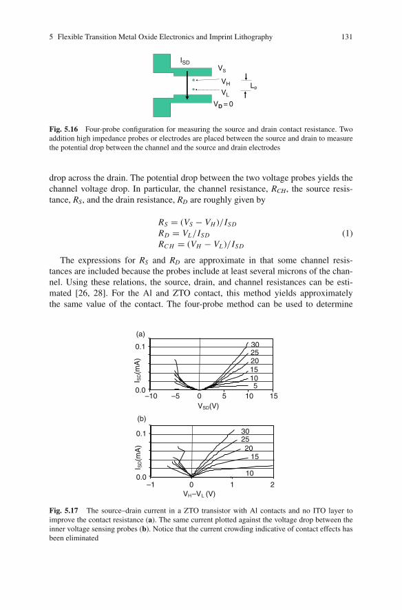
5 Flexible Transition Metal Oxide Electronics and Imprint Lithography 131
VD = 0
VS
VH
VL
ISD
Lp
Fig. 5.16 Four-probe configuration for measuring the source and drain contact resistance. Twoaddition high impedance probes or electrodes are placed between the source and drain to measurethe potential drop between the channel and the source and drain electrodes
drop across the drain. The potential drop between the two voltage probes yields thechannel voltage drop. In particular, the channel resistance, RCH, the source resis-tance, RS, and the drain resistance, RD are roughly given by
RS = (VS − VH )/ISD
RD = VL/ISD
RC H = (VH − VL )/ISD
(1)
The expressions for RS and RD are approximate in that some channel resis-tances are included because the probes include at least several microns of the chan-nel. Using these relations, the source, drain, and channel resistances can be esti-mated [26, 28]. For the Al and ZTO contact, this method yields approximatelythe same value of the contact. The four-probe method can be used to determine
0.1
–10 –5 0 5 10 15
30
0.0
I SD(m
A)
252015105
VSD(V)
0.1
–1 20
30
0.0
I SD(m
A)
2520
15
10
VH–VL (V)1
(b)
(a)
Fig. 5.17 The source–drain current in a ZTO transistor with Al contacts and no ITO layer toimprove the contact resistance (a). The same current plotted against the voltage drop between theinner voltage sensing probes (b). Notice that the current crowding indicative of contact effects hasbeen eliminated
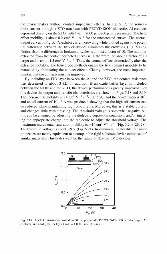
132 W.B. Jackson
the characteristics without contact impedance effects. In Fig. 5.17, the source–drain current through a ZTO transistor with PECVD SiON dielectric, Al contactsdeposited directly on the ZTO, with W/L = 2000 μm/200 μm is presented. The fieldeffect mobility is about 0.2 cm2 V−1 s−1 for the uncorrected curves. The normaloutput curves in Fig. 5.17a exhibit current crowding while plotted against the poten-tial difference between the two electrodes eliminates the crowding (Fig. 5.17b).Notice also the difference in horizontal scales is almost a factor of 10. The mobilityextracted from the contact corrected curves will, therefore, be about a factor of 10larger and is about 1.5 cm2 V−1 s−1. Thus, the contact effects dramatically alter theextracted mobility. The four-probe methods enable the true channel mobility to beextracted by eliminating the contact effects. Clearly, however, the most importantpoint is that the contacts must be improved.
By including an ITO layer between the Al and the ZTO, the contact resistancewas decreased to about 3 kΩ. In addition, if an oxide buffer layer is includedbetween the SiON and the ZTO, the device performance is greatly improved. Forthis device the output and transfer characteristics are shown in Figs. 5.18 and 5.19.The incremental mobility is 14 cm2 V−1 s−1(Fig. 5.20) and the on–off ratio is 107,and an off-current of 10−11 A was produced showing that the high off-current canbe reduced while maintaining high on-currents. Moreover, this is a stable currentand changes little with stressing. The threshold voltage is somewhat negative butthis can be changed by adjusting the dielectric deposition conditions and/or inject-ing the appropriate charge into the dielectric to adjust the threshold voltage. Themaximum incremental saturation mobility is ∼14 cm2 V−1 s−1 (Fig. 5.20) [26, 28].The threshold voltage is about −9 V (Fig. 5.21). In summary, the flexible transistorproperties are nearly equivalent to a comparable rigid substrate device composed ofsimilar materials. This bodes well for the future of flexible TMO devices.
0 10 20 30 40
30 V
25 V
20 V
15 V
10 V
5 V
Vds (V)
S DZTO
SiNO
Gate
ITO
SiO2
1.5
1.0
0.5
0.0
2.0
I d
s (m
A)
Fig. 5.18 A ZTO transistor deposited on 50 μm polyimide, PECVD SiON, ITO contact layer, Alcontacts, and a SiO2 buffer layer (W/L = 1,000 μm /100 μm)
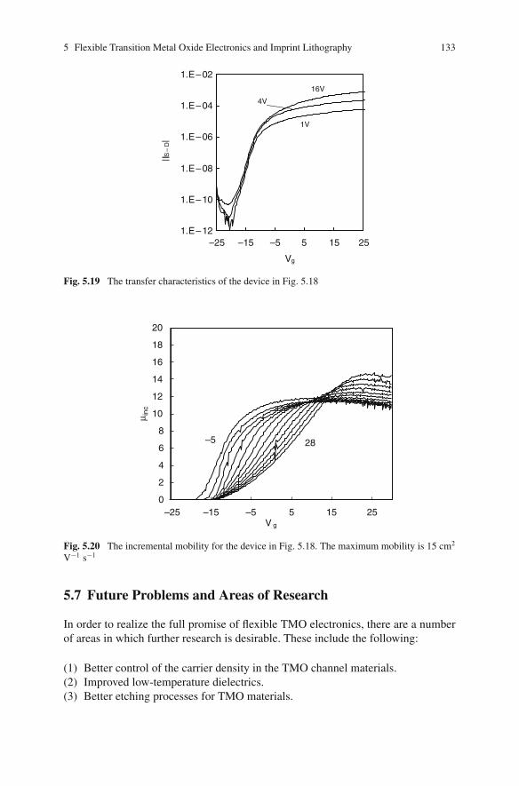
5 Flexible Transition Metal Oxide Electronics and Imprint Lithography 133
1.E – 12
1.E – 10
1.E – 08
1.E – 06
1.E – 04
1.E – 02
–25 –15 5 15 25–5
Vg
|IS –
D|
1V
4V
16V
Fig. 5.19 The transfer characteristics of the device in Fig. 5.18
–25 –15 –5 15 25
μ inc
0
2
4
6
8
10
12
14
16
18
20
5V g
–5 28
Fig. 5.20 The incremental mobility for the device in Fig. 5.18. The maximum mobility is 15 cm2
V−1 s−1
5.7 Future Problems and Areas of Research
In order to realize the full promise of flexible TMO electronics, there are a numberof areas in which further research is desirable. These include the following:
(1) Better control of the carrier density in the TMO channel materials.(2) Improved low-temperature dielectrics.(3) Better etching processes for TMO materials.
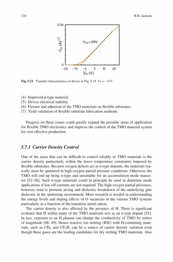
134 W.B. Jackson
0.04
–25 –15 –5 5 15 25
VG (V)
√IS
D(A
)1/2
VSD = 28V
0
Fig. 5.21 Transfer characteristics of device in Fig. 5.18. VT =−9 V
(4) Improved p-type material.(5) Device electrical stability.(6) Flexure and adhesion of the TMO materials on flexible substrates.(7) Yield validation of flexible substrate fabrication methods.
Progress on these issues could greatly expand the possible areas of applicationfor flexible TMO electronics and improve the control of the TMO material systemfor cost effective production.
5.7.1 Carrier Density Control
One of the areas that can be difficult to control reliably in TMO materials is thecarrier density particularly within the lower temperature constraints imposed byflexible substrates. Because oxygen defects act as n-type dopants, the materials typ-ically must be sputtered in high-oxygen partial pressure conditions. Otherwise theTMO will end up being n-type and unsuitable for an accumulation mode transis-tor [52–56]. Such n-type materials could in principle be used in depletion modeapplications if low off-currents are not required. The high-oxygen partial pressures,however, tend to promote arcing and dielectric breakdown of the underlying gatedielectric in the sputtering environment. More research is needed in understandingthe energy levels and doping effects of O vacancies in the various TMO systemsparticularly as a function of the transition metal cation.
The carrier density is also affected by the presence of H. There is significantevidence that H within many of the TMO materials acts as an n-type dopant [51].In fact, exposure to an H plasma can change the conductivity of TMO by ordersof magnitude [48, 49]. Hence reactive ion etching (RIE) with H-containing mate-rials, such as CH4 and CF3H, can be a source of carrier density variation eventhough these gases are the leading candidates for dry etching TMO materials. Also
5 Flexible Transition Metal Oxide Electronics and Imprint Lithography 135
dielectrics such as PECVD a-SiN dielectrics can also introduce H into the adjacentTMO. Because of the ubiquitous prevalence of H during deposition, etching, and inneighboring materials and the rather high mobility of H in TMOs, postfabricationannealing protocols can be important to control the carrier density. Often annealingfor short times above 200◦C can significantly reduce the excess carrier density. Pre-sumably this annealing causes H to move to become electrically inactive withoutreleasing H from any dielectric such as SiN that might contain H. Postfabrication Hmotion could also be a source of instability in the electronic properties of the fab-ricated devices. Significantly more research is needed in understanding the energylevels introduced by H, the diffusion of H within TMOs, and the interchange of Hwith dielectrics both during deposition and postdevice fabrication.
5.7.2 Low-Temperature Dielectrics
As with all material systems used on flexible substrates, good low-temperaturedielectrics are critical. The dielectrics must have low interface defects with the TMOmaterials at low deposition temperatures. In bottom gate devices, it is also desirablethat the surface roughness of the dielectric be small in order that the field effectmobility approaches that of the underlying TMO. Most importantly, the dielec-tric must withstand high fields without trapping significant charge. The trappedcharge will cause threshold shifts arising from continuous application of gate biases.While charge-trapping-induced threshold voltage shifts are undesirable for all flex-ible electronic systems, they are particularly undesirable for electronic applicationssuch as driving OLEDs and drive electronics; the potential new application areasfor TMO materials. Otherwise one must use more elaborate self-compensating cir-cuits in such applications. Some of the dielectrics that have been used are listed inTables 5.1 and 5.4, but there has been little investigation into their stability undervoltage stress or their tendency to create interface states. Research comparing thestability of the various dielectrics may also shed light on the physical origins of themetastability.
5.7.3 Etching of TMO Materials
For batch fabrication of TMO electronics on flexible substrates, etching continuesto be a somewhat difficult area. Both wet and dry etching of TMO materials haveundesirable features. Besides the waste disposal issues and expensive process ofwet etching, many flexible substrates such as polyimide and PET can absorb waterwhich in turn can cause swelling. Hence, wet etching may require a moisture barrierlayer to protect the substrate. The preferable dry RIE etching is also somewhat dif-ficult for TMO materials. The two most promising etching chemistries are CH4/H2
and BCl3 [50]. The BCl3 chemistry is slow and tends to etch contact metals as wellas TMO materials thereby limiting the types of process flows and structures that can
136 W.B. Jackson
be fabricated. The CH4/H2 chemistry on the other hand etches the TMO materialwhile leaving metals intact. The chief difficulty with the CH4/H2 chemistry is thatit tends to leave carbon structures, maybe even carbon nanotubes on surfaces otherthan the TMO such as the walls of the chambers and source–drain contacts. In nor-mal conditions, one uses oxygen to suppress carbon compound formation but thisinterferes with the etching of the oxygen in the TMO. The hydrogen concentrationis adjusted to help etch surface carbon compounds but as mentioned above, excessatomic H can cause problems for the carrier density in the TMO unless the hydrogenis removed by subsequent annealing steps. The deposition of carbon compounds onthe chamber walls often requires periodic mechanically cleaning as the material isremarkable resistant to usual O cleaning procedures. While existing etch protocolsare satisfactory, improved etching chemistries and protocols would be quite usefulfor the wide scale use of TMO electronics.
5.7.4 P-type TMO
Another major area for future research is the deposition of p-type TMO material.P-type material would be highly desirable in order to create CMOS-type circuitry fordrive electronics and other electronic applications. Significant effort has been madeto develop p-type TMO materials [63–69]. In general, because O vacancies dope n-type TMO, it is difficult to produce p-type material. Whenever a p-type dopant atomis introduced into the growing materials, an O vacancy becomes more energeticallyfavorable. The O vacancies compensate the material. There is promising work usingCu containing materials to help dope the material p-type [63–69]. The Cu cationhas an unfilled 4d that lines up with the valence band of most TMO. Cu doping thenserves as a p-type dopant. The p-type carrier densities that have been achieved are3×1019 carriers cm−3. Unfortunately, the features of TMOs that make the electronmobility high even for amorphous disorder, results in reduced mobility for holes.The top of the valence band is primarily directional O 2p-type orbitals that are sen-sitive to disorder. In sufficient quantities, the Cu constituents create a miniband atthe top of the valence band that increases the hole conductivity despite the disorderinduced broadening of the valence band edge. The best mobilities achieve to dateare mobilities of 0.13 cm2/V·s for nonsingle crystalline material [63–69].
5.7.5 Stability
As in the case of many material systems with disorder and low-temperaturedielectrics, TMO devices exhibit metastability. The quantification and understand-ing of this phenomenon are just beginning. It has been known for a while thatZnO, for example, exhibits a persistent photoconductivity [52–56]. Illumination bybandgap light causes significant changes in conductivity that last for hours or more.This effect has been attributed to O chemisorption initiated by the UV light. The
5 Flexible Transition Metal Oxide Electronics and Imprint Lithography 137
effect is minimized if the transistor has a passivation layer preventing O interac-tion with the back surface [52–56]. Depending on the composition, annealing his-tory, and exposure to O or H, the electrical characteristics exhibit varying degrees ofinstability. The instabilities can arise from changes in carrier concentrations, defectsin the semiconductor, and/or charge trapping in the insulator. In general, the higherthe annealing temperatures, the better the stability and the smaller the initial device-to-device variation in threshold voltages and subthreshold slopes. The presence ofIn also appears to increase instability. The origin and control of instabilities areof particular interest as one of the many advantages of TMO is their use in edgedriver electronics and OLED drivers. The stability requirements of driver electronicdevices are typically more demanding because the on-time voltage duty cycle canapproach 100%, while in the typical pixel transistor, the on-time duty cycle can bemade small. Significant work in this area is required.
5.7.6 Flexure and Adhesion of TMO
Common to all flexible electronic materials and fabrication methods, more workneeds to be done characterizing and understanding the effects of flexure on the per-formance of TMO electronics. The brittle nature of TMO may suggest that flexuremaybe a problem. However, the small relative area of the TMO transistor chan-nel region, the small thickness of the TMO material, and the large compliance ofthe substrate suggest that flexure may not be a significant limitation for TMO elec-tronics. Preliminary studies of devices using brittle a-Si:H as a channel materialindicates that metal lines and dielectrics are more of a problem. Virtually no flexingstudies on TMOs have been done.
5.7.7 Flexible Fabrication Method Yields
A final area of future study common to most all flexible material systems concernsthe yield of various fabrication methods. Because the substrate dimensions are notfixed, the fabrication temperatures are low, and the fabrication methods are relativelynonstandard (not the typical photolithography), there is the all important question ofyield. The initial yield of the devices, lines, and crossovers for both imprint lithog-raphy and jetting methods of fabrication must be measured and optimized. Work isjust beginning to characterize the yield issues of imprint lithography. Dirt-induceddefects tend to be eliminated by the imprint process while defects due to imprintstamp wear, propagate, and can result in significant yield loss. Improper stamp fill-ing and bubble defects are less important; they cause at most the failure of one array.Yield issues regarding control and uniformity of etching masks remain unexplored.Jetting methods have problems of splashing, wetting, gaps, and nonuniform cover-age issues. The yield issues associated with these flexible substrates transcend thematerial system and are not specific to the TMO devices.
138 W.B. Jackson
Issues specific to SAIL that need to be measured include the following:
(1) The yield of the devices and arrays using SAIL is not yet known. There areimprint defects such as voids caused by under filling and excess imprint poly-mer if there is over filling.
(2) The impact of imprint wears on device yield needs to be measured in orderto estimate stamp life time. Defects may form in the stamp due to particles orfailure to release from the mold. These defects are then replicated.
(3) The effects of particle densities on yield and whether acceptable yield can beobtained without a clean room.
(4) Finally, the required levels of process uniformities and latitudes that affectdevice yield should be measured. Because SAIL is so recent, many of theseissues require further work. In general, we have been encouraged by the factthat as we have moved toward roll-to-roll fabrication using SAIL, device yields,controllability, and uniformity have markedly improved over batch processingsuggesting that SAIL represents a promising fabrication method for large area,inexpensive, and flexible electronics.
5.8 Summary
SAIL is a solution to the layer-to-layer alignment problem for the critical featureson flexible substrates. The SAIL process can produce submicron-aligned layers andsubmicron-sized features, is compatible with both roll-to-roll and high-throughputmanufacturing, and is inexpensive. The complex series of steps (deposition, coatwith resist, expose resist, develop, etch, and resist removal) required for each layer inthe standard photolithography is eliminated. The capability of the SAIL process canbe used for any materials system, such as a-Si, low-temperature poly-Si, and laserrecrystallized Si as well TMOs. The only materials system for which SAIL doesnot currently seem straightforward is organics because etch selectivity between theimprint polymer and the organic layer has not been adequately investigated. SAILshould be considered as a possible fabrication methodology in the area of flexibleelectronics and can enable many of the structures and devices mentioned elsewherein this book.
The major point of this chapter is the promising possibility of TMOs for flex-ible electronics. These materials have demonstrated high mobilities, large on–offratios, and reasonable threshold voltages using fabrication temperatures and proce-dures compatible with flexible substrates and large-throughput manufacturing meth-ods. Transistors with mobilities as high as 30 cm2 V−1 s−1, on–off ratios of 107,Vt = 3 V, off-currents of 1 pA, and on-currents in the range of 1 mA have beendemonstrated. Moreover, the transistors can be completely transparent so the fillfactor can be large. If the stability issue, transition metal etching and appropriate
5 Flexible Transition Metal Oxide Electronics and Imprint Lithography 139
dielectric material selection are solved, the future looks very promising for flexibleTMO electronics.
Acknowledgements I would like to thank G. Herman and R. Hoffman introducing me to thefield of transition metal oxide transistors and for making various samples, and C. Taussig, P. Mei,and C. Perlov for many consultations and support during this work.
References
1. Boesen GF, Jacobs, JE (1968) ZnO field-effect transistor. Proc IEEE 56:2094–20952. Khuri-Yakub BT, Kino GS (1974) A monolithic zinc-oxide-on-silicon convolver. Appl Phys
Lett 25:188–1903. Mahan, GD (1983) Intrinsic defects in ZnO varistors. J Appl Phys 54:3825–38324. Kudo A, Yanagi H, Ueda K, Hosono H, Kawazoe H, Yano Y (1999) Fabrication of transparent
p–n heterojunction thin-film diodes based entirely on oxide semiconductors. Appl Phys Lett75:2851–2853
5. Chopra K, Major S, Pandya D (1983) Transparent conductors – a status review. Thin SolidFilms 102:1–46
6. Prins MWJ, Grosse-Holz K, Mller G, Cillessen JM, Giesbers JB (1996) A ferroelectric trans-parent thin-film transistor. Appl Phys Lett 68:3650–3652
7. Kawasaki M, Tamura K, Saikusa K, Aita T, Tsukazaki A, Ohtomo A, Jin ZG, Matsumoto Y,Fukumura T, Koinuma H, Ohrnaki Y, Kishimoto S, Ohno Y, Matsukura F, Ohno H, Makino T,Tuan NT, Sun PD, Chia CH, Segawa Y, Tang ZK, Wang GKL (2000) Can ZnO eat marketin optoelectronic applications. Ext. Abst. 2000 Int Conf. Solid State Deyices ard Materials,Sendai, l28–129
8. Ohtomo A, Kawaski M (2000) Novel semiconductor technologies of ZnO films towards ultra-violet LEDs and invisible FETs. IEEE Trans Electron E83-C:1614–1617
9. Ohya Y, Niwa T, Ban T, Takahashi Y (2001) Thin-film transistor of ZnO fabricated by chem-ical solution deposition. Jpn J Appl Phys 40:297–299
10. Hoffman R (2002) Development, fabrication, and characterization of transparent electronicdevices. Masters Thesis, Oregon State University
11. Masuda S, Kitamura K, Okumura Y, Miyatake S, Tabata H, Kawai T (2003) Transparent thin-film transistors using ZnO as an active channel layer and their electrical properties. J ApplPhys 93:1624–1630
12. Nomura K, Ohta H, Ueda K, Kamiya T, Hirano M, Hosono H (2003) Thin-film transistorfabricated in single-crystalline transparent oxide semiconductor. Science 300:1269–1272
13. Hoffman R, Norris B, Wager J (2003) ZnO-based transparent thin-film transistors. Appl PhysLett 82:733–735
14. Nishii J, Hossain FM, Takagi S, Aita T, Saik K, Ohmaki Y, Ohkubo I, Kishimoto S, Ohtomo A,Fukumura T, Matsukura F, Ohno Y, Koinuma H, Ohno H, Kawasaki M (2003) High mobilitythin film transistors with transparent ZnO channels. Jpn J Appl Phys 42:L 347–349 Part 2,No. 4A
15. Carcia PF, McLean RS, Reilly MH, Malajovich I, Sharp KG, Agrawal S, Nunes G Jr (2003)ZnO thin film transistors for flexible electronics. Mat Res Soc Symp Proc 769:H7.2.1
16. Nishii J, Hossain FM, Takagi S, Aita T, Saikusa K, Ohmaki Y, Kishimoto I, Ohtomo A,Fukumura T, Matsukura F, OhnoY, Koinuma H, Ohno H, Kawasaki M (2003) High mobilitythin film transistors with transparent ZnO channels. Jpn J Appl Phys 42:347–349
17. Fortunato E, Hosano H, Granquist C, Wager J (2007) Advances in transparent electronics:From Materials to devices, I, 51(7).
18. Chaing HQ (2003) Development of zinc tin oxide-based transparent thin-film transistors. Mas-ter Thesis, Oregon State University
140 W.B. Jackson
19. Chiang HP, Wager JF, Hoffman, RL, Jeong J, Keszler DA (2005) High mobility transpar-ent thin-film transistors with amorphous zinc tin oxide channel layer. Appl Phys Lett 86:13503–13505
20. Carcia PF, McLean RS, Reilly MH, Nunes G (2003) Transparent ZnO thinfilm transistor fab-ricated by rf magnetron sputtering. Appl Phys Lett 82:1117–1119
21. Fortunato E, Pimentel A, Pereira L, Goncalves A, Lavareda G, Aguas H, Ferreira I, CarvalhoCN, Martins R (2004) High field-effect mobility zinc oxide thin film transistors produced atroom temperature. J Non-Cryst Solids 338–340:806–809
22. Carcia PF, McLean RS, Reilly MH (2005) Oxide engineering of ZnO thin-film transistors forflexible electronics. J Soc Inf Display 13/7:547–550
23. Bellingeria E, Marrea D, Pellegrinoa L, Pallecchia I, Canub G, Vignoloa M, Berninia C, SiriaHS (2005) High mobility ZnO thin film deposition on SrTiO3 and transparent field effecttransistor fabrication Superlattices and Microstructures 38:446–454
24. Hwang CS, Park SH, Chu HY (2005) ZnO TFT fabricated at low temperature for applicationactive-matrix display. 12th Int. Display Workshops/Asia Display, p1149–1151
25. Carcia PF, McLean RS, Reilly MH (2006) High-performance ZnO thin-film transistors ongate dielectrics grown by atomic layer deposition. Appl Phys Lett 88:123509–123511
26. Jackson WB, Hoffman RL, Herman GS (2005) High-performance flexible zinc tin oxide field-effect transistors. Appl Phys Lett 87:193503–193505
27. Hoffman RL (2006) Effects of channel stoichiometry and processing temperature on the elec-trical characteristics of zinc tin oxide thin-film transistors. Solid-State Electron 50:784–787
28. Jackson WB, Herman GS, Hoffman RL, Taussig C, Braymen S, Jeffery F, Hauschildt J (2006)Zinc tin oxide transistors on flexible substrates. J Non-Cryst Solids 352:1753–1755
29. Nomura K, Ohta H, Takagi A, Kamiya T, Hirano M, Hosono H (2004) Room-temperaturefabrication of transparent flexible thin-film transistors using amorphous oxide semiconduc-tors. Nature 432:488–492
30. Yaglioglu B, Yeom HY, Beresford R, Paine DC (2006) A high-mobility amorphous In2O3 –10 wt% ZnO thin film transistors. Appl Phys Lett 89:062103–062105
31. Fortunato E, Barquinha P, Pimentel A, Goncalves A, Marques A, Pereira L, Martins R(2005) Fully transparent ZnO thin-film transistor produced at room temperature. Adv Mat 17:590–594
32. Santato C, Manunza I, Bonfiglio A, Ciroira F, Cosseddu P, Zamboni R, Muccini M(2006) Tetracene light-emitting transistors on flexible plastic substrates. Appl Phys Lett 86:141106–141109
33. Loi A, Manunza I, Bonfiglio A (2005) Flexible, organic, ion-sensitive field-effect transistor.Appl Phys Lett 86:103512–103514
34. Bonfiglio A, Mameli F, Sanna O (2003) A completely flexible organic transistor obtained bya one-mask photolithographic process. Appl Phys Lett 82(20):3550–3552
35. Ohta H, Nomura K, Hiramatsu H, Ueda K, Kamiya T, Hirano M, Hosono H (2003) Frontierof transparent oxide semiconductors. Solid-State Electron 47:2261–2267
36. Fortunato EC, Barquinha PM, Pimentel AC, Goncalves AM, Marques AJ, Martins RF, PereiraLM (2004) Wide-bandgap high-mobility ZnO thin-film transistors produced at room temper-ature. Appl Phys Lett 85:2541–2543
37. Hosono H, Nomura H, Kamiya T (2005) High performance FET using transparent amorphousoxide semiconductors as channel layer on plastic substrate. 12th Int. Display Workshops/AsiaDisplay IDW/AD05 AMD3-1:251–253
38. Ellmer K (2001) Resitivity of polycrystalline zinc oxide films: Current status and physicallimit. J Phys D: Appl Phys 34:3097–3108
39. Chopra K, Major S, Pandya D (1983) Transparent conductors – a status review. Thin SolidFilms 102:1–46
40. Minami T, Miyata T, Yamamoto T (1998) Work function of transparent conducting mul-ticomponent oxide thin films prepared by magnetron sputtering. Surf Coat Tech 108–109:583–587
5 Flexible Transition Metal Oxide Electronics and Imprint Lithography 141
41. Minami T, Takata S, Sato H, Sonhana H (1995) Properties of transparent zinc stannateconducting films prepared by radio frequency magnetron sputtering. J Vac Sci Technol A13:1095–1099
42. Minami T, Sonohara H, Takata S, Sato H (1994) Highly transparent and conductive zinc-stannate thin films prepared by RF magnetron sputtering. Jpn J Appl Phys 33:1693–1696
43. Wu X, Coutts T, Mulligan W (1997) Properties of transparent conducting oxides formed fromCdO and ZnO alloyed with SnO2 and In2O3. J Vac Sci Technol A 15:1057–1062
44. Young DL, Moutinho H, Yan Y, Coutts TJ (2002) Growth and characterization of radiofrequecy magnetron sputter-deposited zinc stannate, Zn2SnO4, thin films. J Appl Phys 92:310–319
45. Young DL (2000) Electron transport in zinc stannate (Zn2SnO4). Ph. D. thesis, ColoradoSchool of Mines
46. Minami T, Sonohara H, Kakumu T, Takata S (1995) Highly transparent and conductiveZn2In2O5 thin films prepared by RF magnetron sputtering. Jpn J Appl Phys 34:971–974
47. Van de Walle CG (2000) Hydrogen as a cause of doping in zinc oxide. Phys Rev Lett 85:1012–1015
48. Raniero L, Ferreira I, Pimentel A, Goncalves A, Canhola P, Fortunato E, Martins R (2006)Role of hydrogen plasma on electrical and optical properties of ZGO, ITO and IZO transparentand conductive coatings. Thin Solid Films 511–512:295–298
49. Theys B, Sallet V, Jomard F, Lusson A, Rommeluere JF, Teukam Z (2002) Effects of inten-tionally introduced hydrogen on the electrical properties of ZnO layers grown by metalorganicchemical vapor deposition. J Appl Phys 91:3922–3924
50. Pearton SJ, Norton DP, Ip K, Heo YW, Steiner T (2005) Recent progress in processing andproperties of ZnO Progress in Materials. Science 50:293–340
51. Van deWalle C, Nequgebauer J (2003) Universal alignment of hydrogen levels in semicon-ductors, insulators and solutions. Nature 423:626–628
52. Zhang DH, Brodie DE (1995) Photoresponse of polycrystalline ZnO films deposited by r.f.bias sputtering. Thin Solid Films 261:334–339
53. Zhang DH (1995) Fast photoresponse and the related change of crystallite barriers for ZnOfilms deposited by RF sputtering. J Phys D: Appl Phys 28:1273–1277
54. Takahashi Y, Kanamori M, Kondoh A, Minoura H, Ohya Y (1994) Photoconductivity of ultra-thin zinc oxide films. Jpn J Appl Phys Part 1, 33:6611–6615
55. Studenikin SA, Golego N, Cocivera M (2000) Carrier mobility and density contributions tophotoconductivity transients in polycrystalline ZnO films. J Appl Phys 87:2413–2421
56. Xirouchaki C, Kiriakidis G, Pedersen TF, Fritzsche H (1996) Photoreduction and oxidationof as-deposited microcrystalline indium oxide. J Appl Phys 79:9349–9352
57. Kim H-J, Almanza-Workman M, Chaiken A, Jackson WB, Jeans A, Kwon O, Luo H, MeiP, Perlov C, Taussig C, Jeffrey, F, Braymen S, Hauschildt J (2006) Roll-to-roll fabricationof active-matrix backplanes using self-aligned imprint lithography (SAIL). 6th Int. Meet-ing Information Display/5th Int. Display Manufacturing Conf. Daegu, Korea, 2006 Digest1539–1543
58. US Patent 20050176182 (2005)59. Xia Y, Whitesides GM, (1998) Soft lithography. Annu Rev Mater Sci 28:153–18460. Quake SR, Scherer A (2000) From micro- to nanofabrication with soft materials. Science
290:1536–154061. Rogers JA, Nuzzo RG (2005, February) Recent progress in soft lithography. Mater today
8:50–5662. Norland Products Inc. www.norlandprod.com63. Kawazoe H, Yasukawa M, Hyodo H, Kurita M, Yanagi H, Hosono H (1997) P-type electrical
conduction in transparent thin films of CuAlO2. Nature 389:939–94264. Tate J, Jayaraj MK, Draeseke AD, Ulbrich T, Sleight AW, Vanaja KA, Nagarajan R, Wager
JF, Hoffman RL (2002) P-type oxides for use in transparent diodes. Thin Solid Films 411:119–124
142 W.B. Jackson
65. Park S, Keszler DA, Valencia MM, Hoffman RL, Bender JP, Wager JF (2002) Transparentp-type conducting BaCu2S2 films. Appl Phys Lett 80:4293–4295
66. Yanagi H, Inoue S, Ueda K, Kawazoe H, Hosono H, Hamada N (2000) Electronic struc-ture and optoelectronic properties of transparent p-type conducting CuAlO2. J Appl Phys 88:4159–4163
67. Nagarajan R, Draeseke AD, Sleight AW, Tate J (2001) P-type conductivity in CuCr1-x MgxO2films and powders. J Appl Phys 89:8022–8025
68. Ueda K, Hase T, Yanagi H, Kawazoe H, Hosono H, Ohta H, Orita M, Hirano M (2001) Epitax-ial growth of transparent p-type conducting CuGaO2 thin films on sapphire (001) substratesby pulsed laser deposition. J Appl Phys, 89:1790–1793
69. Duan N, Sleigh AW, Jayaraj MK, Tate J (2000) Transparent p-type conducting CuScO2+xfilms. Appl Phys Lett 77:1325–1326
Chapter 6Materials and Novel Patterning Methodsfor Flexible Electronics
William S. Wong, Michael L. Chabinyc, Tse-Nga Ng, and Alberto Salleo
Abstract The materials considerations and print-processing techniques forfabricating electronic devices on flexible platforms are reviewed. Organic andinorganic semiconductors, dielectrics, and metals for thin-film transistor (TFT) fab-rication are presented. Jet-printing techniques for both etch-mask patterning anddeposition and patterning of solution-processable polymers will be highlighted. Thecharacterization of low-temperature compatible materials will also be reviewed inregard to conditions that determine device stability and performance in polymericand silicon-based devices. Finally, an overview of specific applications for organicand inorganic semiconductor devices in backplane, display, and image sensor arrayswill be presented.
6.1 Introduction
The scaling of large-area electronics for applications in flat-panel displays, digi-tal X-ray imagers, and flexible electronics is pushing the technological and costlimits of conventional materials and device processing. While conventional process-ing such as photolithography and vacuum deposition can produce high-performancesubmicron devices, this capability and the associated cost is not necessary for large-area platforms. An alternative patterning method that can be scaled to very largeareas, using noncontact jet printing of electronic image files, may be used to fabri-cate both silicon-based [1–4] and polymeric-based [5, 6] thin-film transistors (TFTs)having feature sizes limited by the size of the drops (∼40 μm). Incorporated withroll-to-roll fabrication [7, 8], jet-printing processes can help to reduce processingand materials cost for flexible electronics fabrication.
W.S. Wong (B)Palo Alto Research Center, Palo Alto, CA 94304, USAe-mail: [email protected]
W.S. Wong, A. Salleo (eds.), Flexible Electronics: Materials and Applications, ElectronicMaterials: Science & Technology, DOI 10.1007/978-0-387-74363-9 6,C© Springer Science+Business Media, LLC 2009
143
144 W.S. Wong et al.
Many new materials systems, based on polymeric semiconductors and flexiblesubstrate materials, are rapidly being developed in order to address the intrinsicdifficulties of large-area roll-to-roll processing. Polymeric materials hold promisefor low-cost electronics and simplified device processing. Indeed, materials that aresolution processable will enable novel deposition and patterning processes borrowedfrom the graphic arts industry, such as jet printing, for fabrication of TFT devices.Because a large fraction of fabrication costs is due to patterning, an alternative tech-nology based on ink-jet printing and conventional vacuum deposited thin films mayprovide the required overlap of performance with low-cost fabrication of microelec-tronic circuits on large-area flexible platforms.
Jet-printing technology can be used to pattern etch masks or active materialsto form a desired pattern. The technique has advantages for device processing onflexible substrates: (1) the patterning process is noncontact, (2) layer-to-layer regis-tration is accomplished by digital image processing, and (3) the patterning processoriginates from an electronic image file that is not fixed to a rigid photomask andcan be used for real-time alignment onto a flexible platform. The feature size andspatial control of jet-printed phase-change inks combined with digital imaging andpatterning [9–13] in a process referred to as digital lithography onto conventionalthin-film electronic materials are optimal for large-area device processing on flex-ible platforms and are another alternative to direct writing of solution-processablematerials in additive patterning processes [5, 14, 15].
The integration of inorganic semiconductors and dielectrics on flexible substrateshas the added complexity that high-temperature processing is needed to obtain high-quality materials. No matter what technology is used for flexible displays, if thesubstrate is an organic polymer then close attention must be paid to the depositiontemperatures for all processes used in the fabrication. While plastic substrates havecost advantages and can readily be used in roll-to-roll processes, they have relativelypoor characteristics in terms of thermal expansion, mechanical stability, and solventuptake, when compared to glass and silicon. There are many strategies to addressthese issues, but in general they require processing to occur below ∼170◦C. Sincethis temperature is somewhat lower than that used for conventional processing, it iscritical to perform fundamental studies to understand how electronic devices fabri-cated at these temperatures operate as their defect density is likely to be differentthan that of devices fabricated at higher temperatures. The replacement of conven-tional patterning processes with digital lithography is the first step in simplifying thefabrication of TFT devices. In a second step, solution-processable semiconductorsand metals can be used to replace conventional vacuum deposited materials enablingfabrication in an ambient environment. While devices fabricated using these mate-rials currently have lower performance compared to that of conventional inorganicthin-film devices, they are being rapidly developed for applications in large-area andflexible electronics. The move to solution-processable materials will enable a tran-sition from a conventional subtractive process for TFT fabrication to an all-additiveprocess where reduced cost can be obtained by combining deposition and patterningin a single process step. Organic materials are more easily processed at the lowertemperatures compatible with flexible substrates, but their long-term stability andthe origin of defects are poorly understood.
6 Materials and Novel Patterning Methods for Flexible Electronics 145
6.2 Materials Considerations for Flexible Electronics
6.2.1 Overview
The semiconductor–dielectric combination in a circuit is one of the most importantconsiderations for flexible electronics. The achievement of stable high-performanceTFTs relies on the optimization of the mobility of carriers and the reduction of trapsat the semiconductor–dielectric interface. Thus, the semiconductor and dielectriclayers cannot be considered completely independent. The desired fabrication tech-nology also dictates which materials are compatible. It is currently possible to fab-ricate high-quality TFTs from both inorganic and organic materials and we brieflydescribe these materials here. We also address the possibility of printable conductorsthat can be used, in principle, with either class of material.
6.2.2 Inorganic Semiconductors and Dielectrics
Hydrogenated amorphous silicon (a-Si:H) is the ubiquitous materials system forlarge-area electronics and is currently used as a semiconductor in liquid-crystal dis-play (LCD) backplanes and X-ray imagers on glass substrates [16, 17]. The inte-gration of high-performance a-Si:H-based TFT devices onto polymeric substratesrequires development of high-quality, low-temperature (<200◦C) processed TFTdevices. The development of such materials has been described in detail in earlierchapters. Particular challenges for flexible substrates are deposition of low mechan-ical stress layers and the reduction in defect density through optimization of deposi-tion conditions. The most widely used deposition method for both the a-Si:H layerand the gate dielectric layer, silicon nitride (SiNx), is plasma enhanced chemicalvapor deposition (PE-CVD). While there are alternative low-temperature methods,such as sputtering, these techniques have generally not achieved the same qualitythat is possible with PE-CVD. In addition, since the semiconductor and dielectriclayers are generally deposited sequentially in the same reactor, the interface formedbetween these materials can be highly optimized.
Alternative inorganic materials to amorphous silicon are currently being exploredas semiconductors. Poly-silicon is a well-developed materials system that iscurrently showing promise in OLED display applications. Recently, a form of sil-icon that can be jet-printed has been described [18]. This material, however, suf-fered from the need to be processed in a highly inert atmosphere (<1 ppm O2) andrequired high-temperature postdeposition annealing. Many semiconducting oxidematerials, such as ZnO [19] and ternary compounds, InGaO [20], are being widelystudied in test devices. These optically transparent materials have the advantageof being deposited at low temperatures while yielding relatively high field-effectmobilities (1–10 cm2/Vs). It is, however, difficult to control their doping level dur-ing deposition due to electrically active defects formed during deposition. Printableforms of these materials have also been explored. Nanoparticles of ZnO have been
146 W.S. Wong et al.
used to form TFTs [21], but can require high temperature (>300◦C) postdepositionanneals for the best performance. TFTs formed with these materials are frequentlyused with oxide gate dielectric layers, but there are few studies that have exploredthe best candidates for large-area electronic circuits.
6.2.3 Organic Semiconductors and Dielectrics
Organic semiconductors comprise two broad classes of materials, molecular com-pounds and polymers (Table 6.1). Both of these classes of materials generally havethe feature of either a single conjugated unit or a number of conjugated units thatform a planar or nearly planar molecular structure. There are many known semicon-ducting polymers, but those based on polymers or copolymers of thiophene havegenerally been the most widely used for TFTs. The design and synthesis of poly-meric semiconductors are discussed in chapter 9 in this book. While most of thecharacterization of these materials has been performed using thermally grown sili-con dioxide gate dielectric layers, they are compatible with a variety of dielectricsincluding organic polymers, PE-CVD SiO2 and SiNx, and oxides formed fromanodized metals [22]. Both p- and n-type organic materials have been demon-strated with the former being more common than the latter [23]. Improvements inn-type materials suggest that organic materials may have an advantage over a-Si:Hin applications where complementary logic is required, for example, simple logiccircuits.
The choice of the semiconducting system dictates the deposition method. Molec-ular materials have generally been deposited by vapor methods and have been usedin prototype circuits and backplanes. The best pentacene TFTs have reproduciblemobilities around 1 cm2/Vs [24], but in many cases degradation in performance isobserved during subsequent processing, such as formation of an encapsulation layeror patterning by photolithography [25]. Small molecules can be made amenable tosolution processing by functionalization. Usually, the solution deposition processcauses a reduction in the observed field-effect mobility relative to vapor deposition.The typical reason for this difference is the difficulty in controlling film forma-tion as the solvent evaporates. Recently, a number of materials, such as triisopropy-lsilyl (TIPS)-pentacene, have been designed that form continuous, highly orderedfilms from solution and now provide high mobility when deposited from solvent[26]. Semiconducting polymers have recently been demonstrated to have mobilitiesabove 0.5 cm2/Vs, suggesting that they can have similar performance to molecularmaterials [27].
Most high-performance organic semiconductors form polycrystalline orsemicrystalline films. For many materials, it is found that either thermal or solvent-vapor annealing can lead to improvements in mobility. The orientation of the crys-talline domains relative to the flow of current is considered to be important toachieve the highest field-effect mobility. For example, many semiconducting poly-mers have lamellar structures where a conjugated backbone is separated by alkylside chains. Transport is poor along the lamellar stacking direction due to the
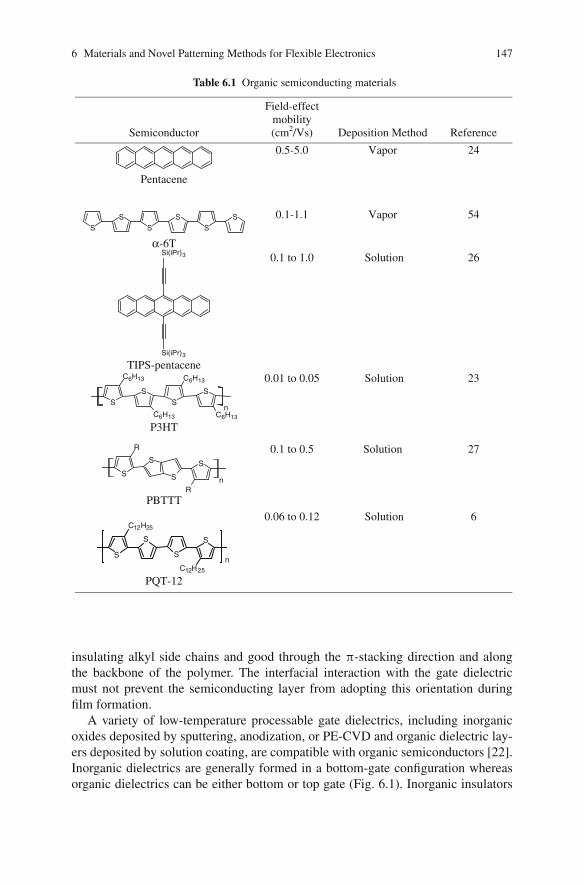
6 Materials and Novel Patterning Methods for Flexible Electronics 147
Table 6.1 Organic semiconducting materials
Semiconductor
Field-effect mobility (cm2/Vs) Deposition Method Reference
Pentacene
0.5-5.0 Vapor 24
S
S
S
S
S
S
α-6T
0.1-1.1 Vapor 54
Si(iPr)3
Si(iPr)3
TIPS-pentacene
0.1 to 1.0 Solution 26
S
S
S
S
C6H13
C6H13
C6H13
C6H13
n
P3HT
0.01 to 0.05 Solution 23
nS
R
S
S S
R
PBTTT
0.1 to 0.5 Solution 27
nS
S
S
S
C12H25
C12H25
PQT-12
0.06 to 0.12 Solution 6
insulating alkyl side chains and good through the π-stacking direction and alongthe backbone of the polymer. The interfacial interaction with the gate dielectricmust not prevent the semiconducting layer from adopting this orientation duringfilm formation.
A variety of low-temperature processable gate dielectrics, including inorganicoxides deposited by sputtering, anodization, or PE-CVD and organic dielectric lay-ers deposited by solution coating, are compatible with organic semiconductors [22].Inorganic dielectrics are generally formed in a bottom-gate configuration whereasorganic dielectrics can be either bottom or top gate (Fig. 6.1). Inorganic insulators
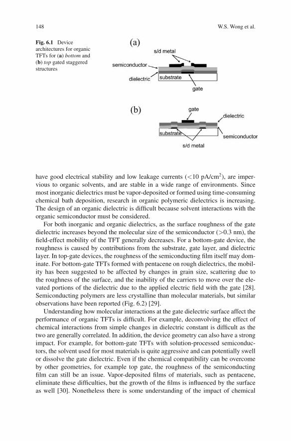
148 W.S. Wong et al.
Fig. 6.1 Devicearchitectures for organicTFTs for (a) bottom and(b) top gated staggeredstructures
have good electrical stability and low leakage currents (<10 pA/cm2), are imper-vious to organic solvents, and are stable in a wide range of environments. Sincemost inorganic dielectrics must be vapor-deposited or formed using time-consumingchemical bath deposition, research in organic polymeric dielectrics is increasing.The design of an organic dielectric is difficult because solvent interactions with theorganic semiconductor must be considered.
For both inorganic and organic dielectrics, as the surface roughness of the gatedielectric increases beyond the molecular size of the semiconductor (>0.3 nm), thefield-effect mobility of the TFT generally decreases. For a bottom-gate device, theroughness is caused by contributions from the substrate, gate layer, and dielectriclayer. In top-gate devices, the roughness of the semiconducting film itself may dom-inate. For bottom-gate TFTs formed with pentacene on rough dielectrics, the mobil-ity has been suggested to be affected by changes in grain size, scattering due tothe roughness of the surface, and the inability of the carriers to move over the ele-vated portions of the dielectric due to the applied electric field with the gate [28].Semiconducting polymers are less crystalline than molecular materials, but similarobservations have been reported (Fig. 6.2) [29].
Understanding how molecular interactions at the gate dielectric surface affect theperformance of organic TFTs is difficult. For example, deconvolving the effect ofchemical interactions from simple changes in dielectric constant is difficult as thetwo are generally correlated. In addition, the device geometry can also have a strongimpact. For example, for bottom-gate TFTs with solution-processed semiconduc-tors, the solvent used for most materials is quite aggressive and can potentially swellor dissolve the gate dielectric. Even if the chemical compatibility can be overcomeby other geometries, for example top gate, the roughness of the semiconductingfilm can still be an issue. Vapor-deposited films of materials, such as pentacene,eliminate these difficulties, but the growth of the films is influenced by the surfaceas well [30]. Nonetheless there is some understanding of the impact of chemical
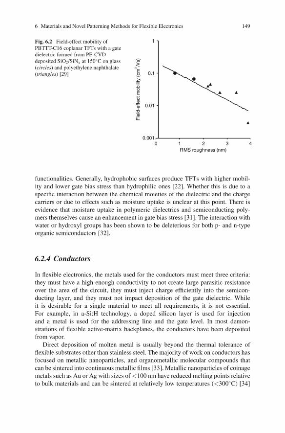
6 Materials and Novel Patterning Methods for Flexible Electronics 149
0.001
0.01
0.1
1
0 1 2 3 4RMS roughness (nm)
Fie
ld-e
ffect
mob
ility
(cm
2/V
s)
Fig. 6.2 Field-effect mobility ofPBTTT-C16 coplanar TFTs with a gatedielectric formed from PE-CVDdeposited SiO2/SiNx at 150◦C on glass(circles) and polyethylene naphthalate(triangles) [29]
functionalities. Generally, hydrophobic surfaces produce TFTs with higher mobil-ity and lower gate bias stress than hydrophilic ones [22]. Whether this is due to aspecific interaction between the chemical moieties of the dielectric and the chargecarriers or due to effects such as moisture uptake is unclear at this point. There isevidence that moisture uptake in polymeric dielectrics and semiconducting poly-mers themselves cause an enhancement in gate bias stress [31]. The interaction withwater or hydroxyl groups has been shown to be deleterious for both p- and n-typeorganic semiconductors [32].
6.2.4 Conductors
In flexible electronics, the metals used for the conductors must meet three criteria:they must have a high enough conductivity to not create large parasitic resistanceover the area of the circuit, they must inject charge efficiently into the semicon-ducting layer, and they must not impact deposition of the gate dielectric. Whileit is desirable for a single material to meet all requirements, it is not essential.For example, in a-Si:H technology, a doped silicon layer is used for injectionand a metal is used for the addressing line and the gate level. In most demon-strations of flexible active-matrix backplanes, the conductors have been depositedfrom vapor.
Direct deposition of molten metal is usually beyond the thermal tolerance offlexible substrates other than stainless steel. The majority of work on conductors hasfocused on metallic nanoparticles, and organometallic molecular compounds thatcan be sintered into continuous metallic films [33]. Metallic nanoparticles of coinagemetals such as Au or Ag with sizes of <100 nm have reduced melting points relativeto bulk materials and can be sintered at relatively low temperatures (<300◦C) [34]
150 W.S. Wong et al.
or optically with visible lasers [35]. Most nanoparticles are synthesized with anorganic surface layer to allow them to be suspended in a solvent without aggregation.While surface layers may be necessary to increase the stability of suspensions ofthese materials, they are likely to cause injection barriers when used as contacts.For example, contacts formed from silver nanoparticles stabilized with oleic acidappear to show less contact resistance with poly[5,5′-bis(3-dodecyl-2-thienyl)-2,2′-bithiophene] (PQT)-12 than those stabilized with oleylamine [36]. The origin of thisdifference could be a modification of the work function of the electrode by the layeror by doping of the semiconducting material near the contact.
Semiconducting polymers can form printable conductors when doped andform good contacts to organic semiconductors. Poly(3,4-ethylenedioxythiophene)poly(styrenesulfonate) (PEDOT/PSS) is a widely used printable conductor, butits conductivity is ∼104 times lower than most metals [37]. Composite filmsof polyaniline and single-wall carbon nanotubes have better conductivity thanPEDOT:PSS (2 S/cm), but still are significantly less conductive than a bulk metal.While organic materials may be used as local contacts, it is unlikely that theycan be used for the addressing lines in large-area circuits that require reasonableswitching speeds.
6.3 Print-Processing Options for Device Fabrication
6.3.1 Overview
Printing methods can be broadly classified as noncontact and contact methods. Mosthigh-volume printing, such as packaging, is performed using techniques such asgravure, offset, and flexographic marking where a roller contacts the substrate. Theroller may be flat with patterned ink transferred to it from another patterned substrateor the roller itself may have patterned depressions into which the ink is deposited. Inelectronics, microcontact printing has been demonstrated for patterning of conduc-tors using self-assembled monolayers as resists for chemical etching [38]. Chapter 5describes the use of imprint methods to fabricate inorganic circuits. Techniques suchas electrophotography have been used to print a resist used to fabricate a-Si:H TFTs[39]. We focus here on noncontact printing, in particular ink-jet printing.
Ink-jet printing has been used both to print etch masks for vapor-deposited mate-rials (digital lithography) and for direct deposition of active materials. In digitallithography, the main issues are control of the feature sizes of the printed etchmask and integration of the printing steps into a conventional fabrication process.For printing active materials, attention must be paid to how the material dries orcures into a solid film. In both cases, it is important to understand the fundamen-tal origins of the achievable feature sizes and the ability to control placement ofthose features.
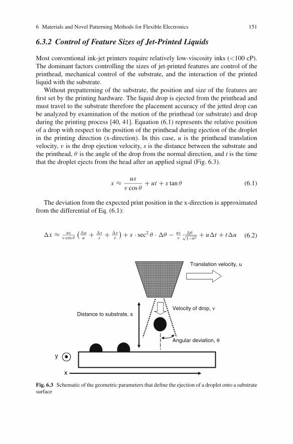
6 Materials and Novel Patterning Methods for Flexible Electronics 151
6.3.2 Control of Feature Sizes of Jet-Printed Liquids
Most conventional ink-jet printers require relatively low-viscosity inks (<100 cP).The dominant factors controlling the sizes of jet-printed features are control of theprinthead, mechanical control of the substrate, and the interaction of the printedliquid with the substrate.
Without prepatterning of the substrate, the position and size of the features arefirst set by the printing hardware. The liquid drop is ejected from the printhead andmust travel to the substrate therefore the placement accuracy of the jetted drop canbe analyzed by examination of the motion of the printhead (or substrate) and dropduring the printing process [40, 41]. Equation (6.1) represents the relative positionof a drop with respect to the position of the printhead during ejection of the dropletin the printing direction (x-direction). In this case, u is the printhead translationvelocity, ν is the drop ejection velocity, s is the distance between the substrate andthe printhead, θ is the angle of the drop from the normal direction, and t is the timethat the droplet ejects from the head after an applied signal (Fig. 6.3).
x ≈ us
ν cos θ+ ut + s tan θ (6.1)
The deviation from the expected print position in the x-direction is approximatedfrom the differential of Eq. (6.1):
Δx ≈ usν cos θ
(Δuu + Δs
s + Δνν
) + s · sec2 θ · Δθ − usv
Δθ√1−θ2
+ uΔt + tΔu (6.2)
Distance to substrate, sVelocity of drop, ν
Translation velocity, u
Angular deviation, θ
x
y
Fig. 6.3 Schematic of the geometric parameters that define the ejection of a droplet onto a substratesurface
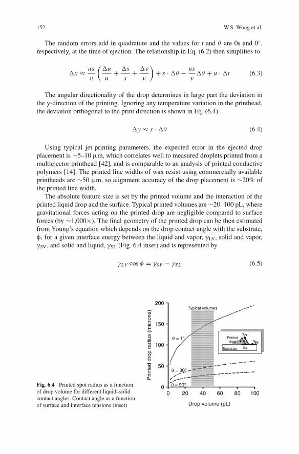
152 W.S. Wong et al.
The random errors add in quadrature and the values for t and θ are 0s and 0◦,respectively, at the time of ejection. The relationship in Eq. (6.2) then simplifies to
Δx ≈ us
v
(Δu
u+ Δs
s+ Δv
v
)+ s · Δθ − us
vΔθ + u · Δt (6.3)
The angular directionality of the drop determines in large part the deviation inthe y-direction of the printing. Ignoring any temperature variation in the printhead,the deviation orthogonal to the print direction is shown in Eq. (6.4).
Δy ≈ s · Δθ (6.4)
Using typical jet-printing parameters, the expected error in the ejected dropplacement is ∼5–10 μm, which correlates well to measured droplets printed from amultiejector printhead [42], and is comparable to an analysis of printed conductivepolymers [14]. The printed line widths of wax resist using commercially availableprintheads are ∼50 μm, so alignment accuracy of the drop placement is ∼20% ofthe printed line width.
The absolute feature size is set by the printed volume and the interaction of theprinted liquid drop and the surface. Typical printed volumes are ∼20–100 pL, wheregravitational forces acting on the printed drop are negligible compared to surfaceforces (by ∼1,000×). The final geometry of the printed drop can be then estimatedfrom Young’s equation which depends on the drop contact angle with the substrate,φ, for a given interface energy between the liquid and vapor, γLV, solid and vapor,γSV, and solid and liquid, γSL (Fig. 6.4 inset) and is represented by
γLV cosφ = γSV − γSL (6.5)
0
50
100
150
200
0 20 40 60 80 100
θ = 1°
θ = 30°
θ = 90°
Printed drop θ
γSL
γSV
γLV
substrate
Drop volume (pL)
Typical volumes
θγSL
γSV
γLV
substrate
Printed drop θ
γSL
γSV
γLV
Substrate
Prin
ted
drop
rad
ius
(mic
rons
)
Fig. 6.4 Printed spot radius as a functionof drop volume for different liquid–solidcontact angles. Contact angle as a functionof surface and interface tensions (inset)
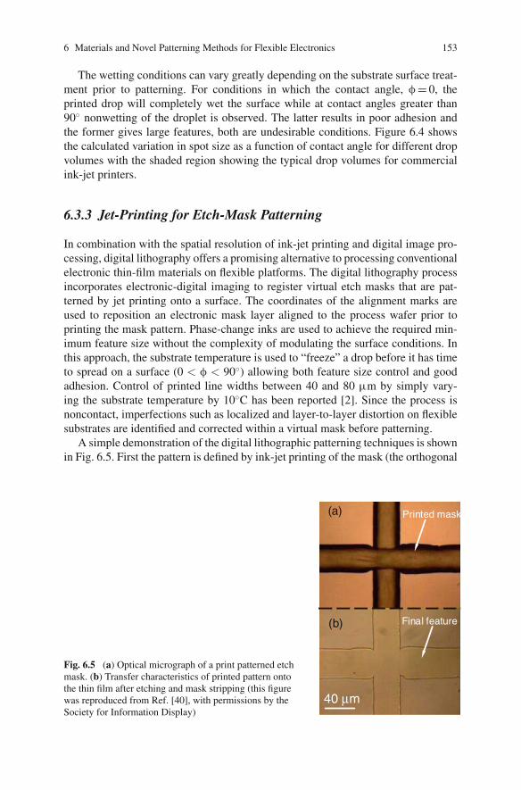
6 Materials and Novel Patterning Methods for Flexible Electronics 153
The wetting conditions can vary greatly depending on the substrate surface treat-ment prior to patterning. For conditions in which the contact angle, φ = 0, theprinted drop will completely wet the surface while at contact angles greater than90◦ nonwetting of the droplet is observed. The latter results in poor adhesion andthe former gives large features, both are undesirable conditions. Figure 6.4 showsthe calculated variation in spot size as a function of contact angle for different dropvolumes with the shaded region showing the typical drop volumes for commercialink-jet printers.
6.3.3 Jet-Printing for Etch-Mask Patterning
In combination with the spatial resolution of ink-jet printing and digital image pro-cessing, digital lithography offers a promising alternative to processing conventionalelectronic thin-film materials on flexible platforms. The digital lithography processincorporates electronic-digital imaging to register virtual etch masks that are pat-terned by jet printing onto a surface. The coordinates of the alignment marks areused to reposition an electronic mask layer aligned to the process wafer prior toprinting the mask pattern. Phase-change inks are used to achieve the required min-imum feature size without the complexity of modulating the surface conditions. Inthis approach, the substrate temperature is used to “freeze” a drop before it has timeto spread on a surface (0 < φ < 90◦) allowing both feature size control and goodadhesion. Control of printed line widths between 40 and 80 μm by simply vary-ing the substrate temperature by 10◦C has been reported [2]. Since the process isnoncontact, imperfections such as localized and layer-to-layer distortion on flexiblesubstrates are identified and corrected within a virtual mask before patterning.
A simple demonstration of the digital lithographic patterning techniques is shownin Fig. 6.5. First the pattern is defined by ink-jet printing of the mask (the orthogonal
printed mask
final feature
40 μm
(a)
(b)
Printed mask
Final feature
40 μm
(a)
(b)
Fig. 6.5 (a) Optical micrograph of a print patterned etchmask. (b) Transfer characteristics of printed pattern ontothe thin film after etching and mask stripping (this figurewas reproduced from Ref. [40], with permissions by theSociety for Information Display)
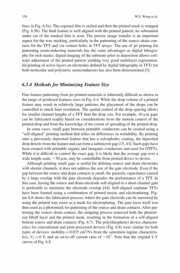
154 W.S. Wong et al.
lines in Fig. 6.5a). The exposed film is etched and then the printed mask is stripped(Fig. 6.5b). The final feature is well aligned with the printed pattern; no substantialunder cut of the masked film is seen. The precise image transfer is an importantaspect for the wax masking, particularly in the patterning of the source–drain con-tacts for the TFT and via contact holes in TFT arrays. The use of jet printing forpatterning semiconducting materials has the same advantages as digital lithogra-phy for etch masks; digital imaging of the substrate prior to deposition allows soft-ware adjustment of the printed pattern yielding very good multilayer registration.Jet printing of active layers on electrodes defined by digital lithography in TFTs forboth molecular and polymeric semiconductors has also been demonstrated [5].
6.3.4 Methods for Minimizing Feature Size
Fine feature patterning from jet-printed materials is inherently difficult as shown inthe range of predicted features sizes in Fig. 6.4. While the drop volume of a printedfeature may result in relatively large patterns, the placement of the drops can becontrolled to much finer resolution. The spatial control of the drop spacing allowsfor smaller channel lengths of a TFT than the drop size. For example, 10 μm gapscan be fabricated readily based on considerations from the motion control of theprinted drop and from the knowledge of the extent of spreading of the printed drop.
In some cases, small gaps between printable conductors can be created using a“self-aligned” printing method that relies on differences in wettability. By printingonto a previously deposited feature that has a solvophobic coating, the depositeddrop dewets from the feature and can form a submicron gap [15, 43]. Such gaps havebeen created with printable organic and inorganic conductors and used for OTFTs.While it is difficult to control the exact gap, it is likely that the average gap over awide length scale, ∼50 μm, may be controllable from printed device to device.
Although printing small gaps is useful for defining source and drain electrodeswith shorter channels, it does not address the size of the gate electrode. Even if thegap between the source and drain contacts is small, the parasitic capacitance causedby a large overlap with the gate electrode degrades the performance of a TFT. Inthis case, having the source and drain electrode self-aligned to a short-channel gateis preferable to minimize the electrode overlap [44]. Self-aligned coplanar TFTshave been formed using a combination of printed resists and electroplating. Fig-ure 6.6 shows the fabrication process, where the gate electrode can be narrowed byusing the printed wax resist as a mask for electroplating. The gate layer itself wasthen used as a photomask for patterning of the source and drain contacts. After pat-terning the source–drain contact, the stripping process removed both the photore-sist liftoff layer and the printed mask, resulting in the formation of a self-alignedbottom source and drain contacts (Fig. 6.7). The poly(thiophene) device character-istics for conventional and print processed devices (Fig. 6.8) were similar for bothtypes of devices: mobility = 0.035 cm2/Vs from the saturation regime characteris-tics, VT = 0 V, and an on-to-off current ratio of ∼107. Note that the original I–Vcurves of Fig. 6.8
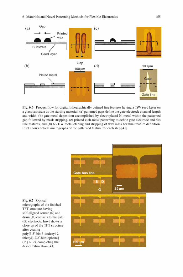
6 Materials and Novel Patterning Methods for Flexible Electronics 155
Gap
Printedwax
substratesubstrate
100 μm100 μm
substrate
Seed layer
(c)
Gap
Gate
Gate line
Substrate
Plated metal
(a)
(b) (d)
Fig. 6.6 Process flow for digital lithographically defined fine features having a TiW seed layer ona glass substrate as the starting material: (a) patterned gaps define the gate electrode channel lengthand width, (b) gate metal deposition accomplished by electroplated Ni metal within the patternedgap followed by mask stripping, (c) printed etch-mask patterning to define gate electrode and busline features, and (d) Ni/TiW metal etching and stripping of wax mask for final feature definition.Inset shows optical micrographs of the patterned feature for each step [41]
Gate bus line
G
S D
100 μm
25 μm
Fig. 6.7 Opticalmicrographs of the finishedTFT structure havingself-aligned source (S) anddrain (D) contacts to the gate(G) electrode. Inset shows aclose up of the TFT structureafter coatingpoly[5,5′-bis(3-dodecyl-2-thienyl)-2,2′-bithiophene](PQT-12), completing thedevice fabrication [41]
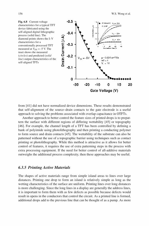
156 W.S. Wong et al.
Fig. 6.8 Current-voltagecharacteristics for a typical TFTdevice fabricated using theself-aligned digital lithographicprocess (solid line). Thediamond points shows the I–Vcharacteristics for aconventionally processed TFTmeasured at VDS = -5 V. Theinset shows the measured(circles) and predicted (solidline) output characteristics of theself-aligned TFTs
from [41] did not have normalized device dimensions. These results demonstratedthat self-alignment of the source–drain contacts to the gate electrode is a usefulapproach to solving the problems associated with overlap capacitance in OTFTs.
Another approach to better control the feature sizes of printed drops is to prepat-tern the surface with different regions of differing wettability [45] or topography[46]. For example, the channel length of a TFT has been controlled by defining abank of polyimide using photolithography and then printing a conducting polymerto form source and drain contacts [45]. The wettability of the substrate can also bepatterned without the use of a topographic barrier using techniques such as contactprinting or photolithography. While this method is attractive as it allows for bettercontrol of features, it requires the use of extra patterning steps in the process withextra processing equipment. If the need for better control of all-additive materialsoutweighs the additional process complexity, then these approaches may be useful.
6.3.5 Printing Active Materials
The shapes of active materials range from simple island areas to lines over largedistances. Printing one drop to form an island is relatively simple as long as thewetting characteristics of the surface are uniform. Printing lines over long distancesis more challenging. Since the long lines in a display are generally the address lines,it is important to form them with as few defects as possible because defects wouldresult in opens in the conductors that control the circuit. As a printed line is formed,additional drops add to the previous line that can be thought of as a pump. As more
6 Materials and Novel Patterning Methods for Flexible Electronics 157
drops are added to the printed liquid line, instabilities, such as necks, may form dueto the dynamics of the spreading and drying of the printed liquid line. The mech-anism of formation of instabilities in printed liquid lines is complex and has beenanalyzed in detail [47, 48]. To achieve control of printed lines, one must optimizethe printing speed and the wetting characteristics of the printed liquid.
The majority of high-performance organic semiconductors are soluble in polar,low-viscosity, and low-surface energy solvents. Controlling the spreading of theseliquids on surfaces when deposited as drops is difficult without physical barriers.Importantly, the surface energy of the gate dielectric in an OTFT cannot be arbi-trarily chosen as most solution-processable organic semiconductors perform best ondielectrics with hydrophobic surfaces. While such low-surface energies can in prin-ciple decrease the size of printed features, the semiconducting solution is frequentlyprinted on a surface with spatially heterogeneous surfaces. In a coplanar TFT, thecontact electrodes will generally be of higher surface energy than the channel caus-ing a printed liquid droplet to dewet from the channel onto the contacts. While it ispossible to print contacts on the surface of the semiconductor after it is deposited,control of the feature size of printed metals will be limited since it is currentlydifficult to arbitrarily change the wetting characteristics of the surface of organicsemiconductors.
The drying time of the printed liquid impacts the performance of solution-processable semiconductors. It has been shown that the drying conditions of spin-coated films can lead to changes in performance of factors of 10, even on the samesurface [49, 50]. Although the drying conditions of printed drops and spin-coatedfilms are quite different due to the volume of solution, both printed and spin-coatedfilms of semiconducting polymers have been demonstrated to have similar perfor-mance when deposited from a high boiling point solvent. While there are no detailedstudies of the morphology and microstructure of films of semiconducting polymersdeposited by jet printing, the electrical characteristics of the TFTs suggest that thematerial can self-organize during the drying time of the printed drop.
6.4 Performance and Characterization of Electronic Devices
6.4.1 Overview
Being able to fabricate single devices with the appropriate performance is only afirst step toward the use of TFTs in electronic circuits where tens or hundreds ofdevices are integrated. Circuit designers rely heavily on device stability, reliability,and uniformity across the substrate and correct size scaling to design properly func-tioning systems. Therefore, all nonideal behavior in TFTs must be well understoodin order to realistically design systems comprising multiple devices.
The deposition conditions available for flexible circuits are substantially differentthan those for conventional devices. In particular, the temperatures that can be usedare substantially lower than those for devices on glass substrates. Because of this
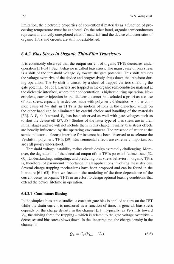
158 W.S. Wong et al.
limitation, the electronic properties of conventional materials as a function of pro-cessing temperature must be explored. On the other hand, organic semiconductorsrepresent a relatively unexplored class of materials and the device characteristics oforganic TFTs and circuits are still not established.
6.4.2 Bias Stress in Organic Thin-Film Transistors
It is commonly observed that the output current of organic TFTs decreases underoperation [51–54]. Such behavior is called bias stress. The main cause of bias stressis a shift of the threshold voltage VT toward the gate potential. This shift reducesthe voltage overdrive of the device and progressively shuts down the transistor dur-ing operation. The VT shift is caused by a sheet of trapped carriers shielding thegate potential [51, 55]. Carriers are trapped in the organic semiconductor material atthe dielectric interface, where their concentration is highest during operation. Nev-ertheless, carrier injection in the dielectric cannot be excluded a priori as a causeof bias stress, especially in devices made with polymeric dielectrics. Another com-mon cause of VT shift in TFTs is the motion of ions in the dielectric, which onthe other hand can be eliminated by careful choice and handling of the materials[56]. A VT shift toward VG has been observed as well with gate voltages such asto shut the device off [57, 58]. Studies of the latter type of bias stress are in theirinitial stages and we will not include them in this chapter. Finally, bias stress effectsare heavily influenced by the operating environment. The presence of water at thesemiconductor–dielectric interface for instance has been observed to accelerate theVT shift in polymeric TFTs [59]. Environmental effects are extremely important butare still poorly understood.
Threshold voltage instability makes circuit design extremely challenging. More-over, the degradation of the electrical output of the TFTs poses a lifetime issue [52,60]. Understanding, mitigating, and predicting bias stress behavior in organic TFTsis, therefore, of paramount importance in all applications involving these devices.Several charge trapping mechanisms have been proposed and can be found in theliterature [61–63]. Here we focus on the modeling of the time dependence of thecurrent decay in organic TFTs in an effort to design optimal biasing conditions thatextend the device lifetime in operation.
6.4.2.1 Continuous Biasing
In the simplest bias stress studies, a constant gate bias is applied to turn-on the TFTwhile the drain current is measured as a function of time. In general, bias stressdepends on the charge density in the channel [51]. Typically, as VT shifts towardVG, the driving force for trapping – which is related to the gate voltage overdrive –decreases and bias stress slows down. In the linear regime, the charge density in thechannel is
QC = C0 (VGS − VT ) (6.6)
6 Materials and Novel Patterning Methods for Flexible Electronics 159
where C0 is the gate capacitance per unit area VT is the threshold voltage and VGS
is the gate-to-source potential, which in the linear regime is approximately equal toVGD, the gate-to-drain potential. When the transistor is not in the linear regime, VGS
is different from VGD, charge density varies along the channel and its average valueis [64]:
QC = 2
3C0
(VGS − VT )3 − (VG D − VT )3
(VGS − VT )2 − (VG D − VT )2 (6.7)
In a-Si:H, the shape of the current decay curves does not depend on whether theTFT operates in the linear regime or in the saturation regime. The average chargedensity, calculated with Eq. (6.6) or Eq. (6.7) is merely a scaling factor. Never-theless, Eqs. (6.6) and (6.7) indicate that the interpretation of the data is easierwhen the device operates in the linear regime, where the charge density is approx-imately constant along the channel. Thus, bias stress data are often measured with|VSD|<<|VGS|.
Several bias stress mechanisms have been proposed, including bipolaron forma-tion in the semiconductor [61], injection in the dielectric [57], and deep trappingat defects in the semiconductor [65]. More than one of these mechanisms may besimultaneously active. In the absence of a firmly established bias stress mechanism,the VT shift laws are purely phenomenological. Thus, different time-dependencelaws have been proposed for bias stress of organic TFTs under continuous gate biasdepending on experimental conditions and materials combinations. For instance, inanalogy to bias stress in a-Si:H, a stretched exponential law was recently proposed[66]. In this model, the VT shift is attributed to the creation of trap states by the gatebias. The threshold voltage has the following time dependence
VT (t) = V 0T + (
VGS − V 0T
) ×{
1 − exp
[−
(t
τ
)β]}(6.8)
where V 0T is the initial threshold voltage, τ is the effective trapping time, and β is a
constant related to the activation energy distribution of the localized states createdby the gate bias. Bias stress in sexithiophene was found to obey Eq. (6.8), up toa stressing time of 10,000 s [67]. At longer stressing times, deviations from thestretched exponential law were observed and the stress data were better representedby a stretched hyperbola [68]
VT (t) = V 0T + (
VGS − V 0T
) ×{
1 −[
exp
(β
Eth − E A
kT
)+ 1
] 11−α
}(6.9)
where Eth is the thermalization energy: Eth = kT ln (νt) (ν is an attempt-to-escapefrequency for trapped charge); EA is the mean activation energy for trap creationand α is a fitting parameter. The models that give rise to bias stress laws such asthose expressed by Eqs. (6.8) and (6.9) assume that the gate bias creates localizedelectronic states in the semiconductor [69]. In organic TFTs, however, there is no
160 W.S. Wong et al.
evidence that the VT shift is due to the creation of new states rather than slow trap-ping in already existing deep states, thus the application of these equations is some-what unjustified.
A physical rationalization for the use of a stretched exponential law may be foundby adapting a lifetime model successfully applied to OLEDs. A degradation law thatclosely approximates the experimentally observed stretched exponential degrada-tion in OLEDs is obtained by assuming that the activation energy of the degradationprocess increases as a function of time [70]. Thus, an analogy with the OLED modelcan be drawn by postulating that trapping in organic TFTs is an activated processwhose activation energy increases as the threshold voltage shifts. As a result, the VT
shift rate decreases as the amount of free charge decreases, in agreement with theobservation that the bias stress rate decreases as total stress increases. In OLEDs,these assumptions lead to a differential equation whose numerical solution closelyapproximates a stretched exponential. It should be noted that while this model mayprovide a physical justification for the stretched exponential law, it has not beenadapted to TFTs yet. Finally, Powell et al. have shown that in certain experimentalconditions, the stretched exponential law observed in a-Si:H reduces to a power law[71]:
ΔVT = A |VG − VT |n tγ (6.10)
VT shifts that follow a power law have indeed been observed in pentacene underconstant biasing with γ ∼ 0.05 and n ∼ 0.75 [57].
In practical applications, it is very unlikely that organic TFTs will be operatedunder a continuous gate bias. Yet, all the decay laws proposed in the literatureexpress ΔVT explicitly as a function of time rather than of the operational param-eters of the transistor (e.g., gate voltage overdrive). The bias stress laws derivedunder continuous bias may provide insight into trapping mechanisms. They cannot,however, be used to predict quantitatively the behavior of devices that are cycledbetween their on and off states.
6.4.2.2 Pulsed Biasing
Relatively, few studies have been conducted with a pulsed gate bias in order toestimate the lifetime of TFTs under realistic operating conditions. A fundamen-tal difference between bias stress in organic TFTs and bias stress in other disor-dered materials, such as a-Si:H, is that charge trapped in organic semiconductors ispartially released when the gate is turned off [52, 60]. As a result, VT shifts backtoward its original value during the off-time of a pulsed biasing cycle. This effect isextremely important in TFTs used in active-matrix displays as these devices spendmost of their duty-cycle in the off-state. The recovery rate depends on trap depthand release activation energy. It was found that the average activation energy was∼0.8–1 eV, placing these traps probably deep in the middle of the polymericbandgap [65]. As a result of the interplay between stress and recovery, and because
6 Materials and Novel Patterning Methods for Flexible Electronics 161
none of these processes are linear with time, the VT shift of an organic transistordepends on both the pulse length and the duty-cycle.
Using very general assumptions, one can show that eventually the transistor willstabilize at a unique VT value that depends only on the operating conditions. Physi-cally, trapping is an equilibrium between free charge and trapped charge. Therefore,the instantaneous trapping rate is a function of the free charge Qf and the trappedcharge Qt. We define the trapping rate T as:
T[Q f , Qt
] = d Qt
dt(6.11)
T is therefore positive during gate biasing. Moreover, T is experimentallyobserved to decrease monotonically as Qt increases (i.e., bias stress slows downas the device is stressed for a longer time). The release of trapped charge on theother hand depends only on Qt because there is no free charge when the transis-tor is turned off. The instantaneous release rate R is negative and its absolute valuedecreases as Qt decreases. At steady state, the exact amount of charge trapped duringthe on-cycle is released during the off-cycle:
∫On
T[Q f , Qt
]dt = −
∫O f f
R [Qt ]dt (6.12)
If there were two possible device states defined by different trapped charge den-sities Q(1)
t and Q(2)t that satisfied Eq. (6.12) for the same operating conditions, we
would have:∫
On
{T
[Q(1)
f , Q(1)t
]− T
[Q(2)
f , Q(2)t
]}dt = −
∫O f f
{R
[Q(1)
t
]− R
[Q(2)
t
]}dt
(6.13)
If Q(1)t > Q(2)
t , the left-hand side of Eq. (6.13) is negative but the right-handside is positive. We conclude that Q(1)
t = Q(2)t and that the steady-state condition
is reached at a single value of Qt. Therefore, an organic TFT will always reachthe same steady-state VT for a given pulsed operating condition regardless of itsinitial conditions. This prediction was recently confirmed in polythiophene TFTs.Three different polythiophene devices started at different levels of VT shift at thebeginning of the stress cycle but stabilized at the same VT shift after ∼1 day ofpulsed gate biasing at a 0.5% duty-cycle [60]. The stabilization kinetics dependson the details of the biasing conditions. At low duty-cycles (<2%) the VT shift inpolythiophenes prior to stabilization exhibits a power-law dependence on stress time(i.e., gate on-time), similar to the one expressed in Eq. (6.10). Here the exponent nwas found to vary between 2 and 4 and γ varied between 0.35 and 0.40. Because γ<1, it takes a long time for the transistor to reach the stabilized VT, especially at thelow duty-cycles encountered in many applications of interest to organic TFTs. For
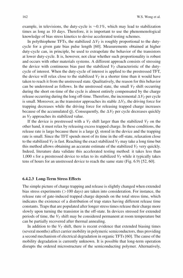
162 W.S. Wong et al.
example, in televisions, the duty-cycle is ∼0.1%, which may lead to stabilizationtimes as long as 10 days. Therefore, it is important to use the phenomenologicalknowledge of bias stress kinetics to devise accelerated testing schemes.
In polythiophene TFTs, the stabilized ΔVT is roughly proportional to the duty-cycle for a given gate bias pulse length [60]. Measurements obtained at higherduty-cycle can, in principle, be used to extrapolate the behavior of the transistorsat lower duty-cycle. It is, however, not clear whether such proportionality is robustand occurs with other materials systems. A different approach consists of stressingthe device with continuous bias past the stabilized VT characteristic of the duty-cycle of interest. When the duty-cycle of interest is applied to the prestressed TFT,the device will relax close to the stabilized VT in a shorter time than it would havetaken to reach it from the unstressed state. Qualitatively, the reason for this behaviorcan be understood as follows. In the unstressed state, the small VT shift occurringduring the short on-time of the cycle is almost entirely compensated by the chargerelease occurring during the long off-time. Therefore, the incremental ΔVT per cycleis small. Moreover, as the transistor approaches its stable ΔVT, the driving force fortrapping decreases while the driving force for releasing trapped charge increasesbecause of the accumulated Qt. Consequently, the ΔVT per cycle decreases quicklyas VT approaches its stabilized value.
If the device is prestressed with a VT shift larger than the stabilized VT on theother hand, it must relax by releasing excess trapped charge. In these conditions, therelease rate is large because there is a large Qt stored in the device and the trappingrate is small. Since the TFT spends most of its time in the off-state, relaxation closeto the stabilized VT is fast. Reaching the exact stabilized VT may take a long time butthis method allows obtaining an accurate estimate of the stabilized VT very quickly.Indeed, literature data validate this accelerated testing method: it takes less than1,000 s for a prestressed device to relax to its stabilized VT while it typically takestens of hours for an unstressed device to reach the same state (Fig. 6.9) [52, 60].
6.4.2.3 Long-Term Stress Effects
The simple picture of charge trapping and release is slightly changed when extendedbias stress experiments (>100 days) are taken into consideration. For instance, therelease rate of gate-induced trapped charge depends on the total stress time, whichindicates the existence of a distribution of trap states having different release timeconstants. Traps that are populated after longer stress times release their charge moreslowly upon turning the transistor in the off-state. In devices stressed for extendedperiods of time, the VT shift may be considered permanent at room temperature butcan be partially recovered after thermal annealing.
In addition to the VT shift, there is recent evidence that extended biasing times(several months) affect carrier mobility in polymeric semiconductors, thus providinga second mechanism of electrical degradation in organic TFTs [60]. The cause of themobility degradation is currently unknown. It is possible that long-term operationdisrupts the ordered microstructure of the semiconducting polymer. Alternatively,
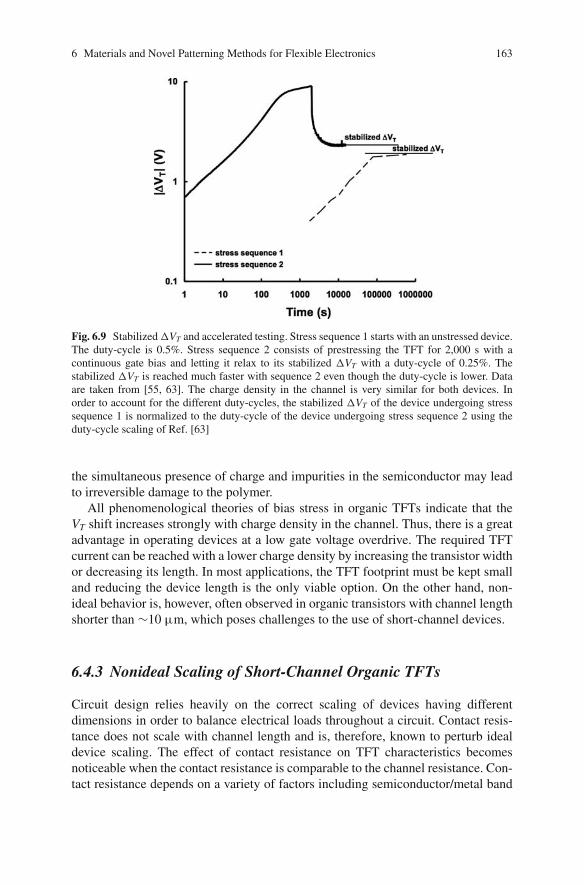
6 Materials and Novel Patterning Methods for Flexible Electronics 163
Fig. 6.9 Stabilized ΔVT and accelerated testing. Stress sequence 1 starts with an unstressed device.The duty-cycle is 0.5%. Stress sequence 2 consists of prestressing the TFT for 2,000 s with acontinuous gate bias and letting it relax to its stabilized ΔVT with a duty-cycle of 0.25%. Thestabilized ΔVT is reached much faster with sequence 2 even though the duty-cycle is lower. Dataare taken from [55, 63]. The charge density in the channel is very similar for both devices. Inorder to account for the different duty-cycles, the stabilized ΔVT of the device undergoing stresssequence 1 is normalized to the duty-cycle of the device undergoing stress sequence 2 using theduty-cycle scaling of Ref. [63]
the simultaneous presence of charge and impurities in the semiconductor may leadto irreversible damage to the polymer.
All phenomenological theories of bias stress in organic TFTs indicate that theVT shift increases strongly with charge density in the channel. Thus, there is a greatadvantage in operating devices at a low gate voltage overdrive. The required TFTcurrent can be reached with a lower charge density by increasing the transistor widthor decreasing its length. In most applications, the TFT footprint must be kept smalland reducing the device length is the only viable option. On the other hand, non-ideal behavior is, however, often observed in organic transistors with channel lengthshorter than ∼10 μm, which poses challenges to the use of short-channel devices.
6.4.3 Nonideal Scaling of Short-Channel Organic TFTs
Circuit design relies heavily on the correct scaling of devices having differentdimensions in order to balance electrical loads throughout a circuit. Contact resis-tance does not scale with channel length and is, therefore, known to perturb idealdevice scaling. The effect of contact resistance on TFT characteristics becomesnoticeable when the contact resistance is comparable to the channel resistance. Con-tact resistance depends on a variety of factors including semiconductor/metal band
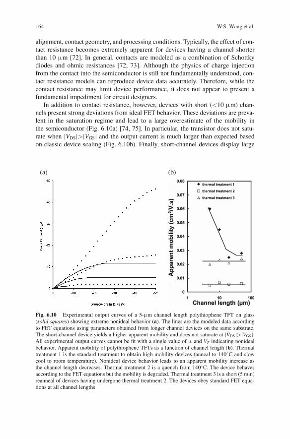
164 W.S. Wong et al.
alignment, contact geometry, and processing conditions. Typically, the effect of con-tact resistance becomes extremely apparent for devices having a channel shorterthan 10 μm [72]. In general, contacts are modeled as a combination of Schottkydiodes and ohmic resistances [72, 73]. Although the physics of charge injectionfrom the contact into the semiconductor is still not fundamentally understood, con-tact resistance models can reproduce device data accurately. Therefore, while thecontact resistance may limit device performance, it does not appear to present afundamental impediment for circuit designers.
In addition to contact resistance, however, devices with short (<10 μm) chan-nels present strong deviations from ideal FET behavior. These deviations are preva-lent in the saturation regime and lead to a large overestimate of the mobility inthe semiconductor (Fig. 6.10a) [74, 75]. In particular, the transistor does not satu-rate when |VDS|>|VGS| and the output current is much larger than expected basedon classic device scaling (Fig. 6.10b). Finally, short-channel devices display large
(a) (b)
Fig. 6.10 Experimental output curves of a 5-μm channel length polythiophene TFT on glass(solid squares) showing extreme nonideal behavior (a). The lines are the modeled data accordingto FET equations using parameters obtained from longer channel devices on the same substrate.The short-channel device yields a higher apparent mobility and does not saturate at |VDS|>|VGS|.All experimental output curves cannot be fit with a single value of μ and VT indicating nonidealbehavior. Apparent mobility of polythiophene TFTs as a function of channel length (b). Thermaltreatment 1 is the standard treatment to obtain high mobility devices (anneal to 140◦C and slowcool to room temperature). Nonideal device behavior leads to an apparent mobility increase asthe channel length decreases. Thermal treatment 2 is a quench from 140◦C. The device behavesaccording to the FET equations but the mobility is degraded. Thermal treatment 3 is a short (5 min)reanneal of devices having undergone thermal treatment 2. The devices obey standard FET equa-tions at all channel lengths
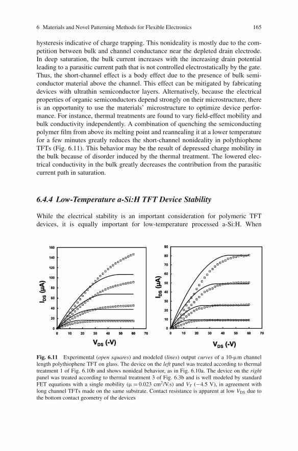
6 Materials and Novel Patterning Methods for Flexible Electronics 165
hysteresis indicative of charge trapping. This nonideality is mostly due to the com-petition between bulk and channel conductance near the depleted drain electrode.In deep saturation, the bulk current increases with the increasing drain potentialleading to a parasitic current path that is not controlled electrostatically by the gate.Thus, the short-channel effect is a body effect due to the presence of bulk semi-conductor material above the channel. This effect can be mitigated by fabricatingdevices with ultrathin semiconductor layers. Alternatively, because the electricalproperties of organic semiconductors depend strongly on their microstructure, thereis an opportunity to use the materials’ microstructure to optimize device perfor-mance. For instance, thermal treatments are found to vary field-effect mobility andbulk conductivity independently. A combination of quenching the semiconductingpolymer film from above its melting point and reannealing it at a lower temperaturefor a few minutes greatly reduces the short-channel nonideality in polythiopheneTFTs (Fig. 6.11). This behavior may be the result of depressed charge mobility inthe bulk because of disorder induced by the thermal treatment. The lowered elec-trical conductivity in the bulk greatly decreases the contribution from the parasiticcurrent path in saturation.
6.4.4 Low-Temperature a-Si:H TFT Device Stability
While the electrical stability is an important consideration for polymeric TFTdevices, it is equally important for low-temperature processed a-Si:H. When
Fig. 6.11 Experimental (open squares) and modeled (lines) output curves of a 10-μm channellength polythiophene TFT on glass. The device on the left panel was treated according to thermaltreatment 1 of Fig. 6.10b and shows nonideal behavior, as in Fig. 6.10a. The device on the rightpanel was treated according to thermal treatment 3 of Fig. 6.3b and is well modeled by standardFET equations with a single mobility (μ = 0.023 cm2/V.s) and VT (−4.5 V), in agreement withlong channel TFTs made on the same substrate. Contact resistance is apparent at low VDS due tothe bottom contact geometry of the devices
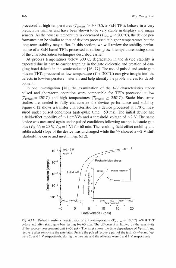
166 W.S. Wong et al.
processed at high temperatures (Tprocess > 300◦C), a-Si:H TFTs behave in a verypredictable manner and have been shown to be very stable in displays and imagesensors. As the process temperature is decreased (Tprocess < 200◦C), the device per-formance can be similar to that of devices processed at higher temperatures but thelong-term stability may suffer. In this section, we will review the stability perfor-mance of a-Si:H-based TFTs processed at various growth temperatures using someof the characterization techniques described earlier.
At process temperatures below 300◦C, degradation in the device stability isexpected due in part to carrier trapping in the gate dielectric and creation of dan-gling bond defects in the semiconductor [76, 77]. The use of pulsed and static gatebias on TFTs processed at low temperature (T < 200◦C) can give insight into thedefects in low-temperature materials and help identify the problem areas for devel-opment.
In one investigation [78], the examination of the I–V characteristics underpulsed and short-term operation were comparable for TFTs processed at low(Tprocess = 120◦C) and high temperatures (Tprocess ≥ 250◦C). Static bias stressstudies are needed to fully characterize the device performance and stability.Figure 6.12 shows a transfer characteristic for a device processed at 170◦C mea-sured under pulsed conditions (gate-pulse time = 50 ms). The initial device hada field-effect mobility of ∼1 cm2/Vs and a threshold voltage of ∼2 V. The samedevice was measured again under pulsed conditions following an applied static gatebias (VG–VT = 20 V, VDS = 1 V) for 60 min. The resulting field-effect mobility andsubthreshold slope of the device was unchanged while the VT showed a ∼2 V shift(dashed-line curve and inset in Fig. 6.12).
0 2500 5000 7500 100002
3
4
5
6Pulsed recoverydc bias
Thr
esho
ld v
olta
ge (
Vol
ts)
Time (seconds)
–5 0 5 10 15 20
10–10
10–9
10–8
10–7
10–6 W/L ~ 3.5VDS = 1V
Postgate bias stress
Initial I–V
Dra
in c
urre
nt (
Am
ps)
Gate voltage (Volts)
Fig. 6.12 Pulsed transfer characteristics of a low-temperature (Tprocess = 170◦C) a-Si:H TFTbefore and after static gate bias testing for 60 min. The off-current is limited by the sensitivityof the source-measurement unit (∼50 pA). The inset shows the time dependence of VT shift andrecovery after removing the gate bias. During the pulsed recovery part of the test, VG−VT and VDS
were 20 and 1 V, respectively, during the on-state and the off-state were 0 and 1 V, respectively
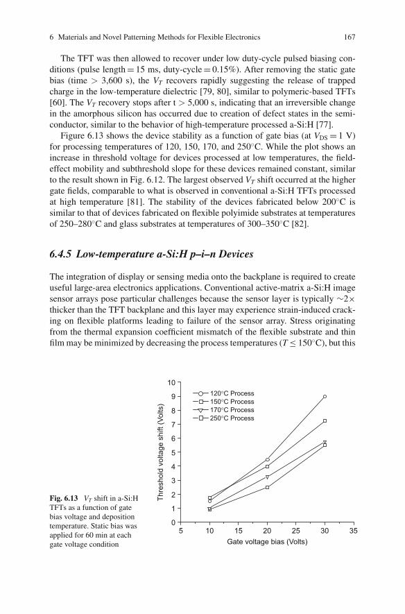
6 Materials and Novel Patterning Methods for Flexible Electronics 167
The TFT was then allowed to recover under low duty-cycle pulsed biasing con-ditions (pulse length = 15 ms, duty-cycle = 0.15%). After removing the static gatebias (time > 3,600 s), the VT recovers rapidly suggesting the release of trappedcharge in the low-temperature dielectric [79, 80], similar to polymeric-based TFTs[60]. The VT recovery stops after t > 5,000 s, indicating that an irreversible changein the amorphous silicon has occurred due to creation of defect states in the semi-conductor, similar to the behavior of high-temperature processed a-Si:H [77].
Figure 6.13 shows the device stability as a function of gate bias (at VDS = 1 V)for processing temperatures of 120, 150, 170, and 250◦C. While the plot shows anincrease in threshold voltage for devices processed at low temperatures, the field-effect mobility and subthreshold slope for these devices remained constant, similarto the result shown in Fig. 6.12. The largest observed VT shift occurred at the highergate fields, comparable to what is observed in conventional a-Si:H TFTs processedat high temperature [81]. The stability of the devices fabricated below 200◦C issimilar to that of devices fabricated on flexible polyimide substrates at temperaturesof 250–280◦C and glass substrates at temperatures of 300–350◦C [82].
6.4.5 Low-temperature a-Si:H p–i–n Devices
The integration of display or sensing media onto the backplane is required to createuseful large-area electronics applications. Conventional active-matrix a-Si:H imagesensor arrays pose particular challenges because the sensor layer is typically ∼2×thicker than the TFT backplane and this layer may experience strain-induced crack-ing on flexible platforms leading to failure of the sensor array. Stress originatingfrom the thermal expansion coefficient mismatch of the flexible substrate and thinfilm may be minimized by decreasing the process temperatures (T ≤ 150◦C), but this
5 10 15 20 25 30 350
1
2
3
4
5
6
7
8
9
10 120°C Process 150°C Process 170°C Process 250°C Process
Thre
shol
d vo
ltage
shi
ft (V
olts
)
Gate voltage bias (Volts)
Fig. 6.13 VT shift in a-Si:HTFTs as a function of gatebias voltage and depositiontemperature. Static bias wasapplied for 60 min at eachgate voltage condition
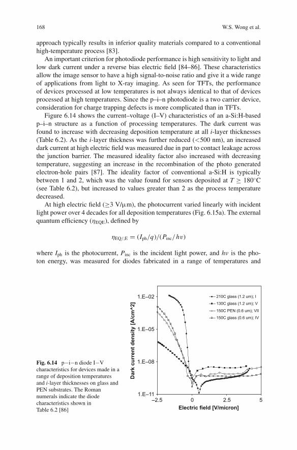
168 W.S. Wong et al.
approach typically results in inferior quality materials compared to a conventionalhigh-temperature process [83].
An important criterion for photodiode performance is high sensitivity to light andlow dark current under a reverse bias electric field [84–86]. These characteristicsallow the image sensor to have a high signal-to-noise ratio and give it a wide rangeof applications from light to X-ray imaging. As seen for TFTs, the performanceof devices processed at low temperatures is not always identical to that of devicesprocessed at high temperatures. Since the p–i–n photodiode is a two carrier device,consideration for charge trapping defects is more complicated than in TFTs.
Figure 6.14 shows the current–voltage (I–V) characteristics of an a-Si:H-basedp–i–n structure as a function of processing temperatures. The dark current wasfound to increase with decreasing deposition temperature at all i-layer thicknesses(Table 6.2). As the i-layer thickness was further reduced (<500 nm), an increaseddark current at high electric field was measured due in part to contact leakage acrossthe junction barrier. The measured ideality factor also increased with decreasingtemperature, suggesting an increase in the recombination of the photo generatedelectron-hole pairs [87]. The ideality factor of conventional a-Si:H is typicallybetween 1 and 2, which was the value found for sensors deposited at T ≥ 180◦C(see Table 6.2), but increased to values greater than 2 as the process temperaturedecreased.
At high electric field (≥3 V/μm), the photocurrent varied linearly with incidentlight power over 4 decades for all deposition temperatures (Fig. 6.15a). The externalquantum efficiency (ηEQE), defined by
ηEQ/;E = (Iph/q)/(Pinc/hv)
where Iph is the photocurrent, Pinc is the incident light power, and hν is the pho-ton energy, was measured for diodes fabricated in a range of temperatures and
1.E–11
1.E–08
1.E–05
1.E–02
–2.5 0 2.5 5Electric field [V/micron]
Dar
k cu
rren
t den
sity
[A/c
m^2
]
210C glass (1.2 um); I
130C glass (1.2 um); V
150C PEN (0.6 um); VII
150C glass (0.6 um); IV
Fig. 6.14 p−i−n diode I−Vcharacteristics for devices made in arange of deposition temperaturesand i-layer thicknesses on glass andPEN substrates. The Romannumerals indicate the diodecharacteristics shown inTable 6.2 [86]
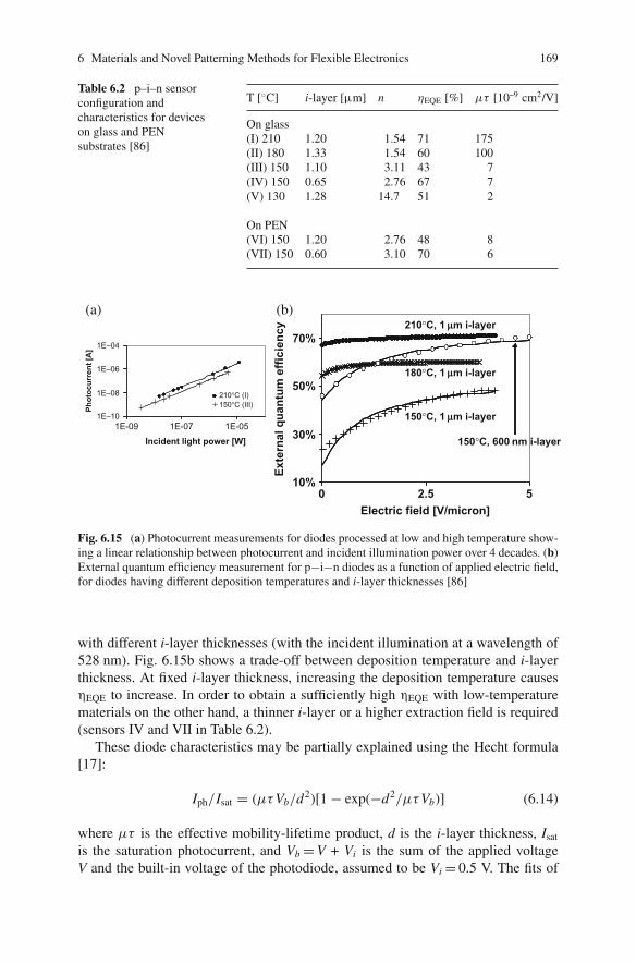
6 Materials and Novel Patterning Methods for Flexible Electronics 169
Table 6.2 p–i–n sensorconfiguration andcharacteristics for deviceson glass and PENsubstrates [86]
T [◦C] i-layer [μm] n ηEQE [%] μτ [10–9 cm2/V]
On glass(I) 210 1.20 1.54 71 175(II) 180 1.33 1.54 60 100(III) 150 1.10 3.11 43 7(IV) 150 0.65 2.76 67 7(V) 130 1.28 14.7 51 2
On PEN(VI) 150 1.20 2.76 48 8(VII) 150 0.60 3.10 70 6
10%
30%
50%
70%
Electric field [V/micron]
Exte
rnal
qua
ntum
effi
cien
cy
150°C, 600 nm i-layer
150°C, 1 μm i-layer
180°C, 1 μm i-layer
210°C, 1 μm i-layer
1E–10
1E–08
1E–06
1E–04
1E-09 1E-07 1E-05
Incident light power [W]
Phot
ocur
rent
[A]
210°C (I)150°C (III)
(a) (b)
0 2.5 5
Fig. 6.15 (a) Photocurrent measurements for diodes processed at low and high temperature show-ing a linear relationship between photocurrent and incident illumination power over 4 decades. (b)External quantum efficiency measurement for p−i−n diodes as a function of applied electric field,for diodes having different deposition temperatures and i-layer thicknesses [86]
with different i-layer thicknesses (with the incident illumination at a wavelength of528 nm). Fig. 6.15b shows a trade-off between deposition temperature and i-layerthickness. At fixed i-layer thickness, increasing the deposition temperature causesηEQE to increase. In order to obtain a sufficiently high ηEQE with low-temperaturematerials on the other hand, a thinner i-layer or a higher extraction field is required(sensors IV and VII in Table 6.2).
These diode characteristics may be partially explained using the Hecht formula[17]:
Iph/Isat = (μτVb/d2)[1 − exp(−d2/μτVb)] (6.14)
where μτ is the effective mobility-lifetime product, d is the i-layer thickness, Isat
is the saturation photocurrent, and Vb = V + Vi is the sum of the applied voltageV and the built-in voltage of the photodiode, assumed to be Vi = 0.5 V. The fits of
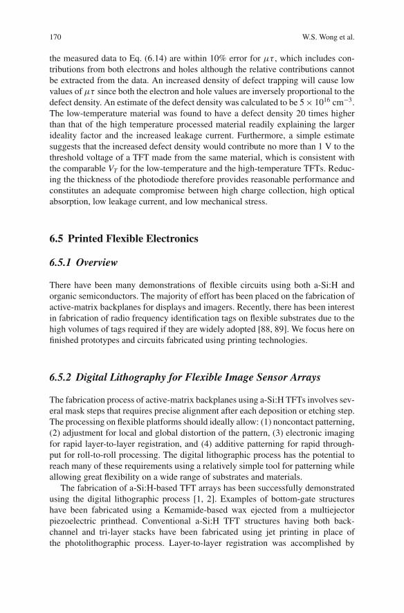
170 W.S. Wong et al.
the measured data to Eq. (6.14) are within 10% error for μτ , which includes con-tributions from both electrons and holes although the relative contributions cannotbe extracted from the data. An increased density of defect trapping will cause lowvalues of μτ since both the electron and hole values are inversely proportional to thedefect density. An estimate of the defect density was calculated to be 5 × 1016 cm−3.The low-temperature material was found to have a defect density 20 times higherthan that of the high temperature processed material readily explaining the largerideality factor and the increased leakage current. Furthermore, a simple estimatesuggests that the increased defect density would contribute no more than 1 V to thethreshold voltage of a TFT made from the same material, which is consistent withthe comparable VT for the low-temperature and the high-temperature TFTs. Reduc-ing the thickness of the photodiode therefore provides reasonable performance andconstitutes an adequate compromise between high charge collection, high opticalabsorption, low leakage current, and low mechanical stress.
6.5 Printed Flexible Electronics
6.5.1 Overview
There have been many demonstrations of flexible circuits using both a-Si:H andorganic semiconductors. The majority of effort has been placed on the fabrication ofactive-matrix backplanes for displays and imagers. Recently, there has been interestin fabrication of radio frequency identification tags on flexible substrates due to thehigh volumes of tags required if they are widely adopted [88, 89]. We focus here onfinished prototypes and circuits fabricated using printing technologies.
6.5.2 Digital Lithography for Flexible Image Sensor Arrays
The fabrication process of active-matrix backplanes using a-Si:H TFTs involves sev-eral mask steps that requires precise alignment after each deposition or etching step.The processing on flexible platforms should ideally allow: (1) noncontact patterning,(2) adjustment for local and global distortion of the pattern, (3) electronic imagingfor rapid layer-to-layer registration, and (4) additive patterning for rapid through-put for roll-to-roll processing. The digital lithographic process has the potential toreach many of these requirements using a relatively simple tool for patterning whileallowing great flexibility on a wide range of substrates and materials.
The fabrication of a-Si:H-based TFT arrays has been successfully demonstratedusing the digital lithographic process [1, 2]. Examples of bottom-gate structureshave been fabricated using a Kemamide-based wax ejected from a multiejectorpiezoelectric printhead. Conventional a-Si:H TFT structures having both back-channel and tri-layer stacks have been fabricated using jet printing in place ofthe photolithographic process. Layer-to-layer registration was accomplished by
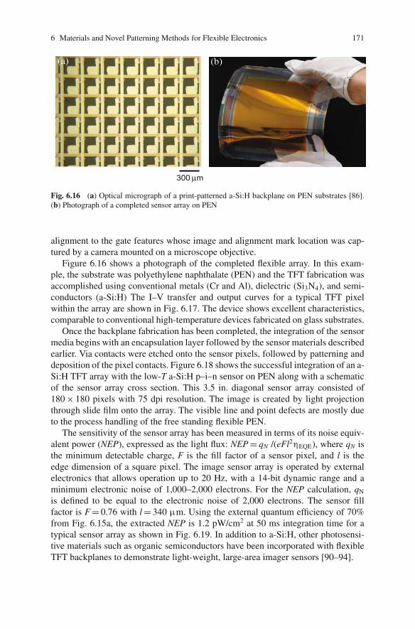
6 Materials and Novel Patterning Methods for Flexible Electronics 171
300 μm
(a) (b)
Fig. 6.16 (a) Optical micrograph of a print-patterned a-Si:H backplane on PEN substrates [86].(b) Photograph of a completed sensor array on PEN
alignment to the gate features whose image and alignment mark location was cap-tured by a camera mounted on a microscope objective.
Figure 6.16 shows a photograph of the completed flexible array. In this exam-ple, the substrate was polyethylene naphthalate (PEN) and the TFT fabrication wasaccomplished using conventional metals (Cr and Al), dielectric (Si3N4), and semi-conductors (a-Si:H) The I–V transfer and output curves for a typical TFT pixelwithin the array are shown in Fig. 6.17. The device shows excellent characteristics,comparable to conventional high-temperature devices fabricated on glass substrates.
Once the backplane fabrication has been completed, the integration of the sensormedia begins with an encapsulation layer followed by the sensor materials describedearlier. Via contacts were etched onto the sensor pixels, followed by patterning anddeposition of the pixel contacts. Figure 6.18 shows the successful integration of an a-Si:H TFT array with the low-T a-Si:H p–i–n sensor on PEN along with a schematicof the sensor array cross section. This 3.5 in. diagonal sensor array consisted of180 × 180 pixels with 75 dpi resolution. The image is created by light projectionthrough slide film onto the array. The visible line and point defects are mostly dueto the process handling of the free standing flexible PEN.
The sensitivity of the sensor array has been measured in terms of its noise equiv-alent power (NEP), expressed as the light flux: NEP = qN /(eFl2ηEQE), where qN isthe minimum detectable charge, F is the fill factor of a sensor pixel, and l is theedge dimension of a square pixel. The image sensor array is operated by externalelectronics that allows operation up to 20 Hz, with a 14-bit dynamic range and aminimum electronic noise of 1,000–2,000 electrons. For the NEP calculation, qN
is defined to be equal to the electronic noise of 2,000 electrons. The sensor fillfactor is F = 0.76 with l = 340 μm. Using the external quantum efficiency of 70%from Fig. 6.15a, the extracted NEP is 1.2 pW/cm2 at 50 ms integration time for atypical sensor array as shown in Fig. 6.19. In addition to a-Si:H, other photosensi-tive materials such as organic semiconductors have been incorporated with flexibleTFT backplanes to demonstrate light-weight, large-area imager sensors [90–94].
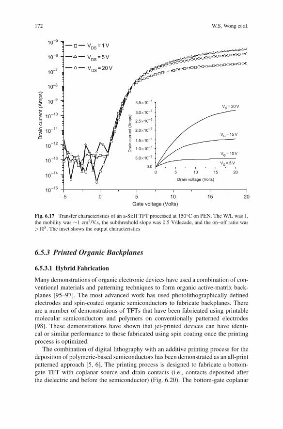
172 W.S. Wong et al.
Gate voltage (Volts)
Dra
in c
urre
nt (A
mps
)
–5 0 5 10 15 2010–15
10–14
10–13
10–12
10–11
10–10
10–9
10–8
10–7
10–6
10–5 VDS = 1 V
VDS = 5 V
VDS = 20 V
Dra
in c
urre
nt (A
mps
)
0 5 10 15 200.0
3.5×10– 6
3.0×10– 6
2.5×10– 6
2.0×10– 6
1.5×10– 6
1.0×10– 6
5.0×10– 6
VG = 20 V
VG = 15 V
VG = 5 V
VG = 10 V
Drain voltage (Volts)
Fig. 6.17 Transfer characteristics of an a-Si:H TFT processed at 150◦C on PEN. The W/L was 1,the mobility was ∼1 cm2/V.s, the subthreshold slope was 0.5 V/decade, and the on–off ratio was>108. The inset shows the output characteristics
6.5.3 Printed Organic Backplanes
6.5.3.1 Hybrid Fabrication
Many demonstrations of organic electronic devices have used a combination of con-ventional materials and patterning techniques to form organic active-matrix back-planes [95–97]. The most advanced work has used photolithographically definedelectrodes and spin-coated organic semiconductors to fabricate backplanes. Thereare a number of demonstrations of TFTs that have been fabricated using printablemolecular semiconductors and polymers on conventionally patterned electrodes[98]. These demonstrations have shown that jet-printed devices can have identi-cal or similar performance to those fabricated using spin coating once the printingprocess is optimized.
The combination of digital lithography with an additive printing process for thedeposition of polymeric-based semiconductors has been demonstrated as an all-printpatterned approach [5, 6]. The printing process is designed to fabricate a bottom-gate TFT with coplanar source and drain contacts (i.e., contacts deposited afterthe dielectric and before the semiconductor) (Fig. 6.20). The bottom-gate coplanar
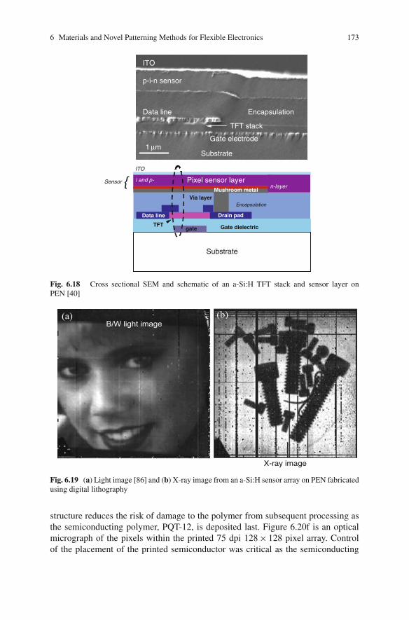
6 Materials and Novel Patterning Methods for Flexible Electronics 173
{
TFTgate
gate dielectric
data line drain pad
layermushroom metal
via layer
pixel sensor layern-layer
TFTgate
gate dielectric
data line drain pad
mushroom metal
via layer
pixel sensor layern-layer
Sensor
TFTgate Gate dielectric
Data line Drain pad
i and p-
ITO
Substrate
Mushroom metalVia layer
Pixel sensor layern-layer
1 μmGate electrode
TFT stack
Data line Encapsulation
p-i-n sensor
ITO
Substrate
Encapsulation
Fig. 6.18 Cross sectional SEM and schematic of an a-Si:H TFT stack and sensor layer onPEN [40]
B/W light image(a)
X-ray image
(b)
Fig. 6.19 (a) Light image [86] and (b) X-ray image from an a-Si:H sensor array on PEN fabricatedusing digital lithography
structure reduces the risk of damage to the polymer from subsequent processing asthe semiconducting polymer, PQT-12, is deposited last. Figure 6.20f is an opticalmicrograph of the pixels within the printed 75 dpi 128 × 128 pixel array. Controlof the placement of the printed semiconductor was critical as the semiconducting
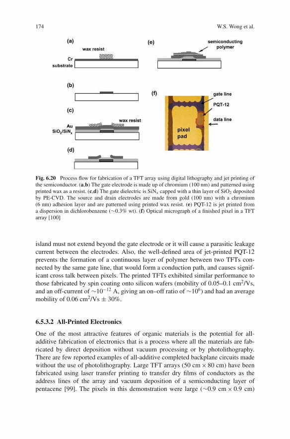
174 W.S. Wong et al.
Fig. 6.20 Process flow for fabrication of a TFT array using digital lithography and jet printing ofthe semiconductor. (a,b) The gate electrode is made up of chromium (100 nm) and patterned usingprinted wax as a resist. (c,d) The gate dielectric is SiNx capped with a thin layer of SiO2 depositedby PE-CVD. The source and drain electrodes are made from gold (100 nm) with a chromium(6 nm) adhesion layer and are patterned using printed wax resist. (e) PQT-12 is jet printed froma dispersion in dichlorobenzene (∼0.3% wt). (f) Optical micrograph of a finished pixel in a TFTarray [100]
island must not extend beyond the gate electrode or it will cause a parasitic leakagecurrent between the electrodes. Also, the well-defined area of jet-printed PQT-12prevents the formation of a continuous layer of polymer between two TFTs con-nected by the same gate line, that would form a conduction path, and causes signif-icant cross talk between pixels. The printed TFTs exhibited similar performance tothose fabricated by spin coating onto silicon wafers (mobility of 0.05–0.1 cm2/Vs,and an off-current of ∼10−12 A, giving an on–off ratio of ∼106) and had an averagemobility of 0.06 cm2/Vs ± 30%.
6.5.3.2 All-Printed Electronics
One of the most attractive features of organic materials is the potential for all-additive fabrication of electronics that is a process where all the materials are fab-ricated by direct deposition without vacuum processing or by photolithography.There are few reported examples of all-additive completed backplane circuits madewithout the use of photolithography. Large TFT arrays (50 cm × 80 cm) have beenfabricated using laser transfer printing to transfer dry films of conductors as theaddress lines of the array and vacuum deposition of a semiconducting layer ofpentacene [99]. The pixels in this demonstration were large (∼0.9 cm × 0.9 cm)
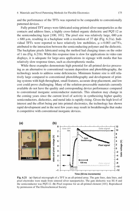
6 Materials and Novel Patterning Methods for Flexible Electronics 175
and the performance of the TFTs was reported to be comparable to conventionallypatterned devices.
Fully printed TFT arrays were fabricated using printed silver nanoparticles as thecontacts and address lines, a highly cross-linked organic dielectric and PQT-12 asthe semiconducting layer [100, 101]. The pixel size was relatively large, 680 μm× 680 μm, resulting in a backplane with a resolution of 37 dpi (Fig. 6.21a). Indi-vidual TFTs were reported to have relatively low mobilities, μ= 0.003 cm2/Vs,attributed to the interaction between the semiconducting polymer and the dielectric.The backplane pixels fabricated using the method had charging times on the orderof 1 ms (Fig. 6.21b). While this response time is slow for applications in video ratedisplays, it is adequate for large-area applications in signage with media that hasrelatively slow response times, such as electrophoretic media.
While these examples demonstrate high potential for all-printed device process-ing as an alternative to conventional vacuum deposition and photolithography, thetechnology needs to address some deficiencies. Minimum feature size is still rela-tively large compared to conventional photolithography and development of print-ing systems with high throughput, small features, accurate drop placement, and lowcost could prove challenging. Many of the solution-processable materials currentlyavailable do not have the quality and corresponding device performance comparedto conventional inorganic semiconductor materials. This situation may change inthe coming years since the current level of activity in synthesizing higher qualitysemiconductors, dielectrics, and metal inks is rapidly rising. Given the high level ofinterest and the effort being put into printed electronics, the technology has shownrapid development and in the next few years may result in breakthroughs that makeit competitive with conventional inorganic devices.
–1
0
1
2
3
4
5
6
7
8
–12
–10
–8
–6
–4
–2
0
2
4
6
8
10
12
dat
a an
d p
ixel
vo
ltag
e (V
)
Time (50 ms increments)
Pixel signal
Gate signal
Gat
e vo
ltag
e (V
)
100 ms Data signal
Gate ON
Gate OFF
Gatefeedthrough
(b)(a)
Fig. 6.21 (a) Optical micrograph of a TFT in an all-printed array. The gate lines, data lines, andpixel electrodes were made from sintered silver nanoparticles. The gate dielectric was SU-8 andthe semiconductor was PQT-12. (b) Pixel response for an all-printed element [101]. Reproducedby permission of The Electrochemical Society
176 W.S. Wong et al.
6.6 Conclusions and Future Prospects
Flexible circuits can now be fabricated using both conventional inorganic andorganic materials. Optimization of the electrical performance of materials depositedon plastic is still under way. The results so far suggest that the current level of per-formance will be adequate for a variety of applications in displays and imagers.Printing technologies have been demonstrated to have great utility for both sub-tractive and additive patterning. Now that commercial instrumentation is becomingmore widely available, adoption of these methods will probably increase. Whileprinting methods present new challenges for control of patterning, they will likelyachieve a place where the highest resolution features are not required or where directdeposition of materials is desirable.
The majority of reported work so far on flexible electronics has focused on fab-rication on single sheets. One of the potential advantages of flexible substrates isroll-to-roll fabrication, which would dramatically change the method of manufac-ture of electronics. Development of these techniques is relatively complex as it com-bines both mechanical design as well as materials processes. Vacuum deposition ina roll-to-roll process has been demonstrated for solar cells and is adaptable for thelayers required for a-Si:H TFTs [8]. Solution processes are potentially more easilyadaptable as the graphic arts industry already uses liquid inks. Some of the signif-icant challenges for adaptation of the materials demonstrated so far are decreasingannealing times, controlling viscosity of solutions without harming electronic prop-erties of the dried films, and development of high-throughput large-scale printheads.Once theses challenges are overcome then the functionality, performance, and costshould ease the burden of manufacturability and flexible electronics should begin topermeate into mainstream electronic applications.
Acknowledgements The authors would like to acknowledge the many insights and assistance ofexperimental data provided by their colleagues and collaborators. The authors would particularlywish to recognize the contributions and efforts of the following colleagues from PARC: Robert A.Street, Rene Lujan, Steve Ready, Beverly Russo, Maryanne Rosenthal, Michael Young, Scott Limb,Sanjiv Sambandan, Jurgen Daniel, Ana-Claudia Arias, Eugene Chow, Vicki Aguilar, and WilliamA. MacDonald of DuPont-Teijin Films. Research performed at PARC was partially supported bythe Advanced Technology Program of the National Institute of Standards and Technology (contract#: 70NANB3H3029).
References
1. Wong WS, Ready S, Matusiak R, White SD, Lu JP, Ho J, Street RA (2002) Amorphoussilicon thin-film transistors and arrays fabricated by jet printing. Appl Phys Lett 80:610–612
2. Wong WS, Ready SE, Lu JP, Street RA (2003) Hydrogenated amorphous silicon thin-filmtransistor arrays fabricated by digital lithography. IEEE Electron Dev Lett 24:577–579
3. Creagh LT, McDonald M (2003) Design and performance of ink-jet print heads for non-graphic-arts applications. Mater Res Soc Bull 28:807–811
4. Young R, Tamura Y, Wang CE, Hsieh D (2003) Cost and efficiency comparisons betweenmanufacturing generations and regions. Proceeding of the International Display and Manu-facturing Conference, IDMC 2003, pp 285–288
6 Materials and Novel Patterning Methods for Flexible Electronics 177
5. Paul KE, Wong WS, Ready SE, Street RA (2003) Additive jet printing of polymer thin-filmtransistors. Appl Phys Lett 83:2070–2702
6. Arias AC, Ready SE, Lujan R, Wong WS, Paul KE, Salleo A, Chabinyc ML, Apte R, StreetRA, Wu Y, Liu P, Ong B (2004) All jet-printed polymer thin-film transistor active-matrixbackplanes. Appl Phys Lett 85:3304–3306
7. Jain K, Klosner M, Zemel M, Raghunandan S (2005) Flexible electronics and displays:High-resolution, roll-to-roll, projection lithography and photoablation processing technolo-gies for high-throughput production. Proc IEEE 93:1500–1510
8. Sheats JR (2002) Roll-to-roll manufacturing of thin film electronics. Proc SPIE – Int SocOpt Eng 4688:240–248
9. Gleskova H, Wagner S, Suo Z (1998) a-Si:H TFTs made on polyimide foil by PE-CVD at150◦C. Mat Res Soc Symp Proc 508:73–78
10. Sarma KR (2004) a-Si TFT OLED fabricated on low-temperature flexible plastic substrate.Mat Res Soc Symp Proc 814:369
11. Zhou L, Jackson T, Brandon E, West W (2004) Flexible substrate a-Si:H TFTs for spaceapplications. Dev Res Conf 1:123–124
12. Gleskova H, Wagner S (2001) DC-gate-bias stressing of a-Si:H TFTs fabricated at 150◦C onpolyimide foil. IEEE Trans Electron Dev 48:1667–1671
13. Sazonov A, Stryahilev D, Lee CH, Nathan A (2005) Low-temperature materials and thin-film transistors for flexible electronics. Proc IEEE 93:1420–1428
14. Shimoda T, Morii TK, Seki S, Kiguchi H (2003) Ink-jet printing of light emitting polymerdisplays. Mater Res Soc Bull 28:821–827
15. Sele CW, vonWerne T, Friend RH, Sirringhaus H (2005) Lithography-free, self-aligned ink-jet printing with sub-hundred-nanometer resolution. Adv Mater 17:997–1001
16. Tsukada T (2000) Active-matrix liquid-crystal displays. In: Street RA (ed) Technology andapplications of amorphous silicon. Springer-Verlag, Heidelberg
17. Street RA (2000) Large area image sensor arrays. In: Street RA (ed) Technology and appli-cations of amorphous silicon. Springer-Verlag, Heidelberg
18. Shimoda T, Matsuki Y, Furusawa M, Aoki T, Yudasaka I, Tanaka H, Iwasawa H, Wang D,Miyasaka M, Takeuchi Y (2006) Solution-processed silicon films and transistors. Nature440:783–786
19. Hoffman RL, Norris BJ, Wager JF (2003) ZnO-based transparent thin-film transistors. ApplPhys Lett 82:733–735
20. Nomura K, Ohta H, Takagi A, Kamiya T, Hirano M, Hosono H (2004) Room-temperaturefabrication of transparent flexible thin-film transistors using amorphous oxide semiconduc-tors. Nature 432:488–492
21. Noh YY, Cheng X, Sirringhaus H, Sohn JI, Welland ME, Kang DJ (2007) Ink-jet printedZnO nanowire field effect transistors. Appl Phys Lett 91:043109
22. Veres J, Ogier SD, Leeming SW, Cupertino DC, Khaffaf SM (2003) Low-k Insulators as thechoice of dielectrics in organic field-effect transistors. Adv Func Mater 13:199–204
23. Sirringhaus H (2005) Device physics of solution-processed organic field-effect transistors.Adv Mater 17:2411–2425
24. Gundlach DJ, Lin YY, Jackson TN, Nelson SF, Schlom DG (1997) Pentacene organicthin-film transistors – molecular ordering and mobility. IEEE Electron Dev Lett 18:87–89
25. Nomoto K, Hirai N, Yoneya N, Kawashima N, Noda M, Wada M, Kasahara J (2005) Ahigh-performance short-channel bottom-contact OTFT and its application to AM-TN-LCD.IEEE Trans Electron Dev 52:1519–1526
26. Payne MM, Parkin SR, Anthony JE, Kuo CC, Jackson TN (2005) Organic field-effect tran-sistors from solution-deposited functionalized acenes with mobilities as high as 1 cm2/Vs. JAm Chem Soc 127:4986–4987
27. McCulloch I, Heeney M, Bailey C, Genevicius K, Macdonald I, Shkunov M, Sparrowe D,Tierney S, Wagner R, Zhang W, Chabinyc ML, Kline RJ, McGehee MD, Toney MF (2006)
178 W.S. Wong et al.
Liquid-crystalline semiconducting polymers with high charge-carrier mobility. Nat Mater5:328–333
28. Steudel S, DeVusser S, DeJonge S, Janssen D, Verlaak S, Genoe J, Heremans P (2004)Influence of the dielectric roughness on the performance of pentacene transistors. Appl PhysLett 85:4400–4402
29. Chabinyc ML, Lujan R, Endicott F, Toney MF, McCulloch I, Heeney M (2006) Effectsof the surface roughness of plastic-compatible inorganic dielectrics on polymeric thin-filmtransistors. Appl Phys Lett 90:233508
30. Nunes G Jr, Zane SG, Meth JS (2005) Styrenic polymers as gate dielectrics for pentacenefield-effect transistors. J Appl Phys 98:104053
31. Jung T, Dodabalapur A, Wenz R, Mohapatra S (2005) Moisture induced surface polariza-tion in a poly(4-vinyl phenol) dielectric in an organic thin-film transistor. Appl Phys Lett87:182109
32. Chua LL, Zaumseil J, Chang JF, Ou ECW, Ho PKH, Sirringhaus H, Friend RH (2005) Gen-eral observation of n-type field-effect behaviour in organic semiconductors. Nature 343:194–199
33. Hong CM, Wagner S (2000) Ink-jet printed copper source/drain metallization for amorphoussilicon thin-film transistors. IEEE Electron Dev Lett 21:384–386
34. Huang D, Liao F, Molesa S, Redinger D, Subramanian V (2003) Plastic compatible low-resistance printable gold nanoparticle conductors for flexible electronics. J Electrochem Soc150:412–417
35. Chung J, Ko S, Bieri NR, Grigoropoulos CP, Poulikakos D (2004) Conductor microstruc-tures by laser curing of printed gold nanoparticle ink. Appl Phys Lett 84:801–803
36. Wu Y, Li Y, Ong BS (2006) Printed silver ohmic contacts for high-mobility organic thin-filmtransistors. J Am Chem Soc 128:4202–4203
37. Groenendaal LB, Jonas F, Freitag D, Pielartzik H, Reynolds JR (2000) Poly(3,4-ethylenedioxythoiphene) and its derivatives: Past, present, and future. Adv Mater 12:481–494
38. Rogers JA, Bao Z, Baldwin K, Dodabalapur A, Crone B, Raju VR, Kuck V, Katz H, Amund-son K, Ewing J, Drzaic P (2001) Paper-like electronic displays: Large-area rubber-stampedplastic sheets of electronics and microencapsulated electrophoretic inks. Proc Nat Acad Sci98:4835–4840
39. Wagner S, Gleskova H, Sturm JC, Suo Z (2000) Novel processing technology for macro-electronics. In: Street RA (ed) Technology and applications of amorphous silicon, vol 37.Springer-Verlag, Berlin, pp 222–251
40. Wong WS, Chabinyc ML, Limb S, Ready SE, Lujan R, Daniel J, Street RA (2007) Digitallithographic processing for large-area electronics. J Soc Info Display 15:463
41. Wong WS, Chow EC, Geluz-Aguilar V, Lujan R, Chabinyc ML (2006) Fine-feature pat-terning of self-aligned polymeric thin-film transistors fabricated by digital lithography andelectroplating. Appl Phys Lett 89:142118-1–142118-3
42. Street RA, Wong WS, Ready SE, Chabinyc ML, Arias AC, Limb S, Salleo A, Lujan R (2006)Jet printing flexible displays. Mater Today 9:32
43. Zhao N, Chiesa M, Sirringhaus H, Li Y, Wu Y, Ong B (2007) Self-aligned ink-jet print-ing of highly conducting gold electrodes with submicron resolution. J Appl Phys 101:064513
44. Thomasson DB, Jackson TN (1998) Fully self-aligned tri-layer a-Si:H thin-film transistorswith deposited doped contact layer. IEEE Electron Dev Lett 19:124
45. Sirringhaus H, Kawase T, Friend RH, Shimoda T, Inbasekaran M, Wu W, Woo EP (2000)High-resolution ink-jet printing of all-polymer transistor circuits. Science 290:2123–2126
46. Li SP, Newsome CJ, Kugler T, Ishida M, Inoue S (2007) Polymer thin-film transistors withself-aligned gates fabricated using ink-jet printing. Appl Phys Lett 90:172103
47. Schiaffino S, Sonin AA (1997) Formation and stability of liquid and molten beads on a solidsurface. J Fluid Mech 343:95–110

6 Materials and Novel Patterning Methods for Flexible Electronics 179
48. Duineveld P (2003) The stability of ink-jet printed lines of liquid with zero receding contactangle on a homogeneous substrate. Phys Fluids 477:175–200
49. Chang JF, Sun B, Breiby DW, Nielsen MM, Solling TI, Giles M, McCulloch I, Sirringhaus H(2004) Enhanced mobility of poly(3-hexylthiophene) transistors by spin-coating from high-boiling-point solvents. Chem Mater 16:4772–4776
50. DeLongchamp DM, Vogel BM, Jung Y, Gurau MC, Richter CA, Kirillov OA, Obrzut J,Fischer DA, Sambasivan S, Richter LJ, Lin EK (2005) Variations in semiconducting polymermicrostructure and hole mobility with spin-coating speed. Chem Mater 17:5610–5612
51. Salleo A, Street RA (2003) Light-induced bias stress reversal in polyfluorene thin-film tran-sistors. J Appl Phys 94(1):471
52. Salleo A, Endicott F, Street RA (2005) Reversible and irreversible trapping inpoly(thiophene) thin-film transistors. Appl Phys Lett 86:263505
53. Ng TN, Marohn JA, Chabinyc ML (2006) Comparing the kinetics of bias stress in organicfield-effect transistors with different dielectric interfaces. J Appl Phys 100:084505
54. Schoonveld WA, Oostinga JB, Vrijmoeth J, Klapwijk TM (1999) Charge trapping instabili-ties in sexithiophene thin-film transistors. Synth Metals 101:6078
55. Brown AR, Jarrett CP, de Leeuw DM, Matters M (1997) Field-effect transistors made fromsolution-processed organic semiconductors. Synth Metals 88:37
56. Zilker SJ, Detcheverry C, Cantatore E, de Leeuw DM (2000) Bias stress in organic thin-filmtransistors and logic gates. Appl Phys Lett 79:1124
57. Knipp D, Street RA, Volkel A, Ho J (2003) Pentacene thin-film transistors on inor-ganic dielectrics: Morphology, structural properties and electronic transport. J Appl Phys93:347
58. Gu G, Kane MG, Mau SC (2007) Reversible memory effects and acceptor states inpentacene-based organic thin-film transistors. J Appl Phys 101:014504
59. Chabinyc ML, Endicott F, Vogt BD, de Longchamp DM, Lin EK, Wu YL, Liu P, Ong BS(2006) Effects of humidity on unencapsulated poly(thiophene) thin-film transistors. ApplPhys Lett 88:113514
60. Street RA, Chabinyc ML, Endicott F, Ong B (2006) Extended time bias stress effects inpolymer transistors. J Appl Phys 11:114518
61. Street RA, Salleo A, Chabinyc ML (2003) Bipolaron mechanism for bias-stress effects inorganic transistors. Phys Rev B 68(8):085316
62. Salleo A, Street RA (2004) Kinetics of bias-stress and bipolaron formation in regio-regularpoly(thiophene). Phys Rev B 70(23):235324
63. Lloyd-Hughes J, Richards T, Sirringhaus H, Castro-Camus E, Herz LM, Johnston MB(2006) Charge trapping in polymer transistors probed by terahertz spectroscopy and scan-ning probe potentiometry. Appl Phys Lett 89:112101
64. Karim KS, Nathan A, Hack M, Milne WI (2004) Drain-bias dependence of threshold voltagestability of amorphous silicon TFTs. IEEE Electron Dev Lett 25:188
65. Salleo A, Chabinyc ML (2006) Electrical and environmental stability of polymer thin-filmtransistors. In: Klauk H (ed) Organic electronics: Materials, manufacturing and applications.Wiley VCH, Weinheim, Germany
66. Libsch FR, Kanicki J (1993) Bias-stress-induced stretched-exponential time dependenceof charge injection and trapping in amorphous thin-film transistors. Appl Phys Lett62:1286
67. Gomes HL, Stallinga P, Dinelli F, Murgia M, Biscarini F, de Leeuw DM, Muccini M, MullenK (2005) Electrical characterization of organic based transistors: stability issues. Polym AdvTech 16:227
68. Gomes HL, Stallinga P, Dinelli F, Murgia M, Biscarini F, de Leeuw DM, Muck T, GeurtsJ, Molenkamp LW, Wagner V (2004) Bias-induced threshold voltages shifts in thin-filmorganic transistors. Appl Phys Lett 84:3184
69. Powell MJ, van Berkel C, Franklin AR, Deane SC, Milne WI (1992) Defects pool inamorphous-silicon thin-film transistors. Phys Rev B 45:4160
70. Fery C, Racine B, Vaufrey D, Doyeux H, Cina S (2005) Physical mechanism responsible for
180 W.S. Wong et al.
the stretched exponential decay behavior of aging organic light-emitting diodes. Appl PhysLett 87:213502
71. Powell MJ, van Berkel C, Hughes JR (1989) Time and temperature dependence of instabilitymechanisms in amorphous silicon thin-film transistors. Appl Phys Lett 54:1323
72. Street RA, Salleo A (2002) Contact effects in polymer transistors. Appl Phys Lett 81:288773. Necliudov PV, Shur MS, Gundlach DJ, Jackson TN (2000) Modeling of organic thin-film
transistors of different designs. J Appl Phys 88:659474. Chabinyc ML, Lu JP, Street RA, Wu YL, Liu P, Ong BS (2004) Short channel effects in
regioregular poly(thiophene) thin-film transistors. J Appl Phys 96:206375. Wang GM, Swensen J, Moses D, Heeger AJ (2003) Increased mobility from regioregular
poly(3-hexylthiophene) field-effect transistors. J Appl Phys 93:613776. Yang CS, Smith LL, Arthur CB, Parsons GN (2000) Stability of low-temperature amorphous
silicon thin-film transistors formed on glass and transparent plastic substrates. J Vac SciTechnol B 18:683
77. van Berkel C, Powell MJ (1987) Resolution of amorphous silicon thin-film transistor insta-bility mechanisms using ambipolar transistors. Appl Phys Lett 51:1094
78. Wong WS, Lujan R, Daniel JH, Limb S (2005) Digital lithography for large-area electronicson flexible substrates. J Non-Cryst Solids 352(9–20):1981–1985
79. Choi JB, Yun DC, Park YI, Kim JH (2000) Properties of hydrogenated amorphous siliconthin-film transistors fabricated at 150◦C. J Non-Cryst Solids 266–269:1315
80. Ikeda M, Mizutani Y, Ashida S, Yamada K (2000) Characteristics of low-temperature-processed a-Si TFT for plastic substrates. IEICE Trans Electron E83-C:1584
81. Powell MJ, van Berkel C, French ID, Nicholls DH (1987) Bias dependence of instabilitymechanisms in amorphous silicon thin-film transistors. Appl Phys Lett 51:1242
82. Long K, Kattamis AZ, Cheng IC, Gleskova H, Wagner S, Sturm JC (2006) Stability ofamorphous-silicon TFTs deposited on clear plastic substrates at 250◦C to 280◦C. IEEE Elec-tron Dev Lett 27:111
83. Wang Q, Ward S, Duda A, Hu J, Stradins P, Crandall RS, Branz HM, Perlov C, Jackson W,Mei P, Taussig C (2004) High-current-density thin-film silicon diodes grown at low temper-ature. Appl Phys Lett 85:2122
84. Vieira M, Louro P, Fernandes M, Schwarz R, Schubert M (2004) Large area p–i–n flexibleimage sensors. Mater Res Soc Proc 814:I7–11.1
85. Kim KH, Vygranenko Y, Bedzyk M, Chang JH, Chuang TC, Striakhilev D, Nathan A, HeilerG, Tredwell T (2007) High performance hydrogenated amorphous silicon n–i–p photo-diodes on glass and plastic substrates by low-temperature fabrication process. Mater ResSoc Proc 989:A19–05
86. Ng TN, Lujan RA, Sambandan S, Street RA, Limb S, Wong WS (2007) Low temperaturea-Si:H photodiodes and flexible image sensor arrays patterned by digital lithography. ApplPhys Lett 91:063505
87. Kroon A, van Swaaij RACMM (2001) Spatial effects on ideality factor of amorphous siliconpin diodes. J Appl Phys 90:994
88. Knobloch A, Manuelli A, Bernds A, Clemens W (2004) Fully printed integrated circuitsfrom solution processed polymers. J Appl Phys 96:2286–2291
89. Zielke D, Hubler AC, Hahn U, Brandt N, Bartzsch M, Fugmann U, Fischer T, Veres J,Ogier S (2005) Polymer-based organic field-effect transistor using offset printed source/drainelectrodes. Appl Phys Lett 87:123508
90. Yu G, Wang J, McElvain J, Heeger AJ (1998) Large-area, full-color image sensors madewith semiconducting polymers. Adv Mater 10:1431
91. Street RA, Mulato M, Lau R, Ho J, Graham J, Popovic Z, Hor J (2001) Image capture arraywith an organic light sensor. Appl Phys Lett 78:4193
92. Someya T, Kato Y, Iba S, Noguchi Y, Sekitani T, Kawaguchi H, Sakurai T (2005) Integrationof organic FETs with organic photodiodes for a large area, flexible, and lightweight sheetimage scanners. IEEE Trans Electron Dev 52:2502
6 Materials and Novel Patterning Methods for Flexible Electronics 181
93. Peumans P, Yakimov A, Forrest SR (2003) Small molecular weight organic thin-film pho-todetectors and solar cells. J Appl Phys 93:3693
94. Schilinsky P, Waldauf C, Hauch J, Brabec CJ (2004) Polymer photodiode detectors: Progressand recent developments. Thin Solid Films 451–452:105
95. Huitema HEA, Gelinck GH, van der Putten JBPH, Kuijk KE, Hart CM, Cantatore E, HerwigPT, van Breemen AJJM, de Leeuw DM (2001) Polymer electronics: Plastic transistors inactive-matrix displays. Nature (London, United Kingdom) 414:599
96. Gelinck GH, Huitema HEA, van Veenendaal E, Cantatore E, Schrijnemakers L, van derPutten JBPH, Geuns TCT, Beenhakkers M, Giesbers JB, Huisman BH, Meijer EJ, BenitoEM, Touwslager FJ, Marsman AW, van Rens BJE, de Leeuw DM (2004) Flexible active-matrix displays and shift registers based on solution-processed organic transistors. Nat Mater3:106–110
97. Burns SE, Cain P, Mills J, Wang J, Sirringhaus H (2003) Inkjet printing of polymer thin-filmtransistor circuits. Mater Res Soc Bull 28:829–834
98. Chang P, Molesa S, Murphy A, Frechet J, Subramanian V (2006) Inkjetted crystalline single-monolayer oligothiophene OTFTs. IEEE Trans Electron Dev 53:594–600
99. Blanchet GB, Loo YL, Rogers JA, Gao F, Fincher CR (2003) Large area, high resolution,dry printing of conducting polymers for organic electronics. Appl Phys Lett 82:463–465
100. Arias AC, Daniel J, Krusor B, Ready S, Sholin V, Street R (2007) All-additive ink-jet-printeddisplay backplanes: materials development and integration. J Soc Info Display 15:485–490
101. Daniel J, Arias AC, Krusor B, Lujan R, Street RA (2006) The road towards large-area elec-tronics without vacuum tools. Electrochem Soc Trans 3:229
Chapter 7Sheet-Type Sensors and Actuators
Takao Someya
7.1 Introduction
Recent intensive research and development of organic field-effect transistors (FETs)[1–6] have been motivated by a new class of applications that cannot be easilyrealized by conventional electronics based on inorganic semiconductors. Organictransistors are mechanically flexible, thin, lightweight, and shock-resistant, becauseorganic devices are manufactured on plastic films at low (ambient) temperature. Fur-thermore, manufacturing costs of organic transistor circuits would be inexpensive,even for large areas, when they are fabricated using printing technologies and/orroll-to-roll processes.
There are two major applications for organic transistors. The first one is a flexibledisplay. This new display includes a paper-like display or an electronic paper, whereelectric inks, electroluminescent (EL) devices, and liquid crystals or other mediumsare powered by organic transistor active matrices [4, 7]. The second one is a radiofrequency identification (RFID) tag [8, 9]. An organic transistor-based RFID tagmay be printed on packages of products, resulting in an inexpensive and robustelectronics.
As another application of organic transistors, we demonstrated large-area flex-ible sensors. The first organic transistor-based large-area sensors are flexible pres-sure sensor matrices; organic transistor active matrices are used to read out pressuredistributions over a large area from a 2-D array of pressure sensor cells. The newpressure sensor can be ideal for electronic artificial skin (e-skin) applications forfuture generations of robots.
The mobility of pentacene that is known as a high-mobility low-molecular weightsemiconductor is typically 1 cm2/Vs. This value is about two or three orders of mag-nitude lower than that of poly- or single-crystalline silicon, respectively. Althoughflexible displays and/or RFID tags require usually high-electronic performance, the
T. Someya (B)School of Engineering, Quantum-Phase Electronics Center, The University of Tokyo, 7-3-1 Hongo,Bunkyo-ku, Tokyo 113-8656 Japane-mail: [email protected]
W.S. Wong, A. Salleo (eds.), Flexible Electronics: Materials and Applications, ElectronicMaterials: Science & Technology, DOI 10.1007/978-0-387-74363-9 7,C© Springer Science+Business Media, LLC 2009
183
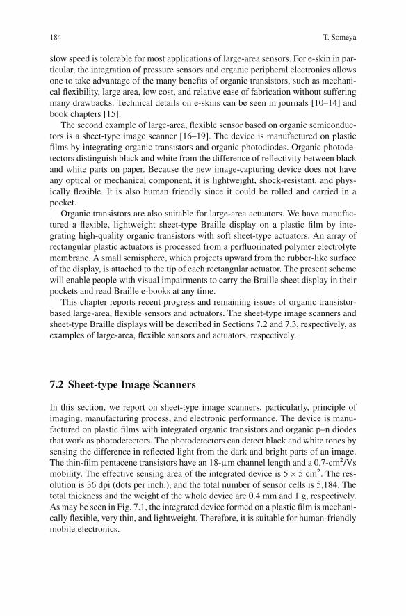
184 T. Someya
slow speed is tolerable for most applications of large-area sensors. For e-skin in par-ticular, the integration of pressure sensors and organic peripheral electronics allowsone to take advantage of the many benefits of organic transistors, such as mechani-cal flexibility, large area, low cost, and relative ease of fabrication without sufferingmany drawbacks. Technical details on e-skins can be seen in journals [10–14] andbook chapters [15].
The second example of large-area, flexible sensor based on organic semiconduc-tors is a sheet-type image scanner [16–19]. The device is manufactured on plasticfilms by integrating organic transistors and organic photodiodes. Organic photode-tectors distinguish black and white from the difference of reflectivity between blackand white parts on paper. Because the new image-capturing device does not haveany optical or mechanical component, it is lightweight, shock-resistant, and phys-ically flexible. It is also human friendly since it could be rolled and carried in apocket.
Organic transistors are also suitable for large-area actuators. We have manufac-tured a flexible, lightweight sheet-type Braille display on a plastic film by inte-grating high-quality organic transistors with soft sheet-type actuators. An array ofrectangular plastic actuators is processed from a perfluorinated polymer electrolytemembrane. A small semisphere, which projects upward from the rubber-like surfaceof the display, is attached to the tip of each rectangular actuator. The present schemewill enable people with visual impairments to carry the Braille sheet display in theirpockets and read Braille e-books at any time.
This chapter reports recent progress and remaining issues of organic transistor-based large-area, flexible sensors and actuators. The sheet-type image scanners andsheet-type Braille displays will be described in Sections 7.2 and 7.3, respectively, asexamples of large-area, flexible sensors and actuators, respectively.
7.2 Sheet-type Image Scanners
In this section, we report on sheet-type image scanners, particularly, principle ofimaging, manufacturing process, and electronic performance. The device is manu-factured on plastic films with integrated organic transistors and organic p–n diodesthat work as photodetectors. The photodetectors can detect black and white tones bysensing the difference in reflected light from the dark and bright parts of an image.The thin-film pentacene transistors have an 18-μm channel length and a 0.7-cm2/Vsmobility. The effective sensing area of the integrated device is 5 × 5 cm2. The res-olution is 36 dpi (dots per inch.), and the total number of sensor cells is 5,184. Thetotal thickness and the weight of the whole device are 0.4 mm and 1 g, respectively.As may be seen in Fig. 7.1, the integrated device formed on a plastic film is mechani-cally flexible, very thin, and lightweight. Therefore, it is suitable for human-friendlymobile electronics.
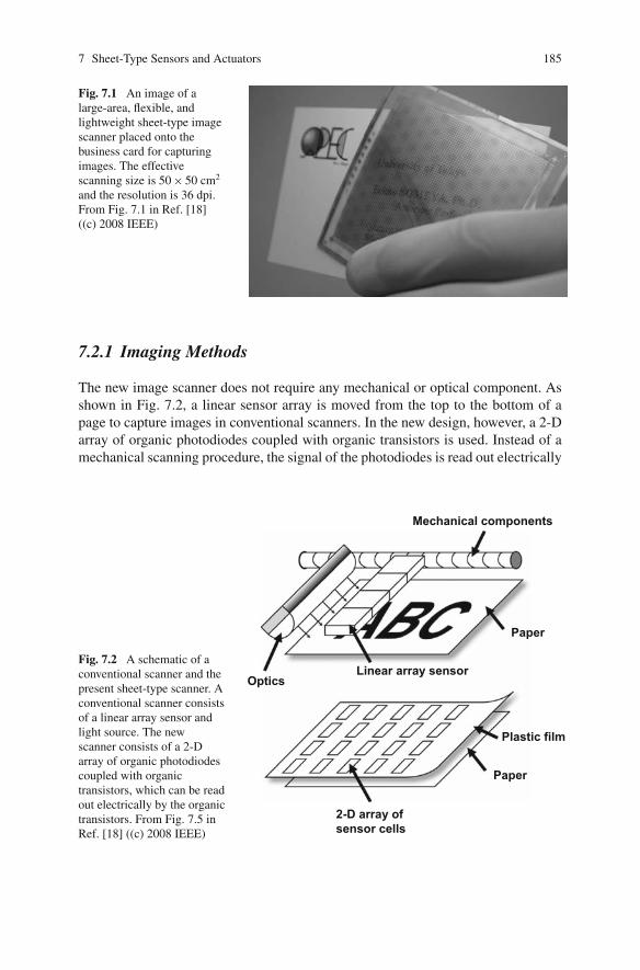
7 Sheet-Type Sensors and Actuators 185
Fig. 7.1 An image of alarge-area, flexible, andlightweight sheet-type imagescanner placed onto thebusiness card for capturingimages. The effectivescanning size is 50 × 50 cm2
and the resolution is 36 dpi.From Fig. 7.1 in Ref. [18]((c) 2008 IEEE)
7.2.1 Imaging Methods
The new image scanner does not require any mechanical or optical component. Asshown in Fig. 7.2, a linear sensor array is moved from the top to the bottom of apage to capture images in conventional scanners. In the new design, however, a 2-Darray of organic photodiodes coupled with organic transistors is used. Instead of amechanical scanning procedure, the signal of the photodiodes is read out electrically
Optics
Mechanical components
Linear array sensor
2-D array ofsensor cells
Paper
Paper
Plastic film
Fig. 7.2 A schematic of aconventional scanner and thepresent sheet-type scanner. Aconventional scanner consistsof a linear array sensor andlight source. The newscanner consists of a 2-Darray of organic photodiodescoupled with organictransistors, which can be readout electrically by the organictransistors. From Fig. 7.5 inRef. [18] ((c) 2008 IEEE)
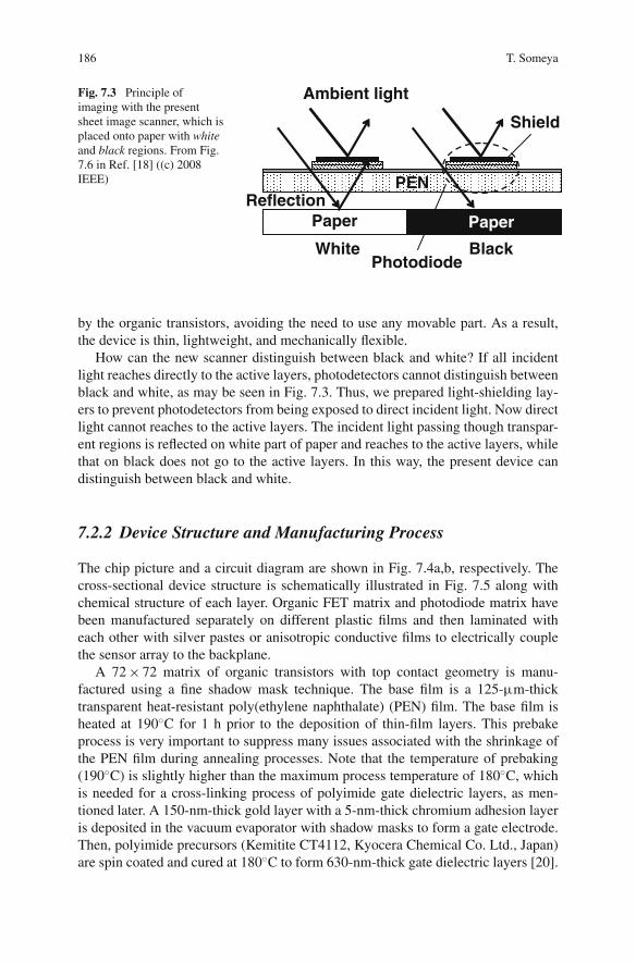
186 T. Someya
Black
Ambient light
Shield
WhitePhotodiode
PEN
PaperPaperReflection
Fig. 7.3 Principle ofimaging with the presentsheet image scanner, which isplaced onto paper with whiteand black regions. From Fig.7.6 in Ref. [18] ((c) 2008IEEE)
by the organic transistors, avoiding the need to use any movable part. As a result,the device is thin, lightweight, and mechanically flexible.
How can the new scanner distinguish between black and white? If all incidentlight reaches directly to the active layers, photodetectors cannot distinguish betweenblack and white, as may be seen in Fig. 7.3. Thus, we prepared light-shielding lay-ers to prevent photodetectors from being exposed to direct incident light. Now directlight cannot reaches to the active layers. The incident light passing though transpar-ent regions is reflected on white part of paper and reaches to the active layers, whilethat on black does not go to the active layers. In this way, the present device candistinguish between black and white.
7.2.2 Device Structure and Manufacturing Process
The chip picture and a circuit diagram are shown in Fig. 7.4a,b, respectively. Thecross-sectional device structure is schematically illustrated in Fig. 7.5 along withchemical structure of each layer. Organic FET matrix and photodiode matrix havebeen manufactured separately on different plastic films and then laminated witheach other with silver pastes or anisotropic conductive films to electrically couplethe sensor array to the backplane.
A 72 × 72 matrix of organic transistors with top contact geometry is manu-factured using a fine shadow mask technique. The base film is a 125-μm-thicktransparent heat-resistant poly(ethylene naphthalate) (PEN) film. The base film isheated at 190◦C for 1 h prior to the deposition of thin-film layers. This prebakeprocess is very important to suppress many issues associated with the shrinkage ofthe PEN film during annealing processes. Note that the temperature of prebaking(190◦C) is slightly higher than the maximum process temperature of 180◦C, whichis needed for a cross-linking process of polyimide gate dielectric layers, as men-tioned later. A 150-nm-thick gold layer with a 5-nm-thick chromium adhesion layeris deposited in the vacuum evaporator with shadow masks to form a gate electrode.Then, polyimide precursors (Kemitite CT4112, Kyocera Chemical Co. Ltd., Japan)are spin coated and cured at 180◦C to form 630-nm-thick gate dielectric layers [20].
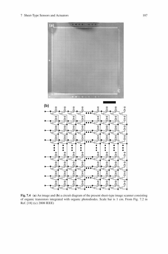
7 Sheet-Type Sensors and Actuators 187
(a)
(b)
Fig. 7.4 (a) An image and (b) a circuit diagram of the present sheet-type image scanner consistingof organic transistors integrated with organic photodiodes. Scale bar is 1 cm. From Fig. 7.2 inRef. [18] ((c) 2008 IEEE)
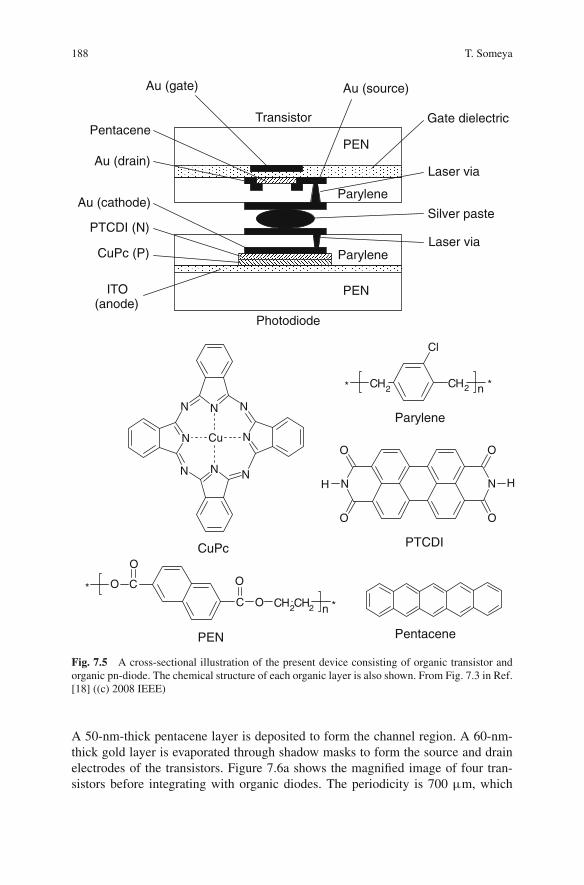
188 T. Someya
Parylene
Photodiode
PEN
Silver paste
Au (gate)
Au (drain)Laser via
PEN
ITO (anode)
Gate dielectricPentacene
Au (cathode)
Transistor
Parylene
Laser via
Au (source)
CuPc (P)
PTCDI (N)
N
N
N
N
N
N N
N
Cu
Cl
CH2* CH2 *n
CO*
O
C
O
O CH2CH2 *n
N N
O
O O
O
H H
Parylene
CuPc
PEN Pentacene
PTCDI
Fig. 7.5 A cross-sectional illustration of the present device consisting of organic transistor andorganic pn-diode. The chemical structure of each organic layer is also shown. From Fig. 7.3 in Ref.[18] ((c) 2008 IEEE)
A 50-nm-thick pentacene layer is deposited to form the channel region. A 60-nm-thick gold layer is evaporated through shadow masks to form the source and drainelectrodes of the transistors. Figure 7.6a shows the magnified image of four tran-sistors before integrating with organic diodes. The periodicity is 700 μm, which
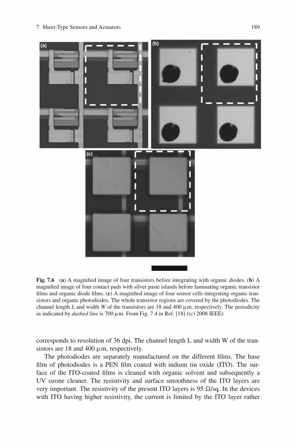
7 Sheet-Type Sensors and Actuators 189
Fig. 7.6 (a) A magnified image of four transistors before integrating with organic diodes. (b) Amagnified image of four contact pads with silver paste islands before laminating organic transistorfilms and organic diode films. (c) A magnified image of four sensor cells integrating organic tran-sistors and organic photodiodes. The whole transistor regions are covered by the photodiodes. Thechannel length L and width W of the transistors are 18 and 400 μm, respectively. The periodicityas indicated by dashed line is 700 μm. From Fig. 7.4 in Ref. [18] ((c) 2008 IEEE)
corresponds to resolution of 36 dpi. The channel length L and width W of the tran-sistors are 18 and 400 μm, respectively.
The photodiodes are separately manufactured on the different films. The basefilm of photodiodes is a PEN film coated with indium tin oxide (ITO). The sur-face of the ITO-coated films is cleaned with organic solvent and subsequently aUV ozone cleaner. The resistivity and surface smoothness of the ITO layers arevery important. The resistivity of the present ITO layers is 95 Ω/sq. In the deviceswith ITO having higher resistivity, the current is limited by the ITO layer rather
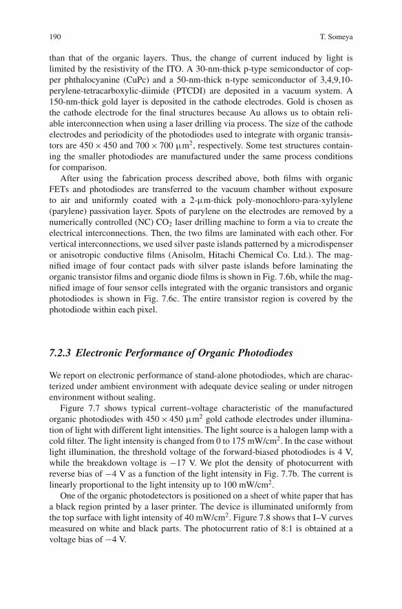
190 T. Someya
than that of the organic layers. Thus, the change of current induced by light islimited by the resistivity of the ITO. A 30-nm-thick p-type semiconductor of cop-per phthalocyanine (CuPc) and a 50-nm-thick n-type semiconductor of 3,4,9,10-perylene-tetracarboxylic-diimide (PTCDI) are deposited in a vacuum system. A150-nm-thick gold layer is deposited in the cathode electrodes. Gold is chosen asthe cathode electrode for the final structures because Au allows us to obtain reli-able interconnection when using a laser drilling via process. The size of the cathodeelectrodes and periodicity of the photodiodes used to integrate with organic transis-tors are 450 × 450 and 700 × 700 μm2, respectively. Some test structures contain-ing the smaller photodiodes are manufactured under the same process conditionsfor comparison.
After using the fabrication process described above, both films with organicFETs and photodiodes are transferred to the vacuum chamber without exposureto air and uniformly coated with a 2-μm-thick poly-monochloro-para-xylylene(parylene) passivation layer. Spots of parylene on the electrodes are removed by anumerically controlled (NC) CO2 laser drilling machine to form a via to create theelectrical interconnections. Then, the two films are laminated with each other. Forvertical interconnections, we used silver paste islands patterned by a microdispenseror anisotropic conductive films (Anisolm, Hitachi Chemical Co. Ltd.). The mag-nified image of four contact pads with silver paste islands before laminating theorganic transistor films and organic diode films is shown in Fig. 7.6b, while the mag-nified image of four sensor cells integrated with the organic transistors and organicphotodiodes is shown in Fig. 7.6c. The entire transistor region is covered by thephotodiode within each pixel.
7.2.3 Electronic Performance of Organic Photodiodes
We report on electronic performance of stand-alone photodiodes, which are charac-terized under ambient environment with adequate device sealing or under nitrogenenvironment without sealing.
Figure 7.7 shows typical current–voltage characteristic of the manufacturedorganic photodiodes with 450 × 450 μm2 gold cathode electrodes under illumina-tion of light with different light intensities. The light source is a halogen lamp with acold filter. The light intensity is changed from 0 to 175 mW/cm2. In the case withoutlight illumination, the threshold voltage of the forward-biased photodiodes is 4 V,while the breakdown voltage is −17 V. We plot the density of photocurrent withreverse bias of −4 V as a function of the light intensity in Fig. 7.7b. The current islinearly proportional to the light intensity up to 100 mW/cm2.
One of the organic photodetectors is positioned on a sheet of white paper that hasa black region printed by a laser printer. The device is illuminated uniformly fromthe top surface with light intensity of 40 mW/cm2. Figure 7.8 shows that I–V curvesmeasured on white and black parts. The photocurrent ratio of 8:1 is obtained at avoltage bias of −4 V.
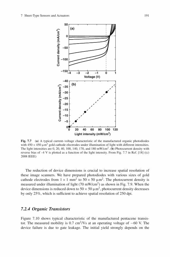
7 Sheet-Type Sensors and Actuators 191
–150
–100
–50
0
50
–4 –3 –2 –1 0 1
Cu
rren
t d
ensi
ty (
mA
/cm
2 )
Voltage (V)–40
–35
–30
–25
–20
–15
–10
–5
00 20 40 60 80 100 120
Cu
rren
t d
ensi
ty (
mA
/cm
2 )
Light intensity (mW/cm2)
(a)
(b)
Fig. 7.7 (a) A typical current–voltage characteristic of the manufactured organic photodiodeswith 450 × 450 μm2 gold cathode electrodes under illumination of light with different intensities.The light intensities are 0, 20, 40, 100, 140, 170, and 180 mW/cm2. (b) Photocurrent density withreverse bias of –4 V is plotted as a function of the light intensity. From Fig. 7.7 in Ref. [18] ((c)2008 IEEE)
The reduction of device dimensions is crucial to increase spatial resolution ofthese image scanners. We have prepared photodiodes with various sizes of goldcathode electrodes from 1 × 1 mm2 to 50 × 50 μm2. The photocurrent density ismeasured under illumination of light (70 mW/cm2) as shown in Fig. 7.9. When thedevice dimensions is reduced down to 50 × 50 μm2, photocurrent density decreasesby only 25%, which is sufficient to achieve spatial resolution of 250 dpi.
7.2.4 Organic Transistors
Figure 7.10 shows typical characteristic of the manufactured pentacene transis-tor. The measured mobility is 0.7 cm2/Vs at an operating voltage of −60 V. Thedevice failure is due to gate leakage. The initial yield strongly depends on the
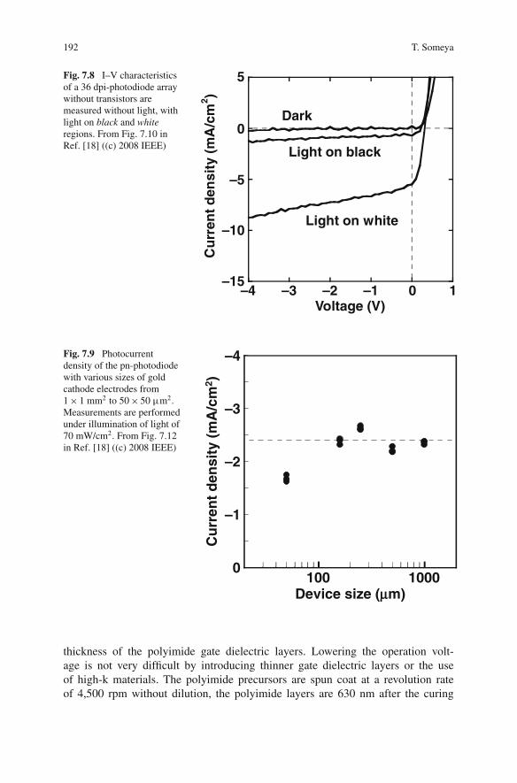
192 T. Someya
–15
–10
–5
0
5
–4 –3 –2 –1 0 1
Cu
rren
t d
ensi
ty (
mA
/cm
2 )
Voltage (V)
Dark
Light on black
Light on white
Fig. 7.8 I–V characteristicsof a 36 dpi-photodiode arraywithout transistors aremeasured without light, withlight on black and whiteregions. From Fig. 7.10 inRef. [18] ((c) 2008 IEEE)
–4
–3
–2
–1
0100 1000
Cu
rren
t d
ensi
ty (
mA
/cm
2 )
Device size (μm)
Fig. 7.9 Photocurrentdensity of the pn-photodiodewith various sizes of goldcathode electrodes from1 × 1 mm2 to 50 × 50 μm2.Measurements are performedunder illumination of light of70 mW/cm2. From Fig. 7.12in Ref. [18] ((c) 2008 IEEE)
thickness of the polyimide gate dielectric layers. Lowering the operation volt-age is not very difficult by introducing thinner gate dielectric layers or the useof high-k materials. The polyimide precursors are spun coat at a revolution rateof 4,500 rpm without dilution, the polyimide layers are 630 nm after the curing
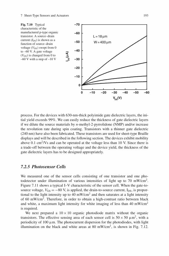
7 Sheet-Type Sensors and Actuators 193
–70
–60
–50
–40
–30
–20
–10
0
–10 –20 –30 –40 –50 –600
I DS (
μA)
VDS
(V)
L = 18 μm
W = 400 μm
Fig. 7.10 Typicalcharacteristic of themanufactured p-type organictransistor. A source–draincurrent (IDS) is shown as afunction of source–drainvoltage (VDS) swept from 0to –60 V. A gate voltage(VGS) is changed from 0 to–60 V with a step of –10 V
process. For the devices with 630-nm-thick polyimide gate dielectric layers, the ini-tial yield exceeds 99%. We can easily reduce the thickness of gate dielectric layersif we dilute the source materials by n-methyl-2-pyrrolidone (NMP) and/or increasethe revolution rate during spin coating. Transistors with a thinner gate dielectric(240 nm) have also been fabricated. These transistors are used for sheet-type Brailledisplays and will be described in the following section. The devices exhibit mobilityabove 0.1 cm2/Vs and can be operated at the voltage less than 10 V. Since there isa trade-off between the operating voltage and the device yield, the thickness of thegate dielectric layers has to be designed appropriately.
7.2.5 Photosensor Cells
We measured one of the sensor cells consisting of one transistor and one pho-todetector under illumination of various intensities of light up to 70 mW/cm2.Figure 7.11 shows a typical I–V characteristic of the sensor cell. When the gate-to-source voltage, VGS = −80 V, is applied, the drain-to-source current, IDS, is propor-tional to the light intensity up to 40 mW/cm2 and then saturates at a light intensityof 60 mW/cm2. Therefore, in order to obtain a high-contrast ratio between blackand white, a maximum light intensity for white imaging of less than 40 mW/cm2
is required.We next prepared a 10 × 10 organic photodiode matrix without the organic
transistors. The effective sensing area of each sensor cell is 50 × 50 μm2, with aperiodicity of 100 μm. The photocurrent dispersion for the photodiodes, with lightillumination on the black and white areas at 80 mW/cm2, is shown in Fig. 7.12.
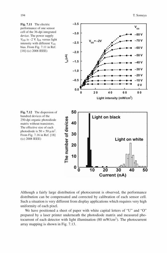
194 T. Someya
–3.5
–3.0
–2.5
–2.0
–1.5
–1.0
–0.5
0.00 2 0 4 0 6 0 8 0
I DS (
μ A)
Light intensity (mW/cm2)
–80 V
VGS
–70 V
–60 V
–50 V
–40 V
–30 V
–20 V–10 V
0 V
VDD = –2V
Fig. 7.11 The electricperformance of one sensorcell of the 36-dpi integrateddevice. The power supplyVDD is –2 V. IDS versus lightintensity with different VGS
bias. From Fig. 7.11 in Ref.[18] ((c) 2008 IEEE)
Light on white
Light on blackFig. 7.12 The dispersion ofhundred devices of the250-dpi organic photodiodematrix without transistors.The effective size of eachphotodiode is 50 × 50 μm2.From Fig. 7.16 in Ref. [18]((c) 2008 IEEE)
Although a fairly large distribution of photocurrent is observed, the performancedistribution can be compensated and corrected by calibration of each sensor cell.Such a situation is very different from display applications which requires very highuniformity of each pixel.
We have positioned a sheet of paper with white capital letters of “U” and “O”prepared by a laser printer underneath the photodiode matrix and measured pho-tocurrent of each detector with light illumination (80 mW/cm2). The photocurrentarray mapping is shown in Fig. 7.13.
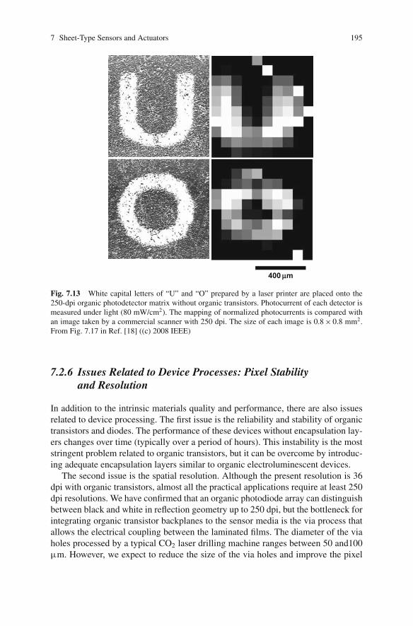
7 Sheet-Type Sensors and Actuators 195
400 μm
Fig. 7.13 White capital letters of “U” and “O” prepared by a laser printer are placed onto the250-dpi organic photodetector matrix without organic transistors. Photocurrent of each detector ismeasured under light (80 mW/cm2). The mapping of normalized photocurrents is compared withan image taken by a commercial scanner with 250 dpi. The size of each image is 0.8 × 0.8 mm2.From Fig. 7.17 in Ref. [18] ((c) 2008 IEEE)
7.2.6 Issues Related to Device Processes: Pixel Stabilityand Resolution
In addition to the intrinsic materials quality and performance, there are also issuesrelated to device processing. The first issue is the reliability and stability of organictransistors and diodes. The performance of these devices without encapsulation lay-ers changes over time (typically over a period of hours). This instability is the moststringent problem related to organic transistors, but it can be overcome by introduc-ing adequate encapsulation layers similar to organic electroluminescent devices.
The second issue is the spatial resolution. Although the present resolution is 36dpi with organic transistors, almost all the practical applications require at least 250dpi resolutions. We have confirmed that an organic photodiode array can distinguishbetween black and white in reflection geometry up to 250 dpi, but the bottleneck forintegrating organic transistor backplanes to the sensor media is the via process thatallows the electrical coupling between the laminated films. The diameter of the viaholes processed by a typical CO2 laser drilling machine ranges between 50 and100μm. However, we expect to reduce the size of the via holes and improve the pixel
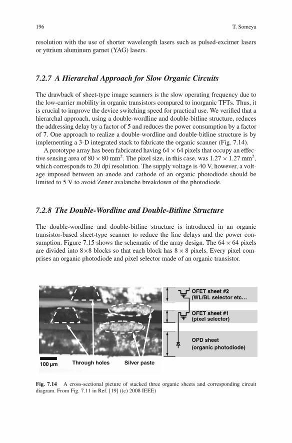
196 T. Someya
resolution with the use of shorter wavelength lasers such as pulsed-excimer lasersor yttrium aluminum garnet (YAG) lasers.
7.2.7 A Hierarchal Approach for Slow Organic Circuits
The drawback of sheet-type image scanners is the slow operating frequency due tothe low-carrier mobility in organic transistors compared to inorganic TFTs. Thus, itis crucial to improve the device switching speed for practical use. We verified that ahierarchal approach, using a double-wordline and double-bitline structure, reducesthe addressing delay by a factor of 5 and reduces the power consumption by a factorof 7. One approach to realize a double-wordline and double-bitline structure is byimplementing a 3-D integrated stack to fabricate the organic scanner (Fig. 7.14).
A prototype array has been fabricated having 64 × 64 pixels that occupy an effec-tive sensing area of 80 × 80 mm2. The pixel size, in this case, was 1.27 × 1.27 mm2,which corresponds to 20 dpi resolution. The supply voltage is 40 V, however, a volt-age imposed between an anode and cathode of an organic photodiode should belimited to 5 V to avoid Zener avalanche breakdown of the photodiode.
7.2.8 The Double-Wordline and Double-Bitline Structure
The double-wordline and double-bitline structure is introduced in an organictransistor-based sheet-type scanner to reduce the line delays and the power con-sumption. Figure 7.15 shows the schematic of the array design. The 64 × 64 pixelsare divided into 8×8 blocks so that each block has 8 × 8 pixels. Every pixel com-prises an organic photodiode and pixel selector made of an organic transistor.
Silver pasteThrough holes100 µm
OPD sheet(organic photodiode)
OFET sheet #1(pixel selector)
OFET sheet #2(WL/BL selector etc…
Fig. 7.14 A cross-sectional picture of stacked three organic sheets and corresponding circuitdiagram. From Fig. 7.11 in Ref. [19] ((c) 2008 IEEE)
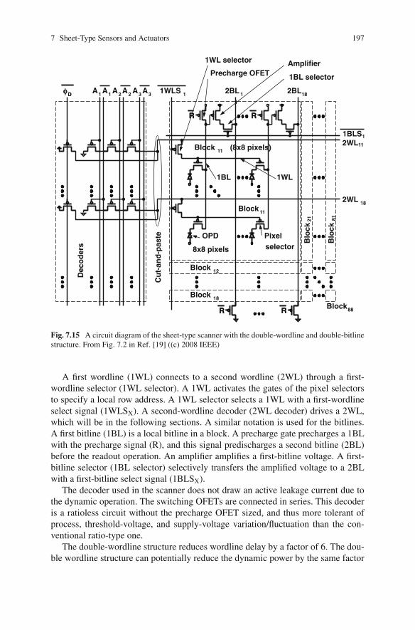
7 Sheet-Type Sensors and Actuators 197
1WLS 1
Amplifier
RR RR
2BL 1
1
2WL11
Block 12
8x8 pixels
φDφD
1BL
2BL18
RR RR
1BL selector
1WL selector
Precharge OFET
Pixelselector
OPD
A2 A2 A3 A3A1 A1
Block 18
Blo
ck21
Blo
ck81
2WL 18
Dec
od
ers
1BLS1
Cu
t-an
d-p
aste
Block 11
Block88
1WL
Block 11 (8x8 pixels)
Fig. 7.15 A circuit diagram of the sheet-type scanner with the double-wordline and double-bitlinestructure. From Fig. 7.2 in Ref. [19] ((c) 2008 IEEE)
A first wordline (1WL) connects to a second wordline (2WL) through a first-wordline selector (1WL selector). A 1WL activates the gates of the pixel selectorsto specify a local row address. A 1WL selector selects a 1WL with a first-wordlineselect signal (1WLSX). A second-wordline decoder (2WL decoder) drives a 2WL,which will be in the following sections. A similar notation is used for the bitlines.A first bitline (1BL) is a local bitline in a block. A precharge gate precharges a 1BLwith the precharge signal (R), and this signal predischarges a second bitline (2BL)before the readout operation. An amplifier amplifies a first-bitline voltage. A first-bitline selector (1BL selector) selectively transfers the amplified voltage to a 2BLwith a first-bitline select signal (1BLSX).
The decoder used in the scanner does not draw an active leakage current due tothe dynamic operation. The switching OFETs are connected in series. This decoderis a ratioless circuit without the precharge OFET sized, and thus more tolerant ofprocess, threshold-voltage, and supply-voltage variation/fluctuation than the con-ventional ratio-type one.
The double-wordline structure reduces wordline delay by a factor of 6. The dou-ble wordline structure can potentially reduce the dynamic power by the same factor
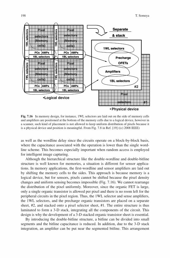
198 T. Someya
Pixel
selectors #1
Pixel
selectors
(Memory
cells)
Pixel
selectors
(Memory
cells)
Pixel
selectors
(Memory
cells)
Pixel
selectors
(Memory
cells)1WL
sel
ecto
rs
1BL selectors
PCs AMPs
1WL
sele
cto
rs
1BL selectors
PCs AMPs1W
L s
elec
tors
1BL selectors
PCs AMPs
1WL
sel
ecto
rs1BL selectors
PCs AMPs
#2
Separate
& stack
1WL selectors
Precharge
OFETs
Amplifiers
1BL selectors
Pixel
selectors #1
Pixel
selectors
(Memory
cells)
Pixel
selectors(Memory
cells)
Pixel
selectors
(Memory
cells)
Pixel
selectors
(Memory
cells)1WL
sel
ecto
rs
1BL selectors
PCs AMPs
1WL
sele
cto
rs
1BL selectors
PCs AMPs1W
L s
elec
tors
1BL selectors
PCs AMPs
1WL
sel
ecto
rs1BL selectors
PCs AMPs
#2
Separate
& stack
1WL selectors1WL selectors
Precharge
OFETs
Precharge
OFETs
AmplifiersAmplifiers
1BL selectors1BL selectors
• Physical device
•Logical device
Fig. 7.16 In memory design, for instance, 1WL selectors are laid out on the side of memory cellsand amplifiers are positioned at the bottom of the memory cells due to a logical device, however ina scanner, such kind of placement is not allowed to keep uniform distribution of pixels because itis a physical device and position is meaningful. From Fig. 7.8 in Ref. [19] ((c) 2008 IEEE)
as well as the wordline delay since the circuits operate on a block-by-block basis,where the capacitance associated with the operation is lower than the single word-line scheme. This becomes especially important when random access is employedfor intelligent image capturing.
Although the hierarchical structure like the double-wordline and double-bitlinestructure is well known for memories, a situation is different for sensor applica-tions. In memory applications, the first-wordline and sensor amplifiers are laid outby shifting the memory cells to the sides. This approach is because memory is alogical device, but for sensors, pixels cannot be shifted because the pixel densitychanges and uniform sensing becomes impossible (Fig. 7.16). We cannot rearrangethe distribution of the pixel uniformly. Moreover, since the organic FET is large,only a single organic transistor is allowed per pixel and there is no room left for theperipheral circuits in the pixel region. Thus, the 1WL selector and sense amplifiers,the 1WL selectors, and the precharge organic transistors are placed on a separatesheet, #2, and stacked onto a pixel selector sheet, #1. The entire structure is thuslaminated to form a 3-D stack, integrating all the components of the circuit. Thisdesign is why the development of a 3-D stacked organic transistor sheet is essential.
By introducing the double-bitline structure, a bitline can be divided into smallsegments and the bitline capacitance is reduced. In addition, due to the 3-D stackintegration, an amplifier can be put near the segmented bitline. This arrangement
7 Sheet-Type Sensors and Actuators 199
means that a photodiode just draws charge out of a relatively small capacitance. Inthe future, we could improve the sensitivity of the photodiode in order to generatemore photocurrent, making it possible to use ambient light as a light source.
7.2.9 A New Dynamic Second-Wordline Decoder
As a 2WL decoder, a serial-connected decoder is introduced for lower power andhigher speed operation than the parallel-connected static one used in the electronic-skin (e-skin) [10–15]. In the e-skin application, switching organic FETs are con-nected in parallel, and the load transistor must be small because of the normallyon load and sizing requirements. Thus, the falling time is slow, and in addition, biasvoltage adjustment is needed to cancel the variability of the threshold voltage, whichresults in a leakage current in the order of micro-Amps. On the other hand, the newdecoder does not draw active leakage due to its dynamic operation. The new decoderis a ratio-less circuit, and thus it has a wider margin of operation.
The layout style is novel and takes advantage of the “cut-and-paste” customiza-tion [12]. For example, five switching organic transistors connected in series are pre-pared in advance. Next, if only 1 out of 8 decoders having only 3 switching organictransistors are needed, then the three switching organic transistors can be removedfrom the prefabricated decoder and laminated to a 2WL pad as shown in Fig. 7.15.This “cut-and-paste” customization reduces the mask cost as well as a nonrecurringengineering cost because we do not need to design or make new masks for varioussizes.
7.2.10 Higher Speed Operation with Lower Power Consumption
The measured operation waveforms are shown in Fig. 7.17 together with a sketchof stimulus signals. Successful operation is observed. Both the conventional single-wordline and single-bitline device and proposed double-wordline and double-bitlinedevice are manufactured for comparison. Falling time of the 1BL from VDD to 90%of VDD in the proposed structure is 3 ms but in the conventional scheme is 17 ms.The wordline delay can be reduced by a factor of >5.
Now, we would like to explain the photocurrent-sensing scheme. After a 1BL isprecharged and wordline is asserted, a photocurrent according to the light intensitydischarges a first-bitline capacitance, and the first-bitline voltage starts decreasing.The falling time depends on the photocurrent. An amplifier amplifies the first-bitlinevoltage, which starts to pull-up the second-bitline voltage. Thus, the rising time ofthe 2BL is a function of the photocurrent, by which black and white pixels arediscriminated. This scheme is a kind of current-to-time conversion.
When the sense voltage is set to 30 V, the readout time in the conventionalsingle-bitline scheme is 18 ms while that in the proposed double-bitline struc-ture is 3 ms, achieving a factor of 6 improvement in the wordline delay. In the
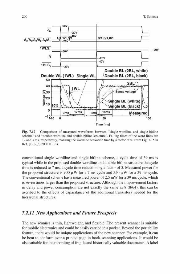
200 T. Someya
1/1,1/1,1/1
1BLS1
18ms3ms
A3/A3,A2/A2,A1/A1
–10 0 50 100–10
0
10
20
30
40
50
1WLS1
φD
R
0/1,0/1,0/1
1WL2BL
Double WL (1WL) Single WLDouble BL (2BL, white)Double BL (2BL, black)
Single BL (white)Single BL (black)V
olt
age
[V]
60V
–20V40V
–20V
–20V60V
Time [ms]
–20V40V
–20V
3ms 17ms Measured
10%
Sense voltage
Fig. 7.17 Comparison of measured waveforms between “single-wordline and single-bitlinescheme” and “double-wordline and double-bitline structure”. Falling times of the word lines are17 and 3 ms, respectively, realizing the wordline activation time by a factor of 5. From Fig. 7.15 inRef. [19] ((c) 2008 IEEE)
conventional single-wordline and single-bitline scheme, a cycle time of 39 ms istypical while in the proposed double-wordline and double-bitline structure the cycletime is reduced to 7 ms, a cycle time reduction by a factor of 5. Measured power forthe proposed structure is 900 μW for a 7 ms cycle and 350 μW for a 39 ms cycle.The conventional scheme has a measured power of 2.5 mW for a 39 ms cycle, whichis seven times larger than the proposed structure. Although the improvement factorsin delay and power consumption are not exactly the same as 8 (8/64), this can beascribed to the effects of capacitance of the additional transistors needed for thehierarchal structures.
7.2.11 New Applications and Future Prospects
The new scanner is thin, lightweight, and flexible. The present scanner is suitablefor mobile electronics and could be easily carried in a pocket. Beyond the portabilityfeature, there would be unique applications of the new scanner. For example, it canbe bent to conform over a printed page in book-scanning applications. It would bealso suitable for the recording of fragile and historically valuable documents. A label
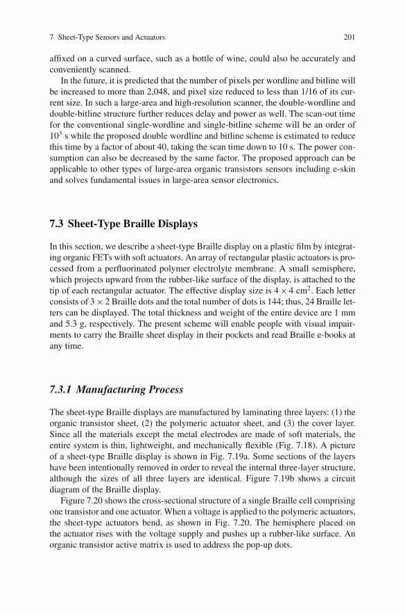
7 Sheet-Type Sensors and Actuators 201
affixed on a curved surface, such as a bottle of wine, could also be accurately andconveniently scanned.
In the future, it is predicted that the number of pixels per wordline and bitline willbe increased to more than 2,048, and pixel size reduced to less than 1/16 of its cur-rent size. In such a large-area and high-resolution scanner, the double-wordline anddouble-bitline structure further reduces delay and power as well. The scan-out timefor the conventional single-wordline and single-bitline scheme will be an order of103 s while the proposed double wordline and bitline scheme is estimated to reducethis time by a factor of about 40, taking the scan time down to 10 s. The power con-sumption can also be decreased by the same factor. The proposed approach can beapplicable to other types of large-area organic transistors sensors including e-skinand solves fundamental issues in large-area sensor electronics.
7.3 Sheet-Type Braille Displays
In this section, we describe a sheet-type Braille display on a plastic film by integrat-ing organic FETs with soft actuators. An array of rectangular plastic actuators is pro-cessed from a perfluorinated polymer electrolyte membrane. A small semisphere,which projects upward from the rubber-like surface of the display, is attached to thetip of each rectangular actuator. The effective display size is 4 × 4 cm2. Each letterconsists of 3 × 2 Braille dots and the total number of dots is 144; thus, 24 Braille let-ters can be displayed. The total thickness and weight of the entire device are 1 mmand 5.3 g, respectively. The present scheme will enable people with visual impair-ments to carry the Braille sheet display in their pockets and read Braille e-books atany time.
7.3.1 Manufacturing Process
The sheet-type Braille displays are manufactured by laminating three layers: (1) theorganic transistor sheet, (2) the polymeric actuator sheet, and (3) the cover layer.Since all the materials except the metal electrodes are made of soft materials, theentire system is thin, lightweight, and mechanically flexible (Fig. 7.18). A pictureof a sheet-type Braille display is shown in Fig. 7.19a. Some sections of the layershave been intentionally removed in order to reveal the internal three-layer structure,although the sizes of all three layers are identical. Figure 7.19b shows a circuitdiagram of the Braille display.
Figure 7.20 shows the cross-sectional structure of a single Braille cell comprisingone transistor and one actuator. When a voltage is applied to the polymeric actuators,the sheet-type actuators bend, as shown in Fig. 7.20. The hemisphere placed onthe actuator rises with the voltage supply and pushes up a rubber-like surface. Anorganic transistor active matrix is used to address the pop-up dots.
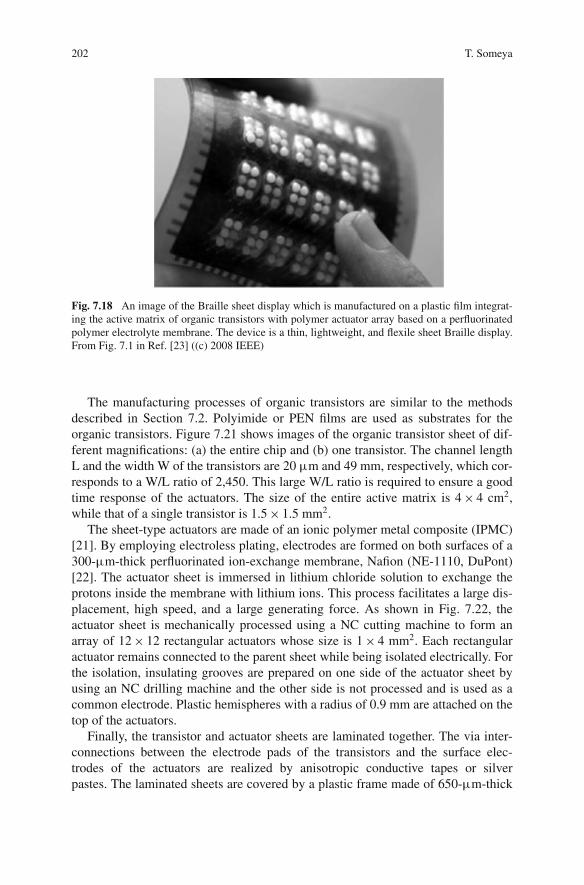
202 T. Someya
Fig. 7.18 An image of the Braille sheet display which is manufactured on a plastic film integrat-ing the active matrix of organic transistors with polymer actuator array based on a perfluorinatedpolymer electrolyte membrane. The device is a thin, lightweight, and flexile sheet Braille display.From Fig. 7.1 in Ref. [23] ((c) 2008 IEEE)
The manufacturing processes of organic transistors are similar to the methodsdescribed in Section 7.2. Polyimide or PEN films are used as substrates for theorganic transistors. Figure 7.21 shows images of the organic transistor sheet of dif-ferent magnifications: (a) the entire chip and (b) one transistor. The channel lengthL and the width W of the transistors are 20 μm and 49 mm, respectively, which cor-responds to a W/L ratio of 2,450. This large W/L ratio is required to ensure a goodtime response of the actuators. The size of the entire active matrix is 4 × 4 cm2,while that of a single transistor is 1.5 × 1.5 mm2.
The sheet-type actuators are made of an ionic polymer metal composite (IPMC)[21]. By employing electroless plating, electrodes are formed on both surfaces of a300-μm-thick perfluorinated ion-exchange membrane, Nafion (NE-1110, DuPont)[22]. The actuator sheet is immersed in lithium chloride solution to exchange theprotons inside the membrane with lithium ions. This process facilitates a large dis-placement, high speed, and a large generating force. As shown in Fig. 7.22, theactuator sheet is mechanically processed using a NC cutting machine to form anarray of 12 × 12 rectangular actuators whose size is 1 × 4 mm2. Each rectangularactuator remains connected to the parent sheet while being isolated electrically. Forthe isolation, insulating grooves are prepared on one side of the actuator sheet byusing an NC drilling machine and the other side is not processed and is used as acommon electrode. Plastic hemispheres with a radius of 0.9 mm are attached on thetop of the actuators.
Finally, the transistor and actuator sheets are laminated together. The via inter-connections between the electrode pads of the transistors and the surface elec-trodes of the actuators are realized by anisotropic conductive tapes or silverpastes. The laminated sheets are covered by a plastic frame made of 650-μm-thick
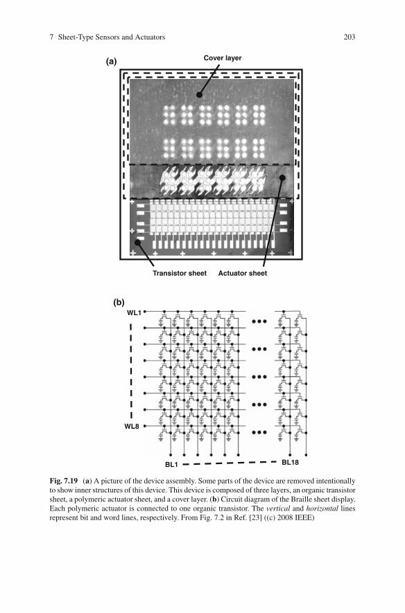
7 Sheet-Type Sensors and Actuators 203
Transistor sheet Actuator sheet
Cover layer(a)
(b)
BL1 BL18
WL1
WL8
Fig. 7.19 (a) A picture of the device assembly. Some parts of the device are removed intentionallyto show inner structures of this device. This device is composed of three layers, an organic transistorsheet, a polymeric actuator sheet, and a cover layer. (b) Circuit diagram of the Braille sheet display.Each polymeric actuator is connected to one organic transistor. The vertical and horizontal linesrepresent bit and word lines, respectively. From Fig. 7.2 in Ref. [23] ((c) 2008 IEEE)
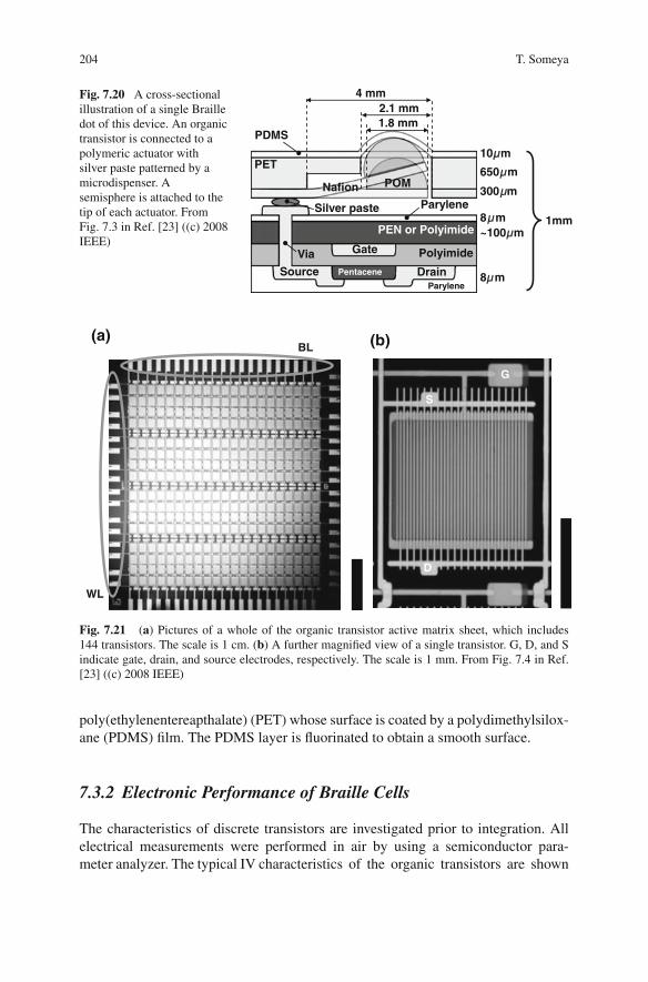
204 T. Someya
10µµm
650µm
300µm
8µ m~100 µm
8µ m
PET
Silver paste
PEN or Polyimide
Polyimide
DrainSource
Gate
POM
PDMS
Nafion
Pentacene
Via
4 mm2.1 mm1.8 mm
1mm
Parylene
Parylene
Fig. 7.20 A cross-sectionalillustration of a single Brailledot of this device. An organictransistor is connected to apolymeric actuator withsilver paste patterned by amicrodispenser. Asemisphere is attached to thetip of each actuator. FromFig. 7.3 in Ref. [23] ((c) 2008IEEE)
WL
BL(a)
S
D
G
(b)
Fig. 7.21 (a) Pictures of a whole of the organic transistor active matrix sheet, which includes144 transistors. The scale is 1 cm. (b) A further magnified view of a single transistor. G, D, and Sindicate gate, drain, and source electrodes, respectively. The scale is 1 mm. From Fig. 7.4 in Ref.[23] ((c) 2008 IEEE)
poly(ethylenentereapthalate) (PET) whose surface is coated by a polydimethylsilox-ane (PDMS) film. The PDMS layer is fluorinated to obtain a smooth surface.
7.3.2 Electronic Performance of Braille Cells
The characteristics of discrete transistors are investigated prior to integration. Allelectrical measurements were performed in air by using a semiconductor para-meter analyzer. The typical IV characteristics of the organic transistors are shown
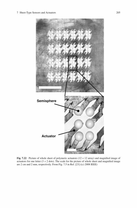
7 Sheet-Type Sensors and Actuators 205
Semisphere
Actuator
Fig. 7.22 Picture of whole sheet of polymeric actuators (12 × 12 array) and magnified image ofactuators for one letter (3 × 2 dots). The scale for the picture of whole sheet and magnified imageare 2 cm and 2 mm, respectively. From Fig. 7.5 in Ref. [23] ((c) 2008 IEEE)
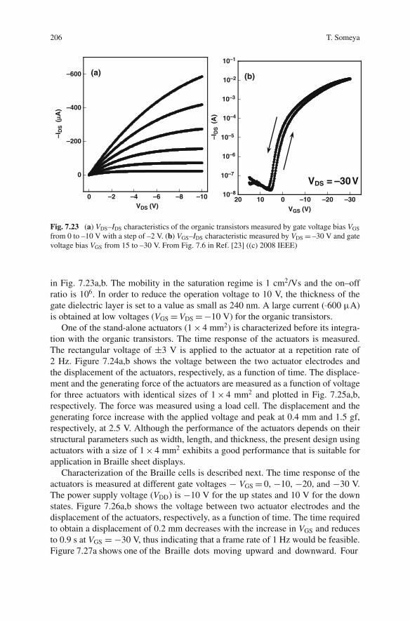
206 T. Someya
–ID
S (
μA)
VDS (V)
–600
–400
–200
0
–8 –10–6–2 –40
(a)
10–8
10–7
10–6
10–5
10–4
10–3
10–2
10–1
–30–20–1001020
–ID
S (
A)
VGS (V)
VDS = –30 V
(b)
Fig. 7.23 (a) VDS–IDS characteristics of the organic transistors measured by gate voltage bias VGS
from 0 to –10 V with a step of –2 V. (b) VGS–IDS characteristic measured by VDS = –30 V and gatevoltage bias VGS from 15 to –30 V. From Fig. 7.6 in Ref. [23] ((c) 2008 IEEE)
in Fig. 7.23a,b. The mobility in the saturation regime is 1 cm2/Vs and the on–offratio is 106. In order to reduce the operation voltage to 10 V, the thickness of thegate dielectric layer is set to a value as small as 240 nm. A large current (˜600 μA)is obtained at low voltages (VGS = VDS = −10 V) for the organic transistors.
One of the stand-alone actuators (1 × 4 mm2) is characterized before its integra-tion with the organic transistors. The time response of the actuators is measured.The rectangular voltage of ±3 V is applied to the actuator at a repetition rate of2 Hz. Figure 7.24a,b shows the voltage between the two actuator electrodes andthe displacement of the actuators, respectively, as a function of time. The displace-ment and the generating force of the actuators are measured as a function of voltagefor three actuators with identical sizes of 1 × 4 mm2 and plotted in Fig. 7.25a,b,respectively. The force was measured using a load cell. The displacement and thegenerating force increase with the applied voltage and peak at 0.4 mm and 1.5 gf,respectively, at 2.5 V. Although the performance of the actuators depends on theirstructural parameters such as width, length, and thickness, the present design usingactuators with a size of 1 × 4 mm2 exhibits a good performance that is suitable forapplication in Braille sheet displays.
Characterization of the Braille cells is described next. The time response of theactuators is measured at different gate voltages − VGS = 0, −10, −20, and −30 V.The power supply voltage (VDD) is −10 V for the up states and 10 V for the downstates. Figure 7.26a,b shows the voltage between two actuator electrodes and thedisplacement of the actuators, respectively, as a function of time. The time requiredto obtain a displacement of 0.2 mm decreases with the increase in VGS and reducesto 0.9 s at VGS = −30 V, thus indicating that a frame rate of 1 Hz would be feasible.Figure 7.27a shows one of the Braille dots moving upward and downward. Four
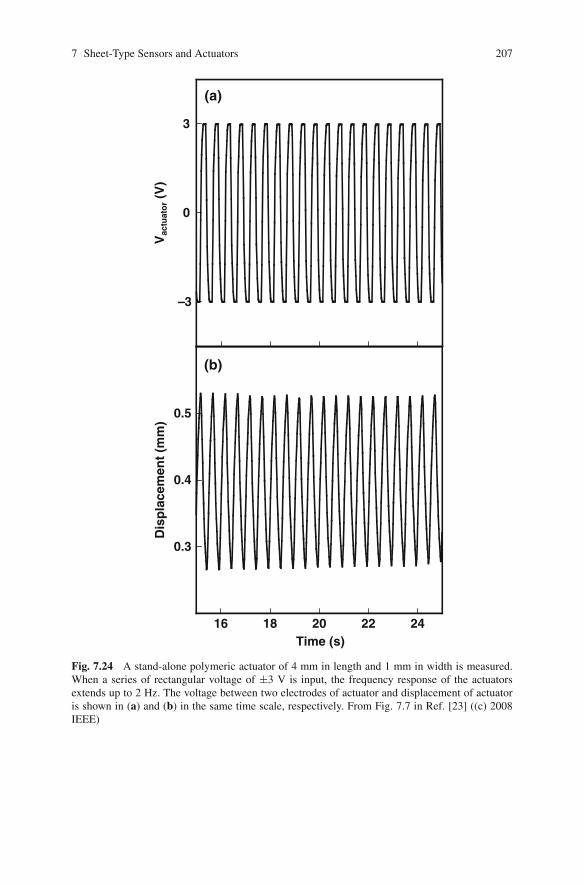
7 Sheet-Type Sensors and Actuators 207
0.3
0.4
0.5
16 18 20 22 24
Dis
pla
cem
ent
(mm
)
Time (s)
–3
0
3
Vac
tuat
or (
V)
(a)
(b)
Fig. 7.24 A stand-alone polymeric actuator of 4 mm in length and 1 mm in width is measured.When a series of rectangular voltage of ±3 V is input, the frequency response of the actuatorsextends up to 2 Hz. The voltage between two electrodes of actuator and displacement of actuatoris shown in (a) and (b) in the same time scale, respectively. From Fig. 7.7 in Ref. [23] ((c) 2008IEEE)
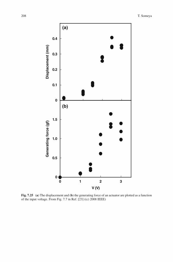
208 T. Someya
0
0.1
0.2
0.3
0.4
Dis
pla
cem
ent
(mm
)
0
0.5
1.0
1.5
0 1 2 3
Gen
erat
ing
fo
rce
(gf)
V (V)
(a)
(b)
Fig. 7.25 (a) The displacement and (b) the generating force of an actuator are plotted as a functionof the input voltage. From Fig. 7.7 in Ref. [23] ((c) 2008 IEEE)
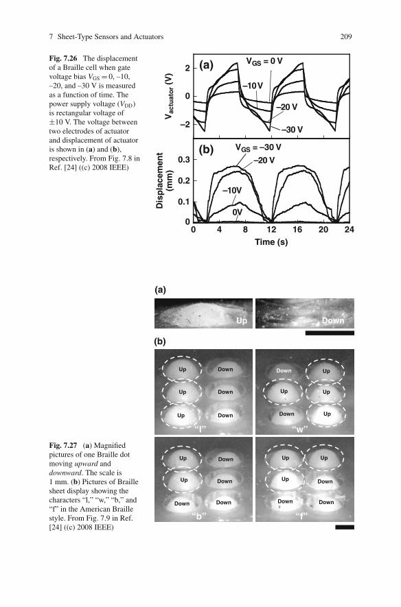
7 Sheet-Type Sensors and Actuators 209
–2
0
2
Vac
tuat
or (
V)
–30 V
–20 V
–10V
VGS = 0 V
VGS = –30 V
0
0.1
0.2
0.3
0 4 8 12 16 20 24
Dis
pla
cem
ent
(mm
)
Time (s)
–20 V
–10V
0V
(a)
(b)
Fig. 7.26 The displacementof a Braille cell when gatevoltage bias VGS = 0, –10,–20, and –30 V is measuredas a function of time. Thepower supply voltage (VDD)is rectangular voltage of±10 V. The voltage betweentwo electrodes of actuatorand displacement of actuatoris shown in (a) and (b),respectively. From Fig. 7.8 inRef. [24] ((c) 2008 IEEE)
Up Down
Up
Up
Up Down
Down
Down
Up
Up
Up
Up
Down
Down
(a)
(b)
Down Down
Down
DownUp
Up
Down Down
Down
Up
Up
Up
“l” “w”
“b” “f”
Fig. 7.27 (a) Magnifiedpictures of one Braille dotmoving upward anddownward. The scale is1 mm. (b) Pictures of Braillesheet display showing thecharacters “l,” “w,” “b,” and“f” in the American Braillestyle. From Fig. 7.9 in Ref.[24] ((c) 2008 IEEE)
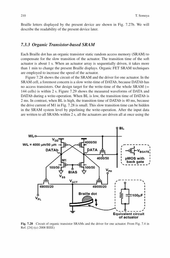
210 T. Someya
Braille letters displayed by the present device are shown in Fig. 7.27b. We willdescribe the readability of the present device later.
7.3.3 Organic Transistor-based SRAM
Each Braille dot has an organic transistor static random access memory (SRAM) tocompensate for the slow transition of the actuator. The transition time of the softactuator is about 1 s. When an actuator array is sequentially driven, it takes morethan 1 min to change the present Braille displays. Organic FET SRAM techniquesare employed to increase the speed of the actuator.
Figure 7.28 shows the circuit of the SRAM and the driver for one actuator. In theSRAM cell, a foremost concern is a slow write-time of DATAb, because DATAb hasno access transistors. Our design target for the write-time of the whole SRAM (=144 cells) is within 2 s. Figure 7.29 shows the measured waveforms of DATA andDATAb during a write-operation. When BL is low, the transition time of DATAb is2 ms. In contrast, when BL is high, the transition time of DATAb is 40 ms, becausethe drive current of M1 in Fig. 7.28 is small. This slow transition time can be hiddenin the SRAM system level by pipelining the write-operation. After the input dataare written to all SRAMs within 2 s, all the actuators are driven all at once using the
Fig. 7.28 Circuit of organic transistor SRAMs and the driver for one actuator. From Fig. 7.4 inRef. [24] ((c) 2008 IEEE)
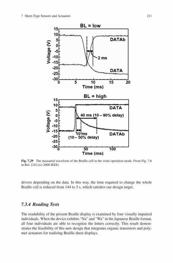
7 Sheet-Type Sensors and Actuators 211
Fig. 7.29 The measured waveform of the Braille cell in the write-operation mode. From Fig. 7.6in Ref. [24] ((c) 2008 IEEE)
drivers depending on the data. In this way, the time required to change the wholeBraille cell is reduced from 144 to 3 s, which satisfies our design target.
7.3.4 Reading Tests
The readability of the present Braille display is examined by four visually impairedindividuals. When the device exhibits “Na” and “Wa” in the Japanese Braille format,all four individuals are able to recognize the letters correctly. This result demon-strates the feasibility of this new design that integrates organic transistors and poly-mer actuators for realizing Braille sheet displays.
212 T. Someya
However, it is known that the ability of reading Braille varies across the visuallyimpaired and, in general, a larger displacement and a larger force should help themin reading Braille more easily. In particular, the variations in the displacement andthe generating force of the Braille dots must be minimized for better readability,although the present device shows fairly large performance variations. These vari-ations may be ascribed to the unevenness in the electroless plating process and/orthe fluctuations in the size of the actuators that arise due to the inaccuracy of themechanical process. These imperfections would be removed by optimizing the pro-cess conditions.
7.3.5 Future Prospects
The new design in this study offers an attractive scheme for reducing the thicknessand weight of Braille displays and yet maintains a reasonable performance. Com-mercial Braille displays that utilize piezoelectric or solenoid actuators are available.Such actuators can control displacement with a high accuracy and also obtain largeforces; however, their miniaturization is complicated. The proposed lightweight,thin, and flexible sheet-type Braille displays can be easily carried in pockets; there-fore, they are suitable for mobile applications such as Braille e-books. It is expectedthat the sheet-type Braille can be easily implemented in many digital and informa-tion appliances including cell phones without necessitating major changes in thedesign of the parent appliances. Thus, Braille will be more conveniently used by thevisually impaired in various situations in the future.
7.4 Summary
This chapter reported on large-area, flexible sensors and actuators based on organictransistors. As an example of large-area sensors, a sheet image scanner integratingorganic transistors and organic photodetectors was described. The new sheet-typescanner with light shielding layers can distinguish between black and white in thereflection geometry. Then, a sheet-type Braille display was reported as an exampleof large-area, flexible actuators. The new Braille display was fabricated on a plasticfilm by integrating high-quality organic transistors and soft sheet-type actuators. Inthose two types of devices, all the components are manufactured on plastic films.Therefore, it is lightweight, shock-resistant, and flexible and is suitable for human-friendly mobile application.
Acknowledgements The research work in this chapter was carried in collaboration with Prof.Takayasu Sakurai, Prof. Makoto Takamiya, Dr. Tsuyoshi Sekitani, Dr. Hiroshi Kawaguchi, YusakuKato, and Yoshiaki Noguchi.
7 Sheet-Type Sensors and Actuators 213
References
1. Drury CJ, Mutsaers CMJ, Hart CM, Matters M, de Leeuw DM (1998) Low-cost all-polymerintegrated circuits. Appl Phys Lett 73:108–110
2. Crone B, Dodabalapur A, Lin YY, Filas RW, Bao Z, LaDuca A, Sarpeshkar R, Katz HE, LiW (2000) Large-scale complementary integrated circuits based on organic transistors. Nature403:521–523
3. Gelinck GH, Geuns TCT, de Leeuw DM (2000) High-performance all-polymer integratedcircuits. Appl Phys Lett 77:1487–1489
4. Gelinck GH, Huitema HEA, van Veenendaal E, Cantatore E, Schrijnemakers L, van der Put-ten JBPH, Geuns TCT, Beenhakkers M, Giesbers JB, Huisman BH, Meijer EJ, Benito EM,Touwslager FJ, Marsman AW, van Rens BJE, de Leeuw DM (2004) Flexible active-matrixdisplays and shift registers based on solution-processed organic transistors. Nat Mater 3:106–110
5. Huitema E, Gelinck G, van der Putten B, Cantatore E, van Veenendaal E, SchrijnemakersL, Huisman BH, Leeuw DM (2003) Plastic transistors in active-matrix displays. ISSCC Dig.Tech. Papers, pp 380–381
6. Brederlow R, Briole S, Klauk H, Halik M, Zschieschang U, Schmid G, Gorriz-Saez JM, PachaC, Thewes R, Weber W (2003) Evaluation of the performance potential of organic TFT cir-cuits. ISSCC Dig. Tech. Papers, pp 378–379.
7. Rogers JA, Bao Z, Baldwin K, Dodabalapur A, Crone B, Raju VR, Kuck V, Katz H, Amund-son K, Ewing J, Drzaic P (2001) Paper-like electronic displays: Large-area rubber-stampedplastic sheets of electronics and microencapsulated electrophoretic inks. Proc Natl Acad SciUSA 98:4835–4840
8. Baude PF, Ender DA, Haase MA, Kelley TW, Muyres DV, Theiss SD (2003) Pentacene-basedradio-frequency identification circuitry. Appl Phys Lett 82:3964–3966
9. Baude PF, Ender DA, Kelley TW, Haase MA, Muyres DV, Theiss SD (2003) Organic semi-conductor RFID transponders. IEDM Tech. Dig., pp 191–194.
10. Someya T, Sekitani T, Iba S, Kato Y, Kawaguchi H, Sakurai T (2004) A large-area, flexiblepressure sensor matrix with organic field-effect transistors for artificial skin applications. ProcNatl Acad Sci USA 101:9966–9970
11. Someya T, Kato Y, Sekitani T, Iba S, Noguchi Y, Murase Y, Kawaguchi H, Sakurai T (2005)Conformable, flexible, large-area networks of pressure and thermal sensors with organic tran-sistor active matrixes. Proc Natl Acad Sci USA 102(35):12321–12325
12. Kawaguchi H, Someya T, Sekitani T, Sakurai T (2005) Cut-and-paste customization of organicFET integrated circuit and its application to electronic artificial skin. IEEE J Solid-State Circ40:177–185
13. Someya T, Kawaguchi H, Sakurai T (2004) Cut-and-paste organic FET customized ICs forapplication to artificial skin. ISSCC Dig. Tech. Papers, pp 288–289
14. Someya T, Sakurai T (2003) Integration of organic field-effect transistors and rubbery pressuresensors for artificial skin applications. IEDM Tech. Dig., pp 203–206
15. Someya T, Sakurai T (2006) Large-area detectors and sensors. In: Klauk H (ed) Organic elec-tronics. Wiley-VCH, Weinheim, pp 395–410
16. Someya T, Iba S, Kato Y, Sekitani T, Noguchi Y, Murase Y, Kawaguchi H, Sakurai T (2004)A large-area, flexible, and lightweight sheet image scanner. IEDM Tech. Dig., pp 580–581
17. Kawaguchi H, Iba S, Kato Y, Sekitani T, Someya T, Sakurai T (2005) A sheet-type scannerbased on a 3D-stacked organic-transistor circuit using double wordline and bitline structure.ISSCC Tech. Dig., pp 365–368
18. Someya T, KatoY, Iba S, Kawaguchi H, Sakurai T (2005) Integration of organic field-effecttransistors with organic photodiodes for a large-area, flexible, and lightweight sheet imagescanner. IEEE Trans Electron Dev 52(11):2502–2511
214 T. Someya
19. Kawaguchi H, Iba S, KatoY, SekitaniT, Someya T, Sakurai T (2006) A 3D-stack organicsheet-type scanner with double-wordline and double-bitline structure. IEEE Sensors J 6(5):1209–1217
20. KatoY, Iba S, Teramoto R, Sekitani T, Someya T, Kawaguchi H, Sakurai T (2004) High mobil-ity of pentacene field-effect transistors with polyimide gate dielectric layers. Appl Phys Lett84:3789–3791
21. Shahinpoor M, Bar-Cohen Y, Simpson JO, Smith J (1998) Ionic polymer-metal composites(IPMCs) as biomimetic sensors, actuators and artificial muscles – a review. Smart Mater Struct7:R15–R30
22. Fujiwara N, Asaka K, Nishimura Y, Oguro K, Torikai E (2000) Preparation of gold-solidpolymer electrolyte composites as electric stimuli-responsive materials. Chem Mater 12:1750–1754
23. Kato Y, Sekitani T, Takamiya M, Doi M, Asaka K, Sakurai T, Someya T (2007) Sheet-typeBraille displays by integrating organic field-effect transistors and polymeric actuators. IEEETrans Electron Dev 54(2):202–209
24. Takamiya M, Sekitani T, Kato Y, Kawaguchi H, Someya T, Sakurai T (2007) An organicFET SRAM with back gate to increase static noise margin and its application to Braille sheetdisplay. IEEE J Solid-State Circ 42(1):93–100
Chapter 8Organic and Polymeric TFTs for FlexibleDisplays and Circuits
Michael G. Kane
8.1 Introduction
Organic and polymeric thin-film transistors are a natural complement to flexiblesubstrates. This is because organic thin-film transistors (OTFTs) can be made usinga very low temperature process, not much above room temperature, allowing elec-tronic circuits and systems to be made on plastic films.1 The organic and polymericmaterials that can be used as semiconductors, dielectrics, and conductors are them-selves flexible like the substrate, so that a complete flexible electronic system ispossible.
There are several benefits of building an electronic system on a flexible sub-strate. In some applications, there may be advantages to mechanical flexibility inactual use, as with a rugged, unbreakable, rollable display. In other cases, flexibil-ity may not be needed in the application, but benefits may derive from the lowermanufacturing costs of continuous roll-to-roll fabrication. For example, low-costdisplays fabricated in a web-based line might end up laminated to a hard, rigidmaterial, which may be curved or flat, glass or plastic. There may also simply becost advantages associated with the use of the organic or polymeric materials. Thefact that OTFTs can be fabricated at low temperatures leads to lower manufactur-ing costs. Manufacturing cost depends on process temperatures, because in generalhigher-temperature processing entails higher capital costs, more expensive substratematerials, and lower throughput because of the time required for temperature ramp-ing. Furthermore, if additive, printing-like processes are used for some or all of thelayers, the costs associated with materials and photolithography, two of the mostexpensive components of thin-film transistor (TFT) manufacturing, are reduced oreliminated.
M.G. Kane (B)Sarnoff Corporation, CN5300, Princeton, NJ 08543, USAe-mail: [email protected]
1For simplicity we use the term organic thin-film transistor and the acronym OTFT to representboth small-molecule organic and polymer thin-film transistors.
W.S. Wong, A. Salleo (eds.), Flexible Electronics: Materials and Applications, ElectronicMaterials: Science & Technology, DOI 10.1007/978-0-387-74363-9 8,C© Springer Science+Business Media, LLC 2009
215
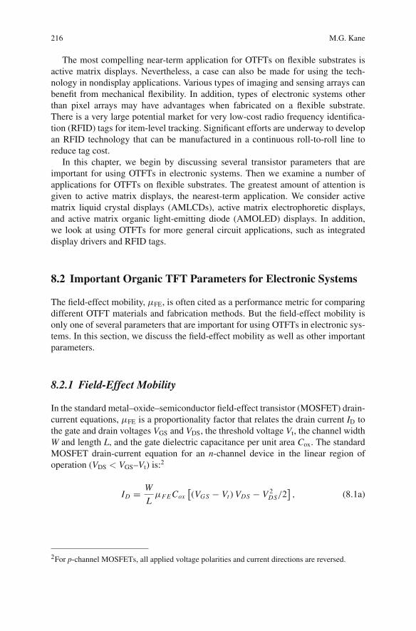
216 M.G. Kane
The most compelling near-term application for OTFTs on flexible substrates isactive matrix displays. Nevertheless, a case can also be made for using the tech-nology in nondisplay applications. Various types of imaging and sensing arrays canbenefit from mechanical flexibility. In addition, types of electronic systems otherthan pixel arrays may have advantages when fabricated on a flexible substrate.There is a very large potential market for very low-cost radio frequency identifica-tion (RFID) tags for item-level tracking. Significant efforts are underway to developan RFID technology that can be manufactured in a continuous roll-to-roll line toreduce tag cost.
In this chapter, we begin by discussing several transistor parameters that areimportant for using OTFTs in electronic systems. Then we examine a number ofapplications for OTFTs on flexible substrates. The greatest amount of attention isgiven to active matrix displays, the nearest-term application. We consider activematrix liquid crystal displays (AMLCDs), active matrix electrophoretic displays,and active matrix organic light-emitting diode (AMOLED) displays. In addition,we look at using OTFTs for more general circuit applications, such as integrateddisplay drivers and RFID tags.
8.2 Important Organic TFT Parameters for Electronic Systems
The field-effect mobility, μFE, is often cited as a performance metric for comparingdifferent OTFT materials and fabrication methods. But the field-effect mobility isonly one of several parameters that are important for using OTFTs in electronic sys-tems. In this section, we discuss the field-effect mobility as well as other importantparameters.
8.2.1 Field-Effect Mobility
In the standard metal–oxide–semiconductor field-effect transistor (MOSFET) drain-current equations, μFE is a proportionality factor that relates the drain current ID tothe gate and drain voltages VGS and VDS, the threshold voltage Vt, the channel widthW and length L, and the gate dielectric capacitance per unit area Cox. The standardMOSFET drain-current equation for an n-channel device in the linear region ofoperation (VDS < VGS–Vt) is:2
ID = W
LμF E Cox
[(VGS − Vt ) VDS − V 2
DS/2], (8.1a)
2For p-channel MOSFETs, all applied voltage polarities and current directions are reversed.
8 Organic and Polymeric TFTs for Flexible Displays and Circuits 217
which reduces to
ID = W
LμF E Cox (VGS − Vt ) VDS (8.1b)
when VDS is small (VDS << VGS–Vt). In the saturation region of operation (VDS ≥VGS–Vt), the standard equation is:
ID = W
L
μF E Cox
2(VGS − Vt )
2. (8.1c)
Experimentally, one finds different values for μFE in the linear and saturationregions. Therefore, a distinction is often made between the linear and saturationfield-effect mobilities. In this chapter, we do not distinguish between the two. How-ever, if the two have significantly different values, a careful circuit designer willdo so.
The field-effect mobility is distinct from the more physically fundamental carriermobility μ, which has the same units but relates average carrier velocity v to appliedelectric field E through v = ± μE, where the positive sign is used for holes andthe negative sign for electrons. Carrier mobility is only one factor in the field-effectmobility. In this chapter, we use the term mobility to refer to the field-effect mobility.
Experimentally, the mobility is found to depend on VGS and VDS. Therefore, itis more straightforward to view it as a small-signal bias-dependent quantity, anal-ogous to the small-signal gain of an amplifier rather than the large-signal quantityof Eq. (8.1a, b, c). Then at each bias point mobility is a proportionality factor thatrelates how small changes in gate voltage VGS produce changes in drain current ID.In this case, in the linear region, for small drain voltages (VDS << VGS–Vt), mobilityis defined as
μF E = L
WCox VDS
∂ ID
∂ VGS, (8.2a)
and in the saturation region mobility is defined as
μF E = 2L
WCox
[∂√
ID
∂ VGS
]2
. (8.2b)
The resulting values for mobility cannot be indiscriminately plugged intoEq. (8.1a, b, c). Figure 8.1 shows the bias-dependent mobility in the satura-tion region for a p-channel pentacene OTFT, derived from measurements usingEq. (8.2b).
There have been efforts to model the bias dependence of the mobility. The best-known model is based on the variable-range hopping (VRH) model of transports inwhich carriers move by hopping in an exponential density of localized states [1]. Inthis model, the physical basis for the increase in mobility with gate voltage is that,as the gate voltage is increased, lower-lying states in the semiconductor’s density of
218 M.G. Kane
0.0
0.1
0.2
0.3
0.4
0.5
0.6
0.7
–15 –10 –5 0 5 10
VDS = –2V
VDS = –20Vin –2V steps
. . .
Fie
ld-e
ffec
t m
ob
ility
(cm
2 V
–1 s
–1)
VGS (V)
Fig. 8.1 Measuredvoltage-dependent mobilityin the saturation region for apentacene OTFT with SiO2
gate dielectric. The mobilityis plotted only for data pointsin the saturation region
states are filled, so that additional charges occupy higher-energy states and requireless energy to hop to nearby states. This model leads to a dependence of mobilityon gate voltage of the form:
μF E = μ0
(VGS − Vt
VAA
)γ(8.3)
where γ depends on the energy distribution of localized states, and typically has avalue of about 0.5. The parameter VAA serves to render the factor in parenthesesdimensionless so that μ0 has standard units for mobility. VAA can be arbitrarily setto 1 V if μ0 is defined as the mobility at VGS–Vt = 1 V. The gate-voltage dependenceof the mobility in Eq. (8.3) results in the linear dependence of drain current on gatevoltage in Eq. (8.1b) being replaced by a superlinear dependence having an exponent1+γ. Similarly, the quadratic dependence in the saturation region in Eq. (8.1c) isreplaced by a dependence with an exponent 2+γ.
Strictly speaking, the VRH transport model applies only to amorphous mate-rials and is not applicable to more ordered organic semiconductors, such asvacuum-sublimed pentacene. Nevertheless Eq. (8.3) is often used as an empiri-cal, curve-fitting model for the mobility of TFTs made with nonamorphous organicsemiconductors. For example, it can be used to fit the data in Fig. 8.1 over a lim-ited gate-voltage range, but not over the entire range, since the mobility decreasesat higher gate voltages. Furthermore, the dependence of mobility on drain voltageseen in Fig. 8.1 is not treated in this model. A similar model has been used forthe gate-voltage-dependent mobility in amorphous silicon thin-film transistors (a-SiTFTs) and is used in the Level 15 a-Si TFT model in the circuit simulation pro-gram AIM-SPICE. Methods have been developed to extract γ from measured TFTdata [2, 3, 4]
Usually, a single value for mobility is cited rather than a set of curves or mobilitymodel parameters. In this case, the convention is to report the maximum mobility
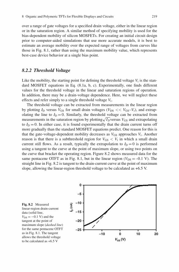
8 Organic and Polymeric TFTs for Flexible Displays and Circuits 219
over a range of gate voltages for a specified drain voltage, either in the linear regionor in the saturation region. A similar method of specifying mobility is used for thebias-dependent mobility of silicon MOSFETs. For creating an initial circuit designprior to computer-aided simulations that use more accurate models, it is best toestimate an average mobility over the expected range of voltages from curves likethose in Fig. 8.1, rather than using the maximum mobility value, which representsbest-case device behavior at a single bias point.
8.2.2 Threshold Voltage
Like the mobility, the starting point for defining the threshold voltage Vt is the stan-dard MOSFET equations in Eq. (8.1a, b, c). Experimentally, one finds differentvalues for the threshold voltage in the linear and saturation regions of operation.In addition, there may be a drain-voltage dependence. Here, we will neglect theseeffects and refer simply to a single threshold voltage Vt.
The threshold voltage can be extracted from measurements in the linear regionby plotting ID versus VGS for small drain voltages (VDS << VGS–Vt), and extrap-olating the line to ID = 0. Similarly, the threshold voltage can be extracted frommeasurements in the saturation region by plotting
√IDversus VGS and extrapolating
to ID = 0. In either case, it is found experimentally that the drain current turns offmore gradually than the standard MOSFET equations predict. One reason for this isthat the gate-voltage-dependent mobility decreases as VGS approaches Vt. Anotherreason is that there is a subthreshold region for VGS < Vt in which a small draincurrent still flows. As a result, typically the extrapolation to ID = 0 is performedusing a tangent to the curve at the point of maximum slope, or using two points onthe curve that bracket the operating region. Figure 8.2 shows measured data for thesame pentacene OTFT as in Fig. 8.1, but in the linear region (VDS = –0.1 V). Thestraight line in Fig. 8.2 is tangent to the drain-current curve at the point of maximumslope, allowing the linear-region threshold voltage to be calculated as +6.5 V.
VGS (V)
–25
–20
–15
–10
–5
0
–10 0 10 20
I D (
nA
)Fig. 8.2 Measuredlinear-region drain-currentdata (solid line,VDS = −0.1 V) and thetangent at the point ofmaximum slope (dashed line)for the same pentacene OTFTas in Fig. 8.1. The tangentallows the threshold voltageto be calculated as +6.5 V
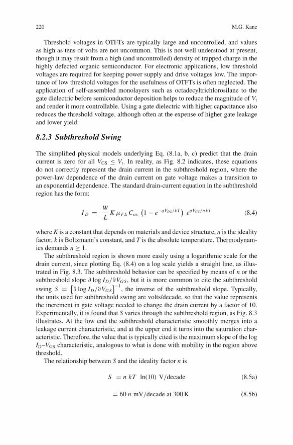
220 M.G. Kane
Threshold voltages in OTFTs are typically large and uncontrolled, and valuesas high as tens of volts are not uncommon. This is not well understood at present,though it may result from a high (and uncontrolled) density of trapped charge in thehighly defected organic semiconductor. For electronic applications, low thresholdvoltages are required for keeping power supply and drive voltages low. The impor-tance of low threshold voltages for the usefulness of OTFTs is often neglected. Theapplication of self-assembled monolayers such as octadecyltrichlorosilane to thegate dielectric before semiconductor deposition helps to reduce the magnitude of Vt
and render it more controllable. Using a gate dielectric with higher capacitance alsoreduces the threshold voltage, although often at the expense of higher gate leakageand lower yield.
8.2.3 Subthreshold Swing
The simplified physical models underlying Eq. (8.1a, b, c) predict that the draincurrent is zero for all VGS ≤ Vt. In reality, as Fig. 8.2 indicates, these equationsdo not correctly represent the drain current in the subthreshold region, where thepower-law dependence of the drain current on gate voltage makes a transition toan exponential dependence. The standard drain-current equation in the subthresholdregion has the form:
I D = W
LK μF E Cox
(1 − e−qVDS/kT
)eqVGS/n kT (8.4)
where K is a constant that depends on materials and device structure, n is the idealityfactor, k is Boltzmann’s constant, and T is the absolute temperature. Thermodynam-ics demands n ≥ 1.
The subthreshold region is shown more easily using a logarithmic scale for thedrain current, since plotting Eq. (8.4) on a log scale yields a straight line, as illus-trated in Fig. 8.3. The subthreshold behavior can be specified by means of n or thesubthreshold slope ∂ log ID/∂VGS , but it is more common to cite the subthresholdswing S = [
∂ log ID/∂VGS]−1
, the inverse of the subthreshold slope. Typically,the units used for subthreshold swing are volts/decade, so that the value representsthe increment in gate voltage needed to change the drain current by a factor of 10.Experimentally, it is found that S varies through the subthreshold region, as Fig. 8.3illustrates. At the low end the subthreshold characteristic smoothly merges into aleakage current characteristic, and at the upper end it turns into the saturation char-acteristic. Therefore, the value that is typically cited is the maximum slope of the logID–VGS characteristic, analogous to what is done with mobility in the region abovethreshold.
The relationship between S and the ideality factor n is
S = n kT ln(10) V/decade (8.5a)
= 60 n mV/decade at 300 K (8.5b)
8 Organic and Polymeric TFTs for Flexible Displays and Circuits 221
0 Vt
VDS largeand fixed
VGS
log ID
Ioff
2)(2 tGS
oxμFED VV
C
L
WI −=
)/exp( kTnVqCKL
WI GSoxFED μ=
Fig. 8.3 The transfercharacteristic of a MOSFETexhibits an exponentialdependence of drain currenton gate voltage below thethreshold voltage. As the gatevoltage is further reduced,the exponential characteristicmerges with a leakagecurrent characteristic. Oftenthe value that is cited for theoff-current Ioff is theminimum current
A subthreshold region is found in all MOSFETs, but long-channel single-crystal sil-icon MOSFETs with light substrate doping have a nearly ideal subthreshold regionin which the ideality factor is very close to unity, so that the change in gate volt-age needed to change the drain current by a factor of 10 is only 60 mV at 300 K.Nonideal subthreshold characteristics (n > 1) occur when a change in gate volt-age does not produce a corresponding equal change in the surface potential of thesemiconductor. Increasing the gate dielectric capacitance reduces the subthresholdswing by improving the coupling between the gate and the semiconductor surface.Typical values of subthreshold swing at 300 K for some representative TFT tech-nologies are:
S = 200 − 500 mV/decade (polysilicon TFTs)= 500 mV − 1 V/decade (a-Si TFTs)= 500 mV − 5 V/decade (OTFTs)
From an electronic system point of view, small subthreshold swing is desirablebecause less gate voltage excursion ΔVGS is needed to turn the transistor from fullyoff to fully on. Indeed, one may view the total ΔVGS required to take the transistorfrom fully off to fully on as having two parts. The subthreshold slope determines thevoltage excursion that must take place below the threshold voltage, and the mobilitydetermines the required excursion above threshold. OTFTs often have subthresh-old swings that are large compared to silicon devices, due to localized states in theenergy gap near the highest occupied molecular orbital (HOMO) or lowest unoccu-pied molecular orbital (LUMO) levels. For OTFTs the voltage excursion requiredbelow threshold often has about the same magnitude as that required above thresh-olds and the dielectric breakdown requirements, power supply requirements, andpower dissipation are adversely affected.
222 M.G. Kane
8.2.4 Leakage Currents
Two types of leakage current have to be considered:
• Drain leakage current ID when the transistor is off. That is, the gate voltage VGS
biases the device below the subthreshold region. This current is often called theoff-current.
• Gate leakage current IG under all transistor conditions, both on and off currents.
The off-current is seen in the log ID–VGS curve of Fig. 8.3 at gate voltages belowthose producing the exponential subthreshold characteristic. In general, the off-current is not independent of the gate and drain voltages. In some cases, it increasesas the gate voltage is reduced further, as Fig. 8.3 illustrates. A similar effect is seen inpolysilicon (poly-Si) TFTs, where it is attributed to field-assisted tunneling throughmid-gap states present at grain boundaries; reducing the gate voltage increases thehigh fields at the drain edge of the gate, increasing the tunneling rate. The value thatis typically cited for the off-current in TFTs is the minimum drain current at a spec-ified drain voltage. For initial design work prior to more accurate computer-aidedsimulations that take into account the entire drain-current characteristic, a better fig-ure to use for off-current is the worst-case leakage over the expected range of gateand drain voltages, rather than the minimum leakage found at a single voltage point.
For the polymer dielectrics and low-temperature inorganic dielectrics often usedin OTFTs, the gate current can be significant. Indeed, sometimes the off-current isdominated not by drain-to-source leakage but by drain-to-gate leakage. Determiningwhether the off-current arises from leakage from drain to source or drain to gate isthe first step in identifying the physical source of the off-current.
8.2.5 Contact Resistance
Making good electrical contact to organic semiconductors is sometimes difficult.As a result there are often large parasitic resistances in series with the source anddrain. In an OTFT, these contact resistances typically depend on the gate voltage,decreasing with gate voltage, just like the channel resistance. Nevertheless, the con-tact resistances are distinct from the channel resistance because they do not scalewith channel length, but rather are channel-length independent. Indeed, sometimesthey can be modeled simply as a fixed added channel length. For example, the con-tact resistances may behave like an extra 2 μm of channel length, so that an OTFTwith channel length L behaves as if it had a channel length L + 2 μm. The contactresistance can be determined by fabricating OTFTs of various channel lengths, plot-ting channel resistance versus channel length, and extrapolating channel resistanceto a channel length of zero. An alternative method for determining channel resis-tance that avoids uncertainties due to device-to-device variations is the four-probetechnique. The OTFT has four electrodes, with the outer two used as source and
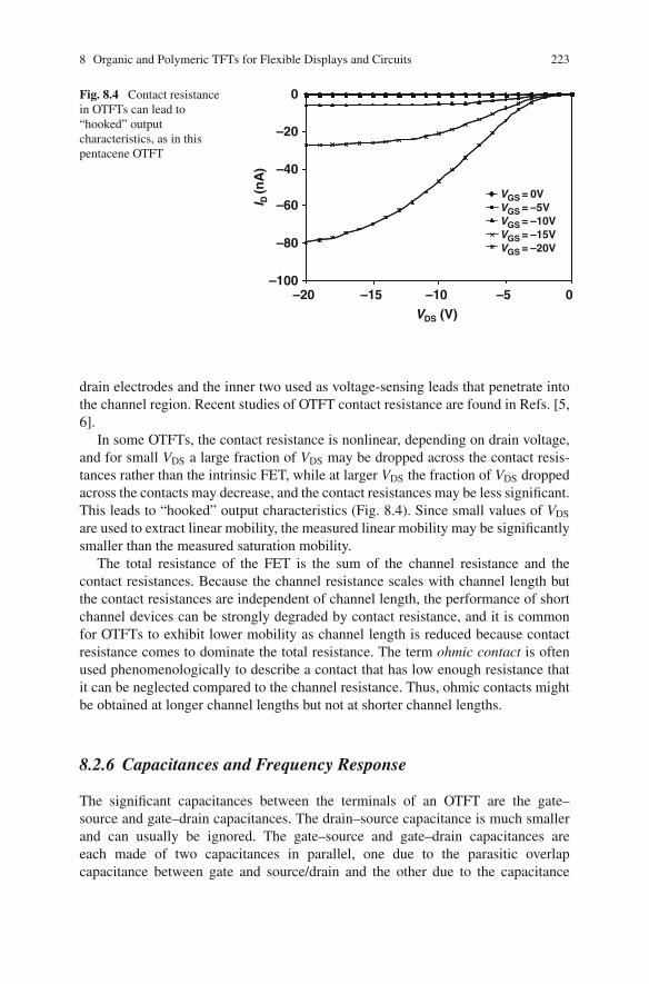
8 Organic and Polymeric TFTs for Flexible Displays and Circuits 223
–20 –15 –10 –5 0
I D (n
A)
0
VDS (V)
–20
–40
–60
–80
–100
VGS = 0VVGS = –5VVGS = –10VVGS = –15VVGS = –20V
Fig. 8.4 Contact resistancein OTFTs can lead to“hooked” outputcharacteristics, as in thispentacene OTFT
drain electrodes and the inner two used as voltage-sensing leads that penetrate intothe channel region. Recent studies of OTFT contact resistance are found in Refs. [5,6].
In some OTFTs, the contact resistance is nonlinear, depending on drain voltage,and for small VDS a large fraction of VDS may be dropped across the contact resis-tances rather than the intrinsic FET, while at larger VDS the fraction of VDS droppedacross the contacts may decrease, and the contact resistances may be less significant.This leads to “hooked” output characteristics (Fig. 8.4). Since small values of VDS
are used to extract linear mobility, the measured linear mobility may be significantlysmaller than the measured saturation mobility.
The total resistance of the FET is the sum of the channel resistance and thecontact resistances. Because the channel resistance scales with channel length butthe contact resistances are independent of channel length, the performance of shortchannel devices can be strongly degraded by contact resistance, and it is commonfor OTFTs to exhibit lower mobility as channel length is reduced because contactresistance comes to dominate the total resistance. The term ohmic contact is oftenused phenomenologically to describe a contact that has low enough resistance thatit can be neglected compared to the channel resistance. Thus, ohmic contacts mightbe obtained at longer channel lengths but not at shorter channel lengths.
8.2.6 Capacitances and Frequency Response
The significant capacitances between the terminals of an OTFT are the gate–source and gate–drain capacitances. The drain–source capacitance is much smallerand can usually be ignored. The gate–source and gate–drain capacitances areeach made of two capacitances in parallel, one due to the parasitic overlapcapacitance between gate and source/drain and the other due to the capacitance
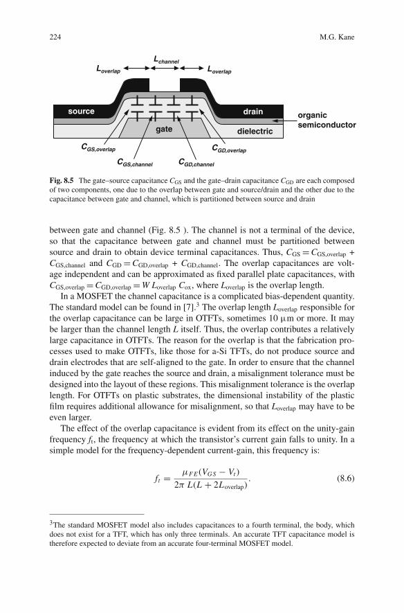
224 M.G. Kane
organicsemiconductor
Loverlap
dielectric
source
gate
Loverlap
Lchannel
drain
CGS,overlap CGD,overlap
CGD,channelCGS,channel
Fig. 8.5 The gate–source capacitance CGS and the gate–drain capacitance CGD are each composedof two components, one due to the overlap between gate and source/drain and the other due to thecapacitance between gate and channel, which is partitioned between source and drain
between gate and channel (Fig. 8.5 ). The channel is not a terminal of the device,so that the capacitance between gate and channel must be partitioned betweensource and drain to obtain device terminal capacitances. Thus, CGS = CGS,overlap +CGS,channel and CGD = CGD,overlap + CGD,channel. The overlap capacitances are volt-age independent and can be approximated as fixed parallel plate capacitances, withCGS,overlap = CGD,overlap = W Loverlap Cox, where Loverlap is the overlap length.
In a MOSFET the channel capacitance is a complicated bias-dependent quantity.The standard model can be found in [7].3 The overlap length Loverlap responsible forthe overlap capacitance can be large in OTFTs, sometimes 10 μm or more. It maybe larger than the channel length L itself. Thus, the overlap contributes a relativelylarge capacitance in OTFTs. The reason for the overlap is that the fabrication pro-cesses used to make OTFTs, like those for a-Si TFTs, do not produce source anddrain electrodes that are self-aligned to the gate. In order to ensure that the channelinduced by the gate reaches the source and drain, a misalignment tolerance must bedesigned into the layout of these regions. This misalignment tolerance is the overlaplength. For OTFTs on plastic substrates, the dimensional instability of the plasticfilm requires additional allowance for misalignment, so that Loverlap may have to beeven larger.
The effect of the overlap capacitance is evident from its effect on the unity-gainfrequency ft, the frequency at which the transistor’s current gain falls to unity. In asimple model for the frequency-dependent current-gain, this frequency is:
ft = μF E (VGS − Vt )
2π L(L + 2Loverlap). (8.6)
3The standard MOSFET model also includes capacitances to a fourth terminal, the body, whichdoes not exist for a TFT, which has only three terminals. An accurate TFT capacitance model istherefore expected to deviate from an accurate four-terminal MOSFET model.
8 Organic and Polymeric TFTs for Flexible Displays and Circuits 225
A model that includes the effect of contact resistance is found in Ref. [8]. WhenLoverlap << L, as is the case for conventional self-aligned silicon CMOS processes,one obtains the well-known silicon scaling law in which the maximum operatingfrequency scales as L−2. Large performance gains come from reducing the channellength, motivating amazingly successful efforts to reduce this transistor dimensionin silicon ICs. However, if the amount of overlap is fixed by large-area registrationcapabilities and cannot be reduced as channel length is reduced, the silicon scalinglaw is replaced by one in which the maximum operating frequency ultimately scalesas L−1, altering significantly the economics of integration.
The overlap capacitance could be reduced dramatically if a self-aligned OTFTprocess could be developed. A self-aligned silicon process uses the gate as an insitu ion-implantation mask to form source and drain regions that are well alignedto the gate. An equivalent process does not yet exist for OTFTs. It would require atop-gate TFT geometry, together with a liquid- or vapor-phase doping process thatrenders the organic semiconductor highly conductive in a stable manner.
8.2.7 TFT Nonuniformity
Although the performance of OTFTs is lower than that of silicon MOSFETs, it isadequate for many applications, as long as the transistor parameters are uniformand predictable. However, nonuniform or unpredictable parameters are difficult totolerate in electronic systems. For example, in displays, transistor nonuniformitiescan lead to visible variations in color or gray level, which is aesthetically displeas-ing and commercially nonviable. Random brightness variations across the display,known as mura, are more of a problem than smooth variations, because the lowspatial frequencies in smooth variations are less visible to the human visual sys-tem. This has been an issue for poly-Si TFTs, which exhibit random variations inthreshold voltage and off-current due to the random grain structure of the poly-Si.
In our laboratory, we have developed routines for the analysis of OTFT nonuni-formity using automated probing and characterization of transistor arrays, followedby statistical analysis. We analyzed spatial parameter variations, including param-eter correlations between pairs of closely spaced OTFTs, in order to predict theperformance of matched pairs such as might be used in current mirror circuits. Thedistributions show smooth variations as well as random variations that cause nonuni-formity at short distance scales.
8.2.8 Bias-Stress Instability and Hysteresis
Bias-stress instability and hysteresis are memory effects in which the DC character-istics of a transistor at a given time depend on voltages applied to the device in thepast. These memory effects are undesirable in electronic systems, although there aredesign methods that can improve the tolerance to memory effects.
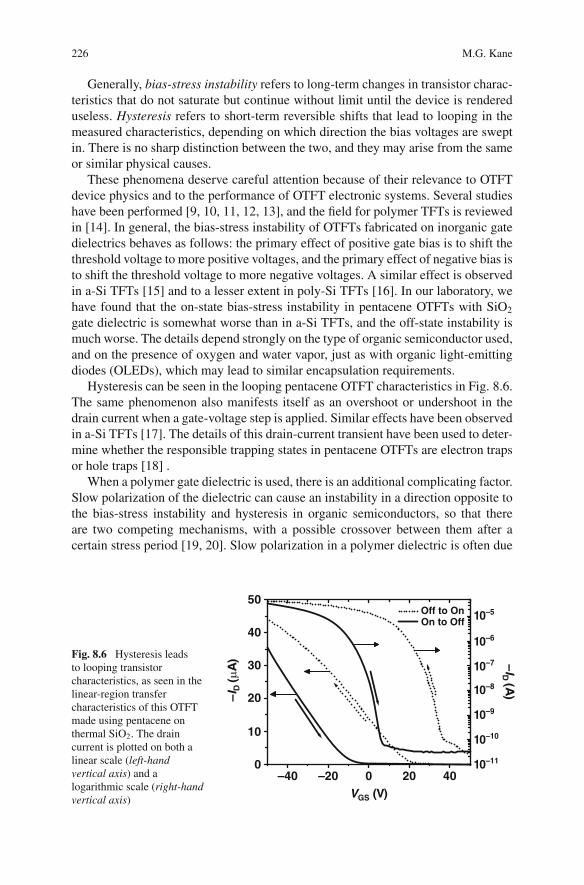
226 M.G. Kane
Generally, bias-stress instability refers to long-term changes in transistor charac-teristics that do not saturate but continue without limit until the device is rendereduseless. Hysteresis refers to short-term reversible shifts that lead to looping in themeasured characteristics, depending on which direction the bias voltages are sweptin. There is no sharp distinction between the two, and they may arise from the sameor similar physical causes.
These phenomena deserve careful attention because of their relevance to OTFTdevice physics and to the performance of OTFT electronic systems. Several studieshave been performed [9, 10, 11, 12, 13], and the field for polymer TFTs is reviewedin [14]. In general, the bias-stress instability of OTFTs fabricated on inorganic gatedielectrics behaves as follows: the primary effect of positive gate bias is to shift thethreshold voltage to more positive voltages, and the primary effect of negative bias isto shift the threshold voltage to more negative voltages. A similar effect is observedin a-Si TFTs [15] and to a lesser extent in poly-Si TFTs [16]. In our laboratory, wehave found that the on-state bias-stress instability in pentacene OTFTs with SiO2
gate dielectric is somewhat worse than in a-Si TFTs, and the off-state instability ismuch worse. The details depend strongly on the type of organic semiconductor used,and on the presence of oxygen and water vapor, just as with organic light-emittingdiodes (OLEDs), which may lead to similar encapsulation requirements.
Hysteresis can be seen in the looping pentacene OTFT characteristics in Fig. 8.6.The same phenomenon also manifests itself as an overshoot or undershoot in thedrain current when a gate-voltage step is applied. Similar effects have been observedin a-Si TFTs [17]. The details of this drain-current transient have been used to deter-mine whether the responsible trapping states in pentacene OTFTs are electron trapsor hole traps [18] .
When a polymer gate dielectric is used, there is an additional complicating factor.Slow polarization of the dielectric can cause an instability in a direction opposite tothe bias-stress instability and hysteresis in organic semiconductors, so that thereare two competing mechanisms, with a possible crossover between them after acertain stress period [19, 20]. Slow polarization in a polymer dielectric is often due
–40 –20 0 20 40
50
–I D
(µA
)
VGS (V)
Off to On On to Off 10–5
40
0
20
30
10
–ID (A
)
10–6
10–7
10–8
10–9
10–10
10–11
Fig. 8.6 Hysteresis leadsto looping transistorcharacteristics, as seen in thelinear-region transfercharacteristics of this OTFTmade using pentacene onthermal SiO2. The draincurrent is plotted on both alinear scale (left-handvertical axis) and alogarithmic scale (right-handvertical axis)
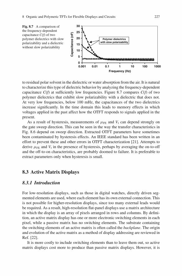
8 Organic and Polymeric TFTs for Flexible Displays and Circuits 227
0
5
10
15
20
25
30
0.001 0.01 0.1 1 10 100 1000
Frequency (Hz)C
apac
itan
ce (
nF
)
Polymer dielectricswith slow polarizability
Fig. 8.7 A comparison ofthe frequency-dependentcapacitance C(f) of twopolymer dielectrics with slowpolarizability and a dielectricwithout slow polarizability
to residual polar solvent in the dielectric or water absorption from the air. It is naturalto characterize this type of dielectric behavior by analyzing the frequency-dependentcapacitance C(f) at sufficiently low frequencies. Figure 8.7 compares C(f) of twopolymer dielectrics that exhibit slow polarizability with a dielectric that does not.At very low frequencies, below 100 mHz, the capacitances of the two dielectricsincrease significantly. In the time domain this leads to memory effects in whichvoltages applied in the past affect how the OTFT responds to signals applied in thepresent.
As a result of hysteresis, measurements of μFE and Vt can depend strongly onthe gate sweep direction. This can be seen in the way the transfer characteristics inFig. 8.6 depend on sweep direction. Extracted OTFT parameters have sometimesbeen contaminated by hysteresis effects. An IEEE standard has been written in aneffort to prevent these and other errors in OTFT characterization [21]. Attempts toderive μFE and Vt in the presence of hysteresis, perhaps by averaging the on-to-offand the off-to-on characteristics, are probably doomed to failure. It is preferable toextract parameters only when hysteresis is small.
8.3 Active Matrix Displays
8.3.1 Introduction
For low-resolution displays, such as those in digital watches, directly driven seg-mented elements are used, where each element has its own external connection. Thisis not possible for higher-resolution displays, since too many external leads wouldbe required. As a result, high-resolution flat-panel displays use a matrix architecturein which the display is an array of pixels arranged in rows and columns. By defini-tion, an active matrix display has one or more electronic switching elements in eachpixel, while a passive matrix has no switching elements. The substrate containingthe switching elements of an active matrix is often called the backplane. The originand evolution of the active matrix as a method of display addressing are reviewed inRef. [22].
It is more costly to include switching elements than to leave them out, so activematrix displays cost more to produce than passive matrix displays. However, it is
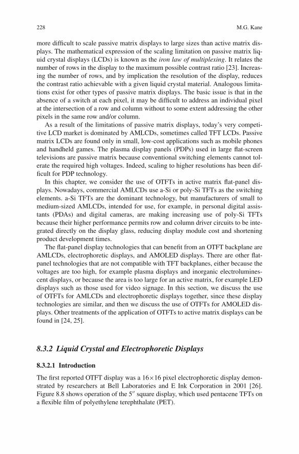
228 M.G. Kane
more difficult to scale passive matrix displays to large sizes than active matrix dis-plays. The mathematical expression of the scaling limitation on passive matrix liq-uid crystal displays (LCDs) is known as the iron law of multiplexing. It relates thenumber of rows in the display to the maximum possible contrast ratio [23]. Increas-ing the number of rows, and by implication the resolution of the display, reducesthe contrast ratio achievable with a given liquid crystal material. Analogous limita-tions exist for other types of passive matrix displays. The basic issue is that in theabsence of a switch at each pixel, it may be difficult to address an individual pixelat the intersection of a row and column without to some extent addressing the otherpixels in the same row and/or column.
As a result of the limitations of passive matrix displays, today’s very competi-tive LCD market is dominated by AMLCDs, sometimes called TFT LCDs. Passivematrix LCDs are found only in small, low-cost applications such as mobile phonesand handheld games. The plasma display panels (PDPs) used in large flat-screentelevisions are passive matrix because conventional switching elements cannot tol-erate the required high voltages. Indeed, scaling to higher resolutions has been dif-ficult for PDP technology.
In this chapter, we consider the use of OTFTs in active matrix flat-panel dis-plays. Nowadays, commercial AMLCDs use a-Si or poly-Si TFTs as the switchingelements. a-Si TFTs are the dominant technology, but manufacturers of small tomedium-sized AMLCDs, intended for use, for example, in personal digital assis-tants (PDAs) and digital cameras, are making increasing use of poly-Si TFTsbecause their higher performance permits row and column driver circuits to be inte-grated directly on the display glass, reducing display module cost and shorteningproduct development times.
The flat-panel display technologies that can benefit from an OTFT backplane areAMLCDs, electrophoretic displays, and AMOLED displays. There are other flat-panel technologies that are not compatible with TFT backplanes, either because thevoltages are too high, for example plasma displays and inorganic electrolumines-cent displays, or because the area is too large for an active matrix, for example LEDdisplays such as those used for video signage. In this section, we discuss the useof OTFTs for AMLCDs and electrophoretic displays together, since these displaytechnologies are similar, and then we discuss the use of OTFTs for AMOLED dis-plays. Other treatments of the application of OTFTs to active matrix displays can befound in [24, 25].
8.3.2 Liquid Crystal and Electrophoretic Displays
8.3.2.1 Introduction
The first reported OTFT display was a 16×16 pixel electrophoretic display demon-strated by researchers at Bell Laboratories and E Ink Corporation in 2001 [26].Figure 8.8 shows operation of the 5′′ square display, which used pentacene TFTs ona flexible film of polyethylene terephthalate (PET).
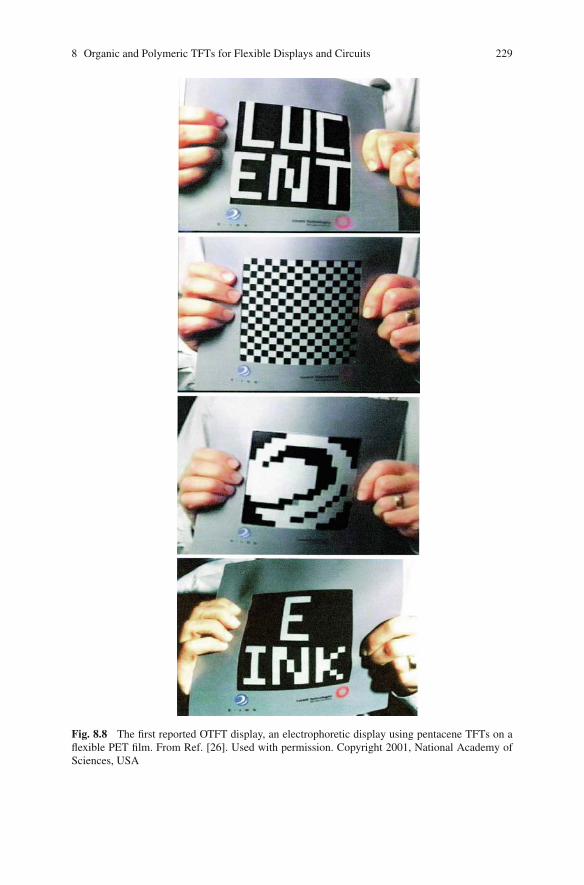
8 Organic and Polymeric TFTs for Flexible Displays and Circuits 229
Fig. 8.8 The first reported OTFT display, an electrophoretic display using pentacene TFTs on aflexible PET film. From Ref. [26]. Used with permission. Copyright 2001, National Academy ofSciences, USA
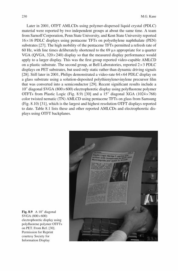
230 M.G. Kane
Later in 2001, OTFT AMLCDs using polymer-dispersed liquid crystal (PDLC)material were reported by two independent groups at about the same time. A teamfrom Sarnoff Corporation, Penn State University, and Kent State University reported16×16 PDLC displays using pentacene TFTs on polyethylene naphthalate (PEN)substrates [27]. The high mobility of the pentacene TFTs permitted a refresh rate of60 Hz, with line times deliberately shortened to the 69 μs appropriate for a quarterVGA (QVGA, 320×240) display so that the measured display performance wouldapply to a larger display. This was the first group reported video-capable AMLCDon a plastic substrate. The second group, at Bell Laboratories, reported 2×3 PDLCdisplays on PET substrates, but used only static rather than dynamic driving signals[28]. Still later in 2001, Philips demonstrated a video-rate 64×64 PDLC display ona glass substrate using a solution-deposited polythienylenevinylene precursor filmthat was converted into a semiconductor [29]. Recent significant results include a10′′ diagonal SVGA (800×600) electrophoretic display using polyfluorene polymerOTFTs from Plastic Logic (Fig. 8.9) [30] and a 15′′ diagonal XGA (1024×768)color twisted nematic (TN) AMLCD using pentacene TFTs on glass from Samsung(Fig. 8.10) [31], which is the largest and highest resolution OTFT displays reportedto date. Table 8.1 lists these and other reported AMLCDs and electrophoretic dis-plays using OTFT backplanes.
Fig. 8.9 A 10′′ diagonalSVGA (800×600)electrophoretic display usingpolyfluorene polymer OTFTson PET. From Ref. [30].Permission for Reprintcourtesy Society forInformation Display
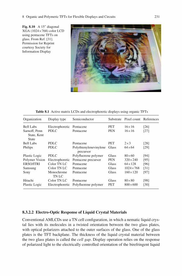
8 Organic and Polymeric TFTs for Flexible Displays and Circuits 231
Fig. 8.10 A 15′′ diagonalXGA (1024×768) color LCDusing pentacene TFTs onglass. From Ref. [31].Permission for Reprintcourtesy Society forInformation Display
Table 8.1 Active matrix LCDs and electrophoretic displays using organic TFTs
Organization Display type Semiconductor Substrate Pixel count References
Bell Labs Electrophoretic Pentacene PET 16×16 [26]Sarnoff, Penn
State, KentState
PDLC Pentacene PEN 16×16 [27]
Bell Labs PDLC Pentacene PET 2×3 [28]Philips PDLC Polythienylenevinylene
precursorGlass 64×64 [29]
Plastic Logic PDLC Polyfluorene polymer Glass 80×60 [94]Polymer Vision Electrophoretic Pentacene precursor PEN 320×240 [95]ERSO/ITRI Color TN LC Pentacene Glass 64×128 [96]Samsung Color TN LC Pentacene Glass 1024×768 [31]Sony Monochrome
TN LCPentacene Glass 160×120 [97]
Hitachi Color TN LC Pentacene Glass 80×80 [98]Plastic Logic Electrophoretic Polyfluorene polymer PET 800×600 [30]
8.3.2.2 Electro-Optic Response of Liquid Crystal Materials
Conventional AMLCDs use a TN cell configuration, in which a nematic liquid crys-tal lies with its molecules in a twisted orientation between the two glass plates,with optical polarizers attached to the outer surfaces of the glass. One of the glassplates is the TFT backplane. The thickness of the liquid crystal material betweenthe two glass plates is called the cell gap. Display operation relies on the responseof polarized light to the electrically controlled orientation of the birefringent liquid
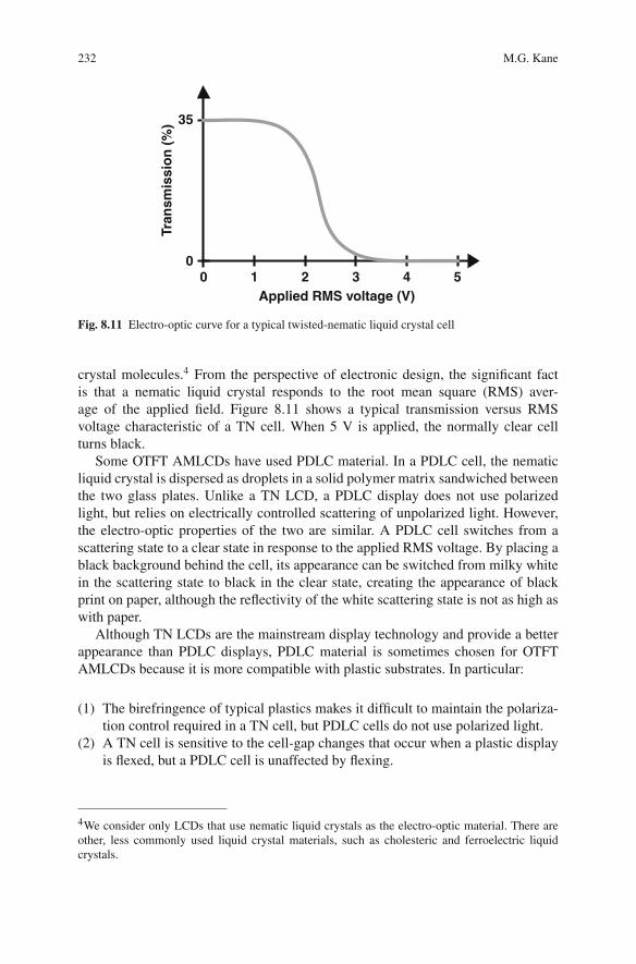
232 M.G. Kane
0 5Applied RMS voltage (V)
4321
35
0
Tran
smis
sio
n (
%)
Fig. 8.11 Electro-optic curve for a typical twisted-nematic liquid crystal cell
crystal molecules.4 From the perspective of electronic design, the significant factis that a nematic liquid crystal responds to the root mean square (RMS) aver-age of the applied field. Figure 8.11 shows a typical transmission versus RMSvoltage characteristic of a TN cell. When 5 V is applied, the normally clear cellturns black.
Some OTFT AMLCDs have used PDLC material. In a PDLC cell, the nematicliquid crystal is dispersed as droplets in a solid polymer matrix sandwiched betweenthe two glass plates. Unlike a TN LCD, a PDLC display does not use polarizedlight, but relies on electrically controlled scattering of unpolarized light. However,the electro-optic properties of the two are similar. A PDLC cell switches from ascattering state to a clear state in response to the applied RMS voltage. By placing ablack background behind the cell, its appearance can be switched from milky whitein the scattering state to black in the clear state, creating the appearance of blackprint on paper, although the reflectivity of the white scattering state is not as high aswith paper.
Although TN LCDs are the mainstream display technology and provide a betterappearance than PDLC displays, PDLC material is sometimes chosen for OTFTAMLCDs because it is more compatible with plastic substrates. In particular:
(1) The birefringence of typical plastics makes it difficult to maintain the polariza-tion control required in a TN cell, but PDLC cells do not use polarized light.
(2) A TN cell is sensitive to the cell-gap changes that occur when a plastic displayis flexed, but a PDLC cell is unaffected by flexing.
4We consider only LCDs that use nematic liquid crystals as the electro-optic material. There areother, less commonly used liquid crystal materials, such as cholesteric and ferroelectric liquidcrystals.
8 Organic and Polymeric TFTs for Flexible Displays and Circuits 233
(3) Unlike a TN cell, a PDLC cell is insensitive to gas permeation through theplastic substrates causing air bubbles to form inside the cell.
With both types of LCD, it is important that the applied voltage averaged over aperiod of seconds not have a significant DC component. A DC voltage componentleads to the transport of ionic impurities within the cell, allowing an ion-inducedcompensating DC potential to build up. In itself this is not harmful, but the effectof a built-in DC potential is that the liquid crystal no longer responds to the appliedsignal alone, but rather to the sum of the applied voltage and the built-in poten-tial. In addition, DC components larger than a few hundred millivolts can lead toirreversible electrolysis of the liquid crystal material.
It is fortuitous that the RMS-responding property allows the requirement that DCvoltage components be avoided to be easily satisfied. The display driver circuits thatprovide data voltages to the display alternate the polarity from one frame to the next.Although it is the responsibility of the display driver circuits to produce the appro-priate alternating-polarity data signals, the display designer must consider whetherthe pixel circuit contributes a DC artifact, due, for example, to charge injection whenthe pixel switch is shut off.
8.3.2.3 Electro-Optic Response of Electrophoretic Materials
Electrophoretic materials contain a charged pigment dispersed in an optically con-trasting material, or a mixture of oppositely charged contrasting pigments dispersedin a neutral material. By applying an electric field, the pigment particles are movedto the front or back surface of the display, producing an electro-optic effect. A dis-play made with electrophoretic material operates in a reflective mode using ambientlight. Changing the optical state requires moving the pigment, so electrophoretic dis-plays typically do not operate at video rates, but have response times of 100–300 ms.Because the only force on the pigment particles is the applied field, the movement ofthe pigment, and therefore its optical state, is only a function of the time-integratedelectric field
∫ t0 E(τ ) dτ .5 When no electric field is applied, there is no applied
force, so that the optical state does not change, at least not over short periods. Thus,an electrophoretic material is a bistable material whose reflectivity depends on thistime integral. Bistability can provide significant display power savings in applica-tions that leave an image on the display for a period, such as electronic books andmaps, because the display module can be powered down at these times. Typicaldata voltages are in the range of −15 V to +15 V, where negative voltage drives thedisplay toward one optical state and positive voltage drives it toward the oppositestate. Therefore, an electrophoretic display is not an RMS-responding display likean LCD, but rather responds to opposite polarities by producing opposite opticalresponses.
5This analysis is approximate, because it ignores forces between the particles and the effect ofinitial pigment conditions.
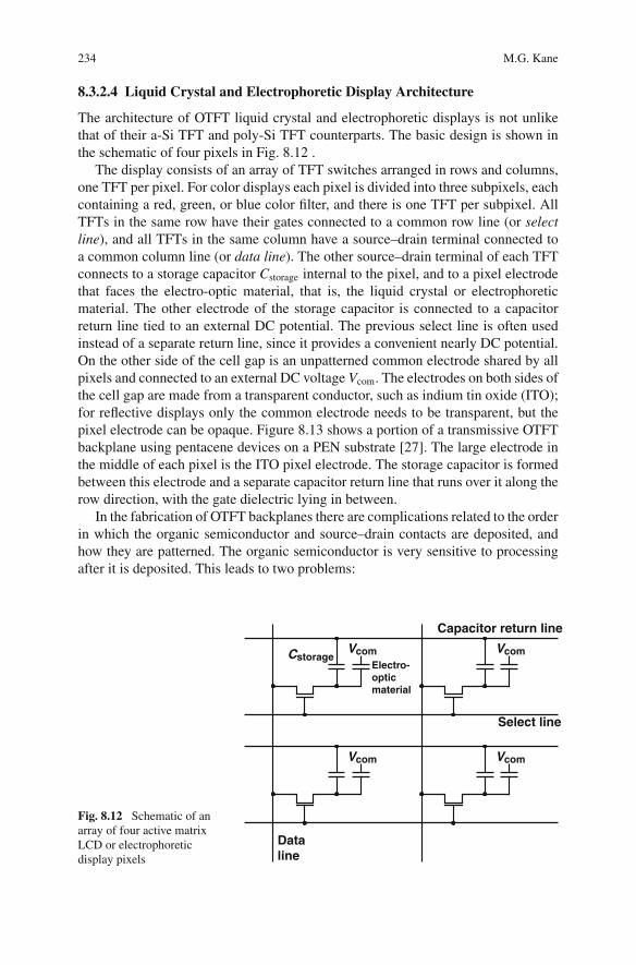
234 M.G. Kane
8.3.2.4 Liquid Crystal and Electrophoretic Display Architecture
The architecture of OTFT liquid crystal and electrophoretic displays is not unlikethat of their a-Si TFT and poly-Si TFT counterparts. The basic design is shown inthe schematic of four pixels in Fig. 8.12 .
The display consists of an array of TFT switches arranged in rows and columns,one TFT per pixel. For color displays each pixel is divided into three subpixels, eachcontaining a red, green, or blue color filter, and there is one TFT per subpixel. AllTFTs in the same row have their gates connected to a common row line (or selectline), and all TFTs in the same column have a source–drain terminal connected toa common column line (or data line). The other source–drain terminal of each TFTconnects to a storage capacitor Cstorage internal to the pixel, and to a pixel electrodethat faces the electro-optic material, that is, the liquid crystal or electrophoreticmaterial. The other electrode of the storage capacitor is connected to a capacitorreturn line tied to an external DC potential. The previous select line is often usedinstead of a separate return line, since it provides a convenient nearly DC potential.On the other side of the cell gap is an unpatterned common electrode shared by allpixels and connected to an external DC voltage Vcom. The electrodes on both sides ofthe cell gap are made from a transparent conductor, such as indium tin oxide (ITO);for reflective displays only the common electrode needs to be transparent, but thepixel electrode can be opaque. Figure 8.13 shows a portion of a transmissive OTFTbackplane using pentacene devices on a PEN substrate [27]. The large electrode inthe middle of each pixel is the ITO pixel electrode. The storage capacitor is formedbetween this electrode and a separate capacitor return line that runs over it along therow direction, with the gate dielectric lying in between.
In the fabrication of OTFT backplanes there are complications related to the orderin which the organic semiconductor and source–drain contacts are deposited, andhow they are patterned. The organic semiconductor is very sensitive to processingafter it is deposited. This leads to two problems:
Cstorage
Capacitor return line
VcomElectro-opticmaterial
Select line
Vcom
Vcom Vcom
Dataline
Fig. 8.12 Schematic of anarray of four active matrixLCD or electrophoreticdisplay pixels
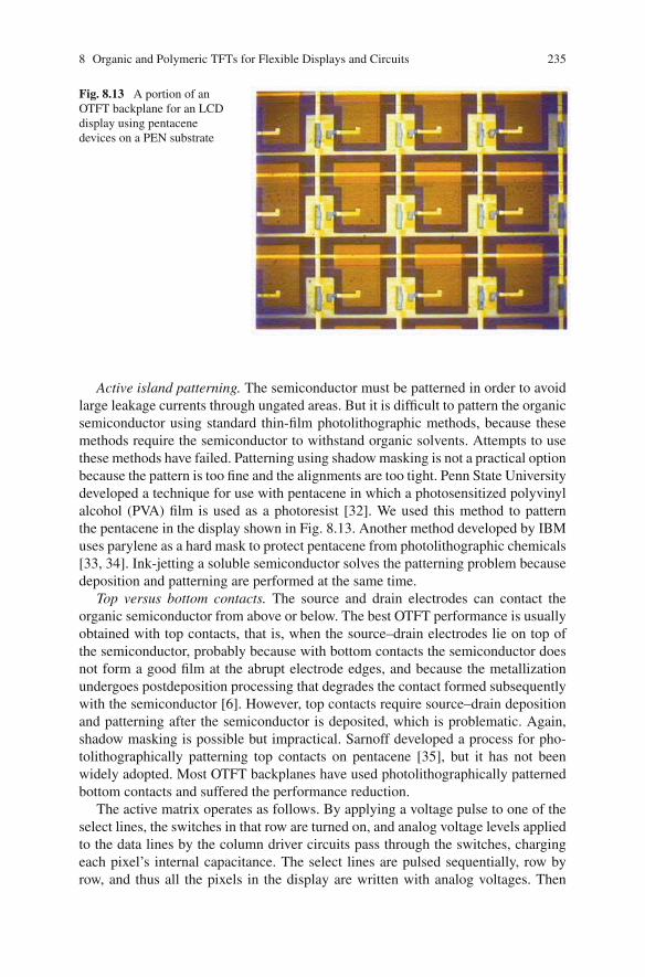
8 Organic and Polymeric TFTs for Flexible Displays and Circuits 235
Fig. 8.13 A portion of anOTFT backplane for an LCDdisplay using pentacenedevices on a PEN substrate
Active island patterning. The semiconductor must be patterned in order to avoidlarge leakage currents through ungated areas. But it is difficult to pattern the organicsemiconductor using standard thin-film photolithographic methods, because thesemethods require the semiconductor to withstand organic solvents. Attempts to usethese methods have failed. Patterning using shadow masking is not a practical optionbecause the pattern is too fine and the alignments are too tight. Penn State Universitydeveloped a technique for use with pentacene in which a photosensitized polyvinylalcohol (PVA) film is used as a photoresist [32]. We used this method to patternthe pentacene in the display shown in Fig. 8.13. Another method developed by IBMuses parylene as a hard mask to protect pentacene from photolithographic chemicals[33, 34]. Ink-jetting a soluble semiconductor solves the patterning problem becausedeposition and patterning are performed at the same time.
Top versus bottom contacts. The source and drain electrodes can contact theorganic semiconductor from above or below. The best OTFT performance is usuallyobtained with top contacts, that is, when the source–drain electrodes lie on top ofthe semiconductor, probably because with bottom contacts the semiconductor doesnot form a good film at the abrupt electrode edges, and because the metallizationundergoes postdeposition processing that degrades the contact formed subsequentlywith the semiconductor [6]. However, top contacts require source–drain depositionand patterning after the semiconductor is deposited, which is problematic. Again,shadow masking is possible but impractical. Sarnoff developed a process for pho-tolithographically patterning top contacts on pentacene [35], but it has not beenwidely adopted. Most OTFT backplanes have used photolithographically patternedbottom contacts and suffered the performance reduction.
The active matrix operates as follows. By applying a voltage pulse to one of theselect lines, the switches in that row are turned on, and analog voltage levels appliedto the data lines by the column driver circuits pass through the switches, chargingeach pixel’s internal capacitance. The select lines are pulsed sequentially, row byrow, and thus all the pixels in the display are written with analog voltages. Then
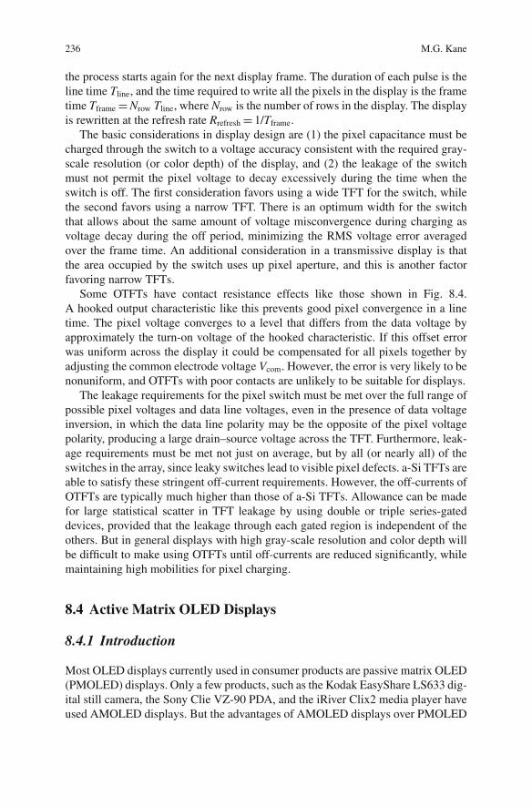
236 M.G. Kane
the process starts again for the next display frame. The duration of each pulse is theline time Tline, and the time required to write all the pixels in the display is the frametime Tframe = Nrow Tline, where Nrow is the number of rows in the display. The displayis rewritten at the refresh rate Rrefresh = 1/Tframe.
The basic considerations in display design are (1) the pixel capacitance must becharged through the switch to a voltage accuracy consistent with the required gray-scale resolution (or color depth) of the display, and (2) the leakage of the switchmust not permit the pixel voltage to decay excessively during the time when theswitch is off. The first consideration favors using a wide TFT for the switch, whilethe second favors using a narrow TFT. There is an optimum width for the switchthat allows about the same amount of voltage misconvergence during charging asvoltage decay during the off period, minimizing the RMS voltage error averagedover the frame time. An additional consideration in a transmissive display is thatthe area occupied by the switch uses up pixel aperture, and this is another factorfavoring narrow TFTs.
Some OTFTs have contact resistance effects like those shown in Fig. 8.4.A hooked output characteristic like this prevents good pixel convergence in a linetime. The pixel voltage converges to a level that differs from the data voltage byapproximately the turn-on voltage of the hooked characteristic. If this offset errorwas uniform across the display it could be compensated for all pixels together byadjusting the common electrode voltage Vcom. However, the error is very likely to benonuniform, and OTFTs with poor contacts are unlikely to be suitable for displays.
The leakage requirements for the pixel switch must be met over the full range ofpossible pixel voltages and data line voltages, even in the presence of data voltageinversion, in which the data line polarity may be the opposite of the pixel voltagepolarity, producing a large drain–source voltage across the TFT. Furthermore, leak-age requirements must be met not just on average, but by all (or nearly all) of theswitches in the array, since leaky switches lead to visible pixel defects. a-Si TFTs areable to satisfy these stringent off-current requirements. However, the off-currents ofOTFTs are typically much higher than those of a-Si TFTs. Allowance can be madefor large statistical scatter in TFT leakage by using double or triple series-gateddevices, provided that the leakage through each gated region is independent of theothers. But in general displays with high gray-scale resolution and color depth willbe difficult to make using OTFTs until off-currents are reduced significantly, whilemaintaining high mobilities for pixel charging.
8.4 Active Matrix OLED Displays
8.4.1 Introduction
Most OLED displays currently used in consumer products are passive matrix OLED(PMOLED) displays. Only a few products, such as the Kodak EasyShare LS633 dig-ital still camera, the Sony Clie VZ-90 PDA, and the iRiver Clix2 media player haveused AMOLED displays. But the advantages of AMOLED displays over PMOLED
8 Organic and Polymeric TFTs for Flexible Displays and Circuits 237
displays are compelling. They arise from the fact that light emission from the passivematrix occurs one line at a time, whereas in the active matrix emission is continuous.Continuous operation leads to higher power-efficiency, longer operational lifetime,and less demands on the current-handling capacity of the driver circuits.
The first AMOLED display was a 16×16 array using a poly-Si TFT back-plane, demonstrated in 1998 by a team from Sarnoff Corporation, Planar America,Kodak, and Princeton University [36]. Later that year Seiko Epson demonstratedan 800×236 AMOLED display, also using poly-Si TFTs [37]. Most AMOLEDbackplanes since then have used poly-Si TFTs because of their high mobility. Theprospects were considered to be poor for making AMOLED backplanes using lowermobility transistors such as a-Si TFTs [38].
However, in 1995 our laboratory began investigating the use of a-Si TFTs forAMOLED displays as a low-cost alternative to poly-Si TFTs. We concluded that a-Si TFT AMOLED backplanes can be competitive, but are sensitive to the bias-stressinstability exhibited by a-Si TFTs. In 1997, Princeton University demonstrated theintegration of a single a-Si TFT with an OLED [39]. In 2003, Chi Mei Optoelec-tronics and IBM demonstrated a 20′′ WXGA (1280×768) color AMOLED displaybased on a-Si technology, proving that a-Si backplanes can be used for large-areaAMOLED displays [40]. There have been other, more recent demonstrations, mostnotably a 40′′ 1280×800 a-Si color AMOLED display from Samsung in 2006 [41].A review of a-Si technology for AMOLED displays is found in [42]. The mobility ofOTFTs is similar to that of a-Si TFTs, so these demonstrations imply the feasibilityof large-area OTFT AMOLED displays.
The first demonstrations of using OTFTs to drive OLEDs came nearly simul-taneously in 1998 from independent groups at Bell Laboratories and CambridgeUniversity [43, 44]. These were single “smart pixels,” each incorporating onepolymer-based OTFT and one OLED. Since AMOLED displays require at least twoTFTs per pixel, these demonstrations were not examples of complete AMOLEDpixels.
In 2004, Pioneer reported the first OTFT AMOLED display, containing an 8×8array of two-TFT pixels using pentacene OTFTs on a glass substrate [45]. In 2005,Penn State University demonstrated a 48×48 OTFT AMOLED display on a PETsubstrate [46], and in 2006 Samsung demonstrated a 64×3×120 OTFT AMOLEDdisplay on a glass substrate [47]. Both displays used two-TFT pixels. Table 8.2 liststhese and other significant OTFT AMOLED display results.
8.4.1.1 Electro-Optic Response of Organic Light-Emitting Diodes
The electro-optic behavior of OLEDs is similar to that of inorganic LEDs. Thecurrent-voltage (I–V) characteristic is diode-like. The current that flows under for-ward bias causes light emission. Under reverse bias little current flows, and thereis no light emission. As with inorganic LEDs, the light output of OLEDs is pro-portional to the forward current over a wide current range. That is, the quantumefficiency is nearly constant. However, at very high current densities the quantumefficiency drops because of high exciton densities in the organic materials. Among
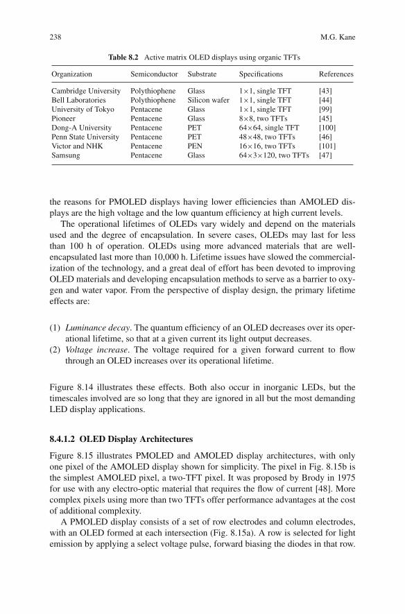
238 M.G. Kane
Table 8.2 Active matrix OLED displays using organic TFTs
Organization Semiconductor Substrate Specifications References
Cambridge University Polythiophene Glass 1×1, single TFT [43]Bell Laboratories Polythiophene Silicon wafer 1×1, single TFT [44]University of Tokyo Pentacene Glass 1×1, single TFT [99]Pioneer Pentacene Glass 8×8, two TFTs [45]Dong-A University Pentacene PET 64×64, single TFT [100]Penn State University Pentacene PET 48×48, two TFTs [46]Victor and NHK Pentacene PEN 16×16, two TFTs [101]Samsung Pentacene Glass 64×3×120, two TFTs [47]
the reasons for PMOLED displays having lower efficiencies than AMOLED dis-plays are the high voltage and the low quantum efficiency at high current levels.
The operational lifetimes of OLEDs vary widely and depend on the materialsused and the degree of encapsulation. In severe cases, OLEDs may last for lessthan 100 h of operation. OLEDs using more advanced materials that are well-encapsulated last more than 10,000 h. Lifetime issues have slowed the commercial-ization of the technology, and a great deal of effort has been devoted to improvingOLED materials and developing encapsulation methods to serve as a barrier to oxy-gen and water vapor. From the perspective of display design, the primary lifetimeeffects are:
(1) Luminance decay. The quantum efficiency of an OLED decreases over its oper-ational lifetime, so that at a given current its light output decreases.
(2) Voltage increase. The voltage required for a given forward current to flowthrough an OLED increases over its operational lifetime.
Figure 8.14 illustrates these effects. Both also occur in inorganic LEDs, but thetimescales involved are so long that they are ignored in all but the most demandingLED display applications.
8.4.1.2 OLED Display Architectures
Figure 8.15 illustrates PMOLED and AMOLED display architectures, with onlyone pixel of the AMOLED display shown for simplicity. The pixel in Fig. 8.15b isthe simplest AMOLED pixel, a two-TFT pixel. It was proposed by Brody in 1975for use with any electro-optic material that requires the flow of current [48]. Morecomplex pixels using more than two TFTs offer performance advantages at the costof additional complexity.
A PMOLED display consists of a set of row electrodes and column electrodes,with an OLED formed at each intersection (Fig. 8.15a). A row is selected for lightemission by applying a select voltage pulse, forward biasing the diodes in that row.
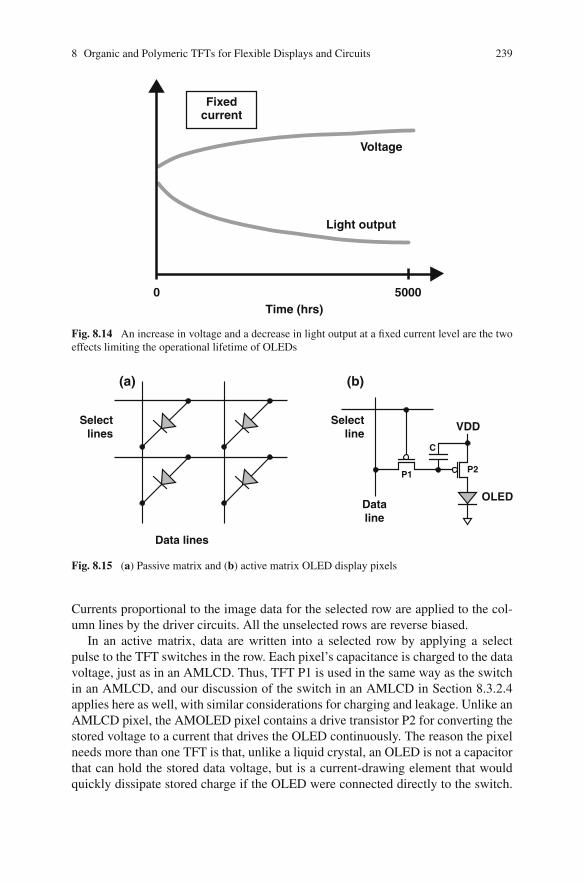
8 Organic and Polymeric TFTs for Flexible Displays and Circuits 239
0 5000Time (hrs)
Light output
Voltage
Fixedcurrent
Fig. 8.14 An increase in voltage and a decrease in light output at a fixed current level are the twoeffects limiting the operational lifetime of OLEDs
Selectlines
Data lines
(a) (b)
Selectline
Dataline
VDD
OLED
P2P1
C
Fig. 8.15 (a) Passive matrix and (b) active matrix OLED display pixels
Currents proportional to the image data for the selected row are applied to the col-umn lines by the driver circuits. All the unselected rows are reverse biased.
In an active matrix, data are written into a selected row by applying a selectpulse to the TFT switches in the row. Each pixel’s capacitance is charged to the datavoltage, just as in an AMLCD. Thus, TFT P1 is used in the same way as the switchin an AMLCD, and our discussion of the switch in an AMLCD in Section 8.3.2.4applies here as well, with similar considerations for charging and leakage. Unlike anAMLCD pixel, the AMOLED pixel contains a drive transistor P2 for converting thestored voltage to a current that drives the OLED continuously. The reason the pixelneeds more than one TFT is that, unlike a liquid crystal, an OLED is not a capacitorthat can hold the stored data voltage, but is a current-drawing element that wouldquickly dissipate stored charge if the OLED were connected directly to the switch.
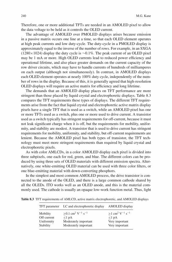
240 M.G. Kane
Therefore, one or more additional TFTs are needed in an AMOLED pixel to allowthe data voltage to be held as it controls the OLED current.
The advantage of AMOLED over PMOLED displays arises because emissionin a passive matrix occurs one line at a time, so that each OLED element operatesat high peak currents and low duty-cycle. The duty-cycle in a PMOLED display isapproximately equal to the inverse of the number of rows. For example, in an SXGA(1280×1024) display the duty cycle is ∼0.1%. The peak current of an OLED pixelmay be 1 mA or more. High OLED currents lead to reduced power efficiency andoperational lifetime, and also place greater demands on the current capacity of therow driver circuits, which may have to handle currents of hundreds of milliampereson each output (although not simultaneously). In contrast, in AMOLED displayseach OLED element operates at nearly 100% duty cycle, independently of the num-ber of rows in the display. Because of this, it is generally agreed that high-resolutionOLED displays will require an active matrix for efficiency and long lifetime.
The demands that an AMOLED display places on TFT performance are morestringent than those placed by liquid crystal and electrophoretic displays. Table 8.3compares the TFT requirements these types of displays. The different TFT require-ments arise from the fact that liquid crystal and electrophoretic active matrix displaypixels have a single TFT that is used as a switch, while an AMOLED pixel has oneor more TFTs used as a switch, plus one or more used to drive current. A transistorused as a switch typically has stringent requirements for off-current, because it mustnot leak significant charge when it is off, but the requirements for mobility, unifor-mity, and stability are modest. A transistor that is used to drive current has stringentrequirements for mobility, uniformity, and stability, but off-current requirements arelenient. Because the AMOLED pixel has both types of transistor, the TFT tech-nology must meet more stringent requirements than required by liquid crystal andelectrophoretic pixels.
As with color AMLCDs, in a color AMOLED display each pixel is divided intothree subpixels, one each for red, green, and blue. The different colors can be pro-duced by using three sets of OLED materials with different emission spectra. Alter-natively, one white-emitting OLED material can be used with three color filters, orone blue-emitting material with down-converting phosphors.
In the simplest and most common AMOLED process, the drive transistor is con-nected to the anode of the OLED, and there is a large common cathode shared byall the OLEDs. ITO works well as an OLED anode, and this is the material com-monly used. The cathode is usually an opaque low-work function metal. Thus, light
Table 8.3 TFT requirements of AMLCD, active matrix electrophoretic, and AMOLED displays
TFT parameter LC and electrophoretic display AMOLED display
Mobility ≥0.1 cm2 V−1 s−1 ≥1 cm2 V−1 s−1
Off-current ≤1 pA ≤1 pAUniformity Moderately important Very importantStability Moderately important Very important
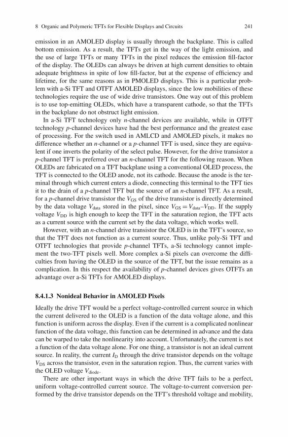
8 Organic and Polymeric TFTs for Flexible Displays and Circuits 241
emission in an AMOLED display is usually through the backplane. This is calledbottom emission. As a result, the TFTs get in the way of the light emission, andthe use of large TFTs or many TFTs in the pixel reduces the emission fill-factorof the display. The OLEDs can always be driven at high current densities to obtainadequate brightness in spite of low fill-factor, but at the expense of efficiency andlifetime, for the same reasons as in PMOLED displays. This is a particular prob-lem with a-Si TFT and OTFT AMOLED displays, since the low mobilities of thesetechnologies require the use of wide drive transistors. One way out of this problemis to use top-emitting OLEDs, which have a transparent cathode, so that the TFTsin the backplane do not obstruct light emission.
In a-Si TFT technology only n-channel devices are available, while in OTFTtechnology p-channel devices have had the best performance and the greatest easeof processing. For the switch used in AMLCD and AMOLED pixels, it makes nodifference whether an n-channel or a p-channel TFT is used, since they are equiva-lent if one inverts the polarity of the select pulse. However, for the drive transistor ap-channel TFT is preferred over an n-channel TFT for the following reason. WhenOLEDs are fabricated on a TFT backplane using a conventional OLED process, theTFT is connected to the OLED anode, not its cathode. Because the anode is the ter-minal through which current enters a diode, connecting this terminal to the TFT tiesit to the drain of a p-channel TFT but the source of an n-channel TFT. As a result,for a p-channel drive transistor the VGS of the drive transistor is directly determinedby the data voltage Vdata stored in the pixel, since VGS = Vdata–VDD. If the supplyvoltage VDD is high enough to keep the TFT in the saturation region, the TFT actsas a current source with the current set by the data voltage, which works well.
However, with an n-channel drive transistor the OLED is in the TFT’s source, sothat the TFT does not function as a current source. Thus, unlike poly-Si TFT andOTFT technologies that provide p-channel TFTs, a-Si technology cannot imple-ment the two-TFT pixels well. More complex a-Si pixels can overcome the diffi-culties from having the OLED in the source of the TFT, but the issue remains as acomplication. In this respect the availability of p-channel devices gives OTFTs anadvantage over a-Si TFTs for AMOLED displays.
8.4.1.3 Nonideal Behavior in AMOLED Pixels
Ideally the drive TFT would be a perfect voltage-controlled current source in whichthe current delivered to the OLED is a function of the data voltage alone, and thisfunction is uniform across the display. Even if the current is a complicated nonlinearfunction of the data voltage, this function can be determined in advance and the datacan be warped to take the nonlinearity into account. Unfortunately, the current is nota function of the data voltage alone. For one thing, a transistor is not an ideal currentsource. In reality, the current ID through the drive transistor depends on the voltageVDS across the transistor, even in the saturation region. Thus, the current varies withthe OLED voltage Vdiode.
There are other important ways in which the drive TFT fails to be a perfect,uniform voltage-controlled current source. The voltage-to-current conversion per-formed by the drive transistor depends on the TFT’s threshold voltage and mobility,
242 M.G. Kane
and these parameters are nonuniform across the display. This has been a particu-lar problem for poly-Si AMOLED backplanes because poly-Si TFTs exhibit largenonuniformities due to the random nature of the poly-Si grain structure. But evena-Si TFTs must cope with this problem. While a-Si TFTs are typically uniform atthe beginning of operational life, they quickly become nonuniform as they undergoimage-dependent threshold voltage shifts from bias-stress instability. Hysteresis isexpected to be a source of image-dependent nonuniformity over shorter timescales,an effect that has been observed in poly-Si TFT AMOLED displays [49]. In thepresent state of the technology OTFTs are expected to exhibit initial nonuniformityas well as image-induced nonuniformity.
One way of dealing with TFT nonuniformities is to demand better initial uni-formity and less bias-stress instability and hysteresis from the TFT technology.There has been progress in this direction using new OTFT materials and processes.However, an alternative is to develop pixel designs that are more tolerant of TFTnonuniformity. AMOLED pixels that perform electronic self-compensation for TFTnonuniformities were first demonstrated by a team from Sarnoff Corporation, PlanarAmerica, Kodak, and Princeton University. In 1998, this team demonstrated 16×16poly-Si AMOLED arrays using four-TFT self-compensating pixels that exhibitedbetter brightness uniformity than arrays using conventional two-TFT pixels [36].In 1999, a full self-compensating QVGA (320×240) AMOLED display using thefour-TFT pixels and integrated row and column drivers to control the compensationcircuitry was demonstrated [50]. Reviews of electronic self-compensation methodscan be found in [51–55]. Optical self-compensation methods have also been demon-strated with a photodetector in each pixel to sense OLED light output, and applyfeedback to correct for nonuniformity [56]. It should be noted that this is the onlyapproach that compensates for OLED luminance decay over operational life, sincenone of the others detects light output. However, the method introduces new sourcesof nonuniformity arising from the photodetector and its associated circuitry, and itis unclear whether the net effect is an improvement in display uniformity.
Additional discussion and analysis of the use of OTFTs for AMOLED displayscan be found in [57, 58]. To date only the conventional two-TFT pixels have beenimplemented with OTFTs, although a paper design for a self-compensating four-OTFT AMOLED pixel has been presented [58]. It is only a matter of time beforethe more complex pixels that have been investigated using poly-Si and a-Si TFTsare evaluated for providing compensation for OTFT nonuniformities.
8.5 Using Organic TFTs for Electronic Circuits
8.5.1 Thin-Film Transistor Circuits
8.5.1.1 Comparison with Silicon CMOS
The use of TFTs for electronic circuits has been led by manufacturers of small- andmedium-sized AMLCDs, who are making increasing use of poly-Si TFTs for the
8 Organic and Polymeric TFTs for Flexible Displays and Circuits 243
integration of row and column display drivers onto the display glass. The integrationof driver circuits on the display substrate can reduce display module cost, shortenproduct development times, and reduce the complexity and improve the reliabilityof the display interconnects. The cost advantage is most dramatic for small displays,because the cost of the driver circuits and the interconnects is a larger fraction of thetotal display module cost for smaller displays than for larger ones. Similar argu-ments could be made for integrated driver circuits for TFT-based imagers such asdigital X-ray imagers, although integrated drivers have not yet made inroads in thisapplication space.
The argument is less compelling for general purpose electronic circuits. Con-ventional CMOS silicon IC technology is able to produce MOSFETs for the aston-ishingly low cost of a few microcents to a few hundred microcents per transistor,depending on the type of IC and the level of integration. Absent any special con-siderations, such as the interconnect arguments that apply to displays and imagers,other types of TFT circuits must compete with silicon ICs on the basis of cost pertransistor. Although the cost of processed TFT substrates per unit area will be lowerthan the areal cost of silicon ICs, the dimensions of MOSFETs used in silicon ICsare so much smaller than typical TFT dimensions that it will be difficult to reducethe cost of a TFT to be lower than the cost of a silicon MOSFET. Fabrication meth-ods that promise to reduce cost per unit area, such as printing processes for OTFTs,but at the expense of increased transistor size because of poorer dimensional tol-erances, may actually increase the cost per transistor, reducing competitiveness forthese types of circuits.
Of course, TFT technology must compete with silicon technology not only onthe basis of cost but also performance. It is well known that the performance ofOTFT circuits is limited by the low mobility of the transistors, but there are otherlimiting factors. One significant factor is the absence of a good organic CMOS tech-nology. The major advantages of CMOS over single-channel circuits and systemsare (1) power dissipation is lower, especially static dissipation in digital systems; (2)signal voltages can easily swing all the way from one power supply voltage to theother; (3) the performance of the system is more tolerant of variations in transistorparameters, so that fabrication yields are higher; (4) circuit gain is higher, leadingto larger noise margins in digital systems; and (5) design methods are simpler.
There are two obstacles to organic CMOS: the lack of good n-channel devices,and the process difficulty of integrating two types of organic TFTs on one substrate.The advantages of CMOS exist even if one transistor type is inferior to the other. Butto derive the full benefit of CMOS, high performance is required from both devicetypes, because otherwise system performance will be dominated by the lower per-forming device. For example, a low-mobility n-channel OTFT in a CMOS invertermust be scaled to large widths to provide pull-down capability that matches the pull-up capability of the p-channel OTFT, but this means that gate input capacitances aredominated by the large n-channel devices. Rise and fall times will be balanced,but slow. A good case can be made that the benefits of a complementary technol-ogy outweigh the gains achieved from achieving modest mobility improvements in asingle-channel process, and that more effort to develop organic CMOS is warranted.
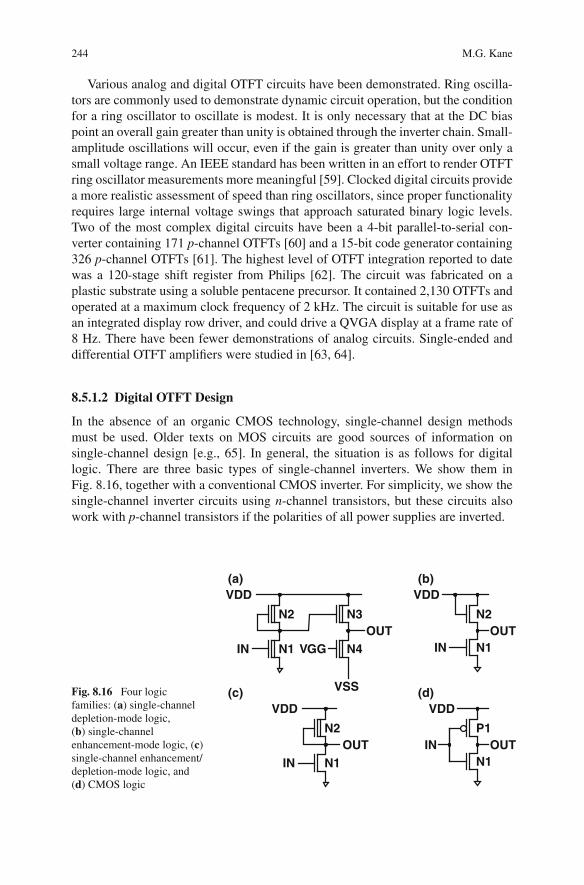
244 M.G. Kane
Various analog and digital OTFT circuits have been demonstrated. Ring oscilla-tors are commonly used to demonstrate dynamic circuit operation, but the conditionfor a ring oscillator to oscillate is modest. It is only necessary that at the DC biaspoint an overall gain greater than unity is obtained through the inverter chain. Small-amplitude oscillations will occur, even if the gain is greater than unity over only asmall voltage range. An IEEE standard has been written in an effort to render OTFTring oscillator measurements more meaningful [59]. Clocked digital circuits providea more realistic assessment of speed than ring oscillators, since proper functionalityrequires large internal voltage swings that approach saturated binary logic levels.Two of the most complex digital circuits have been a 4-bit parallel-to-serial con-verter containing 171 p-channel OTFTs [60] and a 15-bit code generator containing326 p-channel OTFTs [61]. The highest level of OTFT integration reported to datewas a 120-stage shift register from Philips [62]. The circuit was fabricated on aplastic substrate using a soluble pentacene precursor. It contained 2,130 OTFTs andoperated at a maximum clock frequency of 2 kHz. The circuit is suitable for use asan integrated display row driver, and could drive a QVGA display at a frame rate of8 Hz. There have been fewer demonstrations of analog circuits. Single-ended anddifferential OTFT amplifiers were studied in [63, 64].
8.5.1.2 Digital OTFT Design
In the absence of an organic CMOS technology, single-channel design methodsmust be used. Older texts on MOS circuits are good sources of information onsingle-channel design [e.g., 65]. In general, the situation is as follows for digitallogic. There are three basic types of single-channel inverters. We show them inFig. 8.16, together with a conventional CMOS inverter. For simplicity, we show thesingle-channel inverter circuits using n-channel transistors, but these circuits alsowork with p-channel transistors if the polarities of all power supplies are inverted.
IN OUT
VDD
INOUT
VDD
INOUT
VDD
IN
VDD
VGG
VSS
OUT
(a) (b)
(c) (d)
N2
N1
N2
N1
P1
N1
N3
N4
N2
N1
Fig. 8.16 Four logicfamilies: (a) single-channeldepletion-mode logic,(b) single-channelenhancement-mode logic, (c)single-channel enhancement/depletion-mode logic, and(d) CMOS logic
8 Organic and Polymeric TFTs for Flexible Displays and Circuits 245
The first type of inverter (Fig. 8.16a) uses only depletion-mode transistors, thatis, transistors that are on when VGS = 0. High inverter gain, and therefore large noisemargin, is obtained when driver transistor N1 has a larger W/L ratio than load tran-sistor N2, which places the input switching point below zero volts. This necessitatesa level-shifting output stage using a source follower N3 biased by a current sourceN4 to shift the output-low level below zero volts. The amount of level shifting isdetermined by VGS of N4 (which is equal to VGG–VSS) and the relative sizing ofN3 and N4. Source follower N3 not only provides level shifting but also serves asa good output driver because of its low output impedance. We employed this con-figuration in our early work on clocked OTFT circuits, which used depletion-modepentacene devices [63].
The second type of inverter (Fig. 8.16b) uses only enhancement-mode transis-tors, that is, transistors that are off when VGS = 0. The input switching point is abovezero volts, so no level shifter is needed. However, diode-connected load transistorN2 is unable to pull the output higher than a threshold voltage below the VDD sup-ply, limiting output voltage swing. In addition, the impedance of a diode-connecteddevice depends strongly on the voltage across it, so that the pull-up capability of theload transistor diminishes as the output approaches the high logic level. Thus, thedelay times of the low-to-high and high-to-low transitions are typically mismatched.
The third type of inverter (Fig. 8.16c) uses both enhancement- and depletion-mode transistors. An enhancement-mode device is used for driver N1 and adepletion-mode device is used for load N2. The input switching point is above zerovolts, so no level shifter is needed. Load transistor N2 is able to pull the output tothe positive supply rail, and the output transition times can be matched. This inverterconfiguration typically provides the best performance with the lowest complexity ofthe three types of single-channel inverters. However, it requires transistors with twodifferent threshold voltages, one positive and one negative, which may be just ashigh a technological hurdle as providing the n-channel and p-channel devices thatCMOS requires.
However, recent work on OTFTs with a single semiconductor layer combinedwith two gates, one on the top and one on the bottom, has shown that two differentthreshold voltages can be obtained in a relatively straightforward way [66–68]. Thetwo gates can be used in various ways. The top gate and bottom gate can be useddirectly to provide the different threshold voltages; a DC bias can be applied to thetop gate to adjust the threshold voltage of the bottom-gate transistor; or the twogates can be tied together to provide higher on-currents and steeper subthresholdslope [67]. The double-gate approach was recently used to fabricate inverters [69]and was also used in an OTFT static RAM cell, where a DC bias was applied to thetop gate to compensate for poor threshold voltage control in the fabrication process[70]. It is likely that digital circuits using enhancement-mode and depletion-modeOTFTs produced by means of double gates will be demonstrated soon.
We have discussed inverter configurations, but logic gates to perform NANDand NOR functions can be constructed from the single-channel inverter by addingone additional driver transistor per input. It is preferable to place driver transistorsin parallel rather than in series to minimize the resistance of the driver transistor
246 M.G. Kane
network and maximize speed. With n-channel transistors, this implies favoring NORgates over NAND gates; with p-channel transistors NAND gates are favored.
8.5.2 Frequency Limitations of OTFTs
A rough idea of the frequency limitations of an OTFT is obtained by again consid-ering the unity-gain frequency ft, given in a simple model by Eq. (8.6),
ft = μF E (VGS − Vt )
2π L(L + 2Loverlap).
We can estimate the unity-gain frequency of a pentacene OTFT made with currenttechnology and driven at reasonable voltage levels. The field-effect mobility μFE ofa good device is about 0.5 cm2 V−1 s−1 and the DC overdrive bias (VGS−Vt ) is∼10 V. For a process with good dimensional tolerances, the channel length L andthe overlap length Loverlap are both about 5 μm. This yields a unity-gain frequencyof 1.1 MHz.
Digital and analog circuits can be designed to operate up to about 20–30% of ft.In the case of digital circuits one way of viewing this is that the waveforms producedby these circuits should saturate at the power supply rails, requiring the circuits toreproduce harmonics well above the fundamental frequency. Typical analog circuitsuse closed-loop operation with negative feedback, and therefore must operate nohigher than a fraction of ft in order for the open loop gain to be much larger thanone. Thus with current technology a pentacene-based OTFT circuit can operate upto a few hundred kilohertz.
It was noted in Section 8.2.6 that an OTFT’s unity-gain frequency could beimproved significantly by developing a self-aligned process that reduces Loverlap toa very small value, eliminating the overlap capacitances. In the above example thiswould triple the unity-gain frequency. An alternative is to neutralize these capaci-tances using circuit methods. Unlike the channel capacitance, which is distributedalong the length of the device, the overlap capacitances are accessible at the termi-nals of the device and can therefore be resonated out over a band of frequenciesby well-known methods used in high-frequency amplifiers.6 These tuned methodsare usually not applicable to general digital and analog circuits, which operate in abroadband mode, possibly down to DC. But for narrowband RF circuits these meth-ods may allow the effects of Loverlap to be eliminated, so that one must cope only
6It might be objected that parasitics can only be resonated out if their values are predictable.Since the overlap capacitances depend on alignment between different metallization levels, theyare expected to be quite variable. However, layout techniques can render parasitics well-definedand predictable. For example, by laying out a TFT with one source electrode in the middle of thedevice, and two drain electrodes connected in parallel, one on each side of the source, the overlapcapacitances can be made constant, because as the overlap on one side gets larger the overlap onthe other side gets smaller.
8 Organic and Polymeric TFTs for Flexible Displays and Circuits 247
with the distributed channel capacitance due to L, which corresponds to the intrinsicpropagation delay of the device and sets a limit on the highest operating frequency.
8.5.3 Integrated Display Drivers
A matrix-addressed display requires driver circuits to generate the signals that areapplied to the row and column lines. An AMLCD row driver consists of a shiftregister that applies a select pulse to the row lines sequentially. The shift regis-ter typically operates at clock frequencies below 100 kHz, within the capability ofOTFTs. An AMLCD column driver generates an analog voltage on each columnthat depends on the image data for the pixels in that column. External driver chipshave a digital-to-analog converter (DAC) for each column of the display. Integratedcolumn drivers typically do not put all this functionality onto the display. With cur-rent poly-Si integrated drivers, a few high-speed DACs are located on an externalsilicon chip, and the integrated column driver circuitry has an analog demultiplexerwith a shift register and switches to sample the high-speed analog data sequentiallyonto the columns at a rate of a few megasamples to tens of megasamples per second.
The performance of poly-Si TFTs is very good for integrated display drivers.Although poly-Si TFTs often have high off-currents, this is generally not importantfor display driver circuits. Furthermore, complementary n-channel and p-channeldevices are available with poly-Si TFT technology, so that CMOS design methodscan be used.
It is considerably more difficult to make integrated drivers with OTFTs becauseof low mobility and bias-stress instability, and because organic CMOS technologyis not yet available. The situation is similar with a-Si TFTs, which likewise have lowmobility and bias-stress instability, and provide only n-channel TFTs. Nevertheless,a-Si is a lower-cost technology than poly-Si technology, and this has spurred effortsto develop a-Si integrated drivers. As long ago as 1987, the David Sarnoff ResearchCenter and Thomson LCD developed the self-scanned amorphous silicon integrateddisplay (SASID) technology, which permitted the integration of a-Si TFT row andcolumn drivers [71]. SASID consisted primarily of a set of circuit design methodsthat allowed driver circuits to tolerate the performance limitations of a-Si TFTs.For example, a SASID row driver maintains the TFTs in each stage in the off stateexcept when that stage is generating a select pulse, minimizing bias-stress inducedthreshold shift. SASID column drivers implement only the demultiplexing switcheson the display, leaving the DACs and the shift register on an external silicon chip.Thales Avionics manufactures a 480×480 cockpit display using a-Si row driversbased on the SASID technology, and work on a-Si drivers continues to the presenttime [72].
Integrated drivers have not yet been implemented with OTFTs. However, theapplication of OTFTs to integrated drivers is expected to be similar to the situationwith a-Si TFTs, with similar design approaches used. In spite of the difficulties,novel circuit design methods will allow low-cost OTFT drivers to be integrated onthe display.
248 M.G. Kane
8.5.4 Radio Frequency Identification Tags
8.5.4.1 Introduction
RFID tags have been proposed as an application for OTFTs on flexible substratesbecause very low cost tags would open up the possibility of item-level tracking,supplementing or replacing printed bar codes. Item-level RFID tags have severaladvantages over bar codes. Manual scanning is not required, permitting faster andmore automated item inventory and tracking; stored information can be updated;and loss, theft, and counterfeiting can be more easily deterred. General treatmentsof RFID technology can be found in [73, 74].
The use of RFID tags on shipping containers and pallets has demonstrated itsvalue. For these applications, a tag cost of several dollars or more can be justified,especially when tag reuse is possible. But tracking of individual consumer itemsrequires such a low tag cost to be economically viable that RFID has not madeinroads yet, except for high-priced items and controlled pharmaceuticals. It has beenestimated that simply to break even on the cost versus benefits trade-off, an RFIDlabel for a $40 item must cost between 5 and 10 cents. Prices for the lowest-costsilicon-based RFID tags are currently about 7 cents in large volumes for tags thatare unconverted (not yet in label form), and 10–12 cents for tags in the form of self-adhesive labels.7 In contrast, printed bar codes add virtually no packaging cost to anitem, although there are infrastructure and labor costs associated with reading andtracking.
This is the reason OTFTs are considered for this application, with a goal of pro-ducing a very low cost “penny tag.” However, the cautions of Section 8.4.1.1 applyto RFID tags. Unless the cost per transistor of OTFT technology is lower than thatof silicon IC technology, OTFTs will not be cost-competitive. On the other hand,it has been pointed out that, even if the cost per transistor of OTFTs is higher thanthat of silicon ICs, OTFTs could still be cost-competitive. By fabricating the OTFTRFID circuit on the tag itself, the cost of mounting a silicon RFID chip on the tag isavoided, so that OTFT technology has a cost advantage due to lower assembly costs.While this is true, there is a compensating disadvantage to fabricating the OTFT cir-cuit directly on the tag: in order to accommodate the antenna, the circuit must befabricated on a substrate significantly larger than the area required by the transis-tors alone. As a result, the transistor throughput of the OTFT fabrication facility isreduced by this large area factor, and the cost per transistor of the RFID circuit isscaled up by approximately the same factor.
7Here we are not considering so-called one-bit tags, which simply signal their presence to thereader. This type of tag is used in stores as an anti-theft device, and is deactivated during purchase.It does not contain electronic circuitry, but uses a simple physical effect such as the magnetizationproperties of a metal. One-bit tags can be made for only a fraction of a cent.
8 Organic and Polymeric TFTs for Flexible Displays and Circuits 249
RFID tags can be active or passive. Active tags contain a battery for power, whilepassive tags draw their power from the RF signal broadcast by the tag reader.8 Activetags can be used at a greater distance from the reader because of the on-tag powersource, but are more expensive. The advantage of OTFTs is their potentially lowcost, so the technology is only considered for passive tags.
Four carrier frequency bands are currently used for RFID tags:Low-frequency <135 kHz band. The near field of an electromagnetic wave occurs
at distances less than λ/2π than from the antenna, where λ is the free-space wave-length. The far field occurs at larger distances. At 135 kHz the near field is foundat distances closer than 354 m, so that tags in this band operate in the near fieldof the reader. Therefore, the antenna for an RFID tag operating in this band doesnot function as a conventional radio antenna, communicating with the reader via apropagating electromagnetic wave. Instead the antenna is a coil that provides mag-netic coupling to a coil in the reader, like the coupling between primary and sec-ondary windings of a transformer. Wound wire coils with many turns are typicallyused to achieve high inductance with low resistance, sometimes with a ferrite coreto improve the magnetic coupling. These coils are expensive, so that this type oftag is not considered for low-cost item-level tags, and the cost advantage of OTFTtechnology is not likely to be compelling. This is unfortunate because OTFTs canoperate without much difficulty in this frequency range.
There is one possible way tags operating in the low-frequency range mightbe produced at low cost. Reader and tag can be coupled using capacitive ratherthan inductive coupling. A capacitive coupling antenna can be printed at lowcost. Motorola considered commercializing this approach at 13.56 MHz with theirBiStatix technology, which used carbon ink electrodes printed on a paper label, witha silicon IC attached to the electrodes. However, there are significant disadvantagesto capacitive coupling. Nearby conductive objects disrupt the electric field. Further-more, RFID tags typically use an inductor and capacitor in parallel at the input toform an LC tank circuit with resonance at or near the carrier frequency, in order toboost the voltage generated by the carrier to a level that can drive the tag electronics.But since the goal of the capacitive coupling approach is to eliminate the expensivecoil, an on-tag resonant circuit is not practical, and the tag’s read range is limited bylow induced voltages.
High-frequency 13.56 MHz band. Tags operating in this band also operate inthe near field of the reader, since the near field is found at distances closer thanλ/2π or 3.5 m. The higher frequency permits a planar spiral inductor rather than awound wire coil to be used for magnetic coupling to the reader, significantly reduc-ing cost. Typically an etched metal inductor is used. This is an ideal frequency bandfor low-cost RFID tags and is generally considered to be the best opportunity forOTFT RFID tags. However, at present it is challenging for electronic componentsfabricated using OTFT technology to operate reliably at frequencies this high. The
8The reader in an RFID system is sometimes referred to as the interrogator, and the tag is oftenreferred to as the transponder.
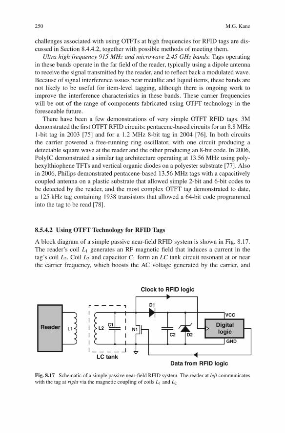
250 M.G. Kane
challenges associated with using OTFTs at high frequencies for RFID tags are dis-cussed in Section 8.4.4.2, together with possible methods of meeting them.
Ultra high frequency 915 MHz and microwave 2.45 GHz bands. Tags operatingin these bands operate in the far field of the reader, typically using a dipole antennato receive the signal transmitted by the reader, and to reflect back a modulated wave.Because of signal interference issues near metallic and liquid items, these bands arenot likely to be useful for item-level tagging, although there is ongoing work toimprove the interference characteristics in these bands. These carrier frequencieswill be out of the range of components fabricated using OTFT technology in theforeseeable future.
There have been a few demonstrations of very simple OTFT RFID tags. 3Mdemonstrated the first OTFT RFID circuits: pentacene-based circuits for an 8.8 MHz1-bit tag in 2003 [75] and for a 1.2 MHz 8-bit tag in 2004 [76]. In both circuitsthe carrier powered a free-running ring oscillator, with one circuit producing adetectable square wave at the reader and the other producing an 8-bit code. In 2006,PolyIC demonstrated a similar tag architecture operating at 13.56 MHz using poly-hexylthiophene TFTs and vertical organic diodes on a polyester substrate [77]. Alsoin 2006, Philips demonstrated pentacene-based 13.56 MHz tags with a capacitivelycoupled antenna on a plastic substrate that allowed simple 2-bit and 6-bit codes tobe detected by the reader, and the most complex OTFT tag demonstrated to date,a 125 kHz tag containing 1938 transistors that allowed a 64-bit code programmedinto the tag to be read [78].
8.5.4.2 Using OTFT Technology for RFID Tags
A block diagram of a simple passive near-field RFID system is shown in Fig. 8.17.The reader’s coil L1 generates an RF magnetic field that induces a current in thetag’s coil L2. Coil L2 and capacitor C1 form an LC tank circuit resonant at or nearthe carrier frequency, which boosts the AC voltage generated by the carrier, and
LC tank
Clock to RFID logic
Reader L1 L2C1
C2
D1
D2
Digitallogic
GND
VCC
Data from RFID logic
N1
Fig. 8.17 Schematic of a simple passive near-field RFID system. The reader at left communicateswith the tag at right via the magnetic coupling of coils L1 and L2

8 Organic and Polymeric TFTs for Flexible Displays and Circuits 251
also makes the tag more detectable by the reader. The AC signal is rectified bydiode D1 and filtered by supply capacitor C2 to generate the DC supply voltageVCC that powers the tag’s digital logic. The single diode D1 provides only half-waverectification and can be replaced by a full-wave rectifier for higher efficiency. Aregulator diode D2 is used to clamp the DC supply voltage seen by the logic, or avoltage regulator circuit is used, since changes in the distance to the reader producelarge variations in field strength. Without some type of voltage regulation, severalhundred volts can be induced close to the reader, which is likely to damage the tagelectronics.
In a conventional silicon-based tag the RF signal is used not only to power thetag but also to generate a clock for the tag’s digital logic, as shown in Fig. 8.17.The carrier signal is divided down by a digital frequency divider, so that only thefirst-stage frequency divider operates at the carrier frequency, while the rest of thelogic operates at lower frequencies.
After a start-up period during which the supply capacitor is charged, the tagbegins to output stored data, either in response to the clock only or in response tocommands sent from the reader by modulating the carrier. Data are sent from the tagto the reader by switching on and off shunt transistor N1, modulating the loading ofthe tank with the output data. The load modulation is detected at the reader by mon-itoring the AC voltage across coil L1. When the tag’s tank circuit is within the rangeof the reader, the reader’s coil is loaded in the same way that the primary windingof a transformer is loaded by the secondary. When N1 is on, the quality factor Q ofthe tank is reduced and the loading of the reader’s coil is altered. An alternative is toplace N1 in series with a capacitor, modulating the tuning of the tank circuit ratherthan its Q. With proper design the switching of N1 does not interfere with power ordata from the reader.
Thus, the RF carrier incident on the tag from the reader performs three functions:
(1) Powering the tag(2) Signaling the tag with a clock or code(3) Detecting the tag
These three functions require some components in the tag to operate at the carrierfrequency. Below we consider the challenges of implementing these functions inan OTFT technology. Then, we examine an additional RFID function that may bedifficult to implement in OTFT technology: memory.
Powering the Tag
To supply power to the tag, AC current at the carrier frequency must pass through thecoil, capacitors C1 and C2, and rectification diode D1. There is no serious difficultyproducing a coil and capacitors that function at RF frequencies in an OTFT process,although it is challenging to produce a low-resistance, high-Q coil and a capacitorwith a well-controlled capacitance using low-cost printing methods [79]. However,
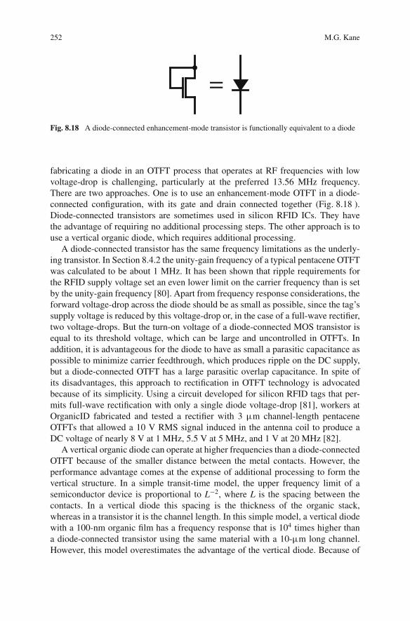
252 M.G. Kane
=
Fig. 8.18 A diode-connected enhancement-mode transistor is functionally equivalent to a diode
fabricating a diode in an OTFT process that operates at RF frequencies with lowvoltage-drop is challenging, particularly at the preferred 13.56 MHz frequency.There are two approaches. One is to use an enhancement-mode OTFT in a diode-connected configuration, with its gate and drain connected together (Fig. 8.18 ).Diode-connected transistors are sometimes used in silicon RFID ICs. They havethe advantage of requiring no additional processing steps. The other approach is touse a vertical organic diode, which requires additional processing.
A diode-connected transistor has the same frequency limitations as the underly-ing transistor. In Section 8.4.2 the unity-gain frequency of a typical pentacene OTFTwas calculated to be about 1 MHz. It has been shown that ripple requirements forthe RFID supply voltage set an even lower limit on the carrier frequency than is setby the unity-gain frequency [80]. Apart from frequency response considerations, theforward voltage-drop across the diode should be as small as possible, since the tag’ssupply voltage is reduced by this voltage-drop or, in the case of a full-wave rectifier,two voltage-drops. But the turn-on voltage of a diode-connected MOS transistor isequal to its threshold voltage, which can be large and uncontrolled in OTFTs. Inaddition, it is advantageous for the diode to have as small a parasitic capacitance aspossible to minimize carrier feedthrough, which produces ripple on the DC supply,but a diode-connected OTFT has a large parasitic overlap capacitance. In spite ofits disadvantages, this approach to rectification in OTFT technology is advocatedbecause of its simplicity. Using a circuit developed for silicon RFID tags that per-mits full-wave rectification with only a single diode voltage-drop [81], workers atOrganicID fabricated and tested a rectifier with 3 μm channel-length pentaceneOTFTs that allowed a 10 V RMS signal induced in the antenna coil to produce aDC voltage of nearly 8 V at 1 MHz, 5.5 V at 5 MHz, and 1 V at 20 MHz [82].
A vertical organic diode can operate at higher frequencies than a diode-connectedOTFT because of the smaller distance between the metal contacts. However, theperformance advantage comes at the expense of additional processing to form thevertical structure. In a simple transit-time model, the upper frequency limit of asemiconductor device is proportional to L−2, where L is the spacing between thecontacts. In a vertical diode this spacing is the thickness of the organic stack,whereas in a transistor it is the channel length. In this simple model, a vertical diodewith a 100-nm organic film has a frequency response that is 104 times higher thana diode-connected transistor using the same material with a 10-μm long channel.However, this model overestimates the advantage of the vertical diode. Because of
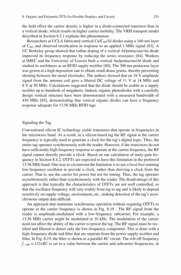
8 Organic and Polymeric TFTs for Flexible Displays and Circuits 253
the field effect the carrier density is higher in a diode-connected transistor than ina vertical diode, which results in higher carrier mobility. The VRH transport modeldescribed in Section 8.2.1 explains this phenomenon.
Researchers at UCLA fabricated vertical Cu/C60/Al diodes using a 100-nm layerof C60, and observed rectification in response to an applied 1 MHz signal [83]. AUC Berkeley group showed that iodine doping of a vertical Al/pentacene/Au diodeimproved its frequency response by reducing the series resistance [84]. Workersat IMEC and the University of Leuven built a vertical Au/pentacene/Al diode andstudied its usefulness as an RFID supply rectifier [80]. The 300 nm pentacene layerwas grown at a high deposition rate to obtain small dense grains, thereby preventingshorting between the metal electrodes. The authors showed that an 18 V amplitudesignal from the antenna coil gave a filtered DC voltage of 11 V at 14 MHz and8 V at 50 MHz. Calculations suggested that the diode should be usable as a supplyrectifier up to hundreds of megahertz. Indeed, organic photodiodes with a carefullydesign vertical structure have been demonstrated with a measured bandwidth of430 MHz [85], demonstrating that vertical organic diodes can have a frequencyresponse adequate for 13.56 MHz RFID tags.
Signaling the Tag
Conventional silicon IC technology yields transistors that operate at frequencies inthe microwave band. As a result, in a silicon-based tag the RF signal at the carrierfrequency is typically used to generate a clock for the tag’s digital logic. Thus, theentire tag operates synchronously with the reader. However, if the transistors do nothave sufficiently high frequency response to operate at the carrier frequency, the RFsignal cannot directly provide a clock. Based on our calculation of unity-gain fre-quency in Section 8.4.2, OTFTs are expected to have this limitation in the preferred13.56 MHz band. One way to circumvent the limitation is to use a local free-runninglow-frequency oscillator to provide a clock, rather than deriving a clock from thecarrier. That is, use the carrier for power but not for timing. Thus, the tag operatesasynchronously rather than synchronously with the reader. The disadvantage of thisapproach is that typically the characteristics of OTFTs are not well controlled, sothat the oscillator frequency will vary widely from tag to tag and is likely to dependsensitively on supply voltage, environment, etc., making detection of the tag’s asyn-chronous output data difficult.
An approach that maintains synchronous operation without requiring OTFTs tooperate at the carrier frequency is shown in Fig. 8.19 . The RF signal from thereader is amplitude-modulated with a low-frequency subcarrier. For example, a13.56 MHz carrier might be modulated at 10 kHz. The modulation of the carrierneed not affect the ability of the carrier to power the tag. The RF signal must be rec-tified and filtered to detect only the low-frequency component. This is done with ahigh-frequency diode and filter that are separate from the power supply rectifier andfilter. In Fig. 8.19, the filter is shown as a parallel RC circuit. The roll-off frequencyf−3db = 1/2πRC is set to a value between the carrier and subcarrier frequencies, in
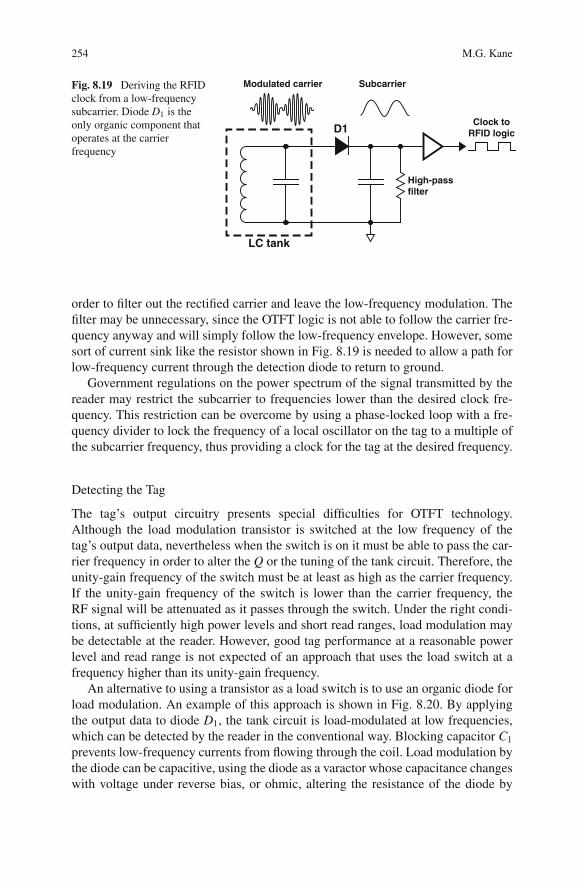
254 M.G. Kane
LC tank
D1Clock to
RFID logic
High-passfilter
Modulated carrier SubcarrierFig. 8.19 Deriving the RFIDclock from a low-frequencysubcarrier. Diode D1 is theonly organic component thatoperates at the carrierfrequency
order to filter out the rectified carrier and leave the low-frequency modulation. Thefilter may be unnecessary, since the OTFT logic is not able to follow the carrier fre-quency anyway and will simply follow the low-frequency envelope. However, somesort of current sink like the resistor shown in Fig. 8.19 is needed to allow a path forlow-frequency current through the detection diode to return to ground.
Government regulations on the power spectrum of the signal transmitted by thereader may restrict the subcarrier to frequencies lower than the desired clock fre-quency. This restriction can be overcome by using a phase-locked loop with a fre-quency divider to lock the frequency of a local oscillator on the tag to a multiple ofthe subcarrier frequency, thus providing a clock for the tag at the desired frequency.
Detecting the Tag
The tag’s output circuitry presents special difficulties for OTFT technology.Although the load modulation transistor is switched at the low frequency of thetag’s output data, nevertheless when the switch is on it must be able to pass the car-rier frequency in order to alter the Q or the tuning of the tank circuit. Therefore, theunity-gain frequency of the switch must be at least as high as the carrier frequency.If the unity-gain frequency of the switch is lower than the carrier frequency, theRF signal will be attenuated as it passes through the switch. Under the right condi-tions, at sufficiently high power levels and short read ranges, load modulation maybe detectable at the reader. However, good tag performance at a reasonable powerlevel and read range is not expected of an approach that uses the load switch at afrequency higher than its unity-gain frequency.
An alternative to using a transistor as a load switch is to use an organic diode forload modulation. An example of this approach is shown in Fig. 8.20. By applyingthe output data to diode D1, the tank circuit is load-modulated at low frequencies,which can be detected by the reader in the conventional way. Blocking capacitor C1
prevents low-frequency currents from flowing through the coil. Load modulation bythe diode can be capacitive, using the diode as a varactor whose capacitance changeswith voltage under reverse bias, or ohmic, altering the resistance of the diode by
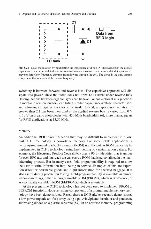
8 Organic and Polymeric TFTs for Flexible Displays and Circuits 255
LC tank
C1
D1
Data fromRFID logic
Fig. 8.20 Load modulation by modulating the impedance of diode D1. In reverse bias the diode’scapacitance can be modulated, and in forward bias its resistance can be modulated. Capacitor C1
prevents large low-frequency currents from flowing through the coil. The diode is the only organiccomponent that operates at the carrier frequency
switching it between forward and reverse bias. The capacitive approach will dis-sipate less power, since the diode does not draw DC current under reverse bias.Heterojunctions between organic layers can behave like conventional p–n junctionsin inorganic semiconductors, exhibiting similar capacitance-voltage characteristicsand allowing an organic varactor to be made. Indeed, a capacitance variation ofgreater than 2:1 has been measured as the applied reverse bias is varied from 0 Vto 10 V on organic photodiodes with 430 MHz bandwidth [86], more than adequatefor RFID applications at 13.56 MHz.
Memory
An additional RFID circuit function that may be difficult to implement in a low-cost OTFT technology is nonvolatile memory. For some RFID applications, afactory-programmed read-only memory (ROM) is sufficient. A ROM can easily beimplemented in OTFT technology using laser cutting of a metallization pattern. Forexample, the Electronic Product Code (EPC) uses a 96-bit identifier that is uniquefor each EPC tag, and thus each tag can carry a ROM that is personalized in the man-ufacturing process. But in many cases field-programmability is required to allowthe user to write information into the tag in service. Examples of this are expira-tion dates for perishable goods and flight information for checked baggage. It isalso useful during production testing. Field-programmability is available in currentsilicon-based tags, either as programmable ROM (PROM), which is write-once, oras electrically erasable PROM (EEPROM), which is rewritable.
At the present time OTFT technology has not been used to implement PROM orEEPROM functions. However, some components of a programmable memory tech-nology have been demonstrated. Researchers at UC Berkeley recently demonstrateda low-power organic antifuse array using a polyvinylphenol insulator and pentaceneaddressing diodes on a plastic substrate [87]. In an antifuse memory, programming
256 M.G. Kane
takes place by applying a sufficiently high voltage across an insulator to physicallydamage it, creating a short circuit. Diodes are required for robust matrix addressing.Provided that the peripheral components for the antifuse array could be fabricatedin an OTFT process, this technology could be used as PROM in low-cost RFIDtags. There has also been work by many researchers on bistable memory effectsthat could form the basis for EEPROM in organic RFID tags. Bistability has beenobserved in vertical organic devices [88–91] as well as lateral OTFT-like deviceswith functionalized gate dielectrics [92, 93].
8.6 Conclusion
Organic TFT technology on flexible substrates holds unique promise for providinga low-cost route to fabricating electronics. Furthermore, the use of flexible sub-strates opens up the possibility of mechanically flexible electronic systems. How-ever, the dominant technology, silicon CMOS, has achieved astonishing levels ofperformance improvement and cost reduction, and displacing it will be a formidablechallenge, even in a limited application space. Applications are needed that per-mit OTFTs to be gracefully and incrementally introduced as a low-cost alterna-tive to existing technologies. Demanding applications such as RFID tags are likelyto require new circuit and system designs in order to coax high enough perfor-mance from OTFT technology to take advantage of its low cost. For less demandingapplications such as active matrix displays, OTFT fabrication could be introducedinto standard TFT display manufacturing lines incrementally and with little fan-fare. Initially, PECVD and photolithographic processes on glass substrates couldbe replaced by lower-cost additive, printing-like processes, with roll-to-roll man-ufacturing on flexible substrates introduced later as OTFT backplane technologybecomes mainstream.
Acknowledgements The author would like to acknowledge G. Gu for many helpful discussionsabout organic thin-film transistors.
References
1. Vissenberg M, Matters M (1998) Theory of the field-effect mobility in amorphous organictransistors. Phys Rev B 57:12964–12967
2. Slade HC (1997) Device and material characterization and analytic modeling of amorphoussilicon thin film transistors. PhD dissertation, University of Virginia
3. Cerdeira A et al. (2001) New procedure for the extraction of basic a-Si:H TFT model param-eters in the linear and saturation regions. Solid-State Electron 45:1077–1080
4. Fadlallah M et al. (2006) Modeling and characterization of organic thin film transistors forcircuit design. J Appl Phys 99:104504-1–104504-7
5. Pesavento PV et al. (2006) Film and contact resistance in pentacene thin-film transistors:Dependence on film thickness, electrode geometry, and correlation with hole mobility. JAppl Phys 99:094504-1–094504-10
8 Organic and Polymeric TFTs for Flexible Displays and Circuits 257
6. Gundlach DJ et al. (2006) An experimental study of contact effects in organic thin-filmtransistors. J Appl Phys 100:024509-1–024509-13
7. Tsividis YP (1999) Operation and modeling of the MOS transistor, 2nd ed. Oxford Univer-sity Press, New York
8. Wagner V et al. (2006) Megahertz operation of organic field-effect transistors based onpoly(3-hexylthiophene). Appl Phys Lett 89:243515-1–243515-3
9. Katz HE et al. (2002) Organic field-effect transistors with polarizable gate insulators. J ApplPhys 91:1572–1576
10. Knipp D et al. (2003) Pentacene thin-film transistors on inorganic dielectrics: Morphology,structural properties, and electronic transport. J Appl Phys 93:347–355
11. Salleo A et al. (2005) Reversible and irreversible trapping at room temperature inpoly(thiophene) thin-film transistors. Appl Phys Lett 86:263505-1–263505-3
12. Han SH, Jang J (2006) Chemical and electrical stabilities of organic thin-film transistors fordisplay applications. J Soc Inf Display 14:1097–1101
13. Gu G et al. (2007) Reversible memory effects and acceptor states in pentacene-based organicthin-film transistors. J Appl Phys 101:014504-1–1-9
14. Salleo A, Chabinyc M (2006) Electrical and environmental stability of polymer thin-filmtransistors. In: Klauk H (ed) Organic electronics: Materials, manufacturing, and applications.Wiley-VCH, Weinheim, pp 108–131
15. Powell MJ et al. (1992) Defect pool in amorphous-silicon thin-film transistors. Phys Rev B45:4160–4170
16. Hack M et al. (1993) Physical models for degradation effects in polysilicon thin-film tran-sistors. IEEE Trans Electron Dev 40:890–897
17. Dresner J (1991) Dynamic changes in characteristics of a-Si transistors during fast pulsedoperation. IEEE Trans Electron Dev 38:2673–2676
18. Gu G et al. (2005) Electron traps and hysteresis in pentacene-based organic thin-film tran-sistors. Appl Phys Lett 87:243512-1–243512-3
19. Zilker SJ et al. (2001) Bias stress in organic thin-film transistors and logic gates. Appl PhysLett 79:1124–1126
20. Jung T et al. (2005) Moisture induced surface polarization in a poly(4-vinyl phenol) dielec-tric in an organic thin-film transistor. Appl Phys Lett 87:182109-1–182109-3
21. IEEE Std 1620-2004, IEEE standard for test methods for the characterization of organictransistors and materials. IEEE, New York
22. Brody TP (1996) The birth and early childhood of active matrix - a personal memoir. J SocInf Display 4:113–127
23. Alt PM, Pleshko P (1974) Scanning limitations of liquid-crystal displays. IEEE Trans Elec-tron Dev ED-21:146–155
24. Huitema E et al. (2002) Polymer-based transistors used as pixel switches in active-matrixdisplays. J Soc Inf Display 10:195–202
25. Martine S et al. (2003) Organic-polymer thin-film transistors for active-matrix flat-paneldisplays? J Soc Inf Display 11:543–549
26. Rogers JA et al. (2001) Paper-like electronic displays: Large-area rubber stamped plas-tic sheets of electronics and microencapsulated electrophoretic inks. Proc Nat Acad Sci98:4835–4840
27. Kane MG et al. (2001) AMLCDs using organic thin-film transistors on polyester substrates.SID Int Symp Dig Tech Papers, vol 32, pp 57–59
28. Mach P et al. (2001) Monolithically integrated flexible display of polymer-dispersed liquidcrystal driven by rubber-stamped organic thin-film transistors. Appl Phys Lett 78:3592–3594
29. Huitema HEA et al. (2001) Plastic transistors in active-matrix displays. Nature 414:59930. Burns SE et al. (2006) A flexible plastic SVGA e-paper display. SID Int Symp Dig Tech
Papers, vol 37, pp 74–7631. Hong MP et al. (2005) Recent progress in large sized and high performance organic TFT
array. SID Int Symp Dig Tech Papers, vol 36, pp 23–25
258 M.G. Kane
32. Sheraw CD et al. (2002) Organic thin-film transistor-driven polymer-dispersed liquid crystaldisplays on flexible polymeric substrates. Appl Phys Lett 80:1088–1090
33. Kymissis I et al. (2002) Patterning pentacene organic thin-film transistors. J Vac Sci TechnolB 20:956
34. DeFranco JA et al. (2006) Photolithographic patterning of organic electronic materials. OrgElectron 7:22
35. Gu G et al. (2004) Organic thin-film transistor with photolithographically patterned top con-tacts and active layer. Device Res Conf Dig, pp 83-84
36. Dawson RMA et al. (1998) Design of an improved pixel for a polysilicon active matrixorganic light emitting diode display. SID Int Symp Dig Tech Papers, vol 29, pp 11-14
37. Shimoda T et al. (1998) High resolution light emitting polymer display driven by low-temperature polysilicon thin-film transistor with integrated driver. Int Display Res Conf,pp 217–220
38. Kanzaki K, Sakamoto M (2001) Direction of low-temperature p-Si technology. SID IntSymp Dig Tech Papers, vol 32, pp 242-245
39. Wu CC et al. (1997) Integration of organic LEDs and amorphous Si TFTs onto flexible andlightweight metal foil substrates. IEEE Electron Dev Lett 18:609–612
40. Tsujimura T et al. (2003) A 20-inch OLED display driven by super-amorphous-silicon tech-nology. SID Int Symp Dig Tech Papers, vol 34, pp 6–9
41. Chung K et al. (2006) Large-sized full-color AMOLED TV: Advancements and issues. SIDInt Symp Dig Tech Papers, vol 37, pp 1958–1963
42. Nathan A et al. (2004) Amorphous silicon backplane electronics for OLED displays. IEEEJ Select Top Quant Electron 10:58–69
43. Sirringhaus H et al. (1998) Integrated optoelectronic devices based on conjugated polymers.Science 280:1741–1744
44. Dodabalapur A et al. (1998) Organic smart pixels. Appl Phys Lett 73:142–14445. Chuman T et al. (2004) Active matrix organic light emitting diode panel using organic thin-
film transistors. SID Int Symp Dig Tech Papers, vol 35, pp 45–4746. Zhou L et al. (2005) Pentacene TFT driven AMOLED displays. IEEE Electron Dev Lett
26:640–64247. Suh M et al. (2006) 4.0 inch organic thin-film transistor (OTFT) based active matrix organic
light emitting diode (AMOLED) display. SID Int Symp Dig Tech Papers, vol 37, pp 116–11848. Brody TP et al. (1975) A 6×6-in 20-lpi electroluminescent display panel. IEEE Trans Elec-
tron Dev ED-22:739–74849. Kim B-K et al. (2004) Recoverable residual image induced by hysteresis of thin-film tran-
sistors in active matrix organic light-emitting diode displays. Jpn J App Phys 43:L482–L48550. Dawson RMA et al. (1999) A poly-Si active matrix OLED display with integrated drivers.
SID Int Symp Dig Tech Papers, p 3051. Dawson RMA et al. (1998) The impact of the transient response of organic light-emitting
diodes on the design of active matrix OLED displays. Int Electron Devices Meeting, pp875–878
52. Dawson RMA, Kane MG (2001) Pursuit of active matrix organic light-emitting diode dis-plays. SID Int Symp Dig Tech Papers, vol 32, pp 372–375
53. Fish D et al. (2002) A comparison of pixel circuits for active matrix polymer/organic LEDdisplays. SID Int Symp Dig Tech Papers, vol 33, pp 968–971
54. Sanford JL, Libsch FR (2003) TFT AMOLED pixel circuits and driving methods. SID IntSymp Dig Tech Papers, vol 34, pp 10–13
55. Nathan A et al. (2005) Driving schemes for a-Si and LTPS AMOLED displays. J DisplayTech 1:267–277
56. Fish D et al. (2005) Optical feedback for AMOLED display compensation using LTPS anda-Si:H technologies. SID Int Symp Dig Tech Papers, vol 36, pp 1340–1343
57. Jackson TN et al. (1998) Organic thin-film transistors for organic light-emitting flat-paneldisplay backplanes. IEEE J Select Top Quant Electron 4:100–104
8 Organic and Polymeric TFTs for Flexible Displays and Circuits 259
58. Aerts WF et al. (2002) Design of an organic pixel addressing circuit for an active-matrixOLED display. IEEE Trans Electron Dev 49:2124–2130
59. IEEE Std 1620.1-2006, IEEE standard for test methods for the characterization of organictransistor-based ring oscillators. IEEE, New York
60. Krumm J et al. (2004) A polymer transistor circuit using PDHHT. IEEE Electron Dev Lett25:399–401
61. Drury CJ et al. (1998) Lost-cost all-polymer integrated circuits. Appl Phys Lett 73:108–11062. van Lieshout PJG et al. (2004) System-on-plastic with organic electronics: A flexible QVGA
display and integrated drivers. SID Int Symp Dig Tech Papers, vol 35, pp 1290–129363. Kane MG et al. (2000) Analog and digital circuits using organic thin-film transistors on
polyester substrates. IEEE Electron Dev Lett 21:534–53664. Gay N et al. (2006) Analog signal processing with organic FETs. IEEE Int Solid-State Cir-
cuits Conf, pp 278–27965. Carr WN, Mize JP (1972) MOS/LSI design and application. McGraw-Hill, New York66. Iba S et al. (2005) Control of threshold voltage of organic field-effect transistors with double-
gate structures. Appl Phys Lett 87:023509-1–023509-367. Gelinck GH et al. (2005) Dual-gate organic thin-film transistors. Appl Phys Lett 87:073508-
1–073508-368. Morana M et al. (2005) Double-gate organic field-effect transistor. Appl Phys Lett
87:153511-1–153511-369. Koo JB et al. (2006) Pentacene thin-film transistors and inverters with dual-gate structure.
Electrochem Solid-State Lett 9:G320–G32270. Takamiya M et al. (2006) An organic FET SRAM for braille sheet display with back gate to
increase static noise margin. IEEE Int Solid-State Circuits Conf, pp 276-27771. Stewart RG et al. (1995) Circuit design for a-Si AMLCDs with integrated drivers. SID Int
Symp Dig Tech Papers, vol 26, pp 89–9272. Lebrun H et al. (2005) Design of integrated drivers with amorphous silicon TFTs for small
displays: Basic concepts. SID Int Symp Dig Tech Papers, vol 36, pp 950–95373. Finkenzeller K (2003) RFID handbook, 2nd ed. Wiley, West Sussex, England74. Paret D (2005) RFID and contactless smart card applications. Wiley, West Sussex, England75. Baude PF et al. (1993) Organic semiconductor RFID transponders. Int Electron Devices
Meeting Tech Dig, pp 191–19476. Baude PF et al. (2004) Pentacene based RFID transponder circuitry. Device Research Conf
Dig, pp 227–22877. Bohm M et al. (2006) Printable electronics for polymer RFID applications. IEEE Int Solid-
State Circuits Conf, pp 270–27178. Cantatore E et al. (2006) A 13.56 RFID system based on organic transponders. IEEE Int
Solid-State Circuits Conf, pp 272–27379. Subramanian V et al. (2005) Progress toward development of all-printed RFID tags: Mate-
rials, processes, and devices. Proc IEEE 93:1330–133880. Steudel S et al. (2005) 50 MHz rectifier based on an organic diode. Nature Mater 4:597–60081. Masui S et al. (1999) A 13.56 MHz CMOS RF identification transponder integrated circuit
with a dedicated CPU. IEEE Int Solid-State Circuits Conf, pp 162-16382. Rotzoll R et al. (2006) Radio frequency rectifiers based on organic thin-film transistors. Appl
Phys Lett 88:123502-1–123502-383. Ma L et al. (2004) High-speed and high current density C60 diodes. Appl Phys Lett 84:
4786–478884. Huang D, Subramanian V (2006) Iodine-doped pentacene schottky diodes for high-
frequency RFID rectification. Device Research Conf Dig, pp 219–22085. Peumans P et al. (2000) Efficient, high-bandwidth organic multilayer photodetectors. Appl
Phys Lett 76:3855–385786. Peumans P et al. (2003) Small molecular weight organic thin-film photodetectors and solar
cells. J Appl Phys 93:3693–3723
260 M.G. Kane
87. Mattis B, Subramanian V (2006) A field-programmable antifuse memory for RFID on plas-tic. Device Research Conf Dig, pp 215–216
88. Ma LP et al. (2002) Organic electrical bistable devices and rewritable memory cells. ApplPhys Lett 80:2997–2999
89. Bozano LD et al. (2004) Mechanism for bistability in organic memory devices. Appl PhysLett 84:607–609
90. Tondelier D et al. (2004) Metal/organic/metal bistable memory devices. Appl Phys Lett85:5763–5765
91. Leong WL et al. (2007) Charging phenomena in pentacene-gold nanoparticle memorydevice. Appl Phys Lett 90:042906-1–042906-3
92. Singh TB et al. (2004) Nonvolatile organic field-effect transistor memory element with apolymeric gate electret. Appl Phys Lett 85:5409–5411
93. Naber RCG et al. (2005) Low-voltage polymer field-effect transistors for nonvolatile mem-ories. Appl Phys Lett 87:203509-1–203509-3
94. Sirringhaus H et al. (2003) Active matrix displays made with printed polymer thin-film tran-sistors. SID Int Symp Dig Tech Papers, vol 34, pp 1084–1087
95. Huitema HEA et al. (2003) A flexible QVGA display with organic transistors. Proc. Int.Display Workshop. Fukuoka, Japan, pp 1663–1664
96. Ho J-C et al. (2004) Pentacene organic thin-film transistor integrated with color twistednematic liquid crystals display (CTNLCD). SID Int Symp Dig Tech Papers, vol 35,pp 1298–1301
97. Nomoto K et al. (2005) A high-performance short-channel bottom-contact OTFT and itsapplication to AM-TN-LCD. IEEE Trans Electron Dev 52:1519–1526
98. Kawasaki M et al. (2006) High-resolution full-color LCD driven by OTFTs using novelpassivation film. IEEE Trans Electron Dev 53:435–441
99. Kitamura M et al. (2003) Organic light-emitting diodes driven by pentacene-based thin-filmtransistors. Appl Phys Lett 83:3410–3412
100. Seong R-G et al. (2005) Flexible AMOLED backplane technology using pentacene TFTs.Int Symp Super-Functionality Organic Devices, pp 146–149
101. Mizukami M et al. (2006) Flexible AMOLED panel driven by bottom-contact OTFTs. IEEEElectron Dev Lett 27:249–251
Chapter 9Semiconducting Polythiophenes for Field-EffectTransistor Devices in Flexible Electronics:Synthesis and Structure Property Relationships
Martin Heeney and Iain McCulloch
9.1 Introduction
Interest in the field of organic electronics has burgeoned over the last 10 years, asthe continuing improvement in performance has transitioned the technology from anacademic curiosity to the focus of intense industrial and academic research. Muchof this interest is driven by the belief that organic materials will be readily amenableto low-cost, large-area deposition techniques, enabling both significant cost savingsand the ability to pattern flexible substrates with active electronics. Potential appli-cations include thin-film transistor (TFT) backplanes for a variety of display modesincluding active matrix liquid crystal displays (AMLCDs), flexible displays such ase-paper, disposable item level radio frequency identity (RFID) tags, flexible solarcells, and cheap and disposable sensors.
The primary figure of merit for charge transport in organic semiconducting mate-rials is the charge carrier mobility. A current target for an organic TFT is to achievea mobility of around 1 cm2/Vs, which would equal the approximate performance ofthe amorphous silicon currently used as semiconductor in AMLCD TFT backplanes.The opportunity to replace amorphous silicon with a printable organic semiconduc-tor of similar electrical performance in an additive process on flexible substrates isa potentially attractive cost proposition to device manufacturers.
In principle each of the components of the organic field-effect transistor (OFET)can be an organic material and several fully organic device examples have beenreported [1–4]. In practice, however, one or more of the components is usuallynonorganic. For the purpose of comparative evaluation of materials, a particularlycommon device set-up comprises of n-doped silicon as the gate electrode, with alayer of thermally grown silicon dioxide on top as the dielectric layer, and patternedsource and drain electrodes. The dielectric provides a very smooth and homoge-neous surface onto which to deposit the organic semiconductor, and this device
M. Heeney (B)Department of Materials, Queen Mary, University of London, Mile End Road, London,E1 4NS, UKe-mail: [email protected]
W.S. Wong, A. Salleo (eds.), Flexible Electronics: Materials and Applications, ElectronicMaterials: Science & Technology, DOI 10.1007/978-0-387-74363-9 9,C© Springer Science+Business Media, LLC 2009
261
262 M. Heeney and I. McCulloch
architecture provides a useful tool for the rapid screening of semiconductor materialproperties. Although each component has an important role in the performance ofthe overall device, only the role of the semiconducting material is considered in thischapter.
Organic semiconductors can be classified into two broad classes: small moleculesemiconductors which are discreet, chemically distinct compounds, and semicon-ducting polymers. The exemplary small molecule semiconductor is pentacene,which is a fused oligoacene consisting of five linearly fused benzene rings. Chargecarrier mobilities of around 1 cm2/Vs for thin films were first reported in 1997 byJackson and coworkers [5]. Since then, the performance has steadily improved, asa better understanding and control of thin-film morphology and device optimiza-tion was achieved, with recent reports quoting mobilities as high as 3.5 cm2/Vsfor thin-film devices [6]. Devices fabricated on single crystals of pentacene havedemonstrated impressive mobilities of 35 cm2/Vs [7], giving some indication ofthe possible upper limits for thin-film devices. However, pentacene has some draw-backs as a semiconducting material. In the presence of oxygen and light, pentacenereadily undergoes photooxidation, and unencapsulated devices operated in ambi-ent air rapidly deteriorate [8]. In addition, pentacene is very poorly soluble in mostorganic solvents, and is most readily processed by vacuum-deposition techniques.This excludes the possibility of solution patterning of the semiconductor by inex-pensive and widely available techniques such as inkjet printing. Although notableprogress has been made in the development of vapor deposition techniques whichare able to pattern the growth of the semiconductor, either by use of prepatterned sur-face templates to direct the crystal growth [9–11] or by organic vapor-phase deposi-tion through an appropriate nozzle [12, 13], solution deposition remains an attractiveprospect, especially for high-throughput and/or large-area applications. The intro-duction of bulky alkynyl silyl groups in the central 6,13-positions of the pentacenering has been shown to significantly improve both solubility and solution stabil-ity by Anthony and coworkers [14–17]. In addition, the substituents dramaticallyalter the crystalline packing of material, resulting in the formation of highly ordered2-D slipped stack arrays in certain derivatives of substituted pentacenes or relateddithienoanthracenes. These materials display highly impressive mobilities in excessof 1 cm2/Vs for drop-cast films [16]. However, potential problems still remain, inparticular issues relating to interlayer mixing during the solution deposition of sub-sequent dielectric or encapsulation layers, control of the crystallization process overlarge substrate areas, and the anisotropic in-plane transport that causes device-to-device nonuniformity.
Polymeric semiconductors have many potential advantages over smallmolecules. Higher solution viscosities can be achieved, opening up the possibilityto formulate solutions compatible with printing techniques such as gravure and flex-ography [18]. The rheological properties of polymer formulations are also advan-tageous in the fabrication of cohesive, conformal thin films from solution castingprocesses. Thin-film reticulation, which often occurs on drying from solution on alow-energy substrate, can be controlled through optimization of polymer molecu-lar weight and polydispersity. Fabrication of multilayer device stacks from solution
9 Semiconducting Polythiophenes for Field-Effect Transistor Devices 263
deposition processes requires that each layer is impervious to the solvents and tem-peratures that are subsequently used during manufacture of the device. Polymers,with their narrow solubility parameter window, negligible vapor pressure, and highbulk viscosity, typically can be exposed to a wider range of solvents while remain-ing inert, thus expanding the choice of materials that can be used in devices. Forexample, top-gate transistor devices incorporating small molecule semiconductorsrequire deposition of the dielectric layer from a very narrow range of solvents on theextremes of high and low polarity. The dielectrics that can therefore be employedneed to be soluble in this narrow solvent range, which limits choice. The mechanicalproperties of polymer semiconductors are also superior to small molecules, mak-ing thin polymer films more compatible with flexible processing or flexible opera-tion. Isotropic in-plane transport can be achieved from solution deposition of evenhighly crystalline polymer semiconductors, due to their small thin-film crystallinedomain sizes (typically tens of nanometers) relative to the transistor channel length.This characteristic results in low device-to-device performance variability, whichis particularly important in TFT devices for organic light-emitting diodes (OLED)applications.
Both amorphous and crystalline polymer semiconductors have been widely stud-ied. Amorphous polymers such as polyarylamines have demonstrated excellentambient stability with mobilities of around 0.005 cm2/Vs and isotropic in-planetransport achieved in transistors with high work function electrodes and low-kdielectrics, with minimal thermal annealing of the semiconductor required [19].Most high performing crystalline semiconducting polymers are at least in part com-prised of either a fluorene or a thiophene unit in the backbone. Polyfluorenes arerigid rod polymers which can be rendered soluble in organic solvents by appro-priate substitution at the bridging C9-position. Alkyl substituted polyfluorenes canexhibit high-temperature liquid crystalline phases which can be exploited to achievethe optimal microstructure in transistor devices [20]. This class of polymer has verylow lying highest occupied molecular orbital (HOMO) energy levels, leading to poorcharge injection in OFET devices and poor charge transport, most likely due to thepoor backbone packing attributed to the nonplanar projection of the alkyl groups atthe bridging position of the fluorene unit. Incorporation of a bithiophene unit to formthe alternating copolymer poly(9,9-dioctylfluorene-co-bithiophene) (F8T2) resultedin an increase in both HOMO energy level (from −5.8 to −5.4 eV) and improvedcharge transport [21]. Orientation of the polymer backbones can be achieved bya thermal annealing step at the mesophase temperature utilizing a rubbed poly-imide alignment layer as substrate [22]. Mobilities of up to 0.02 cm2/Vs havebeen reported for this polymer, with good ambient stability. The highest mobili-ties measured in solution processed all-polymer FET devices have been exhibitedby thiophene polymers. Thiophene is an electron-rich, planar aromatic heterocy-cle, which can form a variety of conjugated polymers when coupled appropriately.The crystalline nature of many functionalized thiophene derivatives contributes totheir excellent charge transport properties. The most widely studied semiconductingpolymer for charge transport applications is poly(3-hexylthiophene) (P3HT), whichwill be highlighted in this article.
264 M. Heeney and I. McCulloch
9.2 Polymerization of Thiophene Monomers
9.2.1 General Considerations
The choice of synthetic route for the preparation of polythiophene derivatives is animportant factor in determining the electrical performance of the resulting polymer.Molecular weight, polydispersity, defects in the polymer backbone and impuritieslevels are all influenced by the choice of synthetic route, and these can have a sig-nificant influence on electrical performance. Several groups have investigated theinfluence of molecular weight upon transistor performance for various classes ofthiophene polymer [23–28]. All studies have shown a beneficial effect of increas-ing molecular weight, and although a plateau region is typically reached, averagemolecular weights above 20,000 KDa are usually desirable. At very high-molecularweights (Mn >150 KDa), the high polymer viscosity can hinder crystallization dur-ing annealing, resulting in a nonoptimal mobility. A systematic study of the influ-ence of polydispersity upon charge carrier mobility has not been reported, but highpolydispersity would be expected to reduce the crystallinity of the polymer andtherefore be detrimental to device performance. Impurities resulting from the syn-thesis such as catalyst residues can have a deleterious impact on device perfor-mance [29], but they can generally be removed by appropriate purification tech-niques such as sequestration, washing, or reprecipitation [30]. Rather harder toremove are defects which are chemically bound into the polymer backbone, andthe best strategy is to minimize defects by the choice and optimization of syntheticroute.
9.2.2 Synthetic Routes for the Preparation of Thiophene Polymers
Many synthetic routes have been described for the preparation of thiophene con-taining polymers [31–33], but they can usually be categorized by one of three syn-thetic methods: chemical oxidation, electrochemical oxidation, or transition metalcatalyzed cross-coupling chemistries. These will be described in more detail in thefollowing sections. Unsubstituted polythiophene is very insoluble in most organicsolvents, making it difficult to process once prepared and is of limited use for tran-sistor devices. The introduction of solubilizing substituents, typically straight chainalkyl groups, into the 3 and/or 4 positions of the thiophene ring greatly enhances thesolubility of the resulting polymers. The introduction of groups into the 3-positionof the thiophene ring results in a noncentrosymmetric monomer, polymerization ofwhich can afford three possible side chain regiochemistries in the polymer back-bone, head-to-tail (HT), head-to-head (HH), or tail-to-tail (TT) (Fig. 9.1). Head-to-head linkages result in stronger steric interactions that cause twisting of the adjacentmonomers out of the backbone plane, interrupting the conjugation length. In com-parison, steric interactions are reduced in HT or TT couplings and the planarityof the backbone is maintained. A number of studies have shown that absorption
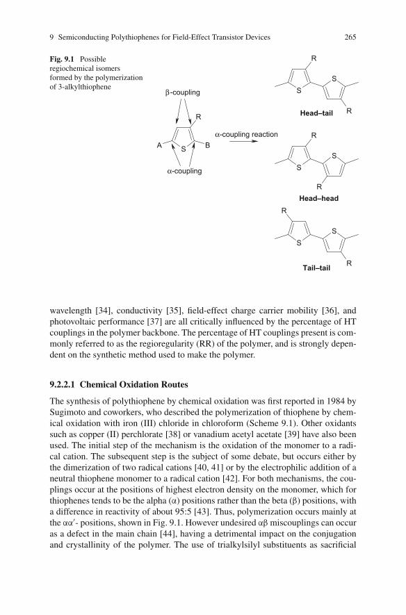
9 Semiconducting Polythiophenes for Field-Effect Transistor Devices 265
S
R
A B
S
R
S
R
S
R
S
R
SS
R
R
Head–tail
Head–head
Tail–tail
α-coupling reaction
α-coupling
β -coupling
Fig. 9.1 Possibleregiochemical isomersformed by the polymerizationof 3-alkylthiophene
wavelength [34], conductivity [35], field-effect charge carrier mobility [36], andphotovoltaic performance [37] are all critically influenced by the percentage of HTcouplings in the polymer backbone. The percentage of HT couplings present is com-monly referred to as the regioregularity (RR) of the polymer, and is strongly depen-dent on the synthetic method used to make the polymer.
9.2.2.1 Chemical Oxidation Routes
The synthesis of polythiophene by chemical oxidation was first reported in 1984 bySugimoto and coworkers, who described the polymerization of thiophene by chem-ical oxidation with iron (III) chloride in chloroform (Scheme 9.1). Other oxidantssuch as copper (II) perchlorate [38] or vanadium acetyl acetate [39] have also beenused. The initial step of the mechanism is the oxidation of the monomer to a radi-cal cation. The subsequent step is the subject of some debate, but occurs either bythe dimerization of two radical cations [40, 41] or by the electrophilic addition of aneutral thiophene monomer to a radical cation [42]. For both mechanisms, the cou-plings occur at the positions of highest electron density on the monomer, which forthiophenes tends to be the alpha (α) positions rather than the beta (β) positions, witha difference in reactivity of about 95:5 [43]. Thus, polymerization occurs mainly atthe αα′- positions, shown in Fig. 9.1. However undesired αβ miscouplings can occuras a defect in the main chain [44], having a detrimental impact on the conjugationand crystallinity of the polymer. The use of trialkylsilyl substituents as sacrificial
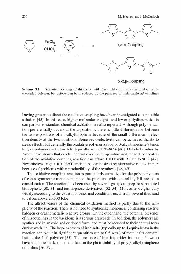
266 M. Heeney and I. McCulloch
S S
SS
S
SS
S
FeCl3CHCl3
+ α,α,α-Coupling
α,α,β-Coupling
Scheme 9.1 Oxidative coupling of thiophene with ferric chloride results in predominatelyα-coupled polymer, but defects can be introduced by the presence of undesirable αβ-couplings
leaving groups to direct the oxidative coupling have been investigated as a possiblesolution [45]. In this case, higher molecular weights and lower polydispersities incomparison to standard chemical oxidation are also reported. Although polymeriza-tion preferentially occurs at the α-positions, there is little differentiation betweenthe two α-positions of a 3-alkylthiophene because of the small difference in elec-tron density at the two positions. Some regioselectivity can be achieved thanks tosteric effects, but generally the oxidative polymerization of 3-alkylthiophene’s tendsto give polymers with low RR, typically around 70–80% [46]. Detailed studies byAmou have shown that careful control over the temperature and reagent concentra-tion of the oxidative coupling reaction can afford P3HT with RR up to 90% [47].Nevertheless, highly RR P3AT tends to be synthesized by alternative routes, in partbecause of problems with reproducibility of the synthesis [48, 49].
The oxidative coupling reaction is particularly attractive for the polymerizationof centrosymmetric monomers, since the problems with controlling RR are not aconsideration. The reaction has been used by several groups to prepare substitutedbithiophene [50, 51] and terthiophene derivatives [52–54]. Molecular weights varywidely according to the exact monomer and conditions used, from several thousandto values above 20,000 KDa.
The attractiveness of the chemical oxidation method is partly due to the sim-plicity of the reaction. There is no need to synthesize monomers containing reactivehalogen or organometallic reactive groups. On the other hand, the potential presenceof miscouplings in the backbone is a serious drawback. In addition, the polymers aresynthesized in an oxidized or doped form, and must be reduced to their neutral formduring work-up. The large excesses of iron salts (typically up to 4 equivalents) in thereaction can result in significant quantities (up to 0.5 wt%) of metal salts contam-inating the final polymer [55]. The presence of iron impurities has been shown tohave a significant detrimental effect on the photostability of poly(3-alkyl)thiophenethin films [56, 57].
9 Semiconducting Polythiophenes for Field-Effect Transistor Devices 267
9.2.2.2 Electrochemical Oxidation Routes
Electrochemical oxidation involves the in-situ polymerization of solution ofmonomer onto a working electrode (commonly ITO or glassy carbon disk) in thepresence of a suitable electrolyte. The polymer forms directly onto the workingelectrode, where it can be studied by a variety of spectroscopic techniques. Themethod is most useful for the study of insoluble polymers, which would other-wise be difficult to isolate, purify, and analyze. In addition, the technique is bestsuited to regiosymmetrical monomers, since there is little control over the couplingof positions of similar electronic charge density in the monomer (for example, inthe 2,5-positions of 3-alkylthiophene). Although soluble polymers can also be pre-pared, problems can exist with dissolution of the growing polymer back into theelectrolyte solution, limiting molecular weight. In addition, the technique is notreadily amenable to scale-up and only small amounts of polymer can usually beprepared. The polymers are also deposited in a doped state, where a counter-anionfrom the electrolyte solution has been incorporated into the polymer matrix. Theresulting materials can be difficult to de-dope fully, and therefore one might expecthigh off-currents during transistor operation. The technique has been reviewed indetail by Roncali [43].
9.2.2.3 Transition Metal Catalyzed Cross-coupling Methodologies
The use of cross-coupling methodologies has been well explored in the synthesis ofpolythiophenes, with the synthesis of RR poly(3-alkyl)thiophene attracting particu-lar interest. These methods have the advantage of using low catalyst loadings (typ-ically around 1 mol%), so catalyst impurities can be more readily removed [58]. Inaddition, the regiochemistry of polymer is usually fixed by appropriate substitutionof the monomer. There are two general approaches to the polymerization (Scheme9.2). In the first, a difunctional monomer is utilized containing both an organometal-lic group and a halogen leaving group (typically bromine or iodine), the so-calledAB polymerization. This has the advantage of maintaining the 1:1 stoichiometrythat is required to achieve high-molecular weights according to the Carother’s equa-tion. In addition, the regiochemistry defined in the monomer is largely preservedin the polymer backbone, so this approach is particularly suited to the polymer-ization of nonregiosymmetrically substituted monomers. The drawback to the ABapproach is that the monomers can be difficult to synthesize and purify. An alterna-tive approach uses two different monomers each functionalized with either two halo-gen groups or two organometallic leaving groups, a so-called AA plus BB approach(Scheme 9.2). This affords alternating copolymers. In this case, it is highly desir-able to have centrosymmetrically substituted monomers, since there is usually littledifferentiation in reactivity between the two groups in each monomer. For exam-ple, in Scheme 9.2, if R and R′ are different substituents then polymerization viathe AA plus BB approach will result in a regiorandom arrangement of R and R′
along the polymer backbone. In order to maintain the 1:1 stoichiometry and affordhigh-molecular weight polymers, it is necessary to have high purity monomers, socrystalline monomers are highly desirable.
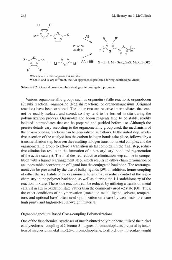
268 M. Heeney and I. McCulloch
SS
* *n
R R'SS
M X
R'R
SM M
S XX
R'R
+
Pd or Ni catalyst
X = Br, I; M = SnR3, ZnX, MgX, B(OR)2AA + BB
AB
When R = R' either approach is suitable.When R and R' are different, the AB approach is preferred for regiodefined polymers.
Scheme 9.2 General cross-coupling strategies to conjugated polymers
Various organometallic groups such as organotin (Stille reaction), organoboron(Suzuki reaction), organozinc (Negishi reaction), or organomagnesium (Grignardreaction) have been explored. The latter two are reactive intermediates that can-not be readily isolated and stored, so they tend to be formed in situ during thepolymerization process. Organo-tin and boron reagents tend to be stable, readilyisolated intermediates that can be prepared and purified before use. Although theprecise details vary according to the organometallic group used, the mechanism ofthe cross-coupling reactions can be generalized as follows. In the initial step, oxida-tive insertion of the catalyst into the carbon halogen bonds take place, followed by atransmetallation step between the resulting halogen transition metal complex and theorganometallic group to afford a transition metal complex. In the final step, reduc-tive elimination results in the formation of a new aryl–aryl bond and regenerationof the active catalyst. The final desired reductive elimination step can be in compe-tition with a ligand rearrangement step, which results in either chain termination oran undesirable incorporation of ligand into the conjugated backbone. The rearrange-ment can be prevented by the use of bulky ligands [59]. In addition, homo-couplingof either the aryl halide or the organometallic groups can reduce control of the regio-chemistry in the polymer backbone, as well as altering the 1:1 stoichiometry of thereaction mixture. These side reactions can be reduced by utilizing a transition metalcatalyst in a zero oxidation state, rather than the commonly used +2 state [60]. Thus,the exact conditions of polymerization (transition metal, ligand, solvent, tempera-ture, and optional base) often need optimization on a case-by-case basis to ensurehigh purity and high-molecular-weight material.
Organomagnesium Based Cross-coupling Polymerizations
One of the first chemical syntheses of unsubstituted polythiophene utilized the nickelcatalyzed cross-coupling of 2-bromo-5-magnesiobromothiophene, prepared by inser-tion of magnesium metal into 2,5-dibromothiophene, to afford low-molecular-weight
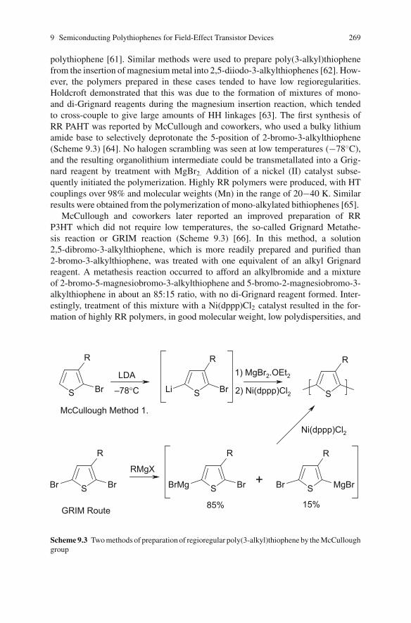
9 Semiconducting Polythiophenes for Field-Effect Transistor Devices 269
polythiophene [61]. Similar methods were used to prepare poly(3-alkyl)thiophenefrom the insertion of magnesium metal into 2,5-diiodo-3-alkylthiophenes [62]. How-ever, the polymers prepared in these cases tended to have low regioregularities.Holdcroft demonstrated that this was due to the formation of mixtures of mono-and di-Grignard reagents during the magnesium insertion reaction, which tendedto cross-couple to give large amounts of HH linkages [63]. The first synthesis ofRR PAHT was reported by McCullough and coworkers, who used a bulky lithiumamide base to selectively deprotonate the 5-position of 2-bromo-3-alkylthiophene(Scheme 9.3) [64]. No halogen scrambling was seen at low temperatures (−78◦C),and the resulting organolithium intermediate could be transmetallated into a Grig-nard reagent by treatment with MgBr2. Addition of a nickel (II) catalyst subse-quently initiated the polymerization. Highly RR polymers were produced, with HTcouplings over 98% and molecular weights (Mn) in the range of 20−40 K. Similarresults were obtained from the polymerization of mono-alkylated bithiophenes [65].
McCullough and coworkers later reported an improved preparation of RRP3HT which did not require low temperatures, the so-called Grignard Metathe-sis reaction or GRIM reaction (Scheme 9.3) [66]. In this method, a solution2,5-dibromo-3-alkylthiophene, which is more readily prepared and purified than2-bromo-3-alkylthiophene, was treated with one equivalent of an alkyl Grignardreagent. A metathesis reaction occurred to afford an alkylbromide and a mixtureof 2-bromo-5-magnesiobromo-3-alkylthiophene and 5-bromo-2-magnesiobromo-3-alkylthiophene in about an 85:15 ratio, with no di-Grignard reagent formed. Inter-estingly, treatment of this mixture with a Ni(dppp)Cl2 catalyst resulted in the for-mation of highly RR polymers, in good molecular weight, low polydispersities, and
S
R
Br S
R
BrLi S
R
S
R
BrBr S
R
BrBrMg S
R
MgBrBr
LDA 1) MgBr2.OEt2
2) Ni(dppp)Cl2
McCullough Method 1.
RMgX
–78°C
+
85% 15%
Ni(dppp)Cl2
GRIM Route
Scheme 9.3 Two methods of preparation of regioregular poly(3-alkyl)thiophene by the McCulloughgroup
270 M. Heeney and I. McCulloch
high yield. Bolognesi reported a similar study utilizing 2,5-diiodo-3-alkylthiophenesaround the same time [67]. Detailed mechanistic studies [68] have shown that theformation of highly RR polymers from the mixture of Grignard reagents can berationalized due to the slow rate of head-to-head coupling reactions in combinationwith the tendency for only one TT miscoupling to occur per polymer chain. Subse-quent studies have found that the reaction proceeds via a chain-growth mechanism[69–71] whereupon the catalyst remains associated with the growing polymer chain,either as an “associated pair” [70] or via an intramolecular transfer [69] to the chainend after reductive elimination. The ability to prepare P3ATs with narrow poly-dispersities and defined endgroups has been exploited by several groups to forminteresting block copolymer structures [72, 73], where blocks of highly RR P3HTcan be combined with amorphous or crystalline nonconjugated polymers. Theseapproaches offer the attractive combination of the processing properties of noncon-jugated polymers with the functional properties of conjugated materials, as well asthe ability to drive self-organization through phase separation. For example, McCul-lough and coworkers reported the formation of well-defined nanowires in thin filmsof P3HT-polystyrene or poly(methyl acrylate) copolymers [72, 73].
Whilst organomagnesium chemistry is probably the method of choice for thepreparation of RR P3HT and its analogues [74, 75], it has not been widely adoptedfor the preparation of other thiophene polymers. This is most likely due to prob-lems in selectively preparing monofunctional Grignard reagents in more complexsystems [76].
Organozinc Based Cross-coupling Polymerizations
An alternative approach to RR P3HT was reported in 1992 by Rieke and cowork-ers [34, 77]. They treated a solution of finely dispersed, highly reactive “Rieke”zinc (Zn∗) with 2,5-dibromo-3-alkylthiophene at low temperature. Zinc insertionoccurred mainly at the 5-position, although small amounts of the two isomers werealways formed, with the regioselectivity being dependent on the temperature ofaddition. Addition of a transition metal catalyst resulted in high-molecular-weightpolymers. The authors were able to control the degree of RR by choice of cata-lyst and phosphine ligand; large transition metals such as palladium led to lowerdegrees of RR than smaller metals like nickel, and bidentate phosphine ligandslike diphenylphosphinoethane (DPPE) led to higher degrees of RR than more labileligands like triphenylphosphine. Regioregularities greater than 98% were reportedfor the best combination {Ni(dppe)Cl2} [34, 77]. This route has also been used toprepare RR poly(3-alkylthio)thiophene [78] and mono-alkylated poly(bithiophenes)[79]. The Rieke route offers the advantage of high-functional group tolerance.Organozinc reagents are much less nucleophilic than Grignard reagents, so sensi-tive functionalities such as ester groups can be incorporated onto the side chains.The organozinc intermediate can also be generated in situ by transmetallation ofan organolithium intermediate with zinc chloride, in a similar approach to the firstMcCullough method [65, 80]. If the organolithium intermediate is generated at low
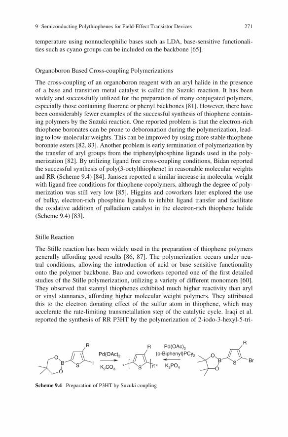
9 Semiconducting Polythiophenes for Field-Effect Transistor Devices 271
temperature using nonnucleophilic bases such as LDA, base-sensitive functionali-ties such as cyano groups can be included on the backbone [65].
Organoboron Based Cross-coupling Polymerizations
The cross-coupling of an organoboron reagent with an aryl halide in the presenceof a base and transition metal catalyst is called the Suzuki reaction. It has beenwidely and successfully utilized for the preparation of many conjugated polymers,especially those containing fluorene or phenyl backbones [81]. However, there havebeen considerably fewer examples of the successful synthesis of thiophene contain-ing polymers by the Suzuki reaction. One reported problem is that the electron-richthiophene boronates can be prone to deboronation during the polymerization, lead-ing to low-molecular weights. This can be improved by using more stable thiopheneboronate esters [82, 83]. Another problem is early termination of polymerization bythe transfer of aryl groups from the triphenylphosphine ligands used in the poly-merization [82]. By utilizing ligand free cross-coupling conditions, Bidan reportedthe successful synthesis of poly(3-octylthiophene) in reasonable molecular weightsand RR (Scheme 9.4) [84]. Janssen reported a similar increase in molecular weightwith ligand free conditions for thiophene copolymers, although the degree of poly-merization was still very low [85]. Higgins and coworkers later explored the useof bulky, electron-rich phosphine ligands to inhibit ligand transfer and facilitatethe oxidative addition of palladium catalyst in the electron-rich thiophene halide(Scheme 9.4) [83].
Stille Reaction
The Stille reaction has been widely used in the preparation of thiophene polymersgenerally affording good results [86, 87]. The polymerization occurs under neu-tral conditions, allowing the introduction of acid or base sensitive functionalityonto the polymer backbone. Bao and coworkers reported one of the first detailedstudies of the Stille polymerization, utilizing a variety of different monomers [60].They observed that stannyl thiophenes exhibited much higher reactivity than arylor vinyl stannanes, affording higher molecular weight polymers. They attributedthis to the electron donating effect of the sulfur atom in thiophene, which mayaccelerate the rate-limiting transmetallation step of the catalytic cycle. Iraqi et al.reported the synthesis of RR P3HT by the polymerization of 2-iodo-3-hexyl-5-tri-
S
R
IBO
O
S
R
BrBO
OS
R
* *n
Pd(OAc)2
K2CO3K3PO4
Pd(OAc)2
(o-Biphenyl)PCy2
Scheme 9.4 Preparation of P3HT by Suzuki coupling

272 M. Heeney and I. McCulloch
n-butylstannylthiophene in an AB type polymerization [88]. The RR was greaterthan 96% with molecular weight around 20,000 KDa. Interestingly, the polymercould be isolated with the tributylstannyl endgroups still intact, which could thenbe utilized in additional cross-coupling chemistry. Poly(bithiophenes) containingone solubilizing side chain were similarly prepared in high-molecular weight andgood RR by the polymerization of a bifunctional monomer [89]. Similar poly-merizations of AB type thiophene monomer have been used to prepare polythio-phenes with functionalized side chains [90–93]. McCullough reported the use ofthe Stille polymerization to make vinyl substituted polythiophenes in 90% RR fromthe reaction of 2,5-dibromo-3-hexylthiophene and 1,2-bis(tributylstannyl)ethylene[94]. It is unusual to have such high RR from the reaction of an AA monomerwith a BB monomer. In this case, it may originate from preferential oxida-tive addition at the less sterically hindered 5-position to generate a vinyl stan-nane AB-type dimer, which then couples with itself to generate the polymer.Yamamoto et al. also reported the preparation of a thiazole–thiophene copolymerin great than 90% RR from the reaction of 2,5-dibromo-3-alkylthiazole with abis(trimethylstannyl)thiophene [95]. Such high RR may also stem from preferen-tial oxidative addition at the 2-position of the thiazole. Copolymers of thiophenewith fluorene [96], naphthalene [97], benzimidazole [98], siloles [87], and bithio-phenes [86] have all been reported by an AA plus BB type Stille polymerization.Tierney and coworkers reported that AA plus BB type Stille polymerizations in allthiophene systems could be accelerated under microwave heating, reducing reactiontimes from days to minutes and affording excellent yields of polymer with high-molecular weights [99]. These conditions were utilized to prepare a range of copoly-mers containing fused thieno(2,3-b)thiophene [100] or thieno(3,2-b)thiophene [101]in the backbone (Scheme 9.5).
S
S Sn
Sn
SS BrBr
H25C12
C12H25
SS*
H25C12
C12H25
S
S*n
+
Pd2(dba)3
Ph(o-tol)3
μW
> 90% Yield, Mw 60,000 KDa.
Scheme 9.5 Preparation of thieno(3,2-b)thiophene copolymers by the microwave acceleratedStille reaction
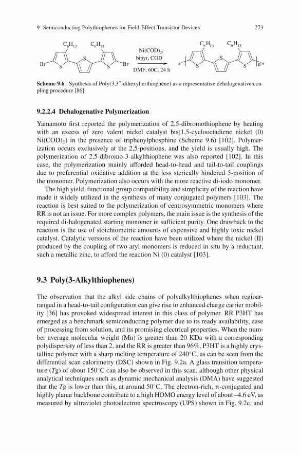
9 Semiconducting Polythiophenes for Field-Effect Transistor Devices 273
S
S S
C6H13 C6H13
BrBrS
S S
C6H1 3 C6H13
** n
Ni(COD)2, bipyr, COD
DMF, 60C, 24 h
Scheme 9.6 Synthesis of Poly(3,3′′-dihexylterthiophene) as a representative dehalogenative cou-pling procedure [86]
9.2.2.4 Dehalogenative Polymerization
Yamamoto first reported the polymerization of 2,5-dibromothiophene by heatingwith an excess of zero valent nickel catalyst bis(1,5-cyclooctadiene nickel (0)Ni(COD)2) in the presence of triphenylphosphine (Scheme 9.6) [102]. Polymer-ization occurs exclusively at the 2,5-positions, and the yield is usually high. Thepolymerization of 2,5-dibromo-3-alkylthiophene was also reported [102]. In thiscase, the polymerization mainly afforded head-to-head and tail-to-tail couplingsdue to preferential oxidative addition at the less sterically hindered 5-position ofthe monomer. Polymerization also occurs with the more reactive di-iodo monomer.
The high yield, functional group compatibility and simplicity of the reaction havemade it widely utilized in the synthesis of many conjugated polymers [103]. Thereaction is best suited to the polymerization of centrosymmetric monomers whereRR is not an issue. For more complex polymers, the main issue is the synthesis of therequired di-halogenated starting monomer in sufficient purity. One drawback to thereaction is the use of stoichiometric amounts of expensive and highly toxic nickelcatalyst. Catalytic versions of the reaction have been utilized where the nickel (II)produced by the coupling of two aryl monomers is reduced in situ by a reductant,such a metallic zinc, to afford the reaction Ni (0) catalyst [103].
9.3 Poly(3-Alkylthiophenes)
The observation that the alkyl side chains of polyalkylthiophenes when regioar-ranged in a head-to-tail configuration can give rise to enhanced charge carrier mobil-ity [36] has provoked widespread interest in this class of polymer. RR P3HT hasemerged as a benchmark semiconducting polymer due to its ready availability, easeof processing from solution, and its promising electrical properties. When the num-ber average molecular weight (Mn) is greater than 20 KDa with a correspondingpolydispersity of less than 2, and the RR is greater than 96%, P3HT is a highly crys-talline polymer with a sharp melting temperature of 240◦C, as can be seen from thedifferential scan calorimetry (DSC) shown in Fig. 9.2a. A glass transition tempera-ture (Tg) of about 150◦C can also be observed in this scan, although other physicalanalytical techniques such as dynamic mechanical analysis (DMA) have suggestedthat the Tg is lower than this, at around 50◦C. The electron-rich, π-conjugated andhighly planar backbone contribute to a high HOMO energy level of about –4.6 eV, asmeasured by ultraviolet photoelectron spectroscopy (UPS) shown in Fig. 9.2c, and
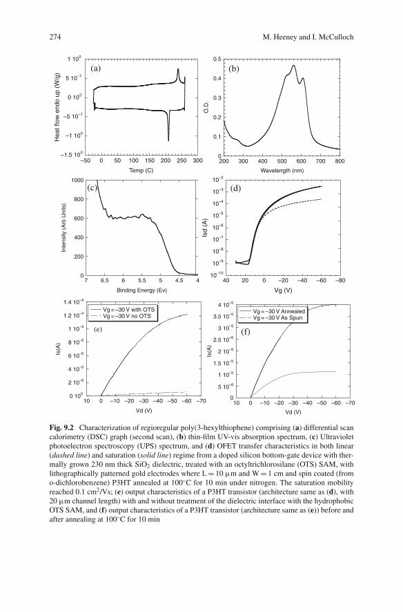
274 M. Heeney and I. McCulloch
0 100
2 10–5
4 10–5
6 10–5
8 10–5
1 10–4
1.2 10–4
1.4 10–4
–70–60–50–40–30–20–10010
Vg = –30 V with OTSVg = –30 V no OTS
Is(A
)
Vd (V)
0
5 10–6
1 10–5
1.5 10–5
2 10–5
2.5 10–5
3 10–5
3.5 10–5
4 10–5
–70–60–50–40–30–20–10010
Vg = –30 V AnnealedVg = –30 V As Spun
Is(A
)
Vd (V)
0
0.1
0.2
0.3
0.4
0.5
200 300 400 500 600 700 800
O.D
.
Wavelength (nm)
–1.5 100
–1 100
–5 10–1
0 100
5 10–1
1 100
–50 0 50 100 150 200 250 300
Hea
t flo
w e
ndo
up (
W/g
)
Temp (C)
10–10
10–9
10–8
10–7
10–6
10–5
10–4
10–3
10–2
–80–60–40–2002040
Isd
(A)
Vg (V)
0
200
400
600
800
1000
44.555.566.57
Inte
nsity
(A
rb U
nits
)
Binding Energy (Ev)
(a) (b)
(c) (d)
(e) (f)
Fig. 9.2 Characterization of regioregular poly(3-hexylthiophene) comprising (a) differential scancalorimetry (DSC) graph (second scan), (b) thin-film UV-vis absorption spectrum, (c) Ultravioletphotoelectron spectroscopy (UPS) spectrum, and (d) OFET transfer characteristics in both linear(dashed line) and saturation (solid line) regime from a doped silicon bottom-gate device with ther-mally grown 230 nm thick SiO2 dielectric, treated with an octyltrichlorosilane (OTS) SAM, withlithographically patterned gold electrodes where L = 10 μm and W = 1 cm and spin coated (fromo-dichlorobenzene) P3HT annealed at 100◦C for 10 min under nitrogen. The saturation mobilityreached 0.1 cm2/Vs; (e) output characteristics of a P3HT transistor (architecture same as (d), with20 μm channel length) with and without treatment of the dielectric interface with the hydrophobicOTS SAM, and (f) output characteristics of a P3HT transistor (architecture same as (e)) before andafter annealing at 100◦C for 10 min
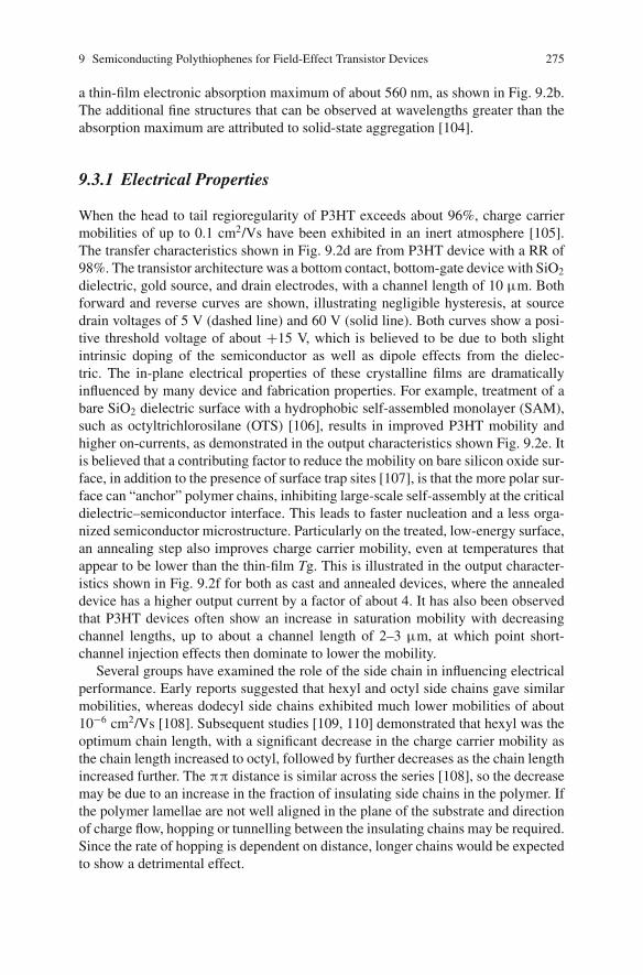
9 Semiconducting Polythiophenes for Field-Effect Transistor Devices 275
a thin-film electronic absorption maximum of about 560 nm, as shown in Fig. 9.2b.The additional fine structures that can be observed at wavelengths greater than theabsorption maximum are attributed to solid-state aggregation [104].
9.3.1 Electrical Properties
When the head to tail regioregularity of P3HT exceeds about 96%, charge carriermobilities of up to 0.1 cm2/Vs have been exhibited in an inert atmosphere [105].The transfer characteristics shown in Fig. 9.2d are from P3HT device with a RR of98%. The transistor architecture was a bottom contact, bottom-gate device with SiO2
dielectric, gold source, and drain electrodes, with a channel length of 10 μm. Bothforward and reverse curves are shown, illustrating negligible hysteresis, at sourcedrain voltages of 5 V (dashed line) and 60 V (solid line). Both curves show a posi-tive threshold voltage of about +15 V, which is believed to be due to both slightintrinsic doping of the semiconductor as well as dipole effects from the dielec-tric. The in-plane electrical properties of these crystalline films are dramaticallyinfluenced by many device and fabrication properties. For example, treatment of abare SiO2 dielectric surface with a hydrophobic self-assembled monolayer (SAM),such as octyltrichlorosilane (OTS) [106], results in improved P3HT mobility andhigher on-currents, as demonstrated in the output characteristics shown Fig. 9.2e. Itis believed that a contributing factor to reduce the mobility on bare silicon oxide sur-face, in addition to the presence of surface trap sites [107], is that the more polar sur-face can “anchor” polymer chains, inhibiting large-scale self-assembly at the criticaldielectric–semiconductor interface. This leads to faster nucleation and a less orga-nized semiconductor microstructure. Particularly on the treated, low-energy surface,an annealing step also improves charge carrier mobility, even at temperatures thatappear to be lower than the thin-film Tg. This is illustrated in the output character-istics shown in Fig. 9.2f for both as cast and annealed devices, where the annealeddevice has a higher output current by a factor of about 4. It has also been observedthat P3HT devices often show an increase in saturation mobility with decreasingchannel lengths, up to about a channel length of 2–3 μm, at which point short-channel injection effects then dominate to lower the mobility.
Several groups have examined the role of the side chain in influencing electricalperformance. Early reports suggested that hexyl and octyl side chains gave similarmobilities, whereas dodecyl side chains exhibited much lower mobilities of about10−6 cm2/Vs [108]. Subsequent studies [109, 110] demonstrated that hexyl was theoptimum chain length, with a significant decrease in the charge carrier mobility asthe chain length increased to octyl, followed by further decreases as the chain lengthincreased further. The ππ distance is similar across the series [108], so the decreasemay be due to an increase in the fraction of insulating side chains in the polymer. Ifthe polymer lamellae are not well aligned in the plane of the substrate and directionof charge flow, hopping or tunnelling between the insulating chains may be required.Since the rate of hopping is dependent on distance, longer chains would be expectedto show a detrimental effect.
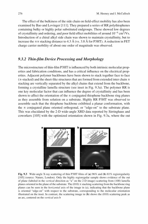
276 M. Heeney and I. McCulloch
The effect of the bulkiness of the side chain on field-effect mobility has also beenexamined by Bao and Lovinger [111]. They prepared a series of RR polythiophenescontaining bulky or highly polar substituted endgroups. These showed low degreesof crystallinity and ordering, and poor field effect mobilities of around 10−6 cm2/Vs.Introduction of a chiral alkyl side chain was shown to maintain crystallinity, but toincrease the ππ stacking distance to 4.3 A (vs. 3.8 A for P3HT). A reduction in FETcharge carrier mobility of about one order of magnitude was observed.
9.3.2 Thin-film Device Processing and Morphology
The microstructure of thin-film P3HT is influenced by both intrinsic molecular prop-erties and fabrication conditions, and has a critical influence on the electrical prop-erties. Adjacent polymer backbones have been shown to stack together face to face(π-stacked) and the sheet-like structures that are formed from extended inter chain π
stacking are vertically separated by the alkyl chains that extend from the backbone,forming a crystalline lamella structure (see inset in Fig. 9.3a). The polymer RR isone key molecular factor that can influence the degree of crystallinity and has beenshown to affect the orientation of the π conjugated thiophene backbone ring planesas they assemble from solution on a substrate. Highly RR P3HT was observed toassemble such that the thiophene backbone exhibited a planar conformation, withthe π conjugated plane oriented orthogonal, or “edge-on” to the substrate plane.This was elucidated by the 2-D wide-angle XRD data reported by Sirringhaus andcoworkers [105] with the optimized orientation shown in Fig. 9.3a, where the out
Fig. 9.3 Wide-angle X-ray scattering of thin P3HT films of (a) 96% and (b) 81% regioregularity[105] (source: Nature, London). Only the highly regioregular sample shows evidence of the outof plane (labeled in the vertical direction as “a” on the 2-D image) scattering from (100) lamellaplanes oriented in the plane of the substrate. The (010) π stacking scattering from the backbone ringplanes can be seen in the horizontal axis of the image in (a), indicating that the backbone planeis oriented “edge-on” with respect to the substrate, corresponding to the molecular orientationillustrated on the inset. In contrast, the scattering image in (b) shows the (010) scattering peak asan arc, centered on the vertical axis b
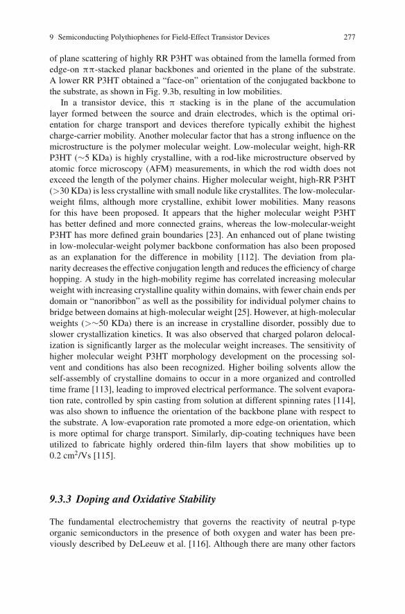
9 Semiconducting Polythiophenes for Field-Effect Transistor Devices 277
of plane scattering of highly RR P3HT was obtained from the lamella formed fromedge-on ππ-stacked planar backbones and oriented in the plane of the substrate.A lower RR P3HT obtained a “face-on” orientation of the conjugated backbone tothe substrate, as shown in Fig. 9.3b, resulting in low mobilities.
In a transistor device, this π stacking is in the plane of the accumulationlayer formed between the source and drain electrodes, which is the optimal ori-entation for charge transport and devices therefore typically exhibit the highestcharge-carrier mobility. Another molecular factor that has a strong influence on themicrostructure is the polymer molecular weight. Low-molecular weight, high-RRP3HT (∼5 KDa) is highly crystalline, with a rod-like microstructure observed byatomic force microscopy (AFM) measurements, in which the rod width does notexceed the length of the polymer chains. Higher molecular weight, high-RR P3HT(>30 KDa) is less crystalline with small nodule like crystallites. The low-molecular-weight films, although more crystalline, exhibit lower mobilities. Many reasonsfor this have been proposed. It appears that the higher molecular weight P3HThas better defined and more connected grains, whereas the low-molecular-weightP3HT has more defined grain boundaries [23]. An enhanced out of plane twistingin low-molecular-weight polymer backbone conformation has also been proposedas an explanation for the difference in mobility [112]. The deviation from pla-narity decreases the effective conjugation length and reduces the efficiency of chargehopping. A study in the high-mobility regime has correlated increasing molecularweight with increasing crystalline quality within domains, with fewer chain ends perdomain or “nanoribbon” as well as the possibility for individual polymer chains tobridge between domains at high-molecular weight [25]. However, at high-molecularweights (>∼50 KDa) there is an increase in crystalline disorder, possibly due toslower crystallization kinetics. It was also observed that charged polaron delocal-ization is significantly larger as the molecular weight increases. The sensitivity ofhigher molecular weight P3HT morphology development on the processing sol-vent and conditions has also been recognized. Higher boiling solvents allow theself-assembly of crystalline domains to occur in a more organized and controlledtime frame [113], leading to improved electrical performance. The solvent evapora-tion rate, controlled by spin casting from solution at different spinning rates [114],was also shown to influence the orientation of the backbone plane with respect tothe substrate. A low-evaporation rate promoted a more edge-on orientation, whichis more optimal for charge transport. Similarly, dip-coating techniques have beenutilized to fabricate highly ordered thin-film layers that show mobilities up to0.2 cm2/Vs [115].
9.3.3 Doping and Oxidative Stability
The fundamental electrochemistry that governs the reactivity of neutral p-typeorganic semiconductors in the presence of both oxygen and water has been pre-viously described by DeLeeuw et al. [116]. Although there are many other factors
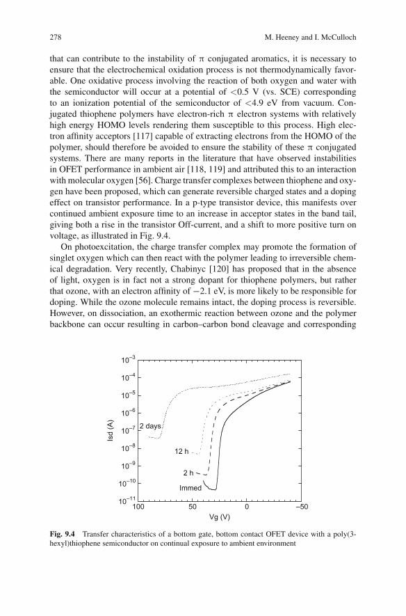
278 M. Heeney and I. McCulloch
that can contribute to the instability of π conjugated aromatics, it is necessary toensure that the electrochemical oxidation process is not thermodynamically favor-able. One oxidative process involving the reaction of both oxygen and water withthe semiconductor will occur at a potential of <0.5 V (vs. SCE) correspondingto an ionization potential of the semiconductor of <4.9 eV from vacuum. Con-jugated thiophene polymers have electron-rich π electron systems with relativelyhigh energy HOMO levels rendering them susceptible to this process. High elec-tron affinity acceptors [117] capable of extracting electrons from the HOMO of thepolymer, should therefore be avoided to ensure the stability of these π conjugatedsystems. There are many reports in the literature that have observed instabilitiesin OFET performance in ambient air [118, 119] and attributed this to an interactionwith molecular oxygen [56]. Charge transfer complexes between thiophene and oxy-gen have been proposed, which can generate reversible charged states and a dopingeffect on transistor performance. In a p-type transistor device, this manifests overcontinued ambient exposure time to an increase in acceptor states in the band tail,giving both a rise in the transistor Off-current, and a shift to more positive turn onvoltage, as illustrated in Fig. 9.4.
On photoexcitation, the charge transfer complex may promote the formation ofsinglet oxygen which can then react with the polymer leading to irreversible chem-ical degradation. Very recently, Chabinyc [120] has proposed that in the absenceof light, oxygen is in fact not a strong dopant for thiophene polymers, but ratherthat ozone, with an electron affinity of −2.1 eV, is more likely to be responsible fordoping. While the ozone molecule remains intact, the doping process is reversible.However, on dissociation, an exothermic reaction between ozone and the polymerbackbone can occur resulting in carbon–carbon bond cleavage and corresponding
10–11
10–10
10–9
10–8
10–7
10–6
10–5
10–4
10–3
–50050100
Isd
(A)
Vg (V)
Immed
2 h
12 h
2 days
Fig. 9.4 Transfer characteristics of a bottom gate, bottom contact OFET device with a poly(3-hexyl)thiophene semiconductor on continual exposure to ambient environment
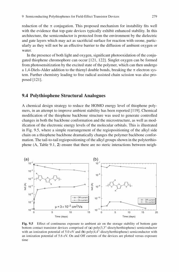
9 Semiconducting Polythiophenes for Field-Effect Transistor Devices 279
reduction of the π conjugation. This proposed mechanism for instability fits wellwith the evidence that top-gate devices typically exhibit enhanced stability. In thisarchitecture, the semiconductor is protected from the environment by the dielectricand gate layers which may act as sacrificial surface for reaction with ozone, partic-ularly as they will not be an effective barrier to the diffusion of ambient oxygen orwater.
In the presence of both light and oxygen, significant photooxidation of the conju-gated thiophene chromophore can occur [121, 122]. Singlet oxygen can be formedfrom photosensitization by the excited state of the polymer, which can then undergoa 1,4-Diels-Alder addition to the thienyl double bonds, breaking the π electron sys-tem. Further chemistry leading to free radical assisted chain scission was also pro-posed [121].
9.4 Polythiophene Structural Analogues
A chemical design strategy to reduce the HOMO energy level of thiophene poly-mers, in an attempt to improve ambient stability has been reported [119]. Chemicalmodification of the thiophene backbone structure was used to generate controlledchanges in both the backbone conformation and the microstructure, as well as mod-ification of the electronic energy levels of the molecular orbitals. This is illustratedin Fig. 9.5, where a simple rearrangement of the regiopositioning of the alkyl sidechain on a thiophene backbone dramatically changes the polymer backbone confor-mation. The tail-to-tail regiopositioning of the alkyl groups shown in the polyterthio-phene (A, Table 9.1, 2) ensure that there are no steric interactions between neigh-
10–8
10–7
10–6
10–5
10–4
10–3
10–2
0 5 10 15
On-current Off-current
Isd
(A)
Time (days)
SS S* *n
R
R
SS S* *n
R
R
(a) (b)
μ = 3 × 10⁻² cm2/Vs10–11
10–10
10–9
10–8
10–7
0 5 10 15 20
Off-currentOn-current
Isd
(A)
Time (days)
Fig. 9.5 Effect of continuous exposure to ambient air on the storage stability of bottom gatebottom contact transistor devices comprised of (a) poly(3,3′′-dioctylterthiophene) semiconductorwith an ionization potential of 5.0 eV and (b) poly(4,4′′-dioctylterthiophene) semiconductor withan ionization potential of 5.6 eV. On and Off currents of the devices are plotted versus exposuretime
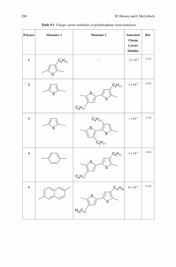
280 M. Heeney and I. McCulloch
Table 9.1 Charge carrier mobilities of polythiophene semiconductors
Polymer Monomer 1 Monomer 2 Saturated
Charge
Carrier
Mobility
Ref.
1
S
C6H13– 2 x 10⁻² [119]
2
S S
S
C8H17
C8H173 x 10–2 [119]
[119]3
S S
S
C8H17
C8H17
1 x10⁻⁵
4
S
S
C8H17
C8H171 x 10–5 [145]
5
S
S
H25C12
C12H256 x 10–4 [119]
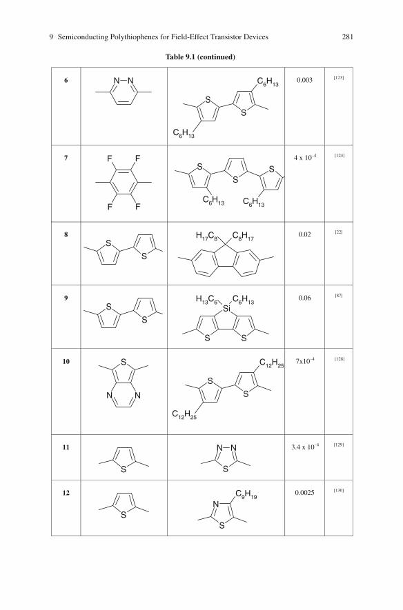
9 Semiconducting Polythiophenes for Field-Effect Transistor Devices 281
Table 9.1 (continued)
6 NN
S
S
C6H13
C6H130.003 [123]
7
F F
F FS
SS
C6H13 C6H13
4 x 10⁻⁴ [124]
8 S
S
H17C8 C8H170.02 [22]
9 S
SSi
S S
H13C6 C6H130.06 [87]
10 S
N N
S
S
C12H25
C12H257x10–4 [128]
11
S S
NN 3.4 x 10⁻⁴ [129]
12
SS
NC9H19
0.0025 [130]
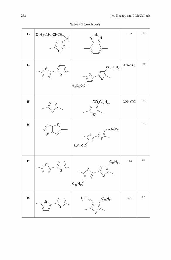
282 M. Heeney and I. McCulloch
Table 9.1 (continued)
13
S
C4H9(C2H5)CHCH2N
SN
0.02 [131]
14 S
S
0.06 (TC) [132]
15
SS
CO2C12H250.004 (TC) [132]
16 S
S
[133]
17 S
S S
S
C12H25
C12H250.14 [55]
18 S
S
S
C10H21H21C10
0.01 [54]
S
S
H25C12O2C
CO2C12H25
S
S
H25C12O2C
CO2C12H25
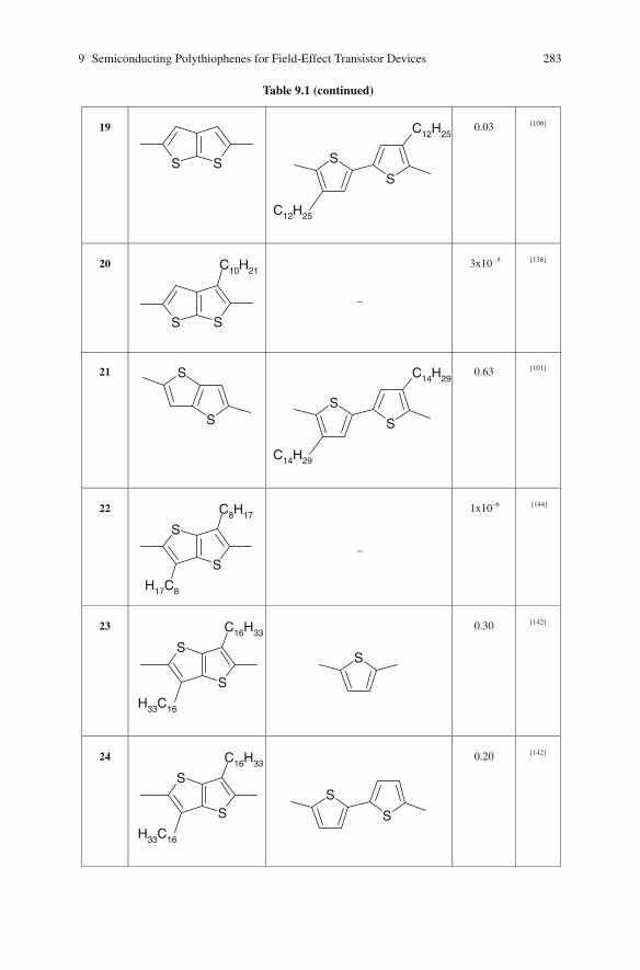
9 Semiconducting Polythiophenes for Field-Effect Transistor Devices 283
Table 9.1 (continued)
19
S S
S
S
C12H25
C12H25
0.03 [100]
20
S S
C10H21
–
3x10 –5 [138]
21
S
S
S
S
C14H29
C14H29
0.63 [101]
22
S
S
C8H17
H17C8
–
1x10⁻⁶ [144]
23
S
S
C16H33
H33C16
S
0.30 [142]
24
S
S
C16H33
H33C16
S
S
0.20 [142]
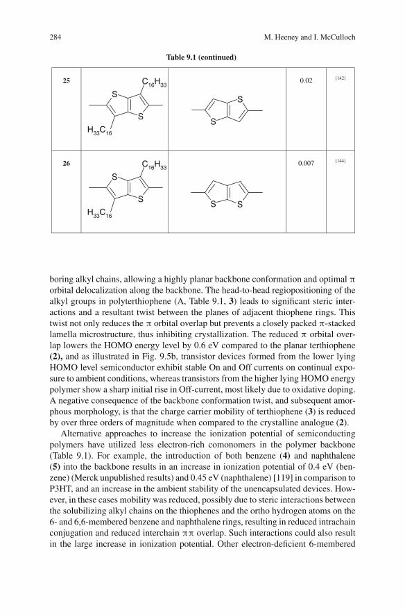
284 M. Heeney and I. McCulloch
Table 9.1 (continued)
25
S
S
C16H33
H33C16
S
S
0.02 [142]
26
S
S
C16H33
H33C16
SS
0.007 [144]
boring alkyl chains, allowing a highly planar backbone conformation and optimal π
orbital delocalization along the backbone. The head-to-head regiopositioning of thealkyl groups in polyterthiophene (A, Table 9.1, 3) leads to significant steric inter-actions and a resultant twist between the planes of adjacent thiophene rings. Thistwist not only reduces the π orbital overlap but prevents a closely packed π-stackedlamella microstructure, thus inhibiting crystallization. The reduced π orbital over-lap lowers the HOMO energy level by 0.6 eV compared to the planar terthiophene(2), and as illustrated in Fig. 9.5b, transistor devices formed from the lower lyingHOMO level semiconductor exhibit stable On and Off currents on continual expo-sure to ambient conditions, whereas transistors from the higher lying HOMO energypolymer show a sharp initial rise in Off-current, most likely due to oxidative doping.A negative consequence of the backbone conformation twist, and subsequent amor-phous morphology, is that the charge carrier mobility of terthiophene (3) is reducedby over three orders of magnitude when compared to the crystalline analogue (2).
Alternative approaches to increase the ionization potential of semiconductingpolymers have utilized less electron-rich comonomers in the polymer backbone(Table 9.1). For example, the introduction of both benzene (4) and naphthalene(5) into the backbone results in an increase in ionization potential of 0.4 eV (ben-zene) (Merck unpublished results) and 0.45 eV (naphthalene) [119] in comparison toP3HT, and an increase in the ambient stability of the unencapsulated devices. How-ever, in these cases mobility was reduced, possibly due to steric interactions betweenthe solubilizing alkyl chains on the thiophenes and the ortho hydrogen atoms on the6- and 6,6-membered benzene and naphthalene rings, resulting in reduced intrachainconjugation and reduced interchain ππ overlap. Such interactions could also resultin the large increase in ionization potential. Other electron-deficient 6-membered
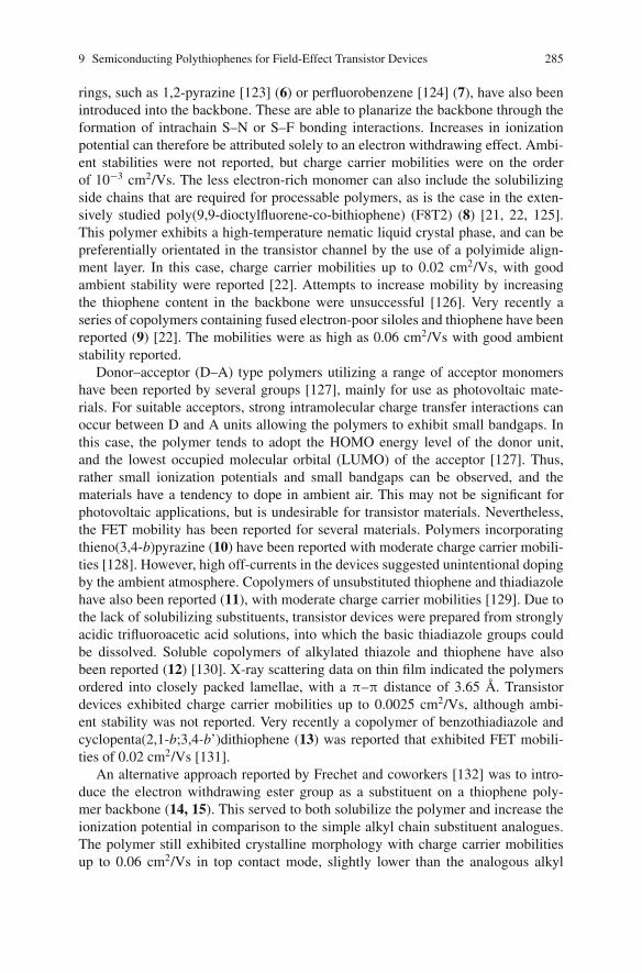
9 Semiconducting Polythiophenes for Field-Effect Transistor Devices 285
rings, such as 1,2-pyrazine [123] (6) or perfluorobenzene [124] (7), have also beenintroduced into the backbone. These are able to planarize the backbone through theformation of intrachain S–N or S–F bonding interactions. Increases in ionizationpotential can therefore be attributed solely to an electron withdrawing effect. Ambi-ent stabilities were not reported, but charge carrier mobilities were on the orderof 10−3 cm2/Vs. The less electron-rich monomer can also include the solubilizingside chains that are required for processable polymers, as is the case in the exten-sively studied poly(9,9-dioctylfluorene-co-bithiophene) (F8T2) (8) [21, 22, 125].This polymer exhibits a high-temperature nematic liquid crystal phase, and can bepreferentially orientated in the transistor channel by the use of a polyimide align-ment layer. In this case, charge carrier mobilities up to 0.02 cm2/Vs, with goodambient stability were reported [22]. Attempts to increase mobility by increasingthe thiophene content in the backbone were unsuccessful [126]. Very recently aseries of copolymers containing fused electron-poor siloles and thiophene have beenreported (9) [22]. The mobilities were as high as 0.06 cm2/Vs with good ambientstability reported.
Donor–acceptor (D–A) type polymers utilizing a range of acceptor monomershave been reported by several groups [127], mainly for use as photovoltaic mate-rials. For suitable acceptors, strong intramolecular charge transfer interactions canoccur between D and A units allowing the polymers to exhibit small bandgaps. Inthis case, the polymer tends to adopt the HOMO energy level of the donor unit,and the lowest occupied molecular orbital (LUMO) of the acceptor [127]. Thus,rather small ionization potentials and small bandgaps can be observed, and thematerials have a tendency to dope in ambient air. This may not be significant forphotovoltaic applications, but is undesirable for transistor materials. Nevertheless,the FET mobility has been reported for several materials. Polymers incorporatingthieno(3,4-b)pyrazine (10) have been reported with moderate charge carrier mobili-ties [128]. However, high off-currents in the devices suggested unintentional dopingby the ambient atmosphere. Copolymers of unsubstituted thiophene and thiadiazolehave also been reported (11), with moderate charge carrier mobilities [129]. Due tothe lack of solubilizing substituents, transistor devices were prepared from stronglyacidic trifluoroacetic acid solutions, into which the basic thiadiazole groups couldbe dissolved. Soluble copolymers of alkylated thiazole and thiophene have alsobeen reported (12) [130]. X-ray scattering data on thin film indicated the polymersordered into closely packed lamellae, with a π–π distance of 3.65 A. Transistordevices exhibited charge carrier mobilities up to 0.0025 cm2/Vs, although ambi-ent stability was not reported. Very recently a copolymer of benzothiadiazole andcyclopenta(2,1-b;3,4-b’)dithiophene (13) was reported that exhibited FET mobili-ties of 0.02 cm2/Vs [131].
An alternative approach reported by Frechet and coworkers [132] was to intro-duce the electron withdrawing ester group as a substituent on a thiophene poly-mer backbone (14, 15). This served to both solubilize the polymer and increase theionization potential in comparison to the simple alkyl chain substituent analogues.The polymer still exhibited crystalline morphology with charge carrier mobilitiesup to 0.06 cm2/Vs in top contact mode, slightly lower than the analogous alkyl
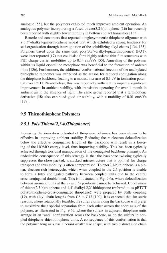
286 M. Heeney and I. McCulloch
analogue [55], but the polymers exhibited much improved ambient operation. Ananalogous polymer incorporating a fused thieno(3,2-b)thiophene (16) has recentlybeen reported with slightly lower mobility in bottom contact transistors [133].
Bauerle and coworkers first reported a regiosymmetric thiophene oligomer witha 3,3′′-dialkyl-quaterthiophene repeat unit which exhibited a strong tendency forself-organization through interdigitation of the solubilizing alkyl chains [134, 135].Polymers based upon the same unit, poly(3,3′′-dialkyl-quaterthiophenes) (PQT),were later reported (17) that could also form highly ordered thin-film structures withFET charge carrier mobilities up to 0.14 cm2/Vs [55]. Annealing of the polymerwithin its liquid crystalline mesophase was beneficial to the formation of orderedfilms [136]. Furthermore, the additional conformational freedom of the unalkylatedbithiophene monomer was attributed as the reason for reduced conjugation alongthe thiophene backbone, leading to a modest increase of 0.1 eV in ionization poten-tial over P3HT. Nevertheless, this was reportedly sufficient to impart a significantimprovement in ambient stability, with transistors operating for over 1 month inambient air in the absence of light. The same group reported that a terthiophenederivative (18) also exhibited good air stability, with a mobility of 0.01 cm2/Vs[137].
9.5 Thienothiophene Polymers
9.5.1 Poly(Thieno(2,3-b)Thiophenes)
Increasing the ionization potential of thiophene polymers has been shown to beeffective in improving ambient stability. Reducing the π electron delocalizationbelow the effective conjugative length of the backbone will result in a lower-ing of the HOMO energy level, thus improving stability. This has been typicallyachieved through torsional manipulation of the conjugated backbone planarity. Anundesirable consequence of this strategy is that the backbone twisting typicallysuppresses the close packed, π-stacked microstructure that is optimal for chargetransport and thus mobility is often compromised. Thieno(2,3-b)thiophene is a pla-nar, electron-rich heterocycle, which when coupled in the 2,5-position is unableto form a fully conjugated pathway between coupled units due to the centralcross-conjugated double bond. This is illustrated in Fig. 9.6a, where delocalizationbetween aromatic units at the 2- and 5- positions cannot be achieved. Copolymersof thieno(2,3-b)thiophene and 4,4′-dialkyl-2,2′-bithiophene (referred to as pBTCTpoly(bithiophene-cross-conjugated thiophene)) were prepared by Stille coupling(19), with alkyl chain lengths from C8 to C12 [100]. It is expected that for stericreasons, where rotationally feasible, the sulfur atoms along the backbone will preferto maximize their spacial separation from each other across the short axis of thepolymer, as illustrated in Fig. 9.6d, where the sulfurs in adjacent thiophene unitsarrange in an “anti” configuration across the backbone, as do the sulfurs in cou-pled thiophene–thienothiophene units. A consequence of this conformation is thatthe polymer long axis has a “crank-shaft” like shape, with two distinct side chain
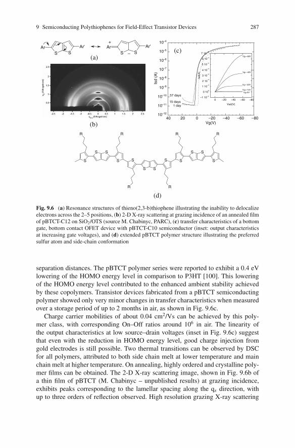
9 Semiconducting Polythiophenes for Field-Effect Transistor Devices 287
(b) Vg(V)
(c)(a)
S SAr Ar'
S SAr Ar'+
–
–1 10–4
0 100
1 10–4
2 10–4
3 10–4
4 10–4
5 10–4
6 10–4
7 10–4
–80–60–40–200
Isd(
A)
Vsd(V)
Vg=–60V
Vg=–45V
Vg=–15V
Vg=–30V
Vg=0V
10–12
10–11
10–10
10–9
10–8
10–7
10–6
10–5
10–4
–80–60–40–2002040
Isd
(A)
1 day15 days
57 days
S S
S S
S S
S S
S S
S S
R R
R R
R R
(d)
Fig. 9.6 (a) Resonance structures of thieno(2,3-b)thiophene illustrating the inability to delocalizeelectrons across the 2–5 positions, (b) 2-D X-ray scattering at grazing incidence of an annealed filmof pBTCT-C12 on SiO2/OTS (source M. Chabinyc, PARC), (c) transfer characteristics of a bottomgate, bottom contact OFET device with pBTCT-C10 semiconductor (inset: output characteristicsat increasing gate voltages), and (d) extended pBTCT polymer structure illustrating the preferredsulfur atom and side-chain conformation
separation distances. The pBTCT polymer series were reported to exhibit a 0.4 eVlowering of the HOMO energy level in comparison to P3HT [100]. This loweringof the HOMO energy level contributed to the enhanced ambient stability achievedby these copolymers. Transistor devices fabricated from a pBTCT semiconductingpolymer showed only very minor changes in transfer characteristics when measuredover a storage period of up to 2 months in air, as shown in Fig. 9.6c.
Charge carrier mobilities of about 0.04 cm2/Vs can be achieved by this poly-mer class, with corresponding On–Off ratios around 106 in air. The linearity ofthe output characteristics at low source–drain voltages (inset in Fig. 9.6c) suggestthat even with the reduction in HOMO energy level, good charge injection fromgold electrodes is still possible. Two thermal transitions can be observed by DSCfor all polymers, attributed to both side chain melt at lower temperature and mainchain melt at higher temperature. On annealing, highly ordered and crystalline poly-mer films can be obtained. The 2-D X-ray scattering image, shown in Fig. 9.6b ofa thin film of pBTCT (M. Chabinyc – unpublished results) at grazing incidence,exhibits peaks corresponding to the lamellar spacing along the qz direction, withup to three orders of reflection observed. High resolution grazing X-ray scattering
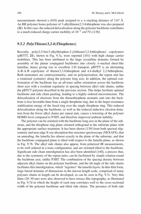
288 M. Heeney and I. McCulloch
measurements showed a (010) peak assigned to a π-stacking distance of 3.67 A.An RR polymer homo polymer of 3-alkylthieno(2,3-b)thiophene was also prepared(21). In this case, the reduced delocalization along the polymer backbone contributesto a much reduced charge carrier mobility of 10−5 cm2/Vs [138].
9.5.2 Poly(Thieno(3,2-b)Thiophenes)
Recently, poly(2,5-bis(3-alkylthiophen-2-yl)thieno(3,2-b)thiophene) copolymers(pBTTT, 21), shown in Fig. 9.7a, were reported [101] with high charge carriermobilities. This has been attributed to the large crystalline domains formed byassembly of the planar conjugated backbones into closely π-stacked sheet-likelamellae, hence giving rise to excellent 2-D transport. pBTTT is an alternatingA-B-A-B copolymer of thieno(3,2-b)thiophene and 4,4-dialkyl 2,2-bithiophene.Both monomers are centrosymmetric, and on polymerization, the repeat unit hasa rotational symmetry along the polymer long axis. In addition, the optimal con-formation of the backbone has an all-trans sulfur orientation across the backboneshort axis with a resultant regularity in spacing between alkyl side chains, unlikethe pBTCT polymer described in the previous section. This helps facilitate optimalbackbone and side chain packing, leading to a highly ordered microstructure. Thedelocalization of electrons from the thienothiophene aromatic unit into the back-bone is less favorable than from a single thiophene ring, due to the larger resonancestabilization energy of the fused ring over the single thiophene ring. This reduceddelocalization along the backbone, as well as the reduced inductive electron dona-tion from the fewer alkyl chains per repeat unit, causes a lowering of the polymerHOMO level compared to P3HT, and therefore improved ambient stability.
The polymer can be oriented with the backbone long axis in the plane of the sub-strate, and the thiophene ring plane oriented orthogonal to the substrate plane withthe appropriate surface treatment. It has been shown [139] from both spectral elip-sometry and near edge X-ray absorption fine structure spectroscopy (NEXAFS), thaton annealing, the lamella lies almost exactly in the plane of the substrate, and thatthe backbone conjugated plane is tilted with respect to the lamella plane, as shownin Fig. 9.7b. The alkyl side chains also appear, from polarized IR measurements,to be well ordered in a trans configuration, and are oriented tilted to the backbone.Significant side chain interdigitation has also been identified [140], a process that,due to the symmetry of the repeat units, can be facilitated by simple rotation roundthe backbone axis, unlike P3HT. The combination of the spacing density betweenadjacent alkyl chains on the polymer backbone, and the tilt angle of the side chainsfacilitates this interdigitation, which “registers” the lamella layers. In thin-film form,large lateral domains of dimensions in the micron length scale, comprised of manypolymer chains in length can be developed, as can be seen in Fig. 9.7c. Very thinfilms (20–30 nm) were also observed to have terrace like topography, as illustratedin Fig. 9.7d in which the height of each step correlates well to the cross-sectionalwidth of the polymer backbone and tilted side chains. The presence of both side
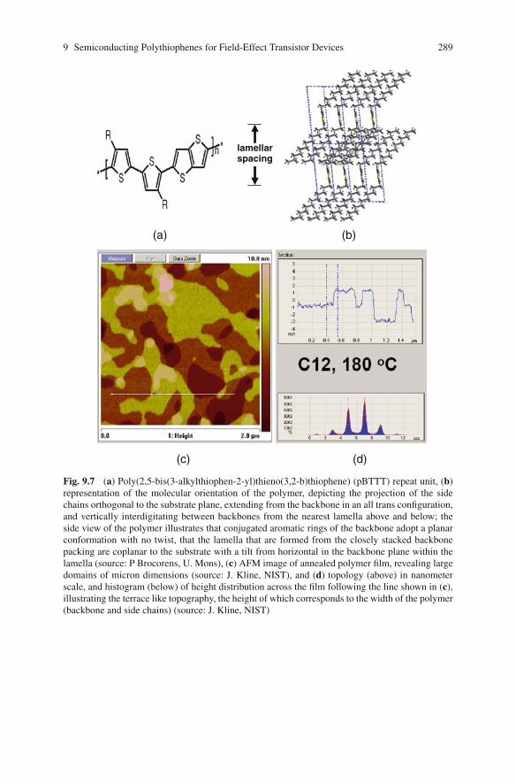
9 Semiconducting Polythiophenes for Field-Effect Transistor Devices 289
(b)(a)
(d)(c)
lamellarspacing
Fig. 9.7 (a) Poly(2,5-bis(3-alkylthiophen-2-yl)thieno(3,2-b)thiophene) (pBTTT) repeat unit, (b)representation of the molecular orientation of the polymer, depicting the projection of the sidechains orthogonal to the substrate plane, extending from the backbone in an all trans configuration,and vertically interdigitating between backbones from the nearest lamella above and below; theside view of the polymer illustrates that conjugated aromatic rings of the backbone adopt a planarconformation with no twist, that the lamella that are formed from the closely stacked backbonepacking are coplanar to the substrate with a tilt from horizontal in the backbone plane within thelamella (source: P Brocorens, U. Mons), (c) AFM image of annealed polymer film, revealing largedomains of micron dimensions (source: J. Kline, NIST), and (d) topology (above) in nanometerscale, and histogram (below) of height distribution across the film following the line shown in (c),illustrating the terrace like topography, the height of which corresponds to the width of the polymer(backbone and side chains) (source: J. Kline, NIST)
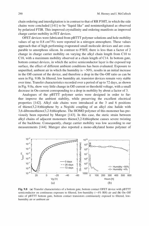
290 M. Heeney and I. McCulloch
chain ordering and interdigitation is in contrast to that of RR P3HT, in which the sidechains were concluded [141] to be “liquid like” and noninterdigitated as observedby polarized FTIR. This improved crystallinity and ordering manifests as improvedcharge carrier mobility in FET devices.
OFET devices were fabricated from pBTTT polymer solutions and hole mobilityvalues of up to 0.8 cm2/Vs were reported in a nitrogen atmosphere. These valuesapproach that of high performing evaporated small molecule devices and are com-parable to amorphous silicon. In contrast to P3HT, there is less than a factor of 2change in charge carrier mobility on varying the alkyl chain length from C10 toC18, with a maximum mobility observed at a chain length of C14. In bottom gate,bottom contact devices, in which the active semiconductor layer is the exposed topsurface, the effect of different ambient conditions has been evaluated. Exposure tounpurified, ambient air in which the humidity is ∼50%, results in an initial increasein the Off-current of the device, and therefore a drop in the On–Off ratio as can beseen in Fig. 9.8b. In filtered, low humidity air, transistor devices remain very stableover time. Transfer characteristics recorded over a period of up to 72 days, as shownin Fig. 9.8a, show very little change in Off-current or threshold voltage, with a smalldecrease in On-current corresponding to a drop in mobility by about a factor of 3.
Analogues of the pBTTT polymer series were designed in order to fur-ther improve the ambient stability, while preserving the excellent electricalproperties [142]. Alkyl side chains were introduced at the 3 and 6 positionsof thieno(3,2-b)thiophene by a Negishi coupling of an alkyl zinc halide with3,6-dibromothieno(3,2-b)thiophene. The HOMO polymer of this monomer has pre-viously been reported by Matzger [143]. In this case, the steric strain betweenalkyl chains of adjacent monomers thieno(3,2-b)thiophene causes severe twistingof the backbone. Consequently, charge carrier mobility was low according to ourmeasurements [144]. Matzger also reported a mono-alkylated homo polymer of
10–9
10–8
10–7
10–6
10–5
10–4
10–3
10–2
–60–40–20020
0 days26 days72 days
I DS
AT(A
)
Vg (V)
1000
104
105
106
107
108
109
1010
0 100 200 300 400 500 600
Humidity ~4%Humidity ~50%
On–
Off
(Sat
urat
ion
regi
me)
Hours [h]
(a) (b)
Fig. 9.8 (a) Transfer characteristics of a bottom gate, bottom contact OFET device with pBTTTsemiconductor on continuous exposure to filtered, low-humidity (∼4% RH) air and (b) On–Offratio of pBTTT bottom gate, bottom contact transistors continuously exposed to filtered, low-humidity air or ambient air
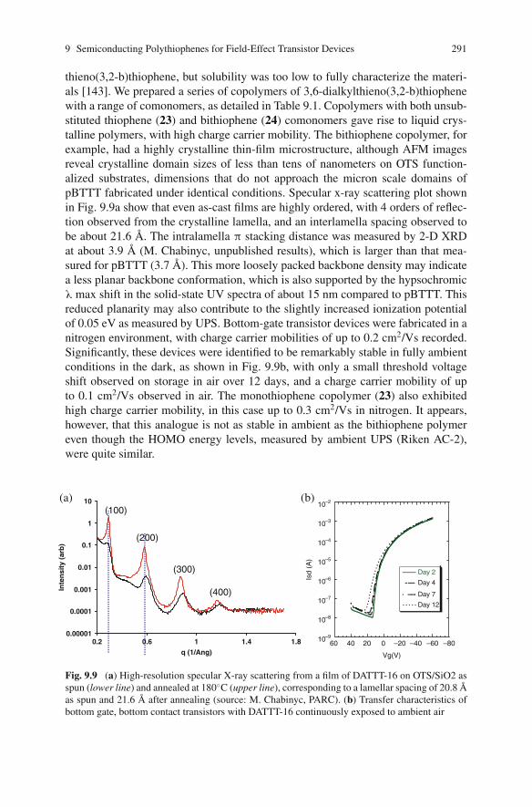
9 Semiconducting Polythiophenes for Field-Effect Transistor Devices 291
thieno(3,2-b)thiophene, but solubility was too low to fully characterize the materi-als [143]. We prepared a series of copolymers of 3,6-dialkylthieno(3,2-b)thiophenewith a range of comonomers, as detailed in Table 9.1. Copolymers with both unsub-stituted thiophene (23) and bithiophene (24) comonomers gave rise to liquid crys-talline polymers, with high charge carrier mobility. The bithiophene copolymer, forexample, had a highly crystalline thin-film microstructure, although AFM imagesreveal crystalline domain sizes of less than tens of nanometers on OTS function-alized substrates, dimensions that do not approach the micron scale domains ofpBTTT fabricated under identical conditions. Specular x-ray scattering plot shownin Fig. 9.9a show that even as-cast films are highly ordered, with 4 orders of reflec-tion observed from the crystalline lamella, and an interlamella spacing observed tobe about 21.6 A. The intralamella π stacking distance was measured by 2-D XRDat about 3.9 A (M. Chabinyc, unpublished results), which is larger than that mea-sured for pBTTT (3.7 A). This more loosely packed backbone density may indicatea less planar backbone conformation, which is also supported by the hypsochromicλ max shift in the solid-state UV spectra of about 15 nm compared to pBTTT. Thisreduced planarity may also contribute to the slightly increased ionization potentialof 0.05 eV as measured by UPS. Bottom-gate transistor devices were fabricated in anitrogen environment, with charge carrier mobilities of up to 0.2 cm2/Vs recorded.Significantly, these devices were identified to be remarkably stable in fully ambientconditions in the dark, as shown in Fig. 9.9b, with only a small threshold voltageshift observed on storage in air over 12 days, and a charge carrier mobility of upto 0.1 cm2/Vs observed in air. The monothiophene copolymer (23) also exhibitedhigh charge carrier mobility, in this case up to 0.3 cm2/Vs in nitrogen. It appears,however, that this analogue is not as stable in ambient as the bithiophene polymereven though the HOMO energy levels, measured by ambient UPS (Riken AC-2),were quite similar.
10–9
10–8
10–7
10–6
10–5
10–4
10–3
10–2
–80–60–40–200204060
Day 7
Day 12
Day 4
Day 2
Isd
(A)
Vg(V)
0.00001
0.0001
0.001
0.01
0.1
1
10
0.2 0.6 1 1.4 1.8
q (1/Ang)
Inte
nsi
ty (
arb
)
(100)
(200)
(300)
(400)
(b)(a)
Fig. 9.9 (a) High-resolution specular X-ray scattering from a film of DATTT-16 on OTS/SiO2 asspun (lower line) and annealed at 180◦C (upper line), corresponding to a lamellar spacing of 20.8 Aas spun and 21.6 A after annealing (source: M. Chabinyc, PARC). (b) Transfer characteristics ofbottom gate, bottom contact transistors with DATTT-16 continuously exposed to ambient air
292 M. Heeney and I. McCulloch
The angle formed from the projection of the two bonds that link a thio-phene monomer at the 2 and 5 positions is less than 180◦. This makes rota-tion of the thiophene ring around the long axis of the polymer a coopera-tive motion requiring rotation of neighboring thiophene units. Replacement ofthese nonrotationally invariant 2,5 thiophene links, with a linear 2,5 thienoth-iophene link gives rise to polymers with a fully linear backbone (25, 26) asdescribed in Table 9.1. These linear, all thienothiophene polymers had a cor-respondingly lower lying HOMO than either of the thiophene analogues, andalso exhibited two thermal transitions, most likely a side chain and a lamellamelt. Initial measurements reported mobilities of 0.02 cm2/Vs for the thieno(3,2-b)thiophene analogue and 0.007 cm2/Vs for the thieno(2,3-b)thiophene ana-logue.
9.6 Summary
Semiconducting polymers containing conjugated thiophene derivatives are attrac-tive candidates for organic electronic transistor devices, due to their combina-tion of high charge carrier mobilities and the potential for low cost processing.Molecular design principles have been employed in the identification of high per-forming thiophene copolymers and several illustrations of this were highlightedin the chapter. Highly crystalline, well ordered and oriented polymer thin-filmmicrostructures have been shown to be necessary to achieve optimal semicon-ducting electrical properties. In particular, liquid crystalline thienothiophene poly-mers with their propensity to efficiently orient and organize within the mesophasetemperature range have shown remarkably high mobilities, combined withreasonable ambient stabilities. Optimization of synthetic routes and purificationtechniques, as well as the appropriate polymer molecular weights, processing con-ditions, choice of solvent, surface treatments, and dielectric interfaces are all impor-tant to achieve incremental device performance improvements. Challenges remain,however, to further improve stability when exposed to the combination of oxy-gen, humidity and light, and to tailor the solubility of these aromatic materialsto processing friendly solvents. Manipulation of the highest occupied molecularorbital energy level of the conjugated backbone was shown to be an effectivestrategy to improve stability. With the promising advances in understanding ofthe morphological and molecular origins of optimal electrical performance madeby many groups in recent years, there is exciting potential for further improve-ments.
Acknowledgements The authors would like to thank the following colleagues and col-laborators for their valuable contributions to the chapter: Maxim Shkunov, David Sparrowe,Weimin Zhang, Steve Tierney, Clare Bailey, Warren Duffy, Kristijonas Genevicius, Joe Kline,Michael Chabinyc, Dean DeLongchamp, Eric Lin, Lee Richter, Alberto Salleo, Mike Toney,Patrick Brocorens, Wojciech Osikowicz, Jui-Fen Chang, Henning Sirringhaus, and MasayoshiSuzuki.
9 Semiconducting Polythiophenes for Field-Effect Transistor Devices 293
References
1. Sandberg HGO, Backlund TG, Osterbacka R, Stubb H (2004) Adv Mater 16:11122. Drury CJ, Mutsaers CMJ, Hart MMCM, de Leeuw DM (1998) Appl Phys Lett 73:1083. Garnier F, Hajlaoui F, Yassar A, Srivastava P (1994) Science 265:16844. Sirringhaus H, Friend RH, Shimoda T, Inbasekaran M, Wu W, Woo EP (2000) Science
298:21235. Gundlach DJ, Lin YY, Jackson TN, Nelson SF, Schlom DG (1997) IEEE Electron Dev Lett
18:876. Kelley T, Boardman L, Dunbar T, Muyres D, Pellerite M, Smith T (2003) J Phys Chem B
107:58777. Jurchescu OD, Baas J, Palstra TTM (2004) Appl Phys Lett 84:30618. Maliakal A, Raghavachari K, Katz H, Chandross E, Siegrist T (2004) Chem Mater 16:4980–
49869. Briseno AL, Tseng RJ, Ling MM, Falcao EHL, Yang Y, Wudl F, Bao Z, (2006) Adv Mater
18:232010. Briseno AL, Mannsfeld SCB, Ling MM, Liu S, Tseng RJ, Reese C, Roberts ME, Yang Y,
Wudl F, Bao Z (2006) Nature 444:91311. Briseno AL, Aizenberg J, Han YJ, Penkala RA, Moon H, Lovinger AJ, Kloc C, Bao Z (2005)
J Am Chem Soc 127:1216412. Shtein M, Peumans P, Benziger JB, Forrest SR (2003) J Appl Phys 93:400513. Burrows PE, Forrest SR, Sapochak LS, Schwartz J, Fenter P, Buma T, Ban VS, Forrest JL
(1995) J Cryst Growth 156:9114. Sheraw CD, Jackson TN, Eaton DL, Anthony JE (2003) Adv Mater 15:200915. Anthony JE, Eaton DL, Parkin SR (2002) Org. Lett 4:1516. Payne MM, Parkin SR, Anthony JE, Kuo CC, Jackson TN (2005) J Am Chem Soc 127:498617. Anthony JE, Brooks JS, Eaton DL, Parkin SR (2001) J Am Chem Soc 123:948218. Lawrence D, Kohler J, Brollier B, Claypole T, Burgin T (2004) Organic & Molecular Elec-
tronics (Ed. Gamota DR, Brazis P, Kalyanasundaram K, Zhang J) Kluwer Academic Pub-lishing 2004 161
19. Veres J, Ogier SD, Leeming SW, Cupertino DC, Khaffaf SM (2006) Adv Funct Mater 13:19920. Knaapila M, Stepanyan R, Lyons BP, Torkkeli M, Monkman AP (2006) Adv Funct Mater
16:59921. Sirringhaus H, Kawase T, Friend RH, Shimoda T, Inbasekaran M, Wu W, Woo EP (2000)
Science 290:212322. Sirringhaus H, Wilson RJ, Friend RH, Inbasekaran M, Wu W, Woo EP, Grell M, Bradley
DDC (2000) Appl Phys Lett 77:40623. Kline RJ, McGehee MD, Kadnikova EN, Liu J, Frechet JMJ, Toney MF (2005) Macro-
molecules 38:331224. Zen A, Pflaum J, Hirschmann S, Zhuang W, Jaiser F, Asawapirom U, Rabe JP, Scherf U,
Neher D (2004) Adv Funct Mater 14:75725. Chang JF, Clark J, Zhao N, Sirringhaus H, Breiby DW, Andreasen JW, Nielsen MM, Giles
M, Heeney M, McCulloch I (2006) Phys Rev B 74:115318/126. Hamilton R, Bailey C, Duffy W, Heeney M, Shkunov M, Sparrowe D, Tierney S,
McCulloch I, Kline RJ, DeLongchamp DM, Chabinyc M (2006) Proc SPIE 6336:633611/127. Pokrop R, Verilhac JM, Gasior A, Wielgus I, Zagorska M, Travers JP, Pron A (2006) J Mater
Chem 16:309928. Verilhac JM, Pokrop R, LeBlevennec G, Kulszewicz-Bajer I, Buga K, Zagorska M, Sadki S,
Pron A (2006) J Phys Chem B 110:1330529. Krebs FC, Nyberg RB, Jorgensen M (2004) Chem Mater ASAP 18:568430. Garrett CE, Prasad K (2004) Adv Synth Catal 346:88931. McCullough R (1998) Adv Mater 10:9332. Pron PRA (2002) Prog Polym Sci 27:135
294 M. Heeney and I. McCulloch
33. Chan HSO, Ng SC (1998) Prog Polym Sci 23:116734. Chen TA, Wu X, Rieke RD (1995) J Am Chem Soc 117:23335. McCullough RD, Tristram-Nagle S, Williams SP, Lowe RD, Jayaraman M (1993) J Am
Chem Soc 115:491036. Bao Z, Dobabalapur A, Lovinger AJ (1996) Appl Phys Lett 69:410837. Kim Y, Cook S, Tuladhar SM, Choulis SA, Nelson J, Durrant JR, Bradley DDC, Giles M,
McCulloch I, Ha CS, Ree M (2006) Nat Mater 5:19738. Inoue NB, Velazquez BF, Inoue M (1988) Synth Met 24:22339. Hayakawa T, Fukukawa KI, Morishima M, Takeuchi K, Asai M, Ando S, Ueda M (2001)
J Polym Sci A: Polym Chem 39:228740. Waltman RJ, Bargon J, Diaz AF (1983) J Phys Chem 87:145941. Barbarella G, Zambianchi M, Di Toro R, Colonna M Jr, Iarossi D, Goldoni F, Bongini A
(1996) J Org Chem 61:828542. Wei Y, Chan CC, Tian J, Jang GW, Hsueh KF (1991) Chem Mater 3:88843. Roncali J (1992) Chem Rev 92:71144. Engelmann G, Jugelt W, Kossmehl G, Welzel HP, Tschuncky P, Heinze J (1996) Macro-
molecules 29:337045. Lere-Porte JP, Moreau JJE, Sauvajol JL (1996) J Organometallic Chem 521:1146. Leclerc M, Diaz FM, Wegner G (1989) Makromol Chem 190:310547. Amou S, Haba O, Shirato K, Hayakaw T, Ueda M, Takeuchi K, Asai M (1999) J Polym Sci
A: Polym Chem 37:194348. McCullough RD (1998) Adv Mater 10:9249. Abdou MSA, Lu X, Xie ZW, Orfino F, Deen MJ, Holdcroft S (1995) Chem Mater 7:63150. Chan HSO, Ng SC (1998) Prog Poly Sci 23:116751. Andreani F, Salatelli E, Lanzi M, Bertinelli F, Fichera AM, Gazzano M (2000) Polymer
41:314752. Gallazzi MC, Castellani L, Marin RA, Zerbi G (1993) J Polym Sci A: Polym Chem 31:333953. Ng SC, Ong TT, Chan HSO (1998) J Mater Chem 8:266354. Ong BS, Wu Y, Jiang L, Liu P, Murti K (2003) Synth Met 19:138455. Ong BS, Wu Y, Liu P, Gardner S (2004) J Am Chem Soc 126:337856. Abdou MSA, Orfino FP, Son Y, Holdcroft S (1997) J Am Chem Soc 119:451857. Abdou MSA, Lu X, Xie ZW, Orfino F, Deen MJ, Holdcroft S (1995) Chem Mater 7:63158. Krebs F, Nyberg CRB, Jorgensen M (2004) Chem Mater 16:131359. Goodson FE, Wallow TI, Novak BM (1998) Macromolecules 31:204760. Bao Z, Chan WK, Yu L (1995) J Am Chem Soc 117:1242661. Yamamoto T, Sanechika K, Yamamoto A (1980) J Polym Sci, Polym Lett Ed 18:962. Sato M, Tanaka S, Kaeriyama K (1986) Chem Commun 87363. Mao H, Holdcroft S (1992) Macromolecules 25:55464. McCullough RD, Lowe RD (1992) Chem Commun 7065. Greve DR, Apperloo JJ, Janssen RAJ (2001) Eur J Org Chem 18:343766. Loewe RS, Khersonsky SM, McCullough RD (1999) Adv Mater 11:25067. Bolognesi WPA, Bajo G, Zannoni G, Fannig L (1999) Acta Polym 50:15168. Loewe RS, Ewbank PC, Liu J, Zhai L, McCullough RD (2001) Macromolecules A 34:432469. Miyakoshi R, Yokoyama A, Yokozawa T (2005) J Am Chem Soc 127:1754270. Sheina EE, Liu J, Iovu MC, Laird DW, McCullough RD (2004) Macromolecules 37:352671. Yokoyama A, Miyakoshi R, Yokozawa T (2004) Macromolecules 37:116972. Jinsong Liu ES, Kowalewski T, McCullough RD (2002) Angew Chem 114:33973. Radano CP, Scherman OA, Stingelin-Stutzmann N, Mueller C, Breiby DW, Smith P, Janssen
RAJ, Meijer EW (2005) J Am Chem Soc 127:1250274. Koeckelberghs G, Vangheluwe M, Samyn C, Persoons A, Verbiest T (2005) Macromolecules
ASAP 38:555475. Babudri F, Colangiuli D, Farinola G, Naso F (2002) Eur J Org Chem 16:278576. Coppo P, Cupertino DC, Yeates SG, Turner ML (2003) Macromolecules 36:2705
9 Semiconducting Polythiophenes for Field-Effect Transistor Devices 295
77. Chen TA, Rieke RD (1992) J Am Chem Soc 114:1008778. Wu X, Chen TA, Rieke RD (1995) Macromolecules, 28:210179. Kowalik J, Tolbert LM, Narayan S, Abhiraman AS (2001) Macromolecules 34:547180. Zhai L, McCullough RD (2002) Adv Mater 14:90181. Schluter AD (2001) J Polym Sci Part A: Polym Chem 39:153382. Jayakannan M, van Dongen JLJ, Janssen RAJ (2001) Macromolecules 34:538683. Liversedge IA, Higgins SJ, Giles M, Heeney M, McCulloch I (2006) Tett Lett 47:514384. Guillerez S, Bidan G (1998) Synth Met 93:12385. Jayakannan M, van Hal PA, Janssen RAJ (2002) J Polym Sci A: Polym Chem 40:236086. Kokubo H, Sato T, Yamamoto T (2006) Macromolecules 39:395987. Usta H, Lu G, Facchetti A, Marks TJ (2006) J Am Chem Soc 128:903488. Iraqi A, Barker GW (1998) J Mater Chem 8:2589. Lere-Porte JP, Moreau JJE, Torreilles C (2001) Eur J Org Chem 7:124990. McCullough RD, Ewbank PC, Loewe RS (1997) J Am Chem Soc 119:63391. Bjørnholm T, Greve DR, Reitzel N, Hassenkam T, Kjaer K, Howes PB, Larsen NB,
Bøgelund J, Jayaraman M, Ewbank PC, McCullough RD (1998) J Am Chem Soc120:7643
92. Malenfant PRL, Frechet JMJ (2000) Macromolecules 33 :363493. de Boer B, van Hutten PF, Ouali L, Grayer V, Hadziioannou G (2002) Macromolecules
35:6883–689294. Loewe RS, McCullough RD (2000) Chem Mater 12:321495. Yamamoto T, Arai M, Kokubo H, Sasaki S (2003) Macromolecules 36:798696. Tsuie B, Reddinger JL, Stzing GA, Soloducho J, Katritzkyb AR, Reynolds JR (1999) J Mater
Chem 9:218997. Nehls BS, Asawapirom U, Fuldner S, Preis E, Farrell T, Scherf U (2004) Adv Funct Mater
14:35298. Nurulla ATI, Shiraishi K, Sasaki S, Yamamoto T (2002) Polymer 43:128799. Tierney S, Heeney M, McCulloch I (2005) Synth Met 148:195
100. Heeney M, Bailey C, Genevicius K, Shkunov M, Sparrowe D, Tierney S, McCulloch I (2005)J Am Chem Soc 127:1078
101. McCulloch I, Heeney M, Bailey C, Genevicius K, MacDonald I, Shkunov M, Sparrowe D,Tierney S, Wagner R, Zhang W, Chabinyc ML, Kline RJ, McGehee MD, Toney MF (2006)Nat Mater 5:328
102. Yamamoto T, Morita A, Miyazaki, Maruyama T, Wakayama H, Zhou Z, Nakamura Y, Kan-bara T, Sasaki S, Kubota K (1992) Macromolecules 25:1214
103. Yamamoto T (2002) J Organomet Chem 653:195104. Brown PJ, Thomas DS, Kohler A, Wilson JS, Kim JS, Ramsdale CM, Sirringhaus H, Friend
RH (2003) Phys Rev B 67:064203105. Sirringhaus H, Brown PJ, Friend RH, Nielsen MM, Bechgaard K, Langeveld-Voss BMW,
Spiering AJH, Janssen RAJ, Meijer EW, Herwig P, de Leeuw DM (1999) Nature 401:685106. Salleo A, Chabinyc ML, Yang M, Street R (2002) Appl Phys Lett 81:4383107. Chua LL, Zaumseil J, Chang JF, Ou ECW, Ho PKH, Sirringhaus H, Friend RH (2005) Nature
434:194108. Bao Z, Feng Y, Dodabalapur A, Raju VR, Lovinger AJ (1997) Chem Mater 9:1299109. Babel A, Jenekhe SA (2005) Synth Met148:169110. Zen A, Saphiannikova M, Neher D, Asawapirom U, Scherf U (2005) Chem Mater 17:781111. Bao Z, Lovinger AJ (1999) Chem Mater 11:2607112. Zen A, Hirschmann PJS, Zhuang W, Jaiser F, Asawapirom U, Rabe JP, Scherf U, Neher D
(2004) Adv Funct Mater 14:757113. Chang JF, Sun B, Breiby DW, Nielsen MM, Solling TI, Giles M, McCulloch I, Sirringhaus
H (2004) Chem Mater 16:4772114. DeLongchamp DM, Vogel BM, Jung Y, Gurau MC, Richter CA, Kirillov OA, Obrzut J,
Fischer DA, Sambasivan S, Richter LJ, Lin EK (2005) Chem Mater 17:5610
296 M. Heeney and I. McCulloch
115. Wang G, Swensen J, Moses D, Heeger AJ (2003) J Appl Phys 93:6137116. de Leeuw DM, Simenon MMJ, Brown AR, Einerhand REF (1997) Synth Met 87:53117. Foster R (1969) Organic charge-transfer complexes (organic chemistry: A series of mono-
graphs), vol 15. Academic Press, New York118. Meijer EJ, Detcheverry C, Baesjou PJ, van Veenendaal E, de Leeuw DM, Klapwijk TM
(2003) J Appl Phys 93:4831119. McCulloch I, Bailey C, Giles M, Heeney M, Love I, Shkunov M, Sparrowe D, Tierney S
(2005) Chem Mater 17:1381120. Chabinyc ML, Street RA, Northrup JE (2007) Appl Phys Lett 90:123508.121. Abdou MSA, Holdcroft S (1993) Macromolecules 26:2954122. Rost H, Ficker J, Alonso JS, Leenders L, McCulloch I (2004) Synth Met 145:83123. Yasuda T, Sakai Y, Aramaki S, Yamamoto T (2005) Chem Mater 17:6060124. Crouch DJ, Skabara PJ, Lohr JE, McDouall JJW, Heeney M, McCulloch I, Sparrowe D,
Shkunov M, Coles SJ, Horton PN, Hursthouse MB (2005) Chem Mater 17:6567125. Salleo A, Street RA (2003) J Appl Phys 94:471126. Brennan DJ, Chen Y, Feng S, Godschalx JP, Spilman GE, Townsend PH, Kisting SR,
Dibbs MG, Shaw JM, Welsh DM, Miklovich JL, Stutts D (2004) Mat Res Soc Symp Proc814:1
127. Roncali J (1997) Chem Rev 97:173128. Zhu Y, Champion RD, Jenekhe SA (2006) Macromolecules 39:8712129. Yamamoto T, Yasuda T, Sakai Y, Aramaki S (2005) Macromol Rapid Commun 26:1214130. Yamamoto T, Kokubo H, Kobashi M, Sakai Y (2004) Chem Mater 16:4616131. Muehlbacher D, Scharber M, Morana M, Zhu Z, Waller D, Guadiana R, Brabec C (2006)
Adv Mater 18:2884132. Murphy AR, Liu J, Luscombe C, Kavulak D, Frechet JMJ, Kline RJ, McGehee MD (2005)
Chem Mater 17:4892133. Tierney S, Bailey C, Duffy W, Hamilton R, Heeney M, MacDonald I, Shkunov M,
Sparrowe D, Zhang W, McCulloch I (2007) PMSE Preprints 96:180134. Baeuerle P, Fischer T, Bidlingmeier B, Stabel A, Rabe JP (1995) Angew Chem Int Ed Engl
34:303135. Azumi R, Gotz G, Debaerdemaeker T, Bauerle P (2000) Chem Eur J 6:735136. Zhao N, Botton GA, Zhu S, Duft A, Ong BS, Wu Y, Liu P (2004) Macromolecules 37:8307137. Ong BS, Wu Y, Jiang L, Murti K (2004) Synth Met 142:49138. Heeney M, Bailey C, Tierney S, McCulloch I (2006), Pat Appl WO2006021277139. DeLongchamp DM, Kline RJ, Lin EK, Fischer DA, Richter LJ, Lucas LA, Heeney M,
McCulloch I, Northrup JE (2007) Adv Mater 19:833140. Kline RJ, DeLongchamp DM, Fischer DA, Lin EK, Richter LJ, Chabinyc ML, Toney MF,
Heeney M, McCulloch I (2007) Macromolecules 40:7960–7965141. Gurau MC, Delongchamp DM, Vogel BM, Lin EK, Fischer DA, Sambasivan S, Richter LJ
(2007) Langmuir 23:834142. Heeney M, Bailey C, Duffy W, Shkunov M, Sparrowe D, Tierney S, Zhang W, McCulloch I
(2006) PMSE Preprints 95:101143. Zhang X, Koehler M, Matzger AJ (2004) Macromolecules 37:6306144. Heeney M, Wagner R, McCulloch I, Tierney S, Pat Appl WO2005111045145. Merck, unpublsihed results
Chapter 10Solution Cast Films of Carbon Nanotubesfor Transparent Conductors and Thin FilmTransistors
David Hecht and George Gruner
10.1 Introduction: Nanoscale Carbon for Electronics,the Value Proposition
In recent years, we have seen the emergence of novel electronic materials rangingfrom conducting plastics to advanced composites. These materials have been devel-oped with the aim of replacing inorganic materials that have been improved to nearperfection decades ago. The attractiveness of using these materials in electronicapplications lies not necessarily in increased performance, but in inexpensive, room-temperature fabrication, and attributes such as mechanical flexibility.
Various new forms of nanoscale carbon have emerged with novel attributes. Thediscovery of C60 [1], a “new form of carbon” was quickly followed by the discoveryof carbon nanotubes [2], and recently graphene flakes [3]. In all cases, the interestingand useful properties derive from the fact that carbon materials based on sp2 bonds,such as are found in graphite, lie between metals, and semiconductors (graphite isa semimetal). This, together with boundary conditions imposed at the nanoscale,leads to remarkable electrical properties.
Currently, carbon nanotubes hold the most promise for applications. The tubeshave excellent electrical properties, and these properties are tunable using chemicalmeans. Thus, they can potentially replace electrical conductors and even semicon-ductors in a variety of applications that require electronic materials.
As is the case for all areas of nanotechnology, manufacturability and systemintegration are required for the successful exploitation of the attributes of carbonnanotubes. This is an objective difficult to achieve if, for example, devices incor-porating single tube elements are fabricated. For this reason, an alternative avenuethat exploits large-scale statistical averaging over many tubes is more promising. Arandom network of carbon nanotubes deposited on a substrate is an obvious – andperhaps most straightforward – realization of this concept. Such a network is also
D. Hecht (B)Department of Physics and Astronomy, Los Angeles, CA, USAe-mail: [email protected]
W.S. Wong, A. Salleo (eds.), Flexible Electronics: Materials and Applications, ElectronicMaterials: Science & Technology, DOI 10.1007/978-0-387-74363-9 10,C© Springer Science+Business Media, LLC 2009
297
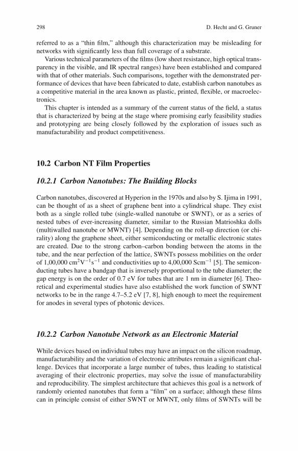
298 D. Hecht and G. Gruner
referred to as a “thin film,” although this characterization may be misleading fornetworks with significantly less than full coverage of a substrate.
Various technical parameters of the films (low sheet resistance, high optical trans-parency in the visible, and IR spectral ranges) have been established and comparedwith that of other materials. Such comparisons, together with the demonstrated per-formance of devices that have been fabricated to date, establish carbon nanotubes asa competitive material in the area known as plastic, printed, flexible, or macroelec-tronics.
This chapter is intended as a summary of the current status of the field, a statusthat is characterized by being at the stage where promising early feasibility studiesand prototyping are being closely followed by the exploration of issues such asmanufacturability and product competitiveness.
10.2 Carbon NT Film Properties
10.2.1 Carbon Nanotubes: The Building Blocks
Carbon nanotubes, discovered at Hyperion in the 1970s and also by S. Ijima in 1991,can be thought of as a sheet of graphene bent into a cylindrical shape. They existboth as a single rolled tube (single-walled nanotube or SWNT), or as a series ofnested tubes of ever-increasing diameter, similar to the Russian Matrioshka dolls(multiwalled nanotube or MWNT) [4]. Depending on the roll-up direction (or chi-rality) along the graphene sheet, either semiconducting or metallic electronic statesare created. Due to the strong carbon–carbon bonding between the atoms in thetube, and the near perfection of the lattice, SWNTs possess mobilities on the orderof 1,00,000 cm2V−1s−1 and conductivities up to 4,00,000 Scm−1 [5]. The semicon-ducting tubes have a bandgap that is inversely proportional to the tube diameter; thegap energy is on the order of 0.7 eV for tubes that are 1 nm in diameter [6]. Theo-retical and experimental studies have also established the work function of SWNTnetworks to be in the range 4.7–5.2 eV [7, 8], high enough to meet the requirementfor anodes in several types of photonic devices.
10.2.2 Carbon Nanotube Network as an Electronic Material
While devices based on individual tubes may have an impact on the silicon roadmap,manufacturability and the variation of electronic attributes remain a significant chal-lenge. Devices that incorporate a large number of tubes, thus leading to statisticalaveraging of their electronic properties, may solve the issue of manufacturabilityand reproducibility. The simplest architecture that achieves this goal is a network ofrandomly oriented nanotubes that form a “film” on a surface; although these filmscan in principle consist of either SWNT or MWNT, only films of SWNTs will be
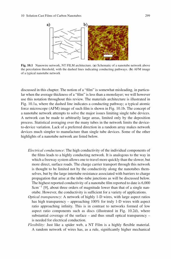
10 Solution Cast Films of Carbon Nanotubes 299
Fig. 10.1 Nanowire network, NT FILM architecture. (a) Schematic of a nanotube network abovethe percolation threshold, with the dashed lines indicating conducting pathways. (b) AFM imageof a typical nanotube network
discussed in this chapter. The notion of a “film” is somewhat misleading, in particu-lar when the average thickness of a “film” is less than a monolayer; we will howeveruse this notation throughout this review. The materials architecture is illustrated inFig. 10.1a, where the dashed line indicates a conducting pathway; a typical atomicforce microscope (AFM) image of such film is shown in Fig. 10.1b. The concept ofa nanotube network attempts to solve the major issues limiting single tube devices.A network can be made to arbitrarily large areas, limited only by the depositionprocess. Statistical averaging over the many tubes in the network limits the device-to-device variation. Lack of a preferred direction in a random array makes networkdevices much simpler to manufacture than single tube devices. Some of the otherhighlights of a nanotube network are listed below.
Electrical conductance: The high conductivity of the individual components ofthe films leads to a highly conducting network. It is analogous to the way inwhich a freeway system allows one to travel more quickly than the slower, butmore direct, surface roads. The charge carrier transport through this networkis thought to be limited not by the conductivity along the nanotubes them-selves, but by the large intertube resistance associated with barriers to chargepropagation that arise at the tube–tube junctions as will be discussed below.The highest reported conductivity of a nanotube film reported to date is 6,000Scm−1 [9], about three orders of magnitude lower than that of a single nan-otube. However, the conductivity is sufficient for a variety of applications.
Optical transparency: A network of highly 1-D wires, with large aspect ratioshas high transparency – approaching 100% for truly 1-D wires with aspectratio approaching infinity. This is in contrast to networks formed of lowaspect ratio components such as discs (illustrated in Fig. 10.2d), wheresubstantial coverage of the surface – and thus small optical transparency –is needed for electrical conduction.
Flexibility: Just like a spider web, a NT Film is a highly flexible material.A random network of wires has, as a rule, significantly higher mechanical
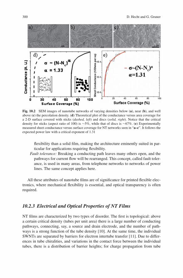
300 D. Hecht and G. Gruner
Fig. 10.2 SEM images of nanotube networks of varying densities below (a), near (b), and wellabove (c) the percolation density. (d) Theoretical plot of the conductance versus area coverage fora 2-D surface covered with sticks (dashed, left) and discs (solid, right). Notice that the criticaldensity for sticks (aspect ratio of 100) is ∼5%, while that of discs is ∼67%. (e) Experimentallymeasured sheet conductance versus surface coverage for NT networks seen in “a–c”. It follows theexpected power law with a critical exponent of 1.31
flexibility than a solid film, making the architecture eminently suited in par-ticular for applications requiring flexibility.
Fault tolerance: Breaking a conducting path leaves many others open, and thepathways for current flow will be rearranged. This concept, called fault toler-ance, is used in many areas, from telephone networks to networks of powerlines. The same concept applies here.
All these attributes of nanotube films are of significance for printed flexible elec-tronics, where mechanical flexibility is essential, and optical transparency is oftenrequired.
10.2.3 Electrical and Optical Properties of NT Films
NT films are characterized by two types of disorder. The first is topological: abovea certain critical density (tubes per unit area) there is a large number of conductingpathways, connecting, say, a source and drain electrode, and the number of path-ways is a strong function of the tube density [10]. At the same time, the individualSWNTs are separated by barriers for electron intertube transfer [11]. Due to differ-ences in tube chiralities, and variations in the contact force between the individualtubes, there is a distribution of barrier heights; for charge propagation from tube
10 Solution Cast Films of Carbon Nanotubes 301
to tube, this leads to a second source of randomness. As expected for a materialwith substantial randomness, charge transport is fundamentally different from bandtransport in materials like a good metal or a single crystal silicon. This leads to aconductivity that is concentration, temperature, frequency, and voltage dependent.Such dependencies and comparison with relevant theories can be used to assess theunderlying transport mechanism.
10.2.3.1 Concentration Dependent Conductivity
One of the more important notions with respect to applications of NT films is theconcept of percolation. Percolation is a phenomenon that describes how paths formacross a surface as the density (i.e., objects/area, referred to below as N) of thenetwork increases; theoretical work has established how the number of paths shouldscale with density for networks consisting of a variety of objects, such as discs andsticks. Percolation, in the case of NT films, refers to the propagation of electriccharge across the random network of tubes, separated by barriers, and it is assumedthat the network conductance is proportional to the number of formed pathways.There are three distinct regimes where the electronic properties of the network aresubstantially different; these three regions are highlighted in Fig. 10.2a–c. At lowdensities, a continuous path across the surface cannot be formed; the conductance(G) here is zero. As the density increases, the NT film reaches a critical density(Nc, called the percolation threshold), where paths are first beginning to form. Atthis critical density, theory predicts that the conductance of a percolating networkvaries as:
G ∼ (N − Nc)α (10.1)
The critical density Nc depends on the geometry of the object in the network;theoretical models have established that for a network comprised of identical sticksof length LT:
Nc = 5.7
L2T
(10.2) [12]
Figure 10.2d illustrates the advantage of using longer aspect ratio materials suchas nanotubes (sticks) as opposed to nanoparticles (discs): the higher aspect ratiomaterial forms percolating pathways at much lower densities, approaching an Nc of0 for truly 1-D objects. This fact will have consequences in forming composites,as well as in using nanotubes in applications where transparency is needed. Unlikethe critical density Nc, the critical exponent (α) depends solely on the dimensionof the percolating space; theory predicts a value of 1.33 for two dimensions and1.94 for three dimensions [13] for objects of arbitrary geometry. This exponent isprecisely accurate only when the density approaches Nc from above; for densitiesgreater than Nc, the exponent in Eq. 10.1 is density dependent and approaches 1 for
302 D. Hecht and G. Gruner
films where N >> Nc. Experimental results on percolating nanotube networks intwo dimensions have confirmed these results [10] (see Fig. 10.2e).
10.2.3.2 Temperature Dependent Conductivity
The temperature dependence of the resistivity of films of various densities has beenexamined in detail [14–16]. At high densities, well above the percolation threshold,the resistivity is weakly temperature dependent, mimicking the behavior of a “bad”metal. In contrast, for smaller network densities – in particular near to the percola-tion threshold – the conductivity depends more strongly on the temperature, givingevidence that temperature-driven charge transport processes dominate the conduc-tivity. The overall temperature and concentration dependence, including both low-density and high-density networks, can be qualitatively understood based on whathas been discussed above, with one additional factor: at low densities the conductingnetworks most likely have at least some semiconducting SWNTs, while at higherdensities all-metallic SWNT pathways are feasible. This can be described with amodel that includes both semiconducting and metallic pathways. These notions havebeen elaborated upon by various groups, often with detailed fits to theories [14–16].All of these are based on the inherent randomness and temperature-driven chargetransport across random barriers. What is important for applications is that carbonNT films can serve as a semiconducting channel (essential for transistor operation)when the density is close to the percolation threshold and also as a “metallic” inter-connect or sheet of conductor for high network densities.
10.2.3.3 Frequency Dependence and Optical Conductivity
As expected for a random network where charge transport is limited by large resis-tances between the tubes, the conductivity is also frequency dependent. At low fre-quencies:
σ (ω) = σdc + Aωβ (10.3)
where ω is the angular frequency, σdc is the dc conductivity, and β ≤ 1 (Zhouand Gruner, unpublished). The coefficient A in Eq. 10.3 is weakly density depen-dent, while σ dc is a strong function of the density, with σ dc→0 at the percolationthreshold. Thus, the conductivity is increasingly dependent on the frequency as thenetwork density approaches Nc from above. For densities well exceeding Nc, theincrease in the conductivity with increasing frequency sets in only at high frequen-cies in the millimeter wave optical range.
The conductivity has been evaluated in a broad spectral range [17, 18], the mostrecent results displayed in Fig. 10.3. As discussed before, with increasing frequencyan increase of σ (ω) is first observed, due to the progressively reduced role of theintertube barriers. This is followed by the typical Drude roll-off in the infrared spec-tral range. Among the additional features observed at higher frequencies, a strong
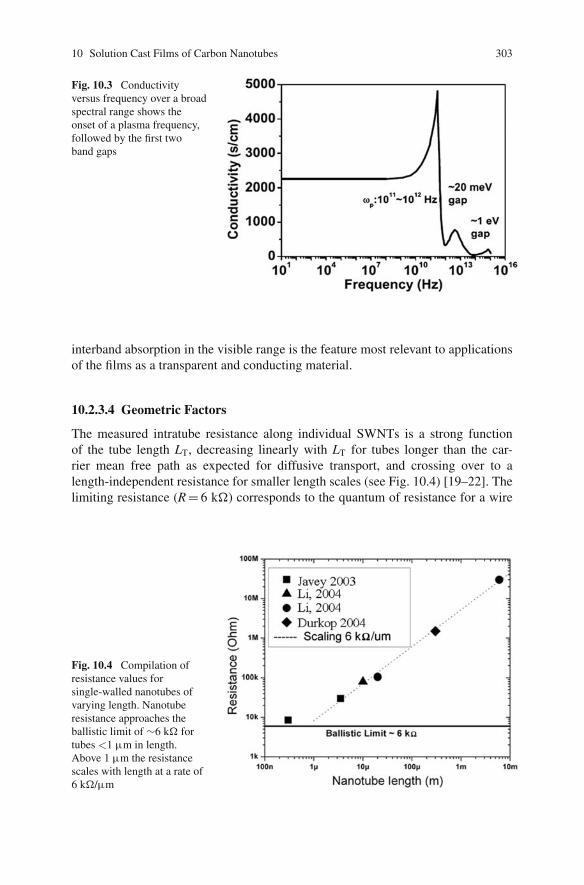
10 Solution Cast Films of Carbon Nanotubes 303
Fig. 10.3 Conductivityversus frequency over a broadspectral range shows theonset of a plasma frequency,followed by the first twoband gaps
interband absorption in the visible range is the feature most relevant to applicationsof the films as a transparent and conducting material.
10.2.3.4 Geometric Factors
The measured intratube resistance along individual SWNTs is a strong functionof the tube length LT, decreasing linearly with LT for tubes longer than the car-rier mean free path as expected for diffusive transport, and crossing over to alength-independent resistance for smaller length scales (see Fig. 10.4) [19–22]. Thelimiting resistance (R = 6 kΩ) corresponds to the quantum of resistance for a wire
Fig. 10.4 Compilation ofresistance values forsingle-walled nanotubes ofvarying length. Nanotuberesistance approaches theballistic limit of ∼6 kΩ fortubes <1 μm in length.Above 1 μm the resistancescales with length at a rate of6 kΩ/μm
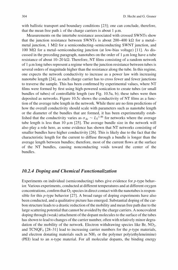
304 D. Hecht and G. Gruner
with ballistic transport and boundary conditions [23]; one can conclude, therefore,that the mean free path λ of the charge carriers is about 1 μm.
Measurements on the intertube resistance associated with crossed SWNTs showthat the junction resistance between SWNTs is about 200–400 kΩ for a metal–metal junction, 1 MΩ for a semiconducting–semiconducting SWNT junction, and100 MΩ for a metal–semiconducting junction (at low-bias voltage) [11]. As dis-cussed in the preceding paragraph, nanotubes on the order of 1 μm long have a tuberesistance of about 10–20 kΩ. Therefore, NT films consisting of a random networkof 1 μm long tubes represent a regime where the junction resistance between tubes isseveral orders of magnitude higher than the resistance along the tube. In this regime,one expects the network conductivity to increase as a power law with increasingnanotube length [24], as each charge carrier has to cross fewer and fewer junctionsto traverse the sample. This has been confirmed by experimental values, where NTfilms were formed by first using high-powered sonication to create tubes (or smallbundles of tubes) of controllable length (see Fig. 10.5a, b); these tubes were thendeposited as networks. Figure 10.5c shows the conductivity of NT films as a func-tion of the average tube length in the network. While there are no firm predictions ofhow the overall conductivity should scale with parameters such as nanotube lengthor the diameter of the bundles that are formed, it has been experimentally estab-lished that the conductivity varies as σ dc ∼ LT
1.46 for networks where the averagetube length is less than 10 μm [25]. The average bundle size in the network willalso play a role here, as some evidence has shown that NT networks consisting ofsmaller bundles have higher conductivity [26]. This is likely due to the fact that thecharacteristic length for the current to diffuse through a bundle is longer than theaverage length between bundles; therefore, most of the current flows at the surfaceof the NT bundles, causing nonconducting voids toward the center of thebundles.
10.2.4 Doping and Chemical Functionalization
Experiments on individual (semiconducting) tubes give evidence for p-type behav-ior. Various experiments, conducted at different temperatures and at different oxygenconcentrations, confirm that O2 species in direct contact with the nanotubes is respon-sible for this p-type behavior [27]. A broad range of doping experiments have alsobeen conducted, and a qualitative picture has emerged. Substantial doping of the car-bon structure leads to a drastic reduction of the mobility and mean free path due to thelarge scattering potential that cannot be avoided by the charge carriers. A noncovalentdoping through (weak) attachment of the dopant molecules to the surface of the tubeshas shown to lead to changes of the carrier number, often with relatively minor degra-dation of the mobility of the network. Electron withdrawing species like Br, NO2,and TCNQF4 [28–31] lead to increasing carrier numbers for the p-type materials,and electron donating materials such as NH3 or the polymer poly(ethyleneimine)(PEI) lead to an n-type material. For all molecular dopants, the binding energy
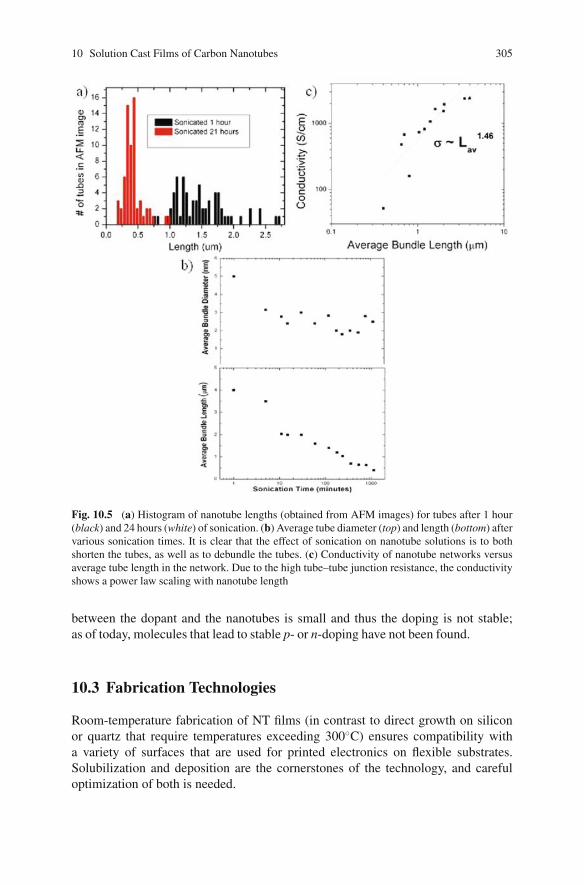
10 Solution Cast Films of Carbon Nanotubes 305
Fig. 10.5 (a) Histogram of nanotube lengths (obtained from AFM images) for tubes after 1 hour(black) and 24 hours (white) of sonication. (b) Average tube diameter (top) and length (bottom) aftervarious sonication times. It is clear that the effect of sonication on nanotube solutions is to bothshorten the tubes, as well as to debundle the tubes. (c) Conductivity of nanotube networks versusaverage tube length in the network. Due to the high tube–tube junction resistance, the conductivityshows a power law scaling with nanotube length
between the dopant and the nanotubes is small and thus the doping is not stable;as of today, molecules that lead to stable p- or n-doping have not been found.
10.3 Fabrication Technologies
Room-temperature fabrication of NT films (in contrast to direct growth on siliconor quartz that require temperatures exceeding 300◦C) ensures compatibility witha variety of surfaces that are used for printed electronics on flexible substrates.Solubilization and deposition are the cornerstones of the technology, and carefuloptimization of both is needed.
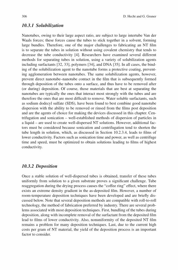
306 D. Hecht and G. Gruner
10.3.1 Solubilization
Nanotubes, owing to their large aspect ratio, are subject to large intertube Van derWaals forces; these forces cause the tubes to stick together in a solvent, forminglarge bundles. Therefore, one of the major challenges to fabricating an NT filmis to separate the tubes in solution without using covalent chemistry that tends todecrease the tube conductivity [4]. Researchers have examined several differentmethods for separating tubes in solution, using a variety of solubilization agentsincluding surfactants [32, 33], polymers [34], and DNA [35]. In all cases, the bind-ing of the solubilization agent to the nanotube forms a protective coating, prevent-ing agglomeration between nanotubes. The same solubilization agents, however,prevent direct nanotube–nanotube contact in the film that is subsequently formedthrough deposition of the tubes onto a surface, and thus have to be removed after(or during) deposition. Of course, those materials that are best at separating thenanotubes are typically the ones that interact most strongly with the tubes and aretherefore the ones that are most difficult to remove. Water soluble surfactants, suchas sodium dodecyl sulfate (SDS), have been found to best combine good nanotubedispersion with the ability to be removed or rinsed from the films post depositionand are the agents of choice for making the devices discussed in this chapter. Cen-trifugation and sonication – well-established methods of dispersion of particles ina liquid – are used to create well-dispersed NT solutions. However, additional fac-tors must be considered because sonication and centrifugation tend to shorten thetube length in solution, which, as discussed in Section 10.2.3.4, leads to films oflower conductivity. Factors such as sonication time and power, as well as centrifugetime and speed, must be optimized to obtain solutions leading to films of highestconductivity.
10.3.2 Deposition
Once a stable solution of well-dispersed tubes is obtained, transfer of these tubesuniformly from solution to a given substrate proves a significant challenge. Tubereaggregation during the drying process causes the “coffee ring” effect, where thereexists an extreme density gradient in the as-deposited film. However, a number ofroom-temperature deposition techniques have been developed and are briefly dis-cussed below. Note that several deposition methods are compatible with roll-to-rolltechnology, the method of fabrication preferred by industry. There are several prob-lems associated with most deposition techniques. First, bundling of the tubes duringdeposition, along with incomplete removal of the surfactant from the deposited filmlead to films of lower conductivity. Also, nonuniformity of the deposited NT filmremains a problem for many deposition techniques. Last, due to the current highcosts per gram of NT material, the yield of the deposition process is an importantfactor to consider.
10 Solution Cast Films of Carbon Nanotubes 307
10.3.2.1 Spraying
The simplest deposition technique is a process involving spraying the solution ofwell-dispersed tubes onto a substrate. Nanotube solutions are sprayed using an artistspray brush (Fig. 10.6a) onto a substrate that is heated to about 80–100◦C. Heat-ing the substrate ensures that the small droplets that hit the surface are evaporatedquickly, so the tubes in solution do not have time to aggregate before depositing.Figure 10.6b–d shows AFM images of a sprayed NT film along with a trace thatindicates an average bundle size of ∼5–10 nm. Rinsing the films in water, eitherafter the deposition or several times during deposition, is important to remove thesurfactant from the film surface, and it tends to improve the conductivity almostan order of magnitude (Hecht, 2006, unpublished). Spray technology may be espe-cially useful in coating irregularly shaped objects such as fabrics [36] or very largeobjects such as vehicles or airplanes requiring electrostatic discharge. However, it
Fig. 10.6 (a) Photograph of nanotube spray coating set up using an artists spray brush. (b) AFMimage of a sprayed nanotube film. (c,d) AFM image of a sprayed nanotube film showing a profilescan indicating a nanotube bundle size between 5 and 10 nm
308 D. Hecht and G. Gruner
is difficult to obtain high degrees of surface uniformity using a spray depositionmethod, due to the nonuniformity of the spray mist from the nozzle. Also, the yieldof a spray deposition process is a concern, as some of the sprayed droplets have atendency to either bounce off of the substrate surface or miss the surface entirely.Due to the high current costs of nanotube material, a low yield in the depositionprocess would make applications cost prohibitive.
10.3.2.2 Slot Coating
Slot coating is a process where a thin film (5–30 μm) of solution is applied evenly tothe substrate surface through a slot die. This method yields films of high uniformityand high yield, and is a well known commercial process used in roll-to-roll manufac-turing. The conductivity of films deposited by this method is limited by surfactantmolecules remaining in the film structure after deposition; therefore, methods tothoroughly rinse away or otherwise remove all unwanted solubilization agents mustbe explored.
10.3.2.3 Spin Coating
Spin coating of aqueous-based surfactant-wrapped SWNT solutions is difficult onmost hydrophobic substrates such as silicon wafers. One successful method thatwas reported involves the simultaneous spin coating of a stream of methanol alongwith the nanotube suspension. The stream removes the nanotube from its surfactant-wrapped protection immediately before hitting the substrate, and allows the tube todeposit on the surface [37]. This method, however, leads to highly nonuniform filmsand is clearly not compatible with roll-to-roll manufacturing.
10.3.2.4 Filtration/Stamping
The deposition method that leads to NT films of highest conductivity involves firstdepositing the films on a filter and then transferring the film from the filter to thesubstrate of interest. To deposit the film, a dilute suspension of nanotubes is quicklyvacuum filtered onto a porous alumina filter (pore size 100 nm). As the solvent fallsthrough the pores, the SWNTs are trapped on the filter surface, forming an intercon-nected surface. After forming the film, large amounts of water or other solvents canbe washed through the film, rinsing away any residual surfactants. Since the porousalumina filter is not transparent or flexible, the network has to be subsequently trans-ferred onto a transparent surface, such as glass or polyethylene terephthalate (PET).A printing method using a poly(dimethylsiloxane) (PDMS) “stamp” is illustratedin Fig. 10.7a. The stamp is first touched to the nanotube–filter surface and the nan-otubes are lifted off of the filter onto the PDMS stamp. Then, the stamp is pressedagainst a PET surface and heated to about 60◦C for 1 h, transferring the tubes fromthe stamp to the PET surface. This method can also be used to produce patternedfilms, by simply patterning the PDMS “stamp” before transferring the nanotube
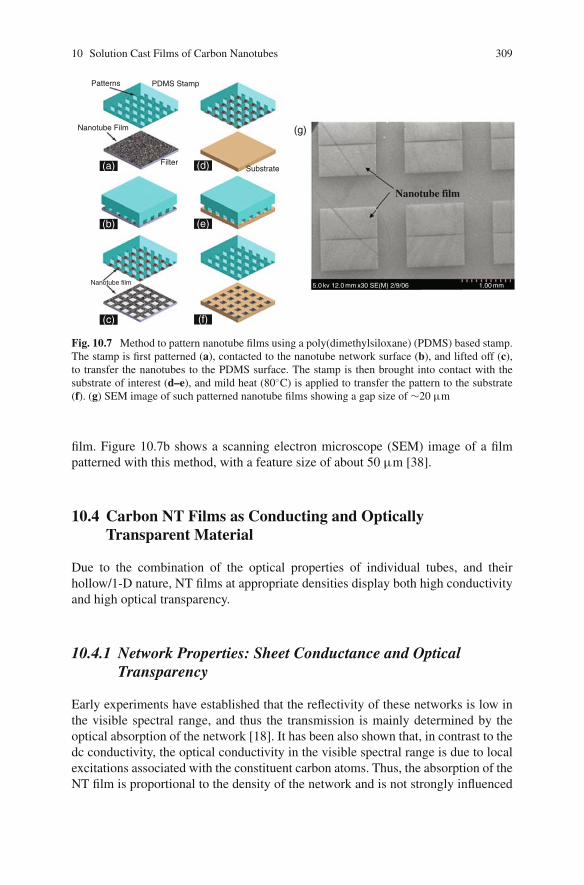
10 Solution Cast Films of Carbon Nanotubes 309
Patterns
Nanotube Film
Substrate
PDMS Stamp
Filter (d)
(g)
Nanotube film
5.0 kv 12.0 mm x30 SE(M) 2/9/06 1.00 mm
(b)
Nanotube film
(e)
(f)(c)
(a)
Fig. 10.7 Method to pattern nanotube films using a poly(dimethylsiloxane) (PDMS) based stamp.The stamp is first patterned (a), contacted to the nanotube network surface (b), and lifted off (c),to transfer the nanotubes to the PDMS surface. The stamp is then brought into contact with thesubstrate of interest (d–e), and mild heat (80◦C) is applied to transfer the pattern to the substrate(f). (g) SEM image of such patterned nanotube films showing a gap size of ∼20 μm
film. Figure 10.7b shows a scanning electron microscope (SEM) image of a filmpatterned with this method, with a feature size of about 50 μm [38].
10.4 Carbon NT Films as Conducting and OpticallyTransparent Material
Due to the combination of the optical properties of individual tubes, and theirhollow/1-D nature, NT films at appropriate densities display both high conductivityand high optical transparency.
10.4.1 Network Properties: Sheet Conductance and OpticalTransparency
Early experiments have established that the reflectivity of these networks is low inthe visible spectral range, and thus the transmission is mainly determined by theoptical absorption of the network [18]. It has been also shown that, in contrast to thedc conductivity, the optical conductivity in the visible spectral range is due to localexcitations associated with the constituent carbon atoms. Thus, the absorption of theNT film is proportional to the density of the network and is not strongly influenced
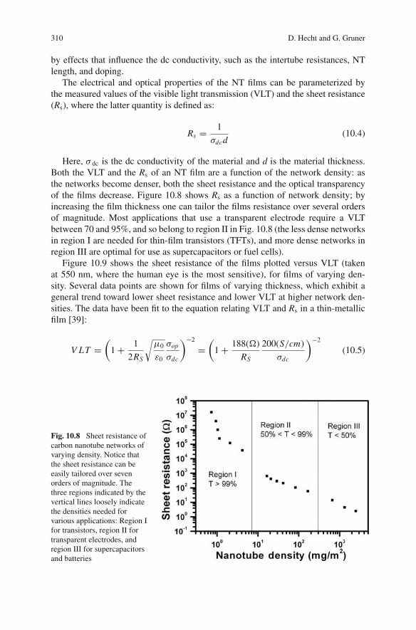
310 D. Hecht and G. Gruner
by effects that influence the dc conductivity, such as the intertube resistances, NTlength, and doping.
The electrical and optical properties of the NT films can be parameterized bythe measured values of the visible light transmission (VLT) and the sheet resistance(Rs), where the latter quantity is defined as:
Rs = 1
σdcd(10.4)
Here, σ dc is the dc conductivity of the material and d is the material thickness.Both the VLT and the Rs of an NT film are a function of the network density: asthe networks become denser, both the sheet resistance and the optical transparencyof the films decrease. Figure 10.8 shows Rs as a function of network density; byincreasing the film thickness one can tailor the films resistance over several ordersof magnitude. Most applications that use a transparent electrode require a VLTbetween 70 and 95%, and so belong to region II in Fig. 10.8 (the less dense networksin region I are needed for thin-film transistors (TFTs), and more dense networks inregion III are optimal for use as supercapacitors or fuel cells).
Figure 10.9 shows the sheet resistance of the films plotted versus VLT (takenat 550 nm, where the human eye is the most sensitive), for films of varying den-sity. Several data points are shown for films of varying thickness, which exhibit ageneral trend toward lower sheet resistance and lower VLT at higher network den-sities. The data have been fit to the equation relating VLT and Rs in a thin-metallicfilm [39]:
V LT =(
1 + 1
2RS
√μ0
ε0
σop
σdc
)−2
=(
1 + 188(Ω)
RS
200(S/cm)
σdc
)−2
(10.5)
Fig. 10.8 Sheet resistance ofcarbon nanotube networks ofvarying density. Notice thatthe sheet resistance can beeasily tailored over sevenorders of magnitude. Thethree regions indicated by thevertical lines loosely indicatethe densities needed forvarious applications: Region Ifor transistors, region II fortransparent electrodes, andregion III for supercapacitorsand batteries
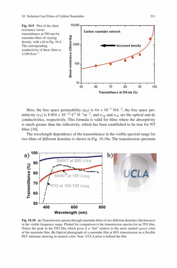
10 Solution Cast Films of Carbon Nanotubes 311
Fig. 10.9 Plot of the sheetresistance versustransmittance at 550 nm fornanotube films of varyingdensity, with a fit to Eq. 10.4.The correspondingconductivity of these films is2,100 Scm−1
Here, the free space permeability (μ0) is 4π× 10−7 NA−2, the free space per-mittivity (ε0) is 8.854 × 10⁻¹² C2 N−1m−2, and σ op and σ dc are the optical and dcconductivities, respectively. This formula is valid for films where the absorptivityis much greater than the reflectivity, which has been established to be true for NTfilms [18].
The wavelength dependence of the transmittance in the visible spectral range fortwo films of different densities is shown in Fig. 10.10a. The transmission spectrum
Fig. 10.10 (a) Transmission spectra through nanotube films of two different densities (thicknesses)in the visible frequency range. Plotted for comparison is the transmission spectra for an ITO film.Notice the peak in the ITO film which gives it a “tint” relative to the more neutral (gray) colorof the nanotube film. (b) Optical photograph of a nanotube film at 80% transmission on a flexiblePET substrate showing its neutral color. Note: UCLA print is behind the film
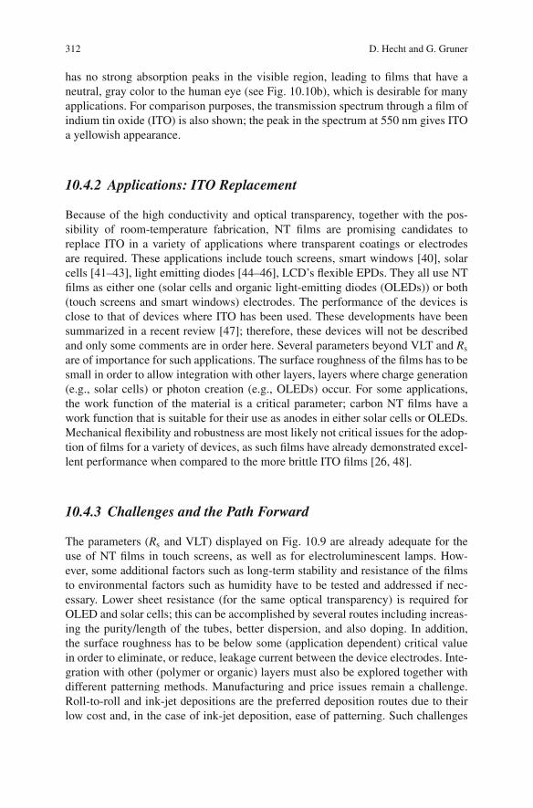
312 D. Hecht and G. Gruner
has no strong absorption peaks in the visible region, leading to films that have aneutral, gray color to the human eye (see Fig. 10.10b), which is desirable for manyapplications. For comparison purposes, the transmission spectrum through a film ofindium tin oxide (ITO) is also shown; the peak in the spectrum at 550 nm gives ITOa yellowish appearance.
10.4.2 Applications: ITO Replacement
Because of the high conductivity and optical transparency, together with the pos-sibility of room-temperature fabrication, NT films are promising candidates toreplace ITO in a variety of applications where transparent coatings or electrodesare required. These applications include touch screens, smart windows [40], solarcells [41–43], light emitting diodes [44–46], LCD’s flexible EPDs. They all use NTfilms as either one (solar cells and organic light-emitting diodes (OLEDs)) or both(touch screens and smart windows) electrodes. The performance of the devices isclose to that of devices where ITO has been used. These developments have beensummarized in a recent review [47]; therefore, these devices will not be describedand only some comments are in order here. Several parameters beyond VLT and Rs
are of importance for such applications. The surface roughness of the films has to besmall in order to allow integration with other layers, layers where charge generation(e.g., solar cells) or photon creation (e.g., OLEDs) occur. For some applications,the work function of the material is a critical parameter; carbon NT films have awork function that is suitable for their use as anodes in either solar cells or OLEDs.Mechanical flexibility and robustness are most likely not critical issues for the adop-tion of films for a variety of devices, as such films have already demonstrated excel-lent performance when compared to the more brittle ITO films [26, 48].
10.4.3 Challenges and the Path Forward
The parameters (Rs and VLT) displayed on Fig. 10.9 are already adequate for theuse of NT films in touch screens, as well as for electroluminescent lamps. How-ever, some additional factors such as long-term stability and resistance of the filmsto environmental factors such as humidity have to be tested and addressed if nec-essary. Lower sheet resistance (for the same optical transparency) is required forOLED and solar cells; this can be accomplished by several routes including increas-ing the purity/length of the tubes, better dispersion, and also doping. In addition,the surface roughness has to be below some (application dependent) critical valuein order to eliminate, or reduce, leakage current between the device electrodes. Inte-gration with other (polymer or organic) layers must also be explored together withdifferent patterning methods. Manufacturing and price issues remain a challenge.Roll-to-roll and ink-jet depositions are the preferred deposition routes due to theirlow cost and, in the case of ink-jet deposition, ease of patterning. Such challenges
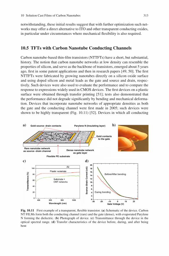
10 Solution Cast Films of Carbon Nanotubes 313
notwithstanding, these initial results suggest that with further optimization such net-works may offer a direct alternative to ITO and other transparent conducting oxides,in particular under circumstances where mechanical flexibility is also required.
10.5 TFTs with Carbon Nanotube Conducting Channels
Carbon nanotube-based thin-film transistors (NTTFTs) have a short, but substantial,history. The notion that carbon nanotube networks at low density can resemble theproperties of silicon, and serve as the backbone of transistors, emerged about 5 yearsago, first in some patent applications and then in research papers [49, 50]. The firstNTTFTs were fabricated by growing nanotubes directly on a silicon oxide surfaceand using doped silicon and metal leads as the gate and source and drain, respec-tively. Such devices were also used to evaluate the performance and to compare theresponse to expressions widely used in CMOS devices. The first devices on a plasticsurface were obtained through transfer printing [51]; tests also demonstrated thatthe performance did not degrade significantly by bending and mechanical deforma-tion. Devices that incorporate nanotube networks of appropriate densities as boththe gate and the conducting channel were first made in 2005; such devices wereshown to be highly transparent (Fig. 10.11) [52]. Devices in which all conducting
Gold source- drain contactsa) b)
c) d)
Parylene N (Insulating layer)
Gold contactsto the gate
Rare nanotube networkas source – drain channel Dense nanotube network
as gate layer
Flexible PE substrate
Fig. 10.11 First example of a transparent, flexible transistor. (a) Schematic of the device. CarbonNT FILMs form both the conducting channel (rare) and the gate (dense), with evaporated ParyleneN forming the dielectric. (b) Photograph of device. (c) Transmittance through the device in theoptical spectral range. (d) Transfer characteristics of the device before, during, and after beingbent
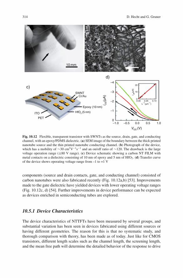
314 D. Hecht and G. Gruner
a)
10 mm
c)
Epoxy (10 nm)
HfO2 (5 nm)
PET
ITO
SWNTCr/Au
d)–4
–3
–2
–1
0
VGS (V)
–1.0 –0.5 0.5 1.00.0
L–1
(µm–1
)
l off(µ
A)
/ DS(µ
A)
0.00 0.05 0.100
20
10
b)a)
Fig. 10.12 Flexible, transparent transistor with SWNTs as the source, drain, gate, and conductingchannel, with an epoxy/PDMS dielectric. (a) SEM image of the boundary between the thick printednanotube source and the thin printed nanotube conducting channel. (b) Photograph of the device,which has a mobility of ∼30 cm2V−1s−1 and an on/off ratio of ∼120. The drawback is the largevoltage operation range (±80 V range). (c) Device schematic showing a carbon NT FILM withmetal contacts on a dielectric consisting of 10 nm of epoxy and 5 nm of HfO2. (d) Transfer curveof the device shows operating voltage range from –1 to +1 V
components (source and drain contacts, gate, and conducting channel) consisted ofcarbon nanotubes were also fabricated recently (Fig. 10.12a,b) [53]. Improvementsmade to the gate dielectric have yielded devices with lower operating voltage ranges(Fig. 10.12c, d) [54]. Further improvements in device performance can be expectedas devices enriched in semiconducting tubes are explored.
10.5.1 Device Characteristics
The device characteristics of NTTFTs have been measured by several groups, andsubstantial variation has been seen in devices fabricated using different sources orhaving different geometries. The reason for this is that no systematic study, andthorough comparison with theory, has been made as of today. Just like for CMOStransistors, different length scales such as the channel length, the screening length,and the mean free path will determine the detailed behavior of the response to drive
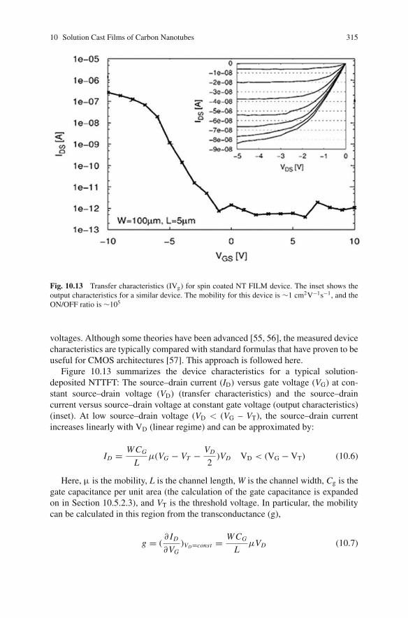
10 Solution Cast Films of Carbon Nanotubes 315
Fig. 10.13 Transfer characteristics (IVg) for spin coated NT FILM device. The inset shows theoutput characteristics for a similar device. The mobility for this device is ∼1 cm2V−1s−1, and theON/OFF ratio is ∼105
voltages. Although some theories have been advanced [55, 56], the measured devicecharacteristics are typically compared with standard formulas that have proven to beuseful for CMOS architectures [57]. This approach is followed here.
Figure 10.13 summarizes the device characteristics for a typical solution-deposited NTTFT: The source–drain current (ID) versus gate voltage (VG) at con-stant source–drain voltage (VD) (transfer characteristics) and the source–draincurrent versus source–drain voltage at constant gate voltage (output characteristics)(inset). At low source–drain voltage (VD < (VG – VT), the source–drain currentincreases linearly with VD (linear regime) and can be approximated by:
ID = WCG
Lμ(VG − VT − VD
2)VD VD < (VG − VT) (10.6)
Here, μ is the mobility, L is the channel length, W is the channel width, Cg is thegate capacitance per unit area (the calculation of the gate capacitance is expandedon in Section 10.5.2.3), and VT is the threshold voltage. In particular, the mobilitycan be calculated in this region from the transconductance (g),
g = (∂ ID
∂VG)VD=const = WCG
LμVD (10.7)
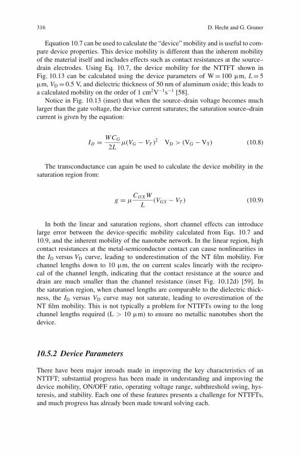
316 D. Hecht and G. Gruner
Equation 10.7 can be used to calculate the “device” mobility and is useful to com-pare device properties. This device mobility is different than the inherent mobilityof the material itself and includes effects such as contact resistances at the source–drain electrodes. Using Eq. 10.7, the device mobility for the NTTFT shown inFig. 10.13 can be calculated using the device parameters of W = 100 μm, L = 5μm, VD = 0.5 V, and dielectric thickness of 50 nm of aluminum oxide; this leads toa calculated mobility on the order of 1 cm2V−1s−1 [58].
Notice in Fig. 10.13 (inset) that when the source–drain voltage becomes muchlarger than the gate voltage, the device current saturates; the saturation source–draincurrent is given by the equation:
ID = WCG
2Lμ(VG − VT )2 VD > (VG − VT) (10.8)
The transconductance can again be used to calculate the device mobility in thesaturation region from:
g = μCO X W
L(VGS − VT ) (10.9)
In both the linear and saturation regions, short channel effects can introducelarge error between the device-specific mobility calculated from Eqs. 10.7 and10.9, and the inherent mobility of the nanotube network. In the linear region, highcontact resistances at the metal-semiconductor contact can cause nonlinearities inthe ID versus VD curve, leading to underestimation of the NT film mobility. Forchannel lengths down to 10 μm, the on current scales linearly with the recipro-cal of the channel length, indicating that the contact resistance at the source anddrain are much smaller than the channel resistance (inset Fig. 10.12d) [59]. Inthe saturation region, when channel lengths are comparable to the dielectric thick-ness, the ID versus VD curve may not saturate, leading to overestimation of theNT film mobility. This is not typically a problem for NTTFTs owing to the longchannel lengths required (L > 10 μm) to ensure no metallic nanotubes short thedevice.
10.5.2 Device Parameters
There have been major inroads made in improving the key characteristics of anNTTFT; substantial progress has been made in understanding and improving thedevice mobility, ON/OFF ratio, operating voltage range, subthreshold swing, hys-teresis, and stability. Each one of these features presents a challenge for NTTFTs,and much progress has already been made toward solving each.
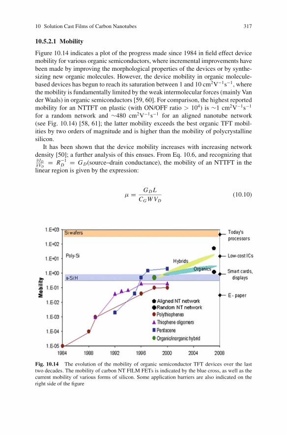
10 Solution Cast Films of Carbon Nanotubes 317
10.5.2.1 Mobility
Figure 10.14 indicates a plot of the progress made since 1984 in field effect devicemobility for various organic semiconductors, where incremental improvements havebeen made by improving the morphological properties of the devices or by synthe-sizing new organic molecules. However, the device mobility in organic molecule-based devices has begun to reach its saturation between 1 and 10 cm2V−1s−1, wherethe mobility is fundamentally limited by the weak intermolecular forces (mainly Vander Waals) in organic semiconductors [59, 60]. For comparison, the highest reportedmobility for an NTTFT on plastic (with ON/OFF ratio > 104) is ∼1 cm2V−1s−1
for a random network and ∼480 cm2V−1s−1 for an aligned nanotube network(see Fig. 10.14) [58, 61]; the latter mobility exceeds the best organic TFT mobil-ities by two orders of magnitude and is higher than the mobility of polycrystallinesilicon.
It has been shown that the device mobility increases with increasing networkdensity [50]; a further analysis of this ensues. From Eq. 10.6, and recognizing that∂ ID∂VD
= R−1D = G D(source–drain conductance), the mobility of an NTTFT in the
linear region is given by the expression:
μ = G D L
CG W VD(10.10)
Fig. 10.14 The evolution of the mobility of organic semiconductor TFT devices over the lasttwo decades. The mobility of carbon NT FILM FETs is indicated by the blue cross, as well as thecurrent mobility of various forms of silicon. Some application barriers are also indicated on theright side of the figure
318 D. Hecht and G. Gruner
In Eq. 10.9, both the source–drain conductance and the gate capacitance dependon the network density. For densities above the percolation threshold, a NT film canbe modeled as a percolating system composed of a random distribution of 1-D sticksspanning a 2-D surface. Standard percolation theory predicts that, for this system,the channel conductance (GD) is given by GD ∼ (N-Nc)1.33 (see Section 10.2.3.1),where N is the device density (tubes/area) and Nc is the critical density where apercolating path first forms. This scaling law is precisely accurate only when thedensity approaches Nc from above; for densities greater than Nc, the exponent in Eq.10.10 is density dependent and approaches 1 for films where N >> Nc. However,experiment has shown that Eq. 10.10 is approximately valid for network densities upto 10 times Nc [10]. The gate capacitance also depends on the network density. Forlow-density networks near the percolation threshold, the gate capacitance is equalto the product of the capacitance of a single isolated tube and the number of tubes[62], or CG ∼ N. Putting it together, one expects the mobility of NTTFTs above thepercolation threshold to scale as:
μ ∝ (N − NC )1.33
N(close to percolation) (10.11)
At higher densities, (N >> Nc), the gate capacitance saturates; therefore, themobility increases linearly with N, even as the network channels become thickerthan one monolayer. Unfortunately, as the network density increases, the ON/OFFratio of the NTTFTs decreases exponentially, as the presence of metallic tubes inthe network short the source–drain electrodes.
10.5.2.2 ON/OFF Ratio
Semiconducting SWNT field-effect transistors (FETs) have ON/OFF ratios above105 [63, 64], while nanotube network-based devices report ON/OFF ratios that varyfrom as high as 105 to as low as ∼1 [58, 65]. Typically, ON/OFF ratios approachingthose found in single tube devices are found only in NTTFTs using conducting chan-nels with densities just above the percolation threshold; as the density is increasedabove this value, the ON/OFF ratio falls off exponentially. This behavior is due tothe presence of metallic tubes in the source–drain channel, which short the device,providing a source–drain current pathway when the device is in its “off” state.Figure 10.15 summarizes the fundamental relationships between device ON/OFFratio and mobility; there is a general trend toward lower ON/OFF ratio for deviceswith higher mobility (density) [50, 52, 53, 54, 57, 58, 80, 81]. The solid line shouldserve as a guide to the eye, separating results obtained from solution-depositedNTTFTs from results obtained from chemical vapor deposition (CVD) grown nan-otubes. It is clear that NTTFTs deposited from solution exhibit lower mobilities forthe same ON/OFF ratios, likely due to larger tube bundles in the network or residualsurfactant.
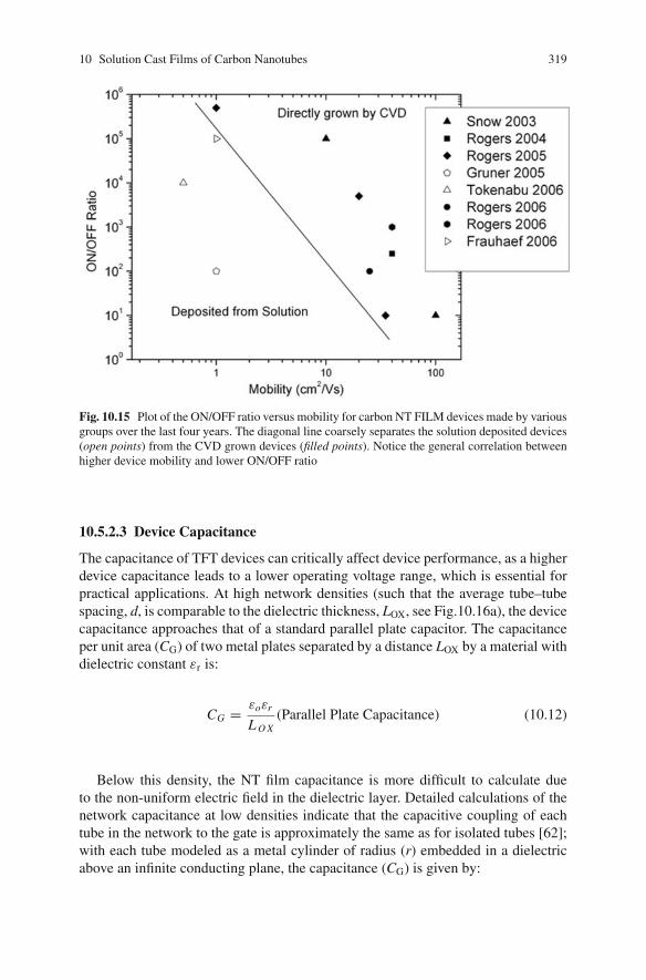
10 Solution Cast Films of Carbon Nanotubes 319
Fig. 10.15 Plot of the ON/OFF ratio versus mobility for carbon NT FILM devices made by variousgroups over the last four years. The diagonal line coarsely separates the solution deposited devices(open points) from the CVD grown devices (filled points). Notice the general correlation betweenhigher device mobility and lower ON/OFF ratio
10.5.2.3 Device Capacitance
The capacitance of TFT devices can critically affect device performance, as a higherdevice capacitance leads to a lower operating voltage range, which is essential forpractical applications. At high network densities (such that the average tube–tubespacing, d, is comparable to the dielectric thickness, LOX, see Fig.10.16a), the devicecapacitance approaches that of a standard parallel plate capacitor. The capacitanceper unit area (CG) of two metal plates separated by a distance LOX by a material withdielectric constant εr is:
CG = εoεr
L O X(Parallel Plate Capacitance) (10.12)
Below this density, the NT film capacitance is more difficult to calculate dueto the non-uniform electric field in the dielectric layer. Detailed calculations of thenetwork capacitance at low densities indicate that the capacitive coupling of eachtube in the network to the gate is approximately the same as for isolated tubes [62];with each tube modeled as a metal cylinder of radius (r) embedded in a dielectricabove an infinite conducting plane, the capacitance (CG) is given by:
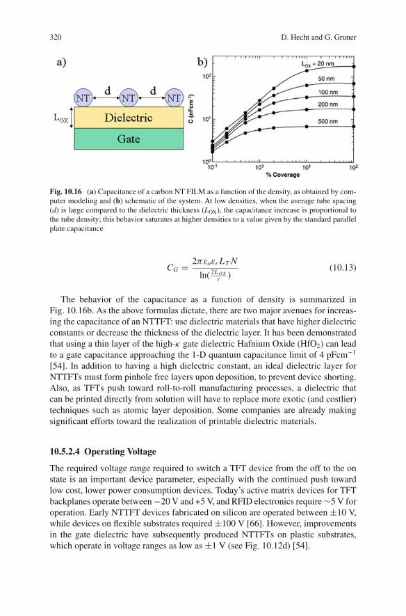
320 D. Hecht and G. Gruner
Fig. 10.16 (a) Capacitance of a carbon NT FILM as a function of the density, as obtained by com-puter modeling and (b) schematic of the system. At low densities, when the average tube spacing(d) is large compared to the dielectric thickness (LOX), the capacitance increase is proportional tothe tube density; this behavior saturates at higher densities to a value given by the standard parallelplate capacitance
CG = 2πεoεr LT N
ln( 2L O Xr )
(10.13)
The behavior of the capacitance as a function of density is summarized inFig. 10.16b. As the above formulas dictate, there are two major avenues for increas-ing the capacitance of an NTTFT: use dielectric materials that have higher dielectricconstants or decrease the thickness of the dielectric layer. It has been demonstratedthat using a thin layer of the high-κ gate dielectric Hafnium Oxide (HfO2) can leadto a gate capacitance approaching the 1-D quantum capacitance limit of 4 pFcm−1
[54]. In addition to having a high dielectric constant, an ideal dielectric layer forNTTFTs must form pinhole free layers upon deposition, to prevent device shorting.Also, as TFTs push toward roll-to-roll manufacturing processes, a dielectric thatcan be printed directly from solution will have to replace more exotic (and costlier)techniques such as atomic layer deposition. Some companies are already makingsignificant efforts toward the realization of printable dielectric materials.
10.5.2.4 Operating Voltage
The required voltage range required to switch a TFT device from the off to the onstate is an important device parameter, especially with the continued push towardlow cost, lower power consumption devices. Today’s active matrix devices for TFTbackplanes operate between −20 V and +5 V, and RFID electronics require ∼5 V foroperation. Early NTTFT devices fabricated on silicon are operated between ±10 V,while devices on flexible substrates required ±100 V [66]. However, improvementsin the gate dielectric have subsequently produced NTTFTs on plastic substrates,which operate in voltage ranges as low as ±1 V (see Fig. 10.12d) [54].
10 Solution Cast Films of Carbon Nanotubes 321
10.5.2.5 Threshold Voltage
The threshold voltage is the value of the gate voltage where the TFT device beginsto switch from the off state to the on state; it can be determined by extrapolatingthe linear region of the transfer curve to the gate voltage axis. The threshold voltagein NTTFTs is determined by the doping level of the nanotube conducting channel,as well as the gate capacitance. It has been found that the magnitude of the thresh-old voltage can be modified by p- or n-type doping of the NT films with variousmolecules or biological species; this has the effect of shifting the transfer curvetoward positive/negative gate voltages for p/n-type dopants [67, 68]. Although thisproperty of NTTFTs makes them excellent sensors [69], for electronics applicationsit is imperative that the threshold voltage be constant over repeated device cycles.Therefore, NTTFTs may require a protective, or encapsulation, layer to render theminsensitive to the environment. Section 10.5.2.8 will elaborate further on methodsto maintain the device stability.
10.5.2.6 Subthreshold Swing
The subthreshold swing (S) is an important device parameter because it correspondsto the voltage range required to switch the device between its off and on states. Thesubthreshold swing is determined by the inverse ratio of the gate capacitance (Cg)to the capacitance due to interfacial traps (CIT):
S = kbT
eln 10(1 + CI T
Cg) (10.14)
The room-temperature limit (CIT<<Cg) is 60 mV/decade and has been achievedby single tube devices with high-κ dielectrics [70] or by electrolyte gated devices[71]. In NTTFT devices, however, S has been reported in a range from 280 to2,500 mVdec−1 [54]. The reason for the larger subthreshold swing measured innetwork devices is not completely understood; one theory is that conduction throughthe metallic tubes in the network (which does not modulate with gate voltage) is themost likely cause for the nonideal behavior of the subthreshold swing in NTTFTdevices. Evidence supporting this can be seen in Fig. 10.17, which shows S decreas-ing with increasing device ON/OFF ratios (decreasing number of metallic path-ways).
10.5.2.7 Hysteresis
One undesirable feature present in NTTFT devices is what is known as hysteresis,which manifests as a difference in the source–drain current for the increasing anddecreasing gate voltage sweeps. Experiments have shown that the magnitude of thehysteresis increases as the gate sweep frequency decreases, indicating that slowlymoving species cause the hysteretic behavior. Furthermore, the introduction of anelectrolytic polymer coating to the NTTFT, as well as exposure of the device to a
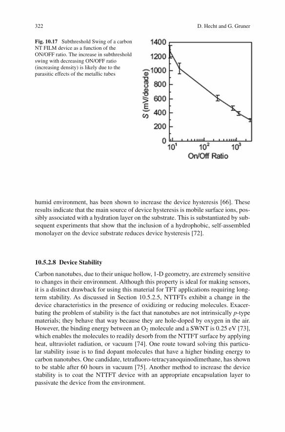
322 D. Hecht and G. Gruner
Fig. 10.17 Subthreshold Swing of a carbonNT FILM device as a function of theON/OFF ratio. The increase in subthresholdswing with decreasing ON/OFF ratio(increasing density) is likely due to theparasitic effects of the metallic tubes
humid environment, has been shown to increase the device hysteresis [66]. Theseresults indicate that the main source of device hysteresis is mobile surface ions, pos-sibly associated with a hydration layer on the substrate. This is substantiated by sub-sequent experiments that show that the inclusion of a hydrophobic, self-assembledmonolayer on the device substrate reduces device hysteresis [72].
10.5.2.8 Device Stability
Carbon nanotubes, due to their unique hollow, 1-D geometry, are extremely sensitiveto changes in their environment. Although this property is ideal for making sensors,it is a distinct drawback for using this material for TFT applications requiring long-term stability. As discussed in Section 10.5.2.5, NTTFTs exhibit a change in thedevice characteristics in the presence of oxidizing or reducing molecules. Exacer-bating the problem of stability is the fact that nanotubes are not intrinsically p-typematerials; they behave that way because they are hole-doped by oxygen in the air.However, the binding energy between an O2 molecule and a SWNT is 0.25 eV [73],which enables the molecules to readily desorb from the NTTFT surface by applyingheat, ultraviolet radiation, or vacuum [74]. One route toward solving this particu-lar stability issue is to find dopant molecules that have a higher binding energy tocarbon nanotubes. One candidate, tetrafluoro-tetracyanoquinodimethane, has shownto be stable after 60 hours in vacuum [75]. Another method to increase the devicestability is to coat the NTTFT device with an appropriate encapsulation layer topassivate the device from the environment.
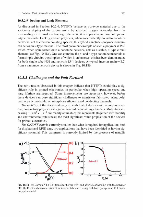
10 Solution Cast Films of Carbon Nanotubes 323
10.5.2.9 Doping and Logic Elements
As discussed in Section 10.2.4, NTTFTs behave as a p-type material due to theaccidental doping of the carbon atoms by adsorbed oxygen molecules from thesurrounding air. To make active logic elements, it is imperative to have both p- andn-type materials. Luckily, certain polymers, when noncovalently bound to nanotubenetworks, act as electron donating species; this hybrid nanotube–polymer structurecan act as an n-type material. The most prevalent example of such a polymer is PEI,which, when spin coated onto a nanotube network, acts as a stable, n-type circuitelement (see Fig. 10.18a). One can combine the p- and n-type nanotube materials toform simple circuits, the simplest of which is an inverter; this has been demonstratedfor both single tube [63] and network [54] devices. A typical inverter (gain = 8.2)from a nanotube network device is shown in Fig. 10.18b.
10.5.3 Challenges and the Path Forward
The early results discussed in this chapter indicate that NTTFTs could play a sig-nificant role in printed electronics, in particular when high operating speed andlong lifetime are required. Some improvements are necessary, however, beforethese devices can pose significant challenges to transistors fabricated using poly-mer, organic molecule, or amorphous silicon-based conducting channels.
The mobility of the devices already exceeds that of devices with amorphous sili-con, conducting polymer, or organic molecule conducting channels. Mobilities sur-passing 10 cm2V−1s−1 are readily attainable; this represents (together with stabilityand environmental robustness) the most significant value proposition of the devicesfor printed electronics.
The ON/OFF ratio is currently smaller than what is required for applications bothfor displays and RFID tags, two applications that have been identified as having sig-nificant potential. This parameter is currently limited by the presence of metallic
Fig. 10.18 (a) Carbon NT FILM transistor before (left) and after (right) doping with the polymerPEI. (b) Electrical characteristics of an inverter fabricated using both bare (p-type) and PEI doped(n-type) material
324 D. Hecht and G. Gruner
tubes in the network. Such tubes lead to finite conduction even if a gate voltagewith appropriate polarity removes the contribution Isd coming from the conductingpathways that consist of semiconducting nanotubes from the conducting channel.Elimination of the metallic tubes either before the fabrication of the TFTs or afterthe fabrication process is, therefore, the main route for enhancing this parameter.While several groups have made attempts in separating metallic from semiconduct-ing tubes, the only methods that have been demonstrated to lead to a significantimprovement of the ON/OFF ratio is that of density differentiation [76] and selectivegas-phase etching [77]. An improvement of about a factor of 103 clearly indicatesthe potential of this route. Chemical routes to eliminate the metallic tubes, suchas treatment with diazonium [78], together with a selective burnout of the metallicpathways [79], have also been experimented with to partial success.
The operating voltage range of most of the devices fabricated to date exceedsthe range that is required of applications. Display applications require a voltagerange of ∼25 V, while smaller operating voltages of about 5 V are needed forelectronic devices, such as RFID tags. The solution to reducing the operating volt-ages lies in the dielectric layer. For all other device characteristics the same volt-age range is inversely proportional to the device capacitance. Thus, as describedin Section 10.5.2.3, a thin layer, preferably composed of a high dielectric constantmaterial is required. The dielectric layer cannot be decreased to arbitrary thin-ness; too thin and “pinholes” in the layer will lead to leakage currents between thegate and the conducting channel of the nanotube network, especially when using“rougher” plastic substrates.
The hysteresis observed is due to mobile ions at the interface between the con-ducting channel and the underlying (dielectric) substrate. This has also been borneout by experiments where the device characteristics were examined at different driv-ing speeds, and also by changing the humidity, and thus the hydration layer on thesurface of the devices. The conclusions have been confirmed by modeling the influ-ence of the surface ions. Not surprisingly the hysteretic behavior can be largelyremoved by self-assembled hydrophobic monolayers and protective encapsulationby suitable fluoropolymers that prevents the absorption of moisture [64].
10.6 Conclusions
The early progress described in this paper demonstrates that carbon films of carbonnanotubes have achieved a competitive position in the area of printed electronics.This derives from several factors. First, the films already meet the performance forcertain applications, and there is reason to believe that further progress will be madeon this front. Second proof-of-concept devices have demonstrated the usefulness fora variety of applications. Third, room-temperature fabrication avenues – still subjectto perfection – make integration into devices in the plastic/organic technology arenastraightforward. Modification of the tubes so that they have increased performanceas a metallic electrode, or a semiconducting material (needed for the conducting
10 Solution Cast Films of Carbon Nanotubes 325
channel in NTTFTs) is also advancing at a rapid pace, and methods that lead toseparation of the metallic and semiconducting tubes are also emerging.
It is also expected that applications beyond what is currently pursued will alsoemerge, such as electrodes for supercapacitors, printed batteries, and fuel cells. Inthese cases, transparency is not an issue, and the attribute that can be exploited isthe high surface area of the tubes, and consequently of the films as well.
Finally, other nanoscale carbon materials will continue to emerge, with graphenealready showing considerable promise.
By considering these advances and opportunities, it is only a question of timewhen NT films will find their application in a variety of areas that require flexible,conductive, and/or transparent coatings, both in a patterned or nonpatterned form.
Acknowledgements We would like to thank Derek Hecht and Liangbing Hu for useful discus-sions and textual improvements.
References
1. Curl RF, Smalley RE (1988) Probing C60. Science 242:1017–10222. Iijima A (1991) Helical microtubles of graphitic carbon. Nature 354:56–583. Novoselov KS, Geim AK, Morozov SV, Jiang D, Zhang Y, Dubonos SV, Grigorieva IV, Firsov
AA (2004) Electric field effects in atomically thin carbon films. Science 306:666–6694. Dresselhaus MS, Dresselhaus G, Avouris P (2001) Carbon nanotubes: Synthesis, structure,
properties, and applications, Vol 80. Springer, Berlin5. Durkop T, Getty SA, Cobas E, Fuhrer MS (2004) Extraordinary mobility in semiconducting
carbon nanotubes. Nano Lett 4:35–396. Saito R, Dresselhaus G, Dresselhaus MS (1998) Physical properties of carbon nanotubes.
Imperial College Press, London7. Gao R, Pan Z, Wang ZL (2001) Work function at the tips of multiwalled carbon nanotubes.
Appl Phys Lett 78:1757–17598. Sun JP, Zhang ZX, Hou SM, Gu ZN, Zhao XY, Liu WM, Xue ZQ (2004) Work function
of single-walled carbon nanotubes determined by field emission microscopy. Appl Phys A:Mater Sci Process 75:479–483
9. Wu Z, Chen Z, Du X, Logan J, Sippel J, Nikolou M, Kamaras K, Reynolds J, TannerD, Hebard A, Rinzler AG (2004) Transparent, conductive carbon nanotube films. Science305:1273–1276
10. Hu L, Hecht DS, Gruner G (2004) Percolation in transparent and conducting carbon nanotubenetworks. Nano Lett 4:2513–2517
11. Fuhrer MS, Nygard J, Shih L, Forero M, Yoon Y, Mazzoni MSC, Choi HJ, Ihm J, Louie S,Zettl A, McEuen PL (2000) Crossed nanotube junctions. Science 288:494–497
12. Pike GE, Seager CH (1973) Percolation and conductivity: A computer study. Phys Rev B10:1421
13. Stauffer G (1985) Introduction to percolation theory. Taylor and Francis, London14. Kaiser AB, Dusberg G, Roth S (1998) Heterogeneous model for conduction in carbon nan-
otubes. Phys Rev B 5715. Hone J, Llaguno C, Nemes NM, Johnson AT, Fischer JE, Walters DA, Casavant MJ, Schmidt J,
Smalley RE (2000) Electrical and thermal transport properties of magnetically aligned singlewall carbon nanotube films. Appl Phys Lett 77:666–668
16. Bekyarova E, Itkis ME, Cabrera N, Zhao B, Yu A, Gao J, Haddon RC (2004) Elec-tronic properties of single-walled carbon nanotube networks. J Am Chem Soc 127:5990–5995
326 D. Hecht and G. Gruner
17. Xu H, Anlag SM, Hu L, Gruner G (2007) Microwave shielding of transparent and conductingsingle-walled carbon nanotube films. Appl Phys Lett 90:183119
18. Ruzicka B, Degiorgi L, Gaal R, Thien L, Bacsa R, Salvetat JP, Forro L (2000) Optical anddc conductivity study of potassium-doped single-walled carbon nanotube films. Phys Rev B61:R2469
19. Durkop T, Getty SA, Cobas E, Fuhrer MS (2004) Extraordinary mobility in semiconductingcarbon nanotubes. Nano Lett 4:55–59
20. Li S, Yu Z, Rutherglen C, Burke PJ (2004a) Electrical properties of 0.4 cm long single-walledcarbon nanotubes. Nano Lett 4:2003–2007
21. Li S, Yu Z, Yen SF, Tang WC, Burke PJ (2004b) Carbon nanotube transistor operation at2.6 GHz. Nano Lett 4:753–756
22. Javey A, Guo J, Wang Q, Lundstrom M, Dai HJ (2003) Ballistic carbon nanotube field-effecttransistors. Nature 424:654–657
23. Wharam DA, Thornton TJ, Newbury R, Pepper M, Ahmed H, Frost JEF, Hasko DG, PeacockDC, Ritchie DA, Jones GAC (1988) One-dimensional transport and the quantization of theballistic resistance. J Phys C: Solid State Phys 21:L209–L214
24. Balberg I, Binenbaum M, Anderson CH (1983) Computer study of the percolationthreshold in a two-dimension anisotropic system of conducting sticks. Phys Rev B51:1605
25. Hecht DS, Hu L, Gruner G (2006a) Conductivity scaling with bundle length and diameter insingle walled carbon nanotube networks. Appl Phys Lett 89:13312
26. Kaempgen M, Duesberg GS, Roth S (2005) Transparent carbon nanotube coatings. Appl SurfSci 252:425–429
27. Collins PG, Bradley K, Ishigami M, Zettl A (2000) Extreme oxygen sensitivity of electronicproperties of carbon nanotubes. Science 287:1801–1804
28. Star A, Bradley K, Gabriel JP, Gruner G (2003a) Nano-electronic sensors: Chemical detectionusing carbon nanotubes. Polymeric Mater: Sci Eng 89:204
29. Lee RS, Kim HJ, Fischer JE, Thess A, Smalley RE (1997) Conductivity enhancement insingle-walled carbon nanotube bundles doped with K and Br. Nature 388:255
30. O’connell MJ, Eibergen EE, Doorn SK (2005) Chiral selectivity in the charge-transfer bleach-ing of single-walled carbon-nanotube spectra. Nat Mater 4:412
31. Takenobu T, Kanbara T, Akima N, Takahashi T, Shiraishi M, Tsukagoshi K, Kataura H, Aoy-agi Y, Iwasa Y (2005) Control of carrier density by a solution method in carbon-nanotubedevices. Adv Mater 17:2430–2434
32. Islam MF, Rojas E, Johnson AT, Yodh AG (2003) High weight fraction surfactant solubiliza-tion of single-wall carbon nanotubes in water. Nano Lett 3:269–273
33. Matarredona O, Rhoads H, Li Z, Harwell JH, Balzano L, Resasco DE (2003) Dispersion ofsingle-walled carbon nanotubes in aqueous solutions of the anionic surfactant NaDDBS. JPhys Chem B 107:13357–13367
34. Star A, Joshi V, Han T, Virginia M, Altoe P, Gruner G, Stoddart JF (2004) Electronic detectionof the enzymatic degradation of starch. Organic Lett 6:2089–2092
35. Zheng M, Jagota A, Semke ED, Diner BA, Mclean RS, Lustig SR, Richardson RE, Tassi NG(2003) DNA-assisted dispersion and separation of carbon nanotubes. Nat Mater 2:338–342
36. Hecht DS, Hu L, Gruner G (2007) Electronic properties of carbon nanotube/fabric composites.Curr Appl Phys 7:60–63
37. Meitl M, Zhou Y, Gaur A, Jeon S, Usrey ML, Strano MS, Rogers JA (2004) Solution castingand transfer printing single-walled carbon nanotube films. Nano Lett 4:1643–1647
38. Zhou Y, Hu L, Gruner G. (2006) A method of printing carbon nanotube thin films. Appl PhysLett 88:123109
39. Dressel M, Gruner G (2002) Electrodynamics of solids: Optical properties of electrons inmattter. Cambridge University Press, Cambridge
40. Hu L, Gruner G, Li D, Kaner RB, Cech J (2007) Patternable transparent carbon nanotubefilms for electrochromic devices. J Appl Phys 101:016102
10 Solution Cast Films of Carbon Nanotubes 327
41. Pasquire AD, Unalan HE, Kanwal A, Miller S, Chhowalla M (2005) Conducting and transpar-ent single-wall carbon nanotube electrodes for polymer-fullerene solar cells. Appl Phys Lett87:203511
42. Lagemaat J, Barnes TM, Rumbles G, Shaheen SE, Coutts TJ, Weeks C, Levitsky I, PeltolaJ, Glatkowski P (2006) Organic solar cells with carbon nanotubes replacing In2O3:Sn as thetransparent electrode. Appl Phys Lett 88:233503
43. Rowell MW, Topinka MA, McGehee MD, Prall J, Dennler G, Sariciftci NS, Hu L, GrunerG (2006) Organic solar cells with carbon nanotube network electrodes. Appl Phys Lett88:233506
44. Li J, Hu L, Wang L, Zhou Y, Gruner G, Marks TJ (2006) Organic light-emitting diodes havingcarbon nanotube anodes. Nano Lett 6:2472–2477
45. Aguirre CM, Auvray S, Pigeon S, Izquierdo R, Desjardins P, Martel R (2006) Carbon nan-otube sheets as electrodes in organic light-emitting diodes. Appl Phys Lett 88:183104
46. Zhang G, Qi P, Wang X, Lu Y, Li X, Tu R, Bangsaruntip S, Mann D, Zhang L, Dai H(2006a) Selective etching of metallic carbon nanotubes by gas-phase reaction. Science 314:974–977
47. Gruner G (2006) Carbon nanotube films for transparent and plastic electronics. J Mater Chem16:3533
48. Saran N, Parikh K, Suh D, Munoz E, Kolla H, Manohar SK (2004) Fabrication and character-ization of thin films of single-walled carbon nanotube bundles on flexible plastic substrates. JAm Chem Soc 126:4462–4463
49. Gabriel JC (2003) Large scale production of carbon nanotube transistors. Mater Res Soc SympProc 776:271–277
50. Snow ES, Novak JP, Campbell PM, Park D (2003) Random networks of carbon nanotubes asan electronic material. Appl Phys Lett 82:2145–2147
51. Bradley K, Cumings J, Star A, Gabriel JP, Gruner G (2003a) Influence of mobile ions onnanotube based FET devices. Nano Lett 3:639–641
52. Artukovic E, Kaempgen M, Hecht DS, Roth S, Gruner G (2005) Transparent and flexiblecarbon nanotube transistors. Nano Lett 5:757–760
53. Cao Q, Hur S, Zhu Z, Sun Y, Wang C, Meitl M, Shim M, Rogers J (2006a) Highly bendable,transparent thin-film transistors that use carbon-nanotube-based conductors and semiconduc-tors with elastomeric dielectrics. Adv Mater 18:304–309
54. Cao Q, Xiz M, Shim M, Rogers J (2006b) Bilayer organic-inorganic gate dielectrics for high-performance low-voltage, single-walled carbon nanotube thin-film transistors, complementarylogic gates, and p-n diodes on plastic substrates. Adv Funct Mater 16:2355–2362
55. Appenzeller J, Knoch J, Radosavljevic M, Avouris P (2004) Multimode transport in Schottky-barrier carbon-nanotube field-effect transistors. Phys Rev Lett 92:226802
56. Koswatta SO, Lundstrom MS, Nikonov DE (2007) Band-to-band tunneling in a carbon nan-otube metal-oxide-semiconductor field-effect transistor is dominated by phonon-assisted tun-neling. Nano Lett 7:1160–1164
57. Neaman DA (1992) Semiconductor physics and devices. Irwin, Chicago58. Schindler A, Brill J, Fruehauf N, Novak JP, Yaniv Z (2007) Solution-deposited carbon nan-
otube layers for flexible display applications. Physica E 37:119–12359. Yoo B, Jung T, Basu D, Dodabalapur A, Jones BA, Facchetti A, Wasielewski MR, Marks TJ
(2006) High-mobility bottom-contact n-channel organic transistors and their use in comple-mentary ring oscillators. Appl Phys Lett 88:082104
60. Dimitrakopolous CD, Mascaro DJ (2001) Organic thin-film transistors: A review of recentadvances. IBM J Res Dev 45:11–27
61. Kang SJ, Kocabas C, Ozel T, Shim M, Pimparkar N, Alam MA, Rotkin SV, Rogers JA (2007)High-performance electronics using dense, perfectly aligned arrays of single-walled carbonnanotubes. Nat Nanotechnol 2:230–236
62. Cao Q, Xia M, Kocabas C, Shim M, Rogers JA, Rotkin S (2007) Gate capacitance couplingof singled-walled carbon nanotube thin-film transistors. Appl Phys Lett 90:023516
328 D. Hecht and G. Gruner
63. Bachtold A, Hadley P, Nakanishi T, Dekker C (2001) Logic circuits with carbon nanotubetransistors. Science 294:1317–1320
64. McGill SA, Rao SG, Manandhar P, Xiong P, Hong S (2006) High-performance, hysteresis-free carbon nanotube field-effect transistors via directed assembly. Appl Phys Lett 89:163123
65. Unalan HE, Fanchini G, Kanwal A, Pasquier AD, Chhowalla M (2006) Design criteria fortransparent single-wall carbon nanotube thin-film transistors. Nano Lett 6:677–682
66. Bradley K, Gabriel JP, Gruner G (2003b) Flexible nanotube electronics. Nano Lett 3:1353–1355
67. Bradley K, Briman M, Star A, Gruner G (2004) Charge transfer from adsorbed proteins. NanoLett 4:253–256
68. Hecht DS, Ramirez RJ, Briman M, Artukovic E, Chichak KS, Stoddart JF, Gruner G (2006)Bio-inspired detection of light using porphyrin-sensitized single-wall carbon nanotube FETs.Nano Lett 6:2031–2036
69. Novak JP, Snow ES, Houser EJ, Park D, Stepnowski JL, McGill RA (2003) Nerve agentdetection using networks of single-walled carbon nanotubes. Appl Phys Lett 83:4026–4028
70. Javey A et al (2002) High-κ dielectrics for advanced carbon-nanotube transistors and logicgates. Nat Mater 1:241
71. Rosenblatt S, Yaish Y, Park J, Gore J, Sazonova V, McEuen PL (2002) High performanceelectrolyte-gated carbon nanotube transistors. Nano Lett 2:869
72. McGill SA, Rao SG, Manandhar P, Xiong P (2006) High-performance, hysteresis-free carbonnanotube field-effect transistors via directed assembly. Appl Phys Lett 89:163123
73. Jhi S, Louie SG, Cohen ML (2000) Electronic properties of oxidized carbon nanotubes. PhysRev Lett 85:1710–1713
74. Chen RJ, Franklin NR, Kong J, Cao J, Tombler TW, Zhang Y, Dai H (2001) Molecular pho-todesorption from single-walled carbon nanotubes. Appl Phys Lett 79:2258–2260
75. Shiraishi M, Nakamura S, Fukao T, Takenobu T, Kataura H, Iwasa Y (2005) Control ofinjected carriers in tetracyano-p-quinodimethane encapsulated carbon nanotube transistors.Appl Phys Lett 87:093107
76. Arnold MS, Green AA, Hulvat JF, Stupp SI, Hersam MC (2001) Sorting carbon nanotubes byelectronic structure using density differentiation. Nat Nanotechnol 1:60–65
77. Zhang D, Ryu K, Liu X, Polikarpov E, Ly J, Tompson ME, Zhou C (2006b) Transparent,conductive, and flexible carbon nanotube films and their application in organic light-emittingdiodes. Nano Lett 6:1880–1886
78. Strano MS, Dyke CA, Usrey ML, Barone PW, Allen MJ, Shan H, Kittrell C, Hauge RH,Tour JM, Smalley R (2003) Electronic structure control of single-walled carbon nanotubefunctionalization. Science 301:1519–1522
79. Collins PG, Arnold MS, Avouris P (2001) Engineering carbon nanotubes and nanotube cir-cuits using electrical breakdown. Science 292:706–709
80. Austing DG, Lefebvre J, Bond J, Finnie P (2007) Carbon contacted nanotube field effecttransistors. Appl Phys Lett 90:103112
81. Takenobu T, Takahashi T, Takayoshi K, Tsukagoshi K, Aoyagi Y, Iwasa Y (2006) High-performance transparent flexible transistors using carbon nanotube films. Appl Phys Lett88:033511
82. Hur S, Yoon M, Gaur A, Shim M, Facchetti A, Marks TJ, Rogers JA (2005) Organic nanodi-electrics for low voltage carbon nanotube thin film transistors and complementary logic gates.J Am Chem Soc 127:13808–13809
Chapter 11Physics and Materials Issues of OrganicPhotovoltaics
Shawn R. Scully and Michael D. McGehee
11.1 Introduction
Organic materials hold promise for use in photovoltaic (PV) devices because oftheir potential to reduce the cost of electricity per kWh ultimately to levels belowthat of electricity produced by coal-fired power plants. Deposition of organics bytechniques such as screen printing, doctor blading, inkjet printing, spray deposition,and thermal evaporation lends itself to incorporation in high-throughput low-costroll-to-roll coating systems. These are low-temperature deposition techniques whichallow the organics to be deposited on plastic substrates such that flexible devicescan easily be made. In addition to the inherent economics of high-throughput man-ufacturing, lightweight and flexibility are qualities claimed to offer a simple wayto reduce the price of PV panels by reducing installation costs. Flexible PVs alsoopen niche markets like portable power generation and aesthetic-PV in buildingdesign. This chapter reviews the current state-of-the-art in making efficient organicand hybrid inorganic–organic PV devices. We discuss the basic physics of operationin a systematic way and also discuss current material limitations and identify areasthat need improvement. Special emphasis is given to materials design and materialsand device characterization. This chapter should serve as a guide to researchers inthe field who plan to develop better material systems and optimize devices to pushorganic PV power conversion efficiencies above 10%.
11.2 Basic Operation
The efficient conversion of a photon absorbed by an organic chromophore to anelectron–hole pair extracted and driven through an external circuit involves manysteps. Upon photon absorption a strongly bound electron–hole pair, known as an
S.R. Scully (B)Department of Materials Science and Engineering, Stanford University, Stanford, CA, USAe-mail: [email protected]
W.S. Wong, A. Salleo (eds.), Flexible Electronics: Materials and Applications, ElectronicMaterials: Science & Technology, DOI 10.1007/978-0-387-74363-9 11,C© Springer Science+Business Media, LLC 2009
329
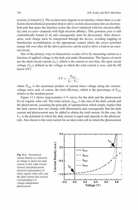
330 S.R. Scully and M.D. McGehee
exciton, is formed [1]. The exciton must migrate to an interface where there is a suf-ficient electrochemical potential drop to drive exciton dissociation into an electron–hole pair that spans the interface across the donor (material with low electron affin-ity) and acceptor (material with high electron affinity). This geminate pair is stillcoulombically bound [2–6] and consequently must be dissociated. After dissoci-ation, each charge must be transported through the device, avoiding trapping orbimolecular recombination, to the appropriate contact where the excess potentialenergy left over after all the above processes can be used to drive a load in an exter-nal circuit.
One of the primary ways to characterize a solar cell is by measuring current as afunction of applied voltage in the dark and under illumination. The figures-of-meritare the short-circuit current (Jsc), which is the current at zero bias, the open circuitvoltage (Voc), defined as the voltage at which the total current is zero, and the fillfactor (FF):
F F = Pmax
Jsc · Voc,
where Pmax is the maximum product of current times voltage along the current–voltage curve and, of course, the total efficiency, which is the percentage of Pmax
relative to the incident power.Figure 11.1 shows representative I–V curves for the dark and the photocurrent
for an organic solar cell. The total current, Jlight, is the sum of the dark current andthe photocurrent, assuming the principle of superposition which simply implies thatthe dark current does not change with illumination and consequently that the darkcurrent and photocurrent may be added to obtain the total current. In this case, theVoc is the potential at which the dark current is equal and opposite to the photocur-rent. Also shown is the total current for an ideal solar cell in which the photocurrent
–0.2 0.0 0.2 0.4 0.6 0.8
–1.0
–0.5
0.0
0.5
Cur
rent
Den
sity
(a.
u.)
Voltage (V)
Jdark
Jphoto
Jlight
Jideal Jsc
Voc
Fig. 11.1 Normalizedcurrent density as a functionof voltage is shown for darkcurrent (solid), light current(dotted) and photocurrent(dashed) representative ofmany organic solar cells, andthe ideal current (fine dotted)corresponding to avoltage-independentphotocurrent
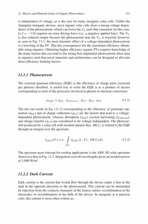
11 Physics and Materials Issues of Organic Photovoltaics 331
is independent of voltage, as is the case for many inorganic solar cells. Unlike thechampion inorganic devices, most organic solar cells show a strong voltage depen-dence of the photocurrent, which can lower the Jsc such that saturation (in this case,to J = −1.0) requires an extra driving force (i.e., a negative applied bias). The Voc
is also reduced simply because the photocurrent near the Voc is lowered; however,as seen in Fig. 11.1, the most dramatic effect of a voltage-dependent photocurrentis a lowering of the FF. This has consequences for the maximum efficiency obtain-able using organics. Obtaining higher efficiency organic PVs requires knowledge ofthe many factors that can lead to the strong bias-dependent photocurrent often seenin organics such that novel materials and architectures can be designed to alleviatethese efficiency limiting factors.
11.2.1 Photocurrent
The external quantum efficiency (EQE) is the efficiency of charge pairs extractedper photons absorbed. A useful way to write the EQE is as a product of factorscorresponding to each of the processes involved in photon-to-electron conversion:
ηE QE = ηabs · ηexharvest · ηCT · ηGS · ηCC (11.1)
The last two terms in Eq. (11.1) corresponding to the efficiency of geminate sep-aration (ηGS) and of charge collection (ηCC) are the factors that lead to a voltage-dependent photocurrent, whereas absorption (ηabs), exciton harvesting (ηexharvest),and charge transfer (ηCT) are considered to be voltage-independent. The photocur-rent produced by a solar cell with incident photon flux, SR(λ), is related to the EQEthrough an integral over the spectrum,
Jphoto(V ) = e ·∫
allλ
ηE QE (λ, V ) · S R (λ) dλ (11.2)
The spectrum most relevant for rooftop applications is the AM1.5G solar spectrumshown as a flux in Fig. 11.2. Integration over all wavelengths gives an incident powerof 1,000 W/m2.
11.2.2 Dark Current
Dark current is the current that would flow through the device under a bias in thedark in the opposite direction as the photocurrent. This current can be dominatedby injection from the contacts, transport of the fastest carrier, recombination at theelectrodes, or recombination in the bulk of the device. In inorganic p–n junctioncells, this current is most often written as:
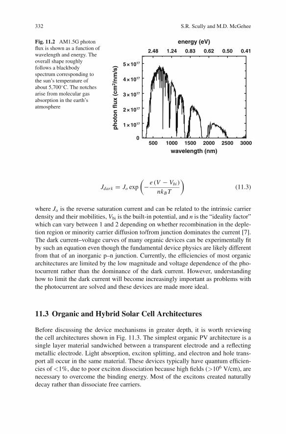
332 S.R. Scully and M.D. McGehee
500 1000 1500 2000 2500 30000
1 × 10¹⁷
2 × 10¹⁷
3 × 10¹⁷
4 × 10¹⁷
5 × 10¹⁷
2.48 1.24 0.83 0.62 0.50 0.41
ph
oto
n f
lux
(cm
2 /n
m/s
)
energy (eV)
wavelength (nm)
Fig. 11.2 AM1.5G photonflux is shown as a function ofwavelength and energy. Theoverall shape roughlyfollows a blackbodyspectrum corresponding tothe sun’s temperature ofabout 5,700◦C. The notchesarise from molecular gasabsorption in the earth’satmosphere
Jdark = Jo exp
(−e (V − Vbi )
nkB T
)(11.3)
where Jo is the reverse saturation current and can be related to the intrinsic carrierdensity and their mobilities, Vbi is the built-in potential, and n is the “ideality factor”which can vary between 1 and 2 depending on whether recombination in the deple-tion region or minority carrier diffusion to/from junction dominates the current [7].The dark current–voltage curves of many organic devices can be experimentally fitby such an equation even though the fundamental device physics are likely differentfrom that of an inorganic p–n junction. Currently, the efficiencies of most organicarchitectures are limited by the low magnitude and voltage dependence of the pho-tocurrent rather than the dominance of the dark current. However, understandinghow to limit the dark current will become increasingly important as problems withthe photocurrent are solved and these devices are made more ideal.
11.3 Organic and Hybrid Solar Cell Architectures
Before discussing the device mechanisms in greater depth, it is worth reviewingthe cell architectures shown in Fig. 11.3. The simplest organic PV architecture is asingle layer material sandwiched between a transparent electrode and a reflectingmetallic electrode. Light absorption, exciton splitting, and electron and hole trans-port all occur in the same material. These devices typically have quantum efficien-cies of <1%, due to poor exciton dissociation because high fields (>106 V/cm), arenecessary to overcome the binding energy. Most of the excitons created naturallydecay rather than dissociate free carriers.
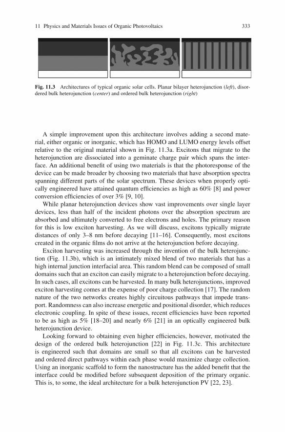
11 Physics and Materials Issues of Organic Photovoltaics 333
Fig. 11.3 Architectures of typical organic solar cells. Planar bilayer heterojunction (left), disor-dered bulk heterojunction (center) and ordered bulk heterojunction (right)
A simple improvement upon this architecture involves adding a second mate-rial, either organic or inorganic, which has HOMO and LUMO energy levels offsetrelative to the original material shown in Fig. 11.3a. Excitons that migrate to theheterojunction are dissociated into a geminate charge pair which spans the inter-face. An additional benefit of using two materials is that the photoresponse of thedevice can be made broader by choosing two materials that have absorption spectraspanning different parts of the solar spectrum. These devices when properly opti-cally engineered have attained quantum efficiencies as high as 60% [8] and powerconversion efficiencies of over 3% [9, 10].
While planar heterojunction devices show vast improvements over single layerdevices, less than half of the incident photons over the absorption spectrum areabsorbed and ultimately converted to free electrons and holes. The primary reasonfor this is low exciton harvesting. As we will discuss, excitons typically migratedistances of only 3–8 nm before decaying [11–16]. Consequently, most excitonscreated in the organic films do not arrive at the heterojunction before decaying.
Exciton harvesting was increased through the invention of the bulk heterojunc-tion (Fig. 11.3b), which is an intimately mixed blend of two materials that has ahigh internal junction interfacial area. This random blend can be composed of smalldomains such that an exciton can easily migrate to a heterojunction before decaying.In such cases, all excitons can be harvested. In many bulk heterojunctions, improvedexciton harvesting comes at the expense of poor charge collection [17]. The randomnature of the two networks creates highly circuitous pathways that impede trans-port. Randomness can also increase energetic and positional disorder, which reduceselectronic coupling. In spite of these issues, recent efficiencies have been reportedto be as high as 5% [18–20] and nearly 6% [21] in an optically engineered bulkheterojunction device.
Looking forward to obtaining even higher efficiencies, however, motivated thedesign of the ordered bulk heterojunction [22] in Fig. 11.3c. This architectureis engineered such that domains are small so that all excitons can be harvestedand ordered direct pathways within each phase would maximize charge collection.Using an inorganic scaffold to form the nanostructure has the added benefit that theinterface could be modified before subsequent deposition of the primary organic.This is, to some, the ideal architecture for a bulk heterojunction PV [22, 23].
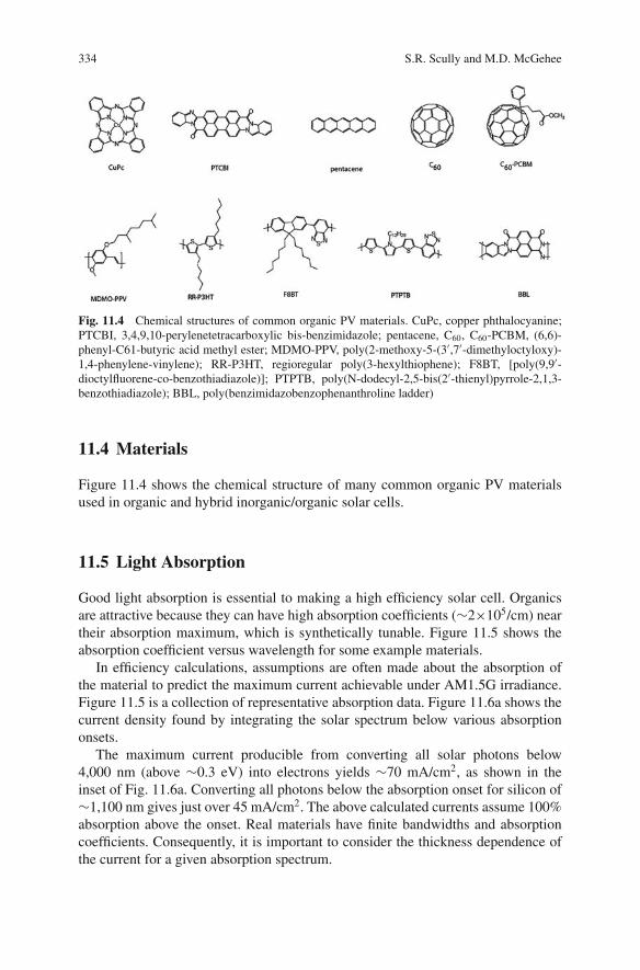
334 S.R. Scully and M.D. McGehee
Fig. 11.4 Chemical structures of common organic PV materials. CuPc, copper phthalocyanine;PTCBI, 3,4,9,10-perylenetetracarboxylic bis-benzimidazole; pentacene, C60, C60-PCBM, (6,6)-phenyl-C61-butyric acid methyl ester; MDMO-PPV, poly(2-methoxy-5-(3′,7′-dimethyloctyloxy)-1,4-phenylene-vinylene); RR-P3HT, regioregular poly(3-hexylthiophene); F8BT, [poly(9,9′-dioctylfluorene-co-benzothiadiazole)]; PTPTB, poly(N-dodecyl-2,5-bis(2′-thienyl)pyrrole-2,1,3-benzothiadiazole); BBL, poly(benzimidazobenzophenanthroline ladder)
11.4 Materials
Figure 11.4 shows the chemical structure of many common organic PV materialsused in organic and hybrid inorganic/organic solar cells.
11.5 Light Absorption
Good light absorption is essential to making a high efficiency solar cell. Organicsare attractive because they can have high absorption coefficients (∼2×10⁵/cm) neartheir absorption maximum, which is synthetically tunable. Figure 11.5 shows theabsorption coefficient versus wavelength for some example materials.
In efficiency calculations, assumptions are often made about the absorption ofthe material to predict the maximum current achievable under AM1.5G irradiance.Figure 11.5 is a collection of representative absorption data. Figure 11.6a shows thecurrent density found by integrating the solar spectrum below various absorptiononsets.
The maximum current producible from converting all solar photons below4,000 nm (above ∼0.3 eV) into electrons yields ∼70 mA/cm2, as shown in theinset of Fig. 11.6a. Converting all photons below the absorption onset for silicon of∼1,100 nm gives just over 45 mA/cm2. The above calculated currents assume 100%absorption above the onset. Real materials have finite bandwidths and absorptioncoefficients. Consequently, it is important to consider the thickness dependence ofthe current for a given absorption spectrum.
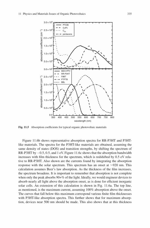
11 Physics and Materials Issues of Organic Photovoltaics 335
350 400 500 550
wavelength (nm)
abso
rptio
n co
effic
ient
(cm
–1)
abso
rptio
n co
effic
ient
(cm
–1)
600 650 700 750 800450
2.0 × 10⁵
2.0 × 10⁵
1.0 × 10⁵
5.0 × 10⁴
3.0 × 10⁵
Ccc
pentacene
CuPcPTCBI
2.5 × 10⁵
1.5 × 10⁵
3.0 × 10⁵
F8BTPTPTBBBL
RR-P3HTMEH-PPV
1.0 × 10⁵
5.0 × 10⁴
0.0
1.5 × 10⁵
2.5 × 10⁵
Fig. 11.5 Absorption coefficients for typical organic photovoltaic materials
Figure 11.6b shows representative absorption spectra for RR-P3HT and P3HT-like materials. The spectra for the P3HT-like materials are obtained, assuming thesame density of states (DOS) and transition strengths, by shifting the spectrum ofRR-P3HT by −0.5, 0.5, and 1 eV. Figure 11.6c shows that the absorption bandwidthincreases with film thickness for the spectrum, which is redshifted by 0.5 eV rela-tive to RR-P3HT. Also shown are the currents found by integrating the absorptionresponse with the solar spectrum. This spectrum has an onset at ∼920 nm. Thiscalculation assumes Beer’s law absorption. As the thickness of the film increases,the spectrum broadens. It is important to remember that absorption is not completewhen only the peak absorbs 90+% of the light. Ideally, we would engineer devices toabsorb nearly all light above the absorption onset, as is done for efficient inorganicsolar cells. An extension of this calculation is shown in Fig. 11.6a. The top line,as mentioned, is the maximum current, assuming 100% absorption above the onset.The curves that fall below this maximum correspond various finite film thicknesseswith P3HT-like absorption spectra. This further shows that for maximum absorp-tion, devices near 500 nm should be made. This also shows that at this thickness
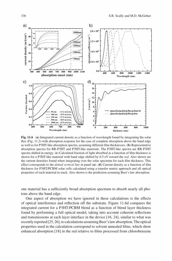
336 S.R. Scully and M.D. McGehee
300 400 500 600 700 800 900 1000 11000
10
20
30
40
50
1000 2000 3000 40000
20
40
60 1000nm
500nm
250nm
100nm
curr
ent
dens
ity
(mA
/cm
2 )
absorption onset (nm)
50nm
a)
400 600 800 1000 1200 14000.0
5.0 × 10⁴
1.0 × 10⁵
1.5 × 10⁵
2.0 × 10⁵
abso
rpti
on c
oeff
icie
nt (
cm –1
)
Wavelength (nm)
b)
400 500 600 700 800 9000.0
0.2
0.4
0.6
0.8
1.0
Fra
ctio
n A
bsor
bed
Wavelength (nm)
50 nm - 13.1 mA/cm2
100 nm - 19.9 mA/cm2
250 nm - 27.5 mA/cm2
500 nm - 30.9 mA/cm2
1000 nm - 32.9 mA/cm2
c)
0 200 400 600 800 10000
2
4
6
8
10
12
14
16
18
glass/ito/pedot/p3ht:pcbm/Alglass/ito/pedot/p3ht:pcbm
J (m
A/c
m 2)
thickness (nm)
d)
Fig. 11.6 (a) Integrated current density as a function of wavelength found by integrating the solarflux (Fig. 11.2) with absorption response for the case of complete absorption above the band edgeas well as for P3HT-like absorption spectra, assuming different film thicknesses. (b) Representativeabsorption spectra for RR-P3HT and P3HT-like materials. The P3HT-like spectra are RR-P3HTspectra shifted in energy. (c) Calculated fraction of light absorbed as a function of film thickness isshown for a P3HT-like material with band edge shifted by 0.5 eV toward the red. Also shown arethe current densities found when integrating over the solar spectrum for each film thickness. Thiseffect corresponds to the dotted vertical line in panel (a). (d) Current density as a function of filmthickness for P3HT/PCBM solar cells calculated using a transfer matrix approach and all opticalproperties of each material in stack. Also shown is the prediction assuming Beer’s law absorption
one material has a sufficiently broad absorption spectrum to absorb nearly all pho-tons above the band edge.
One aspect of absorption we have ignored in these calculations is the effectsof optical interference and reflection off the substrate. Figure 11.6d compares theintegrated current for a P3HT:PCBM blend as a function of blend layer thicknessfound by performing a full optical model, taking into account coherent reflectionsand transmissions at each layer interface in the device [16, 24], similar to what wasrecently reported [25, 26], to calculations assuming Beer’s law absorption. The opticalproperties used in the calculation correspond to solvent annealed films, which showenhanced absorption [18] in the red relative to films processed from chlorobenzene
11 Physics and Materials Issues of Organic Photovoltaics 337
and dried quickly. Optical interference effects give rise to the oscillatory behaviorof the current with blend layer thickness. These effects are strongest for thin films(<200 nm). In fact, comparing the currents for a 50-nm blend layer thickness, we seenearly a factor of 2 increase when including interference effects relative to Beer’slaw absorption. We see for films thicker than this the current calculated for thefull optical model remains below that predicted by Beer’s law. This reduction, of∼1.3 mA/cm2 or ∼8% off the maximum, is primarily due to reflection off the stack.Future work should eventually involve minimizing this reflection by light trapping,antireflective coatings, or surface texturing, as is currently done for silicon [27].
Besides increasing thicknesses to maximize absorption, designing materials withlow bandgaps to more effectively cover the solar spectrum is an obvious route toincrease efficiencies by increasing the maximum possible photocurrent as shown inFig. 11.6a. Numerous excellent reviews on the design and synthesis of low bandgaporganic materials exist [28, 29] and absorption onsets as low as 1,000 nm havebeen reported recently [30–33]. Three synthetic approaches are commonly used tomake low bandgap materials: extending the conjugation, minimizing bond-lengthalternation, and the push–pull approach.
The first of these methods for lowering bandgaps involves designing moleculeswith larger extended pi systems. Anthony et al. has worked with the acene familyand stabilized derivatives of hexacene and heptacene driving the absorption onsetup to 900 nm (1.38 eV) [30]. Calculations show that infinite polyacene chains couldhave an absorption onset above 3,500 nm and some have predicted this to be apotential candidate for a zero gap material [29]. While intuitive, this approach tendsto be synthetically challenging because the molecules become insoluble due to thereduction in configurational entropy in the system.
In some cases, extending the conjugation is not possible because of bond-lengthalternation or breaks in conjugation due to twisting. Consequently, many materialshave bandgaps that saturate with molecular size at or above 2 eV [34]. This brings upthe second route to achieve lower bandgap materials, that is to minimize bond alter-nation. This is sometimes described as making the ground state have more “quinoidcharacter” [29]. Bond-length alternation opens the bandgap of most materials justas it makes intrinsic polyacetylene a semiconductor rather than a metal [35].
The third option to achieve low bandgap materials involves introducing alter-nating electron-rich and electron-poor units onto the conjugated backbone in thepush–pull or donor–acceptor approach.
Figure 11.7 shows how resonance interactions between the units create a com-posite gap that arises primarily from the HOMO of the electron-rich block andthe LUMO of the electron-poor block. This has been hugely successful in tuningbandgaps due to the ease of synthesis [31, 32, 36–38]. Unfortunately, many of thesematerials suffer from poor charge carrier mobilities [33, 36] or large-scale phaseseparation [32] when used in polymer/PCBM devices. Further research is needed toprobe if low mobilities are intrinsic to the push–pull design.
As a last note of caution, one should remember that the shape of the absorp-tion spectrum is not the only important aspect of a prospective material, abso-lute absorption coefficients are equally important. Since optical transitions occur
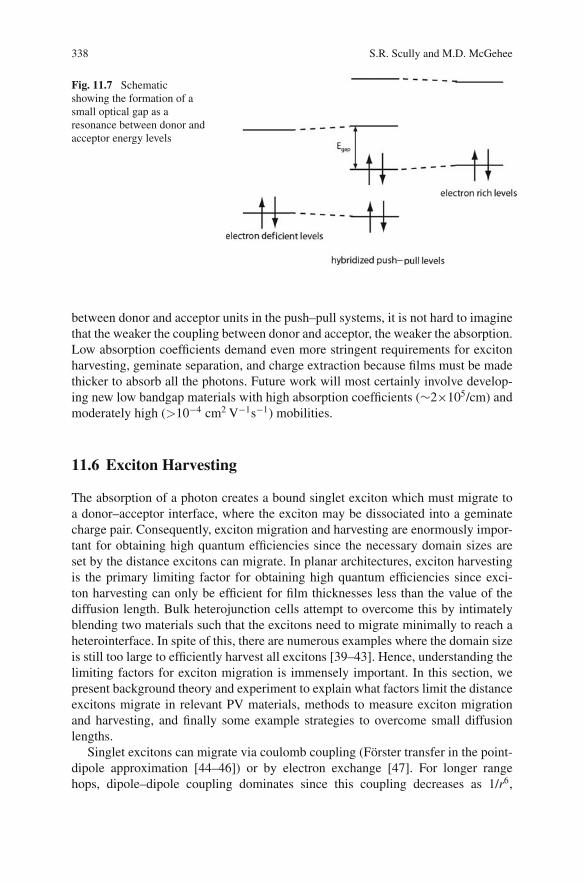
338 S.R. Scully and M.D. McGehee
Fig. 11.7 Schematicshowing the formation of asmall optical gap as aresonance between donor andacceptor energy levels
between donor and acceptor units in the push–pull systems, it is not hard to imaginethat the weaker the coupling between donor and acceptor, the weaker the absorption.Low absorption coefficients demand even more stringent requirements for excitonharvesting, geminate separation, and charge extraction because films must be madethicker to absorb all the photons. Future work will most certainly involve develop-ing new low bandgap materials with high absorption coefficients (∼2×10⁵/cm) andmoderately high (>10−4 cm2 V−1s−1) mobilities.
11.6 Exciton Harvesting
The absorption of a photon creates a bound singlet exciton which must migrate toa donor–acceptor interface, where the exciton may be dissociated into a geminatecharge pair. Consequently, exciton migration and harvesting are enormously impor-tant for obtaining high quantum efficiencies since the necessary domain sizes areset by the distance excitons can migrate. In planar architectures, exciton harvestingis the primary limiting factor for obtaining high quantum efficiencies since exci-ton harvesting can only be efficient for film thicknesses less than the value of thediffusion length. Bulk heterojunction cells attempt to overcome this by intimatelyblending two materials such that the excitons need to migrate minimally to reach aheterointerface. In spite of this, there are numerous examples where the domain sizeis still too large to efficiently harvest all excitons [39–43]. Hence, understanding thelimiting factors for exciton migration is immensely important. In this section, wepresent background theory and experiment to explain what factors limit the distanceexcitons migrate in relevant PV materials, methods to measure exciton migrationand harvesting, and finally some example strategies to overcome small diffusionlengths.
Singlet excitons can migrate via coulomb coupling (Forster transfer in the point-dipole approximation [44–46]) or by electron exchange [47]. For longer rangehops, dipole–dipole coupling dominates since this coupling decreases as 1/r6,
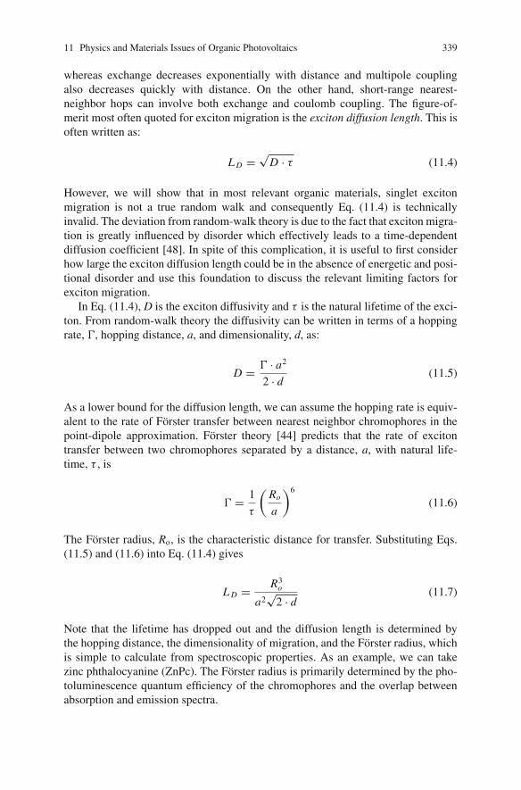
11 Physics and Materials Issues of Organic Photovoltaics 339
whereas exchange decreases exponentially with distance and multipole couplingalso decreases quickly with distance. On the other hand, short-range nearest-neighbor hops can involve both exchange and coulomb coupling. The figure-of-merit most often quoted for exciton migration is the exciton diffusion length. This isoften written as:
L D =√
D · τ (11.4)
However, we will show that in most relevant organic materials, singlet excitonmigration is not a true random walk and consequently Eq. (11.4) is technicallyinvalid. The deviation from random-walk theory is due to the fact that exciton migra-tion is greatly influenced by disorder which effectively leads to a time-dependentdiffusion coefficient [48]. In spite of this complication, it is useful to first considerhow large the exciton diffusion length could be in the absence of energetic and posi-tional disorder and use this foundation to discuss the relevant limiting factors forexciton migration.
In Eq. (11.4), D is the exciton diffusivity and τ is the natural lifetime of the exci-ton. From random-walk theory the diffusivity can be written in terms of a hoppingrate, Γ, hopping distance, a, and dimensionality, d, as:
D = Γ · a2
2 · d(11.5)
As a lower bound for the diffusion length, we can assume the hopping rate is equiv-alent to the rate of Forster transfer between nearest neighbor chromophores in thepoint-dipole approximation. Forster theory [44] predicts that the rate of excitontransfer between two chromophores separated by a distance, a, with natural life-time, τ , is
Γ = 1
τ
(Ro
a
)6
(11.6)
The Forster radius, Ro, is the characteristic distance for transfer. Substituting Eqs.(11.5) and (11.6) into Eq. (11.4) gives
L D = R3o
a2√
2 · d(11.7)
Note that the lifetime has dropped out and the diffusion length is determined bythe hopping distance, the dimensionality of migration, and the Forster radius, whichis simple to calculate from spectroscopic properties. As an example, we can takezinc phthalocyanine (ZnPc). The Forster radius is primarily determined by the pho-toluminescence quantum efficiency of the chromophores and the overlap betweenabsorption and emission spectra.
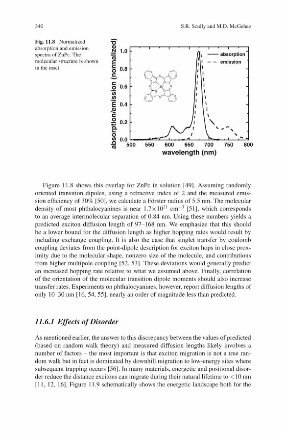
340 S.R. Scully and M.D. McGehee
500 550 600 650 700 750 8000.0
0.2
0.4
0.6
0.8
1.0
abso
rpti
on
/em
issi
on
(n
orm
aliz
ed)
wavelength (nm)
absorption
emission
Fig. 11.8 Normalizedabsorption and emissionspectra of ZnPc. Themolecular structure is shownin the inset
Figure 11.8 shows this overlap for ZnPc in solution [49]. Assuming randomlyoriented transition dipoles, using a refractive index of 2 and the measured emis-sion efficiency of 30% [50], we calculate a Forster radius of 5.5 nm. The moleculardensity of most phthalocyanines is near 1.7×1021 cm−3 [51], which correspondsto an average intermolecular separation of 0.84 nm. Using these numbers yields apredicted exciton diffusion length of 97–168 nm. We emphasize that this shouldbe a lower bound for the diffusion length as higher hopping rates would result byincluding exchange coupling. It is also the case that singlet transfer by coulombcoupling deviates from the point-dipole description for exciton hops in close prox-imity due to the molecular shape, nonzero size of the molecule, and contributionsfrom higher multipole coupling [52, 53]. These deviations would generally predictan increased hopping rate relative to what we assumed above. Finally, correlationof the orientation of the molecular transition dipole moments should also increasetransfer rates. Experiments on phthalocyanines, however, report diffusion lengths ofonly 10–30 nm [16, 54, 55], nearly an order of magnitude less than predicted.
11.6.1 Effects of Disorder
As mentioned earlier, the answer to this discrepancy between the values of predicted(based on random walk theory) and measured diffusion lengths likely involves anumber of factors – the most important is that exciton migration is not a true ran-dom walk but in fact is dominated by downhill migration to low-energy sites wheresubsequent trapping occurs [56]. In many materials, energetic and positional disor-der reduce the distance excitons can migrate during their natural lifetime to <10 nm[11, 12, 16]. Figure 11.9 schematically shows the energetic landscape both for the
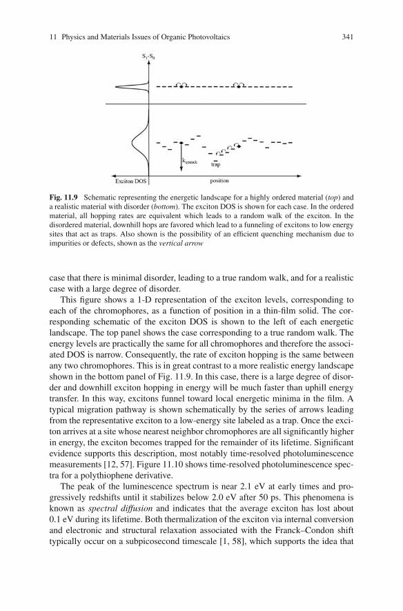
11 Physics and Materials Issues of Organic Photovoltaics 341
Fig. 11.9 Schematic representing the energetic landscape for a highly ordered material (top) anda realistic material with disorder (bottom). The exciton DOS is shown for each case. In the orderedmaterial, all hopping rates are equivalent which leads to a random walk of the exciton. In thedisordered material, downhill hops are favored which lead to a funneling of excitons to low energysites that act as traps. Also shown is the possibility of an efficient quenching mechanism due toimpurities or defects, shown as the vertical arrow
case that there is minimal disorder, leading to a true random walk, and for a realisticcase with a large degree of disorder.
This figure shows a 1-D representation of the exciton levels, corresponding toeach of the chromophores, as a function of position in a thin-film solid. The cor-responding schematic of the exciton DOS is shown to the left of each energeticlandscape. The top panel shows the case corresponding to a true random walk. Theenergy levels are practically the same for all chromophores and therefore the associ-ated DOS is narrow. Consequently, the rate of exciton hopping is the same betweenany two chromophores. This is in great contrast to a more realistic energy landscapeshown in the bottom panel of Fig. 11.9. In this case, there is a large degree of disor-der and downhill exciton hopping in energy will be much faster than uphill energytransfer. In this way, excitons funnel toward local energetic minima in the film. Atypical migration pathway is shown schematically by the series of arrows leadingfrom the representative exciton to a low-energy site labeled as a trap. Once the exci-ton arrives at a site whose nearest neighbor chromophores are all significantly higherin energy, the exciton becomes trapped for the remainder of its lifetime. Significantevidence supports this description, most notably time-resolved photoluminescencemeasurements [12, 57]. Figure 11.10 shows time-resolved photoluminescence spec-tra for a polythiophene derivative.
The peak of the luminescence spectrum is near 2.1 eV at early times and pro-gressively redshifts until it stabilizes below 2.0 eV after 50 ps. This phenomena isknown as spectral diffusion and indicates that the average exciton has lost about0.1 eV during its lifetime. Both thermalization of the exciton via internal conversionand electronic and structural relaxation associated with the Franck–Condon shifttypically occur on a subpicosecond timescale [1, 58], which supports the idea that
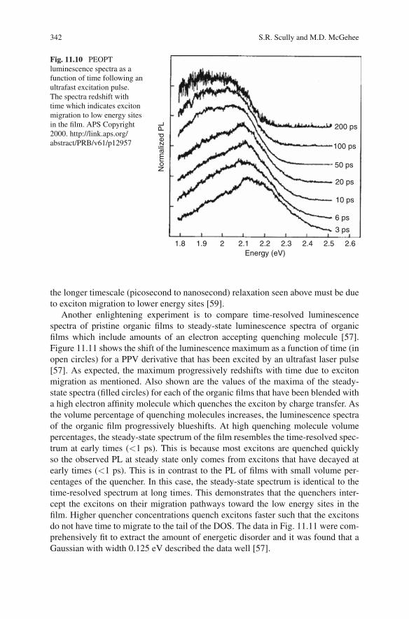
342 S.R. Scully and M.D. McGehee
200 ps
100 ps
50 ps
20 ps
10 ps
6 ps
3 ps
Energy (eV)
Nor
mal
ized
PL
1.8 1.9 2 2.1 2.2 2.3 2.4 2.5 2.6
Fig. 11.10 PEOPTluminescence spectra as afunction of time following anultrafast excitation pulse.The spectra redshift withtime which indicates excitonmigration to low energy sitesin the film. APS Copyright2000. http://link.aps.org/abstract/PRB/v61/p12957
the longer timescale (picosecond to nanosecond) relaxation seen above must be dueto exciton migration to lower energy sites [59].
Another enlightening experiment is to compare time-resolved luminescencespectra of pristine organic films to steady-state luminescence spectra of organicfilms which include amounts of an electron accepting quenching molecule [57].Figure 11.11 shows the shift of the luminescence maximum as a function of time (inopen circles) for a PPV derivative that has been excited by an ultrafast laser pulse[57]. As expected, the maximum progressively redshifts with time due to excitonmigration as mentioned. Also shown are the values of the maxima of the steady-state spectra (filled circles) for each of the organic films that have been blended witha high electron affinity molecule which quenches the exciton by charge transfer. Asthe volume percentage of quenching molecules increases, the luminescence spectraof the organic film progressively blueshifts. At high quenching molecule volumepercentages, the steady-state spectrum of the film resembles the time-resolved spec-trum at early times (<1 ps). This is because most excitons are quenched quicklyso the observed PL at steady state only comes from excitons that have decayed atearly times (<1 ps). This is in contrast to the PL of films with small volume per-centages of the quencher. In this case, the steady-state spectrum is identical to thetime-resolved spectrum at long times. This demonstrates that the quenchers inter-cept the excitons on their migration pathways toward the low energy sites in thefilm. Higher quencher concentrations quench excitons faster such that the excitonsdo not have time to migrate to the tail of the DOS. The data in Fig. 11.11 were com-prehensively fit to extract the amount of energetic disorder and it was found that aGaussian with width 0.125 eV described the data well [57].
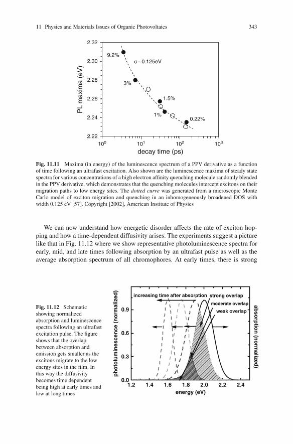
11 Physics and Materials Issues of Organic Photovoltaics 343
2.32
2.30
2.28
2.26
2.24
PL
max
ima
(eV
)
2.22100 101 102 103
0.22%
1.5%
1%
3%
9.2%σ ~ 0.125eV
decay time (ps)
Fig. 11.11 Maxima (in energy) of the luminescence spectrum of a PPV derivative as a functionof time following an ultrafast excitation. Also shown are the luminescence maxima of steady statespectra for various concentrations of a high electron affinity quenching molecule randomly blendedin the PPV derivative, which demonstrates that the quenching molecules intercept excitons on theirmigration paths to low energy sites. The dotted curve was generated from a microscopic MonteCarlo model of exciton migration and quenching in an inhomogeneously broadened DOS withwidth 0.125 eV [57]. Copyright [2002], American Institute of Physics
We can now understand how energetic disorder affects the rate of exciton hop-ping and how a time-dependent diffusivity arises. The experiments suggest a picturelike that in Fig. 11.12 where we show representative photoluminescence spectra forearly, mid, and late times following absorption by an ultrafast pulse as well as theaverage absorption spectrum of all chromophores. At early times, there is strong
1.2 1.4 1.6 1.8 2.0 2.2 2.40.0
0.3
0.6
0.9 weak overlap
moderate overlap
increasing time after absorption
abso
rptio
n (n
orm
alized)
ph
oto
lum
ines
cen
ce (
no
rmal
ized
)
energy (eV)
strong overlap
Fig. 11.12 Schematicshowing normalizedabsorption and luminescencespectra following an ultrafastexcitation pulse. The figureshows that the overlapbetween absorption andemission gets smaller as theexcitons migrate to the lowenergy sites in the film. Inthis way the diffusivitybecomes time dependentbeing high at early times andlow at long times
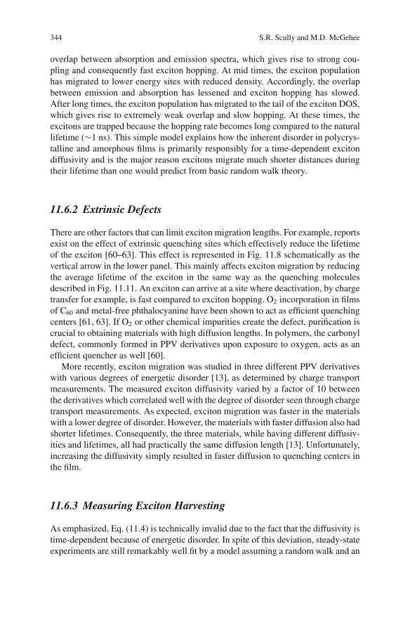
344 S.R. Scully and M.D. McGehee
overlap between absorption and emission spectra, which gives rise to strong cou-pling and consequently fast exciton hopping. At mid times, the exciton populationhas migrated to lower energy sites with reduced density. Accordingly, the overlapbetween emission and absorption has lessened and exciton hopping has slowed.After long times, the exciton population has migrated to the tail of the exciton DOS,which gives rise to extremely weak overlap and slow hopping. At these times, theexcitons are trapped because the hopping rate becomes long compared to the naturallifetime (∼1 ns). This simple model explains how the inherent disorder in polycrys-talline and amorphous films is primarily responsibly for a time-dependent excitondiffusivity and is the major reason excitons migrate much shorter distances duringtheir lifetime than one would predict from basic random walk theory.
11.6.2 Extrinsic Defects
There are other factors that can limit exciton migration lengths. For example, reportsexist on the effect of extrinsic quenching sites which effectively reduce the lifetimeof the exciton [60–63]. This effect is represented in Fig. 11.8 schematically as thevertical arrow in the lower panel. This mainly affects exciton migration by reducingthe average lifetime of the exciton in the same way as the quenching moleculesdescribed in Fig. 11.11. An exciton can arrive at a site where deactivation, by chargetransfer for example, is fast compared to exciton hopping. O2 incorporation in filmsof C60 and metal-free phthalocyanine have been shown to act as efficient quenchingcenters [61, 63]. If O2 or other chemical impurities create the defect, purification iscrucial to obtaining materials with high diffusion lengths. In polymers, the carbonyldefect, commonly formed in PPV derivatives upon exposure to oxygen, acts as anefficient quencher as well [60].
More recently, exciton migration was studied in three different PPV derivativeswith various degrees of energetic disorder [13], as determined by charge transportmeasurements. The measured exciton diffusivity varied by a factor of 10 betweenthe derivatives which correlated well with the degree of disorder seen through chargetransport measurements. As expected, exciton migration was faster in the materialswith a lower degree of disorder. However, the materials with faster diffusion also hadshorter lifetimes. Consequently, the three materials, while having different diffusiv-ities and lifetimes, all had practically the same diffusion length [13]. Unfortunately,increasing the diffusivity simply resulted in faster diffusion to quenching centers inthe film.
11.6.3 Measuring Exciton Harvesting
As emphasized, Eq. (11.4) is technically invalid due to the fact that the diffusivity istime-dependent because of energetic disorder. In spite of this deviation, steady-stateexperiments are still remarkably well fit by a model assuming a random walk and an
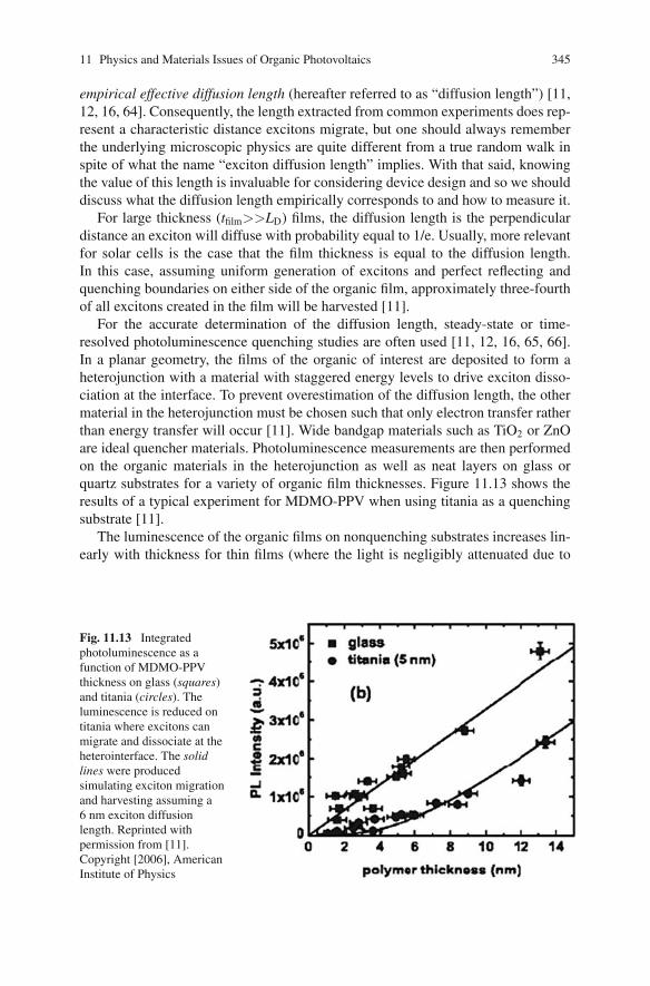
11 Physics and Materials Issues of Organic Photovoltaics 345
empirical effective diffusion length (hereafter referred to as “diffusion length”) [11,12, 16, 64]. Consequently, the length extracted from common experiments does rep-resent a characteristic distance excitons migrate, but one should always rememberthe underlying microscopic physics are quite different from a true random walk inspite of what the name “exciton diffusion length” implies. With that said, knowingthe value of this length is invaluable for considering device design and so we shoulddiscuss what the diffusion length empirically corresponds to and how to measure it.
For large thickness (tfilm>>LD) films, the diffusion length is the perpendiculardistance an exciton will diffuse with probability equal to 1/e. Usually, more relevantfor solar cells is the case that the film thickness is equal to the diffusion length.In this case, assuming uniform generation of excitons and perfect reflecting andquenching boundaries on either side of the organic film, approximately three-fourthof all excitons created in the film will be harvested [11].
For the accurate determination of the diffusion length, steady-state or time-resolved photoluminescence quenching studies are often used [11, 12, 16, 65, 66].In a planar geometry, the films of the organic of interest are deposited to form aheterojunction with a material with staggered energy levels to drive exciton disso-ciation at the interface. To prevent overestimation of the diffusion length, the othermaterial in the heterojunction must be chosen such that only electron transfer ratherthan energy transfer will occur [11]. Wide bandgap materials such as TiO2 or ZnOare ideal quencher materials. Photoluminescence measurements are then performedon the organic materials in the heterojunction as well as neat layers on glass orquartz substrates for a variety of organic film thicknesses. Figure 11.13 shows theresults of a typical experiment for MDMO-PPV when using titania as a quenchingsubstrate [11].
The luminescence of the organic films on nonquenching substrates increases lin-early with thickness for thin films (where the light is negligibly attenuated due to
Fig. 11.13 Integratedphotoluminescence as afunction of MDMO-PPVthickness on glass (squares)and titania (circles). Theluminescence is reduced ontitania where excitons canmigrate and dissociate at theheterointerface. The solidlines were producedsimulating exciton migrationand harvesting assuming a6 nm exciton diffusionlength. Reprinted withpermission from [11].Copyright [2006], AmericanInstitute of Physics
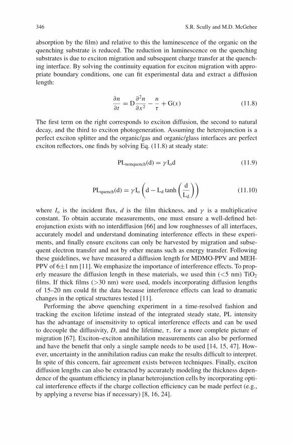
346 S.R. Scully and M.D. McGehee
absorption by the film) and relative to this the luminescence of the organic on thequenching substrate is reduced. The reduction in luminescence on the quenchingsubstrates is due to exciton migration and subsequent charge transfer at the quench-ing interface. By solving the continuity equation for exciton migration with appro-priate boundary conditions, one can fit experimental data and extract a diffusionlength:
∂n
∂t= D
∂2n
∂x2− n
τ+ G(x) (11.8)
The first term on the right corresponds to exciton diffusion, the second to naturaldecay, and the third to exciton photogeneration. Assuming the heterojunction is aperfect exciton splitter and the organic/gas and organic/glass interfaces are perfectexciton reflectors, one finds by solving Eq. (11.8) at steady state:
PLnonquench(d) = γ Iod (11.9)
PLquench(d) = γ Io
(d − Ld tanh
(d
Ld
))(11.10)
where Io is the incident flux, d is the film thickness, and γ is a multiplicativeconstant. To obtain accurate measurements, one must ensure a well-defined het-erojunction exists with no interdiffusion [66] and low roughnesses of all interfaces,accurately model and understand dominating interference effects in these experi-ments, and finally ensure excitons can only be harvested by migration and subse-quent electron transfer and not by other means such as energy transfer. Followingthese guidelines, we have measured a diffusion length for MDMO-PPV and MEH-PPV of 6±1 nm [11]. We emphasize the importance of interference effects. To prop-erly measure the diffusion length in these materials, we used thin (<5 nm) TiO2
films. If thick films (>30 nm) were used, models incorporating diffusion lengthsof 15–20 nm could fit the data because interference effects can lead to dramaticchanges in the optical structures tested [11].
Performing the above quenching experiment in a time-resolved fashion andtracking the exciton lifetime instead of the integrated steady state, PL intensityhas the advantage of insensitivity to optical interference effects and can be usedto decouple the diffusivity, D, and the lifetime, τ , for a more complete picture ofmigration [67]. Exciton–exciton annihilation measurements can also be performedand have the benefit that only a single sample needs to be used [14, 15, 47]. How-ever, uncertainty in the annihilation radius can make the results difficult to interpret.In spite of this concern, fair agreement exists between techniques. Finally, excitondiffusion lengths can also be extracted by accurately modeling the thickness depen-dence of the quantum efficiency in planar heterojunction cells by incorporating opti-cal interference effects if the charge collection efficiency can be made perfect (e.g.,by applying a reverse bias if necessary) [8, 16, 24].
11 Physics and Materials Issues of Organic Photovoltaics 347
In bulk heterojunction cells, a simple litmus test to determine the exciton har-vesting efficiency is to compare luminescence, normalized by absorption, of adonor–acceptor blend to that of a neat organic film [68–71]. The fraction of lumi-nescence quenched directly gives an upper bound for the quantum efficiency. Whilean extremely simple test, care must still be taken as optical interference effects,scattering, and changes in morphology can invalidate this measurement.
11.6.4 Approaches to Overcome Small Diffusion Lengths
We have already discussed bulk heterojunction cells which were originally designedfor the specific purpose of harvesting more excitons. For example, PCBM blendedwith the polymer, MDMO-PPV, quenches (>95%) the luminescence of the polymerat only 1% PCBM loading. At 50% PCBM loading, the photoinduced absorptionsignature of radical anions which are formed after charge transfer in the polymerform in under 50 femtoseconds [72]. Such fast kinetics imply the exciton mustalready be formed adjacent to one or more PCBM molecules. In this case, mini-mal migration, if any, is necessary for efficient exciton harvesting. Another extremeexample where exciton harvesting is near perfect is the dye-sensitized solar cell[73]. In this architecture, the exciton is created in a Ru-dye which is anchored tothe electron acceptor titania. Consequently, the excitons are all created right nextto the titania. This is surely the reason why ultrafast electron transfer from the dyeto titania has also been observed in this system [74].
While some bulk heterojunction systems have high exciton harvesting efficien-cies, others have domains too large for efficient exciton harvesting. As mentionedearlier, disordered heterojunctions can have other problems such as poor chargetransport. It is therefore often believed that a more ordered structure is better. Inboth planar heterojunctions and current ordered bulk heterojunctions, exciton har-vesting is far from perfect. Two major approaches have been used to increase excitonharvesting.
The first approach is to employ triplets by choosing materials with high inter-system crossing rates. Triplet excitons are long lived (∼100 ns–1 ms) relative tosinglet excitons (0.1–10 ns). Consequently, they have more time to migrate anddetrap if stuck at low energy sites. A diffusion length of 40 nm was reported for C60
and attributed to the formation of triplets [16]. Others have used metal-centeredcomplexes to ensure high intersystem crossing rates due to spin–orbit coupling.Enhanced harvesting efficiencies were reported when using the common phospho-rescent OLED material PtOEP and a diffusion length near 20 nm was qualitativelyextracted [75]. More recently, a novel white light OLED architecture was designedand utilizes long-range triplet migration [76]. Also of interest is the technique usedto measure the triplet diffusion length of materials incorporated in the OLED [77].Since these triplet excitons (like many) were nonemissive, a phosphorescent antennawas incorporated that accepts excitons and phosphoresces upon exciton capture. Inthis way, the same thickness dependence study as described above can be performed,
348 S.R. Scully and M.D. McGehee
but the time-resolved phosphorescence of the antenna layer is monitored as a func-tion of the triplet material thickness rather than tracking the luminescence of thetriplet material itself.
While employing triplet diffusion can enhance exciton harvesting, this can comeat the expense of a loss in energy when converting the singlet to triplet. The singlet–triplet splitting of energy levels, due to electron exchange, is often 0.5–0.8 eV [78].This loss reduces the maximum voltage obtainable using these materials. C60 hasbeen reported to have an exchange loss of only 0.15 eV [79, 80]. An extremely novelapproach would be to use exciton fission of the singlet exciton to two triplet excitons[81]. Using this scheme, the exchange energy would not be lost and would insteadbe stored in a second exciton. Only if the exchange energy can be minimized (as inC60) or utilized (through exciton fission for example) will it be practical to utilizetriplets to achieve high efficiencies.
A novel approach our group has been pursuing is to use hetero-energy transferto enhance exciton harvesting [82, 83]. By incorporating a thin highly absorbinglayer which has an absorption spectrum overlapping the emission spectrum of thedonor material at the heterojunction, singlet excitons can be harvested over 30 nmaway. Figure 11.14 shows exciton harvesting measurements for our model systemof DOW Red (as energy donor) and PTPTB (as energy acceptor).
The inset shows the strong overlap in emission and absorption spectra necessaryfor efficient energy transfer. This high exciton harvesting at very large distancesis due to the increased dimensionality of the system. The rate of energy transfergoes as 1/x3 [84, 85] instead of 1/r6 [44] because the total rate of energy transfer isdetermined by the sum of all excited chromophore–acceptor pairs. Here, x is chosento emphasize that the distance is the perpendicular one from the exciton (exciteddonor) to acceptor sheet rather than a radial distance, r, as it is between two point
0 20 40 60 80 100 1200.0
0.2
0.4
0.6
0.8
1.0
Fra
ctio
n E
xcit
on
s H
arve
sted
donor (DOW Red) film thickness (nm)
0 600 700 8000.0
0.2
0.4
0.6
0.8
1.0
Ab
s/P
L (
no
rm.)
wavelength (nm)
Fig. 11.14 Fraction ofexcitons photogenerated inDOW Red film on a thin filmof the energy acceptorPTPTB as a function ofDOW Red film thickness.The inset shows the overlapbetween emission of DOWRed and absorption ofPTPTB. The solid linecorresponds to an effectivediffusion length of 27 nm
11 Physics and Materials Issues of Organic Photovoltaics 349
dipoles. This approach looks extremely promising due to the effectiveness in long-range exciton harvesting and straightforward design criteria for materials choice.
With this said, abundant opportunities exist to increase exciton harvesting bycontrolling the nanomorphology of bulk heterojunctions, through the design of bet-ter ordered bulk heterojunction architectures, by employing triplet materials withsmall exchange losses, using resonant energy transfer, or by designing materialswith higher intrinsic diffusion lengths. For the latter, reducing energetic disorder,minimizing relaxation processes by choosing stiff materials, and using synthesesand materials processing which minimize contaminants that are responsible forforming quenching centers are all necessary to obtain high diffusion lengths andconsequently high quantum efficiencies.
11.7 Exciton Dissociation
Following exciton migration, exciton splitting must occur to obtain extractable elec-trons and holes. Paramount to this discussion is the issue of the exciton bindingenergy. While formerly controversial, there appears to be a consensus that absorp-tion of a photon creates a bound exciton in most organic materials [86–89]. Reportsof the binding energy have ranged between 0.3 and 1.4 eV depending on the mate-rial [88–90]. This binding energy is often associated with the attractive coulombicenergy between the photoexcited electron and hole. As an example, two oppositepoint charges separated 1.2 nm in a medium of dielectric constant ε ∼ 4 correspondsto a coulombic binding energy of 0.3 eV, whereas a separation of 5 Angstroms corre-sponds to a binding energy of 0.72 eV. More precise calculations involving discretepartial charges have shown these qualitative predictions to be close to reality [89].
Comparison of photoelectron spectroscopy, which gives the energy levels asso-ciated with the positively and negatively charged molecules, with the optical spectraoffers a way to measure this energy difference. UPS and IPES have been employedto identify the energy levels associated with the free hole and electron, respectively.The gap between these levels is the so-called transport gap. Similar measurementsof the transport gap can be performed using scanning tunneling microscopy [89]as well as cyclic voltametry. Comparison between this gap and the optical bandgapalways shows the optical gap to be smaller.
This is easily understood by recognizing that the exciton is composed of anelectron coulombically attracted to a hole and hence stabilized relative to the caseinvolving the free, separated (infinitely apart), pair. Simply subtracting the opticalgap from the transport gap gives the binding energy.
The exciton binding energy is often associated with the energy drop necessaryat a donor–acceptor interface to split the exciton. We note a few discrepancies withthis interpretation. The first, as will be discussed in greater detail in the follow-ing section, is that after splitting the exciton, the geminate charge pair is often stillstrongly bound due to the close proximity of the charges to each other. In other
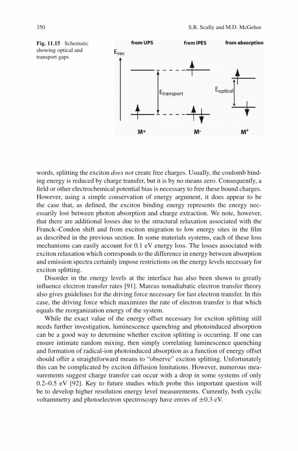
350 S.R. Scully and M.D. McGehee
Fig. 11.15 Schematicshowing optical andtransport gaps
words, splitting the exciton does not create free charges. Usually, the coulomb bind-ing energy is reduced by charge transfer, but it is by no means zero. Consequently, afield or other electrochemical potential bias is necessary to free these bound charges.However, using a simple conservation of energy argument, it does appear to bethe case that, as defined, the exciton binding energy represents the energy nec-essarily lost between photon absorption and charge extraction. We note, however,that there are additional losses due to the structural relaxation associated with theFranck–Condon shift and from exciton migration to low energy sites in the filmas described in the previous section. In some materials systems, each of these lossmechanisms can easily account for 0.1 eV energy loss. The losses associated withexciton relaxation which corresponds to the difference in energy between absorptionand emission spectra certainly impose restrictions on the energy levels necessary forexciton splitting.
Disorder in the energy levels at the interface has also been shown to greatlyinfluence electron transfer rates [91]. Marcus nonadiabatic electron transfer theoryalso gives guidelines for the driving force necessary for fast electron transfer. In thiscase, the driving force which maximizes the rate of electron transfer is that whichequals the reorganization energy of the system.
While the exact value of the energy offset necessary for exciton splitting stillneeds further investigation, luminescence quenching and photoinduced absorptioncan be a good way to determine whether exciton splitting is occurring. If one canensure intimate random mixing, then simply correlating luminescence quenchingand formation of radical-ion photoinduced absorption as a function of energy offsetshould offer a straightforward means to “observe” exciton splitting. Unfortunatelythis can be complicated by exciton diffusion limitations. However, numerous mea-surements suggest charge transfer can occur with a drop in some systems of only0.2–0.5 eV [92]. Key to future studies which probe this important question willbe to develop higher resolution energy level measurements. Currently, both cyclicvoltammetry and photoelectron spectroscopy have errors of ±0.3 eV.
11 Physics and Materials Issues of Organic Photovoltaics 351
11.8 Dissociating Geminate Pairs
While early in the field it was thought that charges were free immediately followingexciton splitting, a large consensus has grown that this is not the case. Immediatelyfollowing exciton splitting, a geminate charge pair spans the donor–acceptor inter-face and is separated by ∼1–3 nm [2–4, 6]. This necessarily implies the charge pairsare strongly coulombically bound due to the low dielectric constants of the materialsand the small extent of the electronic wavefunctions associated with these charges.For efficient PV operation, these charge pairs must be separated efficiently.
The charge transfer process at a donor–acceptor heterojunction has beenexplained to be analogous to the autoionization and subsequent thermalization pro-cesses of “hot excitons” in molecular crystals [1, 3]. Upon charge transfer, the excessenergy of the transferred charge due to the band offsets is lost in discrete scatter-ing events, which convert electrochemical potential energy of the charges into localmolecular vibrational energy. The charges thermalize through these events and cometo rest some distance away from the interface and from each other. This character-istic distance, known as the thermalization radius, then determines the coulombbinding energy of the geminate pair via the coulomb potential:
Egp = 1
4πεo · εr
e
rth(11.11)
Geminate recombination has come to be viewed as one of the major loss mecha-nisms in organic PVs. In the “single photon regime” (i.e., at low light intensity),separation of geminate pairs will be the dominant process that determines the shapeof the photocurrent versus the voltage curve. In this regime at low light intensitybimolecular recombination and space charge can be made inconsequential. Thequantum efficiency is therefore only limited by the separation of the geminate pair,assuming efficient photon and exciton harvesting. FF in small molecule heterojunc-tions and polymer/PCBM cells have been shown to be limited by geminate sep-aration [3, 4]. Normalized photocurrent versus applied field directly measures theprobability of separation versus field.
Onsager-type models of separation have been invoked to explain the probabil-ity of separating the geminate pairs that span a donor–acceptor interface followingexciton dissociation [2–4, 6]. General to all models is that the charges are coulom-bically attracted to each other and, through stochastic motion, undergo a biasedrandom walk. Field, mobility, disorder, dielectric constant, binding energy, back-transfer time, and geometry are all important factors that influence the likelihoodof pair separation. To first order, separation occurs when the carriers are outside oftheir Onsager radius:
ro = e
4πεoε
1
kB T(11.12)
352 S.R. Scully and M.D. McGehee
which is the separation distance at which the coulomb binding energy of the pairbecomes approximately equal to the thermal energy, that is ∼kBT.
Geminate separation in polymer/PCBM devices has been modeled using an aver-age continuum model that reproduces the field and temperature dependence of thisparticular device [4]. Key to the model is that a distribution of thermalization dis-tances and consequently a distribution of binding energies, due to inherent disorderin these systems, are necessary to explain the observed current–voltage character-istics. Spatially averaged mobilities and dielectric constant are used and a back-transfer time, corresponding to the rate of recombination when the electron andhole reside on neighboring molecules, must be assumed.
This last point is more delicate than it might be assumed at first since mostrecombination measurements (transient photovoltage or transient photoinducedabsorption) involve measuring the full kinetics of the recombination process (biasedrandom walk plus back transfer) rather than only the interfacial back-transfer time.Molecular dyads in solution have been studied and their back-transfer kinetics canserve as useful guides; however, there are potential large differences between thesedynamics in solution and in the solid state [52, 93–97].
Monte Carlo simulations have also been used to predict the charge separationdynamics on the microscopic scale [3, 6]. The models only assume average dielec-tric properties and all other parameters are treated microscopically. Geometry is animportant parameter in these dynamics as the electrons and holes are energeticallyconfined to their own phase such that a donor–acceptor interface increases the like-lihood of charge pair separation [3]. Asymmetry in the dynamics of charge hoppinghas also been suggested to lead to high separation efficiencies because the likelihoodof the electron and hole meeting on neighboring sites is reduced [3].
Common to all three reported models is that the ratio of charge carrier hop-ping rate to back-transfer rate is an important parameter since this determinesthe probability of survival when the carriers arrive on adjacent molecules. Forexample, a mobility of 10−4 cm2 V−1s−1 corresponds to a hopping rate of about5 hops/ns assuming the Einstein relation, 3-D diffusion, and a hopping distance of5 Angstroms. Each hop takes ∼200 ps. If the back-transfer time were also 200 ps,each time a geminate pair sits next to each other they would have about a 50%probability of recombining and a 50% probability of hopping away from each other.Were the back-transfer time instead 2 ns, the probability of recombination would bereduced to 10%. Some fullerene–porphyrin dyads have shown back-transfer timesas long as 200 μs [98]. If this were representative of back transfer in a bulk hetero-junction, the likelihood of recombination would be extremely reduced. The longerthe back-transfer time is, the more chances the geminate pairs will have to climb outof their coulomb potential wells.
Another crucial but poorly understood parameter which influences geminate sep-aration is the thermalization distance as this determines the pair’s binding energy.It has been suggested that the thermalization distance should be related to the bandoffset and ultimately to the excess energy between relaxed excitons and relaxedgeminate charge pairs however no thorough study exists that probes this hypothesis
11 Physics and Materials Issues of Organic Photovoltaics 353
[3]. The excess electrochemical potential energy is partially converted to help thegeminate pairs climb out of their mutual coulomb potential wells. It is unknown howefficient this conversion is; however, evidence suggests that it is likely inefficientbecause exciton splitting across heterojunctions with band offsets near 1 eV stillproduce geminate pairs with binding energies of 0.2–0.3 eV rather than free carriers[3, 4, 6, 99]. This implies that much of the excess potential energy is lost to heat inthe form of molecular vibrations.
One of the most recent studies probing these physics reported on the dynam-ics of transient photoconductivity and transient photoinduced absorption for blendsof MDMO-PPV/PCBM and methyl-substituted ladder-type poly(p-phenylene)(MeLPPP)/PCBM [100]. MeLPPP is more rigid and is energetically more orderedthan MDMO-PPV. MeLPPP also has a high bandgap relative to MDMO-PPV andconsequently a larger energy offset at the polymer/PCBM interface. It was reportedthat the geminate pairs in the MDMO-PPV/PCBM blend have a higher probabil-ity of separating than in MeLPPP/PCBM blends and this was attributed to a largerthermalization radius and lower binding energy of the geminate pairs in the MDMO-PPV blend compared to the MeLPPP blend. This is despite a lower band offset in theMDMO-PPV/PCBM blend and implies a more complicated relationship betweenband offset and thermalization distance.
Charge separation following exciton splitting can also be inhibited through theformation of an exciplex state which if significantly more stable than the chargeseparated state will trap the charges until back transfer occurs [5, 101]. Figure 11.16shows a schematic describing the energetics of this situation.
Two blend systems were recently investigated: PFB:F8BT and TFB:F8BT [5]. Inboth blends, photopumping the F8BT results in the formation of a new luminescencespectrum that is not a simple linear combination of the neat layer luminescence forthe polymers that comprise the blend. The new spectrum is broad and redshiftedrelative to the spectra of the pure materials and has a characteristic lifetime of itsown. The interpretation of this phenomena was that the spectrum arises from anintermolecular excited state, termed an exciplex, composed of an electron on anacceptor molecule and a hole on a neighboring donor molecule. Diode structureswere fabricated to investigate the field dependence of the luminescence dynamics ofthe excimer. The generation of the exciplex was found to be highly field-dependentbut the luminescence decay corresponding to the exciplex lifetime was found to befield-independent. Potential energy curves are shown for the ground state system,the state with excited acceptor (F8BT), and the state which has the electron residingon the acceptor and the hole residing on the donor. The field dependence of theexciplex generation is explained by suggesting a “spectroscopically dark” geminatepair is always created following exciton dissociation. This pair can be dissociated bya field or can collapse into a highly stable exciplex whereafter it can regenerate bulkF8BT excitons with a thermal activation energy ranging between 0.1 and 0.3 eV.These findings are relevant for geminate splitting as collapse to an exciplex offersan alternate route to back transfer during the dynamics of geminate migration andseparation.
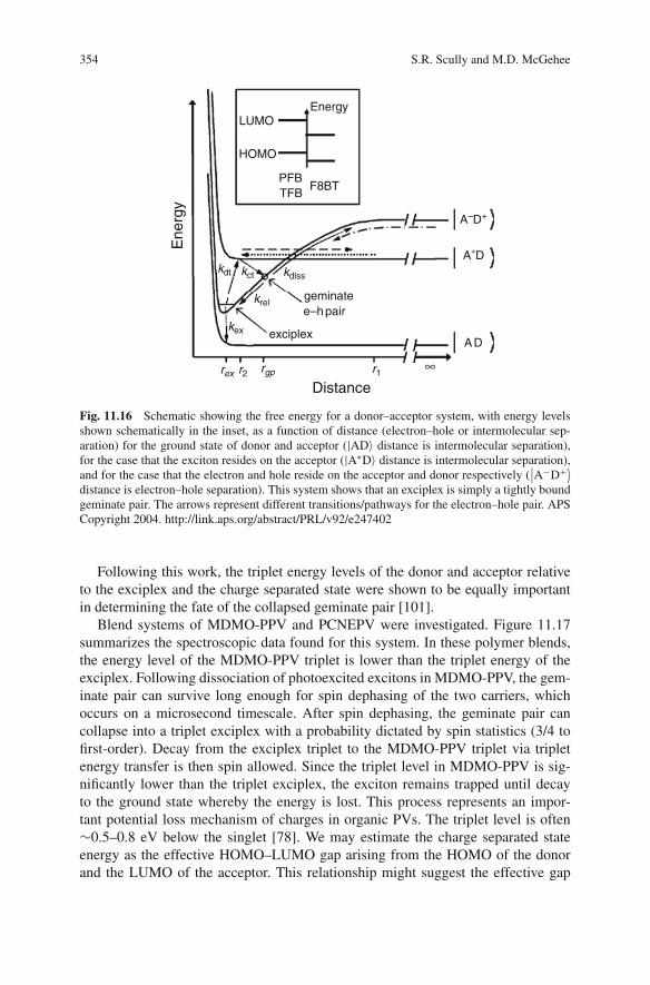
354 S.R. Scully and M.D. McGehee
LUMO
HOMO
PFBTFB
F8BT
A–D+
A∗D
∞A D
geminatee–h pair
Distance
Ene
rgy
exciplex
krel
kex
rex r2 r1rgp
kdt kct kdlss
Energy
Fig. 11.16 Schematic showing the free energy for a donor–acceptor system, with energy levelsshown schematically in the inset, as a function of distance (electron–hole or intermolecular sep-aration) for the ground state of donor and acceptor (|AD〉 distance is intermolecular separation),for the case that the exciton resides on the acceptor (|A∗D〉 distance is intermolecular separation),and for the case that the electron and hole reside on the acceptor and donor respectively (
∣∣A−D+⟩distance is electron–hole separation). This system shows that an exciplex is simply a tightly boundgeminate pair. The arrows represent different transitions/pathways for the electron–hole pair. APSCopyright 2004. http://link.aps.org/abstract/PRL/v92/e247402
Following this work, the triplet energy levels of the donor and acceptor relativeto the exciplex and the charge separated state were shown to be equally importantin determining the fate of the collapsed geminate pair [101].
Blend systems of MDMO-PPV and PCNEPV were investigated. Figure 11.17summarizes the spectroscopic data found for this system. In these polymer blends,the energy level of the MDMO-PPV triplet is lower than the triplet energy of theexciplex. Following dissociation of photoexcited excitons in MDMO-PPV, the gem-inate pair can survive long enough for spin dephasing of the two carriers, whichoccurs on a microsecond timescale. After spin dephasing, the geminate pair cancollapse into a triplet exciplex with a probability dictated by spin statistics (3/4 tofirst-order). Decay from the exciplex triplet to the MDMO-PPV triplet via tripletenergy transfer is then spin allowed. Since the triplet level in MDMO-PPV is sig-nificantly lower than the triplet exciplex, the exciton remains trapped until decayto the ground state whereby the energy is lost. This process represents an impor-tant potential loss mechanism of charges in organic PVs. The triplet level is often∼0.5–0.8 eV below the singlet [78]. We may estimate the charge separated stateenergy as the effective HOMO–LUMO gap arising from the HOMO of the donorand the LUMO of the acceptor. This relationship might suggest the effective gap
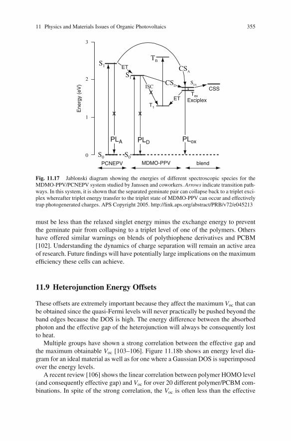
11 Physics and Materials Issues of Organic Photovoltaics 355
CSD
CSA
Sex
Tn
S1
ISC
PLA
PCNEPV
Ene
rgy
(eV
)
MDMO-PPV blend
x x
x
PLD PLox
Tex
T1
ET
ET
Exciplex
CSS
S0S0
S1
3
2
1
0
Fig. 11.17 Jablonski diagram showing the energies of different spectroscopic species for theMDMO-PPV/PCNEPV system studied by Janssen and coworkers. Arrows indicate transition path-ways. In this system, it is shown that the separated geminate pair can collapse back to a triplet exci-plex whereafter triplet energy transfer to the triplet state of MDMO-PPV can occur and effectivelytrap photogenerated charges. APS Copyright 2005. http://link.aps.org/abstract/PRB/v72/e045213
must be less than the relaxed singlet energy minus the exchange energy to preventthe geminate pair from collapsing to a triplet level of one of the polymers. Othershave offered similar warnings on blends of polythiophene derivatives and PCBM[102]. Understanding the dynamics of charge separation will remain an active areaof research. Future findings will have potentially large implications on the maximumefficiency these cells can achieve.
11.9 Heterojunction Energy Offsets
These offsets are extremely important because they affect the maximum Voc that canbe obtained since the quasi-Fermi levels will never practically be pushed beyond theband edges because the DOS is high. The energy difference between the absorbedphoton and the effective gap of the heterojunction will always be consequently lostto heat.
Multiple groups have shown a strong correlation between the effective gap andthe maximum obtainable Voc [103–106]. Figure 11.18b shows an energy level dia-gram for an ideal material as well as for one where a Gaussian DOS is superimposedover the energy levels.
A recent review [106] shows the linear correlation between polymer HOMO level(and consequently effective gap) and Voc for over 20 different polymer/PCBM com-binations. In spite of the strong correlation, the Voc is often less than the effective
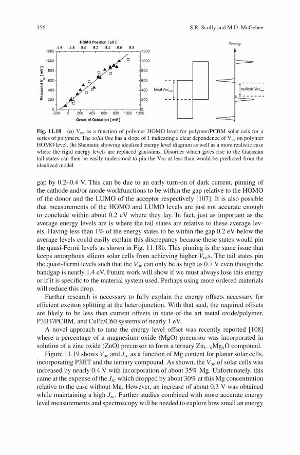
356 S.R. Scully and M.D. McGehee
Fig. 11.18 (a) Voc as a function of polymer HOMO level for polymer/PCBM solar cels for aseries of polymers. The solid line has a slope of 1 indicating a clear dependence of Voc on polymerHOMO level. (b) Shematic showing idealized energy level diagram as well as a more realistic casewhere the rigid energy levels are replaced gaussians. Disorder which gives rise to the Gaussiantail states can then be easily understood to pin the Voc at less than would be predicted from theidealized model
gap by 0.2–0.4 V. This can be due to an early turn-on of dark current, pinning ofthe cathode and/or anode workfunctions to be within the gap relative to the HOMOof the donor and the LUMO of the acceptor respectively [107]. It is also possiblethat measurements of the HOMO and LUMO levels are just not accurate enoughto conclude within about 0.2 eV where they lay. In fact, just as important as theaverage energy levels are is where the tail states are relative to these average lev-els. Having less than 1% of the energy states to be within the gap 0.2 eV below theaverage levels could easily explain this discrepancy because these states would pinthe quasi-Fermi levels as shown in Fig. 11.18b. This pinning is the same issue thatkeeps amorphous silicon solar cells from achieving higher Vocs. The tail states pinthe quasi-Fermi levels such that the Voc can only be as high as 0.7 V even though thebandgap is nearly 1.4 eV. Future work will show if we must always lose this energyor if it is specific to the material system used. Perhaps using more ordered materialswill reduce this drop.
Further research is necessary to fully explain the energy offsets necessary forefficient exciton splitting at the heterojunction. With that said, the required offsetsare likely to be less than current offsets in state-of-the art metal oxide/polymer,P3HT/PCBM, and CuPc/C60 systems of nearly 1 eV.
A novel approach to tune the energy level offset was recently reported [108]where a percentage of a magnesium oxide (MgO) precursor was incorporated insolution of a zinc oxide (ZnO) precursor to form a ternary Zn1−xMgxO compound.
Figure 11.19 shows Voc and Jsc as a function of Mg content for planar solar cells,incorporating P3HT and the ternary compound. As shown, the Voc of solar cells wasincreased by nearly 0.4 V with incorporation of about 35% Mg. Unfortunately, thiscame at the expense of the Jsc which dropped by about 30% at this Mg concentrationrelative to the case without Mg. However, an increase of about 0.3 V was obtainedwhile maintaining a high Jsc. Further studies combined with more accurate energylevel measurements and spectroscopy will be needed to explore how small an energy
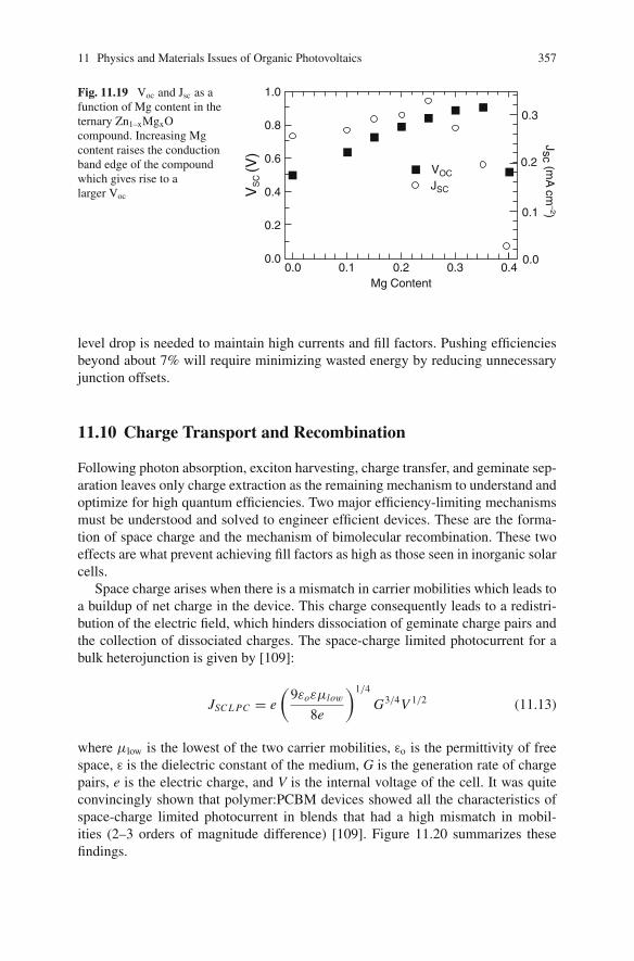
11 Physics and Materials Issues of Organic Photovoltaics 357
1.0
0.8
0.6
0.4VS
C (V
)
JSC
VOC
0.2
0.00.0
0.00.1
0.1
0.2
0.2
Jsc (mA
cm–2)
Mg Content0.3
0.3
0.4
Fig. 11.19 Voc and Jsc as afunction of Mg content in theternary Zn1–xMgxOcompound. Increasing Mgcontent raises the conductionband edge of the compoundwhich gives rise to alarger Voc
level drop is needed to maintain high currents and fill factors. Pushing efficienciesbeyond about 7% will require minimizing wasted energy by reducing unnecessaryjunction offsets.
11.10 Charge Transport and Recombination
Following photon absorption, exciton harvesting, charge transfer, and geminate sep-aration leaves only charge extraction as the remaining mechanism to understand andoptimize for high quantum efficiencies. Two major efficiency-limiting mechanismsmust be understood and solved to engineer efficient devices. These are the forma-tion of space charge and the mechanism of bimolecular recombination. These twoeffects are what prevent achieving fill factors as high as those seen in inorganic solarcells.
Space charge arises when there is a mismatch in carrier mobilities which leads toa buildup of net charge in the device. This charge consequently leads to a redistri-bution of the electric field, which hinders dissociation of geminate charge pairs andthe collection of dissociated charges. The space-charge limited photocurrent for abulk heterojunction is given by [109]:
JSC L PC = e
(9εoεμlow
8e
)1/4
G3/4V 1/2 (11.13)
where μlow is the lowest of the two carrier mobilities, εo is the permittivity of freespace, ε is the dielectric constant of the medium, G is the generation rate of chargepairs, e is the electric charge, and V is the internal voltage of the cell. It was quiteconvincingly shown that polymer:PCBM devices showed all the characteristics ofspace-charge limited photocurrent in blends that had a high mismatch in mobil-ities (2–3 orders of magnitude difference) [109]. Figure 11.20 summarizes thesefindings.
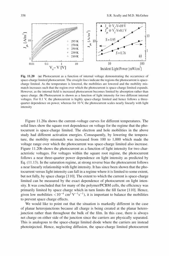
358 S.R. Scully and M.D. McGehee
Fig. 11.20 (a) Photocurrent as a function of internal voltage demonstrating the occurrence ofspace-charge limited photocurrent. The straight lines indicate the regions the photocurrent is space-charge limited. As the temperature is lowered, the mobilities are lowered and the mobility mis-match increases such that the region over which the photocurrent is space-charge limited expands.However, as the internal field is increased photocurrent becomes limited by absorption rather thanspace charge. (b) Photocurrent is shown as a function of light intensity for two different internalvoltages. For 0.1 V, the photocurrent is highly space-charge limited and hence follows a three-quarter dependence on power, whereas for 10 V, the photocurrent scales nearly linearly with lightintensity
Figure 11.20a shows the current–voltage curves for different temperatures. Thesolid lines show the square root dependence on voltage for the regime that the pho-tocurrent is space-charge limited. The electron and hole mobilities in the abovestudy had different activation energies. Consequently, by lowering the tempera-ture, the mobility mismatch was increased from 100 to 1,000 which made thevoltage range over which the photocurrent was space-charge limited also increase.Figure 11.20b shows the photocurrent as a function of light intensity for two char-acteristic voltages. For voltages within the square root regime, the photocurrentfollows a near three-quarter power dependence on light intensity as predicted byEq. (11.13). In the saturation regime, at strong reverse bias the photocurrent followsa near linearly relationship with light intensity. It has since been shown that the pho-tocurrent versus light intensity can fall in a regime where it is limited to some extent,but not fully, by space charge [110]. The extent to which the current is space-chargelimited can be measured by the exact dependence of photocurrent on light inten-sity. It was concluded that for many of the polymer/PCBM cells, the efficiency wasprimarily limited by space charge which in turn limits the fill factor [110]. Hence,given low mobilities <10−4 cm2 V−1s−1), it is important to balance the mobilitiesto prevent space charge effects.
We would like to point out that the situation is markedly different in the caseof planar heterojunctions because all charge is being created at the planar hetero-junction rather than throughout the bulk of the film. In this case, there is alwaysnet charge on either side of the junction since the carriers are physically separated.This is analogous to the space-charge limited diode where the carriers are insteadphotoinjected. Hence, neglecting diffusion, the space-charge limited photocurrent
11 Physics and Materials Issues of Organic Photovoltaics 359
should simply follow Child’s law:
JSC LC = 9
8ε · εoμlow
V 2
L3low
(11.14)
where μlow and Llow are the mobility and the layer thickness, respectively, of thelow mobility material. In this case, space charge can become a problem even if themobilities are matched.
For the case that the mobilities are matched and high enough, the only othermechanism by which charge carriers can be lost is through bimolecular recom-bination. This involves nongeminate electrons which recombine with holes as thecarriers traverse the device to their respective electrodes. Usually in organics withelectron density, n, and hole density, p, the recombination rate (in # of carriers cm−3
s−1) is given by:
R = −βnp (11.15)
11.10.1 Diffusion-Limited Recombination
As has been reported [2, 111, 112], recombination in most organic cells appears tofollow Langevin-like kinetics. In this case, β is given as:
β = 〈μh + μe〉eεo 〈ε〉 (11.16)
where the brackets indicate “spatial average”. This corresponds to a “diffusion-limited” scenario wherein the rate of recombination is limited by the rate an electronand hole meet.
Langevin recombination has been successful in modeling the recombination cur-rent in single layer OLEDs. Recently, however, a deviation from Langevin kinet-ics in bulk heterojunction cells was reported [112] and it was explained that therecombination rate is limited by the slowest carrier, rather than the fastest as above,because the carriers are confined to their own phase – electrons in fullerene andholes in polymer. Replacing the spatial average of the mobility with the mobility ofthe slowest carrier reproduced the current–voltage curves. Understanding the roleof morphology and geometry on recombination will surely be important in the nearfuture.
While recombination is rarely unimportant in most solar cell architecturesthe effects of space charge and geminate separation have largely overshadowedthe importance of bimolecular recombination in organic bulk heterojunctions.However, as these architectures are made more efficient by choosing materialswhich yield efficient geminate separation and high mobilities (which consequently
360 S.R. Scully and M.D. McGehee
eliminate space charge), bimolecular recombination will then be left as the top cul-prit for limiting efficiencies.
Already in 100-nm-thick MDMO-PPV:PCBM blends, it is estimated that at themaximum power point nearly 25% of the photogenerated charge carriers bimolecu-larly recombine [113]. It has been shown that the importance of bimolecular recom-bination will increase at greater device thicknesses because the carriers must betransported further and hence will be more likely to recombine. It is not obviousjust from Eq. (11.16) whether an increase in mobility would lead to an increaseor decrease of bimolecular recombination. Increasing mobility would lead to fasterextraction, but the recombination coefficient would also increase in proportion tothe mobility. However, it is important to recognize that the steady-state carrier den-sity also varies with mobility. For similar generation rates, increasing the mobilityleads to a reduction in the steady-state carrier concentration. This effect outweighsthe increase in bimolecular rate constant such that for higher mobilities bimolecularrecombination is lessened.
11.10.2 Interface-Limited (Back Transfer Limited) Recombination
A few other options exist for increasing the FF which in the case of efficient gem-inate separation and in the absence of space charge would be limited by recom-bination. Designing materials with higher dielectric constants may also be a routeto reduce recombination. Otherwise, to exceed these efficiency limits we need todesign devices that have recombination which is not diffusion limited. Diffusion-limited recombination implies the interfacial back-transfer rate, corresponding tothe electron and hole sitting on adjacent molecules, is not limiting. Therefore, if asystem can be designed such that the back-transfer rate becomes limiting, and weare in an interface limited regime, recombination rates can be slowed to even lessthan that predicted by Langevin theory. This concept has been investigated exten-sively in the dye-sensitized architecture. One recent study [93] is summarized inFig. 11.21.
By adjusting, through molecular design, the spatial location of the HOMO wave-function of the dye relative to the surface titania, the recombination rate from pho-toinjected electrons in the titania through back transfer to the dye can be changed byfive orders of magnitude. These findings clearly indicate that the recombination rateis interface rather than diffusion limited in this system. The solid line in Fig. 2.21is an exponential fit and can be understood by considering the basic nonadiabaticMarcus electron transfer equation:
kET ∝ exp (−β · r ) exp
(− (ΔGo + λ)2
4λkB T
)(11.17)
The first exponential represents the electronic coupling between the dye wave-functions and the titania wavefunctions and contains the distance dependence. The
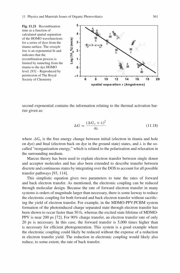
11 Physics and Materials Issues of Organic Photovoltaics 361
Fig. 11.21 Recombinationtime as a function ofcalculated spatial separationof the HOMO wavefunctionsfor a series of dyes from thetitania surface. The straightline is an exponential fit andindicates that therecombination process islimited by tunneling from thetitania to the dye HOMOlevel. [93] – Reproduced bypermission of The RoyalSociety of Chemistry
second exponential contains the information relating to the thermal activation bar-rier given as:
ΔG = (ΔGo + λ)2
4λ(11.18)
where ΔGo is the free energy change between initial (electron in titania and holeon dye) and final (electron back on dye in the ground state) states, and λ is the so-called “reorganization energy,” which is related to the polarization and relaxation inthe surrounding medium.
Marcus theory has been used to explain electron transfer between single donorand acceptor molecules and has also been extended to describe transfer betweendiscrete and continuous states by integrating over the DOS to account for all possibletransfer pathways [93, 114].
This simplistic equation gives two parameters to tune the rates of forwardand back electron transfer. As mentioned, the electronic coupling can be reducedthrough molecular design. Because the rate of forward electron transfer in manysystems is orders of magnitude larger than necessary, there is some leeway to reducethe electronic coupling for both forward and back electron transfer without sacrific-ing the yield of electron transfer. For example, in the MDMO-PPV:PCBM systemformation of the photoinduced charge separated state through electron transfer hasbeen shown to occur faster than 50 fs, whereas the excited state lifetime of MDMO-PPV is near 200 ps [72]. For 90% charge transfer, an electron transfer rate of only20 ps is necessary. In this case, the forward transfer is 5,000 times higher thanis necessary for efficient photogeneration. This system is a good example wherethe electronic coupling could likely be reduced without the expense of a reductionin electron transfer yield. The reduction in electronic coupling would likely alsoreduce, to some extent, the rate of back transfer.
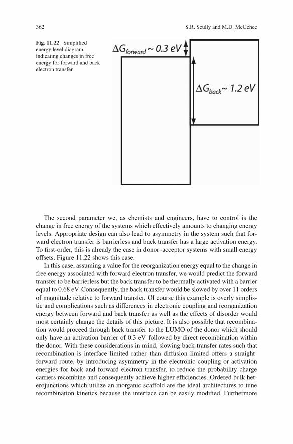
362 S.R. Scully and M.D. McGehee
Fig. 11.22 Simplifiedenergy level diagramindicating changes in freeenergy for forward and backelectron transfer
The second parameter we, as chemists and engineers, have to control is thechange in free energy of the systems which effectively amounts to changing energylevels. Appropriate design can also lead to asymmetry in the system such that for-ward electron transfer is barrierless and back transfer has a large activation energy.To first-order, this is already the case in donor–acceptor systems with small energyoffsets. Figure 11.22 shows this case.
In this case, assuming a value for the reorganization energy equal to the change infree energy associated with forward electron transfer, we would predict the forwardtransfer to be barrierless but the back transfer to be thermally activated with a barrierequal to 0.68 eV. Consequently, the back transfer would be slowed by over 11 ordersof magnitude relative to forward transfer. Of course this example is overly simplis-tic and complications such as differences in electronic coupling and reorganizationenergy between forward and back transfer as well as the effects of disorder wouldmost certainly change the details of this picture. It is also possible that recombina-tion would proceed through back transfer to the LUMO of the donor which shouldonly have an activation barrier of 0.3 eV followed by direct recombination withinthe donor. With these considerations in mind, slowing back-transfer rates such thatrecombination is interface limited rather than diffusion limited offers a straight-forward route, by introducing asymmetry in the electronic coupling or activationenergies for back and forward electron transfer, to reduce the probability chargecarriers recombine and consequently achieve higher efficiencies. Ordered bulk het-erojunctions which utilize an inorganic scaffold are the ideal architectures to tunerecombination kinetics because the interface can be easily modified. Furthermore
11 Physics and Materials Issues of Organic Photovoltaics 363
one can engineer systems such that molecules attach in a preferential geometry tothe scaffold, thereby better controlling the electronic coupling.
11.10.3 Measurements Relevant for Extracting Charge
One of the most important and informative measurements one can do to investigatecharge extraction issues is to measure the charge carrier mobilities. Because of thehigh degree of disorder and consequent field-dependent mobilities, measurementsof mobility corresponding to the carrier densities found in working solar cells underone sun are most relevant. The mobility can vary by four orders of magnitude simplybecause of the differences in carrier density [115, 116]. Mobilities at lower densi-ties are usually lower because low energy sites are not occupied and consequentlytend to trap charges as they traverse the films, whereas at high carrier density trapscan be filled which leads to higher measured mobilities. Time-of-flight (TOF) orspace-charge limited diode (SCLD) measurements are the best options for obtainingmeaningful numbers because the carrier densities in these experiments are similarto densities in solar cells under one sun illumination (1015/cm3). Thin-film transis-tor (TFT) mobilities are less relevant because the charge carrier density is higher(1019/cm3).
Some effort has been made to focus on mobility studies relevant for solar cells.Using TOF, it was shown that slowing the kinetics of film formation of RR-P3HT:PCBM films led to a balancing of electron and hole mobilities [18]. Usingsimilar processing, the hole mobility in the RR-P3HT, measured in SCLDs, wasshown to increase by a factor of 33 to 5×10⁻³ cm2 V−1s−1 [117]. We have shownthat aligning polymer chains in anodic alumina can increase the mobility by aboutthis amount as well and found that, due to the increase in dielectric constant, thespace-charge limitations were reduced which led to higher currents through thestructures than the SCLC of neat films of similar thickness even though less vol-ume was occupied by polymer [118]. Development of high mobility materials testedunder relevant conditions is ongoing and still needed.
Recombination times are most commonly measured by transient photoinducedabsorption [74, 93], transient photovoltage [119, 120], or impedence spectroscopy[121]. Transient microwave photoconductivity [122], charge extraction in linearlyincreasing voltage (CELIV), modified TOF [111], as well as time-delayed col-lection field [123] experiments offer other alternatives to measure back-transfertimes. Key to these experiments is understanding the recombination mechanisms toproperly interpret the data. Transient photoinduced absorption monitors the kinet-ics of the total photoinduced charge population, whereas transient photovoltageappears only to measure the mobile population which reach the electrodes. All ofthese experiments can likely mask the interfacial back-transfer kinetics since thediffusion-limited kinetics often occur on a longer timescale. In this regard, tran-sient photoinduced absorption experiments that involve molecular dyads in solutionare ideal to measure back-transfer times [93–96, 98], in spite of the fact that the
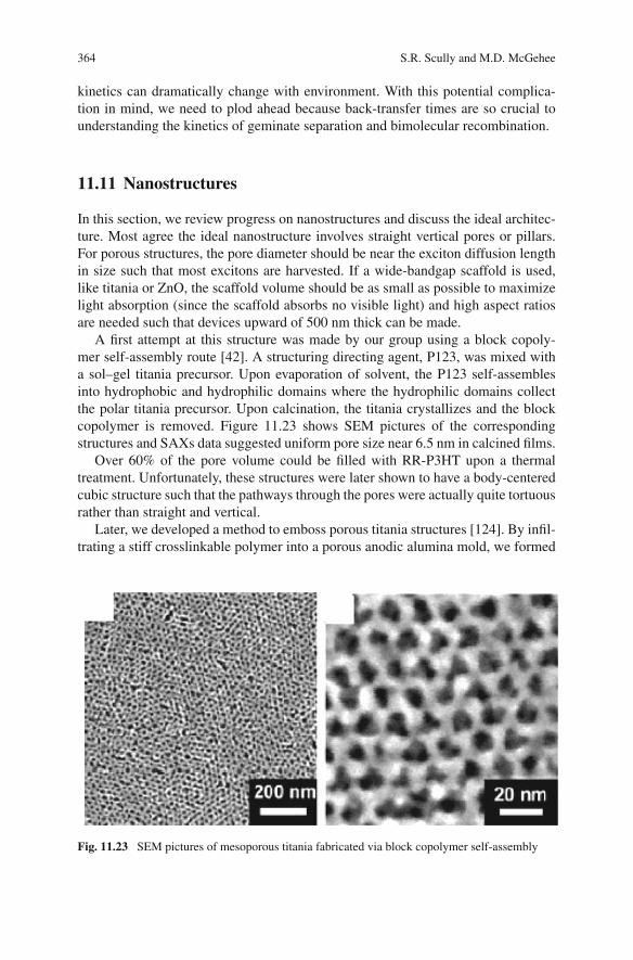
364 S.R. Scully and M.D. McGehee
kinetics can dramatically change with environment. With this potential complica-tion in mind, we need to plod ahead because back-transfer times are so crucial tounderstanding the kinetics of geminate separation and bimolecular recombination.
11.11 Nanostructures
In this section, we review progress on nanostructures and discuss the ideal architec-ture. Most agree the ideal nanostructure involves straight vertical pores or pillars.For porous structures, the pore diameter should be near the exciton diffusion lengthin size such that most excitons are harvested. If a wide-bandgap scaffold is used,like titania or ZnO, the scaffold volume should be as small as possible to maximizelight absorption (since the scaffold absorbs no visible light) and high aspect ratiosare needed such that devices upward of 500 nm thick can be made.
A first attempt at this structure was made by our group using a block copoly-mer self-assembly route [42]. A structuring directing agent, P123, was mixed witha sol–gel titania precursor. Upon evaporation of solvent, the P123 self-assemblesinto hydrophobic and hydrophilic domains where the hydrophilic domains collectthe polar titania precursor. Upon calcination, the titania crystallizes and the blockcopolymer is removed. Figure 11.23 shows SEM pictures of the correspondingstructures and SAXs data suggested uniform pore size near 6.5 nm in calcined films.
Over 60% of the pore volume could be filled with RR-P3HT upon a thermaltreatment. Unfortunately, these structures were later shown to have a body-centeredcubic structure such that the pathways through the pores were actually quite tortuousrather than straight and vertical.
Later, we developed a method to emboss porous titania structures [124]. By infil-trating a stiff crosslinkable polymer into a porous anodic alumina mold, we formed
Fig. 11.23 SEM pictures of mesoporous titania fabricated via block copolymer self-assembly
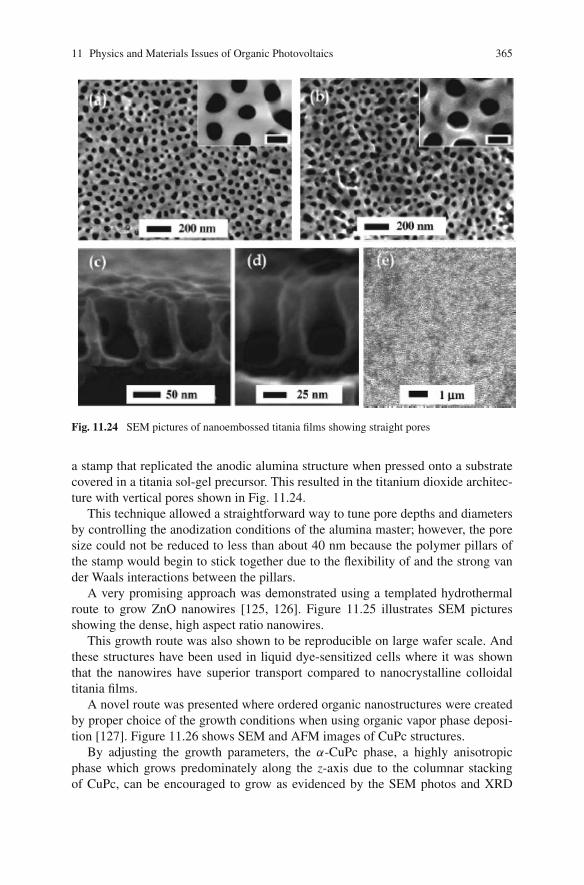
11 Physics and Materials Issues of Organic Photovoltaics 365
Fig. 11.24 SEM pictures of nanoembossed titania films showing straight pores
a stamp that replicated the anodic alumina structure when pressed onto a substratecovered in a titania sol-gel precursor. This resulted in the titanium dioxide architec-ture with vertical pores shown in Fig. 11.24.
This technique allowed a straightforward way to tune pore depths and diametersby controlling the anodization conditions of the alumina master; however, the poresize could not be reduced to less than about 40 nm because the polymer pillars ofthe stamp would begin to stick together due to the flexibility of and the strong vander Waals interactions between the pillars.
A very promising approach was demonstrated using a templated hydrothermalroute to grow ZnO nanowires [125, 126]. Figure 11.25 illustrates SEM picturesshowing the dense, high aspect ratio nanowires.
This growth route was also shown to be reproducible on large wafer scale. Andthese structures have been used in liquid dye-sensitized cells where it was shownthat the nanowires have superior transport compared to nanocrystalline colloidaltitania films.
A novel route was presented where ordered organic nanostructures were createdby proper choice of the growth conditions when using organic vapor phase deposi-tion [127]. Figure 11.26 shows SEM and AFM images of CuPc structures.
By adjusting the growth parameters, the α-CuPc phase, a highly anisotropicphase which grows predominately along the z-axis due to the columnar stackingof CuPc, can be encouraged to grow as evidenced by the SEM photos and XRD
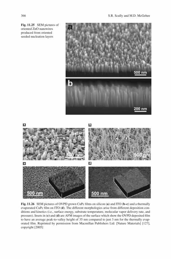
366 S.R. Scully and M.D. McGehee
Fig. 11.25 SEM pictures oforiented ZnO nanowiresproduced from orientedseeded nucleation layers
Fig. 11.26 SEM pictures of OVPD grown CuPc films on silicon (a) and ITO (b–c) and a thermallyevaporated CuPc film on ITO (d). The different morphologies arise from different deposition con-ditions and kinetics (i.e., surface energy, substrate temperature, molecular vapor delivery rate, andpressure). Insets in (c) and (d) are AFM images of the surface which show the OVPD deposited filmto have an average peak-to-valley height of 35 nm compared to just 3 nm for the thermally evap-orated film. Reprinted by permission from Macmillan Publishers Ltd: [Nature Materials] [127],copyright [2005]
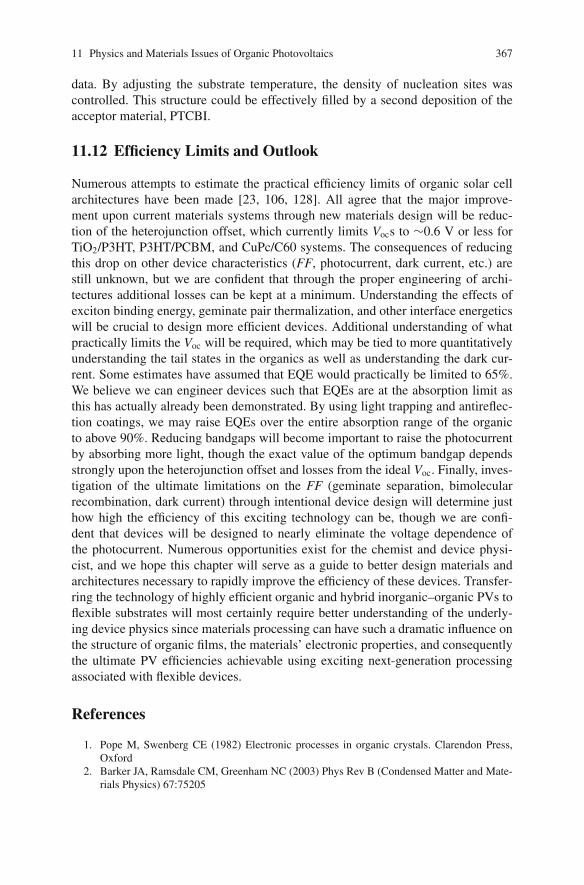
11 Physics and Materials Issues of Organic Photovoltaics 367
data. By adjusting the substrate temperature, the density of nucleation sites wascontrolled. This structure could be effectively filled by a second deposition of theacceptor material, PTCBI.
11.12 Efficiency Limits and Outlook
Numerous attempts to estimate the practical efficiency limits of organic solar cellarchitectures have been made [23, 106, 128]. All agree that the major improve-ment upon current materials systems through new materials design will be reduc-tion of the heterojunction offset, which currently limits Vocs to ∼0.6 V or less forTiO2/P3HT, P3HT/PCBM, and CuPc/C60 systems. The consequences of reducingthis drop on other device characteristics (FF, photocurrent, dark current, etc.) arestill unknown, but we are confident that through the proper engineering of archi-tectures additional losses can be kept at a minimum. Understanding the effects ofexciton binding energy, geminate pair thermalization, and other interface energeticswill be crucial to design more efficient devices. Additional understanding of whatpractically limits the Voc will be required, which may be tied to more quantitativelyunderstanding the tail states in the organics as well as understanding the dark cur-rent. Some estimates have assumed that EQE would practically be limited to 65%.We believe we can engineer devices such that EQEs are at the absorption limit asthis has actually already been demonstrated. By using light trapping and antireflec-tion coatings, we may raise EQEs over the entire absorption range of the organicto above 90%. Reducing bandgaps will become important to raise the photocurrentby absorbing more light, though the exact value of the optimum bandgap dependsstrongly upon the heterojunction offset and losses from the ideal Voc. Finally, inves-tigation of the ultimate limitations on the FF (geminate separation, bimolecularrecombination, dark current) through intentional device design will determine justhow high the efficiency of this exciting technology can be, though we are confi-dent that devices will be designed to nearly eliminate the voltage dependence ofthe photocurrent. Numerous opportunities exist for the chemist and device physi-cist, and we hope this chapter will serve as a guide to better design materials andarchitectures necessary to rapidly improve the efficiency of these devices. Transfer-ring the technology of highly efficient organic and hybrid inorganic–organic PVs toflexible substrates will most certainly require better understanding of the underly-ing device physics since materials processing can have such a dramatic influence onthe structure of organic films, the materials’ electronic properties, and consequentlythe ultimate PV efficiencies achievable using exciting next-generation processingassociated with flexible devices.
References
1. Pope M, Swenberg CE (1982) Electronic processes in organic crystals. Clarendon Press,Oxford
2. Barker JA, Ramsdale CM, Greenham NC (2003) Phys Rev B (Condensed Matter and Mate-rials Physics) 67:75205
368 S.R. Scully and M.D. McGehee
3. Peumans P, Forrest SR (2004) Chem Phys Lett 398:274. Mihailetchi VD, Koster LJA, Hummelen JC, Blom PWM (2004) Phys Rev Lett 93:2166015. Morteani AC, Sreearunothai P, Herz LM, Friend RH, Silva C (2004) Phys Rev Lett
92:2474026. Offermans T, Meskers SCJ, Janssen RAJ (2005) Chem Phys 308:1257. Sze SM (1981) Physics of semiconductor devices. Wiley, New York8. Yoo S, Domercq B, Kippelen B (2004) Appl Phys Lett 85:54279. Peumans P, Forrest SR (2001) Appl Phys Lett 79:126
10. Schulze K, Uhrich C, Schuppel R, Leo K, Pfeiffer M, Brier E, Reinold E, Bauerle P (2006)Adv Mater 18:2872
11. Scully SR, McGehee MD (2006) J Appl Phys 100:03490712. Theander M, Yartsev A, Zigmantas D, Sundstrom V, Mammo W, Anderson MR, Inganas O
(2000) Phys Rev B 61:1295713. Markov DE, Tanase C, Blom PWM, Wildeman J (2005) Phys Rev B 72:04521714. Shaw PE, Lewis AJ, Ruseckas A, Samuel IDW (2006) Proceedings of SPIE – The Interna-
tional Society for Optical Engineering, Bellingham, 633415. Lewis AJ, Ruseckas A, Gaudin OPM, Webster GR, Burn PL, Samuel IDW (2006) Org Elec-
tron: Phys Mater Appl 7:45216. Peumans P, Yakimov A, Forrest S (2003) J Appl Phys 93:369317. Peumans P, Uchida S, Forrest SR (2003) Nature 425:15818. Li G, Shrotriya V, Huang JS, Yao Y, Moriarty T, Emery K, Yang Y (2005) Nat Mater 4:86419. Ma W, Yang C, Gong X, Lee K, Heeger AJ (2005) Adv Func Mater 15:161720. Reyes-Reyes M, Kim K, Carroll DL (2005) Appl Phys Lett 87:08350621. Xue J, Uchida S, Rand BP, Forrest SR (2004) Appl Phys Lett 85:575722. Coakley KM, Liu YX, Goh C, McGehee MD (2005) MRS Bull 30:3723. Coakley KM, McGehee MD (2004) Chem Mater 16:453324. Pettersson LAA, Roman LS, Inganas O (1999) J Appl Phys 86:48725. Hoppe H, Shokhovets S, Gobsch G (2007) Phys Status Solidi – Rapid Res. Lett. (RRL)
1:R4026. Monestier F, Simon JJ, Torchio P, Escoubas L, Flory F, Bailly S, de Bettignies R, Guillerez
S, Defranoux C (2007) Sol Energy Mater Sol Cells 91:40527. Campbell P, Green MA (1987) J Appl Phys 62:24328. Winder C, Sariciftci NS (2004) J Mat Chem 14:107729. van Mullekom HAM, Vekemans JAJM, Havinga EE, Meijer EW (2001) Mater Sci Eng: R:
Reports 32:130. Payne MM, Parkin SR, Anthony JE (2005) J Am Chem S 127:802831. Wang EPX, Oswald F, Langa F, Admassie S, Andersson MR, Inganas O (2005) Adv Funct
Mater 15:166532. Wienk MM, Turbiez MGR, Struijk MP, Fonrodona M, Janssen RAJ (2006) Appl Phys Lett
88:15351133. Muhlbacher MSD, Morana M, Zhu Z, Waller D, Gaudiana R, Brabec C (2006) Adv Mater
18:288434. Gierschner JCJ, Egelhaaf HJ (2007) Adv Mater 19:17335. Hoffmann R, Janiak C, Kollmar C (1991) Macromolecules 24:372536. Brabec CJ, Winder C, Sariciftci NS, Hummelen JC, Dhanabalan A, van Hal PA, Janssen
RAJ (2002) Adv Funct Mater 12:70937. Thompson BC, Kim YG, Reynolds JR (2005) Macromolecules 38:535938. Young-Gi K, Thompson BC, Ananthakrishnan N, Padmanaban G, Ramakrishnan S,
Reynolds JR (2005) J Mater Res 20:318839. Coffey DC, Ginger DS (2006) Nat Mater 5:73540. Snaith HJ, Arias AC, Morteani AC, Silva C, Friend RH (2002) Nano Lett 2:135341. Olson DC, Piris J, Collins RT, Shaheen SE, Ginley DS (2006) Thin Solid Films 496:26
11 Physics and Materials Issues of Organic Photovoltaics 369
42. Coakley KM, Liu YX, McGehee MD, Frindell KL, Stucky GD (2003) Adv Funct Mater13:301
43. Dexter DL (1953) J Chem Phys 21:83644. Forster T (1959) Discussions Faraday Soc 27:745. Madigan C, Bulovic V (2006) Phys Rev Lett 96:04640446. Scheidler M, Lemmer U, Kersting R, Karg S, Riess W, Cleve B, Mahrt RF, Kurz H, Bassler
H, Goebel EO, Thomas P (1996) Phys Rev B 54:553647. Namdas EB, Ruseckas A, Samuel IDW, Lo S-C, Burn PL (2005) Appl Phys Lett 86:9110448. Burlakov VM, Kawata K, Assender HE, Briggs GAD, Ruseckas A, Samuel IDW (2005)
Phys Rev B (Condens Matter Mater Phys) 72:7520649. Du H, Fuh RCA, Li JZ, Corkan LA, Lindsey JS (1998) Photochem Photobiol 68:14150. Seybold PG, Gouterman M (1969) J Mol Spectroscopy 31:151. Hammond RB, Roberts KJ, Docherty R, Edmondson M, Gairns R (1996) J Chem Soc-Perkin
Trans 2:152752. Hukka TI, Toivonen T, Hennebicq E, Bredas JL, Janssen RAJ, Beljonne D (2006) Adv Mater
18:130153. Hennebicq E, Pourtois G, Scholes GD, Herz LM, Russell DM, Silva C, Setayesh S, Grims-
dale AC, Mullen K, Bredas JL, Beljonne D (2005) J Am Chem S 127:474454. Kerp HR, Donker H, Koehorst RBM, Schaafsma TJ, van Faassen EE (1998) Chem Phys Lett
298:30255. Stubinger T, Brutting W (2001) J Appl Phys 90:363256. Yu J, Hu DH, Barbara PF (2000) Science 289:132757. Im C, Lupton JM, Schouwink P, Heun S,. Becker H, Bassler H (2002) J Chem Phys 117:139558. Turro NJ (1978) Modern Molecular Photochemistry. Benjamin/Cummings, Menlo Park, CA59. Westenhoff S, Daniel C, Friend RH, Silva C, Sundstrom V, Yartsev A (2005) J Chem Phys
122:09490360. Yan M, Rothberg LJ, Papadimitrakopoulos F, Galvin ME, Miller TM (1994) Phys Rev Lett
73:74461. Blasse G, Dirksen GJ, Meijerink A, Vanderpol JF, Neeleman E, Drenth W (1989) Chem
Phys Lett 154:42062. Kerp HR, van Faassen EE (2000) Chem Phys Lett 332:563. Murata K, Ito S, Takahashi K, Hoffman BM (1996) Appl Phys Lett 68:42764. Kroeze JE, Savenije TJ, Vermeulen MJW, Warman JM (2003) J Phys Chem B 107:769665. Gregg BA, Sprague J, Peterson MW (1997) J Phys Chem B 101:536266. Markov DE, Amsterdam E, Blom PWM, Sieval AB, Hummelen JC (2005) J Phys Chem A
109:526667. Markov DE, Hummelen JC, Blom PWM (2005) Phys Rev B 72:04521668. Arkhipov VI, Emelianova EV, Bassler H (2004) Phys Rev B 70:08541369. Haugeneder A, Neges M, Kallinger C, Spirkl W, Lemmer U, Feldmann J, Scherf U, Harth
E, Gugel A, Mullen K (1999) Phys Rev B Condens Matter (USA) 59:1534670. Choong V, Park Y, Gao Y, Wehrmeister T, Mullen K, Hsieh BR, Tang CW (1996) Appl Phys
Lett 69:149271. Markov DE, Blom PWM (2006) Phys Rev B (Condens Matter Mater Phys) 74:08520672. Brabec CJ, Zerza G, Cerullo G, De Silvestri S, Luzzati S, Hummelen JC, Sariciftci S (2001)
Chem Phys Lett 340:23273. O′Regan B, Gratzel M (1991) Nature 353:73774. Haque SA, Palomares E, Cho BM, Green ANM, Hirata N, Klug DR, Durrant JR (2005) J
Am Chem S 127:345675. Shao Y, Yang Y (2005) Adv Mater 17:284176. Sun YR, Giebink NC, Kanno H, Ma BW, Thompson ME, Forrest SR (2006) Nature 440:90877. Giebink NC, Sun Y, Forrest SR (2006) Org Electron: Phys Mater Appl 7:37578. Kohler A, Beljonne D (2004) Adv Funct Mater 14:11
370 S.R. Scully and M.D. McGehee
79. Arbogast JW, Darmanyan AP, Foote CS, Rubin Y, Diederich FN, Alvarez MM, Anz SJ,Whetten RL (1991) J Phys Chem (USA) 95:11
80. Capozzi V, Casamassima G, Lorusso GF, Minafra A, Piccolo R, Trovato T, Valentini A(1996) Sol State Commun 98:853
81. Paci I, Johnson JC, Chen X, Rana G, Popovic D, David DE, Nozik AJ, Ratner MA, Michl J(2006) J Am Chem Soc 128:16546
82. Liu YX, Summers MA, Edder C, Frechet JMJ, McGehee MD (2005) Adv Mater 17:296083. Scully SR, Armstrong PB, Edder C, Frechet JMJ, Mcgehee MD (2007) Adv Mat 19(19):
2961–296684. Kuhn H (1970) J Chem Phys 53:10185. Haynes DR, Tokmakoff A, George SM (1994) J Chem Phys 100:196886. Gomes da Costa P, Conwell EM (1993) Phys Rev B 48:199387. Bredas J-L, Cornil J, Heeger AJ (1996) Adv Mater 8:44788. Alvarado SF, Seidler PF, Lidzey DG, Bradley DDC (1998) Phys Rev Lett 81:108289. Hill IG, Kahn A, Soos ZG, Pascal RA (2000) Chem Phys Lett 327:18190. Barth S, Bassler H (1997) Phys Rev Lett 79:444591. Haque SA, Park T, Holmes AB, Durrant JR (2003) ChemPhysChem 4:8992. Halls JJM, Cornil J, dos Santos DA, Silbey R, Hwang DH, Holmes AB, Bredas JL, Friend
RH (1999) Phys Rev B Condens Matter (USA) 60:572193. Durrant JR, Haque SA, Palomares E (2006) Chem Commun 327994. Handa S, Giacalone F, Haque SA, Palomares E, Martin N, Durrant JR (2005) Chem – A Eur
J 11:744095. van Hal PA, Meskers SCJ, Janssen RAJ (2004) Appl Phys A: Mater Sci Process 79:4196. van Hal PA, Beckers EHA, Meskers SCJ, Janssen RAJ, Jousselme B, Blanchard P, Roncali
J (2002) Chem – A Eur J 8:541597. Peeters E, van Hal PA, Knol J, Brabec CJ, Sariciftci NS, Hummelen JC, Janssen RAJ (2000)
J. Phys Chem B 104:1017498. Harriman A (2004) Angewandte Chemie International Edition 43:498599. Mihailetchi VD, Xie HX, de Boer B, Koster LJA, Blom PWM (2006) Adv Funct Mater
16:699100. Muller JG, Lupton JM, Feldmann J, Lemmer U, Scharber MC, Sariciftci NS, Brabec CJ,
Scherf U (2005) Phys Rev B (Condens Matter Mater Phys) 72:195208101. Offermans T, van Hal PA, Meskers SCJ, Koetse MM, Janssen RAJ (2005) Phys Rev B
(Condens Matter Mater Phys) 72:45213102. Ohkita H, Cook S, Astuti Y, Duffy W, Heeney M, Tierney S, McCulloch I, Bradley DDC,
Durrant JR (2006) Chem Commun 3939103. Liu Y, Scully SR, McGehee MD, Jinsong L, Luscombe CK, Frechet JMJ, Shaheen SE,
Ginley DS (2006) J Phys Chem B 110:3257104. Ramsdale CM, Barker JA, Arias AC, MacKenzie JD, Friend RH, Greenham NC (2002) J
Appl Phys 92:4266105. Brabec CJ, Cravino A, Meissner D, Sariciftci NS, Fromherz T, Rispens MT, Sanchez L,
Hummelen JC (2001) Adv Func Mater 11:374106. Scharber MC, Wuhlbacher D, Koppe M, Denk P, Waldauf C, Heeger AJ, Brabec CL (2006)
Adv Mater 18:789107. Mihailetchi VD, Blom PWM, Hummelen JC, Rispens MT (2003) J Appl Phys 94:6849108. Olson DC, Shaheen SE, White MS, Mitchell WJ, van Hest M, Collins RT, Ginley DS (2007)
Adv Funct Mater 17:264109. Mihailetchi VD, Wildeman J, Blom PWM (2005) Phys Rev Lett 94:126602110. Koster LJA, Mihailetchi VD, Xie H, Blom PWM (2005) Appl Phys Lett 87:1
11 Physics and Materials Issues of Organic Photovoltaics 371
111. Pivrikas A, Juska G, Mozer AJ, Scharber M, Arlauskas K, Sariciftci NS, Stubb H, Oster-backa R (2005) Phys Rev Lett 94:1
112. Koster LJA, Mihailetchi VD, Blom PWM (2006) Appl Phys Lett 88:52104113. Koster LJA, Smits ECP, Mihailetchi VD, Blom PWM (2005) Phys Rev B (Condens Matter
Mater Phys) 72:85205114. Tachibana Y, Haque SA, Mercer IP, Moser JE, Klug DR, Durrant JR (2001) J Phys Chem B
105:7424115. Tanase C, Blom PWM, de Leeuw DM, Meijer EJ (2004) Phys Status Solidi A – Appl Res
201:1236116. Tanase C, Meijer EJ, Blom PWM, de Leeuw DM (2003) Phys Rev Lett 91:216601117. Mihailetchi VD, Xie HX, de Boer B, Popescu LM, Hummelen JC, Blom PWM, Koster LJA
(2006) Appl Phys Lett 89:012107118. Coakley KM, Srinivasan BS, Ziebarth JM, Goh C, Liu YX, McGehee MD (2005) Adv Funct
Mater 15:1927119. O′Regan BC, Scully S, Mayer AC, Palomares E, Durrant J (2005) J Phys Chem B 109:4616120. O′Regan BC, Lenzmann F (2004) J Phys Chem B 108:4342121. Bisquert J, Vikhrenko VS (2004) J Phys Chem B 108:2313122. Savenije TJ, Kroeze JE, Yang XN, Loos J (2005) Adv Funct Mater 15:1260123. Offermans T, Meskers SCJ, Janssen RAJ (2006) J Appl Phys 100:074509124. Goh C, Coakley KM, McGehee MD (2005) Nano Lett 5:1545125. Greene LE, Law M, Goldberger J, Kim F, Johnson JC, Zhang Y, Saykally RJ, Yang P (2003)
Angew Chem Int Ed 42:3021126. Greene LE, Law M, Tan DH, Montano M, Goldberger J, Somorjai G, Yang PD (2005) Nano
Lett 5:1231127. Yang F, Shtein M, Forrest SR (2005) Nat Mater 4:37128. Koster LJA, Mihailetchi VD, Blom PWM (2006) Appl Phys Lett 88:093511
Chapter 12Bulk Heterojunction Solar Cells for Large-AreaPV Fabrication on Flexible Substrates
C. Waldauf, G. Dennler, P. Schilinsky, and C. J. Brabec
12.1 Introduction and Motivation
12.1.1 Photovoltaics
Photovoltaics (PV) is the harvesting of energy from sunlight and conversion intoelectrical power. This technology is being increasingly recognized as one of the keycomponents in our future global energy scenario. The limited resources of fossil fueland the steadily increasing costs to supply fossil fuels to the market give a naturallimit when renewable energies will begin to kick in as major energy suppliers. Inaddition, the detrimental long-term effects of CO2 and other emissions from burn-ing fossil fuels into our atmosphere underscore the multiple benefits of developingrenewable energy resources and commercializing them.
Certainly, PV technology is only one of many alternative renewable energies likewind, biomass, and water. Though all of these technologies are expected to givesignificant contributions to the world’s energy supply in the next century, PV hasthree key properties that make it unique:
• it directly generates electricity (without the need of generators);• it is an outstanding flexible technology, supplying electrical power in form of
portable modules in the mW scale toward PV power plants with peak capacitiesin the multiple MW regime;
• it is the only renewable energy which can be customized, i.e., handled by indi-viduals.
Though it is not surprising that PV becomes increasingly recognized as part of thesolution to the growing energy challenge and an essential component of future global
C.J. Brabec (B)Konarka Technologies GmbH, Altenbergerstrasse 69, A-4040 Linz, Austria; Konarka TechnologiesGmbH, Landgrabenstrasse 94, D-90443 Nurnberg, Germanye-mail: [email protected]
W.S. Wong, A. Salleo (eds.), Flexible Electronics: Materials and Applications, ElectronicMaterials: Science & Technology, DOI 10.1007/978-0-387-74363-9 12,C© Springer Science+Business Media, LLC 2009
373
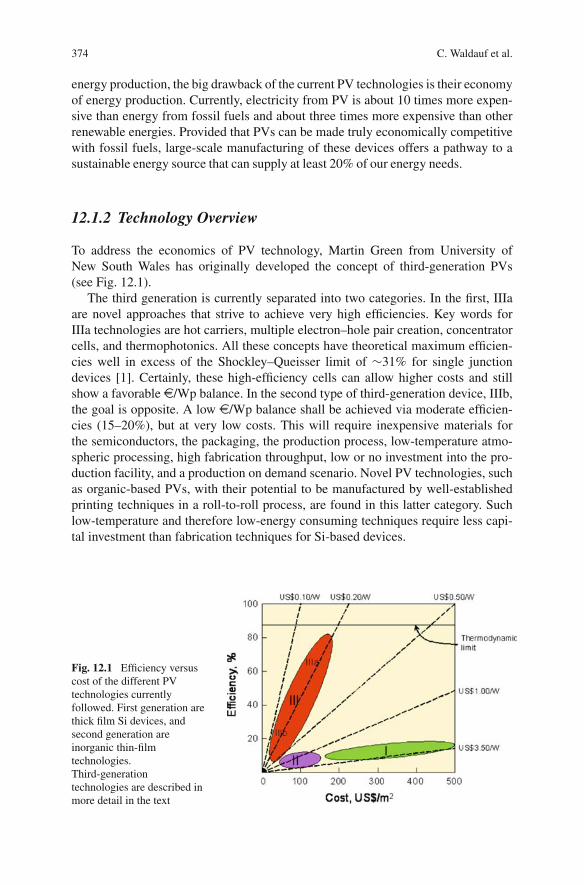
374 C. Waldauf et al.
energy production, the big drawback of the current PV technologies is their economyof energy production. Currently, electricity from PV is about 10 times more expen-sive than energy from fossil fuels and about three times more expensive than otherrenewable energies. Provided that PVs can be made truly economically competitivewith fossil fuels, large-scale manufacturing of these devices offers a pathway to asustainable energy source that can supply at least 20% of our energy needs.
12.1.2 Technology Overview
To address the economics of PV technology, Martin Green from University ofNew South Wales has originally developed the concept of third-generation PVs(see Fig. 12.1).
The third generation is currently separated into two categories. In the first, IIIaare novel approaches that strive to achieve very high efficiencies. Key words forIIIa technologies are hot carriers, multiple electron–hole pair creation, concentratorcells, and thermophotonics. All these concepts have theoretical maximum efficien-cies well in excess of the Shockley–Queisser limit of ∼31% for single junctiondevices [1]. Certainly, these high-efficiency cells can allow higher costs and stillshow a favorable e/Wp balance. In the second type of third-generation device, IIIb,the goal is opposite. A low e/Wp balance shall be achieved via moderate efficien-cies (15–20%), but at very low costs. This will require inexpensive materials forthe semiconductors, the packaging, the production process, low-temperature atmo-spheric processing, high fabrication throughput, low or no investment into the pro-duction facility, and a production on demand scenario. Novel PV technologies, suchas organic-based PVs, with their potential to be manufactured by well-establishedprinting techniques in a roll-to-roll process, are found in this latter category. Suchlow-temperature and therefore low-energy consuming techniques require less capi-tal investment than fabrication techniques for Si-based devices.
Fig. 12.1 Efficiency versuscost of the different PVtechnologies currentlyfollowed. First generation arethick film Si devices, andsecond generation areinorganic thin-filmtechnologies.Third-generationtechnologies are described inmore detail in the text
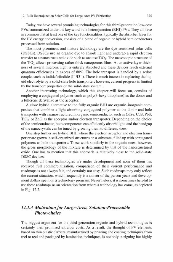
12 Bulk Heterojunction Solar Cells for Large-Area PV Fabrication 375
Today, we have several promising technologies for this third-generation low-costPVs, summarized under the key word bulk heterojunction (BHJ) PVs. They all havein common that at least one of the key functionalities, typically the absorber layer forthe PV energy conversion, consists of a blend of organic or hybrid semiconductorsprocessed from solution.
The most prominent and mature technology are the dye sensitized solar cells(DSSCs). DSSCs use an organic dye to absorb light and undergo a rapid electrontransfer to a nanostructured oxide such as anatase TiO2. The mesoscopic structure ofthe TiO2 allows processing rather thick nanoporous films. At an active layer thick-ness of several microns, light is entirely absorbed and these devices reach externalquantum efficiencies in excess of 80%. The hole transport is handled by a redoxcouple, such as iodide/triiodide (I−/I3−). There is much interest in replacing the liq-uid electrolyte by a solid-state hole transporter; however, current progress is limitedby the transport properties of the solid-state system.
Another interesting technology, which this chapter will focus on, consists ofemploying a conjugated polymer such as poly(3-hexylthiophene) as the donor anda fullerene derivative as the acceptor.
A close hybrid alternative to the fully organic BHJ are organic–inorganic com-posites that combine a light-absorbing conjugated polymer as the donor and holetransporter with a nanostructured, inorganic semiconductor such as CdSe, CdS, PbS,TiO2, or ZnO as the acceptor and/or electron transporter. Depending on the choiceof the semiconductor, both components can efficiently absorb light, and the bandgapof the nanocrystals can be tuned by growing them to different sizes.
One step further are hybrid BHJ, where the electron acceptor and electron trans-porter are grown in self-organized structures on a substrate, filled up with conjugatedpolymers as hole transporters. These work similarly to the organic ones; however,the gross morphology of the mixture is determined by that of the nanostructuredoxide. One has to mention that this approach is relatively close to the solid-stateDSSC devices.
Though all these technologies are under development and none of them hasreceived full commercialization, comparison of their current performance androadmaps is not always fair, and certainly not easy. Such roadmaps may only reflectthe current situation, which frequently is a mirror of the person years and develop-ment dollars spent on a technology program. Nevertheless, it is sometimes helpful touse these roadmaps as an orientation from where a technology has come, as depictedin Fig. 12.2.
12.1.3 Motivation for Large-Area, Solution-ProcessablePhotovoltaics
The biggest argument for the third-generation organic and hybrid technologies iscertainly their promised ultralow costs. As a result, the thought of PV elementsbased on thin plastic carriers, manufactured by printing and coating techniques fromreel to reel and packaged by lamination techniques, is not only intriguing but highly
376 C. Waldauf et al.
Fig. 12.2 Roadmap for prominent thin film PV technologies. Organic BHJ and DSSC data till 2007were added to this roadmap initiated by the National Renewable Energies Laboratory (NREL)
attractive from a cost standpoint. In order to fulfil these requirements, high volumeproduction technologies for large-area coating must be applied to a low-cost mate-rial class. Solution-processable organic and inorganic semiconductors have a highpotential to satisfy these requirements. Flexible chemical tailoring allows the designof organic semiconductors with the desired properties, and printing or coating tech-niques like screen, ink-jet, offset, gravure, or flexo printing are being established forsemiconducting polymers today, driven by display or general electronic demands.Altogether, the BHJ technology offers many attractive features for large-area elec-tronic applications among them
• the potential to be flexible and semitransparent• the potential to be manufactured in a continuous printing and coating process• large-area coating• easy integration in different devices• significant cost reduction compared to traditional solutions• substantial ecological and economic advantages
These features are beneficial for commercialization; however, as their classicalcounterparts, these new technologies have to fulfil the basic requirements for renew-able energy production. In the energy market, the competitive position of everysolar technology is mainly determined by these factors: efficiency, lifetime, andcosts (per Wp). The potential of organic PV has to be judged by these key figuresas well (Fig. 12.3).
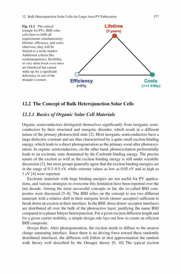
12 Bulk Heterojunction Solar Cells for Large-Area PV Fabrication 377
Fig. 12.3 The criticaltriangle for PVs. BHJ solarcells have to fulfil allrequirements simultaneously:lifetime, efficiency, and costs;otherwise, they will belimited to a niche market.Additional criteria likesemitransparency, flexibility,or very short break even timesare beneficial but cannotmake up for a significantdeficiency in one of thetriangle’s corners
12.2 The Concept of Bulk Heterojunction Solar Cells
12.2.1 Basics of Organic Solar Cell Materials
Organic semiconductors distinguish themselves significantly from inorganic semi-conductors by their structural and energetic disorder, which result in a differentnature of the primary photoexcited state [2]. Most inorganic semiconductors have alarge dielectric constant and are thus characterized by a quite small exciton bindingenergy, which leads to a direct photogeneration as the primary event after photoexci-tation. In organic semiconductors, on the other hand, photoexcitation preferentiallyleads to an excitonic state dominated by the Coulomb binding energy. The precisenature of the exciton as well as the exciton binding energy is still under scientificdiscussion [3], but most groups generally agree that the exciton binding energies arein the range of 0.3–0.5 eV, while extreme values as low as 0.05 eV and as high as1 eV [4] were reported.
Excitonic materials with large binding energies are not useful for PV applica-tions, and various strategies to overcome this limitation have been reported over thelast decade. Among the most successful concepts so far, the so-called BHJ com-posites were discussed [5–8]. The BHJ relies on the concept to use two differentmaterials with a relative shift in their energetic levels (donor–acceptor) sufficient tobreak down an exciton at their interface. In the BHJ, these donor–acceptor interfacesare distributed all over the bulk of the photoactive layer, justifying the name BHJcompared to a planar bilayer heterojunction. For a given exciton diffusion length andfor a given carrier mobility, a simple design rule lays out how to create an efficientBHJ composite.
Design Rule: After photogeneration, the exciton needs to diffuse to the nearestcharge separating interface. Since there is no driving force toward these randomlydistributed interfaces, the diffusion will follow in first approximation the randomwalk theory well described by the Onsager theory [9, 10] The typical exciton
378 C. Waldauf et al.
diffusion length for most organic semiconductors lies between 5 and 15 nm [11–13]before they decay radiatively or nonradiatively. Therefore, the average donor–acceptor separation should be of the order of the exciton diffusion length. A moreintimate mixture leads to recombination losses of charge carriers, while a morecoarse mixing leads to loss of excitons before charge generation.
Other strategies to separate excitons, like trap dissociation, [2], electrical fielddissociation [14], or dissociation of “hot exciton” [15] states with excess energiescurrently have no relevance for the organic PV field.
One very efficient embodiment of a BHJ system was independently reported byWang et al. [16], the Santa Barbara group [17], and the Osaka group [18]. Theirexperiments clearly evidenced that a photoexcited exciton on a conjugated polymeris broken down into free carriers at an interface with a C60-containing molecule(acceptor), leading to a photoinduced charge transfer system from the polymer to thefullerene. The forward electron transfer was observed to happen within few tens offemtoseconds [19], which is much faster than any competing relaxation processes.The internal quantum efficiency of this process is ∼100%.
12.2.2 Fundamentals of Photovoltaics
12.2.2.1 Solar Radiation
According to Planck, a universal dependence of the energy density per photonenergy interval has been found for the so-called blackbody radiation. Any body,which has an absorptivity of a(�ω) = 1 for photons with energy �ω, will emitradiation proportionally to its temperature. Although the sun consists mainly ofprotons, alpha particles, and electrons, its absorptivity is a(�ω) = 1 for all pho-ton energies �ω by virtue of its enormous size. There is a relatively thin layer ofa few hundred km at the surface of the sun, in which the temperature is constantand all incident photons are totally absorbed. The solar spectrum, observed justoutside of the earth’s atmosphere, agrees well with Planck’s law for a temperatureof TS = 5,800 K.
Light passing through the atmosphere of the earth gets modified by scatteringand absorption and it is particularly attenuated in the ultraviolet and in the infraredregime, by an amount proportional to the path length through the atmosphere. Thispath length depends on the incident angle of the sunlight and the light intensityas well as the spectral distribution of sunlight at the earth’s surface. As a standardspectrum, for which solar cell efficiencies are rated, a distance of 1.5 times the atmo-sphere’s thickness is chosen and the spectrum is designated AM1.5 (air mass 1.5).The solar spectrum outside the atmosphere is accordingly AM0. The total energycurrent density obtained by integrating over the spectrum amounts to 1.35 kW/m2
for the AM0-spectrum and to 1.0 kW/m2 for the AM1.5-spectrum.For solar cells, the photon current density is much more important than the
energy current density. Neglecting nonlinear processes like impact ionization effectsor multiple carrier generation, the excitation of one electron requires at least
12 Bulk Heterojunction Solar Cells for Large-Area PV Fabrication 379
one absorbed photon. The photon current density, jph, is derived from Planck’sblackbody equation:
d jph,ideal
d�ω= 2Ω
�3c2
(�ω)2
exp(
�ωkT
) − 1(12.1)
with Ω as the solid angle perpendicular to the emission front. For radiators with anabsorptivity smaller than 1 (i.e., part of the photons are reflected), Kirchoff foundthat the photon current density is proportional to the absorptivity:
d jph
d�ω= a (�ω)
2Ω
�3c2
(�ω)2
exp(
�ωkT
) − 1(12.2)
12.2.2.2 Band Considerations of a Two-Level System
A two-level system is the most general electronic model of a solar cell. It allowsa simple and rigorous treatment of optical transitions and the formulation of theexcitation state. A precise description of the formal treatment of the fermionic two-level system can be found in [20]. Such a system has a lower energy level at ε1
and an upper energy level at ε2. In classical semiconductor terminology, the highestmostly occupied energy range is called valence band, and the next higher mostlyunoccupied energy range is called conduction band. In organic materials, the highestoccupied states are called HOMO (Highest Occupied Molecular Orbital) and in thenext higher energy range states are called LUMO (Lowest Unoccupied MolecularOrbital). The difference between the HOMO and the LUMO is the band energy gapεG of the semiconductor, and the carrier statistics is given by the Fermi distributionfor the individual energy levels.
Specifically for BHJ-type solar cells, it is necessary to define more preciselythe relevant energy levels. In the previous section, we have outlined that pris-tine organic semiconductors have a low quantum efficiency for charge generation.The quantum efficiency for charge generation is significantly increased by design-ing a so-called heterojunction, in which a donor-type material is blended with anacceptor-type material. A BHJ composite is therefore a four-level system, with aHOMOdonor, a HOMOacceptor, a LUMOdonor, and a LUMOacceptor, having two sep-arate bandgaps, εdonor and εacceptor. Specifically for organic BHJ systems, it wasdemonstrated recently [21] that the four-level system can be reduced to a two-levelsystem by assuming that the majority carrier concentrations will reside either in theHOMOdonor or in the LUMOacceptor. Furthermore, the effective electrical bandgap(not to be confused with the optical bandgap) is given by εgap = HOMOdonor −LUMOacceptor. With this set of assumptions, we will be able to calculate the carrierdensity in the respective bands according to well-established equations of semicon-ductor physics.
380 C. Waldauf et al.
According to Fermi statistics, the probability to find an electron in a state inwhich it has the energy,εC, is given by:
f (εC ) = 1
exp(εc−εF
kT
) + 1(12.3)
If the electron density is significantly smaller than the density of states (i.e., in theBoltzmann limit), the “+1” can be omitted. Assuming a two-level system, the totalnumber of electrons per volume in the LUMO (respectively conduction band) isfound by integrating the density of states per energy interval multiplied by the Fermidistribution over the energy range of the conduction band:
ne =∫εC
f (εe)D(εe) dεe (12.4)
where εC designates the bottom of the conduction band. Since the Fermi functiondecreases exponentially with increasing energy, if εC exceeds the Fermi energy bysome kT, only states in the lower part of the conduction band contribute to the inte-gral in Eq. (12.4). As a result, the total number of electrons is in good approxima-tion:
ne = NC exp
(−εC − εF
kT
)(12.5)
where NC is the effective density of states, which depends on the temperature andthe effective electron mass. The effective density of states strongly depends on thenature of the semiconductor, while Eq. (12.5) is quite independent from the natureof a material. The calculation of the total concentration of holes nh in the valenceband is analogous to Eq. (12.5) and yields:
nh = NV exp
(εV − εF
kT
)(12.6)
where NV is the effective density of states in the valence band. The Fermi energyεF, in between the conduction and the valence band, follows from the condition ofcharge conservation.
Doping of the semiconductor shifts the position of the Fermi level relative withinthe band. This is easily rationalized by substituting the carrier density ne by ne +ND. In this case, the increased electron density shifts the Fermi level closer to theconduction band.
For a semiconductor in equilibrium under a constant temperature, the productnenh of electron density in the conduction band and hole density in the valence bandis independent of doping and is a constant. It has the same value for doped as wellas undoped semiconductors, when the electron and hole densities are equal and arecalled intrinsic density ni:
12 Bulk Heterojunction Solar Cells for Large-Area PV Fabrication 381
nenh = NC NV exp
(−εC − εV
kT
)= n2
i (12.7)
A semiconductor under illumination or with a current flow is considered to be inequilibrium, though the electrons and holes will be in a dynamic equilibrium. Thatequilibrium, however, is a thermodynamic equilibrium, in which the blackbodybackground radiation is kept in balance with its inverse, a recombination process.Deviations from this detailed balance result in a perturbation. Due to the additionalcharge carrier generation, however, the electrons in the conduction band are not indetailed balance equilibrium with the holes in the valence band. This perturbationmay not be intermixed with the Coulomb neutrality of the charge carriers, which isalways valid. A more detailed discussion on the equilibrium conditions of a semi-conductor under illumination can be found in [20]. As a consequence, the occupa-tion probability for holes in the valence band and for electrons in the conductionband with electrons has different Fermi energies:
ne = NC exp
(−εC − εF,C
kT
)(12.8)
and
nh = NV exp
(εV − εF,V
kT
)(12.9)
The product of electron and hole densities is now:
nenh = n2i exp
(εF,C − εF,V
kT
)(12.10)
and can exceed ni significantly.
12.2.2.3 Transport Phenomena
The charge carrier transport in solar cells follows the classical transport equation,irrespective of the nature of the semiconductor. Solutions to the transport equationsfor organic solar cells have been published recently, and allow a great insight intothe balance between charge carrier generation and charge carrier recombination.[21–23]. The transport equations are a set of four equations: the Poisson equation,the continuity equation, and the electron and the hole transport equations that aresummarized below.
• The Poisson equation
d2
dx2ψ(x) = q
ε.ε0[n(x) − p(x)] (12.11)
382 C. Waldauf et al.
where ψ(x) is the electric potential in the device as a function of position, andn(x) and p(x), the electron and hole densities, respectively.
• The current continuity equation
d
dxJn(x) = d
dxJp(x) = q [G(x) − R(x)] (12.12)
where Jn(x) and Jp(x) are the electron and hole current densities, respectively,G(x) the generation rate of charge carriers, and R(x) the recombination rate ofcharge carriers.
• The current transport equations for electrons and holes
Jn(x) = −q.n(x).μn .d
dxψ + q.Dn
d
dxn(x) (12.13)
Jp(x) = −q.p(x).μp.d
dxψ + q.Dp
d
dxp(x) (12.14)
where μn and μp are the electron and the hole mobilities, respectively. Dn andDp, the electron and hole diffusion coefficients, are assumed to obey the Einsteinrelation:
Dn,p = μn,p.k.T
q(12.15)
A specific property of disordered semiconductor is the field and temperature depen-dence of the mobility. Various microscopical models have been used to describemobility in a highly disordered system. Among them are the Marcus-type jumptheory [24], the Miller-Abrahams form to describe hopping rates between adjacentsites, [25] an empirical equation [26] reflecting explicitly the field dependence ofthe mobility, and a general formula within the framework of the disorder formalism:
μ(T, E) = μ0 exp
[−2
3
( σkT
)2]
exp
{C
[( σkT
)2− Σ2
]E1/2
}(12.16)
where σ is the width of the Gaussian density of states in a disordered semicon-ductor, Σ is a parameter characterizing the positional disorder, μ0 is a prefactormobility in the energetically disorder-free system, E is the electric field, and C isa fitting parameter. This formalism attributes the temperature and the electric fielddependence of the mobility to two main parameters, namely the energetic and thepositional disorder. The former one is related to the width σ of the Gaussian densityof states normalized by kT. The latter one, on the other hand, arises from fluctuationof the intersite coupling due to either the variation of intersite distance between thecharge transport sites or simply the variation of the overlap between corresponding
12 Bulk Heterojunction Solar Cells for Large-Area PV Fabrication 383
electronic orbital. Equation (12.16) predicts a non-Arrhenius-type activation of themobility extrapolated to zero electric field following [27, 28]:
ln [μ(0, T )] ∝ 1
T 2(12.17)
and a potentially negative field dependence of the mobility, experimentally observedby Mozer et al. in the case of P3HT [29].
The lifetime τ of carriers is the second important parameter besides the mobil-ity to consider for loss analysis. It is the μτ -product of a semiconductor, whichdetermines the volume of the semiconductor contributing to the external circuitry.The kinetics of charge carrier recombination can be of two different natures, namelymonomolecular (first-order), or bimolecular (second or higher order). It is importantto keep in mind that monomolecular does not mean that a carrier can recombine withitself and violate the Coulomb neutrality. Rather, monomolecular recombinationmeans that the species under investigation recombines at a rate that is linearly pro-portional to its population density. The light intensity dependence of the photocur-rent is frequently looked at in order to distinguish between first- and second-orderrecombination processes [30, 31], but only a few studies have focused on determin-ing the photoinduced carrier lifetime of BHJ composites. Among them, transientabsorption spectroscopy and transient photocurrent/photovoltage spectroscopy [32–34], flash photolysis time-resolved microwave conductivity (FP-TRMC) [35, 36],and photoinduced charge carrier extraction by linearly increasing voltage (photo-CELIV) [37–40] technique studies all yielded a second-order-type recombinationbehavior with lifetimes of the mobile carriers in the microsecond regime, whereasthe lifetime of trapped carriers can extend into the millisecond regime. Dependingon the type of polymer, the bimolecular recombination was found to be of Langevintype (βL = e.μ/ε.ε0) for more amorphous semiconductors and of non Langevin-typefor more ordered or semi-crystalline semiconductors [40, 41].
12.2.2.4 Current–Voltage Characteristic
The most simple way to discuss and describe a two-level system is by assumingthat a semipermeable membrane at the interface of the two-level system with theexternal circuitry is selectively allowing only carriers with a distinct energy to pass.In case of an electrical current flowing through the system, independently of whetherthe carriers are injected or photogenerated and extracted, this membrane does onlyallow holes with an energy ε1 and electrons with an energy ε2 through. From Eq.(12.12), the continuity equation for electrons or holes we have:
d
dxJ (x) = q [G(x) − R(x)]
For the qualitative derivation of the current (I)–voltage (V) relation, we now followthe thermodynamic approach and redefine the generation and recombination rates
384 C. Waldauf et al.
for photons instead of carriers. The generation G(x) remains, as defined above, thegeneration of charged carriers. But it is important to understand that these carriersare generated radiatively. Therefore, the number of absorbed photons needs to equalthe number of emitted photons, whereas recombination of carriers is regarded tolead to radiative emission. Nonradiative recombination, i.e., recombination withoutemission of visible light, generates heat and this heat will be emitted as IR photons.This allows us to give an analytical expression for R(x), the radiative recombinationconstant [20], with R0 as the spontaneous emission rate of the material in equilib-rium with its environment:
R(x) = −eR0
[exp
(εF2 − εF1
kT
)− 1
](12.18)
By integrating over the thickness of the two-level system, the total current densityjQ can be calculated as follows:
jQ = e∫
R0
[exp
(εF2 − εF1
kT
)− 1
]dx − e
∫G(x)dx (12.19)
We further assume that our semipermeable membranes give an ideal unipolar ohmiccontact so that the Fermi energy of the higher level is identical to the Fermi energy ofthe electron membrane, and the Fermi energy of the lower level becomes identicalto the Fermi energy of the hole membrane. The difference of the Fermi energiesof the two membranes is then related to the voltage V between the contacts to themembranes, eV=εF2−εF1, and by introducing the dark saturation current density j0and the photocurrent density under short-circuit conditions jSC, we can rewrite Eq.(12.19) as Eq. (12.22), which is the familiar one-diode equation for semiconductorswith two distinct energy levels for electrons and holes (plotted in Fig. 12.4):
j0 = e∫
R0dx (12.20)
jSC = −e∫
G(x)dx (12.21)
jQ = jrev
[exp
(eV
kT
)− 1
]+ jsc (12.22)
12.2.2.5 The Voc
The nature of the Voc in BHJ solar cells has long been debated. Due to the similarityof the device architecture to that of organic light-emitting diodes (OLEDs), it wasintitially suspected that BHJ solar cells can be described by a MIM model (metal–intrinsic–metal) [42], where the built-in voltage is controlled by the difference in the
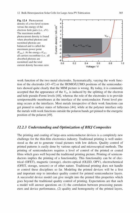
12 Bulk Heterojunction Solar Cells for Large-Area PV Fabrication 385
Fig. 12.4 Photocurrentdensity of a two-level systemversus the energy of theelectron–hole pairs (i.e., eV).The maximum usablephotocurrent density is foundwhen absorbed photons andreemitted photons arebalanced and is called themaximum power point(Pmax). At the energy eVOC,all carriers recombine (i.e., allabsorbed photons arereemitted) and the totalcurrent density becomes zero
work function of the two metal electrodes. Systematically, varying the work func-tion of the electrodes [43–47] or the HOMO/LUMO positions of the semiconduc-tors showed quite clearly that the MIM picture is wrong. By today, it is commonlyaccepted that the appearance of the Voc is induced by the splitting of the electronand hole pseudo-Fermi levels [48], whereas the role of the electrodes is to providesemipermeable membranes at the interface of the semiconductor. Fermi level pin-ning occurs at the interfaces. Most metals irrespective of their work functions canget pinned to surface states of fullerenes [44], while at the polymer interface onlythe metals with work functions outside the polaron bands get pinned to the energeticposition of the polaron [49].
12.2.3 Understanding and Optimization of BHJ Composites
The printing and coating of large-area semiconductor devices is a completely newchallenge for the thin-film electronics industry. Traditional printing is well under-stood as the art to generate visual pictures with low defects. Quality control ofprinted patterns is easily done by various optical and microscopical methods. Theprinting of semiconductors requires a level of control of the printed or coatedfilms which goes well beyond the traditional printing picture. Printing of semicon-ductors implies the printing of a functionality. This functionality can be of elec-trical (OFET), magnetic (storage), electro-optical (OLED, OPV), electrochemical(OFET, storage, sensors) or of other nature. Traditional printing does not handleor control these disciplines so far. Modeling the printed devices will be a firstand important step to introduce quality control for printed semiconductor layers.A successful device model can give insight into the printed film properties whichgoes beyond the traditional quality control of printing. Expectations are that sucha model will answer questions on (1) the correlation between processing param-eters and device performance, (2) quality and homogeneity of the printed layers,
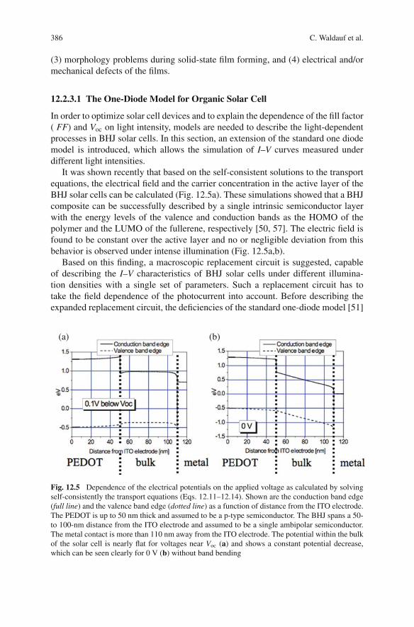
386 C. Waldauf et al.
(3) morphology problems during solid-state film forming, and (4) electrical and/ormechanical defects of the films.
12.2.3.1 The One-Diode Model for Organic Solar Cell
In order to optimize solar cell devices and to explain the dependence of the fill factor( FF) and Voc on light intensity, models are needed to describe the light-dependentprocesses in BHJ solar cells. In this section, an extension of the standard one diodemodel is introduced, which allows the simulation of I–V curves measured underdifferent light intensities.
It was shown recently that based on the self-consistent solutions to the transportequations, the electrical field and the carrier concentration in the active layer of theBHJ solar cells can be calculated (Fig. 12.5a). These simulations showed that a BHJcomposite can be successfully described by a single intrinsic semiconductor layerwith the energy levels of the valence and conduction bands as the HOMO of thepolymer and the LUMO of the fullerene, respectively [50, 57]. The electric field isfound to be constant over the active layer and no or negligible deviation from thisbehavior is observed under intense illumination (Fig. 12.5a,b).
Based on this finding, a macroscopic replacement circuit is suggested, capableof describing the I–V characteristics of BHJ solar cells under different illumina-tion densities with a single set of parameters. Such a replacement circuit has totake the field dependence of the photocurrent into account. Before describing theexpanded replacement circuit, the deficiencies of the standard one-diode model [51]
(a) (b)
Fig. 12.5 Dependence of the electrical potentials on the applied voltage as calculated by solvingself-consistently the transport equations (Eqs. 12.11–12.14). Shown are the conduction band edge(full line) and the valence band edge (dotted line) as a function of distance from the ITO electrode.The PEDOT is up to 50 nm thick and assumed to be a p-type semiconductor. The BHJ spans a 50-to 100-nm distance from the ITO electrode and assumed to be a single ambipolar semiconductor.The metal contact is more than 110 nm away from the ITO electrode. The potential within the bulkof the solar cell is nearly flat for voltages near Voc (a) and shows a constant potential decrease,which can be seen clearly for 0 V (b) without band bending
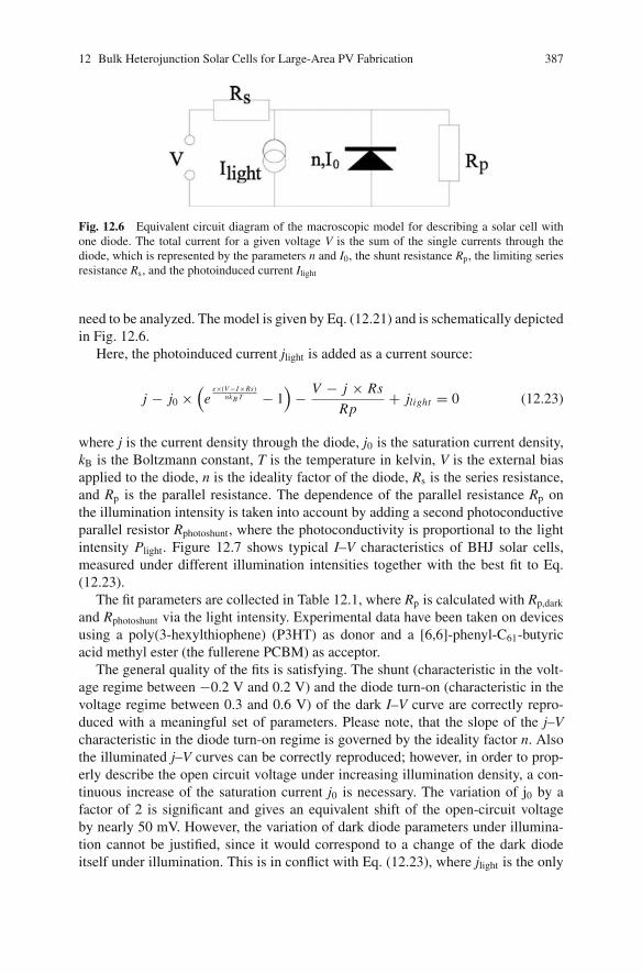
12 Bulk Heterojunction Solar Cells for Large-Area PV Fabrication 387
Fig. 12.6 Equivalent circuit diagram of the macroscopic model for describing a solar cell withone diode. The total current for a given voltage V is the sum of the single currents through thediode, which is represented by the parameters n and I0, the shunt resistance Rp, the limiting seriesresistance Rs, and the photoinduced current Ilight
need to be analyzed. The model is given by Eq. (12.21) and is schematically depictedin Fig. 12.6.
Here, the photoinduced current jlight is added as a current source:
j − j0 ×(
ee×(V −I×Rs)
nkB T − 1)
− V − j × Rs
Rp+ jlight = 0 (12.23)
where j is the current density through the diode, j0 is the saturation current density,kB is the Boltzmann constant, T is the temperature in kelvin, V is the external biasapplied to the diode, n is the ideality factor of the diode, Rs is the series resistance,and Rp is the parallel resistance. The dependence of the parallel resistance Rp onthe illumination intensity is taken into account by adding a second photoconductiveparallel resistor Rphotoshunt, where the photoconductivity is proportional to the lightintensity Plight. Figure 12.7 shows typical I–V characteristics of BHJ solar cells,measured under different illumination intensities together with the best fit to Eq.(12.23).
The fit parameters are collected in Table 12.1, where Rp is calculated with Rp,dark
and Rphotoshunt via the light intensity. Experimental data have been taken on devicesusing a poly(3-hexylthiophene) (P3HT) as donor and a [6,6]-phenyl-C61-butyricacid methyl ester (the fullerene PCBM) as acceptor.
The general quality of the fits is satisfying. The shunt (characteristic in the volt-age regime between −0.2 V and 0.2 V) and the diode turn-on (characteristic in thevoltage regime between 0.3 and 0.6 V) of the dark I–V curve are correctly repro-duced with a meaningful set of parameters. Please note, that the slope of the j–Vcharacteristic in the diode turn-on regime is governed by the ideality factor n. Alsothe illuminated j–V curves can be correctly reproduced; however, in order to prop-erly describe the open circuit voltage under increasing illumination density, a con-tinuous increase of the saturation current j0 is necessary. The variation of j0 by afactor of 2 is significant and gives an equivalent shift of the open-circuit voltageby nearly 50 mV. However, the variation of dark diode parameters under illumina-tion cannot be justified, since it would correspond to a change of the dark diodeitself under illumination. This is in conflict with Eq. (12.23), where jlight is the only
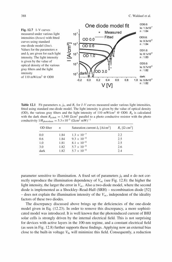
388 C. Waldauf et al.
Fig. 12.7 I–V curvesmeasured under various lightintensities (boxes) with fittedcurves using standardone-diode model (line).Values for the parameters nand I0 are given for each lightintensity. The light intensityis given by the value ofoptical density of the variousgray filters and the lightintensityof 110 mW/cm2 @ OD0
Table 12.1 Fit parameters n, j0, and Rs for I–V curves measured under various light intensities,fitted using standard one-diode model. The light intensity is given by the value of optical density(OD), the various gray filters and the light intensity of 110 mW/cm2 @ OD0. Rp is calculatedwith the dark shunt Rp,dark = 1,540 Ωcm2 parallel to a photo conductive resistor with the photoconductivity 1/Rphotoshunt = 5.3×10⁻⁵ (Ωcm2 mW)−1
OD filter n Saturation current I0 [A/cm2] Rs [Ω cm2]
0.0 1.84 1.3 × 10⁻⁷ 2.20.6 1.84 9.3 × 10⁻⁸ 2.51.0 1.81 8.1 × 10⁻⁸ 2.53.0 1.82 5.7 × 10⁻⁸ 2.6dark 1.82 5.7 × 10⁻⁸ 2.4
parameter sensitive to illumination. A fixed set of parameters j0 and n do not cor-rectly reproduce the illumination dependency of Voc (see Fig. 12.8): the higher thelight intensity, the larger the error in Voc. Also a two-diode model, where the seconddiode is implemented as a Shockley–Read-Hall (SRH) – recombination diode [52]– does not explain the illumination intensity of the Voc, independent of the idealityfactors of these two diodes.
The discrepancy discussed above brings up the deficiencies of the one-diodemodel given in Eq. (12.23). In order to remove this discrepancy, a more sophisti-cated model was introduced. It is well known that the photoinduced current of BHJsolar cells is strongly driven by the internal electrical field. This is not surprisingfor devices with active layers in the 100-nm regime, and a constant electrical field(as seen in Fig. 12.8) further supports these findings. Applying now an external biasclose to the built-in voltage Vbi will minimize this field. Consequently, a reduction
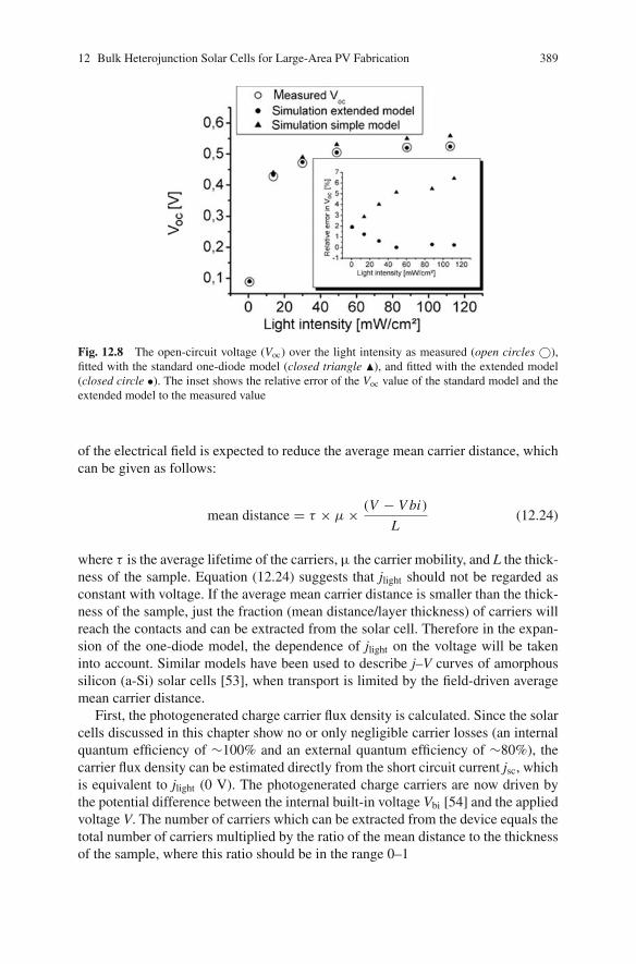
12 Bulk Heterojunction Solar Cells for Large-Area PV Fabrication 389
Fig. 12.8 The open-circuit voltage (Voc) over the light intensity as measured (open circles ©),fitted with the standard one-diode model (closed triangle �), and fitted with the extended model(closed circle •). The inset shows the relative error of the Voc value of the standard model and theextended model to the measured value
of the electrical field is expected to reduce the average mean carrier distance, whichcan be given as follows:
mean distance = τ × μ× (V − V bi)
L(12.24)
where τ is the average lifetime of the carriers, μ the carrier mobility, and L the thick-ness of the sample. Equation (12.24) suggests that jlight should not be regarded asconstant with voltage. If the average mean carrier distance is smaller than the thick-ness of the sample, just the fraction (mean distance/layer thickness) of carriers willreach the contacts and can be extracted from the solar cell. Therefore in the expan-sion of the one-diode model, the dependence of jlight on the voltage will be takeninto account. Similar models have been used to describe j–V curves of amorphoussilicon (a-Si) solar cells [53], when transport is limited by the field-driven averagemean carrier distance.
First, the photogenerated charge carrier flux density is calculated. Since the solarcells discussed in this chapter show no or only negligible carrier losses (an internalquantum efficiency of ∼100% and an external quantum efficiency of ∼80%), thecarrier flux density can be estimated directly from the short circuit current jsc, whichis equivalent to jlight (0 V). The photogenerated charge carriers are now driven bythe potential difference between the internal built-in voltage Vbi [54] and the appliedvoltage V. The number of carriers which can be extracted from the device equals thetotal number of carriers multiplied by the ratio of the mean distance to the thicknessof the sample, where this ratio should be in the range 0–1
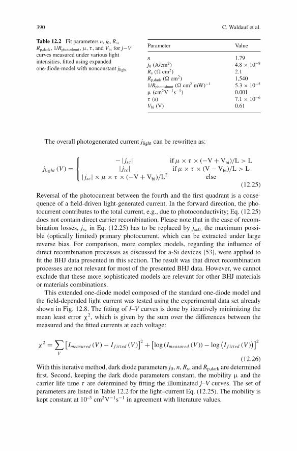
390 C. Waldauf et al.
Table 12.2 Fit parameters n, j0, Rs,Rp,dark, 1/Rphotoshunt, μ, τ , and Vbi for j−Vcurves measured under various lightintensities, fitted using expandedone-diode-model with nonconstant jlight
Parameter Value
n 1.79j0 (A/cm2) 4.8 × 10⁻⁸
Rs (Ω cm2) 2.1Rp,dark (Ω cm2) 1,5401/Rphotoshunt (Ω cm2 mW)−1 5.3 × 10⁻⁵
μ (cm2V−1s−1) 0.001τ (s) 7.1 × 10⁻⁶
Vbi (V) 0.61
The overall photogenerated current jlight can be rewritten as:
jlight (V ) =⎧⎨⎩
− | jsc|| jsc|
| jsc| × μ× τ × (−V + Vbi)/L2
ifμ× τ × (−V + Vbi)/L > Lifμ× τ × (V − Vbi)/L > L
else(12.25)
Reversal of the photocurrent between the fourth and the first quadrant is a conse-quence of a field-driven light-generated current. In the forward direction, the pho-tocurrent contributes to the total current, e.g., due to photoconductivity; Eq. (12.25)does not contain direct carrier recombination. Please note that in the case of recom-bination losses, jsc in Eq. (12.25) has to be replaced by jsc0, the maximum possi-ble (optically limited) primary photocurrent, which can be extracted under largereverse bias. For comparison, more complex models, regarding the influence ofdirect recombination processes as discussed for a-Si devices [53], were applied tofit the BHJ data presented in this section. The result was that direct recombinationprocesses are not relevant for most of the presented BHJ data. However, we cannotexclude that these more sophisticated models are relevant for other BHJ materialsor materials combinations.
This extended one-diode model composed of the standard one-diode model andthe field-depended light current was tested using the experimental data set alreadyshown in Fig. 12.8. The fitting of I–V curves is done by iteratively minimizing themean least error χ2, which is given by the sum over the differences between themeasured and the fitted currents at each voltage:
χ2 =∑
V
[Imeasured (V ) − I f i t ted (V )
]2 + [log (Imeasured (V )) − log
(I f i t ted (V )
)]2
(12.26)With this iterative method, dark diode parameters j0, n, Rs, and Rp,dark are determinedfirst. Second, keeping the dark diode parameters constant, the mobility μ and thecarrier life time τ are determined by fitting the illuminated j–V curves. The set ofparameters are listed in Table 12.2 for the light–current Eq. (12.25). The mobility iskept constant at 10–3 cm2V−1s−1 in agreement with literature values.
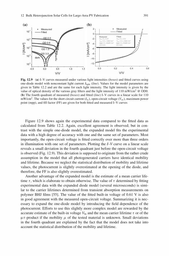
12 Bulk Heterojunction Solar Cells for Large-Area PV Fabrication 391
(a) (b)
Fig. 12.9 (a) I–V curves measured under various light intensities (boxes) and fitted curves usingone-diode model with nonconstant light current Ilight (line). Values for the model parameters aregiven in Table 12.2 and are the same for each light intensity. The light intensity is given by thevalue of optical density of the various gray filters and the light intensity of 110 mW/cm2 @ OD0.(b) The fourth quadrant of measured (boxes) and fitted (line) I–V curves in a linear scale for 110mW/cm2. The values for the short circuit current (Isc), open-circuit voltage (Voc), maximum powerpoint (mpp), and fill factor (FF) are given for both fitted and measured I–V curves
Figure 12.9 shows again the experimental data compared to the fitted data ascalculated from Table 12.2. Again, excellent agreement is observed; but in con-trast with the simple one-diode model, the expanded model fits the experimentaldata with a high degree of accuracy with one and the same set of parameters. Mostimportantly, the open-circuit voltage is fitted correctly over more than three ordersin illumination with one set of parameters. Plotting the I–V curve on a linear scalereveals a small deviation in the fourth quadrant just before the open-circuit voltageis observed (Fig. 12.9). This deviation is supposed to originate from the rather crudeassumption in the model that all photogenerated carriers have identical mobilityand lifetime. Because we neglect the statistical distribution of mobility and lifetimevalues, the photocurrent is slightly overestimated at the opening of the diode, andtherefore, the FF is also slightly overestimated.
Another advantage of the expanded model is the estimate of a mean carrier life-time τ , which is elaborate to obtain otherwise. The value of τ determined by fittingexperimental data with the expanded diode model (several microseconds) is simi-lar to the carrier lifetimes determined from transient absorption measurements onpolymer BHJ films [55]. The value of the fitted built-in voltage of 0.61 V is alsoin good agreement with the measured open-circuit voltage. Summarizing it is nec-essary to expand the one-diode model by introducing the field dependence of thephotocurrent. Efforts to use this slightly more complex model are rewarded by theaccurate estimate of the built-in voltage Vbi and the mean carrier lifetime τ or of theμτ -product if the mobility μ of the tested material is unknown. Small deviationsin the fourth quadrant are explained by the fact that the model does not take intoaccount the statistical distribution of the mobility and lifetime.
392 C. Waldauf et al.
12.2.3.2 Consequences of the One-Diode Model
In the previous section, a simplified model for BHJ solar cells was intro-duced, allowing to deviate from the misleading concept of a MIM picture asthe charge-generating principle in the solar cell. Clearly, the intimate mixture ofelectron-accepting and hole-accepting materials is responsible for the direct chargegeneration, independently of the choice of metal contacts. Since it is agreed that thecharges are generated everywhere within the bulk, the proper picture for the organicbulk heterojunction (oBHJ) solar cells is a homogenously distributed p–n junction,with the p–n junction formed between the donor and the acceptor molecules. Incontrast to other models [56, 57], this picture allows to explain the light intensityand temperature dependence of solar cells without the introduction of microscopictransport parameters.
The fundamental question for any PV technology is the origin of the diode rectifi-cation, which is the energetic barrier which physically separates the charge carriersfrom each other and prevents their recombination after separation. This energeticbarrier is the origin of the diode I–V characteristics which was discussed in Sec-tion 12.2.2.4. Addition of a parallel and a series resistance to the diode resulted inthe expanded equivalent circuit with a field-dependent photocurrent. In case of noillumination (jlight=0), assuming Rp>>Rs, the electrical response of the solar cell isexpected to consist of three distinct regimes:
• A linear regime at negative voltages and low positive voltages where the currentis limited by Rp.
• An exponential behavior at intermediate positive voltages where the current iscontrolled by the diode.
• A second linear regime at high voltages where the current is limited by the seriesresistance.
Typical j–V characteristics of nonilluminated BHJ devices are presented inFig. 12.10. The three regimes can be easily identified. Differently processed solarcells differ in the ohmic response in regimes (1) and (3), but have a common positiveslope between 0.5 V and 0.75 V. The linearity of this j–V regime in the semiloga-rithmic representation indicates an exponential correlation between current densityand voltage. Exponential behavior is usually attributed to a clearly defined inter-face between two materials with chemical potentials shifted relative to each other,as present in bilayer or Schottky devices. The relation between current density j andvoltage V therefore is analytically best described by Eqs. (12.23) and (12.25).
For devices consisting of an intimate mixture of two materials, a well-definedinterface for charge separation, such as a p–n junction, suggests an arrangement ofthe two blended semiconductor materials as shown schematically in Fig. 12. 11.
The concept of organic BHJ devices was initiated by the idea of an increasedinterface for charge separation in order to overcome the limits due to low excitondiffusion lengths [58, 59] in organic materials. For several reasons, it is sound to
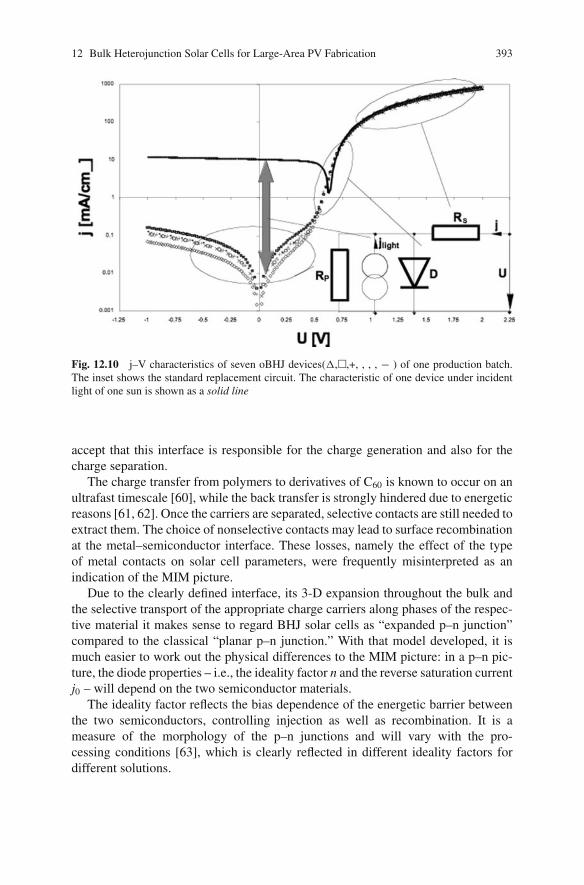
12 Bulk Heterojunction Solar Cells for Large-Area PV Fabrication 393
Fig. 12.10 j–V characteristics of seven oBHJ devices(Δ,�,+, , , , − ) of one production batch.The inset shows the standard replacement circuit. The characteristic of one device under incidentlight of one sun is shown as a solid line
accept that this interface is responsible for the charge generation and also for thecharge separation.
The charge transfer from polymers to derivatives of C60 is known to occur on anultrafast timescale [60], while the back transfer is strongly hindered due to energeticreasons [61, 62]. Once the carriers are separated, selective contacts are still needed toextract them. The choice of nonselective contacts may lead to surface recombinationat the metal–semiconductor interface. These losses, namely the effect of the typeof metal contacts on solar cell parameters, were frequently misinterpreted as anindication of the MIM picture.
Due to the clearly defined interface, its 3-D expansion throughout the bulk andthe selective transport of the appropriate charge carriers along phases of the respec-tive material it makes sense to regard BHJ solar cells as “expanded p–n junction”compared to the classical “planar p–n junction.” With that model developed, it ismuch easier to work out the physical differences to the MIM picture: in a p–n pic-ture, the diode properties – i.e., the ideality factor n and the reverse saturation currentj0 – will depend on the two semiconductor materials.
The ideality factor reflects the bias dependence of the energetic barrier betweenthe two semiconductors, controlling injection as well as recombination. It is ameasure of the morphology of the p–n junctions and will vary with the pro-cessing conditions [63], which is clearly reflected in different ideality factors fordifferent solutions.
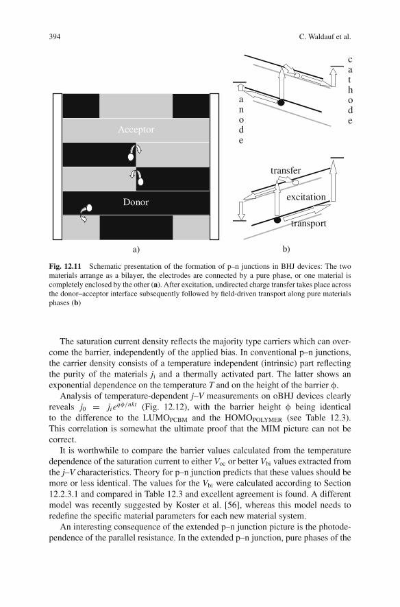
394 C. Waldauf et al.
a) b)
Donor
Acceptor
cathode
anode
excitation
transport
transfer
Fig. 12.11 Schematic presentation of the formation of p–n junctions in BHJ devices: The twomaterials arrange as a bilayer, the electrodes are connected by a pure phase, or one material iscompletely enclosed by the other (a). After excitation, undirected charge transfer takes place acrossthe donor–acceptor interface subsequently followed by field-driven transport along pure materialsphases (b)
The saturation current density reflects the majority type carriers which can over-come the barrier, independently of the applied bias. In conventional p–n junctions,the carrier density consists of a temperature independent (intrinsic) part reflectingthe purity of the materials ji and a thermally activated part. The latter shows anexponential dependence on the temperature T and on the height of the barrier φ.
Analysis of temperature-dependent j–V measurements on oBHJ devices clearlyreveals j0 = ji eqφ/nkt (Fig. 12.12), with the barrier height φ being identicalto the difference to the LUMOPCBM and the HOMOPOLYMER (see Table 12.3).This correlation is somewhat the ultimate proof that the MIM picture can not becorrect.
It is worthwhile to compare the barrier values calculated from the temperaturedependence of the saturation current to either Voc or better Vbi values extracted fromthe j–V characteristics. Theory for p–n junction predicts that these values should bemore or less identical. The values for the Vbi were calculated according to Section12.2.3.1 and compared in Table 12.3 and excellent agreement is found. A differentmodel was recently suggested by Koster et al. [56], whereas this model needs toredefine the specific material parameters for each new material system.
An interesting consequence of the extended p–n junction picture is the photode-pendence of the parallel resistance. In the extended p–n junction, pure phases of the
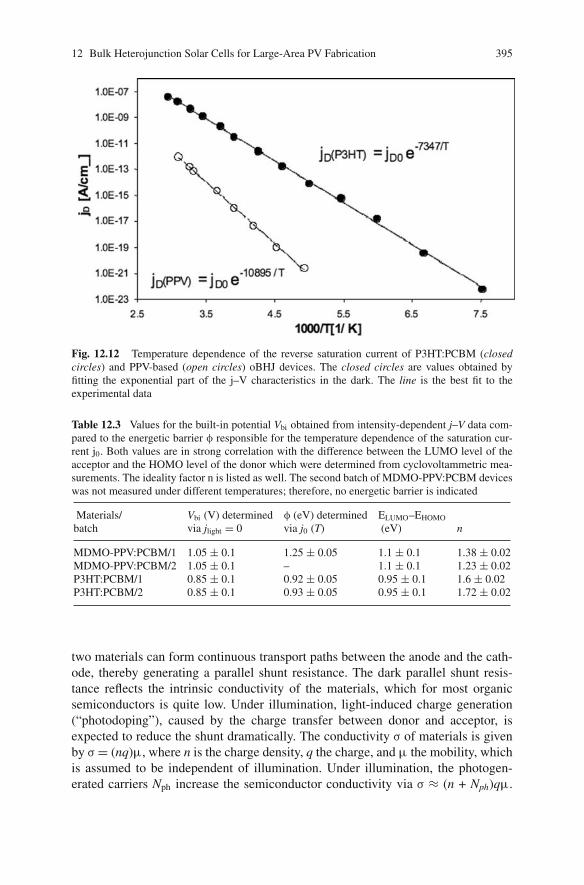
12 Bulk Heterojunction Solar Cells for Large-Area PV Fabrication 395
Fig. 12.12 Temperature dependence of the reverse saturation current of P3HT:PCBM (closedcircles) and PPV-based (open circles) oBHJ devices. The closed circles are values obtained byfitting the exponential part of the j–V characteristics in the dark. The line is the best fit to theexperimental data
Table 12.3 Values for the built-in potential Vbi obtained from intensity-dependent j–V data com-pared to the energetic barrier φ responsible for the temperature dependence of the saturation cur-rent j0. Both values are in strong correlation with the difference between the LUMO level of theacceptor and the HOMO level of the donor which were determined from cyclovoltammetric mea-surements. The ideality factor n is listed as well. The second batch of MDMO-PPV:PCBM deviceswas not measured under different temperatures; therefore, no energetic barrier is indicated
Materials/ Vbi (V) determined φ (eV) determined ELUMO–EHOMO
batch via jlight = 0 via j0 (T) (eV) n
MDMO-PPV:PCBM/1 1.05 ± 0.1 1.25 ± 0.05 1.1 ± 0.1 1.38 ± 0.02MDMO-PPV:PCBM/2 1.05 ± 0.1 – 1.1 ± 0.1 1.23 ± 0.02P3HT:PCBM/1 0.85 ± 0.1 0.92 ± 0.05 0.95 ± 0.1 1.6 ± 0.02P3HT:PCBM/2 0.85 ± 0.1 0.93 ± 0.05 0.95 ± 0.1 1.72 ± 0.02
two materials can form continuous transport paths between the anode and the cath-ode, thereby generating a parallel shunt resistance. The dark parallel shunt resis-tance reflects the intrinsic conductivity of the materials, which for most organicsemiconductors is quite low. Under illumination, light-induced charge generation(“photodoping”), caused by the charge transfer between donor and acceptor, isexpected to reduce the shunt dramatically. The conductivity σ of materials is givenby σ = (nq)μ, where n is the charge density, q the charge, and μ the mobility, whichis assumed to be independent of illumination. Under illumination, the photogen-erated carriers Nph increase the semiconductor conductivity via σ ≈ (n + Nph)qμ.
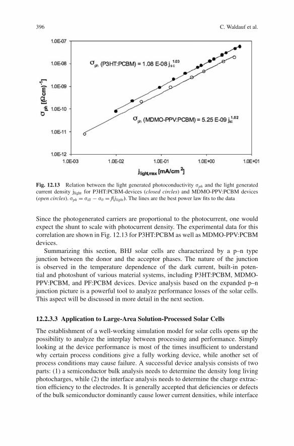
396 C. Waldauf et al.
Fig. 12.13 Relation between the light generated photoconductivity σph and the light generatedcurrent density jlight for P3HT:PCBM-devices (closed circles) and MDMO-PPV:PCBM devices(open circles). σph = σill − σ0 = f(jlight). The lines are the best power law fits to the data
Since the photogenerated carriers are proportional to the photocurrent, one wouldexpect the shunt to scale with photocurrent density. The experimental data for thiscorrelation are shown in Fig. 12.13 for P3HT:PCBM as well as MDMO-PPV:PCBMdevices.
Summarizing this section, BHJ solar cells are characterized by a p–n typejunction between the donor and the acceptor phases. The nature of the junctionis observed in the temperature dependence of the dark current, built-in poten-tial and photoshunt of various material systems, including P3HT:PCBM, MDMO-PPV:PCBM, and PF:PCBM devices. Device analysis based on the expanded p–njunction picture is a powerful tool to analyze performance losses of the solar cells.This aspect will be discussed in more detail in the next section.
12.2.3.3 Application to Large-Area Solution-Processed Solar Cells
The establishment of a well-working simulation model for solar cells opens up thepossibility to analyze the interplay between processing and performance. Simplylooking at the device performance is most of the times insufficient to understandwhy certain process conditions give a fully working device, while another set ofprocess conditions may cause failure. A successful device analysis consists of twoparts: (1) a semiconductor bulk analysis needs to determine the density long livingphotocharges, while (2) the interface analysis needs to determine the charge extrac-tion efficiency to the electrodes. It is generally accepted that deficiencies or defectsof the bulk semiconductor dominantly cause lower current densities, while interface
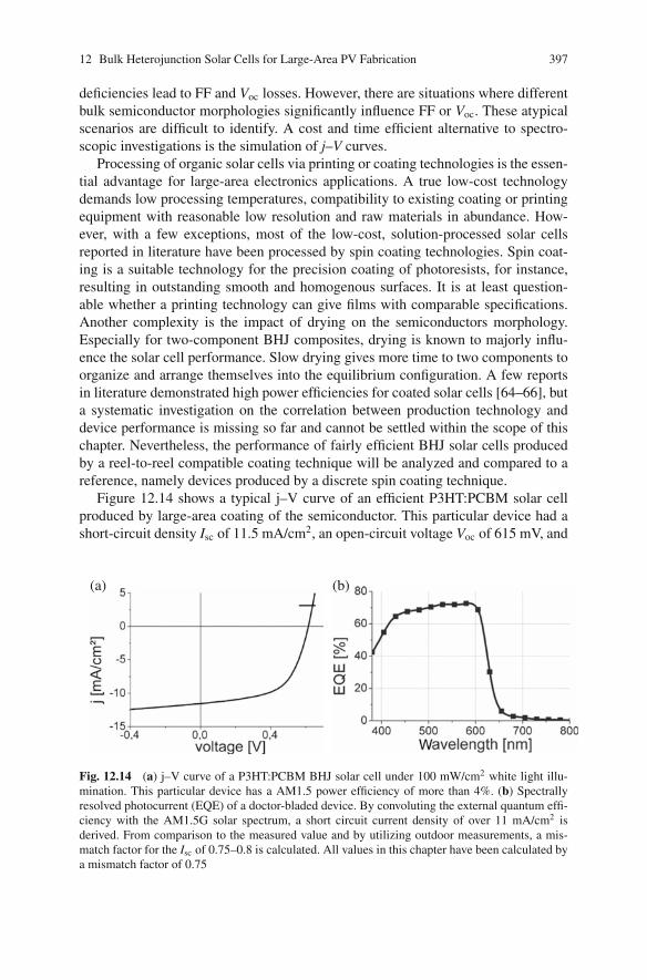
12 Bulk Heterojunction Solar Cells for Large-Area PV Fabrication 397
deficiencies lead to FF and Voc losses. However, there are situations where differentbulk semiconductor morphologies significantly influence FF or Voc. These atypicalscenarios are difficult to identify. A cost and time efficient alternative to spectro-scopic investigations is the simulation of j–V curves.
Processing of organic solar cells via printing or coating technologies is the essen-tial advantage for large-area electronics applications. A true low-cost technologydemands low processing temperatures, compatibility to existing coating or printingequipment with reasonable low resolution and raw materials in abundance. How-ever, with a few exceptions, most of the low-cost, solution-processed solar cellsreported in literature have been processed by spin coating technologies. Spin coat-ing is a suitable technology for the precision coating of photoresists, for instance,resulting in outstanding smooth and homogenous surfaces. It is at least question-able whether a printing technology can give films with comparable specifications.Another complexity is the impact of drying on the semiconductors morphology.Especially for two-component BHJ composites, drying is known to majorly influ-ence the solar cell performance. Slow drying gives more time to two components toorganize and arrange themselves into the equilibrium configuration. A few reportsin literature demonstrated high power efficiencies for coated solar cells [64–66], buta systematic investigation on the correlation between production technology anddevice performance is missing so far and cannot be settled within the scope of thischapter. Nevertheless, the performance of fairly efficient BHJ solar cells producedby a reel-to-reel compatible coating technique will be analyzed and compared to areference, namely devices produced by a discrete spin coating technique.
Figure 12.14 shows a typical j–V curve of an efficient P3HT:PCBM solar cellproduced by large-area coating of the semiconductor. This particular device had ashort-circuit density Isc of 11.5 mA/cm2, an open-circuit voltage Voc of 615 mV, and
(a) (b)
Fig. 12.14 (a) j–V curve of a P3HT:PCBM BHJ solar cell under 100 mW/cm2 white light illu-mination. This particular device has a AM1.5 power efficiency of more than 4%. (b) Spectrallyresolved photocurrent (EQE) of a doctor-bladed device. By convoluting the external quantum effi-ciency with the AM1.5G solar spectrum, a short circuit current density of over 11 mA/cm2 isderived. From comparison to the measured value and by utilizing outdoor measurements, a mis-match factor for the Isc of 0.75–0.8 is calculated. All values in this chapter have been calculated bya mismatch factor of 0.75
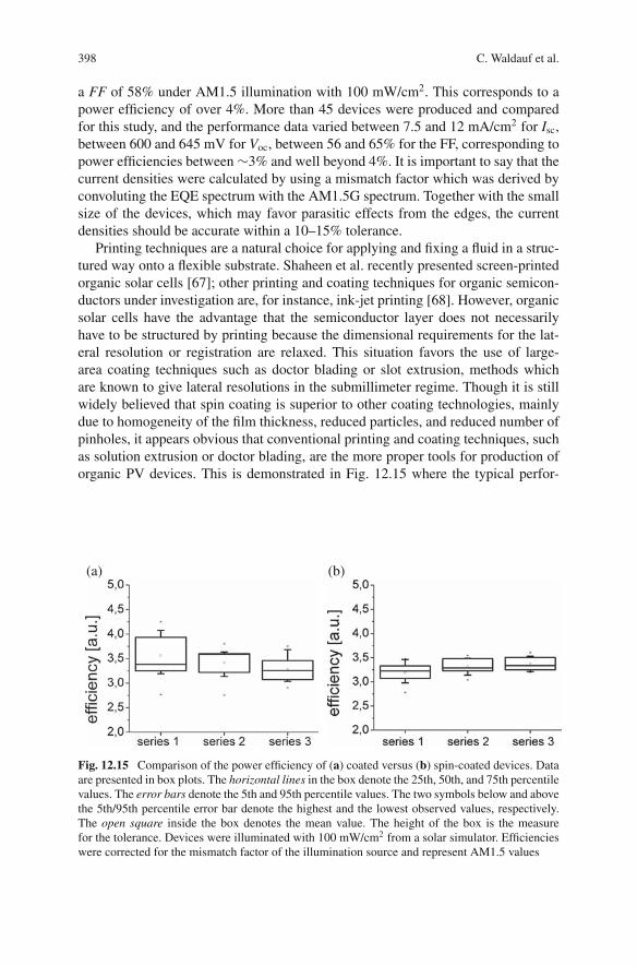
398 C. Waldauf et al.
a FF of 58% under AM1.5 illumination with 100 mW/cm2. This corresponds to apower efficiency of over 4%. More than 45 devices were produced and comparedfor this study, and the performance data varied between 7.5 and 12 mA/cm2 for Isc,between 600 and 645 mV for Voc, between 56 and 65% for the FF, corresponding topower efficiencies between ∼3% and well beyond 4%. It is important to say that thecurrent densities were calculated by using a mismatch factor which was derived byconvoluting the EQE spectrum with the AM1.5G spectrum. Together with the smallsize of the devices, which may favor parasitic effects from the edges, the currentdensities should be accurate within a 10–15% tolerance.
Printing techniques are a natural choice for applying and fixing a fluid in a struc-tured way onto a flexible substrate. Shaheen et al. recently presented screen-printedorganic solar cells [67]; other printing and coating techniques for organic semicon-ductors under investigation are, for instance, ink-jet printing [68]. However, organicsolar cells have the advantage that the semiconductor layer does not necessarilyhave to be structured by printing because the dimensional requirements for the lat-eral resolution or registration are relaxed. This situation favors the use of large-area coating techniques such as doctor blading or slot extrusion, methods whichare known to give lateral resolutions in the submillimeter regime. Though it is stillwidely believed that spin coating is superior to other coating technologies, mainlydue to homogeneity of the film thickness, reduced particles, and reduced number ofpinholes, it appears obvious that conventional printing and coating techniques, suchas solution extrusion or doctor blading, are the more proper tools for production oforganic PV devices. This is demonstrated in Fig. 12.15 where the typical perfor-
(a) (b)
Fig. 12.15 Comparison of the power efficiency of (a) coated versus (b) spin-coated devices. Dataare presented in box plots. The horizontal lines in the box denote the 25th, 50th, and 75th percentilevalues. The error bars denote the 5th and 95th percentile values. The two symbols below and abovethe 5th/95th percentile error bar denote the highest and the lowest observed values, respectively.The open square inside the box denotes the mean value. The height of the box is the measurefor the tolerance. Devices were illuminated with 100 mW/cm2 from a solar simulator. Efficiencieswere corrected for the mismatch factor of the illumination source and represent AM1.5 values
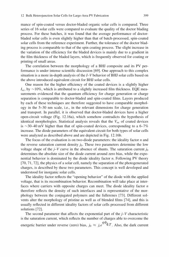
12 Bulk Heterojunction Solar Cells for Large-Area PV Fabrication 399
mance of spin-coated versus doctor-bladed organic solar cells is compared. Threeseries of 16 solar cells were compared to evaluate the quality of the doctor bladingprocess. For these batches, it was found that the average performance of doctor-bladed solar cells is even slightly higher than that of batch-processed, spin-coatedsolar cells from the reference experiment. Further, the tolerance of the doctor blad-ing process is comparable to that of the spin coating process. The slight increase inthe variation of the efficiency for the bladed devices is mainly due to a gradient inthe film thickness of the bladed layers, which is frequently observed for coating orprinting of small areas.
The correlation between the morphology of a BHJ composite and its PV per-formance is under intense scientific discussion [69]. One approach to this complexsituation is a more in-depth analysis of the I–V behavior of BHJ solar cells based onthe above introduced equivalent circuit for BHJ solar cells.
One reason for the higher efficiency of the coated devices is a slightly higherIsc, by ∼10%, which is attributed to a slightly increased film thickness. EQE mea-surements evidenced that the quantum efficiency for charge generation or chargeseparation is comparable to doctor-bladed and spin-coated films. Layers producedby each of these techniques are therefore suggested to have comparable morphol-ogy in the 5–30 nm scale, i.e., in the relevant dimensions for charge generationand transport. In parallel, it is observed that doctor-bladed devices have a higheropen-circuit voltage (Fig. 12.16a), which somehow contradicts the hypothesis ofidentical morphologies. Statistical analysis reveals that the Voc of coated devicesis ∼30–40 mV higher than that of spin-coated devices, corresponding to a 6–7%increase. The diode parameters of the equivalent circuit for both types of solar cellswere analyzed as described above and are depicted in Fig. 12.16b.
The focus of the evaluation is on two-diode parameters: the ideality factor n andthe reverse saturation current density j0. These two parameters determine the lowvoltage shape of the j–V curve in the absence of shunts. The saturation current j0determines the absolute size of the diode current around zero bias, while the expo-nential behavior is dominated by the diode ideality factor n. Following PV theory[70, 71, 72], the physics of a solar cell, namely the separation of the photogeneratedcharges, is described by these two parameters. This concept is well developed andunderstood for inorganic solar cells.
The ideality factor reflects the “opening behavior” of the diode with the appliedvoltage, that is its recombination behavior. Recombination will take place at inter-faces where carriers with opposite charges can meet. The diode ideality factor ntherefore reflects the density of such interfaces and is representative of the mor-phology between the conjugated polymers and the fullerenes [73]. Different sol-vents alter the morphology of pristine as well as of blended films [74], and this isusually reflected in different ideality factors of solar cells processed from differentsolutions [72].
The second parameter that affects the exponential part of the j–V characteristicis the saturation current, which reflects the number of charges able to overcome the
energetic barrier under reverse (zero) bias, j0 ≈ ji eqφ/kT . Also, the dark current
400 C. Waldauf et al.
(a) (b)
(c)
Fig. 12.16 (a) Comparison of the open-circuit voltage Voc of spin coated and doctor-bladeddevices. The experimental data of 16 devices are presented in the box diagrams. (b) Diode idealityfactor n (open circles) and saturation current density j0 (closed squares) of spin-coated and coateddevices according to the analysis with an equivalent circuit. (c) Dependence of the Voc on n and j0.The cross marks the parameter set for spin-coated devices, and the dot for coated devices
density is representative of the loss mechanisms as lumincescent recombination. Asdemonstrated above, the height of the respective energetic barrier φ correlates to thedifference between the conjugated polymer’s HOMO and the fullerene’s LUMO.
For the investigated samples, analysis of spin-coated versus doctor-bladed cellsreveals differences in the saturation current density j0. The diode ideality factor n isunchanged as it can be expected for devices processed from the same solvent. It isthis reduction of j0 by approximately a factor of 3 which is responsible for the Voc
enhancement. For BHJ devices, j0 correlates with the probability that carriers aregenerated across a barrier. This barrier originates from the difference of the donor’sHOMO relative to acceptor’s LUMO. As such, there is a distinct difference betweenn and j0. The former parameter correlates with the number of interfaces and the latterparameter correlates with the quality of the interface with respect to recombinationand generation processes. Different processing techniques yield different morpholo-gies of the composite exerting a strong influence on the absolute value of j0, sincej0 may be governed by the particular combination of grain boundaries, crystallineregions, mixed amorphous regions between the two semiconductors and especially
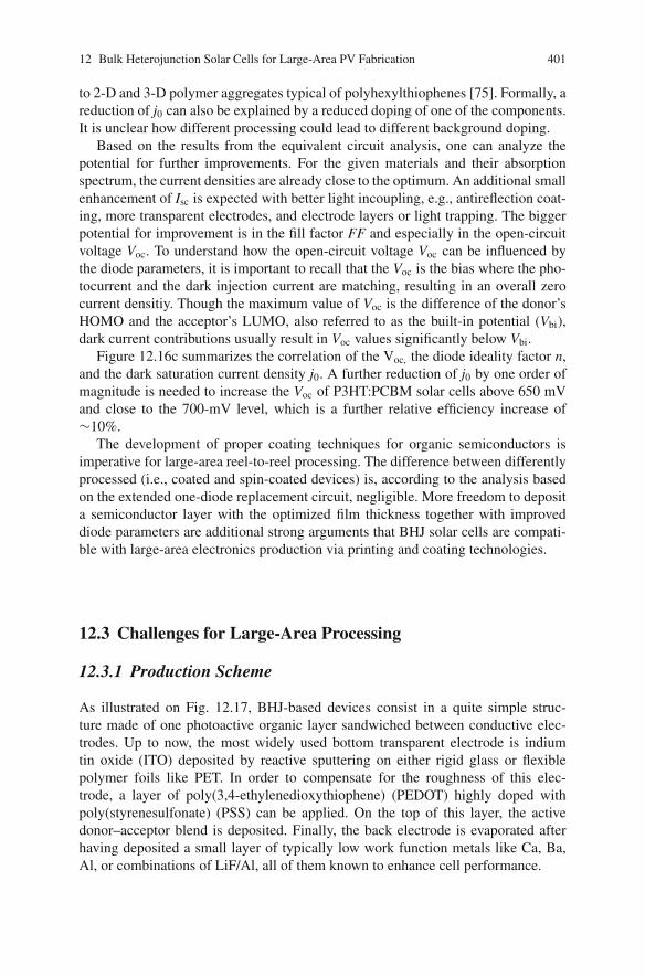
12 Bulk Heterojunction Solar Cells for Large-Area PV Fabrication 401
to 2-D and 3-D polymer aggregates typical of polyhexylthiophenes [75]. Formally, areduction of j0 can also be explained by a reduced doping of one of the components.It is unclear how different processing could lead to different background doping.
Based on the results from the equivalent circuit analysis, one can analyze thepotential for further improvements. For the given materials and their absorptionspectrum, the current densities are already close to the optimum. An additional smallenhancement of Isc is expected with better light incoupling, e.g., antireflection coat-ing, more transparent electrodes, and electrode layers or light trapping. The biggerpotential for improvement is in the fill factor FF and especially in the open-circuitvoltage Voc. To understand how the open-circuit voltage Voc can be influenced bythe diode parameters, it is important to recall that the Voc is the bias where the pho-tocurrent and the dark injection current are matching, resulting in an overall zerocurrent densitiy. Though the maximum value of Voc is the difference of the donor’sHOMO and the acceptor’s LUMO, also referred to as the built-in potential (Vbi),dark current contributions usually result in Voc values significantly below Vbi.
Figure 12.16c summarizes the correlation of the Voc, the diode ideality factor n,and the dark saturation current density j0. A further reduction of j0 by one order ofmagnitude is needed to increase the Voc of P3HT:PCBM solar cells above 650 mVand close to the 700-mV level, which is a further relative efficiency increase of∼10%.
The development of proper coating techniques for organic semiconductors isimperative for large-area reel-to-reel processing. The difference between differentlyprocessed (i.e., coated and spin-coated devices) is, according to the analysis basedon the extended one-diode replacement circuit, negligible. More freedom to deposita semiconductor layer with the optimized film thickness together with improveddiode parameters are additional strong arguments that BHJ solar cells are compati-ble with large-area electronics production via printing and coating technologies.
12.3 Challenges for Large-Area Processing
12.3.1 Production Scheme
As illustrated on Fig. 12.17, BHJ-based devices consist in a quite simple struc-ture made of one photoactive organic layer sandwiched between conductive elec-trodes. Up to now, the most widely used bottom transparent electrode is indiumtin oxide (ITO) deposited by reactive sputtering on either rigid glass or flexiblepolymer foils like PET. In order to compensate for the roughness of this elec-trode, a layer of poly(3,4-ethylenedioxythiophene) (PEDOT) highly doped withpoly(styrenesulfonate) (PSS) can be applied. On the top of this layer, the activedonor–acceptor blend is deposited. Finally, the back electrode is evaporated afterhaving deposited a small layer of typically low work function metals like Ca, Ba,Al, or combinations of LiF/Al, all of them known to enhance cell performance.
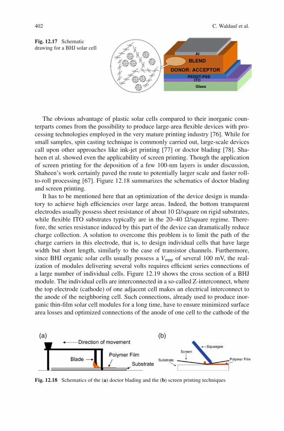
402 C. Waldauf et al.
Fig. 12.17 Schematicdrawing for a BHJ solar cell
The obvious advantage of plastic solar cells compared to their inorganic coun-terparts comes from the possibility to produce large-area flexible devices with pro-cessing technologies employed in the very mature printing industry [76]. While forsmall samples, spin casting technique is commonly carried out, large-scale devicescall upon other approaches like ink-jet printing [77] or doctor blading [78]. Sha-heen et al. showed even the applicability of screen printing. Though the applicationof screen printing for the deposition of a few 100-nm layers is under discussion,Shaheen’s work certainly paved the route to potentially larger scale and faster roll-to-roll processing [67]. Figure 12.18 summarizes the schematics of doctor bladingand screen printing.
It has to be mentioned here that an optimization of the device design is manda-tory to achieve high efficiencies over large areas. Indeed, the bottom transparentelectrodes usually possess sheet resistance of about 10 Ω/square on rigid substrates,while flexible ITO substrates typically are in the 20–40 Ω/square regime. There-fore, the series resistance induced by this part of the device can dramatically reducecharge collection. A solution to overcome this problem is to limit the path of thecharge carriers in this electrode, that is, to design individual cells that have largewidth but short length, similarly to the case of transistor channels. Furthermore,since BHJ organic solar cells usually possess a Vmpp of several 100 mV, the real-ization of modules delivering several volts requires efficient series connections ofa large number of individual cells. Figure 12.19 shows the cross section of a BHJmodule. The individual cells are interconnected in a so-called Z-interconnect, wherethe top electrode (cathode) of one adjacent cell makes an electrical interconnect tothe anode of the neighboring cell. Such connections, already used to produce inor-ganic thin-film solar cell modules for a long time, have to ensure minimized surfacearea losses and optimized connections of the anode of one cell to the cathode of the
(a) (b)
Fig. 12.18 Schematics of the (a) doctor blading and the (b) screen printing techniques
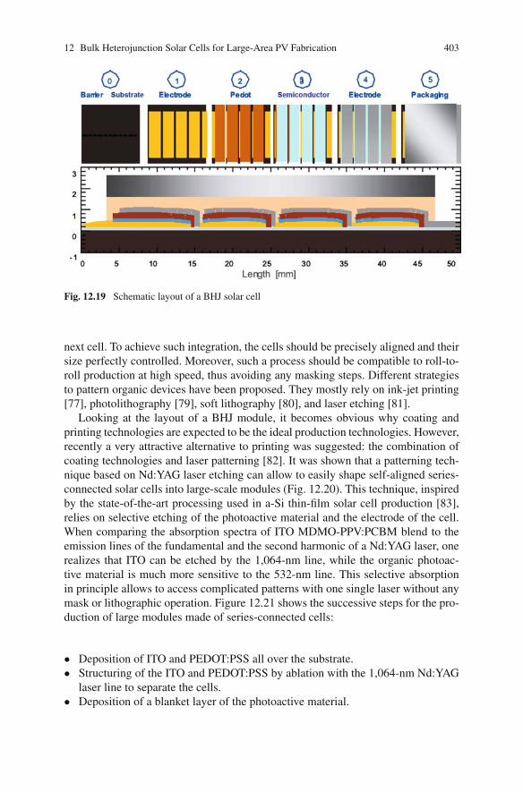
12 Bulk Heterojunction Solar Cells for Large-Area PV Fabrication 403
Fig. 12.19 Schematic layout of a BHJ solar cell
next cell. To achieve such integration, the cells should be precisely aligned and theirsize perfectly controlled. Moreover, such a process should be compatible to roll-to-roll production at high speed, thus avoiding any masking steps. Different strategiesto pattern organic devices have been proposed. They mostly rely on ink-jet printing[77], photolithography [79], soft lithography [80], and laser etching [81].
Looking at the layout of a BHJ module, it becomes obvious why coating andprinting technologies are expected to be the ideal production technologies. However,recently a very attractive alternative to printing was suggested: the combination ofcoating technologies and laser patterning [82]. It was shown that a patterning tech-nique based on Nd:YAG laser etching can allow to easily shape self-aligned series-connected solar cells into large-scale modules (Fig. 12.20). This technique, inspiredby the state-of-the-art processing used in a-Si thin-film solar cell production [83],relies on selective etching of the photoactive material and the electrode of the cell.When comparing the absorption spectra of ITO MDMO-PPV:PCBM blend to theemission lines of the fundamental and the second harmonic of a Nd:YAG laser, onerealizes that ITO can be etched by the 1,064-nm line, while the organic photoac-tive material is much more sensitive to the 532-nm line. This selective absorptionin principle allows to access complicated patterns with one single laser without anymask or lithographic operation. Figure 12.21 shows the successive steps for the pro-duction of large modules made of series-connected cells:
• Deposition of ITO and PEDOT:PSS all over the substrate.• Structuring of the ITO and PEDOT:PSS by ablation with the 1,064-nm Nd:YAG
laser line to separate the cells.• Deposition of a blanket layer of the photoactive material.
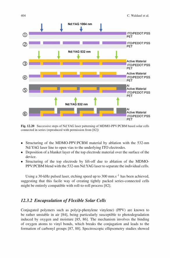
404 C. Waldauf et al.
Fig. 12.20 Successive steps of Nd:YAG laser patterning of MDMO-PPV:PCBM based solar cellsconnected in series (reproduced with permission from [82])
• Structuring of the MDMO-PPV:PCBM material by ablation with the 532-nmNd:YAG laser line to open vias to the underlying ITO electrodes.
• Deposition of a blanket layer of the top electrode material over the surface of thedevice.
• Structuring of the top electrode by lift-off due to ablation of the MDMO-PPV:PCBM blend with the 532-nm Nd:YAG laser to separate the individual cells.
Using a 30-kHz pulsed laser, etching speed up to 300 mm.s–1 has been achieved,suggesting that this facile way of creating tightly packed series-connected cellsmight be entirely compatible with roll-to-roll process [82].
12.3.2 Encapsulation of Flexible Solar Cells
Conjugated polymers such as poly(p-phenylene vinylene) (PPV) are known tobe rather unstable in air [84], being particularly susceptible to photodegradationinduced by oxygen and moisture [85, 86]. The mechanism involves the bindingof oxygen atoms to vinyl bonds, which breaks the conjugation and leads to theformation of carbonyl groups [87, 88]. Spectroscopic ellipsometry studies showed
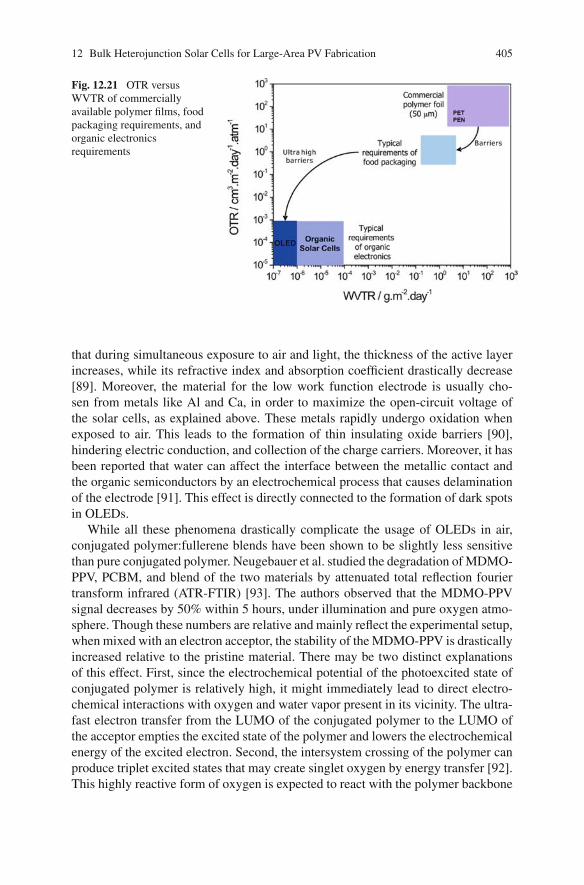
12 Bulk Heterojunction Solar Cells for Large-Area PV Fabrication 405
Fig. 12.21 OTR versusWVTR of commerciallyavailable polymer films, foodpackaging requirements, andorganic electronicsrequirements
that during simultaneous exposure to air and light, the thickness of the active layerincreases, while its refractive index and absorption coefficient drastically decrease[89]. Moreover, the material for the low work function electrode is usually cho-sen from metals like Al and Ca, in order to maximize the open-circuit voltage ofthe solar cells, as explained above. These metals rapidly undergo oxidation whenexposed to air. This leads to the formation of thin insulating oxide barriers [90],hindering electric conduction, and collection of the charge carriers. Moreover, it hasbeen reported that water can affect the interface between the metallic contact andthe organic semiconductors by an electrochemical process that causes delaminationof the electrode [91]. This effect is directly connected to the formation of dark spotsin OLEDs.
While all these phenomena drastically complicate the usage of OLEDs in air,conjugated polymer:fullerene blends have been shown to be slightly less sensitivethan pure conjugated polymer. Neugebauer et al. studied the degradation of MDMO-PPV, PCBM, and blend of the two materials by attenuated total reflection fouriertransform infrared (ATR-FTIR) [93]. The authors observed that the MDMO-PPVsignal decreases by 50% within 5 hours, under illumination and pure oxygen atmo-sphere. Though these numbers are relative and mainly reflect the experimental setup,when mixed with an electron acceptor, the stability of the MDMO-PPV is drasticallyincreased relative to the pristine material. There may be two distinct explanationsof this effect. First, since the electrochemical potential of the photoexcited state ofconjugated polymer is relatively high, it might immediately lead to direct electro-chemical interactions with oxygen and water vapor present in its vicinity. The ultra-fast electron transfer from the LUMO of the conjugated polymer to the LUMO ofthe acceptor empties the excited state of the polymer and lowers the electrochemicalenergy of the excited electron. Second, the intersystem crossing of the polymer canproduce triplet excited states that may create singlet oxygen by energy transfer [92].This highly reactive form of oxygen is expected to react with the polymer backbone
406 C. Waldauf et al.
creating carbonyl-type defects. As shown above, the ultrafast photoinduced electrontransfer does quench the inert system crossing to the triplet state, by hindering thisdegradation route.
Several studies focused on the lifetime investigation of conjugated poly-mer:fullerene solar cells. In the case of MDMO-PPV:PCBM cells encapsulatedbetween glass plates, Neugebauer et al. reported a decrease of 40% of the Voc and60% of the Isc within 3,000 hours, whereas unprotected cells lasted only coupleof hours [93]. Accelerated lifetime test showed that the degradation was about 10times faster at 80◦C than at 25◦C [94]. Moreover, the degradation was found tobe influenced by some morphological components. Indeed, Jeranko et al. investi-gated the aging effect by photocurrent imaging, which revealed the formation ofisland of higher efficiency [95]. Finally, deterioration of the electron collectingelectrode–polymer interface has been proposed as a determining factor [96, 97].Several attempts have been tried to reduce the degradation of the active materials,such as replacing the easily oxidized Al by more stable Au [98] or blending the pho-toactive polymer with a potentially protective host matrix [99]. However, efficientencapsulation solutions are required in order to ensure extended lifetime to this typeof device. In order to fully take advantage of the opportunities offered by solublematerials like conjugated polymers, these solution have to be mechanically flexible.
The ability of oxygen and moisture to cross an encapsulating membrane isquantified by the oxygen transmission rate (OTR) and the water vapor transmis-sion rate (WVTR). It is generally accepted that the lifetime of OLED devicesabove 10,000 hours requires WVTR and OTR of about 10−6 g.m−2.day−1 and10−4cm3.m−2.day−1.atm−1, respectively [100]. As illustrated on Fig. 12.21, thesevalues are about three to five orders of magnitude lower than the correspond-ing values of commercially available polymer films. However, since conjugatedpolymer:fullerene-based solar cells are slightly less sensitive to oxidative agents, itis commonly considered that WVTR around 10−4 g.m−2.day−1 might be sufficientfor this type of device. It has to be noted here that WVTR and OTR are inverselyproportional to the thickness of a homogeneous membrane. This result arises fromthe fact that these parameters are experimentally evaluated by placing the membranein between a fully saturated and a fully depleted atmosphere (under constant flux ofinert drain gas). The concentration of diffusing species decreases linearly across thethickness of the membrane. Thus, in order to decrease by four orders of magnitude,the OTR of a 50-μm-thick PET substrate, one would have to increase its thicknessby the same factor. Luckily, and for the sake of flexibility, another solution consistsof using inorganic gas barrier thin-film deposited on thin polymer substrates.
Transparent thin-film barrier coatings resistant to permeation of gases andvapors deposited onto flexible polymer substrates have been intensively studied forapplications in food and pharmaceutical packaging, where improving the barriercapabilities of the bare plastic films by 1–3 orders of magnitude is usually consid-ered sufficient (Fig. 12.21). It has been shown that silicon-based dielectric coatingsdeposited by plasma enhanced chemical vapor deposition (PECVD) on plastic filmscan be used as single layer permeation barriers yielding barrier improvement fac-tors (BIF) up to 3 orders of magnitude [101, 102]. Permeation through those barrier
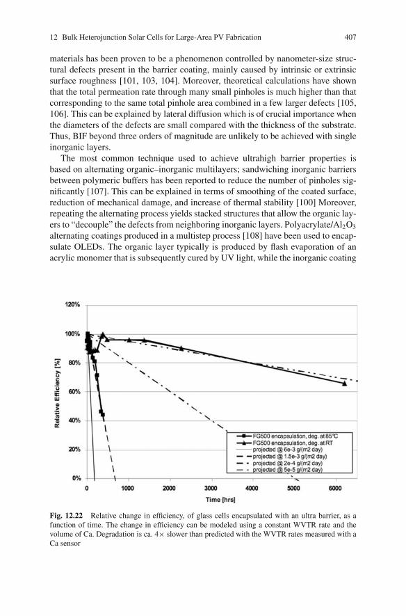
12 Bulk Heterojunction Solar Cells for Large-Area PV Fabrication 407
materials has been proven to be a phenomenon controlled by nanometer-size struc-tural defects present in the barrier coating, mainly caused by intrinsic or extrinsicsurface roughness [101, 103, 104]. Moreover, theoretical calculations have shownthat the total permeation rate through many small pinholes is much higher than thatcorresponding to the same total pinhole area combined in a few larger defects [105,106]. This can be explained by lateral diffusion which is of crucial importance whenthe diameters of the defects are small compared with the thickness of the substrate.Thus, BIF beyond three orders of magnitude are unlikely to be achieved with singleinorganic layers.
The most common technique used to achieve ultrahigh barrier properties isbased on alternating organic–inorganic multilayers; sandwiching inorganic barriersbetween polymeric buffers has been reported to reduce the number of pinholes sig-nificantly [107]. This can be explained in terms of smoothing of the coated surface,reduction of mechanical damage, and increase of thermal stability [100] Moreover,repeating the alternating process yields stacked structures that allow the organic lay-ers to “decouple” the defects from neighboring inorganic layers. Polyacrylate/Al2O3
alternating coatings produced in a multistep process [108] have been used to encap-sulate OLEDs. The organic layer typically is produced by flash evaporation of anacrylic monomer that is subsequently cured by UV light, while the inorganic coating
Fig. 12.22 Relative change in efficiency, of glass cells encapsulated with an ultra barrier, as afunction of time. The change in efficiency can be modeled using a constant WVTR rate and thevolume of Ca. Degradation is ca. 4× slower than predicted with the WVTR rates measured with aCa sensor
408 C. Waldauf et al.
is usually deposited by reactive sputtering. WVTR of about 2 × 10⁻⁶ g.m−2.day−1
has been reported [109], yielding 5-mm2 OLED lifetime of 2,500 hours [110].In the case of conjugated polymer:fullerene solar cells, the usage of another
type of ultrahigh barrier was reported. This barrier, entirely produced by PECVDof alternating organic/SiOx on 175-μm-thick PET substrate, succeeded accelerated“calcium test” (50◦C, 85% relative humidity) for more than 1,000 hours, which cor-responds to at least 10,000 hours under normal ambient conditions [111]. Dennleret al. showed that MDMO-PPV:PCBM cells fabricated on such substrates andsubsequently encapsulated exhibit shelf lifetime of about 3,000 hours in spite oftheir appreciable mechanical flexibility. The correlation between the device life-time and the barrier property was recently investigated by Hauch et al. (Fig. 12.22).Figure 12.22 correlates the lifetime of single cells with the WVTR of the packagingmaterial. For a variety of WVTRs, the device lifetime correlated quite well with theWVTR of the top package. Thus, solar cells with sensitive electrodes like Ca dohave an environmental stability issue. Careful engineering of the devices was nec-essary to achieve longer lifetimes. Operational lifetimes beyond 1,000 hours underone sun and elevated temperatures were reported for glass as well as flexible sub-strates [112–114]. These observations reveal that the encapsulation may not be thelimiting factor and the combined usage of more stable conjugated polymers, betterdefined interfaces in combination with reasonable high barrier coatings, will lead tovery long lifetimes [95].
12.4 Conclusions
BHJ solar cells made impressive progress over the last couple of years. Starting withroughly 1% efficient devices on a few millimeter square active areas, processed bysublimation of compounds such as merocyanines [115] and pthalocyanines [116]in the late 1980s, today’s efficiency is over 6%, on large areas and on flexible sub-strates with impressive lifetime. The rapid progress in this field is mostly basedon the progress in the materials science and production technologies. Today’s BHJsolar cells can be processed on glass as well as on flexible substrates with rela-tive ease and comparable performance. From today’s perspective, it seems onlya question of time when devices with 10% power conversion efficiency on flexi-ble substrates and large areas will be demonstrated. One key development allow-ing such high efficiencies certainly will be on the materials side. The second, asimportant development, is to gain improved control over the solid-state morphologyof donor–acceptor composites. The near future will show exciting developments,and some of them can be anticipated already today, like self-assembled materi-als, nanosized device geometries release the requirements on the proper morphol-ogy, metallic nanoparticles and plasmon absorption and highly complex moleculeswhich fulfil all functions in distinct parts of the molecule. In parallel to these excit-ing new fields, we will see a fast development of the solution-based techniquessuch as ink-jet, screen, or flexographic printing (a form of rotary web letterpress
12 Bulk Heterojunction Solar Cells for Large-Area PV Fabrication 409
using flexible relief plates) for the production of BHJ solar cells. Other importanteconomic factors addressing the balance-of-system costs are novel semiconductingelectrodes to replace ITO, low-cost barriers against water and oxygen permeationas well as flexible electronic components to be combined with flexible PV powersupply. The BHJ technologies will see an exciting nearby future in the applicationof PVs.
References
1. Shockley W, Queisser HJ (1961) Detailed Balance Limit of Efficiency of p-n Junction SolarCells J Appl Phys 32:510
2. Gregg BA, Hanna MC (2003) J Appl Phys 93:36053. Sariciftci NS (ed) (1997) Primary Photoexcitation in Conjugated Polymers: Molecular Exci-
ton Versus Semiconductor Band Model. World Scientific, Singapore4. Gregg BA (2003) J Phys Chem B 107:46885. O’Regan B, Graetzel M (1991) Nature 353:7376. Yu G, Gao J, Hummelen JC, Wudl F, Heeger AJ (1995) Science 270:17897. Drechsel J, Mannig B, Kozlowski F, Pfeiffer M, Leo K, Hoppe H (2005) Appl Phys Lett
86:2441018. Huynh WU, Dittmer JJ, Alivisatos AP (2002) Science 295:24259. Onsager L (1938) Phys Rev 54:554
10. Schweitzer B, Bassler H (2000) Synth Met 109:111. Haugeneder A, Neges M, Kallinger C, Spirkl W, Lemmer U, Feldmann J, Scherf U, Harth
E, Gugel A, Mullen K (1999) Phys Rev B 59:1534612. Vacar D, Maniloff ES, McBranch DW, Heeger AJ (1997) Phys Rev B 56:457313. Theander M, Yartsev A, Zigmantas D, Sundstrom V, Mammo W, Andersson MR, Inganas O
(2000) Phys Rev B 61:1295714. Popovic ZD, Hor A-M, Loutfy RO (1988) Chem Phys 127:45115. Arkhipov VI, Emelianova EV, Bassler H (1999) Phys Rev Lett 82:132116. Wang Y (1992) Nature 356:58517. Sariciftci NS, Smilowitz L, Heeger AJ, Wudl F (1992) Science 258:147418. Morita S, Zakhidov AA, Yoshino K (1992) Solid State Commun 82:24919. Brabec CJ, Zerza G, Cerullo G, De Silvestri S, Luzzati S, Hummelen JC, Sariciftci NS
(2001) Chem Phys Lett 340:23220. Wurfel P, Bauer G (2003) Quantum solar energy conversion in organic solar cells. In:
Brabec CJ, Dyakonov V, Parisi J, Sariciftci S (eds) Organic Photovoltaics, Springer, Berlin,pp 118–158
21. Waldauf C, Schilinsky P, Hauch J, Brabec CJ (2004) Thin Solid Films 451–452:50322. Koster LJA, Smits ECP, Mihailetchi VD, Blom PWM (2005) Phys Rev B 72:08520523. Mihailetchi VD, Koster LJA, Hummelen JC, Blom PWM (2005) Phys Rev Lett 93:21660124. Marcus RA (1993) Rev Mod Phys 65:59925. Miller A, Abrahams E (1960) Phys Rev 120:74526. Pai DM (1970) J Chem Phys 52:228527. Mozer AJ, Dennler G, Sarificti NS, Westerling M, Pivrikas A, Osterbacka R, Juska G (2005)
Phys Rev B 72:03521728. Rakhmanova SV, Conwell EM (2001) Synth Met 116:38929. Mozer AJ, Sariciftci NS, Pivrikas A, Osterkacka R, Juska G, Brassat L, Bassler H (2005)
Phys Rev B 72:03521430. Riedel I, Parisi J, Dyakonov V, Lutsen L, Vanderzande D, Hummelen JC (2004) Adv Funct
Mater 14:3831. Gommans HHP, Kemerink M, Kramer JM, Janssen RAJ (2005) Appl Phys Lett 87:122104
410 C. Waldauf et al.
32. Montanari I, Nohueira AF, Nelson J, Durrant J, Winder C, Loi MA, Sariciftci NS, BrabecCJ (2002) Appl Phys Lett 81:3001
33. O′Regan BC, Scully S, Mayer AC, Palomares E, Durrant J (2005) J Phys Chem B 109:461634. Meskers SCJ, van Hal PA, Spiering AJH, Hummelen JC, Janssen RAJ (2000) Phys Rev B
61:991735. Kroeze JE, Savenije TJ, Vermeulen MJW, Warman JM (2003) J Phys Chem B 107:769636. Savenije TJ, Kreoze JE, Wienk MM, Kroon JM, Warman JM (2004) Phys Rev B 69:15520537. Juska G, Arlauskas K, Viliunas M, Kocka J (2000) Phys Rev Lett 84:494638. Juska G, Arlauskas K, Viliunas M, Genevicius K, Osterbacka R, Stubb H (2000) Phys Rev
B 62:1623539. Langevin P (1903) Ann Chem Phys 28:28940. Pivrikas A, Juska G, Mozer AJ, Scharber M, Arlauskas K, Sariciftci NS, Stubb H, Oster-
backa R (2005) Phys Rev Lett 94:17680641. Mihailetchi VD, Koster LJA, Blom PWM, Melzer C, de Boer B, van Duren JKJ, Janssen
RAJ (2005) Adv Funct Mater 15:79542. Parker ID (1994) J Appl Phys 75:165643. Brabec CJ, Cravino A, Meissner D, Sariciftci NS, Fromherz T, Rispens MT, Sanchez L,
Hummelen JC (2001) Adv Funct Mater 11:37444. Brabec CJ, Cravino A, Meissner D, Sariciftci NS, Rispens MT, Sanchez L, Hummelen JC,
Fromherz T (2002) Thin Solid Films 403–404:36845. Kim H, Jin S-H, Suh H, Lee K (2004) Proc. SPIE 5215:11146. Gadisa A, Svensson M, Andersson MR, Inganas O (2004) Appl Phys Lett 84:160947. Frohne H, Shaheen SE, Brabec CJ, Mueller D, Sariciftci NS, Meerholz K. (2002) Chem
Phys Chem 9:79548. Wurfel P. (2004) Physics of Solar Cells. Wiley VCH, Weinheim49. Crispin A, Crispin X, Fahlman M, Berggren M, Salaneck, W (2006) Appl Phys Lett
89:21350350. Waldauf C, Schilinsky P, Hauch J, Brabec CJ (2004) Thin Solid Films 451–452:50351. Hall RN (1952) Phys Rev 87:38752. Shockley W, Read WT (1952) Phys Rev 87:835–84253. Merten J, Asensi JM, Voz C, Shah AV, Platz R, Andreu J (1998) IEEE Transactions on
Electron Devices 45:42354. Brabec CJ, Cravino A, Meissner D, Sariciftci NS, Fromherz T, Rispens MT, Sanchez L,
Hummelen JC (2001) Adv Funct Mater 11(5):374–38055. Montanari I, Nogueira AF, Nelson J, Durrant JR, Winder C, Loi MA, Sariciftci NS, Brabec
C (2002) Appl Phys Lett 81:300156. Koster LJA, Mihailetchi VD, Ramaker R, Blom PWM (2005) Appl Phys Lett 86:12350957. Mihailetchi VD, Koster LJA, Blom PWM (2004) Appl Phys Lett 85(6):97158. Haugeneder A, Neges M, Kallinger C, Spirkl W, Lemmer U, Feldmann J, Scherf U, Harth
E, Gugel A, Mullen K (1999) Phys Rev B Condens Matter 59(23):1534659. Kankan B, Castelino K, Majumdar A (2003) Nano Lett 3(12):172960. Brabec CJ, Zerza G, Cerillo G, DeSilvestris S, Luzatti S, Hummelen JC, Sariciftci NS (2001)
Chem Phys Lett 340:23261. Morteani AC, Sreearunothai P, Herz LM, Friend RH, Silva C (2004) Phys Rev Lett
92(24):247402–24741362. Halls JJM, Cornil J, dosSantos DA, Silbey R, Hwang DH, Holmes AB, Bredas JL, Friend
RH (1999) Phys Rev B Condens Matter 60(8):572163. Fujii A, Mizukami H, Umeda T, Shirakawa T, Hashimoto Y, Yoshino K (2004) Jpn J Appl
Phys 43(12):8312–831564. Schilinsky P, Waldauf C, Brabec CJ (2002) Appl Phys Lett 81:388565. Waldauf C, Schilinsky P, Hauch J, Brabec CJ (2004) Thin Solid Films 451–452:50366. NREL certificate for Konarka solar cell E8-6 from July, 18th, 200567. Shaheen S, Radspinner R, Peyghambarian N, Jabbour GE (2001) Appl Phys Lett 79:2996
12 Bulk Heterojunction Solar Cells for Large-Area PV Fabrication 411
68. Sirringhaus H, Kawase T, Friend RH (2001) MRS Bulletin 26(7):53969. Duren KJ, Yang X, Loos J, Bulle-Lieuwana CWT, Sieval AB, Hummelen JC, Janssen RAJ
(2004) Adv Func Mat 14:42570. Sze SM (1985) Physics of Semiconductor Devices, 2nd edn. John Wiley & Sons, New York71. Lewerenz HJ, Jungblut H (1995) Photovoltaik. Springer, Berlin72. Waldauf C, Scharber MC, Schilinsky P, Hauch JA, Brabec CJ (2006) J Appl Phys 99:10450373. Waldauf C, Schilinsky P, Hauch J, Brabec CJ (2004) Thin Solid Films 451–452:50374. Chang J-F, Sun B, Breiby DW, Nielsen MM, Solling T, Giles M, McCulloch I, Sirringhaus
H (2004) Chem Mater 16:477275. Osterbacka R, An CP, Jiang XM, Vardeny ZV (2000) Science 287:83976. Brabec CJ, Hummelen JC, Janssen RAJ, Sariciftci NS (1999) Synth Met 102:86177. Sirringhaus H, Kawase T, Friend RH, Shimoda T, Inbasekaran M, Wu W, Woo EP (2000)
Science 290:212378. Brabec CJ, Sariciftci NS, Hummelen JC (2001) Adv Funct Mater 11:1579. Makela T, Pienimaa S, Jussila S (1999) Synth Met 101:70580. Granlund T, Nyberg T, Roman LS, Svensson M, Inganas O (2000) Adv Mater 12:26981. Tak Y-H, Kim C-N, Kim M-S, Kim K-B, Lee M-H, Kim S-T (2003) Synth Met 138:49782. Dennler G, Lungenschmied C, Neugebauer H, Sariciftci NS, Labouret A (2005) J Mater Res
20:322483. Akimasa U, Susumu K (2001) Method of Fabricating Integrated Thin Film Solar Cells.
Patent US616896884. Morgado J, Friend RH, Cacialli F (2000) Synth Met 114:18985. Sutherland DGJ, Carlisle JA, Elliker P, Fox G, Hagler TW, Jimenez I, Lee HW, Pakbaz K,
Terminello LJ, Williams SC, Himpsel FJ, Shuh DK, Tong WM, Lia JJ, Callcott TA, EdererDL (1996) Appl Phys Lett 68:2046
86. Low HY (2002) Thin Solid Films 413:16087. Scurlock RD, Wang B, Ogilby PR, Sheats JR, Clough RL (1995) J Am Chem Soc 117:1019488. Cumpston BH, Parker ID, Jensen KF (1997) J Appl Phys 81:371689. Kumar S, Biswas AK, Shukla VK, Awasthi A, Anand RS, Narain J (2003) Synth Met
139:75190. Do LM, Han EM, Nidome Y, Fujihira M, Kanno T, Yoshida S, Maeda A, Ikushima AJ (1994)
J Appl Phys 76:511891. Schaer M, Nuesch F, Berner D, Leo W, Zuppiroli L (2001) Adv Func Mater 11:11692. Hale GD, Oldenburg SJ, Halas NJ (1997) Phys Rev B 55:1606993. Neugebauer H, Brabec CJ, Hummelen JC, Sariciftci NS (2000) Sol Ener Mater Sol Cells
61:3594. Schuller S, Schilinsky P, Hauch J, Brabec CJ (2004) Appl Phys A 79:3795. Jeranko T, Tributsch H, Sariciftci NS, Hummelen JC (2004) Sol Ener Mater Sol Cells 83:24796. Krebs FC, Carle JE, Cruys-Bagger N, Andersen M, Lilliedal MR, Hammond MA, Hvidt S
(2005) Sol Ener Mater Sol Cells 86:49997. Kroon JM, Wienk MM, Verhees WJH, Hummelen JC (2002) Thin Solid Films 403–404:22398. Sahin Y, Alem S, De Bettignies R, Nunzi J-M (2005) Thin Solid Films 476:34099. Brabec CJ, Padinger F, Sarificti NS, Hummelen JC (1999) J Appl Phys 85:6866
100. Lewis JS, Weaver MS (2004) IEEE. J Select Topics Quantum Elect 10:45101. da Silva Sobrinho AS, Latreche M, Czeremuszkin G, Klemberg-Sapieha JE, Wertheimer
MR (1998) J Vac Sci Technol A 16:3190102. Leterrier Y (2003) Prog Mater Sci 48:1103. da Silva Sobrinho AS, Czeremuszkin G, Latreche M, Dennler G, Wertheimer MR (1999)
Surf Coat Technol 116–119:1204104. Dennler G, Houdayer A, Segui Y, Wertheimer MR (2001) J Vac Sci Technol A 19:2320105. Russi G, Nulman M (1993) J Appl Phys 74:5471106. da Silva Sobrinho AS, Czeremuszkin G, Latreche M, Wertheimer MR (2000) J Vac Sci
Technol A 18:149
412 C. Waldauf et al.
107. Affinito JD, Gross ME, Coronado CA, Graff GL, Greenwell EN, Martin PM (1996) ThinSolid Films 290–291:263
108. Affinito JD, Gross ME, Mournier PA, Shi MK, Graff GL (1999) J Vac Sci Technol A 17:1974109. Weaver MS, Michalski LA, Rajan K, Rothman MA, Silvernail JA, Burrows PE, Graff GL,
Gross ME, Martin PM, Hall M, Mast E, Bonham C, Bennett W, Zumhoff M (2002) ApplPhys Lett 81:2929
110. Chwang AB, Rothman MA, Mao SY, Hewitt RH, Weaver MS, Sivernail JA, Rajan K, HackM, Brown JJ, Chu X, Moro L, Krajewski T, Rutherford N (2003) Appl Phys Lett 83:413
111. Dennler G, Lungenschmied C, Neugebauer H, Sariciftci NS, Latreche M, Czeremuszkin G,Wertheimer MR (2005) Thin Sol Films 349
112. Kroon JM, Veenstra SC, Slooff LH, Verhees WJH, Koetse MM, Sweelssen J, Schoo HFM,Beek WJE, Wienk MM, Janssen RAJ, Yang X, Loos J, Michailetchi VD, Blom PWM, KnolJ, Hummelen JC (2005) Proceedings of the 20th European Photovoltaic Solar Energy Con-ference and Exhibition, Barcelona, Spain, June 6–10, 2005
113. Schuller S, Schilinsky P, Hauch J, Brabec CJ (2004) Appl Phys A 79:37114. Brabec CJ, Schilinsky P, Waldauf C, Hauch J (2005) MRS Bulletin January 30, 2005115. Chamberlain GA (1983) Solar Cells 8:47116. Simon J, Andre J-J (1985) Molecular Semiconductors. Springer-Verlag, Berlin
Chapter 13Substrates and Thin-Film Barrier Technologyfor Flexible Electronics
Ahmet Gun Erlat, Min Yan, and Anil R. Duggal
13.1 Introduction
The term “flexible electronics” encompasses a wide array of applications such asflexible displays, low-cost and/or large-area sensors, conformal lighting, and solarcells to name a few, with one common ingredient: the ability to fabricate electronicand optoelectronic devices on nonrigid substrates such as plastic films, metal foil,or thin glass, without losing the functionality of the devices during operation. Otherterms often used to convey this concept include “printable electronics”, “macro-electronics,” and “organic electronics.” The promise of flexible electronics lies inthe potential for building large-area electronic devices with much lower cost thanpossible with conventional silicon-based technology [1]. The technologies beingdeveloped to enable this all revolve around building devices using low-cost print-ing techniques that are compatible with high-volume “roll-to-roll” manufacturing.Example technologies that are potentially compatible with low-cost printing tech-niques include organic light-emitting devices (OLEDs) [2–3], organic photovoltaicdevices [4–6], thin-film transistors (TFTs) and TFT arrays using both organic [7–9]and solution-processible inorganic materials [10, 11], electronic paper [12], wear-able electronics [13], flexible batteries [14], RFID tags [15], sensors [16], and morecomplicated circuitry [17–19].
Fabricating these devices on flexible substrates, particularly on plastic, bringswith it new challenges in order to make them commercially viable. One critical chal-lenge is to design a means of hermetic packaging of the organic electronic devicebecause many such devices exhibit a very short shelf lifetime if not protected fromthe ingress of environmental permeants such as oxygen and water vapor [20]. Sucha packaging scheme can be viewed to have two components. First, the substrate on
A.G. Erlat (B)General Electric Global Research Center, 1 Research Circle, KWC 331, Niskayuna, NY 12309e-mail: [email protected]
W.S. Wong, A. Salleo (eds.), Flexible Electronics: Materials and Applications, ElectronicMaterials: Science & Technology, DOI 10.1007/978-0-387-74363-9 13,C© Springer Science+Business Media, LLC 2009
413
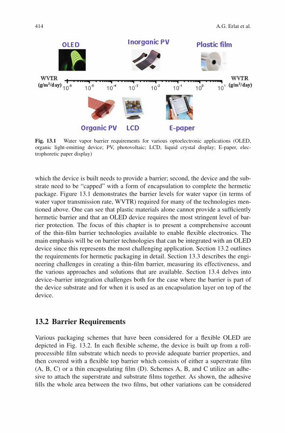
414 A.G. Erlat et al.
Fig. 13.1 Water vapor barrier requirements for various optoelectronic applications (OLED,organic light-emitting device; PV, photovoltaic; LCD, liquid crystal display; E-paper, elec-trophoretic paper display)
which the device is built needs to provide a barrier; second, the device and the sub-strate need to be “capped” with a form of encapsulation to complete the hermeticpackage. Figure 13.1 demonstrates the barrier levels for water vapor (in terms ofwater vapor transmission rate, WVTR) required for many of the technologies men-tioned above. One can see that plastic materials alone cannot provide a sufficientlyhermetic barrier and that an OLED device requires the most stringent level of bar-rier protection. The focus of this chapter is to present a comprehensive accountof the thin-film barrier technologies available to enable flexible electronics. Themain emphasis will be on barrier technologies that can be integrated with an OLEDdevice since this represents the most challenging application. Section 13.2 outlinesthe requirements for hermetic packaging in detail. Section 13.3 describes the engi-neering challenges in creating a thin-film barrier, measuring its effectiveness, andthe various approaches and solutions that are available. Section 13.4 delves intodevice–barrier integration challenges both for the case where the barrier is part ofthe device substrate and for when it is used as an encapsulation layer on top of thedevice.
13.2 Barrier Requirements
Various packaging schemes that have been considered for a flexible OLED aredepicted in Fig. 13.2. In each flexible scheme, the device is built up from a roll-processible film substrate which needs to provide adequate barrier properties, andthen covered with a flexible top barrier which consists of either a superstrate film(A, B, C) or a thin encapsulating film (D). Schemes A, B, and C utilize an adhe-sive to attach the superstrate and substrate films together. As shown, the adhesivefills the whole area between the two films, but other variations can be considered
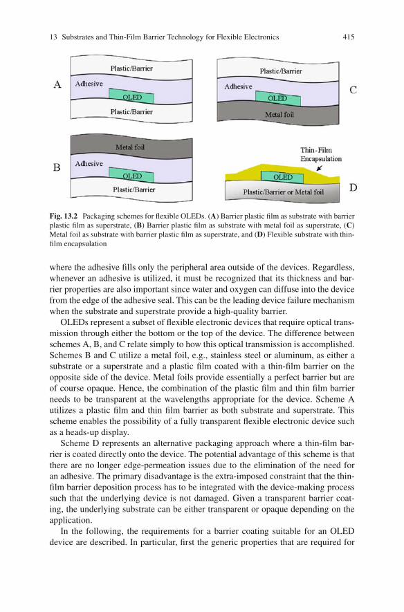
13 Substrates and Thin-Film Barrier Technology for Flexible Electronics 415
Fig. 13.2 Packaging schemes for flexible OLEDs. (A) Barrier plastic film as substrate with barrierplastic film as superstrate, (B) Barrier plastic film as substrate with metal foil as superstrate, (C)Metal foil as substrate with barrier plastic film as superstrate, and (D) Flexible substrate with thin-film encapsulation
where the adhesive fills only the peripheral area outside of the devices. Regardless,whenever an adhesive is utilized, it must be recognized that its thickness and bar-rier properties are also important since water and oxygen can diffuse into the devicefrom the edge of the adhesive seal. This can be the leading device failure mechanismwhen the substrate and superstrate provide a high-quality barrier.
OLEDs represent a subset of flexible electronic devices that require optical trans-mission through either the bottom or the top of the device. The difference betweenschemes A, B, and C relate simply to how this optical transmission is accomplished.Schemes B and C utilize a metal foil, e.g., stainless steel or aluminum, as either asubstrate or a superstrate and a plastic film coated with a thin-film barrier on theopposite side of the device. Metal foils provide essentially a perfect barrier but areof course opaque. Hence, the combination of the plastic film and thin film barrierneeds to be transparent at the wavelengths appropriate for the device. Scheme Autilizes a plastic film and thin film barrier as both substrate and superstrate. Thisscheme enables the possibility of a fully transparent flexible electronic device suchas a heads-up display.
Scheme D represents an alternative packaging approach where a thin-film bar-rier is coated directly onto the device. The potential advantage of this scheme is thatthere are no longer edge-permeation issues due to the elimination of the need foran adhesive. The primary disadvantage is the extra-imposed constraint that the thin-film barrier deposition process has to be integrated with the device-making processsuch that the underlying device is not damaged. Given a transparent barrier coat-ing, the underlying substrate can be either transparent or opaque depending on theapplication.
In the following, the requirements for a barrier coating suitable for an OLEDdevice are described. In particular, first the generic properties that are required for
416 A.G. Erlat et al.
both an encapsulation coating and a substrate coating are described and then theneeds that are unique to the substrate coating application are given.
13.2.1 Generic Requirements
13.2.1.1 Barrier Level
The packaging of an OLED device affects mainly its “shelf lifetime,” i.e., how thedevice degrades in the environment even when it is not in use. Shelf lifetime is lim-ited due to several potential degradation mechanisms. OLEDs utilize low work func-tion cathodes that are evaporatively deposited [3, 21]. These materials are extremelyreactive with water and can lose their electrical properties rapidly upon exposure tomoisture [22]. Also, water vapor permeating through the pinholes in the vacuum-deposited cathode can diffuse into the metal–organic interface and limit electroninjection as well as cause delamination [22]. In addition, the commonly used organicmaterials within the active layers of the device are known to lose their emissiveproperties due to moisture exposure [22, 23]. As a result of all or some of thesemechanisms, degradation presents itself as growing dark spots distributed through-out the active area or as a front of nonemissive area growing in from the edges ofthe device. Simple calculations, primarily based on the degradation of the cathodematerial when exposed to water vapor, suggest that in order to achieve a device life-time of 10,000 hours at room temperature, the substrate must provide a barrier thatlimits permeation rates to less than 10−6 g/m2/day and 10−3 cm3/m2/day for watervapor and oxygen, respectively [24, 25].
13.2.1.2 Optical Properties
Any absorption of light in the barrier film through the emissive side of the deviceresults directly in a loss in device efficiency. Hence, any such loss needs to beminimized. In addition, because light from an OLED is emitted from an opticalmicrocavity, the refractive index of the barrier film needs to be understood and con-trolled [26]. This is particularly important for cases where the barrier coating con-sists of multiple components with different refractive indices since these can act asdielectric mirrors, which greatly enhance microcavity effects. Depending on devicedesign, these microcavity effects can enhance, suppress, or distort the desired lightemission.
13.2.1.3 Mechanical Flexibility
Mechanical flexibility is required for roll-to-roll (R2R) processing and for variousend-use applications such as bendable to “roll-up” displays. A typical metric to testthe barrier structure for the latter application is to bend the barrier-coated substrateover a 1” diameter 100 or 1,000 times and measure the barrier properties beforeand after this test. It has been demonstrated that the most advanced barrier films onplastic substrates can pass this test [26–28].
13 Substrates and Thin-Film Barrier Technology for Flexible Electronics 417
13.2.1.4 Compatibility of the Barrier Coating
It goes without saying that the process conditions used to deposit the barrier must becompatible with the underlying layers. For a device encapsulation application, thiscan be a demanding requirement – particularly for organic electronic devices wherethe active organic layers degrade at relatively low temperatures (150–200◦C) andare sensitive to UV radiation and ion bombardment. For a barrier coating on plasticsubstrate application, the same considerations apply but there is less sensitivity toslight degradation in the substrate since it is not one of the active layers of the device.
13.2.2 Substrate-Specific Requirements
13.2.2.1 Substrate Options
When mechanical flexibility is not a requirement, the substrate material of choice forOLED devices is glass as it is transparent, smooth, impermeable to water and oxy-gen, and chemically and thermally stable. Glass can actually be considered for flexi-ble electronics applications because, when fabricated with a thickness of <200 μm,it is relatively bendable. Currently, glass sheet as thin as 30 microns can be producedusing down-draw processing [29]. Unfortunately, the application space open to thinglass is likely to be small because this material is still brittle, difficult to produce inlarge sheets, and unsuitable for R2R processing.
Metal foils are flexible, have excellent barrier and thermal properties, and arecompatible with R2R processing. In fact, at the research stage, stainless steel foilhas been successfully integrated into a flexible active-matrix electrophoretic displaydevice by E Ink Corporation [30] and into a flexible active-matrix OLED displaydevice by Universal Display Corporation [31]. Hence, it appears likely that metalfoil substrates will play a prominent role in flexible electronics. The main drawbackis that applications are limited to the packaging scheme C depicted in Fig. 13.2 and,for optical devices, still require a barrier encapsulation coating or a superstrate. Itshould be noted that typically the metal foil substrate still requires its own thin-filmcoating to provide the appropriate combination of surface smoothness, electricalisolation, and chemical resistance required by the application.
For applications where a transparent flexible substrate is required, a plastic filmis necessary. In choosing an appropriate plastic film, it is useful to categorize theavailable options by glass transition temperature (Tg) as this sets the scale for theaccessible processing temperatures and time. Another key distinction is whetherthe underlying structure is amorphous or semicrystalline as this leads to differentthermomechanical film properties. Amorphous polymers can be further subdividedinto thermoplastic materials, which can be converted into films via an extrusionprocess, and higher Tg materials, which require solvent casting for film formation.
Semicrystalline polymeric films, such as PET and PEN, are commercially avail-able from DuPont under the names Melinex® and Teonex® respectively. PET hasa relatively low Tg around 78◦C, while PEN has Tg around 120◦C. Due to theirsemicrystallinity, PET and PEN have relatively low coefficient of thermal expansion
418 A.G. Erlat et al.
(CTE), which is around 15 ppm/◦C and better solvent resistance when comparedwith amorphous polymeric films. PET and PEN films can be melt cast followedby biaxial stretching and heat setting processes to crystallize the film. The dimen-sional stability of PET and PEN films can be further enhanced by a heat stabiliza-tion process in which the internal stress in the film is relaxed by exposure to hightemperature while under minimum line tension [32]. The heat stabilization processdramatically reduces the shrinkage rate of PET and PEN films at temperatures abovetheir glass transition temperatures and thereby extends the accessible process tem-peratures. For instance, even though PET has a Tg of 78◦C, when heat stabilized itcan be processed at temperatures above 100◦C.
Examples of thermoplastic amorphous polymers include polycarbonates (PCs)and polyethersulfones (PES). The classic bisphenol A (BPA) PC (e.g., GE’sLexan®) has a Tg of ∼150◦C, while new engineered high heat PCs are now com-mercially available with Tgs around 220◦C (e.g., GE’s Lexan® XHT resin). PES,materials (e.g., Sumitomo Bakelite’s Sumilite®) also offer Tgs around 220◦C. BothPC and PES have a relatively high CTE (50∼70 ppm/◦C) due to their amorphousstructure.
Several high Tg polymers can only be solvent cast due to the fact that their melt-ing points are too high to allow the polymers to be melt processed without significantdegradation. This typically results in a higher cost for the resulting film. Examplesof solvent cast amorphous polymer films include aromatic fluorine-containing pol-yarylate (PAR), e.g., Ferranias Arylite®; polycyclic olefin (PCO), e.g., PromerusAppear®; and polyimide (PI), e.g., DuPont Kapton® [32, 33].
Most of the plastic films described above can deliver optical transparency overthe visible light range except for PI, which is yellow. PC, in particular, has excel-lent optical properties (high transmission, low haziness). Polymeric films tend toundergo undesirable change in dimension when heated to high temperatures dueto molecular relaxation associated with the increased mobility of polymer chainsand relaxation of residual strain within the film. This effect is, in general, lesspronounced for semicrystalline polymers than for amorphous polymers. In addi-tion, semicrystalline films are inherently stiffer than amorphous films (∼3× greaterYoung’s modulus). Nevertheless, the thermomechanical stability of any plastic filmis substantially inferior to glass or metal foil and hence any robust manufacturingprocess needs to be designed with this in mind.
All these substrate choices have advantages and disadvantages and they mostoften require additional coatings that can provide functions other than barrier tomoisture and oxygen.
13.2.2.2 Chemical Resistance
Most device fabrication processes utilize solvents and chemicals that may dis-solve or otherwise damage the plastic substrate. A typical list of the materials thatthe substrate must be compatible with includes methanol, isopropanol, acetone,tetrahydrofuran, n-methylpyrrolidone, ethylacetate, sulfuric acid, glacial acetic acid,hydrogen peroxide, and sodium hydroxide. Fabricating a thin-film barrier structure
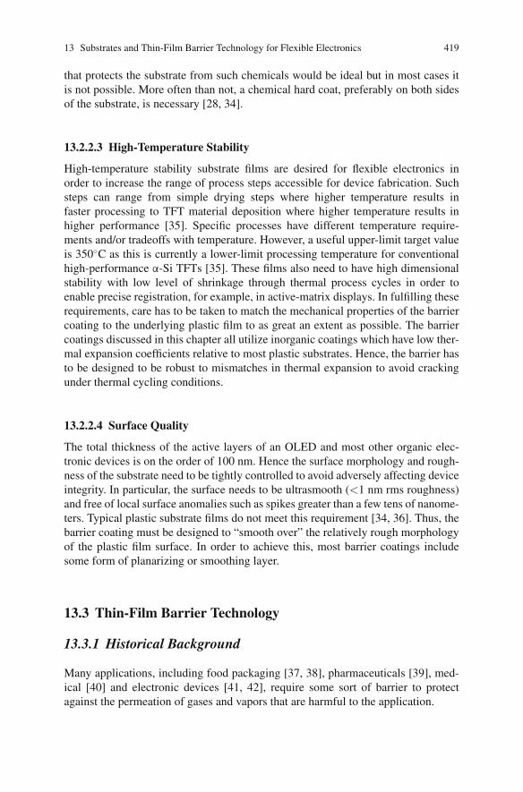
13 Substrates and Thin-Film Barrier Technology for Flexible Electronics 419
that protects the substrate from such chemicals would be ideal but in most cases itis not possible. More often than not, a chemical hard coat, preferably on both sidesof the substrate, is necessary [28, 34].
13.2.2.3 High-Temperature Stability
High-temperature stability substrate films are desired for flexible electronics inorder to increase the range of process steps accessible for device fabrication. Suchsteps can range from simple drying steps where higher temperature results infaster processing to TFT material deposition where higher temperature results inhigher performance [35]. Specific processes have different temperature require-ments and/or tradeoffs with temperature. However, a useful upper-limit target valueis 350◦C as this is currently a lower-limit processing temperature for conventionalhigh-performance α-Si TFTs [35]. These films also need to have high dimensionalstability with low level of shrinkage through thermal process cycles in order toenable precise registration, for example, in active-matrix displays. In fulfilling theserequirements, care has to be taken to match the mechanical properties of the barriercoating to the underlying plastic film to as great an extent as possible. The barriercoatings discussed in this chapter all utilize inorganic coatings which have low ther-mal expansion coefficients relative to most plastic substrates. Hence, the barrier hasto be designed to be robust to mismatches in thermal expansion to avoid crackingunder thermal cycling conditions.
13.2.2.4 Surface Quality
The total thickness of the active layers of an OLED and most other organic elec-tronic devices is on the order of 100 nm. Hence the surface morphology and rough-ness of the substrate need to be tightly controlled to avoid adversely affecting deviceintegrity. In particular, the surface needs to be ultrasmooth (<1 nm rms roughness)and free of local surface anomalies such as spikes greater than a few tens of nanome-ters. Typical plastic substrate films do not meet this requirement [34, 36]. Thus, thebarrier coating must be designed to “smooth over” the relatively rough morphologyof the plastic film surface. In order to achieve this, most barrier coatings includesome form of planarizing or smoothing layer.
13.3 Thin-Film Barrier Technology
13.3.1 Historical Background
Many applications, including food packaging [37, 38], pharmaceuticals [39], med-ical [40] and electronic devices [41, 42], require some sort of barrier to protectagainst the permeation of gases and vapors that are harmful to the application.
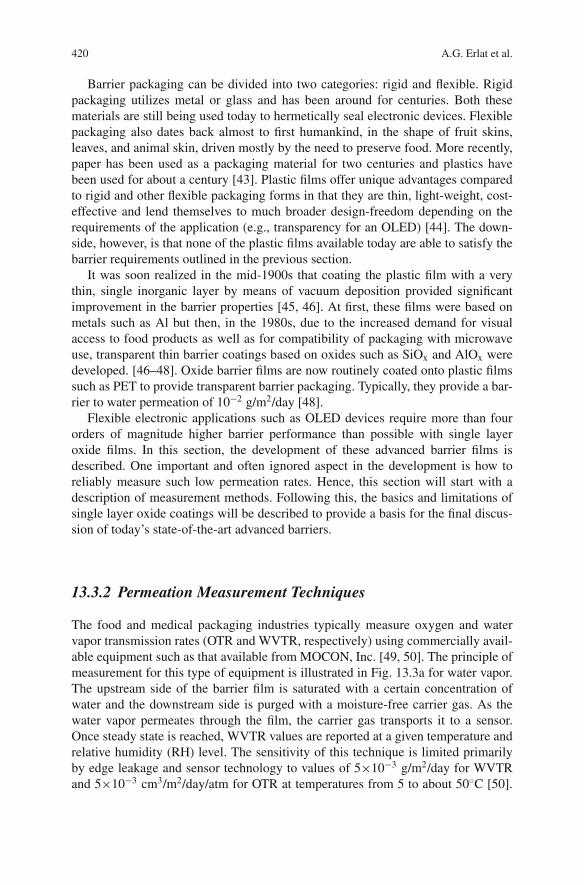
420 A.G. Erlat et al.
Barrier packaging can be divided into two categories: rigid and flexible. Rigidpackaging utilizes metal or glass and has been around for centuries. Both thesematerials are still being used today to hermetically seal electronic devices. Flexiblepackaging also dates back almost to first humankind, in the shape of fruit skins,leaves, and animal skin, driven mostly by the need to preserve food. More recently,paper has been used as a packaging material for two centuries and plastics havebeen used for about a century [43]. Plastic films offer unique advantages comparedto rigid and other flexible packaging forms in that they are thin, light-weight, cost-effective and lend themselves to much broader design-freedom depending on therequirements of the application (e.g., transparency for an OLED) [44]. The down-side, however, is that none of the plastic films available today are able to satisfy thebarrier requirements outlined in the previous section.
It was soon realized in the mid-1900s that coating the plastic film with a verythin, single inorganic layer by means of vacuum deposition provided significantimprovement in the barrier properties [45, 46]. At first, these films were based onmetals such as Al but then, in the 1980s, due to the increased demand for visualaccess to food products as well as for compatibility of packaging with microwaveuse, transparent thin barrier coatings based on oxides such as SiOx and AlOx weredeveloped. [46–48]. Oxide barrier films are now routinely coated onto plastic filmssuch as PET to provide transparent barrier packaging. Typically, they provide a bar-rier to water permeation of 10−2 g/m2/day [48].
Flexible electronic applications such as OLED devices require more than fourorders of magnitude higher barrier performance than possible with single layeroxide films. In this section, the development of these advanced barrier films isdescribed. One important and often ignored aspect in the development is how toreliably measure such low permeation rates. Hence, this section will start with adescription of measurement methods. Following this, the basics and limitations ofsingle layer oxide coatings will be described to provide a basis for the final discus-sion of today’s state-of-the-art advanced barriers.
13.3.2 Permeation Measurement Techniques
The food and medical packaging industries typically measure oxygen and watervapor transmission rates (OTR and WVTR, respectively) using commercially avail-able equipment such as that available from MOCON, Inc. [49, 50]. The principle ofmeasurement for this type of equipment is illustrated in Fig. 13.3a for water vapor.The upstream side of the barrier film is saturated with a certain concentration ofwater and the downstream side is purged with a moisture-free carrier gas. As thewater vapor permeates through the film, the carrier gas transports it to a sensor.Once steady state is reached, WVTR values are reported at a given temperature andrelative humidity (RH) level. The sensitivity of this technique is limited primarilyby edge leakage and sensor technology to values of 5×10⁻³ g/m2/day for WVTRand 5×10⁻³ cm3/m2/day/atm for OTR at temperatures from 5 to about 50◦C [50].
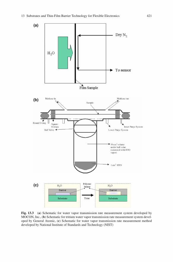
13 Substrates and Thin-Film Barrier Technology for Flexible Electronics 421
(a)
(b)
(c)
Fig. 13.3 (a) Schematic for water vapor transmission rate measurement system developed byMOCON, Inc., (b) Schematic for tritium water vapor transmission rate measurement system devel-oped by General Atomic, (c) Schematic for water vapor transmission rate measurement methoddeveloped by National Institute of Standards and Technology (NIST)
422 A.G. Erlat et al.
Numerous techniques have been developed over the last few years with better sensi-tivity, most notably mass spectrometry [51, 52], measurements utilizing X-ray andneutron reflectivity [53], tritium diffusion test [54] and the calcium test [55–61] forwater vapor permeation measurement, and residual gas analysis in ultra high vac-uum [62] for oxygen permeation measurements.
The principle of tritium diffusion test is shown in Fig. 13.3b [54]. This techniquefollows the same basic principle as the MOCON test except that tritium-enrichedwater (HTO-enriched water) permeates through the barrier film and is carried to abeta counter by means of a dry methane gas. In the ionization chamber, radioac-tivity counts are converted to WVTR values once steady state is reached, takinginto account the concentrations and geometry of the setup. In this case, since onlyHTO contributes to beta decay, the influence of water vapor contamination fromother sources such as edge leakage is alleviated. Hence, a theoretical detection limitof 2×10⁻⁷ g/m2/day is possible and so far a practical detection limit of 1×10⁻⁶
g/m2/day has been reported [54]. This technique meets the barrier testing require-ment for an OLED but suffers from two shortcomings: (1) only WVTR spatiallyaveraged over the measurement area can be determined and (2) it produces radioac-tive waste contaminants.
Another technique introduced to study barrier films with ultralow permeationrates works by measuring film swelling using X-ray and neutron reflectivity mea-surements as a function of time at given temperature and humidity conditions [53].The measurement utilizes an undercured polymer film sandwiched between the bar-rier and the base substrate as shown in Fig. 13.3c. As water vapor permeates throughthe barrier and reaches the polymer, swelling of the polymer is used as a means ofcalculating the amount of water vapor that has permeated. This technique, althoughshown to be a useful tool to understand the water vapor permeation mechanismthrough multilayer films [53], has not been taken up by the industry as a standardmeans of measurement, likely due to the need for expensive measurement appara-tus and very specific processing required to prepare the polymer film for swellingstudies.
The technique that is the most widely used today is the so-called “Calcium test”,first introduced by Nisato et al. [55, 56]. The principle is simple: very thin, evap-orated Ca metal is sealed between a perfect barrier such as glass and the film tobe tested and serves as a well to collect the water vapor that permeates throughthe barrier film. The test relies on the high level of reactivity of Ca metal withH2O to create transparent and nonconducting calcium hydroxide as depicted inReaction (13.1).
Ca + 2H2O → Ca(OH)2 + H2 (13.1)
It should be noted that calcium also reacts with oxygen but the contributionof oxygen to the degradation of Ca has been shown to be negligible at roomtemperature [60, 61]. Typically, the rate of Reaction (13.1), and hence the waterpermeation rate, is monitored by measuring the change in visual appearance and/or
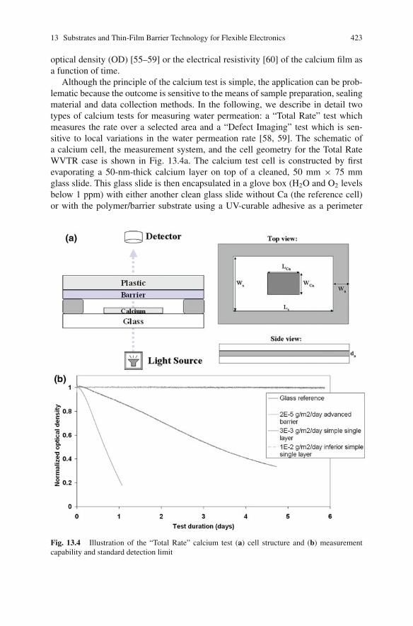
13 Substrates and Thin-Film Barrier Technology for Flexible Electronics 423
optical density (OD) [55–59] or the electrical resistivity [60] of the calcium film asa function of time.
Although the principle of the calcium test is simple, the application can be prob-lematic because the outcome is sensitive to the means of sample preparation, sealingmaterial and data collection methods. In the following, we describe in detail twotypes of calcium tests for measuring water permeation: a “Total Rate” test whichmeasures the rate over a selected area and a “Defect Imaging” test which is sen-sitive to local variations in the water permeation rate [58, 59]. The schematic ofa calcium cell, the measurement system, and the cell geometry for the Total RateWVTR case is shown in Fig. 13.4a. The calcium test cell is constructed by firstevaporating a 50-nm-thick calcium layer on top of a cleaned, 50 mm × 75 mmglass slide. This glass slide is then encapsulated in a glove box (H2O and O2 levelsbelow 1 ppm) with either another clean glass slide without Ca (the reference cell)or with the polymer/barrier substrate using a UV-curable adhesive as a perimeter
Fig. 13.4 Illustration of the “Total Rate” calcium test (a) cell structure and (b) measurementcapability and standard detection limit
424 A.G. Erlat et al.
seal. By depositing the calcium onto the glass substrate and not onto the barrier,one is assured that the Ca will corrode uniformly over its area even if the barrierfilm has nonuniform properties across its area. Hence, the calcium corrosion ratemeasures the diffusion rate integrated over the barrier area. The Ca cell is placedbetween a LED light source and a photodetector and is kept in a temperature- andhumidity-controlled chamber. As the water vapor permeates through the substrateand/or the edge perimeter seal, or is being released from any internal sources (e.g.,residual moisture in adhesive), it reacts with the calcium inside the cell according toReaction (13.1) above. As water vapor permeation progresses, calcium, corrodinguniformly according to Reaction (13.1), becomes thinner and more transparent. Thelight transmittance (T) of calcium at 880-nm wavelength is measured continuouslyvia the photodetector at an interval of about 1 Hz, and the average value is storedto a file every 5 minutes. As the OD of a film is proportional to its thickness, theWVTR is calculated via the following equation:
W V T R = −2AM[H2 O]
M[Ca]ρCa
LCa · WC A
L S · WS
d(O D)
dt(13.1)
where A is the scaling factor between calcium thickness and OD; M[H2O] andM[Ca] are the molar masses of H2O and Ca with values of 18 and 40.1 amu, respec-tively; ρCa is the density of calcium; LCa and WCa are the length and the width of thedeposited Ca; Ls and Ws are the length and the width of the permeation area definedby the interior boundary of the edge perimeter seal (Fig. 13.4a), and d(OD)/dt is theslope of the measured optical absorbance.
In order to be able to measure substrate materials with WVTR values on theorder of 10−6 g/m2/day, the effective WVTR (WVTReff) from the perimeter edgeseal needs to be either significantly below 10−6 g/m2/day or it should have a verylow variation so that it can be subtracted from Eq. (13.1) to obtain the true substrateWVTR. One can estimate the steady state WVTReff for a reference cell with thegeometry as shown in Fig. 13.4a with the following equation:
W V T R = Pa
Wa · La · Ws· da · (2Ls + 2Ws) (13.2)
where Pa, Wa, La, and da are the permeability, width, length, and thickness of theadhesive respectively. Figure 13.4b shows OD versus time plots from a Total Ratecalcium corrosion test for a single inorganic barrier layer and from an advanced bar-rier on polymer substrates and glass/glass reference cells. It is clear from this figurethat the Total Rate calcium test is a reliable test to measure samples with WVTRin the range of 10−2 to 10−5 g/m2/day. With improvements to the sealing techniqueand seal degassing procedures, it has also been demonstrated that measurements inthe 10−6 g/m2/day regime are possible at 23◦C/50%RH [63].
One of the shortcomings of the Total Rate calcium test is that it is not possible toassess information about permeation through defects/pinholes. When such informa-tion is needed, the Defect Imaging test, originally developed by Nisato [55, 56, 59],
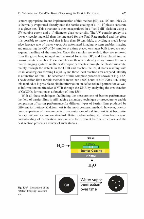
13 Substrates and Thin-Film Barrier Technology for Flexible Electronics 425
is more appropriate. In one implementation of this method [59], ca. 100-nm-thick Cais thermally evaporated directly onto the barrier coating of a 1′′×1′′ plastic substratein a glove box. This structure is then encapsulated in a “solid-fill” fashion using aUV curable epoxy and a 1′′ diameter glass cover slip. The UV curable epoxy is alower viscosity material than the one used for the Total Rate method and thereforeit is possible to make a seal that is less than 10 μm thick, providing a much loweredge leakage rate of water vapor. An automated imaging system enables imagingand measuring the OD of 24 samples at a time placed on stages built to reduce sub-sequent handling of the samples. Once the samples are sealed, they are removedfrom the glove box, imaged and measured for initial OD, and then placed into anenvironmental chamber. These samples are then periodically imaged using the auto-mated imaging system. As the water vapor permeates through the plastic substrate,mainly through the defects in the UHB and reaches the Ca, it starts reacting withCa in local regions forming Ca(OH)2 and these local reaction areas expand laterallyas a function of time. The schematic of this complete process is shown in Fig. 13.5.The detection limit for this method is more than 1,000 hours at 60◦C/90%RH. Usingthis method, it is possible to obtain information on defect related permeation as wellas information on effective WVTR through the UHB by analyzing the area fractionof Ca(OH)2 formation as a function of time [56].
With all these techniques facilitating the measurement of barrier performance,the field of barrier films is still lacking a standard technique or procedure to enablecomparison of barrier performance for different types of barrier films produced bydifferent institutions. Calcium test is the most common method; however, one-to-one comparison of measurements from variations of calcium test is at best satis-factory, without a common standard. Better understanding will stem from a goodunderstanding of permeation mechanisms for different barrier structures and thenext section presents a review of such studies.
Fig. 13.5 Illustration of the“Defect Imaging” calciumtest
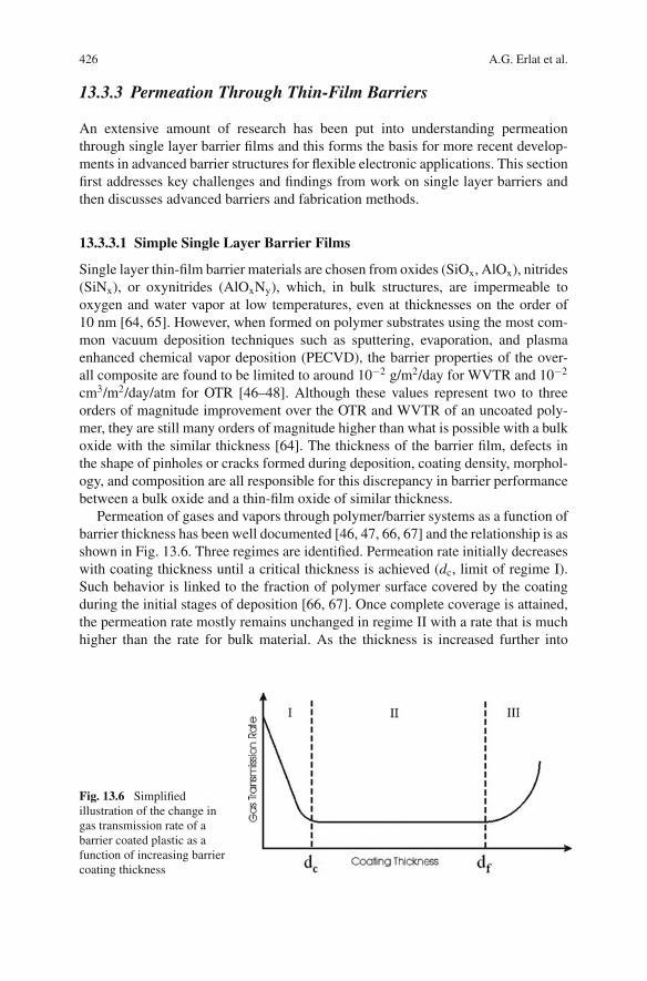
426 A.G. Erlat et al.
13.3.3 Permeation Through Thin-Film Barriers
An extensive amount of research has been put into understanding permeationthrough single layer barrier films and this forms the basis for more recent develop-ments in advanced barrier structures for flexible electronic applications. This sectionfirst addresses key challenges and findings from work on single layer barriers andthen discusses advanced barriers and fabrication methods.
13.3.3.1 Simple Single Layer Barrier Films
Single layer thin-film barrier materials are chosen from oxides (SiOx, AlOx), nitrides(SiNx), or oxynitrides (AlOxNy), which, in bulk structures, are impermeable tooxygen and water vapor at low temperatures, even at thicknesses on the order of10 nm [64, 65]. However, when formed on polymer substrates using the most com-mon vacuum deposition techniques such as sputtering, evaporation, and plasmaenhanced chemical vapor deposition (PECVD), the barrier properties of the over-all composite are found to be limited to around 10−2 g/m2/day for WVTR and 10−2
cm3/m2/day/atm for OTR [46–48]. Although these values represent two to threeorders of magnitude improvement over the OTR and WVTR of an uncoated poly-mer, they are still many orders of magnitude higher than what is possible with a bulkoxide with the similar thickness [64]. The thickness of the barrier film, defects inthe shape of pinholes or cracks formed during deposition, coating density, morphol-ogy, and composition are all responsible for this discrepancy in barrier performancebetween a bulk oxide and a thin-film oxide of similar thickness.
Permeation of gases and vapors through polymer/barrier systems as a function ofbarrier thickness has been well documented [46, 47, 66, 67] and the relationship is asshown in Fig. 13.6. Three regimes are identified. Permeation rate initially decreaseswith coating thickness until a critical thickness is achieved (dc, limit of regime I).Such behavior is linked to the fraction of polymer surface covered by the coatingduring the initial stages of deposition [66, 67]. Once complete coverage is attained,the permeation rate mostly remains unchanged in regime II with a rate that is muchhigher than the rate for bulk material. As the thickness is increased further into
Fig. 13.6 Simplifiedillustration of the change ingas transmission rate of abarrier coated plastic as afunction of increasing barriercoating thickness
13 Substrates and Thin-Film Barrier Technology for Flexible Electronics 427
regime III (> df), the barrier performance degrades mostly due to the internal stressbuild-up in the glassy coating which leads to the formation of cracks [67, 68]. Thedetermination of the critical thickness (dc, onset of regime II) is the crucial first stepin designing barrier films due to the fact that optimal barrier properties need to besatisfied while avoiding commercially unacceptable processing times (thick films).The value for dc changes with coating material, deposition method, and to a largerextent the substrate surface [48, 69]. The reported values on polymers are 40–50 nmfor PECVD SiOx [70, 71], ∼20 nm for EB-evaporated AlOx [72], ∼20–30 nm forsputtered AlOx [72, 73], 8–30 nm for PECVD SiNx coatings [71, 74], ∼100 nm forETP SiN [75], and <25 nm for ALD AlOx [76, 77].
For the purposes of this chapter, the main interest is in transparent thin-film bar-riers with thicknesses in regime II. In this regime, thin-film oxides and oxynitridesgrown at low substrate temperatures (usually below 100◦C) have varying degrees ofporosity [69, 78–80]. The permeation channels that create this porosity and hencecontribute to varying degrees of barrier performance can be classified as macrochan-nels (>5 μm), microchannels (1–5 μm), Nanochannels (<1 μm), and the oxide lat-tice (<0.3 nm). The extent to which these channels are created and influence barrierperformance depends on several factors, including handling and cleanliness of thedeposition environment, substrate surface roughness and morphology, and deposi-tion technique and process parameters.
Handling and cleanliness (or lack thereof) of the deposition environment ismostly known to contribute to the occurrence of macro- and microchannels. A goodexample of this was shown by Jamiesson and Windle [45] for their PET/Al barrierswhere they found that the density and size of pinholes correlate well with the densityand size (1–5 μm) of atmospheric dust particles on the polymer surface. In addition,the number density (mm–2) of the channels created correlate well with OTR values(<10 mm−2 for ∼0.1 cm3/m2/day/atm and ∼100 mm−2 for ∼1.3 cm3/m2/day/atm).This is a clear indication that proper handling of the barrier coated substrate, imple-menting effective substrate cleaning procedures, and controlling the particle countsin the deposition environment by means of utilizing “cleanrooms” are the first stepsto eliminating macro and some of the microchannels in the barrier film.
High substrate surface roughness is another key factor that adversely affects bar-rier performance as demonstrated by many researchers [81–83]. Especially for themost widely used commodity polymers such as PET and oriented polypropylene(OPP), it has been shown that the surface may appear very smooth (rms ∼ 1–5 nm)when analyzed in μm2 lateral scale (by AFM), but when studied on a broader lateralrange, this roughness can reach tens to hundreds of nanometers [81]. Similar rough-ness can be created by antiblock, filler particles (i.e., silica) of 1–2 μm diameter[83]. Shaw [84] first reported the application of a flash-evaporated, UV or E-beamcurable smoothing coating on such surfaces and through systematic AFM analysisshowed that surface anomalies were covered by increasing the thickness of this layerto a few microns [85]. It was further shown that the application of this layer prior toan Al or AlOx barrier coating improved both the OTR and the WVTR of the compos-ite by more than three orders of magnitude compared to an uncoated polymer [84,86, 87]. More recently, it has been demonstrated that WVTR values in the range of

428 A.G. Erlat et al.
10–4 to 10−5 g/m2/day, as well as a dramatic reduction in microscale defects, can beachieved by appropriate modification of the polymer surface with a smoothing layerapplied either via flash evaporation or simple nonvacuum techniques such as spincoating [88].
Assuming that the deposition environment is kept clean and proper film handlingprocedures are implemented and if applicable, a smoothing coating is applied, themajority of macro- and microchannels for permeation can be eliminated. Many stud-ies utilizing either analytical characterization [71, 72, 79, 80, 89, 90] or the activatedrate theory [70, 79, 90, 91] and several physical “defect” models [45, 69, 78, 92–96]have demonstrated that especially oxygen permeation is dominated by these type ofdefects. On the other hand, water vapor permeation through polymers coated withSiOx [70, 80, 97], AlOx [72, 91, 98, 99] AlOxNy [99, 100] exhibits less linear depen-dence on the size and density of larger defects and at times has been shown to becontrolled by the nanoscale morphology and composition of the coating (due to itspolar nature, water molecules can chemically interact with the coating depending onthe material chosen). The remaining engineering challenge then becomes producinga dense thin film as close as possible in structure to its bulk counterpart with goodcontrol of composition. The optimal solution depends greatly on the material systemchosen, deposition method, and process parameters.
Denser films can be fabricated by supplying high kinetic energy species (atomsof the material to be deposited, ions, neutrals) to the surface. Hence, thermal andE-beam evaporation techniques fall short of producing high-quality barriers, despiteexceptionally high deposition rates. Placing an auxiliary plasma between the sourceand the substrate can improve barrier performance by densifying the films [101].Magnetron sputtering, another widely used physical vapor deposition technique, isa more preferred and versatile technique to densify films. Since with this technique,there is a dense plasma confined to the cathode surface, acceleration of high energyspecies to the substrate surface is enhanced [82, 90]. In addition, manipulation of themagnet configuration to leak the plasma toward the substrate, using more advancedpower supply schemes such as pulsed DC, has been shown to enable highly denselypacked film morphology, which especially aids in improving water vapor barrierperformance [102, 103]. Examples have been reported for AlOx and AlOxNy onPET [82, 90, 99, 100, 102, 103].
One shortcoming of physical vapor deposition techniques is that they suffer from“line of sight” film deposition, which makes the barrier films very sensitive to evensmall anomalies on the surface that can create defects. PECVD and ALD are tech-niques with much reduced directionality of deposition and have been shown to pro-duce superior barrier films for SiN [71, 79, 89, 104] and AlOx [76, 77], respectively.For PECVD, when the substrate is placed on the powered electrode (RIE mode),additional ion bombardment produces dense SiNx films with WVTR levels in the10−4 regime. At the same time, compressive stresses can build up in the film dueto this high energy process and these may need to be controlled depending on theapplication [105]. ALD, on the other hand, is perfect for producing highly conformalfilms and recent developments using plasma-enhanced ALD have produced singlelayer AlOx films in the 10−4−10−5 g/m2/day regime [76, 77]. Significantly, slower
13 Substrates and Thin-Film Barrier Technology for Flexible Electronics 429
deposition rates for ALD compared to other techniques discussed here, however,make it commercially unattractive for the flexible electronics application.
The materials system and its effect on the permeation of water vapor is a finalkey aspect to consider. Tropha and Harvey [70] provided the first insight into themechanism of water vapor permeation by using activated rate theory to calculatean activation energy for H2O permeation. They deposited a series of SiOx coatingson PET, polycarbonate(PC), polypropylene (PP), and polystyrene (PS) substratesusing PECVD. They show that regardless of the water vapor activation energy(EA(WVTR)) for permeation through the four uncoated substrates, the activationenergy was always the same when each substrate was coated with SiOx. This issignificant because if the mechanism for water permeation were simply diffusionthrough the constricted pores of the SiOx coating, then the temperature dependenceof permeation should be controlled by the temperature dependence of permeationthrough the plastic film only. The fact that it is controlled by an activation energywhich is characteristic of the coating suggests that some sort of chemical interactionoccurs between the water and the coating. Suggested interactions include attach-ment of water molecules to Si-O or Si-dangling bonds within the SiOx pores [80].Other studies on AlOx and AlOxNy coatings have suggested that the level of interac-tion is coating-material-dependent as might be expected for a chemical process [82,98–100].
As described in this section, considerable effort has been undertaken to developsimple single layer barrier coatings, but their performance is not adequate for themost demanding flexible electronics applications. The barrier properties are primar-ily limited by the presence of macro and micro defects, but so far a practical way toeliminate these defects has not been demonstrated. As a result, the technical com-munity began to develop advanced barrier films that can provide a good barrier inspite of the presence of defects. These are described further in the next section.
13.3.3.2 Advanced Barrier Films
The first approach designed to provide a high barrier in spite of the presence offilm defects is illustrated in Fig. 13.7. The idea is to have multilayers of inorganic
Fig. 13.7 Concept of “defect de-coupling” gas permeation mechanism through multilayeradvanced barrier coatings
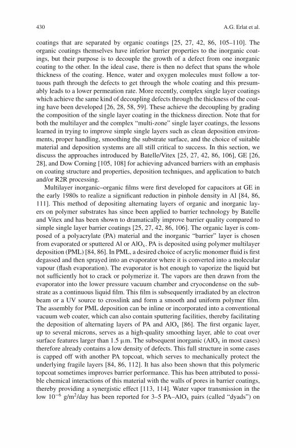
430 A.G. Erlat et al.
coatings that are separated by organic coatings [25, 27, 42, 86, 105–110]. Theorganic coatings themselves have inferior barrier properties to the inorganic coat-ings, but their purpose is to decouple the growth of a defect from one inorganiccoating to the other. In the ideal case, there is then no defect that spans the wholethickness of the coating. Hence, water and oxygen molecules must follow a tor-tuous path through the defects to get through the whole coating and this presum-ably leads to a lower permeation rate. More recently, complex single layer coatingswhich achieve the same kind of decoupling defects through the thickness of the coat-ing have been developed [26, 28, 58, 59]. These achieve the decoupling by gradingthe composition of the single layer coating in the thickness direction. Note that forboth the multilayer and the complex “multi-zone” single layer coatings, the lessonslearned in trying to improve simple single layers such as clean deposition environ-ments, proper handling, smoothing the substrate surface, and the choice of suitablematerial and deposition systems are all still critical to success. In this section, wediscuss the approaches introduced by Batelle/Vitex [25, 27, 42, 86, 106], GE [26,28], and Dow Corning [105, 108] for achieving advanced barriers with an emphasison coating structure and properties, deposition techniques, and application to batchand/or R2R processing.
Multilayer inorganic–organic films were first developed for capacitors at GE inthe early 1980s to realize a significant reduction in pinhole density in Al [84, 86,111]. This method of depositing alternating layers of organic and inorganic lay-ers on polymer substrates has since been applied to barrier technology by Batelleand Vitex and has been shown to dramatically improve barrier quality compared tosimple single layer barrier coatings [25, 27, 42, 86, 106]. The organic layer is com-posed of a polyacrylate (PA) material and the inorganic “barrier” layer is chosenfrom evaporated or sputtered Al or AlOx. PA is deposited using polymer multilayerdeposition (PML) [84, 86]. In PML, a desired choice of acrylic monomer fluid is firstdegassed and then sprayed into an evaporator where it is converted into a molecularvapour (flash evaporation). The evaporator is hot enough to vaporize the liquid butnot sufficiently hot to crack or polymerize it. The vapors are then drawn from theevaporator into the lower pressure vacuum chamber and cryocondense on the sub-strate as a continuous liquid film. This film is subsequently irradiated by an electronbeam or a UV source to crosslink and form a smooth and uniform polymer film.The assembly for PML deposition can be inline or incorporated into a conventionalvacuum web coater, which can also contain sputtering facilities, thereby facilitatingthe deposition of alternating layers of PA and AlOx [86]. The first organic layer,up to several microns, serves as a high-quality smoothing layer, able to coat oversurface features larger than 1.5 μm. The subsequent inorganic (AlOx in most cases)therefore already contains a low density of defects. This full structure in some casesis capped off with another PA topcoat, which serves to mechanically protect theunderlying fragile layers [84, 86, 112]. It has also been shown that this polymerictopcoat sometimes improves barrier performance. This has been attributed to possi-ble chemical interactions of this material with the walls of pores in barrier coatings,thereby providing a synergistic effect [113, 114]. Water vapor transmission in thelow 10−6 g/m2/day has been reported for 3–5 PA–AlOx pairs (called “dyads”) on
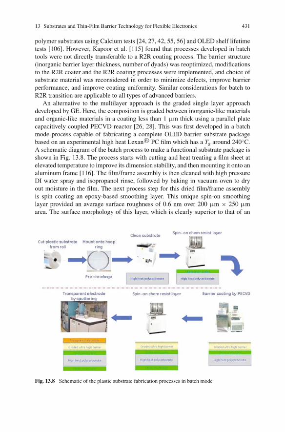
13 Substrates and Thin-Film Barrier Technology for Flexible Electronics 431
polymer substrates using Calcium tests [24, 27, 42, 55, 56] and OLED shelf lifetimetests [106]. However, Kapoor et al. [115] found that processes developed in batchtools were not directly transferable to a R2R coating process. The barrier structure(inorganic barrier layer thickness, number of dyads) was reoptimized, modificationsto the R2R coater and the R2R coating processes were implemented, and choice ofsubstrate material was reconsidered in order to minimize defects, improve barrierperformance, and improve coating uniformity. Similar considerations for batch toR2R transition are applicable to all types of advanced barriers.
An alternative to the multilayer approach is the graded single layer approachdeveloped by GE. Here, the composition is graded between inorganic-like materialsand organic-like materials in a coating less than 1 μm thick using a parallel platecapacitively coupled PECVD reactor [26, 28]. This was first developed in a batchmode process capable of fabricating a complete OLED barrier substrate packagebased on an experimental high heat Lexan® PC film which has a Tg around 240◦C.A schematic diagram of the batch process to make a functional substrate package isshown in Fig. 13.8. The process starts with cutting and heat treating a film sheet atelevated temperature to improve its dimension stability, and then mounting it onto analuminum frame [116]. The film/frame assembly is then cleaned with high pressureDI water spray and isopropanol rinse, followed by baking in vacuum oven to dryout moisture in the film. The next process step for this dried film/frame assemblyis spin coating an epoxy-based smoothing layer. This unique spin-on smoothinglayer provided an average surface roughness of 0.6 nm over 200 μm × 250 μmarea. The surface morphology of this layer, which is clearly superior to that of an
Fig. 13.8 Schematic of the plastic substrate fabrication processes in batch mode
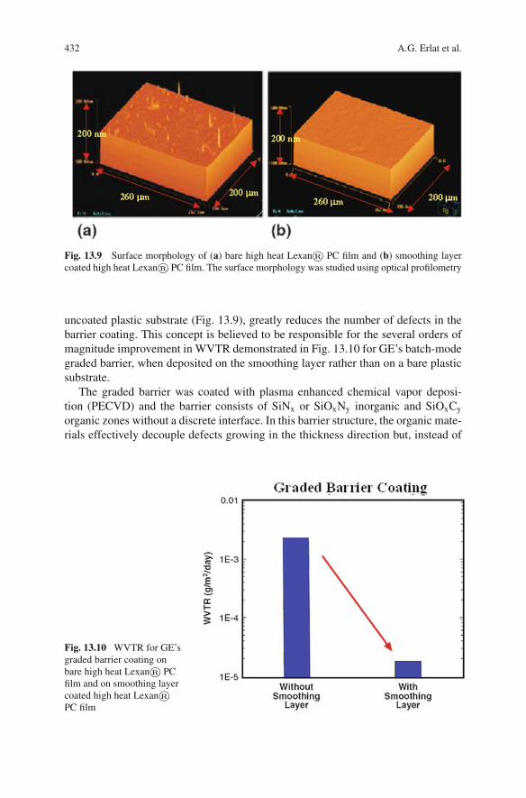
432 A.G. Erlat et al.
Fig. 13.9 Surface morphology of (a) bare high heat Lexan® PC film and (b) smoothing layercoated high heat Lexan® PC film. The surface morphology was studied using optical profilometry
uncoated plastic substrate (Fig. 13.9), greatly reduces the number of defects in thebarrier coating. This concept is believed to be responsible for the several orders ofmagnitude improvement in WVTR demonstrated in Fig. 13.10 for GE’s batch-modegraded barrier, when deposited on the smoothing layer rather than on a bare plasticsubstrate.
The graded barrier was coated with plasma enhanced chemical vapor deposi-tion (PECVD) and the barrier consists of SiNx or SiOxNy inorganic and SiOxCy
organic zones without a discrete interface. In this barrier structure, the organic mate-rials effectively decouple defects growing in the thickness direction but, instead of
Fig. 13.10 WVTR for GE’sgraded barrier coating onbare high heat Lexan® PCfilm and on smoothing layercoated high heat Lexan®PC film
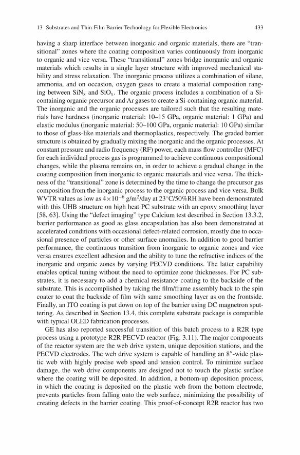
13 Substrates and Thin-Film Barrier Technology for Flexible Electronics 433
having a sharp interface between inorganic and organic materials, there are “tran-sitional” zones where the coating composition varies continuously from inorganicto organic and vice versa. These “transitional” zones bridge inorganic and organicmaterials which results in a single layer structure with improved mechanical sta-bility and stress relaxation. The inorganic process utilizes a combination of silane,ammonia, and on occasion, oxygen gases to create a material composition rang-ing between SiNx and SiOx. The organic process includes a combination of a Si-containing organic precursor and Ar gases to create a Si-containing organic material.The inorganic and the organic processes are tailored such that the resulting mate-rials have hardness (inorganic material: 10–15 GPa, organic material: 1 GPa) andelastic modulus (inorganic material: 50–100 GPa, organic material: 10 GPa) similarto those of glass-like materials and thermoplastics, respectively. The graded barrierstructure is obtained by gradually mixing the inorganic and the organic processes. Atconstant pressure and radio frequency (RF) power, each mass flow controller (MFC)for each individual process gas is programmed to achieve continuous compositionalchanges, while the plasma remains on, in order to achieve a gradual change in thecoating composition from inorganic to organic materials and vice versa. The thick-ness of the “transitional” zone is determined by the time to change the precursor gascomposition from the inorganic process to the organic process and vice versa. BulkWVTR values as low as 4×10⁻⁶ g/m2/day at 23◦C/50%RH have been demonstratedwith this UHB structure on high heat PC substrate with an epoxy smoothing layer[58, 63]. Using the “defect imaging” type Calcium test described in Section 13.3.2,barrier performance as good as glass encapsulation has also been demonstrated ataccelerated conditions with occasional defect-related corrosion, mostly due to occa-sional presence of particles or other surface anomalies. In addition to good barrierperformance, the continuous transition from inorganic to organic zones and viceversa ensures excellent adhesion and the ability to tune the refractive indices of theinorganic and organic zones by varying PECVD conditions. The latter capabilityenables optical tuning without the need to optimize zone thicknesses. For PC sub-strates, it is necessary to add a chemical resistance coating to the backside of thesubstrate. This is accomplished by taking the film/frame assembly back to the spincoater to coat the backside of film with same smoothing layer as on the frontside.Finally, an ITO coating is put down on top of the barrier using DC magnetron sput-tering. As described in Section 13.4, this complete substrate package is compatiblewith typical OLED fabrication processes.
GE has also reported successful transition of this batch process to a R2R typeprocess using a prototype R2R PECVD reactor (Fig. 3.11). The major componentsof the reactor system are the web drive system, unique deposition stations, and thePECVD electrodes. The web drive system is capable of handling an 8′′-wide plas-tic web with highly precise web speed and tension control. To minimize surfacedamage, the web drive components are designed not to touch the plastic surfacewhere the coating will be deposited. In addition, a bottom-up deposition process,in which the coating is deposited on the plastic web from the bottom electrode,prevents particles from falling onto the web surface, minimizing the possibility ofcreating defects in the barrier coating. This proof-of-concept R2R reactor has two
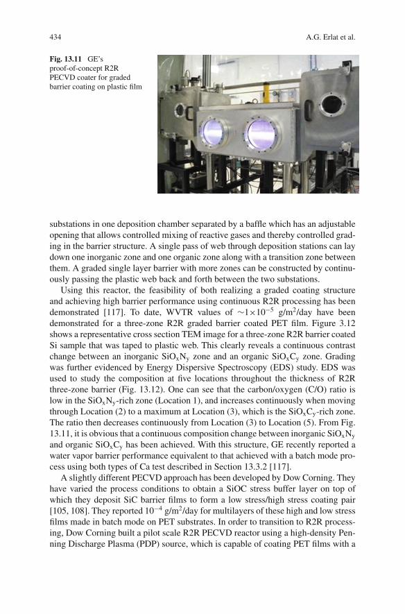
434 A.G. Erlat et al.
Fig. 13.11 GE’sproof-of-concept R2RPECVD coater for gradedbarrier coating on plastic film
substations in one deposition chamber separated by a baffle which has an adjustableopening that allows controlled mixing of reactive gases and thereby controlled grad-ing in the barrier structure. A single pass of web through deposition stations can laydown one inorganic zone and one organic zone along with a transition zone betweenthem. A graded single layer barrier with more zones can be constructed by continu-ously passing the plastic web back and forth between the two substations.
Using this reactor, the feasibility of both realizing a graded coating structureand achieving high barrier performance using continuous R2R processing has beendemonstrated [117]. To date, WVTR values of ∼1×10⁻⁵ g/m2/day have beendemonstrated for a three-zone R2R graded barrier coated PET film. Figure 3.12shows a representative cross section TEM image for a three-zone R2R barrier coatedSi sample that was taped to plastic web. This clearly reveals a continuous contrastchange between an inorganic SiOxNy zone and an organic SiOxCy zone. Gradingwas further evidenced by Energy Dispersive Spectroscopy (EDS) study. EDS wasused to study the composition at five locations throughout the thickness of R2Rthree-zone barrier (Fig. 13.12). One can see that the carbon/oxygen (C/O) ratio islow in the SiOxNy-rich zone (Location 1), and increases continuously when movingthrough Location (2) to a maximum at Location (3), which is the SiOxCy-rich zone.The ratio then decreases continuously from Location (3) to Location (5). From Fig.13.11, it is obvious that a continuous composition change between inorganic SiOxNy
and organic SiOxCy has been achieved. With this structure, GE recently reported awater vapor barrier performance equivalent to that achieved with a batch mode pro-cess using both types of Ca test described in Section 13.3.2 [117].
A slightly different PECVD approach has been developed by Dow Corning. Theyhave varied the process conditions to obtain a SiOC stress buffer layer on top ofwhich they deposit SiC barrier films to form a low stress/high stress coating pair[105, 108]. They reported 10−4 g/m2/day for multilayers of these high and low stressfilms made in batch mode on PET substrates. In order to transition to R2R process-ing, Dow Corning built a pilot scale R2R PECVD reactor using a high-density Pen-ning Discharge Plasma (PDP) source, which is capable of coating PET films with a
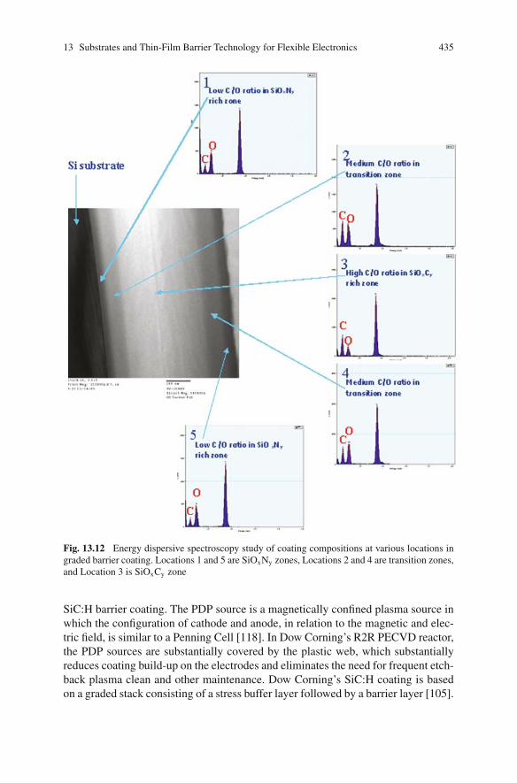
13 Substrates and Thin-Film Barrier Technology for Flexible Electronics 435
Fig. 13.12 Energy dispersive spectroscopy study of coating compositions at various locations ingraded barrier coating. Locations 1 and 5 are SiOxNy zones, Locations 2 and 4 are transition zones,and Location 3 is SiOxCy zone
SiC:H barrier coating. The PDP source is a magnetically confined plasma source inwhich the configuration of cathode and anode, in relation to the magnetic and elec-tric field, is similar to a Penning Cell [118]. In Dow Corning’s R2R PECVD reactor,the PDP sources are substantially covered by the plastic web, which substantiallyreduces coating build-up on the electrodes and eliminates the need for frequent etch-back plasma clean and other maintenance. Dow Corning’s SiC:H coating is basedon a graded stack consisting of a stress buffer layer followed by a barrier layer [105].
436 A.G. Erlat et al.
The stress buffer layer is used to mitigate the high mechanical stress of the barrierlayer to the interface with the substrate. The SiC:H coating could be put down atdeposition rate above 125 nm·m/min and the R2R coated SiC:H barrier achieved aWVTR below the 10−3 g/m2/day MOCON detection limit [119].
At present, the use of a combination of inorganic and organic materials remainsthe primary approach to achieving high barrier performance. The details of the per-meation mechanism of water vapor through these structures are not well understood.Several modeling approaches [75, 120] and a survey of Calcium test data of variousgroups suggest that the mechanism of “defect de-coupling” mechanism is dominant.Since the majority of advanced barriers contain either AlOx or SiNx as the inorganiccomponent, the two inorganic films shown to be the least reactive with permeatingwater molecules (see Section 13.3.3.1), it is plausible that this mechanism is dom-inant. However, recently the question has arisen as to whether the reported valuesof WVTR (mostly) by Ca test represent the true steady state permeation rate. Inparticular, Graff and coworkers [25, 121] developed a model for multilayer filmsbased on Fickian mechanics and used it to argue that the structure in Fig. 13.7 pro-motes a significant increase in lag times for water vapor to “fill up” the structure,but only a modest decrease in the actual steady state transmission rate (at best from10−2 to 10−3 for structures with the least number of defects. In other words, it isargued that the improvements in barrier performance shown for advanced barrierfilms over single layer ones are due to an extended transient period because of thehighly increased diffusion path (Fig. 13.7). This argument is supported by Vogt et al.[53] in their X-ray and neutron reflectivity measurements of such multilayer struc-tures (using an undercured PA in dyads to ensure swelling – see Section 13.3.2).They conclude that water accumulation at the oxide–polymer interface, character-ized as strong adsorption of water to AlOx, creates a desiccant effect and this effectis responsible for the long transient “fill-up” times they observe for such structures.While these studies provide useful insights to better understand the water vapor per-meation mechanisms, it should be noted that for similar barrier structures, steadystate, as opposed to transient, consumption of Ca has been reported [55–57, 59]leading to WVTR values of around 10−6 g/m2/day. In addition, for PECVD gradedbarrier films, tritium diffusion tests where lag times are clearly discernable fromsteady state behavior, WVTR values of 10−5 g/m2/day have been reported after atransient period of several hundred hours [54]. In general, the complexity of watervapor permeation compared to other nonreactive permeants makes it difficult to pindown one exact mechanism for moisture permeation at present and, as is the casefor simple single layer films (see Section 13.3.3.1), the materials used to constructUHB structures can play a significant role in how water vapor permeates.
As clear from the discussion above, there have been significant strides inadvanced barrier films with barrier performance necessary for OLED packagingand in developing R2R processes to make the films commercially viable. Theseefforts have also been accompanied by developments in integrating OLEDs ontopolymer/barrier structures and integrating UHB coatings as a top encapsulation forOLEDs. The final section discusses the challenges and developments in these twocritical device–barrier integration areas.
13 Substrates and Thin-Film Barrier Technology for Flexible Electronics 437
13.4 Barrier–Device Integration
13.4.1 Substrate and Barrier Compatibility with OLEDs
The unique thin device structure of OLEDs has made them a natural choice forflexible display applications. Flexible OLED display prototypes have already beendemonstrated on barrier-coated plastic substrates. A group from Pioneer Corpora-tion built a 3′′ full-color passive-matrix OLED device (160×RGB×120 pixels) on asingle layer SiOxNy barrier coated plastic substrate [122]. The first proof-of-conceptof a flexible OLED on an advanced barrier coating was a 128×64 passive matrix(PM) monochrome display fabricated on a multilayer barrier coated heat stabilizedPET made by Vitex [24]. Quantitative tests of the compatibility of the Vitex mul-tilayer barrier as both a substrate and a top encapsulation layer for an OLED havealso been performed. In particular, Weaver et al. [106] built an OLED test device onPML barrier coated heat stabilized PET with glass lid encapsulation and achieved ahalf life of 3,800 hours from an initial luminance of 425 cd/m2 measured at roomtemperature environment. Chwang et al. [123] demonstrated a 5-mm2 OLED testpixel and a passive-matrix flexible OLED device on a multilayer barrier coated heatstabilized PET substrate with transmissive multilayer barrier coating direct encap-sulation and reached a room-temperature half life (initial luminance 600 cd/m2) fora test pixel of 2,500 hours.
In the following, the details of experiments performed to ensure the compati-bility of GE’s graded barrier with OLED devices will be described. Compatibilityis best demonstrated by actual device fabrication since many unanticipated issuessuch as the presence of particles, handling methods, resistance to a certain set ofsolvents, stability during high-temperature steps, the effect of mechanical stress dueto sealing, performance of the transparent conductor, and shelf life tend to surfaceat this stage. In order to test for these, two-layer polymer OLED devices consistingof PEDOT/PSS [poly(ethylenedioxythiopene)/poly(sulfonated styrene)] as a holetransport layer and a polyfluorene-based light-emitting polymer (LEP) layer werefabricated onto an ITO and graded barrier-coated high temperature PC substrate[28]. A series-connected architecture described elsewhere [124, 125] was employedto enable a large emitting area. In particular, 10 devices consisting of eight series-connected elements, each with area 1.95 cm2
, were fabricated on a 15 × 15 cm2 sub-strate. Fabrication was accomplished using the fairly standard procedure describedbelow.
In order to enable device fabrication using conventional batch processing tools,the substrate films were first affixed to 3 mm wide, 15 × 15 cm square titaniumframes by means of double-sided Kapton polyimide tape. The affixed film wascleaned with isopropanol, then given a 10-minute dwell in an aqueous detergent(Alconox) with ultrasonic agitation, followed by water rinsing and drying.
ITO patterning was accomplished using a photoresist and immersion etching.The photoresist (AZ1512) was applied by means of spin coating and baked for10 min at 110◦C, producing a film 1 micron thick. The positive photoresist wasimaged through a glass mask using a UV collimated light source for 15 sec. The
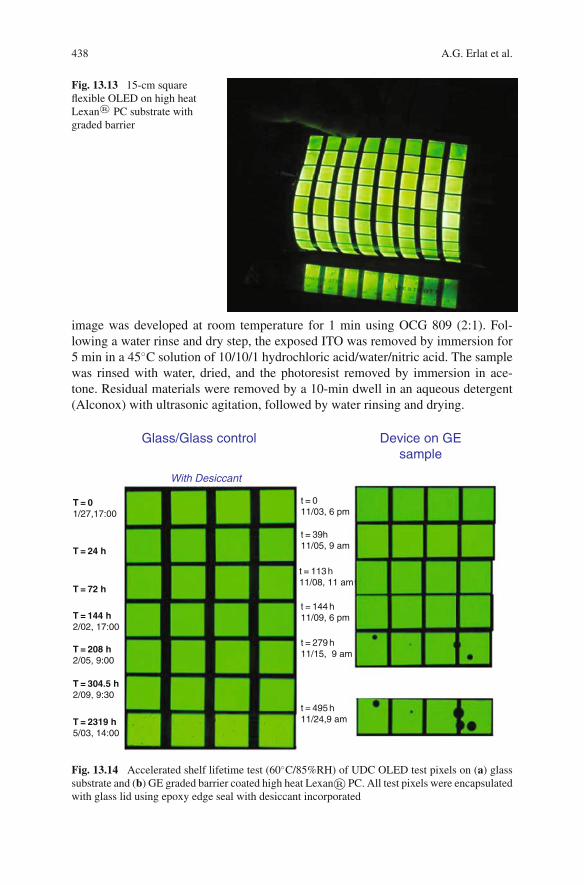
438 A.G. Erlat et al.
Fig. 13.13 15-cm squareflexible OLED on high heatLexan® PC substrate withgraded barrier
image was developed at room temperature for 1 min using OCG 809 (2:1). Fol-lowing a water rinse and dry step, the exposed ITO was removed by immersion for5 min in a 45◦C solution of 10/10/1 hydrochloric acid/water/nitric acid. The samplewas rinsed with water, dried, and the photoresist removed by immersion in ace-tone. Residual materials were removed by a 10-min dwell in an aqueous detergent(Alconox) with ultrasonic agitation, followed by water rinsing and drying.
T = 01/27,17:00
With Desiccant
Glass/Glass control Device on GEsample
t = 011/03, 6 pm
t = 39h11/05, 9 am
t = 113 h11/08, 11 am
t = 144 h11/09, 6 pm
t = 279 h11/15, 9 am
t = 495 h11/24,9 am
T = 24 h
T = 72 h
T = 144 h2/02, 17:00
T = 208 h2/05, 9:00
T = 304.5 h2/09, 9:30
T = 2319 h5/03, 14:00
Fig. 13.14 Accelerated shelf lifetime test (60◦C/85%RH) of UDC OLED test pixels on (a) glasssubstrate and (b) GE graded barrier coated high heat Lexan® PC. All test pixels were encapsulatedwith glass lid using epoxy edge seal with desiccant incorporated
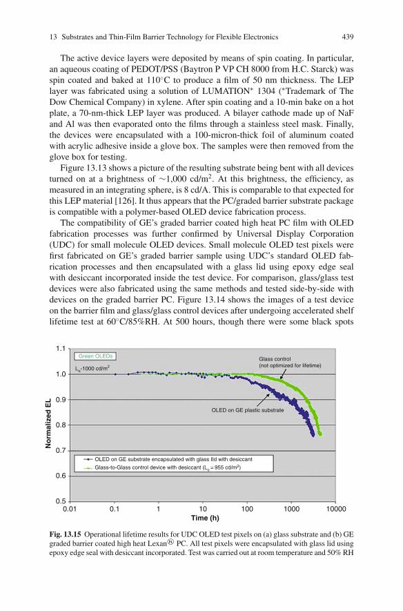
13 Substrates and Thin-Film Barrier Technology for Flexible Electronics 439
The active device layers were deposited by means of spin coating. In particular,an aqueous coating of PEDOT/PSS (Baytron P VP CH 8000 from H.C. Starck) wasspin coated and baked at 110◦C to produce a film of 50 nm thickness. The LEPlayer was fabricated using a solution of LUMATION∗ 1304 (∗Trademark of TheDow Chemical Company) in xylene. After spin coating and a 10-min bake on a hotplate, a 70-nm-thick LEP layer was produced. A bilayer cathode made up of NaFand Al was then evaporated onto the films through a stainless steel mask. Finally,the devices were encapsulated with a 100-micron-thick foil of aluminum coatedwith acrylic adhesive inside a glove box. The samples were then removed from theglove box for testing.
Figure 13.13 shows a picture of the resulting substrate being bent with all devicesturned on at a brightness of ∼1,000 cd/m2. At this brightness, the efficiency, asmeasured in an integrating sphere, is 8 cd/A. This is comparable to that expected forthis LEP material [126]. It thus appears that the PC/graded barrier substrate packageis compatible with a polymer-based OLED device fabrication process.
The compatibility of GE’s graded barrier coated high heat PC film with OLEDfabrication processes was further confirmed by Universal Display Corporation(UDC) for small molecule OLED devices. Small molecule OLED test pixels werefirst fabricated on GE’s graded barrier sample using UDC’s standard OLED fab-rication processes and then encapsulated with a glass lid using epoxy edge sealwith desiccant incorporated inside the test device. For comparison, glass/glass testdevices were also fabricated using the same methods and tested side-by-side withdevices on the graded barrier PC. Figure 13.14 shows the images of a test deviceon the barrier film and glass/glass control devices after undergoing accelerated shelflifetime test at 60◦C/85%RH. At 500 hours, though there were some black spots
No
rmal
ized
EL
0.5
0.6
0.7
0.8
0.9
1.0
1.1
OLED on GE substrate encapsulated with glass IId with desiccant
OLED on GE plastic substrate
Glass-to-Glass control device with desiccant (Lo = 955 cd/m2)
Glass control(not optimized for lifetime)Lo-1000 cd/m2
Green OLEDs
Time (h)0.01 0.1 1 10 100 1000 10000
Fig. 13.15 Operational lifetime results for UDC OLED test pixels on (a) glass substrate and (b) GEgraded barrier coated high heat Lexan® PC. All test pixels were encapsulated with glass lid usingepoxy edge seal with desiccant incorporated. Test was carried out at room temperature and 50% RH
440 A.G. Erlat et al.
forming, most pixel areas on the graded barrier substrate were still intact. The roomtemperature operational lifetime test results were illustrated in Fig. 13.15 and it wasestimated that the OLED device on the barrier film sample has a half life 80% ofthat of glass/glass control.
These test results show that barrier coated plastic films can potentially be used inplace of a glass substrate for both polymer and small molecule OLED devices.
13.4.2 Thin-Film Encapsulation
Another technology for realizing flexible OLEDs and other organic electronicdevices is thin-film encapsulation (TFE) (Fig. 13.1, scheme D). Currently, commer-cial OLED displays are encapsulated with a thin metal or a glass cap sealed to thebase OLED substrate with an epoxy seal [20, 127, 128]. In addition, getter materialssuch as CaO or BaO are used inside this package to prolong the shelf lifetime of thedevice [20, 128, 129]. This method of encapsulation limits the ability to produce afully flexible device. In addition, it is a slow and high-cost process and the standardseal thickness is microns thick and therefore cannot provide adequate barrier withoutthe addition of a desiccant. It is the combination of these disadvantages of currentencapsulation technologies that have led researchers and companies to put effortinto developing TFE methods that can be commercially viable. Reduction of edgeseal thickness, reduction in processing tact time, and thereby reduction in cost alongwith the potential for enabling full flexibility are the core advantages of this technol-ogy. On the other hand, development of TFEs presents unique challenges comparedto those outlined for plastic substrates. The substrate is now the OLED structureitself, which is an inorganic/organic multilayer structure with multiple terminatingsurfaces depending on the OLED architecture (metal cathode, organic layer, con-tacts, etc.). The barrier structure used for encapsulation therefore needs to be com-patible with the underlying OLED and to exhibit low stress and good adhesion.Especially for passive-matrix OLED displays, where cathode partition structurescan be microns high and have negative slopes, conformality of the TFE layer isimportant to ensure continuous coverage of all active areas. Avoiding physical orchemical damage to the OLED during deposition is also crucial since most activeorganic materials tend to degrade at high processing temperatures and when exposedto high energy species. Finally, an important aspect not generally noted is the abilityto properly encapsulate contact leads to the outside of the package to avoid any pre-mature device failure. All these requirements should be fulfilled while maintainingexcellent barrier properties for TFE and maintaining electro-optical function of theOLED after prolonged shelf life tests.
Studies to date have explored different TFE deposition methods with differentstructures on a variety of OLED architectures for both solution-processed polymerand evaporated small molecule devices [105, 123, 130–142]. There are two basicOLED device architectures: “bottom-emitting” and “top-emitting”. In the “bottom-emitting” configuration, active organic layers are deposited on top of a transparent
13 Substrates and Thin-Film Barrier Technology for Flexible Electronics 441
substrate with a transparent conductive contact and then capped with a nontrans-parent low work function metal cathode, such as Ca capped with Al. In the “top-emitting” configuration, the active organic layers are deposited on top of a opaqueor reflective substrate with a metallic contact and then capped with a transparentconductive electrode. OLED display devices can be further subdivided into passive-matrix (PMOLED) or active-matrix (AMOLED) depending on how the individualpixels are driven. Combinations of these architectures can be fabricated on glass,metal foil, or plastic substrates.
On glass substrates, most TFE studies have been reported on simple test pix-els for bottom-emitting small molecule devices. Here, the PML-type multilayerapproach [27, 130] and the PECVD graded single layer approach [131] demonstratethe longest shelf lifetimes with less than 10% pixel degradation at 60◦C/90%RHafter 500 hours for the former and less than 10% pixel degradation at the sameconditions after 1,000 hours for the latter. The ALD method of Ghosh [136] is alsopromising, with a report of negligible degradation after 1,000 hours at 85◦C/85%RHfor top-emission small molecule OLEDs.
For passive-matrix display applications, promising results are achieved so far bythe deposition of a thick organic layer first to cover the cathode partition topol-ogy and subsequent multilayer film deposition [27, 130]. However, recently a veryconformal PECVD SiN process coupled with either SiOx or a topcoat [133, 134]with ink-jet printed organic layers to make up a multilayer barrier [135] has beendemonstrated to be able to cover the cathode partition type of topology. In thiscase, shelf lifetimes of 500 hours with some dark spot formation and edge leak-age were reported at accelerated environmental conditions. The primary cause ofdegradation in these studies is cited as relating to large particles of micron size,which means there is still more work to be done to enable commercial viability. Inaddition, as a general trend, the operational lifetimes of encapsulated OLEDs areinferior to their glass encapsulated counterparts. This degradation is, in most cases,due to dominance of fast-growing dark spots caused by moisture ingress throughdefects in the barrier. Weidner et al. [105], however, showed in an experiment wherethey glass encapsulated PECVD TFE-coated OLED and compared to simple glass-encapsulated OLED, operational lifetime performance of the OLED/TFE was sim-ilar and in cases better than glass-encapsulated samples. This result indicates thatPECVD TFE does not adversely affect the operational performance of an OLED.Several groups have also demonstrated TFE on OLEDs fabricated on plastic sub-strates with or without barrier. Chwang et al. [123] applied PML-type multilayercoatings onto OLEDs fabricated on PET substrates with a similar barrier stack.When compared at equivalent conditions, the all plastic structure displayed a life-time of 2,500 hours, whereas the same TFE encapsulated device on a glass substrateperformed to 3,700 hours. The traditional all glass package decayed in 9,000 hours.The same group demonstrated TFE encapsulation of an all plastic 80 dpi, passivematrix display with an operational lifetime of 110 hours, with initial luminance at110 cd/m2. Recently, Yoshida et al. have demonstrated a flexible OLED display onPET, encapsulated with a 3-μm thick PECVD SiN layer with a projected opera-tional lifetime (to reach 50% initial luminance of 1,000 cd/m2) of over 5,000 hours.
442 A.G. Erlat et al.
The same group also showed that, with identical encapsulation, negligible changein OLED performance for a full-color OLED display (5.2 in. 1/4 VGA) after 500hours at accelerated environmental testing conditions [143].
Significant ground has been covered over the last five years or so in making TFEa commercially viable technology. Improving both operational and shelf lifetimeremains a challenge. Also, there is surprisingly little work on TFE of active matrixdisplays, which are the most promising candidates for future, high information con-tent, high-resolution displays; so more work in this field is necessary. Last but notleast, particle control, yield, and tact time, irrespective of the deposition methodfor advanced barrier systems remain the primary challenges standing between TFEbeing an excellent research level effort and TFE being a commercially viable solu-tion for encapsulation of flexible organic electronic devices.
13.5 Concluding Remarks
Hermetic packaging of organic electronic devices is one of the most importantchallenges that must be overcome before flexible electronic devices can becomea commercial reality. In this regard, thin-film barrier technology, especially on plas-tic substrates and also directly on the device, is a key enabling technology. Fromthis review, it is clear that there are now multiple advanced barrier technologiesthat, at least in the research lab, can provide the right order of magnitude hermetic-ity. However, system integration challenges such as substrate deformation duringdevice processing, thermomechanical stability, and compatibility with the devicerequire more work and further improvements. Challenges also remain to demon-strate similar barrier performance using commercially viable R2R fabrication pro-cesses. Nevertheless, given the increasing rate of progress and increasing effort overthe last decade, it seems likely that flexible thin-film barrier technology will maturein time to enable flexible electronics applications.
References
1. Forrest SR (2004) The path to ubiquitous and low-cost organic electronic appliances onplastic. Nature 428:911–918
2. Friend RH, Gymer RW, Holmes AB, Burroughes JH, Marks RN, Taliani C, Bradley DDC,Dos Santos DA, Bredas JL, Logdlund M, Salaneck WR (1999) Electroluminescence in con-jugated polymers. Nature 397:121–128
3. Forrest SR (2000) Active optoelectronics using thin-film organic semiconductors. IEEE JSelect Topics Quantum Electron 6:1072–1083
4. Tang CW (1986) Two-layer organic photovoltaic cell. Appl Phys Lett 48:183–1855. Yu G, Gao J, Hummelen J, Wudl F, Heeger AJ (1995) Polymer photovoltaic cells: Enhanced
efficiencies via a network of internal donor–acceptor heterojunctions. Science 270:1789–1791
6. Halls JJM, Walsh CA, Greenham NC, Marseglia EA, Friend RH, Moratti SC, HolmesAB (1995) Efficient photodiodes from interpenetrating polymer networks. Nature 376:498–500
13 Substrates and Thin-Film Barrier Technology for Flexible Electronics 443
7. Lovinger AJ, Rothberg LJ (1996) Electrically active organic and polymeric materials forthin-film-transistor technologies. J Mater Res 11:1581–1592
8. Rogers JA, Bao Z, Baldwin K, Dodabalapur A, Crone B, Raju VR, Kuck V, Katz H, Amund-son K, Ewing J, Drzaic P (2001) Paper-like electronic displays: Large-area, rubber-stampedplastic sheets of electronics and microencapsulated electrophoretic inks. Proc Natl Acad Sci98:4835–4840
9. Snow ES, Novak JP, Campbell PM, Park D (2003) Random networks of carbon nanotubesas an electronic material. Appl Phys Lett 82:2145–2147
10. Duan X, Niu C, Sahl V, Chen J, Parce JW, Empedocles S, Goldman JL (2003) High-performance thin-film transistors using semiconductor nanowires and nanoribbons. Nature425:274–278
11. Mitzi DB, Kosbar LL, Murray CE, Copel M, Afzali A (2004) High-mobility ultrathin semi-conducting films prepared by spin coating. Nature 428:299–302
12. Kazlas PT, McCreary MD (2002) Paperlike microencapsulated electrophoretic materials anddisplays. MRS Bulletin 27:894–897
13. Park S, Jayaraman S (2003) Smart textiles: Wearable electronic systems. MRS Bulletin28:585–591
14. Jansen AN, Amine K, Newman AE, Vissers DR, Henriksen GL (2002) Low-cost, flexiblebattery packaging materials. JOM 54:29–54
15. Robshaw MJB (2006) An overview of RFID tags and new cryptographic developments. InfSecur Tech Rep 11:82–88
16. Tung S, Witherspoon SR, Roe LA, Silano A, Maynard DP, Ferraro N (2001) A MEMS-based flexible sensor and actuator system for space inflatable structures. Smart Mater Struct10:1230–1239
17. Crone BK, Dodabalapur A, Sarpeshkar R, Gelperin A, Katz HE, Bao Z (2002) Organicoscillator and adaptive amplifier circuits for chemical vapor sensing. J Appl Phys 91:140–146
18. Fix W, Ullmann A, Ficker J, Clemens W (2002) Fast polymer integrated circuits. Appl PhysLett 81:1735–1737
19. Gelinck G, Huitema HEA, Veenendaal EV, Cantatore E, Schrijnemakers L, Van Der Put-ten JBPH, Geuns TCT, Beenhakkers M, Giesbers JB, Huisman B, Meijer EJ, Benito EM,Touwslager FJ, Marsman AW, Van Rens BJE, De Leeuw DM (2004) Flexible active-matrix displays and shift registers based on solution-processed organic transistors. Nat Mater3:106–110
20. Lewis JS, Weaver MS (2004) Thin-film permeation-barrier technology for flexible organiclight-emitting devices. IEEE J Select Topics Quantum Electron 10:45–57
21. Parthasarathy G, Liu J, Duggal AR (2003) Organic light emitting devices from displays tolighting. The Electrochem Soc Interface 12:42–47
22. Schaer M, Nuesch F, Berner D, Leo W, Zuppiroli L (2001) Water vapor and oxy-gen degradation mechanisms in organic light emitting diodes. Adv Funct Mater 11:116–121
23. McElvain J, Antoniadis H, Hueschen MR, Miller JN, Roitman DM, Sheats JR, Moon L(1996) Formation and growth of black spots in organic light-emitting diodes. J Appl Phys80:6002–6007
24. Burrows PE, Graff GL, Gross ME, Martin PM, Hall M, Mast E, Bonham C, Bennett W,Michalski L, Weaver M, Brown JJ, Fogarty D, Sapochak LS (2001) Gas permeation andlifetime tests on polymer-based barrier coatings. Proc SPIE 4105:75–83
25. Graff GL, Burrows PE, Williford RE, Praino RF (2005) Barrier layer technology for flexibledisplays. In: Crawford GP (ed) Flexible Flat Panel Displays. John Wiley & Sons Ltd, WestSuccex, pp 57–78
26. Kim TW, Yan M, Erlat AG, McConnelee PA, Pellow M, Deluca J, Feist TP, Duggal AR,Schaepkens M (2005) Transparent hybrid inorganic/organic barrier coatings for plasticorganic light-emitting diode substrates. J Vac Sci Technol 23:971–977
444 A.G. Erlat et al.
27. Rutherford NM, Moro L, Chu X, Visser RJ (2004) Plastic barrier substrate and thin filmencapsulation: Progress toward manufacturability. Third Annual Flexible Displays andMicroelectronics Conference
28. Yan M, Kim TW, Erlat AG, Pellow M, Foust D, Liu J, Schaepkens M, Heller CM,McConnelee PA, Feist T, Duggal A (2005) A transparent, high barrier, and high heat sub-strate for organic electronics. Proc IEEE 93:1468–1477
29. Plichta A, Habeck A, Knoche S, Kruse A, Weber A, Hildebrand N (2005) Flexible glasssubstrate. In: Crawford GP (ed) Flexible Flat Panel Displays. John Wiley & Sons Ltd, WestSussex, pp 35–55
30. Chen Y, Au J, Kazlas P, Ritenour A, Gates H, McCreary M (2003) Flexible active-matrixelectronic ink display. Nature 423:136
31. Ma RQ, Hewitt R, Rajan K, Silvernail J, Urbanik K, Hack M, Brown J (2007) Flexiblelow power consumption active-matrix OLED displays. International Display ManufacturingConference and FPD Expo – Proceedings, Taipei, Taiwan 305–308
32. MacDonald WA (2004) Engineered films for display technologies. J Mater Chem 14:4–1033. MacDonald WA, Rollins K, MacKerron D, Rakos K, Eveson R, Hashimoto K, Rustin R
(2005) Engineered films for display technologies. In: Crawford GP (ed) Flexible Flat PanelDisplays. John Wiley & Sons Ltd, West Sussex, pp 11–33
34. MacDonald WA (2004) Engineered films for display technologies. J Mater Chem 14:4–1035. Long K, Kattamis AZ, Cheng IC, Gleskova H, Wagner S, Sturm JC (2006) Stability of
amorphous-silicon TFTs deposited on clear plastic substrates at 250◦C to 280◦C. IEEE Elec-tron Device Lett 27:111–113
36. Mahon JK, Brown JJ, Zhou TX, Burrows PE, Forrest SR (1999) Requirements of flexiblesubstrates for organic light emitting devices in flat panel display applications. 42nd AnnualTechnical Conference Proceedings of the Society of Vacuum Coaters, Chicago, IL, pp 456–459
37. Kadoya T (ed) (1990) Food packaging. Academic Press, London38. Gavitt IF (1994) Snack food packaging barrier: How much is enough? Proceedings of the
Society Of Vacuum Coaters, 37th Annual Technical cConference, pp 127–13239. Dean DA(1990) Plastics in pharmaceutical packaging: A literature review, Leatherhead, Pira40. Coxe M (1998) Improved barrier properties of medical packaging. Annual Technical Con-
ference – ANTEC, Conference Proceedings 13:3380–338341. Goosey MT (1985) Permeability of coatings and encapsulants for electronic and optoelec-
tronic devices. In: Comyn J (ed) Polymer Permeability. Elsevier Applied Science, London,pp 309–339
42. Burrows PE, Graff GL, Gross ME, Martin PM, Shi MK, Hall M, Mast E, Bonham C, BennettW, Sullivan MB (2001) Ultra barrier flexible substrates for flat panel displays. Displays22:65–69
43. Childs ES (1974) The rapid growth of and big potential for plastics in packaging. In: BruinsPF (ed) Packaging with plastics. Gordon and Breach Science Publishers, New York, pp 1–24
44. McCrum NC, Buckley CP, Bucknall CB (1997) Principles of polymer engineering. OxfordUniversity Press, Oxford
45. Jamieson EHH, Windle AH (1983) Structure and oxygen-barrier properties of metallizedpolymer film. J Mater Sci 18:64–80
46. Krug TG (1990) Transparent barriers for food packaging. Proceedings of the Society ofVacuum Coaters, 33rd Annual Technical Conference, pp 163–169
47. Krug TG, Ludwig R, Steiniger G (1993) New developments in transparent barrier coat-ings. Proceedings of the Society of Vacuum Coaters, 36th Annual Technical Conference,pp 302–306
48. Chatham H (1996) Oxygen diffusion barrier properties of transparent oxide coatings onpolymeric substrates. Surf Coat Technol 78:1–9
49. Maixner RD (2002) Future trends in permeation measurement. Proceedings of the Societyof Vacuum Coaters, 45th Annual Technical Conference, pp 461–464
13 Substrates and Thin-Film Barrier Technology for Flexible Electronics 445
50. Stevens M, Tuomela S, Mayer D (2005) Water vapor permeation testing of ultra-barriers:Limitations of current methods and advancements resulting in increased sensitivity. Pro-ceedings of the Society of Vacuum Coaters, 48th Annual Technical Conference, pp 189–191
51. Norenberg H, Miyamoto T, Tsukahara Y, Smith GDW, Briggs, GAD (1999) Mass spec-trometric estimation of gas permeation coefficients for thin polymer membranes. Rev SciInstrum 70:2414–2420
52. Norenberg H, Burlakov V (2004) Recent developments in measuring permeation throughbarrier films and understanding of permeation processes. Proceedings of the Society of Vac-uum Coaters, 47th Annual Technical Conference, 164–167
53. Vogt BD, Lee HJ, Prabhu VM, Delongchamp DM, Lin EK, Wu WL, Satija SK (2005) X-ray and neutron reflectivity measurements of moisture transport through model multilayeredbarrier films for flexible displays. J Appl Phys 11:114509-1–114509-7
54. Dunkel R, Bujas R, Klein A, Horndt V (2005) Method of measuring ultralow water vaporpermeation for OLED displays. Proc IEEE 93:1478–1482
55. Nisato G, Bouten PCP, Slinkkerveer PJ, Bennet WD, Graff GL, Rutherford N, WieseL (2001) Evaluating high performance diffusion barriers: The calcium test. Asia Dis-play/IDW’01 Proceedings, pp 1435–1438
56. Nisato G, Kuilder M, Bouten P, Moro L, Philips O, Rutherford N (2003) Thin-film encap-sulation for OLEDs: Evaluation of multilayer barriers using the Ca test. SID 03 DigestXXXIV:550–553
57. Burrows PE, Graff GL, Gross ME, Martin PM, Hall M, Mast E, Bonham C, Bennett W,Michalski L, Weaver M, Brown JJ, Fogarty D, Sapochak LS (2001) Gas permeation andlifetime tests on polymer-based barrier coatings. Proc SPIE 4105:75–83
58. Erlat AG, Schaepkens M, Kim TW, Heller CM, Yan M, McConnelee P (2004) Ultra-highbarrier coatings on polymer substrates for flexible optoelectronics: Water vapor transportand measurement systems. Proceedings of the Society of Vacuum Coaters, 47th AnnualTechnical Conference, pp 654–657
59. Erlat AG, Yan M, Kim TW, Schaepkens M, Liu J, Heller CM, McConnelee P, Feist T, DuggalAR (2005) Ultra-high barrier coatings for flexible organic electronics. Proceedings of theSociety of Vacuum Coaters, 48th Annual Technical Conference, pp 116–120
60. Paetzold R, Winnacker A, Henseler D, Cesari V, Heuser K (2003) Permeation rate measure-ments by electrical analysis of calcium corrosion. Rev Sci Instrum 74:5147
61. Cros S, Firon M, Lenfant S, Trouslard P, Beck L (2006) Study of thin calcium electrodedegradation by ion beam analysis. Nucl Instrum Methods Phys Res B 251:257–260
62. Lewis J, Grego S, Vick E, Temple D (2004) Performance of thin films for flexible OLEDdisplays. 4th Annual Flexible Displays and Microelectronics Conference
63. Erlat AG, Yan M, Heller CMH, unpublished results, GE Global Research Center64. Deal BE, Grove AS (1965) General relationship for the thermal oxidation of silicon. J Appl
Phys 36:3770–377865. Barrer RM (1941) Diffusion in and through solids. Cambridge University Press, New York66. Felts JT (1991) Thickness effects on thin film gas barriers: Silicon-based coatings. Proceed-
ings of the Society of Vacuum Coaters, 34th Aannual Technical Conference, pp 99–10467. Felts JT (1993) Transparent barrier coatings update: Flexible substrates. Proceedings of the
Society of Vacuum Coaters 36th Annual Technical Conference, pp 324–33168. Benmalek M, Dunlop HM (1995) Inorganic coatings on polymers. Surf Coat Technol
76–77:821–82669. Roberts AP, Henry BM, Sutton AP, Grovenor CRM, Briggs GAD, Miyamoto T, Kano
M, Tsukahara Y, Yanaka M (2002) Gas permeation in silicon-oxide/polymer (SiOx/PET)barrier films: Role of the oxide lattice, nano-defects and macro-defects. J Membrane Sci208:75–88
70. Tropsha YG, Harvey NG (1997) Activated rate theory treatment of oxygen and water trans-port through silicon oxide/poly(ethylene terephthalate) composite barrier structures. J PhysChem B 101:2239–2266
446 A.G. Erlat et al.
71. da Silva Sobrinho AS, Latreche M, Czeremuszkin G, Klemberg-Sapieha JE, WertheimerMR (1998) Transparent barrier coatings on polyethylene terephthalate by single- and dual-frequency plasma-enhanced chemical vapor deposition. J Vac Sci Technol A 16:3190–3198
72. Henry BM, Dinelli F, Zhao KY, Erlat AG, Grovenor CRM, Briggs GAD (1999) Charac-terization of oxide gas barrier films. Proceedings of the Society of Vacuum Coaters, 42ndAnnual Technical Conference, pp 403–407
73. Barker CP, Kochem KH, Revell KM, Kelly RSA, Badyal JPS (1995) Interfacial chemistryof metallized, oxide coated, and nanocomposite coated polymer films. Thin Solid Films257:77–82
74. Klemberg-Sapieha JE, Martinu L, Kuttel OM, Wertheimer MR (1993) Transparent gas bar-rier coatings produced by dual-frequency PECVD. Proceedings of the Society of VacuumCoaters, 36th Annual Technical Conference pp 445–449
75. Schaepkens M, Kim TW, Erlat AG, Yan M, Flanagan KW, Heller CM, McConnelee PA(2004) Ultrahigh barrier coating deposition on polycarbonate substrates. J Vac Sci TechnolA 22:1716–1722
76. Groner MD, George SM, McLean RS, Carcia PF (2006) Gas diffusion barriers on polymersusing Al2O3 atomic layer deposition. Appl Phys Lett 88:0517109
77. Carcia PF, McLean RS, Reilly MH, Groner MD, George SM (2006) Ca test of Al2O3 gasdiffusion barriers grown by atomic layer deposition on polymers. Appl Phys Lett 89:031915
78. Decker W, Henry BM (2002) Basic principles of thin film barrier coatings. Proceedings ofthe Society of Vacuum Coaters, 45th annual technical conference, pp 493–502
79. da Silva Sobrinho AS, Czeremuszkin G, Latreche M, Wertheimer MR (2000) Defect-permeation correlation for ultrathin transparent barrier coatings on polymers. J Vac Sci Tech-nol A 18:149–157
80. Erlat AG, Spontak RJ, Clarke RP, Robinson TC, Haaland PD, Tropsha Y, Harvey NG, VoglerEA (1999) SiOx gas barrier coatings on polymer substrates: morphology and gas transportconsiderations. J Phys Chem B 103:6047–6055
81. Ling JSG, Leggett GJ (1997) Scanning force microscopy of poly(ethylene terephthalate)surfaces: Comparison of SEM with SFM topographical, lateral force and force modulationdata. Polymer 38:2617–2625
82. Erlat AG, Henry BM, Ingram JJ, Mountain DB, McGuigan, A, Howson RP, Grovenor, CRM,Briggs GAD, Tsukahara Y (2001) Characterisation of aluminium oxynitride gas barrierfilms. Thin Solid Films 388:78–86
83. Cros B, Vallat MF, Despaux G (1997) Characterization by acoustic microscopy of adhesionin poly(ethylene terephthalate) films coated by aluminum. Appl Surf Sci 126:159–168
84. Shaw DG, Langlois MG (1994) Use of vapor deposited acrylate coatings to improve thebarrier properties of metallized film. Proceedings of the Society of Vacuum Coaters, 45thAnnual Technical Conference, pp 240–247
85. Roehrig M, Shaw D, Langlois M, Sheehan C (1997) Use of evaporated acrylate coatings tosmooth the surface of polyester and polypropylene film substrates. J Plastic Film & Sheeting13:235–251
86. Affinito JD, Gross ME, Coronado CA, Graff GL, Greenwell EN, Martin PM (1996) Newmethod for fabricating transparent barrier layers. Thin Solid Films 290–291:63–67
87. Affinito JD, Eufinger S, Gross ME, Graff GL, Martin PM (1997) PML/oxide/PML barrierlayer performance differences arising from use of UV or electron beam polymerization ofthe PML layers. Thin Solid Films 308–309:19–25
88. Yan M, Erlat AG, Duggal AR, GE Global Research, unpublished results89. da Silva Sobrinho AS, Czeremuszkin G, Latreche M, Dennle G, Wertheimer MR (1999)
Study of defects in ultra-thin transparent coatings on polymers. Surf Coat Technol116–119:1204–1210
90. Henry BM, Dinelli F, Zhao KY, Grovenor CRM, Kolosov OV, Briggs GAD, Roberts AP,Kumar RS, Howson RP (1999) Microstructural study of transparent metal oxide gas barrierfilms. Thin Solid Films 355–356:500–505
13 Substrates and Thin-Film Barrier Technology for Flexible Electronics 447
91. Henry BM, Erlat AG, Grovenor CRM, Briggs GAD, Tsukahara T, Miyamoto T, NoguchiN, Niijima T (2000) Proceedings of the Society of Vacuum Coaters, 43rd Annual TechnicalConference pp 373–378
92. Prins W, Hermans JJ (1959) Theory of permeation through metal coated polymer films. JPhys Chem 63:716–719
93. Beu TA, Mercea PV (1990) Gas transport through metallized polymer membranes. MaterChem Phys 26:309–322
94. Rossi G, Nulman M (1993) Effect of local flaws in polymeric permeation reducing barriers.J Appl Phys 74:5471–5475
95. Czeremuszkin G, Latreche M, da Silva Sobrinho AS, Wertheimer MR (1999) Simple modelof oxygen permeation through defects in transparent coatings. Proceedings of the Society ofVacuum Coaters, 42nd Annual Technical Conference, pp 176–180
96. Hanika M, Langowski HC, Moosheimer U, Peukert W (2003) Inorganic layers on poly-meric films – Influence of defects and morphology on barrier properties. Chem Eng Technol26:605–614
97. Koo WH, Jeong SM, Choi SH, Kim W, Baik HK, Lee SM, Lee SJ (2005) Effects of thepolarizability and packing density of transparent oxide films on water vapor permeation. JPhys Chem B 109:11354–11360
98. Henry BM, Erlat AG, Deng CS, Briggs GAD, Miyamoto T, Noguchi N, Niijima T, Tsuka-hara Y (2001) The permeation of water vapor through gas barrier films. Proceedings of theSociety of Vacuum Coaters, 44th Annual Technical Conference, pp 469–475
99. Erlat AG, Henry BM, Howson RP, Grovenor CRM, Briggs GAD, Tsukahara Y (2001)Growth and characterization of transparent metal oxide and oxynitride gas barrier films onpolymer substrates. Proceedings of the Society of Vacuum Coaters, 44th Annual TechnicalConference, pp 448–454
100. Erlat AG, Henry BM, Grovenor CRM, Briggs GAD, Chater RJ, Tsukahara Y (2004) Mech-anism of water vapor transport through PET/AlOxNy gas barrier films. J Phys Chem B108:883–890
101. Schiller S, Neumann M, Morgner H, Schiller N (1995) Reactive aluminum oxide coatingof plastic films – possibilities and limitations for high deposition rates. Proceedings of theSociety of Vacuum Coaters, 38th Annual Technical Conference, pp 18–27
102. Schiller N, Reschke J, Goedicke K, Neumann M (1996) Application of the magnetron acti-vated deposition process (MAD-process) to coat polymer films with alumina in web coaters.Surf Coat Technol 86–87:776–782
103. Schiller N, Morgner H, Fahland M, Straach S, Rabisch M, Charton C (1999) Transparentoxide coatings on plastic webs for emerging applications. Proceedings of the Society ofVacuum Coaters, 42nd Annual Technical Conference, pp 392–396
104. Langereis E, Creatore M, Heil SBS, van de Sanden MCM, Kessels WMM (2006) Plasma-assisted atomic layer deposition of Al2O3 moisture permeation barriers on polymers. ApplPhys Lett 89:081915
105. Weidner WK, Zambov LM, Shamamian VA, Perz SV, Camilletti RC, Snow SA, LobodaMJ, Cerny GA (2005) PECVD processed silicon carbide coatings for organic luminescentdevices. Proceedings of the Society of Vacuum Coaters, 48th Annual Technical Conference,158–162
106. Weaver MS, Michalski LA, Rajan K, Rothman MA, Silvernail JA, Brown JJ, Burrows PE,Graff GL, Gross ME, Martin PM, Hall M, Mast M, Bonham C, Bennett W, Zumhoff M(2002) Organic light-emitting devices with extended operating lifetimes on plastic sub-strates. Appl Phys Lett 81:2929–2931
107. Langowski HC, Melzer A, Schubert D (2002) Ultra high barrier layers for technical appli-cations. Proceedings of the Society of Vacuum Coaters, 45th Annual Technical Conference,pp 471–475
108. Zambov L, Weidner K, Shamamian V, Camilletti R, Pernisz U, Loboda M, Cerny G (2006)Advanced chemical vapor deposition silicon carbide barrier technology for ultra-low perme-ability applications. J Vac Sci Technol 24:1706–1713
448 A.G. Erlat et al.
109. Henry BM, Howells D, Topping JA, Assender HE, Grovenor CRM, Marras L (2006)Microstructural and barrier properties of multilayered films. Proceedings of the Society ofVacuum Coaters, 49th Annual Technical Conference, pp 654–657
110. Charton C, Schiller N, Fahland M, Hollander A, Wedel A, Noller K (2006) Development ofhigh barrier films on flexible polymer substrates. Thin Solid Films 502:99–103
111. Yializis A, Powers GL, Shaw DG (1990) A new high temperature multilayer capacitor withacrylate dielectrics. IEEE Trans Components, Hybrids Manufact Technol 13:611–616
112. Leterrier Y (2003) Durability of nanosized oxygen-barrier coatings on polymers. Prog MaterSci 48:1–55
113. Miyamoto T, Mizuno K, Noguchi N, Niijima N (2001) Gas barrier performances of organic–inorganic multilayered films. Proceedings of the Society of Vacuum Coaters, 44th annualTechnical Conference, pp 166–171
114. Haas KH, Amberg-Schwab A, Rose K, Schottner G (1999) Functionalized coatings basedon inorganic–organic polymers (ORMOCER) and their combination with vapor depositedinorganic thin films. Surf Coat Technol 111:72–79
115. Kapoor S, Seta ME, Visser RJ, Gross ME, Bennett WD, Newton R, Goodwin K, Deng Y(2006) Pilot production of ultra-barrier substrate for flexible displays. Proceedings of theSociety of Vacuum Coaters, 49th Annual Technical Conference, pp 625–631
116. Yan M, Duggal A, McConnelee PA, Schaepkens M (2005) Methods and fixtures for facili-tating handling of thin films. US 20050016464 A1
117. Yan M, Erlat AG, Zhao R, Smith DJ, Scherer B, Jones C, Foust D, McConnelee PA, FeistTP, Duggal AR (2007) Roll-to-roll ultra-high barrier substrate for organic electronics. 6thAnnual Flexible Displays and Microelectronics Conference
118. Madocks J, Rewhinkle J, Barton L (2005) Packaging barrier films deposited on PET byPECVD using a new high density plasma source. Mater Sci Eng B 119:268–273
119. Shamamian V, Zambov L, Pernisz U, Kim SJ, Perz S, Cerny GA (2006) Progress in thedevelopment of SiC:H alloy films on flexible substrates for extremely low moisture perme-ability applications. 5th Flexible Displays and Microelectronics Conference
120. Czeremuszkin G, Latreche M, Wertheimer MR (2001) Permeation through defects in trans-parent barrier-coated plastic films. Proceedings of the Society of Vacuum Coaters, 49thAnnual Technical Conference, pp 178–183
121. Graff GL, Williford RE, Burrows PE (2004) Mechanisms of vapor permeation throughmultilayer barrier films: Lag time versus equilibrium permeation. J Appl Phys 96:1840–1849
122. Sugimoto A, Ochi H, Fujimura S, Yoshida A, Miyadera T, Tsuchida M (2004) Flexi-ble OLED displays using plastic substrates. IEEE J Select Top Quantum Electron 10:107–114
123. Chwang A, Rothman MA, Mao SY, Hewitt RH, Weaver MS, Silvernail JA, Rajan K, HackM, Brown JJ, Chu X, Moro L, Krajewski T, Rutherford N (2003) Thin film encapsulatedflexible organic electroluminescent displays. Appl Phys Lett 83:413–415
124. Foust D, Balch E, Duggal A, Heller C, Guida R, Nealon W, Faircloth T (2006) Series con-nected OLED structure and fabrication method. US7049757 B2
125. Duggal AR, Foust DF, Nealon WF, Heller CM (2003) Fault-tolerant, scalable organic light-emitting device architecture. Appl Phys Lett 82:2580–2582
126. LUMATION Green 1300 Series LEP Data Sheets, The Dow Chemical Company127. Burrows PE, Bulovic V, Forrest SR, Sapochak LS, Mccarty DM, Thompson ME (1994)
Reliability and degradation of organic light emitting devices. Appl Phys Lett 65:2922–2924128. Williams DJ, Rajeswaran G (2003) Proc SPIE 5080:166–169129. Tsuruoka Y, Hieda S, Tanaka S, Takahashi H (2003) Transparent thin film desiccant for
OLEDs. Proc Soc Inform Display Symp Dig Tech Papers, pp 860–863130. Moro L, Krajewski TA, Rutherford NM, Philips O, Visser RJ, Gross M, Bennett WD, Graff
G (2004) Process and design of a multilayer thin film encapsulation of passive matrix OLEDdisplays. Proc SPIE 5214:83–93
13 Substrates and Thin-Film Barrier Technology for Flexible Electronics 449
131. Erlat AG, Yan M, Zhao R, Tandon S, Smith DJ, Scherer B, Jones C, Foust D, McConneleePA, Feist TP, Duggal AR (2007) Recent developments in ultra-high barrier (UHB) coatingsfor organic electronics. Presentation at the 50th Annual Technical Conference, Society ofVacuum Coaters
132. Van Assche FJH, Vangheluwe RT, Maes JWC, Mishcke MS, Bijker MD, Dings FC, EversMF, Kessels WMM, van de Sanden MCM (2004) A thin film encapsulation stack for PLEDand OLED displays. SID 04 Digest 35:695–697
133. Lifka H, van Esch HA, Rosink JJWM (2004) Thin film encapsulation of OLEDs with aNONON stack. SID 04 Digest 35:1384–1387
134. Rosink JJWM, Lifka H, Rietjens GH, Pierik A (2005) Ultra-thin encapsulation for large areaOLED displays. SID 05 Digest 36:1272–1275
135. van Rens B (2006) Breaking the LCD cost barrier for OLED production using inline con-cepts. 2nd Plastic Electronics Conference and Showcase
136. Ghosh AP, Gerenser LJ, Jarman CM, Fornalik JE (2005) Thin-film encapsulation of organiclight-emitting devices. Appl Phys Lett 86:223503-1–223503-3
137. Park SK, Oh J, Hwang C, Lee J, Yang YS, Chu HY (2005) Ultrathin film encapsulation ofan OLED by ALD. Electrochem Solid State Lett 8:H21–H23
138. Tzen CK, Shen WJ, Wang HC, Su CF, Wu CC, Lu CC, Tzen JC, Su CY, Tang SJ (2006)High transparency and low operation voltage top emission organic light emitting deviceswith thin film encapsulation. SID 06 Digest 37:972–974
139. Hemerik M, van Erven R, Vangheluwe R, Yang J, van Rijswijk T, Winters R, van Rens B(2006) Lifetime of thin-film encapsulation and its impact on OLED device performance.SID 06 Digest 1571–1573
140. Yi CH, LeeYK, Lee SM, Ju SH, Lee EJ, Choo YM, Park KC, Jang J (2004) A hybridencapsulation method for OLED. SID 04 Digest 715–716
141. Akedo K, Miura A, Fujikawa H, Taga Y (2003) Plasma-CVD SiNx/plasma-polymerizedCNx:H multi-layer passivation films for organic light emitting diodes. Proc Soc Inform Dis-play Symp 34:559–561
142. Yoshida A, Fujimura S, Miyake T, Yoshizawa T, Ochi H, Sugimoto A, Kubota H, MiyaderaT, Ishizuka S, Tsuchida M, Nakada H (2003) 3-inch Full-color OLED display using a plasticsubstrate. Proc Soc Inform Display Symp 34:856–859
143. Kubota H, Miyaguchi S, Ishizuka S, Wakimoto T, Funaki J, Fukuda Y, Watanabe T, OchiH, Sakamoto T, Miyake T, Tsuchida M, Ohshita I, Tohma T (2000) Organic LED full colorpassive-matrix display. J Luminescence 87–89:56–60
Index
AAbsorption
light, 334–338See also Photovoltaics (PV) technology
Active matrix LCD (AMLCD), 2, 230electro-optic response, 232integrated display drivers, 247OTF-based integrated display drivers, 247TFT technologies for flexible backplanes
low temperature a-Si TFT, 87low-temperature processing, 85–86
See also Electrophoretic displays (EPD);Liquid crystal displays (LCD)
Active matrix OLED (AMOLED)architecture, 235–236
active island patterning, 235top versus bottom contacts, 235
backplane requirements, 91–95active matrix addressing, 92–95current programming, 94–95voltage programming, 92–94
displays using a-Si TFT backplanesfabrication using PEN plastic substrates,
95–97fabrication with thin film encapsulation,
100–102flexible OLED display fabrication,
98–100low temperature a-Si TFT, 87–88
low-temperature processing, 82–88media for flexible displays, 89nonideal behavior in, 241–242organic TFT for, 237–242
architectures, 238–241electro-optic response, 237–238electrophoretic displays, 230–236LCD, 230–236
See also Electrophoretic displays (EPD);Liquid crystal displays (LCD);Passive matrix OLED (PMOLED)
Actuators, 183organic transistors for, 184sheet-type Braille displays, 201–212See also Frontplane electronics
Additive printing, 20Adhesion, TMO, 137Alignment
experimental result for a-Si TFTs, 49–50overlay, 38–39See also Mechanical theory of
film-on-substrate-foil structure(a-Si:H TFT)
Alkylthiophenes, see Polythiophenes)Amorphous silicon
film-on-substrate-foil structure,see Mechanical theory offilm-on-substrate-foil structure(a-Si:H TFT)
low-temperature processing, 53–56contacts, 62–64dielectrics, 57–59for flexible backplanes, 82–89TFT, 59–70, 102–104, 165–167
TFTAMOLED displays using a-Si TFT
backplanes, 95–102backplanes and displays, see Thin-film
transistors (TFTs) backplanes anddisplays
electrophoretic displays fabricatedusing a-Si TFT backplanes, 102
for flexible backplanes, 82–89, 102–104low-temperature processing, 85–89,
102–104See also Nanocrystalline silicon (nc-Si)
451
452 Index
BBack transfer limited recombination, see
Interface-limited (back transferlimited) recombination
Backplane electronicsmaterials for interconnects and contacts
conducting organic polymers, 11stretchable interconnects, 12transparent conductive oxides, 11
printed organic, 172–175TFTs
organic, 10, see also under OrganicTFTs
silicon, 9–10transparent, 10
TFTs backplanes and displays, 75–104AMOLED, 95–102electrophoretic displays, 89, 102LCD, 89OLED, 90–95
See also Frontplane electronics; SubstratesBarrier, see Thin-film barrier technologyBatch processing
fabrication on sheets by, 18–19See also Roll-to-roll processing
Bendable or rollable electronics, 4Bias stress
continuous biasing, 158–160in organic TFT, 158–163instability, 226long-term stress effects, 162–163organic TFT parameter, 225–226pulsed biasing, 160–162See also Hysteresis
Bitline (BL) structurein sheet-type image scanners, 197See also Wordline (WL) structure
Braille, see Sheet-type Braille displaysBulk heterojunction (BHJ) solar cells
BHJ composites understanding andoptimization, 385–401
application to large-areasolution-processed solar cells,396–401
one-diode model consequences,392–396
one-diode model for organic solar cell,386–391
large-area processable photovoltaicschallenges, 401–408flexible solar cells encapsulation,
404–408
large-area solution-processed solar cellsapplication, 396–401
motivation for, 375–376production scheme, 401–404
organic solar cell materials basics, 377–378photovoltaics fundamentals
current–voltage characteristic, 383–384solar radiation, 378–379two-level system band considerations,
379–381transport phenomena, 381–383VOC, 384–385
See also Organic photovoltaics
CCalcium test
permeation and, 420–425See also Thin-film barrier technology
Capacitanceselectronic systems parameter, 223–225NTTFTs, 319–320
Carbon nanotubes, see Nanotubes (NT)Carrier density, 134–135Carrier mobility, 217
See also Field-effect mobilityCdO, 11Chemical oxidation method, 265, 266CMOS
OTFT circuits comparison with silicon,242–244
See also Thin-film transistors (TFTs)Coating (NT films)
slot, 308spin, 308See also Spraying
Conductance (NT films)concentration dependent, 301electrical, 299frequency dependence and optical
conductivity, 302sheet conductance and optical transparency,
309–312temperature dependent, 302
Conducting organic polymersfor interconnects and contacts, 11See also Backplane electronics
Contactsbackplane electronics materials for, 11low-temperature TFTs
a-Si:H TFT, 62–64nc-Si TFT, 64–66
resistance, 222–223TMO transistors, 116
Index 453
Continuous biasing, see under Bias stressCross-coupling methodologies, see under
PolythiophenesCurrents
current–voltage characteristics (BHJ solarcells), 383–384
dark, 331–332leakage, 222
Curvature, see Radius of curvature
DDegrees of flexibility, see under Flexible
electronicsDehalogenative polymerization, 273
See also PolythiophenesDeposition (NT films), 306–308
filtration/stamping, 308slot coating, 308spin coating, 308spraying, 307–308See also Solubilization
Device Layer Transfer (DLT) process, 82–83See also Low temperature processing
Dielectricsfor flexible electronics
inorganic semiconductors anddielectrics, 145
organic semiconductors and dielectrics,146–149
low-temperature processingsilicon nitride characteristics, 57–58silicon oxide characteristics, 58–59thin-film deposition characteristics, 57TMO TFT and, 135
TMO transistors properties, 115–116Diffusion lengths
discrepancy between measured andpredicted, 340–344
exciton harvesting, 338–340, 344–347small
hetero-energy transfer, 348–349overcoming approaches, 347–349triplet diffusion, 347–348
spectral diffusion and, 341See also Excitons; Organic photovoltaics
Diffusion-limited recombination, 359–360See also Interface-limited (back transfer
limited) recombinationDigital lithography
for flexible image sensor arrays, 170–171See also Self-aligned imprint lithography
(SAIL)Dimensional stability, 80–81
Direct fabrication, 3See also Transfer-and-bond approach
Displaysintegrated display drivers, 247SASID, 247using a-Si TFT backplanes
AMOLED, 100–102electrophoretic displays, 102fabrication using PEN plastic substrates,
95–97low-temperature processing, 102–104OLED, 98–100
See also Active matrix LCD (AMLCD);Active matrix OLED (AMOLED);Thin-film transistors (TFTs)backplanes and displays
Doping (nanotubes)chemical functionalization and,
304–305NTTFTs logic elements and, 323
Dye sensitized solar cells (DSSCs), 375
EEfficiency, see External quantum efficiency
(EQE)Elastically stretchable electronics, 5Electrically erasable PROM (EEPROM), 255Electrochemical oxidation, 267Electronic textiles, 16
See also Frontplane electronicsElectro-optic response
electrophoretic materials, 233LCD, 231–233organic LED, 237–238
luminance decay, 238voltage increase, 238
Electrophoretic displays (EPD), 13–14architecture, 234–236electro-optic response, 233fabricated using a-Si TFT backplanes, 102low-temperature a-Si TFT for, 104media for flexible displays, 89organic TFT for, 230, 233–236TFT backplanes and displays, 82See also Light emitting displays (LEDs);
Liquid crystal displays (LCD)Encapsulation
flexible solar cells, 404–408thin film (TFE), 16–18
barrier–device integration and,437–442
flexible AMOLED display fabricationwith TFE, 100–102
454 Index
Etching, 135–136Etch-mask patterning, 153–154
See also Print processingExciplex, 353
See also Organic photovoltaicsExcitons, 332
dissociation, 349–350harvesting, 338–349
effects of disorder, 340–344extrinsic defects, 344measurement, 344–347small diffusion lengths overcoming
approaches, 347–349See also Photovoltaics (PV) technology
External quantum efficiency (EQE), 331, 367
FFabrication approaches
additive printing, 20batch processing, 18–19direct fabrication, 3NT films, 305–308
deposition, 306–308solubilization, 306
roll-to-roll processing, 19transfer-and-bond approach, 3See also Print processing
Fault tolerance (NT film), 300Feature sizes
control of feature sizes of jet-printedliquids, 151–153
methods for minimizing, 154–156See also Print processing
Field-effect mobility, 216–219See also Carrier mobility
Field-effect transistors (FET)organic (OFET), 261See also Polythiophenes; Thin-film
transistors (TFTs)Film-on-substrate-foil structure, see Mechani-
cal theory of film-on-substrate-foilstructure (a-Si:H TFT)
Filtration/stamping (NT film) fabricationtechnology, 308
Flexible electronics, 1, 144degrees of flexibility, 3–5
bendable or rollable electronics, 4elastically stretchable electronics, 5permanently shaped, 4
devices performance and characterization,157–170
bias stress in organic thin-filmtransistors, 158–163
low-temperature a-Si:H p–i–n devices,167–170
low-temperature a-Si:H TFT devicestability, 165–167
scaling of short-channel OTFT,163–165
fabrication approachesadditive printing, 20batch processing, 18–19roll-to-roll processing, 19transfer-and-bond, 3
history, 1–2materials considerations
conductors, 149–150inorganic semiconductors and
dielectrics, 145organic semiconductors and dielectrics,
146–149materials for, 3–16
backplane electronics, 8–12encapsulation, 16–18frontplane electronics, 12–16substrates, 5–8
outlook, 20patterning methods for, 143printed
digital lithography, 170–171future prospects, 176printed organic backplanes, 172–175
print-processing options for devicefabrication, 150
control of feature sizes of jet-printedliquids, 151–153
jet-printing for etch-mask patterning,153–154
methods for minimizing feature size,154–156
printing active materials, 156–157substrates
metal foil substrate material, 7–8PEN plastic substrates, 79plastic, 77–79plastic film substrate material, 7properties, 5–6stainless steel, 76–77thin glass substrate material, 6
See also Backplane electronics; Frontplaneelectronics; Transition metal oxide(TMO)
Flexure, TMO, 137Foil substrates, free-standing, see Mechanical
theory of film-on-substrate-foilstructure (a-Si:H TFT)
Index 455
Frequency response parameter, 223–225Frontplane electronics
actuators, 16electronic textiles, 16electrophoretic displays, 13–14LCD, 12–13OLED, 14–15sensors, 15–16See also Backplane electronics
GGeminate pairs
dissociating, 351–355See also Organic photovoltaics
Geometric factors (NT film), 303, 304
HHeterojunction energy offsets, 355–357
See also Bulk heterojunction (BHJ) solarcells; Organic photovoltaics
High temperature processingTFT technologies for flexible back-
planes, 82See also Low temperature processing
Hysteresisdefined, 226NTTFTs, 321–322, 324organic TFT parameter, 226–227See also Bias stress
IImage sensors
digital lithography for flexible, 170–171sheet-type, 183
Braille displays, 201–212image scanners, 185–200
Imprint lithographyfor TMO TFT fabrication on flexible
substrates, 120–127self-aligned (SAIL), 122–127
Inorganic semiconductorsand dielectrics, 145See also Flexible electronics; Organic
semiconductorsIntegrated display drivers
OTFT for, 247SASID, 247
Interconnectsstretchable, 12See also Backplane electronics
Interface-limited (back transfer limited)recombination, 360–363
See also Diffusion-limited recombinationIron law of multiplexing, 228
ITOreplacement, 312transparent conductive oxide, 11See also Nanotubes films
JJet printing, see under Print processing
LLarge-area processable photovoltaics, see
under Bulk heterojunction (BHJ)solar cells
Leakage currentsdrain, 222gate, 222See also Threshold voltage
Light absorption, 334photovoltaics (PV) technology,
373–374See also Excitons; Organic photovoltaics
Light emitting displays (LEDs)frontplane electronics, 14–15organic (OLED)
active matrix, see Active matrix OLED(AMOLED)
architectures, 238–241electro-optic response, 237–238polymer organic (PLEDs), 14
See also Electrophoretic displays (EPD);Liquid crystal displays (LCD)
Liquid crystal displays (LCD)active-matrix (AMLCD), see Active matrix
LCD (AMLCD)architecture, 234–236barrier layers aspects, 90display media for flexible displays, 89electro-optic response, 231–233frontplane electronics, 12–13low-temperature a-Si TFT for, 102–103organic TFT for, 230–236polymer-dispersed liquid crystal (PDLC),
13, 230TFT backplanes and displays
flexible substrate technologies,79–80
low-temperature processing, 85–86See also Electrophoretic displays (EPD);
Light emitting displays (LEDs)Lithography
digital, 170–171imprint
for TMO TFT fabrication, 120–127self-aligned (SAIL), 122–127
See also Print processing
456 Index
Low temperature processingamorphous silicon, 53–56
a-Si:H p–i–n devices performance andcharacterization, 167–170
a-Si:H TFT, 102–104, 165–167contacts, 62–64for flexible backplanes, 87–89
dielectricssilicon nitride characteristics, 57–58silicon oxide characteristics, 58–59thin-film deposition characteristics, 57TMO TFT and, 135
issues, 55nanocrystalline silicon (nc-Si), 53, 56TFT, 59
a-Si:H contacts, 62–64device performance, 61–62device stability aspects, 67–69,
165–167device structures and materials
processing, 60for backplanes and displays, 102–104for flexible backplanes, 82–83, 87–89future prospective, 70low-temperature doped nc-Si contacts,
64–66nc-Si TFTs, 66–67
See also Device Layer Transfer (DLT)process
MMechanical theory of film-on-substrate-foil
structure (a-Si:H TFT), 29–50built-in strain, 35–36experimental results for a-Si:H TFTs
fabricated on Kapton, 47–50radius of curvature of workpiece, 42–47strain
in substrate and film at depositiontemperature, 36–37
in substrate and film at roomtemperature, 38–42
of substrate and curvature of workpiecefor three-layer structure, 46–47
theory, 32–36Metal foil
substrate material, 7–8See also Plastic film; Thin glass
Mobilitycarrier, 217field-effect, 216–217NTTFTs, 317–323
Multiwalled nanotube (MWNT), 298
NNanocrystalline silicon (nc-Si)
low-temperature doped contacts, 64–66low-temperature TFTs, 66–70
device stability aspects, 68–69future prospective, 70
low-temperature processing, 53, 56See also Amorphous silicon
Nanostructures, organic photovoltaics and,364–367
Nanotubes (NT), 297films, see Nanotubes filmsmultiwalled (MWNT), 298single-walled (SWNT), 298See also Nanotubes TFTs (NTTFTs)
Nanotubes filmsas conducting and optically transparent
materialchallenges and path forward, 312–313ITO replacement, 312sheet conductance and optical
transparency, 309–312building blocks, 298doping and chemical functionalization,
304–305electrical and optical properties, 300–304
concentration dependent conductiv-ity, 301
frequency dependence and opticalconductivity, 302
geometric factors, 303–304temperature dependent conductiv-
ity, 302fabrication technologies, 305–308
deposition, 306–308solubilization, 306
NT as electronic material, 298–300electrical conductance, 299fault tolerance, 300optical transparency, 299
Nanotubes TFTs (NTTFTs), 313–324challenges and path forward
hysteresis, 324mobility, 323ON/OFF ratio, 323–324operating voltage, 324
device characteristics, 314–316device parameters, 316–323
device capacitance, 319–320doping and logic elements, 323hysteresis, 321–322mobility, 317–318ON/OFF ratio, 318
Index 457
operating voltage, 320stability, 322subthreshold swing, 321threshold voltage, 321
Nonuniformity, TFT, 225
OON/OFF ratio
NTTFTs, 318, 323–324See also Nanotubes (NT)
One-diode modelconsequences, 392–396for organic solar cell, 386–391See also Bulk heterojunction (BHJ) solar
cellsOptical conductivity (NT film), 299
frequency dependence and, 302sheet conductance aspects, 309–312
Organic LED (OLED)architectures, 238–241barrier layers aspects, 90–91electro-optic response, 237–238low-temperature a-Si TFT for, 104matrix displays
active matrix, see Active matrix OLED(AMOLED)
passive matrix, 236media for flexible displays, 89polymer (PLEDs), 14–15TFT technologies for flexible backplanes
flexible substrate technologies, 76–82low-temperature processing, 83–89,
104See also Electrophoretic displays (EPD);
Light emitting displays (LEDs);Liquid crystal displays (LCD);Organic TFTs; Thin-film barriertechnology
Organic FET (OFET), 261Organic photodiodes, 190–191Organic photovoltaics
architecture, 332–333basic operation, 329–332
acceptor, 330dark current, 331–332donor, 330geminate pair, 330photocurrent, 331
charge transport and recombination,357–364
diffusion-limited recombination,359–360
interface-limited recombination,360–363
measurements relevant for extractingcharge, 363–364
dissociating geminate pairs, 351–355efficiency limits and outlook, 367excitons
dissociation, 349–350harvesting, 338–349
heterojunction energy offsets, 355–357light absorption, 334–338materials, 334nanostructures and, 364–367See also Bulk heterojunction (BHJ) solar
cells; Organic solar cells; OrganicTFTs
Organic semiconductorsfor flexible electronics (organic
semiconductors and dielectrics),146–149
semiconducting polymers, 262small molecule, 262See also Inorganic semiconductors;
Organic TFTsOrganic solar cells
BHJ andone-diode model, 386–396PV materials basics, 377, 378
PV materials basics (design rule), 377–378See also Bulk heterojunction (BHJ) solar
cells; Organic photovoltaicsOrganic TFTs, 215
backplane electronics, 10bias stress in
continuous biasing, 158–160long-term stress effects, 162–163pulsed biasing, 160–162
circuits comparison with silicon CMOS,242–244
digital OTFT design, 244–245for active matrix displays, 228–236for AMOLED displays
architectures, 238–241electro-optic response, 237–238nonideal behavior in AMOLED pixels,
241–242for electrophoretic displays, 230
architecture, 234–236electro-optic response, 233
for flexible backplane applications, 82, 86for integrated display drivers (AMLCD),
247for liquid crystal displays, 230–236
architecture, 234–236electro-optic response, 231–233
458 Index
Organic TFTs, (cont.)for RFID Tags, 248–256for sheet-type sensors, 183
sheet-type Braille displays, 210sheet-type image scanners, 191–193
frequency limitations, 246nonideal scaling of short-channel, 163–165parameters for electronic systems
bias-stress instability and hysteresis,225–227
capacitances and frequency response,223–225
contact resistance, 222–223field-effect mobility, 216–219leakage currents, 222nonuniformity, 225subthreshold swing, 220–221threshold voltage, 219–220
See also Organic photovoltaicsOrgano-boron based polymerizations, 271
See also PolythiophenesOrgano-magnesium polymerizations,
268–270Organo-zin polymerizations, 270Oxidation (polythiophenes)
chemical, 265–266electrochemical, 267
Oxygen transmission rate (OTR), 406thin-film barrier technology and, 419, 422See also Permeation; Water vapor
transmission rate (WVTR)
PPassive matrix OLED (PMOLED), 236
architecture, 238disadvantages, 240See also Active matrix OLED (AMOLED)
Patterning, 143–144active island, 235etch-mask, 153–154nonideal scaling of short-channel OTFT,
163–165See also Lithography; Print processing;
Printed flexible electronicsPEN plastic substrates
AMOLED displays using a-Si TFTbackplanes on, 95–97
TFT backplane and display applicationsbarrier properties, 82dimensional stability, 80optical properties, 79solvent and moisture resistance, 81, 82surface quality, 80
Permanently shaped electronics, 4Permeation
measurement techniques, 420–425through thin-film barriers
advanced barrier films, 429–436simple single layer barrier films,
426–429See also Oxygen transmission rate (OTR);
Water vapor transmission rate(WVTR)
Photocurrent, 331Photodiodes
organic, 190–191See also Sheet-type image scanners
Photosensor cells, 193–194Photovoltaics (PV) technology
defined, 373large-area processable (BHJ solar cells)
challenges, 401–408flexible solar cells encapsulation,
404–408fundamentals for BHJ solar cells,
378–385large-area solution-processed solar cells
application, 396–401motivation for, 375–376production scheme, 401–404
organic, 329–367overview, 374–375
Pixel stability and resolution, 195See also Sheet-type image scanners
Plastic filmsubstrate material, 7See also Metal foil; PEN plastic substrates;
Thin glassPolymerization, see under PolythiophenesPolymers
dispersed liquid crystal (PDLC), 13, 230LED (PLEDs), 14polymeric TFTs, 215
circuits comparison with Si CMOS, 242for integrated display drivers, 247
semiconductingamorphous, 263crystalline, 263
Polythiophenes, 261–292cross-coupling methodologies
organoboron based, 271organomagnesium based, 268–270organozinc based, 270Stille reaction, 271–272
poly(3-alkylthiophenes), 273–279doping and oxidative stability, 277–279
Index 459
electrical properties, 275–276thin-film device processing and
morphology, 276–277poly(thieno(2,3-b)thiophenes), 286–288poly(thieno(3,2-b)thiophenes), 288–292structural analogues, 279–286polymerization
chemical oxidation routes, 264–266dehalogenative, 273electrochemical oxidation routes, 267transition metal catalyzed
cross-coupling methodologies,267–272
Print processingjet printing
control of feature sizes, 151–153for etch-mask patterning, 153–154
methods for minimizing feature size,154–156
printing active materials, 156–157See also Lithography
Printed flexible electronicsdigital lithography for flexible image
sensor arrays, 170–171future prospects, 176printed organic backplanes
all-printed electronics, 174–175hybrid fabrication, 172–174
Programmable ROM (PROM), 255–256P-type TMO, 136Pulsed biasing, 161–162
RRadio frequency identification (RFID) tags,
183, 248functions
memory, 255–256tag detection, 254–255tag powering, 251–253tag signaling, 253–254
operating frequencyhigh-frequency 13.56 MHz band, 249low-frequency <135 kHz band, 249microwave 2.45 GHz bands, 250ultra high frequency 915 MHz, 250
using OTFT technology, 250–251Radius of curvature, 42–47
experimental result for a-Si:H TFTsfabricated on Kapton, 47–48
for three-layer structure, 46–47See also Strains
Reading tests, see under Sheet-type Brailledisplays
Recombinationdiffusion-limited, 359–360interface-limited, 360–362See also Photovoltaics (PV) technology
Resolution issues, 195See also Sheet-type image scanners
Roll-to-roll processingfabrication on web by, 19See also Batch processing
Roughness, see Surface roughness
SScaling (short-channel OTFT)
nonideal, 163, 164, 165See also Print processing
Scanners, see Sheet-type image scannersSelf-aligned imprint lithography (SAIL),
122–127flexible fabrication method yields, 138transistor results, 126–127
Self-scanned amorphous silicon integrateddisplay (SASID), 247
Sensorsflexible image sensor arrays, 170–171skin, 15–16See also Frontplane electronics; Sheet-type
Braille displays; Sheet-type imagescanners
Sheet-type Braille displayselectronic performance of Braille cells,
204–210future prospects, 212manufacturing process, 201–204organic transistor-based SRAM, 210reading tests, 211–212
Sheet-type image scanners, 184applications and future prospects,
200–201device structure and manufacturing
process, 186–190double-wordline and double-bitline
structure, 196–199electronic performance of organic
photodiodes, 190–191hierarchal approach for slow organic
circuits, 196higher speed operation with lower power
consumption, 199–200imaging methods, 185–186new dynamic second-wordline decoder,
199organic transistors for, 183, 191–193photosensor cells and, 193–194
460 Index
Sheet-type image scanners (cont.)pixel stability and resolution issues, 195
Silicon, 53integrated circuits history, 1–2, see also
under Silicon TFTlow-temperature
silicon nitride, 57–58silicon oxide, 58–59
See also Amorphous silicon; Nanocrys-talline silicon (nc-Si)
Silicon TFT, 2amorphous silicon (a-Si:H TFT)
AMOLED displays using a-Si TFTbackplanes, 95–102
backplanes and displays, see Thin-filmtransistors (TFTs) backplanes anddisplays
electrophoretic displays fabricatedusing a-Si TFT backplanes, 102
for flexible backplanes, 85–89, 102–104low-temperature processing, 85–89,
102–104backplane electronics, 9, 10
Single-walled nanotube (SWNT), 298Skin sensor, 15–16Slot coating, 308Solar cells
BHJ, see bulk heterojunction (BJH) solarcells
dye sensitized (DSSCs), 375hybrid architecture, 332–333organic architecture, 332–333silicon-integrated circuits (a-Si:H), 1See also Organic photovoltaics
SolubilizationNT films fabrication technology, 306See also Deposition (NT films)
Spectral diffusion, 341See also Diffusion lengths
SprayingNT film fabrication technology, 307–308See also Coating (NT films)
SRAM, 210Stability
low-temperature a-Si:H TFT, 165–167NTTFTs, 322TMO TFT, 136–137
Stainless steel substrates, 76–77Stamping (NT film fabrication), 308Stille reaction, 271–272
See also PolythiophenesStrains
built-in, 35–36
experimental results for a-Si:H TFTs,47–48
in substrate and filmat deposition temperature, 36–38at room temperature, 38–42
mechanical, 31, 33of substrate and curvature of workpiece for
three-layer structure, 46–47See also Mechanical theory of
film-on-substrate-foil structure(a-Si:H TFT); Radius of curvature
Stress, see Bias stressStretchable interconnects, 12Substrates
barrier compatibility with OLEDs and,437–440
film-on-substrate-foil structure,see Mechanical theory offilm-on-substrate-foil structure
flexiblePEN plastic substrates, 79,
95–97plastic, 77–79stainless steel, 76–77
materialsmetal foil, 7–8plastic film, 7thin glass, 6
propertieschemical, 5electrical and magnetic, 5mechanical, 5optical, 5surface roughness, 5thermal and thermomechanical, 5
thin-film barrier technology and, 413chemical resistance, 418–419high-temperature stability, 419substrate options, 417–418surface quality, 419
TMO TFT fabrication on flexible, 119imprint lithography, 120–127SAIL, 122–127
See also Backplane electronics; Thin-filmbarrier technology
Subthreshold swing, 220–221NTTFTs, 321See also Threshold voltage
Surface qualityPEN plastic substrates for TFT backplane
and display applications, 80See also Substrates
Surface roughness, 5
Index 461
TTextiles, see Electronic textilesThermalization
radius, 351–352See also Organic photovoltaics
Thienothiophene polymerspoly(thieno(2,3-b)thiophenes), 286–288poly(thieno(3,2-b)thiophenes), 288–292See also Polythiophenes
Thin glasssubstrate material, 6See also Metal foil; Plastic film
Thin-film barrier technology, 413–442barrier device integration
substrate and barrier compatibility withOLEDs, 437–440
thin-film encapsulation, 440–442barrier requirements
barrier coating compatibility, 417barrier level, 416calcium test, 422–425chemical resistance, 418–419high-temperature stability, 419historical background, 419–420mechanical flexibility, 416optical properties, 416substrate options, 417–418substrate-specific, 417–419surface quality, 419
display media and barrier layers, 90–91PEN plastic substrates for TFT backplane
and display applications, 82permeation
measurement techniques, 420–425through thin-film barriers, 426–436
Thin-film transistors (TFTs)backplane electronics, see also under
Thin-film transistors (TFTs)backplanes and displays
organic TFT, 10silicon TFT, 9–10transparent TFT, 10
history, 1–2low-temperature processing, 59
a-Si:H TFT contacts, 62–64device performance, 61–62device stability aspects, 67–69device structures and materials
processing, 60for flexible backplanes, 82–85, 87–89,
102–104future prospective, 70
low-temperature doped nc-Si contacts,64–66
nc-Si TFTs, 66–67NT-based (NTTFTs), 313–324
challenges and path forward, 323–324device characteristics, 314–316device parameters, 316–323
organic, 215–256, see also under OrganicTFTs
polymeric, 215See also Mechanical theory of
film-on-substrate-foil structure(a-Si:H TFT); Thin-film barriertechnology; Transition metal oxide(TMO) transistors
Thin-film transistors (TFTs) backplanes anddisplays, 75–104
active matrix backplane requirements forOLED displays, 91–95
active matrix addressing, 92–95current programming, 94–95voltage programming, 92–94
AMOLED displays using a-Si TFTbackplanes
backplane fabrication using PEN plasticsubstrates, 95–97
flexible AMOLED display fabricationwith thin film encapsulation,100–102
flexible OLED display fabrication,98–100
barrier layers and, 90–91display media for flexible displays
electrophoretic display media,89–90
LCD media, 89OLED display media, 90
electrophoretic displays, 102flexible substrate technologies
PEN plastic, 79–82plastic, 77–79stainless steel electronics, 76–77
TFT technologies for flexible backplanesdirect fabrication, 86high temperature processing, 82low temperature processing, 82–85,
87–89, 102–104Thiophenes, see PolythiophenesThreshold voltage, 219–220
NTTFTs, 321See also Mobility
Transfer-and-bond approach, 3See also Direct fabrication
462 Index
Transition metal catalyzed polymerizationorgano-boron based, 271organo-magnesium based, 268–270organo-zinc based, 270
Transition metal oxide (TMO) transistors,107–139
device results, 128–132device structures
bottom gate staggered, 117constant level transistor, 119continuous bottom gate, 117
fabrication on flexible substrates, 119–127imprint lithography, 120–127SAIL transistor results, 126–127self-aligned imprint lithography,
122–127future problems and areas of research,
133–138carrier density control, 134–135etching of TMO materials, 135–136flexible fabrication method yields,
137–138flexure and adhesion of TMO, 137low-temperature dielectrics, 135P-type TMO, 136stability aspects, 136–137
previous work, 108–113properties
contact materials, 116dielectrics, 115–116semiconductors, 113–115
ZnO transistors, 108–110, 111, 113
ZTO (zinc tin oxide), 107Transparency (optical)
NT film, 299See also Optical conductivity (NT film)
Transparent conductive oxides (TCO)for interconnects and contacts, 11See also Backplane electronics
Transparent TFT, 10Triplet diffusion, 347–348
See also Diffusion lengths
WWater vapor transmission rate (WVTR)
BHJ solar cells and, 403thin-film barrier technology and, 419–425See also Oxygen transmission rate (OTR);
PermeationWordline (WL) structure
in sheet-type image scanners, 197–199new dynamic second-wordline decoder,
199See also Bitline (BL) structure
ZZinc-based semiconductors
ZnO transistors, 108for flexible backplanes, 86semiconductors properties, 113–115
ZTO (Zinc tin oxide), 107, 129, 131–132See also Transition metal oxide (TMO)
transistors
Related Documents