Flexible double gate a-IGZO TFT fabricated on free standing polyimide foil Niko Münzenrieder ⇑ , Christoph Zysset, Luisa Petti, Thomas Kinkeldei, Giovanni A. Salvatore, Gerhard Tröster Electronics Laboratory, Swiss Federal Institute of Technology Zurich, Zurich 8092, Switzerland article info Article history: Available online 15 March 2013 Keywords: Flexible electronics Thin-film transistor Amorphous indium–gallium–zinc-oxide Plastic substrates Double gate transistor abstract In this paper, the concept of double gate transistors is applied to mechanically flexible amorphous indium–gallium–zinc-oxide (a-IGZO) thin film transistors (TFTs) fabricated on free standing plastic foil. Due to the temperature sensitivity of the plastic substrate, a-IGZO is a suitable semiconductor because it provides carrier mobilities around 10 cm 2 /Vs when deposited at room temperature. Double gate TFTs with connected bottom and top gate are compared to bottom gate reference TFTs fabricated on the same substrate. Double gate a-IGZO TFTs exhibit a by 78% increased gate capacitance, a by 700 mV higher threshold voltage, and therefore an up to 92% increased transconductance when characterized at the same gate voltage above threshold (over-bias voltage). The subthreshold swing and the on/off current ratios are improved as well, and reach excellent values of 69 mV/dec and 2 10 9 , respectively. The mechanical flexibility of double gate TFTs compared to bottom gate TTFs is investigated, and device oper- ation is shown while the double gate TFT is exposed to tensile strain of 0.55%, induced by bending to a radius of 5 mm. Ó 2013 Elsevier Ltd. All rights reserved. 1. Introduction Electronic devices, especially thin-film transistors (TFTs) fabri- cated directly on flexible plastic substrates are a key requirement for a number of new large-area applications such as rollable dis- plays, electronic skins or woven electronics for smart textiles [1]. Additionally, the use of roll to roll techniques allows cost effective, large scale processing on flexible substrates [2]. While organic [3] and a-Si [4] based TFTs fabricated on flexible and temperature sen- sitive substrates in general suffer from low mobilities around 1 cm 2 /V s, amorphous indium–gallium–zinc-oxide (a-IGZO) TFTs are nearly unaffected by the choice of the substrate (rigid or flexi- ble), and offer mobilities around 10 cm 2 /V s even when deposited at room temperature [5]. Besides the mobility, there are other important parameters to take into account for device performance, such as threshold voltage V TH , on–off current ratio I on /I off , and sub- threshold swing SS. TFT performance parameters aim at a large I on / I off , a small SS, and a V TH which allows TFT operation between 0 V and 5 V. One important factor which influences the TFT perfor- mance is the capacitance of the gate insulator. In the past, several groups used different double gate structures [6,7] to increase the coupling between the gate and the channel, and thereby improve the performance of a-IGZO TFTs, fabricated on rigid glass or Si sub- strates. Additionally, other approaches to increase the gate capac- itance, and therefore the gate-channel coupling, are the use of high k materials [8], or thinner gate oxide layers. In this work, the double gate concept was combined with a 10 nm thin gate oxide and applied to a-IGZO TFTs fabricated on free standing flexible plastic foils. The bottom and the top gate were electrically connected to form an a-IGZO TFT controllable with a single gate voltage, and ensure comparability with standard TFT designs. The resulting n-type a-IGZO TFTs showed improved performance, and remained fully operational while subjected to mechanically induced strain of 0.55%. A-IGZO double gate TFTs while flat, as well as under mechanical strain, exhibit subthreshold slopes of 69 mV/dec and on–off current ratios >10 9 . In addition, the transconductance g m of double gate TFTs was increased by 92% when compared to single bottom gate reference TFTs fabricated on the same substrate, and measured at the same gate voltage above threshold (over-bias voltage). 2. Fabrication A micrograph of a fully processed flexible a-IGZO double gate TFT and the corresponding device cross section are shown in Fig. 1. To ensure the successful fabrication of the presented a-IGZO double gate TFTs on flexible substrates, the following points had to be considered during the design: 0038-1101/$ - see front matter Ó 2013 Elsevier Ltd. All rights reserved. http://dx.doi.org/10.1016/j.sse.2013.02.025 ⇑ Corresponding author. E-mail address: [email protected] (N. Münzenrieder). Solid-State Electronics 84 (2013) 198–204 Contents lists available at SciVerse ScienceDirect Solid-State Electronics journal homepage: www.elsevier.com/locate/sse

Welcome message from author
This document is posted to help you gain knowledge. Please leave a comment to let me know what you think about it! Share it to your friends and learn new things together.
Transcript
Solid-State Electronics 84 (2013) 198–204
Contents lists available at SciVerse ScienceDirect
Solid-State Electronics
journal homepage: www.elsevier .com/locate /sse
Flexible double gate a-IGZO TFT fabricated on free standing polyimide foil
Niko Münzenrieder ⇑, Christoph Zysset, Luisa Petti, Thomas Kinkeldei, Giovanni A. Salvatore,Gerhard TrösterElectronics Laboratory, Swiss Federal Institute of Technology Zurich, Zurich 8092, Switzerland
a r t i c l e i n f o a b s t r a c t
Article history:Available online 15 March 2013
Keywords:Flexible electronicsThin-film transistorAmorphous indium–gallium–zinc-oxidePlastic substratesDouble gate transistor
0038-1101/$ - see front matter � 2013 Elsevier Ltd. Ahttp://dx.doi.org/10.1016/j.sse.2013.02.025
⇑ Corresponding author.E-mail address: [email protected] (N.
In this paper, the concept of double gate transistors is applied to mechanically flexible amorphousindium–gallium–zinc-oxide (a-IGZO) thin film transistors (TFTs) fabricated on free standing plastic foil.Due to the temperature sensitivity of the plastic substrate, a-IGZO is a suitable semiconductor becauseit provides carrier mobilities around 10 cm2/Vs when deposited at room temperature. Double gate TFTswith connected bottom and top gate are compared to bottom gate reference TFTs fabricated on the samesubstrate. Double gate a-IGZO TFTs exhibit a by 78% increased gate capacitance, a by 700 mV higherthreshold voltage, and therefore an up to 92% increased transconductance when characterized at thesame gate voltage above threshold (over-bias voltage). The subthreshold swing and the on/off currentratios are improved as well, and reach excellent values of 69 mV/dec and 2 � 109, respectively. Themechanical flexibility of double gate TFTs compared to bottom gate TTFs is investigated, and device oper-ation is shown while the double gate TFT is exposed to tensile strain of 0.55%, induced by bending to aradius of 5 mm.
� 2013 Elsevier Ltd. All rights reserved.
1. Introduction
Electronic devices, especially thin-film transistors (TFTs) fabri-cated directly on flexible plastic substrates are a key requirementfor a number of new large-area applications such as rollable dis-plays, electronic skins or woven electronics for smart textiles [1].Additionally, the use of roll to roll techniques allows cost effective,large scale processing on flexible substrates [2]. While organic [3]and a-Si [4] based TFTs fabricated on flexible and temperature sen-sitive substrates in general suffer from low mobilities around1 cm2/V s, amorphous indium–gallium–zinc-oxide (a-IGZO) TFTsare nearly unaffected by the choice of the substrate (rigid or flexi-ble), and offer mobilities around 10 cm2/V s even when depositedat room temperature [5]. Besides the mobility, there are otherimportant parameters to take into account for device performance,such as threshold voltage VTH, on–off current ratio Ion/Ioff, and sub-threshold swing SS. TFT performance parameters aim at a large Ion/Ioff, a small SS, and a VTH which allows TFT operation between 0 Vand 5 V. One important factor which influences the TFT perfor-mance is the capacitance of the gate insulator. In the past, severalgroups used different double gate structures [6,7] to increase thecoupling between the gate and the channel, and thereby improve
ll rights reserved.
Münzenrieder).
the performance of a-IGZO TFTs, fabricated on rigid glass or Si sub-strates. Additionally, other approaches to increase the gate capac-itance, and therefore the gate-channel coupling, are the use of highk materials [8], or thinner gate oxide layers.
In this work, the double gate concept was combined with a10 nm thin gate oxide and applied to a-IGZO TFTs fabricated onfree standing flexible plastic foils. The bottom and the top gatewere electrically connected to form an a-IGZO TFT controllablewith a single gate voltage, and ensure comparability with standardTFT designs. The resulting n-type a-IGZO TFTs showed improvedperformance, and remained fully operational while subjected tomechanically induced strain of 0.55%. A-IGZO double gate TFTswhile flat, as well as under mechanical strain, exhibit subthresholdslopes of 69 mV/dec and on–off current ratios >109. In addition, thetransconductance gm of double gate TFTs was increased by 92%when compared to single bottom gate reference TFTs fabricatedon the same substrate, and measured at the same gate voltageabove threshold (over-bias voltage).
2. Fabrication
A micrograph of a fully processed flexible a-IGZO double gateTFT and the corresponding device cross section are shown inFig. 1. To ensure the successful fabrication of the presented a-IGZOdouble gate TFTs on flexible substrates, the following points had tobe considered during the design:
200 µm
Gate
Source Drain
gate isolator50 µm
15 nm a-IGZO
10 nm Al O2 3
35 nm Ti
50 nm Ti source- / drain contacts
bottom gate contact
flexible substrate50 nm Crtop gate contact
(a) (b)
Fig. 1. (a) Micrograph of a fully processed flexible a-IGZO double gate TFT (W/L = 280 lm/10 lm). (b) Device cross section of double gate a-IGZO TFT including layer materialsand thicknesses.
N. Münzenrieder et al. / Solid-State Electronics 84 (2013) 198–204 199
� Atomic layer deposition (ALD) enables the deposition of thin(10 nm) and pinhole free aluminum oxide (Al2O3) isolation lay-ers with good sidewall coverage. Additionally, ALD depositedAl2O3 provides a dielectric constant �r of 9.5.� Evaporated Ti and Cr provide sufficient adhesion on polyimide
and a-IGZO, suitable for the fabrication of flexible TFTs. Addi-tionally, the work functions of these two materials are compa-rable (/Ti = 4.33 eV, /Cr = 4.44 eV) [9]. Therefore the workfunctions influence on the threshold voltage can be neglectedif Ti and Cr gate contacts are compared.� Ti, in contrast to other metals e.g. Au, Cu or Al, has a high resis-
tance against all wet etchants used to structure Al2O3, a-IGZO,and Cr. Hence, Ti is a suitable material for the bottom gate,which can be structured in a lift-off process, but should notbe damaged by the chemicals used during further processing.� Since wet etching is applicable to Cr, it is an appropriate mate-
rial for the top gate contact.
To determine the influence of the double gate structure, flexiblea-IGZO double gate TFTs, as well as standard single bottom gatereference devices were fabricated on the same free standing50 lm-thick Kapton�E polyimide foil from DuPont, using a maxi-mum process temperature of 150 �C. The total substrate size was7.6 cm � 7.6 cm. The manufacturing process for flexible a-IGZOTFTs on plastic substrates is described in the following paragraph:
(a)
(b)
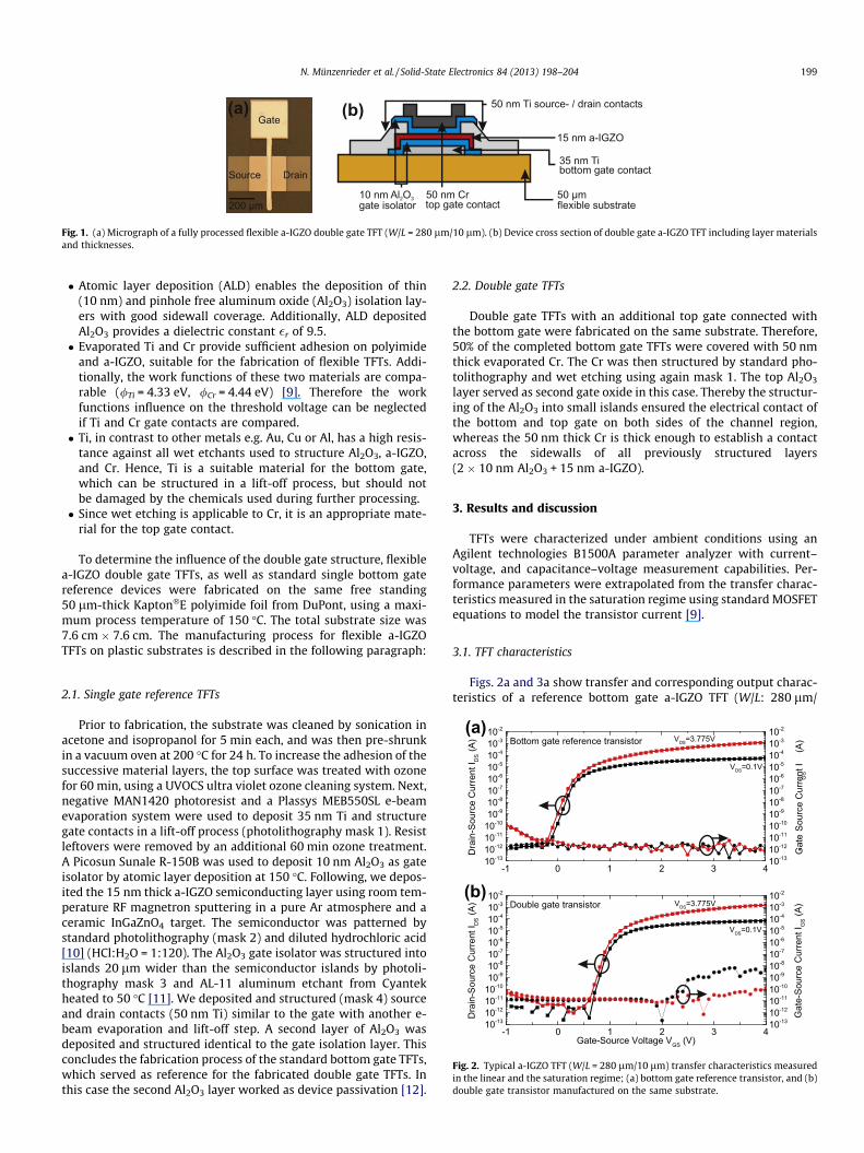
Fig. 2. Typical a-IGZO TFT (W/L = 280 lm/10 lm) transfer characteristics measuredin the linear and the saturation regime; (a) bottom gate reference transistor, and (b)double gate transistor manufactured on the same substrate.
2.1. Single gate reference TFTs
Prior to fabrication, the substrate was cleaned by sonication inacetone and isopropanol for 5 min each, and was then pre-shrunkin a vacuum oven at 200 �C for 24 h. To increase the adhesion of thesuccessive material layers, the top surface was treated with ozonefor 60 min, using a UVOCS ultra violet ozone cleaning system. Next,negative MAN1420 photoresist and a Plassys MEB550SL e-beamevaporation system were used to deposit 35 nm Ti and structuregate contacts in a lift-off process (photolithography mask 1). Resistleftovers were removed by an additional 60 min ozone treatment.A Picosun Sunale R-150B was used to deposit 10 nm Al2O3 as gateisolator by atomic layer deposition at 150 �C. Following, we depos-ited the 15 nm thick a-IGZO semiconducting layer using room tem-perature RF magnetron sputtering in a pure Ar atmosphere and aceramic InGaZnO4 target. The semiconductor was patterned bystandard photolithography (mask 2) and diluted hydrochloric acid[10] (HCl:H2O = 1:120). The Al2O3 gate isolator was structured intoislands 20 lm wider than the semiconductor islands by photoli-thography mask 3 and AL-11 aluminum etchant from Cyantekheated to 50 �C [11]. We deposited and structured (mask 4) sourceand drain contacts (50 nm Ti) similar to the gate with another e-beam evaporation and lift-off step. A second layer of Al2O3 wasdeposited and structured identical to the gate isolation layer. Thisconcludes the fabrication process of the standard bottom gate TFTs,which served as reference for the fabricated double gate TFTs. Inthis case the second Al2O3 layer worked as device passivation [12].
2.2. Double gate TFTs
Double gate TFTs with an additional top gate connected withthe bottom gate were fabricated on the same substrate. Therefore,50% of the completed bottom gate TFTs were covered with 50 nmthick evaporated Cr. The Cr was then structured by standard pho-tolithography and wet etching using again mask 1. The top Al2O3
layer served as second gate oxide in this case. Thereby the structur-ing of the Al2O3 into small islands ensured the electrical contact ofthe bottom and top gate on both sides of the channel region,whereas the 50 nm thick Cr is thick enough to establish a contactacross the sidewalls of all previously structured layers(2 � 10 nm Al2O3 + 15 nm a-IGZO).
3. Results and discussion
TFTs were characterized under ambient conditions using anAgilent technologies B1500A parameter analyzer with current–voltage, and capacitance–voltage measurement capabilities. Per-formance parameters were extrapolated from the transfer charac-teristics measured in the saturation regime using standard MOSFETequations to model the transistor current [9].
3.1. TFT characteristics
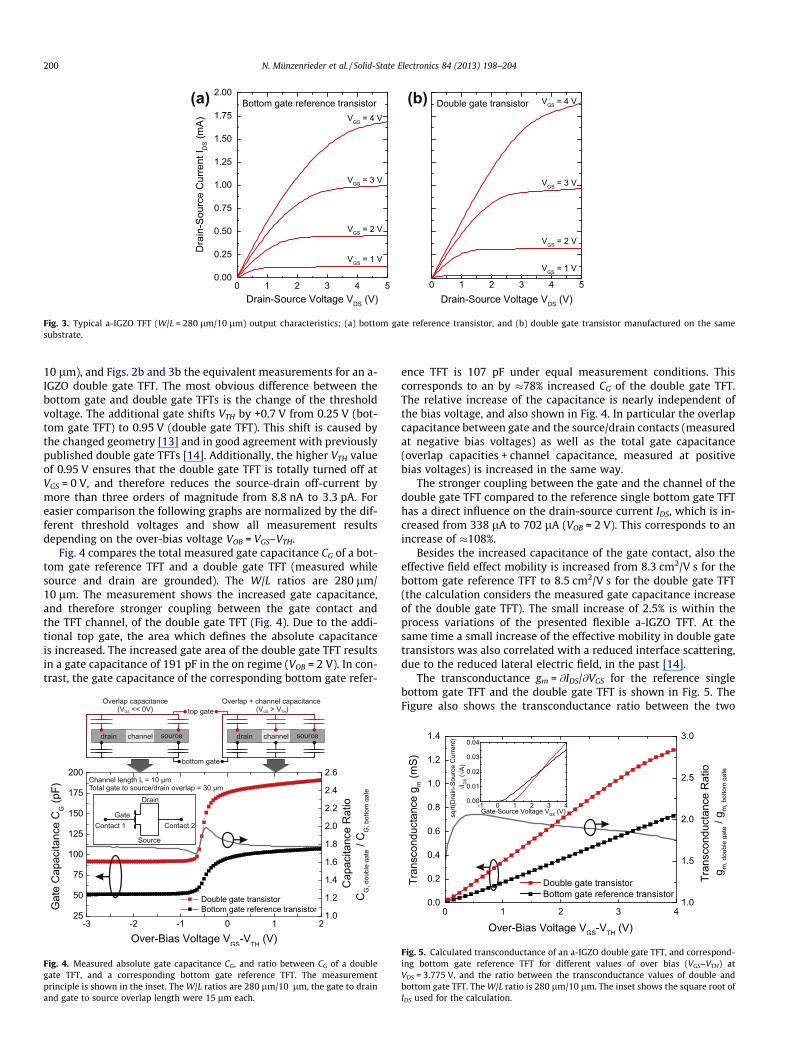
Figs. 2a and 3a show transfer and corresponding output charac-teristics of a reference bottom gate a-IGZO TFT (W/L: 280 lm/
(b)(a)
Fig. 3. Typical a-IGZO TFT (W/L = 280 lm/10 lm) output characteristics; (a) bottom gate reference transistor, and (b) double gate transistor manufactured on the samesubstrate.
200 N. Münzenrieder et al. / Solid-State Electronics 84 (2013) 198–204
10 lm), and Figs. 2b and 3b the equivalent measurements for an a-IGZO double gate TFT. The most obvious difference between thebottom gate and double gate TFTs is the change of the thresholdvoltage. The additional gate shifts VTH by +0.7 V from 0.25 V (bot-tom gate TFT) to 0.95 V (double gate TFT). This shift is caused bythe changed geometry [13] and in good agreement with previouslypublished double gate TFTs [14]. Additionally, the higher VTH valueof 0.95 V ensures that the double gate TFT is totally turned off atVGS = 0 V, and therefore reduces the source-drain off-current bymore than three orders of magnitude from 8.8 nA to 3.3 pA. Foreasier comparison the following graphs are normalized by the dif-ferent threshold voltages and show all measurement resultsdepending on the over-bias voltage VOB = VGS–VTH.
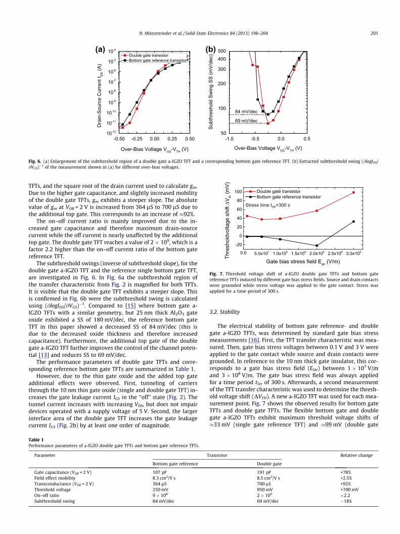
Fig. 4 compares the total measured gate capacitance CG of a bot-tom gate reference TFT and a double gate TFT (measured whilesource and drain are grounded). The W/L ratios are 280 lm/10 lm. The measurement shows the increased gate capacitance,and therefore stronger coupling between the gate contact andthe TFT channel, of the double gate TFT (Fig. 4). Due to the addi-tional top gate, the area which defines the absolute capacitanceis increased. The increased gate area of the double gate TFT resultsin a gate capacitance of 191 pF in the on regime (VOB = 2 V). In con-trast, the gate capacitance of the corresponding bottom gate refer-
Total gate to source/drain overlap = 30 Channel length L = 10 µm
µm
Gate
Source
Drain
Contact 1 Contact 2
drain source channel drain source channel
bottom gate
top gate Overlap capacitance
(V << 0V)GS
Overlap + channel capacitance (V > V )GS TH
Fig. 4. Measured absolute gate capacitance CG, and ratio between CG of a doublegate TFT, and a corresponding bottom gate reference TFT. The measurementprinciple is shown in the inset. The W/L ratios are 280 lm/10 lm, the gate to drainand gate to source overlap length were 15 lm each.
ence TFT is 107 pF under equal measurement conditions. Thiscorresponds to an by �78% increased CG of the double gate TFT.The relative increase of the capacitance is nearly independent ofthe bias voltage, and also shown in Fig. 4. In particular the overlapcapacitance between gate and the source/drain contacts (measuredat negative bias voltages) as well as the total gate capacitance(overlap capacities + channel capacitance, measured at positivebias voltages) is increased in the same way.
The stronger coupling between the gate and the channel of thedouble gate TFT compared to the reference single bottom gate TFThas a direct influence on the drain-source current IDS, which is in-creased from 338 lA to 702 lA (VOB = 2 V). This corresponds to anincrease of �108%.
Besides the increased capacitance of the gate contact, also theeffective field effect mobility is increased from 8.3 cm2/V s for thebottom gate reference TFT to 8.5 cm2/V s for the double gate TFT(the calculation considers the measured gate capacitance increaseof the double gate TFT). The small increase of 2.5% is within theprocess variations of the presented flexible a-IGZO TFT. At thesame time a small increase of the effective mobility in double gatetransistors was also correlated with a reduced interface scattering,due to the reduced lateral electric field, in the past [14].
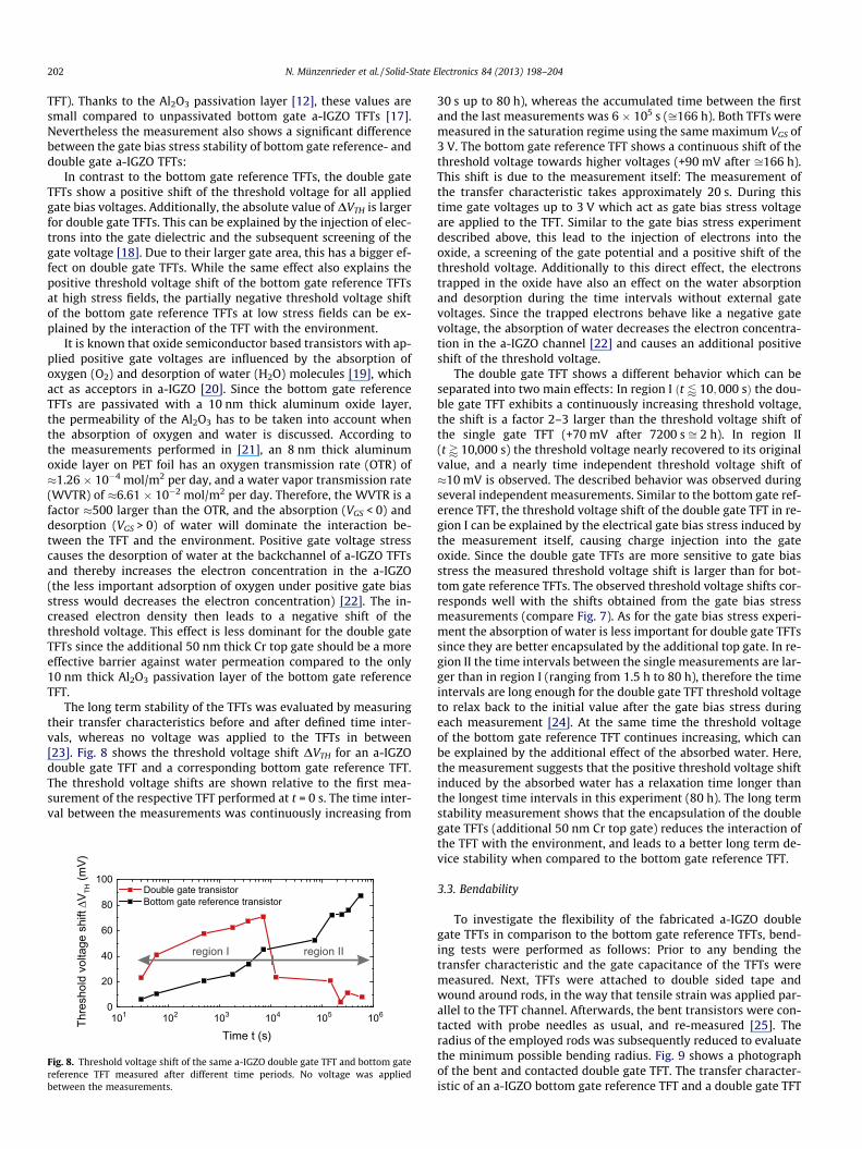
The transconductance gm = @IDS/@VGS for the reference singlebottom gate TFT and the double gate TFT is shown in Fig. 5. TheFigure also shows the transconductance ratio between the two
Fig. 5. Calculated transconductance of an a-IGZO double gate TFT, and correspond-ing bottom gate reference TFT for different values of over bias (VGS–VTH) atVDS = 3.775 V, and the ratio between the transconductance values of double andbottom gate TFT. The W/L ratio is 280 lm/10 lm. The inset shows the square root ofIDS used for the calculation.
(a) (b)
Fig. 6. (a) Enlargement of the subthreshold region of a double gate a-IGZO TFT and a corresponding bottom gate reference TFT. (b) Extracted subthreshold swing (@logIDS/@VGS)�1 of the measurement shown in (a) for different over-bias voltages.
Stress time t =300 sstr
Fig. 7. Threshold voltage shift of a-IGZO double gate TFTs and bottom gatereference TFTs induced by different gate bias stress fields. Source and drain contactswere grounded while stress voltage was applied to the gate contact. Stress wasapplied for a time period of 300 s.
N. Münzenrieder et al. / Solid-State Electronics 84 (2013) 198–204 201
TFTs, and the square root of the drain current used to calculate gm.Due to the higher gate capacitance, and slightly increased mobilityof the double gate TFTs, gm exhibits a steeper slope. The absolutevalue of gm at VOB = 2 V is increased from 364 lS to 700 lS due tothe additional top gate. This corresponds to an increase of �92%.
The on–off current ratio is mainly improved due to the in-creased gate capacitance and therefore maximum drain-sourcecurrent while the off current is nearly unaffected by the additionaltop gate. The double gate TFT reaches a value of 2 � 109, which is afactor 2.2 higher than the on–off current ratio of the bottom gatereference TFT.
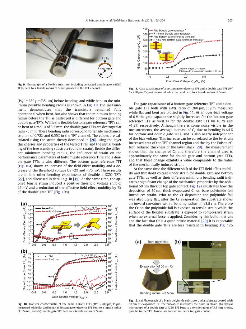
The subthreshold swings (inverse of subthreshold slope), for thedouble gate a-IGZO TFT and the reference single bottom gate TFT,are investigated in Fig. 6. In Fig. 6a the subthreshold region ofthe transfer characteristic from Fig. 2 is magnified for both TFTs.It is visible that the double gate TFT exhibits a steeper slope. Thisis confirmed in Fig. 6b were the subthreshold swing is calculatedusing (@logIDS/@VGS)�1. Compared to [15] where bottom gate a-IGZO TFTs with a similar geometry, but 25 nm thick Al2O3 gateoxide exhibited a SS of 180 mV/dec, the reference bottom gateTFT in this paper showed a decreased SS of 84 mV/dec (this isdue to the decreased oxide thickness and therefore increasedcapacitance). Furthermore, the additional top gate of the doublegate a-IGZO TFT further improves the control of the channel poten-tial [13] and reduces SS to 69 mV/dec.
The performance parameters of double gate TFTs and corre-sponding reference bottom gate TFTs are summarized in Table 1.
However, due to the thin gate oxide and the added top gateadditional effects were observed. First, tunneling of carriersthrough the 10 nm thin gate oxide (single and double gate TFT) in-creases the gate leakage current IGS in the ‘‘off’’ state (Fig. 2). Thetunnel current increases with increasing VDS, but does not impairdevices operated with a supply voltage of 5 V. Second, the largerinterface area of the double gate TFT increases the gate leakagecurrent IGS (Fig. 2b) by at least one order of magnitude.
Table 1Performance parameters of a-IGZO double gate TFTs and bottom gate reference TFTs.
Parameter T
Bottom gate reference
Gate capacitance (VOB = 2 V) 107 pFField effect mobility 8.3 cm2/V sTransconductance (VOB = 2 V) 364 lSThreshold voltage 250 mVOn–off ratio 9 � 108
Subthreshold swing 84 mV/dec
3.2. Stability
The electrical stability of bottom gate reference- and doublegate a-IGZO TFTs, was determined by standard gate bias stressmeasurements [16]. First, the TFT transfer characteristic was mea-sured. Then, gate bias stress voltages between 0.1 V and 3 V wereapplied to the gate contact while source and drain contacts weregrounded. In reference to the 10 nm thick gate insulator, this cor-responds to a gate bias stress field (EStr) between 1 � 107 V/mand 3 � 108 V/m. The gate bias stress field was always appliedfor a time period tStr of 300 s. Afterwards, a second measurementof the TFT transfer characteristic was used to determine the thresh-old voltage shift (DVTH). A new a-IGZO TFT was used for each mea-surement point. Fig. 7 shows the observed results for bottom gateTFTs and double gate TFTs. The flexible bottom gate and doublegate a-IGZO TFTs exhibit maximum threshold voltage shifts of�33 mV (single gate reference TFT) and �99 mV (double gate
ransistor Relative change
Double gate
191 pF +78%8.5 cm2/V s +2.5%700 lS +92%950 mV +700 mV2 � 109 �2.269 mV/dec �18%
202 N. Münzenrieder et al. / Solid-State Electronics 84 (2013) 198–204
TFT). Thanks to the Al2O3 passivation layer [12], these values aresmall compared to unpassivated bottom gate a-IGZO TFTs [17].Nevertheless the measurement also shows a significant differencebetween the gate bias stress stability of bottom gate reference- anddouble gate a-IGZO TFTs:
In contrast to the bottom gate reference TFTs, the double gateTFTs show a positive shift of the threshold voltage for all appliedgate bias voltages. Additionally, the absolute value of DVTH is largerfor double gate TFTs. This can be explained by the injection of elec-trons into the gate dielectric and the subsequent screening of thegate voltage [18]. Due to their larger gate area, this has a bigger ef-fect on double gate TFTs. While the same effect also explains thepositive threshold voltage shift of the bottom gate reference TFTsat high stress fields, the partially negative threshold voltage shiftof the bottom gate reference TFTs at low stress fields can be ex-plained by the interaction of the TFT with the environment.
It is known that oxide semiconductor based transistors with ap-plied positive gate voltages are influenced by the absorption ofoxygen (O2) and desorption of water (H2O) molecules [19], whichact as acceptors in a-IGZO [20]. Since the bottom gate referenceTFTs are passivated with a 10 nm thick aluminum oxide layer,the permeability of the Al2O3 has to be taken into account whenthe absorption of oxygen and water is discussed. According tothe measurements performed in [21], an 8 nm thick aluminumoxide layer on PET foil has an oxygen transmission rate (OTR) of�1.26 � 10�4 mol/m2 per day, and a water vapor transmission rate(WVTR) of �6.61 � 10�2 mol/m2 per day. Therefore, the WVTR is afactor �500 larger than the OTR, and the absorption (VGS < 0) anddesorption (VGS > 0) of water will dominate the interaction be-tween the TFT and the environment. Positive gate voltage stresscauses the desorption of water at the backchannel of a-IGZO TFTsand thereby increases the electron concentration in the a-IGZO(the less important adsorption of oxygen under positive gate biasstress would decreases the electron concentration) [22]. The in-creased electron density then leads to a negative shift of thethreshold voltage. This effect is less dominant for the double gateTFTs since the additional 50 nm thick Cr top gate should be a moreeffective barrier against water permeation compared to the only10 nm thick Al2O3 passivation layer of the bottom gate referenceTFT.
The long term stability of the TFTs was evaluated by measuringtheir transfer characteristics before and after defined time inter-vals, whereas no voltage was applied to the TFTs in between[23]. Fig. 8 shows the threshold voltage shift DVTH for an a-IGZOdouble gate TFT and a corresponding bottom gate reference TFT.The threshold voltage shifts are shown relative to the first mea-surement of the respective TFT performed at t = 0 s. The time inter-val between the measurements was continuously increasing from
0
20
40
60
80
100
Thre
shol
d vo
ltage
shi
ft ΔV
TH (m
V)
Time t (s)
Double gate transistor Bottom gate reference transistor
region I region II
101 102 103 104 105 106
Fig. 8. Threshold voltage shift of the same a-IGZO double gate TFT and bottom gatereference TFT measured after different time periods. No voltage was appliedbetween the measurements.
30 s up to 80 h), whereas the accumulated time between the firstand the last measurements was 6 � 105 s (ffi166 h). Both TFTs weremeasured in the saturation regime using the same maximum VGS of3 V. The bottom gate reference TFT shows a continuous shift of thethreshold voltage towards higher voltages (+90 mV after ffi166 h).This shift is due to the measurement itself: The measurement ofthe transfer characteristic takes approximately 20 s. During thistime gate voltages up to 3 V which act as gate bias stress voltageare applied to the TFT. Similar to the gate bias stress experimentdescribed above, this lead to the injection of electrons into theoxide, a screening of the gate potential and a positive shift of thethreshold voltage. Additionally to this direct effect, the electronstrapped in the oxide have also an effect on the water absorptionand desorption during the time intervals without external gatevoltages. Since the trapped electrons behave like a negative gatevoltage, the absorption of water decreases the electron concentra-tion in the a-IGZO channel [22] and causes an additional positiveshift of the threshold voltage.
The double gate TFT shows a different behavior which can beseparated into two main effects: In region I ðt / 10;000 sÞ the dou-ble gate TFT exhibits a continuously increasing threshold voltage,the shift is a factor 2–3 larger than the threshold voltage shift ofthe single gate TFT (+70 mV after 7200 s ffi 2 h). In region II(t ’ 10,000 s) the threshold voltage nearly recovered to its originalvalue, and a nearly time independent threshold voltage shift of�10 mV is observed. The described behavior was observed duringseveral independent measurements. Similar to the bottom gate ref-erence TFT, the threshold voltage shift of the double gate TFT in re-gion I can be explained by the electrical gate bias stress induced bythe measurement itself, causing charge injection into the gateoxide. Since the double gate TFTs are more sensitive to gate biasstress the measured threshold voltage shift is larger than for bot-tom gate reference TFTs. The observed threshold voltage shifts cor-responds well with the shifts obtained from the gate bias stressmeasurements (compare Fig. 7). As for the gate bias stress experi-ment the absorption of water is less important for double gate TFTssince they are better encapsulated by the additional top gate. In re-gion II the time intervals between the single measurements are lar-ger than in region I (ranging from 1.5 h to 80 h), therefore the timeintervals are long enough for the double gate TFT threshold voltageto relax back to the initial value after the gate bias stress duringeach measurement [24]. At the same time the threshold voltageof the bottom gate reference TFT continues increasing, which canbe explained by the additional effect of the absorbed water. Here,the measurement suggests that the positive threshold voltage shiftinduced by the absorbed water has a relaxation time longer thanthe longest time intervals in this experiment (80 h). The long termstability measurement shows that the encapsulation of the doublegate TFTs (additional 50 nm Cr top gate) reduces the interaction ofthe TFT with the environment, and leads to a better long term de-vice stability when compared to the bottom gate reference TFT.
3.3. Bendability
To investigate the flexibility of the fabricated a-IGZO doublegate TFTs in comparison to the bottom gate reference TFTs, bend-ing tests were performed as follows: Prior to any bending thetransfer characteristic and the gate capacitance of the TFTs weremeasured. Next, TFTs were attached to double sided tape andwound around rods, in the way that tensile strain was applied par-allel to the TFT channel. Afterwards, the bent transistors were con-tacted with probe needles as usual, and re-measured [25]. Theradius of the employed rods was subsequently reduced to evaluatethe minimum possible bending radius. Fig. 9 shows a photographof the bent and contacted double gate TFT. The transfer character-istic of an a-IGZO bottom gate reference TFT and a double gate TFT
1 cm
r =5 mm
TFTs
Fig. 9. Photograph of a flexible substrate, including contacted double gate a-IGZOTFTs, bent to a tensile radius of 5 mm parallel to the TFT channel.
Total gate to source/drain overlap = 30 Channel length L = 35 µm
µm
Fig. 11. Gate capacitance of a bottom gate reference TFT and a double gate TFT (W/L = 280 lm/35 lm) measured while flat, and bent to a tensile radius of 5 mm.
N. Münzenrieder et al. / Solid-State Electronics 84 (2013) 198–204 203
(W/L = 280 lm/35 lm) before bending, and while bent to the min-imum possible bending radius is shown in Fig. 10. The measure-ment demonstrates that the transistors remained fullyoperational when bent, but also shows that the minimum bendingradius before the TFT is destroyed is different for bottom gate anddouble gate TFTs. While the flexible bottom gate reference TFTs canbe bent to a radius of 3.5 mm, the double gate TFTs are destroyed atradii <5 mm. These bending radii correspond to tensile mechanicalstrain � of 0.72% and 0.55% in the TFT channel. The values are cal-culated using the strain theory developed in [26] using the layerthicknesses and properties of the tested TFTs, and the initial bend-ing of the free standing substrate (build in strain). Beside the differ-ent minimum bending radius, the influence of strain on theperformance parameters of bottom gate reference TFTs and a dou-ble gate TFTs is also different. The bottom gate reference TFT(Fig. 10a) shows an increase of the field effect mobility and a de-crease of the threshold voltage by +2% and �75 mV. These resultsare in line other bending experiments of flexible a-IGZO TFTs[27], and discussed in detail e.g. in [15]. At the same time, the ap-plied tensile strain induced a positive threshold voltage shift of25 mV and a reduction of the effective field effect mobility by 7%of the double gate TFT (Fig. 10b).
flatbent
Source Drain
Gate
(a)
(b)
Fig. 10. Transfer characteristic of the same a-IGZO TFTs (W/L = 280 lm/35 lm)measured while flat and bent. (a) Bottom gate reference TFT bent to a tensile radiusof 3.5 mm, and (b) double gate TFT bent to a tensile radius of 5 mm.
The gate capacitance of a bottom gate reference TFT and a dou-ble gate TFT both with aW/L ratio of 280 lm/35 lm measuredwhile flat and bent are plotted in Fig. 11. At an over-bias voltageof 0 V the gate capacitance slightly increases for the bottom gatereference TFT as well as for the double gate TFT by +0.7% and+1.2%, respectively. Although there is some noise visible in themeasurements, the average increase of CG due to bending is �1%for bottom and double gate TFTs, and is also nearly independentof the bias voltage. This increase can be correlated to the by strainincreased area of the TFT channel region and the, by the Poison ef-fect, reduced thickness of the layer stack [28]. The measurementshows that the change of CG and therefore the channel area isapproximately the same for double gate and bottom gate TFTs,and that these change exhibits a value comparable to the valueof the mechanically induced strain.
At the same time the different shift of the TFT field effect mobil-ity and threshold voltage under strain for double gate and bottomgate TFTs, as well as their different minimum bending radii indi-cates a significant change of the mechanical properties by the addi-tional 50 nm thick Cr top gate contact. Fig. 12a illustrates how thedeposition of 50 nm thick evaporated Cr on bare polyimide foilintroduces strain. Prior to the Cr deposition the polyimide foilwas absolutely flat, after the Cr evaporation the substrate showsan inward curvature with a bending radius of �3.5 cm. Thereforethe Cr on the polyimide foil is exposed to tensile strain while thesurface of the flexible substrate is exposed to compressive strainwhen no external force is applied. Considering this build in strainand the fact that Cr is a quite brittle material [29] it is expectablethat the double gate TFTs are less resistant to bending. Fig. 12b
100 µm
25 µmBare polyimide
Evaporation of 50 nm Cr
Bending radius: 3.5 cm
(a) (b)
Fig. 12. (a) Photograph of a blank polyimide substrate, and a substrate coated with50 nm of evaporated Cr. The curvature illustrates the build in strain. (b) Opticalmicrograph of a double gate a-IGZO TFT bent to a tensile radius of 3.5 mm, cracks,parallel to the TFT channel are formed in the Cr top gate contact.
204 N. Münzenrieder et al. / Solid-State Electronics 84 (2013) 198–204
shows a micrograph of a double gate a-IGZO TFT while bent to aradius of 3.5 mm (corresponds to a strain of 0.79%, when the initialcurvature of the substrate is taken into account). In contrast to thebottom gate reference TFT, the micrograph shows multiple cracksperpendicular to the applied strain and therefore parallel to theTFT channel. The cracks are formed only in areas covered withthe Cr top gate, but e.g. not on the more ductile Au contacts. Fur-thermore no cracks have been observed when bottom gate refer-ence TFTs were bent to a tensile radius of 3.5 mm. The formationof cracks explains the different behavior of the double gate TFT un-der strain compared to strained bottom gate reference TFTs. Webelieve that the use of more ductile metals like Cu as top gate con-tact would enable bending radii between 1 mm and 2 mm withoutthe need of modifying the device structure, but at the cost of aneven higher work function compared to Ti (/Cu = 4.54 eV) [9].
4. Conclusion
A double gate structure was combined with 10 nm thick Al2O3
gate oxide layers to fabricate TFTs on free standing flexible plasticfoils. Double gate a-IGZO TFTs yield improved performance param-eters compared to single bottom reference TFTs fabricated on thesame substrate. The by 74% increased absolute gate capacitance in-creased the transconductance up to 92% (VOB = 2 V). On–off currentratio increased by more than a factor of 2, while the subthresholdswing reached a value of 69 mV/dec. This is to our knowledge thesmallest value ever reported on flexible a-IGZO TFTs. Althoughdouble gate TFTs are less resistant to mechanical strain than bot-tom gate reference TFTs, tensile mechanical strain of 0.55%, in-duced by bending the flexible a-IGZO double gate TFTs to aradius of 5 mm did not impair the device functionality signifi-cantly. In particular, the subthreshold swing remained unchangedwhile lFE decreased by 7% and Vth increased by 25 mV.
Acknowledgements
This work has been partially supported by the European Com-mission through the FP7 Project: Flexible multifunctional bendableintegrated light-weight ultra-thin systems (FLEXIBILITY), ContractNo. FP7–287568. This work has also been scientifically evaluatedby the Swiss National Scientific Foundation (SNSF), and financedby the Swiss Confederation and Nano-Tera.ch.
References
[1] Cherenack K, Zysset C, Kinkeldei T, Münzenrieder N, Tröster G. Wearableelectronics: woven electronic fibers with sensing and display functions forsmart textiles (Adv Mater 45/2010). Adv Mater 2010;22:5071.
[2] Service RF. Patterning electronics on the cheap. Science 1997;278:383–4.[3] Li W, Katz H, Lovinger A, Laquindanum J. Field-effect transistors based on
thiophene hexamer analogues with diminished electron donor strength. ChemMater 1999;11:458–65.
[4] Cherenack K, Kattamis A, Hekmatshoar B, Sturm J, Wagner S. Amorphous-silicon thin-film transistors fabricated at 300 �C on a free-standing foilsubstrate of clear plastic. IEEE Electron Dev Lett 2007;28:1004–6.
[5] Nomura K, Ohta H, Takagi A, Kamiya T, Hirano M, Hosono H. Room-temperature fabrication of transparent flexible thin-film transistors usingamorphous oxide semiconductors. Nature 2004;432:488–92.
[6] Lim H, Yin H, Park J, Song I, Kim C, Park J, et al. Double gate GaInZnO thin filmtransistors. Appl Phys Lett 2008;93. p. 063505.
[7] Zan H, Chen W, Yeh C, Hsueh H, Tsai C, Meng H. Dual gate indium–gallium–zinc-oxide thin film transistor with an unisolated floating metal gate forthreshold voltage modulation and mobility enhancement. Appl Phys Lett2011;98. p. 153506.
[8] Su N, Wang S, Chin A. High-performance InGaZnO thin-film transistors usingHfLaO gate dielectric. IEEE Electron Dev Lett 2009;30:1317–9.
[9] Sze S, Ng K. Physics of semiconductor devices. 3rd ed. Hoboken: John Wiley &Sons; 2007.
[10] Kim J, Fuentes-Hernandez C, Potscavage Jr W, Zhang X, Kippelen B. Low-voltage InGaZnO thin-film transistors with ALO gate insulator grown byatomic layer deposition. Appl Phys Lett 2009;94:142107.
[11] Zhou B, Ramirez W. Kinetics and modeling of wet etching of aluminum oxideby warm phosphoric acid. J Electrochem Soc 1996;143:619–23.
[12] Cho I, Lee J, Lee J, Kwon H. Charge trapping and detrapping characteristics inamorphous InGaZnO TFTs under static and dynamic stresses. Semicond SciTechnol 2008;24:015013.
[13] Zhang S, Han R, Sin J, Chan M. A novel self-aligned double-gate TFT technology.IEEE Electron Dev Lett 2001;22:530–2.
[14] Son K, Jung J, Lee K, Kim T, Park J, Choi Y, et al. Characteristics of double-gatega–in–zn–o thin-film transistor. IEEE Electron Dev Lett 2010;31:219–21.
[15] Münzenrieder N, Cherenack K, Tröster G. The effects of mechanical bendingand illumination on the performance of flexible IGZO TFTs. IEEE Trans ElectronDev 2011;58:2041–8.
[16] Hoshino K, Hong D, Chiang H, Wager J. Constant-voltage-bias stress testing ofa-IGZO thin-film transistors. IEEE Trans Electron Dev 2009;56:1365–70.
[17] Lee J, Cho I, Lee J, Kwon H. Bias-stress-induced stretched-exponential timedependence of threshold voltage shift in InGaZnO thin film transistors. ApplPhys Lett 2008;93. p. 093504.
[18] Suresh A, Muth J. Bias stress stability of indium gallium zinc oxide channelbased transparent thin film transistors. Appl Phys Lett 2008;92. p. 033502.
[19] Liu P, Chou Y, Teng L. Environment-dependent metastability of passivation-free indium zinc oxide thin film transistor after gate bias stress. Appl Phys Lett2009;95. p. 233504.
[20] Park J, Jeong J, Chung H, Mo Y, Kim H. Electronic transport properties ofamorphous indium–gallium–zinc oxide semiconductor upon exposure towater. Appl Phys Lett 2008;92. p. 072104.
[21] Henry B, Erlat A, McGuigan A, Grovenor C, Briggs G, Tsukahara Y, et al.Characterization of transparent aluminium oxide and indium tin oxide layerson polymer substrates. Thin Solid Films 2001;382:194–201.
[22] Jeong J, Won Yang H, Jeong J, Mo Y, Kim H. Origin of threshold voltageinstability in indium–gallium–zinc oxide thin film transistors. Appl Phys Lett2008;93. p. 123508.
[23] Lim W, Kim S, Wang Y, Lee J, Norton D, Pearton S, et al. Stable roomtemperature deposited amorphous InGaZnO4 thin film transistors. J Vac SciTechnol B: Microelectron Nanometer Struct 2008;26:959–62.
[24] Jung J, Rha S, Kim U, Chung Y, Jung Y, Choi J, et al. The charge trappingcharacteristics of Si3N4 and Al2O3 layers on amorphous-indium–gallium–zincoxide thin films for memory application. Appl Phys Lett 2012;100:183503.
[25] Münzenrieder N, Zysset C, Kinkeldei T, Tröster G. Design rules for IGZO logicgates on plastic foil enabling operation at bending radii of 3.5 mm. IEEE TransElectron Dev 2012;59:2153–9.
[26] Gleskova H, Wagner S, Suo Z. a-Si: H thin film transistors after very high strain.J Non-Cryst Solids 2000;266–269:1320–4.
[27] Kim D, Hwang B, Park J, Jeon H, Bae B, Lee H, et al. Mechanical bending offlexible complementary inverters based on organic and oxide thin filmtransistors. Org Electron 2012.
[28] Rice J. Foundations of solid mechanics. Mech Mater: Fundam Linkages1999:33–69.
[29] Reiley T, Nix W. The structure and mechanical properties of physically vapordeposited chromium. Metall Mater Trans A 1976;7:1695–701.
Related Documents