Flexible and Stretchable Electronics

Welcome message from author
This document is posted to help you gain knowledge. Please leave a comment to let me know what you think about it! Share it to your friends and learn new things together.
Transcript
Flexible and Stretchable Electronics

edited by
Flexible and Stretchable ElectronicsMaterials, Designs, and Devices
Run-Wei LiGang Liu
Published by
Jenny Stanford Publishing Pte. Ltd.Level 34, Centennial Tower3 Temasek AvenueSingapore 039190
Email: [email protected]: www.jennystanford.com
British Library Cataloguing-in-Publication DataA catalogue record for this book is available from the British Library.
Flexible and Stretchable Electronics: Materials, Designs, and DevicesCopyright © 2020 by Jenny Stanford Publishing Pte. Ltd.All rights reserved. This book, or parts thereof, may not be reproduced in any form or by any means, electronic or mechanical, including photocopying, recording or any information storage and retrieval system now known or to be invented, without written permission from the publisher.
For photocopying of material in this volume, please pay a copying fee through the Copyright Clearance Center, Inc., 222 Rosewood Drive, Danvers, MA 01923, USA. In this case permission to photocopy is not required from the publisher.
ISBN 978-981-4800-46-4 (Hardcover)ISBN 978-0-429-05890-5 (eBook)
Contents
Preface xiii
1. Organic Field-Effect Transistors for Flexible Electronics Application 1
Jung-Yao Chen and Cheng-Liang Liu 1.1 Introduction 2 1.2 Device Structures and Operation Principle 3 1.3 Important Device Parameters 5 1.3.1 Field-Effect Mobility 6 1.3.2 Current ON/OFF Ratio 6 1.3.3 Threshold Voltage 7 1.3.4 Subthreshold Swing 7 1.4 Materials 7 1.4.1 Organic Semiconductors 8 1.4.1.1 p-Type 8 1.4.1.2 n-Type 10 1.4.2 Gate Dielectric Materials 12 1.4.3 Electrode Materials 12 1.4.4 Substrate Materials 13 1.5 Overview of Processing Techniques 13 1.5.1 Vacuum Deposition 14 1.5.2 Solution-Processed Deposition 14 1.6 Flexible Organic Transistor Device 15 1.7 Flexible Organic Phototransistor 18 1.7.1 Introduction 18 1.7.2 Important Device Parameters of
Organic Phototransistor 19 1.7.2.1 Photoconductive gain (G) 19 1.7.2.2 Photocurrent/dark current
ratio (P) 20 1.7.2.3 Photosensitivity (R) 20 1.7.2.4 Quantum efficiency (η) 20 1.7.2.5 Photodetectivity (D*) 20
vi Contents
1.7.3 Examples of Flexible Organic Phototransistors 21
1.7.3.1 Donor–acceptor system 21 1.7.3.2 Photochromism 23 1.7.3.3 Photopolymerization 24 1.8 Conclusion 26
2. Flexible and Organic Solar Cells 33
Bing Cao
2.1 Introduction 33 2.2 Basic Solar Cell Concepts 34 2.2.1 Structure of Organic Solar Cells 34 2.2.2 Operation Principle of Organic Solar
Cells 35 2.2.3 Photovoltaic Parameters 36 2.3 Donor Materials Development 38 2.3.1 Conjugated Polymers 39 2.3.2 Conjugated Small Molecules 45 2.4 Acceptor Materials Development 49 2.4.1 Fullerene Derivatives 49 2.4.2 Non-fullerene Small Molecules 50 2.5 Interfacial Materials and Device Engineering 54 2.6 Flexible and Organic Solar Cells 56
3. Flexible Parylene-C Material and Its Applications in MOSFETs, RRAMs, and Sensors 81
Yimao Cai, Min Lin, and Qingyu Chen
3.1 An Introduction to Parylene 82 3.1.1 Types and Growth of Parylene Thin
Films 82 3.1.2 Properties of Parylene-C Thin Films 83 3.2 Application of Parylene-C in MOSFETs 84 3.2.1 Gate Dielectric 84 3.2.2 Substrate 87 3.2.3 Encapsulation Gate Dielectric 89 3.3 Application of Parylene-C in RRAM 91 3.4 Application of Parylene-C in Sensors 96 3.4.1 Flow Sensors 96 3.4.2 pH Sensors 98
viiContents
3.4.3 Force Sensors 100 3.4.4 Pressure Sensors 101 3.5 Conclusion 104
4. Resistive Switching Phenomenon for Flexible and Stretchable Memories 113
Xiaohui Yi, Shuang Gao, Jie Shang, Bin Chen, Gang Liu, and Run-Wei Li
4.1 Introduction 114 4.2 Design Principle of Flexible Resistive
Switching Memory 117 4.3 Flexible Resistive Switching Storage Media
Materials 119 4.3.1 Inorganic Materials 119 4.3.2 Organic Materials 122 4.3.2.1 Organic resistive
switching memory with small molecules 124
4.3.2.2 Blends or mixtures of memory polymer materials 127
4.3.2.3 Polymer matrices for electroactive components 129
4.3.2.4 Single-component polymer active materials 134
4.3.3 Inorganic–Organic Hybrid Materials 141 4.3.3.1 Metal-organic frameworks 141 4.3.3.2 Perovskite 144 4.4 Conclusion and Outlook 146
5. Two-Dimensional Materials for Flexible In-Plane Micro-Supercapacitors 157
Kaiyue Jiang, Chongqing Yang, and Xiaodong Zhuang
5.1 Introduction 157 5.2 In-Plane Micro-Supercapacitors 158 5.3 Graphene 160 5.3.1 Reduced Graphene Oxide 160 5.3.2 Electrochemically Exfoliated
Graphene 162 5.3.3 Laser-Scribed Graphene 165
viii Contents
5.3.4 Graphene Composites 168 5.4 MXenes 173 5.5 Two-Dimensional Metal Oxides 174 5.5.1 Layered Double Hydroxides 175 5.5.2 V2O5/MWNT 177 5.6 Two-Dimensional Soft Materials 178 5.6.1 Two-Dimensional Coordination
Polymer Framework 180 5.6.2 Two-Dimensional Thiophene 180 5.7 Summary and Outlook 181
6. Flexible On-Chip Interdigital Micro-Supercapacitors: Efficient Power Units for Wearable Electronics 191
Guozhen Shen, Kai Jiang, and Di Chen 6.1 Introduction 192 6.2 Fabrication Methods 195 6.2.1 Conventional Photolithography
Method 196 6.2.2 Laser-Scribing Method 199 6.2.3 Printing Method 203 6.3 Stretchable On-Chip MSCs 205 6.4 Integrated Systems 209 6.5 Conclusion 213
7. Flexible and Stretchable Sensors 221
Tie Li, Yudong Cao, Chunyan Qu, and Ting Zhang
7.1 Introduction 222 7.2 Classes of Architectural Strategies for
Flexible and Stretchable Sensors 223 7.2.1 One-Dimensional Fibrous
Configuration 224 7.2.2 Two-Dimensional Planar
Configuration 228 7.2.3 Three-Dimensional Blocks
Configuration 230 7.2.4 Nature-Inspired Structure for
Flexibility and Stretchability 233 7.3 Classes of Functional Materials for Flexible
and Stretchable Sensors 234
ixContents
7.3.1 One-Dimensional Nanowire Materials 235 7.3.2 Two-Dimensional Planar Materials 238 7.3.3 Semiconductors 240 7.3.4 Other Special Functional Materials 244 7.4 Flexible and Stretchable Sensors for Human
Information Detection 246 7.5 Conclusion 254
8. Liquid Metal–Enabled Functional Flexible and Stretchable Electronics 267
Xuelin Wang and Jing Liu 8.1 Introduction 268 8.2 Materials and Properties of Gallium-Based
RTLMs 269 8.2.1 Compositions of Gallium-Based
RTLM Alloys 269 8.2.2 Basic Properties of LMs in Flexible
Electronics 271 8.3 Design and Fabrication of LM Flexible
Electronics 274 8.3.1 Planar Electronics Printing 274 8.3.2 3D Printing 277 8.4 Applications: LM Soft Devices 278 8.4.1 LM Sensor 279 8.4.2 LM Coil 281 8.4.3 LM e-Skin and Wearable
Bioelectronics 282 8.4.4 LM-Conformable Electronics 283 8.4.5 Other Applications 283 8.5 Discussion and Conclusion 284
9. Printing Technology for Fabrication of Flexible and Stretchable Electronics 295
Wei Yuan and Zheng Cui
9.1 Introduction 296 9.2 Printing Process 298 9.2.1 Jet Printing (Non-contact Printing) 299 9.2.1.1 Inkjet printing 300 9.2.1.2 Aerosol-jet printing 300
x Contents
9.2.1.3 Electrohydrodynamic-jet printing 301
9.2.2 Replicate Printing (Impact Printing) 302 9.2.2.1 Screen printing 302 9.2.2.2 Gravure printing 303 9.2.2.3 Flexographic printing 304 9.2.2.4 Offset printing 304 9.2.2.5 Roll-to-roll printing 305 9.3 Printable Inks 305 9.3.1 Metal Materials 305 9.3.2 Transparent Conducting Oxide Inks 308 9.3.3 Carbon Nanomaterials 309 9.3.4 Semiconductor Nanomaterials 311 9.3.5 Reactive Inks 312 9.3.6 Stretchable Inks 313 9.4 Post-printing Process 314 9.4.1 Thermal Sintering 315 9.4.2 Photonic Sintering 316 9.4.3 Plasma, Microwave, and Electrical
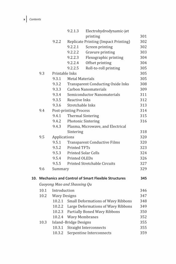
Sintering 318 9.5 Applications 320 9.5.1 Transparent Conductive Films 320 9.5.2 Printed TFTs 323 9.5.3 Printed Solar Cells 324 9.5.4 Printed OLEDs 326 9.5.5 Printed Stretchable Circuits 327 9.6 Summary 329
10. Mechanics and Control of Smart Flexible Structures 345
Guoyong Mao and Shaoxing Qu
10.1 Introduction 346 10.2 Wavy Designs 347 10.2.1 Small Deformations of Wavy Ribbons 348 10.2.2 Large Deformations of Wavy Ribbons 349 10.2.3 Partially Boned Wavy Ribbons 350 10.2.4 Wavy Membranes 352 10.3 Island–Bridge Designs 355 10.3.1 Straight Interconnects 355 10.3.2 Serpentine Interconnects 359

xiContents
10.3.3 Fractal Interconnects 362 10.4 Origami/Kirigami Designs 366 10.5 Conclusion 374
Index 383

The last decade has witnessed evolutional development of flexible electronics and they are reshaping the way we live, work, and communicate with the world. Setting themselves apart from the traditional silicon-based semiconductor devices, the unique capability of bending and stretching, together with the merits of light-weight and low-cost fabrications, endows flexible electronics imaginative versatility for soft circuits in portable energy and industrial equipments, wearable consumer digital gadgets, implantable health-monitoring electronic skins, medicine robots and prosthetics, and even the fictional human (brain)-machine docking that appears only in sci-fi movies. As an important technological advance and one of the most promising information technologies, flexible electronics have received broad and intensive attention from both the academic and industrial community ever since their birth twenty years ago. The fabrication of flexible electronics requires multiscale manufacture on soft substrates, spanning from the nanofeatures, microstructures, to large-area macro-integration. What determines their performance characteristics and, in principle, enables a host of potential applications is the accurate control of multiple functional materials at their interfaces, such as organics, metals, and ceramics, which show completely different mechanical and electrical properties, and multidisciplinary investigations in the area of chemistry, physics, materials science, biotechnology, and electronic engineering. In this book, we provide a timely and systematic overview of the operating mechanisms, materials selection, device structure and circuit design, fabrication methods, and range of applications of flexible electronics, with the aim to deliver a comprehensive summary and present the prospects of the specific field. The materials used for flexible electronics range from those that carry intrinsic molecular and structural flexibility, namely, organic semiconductors, organic–inorganic hybrids, two-dimensional graphene derivatives and analogs, and layered metal oxides, to room-temperature liquid metals that demonstrate the fluidity of common liquid and electrical
Preface
xiv Preface
conductivity of metals. Fundamental circuit elements of resistors, capacitors, and transistors are then produced with these materials to construct sensors, memory and energy storage devices, and circuits. This book is a result of the great efforts of our contributing authors, who have covered major areas of flexible electronics. In Chapter 1, Drs. Jung-Yao Chen and Cheng-Liang Liu discuss the materials, charge-transport model, deposition methods, and integration of organic field-effect transistor (OFET) for photo detecting. In Chapter 2, Dr. Bing Cao mainly presents an overview on the device structure, operating principle, and the latest advancement of new materials for high-performance organic solar cells (OSCs). Dr. Yimao Cai and coworkers have compiled Chapter 3, which focuses on the use of CMOS-compatible poly(para-xylylene) material in metal–oxide semiconductor field-effect transistors (MOSFETs), resistive random access memories (RRAMs), and sensor applications. In Chapter 4, Dr. Xiaohui Yi and coauthors offer a deep understanding of the designing strategy for flexible RRAM devices, followed by particular emphasis on organic and inorganic–organic hybrid resistive switching materials and devices. Chapters 5 and 6, contributed by Drs. Zhuang’s and Shen’s research groups, respectively, review the device structure, working principle, materials selection, fabrication approach, and integration of in-plane microcapacitor as on-chip power supply in stretchable electronic skin systems. Drs. Tie Li and Ting Zhang and their coworkers identify the special characters and requirements for flexible and stretchable sensors and summarize the strategies of structural design and functional materials for detecting human information in Chapter 7. Beyond the electroactive materials employed in the above-mentioned device applications, Drs. Xuelin Wang and Jing Liu present the use of liquid metal as soft conductor and electrode in flexible and stretchable electronics in Chapter 8. After an overview of the performance benchmarks for the different materials and devices of flexible electronics in Chapter 9, Drs. Wei Yuan and Zheng Cui introduce the manufacturing processes, inks, post-treatments, and important applications of the high-throughput, cost-effective, and eco-friendly printing technology for producing wearable electronics, portable energy harvesting and storage devices, flexible display panels, and human-skin sensors. Finally, the mechanical design concept, theory, simulation, and applications of smart flexible structures for optimizing the overall performance
xvPreface
of stretchable electronics are discussed by Drs. Guoyong Mao and Shaoxing Qu in Chapter 10 As we enter the 21st century Big Data and Artificial Intelligence era, information technology has changed rapidly over the past few years and is mainly being driven by the new practical require-ments and application scenarios that we had never expected before. Looking back into the 1980s, none of the prophets could have im-agined that a palm-sized telephone will accomplish complex tasks that were being done separately by clumpy desktop computers, brick-like walkie-talkies, mechanical film cameras, etc. Thanks to the fourth technological revolution, the “mission impossible” is be-coming “impossible is nothing” and flexible electronics show great promise for the future as they will closely interconnect every human being, every object, and every circumstance. As this is a newborn area, the theoretical framework of flexible electronics is still incom-plete and global efforts are needed to facilitate their transition from research and laboratory prototypes to commercial products. This book examines the research progress achieved in this field around the world, and through it we hope to inspire interests to advance flexible electronics technology, especially colleagues and university students.
Run-Wei Li
Gang Liu
Autumn 2019

During the past decades, with the advent of novel organic semiconductors (such as conjugated polymers and small molecules) and low-cost process requirement, significant interest and progress in the field of organic electronics have been reported. In particular, organic field-effect transistors (OFETs) have become the backbone of the recent developments in the large-area flexible electronics and found usage in numerous applications such as the digital and analog circuits, memories, photovoltaic, and sensors. This chapter gives the present advancements in OFET devices based on an overview of the individual layers of OFETs, charge transport model, deposition methods, and their integration of flexible substrate. Besides, their applications in organic phototransistors based on the OFET architecture are briefly addressed at the end of the chapter.
Chapter 1
Organic Field-Effect Transistors for Flexible Electronics Application
Flexible and Stretchable Electronics: Materials, Designs, and DevicesEdited by Run-Wei Li and Gang LiuCopyright © 2020 Jenny Stanford Publishing Pte. Ltd.ISBN 978-981-4800-46-4 (Hardcover), 978-0-429-05890-5 (eBook)www.jennystanford.com
Jung-Yao Chena and Cheng-Liang Liub
aDepartment of Chemical Engineering, National Chung Cheng University, Chiayi 62102, TaiwanbDepartment of Chemical and Materials Engineering, National Central University, Taoyuan 32001, [email protected]; [email protected]
2 Organic Field-Effect Transistors for Flexible Electronics Application
1.1 Introduction
Organic electronics have been a field of broad academic and industrial interest for the past few decades [1–3]. A wide range of organic semiconductors are currently being explored steadily for organic electronics primarily due to the growing need for substituting Si-based technology with some organic-based materials offering relatively simple and commercial products and applications. Organic devices demonstrate numerous advantages such as light weight, low cost, mechanical and molecular flexibility, and low-temperature processing allows cost-effective production, which eventually leads to huge benefits on various fronts, such as fabrication with flexible substrates. The transistor is a fundamental element for all modern electronics. Here, transistors based on organic semiconductors as active layer are referred to as OFETs. The performance of OFETs is comparable to but still lower than that of conventional inorganic transistors; however, the production cost and flexibility of Si-based devices are obvious constraints. Consistent advancements in fabrication techniques provide the ideal solution to the realization of flexible and large-area electronic circuits. The charge transport properties can be undoubtedly enhanced with the optimization of fabrication methodology and the synthesis of novel organic-based materials. Excellent review articles are available in the recent years, which introduce the overall picture of OFETs or deal with each layer in detail [4–14]. This chapter aims to give the readers a brief overview of the building blocks in the chemical structures of organic semiconductors and fabrication and characterization in OFET devices and to provide their flexible electronic applications. This chapter is organized into eight sections, including the current introduction section. Section 1.2 covers the study of the major developments in OFET structures and operation principles. The characteristic parameters of OFETs for analyzing device performance are discussed in Section 1.3. Several first-generation p-type and n-type molecular and polymeric semiconductors used in the active layer are reported in Section 1.4. Major processing techniques involved in the fabrication are illustrated in Section 1.5. Furthermore, Section 1.6 enumerates several representative studies on flexible OFETs. Section 1.7
3
demonstrates the application of OFETs on phototransistors. Finally, concluding remarks related to OFETs are summarized in Section 1.8.
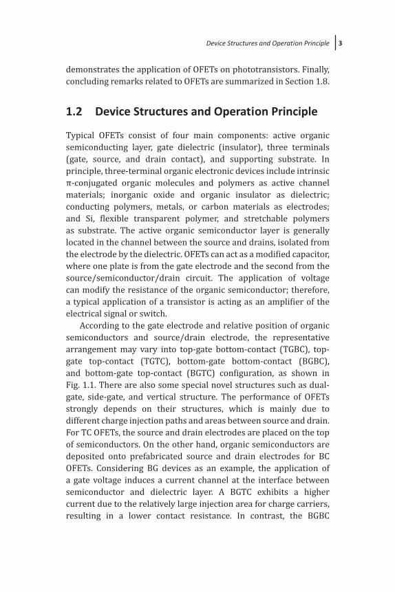
1.2 Device Structures and Operation Principle
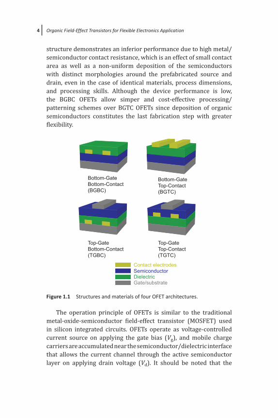
Typical OFETs consist of four main components: active organic semiconducting layer, gate dielectric (insulator), three terminals (gate, source, and drain contact), and supporting substrate. In principle, three-terminal organic electronic devices include intrinsic π-conjugated organic molecules and polymers as active channel materials; inorganic oxide and organic insulator as dielectric; conducting polymers, metals, or carbon materials as electrodes; and Si, flexible transparent polymer, and stretchable polymers as substrate. The active organic semiconductor layer is generally located in the channel between the source and drains, isolated from the electrode by the dielectric. OFETs can act as a modified capacitor, where one plate is from the gate electrode and the second from the source/semiconductor/drain circuit. The application of voltage can modify the resistance of the organic semiconductor; therefore, a typical application of a transistor is acting as an amplifier of the electrical signal or switch. According to the gate electrode and relative position of organic semiconductors and source/drain electrode, the representative arrangement may vary into top-gate bottom-contact (TGBC), top-gate top-contact (TGTC), bottom-gate bottom-contact (BGBC), and bottom-gate top-contact (BGTC) configuration, as shown in Fig. 1.1. There are also some special novel structures such as dual-gate, side-gate, and vertical structure. The performance of OFETs strongly depends on their structures, which is mainly due to different charge injection paths and areas between source and drain. For TC OFETs, the source and drain electrodes are placed on the top of semiconductors. On the other hand, organic semiconductors are deposited onto prefabricated source and drain electrodes for BC OFETs. Considering BG devices as an example, the application of a gate voltage induces a current channel at the interface between semiconductor and dielectric layer. A BGTC exhibits a higher current due to the relatively large injection area for charge carriers, resulting in a lower contact resistance. In contrast, the BGBC
Device Structures and Operation Principle
4 Organic Field-Effect Transistors for Flexible Electronics Application
structure demonstrates an inferior performance due to high metal/semiconductor contact resistance, which is an effect of small contact area as well as a non-uniform deposition of the semiconductors with distinct morphologies around the prefabricated source and drain, even in the case of identical materials, process dimensions, and processing skills. Although the device performance is low, the BGBC OFETs allow simper and cost-effective processing/patterning schemes over BGTC OFETs since deposition of organic semiconductors constitutes the last fabrication step with greater flexibility.
Contact electrodesSemiconductorDielectricGate/substrate
Top-GateBottom-Contact(TGBC)
Top-GateTop-Contact(TGTC)
Bottom-GateBottom-Contact(BGBC)
Bottom-GateTop-Contact(BGTC)
Figure 1.1 Structures and materials of four OFET architectures.
The operation principle of OFETs is similar to the traditional metal-oxide-semiconductor field-effect transistor (MOSFET) used in silicon integrated circuits. OFETs operate as voltage-controlled current source on applying the gate bias (Vg), and mobile charge carriers are accumulated near the semiconductor/dielectric interface that allows the current channel through the active semiconductor layer on applying drain voltage (Vd). It should be noted that the
5
source serves as the grounded electrode. Hole and electron in the semiconductor act as charge carriers mostly depending on the relative energy level relationship between the semiconductor and source/drain contact, which can be divided into three operation modes, including p-type, n-type, and ambipolar channel. Current–voltage (I–V) characteristics of typical OFETs can be expressed from the linear (Eq. 1.1) and saturation region (Eq. 1.2).
( )IWL
CV V V
Vid lin
g th d
d= ÊËÁ
ˆ¯̃
- -Ê
ËÁˆ
¯̃m
2 (1.1)
( ) ( )IWL
C V Vid sat g d= ÊËÁ
ˆ¯̃
-2
2m (1.2)
where Id is the drain current, W and L are the width and length of the channel, μ is the field-effect mobility, Ci is the capacitance per unit area of the gate dielectric, and Vth is the threshold voltage. At low Vd, Id builds up linearly due to the presence of carriers all along the channel, following Ohm’s law. As Vd further increases and approaches Vg, pinch-off channel occurs and Id becomes independent of Vd. Thus, any further increase in Vd does not contribute more toward the increase in Id. The region is called the saturation operation.
1.3 Important Device Parameters
The performance of OFETs is characterized in terms of the important parameters, including the field-effect mobility, threshold voltage, ON/OFF current ratio, and subthreshold swing. Basically all the parameters can be evaluated by the output and transfer plot, where the former provides a plot of Id versus Vd at constant Vg and the latter provides a plot of Id versus Vg at constant Vd. The transition from linear to saturation region is observed in the output curves. The operation of performance of OFETs is generally governed by two key mechanisms: (1) charge transport within the organic semiconductor layer and (2) charge injection and extraction at the contact. Four critical parameters—field-effect mobility (μ), current ON/OFF ratio (ION/IOFF), threshold voltage (Vth), and subthreshold swing (SS)—are measured.
Important Device Parameters
6 Organic Field-Effect Transistors for Flexible Electronics Application
log(
l d)
l d
(a) (b)Vg
VdVth Vg
ld 1/2
Figure 1.2 (a) Typical transfer and (b) output characteristics of OFET device operation.
1.3.1 Field-Effect Mobility
Mobility is defined as the charge-carrier drift velocity per unit electrical field, which is commonly used as a figure of merit for reporting OFET performance of various organic semiconductor materials by the research community. The field-effect mobility can be extracted from the slope of the linear fit in the saturation region on the plot of Id
1/2 versus Vg. Important factors that strongly affect mobility is the crystallinity and grain size of the active semiconducting layer, which depends on how the layer is deposited. Significant improvements in the mobility of organic semiconductors are obtained by designing novel high-performance materials and optimizing the fabrication methods, which may fulfill the possibility of organic electronic devices for real applications.
1.3.2 Current ON/OFF Ratio
In addition to charge-carrier mobility, the other important device parameter for OFETs is the current ON/OFF ratio, which is defined as the ratio of the maximum Id (accumulation current) in the ON state of the transistor to the minimum Id (depletion current) in the OFF state of the transistor. During the OFF state, negligible Id flows when Vg is small and independent of the bias applied between the source and drain contacts (Vd). The OFETs turn ON when Vg is
7
applied, which induces charge carriers in the semiconductors at the interface with dielectric layer. This ratio is strongly influenced by the channel conductance, mobility, thickness, and dielectric constant of the dielectric layer. A high ON/OFF ratio is a desirable quality since it is essentially the signal-to-noise ratio for a transistor.
1.3.3 Threshold Voltage
The threshold voltage Vth is the minimum Vg required for accumulating charge carriers at the semiconductor/dielectric interface forming the active channel between the source and drain. By plotting Id
1/2 versus Vg in the saturation region and performing the linear curve fitting, Vth can be extracted from the intercept of linearly fitted curve. Vth shows strong dependence on the dielectric constant of insulator, channel length, and the thicknesses of active and dielectric layer. Typically, a decrease in the thickness and an increase in the dielectric constant of the dielectric layer result in a significant reduction in Vth due to the high gate capacitance.
1.3.4 Subthreshold Swing
The subthreshold swing (SS) is the ratio of the change in the gate biasing to the change in Id in the logarithmic scale, which can be expressed as
SSV
I=
∂∂
G
Dlog (1.3)
The subthreshold operation of OFETs is closely related to the mobility enhancement for carrier hopping, which determines an efficient usage of the transistor as a switch. The active thin film equality achieved during the fabrication process may affect this value. A discontinuous semiconducting layer leads to the accumulation of defects and higher trap density, which results in less steeper slope (high SS).
1.4 Materials
Tremendous efforts have been put toward the synthesis of new organic materials for enhancing the performance of OFETs. Material
Materials
8 Organic Field-Effect Transistors for Flexible Electronics Application
engineering is a necessary component for the success of organic electronics and development of molecular devices. The applicability of OFETs has increased rapidly with the progress of high-performance novel organic materials. The performance of OFETs significantly depends on the material constituents for the active layer. However, the selection of the dielectric and electrode layers also has a strong influence. Besides, an appropriate selection of substrate material makes the device flexible at low cost. This section provides insight into the materials of different layers in OFETs.
1.4.1 Organic Semiconductors
Semiconducting materials are the most significant in OFET devices. Organic semiconductor materials are generally classified as small molecules and polymers made from small fundamental groups of conjugated monomer units. Small-molecule semiconductors have been widely studied because they are easy to purify and they form crystalline films for the fabrication of the desired high-performance device. Polymers have good solution processability on a range of desirable substrates, which renders them the most promising materials for large-area flexible electronics. A variety of approaches have given valuable insight into the relationship between functionality and electrical properties. Undoubtedly, the semiconducting π-conjugated system is one of the most important factors determining the ultimate performance of a device. For good semiconducting materials, it should give an extended electron-delocalized π-conjugation, high intermolecular interaction, and appropriate energy level structures in favor of charge injection. This section will focus on the categorization of p-type and n-type organic semiconducting materials, compiling structural and performance data as reported in the literature.
1.4.1.1 p-Type
The molecular design and synthesis of p-type organic semi-conductors are hot topics of chemical research. The common strategy for obtaining good hole-transporting semiconductors for OFETs is via a delicate balance of highest occupied molecular orbital (HOMO) energy level, which should lie somewhere around −5 to −5.5 eV. Holes are less affected in ambient condition, and thus p-type
9
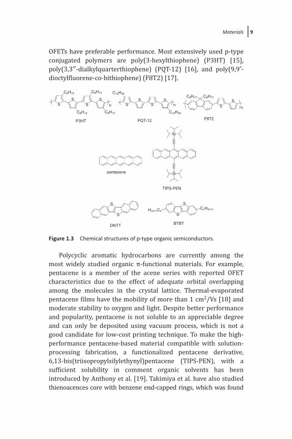
OFETs have preferable performance. Most extensively used p-type conjugated polymers are poly(3-hexylthiophene) (P3HT) [15], poly(3,3¢¢-dialkylquarterthiophene) (PQT-12) [16], and poly(9,9¢-dioctylfluorene-co-bithiophene) (F8T2) [17].
C6H13
C6H13 C6H13 C12H25
H2n+1CnCnH2n+1
C6H13 C12H25C8H17 C8H17
S
Si
Si
S
SS
SS
SS
P3HT PQT-12
pentacene
TIPS-PEN
F8T2
SS
Snnn
S
S
S
DNTT BTBT
Figure 1.3 Chemical structures of p-type organic semiconductors.
Polycyclic aromatic hydrocarbons are currently among the most widely studied organic π-functional materials. For example, pentacene is a member of the acene series with reported OFET characteristics due to the effect of adequate orbital overlapping among the molecules in the crystal lattice. Thermal-evaporated pentacene films have the mobility of more than 1 cm2/Vs [18] and moderate stability to oxygen and light. Despite better performance and popularity, pentacene is not soluble to an appreciable degree and can only be deposited using vacuum process, which is not a good candidate for low-cost printing technique. To make the high-performance pentacene-based material compatible with solution-processing fabrication, a functionalized pentacene derivative, 6,13-bis(triisopropylsilylethynyl)pentacene (TIPS-PEN), with a sufficient solubility in comment organic solvents has been introduced by Anthony et al. [19]. Takimiya et al. have also studied thienoacences core with benzene end-capped rings, which was found
Materials
10 Organic Field-Effect Transistors for Flexible Electronics Application
to result in higher hole mobility compared to the earlier heteroacene-based organic semiconductors. For example, benzothieno[3,2-b]benzothiophene (BTBT) [20] and dinaphtho[2,3-b:2¢,3¢-f]thieno[3,2-b]thiophene (DNTT) [21] derivatives were founded to be air-stable, high-performance organic semiconductor materials. Poly(3-alkylthiophene)s are one of the most studied polymeric families for semiconducting applications thanks to their good processability. The length of alkyl chain plays an important role in thin-film charge transport, and the hexyl chain length is reported to be optimized. Regioregular head-to-tail P3HT shows outstanding solubility in a range of organic solvents and mobility of 0.1 cm2/Vs [22]. However, exposure of a P3HT film to air easily causes polymer doping degradation of the ON/OFF ratio of OFETs. Ong et al. have reported PQT to afford excellent OFET performance under ambient condition. Another popular category of polymeric semiconductor materials is polyfluorene derivatives. It was found that F8T2 with nematic liquid crystalline properties can be preferentially oriented by rubbing polyimide, with a mobility of 0.02 cm2/Vs [17].
1.4.1.2 n-Type
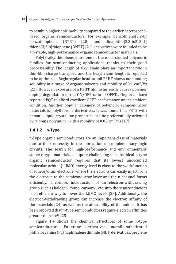
n-Type organic semiconductors are an important class of materials due to their necessity in the fabrication of complementary logic circuits. The search for high-performance and environmentally stable n-type materials is a quite challenging task. An ideal n-type organic semiconductor requires that its lowest unoccupied molecular orbital (LUMO) energy level is close to the workfunction of source/drain electrode, where the electrons can easily inject from the electrode to the semiconductor layer and the n-channel forms efficiently. Therefore, introduction of an electron-withdrawing group such as halogen, cyano, carbonyl, etc. into the semiconductors is an efficient way to lower the LUMO levels [23]. Additionally, the electron-withdrawing group can increase the electron affinity of the materials [24] as well as the air stability of the anions. It has been reported that n-type semiconductors require electron affinities greater than 4 eV [25]. Figure 1.4 shows the chemical structures of some n-type semiconductors. Fullerene derivatives, metallo-substituted phthalocyanine (Pc) naphthalene diimide (NDI) derivatives, perylene
11
diimide (PDI) derivatives, thiopene-based n-type oligomers, and quinoidal system are typical n-type small molecular semiconductors. Reports on n-type polymers are much rarer than those on p-type polymers. The first report of n-type active semiconducting polymer was ladder-like poly(benzobisimidazobenzophenanthroline) (BBL) with an electron mobility as high as 0.1 cm2/Vs, but the film can only be prepared from Lewis acid/nitromethane solutions [26, 27]. Recently, Facchetti’s group developed naphthalene dicarboximide-bithophene based copolymers with an electron mobility of 0.06 cm2/Vs and good stability after 14 weeks in air [28].
C60 MPc
R R
RR
R R R R
R
R
n
n
N
N NMN N
NN
N
N N N
O
N
N
N
N
N
N
N
O
O
OO
NDI
BBLPNDI-T2
PDI
OO
O
O O O
O
O
SS
O
Figure 1.4 Chemical structures of n-type organic semiconductors.
Materials
12 Organic Field-Effect Transistors for Flexible Electronics Application
1.4.2 Gate Dielectric Materials
Gate dielectric materials play an important role in the performance of OFETs, especially in terms of lowering the device operating voltage and minimizing gate leakage current. The accumulation of induced charge carriers at the semiconductor/dielectric interface strongly depends on the dielectric constant and the thickness of the insulator layer. The dielectrics are typically classified into inorganic and organic materials. Inorganic-based dielectrics, mainly including SiO2 and various metal oxides such as AlOx, ZrOx, HfOx, and TiOx, possess high areal capacitance, high dielectric strength, and low-term stability. These excellent dielectric properties are guaranteed only after good film formation, which typically requires expensive vacuum apparatus or high annealing temperatures. Therefore, it is not easy to fabricate inorganic dielectric films on the top of organic semiconductors and plastic flexible substrates. Organic dielectric materials mainly from a variety of polymers, such as poly (methyl methacrylate) (PMMA), polystyrene (PS), and polyimide (PI), demonstrate versatile processability in solution and compatibility with organic semiconductors for flexible electronics. Most of the solution-processed polymers need high enough thickness for use as a dielectric since a thin layer of polymeric dielectric contains pinholes, which may pass substantial amount of gate leakage. Generally, a high operation voltage is required for the organic dielectric-based OFETs due to their low dielectric constant. The balance of dielectric materials between the working voltage and flexible substrate should be considered for use in specific organic electronic devices.
1.4.3 Electrode Materials
One of the critical operation junctions in OFET devices is the source and drain electrodes to the channel. Any barrier between the contacts and the channel will appear in series and impede the flow of charge through the device. Therefore, the selection of electrode materials is important. The contact metal should be selected in such a way that it should not produce high contact resistance. It implies that the barrier difference between workfunction of electrode and relative energy level of organic semiconductor layer should be low for efficient carrier injection. Gold is a popular choice for p-type
13
OFETs since its high workfunction provides reasonable access to the HOMO level of many semiconducting materials. The addition of a thin layer of nickel, titanium, or chromium with gold improves their adhesion. On the other hand, using low workfunction metal contacts for n-type organic semiconductors should be favorable. Some alternatives are under consideration for better energy level matching and contact injection. A series of doped conducting polymers such as poly(3,4-ethylenedioxythiophene):styrene sulfonic (PEDOT:PSS) and polyaniline doped with camphorsulfonic acid (PANI:CSA) offer a reasonable energy level match and can potentially locally dope the semiconductor with contact dopant and offer a better surface for oligomer organization than metals.
1.4.4 Substrate Materials
The selection of substrate materials for the device mainly relies on the different kinds of applications. Silicon substrates are used in OFETs not only because of the intrinsic stable conducting properties but also for the ability to produce an oxide layer by thermal oxidation process. Solid glass substrate is also necessary for fabricating transparent devices. On the other hand, plastic substrates have attractive features such as physical durability, high flexibility (which makes them good for roll-to-roll processing), light weight, and potentially low cost when produced in large volumes. Numerous printed organic transistors were made on flexible polymer substrates such as polyethylene naphthalate (PEN), polyethylene therephthalate (PET), and polyimide (PI) for flexible electronics. Furthermore, to realize a human-friendly interface system such as wearable and stretchable electronics, stretchability of the device is critical. Stretchable substrate based on rubber materials can be integrated in OFET devices.
1.5 Overview of Processing Techniques
The processing methods used to deposit organic semiconductors play a crucial rule when determining the performance of OFETs, even though the same material is used. In general, organic semiconductors are deposited either from vapor or solution deposition depending on
Overview of Processing Techniques
14 Organic Field-Effect Transistors for Flexible Electronics Application
their solubility. Small-molecule semiconductors such as pentacene or oligothiophene are usually deposited through the vacuum deposition method due to their limited solubility in the organic solvents. On the other hand, conjugated polymers such as P3HT are solution in solvents, which can be deposited by the solution-processing method. These two techniques are described as follows.
1.5.1 Vacuum Deposition
Thermal evaporation in vacuum allows for the deposition of the small molecule and oligomer semiconductors. The material is placed in a vacuum (evacuated to a minimum pressure of 10−5 Torr) and heated by Joule heats (delivered through a high melting point metal). When the vapor pressure of the heated material exceeds the background pressure of the material in the chamber, the vapor state stable material evaporates and condenses on cooler surfaces. High molecular weight organic/polymeric semiconductors may decompose at higher temperature, and thus this method is not suitable for them. The main advantages of vacuum thermal deposition are the precise control of the thickness and enhanced purity of the deposited film. By monitoring the deposition rate and substrate temperature, a highly ordered film can be realized. Besides, the patterned films can be fabricated by evaporation through the shadow mask. The primary drawback is the requirement of sophisticated vacuum-based apparatus, which is in contrast to the simplicity of spin-coating or other solution process techniques.
1.5.2 Solution-Processed Deposition
Solution-processed deposition of organic semiconductors may offer a significant reduction in manufacturing cost by eliminating the vacuum deposition process and replacing them with the potentially cheaper solution deposition method. Many strategies have been developed for the solution-coating of organic semiconductors, which are beneficial in realizing large-area electronics at considerably low temperature and lower cost [29]. The common deposition methods include spin coating, drop casting, dip coating, spray coating, blade coating (e.g., doctor blading), and inkjet printing.
15
One of the most simple and effective ways of realizing a nice organic semiconductor (especially polymer) film is by spin-coating. Controlled parameters of the spin-coating process include spin speed, choice of solvent and concentration in the utilized solution, drying temperature/time, and so on. When a small amount of the coating solution is paced on the substrate with a high speed rotation, the organic semiconductor is uniformly spread over the substrate due to the centrifugal force. The optimized thin-film thickness and uniformity can be achieved. The dip-coating process is generally used to fabricate a uniform film efficiently and economically over cylindrical and flat substrates, which involves the vertical withdrawal of the substrate dipped in a bath of organic semiconductor solution. Key parameters such as pooling velocity, substrate/solution temperature influence the development of concentration gradients and fluid flow within the meniscus. Wet films of varying thicknesses are achieved to produce aligned crystalline domain in the dried film after solvent evaporation. Alternative solution-based processing methods also demonstrate potential for organic electronic fabrication.
1.6 Flexible Organic Transistor Device
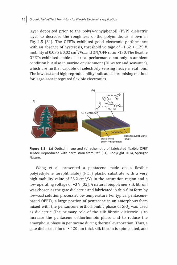
Since organic electronics are envisioned to be flexible and light weight, the ability to fabricate organic electronics on flexible substrate is of considerable interest for devices. The mechanical flexibility of organic materials makes them particularly attractive. The criteria of selection of flexible substrate used in OFETs include thermal, chemical, and mechanical stability, surface roughness, and the cost of films. Several representative studies about flexible OFET devices are demonstrated here. Bao’s group did comprehensive studies on OFETs and their flexible electronic applications. The organic electronic devices are easily degraded in both ambient and aqueous environments, which may limit the development of OFETs. Their group overcame the barrier using the isoindigo-based polymer semiconductors with siloxane-terminated solubilizing group, which demonstrates its good solubility and high mobility [30]. Flexible OFET sensors were fabricated on polyimide substrate, with a benzocyclobutene (BCB)
Flexible Organic Transistor Device
16 Organic Field-Effect Transistors for Flexible Electronics Application
layer deposited prior to the poly(4-vinylphenol) (PVP) dielectric layer to decrease the roughness of the polyimide, as shown in Fig. 1.5 [31]. The OFETs exhibited good electronic performance with an absence of hysteresis, threshold voltage of −1.62 ± 1.25 V, mobility of 0.035 ± 0.02 cm2/Vs, and ON/OFF ratio >130. The flexible OFETs exhibited stable electrical performance not only in ambient condition but also in marine environment (DI water and seawater), which are further capable of selectively sensing heavy metal ions. The low cost and high reproducibility indicated a promising method for large-area integrated flexible electronics.
polyimide
PII2T-Si
Au electrodes
(a)
(b)
cross-linkedpoly(4-vinylphenol)
bisbenzocyclobutene(BCB)
Figure 1.5 (a) Optical image and (b) schematic of fabricated flexible OFET sensor. Reproduced with permission from Ref. [31], Copyright 2014, Springer Nature.
Wang et al. presented a pentacene made on a flexible poly(ethylene terephthalate) (PET) plastic substrate with a very high mobility value of 23.2 cm2/Vs in the saturation region and a low operating voltage of −3 V [32]. A natural biopolymer silk fibroin was chosen as the gate dielectric and fabricated in thin-film form by low-cost solution process at low temperature. For typical pentacene-based OFETs, a large portion of pentacene in an amorphous form mixed with the pentancene orthorhombic phase of SiO2 was used as dielectric. The primary role of the silk fibroin dielectric is to increase the pentacene orthorhombic phase and to reduce the amorphous phase in pentacene during thermal evaporation. Thus, a gate dielectric film of ~420 nm thick silk fibroin is spin-coated, and
17
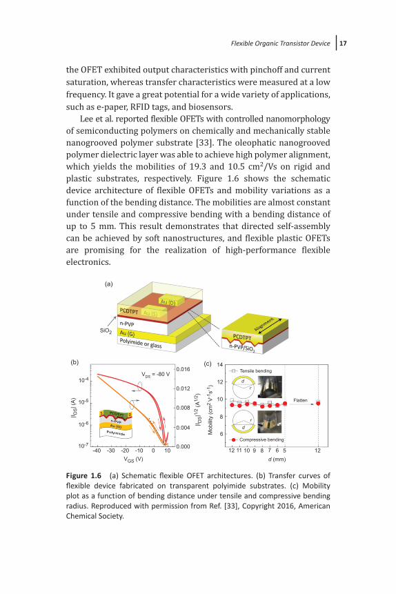
the OFET exhibited output characteristics with pinchoff and current saturation, whereas transfer characteristics were measured at a low frequency. It gave a great potential for a wide variety of applications, such as e-paper, RFID tags, and biosensors. Lee et al. reported flexible OFETs with controlled nanomorphology of semiconducting polymers on chemically and mechanically stable nanogrooved polymer substrate [33]. The oleophatic nanogrooved polymer dielectric layer was able to achieve high polymer alignment, which yields the mobilities of 19.3 and 10.5 cm2/Vs on rigid and plastic substrates, respectively. Figure 1.6 shows the schematic device architecture of flexible OFETs and mobility variations as a function of the bending distance. The mobilities are almost constant under tensile and compressive bending with a bending distance of up to 5 mm. This result demonstrates that directed self-assembly can be achieved by soft nanostructures, and flexible plastic OFETs are promising for the realization of high-performance flexible electronics.
(a)
(b)
VDS = -80 V
Compressive bending
Flatten
Tensile bending
dr
rd
d (mm)12 1211 10 9 8 7 6 5
|I DS|1
/2 (A
1/2 )
Mob
ility
(cm
2 V
-1s-
1 )
0.01614
12
10
8
6
0.012
0.008
0.004
0.000
(c)
10-4
10-5
|I DS| (
A)
10-6
10-7-40 -30 -20
VGS (V)-10 100
SiO2
Figure 1.6 (a) Schematic flexible OFET architectures. (b) Transfer curves of flexible device fabricated on transparent polyimide substrates. (c) Mobility plot as a function of bending distance under tensile and compressive bending radius. Reproduced with permission from Ref. [33], Copyright 2016, American Chemical Society.
Flexible Organic Transistor Device
18 Organic Field-Effect Transistors for Flexible Electronics Application
1.7 Flexible Organic Phototransistor
1.7.1 Introduction
The high demand for sensing and imaging applications such as optical communication, light fidelity health monitoring, and thermal imaging has allowed the rapid progress in photosensing devices, including photodiodes [34] (vertical device configurations) and photoresistors [35, 36]/phototransistors [37–39] (lateral device architectures). Phototransistors typically exhibit higher responsivity than photodiodes because the current generated by photons is amplified by gate voltage modulation without increasing noise [40]. In contrast to two-terminal photosensors, the photo-excited current in phototransistor can be further increased via lateral bias (Vd) to assist the dissociation of light-induced excitons [41]. Besides, phototransistors that combine light detection and signal amplification together in a single device can be easily integrated into conventional electronic circuits due to the unique structure of field-effect transistors (FETs) such as light switchers, light memories, and light detectors [42]. The first phototransistor with the prototype of n-p-n junction where the hole injection by the emitter junction was simply replaced by hole electron pair generation by light was induced to optoelectronics in 1951 by William Shockley [43]. Field-effect transistor gradually replaced the bipolar junction transistor due to the superior energy consumption, which also prompted the invention of phototransistors based on field-effect transistors. Besides, among the various stimulations for human beings, light is a distinct external stimulus with wavelength expanded from ultraviolet region to infrared light radiating from sunlight or even X-ray or g-radiation from medical equipment, which is usually invisible to our bare eyes. Therefore, exploring stretchable, wavelength-accessible light detectors with high sensitivity within a broad spectrum has been of longstanding interest owing to their potential for use in invisible or detrimental radiative detector during daily life. Furthermore, non-contact and media-less transportation characteristics of electromagnetic wave communication also show promising application in electronic skin labeling for entertainment purpose or human health monitor.
19
Organic photosensitive material is essential in realizing a flexible photosensitive device. Therefore, the organic photovoltaic material is an appropriate candidate for the charge-transporting material in organic phototransistors. A bulk heterojunction composed of a donor–acceptor system not only provides an effective charge-carrier pathway but also strengthens the photosensitivity through exciton (electron–hole) separation between the junction of donor and acceptor compared to a single component. Photochromic material is a compound that can undergo reversible structural transformations under the influence of light stimuli; this induces a color change, as well as changes in their physical and chemical properties [44]. Through the introduction of photochromic material in the active layer or dielectric layer in an organic phototransistor, the electrical properties can be further verified under light illumination. Besides, the monomer that shows reversible photon-induced polymerization also serves as the photosensitive material in organic phototransistors. In the following, we will introduce the main parameters for organic phototransistors and categorize the flexible organic phototransistor based on their photon-responsive mechanism as donor–acceptor system, photochromism, and photopolymerization.
1.7.2 Important Device Parameters of Organic Phototransistor
For organic phototransistors, in addition to the normal OFET parameters, photoconductive gain, photocurrent/dark current ratio, photoresponsivity, and external quantum efficiency are the main factors that determine the efficacy of the device.
1.7.2.1 Photoconductive gain (G)
The photoconductive gain is given by the following equation:
G =ttlifetime
drift
(1.4)
where tlifetime is carrier lifetime, tdrift = L2m−1Vd−1 is the drift time
of charge carrier along the channel length (L) with the charge-carrier mobility (m) and lateral voltage (Vd) [45]. When the organic phototransistors are operated under a high bias, the carrier lifetime will be larger than the drift time, which is needed for carriers to
Flexible Organic Phototransistor
20 Organic Field-Effect Transistors for Flexible Electronics Application
travel from one electrode to the opposite electrode. So the gain can well exceed 1 (>100%).
1.7.2.2 Photocurrent/dark current ratio (P)
The photocurrent/dark current ratio is given by the following formula:
PI I
I
I
I= =
-Signal
Noise
photon dark
dark
photon
dark
(1.5)
where Iphoton and Idark correspond to Id under illumination and dark. P strongly depends on the illuminated intensity and also on the operating bias (Vg).
1.7.2.3 Photosensitivity (R)
The value of R reveals to what extent the optical power (Popt) is converted into an electrical current with the unit of A/W.
RI I
P=
-photon dark
opt
(1.6)
1.7.2.4 Quantum efficiency (η)
The quantum efficiency, known more specifically as the external quantum efficiency, is the number of electron–hole pairs generated for each incident photon (unit of %):
h =Ê
ËÁˆ
¯̃
Ê
ËÁˆ
¯̃
-I
q
P
hvphoton opt
1
where Iphoton is the photogenerated current from the absorption of incident optical power Popt at a wavelength l (corresponding to a photon energy hn), and q is the electronic charge [46].
1.7.2.5 Photodetectivity (D*)
The photodetectivity is given by the following formula:
DA f Ri
*( ) /
=D 1 2
n
(1.7)
where A is the effective area of the detector, Δf is the electrical bandwidth, R is the photoresponsivity, and in is the noise current.
21
1.7.3 Examples of Flexible Organic Phototransistors
The widely available materials for the fabrication of high-performance flexible organic phototransistors are acutely required in order to further the practical applications of organic optoelectronic devices. The possible routes to enhance photoresponsivity include fabrication of the semiconducting layer with the donor−acceptor interface [38, 40, 41, 47] and the introduction of photosensitive materials such as photochromic molecules [48, 49] or photopolymerization molecules [50] in the semiconducting material layer. This section will focus on the mechanism of the above flexible organic phototransistors and their specific examples.
1.7.3.1 Donor–acceptor system
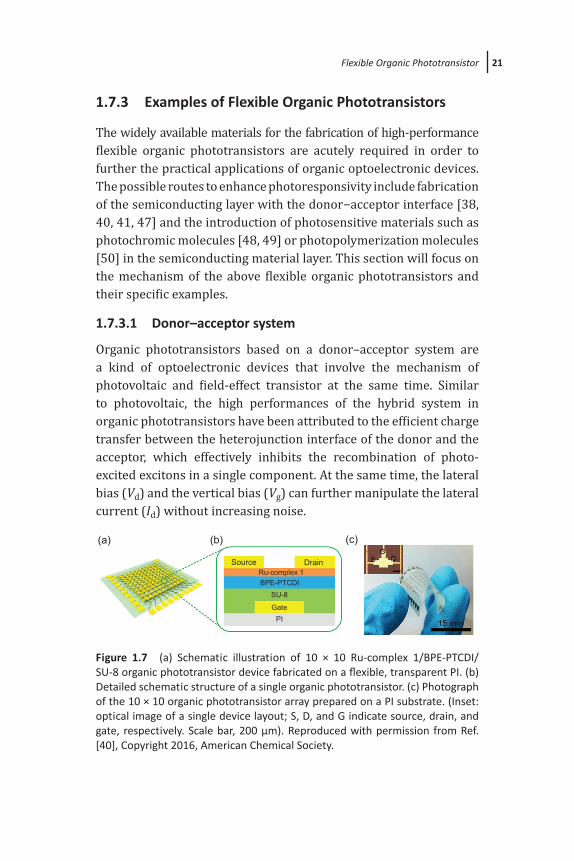
Organic phototransistors based on a donor–acceptor system are a kind of optoelectronic devices that involve the mechanism of photovoltaic and field-effect transistor at the same time. Similar to photovoltaic, the high performances of the hybrid system in organic phototransistors have been attributed to the efficient charge transfer between the heterojunction interface of the donor and the acceptor, which effectively inhibits the recombination of photo-excited excitons in a single component. At the same time, the lateral bias (Vd) and the vertical bias (Vg) can further manipulate the lateral current (Id) without increasing noise.
Source DrainRu-complex 1BPE-PTCDI
SU-8
GatePI
(a) (b) (c)
Figure 1.7 (a) Schematic illustration of 10 × 10 Ru-complex 1/BPE-PTCDI/SU-8 organic phototransistor device fabricated on a flexible, transparent PI. (b) Detailed schematic structure of a single organic phototransistor. (c) Photograph of the 10 × 10 organic phototransistor array prepared on a PI substrate. (Inset: optical image of a single device layout; S, D, and G indicate source, drain, and gate, respectively. Scale bar, 200 μm). Reproduced with permission from Ref. [40], Copyright 2016, American Chemical Society.
Flexible Organic Phototransistor
22 Organic Field-Effect Transistors for Flexible Electronics Application
Rigid rod conjugated polymers have been used as a single component of active layer in flexible organic phototransistor. Chou et al. demonstrated flexible organic phototransistors by using the cross-linked poly(4-vinylphenol) (C-PVP) as a polymer dielectric layer, and N,N¢-ditridecyl-3,4,9,10-perylenetetracarboxylic diimide (PTCDI-C13H27) as an n-type active layer on a transparent polyether sulfone (PES) substrate with R = 0.41 A/W, a tunable photocurrent/dark current ratio through lateral and vertical bias. With the merit of energy offset between the donor and acceptor, organic phototransistors based on a bulk heterojunction system in active channel can enhance the dissociation of photo-excited excitons and further provide the possible routes to improve photoresponsivity. An air-stable n-type organic semiconductor, N,N¢-bis(2phenylethyl)-perylene-3,4:9,10-tetracarboxylic diimide (BPE-PTCDI)-based organic phototransistors functionalized with ruthenium (Ru)-complex 1 exhibited ~5000 times higher h than that of pristine BPE-PTCDI organic phototransistors and high R of 7230 A/W at Vg = 80 V, owing to the metal−ligand charge transfer (MLCT) from Ru-complex 1 to the active component of the device [40]. In addition, a large 10 × 10 organic phototransistor array (2.5 × 2.5 cm2) has been prepared on a transparent PI substrate, showing distinct light mapping (Fig. 1.7). One-dimensional poly(3-hexylthiophene-2,5-diyl) (P3HT): phenyl-C61-butyric acid methyl ester (PCBM) electrospun fibers based organic phototransistors also have demonstrated the maximum P and R values of ~40 and 0.2 A/W, respectively [47]. Recently, organic–inorganic hybrid perovskite materials have emerged as effective photoactive components, which possess exceptional semiconducting properties such as intense light-harvesting capability, small exciton binding energy (~20–50 meV) [51], and long charge-carrier lifetime (>100 ns) and diffusion length (>1 μm) [52–54]. These characteristics have allowed its rapid progress in photosensing devices. Therefore, apart from using organic/organic mixtures in flexible organic phototransistors, a light-sensitive transistor based on a composite of conjugated polymer and hybrid organic/inorganic perovskite has also been developed. Xie and Shi et al. have successfully utilized methyl ammonium lead iodide (CH3NH3PbI3) and poly(diketopyrrolopyrrole-terthiophene)
23
(PDPP3T) as complementary light absorbers, which overcome the low exciton diffusion length (~10 nm) of conjugated polymer and broaden the spectral sensitivity [38]. The organic phototransistor demonstrated sensitive photo-response in the near-infrared region but also significantly improved photoresponsivity and photodetectivity in the UV–visible region, compared with those of pure CH3NH3PbI3 organic phototransistor even at low driving voltages. For the CH3NH3PbI3/PDPP3T composite photodetector, R was calculated to be 10.7 mA/W at 365 nm (UV light), 25.5 mA/W at 650 nm (visible light), or 5.5 mA/W at 937 nm (near-infrared radiation) at a low applied voltage of 1 V, demonstrating its broadband photo-detection characteristics [38].
1.7.3.2 Photochromism
Photochromism involves the reversible transformation of a chemical species between two isomeric forms triggered by light stimuli, which results in the change in absorption spectra. Most studies on photochromic molecules in organic phototransistors have focused on three types of photochromic system: azobenzenes, spiropyrans, and diarylethenes. The mechanisms include changes in the cis–trans isomerizations, conjugation length and ring structure, which can be translated into corresponding adaptations of the optoelectronic properties, such as dipole moment, refractive index, and charge-carrier mobility. Importantly, these dynamic transformations can generate coincident changes in the optical, chemical, electrical, and bulk properties of the system that incorporates them. Photochromic molecules, therefore, play a pivotal role within photo-responsive systems, being able to convert an optical signal via their isomerization to a useful property change [49]. Leydecker et al. demonstrated a flexible organic phototransistor via an active layer consisting of a blend of diarylethene (DAE) moiety, namely DAE-Me, and semiconducting polymer, poly(3-hexylthiophene) (P3HT), serving as the electroactive nanomaterial (Fig. 1.8) [48]. When the organic phototransistor is illuminated with monochromatic light at l = 546 nm, the DAE-Me is in its open form (DAE-Me-o) with the corresponding HOMO level lying outside the bandgap of P3HT, which results in a scattering center for charge
Flexible Organic Phototransistor
24 Organic Field-Effect Transistors for Flexible Electronics Application
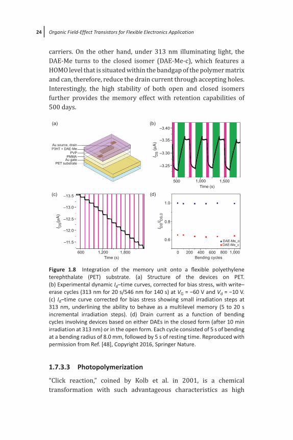
carriers. On the other hand, under 313 nm illuminating light, the DAE-Me turns to the closed isomer (DAE-Me-c), which features a HOMO level that is situated within the bandgap of the polymer matrix and can, therefore, reduce the drain current through accepting holes. Interestingly, the high stability of both open and closed isomers further provides the memory effect with retention capabilities of 500 days.
(a) (b)
(d)(c)
Au source, drainP3HT + DAE-Me
PVPPMMA
–3.40
–3.35
–3.30I D
S (m
A)
I DS/I D
S,0
I DS(m
A)
–3.25
–13.5
–13.0
–12.5
–12.0
–11.5
600 1,200Time (s)
1,800
500
1.0
0.8
0.6
0 200 400Bending cycles
600 800 1,000
DAE-Me_oDAE-Me_c
1,000 1,500Time (s)
Au gatePET substrate
Figure 1.8 Integration of the memory unit onto a flexible polyethylene terephthalate (PET) substrate. (a) Structure of the devices on PET. (b) Experimental dynamic Id–time curves, corrected for bias stress, with write–erase cycles (313 nm for 20 s/546 nm for 140 s) at VG = −60 V and Vd = −10 V. (c) Id–time curve corrected for bias stress showing small irradiation steps at 313 nm, underlining the ability to behave as a multilevel memory (5 to 20 s incremental irradiation steps). (d) Drain current as a function of bending cycles involving devices based on either DAEs in the closed form (after 10 min irradiation at 313 nm) or in the open form. Each cycle consisted of 5 s of bending at a bending radius of 8.0 mm, followed by 5 s of resting time. Reproduced with permission from Ref. [48], Copyright 2016, Springer Nature.
1.7.3.3 Photopolymerization
“Click reaction,” coined by Kolb et al. in 2001, is a chemical transformation with such advantageous characteristics as high
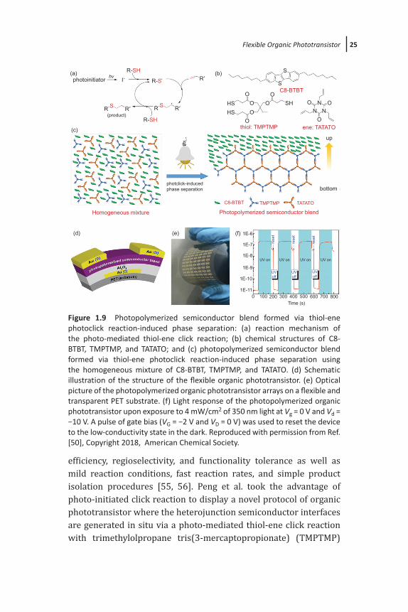
25
(a)
(c)
(d) (e) (f)
(b)photoinitiator I
R-SH
R-SH(product)
R-S
S S
hv
R RHS
O
S
S
OO
O
O O O
O
up
photclick-inducedphase separation bottom
1E-6
1E-7
1E-8
1E-9
1E-10
1E-110 100 200 300 400
Time (s)500 600 700 800
NN
N
O
HSSH
C8-BTBT
thiol: TMPTMP
Homogeneous mixture
C8-BTBT TMPTMP TATATO
Photopolymerized semiconductor blend
ene: TATATO
R¢ R¢
R¢
UV on UV onUV onUV on
rese
t
rese
t
rese
tUVoff
UVoff
UVoff
Figure 1.9 Photopolymerized semiconductor blend formed via thiol-ene photoclick reaction-induced phase separation: (a) reaction mechanism of the photo-mediated thiol-ene click reaction; (b) chemical structures of C8-BTBT, TMPTMP, and TATATO; and (c) photopolymerized semiconductor blend formed via thiol-ene photoclick reaction-induced phase separation using the homogeneous mixture of C8-BTBT, TMPTMP, and TATATO. (d) Schematic illustration of the structure of the flexible organic phototransistor. (e) Optical picture of the photopolymerized organic phototransistor arrays on a flexible and transparent PET substrate. (f) Light response of the photopolymerized organic phototransistor upon exposure to 4 mW/cm2 of 350 nm light at Vg = 0 V and Vd = −10 V. A pulse of gate bias (VG = −2 V and VD = 0 V) was used to reset the device to the low-conductivity state in the dark. Reproduced with permission from Ref. [50], Copyright 2018, American Chemical Society.
efficiency, regioselectivity, and functionality tolerance as well as mild reaction conditions, fast reaction rates, and simple product isolation procedures [55, 56]. Peng et al. took the advantage of photo-initiated click reaction to display a novel protocol of organic phototransistor where the heterojunction semiconductor interfaces are generated in situ via a photo-mediated thiol-ene click reaction with trimethylolpropane tris(3-mercaptopropionate) (TMPTMP)
Flexible Organic Phototransistor
26 Organic Field-Effect Transistors for Flexible Electronics Application
and 1,3,5-triallyl-1,3,5-triazine-2,4,6(1H,3H,5H)-trione (TATATO) as monomers, diphenyl(2,4,6-trimethylbenzoyl)phosphine oxide (TPO) as the photoinitiator, and the p-type semiconductor, 2,7-dioctyl[1]benzothieno[3,2-b][1]benzothiophene (C8-BTBT) [50]. Under 350 nm light exposure, the in-plan phase separation of thiol-ene monomers network (bottom layer) and C8-BTBT (top layer) leads to an increase in hole density derived from electron−hole pair formation and thus the positive shift in threshold voltage, as shown in Fig. 1.9. The photopolymerized organic phototransistors show no deterioration even after 50 ON/OFF cycles with R = 2.5 A/W.
1.8 Conclusion
This chapter presents an overview of OFETs, particularly aiming at flexible electronic applications. The fundamental properties of organic semiconductors and the basic operation of OFET devices were reviewed. A procedure was explained for the extraction of important OFET parameters to provide a basic evaluation of OFET performance. Organic semiconductors and device architecture considered for specific processing skills in OFET fabrication were also discussed. Flexible OFETs and organic memories were integrated to realize functional flexible electronic applications. OFETs boast of a bright future with a wide range of potential applications. It still faces a number of challenges and needs interdisciplinary research to develop a commercially viable OFET technology.
Acknowledgments
We appreciate the financial support by the Ministry of Science and Technology (MOST) of Taiwan. Jung-Yao Chen appreciates the financial support from the Young Scholar Fellowship Program by the Ministry of Science and Technology (MOST) of Taiwan, under Grant MOST107-2636-E-194-001.
References
1. Arias, A. C., J. D. MacKenzie, I. McCulloch, J. Rivnay, and A. Salleo. (2010). Materials and applications for large area electronics: Solution-based approaches, Chem. Rev., 110, pp. 3–24.
2. Liao, C., M. Zhang, M. Y. Yao, T. Hua, L. Li, and F. Yan. (2015). Flexible organic electronics in biology: Materials and devices, Adv. Mater., 27, pp. 7493–7527.
3. Janneck, R., N. Pilet, S. P. Bommanaboyena, B. Watts, P. Heremans, J. Genoe, and C. Rolin. (2017). Highly crystalline C8-BTBT thin-film transistors by lateral homo-epitaxial growth on printed templates, Adv. Mater., 29, pp. 1703864.
4. Allard, S., M. Forster, B. Souharce, H. Thiem, and U. Scherf. (2008). Organic semiconductors for solution-processable field-effect transistors (OFETs), Angew. Chem. lnt. Ed., 47, pp. 4070–4098.
5. Russew, M.-M. and S. Hecht. (2010). Photoswitches: From molecules to materials, Adv. Mater., 22, pp. 3348–3360.
6. Klauk, H. (2010). Organic thin-film transistors, Chem. Soc. Rev., 39, pp. 2643–2666. 7. Mei, J., Y. Diao, A. L. Appleton, L. Fang, and Z. Bao. (2013). Integrated materials design of
organic semiconductors for field-effect transistors, J. Am. Chem. Soc., 135, pp. 6724–6746. 8. Wang, X., Y. Gu, Z. Xiong, Z. Cui, and T. Zhang. (2014). Silk-molded flexible, ultrasensitive,
and highly stable electronic skin for monitoring human physiological signals, Adv. Mater., 26, pp. 1336–1342.
9. Gsänger, M., D. Bialas, L. Huang, M. Stolte, and F. Würthner. (2016). Organic semiconductors based on dyes and color pigments, Adv. Mater., 28, pp. 3615–3645.
10. Richter, L. J., D. M. DeLongchamp, and A. Amassian. (2017). Morphology development in solution-processed functional organic blend films: An in situ viewpoint, Chem. Rev., 117, pp. 6332–6366.
11. Huang, H., L. Yang, A. Facchetti, and T. J. Marks. (2017). Organic and polymeric semiconductors enhanced by noncovalent conformational locks, Chem. Rev., 117, pp. 10291–10318.
12. Wang, B., W. Huang, L. Chi, M. Al-Hashimi, T. J. Marks, and A. Facchetti. (2018). High-k gate dielectrics for emerging flexible and stretchable electronics, Chem. Rev., 118, pp. 5690–5754.
13. Liu, A., H. Zhu, H. Sun, Y. Xu, and Y.-Y. Noh. (2018). Solution processed metal oxide high-K dielectrics for emerging transistors and circuits, Adv. Mater., 30, pp. 1706364.
14. Glowacki, E. D., M. Irimia-Vladu, M. Kaltenbrunner, J. Gsiorowski, M. S. White, U. Monkowius, G. Romanazzi, G. P. Suranna, P. Mastrorilli, T. Sekitani, S. Bauer, T. Someya, L. Torsi, and N. S. Sariciftci. (2013). Hydrogen-bonded semiconducting pigments for air-stable field-effect transistors, Adv. Mater., 25, pp. 1563–1569.
15. Kline, R. J., M. D. McGehee, E. N. Kadnikova, J. Liu, J. M. J. Fréchet, and M. F. Toney. (2005). Dependence of regioregular poly(3-hexylthiophene) film morphology and field-effect mobility on molecular weight, Macromolecules, 38, pp. 3312–3319.
16. Ong, B. S., Y. Wu, P. Liu, and S. Gardner. (2004). High-performance semiconducting polythiophenes for organic thin-film transistors, J. Am. Chem. Soc., 126, pp. 3378–3379.
17. Sirringhaus, H., R. J. Wilson, R. H. Friend, M. Inbasekaran, W. Wu, E. P. Woo, M. Grell, and D. D. C. Bradley. (2000). Mobility enhancement in conjugated polymer field-effect transistors through chain alignment in a liquid-crystalline phase, Appl. Phys. Lett., 77, pp. 406–408.
18. Lin, Y., D. J. Gundlach, S. F. Nelson, and T. N. Jackson. (1997). Stacked pentacene layer organic thin-film transistors with improved characteristics, IEEE Electron. Device Lett., 18, pp. 606–608.
19. Anthony, J. E., J. S. Brooks, D. L. Eaton, and S. R. Parkin. (2001). Functionalized pentacene: Improved electronic properties from control of solid-state order, J. Am. Chem. Soc., 123, pp. 9482–9483.
20. Takimiya, K., H. Ebata, K. Sakamoto, T. Izawa, T. Otsubo, and Y. Kunugi. (2006). 2,7-Diphenyl[1]benzothieno[3,2-b]benzothiophene, a new organic semiconductor for air-stable organic field-effect transistors with mobilities up to 2.0 cm2 V-1 s-1, J. Am. Chem. Soc., 128, pp. 12604–12605.
21. Yamamoto, T. and K. Takimiya. (2007). Facile synthesis of highly π-extended heteroarenes, dinaphtho[2,3-b:2’,3’-f] chalcogenopheno[3,2-b]chalcogenophenes, and their application to field-effect transistors, J. Am. Chem. Soc., 129, pp. 2224–2225.
22. Sirringhaus, H., P. J. Brown, R. H. Friend, M. M. Nielsen, K. Bechgaard, B. M. W. Langeveld-Voss, A. J. H. Spiering, R. A. J. Janssen, E. W. Meijer, P. Herwig, and D. M. de Leeuw. (1999). Two-dimensional charge transport in self-organized, high-mobility conjugated polymers, Nature, 401, pp. 685.
23. Newman, C. R., C. D. Frisbie, D. A. da Silva Filho, J.-L. Brédas, P. C. Ewbank, and K. R. Mann. (2004). Introduction to organic thin film transistors and design of n -channel organic semiconductors, Chem. Mater., 16, pp. 4436–4451.
24. Chua, L.-L., J. Zaumseil, J.-F. Chang, E. C. W. Ou, P. K. H. Ho, H. Sirringhaus, and R. H. Friend. (2005). General observation of n-type field-effect behaviour in organic semiconductors, Nature, 434, pp. 194.
25. de Leeuw, D. M., M. M. J. Simenon, A. R. Brown, and R. E. F. Einerhand (1997). Stability of n-type doped conducting polymers and consequences for polymeric microelectronic devices, Synth. Met., 87, pp. 53–59.
26. Babel, A. and S. A. Jenekhe. (2003). High electron mobility in ladder polymer field-effect transistors, J. Am. Chem. Soc., 125, pp. 13656–13657.
27. Babel, A. and S. A. Jenekhe. (2002). Electron transport in thin-film transistors from an n-type conjugated polymer, Adv. Mater., 14, pp. 371–374.
28. Chen, Z., Y. Zheng, H. Yan, and A. Facchetti. (2009). Naphthalenedicarboximide-vs perylenedicarboximide-based copolymers. Synthesis and semiconducting properties in bottom-gate N-channel organic transistors, J. Am. Chem. Soc., 131, pp. 8–9.
29. Diao, Y., L. Shaw, Z. Bao, and S. C. B. Mannsfeld. (2014). Morphology control strategies for solution-processed organic semiconductor thin films, Energ. Environ. Sci., 7, pp. 2145–2159.
30. Mei, J., D. H. Kim, A. L. Ayzner, M. F. Toney, and Z. Bao. (2011). Siloxane-terminated solubilizing side chains: Bringing conjugated polymer backbones closer and boosting hole mobilities in thin-film transistors, J. Am. Chem. Soc., 133, pp. 20130–20133.
31. Knopfmacher, O., M. L. Hammock, A. L. Appleton, G. Schwartz, J. Mei, T. Lei, J. Pei, and Z. Bao. (2014). Highly stable organic polymer field-effect transistor sensor for selective detection in the marine environment, Nat. Commun., 5, pp. 2954.
32. Wang, C.-H., C.-Y. Hsieh, and J.-C. Hwang. (2011). Flexible organic thin-film transistors with silk fibroin as the gate dielectric, Adv. Mater., 23, pp. 1630–1634.
33. Lee, B. H., B. B. Y. Hsu, S. N. Patel, J. Labram, C. Luo, G. C. Bazan, and A. J. Heeger. (2016). Flexible organic transistors with controlled nanomorphology, Nano Lett., 16, pp. 314–319.
34. Maculan, G., A. D. Sheikh, A. L. Abdelhady, M. I. Saidaminov, M. A. Haque, B. Murali, E. Alarousu, O. F. Mohammed, T. Wu, and O. M. Bakr. (2015). CH3NH3PbCl3 single crystals: Inverse temperature crystallization and visible-blind UV-photodetector, J. Phys. Chem. Lett., 6, pp. 3781–3786.
35. He, M., Y. Chen, H. Liu, J. Wang, X. Fang, and Z. Liang. (2015). Chemical decoration of CH3NH3PbI3 perovskites with graphene oxides for photodetector applications, Chem. Commun., 51, pp. 9659–9661.
36. Wang, H., R. Haroldson, B. Balachandran, A. Zakhidov, S. Sohal, J. Y. Chan, A. Zakhidov, and W. Hu. (2016). Nanoimprinted perovskite nanograting photodetector with improved efficiency, ACS Nano, 10, pp. 10921–10928.
37. Lee, Y., J. Kwon, E. Hwang, C.-H. Ra, W. J. Yoo, J.-H. Ahn, J. H. Park, and J. H. Cho. (2015). High-performance perovskite-graphene hybrid photodetector, Adv. Mater., 27, pp. 41–46.
38. Chen, S., C. Teng, M. Zhang, Y. Li, D. Xie, and G. Shi. (2016). A flexible UV-vis-NIR photodetector based on a perovskite/conjugated-polymer composite, Adv. Mater., 28, pp. 5969–5974.
39. Ma, C., Y. Shi, W. Hu, M.-H. Chiu, Z. Liu, A. Bera, F. Li, H. Wang, L.-J. Li, and T. Wu. (2016). Heterostructured WS2/CH3NH3PbI3 photoconductors with suppressed dark current and enhanced photodetectivity, Adv. Mater., 28, pp. 3683–3689.
40. Liu, X., E. K. Lee, D. Y. Kim, H. Yu, and J. H. Oh. (2016). Flexible organic phototransistor array with enhanced responsivity via metal-ligand charge transfer, ACSAppl. Mater. Interfaces, 8, pp. 7291–7299.
41. Chou, W.-Y., Y.-S. Lin, L.-L. Kuo, S.-J. Liu, H.-L. Cheng, and F.-C. Tang. (2014). Light sensing in photosensitive, flexible n-type organic thin-film transistors, J. Mater. Chem. C, 2, pp. 626–632.
42. Gu, P., Y. Yao, L. Feng, S. Niu, and H. Dong. (2015). Recent advances in polymer phototransistors, Polym. Chem., 6, pp. 7933–7944.
43. Shockley, W., M. Sparks, and G. K. Teal. (1951). p-n Junction transistors, Phys. Rev., 83, pp. 151–162.
44. Xia, H., K. Xie, and G. Zou. (2017). Advances in spiropyrans/spirooxazines and applications based on fluorescence resonance energy transfer (FRET) with fluorescent materials, Molecules, 22, pp. 2236.
45. Xu, H., J. Li, B. H. K. Leung, C. C. Y. Poon, B. S. Ong, Y. Zhang, and N. Zhao. (2013). A high-sensitivity near-infrared phototransistor based on an organic bulk heterojunction, Nanoscale, 5, pp. 11850–11855.
46. Sze, S. M. (1985). Semiconductor Devices, Physics and Technology. New York: Wiley. 47. Kim, M., S. B. Jo, J. H. Park, and K. Cho. (2015). Flexible lateral organic solar cells with
core-shell structured organic nanofibers, Nano Energy, 18, pp. 97–108. 48. Leydecker, T., M. Herder, E. Pavlica, G. Bratina, S. Hecht, E. Orgiu, and P. Samorì. (2016).
Flexible non-volatile optical memory thin-film transistor device with over 256 distinct levels based on an organic bicomponent blend, Nat. Nanotech., 11, pp. 769.
49. Ercole, F., T. P. Davis, and R. A. Evans. (2010). Photo-responsive systems and biomaterials: Photochromic polymers, light-triggered self-assembly, surface modification, fluorescence modulation and beyond, Polym. Chem., 1, pp. 37–54.
50. Peng, H., Y. Yan, Y. Yang, L. Zhou, W. Wu, Q. Sun, J. Zhuang, S.-T. Han, C.-C. Ko, Z. Xu, X. Xie, R. K. Y. Li, and V. A. L. Roy. (2018). Interface engineering via photopolymerization -induced phase separation for flexible UV-responsive phototransistors, ACS Appl. Mat. Interfaces, 10, pp. 7487–7496.
51. Miyata, A., A. Mitioglu, P. Plochocka, O. Portugall, J.T.-W. Wang, S. D. Stranks, H. J. Snaith, and R. J. Nicholas. (2015). Direct measurement of the exciton binding energy and effective masses for charge carriers in organic-inorganic tri-halide perovskites, Nat. Phys., 11, pp. 582–587.
52. Johnston, M. B. and L. M. Herz. (2016). Hybrid perovskites for photovoltaics: Charge-carrier recombination, diffusion, and radiative efficiencies, Acc. Chem. Res., 49, pp. 146–154.
53. Xu, W., H. Cho, Y.-H. Kim, Y.-T. Kim, C. Wolf, C.-G. Park, and T.-W. Lee. (2016). Organometal halide perovskite artificial synapses, Adv. Mater., 28, pp. 5916–5922.
54. Chen, J.-Y., Y.-C. Chiu, Y.-T. Li, C.-C. Chueh, and W.-C. Chen. (2017). Nonvolatile perovskite-based photomemory with a multilevel memory behavior, Adv. Mater., 29, pp. 1702217.
55. Qin, A., J. W. Y. Lam, and B. Z. Tang. (2010). Click polymerization: Progresses, challenges, and opportunities, Macromolecules, 43, pp. 8693–8702.
56. Kolb, H. C., M. G. Finn, and K. B. Sharpless. (2001). Click chemistry: Diverse chemical function from a few good reactions, Angew. Chem. Int. Ed., 40, pp. 2004–2021.
1. Lewis, N. S. and Nocera, D. G. (2006). Powering the planet: Chemical challenges in solar
energy utilization. Proc. Natl. Acad. Sci., 103, pp. 15729–15735. 2. Reale, A., La Notte, L., Salamandra, L., Polino, G., Susanna, G., Brown, T. M., Brunetti, F.,
and Di Carlo, A. (2015). Spray coating for polymer solar cells: An up-to-date overview. Energy Technol., 3, pp. 385–406.
3. Krebs, F. C., Espinosa, N., Hösel, M., Søndergaard, R. R., and Jørgensen, M. (2014). 25th Anniversary Article: Rise to power: OPV-based solar parks. Adv. Mater., 26, pp. 29–39.
4. Nielsen, T. D., Cruickshank, C., Foged, S., Thorsen, J., and Krebs, F. C. (2010). Business, market and intellectual property analysis of polymer solar cells. Sol. Energy Mater. Sol. Cells, 94, pp. 1553–1571.
5. Darling, S. B. and You, F. (2013). The case for organic photovoltaics. RSC Adv., 3, pp. 17633–17648.
6. Espinosa, N., Hösel, M., Angmo, D., and Krebs, F. C. (2012). Solar cells with one-day energy payback for the factories of the future. Energy Environ. Sci., 5, pp. 5117–5132.
7. Carlé, J. E., Helgesen, M., Hagemann, O., Hösel, M., Heckler, I. M., Bundgaard, E., Gevorgyan, S. A., Søndergaard, R. R., Jørgensen, M., Garcia-Valverde, R., Chaouki-Almagro, S., Villarejo, J. A., and Krebs, F. C. (2017). Overcoming the scaling lag for polymer solar cells. Joule, 1, pp. 274–289.
8. Machui, F., Hösel, M., Li, N., Spyropoulos, G. D., Ameri, T., Søndergaard, R. R., Jørgensen, M., Scheel, A., Gaiser, D., Kreul, K., Lenssen, D., Legros, M., Lemaitre, N., Vilkman, M., Välimäki, M., Nordman, S., Brabec, C. J., and Krebs, F. C. (2014). Cost analysis of roll-to-roll fabricated ITO free single and tandem organic solar modules based on data from manufacture. Energy Environ. Sci., 7, pp. 2792–2802.
9. Li, S., Ye, L., Zhao, W., Yan, H., Yang, B., Liu, D., Li, W., Ade, H., and Hou, J., (2018) . A wide band gap polymer with a deep highest occupied molecular orbital level enables 14.2% efficiency in polymer solar cells. J. Am. Chem. Soc., 140, pp. 7159–7167.
10. Heliatek sets new organic photovoltaic world record efficiency of 13.2%. https://www.heliatek.com/en/press/press-releases/details/heliatek-sets-new-organic-photovoltaic-world-record-efficiency-of-13-2.
11. Mazzio, K. A. and Luscombe, C. K. (2014). The future of organic photovoltaics. Chem. Soc. Rev., 44, pp. 78–90.
12. Brabec, C. J., Sariciftci, N. S., and Hummelen, J. C. (2001). Plastic solar cells. Adv. Funct. Mater., 11, pp. 15–26.
13. Tang, C. W. (1986). Two-layer organic photovoltaic cell. Appl. Phys. Lett., 48, pp. 183–185. 14. Yu, G., Gao, J., Hummelen, F. W., and Heeger, A. J. (1995). Polymer photovoltaic cells:
Enhanced efficiencies via a network of internal donor-acceptor heterojunctions. Science, 270, pp. 1789–1791.
15. Padinger, F., Rittberger, R. S., and Sariciftci, N. S. (2003). Effects of postproduction treatment on plastic solar cells. Adv. Funct. Mater., 13, pp. 85–88.
16. Yin, Z., Wei, J., and Zheng, Q. (2016). Interfacial materials for organic solar cells: Recent advances and perspectives. Adv. Sci., 3, pp. 1500362.
17. Kim, H., Lim, K.-G., and Lee, T.-W. (2016). Planar heterojunction organometal halide perovskite solar cells: Roles of interfacial layers. Energy Environ. Sci., 9, pp. 12–30.
18. Chueh, C.-C., Li, C.-Z., and Jen, A.K.-Y. (2015). Recent progress and perspective in solution-processed interfacial materials for efficient and stable polymer and organometal perovskite solar cells. Energy Environ. Sci., 8, pp. 1160–1189.
19. Pivrikas, A., Sariciftci, N. S., Juška, G., and Österbacka, R. (2007). A review of charge transport and recombination in polymer/fullerene organic solar cells. Prog. Photovolt. Res. Appl., 15, pp. 677–696.
20. Li, G., Zhu, R., and Yang, Y. (2012). Polymer solar cells. Nat. Photonics, 6, pp. 153–161. 21. Cao, W. and Xue, J. (2014). Recent progress in organic photovoltaics: Device architecture
and optical design. Energy Environ. Sci., 7, pp. 2123–2144. 22. Lindholm, F. A., Fossum, J. G., and Burgess, E. L. (1979). Application of the superposition
principle to solar-cell analysis. IEEE Trans. Electron Devices, 26, pp. 165–171. 23. Guo, X., Zhou, N., Lou, S. J., Smith, J., Tice, D. B., Hennek, J. W., Ortiz, R. P., Navarrete, J.
T. L., Li, S., Strzalka, J., Chen, L. X., Chang, R. P. H., Facchetti, A., and Marks, T. J. (2013). Polymer solar cells with enhanced fill factors. Nat. Photonics, 7, pp. 825–833.
24. Zhou, H., Yang, L., and You, W. (2012). Rational design of high performance conjugated polymers for organic solar cells. Macromolecules, 45, pp. 607–632.
25. Jung, J. W., Jo, J. W., Jung, E. H., and Jo, W. H. (2016). Recent progress in high efficiency polymer solar cells by rational design and energy level tuning of low bandgap copolymers with various electron-withdrawing units. Org. Electron., 31, pp. 149–170.
26. Scharber, M. C., Mühlbacher, D., Koppe, M., Denk, P., Waldauf, C., Heeger, A. J., and Brabec, C. J. (2006). Design rules for donors in bulk-heterojunction solar cells: Towards 10% energy-conversion efficiency. Adv. Mater., 18, pp. 789–794.
27. Lu, L., Zheng, T., Wu, Q., Schneider, A. M., Zhao, D., and Yu, L. (2015). Recent advances in bulk heterojunction polymer solar cells. Chem. Rev., 115, pp. 12666–12731.
28. Dennler, G., Scharber, M. C., and Brabec, C. J. (2009). Polymer-fullerene bulk-heterojunction solar cells. Adv. Mater., 21, pp. 1323–1338.
29. Zhang, S., Ye, L., Zhao, W., Liu, D., Yao, H., and Hou, J. (2014). Side chain selection for designing highly efficient photovoltaic polymers with 2D-conjugated structure. Macromolecules, 47, pp. 4653–4659.
30. Sariciftci, N. S., Smilowitz, L., Heeger, A. J., and Wudl, F. (1992). Photoinduced electron transfer from a conducting polymer to buckminsterfullerene. Science, 258, pp. 1474–1476.
31. Kraabel, B., Lee, C. H., McBranch, D., Moses, D., Sariciftci, N. S., and Heeger, A. J. (1993). Ultrafast photoinduced electron transfer in conducting polymer—buckminsterfullerene composites. Chem. Phys. Lett., 213, pp. 389–394.
32. Halls, J. J. M., Walsh, C. A., Greenham, N. C., Marseglia, E. A., Friend, R. H., Moratti, S. C., and Holmes, A. B. (1995). Efficient photodiodes from interpenetrating polymer networks. Nature, 376, pp. 498–500.
33. Brabec, C. J., Shaheen, S. E., Winder, C., Sariciftci, N. S., and Denk, P. (2002). Effect of LiF/metal electrodes on the performance of plastic solar cells. Appl. Phys. Lett., 80, pp. 1288–1290.
34. Schilinsky, P., Waldauf, C., and Brabec, C. J. (2002). Recombination and loss analysis in polythiophene based bulk heterojunction photodetectors. Appl. Phys. Lett., 81, pp. 3885–3887.
35. Kim, J. Y., Kim, S. H., Lee, H.-H., Lee, K., Ma, W., Gong, X., and Heeger, A. J. (2006). New architecture for high-efficiency polymer photovoltaic cells using solution-based titanium oxide as an optical spacer. Adv. Mater., 18, pp. 572–576.
36. Ma, W., Yang, C., Gong, X., Lee, K., and Heeger, A. J. (2005). Thermally stable, efficient polymer solar cells with nanoscale control of the interpenetrating network morphology. Adv. Funct. Mater., 15, pp. 1617–1622.
37. Reyes-Reyes, M., Kim, K., and Carroll, D. L. (2005). High-efficiency photovoltaic devices based on annealed poly(3-hexylthiophene) and 1-(3-methoxycarbonyl)-propyl-1-phenyl-(6,6)C61 blends. Appl. Phys. Lett., 87, pp. 083506.
38. Verploegen, E., Mondal, R., Bettinger, C. J., Sok, S., Toney, M. F., and Bao, Z. (2010). Effects of thermal annealing upon the morphology of polymer-fullerene blends. Adv. Funct. Mater., 20, pp. 3519–3529.
39. Lou, S. J., Szarko, J. M., Xu, T., Yu, L., Marks, T. J., and Chen, L. X. (2011). Effects of additives on the morphology of solution phase aggregates formed by active layer components of high-efficiency organic solar cells. J. Am. Chem. Soc., 133, pp. 20661–20663.
40. Lee, J. K., Ma, W. L., Brabec, C. J., Yuen, J., Moon, J. S., Kim, J. Y., Lee, K., Bazan, G. C., and Heeger, A. J. (2008). Processing additives for improved efficiency from bulk heterojunction solar cells. J. Am. Chem. Soc., 130, pp. 3619–3623.
41. Lin, H., Chen, S., Li, Z., Lai, J. Y. L., Yang, G., McAfee, T., Jiang, K., Li, Y., Liu, Y., Hu, H., Zhao, J., Ma, W., Ade, H., and Yan, H. (2015). High-performance non-fullerene polymer solar cells based on a pair of donor-acceptor materials with complementary absorption properties. Adv. Mater., 27, pp. 7299–7304.
42. Zhou, H., Yang, L., Stoneking, S., and You, W. (2010). A weak donor–strong acceptor strategy to design ideal polymers for organic solar cells. ACS Appl. Mater. Interfaces, 2, pp. 1377–1383.
43. Brédas, J.-L., Norton, J. E., Cornil, J., and Coropceanu, V. (2009). Molecular understanding of organic solar cells: The challenges. Acc. Chem. Res., 42, pp. 1691–1699.
44. Svensson, M., Zhang, F., Veenstra, S. C., Verhees, W. J. H., Hummelen, J. C., Kroon, J. M., Inganäs, O., and Andersson, M. R. (2003). High-performance polymer solar cells of an alternating polyfluorene copolymer and a fullerene derivative. Adv. Mater., 15, pp. 988–991.
45. Park, S. H., Roy, A., Beaupré, S., Cho, S., Coates, N., Moon, J. S., Moses, D., Leclerc, M., Lee, K., and Heeger, A. J. (2009). Bulk heterojunction solar cells with internal quantum efficiency approaching 100%. Nat. Photonics, 3, pp. 297–302.
46. Zou, Y., Najari, A., Berrouard, P., Beaupré, S., Réda Aïch, B., Tao, Y., and Leclerc, M. (2010). A thieno[3,4-c]pyrrole-4,6-dione-based copolymer for efficient solar cells. J. Am. Chem. Soc., 132, pp. 5330–5331.
47. Liang, Y., Xu, Z., Xia, J., Tsai, S.-T., Wu, Y., Li, G., Ray, C., and Yu, L. (2010). For the bright future: Bulk heterojunction polymer solar cells with power conversion efficiency of 7.4%. Adv. Mater., 22, pp. E135–E138.
48. Zhang, Y., Parnell, A. J., Pontecchiani, F., Cooper, J. F. K., Thompson, R. L., Jones, R. A. L., King, S. M., Lidzey, D. G., and Bernardo, G. (2017). Understanding and controlling morphology evolution via DIO plasticization in PffBT4T-2OD/PC71BM devices. Sci. Rep., 7, pp. 44269.
49. Ma, W., Yang, G., Jiang, K., Carpenter, J. H., Wu, Y., Meng, X., McAfee, T., Zhao, J., Zhu, C., Wang, C., Ade, H., and Yan, H. (2015). Influence of processing parameters and molecular weight on the morphology and properties of high-performance PffBT4T-2OD:PC71BM organic solar cells. Adv. Energy Mater., 5, pp. 1501400.
50. Chu, T.-Y., Alem, S., Verly, P. G., Wakim, S., Lu, J., Tao, Y., Beaupré, S., Leclerc, M., Bélanger, F., Désilets, D., Rodman, S., Waller, D., and Gaudiana, R. (2009). Highly efficient polycarbazole-based organic photovoltaic devices. Appl. Phys. Lett., 95, pp. 063304.
51. Liang, Y., Wu, Y., Feng, D., Tsai, S.-T., Son, H.-J., Li, G., and Yu, L. (2009). Development of new semiconducting polymers for high performance solar cells. J. Am. Chem. Soc., 131, pp. 56–57.
52. Chen, H.-Y., Hou, J., Zhang, S., Liang, Y., Yang, G., Yang, Y., Yu, L., Wu, Y., and Li, G. (2009). Polymer solar cells with enhanced open-circuit voltage and efficiency. Nat. Photonics, 3, pp. 649–653.
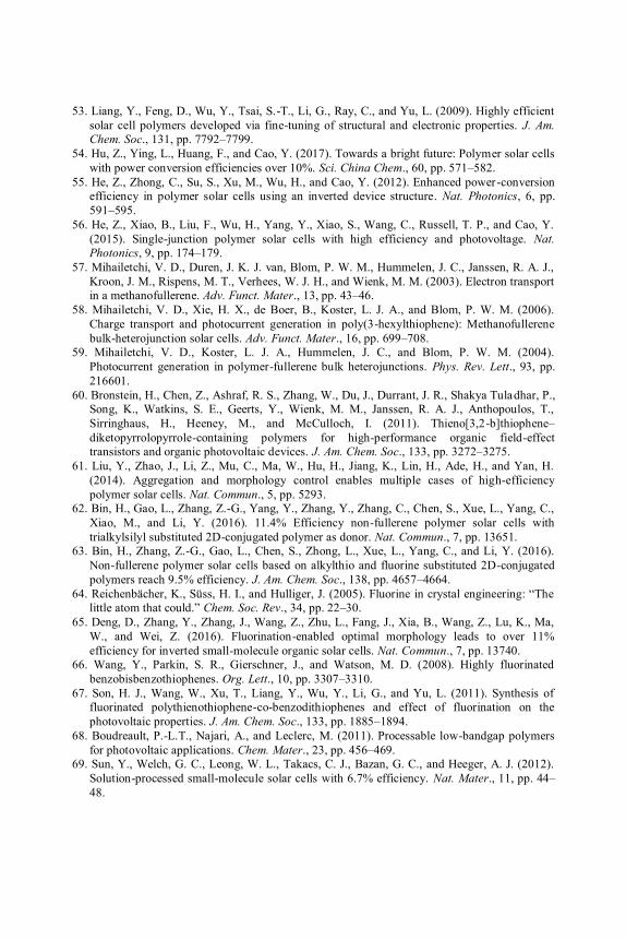
53. Liang, Y., Feng, D., Wu, Y., Tsai, S.-T., Li, G., Ray, C., and Yu, L. (2009). Highly efficient solar cell polymers developed via fine-tuning of structural and electronic properties. J. Am. Chem. Soc., 131, pp. 7792–7799.
54. Hu, Z., Ying, L., Huang, F., and Cao, Y. (2017). Towards a bright future: Polymer solar cells with power conversion efficiencies over 10%. Sci. China Chem., 60, pp. 571–582.
55. He, Z., Zhong, C., Su, S., Xu, M., Wu, H., and Cao, Y. (2012). Enhanced power-conversion efficiency in polymer solar cells using an inverted device structure. Nat. Photonics, 6, pp. 591–595.
56. He, Z., Xiao, B., Liu, F., Wu, H., Yang, Y., Xiao, S., Wang, C., Russell, T. P., and Cao, Y. (2015). Single-junction polymer solar cells with high efficiency and photovoltage. Nat. Photonics, 9, pp. 174–179.
57. Mihailetchi, V. D., Duren, J. K. J. van, Blom, P. W. M., Hummelen, J. C., Janssen, R. A. J., Kroon, J. M., Rispens, M. T., Verhees, W. J. H., and Wienk, M. M. (2003). Electron transport in a methanofullerene. Adv. Funct. Mater., 13, pp. 43–46.
58. Mihailetchi, V. D., Xie, H. X., de Boer, B., Koster, L. J. A., and Blom, P. W. M. (2006). Charge transport and photocurrent generation in poly(3-hexylthiophene): Methanofullerene bulk-heterojunction solar cells. Adv. Funct. Mater., 16, pp. 699–708.
59. Mihailetchi, V. D., Koster, L. J. A., Hummelen, J. C., and Blom, P. W. M. (2004). Photocurrent generation in polymer-fullerene bulk heterojunctions. Phys. Rev. Lett., 93, pp. 216601.
60. Bronstein, H., Chen, Z., Ashraf, R. S., Zhang, W., Du, J., Durrant, J. R., Shakya Tuladhar, P., Song, K., Watkins, S. E., Geerts, Y., Wienk, M. M., Janssen, R. A. J., Anthopoulos, T., Sirringhaus, H., Heeney, M., and McCulloch, I. (2011). Thieno[3,2-b]thiophene–diketopyrrolopyrrole-containing polymers for high-performance organic field-effect transistors and organic photovoltaic devices. J. Am. Chem. Soc., 133, pp. 3272–3275.
61. Liu, Y., Zhao, J., Li, Z., Mu, C., Ma, W., Hu, H., Jiang, K., Lin, H., Ade, H., and Yan, H. (2014). Aggregation and morphology control enables multiple cases of high-efficiency polymer solar cells. Nat. Commun., 5, pp. 5293.
62. Bin, H., Gao, L., Zhang, Z.-G., Yang, Y., Zhang, Y., Zhang, C., Chen, S., Xue, L., Yang, C., Xiao, M., and Li, Y. (2016). 11.4% Efficiency non-fullerene polymer solar cells with trialkylsilyl substituted 2D-conjugated polymer as donor. Nat. Commun., 7, pp. 13651.
63. Bin, H., Zhang, Z.-G., Gao, L., Chen, S., Zhong, L., Xue, L., Yang, C., and Li, Y. (2016). Non-fullerene polymer solar cells based on alkylthio and fluorine substituted 2D-conjugated polymers reach 9.5% efficiency. J. Am. Chem. Soc., 138, pp. 4657–4664.
64. Reichenbächer, K., Süss, H. I., and Hulliger, J. (2005). Fluorine in crystal engineering: “The little atom that could.” Chem. Soc. Rev., 34, pp. 22–30.
65. Deng, D., Zhang, Y., Zhang, J., Wang, Z., Zhu, L., Fang, J., Xia, B., Wang, Z., Lu, K., Ma, W., and Wei, Z. (2016). Fluorination-enabled optimal morphology leads to over 11% efficiency for inverted small-molecule organic solar cells. Nat. Commun., 7, pp. 13740.
66. Wang, Y., Parkin, S. R., Gierschner, J., and Watson, M. D. (2008). Highly fluorinated benzobisbenzothiophenes. Org. Lett., 10, pp. 3307–3310.
67. Son, H. J., Wang, W., Xu, T., Liang, Y., Wu, Y., Li, G., and Yu, L. (2011). Synthesis of fluorinated polythienothiophene-co-benzodithiophenes and effect of fluorination on the photovoltaic properties. J. Am. Chem. Soc., 133, pp. 1885–1894.
68. Boudreault, P.-L.T., Najari, A., and Leclerc, M. (2011). Processable low-bandgap polymers for photovoltaic applications. Chem. Mater., 23, pp. 456–469.
69. Sun, Y., Welch, G. C., Leong, W. L., Takacs, C. J., Bazan, G. C., and Heeger, A. J. (2012). Solution-processed small-molecule solar cells with 6.7% efficiency. Nat. Mater., 11, pp. 44–48.
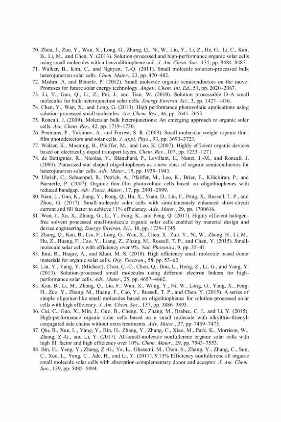
70. Zhou, J., Zuo, Y., Wan, X., Long, G., Zhang, Q., Ni, W., Liu, Y., Li, Z., He, G., Li, C., Kan, B., Li, M., and Chen, Y. (2013). Solution-processed and high-performance organic solar cells using small molecules with a benzodithiophene unit. J. Am. Chem. Soc., 135, pp. 8484–8487.
71. Walker, B., Kim, C., and Nguyen, T.-Q. (2011). Small molecule solution-processed bulk heterojunction solar cells. Chem. Mater., 23, pp. 470–482.
72. Mishra, A. and Bäuerle, P. (2012). Small molecule organic semiconductors on the move: Promises for future solar energy technology. Angew. Chem. Int. Ed., 51, pp. 2020–2067.
73. Li, Y., Guo, Q., Li, Z., Pei, J., and Tian, W. (2010). Solution processable D-A small molecules for bulk-heterojunction solar cells. Energy Environ. Sci., 3, pp. 1427–1436.
74. Chen, Y., Wan, X., and Long, G. (2013). High performance photovoltaic applications using solution-processed small molecules. Acc. Chem. Res., 46, pp. 2645–2655.
75. Roncali, J. (2009). Molecular bulk heterojunctions: An emerging approach to organic solar cells. Acc. Chem. Res., 42, pp. 1719–1730.
76. Peumans, P., Yakimov, A., and Forrest, S. R. (2003). Small molecular weight organic thin -film photodetectors and solar cells. J. Appl. Phys., 93, pp. 3693–3723.
77. Walzer, K., Maennig, B., Pfeiffer, M., and Leo, K. (2007). Highly efficient organic devices based on electrically doped transport layers. Chem. Rev., 107, pp. 1233–1271.
78. de Bettignies, R., Nicolas, Y., Blanchard, P., Levillain, E., Nunzi, J.-M., and Roncali, J. (2003). Planarized star-shaped oligothiophenes as a new class of organic semiconductors for heterojunction solar cells. Adv. Mater., 15, pp. 1939–1943.
79. Uhrich, C., Schueppel, R., Petrich, A., Pfeiffer, M., Leo, K., Brier, E., Kilickiran, P., and Baeuerle, P. (2007). Organic thin-film photovoltaic cells based on oligothiophenes with reduced bandgap. Adv. Funct. Mater., 17, pp. 2991–2999.
80. Nian, L., Gao, K., Jiang, Y., Rong, Q., Hu, X., Yuan, D., Liu, F., Peng, X., Russell, T. P., and Zhou, G. (2017). Small-molecule solar cells with simultaneously enhanced short-circuit current and fill factor to achieve 11% efficiency. Adv. Mater., 29, pp. 1700616.
81. Wan, J., Xu, X., Zhang, G., Li, Y., Feng, K., and Peng, Q. (2017). Highly efficient halogen-free solvent processed small-molecule organic solar cells enabled by material design and device engineering. Energy Environ. Sci., 10, pp. 1739–1745.
82. Zhang, Q., Kan, B., Liu, F., Long, G., Wan, X., Chen, X., Zuo, Y., Ni, W., Zhang, H., Li, M., Hu, Z., Huang, F., Cao, Y., Liang, Z., Zhang, M., Russell, T. P., and Chen, Y. (2015). Small-molecule solar cells with efficiency over 9%. Nat. Photonics, 9, pp. 35–41.
83. Ilmi, R., Haque, A., and Khan, M. S. (2018). High efficiency small molecule-based donor materials for organic solar cells. Org. Electron., 58, pp. 53–62.
84. Liu, Y., Yang, Y. (Michael), Chen, C.-C., Chen, Q., Dou, L., Hong, Z., Li, G., and Yang, Y. (2013). Solution-processed small molecules using different electron linkers for high-performance solar cells. Adv. Mater., 25, pp. 4657–4662.
85. Kan, B., Li, M., Zhang, Q., Liu, F., Wan, X., Wang, Y., Ni, W., Long, G., Yang, X., Feng, H., Zuo, Y., Zhang, M., Huang, F., Cao, Y., Russell, T. P., and Chen, Y. (2015). A series of simple oligomer-like small molecules based on oligothiophenes for solution-processed solar cells with high efficiency. J. Am. Chem. Soc., 137, pp. 3886–3893.
86. Cui, C., Guo, X., Min, J., Guo, B., Cheng, X., Zhang, M., Brabec, C. J., and Li, Y. (2015). High-performance organic solar cells based on a small molecule with alkylthio-thienyl-conjugated side chains without extra treatments. Adv. Mater., 27, pp. 7469–7475.
87. Qiu, B., Xue, L., Yang, Y., Bin, H., Zhang, Y., Zhang, C., Xiao, M., Park, K., Morrison, W., Zhang, Z.-G., and Li, Y. (2017). All-small-molecule nonfullerene organic solar cells with high fill factor and high efficiency over 10%. Chem. Mater., 29, pp. 7543–7553.
88. Bin, H., Yang, Y., Zhang, Z.-G., Ye, L., Ghasemi, M., Chen, S., Zhang, Y., Zhang, C., Sun, C., Xue, L., Yang, C., Ade, H., and Li, Y. (2017). 9.73% Efficiency nonfullerene all organic small molecule solar cells with absorption-complementary donor and acceptor. J. Am. Chem. Soc., 139, pp. 5085–5094.
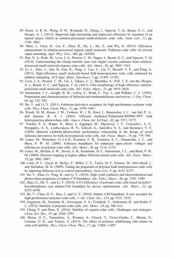
89. Kyaw, A. K. K., Wang, D. H., Wynands, D., Zhang, J., Nguyen, T.-Q., Bazan, G. C., and Heeger, A. J. (2013). Improved light harvesting and improved efficiency by insertion of an optical spacer (ZnO) in solution-processed small-molecule solar cells. Nano Lett., 13, pp. 3796–3801.
90. Miao, J., Chen, H., Liu, F., Zhao, B., Hu, L., He, Z., and Wu, H. (2015). Efficiency enhancement in solution-processed organic small molecule: Fullerene solar cells via solvent vapor annealing. Appl. Phys. Lett., 106, pp. 183302.
91. Ran, N. A., Kuik, M., Love, J. A., Proctor, C. M., Nagao, I., Bazan, G. C., and Nguyen, T. -Q. (2014). Understanding the charge-transfer state and singlet exciton emission from solution-processed small-molecule organic solar cells. Adv. Mater., 26, pp. 7405–7412.
92. Li, L., Xiao, L., Qin, H., Gao, K., Peng, J., Cao, Y., Liu, F., Russell, T. P., and Peng, X. (2015). High-efficiency small molecule-based bulk-heterojunction solar cells enhanced by additive annealing. ACS Appl. Mater. Interfaces, 7, pp. 21495–21502.
93. Love, J. A., Proctor, C. M., Liu, J., Takacs, C. J., Sharenko, A., Poll, T. S. van der, Heeger, A. J., Bazan, G. C., and Nguyen, T.-Q. (2013). Film morphology of high efficiency solution-processed small-molecule solar cells. Adv. Funct. Mater., 23, pp. 5019–5026.
94. Hummelen, J. C., Knight, B. W., LePeq, F., Wudl, F., Yao, J., and Wilkins, C. L. (1995). Preparation and characterization of fulleroid and methanofullerene derivatives. J. Org. Chem., 60, pp. 532–538.
95. He, Y. and Li, Y. (2011). Fullerene derivative acceptors for high performance polymer solar cells. Phys. Chem. Chem. Phys., 13, pp. 1970–1983.
96. Wienk, M. M., Kroon, J. M., Verhees, W. J. H., Knol, J., Hummelen, J. C., van Hal, P. A., and Janssen, R. A. J. (2003). Efficient methano[70]fullerene/MDMO-PPV bulk heterojunction photovoltaic cells. Angew. Chem. Int. Ed Engl., 42, pp. 3371–3375.
97. Troshin, P. A., Hoppe, H., Renz, J., Egginger, M., Mayorova, J. Y., Goryachev, A. E., Peregudov, A. S., Lyubovskaya, R. N., Gobsch, G., Sariciftci, N. S., and Razumov, V. F. (2009). Material solubility-photovoltaic performance relationship in the design of novel fullerene derivatives for bulk heterojunction solar cells. Adv. Funct. Mater., 19, pp. 779–788.
98. Lenes, M., Wetzelaer, G.-J.A.H., Kooistra, F. B., Veenstra, S. C., Hummelen, J. C., and Blom, P. W. M. (2008). Fullerene bisadducts for enhanced open-circuit voltages and efficiencies in polymer solar cells. Adv. Mater., 20, pp. 2116–2119.
99. Lenes, M., Shelton, S. W., Sieval, A. B., Kronholm, D. F., Hummelen, J. C., and Blom, P. W. M. (2009). Electron trapping in higher adduct fullerene-based solar cells. Adv. Funct. Mater., 19, pp. 3002–3007.
100. Cates, N. C., Gysel, R., Beiley, Z., Miller, C. E., Toney, M. F., Heeney, M., McCulloch, I., and McGehee, M. D. (2009). Tuning the properties of polymer bulk heterojunction solar cells by adjusting fullerene size to control intercalation. Nano Lett., 9, pp. 4153–4157.
101. He, Y., Zhao, G., Peng, B., and Li, Y. (2010). High-yield synthesis and electrochemical and photovoltaic properties of indene-C70 bisadduct. Adv. Funct. Mater., 20, pp. 3383–3389.
102. Zhao, G., He, Y., and Li, Y. (2010). 6.5% Efficiency of polymer solar cells based on poly(3 -hexylthiophene) and indene-C60 bisadduct by device optimization. Adv. Mater., 22, pp. 4355–4358.
103. He, Y., Chen, H.-Y., Hou, J., and Li, Y. (2010). Indene–C60 bisadduct: A new acceptor for high-performance polymer solar cells. J. Am. Chem. Soc., 132, pp. 5532–5532.
104. Jorgensen, M., Norrman, K., Gevorgyan, S. A., Tromholt, T., Andreasen, B., and Krebs, F. C. (2012). Stability of polymer solar cells. Adv. Mater., 24, pp. 580–612.
105. Cheng, P. and Zhan, X. (2016). Stability of organic solar cells: Challenges and strategies. Chem. Soc. Rev., 45, pp. 2544–2582.
106. Morse, G. E., Tournebize, A., Rivaton, A., Chassé, T., Taviot-Gueho, C., Blouin, N., Lozman, O. R., and Tierney, S. (2015). The effect of polymer solubilizing side-chains on solar cell stability. Phys. Chem. Chem. Phys., 17, pp. 11884–11897.
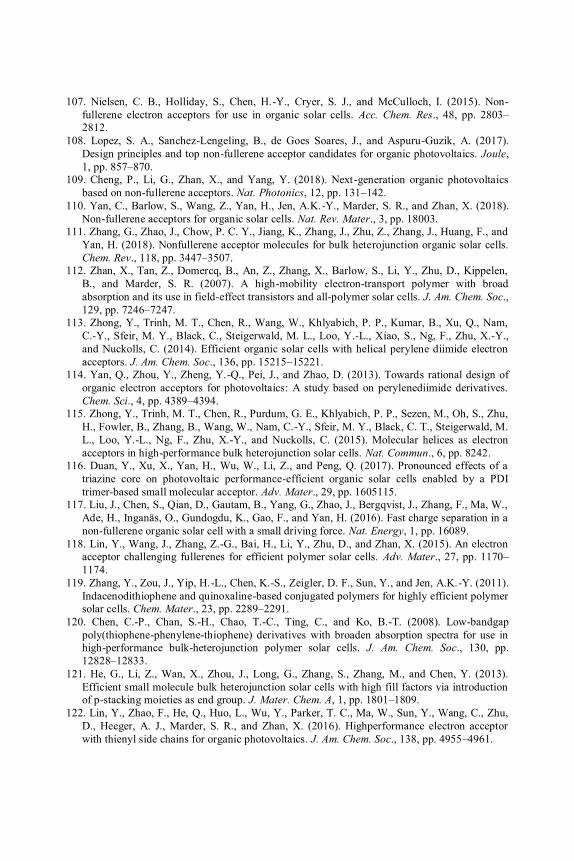
107. Nielsen, C. B., Holliday, S., Chen, H.-Y., Cryer, S. J., and McCulloch, I. (2015). Non-fullerene electron acceptors for use in organic solar cells. Acc. Chem. Res., 48, pp. 2803–2812.
108. Lopez, S. A., Sanchez-Lengeling, B., de Goes Soares, J., and Aspuru-Guzik, A. (2017). Design principles and top non-fullerene acceptor candidates for organic photovoltaics. Joule, 1, pp. 857–870.
109. Cheng, P., Li, G., Zhan, X., and Yang, Y. (2018). Next-generation organic photovoltaics based on non-fullerene acceptors. Nat. Photonics, 12, pp. 131–142.
110. Yan, C., Barlow, S., Wang, Z., Yan, H., Jen, A.K.-Y., Marder, S. R., and Zhan, X. (2018). Non-fullerene acceptors for organic solar cells. Nat. Rev. Mater., 3, pp. 18003.
111. Zhang, G., Zhao, J., Chow, P. C. Y., Jiang, K., Zhang, J., Zhu, Z., Zhang, J., Huang, F., and Yan, H. (2018). Nonfullerene acceptor molecules for bulk heterojunction organic solar cells. Chem. Rev., 118, pp. 3447–3507.
112. Zhan, X., Tan, Z., Domercq, B., An, Z., Zhang, X., Barlow, S., Li, Y., Zhu, D., Kippelen, B., and Marder, S. R. (2007). A high-mobility electron-transport polymer with broad absorption and its use in field-effect transistors and all-polymer solar cells. J. Am. Chem. Soc., 129, pp. 7246–7247.
113. Zhong, Y., Trinh, M. T., Chen, R., Wang, W., Khlyabich, P. P., Kumar, B., Xu, Q., Nam, C.-Y., Sfeir, M. Y., Black, C., Steigerwald, M. L., Loo, Y.-L., Xiao, S., Ng, F., Zhu, X.-Y., and Nuckolls, C. (2014). Efficient organic solar cells with helical perylene diimide electron acceptors. J. Am. Chem. Soc., 136, pp. 15215–15221.
114. Yan, Q., Zhou, Y., Zheng, Y.-Q., Pei, J., and Zhao, D. (2013). Towards rational design of organic electron acceptors for photovoltaics: A study based on perylenediimide derivatives. Chem. Sci., 4, pp. 4389–4394.
115. Zhong, Y., Trinh, M. T., Chen, R., Purdum, G. E., Khlyabich, P. P., Sezen, M., Oh, S., Zhu, H., Fowler, B., Zhang, B., Wang, W., Nam, C.-Y., Sfeir, M. Y., Black, C. T., Steigerwald, M. L., Loo, Y.-L., Ng, F., Zhu, X.-Y., and Nuckolls, C. (2015). Molecular helices as electron acceptors in high-performance bulk heterojunction solar cells. Nat. Commun., 6, pp. 8242.
116. Duan, Y., Xu, X., Yan, H., Wu, W., Li, Z., and Peng, Q. (2017). Pronounced effects of a triazine core on photovoltaic performance-efficient organic solar cells enabled by a PDI trimer-based small molecular acceptor. Adv. Mater., 29, pp. 1605115.
117. Liu, J., Chen, S., Qian, D., Gautam, B., Yang, G., Zhao, J., Bergqvist, J., Zhang, F., Ma, W., Ade, H., Inganäs, O., Gundogdu, K., Gao, F., and Yan, H. (2016). Fast charge separation in a non-fullerene organic solar cell with a small driving force. Nat. Energy, 1, pp. 16089.
118. Lin, Y., Wang, J., Zhang, Z.-G., Bai, H., Li, Y., Zhu, D., and Zhan, X. (2015). An electron acceptor challenging fullerenes for efficient polymer solar cells. Adv. Mater., 27, pp. 1170–1174.
119. Zhang, Y., Zou, J., Yip, H.-L., Chen, K.-S., Zeigler, D. F., Sun, Y., and Jen, A.K.-Y. (2011). Indacenodithiophene and quinoxaline-based conjugated polymers for highly efficient polymer solar cells. Chem. Mater., 23, pp. 2289–2291.
120. Chen, C.-P., Chan, S.-H., Chao, T.-C., Ting, C., and Ko, B.-T. (2008). Low-bandgap poly(thiophene-phenylene-thiophene) derivatives with broaden absorption spectra for use in high-performance bulk-heterojunction polymer solar cells. J. Am. Chem. Soc., 130, pp. 12828–12833.
121. He, G., Li, Z., Wan, X., Zhou, J., Long, G., Zhang, S., Zhang, M., and Chen, Y. (2013). Efficient small molecule bulk heterojunction solar cells with high fill factors via introduction of p-stacking moieties as end group. J. Mater. Chem. A, 1, pp. 1801–1809.
122. Lin, Y., Zhao, F., He, Q., Huo, L., Wu, Y., Parker, T. C., Ma, W., Sun, Y., Wang, C., Zhu, D., Heeger, A. J., Marder, S. R., and Zhan, X. (2016). Highperformance electron acceptor with thienyl side chains for organic photovoltaics. J. Am. Chem. Soc., 138, pp. 4955–4961.
123. Yang, Y., Zhang, Z.-G., Bin, H., Chen, S., Gao, L., Xue, L., Yang, C., and Li, Y (2016). Side-chain isomerization on an n-type organic semiconductor ITIC acceptor makes 11.77% high efficiency polymer solar cells. J. Am. Chem. Soc., 138, pp. 15011–15018.
124. Yao, H., Ye, L., Hou, J., Jang, B., Han, G., Cui, Y., Su, G. M., Wang, C., Gao, B., Yu, R., Zhang, H., Yi, Y., Woo, H. Y., Ade, H., and Hou, J. (2017). Achieving highly efficient nonfullerene organic solar cells with improved intermolecular interaction and open-circuit voltage. Adv. Mater., 29, pp. 1700254.
125. Lin, Y., He, Q., Zhao, F., Huo, L., Mai, J., Lu, X., Su, C.-J., Li, T., Wang, J., Zhu, J., Sun, Y., Wang, C., and Zhan, X. (2016). A facile planar fused-ring electron acceptor for as-cast polymer solar cells with 8.71% efficiency. J. Am. Chem. Soc., 138, pp. 2973–2976.
126. Lin, Y., Zhao, F., Wu, Y., Chen, K., Xia, Y., Li, G., Prasad, S. K. K., Zhu, J., Huo, L., Bin, H., Zhang, Z.-G., Guo, X., Zhang, M., Sun, Y., Gao, F., Wei, Z., Ma, W., Wang, C., Hodgkiss, J., Bo, Z., Inganäs, O., Li, Y., and Zhan, X. (2016). Mapping polymer donors toward high-efficiency fullerene free organic solar cells. Adv. Mater., 29, pp. 1604155.
127. Wu, Y., Bai, H., Wang, Z., Cheng, P., Zhu, S., Wang, Y., Ma, W., and Zhan, X. (2015). A planar electron acceptor for efficient polymer solar cells. Energy Environ. Sci., 8, pp. 3215–3221.
128. Holliday, S., Ashraf, R. S., Wadsworth, A., Baran, D., Yousaf, S. A., Nielsen, C. B., Tan, C.-H., Dimitrov, S. D., Shang, Z., Gasparini, N., Alamoudi, M., Laquai, F., Brabec, C. J., Salleo, A., Durrant, J. R., and McCulloch, I. (2016). High-efficiency and air-stable P3HT-based polymer solar cells with a new non-fullerene acceptor. Nat. Commun., 7, pp. 11585.
129. Lin, Y., Zhang, Z.-G., Bai, H., Wang, J., Yao, Y., Li, Y., Zhu, D., and Zhan, X. (2015). High-performance fullerene-free polymer solar cells with 6.31% efficiency. Energy Environ. Sci., 8, pp. 610–616.
130. Wang, W., Yan, C., Lau, T.-K., Wang, J., Liu, K., Fan, Y., Lu, X., and Zhan, X. (2017). Fused hexacyclic nonfullerene acceptor with strong near-infrared absorption for semitransparent organic solar cells with 9.77% efficiency. Adv. Mater., 29, pp. 1701308.
131. Yao, H., Cui, Y., Yu, R., Gao, B., Zhang, H., and Hou, J. (2017). Design, synthesis, and photovoltaic characterization of a small molecular acceptor with an ultra-narrow band gap. Angew. Chem. Int. Ed., 56, pp. 3045–3049.
132. Zhao, W., Li, S., Yao, H., Zhang, S., Zhang, Y., Yang, B., and Hou, J. (2017). Molecular optimization enables over 13% efficiency in organic solar cells. J. Am. Chem. Soc., 139, pp. 7148–7151.
133. Li, W., Ye, L., Li, S., Yao, H., Ade, H., and Hou, J. (2018). A high-efficiency organic solar cell enabled by the strong intramolecular electron pushpull effect of the nonfullerene acceptor. Adv. Mater., 30, pp. 1707170.
134. Xin, R., Feng, J., Zeng, C., Jiang, W., Zhang, L., Meng, D., Ren, Z., Wang, Z., and Yan, S. (2017). Nonfullerene-acceptor all-small-molecule organic solar cells based on highly twisted perylene bisimide with an efficiency of over 6%. ACS Appl. Mater. Interfaces, 9, pp. 2739–2746.
135. Hadmojo, W. T., Yim, D., Sinaga, S., Lee, W., Ryu, D. Y., Jang, W.-D., Jung, I. H., and Jang, S.-Y. (2018). Near-infrared harvesting fullerene-free all-small-molecule organic solar cells based on porphyrin donors. ACS Sustain. Chem. Eng., 6, pp. 5306–5313.
136. Wang, Y., Chang, M., Kan, B., Wan, X., Li, C., and Chen, Y. (2018). All-small-molecule organic solar cells based on pentathiophene donor and alkylated indacenodithiophene-based acceptors with efficiency over 8%. ACS Appl. Energy Mater., 1, pp. 2150–2156.
137. Zhang, J., Zhu, L., and Wei, Z. (2017). Toward over 15% power conversion efficiency for organic solar cells: Current status and perspectives. Small Methods, 1, pp. 1700258.
138. Yip, H.-L. and Jen, A.K.-Y. (2012). Recent advances in solution-processed interfacial materials for efficient and stable polymer solar cells. Energy Environ. Sci., 5, pp. 5994–6011.
139. Zeng, H., Zhu, X., Liang, Y., and Guo, X. (2015). Interfacial layer engineering for performance enhancement in polymer solar cells. Polymers, 7, pp. 333–372.
140. Hau, S. K., Yip, H.-L., Acton, O., Baek, N. S., Ma, H., and Jen, A.K.-Y. (2008). Interfacial modification to improve inverted polymer solar cells. J. Mater. Chem., 18, pp. 5113–5119.
141. Sun, Y., Seo, J. H., Takacs, C. J., Seifter, J., and Heeger, A. J. (2011). Inverted polymer solar cells integrated with a low-temperature-annealed solgel-derived ZnO film as an electron transport layer. Adv. Mater., 23, pp. 1679–1683.
142. Yuan, Z., Fu, M., and Huang, W. (2013). Air-stable inverted ZnO nanorod arrays/polymer hybrid solar cell. Synth. Met., 185–186, pp. 133–136.
143. Noh, Y.-J., Na, S.-I., and Kim, S.-S. (2013). Inverted polymer solar cells including ZnO electron transport layer fabricated by facile spray pyrolysis. Sol. Energy Mater. Sol. Cells, 117, pp. 139–144.
144. White, M. S., Olson, D. C., Shaheen, S. E., Kopidakis, N., and Ginley, D. S. (2006). Inverted bulk-heterojunction organic photovoltaic device using a solution-derived ZnO underlayer. Appl. Phys. Lett., 89, pp. 143517.
145. Xiong, J., Yang, B., Zhou, C., Yang, J., Duan, H., Huang, W., Zhang, X., Xia, X., Zhang, L., Huang, H., and Gao, Y. (2014). Enhanced efficiency and stability of polymer solar cells with TiO2 nanoparticles buffer layer. Org. Electron., 15, pp. 835–843.
146. Lee, K., Kim, J. Y., Park, S. H., Kim, S. H., Cho, S., and Heeger, A. J. (2007). Air -stable polymer electronic devices. Adv. Mater., 19, pp. 2445–2449.
147. Waldauf, C., Morana, M., Denk, P., Schilinsky, P., Coakley, K., Choulis, S. A., and Brabec, C. J. (2006). Highly efficient inverted organic photovoltaics using solution based titanium oxide as electron selective contact. Appl. Phys. Lett., 89, pp. 233517.
148. Hamada, K., Murakami, N., Tsubota, T., and Ohno, T. (2013). Solution-processed amorphous niobium oxide as a novel electron collection layer for inverted polymer solar cells. Chem. Phys. Lett., 586, pp. 81–84.
149. Siddiki, M. K., Venkatesan, S., Galipeau, D., and Qiao, Q. (2013). Kelvin probe force microscopic imaging of the energy barrier and energetically favorable offset of interfaces in double-junction organic solar cells. ACS Appl. Mater. Interfaces, 5, pp. 1279–1286.
150. Siddiki, M. K., Venkatesan, S., and Qiao, Q. (2012). Nb2O5 as a new electron transport layer for double junction polymer solar cells. Phys. Chem. Chem. Phys., 14, pp. 4682–4686.
151. Vasilopoulou, M., Georgiadou, D. G., Soultati, A., Boukos, N., Gardelis, S., Palilis, L. C., Fakis, M., Skoulatakis, G., Kennou, S., Botzakaki, M., Georga, S., Krontiras, C. A., Auras, F., Fattakhova-Rohlfing, D., Bein, T., Papadopoulos, T. A., Davazoglou, D., and Argitis, P. (2014). Atomic-layer-deposited aluminum and zirconium oxides for surface passivation of TiO2 in high-efficiency organic photovoltaics. Adv. Energy Mater., 4, pp. 1400214.
152. Zhou, Y., Fuentes-Hernandez, C., Shim, J., Meyer, J., Giordano, A. J., Li, H., Winget, P., Papadopoulos, T., Cheun, H., Kim, J., Fenoll, M., Dindar, A., Haske, W., Najafabadi, E., Khan, T. M., Sojoudi, H., Barlow, S., Graham, S., Brédas, J.-L., Marder, S. R., Kahn, A., and Kippelen, B. (2012). A universal method to produce low-work function electrodes for organic electronics. Science, 336, pp. 327–332.
153. Wang, H., Zhang, W., Xu, C., Bi, X., Chen, B., and Yang, S. (2013). Efficiency enhancement of polymer solar cells by applying poly(vinylpyrrolidone) as a cathode buffer layer via spin coating or self-assembly. ACS Appl. Mater. Interfaces, 5, pp. 26–34.
154. Kang, H., Hong, S., Lee, J., and Lee, K. (2012). Electrostatically selfassembled nonconjugated polyelectrolytes as an ideal interfacial layer for inverted polymer solar cells. Adv. Mater., 24, pp. 3005–3009.
155. Gommans, H., Verreet, B., Rand, B. P., Muller, R., Poortmans, J., Heremans, P., and Genoe, J. (2008). On the role of bathocuproine in organic photovoltaic cells. Adv. Funct. Mater., 18, pp. 3686–3691.
156. Vogel, M., Doka, S., Breyer, C., Lux-Steiner, M. C., and Fostiropoulos, K. (2006). On the function of a bathocuproine buffer layer in organic photovoltaic cells. Appl. Phys. Lett., 89, pp. 163501.
157. Jin, F., Chu, B., Li, W., Su, Z., Zhao, B., Yan, X., Zhang, F., Fan, D., Zhang, T., Gao, Y., Lee, C. S., and Wang, J. (2013). Improvement in power conversion efficiency and long-term lifetime of organic photovoltaic cells by using bathophenanthroline/molybdenum oxide as compound cathode buffer layer. Sol. Energy Mater. Sol. Cells, 117, pp. 189–193.
158. Ye, H., Hu, X., Jiang, Z., Chen, D., Liu, X., Nie, H., Su, S.-J., Gong, X., and Cao, Y. (2013). Pyridinium salt-based molecules as cathode interlayers for enhanced performance in polymer solar cells. J. Mater. Chem. A, 1, pp. 3387–3394.
159. Sun, K., Zhang, S., Li, P., Xia, Y., Zhang, X., Du, D., Isikgor, F. H., and Ouyang, J. (2015). Review on application of PEDOTs and PEDOT:PSS in energy conversion and storage devices. J. Mater. Sci. Mater. Electron., 26, pp. 4438–4462.
160. Lee, E. J., Han, J. P., Jung, S. E., Choi, M. H., and Moon, D. K. (2016). Improvement in half-life of organic solar cells by using a blended hole extraction layer consisting of PEDOT:PSS and conjugated polymer electrolyte. ACS Appl. Mater. Interfaces, 8, pp. 31791–31798.
161. Vitoratos, E., Sakkopoulos, S., Dalas, E., Paliatsas, N., Karageorgopoulos, D., Petraki, F., Kennou, S., and Choulis, S. A. (2009). Thermal degradation mechanisms of PEDOT:PSS. Org. Electron., 10, pp. 61–66.
162. Grossiord, N., Kroon, J. M., Andriessen, R., and Blom, P. W. M. (2012). Degradation mechanisms in organic photovoltaic devices. Org. Electron., 13, pp. 432–456.
163. Silva, W. J. da, Kim, H. P., Yusoff, A. R. bin M., and Jang, J. (2013). Transparent flexible organic solar cells with 6.87% efficiency manufactured by an all-solution process. Nanoscale, 5, pp. 9324–9329.
164. Zhao, W., Ye, L., Zhang, S., Fan, B., Sun, M., and Hou, J. (2014). Ultrathin polyaniline-based buffer layer for highly efficient polymer solar cells with wide applicability. Sci. Rep., 4, pp. 6570.
165. Cao, B., He, X., Fetterly, C. R., Olsen, B. C., Luber, E. J., and Buriak, J. M. (2016). Role of interfacial layers in organic solar cells: Energy level pinning versus phase segregation. ACS Appl. Mater. Interfaces., 8, pp. 18238–18248.
166. Meng, B., Fu, Y., Xie, Z., Liu, J., and Wang, L. (2014). Phosphonate-functionalized donor polymer as an underlying interlayer to improve active layer morphology in polymer solar cells. Macromolecules, 47, pp. 6246–6251.
167. Xu, Q., Wang, F., Qian, D., Tan, Z., Li, L., Li, S., Tu, X., Sun, G., Hou, X., Hou, J., and Li, Y. (2013). Construction of planar and bulk integrated heterojunction polymer solar cells using cross-linkable D-A copolymer. ACS Appl. Mater. Interfaces, 5, pp. 6591–6597.
168. Zhang, W., Zhao, B., He, Z., Zhao, X., Wang, H., Yang, S., Wu, H., and Cao, Y. (2013). High-efficiency ITO-free polymer solar cells using highly conductive PEDOT:PSS/surfactant bilayer transparent anodes. Energy Environ. Sci., 6, pp. 1956–1964.
169. Jasieniak, J. J., Seifter, J., Jo, J., Mates, T., and Heeger, A. J. (2012). A solution-processed MoOx anode interlayer for use within organic photovoltaic devices. Adv. Funct. Mater., 22, pp. 2594–2605.
170. Xie, F., Choy, W. C. H., Wang, C., Li, X., Zhang, S., and Hou, J. (2013). Low-temperature solution-processed hydrogen molybdenum and vanadium bronzes for an efficient hole-transport layer in organic electronics. Adv. Mater., 25, pp. 2051–2055.
171. Villers, B. J. T. de, MacKenzie, R. C. I., Jasieniak, J. J., Treat, N. D., and Chabinyc, M. L. (2013). Linking vertical bulk-heterojunction composition and transient photocurrent dynamics in organic solar cells with solution-processed MoOx contact layers. Adv. Energy Mater., 4, pp. 1301290.
172. Gu, X., Cui, W., Li, H., Wu, Z., Zeng, Z., Lee, S.-T., Zhang, H., and Sun, B. (2013). A solution-processed hole extraction layer made from ultrathin MoS2 nanosheets for efficient organic solar cells. Adv. Energy Mater., 3, pp. 1262–1268.
173. Qin, P., Fang, G., Ke, W., Cheng, F., Zheng, Q., Wan, J., Lei, H., and Zhao, X. (2014). In situ growth of double-layer MoO3/MoS2 film from MoS2 for hole-transport layers in organic solar cell. J. Mater. Chem. A, 2, pp. 2742–2756.
174. Bai, S., Cao, M., Jin, Y., Dai, X., Liang, X., Ye, Z., Li, M., Cheng, J., Xiao, X., Wu, Z., Xia, Z., Sun, B., Wang, E., Mo, Y., Gao, F., and Zhang, F. (2013). Low-temperature combustion-synthesized nickel oxide thin films as hole-transport interlayers for solution-processed optoelectronic devices. Adv. Energy Mater., 4, pp. 1301460.
175. Tu, X., Wang, F., Li, C., Tan, Z., and Li, Y. (2014). Solution-processed and low-temperature annealed CrOx as anode buffer layer for efficient polymer solar cells. J. Phys. Chem. C, 118, pp. 9309–9317.
176. Chuang, M.-K., Lin, S.-W., Chen, F.-C., Chu, C.-W., and Hsu, C.-S. (2014). Gold nanoparticle-decorated graphene oxides for plasmonic-enhanced polymer photovoltaic devices. Nanoscale, 6, pp. 1573–1579.
177. Stratakis, E., Stylianakis, M. M., Koudoumas, E., and Kymakis, E. (2013). Plasmonic organic photovoltaic devices with graphene based buffer layers for stability and efficiency enhancement. Nanoscale, 5, pp. 4144–4150.
178. Murray, I. P., Lou, S. J., Cote, L. J., Loser, S., Kadleck, C. J., Xu, T., Szarko, J. M., Rolczynski, B. S., Johns, J. E., Huang, J., Yu, L., Chen, L. X., Marks, T. J., and Hersam, M. C. (2011). Graphene oxide interlayers for robust, highefficiency organic photovoltaics. J. Phys. Chem. Lett., 2, pp. 3006–3012.
179. Li, S.-S., Tu, K.-H., Lin, C.-C., Chen, C.-W., and Chhowalla, M. (2010). Solution-processable graphene oxide as an efficient hole transport layer in polymer solar cells. ACS Nano, 4, pp. 3169–3174.
180. Lee, B. H., Lee, J.-H., Jeong, S. Y., Park, S. B., Lee, S. H., and Lee, K. (2014). Broad work-function tunability of p-type conjugated polyelectrolytes for efficient organic solar cells. Adv. Energy Mater., 5, pp. 1401653.
181. Choi, H., Kim, H.-B., Ko, S.-J., Kim, J. Y., and Heeger, A. J. (2015). An organic surface modifier to produce a high work function transparent electrode for high performance polymer solar cells. Adv. Mater., 27, pp. 892–896.
182. Lu, L., Xu, T., Jung, I. H., and Yu, L. (2014). Match the interfacial energy levels between hole transport layer and donor polymer to achieve high solar cell performance. J. Phys. Chem. C, 118, pp. 22834–22839.
183. Angmo, D. and Krebs, F. C. (2013). Flexible ITO-free polymer solar cells. J. Appl. Polym. Sci., 129, pp. 1–14.
184. Silva, W. J. da, Kim, H. P., Yusoff, A. R. bin M., and Jang, J. (2013). Transparent flexible organic solar cells with 6.87% efficiency manufactured by an all-solution process. Nanoscale, 5, pp. 9324–9329.
185. Tong, G., Jia, Z., and Chang, J. (2018). Flexible hybrid electronics: Review and challenges. 2018 IEEE Int. Symp. Circuits Syst. ISCAS, pp. 1–5.
186. Zou, M., Ma, Y., Yuan, X., Hu, Y., Liu, J., and Jin, Z. (2018). Flexible devices: From materials, architectures to applications. J. Semicond., 39, pp. 011010.
187. Espinosa, N., Garcia-Valverde, R., and Krebs, F. C. (2011). Life-cycle analysis of product integrated polymer solar cells. Energy Environ. Sci., 4, pp. 1547–1557.
188. Shaheen, S. E., Ginley, D. S., and Jabbour, G. E. (2005). Organic-based photovoltaics: Toward low-cost power generation. MRS Bull., 30, pp. 10–19.
189. Forrest, S. R. (2004). The path to ubiquitous and low-cost organic electronic appliances on plastic. Nature, 428, pp. 911–918.
190. Kaltenbrunner, M., White, M. S., Głowacki, E. D., Sekitani, T., Someya, T., Sariciftci, N. S., and Bauer, S. (2012). Ultrathin and lightweight organic solar cells with high flexibility. Nat. Commun., 3, pp. 770.
191. Jean, J., Wang, A., and Bulović, V. (2016). In situ vapor-deposited parylene substrates for ultra-thin, lightweight organic solar cells. Org. Electron., 31, pp. 120–126.
192. Aernouts, T., Vanlaeke, P., Geens, W., Poortmans, J., Heremans, P., Borghs, S., Mertens, R., Andriessen, R., and Leenders, L. (2004). Printable anodes for flexible organic solar cell modules. Thin Solid Films, 451–452, pp. 22–25.
193. Ostfeld, A. E., Catheline, A., Ligsay, K., Kim, K.-C., Chen, Z., Facchetti, A., Fogden, S., and Arias, A. C. (2014). Single-walled carbon nanotube transparent conductive films fabricated by reductive dissolution and spray coating for organic photovoltaics. Appl. Phys. Lett., 105, pp. 253301.
194. Pasquier, A. D., Unalan, H. E., Kanwal, A., Miller, S., and Chhowalla, M. (2005). Conducting and transparent single-wall carbon nanotube electrodes for polymer-fullerene solar cells. Appl. Phys. Lett., 87, pp. 203511.
195. De, S., Higgins, T. M., Lyons, P. E., Doherty, E. M., Nirmalraj, P. N., Blau, W. J., Boland, J. J., and Coleman, J. N. (2009). Silver nanowire networks as flexible, transparent, conducting films: Extremely high DC to optical conductivity ratios. ACS Nano, 3, pp. 1767–1774.
196. Pastorelli, F., Schmidt, T., Hösel, M., Søndergaard, R., Jørgensen, M., and Krebs, F. (2016). The organic power transistor: Roll-to-roll manufacture, thermal behavior, and power handling when driving printed electronics. Adv. Eng. Mater., 18, pp. 51–55.
197. Dam, H., Andersen, T., Madsen, M. K., Mortensen, T. F., Pedersen, M., Nielsen, U., and Krebs, F. (2015). Roll and roll-to-roll process scaling through development of a compact flexo unit for printing of back electrodes. Sol. Energy Mater. Sol. Cells, 140, pp. 187–192.
198. Gevorgyan, S., Madsen, M., Roth, B., Corazza, M., Hösel, M., Søndergaard, R., Jørgensen, M., and Krebs, F. (2015). Lifetime of organic photovoltaics: Status and predictions. Adv. Energy Mater., 6, pp. 1501208.
199. Roth, B., Søndergaard, R., and Krebs, F. (2015). Handbook of Flexible Organic Electronics: Materials, Manufacturing and Applications, 1st Ed. Chapter 7 “Roll-to-roll printing and coating techniques for manufacturing large-area flexible organic electronics,” (Woodhead Publishing), pp. 171–197.
200. Kim, Y., Bradley, D., Hou, Y., Krebs, F., and McNeill, R. C. (2016). Introduction to the issue on organic nanophotonics. IEEE J. Sel. Top. Quantum Electron., 22, pp. 1–3.
201. Garcia-Valverde, R., Villarejo, J., Hösel, M., Madsen, M., Søndergaard, R., Jørgensen, M., and Krebs, F. (2016). Scalable single point power extraction for compact mobile and stand-alone solar harvesting power sources based on fully printed organic photovoltaic modules and efficient high voltage DC/DC conversion. Sol. Energy Mater. Sol. Cells, 144, pp. 48–54.
202. Rossander, L., Dam, H., Carlé, J., Helgesen, M., Rajkovic, I., Corazza, M., Krebs, F., and Wenzel Andreasen, J. (2017). In-line, roll-to-roll morphology analysis of organic solar cell active layers. Energy Env. Sci, 10, pp. 2411–2419.
203. Liu, K., Larsen-Olsen, T. T., Lin, Y., Beliatis, M., Bundgaard, E., Jørgensen, M., Krebs, F. C., and Zhan, X. (2016). Roll-coating fabrication of flexible organic solar cells: Comparison of fullerene and fullerene-free systems. J. Mater. Chem. A, 4, pp. 1044–1051.
204. Corazza, M., Simonsen, S., Gnaegi, H., Thydén, K., Krebs, F., and Gevorgyan, S. (2016). Comparison of ultramicrotomy and focused-ion-beam for the preparation of TEM and STEM cross section of organic solar cells. Appl. Surf. Sci., 389, pp. 462–488.
205. Gevorgyan, S., Espinosa, N., Ciammaruchi, L., Roth, B., Livi, F., Tsopanidis, S., Zuefle, S., Queirós, S., Gregori, A., Benatto, G., Corazza, M., Madsen, M., Hösel, M. J., Beliatis, M., Trofod, T., Pastorelli, F., Castro, A., Mingorance, A., Lenzi, V., and Krebs, F. (2016). Baselines for lifetime of organic solar cells. Adv. Energy Mater., 6, pp. 1600910.
206. Benatto, G., Corazza, M., Roth, B., Schütte, F., Rengenstein, M., Gevorgyan, S., and Krebs, F. (2016). Inside or outside? Linking outdoor and indoor lifetime tests of ITO-free organic photovoltaic devices for greenhouse applications. Energy Technol. 5, pp. 338–344.
207. Torto, L., Cester, A., Rizzo, A., Wrachien, N., Gevorgyan, S., Corazza, M., and Krebs, F. (2016). Model of organic solar cell photocurrent including the effect of charge accumulation at interfaces and non-uniform carrier generation. IEEE J. Electron Devices Soc., 4, pp. 387–395.
208. Gevorgyan, S., Maria Heckler, I., Bundgaard, E., Corazza, M., Hösel, M., Søndergaard, R., Benatto, G., Jørgensen, M., and Krebs, F. (2017). Improving, characterizing and predicting the lifetime of organic photovoltaics. J. Phys. Appl. Phys., 50, pp. 103001.
209. Pastorelli, F., Accanto, N., Jørgensen, M., van Hulst, N., and Krebs, F. (2017). In situ electrical and thermal monitoring of printed electronics by two-photon mapping OPEN. Sci. Rep., 7, pp. 3837.
1. Aguirre C. M., Levesque P. L., Paillet, M., Lapointe, F., St-Antoine, B. C., Desjardins, P., and
Martel, R. (2009). The role of the oxygen/water redox couple in suppressing electron conduction in field-effect transistors, Adv. Mater., 21: 3087–3091.
2. Boeck, J. D., Roy, W. V., Dsa, J., Motsnyi, V., Liu, Z., Lagae, L., Boeve, H., Desssein, K., and Borghs, G. (2002). Technology and materials issues in semiconductor -based magnetoelectronics, Semicond. Sci. Technol., 17: 342–354.
3. Bai, W., Huang, R., Cai, Y., Tang, Y., Zhang, X., and Wang, Y. (2013). Record low-power organic RRAM with sub-20-nA reset current, IEEE Electron. Device Lett., 34: 223–225.
4. Chen, Q., Lin, M., Fang, Y., Wang, Z., Yang, Y., Xu, J., Cai, Y., and Huang, R. (2018). Integration of biocompatible organic resistive memory and photoresistor for wearable image sensing application, Sci. China Inf. Sci. (unpublished).
5. Chiang, C. C., Wuu, D. S., Lin, H. B., Chen, Y. P., Chen, T. N., Lin, Y. C., Chen, W. C., Jaw, T. H., and Horng, R. H. (2006). Deposition and permeation properties of SiNX/parylene multilayers on polymeric substrates, Surf. Coat. Technol., 200: 5843–5848.
6. Chen, P. J., Rodger, D. C., Agrawal, R., Saati, S., Meng, E., Varma, R., Humayun, M. S., and Tai, Y. C. (2007). Implantable micromechanical parylene-based pressure sensors for unpowered intraocular pressure sensing, J. Micromach. Microeng., 17: 1931–1938.
7. Chen, P. J., Rodger, D. C., Saati, S., Humayun, M. S., and Tai, Y. C. (2008). Microfabricated implantable parylene-based wireless passive intraocular pressure sensors, J. Microelectromech. Syst., 17: 1342–1351.
8. Chen, P. J., Rodger, D. C., Saati, S., Humayun, M. S., and Tai, Y. C. (2008). Implantable parylene-based wireless intraocular pressure sensor, Proceedings of the 21st IEEE International Conference on Micro Electro Mechanical Systems (MEMS) , Wuhan, China, 13–17 January, pp. 58–61.
9. Chua, L. L., Zaumseil, J., Chang, J. F., Ou, E. C. W., Ho, P. K. H., Sirringhaus, H., and Friend, R. H. (2005). General observation of n-type field-effect behaviour in organic semiconductors, Nature, 434: 194–199.
10. Chamlagain, B., Li, Q., Ghimire, N. J., Chuang, H. J., Perera, M. M., Tu, H., Xu, Y., Pan, M., Xaio, D., Yan, J., Mandrus, D., and Zhou, Z. (2014). Mobility improvement and temperature dependence in MoSe2 field-effect transistors on parylene-C substrate, ACS Nano, 8: 5079–5088.
11. Carchano, H., Lacoste, R., and Segui, Y. (1971). Bistable electrical switching in polymer thin films, Appl. Phys. Lett., 19: 414–415.
12. Cai, Y., Tan, J., Liu, Y., Lin, M., and Huang, R. (2016). A flexible organic resistance memory device for wearable biomedical applications, Nanotechnology, 27: 275–206.
13. Collins, C. C. (1967). Miniature passive pressure transensor for implanting in the eye, Proceedings of IEEE Transactions on Biomedical Engineering, BME-14: 74–83.
14. Donhauser, Z. J., Mantooth, B. A., Kelly, K. F., Bumm, L. A., Monnell, J. D., Stapleton, J. J., Price, D. W. Jr, Rawlett, A. M., Allara, D. L., Tour, J. M., and Weiss, P. S. (2001). Conductance switching in single molecules through conformational changes, Science, 292: 2303–2307.
15. Das, B. C. and Pal, A. J. (2008). Switching between different conformers of a molecule: Multilevel memory elements, Org. Electron., 9: 39–44.
16. Feng, Y., Hagiwara, K., Iguchi, Y., and Suzuki, Y. (2012). Trench-filled cellular parylene electret for piezoelectric transducer, Appl. Phys. Lett., 100: 262901.
17. Feili, D., Schuettler, M., Doerge, T., Kammer, S., Hoffmann, K. P., and Stieglitz, T. (2006). Flexible organic field effect transistors for biomedical microimplants using polyimide and parylene C as substrate and insulator layers, J. Micromech. Microeng., 16: 1555–1561.
18. Frischholz, M., Sarmento, L., Wenzel, M., Aquilina, K., Edwards, R., and Coakham, H. B. (2007). Telemetric implantable pressure sensor for short- and long-term monitoring of intracranial pressure, Proceedings of the 29th IEEE Annual International Conference on Engineering in Medicine and Biology Society, Lyon, France, 22–26 August, 514.
19. Gutierrez, C. A., McCarty, C., Kim, B., Pahwa, M., and Meng, E. (2010). An implantable all -parylene liquid-impedance based MEMS force sensor, Proceedings of the 23rd IEEE International Conference on Micro Electro Mechanical Systems (MEMS), Hong Kong, China, 24–28 January, pp. 600–603.
20. Gutierrez, C. A. and Meng, E. (2011). A subnanowatt microbubble pressure sensor based on electrochemical impedance transduction in a flexible all-parylene package, Proceedings of the 24th IEEE International Conference on Micro Electro Mechanical Systems (MEMS) , Cancun, Mexico, 23–27 January, pp. 549–552.
21. Hsu, J. M., Rieth, L., Normann, R. A., Tathireddy, P., and Solzbacher, F. (2009). Encapsulation of an integrated neural interface device with parylene C, IEEE Trans. Biomed. Eng., 56: 23–29.
22. Hudgens, S. and Johnson, B. (2004). Overview of phase-change chalcogenide nonvolatile memory technology, MRS Bull., 11: 829–832.
23. Henisch, H. K. and Smith, W. R. (1974). Switching in organic polymer films, Appl. Phys. Lett., 24: 589–591.
24. Hongyu, Y., Lisong, A., Rouhanizadeh, M., Patel, D., Kim, E. S., and Hsiai, T. K. (2008). Flexible polymer sensors for in vivo intravascular shear stress analysis, J. Microelectromech. Syst., 17: 1178–1186.
25. He, S., Mench, M. M., and Tadigadapa, S. (2006). Thin film temperature sensor for real-time measurement of electrolyte temperature in a polymer electrolyte fuel cell, Sens. Actuators A: Phys., A 125: 170–177.
26. Iba, S., Sekitani, T., Kato, Y., Someya, T., Kawaguchi, H., Takamiya, M., Sakurai, T., and Takagi, S. (2005). Control of threshold voltage of organic field-effect transistors with double-gate structures, Appl. Phys. Lett., 87: 023509.
27. Iguchi, N., Kasanuki, H., Matsuda, N., Shoda, M., Ohnishi, S., and Hosoda, S. (1997). Contact sensitivity to polychloroparaxylene-coated cardiac pacemaker, Pacing Clin. Electrophysiol., 20: 372–373.
28. Ju, P. Y., Tsai, C. H., Fu, L. M., and Lin, C. H. (2011). Microfluidic flow meter and viscometer utilizing flow-induced vibration on an optic fiber cantilever, Proceedings of the 16th IEEE International Conference on Solid-State Sensors, Actuators and Microsystems Conference (TRANSDUCERS), Beijing, China, 5–9 June, pp. 1428–1431.
29. Kawasaki, N., Kalb, W. L., Mathis, T., Kaji, Y., Mitsuhashi, R., Okamoto, H., Sugawara, Y., Fujiwara, A., Kubozono, Y., and Batlogg, B. (2010). Flexible picene thin film field -effect transistors with parylene gate dielectric and their physical properties, Appl. Phys. Lett., 96: 113305.
30. Kaji, Y., Kawasaki, N., Lee, X., Okamoto, H., Sugawara, Y., Oikawa, S., Ito, A., Okazaki, H., Yokoya, T., Fujiwara, A., and Kubozono, Y. (2009). Low voltage operation in picene thin film field-effect transistor and its physical characteristics, Appl. Phys. Lett., 95: 183302.
31. Kim, S., Kwon, H. J., Lee, S., Shim, H., Chun, Y., Choi, W., Kwack, J., Han, D., Song, M., Kim, S., Mohammadi, S., Kee, I., and Lee, S. Y. (2011). Low-power flexible organic light-emitting diode display device, Adv. Mater., 23: 3511–3516.
32. Kaminishi, D., Ozaki, H., Ohno, Y., Maehashi, K., Inoue, K., Matsumoto, K., Seri, Y., Masuda, A., and Matsumura, H. (2005). Air-stable n-type carbon nanotube field-effect transistors with Si3N4 passivation films fabricated by catalytic chemical vapor deposition, Appl. Phys. Lett., 86: 113115.
33. Kim, W., Javey, A., Vermesh, O., Wang, Q., Li, Y., and Dai, H. (2003). Hysteresis caused by water molecules in carbon nanotube field-effect transistors, Nano Lett., 3: 193–198.
34. Kuo, J. T. W., Yu, L., and Meng, E. (2012). Micromachined thermal flow sensors: A review, Micromachines, 3: 550–573.
35. Kaanta, B. C., Chen, H., Lambertus, G., Steinecker, W. H., Zhdaneev, O., and Zhang, X. (2009). High sensitivity micro-thermal conductivity detector for gas chromatography, Proceedings of the 22rd IEEE International Conference on Micro Electro Mechanical Systems (MEMS), Sorrento, Italy, 25–29 January, pp. 264–267.
36. Kuijk, J., Lammerink, T. S. J., Bree, H. E., Elwenspoek, M., and Fluitman, J. H. J. (1995). Multi-parameter detection in fluid fows, Sens. Actuators A: Phys, 46–47: 369–372.
37. Kim, B. J., Gutierrez, C. A., Gerhardt, G. A., and Meng, E. (2012). Parylene-based electrochemical-MEMS force sensor array for assessing neural probe insertion mechanics, Proceedings of the 25rd IEEE International Conference on Micro Electro Mechanical Systems (MEMS), Paris, France, 29 January-2 February, pp. 124–127.
38. Lin, M., Chen, Q., Wang, Z., Fang, Y., Liu, J., Yang, Y., Wang, W., Cai, Y., and Huang, R. (2017). Flexible polymer device based on parylene-C with memory and temperature sensing functionalities, Polymers, 9: 310.
39. Lee, X., Sugawara, Y., Ito, A., Oikawa, S., Kawasaki, N., Kaji, Y., Mitsuhashi, R., Okamato, H., Fujiwara, A., and Omote, K. (2010). Quantitative analysis of O2 gas sensing characteristics of picene thin film field-effect transistors, Org. Electron., 11: 1394–1398.
40. Leonov, V. and Vullers, R. J. M. (2009). Wearable electronics self-powered by using human body heat: The state of the art and the perspective, J. Renew. Sustain. Energy, 1: 062701.
41. Lau, C. N., Stewart, D. R., Williams, R. S., and Bockrath, M. (2004). Direct observation of nanoscale switching centers in metal/molecule/metal structures, Nano Lett., 4: 569.
42. Lim, S. L., Ling, Q. D., Teo, E. Y. H., Zhu, C. X., Chan, D. S. H., Kang, E. T., and Neoh, K. G. (2007). Conformation-induced electrical bistability in non-conjugated polymers with pendant carbazole moieties, Chem. Mater., 19: 5148–5157.
43. Laiho, A., Majumdar, H. S., Baral, J. K., Jansson, F., Osterbacka, R., and Ikkala, O. (2008). Tuning the electrical switching of polymer/fullerene nanocomposite thin film devices by control of morphology, Appl. Phys. Lett., 93: 203309.
44. Li, F., Son, D. I., Seo, S. M., Cha, H. M., Kim, H. J., Kim, B. J., Jung, J. H., and Kim, T. W. (2007). Organic bistable devices based on core/shell CdSe/ZnS nanoparticles embedded in a conducting poly(N-vinylcarbazole) polymer layer, Appl. Phys. Lett., 91: 122111.
45. Li, F., Kim, T. W., Dong, W., and Kim, Y.-H. (2008). Formation and electrical bistability properties of ZnO nanoparticles embedded in polyimide nanocomposites sandwiched between two C60 layers, Appl. Phys. Lett., 92: 011906.
46. Liu, Y., Cai, Y., Li, Q., Wang, Z., Pan, Y., and Huang, R. (2014). Inorganic–organic hybrid resistive switching memory with high uniformity and multilevel operation, Proceedings of International Symposium on VLSI Technology, Systems and Application (VLSI-TSA), Hsinchu, Taiwan, 28–30 April.
47. Lo, H. and Tai, Y. C. (2007). Characterization of parylene as a water barrier via buried-in pentacene moisture sensors for soaking tests, Proceedings of the 2nd IEEE International Conference on Nano/Micro Engineered and Molecular Systems, Bangkok, Thailand, 16–19 January, pp. 872–875.
48. Löfdahl, L. and Gad-el-Hak, M. (1999). MEMS-based pressure and shear-stress sensors for turbulent flows, Meas. Sci. Technol., 10: 665–686.
49. Lee, S. C., Chen, J. F., and Lee, S. T. (2005). Continuous regional cerebral blood flow monitoring in the neurosurgical intensive care unit, J. Clin. Neurosci., 12: 520–523.
50. Li, C., Wu, P. M., Hartings, J. A., Wu, Z., Ahn, C. H., and Narayan, R. K. (2012). Cerebral blood flow sensor with in situ temperature and thermal conductivity compensation, Proceedings of the 25th IEEE International Conference on Micro Electro Mechanical Systems (MEMS), Paris, France, 29 January-2 February, 264–267.
51. Luharuka, R., Noh, H., Kim, S. K., Mao, H., Wong, L., and Hesketh, P. J. (2006). Improved manufacturability and characterization of a corrugated parylene diaphragm pressure transducer, J. Micromech. Microeng., 16: 1468–1474.
52. Majid, N., Dabral, S., and Mc Donald, J. F. (1989). The parylene–aluminum multilayer interconnection system for wafer scale integration and wafer scale hybrid packaging, J. Electron. Mater., 18: 301–311.
53. Mach, P., Rodriguez, S. J., Nortrup, R., Wiltzius, P., and Rogers, J. A. (2001). Monolithically integrated, flexible display of polymer-dispersed liquid crystal driven by rubber-stamped organic thin-film transistors, Appl. Phys. Lett., 78: 3592–3594.
54. Marszalek, T., Nosal, A., Pfattner, R., Jung, J., Kotarba, S., Mas-Torrent, M., Krause, B., Veciana, J., Gazicki-Lipman, M., Crickert, C., Schmidt, G., Rovira, C., and Ulanski, J. (2012). Role of geometry, substrate and atmosphere on performance of OFETs based on TTF derivatives, Org. Electron., 13: 121–128.
55. Makinwa, K. A. A. and Huijsing, J. H. (2001). A wind sensor with an integrated low-offset instrumentation amplifier, Proceedings of the 8th IEEE International Conference on Electronics, Circuits and Systems, Malta, 2–5 September, pp. 1505–1508.
56. Meng, E., Li, P.-Y., and Tai, Y.-C. (2008). A biocompatible parylene thermal flow sensing array, Sens. Actuators A: Phys., 144: 18–28.
57. Mette, D., Strunk, R., and Zuccarello, M. (2011). Cerebral blood flow measurement in neurosurgery, Transl. Stroke Res., 2: 152–158.
58. Nguyen, N. T. and Kiehnscherf, R. (1995). Low-cost silicon sensors for mass flow measurement of liquids and gases, Sens. Actuators A: Phys., 49: 17–20.
59. Nguyen, N. T. and Dötzel, W. (1997). Asymmetrical locations of heaters and sensors relative to each other using heater arrays: A novel method for designing multi-range electrocaloric mass-flow sensors, Sens. Actuators A: Phys., 62: 506–512.
60. Prodromakis, T., Michelakis, K., Zoumpoulidis, T., Dekker, R., and Toumazou, C. (2009). Biocompatible encapsulation of CMOS based chemical sensors, IEEE Sensors Conference, Christchurch, New Zealand, 25–28 October, pp. 791–794.
61. Podzorov, V., Pudalov, V. M., and Gershenson, M. E. (2003). Field -effect transistors on rubrene single crystals with parylene gate insulator, Appl. Phys. Lett., 82: 1739–1741.
62. Park, D. W., Schendel, A. A., Mikael, S., Brodnick, S. K., Richner, T. J., Ness, J. P., Hayat, M. R., Atry, F., Frye, S. T., Pashaie, R., Thongpang, S., Ma, Z., and Williams, J. C. (2014). Graphene-based carbon-layered electrode array technology for neural imaging and optogenetic applications, Nat. Commun., 5: 5258.
63. Park, D. W., Kim, H., Bong, J., Mikael, S., Kim, T. J., Williams, J. C., and Ma, Z. (2016). Flexible bottom-gate graphene transistors on parylene C substrate and the effect of current annealing, Appl. Phys. Lett., 109: 152105.
64. Stassen, A. F., de Boer, R. W. I., Iosad, N. N., and Morpurgo, A. F. (2004). Influence of the gate dielectric on the mobility of rubrene single-crystal field-effect transistors, Appl. Phys. Lett., 85: 3899–3901.
65. Sabri, S. S., Lévesque, P. L., Aguirre, C. M., Guillemette, J., Martel, R., and Szkopek, T. (2009). Graphene field effect transistors with parylene gate dielectric, Appl. Phys. Lett., 95: 242104.
66. Stoppa, M. and Chiolerio, A. (2014). Wearable electronics and smart textiles: A critical review, Sensors, 14: 11957–11992.
67. Stieglitz, T. (2001). Flexible biomedical microdevices with doublesided electrode arrangements for neural applications, Sens. Actuators, A90: 203.
68. Stieglitz, T., Schuettler, M., and Koch, K. P. (2005). Implantable biomedical microsystems for neural prostheses, IEEE Eng. Med. Biol., 24: 58–65.
69. Selvarasah, S., Li, X., Busnaina, A., and Dokmeci, M. R. (2010). Parylene-C passivated carbon nanotube flexible transistors, Appl. Phys. Lett., 97: 153120.
70. Setter, N., Damjanovic, D., Eng, L., Fox, G., Gevorgian, S., Hong, S., Kingon, A., Kohlstedt, H., Park, N. Y., Stephenson, G. B., Stolitchnov, I., Taganstev, A. K., Taylor, D. V., Yamada, T., and Streiffer, S. (2006). Ferroelectric thin films: Review of materials, propert ies, and applications, J. Appl. Phys., 100: 051606.
71. Takahashi, K., Ozawa, R., Oyama, H., Futagawa, M., Dasai, F., Ishida, M., and Sawada, K. (2012). A CMOS-MEMS-based label-free protein sensor for high-sensitive and compact system, Proceedings of IEEE International Conference on Electron Devices Meeting (IEDM), San Francisco, CA, USA, 10–13 December.
72. Trantidou, T., Payne, D. J., Tsiligkiridis, V., Chang, Y.-C., Toumazou, C., and Prodromakis, T. (2013). The dual role of parylene C in chemical sensing: Acting as an encapsulant and as a sensing membrane for pH monitoring applications, Sensors Actuators B, 186: 1–8.
73. Trantidou, T., Tariq, M., Terracciano, C., Toumazou, C., and Prodromakis, T. (2014). Parylene C-based flexible electronics for pH monitoring applications, Sensors, 14: 11629–11639.
74. Waser, R. and Aono, M. (2007). Nanoionics-based resistive switching memories, Nat. Mater., 6: 833–840.
75. Yu, B., Gan, Z., Cao, S., Xu, J., and Liu, S. (2008). A micro channel integrated gas flow sensor for high sensitivity, Proceedings of the 11th Intersociety Conference on Thermal and Thermomechanical Phenomena in Electronic Systems, Orlando, FL, USA, 28–31 May, pp. 215–220.
76. Yu, H., Ai, L., Rouhanizadeh, M., Patel, D., Kim, E. S., and Hsiai, T. K. (2008). Flexible polymer sensors for in vivo intravascular shear stress analysis, J. Microelectromech. Syst., 17: 1178–1186.
77. Zhou, L., Wanga, A., Wu, S.-C., Sun, J., Park, S., and Jackson, T. N. (2006). All-organic active matrix flexible display, Appl. Phys. Lett., 88: 083502.
78. Zeng, W., Shu, L., Li, Q., Chen, S., Wang, F., and Tao, X. M. (2014). Fiber-based wearable electronics: A review of materials, fabrication, devices, and applications, Adv. Mater, 26: 5310–5336.
79. Zhang, J., Boyd, A., Tselev, A., Paranjape, M., and Barbara, P. (2006). Mechanism of NO2 detection in carbon nanotube field effect transistor chemical sensors, Appl. Phys. Lett., 88: 123112.
1. Pan, F., Gao, S., Chen, C., Song, C., and Zeng, F. (2014). Recent progress in resistive random
access memories: Materials, switching mechanisms, and performance. Materials Science and Engineering: R: Reports, 83, 1–59.
2. Han, S.-T., Peng, H., Sun, Q., Venkatesh, S., Chung, K.-S., Lau, S. C., Zhou, Y., and Roy, V. A. L. (2017). An overview of the development of flexible sensors. Advanced Materials, 29(33), 1700375-n/a.
3. Liu, Y., Pharr, M., and Salvatore, G. A. (2017). Lab-on-skin: A review of flexible and stretchable electronics for wearable health monitoring. ACS Nano, 11(10), 9614–9635.
4. Kim, D. H., Lu, N. S., Ma, R., Kim, Y. S., Kim, R. H., Wang, S. D., Wu, J., Won, S. M., Tao, H., Islam, A., Yu, K. J., Kim, T. I., Chowdhury, R., Ying, M., Xu, L. Z., Li, M., Chung, H. J., Keum, H., McCormick, M., Liu, P., Zhang, Y. W., Omenetto, F. G., Huang, Y. G., Coleman, T., and Rogers, J. A. (2011). Epidermal electronics. Science, 333(6044), 838–843.
5. Noda, M., Kobayashi, N., Katsuhara, M., Yumoto, A., Ushikura, S., Yasuda, R., Hirai, N., Yukawa, G., Yagi, I., Nomoto, K., and Urabe, T. (2011). An OTFT-driven rollable OLED display. Journal of the Society for Information Display, 19(4), 316–322.
6. Rosset, S. and Shea, H. R. (2013). Flexible and stretchable electrodes for dielectric elastomer actuators. Applied Physics A: Materials Science & Processing, 110(2), 281–307.
7. Meng, Y. N., Zhao, Y., Hu, C. G., Cheng, H. H., Hu, Y., Zhang, Z. P., Shi, G. Q., and Qu, L. T. (2013). All-graphene core-sheath microfibers for all-solid-state, stretchable fibriform supercapacitors and wearable electronic textiles. Advanced Materials, 25(16), 2326–2331.
8. Shen, L. K., Wu, L., Sheng, Q., Ma, C. R., Zhang, Y., Lu, L., Ma, J., Ma, J., Bian, J. H., Yang, Y. D., Chen, A. P., Lu, X. L., Liu, M., Wang, H., Jia, C. L. (2017). Epitaxial lift -off of centimeter-scaled spinel ferrite oxide thin films for flexible electronics. Advanced Materials, 29(33), 7.
9. Waser, R., Dittmann, R., Staikov, G., and Szot, K. (2009). Redox-based resistive switching memories: Nanoionic mechanisms, prospects, and challenges. Advanced Materials, 21(25–26), 2632.
10. Waser, R. and Aono, M. (2007). Nanoionics-based resistive switching memories. Nature Materials, 6(11), 833–840.
11. Tsai, C.-L., Xiong, F., Pop, E., and Shim, M. (2013). Resistive random access memory enabled by carbon nanotube crossbar electrodes. ACS Nano, 7(6), 5360–5366.
12. Torrezan, A. C., Strachan, J. P., Medeiros-Ribeiro, G., and Williams, R. S. (2011). Sub-nanosecond switching of a tantalum oxide memristor. Nanotechnology, 22(48), 485203.
13. Lee, M.-J., Lee, C. B., Lee, D., Lee, S. R., Chang, M., Hur, J. H., Kim, Y.-B., Kim, C.-J., Seo, D. H., Seo, S., Chung, U. I., Yoo, I.-K., and Kim, K. (2011). A fast, high-endurance and scalable non-volatile memory device made from asymmetric Ta2O5-x/TaO2-x bilayer structures. Nature Materials, 10, 625.
14. Zhu, X., Su, W., Liu, Y., Hu, B., Pan, L., Lu, W., Zhang, J., and Li, R.-W. (2012). Observation of conductance quantization in oxide-based resistive switching memory. Advanced Materials, 24(29), 3941–3946.
15. Hu, B., Zhu, X., Chen, X., Pan, L., Peng, S., Wu, Y., Shang, J., Liu, G., Yan, Q., and Li, R.-W. (2012). A multilevel memory based on proton-doped polyazomethine with an excellent uniformity in resistive switching. Journal of the American Chemical Society, 134(42), 17408–17411.
16. Tan, H., Liu, G., Zhu, X., Yang, H., Chen, B., Chen, X., Shang, J., Lu, W. D., Wu, Y., and Li, R.-W. (2015). An optoelectronic resistive switching memory with integrated demodulating and arithmetic functions. Advanced Materials, 27(17), 2797–2803.
17. Yang, Y., Gao, P., Gaba, S., Chang, T., Pan, X., and Lu, W. (2012). Observation of conducting filament growth in nanoscale resistive memories. Nature Communications, 3, 732.
18. Gao, S., Song, C., Chen, C., Zeng, F., and Pan, F. (2012). Dynamic processes of resistive switching in metallic filament-based organic memory devices. The Journal of Physical Chemistry C, 116(33), 17955–17959.
19. Gao, S., Zeng, F., Li, F., Wang, M., Mao, H., Wang, G., Song, C., and Pan, F.(2015). Forming-free and self-rectifying resistive switching of the simple Pt/TaOx/n-Si structure for access device-free high-density memory application. Nanoscale, 7(14), 6031–6038.
20. Shang, J., Xue, W., Ji, Z., Liu, G., Niu, X., Yi, X., Pan, L., Zhan, Q., Xu, X.-H., and Li, R.-W. (2017). Highly flexible resistive switching memory based on amorphous-nanocrystalline hafnium oxide films. Nanoscale, 9(21), 7037–7046.
21. Hwang, S. K., Lee, J. M., Kim, S., Park, J. S., Park, H. I., Ahn, C. W., Lee, K. J., Lee, T., and Kim, S. O. (2012). Flexible multilevel resistive memory with controlled charge trap B- and N-doped carbon nanotubes. Nano Letters, 12(5), 2217–2221.
22. Chen, J.-Y., Hsin, C.-L., Huang, C.-W., Chiu, C.-H., Huang, Y.-T., Lin, S.-J., Wu, W.-W., and Chen, L.-J. (2013). Dynamic evolution of conducting nanofilament in resistive switching memories. Nano Letters, 13(8), 3671–3677.
23. Kim, S., Kim, S. J., Kim, K. M., Lee, S. R., Chang, M., Cho, E., Kim, Y. B., Kim, C. J., Chung, U. I., and Yoo, I. K. (2013). Physical electro-thermal model of resistive switching in bi-layered resistance-change memory. Scientific Reports, 3, 6.
24. Yeom, S.-W., Shin, S.-C., Kim, T.-Y., Ha, H. J., Lee, Y.-H., Shim, J. W., and Ju, B.-K. (2016). Transparent resistive switching memory using aluminum oxide on a flexible substrate. Nanotechnology, 27(7), 07LT01.
25. Kim, S., Son, J. H., Lee, S. H., You, B. K., Park, K.-I., Lee, H. K., Byun, M., and Lee, K. J. (2014). Flexible crossbar-structured resistive memory arrays on plastic substrates via inorganic-based laser lift-off. Advanced Materials, 26(44), 7480–7487.
26. Ji, Y., Yang, Y., Lee, S.-K., Ruan, G., Kim, T.-W., Fei, H., Lee, S.-H., Kim, D.-Y., Yoon, J., and Tour, J. M. (2016). Flexible nanoporous WO3-x nonvolatile memory device. ACS Nano, 10(8), 7598–7603.
27. Jang, J., Pan, F., Braam, K., and Subramanian, V. (2012). Resistance switching characteristics of solid electrolyte chalcogenide Ag2Se nanoparticles for flexible nonvolatile memory applications. Advanced Materials, 24(26), 3573–3576.
28. Qian, K., Tay, R. Y., Nguyen, V. C., Wang, J., Cai, G., Chen, T., Teo, E. H. T., and Lee, P. S. (2016). Hexagonal boron nitride thin film for flexible resistive memory applications. Advanced Functional Materials, 26(13), 2176–2184.
29. Zhao, F., Cheng, H., Hu, Y., Song, L., Zhang, Z., Jiang, L., and Qu, L. (2014). Functionalized graphitic carbon nitride for metal-free, flexible and rewritable nonvolatile memory device via direct laser-writing. Scientific Reports, 4(1).
30. Nau, S., Wolf, C., Sax, S., and List-Kratochvil, E. J. W. (2015). Organic non-volatile resistive photo-switches for flexible image detector arrays. Advanced Materials, 27(6), 1048–1052.
31. Hosseini, N. R. and Lee, J.-S. (2015). Biocompatible and flexible chitosan-based resistive switching memory with magnesium electrodes. Advanced Functional Materials, 25(35), 5586–5592.
32. Jang, B. C., Seong, H., Kim, S. K., Kim, J. Y., Koo, B. J., Choi, J., Yang, S. Y., Im, S. G., and Choi, S.-Y. (2016). Flexible nonvolatile polymer memory array on plastic substrate via initiated chemical vapor deposition. ACS Applied Materials & Interfaces, 8(20), 12951–12958.
33. Son, D. I., Kim, T. W., Shim, J. H., Jung, J. H., Lee, D. U., Lee, J. M., Park, W. I., and Choi, W. K. (2010). Flexible organic bistable devices based on graphene embedded in an insulating poly(methyl methacrylate) polymer layer. Nano Letters, 10(7), 2441–2447.
34. Nagashima, K., Koga, H., Celano, U., Zhuge, F., Kanai, M., Rahong, S., Meng, G., He, Y., De Boeck, J., Jurczak, M., Vandervorst, W., Kitaoka, T., Nogi, M., and Yanagida, T. (2014). Cellulose nanofiber paper as an ultra flexible nonvolatile memory. Scientific Reports, 4(1).
35. Siddiqui, G. U., Rehman, M. M., Yang, Y.-J., and Choi, K. H. (2017). A two-dimensional hexagonal boron nitride/polymer nanocomposite for flexible resistive switching devices. Journal of Materials Chemistry C, 5(4), 862–871.
36. Hickmott, T. W. (1962). Low-frequency negative resistance in thin anodic oxide films. Journal of Applied Physics, 33(9), 2669.
37. Hwang, S. K., Lee, J. M., Kim, S., Park, J. S., Park, H. I., Ahn, C. W., Lee, K. J., Lee, T., and Kim, S. O. (2012). Flexible multilevel resistive memory with controlled charge trap band N-doped carbon nanotubes. Nano Letters, 12(5), 2217–2221.
38. Ji, Y., Cho, B., Song, S., Kim, T.-W., Choe, M., Kahng, Y. H., and Lee, T. (2010). Stable switching characteristics of organic nonvolatile memory on a bent flexible substrate. Advanced Materials, 22(28), 3071–3075.
39. Ji, Y., Zeigler, D. F., Lee, D. S., Choi, H., Jen, A. K. Y., Ko, H. C., and Kim, T. W. (2013). Flexible and twistable non-volatile memory cell array with all organic one diode-one resistor architecture. Nature Communications, 4, 7.
40. Kim, S. and Choi, Y.-K. (2008). Resistive switching of aluminum oxide for flexible memory. Applied Physics Letters, 92(22).
41. Han, S.-T., Zhou, Y., and Roy, V. A. L. (2013). Towards the development of flexible non-volatile memories. Advanced Materials, 25(38), 5425–5449.
42. Kwon, D.-H., Kim, K. M., Jang, J. H., Jeon, J. M., Lee, M. H., Kim, G. H., Li, X.-S., Park, G.-S., Lee, B., Han, S., Kim, M., and Hwang, C. S. (2010). Atomic structure of conducting nanofilaments in TiO2 resistive switching memory. Nature Nanotechnology, 5, 148.
43. Park, G.-S., Kim, Y. B., Park, S. Y., Li, X. S., Heo, S., Lee, M.-J., Chang, M., Kwon, J. H., Kim, M., Chung, U. I., Dittmann, R., Waser, R., and Kim, K. (2013). In situ observation of filamentary conducting channels in an asymmetric Ta2O5-x/TaO2-x bilayer structure. Nature Communications, 4, 2382.
44. Yao, Y., Li, C., Huo, Z. L., Liu, M., Zhu, C. X., Gu, C. Z., Duan, X. F., Wang, Y. G., Gu, L., and Yu, R. C. (2013). In situ electron holography study of charge distribution in high -K charge-trapping memory. Nature Communications, 4, 2764.
45. Yang, Y., Zhang, X., Qin, L., Zeng, Q., Qiu, X., and Huang, R. (2017). Probing nanoscale oxygen ion motion in memristive systems. Nature Communications, 8, 15173.
46. Kim, S. and Choi, Y.-K. (2008). Resistive switching of aluminum oxide for flexible memory. Applied Physics Letters, 92(22), 223508.
47. Lien, D.-H., Kao, Z.-K., Huang, T.-H., Liao, Y.-C., Lee, S.-C., and He, J.-H. (2014). All-printed paper memory. ACS Nano, 8(8), 7613–7619.
48. Kim, S., Jeong, H. Y., Kim, S. K., Choi, S.-Y., and Lee, K. J. (2011). Flexible memristive memory array on plastic substrates. Nano Letters, 11(12), 5438–5442.
49. Wang, H., Zou, C., Zhou, L., Tian, C., and Fu, D. (2012). Resistive switching characteristics of thin NiO film based flexible nonvolatile memory devices. Microelectronic Engineering, 91, 144–146.
50. Lee, S., Kim, H., Yun, D.-J., Rhee, S.-W., and Yong, K. (2009). Resistive switching characteristics of ZnO thin film grown on stainless steel for flexible nonvolatile memory devices. Applied Physics Letters, 95(26), 262113.
51. Park, S., Lee, J. H., Kim, H.-D., Hong, S. M., An, H.-M., and Kim, T. G. (2013). Resistive switching characteristics of sol-gel based ZnO nanorods fabricated on flexible substrates. Physica Status Solidi (RRL): Rapid Research Letters, 7(7), 493–496.
52. Cheng, C.-H., Yeh, F.-S., and Chin, A. (2011). Low-power high-performance non-volatile memory on a flexible substrate with excellent endurance. Advanced Materials, 23(7), 902.
53. Zheng, Z.-W., Cheng, C.-H., Chou, K.-I., Liu, M., and Chin, A. (2012). Improved current distribution in resistive memory on flexible substrate using nitrogen-rich TaN electrode. Applied Physics Letters, 101(24), 243507.
54. Liang, L., Li, K., Xiao, C., Fan, S., Liu, J., Zhang, W., Xu, W., Tong, W., Liao, J., Zhou, Y., Ye, B., and Xie, Y. (2015). Vacancy associates-rich ultrathin nanosheets for high performance and flexible nonvolatile memory device. Journal of the American Chemical Society, 137(8), 3102–3108.
55. Yang, Y., Yuan, G., Yan, Z., Wang, Y., Lu, X., and Liu, J. -M. (2017). Flexible, semitransparent, and inorganic resistive memory based on BaTi0.95Co0.05O3 Film. Advanced Materials, 29(26).
56. Huber, B., Popp, P. B., Kaiser, M., Ruediger, A., and Schindler, C. (2017). Fully inkjet printed flexible resistive memory. Applied Physics Letters, 110(14), 143503.
57. Wang, G., Raji, A.-R. O., Lee, J.-H., and Tour, J. M. (2014). Conducting-interlayer SiOx memory devices on rigid and flexible substrates. ACS Nano, 8(2), 1410–1418.
58. Yoo, H. G., Kim, S., and Lee, K. J. (2014). Flexible one diode-one resistor resistive switching memory arrays on plastic substrates. RSC Advances, 4(38), 20017–20023.
59. Park, K. and Lee, J.-S. (2016). Flexible resistive switching memory with a Ni/CuOx/Ni structure using an electrochemical deposition process. Nanotechnology, 27(12), 125203.
60. Chen, Y., Zhang, B., Liu, G., Zhuang, X., and Kang, E.-T. (2012). Graphene and its derivatives: switching ON and OFF. Chemical Society Reviews, 41(13), 4688–4707.
61. Chen, Y., Liu, G., Wang, C., Zhang, W., Li, R.-W., and Wang, L. (2014). Polymer memristor for information storage and neuromorphic applications. Materials Horizons, 1(5), 489–506.
62. Gu, Q. F., He, J. H., Chen, D. Y., Dong, H. L., Li, Y. Y., Li, H., Xu, Q. F., and Lu, J. M. (2015). Multilevel conductance switching of a memory device induced by enhanced intermolecular charge transfer. Advanced Materials, 27(39), 5968–5973.
63. Yang, L., Hua, L., Hongfei, C., Yu, W., Najun, L., Qingfeng, X., Jinghui, H., Dongyun, C., Lihua, W., and Jianmei, L. (2015). Controlling crystallite orientation of diketopyrrolopyrrole-based small molecules in thin films for highly reproducible multilevel memory device: Role of furan substitution. Advanced Functional Materials, 25(27), 4246–4254.
64. Zhang, Q.-J., He, J.-H., Zhuang, H., Li, H., Li, N.-J., Xu, Q.-F., Chen, D.-Y., and Lu, J.-M. (2016). Ternary flexible electro-resistive memory device based on small molecules. Chemistry: An Asian Journal, 11(10), 1624–1630.
65. Zhang, Q., Pan, J., Yi, X., Li, L., and Shang, S. (2012). Nonvolatile memory devices based on electrical conductance tuning in poly(N-vinylcarbazole)-graphene composites. Organic Electronics, 13(8), 1289–1295.
66. Jo, H., Ko, J., Lim, J. A., Chang, H. J., and Kim, Y. S. (2013). Organic nonvolatile resistive switching memory based on molecularly entrapped fullerene derivative within a diblock copolymer nanostructure. Macromolecular Rapid Communications, 34(4), 355–361.
67. Chen, Y., Zhang, B., Liu, G., Zhuang, X. D., and Kang, E. T. (2012). Graphene and its derivatives: Switching ON and OFF. Chemical Society Reviews, 41(13), 4688–4707.
68. Rehman, M. M., Siddiqui, G. U., Gul, J. Z., Kim, S.-W., Lim, J. H., and Choi, K. H. (2016). Resistive switching in all-printed, flexible and hybrid MoS2-PVA nanocomposite based memristive device fabricated by reverse offset. Scientific Reports, 6.
69. Zhang, P., Gao, C., Xu, B., Qi, L., Jiang, C., Gao, M., and Xue, D. (2016). Structural phase transition effect on resistive switching behavior of MoS2-polyvinylpyrrolidone nanocomposites films for flexible memory devices. Small, 12(15), 2077–2084.
70. Liu, G., Ling, Q.-D., Teo, E. Y. H., Zhu, C.-X., Chan, D. S.-H., Neoh, K.-G., and Kang, E.-T. (2009). Electrical conductance tuning and bistable switching in poly(N-vinylcarbazole)-carbon nanotube composite films. Acs Nano, 3(7), 1929–1937.
71. Mohapatra, S. R., Tsuruoka, T., Hasegawa, T., Terabe, K., and Aono, M. (2012). Flexible resistive switching memory using inkjet printing of a solid polymer electrolyte. Aip Advances, 2(2).
72. Pan, L., Hu, B., Zhu, X., Chen, X., Shang, J., Tan, H., Xue, W., Zhu, Y., Liu, G., and Li, R.-W. (2013). Role of oxadiazole moiety in different D-A polyazothines and related resistive switching properties. Journal of Materials Chemistry C, 1(30), 4556–4564.
73. Zhang, W., Wang, C., Liu, G., Wang, J., Chen, Y., and Li, R.-W. (2014). Structural effect on the resistive switching behavior of triphenylamine-based poly(azomethine)s. Chemical Communications, 50(78), 11496–11499.
74. Zhang, W., Wang, C., Liu, G., Zhu, X., Chen, X., Pan, L., Tan, H., Xue, W., Ji, Z., Wang, J., Chen, Y., and Li, R.-W. (2014). Thermally-stable resistive switching with a large ON/OFF ratio achieved in poly(triphenylamine). Chemical Communications, 50(80), 11856–11858.
75. Yen, H. J., Chen, C. J., and Liou, G. S. (2013). Flexible multi-colored electrochromic and volatile polymer memory devices derived from starburst triarylamine-based electroactive polyimide. Advanced Functional Materials, 23(42), 5307–5316.
76. Liu, G., Zhuang, X., Chen, Y., Zhang, B., Zhu, J., Zhu, C.-X., Neoh, K.-G., and Kang, E.-T. (2009). Bistable electrical switching and electronic memory effect in a solution-processable graphene oxide-donor polymer complex. Applied Physics Letters, 95(25).
77. Lee, B.-H., Bae, H., Seong, H., Lee, D.-I., Park, H., Choi, Y. J., Im, S.-G., Kim, S. O., and Choi, Y.-K. (2015). Direct observation of a carbon filament in water-resistant organic memory. ACS Nano, 9(7), 7306–7313.
78. Zhou, H. C., Long, J. R., and Yaghi, O. M. (2012). Introduction to metal-organic frameworks. Chemical Reviews, 112(2), 673–674.
79. Yaghi, O. M., O'Keeffe, M., Ockwig, N. W., Chae, H. K., Eddaoudi, M., and Kim, J. (2003). Reticular synthesis and the design of new materials. Nature, 423(6941), 705–714.
80. Yoon, S. M., Warren, S. C., and Grzybowski, B. A. (2014). Storage of electrical information in metal-organic-framework memristors. Angewandte Chemie-International Edition, 53(17), 4437–4441.
81. Pan, L., Liu, G., Li, H., Meng, S., Han, L., Shang, J., Chen, B., Platero-Prats, A.E., Lu, W., Zou, X., and Li, R.-W. (2014). A resistance-switchable and ferroelectric metal-organic framework. Journal of the American Chemical Society, 136(50), 17477–17483.
82. Pan, L., Ji, Z., Yi, X., Zhu, X., Chen, X., Shang, J., Liu, G., and Li, R. -W. (2015). Metal-organic framework nanofilm for mechanically flexible information storage applications. Advanced Functional Materials, 25(18), 2677–2685.
83. Liu, Y., Wang, H., Shi, W., Zhang, W., Yu, J., Chandran, B. K., Cui, C., Zhu, B., Liu, Z., Li, B., Xu, C., Xu, Z., Li, S., Huang, W., Huo, F., and Chen, X. (2016). Alcohol-mediated resistance-switching behavior in metal-organic framework-based electronic devices. Angewandte Chemie-International Edition, 55(31), 8884–8888.
84. Gu, C. and Lee, J.-S. (2016). Flexible hybrid organic-inorganic perovskite memory. ACS Nano, 10(5), 5413–5418.
85. Burschka, J., Pellet, N., Moon, S.-J., Humphry-Baker, R., Gao, P., Nazeeruddin, M. K., and Gratzel, M. (2013). Sequential deposition as a route to high-performance perovskite-sensitized solar cells. Nature, 499, 316.
86. Kagan, C. R., Mitzi, D. B., and Dimitrakopoulos, C. D. (1999). Organic-inorganic hybrid materials as semiconducting channels in thin-film field-effect transistors. Science, 286(5441), 945–947.
87. Jeon, N. J., Noh, J. H., Kim, Y. C., Yang, W. S., Ryu, S., and Seok, S. I. (2014). Solvent engineering for high-performance inorganic-organic hybrid perovskite solar cells. Nature Materials, 13, 897.
88. Kim, Y.-H., Cho, H., Heo, J. H., Kim, T.-S., Myoung, N., Lee, C.-L., Im, S.H., and Lee, T.-W. (2015). Multicolored organic/inorganic hybrid perovskite light-emitting diodes. Advanced Materials, 27(7), 1248–1254.
89. Chin, X. Y., Cortecchia, D., Yin, J., Bruno, A., and Soci, C. (2015). Lead iodide perovskite light-emitting field-effect transistor. Nature Communications, 6, 7383.
90. Li, F., Ma, C., Wang, H., Hu, W., Yu, W., Sheikh, A. D., and Wu, T. (2015). Ambipolar solution-processed hybrid perovskite phototransistors. Nature Communications, 6, 8238.
91. Choi, J., Quyet Van, L., Hong, K., Moon, C. W., Han, J. S., Kwon, K. C., Cha, P.-R., Kwon, Y., Kim, S. Y., and Jang, H. W. (2017). Enhanced endurance organolead halide perovskite resistive switching memories operable under an extremely low bending radius. ACS Applied Materials & Interfaces, 9(36), 30764–30771.
92. Yang, K., Li, F., Veeramalai, C. P., and Guo, T. (2017). A facile synthesis of CH3NH3PbBr3 perovskite quantum dots and their application in flexible nonvolatile memory. Applied Physics Letters, 110(8).
1. Rogers, J. A., Someya, T., and Huang, Y. (2010). Materials and mechanics for stretchable
electronics, Science, 327, pp. 1603–1607. 2. Xu, J., Wang, S., Wang, G.-J. N., Zhu, C., Luo, S., Jin, L., Gu, X., Chen, S., Feig, V. R., To, J.
W. F., et al. (2017). Highly stretchable polymer semiconductor films through the nanoconfinement effect, Science, 355, pp. 59–64.
3. Sagu, J. S., York, N., Southee, D., and Wijayantha, K. G. U. (2015). Printed electrodes for flexible, light-weight solid-state supercapacitors: A feasibility study, Circuit World, 41, pp. 80–86.
4. Nishide, H. and Oyaizu, K. (2008). Materials science: Toward flexible batteries, Science, 319, pp. 737–738.
5. Kyeremateng, N. A., Brousse, T., and Pech, D. (2017). Microsupercapacitors as miniaturized energy-storage components for on-chip electronics, Nat. Nanotechnol., 12, pp. 7–15.
6. Ghidiu, M., Lukatskaya, M. R., Zhao, M. Q., Gogotsi, Y., and Barsoum, M. W. (2014). Conductive two-dimensional titanium carbide ‘clay’ with high volumetric capacitance, Nature, 516, pp. 78–81.
7. Chmiola, J., Largeot, C., Taberna, P.-L., Simon, P., and Gogotsi, Y. (2010). Monolithic carbide-derived carbon films for micro-supercapacitors, Science, 328, pp. 480–483.
8. Shao, Y., El-Kady, M. F., Wang, L. J., Zhang, Q., Li, Y., Wang, H., Mousavi, M. F., and Kaner, R. B. (2015). Graphene-based materials for flexible supercapacitors, Chem. Soc. Rev., 44, pp. 3639–3665.
9. Levi, M. D., Lukatskaya, M. R., Sigalov, S., Beidaghi, M., Shpigel, N., Daikhin, L., Aurbach, D., Barsoum, M. W., and Gogotsi, Y. (2015). Solving the capacitive paradox of 2D MXene using electrochemical quartz-crystal admittance and in situ electronic conductance measurements, Adv. Energy Mater., 5, pp. 1400815.
10. Qi, D., Liu, Y., Liu, Z., Zhang, L., and Chen, X. (2016). Design of architectures and materials in in-plane micro-supercapacitors: Current status and future challenges, Adv. Mater., 29, pp. 1602802.
11. Bonaccorso, F., Colombo, L., Yu, G., Stoller, M., Tozzini, V., Ferrari, A. C., Ruoff, R. S., and Pellegrini, V. (2015). 2D materials. Graphene, related two-dimensional crystals, and hybrid systems for energy conversion and storage, Science, 347, pp. 1246501.
12. Xia, J., Chen, F., Li, J., and Tao, N. (2009). Measurement of the quantum capacitance of graphene, Nat. Nanotechnol., 4, pp. 505–509.
13. Liu, C., Yu, Z., Neff, D., Zhamu, A., and Jang, B. Z. (2010). Graphene-based supercapacitor with an ultrahigh energy density, Nano Lett., 10, pp. 4863–4868.
14. Zhu, Y., Murali, S., Stoller, M. D., Ganesh, K. J., Cai, W., Ferreira, P. J., Pirkle, A., Wallace, R. M., Cychosz, K. A., Thommes, M., et al. (2011). Carbon-based supercapacitors produced by activation of graphene, Science, 332, pp. 1537–1541.
15. Miller, J. R., Outlaw, R. A., and Holloway, B. C. (2010). Graphene doublelayer capacitor with ac line-filtering performance, Science, 329, pp. 1637–1639.
16. Wu, Z. S., Winter, A., Chen, L., Sun, Y., Turchanin, A., Feng, X., and Mullen, K. (2012). Three-dimensional nitrogen and boron co-doped graphene for high-performance all-solid-state supercapacitors, Adv. Mater., 24, pp. 5130–5135.
17. El-Kady, M. F., Strong, V., Dubin, S., and Kaner, R. B. (2012). Laser scribing of high-performance and flexible graphene-based electrochemical capacitors, Science, 335, pp. 1326–1330.
18. Wu, Z.-S., Zhou, G., Yin, L.-C., Ren, W., Li, F., and Cheng, H.-M. (2012). Graphene/metal oxide composite electrode materials for energy storage, Nano Energy, 1, pp. 107–131.
19. Xiong, G., Meng, C., Reifenberger, R. G., Irazoqui, P. P., and Fisher, T. S. (2014). A review of graphene-based electrochemical microsupercapacitors, Electroanalysis, 26, pp. 30–51.
20. Dubal, D. P., Chodankar, N. R., Kim, D.-H., and Gomez-Romero, P. (2018). Towards flexible solid-state supercapacitors for smart and wearable electronics, Chem. Soc. Rev., DOI: 10.1039/C7CS00505A.
21. Dreyer, D. R., Park, S., Bielawski, C. W., and Ruoff, R. S. (2010). The chemistry of graphene oxide, Chem. Soc. Rev., 39, pp. 228–240.
22. Bottari, G., Herranz, M. A., Wibmer, L., Volland, M., Rodriguez-Perez, L., Guldi, D. M., Hirsch, A., Martin, N., D’Souza, F., and Torres, T. (2017). Chemical functionalization and characterization of graphene-based materials, Chem. Soc. Rev., 46, pp. 4464–4500.
23. Wu, Z. S., Parvez, K., Feng, X., and Mullen, K. (2013). Graphene-based in-plane micro-supercapacitors with high power and energy densities, Nat. Commun., 4, pp. 2487.
24. Yang, S., Lohe, M. R., Mullen, K., and Feng, X. (2016). New-generation graphene from electrochemical approaches: Production and applications, Adv. Mater., 28, pp. 6213–6221.
25. Li, J., Sollami Delekta, S., Zhang, P., Yang, S., Lohe, M. R., Zhuang, X., Feng, X., and Ostling, M. (2017). Scalable fabrication and integration of graphene microsupercapacitors through full inkjet printing, ACS Nano, 11, pp. 8249–8256.
26. Liu, Z., Wu, Z. S., Yang, S., Dong, R., Feng, X., and Mullen, K. (2016). Ultraflexible in -plane micro-supercapacitors by direct printing of solution-processable electrochemically exfoliated graphene, Adv. Mater., 28, pp. 2217–2222.
27. El-Kady, M. F. and Kaner, R. B. (2013). Scalable fabrication of high-power graphene micro-supercapacitors for flexible and on-chip energy storage, Nat. Commun., 4, pp. 1475.
28. Peng, Z., Ye, R., Mann, J. A., Zakhidov, D., Li, Y., Smalley, P. R., Lin, J., and Tour, J. M. (2015). Flexible boron-doped laser-induced graphene microsupercapacitors, ACS Nano, 9, pp. 5868–5875.
29. Wu, Z., Li, L., Yan, J.-M., and Zhang, X.-B. (2017). Materials design and system construction for conventional and new-concept supercapacitors, Adv. Sci., 4, pp. 1600382.
30. Zhang, P., Zhu, F., Wang, F., Wang, J., Dong, R., Zhuang, X., Schmidt, O. G., and Feng, X. (2017). Stimulus-responsive micro-supercapacitors with ultrahigh energy density and reversible electrochromic window, Adv. Mater., 29, pp. 1604491.
31. Wu, Z. S., Parvez, K., Li, S., Yang, S., Liu, Z., Liu, S., Feng, X., and Mullen, K. (2015). Alternating stacked graphene-conducting polymer compact films with ultrahigh areal and volumetric capacitances for high-energy micro-supercapacitors, Adv. Mater., 27, pp. 4054–4061.
32. Heon, M., Lofland, S., Applegate, J., Nolte, R., Cortes, E., Hettinger, J. D., Taberna, P.-L., Simon, P., Huang, P., Brunet, M., et al. (2011). Continuous carbide-derived carbon films with high volumetric capacitance, Energy Environ. Sci., 4, pp. 135–138.
33. Hsia, B., Kim, M. S., Vincent, M., Carraro, C., and Maboudian, R. (2013). Photoresist-derived porous carbon for on-chip micro-supercapacitors, Carbon, 57, pp. 395–400.
34. Shen, C., Wang, X., Zhang, W., and Kang, F. (2013). Direct prototyping of patterned nanoporous carbon: A route from materials to on-chip devices, Sci. Rep., 3, pp. 2294.
35. Pech, D., Brunet, M., Taberna, P.-L., Simon, P., Fabre, N., Mesnilgrente, F., Conédéra, V., and Durou, H. (2010). Elaboration of a microstructured inkjet-printed carbon electrochemical capacitor, J. Power Sources, 195, pp. 1266–1269.
36. Pech, D., Brunet, M., Durou, H., Huang, P., Mochalin, V., Gogotsi, Y., Taberna, P. L., and Simon, P. (2010). Ultrahigh-power micrometresized supercapacitors based on onion-like carbon, Nat. Nanotechnol., 5, pp. 651–654.
37. Gao, W., Singh, N., Song, L., Liu, Z., Reddy, A. L., Ci, L., Vajtai, R., Zhang, Q., Wei, B., and Ajayan, P. M. (2011). Direct laser writing of microsupercapacitors on hydrated graphite oxide films, Nat. Nanotechnol., 6, pp. 496–500.
38. Li, L., Zhang, J., Peng, Z., Li, Y., Gao, C., Ji, Y., Ye, R., Kim, N. D., Zhong, Q., Yang, Y., et al. (2016). High-performance pseudocapacitive microsupercapacitors from laser-induced graphene, Adv. Mater., 28, pp. 838–845.
39. Naguib, M., Mochalin, V. N., Barsoum, M. W., and Gogotsi, Y. (2014). 25th anniversary article: MXenes: a new family of two-dimensional materials, Adv. Mater., 26, pp. 992–1005.
40. Naguib, M., Kurtoglu, M., Presser, V., Lu, J., Niu, J., Heon, M., Hultman, L., Gogotsi, Y., and Barsoum, M. W. (2011). Two-dimensional nanocrystals produced by exfoliation of Ti3AlC2, Adv. Mater., 23, pp. 4248–4253.
41. Kurra, N., Ahmed, B., Gogotsi, Y., and Alshareef, H. N. (2016). MXene-on-paper coplanar microsupercapacitors, Adv. Energy Mater., 6, pp. 1601372.
42. Li, H., Hou, Y., Wang, F., Lohe, M. R., Zhuang, X., Niu, L., and Feng, X. (2017). Flexible all-solid-state supercapacitors with high volumetric capacitances boosted by solution processable MXene and electrochemically exfoliated graphene, Adv. Energy Mater., 7, pp. 1601847.
43. Jiang, H., Ma, J., and Li, C. Z. (2012). Mesoporous carbon incorporated metal oxide nanomaterials as supercapacitor electrodes, Adv. Mater., 24, pp. 4197–4202.
44. He, Y., Chen, W., Li, X., Zhang, Z., Fu, J., Zhao, C., and Xie, E. (2013). Freestanding three-dimensional graphene MnO2 composite networks as ultralight and flexible supercapacitor electrodes, ACS Nano, 7, pp. 174–182.
45. Dong, X.-C., Xu, H., Wang, X.-W., Huang, Y.-X., Chan-Park, M. B., Zhang, H., Wang, L.-H., Huang, W., and Chen, P. (2012). 3D graphene-cobalt oxide electrode for high-performance supercapacitor and enzymeless glucose detection, ACS Nano, 6, pp. 3206–3213.
46. Hu, C.-C., Chang, K.-H., Lin, M.-C., and Wu, Y.-T. (2006). Design and tailoring of the nanotubular arrayed architecture of hydrous RuO2 for next generation supercapacitors, Nano Lett., 6, pp. 2690–2695.
47. Cao, X., Shi, Y., Shi, W., Lu, G., Huang, X., Yan, Q., Zhang, Q., and Zhang, H. (2011). Preparation of novel 3D graphene networks for supercapacitor applications, Small, 7, pp. 3163–3168.
48. Zhai, T., Wang, F., Yu, M., Xie, S., Liang, C., Li, C., Xiao, F., Tang, R., Wu, Q., Lu, X., et al. (2013). 3D MnO2-graphene composites with large areal capacitance for high-performance asymmetric supercapacitors, Nanoscale, 5, pp. 6790–6796.
49. Cheng, Y., Lu, S., Zhang, H., Varanasi, C. V., and Liu, J. (2012). Synergistic effects from graphene and carbon nanotubes enable flexible and robust electrodes for high-performance supercapacitors, Nano Lett., 12, pp. 4206–4211.
50. Tao, J., Liu, N., Li, L., Su, J., and Gao, Y. (2014). Hierarchical nanostructures of polypyrrole@MnO2 composite electrodes for high performance solid-state asymmetric supercapacitors, Nanoscale, 6, pp. 2922–2928.
51. Toupin, M., Brousse, T., and Bélanger, D. (2004). Charge storage mechanism of MnO 2 electrode used in aqueous electrochemical capacitor, Chem. Mater., 16, pp. 3184–3190.
52. Wang, Y., Takahashi, K., Lee, K. H., and Cao, G. Z. (2006). Nanostructured vanadium oxide electrodes for enhanced lithium-ion intercalation, Adv. Funct. Mater., 16, pp. 1133–1144.
53. Chou, S.-L., Wang, J.-Z., Sun, J.-Z., Wexler, D., Forsyth, M., Liu, H.-K., MacFarlane., D. R., and Dou, S.-X. (2008). High capacity, safety, and enhanced cyclability of lithium metal battery using a V2O5 nanomaterial cathode and room temperature ionic liquid electrolyte, Chem. Mater., 20, pp. 7044–7051.
54. Cheah, Y. L., von Hagen, R., Aravindan, V., Fiz, R., Mathur, S., and Madhavi, S. (2013). High-rate and elevated temperature performance of electrospun V2O5 nanofibers carbon-coated by plasma enhanced chemical vapour deposition, Nano Energy, 2, pp. 57–64.
55. Shao, M., Zhang, R., Li, Z., Wei, M., Evans, D. G., and Duan, X. (2015). Layered double hydroxides toward electrochemical energy storage and conversion: Design, synthesis and applications, Chem. Commun., 51, pp. 15880–15893.
56. Tang, C., Wang, H. S., Wang, H. F., Zhang, Q., Tian, G. L., Nie, J. Q., and Wei, F. (2015). Spatially confined hybridization of nanometer-sized NiFe hydroxides into nitrogen-doped graphene frameworks leading to superior oxygen evolution reactivity, Adv. Mater., 27, pp. 4516–4522.
57. Shao, M., Li, Z., Zhang, R., Ning, F., Wei, M., Evans, D. G., and Duan, X. (2015). Hierarchical conducting polymer@clay core-shell arrays for flexible all-solid-state supercapacitor devices, Small, 11, pp. 3530–3538.
58. Wang, Q. and O’Hare, D. (2012). Recent advances in the synthesis and application of layered double hydroxide (LDH) nanosheets, Chem. Rev., 112, pp. 4124–4155.
59. Peng, L., Peng, X., Liu, B., Wu, C., Xie, Y., and Yu, G. (2013). Ultrathin two-dimensional MnO2/graphene hybrid nanostructures for high-performance, flexible planar supercapacitors, Nano Lett., 13, pp. 2151–2157.
60. Xiao, X., Ding, T., Yuan, L., Shen, Y., Zhong, Q., Zhang, X., Cao, Y., Hu, B., Zhai, T., Gong, L., et al. (2012). WO3-x/MoO3-xCore/Shell nanowires on carbon fabric as an anode for all-solid-state asymmetric supercapacitors, Adv. Energy Mater., 2, pp. 1328–1332.
61. Liu, R. and Lee, S. B. (2008). MnO2 poly4-ethylenedioxythiophene coaxial nanowires by one-step coelectrodeposition for electrochemical energy storage, J. Am. Chem. Soc., 130, pp. 2942–2943.
62. Zhao, J., Xu, S., Tschulik, K., Compton, R. G., Wei, M., O’Hare, D., Evans, D. G., and Duan, X. (2015). Molecular-scale hybridization of clay monolayers and conducting polymer for thin-film supercapacitors, Adv. Funct. Mater., 25, pp. 2745–2753.
63. Chang, J., Jin, M., Yao, F., Kim, T. H., Le, V. T., Yue, H., Gunes, F., Li, B., Ghosh, A., Xie, S., et al. (2013). Asymmetric supercapacitors based on graphene/MnO2 nanospheres and graphene/MoO3 nanosheets with high energy density, Adv. Funct. Mater., 23, pp. 5074–5083.
64. Kim, D., Yun, J., Lee, G., and Ha, J. S. (2014). Fabrication of high performance flexible micro-supercapacitor arrays with hybrid electrodes of MWNT/V2O5 nanowires integrated with a SnO2 nanowire UV sensor, Nanoscale, 6, pp. 12034–12041.
65. Zhuang, X., Mai, Y., Wu, D., Zhang, F., and Feng, X. (2015). Twodimensional soft nanomaterials: A fascinating world of materials, Adv. Mater., 27, pp. 403–427.
66. Yang, M. and Zhou, Z. (2017). Recent breakthroughs in supercapacitors boosted by nitrogen -rich porous carbon materials, Adv. Sci., 4, pp. 1600408.
67. Yang, C., Schellhammer, K. S., Ortmann, F., Sun, S., Dong, R., Karakus, M., Mics, Z., Loffler, M., Zhang, F., Zhuang, X., et al. (2017). Coordination polymer framework based on-chip micro-supercapacitors with AC line-filtering performance, Angew. Chem. lnt. Ed., 56, pp. 3920–3924.
68. Lin, J., Zhang, C., Yan, Z., Zhu, Y., Peng, Z., Hauge, R. H., Natelson, D., and Tour, J. M. (2013). 3-Dimensional graphene carbon nanotube carpet-based microsupercapacitors with high electrochemical performance, Nano Lett., 13, pp. 72–78.
69. Wu, Z. S., Zheng, Y., Zheng, S., Wang, S., Sun, C., Parvez, K., Ikeda, T., Bao, X., Mullen, K., and Feng, X. (2017). Stacked-layer heterostructure films of 2D thiophene nanosheets and graphene for high-rate all-solid-state pseudocapacitors with enhanced volumetric capacitance, Adv. Mater., 29, pp. 1602960.
70. Yang, X., Cheng, C., Wang, Y., Qiu, L., and Li, D. (2013). Liquid-mediated dense integration of graphene materials for compact capacitive energy storage, Science, 341, pp. 534–537.
71. Roldan, R., Chirolli, L., Prada, E., Silva-Guillen, J. A., San-Jose, P., and Guinea, F. (2017). Theory of 2D crystals: Graphene and beyond, Chem. Soc. Rev., 46, pp. 4387–4399.
72. Yu, J., Wang, Q., O’Hare, D., and Sun, L. (2017). Preparation of two-dimensional layered double hydroxide nanosheets and their applications, Chem. Soc. Rev., 46, pp. 5950–5974.
73. Zhang, X. Y., Hou, L. L., Ciesielski, A., and Samori, P. (2016). 2D materials beyond graphene for high-performance energy storage applications, Adv. Energy Mater., 6, pp. 1600671.
74. Mao, J., Iocozzia, J., Huang, J., Meng, K., Lai, Y., and Lin, Z. (2018). Graphene aerogels for efficient energy storage and conversion, Energ Environ Sci., DOI: 10.1039/C7EE03031B.
75. Fu, Q. and Bao, X. (2017). Surface chemistry and catalysis confined under two-dimensional materials, Chem. Soc. Rev., 46, pp. 1842–1874.
76. Castellanos-Gomez, A. (2015). Black phosphorus: Narrow gap, wide applications, J. Phys. Chem. Lett., 6, pp. 4280–4291.
77. Peplow, M. (2015). Silicene makes its transistor debut, Nature, 581, pp. 17. 78. Auwa’rter, W., Kreutz, T. J., Greber, T., and Osterwalder, J. (1999). XPD and STM
investigation of hexagonal boron nitride on Ni (111), Surf. Sci., 429, pp. 229–236. 79. Kelly, A. G., Hallam, T., Backes, C., Harvey, A., Esmaeily, A. S., Godwin, I., Coelho, J.,
Nicolosi, V., Lauth, J., Kulkarni, A., et al. (2017). All-printed thin-film transistors from networks of liquid-exfoliated nanosheets, Science, 356, pp. 69–73.
80. McManus, D., Vranic, S., Withers, F., Sanchez-Romaguera, V., Macucci, M., Yang, H., Sorrentino, R., Parvez, K., Son, S. K., Iannaccone, G., et al. (2017). Water-based and biocompatible 2D crystal inks for all-inkjet-printed heterostructures, Nat. Nanotechnol., 12, pp. 343–350.
1. Lee, J. W., Xu, S., Lee, S., Jang, K. I., Yang, Y., Banks, A., Yu, K. J., Kim, J., Xu, S., Ma, S.,
Jang, S. W., Won, P., Li, Y., Kim, B. H., Choe, J. Y., Huh, S., Kwon, Y. H., Huang, Y., Paik, U., and Rogers, J. A. (2016). Soft, thin skin-mounted power management systems and their use in wireless thermography, Proc. Natl. Sci., 113, pp. 6131–6136.
2. Gao, W., Emaninejad, S., Nyein, H. Y. Y., Challa, S., Chen, K., Peck, A., Fahad, H. M., Ota, H., Shiraki, H., Kiriya, D., Lien, D. H., Brooks, G. A., Davis, R. W., and Javey, A. (2016). Fully integrated wearable sensor arrays for multiplexed in situ perspiration analysis, Nature, 529, pp. 509–514.
3. Park, S. and Jayaraman, S. (2013). Smart textiles: Wearable electronic systems, MRS Bull., 28, pp. 585–591.
4. Shim, B. S., Chen, W., Doty, C., Xu, C., and Kotov, N. A. (2008). Smart electronic yarns and wearable fabrics for human biomonitoring made by carbon nanotube coating with polyelectrolytes, Nano Lett., 8, pp. 4151–4157.
5. Wang, L., Chen, D., Jiang, K., and Shen, G. Z. (2017). New insights and perspectives into biological materials for flexible electronics, Chem. Soc. Rev., 46, pp. 6764.
6. Liu, Z., Xu, J., Chen, D., and Shen, G. Z. (2015). Flexible electronics based on inorganic nanowires, Chem. Soc. Rev., 44, pp. 161–192.
7. Chen, S., Lou, Z., Chen, D., and Shen, G. Z. (2018). An artificial flexible visual memory system based on ultraviolet-motivated memristor, Adv. Mater., 30, pp. 1705400.
8. Li, L., Lou, Z., and Shen, G. Z. (2018). Flexible broadband image sensors with SnS quantum dots/Zn2SnO4 nanowires hybrid nanostructures, Adv. Funct. Mater., 18, pp. 1705389.
9. Lou, Z., Chen, S., Wang, L., Shi, R., Li, L., Jiang, K., Chen, D., and Shen, G. Z. (2017). Ultrasensitive and ultraflexible e-skins with dual functionalities for wearable electronics, Nano Energy, 38, pp. 28–35.
10. Wang, X., Liu, B., Liu, R., Wang, Q., Hou, X., Chen, D., Wang, R., and Shen, G. Z. (2014). Fiber-based flexible all-solid-state asymmetric supercapacitors for integrated photodetecting system, Angew. Chem. Int. Ed., 53, pp. 1849–1853.
11. Liu, B, Zhang, J., Wang, X., Chen, G., Chen, D., Zhou, C., and Shen, G. Z. (2012). Hierarchical 3D ZnCo2O4 nanowire arrays/carbon cloth anodes for a novel class of high-performance flexible lithium-ion batteries, Nano Lett., 12, pp. 3005–3011.
12. Wang, X., Liu, B., Wang, Q., Song, W., Hou, X., Cheng, Y. B., and Shen, G. Z. (2013). Three-dimensional hierarchical GeSe2 nanostructures for high performance flexible all-solid-state supercapacitors, Adv. Mater., 25, pp. 1479–1486.
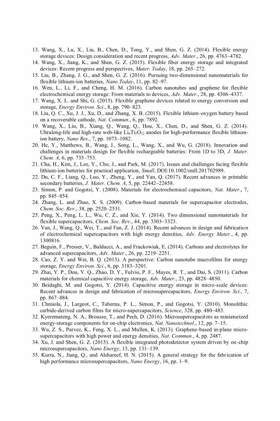
13. Wang, X., Lu, X., Liu, B., Chen, D., Tong, Y., and Shen, G. Z. (2014). Flexible energy storage devices: Design consideration and recent progress, Adv. Mater., 26, pp. 4763–4782.
14. Wang, X., Jiang, K., and Shen, G. Z. (2015). Flexible fiber energy storage and integrated devices: Recent progress and perspectives, Mater. Today, 18, pp. 265–272.
15. Liu, B., Zhang, J. G., and Shen, G. Z. (2016). Pursuing two-dimensional nanomaterials for flexible lithium-ion batteries, Nano Today, 11, pp. 82–97.
16. Wen, L., Li, F., and Cheng, H. M. (2016). Carbon nanotubes and graphene for flexible electrochemical energy storage: From materials to devices, Adv. Mater., 28, pp. 4306–4337.
17. Wang, X. L. and Shi, G. (2015). Flexible graphene devices related to energy conversion and storage, Energy Environ. Sci., 8, pp. 790–823.
18. Liu, Q. C., Xu, J. J., Xu, D., and Zhang, X. B. (2015). Flexible lithium-oxygen battery based on a recoverable cathode, Nat. Commun., 6, pp. 7892.
19. Wang, X., Liu, B., Xiang, Q., Wang, Q., Hou, X., Chen, D., and Shen, G. Z. (2014). Ultralong-life and high-rate web-like Li4Ti5O12 anodes for high-performance flexible lithium-ion battery, Nano Res., 7, pp. 1073–1082.
20. He, Y., Matthews, B., Wang, J., Song, L., Wang, X., and Wu, G. (2018). Innovation and challenges in materials design for flexible rechargeable batteries: From 1D to 3D, J. Mater. Chem. A, 6, pp. 735–753.
21. Cha, H., Kim, J., Lee, Y., Cho, J., and Park, M. (2017). Issues and challenges facing flexible lithium-ion batteries for practical application, Small, DOI:10.1002/smll.201702989.
22. Du, C. F., Liang, Q., Luo, Y., Zheng, Y., and Yan, Q. (2017). Recent advances in printable secondary batteries, J. Mater. Chem. A, 5, pp. 22442–22458.
23. Simon, P. and Gogotsi, Y. (2008). Materials for electrochemical capacitors, Nat. Mater., 7, pp. 845–854.
24. Zhang, L. and Zhao, X. S. (2009). Carbon-based materials for supercapacitor electrodes, Chem. Soc. Rev., 38, pp. 2520–2531.
25. Peng, X., Peng, L. L., Wu, C. Z., and Xie, Y. (2014). Two dimensional nanomaterials for flexible supercapacitors, Chem. Soc. Rev., 44, pp. 3303–3323.
26. Yan, J., Wang, Q., Wei, T., and Fan, Z. J. (2014). Recent advances in design and fabrication of electrochemical supercapacitors with high energy densities, Adv. Energy Mater., 4, pp. 1300816.
27. Beguin, F., Presser, V., Balducci, A., and Frackowiak, E. (2014). Carbons and electrolytes for advanced supercapacitors, Adv. Mater., 26, pp. 2219–2251.
28. Cao, Z. Y. and Wei, B. Q. (2013). A perspective: Carbon nanotube macrofilms for energy storage, Energy Environ. Sci., 6, pp. 3183–3201.
29. Zhai, Y. P., Dou, Y. Q., Zhao, D. Y., Fulvio, P. F., Mayes, R. T., and Dai, S. (2011). Carbon materials for chemical capacitive energy storage, Adv. Mater., 23, pp. 4828–4850.
30. Beidaghi, M. and Gogotsi, Y. (2014). Capacitive energy storage in micro-scale devices: Recent advances in design and fabrication of microsupercapacitors, Energy Environ. Sci., 7, pp. 867–884.
31. Chmiola, J., Largeot, C., Taberna, P. L., Simon, P., and Gogotsi, Y. (2010). Monolithic carbide-derived carbon films for micro-supercapacitors, Science, 328, pp. 480–483.
32. Kyeremateng, N. A., Brousse, T., and Pech, D. (2016). Microsupercapacitors as miniaturized energy-storage components for on-chip electronics, Nat. Nanotechnol., 12, pp. 7–15.
33. Wu, Z. S., Parvez, K., Feng, X. L., and Mullen, K. (2013). Graphene-based in-plane micro-supercapacitors with high power and energy densities, Nat. Commun., 4, pp. 2487.
34. Xu, J. and Shen, G. Z. (2015). A flexible integrated photodetector system driven by on -chip microsupercapacitors, Nano Energy, 13, pp. 131–139.
35. Kurra, N., Jiang, Q., and Alshareef, H. N. (2015). A general strategy for the fabr ication of high performance microsupercapacitors, Nano Energy, 16, pp. 1–9.
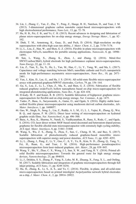
36. Lin, J., Zhang, C., Yan, Z., Zhu, Y., Peng, Z., Hauge, R. H., Natelson, D., and Tour, J. M. (2013). 3-dimensional graphene carbon nanotube carpet-based microsupercapacitors with high electrochemical performance, Nano Lett., 13, pp. 72–78.
37. Hu, H. B., Pei, Z. B., and Ye, C. H. (2015). Recent advances in designing and fabrication of planar micro-supercapacitors for on-chip energy storage, Energy Storage Mater., 1, pp. 82–102.
38. Dinh, T. M., Armstrong, K., Guay, D., and Pech, D. (2014). High-resolution on-chip supercapacitors with ultra-high scan rate ability, J. Mater. Chem. A., 2, pp. 7170–7174.
39. Li, L., Lou, Z., Han, W., and Shen, G. Z. (2016). Flexible in-plane microsupercapacitors with electrospun NiFe2O4 nanofibers for portable sensing applications, Nanoscale, 8, pp. 14986–14991.
40. Sun, L, Wang, X., Zhang, K., Zhou, J., and Zhang, Q. (2016). Metal-free SWNT/carbon/MnO2 hybrid electrode for high performance coplanar micro-supercapacitors, Nano Energy, 22, pp. 11–18.
41. Liu, Z., Tian, X., Xu, X., He, L., Yan, M., Han, C., Li, Y., Yang, W., and Ma, L. (2017). Capacitance and voltage matching between MnO2 nanoflake cathode and Fe2O3 nanoparticle anode for high-performance asymmetric micro-supercapacitors, Nano Res., 10, pp. 2471–2481.
42. Yun, J., Kim, D., Lee, G., and Ha, J. S. (2014). All-solid-state flexible micro-supercapacitor arrays with patterned graphene/MWNT electrodes, Carbon, 79, pp. 156–164.
43. Gu, S., Lou, Z., Li, L., Chen, Z., Ma, X., and Shen, G. Z. (2016). Fabrication of flexible reduced graphene oxide/Fe2O3 hollow nanospheres based on-chip micro-supercapacitors for integrated photodetecting applications, Nano Res., 9, pp. 424–434.
44. El-kady, M. F. and Kaner, R. B. (2013). Scalable fabrication of highpower graphene micro-supercapacitors for flexible and on-chip energy storage, Nat. Commun., 4, pp. 1475.
45. Yadav, P., Basu, A., Suryawanshi, A., Game, O., and Ogale, S. (2016). Highly stable laser -scribed flexible planar microsupercapacitor using mushroom derived carbon electrodes, Adv. Mater. Interfaces, 1, pp. 1600057.
46. Gao, W., Singh, N., Song, L., Liu, Z., Reddy, A. L. M., Ci, L. J., Vajtai, R., Zhang, Q., Wei, B. Q., and Ajayan, P. M. (2011). Direct laser writing of microsupercapacitors on hydrated graphite oxide films, Nat. Nanotechnol., 6, pp. 496–500.
47. Basu, A., Roy, K., Sharma, N., Nandi, S., Vaidhyanathan, R., Rane, S., Rode, C., and Ogale, S. (2016). CO2 laser direct written MOF-based metal-decorated and heteroatom-doped porous grapheme for flexible allsolid-state microsupercapacitor with extremely high cycling stability, ACS Appl. Mater. Interfaces, 8, pp. 31841–31848.
48. Wang, S., Wu, Z. S., Zheng, S., Zhou, F., Sun, C., Cheng, H. M., and Bao, X. (2017). Scalable fabrication of photochemically reduced graphene-based monolithic micro-supercapacitors with superior energy and power densities, ACS Nano, 11, pp. 4283–4291.
49. Li, L., Zhang, J., Peng, Z., Li, Y., Gao, C., Ji, Y., Ye, R., Kim, N. D., Zhong, Q., Yang, Y., Fei, H., Ruan, G., and Tour, J. M. (2016). High-performance pseudocapacitive microsupercapacitors form laser-induced graphene, Adv. Mater., 28, pp. 838–845.
50. Wang, Y., Shi, Y., Zhao, C. X., Wong, J. I., Sun, X. W., and Yang, H. Y. (2014). Printed all-solid flexible microsupercapacitors: Towards the general route for high energy storage devices, Nanotechnology, 25, pp. 094010.
51. Li, J., Delekta, S. S., Zhang, P., Yang, S., Lohe, M. R., Zhuang, X., Feng, X. L., and Ostling, M. (2017). Scalable fabrication and integration of graphene microsupercapacitors through full inkjet printing, ACS Nano, 11, pp. 8249–8256.
52. Hu, H., Zhang, K., Li, S., Ji, S., and Ye, C. (2014). Flexible, in -plane, and all-solid-state micro-supercapacitors based on printed interdigital Au/polyaniline network hybrid electrodes on a chip, J. Mater. Chem. A., 2, pp. 20916–20922.
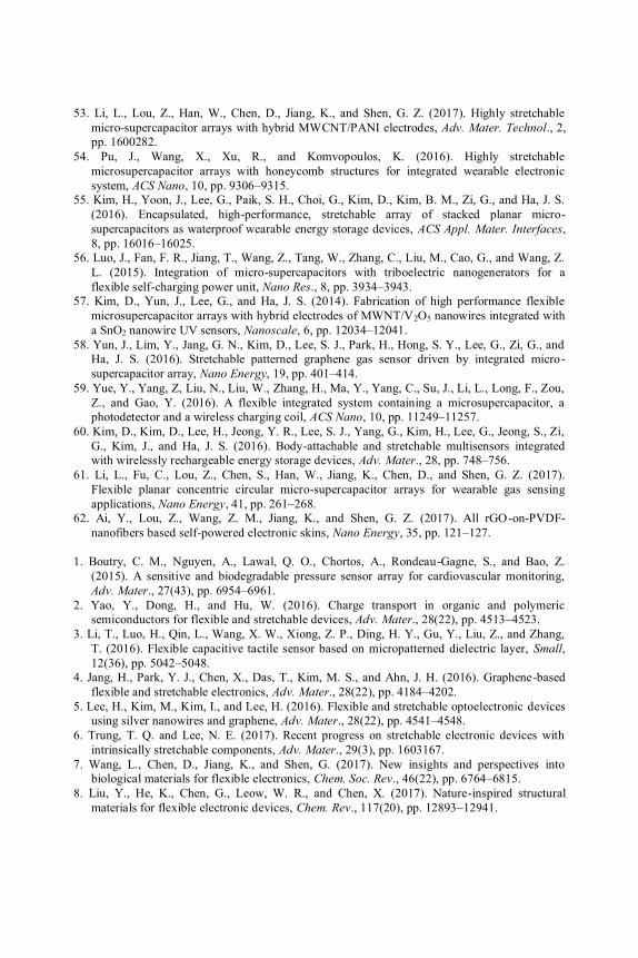
53. Li, L., Lou, Z., Han, W., Chen, D., Jiang, K., and Shen, G. Z. (2017). Highly stretchable micro-supercapacitor arrays with hybrid MWCNT/PANI electrodes, Adv. Mater. Technol., 2, pp. 1600282.
54. Pu, J., Wang, X., Xu, R., and Komvopoulos, K. (2016). Highly stretchable microsupercapacitor arrays with honeycomb structures for integrated wearable electronic system, ACS Nano, 10, pp. 9306–9315.
55. Kim, H., Yoon, J., Lee, G., Paik, S. H., Choi, G., Kim, D., Kim, B. M., Zi, G., and Ha, J. S. (2016). Encapsulated, high-performance, stretchable array of stacked planar micro-supercapacitors as waterproof wearable energy storage devices, ACS Appl. Mater. Interfaces, 8, pp. 16016–16025.
56. Luo, J., Fan, F. R., Jiang, T., Wang, Z., Tang, W., Zhang, C., Liu, M., Cao, G., and Wang, Z. L. (2015). Integration of micro-supercapacitors with triboelectric nanogenerators for a flexible self-charging power unit, Nano Res., 8, pp. 3934–3943.
57. Kim, D., Yun, J., Lee, G., and Ha, J. S. (2014). Fabrication of high performance flexible microsupercapacitor arrays with hybrid electrodes of MWNT/V2O5 nanowires integrated with a SnO2 nanowire UV sensors, Nanoscale, 6, pp. 12034–12041.
58. Yun, J., Lim, Y., Jang, G. N., Kim, D., Lee, S. J., Park, H., Hong, S. Y., Lee, G., Zi, G., and Ha, J. S. (2016). Stretchable patterned graphene gas sensor driven by integrated micro-supercapacitor array, Nano Energy, 19, pp. 401–414.
59. Yue, Y., Yang, Z, Liu, N., Liu, W., Zhang, H., Ma, Y., Yang, C., Su, J., Li, L., Long, F., Zou, Z., and Gao, Y. (2016). A flexible integrated system containing a microsupercapacitor, a photodetector and a wireless charging coil, ACS Nano, 10, pp. 11249–11257.
60. Kim, D., Kim, D., Lee, H., Jeong, Y. R., Lee, S. J., Yang, G., Kim, H., Lee, G., Jeong, S., Zi, G., Kim, J., and Ha, J. S. (2016). Body-attachable and stretchable multisensors integrated with wirelessly rechargeable energy storage devices, Adv. Mater., 28, pp. 748–756.
61. Li, L., Fu, C., Lou, Z., Chen, S., Han, W., Jiang, K., Chen, D., and Shen, G. Z. (2017). Flexible planar concentric circular micro-supercapacitor arrays for wearable gas sensing applications, Nano Energy, 41, pp. 261–268.
62. Ai, Y., Lou, Z., Wang, Z. M., Jiang, K., and Shen, G. Z. (2017). All rGO-on-PVDF-nanofibers based self-powered electronic skins, Nano Energy, 35, pp. 121–127.
1. Boutry, C. M., Nguyen, A., Lawal, Q. O., Chortos, A., Rondeau-Gagne, S., and Bao, Z.
(2015). A sensitive and biodegradable pressure sensor array for cardiovascular monitoring, Adv. Mater., 27(43), pp. 6954–6961.
2. Yao, Y., Dong, H., and Hu, W. (2016). Charge transport in organic and polymeric semiconductors for flexible and stretchable devices, Adv. Mater., 28(22), pp. 4513–4523.
3. Li, T., Luo, H., Qin, L., Wang, X. W., Xiong, Z. P., Ding, H. Y., Gu, Y., Liu, Z., and Zhang, T. (2016). Flexible capacitive tactile sensor based on micropatterned dielectric layer, Small, 12(36), pp. 5042–5048.
4. Jang, H., Park, Y. J., Chen, X., Das, T., Kim, M. S., and Ahn, J. H. (2016). Graphene-based flexible and stretchable electronics, Adv. Mater., 28(22), pp. 4184–4202.
5. Lee, H., Kim, M., Kim, I., and Lee, H. (2016). Flexible and stretchable optoelectronic devices using silver nanowires and graphene, Adv. Mater., 28(22), pp. 4541–4548.
6. Trung, T. Q. and Lee, N. E. (2017). Recent progress on stretchable electronic devices with intrinsically stretchable components, Adv. Mater., 29(3), pp. 1603167.
7. Wang, L., Chen, D., Jiang, K., and Shen, G. (2017). New insights and perspectives into biological materials for flexible electronics, Chem. Soc. Rev., 46(22), pp. 6764–6815.
8. Liu, Y., He, K., Chen, G., Leow, W. R., and Chen, X. (2017). Nature-inspired structural materials for flexible electronic devices, Chem. Rev., 117(20), pp. 12893–12941.
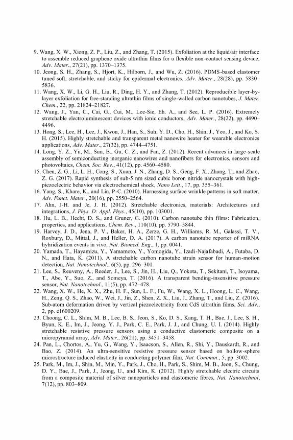
9. Wang, X. W., Xiong, Z. P., Liu, Z., and Zhang, T. (2015). Exfoliation at the liquid/air interface to assemble reduced graphene oxide ultrathin films for a flexible non-contact sensing device, Adv. Mater., 27(21), pp. 1370–1375.
10. Jeong, S. H., Zhang, S., Hjort, K., Hilborn, J., and Wu, Z. (2016). PDMS-based elastomer tuned soft, stretchable, and sticky for epidermal electronics, Adv. Mater., 28(28), pp. 5830–5836.
11. Wang, X. W., Li, G. H., Liu, R., Ding, H. Y., and Zhang, T. (2012). Reproducible layer-by-layer exfoliation for free-standing ultrathin films of single-walled carbon nanotubes, J. Mater. Chem., 22, pp. 21824–21827.
12. Wang, J., Yan, C., Cai, G., Cui, M., Lee-Sie, Eh. A., and See, L. P. (2016). Extremely stretchable electroluminescent devices with ionic conductors, Adv. Mater., 28(22), pp. 4490–4496.
13. Hong, S., Lee, H., Lee, J., Kwon, J., Han, S., Suh, Y. D., Cho, H., Shin, J., Yeo, J., and Ko, S. H. (2015). Highly stretchable and transparent metal nanowire heater for wearable electronics applications, Adv. Mater., 27(32), pp. 4744–4751.
14. Long, Y. Z., Yu, M., Sun, B., Gu, C. Z., and Fan, Z. (2012). Recent advances in large-scale assembly of semiconducting inorganic nanowires and nanofibers for electronics, sensors and photovoltaics, Chem. Soc. Rev., 41(12), pp. 4560–4580.
15. Chen, Z. G., Li, L. H., Cong, S., Xuan, J. N., Zhang, D. S., Geng, F. X., Zhang, T., and Zhao, Z. G. (2017). Rapid synthesis of sub-5 nm sized cubic boron nitride nanocrystals with high-piezoelectric behavior via electrochemical shock, Nano Lett., 17, pp. 355–361.
16. Yang, S., Khare, K., and Lin, P-C. (2010). Harnessing surface wrinkle patterns in soft matter, Adv. Funct. Mater., 20(16), pp. 2550–2564.
17. Ahn, J-H. and Je, J. H. (2012). Stretchable electronics, materials: Architectures and integrations, J. Phys. D: Appl. Phys., 45(10), pp. 103001.
18. Hu, L. B., Hecht, D. S., and Gruner, G. (2010). Carbon nanotube thin films: Fabrication, properties, and applications, Chem. Rev., 110(10), pp. 5790–5844.
19. Harvey, J. D., Jena, P. V., Baker, H. A., Zerze, G. H., Williams, R. M., Galassi, T. V., Roxbury, D., Mittal, J., and Heller, D. A. (2017). A carbon nanotube reporter of miRNA hybridization events in vivo, Nat. Biomed. Eng., 1, pp. 0041.
20. Yamada, T., Hayamizu, Y., Yamamoto, Y., Yomogida, Y., Izadi-Najafabadi, A., Futaba, D. N., and Hata, K. (2011). A stretchable carbon nanotube strain sensor for human-motion detection, Nat. Nanotechnol., 6(5), pp. 296–301.
21. Lee, S., Reuveny, A., Reeder, J., Lee, S., Jin, H., Liu, Q., Yokota, T., Sekitani, T., Isoyama, T., Abe, Y., Suo, Z., and Someya, T. (2016). A transparent bending-insensitive pressure sensor, Nat. Nanotechnol., 11(5), pp. 472–478.
22. Wang, X. W., He, X. X., Zhu, H. F., Sun, L. F., Fu, W., Wang, X. L., Hoong, L. C., Wang, H., Zeng, Q. S., Zhao, W., Wei, J., Jin, Z., Shen, Z. X., Liu, J., Zhang, T., and Liu, Z. (2016). Sub-atom deformation driven by vertical piezoelectricity from CdS ultrathin films, Sci. Adv., 2, pp. e1600209.
23. Choong, C. L., Shim, M. B., Lee, B. S., Jeon, S., Ko, D. S., Kang, T. H., Bae, J., Lee, S. H., Byun, K. E., Im, J., Jeong, Y. J., Park, C. E., Park, J. J., and Chung, U. I. (2014). Highly stretchable resistive pressure sensors using a conductive elastomeric composite on a micropyramid array, Adv. Mater., 26(21), pp. 3451–3458.
24. Pan, L., Chortos, A., Yu, G., Wang, Y., Isaacson, S., Allen, R., Shi, Y., Dauskardt, R., and Bao, Z. (2014). An ultra-sensitive resistive pressure sensor based on hollow-sphere microstructure induced elasticity in conducting polymer film, Nat. Commun., 5, pp. 3002.
25. Park, M., Im, J., Shin, M., Min, Y., Park, J., Cho, H., Park, S., Shim, M. B., Jeon, S., Chung, D. Y., Bae, J., Park, J., Jeong, U., and Kim, K. (2012). Highly stretchable electric circuits from a composite material of silver nanoparticles and elastomeric fibres, Nat. Nanotechnol, 7(12), pp. 803–809.
26. Yan, C., Wang, J., Kang, W., Cui, M., Wang, X., Foo, C. Y., Chee, K. J., and Lee, P. S. (2014). Highly stretchable piezoresistive graphene-nanocellulose nanopaper for strain sensors, Adv. Mater., 26(13), pp. 2022–2027.
27. Yao, S. and Zhu, Y. (2015). Nanomaterial-enabled stretchable conductors: Strategies, materials and devices, Adv. Mater., 27(9), pp. 1480–1511.
28. Ma, Y., Liu, N., Li, L., Hu, X., Zou, Z., Wang, J., Luo, S., and Gao, Y. (2017). A highly flexible and sensitive piezoresistive sensor based on MXene with greatly changed interlayer distances, Nat. Commun., 8, pp. 1207.
29. Zhang, J., Liu, X., Neri, G., and Pinna, N. (2016). Nanostructured materials for room-temperature gas sensors, Adv. Mater., 28(5), pp. 795–831.
30. Zhao, J., Li, N., Yu, H., Wei, Z., Liao, M., Chen, P., Wang, S., Shi, D., Sun, Q., and Zhang, G. (2017). Highly sensitive MoS2 humidity sensors array for noncontact sensation, Adv. Mater., 29(34), pp. 1702076.
31. Liu, X., Jin, X., and Ma, P. X. (2011). Nanofibrous hollow microspheres self-assembled from star-shaped polymers as injectable cell carriers for knee repair, Nat. Mater., 10(5), pp. 398–406.
32. Wang, H., Liu, H., Zhao, Q., Cheng, C., Hu, W., and Liu, Y. (2016). Three-component integrated ultrathin organic photosensors for plastic optoelectronics, Adv. Mater., 28(4), pp. 624–630.
33. Smith, T. T., Stephan, S. B., Moffett, H. F., McKnight, L. E., Ji, W., Reiman, D., Bonagofski, E., Wohlfahrt, M. E., Pillai, S. P. S., and Stephan, M. T. (2017). In situ programming of leukaemia-specific T cells using synthetic DNA nanocarriers, Nat. Nanotechnol., 12(8), pp. 813–820.
34. Kim, S. M., Jeon, H., Shin, S. H., Park, S. A., Jegal, J., Hwang, S. Y., Oh, D. X., and Park, J. (2018). Superior toughness and fast self-healing at room temperature engineered by transparent elastomers, Adv. Mater., 30(1), pp. 1705145.
35. Sun, Y., Lopez, J., Lee, H. W., Liu, N., Zheng, G., Wu, C. L., Sun, J., Liu, W., Chung, J. W., Bao, Z., and Cui, Y. (2016). A stretchable graphitic carbon/Si anode enabled by conformal coating of a self-healing elastic polymer, Adv. Mater., 28(12), pp. 2455–2461.
36. Liu, Z. F., Fang, S., Moura, F. A., Ding, J. N., Jiang, N., Di, J., Zhang, M., Lepro, X., Galvao, D. S., Haines, C. S., Yuan, N. Y., Yin, S. G., Lee, D. W., Wang, R., Wang, H. Y., Lv, W., Dong, C., Zhang, R. C., Chen, M. J., Yin, Q., Chong, Y. T., Zhang, R., Wang, X., Lima, M. D., Ovalle-Robles, R., Qian, D., Lu, H., and Baughman, R. H. (2015). Hierarchically buckled sheath-core fibers for superelastic electronics: Sensors and muscles, Science, 349(6246), pp. 400–404.
37. Wang, H., Liu, Z., Ding, J., Lepro, X., Fang, S., Jiang, N., Yuan, N., Wang, R., Yin, Q. L. W., Liu, Z., Zhang, M., Ovalle-Robles, R., Inoue, K., Yin, S., and Baughman, R. H. (2016). Downsized sheath-core conducting fibers for weavable superelastic wires, biosensors, supercapacitors, and strain sensors, Adv. Mater., 28(25), pp. 4998–5007.
38. Kim, A., Ahn, J., Hwang, H., Lee, E., and Moon, J. (2017). A pre-strain strategy for developing a highly stretchable and foldable onedimensional conductive cord based on an Ag nanowire network, Nanoscale, 9(18), pp. 5773–5778.
39. Wang, X., Qiu, Y., Cao, W., and Hu, P. (2015). Highly stretchable and conductive core-sheath chemical vapor deposition graphene fibers and their applications in safe strain sensors, Chem. Mater., 27(20), pp. 6969–6975.
40. Wei, Y., Chen, S., Yuan, X., Wang, P., and Liu, L. (2016). Multiscale wrinkled microstructures for piezoresistive fibers, Adv. Funct. Mater., 26(28), pp. 5078–5085.
41. Hua, C., Shang, Y., Li, X., Hu, X., Wang, Y., Wang, X., Zhang, Y., Li, X., Duan, H., and Cao, A. (2016). Helical graphene oxide fibers as a stretchable sensor and an electrocapillary sucker, Nanoscale, 8(20), pp. 10659–10668.
42. Cooper, C. B., Arutselvan, K., Liu, Y., Armstrong, D., Lin, Y., Khan, M. R., Genzer, J., and Dickey, M. D. (2017). Stretchable capacitive sensors of torsion, strain, and touch using double helix liquid metal fibers, Adv. Funct. Mater., 27(20), pp. 1605630.
43. Choi, C., Lee, J. M., Kim, S. H., Kim, S. J., Di, J., and Baughman, R. H. (2016). Twistable and stretchable sandwich structured fiber for wearable sensors and supercapacitors, Nano Lett., 16(12), pp. 7677–7684.
44. Zhong, J., Zhong, Q., Hu, Q., Wu, N., Li, W., Wang, B., Hu, B., and Zhou, J. (2015). Stretchable self-powered fiber-based strain sensor, Adv. Funct. Mater., 25(12), pp. 1798–1803.
45. Gong, W., Hou, C., Guo, Y., Zhou, J., Mu, J., Li, Y., Zhang, Q., and Wang, H. (2017). A wearable, fibroid, self-powered active kinematic sensor based on stretchable sheath-core structural triboelectric fibers, Nano Energy, 39, pp. 673–683.
46. Mannsfeld, S. C., Tee, B. C., Stoltenberg, R. M., Chen, C. V., Barman, S., Muir, B. V., Sokolov, A. N., Reese, C., and Bao, Z. (2010). Highly sensitive flexible pressure sensors with microstructured rubber dielectric layers, Nat. Mater., 9(10), pp. 859–864.
47. Jang, K. I., Li, K., Chung, H. U., Xu, S., Jung, H. N., Yang, Y., Kwak, J. W., Jung, H. H., Song, J., Yang, C., Wang, A., Liu, Z., Lee, J. Y., Kim, B. H., Kim, J. H., Lee, J., Yu, Y., Kim, B. J., Jang, H., Yu, K. J., Kim, J., Lee, J. W., Jeong, J. W., Song, Y. M., Huang, Y., Zhang, Y., and Rogers, J. A. (2017). Self-assembled three-dimensional network designs for soft electronics, Nat. Commun., 8, pp. 15894.
48. Duan, Y., Huang, Y., Yin, Z., Bu, N., and Dong, W. (2014). Non-wrinkled, highly stretchable piezoelectric devices by electrohydrodynamic direct-writing, Nanoscale, 6(6), pp. 3289–3295.
49. Kim, K. K., Hong, S., Cho, H. M., Lee, J., Suh, Y. D., Ham, J., and Ko, S. H. (2015). Highly sensitive and stretchable multidimensional strain sensor with prestrained anisotropic metal nanowire percolation networks, Nano Lett., 15(8), pp. 5240–5247.
50. Shin, U. H., Jeong, D. W., Kim, S. H., Lee, H. W., and Kim, J. M. (2014). Elastomer -infiltrated vertically aligned carbon nanotube film-based wavy-configured stretchable conductors, ACS Appl. Mater. Inter., 6(15), pp. 12909–12914.
51. Lee, W. K., Kang, J., Chen, K. S., Engel, C. J., Jung, W. B., Rhee, D., Hersam, M. C., and Odom, T. W. (2016). Multiscale, hierarchical patterning of graphene by conformal wrinkling, Nano Lett., 16(11), pp. 7121–7127.
52. Yin, L., Hwang, K.-C. Rogers, J. A., and Huang, Y. (2014). Experimental and theoretical studies of serpentine microstructures bonded to prestrained elastomers for stretchable electronics, Adv. Funct. Mater., 24(14), pp. 2028–2037.
53. Zhang, Y., Xu, S., Fu, H., Lee, J., Su, J., Hwang, K. C., Rogers, J. A., and Huang, Y. (2013). Buckling in serpentine microstructures and applications in elastomer-supported ultra-stretchable electronics with high areal coverage, Soft Matter., 9(33), pp. 8062–8070.
54. Ma, Y., Jang, K. I., Wang, L., Jung, H. N., Kwak, J. W., Xue, Y., Chen, H., Yang, Y., Shi, D., Feng, X. P., Rogers, J. A. P., and Huang, Y. P. (2016). Design of strain-limiting substrate materials for stretchable and flexible electronics, Adv. Funct. Mater., 26(29), pp. 5345–5351.
55. Bandodkar, A. J., Jeerapan, I., You, J. M., Nunez-Flores, R., and Wang, J. (2016). Highly stretchable fully-printed CNT-based electrochemical sensors and biofuel cells, combining intrinsic and design-induced stretchability, Nano Lett., 16(1), pp. 721–727.
56. Miyamoto, A., Lee, S., Cooray, N. F., Lee, S., Mori, M., Matsuhisa, N., Jin, H., Yoda, L., Yokota, T., Itoh, A., Sekino, M., Kawasaki, H., Ebihara, T., Amagai, M., and Someya, T. (2017). Inflammation-free, gas-permeable, lightweight, stretchable on-skin electronics with nanomeshes, Nat. Nanotechnol., 12(9), pp. 907–913.
57. Luo, N., Huang, Y., Liu, J., Chen, S. C., Wong, C. P., and Zhao, N. (2017). Hollow-structured graphene-silicone-composite-based piezoresistive sensors, decoupled property tuning and bending reliability, Adv. Mater., 29(40), pp. 1702675.
58. Wang, H., Lu, W., Di, J., Li, D., Zhang, X., Li, M., Zhang, Z., Zheng, L., and Li, Q. (2017). Ultra-lightweight and highly adaptive all-carbon elastic conductors with stable electrical resistance, Adv. Funct. Mater., 27(13), pp. 1606220.
59. Schutt, F., Signetti, S., Kruger, H., Roder, S., Smazna, D., Kaps, S., Gorb, S. N., Mishra, Y. K., Pugno, N. M., and Adelung, R. (2017). Hierarchical selfentangled carbon nanotube tube networks, Nat. Commun., 8, pp. 1215.
60. Qin, Y. Y., Peng, Q. Y., Ding, Y. J., Lin, Z. S., Wang, C. H., Li, Y., Li, J. J., Yuan, Y., He, X. D., and Li, Y. B. (2015). Lightweight, superelastic, and mechanically flexible graphene/polyimide nanocomposite foam for strain sensor application, ACS Nano, 9(9), pp. 8933–8941.
61. Tang, Y., Gong, S., Chen, Y., Yap, L. W., and Cheng, W. L. (2014). Manufacturable conducting rubber ambers and stretchable conductors from copper nanowire aerogel monoliths, ACS Nano, 8(6), pp. 5707–5714.
62. He, W. N., Li, G. Y., Zhang, S. Q., Wei, Y., Wang, J., Li, Q. W., and Zhang, X. T. (2015). Polypyrrole/silver coaxial nanowire aero-sponges for temperature-independent stress sensing and stress-triggered joule heating, ACS Nano, 9(4), pp. 4244–4251.
63. Xu, S., Yan, Z., Jang, K. I., Huang, W., Fu, H. R., Kim, J., Wei, Z., Flavin, M. McCracken, J., Wang, R., Badea, A., Liu, Y., Xiao, D. Q., Zhou, G. Y., Lee, J., Chung, H. U., Cheng, H. Y., Ren, W., Banks, A., Li, X. L., Paik, U., Nuzzo, R. G., Huang, Y. G., Zhang, Y. H., and Rogers, J. A. (2015). Assembly of micro/nanomaterials into complex, three-dimensional architectures by compressive buckling, Science, 347(6218), pp. 154–159.
64. Yan, Z., Han, M., Yang, Y., Nan, K., Luan, H., Luo, Y., Zhang, Y., Huang, Y., and Rogers, J. A. (2017). Deterministic assembly of 3D mesostructures in advanced materials via compressive buckling: A short review of recent progress, Extreme Mechanics Lett., 11, pp. 96–104.
65. Han, S. T., Peng, H., Sun, Q., Venkatesh, S., Chung, K. S., Lau, S. C., Zhou, Y., and Roy, V. A. L. (2017). An overview of the development of flexible sensors, Adv. Mater., 29(33), pp. 1700375.
66. Hua, Q., Sun, J., Liu, H., Bao, R., Yu, R., Zhai, J., Pan, C., and Wang, Z. L. (2018). Skin-inspired highly stretchable and conformable matrix networks for multifunctional sensing, Nat. Commun., 9, pp. 244.
67. Kang, D., Pikhitsa, P. V., Choi, Y. W., Lee, C., Shin, S. S., Piao, L., Park, B., Suh, K. Y., Kim, T. I., and Choi, M. (2014). Ultrasensitive mechanical crack-based sensor inspired by the spider sensory system, Nature, 516(7530), pp. 222–226.
68. Zeng, S., Zhang, D., Huang, W., Wang, Z., Freire, S. G., Yu, X., Smith, A. T., Huang, E. Y., Nguon, H., and Sun, L. (2016). Bio-inspired sensitive and reversible mechanochromisms via strain-dependent cracks and folds, Nat. Commun., 7, pp. 11802.
69. Yamada, T., Hayamizu, Y., Yamamoto, Y., Yomogida, Y., Izadi-Najafabadi, A., Futaba, D. N., and Hata, K. (2011). A stretchable carbon nanotube strain sensor for human-motion detection, Nat. Nanotechnol, 6(5), pp. 296–301.
70. Chortos, A., Koleilat, G. I., Pfattner, R., Kong, D., Lin, P., Nur, R., Lei, T., Wang, H., Liu, N., Lai, Y. C., Kim, M. G., Chung, J. W., Lee, S., and Bao, Z. (2016). Mechanically durable and highly stretchable transistors employing carbon nanotube semiconductor and electrodes, Adv. Mater., 28(22), pp. 4441–4448.
71. Di, J., Zhang, X., Yong, Z., Zhang, Y., Li, D., Li, R., and Li, Q. (2016). Carbon-nanotube fibers for wearable devices and smart textiles, Adv. Mater., 28(47), pp. 10529–10538.
72. Wang, C., Takei, K., Takahashi, T., and Javey, A. (2013). Carbon nanotube electronics-moving forward, Chem. Soc. Rev., 42(7), pp. 2592–2609.
73. Chen, K., Gao, W., Emaminejad, S., Kiriya, D., Ota, H., Nyein, H. Y., Takei, K., and Javey, A. (2016). Printed carbon nanotube electronics and sensor systems, Adv. Mater., 28(22), pp. 4397–4414.
74. Liu, Z., Xu, J., Chen, D., and Shen, G. (2015). Flexible electronics based on inorganic nanowires, Chem. Soc. Rev., 44(1), pp. 161–192.
75. Gong, S., Schwalb, W., Wang, Y., Chen, Y., Tang, Y., Si, J., Shirinzadeh, B., and Cheng, W. (2014). A wearable and highly sensitive pressure sensor with ultrathin gold nanowires, Nat. Commun., 5, pp. 3132.
76. Xiao, X., Yuan, L., Zhong, J., Ding, T., Liu, Y., Cai, Z., Rong, Y., Han, H., Zhou, J., and Wang, Z. L. (2011). High-strain sensors based on ZnO nanowire/polystyrene hybridized flexible films, Adv. Mater., 23(45), pp. 5440–5444.
77. Jang, H., Park, Y. J., Chen, X., Das, T., Kim, M. S., and Ahn, J. H. (2016). Graphene-based flexible and stretchable electronics, Adv. Mater., 28(22), pp. 4184–4202.
78. Ho, D. H., Sun, Q., Kim, S. Y., Han, J. T., Kim, D. H., and Cho, J. H. (2016). Stretchable and multimodal all-graphene electronic skin, Adv. Mater., 28(13), pp. 2601–2608.
79. Park, M., Park, Y. J., Chen, X., Park, Y. K., Kim, M. S., and Ahn, J. H. (2016). MoS 2-based tactile sensor for electronic skin applications, Adv. Mater., 28(13), pp. 2556–2562.
80. Lim, Y. R., Song, W., Han, J. K., Lee, Y. B., Kim, S. J., Myung, S., Lee, S. S., An, K. S., Choi, C. J., and Lim, J. (2016). Wafer-scale, homogeneous MoS2 layers on plastic substrates for flexible visible-light photodetectors, Adv. Mater., 28(25), pp. 5025–5030.
81. Ma, Y., Liu, N., Li, L., Hu, X., Zou, Z., Wang, J., Luo, S., and Gao, Y. (2017). A highly flexible and sensitive piezoresistive sensor based on MXene with greatly changed interlayer distances, Nat. Commun., 8, pp. 1207.
82. Hirsch, A., Michaud, H. O., Gerratt, A. P., de Mulatier, S., and Lacour, S. P. (2016). Intrinsically stretchable biphasic (solid-liquid) thin metal films, Adv. Mater., 28(22), pp. 4507–4512.
83. Zhong, Q., Zhong, J., Cheng, X., Yao, X., Wang, B., Li, W., Wu, N., Liu, K., Hu, B., and Zhou, J. (2015), Paper-based active tactile sensor array, Adv. Mater., 27(44), pp. 7130–7136.
84. Huynh, T. P., Sonar, P., and Haick, H. (2017). Advanced materials for use in soft self-healing devices, Adv. Mater., 29(19), pp. 1604973.
85. Kim, J., Rim, Y. S., Chen, H. J., Cao, H. H., Nakatsuka, N., Hinton, H. L., Zhao, C. Z., Andrews, A. M., Yang, Y., and Weiss, P. S. (2015). Fabrication of high-performance ultrathin In2O3 film field-effect transistors and biosensors using chemical lift-off lithography, ACS Nano, 9(4), pp. 4572–4582.
86. Lang, C., Fang, J., Shao, H., Ding, X., and Lin, T. (2016). High-sensitivity acoustic sensors from nanofibre webs, Nat. Commun., 7, pp. 11108.
87. Chen, Z., Wang, Z., Li, X., Lin, Y., Luo, N., Long, M., Zhao, N., and Xu, J. B. (2017). Flexible piezoelectric-induced pressure sensors for static measurements based on nanowires/graphene heterostructures, ACS Nano, 11(5), pp. 4507–4513.
88. Pu, X., Liu, M. M., Chen, X. Y., Sun, J. M., Du, C. H., Zhang, Y., Zhai, J. Y., Hu, W. G., and Wang, Z. L. (2017). Ultrastretchable transparent triboelectric nanogenerator as electronic skin for biomechanical energy harvesting and tactile sensing, Sci. Adv., 3(5), pp. e1700015.
89. Li, T., Zou, J., Xing, F., Zhang, M., Cao, X., Wang, N., and Wang, Z. L. (2017). From dual-mode triboelectric nanogenerator to smart tactile sensor: A multiplexing design, ACS Nano, 11(4), pp. 3950–3956.
90. Root, S. E., Savagatrup, S., Printz, A. D., Rodriquez, D., and Lipomi, D. J. (2017). Mechanical properties of organic semiconductors for stretchable, highly flexible, and mechanically robust electronics, Chem. Rev., 117(9), pp. 6467–6499.
91. Oh, J. Y., Kim, S., Baik, H. K., and Jeong, U. (2016). Conducting polymer dough for deformable electronics, Adv. Mater., 28(22), pp. 4455–4461.
92. Yao, Y., Dong, H., and Hu, W. (2016). Charge transport in organic and polymeric semiconductors for flexible and stretchable devices, Adv. Mater., 28(22), pp. 4513–4523.
93. Wang, L., Chen, D., Jiang, K., and Shen, G. (2017). New insights and perspectives into biological materials for flexible electronics, Chem. Soc. Rev., 46(22), pp. 6764–6815.
94. Montero de Espinosa, L., Meesorn, W., Moatsou, D., and Weder, C. (2017). Bioinspired polymer systems with stimuli-responsive mechanical properties, Chem. Rev., 117(20), pp. 12851–12892.
95. Wang, L., Jackman, J. A., Tan, E.-L., Park, J. H., Potroz, M. G., Hwang, E. T., and Cho, N. J. (2017). High-performance flexible electronic skin sensor incorporating natural microcapsule actuators, Nano Energy, 36, pp. 38–45.
96. Wang, Q., Jian, M. Q., Wang, C. Y., and Zhang, Y. Y. (2017). Carbonized silk nanofiber membrane for transparent and sensitive electronic skin, Adv. Funct. Mater., 27. pp. 1605657.
97. Zhu, B., Wang, H., Leow, W. R., Cai, Y., Loh, X. J., Han, M. Y., and Chen, X. (2016). Silk fibroin for flexible electronic devices, Adv. Mater., 28(22), pp. 4250–4265.
98. Irimia-Vladu, M. (2014). “Green” electronics, biodegradable and biocompatible materials and devices for sustainable future, Chem. Soc. Rev., 43(2), pp. 588–610.
99. Boutry, C. M., Nguyen, A., Lawal, Q. O., Chortos, A., Rondeau-Gagne, S., and Bao, Z. (2015). A sensitive and biodegradable pressure sensor array for cardiovascular monitoring, Adv. Mater., 27(43), pp. 6954–6961.
100. Curry, E. J., Ke, K., Chorsi, M. T., Wrobel, K. S., Miller III, A. N., Patel, A., Kim, I., Feng, J. L., Yue, L. X., Wu, Q., Kuo, C.-L., Lo, K. W.-H., Laurencin, C. T., Ilies, H., Purohit, P. K., and Nguyen, T. D. (2018). Biodegradable piezoelectric force sensor, Proc. Natl. Acad. Sci. USA, 115(5), pp. 909–914.
101. Benight, S. J., Wang, C., Tok, J. B. H., and Bao, Z. (2013). Stretchable and self-healing polymers and devices for electronic skin, Prog. Polym. Sci., 38(12), pp. 1961–1977.
102. Tee, B. C., Wang, C., Allen, R., and Bao, Z. (2012). An electrically and mechanically self -healing composite with pressure-and flexionsensitive properties for electronic skin applications, Nat. Nanotechnol., 7(12), pp. 825–832.
103. Hou, C., Huang, T., Wang, H., Yu, H., Zhang, Q., and Li, Y. (2013). A strong and stretchable self-healing film with self-activated pressure sensitivity for potential artificial skin applications, Sci. Rep., 3, pp. 3138.
104. Phadke, A., Zhang, C., Arman, B., Hsu, C. C., Mashelkar, R. A., Lele, A. K., Tauber, M. J., Arya, G., and Varghese, S. (2012). Rapid self-healing hydrogels, Proc. Natl. Acad. Sci. USA, 109(12), pp. 4383–4388.
105. Lin, S., Yuk, H., Zhang, T., Parada, G. A., Koo, H., Yu, C., and Zhao, X. (2016). Stretchable hydrogel electronics and devices, Adv. Mater., 28(22), pp. 4497–4505.
106. Keplinger, C., Sun, J. Y., Foo, C. C., Rothemund, P., Whitesides, G. M., and Suo, Z. G. (2013). Stretchable, transparent, ionic conductors, Science, 341(6149), pp. 984–987.
107. Wang, X. W., Gu, Y., Xiong, Z. P., Cui, Z., and Zhang, T. (2013). Silk-molded flexible, ultrasensitive, and highly stable electronic skin for monitoring human physiological signals, Adv. Mater., 26, pp. 1336–1342.
108. Gerratt, A. P., Michaud, H. O., and Lacour, S. P. (2015). Elastomeric electronic skin for prosthetic tactile sensation, Adv. Funct. Mater., 25(15), pp. 2287–2295.
109. Liu, W. H., Zhang, C., Lin, H. S., Qu, W. M., Li, X., and Wang, X. L. (2017). Texture and sliding motion sensation with a triboelectric-nanogenerator transducer, Sensors Actuators A, 256, pp. 89–94.
110. Chun, S., Hong, A., Choi, Y., Ha, C., and Park, W. (2016). A tactile sensor using a conductive graphene-sponge composite, Nanoscale, 8, pp. 9185–9192.
111. Park, J., Kim, M., Lee, Y., Lee, H. S., and Ko, H. (2015). Fingertip skin -inspired microstructured ferroelectric skins discriminate static/dynamic pressure and temperature stimuli, Sci. Adv., 1, pp. 1500661.
112. Tao, L. Q., Zhang, K. N., Tian, H., Liu, Y., Wang, D. Y., Chen, Y. Q., Yang, Y., and Ren, T. L. (2017). Graphene-paper pressure sensor for detecting human motions, ACS Nano, 11(9), pp. 8790–8795.
113. Zhao, J. J., Han, S., Yang, Y., Fu, R. P., Ming, Y., Lu, C., Liu, H., Gu, H. W., and Chen, W. (2017). Passive and space-discriminative ionic sensors based on durable nanocomposite electrodes toward sign language recognition, ACS Nano, 11, pp. 8590–8599.
114. Li, L. L., Bai, Y. Y., Li, L. L., Wang, S. Q., and Zhang, T. (2017). A superhydrophobic smart coating for flexible and wearable sensing electronics, Adv. Mater., 29, pp. 1702517
115. Khan, Y., Ostfeld, A. E., Lochner, C. M., Pierre, A., and Arias, A. C. (2016). Monitoring of vital signs with flexible and wearable medical devices, Adv. Mater., 28(22), pp. 4373–4395.
116. Schwartz, G., Tee, B. C.-K., Mei, J. G., Appleton, A. L., Kim, D. H., Wang, H. L., and Bao, Z. N. (2013). Flexible polymer transistors with high pressure sensitivity for application in electronic skin and health monitoring, Nat. Commun., 4, pp. 1859.
117. Choi, S., Lee, H., Ghaffari, R., Hyeon, T., and Kim, D. H. (2016). Recent advances in flexible and stretchable bio-electronic devices integrated with nanomaterials, Adv. Mater., 28(22), pp. 4203–4218.
118. Pang, C., Koo, J. H., Nguyen, A., Caves, J. M., Kim, M. G., Chortos, A., Kim, K., Wang, P. J., Tok, J. B.-H., and Bao, Z. (2015). Highly skin-conformal microhairy sensor for pulse signal amplification, Adv. Mater., 27, pp. 634–640.
119. Kim, J., Kim, M., Lee, M. S., Kim, K., Ji, S., Kim, Y. T., Park, J., Na, K., Bae, K. H., Kyun, K. H., Bien, F., Young, L. C., and Park, J. U. (2017). Wearable smart sensor systems integrated on soft contact lenses for wireless ocular diagnostics, Nat. Commun., 8, pp. 14997.
120. Song, Y. M., Xie, Y. Z., Malyarchuk, V., Xiao, J. L., Jung, I., Choi, K.-J., Liu, Z. J., Park, H., Lu, C. F., Kim, R.-H., Li, R., Crozier, K. B., Huang, Y. G., and Rogers, J. A. (2013). Digital cameras with designs inspired by the arthropod eye, Nature, 497, pp. 95–99.
121. Henning, A., Swaminathan, N., Godkin, A., Shalev, G., Amit, I., and Rosenwaks, Y. (2015). Tunable diameter electrostatically formed nanowire for high sensitivity gas sensing, Nano Res., 8(7), pp. 2206–2215.
122. Gu, Y., Wang, X. W., Gu, W., Wu, Y. J., Li, T., and Zhang, T. (2017). Flexible electronic eardrum, Nano Res., 10(8), pp. 2683–2691.
123. Trung, T. Q. and Lee, N. E. (2016). Flexible and stretchable physical sensor integrated platforms for wearable human-activity monitoring and personal healthcare, Adv. Mater., 28(22), pp. 4338–4372.
124. Li, T., Li, L. H., Sun, H. W., Xu, Y., Wang, X. W., Luo, H., Liu, Z., and Zhang, T. (2017). Porous ionic membrane based flexible humidity sensor and its multifunctional applications, Adv. Sci., 4, pp.1600404.
125. Kim, J., Campbell, A. S., and Wang, J. (2018). Wearable non-invasive epidermal glucose sensors: A review, Talanta, 177, pp. 163–170.
126. Wang, S. Q., Wu, Y. J., Gu, Y., Li, T., Luo, H., Li, L. H., Bai, Y. Y., Li, L.L. Liu, L., Cao, Y. D., Ding, H. Y., and Zhang, T. (2017). Wearable sweatband sensor platform based on gold nanodendrite array as efficient solid contact of ion-selective electrode, Anal. Chem., 89, pp. 10224–10231.
127. Gao, W., Emaminejad, S., Nyein, H. Y. Y., Challa, S., Chen, K., Peck, A., Fahad, H. M., Ota, H., Shiraki, H., Kiriya, D., Lien, D.-H., Brooks, G. A., Davis, R. W., and Javey, A. (2016). Fully integrated wearable sensor arrays for multiplexed in situ perspiration analysis, Nature, 529, pp. 509–514.
1. Wang, X. and Liu, J. (2016). Recent advancements in liquid metal flexible printed electronics:
Properties, technologies, and applications, Micromachines, 7, 206. 2. Yi, L., Jin, C., Wang, L., and Liu, J. (2014). Liquid-solid phase transition alloy as reversible
and rapid molding bone cement, Biomaterials, 35, pp. 9789–9801. 3. Yi, L. and Liu, J. (2017). Liquid metal biomaterials: A newly emerging area to tackle modern
biomedical challenges, International Materials Reviews, 62, pp. 415–440.
4. Wang, Q., Yu, Y., Pan, K., and Liu, J. (2014). Liquid metal angiography for mega contrast X-ray visualization of vascular network in reconstructing in-vitro organ anatomy, IEEE Trans. Biomed. Eng., 61, pp. 2161–2166.
5. Jung, Y. H., Seo, J.-H., and Zhang, H. (2017). Radio-frequency flexible and stretchable electronics: The need, challenges and opportunities, Micro-Nanotechnology Sensors, Systems, and Applications IX, 10194: 101941C.
6. Shin, G., Gomez, A. M., Al-Hasani, R., Jeong, Y. R., Kim, J., Xie, Z., Banks, A., Lee, S., Han, S. Y., Yoo, C. J., and Rogers, J. A. (2017). Flexible near-field wireless optoelectronics as subdermal implants for broad applications in optogenetics, Neuron, 93, pp. 509–521.
7. Xu, R., Lee, J. W., Pan, T., Ma, S., Wang, J., Han, H., Ma, Y., Rogers, J. A., and Huang, Y. (2017). Designing thin, ultrastretchable electronics with stacked circuits and elastomeric encapsulation materials, Adv. Funct. Mater., 27, 1604545.
8. Kim, B. H., Kim, J.-H., Persano, L., Hwang, S.-W., Lee, S., and Rogers, J. A. (2017). Dry transient electronic systems by use of materials that sublime, Adv. Funct. Mater., 27, 1606008.
9. Hirsch, A., Michaud, H. O., Gerratt, A. P., Mulatier, S., and Lacour, S. P. (2016). Intrinsically stretchable biphasic (solid-liquid) thin metal films, Adv. Mater., 28, pp. 4507–4512.
10. Gao, Y., Li, H., and Liu, J. (2013). Directly writing resistor, inductor and capacitor to composite functional circuits: A super-simple way for alternative electronics, PLoS One, 8, e69761.
11. Jeong, S. H., Hjort, K., and Wu, Z. (2014). Tape transfer printing of a liquid metal alloy for stretchable RF electronics, Sensors, 14, pp. 16311–16321.
12. Jin, C., Zhang, J., Li, X., Yang, X., and Liu, J. (2013). Injectable 3 -D fabrication of medical electronics at the target biological tissues, Sci. Rep., 3, 3442.
13. Li, H. and Liu, J. (2011). Revolutionizing heat transport enhancement with liquid metals: Proposal of a new industry of water-free heat exchangers, Front. Energy, 5, pp. 20–42.
14. Jeong, S. H., Hjort, K., and Wu, Z. (2015). Tape transfer atomization patterning of liquid alloys for microfluidic stretchable wireless power transfer, Sci. Rep., 5, 8419.
15. Cheng, S. and Wu, Z. (2012). Microfluidic electronics, Lab Chip, 12, pp. 2782–2791. 16. Cheng, S. and Wu, Z. (2011). A microfluidic, reversibly stretchable, large-area wireless strain
sensor, Adv. Funct. Mater., 21, pp. 2282–2290. 17. Jeong, S. H., Hagman, A., Hjort, K., Jobs, M., Sundqvist, J., and Wu, Z. (2012). Liquid alloy
printing of microfluidic stretchable electronics, Lab Chip, 12, pp. 4657–4664. 18. Yu, Y., Zhang, J., and Liu, J. (2013). Biomedical implementation of liquid metal ink as
drawable ECG electrode and skin circuit, PLoS One, 8, e58771. 19. Wang, Q., Yu, Y., Yang, J., and Liu, J. (2015). Fast fabrication of flexible functional circuits
based on liquid metal dual-trans printing, Adv. Mater., 27, pp. 7109–7116. 20. Matsuzaki, R. and Tabayashi, K. (2015). Highly stretchable, global, and distributed local
strain sensing line using GalnSn electrodes for wearable electronics, Adv. Funct. Mater., 25, pp. 3806–3813.
21. Krupenkin, T. and Taylor, J. A. (2011). Reverse electrowetting as a new approach to high-power energy harvesting, Nat. Commun., 2, 448.
22. Sheng, L., Zhang, J., and Liu, J. (2014). Diverse transformations of liquid metals between different morphologies, Adv. Mater., 26, pp. 6036–6042.
23. Zhang, J., Yao, Y., Sheng, L., and Liu, J. (2015). Self-fueled biomimetic liquid metal mollusk, Adv. Mater., 27, pp. 2648–2655.
24. Khoshmanesh, K., Tang, S., Zhu, J. Y., Schaefer, S., Mitchell, A., Kalantar-zadeh, K., and Dickey, M. D. (2017). Liquid metal enabled microfluidics, Lab Chip, 17, pp. 974–993.
25. Tabatabai, A., Fassler, A., Usiak, C., and Majidi, C. (2013). Liquid-phase gallium-indium alloy electronics with microcontact printing, Langmuir, 29, pp. 6194–6200.
26. Kramer, R. K., Majidi, C., and Wood, R. J. (2013). Masked deposition of gallium-indium alloys for liquid-embedded elastomer conductors, Adv. Funct. Mater, 23, pp. 5292–5296.
27. Zheng, Y., Zhang, Q., and Liu, J. (2013). Pervasive liquid metal based direct writing electronics with roller-ball pen, AIP Adv., 3, pp. 6459–6463.
28. Li, G., Wu, X., and Lee, D.-W. (2016). A galinstan-based inkjet printing system for highly stretchable electronics with self-healing capability, Lab Chip, 16, pp. 1366–1373.
29. Jin, S. W., Park, J., Hong, S. Y., Park, H., Jeong, Y. R., Park, J., Lee, S. -S., and Ha, J. S. (2015). Stretchable loudspeaker using liquid metal microchannel, Sci. Rep., 5, 11695.
30. Liu, F., Yu, Y., Yi, L., and Liu, J. (2016). Liquid metal as reconnection agent for peripheral nerve injury, Sci. Bull., 61, pp. 939–947.
31. Deng, Y. and Liu, J. (2014). Flexible mechanical joint as human exoskeleton using low-melting-point alloy, J. Med. Devices, 8, 044506.
32. Zhang, Q., Zheng, Y., and Liu, J. (2012). Direct writing of electronics based on alloy and metal ink (DREAM Ink): A newly emerging area and its impact on energy, environment and health sciences, Front. Energy, 6, pp. 311–340.
33. Dickey, M. D. (2017). Stretchable and soft electronics using liquid metals, Adv. Mater., 1606425.
34. Wang, L. and Liu, J. (2014). Research advancement of liquid metal printed electronics ink, Imaging Sci. Photochem., 32, pp. 382–392.
35. Hammock, M. L., Chortos, A., Tee, B. C. K., Tok, J. B. H., and Bao, Z. (2013). 25th anniversary article: The evolution of electronic skin (e-skin): A brief history, design considerations, and recent progress, Adv. Mater., 25, pp. 5997–6038.
36. So, J.-H., Koo, H.-J., Dickey, M. D., and Velev, O. D. (2012). Ionic current rectification in soft-matter diodes with liquid-metal electrodes, Adv. Funct. Mater., 22, pp. 625–631.
37. Guo, C., Yu, Y., and Liu, J. (2014). Rapidly patterning conductive components on skin substrates as physiological testing devices via liquid metal spraying and pre-designed mask, J. Mater. Chem. B, 2, pp. 5739–5745.
38. Boley, J. W., White, E. L., Chiu, G. T. C., and Kramer, R. K. (2014). Direct writing of gallium-indium alloy for stretchable electronics, Adv. Funct. Mater., 24, pp. 3501–3507.
39. Gozen, B. A., Tabatabai, A., Ozdoganlar, O. B., and Majidi, C. (2014). High-density soft-matter electronics with micron-scale line width, Adv. Mater., 26, pp. 5211–5216.
40. Zheng, Y., He, Z., Gao, Y., and Liu, J. (2013). Direct desktop printed-circuits-on-paper flexible electronics, Sci. Rep., 3, 1786.
41. Wang, L. and Liu, J. (2015). Pressured liquid metal screen printing for rapid manufacture of high-resolution electronic patterns, RSC Adv., 5, pp. 57686–57691.
42. Kubo, M., Li, X., Kim, C., Hashimoto, M., Wiley, B. J., Ham, D., and Whitesides, G. M. (2010). Stretchable microfluidic radiofrequency antennas, Adv. Mater., 22, pp. 2749–2752.
43. Zhu, S., So, J.-H., Mays, R., Desai, S., Barnes, W. R., Pourdeyhimi, B., and Dickey, M. D. (2013). Ultrastretchable fiber with metallic conductivity using a liquid metal alloy core, Adv. Funct. Mater., 23, pp. 2308–2314.
44. Schrader, M. E. (1995). Young-dupre revisited, Langmuir, 11, pp. 3585–3589. 45. Liu, Y., Gao, M., Mei, S., Han, Y., and Liu, J. (2013). Ultra-compliant liquid metal electrodes
with in-plane self-healing capability for dielectric elastomer actuators, Appl. Phys. Lett., 103, 064101.
46. Kim, D., Thissen, P., Viner, G., Lee, D.-W., Choi, W., Chabal, Y. J., and Lee, J.-B. (2013). Recovery of nonwetting characteristics by surface modification of gallium-based liquid metal droplets using hydrochloric acid vapor, ACS Appl. Mater. Interfaces, 5, pp. 179–185.
47. Doudrick, K., Liu, S., Mutunga, E. M., Klein, K. L., Damle, V., Varanasi, K. K., and Rykaczewski, K. (2014). Different shades of oxide: From nanoscale wetting mechanisms to contact printing of gallium-based liquid metals, Langmuir, 30, pp. 6867–6877.
48. Gao, Y., Li, H., and Liu, J. (2012). Direct writing of flexible electronics through room temperature liquid metal ink, PLoS ONE, 7, e45485.
49. Zhang, Q., Gao, Y., and Liu, J. (2014). Atomized spraying of liquid metal droplets on desired substrate surfaces as a generalized way for ubiquitous printed electronics, Appl. Phys. A, 116, pp. 1091–1097.
50. Li, H., Yang, Y., and Liu, J. (2012). Printable tiny thermocouple by liquid metal gallium and its matching metal, Appl. Phys. Lett., 101, 073511.
51. Liu, J. and Li, H. (2011). A liquid metal based printed circuit board and its fabrication method. China Patent 201110140156, 14 October 2011.
52. Wang, L. and Liu, J. (2014). Printing low-melting-point alloy ink to directly make a solidified circuit or functional device with a heating pen, Proc. R. Soc. A: Math. Phys. Eng. Sci., 470, 0609.
53. Yang, J. and Liu, J. (2014). Direct printing and assembly of FM radio at the user end via liquid metal printer, Circ. World, 40, pp. 134–140.
54. Sheng, L., Teo, S., and Liu, J. (2016). Liquid-metal-painted stretchable capacitor sensors for wearable healthcare electronics, J. Med. Biol. Eng., 36, pp. 265–272.
55. Tang, J., Zhao, X., Li, J., Guo, R., Zhou, Y., and Liu, J. (2017). Gallium-based liquid metal amalgams: Transitional-state metallic mixtures (TransM2ixes) with enhanced and tunable electrical, thermal, and mechanical properties, ACS Appl. Mater. Interfaces, 9, pp. 35977–35987.
56. Boley, J. W., White, E. L., and Kramer, R. K. (2015). Mechanically sintered gallium-indium nanoparticles, Adv. Mater., 27, pp. 2355–2360.
57. Zheng, Y., He, Z.-Z., Yang, J., and Liu, J. (2014). Personal electronics printing via tapping mode composite liquid metal ink delivery and adhesion mechanism, Sci. Rep., 4, pp. 101–104.
58. Je, J. and Lee, J. (2014). Design, fabrication, and characterization of liquid metal microheaters, J. Microelectromech. Syst., 23, pp. 1156–1163.
59. Lu, T., Markvicka, E. J., Jin, Y., and Majidi, C. (2017). Soft -matter printed circuit board with UV laser micropatterning, ACS Appl. Mater. Interfaces, 9, pp. 22055–22062.
60. Tabatabai, A., Fassler, A., Usiak, C., and Majidi, C. (2013). Liquid-phase gallium-indium alloy electronics with microcontact printing, Langmuir, 29, pp. 6194–6200.
61. Jeong, J.-A. and Kim, H.-K. (2010). Characteristics of inkjet-printed nano indium tin oxide particles for transparent conducting electrodes, Curr. Appl. Phys., 10, e105–e108.
62. Kim, D., Yoo, J. H., Lee, Y., Choi, W., Yoo, K., and Lee, J. B. J. (2014). Gallium-based liquid metal inkjet printing, Proc. 27th IEEE Inter. Conf. MEMS, pp. 967–970 (in USA).
63. Sia, S. K. and Whitesides, G. M. (2003). Microfluidic devices fabricated in poly(dimethylsiloxane) for biological studies, Electrophoresis, 24, pp. 3563–3576.
64. Roberts, M. A., Rossier, J. S., Bercier, P., and Girault, H. (1997). UV laser machined polymer substrates for the development of microdiagnostic systems, Anal. Chem., 69, pp. 2035–2042.
65. Wang, L. and Liu, J. (2014). Liquid phase 3D printing for quickly manufacturing conductive metal objects with low melting point alloy ink, Sci. China Technol. Sci., 57, pp. 1721–1728.
66. Yu, Y., Liu, F., Zhang, R., and Liu, J. (2017). Suspension 3D printing of LM into self -healing hydrogel, Adv. Mater. Technol., 2, 1700173.
67. Li, J., Guo, C., Wang, Z., Gao, K., Shi, X., and Liu, J. (2016). Electrical stimulation towards melanoma therapy via liquid metal printed electronics on skin, Clin. Trans. Med., 5, 21.
68. Fassler, A. and Majidi, C. (2013). 3D structures of liquid-phase gain alloy embedded in PDMS with freeze casting, Lab Chip, 13, pp. 4442–4450.
69. Liu, R., Yang, X., Jin, C., Fu, J., Chen, W., and Liu, J. (2013). Development of three-dimension microelectrode array for bioelectric measurement using the liquid metal-micromolding technique, Appl. Phys. Lett., 103, 193701.
70. Jeong, Y. R., Kim, J., Xie, Z., Xue, Y., Won, S. M., Lee, G., Jin, S. W., Hong, S. Y., Feng, X., Huang, Y., Rogers, J. A., and Ha, J. S. (2017). A skin-attachable, stretchable integrated system based on liquid GaInSn for wireless human motion monitoring with multi-site sensing capabilities, NPG Asia Mater., 9, e443.
71. Zhao, Z., Lin, J., Zhang, J., Yu, Y., Yuan, B., Fan, C.-C., Wang, L., and Liu, J. (2018). Liquid metal enabled flexible electronic system for eye movement tracking, IEEE Sens. J., 18, pp. 2592–2598.
72. Sun, X., Yuan, B., Rao, W., and Liu, J. (2017). Amorphous liquid metal electrodes enabled conformable electrochemical therapy of tumors, Biomaterials, 146, pp. 156–167.
73. Kramer, R. K., Majidi, C., Sahai, R., and Wood, R. J. (2011). Soft curvature sensors for joint angle proprioception, 2011 IEEERSJ Int. Conf Intelligent Robots and Systems (IROS), pp. 1919–1926 (in USA).
74. Menguc, Y., Park, Y.-L., Pei, H., Vogt, D., Aubin, P. M., Winchell, E., Fluke, L., Stirling, L., Wood, R. J., and Walsh, C. J. (2014). Wearable soft sensing suit for human gait measurement, Int. J. Robot. Res., 33, pp. 1748–1764.
75. Guo, R., Sheng, L., Guo, Y., and Liu, J. (2017). Liquid metal spiral coil enabled soft electromagnetic actuator, Sci. China Tech. Sci., 60, pp. 1–6.
76. Wu, Z., Hjort, K., and Jeong, S. H. (2015). Microfluidic stretchable radio-frequency devices, P. IEEE, 103, pp. 1211–1225.
77. Guo, R. and Liu, J. (2017). Implantable liquid metal-based flexible neural microelectrode array and its application in recovering animal locomotion functions, J. Micromech. Microeng., 27, 104002.
78. Wang, X., Zhang, Y., Guo, R., Wang, H., Yuan, B., and Liu, J. (2018). Conformable liquid metal printed epidermal electronics for smart physiological monitoring and simulation treatment, J. Micromech. Microeng., 28, 034003.
79. Wang, L. and Liu, J. (2015). Ink spraying based liquid metal printed electronics for directly making smart home appliances, ECS J. Solid State Sci. Technol., 4, pp. 3057–3062.
80. Fassler, A. and Majidi, C. (2013). Soft-matter capacitors and inductors for hyperelastic strain sensing and stretchable electronics, Smart Mater. Struct., 22, pp. 955–966.
81. Wang, X., Guo, R., Yuan, B., Yao, Y., Wang, F., and Liu, J. (2018). Ni-doped liquid metal printed highly stretchable and conformable strain sensor for multifunctional human-motion monitoring, 40th Annual International Conference of the IEEE Engineering in Medicine and Biology Society, Hawaii, USA.
82. Guo, R., Tang, J., Dong, S., Lin, J., Wang, H., Liu, J., and Rao, W. (2018). One-step liquid metal transfer printing: toward fabrication of flexible electronics on wide range of substrates, Adv. Mater. Technol., 1800265.
83. Wang, X., Ren, Y., and Liu, J. (2018). Liquid metal enabled electrobiology: a new frontier to tackle disease challenges, Micromachines, 9, p. 360.
84. Guo, R., Wang, H., Duan, M., Yu, W., Wang, X., and Liu, J. (2018). Stretchable electronics based on Nano-Fe GaIn amalgams for smart flexible pneumatic actuator, Smart Mater. Struct., 27, 085022 (10 pp).
85. Jeong, S. H., Hjort, K., and Wu, Z. (2015). Tape transfer atomization patterning of liquid alloys for microfluidic stretchable wireless power transfer, Sci. Rep., 5, 8419.
86. Guo, R., Wang, X., Chang, H., Yu, W., Liang, S., Rao, W., and Liu, J. (2018). Ni-GaIn amalgams enabled rapid and customizable fabrication of wearable and wireless healthcare electronics, Adv. Eng. Mater., 201800054.
1. Suo, Z. (2012). Mechanics of stretchable electronics and soft machines, MRS Bull., 37, pp.
218–225. 2. Kim, D. H., Kim, Y. S., Wu, J., Liu, Z., Song, J., Kim, H. S., Huang, Y. Y., Hwang, K. C., and
Rogers, J. A. (2009). Flexible electronics: Ultrathin silicon circuits with strain-isolation layers
and mesh layouts for high-performance electronics on fabric, vinyl, leather, and paper, Adv. Mater., 21, pp. 3703–3707.
3. Su, Y. and Rogers, J. A. (2007). Inorganic semiconductors for flexible electronics, Adv. Mater., 19(15), pp. 1897–1916.
4. Minemawari, H., Yamada, T., Matsui, H., Tsutsumi, J., Haas, S., Chiba, R., Kumai, R., and Hasegawa, T. (2011). Inkjet printing of single-crystal films, Nature, 475(7356), pp. 364–367.
5. Cui, Z., Qiu, S., Zhou, C., Chen, Z., Lin, J., Zhao, J., Ma, C., and Su, W. (2016). Printed Electronics: Materials, Technologies and Applications (Wiley).
6. Gao, M., Li, L., and Song, Y. (2017). Inkjet printing wearable electronic devices, J. Mater. Chem. C, 5, pp. 2971–2993.
7. Kamyshny, A. and Magdassi, S. (2014). Conductive nanomaterials for printed electronics, Small, 10(17), pp. 3515–3535.
8. Magliulo, M., Mulla, M. Y., Singh, M., Macchia, E., Tiwari, A., and Torsi, L., and Manoli, K. (2016). Printable and flexible electronics: From TFTs to bioelectronic devices, J. Mater. Chem. C, 3, pp. 12347–12363.
9. Wu, W. (2017). Inorganic nanomaterials for printed electronics: A review, Nanoscale, 9, pp. 7342–7372.
10. Hoeng, F., Denneulin, A., and Bras, J. (2016). Use of nanocellulose in printed electronics: A review, Nanoscale, 8, pp. 13131–13154.
11. Khan, S. and Lorenzelli, L. (2017). Recent advances of conductive nanocomposites in printed and flexible electronics, Smart Mater. Struct., 26, pp. 083001.
12. Chen, K., Gao, W., Emaminejad, S., Kiriya, D., Ota, H., Nyein, H. Y. Y., Takei, K., and Javey, A. (2016). Carbon nanotubes: Printed carbon nanotube electronics and sensor systems, Adv. Mater., 28, pp. 4397–4414.
13. Parashkov, R., Becker, E., Riedl, T., Johannes, H. H., and Kowalsky, W. (2005). Large area electronics using printing methods, Proc. IEEE, 93(7), pp. 1321–1329.
14. Website of PERC. http://www.perc-sinano.com/ 15. Kipphan, H. (Ed.) (2001) Handbook of Print Media (Berlin: Springer). 16. Tekin, E., Smith, P. J., and Schubert, U. S. (2008). Inkjet printing as a deposition and
patterning tool for polymers and inorganic particles, Soft Matter., 4(4), pp. 703–713. 17. Singh, M., Haverinen, H. M., Dhagat, P., and Jabbour, G. E. (2010). Inkjet printing-process
and its applications, Adv. Mater., 22, pp. 673–685. 18. Derby, B. and Reis, N. (2003). Inkjet printing of highly loaded particulate suspensions, MRS
Bull., 28(11), pp. 815–818. 19. Jang, D., Kim, D., and Moon, J. (2009). Influence of fluid physical properties on ink -jet
printability, Langmuir, 25(5), pp. 2629–2635. 20. Torrisi, F., Hasan, T., Wu, W., Sun, Z., Lombardo, A., Kulmala, T. S., Hsieh, G. W., Jung, S.,
Bonaccorso, F., Paul, P. J., Chu, D., and Ferrari, A. C. (2012). Inkjet -printed graphene electronics, ACS Nano, 6(4), pp. 2992–3006.
21. Sirringhaus, H., Kawase, T., Friend, R. H., Shimoda, T., Inbasekaran, M., Wu, W., and Woo, E. P. (2000). High-resolution inkjet printing of allpolymer transistor circuits, Science, 290, pp. 2123–2126.
22. Aersol jet printer. Available from: http://www.optomec.com. 23. Wang, K., Chang, Y. H., Zhang, C., and Wang, B. (2016). Conductive-on-demand: Tailorable
polyimide/carbon nanotube nanocomposite thin film by dual-material aerosol jet printing, Carbon, 98, pp. 397–403.
24. Hong, K., Kim, Y. H., Kim, S. H., Xie, W., Xu, W. D., Kim, C. H., and Frisbie, C. D. (2014). Aerosol jet printed, sub-2 V complementary circuits constructed from p-and n-type electrolyte gated transistors, Adv. Mater., 26, pp. 7032–7037.
25. Onses, M. S., Sutanto, E., Ferreira, P. M., Alleyne, A. G., and Rogers, J. A. (2015). Mechanisms, capabilities, and applications of high-resolution electrohydrodynamic jet printing, Small, 11(34), pp. 4237–4266.
26. Seong, B., Yoo, H., Nguyen, V. D., Jang, Y., Ryu, C., and Byun, D. (2014). Metal-mesh based transparent electrode on a 3-d curved surface by electrohydrodynamic jet printing, J. Micromech. Microeng., 24(9), pp. 097002.
27. Shin, D. Y., Seo, J. Y., Tak, H., and Byun, D. (2015). Bimodally dispersed silver paste for the metallization of a crystalline silicon solar cell using electrohydrodynamic jet printing, Sol. Energy Mater. Sol. Cells, 136, pp. 148–156.
28. Kim, B. H., Onses, M. S., Lim, J. B., Nam, S., Oh, N., Kim, H., Yu, K. J., Lee, J. W., Kang, S. K., Lee, C. H., Lee, J., Shin, J. H., Kim, N. H., Leal, C., Shim, M., and Rogers, J. A. (2015). High-resolution patterns of quantum dots formed by electrohydrodynamic jet printing for light-emitting diodes, Nano Lett., 15(2), pp. 969–973.
29. Shin, D. Y., Yoo, S. S., Song, H., Tak, H., and Byun, D. (2015). Electrostat ic-force-assisted dispensing printing to construct high-aspect-ratio of 79 electrodes on a textured surface with improved adhesion and contact resistivity, Sci. Rep., 5, pp. 16704.
30. Park, J. U., Hardy, M., Kang, S. J., Barton, K., Adair, K., Mukhopadhyay, D. K., Lee, C. Y., Strano, M. S., Alleyne, A. G., Georgiadis, J. G., Ferreira, P. M., and Rogers, J. A. (2007). High-resolution electrohydrodynamic jet printing, Nat. Mater., 6(10), pp. 782–789.
31. Yao, W., Tian, Q., Liu, J., Wu, Z., Cui, S., Ding, J., Dai, Z., and Wu, W. (2016). Large-scale synthesis and screen printing of upconversion hexagonalphase nayf4: yb3+, tm3+/er3+/eu3+ plates for security applications, J. Mater Chem. C, 4, pp. 6327–6335.
32. Sekitani, T., Takamiya, M., Noguchi, Y., Nakano, S., Kato, Y., Sakurai, T., and Someya, T. (2007). A large-area wireless power-transmission sheet using printed organic transistors and plastic mems switches, Nat. Mater., 6(6), pp. 413–417.
33. Kuo, H. P., Yang, C. F., Huang, A. N., Wu, C. T., and Pan, W. C. (2014). Preparation of the working electrode of dye-sensitized solar cells: Effects of screen printing parameters, J. Taiwan Inst. Chem. Eng., 45(5), pp. 2340–2345.
34. Koo, H., Lee, W., Choi, Y., Sun, J., Bak, J., Noh, J., Subramanian, V., Azuma, Y., Majima, Y., and Cho, G. (2015). Scalability of carbon-nanotube-based thin film transistors for flexible electronic devices manufactured using an all roll-to-roll gravure printing system, Sci. Rep., 5, pp. 14459.
35. Deganello, D., Cherry, J. A., Gethin, D. T., and Claypole, T. C. (2012). Impact of metered ink volume on reel-to-reel flexographic printed conductive networks for enhanced thin film conductivity, Thin Solid Films, 520(6), pp. 2233–2237.
36. Izumi, K., Yoshida, Y., and Tokito, S. (2017). Soft blanket gravure printing technology for finely patterned conductive layers on three-dimensional or curved surfaces, Jpn. J. Appl. Phys., 56 (5S2), pp. 05EA03.
37. Cheng, H. C., Chen, Y. W., Chen, W. H., Lu, S. T., and Lin, S. M. (2018). Assessing ink transfer performance of gravure-offset fine-line circuitry printing, J. Electron. Mater., 47, pp. 1832–1846.
38. Krebs, F. C., Fyenbo, J., and Jørgensen, M. (2010). Product integration of compact roll-to-roll processed polymer solar cell modules: Methods and manufacture using flexographic printing, slot-die coating and rotary screen printing, J. Mater. Chem., 20, pp. 8994–9001.
39. Noh, J., Yeom, D., Lim, C., Cha, H., Han, J., Kim, J., Park, Y., Subramanian, V., and Cho, G. (2010). Scalability of roll-to-roll gravure-printed electrodes on plastic foils, IEEE Trans. Electron. Packag. Manuf., 33(4), pp. 275–283.
40. Guo, G., Gan, W., Xiang, F., Zhang, J., Zhou, H., Liu, H., and Luo, J. (2011). Effect of dispersibility of silver powders in conductive paste on microstructure of screen-printed front contacts and electrical performance of crystalline silicon solar cells, J. Mater. Sci.: Mater. Electron., 22(5), pp. 527–530.
41. Kure, K., Kanda, T., Suzumori, K., and Wakimoto, S. (2008). Flexible displacement sensor using injected conductive paste, Sens. Actuators, A, 143(2), pp. 272–278.
42. Yang, C., Wong, C. P., and Yuen, M. M. F. (2013). Printed electrically conductive composites: Conductive filler designs and surface engineering, J. Mater. Chem. C, 1, pp. 4052–4069.
43. Chung, J., Ko, S., Bieri, N. R., Grigoropoulos, C. P., and Poulikakos, D. (2004). Conductor microstructures by laser curing of printed gold nanoparticle ink, Appl. Phys. Lett., 84(5), pp. 801–803.
44. Urban, A. S., Lutich, A. A., Stefani, F. D., and Feldmann, J. (2010). Laser printing single gold nanoparticles, Nano Lett., 2010, pp. 4794–4798.
45. Bakhishev, T. and Subramanian, V. (2009). Investigation of gold nanoparticle inks for low-temperature lead-free packaging technology, J. Electron. Mater., 38(12), pp. 2720–2725.
46. Jong Lee, K., Jun, B. H., Choi, J., Lee, Y. I., Joung, J., and Oh, Y. S. (2007). Environmentally friendly synthesis of organic-soluble silver nanoparticles for printed electronics, Nanotechnology, 18(33), pp. 335601.
47. Lee, H. H., Chou, K. S., and Huang, K. C. (2005). Inkjet printing of nanosized silver colloids, Nanotechnology, 16(10), pp. 2436–2441.
48. Rama, V. K. R., Korada, V. A., Karthik, P. S., and Singh, S. P. (2015). Conductive silver inks and its applications in printed and flexible electronics, RSC Adv., 5, pp. 77760–77790.
49. Tseng, C. C., Chang, C. P., Sung, Y., Chen, Y. C., and Ger, M. D. (2009). A novel method to produce pd nanoparticle ink for ink-jet printing technology, Colloids Surf. A, 339, pp. 206–210.
50. Venkata, A. K., Rao, R. V. K., Karthik, P. S., and Singh, S. P. (2015). Copper conductive inks: Synthesis and utilization in flexible electronics, RSC Adv., 5, pp. 63985–64030.
51. Tang, X. F., Yang, Z. G., and Wang, W. J. (2010). A simple way of preparing high -concentration and high-purity nano copper colloid for conductive ink in inkjet printing technology, Colloids Surf. A, 360, pp. 99–104.
52. Jeong, S., Woo, K., Kim, D., Lim, S., Kim, J. S., Shin, H., Xia, Y., and Moon, J. (2010). Controlling the thickness of the surface oxide layer on Cu nanoparticles for the fabrication of conductive structures by ink-jet printing, Adv. Funct. Mater., 18, pp. 679–686.
53. Jeong, S., Song, H. C., Lee, W. W., Lee, S. S., Choi, Y., Son, W., Kim, E. D., Paik, C. H., Oh, S. H., and Ryu, B. H. (2011). Stable aqueous based Cu nanoparticle ink for printing well-defined highly conductive features on a plastic substrate, Langmuir, 27, pp. 3144–3149.
54. Jo, Y. H., Jung, I., Choi, C. S., Kim, I., and Lee, H. M. (2011). Synthesis and characterization of low temperature Sn nanoparticles for the fabrication of highly conductive ink, Nanotechnology, 22(22), pp. 225701.
55. Tseng, W. J. and Chen, C. N. (2006). Dispersion and rheology of nickel nanoparticle inks, J. Mater. Sci., 41(4), pp. 1213–1219.
56. Grouchko, M., Kamyshny, A., and Magdassi, S. (2009). Formation of air-stable copper-silver core–shell nanoparticles for inkjet printing, J. Mater. Chem., 19, pp. 3057–3062.
57. Kim, C. K., Lee, G. J., Lee, M. K., and Rhee, C. K. (2014). A novel method to prepare Cu@Ag core–shell nanoparticles for printed flexible electronics, Powder Technol., 263(5), pp. 1–6.
58. Magdassi, S. (2009). The Chemistry of Inkjet Inks (Singapore: World Scientific Publishing Co).
59. Lee, J. Y., Connor, S. T., Yi, C., and Peumans, P. (2008). Solution-processed metal nanowire mesh transparent electrodes, Nano Lett., 8(2), pp. 689–692.
60. Gaynor, W., Lee, J. Y., and Peumans, P. (2010). Fully solution-processed inverted polymer solar cells with laminated nanowire electrodes, ACS Nano, 4(1), pp. 30–34.
61. Yu, Z., Zhang, Q., Li, L., Chen, Q., Niu, X., Liu, J., and Pei, Q. (2011). Highly flexible silver nanowire electrodes for shape-memory polymer light-emitting diodes, Adv. Mater., 23, pp. 664–668.
62. Madaria, A. R., Kumar, A., and Zhou, C. (2011). Large scale, highly conductive and patterned transparent films of silver nanowires on arbitrary substrates and their application in touch screens, Nanotechnology, 22(24), pp. 245201.
63. Scardaci, V., Coull, R., Lyons, P. E., Rickard, D., and Coleman, J. N. (2011). Spray deposition of highly transparent, low-resistance networks of silver nanowires over large areas, Small, 7(18), pp. 2621–2628.
64. Leem, D. S., Edwards, A., Faist, M., Nelson, J., Bradley, D. D., and de Mello, J. C. (2011). Efficient organic solar cells with solution-processed silver nanowire electrodes, Adv. Mater., 23(38), pp. 4371–4375.
65. Liu, C. H. and Yu, X. (2011). Silver nanowire-based transparent, flexible, and conductive thin film, Nanoscale Res. Lett., 6(1), pp. 75.
66. Hu, L., Kim, H. S., Lee, J. Y., Peumans, P., and Cui, Y. (2010). Scalable coating and properties of transparent, flexible, silver nanowire electrodes, ACS Nano, 4(5), pp. 2955–2963.
67. Park, J. D., Lim, S., and Kim, H. (2015). Patterned silver nanowires using the gravure printing process for flexible applications, Thin Solid Films, 586, pp. 70–75.
68. Finn, D. J., Lotya, M., and Coleman, J. N. (2015). Inkjet printing of silver nanowire networks, ACS Appl. Mater. Interfaces., 7(17), pp. 9254–9261.
69. Lu, H., Lin, J., Wu, N., Nie, S., Luo, Q., Ma, C. Q., and Cui, Z. (2015). Inkjet -printed silver nanowire network as top electrode for semi-transparent organic photovoltaic devices, Appl. Phys. Lett., 106.093302.
70. Muramatsu, A., Kanie, K., Sasaki, T., and Nakaya, M. (2014). High performance ITO nanoparticles as nanoink for printing as a substitute process of sputtering, MRS Proc., 1699, mrss14-1699-1106-04.
71. Dattoli, E. N. and Lu, W. (2011). ITO nanowires and nanoparticles for transparent films, MRS Bull., 36(10), pp. 782–788.
72. Song, J., Kulinich, S. A., Li, J., Liu, Y., and Zeng, H. (2015). A general one-pot strategy for the synthesis of high-performance transparent-conducting-oxide nanocrystal inks for all-solution-processed devices, Angew. Chem. Int. Ed., 127(2), pp. 472–476.
73. Hecht, D. S. and Kaner, R. B. (2011). Solution-processed transparent electrodes, MRS Bull., 36(10), pp. 749–755.
74. Wang, J., Tian, B., Nascimento, V. B., and Angnes, L. (1998). Performance of screen -printed carbon electrodes fabricated from different carbon inks, Electrochimi. Acta., 43(23), pp. 3459–3465.
75. de Volder, M. F., Tawfick, S. H., Baughman, R. H., and Hart, A. J. (2013). Carbon nanotubes: Present and future commercial applications, Science, 339(6119), pp. 535–539.
76. Tortorich, R. P. and Choi, J. W. (2013). Inkjet printing of carbon nanotubes, Nanomaterials, 3(3), pp. 453–468.
77. Gracia-Espino, E., Sala, G., Pino, F., Halonen, N., Luomahaara, J., Mäklin, J., Tóth, G., Kordás, K., Jantunen, H., Terrones, M., Helistö, P., Seppä, H., Ajayan, P. M., and Vajtai, R. (2010). Electrical transport and field-effect transistors using inkjet-printed SWCNT films having different functional side groups, ACS Nano, 4(6), pp. 3318–3324.
78. Chen, P., Fu, Y., Aminirad, R., Wang, C., Zhang, J., Wang, K., Galatsis, K., and Zhou, C. (2011). Fully printed separated carbon nanotube thin film transistor circuits and its application in organic light emitting diode control, Nano Lett., 11(12), pp. 5301–5308.
79. Kordás, K., Mustonen, T., Tóth, G., Jantunen, H., Lajunen, M., Soldano, C., Taplapatra, S., Kar, S., Vajtai, R., and Ajayan, P. M. (2006). Inkjet printing of electrically conductive patterns of carbon nanotubes, Small, 2(8–9), pp. 1021–1025.
80. Baechler, C., Gardin, S., Abuhimd, H., and Kovacs, G. (2016). Inkjet-printed multiwall carbon nanotube electrodes for dielectric elastomer actuators, Smart Mater. Struct., 25(5), 055009.
81. Geim, A. K. and Novoselov, K. S. (2007). The rise of graphene, Nat. Mater, 6(3), pp. 183–191.
82. Lee, C. L., Chen, C. H., and Chen, C. W. (2013). Graphene nanosheets as ink particles for inkjet printing on flexible board, Chem. Eng. J., 230, pp. 296–302.
83. Lotya, M., Hernandez, Y., King, P. J., Smith, R. J., Nicolosi, V., Karlsson, L. S., Blighe, F. M., De, M., Wang, Z., McGovern, I. T., Duesberg, G. S., and Coleman, J. N. (2009). Liquid phase production of graphene by exfoliation of graphite in surfactant/water solutions, J. Am. Chem. Soc., 131(10), pp. 3611–3620.
84. Hasan, T., Torrisi, F., Sun, Z., Popa, D., Nicolosi, V., Privitera, G., Bonaccorso, F., and Ferrari, A. C. (2010). Solution-phase exfoliation of graphite for ultrafast photonics, Phys. Status Solidi B, 247 (11–12), pp. 2953–2957.
85. Vadukumpully, S., Paul, J., and Valiyaveettil, S. (2009). Cationic surfactant mediated exfoliation of graphite into graphene flakes, Carbon, 47(14), pp. 3288–3294.
86. Secor, E. B., Prabhumirashi, P. L., Puntambekar, K., Geier, M. L., and Hersam, M. C. (2013). Inkjet printing of high conductivity, flexible graphene patterns, J. Phys. Chem. Lett., 4(8), pp. 1347–1351.
87. Torrisi, F., Hasan, T., Wu, W., Sun, Z., Lombardo, A., Kulmala, T. S., Hsieh, G. W., Jung, S., Bonaccorso, F., Paul, P. J., Chu, D., and Ferrari, A. C. (2012). Inkjet -printed graphene electronics, ACS Nano, 6(4), pp. 2992–3006.
88. Huang, L., Huang, Y., Liang, J., Wan, X., and Chen, Y. (2011). Graphene-based conducting inks for direct inkjet printing of flexible conductive patterns and their applications in electric circuits and chemical sensors, Nano Res., 4(7), pp. 675–684.
89. Wu, W., Yang, S., Zhang, S., Zhang, H., and Jiang, C. (2014). Fabrication, characterization and screen printing of conductive ink based on carbon@ Ag core-shell nanoparticles, J. Colloid Interface Sci., 427, pp. 15–19.
90. Zhang, W., Bi, E., Li, M., and Gao, L. (2016). Synthesis of Ag/RGO composite as effective conductive ink filler for flexible inkjet printing electronics, Colloids Surf. A., 490, pp. 232–240.
91. Lim, S. C., Koo, J. B., Park, C. W., Jung, S. W., Na, B. S., Lee, S. S., and Chu, H. Y. (2014). Device characteristics of inkjet-printed ZnO TFTs by solution process, Jpn. J. Appl. Phys., 53(5S3), 05HB10.
92. Rehman, M. M., Siddiqui, G. U., Gul, J. Z., Kim, S. W., Lim, J. H., and Choi, K. H. (2016). Resistive switching in all-printed, flexible and hybrid MoS 2-PVA nanocomposite based memristive device fabricated by reverse offset, Sci. Rep., 6, 36195.
93. Kim, A., Won, Y., Woo, K., Kim, C. H., and Moon, J. (2013). Highly transparent low resistance ZnO/Ag nanowire/ZnO composite electrode for thin film solar cells, ACS Nano, 7(2), pp. 1081–1091.
94. Cui, S., Dai, Z., Tian, Q., Liu, J., Xiao, X., Jiang, C., Wu, W., and Roy, V. A. (2016). Wetting properties and SERS applications of ZnO/Ag nanowire arrays patterned by a screen-printing method, J. Mater. Chem. C, 4(26), pp. 6371–6379.
95. Lim, S., Cho, B., Bae, J., Kim, A. R., Lee, K. H., Kim, S. H., Hahm, M. G., and Nam, J. (2016). Electrohydrodynamic printing for scalable MoS2 flake coating: Application to gas sensing device, Nanotechnology, 27(43), pp. 435501.
96. Rowley-Neale, S. J., Foster, C. W., Smith, G. C., Brownson, D. A., and Banks, C. E. (2017). Mass-producible 2D-MoSe2 bulk modified screen-printed electrodes provide significant electrocatalytic performances towards the hydrogen evolution reaction, Sustainable Energy Fuels, 1(1), pp. 74–83.
97. Madan, D., Wang, Z., Chen, A., Juang, R. C., Keist, J., Wright, P. K., and Evans, J. W. (2012). Enhanced performance of dispenser printed MA n-type Bi2Te3 composite thermoelectric generators, ACS Appl. Mater. Interfaces, 4(11), pp. 6117–6124.
98. Li, J., Naiini, M. M., Vaziri, S., Lemme, M. C., and Östling, M. (2014). Inkjet printing of MoS2, Adv. Funct. Mater., 24(41), pp. 6524–6531.
99. Saito, R., Fujita, M., Dresselhaus, G., and Dresselhaus, U. M. (1992). Electronic structure of chiral graphene tubules, Appl. Phys. Lett., 60(18), pp. 2204–2206.
100. Arnold, M. S., Green, A. A., Hulvat, J. F., Stupp, S. I., and Hersam, M. C. (2006). Sorting carbon nanotubes by electronic structure using density differentiation, Nat. Nanotechnol., 1, pp. 60–65.
101. Liu, H., Nishide, D., Tanaka, T., and Kataura, H. (2011). Large-scale single-chirality separation of single-wall carbon nanotubes by simple gel chromatography, Nat. Commun., 2, pp. 309.
102. Khripin, C. Y., Fagan, J. A., and Zheng, M. (2013). Spontaneous partition of carbon nanotubes in polymer-modified aqueous phases, J. Am. Chem. Soc., 135(18), pp. 6822–6825.
103. Hu, Y., Chen, Y., Li, P., and Zhang, J. (2013). Sorting out semiconducting single-walled carbon nanotube arrays by washing off metallic tubes using SDS aqueous solution, Small, 9(8), pp. 1306–1311.
104. Lee, H. W., Yoon, Y., Park, S., Oh, J. H., Hong, S., Liyanage, L. S., Wang, H., Morishita, S., Patil, N., Park, Y. J., Park, J., Spakowitz, A., Galli, G., Gygi, F., Wong, P. H. S., Tok, J. B. H., Kim, J. M., and Bao, Z. (2011). Selective dispersion of high purity semiconducting single-walled carbon nanotubes with regioregular poly (3-alkylthiophene)s, Nat. Commun., 2, pp. 541.
105. Gao, W., Xu, W., Ye, J., Liu, T., Wang, J., Tan, H., Lin, Y., Tange, M., Sun, D., Wu, L., Okazaki, T., Yang, Y., Zhang, Z., Zhao, J., Cui, Z., and Ma, C. Q. (2017). Selective dispersion of large-diameter semiconducting carbon nanotubes by functionalized conjugated dendritic oligothiophenes for use in printed thin film transistors, Adv. Funct. Mater., 27(44), pp. 1703938.
106. Wang, C., Qian, L., Xu, W., Nie, S., Gu, W., Zhang, J., Zhao, J., Lin, J., Chen, Z., and Cui, Z. (2013). High performance thin film transistors based on regioregular poly (3-dodecylthiophene)-sorted large diameter semiconducting single-walled carbon nanotubes, Nanoscale, 5(10), pp. 4156–4161.
107. Zhao, J., Gao, Y., Gu, W., Wang, C., Lin, J., Chen, Z., and Cui, Z. (2012). Fabrication and electrical properties of all-printed carbon nanotube thin film transistors on flexible substrates, J. Mater. Chem., 22(38), pp. 20747–20753.
108. Xu, W., Liu, Z., Zhao, J., Xu, W., Gu, W., Zhang, X., Qian, L., and Cui, Z. (2014). Flexible logic circuits based on top-gate thin film transistors with printed semiconductor carbon nanotubes and top electrodes, Nanoscale, 6(24), pp. 14891–14897.
109. Li, D., Sutton, D., Burgess, A., Graham, D., and Calvert, P. D. (2009). Conductive copper and nickel lines via reactive inkjet printing, J. Mater. Chem., 19(22), pp. 3719–3724.
110. Smith, P. J. and Morrin, A. (2012). Reactive inkjet printing, J. Mater. Chem., 22(22), pp. 10965–10970.
111. Abulikemu, M., Da’as, E. H., Haverinen, H., Cha, D., Malik, M. A., and Jabbour, G. E. (2014). In situ synthesis of self-assembled gold nanoparticles on glass or silicon substrates through reactive inkjet printing, Angew. Chem., 126(2), pp. 430–433.
112. Fei, F., Zhuang, J., Wu, W., Song, M., Zhang, D., Li, S., Su, W., and Cui, Z. (2015). A printed aluminum cathode with low sintering temperature for organic light-emitting diodes, RSC Adv., 5(1), pp. 608–611.
113. Walker, S. B. and Lewis, J. A. (2012). Reactive silver inks for patterning high-conductivity features at mild temperatures, J. Am. Chem. Soc., 134(3), pp. 1419–1421.
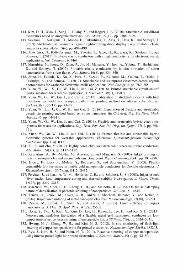
114. Kim, D. H., Xiao, J., Song, J., Huang, Y., and Rogers, J. A. (2010). Stretchable, curvilinear electronics based on inorganic materials, Adv. Mater., 22(19), pp. 2108–2124.
115. Sekitani, T., Nakajima, H., Maeda, H., Fukushima, T., Aida, T., Hata, K., and Someya, T. (2009). Stretchable active-matrix organic light-emitting diode display using printable elastic conductors, Nat. Mater., 8(6), pp. 494–499.
116. Matsuhisa, N., Kaltenbrunner, M., Yokota, T., Jinno, H., Kuribara, K., Sekitani, T., and Someya, T. (2015). Printable elastic conductors with a high conductivity for electronic textile applications, Nat. Commun., 6, 7461.
117. Matsuhisa, N., Inoue, D., Zalar, P., Jin, H., Matsuba, Y., Itoh, A., Yokota, T., Hashizume, D., and Someya, T. (2017). Printable elastic conductors by in situ formation of silver nanoparticles from silver flakes, Nat. Mater., 16(8), pp. 834–840.
118. Jinno, H., Fukuda, K., Xu, X., Park, S., Suzuki, Y., Koizumi, M., Yokota, T., Osaka, I., Takimiya, K., and Someya, T. (2017). Stretchable and waterproof elastomer-coated organic photovoltaics for washable electronic textile applications, Nat. Energy, 2, pp. 780–785.
119. Yuan, W., Wu, X., Gu, W., Lin, J., and Cui, Z. (2018). Printed stretchable circuit on soft elastic substrate for wearable application, J. Semicond., 39(1), 015002.
120. Yuan, W., Gu, W., Lin, J., and Cui, Z. (2017). Fabrication of stretchable circuit with high resolution line width and complex pattern via printing method on silicone substrate, Sci. Technol. Rev., 35(17), pp. 73–79.
121. Yuan, W., Lin, J., Gu, W. B., and Cui, Z. (2016). Preparation of flexible and stretchable circuit via printing method based on silver nanowires (in Chinese), Sci. Sin-Phys. Mech. Astron., 46, pp. 044611.
122. Yuan, W., Gu, W., Lin, J., and Cui, Z. (2016). Flexible and stretchable hybrid electronics systems for wearable applications, Dig. Tech. Pap. Soc. Inf. Disp. Int. Symp., 47(1), pp. 668–671.
123. Yuan, W., Gu, W., Lin, J., and Cui, Z. (2016). Printed flexible and stretchable hybrid electronic systems for wearable applications, Electronic System-Integration Technology Conference (pp. 1–4). IEEE.
124. Xu, F. and Zhu, Y. (2012). Highly conductive and stretchable silver nanowire conductors, Adv. Mater., 24(37), pp. 5117–5122.
125. Kamyshny, A., Ben-Moshe, M., Aviezer, S., and Magdassi, S. (2005). Inkjet printing of metallic nanoparticles and microemulsions, Macromol. Rapid Commun., 26(4), pp. 281–288.
126. Huang, D., Liao, F., Molesa, S., Redinger, D., and Subramanian, V. (2003). Plastic-compatible low resistance printable gold nanoparticle conductors for flexible electronics, J. Electrochem. Soc., 150(7), pp. G412–G417.
127. Perelaer, J., de Laat, A. W. M., Hendriks, C. E., and Schubert, U. S. (2008). Inkjet-printed silver tracks: Low temperature curing and thermal stability investigation, J. Mater. Chem., 18(27), pp. 3209–3215.
128. MacNeill, W., Choi, C. H., Chang, C. H., and Malhotra, R. (2015). On the self-damping nature of densification in photonic sintering of nanoparticles, Sci. Rep., 5, 14845.
129. Ermak, O., Zenou, M., Toker, G. B., Ankri, J., Shacham-Diamand, Y., and Kotler, Z. (2016). Rapid laser sintering of metal nano-particles inks, Nanotechnology, 27(38), 385201.
130. Zenou, M., Ermak, O., Saar, A., and Kotler, Z. (2013). Laser sintering of copper nanoparticles, J. Phys. D: Appl. Phys., 47(2), 025501.
131. Hong, S., Yeo, J., Kim, G., Kim, D., Lee, H., Kwon, J., Lee, H., and Ko, S. H. (2013). Nonvacuum, mask-less fabrication of a flexible metal grid transparent conductor by low-temperature selective laser sintering of nanoparticle ink, ACS Nano, 7(6), pp. 5024–5031.
132. Hwang, H. J., Chung, W. H., and Kim, H. S. (2012). In situ monitoring of flash-light sintering of copper nanoparticle ink for printed electronics, Nanotechnology, 23(48), 485205.
133. Ryu, J., Kim, H. S., and Hahn, H. T. (2011). Reactive sintering of copper nanoparticles using intense pulsed light for printed electronics, J. Electron. Mater., 40(1), pp. 42–50.
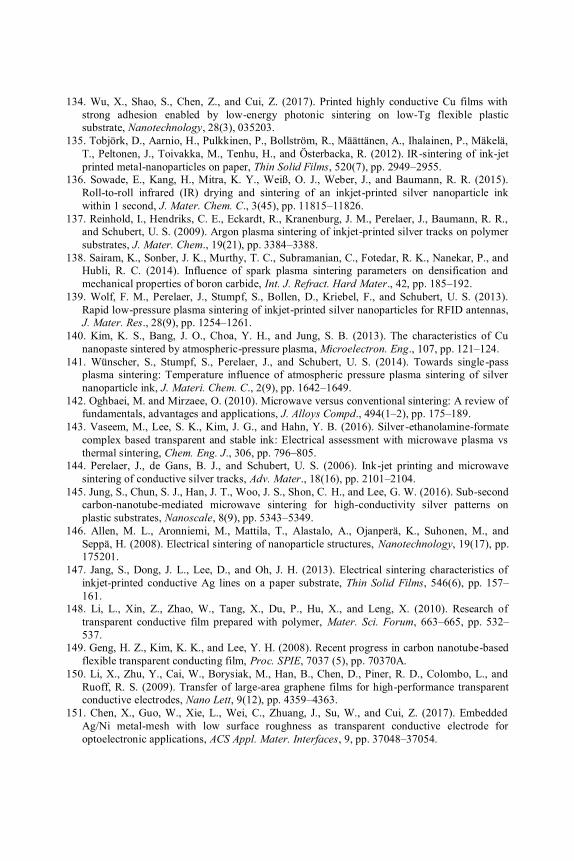
134. Wu, X., Shao, S., Chen, Z., and Cui, Z. (2017). Printed highly conductive Cu films with strong adhesion enabled by low-energy photonic sintering on low-Tg flexible plastic substrate, Nanotechnology, 28(3), 035203.
135. Tobjörk, D., Aarnio, H., Pulkkinen, P., Bollström, R., Määttänen, A., Ihalainen, P., Mäkelä, T., Peltonen, J., Toivakka, M., Tenhu, H., and Österbacka, R. (2012). IR-sintering of ink-jet printed metal-nanoparticles on paper, Thin Solid Films, 520(7), pp. 2949–2955.
136. Sowade, E., Kang, H., Mitra, K. Y., Weiß, O. J., Weber, J., and Baumann, R. R. (2015). Roll-to-roll infrared (IR) drying and sintering of an inkjet-printed silver nanoparticle ink within 1 second, J. Mater. Chem. C., 3(45), pp. 11815–11826.
137. Reinhold, I., Hendriks, C. E., Eckardt, R., Kranenburg, J. M., Perelaer, J., Baumann, R. R., and Schubert, U. S. (2009). Argon plasma sintering of inkjet-printed silver tracks on polymer substrates, J. Mater. Chem., 19(21), pp. 3384–3388.
138. Sairam, K., Sonber, J. K., Murthy, T. C., Subramanian, C., Fotedar, R. K., Nanekar, P., and Hubli, R. C. (2014). Influence of spark plasma sintering parameters on densification and mechanical properties of boron carbide, Int. J. Refract. Hard Mater., 42, pp. 185–192.
139. Wolf, F. M., Perelaer, J., Stumpf, S., Bollen, D., Kriebel, F., and Schubert, U. S. (2013). Rapid low-pressure plasma sintering of inkjet-printed silver nanoparticles for RFID antennas, J. Mater. Res., 28(9), pp. 1254–1261.
140. Kim, K. S., Bang, J. O., Choa, Y. H., and Jung, S. B. (2013). The characteristics of Cu nanopaste sintered by atmospheric-pressure plasma, Microelectron. Eng., 107, pp. 121–124.
141. Wünscher, S., Stumpf, S., Perelaer, J., and Schubert, U. S. (2014). Towards single-pass plasma sintering: Temperature influence of atmospheric pressure plasma sintering of silver nanoparticle ink, J. Materi. Chem. C., 2(9), pp. 1642–1649.
142. Oghbaei, M. and Mirzaee, O. (2010). Microwave versus conventional sintering: A review of fundamentals, advantages and applications, J. Alloys Compd., 494(1–2), pp. 175–189.
143. Vaseem, M., Lee, S. K., Kim, J. G., and Hahn, Y. B. (2016). Silver -ethanolamine-formate complex based transparent and stable ink: Electrical assessment with microwave plasma vs thermal sintering, Chem. Eng. J., 306, pp. 796–805.
144. Perelaer, J., de Gans, B. J., and Schubert, U. S. (2006). Ink-jet printing and microwave sintering of conductive silver tracks, Adv. Mater., 18(16), pp. 2101–2104.
145. Jung, S., Chun, S. J., Han, J. T., Woo, J. S., Shon, C. H., and Lee, G. W. (2016). Sub-second carbon-nanotube-mediated microwave sintering for high-conductivity silver patterns on plastic substrates, Nanoscale, 8(9), pp. 5343–5349.
146. Allen, M. L., Aronniemi, M., Mattila, T., Alastalo, A., Ojanperä, K., Suhonen, M., and Seppä, H. (2008). Electrical sintering of nanoparticle structures, Nanotechnology, 19(17), pp. 175201.
147. Jang, S., Dong, J. L., Lee, D., and Oh, J. H. (2013). Electrical sintering characteristics of inkjet-printed conductive Ag lines on a paper substrate, Thin Solid Films, 546(6), pp. 157–161.
148. Li, L., Xin, Z., Zhao, W., Tang, X., Du, P., Hu, X., and Leng, X. (2010). Research of transparent conductive film prepared with polymer, Mater. Sci. Forum, 663–665, pp. 532–537.
149. Geng, H. Z., Kim, K. K., and Lee, Y. H. (2008). Recent progress in carbon nanotube-based flexible transparent conducting film, Proc. SPIE, 7037 (5), pp. 70370A.
150. Li, X., Zhu, Y., Cai, W., Borysiak, M., Han, B., Chen, D., Piner, R. D., Colombo, L., and Ruoff, R. S. (2009). Transfer of large-area graphene films for high-performance transparent conductive electrodes, Nano Lett, 9(12), pp. 4359–4363.
151. Chen, X., Guo, W., Xie, L., Wei, C., Zhuang, J., Su, W., and Cui, Z. (2017). Embedded Ag/Ni metal-mesh with low surface roughness as transparent conductive electrode for optoelectronic applications, ACS Appl. Mater. Interfaces, 9, pp. 37048–37054.
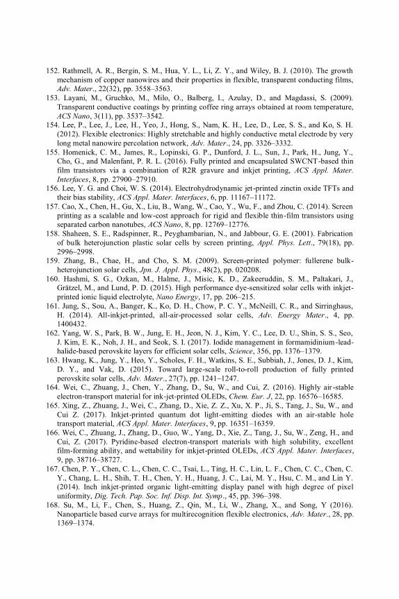
152. Rathmell, A. R., Bergin, S. M., Hua, Y. L., Li, Z. Y., and Wiley, B. J. (2010). The growth mechanism of copper nanowires and their properties in flexible, transparent conducting films, Adv. Mater., 22(32), pp. 3558–3563.
153. Layani, M., Gruchko, M., Milo, O., Balberg, I., Azulay, D., and Magdassi, S. (2009). Transparent conductive coatings by printing coffee ring arrays obtained at room temperature, ACS Nano, 3(11), pp. 3537–3542.
154. Lee, P., Lee, J., Lee, H., Yeo, J., Hong, S., Nam, K. H., Lee, D., Lee, S. S., and Ko, S. H. (2012). Flexible electronics: Highly stretchable and highly conductive metal electrode by very long metal nanowire percolation network, Adv. Mater., 24, pp. 3326–3332.
155. Homenick, C. M., James, R., Lopinski, G. P., Dunford, J. L., Sun, J., Park, H., Jung, Y., Cho, G., and Malenfant, P. R. L. (2016). Fully printed and encapsulated SWCNT-based thin film transistors via a combination of R2R gravure and inkjet printing, ACS Appl. Mater. Interfaces, 8, pp. 27900–27910.
156. Lee, Y. G. and Choi, W. S. (2014). Electrohydrodynamic jet-printed zinctin oxide TFTs and their bias stability, ACS Appl. Mater. Interfaces, 6, pp. 11167–11172.
157. Cao, X., Chen, H., Gu, X., Liu, B., Wang, W., Cao, Y., Wu, F., and Zhou, C. (2014). Screen printing as a scalable and low-cost approach for rigid and flexible thin-film transistors using separated carbon nanotubes, ACS Nano, 8, pp. 12769–12776.
158. Shaheen, S. E., Radspinner, R., Peyghambarian, N., and Jabbour, G. E. (2001). Fabrication of bulk heterojunction plastic solar cells by screen printing, Appl. Phys. Lett., 79(18), pp. 2996–2998.
159. Zhang, B., Chae, H., and Cho, S. M. (2009). Screen-printed polymer: fullerene bulk-heterojunction solar cells, Jpn. J. Appl. Phys., 48(2), pp. 020208.
160. Hashmi, S. G., Ozkan, M., Halme, J., Misic, K. D., Zakeeruddin, S. M., Paltakari, J., Grätzel, M., and Lund, P. D. (2015). High performance dye-sensitized solar cells with inkjet-printed ionic liquid electrolyte, Nano Energy, 17, pp. 206–215.
161. Jung, S., Sou, A., Banger, K., Ko, D. H., Chow, P. C. Y., McNeill, C. R., and Sirringhaus, H. (2014). All-inkjet-printed, all-air-processed solar cells, Adv. Energy Mater., 4, pp. 1400432.
162. Yang, W. S., Park, B. W., Jung, E. H., Jeon, N. J., Kim, Y. C., Lee, D. U., Shin, S. S., Seo, J. Kim, E. K., Noh, J. H., and Seok, S. I. (2017). Iodide management in formamidinium-lead-halide-based perovskite layers for efficient solar cells, Science, 356, pp. 1376–1379.
163. Hwang, K., Jung, Y., Heo, Y., Scholes, F. H., Watkins, S. E., Subbiah, J., Jones, D. J., Kim, D. Y., and Vak, D. (2015). Toward large-scale roll-to-roll production of fully printed perovskite solar cells, Adv. Mater., 27(7), pp. 1241–1247.
164. Wei, C., Zhuang, J., Chen, Y., Zhang, D., Su, W., and Cui, Z. (2016). Highly air -stable electron-transport material for ink-jet-printed OLEDs, Chem. Eur. J, 22, pp. 16576–16585.
165. Xing, Z., Zhuang, J., Wei, C., Zhang, D., Xie, Z. Z., Xu, X. P., Ji, S., Tang, J., Su, W., and Cui Z. (2017). Inkjet-printed quantum dot light-emitting diodes with an air-stable hole transport material, ACS Appl. Mater. Interfaces, 9, pp. 16351–16359.
166. Wei, C., Zhuang, J., Zhang, D., Guo, W., Yang, D., Xie, Z., Tang, J., Su, W., Zeng, H., and Cui, Z. (2017). Pyridine-based electron-transport materials with high solubility, excellent film-forming ability, and wettability for inkjet-printed OLEDs, ACS Appl. Mater. Interfaces, 9, pp. 38716–38727.
167. Chen, P. Y., Chen, C. L., Chen, C. C., Tsai, L., Ting, H. C., Lin, L. F., Chen, C. C., Chen, C. Y., Chang, L. H., Shih, T. H., Chen, Y. H., Huang, J. C., Lai, M. Y., Hsu, C. M., and Lin Y. (2014). Inch inkjet-printed organic light-emitting display panel with high degree of pixel uniformity, Dig. Tech. Pap. Soc. Inf. Disp. Int. Symp., 45, pp. 396–398.
168. Su, M., Li, F., Chen, S., Huang, Z., Qin, M., Li, W., Zhang, X., and Song, Y (2016). Nanoparticle based curve arrays for multirecognition flexible electronics, Adv. Mater., 28, pp. 1369–1374.
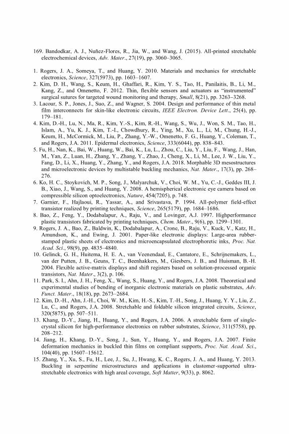
169. Bandodkar, A. J., Nuñez-Flores, R., Jia, W., and Wang, J. (2015). All-printed stretchable electrochemical devices, Adv. Mater., 27(19), pp. 3060–3065.
1. Rogers, J. A., Someya, T., and Huang, Y. 2010. Materials and mechanics for stretchable
electronics, Science, 327(5973), pp. 1603–1607. 2. Kim, D. H., Wang, S., Keum, H., Ghaffari, R., Kim, Y. S., Tao, H., Panilaitis, B., Li, M.,
Kang, Z., and Omenetto, F. 2012. Thin, flexible sensors and actuators as “instrumented” surgical sutures for targeted wound monitoring and therapy, Small, 8(21), pp. 3263–3268.
3. Lacour, S. P., Jones, J., Suo, Z., and Wagner, S. 2004. Design and performance of thin metal film interconnects for skin-like electronic circuits, IEEE Electron. Device Lett., 25(4), pp. 179–181.
4. Kim, D.-H., Lu, N., Ma, R., Kim, Y.-S., Kim, R.-H., Wang, S., Wu, J., Won, S. M., Tao, H., Islam, A., Yu, K. J., Kim, T.-I., Chowdhury, R., Ying, M., Xu, L., Li, M., Chung, H.-J., Keum, H., McCormick, M., Liu, P., Zhang, Y.-W., Omenetto, F. G., Huang, Y., Coleman, T., and Rogers, J.A. 2011. Epidermal electronics, Science, 333(6044), pp. 838–843.
5. Fu, H., Nan, K., Bai, W., Huang, W., Bai, K., Lu, L., Zhou, C., Liu, Y., Liu, F., Wang, J., Han, M., Yan, Z., Luan, H., Zhang, Y., Zhang, Y., Zhao, J., Cheng, X., Li, M., Lee, J. W., Liu, Y., Fang, D., Li, X., Huang, Y., Zhang, Y., and Rogers, J.A. 2018. Morphable 3D mesostructures and microelectronic devices by multistable buckling mechanics, Nat. Mater., 17(3), pp. 268–276.
6. Ko, H. C., Stoykovich, M. P., Song, J., Malyarchuk, V., Choi, W. M., Yu, C.-J., Geddes III, J. B., Xiao, J., Wang, S., and Huang, Y. 2008. A hemispherical electronic eye camera based on compressible silicon optoelectronics, Nature, 454(7205), p. 748.
7. Garnier, F., Hajlaoui, R., Yassar, A., and Srivastava, P. 1994. All-polymer field-effect transistor realized by printing techniques, Science, 265(5179), pp. 1684–1686.
8. Bao, Z., Feng, Y., Dodabalapur, A., Raju, V., and Lovinger, A.J. 1997. Highperformance plastic transistors fabricated by printing techniques, Chem. Mater., 9(6), pp. 1299–1301.
9. Rogers, J. A., Bao, Z., Baldwin, K., Dodabalapur, A., Crone, B., Raju, V., Kuck, V., Katz, H., Amundson, K., and Ewing, J. 2001. Paper-like electronic displays: Large-area rubber-stamped plastic sheets of electronics and microencapsulated electrophoretic inks, Proc. Nat. Acad. Sci., 98(9), pp. 4835–4840.
10. Gelinck, G. H., Huitema, H. E. A., van Veenendaal, E., Cantatore, E., Schrijnemakers, L., van der Putten, J. B., Geuns, T. C., Beenhakkers, M., Giesbers, J. B., and Huisman, B.-H. 2004. Flexible active-matrix displays and shift registers based on solution-processed organic transistors, Nat. Mater., 3(2), p. 106.
11. Park, S. I., Ahn, J. H., Feng, X., Wang, S., Huang, Y., and Rogers, J.A. 2008. Theoretical and experimental studies of bending of inorganic electronic materials on plastic substrates, Adv. Funct. Mater., 18(18), pp. 2673–2684.
12. Kim, D.-H., Ahn, J.-H., Choi, W. M., Kim, H.-S., Kim, T.-H., Song, J., Huang, Y. Y., Liu, Z., Lu, C., and Rogers, J.A. 2008. Stretchable and foldable silicon integrated circuits, Science, 320(5875), pp. 507–511.
13. Khang, D.-Y., Jiang, H., Huang, Y., and Rogers, J.A. 2006. A stretchable form of single-crystal silicon for high-performance electronics on rubber substrates, Science, 311(5758), pp. 208–212.
14. Jiang, H., Khang, D.-Y., Song, J., Sun, Y., Huang, Y., and Rogers, J.A. 2007. Finite deformation mechanics in buckled thin films on compliant supports, Proc. Nat. Acad. Sci., 104(40), pp. 15607–15612.
15. Zhang, Y., Xu, S., Fu, H., Lee, J., Su, J., Hwang, K. C., Rogers, J. A., and Huang, Y. 2013. Buckling in serpentine microstructures and applications in elastomer-supported ultra-stretchable electronics with high areal coverage, Soft Matter, 9(33), p. 8062.
16. Zhang, Y., Wang, S., Li, X., Fan, J. A., Xu, S., Song, Y. M., Choi, K.-J., Yeo, W.-H., Lee, W., Nazaar, S. N., Lu, B., Yin, L., Hwang, K.-C., Rogers, J. A., and Huang, Y. 2014. Experimental and theoretical studies of serpentine microstructures bonded to prestrained elastomers for stretchable electronics, Adv. Funct. Mater., 24(14), pp. 2028–2037.
17. Fan, Z., Zhang, Y., Ma, Q., Zhang, F., Fu, H., Hwang, K.-C., and Huang, Y. 2016. A finite deformation model of planar serpentine interconnects for stretchable electronics, Int. J. Solids Struct., 91, pp. 46–54.
18. Kim, D.-H., Song, J., Choi, W. M., Kim, H.-S., Kim, R.-H., Liu, Z., Huang, Y. Y., Hwang, K.-C., Zhang, Y.-W., and Rogers, J.A. 2008. Materials and noncoplanar mesh designs for integrated circuits with linear elastic responses to extreme mechanical deformations, Proc. Nat. Acad. Sci., 105(48), pp. 18675–18680.
19. Su, Y., Wu, J., Fan, Z., Hwang, K.-C., Song, J., Huang, Y., and Rogers, J.A. 2012. Postbuckling analysis and its application to stretchable electronics, J. Mech. Phys. Solids, 60(3), pp. 487–508.
20. Kim, D. H., Choi, W. M., Ahn, J. H., Kim, H. S., Song, J., Huang, Y., Liu, Z., Lu, C., Chan, G. K., and Rogers, J.A. 2008. Complementary metal oxide silicon integrated circuits incorporating monolithically integrated stretchable wavy interconnects, Appl. Phys. Lett., 93(4), p. 1459.
21. Song, J., Huang, Y., Xiao, J., Wang, S., Hwang, K., Ko, H., Kim, D.-H., Stoykovich, M., and Rogers, J. 2009. Mechanics of noncoplanar mesh design for stretchable electronic circuits, J. Appl. Phys., 105(12), p. 123516.
22. Lacour, S. P., Jones, J., Wagner, S., Li, T., and Suo, Z. 2005. Stretchable interconnects for elastic electronic surfaces, Proc. IEEE, 93(8), pp. 1459–1467.
23. Su, Y., Wang, S., Huang, Y., Luan, H., Dong, W., Fan, J. A., Yang, Q., Rogers, J. A., and Huang, Y. 2015. Elasticity of fractal inspired interconnects, Small, 11(3), pp. 367–373.
24. Zhang, Y., Fu, H., Xu, S., Fan, J. A., Hwang, K.-C., Jiang, J., Rogers, J. A., and Huang, Y. 2014. A hierarchical computational model for stretchable interconnects with fractal-inspired designs, J. Mech. Phys. Solids, 72, pp. 115–130.
25. Hsu, Y.-Y., Gonzalez, M., Bossuyt, F., Axisa, F., Vanfleteren, J., and De Wolf, I. 2009. In situ observations on deformation behavior and stretching-induced failure of fine pitch stretchable interconnect, J. Mater. Res., 24(12), pp. 3573–3582.
26. Duan, Y., Huang, Y., Yin, Z., Bu, N., and Dong, W. 2014. Non-wrinkled, highly stretchable piezoelectric devices by electrohydrodynamic direct-writing, Nanoscale, 6(6), pp. 3289–3295.
27. Xu, S., Zhang, Y., Cho, J., Lee, J., Huang, X., Jia, L., Fan, J. A., Su, Y., Su, J., Zhang, H., Cheng, H., Lu, B., Yu, C., Chuang, C., Kim, T.-I., Song, T., Shigeta, K., Kang, S., Dagdeviren, C., Petrov, I., Braun, P. V., Huang, Y., Paik, U., and Rogers, J.A. 2013. Stretchable batteries with self-similar serpentine interconnects and integrated wireless recharging systems, Nat. Commun., 4, p. 1543.
28. Choi, W. M., Song, J., Khang, D., Jiang, H., Huang, Y., and Rogers, J.A. 2007. Biaxially stretchable “Wavy” silicon nanomembranes, Nano Lett., 7(6), pp. 1655–1663.
29. Wang, X., Zeng, W., Hong, L., Xu, W., Yang, H., Wang, F., Duan, H., Tang, M., and Jiang, H. 2018. Stress-driven lithium dendrite growth mechanism and dendrite mitigation by electroplating on soft substrates, Nat. Energy, 3(3), pp. 227–235.
30. Xu, S., Yan, Z., Jang, K.-I., Huang, W., Fu, H., Kim, J., Wei, Z., Flavin, M., McCracken, J., Wang, R., Badea, A., Liu, Y., Xiao, D., Zhou, G., Lee, J., Chung, H. U., Cheng, H., Ren, W., Banks, A., Li, X., Paik, U., Nuzzo, R. G., Huang, Y., Zhang, Y., and Rogers, J.A. 2015. Assembly of micro/nanomaterials into complex, three-dimensional architectures by compressive buckling, Science, 347(6218), pp. 154–159.
31. Yan, Z., Zhang, F., Wang, J., Liu, F., Guo, X., Nan, K., Lin, Q., Gao, M., Xiao, D., Shi, Y., Qiu, Y., Luan, H., Kim, J. H., Wang, Y., Luo, H., Han, M., Huang, Y., Zhang, Y., and
Rogers, J.A. 2016. Controlled mechanical buckling for origami-inspired construction of 3D microstructures in advanced materials, Adv. Funct. Mater., 26(16), pp. 2629–2639.
32. Yan, Z., Zhang, F., Liu, F., Han, M., Ou, D., Liu, Y., Lin, Q., Guo, X., Fu, H., Xie, Z., Gao, M., Huang, Y., Kim, J., Qiu, Y., Nan, K., Kim, J., Gutruf, P., Luo, H., Zhao, A., Hwang, K.-C., Huang, Y., Zhang, Y., and Rogers, J.A. 2016. Mechanical assembly of complex, 3D mesostructures from releasable multilayers of advanced materials, Sci. Adv., 2(9), p. e1601014.
33. Zhang, Y., Yan, Z., Nan, K., Xiao, D., Liu, Y., Luan, H., Fu, H., Wang, X., Yang, Q., Wang, J., Ren, W., Si, H., Liu, F., Yang, L., Li, H., Wang, J., Guo, X., Luo, H., Wang, L., Huang, Y., and Rogers, J.A. 2015. A mechanically driven form of Kirigami as a route to 3D mesostructures in micro/nanomembranes, Proc. Nat. Acad. Sci., 112(38), pp. 11757–11764.
34. Hung, P. J., Jeong, K., Liu, G. L., and Lee, L.P. 2004. Microfabricated suspensions for electrical connections on the tunable elastomer membrane, Appl. Phys. Lett., 85(24), pp. 6051–6053.
35. Dinyari, R., Rim, S.-B., Huang, K., Catrysse, P. B., and Peumans, P. 2008. Curving monolithic silicon for nonplanar focal plane array applications, Appl. Phys. Lett., 92(9), p. 091114.
36. Huang, K. and Peumans, P. 2006. Stretchable silicon sensor networks for structural health monitoring, Proc. Smart Structures and Materials 2006: Sensors and Smart Structures Technologies for Civil, Mechanical, and Aerospace Systems, International Society for Optics and Photonics, p. 617412.
37. Someya, T., Kato, Y., Sekitani, T., Iba, S., Noguchi, Y., Murase, Y., Kawaguchi, H., and Sakurai, T. 2005. Conformable, flexible, large-area networks of pressure and thermal sensors with organic transistor active matrixes, Proc. Natl. Acad. Sci. U.S.A., 102(35), pp. 12321–12325.
38. Song, J., Jiang, H., Huang, Y., and Rogers, J. 2009. Mechanics of stretchable inorganic electronic materials, J. Vac. Sci. Technol. A, 27(5), pp. 1107–1125.
39. Song, J. 2015. Mechanics of stretchable electronics, Curr. Opin. Solid State Mat. Sci., 19(3), pp. 160–170.
40. Song, J., Jiang, H., Liu, Z. J., Khang, D. Y., Huang, Y., Rogers, J. A., Lu, C., and Koh, C.G. 2008. Buckling of a stiff thin film on a compliant substrate in large deformation, Int. J. Solids Struct., 45(10), pp. 3107–3121.
41. Cheng, H. and Song, J. 2013. A simply analytic study of buckled thin films on compliant substrates, J. Appl. Mech., 81(2), pp. 024501–024501–024501–024503.
42. Sun, Y., Choi, W. M., Jiang, H., Huang, Y. Y., and Rogers, J.A. 2006. Controlled buckling of semiconductor nanoribbons for stretchable electronics, Nat. Nanotechnol., 1(3), p. 201.
43. Jiang, H., Sun, Y., Rogers, J. A., and Huang, Y. 2007. Mechanics of precisely controlled thin film buckling on elastomeric substrate, Appl. Phys. Lett., 90(13), p. 133119.
44. Song, J., Jiang, H., Choi, W., Khang, D., Huang, Y., and Rogers, J. 2008. An analytical study of two-dimensional buckling of thin films on compliant substrates, J. Appl. Phys., 103(1), p. 014303.
45. Choi, W. M., Song, J., Khang, D.-Y., Jiang, H., Huang, Y. Y., and Rogers, J.A. 2007. Biaxially stretchable “wavy” silicon nanomembranes, Nano Lett., 7(6), pp. 1655–1663.
46. Huang, Z., Hong, W., and Suo, Z. 2005. Nonlinear analyses of wrinkles in a film bonded to a compliant substrate, J. Mech. Phys. Solids, 53(9), pp. 2101–2118.
47. Huang, Z., Hong, W., and Suo, Z. 2004. Evolution of wrinkles in hard films on soft substrates, Phys. Rev. E, 70(3), p. 030601.
48. Chen, X. and Hutchinson, J.W. 2004. A family of herringbone patterns in thin films, Scripta Mater., 50(6), pp. 797–801.
49. Chen, X. and Hutchinson, J.W. 2004. Herringbone buckling patterns of compressed thin films on compliant substrates, J. Appl. Mech. Trans. ASME, 71(5), pp. 597–603.
50. Huang, R. and Im, S.H. 2006. Dynamics of wrinkle growth and coarsening in stressed thin films, Phys. Rev. E, 74(2), p. 026214.
51. Song, Z., Ma, T., Tang, R., Cheng, Q., Wang, X., Krishnaraju, D., Panat, R., Chan, C. K., Yu, H., and Jiang, H. 2014. Origami lithium-ion batteries, Nat. Commun., 5, p. 3140.
52. Stafford, C. M., Vogt, B. D., Harrison, C., Julthongpiput, D., and Huang, R. 2006. Elastic moduli of ultrathin amorphous polymer films, Macromolecules, 39(15), pp. 5095–5099.
53. Lamoureux, A., Lee, K., Shlian, M., Forrest, S. R., and Shtein, M. 2015. Dynamic kirigami structures for integrated solar tracking, Nat. Commun., 6, p. 8092.
54. Song, Z., Wang, X., Lv, C., An, Y., Liang, M., Ma, T., He, D., Zheng, Y. J., Huang, S. Q., and Yu, H. 2015. Kirigami-based stretchable lithium-ion batteries, Sci. Rep., 5, p. 10988.
55. Wu, C., Wang, X., Lin, L., Guo, H., and Wang, Z.L. 2016. Paper-based triboelectric nanogenerators made of stretchable interlocking kirigami patterns, ACS Nano, 10(4), pp. 4652–4659.
56. Zhang, Y., Zhang, F., Yan, Z., Ma, Q., Li, X., Huang, Y., and Rogers, J.A. 2017. Printing, folding and assembly methods for forming 3D mesostructures in advanced materials, Nat. Rev. Mater., 2, p. 17019.
57. Schroeder, T. B., Guha, A., Lamoureux, A., Van Renterghem, G., Sept, D., Shtein, M., Yang, J., and Mayer, M. 2017. An electric-eel-inspired soft power source from stacked hydrogels, Nature, 552(7684), p. 214.
58. Rafsanjani, A. and Bertoldi, K. 2017. Buckling-induced kirigami, Phys. Rev. Lett., 118(8), p. 084301.
59. Bertoldi, K., Vitelli, V., Christensen, J., and van Hecke, M. 2017. Flexible mechanical metamaterials, Nat. Rev. Mater., 2(11), p. 17066.
60. Lv, C., Krishnaraju, D., Konjevod, G., Yu, H., and Jiang, H. 2014. Origami based mechanical metamaterials, Sci. Rep., 4, p. 5979.
61. Yan, Z., Zhang, F., Liu, F., Han, M., Ou, D., Liu, Y., Lin, Q., Guo, X., Fu, H., and Xie, Z. 2016. Mechanical assembly of complex, 3D mesostructures from releasable multilayers of advanced materials, Sci. Adv., 2(9), pp. e1601014–e1601014.
62. Xu, S., Yan, Z., Jang, K. I., Huang, W., Fu, H., Kim, J., Wei, Z., Flavin, M., Mccracken, J. M., and Wang, R. 2015. Assembly of micro/nanomaterials into complex, three-dimensional architectures by compressive buckling, Science, 347(6218), pp. 154–159.
63. Liu, Y., Yan, Z., Lin, Q., Guo, X., Han, M., Nan, K., Hwang, K. C., Huang, Y., Zhang, Y., and Rogers, J.A. 2016. Guided formation of 3D helical mesostructures by mechanical buckling: Analytical modeling and experimental validation, Adv. Funct. Mater., 26(17), p. 2909.
64. Yan, Z., Han, M. D., Yang, Y. Y., Nan, K. W., Luan, H. W., Luo, Y. Y., Zhang, Y. H., Huang, Y. G., and Rogers, J.A. 2017. Deterministic assembly of 3D mesostructures in advanced materials via compressive buckling: A short review of recent progress, Extreme Mech. Lett., 11, pp. 96–104.
65. Gong, S. and Cheng, W. 2017. Toward soft skin-like wearable and implantable energy devices, Adv. Energy Mater., 7(23), p. 1700648.
66. Liu, W., Song, M.-S., Kong, B., and Cui, Y. 2017. Flexible and stretchable energy storage: Recent advances and future perspectives, Adv. Mater., 29(1), p. 1603436.
Related Documents


