© Semiconductor Components Industries, LLC, 2016 January, 2016 - Rev. 5 1 Publication Order Number: NCP1236/D NCP1236 Fixed Frequency Current Mode Controller for Flyback Converters The NCP1236 is a new fixed-frequency current-mode controller featuring Dynamic Self-Supply (DSS). This device is pin-to-pin compatible with the previous NCP12xx families. The DSS function greatly simplifies the design of the auxiliary supply and the V CC capacitor by activating the internal startup current source to supply the controller during transients. Due to frequency foldback, the controller exhibits excellent efficiency in light load condition while still achieving very low standby power consumption. Internal frequency jittering, ramp compensation, and a versatile latch input make this controller an excellent candidate for converters where components cost is the key constraints. In addition, the controller includes a new high voltage circuitry that combines a start-up current source and a brown-out detector able to sense the input voltage either from the rectified ac line or the dc filtered bulk voltage. The high voltage sensing circuitry is used for the overpower protection purposes as well. Overpower protection, overload protection, and next protective features increases safety level of the final application. Finally, due to a careful design, the precision of critical parameters is well controlled over the entire temperature range (-40°C to +125°C). Features • Fixed-Frequency Current-Mode Operation with Built-In Ramp Compensation • 65 kHz or 100 kHz Oscillator Frequency • Frequency Foldback then Skip Mode for Maximized Performance in Light Load and Standby Conditions • Timer-Based Overload Protection with Latched (option A) or Auto-Recovery (option B) Operation, Shortened Overload Timer for Increased Safety (options C and D), (see all options on page 2) • High-voltage Current Source with Brown-Out detection and Dynamic Self-Supply, Simplifying the Design of the V CC Capacitor • Frequency Modulation for Softened EMI Signature, including during Frequency Foldback mode • Adjustable Overpower Compensation • Latch-off Input for Severe Fault Conditions, Allowing Direct Connection of an NTC for Overtemperature Protection (OTP) • V CC Operation up to 28 V, with Overvoltage Detection • $500 mA Peak Source / Sink Current Drive Capability • 4.0 ms Soft-Start • Internal Thermal Shutdown • Pin-to-Pin Compatible with the Existing NCP12xx Series • These Devices are Pb-Free, Halogen Free/BFR Free and are RoHS Compliant Typical Applications • AC-DC Adapters for Notebooks, LCD, and Printers • Offline Battery Chargers • Consumer Electronic Power Supplies • Auxiliary/Housekeeping Power Supplies SOIC-7 CASE 751U MARKING DIAGRAM www. onsemi.com 36Xff ALYW G 1 8 36Xff = Specific Device Code X = A, B, C or D ff = 65 or 100 A = Assembly Location L = Wafer Lot Y = Year W = Work Week G = Pb-Free Package See detailed ordering and shipping information in the package dimensions section on page 33 of this data sheet. ORDERING INFORMATION 1 8 5 3 4 (Top View) Latch CS HV PIN CONNECTIONS 6 2 FB GND DRV V CC

Welcome message from author
This document is posted to help you gain knowledge. Please leave a comment to let me know what you think about it! Share it to your friends and learn new things together.
Transcript
© Semiconductor Components Industries, LLC, 2016
January, 2016 − Rev. 51 Publication Order Number:
NCP1236/D
NCP1236
Fixed Frequency CurrentMode Controller for FlybackConverters
The NCP1236 is a new fixed−frequency current−mode controllerfeaturing Dynamic Self−Supply (DSS). This device is pin−to−pincompatible with the previous NCP12xx families.
The DSS function greatly simplifies the design of the auxiliarysupply and the VCC capacitor by activating the internal startup currentsource to supply the controller during transients.
Due to frequency foldback, the controller exhibits excellentefficiency in light load condition while still achieving very lowstandby power consumption. Internal frequency jittering, rampcompensation, and a versatile latch input make this controller anexcellent candidate for converters where components cost is the keyconstraints.
In addition, the controller includes a new high voltage circuitry thatcombines a start−up current source and a brown−out detector able tosense the input voltage either from the rectified ac line or the dcfiltered bulk voltage. The high voltage sensing circuitry is used for theoverpower protection purposes as well. Overpower protection,overload protection, and next protective features increases safety levelof the final application.
Finally, due to a careful design, the precision of critical parametersis well controlled over the entire temperature range (−40°C to+125°C).
Features• Fixed−Frequency Current−Mode Operation with Built−In Ramp
Compensation• 65 kHz or 100 kHz Oscillator Frequency
• Frequency Foldback then Skip Mode for Maximized Performance inLight Load and Standby Conditions
• Timer−Based Overload Protection with Latched (option A) orAuto−Recovery (option B) Operation, Shortened Overload Timer forIncreased Safety (options C and D), (see all options on page 2)
• High−voltage Current Source with Brown−Outdetection and Dynamic Self−Supply, Simplifying theDesign of the VCC Capacitor
• Frequency Modulation for Softened EMI Signature,including during Frequency Foldback mode
• Adjustable Overpower Compensation
• Latch−off Input for Severe Fault Conditions, AllowingDirect Connection of an NTC for OvertemperatureProtection (OTP)
• VCC Operation up to 28 V, with Overvoltage Detection
• �500 mA Peak Source / Sink Current Drive Capability
• 4.0 ms Soft−Start
• Internal Thermal Shutdown
• Pin−to−Pin Compatible with the Existing NCP12xxSeries
• These Devices are Pb−Free, Halogen Free/BFR Freeand are RoHS Compliant
Typical Applications• AC−DC Adapters for Notebooks, LCD, and Printers
• Offline Battery Chargers
• Consumer Electronic Power Supplies
• Auxiliary/Housekeeping Power Supplies
SOIC−7CASE 751U
MARKINGDIAGRAM
www.onsemi.com
36XffALYW
�1
8
36Xff = Specific Device CodeX = A, B, C or Dff = 65 or 100
A = Assembly LocationL = Wafer LotY = YearW = Work Week� = Pb−Free Package
See detailed ordering and shipping information in the packagedimensions section on page 33 of this data sheet.
ORDERING INFORMATION
1 8
5
3
4
(Top View)
Latch
CS
HV
PIN CONNECTIONS
6
2FB
GND DRV
VCC
NCP1236
www.onsemi.com2
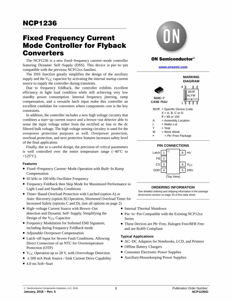
TYPICAL APPLICATION EXAMPLE
VOUTVIN(dc)
NCP1236
LATCH
FB
CS
GND
HV
VCC
DRV
Figure 1. Flyback Converter Application Using the NCP1236
OPTIONS
Part Option Frequency OCP Fault Fault TimerAutorecovery
Timer
NCP1236
A 65 kHz Latched 128 ms 1 s
A 100 kHz Latched 128 ms 1 s
B 65 kHz Autorecovery 128 ms 1 s
B 100 kHz Autorecovery 128 ms 1 s
C 65 kHz Latched 32 ms 1.5 s
C 100 kHz Latched 32 ms 1.5 s
D 65 kHz Autorecovery 32 ms 1.5 s
D 100 kHz Autorecovery 32 ms 1.5 s
PIN FUNCTION DESCRIPTION
Pin No Pin Name Function Pin Description
1 LATCH Latch−Off Input Pull the pin up or down to latch−off the controller. An internal current sourceallows the direct connection of an NTC for over temperature detection
2 FB Feedback An optocoupler collector to ground controls the output regulation.
3 CS Current Sense This Input senses the Primary Current for current−mode operation, and Offersan overpower compensation adjustment.
4 GND IC Ground
5 DRV Drive output Drives external MOSFET
6 VCC VCC input This supply pin accepts up to 28 Vdc, with overvoltage detection
8 HV High−voltage pin Connects to the bulk capacitor or the rectified AC line to perform the functionsof Start−up Current Source, Dynamic Self−Supply and brown−out detection
NCP1236
www.onsemi.com3
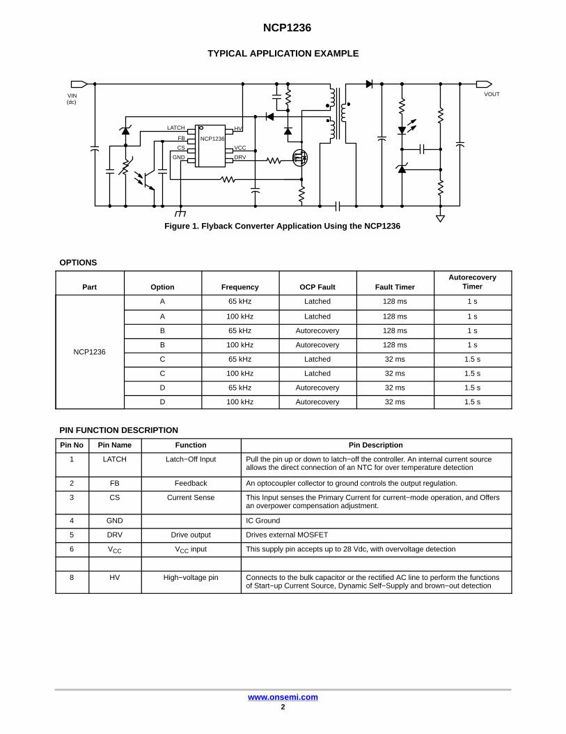
SIMPLIFIED INTERNAL BLOCK SCHEMATIC
Figure 2. Simplified Internal Block Schematic
Reset
Brown−out
CS
FB
−+
tLEB
blanking
/ 5
tfaulttimer
VFB(ref)
20 k�
−+
−+
+−
+
+
VILIM
VCS(stop)
S
RQ
tSSTART
Soft−start ramp Start
Reset
IC Start
IC Stop
Oscillator
DCMAX
HV
VCC
Latch
−+
+
Vskip
ProtectionModerelease
tautorec
timer
ForAutorecoveryprotectionmode only
DRV
HV sample
BO
Clamp
UVLO
Fault
Sawtooth
Jitter
Brown−out
Brown−out
−+
V to I
HV sample
IOPC = 0.5� x (VHV − 125)
−+
+
VFB(OPC)
Latch
Dual HVstart−upcurrent source
VCCmanagement
HV currentTSD
VDD
UVLOReset
TSD
StartIC Start
PWM
Soft−start
ILIMIT
Reset
VDDUVLO
IC stop
TSD
TSD
HV dc
ILIMIT
PWM
Fault Flag
Foldback
GND
Stop
DMAX
DMAX
S
RQ
tBCS
blanking
−+
VOVP
S
RQ
−+
VOTP
tLatch(OVP)
blankingVDD
Brown−out
Reset
Latch
Vclamp
INTC
tLatch(OTP)
blanking
1 k�
INTC
+
+
Soft−startend
Soft−start end
End
slopecomp.
VCC OVP OVP
VCC OVP
NCP1236
www.onsemi.com4
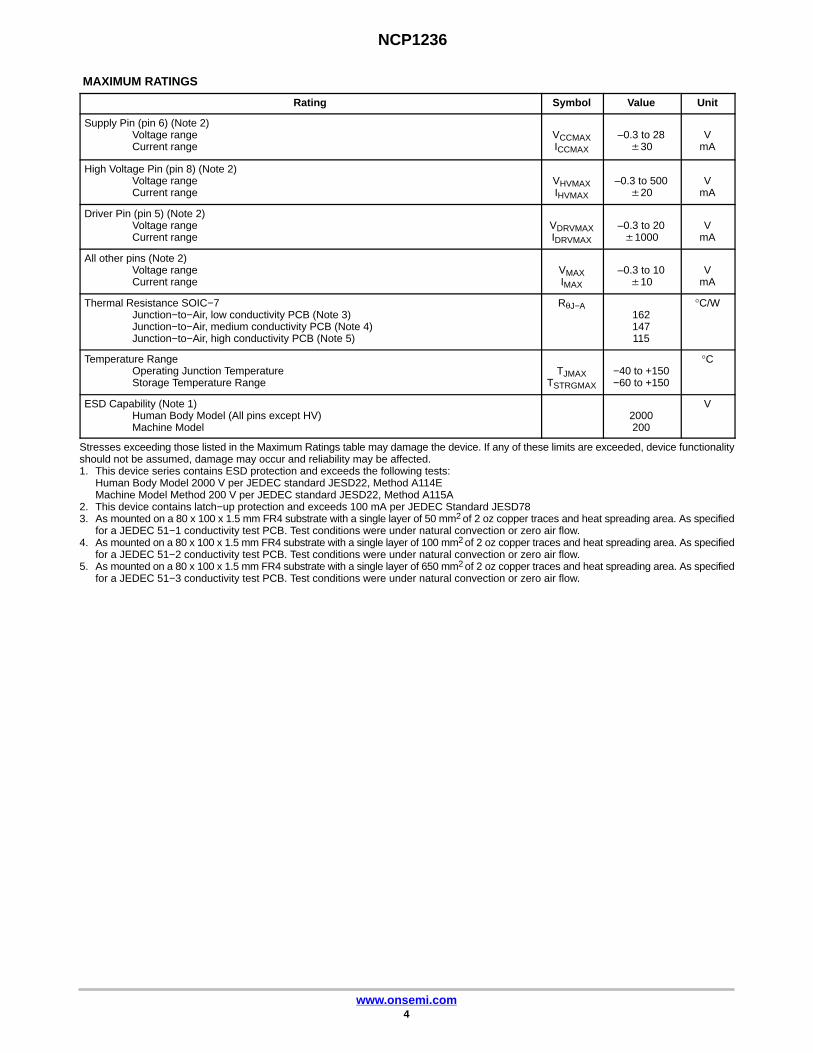
MAXIMUM RATINGS
Rating Symbol Value Unit
Supply Pin (pin 6) (Note 2)Voltage rangeCurrent range
VCCMAXICCMAX
–0.3 to 28�30
VmA
High Voltage Pin (pin 8) (Note 2)Voltage rangeCurrent range
VHVMAXIHVMAX
–0.3 to 500�20
VmA
Driver Pin (pin 5) (Note 2)Voltage rangeCurrent range
VDRVMAXIDRVMAX
–0.3 to 20�1000
VmA
All other pins (Note 2)Voltage rangeCurrent range
VMAXIMAX
–0.3 to 10�10
VmA
Thermal Resistance SOIC−7Junction−to−Air, low conductivity PCB (Note 3)Junction−to−Air, medium conductivity PCB (Note 4)Junction−to−Air, high conductivity PCB (Note 5)
RθJ−A162147115
°C/W
Temperature RangeOperating Junction TemperatureStorage Temperature Range
TJMAXTSTRGMAX
−40 to +150−60 to +150
°C
ESD Capability (Note 1)Human Body Model (All pins except HV)Machine Model
2000200
V
Stresses exceeding those listed in the Maximum Ratings table may damage the device. If any of these limits are exceeded, device functionalityshould not be assumed, damage may occur and reliability may be affected.1. This device series contains ESD protection and exceeds the following tests:
Human Body Model 2000 V per JEDEC standard JESD22, Method A114EMachine Model Method 200 V per JEDEC standard JESD22, Method A115A
2. This device contains latch−up protection and exceeds 100 mA per JEDEC Standard JESD783. As mounted on a 80 x 100 x 1.5 mm FR4 substrate with a single layer of 50 mm2 of 2 oz copper traces and heat spreading area. As specified
for a JEDEC 51−1 conductivity test PCB. Test conditions were under natural convection or zero air flow.4. As mounted on a 80 x 100 x 1.5 mm FR4 substrate with a single layer of 100 mm2 of 2 oz copper traces and heat spreading area. As specified
for a JEDEC 51−2 conductivity test PCB. Test conditions were under natural convection or zero air flow.5. As mounted on a 80 x 100 x 1.5 mm FR4 substrate with a single layer of 650 mm2 of 2 oz copper traces and heat spreading area. As specified
for a JEDEC 51−3 conductivity test PCB. Test conditions were under natural convection or zero air flow.
NCP1236
www.onsemi.com5
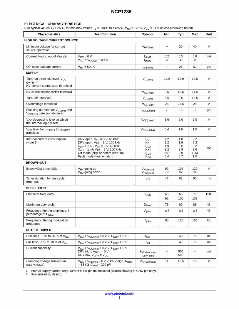
ELECTRICAL CHARACTERISTICS (For typical values TJ = 25°C, for min/max values TJ = −40°C to +125°C, VHV = 125 V, VCC = 11 V unless otherwise noted)
Characteristics Test Condition Symbol Min Typ Max Unit
HIGH VOLTAGE CURRENT SOURCE
Minimum voltage for currentsource operation
VHV(min) − 30 40 V
Current flowing out of VCC pin VCC = 0 VVCC = VCC(on) − 0.5 V
Istart1Istart2
0.23
0.56
0.89
mA
Off−state leakage current VHV = 500 V Istart(off) − 25 50 �A
SUPPLY
Turn−on threshold level, VCCgoing upHV current source stop threshold
VCC(on) 11.0 12.0 13.0 V
HV current source restart threshold VCC(min) 9.5 10.5 11.5 V
Turn−off threshold VCC(off) 8.5 9.5 10.5 V
Overvoltage threshold VCC(ovp) 25 26.5 28 V
Blanking duration on VCC(off) andVCC(ovp) detection (Note 7)
tVCC(blank) 7 10 13 �s
VCC decreasing level at whichthe internal logic resets
VCC(reset) 3.6 5.0 6.0 V
VCC level for ISTART1 to ISTART2transition
VCC(inhibit) 0.4 1.0 1.6 V
Internal current consumption(Note 6)
DRV open, VFB = 3 V, 65 kHzDRV open, VFB = 3 V, 100 kHzCdrv = 1 nF, VFB = 3 V, 65 kHzCdrv = 1 nF, VFB = 3 V, 100 kHzOff mode (skip or before start−up)Fault mode (fault or latch)
ICC1ICC1ICC2ICC2ICC3ICC4
1.21.21.92.20.670.4
1.81.92.52.90.90.7
2.22.33.23.61.131.0
mA
BROWN−OUT
Brown−Out thresholds VHV going upVHV going down
VHV(start)VHV(stop)
9279
10792
122105
V
Timer duration for line cycledrop−out
tHV 47 68 90 ms
OSCILLATOR
Oscillator frequency fOSC 6092
65100
70108
kHz
Maximum duty cycle DMAX 75 80 85 %
Frequency jittering amplitude, inpercentage of FOSC
Ajitter �4 �6 �8 %
Frequency jittering modulationfrequency
Fjitter 85 125 165 Hz
OUTPUT DRIVER
Rise time, 10% to 90 % of VCC VCC = VCC(min) + 0.2 V, CDRV = 1 nF trise − 40 70 ns
Fall time, 90% to 10 % of VCC VCC = VCC(min) + 0.2 V, CDRV = 1 nF tfall − 40 70 ns
Current capability VCC = VCC(min) + 0.2 V, CDRV = 1 nFDRV high, VDRV = 0 VDRV low, VDRV = VCC
IDRV(source)IDRV(sink)
−−
500500
−−
mA
Clamping voltage (maximumgate voltage)
VCC = VCCmax – 0.2 V, DRV high, RDRV= 33 k�, Cload = 220 pF
VDRV(clamp) 11 13.5 16 V
6. Internal supply current only, current in FB pin not included (current flowing in GND pin only).7. Guaranteed by design.
NCP1236
www.onsemi.com6
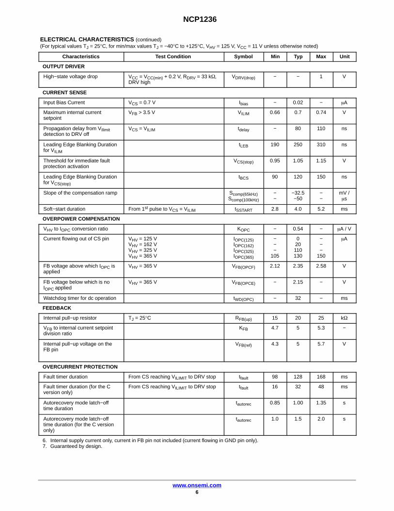
ELECTRICAL CHARACTERISTICS (continued)(For typical values TJ = 25°C, for min/max values TJ = −40°C to +125°C, VHV = 125 V, VCC = 11 V unless otherwise noted)
Characteristics UnitMaxTypMinSymbolTest Condition
OUTPUT DRIVER
High−state voltage drop VCC = VCC(min) + 0.2 V, RDRV = 33 k�,DRV high
VDRV(drop) − − 1 V
CURRENT SENSE
Input Bias Current VCS = 0.7 V Ibias − 0.02 − �A
Maximum internal currentsetpoint
VFB > 3.5 V VILIM 0.66 0.7 0.74 V
Propagation delay from VIlimitdetection to DRV off
VCS = VILIM tdelay − 80 110 ns
Leading Edge Blanking Durationfor VILIM
tLEB 190 250 310 ns
Threshold for immediate faultprotection activation
VCS(stop) 0.95 1.05 1.15 V
Leading Edge Blanking Durationfor VCS(stop)
tBCS 90 120 150 ns
Slope of the compensation ramp Scomp(65kHz)Scomp(100kHz)
−−
−32.5−50
−−
mV /�s
Soft−start duration From 1st pulse to VCS = VILIM tSSTART 2.8 4.0 5.2 ms
OVERPOWER COMPENSATION
VHV to IOPC conversion ratio KOPC − 0.54 − �A / V
Current flowing out of CS pin VHV = 125 VVHV = 162 VVHV = 325 VVHV = 365 V
IOPC(125)IOPC(162)IOPC(325)IOPC(365)
−−−
105
020110130
−−−
150
�A
FB voltage above which IOPC isapplied
VHV = 365 V VFB(OPCF) 2.12 2.35 2.58 V
FB voltage below which is noIOPC applied
VHV = 365 V VFB(OPCE) − 2.15 − V
Watchdog timer for dc operation tWD(OPC) − 32 − ms
FEEDBACK
Internal pull−up resistor TJ = 25°C RFB(up) 15 20 25 k�
VFB to internal current setpointdivision ratio
KFB 4.7 5 5.3 −
Internal pull−up voltage on theFB pin
VFB(ref) 4.3 5 5.7 V
OVERCURRENT PROTECTION
Fault timer duration From CS reaching VILIMIT to DRV stop tfault 98 128 168 ms
Fault timer duration (for the Cversion only)
From CS reaching VILIMIT to DRV stop tfault 16 32 48 ms
Autorecovery mode latch−offtime duration
tautorec 0.85 1.00 1.35 s
Autorecovery mode latch−offtime duration (for the C versiononly)
tautorec 1.0 1.5 2.0 s
6. Internal supply current only, current in FB pin not included (current flowing in GND pin only).7. Guaranteed by design.
NCP1236
www.onsemi.com7
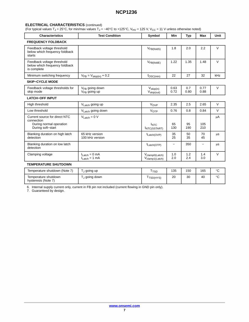
ELECTRICAL CHARACTERISTICS (continued)(For typical values TJ = 25°C, for min/max values TJ = −40°C to +125°C, VHV = 125 V, VCC = 11 V unless otherwise noted)
Characteristics UnitMaxTypMinSymbolTest Condition
FREQUENCY FOLDBACK
Feedback voltage thresholdbelow which frequency foldbackstarts
VFB(foldS) 1.8 2.0 2.2 V
Feedback voltage thresholdbelow which frequency foldbackis complete
VFB(foldE) 1.22 1.35 1.48 V
Minimum switching frequency VFB = Vskip(in) + 0.2 fOSC(min) 22 27 32 kHz
SKIP−CYCLE MODE
Feedback voltage thresholds forskip mode
VFB going downVFB going up
Vskip(in)Vskip(out)
0.630.72
0.70.80
0.770.88
V
LATCH−OFF INPUT
High threshold VLatch going up VOVP 2.35 2.5 2.65 V
Low threshold VLatch going down VOTP 0.76 0.8 0.84 V
Current source for direct NTCconnection
During normal operationDuring soft−start
VLatch = 0 V
INTCINTC(SSTART)
65130
95190
105210
�A
Blanking duration on high latchdetection
65 kHz version100 kHz version
tLatch(OVP) 3525
5035
7045
�s
Blanking duration on low latchdetection
tLatch(OTP) − 350 − �s
Clamping voltage ILatch = 0 mAILatch = 1 mA
Vclamp0(Latch)Vclamp1(Latch)
1.02.0
1.22.4
1.43.0
V
TEMPERATURE SHUTDOWN
Temperature shutdown (Note 7) TJ going up TTSD 135 150 165 °C
Temperature shutdownhysteresis (Note 7)
TJ going down TTSD(HYS) 20 30 40 °C
6. Internal supply current only, current in FB pin not included (current flowing in GND pin only).7. Guaranteed by design.

NCP1236
www.onsemi.com8
TYPICAL PERFORMANCE CHARACTERISTICS
20.00
22.00
24.00
26.00
28.00
30.00
32.00
34.00
36.00
38.00
40.00
−50 −25 0 25 50 75 100 125
Figure 3. Minimum Current Source OperationVHV(min)
TEMPERATURE (°C)
VH
V(m
in) (
V)
0
5
10
15
20
25
30
35
−50 −25 0 25 50 75 100 125
Figure 4. Off−State Leakage Current Istart(off)
TEMPERATURE (°C)
I sta
rt(o
ff) (
V)
90
95
100
105
110
115
120
−50 −25 0 25 50 75 100 125
VH
V(s
tart
) (V
)
TEMPERATURE (°C)
Figure 5. Brown−out Device Start ThresholdVHV(start)
75
80
85
90
95
100
105
−50 −25 0 25 50 75 100 125
TEMPERATURE (°C)
VH
V(s
top)
(V
)
Figure 6. Brown−Out Device Stop ThresholdVHV(stop)
0.65
0.66
0.67
0.68
0.69
0.70
0.71
0.72
0.73
0.74
0.75
−50 −25 0 25 50 75 100 125
VIL
IM (
V)
TEMPERATURE (°C)
Figure 7. Maximum Internal Current SetpointVILIM
0.95
0.97
0.99
1.01
1.03
1.05
1.07
1.09
1.11
1.13
1.15
−50 −25 0 25 50 75 100 125
TEMPERATURE (°C)
VC
S(s
top)
(V
)
Figure 8. Threshold for Immediate FaultProtection Activation VCS(stop)
NCP1236
www.onsemi.com9
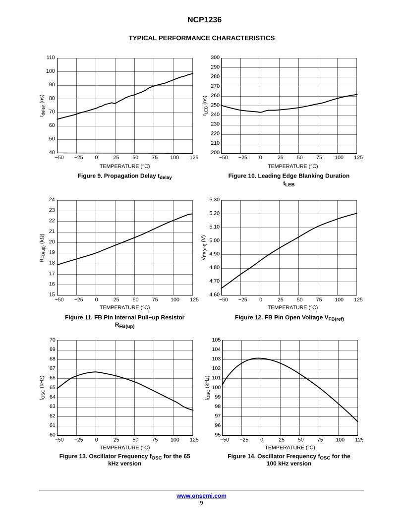
TYPICAL PERFORMANCE CHARACTERISTICS
40
50
60
70
80
90
100
110
−50 −25 0 25 50 75 100 125
TEMPERATURE (°C)
t del
ay (
ns)
Figure 9. Propagation Delay tdelay
60
61
62
63
64
65
66
67
68
69
70
−50 −25 0 25 50 75 100 125
TEMPERATURE (°C)
t LE
B (
ns)
15
16
17
18
19
20
21
22
23
24
−50 −25 0 25 50 75 100 125
TEMPERATURE (°C)
RF
B(u
p) (
k�)
Figure 10. Leading Edge Blanking DurationtLEB
Figure 11. FB Pin Internal Pull−up ResistorRFB(up)
4.60
4.70
4.80
4.90
5.00
5.10
5.20
5.30
−50 −25 0 25 50 75 100 125
VF
B(r
ef) (
V)
TEMPERATURE (°C)
Figure 12. FB Pin Open Voltage VFB(ref)
TEMPERATURE (°C)
f OS
C (
kHz)
Figure 13. Oscillator Frequency fOSC for the 65kHz version
200
210
220
230
240
250
260
270
280
290
300
−50 −25 0 25 50 75 100 125
Figure 14. Oscillator Frequency fOSC for the100 kHz version
95
96
97
98
99
100
101
102
103
104
105
−50 −25 0 25 50 75 100 125
TEMPERATURE (°C)
f OS
C (
kHz)
NCP1236
www.onsemi.com10
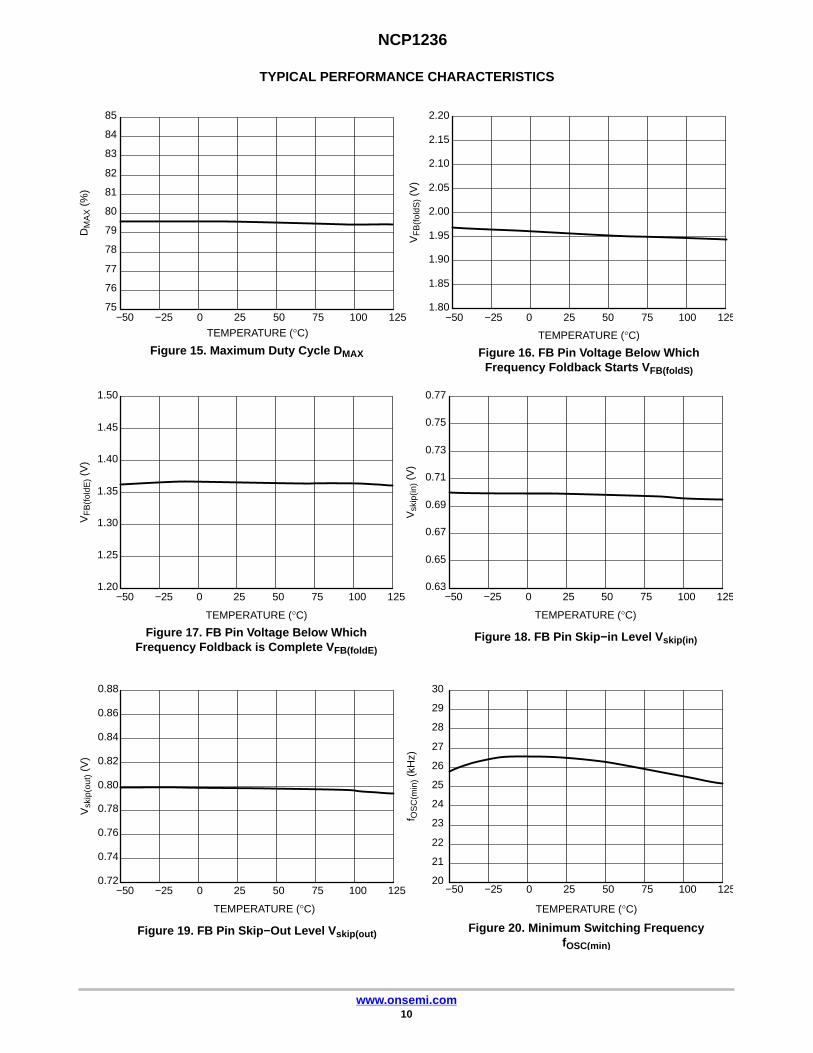
TYPICAL PERFORMANCE CHARACTERISTICS
75
76
77
78
79
80
81
82
83
84
85
−50 −25 0 25 50 75 100 125
TEMPERATURE (°C)
DM
AX (
%)
Figure 15. Maximum Duty Cycle DMAX
1.80
1.85
1.90
1.95
2.00
2.05
2.10
2.15
2.20
−50 −25 0 25 50 75 100 125
VF
B(f
oldS
) (V
)
TEMPERATURE (°C)
Figure 16. FB Pin Voltage Below WhichFrequency Foldback Starts VFB(foldS)
1.20
1.25
1.30
1.35
1.40
1.45
1.50
−50 −25 0 25 50 75 100 125
TEMPERATURE (°C)
VF
B(f
oldE
) (V
)
Figure 17. FB Pin Voltage Below WhichFrequency Foldback is Complete VFB(foldE)
0.63
0.65
0.67
0.69
0.71
0.73
0.75
0.77
−50 −25 0 25 50 75 100 125
Vsk
ip(in
) (V
)
TEMPERATURE (°C)
Figure 18. FB Pin Skip−in Level Vskip(in)
0.72
0.74
0.76
0.78
0.80
0.82
0.84
0.86
0.88
−50 −25 0 25 50 75 100 125
TEMPERATURE (°C)
Vsk
ip(o
ut) (
V)
Figure 19. FB Pin Skip−Out Level Vskip(out)
20
21
22
23
24
25
26
27
28
29
30
−50 −25 0 25 50 75 100 125
f OS
C(m
in) (
kHz)
TEMPERATURE (°C)
Figure 20. Minimum Switching FrequencyfOSC(min)
NCP1236
www.onsemi.com11
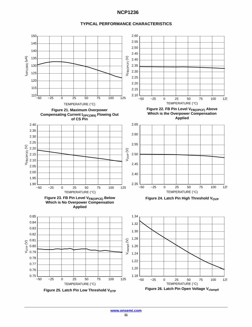
TYPICAL PERFORMANCE CHARACTERISTICS
110
115
120
125
130
135
140
145
150
−50 −25 0 25 50 75 100 125
TEMPERATURE (°C)
I OP
C(3
65) (�A
)
Figure 21. Maximum OverpowerCompensating Current IOPC(365) Flowing Out
of CS Pin
2.10
2.15
2.20
2.25
2.30
2.35
2.40
2.45
2.50
2.55
2.60
−50 −25 0 25 50 75 100 125
Figure 22. FB Pin Level VFB(OPCF) AboveWhich is the Overpower Compensation
Applied
VF
B(O
PC
F) (
V)
TEMPERATURE (°C)
1.90
1.95
2.00
2.05
2.10
2.15
2.20
2.25
2.30
2.35
2.40
−50 −25 0 25 50 75 100 125TEMPERATURE (°C)
VF
B(O
PC
E) (
V)
Figure 23. FB Pin Level VFB(OPCE) BelowWhich is No Overpower Compensation
Applied
2.35
2.40
2.45
2.50
2.55
2.60
2.65
−50 −25 0 25 50 75 100 125
VO
VP (
V)
TEMPERATURE (°C)
Figure 24. Latch Pin High Threshold VOVP
0.75
0.76
0.77
0.78
0.79
0.80
0.81
0.82
0.83
0.84
0.85
−50 −25 0 25 50 75 100 125
TEMPERATURE (°C)
VO
TP (
V)
Figure 25. Latch Pin Low Threshold VOTP
1.18
1.20
1.22
1.24
1.26
1.28
1.30
1.32
1.34
−50 −25 0 25 50 75 100 125
Vcl
amp0
(V
)
TEMPERATURE (°C)
Figure 26. Latch Pin Open Voltage Vclamp0
NCP1236
www.onsemi.com12
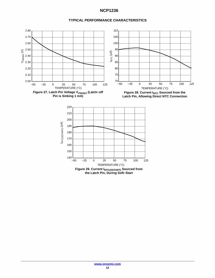
TYPICAL PERFORMANCE CHARACTERISTICS
2.00
2.10
2.20
2.30
2.40
2.50
2.60
2.70
2.80
−50 −25 0 25 50 75 100 125TEMPERATURE (°C)
Vcl
amp1
(V
)
Figure 27. Latch Pin Voltage Vclamp1 (Latch−offPin is Sinking 1 mA)
70
75
80
85
90
95
100
105
110
−50 −25 0 25 50 75 100 125
TEMPERATURE (°C)
I NT
C (�A
)
Figure 28. Current INTC Sourced from theLatch Pin, Allowing Direct NTC Connection
140
150
160
170
180
190
200
210
220
−50 −25 0 25 50 75 100 125
I NT
C(S
STA
RT
) (�A
)
TEMPERATURE (°C)
Figure 29. Current INTC(SSTART) Sourced fromthe Latch Pin, During Soft−Start
NCP1236
www.onsemi.com13
APPLICATION INFORMATION
Introduction
The NCP1236 includes all necessary features to build a safeand efficient power supply based on a fixed−frequencyflyback converter. It is particularly well suited forapplications where low part count is a key parameter,without sacrificing safety.• Current−Mode Operation with slope compensation:
The primary peak current is permanently controlled bythe FB voltage, ensuring maximum safety: the DRVturn−off event is dictated by the peak current setpoint.It also ensures that the frequency response of thesystem stays a first order if in DCM, which eases thedesign of the FB loop. The controller can be also usedin CCM applications with a wide input voltage rangethanks to its fixed ramp compensation that prevents theappearance of sub−harmonic oscillations.
• Fixed−Frequency Oscillator with Jittering: TheNCP1236 is available in different frequency options tofit any application. The internal oscillator features alow−frequency jittering that helps passing the EMIlimits by spreading out the energy content of frequencypeaks in quasi−peak and average mode ofmeasurement.
• Latched / Autorecovery Timer−Based OverloadProtection: The overload protection depends only onthe FB signal, making it able to work with anytransformer, even with very poor coupling or highleakage inductance. When the fault timer elapses thedevice can be permanently latched in version A or thelatch can be reset by an autorecovery restart of thedevice in version B. The power supply has to bestopped then restarted in order to resume operation,even if the overload condition disapears, in case ofusage the A version of the NCP1236. The fault timerduration is internally fixed. The controller also latchesoff if the voltage on the CS pin reaches 1.5 times themaximum internal setpoint (allowing to detect windingshort−circuits), with the same modes of releasing thelatch in A or B version.
• High Voltage Start−Up Current Source withBrown−Out Detection: Due to ON Semiconductor’sVery High Voltage technology, the NCP1236 can bedirectly connected to the high input voltage. Thestart−up current source ensures a clean start−up and theDynamic Self−Supply (DSS) restarting the start−upcurrent source to supply the controller if the VCC
voltage transiently drops. The high voltage pin alsofeatures a high−voltage sensing circuitry, which is ableto turn the controller off if the input voltage is too low(brown−out condition). This protection works eitherwith a DC input voltage or a rectified AC input voltage,and is independent of the high voltage ripple.
• Adjustable Overpower Compensation: The highinput voltage sensed on the HV pin is converted into acurrent to build on the current sense voltage an offsetproportional to the input voltage. By choosing the valueof the resistor in series with the CS pin, the amount ofcompensation can be adjusted to the application.
• Frequency foldback then skip mode for light loadoperation: In order to ensure a high efficiency under allload conditions, the NCP1236 implements a frequencyfoldback for light load condition and a skip mode forextremely low load condition. The switching frequencyis decreased down to 27 kHz to reduce switchinglosses.
• Extended VCC range: The NCP1236 accepts a supplyvoltage as high as 28 V, with an overvoltage thresholdVCC(ovp) (typically 26.5 V) that latches the controlleroff.
• Clamped Driver Stage: Despite the high maximumsupply voltage, the voltage on DRV pin is safelyclamped below 16 V, allowing the use of any standardMOSFET, and reducing the current consumption of thecontroller.
• Dual Latch−off Input: The NCP1236 can be latchedoff by 2 ways: The voltage increase applied to its Latchpin (typically an overvoltage) or by a decrease thisvoltage. Thanks to the internal precise pull−up currentsource a NTC can be directly connected to the latch pin.This NTC will provide an overtemperature protectionby decreasing its resistance and consequently thevoltage at Latch pin,
• Soft−Start: At every start−up the peak current isgradually increased during 4.0 ms to minimize thestress on power components.
• Temperature Shutdown: The NCP1236 is internallyprotected against self−overheating: if the dietemperature is too high, the controller shuts allcircuitries down (including the HV start−up currentsource), allowing the silicon to cool down beforeattempting to restart. This ensures a safe behavior incase of failure.
NCP1236
www.onsemi.com14
Typical Operation• Start−up: The HV start−up current source ensures the
charging of the VCC capacitor up to the start−upthreshold VCC(on), until the input voltage is highenough (above VHV(start)) to allow the switching tostart. The controller then delivers pulses, starting with asoft−start period tSSTART during which the peak currentlinearly increases before the current−mode control takesover. During the soft−start period, the low level latch isignored, and the latch current is double, to ensure a fastpre−charge of the Latch pin decoupling capacitor.
• Normal operation: As long as the feedback voltage iswithin the regulation range and VCC is maintainedabove VCC(min), the NCP1236 runs at a fixed frequency(with jittering) in current−mode control. The peakcurrent (sensed on the CS pin) is set by the voltage onthe FB pin. Fixed ramp compensation is appliedinternally to prevent sub−harmonic oscillations fromoccurring.
• Light load operation: When the FB voltage decreasesbelow VFB(foldS), typically corresponding to a load of33 % of the maximum load (for a DCM design), theswitching frequency starts to decrease down tofOSC(min). By lowering the switching losses, this featurehelps to improve the efficiency in light load conditions.The frequency jittering is enabled in light loadoperation as well.
• No load operation: When the FB voltage decreasesbelow Vskip(in), typically corresponding to a load of 2% of the maximum load, the controller enters skipmode. By completely stopping the switching while thefeedback voltage is below Vskip(out), the losses are
further reduced. This allows minimizing the powerdissipation under extremely low load conditions. As theskip mode is entered at very light loads, for which thepeak current is very small, there is no risk of audiblenoise. VCC can be maintained between VCC(on) andVCC(min) by the DSS, if the auxiliary winding does notprovide sufficient level of VCC voltage under thiscondition.
• Overload: The NCP1236 features timer−basedoverload detection, solely dependent on the feedbackinformation: as soon as the internal peak currentsetpoint hits the VILIM clamp, an internal timer starts tocount. When the timer elapses, the controller stops andenter the protection mode, autorecovery for the Bversion (the controller initiates a new start−up aftertautorec elapses), or latched for the A version (the latchis released if a brown−out event occurs or VCC is reset).
• Brown−out: The NCP1236 features a true AC linemonitoring circuitry. It includes a minimum start−upthreshold and an autorecovery brown−out protection;both of them independent of the ripple on the inputvoltage. It can even work with an unfiltered, rectifiedAC input. The thresholds are fixed, but they aredesigned to fit most of the standard AC−DC conversionapplications.
• Latch−off: When the Latch input is pulled up (typicallyby an over−voltage condition), or pulled down(typically by an over−temperature condition, using theprovided current source with an NTC), the controllerlatches off. A voltage higher than VCC(ovp) on the VCCpin has the same effect. The latch is released when abrown−out condition occurs, or when the VCC is reset.
NCP1236
www.onsemi.com15
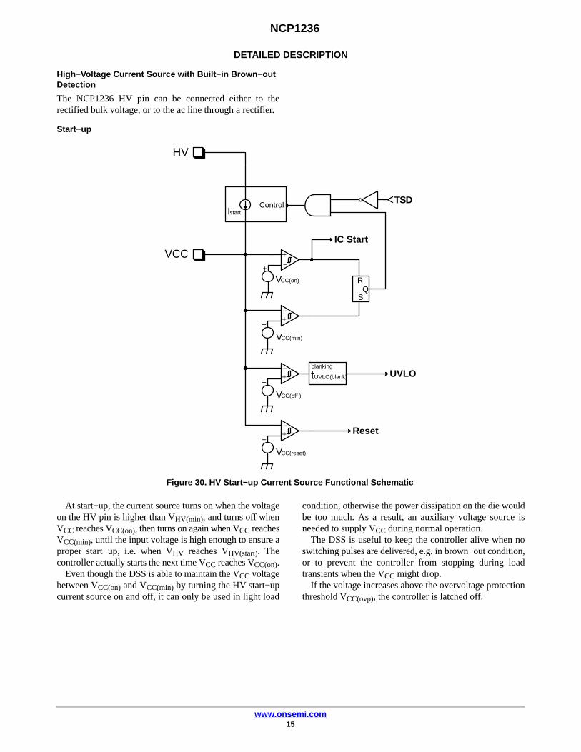
DETAILED DESCRIPTION
High−Voltage Current Source with Built−in Brown−outDetection
The NCP1236 HV pin can be connected either to therectified bulk voltage, or to the ac line through a rectifier.
Start−up
−+
−+
+
+
R
SQ
TSD
HV
VCC
Istart
VCC(on)
VCC(off )
tUVLO(blank)
blanking
Control
UVLO
−+
+
VCC(reset)
Reset
IC Start
−+
+
VCC(min)
Figure 30. HV Start−up Current Source Functional Schematic
At start−up, the current source turns on when the voltageon the HV pin is higher than VHV(min), and turns off whenVCC reaches VCC(on), then turns on again when VCC reachesVCC(min), until the input voltage is high enough to ensure aproper start−up, i.e. when VHV reaches VHV(start). Thecontroller actually starts the next time VCC reaches VCC(on).
Even though the DSS is able to maintain the VCC voltagebetween VCC(on) and VCC(min) by turning the HV start−upcurrent source on and off, it can only be used in light load
condition, otherwise the power dissipation on the die wouldbe too much. As a result, an auxiliary voltage source isneeded to supply VCC during normal operation.
The DSS is useful to keep the controller alive when noswitching pulses are delivered, e.g. in brown−out condition,or to prevent the controller from stopping during loadtransients when the VCC might drop.
If the voltage increases above the overvoltage protectionthreshold VCC(ovp), the controller is latched off.
NCP1236
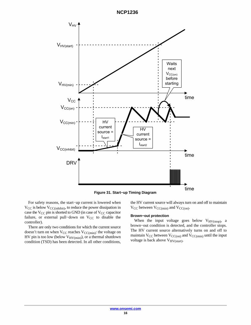
www.onsemi.com16
time
VHV
time
VCC
time
DRV
VHV(start)
VHV(min)
VCC(on)
VCC(min)
VCC(inhibit)
HV
current
source =
Istart1
HV
current
source =
Istart2
Waits
next
VCC(on)
before
starting
Figure 31. Start−up Timing Diagram
For safety reasons, the start−up current is lowered whenVCC is below VCC(inhibit), to reduce the power dissipation incase the VCC pin is shorted to GND (in case of VCC capacitorfailure, or external pull−down on VCC to disable thecontroller).
There are only two conditions for which the current sourcedoesn’t turn on when VCC reaches VCC(min): the voltage onHV pin is too low (below VHV(min)), or a thermal shutdowncondition (TSD) has been detected. In all other conditions,
the HV current source will always turn on and off to maintainVCC between VCC(min) and VCC(on).
Brown−out protectionWhen the input voltage goes below VHV(stop), a
brown−out condition is detected, and the controller stops.The HV current source alternatively turns on and off tomaintain VCC between VCC(on) and VCC(min) until the inputvoltage is back above VHV(start).
NCP1236
www.onsemi.com17
time
HV stop
time
VCC
time
DRV
VCC(on)
VCC(min)
Waits next
VCC(on) before
starting
Brown-out
or AC OVP
detected
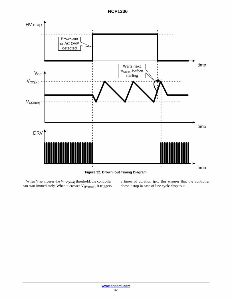
Figure 32. Brown−out Timing Diagram
When VHV crosses the VHV(start) threshold, the controllercan start immediately. When it crosses VHV(stop), it triggers
a timer of duration tHV: this ensures that the controllerdoesn’t stop in case of line cycle drop−out.
NCP1236
www.onsemi.com18
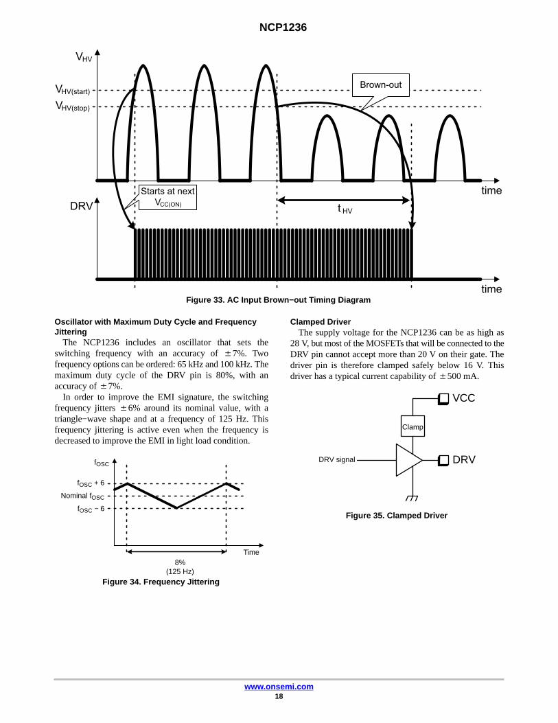
time
VHV
time
DRV
VHV(start)
Starts at next
VCC(ON)
VHV(stop)
Brown-out
HVt
Figure 33. AC Input Brown−out Timing Diagram
Oscillator with Maximum Duty Cycle and FrequencyJittering
The NCP1236 includes an oscillator that sets theswitching frequency with an accuracy of �7%. Twofrequency options can be ordered: 65 kHz and 100 kHz. Themaximum duty cycle of the DRV pin is 80%, with anaccuracy of �7%.
In order to improve the EMI signature, the switchingfrequency jitters �6% around its nominal value, with atriangle−wave shape and at a frequency of 125 Hz. Thisfrequency jittering is active even when the frequency isdecreased to improve the EMI in light load condition.
Time8%
(125 Hz)
Figure 34. Frequency Jittering
fOSC
fOSC + 6
Nominal fOSC
fOSC − 6
Clamped DriverThe supply voltage for the NCP1236 can be as high as
28 V, but most of the MOSFETs that will be connected to theDRV pin cannot accept more than 20 V on their gate. Thedriver pin is therefore clamped safely below 16 V. Thisdriver has a typical current capability of �500 mA.
Figure 35. Clamped Driver
DRV
Clamp
DRV signal
VCC
NCP1236
www.onsemi.com19
CURRENT−MODE CONTROL WITH OVERPOWER COMPENSATION AND SOFT−START
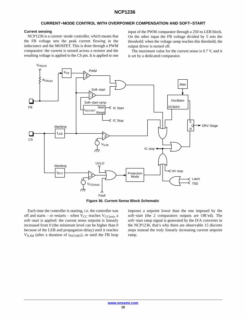
Current sensingNCP1236 is a current−mode controller, which means that
the FB voltage sets the peak current flowing in theinductance and the MOSFET. This is done through a PWMcomparator: the current is sensed across a resistor and theresulting voltage is applied to the CS pin. It is applied to one
input of the PWM comparator through a 250 ns LEB block.On the other input the FB voltage divided by 5 sets thethreshold: when the voltage ramp reaches this threshold, theoutput driver is turned off.
The maximum value for the current sense is 0.7 V, and itis set by a dedicated comparator.
CS
FB
−+
tLEB
blanking
KFB
RFB(up)
−+
−+
−+
+
+
VILIM
VCS(stop)
S
RQ
tSSTART
Soft−start ramp
Start
ResetIC Start
IC Stop
Oscillator
DCMAX
ProtectionMode
UVLO
Jitter
HV stop
Latch
Soft−start
IC stop
TSD
Fault
DRV Stage
blanking
PWM
tBCS
Figure 36. Current Sense Block Schematic
VFB(ref)
Each time the controller is starting, i.e. the controller wasoff and starts – or restarts – when VCC reaches VCC(on), asoft−start is applied: the current sense setpoint is linearlyincreased from 0 (the minimum level can be higher than 0because of the LEB and propagation delay) until it reachesVILIM (after a duration of tSSTART), or until the FB loop
imposes a setpoint lower than the one imposed by thesoft−start (the 2 comparators outputs are OR’ed). Thesoft−start ramp signal is generated by the D/A converter inthe NCP1236, that’s why there are observable 15 discretesteps instead the truly linearly increasing current setpointramp.
NCP1236
www.onsemi.com20
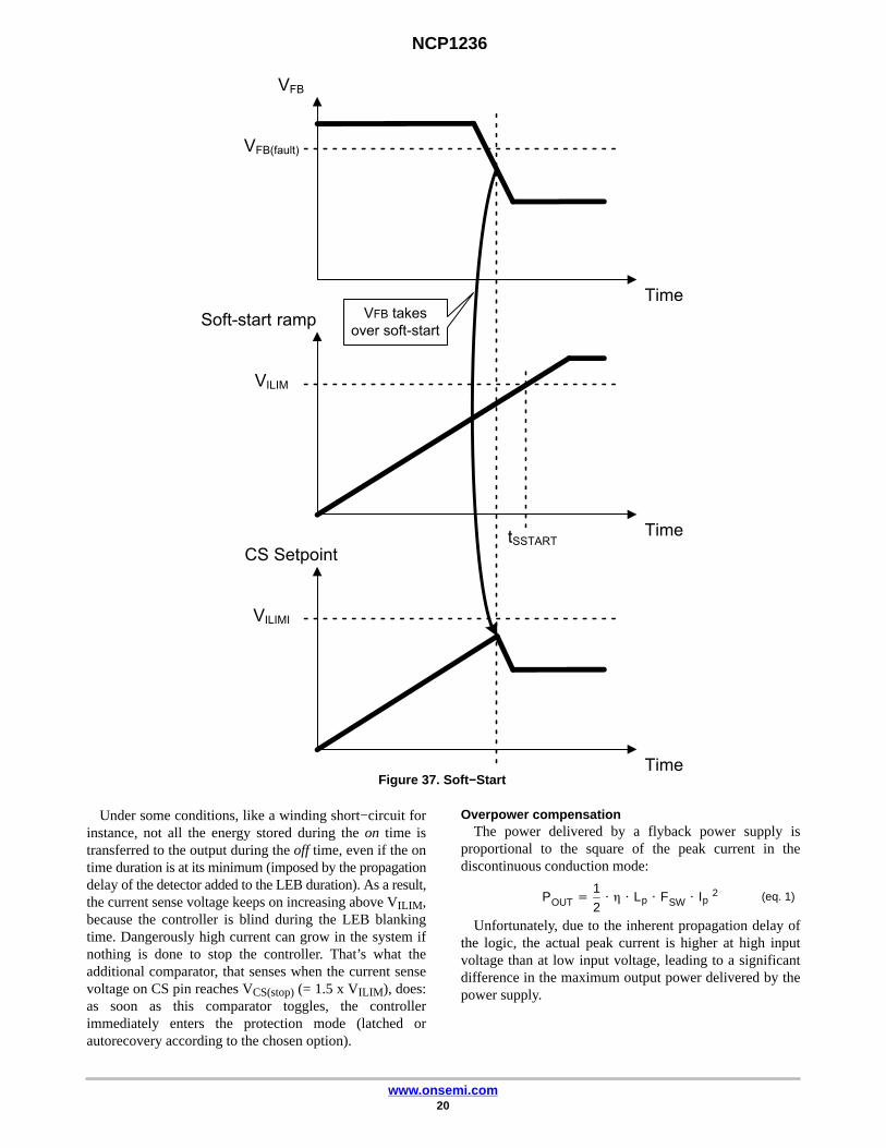
Time
VFB
VFB(fault)
Time
Soft-start ramp
VILIM
tSSTART
Time
CS Setpoint
VILIMI
VFB takes
over soft-start
Figure 37. Soft−Start
Under some conditions, like a winding short−circuit forinstance, not all the energy stored during the on time istransferred to the output during the off time, even if the ontime duration is at its minimum (imposed by the propagationdelay of the detector added to the LEB duration). As a result,the current sense voltage keeps on increasing above VILIM,because the controller is blind during the LEB blankingtime. Dangerously high current can grow in the system ifnothing is done to stop the controller. That’s what theadditional comparator, that senses when the current sensevoltage on CS pin reaches VCS(stop) (= 1.5 x VILIM), does:as soon as this comparator toggles, the controllerimmediately enters the protection mode (latched orautorecovery according to the chosen option).
Overpower compensationThe power delivered by a flyback power supply is
proportional to the square of the peak current in thediscontinuous conduction mode:
POUT �1
2� � � Lp � FSW � Ip 2 (eq. 1)
Unfortunately, due to the inherent propagation delay ofthe logic, the actual peak current is higher at high inputvoltage than at low input voltage, leading to a significantdifference in the maximum output power delivered by thepower supply.
NCP1236
www.onsemi.com21
time
IP
High
LineLow
Line
ILIMIT
tdelay tdelay
IP to be
compensated
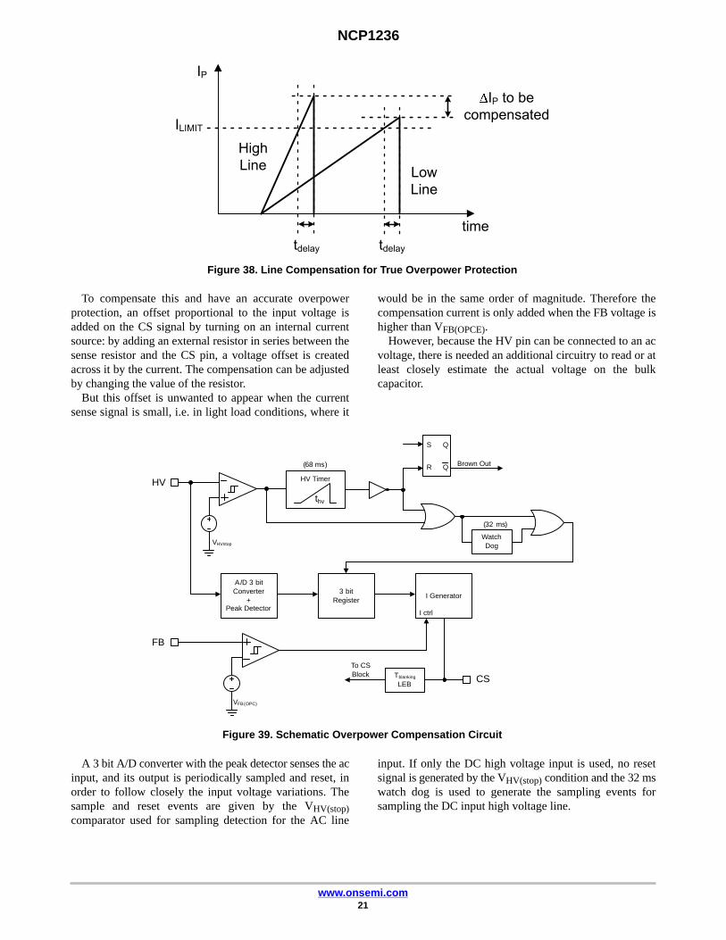
Figure 38. Line Compensation for True Overpower Protection
To compensate this and have an accurate overpowerprotection, an offset proportional to the input voltage isadded on the CS signal by turning on an internal currentsource: by adding an external resistor in series between thesense resistor and the CS pin, a voltage offset is createdacross it by the current. The compensation can be adjustedby changing the value of the resistor.
But this offset is unwanted to appear when the currentsense signal is small, i.e. in light load conditions, where it
would be in the same order of magnitude. Therefore thecompensation current is only added when the FB voltage ishigher than VFB(OPCE).
However, because the HV pin can be connected to an acvoltage, there is needed an additional circuitry to read or atleast closely estimate the actual voltage on the bulkcapacitor.
A/D 3 bitConverter
+Peak Detector
Tblanking
LEB
WatchDog
HV
CS
FB
VHVstop
Q
QS
R
HV Timer
(68 ms)
(32 ms)
3 bitRegister
I Generator
Brown Out
thv
VFB(OPC)
To CSBlock
I ctrl
Figure 39. Schematic Overpower Compensation Circuit
A 3 bit A/D converter with the peak detector senses the acinput, and its output is periodically sampled and reset, inorder to follow closely the input voltage variations. Thesample and reset events are given by the VHV(stop)comparator used for sampling detection for the AC line
input. If only the DC high voltage input is used, no resetsignal is generated by the VHV(stop) condition and the 32 mswatch dog is used to generate the sampling events forsampling the DC input high voltage line.

NCP1236
www.onsemi.com22
VFB
IOPC
VFB(OPCE) VFB(OPCF)
VHV
Figure 40. Overpower Compensation Current Relation to Feedback Voltage and Input Voltage
time
time
Sample/resetsignal
time
Peakdetector
HVtimerstarts
HVtimer
restarts
HVtimer
restarts
tHV
time
time
One shotHV
timerrestarts
SampleSample
Sample Sample
ResetReset
Reset
Reset
Reset
Reset
Figure 41. Overpower Compensation
IOPC
VHV(stop)
VHV
NCP1236
www.onsemi.com23
time
time
Peakdetector
time
Sample
Sample Sample
Reset
Reset
VHV
VHV(stop)
IOPC
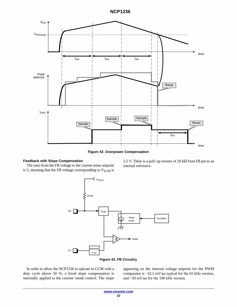
Figure 42. Overpower Compensation
twd twd twd
tHV
Feedback with Slope CompensationThe ratio from the FB voltage to the current sense setpoint
is 5, meaning that the FB voltage corresponding to VILIM is
3.5 V. There is a pull−up resistor of 20 k� from FB pin to aninternal reference.
CS
FB
−
+
blanking
Oscillator
20 k�
K FB
slopecomp.
PWM
VFB(ref)
Figure 43. FB Circuitry
tLEB
In order to allow the NCP1236 to operate in CCM with aduty cycle above 50 %, a fixed slope compensation isinternally applied to the current−mode control. The slope
appearing on the internal voltage setpoint for the PWMcomparator is −32.5 mV/�s typical for the 65 kHz version,and −50 mV/�s for the 100 kHz version.

NCP1236
www.onsemi.com24
Overcurrent protection with Fault timerWhen an overcurrent occurs on the output of the power
supply, the FB loop asks for more power than the controllercan deliver, and the CS setpoint reaches VILIMIT. When thisevent occurs, an internal tfault timer is started: once the timerelapsed, DRV pulses are stopped and the controller is either
latched off (latched protection, version A), or it enters anautorecovery mode (version B). The timer is reset when theCS setpoint goes back below VILIM before the timer elapses.The fault timer is also started if the driver signal is reset bythe max duty cycle.
CS
FB−+
tLEB
blanking
/ 5
−+
+
VILIM
ProtectionMode
Brown−out
tfault
timer
release
t autorec
timer
Reset
Autorecoveryprotectionmode only
R
SQ
PWM
Reset DRV
Fault Flag
DC MAX
DRVFigure 44. Timer−Based Overcurrent Protection
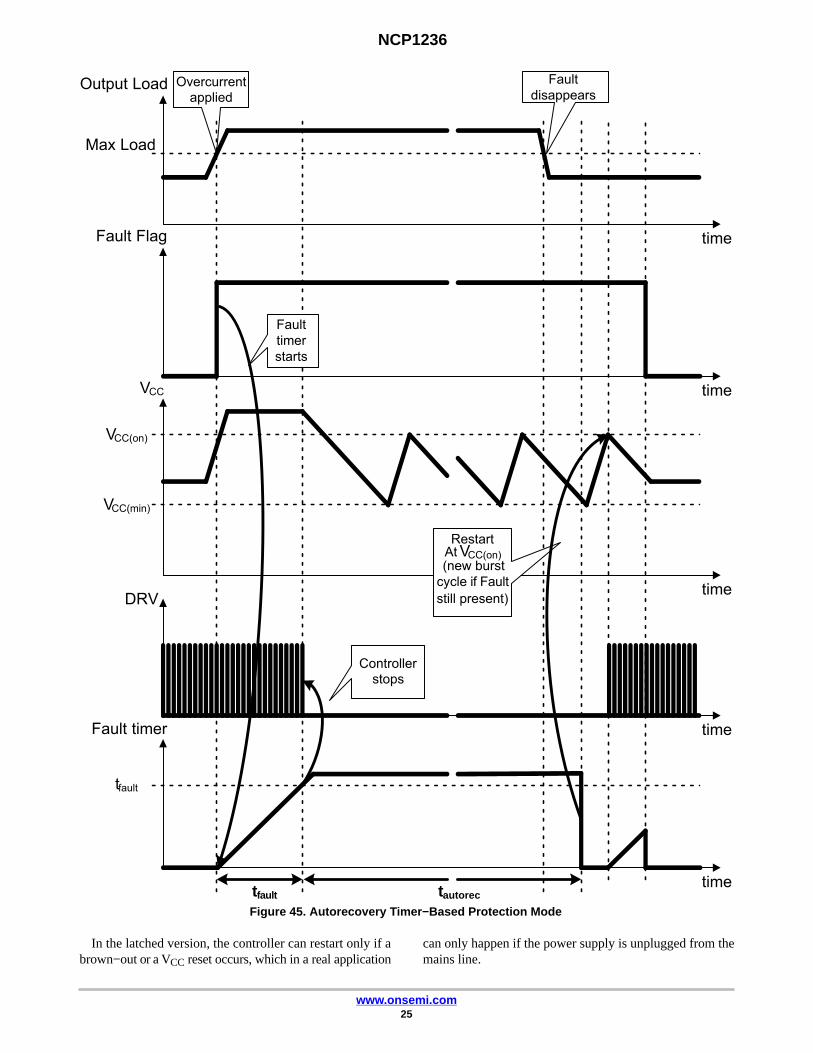
In autorecovery mode, the controller tries to restart aftertautorec. If the fault has gone, the supply resumes operation;if not, the system starts a new burst cycle.
NCP1236
www.onsemi.com25
time
Fault Flag
time
VCC
time
DRV
VCC(on)
VCC(min)
Overcurrent
applied
time
Output Load
Max Load
time
Fault timer
tfault
Fault
timer
starts
Controller
stops
Fault
disappears
tfault tautorec
RestartAt VCC(on)(new burst
cycle if Fault
still present)
Figure 45. Autorecovery Timer−Based Protection Mode
In the latched version, the controller can restart only if abrown−out or a VCC reset occurs, which in a real application
can only happen if the power supply is unplugged from themains line.
NCP1236
www.onsemi.com26
time
Fault Flag
time
VCC
time
DRV
VCC(on)
VCC(min)
Overcurrent
applied
time
Output Load
Max Load
time
Fault timer
tfault
Fault
timer
starts
Controller
latches off
No restart
when faultdisappears
tfault
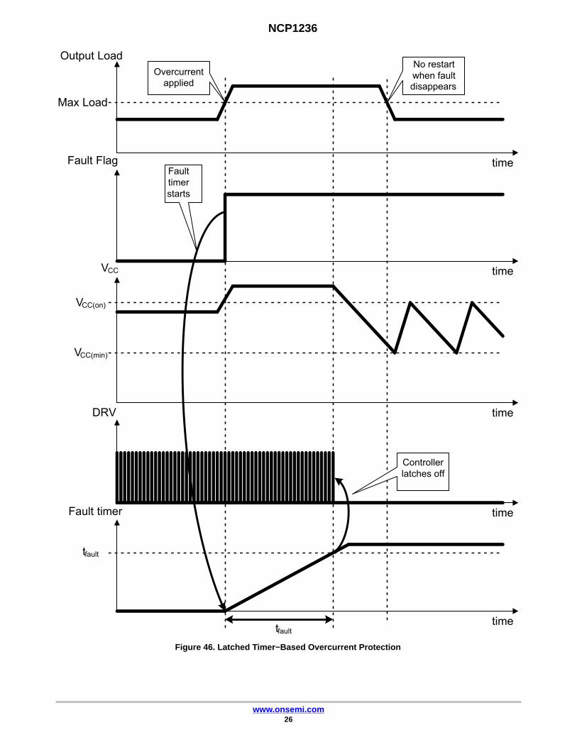
Figure 46. Latched Timer−Based Overcurrent Protection
NCP1236
www.onsemi.com27
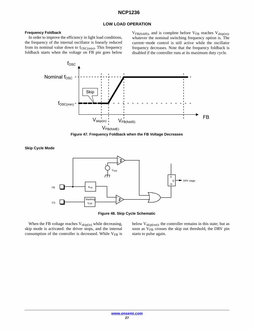
LOW LOAD OPERATION
Frequency FoldbackIn order to improve the efficiency in light load conditions,
the frequency of the internal oscillator is linearly reducedfrom its nominal value down to fOSC(min). This frequencyfoldback starts when the voltage on FB pin goes below
VFB(foldS), and is complete before VFB reaches Vskip(in),whatever the nominal switching frequency option is. Thecurrent−mode control is still active while the oscillatorfrequency decreases. Note that the frequency foldback isdisabled if the controller runs at its maximum duty cycle.
FB
fOSC
Nominal fOSC
Vskip(in) VFB(foldS)
fOSC(min)
Skip
Figure 47. Frequency Foldback when the FB Voltage Decreases
VFB(foldE)
Skip Cycle Mode
Figure 48. Skip Cycle Schematic
−
+
CS
S
RQ
FB
blanking−
+
+
DRV stage
Vskip
KFB
tLEB
When the FB voltage reaches Vskip(in) while decreasing,skip mode is activated: the driver stops, and the internalconsumption of the controller is decreased. While VFB is
below Vskip(out), the controller remains in this state; but assoon as VFB crosses the skip out threshold, the DRV pinstarts to pulse again.

NCP1236
www.onsemi.com28
Time
Time
DRV
Enters
skip
Exits
skip
Enters
skip
Exits
skip
Figure 49. Skip Cycle Timing Diagram
VFB
VFB(fold)
Vskip(out)Vskip(in)
Latch−off Input
−+
Latch
VOVP
S
RQ
−+
VOTP
tLatch(OVP)
blankingVDD
Brown−outReset
Latch
Vclamp
INTC
tLatch(OTP)
blanking
1 k�
INTC
+
+
Soft−startend
Figure 50. Latch Detection Schematic
The Latch pin is dedicated to the latch−off function: itincludes two levels of detection that define a workingwindow, between a high latch and a low latch: within thesetwo thresholds, the controller is allowed to run; but as soonas either the low or the high threshold is crossed, thecontroller is latched off. The lower threshold is intended tobe used with an NTC thermistor, thanks to an internal currentsource INTC.
An active clamp prevents the voltage from reaching thehigh threshold if it is only pulled up by the INTC current. Toreach the high threshold, the pull−up current has to be higherthan the pull−down capability of the clamp (typically1.5 mA at VOVP).
To avoid any false triggering, spikes shorter than 50 �s(for the high latch) or 350 �s (for the low latch) are blankedand only longer signals can actually latch the controller.
Reset occurs when a brown−out condition is detected orthe VCC is cycled down to a reset voltage, which in a realapplication can only happen if the power supply isunplugged from the AC line.
Upon start−up, the internal references take some timebefore being at their nominal values; so one of thecomparators could toggle even if it should not. Therefore theinternal logic does not take the latch signal into accountbefore the controller is ready to start: once VCC reachesVCC(on), the latch pin High latch state is taken into account

NCP1236
www.onsemi.com29
and the DRV switching starts only if it is allowed; whereasthe Low latch (typically sensing an overtemperature) istaken into account only after the soft−start is finished. Inaddition, the NTC current is doubled to INTC(SSTART) duringthe soft−start period, to speed up the charging of the Latchpin capacitor. The maximum value of Latch pin capacitor isgiven by the following formula (The standard start−upcondition is considered and the NTC current is neglected) :
CLATCHmax �tSSTARTmin � INTC(SSTART)min
Vclamp0min (eq. 2)
�2.8 � 10−3 � 130 � 10−6
1.0F � 364 nF
time
Internal Latch Signaltime
VCC
time
DRV
VCC(on)
VCC(min)
Latch signal
high during
pre-start phase
Noise spike
ignored
(tLatch blanking)
Start-up
initiated by
VCC(on)
Switching
allowed (no
latch event)
Latch-off
Figure 51. Latch−off Function Timing Diagram
Temperature ShutdownThe die includes a temperature shutdown protection with
a trip point guaranteed above 135°C and below 165°C, anda typical hysteresis of 30°C. When the temperature risesabove the high threshold, the controller stops switching
instantaneously, and the HV current source is turned off.Internal logic state is reset. When the temperature fallsbelow the low threshold, the HV start−up current source isenabled, and a regular start−up sequence takes place.
NCP1236
www.onsemi.com30
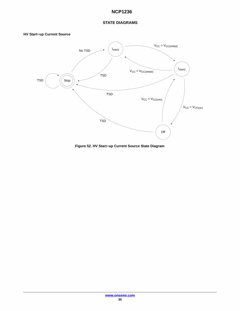
STATE DIAGRAMS
HV Start−up Current Source
Stop
Istart1
Istart2
Off
No TSD
TSD
TSD
VCC > VCC(inhibit)
VCC < VCC(inhibit)
VCC > VCC(on)
VCC < VCC(min)
TSD
TSD
Figure 52. HV Start−up Current Source State Diagram
NCP1236
www.onsemi.com31
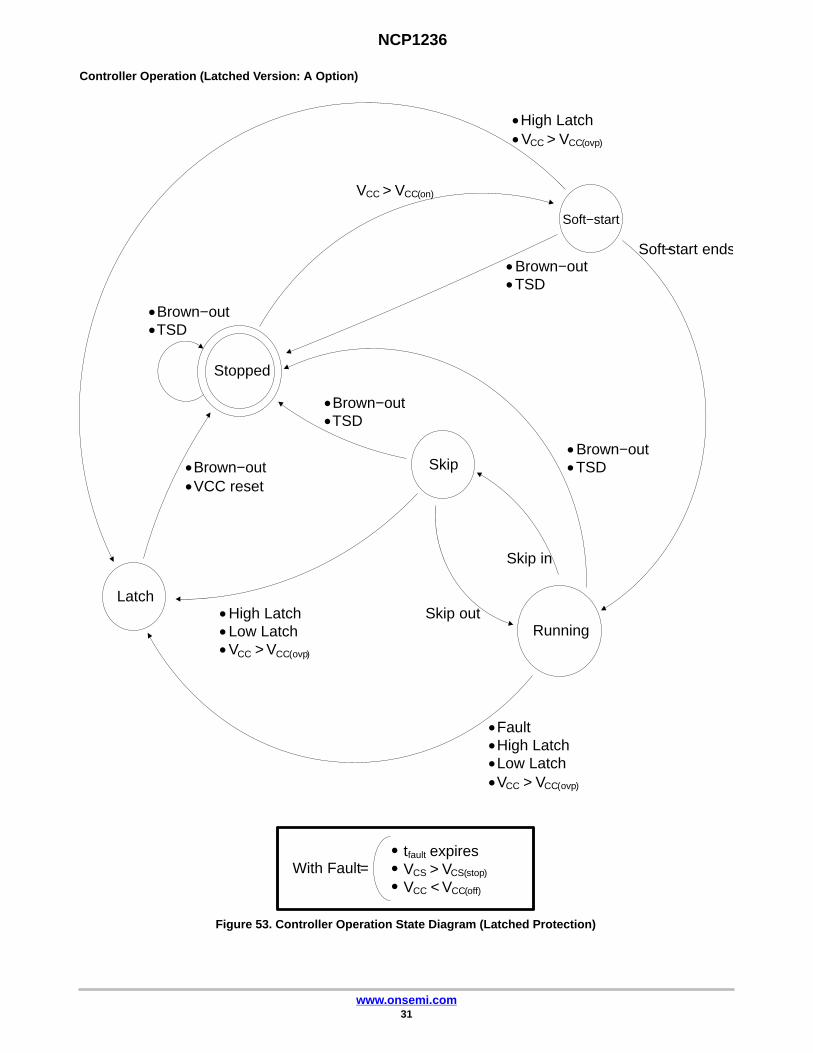
Controller Operation (Latched Version: A Option)
Stopped
Running
• Brown−out• TSD
VCC > VCC(on)
• Brown−out• TSD
Skip out
With Fault= • tfault expires • VCS > VCS(stop)
• VCC < VCC(off)
Soft−start
Soft−start ends
Skip
Skip in
• Brown−out• TSD
• Brown−out• TSD
Latch
• Brown−out• VCC reset
•High Latch• VCC > VCC(ovp)
• High Latch• Low Latch• VCC > VCC(ovp)
• Fault• High Latch• Low Latch• VCC > VCC(ovp)
Figure 53. Controller Operation State Diagram (Latched Protection)
NCP1236
www.onsemi.com32
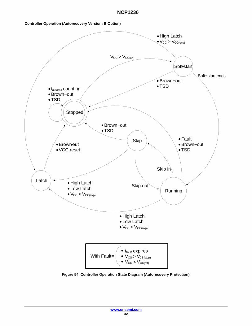
Controller Operation (Autorecovery Version: B Option)
Stopped
Running
• Fault• Brown−out• TSD
VCC > VCC(on)
• tautorec counting• Brown−out• TSD
Skip out
With Fault= • tfault expires • VCS > VCS(stop)
• VCC < VCC(off)
Soft−start
Soft−start ends
Skip
Skip in
• Brown−out• TSD
• Brown−out• TSD
Latch
• Brown−out• VCC reset
•High Latch• VCC > VCC(ovp)
• High Latch• Low Latch• VCC > VCC(ovp)
• High Latch• Low Latch• VCC > VCC(ovp)
Figure 54. Controller Operation State Diagram (Autorecovery Protection)
NCP1236
www.onsemi.com33
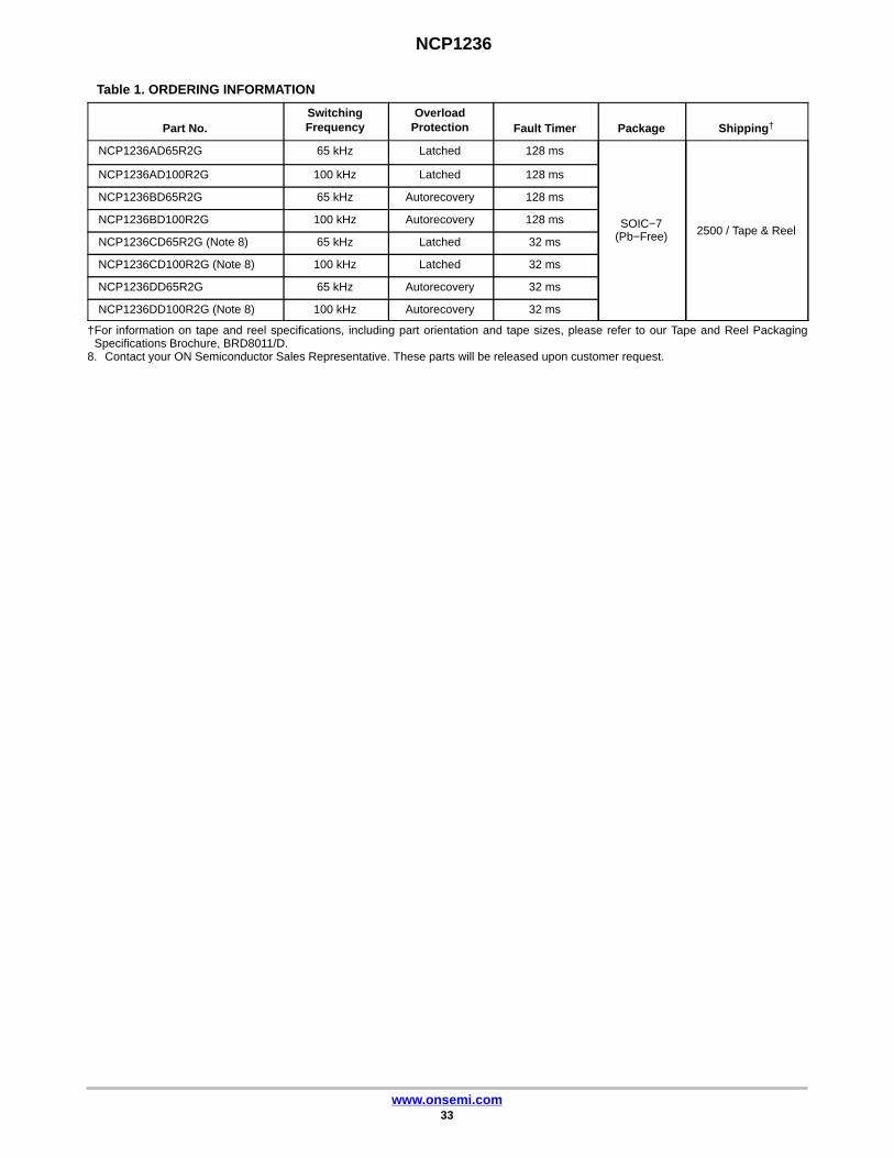
Table 1. ORDERING INFORMATION
Part No.SwitchingFrequency
OverloadProtection Fault Timer Package Shipping†
NCP1236AD65R2G 65 kHz Latched 128 ms
SOIC−7(Pb−Free) 2500 / Tape & Reel
NCP1236AD100R2G 100 kHz Latched 128 ms
NCP1236BD65R2G 65 kHz Autorecovery 128 ms
NCP1236BD100R2G 100 kHz Autorecovery 128 ms
NCP1236CD65R2G (Note 8) 65 kHz Latched 32 ms
NCP1236CD100R2G (Note 8) 100 kHz Latched 32 ms
NCP1236DD65R2G 65 kHz Autorecovery 32 ms
NCP1236DD100R2G (Note 8) 100 kHz Autorecovery 32 ms
†For information on tape and reel specifications, including part orientation and tape sizes, please refer to our Tape and Reel PackagingSpecifications Brochure, BRD8011/D.
8. Contact your ON Semiconductor Sales Representative. These parts will be released upon customer request.
NCP1236
www.onsemi.com34
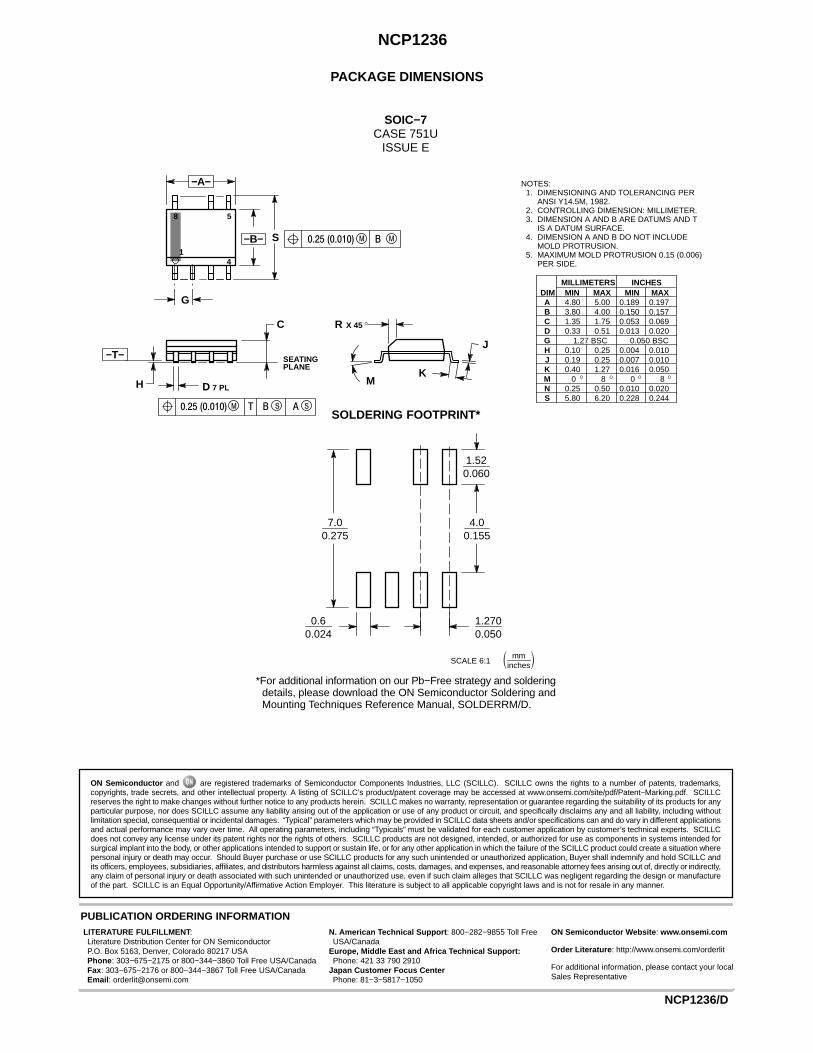
PACKAGE DIMENSIONS
SOIC−7CASE 751U
ISSUE E
SEATINGPLANE
14
58
R
J
X 45�
K
NOTES:1. DIMENSIONING AND TOLERANCING PER
ANSI Y14.5M, 1982.2. CONTROLLING DIMENSION: MILLIMETER.3. DIMENSION A AND B ARE DATUMS AND T
IS A DATUM SURFACE.4. DIMENSION A AND B DO NOT INCLUDE
MOLD PROTRUSION.5. MAXIMUM MOLD PROTRUSION 0.15 (0.006)
PER SIDE.
S
DH
C
DIMA
MIN MAX MIN MAXINCHES
4.80 5.00 0.189 0.197
MILLIMETERS
B 3.80 4.00 0.150 0.157C 1.35 1.75 0.053 0.069D 0.33 0.51 0.013 0.020G 1.27 BSC 0.050 BSCH 0.10 0.25 0.004 0.010J 0.19 0.25 0.007 0.010K 0.40 1.27 0.016 0.050M 0 8 0 8 N 0.25 0.50 0.010 0.020S 5.80 6.20 0.228 0.244
−A−
−B−
G
MBM0.25 (0.010)
−T−
BM0.25 (0.010) T S A S
M7 PL
� � � �
1.520.060
7.00.275
0.60.024
1.2700.050
4.00.155
� mminches
�SCALE 6:1
*For additional information on our Pb−Free strategy and solderingdetails, please download the ON Semiconductor Soldering andMounting Techniques Reference Manual, SOLDERRM/D.
SOLDERING FOOTPRINT*
ON Semiconductor and are registered trademarks of Semiconductor Components Industries, LLC (SCILLC). SCILLC owns the rights to a number of patents, trademarks,copyrights, trade secrets, and other intellectual property. A listing of SCILLC’s product/patent coverage may be accessed at www.onsemi.com/site/pdf/Patent−Marking.pdf. SCILLCreserves the right to make changes without further notice to any products herein. SCILLC makes no warranty, representation or guarantee regarding the suitability of its products for anyparticular purpose, nor does SCILLC assume any liability arising out of the application or use of any product or circuit, and specifically disclaims any and all liability, including withoutlimitation special, consequential or incidental damages. “Typical” parameters which may be provided in SCILLC data sheets and/or specifications can and do vary in different applicationsand actual performance may vary over time. All operating parameters, including “Typicals” must be validated for each customer application by customer’s technical experts. SCILLCdoes not convey any license under its patent rights nor the rights of others. SCILLC products are not designed, intended, or authorized for use as components in systems intended forsurgical implant into the body, or other applications intended to support or sustain life, or for any other application in which the failure of the SCILLC product could create a situation wherepersonal injury or death may occur. Should Buyer purchase or use SCILLC products for any such unintended or unauthorized application, Buyer shall indemnify and hold SCILLC andits officers, employees, subsidiaries, affiliates, and distributors harmless against all claims, costs, damages, and expenses, and reasonable attorney fees arising out of, directly or indirectly,any claim of personal injury or death associated with such unintended or unauthorized use, even if such claim alleges that SCILLC was negligent regarding the design or manufactureof the part. SCILLC is an Equal Opportunity/Affirmative Action Employer. This literature is subject to all applicable copyright laws and is not for resale in any manner.
PUBLICATION ORDERING INFORMATIONN. American Technical Support: 800−282−9855 Toll FreeUSA/Canada
Europe, Middle East and Africa Technical Support:Phone: 421 33 790 2910
Japan Customer Focus CenterPhone: 81−3−5817−1050
NCP1236/D
LITERATURE FULFILLMENT:Literature Distribution Center for ON SemiconductorP.O. Box 5163, Denver, Colorado 80217 USAPhone: 303−675−2175 or 800−344−3860 Toll Free USA/CanadaFax: 303−675−2176 or 800−344−3867 Toll Free USA/CanadaEmail: [email protected]
ON Semiconductor Website: www.onsemi.com
Order Literature: http://www.onsemi.com/orderlit
For additional information, please contact your localSales Representative
Related Documents