1FEATURES DESCRIPTION APPLICATIONS bq77PL900 www.ti.com ...................................................................................................................................................... SLUS844B–JUNE 2008–REVISED JANUARY 2009 Five to Ten Series Cell Lithium-Ion or Lithium-Polymer Battery Protector and Analog Front End • 5, 6, 7, 8, 9, or 10 Series-Cell Primary Protection The bq77PL900 is a five to ten series cell lithium-ion battery pack protector. The integrated I 2 C • PMOS FET Drive for Charge and Discharge communications interface allows the bq77PL900 also FETs to be as an analog front end (AFE) for a Host • Capable of Operation with 1-mΩ Sense controller. Two LDOs, one 5-V, 25-mA and one 3.3-V, Resistor 25-mA, are also included and may be used to power • Supply Voltage Range from 7 V to 50 V a host controller or support circuitry. • Low Supply Current of 450 μA Typical The bq77PL900 integrates a voltage translation • Integrated 5-V, 25-mA LDO system to extract battery parameters such as individual cell voltages and charge/discharge current. • Integrated 3.3-V, 25-mA LDO Variables such as voltage protection thresholds and • Stand-Alone Mode detection delay times can be programmed by using – Pack Protection Control and Recovery the internal EEPROM. – Individual Cell Monitoring The bq77PL900 can act as a stand-alone – Integrated Cell Balancing self-contained battery protection system (stand-alone mode). It can alternatively be combined with a host – Programmable Threshold and Delay Time microcontroller to offer fuel gauge or other battery for management capabilities to the host system – Overvoltage (host-control mode). – Undervoltage The bq77PL900 provides full safety protection for – Overcurrent in Discharge overvoltage, undervoltage, overcurrent in discharge, and short circuit in discharge conditions. When the – Short Circuit in Discharge EEPROM programmable safety thresholds are – Fixed Overtemperature Protection reached, the bq77PL900 turns off the FET drive • Host Control Mode autonomously. No external components are needed – I 2 C Interface to Host Controller to configure the protection features. – Analog Interface for Host Cell Measurement The analog front end (AFE) outputs allow a host and System Charge/Discharge Current controller to observe individual cell voltages and charge/discharge currents. The host controller’s – Host-Controlled Protection Recovery analog-to-digital converter connects to the – Host-Controlled Cell Balancing bq77PL900 to acquire these values. Cell balancing can be performed autonomously, or the host controller can activate it individually via a cell • Cordless Power Tools bypass path integrated into the bq77PL900. Internal • Power Assisted Bicycle/Scooter control registers accessible via the I 2 C interface • Uninterruptible Power Supply (UPS) Systems configure this operation. The maximum balancing • Medical Equipment bypass current is set via an external series resistor and the internal FET-on resistance (typically 400 Ω). • Portable Test Equipment Optionally, external bypass cell balance FETs can be used for increased current capability. 1 Please be aware that an important notice concerning availability, standard warranty, and use in critical applications of Texas Instruments semiconductor products and disclaimers thereto appears at the end of this data sheet. PRODUCTION DATA information is current as of publication date. Copyright © 2008–2009, Texas Instruments Incorporated Products conform to specifications per the terms of the Texas Instruments standard warranty. Production processing does not necessarily include testing of all parameters.

Welcome message from author
This document is posted to help you gain knowledge. Please leave a comment to let me know what you think about it! Share it to your friends and learn new things together.
Transcript
1FEATURESDESCRIPTION
APPLICATIONS
bq77PL900
www.ti.com ...................................................................................................................................................... SLUS844B–JUNE 2008–REVISED JANUARY 2009
Five to Ten Series Cell Lithium-Ion or Lithium-Polymer Battery Protectorand Analog Front End
• 5, 6, 7, 8, 9, or 10 Series-Cell PrimaryProtection The bq77PL900 is a five to ten series cell lithium-ion
battery pack protector. The integrated I2C• PMOS FET Drive for Charge and Dischargecommunications interface allows the bq77PL900 alsoFETsto be as an analog front end (AFE) for a Host• Capable of Operation with 1-mΩ Sense controller. Two LDOs, one 5-V, 25-mA and one 3.3-V,Resistor 25-mA, are also included and may be used to power
• Supply Voltage Range from 7 V to 50 V a host controller or support circuitry.• Low Supply Current of 450 µA Typical The bq77PL900 integrates a voltage translation• Integrated 5-V, 25-mA LDO system to extract battery parameters such as
individual cell voltages and charge/discharge current.• Integrated 3.3-V, 25-mA LDOVariables such as voltage protection thresholds and• Stand-Alone Mode detection delay times can be programmed by using
– Pack Protection Control and Recovery the internal EEPROM.– Individual Cell Monitoring The bq77PL900 can act as a stand-alone– Integrated Cell Balancing self-contained battery protection system (stand-alone
mode). It can alternatively be combined with a host– Programmable Threshold and Delay Timemicrocontroller to offer fuel gauge or other batteryformanagement capabilities to the host system
– Overvoltage (host-control mode).– Undervoltage The bq77PL900 provides full safety protection for– Overcurrent in Discharge overvoltage, undervoltage, overcurrent in discharge,
and short circuit in discharge conditions. When the– Short Circuit in DischargeEEPROM programmable safety thresholds are– Fixed Overtemperature Protectionreached, the bq77PL900 turns off the FET drive
• Host Control Mode autonomously. No external components are needed– I2C Interface to Host Controller to configure the protection features.– Analog Interface for Host Cell Measurement The analog front end (AFE) outputs allow a host
and System Charge/Discharge Current controller to observe individual cell voltages andcharge/discharge currents. The host controller’s– Host-Controlled Protection Recoveryanalog-to-digital converter connects to the– Host-Controlled Cell Balancing bq77PL900 to acquire these values.
Cell balancing can be performed autonomously, orthe host controller can activate it individually via a cell• Cordless Power Toolsbypass path integrated into the bq77PL900. Internal• Power Assisted Bicycle/Scooter control registers accessible via the I2C interface
• Uninterruptible Power Supply (UPS) Systems configure this operation. The maximum balancing• Medical Equipment bypass current is set via an external series resistor
and the internal FET-on resistance (typically 400 Ω).• Portable Test EquipmentOptionally, external bypass cell balance FETs can beused for increased current capability.
1
Please be aware that an important notice concerning availability, standard warranty, and use in critical applications of TexasInstruments semiconductor products and disclaimers thereto appears at the end of this data sheet.
PRODUCTION DATA information is current as of publication date. Copyright © 2008–2009, Texas Instruments IncorporatedProducts conform to specifications per the terms of the TexasInstruments standard warranty. Production processing does notnecessarily include testing of all parameters.

TYPICAL IMPLEMENTATION
LDO, Thermal Output Drive
Pack +
Cell Balance Drive
Overload Protection
Overvoltage/Undervoltage Protection
bq77PL900
PCH FET Drive
RAM Registers
Sense Resistor
Short-Circuit Protection
Serial Interface
Pack –
Discharge
Fuse
Charge
B0323-01
bq77PL900
SLUS844B–JUNE 2008–REVISED JANUARY 2009 ...................................................................................................................................................... www.ti.com
These devices have limited built-in ESD protection. The leads should be shorted together or the device placed in conductive foamduring storage or handling to prevent electrostatic damage to the MOS gates.
Figure 1. Stand-Alone Mode
2 Submit Documentation Feedback Copyright © 2008–2009, Texas Instruments Incorporated
Product Folder Link(s): bq77PL900

LDO, Thermal Output Drive
Pack +
Cell Voltage Output, Cell Balance
Overload Protection
Overvoltage/Undervoltage Protection
bq77PL900
PCH FET Drive
Sense Resistor
Short-Circuit Protection
Pack –
Fuse
RAM RegistersSerial Interface
B0324-01
Voltage OutputSafety and Power
ManagementControl
Microprocessor
3.3 V or 5 V
XRST
Battery Capacity Monitor
Cell Balance Algorithmand Control
Thermal Measurement
Serial Interface
Serial InterfaceRAM ROM
NTC
bq77PL900
www.ti.com ...................................................................................................................................................... SLUS844B–JUNE 2008–REVISED JANUARY 2009
Figure 2. Host-Control Mode
Copyright © 2008–2009, Texas Instruments Incorporated Submit Documentation Feedback 3
Product Folder Link(s): bq77PL900
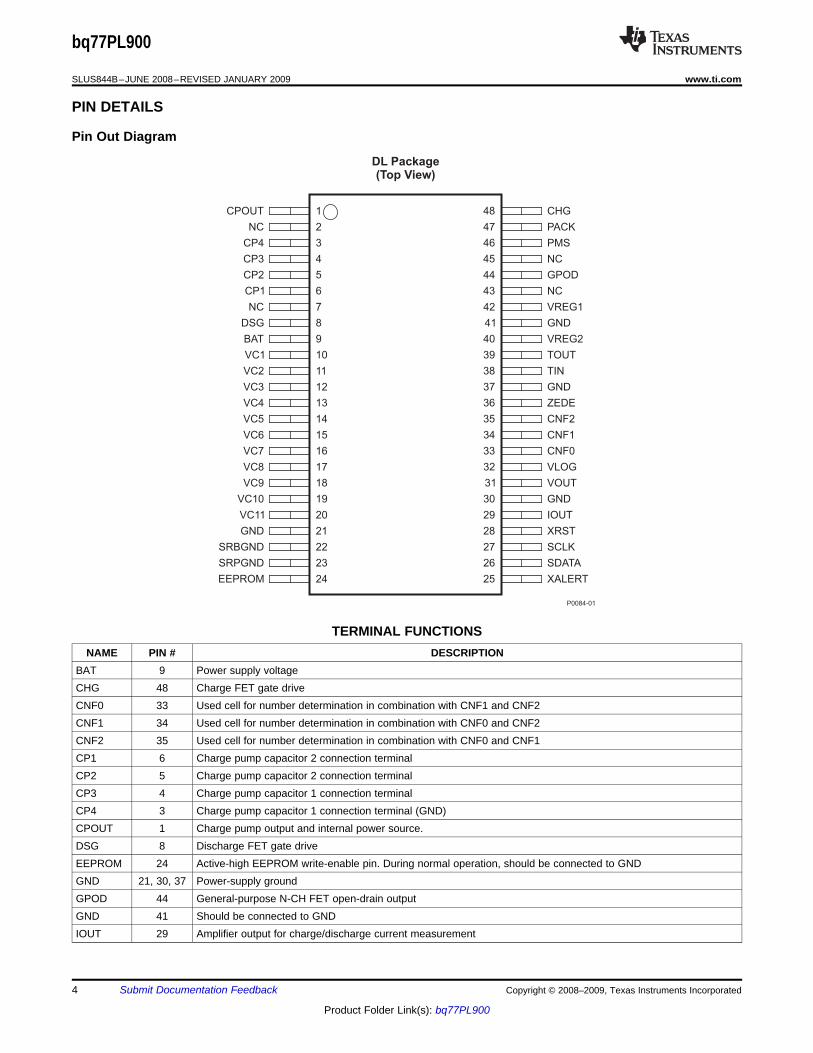
PIN DETAILS
Pin Out Diagram
DSG
CPOUT
CP4
2
7
6
5
4
3
36
35
34
33
32
31
30
8
9
10
11
12
29
28
27
26
48
13
14
47
1
NC
VC1
CNF2
PMS
VREG1
VC2
VC3
VREG2
VC4
VC5
XRST
VLOG
TOUT
VC6
PACK
GPOD
15
VC9
38
37
CHG
16
17
18
GND
VC10 19
VC11
46
45
44
43
CP3
VC7
CNF1
VC8
BAT
SDATA
SCLK
42
XALERT
GND
VOUT
20
SRBGND
21
22
23
CP1
SRPGND
24
CP2
41
40
39
25
IOUT
EEPROM
NC
NC
GND
GND
NC
ZEDE
CNF0
TIN
P0084-01
DL Package(Top View)
bq77PL900
SLUS844B–JUNE 2008–REVISED JANUARY 2009 ...................................................................................................................................................... www.ti.com
TERMINAL FUNCTIONSNAME PIN # DESCRIPTION
BAT 9 Power supply voltageCHG 48 Charge FET gate driveCNF0 33 Used cell for number determination in combination with CNF1 and CNF2CNF1 34 Used cell for number determination in combination with CNF0 and CNF2CNF2 35 Used cell for number determination in combination with CNF0 and CNF1CP1 6 Charge pump capacitor 2 connection terminalCP2 5 Charge pump capacitor 2 connection terminalCP3 4 Charge pump capacitor 1 connection terminalCP4 3 Charge pump capacitor 1 connection terminal (GND)CPOUT 1 Charge pump output and internal power source.DSG 8 Discharge FET gate driveEEPROM 24 Active-high EEPROM write-enable pin. During normal operation, should be connected to GNDGND 21, 30, 37 Power-supply groundGPOD 44 General-purpose N-CH FET open-drain outputGND 41 Should be connected to GNDIOUT 29 Amplifier output for charge/discharge current measurement
4 Submit Documentation Feedback Copyright © 2008–2009, Texas Instruments Incorporated
Product Folder Link(s): bq77PL900

bq77PL900
www.ti.com ...................................................................................................................................................... SLUS844B–JUNE 2008–REVISED JANUARY 2009
TERMINAL FUNCTIONS (continued)NAME PIN # DESCRIPTION
NC 2, 7, 43, No connect (not electrically connected)45
PACK 47 PACK positive terminal and alternative power sourcePMS 46 Determines CHG output state for zero-volt chargeSCLK 27 Open-drain bidirectional serial interface clock with an internal 10-kΩ pullup to VLOG
SDATA 26 Open-drain bidirectional serial interface data with an internal 10-kΩ pullup to VLOG
SRBGND 22 Current sense terminal (Connect Battery to cell’s GND)SRPGND 23 Current-sense positive terminal when discharging relative to SRNGND, current-sense negative terminal when
charging relative to SRGND. (Connect to pack GND)TIN 38 Temperature sensing inputTOUT 39 Thermistor bias current sourceVC1 10 Sense voltage input terminal for most positive cell, balance current input for most positive cell, and battery stack
measurement inputVC2 11 Sense voltage input terminal for second-most positive cell, balance current input for second-most positive cell, and
return balance current for most positive cellVC3 12 Sense voltage input terminal for third-most positive cell, balance current input for third-most positive cell, and
return balance current for second-most positive cellVC4 13 Sense voltage input terminal for fourth-most positive cell, balance current input for fourth-most positive cell, and
return balance current for third-most positive cellVC5 14 Sense voltage input terminal for fifth-most positive cell, balance current input for fifth-most positive cell, and return
balance current for fourth-most positive cellVC6 15 Sense voltage input terminal for sixth-most positive cell, balance current input for sixth-most positive cell, and
return balance current for fifth-most positive cellVC7 16 Sense voltage input terminal for seventh-most positive cell, balance current input for seventh-most positive cell,
and return balance current for sixth-most positive cellVC8 17 Sense voltage input terminal for eighth-most positive cell, balance current input for eighth-most positive cell, and
return balance current for seventh-most positive cellVC9 18 Sense voltage input terminal for ninth-most positive cell, balance current input for ninth-most positive cell, and
return balance current for eighth-most positive cellVC10 19 Sense voltage input terminal for tenth-most positive cell, balance current input for tenth-most positive cell, and
return balance current for ninth-most positive cellVC11 20 Sense voltage input terminal for most negative cell, return balance current for least positive cellVLOG 32 Data I/O voltage set by connecting either VREG1 or VREG2VOUT 31 Amplifier output for cell voltage measurementVREG1 42 Integrated 5-V regulator outputVREG2 40 Integrated 3.3-V regulator outputXALERT 25 Open-drain output used to indicate status register change. (Includes an internal 100-kΩ pullup to VLOG.)XRST 28 Power-on-reset output. Active-low open-drain output with an internal 3-kΩ pullup to VLOG
ZEDE 36 Protection delay test pin. Minimizes protection delay times when connected to VLOG. Programmed delay timesused when pulled to GND, normal operation.
Copyright © 2008–2009, Texas Instruments Incorporated Submit Documentation Feedback 5
Product Folder Link(s): bq77PL900

FUNCTIONAL BLOCK DIAGRAM
GN
DO
ve
rcu
rre
nt
CE
LL1
..10
SR
BG
ND
SR
PG
ND
Sh
ort
-Cir
cu
it
Dela
y
GP
OD
Un
derv
oltage
PA
CK
CH
GD
SG
PA
CK
–
VC
7
VC
8
VC
11
CE
LL
8
CE
LL
7
VC
9
VC
10
CE
LL
10
CE
LL
9
XA
LE
RT
SD
ATA
Sta
tus
Ou
tpu
tC
tl
OV
/UV
OL
D/O
LV
SC
C
SC
D
Re
gis
ters
PA
CK+
VC
3
VC
4
CE
LL
4
CE
LL
3
VC
5
CE
LL
6
CE
LL
5
CE
LL
2
CE
LL
1
VC
6
VC
1
VC
2
TO
UT
CT
HE
RM
VR
EG
15
VL
DO
RT
HE
RM
3.3
VL
DO
VR
EG
2
SC
LK
Ce
llB
al
+IO
UT
XR
ST
EE
PR
OM
VLO
G
CP
OU
T
Ce
llA
MP
CE
LL
OU
T
BA
T
Ove
rvolta
ge
0.9
8V
Co
ntr
ol
EE
PR
OM
CN
F2
CN
F1
CN
F0
ZE
DE
TIN
Op
tio
n
PM
S
Buffer
Level
Sta
teC
ontr
ol
Open D
rain
Ooutp
ut
SerialInterface
Therm
al
Shutd
ow
n
CP
1C
P2
CP
3C
P4
Cha
rge P
um
pS
tep D
ow
nP
CH
Gate
Driver
PC
H G
ate
Driver
Short
-Circuit
Com
para
tor
Overload
Com
para
tor ´
´10 o
r50
Cell
Sele
ction
Sw
itches
B0325-0
1
bq77PL900
SLUS844B–JUNE 2008–REVISED JANUARY 2009 ...................................................................................................................................................... www.ti.com
6 Submit Documentation Feedback Copyright © 2008–2009, Texas Instruments Incorporated
Product Folder Link(s): bq77PL900

4 SAFETY STATE OVERVIEW
UVLO Mode Shutdown Mode
Power Supply to PACK
Internal VREG2 > 2.4 V Internal VREG2 < 2.3 V
Power Supply to PACK
No Power Supply
CHG: OFFDSG: OFFVREG1: OFFVREG2: OFFXRST: LOW
I C: DisabledUV Protection: DisabledOV Protection: DisabledCurrent Protection: DisabledThermal Protection: Disabled
2
CHG: OFFDSG: OFFVREG1: OFFVREG2: OFFXRST: LOW
I C: DisabledCurrent Protection: DisabledVCELL: DisabledWatchdog: DisabledThermal Protection: Disabled
2
No Supply to PACK
Attach a Charger
CHG: OFFDSG: OFFVREG1: ONVREG2: ONXRST: HIGH
I C: EnabledUV Protection: EnabledOV Protection: EnabledCurrent Protection: DisabledThermal Protection: Enabled
2
CHG: ONDSG: OFFVREG1: ONVREG2: ONXRST: HIGH
I C: EnabledUV Protection: DisabledOV Protection: EnabledCurrent Protection: EnabledThermal Protection: Enabled
2
CHG: ONDSG: ONVREG1: ONVREG2: ONXRST: HIGH
I C: EnabledUV Protection: EnabledOV Protection: EnabledCurrent Protection: EnabledThermal Protection: Enabled
2
Current Protection ModeDischarge Side
CHG: OFFDSG: OFFVREG1: ONVREG2: ONXRST: HIGH
I C: EnabledUV Protection: EnabledOV Protection: EnabledCurrent Protection: EnabledThermal Protection: Disabled
2
OvertemperatureProtection Mode
CHG: OFFDSG: ONVREG1: ONVREG2: ONXRST: HIGH
I C: EnabledUV Protection: EnabledOV Protection: DisabledCurrent Protection: EnabledThermal Protection: Enabled
2
OvervoltageProtection Mode
UndervoltageProtection Mode
Normal ModeV > V or V for a
period of t or tSR OC SC
OC SCV < Vcell UV
V > Vcell OV
All Cell Voltage > V + V
(or V – V > 0.4 V and All
Cell Voltage > V )
UV UV
pack bat
UV
Δ
All Cell Voltage < V – VOV OVΔ
V < 0.975 VIN
B0326-01
V > 1.075 VIN
bq77PL900
www.ti.com ...................................................................................................................................................... SLUS844B–JUNE 2008–REVISED JANUARY 2009
Figure 3. Stand-Alone Mode
Table 1. Stand-Alone STATUS Bit, XALERT and FET Transition SummaryMODE TRANSITION STATUS BIT XALERT FET ACTIVITY
Normal to current protection SCD or OCD = H to L DSG and CHG off1
Current protection to normal SCD or OCD = L to H DSG and CHG on0
Normal to overvoltage protection OVP = 1 H to L CHG offOvervoltage protection to normal OVP = 0 L to H CHG onNormal to undervoltage protection (when VPACK goes down to 0 V, move to UVP = 1 H to L DSG offshutdown mode)Undervoltage protection to normal UVP = 0 L to H DSG onNormal to overtemperature OVT = 1 H to L DSG and CHG offOvertemperature to normal OVT = 0 L to H DSG and CHG on
Copyright © 2008–2009, Texas Instruments Incorporated Submit Documentation Feedback 7
Product Folder Link(s): bq77PL900

UVLO Mode
Shutdown Mode
Power Supply to PACK
Internal VREG2 > 2.4 V Internal VREG2 < 2.3 V
Power Supply to PACK
DSG: OFF
Any State
No Power Supply
CHG: OFFDSG: OFFVREG1: OFFVREG2: OFFXRST: LOW
I C: DisabledUV Protection: DisabledOV Protection: DisabledCurrent Protection: DisabledThermal Protection: Disabled
2
CHG: OFFDSG: OFFVREG1: OFFVREG2: OFFXRST: LOW
I C: DisabledCurrent Protection: DisabledVCELL: DisabledWatchdog: DisabledThermal Protection: Disabled
2
Firmware Commandand No Supply to PACK
FirmwareCommand
FirmwareCommand
Firmware Command
No Supply PACKVoltage Mode
CHG: OFFDSG: OFFVREG1: ONVREG2: ONXRST: HIGH
I C: EnabledUV Protection: EnabledOV Protection: EnabledCurrent Protection: DisabledThermal Protection: Enabled
2
CHG: ONDSG: OFFVREG1: ONVREG2: ONXRST: HIGH
I C: EnabledUV Protection: DisabledOV Protection: EnabledCurrent Protection: EnabledThermal Protection: Enabled
2
CHG: ONDSG: ONVREG1: ONVREG2: ONXRST: HIGH
I C: EnabledUV Protection: EnabledOV Protection: EnabledCurrent Protection: EnabledThermal Protection: Enabled
2
Current Protection ModeDischarge Side
CHG: OFFDSG: OFFVREG1: ONVREG2: ONXRST: HIGH
I C: EnabledUV Protection: EnabledOV Protection: EnabledCurrent Protection: EnabledThermal Protection: Disabled
2
OvertemperatureProtection Mode
CHG: OFFDSG: ONVREG1: ONVREG2: ONXRST: HIGH
I C: EnabledUV Protection: EnabledOV Protection: DisabledCurrent Protection: EnabledThermal Protection: Enabled
2
OvervoltageProtection Mode
UndervoltageProtection Mode
Normal ModeV > V or V
for a period oft or t
SR OC SC
OC SC
FirmwareCommand
V < Vcell UV or
V > Vcell OV
or
All Cell Voltage > V + V
(or V – V > 0.4 V and All
Cell Voltage < V ), then
Firmware Command
UV UV
pack bat
UV
Δ
All Cell Voltage < V , then
Firmware CommandOV
Turn On T and
V < 0.975 Vout
IN
Turn On T and
V > 1.075 V,
then FirmwareCommand
out
IN
B0327-01
bq77PL900
SLUS844B–JUNE 2008–REVISED JANUARY 2009 ...................................................................................................................................................... www.ti.com
Figure 4. Host-Control Mode
8 Submit Documentation Feedback Copyright © 2008–2009, Texas Instruments Incorporated
Product Folder Link(s): bq77PL900

bq77PL900
www.ti.com ...................................................................................................................................................... SLUS844B–JUNE 2008–REVISED JANUARY 2009
Table 2. Host Control SummaryMODE TRANSITION FUNCTION AND FIRMWARE PROCEDURE
Normal to current protection Vsr > Voc or Vsc for period of toc or tscAutomatically, DSG and CHG turn off, SCD or OCD status changes = 1, XALERT = L
Current protection to normal 1. Send commands to transition LTCLR from 0 to 1 to 02. Read status bit. XALERT would change to H.3. Set CHG and DSG FET ON to enable normal operation
Vcell > Vov for period of tovNormal to overvoltage protection Automatically, CHG turns off, UV status changes = 1, XALERT = LOvervoltage protection to normal 1. Confirm the OVP protection status is cleared
2. Send command LTCLR from 1 to 03. Read status bit. XALERT changes to H.4. Set CHG FET ON to enable normal operation
Vcell < Vuv for period of tuvUVFET_DIS = 0 Automatically, DSG turns off, UV status changes = 1, XALERT = LNormal to undervoltageprotection 1. Vcell < Vuv or for period of tuv, UV status changes = 1, XALERT = L
UVFET_DIS = 12. Send commands to turn off DSG.
Undervoltage protection 1. Confirm the OVP protection status is clearedto normal 2. Send command LTCLR from 1 to 0
UVFET_DIS = X3. Set DSG FET ON to enable normal operation4. Read status bit. XALERT changes to H.
Normal to overtemperature 1. Send commands to turn on TOUT2. If TIN voltage < 0.975 V, DSG and CHG turn off, OVTEMP status changes = 1,
XALERT = LOvertemperature to normal 1. Send commands to turn on TOUT (To return to normal mode, bq77PL900 must
acknowledge Vth > 1.075 V)2. Send commands to transition LTCLR from 1 to 03. Set CHG and DSG FET ON4. Read status bit. XALERT changes to H.
Any mode to shutdown 1. Set DSG FET OFF2. Wait until PACK voltage decreases to 0 V3. SET shutdown bit to 1
ORDERING INFORMATIONTA PACKAGED
SSOP48–40°C to 100°C bq77PL900DL (1)
(1) The bq77PL900 can be ordered in tape and reel by adding the suffixR to the orderable part number, I.e., bq77PL900DLR.
Copyright © 2008–2009, Texas Instruments Incorporated Submit Documentation Feedback 9
Product Folder Link(s): bq77PL900

ABSOLUTE MAXIMUM RATINGS
DISSIPATION RATINGS
bq77PL900
SLUS844B–JUNE 2008–REVISED JANUARY 2009 ...................................................................................................................................................... www.ti.com
over operating free-air temperature range (unless otherwise noted) (1) (2)
VALUE UNITVMAX Supply voltage range BAT, PACK –0.3 to 60 V
VC1–VC10 –0.3 to 60VC11 –0.3 to 0.3VCn to VCn + 1, n = 1 to 10 –0.3 to 8
VIN Input voltage range VPMS –0.3 to 60SRP, SRN –0.5 to 1SDATA, SCLK, EEPROM, VLOG, ZEDE, CNF0, CNF1, CNF2, TIN –0.3 to 7CHG PACK – 20 to 60DSG BAT – 20 to 60TOUT, VOUT, IOUT, XRST, XALERT, SDATA, SCLK –0.3 to 7
VO Output voltage range VCP1, CP2, CP3, CP4, CPOUT, GPOD –0.3 to 60VREG1 –0.3 to 8VREG2 –0.3 to 3.6
ICB Current for cell balancing 10 mATSTG Storage temperature range –65 to 150 °CTSOLDER Lead temperature (soldering, 10 s) 300 °C
(1) Stresses beyond those listed under Absolute Maximum Ratings may cause permanent damage to the device. These are stress ratingsonly, and functional operation of the device at these or any other conditions beyond those indicated under Recommended OperatingConditions is not implied. Exposure to absolute-maximum-rated conditions for extended periods may affect device reliability.
(2) All voltages are with respect to ground of this device except VCn – VC(n+1), where n=1 to 10 cell voltage.
TA ≤ 25°C DERATING FACTOR TA = 85°C TA = 100°CPACKAGE ABOVE TA ≥ 70°CPOWER RATING POWER RATING POWER RATINGDL 1388 mW 11.1 mW/°C 720 mW 555 mW
10 Submit Documentation Feedback Copyright © 2008–2009, Texas Instruments Incorporated
Product Folder Link(s): bq77PL900

RECOMMENDED OPERATING CONDITIONS
bq77PL900
www.ti.com ...................................................................................................................................................... SLUS844B–JUNE 2008–REVISED JANUARY 2009
MIN NOM MAX UNITSupply Voltage PACK, BAT 7 50 VVI(STARTUP) Start-up voltage PACK 7.5 VVLOG Logic supply voltage 0.8 × VREG2 1.2 × VREG1 V
Input voltage range VC1 to VC10 0 BATVC11 0 0.5
VI SRP, SRN –0.3 0.5 VVCn – VC(n + 1), (n = 1 to 10) 0 7PACK, BAT 50
VIH Logic level input voltage high SCLK, SDATA, EEPROM, VLOG 0.8 × VLOG VLOG(VLOG = VREG1 or VREG2)VIL Logic level input voltage low 0 0.2 × VLOG
XALERT, SDATA VLOG
VGAIN = High 1.2 VVO Output voltage range VOUT, IOUT
VGAIN = Low 0.975GPOD 45 V
RVCX 400 ΩIREGOUT I(reg1 + reg2) 25 mACREG1 External 5-V REG capacitor 2.2 µFCREG2 External 3.3-V REG capacitor 2.2 µFCCP1, CCP2 Charge pump flying capacitor 1 µFCCPOUT Charge pump output capacitor 4.7 µFCVOUT Output capacitance 0.1 µFCIOUT Output capacitance 0.1 µFIOL GPOD, XRST 1 mAfSCLK Input frequency SCLK 100 kHz
EEPROM number of writes 3TOPR Operating temperature –25 85 °CTFUNC Functional temperature –40 100 °C
Copyright © 2008–2009, Texas Instruments Incorporated Submit Documentation Feedback 11
Product Folder Link(s): bq77PL900

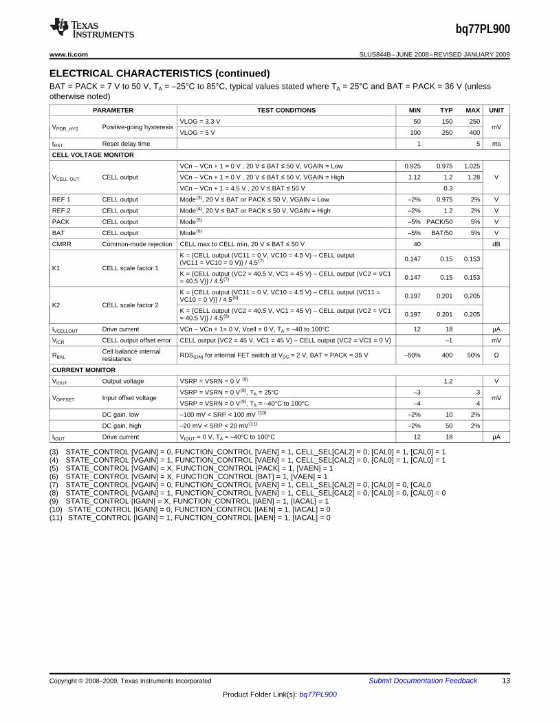
ELECTRICAL CHARACTERISTICS
bq77PL900
SLUS844B–JUNE 2008–REVISED JANUARY 2009 ...................................................................................................................................................... www.ti.com
BAT = PACK = 7 V to 50 V, TA = –25°C to 85°C, typical values stated where TA = 25°C and BAT = PACK = 36 V (unlessotherwise noted)
PARAMETER TEST CONDITIONS MIN TYP MAX UNIT
SUPPLY CURRENT
No load at REG1, REG2, TOUT, SCLK, SDIN, TA = 25°C 450 550XALERT, CELLAMP, CURRENTAMP = offCHG, DSG = on, cell balance = off,ICC1 Supply current 1 µATA = –40°C to 600IREG1 = IREG2 = 0 mA, 100°CCharge pump = off (1), BAT = PACK = 35 V
No load at REG1, REG2, TOUT, SCLK, SDIN, TA = 25°C 650 750XALERT, CELLAMP, CURRENTAMP = on,CHG, DSG = on,ICC2 Supply current 2 µATA = –40°C to 800Cell balance = off, IREG1 = IREG2 = 0 mA, 100°CCharge pump = off, BAT = PACK = 35 V
TA = 25°C 0.1 1.2CHG, DSG = off, VREG1 = VREG2 = off,ISHUTDOWN Shutdown mode µATA = –40°C toPACK = 0 V, BAT = 35 V 2100°C
VREG1, INTEGRATED 5-V LDO
8.5 V < PACK or BAT ≤ 50 V, IOUT ≤ 25 mA 4.55 5 5.45TA = –40°C toV(REG1) Output voltage V100°C7 V < PACK or BAT ≤ 8.5 V, IOUT ≤ 3 mA 4.55 5 5.45
ΔV(REG1) Output temperature drift PACK or BAT = 50 V, IOUT = 2 mA TA = 25°C ±0.2%
ΔV(REG1LINE) Line regulation 10 V ≤ PACK or BAT ≤ 50 V, IOUT = 2 mA TA = 25°C 10 20 mV
PACK or BAT = 36 V, 0.2 mA ≤ IOUT ≤ 2 mA 7 15ΔV(REG1LOAD) Load regulation TA = 25°C mV
PACK or BAT = 36 V, 0.2 mA ≤ IOUT ≤ 25 mA 40 100
PACK or BAT = 36 V, VREG1 = 4.5 V 35 75 125IREG1MAX Current limit TA = 25°C mA
PACK or BAT = 36 V, VREG1 = 0 V 5 20 35
VREG2, INTEGRATED 3.3-V LDO
8.5 V < PACK or BAT ≤ 50 V, IOUT ≤ 25 mA 3.05 3.3 3.55TA = –40°C toV(REG2) Output voltage 7 V < PACK or BAT ≤ 8.5 V, IOUT ≤ 10 mA 3.05 3.3 3.55 V100°C
7 V < PACK or BAT ≤ 50 V, IOUT = 0.2 mA –2% 3.3 2%
TA = –40°C toOutput temperature drift PACK or BAT = 50 V, IOUT = 2 mA ±0.2%100°C
Line regulation 7 V ≤ PACK or BAT ≤ 50 V, IOUT = 2 mA TA = 25°C 10 20 mVΔV(REG2)
PACK or BAT = 36 V, 0.2 mA ≤ IOUT ≤ 2 mA 7 15Load regulation TA = 25°C mV
PACK or BAT = 36 V, 0.2 mA ≤ IOUT ≤ 25 mA 40 100
PACK or BAT = 36 V, VREG2 = 3 V 25 50 100IREG2MAX Current limit TA = 25°C mA
PACK or BAT = 36 V, VREG2 = 0 V 10 20 30
TOUT, THERMISTOR POWER SUPPLY
TA = –40°C toVTOUT IOUT = 0 mA 3.05 3.55 V100°C
Pass-element series IOUT = –1 mA at TOUT pin, Ireg2 = –0.2 mA TA = –40°C toRDS(ON) 50 100 Ωresistance RDS(ON) = (VREG2 – VTOUT)/1 mA 100°C
Thermistor senseVTINS TA = –40°C to 100°C –5% 0.975 5% Vvoltage
Thermistor senseVTINSHYS TA = –40°C to 100°C 50 100 150 mVhysteresis voltage
THERMAL SHUTDOWN
Ttherm Shutdown threshold PACK or BAT = 36 V (2) 150 °C
PMS, PRECHARGE MODE SELECT DISABLE
PMS disable threshold ofVPMSDISABLE PACK = PMS = 20 V, VREG2 = 0 V, CHG = ON → OFF 8 13 16 VBAT
POR, POWER-ON RESET
VLOG = VREG1(5 V) V 3.85 4.05 4.25Negative-going voltageVPOR– Vinput VLOG = VREG2(3.3 V) V 2.45 2.65 2.8
(1) Charge pump starts working when (IREG33 + IREG5) > 3 mA.(2) Not 100% tested, assured by design up to 125°C
12 Submit Documentation Feedback Copyright © 2008–2009, Texas Instruments Incorporated
Product Folder Link(s): bq77PL900
bq77PL900
www.ti.com ...................................................................................................................................................... SLUS844B–JUNE 2008–REVISED JANUARY 2009
ELECTRICAL CHARACTERISTICS (continued)BAT = PACK = 7 V to 50 V, TA = –25°C to 85°C, typical values stated where TA = 25°C and BAT = PACK = 36 V (unlessotherwise noted)
PARAMETER TEST CONDITIONS MIN TYP MAX UNIT
VLOG = 3.3 V 50 150 250VPOR_HYS Positive-going hysteresis mV
VLOG = 5 V 100 250 400
tRST Reset delay time 1 5 ms
CELL VOLTAGE MONITOR
VCn – VCn + 1 = 0 V , 20 V ≤ BAT ≤ 50 V, VGAIN = Low 0.925 0.975 1.025
VCELL OUT CELL output VCn – VCn + 1 = 0 V , 20 V ≤ BAT ≤ 50 V, VGAIN = High 1.12 1.2 1.28 V
VCn – VCn + 1 = 4.5 V , 20 V ≤ BAT ≤ 50 V 0.3
REF 1 CELL output Mode (3), 20 V ≤ BAT or PACK ≤ 50 V, VGAIN = Low –2% 0.975 2% V
REF 2 CELL output Mode (4), 20 V ≤ BAT or PACK ≤ 50 V, VGAIN = High –2% 1.2 2% V
PACK CELL output Mode (5) –5% PACK/50 5% V
BAT CELL output Mode (6) –5% BAT/50 5% V
CMRR Common-mode rejection CELL max to CELL min, 20 V ≤ BAT ≤ 50 V 40 dB
K = CELL output (VC11 = 0 V, VC10 = 4.5 V) – CELL output 0.147 0.15 0.153(VC11 = VC10 = 0 V) / 4.5 (7)
K1 CELL scale factor 1K = CELL output (VC2 = 40.5 V, VC1 = 45 V) – CELL output (VC2 = VC1 0.147 0.15 0.153= 40.5 V) / 4.5 (7)
K = CELL output (VC11 = 0 V, VC10 = 4.5 V) – CELL output (VC11 = 0.197 0.201 0.205VC10 = 0 V) / 4.5 (8)
K2 CELL scale factor 2K = CELL output (VC2 = 40.5 V, VC1 = 45 V) – CELL output (VC2 = VC1 0.197 0.201 0.205= 40.5 V) / 4.5 (8)
IVCELLOUT Drive current VCn – VCn + 1= 0 V, Vcell = 0 V, TA = –40 to 100°C 12 18 µA
VICR CELL output offset error CELL output (VC2 = 45 V, VC1 = 45 V) – CELL output (VC2 = VC1 = 0 V) –1 mV
Cell balance internalRBAL RDS(ON) for internal FET switch at VDS = 2 V, BAT = PACK = 35 V –50% 400 50% Ωresistance
CURRENT MONITOR
VIOUT Output voltage VSRP = VSRN = 0 V (9) 1.2 V
VSRP = VSRN = 0 V (9), TA = 25°C –3 3VOFFSET Input offset voltage mV
VSRP = VSRN = 0 V (9), TA = –40°C to 100°C –4 4
DC gain, low –100 mV < SRP < 100 mV (10) –2% 10 2%
DC gain, high –20 mV < SRP < 20 mV (11) –2% 50 2%
IIOUT Drive current VIOUT = 0 V, TA = –40°C to 100°C 12 18 µA
(3) STATE_CONTROL [VGAIN] = 0, FUNCTION_CONTROL [VAEN] = 1, CELL_SEL[CAL2] = 0, [CAL0] = 1, [CAL0] = 1(4) STATE_CONTROL [VGAIN] = 1, FUNCTION_CONTROL [VAEN] = 1, CELL_SEL[CAL2] = 0, [CAL0] = 1, [CAL0] = 1(5) STATE_CONTROL [VGAIN] = X, FUNCTION_CONTROL [PACK] = 1, [VAEN] = 1(6) STATE_CONTROL [VGAIN] = X, FUNCTION_CONTROL [BAT] = 1, [VAEN] = 1(7) STATE_CONTROL [VGAIN] = 0, FUNCTION_CONTROL [VAEN] = 1, CELL_SEL[CAL2] = 0, [CAL0] = 0, [CAL0(8) STATE_CONTROL [VGAIN] = 1, FUNCTION_CONTROL [VAEN] = 1, CELL_SEL[CAL2] = 0, [CAL0] = 0, [CAL0] = 0(9) STATE_CONTROL [IGAIN] = X, FUNCTION_CONTROL [IAEN] = 1, [IACAL] = 1(10) STATE_CONTROL [IGAIN] = 0, FUNCTION_CONTROL [IAEN] = 1, [IACAL] = 0(11) STATE_CONTROL [IGAIN] = 1, FUNCTION_CONTROL [IAEN] = 1, [IACAL] = 0
Copyright © 2008–2009, Texas Instruments Incorporated Submit Documentation Feedback 13
Product Folder Link(s): bq77PL900

bq77PL900
SLUS844B–JUNE 2008–REVISED JANUARY 2009 ...................................................................................................................................................... www.ti.com
ELECTRICAL CHARACTERISTICS (continued)BAT = PACK = 7 V to 50 V, TA = –25°C to 85°C, typical values stated where TA = 25°C and BAT = PACK = 36 V (unlessotherwise noted)
PARAMETER TEST CONDITIONS MIN TYP MAX UNIT
BATTERY PROTECTION THRESHOLDS
OV detection thresholdVOV Default 4.15 4.5 Vrange
OV detection thresholdΔVOV 50 mVprogram step
OV detection hysteresisVOVH Default 0 0.3 Vvoltage range
OV detection hysteresisΔVOVH 0.1 Vprogram step
UV detection thresholdVUV Default 1.4 2.9 Vrange
UV detection thresholdΔVUV 100 mVprogram step
UV detection hysteresisVUVH Default 0.2 1.2 Vvoltage
UV detection thresholdΔVUVH 200 mVprogram step
OCD detection thresholdVOCDT Default 10 85 mVrange
OCD detection thresholdΔVOCDT 5 mVprogram step
SCD detection thresholdVSCDT Default 60 135 mVrange
SCD detection thresholdΔVSCDT 5 mVprogram step
OV detection thresholdVOV_acr Default (TA = 0°C to 85°C) –50 0 50 mVaccuracy
UV detection thresholdVUV_acr Default –100 0 100 mVaccuracy
VOCD = 10 mV or 15 mV –4 0 4 mVOCD detection thresholdVOCD_acr accuracy VOCD > 20 mV –20% 0 20%
SCD detection thresholdVSCD_acr Default –20% 0 20%accuracy
BATTERY PROTECTION DELAY TIMES
OV detection delay timetOV Default 500 2250 msrange
OV detection delay timeΔtOV 250 msstep
UV detection delay timetUV Default 0 8000 msrange
UV detection delay timeΔtUV 1.25 1000 msstep
OCD detection delaytOCD Default 20 1600 mstime range
OCD detection delayΔtOCD 20 100 mstime step
SCD detection delaytSCD Default 0 900 µstime range
SCD detection thresholdΔtSCD 60 µsprogram step
OV detection delay timetOV_acr Default –15% 0% 15%accuracy
UV detection delay timetUV_acr Default –15% 0% 15%accuracy
OC detection delay timetOC_acr Default –15% 0% 15%accuracy
SC detection delay timeVSCD_acr tSCD Max –15% 0% 15%accuracy
14 Submit Documentation Feedback Copyright © 2008–2009, Texas Instruments Incorporated
Product Folder Link(s): bq77PL900

bq77PL900
www.ti.com ...................................................................................................................................................... SLUS844B–JUNE 2008–REVISED JANUARY 2009
ELECTRICAL CHARACTERISTICS (continued)BAT = PACK = 7 V to 50 V, TA = –25°C to 85°C, typical values stated where TA = 25°C and BAT = PACK = 36 V (unlessotherwise noted)
PARAMETER TEST CONDITIONS MIN TYP MAX UNIT
OC/SC recovery timingtSRC –15% 12.8 s 15%in stand-alone mode
BATTERY PROTECTION RECOVERY
VRECSC SC, OC recovery voltage 1 1.4 2 V
VRECUV = VPACK– VBAT,Undervoltage recoverVRECUV 0.05 0.1 0.3 Vvoltage VUV + VUVH > VCELL > VUV
FET DRIVE
VO(FETONDSG) = V(BAT) – V(DSG), 8 12 16VGS connect 1 MΩ, BAT = PACK = 35 VOutput voltage, chargeV(FETON) Vand discharge FETs on VO(FETONCHG) = V(PACK) – V(CHG), 8 12 16VGS connect 1 MΩ, BAT = PACK = 35 V
VO(FETOFFDSG) = V(PACK) – V(DSG), BAT = PACK = 35 V 0.2Output voltage, chargeV(FETOFF) Vand discharge FETs off VO(FETOFFCHG) = V(BAT) – V(CHG), BAT = PACK = 35 V 0.2
VDSG: 10% to 90% 5 15tr Rise time CL = 20 nF, BAT = PACK = 35 V µs
VCHG: 10% to 90% 5 15
VDSG: 90% to 10% 90 140tf Fall time CL = 20 nF, BAT = PACK = 35 V µs
VCHG: 90% to 10% 90 140
LOGIC
XALERT, IOUT = 200 µA, TA = –40°C to 100°C 0.4
Logic-level output SDATA, SCLK, XRST, IOUT = 1 mA,VOL 0.4 Vvoltage TA = –40°C to 100°C
GPOD, IOUT = 1 mA, TA = –40°C to 100°C 0.6
ILEAK Leakage current GPOD VOUT = 1 V, TA = –40°C to 100°C 1 µA
VIH SCLK (hysteresis input) Hysteresis 400 mV
XALERT, TA = –40°C to 100°C 60 100 200
RUP Pullup resistance DATA, SCLK, TA = –40°C to 100°C 6 10 20 kΩ
XRST, TA = –40°C to 100°C 1 3 6
IDOWN Pulldown current CNF0, CNF1, CNF2 = VREG2 2 4 µA
Copyright © 2008–2009, Texas Instruments Incorporated Submit Documentation Feedback 15
Product Folder Link(s): bq77PL900

I2C COMPATIBLE INTERFACE
tsu(STA)
th(STA)
tw(H)tw(L)
tsu(STOP)
tf
tf
tr
tsu(DAT)
th(DAT)
tr
SDA Change
SDA Input
SCLK
SCLK
SDATA
SDATA
SDATA
MSB
1 2 3 7 8 9
ACK
tv
SCLK
MSB
1 2 3 7 8 9
ACK
Stop Condition
Start Condition
Start Condition
T0369-01
Stop Condition
th(ch)
tsu(BUF)
bq77PL900
SLUS844B–JUNE 2008–REVISED JANUARY 2009 ...................................................................................................................................................... www.ti.com
BAT = PACK = 7 V to 50 V, TA = –25°C to 85°C, typical values stated where TA = 25°C and BAT = PACK = 36 V (unlessotherwise noted)
PARAMETER MIN MAX UNITtr SCLK, SDATA rise time 1000 nstf SCLK, SDATA fall time 300 nstw(H) SCLK pulse duration high 4 µstw(L) SCLK pulse duration low 4.7 µstsu(STA) Setup time for START condition 4.7 µsth(STA) START condition hold time after which first clock pulse is generated 4 µstsu(DAT) Data setup time 250 nsth(DAT) Data hold time 0 µstsu(STOP) Setup time for STOP condition 4 µstsu(BUF) Time the bus must be free before new transmission can start 4.7 µst V Clock low to data-out valid 900 nsth(CH) Data-out hold time after clock low 0 nsfSCL Clock frequency 0 100 kHz
Figure 5. I2C-Like I/F Timing Chart
16 Submit Documentation Feedback Copyright © 2008–2009, Texas Instruments Incorporated
Product Folder Link(s): bq77PL900

GENERAL OPERATIONAL OVERVIEW
Stand-Alone Mode and Host Control Mode
bq77PL900
www.ti.com ...................................................................................................................................................... SLUS844B–JUNE 2008–REVISED JANUARY 2009
The bq77PL900 has two operational modes, stand-alone mode and host-control mode. The mode is switched bySTATE_CONTROL [HOST]. In stand-alone mode, the battery protection is managed by the bq77PL900 withoutthe need for any external control. In this mode, the CHG and DSG FETs are driven ON and OFF automaticallyand cell balancing is processed by a fixed algorithm if enabled by OCDELAY[CBEN]). In this mode, I2Ccommunication is enabled, and a host can read the registers and set STATE_CONTROL [HOST] but cannotcontrol any output or function such as Vcell AMP enable.
In host control mode, a host microcontroller can obtain battery information such as voltage and current from thebq77PL900 analog interface. This allows the host, such as a microcontroller, to calculate remaining capacity orimplement an alternative cell balancing algorithm. In this mode, the bq77PL900 still detects cell protection faultsand acts appropriately, although the recovery method is different from that in stand-alone mode. The hostcontroller has control over the recovery method and FET action after the protection state has been entered.Table 3 contains further details of the protection action differences.
Table 3. Stand-Alone Mode and Host Control Mode Protection SummaryStand-Alone Mode Host-Control ModeFUNCTION MODE (HOST = L) (HOST = H)
AutomaticThe bq77PL900 detects an OV voltage andDetection turns OFF the CHG FET. Must turn off cellOV protection
balancing for correct voltage detection.Recovery Host Control
Host ControlThe bq77PL900 detects a UV voltage but noDetection FET action is taken. Must turn off cellAutomaticUV protection
balancing for correct voltage detection.The bq77PL900 detects and recovers fromprotection states and controls the FETs.Recovery Host Control
AutomaticDetection The bq77PL900 detects OCD and turns CHGOCD/SCD
and DSG FETs OFF.protectionRecovery Host ControlDetection Host must turn ON.Overtemperature
protection Recovery Host ControlHost ControlCHG/DSG FET Automatic— The bq77PL900 cannot release fromcontrol Host cannot drive the FETs protection state automatically.Host ControlCBEN = 1: AutomaticCell balancing — The host can balance any cells at any timeCBEN = 0: No function CBEN = Don’t care
PMS = High, AutomaticZero-volt charge1 AutomaticZVC = X (0-V charge current flows through CHG FET)PMS = Low,Zero-volt charge2 No support for 0-V chargeZVC = 0 Host Control
Host should control precharge FET by usingAutomaticPMS = Low, GPOD pin.Zero-volt charge3 (0-V charge current flows through FET that isZVC = 1 driven by GPOD)
Copyright © 2008–2009, Texas Instruments Incorporated Submit Documentation Feedback 17
Product Folder Link(s): bq77PL900

Normal Operation Mode
bq77PL900Battery
On On
Pack+
Pack
Load
Pack–
S0345-01
Bat
bq77PL900
SLUS844B–JUNE 2008–REVISED JANUARY 2009 ...................................................................................................................................................... www.ti.com
When all cell voltages are within the range of VUV to VOV, and the CHG and DSG FETs are turned ON, the cellsare charged and discharged at any time.
Figure 6. Normal Operation Mode
18 Submit Documentation Feedback Copyright © 2008–2009, Texas Instruments Incorporated
Product Folder Link(s): bq77PL900

Battery Protection
Cell Overvoltage and Cell Undervoltage Detection
bq77PL900
www.ti.com ...................................................................................................................................................... SLUS844B–JUNE 2008–REVISED JANUARY 2009
The bq77PL900 fully integrates battery protection circuits including cell overvoltage, undervoltage, andovercurrent in discharge and short circuit in discharge detection. Each detection voltage can be adjusted byprogramming the integrated EEPROM. Also, the detection delay time can be programmed as shown in Table 4.
CAUTION:
Only a maximum of three programming cycles should performed to ensure datastability.
Table 4. Detection Voltage, Detection Delay Time SummaryPARAMETER MIN MAX STEP BITS
Voltage 4.15 V 4.5 V 50 mV 3Overvoltage Delay 0.5 s 2.25 s 0.25 s 3
Hysteresis 100 mV 400 mV 50 mV 2Voltage 1.4 V 2.9 V 100 mV 4Delay 0 ms 30 ms 1.25 ms–10 ms 4
Undervoltage1 s 8 s 1 s
Hysteresis 100 mV 1200 mV 0.2 V, 0.4 V 2Voltage 10 mV 85 mV 5 mV 4
Overcurrent in dischargeDelay 20 ms 1600 ms 20 ms or 100 ms 5
Voltage 60 mV 135 mV 5 mV 4Short circuit in discharge
Delay 0 µs 900 µs 60 µs 4
The cell overvoltage and cell undervoltage detection circuit consists of a sample-and-hold (S/H) circuit and twocomparators.
The S/H period is about 120 µs for each cell, and S/H is performed sequentially on each cell. Once all of thecells are checked, the bq77PL900 waits about 50 mS for the next S/H.
Copyright © 2008–2009, Texas Instruments Incorporated Submit Documentation Feedback 19
Product Folder Link(s): bq77PL900

Sample-and-Hold Circuit
OV Comparator
VC11
VC10
VC9
VC8
UV Comparator
OVth
UVth
DelayCounter
DelayCounter
OV/UV Comparator
120 s Number of Cells/Monitor OV and UV
m ´
Sampling Sequence: 50 ms
+
+
+
–
–
–
S0346-01
Cell Overvoltage Detection and Recovery
bq77PL900
SLUS844B–JUNE 2008–REVISED JANUARY 2009 ...................................................................................................................................................... www.ti.com
Figure 7. Cell Voltage Monitoring Circuit
Cell overvoltage detection is the same as host control mode for the FET OFF state, but the recovery conditionsare different. The CHG FET is turned OFF if any one of the cell voltages remains higher than VOV for a periodgreater than tOV. As a result, the cells are protected from an overcharge condition. Also XLAERT changes fromHigh to Low. Both VOV and tOV can be programmed in the internal EEPROM.
Recovery in Host Control ModeThe recovery condition is as follows:1. All cell voltages become lower than VOV (ΔVOVH is ignored).2. Additionally, the host must send a sequence of firmware commands to the bq77PL900 to turn ON the CHG
FET.
The command sequence required is as follows:1. The host must toggle LTCLR from 0 to 1 and then back to 0.2. Then set the CHG control bit to 1. To reset XLAERT high, the host must read the status register.
Figure 8 illustrates the circuit schematic in overvoltage protection mode in Host Control Mode. Figure 9 illustratesthe timing of this protection mode.
20 Submit Documentation Feedback Copyright © 2008–2009, Texas Instruments Incorporated
Product Folder Link(s): bq77PL900

OvervoltageDetect Comparator
Cell Voltage
VOV
bq77PL900
Battery
On Off
Pack+
Pack
Pack–
Charger
S0347-01
Bat
bq77PL900
www.ti.com ...................................................................................................................................................... SLUS844B–JUNE 2008–REVISED JANUARY 2009
Figure 8. Overvoltage in Host-Control Mode
Copyright © 2008–2009, Texas Instruments Incorporated Submit Documentation Feedback 21
Product Folder Link(s): bq77PL900

DisconnectCharger
BAT
PACK
DSG
CHG
OV Detect
All Cell Voltage < VOV
ConnectLoad
Host Turns on CHG FET
XALERT
Host Reads STATUS Register
T0370-01
bq77PL900
SLUS844B–JUNE 2008–REVISED JANUARY 2009 ...................................................................................................................................................... www.ti.com
Figure 9. OV and OV Recovery Timing in Host-Control Mode
22 Submit Documentation Feedback Copyright © 2008–2009, Texas Instruments Incorporated
Product Folder Link(s): bq77PL900

OvervoltageDetect Comparator
Cell Voltage
VOV – VD OVH
bq77PL900
Battery
On Off
Pack+
Pack
Pack–
Charger
S0348-01
Bat
bq77PL900
www.ti.com ...................................................................................................................................................... SLUS844B–JUNE 2008–REVISED JANUARY 2009
Recovery in Stand-Alone ModeThe recovery condition occurs when all cell voltages become lower than (VOV – ΔVOVH).
Figure 10 illustrates the circuit schematic in overvoltage protection mode in stand-alone mode. Figure 11illustrates the timing of this protection mode.
Figure 10. Cell Overvoltage Protection Mode in Stand-Alone Mode
Copyright © 2008–2009, Texas Instruments Incorporated Submit Documentation Feedback 23
Product Folder Link(s): bq77PL900

DisconnectCharger
BAT
PACK
DSG
CHG
OV Detect
All Cell Voltage < ( )V – VOV OVHD
ConnectLoad
XALERT
T0371-01
bq77PL900
SLUS844B–JUNE 2008–REVISED JANUARY 2009 ...................................................................................................................................................... www.ti.com
Figure 11. OV and OV Recovery Timing in Stand-Alone Mode
24 Submit Documentation Feedback Copyright © 2008–2009, Texas Instruments Incorporated
Product Folder Link(s): bq77PL900

7.14.1 Cell Undervoltage Detection and Recovery
UndervoltageDetect Comparator
Charge CurrrentDetect Comparator
bq77PL900
Bat
Battery
Off On
Pack+
Pack
Pack–
S0349-01
Load
bq77PL900
www.ti.com ...................................................................................................................................................... SLUS844B–JUNE 2008–REVISED JANUARY 2009
When any one of the cell voltages falls below VUV for a period of tUV, the bq77PL900 enters the undervoltagemode. At this time, the DSG FET is turned OFF and XALERT driven low. Both VUV and tUV can be programmedin the internal EEPROM.
Figure 12. Cell Undervoltage Protection Mode in Host Mode and Stand-Alone Mode (Attaching a Charger)
In Host-Control ModeCell undervoltage protection recovery conditions are when:1. All cell voltages become higher than (VUV + ΔVUVH), or2. All cell voltages are higher than VUV AND a charger is connected between PACK+ and PACK–, noting that
PACK+ voltage must be higher than BAT due to the diode forward voltage.
The bq77PL900 monitors the voltage difference between the PACK+ and BAT pins. When a difference higherthan 0.4V (typ.) is seen, it is interpreted that a charger has been connected.
Figure 12 illustrates the circuit schematic in undervoltage protection mode.
In some applications, it is required not to turn OFF the DSG FET suddenly. In these cases, by setting UVLEVLE[UVFET_DIS] = 1, only XALERT is driven low in response to entering an undervoltage condition. The host canturn OFF the DSG FET to protect the undervoltage condition. When the bq77PL900 recovery condition issatisfied, the host must send a sequence of firmware commands to the bq77PL900. The firmware commandsequence to turn ON the DSG FET is as follows:1. The host must toggle LTCLR from 0 to 1 and back to 0.2. Then the host must set the DSG ON bit to 1.3. Then the host can read the status register to reset XALERT high.
Figure 13 and Figure 14 illustrate the timing chart of protection mode.
Copyright © 2008–2009, Texas Instruments Incorporated Submit Documentation Feedback 25
Product Folder Link(s): bq77PL900

All Cell Voltage > (V +UV DV ) or
All Cell Voltage > V
and Detecting (PACK+) – V > 0.1 V
UVH
UV
BATConnect a Charger
BAT
PACK
DSG
CHG
XALERT
UV Detection
Host Turns On DSG FET
Host Read Status Register
T0372-01
BAT
PACK
DSG
CHG
XALERT
Host Turns Off DSG FET
DSG NotTurning Off
All Cell Voltage > (V +UV DV ) or
All Cell Voltage > V
and Detecting (PACK+) – V > 0.1 V
UVH
UV
BATConnect a ChargerUV Detection
Host Turns on DSG FET
Host Read Status Register
T0373-01
bq77PL900
SLUS844B–JUNE 2008–REVISED JANUARY 2009 ...................................................................................................................................................... www.ti.com
Figure 13. UV and UV Recovery Timing Host-Control Mode (UVFET_DIS = 0)
Figure 14. UV and UV Recovery Timing Host Control Mode (UVFET_DIS = 1)
26 Submit Documentation Feedback Copyright © 2008–2009, Texas Instruments Incorporated
Product Folder Link(s): bq77PL900

BAT
PACK
DSG
CHG
REG1/REG2
Change to Shutdown Wake Up
All Cell Voltage > (V +UV DV ) or
All Cell Voltage > V
and Detecting (PACK+) – V > 0.1 V
UVH
UV
BAT
Connect a Charger
UV Detection
UV Detection
T0374-01
Overcurrent in Discharge (OCD) Detection
Short Circuit in Discharge (SCD) Detection
bq77PL900
www.ti.com ...................................................................................................................................................... SLUS844B–JUNE 2008–REVISED JANUARY 2009
In Stand-Alone ModeOn detecting entry to undervoltage mode, the bq77PL900 moves to the shutdown power mode.
When a charger is attached, the bq77PL900 wakes up from shutdown mode. If cell voltages are lower than theundervoltage condition, the DSG FET is turned OFF and XALERT driven low. During periods when a charger isattached, the bq77PL900 never changes to shutdown mode.
When the undervoltage recovery condition is satisfied, the DSG FET turns ON and XLAERT is reset high.
Figure 15. UV and UV Recovery in Stand-Alone Mode
The overcurrent in discharge detection feature detects abnormal currents in the discharge direction viameasuring the voltage across the sense resistor (VOCD) and is used to protect the pass FETs, cells, and anyother inline components from abnormal discharge current conditions. The detection circuit also incorporates ablanking delay period (tOCD) before turning OFF the pass FETs. Both VOCD and tOCD can be programmed ininternal EEPROM.
The short circuit in discharge detection feature detects severe discharge current via measuring the voltageacross the sense resistor (VSCD) and is used to protect the pass FETs, cells, and any other inline componentsfrom severe current conditions. The detection circuit also incorporates a blanking delay period (tSCD) beforeturning OFF the pass FETs. Both VSCD and tSCD can be programmed in the internal EEPROM.
Copyright © 2008–2009, Texas Instruments Incorporated Submit Documentation Feedback 27
Product Folder Link(s): bq77PL900

7.14.1 Overcurrent in Discharge and Short Circuit in Discharge Recovery
OL/SC ReleaseComparator
bq77PL900
Bat
Battery
Off Off
Pack+
Pack
Pack–
S0350-01
Load
bq77PL900
SLUS844B–JUNE 2008–REVISED JANUARY 2009 ...................................................................................................................................................... www.ti.com
In host-control mode, the host must send a sequence of firmware commands to the bq77PL900 to recover fromovercurrent and short-circuit currents. The command sequence to turn ON the DSG and CHG FETs is as follows:1. The host must toggle LTCLR from 0 to 1 and back to 0.2. Then set the DSG and CHG control bits to 1. To reset XALERT high, the STATUS register must be read.
In stand-alone mode, the bq77PL900 has two methods to recover from overcurrent and short-circuit conditionsby setting the SOR bit of OCD_CFG.
SOR = 0: Recover comparator is active after 12.8 s. An internal comparator monitors the PACK+ voltage andwhen the PACK+ voltage reaches VRECSC, the overcurrent in discharge recovers. When the bq77PL900detects a charger is attached, the DSG and CHG FETs turn ON and XALERT is reset High.SOR = 1: After 12.8 s, the bq77PL900 automatically recovers from OC and SC. The DSG and CHG FETsturn ON and XALERT is reset high. If the OC or SC condition is still present, OC and SC is detected againand the recovery/detection cycle continues until the fault is removed.
Figure 16. Overcurrent and Short-Circuit Protection Modes
28 Submit Documentation Feedback Copyright © 2008–2009, Texas Instruments Incorporated
Product Folder Link(s): bq77PL900

Low-Dropout Regulators (REG1 and REG2)
Initialization
bq77PL900
www.ti.com ...................................................................................................................................................... SLUS844B–JUNE 2008–REVISED JANUARY 2009
Table 5. Detection and Recovery Condition Summary (Stand-Alone Mode)OVERCURRENT IN SHORT CIRCUIT INCELL OVERVOLTAGE CELL UNDERVOLTAGE DISCHARGE DISCHARGE
Detection condition Any cell voltage > VOV Any cell voltage < VUV (VSRP – VSRN) > VOCD (VSRP – VSRN) > VSCD
CHG FET ON → OFF ON ON → OFF ON → OFFDSG FET ON ON → OFF ON → OFF ON → OFF
SOR = 0: Attach a SOR = 0: Attach aAll cell voltage < All cell voltages > charger chargerRecovery condition 1 (VOV – ΔVOVH) (VUV + ΔVUVH) SOR = 1: OC condition is SOR = 1: SC condition is
released releasedAll cell voltages > VUV
Recovery condition 2 ANDPACK+ – VBAT > 0.1 V
CHG FET OFF → ON ON OFF → ON OFF → ONDSG FET ON OFF → ON OFF → ON OFF → ON
Table 6. Detection and Recovery Condition Summary (Host-Control Mode)OVERCURRENT IN SHORT CIRCUIT INCELL OVERVOLTAGE CELL UNDERVOLTAGE DISCHARGE DISCHARGE
Detection condition Any cell voltage > VOV Any cell voltage < VUV (VSRP – VSRN) > VOCD (VSRP – VSRN) > VSCD
CHG FET ON → OFF ON ON → OFF ON → OFFON → OFFDSG FET ON ON → OFF ON → OFF(UVFET_DIS = 0)
All cell voltage < VOV All cell voltage >Recovery condition 1 None None(ignore the hysteresis) (VUV + ΔVUVH)All cell voltage > VUV
Recovery condition 2 ANDVPACK – VBAT > 0.1 V
CHG FET (1) OFF → ON ON OFF → ON OFF → ONDSG FET (1) ON OFF → ON OFF → ON OFF → ON
(1) Host is required to set and clear LTCLR, then turn on the FETs.
The bq77PL900 has two low dropout (LDO) regulators that provide power to both internal and external circuitry.The inputs for these regulators can be derived from the PACK or BAT terminals (see the Initialization section forfurther details). The output of REG1 is typically 5 V, with a minimum output capacitance of 2.2 µF required forstable operation. It is also internally current-limited. During normal operation, the regulator limits the outputcurrent, typically to 25 mA. The output of REG2 is typically 3.3 V, also with a minimum output capacitance of 2.2µF for stable operation, and it is also internally current-limited.
Until the internal regulator circuit is correctly powered, the DSG and CHG FETs are driven OFF.
From a shutdown situation, the bq77PL900 requires a voltage greater that the start-up voltage (VSTARTUP) appliedto the PACK pin to enable its integrated regulator and provide the regulator power source. Once the REG1 andREG2 outputs become stable, the power source of the regulator is switched to BAT.
After the regulators have started, they then continue to operate through the BAT input. If the BAT input is belowthe minimum operating range, then the bq77PL900 does not operate until the supply to the PACK input isapplied.
If the voltage at REG2 falls, the internal circuit turns off the CHG and DSG FETs and disables all controllablefunctions, including the REG1, REG2, and TOUT outputs.
Copyright © 2008–2009, Texas Instruments Incorporated Submit Documentation Feedback 29
Product Folder Link(s): bq77PL900

Series Configuration of Five to Ten Cells
Delay Time Zero
Cell Voltage Measurement
Cell Voltage Measurement Calibration
bq77PL900
SLUS844B–JUNE 2008–REVISED JANUARY 2009 ...................................................................................................................................................... www.ti.com
Unused cell inputs are required to be shorted to the uppermost-voltage-connected terminal. For example, in afive-cell configuration, VC1 to VC5 are shorted to VC6. In a 9-cell configuration, VC1 is shorted to VC2.
The CNF0, CNF1, and CNF2 pins should be connected to VLOG = logic 1 (through a10-kΩ resistance) or GND =logic 0 (directly) according to the desired cell configuration as seen in Table 7.
Table 7. Cell ConfigurationCELLCNF2 PIN CNF1 PIN CNF0 PIN CONFIGURATION
0 0 0 10-cell0 0 1 9-cell0 1 0 8-cell0 1 1 7-cell1 0 0 6-cell1 0 1 5-cell
All other combinations 10-cell
The ZEDE pin enables EEPROM-programmed detection delay times when connected with GND (normaloperation). The detection delay time is set to 0 when this pin is connected with VLOG. This is typically used inbattery manufacturing test only.
The cell voltage is translated to allow a host controller to measure individual series elements of the battery. Theseries element voltage is presented on the VOUT terminal. The cell voltage amplifier gain can be selected asone of the following two equations. The VOUT voltage gain is selected by STATE_CONTROL [VGAIN]. VOUT isinternally connected to ground when disabled.
VOUT1 = 0.975 – (Cell voltage) × 0.15 when VGAIN = 0orVOUT 2 = 1.2 – (Cell voltage) × 0.20 when VGAIN = 1
The total pack voltage can also be monitored. The PACK voltage output is enabled or disabled byFUNCTION_CONTROL [PACK].
VOUT3 = (Total pack voltage) × 0.02 when PACK = 1
The total pack voltage can also be monitored. The BAT voltage output is enabled or disabled byFUNCTION_CONTROL [BAT].
VOUT4 = (Total battery voltage) × 0.02 when BAT = 1
The bq77PL900 cell-voltage monitor consists of a sample-and-hold (S/H) circuit and differential amplifier.
30 Submit Documentation Feedback Copyright © 2008–2009, Texas Instruments Incorporated
Product Folder Link(s): bq77PL900

Sample-and-Hold Circuit
VC11
VC10
VC9
VC8
+
+
–
–
S0351-01
Differential Amp Circuit
REF = 2.5 V
VREF = 0.975 V or 1.2 V
Calibration
VOUT
0 VV – VC(n + 1) Cn
Step 5 Vout(VREF_m)
Step 6 Vout(2.5V)
VREF_m(0.975V or 1.2V)
0 V
Step 1 Vd (0V)OUT
Step 2 VREF_mStep 2 VREF_m
Step 3 Vd (VREF_m)OUT
Step 4 Vd (2.5V)OUT
KdACT
VREF_m(0.975V or 1.2V)
Calculate VREF_2.5V from Step 1-4
VREF_2.5V VREF_2.5V
VOUT VOUT
Calculate VREF_2.5V from Step 1–4
Differential AmpInput
M0122-01
bq77PL900
www.ti.com ...................................................................................................................................................... SLUS844B–JUNE 2008–REVISED JANUARY 2009
Figure 17. Cell Voltage Monitoring Circuit
To calibrate the VCELL output, it must measure a 2.5-V signal, but 2.5 V is beyond the ADC input range of mostanalog-to-digital converters used in these applications. The bq77PL900 is designed to measure the 2.5 Vthrough a differential amplifier first, which is where the calibration procedure starts.
Figure 18. Calibration Method
Copyright © 2008–2009, Texas Instruments Incorporated Submit Documentation Feedback 31
Product Folder Link(s): bq77PL900

Step 1
Step 2
Step 3
Step 4
Step 5
Step 6
bq77PL900
SLUS844B–JUNE 2008–REVISED JANUARY 2009 ...................................................................................................................................................... www.ti.com
Set CAL2 = 0, CAL1 = 0, CAL0 = 1, CELL[4:1] = 0, VAEN = 1
Measure the output voltage of the differential amplifier at 0-V input (both inputs of the differential amplifier areconnected to GND). The output voltage includes the offset and is represented by:
VdOUT(0V) = measured output voltage of differential amplifier at 0-V input(This value includes an offset voltage (VOS) and a reference voltage.)
Set CAL2 = 0, CAL1 = 1, CAL0 = 1, VAEN = 1
VREF is trimmed to 0.975 V or 1.2 V within ±2%. Then measure internal reference voltage VREF directly fromVOUT:
VREF_m = measured reference voltage (0.975 V or 1.2 V)
Set CAL2 = 0, CAL1 = 1, CAL0 = 0, CELL[4:1] = 0, VAEN = 1
Measure the scaled REF voltage through the differential amplifier.VdOUT(VREF_m) = The output voltage, including the scale factor error and offset
= VREF + (1 + K) × VOS – K × VREF= VREF_m + (1 + KdACT) × VOS – KdACT × VREF_m
where: VREF_m + (1 + KdACT) × VOS = VdOUT(0V)KdACT = ( VdOUT(0V) – VdOUT(VREF_m)) / VREF_m
= (measured value at step 1 – measured value at step 3)/ measured value at step 2
Calibrated differential voltage is calculated by:Vdout = VREF + (1 + K) × VOS – K × Vdin= VdOUT(0V) – KdACT × VdinWhere: Vdin = input voltage of differential amp lifier
Set CAL2 = 1, CAL1 = 0, CAL0 = 0, CELL[4:1] = 0, VAEN = 1
Measure scaled REF(2.5V) though differential amp,
Some TI-Benchmarq gas gauges cannot measure 2.5 V directly, because the ADC input voltage is 1 V. So tomeasure the 2.5-V internal reference voltage, use a differential amplifier as a method to scale down themeasurement value.
Vdout(2.5V) = measured differential amp output voltage at the 2.5-V input
Already, differential amplifier calibration was performed in steps 1, 2, and 3.
So VREF_2.5V is presented byVREF_2.5V = VdOUT(0V) – Vdout(2.5V)/KdACT
Set CAL2 = 1, CAL1 = 0, CAL0 = 1, CELL2 = 0, CELL1 = 0, VAEN = 1Vout(0.975V or 1.2V) = Measure scaled REF (0.975-V or 1.2-V) output voltage S/H and differential amplifier.
Set CAL2 = 1, CAL1 = 1, CAL0 = 0, CELL[4:1] = 0, VAEN = 1Vout(2.5V) = Measure scaled REF (2.5-V) output voltage S/H and differential amp.
Scale factorKACT = –(VOUT(2.5V) – VOUT(0.975V or 1.2V)/(VREF_2.5V – VREF_m)
32 Submit Documentation Feedback Copyright © 2008–2009, Texas Instruments Incorporated
Product Folder Link(s): bq77PL900

Current Monitor
Cell Balance Control
bq77PL900
www.ti.com ...................................................................................................................................................... SLUS844B–JUNE 2008–REVISED JANUARY 2009
Vout(0V) = VOUT(2.5V) + KACT × VREF_2.5VORVout(0V) = VOUT(0.975V or 1.2V) + KACT × VREF_m
Cell voltage is calculated by as follows:VCn – VC(n + 1) = Vout(0V) – VOUT / KACT
Discharge and charge currents are translated to allow a host controller to measure accurately current, whichmeasurement can then be used for additional safety features or calculating the remaining capacity of the battery.The sense resistor voltage is converted using the following equation. The typical offset voltage is VCELL_OFF(1.2 V typical), although it can be presented on the IOUT pin for measurement, if required.
The output voltage increases when current is positive (discharging) and decreases when current is negative(charging).
VCURR = 1.2 + (IPACK × RSENSE) × (IGAIN)
whereState_Control [IGAIN] = 1 then IGAIN = 50State_Control [IGAIN] = 0 then IGAIN = 10
The current monitor amplifier can present the offset voltage as shown in Table 8. The IOUT pin is enabled ordisabled by FUNCTION_CONTROL [IACAL, IAEN] and has a default state of OFF. IOUT is internally connectedto ground when disabled.
Table 8. IACAL and IAEN ConfigurationIACAL IAEN CONDITION
0 1 NORMAL1 1 OFFSETX 0 OFF
The integrated cell balance FETs allow a bypass path to be enabled for any one series element. The purpose ofthis bypass path is to reduce the current into any one cell during charging to bring the series elements to thesame voltage. Series resistors placed between the input pins and the positive series element nodes limits thebypass current value. Series input resistors between 500 Ω and 1 kΩ are recommended for effective cellbalancing.
In host-control mode, individual series element selection is made via CELL_BALANCE [CBAL1, CBAL2, CBAL3,CBAL4, CBAL5, CBAL6, CBAL7, and CBAL8] and FUNCTION_CONTROL [CBAL9, CBAL10].
In stand-alone mode, cell balancing works as shown in Figure 19. When a certain cell (cell A) voltage reachescell overvoltage, the battery charging stops and then cell balance starts working at ta. The cell-A voltagedecreases by the bypass current until the voltage reaches (VOV – ΔVOVH). Cell-B voltage does not change duringthe period because cell balancing works only for the cell that reached VOV. At tb, battery charging starts again.Cell A and cell B have been charged in this period until cell-A voltage reaches VOV again. The voltage differencebetween cell A and cell B becomes smaller when the bq77PL900 repeats the foregoing cycle. The bq77PL900stops cell balance when cell overvoltage protection has released.
The bq77PL900 is designed to prevent cell balancing on adjacent cells or on every other cell. For example, if cellovervoltage happened to cell 8, cell 7 (cell 7 is next to cell 8) and cell 3 (cell 3 is not next to cell 8 or cell 7), thencell balancing starts for cell 8 and cell 3 first. When the cell-8 voltage is back to normal, then cell balancing startsfor cell 7.
While the bq77PL900 monitors the overvoltage and undervoltage, cell balancing is automatically turned off. Thisconfiguration is supported for both modes (host-control and stand-alone modes).
Copyright © 2008–2009, Texas Instruments Incorporated Submit Documentation Feedback 33
Product Folder Link(s): bq77PL900

Cell A
Cell B
Vdiffa
Vdiffb
ta tb tc td te tf
VOV
V – VOV OVH
D
T0375-01
Thermistor Drive Circuit (TOUT), Thermistor Input (TIN)
3.3 V
S0352-01
TOUT
CTHERM
RTHERM
VREF
TIN
General-Purpose Open-Drain Drive (GPOD)
Alerting the Host (XALERT)
bq77PL900
SLUS844B–JUNE 2008–REVISED JANUARY 2009 ...................................................................................................................................................... www.ti.com
Figure 19. Cell Balancing Timing Chart (Automatic)
The TOUT pin is powered by REG2, can be enabled via FUNCTION_CONTROL [TOUT] to drive an externalthermistor, and is OFF by default. A 10-kΩ, 25°C NTC (e.g., Semitec 103AT) thermistor is typical. The maximumoutput impedance is 100 Ω.
The bq77PL900 monitors the battery temperature as shown in Figure 20. A voltage divided by the NTCthermistor and reference resistor is connected to TIN. The bq77PL900 compares the TIN voltage with the internalreference voltage (0.975V), and when VTIN < VREF the bq77PL900 turns OFF the CHG and DSG FETs and setsSTATUS [OVTEMP].
In host-control mode, the host should enable and disable TOUT.
Figure 20. Temperature Monitoring Circuit
The GPOD output is enabled or disabled by OUTPUT_CONTROL [GPOD] and has a default state of OFF.
In stand-alone mode, this pin is used for driving the 0-V/precharge FET for zero-voltage battery charging byOCD_CFG [ZVC] = 1.
In both modes, the XALERT pin is available and is driven low when faults are detected. The method to clear theXALERT pin is different in stand-alone mode than in host-control mode. In stand-alone mode, XLAERT is clearedwhen all of the faults are cleared. In host-control mode, the host must toggle (from 0, set to 1, then reset to 0)OUTPUT_CONTROL [LTCLR] and then read the STATUS register.
34 Submit Documentation Feedback Copyright © 2008–2009, Texas Instruments Incorporated
Product Folder Link(s): bq77PL900

Alerting the Host (LTCLR)
FET Control Access by Host
Fault Flag Set
LTCLR Bit
XALERT Output
Fault TimeoutExpired
STATUS RegisterRead
T0376-01
POR
REG Output
XRST Output
VREGTH+
VREGTH–
VLOG
tRST
T0377-01
bq77PL900
www.ti.com ...................................................................................................................................................... SLUS844B–JUNE 2008–REVISED JANUARY 2009
In host-control mode, when a protection fault occurs, the state is latched. The fault flag is unlatched by toggling(from 0, set to 1 then reset to 0) OUTPUT_CONTROL [LTCLR]. The OCD, SCD, OV, and UV bits are unlatchedby this function. Now the FETs can be controlled by programming the OUTPUT_CONTROL register, and theXALERT output can be cleared by reading the STATUS register. When detecting overvoltage or undervoltagefaults, LTCTR changes are ignored. After a period of 1 ms, it must send an LTCLR command.
Figure 21. LTCLR and XLAERT Clear Timing (Host-Control Mode)
The XRST open-drain output pin is triggered on activation of the VREG1 or VREG2 output. This holds the hostcontroller in reset for tRST, allowing VVREG1 or VVREG2 to stabilize before the host controller is released from reset.
The XRST output and monitoring voltage is supplied by the source of VLOG. When VLOG is connected toVREG1, the XRST output level is VVREG1 and monitors the activation of VREG1. When VLOG is connected toVREG2, the XRST output level is VVREG2 and monitors the activation of VREG2.
When VVREG1 or VVREG2 voltage is below the output specifications, XRST is active-low (0.8 × VLOG). When VBATis below 7 V, VREG1 and VREG2 stop, then XRST goes low. If a host has a problem with a sudden reset signal,it is recommended monitoring the battery voltage to avoid it, e.g., burnout detection.
Figure 22. XRST Timing Chart – Power Up and Power Down
Copyright © 2008–2009, Texas Instruments Incorporated Submit Documentation Feedback 35
Product Folder Link(s): bq77PL900

EEPROM Write Sequence
bq77PL900
SLUS844B–JUNE 2008–REVISED JANUARY 2009 ...................................................................................................................................................... www.ti.com
The bq77PL900 has integrated configuration EEPROM for OV, UV, OCD, and SCD thresholds and delays. Theappropriate configuration data is programmed to the configuration registers, and then 0xe2 is sent to theEEPROM register to enable the programming supply voltage. By driving the EEPROM pin (set high and thenlow), the data is written to the EEPROM.
When supplying BAT, care should be taken not to exceed VCn – VC(n + 1), (n = 1 to 10) > 5 V. If BAT and VC1are connected onboard, it is recommended that all cell-balance FETs be ON where each input voltage is dividedwith the internal cell-balance ON resistance.
The recommended voltage at BAT or PACK for EEPROM writing is 20 V. When supplying VBAT, care is neededto ensure VBAT does not exceed the VCn – VC(n + 1), (n = 1 to 10) absolute maximum voltage. If BAT and VC1are connected onboard, supplying 7.5 V is recommended to activate the bq77PL900 and turn ON all cell-balanceFETs.
Then increase the power supply up to 20 V. By this method, each input voltage is divided with the internalcell-balance ON resistance.
36 Submit Documentation Feedback Copyright © 2008–2009, Texas Instruments Incorporated
Product Folder Link(s): bq77PL900

EEPROMProgramming
Start
Send I C Command2
EEPROM Register= 0110 0010
Send I C Command2
EEPROM Register= 0100 0001
Send I C command2
OV/UV/SC/OLRegister = Desired Value
Confirm the StatusRegister VGOOD = 1
Verify theOV/UV/OL/SC Value
SetBAT Voltage or
PACK Voltage = 20 V
Wait 1 ms
Wait 100 ms
Verify theOV/UV/OL/SC Value
Send I C Command2
EEPROM Register= 0000 0000
Set EEPROM Pin = GND
Set EEPROM Pin =VLOG Voltage (3.3 V
or 5.5 V)
EEPROMProgramming
Finish
F0038-01
bq77PL900
www.ti.com ...................................................................................................................................................... SLUS844B–JUNE 2008–REVISED JANUARY 2009
Figure 23. EEPROM Data-Writing Flow Chart
Copyright © 2008–2009, Texas Instruments Incorporated Submit Documentation Feedback 37
Product Folder Link(s): bq77PL900

Power Modes
Shutdown Mode
Exit From Shutdown
Parity Check
Communications
bq77PL900
SLUS844B–JUNE 2008–REVISED JANUARY 2009 ...................................................................................................................................................... www.ti.com
The bq77PL900 has two power modes, normal and shutdown. Table 9 outlines the operational functions duringthe two power modes.
Table 9. Power ModesPOWER TO ENTER MODE DESCRIPTIONMODE NORMAL MODE
The battery is in normal operation with protection, power management, and battery monitoringNormal functions available and operating. The supply current of this mode varies, as the host can enable and
disable various features.Add supply at the When undervoltage is detected in stand-alone mode, or shutdown command at host-control mode, theShutdown VPACK < VWAKE bq77PL900 goes into shutdown: all outputs and interfaces are OFF and memory is not valid.
In host-control mode, the bq77PL900 enters shutdown mode when it receives the shutdown command,STATE_CONTROL [SHDN] set. First, the DSG FET is turned OFF, and then after the pack voltage goes to 0 V,the bq77PL900 enters shutdown mode, which stops all functions of the bq77PL900.
In stand-alone mode the bq77PL900 enters shutdown when the battery voltage falls and UV is detected. It turnsthe DSG FET OFF, and after the pack voltage goes to 0 V, the bq77PL900 enters shutdown mode, which stopsall functions.
If a voltage greater than VSTARTUP is applied to the PACK pin, then the bq77PL900 exits from shutdown andenters normal mode.
The bq77PL900 uses EEPROM for storage of protection thresholds, delay times, etc. The EEPROM is also usedto store internal trimming data. For safety reasons, the bq77PL900 uses a column parity error checking scheme.If the column parity bit is changed from the written value, then OUT_CONTROL [PFALT] is set to 1 and XALERTdriven low. In stand-alone mode, both DSG and CHG outputs are driven high, turning OFF the DSG and CHGFETs. The GPOD output is also turned off.
In host-control mode, only OUT_CONTROL [PFALT] and the XALERT output are changed, allowing themicroprocessor host to control bq77PL900 operation.
The I2C-like communication provides read and write access to the bq77PL900 data area. The data is clocked viaseparate data (SDATA) and clock (SCLK) pins. The bq77PL900 acts as a slave device and does not generateclock pulses. Communication to the bq77PL900 can be provided from the GPIO pins of a host controller. Theslave address for the bq77PL900 is 7 bits and the value is 0010 000.
(MSB) I2C Address + R/W Bit (LSB)(MSB) I2C Address (LSB)
Write 00 0 1 0 0 0 0
Read 1
The bq77PL900 does NOT have the following functions compatible with the I2C specification.• The bq77PL900 is always regarded as a slave.• The bq77PL900 does not support the general code of the I2C specification and therefore does not return an
ACK, but may return a NACK.• The bq77PL900 does not support the address auto-increment, which allows continuous reading and writing.• The bq77PL900 allows data to be written to or read from the same location without resending the location
address.
38 Submit Documentation Feedback Copyright © 2008–2009, Texas Instruments Incorporated
Product Folder Link(s): bq77PL900

A5 A4 D5 ACKD6D7ACKACK R5R6R7R/WA6 A0 R0 D0• • •• • •
• • •
• • •
• • • • • •
Start Data
0
Register AddressSlave Address Stop
00 0
T0378-01
SCLK
SDATA
ACKA5 NACKD6R/W ACK D7A6ACKR6R7R/WA6 A0 A0R0 D0• • •• • •
• • •• • •
• • •• • •
• • •
Start
RepeatedStart
Slave
0
Register Address Slave Address StopSlave Drives
the Data
MasterDrives
NACK andStop
010 0
• • •
T0379-01
SCLK
SDATA
ACKA5 NACKD0D7R/WA5 ACKA0A6ACKR6R7R/WA6 A0 R0 • • •• • •• • •• • •
• • •• • • • • • • • •
Start StartSlave
0
Register Address Slave AddressStop StopSlaveDrives
the Data
MasterDrives
NACK andStop
T0380-01
SCLK
SDATA
bq77PL900
www.ti.com ...................................................................................................................................................... SLUS844B–JUNE 2008–REVISED JANUARY 2009
Figure 24. I2C-Bus Write to bq77PL900
Figure 25. I2C-Bus Read From bq77PL900: Protocol A
Figure 26. I2C-Bus Read From bq77PL900: Protocol B
Copyright © 2008–2009, Texas Instruments Incorporated Submit Documentation Feedback 39
Product Folder Link(s): bq77PL900

Register Set
bq77PL900
SLUS844B–JUNE 2008–REVISED JANUARY 2009 ...................................................................................................................................................... www.ti.com
The bq77PL900 has 12 addressable registers. These registers provide status, control, and configurationinformation for the battery protection system.
Table 10. Register DescriptionsTESTNAME ADDR MEMORY R/W DESCRIPTIONPIN
STATUS X 0x00 Read R Status registerOutput pin control from system host-control mode and external pinOUTPUT_CONTROL X 0x01 RAM R/W status
STATE_CONTROL X 0x02 RAM R/W State control from system host and external pin statusFUNCTION_CONTROL X 0x03 RAM R/W Function control from system host and external pin statusCELL BALANCE X 0x04 RAM R/W Battery cell select for balance bypassCELL _SEL X 0x05 RAM R/W Battery cell select for balance bypass and for analog output voltageOV CFG X 0x06 EEPROM R/W (1) Overvoltage level and delay time registerUV LEVEL X 0x07 EEPROM R/W (1) Undervoltage level registerOCV & UV DELAY X 0x08 EEPROM R/W (1) Overload voltage level and undervoltage delay time registerOCDELAY X 0x09 EEPROM R/W (1) Overload delay time registerSCD CFG X 0x0a EEPROM R/W (1) Short-circuit in discharge current level and delay time registerEEPROM X 0x0b RAM R/W EEPROM read and write enable register
(1) Write and read data will be match after write EEPROM writing procedure.
Table 11. Register MapNAME B7 B6 B5 B4 B3 B2 B1 B0I2C ADDR
STATUS 0x00 CHG DSG VGOOD OVTEMP UV OV OCD SCD
OUTPUT_CONTROL 0x01 FS PFALT 0 0 GPOD CHG DSG LTCLR
STATE_CONTROL 0x02 IGAIN VGAIN 0 0 0 0 HOST SHDN
FUNCTION_CONTROL 0x03 CBAL10 CBAL9 TOUT BAT PACK IACAL IAEN VAEN[Cell(9,10) balance register]
CELL_BALANCE 0x04 CBAL8 CBAL7 CBAL6 CBAL5 CBAL4 CBAL3 CBAL2 CBAL1
CELL_SEL 0x05 0 CAL2 CAL1 CAL0 CELL4 CELL3 CELL2 CELL1
OV_CFG 0x06 OVD2 OVD1 OVD0 OVH1 OVH0 OV2 OV1 OV0
UV_CFG 0x07 0 UVFET_DIS UVH1 UVH0 UV3 UV2 UV1 UV0
OCV&UV_DELAY 0x08 UVD3 UVD2 UVD1 UVD0 OCD3 OCD2 OCD1 OCD0
OCD_CFG 0x09 CBEN ZVC SOR OCDD4 OCDD3 OCDD2 OCDD1 OCDD0
SCD_CFG 0x0a SCDD3 SCDD2 SCDD1 SCDD0 SCD3 SCD2 SCD1 SCD0
Read-writing 0 1 1 0 0 0 1 0
EEPROM Writing (0x41) 0x0b 0 1 0 0 0 0 0 1
Reading (except above) 0 0 0 0 0 0 0 0
40 Submit Documentation Feedback Copyright © 2008–2009, Texas Instruments Incorporated
Product Folder Link(s): bq77PL900

Register Control
bq77PL900
www.ti.com ...................................................................................................................................................... SLUS844B–JUNE 2008–REVISED JANUARY 2009
0x01 to 0x05 should be controlled during host-control mode.
STATUS: Status RegisterSTATUS REGISTER (0x00)
7 6 5 4 3 2 1 0CHG DSG VGOOD OVTEMP UV OV OCD SCD
The STATUS register provides information about the current state of the bq77PL900.
STATUS b0 (SCD): This bit indicates a short-circuit in discharge condition.0 = Current is below the short-circuit in discharge threshold (default).1 = Current is greater than or equal to the short-circuit in discharge threshold.
STATUS b1 (OCD): This bit indicates an overload condition.0 = Current is less than or equal to the overload threshold (default).1 = Current is greater than the overload threshold.
STATUS b2 (OV): This bit indicates an overvoltage condition.0 = Voltage is less than or equal to the overvoltage threshold (default).1 = Voltage is greater than the overvoltage threshold.
STATUS b3 (UV): This bit indicates an undervoltage condition.0 = Voltage is greater than or equal to the undervoltage threshold (default).1 = Voltage is less than the undervoltage threshold.
STATUS b4 (OVTEMP): This bit indicates an overtemperature condition.0 = Temperature is lower than or equal to the overtemperature threshold (default).1 = Temperature is higher than the overtemperature threshold.
STATUS b5 (VGOOD): This bit indicates a valid EEPROM power-supply voltage condition.0 = Voltage is smaller than specified EEPROM power-supply voltage (default).1 = Voltage is greater than or equal to the specified EEPROM power-supply voltage.
STATUS b6 (DSG): This bit reports the external discharge FET state.0 = Discharge FET is off.1 = Discharge FET is on.
STATUS b7 (CHG): This bit reports the external charge FET state.0 = Charge FET is off.1 = Charge FET is on.
Copyright © 2008–2009, Texas Instruments Incorporated Submit Documentation Feedback 41
Product Folder Link(s): bq77PL900

OUTPUT_CONTROL: Output Control Register
bq77PL900
SLUS844B–JUNE 2008–REVISED JANUARY 2009 ...................................................................................................................................................... www.ti.com
OUTPUT_CONTROL REGISTER (0x01)7 6 5 4 3 2 1 0
FS PFALT 0 0 GPOD CHG DSG LTCLR
The OUPTUT_CONTROL register controls some of the outputs of the bq77PL900 and can show the state of theexternal pin corresponding to the control.
OUTPUT_ CONTROL b0 (LTCLR): When a fault is latched, this bit releases the fault latch when toggled(default).
0→1→0 clears the fault latches, allowing STATUS to be cleared on its next read.
OUTPUT_ CONTROL b1 (DSG): This bit controls the external discharge FET.0 = Discharge FET is OFF in host-control mode.1 = Discharge FET is ON in host-control mode.
OUTPUT_ CONTROL b2 (CHG): This bit controls the external charge FET.0 = Charge FET is OFF in host-control mode.1 = Charge FET is ON in host-control mode.
OUTPUT_CONTROL b3 (GPOD): This bit enables or disables the GPOD output.0 = GPOD output is high impedance (default).1 = GPOD output is active (GND).
OUTPUT_CONTROL b6 (PFALT): This bit indicates a parity error in the EEPROM. This bit is read-only.0 = No parity error (default)1 = A parity error has occurred.
OUTPUT_CONTROL b7 (FS): This bit selects the undervoltage detection sampling time.0 = Sampling time is 50 ms/cell (typ) (default).1 = Sampling time is 100 µs/cell (typ)
OUTPUT_CONTROL b6-b4: These bits are not used and should be set to 0.
42 Submit Documentation Feedback Copyright © 2008–2009, Texas Instruments Incorporated
Product Folder Link(s): bq77PL900

STATE_CONTROL: State Control Register
bq77PL900
www.ti.com ...................................................................................................................................................... SLUS844B–JUNE 2008–REVISED JANUARY 2009
STATE_CONTROL REGISTER (0x02)7 6 5 4 3 2 1 0
IGAIN VGAIN 0 0 0 0 HOST SHDN
The STATE_CONTROL register controls the states of the bq77PL900.
STATE_CONTROL b0 (SHDN): This bit enables or disables the shut down mode in host mode.0 = Disable shutdown mode (default).1 = Enable shutdown mode (if PACK voltage = 0 V).
STATE_CONTROL b1 (HOST): This bit selects stand-alone mode or host-control mode.0 = Stand-alone mode (default)1 = Host control mode
STATE_CONTROL b6 (VGAIN): This bit controls the cell amplifier scale.0 = SCALE is 0.15 (default).1 = SCALE is 0.2.
STATE_CONTROL b7 (IGAIN): This bit controls the current monitor amplifier gain.0 = GAIN is 10 (default).1 = GAIN is 50.
STATE_CONTROL b5-b2: These bits are not used and should be set to 0.
Copyright © 2008–2009, Texas Instruments Incorporated Submit Documentation Feedback 43
Product Folder Link(s): bq77PL900

FUNCTION_CONTROL: Function Control Register, [Cell (9, 10) Balance Register]
bq77PL900
SLUS844B–JUNE 2008–REVISED JANUARY 2009 ...................................................................................................................................................... www.ti.com
FUNCTION CONTROL REGISTER (0x03)7 6 5 4 3 2 1 0
CBAL10 CBAL9 TOUT BAT PACK IACAL IAEN VAEN
The FUNCTION_CONTROL register controls some features of the bq77PL900.
FUNCTION_ CONTROL b0 (VAEN): This bit controls the internal cell-voltage amplifier.0 = Disable cell-voltage amplifier (default).1 = Enable cell-voltage amplifier.
FUNCTION _CONTROL b1 (IAEN): This bit controls the internal current-monitor amplifier.0 = Disable current-monitor amplifier (default).1 = Enable current-monitor amplifier.
FUNCTION_CONTROL b2 (IACAL): This bit controls the internal current-monitor amplifier offset-voltage output.0 = Disable offset voltage output (default).1 = Enable offset voltage output.
FUNCTION_CONTROL b3 (PACK): When VAEN = 1, PACK input is divided by 50 and presented on VCELL0 = Disable pack total voltage output (default).1 = Enable pack total voltage output.
FUNCTION_ CONTROL b4 (BAT): When VAEN = 1, BAT input is divided by 50 and presented on VCELL.0 = Disable pack total voltage output (default).1 = Enable pack total voltage output.
This bit priority is higher than PACK(b3).
FUNCTION _CONTROL b5 (TOUT): This bit controls the power to the thermistor.0 = Thermistor power is off in host-control mode (default).1 = Thermistor power is on in host-control mode.
FUNCTION _CONTROL b7–b6 (CELL10–9): This bit enables or disables the cell 9 and cell 10 balance chargebypass path
0 = Disable bottom series cell 9 or cell 10 balance charge bypass path (default).1 = Enable bottom series cell 9 or cell 10 balance charge bypass path.
44 Submit Documentation Feedback Copyright © 2008–2009, Texas Instruments Incorporated
Product Folder Link(s): bq77PL900

CELL_BALANCE: Cell (1 to 8) Balance Register
CELL_SEL: Cell Translation Selection and Cell Translation Status Register
bq77PL900
www.ti.com ...................................................................................................................................................... SLUS844B–JUNE 2008–REVISED JANUARY 2009
CELL_BALANCE REGISTER (0x04)7 6 5 4 3 2 1 0
CBAL8 CBAL7 CBAL6 CELL5 CBAL4 CBAL3 CBAL2 CBAL1
The CELL_BALANCE register controls cell balancing of the bq77PL900.
CELL_BALANCE b7(CBAL8): This bit enables VC3–VC4 cell balance charge bypass path.
CELL_BALANCE b6(CBAL7): This bit enables VC4–VC5 cell balance charge bypass path.
CELL_BALANCE b5(CBAL6): This bit enables VC5–VC6 cell balance charge bypass path.
CELL_BALANCE b4(CBAL5): This bit enables VC6–VC7 cell balance charge bypass path.
CELL_BALANCE b3(CBAL4): This bit enables VC7–VC8 cell balance charge bypass path.
CELL_BALANCE b2(CBAL3): This bit enables VC8–VC9 cell balance charge bypass path.
CELL_BALANCE b1(CBAL2): This bit enables VC9–VC10 cell balance charge bypass path.
CELL_BALANCE b0(CBAL1): This bit enables VC10–VC11 cell balance charge bypass path.0 = Disable series cell balance charge bypass path (default).1 = Enable series cell balance charge bypass path.
CELL_SEL REGISTER (0x05)7 6 5 4 3 2 1 00 CAL2 CAL1 CAL0 CELL4 CELL3 CELL2 CELL1
The CELL_SEL register determines the cell selection for voltage measurement and translation. The register alsodetermines operation mode of the cell voltage monitoring.
The CELL_SEL b6–b4 (CAL2–CAL0) bits should be 0 when VAEN(b0) in register 3 is changed from 0 to 1 or theVOUT pin will not go active.
This register is don’t care when either BAT(b4) or PACK(b3) is set or VAEN(b0) is cleared in register 3.
CELL_SEL b3–b0 (CELL4–1): These four bits select the series cell for voltage measurement translation.These are don’t care when CAL2–0 are not equal to 0x0.
CELL4 CELL3 CELL2 CELL1 SELECTED CELL0 0 0 0 VC10–VC11, Bottom series element (default)0 0 0 1 VC9–VC10, Second-lowest series element0 0 1 0 VC8–VC9, Third-lowest series element0 0 1 1 VC7–VC8, Fourth-lowest series element0 1 0 0 VC6–VC7, Fifth-lowest series element0 1 0 1 VC5–VC6, Sixth-highest series element0 1 1 0 VC4–VC5, Seventh-highest series element0 1 1 1 VC3–VC4, Eighth-highest series element1 0 0 0 VC2–VC3, Ninth-highest series element1 0 0 1 VC1–VC2, Top series element
Other VC10–VC11, Bottom series element
Copyright © 2008–2009, Texas Instruments Incorporated Submit Documentation Feedback 45
Product Folder Link(s): bq77PL900

OV_CFG: Overvoltage Delay Time, Hysteresis, and Threshold Configuration Register
bq77PL900
SLUS844B–JUNE 2008–REVISED JANUARY 2009 ...................................................................................................................................................... www.ti.com
CELL_SEL b6–b4 (CAL2–0): These three bits determine the mode of the voltage monitor block.
CAL2 CAL1 CAL0 SELECTED MODE0 0 0 Cell translation for selected cell (default), VOUT output depends on CELL4–1.0 0 1 Monitor offset of differential amplifier (both inputs of differential amplifier are
connected to GND).0 1 0 Monitor the scaled VREF
(1) value.0 1 1 Monitor VREF
(1) directly.1 0 0 Monitor the scaled 2.5-V value to the measured 2.5 V.1 0 1 Monitor VREF–0 V, through the sample-and-hold circuit. (1)
1 1 0 Monitor 2.5 V–0 V through the sample-and-hold circuit.1 1 1 Monitor 2.5 V–1.2 V through the sample-and-hold circuit.
(1) When VGAIN = 0, VREF = 0.975 V; when VGAIN = 1, VREF = 1.2 V.
CELL_SEL b7: These bits are not used and should be set to 0.
OV CFG REGISTER (0x06)7 6 5 4 3 2 1 0
OVD2 OVD1 OVD0 OVH1 OVH0 OV2 OV1 OV0
The OV register determines cell overvoltage threshold, hysteresis voltage, and detection delay time.
OV_CFG b2–b0 (OV2–0) configuration bits with corresponding voltage threshold with a default of 000.Resolution is 50 mV.
0x00 4.15 V 0x02 4.25 V 0x04 4.35 V 0x06 4.45 V0x01 4.2 V 0x03 4.3 V 0x05 4.4 V 0x07 4.5 V
OV_CFG b4–b3 (OVH1–0) configuration bits with corresponding hysteresis voltage with a default of 00.Resolution is 100 mV.
0x00 0.1 V 0x01 0.2 V 0x02 0.3 V 0x03 0 V
OV_CFG b7–b5 (OVD2–0) configuration bits with corresponding delay time for overvoltage with a default of 000.Resolution is 250 ms.
0x00 0.5 s 0x02 1 s 0x04 1.5 s 0x06 2 s0x01 0.75 s 0x03 1.25 s 0x05 1.75 s 0x07 2.25 s
46 Submit Documentation Feedback Copyright © 2008–2009, Texas Instruments Incorporated
Product Folder Link(s): bq77PL900

UV_CFG: Undervoltage Hysteresis and Threshold Configuration Register
bq77PL900
www.ti.com ...................................................................................................................................................... SLUS844B–JUNE 2008–REVISED JANUARY 2009
UV LEVEL REGISTER (0x07)7 6 5 4 3 2 1 00 UVFET _-DIS UVH1 UVH0 UV3 UV2 UV1 UV0
The UV register determines the cell undervoltage threshold, hysteresis voltage, and detection delay time.
UV_CFG b2–b0 (UV3–0) configuration bits with corresponding voltage threshold with a default of 000. Resolutionis 100 mV.
0x00 1.4 V 0x04 1.8 V 0x08 2.2 V 0x0c 2.6 V0x01 1.5 V 0x05 1.9 V 0x09 2.3 V 0x0d 2.7 V0x02 1.6 V 0x06 2 V 0x0a 2.4 V 0x0e 2.8 V0x03 1.7 V 0x07 2.1 V 0x0b 2.5 V 0x0f 2.9 V
UV_CFG b5–b4 (UVH1–0) configuration bits with corresponding hysteresis voltage with a default of 00.Resolution is 200 mV.
0x00 0.2 V 0x01 0.4 V 0x02 0.8 V 0x03 1.2 V
When the undervoltage threshold and the hysteresis values are high, then undervoltage recovery may not occur.To avoid this, Table 12 should be used for assistance in configuration.
Table 12. Combination of UV Release Voltage vs HysteresisHYSTERESIS
0.2 V 0.4 V 0.8 V 1.2 V1.4 1.6 1.8 2.2 2.61.5 1.7 1.9 2.3 2.71.6 1.8 2 2.4 2.81.7 1.9 2.1 2.5 2.91.8 2 2.2 2.6 31.9 2.1 2.3 2.7 3.12 2.2 2.4 2.8 3.2
2.1 2.3 2.5 2.9 3.3Cell undervoltage (V)
2.2 2.4 2.6 3 3.32.3 2.5 2.7 3.1 3.32.4 2.6 2.8 3.2 3.32.5 2.7 2.9 3.3 3.32.6 2.8 3 3.3 3.32.7 2.9 3.1 3.3 3.32.8 3 3.2 3.3 3.32.9 3.1 3.3 3.3 3.3
UV_CFG b6 (UVFET_DIS): This bit disable automatically turns off the DSG output when UV is detected inhost-control mode.
0 = DSG output changes to OFF when UV is detected (default).1 = DSG output does not change to OFF when UV is detected.
But the UV bit of the status register (0x00) is changed, even if this bit = 1.
UV_CFG b7: This bit should be set to 0, so that the bq77PL900 protects battery cell safety.
Copyright © 2008–2009, Texas Instruments Incorporated Submit Documentation Feedback 47
Product Folder Link(s): bq77PL900

OC&UV_DELAY: Overcurrent and Undervoltage Delay Register
bq77PL900
SLUS844B–JUNE 2008–REVISED JANUARY 2009 ...................................................................................................................................................... www.ti.com
OC&UVDELAY REGISTER (0x08)7 6 5 4 3 2 1 0
UVD3 UVD2 UVD1 UVD0 OCD3 OCD2 OCD1 OCD0
The FUNCTION and OCDV CFG register determines overcurrent in discharge voltage threshold and controlsfunctions.
OC&UV_DELAY b3–b0 (OCD3–0) configuration bits with corresponding voltage threshold. Resolution is 5 mV.0x00 10 mV 0x04 30 mV 0x08 50 mV 0x0c 70 mV0x01 15 mV 0x05 35 mV 0x09 55 mV 0x0c 75 mV0x02 20 mV 0x06 40 mV 0x0a 60 mV 0x0e 80 mV0x03 25 mV 0x07 45 mV 0x0b 65 mV 0x0f 85 mV
OC&UVDELAY b7–hb4 (UVD3–0) configuration bits with corresponding delay time for undervoltage with adefault of 000. Resolution is 1 s when the FS bit = 0.
OC&UVDELAY FS bit (OUTPUT_CONTROL b7 )b7-b4 (UVD3-0) 1 0
0x00 See the following table. 1 s0x01 2 s0x02 3 s0x03 4 s0x04 5 s0x05 6 s0x06 7 s0x07 8 s0x08 1 s 1 s0x09 2 s 2 s0x0a 3 s 3 s0x0b 4 s 4 s0x0c 5 s 5 s0x0d 6 s 6 s0x0e 7 s 7 s0x0f 8 s 8 s
DELAY TIME (ms), FS = 1UVD<3:0> Internal Count
5 Cells 6 Cells 7 Cells 8 Cells 9 Cells 10 Cells0x00 0 0 0 0 0 0 00x01 2 1.25 1.5 1.75 2 2.25 2.50x02 4 2.5 3 3.5 4 4.5 50x03 8 5 6 7 8 9 100x04 10 6.25 7.5 8.75 10 11.25 12.50x05 12 7.5 9 10.5 12 13.5 150x06 16 10 12 14 16 18 200x07 24 15 18 21 24 27 30
48 Submit Documentation Feedback Copyright © 2008–2009, Texas Instruments Incorporated
Product Folder Link(s): bq77PL900

OCD_CFG: Overcurrent in Discharge Configuration Register
bq77PL900
www.ti.com ...................................................................................................................................................... SLUS844B–JUNE 2008–REVISED JANUARY 2009
OCD_CFG REGISTER (0x09)7 6 5 4 3 2 1 0
CBEN ZVC SOR OCDD4 OCDD3 OCDD2 OCDD1 OCDD0
The FUNCTION & OCD_CFG register determines function and overload-detection delay time.
OCD_CFG b4–b0 (OCDD4–0) configuration bits with corresponding delay time. Units are in ms and resolution is20 ms or 100 ms.
0x00 20 ms 0x08 180 ms 0x10 100 ms 0x18 900 ms0x01 40 ms 0x09 200 ms 0x11 200 ms 0x19 1000 ms0x02 60 ms 0x0a 220 ms 0x12 300 ms 0x1a 1100 ms0x03 80 ms 0x0b 240 ms 0x13 400 ms 0x1b 1200 ms0x04 100 ms 0x0c 260 ms 0x14 500 ms 0x1c 1300 ms0x05 120 ms 0x0d 280 ms 0x15 600 ms 0x1d 1400 ms0x06 140 ms 0x0e 300 ms 0x16 700 ms 0x1e 1500 ms0x07 160 ms 0x0f 320 ms 0x17 800 ms 0x1f 1600 ms
OCD_CFG b5 (SOR): Recover condition from SC and OC with stand-alone mode0 = Recover by attaching a charger. Recover comparator is active after 12.8 s for OC/SC
detection (default).1 = Recover by SC/OC condition released. Recovery from OC/SC after 12.8 s.
OCD_CFG b6 (ZVC): This bit controls the 0-V/precharge of the GPOD output.0 = Disable the GPOD output 0-V/precharge mode with stand-alone (default).1 = Enable the GPOD output 0-V/precharge mode with stand-alone.
OCD_CFG b7 (CBEN): This bit controls cell balancing.0 = Disable the cell balancing function (default)1 = Enable the cell balancing function.
Copyright © 2008–2009, Texas Instruments Incorporated Submit Documentation Feedback 49
Product Folder Link(s): bq77PL900

SCD_CFG: Short-Circuit in Discharge Configuration Register
EEPROM: EEPROM Write Enable and Configurati0n Register
Zero-Volt Charging
bq77PL900
SLUS844B–JUNE 2008–REVISED JANUARY 2009 ...................................................................................................................................................... www.ti.com
SCD_CFG REGISTER (0x0a)7 6 5 4 3 2 1 0
SCDD3 SCDD2 SCDD1 SCDD0 SCD3 SCD2 SCD1 SCD0
The SCD_CFG register determines the short-circuit voltage threshold and detection delay time.
SCD_CFG b3–b0 (SCD3–0): These lower-nibble bits select the value of the short-circuit in discharge voltagethreshold with 0000 as the default, units in mV, and a resolution of 5 mV.
0x00 60 mV 0x04 80 mV 0x08 100 mV 0x0c 120 mV0x01 65 mV 0x05 85 mV 0x09 105 mV 0x0d 125 mV0x02 70 mV 0x06 90 mV 0x0a 110 mV 0x0e 130 mV0x03 75 mV 0x07 95 mV 0x0b 115 mV 0x0f 135 mV
SCD_CFG b7-b4 (SCDD3-0): These upper nibble bits select the value of the short circuit in discharge delay time.0000 is the default, units of µs and a resolution of 60µs.
0x00 0 µs 0x04 240 µs 0x08 480 µs 0x0c 720 µs0x01 60 µs 0x05 300 µs 0x09 540 µs 0x0d 780 µs0x02 120 µs 0x06 360 µs 0x0a 600 µs 0x0e 840 µs0x03 180 µs 0x07 420 µs 0x0b 660 µs 0x0f 900 µs
EEPROM REGISTER (0x0b)7 6 5 4 3 2 1 0
EEPROM7 EEPROM6 EEPROM5 EEPROM4 EEPROM3 EEPROM2 EEPROM1 EEPROM0
EEPROM b7–b0 (EEPROM7–0):These bits enable data write to EEPROM(0x06-0x9a) with 0100 0001 (0x41).Prewriting data is available by setting these bits with 0110 0010 (0x62).Default is 0000 0000 (0x00).
In order to charge cells, the CHG FET must be turned on to create a current path. When the battery voltage(VBAT) is low and the CHG is ON, the pack voltage (VPACK) is as low as the battery voltage. In cases where thelevel is below the supply voltage for the bq77PL900 is too low to operate, there are two configurations to providethe appropriate 0-V/precharge function.
Common FET mode does not require a dedicated 0-V/precharge FET. The CHG FET is ON. This method issuitable for a charger that has a 0-V/precharge function. The second mode is to use a 0-V/precharge FET whichestablishes a dedicated 0-V/precharge current path by using an additional open drain (GPOD output) for drivingan external FET (PCHG FET). This configuration sustains the PACK+ voltage level. Any type of charger can beused with this configuration.
Table 13. 0-V Charge SummaryPROTECTION DEMANDED CHARGE0-V CHARGE TYPE APPLICATION CIRCUITMODE FUNCTION
Host-control mode Common FET (1) Fast charge PMS = PACKPrecharge GPOD output not used
0-V/precharge FET (2) Fast charge PMS = GNDGPOD output: Drives 0-V charge FET (PCHG FET)
Stand-alone mode Common FET (1) Fast charge PMS = PACKPrecharge GPOD output not used
0-V/precharge FET (2) Fast charge PMS = GNDGPOD output: Drives 0-V charge FET (PCHG FET)
50 Submit Documentation Feedback Copyright © 2008–2009, Texas Instruments Incorporated
Product Folder Link(s): bq77PL900

Common FET
I-PC: Precharge CurrentI-QC: Quick-Charge Current
CV
Charger
CHG
PACK
GPOD
PMS
REG
DSG
bq77PL900Battery
BAT
DSG-FET CHG-FET
S0353-01
PACK+I-PC
I-QC
CC
Open
bq77PL900
www.ti.com ...................................................................................................................................................... SLUS844B–JUNE 2008–REVISED JANUARY 2009
In this mode, the PMS pin is connected to PACK+. In this configuration, the charger must have a 0-V/prechargingfunction which is typically controlled as follows:• The cell voltage is lower than a certain constant voltage (normally about 3 V/cell).
– Apply 0-V/precharging current.• The cell voltage is higher than a certain constant voltage (normally about 3 V/cell).
– Apply fast-charging current.
When the charger is connected and VPMS is greater than or equal to 0.7 V, the CHG FET is turned ON. Thecharging current flows through the CHG FET and the back diode of the DSG.
VPACK+ = VBAT + 0.7 V (VF: forward voltage of a DSG-FET back diode) + VDS(CHG-FET)
Figure 27. Common FET Circuit Diagram
When the PACK pin voltage is maintained at higher than 0.7 V and the precharging current is maintained, thePACK voltage and BAT voltage are under the minimum bq77PL900 supply voltage, so the regulator is inactive.
When the BAT voltage rises and the PACK pin voltage reaches the bq77PL900 minimum supply voltage, aninternal 3.3-V regulator is turned ON. Then, the CHG FET state is controlled by UVP and OVP functions. Whenthe all the cell voltages reach fast-charge voltage (about 3 V per cell), the charger starts the fast-charging mode.
Copyright © 2008–2009, Texas Instruments Incorporated Submit Documentation Feedback 51
Product Folder Link(s): bq77PL900

PACK
PMS
CHG
REG23.3 V
Charge Current 0-V and Prechg Current
Quick-Charge Current
Battery Voltage
DSG
0 A
0 V
0 V
0 V
OV Charge andPrecharge Mode
Quick-ChargeMode
0 V
L
0 V
L
Operating Voltage
0 V Charge Disable Voltage
CHG = L by 0 V Charge Control
DSG = L by 0 V Charge Control
T0381-01
8.22.2 0-V/Precharge FET in Host Control Mode
bq77PL900
SLUS844B–JUNE 2008–REVISED JANUARY 2009 ...................................................................................................................................................... www.ti.com
Figure 28. Signal Timing of Pins During 0-V/Precharging
In this configuration, the charger does not have a requirement to support a precharge function. Thus, the hostcontroller and bq77PL900 must limit the fast charging current to a suitable 0-V/precharge level.
The PMS pin is connected to GND and a 0-V/precharge current flows through a dedicated 0-V/precharge FET(PCHG FET).
52 Submit Documentation Feedback Copyright © 2008–2009, Texas Instruments Incorporated
Product Folder Link(s): bq77PL900

I-QC
I-QC: Quick-Charge Current
CV
Charger
CHG
PACK
GPOD
PMS
REG
DSG
bq77PL900
Battery
BAT
DSG-FET CHG-FET
PCHG-FET
R(PCHG)
S0354-01
PACK+
CC
VDS
ID ID = (VPACK)
M0123-01
bq77PL900
www.ti.com ...................................................................................................................................................... SLUS844B–JUNE 2008–REVISED JANUARY 2009
Figure 29. 0-V/Precharge FET Circuit in Host-Control Mode
The 0-V/precharge FET is driven by the GPOD output. By setting the GPOD bit to 1, the GPOD output turns ON,and then the PCHG FET. The 0-V/precharge current is limited by the 0-V/precharge FET (PCHG FET) and aseries resistor (R(PCHG)) as follows.
I0V/PCHG = ID = ( VPACK+ – VBAT – VDS ) / RP
A load curve of the PCHG FET is shown in Figure 30. When the gate-source voltage (VDS) is high enough, theFET operates in the linear region and has low resistance. By approximating VDS as 0 V, the 0-V/prechargecurrent (I0V/PCHG) is expressed as follows.
I0V/PCHG = (VPACK+ – VBAT) / RP
Figure 30. 0V/PCHG FET ID and VDS Characteristics
Copyright © 2008–2009, Texas Instruments Incorporated Submit Documentation Feedback 53
Product Folder Link(s): bq77PL900

PACK
CHG
REG23.3 V
Charge Current 0-V and Prechg Current
Quick-Charge Current
Battery Voltage
DSG
0 A
0 V
L
CHG-FET = ON
DSG-FET = ON by uC
0 V
0 V
uP: Active
GPOD
0 V
Charge CV
CHG-FET = OFF
PCHG FET = ONOFFOFF
L
OV Charge andPrecharge Mode
Quick-ChargeMode
T0382-01
bq77PL900
SLUS844B–JUNE 2008–REVISED JANUARY 2009 ...................................................................................................................................................... www.ti.com
During the 0-V/precharge, the CHG FET is turned OFF and the PCHG FET is turned ON. When the hostcontroller detects that all the cell voltages have reached the fast-charge threshold, it then turns ON the CHG FETand turns OFF the PCHG FET. The signal timing is shown in Figure 31.
The CHG, DSG and PCHG FETs are turned OFF when the charger is connected. Then, the charger applies itsmaximum output voltage (constant-voltage-mode output voltage) to the PACK+ pin. Then, the bq77PL900 3.3-Vregulator becomes active and supplies power to the host controller. As the host controller starts up, it turns onthe GPOD output and the 0-V/precharge current begins to flow.
In this configuration, attention is needed to control high power consumption at the PCHG FET and the seriesresistor (RP). The highest power is consumed at 0-V cell voltage (highest voltage between PACK+ and BAT pins)and it results in highest heat generation. For example, the power consumption in 10 series batteries with 42-Vfast charge voltage and 1-kΩ RP is expressed as follows.
IOV/PCHG = (42 V – 0 V) /1 kΩ = 42 mA(Power consumption at RP) = 42 V × 42 mA = 1.6 W
It is recommended to combine the resistor (RP) and the thermistor to reduce the consumption. Once the cellvoltage reaches the fast-charge threshold, the host controller turns ON the CHG and DSG FETs and also turnsOFF the PCHG FET.
Figure 31. Signal Timing of Pins During 0-V Charging and Precharging (Precharge FET) WithHost-Control Mode
54 Submit Documentation Feedback Copyright © 2008–2009, Texas Instruments Incorporated
Product Folder Link(s): bq77PL900

0-V/Precharge FER in Stand-Alone Mode
I-QC
I-QC: Quick-Charge Current
CV
Charger
CHG
PACK
GPOD
PMS
REG
DSG
bq77PL900
Battery
BAT
DSG-FET CHG-FET
PCHG-FET
R(PCHG)
S0354-01
PACK+
CC
bq77PL900
www.ti.com ...................................................................................................................................................... SLUS844B–JUNE 2008–REVISED JANUARY 2009
The circuit configuration is the same as 0-V/precharge FET in host-control mode, although in stand-alone modethe bq77PL900 automatically turns on the GPOD output. When the battery voltage reaches 0 V, the chargerdisable voltage (= PMS disable voltage), the GPOD output is turned OFF, and then the DSG and CHG FETs arecontrolled by an internal UV comparator function. To activate this mode, set OCDELAY register [ZVC].
Figure 32. 0-V/Precharge FET Circuit Diagram In Stand-Alone Mode
Copyright © 2008–2009, Texas Instruments Incorporated Submit Documentation Feedback 55
Product Folder Link(s): bq77PL900

PACK
CHG
REG23.3 V
Charge Current 0-V and Prechg Current
Quick-Charge Current
Battery Voltage
DSG
0 A
0 V
L
CHG-FET = ON
DSG-FET = ON by uC
0 V
0 V
uP: Active
GPOD
0 V
Charge CV
CHG-FET = OFF
PCHG FET = ONOFF
L
OV Charge andPrecharge Mode
Quick-ChargeMode
T0383-01
0 V Charge Disable Voltage
bq77PL900
SLUS844B–JUNE 2008–REVISED JANUARY 2009 ...................................................................................................................................................... www.ti.com
Figure 33. Signal Timing of Pins During 0-V/Precharging (PCHG FET) In Stand-Alone Mode
56 Submit Documentation Feedback Copyright © 2008–2009, Texas Instruments Incorporated
Product Folder Link(s): bq77PL900

PACKAGE OPTION ADDENDUM
www.ti.com 10-Jun-2014
Addendum-Page 1
PACKAGING INFORMATION
Orderable Device Status(1)
Package Type PackageDrawing
Pins PackageQty
Eco Plan(2)
Lead/Ball Finish(6)
MSL Peak Temp(3)
Op Temp (°C) Device Marking(4/5)
Samples
BQ77PL900DL ACTIVE SSOP DL 48 25 Green (RoHS& no Sb/Br)
CU NIPDAU Level-2-260C-1 YEAR -40 to 100 BQ77PL900
BQ77PL900DLR ACTIVE SSOP DL 48 1000 Green (RoHS& no Sb/Br)
CU NIPDAU Level-2-260C-1 YEAR -40 to 100 BQ77PL900
BQ77PL900DLRG4 ACTIVE SSOP DL 48 1000 Green (RoHS& no Sb/Br)
CU NIPDAU Level-2-260C-1 YEAR -40 to 100 BQ77PL900
(1) The marketing status values are defined as follows:ACTIVE: Product device recommended for new designs.LIFEBUY: TI has announced that the device will be discontinued, and a lifetime-buy period is in effect.NRND: Not recommended for new designs. Device is in production to support existing customers, but TI does not recommend using this part in a new design.PREVIEW: Device has been announced but is not in production. Samples may or may not be available.OBSOLETE: TI has discontinued the production of the device.
(2) Eco Plan - The planned eco-friendly classification: Pb-Free (RoHS), Pb-Free (RoHS Exempt), or Green (RoHS & no Sb/Br) - please check http://www.ti.com/productcontent for the latest availabilityinformation and additional product content details.TBD: The Pb-Free/Green conversion plan has not been defined.Pb-Free (RoHS): TI's terms "Lead-Free" or "Pb-Free" mean semiconductor products that are compatible with the current RoHS requirements for all 6 substances, including the requirement thatlead not exceed 0.1% by weight in homogeneous materials. Where designed to be soldered at high temperatures, TI Pb-Free products are suitable for use in specified lead-free processes.Pb-Free (RoHS Exempt): This component has a RoHS exemption for either 1) lead-based flip-chip solder bumps used between the die and package, or 2) lead-based die adhesive used betweenthe die and leadframe. The component is otherwise considered Pb-Free (RoHS compatible) as defined above.Green (RoHS & no Sb/Br): TI defines "Green" to mean Pb-Free (RoHS compatible), and free of Bromine (Br) and Antimony (Sb) based flame retardants (Br or Sb do not exceed 0.1% by weightin homogeneous material)
(3) MSL, Peak Temp. - The Moisture Sensitivity Level rating according to the JEDEC industry standard classifications, and peak solder temperature.
(4) There may be additional marking, which relates to the logo, the lot trace code information, or the environmental category on the device.
(5) Multiple Device Markings will be inside parentheses. Only one Device Marking contained in parentheses and separated by a "~" will appear on a device. If a line is indented then it is a continuationof the previous line and the two combined represent the entire Device Marking for that device.
(6) Lead/Ball Finish - Orderable Devices may have multiple material finish options. Finish options are separated by a vertical ruled line. Lead/Ball Finish values may wrap to two lines if the finishvalue exceeds the maximum column width.
Important Information and Disclaimer:The information provided on this page represents TI's knowledge and belief as of the date that it is provided. TI bases its knowledge and belief on informationprovided by third parties, and makes no representation or warranty as to the accuracy of such information. Efforts are underway to better integrate information from third parties. TI has taken and

PACKAGE OPTION ADDENDUM
www.ti.com 10-Jun-2014
Addendum-Page 2
continues to take reasonable steps to provide representative and accurate information but may not have conducted destructive testing or chemical analysis on incoming materials and chemicals.TI and TI suppliers consider certain information to be proprietary, and thus CAS numbers and other limited information may not be available for release.
In no event shall TI's liability arising out of such information exceed the total purchase price of the TI part(s) at issue in this document sold by TI to Customer on an annual basis.

TAPE AND REEL INFORMATION
*All dimensions are nominal
Device PackageType
PackageDrawing
Pins SPQ ReelDiameter
(mm)
ReelWidth
W1 (mm)
A0(mm)
B0(mm)
K0(mm)
P1(mm)
W(mm)
Pin1Quadrant
BQ77PL900DLR SSOP DL 48 1000 330.0 32.4 11.35 16.2 3.1 16.0 32.0 Q1
PACKAGE MATERIALS INFORMATION
www.ti.com 14-Jul-2012
Pack Materials-Page 1

*All dimensions are nominal
Device Package Type Package Drawing Pins SPQ Length (mm) Width (mm) Height (mm)
BQ77PL900DLR SSOP DL 48 1000 367.0 367.0 55.0
PACKAGE MATERIALS INFORMATION
www.ti.com 14-Jul-2012
Pack Materials-Page 2


IMPORTANT NOTICETexas Instruments Incorporated and its subsidiaries (TI) reserve the right to make corrections, enhancements, improvements and otherchanges to its semiconductor products and services per JESD46, latest issue, and to discontinue any product or service per JESD48, latestissue. Buyers should obtain the latest relevant information before placing orders and should verify that such information is current andcomplete. All semiconductor products (also referred to herein as “components”) are sold subject to TI’s terms and conditions of salesupplied at the time of order acknowledgment.TI warrants performance of its components to the specifications applicable at the time of sale, in accordance with the warranty in TI’s termsand conditions of sale of semiconductor products. Testing and other quality control techniques are used to the extent TI deems necessaryto support this warranty. Except where mandated by applicable law, testing of all parameters of each component is not necessarilyperformed.TI assumes no liability for applications assistance or the design of Buyers’ products. Buyers are responsible for their products andapplications using TI components. To minimize the risks associated with Buyers’ products and applications, Buyers should provideadequate design and operating safeguards.TI does not warrant or represent that any license, either express or implied, is granted under any patent right, copyright, mask work right, orother intellectual property right relating to any combination, machine, or process in which TI components or services are used. Informationpublished by TI regarding third-party products or services does not constitute a license to use such products or services or a warranty orendorsement thereof. Use of such information may require a license from a third party under the patents or other intellectual property of thethird party, or a license from TI under the patents or other intellectual property of TI.Reproduction of significant portions of TI information in TI data books or data sheets is permissible only if reproduction is without alterationand is accompanied by all associated warranties, conditions, limitations, and notices. TI is not responsible or liable for such altereddocumentation. Information of third parties may be subject to additional restrictions.Resale of TI components or services with statements different from or beyond the parameters stated by TI for that component or servicevoids all express and any implied warranties for the associated TI component or service and is an unfair and deceptive business practice.TI is not responsible or liable for any such statements.Buyer acknowledges and agrees that it is solely responsible for compliance with all legal, regulatory and safety-related requirementsconcerning its products, and any use of TI components in its applications, notwithstanding any applications-related information or supportthat may be provided by TI. Buyer represents and agrees that it has all the necessary expertise to create and implement safeguards whichanticipate dangerous consequences of failures, monitor failures and their consequences, lessen the likelihood of failures that might causeharm and take appropriate remedial actions. Buyer will fully indemnify TI and its representatives against any damages arising out of the useof any TI components in safety-critical applications.In some cases, TI components may be promoted specifically to facilitate safety-related applications. With such components, TI’s goal is tohelp enable customers to design and create their own end-product solutions that meet applicable functional safety standards andrequirements. Nonetheless, such components are subject to these terms.No TI components are authorized for use in FDA Class III (or similar life-critical medical equipment) unless authorized officers of the partieshave executed a special agreement specifically governing such use.Only those TI components which TI has specifically designated as military grade or “enhanced plastic” are designed and intended for use inmilitary/aerospace applications or environments. Buyer acknowledges and agrees that any military or aerospace use of TI componentswhich have not been so designated is solely at the Buyer's risk, and that Buyer is solely responsible for compliance with all legal andregulatory requirements in connection with such use.TI has specifically designated certain components as meeting ISO/TS16949 requirements, mainly for automotive use. In any case of use ofnon-designated products, TI will not be responsible for any failure to meet ISO/TS16949.Products ApplicationsAudio www.ti.com/audio Automotive and Transportation www.ti.com/automotiveAmplifiers amplifier.ti.com Communications and Telecom www.ti.com/communicationsData Converters dataconverter.ti.com Computers and Peripherals www.ti.com/computersDLP® Products www.dlp.com Consumer Electronics www.ti.com/consumer-appsDSP dsp.ti.com Energy and Lighting www.ti.com/energyClocks and Timers www.ti.com/clocks Industrial www.ti.com/industrialInterface interface.ti.com Medical www.ti.com/medicalLogic logic.ti.com Security www.ti.com/securityPower Mgmt power.ti.com Space, Avionics and Defense www.ti.com/space-avionics-defenseMicrocontrollers microcontroller.ti.com Video and Imaging www.ti.com/videoRFID www.ti-rfid.comOMAP Applications Processors www.ti.com/omap TI E2E Community e2e.ti.comWireless Connectivity www.ti.com/wirelessconnectivity
Mailing Address: Texas Instruments, Post Office Box 655303, Dallas, Texas 75265Copyright © 2014, Texas Instruments Incorporated
Related Documents