This article appeared in a journal published by Elsevier. The attached copy is furnished to the author for internal non-commercial research and education use, including for instruction at the authors institution and sharing with colleagues. Other uses, including reproduction and distribution, or selling or licensing copies, or posting to personal, institutional or third party websites are prohibited. In most cases authors are permitted to post their version of the article (e.g. in Word or Tex form) to their personal website or institutional repository. Authors requiring further information regarding Elsevier’s archiving and manuscript policies are encouraged to visit: http://www.elsevier.com/copyright

Welcome message from author
This document is posted to help you gain knowledge. Please leave a comment to let me know what you think about it! Share it to your friends and learn new things together.
Transcript
This article appeared in a journal published by Elsevier. The attachedcopy is furnished to the author for internal non-commercial researchand education use, including for instruction at the authors institution
and sharing with colleagues.
Other uses, including reproduction and distribution, or selling orlicensing copies, or posting to personal, institutional or third party
websites are prohibited.
In most cases authors are permitted to post their version of thearticle (e.g. in Word or Tex form) to their personal website orinstitutional repository. Authors requiring further information
regarding Elsevier’s archiving and manuscript policies areencouraged to visit:
http://www.elsevier.com/copyright
Author's personal copy
Journal of Alloys and Compounds 507 (2010) 356–363
Contents lists available at ScienceDirect
Journal of Alloys and Compounds
journa l homepage: www.e lsev ier .com/ locate / ja l l com
First-principles calculations of structural, electronic and optical properties ofCdxZn1−xS alloys
N.A. Noora, N. Ikrama, S. Ali a, S. Nazirb, S.M. Alay-e-Abbasc, A. Shaukatd,∗
a Department of Physics, University of the Punjab, Quaid-e-Azam Campus, 54590 Lahore, Pakistanb Physical Sciences and Engineering Division, KAUST, Thuwal, Saudi Arabiac Department of Physics, GC University, Allama Iqbal Road, Faisalabad 38000, Pakistand Department of Physics, University of Sargodha, Sargodha 40100, Pakistan
a r t i c l e i n f o
Article history:Received 25 May 2010Received in revised form 21 July 2010Accepted 27 July 2010Available online 5 August 2010
Keywords:Mixed binary semiconductorsFirst-principles calculationsElectronic and optical properties
a b s t r a c t
Structural, electronic and optical properties of ternary alloy system CdxZn1−xS have been studied usingfirst-principles approach based on density functional theory. Electronic structure, density of states andenergy band gap values for CdxZn1−xS are estimated in the range 0 ≤ x ≤ 1 using both the standard localdensity approximation (LDA) as well as the generalized gradient approximations (GGA) of Wu–Cohen(WC) for the exchange-correlation potential. It is observed that the direct band gap E� −�
g of CdxZn1−xSdecreases nonlinearly with the compositional parameter x, as observed experimentally. It is also foundthat Cd s and d, S p and Zn d states play a major role in determining the electronic properties of thisalloy system. Furthermore, results for complex dielectric constant ε(ω), refractive index n(ω), normal-incidence reflectivity R(ω), absorption coefficient ˛(ω) and optical conductivity �(ω) are also describedin a wide range of the incident photon energy and compared with the existing experimental data.
© 2010 Elsevier B.V. All rights reserved.
1. Introduction
Over the last 60 years semiconductor technology of type II–VIand III–V compounds has steadily progressed because of theirpotential use as phosphors, photoconductors and in fabricatingoptical detectors, light sources and optoelectronic devices. One ofthe motives to form alloys of these compounds and investigat-ing their properties is the desire to control the energy band gap,which provides the base for achieving optimal range over whichoptical detectors and other optoelectronic devices operate [1,2].Structural, mechanical, electronic and optical properties of a largenumber of III–V semiconductors and II–VI compounds have beenextensively studied both theoretically and experimentally becauseof their technological importance in modern devices. Especially,with the advent of semiconductor nanodevices, the detailed studyof semiconducting materials has become crucial. Furthermore, thewide and direct band gap II–VI semiconductors with the possibilityof tailoring lattice parameters and band gap through mixing haverecently drawn considerable attention because of their use in solarcells, electroluminescent devices, light emitting and laser diodes[3,4].
∗ Corresponding author. Tel.: +92 48 9230 618; fax: +92 48 9230 671.E-mail address: [email protected] (A. Shaukat).
ZnS, in both zinc-blende (B3) and wurtzite (B4) phases, is exten-sively used in electroluminescent devices, blue or ultraviolet lightemitting diodes, laser diodes, tunable mid infrared lasers and sec-ond harmonic generation devices [5]. To exploit their potentialutilization in optical devices, a lot of experimental and theoreticalwork has been done on cadmium and zinc sulfide semiconduc-tors [6–10]. Whereas CdxZn1−xS thin films are used as wide bandgap window material in heterojunction photovoltaic solar cellsas well as in photoconductive devices, CdxZn1−xS nanocrystalshave also been synthesized at x = 0.5 [11–14]. While efforts tofabricate CdxZn1−xS films using starting solutions including bothcadmium and zinc nitrates have been undertaken to investi-gate physical properties of both ZnS and CdS [15], not much ofwork on the electronic band structure and total energy calcula-tions of the ternary alloys CdxZn1−xS has been reported in theliterature.
In this paper, we have calculated the structural, electronic andoptical properties of binary compounds ZnS, CdS as well as theirternary alloys CdxZn1−xS, and have compared our results withexperiment and other available theoretical studies.
2. Computational details
The calculations for the structural, electronic and opticalproperties of CdxZn1−xS are performed using the full-potentiallinear-augmented plane wave (FP-LAPW) method within the
0925-8388/$ – see front matter © 2010 Elsevier B.V. All rights reserved.doi:10.1016/j.jallcom.2010.07.197
Author's personal copy
N.A. Noor et al. / Journal of Alloys and Compounds 507 (2010) 356–363 357
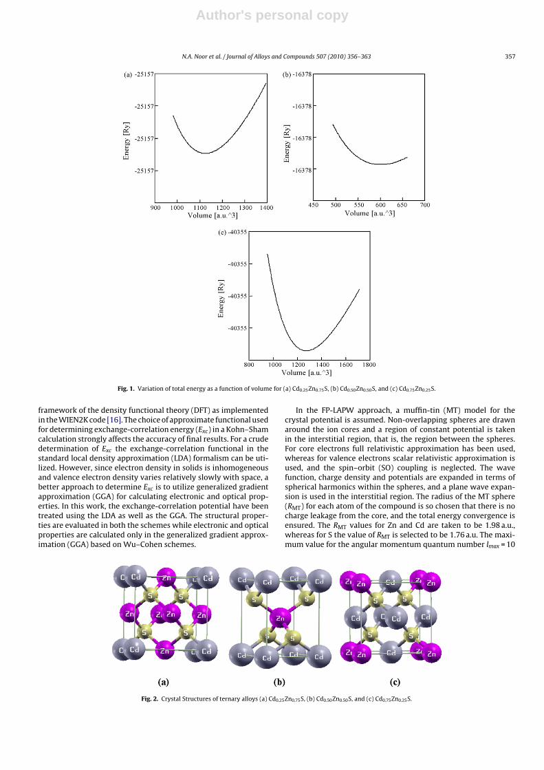
Fig. 1. Variation of total energy as a function of volume for (a) Cd0.25Zn0.75S, (b) Cd0.50Zn0.50S, and (c) Cd0.75Zn0.25S.
framework of the density functional theory (DFT) as implementedin the WIEN2K code [16]. The choice of approximate functional usedfor determining exchange-correlation energy (Exc) in a Kohn–Shamcalculation strongly affects the accuracy of final results. For a crudedetermination of Exc the exchange-correlation functional in thestandard local density approximation (LDA) formalism can be uti-lized. However, since electron density in solids is inhomogeneousand valence electron density varies relatively slowly with space, abetter approach to determine Exc is to utilize generalized gradientapproximation (GGA) for calculating electronic and optical prop-erties. In this work, the exchange-correlation potential have beentreated using the LDA as well as the GGA. The structural proper-ties are evaluated in both the schemes while electronic and opticalproperties are calculated only in the generalized gradient approx-imation (GGA) based on Wu–Cohen schemes.
In the FP-LAPW approach, a muffin-tin (MT) model for thecrystal potential is assumed. Non-overlapping spheres are drawnaround the ion cores and a region of constant potential is takenin the interstitial region, that is, the region between the spheres.For core electrons full relativistic approximation has been used,whereas for valence electrons scalar relativistic approximation isused, and the spin–orbit (SO) coupling is neglected. The wavefunction, charge density and potentials are expanded in terms ofspherical harmonics within the spheres, and a plane wave expan-sion is used in the interstitial region. The radius of the MT sphere(RMT) for each atom of the compound is so chosen that there is nocharge leakage from the core, and the total energy convergence isensured. The RMT values for Zn and Cd are taken to be 1.98 a.u.,whereas for S the value of RMT is selected to be 1.76 a.u. The maxi-mum value for the angular momentum quantum number lmax = 10
Fig. 2. Crystal Structures of ternary alloys (a) Cd0.25Zn0.75S, (b) Cd0.50Zn0.50S, and (c) Cd0.75Zn0.25S.
Author's personal copy
358 N.A. Noor et al. / Journal of Alloys and Compounds 507 (2010) 356–363
is taken for the wave function expansion inside the atomic spheres.In order to get the energy eigenvalue convergence, Kmax × RMT = 7is used for the binary compounds ZnS and CdS, whereas for theternary alloys CdxZn1−xS, we have used Kmax × RMT = 9, where Kmax
denotes the maximum value of the reciprocal lattice vector k. Boththe muffin-tin radius and the number of k-points are adjusted toensure convergence. A mesh of 72 k-points for the binary com-pounds and 35 k-points for the ternary alloy were taken for theBrillion zone integrations in the corresponding irreducible wedge.However, a finer k-mesh was used in the calculation of dielectricfunction and related optical properties. The self-consistent calcula-tions process was repeated until the total energy convergence wasless than 0.00001 Ryd.
3. Results and discussions
3.1. Structural properties
We have calculated the structural properties of the binary com-pounds ZnS, CdS and their ternary alloy CdxZn1−xS using both theLDA and GGA schemes for the exchange-correlation functional. Vol-ume optimization was performed by minimizing the total energywith respect to the unit cell volume using Murnaghan’s equation ofstate (EOS) [17]. The results of volume optimization for CdxZn1−xSat x = 0.25, 0.50 and 0.75 are shown in Fig. 1. The crystal struc-ture (of zinc-blende type) for both end compounds ZnS and CdSbelongs to space group F 43m (no. 216), while for the composi-tional parameter x = 0.25 and 0.75, where Zn is replaced by Cd atthe apex and face-center sites, it belongs to the space group P43m(no. 215). Similarly, for the composition x = 0.50, the resultant crys-tal structure belongs to the space group P4m2 (no. 115), which is atetragonal structure. The crystal structures of CdxZn1−xS for com-positional parameter x = 0.25, 0.50 and 0.75 have been shown inFig. 2.
From the volume optimization, equilibrium structure param-eters such as the lattice constant ‘a’ and the bulk modulus Band its pressure derivative B′ are estimated, Table 1. It can bereadily seen that the calculated values of ‘a’ and B for the end
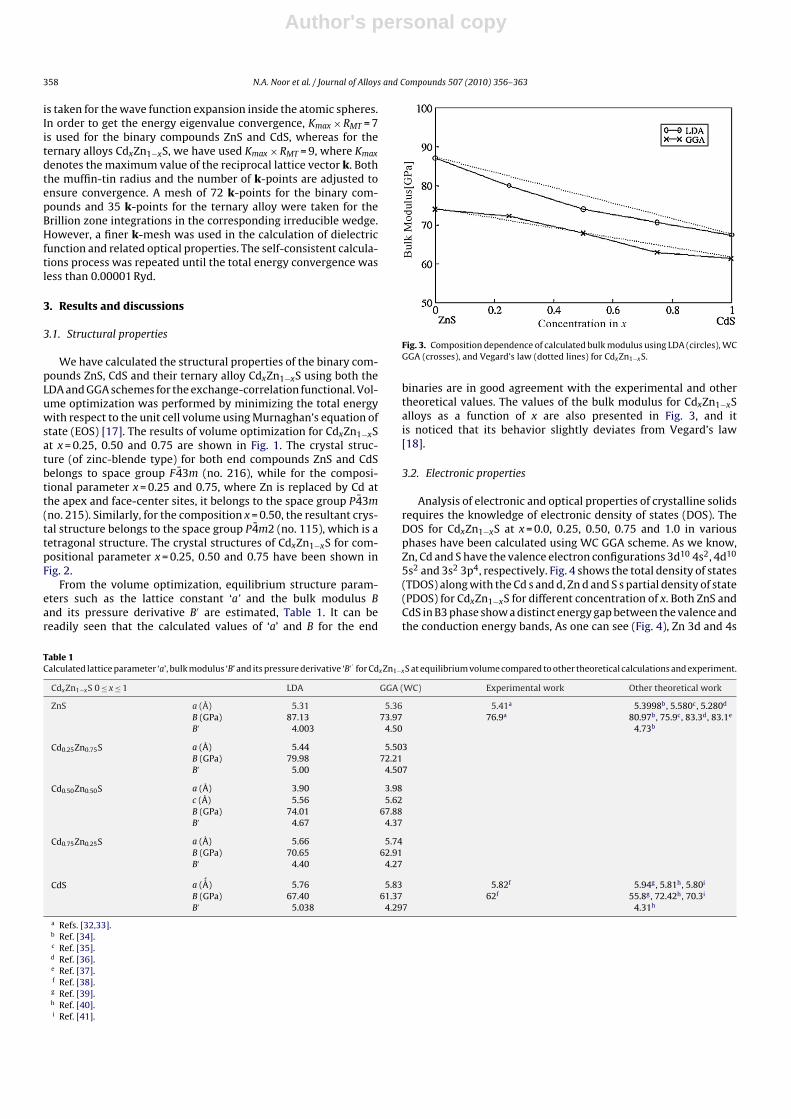
Fig. 3. Composition dependence of calculated bulk modulus using LDA (circles), WCGGA (crosses), and Vegard’s law (dotted lines) for CdxZn1−xS.
binaries are in good agreement with the experimental and othertheoretical values. The values of the bulk modulus for CdxZn1−xSalloys as a function of x are also presented in Fig. 3, and itis noticed that its behavior slightly deviates from Vegard’s law[18].
3.2. Electronic properties
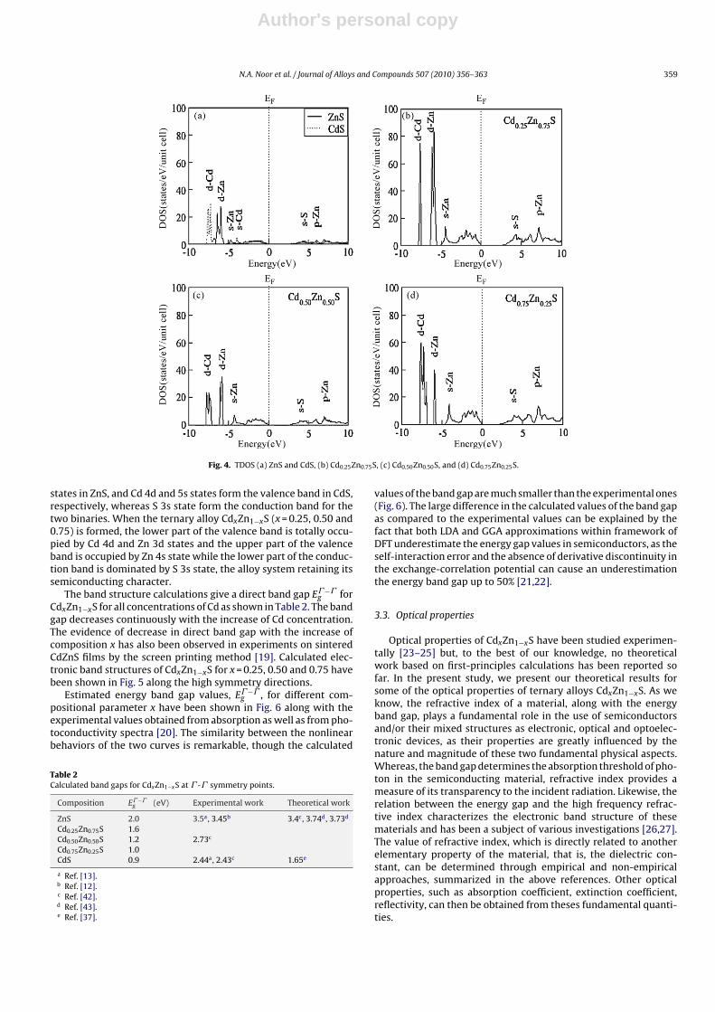
Analysis of electronic and optical properties of crystalline solidsrequires the knowledge of electronic density of states (DOS). TheDOS for CdxZn1−xS at x = 0.0, 0.25, 0.50, 0.75 and 1.0 in variousphases have been calculated using WC GGA scheme. As we know,Zn, Cd and S have the valence electron configurations 3d10 4s2, 4d10
5s2 and 3s2 3p4, respectively. Fig. 4 shows the total density of states(TDOS) along with the Cd s and d, Zn d and S s partial density of state(PDOS) for CdxZn1−xS for different concentration of x. Both ZnS andCdS in B3 phase show a distinct energy gap between the valence andthe conduction energy bands, As one can see (Fig. 4), Zn 3d and 4s
Table 1Calculated lattice parameter ‘a’, bulk modulus ‘B’ and its pressure derivative ‘B′ ′ for CdxZn1−xS at equilibrium volume compared to other theoretical calculations and experiment.
CdxZn1−xS 0 ≤ x ≤ 1 LDA GGA (WC) Experimental work Other theoretical work
ZnS a (Å) 5.31 5.36 5.41a 5.3998b, 5.580c, 5.280d
B (GPa) 87.13 73.97 76.9a 80.97b, 75.9c, 83.3d, 83.1e
B′ 4.003 4.50 4.73b
Cd0.25Zn0.75S a (Å) 5.44 5.503B (GPa) 79.98 72.21B′ 5.00 4.507
Cd0.50Zn0.50S a (Å) 3.90 3.98c (Å) 5.56 5.62B (GPa) 74.01 67.88B′ 4.67 4.37
Cd0.75Zn0.25S a (Å) 5.66 5.74B (GPa) 70.65 62.91B′ 4.40 4.27
CdS a ( ´A) 5.76 5.83 5.82f 5.94g, 5.81h, 5.80i
B (GPa) 67.40 61.37 62f 55.8g, 72.42h, 70.3i
B′ 5.038 4.297 4.31h
a Refs. [32,33].b Ref. [34].c Ref. [35].d Ref. [36].e Ref. [37].f Ref. [38].g Ref. [39].h Ref. [40].i Ref. [41].
Author's personal copy
N.A. Noor et al. / Journal of Alloys and Compounds 507 (2010) 356–363 359
Fig. 4. TDOS (a) ZnS and CdS, (b) Cd0.25Zn0.75S, (c) Cd0.50Zn0.50S, and (d) Cd0.75Zn0.25S.
states in ZnS, and Cd 4d and 5s states form the valence band in CdS,respectively, whereas S 3s state form the conduction band for thetwo binaries. When the ternary alloy CdxZn1−xS (x = 0.25, 0.50 and0.75) is formed, the lower part of the valence band is totally occu-pied by Cd 4d and Zn 3d states and the upper part of the valenceband is occupied by Zn 4s state while the lower part of the conduc-tion band is dominated by S 3s state, the alloy system retaining itssemiconducting character.
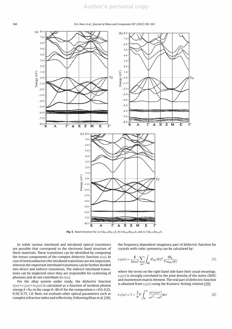
The band structure calculations give a direct band gap E� −�g for
CdxZn1−xS for all concentrations of Cd as shown in Table 2. The bandgap decreases continuously with the increase of Cd concentration.The evidence of decrease in direct band gap with the increase ofcomposition x has also been observed in experiments on sinteredCdZnS films by the screen printing method [19]. Calculated elec-tronic band structures of CdxZn1−xS for x = 0.25, 0.50 and 0.75 havebeen shown in Fig. 5 along the high symmetry directions.
Estimated energy band gap values, E� −�g , for different com-
positional parameter x have been shown in Fig. 6 along with theexperimental values obtained from absorption as well as from pho-toconductivity spectra [20]. The similarity between the nonlinearbehaviors of the two curves is remarkable, though the calculated
Table 2Calculated band gaps for CdxZn1−xS at � -� symmetry points.
Composition E� −�g (eV) Experimental work Theoretical work
ZnS 2.0 3.5a, 3.45b 3.4c, 3.74d, 3.73d
Cd0.25Zn0.75S 1.6Cd0.50Zn0.50S 1.2 2.73c
Cd0.75Zn0.25S 1.0CdS 0.9 2.44a, 2.43c 1.65e
a Ref. [13].b Ref. [12].c Ref. [42].d Ref. [43].e Ref. [37].
values of the band gap are much smaller than the experimental ones(Fig. 6). The large difference in the calculated values of the band gapas compared to the experimental values can be explained by thefact that both LDA and GGA approximations within framework ofDFT underestimate the energy gap values in semiconductors, as theself-interaction error and the absence of derivative discontinuity inthe exchange-correlation potential can cause an underestimationthe energy band gap up to 50% [21,22].
3.3. Optical properties
Optical properties of CdxZn1−xS have been studied experimen-tally [23–25] but, to the best of our knowledge, no theoreticalwork based on first-principles calculations has been reported sofar. In the present study, we present our theoretical results forsome of the optical properties of ternary alloys CdxZn1−xS. As weknow, the refractive index of a material, along with the energyband gap, plays a fundamental role in the use of semiconductorsand/or their mixed structures as electronic, optical and optoelec-tronic devices, as their properties are greatly influenced by thenature and magnitude of these two fundamental physical aspects.Whereas, the band gap determines the absorption threshold of pho-ton in the semiconducting material, refractive index provides ameasure of its transparency to the incident radiation. Likewise, therelation between the energy gap and the high frequency refrac-tive index characterizes the electronic band structure of thesematerials and has been a subject of various investigations [26,27].The value of refractive index, which is directly related to anotherelementary property of the material, that is, the dielectric con-stant, can be determined through empirical and non-empiricalapproaches, summarized in the above references. Other opticalproperties, such as absorption coefficient, extinction coefficient,reflectivity, can then be obtained from theses fundamental quanti-ties.
Author's personal copy
360 N.A. Noor et al. / Journal of Alloys and Compounds 507 (2010) 356–363
Fig. 5. Band structure for (a) Cd0.25Zn0.75S, (b) Cd0.50Zn0.50S, and (c) Cd0.75Zn0.25S.
In solids various interband and intraband optical transitionsare possible that correspond to the electronic band structure ofthese materials. These transitions can be identified by computingthe tensor components of the complex dielectric function ε(ω). Incase of semiconductors the intraband transitions are not important,whereas the important interband transitions can be further dividedinto direct and indirect transitions. The indirect interband transi-tions can be neglected since they are responsible for scattering ofphonons and do not contribute to ε(ω).
For the alloy system under study, the dielectric functionε(ω) = ε1(ω) + iε2(ω) is calculated as a function of incident photonenergy E = hω in the range 0–40 eV for the composition x = 0.0, 0.25,0.50, 0.75, 1.0. Next, we evaluate other optical parameters such ascomplex refractive index and reflectivity. Following Khan et al. [28],
the frequency dependent imaginary part of dielectric function forcrystals with cubic symmetry can be calculated by:
ε2(ω) = 83�ω2
∑nn′
∫BZ
|Pnn′ (k)|2 dSk
∇ωnn′ (k), (1)
where the terms on the right hand side have their usual meanings.ε2(ω) is strongly correlated to the joint density of the states (DOS)and momentum matrix element. The real part of dielectric functionis obtained from ε2(ω) using the Kramers–Krönig relation [29].
ε1(ω) = 1 + 2�
P
∫ ∞
0
ω′ε2(ω′)ω′2 − ω2
dω′ (2)
Author's personal copy
N.A. Noor et al. / Journal of Alloys and Compounds 507 (2010) 356–363 361
Fig. 6. E� −�g as a function of x, experimental and theoretical curve.
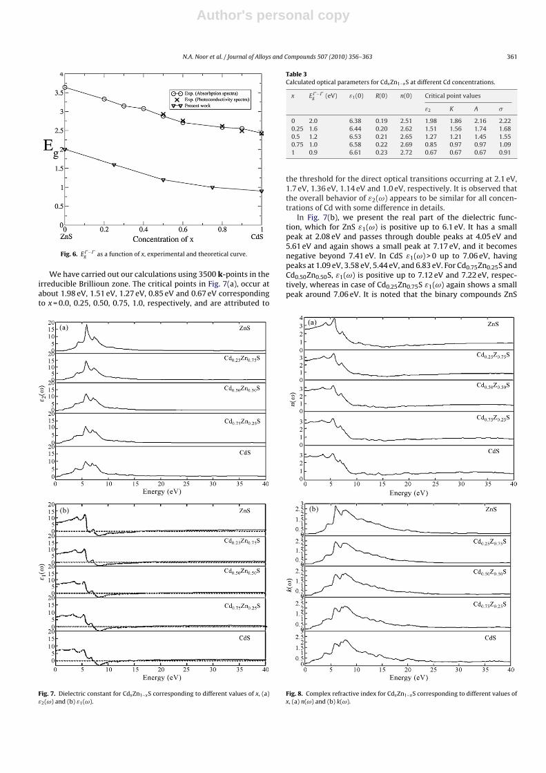
We have carried out our calculations using 3500 k-points in theirreducible Brillioun zone. The critical points in Fig. 7(a), occur atabout 1.98 eV, 1.51 eV, 1.27 eV, 0.85 eV and 0.67 eV correspondingto x = 0.0, 0.25, 0.50, 0.75, 1.0, respectively, and are attributed to
Fig. 7. Dielectric constant for CdxZn1−xS corresponding to different values of x, (a)ε2(ω) and (b) ε1(ω).
Table 3Calculated optical parameters for CdxZn1−xS at different Cd concentrations.
x E� −�g (eV) ε1(0) R(0) n(0) Critical point values
ε2 K A �
0 2.0 6.38 0.19 2.51 1.98 1.86 2.16 2.220.25 1.6 6.44 0.20 2.62 1.51 1.56 1.74 1.680.5 1.2 6.53 0.21 2.65 1.27 1.21 1.45 1.550.75 1.0 6.58 0.22 2.69 0.85 0.97 0.97 1.091 0.9 6.61 0.23 2.72 0.67 0.67 0.67 0.91
the threshold for the direct optical transitions occurring at 2.1 eV,1.7 eV, 1.36 eV, 1.14 eV and 1.0 eV, respectively. It is observed thatthe overall behavior of ε2(ω) appears to be similar for all concen-trations of Cd with some difference in details.
In Fig. 7(b), we present the real part of the dielectric func-tion, which for ZnS ε1(ω) is positive up to 6.1 eV. It has a smallpeak at 2.08 eV and passes through double peaks at 4.05 eV and5.61 eV and again shows a small peak at 7.17 eV, and it becomesnegative beyond 7.41 eV. In CdS ε1(ω) > 0 up to 7.06 eV, havingpeaks at 1.09 eV, 3.58 eV, 5.44 eV, and 6.83 eV. For Cd0.75Zn0.25S andCd0.50Zn0.50S, ε1(ω) is positive up to 7.12 eV and 7.22 eV, respec-tively, whereas in case of Cd0.25Zn0.75S ε1(ω) again shows a smallpeak around 7.06 eV. It is noted that the binary compounds ZnS
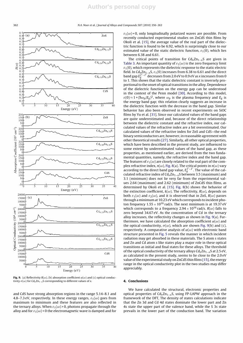
Fig. 8. Complex refractive index for CdxZn1−xS corresponding to different values ofx, (a) n(ω) and (b) k(ω).
Author's personal copy
362 N.A. Noor et al. / Journal of Alloys and Compounds 507 (2010) 356–363
Fig. 9. (a) Reflectivity R(ω), (b) absorption coefficient ˛(ω) and (c) optical conduc-tivity �(ω) for CdxZn1−xS corresponding to different values of x.
and CdS have strong absorption regions in the range 5.14–8.1 and4.8–7.3 eV, respectively. In these energy ranges, ε1(ω) goes frommaximum to minimum and these features are also reflected inthe ternary alloys. When ε1(ω) > 0, photons propagate through thealloy and for ε1(ω) < 0 the electromagnetic wave is damped and for
ε1(ω) = 0, only longitudinally polarized waves are possible. Fromrecently conducted experimental studies on ZnCdS thin films byOkoli et al. [15], the average value of the real part of the dielec-tric function is found to be 6.92, which is surprisingly close to ourestimated value of the static dielectric function, ε1(0), which liesbetween 6.38 and 6.61.
The critical points of transition for CdxZn1−xS are given inTable 3. An important quantity of ε1(ω) is the zero frequency limitε1(0), which represents the dielectric response to the static electricfield. In CdxZn1−xS, ε1(0) increases from 6.38 to 6.61 and the directband gap E� −�
g decreases from 2.0 eV to 0.9 eV as x increases from 0to 1. This shows that the static dielectric constant is inversely pro-portional to the onset of optical transitions in the alloy. Dependenceof the dielectric function on the energy gap can be understoodin the context of the Penn model [30]. According to this model,ε(0) ≈ 1 + (hωp/Eg)2, where ωp is the plasma frequency and Eg isthe energy band gap; this relation clearly suggests an increase inthe dielectric function with the decrease in the band gap. Similarbehavior has also been observed in recent experiments on SiOCfilms by Yu et al. [31]. Since our calculated values of the band gapsare quite underestimated and, because of the direct relationshipbetween the dielectric constant and the refractive index, our cal-culated values of the refractive index are a bit overestimated. Ourcalculated values of the refractive index for ZnS and CdS—the endbinary semiconductors are, however, in reasonable agreement withother theoretical results [27]. Similarly, all other optical properties,which have been described in the present study, are influenced tosome extent by underestimated values of the band gap, as theseproperties, as mentioned earlier, are derived from the two funda-mental quantities, namely, the refractive index and the band gap.The features of ε1(ω) are closely related to the real part of the com-plex refractive index, n(ω), Fig. 8(a). The critical points in n(ω) varyaccording to the direct band gap value, E� −�
g . The value of the cal-culated refractive index of CdxZn1−xS between 3.5 (maximum) and3.1 (minimum) does not lie very far from the experimental val-ues 2.64 (maximum) and 2.62 (minimum) of ZnCdS thin films, asdetermined by Okoli et al. [15]. Fig. 8(b) shows the behavior ofthe extinction coefficient, k(ω). The reflectivity, R(ω), depends onboth ε1(ω) and ε2(ω), and it is observed that in ZnS, R(ω) passesthrough a minimum at 10.23 eV which corresponds to incident pho-ton frequency 1.55 × 10¹⁶ rad/s. The next minimum is at 19.37 eVwhich corresponds to a frequency 2.94 × 10¹⁶ rad/s. R(ω) falls tozero beyond 34.67 eV. As the concentration of Cd in the ternaryalloy increases, the reflectivity changes as shown in Fig. 9(a). Fur-thermore, we have calculated the absorption coefficient ˛(ω) andthe optical conductivity, �(ω), which are shown Fig. 9(b) and (c),respectively. A comparative analysis of ˛(ω) with electronic bandstructure presented in Fig. 5 reveals the manner in which incidentradiation may get absorbed in these materials. The S atom s statesand Zn and Cd atom s like states play a major role in these opticaltransitions as initial and final states for these alloys. The thresholdof the optical conductivity of the ternary alloys CdxZn1−xS at 2.5 eV,as calculated in the present study, seems to lie close to the 2.0 eVvalue of the experimental study on ZnCdS thin films [15], the energyrange in the optical conductivity plot in the two studies may differappreciably.
4. Conclusions
We have calculated the structural, electronic properties andoptical properties of CdxZn1−xS, using FP-LAPW approach in theframework of the DFT, The density of states calculations indicatethat the Zn 3d and Cd 4d states dominate the lower part and Zn4s state the upper part of the valence band, while the S 3s stateprevails in the lower part of the conduction band. The variation
Author's personal copy
N.A. Noor et al. / Journal of Alloys and Compounds 507 (2010) 356–363 363
of the direct energy band gap E� −�g in CdxZn1−xS, as estimated
from the calculated electronic band structure, agrees well quali-tatively with experimental results, Furthermore, the calculationsfor the dielectric constant ε(ω) show that smaller energy gap E� −�
g
yields a larger static dielectric constant ε1(0) and refractive indexvaries as ε1(0). For all values of x in ε2(ω) curves, the critical pointscorrespond to direct optical transitions. Reasonable agreement canbe found between some of the optical properties calculated in thiswork and the experimental results from a recently conducted studyon ZnCdS thin films. The overall features of real and imaginary partsof the complex dielectric functions are similar for CdxZn1−xS alloysover all compositions ranges (x = 0.0, 0.25, 0.50, 0.75 and 1.0). How-ever the major maxima in the spectra of ε2(ω) and ε1(ω) seemto decrease as one goes from ZnS to CdS. Furthermore, the calcu-lated reflectivity spectra for the ternary alloys CdxZn1−xS show thatthere are regions of maximum and minimum reflectivity, whichshift with x, and this feature may be utilized in the fabrication ofoptoelectronic devices.
References
[1] M.C. Gupta, J. J. Ballato (Eds.), Handbook of Photonics, Taylor & Francis, 2006.[2] H.E. Ruda, Wide-gap II–VI Compounds for Opto-electronic Applications,
Springer, 1992.[3] K.T.R. Reddy, P.J. Reddy, J. Phys. D 25 (1992) 1345.[4] F. Benkabou, H. Aourag, M. Certier, Mater. Chem. Phys. 66 (2000) 10.[5] Z.J. Xin, R. Peaty, H.N. Rutt, R.W. Eason, Semicond. Sci. Technol. 14 (1999) 695.[6] C.G. Van der Walle, Phys. B 185 (1993) 1.[7] T.A. Chnoweth, R.H. Bube, J. Appl. Phys. 51 (1980) 1844.[8] A.D. Corsa, S. Baroni, R. Resta, S. Gironcoli, Phys. Rev. B 47 (1993) 3588.[9] T. Okamoto, Y. Matsuzaki, N. Amin, A. Yamada, M. Konagai, Jpn. J. Appl. Phys.
37 (1998) 3894.[10] D. Hariskos, M. Ruck, T. Walter, H.W. Schock, Proc. 1st WCPEC, Hawaii, 1994, p.
91.[11] E. Dutková, P. Baláz, P. Pourghahramani, A.V. Nguyen, V. Sepelák, A. Feldhoff, J.
Kovác, A. Satka, Solid State Ionics 179 (2008) 1242.[12] S. Arora, S.S. Manoharan, Opt. Mater. 31 (2008) 176.
[13] P. Kumar, A. Misra, D. Kumar, N. Dhama, T.P. Sharma, P.N. Dixit, Opt. Mater. 27(2004) 261.
[14] J. Torres, G. Gordillo, Thin Solid Films 207 (1992) 231.[15] (a) M.K. Karanjai, D.D. Gupta, Thin Solid Films 155 (1987) 309;
(b) D.N. Okoli, A.J. Ekpunobi, C.E. Okeke, Acad. Open Internet J. 18 (2006) 1.[16] P. Blaha, K. Schwarz, G.H. Madsen, D. Kvasnicka, J. Luitz, FP-L/APW+lo Program
for Calculating Crystal Properties, K. Schwarz, Techn. WIEN2K, Austria, 2001.[17] F.D. Murnagham, Proc. Natl. Acad. Sci. 30 (1944) 244.[18] L. Vegard, Z. Phys. 5 (1921) 17.[19] V. Kumar, V. Singh, S.K. Sharma, T.P. Sharma, Opt. Mater. 11 (1998) 29.[20] V.P. Singh, S. Singh, Czech. J. Phys. B 26 (1976) 1161.[21] R.W. Godby, M. Schlüter, L.J. Sham, Phys. Rev. Lett. 56 (1986) 2415.[22] M. Städle, J.A. Majevski, P. Vogel, A. Görling, Phys. Rev. Lett. 79 (1997) 2089.[23] J. Torres, J.I. Cisneros, G. Gordillo, F. Alvarez, Thin Solid Film 289 (1996) 238.[24] S.C. Ray, M.K. Karanjai, D.D. Gupta, Thin Solid Films 322 (1998) 117.[25] A.H. Ammar, Phys. B 296 (2001) 312.[26] N.M. Ravindra, P. Ganapathy, J. Choi, Infrared Phys. Technol. 50 (2007) 21.[27] M.A. Salem, Chin. J. Phys. 42 (2003) 288.[28] M.A. Khan, A. Kashyap, A.K. Solanki, T. Nautiyal, S. Auluck, Phys. Rev. B 23 (1993)
16974.[29] F. Wooten, Optical Properties of Solids, Academic, New York, 1972.[30] D.R. Penn, Phys. Rev. 128 (1962) 2093.[31] Y.H. Yu, S.C. Lee, C.S. Yang, C.K. Choi, W.K. Jung, J. Korean Phys. Soc. 42 (2003)
682.[32] O. Madelung, M. Schultz, H. Weiss, Physics of II–IV and I–VII Compounds. Semi-
magnetic Semiconductors, Landolt Börnstein New Series group III, vol. 17, Pt.b, Springer, Berlin, 1982.
[33] K.H. Hellwege, O. Madelung (Eds.), Semiconductors, Intrinsic properties ofgroup IV elements and III–V, II–VI and I–VII Compounds, Landolt-BörnsteinNew Series group III, vol. 22, Pt. a, Springer, Berlin, 1982.
[34] R. Gangadharan, V. Jayalakshmi, J. Kalaiselvi, R. Murugan, B. Palanivel, J. AlloysCompd. 359 (2003) 22.
[35] J.E. Jaffe, R. Pandey, M.J. Seal, Phys. Rev. B 47 (1993) 6299.[36] A. Nazzal, A. Qteish, Phys. Rev. B 53 (1996) 8262.[37] A. Qteish, M. Parrinello, Phys. Rev. B 61 (2000) 6521.[38] O. Madelung, M. Schulz, H. Weiss, Numerical Data and Functional Relationships
in Science and Technology, Landolt-Borstein, vol. 17, Springer, Berlin, 1982.[39] S. Zerroug, F. Ali Sahraoui, N. Bouarissa, Eur. Phys. J. B 57 (2007) 9.[40] E. Deligoz, K. Colakoglu, Y. Ciftci, Phys. B 373 (2006) 124.[41] S. Wei, S.B. Zhang, Phys. Rev. B 62 (2000) 6944.[42] N. Fitzer, A. Kuligk, R. Redmer, Phys. Rev. B 67 (2003) 201201.[43] S. Nazir, N. Ikram, S.A. Siddiqi, Y. Saeed, A. Shaukat, A.H. Reshak, Curr. Opin.
Solid State Mater. Sci. 14 (2010) 1.
Related Documents

![Influence of Titanium Oxide on Structure, Corrosion and ... · Microstructure, wettability and physical properties of Sn 96-x Zn 4 Bi x alloys are reported by El-Bediwi et al. [1].](https://static.cupdf.com/doc/110x72/5ed724bec30795314c1746ea/influence-of-titanium-oxide-on-structure-corrosion-and-microstructure-wettability.jpg)


