Efficiency Enhancement of Doherty Amplifier by Mitigating the Knee Voltage Effect Junghwan Moon, Student Member, IEEE, Jangheon Kim, Member, IEEE, Jungjoon Kim, Ildu Kim, and Bumman Kim, Fellow, IEEE Abstract—This paper presents an approach to mitigating the knee voltage effect of the Doherty power amplifier (PA), especially on the carrier amplifier. Such an effort increases the efficiency when the PA is driven by modulated signals. It is shown that, for the carrier PA, 2Ropt, which is the theoretical value for the PA at a low power region, is not optimum condition when the knee voltage is not negligible. Due to the effect, the carrier PA is not in the saturated operation at the 6 dB back-off power level. To obtain the maximum efficiency at the region under the non-zero knee voltage, the load impedance of a carrier amplifier should be increased larger larger than that of conventional amplifier, i.e., 2Ropt, to reduce the knee voltage effect. By mitigating the effect, the optimized operation condition for efficiency is derived. The optimized Doherty amplifier is analyzed and simulated in terms of its load modulation behavior, efficiency, and output power, and compared with the conventional Doherty PA. The good performance is demonstrated by the Doherty PA built using Cree GaN HEMT CGH40045 devices at 2.655 GHz. For worldwide interoperability for microwave access applications with a 7.8 dB peak-to-average power ratio, the proposed PA delivers an efficiency of 49.3% at an output power of 42 dBm, which is a 7.5 dB back-off level from the peak power, with an acceptable linearity of –23.1 dBc. The linearity is improved to –43 dBc by employing a digital feedback predistortion technique, satisfying the system linearity specification. Index Terms—Doherty, efficiency enhancement, gallium ni- tride, knee voltage, load modulation, power amplifier, worldwide interoperability for microwave access. I. I NTRODUCTION A S wireless communication systems utilize higher data rates, the signals of the systems vary rapidly and have large peak-to-average power ratios (PAPRs) becuase of the complex modulation schemes for efficient spectrum usage. To satisfy linearity requirements for the signals such as wideband code division multiple access, orthogonal frequency division multiple access, and world wide interoperability for microwave access (WiMAX), PAs should have a capability Manuscript received September 3, 2009; revised February 10, 2010. This work was supported by the MKE (The Ministry of Knowledge Economy), Korea, under the ITRC (Information Technology Research Center) sup- port program supervised by the NIPA (National IT Industry Promotion Agency)(NIPA-2010-(C1090-1011-0011)), by WCU (World Class University) program through the Korea Science and Engineering Foundation funded by the Ministry of Education, Science and Technology(Project No. R31-2008- 000-10100-0), and by the Brain Korea 21 Project in 2010. J. Moon, J. Kim, and B. Kim are with the Department of Electrical Engineering, Pohang University of Science and Technology, Pohang, Gyeong- buk 790-784, Korea (e-mail: [email protected]; [email protected]; [email protected]). J. Kim and I. Kim are with the Samsung Electronics Company Ltd., Suwon, Gyeunggi, Korea (e-mail: [email protected]; [email protected]). of generating the peak power, and generate all power levels linearly following the signal distribution. Therefore, the PAs operate mostly at the average power level, back-off from the peak power by PAPR. The efficiency at the operation point is low, leading to a low efficiency PA. There are a few candidates that can solve the low efficiency problem due to the operation at a back-off power region, such as envelope elimination and restoration, envelope tracking, and Doherty PA [1]– [23]. The first two systems provide good efficiency by adjusting the drain/collector bias to reduce the dissipated power consumptions. However, they have some problems, such as difficulty of the delay adjustment of the RF and envelope paths and the complexity of the linkage between the PA and bias modulator. Moreover, they require a highly efficient bias modulator as well as the PA [4]– [7]. However, the Doherty PA can accomplish the high efficiency employing two PAs: one PA, carrier amplifier, is operational at a low power region, and another one, peaking amplifier, is turned on at a high power region. The power of the PAs are combined by the self-adjusted load modulation technique [8]– [23]. A significant amount of research has been focused on the Doherty PA to improve its efficiency. Asymmetrical Doherty PAs, such as an N-way Doherty PA [13], an extended Doherty PA [14], and a multistage Doherty PA [15] have been proposed to extend the peak efficiency region over a wider range of output power. In addition, the Doherty PA based on a saturated PA [16]– [19], such as the class-F and inverse class-F, shows the enhanced maximum efficiency. Although the previous works provide good theoretical analysis, they are performed in the ideal design environment. However, it is a challenging task to obtain the same high efficiencies at the peak and back-off power levels like an Ideal Doherty, as shown in Fig. 1. Thus, it is crucial to determine which region should be optimized for better overall-efficiency when the PA is driven by a modulated signal, and we have evaluated the efficiency of the Doherty PAs optimized at the each theoretical maximum region. Doherty Type-I shows a degraded efficiency at the peak power level, resulted from imperfect load modulation of the Doherty PA. Doherty Type-II, on the other hand, has reduced efficiency at the back-off power level because the carrier PA does not reach to the peak efficiency when the peaking PA is turned on. Based on these profiles, the estimated overall-efficiencies for amplification of the modulated signal with PAPR of 7.8 dB are computed using a routine coded in MATLAB and summarized in Table I [16]. Our results show that the Doherty amplifier’s should be optimized for high efficiency at the back-off region and not at the peak power Copyright © 2010 IEEE. Reprinted from the IEEE TRANSACTIONS ON MICROWAVE THEORY AND TECHNIQUES, VOL. 59, NO. 1, JANUARY 2011 This material is posted here with permission of the IEEE. Such permission of the IEEE does not in any way imply IEEE endorsement of any of Cree’s products or services. Internal or personal use of this material is permitted. However, permission to reprint/republish this material for advertising or pro- motional purposes or for creating new collective works for resale or redistribution must be obtained from the IEEE by writing to [email protected] By choosing to view this document, you agree to all provisions of the copyright laws protecting it.

Welcome message from author
This document is posted to help you gain knowledge. Please leave a comment to let me know what you think about it! Share it to your friends and learn new things together.
Transcript
FINAL MANUSCRIPT (MANUSCRIPT NUMBMER:7732) TO IEEE TRANSACTIONS ON MICROWAVE THEORY AND TECHNIQUES 1
Efficiency Enhancement of Doherty Amplifier byMitigating the Knee Voltage Effect
Junghwan Moon, Student Member, IEEE, Jangheon Kim, Member, IEEE, Jungjoon Kim,Ildu Kim, and Bumman Kim, Fellow, IEEE
Abstract—This paper presents an approach to mitigating theknee voltage effect of the Doherty power amplifier (PA), especiallyon the carrier amplifier. Such an effort increases the efficiencywhen the PA is driven by modulated signals. It is shown that, forthe carrier PA, 2Ropt, which is the theoretical value for the PAat a low power region, is not optimum condition when the kneevoltage is not negligible. Due to the effect, the carrier PA is notin the saturated operation at the 6 dB back-off power level. Toobtain the maximum efficiency at the region under the non-zeroknee voltage, the load impedance of a carrier amplifier shouldbe increased larger larger than that of conventional amplifier,i.e., 2Ropt, to reduce the knee voltage effect. By mitigating theeffect, the optimized operation condition for efficiency is derived.The optimized Doherty amplifier is analyzed and simulated interms of its load modulation behavior, efficiency, and outputpower, and compared with the conventional Doherty PA. Thegood performance is demonstrated by the Doherty PA builtusing Cree GaN HEMT CGH40045 devices at 2.655 GHz. Forworldwide interoperability for microwave access applicationswith a 7.8 dB peak-to-average power ratio, the proposed PAdelivers an efficiency of 49.3% at an output power of 42 dBm,which is a 7.5 dB back-off level from the peak power, with anacceptable linearity of –23.1 dBc. The linearity is improved to–43 dBc by employing a digital feedback predistortion technique,satisfying the system linearity specification.
Index Terms—Doherty, efficiency enhancement, gallium ni-tride, knee voltage, load modulation, power amplifier, worldwideinteroperability for microwave access.
I. INTRODUCTION
AS wireless communication systems utilize higher datarates, the signals of the systems vary rapidly and have
large peak-to-average power ratios (PAPRs) becuase of thecomplex modulation schemes for efficient spectrum usage.To satisfy linearity requirements for the signals such aswideband code division multiple access, orthogonal frequencydivision multiple access, and world wide interoperability formicrowave access (WiMAX), PAs should have a capability
Manuscript received September 3, 2009; revised February 10, 2010. Thiswork was supported by the MKE (The Ministry of Knowledge Economy),Korea, under the ITRC (Information Technology Research Center) sup-port program supervised by the NIPA (National IT Industry PromotionAgency)(NIPA-2010-(C1090-1011-0011)), by WCU (World Class University)program through the Korea Science and Engineering Foundation funded bythe Ministry of Education, Science and Technology(Project No. R31-2008-000-10100-0), and by the Brain Korea 21 Project in 2010.
J. Moon, J. Kim, and B. Kim are with the Department of ElectricalEngineering, Pohang University of Science and Technology, Pohang, Gyeong-buk 790-784, Korea (e-mail: [email protected]; [email protected];[email protected]).
J. Kim and I. Kim are with the Samsung Electronics CompanyLtd., Suwon, Gyeunggi, Korea (e-mail: [email protected];[email protected]).
of generating the peak power, and generate all power levelslinearly following the signal distribution. Therefore, the PAsoperate mostly at the average power level, back-off from thepeak power by PAPR. The efficiency at the operation pointis low, leading to a low efficiency PA. There are a fewcandidates that can solve the low efficiency problem due tothe operation at a back-off power region, such as envelopeelimination and restoration, envelope tracking, and DohertyPA [1]– [23]. The first two systems provide good efficiencyby adjusting the drain/collector bias to reduce the dissipatedpower consumptions. However, they have some problems, suchas difficulty of the delay adjustment of the RF and envelopepaths and the complexity of the linkage between the PA andbias modulator. Moreover, they require a highly efficient biasmodulator as well as the PA [4]– [7]. However, the Doherty PAcan accomplish the high efficiency employing two PAs: onePA, carrier amplifier, is operational at a low power region,and another one, peaking amplifier, is turned on at a highpower region. The power of the PAs are combined by theself-adjusted load modulation technique [8]– [23].
A significant amount of research has been focused on theDoherty PA to improve its efficiency. Asymmetrical DohertyPAs, such as an N-way Doherty PA [13], an extended DohertyPA [14], and a multistage Doherty PA [15] have been proposedto extend the peak efficiency region over a wider range ofoutput power. In addition, the Doherty PA based on a saturatedPA [16]– [19], such as the class-F and inverse class-F, showsthe enhanced maximum efficiency. Although the previousworks provide good theoretical analysis, they are performedin the ideal design environment. However, it is a challengingtask to obtain the same high efficiencies at the peak andback-off power levels like an Ideal Doherty, as shown inFig. 1. Thus, it is crucial to determine which region should beoptimized for better overall-efficiency when the PA is drivenby a modulated signal, and we have evaluated the efficiency ofthe Doherty PAs optimized at the each theoretical maximumregion. Doherty Type-I shows a degraded efficiency at thepeak power level, resulted from imperfect load modulationof the Doherty PA. Doherty Type-II, on the other hand, hasreduced efficiency at the back-off power level because thecarrier PA does not reach to the peak efficiency when thepeaking PA is turned on. Based on these profiles, the estimatedoverall-efficiencies for amplification of the modulated signalwith PAPR of 7.8 dB are computed using a routine coded inMATLAB and summarized in Table I [16]. Our results showthat the Doherty amplifier’s should be optimized for highefficiency at the back-off region and not at the peak power
Copyright © 2010 IEEE. Reprinted from the IEEE TRANSACTIONS ON MICROWAVE THEORY AND TECHNIQUES, VOL. 59, NO. 1, JANUARY 2011
This material is posted here with permission of the IEEE. Such permission of the IEEE does not in any way imply IEEE endorsement of any of Cree’s products or services. Internal or personal use of this material is permitted. However, permission to reprint/republish this material for advertising or pro-motional purposes or for creating new collective works for resale or redistribution must be obtained from the IEEE by writing to [email protected] By choosing to view this document, you agree to all provisions of the copyright laws protecting it.

FINAL MANUSCRIPT (MANUSCRIPT NUMBMER:7732) TO IEEE TRANSACTIONS ON MICROWAVE THEORY AND TECHNIQUES 2
Fig. 1. Ideal efficiencies of the class-B and two-way Doherty poweramplifiers and the probability density and power generation distribution ofa WiMAX signal with a 7.8 dB PAPR.
TABLE IESTIMATED EFFICIENCY OF TWO-WAY DOHERTY AMPLIFIERS FOR A
SIGNAL WITH A PAPR OF 7.8 dB
Ideal Doherty Doherty Type I Doherty Type II
ηavg [%] 61.5 59.4 56.3
one to ensure better performance under modulated signals.To get the maximum efficiency at the back-off region, the
knee voltage effect of the carrier PA should be considered. Wehave found that a load impedance larger than 2Ropt is neededin the low power region to obtain fully saturated operationwhen the peaking PA is turned on. Even though the basicdesign concept has been discussed previously [20], this studypresents a more detailed analysis and further experimentalresults. We examine the basic operation of the Doherty PAin Section II. Section III describes the detailed behavior ofthe PA using real device simulation. To verify our analysesand simulations, we implement the amplifier using Cree GaNHEMT CGH40045 devices at 2.655 GHz and compared withthe conventional Doherty PA for continuous wave (CW) andmobile WiMAX 1FA signals, which is explained in SectionIV. The experimental results clearly show that the knee voltageeffect should be considered to properly design the Doherty PA.Finally, the digital feedback predistortion (DFBPD) techniqueis applied to achieve highly linear performance [24], satisfyingthe system specifications.
II. ANALYSIS FOR OPERATIONAL CHARACTERISTICS OFTHE DOHERTY POWER AMPLIFIER
A. Doherty PA Operation with Knee Voltage EffectTheoretically, the Doherty PA attains the highest efficiencies
at the 6 dB back-off and at the peak power levels. Themaximum efficiencies at the two points can be achieved withperfect load-modulated-operation of the carrier and peakingPAs and infinite output impedance of the peaking PA at theturn-off state. The perfect load modulation of the carrier PAwith zero-knee voltage, depicted in Fig. 2(a), indicates that
(a)
(b)
Fig. 2. Load line of the carrier amplifier. (a) Ideal case with zero kneevoltage. (b) Practical case with non-zero knee voltage.
the output powers for both RIdealopt and 2RIdeal
opt are P Ideal1 and
P Ideal1 /2, respectively. The efficiencies (ηIdeals) are also the
same at P Ideal1 and P Ideal
1 /2, respectively; the carrier PA isin equally saturated states for both cases. In this operation,P Ideal
1 , ηIdeal, and RIdealopt are given by
P Ideal1 =
12· I1,c (θc) · V1
ηIdeal =P Ideal
1
P Idealdc
× 100 =(1/2) · I1,c (θc)
Idc,c (θc)× 100
RIdealopt =
V1
I1,c (θc)(1)
where
I1,c (θc) =Imax
2π· θc − sin θc
1 − cos (θc/2)
Idc,c (θc) =Imax
2π· 2 · sin (θc/2) − θc · cos (θc/2)
1 − cos (θc/2).
I1,c (θc) and Idc,c (θc) are the fundamental and dc currentcomponents of the carrier PA biased at the conduction angleθc, respectively. In the ideal case, V1 is equal to Vdc becauseof the zero on-resistance Ron with the zero knee voltage.
In a real device, the effect of knee voltage should beconsidered. Fig. 2(b) shows a load line with the knee voltage

FINAL MANUSCRIPT (MANUSCRIPT NUMBMER:7732) TO IEEE TRANSACTIONS ON MICROWAVE THEORY AND TECHNIQUES 3
(a)
(b)
Fig. 3. (a) Maximum output powers employing Ropt, RCase I, and RCase II
as Ron varies from 0 to 0.8 Ω. (b) Load impedances for Ropt, RCase I, andRCase II as Ron varies from 0 to 0.8 Ω.
Vk. For Ropt and 2Ropt, the load impedances are written by
Ropt =Vdc − Vk
I1,c (θc)(2)
RCase I =Vdc − V ′
k
i′1,c (θc)(3)
where
i′1,c (θc) =i′max
2π· θc − sin θc
1 − cos (θc/2)Vk = Ron · Imax
V ′k = Ron · i′max.
Since Case I represents the 2Ropt case, i′max can be derivedusing (2) and (3) as follows:
i′max =ImaxVdc
2Vdc − ImaxRon. (4)
i′max represents the maximum current when the carrier PA hasa load impedance of 2Ropt. Thus, the output powers for the
Fig. 4. Load modulation results for carrier amplifier employing the loadimpedances of 50 Ω, 100 Ω, and 130 Ω.
Ropt and RCase I cases can be calculated as follows
PRopt =(
12
)· I1,c (θc) · (Vdc − Vk)
PCase I =(
12
)· i′1,c (θc) · (Vdc − V ′
k) (5)
and are shown in Fig. 3(a). For the calculation, we assumea Vdc supply of 30 V and Imax of 8 A with uniform trans-conductance. θc is fixed at 210. As shown, the carrier PAwith 2Ropt delivers more power than the expected valueof (1/2) PRopt because of the enlarged voltage and currentswings from (Vdc − Vk) to (Vdc − V ′
k) and from Imax/2 toi′max, respectively. The efficiency deteriorates in the 6 dB back-off region of the Doherty PA because the carrier PA doesnot reach to the saturation state when the peaking PA beginsconducting.
To maximize the efficiency at the 6 dB back-off powerregion, the carrier PA with non-zero knee voltage shouldhave a load impedance larger than 2Ropt, like the case-II inFig. 2(b), because the carrier PA with 2Ropt cannot be fullysaturated at the 3 dB back-off region, as depicted in Fig. 3(a).In this case, the output power can be written as
PCase II =(
12
)· i′′1,c (θc) · (Vdc − V ′′
k ) (6)
where
i′′1,c (θc) =i′′max
2π· θc − sin θc
1 − cos (θc/2)V ′′
k = Ron · i′′max.
Since PCase II should be a half of PRopt to obtain the fullysaturated state at the 3 dB back-off region, i′′max, the maximumcurrent when the carrier PA has a load impedance larger than2Ropt, can be calculated as follows
i′′max =1
Ron·Vdc −
√(Vdc)
2 − 2 · Vk · (Vdc − Vk)
2. (7)
Fig. 3(b) shows the required load impedance with varying Ron.As Ron increases, the load impedance of the carrier PA in alow power region also increases larger than 2Ropt, leading tothe fully saturated state of the PA at the 6 dB back-off level.

FINAL MANUSCRIPT (MANUSCRIPT NUMBMER:7732) TO IEEE TRANSACTIONS ON MICROWAVE THEORY AND TECHNIQUES 4
CarrierPA
IC
PeakingPA
IP
ZT,λ/4IC IC IP
Z`CZC ZPZL
Fig. 5. Operational diagram of the proposed Doherty amplifier.
Fig. 6. Fundamental currents of the conventional and proposed Doherty PAaccording to the input voltage (θc = 210 and θp = 150).
To verify the knee voltage effects on the Doherty operation,especially the carrier PA, we implement the carrier PA usinga Cree GaN HEMT CGH40045 device with a 45-W peakenvelope power at 2.655 GHz. First, the output of the PAis matched to Ropt from 50 Ω. Then, its load impedance ismodulated by adjusting the offset line and output terminationimpedance [11]. Fig. 4 shows the load modulation results forthe carrier PA employing the output termination impedancesof 50 Ω, 100 Ω, and 130 Ω. As expected, the PA with 100 Ωdelivers maximum efficiency at 45.3 dBm, which is 1.9 dBback-off power from the maximum output power of 47.2 dBmwith the output termination impedance of 50 Ω. On the otherhand, the PA with 130 Ω has its maximum efficiency at the2.9 dB back-off point. Initially, the load impedance for themaximum efficiency at the 3 dB back-off level is determinedby i′′max, i′′1,c (θc), and V ′′
k , and then further optimized toachieve maximum efficiency at the 3 dB back-off power level.
B. Load Modulation Behavior of Doherty Amplifier with Op-timized Carrier PA
The fundamental operating principle and efficiency analysisof the Doherty amplifier have been well described in [8]– [23].To design the Doherty amplifier properly for the real device,we suggest that the knee voltage effect should be considered,as described in Section II-A. Fig. 5 shows an operationaldiagram of the proposed Doherty PA used to analyze loadmodulation behavior, efficiency, and output power. Compared
to the conventional Doherty PA, it has a scaled load impedanceof ZL/δ at the output power combining point.
For simplicity, it is assumed that each current source islinearly proportional to the input voltage signal with themaximum current of Imax. The ideal harmonic short circuitsare provided so that the output power and efficiency can bedetermined using only the fundamental and dc components.The load impedances of the carrier and peaking amplifiersare determined by the current ratios of each amplifier. Sincethe load impedance of the carrier PA is larger than thatof the conventional PA for the power levels, the current ofthe carrier amplifier cannot reach to the maximum value.However, for the peaking PA, it is assumed to reach thesame maximum output current values for the conventionaland proposed amplifiers. Thus, the load cannot be properlymodulated in this structure, which is a disadvantage, leadingto the degradation of output power. The peaking PAs of theconventional and proposed Doherty PAs start conducting whenthe carrier amplifiers generate the half of those maximumoutput power. In addition, the peaking PA is unevenly drivenfor proper load modulation [12], [17].
The fundamental currents of the conventional and proposedDoherty PAs based on the input voltage are represented inFig. 6 and given by
IC =I1,c (θc)Vin,max
· vin, 0 ≤ vin ≤ γβ + 12γ
· Vin,max(8)
IDC,C =Idc,c (θc)Vin,max
· vin, 0 ≤ vin ≤ γβ + 12γ
· Vin,max(9)
IP =
0, 0 ≤ vin < (β/2)Vin,max
γ · σ · I1,p (θp) ·(
vin
Vin,max− β
2
),
(β/2)Vin,max ≤ vin ≤ (γβ + 1)Vin,max/2γ
(10)
IDC,P =
0, 0 ≤ vin < β · Vin,max/2
γ · σ · Idc,p (θp) ·(
vin
Vin,max− β
2
),
(β/2)Vin,max ≤ vin ≤ (γβ + 1)Vin,max/2γ
(11)
where
I1,p (θp) =Imax
2π· θp − sin θp
1 − cos (θp/2)
Idc,p (θp) =Imax
2π· 2 · sin (θp/2) − θp · cos (θp/2)
1 − cos (θp/2)
β =2 · i′′max
Imax
=Vdc −
√(Vdc)
2 − 2 · Vk · (Vdc − Vk)
Vk
σ =2 · I1,c (θc)I1,p (θp)
.
IC, IP, IDC,C, and IDC,P denote the fundamental and dccurrent components of the carrier and peaking PAs, respec-tively. As explained in Section II-A, the load impedance of thecarrier amplifier in the proposed Doherty PA has larger loadimpedance than 2Ropt, leading to an increment on the voltageswing in comparison with the conventional carrier amplifier,
FINAL MANUSCRIPT (MANUSCRIPT NUMBMER:7732) TO IEEE TRANSACTIONS ON MICROWAVE THEORY AND TECHNIQUES 5
as shown in Fig. 2(b). In order to deliver the same outputpower for both conventional and proposed PAs at the 6 dBback-off level, a current reduction is required. Compared tothe conventional Doherty amplifier, a current of the carrieramplifier in the proposed Doherty amplifier is reduced by β.σ indicates the uneven power drive ratio [12].
By using the currents of the carrier and peaking PAs, theload impedances of the two PAs are given by
ZC =
δ · Z2T
ZL, 0 ≤ vin <
β
2· Vin,max
δ · Z2T
ZL ·[1 +
IP
I′C
] ,
β
2· Vin,max ≤ vin ≤ γβ + 1
2γ· Vin,max
(12)
ZP =
∞, 0 ≤ vin <β
2· Vin,max
ZL
δ·(
1 +I
′C
IP
),
β
2· Vin,max ≤ vin ≤ γβ + 1
2γ· Vin,max
(13)where
δ =RCase II
RCase I=
Vdc +√
(Vdc)2 − 2 · Vk · (Vdc − Vk)
2 · β · (Vdc − Vk).
By assumption of a lossless quarter-wave transmission line inFig. 5, I
′C is defined by
I′C = δ · IC · ZT
ZL− IP.
Since the carrier PA of the proposed Doherty amplifier haslarger load impedance than conventional PA, the carrier am-plifier operates in the hardly saturated region after the peakingamplifier is turned on. To prevent the clips of the voltageand current for the carrier amplifier, an additional unevenpower drive of the peaking amplifier is required, loweringthe load impedance of the carrier amplifier. γ represents theadditional uneven power drive ratio. For the linear operationof the carrier PA, the voltage across the current source of thecarrier cell should satisfy following condition at the maximuminput voltage:
ZC · IC ≤ Vdc − γβ + 12γ
· Vk. (14)
From (14), γ can be inferred and is given by
γ ≥ 2δRoptI1,c (θc) + Vk
2Vdc − 2RoptI1,c (θc) (βδ − 1) − βVk. (15)
In this analysis, we use ZT=Ropt and ZL=Ropt/2. δ sig-nifies the necessary ratio of RCase I to RCase II to achievethe fully saturated operation of the carrier PA at the back-off region. For the conventional case, δ, γ, and β are equalto one. Thus, the fundamental load impedance of the car-rier PA is modulated from 2Ropt to Ropt, and that of thepeaking PA varies from ∞ to Ropt. On the other hand,for the proposed Doherty PA, δ and γ are greater than
(a)
(b)
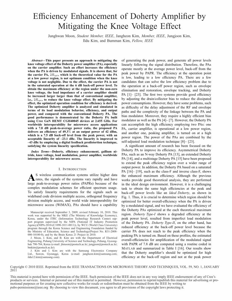
Fig. 7. (a) Load impedances of the conventional and proposed Doherty PAaccording to the input voltage. (b) Fundamental voltages of the carrier (VC)and peaking (VP) amplifiers for the conventional and proposed Doherty PAs.
one, but β is less than one. Thus, the fundamental loadimpedances of the carrier and peaking PAs are modulatedfrom 2δRopt to 2Ropt δ (γβ + 1) − γ / (γβ + 1) and from∞ to Ropt (γβ + 1) /2γ, as described in Fig. 7(a). To ex-plore the load modulation behavior, Vk of 4 V is assumedand Ropt is calculated by (2). At the low power region(0 ≤ vin < βVin,max/2), the load impedance for the carrierPA is larger than 2Ropt, i.e., 2δRopt. Moreover, at the highpower region (βVin,max/2 ≤ vin ≤ (γβ + 1) Vin,max/2γ), theload impedance of the carrier PA maintains a value larger thanconventional PA. In contrast, the load impedance of the peak-ing PA sustains a smaller value than that of the conventionalPA, which results in a slight power degradation. Fig. 7(b)shows the resulting fundamental voltages of the carrier andpeaking amplifiers for the conventional and proposed DohertyPAs. As expected, compared with the conventional PA, atthe low power region, the carrier amplifier for the proposedamplifier has the larger fundamental voltage due to the largerload impedance. It leads to the carrier PA can be fully saturatedstate, delivering the better efficiency.
By using the currents and load impedances of the carrierand peaking PAs, the efficiency can be estimated. Fig. 8

FINAL MANUSCRIPT (MANUSCRIPT NUMBMER:7732) TO IEEE TRANSACTIONS ON MICROWAVE THEORY AND TECHNIQUES 6
Fig. 8. Efficiencies of the conventional and proposed Doherty PA accordingto the output power.
Fig. 9. Simulated load modulation results for the carrier PA with the loadimpedances of 50 Ω, 100 Ω, 110 Ω, and 120 Ω.
represents the calculated efficiencies based on the above anal-ysis for θc=210 and θp=150 using MATLAB. To calculatethe efficiencies, δ, β, σ, and γ are determined by Vdc, Vk,I1,c (θc), and I1,p (θp), which are 30 V, 4 V, 4.2129 A, and3.6384 A, respectively. The resulting δ, β, σ, and γ are 1.1725and 0.9235, 2.3158, and 1.2494, respectively. In the lowpower region, the proposed Doherty PA has higher efficiencythan that of the conventional PA because of its larger loadimpedance. In particular, the proposed Doherty PA deliversits maximum efficiency of 67.9% at the 6 dB back-off outputpower, which is an increase of about 5% compared with theconventional one. Although the maximum output power andefficiency at the maximum output power are slightly degradedbecause of the imperfect load modulation characteristic, theproposed Doherty scheme improves efficiency for modulatedsignals without any additional circuitry.
III. SIMULATION RESULTS
In Section II, we proposed a Doherty PA design consideringthe knee voltage effect, and analyzed efficiency and outputpower of the PA. To verify the analysis and investigate the
Fig. 10. Simulated load impedances of the conventional and proposedDoherty PAs as a function of the output power.
Fig. 11. Simulated efficiencies of the conventional and proposed DohertyPAs according to the output power.
real behavior of the PA, we performed ADS simulation usingCree’s large signal model for CGH40045 GaN HEMT. Theunit cell PA was designed to deliver maximum efficiency whilemaintaining the maximum output power. The quiescent currentof the carrier cell was set to 200 mA, and the gate voltage ofthe peaking cell was adjusted to turn on at the 6 dB back-offpower level.
To find the load impedance of the carrier PA delivering themaximum efficiency at the 3 dB back-off from peak outputpower, we simulated load modulation test. Fig. 9 illustratesthe simulated efficiencies for a carrier PA with the outputtermination impedances of 50 Ω, 100 Ω, 110 Ω, and 120 Ω.As expected, the carrier PA with 100 Ω delivers its maximumefficiency at an output power of 45.1 dBm, which is 2.6 dBback-off power from the maximum output power of 47.7 dBmwith the output termination impedance of 50 Ω. For thePA with 120 Ω, its maximum efficiency is achieved at the2.9 dB back-off power level. As a result, we selected 120 Ωfor the carrier PA at the low power region, i.e., before thepeaking PA starts to turn on. Compared to the analytical valueobtained from Fig. 3, we conclude that the output termination
FINAL MANUSCRIPT (MANUSCRIPT NUMBMER:7732) TO IEEE TRANSACTIONS ON MICROWAVE THEORY AND TECHNIQUES 7
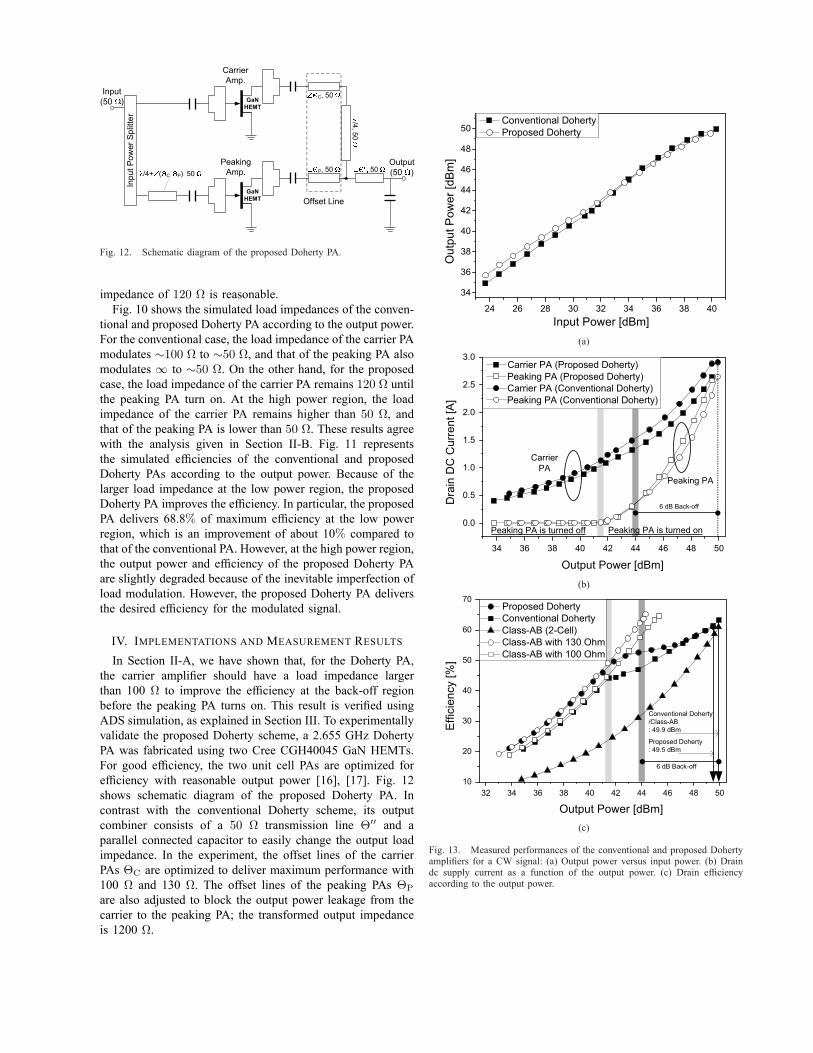
Fig. 12. Schematic diagram of the proposed Doherty PA.
impedance of 120 Ω is reasonable.Fig. 10 shows the simulated load impedances of the conven-
tional and proposed Doherty PA according to the output power.For the conventional case, the load impedance of the carrier PAmodulates ∼100 Ω to ∼50 Ω, and that of the peaking PA alsomodulates ∞ to ∼50 Ω. On the other hand, for the proposedcase, the load impedance of the carrier PA remains 120 Ω untilthe peaking PA turn on. At the high power region, the loadimpedance of the carrier PA remains higher than 50 Ω, andthat of the peaking PA is lower than 50 Ω. These results agreewith the analysis given in Section II-B. Fig. 11 representsthe simulated efficiencies of the conventional and proposedDoherty PAs according to the output power. Because of thelarger load impedance at the low power region, the proposedDoherty PA improves the efficiency. In particular, the proposedPA delivers 68.8% of maximum efficiency at the low powerregion, which is an improvement of about 10% compared tothat of the conventional PA. However, at the high power region,the output power and efficiency of the proposed Doherty PAare slightly degraded because of the inevitable imperfection ofload modulation. However, the proposed Doherty PA deliversthe desired efficiency for the modulated signal.
IV. IMPLEMENTATIONS AND MEASUREMENT RESULTS
In Section II-A, we have shown that, for the Doherty PA,the carrier amplifier should have a load impedance largerthan 100 Ω to improve the efficiency at the back-off regionbefore the peaking PA turns on. This result is verified usingADS simulation, as explained in Section III. To experimentallyvalidate the proposed Doherty scheme, a 2.655 GHz DohertyPA was fabricated using two Cree CGH40045 GaN HEMTs.For good efficiency, the two unit cell PAs are optimized forefficiency with reasonable output power [16], [17]. Fig. 12shows schematic diagram of the proposed Doherty PA. Incontrast with the conventional Doherty scheme, its outputcombiner consists of a 50 Ω transmission line Θ′′ and aparallel connected capacitor to easily change the output loadimpedance. In the experiment, the offset lines of the carrierPAs ΘC are optimized to deliver maximum performance with100 Ω and 130 Ω. The offset lines of the peaking PAs ΘP
are also adjusted to block the output power leakage from thecarrier to the peaking PA; the transformed output impedanceis 1200 Ω.
(a)
(b)
(c)
Fig. 13. Measured performances of the conventional and proposed Dohertyamplifiers for a CW signal: (a) Output power versus input power. (b) Draindc supply current as a function of the output power. (c) Drain efficiencyaccording to the output power.

FINAL MANUSCRIPT (MANUSCRIPT NUMBMER:7732) TO IEEE TRANSACTIONS ON MICROWAVE THEORY AND TECHNIQUES 8
(a)
(b)
Fig. 14. Measured performances of the conventional and proposed Dohertyamplifiers for a WiMAX signal: (a) Drain efficiency. (b) ACLR.
A. CW and WiMAX Tests of the Doherty Amplifiers
Fig. 13 shows the measured power characteristics, draindc currents, and drain efficiencies of the conventional andproposed Doherty PAs for a CW signal. In the experiments, theturn-on power level of the peaking PA is adjusted only by thegate-source voltage Vgs. When the peaking PA is turned off,the load impedance of the proposed carrier PA is higher thanthat of the conventional PA. Thus, the dc current level of theproposed PA is lower than that of the conventional PA, whichleads to improved efficiency at the low power region. However,the peak power of the Doherty PA is degraded because theimperfect load impedance causes an impedance mismatch forRopt at the peak power region. Although the peak power ofthe proposed Doherty PA is slightly degraded, the efficiencyis increased over a broad output power range.
Fig. 14(a) shows the measured efficiencies for a mobileWiMAX signal with a 10 MHz signal bandwidth and a7.8 dB PAPR. Compared to the conventional Doherty PA, theefficiency of the proposed PA is improved over a broad averageoutput power level. Fig. 14(b) represents the measured ACLRof the implemented PAs. Because the proposed Doherty PA hasa larger load impedance than that of the conventional PA at thelow power region and cannot achieve perfect load modulation
TABLE IIMEASURED PERFORMANCE AT THE 8 dB BACK-OFF OUTPUT POWER FOR
A CONVENTIONAL DOHERTY PA AND THE 8 dB AND 7.5 dB BACK-OFFOUTPUT POWERS FOR THE PROPOSED DOHERTY PA
Conventional Doherty Proposed Doherty
Pavg [dBm] 42 41.5 42
Back-off level [dB] 8 8 7.5
ηavg [%] 45.5 48.0 49.3
ACLR [dBc] –25.1 –23.2 –23.1
Fig. 15. Experimental setup for linearization.
at the high power region, the ACLR is slightly degraded overthe power range. The Doherty PAs also have a worse ACLRthan that of the class-AB PA because the peaking PAs arebiased at deep class-C to turn off the PAs until the carrier PAis fully saturated, and are optimized to improve the efficiencyrather than linearity. In Table II, we summarize the measuredefficiencies and ACLRs at the 8 dB back-off output power fora conventional Doherty PA and the 8 dB and 7.5 dB back-off output powers for the proposed Doherty PA. These resultsallow us to conclude that the proposed Doherty PA has anexcellent efficiency with acceptable linearity.
B. Linearization Performance of the AmplifierTo confirm the suitability of the proposed Doherty amplifier
as the main PA of a base-station or repeater linear poweramplifier (LPA) system, we applied the DFBPD linearizationtechnique to the proposed Doherty amplifier. Two 1024-entryAM/AM and AM/PM lookup tables are accomplished byMATLAB program using the DFBPD algorithm as shown inFig. 15 [24]. The measured spectra before and after com-pensation for the memoryless nonlinearity by the DFBPDtechnique are described in Fig. 16. After linearization, theACLR at an offset of 6.05 MHz is –43 dBc, which is animprovement of approximately 18 dB at an average output
TABLE IIIMEASURED LINEARIZATION PERFORMANCE OF THE PROPOSED DOHERTY
AMPLIFIER AT AN AVERAGE OUTPUT POWER OF 42 dBm FORWIMAX 1FA SIGNAL
+ / – 5.32 MHz + / – 6.05 MHz RCE
[dBc] [dBc] [dB]
Before linearization –23.5 / –21.8 –25.4 / –23.2 17.7
After linearization –42.5 / –42.2 –43.0 / –43.0 34.5

FINAL MANUSCRIPT (MANUSCRIPT NUMBMER:7732) TO IEEE TRANSACTIONS ON MICROWAVE THEORY AND TECHNIQUES 9
Fig. 16. Measured WiMAX spectra before and after the DFBPD linearizationof the Doherty PA at an average output power of 42 dBm.
power of 42 dBm. This spectra satisfies the spectrum maskof the mobile WiMAX system, especially the WiMAX sys-tem type-G, (see Fig. 16). The measured signal constellationdiagrams before and after the linearization are described inFig. 17. By linearizing with DFBPD, the relative constellationerror (RCE) is –34.5 dB, which is an improvement of about16.8 dB. These results clearly indicate that after employingthe linearization technique, the proposed saturated PA is wellsuited as a highly efficient main PA of the LPA for themodulated signal. The measured linearization performancesare summarized in Table III.
V. CONCLUSION
We have investigated the knee voltage effect on the opera-tion of the Doherty PA, especially the carrier PA, to improveefficiency for amplification of modulated signals. From theexploration, we have found that the efficiency at the back-offregion of a Doherty PA with 2Ropt for the carrier PA is lowerthan the expected value. To overcome this problem, the carrierPA should employ the load impedance larger than 2Ropt. Themodified Doherty PA delivers the maximum efficiency at the6 dB back-off region because the PA is saturated enoughat this level while the conventional PA is not. Therefore,the proposed PA delivers better efficiency for the modulatedsignals. To experimentally validate the amplifier, we haveimplemented and tested the Doherty PAs using Cree GaNHEMT CGH40045 devices at 2.655 GHz. The experimentalresults clearly show that the proposed Doherty PA deliversbetter efficiency at the back-off output power level than theconventional PA with satisfactory linearity because of its betterload modulation behavior. The linearity performance is furtherimproved by adopting the DFBPD linearization technique.
ACKNOWLEDGEMENT
The authors would like to thank to Cree Inc. for providingthe GaN HEMT transistors used in this work.
REFERENCES
[1] F. H. Raab, P. Asbeck, S. Cripps, P. B. Kenington, Z. B. Popovic,N. Pothecary, J. F. Sevic, and N. O. Sokal “Power amplifiers andtransmitters for RF and microwave,” IEEE Trans. Microw. Theory Tech.,vol. 50, no. 3, pp. 814–826, Mar. 2002.
(a)
(b)
Fig. 17. Measured WiMAX signal constellation diagram of the Doherty PAat an average output power of 42 dBm: (a) Before linearization. (b) Afterlinearization.
[2] J. Choi, D. Kang, D. Kim, J. Park, B. Jin, and B. Kim, “Power amplifiersand transmitters for next generation mobile handset,” J. Semicond.Technol. Sci., vol. 9, no. 4, pp. 249–256, Dec. 2009.
[3] L. Kahn, “Single-sideband transmission by envelope elimination andrestoration,” Proc. IRE, pp. 803–806, Jul. 1952.
[4] D. F. Kimball, J. Jeong, C. Hsia, P. Draxler, S. Lanfranco, W. Nagy, K.Linthicum, L. E. Larson, and P. M. Asbeck, “High-efficiency envelope-tracking W-CDMA base-station amplifier using GaN HFETs,” IEEETrans. Microw. Theory Tech., vol. 54, no. 11, pp. 3848–3856, Nov. 2006.
[5] F. Wang, D. F. Kimball, J. D. Popp, A. H. Yang, D. Y. C. Lie, P. M.Asbeck, and L. E. Larson, “An improved power-added efficiency 19-dBm hybrid envelope elimination and restoration power amplifier for802.11g WLAN applications,” IEEE Trans. Microw. Theory Tech., vol.54, no. 12, pp. 4086–4099, Dec. 2006.
[6] F. Wang, A. H. Yang, D. F. Kimball, L. E. Larson, and P. M. Asbeck,“Design of wide-bandwidth envelope tracking power amplifiers forOFDM applications,” IEEE Trans. Microw. Theory Tech., vol. 53, no.4, pp. 1244–1255, Apr. 2005.
[7] I. Kim, Y. Y. Woo, J. Kim, J. Moon, J. Kim, and B. Kim, “High-efficiency hybrid EER transmitter using optimized power amplifier,”IEEE Trans. Microw. Theory Tech., vol. 56, no. 11, pp. 2582–2593,Nov. 2008.
[8] S.C. Cripps, RF Power Amplifiers for Wireless Communications. 2nded. Norwood, MA: Artech House, 2006.
[9] W. H. Doherty, “A new high efficiency power amplifier for modulatedwaves,” Proc. IRE, vol. 24, no. 9, pp. 1163–1182, Sep. 1936.
[10] F. H. Raab, “Efficiency of Doherty RF power-amplifier systems,” IEEETrans. Broadcast., vol. BC-33, no. 3, pp. 77–83, Sep. 1987.
[11] Y. Yang, J. Yi, Y. Y. Woo, and B. Kim,“Optimum design for linearity and

FINAL MANUSCRIPT (MANUSCRIPT NUMBMER:7732) TO IEEE TRANSACTIONS ON MICROWAVE THEORY AND TECHNIQUES 10
efficiency of microwave Doherty amplifier using a new load matchingtechnique,”Microw. J., vol. 44, no. 12, pp. 20–36, Dec. 2001.
[12] J. Kim, J. Cha, I. Kim, and B. Kim, “Optimum operation ofasymmetrical-cells-based linear Doherty power amplifiers – unevenpower drive and power matching,” IEEE Trans. Microw. Theory Tech.,vol. 53, no. 5, pp. 1802–1809, May 2005.
[13] Y. Yang, J. Cha, B. Shin, and B. Kim, “A fully matched N-way Dohertyamplifier with optimized linearity,” IEEE Trans. Microw. Theory Tech.,vol. 51, no. 3, pp. 986–993, Mar. 2003.
[14] M. Iwamoto, A. Williams, P. F. Chen, A. G. Metzger, L. E. Larson, andP. M. Asbeck, “An extended Doherty amplifier with high efficiency overa wide power range,” IEEE Trans. Microw. Theory Tech., vol. 49, no.12, pp. 2472–2479, Dec. 2001.
[15] N. Srirattana, A. Raghavan, D. Heo, P. E. Allen, and J. Laskar, “Analysisand design of a high-efficiency multistage Doherty power amplifier forwireless communications,” IEEE Trans. Microw. Theory Tech., vol. 53,no. 3, pp. 852–860, Mar. 2003.
[16] J. Moon, J. Kim, I. Kim, J. Kim, and B. Kim “Highly efficient three-waysaturated Doherty amplifier with digital feedback predistortion,” IEEEMicrow. Wireless Compon. Lett., vol. 18, no. 8, pp. 539–541, Aug. 2008.
[17] J. Kim, J. Moon, Y. Y. Woo, S. Hong, I. Kim, J. Kim, and B. Kim,“Analysis of a fully matched saturated Doherty amplifier with excellentefficiency,” IEEE Trans. Microw. Theory Tech., vol. 56, no. 2, pp. 328–338, Feb. 2008.
[18] S. Goto, T. Kunii, A. Inoue, K. Izawa, T. Ishikawa, and Y. Matsuda,“Efficiency enhancement of Doherty amplifier with combination ofclass-F and inverse class-F schemes for S-band base station application,”in IEEE MTT-S Int. Microw. symp. Dig., Jun. 2004, pp. 839–842.
[19] Y. Suzuki, T. Hirota, and T. Nojima, “Highly efficient feed-forwardamplifier using a class-F Doherty amplifier,” in IEEE MTT-S Int. Microw.symp. Dig., Jun. 2003, pp. 77–80.
[20] J. Moon, Y. Y. Woo, and B. Kim, “A highly efficient Doherty poweramplifier employing optimized carrier cell,” in Proc. 39th Eur. Microw.Conf., Sep. 28–Oct. 2 2009, pp. 1720–1723.
[21] K. Horiguchi, S. Ishizaka, T. Okano, M. Nakayama, H. Ryoji, Y. Isota,and T. Takagi, “Efficiency enhancement of 250 W Doherty poweramplifier using virtual open stub techniques for UHF-band OFDMapplications,” in IEEE MTT-S Int. Microw. symp. Dig., Jun. 2006, pp.1356–1359.
[22] N. Ui, H. Sano, and S. Sano, “A 80 W 2-stage GaN HEMT Dohertyamplifier with –50 dBc ACLR, 40% efficienecy, 32 dB gain with DPDfor W-CDMA base station,” in IEEE MTT-S Int. Microw. symp. Dig.,Jun. 2007, pp. 1259–1262.
[23] R. Sweeney, “Practical magic,” IEEE Microw. Mag., vol. 9, no. 2, pp.73–82, Apr. 2008.
[24] Y. Y. Woo, J. Kim, J. Yi, S. Hong, I. Kim, J. Moon, and B. Kim,“Adaptive digital feedback predistortion technique for linearizing poweramplifier,” IEEE Trans. Microw. Theory Tech., vol. 55, no. 5, pp. 932–940, May 2007.
Junghwan Moon (S’07) received the B.S. degreein electrical and computer engineering from theUniversity of Seoul, Seoul, Korea, in 2006 andis currently working toward the Ph.D. degree atthe Pohang University of Science and Technology(POSTECH), Pohang, Gyungbuk, Korea.
His current research interests include highly linearand efficient RF PA design, memory-effect com-pensation techniques, digital predistortion (DPD)techniques, and wideband RF PA design.
Mr. Moon was the recipient of the Highest Effi-ciency Award at Student High-Efficiency Power Amplifier Design Competitionin IEEE MTT-S International Microwave Symposium (IMS), 2008.
Jangheon Kim (S’07-M’09) received the B.S. de-gree in electronics and information engineering fromChon-buk National University, Chonju, Korea, in2003, and the Ph.D. degree in electrical engineeringfrom the Pohang University of Science and Tech-nology (POSTECH), Pohang, Gyungbuk, Korea, in2009.
He is currently a senior engineer with the NetworkDivision, Digital Media & Commnunications, Sam-sung Electronics Company Ltd., Suwon, Republic ofKorea. From 2009 to 2010, he was a post-doctoral
Fellow with the University of Waterloo, Waterloo, ON, Canada. His currentresearch interests include highly linear and efficient RF PA design, digitalpredistortion (DPD) techniques, and highly efficient transmitter for wirelesscommunication systems.
Dr. Kim was the recipient of the Highest Efficiency Award at Student High-Efficiency Power Amplifier Design Competition in IEEE MTT-S InternationalMicrowave Symposium (IMS), 2008, and 2010 MICROWAVE AND WIRELESSCOMPONENTS LETTERS Outstanding Reviewer Award, 2010.
Jungjoon Kim received the B.S. degree in electri-cal engineering from Han-Yang University, Ansan,Korea, in 2007, and the Master degree in electricalengineering from the Pohang University of Scienceand Technology (POSTECH), Pohang, Gyungbuk,Korea, in 2009. He is currently working toward thePh.D. degree at the POSTECH, Pohang, Gyungbuk,Korea.
His current research interests include RF PA de-sign and supply modulator design for highly efficienttransmitter system.
Ildu Kim received his B.S. degree in electronics andinformation engineering from Chon-nam NationalUniversity, Kwangju, Korea, in 2004 and the Ph.D.degree in Pohang University of Science and Technol-ogy (POSTECH), Pohang, Korea, in 2010. In 2010,he joined the Samsung Electronics Company Ltd.,Suwon, Gyeunggi, Korea.
His current research interests include highly lin-ear and efficient RF power amplifier design, linearpower amplifier (LPA) system design and highlylinear and efficient RF transmitter architectures.
Bumman Kim (M’78-SM’97-F’07) received thePh.D. degree in electrical engineering from CarnegieMellon University, Pittsburgh, PA, in 1979.
From 1978 to 1981, he was engaged in fiber-opticnetwork component research with GTE LaboratoriesInc. In 1981, he joined the Central Research Labo-ratories, Texas Instruments Incorporated, where hewas involved in development of GaAs power field-effect transistors (FETs) and monolithic microwaveintegrated circuits (MMICs). He has developed alarge-signal model of a power FET, dual-gate FETs
for gain control, high-power distributed amplifiers, and various millimeter-wave MMICs. In 1989, he joined the Pohang University of Science andTechnology (POSTECH), Pohang, Gyungbuk, Korea, where he is a POSTECHFellow and a Namko Professor with the Department of Electrical Engineering,and Director of the Microwave Application Research Center, where he isinvolved in device and circuit technology for RF integrated circuits (RFICs).He has authored over 300 technical papers.
Prof. Kim is a member of the Korean Academy of Science and Tech-nology and the National Academy of Engineering of Korea. He was anassociate editor for the IEEE TRANSACTIONS ON MICROWAVE THEORY ANDTECHNIQUES, a Distinguished Lecturer of the IEEE Microwave Theory andTechniques Society (IEEE MTT-S), and an AdCom member.
Related Documents


