CENTRAL BOARD OF SECONDARY EDUCATION Shiksha Kendra, 2, Community Centre, Preet Vihar, Delhi-110092 BASIC ELECTRONICS Student Handbook Class - XI

Welcome message from author
This document is posted to help you gain knowledge. Please leave a comment to let me know what you think about it! Share it to your friends and learn new things together.
Transcript

CENTRAL BOARD OF SECONDARY EDUCATION
Shiksha Kendra, 2, Community Centre, Preet Vihar, Delhi-110092
BASIC ELECTRONICSStudent Handbook
Class - XI

CENTRAL BOARD OF SECONDARY EDUCATION
Shiksha Kendra, 2, Community Centre, Preet Vihar, Delhi-110092
BASIC ELECTRONICS
Student Handbook
Class - XI
Basic ElectronicsStudent Handbook, Class - XI
First Edition :
o. of Copies :
Paper Used : 80 GSM CBSE Water Mark White Maplitho
Price: `
January 2018, CBSE
N
Published By : The Secretary, Central Board of Secondary Education,
Shiksha Kendra, 2, Community Centre, Preet Vihar, Delhi-110092
Design Layout &Composed By
:
“This book or part thereof may not be reproduced by any person
any agency in any manner.”
Vijaylakshmi Printing Works Pvt. Ltd.,
B-117, Sector-5, Noida-201301(U.P.)

Hkkjr dk lafo/ku
ewy dÙkZO;
mísf'kdk1ge] Hkkjr ds yksx] Hkkjr dks ,d lEiw.kZ izHkqRo&laiUu lektoknh iaFkfujis{k yksdra=kkRed x.kjkT; cukus ds fy,] rFkk
mlds leLr ukxfjdksa dks%
lkekftd] vkfFkZd vkSj jktuSfrd U;k;]
fopkj] vfHkO;fDr] fo'okl] /eZ
vkSj mikluk dh Lora=krk]
izfr"Bk vkSj volj dh lerk
izkIr djkus ds fy,
rFkk mu lc esa O;fDr dh xfjek2vkSj jk"Vª dh ,drk vkSj v[kaMrk
lqfuf'pr djus okyh ca/qrk c<+kus ds fy,
n`<+ladYi gksdj viuh bl lafo/ku lHkk esa vkt rkjh[k 26 uoEcj] 1949 bZñ dks ,rn~}kjk bl lafo/ku dks vaxhÑr]
vf/fu;fer vkSj vkRekfiZr djrs gSaA
1- lafo/ku (c;kyhloka la'kks/u) vf/fu;e] 1976 dh /kjk 2 }kjk (3-1-1977) ls ¶izHkqRo&laiUu yksdra=kkRed x.kjkT;¸ ds LFkku ij izfrLFkkfirA
2- lafo/ku (c;kyhloka la'kks/u) vf/fu;e] 1976 dh /kjk 2 }kjk (3-1-1977) ls ¶jk"Vª dh ,drk¸ ds LFkku ij izfrLFkkfirA
51 d- ewy dÙkZO; & Hkkjr ds izR;sd ukxfjd dk ;g dÙkZO; gksxk fd og &
(d) lafo/ku dk ikyu djs vkSj mlds vkn'kksZa] laLFkkvksa] jk"Vªèot vkSj jk"Vªxku dk vknj djs_
([k) Lora=krk ds fy, gekjs jk"Vªh; vkanksyu dks izsfjr djus okys mPp vkn'kksZa dks ân; esa latks, j[ks vkSj mudk ikyu djs_
(x) Hkkjr dh izHkqrk] ,drk vkSj v[kaMrk dh j{kk djs vkSj mls v{kq..k j[ks_
(?k) ns'k dh j{kk djs vkSj vkg~oku fd, tkus ij jk"Vª dh lsok djs_
(Ä) Hkkjr ds lHkh yksxksa esa lejlrk vkSj leku Hkzkr`Ro dh Hkkouk dk fuekZ.k djs tks /eZ] Hkk"kk vkSj izns'k ;k oxZ ij vk/kfjr lHkh
HksnHkko ls ijs gksa] ,slh izFkkvksa dk R;kx djs tks fL=k;ksa ds lEeku ds fo#¼ gSa_
(p) gekjh lkekfld laLÑfr dh xkSjo'kkyh ijaijk dk egÙo le>s vkSj mldk ifjj{k.k djs_
(N) izkÑfrd i;kZoj.k dh ftlds varxZr ou] >hy] unh] vkSj oU; tho gSa] j{kk djs vkSj mldk lao/Zu djs rFkk izk.kh ek=k ds izfr
n;kHkko j[ks_
(t) oSKkfud n`f"Vdks.k] ekuookn vkSj KkuktZu rFkk lq/kj dh Hkkouk dk fodkl djs_
(>) lkoZtfud laifÙk dks lqjf{kr j[ks vkSj fgalk ls nwj jgs_
(×k) O;fDrxr vkSj lkewfgd xfrfof/;ksa ds lHkh {ks=kksa esa mRd"kZ dh vksj c<+us dk lrr iz;kl djs ftlls jk"Vª fujarj c<+rs gq, iz;Ru
vkSj miyfC/ dh ubZ mapkb;ksa dks Nw ys_1(V) ;fn ekrk&firk ;k laj{kd gS] Ng o"kZ ls pkSng o"kZ rd dh vk;q okys vius] ;FkkfLFkfr] ckyd ;k izfrikY; ds fy;s f'k{kk ds
volj iznku djsA
1- lafo/ku (N;klhoka la'kks/u) vf/fu;e] 2002 dh /kjk 4 }kjk izfrLFkkfirA
Hkkx 4 d

THE CONSTITUTION OF INDIA
PREAMBLE
1WE, THE PEOPLE OF INDIA, having solemnly resolved to constitute India into a SOVEREIGN
SOCIALIST SECULAR DEMOCRATIC REPUBLIC and to secure to all its citizens :
JUSTICE, social, economic and political;
LIBERTY of thought, expression, belief, faith and worship;
EQUALITY of status and of opportunity; and to promote among them all
2FRATERNITY assuring the dignity of the individual and the unity and integrity of the Nation;
IN OUR CONSTITUENT ASSEMBLY this twenty-sixth day of November, 1949, do HEREBY ADOPT,
ENACT AND GIVE TO OURSELVES THIS CONSTITUTION.
THE CONSTITUTION OF INDIA
Chapter IV A
FUNDAMENTAL DUTIES
ARTICLE 51A
Fundamental Duties - It shall be the duty of every citizen of India-
(a) to abide by the Constitution and respect its ideals and institutions, the National Flag and the National
Anthem;
(b) to cherish and follow the noble ideals which inspired our national struggle for freedom;
(c) to uphold and protect the sovereignty, unity and integrity of India;
(d) to defend the country and render national service when called upon to do so;
(e) to promote harmony and the spirit of common brotherhood amongst all the people of India transcending
religious, linguistic and regional or sectional diversities; to renounce practices derogatory to the dignity of
women;
(f) to value and preserve the rich heritage of our composite culture;
(g) to protect and improve the natural environment including forests, lakes, rivers, wild life and to have
compassion for living creatures;
(h) to develop the scientific temper, humanism and the spirit of inquiry and reform;
(i) to safeguard public property and to abjure violence;
(j) to strive towards excellence in all spheres of individual and collective activity so that the nation constantly
rises to higher levels of endeavour and achievement;1(k) to provide opportunities for education to his/her child or, as the case may be, ward between age of 6 and 14
years.
1. Subs, by the Constitution (Forty-Second Amendment) Act. 1976, sec. 2, for "Sovereign Democratic Republic” (w.e.f. 3.1.1977)
2. Subs, by the Constitution (Forty-Second Amendment) Act. 1976, sec. 2, for "unity of the Nation” (w.e.f. 3.1.1977)
1. Subs. by the Constitution (Eighty - Sixth Amendment) Act, 2002

Preface
The technology is changing very fast. The invention of Electron was breakthrough towards
the modernized shape of Electrical, Analog Electronics, Digital Electronics and
Nanotechnology. From Electron to Electronics, from Diode to Transistor, from Transistor to
Logic Gates from Logic Gates to Chips (Integrated Circuits) and further advancements in
Nanotechnology and applications of Micro-Electro-Mechanical System (MEMS) has
revolutionized the electronics area.
Any advanced technology is basically dependent on basic concepts. Keeping this in
perspective CBSE has introduced Electronics Technology as a Vocational Course at Senior
Secondary level in class-XI (Level-3) and class-XII (Level-4). The Basic Electronics,
Student Handbook for class XI has been designed to help the students to understand the
basics of electronics. The units of the book have been designed in a way that students can get
the concept of basics in sequence.
The Student Handbook encompasses the evolution of electronics, atoms and element, atomic
energy level, field intensity, current density, electric field, magnetic field and cathode ray
oscilloscope etc. The units relate to voltage and current where fundamentals of current,
resistors, voltage source, battery etc., have been discussed. In addition, it focuses on basics of
semiconductors which give an insight into metals, semiconductors, insulators, PN Junction
diode, rectifiers etc. The content provides information about various configurations of
Junction Transistor, FET, MOSFET Transistor amplifier and its applications, SCR, DIAC
and TRIAC etc.
The language used in this book is simple and easily understandable to the student at class XI
level. Relevant pictorial illustrations, examples and simplified concepts help the student to
learn with ease and comfort.
This book is authored by competent educationists in the field of Electronics and
Communication in association with CBSE focussing on helping the students to learn without
any difficulty and use this book as a tool for easy learning.
Chairperson, CBSE
ADVISORS
Acknowledgements
CONTENT DEVELOPED BY
EDITING & COORDINATION
·Sh. Rakesh Kr. Dhammi, HOD, Department of Mechatronics, Delhi - (Convener)
·Smt. Monika Garg, Assistant Professor, GP Pant Government Engineering College,
Okhla, New Delhi
·Smt. Charu Gaur, Assistant Professor, Department of Physics, Delhi Institute of Tool
Engineering, Govt. of Delhi, Okhla, New Delhi
·Smt.Anita Karwal, IAS, Chairperson, CBSE
·Dr. Biswajit Saha, Director (Vocational & Training), CBSE

Contents
Unit-1
Unit-2
Unit-3
Voltage & Current
Basics of Semiconductor
Overview of Atom, Sub Atomic Particles & CRO1.0 Unit Overview and Description ... 1
1.1 Brief History of Electronics ... 2
1.2 Atoms and its Elements ... 4
1.3 Bohr’s Atomic Model ... 4
1.4 Atomic Energy Level ... 5
1.5 Electron ... 7
1.6 Field Intensity ... 7
1.7 Potential Energy ... 7
1.8 Current and Current Density ... 8
1.9 Electric Field ... 9
1.10 Magnetic Field ... 9
1.11 Motion of Charged Particles in Electric Field ... 10
1.12 Cathode Ray Oscilloscope ... 10
2.0 Unit Overview and Description ... 18
2.1 Current Flow Theories ... 19
2.2 Resistors ... 23
2.2.1 Fixed Resistors ... 23
2.2.2 Variable Resistors ... 29
2.3 Introduction to Capacitors ... 30
2.4 The Inductors ... 38
2.5 Voltage Source ... 40
2.6 Battery (Electricity) ... 45
3.0 Unit Overview and Description ... 52
3.1 Semiconductor Materials ... 54
3.2 Energy Band ... 54
3.3 Material Structure ... 55
3.4 Energy Gap ... 56
3.5 Field and Photo Electric Emission ... 56
3.6 Intrinsic & Extrinsic Semiconductor ... 57(n-type & p-type Semiconductors)
3.7 Drift Current ... 58
3.8 Diffusion Current ... 58

3.9 Effects of Temperature on Conductivity of Semiconductor
3.10 PN Junction Diode (Semiconductor Diode) ... 60
3.11 Depletion Layer ... 60
3.12 Potential Barrier ... 61
3.13 Forward & Reverse Biasing ... 61
3.14 V-I Characteristic of Semiconductor ... 62
3.15 Resistance Level ... 63
3.16 Breakdown in Junction Diode ... 63
3.17 Zener Diode ... 64
3.18 Photo Diode ... 65
3.19 LED (Light Emitting Diode) ... 66
3.20 Diode as a Rectifier ... 66
3.21 Voltage Multipliers ... 68
3.22 Zener Diode Regulator ... 68
3.23 Special Information - ... 69(Introduction to Filters, Clippers, Clampers)
4.0 Unit Overview and Description ... 74
4.1 Bipolar Junction Transistor (BJT) ... 75
4.2 BJT Biasing ... 78
4.3 CB, CE and CC Configuration ... 78
4.4 Characteristics and Transistor Parameters for CB, CE, CC, ... 80Configuration
4.5 Introduction to FET, JFET, MOSFET, CMOS and VMOS ... 85
4.6 Characteristics of Various Transistors ... 91
5.0 Unit Overview and Description ... 93
5.1 Introduction to Amplifiers ... 95
5.2 Single and Multistage Amplifiers ... 96
5.3 Amplifier Characteristics ... 97
5.4 Feedbacks in Amplifiers ... 97
5.5 Introduction to Oscillators ... 98
5.6 Multivibrators (MVS) ... 99
5.7 Signal Generator ... 99
5.8 Thyristors ... 100
5.9 Light Activated SCR (LASCR) ... 102
... 59
Unit - 4
Unit - 5
Bipolar Junction Transistor
Transistor Amplifier and Applications

Overview of Atom, Sub-Atomic Particles & CRO
Overview
Knowledge and Skill Outcomes
Assessment Plan: (For the Teachers)
This unit starts with the understanding of History of Electronics and Fundamentals Elements suchas Atoms and its Elements, Atomic Energy Level, Electron, Field Intensity, Potential Energy,Current and Current Density, Electric Field, Magnetic Field, Motion of Charged Particles inElectric Field, Cathode Ray Oscilloscope.
i) Understanding of fundamentals of basic electronics elements.
ii) Understanding of all about the atom and electron.
iii) Knowledge of various types of fields.
iv) Knowledge of Cathode Ray Oscilloscope.
Brief History of Electronics, Atoms andits Elements, Bohr’s Atomic Model,Atomic Energy Level.
Unit-1 Topic AssessmentMethod
TimePlan
Remarks
Exercise:Question & Answer
Two Hours
1.0 Unit Overview and Description
?Overview
?Knowledge and Skill Outcomes
?Assessment Plan
?Learning Outcomes
?Resource Material
?Topics Covered
Brief History of Electronics, Atoms and its Elements, Atomic Energy Level, Electron, Field
Intensity, Potential Energy, Current and Current Density, Electric Field, Magnetic Field, Motion
of Charged Particles in Electric Field, Cathode Ray Oscilloscope.
Exercise:Question & Answer
Exercise:Question & Answer
Two Hours
Two Hours
Electron, Field Intensity, PotentialEnergy, Current and Current Density.
Electric Field, Magnetic Field, Motionof Charged Particles in Electric Field,Cathode Ray Oscilloscope.
UNIT 1
1Basic Electronics

1.1 Brief History of Electronics
The word ‘Electronics’ is originated from the word electron which is a branch of science dealing
with theory and use of devices in which the electrons travel through a vacuum, gas or a
semiconductor medium. Electronics is that field of science which deals with the motion of
electrons under the influence of applied electric and/or magnetic field. Electronics can be
classified into two branches: Physical Electronics and Electronics Engineering. Physical
electronics deals with the motion of electronics in a vacuum, gas or semiconductor. Whereas,
electronics engineering deals with the design, fabrication and application of electronic devices.
Alternatively we can define Electronics as the science of how to control the electric energy,
energy in which the electrons have a fundamental role. Electronics deals with electrical circuits
that involve active electrical components such as vacuum tubes, transistors, diodes, integrated
circuits, and associated passive electrical components and interconnection technologies.
Commonly, electronic devices contain circuitry consisting primarily or exclusively of active
semiconductors supplemented with passive elements; such a circuit is described as an electronic
circuit.
Electronics has evolved around three components; vacuum tubes, transistor, and integrated
circuits. In 1883, Thomas Alva Edison discovered that electrons will flow from one metal
conductor to another through vacuum. This discovery of conductor is known as Edison Effect. In
1897, John Fleming applied Edison Effect in inventing a two- element electron tube called diode.
In 1906, Lee de Forest utilized Edison Effect to invent a three-element tube called triode. Diode
and triode were instrumental in amplification and transmission of electrical energy. But vacuum
tubes were bulky, fragile and had high power consumption. Therefore, it gave rise to another
invention, and it was a prominent development in the field of electronics. In 1948 John Bardeen,
Walter Brattain and William Shockley at Bell Laboratories developed Transistor and they received
Nobel Prize for their creation. These metal transistors replaced vacuum tubes as this
semiconductor device are compact in size, light in weight, low cost, less power consumption, fast
and have longer life if operated within same operating conditions.
The concept of the integrated circuit was proposed in 1952 by Geoffrey W. A. Dummer, a British
electronics expert with the Royal Radar Establishment. Throughout the 1950s, transistors were
Learning Outcomes
Unit-1 Outcomes
Brief History of Electronics.
Overview of Atoms.
Sub-Atomic Particles.
CRO (Cathode Ray Oscilloscope).
(i) Understanding the Brief Historyof Electronics.
(ii) Understanding the Atoms and itsElements.
(i) Identification of Sub-AtomicParticles.
(i) Understanding of Cathode RayOscilloscope.
Overview of Atom, Sub-Atomic Particles & CRO
2

mass produced on single wafers and cut apart. The total semiconductor circuit was a simple step
away from this; it combined transistors and diodes (active devices) and capacitors and resistors
(passive devices) on a planar unit or chip. The semiconductor industry and the silicon integrated
circuit (SIC) evolved simultaneously at Texas Instruments and Fairchild Semiconductor Company.
By 1961, integrated circuits were in full production at a number of firms, and designs of
equipment changed rapidly and in several directions to adapt to the technoloy. Bipolar transistors
and digital integrated circuits were made first, but analog ICs, large-scale integration (LSI), and
very-large-scale integration (VLSI) followed by the mid-1970s. VLSI consists of thousands of
circuits with on-and-off switches or gates between them on a single chip. Microcomputers,
medical equipment, video cameras, and communication satellites are only examples of devices
made possible by integrated circuits.
The history of electronics can be summarized as:
1890: Hertz performed experiment on generation of electromagnetic waves.
1894: Sir J. C. Bose discovered the propagation of radio waves.
1895: H. A. Lorentz postulated the existence of electron.
1897: J. J. Thomson experimentally verified the existence of electron.
1897: Braun invented first electron tube.
1904: Fleming invented diode.
1906: De Forest invented triode.
1912: Application of radio and birth of Institute of Radio Engineers at USA.
1930: Monochrome Television invented.
1950: Colour TV came to existence.
1963: IEEE introduced.
1948: Brattain, Bardeen invented point contact transistor.
1948: Shockley discovered junction transistor.
1951: Commercial production of transistor.
1958: Kilby (Texas Instruments, USA) gave idea of monolithic.
1961: Fairchild and Texas Instruments commercially produced Integrated Circuits(IC).
1960: Small Scale Integration (SSI) (<100 components per chip).
1966: Medium Scale Integration (MSI) (>100 and <1000 components per chip).
1969: Large Scale Integration (LSI) (>1000 and <10000 components per chip).
1975: Very Large Scale Integration (VLSI) (>10000 components per chip).
Evolution of Electronics
Evolution of Transistors
Evolution of ICs
Basic Electronics 3

1.2 Atoms and its Elements
1.3 Bohr’s Atomic Model
Atom is the smallest unit of matter that defines the chemical element. Every solid, liquid, gas andplasma is made up of atom. The atoms are very small: the size of atoms is measured in picometers
–12– trillionths (10 ) of a meter. Every atom is composed of a nucleus and one or more electronsthat orbit the nucleus. Protons and neutrons are called nucleons. Over 99.94% of the atom’s massis in the nucleus. The protons have a positive electric charge, the electrons have a negative electric charge, and the neutrons have no electric charge. If the number of protons and electrons are equal,that atom is electrically neutral. If an atom has a surplus or deficit of electrons relative to protons,then it has an overall positive or negative charge, and is called an ion.
Elements consist of only one kind of atom and can’t be decomposed into simpler substance.Therefore, atom is the most fundamental unit of matter which is capable of independent existencein the atom is defined as its element. An atom consists of a central unit called nucleus aroundwhich a number of smaller particles move around the nucleus. The nuclei of all the elements(except hydrogen which has only one proton in its nucleus) contains two types of particles calledprotons and neutrons. The protons and neutrons have same mass. Protons are positively chargedparticles whereas neutrons are electrically neutral. The mass of an atom is concentrated in itsnucleus. The electrons revolving around the nucleus are very light in weight. An electron is 1850times lighter than a proton or neutron. An electron has same amount of charge as proton.However, the charge on electron is negative. Since matter in its normal state is electrically neutral,therefore the atom should be neutral. In an atom, the number of orbiting electron must be the same as the number of protons in its nucleus.
By early 1900s, the scientists understood that matter is composed of atoms and that the atom ofHydrogen contained positive charge +e at its centre and –e outside at its centre. However, no oneunderstood why the electrical attraction between the electron and positive charge did not cause the two to collapse. One clue came from the fact that a hydrogen atom cannot emit and absorb allwavelengths of visible light. Rather, it can emit and absorb only four particular wavelengths ofvisible range. Johann Balmer devised a formula that gave those wavelengths:
for n = 3,4,5, and 6. (1.1)
Here R is constant. No one knew why this formula gave the right wavelength or why no othervisible wavelengths are emitted or absorbed until 1913 when Bohr saw Balmer’s equation andquickly realized that he could derive it after few assumptions:
1. The electron in hydrogen atom orbits the nucleus in a circle.
2. The magnitude of angular momentum L of electron in its orbit is restricted to the valuesL= nh (nh – bar) for n = 1,2,3……. (1.2)
Where h (h – bar) is h/2
Let us consider the simplest example of hydrogen atom, which contains an electron that is trappedto be near proton, which forms atom’s nucleus. We will not consider about nucleus, in fact, we
1.2.1 Definition of Atom
1.2.2 Elements of Atom
ð and n is the quantum number.
1
λ= R
12
2–
12
n
4

will use the fact that negatively charged electron is attracted by coulomb force to positivelycharged proton. As the mass of proton is greater than mass of electron, we assume that proton isfixed in place.
We know that electron energy E and change in energy ÄE is quantized therefore in this section,quantized energy of hydrogen atom will be calculated. The orbital motion of electron is examinedin Bohr Model. The force holding the electron in an orbit of radius r is the coulomb force.
2The magnitude of force F = k q q /r1 2
Where k = 1/4ðª Here q is the –e charge of electron and q is the +e charge of proton. The0. 1 22
electron’s acceleration is centripetal acceleration with a magnitude given by a = v /r, where v isthe velocity of electron. Both Force F and acceleration a are radial inward (negative direction onradial axis), thus we can write Newton’s second law (F = ma) for radial axis as:
(1.3)
Here m is the mass of electron.
Let us now consider quantization using Bohr’s assumption expressed in equation (1.2) .
or v = (1.4)
Substituting equation (1.3) and replacing h by h/2ð
we get for n = 1, 2,3…… (1.5)
2
we can rewrite this as r = an for n=1,2,3…… (1.6)
–11Where a is a constant and its value is 5.291×10 m
These last three equations tell us that in Bohr’s Model of Hydrogen atom, the electron’s orbitalradius r is quantized and smallest possible orbital radius (for n=1) is a, which is called Bohr’sradius. According to Bohr Model, the electron cannot get any closer to nucleus than orbital radiusa and that is why the attraction between electron and nucleus does not collapse.
An atom of an element is generally made up of electrons, protons, and neutrons. The onlyexception is the hydrogen atom which possesses one electron and one proton, but no neutrons.While an electron is negatively charged, the proton is a positively charged particle. The charge ofproton is numerically equal to charge on electron, but the mass of proton is 1837 times greaterthan that of electron. A neutron is a neutral particle having a mass nearly equal to the proton mass.Because the neutrons and protons carry practically the entire mass of the atom, they remain almostimmobile in a region called atomic nucleus. The electrons revolve around the nucleus in definiteorbit, which are circular or elliptical. The motion is analogous to that of planets around sun. Theatom is electrically neutral because the number of orbital electrons is equal to the number ofprotons in the nucleus. The atom of one element differs from another due to different number ofprotons, neutrons and electrons in the atom.
1.4 Atomic Energy Level
1
4πεο= m
2e
2r
2v
m ( r )–
rmnh
hnmvr =
2h εο
2πmer = 2
n
Basic Electronics 5

In the Bohr atomic model, the electrons are assumed to move about the nucleus in certain discretecircular orbits without radiating any energy. In any orbit, the angular momentum of electron is
–34equal to integral multiple of h/2p, where h is Plank’s constant (h= 6.626×10 Js). The integral
number n has values 1, 2, 3, etc. for different orbits. The higher the value of n, the larger is theradius of orbit.
The allowable discrete values of n show that all energies are not permitted for electrons. Theelectrons can have only certain discrete energies corresponding to different values of n. in otherwords, the electron energy is quantized. The allowable energy levels are shown by horizontal linescalled energy level diagram of electron.
Figure shows the energy diagram of atom
n= 1,2,3,…..∞
when an electron jumps from higher state to a lower state, an electromagnetic radiation offrequency is emitted, where
(1.7)
On the contrary, on absorbing a photon of energy hv, an electron initially at energy state E canl
move to higher energy state E .h
An electron normally occupies the lowest energy state, called ground level in the atom. Howeverwith some energy supplied to atom, it goes to higher energy state, called excited level of atom. Byabsorbing more and more energy, an electron can move into excited states which are farther andfarther away from the nucleus. If the energy is sufficiently high, the electron can overcome the
attraction of nucleus and gets detached from the atom. The energy level corresponding to n= ¥is
called ionization level.
As the electrons are electostatically attracted by a positively charged nucleus, the allowed energiesfor electrons are negative. The ionization level represents the zero level of energy. The energiesbecome more and more negative with decreasing value of n.
The wavelengths emitted from the atom due to electronic transitions from higher energy states tolower energy state give the spectral lines characterizing the atom.
The specific value of principal quantum number n determines an electronic shell. All the electronsof given atom having the same value of n belong to the same direction shell. The letters K, L, M,N,….. denote the shells for n=1, 2, 3, 4….. respectively. The different values of l for a given ndefine the subshells for the shell. The subshells are represented by s, p, d, f……corresponding tol= 0, 1, 2, 3…..respectively. The number of protons in the nucleus is the atomic number Z. The
2 2 6atomic number of sodium is 11. The electronic configuration of the sodium atom is 1s 2s 2p 3s ,where the superscripts denote the number of electrons in a particular subshell. Clearly, the sodiumatom has one electron in the outermost subshell.
Energy(eV)
1
Eh–Elhυ =
6
1.5 Electron
1.6 Field Intensity
1.7 Potential Energy
Electron is a subatomic particle, with negative elementary electric charge. The electron is one ofthe fundamental particles constituting the atom. The charge of an electron is negative and is
–19denoted by e. the magnitude of e is 1.6 x 10 coulomb.
The mass of an electron changes with its velocity in accordance with the theory of relativity. Anelectron moving with a velocity v has the mass
(1.8)
8Where c is the velocity of light in free space. (c= 3.00 × 10 m/s) if v<<c, then m = m , called the0
–31rest mass of electron. The rest mass of electron has a value of 9.1 x 10 Kg.
Equation 1.1 shows that the mass of electron increases with the velocity v and approaches infinity
as v®c, the radius of electron is very small and is considered as point mass.
The electric field intensity is the force on a unit positive charge placed at that point in the field. Ina uniform field the electric field intensity is constant (the same at any point in the field) while in aradial field the electric field intensity decreases as the distance from the central charge increases
The electric field E at a given point is defined as the vectorial force F that would be exerted on astationary test particle of unit charge by electromagnetic forces (i.e. the Lorentz force). A particleof charge q would be subject to a force.
F = qE (1.9)–1 –1
Its SI units are Newton per coulomb (N.C ) or, equivalently, volts per metre (Vm ), which in–3 –1
terms of SI base units are kg.m.s A .
When an electrostatic force acts between two or more charged particles within a system ofparticles, we assign an electric potential energy U to the system. If the system changes itsconfiguration from initial state i to different final state f , then the electrostatic force foes workW on particles.
ÄU = U – U = –W (1.10)f i
The potential energy of charged particle in an electric field depends on the charge magnitude.However, potential energy per unit charge has a unique value at any point in an electric field. For
–19example, suppose we place a test particle of positive charge 1.6×10 C at a point in an electric
–17field where particle has an electric potential energy of 2.4×10 J. Then, the potential energy per
unit charge is = 150 J/C
Next, suppose we replace that test particle with one having twice as much positive charge,-19 -17
3.20 ×10 C. we would find that second particle has an electric potential energy of 4.8×10 J,
twice that of first particle. However, the potential energy per unit charge would be the same, still150J/C. Thus, potential energy per unit charge, which can be symbolized as U/q, is independentof charge q of particle.
.
mo2 2
1–v cm =
2.4 1́0 – 171.6 1́0 – 19
Basic Electronics 7
The potential difference ÄV between any two points i and f in an electric field is equal to thedifference in potential energy per unit charge between two points.
(1.11)
One electron-volt (eV) is the energy equal to the work required to move a single elementarycharge e, such as electron or proton, through a potential difference of exactly one volt.
-19 -19ƒeV = 1.6 1́0 C 1́J/C = 1.6 1́0 J (1.12)
Electric current is the stream of moving charge. If there is any electric current through a givensurface, there must be a net flow of charge through that surface. For example, the free electrons ina conducting medium travel with random motion. If a voltage is applied, free electrons will flowunder the influence of voltage and there will be a net transport of charge thus an electric currentwill start flowing through the conducting medium e.g. Copper wire.
Therefore, current i = (1.13)
The SI unit of current is Coulomb per second or the Ampere (A) which is an SI base unit. Currentis a scalar quantity as both charge and time are scalar quantities. Current is often expressed withan arrow mark to show that it is moving, not for vector quantity.
Sometimes, we are interested in current i in a conductor and then we can study the flow of chargethrough a cross section of conductor at a particular point. Current density J is used to describe thisflow, which has the same direction as the velocity of moving charge if charge carriers are positiveand it has opposite direction if charge carriers are negative. For each element of cross-section, themagnitude J is equal to the current per unit area through that element.
(1.14)
J=i/A (1.15)
Here A is the total area of surface.
2The SI unit for current density is Ampere per square meter ( A/m ).
Ionization Potential: The potential difference through which a bound electron must be raised tofree it from the atom or molecule to which it is attached. In particular, the ionization potential isthe difference in potential between the initial state, in which the electron is bound, and the finalstate, in which it is at rest at infinity.
The ionization potential for the removal of an electron from a neutral atom other than hydrogen ismore correctly designated as the first ionization potential. The potential associated with theremoval of a second electron from a singly ionized atom or molecule is then the second ionizationpotential, and so on. A physical quantity determined by the ratio of the least energy necessary forsingle ionization of an atom (or molecule) in the ground state to the charge of the electron. Theionization potential is a measure of the ionization energy, which is equal to the work expended inemitting the electron from the atom or molecule and characterizes the electron’s bond strength inthe atom or molecule. The ionization potential commonly is expressed in volts and is numericallyequal to the ionization energy in electron volts.
1.8 Current and Current Density
Current Density
Uf
q
Ui
q
∆U
q=–=∆V = V –f Vi
i = = JAòJ.dA
dqdt
8

The values of the ionization potential can be determined experimentally by studying the ionization induced by an electron impact or by measuring the energy of photons during photoionization.Highly accurate values of the ionization potential for atoms and the simplest molecules can beobtained from spectroscopic data on energy levels and their convergence toward the ionizationboundary.
For atoms the values of the first ionization potential, which corresponds to the removal of themost weakly bound electron from a neutral atom in its ground state, range from 3.894 V forcesium to 24.587 V for helium.
The electric field is the component of electromagnetic field. It is a vector field and is generated byelectric charges or time varying magnetic field. The concept of electric field was introduced byMichael Faraday. However, since the magnetic field is described as a function of electric field, theequations of both fields are coupled and together form Maxwell’s equations that describe bothfields as a function of charges and currents.
A uniform electric field is constant at every point. It can be approximated by placing twoconducting plates parallel to each other and maintaining a voltage (potential difference) betweenthem; it is only an approximation because of boundary effects (near the edge of the planes, electric field is distorted because the plane does not continue). Assuming infinite planes, the magnitude ofthe electric field E is:
E= V /d (1.16)
where V is the potential difference between the plates and d is the distance separating the plates.The negative sign arises as positive charges repel, so a positive charge will experience a forceaway from the positively charged plate, in the opposite direction to that in which the voltageincreases. In micro and nano applications, for instance in relation to semiconductors, a typical
6magnitude of an electric field is in the order of 10 V.m , achieved by applying a voltage of theorder of 1 volt between conductors spaced 1 µm apart.
A magnetic field is the magnetic effect of electric currents andmagnetic materials. The magnetic field at any given point isspecified by both a direction and a magnitude (or strength); assuch it is a vector field. The term is used for two distinct but
B and H, where Hclosely related fields denoted by the symbols–1
is measured in units of amperes per meter (symbol: A·m oris measured in teslas (symbol:T) and newtonsA/m) in the SI. B
–1 –1per meter per ampere (symbol: N·m ·A or N/(m·A) in the SI. B is most commonly defined interms of the Lorentz force it exerts on moving electric charges.
Magnetic fields can be produced by moving electric charges and the intrinsic magnetic momentsof elementary particles associated with a fundamental quantum property, their spin. In specialrelativity, electric and magnetic fields are two interrelated aspects of a single object, called theelectromagnetic tensor; the split of this tensor into electric and magnetic fields depends on therelative velocity of the observer and charge. In quantum physics, the electromagnetic field isquantized and electromagnetic interactions result from the exchange of photons.
1.9 Electric Field
1.10 Magnetic Field
–1
Figure-1
Basic Electronics 9

In everyday life, magnetic fields are most often encountered as a force created by permanentmagnets, which pull on ferromagnetic materials such as iron, cobalt, or nickel, and attract or repelother magnets. Magnetic fields are widely used throughout modern technology, particularly inelectrical engineering and electromechanics. The Earth produces its own magnetic field, which isimportant in navigation, and it shields the Earth’s atmosphere from solar wind. Rotating magneticfields are used in both electric motors and generators. Magnetic forces give information about thecharge carriers in a material through the Hall Effect. The interaction of magnetic fields in electricdevices such as transformers is studied in the discipline of magnetic circuits.
Consider a particle of mass m and electric charge q moving in the uniform electric and magneticfields, E and B. Suppose that the fields are “crossed” (i.e., perpendicular to one another), so thatE.B = 0
The force acting on the particle is given by the familiar Lorentz law:
F = q(E+v×B) (1.17)
Where v is the particle’s instantaneous velocity. Hence, from Newton’s second law, the particle’sequation of motion can be written
= q(E+v×B) (1.18)
It turns out that we can eliminate the electric field from the above equation by transforming to adifferent inertial frame. Thus, writing
v = + v' (1.19)
Equation (1.18) reduces to
= qv'×B (1.20)
We know, E.B = 0. Hence, we conclude that the addition of an electric field perpendicular to agiven magnetic field simply causes the particle to drift perpendicular to both the electric andmagnetic field with the fixed velocity
V(EB) = (1.21)
It follows that the electric field has no effect on the particle’s motion in a frame of reference which is co-moving with the so-called E-cross-B velocity given above.
We conclude that the general motion of a charged particle in crossed electric and magnetic field isa combination of E×B drift and spiral motion aligned along the direction of the magnetic field.Particles drift parallel to the magnetic field with constant speeds, and gyrate at the cyclotronfrequency in the plane perpendicular to the magnetic field with constant speeds. Oppositelycharged particles gyrate in opposite directions.
Cathode Ray Oscilloscope is an extremely versatile and useful laboratory instrument used fordisplaying shapes of alternating current and voltages and measures voltage, current, power, time
1.11 Motion of Charged Particles in Electric Field
1.12 Cathode Ray Oscilloscope
dvdt
m
E ́B2
B
dv'dt
m
E ́B2
B
10
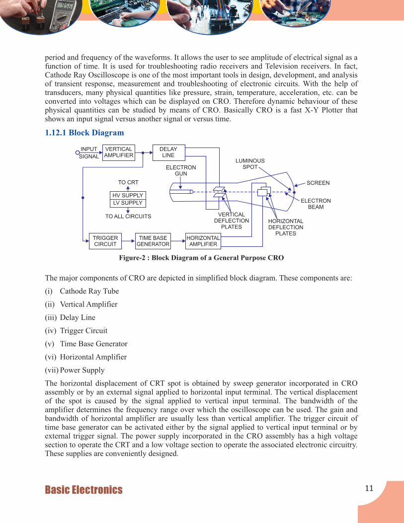
period and frequency of the waveforms. It allows the user to see amplitude of electrical signal as a function of time. It is used for troubleshooting radio receivers and Television receivers. In fact,Cathode Ray Oscilloscope is one of the most important tools in design, development, and analysisof transient response, measurement and troubleshooting of electronic circuits. With the help oftransducers, many physical quantities like pressure, strain, temperature, acceleration, etc. can beconverted into voltages which can be displayed on CRO. Therefore dynamic behaviour of thesephysical quantities can be studied by means of CRO. Basically CRO is a fast X-Y Plotter thatshows an input signal versus another signal or versus time.
The major components of CRO are depicted in simplified block diagram. These components are:
(i) Cathode Ray Tube
(ii) Vertical Amplifier
(iii) Delay Line
(iv) Trigger Circuit
(v) Time Base Generator
(vi) Horizontal Amplifier
(vii) Power Supply
The horizontal displacement of CRT spot is obtained by sweep generator incorporated in CROassembly or by an external signal applied to horizontal input terminal. The vertical displacementof the spot is caused by the signal applied to vertical input terminal. The bandwidth of theamplifier determines the frequency range over which the oscilloscope can be used. The gain andbandwidth of horizontal amplifier are usually less than vertical amplifier. The trigger circuit oftime base generator can be activated either by the signal applied to vertical input terminal or byexternal trigger signal. The power supply incorporated in the CRO assembly has a high voltagesection to operate the CRT and a low voltage section to operate the associated electronic circuitry.These supplies are conveniently designed.
1.12.1 Block Diagram
INPUT
SIGNAL
VERTICALAMPLIFIER
DELAYLINE
ELECTRONGUN
TO CRT
TO ALL CIRCUITS VERTICALDEFLECTION
PLATESHORIZONTALDEFLECTION
PLATES
ELECTRONBEAM
SCREEN
LUMINOUSSPOT
TRIGGERCIRCUIT
TIME BASEGENERATOR
HORIZONTALAMPLIFIER
HV SUPPLY
LV SUPPLY
Figure-2 : Block Diagram of a General Purpose CRO
Basic Electronics 11
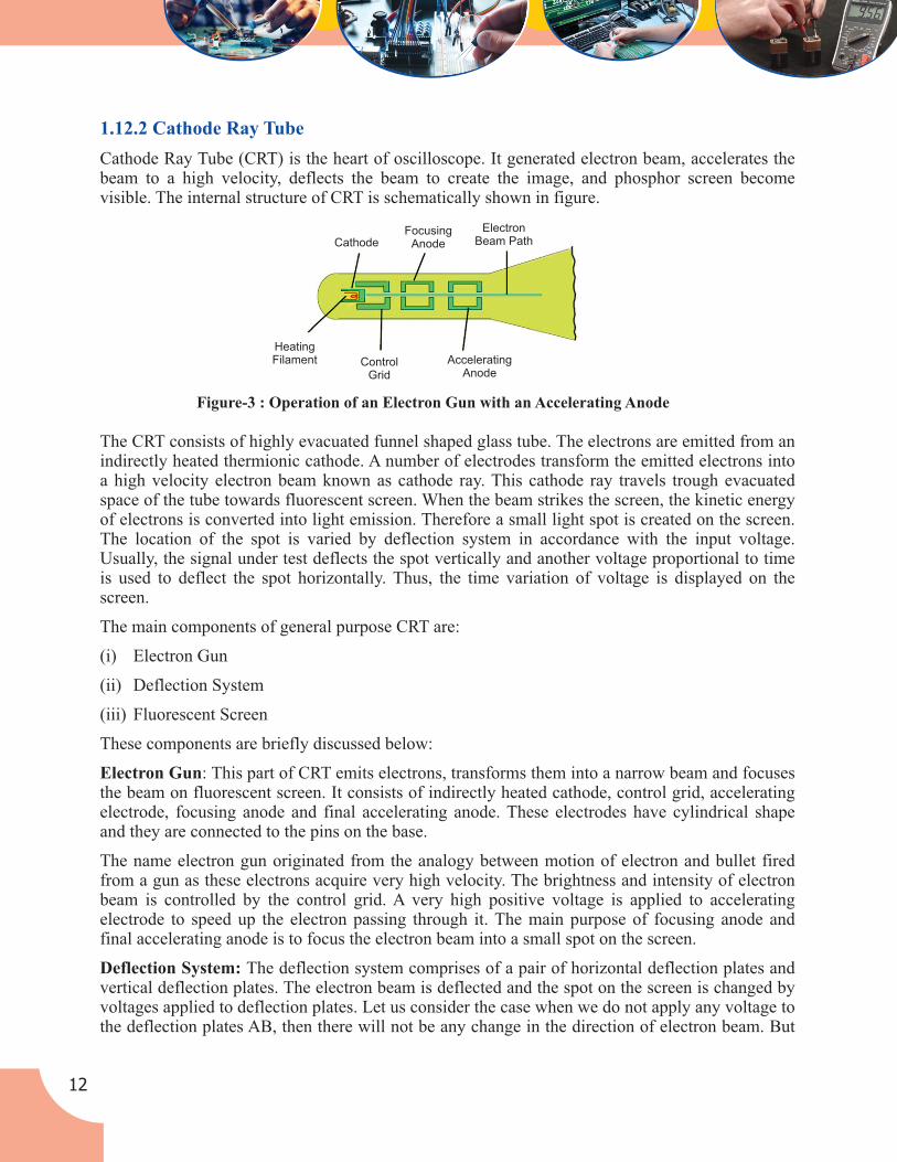
1.12.2 Cathode Ray Tube
Cathode Ray Tube (CRT) is the heart of oscilloscope. It generated electron beam, accelerates thebeam to a high velocity, deflects the beam to create the image, and phosphor screen becomevisible. The internal structure of CRT is schematically shown in figure.
The CRT consists of highly evacuated funnel shaped glass tube. The electrons are emitted from anindirectly heated thermionic cathode. A number of electrodes transform the emitted electrons intoa high velocity electron beam known as cathode ray. This cathode ray travels trough evacuatedspace of the tube towards fluorescent screen. When the beam strikes the screen, the kinetic energyof electrons is converted into light emission. Therefore a small light spot is created on the screen.The location of the spot is varied by deflection system in accordance with the input voltage.Usually, the signal under test deflects the spot vertically and another voltage proportional to timeis used to deflect the spot horizontally. Thus, the time variation of voltage is displayed on thescreen.
The main components of general purpose CRT are:
(i) Electron Gun
(ii) Deflection System
(iii) Fluorescent Screen
These components are briefly discussed below:
Electron Gun: This part of CRT emits electrons, transforms them into a narrow beam and focusesthe beam on fluorescent screen. It consists of indirectly heated cathode, control grid, acceleratingelectrode, focusing anode and final accelerating anode. These electrodes have cylindrical shapeand they are connected to the pins on the base.
The name electron gun originated from the analogy between motion of electron and bullet firedfrom a gun as these electrons acquire very high velocity. The brightness and intensity of electronbeam is controlled by the control grid. A very high positive voltage is applied to acceleratingelectrode to speed up the electron passing through it. The main purpose of focusing anode andfinal accelerating anode is to focus the electron beam into a small spot on the screen.
Deflection System: The deflection system comprises of a pair of horizontal deflection plates andvertical deflection plates. The electron beam is deflected and the spot on the screen is changed byvoltages applied to deflection plates. Let us consider the case when we do not apply any voltage tothe deflection plates AB, then there will not be any change in the direction of electron beam. But
HeatingFilament Control
Grid
AcceleratingAnode
Figure-3 : Operation of an Electron Gun with an Accelerating Anode
CathodeFocusing
Anode
ElectronBeam Path
12

now, when we apply some positive voltage to deflection plate A w.r.t. deflection plate B, thenelectrons being negatively charged, will have some deviation in path towards deflection plate A.The voltage applied to horizontal plate deflects the beam in horizontal direction and voltageapplied to vertical deflection plates deflects the beam in vertical direction. However, this shift isdependent on the intensity of voltage applied. This moving spot appears as continuous luminouswaveform owing to the persistence of the screen and human eye.
Fluorescent Screen: The inner surface of the face plate of CRT is coated with a fluorescentmaterial known as phosphor. The phosphor absorbs the kinetic energy of cathode ray and re-emitsthe energy as light.
In the electrostatic deflection, the spot is deflected on the screen by applying the voltage onvertical and/or horizontal deflection plates. The dc or peak-to-peak ac voltage applied to thedeflecting plates to displace the spot by 1mm on the screen is termed the deflection factor. Thereciprocal of the deflection factor is called the deflection sensitivity. The deflection factor isexpressed in V/mm and deflection sensitivity in mm/V.
Instead of electrostatic deflection, magnetic deflection can also be employed. The electrons aredeflected by a magnetic field applied perpendicular to the beam over a short distance of its path.The electrons experience a magnetic force in a direction perpendicular to both the direction of themotion and direction of magnetic field. Consequently, on emerging from the magnetic field, theelectrons travel at an angle to their original direction. The deflection of the spot on the screen perunit magnetic field is termed the magnetic field sensitivity. It is expressed in mm/gauss.
(i) Electrostatic Deflection
The electrostatic deflection of an electron beam is depicted in the figure. Let s be the separationbetween the deflecting plates, D be the distance from the screen S and l be the length of eachdeflection plate. Suppose that the deflecting voltage applied between the plates is V If m and e bed.
respectively the mass and charge of an electron entering the deflecting system with a velocity vand V be the final accelerating anode voltage, then we havea
2mv = eV (1.22)a
2Or v = (1.23)
1.12.3 Deflection Sensitivity
12
2e Vam
Figure-4
Vy
V
θ
d2
d1
θ
B
C
D
A
S
VVd
+
–
VR
S
Basic Electronics 13

The force exerted on the electron towards the positive deflection plate
F = (1.24)
The acceleration of electron is a = = (1.25)
The time taken by electron to move through the deflection plate is l/v. the upward velocity vy
acquired by electron on emergence from deflecting system is
v = = (1.26)y
The electron leaves the region of the deflecting plates, no deflecting force exists, and the electronmoves in a straight line at an angle è with the initial direction, we have
tan è = = (1.27)
The vertical displacement of electron in this interval is
d = = (1.28)1
Here d is the additional deflection on the screen.2
d = D = (1.29)2
The total deflection d = d + d = (1.30)1 2
The deflection sensitivity of CRT is S = = (1.31)
The expression for S shows that deflection sensitivity is independent of the deflecting voltage butis inversely proportional to the final anode voltage. Thus, deflection sensitivity can be enhancedby reducing the anode voltage. But then the brightness of the spot is reduced. The disadvantage isremoved by employing post acceleration. Here the beam is accelerated after it is deflected bydeflecting system. Equation (1.31) shows that deflection sensitivity varies directly as the length lof deflecting plates and as length L of the screen from the centre of plates. Also, S varies inversely as separation s between deflection plates.
(ii) Magnetic Deflection
Let a uniform field B act on the electron beam AC emitted from electron gun over a length lof its path (see figure).
e Vds
Fm
e Vdms
alv
e Vdms
lv
vyv
d2D
2al22v
e Vdms
2l22v
vyv
eVd lD2sm v
eVd l2sm v
l2
dVd
1L2sVa
+ D
Figure-5
O
D
R M
C Q N P
E
A
LI
rd2
α
rα
14

If the magnetic field is perpendicular to the plane of the paper , a magnetic force acts on theelectron along the plane of paper at right angles to magnetic field and the direction of motion ofelectron. As a result, the electron beam moves along a circular arc CE in the magnetic field. The
2radius r of circle is found by equating magnetic force Bev to the centripetal force mv /r , v beingthe velocity of an electron of mass m and charge e. Hence
Bev = (1.32)
r = (1.33)
Let accelerating potential be V, then
2 mv = eV
(1.34)
Using equation (1.34) in equation (1.33), we get
(1.35)
The deflection d of electron is 1
d = PM = NE = CR = OC-OR = r(1- cosá) (1.36)1
Where as, d = L taná (1.37)2
2In practice, the angle á is small enough so that only the terms up to á are important. Therefore
taná ~ á ~ (1.38)
cosá ~ 1- = 1- (1.39)
Substituting the value of taná and cosá from equations (1.38) and (1.39)
d = (1.40)2
d = (1.41)1
The total spot deflection on the screen is d = d + d = (1.42)1 2
The distance (L+ ) equals QP, the distance of the screen from the centre of magnetic fieldregion. Substituting value of r from equation (1.35) , we get
(1.43)
by definition, magnetic deflection sensitivity is
(1.44)
2mvr
mvBe
12
lr
2a2
1
2
2l2r
Llr
2l2r
l2
meV
v2
=
em V
Br
21=
lr
l2
d = e2mV (L+2)
l
L +
S =m
e2mV
dB
= ll2
L +
Basic Electronics 15

)(2
22 ttT
−=Φπ
1.12.3 Electrostatic Deflection versus Magnetic Deflection
1.12.4 Applications of Cathode Ray Oscilloscope
1. The electrostatic deflection needs little power for deflection. Whereas, magnetic deflectionneeds large power for the same deflection.
2. The electrostatic deflection can be employed at higher frequencies than magnetic deflection.
3. In electrostatic deflection, the deflection sensitivity falls more rapidly with increasing anodevoltage than that in case of magnetic deflection.
(i) Visual Display and Qualitative Study of Signal Waveforms: To display a signal on theCRT screen, the signal is applied to the vertical input terminals. The time variation of thesignal is visualized by means of time base generator displacing a spot in proportion to time inthe horizontal direction. The nature of the signal can be qualitatively studied from the traceon CRT screen.
(ii) Measurement of Voltage: The calibration of vertical scale gives the voltage correspondingto the vertical deflection of the spot on the CRT screen. Thus the magnitude of an appliedvoltage at different times of time varying signal can be measured.
(iii) Measurement of Frequency: The calibration of horizontal scale i.e. the time base helps todetermine the frequency of time varying signal displayed on the CRT screen. If N completecycles of ac signal are found to appear in a time interval t, then time period of signal is
T= t/N
And frequency of signal is f= 1/T = N/t
(iv) Measurement of Phase: The two signals, whose phase difference is to be measured, areapplied to the two channels of double beam CRO. The same trigger is used for two sweepvoltages. The phase difference between two waveforms displayed on CRT screen can befound from time base. If two sinusoidal signals of time period T are found to attain samephase at times t and t respectively, the phase difference between them is 1 2
(1.45)
Resource Material
(1) Electrical technology by V.K. Mehta & Rohit Mehta.
(2) Few reference from Wikipedia free encyclopedia.
16

Exercise
1. Short questions:
(a) Define Atoms.
(b) Define Transistors.
(c) Define ICs.
(d) Define Electron.
(e) What are the elements of Atoms?
2. Write short note on:
(a) What is Atomic Energy Level?
(b) Explain about Field Intensity.
(c) What is Potential Energy?
(d) What do you mean about Electric Field?
3. Explain the following:
(a) What is Bohr’s Atomic Model? Write the mathematical expression with your answer.
(b) What do you mean about Current and Current Density?
(c) What is Magnetic Field? Explain motion of charged particles in Electric Field.
4. Long questions:
(a) What are the applications of Cathode Ray Oscilloscope?
(b) Explain with block diagram Cathode Ray Oscilloscope.
Basic Electronics 17

Overview
Knowledge and Skill Outcomes
Assessment Plan: (For the Teachers)
This unit starts with the understanding of fundamentals of electrical parameter (Resistor,capacitor, inductor) their Properties etc. Further different types of electrical sources such asvoltage and current sources has been discussed along with the symbols and graphicalrepresentation also conversion of current and voltage source have been presented. A comparativestudy of various electrical signals (AC & DC) has been discussed. Proper explanation of cells andbatteries, energy and power finally whatever discussed and presented in various chapters has beensummarized as a quick review.
i) Understanding of fundamentals of electrical parameter i.e, voltage, current and all theirassociated parts.
ii) Understanding of all the electrical passive components (resistor, inductor and capacitor).
iii) Knowledge of various types of voltage and current sources.
iv) Difference between energy, work and power.
UNIT 2
Resistance, Ohm’s law, V-I Characteristics,Resistors, Capacitors, Inductors.
Unit-2 Topic AssessmentMethod
TimePlan
Remarks
Exercise:Question & Answer
Two Hours
2.0 Unit Overview and Description
?Overview
?Knowledge and Skill Outcomes
?Assessment Plan
?Learning Outcomes
?Resource Material
?Topics Covered
Resistance, Ohm’s law, V-l Characteristics, Resistors, Capacitors, Inductors, Voltage and Current Sources, Symbols and Graphical Representation, Conversion of Current and Voltage Sources,Overview of AC, DC, Cells and Batteries, Energy and Power.
Exercise:Question & Answer
Two HoursVoltage and Current Sources, Symbols andGraphical Representation, Conversion ofCurrent and Voltage sources.
Voltage & Current
Exercise:Question & Answer
Two HoursOverview of AC, DC, Cells and Batteries,Energy and Power.
18

Learning Outcomes
Unit-2 Outcomes
Resistors, Capacitors, Inductors.Resistance, Ohm’s law, V-l Characteristics,
Graphical Representation, Conversion ofCurrent and Voltage sources.
Voltage and Current Sources, Symbols and
Energy and Power.Overview of AC, DC, Cells and Batteries,
(i) Understanding the concept ofelectrical fundamentals.
(ii) Understanding the passivecomponents and their Characteristics.
(i) Identification of voltage and currentsources and their conversion.
(ii) Graphical representation and symbolsof electrical sources.
(i) Understanding of AC, DC, Cells andbatteries.
(ii) To know the difference of workenergy and power.
Voltage & Current
2.1. Current Flow Theories
Two theories describe current flow. The conventional theory commonly used for automotivesystem says current flow from (+) to (-)…excess electrons flow from an area of high potential toone of low potential (-).
The electron theory commonly used for electronics says current flows from(-) to (+)…excesselectron cause an area of negative potential (-) and flow toward an area lacking electrons , an areaof positive potential(+), to balance the charges.
While the direction of current flow makes a difference in the operation of some devices, such asdiodes, the direction makes no difference to the three measurable units of electricity; voltage,current, and resistance.
Electricity cannot be weighted on a scale or measured into a container. But certain electrical“action” can be measured.
These actions or terms are used to describe electricity, voltage, current, resistance, and power.
Voltage is pressure.
Current is flow.
Resistance opposes flow.
Power is that amount of work performed. It depends on the amount of pressure and the volume offlow.
(i) Voltage
Voltage is the electrical pressure, a potential force or difference in electrical charge between twopoints. It can push electrical current through a wire, but not through its insulation.
2.1.1. Terms of Electricity
19Basic Electronics
Voltage is measured in volts. One volt can push a certain amount of current, two volts twice asmuch and so on. A voltmeter measures the difference in electrical pressure between two points involts. A voltmeter is used in parallel.
(ii) Current
Current is electrical flow moving through a wire. Current flow in a wire pushed by voltage.
Current is measured in amperes, or amps, for short. An ammeter measures current flow in ampere.It is inserted into the path of current flow, or in series, in a circuit.
(iii) Resistance
Resistance opposes current flow. It is like electrical “friction”. This resistance slows the flow ofcurrent. Every electrical component or circuit has resistance. And this resistance changes electricalenergy into another form of energy- heat, light, motion.
Resistance is measured in ohms. A special meter called ohmmeter, can measure the resistance of adevice in ohms when no current is flowing.
(iv) Factors Affecting Resistance
Five factors determine the resistance of conductors. These factors are length of the conductor,diameter of the conductor, temperature, physical condition and conductor material. The filamentof a lamp, the winding of a motor or coil, and the bimetal element in sensors are conductors. Sothese factors apply to circuit wiring as well working devices or loads.
(v) Length
Electrons in motion are constantly colliding as voltage pushes them through a conductor. If twowires are of the same material and diameter, the longer wire has more resistance than shorter wire.Wire resistance is often listed in ohms per foot (e.g., spark plug cables at 5 ohm per foot). Lengthmust be considered when replacing wires.
(vi) Diameter
Large diameter allows more current to flow. If two wires are the same material and length, thethinner wire has more resistance than the thicker wire. Wire resistance tables list ohm per foot forwires of various thickness.
Replacement of wires and splices must be of the proper size for the circuit current.
(vii) Temperature
In most conductors, resistance increases as the wire temperature increases. Electrons move fasterbut not necessarily in the right direction. Most insulators have less, resistance at highertemperatures.
Semiconductor device called thermister have negative temperature coefficient (NTC) resistancedecrease as temperature increase.
R = PLA
R = Resistance of Conductor
P = Resistivity; L = Length of Conductor
A = Area of Conductor
20

(viii) Physical Condition
Partially cut or nicked wire will act like smaller wire with high resistance in the damaged area. Akink in the wire, poor splices, and loose or corroded connections also increase resistance. Takecare not to damage wires during testing or stripping insulation.
(ix) Material
Material with many free electrons is good conductors with low resistance to current flow. Materialwith many bound electrons is poor conductors (insulators) with high resistance to current flow.Copper, aluminium, gold, and silver have low resistance. Rubber, glass, paper, ceramics, plastics,and air have high resistance.
A simple relationship exists between voltage, current & resistance in electrical circuits.Understanding this relationship is important for fast accurate electrical problem diagnosis andrepair.
2.1.2. Voltage, Current, and Resistance in a Circuit
2.1.2.1. OHM’S LAW
Ohm’s law says: the current in a circuit is directly proportional to the applied voltage andinversely proportional to the amount of resistance.
This means that if the voltage goes up, the current flow will go up, and vice versa. Also as theresistance goes up, the current goes down and vice versa.
Figure-1
also I1R
I =VR
where V = Voltage
I = Current
R = Resistance
I VCurrent is directly proportional to potential difference
current
(amperes)
directlyproportional potential difference
(volts)
(i) I-V Characteristic Curves
The I-V characteristic curves, which is short for current-voltage characteristic curves or simply I-V curves of an electrical/electronic device or component, are a set of graphical curves which areused to define its operation within an electrical circuit. As its name suggests, I-V characteristic
21Basic Electronics

curves show the relationship between the current flowing through an electronic device and theapplied voltage across its terminals.
I-V characteristic curves are generally used as a tool to determine and understand the basicparameters of a component or device and which can also be used to mathematically model itsbehavior within an electronic circuit.
But as with most electronic devices, there are an infinite number of I-V characteristic curvesrepresenting the various inputs or parameters and as such we can display a family or group ofcurves on the same graph to represent the various values.
For example, the “current-voltage characteristics” of a bipolar transistor can be shown withvarious amounts of base drive or the I-V characteristic curves of a diode operating in both itsforward and reverse regions.
But the static current–voltage characteristics of a component or device need not be a straight line.Take for example the characteristics of a fixed value resistor, we would expect them to bereasonably straight and constant within certain ranges of current, voltage and power as it is alinear or ohmic device.
There are however, other resistive elements such as LDR’s, thermistors, varistors, and even thelight bulb, whose I-V characteristic curves are not straight or linear lines but instead are curved orshaped and are therefore called non-linear devices because their resistances are non-linearresistances.
If the electrical supply voltage, V applied to the terminals of the resistive element R above wasvaried, and the resulting current, I measured, this current would be characterized as: I = V/R,being one of Ohm’s Law equations.
We know from Ohm’s Law that as the voltage across the resistor increases so too does the currentflowing through it, it would be possible to construct a graph to show the relationship between thevoltage and current as shown with the graph representing the volt-ampere characteristics (its I-Vcharacteristic curves) of the resistive element. Consider the circuit below. (Fig.-2)
I-V Characteristic Curves of an Ideal Resistor
Figure-2
22

2.2. Resistors
A resistor is a passive two-terminal component that implements electrical resistance as a circuitelement. Resistors act to reduce current flow, and, at the same time, act to lower voltage levelswithin circuits. In electronic circuits, resistors are used to limit current flow, to adjust signallevels, bias active elements and terminate transmission lines among other uses. High-powerresistors, that can dissipate many watts of electrical power as heat, may be used as part of motorcontrols, in power distribution systems or as test loads for generators. Fixed resistors haveresistances that only change slightly with temperature, time or operating voltage. Variable resistors can be used to adjust circuit elements (such as a volume control or a lamp dimmer), or as sensingdevices for heat, light, humidity, force, or chemical activity.
Resistors are common elements of electrical networks and electronic circuits and are ubiquitous inelectronic equipment. Practical resistors as discrete components can be composed of variouscompounds and forms. Resistors are also implemented within integrated circuits.
The electrical function of a resistor is specified by its resistance: common commercial resistorsare manufactured over a range of more than nine orders of magnitude. The nominal value of theresistance will fall within a manufacturing tolerance.
A single in line (SIL) resistor package with 8 individual, 47 ohm resistors. One end of eachresistor is connected to a separate pin and the other ends are all connected together to theremaining (common) pin – pin 1, at the end identified by the white dot. (Fig. - 3)
(i) Lead Arrangements
Resistors with wire leads for through-hole mounting through-hole components typically have“leads” leaving the body “axially,” that is, on a line parallel with the part’s longest axis. Othershave leads coming off their body “radially” instead. Other components may be SMT (surfacemount technology), while high power resistors may have one of their leads designed into the heatsink.
2.2.1. Fixed Resistors
(Fig. - 4)
Figure-3
Figure-4
23Basic Electronics

(ii) Carbon Composition
Three carbon composition resistors in a 1960s valve (vacuum tube) radio.
Carbon composition resistors consist of a solid cylindrical resistive element with embedded wireleads or metal end caps to which the lead wires are attached. The body of the resistor is protectedwith paint or plastic. Early 20th-century carbon composition resistors had uninsulated bodies; thelead wires were wrapped around the ends of the resistance element rod and soldered. Thecompleted resistor was painted for color-coding of its value.
The resistive element is made from a mixture of finely ground (powdered) carbon and aninsulating material (usually ceramic). A resin holds the mixture together. The resistance isdetermined by the ratio of the fill material (the powdered ceramic) to the carbon. Higherconcentrations of carbon- a good conductor- result in lower resistance. Carbon compositionresistors were commonly used in the 1960s and earlier, but are not so popular for general use nowas other types have better specifications, such as tolerance, voltage dependence, and stress (carbon composition resistors will change value when stressed with over-voltages). Moreover, if internalmoisture content (from exposure for some length of time to a humid environment) is significant,soldering heat will create a non-reversible change in resistance value. Carbon compositionresistors have poor stability with time and were consequently factory sorted to, at best, only 5%tolerance. These resistors, however, if never subjected to overvoltage or overheating wereremarkably reliable considering the component’s size.
Carbon composition resistors are still available, but comparatively quite costly. Values rangedfrom fractions of an ohm to 22 megaohms. Due to their high price, these resistors are no longerused in most applications. However, they are used in power supplies and welding controls.
(iii) Carbon Pile
A carbon pile resistor is made of a stack of carbon disks compressed between two metal contactplates. Adjusting the clamping pressure changes the resistance between the plates. These resistorsare used when an adjustable load is required, for example in testing automotive batteries or radiotransmitters. A carbon pile resistor can also be used as a speed control for small motors inhousehold appliances (sewing machines, hand-held mixers) with ratings up to a few hundredwatts. A carbon pile resistor can be incorporated in automatic voltage regulators for generators,where the carbon pile controls the field current to maintain relatively constant voltage. Theprinciple is also applied in the carbon microphone.
(Fig.-5)
Figure-5
24
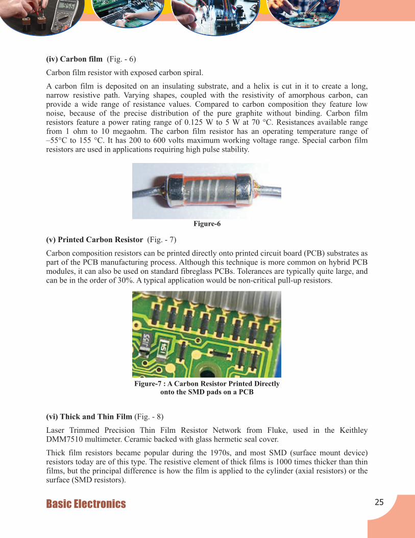
(iv) Carbon film (Fig. - 6)
Carbon film resistor with exposed carbon spiral.
A carbon film is deposited on an insulating substrate, and a helix is cut in it to create a long,narrow resistive path. Varying shapes, coupled with the resistivity of amorphous carbon, canprovide a wide range of resistance values. Compared to carbon composition they feature lownoise, because of the precise distribution of the pure graphite without binding. Carbon filmresistors feature a power rating range of 0.125 W to 5 W at 70 °C. Resistances available rangefrom 1 ohm to 10 megaohm. The carbon film resistor has an operating temperature range of–55°C to 155 °C. It has 200 to 600 volts maximum working voltage range. Special carbon filmresistors are used in applications requiring high pulse stability.
(v) Printed Carbon Resistor (Fig. - 7)
Carbon composition resistors can be printed directly onto printed circuit board (PCB) substrates as part of the PCB manufacturing process. Although this technique is more common on hybrid PCBmodules, it can also be used on standard fibreglass PCBs. Tolerances are typically quite large, andcan be in the order of 30%. A typical application would be non-critical pull-up resistors.
(vi) Thick and Thin Film (Fig. - 8)
Laser Trimmed Precision Thin Film Resistor Network from Fluke, used in the KeithleyDMM7510 multimeter. Ceramic backed with glass hermetic seal cover.
Thick film resistors became popular during the 1970s, and most SMD (surface mount device)resistors today are of this type. The resistive element of thick films is 1000 times thicker than thinfilms, but the principal difference is how the film is applied to the cylinder (axial resistors) or thesurface (SMD resistors).
Figure-7 : A Carbon Resistor Printed Directlyonto the SMD pads on a PCB
Figure-6
25Basic Electronics

Thin film resistors are made by sputtering (a method of vacuum deposition) the resistive materialonto an insulating substrate. The film is then etched in a similar manner to the old (subtractive)process for making printed circuit boards; that is, the surface is coated with a photo-sensitivematerial, then covered by a pattern film, irradiated with ultraviolet light, and then the exposedphoto-sensitive coating is developed, and underlying thin film is etched away.
Thick film resistors are manufactured using screen and stencil printing processes.
Because the time during which the sputtering is performed can be controlled, the thickness of thethin film can be accurately controlled. The type of material is also usually different consisting ofone or more ceramic (cermet) conductors such as tantalum nitride (TaN), ruthenium oxide (RuO ),2
lead oxide(PbO), bismuth ruthenate (BiO ), nickel chromium (NiCr).2
The resistance of both thin and thick film resistors after manufacture is not highly accurate; theyare usually trimmed to an accurate value by abrasive or laser trimming. Thin film resistors areusually specified with tolerances of 0.1, 0.2, 0.5, or 1%, and with temperature coefficients of 5 to25 ppm/K. They also have much lower noise levels, on the level of 10-100 times less than thickfilm resistors.
Thick film resistors may use the same conductive ceramics, but they are mixed with sintered(powdered) glass and a carrier liquid so that the composite can be screen-printed. This compositeof glass and conductive ceramic (cermet) material is then fused (baked) in an oven at about850°C.
Thick film resistors, when first manufactured, had tolerances of 5%, but standard tolerances haveimproved to 2% or 1% in the last few decades. Temperature coefficients of thick film resistors arehigh, typically ±200 or ±250 ppm/K; a 40 kelvin (70 °F) temperature change can change theresistance by 1%.
Thin film resistors are usually far more expensive than thick film resistors. For example, SMDthin film resistors, with 0.5% tolerances, and with 25 ppm/K temperature coefficients, whenbought in full size reel quantities, are about twice the cost of 1%, 250 ppm/K thick film resistors.
(vii) Metal Film
A common type of axial-leaded resistor today is the metal-film resistor. Metal Electrode LeadlessFace (MELF) resistors often use the same technology, and are also cylindrically shaped but aredesigned for surface mounting. Note that other types of resistors (e.g., carbon composition) arealso available in MELF packages.
Figure-8
26

Metal film resistors are usually coated with nickel chromium (NiCr), but might be coated with any of the cermet materials listed above for thin film resistors. Unlike thin film resistors, the materialmay be applied using different techniques than sputtering (though this is one of the techniques).Also, unlike thin-film resistors, the resistance value is determined by cutting a helix through thecoating rather than by etching. (This is similar to the way carbon resistors are made.) The result isa reasonable tolerance (0.5%, 1%, or 2%) and a temperature coefficient that is generally between50 and 100 ppm/K. Metal film resistors possess good noise characteristics and low non-linearitydue to a low voltage coefficient. Also beneficial are their tight tolerance, low temperaturecoefficient and long-term stability.
(viii) Metal Oxide Film
Metal-oxide film resistors are made of metal oxides which results in a higher operatingtemperature and greater stability/reliability than Metal film. They are used in applications withhigh endurance demands.
(ix) Wire Wound (Fig. - 9)
High-power wire wound resistors used for dynamic braking on an electric railway car. Suchresistors may dissipate many kilowatts for an extended length of time.
Types of windings in wire resistors: (Fig. - 10)
1. Common
2. Bifilar
3. Common on a thin former
4. Ayrton-Perry
Wire wound resistors are commonly made by winding a metal wire, usually nichrome, around aceramic, plastic, or fiberglass core. The ends of the wire are soldered or welded to two caps orrings, attached to the ends of the core. The assembly is protected with a layer of paint, moldedplastic, or an enamel coating baked at high temperature. These resistors are designed to withstandunusually high temperatures of up to 450°C. Wire leads in low power wire wound resistors areusually between 0.6 and 0.8 mm in diameter and tinned for ease of soldering. For higher powerwire wound resistors, either a ceramic outer case or an aluminum outer case on top of aninsulating layer is used – if the outer case is ceramic, such resistors are sometimes described as“cement” resistors, though they do not actually contain any traditional cement. The aluminum-
Figure-9
27Basic Electronics

cased types are designed to be attached to a heat sink to dissipate the heat; the rated power isdependent on being used with a suitable heat sink, e.g., a 50 W power rated resistor will overheatat a fraction of the power dissipation if not used with a heat sink. Large wire wound resistors maybe rated for 1,000 watts or more.
Because wire wound resistors are coils they have more undesirable inductance than other types ofresistor, although winding the wire in sections with alternately reversed direction can minimizeinductance. Other techniques employ bifilar winding, or a flat thin former (to reduce cross-sectionarea of the coil). For the most demanding circuits, resistors with Ayrton-Perry winding are used.
Applications of wire wound resistors are similar to those of composition resistors with theexception of the high frequency. The high frequency response of wire wound resistors is
[7]substantially worse than that of a composition resistor.
(x) Foil Resistor
The primary resistance element of a foil resistor is a special alloy foil several micrometers thick.Since their introduction in the 1960s, foil resistors have had the best precision and stability of anyresistor available. One of the important parameters influencing stability is the temperaturecoefficient of resistance (TCR). The TCR of foil resistors is extremely low, and has been furtherimproved over the years. One range of ultra-precision foil resistors offers a TCR of 0.14 ppm/°C,tolerance ±0.005%, long-term stability (1 year) 25 ppm, (3 years) 50 ppm (further improved
5-fold by hermetic sealing), stability under load (2000 hours) 0.03%, thermal EMF 0.1 mV/°C,
noise “42 dB, voltage coefficient 0.1 ppm/V, inductance 0.08 mH, capacitance 0.5 pF.”
(xi) Ammeter Shunts
An ammeter shunt is a special type of current-sensing resistor, having four terminals and a valuein milliohms or even micro-ohms. Current-measuring instruments, by themselves, can usuallyaccept only limited currents. To measure high currents, the current passes through the shunt acrosswhich the voltage drop is measured and interpreted as current. A typical shunt consists of twosolid metal blocks, sometimes brass, mounted on an insulating base. Between the blocks, andsoldered or brazed to them, are one or more strips of low temperature coefficient of resistance(TCR) manganin alloy. Large bolts threaded into the blocks make the current connections, whilemuch smaller screws provide volt meter connections. Shunts are rated by full-scale current, andoften have a voltage drop of 50 mV at rated current. Such meters are adapted to the shunt fullcurrent rating by using an appropriately marked dial face; no change need to be made to the otherparts of the meter.
Figure-10
28
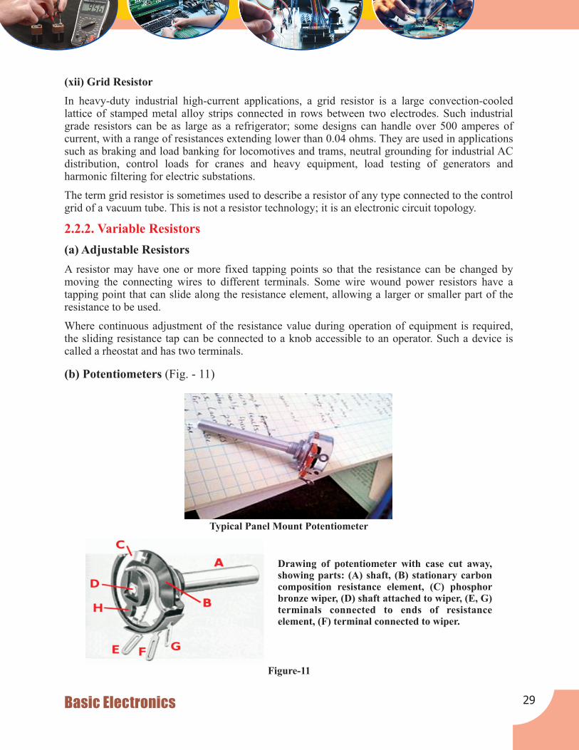
(xii) Grid Resistor
In heavy-duty industrial high-current applications, a grid resistor is a large convection-cooledlattice of stamped metal alloy strips connected in rows between two electrodes. Such industrialgrade resistors can be as large as a refrigerator; some designs can handle over 500 amperes ofcurrent, with a range of resistances extending lower than 0.04 ohms. They are used in applicationssuch as braking and load banking for locomotives and trams, neutral grounding for industrial AC distribution, control loads for cranes and heavy equipment, load testing of generators andharmonic filtering for electric substations.
The term grid resistor is sometimes used to describe a resistor of any type connected to the control grid of a vacuum tube. This is not a resistor technology; it is an electronic circuit topology.
(a) Adjustable Resistors
A resistor may have one or more fixed tapping points so that the resistance can be changed bymoving the connecting wires to different terminals. Some wire wound power resistors have atapping point that can slide along the resistance element, allowing a larger or smaller part of theresistance to be used.
Where continuous adjustment of the resistance value during operation of equipment is required,the sliding resistance tap can be connected to a knob accessible to an operator. Such a device iscalled a rheostat and has two terminals.
2.2.2. Variable Resistors
Figure-11
Typical Panel Mount Potentiometer
Drawing of potentiometer with case cut away,showing parts: (A) shaft, (B) stationary carboncomposition resistance element, (C) phosphorbronze wiper, (D) shaft attached to wiper, (E, G)terminals connected to ends of resistanceelement, (F) terminal connected to wiper.
(b) Potentiometers (Fig. - 11)
29Basic Electronics

Potentiometer
A potentiometer or pot is a three-terminal resistor with a continuously adjustable tapping pointcontrolled by rotation of a shaft or knob or by a linear slider.It is called a potentiometer because itcan be connected as an adjustable voltage divider to provide a variable potential at the terminalconnected to the tapping point. A volume control for an audio device is a common use of apotentiometer. A typical low power potentiometer (see drawing) is constructed of a flat resistanceelement (B) of carbon composition, metal film, or conductive plastic, with a springy phosphorbronze wiper contact (C) which moves along the surface. An alternate construction is resistancewire wound on a form, with the wiper sliding axially along the coil.These have lower resolution,since as the wiper moves the resistance changes in steps equal to the resistance of a single turn.
High-resolution multiturn potentiometers are used in a few precision applications. These havewire wound resistance elements typically wound on a helical mandrel, with the wiper moving on a helical track as the control is turned, making continuous contact with the wire. Some include aconductive-plastic resistance coating over the wire to improve resolution. These typically offer ten turns of their shafts to cover their full range. They are usually set with dials that include a simpleturns counter and a graduated dial, and can typically achieve three digit resolution. Electronicanalog computers used them in quantity for setting coefficients, and delayed-sweep oscilloscopesof recent decades included one on their panels.
Just like the Resistor, the Capacitor, sometimes referred to as a Condenser, is a simple passivedevice that is used to “store electricity”. The capacitor is a component which has the ability or“capacity” to store energy in the form of an electrical charge producing a potential difference(Static Voltage) across its plates, much like a small rechargeable battery.
2.3. Introduction to Capacitors
Figure-12
An Assortment of Small Through-Hole Potentiometers Designed
for Mounting on Printed
Figure-13 : A Typical Capacitor
30

There are many different kinds of capacitors available from very small capacitor beads used inresonance circuits to large power factor correction capacitors, but they all do the same thing, theystore charge.
In its basic form, a Capacitor consists of two or more parallel conductive (metal) plates which arenot connected or touching each other, but are electrically separated either by air or by some formof a good insulating material such as waxed paper, mica, ceramic, plastic or some form of a liquidgel as used in electrolytic capacitors. The insulating layer between capacitors plates is commonlycalled the Dielectric.
Due to this insulating layer, DC current cannot flow through the capacitor as it blocks it allowinginstead a voltage to be present across the plates in the form of an electrical charge.
The conductive metal plates of a capacitor can be square, circular or rectangular, or they can be ofa cylindrical or spherical shape with the general shape, size and construction of a parallel platecapacitor depending on its application and voltage rating.
When used in a direct current or DC circuit, a capacitor charges up to its supply voltage butblocks the flow of current through it because the dielectric of a capacitor is non-conductive andbasically an insulator. However, when a capacitor is connected to an alternating current or ACcircuit, the flow of the current appears to pass straight through the capacitor with little or noresistance.
There are two types of electrical charge, positive charge in the form of Protons and negativecharge in the form of Electrons. When a DC voltage is placed across a capacitor, the positive(+ve) charge quickly accumulates on one plate while a corresponding negative (-ve) chargeaccumulates on the other plate. For every particle of +ve charge that arrives at one plate a chargeof the same sign will depart from the -ve plate.
Then the plates remain charge neutral and a potential difference due to this charge is establishedbetween the two plates. Once the capacitor reaches its steady state condition an electrical currentis unable to flow through the capacitor itself and around the circuit due to the insulating propertiesof the dielectric used to separate the plates.
The flow of electrons onto the plates is known as the capacitor's charging current which continuesto flow until the voltage across both plates (and hence the capacitor) is equal to the appliedvoltage Vc (Fig. - 14). At this point the capacitor is said to be “fully charged” with electrons. Thestrength or rate of this charging current is at its maximum value when the plates are fullydischarged (initial condition) and slowly reduces in value to zero as the plates charge up to apotential difference across the capacitors plates equal to the source voltage.
The amount of potential difference present across the capacitor depends upon how much chargewas deposited onto the plates by the work being done by the source voltage and also by howmuch capacitance the capacitor has and this is illustrated below.
The parallel plate capacitor is the simplest form of capacitor. It can be constructed using twometal or metallised foil plates at a distance parallel to each other, with its capacitance value inFarads, being fixed by the surface area of the conductive plates and the distance of separationbetween them. Altering any two of these values alters the value of its capacitance and this formsthe basis of operation of the variable capacitors.
Capacitor Construction
31Basic Electronics
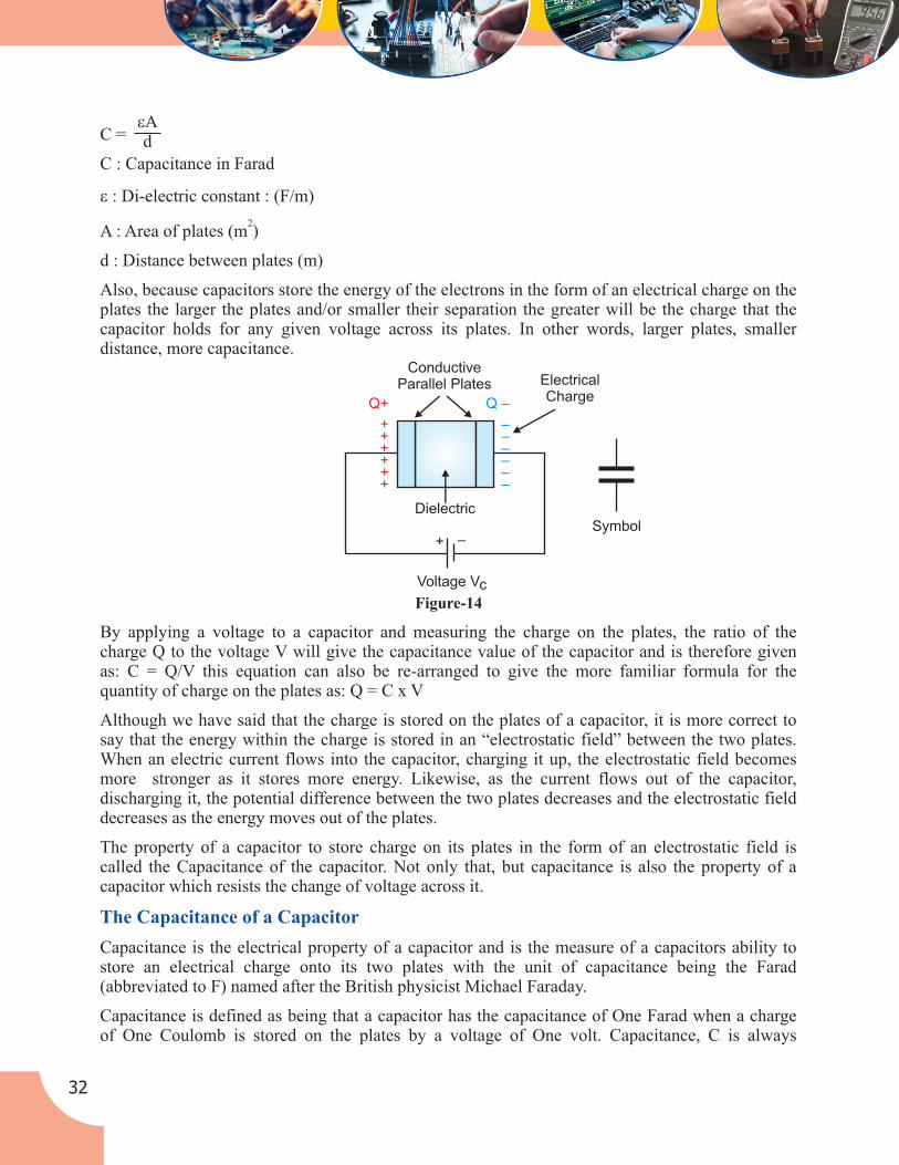
C =
C : Capacitance in Farad
e : Di-electric constant : (F/m)
2A : Area of plates (m )
d : Distance between plates (m)
Also, because capacitors store the energy of the electrons in the form of an electrical charge on theplates the larger the plates and/or smaller their separation the greater will be the charge that thecapacitor holds for any given voltage across its plates. In other words, larger plates, smallerdistance, more capacitance.
By applying a voltage to a capacitor and measuring the charge on the plates, the ratio of thecharge Q to the voltage V will give the capacitance value of the capacitor and is therefore givenas: C = Q/V this equation can also be re-arranged to give the more familiar formula for thequantity of charge on the plates as: Q = C x V
Although we have said that the charge is stored on the plates of a capacitor, it is more correct tosay that the energy within the charge is stored in an “electrostatic field” between the two plates.When an electric current flows into the capacitor, charging it up, the electrostatic field becomesmore stronger as it stores more energy. Likewise, as the current flows out of the capacitor,discharging it, the potential difference between the two plates decreases and the electrostatic fielddecreases as the energy moves out of the plates.
The property of a capacitor to store charge on its plates in the form of an electrostatic field iscalled the Capacitance of the capacitor. Not only that, but capacitance is also the property of acapacitor which resists the change of voltage across it.
Capacitance is the electrical property of a capacitor and is the measure of a capacitors ability tostore an electrical charge onto its two plates with the unit of capacitance being the Farad(abbreviated to F) named after the British physicist Michael Faraday.
Capacitance is defined as being that a capacitor has the capacitance of One Farad when a chargeof One Coulomb is stored on the plates by a voltage of One volt. Capacitance, C is always
The Capacitance of a Capacitor
Figure-14
eAd
Q+
++++++
Q –
––––––
–+
ElectricalCharge
ConductiveParallel Plates
Symbol
Dielectric
Voltage Vc
32

positive and has no negative units. However, the Farad is a very large unit of measurement to useon its own so sub-multiples of the Farad are generally used such as microfarads, nanofarads andpicofarads, for example.
–6·Microfarad (mF) 1mF = 1/1,000,000 = 0.000001 = 10 F
–9·Nanofarad (nF) 1nF = 1/1,000,000,000 = 0.000000001 = 10 F
–12·Picofarad (pF) 1pF = 1/1,000,000,000,000 = 0.000000000001 = 10 F
There are a very, very large variety of different types of capacitor available in the market placeand each one has its own set of characteristics and applications, from very small delicate trimming capacitors up to large power metal-can type capacitors used in high voltage power correction andsmoothing circuits.
The comparisons between the different types of capacitor is generally made with regards to thedielectric used between the plates. Like resistors, there are also variable types of capacitors whichallow us to vary their capacitance value for use in radio or “frequency tuning” type circuits.
Commercial types of Capacitors are made from metallic foil interlaced with thin sheets of eitherparaffin-impregnated paper or Mylar as the dielectric material. Some capacitors look like tubes,this is because the metal foil plates are rolled up into a cylinder to form a small package with theinsulating dielectric material sandwiched in between them.
Small capacitors are often constructed from ceramic materials and then dipped into an epoxy resinto seal them. Either way, capacitors play an important part in electronic circuits so here are a fewof the more “common” types of capacitor available.
(i) Dielectric Capacitor
Dielectric Capacitors are usually of the variable type were a continuous variation of capacitance isrequired for tuning transmitters, receivers and transistor radios. Variable dielectric capacitors aremulti-plate air-spaced types that have a set of fixed plates (the stator vanes) and a set of movableplates (the rotor vanes) which move in between the fixed plates.
The position of the moving plates with respect to the fixed plates determines the overallcapacitance value. The capacitance is generally at maximum when the two sets of plates are fullymeshed together. High voltage type tuning capacitors have relatively large spacings or air-gapsbetween the plates with breakdown voltages reaching many thousands of volts.
Standard Units of Capacitance
Types of Capacitor
Figure-15 : Variable Capacitor Symbols
VariableCapacitorSymbol
TrimmerCapacitorSymbol
33Basic Electronics

Figure-16 : Radial Lead Type
DielectricLayer
Metal - Filmelectrodes
Outercase
Wireleads
As well as the continuously variable types, preset type variable capacitors are also available called Trimmers. These are generally small devices that can be adjusted or “pre-set” to a particularcapacitance value with the aid of a small screwdriver and are available in very small capacitance’sof 500pF or less and are non-polarized.
(ii) Film Capacitor
Film Capacitors are the most commonly available of all types of capacitors, consisting of arelatively large family of capacitors with the difference being in their dielectric properties. Theseinclude polyester (Mylar), polystyrene, polypropylene, polycarbonate, metalized paper, Teflon etc.Film type capacitors are available in capacitance ranges from as small as 5pF to as large as 100uFdepending upon the actual type of capacitor and its voltage rating.
Film capacitors also come in an assortment of shapes and case styles which include:
·Wrap & Fill (Oval & Round) – where the capacitor is wrapped in a tight plastic tape and
have the ends filled with epoxy to seal them.
·Epoxy Case (Rectangular & Round) – where the capacitor is encased in a moulded plastic
shell which is then filled with epoxy.
·Metal Hermetically Sealed (Rectangular & Round) – where the capacitor is encased in a
metal tube or can and again sealed with epoxy with all the above case styles available inboth Axial and Radial Leads.
Film Capacitors which use polystyrene, polycarbonate or Teflon as their dielectrics are sometimescalled “Plastic capacitors”. The construction of plastic film capacitors is similar to that for paperfilm capacitors but use a plastic film instead of paper. The main advantage of plastic filmcapacitors compared to impregnated paper types is that they operate well under conditions of hightemperature, have smaller tolerances, a very long service life and high reliability. Examples offilm capacitors are the rectangular metalized film and cylindrical film & foil types as shownbelow.
The film and foil types of capacitors are made from long thin strips of thin metal foil with thedielectric material sandwiched together which are wound into a tight roll and then sealed in paperor metal tubes.
34

Figure-17 : Axial Lead Type
DielectricMaterial
Metalfoil
These film types require a much thicker dielectric film to reduce the risk of tears or puncture inthe film, and are therefore more suited to lower capacitance values and larger case sizes.
Figure-18 : Film Capacitor
Metalized foil capacitors have the conductive film metalized sprayed directly onto each side of thedielectric which gives the capacitor self-healing properties and can therefore use much thinnerdielectric films. This allows for higher capacitance values and smaller case sizes for a givencapacitance. Film and foil capacitors are generally used for higher power and more preciseapplications.
(iii) Ceramic Capacitors
Ceramic Capacitors or Disc Capacitors as they are generally called are made by coating two sidesof a small porcelain or ceramic disc with silver and are then stacked together to make a capacitor.For very low capacitance values a single ceramic disc of about 3-6mm is used. Ceramic capacitors have a high dielectric constant (High-K) and are available so that relatively high capacitances canbe obtained in a small physical size.
Figure-19 : Ceramic Capacitor
They exhibit large non-linear changes in capacitance against temperature and as a result are usedas de-coupling or by-pass capacitors as they are also non-polarized devices. Ceramic capacitors
have values ranging from a few picofarads to one or two microfarads, ( mF ) but their voltage
ratings are generally quite low.
35Basic Electronics

Figure-20 : Electrolytic Capacitor
Ceramic types of capacitors generally have a 3-digit code printed onto their body to identify theircapacitance value in pico-farads. Generally the first two digits indicate the capacitors value andthe third digit indicates the number of zero’s to be added. For example, a ceramic disc capacitorwith the markings 103 would indicate 10 and 3 zero’s in pico-farads which is equivalent to 10,000pF or 10nF.
Likewise, the digits 104 would indicate 10 and 4 zero’s in pico-farads which is equivalent to100,000 pF or 100nF and so on. So on the image of the ceramic capacitor above the numbers 154indicate 15 and 4 zero’s in pico-farads which is equivalent to 150,000 pF or 150nF or 0.15uF.Letter codes are sometimes used to indicate their tolerance value such as: J = 5%, K = 10% orM = 20% etc.
(iv) Electrolytic Capacitors
Electrolytic Capacitors are generally used when very large capacitance values are required. Hereinstead of using a very thin metallic film layer for one of the electrodes, a semi-liquid electrolytesolution in the form of a jelly or paste is used which serves as the second electrode (usually thecathode).
The dielectric is a very thin layer of oxide which is grown electro-chemically in production withthe thickness of the film being less than ten microns. This insulating layer is so thin that it ispossible to make capacitors with a large value of capacitance for a small physical size as thedistance between the plates, d is very small.
The majority of electrolytic types of capacitors are Polarised, that is the DC voltage applied to thecapacitor terminals must be of the correct polarity, i.e. positive to the positive terminal andnegative to the negative terminal as an incorrect polarization will break down the insulating oxidelayer and permanent damage may result.
All polarized electrolytic capacitors have their polarity clearly marked with a negative sign toindicate the negative terminal and this polarity must be followed.
Electrolytic Capacitors are generally used in DC power supply circuits due to their largecapacitance’s and small size to help reduce the ripple voltage or for coupling and decouplingapplications. One main disadvantage of electrolytic capacitors is their relatively low voltage rating and due to the polarization of electrolytic capacitors, it follows then that they must not be used onAC supplies. Electrolytic’s generally come in two basic forms; Aluminium Electrolytic Capacitors and Tantalum Electrolytic Capacitors.
1. Aluminium Electrolytic Capacitors
There are basically two types of Aluminium Electrolytic Capacitor, the plain foil type and theetched foil type. The thickness of the aluminium oxide film and high breakdown voltage givethese capacitors very high capacitance values for their size.
36
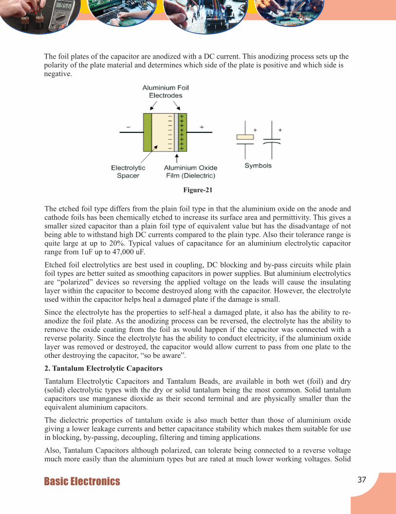
The foil plates of the capacitor are anodized with a DC current. This anodizing process sets up the polarity of the plate material and determines which side of the plate is positive and which side is negative.
The etched foil type differs from the plain foil type in that the aluminium oxide on the anode andcathode foils has been chemically etched to increase its surface area and permittivity. This gives asmaller sized capacitor than a plain foil type of equivalent value but has the disadvantage of notbeing able to withstand high DC currents compared to the plain type. Also their tolerance range isquite large at up to 20%. Typical values of capacitance for an aluminium electrolytic capacitorrange from 1uF up to 47,000 uF.
Etched foil electrolytics are best used in coupling, DC blocking and by-pass circuits while plainfoil types are better suited as smoothing capacitors in power supplies. But aluminium electrolyticsare “polarized” devices so reversing the applied voltage on the leads will cause the insulatinglayer within the capacitor to become destroyed along with the capacitor. However, the electrolyteused within the capacitor helps heal a damaged plate if the damage is small.
Since the electrolyte has the properties to self-heal a damaged plate, it also has the ability to re-anodize the foil plate. As the anodizing process can be reversed, the electrolyte has the ability toremove the oxide coating from the foil as would happen if the capacitor was connected with areverse polarity. Since the electrolyte has the ability to conduct electricity, if the aluminium oxidelayer was removed or destroyed, the capacitor would allow current to pass from one plate to theother destroying the capacitor, “so be aware”.
2. Tantalum Electrolytic Capacitors
Tantalum Electrolytic Capacitors and Tantalum Beads, are available in both wet (foil) and dry(solid) electrolytic types with the dry or solid tantalum being the most common. Solid tantalumcapacitors use manganese dioxide as their second terminal and are physically smaller than theequivalent aluminium capacitors.
The dielectric properties of tantalum oxide is also much better than those of aluminium oxidegiving a lower leakage currents and better capacitance stability which makes them suitable for usein blocking, by-passing, decoupling, filtering and timing applications.
Also, Tantalum Capacitors although polarized, can tolerate being connected to a reverse voltagemuch more easily than the aluminium types but are rated at much lower working voltages. Solid
Figure-21
37Basic Electronics

tantalum capacitors are usually used in circuits where the AC voltage is small compared to the DCvoltage.
However, some tantalum capacitor types contain two capacitors in-one, connected negative-to-negative to form a “non-polarized” capacitor for use in low voltage AC circuits as a non-polariseddevice. Generally, the positive lead is identified on the capacitor body by a polarity mark, with thebody of a tantalum bead capacitor being an oval geometrical shape. Typical values of capacitancerange from 47nF to 470uF.
Electrolytics are widely used capacitors due to their low cost and small size but there are threeeasy ways to destroy an electrolytic capacitor:
·Over-Voltage – Excessive voltage will cause current to leak through the dielectric resulting
in a short circuit condition.
·Reversed Polarity – Reverse voltage will cause self-destruction of the oxide layer and failure.
·Over Temperature – Excessive heat dries out the electrolytic and shortens the life of an
electrolytic capacitor.
When an electrical current flows through a wire conductor, a magnetic flux is developed aroundthe conductor producing a relationship between the direction of this magnetic flux which iscirculating around the conductor and the direction of the current flowing through the sameconductor. This well known relationship between current and magnetic flux direction is called,“Fleming’s Right Hand Rule”.
But there is also another important property relating to a wound coil that also exists, which is thata secondary voltage is induced into the same coil by the movement of the magnetic flux as itopposes or resists any changes in the electrical current flowing it.
2.4. The Inductor
Figure-22 : Aluminium & Tantalum Electrolytic Capacitor
Figure-23 : A Typical Inductor
Aluminiumelectrolytic
Tantalumelectrolytic
+
+
38

In its most basic form, an Inductor is nothing more than a coil of wire wound around a central
core. For most coils the current, (i) flowing through the coil produces a magnetic flux, (NF)
around it that is proportional to this flow of electrical current.
The Inductor, also called a choke, is another passive type electrical component which is just a coilof wire that is designed to take advantage of this relationship by inducing a magnetic field in itselfor in the core as a result of the current passing through the coil. This results in a much strongermagnetic field than one that would be produced by a simple coil of wire.
Inductors are formed with wire tightly wrapped around a solid central core which can be either astraight cylindrical rod or a continuous loop or ring to concentrate their magnetic flux.
The schematic symbol for an inductor is that of a coil of wire so therefore, a coil of wire can alsobe called an Inductor. Inductors usually are categorized according to the type of inner core theyare wound around, for example, hollow core (free air), solid iron core or soft ferrite core with thedifferent core types being distinguished by adding continuous or dotted parallel lines next to thewire coil as shown below.
The current, i that flows through an inductor produces a magnetic flux that is proportional to it.But unlike a Capacitor which opposes a change of voltage across their plates, an inductor opposesthe rate of change of current flowing through it due to the build up of self-induced energy withinits magnetic field.
Figure-24 : Inductor Symbols
Length (l)
Cross-sectionalArea, (A)
Inner CoreMaterial
Number of Turns (N)
V
i
Air Core Iron Core
FerriteCore
VariableCore
In other words, inductors resist or oppose changes of current but will easily pass a steady state DCcurrent. This ability of an inductor to resist changes in current and which also relates current, I
with its magnetic flux linkage, NFas a constant of proportionality is called Inductance which is
given the symbol L with units of Henry, (H) after Joseph Henry.
Because the Henry is a relatively large unit of inductance, for the smaller inductors sub-units ofthe Henry are used to denote its value.
–31mH = 10 H
–61mH = 10 H
39Basic Electronics
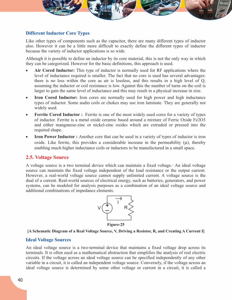
Different Inductor Core Types
Like other types of components such as the capacitor, there are many different types of inductoralso. However it can be a little more difficult to exactly define the different types of inductorbecause the variety of inductor applications is so wide.
Although it is possible to define an inductor by its core material, this is not the only way in whichthey can be categorized. However for the basic definitions, this approach is used.
·Air Cored Inductor: This type of inductor is normally used for RF applications where the
level of inductance required is smaller. The fact that no core is used has several advantages:there is no loss within the core as air is lossless, and this results in a high level of Q,assuming the inductor or coil resistance is low. Against this the number of turns on the coil islarger to gain the same level of inductance and this may result in a physical increase in size.
·Iron Cored Inductor: Iron cores are normally used for high power and high inductance
types of inductor. Some audio coils or chokes may use iron laminate. They are generally notwidely used.
·Ferrite Cored Inductor : Ferrite is one of the most widely used cores for a variety of types
of inductor. Ferrite is a metal oxide ceramic based around a mixture of Ferric Oxide Fe2O3and either manganese-zinc or nickel-zinc oxides which are extruded or pressed into therequired shape.
·Iron Power Inductor : Another core that can be used in a variety of types of inductor is iron
oxide. Like ferrite, this provides a considerable increase in the permeability (m), thereby
enabling much higher inductance coils or inductors to be manufactured in a small space.
2.5. Voltage Source
[1]A voltage source is a two terminal device which can maintain a fixed voltage. An ideal voltagesource can maintain the fixed voltage independent of the load resistance or the output current.However, a real-world voltage source cannot supply unlimited current. A voltage source is thedual of a current. Real-world sources of electrical energy, such as batteries, generators, and powersystems, can be modeled for analysis purposes as a combination of an ideal voltage source andadditional combinations of impedance elements.
®I
RV +–
Figure-25
[A Schematic Diagram of a Real Voltage Source, V, Driving a Resistor, R, and Creating A Current I]
Ideal Voltage Sources
An ideal voltage source is a two-terminal device that maintains a fixed voltage drop across itsterminals. It is often used as a mathematical abstraction that simplifies the analysis of real electriccircuits. If the voltage across an ideal voltage source can be specified independently of any othervariable in a circuit, it is called an independent voltage source. Conversely, if the voltage across an ideal voltage source is determined by some other voltage or current in a circuit, it is called a
40

Figure 26 : Symbols used for Voltage Sources & Current Sources
dependent or controlled voltage source. A mathematical model of an amplifier will includedependent voltage sources whose magnitude is governed by some fixed relation to an input signal,for example, in the analysis of faults on electrical power systems, the whole network ofinterconnected sources and transmission lines can be usefully replaced by an ideal (AC) voltagesource and a single equivalent impedance.
Ideal Voltage Source
Controlled Voltage Source
Ideal Current Source
Controlled Current Source
+–
+–
The internal resistance of an ideal voltage source is zero; it is able to supply or absorb any amount ofcurrent. The current through an ideal voltage source is completely determined by the external circuit.When connected to an open circuit, there is zero current and thus zero power. When connected to aload resistance, the current through the source approaches infinity as the load resistance approacheszero (a short circuit). Thus, an ideal voltage source can supply unlimited power.
No real voltage source is ideal; all have a non-zero effective internal resistance, and none cansupply unlimited current. However, the internal resistance of a real voltage source is effectivelymodeled in linear circuit analysis by combining a non-zero resistance in series with an idealvoltage source (a Thévenin equivalent circuit).
I R V
+
–
®
Figure 27: An Ideal Current Source, I, Driving a Resistor, R, and Creating a Voltage V
Current Source
A current source is an electronic circuit that delivers or absorbs an electric current which isindependent of the voltage across it.
A current source is the dual of a voltage source. The term constant-current ‘sink’ is sometimesused for sources fed from a negative voltage supply. Figure 27 shows the schematic symbol for anideal current source, driving a resistor load. There are two types of current source: An independent current source (or sink) delivers a constant current. A dependent current source delivers a currentwhich is proportional to some other voltage or current in the circuit.
In circuit theory, an ideal current source is a circuit element where the current through it isindependent of the voltage across it. If the current through an ideal current source can be specifiedindependently of any other variable in a circuit, it is called an independent current source.Conversely, if the current through an ideal current source is determined by some other voltage or
41Basic Electronics
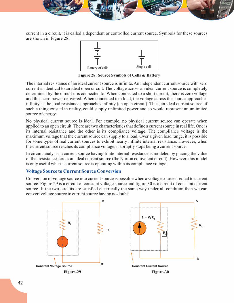
Figure 28: Source Symbols of Cells & Battery
Battery of cells Single cell
current in a circuit, it is called a dependent or controlled current source. Symbols for these sourcesare shown in Figure 28.
The internal resistance of an ideal current source is infinite. An independent current source with zerocurrent is identical to an ideal open circuit. The voltage across an ideal current source is completelydetermined by the circuit it is connected to. When connected to a short circuit, there is zero voltageand thus zero power delivered. When connected to a load, the voltage across the source approachesinfinity as the load resistance approaches infinity (an open circuit). Thus, an ideal current source, ifsuch a thing existed in reality, could supply unlimited power and so would represent an unlimitedsource of energy.
No physical current source is ideal. For example, no physical current source can operate whenapplied to an open circuit. There are two characteristics that define a current source in real life. One isits internal resistance and the other is its compliance voltage. The compliance voltage is themaximum voltage that the current source can supply to a load. Over a given load range, it is possiblefor some types of real current sources to exhibit nearly infinite internal resistance. However, whenthe current source reaches its compliance voltage, it abruptly stops being a current source.
In circuit analysis, a current source having finite internal resistance is modeled by placing the valueof that resistance across an ideal current source (the Norton equivalent circuit). However, this modelis only useful when a current source is operating within its compliance voltage.
Conversion of voltage source into current source is possible when a voltage source is equal to currentsource. Figure 29 is a circuit of constant voltage source and figure 30 is a circuit of constant currentsource. If the two circuits are satisfied electrically the same way under all condition then we canconvert voltage source to current source having no doubt.
Voltage Source to Current Source Conversion
Figure-29 Figure-30
Constant Voltage Source
A
B
RL
Ri
Constant Current Source
Ri
I = V/R i
A
B
RL
42

Condition 1: In figure 29 if the supply voltage is V and we remove the load resistance R then itL
becomes open circuit (Fig.-31) . In this situation the terminal voltage between point A and B is V.In figure 30 if we remove the load resistance R then all the current goes through the internalL
resistance R . (Fig. - 32) The terminal voltage between A and B is the same of internal resistancei
R voltage for open circuit. Voltage across the internal resistance R isV = I R . As open circuiti i i
voltage between two circuits is electrically equal and that is V. So the circuits are equivalent.
Condition 2: In figure 29 if we make the load R to short circuit then we get short circuit current,L
I = V/ R (Fig. - 33)short i
Figure-31 Figure-32
Constant Voltage Source
open circuit voltage
V
A
B
Ri
Constant Current Source
internal resistance voltage is open circuit
B
V
A
Ri
iI = V/R
Figure-33 Figure-34
Constant Voltage SourceConstant Current Source
B
B
Ri
A
A
Ri
I short
I short
short circuit current
short circuit
Similarly we get short circuit current from figure 30. If we short the path removing R loadL
resistance current I bypasses R in favour of short circuit (fig. - 34). This is clear indication thatshort i
the current I is electrically same between two circuits.short
43Basic Electronics

Figure-35
Here we get 20 V constant voltage source and 20Wresistance. We have to follow the steps for
conversion
(i) First place a short across A and B and find short circuit current I.Short circuit current, I = 20/20 = 1 AEquivalent current source has a magnitude of 1 A.
(ii) At AB terminal measure the resistance with load removed and 20V source replaced by itsinternal resistance. The voltage source has negligible resistance so that resistance at terminals
AB is R = 20W.
(iii) The equivalent current source is a source of 1 A in parallel with a resistance of 20Was shown
in figure 36.
In this way we can convert a constant voltage source to a constant current source. Following stepsshould be taken:
1. Make short circuit between two terminals A and B as we have done in above figure. Find theshort circuit current and let it be I.
2. Measure the resistance at the terminals with load removed and sources of e.m.f s replaced bytheir internal resistances if any. Let the resistance is R.
3. Then equivalent current source can be represented by a single current source of magnitude Iin parallel with resistance R.
Let’s see a problem. By solving this you will get clear concept if any trouble.
Conversion of Voltage Source to Current Source Problem
Problem: Convert the constant voltage source shown in figure 35 to constant current source.
+
I
20V
20W
B
A
Figure-36
I = 1A
20W
B
A
44

If we apply ohm’s law in this circuit we get the voltage which is same in previous circuit so figure35 and figure 36 are equivalent circuit and source conversion done properly. V = IR = 1×20 = 20V.
Conversion of Current Source to Voltage Source
Problem: Convert the current source to voltage source for figure 37.
Figure-37
I = 2A
20W
B
A
We have to do same inverse procedure.
From ohm’s law V = IR = 2 × 20 = 40V. So when we convert the current source to voltage sourceit will give 40V supply. Redrawing the circuit for voltage source we get as figure 38 equivalentcircuit.
Figure-38
+
I
40V
20W
B
A
In this way source conversion or source transformation can be possible.
Various cells and batteries (top-left to bottom-right): two AA, one D, one handheld ham radiobattery, two 9-volt (PP3), two AAA, one C, one camcorder battery, one cordless phone battery
2.6. Battery (Electricity)
Figure-39 Figure-40
Electronic Symbol
The Symbol for a Battery in a Circuit Diagram.
45Basic Electronics

An electric battery is a device consisting of two or more electrochemical that converts storedchemical energy into electrical energy. Each cell has a positive terminal, or anode, and a negativeterminal, or cathode. The terminal marked positive is at a higher electrical potential energy than isthe terminal marked negative. The terminal marked negative is the source of electrons that whenconnected to an external circuit will flow and deliver energy to an external device. When a batteryis connected to an external circuit, electrolytes are able to move as ions within, allowing thechemical reactions to be completed at the separate terminals and so deliver energy to the externalcircuit. It is the movement of those ions within the battery which allows current to flow out of thebattery to perform work. Although the term battery technically means a device with multiple cells,single cells are also popularly called batteries.
Primary (single-use or “disposable”) batteries are used once and discarded; the electrode materialsare irreversibly changed during discharge. Common examples are the alkaline battery used forflashlights and a multitude of portable devices. Secondary (rechargeable batteries) can bedischarged and recharged multiple times; the original composition of the electrodes can berestored by reverse current. Examples include the lead-acid batteries used in vehicles and lithium-ion batteries used for portable electronics.
Batteries come in many shapes and sizes, from miniature cells used to power hearing aids andwrist watches to battery banks of the size of rooms that provide standby power for exchanges andcomputer data centers.
Batteries have much lower specific energy (energy per unit mass) than common fuels such asgasoline. This is somewhat offset by the higher efficiency of electric motors in producingmechanical work, compared to combustion engines.
A voltaic cell for demonstration purpose is shown in fig. 41. In this example the two half-cells arelinked by a bridge separator that permits the transfer of ions.
Principle of Operation
Figure-41
Batteries convert chemical energy directly to electrical energy. A battery consists of some numberof voltaic cells. Each cell consists of two half-cells connected in series by a conductive electrolytecontaining anions and cations. One half-cell includes electrolyte and the negative electrode, theelectrode to which anions (negatively charged ions) migrate; the other half-cell includeselectrolyte and the positive electrode to which cations (positively charged ions) migrate. Redoxreactions power the battery. Cations are reduced (electrons are added) at the cathode during
46
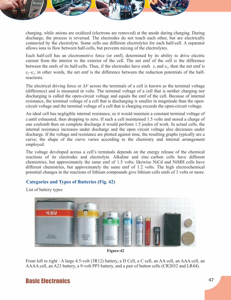
charging, while anions are oxidized (electrons are removed) at the anode during charging. Duringdischarge, the process is reversed. The electrodes do not touch each other, but are electricallyconnected by the electrolyte. Some cells use different electrolytes for each half-cell. A separatorallows ions to flow between half-cells, but prevents mixing of the electrolytes.
Each half-cell has an electromotive force (or emf), determined by its ability to drive electriccurrent from the interior to the exterior of the cell. The net emf of the cell is the difference
between the emfs of its half-cells. Thus, if the electrodes have emfs eand e, then the net emf is1 2
e–e; in other words, the net emf is the difference between the reduction potentials of the half-2 1
reactions.
The electrical driving force or DV across the terminals of a cell is known as the terminal voltage(difference) and is measured in volts. The terminal voltage of a cell that is neither charging nordischarging is called the open-circuit voltage and equals the emf of the cell. Because of internalresistance, the terminal voltage of a cell that is discharging is smaller in magnitude than the open-circuit voltage and the terminal voltage of a cell that is charging exceeds the open-circuit voltage.
An ideal cell has negligible internal resistance, so it would maintain a constant terminal voltage of
euntil exhausted, then dropping to zero. If such a cell maintained 1.5 volts and stored a charge ofone coulomb then on complete discharge it would perform 1.5 joules of work. In actual cells, theinternal resistance increases under discharge and the open circuit voltage also decreases underdischarge. If the voltage and resistance are plotted against time, the resulting graphs typically are a curve; the shape of the curve varies according to the chemistry and internal arrangementemployed.
The voltage developed across a cell’s terminals depends on the energy release of the chemicalreactions of its electrodes and electrolyte. Alkaline and zinc–carbon cells have differentchemistries, but approximately the same emf of 1.5 volts; likewise NiCd and NiMH cells havedifferent chemistries, but approximately the same emf of 1.2 volts. The high electrochemicalpotential changes in the reactions of lithium compounds give lithium cells emfs of 3 volts or more.
Categories and Types of Batteries (Fig. 42)
List of battery types
Figure-42
From left to right : A large 4.5-volt (3R12) battery, a D Cell, a C cell, an AA cell, an AAA cell, anAAAA cell, an A23 battery, a 9-volt PP3 battery, and a pair of button cells (CR2032 and LR44).
47Basic Electronics
Batteries are classified into primary and secondary forms:
·Primary batteries irreversibly transform chemical energy to electrical energy. When the
supply of reactants is exhausted, energy cannot be readily restored to the battery.
·Secondary batteries can be recharged; that is, they can have their chemical reactions reversed
by supplying electrical energy to the cell, approximately restoring their original composition.
Some types of primary batteries used, for example, for telegraph circuits, were restored tooperation by replacing the electrodes. Secondary batteries are not indefinitely rechargeable due todissipation of the active materials, loss of electrolyte and internal corrosion.
Primary Cell
Primary batteries, or primary cells, can produce current immediately on assembly. These are mostcommonly used in portable devices that have low current drain, are used only intermittently, orare used well away from an alternative power source, such as in alarm and communicationcircuits where other electric power is only intermittently available. Disposable primary cellscannot be reliably recharged, since the chemical reactions are not easily reversible and activematerials may not return to their original forms. Battery manufacturers recommend againstattempting to recharge primary cells.
In general, these have higher energy densities than rechargeable batteries, but disposable batteriesdo not fare well under high-drain applications with loads under 75 ohms (75 mA).
Common types of disposable batteries include zinc–carbon batteries and alkaline.
Main Article: Rechargeable Battery
Secondary batteries, also known as secondary cells, or rechargeable batteries, must be chargedbefore first use; they are usually assembled with active materials in the discharged state.Rechargeable batteries are recharged by applying electric current, which reverses the chemicalreactions that occur during discharge/use. Devices to supply the appropriate current are calledchargers.
The oldest form of rechargeable battery is the lead–acid battery. This technology contains liquidelectrolyte in an unsealed container, requiring that the battery be kept upright and the area be wellventilated to ensure safe dispersal of the hydrogen gas it produces during overcharging. Thelead–acid battery is relatively heavy for the amount of electrical energy it can supply. Its lowmanufacturing cost and its high surge current levels make it common where its capacity (overapproximately 10 Ah) is more important than weight and handling issues. A common applicationis the modern car battery, which can, in general, deliver a peak current of 450 amperes.
The sealed valve regulated lead–acid battery (VRLA battery) is popular in the automotive industryas a replacement for the lead–acid wet cell. The VRLA battery uses an immobilized sulfuric acidelectrolyte, reducing the chance of leakage and extending shelf life. VRLA batteries immobilizethe electrolyte. The two types are:
·Gel batteries (or “gel cell”) use a semi-solid electrolyte.
·Absorbed Glass Mat (AGM) batteries absorb the electrolyte in special fiberglass matting.
2.6.1. Primary Batteries
2.6.2. Secondary Batteries
48
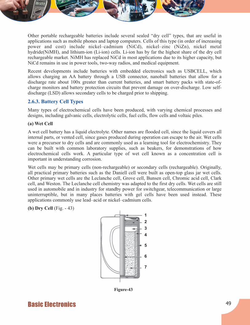
Other portable rechargeable batteries include several sealed “dry cell” types, that are useful inapplications such as mobile phones and laptop computers. Cells of this type (in order of increasing power and cost) include nickel–cadmium (NiCd), nickel–zinc (NiZn), nickel metalhydride(NiMH), and lithium-ion (Li-ion) cells. Li-ion has by far the highest share of the dry cellrechargeable market. NiMH has replaced NiCd in most applications due to its higher capacity, butNiCd remains in use in power tools, two-way radios, and medical equipment.
Recent developments include batteries with embedded electronics such as USBCELL, whichallows charging an AA battery through a USB connector, nanoball batteries that allow for adischarge rate about 100x greater than current batteries, and smart battery packs with state-of-charge monitors and battery protection circuits that prevent damage on over-discharge. Low self-discharge (LSD) allows secondary cells to be charged prior to shipping.
Many types of electrochemical cells have been produced, with varying chemical processes anddesigns, including galvanic cells, electrolytic cells, fuel cells, flow cells and voltaic piles.
(a) Wet Cell
A wet cell battery has a liquid electrolyte. Other names are flooded cell, since the liquid covers allinternal parts, or vented cell, since gases produced during operation can escape to the air. Wet cells were a precursor to dry cells and are commonly used as a learning tool for electrochemistry. Theycan be built with common laboratory supplies, such as beakers, for demonstrations of howelectrochemical cells work. A particular type of wet cell known as a concentration cell isimportant in understanding corrosion.
Wet cells may be primary cells (non-rechargeable) or secondary cells (rechargeable). Originally,all practical primary batteries such as the Daniell cell were built as open-top glass jar wet cells.Other primary wet cells are the Leclanche cell, Grove cell, Bunsen cell, Chromic acid cell, Clarkcell, and Weston. The Leclanche cell chemistry was adapted to the first dry cells. Wet cells are still used in automobile and in industry for standby power for switchgear, telecommunication or largeuninterruptible, but in many places batteries with gel cells have been used instead. Theseapplications commonly use lead–acid or nickel–cadmium cells.
(b) Dry Cell (Fig. - 43)
2.6.3. Battery Cell Types
Figure-43
1
2
3
4
5
6
7
49Basic Electronics
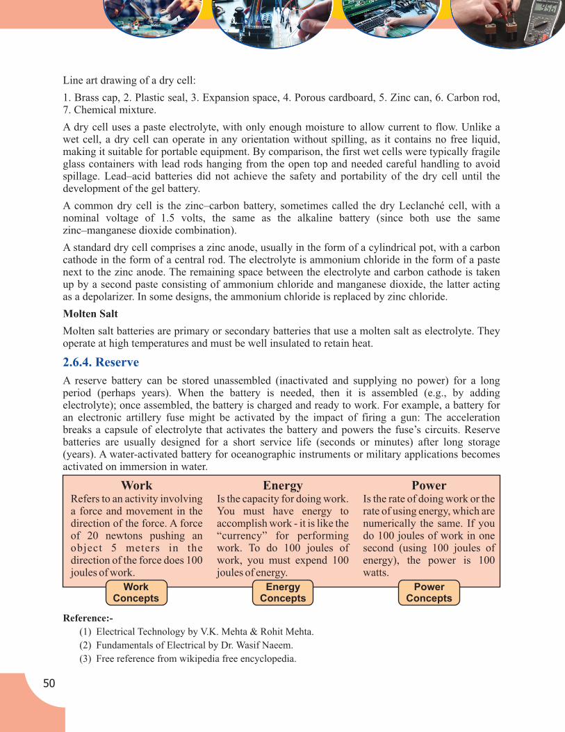
Line art drawing of a dry cell:
1. Brass cap, 2. Plastic seal, 3. Expansion space, 4. Porous cardboard, 5. Zinc can, 6. Carbon rod,7. Chemical mixture.
A dry cell uses a paste electrolyte, with only enough moisture to allow current to flow. Unlike awet cell, a dry cell can operate in any orientation without spilling, as it contains no free liquid,making it suitable for portable equipment. By comparison, the first wet cells were typically fragileglass containers with lead rods hanging from the open top and needed careful handling to avoidspillage. Lead–acid batteries did not achieve the safety and portability of the dry cell until thedevelopment of the gel battery.
A common dry cell is the zinc–carbon battery, sometimes called the dry Leclanché cell, with anominal voltage of 1.5 volts, the same as the alkaline battery (since both use the samezinc–manganese dioxide combination).
A standard dry cell comprises a zinc anode, usually in the form of a cylindrical pot, with a carboncathode in the form of a central rod. The electrolyte is ammonium chloride in the form of a pastenext to the zinc anode. The remaining space between the electrolyte and carbon cathode is takenup by a second paste consisting of ammonium chloride and manganese dioxide, the latter actingas a depolarizer. In some designs, the ammonium chloride is replaced by zinc chloride.
Molten Salt
Molten salt batteries are primary or secondary batteries that use a molten salt as electrolyte. Theyoperate at high temperatures and must be well insulated to retain heat.
A reserve battery can be stored unassembled (inactivated and supplying no power) for a longperiod (perhaps years). When the battery is needed, then it is assembled (e.g., by addingelectrolyte); once assembled, the battery is charged and ready to work. For example, a battery foran electronic artillery fuse might be activated by the impact of firing a gun: The accelerationbreaks a capsule of electrolyte that activates the battery and powers the fuse’s circuits. Reservebatteries are usually designed for a short service life (seconds or minutes) after long storage(years). A water-activated battery for oceanographic instruments or military applications becomesactivated on immersion in water.
2.6.4. Reserve
WorkRefers to an activity involvinga force and movement in thedirection of the force. A forceof 20 newtons pushing anobject 5 meters in thedirection of the force does 100joules of work.
EnergyIs the capacity for doing work.You must have energy toaccomplish work - it is like the“currency” for performingwork. To do 100 joules ofwork, you must expend 100joules of energy.
PowerIs the rate of doing work or therate of using energy, which arenumerically the same. If youdo 100 joules of work in onesecond (using 100 joules ofenergy), the power is 100watts.
Reference:-
(1) Electrical Technology by V.K. Mehta & Rohit Mehta.
(2) Fundamentals of Electrical by Dr. Wasif Naeem.
(3) Free reference from wikipedia free encyclopedia.
WorkConcepts
EnergyConcepts
PowerConcepts
50

Exercise
1. Short questions:
(a) Define current.
(b) Define voltage.
(c) Define work, energy and power.
(d) One coulomb of charge is equal to.
(e) What are the effect of temperature on conductivity on a material?
2. Write short note on:
(a) How can you relate voltage and current in physical terms? Explain.
(b) What are the different parameters at which resistance in a conductor depends?
(c) What is unit of current, voltage, resistance, capacitance, inductance, energy, work &power?
(d) Awire is carrying current. Is it charged?
3. Explain the following:
(a) What is ohm’s law? Write the mathematical expression to justify your answer? Draw its V-lCharacteristics.
(b) What is voltage and current sources? How will you convert it from one another?
(c) What are cells and batteries? Explain their types.
4. Long questions:
(a) Why do conductors have positive temperature co- efficient of resistance?
(b) Why does a positive charge attracts a negative charge?
51Basic Electronics

Overview
Knowledge and Skill Outcomes
This unit starts with the understanding of fundamentals of semiconductors materials and theirproperties etc. Further different types of energy band structure of Insulators, metals andsemiconductors has been discussed along with the symbols and graphical representation . N-typeand P-type semiconductor with their associated concepts have been presented. A detailed study ofsemiconductor diode and others types of diode with their characteristics has been discussed,proper explanation of Diode as a Rectifier, Voltage multipliers, Zener diode as Regulator isexplained in this chapter, also the chapter contains special information -(Introduction to Filters,Clippers, Clampers). Finally whatever discussed and presented in various chapters has beensummarized as a quick review.
i) Understanding of fundamentals of electrical Semiconductor materials, Energy bandstructure of solids.
ii) Understanding of Mobility of charges, Effects of temperature on conductivity ofsemiconductor etc.
iii) Knowledge of various types of semiconductor diodes and their characteristics.
iv) Study of Diode as a rectifier, Half wave and full wave rectification, Voltage multipliers,Zener diode Regulator.
v) Special information on- (lntroduction to Filters, Clippers, Clampers).
Basics of Semiconductor
UNIT 3
3.0 Unit Overview and Description
?Overview
?Knowledge and Skill Outcomes
?Assessment Plan
?Learning Outcomes
?Resource Material
?Topics Covered
Semiconductor materials, Energy band structure of Insulators, Metals and Semiconductors,Energy gap, Field and Photo-electric emission, Intrinsic & Extrinsic semiconductor, N-type andP-type semiconductor, Drift current, Diffusion current and Total current, Mobility of charges,Effects of temperature on conductivity of semiconductor, PN junction diode, Depletion layer,Potential barrier, Forward & reverse bias, V-l Characteristic, Effects of temperature, Resistancelevels, Breakdown in Junction diode, Zener diode, Photo diode, LED, Types and applications ofdiode, Diode as a rectifier, Half wave and full wave rectification, Voltage multipliers, Zenerdiode Regulator.
Special information -(Introduction to Filters, Clippers, Clampers).
52

Assessment Plan: (For the Teachers)
structure of Insulators, Metals andSemiconductors, Energy gap, Field andPhoto-electric emission.
Semiconductor materials, Energy band
Unit-3 Topic AssessmentMethod
TimePlan
Remarks
Exercise:Question & Answer
Two Hours
N-type and P-type semiconductor,Drift current, Diffusion currentand Total current, Mobility of charges,Effects of temperature on Conductivityof semiconductor.
Intrinsic & Extrinsic semiconductor, Exercise:Question & Answer
Two Hours
potential barrier, Forward & Reversebias, V-l Characteristic, Effects oftemperature, Resistance levels,Breakdown in Junction diode, Zenerdiode, Photo diode, LED, Types andapplications of diode.
PN junction diode, depletion layer, Exercise:Question & Answer
Two Hours
wave rectification, Voltage multipliers,Zener diode Regulator.
Diode as a rectifier, Half wave and full Exercise:Question & Answer
Two Hours
Filters, Clippers, Clampers).Special information on- (Introduction to Exercise:
Question & Answer
Two Hours
Learning Outcomes
Unit-3 Outcomes
structure of Insulators, Metals andSemiconductors, Energy gap, Field andPhoto-electric emission.
Semiconductor materials, Energy band
and P-type semiconductor, Drift current,Diffusion current and Total current,Mobility of charges, Effects of temperatureon conductivity of semiconductor.
Intrinsic & Extrinsic semiconductor, N-type
(i) Brief knowledge of differentsemiconductor materials and theirenergy bands.
(ii) Principle knowledge of photoelectricemission.
(i) Kind of semiconductors andexplanation of associate terms.
(ii) Dependability of conductivity insemiconductor.
Basic of Semiconductor
53Basic Electronics
Unit-3 Outcomes
Potential barrier, Forward & Reverse bias,V-l Characteristic, Effects of temperature,Resistance levels, Breakdown in Junctiondiode, Zener diode, Photo diode, LED,Types and applications of diode.
PN junction diode, Depletion layer,
rectification, Voltage multipliers, Zenerdiode Regulator.
Diode as rectifier, Half wave and full wave
(i) Knowledge of semiconductordiodes, there V-I characteristic andassociated important.
(ii) Applications of diodes.
(i) Knowledge of rectification andregulation of electrical signs usingsemiconductor diodes.
Basic of Semiconductor
Filters, Clippers, Clampers).Special information on - (Introduction to (i) Overview of filters, clippers clampers
etc.
3.1. Semiconductor Materials
3.2 Energy Band
In general, semiconductors are special class of elements having a conductivity between thatof a good conductor and that of an insulator
Semiconductor materials fall into one of two classes: Single crystal and Compound. Single crystalsemiconductor such as germanium (GE) and silicon (Si) have a repetitive crystal structure,whereas compound semiconductors such as gallium arsenide (GaAs), cadmium sulphide (CdS),gallium nitride (GaN), and gallium arsenide phosphide (GaAsP) are constructed of two or moresemiconductor materials of different atomic structure.
The three semiconductors used most frequently in the construction of electronic device areGe, Si, and GaAs.
The range of energies possessed by electrons of the same orbit in a solid is known as energyband.
In case of a single isolated atom, the electrons revolving in any orbit possess a definite energy.However in a solid an atom is greatly influenced by the closely packed neighbouring atoms.Because of this the electrons in the same orbit have a range of energies rather than a single energy.This is known as energy band.
Fig 1 shows how energy levels are changed into energy bands. All the electrons moving in thefirst orbit have slightly different energy levels because no two electrons see exactly the samecharge environment. As there are billions of first orbit electrons in the solid with slightly differentenergy levels which is called energy bands.
Although there are number of energy bands in solids, but we are more concerned with thefollowing:
Important Energy Bands in Solids
54

(i) Valence Band: The electrons in the outermost orbit of an atom are known as valenceelectrons. Under normal condition of an atom, valence band contains the electrons ofhighest energy. This band may be filled completely or partially.
The energy band which possesses the valence electrons is called valence band.
(ii) Conduction Band: In some of the materials (eg metals), the valence electrons are looselyattached to the nucleus and can be detached very easily. These electrons are known as freeelectrons and are responsible for the conduction of current. For this reason these electronsare known as conduction electrons.
The energy band which possesses the conduction electrons is called conduction band.
(iii) Forbidden Energy Gap: The energy gap between the valence band and conduction band isknown as forbidden energy gap.
a) Structure of Insulators
The substance (like, wood, glass, mica etc.) which do not allow the passage of current throughthem are known as insulators. The valence band of these substance is full, whereas the conductionband is completely empty. Moreover the forbidden energy gap between valence band andconduction band is large (15ev nearly). Therefore a large amount of energy i.e a very high electricfield is required to push the valence electrons to the conduction band. This is the reason why suchmaterials under ordinary condition do not conduct at all and are designed as insulators.
b) Metals
The substance (like copper, aluminium, silver etc.) which allow the passage of current throughthem are known as conductors. The valence band of these substance overlap the conduction bandas shown in fig. 3.1. Due to this overlapping, a large number of free electrons are available forconduction. This the reason, why a slight potential difference applied across such substancecauses a heavy flow of current through them.
3.3.Material Structure
Figure-1
Conduction band
Conduction band
Conduction states
Valence band
Valence band
Valence states
Insulator Semiconductor Metal (Conductor)
EC
EC
EC
EV
EV
EgEg
55Basic Electronics

c) Semiconductors
The substance (like carbon, silicon, germanium etc.) whose electrical conductivity lies in betweenthe conductor and insulators are known as semiconductors. Although the valence band of thesesubstances is almost filled and conduction band is almost empty as in case of insulators. But theforbidden energy gap between valence band and conduction band is very small (nearly 1 ev).Therefore comparatively a smaller electric field (much smaller than insulator but much greaterthan conductors) is required to push the valence electrons to the conduction band. This is thereason why such materials under ordinary conditions do not conduct current and behave as aninsulators.
However even at room temperature some heat energy is imparted to the valence electrons and afew of them cross over to the conduction band imparting minor conductivity to thesemiconductors. As the temperature is increased more valence electrons cross over to theconduction band and the conductivity of the material increases. Thus these materials havenegative temperature coefficient of resistance.
Fig. 2 Shows the energy gap of conductor, insulators and semiconductors.
3.4. Energy Gap
Figure-2
Energy of electrons
Conduction Band
Valence Band Valence Band Valence Band
Conduction Band
Conduction BandFermilevel
.........................
Large energygap betweenvalence andconduction bands
a. Insulator b. Semiconductor c. Conductor
3.5. Field and Photo-Electric Emission
The emission of electrons from a metallic surface by the application of light energy is calledphotoelectric emission.
Figure-3
Galvanometer
ElectronsLight
A
+
56

When a beam of light strikes at the surface of certain metals of slow work function such as potassium,sodium and cesium, the electrons may be emitted from their surface if the quantum of energy carriedby the photons is equal to or greater than the work function of the metal. Such a phenomenon istermed as photo-electric emission and emitted electrons are known as photo electrons.
The amount of photoelectric emission depends upon the intensity of light falling upon the emitterand the frequency of radiation. The amount of energy of a photon is given by the relation:
E=hf
Where, E = the energy of photon in joules
h = plank's constant in joules second = 6.625 *10^-34
f = frequency of photons in HZ
(i) Intrinsic Semiconductor
An extremely pure semiconductor is called intrinsic semiconductor.
On the basis of energy band phenomenon, an intrinsic semiconductor at absolute zero temperatureis shown in fig. 2 its valence band is completely filled and the conduction band is completely empty.
When some heat energy is supplied to it (i.e its temperature is raised say to room temperature) someof the valence electrons are lifted to conduction band are free to move at random. The holes createdin the crystal also move at random in the crystal. The behaviour of semiconductor shows that theyhave negative temperature co-efficient of resistance i.e the resistivity decreases or conductivityincreases with the rise in temperature.
(ii) Extrinsic Semiconductor
Although an intrinsic semiconductor is capable to conduct a little current even at room temperaturebut as it is, it is not useful for the preparation of various electronic devices. To make it conductive asmall amount of suitable impurity is added. It is then called extrinsic (impure) semiconductor.
Doping : The process by which an impurity is added to a semiconductor is known as doping.
The amount and type of such impurities have to be closely controlled during the preparation ofextrinsic semiconductor. Generally one impurity atom is added to 10^8 atoms of a semiconductor.
Thus, a semiconductor to which an impurity at controlled rate is added to make it conductive isknown as an extrinsic semiconductor.
Depending upon the type of impurity added extrinsic semiconductor may be classified as :
(i) n- type semiconductor
(ii) p-type semiconductor
3.6. Intrinsic & Extrinsic Semiconductor
Figure-4
N (Donor)D N (Acceptor)A
Neutral p-regionNeutral n-region
E
+ –
57Basic Electronics

(i) n- type semiconductor
When a small amount of pentavalent impurity is added to a pure semiconductor providing a largenumber of free electrons in it, the extrinsic semiconductor thus formed is known as n-typesemiconductor.
The addition of pentavalent impurities such as arsenic (atomic number 33) and antimony (atomicnumber 51) provide a large number of free electrons in the semiconductor crystal. Such impuritieswhich produce n-type semiconductor are known as donar impurities because each atom of themdonate one free electron to the semiconductor crystal as explained below:
When a small amount of pentavalent impurity like arsenic (At no 33 : 2,8,18,5) having fivevalence electrons is added to germanium crystal each atom of the impurity fits in the germaniumcrystal in such a way that its four valence electrons form covalent bonds with four germaniumatoms as shown. Whereas the fifth electron of the impurity (arsenic) atom finds no place incovalent bonds and is thus free. Hence each arsenic atom provides one free electron in thegermanium crystal. Since, an extremely small amount of arsenic impurity has a large number ofatoms, therefore it provides millions of free electrons for conduction.
(ii) p- type semiconductors
When a small amount of trivalent impurity is added to a pure semiconductor providing a largenumber of free holes in it, the extrinsic semiconductor thus formed is known as p-typesemiconductor.
The addition of trivalent impurities such as gallium (atomic number 31) and indium (atomicnumber 49) provide a large number of free holes in the semiconductor crystal. Such impuritieswhich produce p-type semiconductor are known as acceptor impurities because each atom of themcreate one hole which can accept one electron from the semiconductor crystal as explained below.
When a small amount of trivalent impurity like gallium (At no 31:2,8,18,3) having three valenceelectrons is added to germanium crystal each atom of the impurity fits in the germanium crystalin such a way that its three valence electrons form covalent bonds with four germanium atoms, inthe fourth covalent bond, only germanium atom contributes one valence electron, while galliumatom has no valence electron to contribute, as all its three valence electron are already engaged inthe covalent bonds. Hence the covalent bond is incomplete having one electron short. The amountof gallium impurity has a large number of atoms, therefore it provides millions of holes in thesemiconductor.
The flow of current in the semiconductor constituted by the drift electrons available in theconduction band and holes available in the valence band, which are formed due to external (heat)energy supplied to them, is known as drift current.
When the two pieces are joined together and suitably treated, they form a pn junction. Themoment they form a pn junction, some of the conduction electrons from n- type material diffuseover to the p-type material and undergo electrons holes recombination with the holes available inthe valence band. Simultaneously holes from p-type material diffuse over to the n-type materialand undergo hole-electron combination with the electron available in the conduction band. Thisprocess is called diffusion.
3.7. Drift Current
3.8. Diffusion Current
58

Thus the current which obtained while having diffusion is called diffusion current.
(a) Total Current
It is possible that a potential gradient and a concentration gradient may exist within
semiconductor. In such a case the total current is the sum of drift current due to potential gradient
and the diffusion current due to charge carrier concentration gradient.
(b) Mobility of Charges
The mobility of charge carriers (elctrons and holes) varies as T^-m over a temperature range of
100 and 400 k. for silicon m = 2.5 for electrons amd 2.7 for holes. For germanium m = 1.66 for
electrons and 2.33 for holes.
The carriers currents are also due to concentration gradients in the doped material which leads to
diffusion of carriers from high concentration region to low concentration region.
The change in temperature changes the electrical conductivity of semiconductor appreciably. Let
us see how conductivity changes with the change in temperature.
3.9. Effects of Temperature on Conductivity of Semiconductor
Figure-5
Egap
ConductionBand
ConductionBand
ConductionBand
At absolutezero, OK
Some electrons haveenergy above the Fermi
level.
HighTemperature
f(E) f(E) f(E)Valence Band Valence Band Valence Band
1.0
1.0
1.0
FermiLevel
No electrons can be above the valenceband at OK, since none have energyabove the Fermi level and there areno available energy states in the band gap.
At high temperatures, some electronscan reach the conduction band andcontribute to electric current.
(i) At absolute zero
At absolute zero temperature all the electrons of semiconductor are held tightly by their atom. Theinner orbit electrons are bound to the nucleus whereas the valence electrons are bound by theforces of covalent bonds. Therefore at this temperature no free electrons is available insemiconductor. Hence the semiconductor crystal behaves like a perfect insulator.
59Basic Electronics
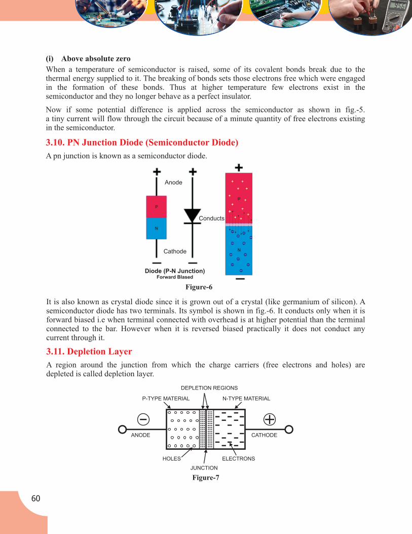
(i) Above absolute zero
When a temperature of semiconductor is raised, some of its covalent bonds break due to thethermal energy supplied to it. The breaking of bonds sets those electrons free which were engagedin the formation of these bonds. Thus at higher temperature few electrons exist in thesemiconductor and they no longer behave as a perfect insulator.
Now if some potential difference is applied across the semiconductor as shown in fig.-5.a tiny current will flow through the circuit because of a minute quantity of free electrons existingin the semiconductor.
A pn junction is known as a semiconductor diode.
3.10. PN Junction Diode (Semiconductor Diode)
Figure-6
Anode
Conducts
Cathode
Diode (P-N Junction)Forward Blased
It is also known as crystal diode since it is grown out of a crystal (like germanium of silicon). Asemiconductor diode has two terminals. Its symbol is shown in fig.-6. It conducts only when it isforward biased i.e when terminal connected with overhead is at higher potential than the terminalconnected to the bar. However when it is reversed biased practically it does not conduct anycurrent through it.
A region around the junction from which the charge carriers (free electrons and holes) aredepleted is called depletion layer.
3.11. Depletion Layer
Figure-7
DEPLETION REGIONS
P-TYPE MATERIAL N-TYPE MATERIAL
CATHODEANODE
HOLES ELECTRONS
JUNCTION
60
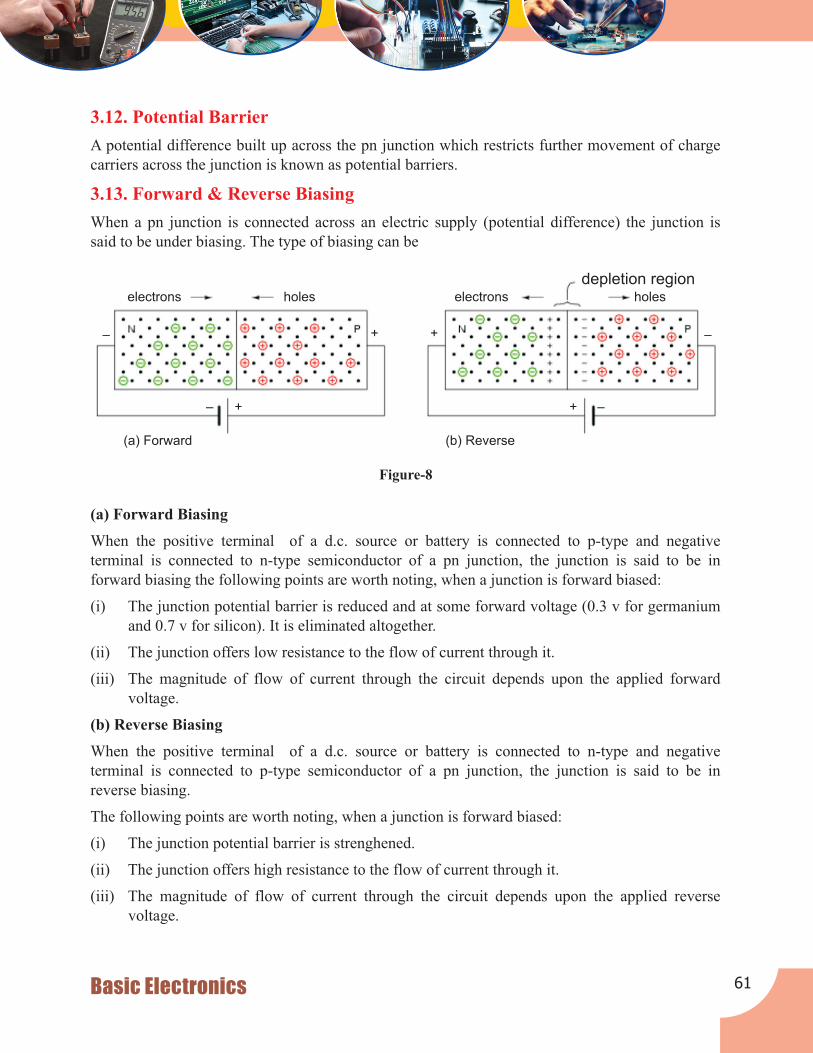
3.12. Potential Barrier
3.13. Forward & Reverse Biasing
A potential difference built up across the pn junction which restricts further movement of charge
carriers across the junction is known as potential barriers.
When a pn junction is connected across an electric supply (potential difference) the junction is
said to be under biasing. The type of biasing can be
(a) Forward Biasing
When the positive terminal of a d.c. source or battery is connected to p-type and negative
terminal is connected to n-type semiconductor of a pn junction, the junction is said to be in
forward biasing the following points are worth noting, when a junction is forward biased:
(i) The junction potential barrier is reduced and at some forward voltage (0.3 v for germanium
and 0.7 v for silicon). It is eliminated altogether.
(ii) The junction offers low resistance to the flow of current through it.
(iii) The magnitude of flow of current through the circuit depends upon the applied forward
voltage.
(b) Reverse Biasing
When the positive terminal of a d.c. source or battery is connected to n-type and negative
terminal is connected to p-type semiconductor of a pn junction, the junction is said to be in
reverse biasing.
The following points are worth noting, when a junction is forward biased:
(i) The junction potential barrier is strenghened.
(ii) The junction offers high resistance to the flow of current through it.
(iii) The magnitude of flow of current through the circuit depends upon the applied reverse
voltage.
Figure-8
electrons holes holeselectrons
depletion region
(a) Forward (b) Reverse
+ +
+ –– +
––
61Basic Electronics

3.14. V-I Characteristic of Semiconductor
The volt ampere (v-i) characteristics of a pn junction is just a curve between voltage across thejunction and the circuit current. To draw the curve the circuit is arranged. In the circuit it isimportant to note that a resistor R is connected in series with the pn junction which limits theforward diode current from exceeding the permitted value. The characteristics are studied underthree heads viz. zero external voltage, forward biasing and reverse biasing.
(i) Zero External Voltage: When no external voltage is applied i.e circuit is open at key k. no
current flow through the circuit. It is indicated by points 0 on the graph.
(ii) Forward Biasing: When key k is closed and double pole double throw switch is thrown to
position 1. the pn junction is forward biasd as p-type semiconductor is connected to the positive
terminal and n-type to the negative terminal of the supply. Now when supply voltage is increased
by changing the variable resistor R the circuit current increases very slowly and the curve is non
linear. The slow rise in current in this region is because the external applied voltage is used to
overcome the potential barrier (0.3V for Ge and 0.7V for Si) of the pn junction.
However once the potential barrier is eliminated and external voltage is increased further the pn
junction behaves like an ordinary conductor and the circuit current rises very sharply. At this
instant the circuit current is limited by the series resistance R and a small value of the junction
forward resistance R. The curve is almost linear. If the current rises more than the rated value of
the diode the diode may change.
Figure - 9
Symbol
Cathode Anodeor
(K) (A)
ForwardCurrent
ForwardBias
Region
Reverse Bias
Forward Bias
VF
0.3 - 0.7v
–VZ
–VR
Iz(min)
Iz(max)
– IR
ConstantZener Voltage
ReverseCurrent
+VF
+IF
“Zener” BreakdownRegion
62

(iii) Reverse Biasing: When the double pole double throw switch is thrown to position 2, the pn
junction is reverse biased as p- type semiconductor is connected to the negative terminal and n-
type to the positive terminal of the supply. Under this condition the potential barrier at the
junction is increased. Therefore the junction resistance becomes very high and practically no
current flows through the circuit. However in actual practice a very small current flows in the
circuit as shown, this current is called reverse current and is due to minority carriers available at
room temperature in the two types of semiconductor. The reverse bias appears as a forward biased
for these undesirable minority carriers and thus they constitue a minor current in reverse direction.
The reverse current increases slightly with the increase in reverse bias supply voltage.
The reverse voltage at which pn junction breaks in known as breakdown voltage.
An actual diode offers a very small resistance when forward biased and is called a forwardresistance whereas it offers a very high resistance when reverse biased and is called a reverseresistance.
3.15. Resistance Level
3.16. Breakdown in Junction Diode
The breakdown of the pn junction can be of two types, these are
(i) Avalanche Breakdown
For thicker junctions the breakdown mechanism is by the process of avalanche breakdown. In thismechanism when the electric field existing in the depletion layer is sufficiently high, the velocityof the carriers (minority carriers) crossing the depletion layer increases. These carriers collide with the crystal atoms. Some collisions are so violent that electrons are knocked off the crystal atoms,thus creating electron hole pairs as the pair of electron hole is created in the midst of the highfield, they quickly separate and attain high velocities to cause further pair generation throughmore collisions. This is cumulative process and as we approach the breakdown voltage, the fieldbecomes so large that the chain of collisions can give rise to an almost infinite current with veryslight additional increase in voltage. The process is known as avalanche breakdown. Once thisbreakdown occurs, the junction cannot regain its original position. Thus the diode is said to beburnt off.
Figure-10 : Determining the DC Resistance of a Diode at a Particular Operating Point
V (V)D
I (mA)D
ID
VD
0
63Basic Electronics
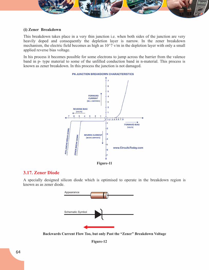
(i) Zener Breakdown
This breakdown takes place in a very thin junction i.e. when both sides of the junction are veryheavily doped and consequently the depletion layer is narrow. In the zener breakdownmechanism, the electric field becomes as high as 10^7 v/m in the depletion layer with only a small applied reverse bias voltage.
In his process it becomes possible for some electrons to jump across the barrier from the valenceband in p- type material to some of the unfilled conduction band in n-material. This process isknown as zener breakdown. In this process the junction is not damaged.
Figure-11
3.17. Zener Diode
A specially designed silicon diode which is optimised to operate in the breakdown region isknown as as zener diode.
Figure-12
Backwards Current Flow Too, but only Past the “Zener” Breakdown Voltage
Appearance
Schematic Symbol
64

3.17.1. Characteristics of Zener Diode
3.17.2. Application
(i) Its characteristics are similar to an ordinary diode with the exception that it has a sharp (ordistinct) breakdown voltage called zener voltage v .z
(ii) It can be operated in any of the three region i.e. forward, leakage or breakdown. But usuallyit is operated in the breakdown region as shown in fig.11.
(iii) The voltage is almost constant (v ) over the operating region.z
(iv) Usually, the value of v at particular test current I is specified in the data sheet.z zr
(v) During operation it will not burn as long as the external circuit limits the current flowingthrough it below the burn out value i.e I (the maximum rated zener current). zm
(i) Meter Protection
(ii) Voltage Regulator
(iii) Wave Shaping Circuit
3.18. Photo Diode
Figure-13
When a diode is reverse biased a minute current flows in the diode due to minority carriers. These carriers exist because of thermal energy which dislodge the valence electrons from their orbitsproducing free electrons and holes in the process.
When light energy falls on a pn junction, it also imparts energy to dislodge valence electron. Inother words the amount of light striking on the junction can control the reverse current in a diode.
A diode that is optimised for its sensitivity to light is known as photo diode.
(a)(c)
(b)
+–
VR
Reversecurrent
800
600
400
200Re
ve
rse
cu
rre
nt(m
A)
LightIntensity Illuminance
2lumens/m(lux)2000 4000 6000
–5 –4 –3 –2 –1 0 +.5
0
1.0
1.5
2.0
2.5
100
200
300
400
Dark current
Illuminance
in lux ́1000
Re
ve
rse
cu
rren
tin
mic
roa
mp
s
VR VF
I
65Basic Electronics

3.19. LED (Light Emitting Diode)
Figure-14
(a)
(b)
(c)
When a diode is forward biased the potential barrier is lowered. The conduction band free electronsfrom n- region cross the barrier and enter the p-region, as these electrons enter the p- region they fallinto the holes lying in the valence band. Hence they fall from a higher energy level to a lower energylevel in the process they radiate energy.
The LED are different. These are made of gallium arsenide phosphide (GaAsP) and galliumphosphide (GaP). In LED the energy is radiated in the form of light and hence they glow.
A manufacturer can produce LED that radiate red, green, yellow, blue, orange light.
Application
Instrument display, panel indicators, digital watches, calculator etc.
The electrical power is generated transmitted and distributed as d.c. for economical reasons. As an alternating voltage is available at the mains. But most of the electronic circuit need d.c. voltage for their operation. Therefore the rectifier is the heart of power supply. The rectifier can be of two types:
(i) Half Wave Rectifier
(ii) Full Wave Rectifier
(i) Half Wave Rectifier
In half wave rectifier when a.c. supply is applied at the input only positive half cycle appears acrossthe load, whereas the negative half cycle is suppressed.
3.20. Diode as a Rectifier
Figure-15
(a)(b)
(c)
Rectified Output Voltage/CurrentWaveform
Half-Wave Rectifier
Input Voltage Waveform
66

Circuit
Operation
For half wave rectification only one crystal diode is used. It is connected in the circuit as shown infig. 15 the a.c. supply to be rectified is generally given through a transformer. The transformer isused to step down or step up as per requirement. It also isolates the rectifier circuit from power linesand thus reduce the risk of electric shock.
when an a.c. supply is switched on, the alternating voltage (Vin) as shown fig.-15(a). Appearsacross the terminal AB at secondary winding. During positive half cycle. The terminal A is positivew.r.t. B and the crystal diode is forward biased. Therefore it conducts and current (i) flows through the load resistor RL. This current varies in magnitude as shown fig.-15(c). Thus a positive half cycleof the output voltage appears, across the load resistor as shown.
During the negative half cycle the terminal A is negative w.r.t. B and the crystal diode is reversebiased. Under this condition the diode does not conduct and no current flows through the circuit.
(ii) Full Wave Rectifier
Fig. 16 shows the circuit of a full wave bridge rectifier. In this case aan ordinary transformer is usedin place of a centre taped transformer. The circuit contains four diodes D1, D2, D3 and D4connected to form a bridge. The a.c. supply to be rectified is applied to the diagonally opposite endsof the bridge. Whereas the load resistor RL is connected across the remaining two diagonallyopposite ends of the bridge.
Figure-16
(a) (b)
Operation
When an a.c. supply is switched on, the alternating voltage Vin appears across the terminal AB ofsecondary winding of transformer which needs rectification.
During positive half cycle of secondary voltage the end A becomes positive and end B negative.This makes diode D1 and D3 forward biased and diodes D2 and D4 reverse biased. Thereforediodes D1 and D3 conduct while diodes D2 and D4 do not. Thus current (i) flows through diode D1,load resistor RL diode D3 and the transformer secondary as shown 16(c). The wave shape is shownin fig. 16(b).
During negative half cycle of secondary voltage the end A becomes negative and end B positive.This makes diode D2 and D4 forward biased and diodes D1 and D3 reverse biased. Thereforediodes D2 and D4 conduct while diodes D1 and D3 do not. Thus current (i) flows through diode D2,load resistor RL diode D4 and the transformer secondary as shown. The wave shape is shown infig.16(b)
67Basic Electronics

3.21.Voltage Multipliers
3.22. Zener Diode Regulator
An electronic circuit that produce a dc voltage equal to a multiple of the peak of input ac voltage(i.e 2Vm, 3Vm, 4Vm and so on) is called a voltage multiplier.
A voltage multiplier is basically a combination of two or more peak rectifiers. Each peak rectifierconsists of a diode and a capacitor. Thus circuit is generally employed in the power supplies usedfor high voltage/low current devices like cathode ray tubes (such as picture tubes in TV receivers ,oscilloscopes and computer displays). By using voltage multipliers the voltage level is usuallyraised well into hundred or thousand of volts.
Types :-
(i) Half Wave Voltage Doubler
(ii) Full Wave Voltage Doubler
(iii) Voltage Tripler
(iv) Voltage Quadrupler and so on
The major application of zener diode in the electronic circuit is as a voltage regulator. It providesa constant voltage to the load from a source whose voltage may vary over sufficient range. Thezener diode of zener voltage V is reverse connected across the load R across which constantz 1
voltage is desired. A resistor R is connected in series with the circuit which absorbs the outputvoltage fluctuation so as to maintain constant voltage (V ) across the load.0
Let a variable voltage Vin be applied across the load R . When the value of Vin is less than zener1
voltage V of the zener diode. No current flows through it and the same voltage appears across thez
load. When the input voltage Vin is more than V this will cause the zener diode to conduct a largez
current I .z
In the above discussion it has been seen that when a zener diode of zener voltage V is connectedz
in reverse direction parallel to the load. It maintains a constant voltage across the load equal yp Vz
and hence stablises the output voltage.
Figure-17
RLVz
R
The remainder of theunregulated voltage dropsacross the resistor R
UnregulatedPowerSupply
The Zener Diodedrops constantvoltage
Within the designlimits, the LoadResistor sees aconstant voltage,regardless ofcurrent
+
–
68

3.23. Special Information – (Introduction to Filters, Clippers, Clampers)
3.23.1. Filters Circuit
An electronic circuit or device which blocks the a.c. components but allows the d.c. componentsof the rectifiers to pass to the load is called a filter circuit.
Types of filter circuit:-
(i) Shunt Capacitor Filter
(ii) Series Inductor Filter
(iii) Choke Input (LC) Filter
(iv) Capacitor Input (pi) Filter
(i) Shunt Capacitor Filter
Working
The working of a shunt capacitor filter can be explained with the help of a wave diagram shown
in fig.18 the dotted pulsating wave shows the output of a full wave rectifier. When the rectifier
voltage is increasing the capacitor is charged to +Vm. at point b the rectifier voltage tries to fall
but the charged capacitor immediately tries to send the current back to rectifier. In the process the
rectifier diodes are reverse biased and stop giving supply to the load. Thus the capacitor
discharges (B to C) through the load. The capacitor continues to discharge until the source
voltage becomes more than the capacitor voltage. The diode again starts conducting and the
capacitor is again charged to peak value +Vm (point ). During this time the rectifier supplies the
charging current I and the load current.
From above it is clear that capacitor not only remove the a.c. component but also improves the
output voltage. The smoothless and magnitude of output voltage depends upon the time constant
CR. The longer the time period the steadier is the output voltage. This can be achieved by using a
large value of capacitor.
However the maximum value of the capacitance that can be employed is limited by the current
that can be safely handled by the diode. The diodes employed in the rectifier circuit can deliver
maximum current as per their rating. Therefore the size of the capacitor has to be limited so that it
may not draw current more than the rating of the diodes.
Figure-18
+ +
FromRectifier
+C
RiVp
Vo
Vo
Rectifier O/P Filter O/P
B D
A Cwt
p2 p3 p4 p
Vdc
a) Capacitor Filter b) Waveform
69Basic Electronics

A series inductor filter is shown. In this case an inductor is just connected in series with load. The inductor has the inherent property to oppose the change of current. This property of inductorutilised here to suppress the a.c. component (ripples) from the output of the rectifier.
The reactance (X=2 pi fL) of the inductor is large for high frequencies and offers more oppositionto them but it allows the d.c. component of the rectifier output. Hence an inductance blocks thea.c. components but allows the d.c. components to reach the load. Thus it smooths out the rectifieroutput as shown fig.-19.
(iii) Choke Input LC Filter
A choke input LC filter is shown fig.-20. In this case an inductor is connected in series and acapacitor is parallel with the load.
Output Voltage Waveforms Full-Wave Rectifier with Series Inductor FilterFigure-19
Figure-20
(ii) Series Inductor Filter
+ +
RLVL
SU
PP
LYF
RO
MR
EC
TIF
IER
L
Circuit Diagram
VL maxWITHOUT
FILTERWITH CHOKE
FILTER
π 2π 3π 4π
VL maxVdc2π=
υ L
ωτ
C
Lin out RL
The output of a full wave rectifier contains a.c. components of a fundamental frequencies 100 Hz.The inductor offers a high opposition to the a.c component and blocks it but allows the d.c.component to pass through the low reactance of the capacitor. Hence almost pure d.c. reaches at
70

The filter action of three components C1,L and C2 is described below:
(I) Action of C1: It provides an easy path to the a.c. components and by pass it and blocks d.c.components which continues its journey through the inductor choke. It also increases themagnitude of Vav because of its charging and discharging action.
(II) Action of L: It provides an easy path to d.c. component but blocks the a.c. componentsbecause of its high reactance.
(III) Action of C2: Any a.c component which the inductor has failed to block is by passed bythis capacitor and only pure d.c. appears across the load.
A circuit used to change the shape of an input wave by clipping or removing a portion of it iscalled a clipping circuit.
3.23.2. Clippers
the load. Although the output of this filter is almost d.c. but still it contains small a.c. component.To improve it further one or more sets of LC filter may be applied further.
(iv) Capacitor Input (PIE) Filter
A capacitor input filter is shown fig.-21(a). In this case an additional capacitor C, is connected inthe beginning across the output terminals of the rectifier. Since its shape is like the Greek letter(PIE) it is named as pie rectifier.
++
C1 L VL
Su
pp
lyfr
om
Re
ctifi
er
L
C2 R
I
(a) Circuit Digram
(b) Rectified and Filtered Output Voltage Waveform Full-Wave Rectifierwith Capacitor Input Filter
Figure-21
π 2π 3πωt
VL max
VL
FilteredOutput
RectifiedOutput
71Basic Electronics
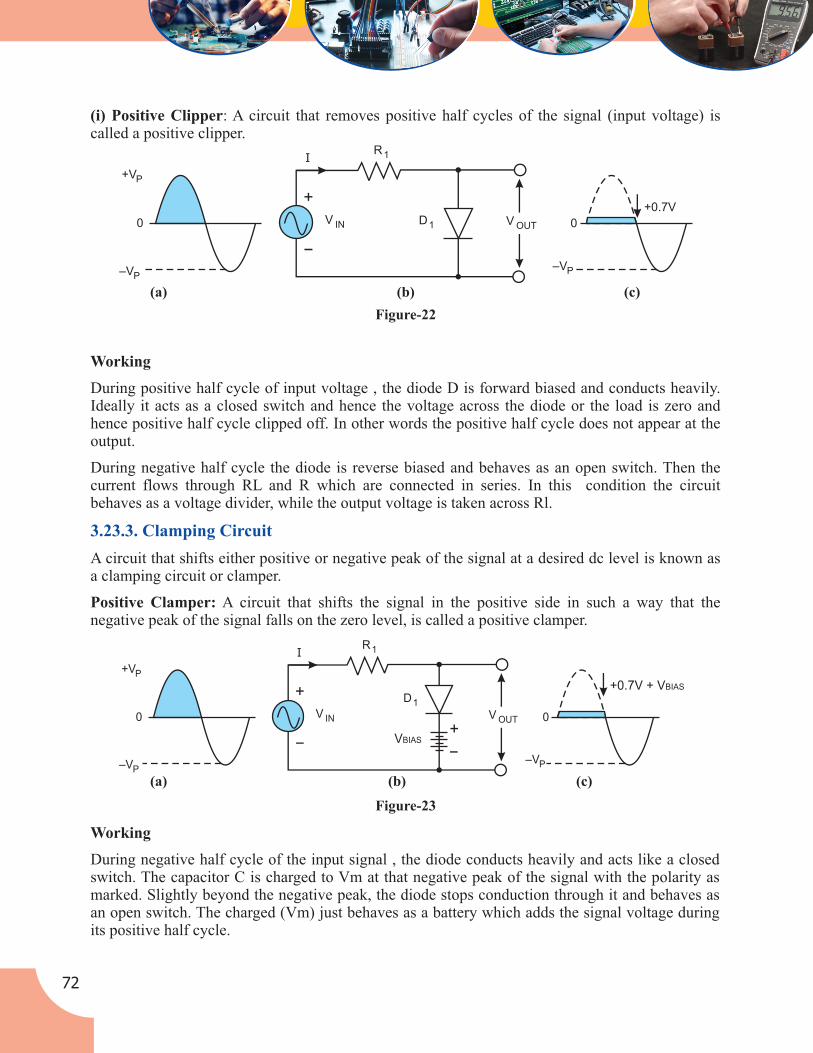
(i) Positive Clipper: A circuit that removes positive half cycles of the signal (input voltage) iscalled a positive clipper.
Working
During positive half cycle of input voltage , the diode D is forward biased and conducts heavily.Ideally it acts as a closed switch and hence the voltage across the diode or the load is zero andhence positive half cycle clipped off. In other words the positive half cycle does not appear at theoutput.
During negative half cycle the diode is reverse biased and behaves as an open switch. Then thecurrent flows through RL and R which are connected in series. In this condition the circuitbehaves as a voltage divider, while the output voltage is taken across Rl.
A circuit that shifts either positive or negative peak of the signal at a desired dc level is known asa clamping circuit or clamper.
Positive Clamper: A circuit that shifts the signal in the positive side in such a way that thenegative peak of the signal falls on the zero level, is called a positive clamper.
3.23.3. Clamping Circuit
Figure-22
(b)(a) (c)
Figure-23
(b)(a) (c)
I
V IN V OUTD1
R1
+
+VP
–VP
0
–VP
0
+0.7V
I
V IN V OUT
D1
R1
+
+VP
–VP
0
–VP
0
+0.7V + VBIAS
VBIAS+
Working
During negative half cycle of the input signal , the diode conducts heavily and acts like a closedswitch. The capacitor C is charged to Vm at that negative peak of the signal with the polarity asmarked. Slightly beyond the negative peak, the diode stops conduction through it and behaves asan open switch. The charged (Vm) just behaves as a battery which adds the signal voltage duringits positive half cycle.
72

During positive half cycle of the signal the diode is reversed biased and acts as an open switch.The resultant output voltage coming across the load resistor the load resistor RL will be:
Output Voltage =Vm+Vm=2Vm
Resource Material
1. Electronics devices and circuit theory by Robert L. Boylestad & Louis Nashelsky, ninthedition.
2. Electronics devices and circuit by S.K. Sahdev, Dhanpat Rai Publications.
Exercise
1. Short questions:
(a) What are the two common semiconductors which are mostly used in electronics?
(b) When a pure semiconductor is heated its resistivity increases, decreases or remains
constant?
(c) The leakage current is least in?
(d) The process of adding impurities in an intrinsic semiconductor is called?
(e) What is forward and reverse biasing?
2. Write short note on:
(a) What is intrinsic and extrinsic semiconductor?
(b) Define Energy band structure of Insulators, Metals and Semiconductors.
(c) What is Photo-electric emission?
(d) Define Drift current.
3. Explain the following:
(a) Effects of temperature on Conductivity of semiconductor.
(b) Why Zener diode connected reverse across the supply?
(c) Why do we use transformer in a rectifier circuit?
4. Long questions:
(a) Explain full wave and half wave rectifier with their types.
(b) Give the brief introduction of Filters, Clippers, Clampers.
73Basic Electronics

Overview
Knowledge and Skill Outcomes
Assessment Plan: (For the Teachers)
This unit starts with the understanding of fundamentals of a transistor, types of transistors andbiasing of transistor. Further three types of transistor configuration has been discussed along withthe characteristics of transistor. Fundamentals of FET, JFET, MOSFET, CMOS and VMOS havebeen presented. A comparative study of various transistors has been conducted. Finally whateverdiscussed and presented in various chapters has been summarized as a quick review.
i) Understanding of construction and working of Bipolar Junction Transistor.
ii) Difference between operation of NPN and PNP transistor.
iii) Knowledge of various types of transistor configuration.
iv) Difference between CB, CE and CC configuration.
v) Knowledge about transistor parameters.
vi) Knowledge of FET, JFET and MOSFET.
vii) Knowledge of CMOS and VMOS
viii) Learn about characteristics and comparison between various configuration.
Bipolar Junction Transistor
UNIT 4
4.0 Unit Overview and Description
?Overview
?Knowledge and Skill Outcomes
?Assessment Plan
?Learning Outcomes
?Resource Material
?Topics Covered
Construction and operation of NPN and PNP transistors, Biasing of BJT, CB, CE and CC
configuration, Characteristics and transistor parameters for CB, CE, CC configuration,
Introduction to FET, JFET, MOSFET, CMOS and VMOS, Characteristics of various transistors,
Comparison of various transistors.
and PNPtransistors, Biasing of BJT.Construction and operation of NPN
Unit-1 Topic AssessmentMethod
TimePlan
Remarks
(i) An interactive session: Question & Answer
One Hour
74

Unit-3 OutcomesBipolar Junction Transistor
Characteristics and transistor parameters for CB, CE, CC configuration.
CB, CE and CC configuration, i) Understanding the various configurationsof transistor.
ii) To have the knowledge of various parameters of a transistor
CMOS and VMOS , Characteristics of various transistors, Comparison of various transistors.
Introduction to FET, JFET, MOSFET, i) Understanding various UJTs
ii) To know the characteristics of all typesof transistors.
iii) A comparision study of varioustransistors.
Construction and operation of NPN andPNPtransistors, Biasing of BJT.
i) Understanding the basics of transistors.
ii) Understanding the fundamentals of biasing.
Characteristics and Transistorparameters for CB, CE, CC configuration
CB, CE and CC configuration,
Unit-1 Topic AssessmentMethod
TimePlan
Remarks
(ii) Assignment After one day
One hour
After one day
CMOS and VMOS, Characteristics ofvarious transistors, Comparison ofvarious transistors
Introduction to FET, JFET, MOSFET,
Learning Outcomes
4.1. Bipolar Junction Transistor (BJT)
A Semiconductor device consisting of two pn junctions formed by sandwitching either p type orn type semiconductor between a pair of opposite types is known as a transistor thus it is also wellknown by the name bipolar junction transistor because its operation depends upon both themajority and minority carriers.
Accordingly, there are two types of transistors namely;
(i) NPN Transistor
(ii) PNP Transistor
(I) NPN Transistor: A transistor in which two blocks of n-type semiconductor are separated bya thin layer of p-type semiconductor is known as NPN Transistor.
(II) PNP Transistor: A transistor in which two blocks of p-type semiconductors are separatedby a thin layer of n- type semiconductor is known as PNP Transistor.
NPN and PNP Transistor (Construction and Working)
(i) An interactive session: Question & Answerii) Assignment
75Basic Electronics

Figure-1
Figure-2
Construction: or Transistor Terminals
Every transistor has three terminals called emitter, base and collector.
(i) Emitter
The Section on one side of the transistor that supplies a large number of majority carriers (electrons if
emitter is n- type and holes if the emitter is of p-type) is called emitter. The emitter is always forward
biased w’r’t. base so that it can supply a large number of majority carriers to its junction with the base.
The biasing of emitter base junction of npn transistor and pnp transistor is shown in fig. 1 & fig. 2.
Since emitter is to supply or inject a large amount of majority carriers into the base, it is heavily doped
but moderate in size.
(ii) Base
The middle section which forms two pn junctions between emitter and collector is called base. The
base form two circuits, one input circuit with emitter and other output circuit with collector. The base
emitter junction is forward biased, providing low resistance to the emitter circuit. The base collector
junction is reversed biased, offering high resistance path to the collector circuit. The base is lightly
doped and very thin so that it can pass on most of the majority carriers supplied by emitter to the
collector.
(iii) Collector
The section on the other side of the transistor that collects the major portion of the majority carrierssupplied by the emitter is called collector. The collector base junction is always reverse biased. Itsmain function is to remove majority carriers (or charges) from its junction with base. The collector is
Emitter CollectorCircuitSymbol
Base
IE
VBE
IB
VCB
N P N
IC
IE IE IE= +
IE
IB
+
+
–VBE
VCE
VCBIC
B
E
C
–
Emitter CollectorCircuitSymbol
Base
IE
VBE
IB
VCB
N P N
IC
IC IE IB= –
IC
IB
+
–VBC
VCE
VBEIE
B
C
E
+
–
–+ –+
76

moderately doped but larger in size so that it can collect most of the majority carriers supplied by theemitter. The biasing of collector base junction of npn & pnp transistor is shown.
The npn transistor circuit is shown in fig.1 the emitter base junction is forward biased while collectorbase junction is reverse biased. The forward biased voltage V is quite small, whereas reverse biasedBE
voltage for V is considerably high.CB
As the emitter base junction is forward biased, a large number of electrons (majority carriers) in theemitter (N-TYPE) region are pushed toward the base. This constitutes the emitter current Ie. whenthese electron enter the p-type material(base) they tend to combine with holes. Since the base is lightlydoped and very thin, only a few electron (less than 5 %) combine with holes to constitute base currentIb. The remaining electrons (more than 95%) diffuse across the thin base region and reach thecollector space charge layer. These electron then come under the influence of the positively biased n-region and are attracted or collected by the collector. This constitutes the collector current Ic thus it isseen that almost the entire emitter current flows into the collector circuit. However to be more precisethe emitter current is the sum of collector current and base current .i.e
Ie=Ic+Ib
The pnp transistor circuit is shown in fig.2 the emitter base junction is forward biased while collectorbase junction is reverse biased.The forward biased voltageV is quite small, whereas reverse biasedBE
voltage V is considerably high.CB
As the emitter base junction is forward biased, a large number of holes (majority carriers) in theemitter (P-TYPE) region are pushed toward the base. This constitutes the emitter current Ie. whenthese electron enter the n-type material (base) they tend to combine with electrons. Since the base islightly doped and very thin, only a few electron (less than 5 %) combine with holes to constitute basecurrent Ib. The remaining electrons (more than 95%) diffuse across the thin base region and reach thecollector space charge layer. These holes then come under the influence of the negatively biased p-region and are attracted or collected by the collector. This constitutes the collector current Ic thus it isseen that almost the entire emitter current flows into the collector circuit. However to be more precisethe emitter current is the sum of collector current and base current. i.e
Ie=Ic+Ib
4.1.1. Working of NPN Transistor
4.1.2. Working of PNPTransistor
4.1.3 Current Voltage Characteristics of BJT
Figure-3 : The i V CharacteristicsC CB
ic
iE
77Basic Electronics

Figure-4 : The i V CharacteristicsC CE
4.2. BJT Biasing
4.3. CB, CE and CC Configuration
The process by which required condition such as proper flow of zero signal collector current and themaintenance of proper collector emitter voltage during the passage of signal are obtained is known astransistor biasing.
The basic procedure of transistor biasing is to keep the emitter junction forward biased and thecollector junction properly reverse biased during the application of signal so that faithfulamplification can be achieved. The biasing can be achieved either by using bias batteries Vbb andVccor by applying associating circuitry with the transistor. Generally, the latter method is employed sinceit is more efficient.
The circuitry which provides the necessary conditions of transistor biasing is known as biasingcircuit. While designing a biasing circuit, various transistor rating such as maximum collector currentI , maximum collector emitter voltage V etc. are kept in view for safe operation of theCMAX
transistor. In the amplifier circuits, a load resistance Rc is connected in the collector circuit, a loadresistance R is connected in the collector circuit. Then a d.c. load line AB corresponding to thisC
resistance R is drawn on the output characteristics as shown in fig. 4. The operating point will lieC
somewhere on this load line. Depending upon the base current, the operating point may lie at C, D orE.
When an a.c signal is applied at the input, the base current varies instant to instant. As a result of this,the current and collector voltage also vary with time. Thus an amplified signal is obtained at theoutput.
If point D is the as the operating point, the upper portion of the positive half will be clipped off as thepoint lies very near to the satisfaction region. On the other hand if point E is selected as the operatingpoint., the peak of negative half will be clipped off as this point lies very near to the cut off region. Thus, in both the cases, distorted signal is obtained at the output.
However, if point C is selected as the operating point, full cycle of the signal is obtained in theamplified form at the output in this case, signal is not distorted at all.
A transistor has three leads, namely emitter, base and collector. However, to handle input and outputfour terminals are needed (two for input and two for output). Therefore to connect transistor in the
CEMAX
i icc
78

circuit, one lead or terminal is made common. The input is fed between common and one of theremaining terminals whereas, output is connected between the common and other terminal of thetransistor. Accordingly a transistor can be connected in the circuit in the following three ways: (seefig. 5)
(i) Common Base Connection (CB Configuration)
(ii) Common Emitter Connections (CE Configuration)
(iii) Common Collector Connection(CC Configuration)
Figure-5
(a) Common-Base (b) Common-Emitter (c) Cascode
It is important to note that transistor may be connected in any one of the above said three ways,
the emitter base junction is always forward biased and collector base junction is always reverse
biased to operate the transistor in active region.
The common base circuit arrangement for npn transistor and pnp transistor is shown in fig. (a) and
(b) respectively. In this case, the input is connected between emitter and base while output is taken
across collector and base. Thus the base of the transistor is common to both input and output
circuit and hence the name common base connection or common base configuration.
Current Amplification Factor (Alpha)
The ratio of output to input current is known as current amplification factor in a common base
connection the output current is collector current Ic whereas the input current is emitter current Ie.
Thus the ratio of change in collector current to the change in emitter current at constant collector
base voltage Vcb is known as current amplification factor of transistor in common base
configuration. It is generally represented by Greek letter (alpha).
The common emitter circuit arrangement for npn transistor and pnp transistor is shown in fig. (a)
and (b) respectively. In this case, the input is connected between emitter and base while output is
taken across collector and emitter. Thus the emitter of the transistor is common to both input and
output circuit and hence the name common emitter connection or common emitter configuration.
4.3.1. Common Base Connection (or CB Configuration)
4.3.2. Common Emitter Connection (or CE Configuration)
79Basic Electronics
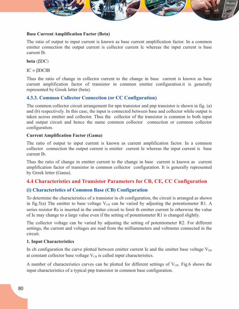
Base Current Amplification Factor (Beta)
The ratio of output to input current is known as base current amplification factor. In a common
emitter connection the output current is collector current Ic whereas the input current is base
current Ib.
beta (bDC)
IC = bDCIB
Thus the ratio of change in collector current to the change in base current is known as base
current amplification factor of transistor in common emitter configuration.it is generally
represented by Greek letter (beta).
The common collector circuit arrangement for npn transistor and pnp transistor is shown in fig. (a)
and (b) respectively. In this case, the input is connected between base and collector while output is
taken across emitter and collector. Thus the collector of the transistor is common to both input
and output circuit and hence the name common collector connection or common collector
configuration.
Current Amplification Factor (Gama)
The ratio of output to input current is known as current amplification factor. In a common
collector connection the output current is emitter current Ie whereas the input current is base
current Ib.
Thus the ratio of change in emitter current to the change in base current is known as current
amplification factor of transistor in common collector configuration. It is generally represented
by Greek letter (Gama).
To determine the characteristics of a transistor in cb configuration, the circuit is arranged as shown
in fig.5(a) The emitter to base voltage V can be varied by adjusting the potentiometer R1. ACB
series resistor Rs is inserted in the emitter circuit to limit th emitter current Ie otherwise the value
of Ie may change to a large value even if the setting of potentiometer R1 is changed slightly.
The collector voltage can be varied by adjusting the setting of potentiometer R2. For different
settings, the current and voltages are read from the milliammeters and voltmeter connected in the
circuit.
1. Input Characteristics
In cb configuration the curve plotted between emitter current Ie and the emitter base voltage VEB
at constant collector base voltage V is called input characteristics.CB
A number of characteristics curves can be plotted for different settings of V . Fig.6 shows theCB
input characteristics of a typical pnp transistor in common base configuration.
4.3.3. Common Collector Connection (or CC Configuration)
(i) Characteristics of Common Base (CB) Configuration
4.4 Characteristics and Transistor Parameters for CB, CE, CC Configuration
80

(i) For a particular value of Vcb the curve is just like a diode characteristic in the forwardregion. In fact here the pn emitter junction is forward biased.
(ii) When Vcb is increased the value Ie increase slightly for the given value of Veb. Hence thejunction becomes a better diode. It also reveals that emitter current and hence collectorcurrent is almost independent of collector base voltage Vcb.
(iii) The emitter current Ie increase rapidly wth a small increase in emitter base voltage Veb. Itshows that input resistance is very small.
1. (a) Input Resistance
The ratio of change in emitter base voltage (delta Veb) to the resulting change in emitter current(delta Ie) at constant collector base voltage (Vcb) is known as input resistance, i.e
Input resistance, p1= delta Veb/delta Ie at constant Vcb
The value of input resistance p1 is very low. Its value further decrease with the increase in
collector base voltage Vcb since the curve tends to become more vertical. The typical value ofinput resistance varies from a few ohms to 100 ohms.
2. Output Characteristics
In CB configuration, the curve plotted between collector current Ic and collector base voltage Vcb at constant emitter current Ig is called output characteristics. Number of characteristics curves canbe plotted for different settings of Vcb. Fig.7 shows the input characteristics of a typical pnptransistor in common base configuration.
The following points may be noted from these characteristics:
Figure-6
The following points may be noted from these characteristics:
Figure-7 : Output Characteristics for Common-Base Transistor
7
6
5
4
3
2
1
I (mA)C
V (V)CB
Active Region
SaturationRegion
CutoffRegion
I = 7 mAg
I = 6 mAg
I = 5 mAg
I = 4 mAg
I = 3 mAg
I = 2 mAg
I = 1 mAg
I = 0 mAg
–1 0 5 10 15 20
Output characteristics
81Basic Electronics

(i) In the active region, where collector base junction is reverse biased, the collector current Icis almost equal to the emitter current Ie. The transistor is always operated in this region.
(ii) In the active region. The curve are almost flat. A very large change in Vcb produces only atiny change in Ic. It means that the circuit has very high output resistance rb.
(iii) When V becomes positive i.e the collector base junction is forward biased the collectorCB
current Ic decrease abruptly. This is the saturated region. In this region Ic does not dependmuch upon Ie.
(iv) When Ie=0, collector current Ic is not zero although its value is very small. In fact, this isthe reverse leakage current i.e I that flows in the collector circuit. This current isCBO
temperature dependent and its value ranges from 0.1 to 1.0 micro A for silicon transistor and2 to 5 micro A for germanium transistor.
2. (a) Output Resistance
The ratio of change in collector base voltage (delta Vcb) to the resulting change in collectorcurrent (delta Ic) at constant emitter current (Ie) is known as output resistance, i.e
output resistance, r0 = delta Vcb/delta Ic at constant Ie
Figure-8
30
25
20
15
10
5
0
INPUTCHARACTERISTICS
0.3V 1V 2V 3V
EMITTER VOLTAGE [V ] C COLLECTOR VOLTAGE [V ] C
EM
ITT
ER
CU
RR
EN
T[I
] C I = 20mqC
I = 15mqC
I = 10mqC
OUTPUTCHARACTERISTICSV
=2
0C
V=
10
C V=
0C
CO
LL
EC
TO
RC
UR
RE
NT
[I]
C
0 5V 10V 15V 20V
(ii) Characteristics of Common Emitter (CE) Configuration
To determine the characteristics of a transistor in ce configuration, the circuit is arranged as shownin fig. 5(b). The emitter to base voltage Veb can be varied by adjusting the potentiometer R1. Aseries potentiometer R2 is inserted to vary the collector to emitter voltage otherwise the value ofIe may change to a large value even if the setting of potentiometer R1 is changed slightly. Thecollector voltage can be varied by adjusting the setting of potentiometer R2. For different settings,the current and voltages are read from the milliammeters and voltmeter connected in the circuit.
2. Input Characteristics
In CE configuration the curve plotted between base current Ib and the emitter base voltage Veb atconstant collector emitter voltage Vce is called input characteristics.
82

Figure-9
To draw the input characteristics note down the reading of ammeter (Ib) connected in the basecircuit for various values of Veb at constant Vce. Plot the curve on the graph taking Ib along Y-axis and Vbe along X-axis as shown in fig. 9. A number of characteristics curves can be plottedfor different settings of Vcb. Fig.9 shows the input characteristics of a typical PNP transistor incommon base configuration.
100
90
80
70
60
50
40
30
20
10
0.2 0.4 0.6 0.8 1.0V (V)BE
V = 1VCE
V = 10VCE
V = 20VCE
IB(µA)
The following points may be noted from these characteristics:
(i) These curves are similar to those obtained for CB configuration i.e like a forward diodecharacteristics. The only differences is that in this case Ig increase less rapidly with increasein Vbe. Hence the input resistance of CE configuration is comparatively higher than of CBconfiguration.
(ii) The change in Vce does not result in a large deviation of the curves and hence the effect ofchange in Vce on the input characteristics is ignored for all practical purposes.
1. (a) Input Resistance
The ratio of change in emitter base voltage (delta Veb) to the resulting change in base current(delta Ib) at constant collector emitter voltage (Vce) is known as input resistance, i.e
Input resistance, ri = delta Veb/delta Ib at constant Vcb
In CE configuration, the typical value of input resistance is of the order of a few hundred ohms.
2. Output Characteristics
In CE configuration, the curve plotted between collector current Ic and collector emitter voltageVce at constant base current Ib is called output characteristics. A number of characteristics curves
83Basic Electronics
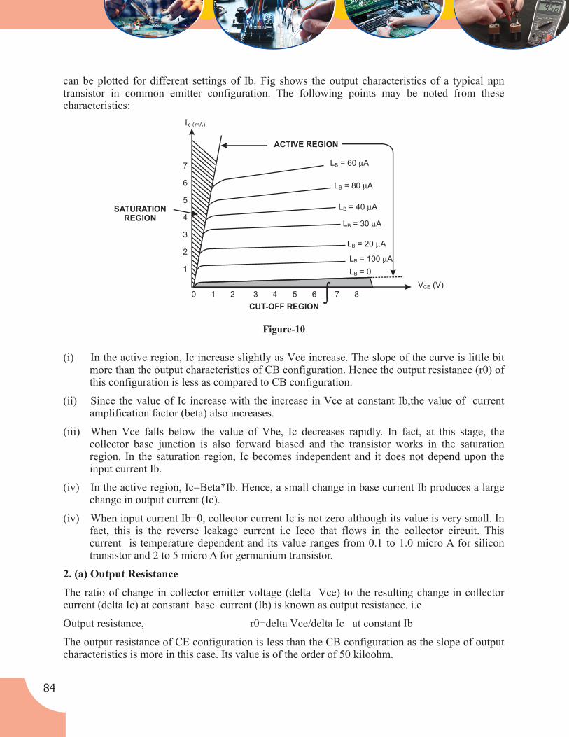
(i) In the active region, Ic increase slightly as Vce increase. The slope of the curve is little bitmore than the output characteristics of CB configuration. Hence the output resistance (r0) ofthis configuration is less as compared to CB configuration.
(ii) Since the value of Ic increase with the increase in Vce at constant Ib,the value of currentamplification factor (beta) also increases.
(iii) When Vce falls below the value of Vbe, Ic decreases rapidly. In fact, at this stage, thecollector base junction is also forward biased and the transistor works in the saturationregion. In the saturation region, Ic becomes independent and it does not depend upon theinput current Ib.
(iv) In the active region, Ic=Beta*Ib. Hence, a small change in base current Ib produces a largechange in output current (Ic).
(iv) When input current Ib=0, collector current Ic is not zero although its value is very small. Infact, this is the reverse leakage current i.e Iceo that flows in the collector circuit. Thiscurrent is temperature dependent and its value ranges from 0.1 to 1.0 micro A for silicontransistor and 2 to 5 micro A for germanium transistor.
2. (a) Output Resistance
The ratio of change in collector emitter voltage (delta Vce) to the resulting change in collectorcurrent (delta Ic) at constant base current (Ib) is known as output resistance, i.e
Output resistance, r0=delta Vce/delta Ic at constant Ib
The output resistance of CE configuration is less than the CB configuration as the slope of outputcharacteristics is more in this case. Its value is of the order of 50 kiloohm.
Figure-10
can be plotted for different settings of Ib. Fig shows the output characteristics of a typical npntransistor in common emitter configuration. The following points may be noted from thesecharacteristics:
0 1 2 3 4 5 6 7 8∫V (V)CE
L = 60 µAB
L = 80 µAB
L = 40 µAB
L = 30 µAB
L = 20 µAB
L = 100 µAB
L = 0B
CUT-OFF REGION
ACTIVE REGION
7
6
5
4
3
2
1
SATURATIONREGION
Ic (mA)
84
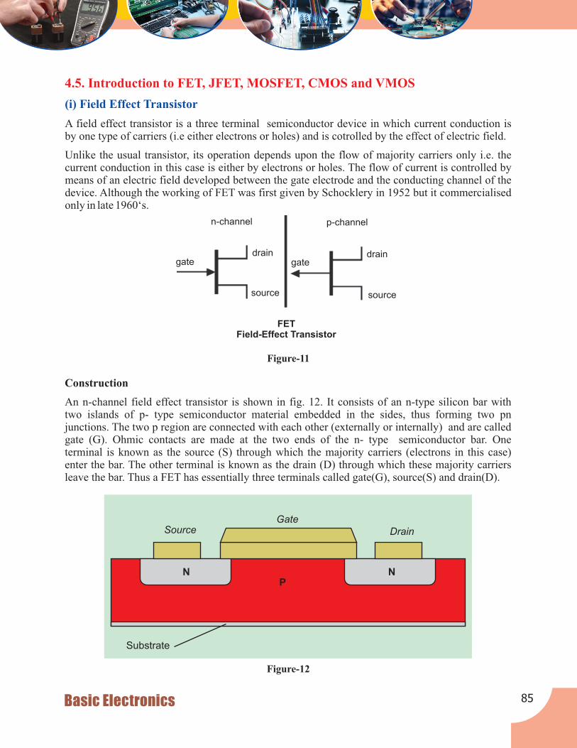
4.5. Introduction to FET, JFET, MOSFET, CMOS and VMOS
(i) Field Effect Transistor
A field effect transistor is a three terminal semiconductor device in which current conduction isby one type of carriers (i.e either electrons or holes) and is cotrolled by the effect of electric field.
Unlike the usual transistor, its operation depends upon the flow of majority carriers only i.e. thecurrent conduction in this case is either by electrons or holes. The flow of current is controlled bymeans of an electric field developed between the gate electrode and the conducting channel of thedevice. Although the working of FET was first given by Schocklery in 1952 but it commercialisedonly in late 1960‘s.
Figure-11
n-channel p-channel
drain
source
gatedrain
source
gate
FETField-Effect Transistor
Construction
An n-channel field effect transistor is shown in fig. 12. It consists of an n-type silicon bar withtwo islands of p- type semiconductor material embedded in the sides, thus forming two pnjunctions. The two p region are connected with each other (externally or internally) and are called gate (G). Ohmic contacts are made at the two ends of the n- type semiconductor bar. Oneterminal is known as the source (S) through which the majority carriers (electrons in this case)enter the bar. The other terminal is known as the drain (D) through which these majority carriersleave the bar. Thus a FET has essentially three terminals called gate(G), source(S) and drain(D).
Figure-12
Substrate
SourceGate
Drain
PN N
85Basic Electronics

Figure-13
Working of FET
The circuit diagram of an n- channel FET with normal polarities is shown.
When a voltage Vds is applied across the drain and source terminals and voltage applied acrossthe gate and source Vgs is zero (i.e gate circuit is open) as shown in fig., the two pn junctionestablish a very thin depletion layer. Thus a large amount of electrons will flow from source todrain through a wide channel formed between the two depletion layers.
When a reverse Vgs is applied across the gate and source as shown in fig. the width of thedepletion layer is increased. This reduces the width of the conducting channel thereby decreasingthe conduction (flow of electrons) through it. Thus the current flowing from source to draindepends upon the width of the conducting channel which depends upon the thickness of depletionlayer establish by the two pn junctions depends upon the voltage applied across the gate sourceterminals.
Hence it is clear that the current from source to drain can be controlled by the application ofpotential (I.e electric field) on the gate. That is why the device is called field effect transistor. Itmay be noted that a p- channel FET also operates in the same manner as an n-channel FET exceptthat the channel current carriers will be holes instead of electrons and all the polarities will bereversed.
Advantages
A FET is a voltage controlled device. In which the output current (drain current) is controlled bythe input (gate) voltage, therefore it has the following important advantages.
(i) FET has a very high input impedance which shows a high degree of isolation between theinput and output circuit.
(ii) The operation of FET depends upon the majority carriers (i.e. electron in n-channel andholes in P-channel FET) which do not cross junctions. Therefore, the inherent noise of tubes(because of high temperature operation) and those of ordinary transistor are not present in aFET.
(iii) In FET the risk of thermal runway is avoided since it has a negative temperature coefficientof resistance.
(iv) A FET has smaller size, longer life and higher efficiency.
86

Basic Construction (Fig. 14)
In an N- channel JFET an N-type silicon bar, referred to as the channel, has two smaller pieces ofP-type silicon material diffused on the opposite sides of its middle part, forming P-N junctions asshown in fig.14. The two P-n junctions forming diodes or gates are connected internally and acommon terminal called the gate terminal is brought out. Ohmic contacts are made at the two ends of the channel-one lead is called the source terminal S and the other drain terminal D.
The silicon bar behaves like a resistor between its two terminals D and S. The gate terminal isanalogous to the base of an ordinary transistor (BJT). It is used to control the flow of current fromsource to drain. Thus source and drain terminal are analogous to emitter and collector terminalsrespectively of a BJT.
Operation
Let us consider n- channel JFET for discussing its operation:
Disadvantages
(I) Since FET has high input impedance the gate voltage has less voltage and has less controlover the drain current. Therefore FET amplifier has much less voltage gain than a bipolaramplifier.
There are two major categories of field effect transistors namely:
(i) Junction field effect transistors(JFET)
(ii) Metal oxide field effect transistor (MOSFET)
JFET are of two types viz. N-channel JFET and P-channel JFETs. Generally N-channel JFET arepreferred.
(ii) Construction and Characteristics of JFETs
87Basic Electronics
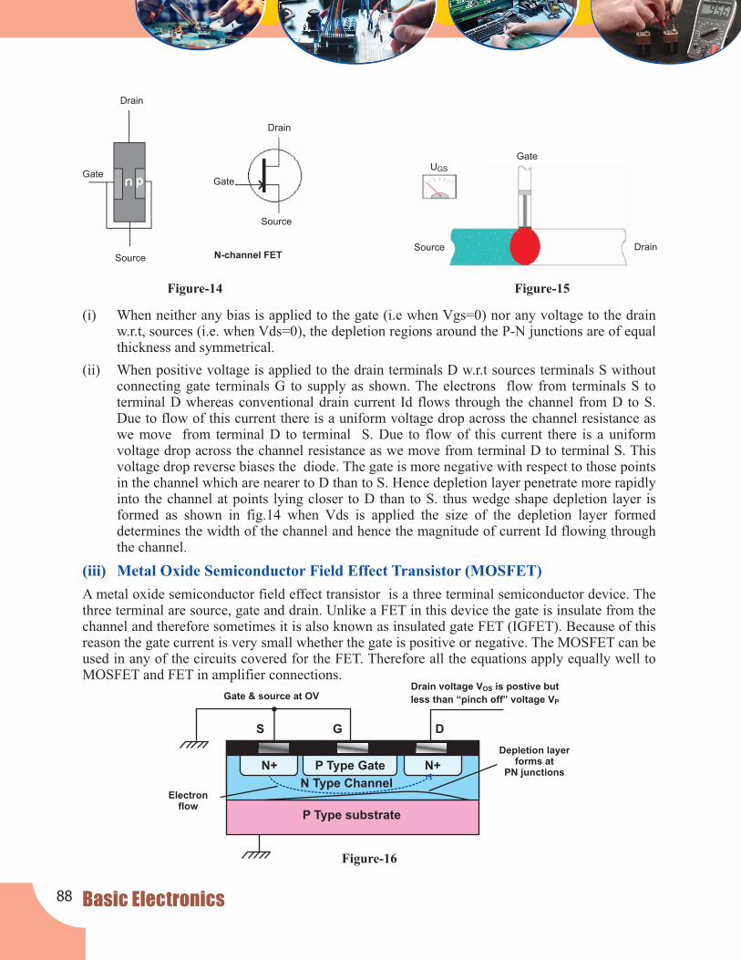
(i) When neither any bias is applied to the gate (i.e when Vgs=0) nor any voltage to the drainw.r.t, sources (i.e. when Vds=0), the depletion regions around the P-N junctions are of equalthickness and symmetrical.
(ii) When positive voltage is applied to the drain terminals D w.r.t sources terminals S withoutconnecting gate terminals G to supply as shown. The electrons flow from terminals S toterminal D whereas conventional drain current Id flows through the channel from D to S.Due to flow of this current there is a uniform voltage drop across the channel resistance aswe move from terminal D to terminal S. Due to flow of this current there is a uniformvoltage drop across the channel resistance as we move from terminal D to terminal S. Thisvoltage drop reverse biases the diode. The gate is more negative with respect to those points in the channel which are nearer to D than to S. Hence depletion layer penetrate more rapidlyinto the channel at points lying closer to D than to S. thus wedge shape depletion layer isformed as shown in fig.14 when Vds is applied the size of the depletion layer formeddetermines the width of the channel and hence the magnitude of current Id flowing throughthe channel.
A metal oxide semiconductor field effect transistor is a three terminal semiconductor device. Thethree terminal are source, gate and drain. Unlike a FET in this device the gate is insulate from thechannel and therefore sometimes it is also known as insulated gate FET (IGFET). Because of thisreason the gate current is very small whether the gate is positive or negative. The MOSFET can be used in any of the circuits covered for the FET. Therefore all the equations apply equally well toMOSFET and FET in amplifier connections.
(iii) Metal Oxide Semiconductor Field Effect Transistor (MOSFET)
Figure-16
Gate & source at OVDrain voltage V is postive but
less than “pinch off” voltage VP
OS
Electronflow
Depletion layerforms at
PN junctions
S G D
N+ P Type Gate N+
N Type Channel
P Type substrate
Basic Electronics
Figure-14
Drain
Source
GateGate
Drain
Source
N-channel FET
Figure-15
DrainSource
GateUGS
88
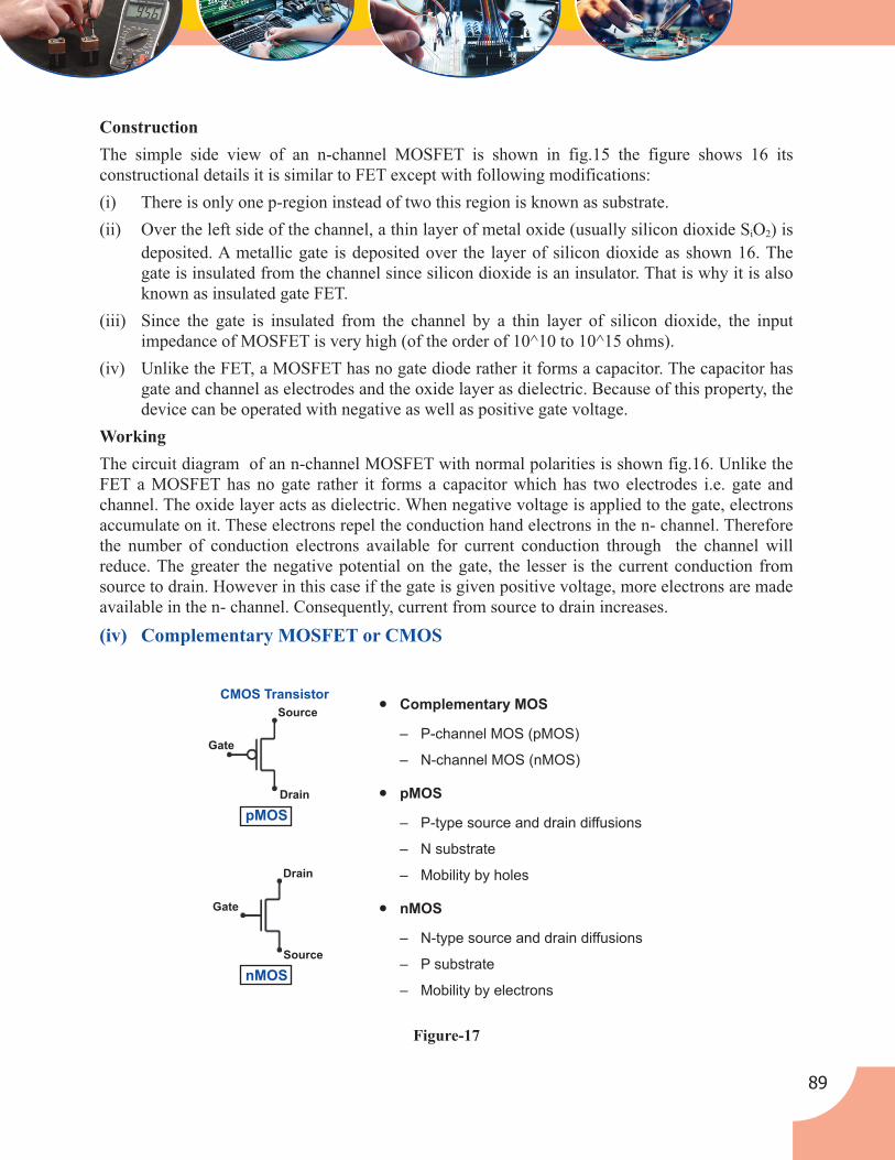
Construction
The simple side view of an n-channel MOSFET is shown in fig.15 the figure shows 16 its
constructional details it is similar to FET except with following modifications:
(i) There is only one p-region instead of two this region is known as substrate.
(ii) Over the left side of the channel, a thin layer of metal oxide (usually silicon dioxide S O ) isi
deposited. A metallic gate is deposited over the layer of silicon dioxide as shown 16. The
gate is insulated from the channel since silicon dioxide is an insulator. That is why it is also
known as insulated gate FET.
(iii) Since the gate is insulated from the channel by a thin layer of silicon dioxide, the input
impedance of MOSFET is very high (of the order of 10^10 to 10^15 ohms).
(iv) Unlike the FET, a MOSFET has no gate diode rather it forms a capacitor. The capacitor has
gate and channel as electrodes and the oxide layer as dielectric. Because of this property, the
device can be operated with negative as well as positive gate voltage.
Working
The circuit diagram of an n-channel MOSFET with normal polarities is shown fig.16. Unlike the
FET a MOSFET has no gate rather it forms a capacitor which has two electrodes i.e. gate and
channel. The oxide layer acts as dielectric. When negative voltage is applied to the gate, electrons
accumulate on it. These electrons repel the conduction hand electrons in the n- channel. Therefore
the number of conduction electrons available for current conduction through the channel will
reduce. The greater the negative potential on the gate, the lesser is the current conduction from
source to drain. However in this case if the gate is given positive voltage, more electrons are made
available in the n- channel. Consequently, current from source to drain increases.
2
(iv) Complementary MOSFET or CMOS
Figure-17
• Complementary MOS
– P-channel MOS (pMOS)
– N-channel MOS (nMOS)
• pMOS
– P-type source and drain diffusions
– N substrate
– Mobility by holes
• nMOS
– N-type source and drain diffusions
– P substrate
– Mobility by electrons
Source
Gate
Drain
pMOS
Drain
Gate
Source
nMOS
CMOS Transistor
89

(v) VMOS
One of the disadvantage of the typical MOSFET is the reduced power-handling levels compared
to BJT transistors. This shortfall for a device with so many positive characteristics can be softened
by changing the construction mode from one of a planar nature such as shown in to one with a
vertical structure as shown in fig.19. All the elements of the planar MOSFET are present in the
vertical metal oxide silicon FET(VMOS). The term vertical is due primarily to the fact that the
channel is now formed in the vertical direction rather than the horizontal direction as for the
planar device. However the channel has the appearance of a V cut in the semiconductor base,
which often stands out as a characteristic for memorization of the name of the device.
Source
Gate
Source
Bodyp+n+n+
p p
Gate oxideDepletion region
n - type epitaxial layer
n±substrate
Figure-19 : VMOS Structure, Drain Terminal is on Underside
A very effective logic can be established by constructing a p- channel and n- channel MOSFET on
the same substrate as shown in fig.17 note the induced p- channel on the left and the induced n-
channel on the right for the p-and n- channel devices, respectively. The configuration is referred
to as a complementary MOSFET arrangement CMOS. It has extensive application in computer
logic design the relatively high input impedance, fast switching speeds, and lower operating
power levels of the CMOS configuration have resulted in a whole new discipline referred to as
CMOS logic design.
Gate Dielectric
Channel DrainSource
Gate Electrode
Figure-18 : Basic CMOS Transistor
90

4.6. Characteristics of Various Transistors
a b
c d
Figure-20 Figure-21
Figure-22 Figure-23
e f
Figure-24 Figure-25
91Basic Electronics

Resource Material
1. Digital Logic and Computer Design by M. Morris Mano, Prentice Hall India Publication,
New Delhi, 2002.
2. Digital Principles and Applications by A. P. Malvino & D. P. Leach, Tata McGraw-Hill
Publication, New Delhi 1995.
3. Modern Digital Electronics by R. P. Jain, Tata McGraw- Hill Publication, New Delhi 2010.
4. Digital Electronics by G. K. Kharate, Oxford University Press Publication, New Delhi 2011.
5. Digital Electronics: Principles and Integrated Circuits by A. K. Maini, Wiley India
Publication, New Delhi 2010.
6. Digital Technology: Principles and Practice by Virendra Kumar, New Age International
Publishers, New Delhi 2002.
7. Digital Circuits and Design by S. Salivahanan & S. Arivazhagan, Vikas Publishing, Noida,
Uttar Pradesh, 2012.
Exercise
1. Very short answers:
(a) The output impedance of a transistor is _____________.
(b) The phase difference between input and output voltage of a transistor connected in common emitter arrangement is _____________.
(c) As the temperature of a transistor goes up, the base emitter resistance _____________.
(d) What are the three common transistor connections?
(e) The most commonly used transistor connection is _____________.
2. Short answers:
(a) If emitter current is in a transistor is 2mA, then the collector will be nearly __________.
(b) CC configuration is generally used for _____________.
(c) The silicon transistor is generally used than germanium transistor because ___________.
(d) The transistor is said to be in quiescent state when _____________.
3. Write short note on:
(a) Draw the circuit symbol for an NPN transistor and indicate the reference polarities for the voltage and the reference direction for the three currents.
(b) Repeat the above for PNP transistor.
(c) Why is an ordinary junction transistor called bipolar transistor?
4. Explain in detail:
(a) Draw the output characteristics of a transistor in CE configuration and label all the parameters.
(b) A properly connected transistor can do amplification. Is transistor a source of energy.
92

Overview
Knowledge and Skill Outcomes
Assessment Plan: (For the Teachers)
This unit starts with the understanding of Amplifiers. It includes description of single and multistage amplifiers and their characteristics. Concept of Positive Feedback and Negative Feedback isdiscussed. Damped and Undamped oscillations have been explained using suitable diagrams.Brief introduction to Multivibrator and Signal Generator has been given. Introduction toThyristors and various types of Thyristors like SCR, TRIAC and DIAC are discussed with theirsymbols. Operation of Light Activated SCR is discussed along with its symbol.
i) Understanding of amplifier
ii) Understanding the singlestage and multistage amplifier
iii) Knowledge about circuit diagram of singlestage and multistage amplifiers.
iv) To know various types of characteristics of an amplifier.
v) Understanding the concept of feedback in amplifiers.
vi) Understanding the sinusoidal, non-sinusoidal, damped and undamped oscillations.
vii) Basic idea about multivibrator and its various uses.
viii) To understand the block diagram of signal generator.
ix) Understanding of Thyristors- SCR, TRIAC and DIAC with their symbols.
x) To understand the operation of Light Activated SCR.
Transistor Amplifier and Applications
UNIT 5
5.0 Unit Overview and Description
?Overview
?Knowledge and Skill Outcomes
?Assessment Plan
?Learning Outcomes
?Resource Material
?Topics Covered
Introduction to Amplifiers, Single and Multistage Amplifiers, Amplifier Characteristics,Feedbacks in Amplifiers, Introduction to Oscillators, Multivibrators, Signal Generator,Thyristors, Light Activated SCR.
Introduction toAmplifier
Unit-1 Topic AssessmentMethod
TimePlan
Remarks
Interactive session 20 Minutes
Single and Multistage amplifier Assignment To be submitted after one day
93Basic Electronics

Unit-1 Topic AssessmentMethod
TimePlan
Remarks
Amplifier characteristics Internal Test 25 Minutes
Feedback in amplifier Presentation by group of students
45 Minutes
Introduction oscillators Interactivesession and Test
45 Minutes
Multivibrators Assignment To be submitted after one day
Signal Generator Assignment To be submitted after one day
Thyristors Assignment To be submitted after one day
LightActivated SCR Assignment To be submitted after one day
Unit-5 OutcomesTransistor Amplifier and Applications
Single and Multistage amplifier i) Identification single stage and multistageamplifier.
ii) Understanding of basic circuit diagram ofsingle stage and multistage amplifier.
Amplifier characteristics i) To know various characteristics of anamplifier.
Introduction toAmplifiers i) Understanding of concept of amplificationand amplifier.
ii) Understanding the basic circuit diagram ofTransistor amplifier.
Learning Outcomes
Feedback in amplifier i) Understanding the basic concept of feedback
ii) Understanding of concept of positive and negative feedback.
Introduction to Oscillators i) To learn about sinusoidal, non-sinusoidal,damped and undamped oscillations withtheir wave forms.
Multivibrators i) To understand the basic idea aboutmultivibrator and its uses.
Signal Generator i) To understand the signal generator and itsvarious categories.
Thyristors i) To understand the basic concept ofThyristors-SCR,TRIAC and DIAC
Light Activated SCR i) To understand the basic operation of LASCR
94
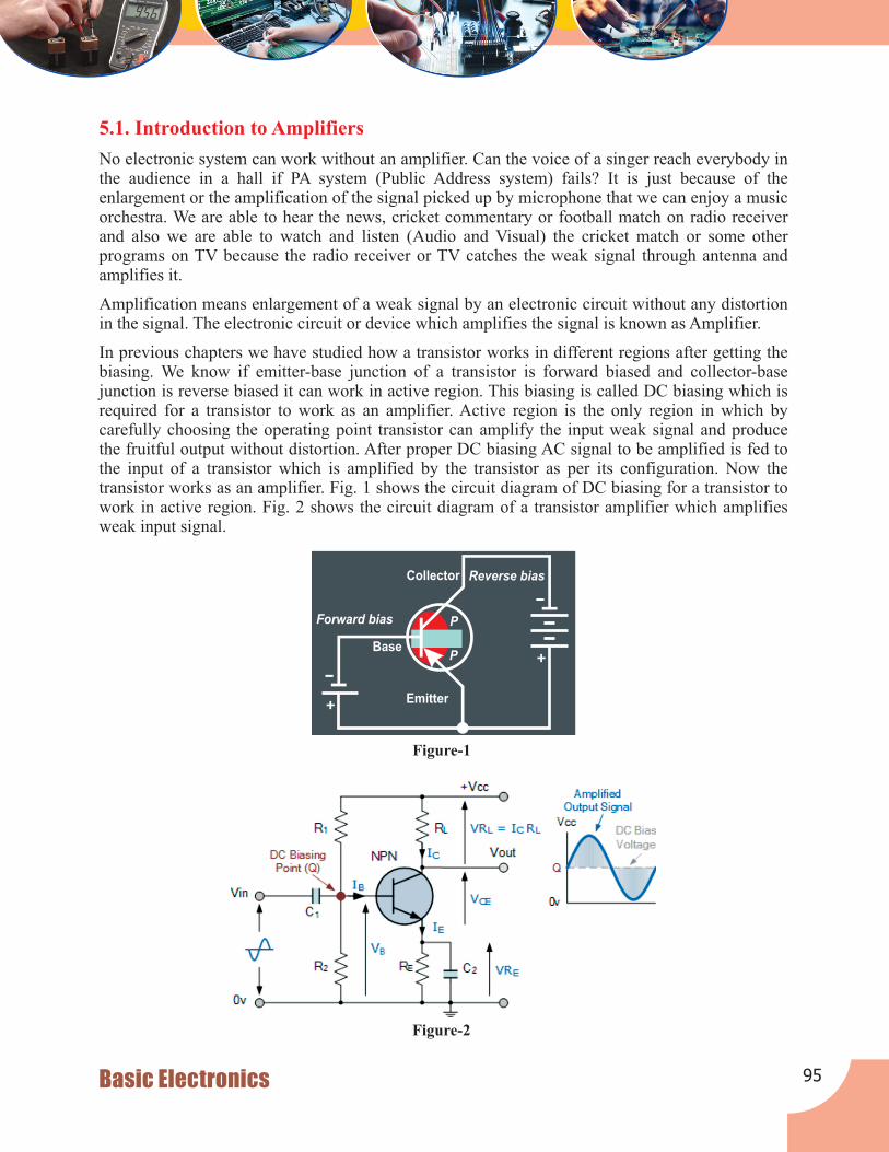
Figure-2
5.1. Introduction to Amplifiers
No electronic system can work without an amplifier. Can the voice of a singer reach everybody inthe audience in a hall if PA system (Public Address system) fails? It is just because of theenlargement or the amplification of the signal picked up by microphone that we can enjoy a musicorchestra. We are able to hear the news, cricket commentary or football match on radio receiverand also we are able to watch and listen (Audio and Visual) the cricket match or some otherprograms on TV because the radio receiver or TV catches the weak signal through antenna andamplifies it.
Amplification means enlargement of a weak signal by an electronic circuit without any distortionin the signal. The electronic circuit or device which amplifies the signal is known as Amplifier.
In previous chapters we have studied how a transistor works in different regions after getting thebiasing. We know if emitter-base junction of a transistor is forward biased and collector-basejunction is reverse biased it can work in active region. This biasing is called DC biasing which isrequired for a transistor to work as an amplifier. Active region is the only region in which bycarefully choosing the operating point transistor can amplify the input weak signal and producethe fruitful output without distortion. After proper DC biasing AC signal to be amplified is fed tothe input of a transistor which is amplified by the transistor as per its configuration. Now thetransistor works as an amplifier. Fig. 1 shows the circuit diagram of DC biasing for a transistor towork in active region. Fig. 2 shows the circuit diagram of a transistor amplifier which amplifiesweak input signal.
–
+
–
+
Collector Reverse bias
Base
Emitter
Forward bias P
P
Figure-1
95Basic Electronics

It means now it is clear from above discussion that an Amplifier is more precisely an electronicdevice that increases the voltage, current or power of an input signal with the aid of transistor byfurnishing the additional power from a separate power source. At that time we can also say that itis a Transistor Amplifier.
When only one transistor is used in a transistor amplifier to amplify weak input signal then it isknown as Single Stage Amplifier. A practical amplifier generally uses a number of stages foramplification and is known as Multistage Amplifier. Fig. 3 and Fig. 4 are examples of single andmultistage amplifiers respectively.
5.2. Single and Multistage Amplifiers
Figure-3
Figure-4
In single stage amplifier the input signal is multiplied by the gain or amplification factor of a
single amplifier. If input current is i then output current for CE amplifier will be β i thatB B
shall flow through output collector circuit. Here β is the current amplification factor for CEamplifier. If input voltage is v then output amplified voltage will be Axv where A is thei i
96

0voltage gain of the amplifier. The amplified output voltage of amplifier will be 180 out ofphase with its input voltage signal for CE amplifier circuit as shown in fig. 2 & 3.
The output from a singlestage amplifier is usually not sufficient to drive an output device. In otherwords, the gain of a single amplifier is inadequate for practical purposes. Consequently, additionalamplification over two or three stages is necessary. To achieve this, the output of each amplifierstage is coupled in some way to the input of the next stage. The resulting system is referred to asmultistage amplifier. It may be emphasised here that a practical amplifier is always a multistageamplifier. For example, in a transistor radio receiver, the number of amplification stages may besix or more. A multistage amplifier is shown in Fig. 4
Any amplifier is characterised with its following characteristics:
(1) Input Resistance
(2) Output Resistance
(3) Voltage Gain
(4) Current Gain
(5) Power Gain
(6) Phase Reversal
Feedback : (Fig. 5) When a fraction of output is fed back to the input circuit, it is known asfeedback. The fraction of output may either be current or voltage. A feedback amplifier consists oftwo parts: an amplifier and a feedback circuit. There are two types of feedback: (1) Positivefeedback (2) Negative feedback.
(1) Positive Feedback: If the feedback voltage (or current) is so applied that it increases theinput voltage (or current) then it is called positive feedback. In this case applied feedbackvoltage is in phase with input voltage. It is also known as regenerative or direct feedback.Positive feedback is used in oscillator circuits.
(2) Negative Feedback: If the feedback voltage (or current) is so applied that it reduces theamplifier input then it is called negative feedback. In this case applied feedback voltage is
0180 out of phase with input voltage. It is also known as degenerative or inverse feedback.Negative feedback is frequently used in amplifier circuits.
5.3. Amplifier Characteristics
5.4. Feedbacks in Amplifiers
Figure-5
97Basic Electronics

5.5. Introduction to Oscillators
Any circuit that generates an alternative voltage is called an oscillator. Output of an oscillator maybe a sine wave, square wave, sawtooth wave or pulses. Electronic oscillators may be broadlydivided into following two groups:
(i) Sinusoidal (or Harmonic) Oscillators: Which produce an output having sine wave form.
(ii) Non-Sinusoidal Oscillators: They produce an output which has rectangular, square or sawtooth waveform or is of pulse shape.
Sinusoidal Oscillators may be damped and undamped.
(i) Damped Oscillations: Oscillations whose amplitude keeps decreasing (or decaying)with time are called damped or decaying oscillations. Wave form of such oscillationsare shown in Fig.6(a)
(ii) Undamped Oscillations: Oscillations whose amplitude remains constant i.e. does not change with time are called undamped oscillations. Such oscillations are shown inFig.6(b)
Figure-6(a)
Figure-6(b)
98

5.6. Multivibrators (MVS)
These devices are very useful as pulse generating, storing and counting circuits. They are basicallytwo-stage amplifiers with positive feedback from the output of one amplifier to the input of theother as shown in Fig. 7
Feedback is supplied in such a manner that one transistor is driven to saturation and the other tocut-off. There are three basic types of AMVs:
(i) Astable multivibrator (AMV)
(ii) Monostable multivibrator (MMV)
(iii) Bistable multivibrator (BMV)
Uses of Multivibrators
(i) As frequency divider.
(ii) As sawtooth generators.
(iii) As square wave and pulse generators.
(iv) As a standard frequency source.
(v) Specialised uses in radar and TV circuits.
(vi) As memory elements in computers.
Signal generator is an instrument that generates an electrical signal in either the audio or radio-frequency range. Audio signal generator produces audio frequencies (sine wave and/or squarewaves). It is very popular instrument and is extensively used for testing amplifiers. Block diagramis shown in Fig. 8
5.7. Signal Generator
Figure-7
OSCILLATORSECTION AMPLIFIER
OUTPUTMETER
OUTPUTCONTROL
(ATTENUATOR) OUTPUT
POWER SUPPLY
Figure-8
99Basic Electronics

The signal generators can be classified into the following categories:
(i) Audio Generators
(ii) Function Generators
(iii) Pulse Generators
(iv) RF Generators
Thyristor means a solid-state device with two or more junctions. A thyristor may be switchedfrom ON state to OFF state between two conducting layers or vice versa. These are capable ofhandling large currents, even upto hundreds of amperes. The three widely used thyristors are :
(i) Silicon-Controlled Rectifier (SCR)
(ii) TRIAC
(iii) DIAC
It is a semiconductor device which acts as an electronic switch. A silicon-controlled rectifier canchange an alternating current into direct one and also it can control the amount of power fed to theload. Means an SCR combines the features of both rectifier and transistor.
If a P-N junction is added to a junction transistor then the resulting P-N junction device is termedas a silicon-controlled rectifier. Construction of SCR is shown in Fig. 9 (a) and symbolicrepresentation is shown in Fig. 9 (b). It is a combination of a rectifier (P-N) and a junctiontransistor (N-P-N) in one unit to form a P-N-P-N device. There are three terminals as shown inthe fig. 13 (a). One terminal from the outer P-type material is called anode (A), the second fromthe outer N-type material is called cathode (K) and the third from the base of transistor section isthe gate (G). The anode is kept at high positive potential with respect to cathode while gate is held at small positive potential with respect to cathode.
5.8. Thyristors
Introduction
5.8.1. Silicon-Controlled Rectifier (SCR)
5.8.1.1. Construction of SCR
A
P
N
P
N
K
A
K G
G
J1
J2
J3
SCR Symbol
Figure - 9(a) Figure - 9 (b)
100
5.8.1.2. SCR as a Switch
5.8.2. TRIAC
SCR has two states (i) ON state and (ii) OFF state. If an appropriate value of the gate current is
passed, the SCR begins to conduct heavily and remains in the position for an indefinite period
even if the gate voltage is removed. This is the ON state of the SCR. But if the anode current is
further reduced a point comes when SCR becomes OFF. This particular anode current at which the
SCR becomes OFF is known as “Holding current”. Thus SCR behaves as Switch. Being an
electronic device this may be termed as an “Electronic Switch”.
The major drawback of an SCR is that it can conduct current in one direction only. Therefore an
SCR can only control d.c. power i.e it controls only forward biased half cycles of a.c. However in
an a.c. system it is required to control both positive and negative half cyles. For this purpose, a
semiconductor device called triac is used.
A triac is a three-terminal five-layer semiconductor switching device which can control alternating
current in a load. Triac is an abbreviation for triac a.c. switch. Tri-indicates that device has three
terminals and a.c. means that the device controls alternating current or can conduct current in
either direction. The three terminals are designated as main terminal MT1, main terminal MT2 and
gate G. Triac physical construction, two thyristor analogy and circuit symbol are shown in Fig. 13.
Figure-10
5.8.3. DIAC
A DIAC is a two terminal three layer bidirectional device which can be switched from its OFFstate to ON state for either polarity of applied voltage.
The diac can be constructed in either npn or pnp form. Fig. 11 and Fig. 12 shows the basicstructure of a diac in pnp form and symbol of DIAC respectively. Two leads are connected to p-regions of silicon separated by an n-region. The structure of diac is very much similar to that of atransistor. However there are some important differences:
Physical Construction Two-Thyristor Analogy Circuit Symbol
101Basic Electronics
P
N
P
Figure-11 Figure-12
(i) There is no terminal attached to the base layer.
(ii) The three regions are nearly identical in size.
(iii) The doping concentrations are identical to give the device symmetrical properties.
5.9. Light Activated SCR (LASCR)
Operation of LASCR is similar to SCR one only difference is that it is activated through light. It haswindow and lens which focuses the light on gate junction area. The LASCR works as a latch. It can betriggered ON by a light input on the gate area but does not turn OFF when light source is removed. Itcan be turned OFF only by reducing current through it below its holding current. Depending on thesize, a LASCR is capable of handling large amount of current that can be handled by a photodiode or aphoto-transistor. Fig. 13 shows construction of LASCR and its symbol.
A
P
N
P
N
K
A
K G
G
J1
J2
J3
A
P
N
P
N
K
G
J1
J2
J3
LASCR Symbol
Figure-13
Summary
This unit explains about the basic circuit of an amplifier as a single-stage and multistage with theuse of a basic element that is transistor. Feedback concept and difference between positive andnegative feedback has been explained. Introduction to oscillator, multivibrator and signalgenerator has been included in this unit. Construction, symbol and operation of SCR, TRIAC,DIAC and LASCR has been described. Wherever necessary circuit diagram and symbols havebeen drawn which are self explanatory.
102

Resource Material
1. Basic Electronics Engineering by Dr. N. K. Dutta, New Central Book Agency Publication.
2. Electronic Devices & Circuits by Sanjeev Gupta, Dhanpat Rai Publications.
3. Basic Electronics and Linear Circuits by N N Bhargava, D C Kulshreshtha and S C Gupta, McGraw Hill Education.
4. Electronics Engineering by Sanjay Sharma, S.K. Kataria & Sons.
5. Principles of Electronics by V.K.Mehta and Rohit Mehta, S. Chand.
6. Electronic Devices and Circuit Theory by Robert L. Boylestad and Louis Nashelsky, Pearson Publishers.
Exercise
Questions:
(a) Define amplification and amplifier.
(b) In which region transistor should be biased so that it works as an amplifier.
(c) Draw the circuit diagram of a single and multistage amplifier.
(d) For a three stage transistor amplifier if total gain is 1000 and each stage has the same gainthen what is the gain of individual stage? If input signal is 1 mv then what will be the finaloutput of this three stage amplifier?
(e) Write down various characteristics of an amplifier.
(f) Define feedback with block diagram. Explain positive and negative feedback.
(g) What do you understand by an oscillator? Explain damped and undamped oscillations withthe help of suitable diagrams.
(h) What do you mean by multivibrator? What are the basic types of mutivibrators.
(i) Enumerate various applications of a multivibrator.
(j) Write symbol of :
i) SCR
ii) TRIAC
iii) DIAC
iv) LASCR
(k) Write short note on:
(i) SCR
(ii) TRIAC
(iii) DIAC
103Basic Electronics

Web references for Chapter: 1
1. http://encyclopedia2.thefreedictionary.com/ionization+potential
2. https://en.wikipedia.org/wiki/Electronics
3. http://farside.ph.utexas.edu/teaching/336k/Newtonhtml/node30.html
4. http://www.amigainformatics.com/industries/electronics/
5. http://article.sapub.org/10.5923.j.mm.20170701.05.html
6. https://en.wikipedia.org/wiki/Magnetic_field
7. http://wikivisually.com/wiki/Magnetic_viewing_film
8. https://www.youtube.com/watch?v=8QY0zlX2YV4
9. https://www.collaborizm.com/project/Nk2i5Fcnx
10. https://www.revolvy.com/main/index.php?s=Teltron%20tube&item_type=topic
11. https://www.newagepublishers.com/samplechapter/001410.pdf
12. https://en.wikipedia.org/wiki/Electric_field
13. http://www.idc-online.com/technical_references/pdfs/electrical_engineering/Quantum_Mechanics_Electric_Field.pdf
14. https://www.quora.com/Why-does-a-magnet-produce-a-magnetic-field-1
15. http://www.ocr.org.uk/Images/208240-unit-02-delivery-guide.pdf
16. https://www.scribd.com/doc/91954223/Laboratory-REPORT-Physics-Electric-Field
17. https://www.youtube.com/watch?v=6WTohdnUV4s
18. https://www.physicsforums.com/threads/what-is-a-uniform-electric-field-is-the-acceleration-of-a-charge-in-it-constant.778497/
19. http://www.smashinglists.com/10-first-electricity-milestones/2/
20. https://www.slideshare.net/SriKumaran4/swg-dreams
21. http://science.jrank.org/pages/2385/Electronics.html
22. https://www.pinterest.com/catiemouse/computers-technology/
23. http://www.icym.edu.my/v13/about-us/our-news/general/582-electronics.html
24. https://ahduni.edu.in/seas/ict-lab-facilities/electronics-lab
25. https://www.softtrix.com/trainings/electronics-training/
26. http://www.bluebird-electric.net/artificial_intelligence_autonomous_robotics/Robots_Hexapods_Insects_Animatronics/Electronics.htm
27. http://dbpedia.org/page/Electronics
28. http://science.jrank.org/pages/2376/Electronics-History.html
29. http://www.guidebuz.com/electronics
30. https://www.slideshare.net/VishwasAgarwal4/application-of-electronics
31. http://www.physchemres.org/article_11968_ef8c31fb13b165c7b5efe3ecd530d6c8.pdf
104
Web references for Chapter: 2
1.
2.
3.
4.
5.
6.
7.
8.
9.
10.
11.
12.
13.
14.
15.
16.
17.
18.
19.
20.
21.
22.
23.
24.
25.
26.
27.
28.
29.
30.
31.
32.
https://en.wikipedia.org/wiki/Resistor
http://en.academic.ru/dic.nsf/enwiki/15781
https://www.linkedin.com/pulse/dont-resist-resistorthey-deserve-more-respect-rick-grigalunas
https://www.scribd.com/doc/46665699/Seismic-Sensor
https://www.quora.com/Is-electrolytic-capacitor-variable
http://www.electronics-tutorials.ws/capacitor/cap_2.html
https://www.slideshare.net/LorenzAlfuente/resistors-11251561
https://www.youtube.com/watch?v=TqOsvfi7QZM
http://www.radio-electronics.com/info/data/inductors/inductor-types.php
https://www.criticalpowersupplies.co.uk/How-batteries-work-and-their-different-types
http://www.newworldencyclopedia.org/entry/Resistor
https://www.slideshare.net/shashankdevvrath/electronic-devices-and-circuits-manual
https://www.scribd.com/doc/28788258/Resistors-Colour-Coding
https://www.slideshare.net/ayeshamubeen37/mini-final-docmtn-final
https://en.wikipedia.org/wiki/Current_source
https://www.slideshare.net/MdAshikurRahman14/research-methodology-presentation-66119877
http://www.rockstone-research.com/index.php/en/research-reports/915-Prima-Diamond-becomes-Voltaic-Minerals-with-focus-on-energy-metals
https://en.wikipedia.org/wiki/Battery_(electricity)
http://ocw.ump.edu.my/mod/resource/view.php?id=73
https://www.ukessays.com/essays/chemistry/electrochemical-battery.php
https://en.wikipedia.org/wiki/Potentiometer
https://www.quora.com/Why-do-voltage-source-is-represented-as-short-circuit-and-current-source-as-open-circuit-while-taking-single-source
https://www.scribd.com/doc/86589859/Over-under-Voltage-Cut-Off-With-on-Time-Delay-PROJECT-REPORT
http://www.electronics-tutorials.ws/capacitor/cap_1.html
https://en.wikipedia.org/wiki/Dry_cell
http://www.ijimt.org/papers/504-H1011.pdf
http://www.amateur-radio-wiki.net/index.php?title=Resistors
http://www.robotpark.com/Resistor
https://www.revolvy.com/main/index.php?s=Current%20source&item_type=topic
http://www.wikiwand.com/en/Potentiometer
http://www.wow.com/wiki/Resistor
https://www.revolvy.com/topic/Dry%20cell
105Basic Electronics
33.
34.
35.
36.
37.
38.
39.
40.
41.
42.
43.
44.
45.
46.
47.
48.
49.
50.
51.
52.
53.
54.
55.
56.
57.
58.
59.
60.
61.
http://wikivisually.com/wiki/Potentiometer
http://diodetech.blogspot.com/2013/07/types-of-capacitor.html
http://www.rechargebatteries.org/knowledge-base/batteries/other-technologies/
https://www.revolvy.com/main/index.php?s=Ayrton-Perry%20winding
http://wikivisually.com/wiki/Dry_cell
http://www.robotiik.com/Resistor
http://dspace.ewubd.edu/bitstream/handle/123456789/1786/Arefeen_Binta_Belal.pdf?sequence=1
https://www.scribd.com/doc/138081352/Automotive-electrics-and-autotronics-by-M-A-Qadeer-Siddiqui
http://eeeinterviewtips.blogspot.com/
http://www.mojotone.com/amp-parts/Resistors_1/Ceramic-5W-10K-OHM-Resistor
https://en.wikipedia.org/wiki/Laser_trimming
http://www.freeway-batteries.com/faqs/where-are-primary-non-rechargeable-cells-used-mostly/
https://upload.wikimedia.org/wikipedia/commons/d/d3/1.Resistors.wiki.20150309.pdf
https://www.youtube.com/watch?v=b8BxFrIj85I
https://hi.wikipedia.org/wiki/%E0%A4%9A%E0%A4%BF%E0%A4%A4%E0%A5%8D%E0%A4%B0:Laser_Trimmed_Precision_Thin_Film_Resistor_Network.JPG
https://en.m.wikipedia.org/wiki/File:Laser_Trimmed_Precision_Thin_Film_Resistor_Network.JPG
https://www.pulsetech.net/support/lead-acid-batteries.html
https://www.researchgate.net/publication/286194982_Design_Fabrication_Of_A_Gravity_Powered_Light
https://answers.yahoo.com/question/index?qid=20120905094415AAcmtIU
http://www.digitalpower.in/product.html
https://www.slideshare.net/shashank571/electronic-letter-box-47643938
http://www.c-sharpcorner.com/article/python-scripting-on-gpio-in-raspberry-pi/
http://www.scullcom.uk/resistor-basics/
https://www.slideshare.net/OmkarRane15/lab-manual-for-basic-electrical-and-electronics-engineering-for-first-year
http://www.ebay.com/itm/100K-Ohm-104-3296W-Cermet-Potentiometer-Trimpot-Trimmer-50-pcs-DT-/262465521913
https://www.slideshare.net/VivekVenugopal11/an-integrated-fourport-dcdc-convertercei0080-56679170
https://www.scribd.com/doc/88678560/Foot-Step-Power-Generation
http://wikivisually.com/wiki/Resistor
http://byjus.com/physics/cells-electromotive-force-and-internal-resistance/
106
62.
63.
64.
65.
66.
67.
68.
69.
https://www.amazon.com/a13081500ux0324-3296W-104-Potentiometer-Variable-Resistors/dp/B00D2JRALS
http://www.ht.energy.lth.se/fileadmin/ht/Kurser/MVKF25/Batteries_Introduction.pdf
https://www.amazon.com/uxcell-Through-Hole-Trimmer-Potentiometer/dp/B008LT4IGY
https://www.scribd.com/document/85566835/Capacitor
http://www.sankethika.in/types-of-capacitors/
http://www.linguee.es/espanol-ingles/traduccion/cloruro+de+amonio.html
http://www.e-gourakani.blogfa.com/post/139
https://www.h2sys.fr/en/electric-storage-system/
70. http://www.circuitstoday.com/2-km-fm-transmitter
Web references for Chapter: 3
1.
2.
https://www.scribd.com/document/176253818/Engineering-Material-Questions
https://www.quora.com/Electronics-What-is-the-full-wave-bridge-rectifier
3. http://analyseameter.com/2016/03/rectifiers-types-efficiency-comparison-basics.html
4. www.circuitstoday.com
Web references for Chapter: 4
1.
2.
3.
4.
5.
6.
7.
8.
9.
10.
11.
12.
13.
14.
15.
16.
17.
18.
19.
http://www.circuitstoday.com/jfet-junction-field-effect-transistor
http://www.rgcetpdy.ac.in/Notes/ECE/II%20YEAR/EC%20T34-EDC/Unit%202.pdf
http://analyseameter.com/2016/02/jfet-mosfet-difference-comparison.html
https://www.scribd.com/document/331926881/EC6464-Electro-Micro-Proc-Notes-Typed
http://sctevtodisha.nic.in/docs/website/pdf/140296.pdf
http://slideplayer.com/slide/10835710/
https://www.slideshare.net/KrishnaPrasad126/ece-50416328
https://www.coursehero.com/file/11706491/Transistor-Biasing/
https://www.scribd.com/doc/146444258/Ece-III-Analog-Electronic-Ckts-10es32-Notes
http://www.neduet.edu.pk/electronics/pdf/Lab_Work_Books/EDC.pdf
http://circuitglobe.com/common-base-connection-cb-configuration.html
https://www.ikbooks.com/home/samplechapter?filename=187_Sample-Chapter.pdf
https://www.slideshare.net/shankhaShankhamitras/aec-ppt2-75625241
http://slideplayer.com/slide/8551848/
http://slideplayer.com/slide/10868731/
http://m.kkhsou.in/EBIDYA/BPP/MODIFY_electronics.html
http://www.bhojvirtualuniversity.com/slm/mscphy1p4.pdf
https://www.scribd.com/doc/51854658/BJT
https://www.slideshare.net/AnisurRahmanNayem/transistor-biasing-69604669
20. http://sctevtodisha.nic.in/docs/website/pdf/140292.pdf
107Basic Electronics
Web references for Chapter: 5
1.
2.
3.
4.
5.
6.
7.
8.
9.
http://www.talkingelectronics.com/Download%20eBooks/Principles%20of%20electronics/CH-21.pdf
https://www.slideshare.net/mhmdenab/ch-65
http://slideplayer.com/slide/5277224/
http://repository.unn.edu.ng:8080/xmlui/bitstream/handle/123456789/1690/Arilesere%20Opeyemi%20Munirudeen.pdf?sequence=1
https://www.scribd.com/document/255258868/CHAPTER-2-Oscillator-pdf
http://wikieducator.org/Sinusoidal_Oscillator
http://documents.mx/engineering/sinusoidal-and-non-sinusoidal-oscillations.html
https://www.slideshare.net/awaisahmad24/electronic-circuit-design-lab-manual
https://www.tutorialspoint.com/amplifiers/amplifiers_based_on_configurations.htm
10. https://parthoduet.files.wordpress.com/2013/02/ch-65.pdf
108

CENTRAL BOARD OF SECONDARY EDUCATION
Shiksha Kendra, 2, Community Centre, Preet Vihar, Delhi-110092
Tel: 011-22527183, 22421438 • Fax: 011-22526580
Website: www.cbse.nic.in
Related Documents


