Filter-Bank Design by Transconductor for Sub-Band ADC by Arka Majumdar, (03EC 1024) Under the guidance of Prof. Anindya Sundar Dhar Thesis Presented to the Faculty of Electronics and Electrical Communication Engineering of Indian Institute of Technology, Kharagpur in Partial Fulfillment of the Requirements for the Degree of BACHELOR OF TECHNOLOGY (HONORS) Indian Institute of Technology, Kharagpur May 2007

Welcome message from author
This document is posted to help you gain knowledge. Please leave a comment to let me know what you think about it! Share it to your friends and learn new things together.
Transcript

Filter-Bank Design by Transconductor for Sub-Band
ADC
by
Arka Majumdar, (03EC1024)
Under the guidance of
Prof. Anindya Sundar Dhar
Thesis
Presented to the Faculty of Electronics and Electrical Communication Engineering
of
Indian Institute of Technology, Kharagpur
in Partial Fulfillment of the Requirements for the Degree of
BACHELOR OF TECHNOLOGY (HONORS)
Indian Institute of Technology, Kharagpur
May 2007
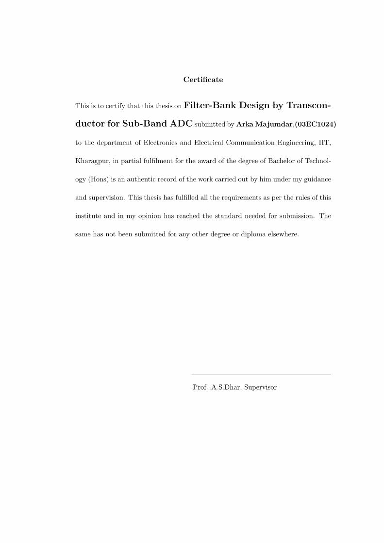
Certificate
This is to certify that this thesis on Filter-Bank Design by Transcon-
ductor for Sub-Band ADC submitted by Arka Majumdar,(03EC1024)
to the department of Electronics and Electrical Communication Engineering, IIT,
Kharagpur, in partial fulfilment for the award of the degree of Bachelor of Technol-
ogy (Hons) is an authentic record of the work carried out by him under my guidance
and supervision. This thesis has fulfilled all the requirements as per the rules of this
institute and in my opinion has reached the standard needed for submission. The
same has not been submitted for any other degree or diploma elsewhere.
Prof. A.S.Dhar, Supervisor

This Thesis is dedicated to my Parents and Godhuli
Acknowledgments
I would like to express my sincere gratitude to my supervisor Dr. Anindya Sundar
Dhar for his guidance, advice and encouragement throughout the course of this
research. I am deeply indebted to Prof. Nirmal B. Chakrabarti for his unfailing
support and guidance throughout my undergraduate education. He has been an
inspirational source for my many daunting undertakings and put himself engaged
round the clock in the supervision of my work. Thanks are also due to Dr. Pradip
Mandal and Dr. Saswat Chakrabarty, who helped me whenever I was stuck at
any problem. I am also grateful to Prof. Hossein Hashemi, University of Southern
California, who gave me a very good idea about how to do research. I would like
to thank some of my friends Mr. Saurabh Bandyopadhya, Mr. Sailesh Pati, Mr.
Sandipan Kundu, Mr. Shreepriya Das, Mr. Kaushik Dasgupta and Mr. Abhishek
Ghosh, who were real help during my working in Advanced VLSI Design Laboratory.
I also like to thank Mr. Saurabh Maiti , Mr. Mayur Agrawaal and Mr. N.C.Reddy.
I am really grateful to all these people as I have shared many discussions with them
and I got immense support and never-ending inspiration from them. Finally, I would
like to thank my parents and Godhuli for their continuing inspiration, unyielding
support, encouragement and their unconditional love over the years.
Arka Majumdar
Indian Institute of Technology, Kharagpur
May 2007
iv

Filter-Bank Design by Transconductor for Sub-Band
ADC
Arka Majumdar, B. Tech (Hons)
Indian Institute of Technology, Kharagpur, 2007
Supervisor: Prof. A.S.Dhar
The growing VLSI technology and ease in signal processing in digital domain calls
for high-speed good ADCs. In this thesis a new type of ADC, viz., sub-band ADC is
described. The system level simulation and mathematical analysis are done to show
that in certain applications, Sub-band ADC performs better than conventional time-
interleaved ADC. The practical difficulties of implementation this ADC in silicon are
described. The most critical part of sub-band ADC, viz., the filter-bank is designed
and simulated in CADENCE in commercially available 0.18µ technology. Two types
of architectures are described and their design criteria are elaborated. For designing
filters gmC topology is used and hence a transconductor is designed. An analog
active delay is designed in MOS. For recombining the signal from different bands a
new heuristic is proposed and considerable performance (around 6dB) enhancement
is obtained.
v

Contents
Acknowledgments iv
Abstract v
List of Figures ix
List of Tables xiii
Chapter 1 Introduction 1
1.1 Motivation . . . . . . . . . . . . . . . . . . . . . . . . . . . . . . . . 11.2 Problems With Conventional ADCs . . . . . . . . . . . . . . . . . . 2
1.2.1 Jitter Analysis . . . . . . . . . . . . . . . . . . . . . . . . . . 21.3 Concept of Sub-band Coding . . . . . . . . . . . . . . . . . . . . . . 41.4 Applications . . . . . . . . . . . . . . . . . . . . . . . . . . . . . . . . 41.5 The Work Described in the Thesis . . . . . . . . . . . . . . . . . . . 5
Chapter 2 System Level Description of Sub-band ADC 7
2.1 Introduction . . . . . . . . . . . . . . . . . . . . . . . . . . . . . . . . 72.2 Virtue of Sub-band ADC . . . . . . . . . . . . . . . . . . . . . . . . 7
2.2.1 Dynamic Range Reduction . . . . . . . . . . . . . . . . . . . 72.2.2 Lower Sampling Frequency . . . . . . . . . . . . . . . . . . . 102.2.3 Lower Jitter Effect . . . . . . . . . . . . . . . . . . . . . . . . 112.2.4 Noise Immunity in Dead Bands . . . . . . . . . . . . . . . . . 112.2.5 Ease in Reconstruction . . . . . . . . . . . . . . . . . . . . . . 11
2.3 System Level Simulation . . . . . . . . . . . . . . . . . . . . . . . . . 112.3.1 Simulation Procedure . . . . . . . . . . . . . . . . . . . . . . 112.3.2 Case I:Simulation With Three-tone Signal and Noise . . . . . 12
vi
2.3.3 Case II:Simulation With Chirp Signal . . . . . . . . . . . . . 132.3.4 Case III:Comparison With Time-interleaved ADC . . . . . . 18
2.4 Difficulty in Practical Implementation . . . . . . . . . . . . . . . . . 18
Chapter 3 Transconductance 22
3.1 Introduction . . . . . . . . . . . . . . . . . . . . . . . . . . . . . . . . 223.2 Review . . . . . . . . . . . . . . . . . . . . . . . . . . . . . . . . . . . 22
3.2.1 Performance Criteria of Transconductors . . . . . . . . . . . . 233.2.2 Transconductance-C Filter . . . . . . . . . . . . . . . . . . . 24
3.3 Performance of the Transconductor Used . . . . . . . . . . . . . . . . 25
Chapter 4 Filter-bank:First Architecture 30
4.1 Introduction . . . . . . . . . . . . . . . . . . . . . . . . . . . . . . . . 304.2 Description of Architecture . . . . . . . . . . . . . . . . . . . . . . . 304.3 Implementation and Performance of Filters . . . . . . . . . . . . . . 31
Chapter 5 Filter-bank:Second Architecture 42
5.1 Introduction . . . . . . . . . . . . . . . . . . . . . . . . . . . . . . . . 425.2 Architecture and Its Advantages . . . . . . . . . . . . . . . . . . . . 425.3 Design of Delay Block & Subtractor . . . . . . . . . . . . . . . . . . 435.4 Result . . . . . . . . . . . . . . . . . . . . . . . . . . . . . . . . . . . 49
Chapter 6 ADC Block 52
6.1 Introduction . . . . . . . . . . . . . . . . . . . . . . . . . . . . . . . . 526.2 Sample-Hold . . . . . . . . . . . . . . . . . . . . . . . . . . . . . . . 526.3 Comparator . . . . . . . . . . . . . . . . . . . . . . . . . . . . . . . . 536.4 Flash ADC . . . . . . . . . . . . . . . . . . . . . . . . . . . . . . . . 57
Chapter 7 Reconstruction 60
7.1 Introduction . . . . . . . . . . . . . . . . . . . . . . . . . . . . . . . . 607.2 Methodology of Reconstruction . . . . . . . . . . . . . . . . . . . . . 60
7.2.1 The Main Concept . . . . . . . . . . . . . . . . . . . . . . . . 617.3 Simulation and Result . . . . . . . . . . . . . . . . . . . . . . . . . . 61
Chapter 8 Other Supplementary Works 67
8.1 Introduction . . . . . . . . . . . . . . . . . . . . . . . . . . . . . . . . 678.2 Sub-sampling . . . . . . . . . . . . . . . . . . . . . . . . . . . . . . . 67
vii

8.2.1 Implementation in silicon . . . . . . . . . . . . . . . . . . . . 698.3 Low-pass Sigma-Delta Modulator . . . . . . . . . . . . . . . . . . . . 698.4 Band-pass Filters . . . . . . . . . . . . . . . . . . . . . . . . . . . . . 728.5 Folding Architecture . . . . . . . . . . . . . . . . . . . . . . . . . . . 72
Chapter 9 Conclusion and Future Work 75
9.1 Summary . . . . . . . . . . . . . . . . . . . . . . . . . . . . . . . . . 759.2 Future Work . . . . . . . . . . . . . . . . . . . . . . . . . . . . . . . 76
Bibliography 77
viii

List of Figures
2.1 Probability distribution of a signal and its filtered output . . . . . . 92.2 Relation between the variance of the filtered signal and the filter order 102.3 Simulink Model for sub-band ADC . . . . . . . . . . . . . . . . . . . 122.4 Spectrum of the Jittery Clock . . . . . . . . . . . . . . . . . . . . . . 132.5 Spectrum of the output of the sub-band ADC . . . . . . . . . . . . . 142.6 Spectrum of the output of the conventional ADC . . . . . . . . . . . 142.7 Spectrum of the three bands . . . . . . . . . . . . . . . . . . . . . . . 152.8 Spectrum of the final result when all the bands are sampled at 2GHz 162.9 Spectrum of the final result when the first band is sampled at 1GHz 162.10 Second Filter-bank Architecture (involving only low-pass filters and
delays) . . . . . . . . . . . . . . . . . . . . . . . . . . . . . . . . . . . 172.11 Spectrum of bands (obtained by the second type of Filter-Bank) . . 172.12 Spectrum of the output of time-interleaved ADC when the signal is
noisy . . . . . . . . . . . . . . . . . . . . . . . . . . . . . . . . . . . . 192.13 Spectrum of the output of sub-band ADC when the signal is noisy . 192.14 Spectrum of the output of time-interleaved ADC when the signal is
noise free . . . . . . . . . . . . . . . . . . . . . . . . . . . . . . . . . 202.15 Spectrum of the output of sub-band ADC when the signal is noise free 20
3.1 The circuit used for implementing the transconductor (differentialtopology) . . . . . . . . . . . . . . . . . . . . . . . . . . . . . . . . . 26
3.2 The linearity of the transconductor: first harmonic measured at dif-ferent input frequencies and different control current . . . . . . . . . 27
3.3 The non-linearity of the transconductor: third harmonic measured atdifferent input frequencies and different control current . . . . . . . . 27
ix

3.4 The tunability of the transconductance with controlling current (mea-sured by the cut-off frequency of the first order gmC low-pass filter . 28
4.1 Block-Diagram of Filter-bank Architecture . . . . . . . . . . . . . . . 314.2 Block-Diagram for gm-c filter (single-ended) . . . . . . . . . . . . . . 324.3 Block-Diagram for gm-c filter (double-ended) . . . . . . . . . . . . . 324.4 Second-order Filter Low-pass Response (Upper one is Phase and
Lower one is Magnitude Response) . . . . . . . . . . . . . . . . . . . 334.5 Second-order Filter Band-pass Response (Upper one is Phase and
Lower one is Magnitude Response) . . . . . . . . . . . . . . . . . . . 344.6 Second-order Filter High-pass Response (Upper one is Phase and
Lower one is Magnitude Response) . . . . . . . . . . . . . . . . . . . 354.7 Frequency Response (Phase and Magnitude) of the low-pass filter . 354.8 Frequency Response (Phase and Magnitude) of the first band-pass
filter . . . . . . . . . . . . . . . . . . . . . . . . . . . . . . . . . . . . 364.9 Frequency Response (Phase and Magnitude) of the second band-pass
filter . . . . . . . . . . . . . . . . . . . . . . . . . . . . . . . . . . . . 364.10 Spectrum of the input chirp signal to the filter-bank . . . . . . . . . 374.11 The waveform of the original signal and the signal obtained after
passing the chirp signal through the low-pass filter . . . . . . . . . . 374.12 The spectrum of the output of the low-pass filter (the first band) . . 384.13 The waveform of the signal obtained after passing the chirp signal
through the second band-pass filter (the second band) . . . . . . . . 384.14 The spectrum of the output of the second bandpass filter (the second
band) . . . . . . . . . . . . . . . . . . . . . . . . . . . . . . . . . . . 394.15 The waveform of the signal obtained after passing the chirp signal
through the second band-pass filter(the third band) . . . . . . . . . 394.16 The spectrum of the signal obtained after passing the chirp signal
through the second band-pass filter(the third band) . . . . . . . . . 404.17 The linearity of the low pass filter . . . . . . . . . . . . . . . . . . . 404.18 The linearity of the first band pass filter . . . . . . . . . . . . . . . 414.19 The linearity of the second band pass filter . . . . . . . . . . . . . . 41
5.1 The circuit used for implementing delay in analog domain . . . . . . 445.2 The circuit used for implementing subtractor in analog domain . . . 465.3 The output of the subtractor when input is totally differential . . . . 47
x

5.4 Cascaded delays (Cm is the load due to the next stage) . . . . . . . 485.5 The actual signal, delayed signal by one stage delay, delayed single
by two stages . . . . . . . . . . . . . . . . . . . . . . . . . . . . . . . 485.6 The two bands obtained using the filter-bank (consisting of low-pass
filters and delays) . . . . . . . . . . . . . . . . . . . . . . . . . . . . . 495.7 The signal and the reconstructed signal (in analog domain) using the
filter-bank (consisting of low-pass filters and delays) . . . . . . . . . 505.8 Spectrum of the first band (obtained by low-pass filtering) . . . . . . 505.9 Spectrum of the second band (obtained by subtracting the low-pass
signal from the original signal) . . . . . . . . . . . . . . . . . . . . . 515.10 Spectrum of the reconstructed signal (just adding the two signals in
analog domain) . . . . . . . . . . . . . . . . . . . . . . . . . . . . . . 51
6.1 The Circuit Diagram for Sample and Hold . . . . . . . . . . . . . . . 536.2 The output of the Sample and Hold Circuit when the clock frequency
is 800MHz and the input signal is at 200MHz . . . . . . . . . . . . 546.3 The Circuit Diagram for Comparator(open-loop) . . . . . . . . . . . 546.4 The Circuit Diagram for Comparator(Regenerative) . . . . . . . . . 556.5 The output of the open-loop comparator when reference voltage is low 556.6 The output of the open-loop comparator when reference voltage is high 566.7 The output of the regenerative comparator when reference voltage is
low . . . . . . . . . . . . . . . . . . . . . . . . . . . . . . . . . . . . . 566.8 The output of the regenerative comparator when reference voltage is
high . . . . . . . . . . . . . . . . . . . . . . . . . . . . . . . . . . . . 576.9 Block Diagram of Flash ADC . . . . . . . . . . . . . . . . . . . . . . 576.10 The output of the 3-bit flash ADC (from top to bottom is MSB to
LSB) . . . . . . . . . . . . . . . . . . . . . . . . . . . . . . . . . . . . 59
7.1 Spectrum of the Input Chirp Signal . . . . . . . . . . . . . . . . . . 627.2 Magnitude Response of three analog filters . . . . . . . . . . . . . . . 627.3 The Spectrum of the signal when the three bands are just added . . 637.4 The Desired Response of the FIR filters for all three bands . . . . . 637.5 The response of three digital filters as designed in MATLAB . . . . 647.6 The Spectrum of the signal after applying the digital filtering technique 66
8.1 Input spectra of the sub-sampling receiver output . . . . . . . . . . 68
xi

8.2 Output spectra of the sub-sampling receiver output . . . . . . . . . 688.3 Architecture simulated in MATLAB Simulink for sub-sampling re-
ceiver . . . . . . . . . . . . . . . . . . . . . . . . . . . . . . . . . . . 698.4 The Circuit Diagram for Sub-sampling . . . . . . . . . . . . . . . . . 698.5 The Input and Output Spectra for Sub-sampling as simulated in CA-
DENCE . . . . . . . . . . . . . . . . . . . . . . . . . . . . . . . . . . 708.6 Circuit for sigma-delta modulator (low-pass) . . . . . . . . . . . . . 718.7 Output of Sigma-Delta Modulator . . . . . . . . . . . . . . . . . . . 718.8 Filter Band-pass Response (Flat-band) . . . . . . . . . . . . . . . . . 728.9 Filter Band-pass Response (this can generate quadrature output) . . 738.10 Quadrature wave-forms for the band-pass filter . . . . . . . . . . . . 738.11 The output of folder circuit . . . . . . . . . . . . . . . . . . . . . . . 748.12 The Folding Circuit . . . . . . . . . . . . . . . . . . . . . . . . . . . 74
xii

List of Tables
2.1 SNR of the input signal and the output of conventional ADC andsub-band ADC for the three cases . . . . . . . . . . . . . . . . . . . 18
7.1 MSE of the signal after applying the reconstruction technique andthe performance enhancement with filter order (Just adding MSE is1.7694× 10−5) . . . . . . . . . . . . . . . . . . . . . . . . . . . . . . 65
xiii

Chapter 1
Introduction
1.1 Motivation
In today’s Electronics Industry, Analog to digital converters are gaining a lot ofattention due to the ease of signal processing in digital domain [1]. Digital SignalProcessing Algorithms are becoming more powerful, while advances in integrated-circuit (IC) technology are providing compact, efficient implementation of thesealgorithms in silicon. But naturally occurring signals are analog and for all thedigital processors we require an interface to convert the analog signal to a digital one.In fact, the whole philosophy of realization of a large system may be significantlyeased by the performance enhancement of many analog circuits (like filters, Analog-Digital-Converters etc.) at some interfacing point between real world and digitalcomputation. Advent of software defined radio has made the necessity of ADC,working at very high speed and for a large bandwidth, more prominent. Bit orresolution and dynamic range are two key specifications of an ADC and people aretrying to get a good trade-off between these two [2] while designing ADCs. Now-a-days over-sampling ADCs are also getting attention with nyquist-rate ADCs for itsbetter resolution and better noise shaping. But the performance of all the ADCs islimited by the requirement of good sample-hold circuit. In many applications, theincoming signal is of very high band-width. To digitize this signal, the samplingfrequency required is very high and often unreachable in practical realization onsilicon. These practical problems motivated me to design a new kind of ADC, whichrequires less sampling frequency. As the basic concept is taken from sub-band codingtechnique, it is called sub-band ADC.
1
My thesis is about some basic investigations which I carried out into the pos-sibility of breaking the analog signal in several frequency sub-bands and performinganalog to digital conversion in each frequency band separately and finally combinethe signals from each band. To put this work into context, it may be wise to discussabout the basic problem when the incoming signal is of high bandwidth and theidea by which this can be combatted.
1.2 Problems With Conventional ADCs
According to nyquist criteria, a signal should be sampled at more than twice thebandwidth of the signal for faithful reconstruction of the original signal from sampledsignal. Hence for a wide band-width signal the sampling frequency required is veryhigh. For sampling, we need good track-and-hold circuits. But whenever the circuitsare mapped to silicon, due to many non-idealities the track-and-hold cannot workproperly at high frequency.
Again all the track-and-hold circuits need a clock of the sampling frequency.Due to phase noise all practical clocks are jittery. The phase noise increases with thefrequency of the clock and hence at high frequency the jittery clock causes distortionin the sampled digital signal. In the following subsection an analysis is given to showhow the jitter in clock causes distortion in the signal.
However, to reduce the requirement of track-and-hold circuit operating atvery high sampling frequency people have already proposed time-interleaved ADC.This type of ADC basically has M ADCs, each sampling the signal at Fs/M fre-quency in a serial fashion and thus ultimately results in sampling the signal at afrequency Fs. A fundamental problem with an actual implementation of such time-interleaved architecture is that each ADC sees the full bandwidth of the input signaland hence clock jitter is very detrimental to the performance of this type of ADC.Hence good time-interleaved ADC needs a good sample-hold circuit along with aclock with a very little phase noise. Both of these are difficult to achieve. Apartfrom this the synchronization of the clocks is also difficult in practice and clock-skewcauses problem in time-interleaved ADCs.
1.2.1 Jitter Analysis
Jitter is a severe problem in any sample-hold circuit. The clock-jitter is translatedinto the output spectra and distorts the signal. A theoretical jitter analysis is
2

performed to predict the distortion in output spectra from the clock-jitter. Twotypes of analysis are performed (time and frequency domain analysis) to reach thesame result. Let the input signal be A sin(2πfint) and the sampling clock (which isjittery) be B sin(2πfst).
Time Domain Analysis: Due to jitter at nth sampling instant the actualinstant becomes nT + τn. So the error ε(t) becomes
ε(t) = A sin(2πfin(nT + τn))−A sin(2πfinnT ) (1.1)
By taylor’s series expansion
ε(t) = A2πfinτn cos(2πfinnT ) (1.2)
Hence noise-power Nτ in the sampled signal is given by
Nτ = E((ε(t))2) = 2π2f2inA2σ2
t (1.3)
whereE((τn)2) = σ2
t (1.4)
Now in the similar manner, for oscillator due to the jitter
εosc(t) = B2πfsτn cos(2πfsnT ) (1.5)
Noscτ = E((εosc(t))2) = 2π2f2s B2σ2
t (1.6)
Hence the ratio R of the noise-power in oscillator and sampled signal is
R = (fin
fs)2(
A
B)2 (1.7)
The same relation can be obtained by modeling the jitter as a random walk model[3].
Frequency-Domain Analysis: In frequency domain also the same analy-sis can be done [4]. Oscillator output S(t) is
S(t) = B sin(2πfs(nT + τn)) = B sin(2πfsnT ) + 2πfsτnB cos(2πfssinT ) (1.8)
So if the autocorrelation of the jitter is r(λ) then the autocorrelation R(λ) of the
3
oscillator noisy signal is given by
R(λ) =B2
2E(cos(2πfsτn))(1 + 4π2f2
s )r(λ)) (1.9)
So PSD S(f) is given by
S(f) =B2
4(1 + (2πfs)2s(f)) ∗ (δ(f + fs) + δ(f − fs)) (1.10)
For the sampled output from the relation given in 1.5 autocorrelation as well asPSD obtained is
R(λ) =A2
2E(cos(2πfinτn))(4π2f2
in)r(λ)) (1.11)
Ssample(f) =A2
4(1+(2πfin)2s(f))∗ 1
T
k=+∞∑
k=−∞(δ(f−fin+
k
T)+δ(f +fin+
k
T)) (1.12)
So in baseband the ratio becomes the same as obtained from the time-domain asf2
s >> 1.
1.3 Concept of Sub-band Coding
In video and image applications people use sub-band coding. The idea is to breakthe image or the video in several frequency bands. Now in most of these signalsthe information content is non-uniformly distributed in frequency bands. Mostof the information are in lower frequencies and higher frequency bands containless information. So the lower frequency signals are assigned more number of bitscompared to the higher frequency signals and thus total number of bits are reducedretaining the amount of information. This sub-band technique is very much usedin speech analysis [5]. This idea is exploited in sub-band ADC. A mathematicalanalysis on the virtue of sub-band ADC is given in chapter 2.
1.4 Applications
There are many applications where the sub-band ADC will be helpful. Now-a-daysUWB radio is gaining lots of attention. This type of radio operates by spreading theenergy of the radio signal very thinly from near d.c. to a few gigahertz [6]. For thistype of radio this ADC can be useful. In some satellite applications we get signal
4

with very wide band-width [7]. In that case the signal information is not uniformlydistributed. Some band contain more information compared to other bands. Herethis type of ADC is useful. In fact, if in some applications we see the signal is ofvery high band-width and the information is not uniformly spread over the wholefrequency band, then this type of ADC gives very good performance.
1.5 The Work Described in the Thesis
The thesis mainly deals with the possible CMOS implementation of this new type ofADC. Due to many practical difficulties no ADC performs well when the input sig-nal bandwidth is more. The architecture proposed here works better in this type ofscenario. The virtue of this proposed sub-band ADC is mathematically established.By MATLAB simulations, the superiority of sub-band ADC over conventional time-interleaved ADC is established. Though mathematically true, practical implemen-tation of this type of ADC poses many problems. Those problems are addressedand possible solutions are found out in this thesis. I mainly concentrated on thefilter-bank design of this ADC as this is the most important part in this ADC. Twotypes of band-splitting architectures are proposed. In CADENCE, in commerciallyavailable 0.18µ technology the filter-banks are simulated. Here the incoming signalis split mainly in two bands. ADCs for each band is also designed. For this goodtrack-and-hold circuits and comparators are studied as well as designed in silicon.
The thesis is organized as follows. Chapter 2 deals with the system levelsimulation (mainly in MATLAB) of sub-band ADC and the performance enhance-ment is reported and mathematically analyzed. This chapter also gives many usefuldesign criteria of the ADC. Chapter 3 describes basic transconductor block andtransconductor-C filter. Different implementations of transconductors are discussedand the performance of the transconductor used in my case is reported. The next2 chapters deal with the filter-bank. Two different architectures for filter-banks arediscussed and their implementation in silicon are described. The advantages and dis-advantages of each architecture are also discussed. In chapter 6 the design of ADCis described. It includes design of good sample-hold as well as good comparatorcircuits. Chapter 7 mainly discusses the reconstruction in digital domain by meansof FIR filtering and equalization concept. The result obtained from the system-levelsimulation in MATLAB is also reported. Chapter 8 discusses some other works notdirectly related to the main work of the thesis. Chapter 9 draws the conclusion and
5

discusses about the future work.
6
Chapter 2
System Level Description of
Sub-band ADC
2.1 Introduction
In this chapter the system level simulations (the procedure and the result) on sub-band ADC are described. I have simulated the whole system in MATLAB and theperformance enhancement is reported. I have also established mathematically thereason for enhancement in performance.
2.2 Virtue of Sub-band ADC
Sub-band ADC can perform better than conventional time-interleaved ADC. In thissection, mathematically the virtue of sub-band ADC is established. The requirementof less sampling frequency for some bands are also established.
2.2.1 Dynamic Range Reduction
The dynamic range of the signal is reduced due to filtering. Variance of the signalis a good estimate of the dynamic range of the signal. The variance R(0) (R is theautocorrelation function of the signal) of a signal (whose spectral content lies in therange of ±f)can be expressed in terms of its Power Spectral Density (PSD) S(ω) as
R(0) =∫ +f
−fS(ω)dω (2.1)
7
After low pass filtering (with transfer function H(ω)) let the spectral content lies inthe range of ±w. Then the new variance R′(0) of the signal becomes
R′(0) =∫ +w
−wH(ω)S(ω)dω (2.2)
Now if |H(ω)| < 1, (which is true for a low-pass filter with pass-band gain 1) then thevariance after filtering reduces and this helps in reduction in the dynamic range. Forband-pass filtering also this argument holds true. This reduction in dynamic rangehelps in reduction in quantization noise. This is elaborated here. Let us assumethat the incoming signal amplitude is Gaussian distributed. So using non-uniformquantization (smaller steps at ±3σ limit) for the incoming signal total quantizationnoise qin is
qin = P1∆2
1
12+ (1− P1)
∆22
12(2.3)
Where P1 denotes the probability that the signal will be in ±3σ limit. For thefiltered signal also this is valid. But due to the reduction of variance the value of∆1 (which is proportional to the σ as δ1 = 6σ
2N ) reduces and thus the quantizationnoise is less. Again if the incoming signal amplitude is uniformly distributed andthe signal amplitudes are uncorrelated, then after filtering the amplitude is normallydistributed. Mathematically it can be argued that the filtering operation is nothingbut multiplying the random signal by some deterministic weights. If a random signalx(t) is passed through a filter then the output y(t) can be written as
y(t) =∫ t
0ξ(t)x(t)dt (2.4)
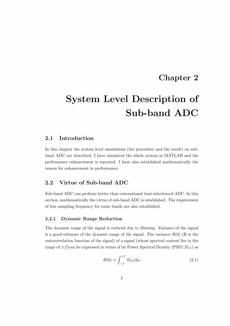
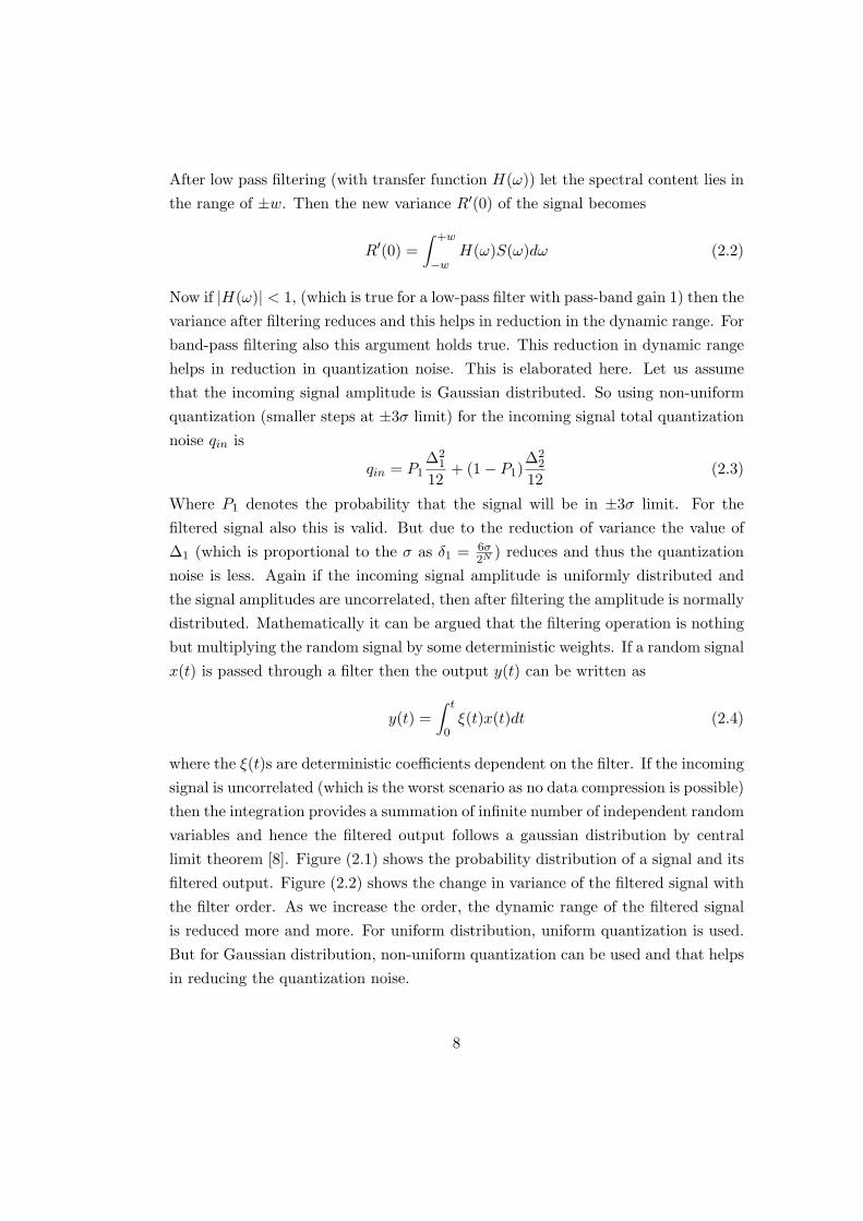
where the ξ(t)s are deterministic coefficients dependent on the filter. If the incomingsignal is uncorrelated (which is the worst scenario as no data compression is possible)then the integration provides a summation of infinite number of independent randomvariables and hence the filtered output follows a gaussian distribution by centrallimit theorem [8]. Figure (2.1) shows the probability distribution of a signal and itsfiltered output. Figure (2.2) shows the change in variance of the filtered signal withthe filter order. As we increase the order, the dynamic range of the filtered signalis reduced more and more. For uniform distribution, uniform quantization is used.But for Gaussian distribution, non-uniform quantization can be used and that helpsin reducing the quantization noise.
8

0 0.5 1 1.5 20
1
2
3
4
5
6x 10
−4
signal amplitude
prob
abili
ty
0 0.2 0.4 0.6 0.8 1 1.2 1.4 1.6 1.80
0.1
0.2
0.3
0.4
0.5
0.6
0.7
0.8
0.9
1x 10
−3
signal amplitude
prob
abili
ty
Figure 2.1: Probability distribution of a signal and its filtered output
9

2.2.2 Lower Sampling Frequency
As the signal is divided in bands, hence the sampling frequency required for thelower bands is less. Again, the band-pass sampling theory [9]states that for properreconstruction of a signal of bandwidth BW and at a center frequency of fc, it shouldbe sampled at 2×BW frequency only. The sampling frequency does not depend onfc. In some literature, it is proposed to down-convert the upper sub-bands of thesub-band ADC to lower bands and thus to reduce the sampling frequency for thehigher bands[10],[11].
But for a signal with equal signal components in all the frequency the down-conversion process is difficult to implement in silicon. The non-idealities of filters andthe down-converters make the SNR go low. So here I am doing the digitization keep-ing the higher sub-band at the same frequency. Though for lower frequency-bandsthe sampling frequency is reduced,this method calls for higher sampling frequencyfor the higher sub-bands but helps to reduce the effect of clock-jitter as the sample-hold faces a portion of the signal at the upper bands, unlike time-interleaved ADC,where the sample-hold faces the whole signal all the time. For lower sub-bands, the
1 2 3 4 5 0.2
0.3
0.4
0.5
0.6
0.7
0.8
0.9
1
filter order
varia
nce
of th
e fil
tere
d si
gnal
The input signalis Gaussian
Figure 2.2: Relation between the variance of the filtered signal and the filter order
10

jitter is less as the jitter noise increases with the frequency of the clock.
2.2.3 Lower Jitter Effect
The jitter due to the clock is less detrimental in case of sub-band ADC, as ADCswill not face the whole signal hence the effect of jitter is much less.
2.2.4 Noise Immunity in Dead Bands
If we have a signal with lots of dead-bands in the signal spectrum, then the noise inthe dead-band can be removed by filtering. Sub-band ADC helps in those cases byremoving the noise in the dead-bands. This is not a fundamental virtue of splittingbands and the same performance can be achieved by filtering and cleaning the noisebefore using conventional ADC. But sub-band ADC does not require any additionalfiltering to achieve this.
2.2.5 Ease in Reconstruction
As the output is digital it is easier to reconstruct the signal from digitized signalfrom different paths.
2.3 System Level Simulation
The whole system is simulated in MATLAB and Simulink. Several cases are simu-lated and the corresponding simulation results are shown. From these system levelsimulations significant design insights are found out. The reason for the performanceenhancement, or in some cases performance degradation is intuitively established.Before going to the simulation results, I will describe the simulation procedure.
2.3.1 Simulation Procedure
To characterize the system several inputs are used. Three-tone signal is used toinvestigate the effect of sub-band ADC in presence of dead-bands in the incomingsignal. Chirp signal is used to see the performance when there is no dead-band inthe incoming signal spectrum. The filters used are of very high order to reducethe overlap between filter contents. A second order filter transfer function is foundout and is incorporated in simulink. Several such blocks are cascaded to obtain
11

the desired higher order transfer function. The in-built sample-hold function andquantizer of simulink are used. Quantization step is kept same for all the simulationsto ensure same quantization noise for all cases. Figure 2.3 shows one such simulationsetup. The system is also simulated in presence of white gaussian noise. To establish
L2.s
den(s)
Transfer Fcn9
L2.s
den(s)
Transfer Fcn8
L1.s
den(s)
Transfer Fcn7
L1.s
den(s)
Transfer Fcn6
L1.s
den(s)
Transfer Fcn5
L1.s
den(s)
Transfer Fcn4
L3.s
den(s)
Transfer Fcn16
L3.s
den(s)
Transfer Fcn15
L3.s
den(s)
Transfer Fcn14
L3.s
den(s)
Transfer Fcn13
L2.s
den(s)
Transfer Fcn11
L2.s
den(s)
Transfer Fcn10
band6
To Workspace7
band5
To Workspace6
band12
To Workspace5
signal
To Workspace4 band3
To Workspace2
band11
To Workspace1
band10
To Workspace
S/H
Sampleand Hold3
S/H
Sampleand Hold2
S/H
Sampleand Hold1
Quantizer3
Quantizer2
Quantizer1
PulseGenerator3
PulseGenerator2
PulseGenerator1
Chirp Signal
Figure 2.3: Simulink Model for sub-band ADC
its virtue over time-interleaved ADC, simulation with jittery clock is performed.For this jittery clock has been generated. To generate the jittery clock I first passa gaussian white noise through a very narrow band filter. Then I hard-limit thesignal to get jittery clock. As the filter is very narrow-band hence it passes otherfrequencies in small amount. The spectrum of jittery clock is shown in figure 2.4.
2.3.2 Case I:Simulation With Three-tone Signal and Noise
Here a three tone signal (frequency 50MHz, 150MHz and 250MHz) with noiseis taken as input. Here we are comparing two situations. In both the situations,
12

we have jitter free clock. In the first case, the whole signal is sampled followingnyquist rate. In the second case, the signal is broken in three bands and eachband is sampled at corresponding nyquist frequency. Table 2.1 (Case-I) shows theperformance enhancement in the sub-band ADC. Figure 2.5 and figure 2.6 showthe spectrum of the output of sub-band ADC and the conventional ADC (withoutsplitting the signal in bands). Here we can see that the output SNR of the sub-band ADC is more than the input SNR. Actually the sub-band ADC is cleaningthe out-band noise and thus this performance enhancement is achieved. In thiscontext, I want to make an important observation. If there can be any ADC whichcan sample the whole signal following nyquist criteria, then no other ADC can givebetter performance compared to that. The need for other ADCs roots in the factthat such high sampling frequency is not achievable.
2.3.3 Case II:Simulation With Chirp Signal
The next simulation is performed with no dead-band in the signal spectrum. Forthis, a chirp signal (bandlimited from d.c. to 500MHz) is used. Here also theclocks are assumed to be jitter free. The filters are designed such that, just addingthe signal in analog domain gives back the signal. Here second order filters are
0 1 2 3 4 5
x 109
0
0.05
0.1
0.15
0.2
0.25
0.3
0.35
frequency
spet
ral c
ompo
nent
Figure 2.4: Spectrum of the Jittery Clock
13

0 0.5 1 1.5 2 2.5 3
x 108
−35
−30
−25
−20
−15
−10
−5
0
Frequency
The
Spe
ctru
m
Figure 2.5: Spectrum of the output of the sub-band ADC
0 0.5 1 1.5 2 2.5 3
x 108
−35
−30
−25
−20
−15
−10
−5
0
Frequency
The
Spe
ctru
m
Figure 2.6: Spectrum of the output of the conventional ADC
14
used. This criteria of reconstruction in analog domain is very important. In factdesigning higher order filters ensuring this reconstruction criteria is difficult andhence in chapter 7 some heuristic is proposed to reconstruct the signal totally.
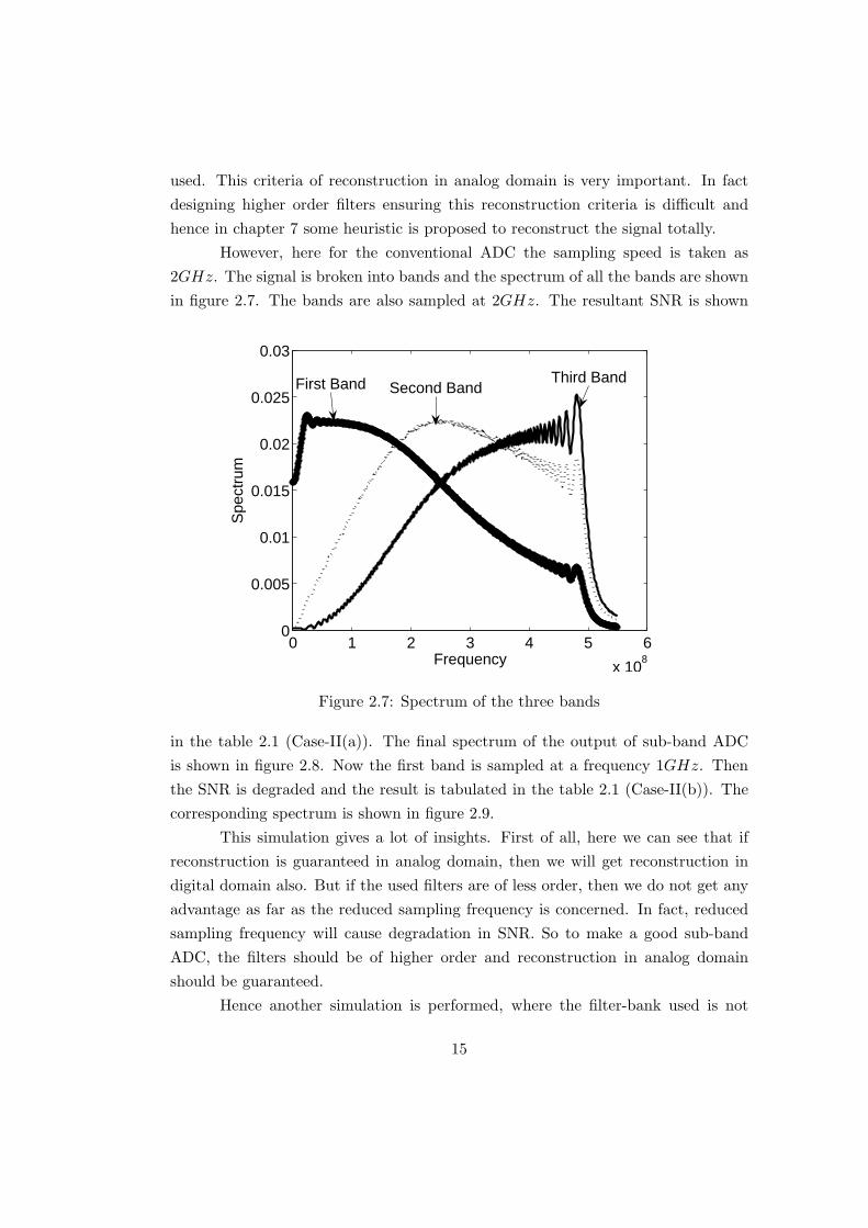
However, here for the conventional ADC the sampling speed is taken as2GHz. The signal is broken into bands and the spectrum of all the bands are shownin figure 2.7. The bands are also sampled at 2GHz. The resultant SNR is shown
0 1 2 3 4 5 6
x 108
0
0.005
0.01
0.015
0.02
0.025
0.03
Frequency
Spe
ctru
m
First Band Second BandThird Band
Figure 2.7: Spectrum of the three bands
in the table 2.1 (Case-II(a)). The final spectrum of the output of sub-band ADCis shown in figure 2.8. Now the first band is sampled at a frequency 1GHz. Thenthe SNR is degraded and the result is tabulated in the table 2.1 (Case-II(b)). Thecorresponding spectrum is shown in figure 2.9.
This simulation gives a lot of insights. First of all, here we can see that ifreconstruction is guaranteed in analog domain, then we will get reconstruction indigital domain also. But if the used filters are of less order, then we do not get anyadvantage as far as the reduced sampling frequency is concerned. In fact, reducedsampling frequency will cause degradation in SNR. So to make a good sub-bandADC, the filters should be of higher order and reconstruction in analog domainshould be guaranteed.
Hence another simulation is performed, where the filter-bank used is not
15

0 1 2 3 4 5 6
x 108
0
0.005
0.01
0.015
0.02
0.025
Frequency
Spe
ctru
m
Figure 2.8: Spectrum of the final result when all the bands are sampled at 2GHz
0 1 2 3 4 5 6
x 108
0
0.005
0.01
0.015
0.02
0.025
Frequency
Spe
ctru
m
Figure 2.9: Spectrum of the final result when the first band is sampled at 1GHz
16

conventional parallel filter-bank type. Rather here the signal is broken into bandsby means of low-pass filters and delay banks. The architecture is shown in figure2.10.
Figure 2.10: Second Filter-bank Architecture (involving only low-pass filters anddelays)
The spectrum of the bands are shown in figure 2.11. Here we get same SNR
0 1 2 3 4 5 6
x 108
0
0.005
0.01
0.015
0.02
0.025
Frequency
Spe
ctru
m
Figure 2.11: Spectrum of bands (obtained by the second type of Filter-Bank)
as conventional ADC, with less sampling frequency for the lower bands.
17

Table 2.1: SNR of the input signal and the output of conventional ADC and sub-band ADC for the three cases
Cases Actual Signal Conventional ADC Sub-band ADC
Case-I 7.8391dB 6.5545dB 8.8526dB
Case-II(a) 14.8263dB 13.0733dB 13.0733dB
Case-II(b) 14.8263dB 13.0733dB 12.6405dB
Case-III(a) 7.8391dB 4.7308dB 7.8391dB
Case-III(b) 50.2508dB 12.0720dB 19.3005dB
2.3.4 Case III:Comparison With Time-interleaved ADC
So far in the simulations jitter is not considered. Those simulations are done togain some insights about the design of sub-band ADC. In this simulation the jittereffect is considered. The simulation is performed on the three-tone signal (frequency50MHz, 150MHz and 250MHz) with noise and without noise. Clocks used arejittery and the jitter increases with the frequency. The signal is passed through atime-interleaved ADC and a sub-band ADC.
In both cases (with noise and without noise) the signal is broken in threebands for sub-band ADC and there are three channels for time-interleaved ADC.For time-interleaved ADC sampling frequency in each channel is kept 500MHz. Forsub-band ADC, the sampling frequency at first two-bands are kept at 500MHz andfor the third band it is kept 1GHz. Table 2.1 (Case-III(a)) shows the performancewhen there is noise. Figure 2.12 and 2.13 shows the spectrum of the final output.Table 2.1 (Case-III(b)) shows the performance when there is no noise. Figure 2.14and 2.15 shows the spectrum of the final output.
2.4 Difficulty in Practical Implementation
Though the ADC performs well in system level, it is difficult to implement it insilicon. When I tried to implement the whole system by means of analog circuit insilicon, I came across the following difficulties. In no literature people have reportedthe implementation the sub-band ADC in CMOS technology. So I think it is wiseto mention the practical difficulties of implementation, so that the non-triviality of
18

0 0.5 1 1.5 2 2.5 3
x 108
−30
−25
−20
−15
−10
−5
0
Frequency
Spe
ctru
m
Figure 2.12: Spectrum of the output of time-interleaved ADC when the signal isnoisy
0 0.5 1 1.5 2 2.5 3
x 108
−35
−30
−25
−20
−15
−10
−5
0
Frequency
Spe
ctru
m
Figure 2.13: Spectrum of the output of sub-band ADC when the signal is noisy
19

0 0.5 1 1.5 2 2.5 3
x 108
−40
−35
−30
−25
−20
−15
−10
−5
0
Frequency
Spe
ctru
m
Figure 2.14: Spectrum of the output of time-interleaved ADC when the signal isnoise free
0 0.5 1 1.5 2 2.5 3
x 108
−40
−35
−30
−25
−20
−15
−10
−5
0
Frequency
Spe
ctru
m
Figure 2.15: Spectrum of the output of sub-band ADC when the signal is noise free
20

many blocks can be established, though they may seem to be trivial in system levelsimulation.
1. Designing a good filter bank is the main challenge in practical implementationof sub-band ADC. The filters designed are not brick-walled and hence therewill be always some overlap between different bands. This causes error in thedata conversion. If dead-bands are present in the signal, then the filtering iseasier. But if the spectral components are distributed in the whole frequencyrange, then it is difficult to do proper filtering.
2. Maintaining the linear phase characteristic of the filter is difficult. In a mod-ified architecture(described in chapter 5), I have to design an analog delayblock. There the linear phase of the filter is must and it is difficult to achieve.
3. Though down-sampling seems lucrative in system level, but this is difficult todo in silicon. After breaking the signal into bands, for the higher bands thecenter frequency and the bandwidth is comparable (due to finite Q of the fil-ters) and hence down-conversion poses some problems. This down-conversionalso calls for up-conversion and a little mismatch in frequency produces a largedistortion.
4. Designing good sample-hold circuit as well as good comparator for ADC isalso a big challenge.
In this thesis, I am mainly concerned about the implementation of the filter-bankin silicon. Two types of architectures are proposed and for implementation of thefilters gm−C topology is selected. The design of delay block and subtractors are alsodescribed. Design of sample-hold circuit and comparators are discussed. As filter-banks are mainly based on transconductance-c topology, hence the transconductanceis described at length in the next chapter.
21

Chapter 3
Transconductance
3.1 Introduction
In this chapter, the different types of implementations of transconductors are de-scribed. Brief literature survey on various transconductor structures has been re-ported. Different performance criteria to design appropriate transconductors havealso been addressed here. Detailed analysis and design of the differential transcon-ductor, used throughout the thesis, have also been carried out in this chapter.
3.2 Review
This section presents comprehensive review of different transconductors and oper-ational transconductance amplifiers (OTA) which have been proposed for differentapplications of filters and amplifier structures. While BiCmos OTAs are receivingsome attention in the literature [12], CMOS transconductors have been highlightedsince CMOS technology is predominating the field of integrated circuit design forits significant use towards low power dissipation and major application in digitalcircuits. Some of the literatures contribute towards sub-threshold transconductorwith their inherent advantage of low transconductance gain, very low power dissi-pation and possibility of tuning and adjustability through current bias changing atthe cost of worsening noise performance [13].
Various transconductors and OTA structures, proposed in different litera-tures, are designed to fit with some specific application, so it is absolutely unreliableto fix one single performance criteria to design a transconductor for a specific appli-
22
cation. The following subsection describes the criteria, which are normally fixed todetermine meaningful classification between different transconductance topologies.
3.2.1 Performance Criteria of Transconductors
The brief descriptions of each criteria for measuring the performance are given below:
1. Bandwidth:One of the most important aspects of active lowpass filter designis the bandwidth of the OTA, defined as the frequency range between DC andthe 3-dB point of the OTA frequency response. Empirically, the OTA mustprovide bandwidth at least 10 times higher than the operating frequency.
2. Power Dissipation:One of the motivations for integrating analog filters istheir prospective use in portable system applications where low power dis-sipation is a major design consideration. In addition, the increased featuredensity of modern CMOS technologies leads to higher power dissipation perarea, which can cause reliability problems. Power dissipation of less than100mW is desirable for CMOS transconductors. Power dissipation can bemeasured as the product of the supply voltage and the total current flowingthrough the supply terminal.
3. Total Harmonic Distortion:In general, the output signal y(t) of a time-invariant electrical network can be expressed in terms of its input x(t) by aTaylor series expansion:
y(t) = a1x(t) + a2x2(t) + a3x
3(t) + .... (3.1)
where the coefficient a1 represents the desired linear gain of the network andcoefficients a2, a3, ... represent its distortions. In practice, the output signaly(t) of a transistor-level OTA will be distorted and its maximum signal levelwill be dictated by the non-linear effect of practical amplifier saturation char-acteristics. If for example, a sinusoidal signal is applied to the input of anOTA, then harmonic distortion is defined as the root-men-square (rms) valueof the ratio of all the harmonics an to the fundamental a1. In differentialimplementation the even harmonics are eliminated. Hence the odd harmonicsdecide the non-linearity. As the value of the harmonics reduces with the orderof the harmonics hence in most applications, we are concerned with the third
23
order distortion only. Mathematically, the third order distortion (THD) ismeasured as:
THD(dB) = 20log10(a3
a1) (3.2)
In some applications people are interested in total harmonic distortion andthis THD can be expressed as
THD(dB) = 20log10(
√√√√n∑
i=2
(ai
a1)2) (3.3)
where n depends on the application.
4. Tuning Range:In almost every OTA reported in the literature, the transcon-ductance gain gm is proportional to an external DC bias voltage or current.The ability to tune the gm is one of the main advantages of gm − C filterdesign, since it enables external control of filter parameters including centerfrequency (ω0), cutoff frequency (ωc) and quality factor (Q). A wide tuningrange is advantageous in active integrated filter design, especially for tuningωc or ω0 of the gm − C filter. The tuning range will be expressed in termsof the minimum and maximum gm value, which can be achieved within thepossible bias voltage or current range.
3.2.2 Transconductance-C Filter
Till today various analog filters in the megahertz range have been reported us-ing both switched capacitor and continuous time techniques. In my application, Ihave opted for the continuous time implementation and chosen transconductance-Ctopology. In this subsection, I mainly discuss about the reason behind choosingtransconductance-C topology by stating various advantages and disadvantages ofdifferent topologies.
Switched capacitor filters have some advantages of implementation, such aseasy tunability of frequency by varying the clock frequency and easy programmabil-ity. But they have got some drawbacks as well, which make them less suitable forhigh frequency application. Performance of switched capacitor filters is dependenton the clock, and at high frequency due to clock jitters, switched capacitor filters arenot suitable for high frequency applications. Switched capacitor filters also need preand post filters (anti-aliasing and smoothing) which due to small clock to baseband
24
frequency ratio must have sharp and precise cut-off characteristics, which is not eas-ily realizable in integrated circuits. Furthermore, switched capacitor filters also needa precise multi-phase clock signal four times or higher than the filter bandwidth.
Thus continuous time filters are always preferred for implementing high fre-quency filters [14], [15]. MOSFET-C and transconductance-C are the two maintechniques of realizing continuous time filters. Continuous time integrator is thebasic building block for both the topologies. Apart from the advantage of the highfrequency operation of the filters, the implementation of high order filters is veryeasy in transconductance-C filters. Here there is no global feedback and all the cas-caded structures have local feedback and hence stability of the higher order filtersis easily achieved.
But this type of filters has some disadvantages too. Due to the lack ofvirtual ground and low impedance nodes, continuous time integrators are sensitiveto parasitic capacitors. Capacitances at the output nodes also include the parasiticcapacitances at those nodes and hence distract it from the actual application. Againthese filters, due to high non-linearity, cannot filter the signal faithfully if the inputsignal amplitude is very large. The other drawbacks are the deviations of the gm/C
ratios due to process parameter tolerances, temperature variations, mismatches,aging etc.
3.3 Performance of the Transconductor Used
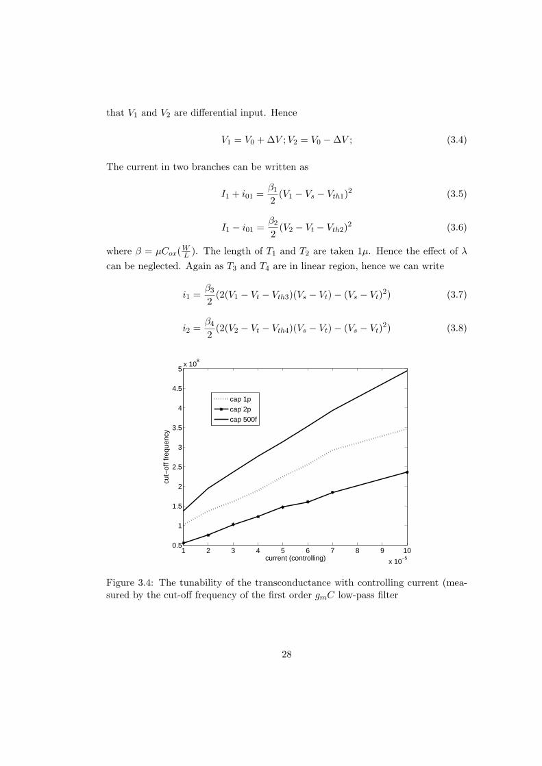
The transconductor used in my application is shown in figure 3.1. The transcon-ductance is source-degenerated to increase the linearity [16]. Some preliminaryobservations (on linearity and tunability of the value of the transconductance w.r.t.the biasing current) are reported here on the transconductance. Figures 3.2 and 3.3show the 1st and 3rd harmonics of the output current with the input voltage. Fig-ure 3.4 shows the cut-off frequency of transconductance-C filter w.r.t. the biasingcurrent. Actually by changing the current gm value is changed and that is reflectedin the increased cut-off frequency of gm− C filter.
The transistors used for source degeneration are 7−8 times less size of that ofthe input transistor as this gives the optimum performance [1]. These two transistorsare kept in linear region.
The transconductance of the transconductor is derived below: Let us assume
25

Figure 3.1: The circuit used for implementing the transconductor (differential topol-ogy)
26

0 0.05 0.1 0.15 0.2 0.25 0.3 0.350
0.2
0.4
0.6
0.8
1
1.2x 10
−4
input voltage
outp
ut c
urre
nt
110 M Input frequency and 10u current
155 M Input frequency and 40u current
200M Input frequency and 50u current
Figure 3.2: The linearity of the transconductor: first harmonic measured at differentinput frequencies and different control current
0 0.05 0.1 0.15 0.2 0.25 0.3 0.350
1
2
3
4
5
6x 10
−6
input voltage
the
third
har
mon
ic o
f the
out
put c
urre
nt
110M Input frequency and 10u current
150M input frequency and 40u current
200M input frequency and 50u current
Figure 3.3: The non-linearity of the transconductor: third harmonic measured atdifferent input frequencies and different control current
27
that V1 and V2 are differential input. Hence
V1 = V0 + ∆V ; V2 = V0 −∆V ; (3.4)
The current in two branches can be written as
I1 + i01 =β1
2(V1 − Vs − Vth1)2 (3.5)
I1 − i01 =β2
2(V2 − Vt − Vth2)2 (3.6)
where β = µCox(WL ). The length of T1 and T2 are taken 1µ. Hence the effect of λ
can be neglected. Again as T3 and T4 are in linear region, hence we can write
i1 =β3
2(2(V1 − Vt − Vth3)(Vs − Vt)− (Vs − Vt)2) (3.7)
i2 =β4
2(2(V2 − Vt − Vth4)(Vs − Vt)− (Vs − Vt)2) (3.8)
1 2 3 4 5 6 7 8 9 10
x 10−5
0.5
1
1.5
2
2.5
3
3.5
4
4.5
5x 10
8
current (controlling)
cut−
off f
requ
ency
cap 1p
cap 2p
cap 500f
Figure 3.4: The tunability of the transconductance with controlling current (mea-sured by the cut-off frequency of the first order gmC low-pass filter
28

Buti1 + i2 = i01 (3.9)
Adding equations 3.7 and 3.8 and assuming T3 and T4 are same we get
i01 = β3((V1+V2−2Vt−2Vth3)(Vs−Vt)−(Vs−Vt)2) = β3(Vs−Vt)(2V0−(Vs+Vt)−2Vth)(3.10)
Subtracting 3.6 from 3.5 and assuming T1 and T2 are same we get
i01 =β1
4(2V0 − (Vs + Vt)− 2Vth)(2∆V − (Vs − Vt)) (3.11)
Dividing equations 3.10 and 3.11 we get
(Vs − Vt) =2∆V β1
β1 + 4β3(3.12)
Now from equations 3.5 and 3.6 we get
2∆V − (Vs − Vt) =
√2(I1 + i01)
β1−
√2(I1 − i01)
β1(3.13)
By binomial expansion and a little algebra we get
gm =i01
V1 − V2=
4√
2β1β3
√I1
(β1 + 4β3)√
β1(3.14)
Hence by increasing β and bias current I1 the transconductance can be increased.This helps in designing filters with high cut-off frequency.
29

Chapter 4
Filter-bank:First Architecture
4.1 Introduction
To divide the signal into several frequency-bands, a filter-bank is required. Asexplained earlier, the filter-bank is the most important and critical part of sub-bandADC. The filter-banks should divide the signal in bands with very less overlap andall the bands together should contain the whole signal. Otherwise, after conversion,recombination of different bands will create problem. In this chapter the architectureof the filter-bank is described. The advantage and disadvantages of this architectureis also explained. The implementation of the filters is described and the performanceof the filters are reported.
4.2 Description of Architecture
The first architecture of the filter-bank consists of several parallel band-pass filters.Figure 4.1 shows the architecture of the filter-bank. In my project, I have dividedthe whole signal in two bands. In this architecture, ideally we need n filters fordividing the signal in n bands. Among those filters the first one is low-pass filterand all others are band-pass filters. But due to the non-ideality of filters and overlapbetween bands to split the signal in two bands, we require some more filters. So inmy analysis I have three filters and I get three bands, which are overlapping. Thefilters should satisfy certain criteria:
1. The filters should have zero pass-band ripple.
30
2. The filters should have sharp roll-off so that the overlap between bands areless.
3. The filters should be linear w.r.t. the input signal amplitude and should beable to handle signals with high amplitude.
4. They should have linear phase in the pass-band.
5. The filters should have flat band response for a large band-width.
4.3 Implementation and Performance of Filters
The filters are implemented in gm − C topology [17],[18]. The basic filter topologymade by gm − C is shown in the figure 4.2. The transfer function of this filter is
Vout(s) =s2C1C2Vc(s) + sC1gm2Vb(s) + gm1gm2Va(s)
s2C1C2 + sC1gm2 + gm1gm2(4.1)
Making Va = Vin and Vb = Vc = 0 the filter acts as a low-pass filter; Vb = Vin andVa = Vc = 0 makes the filter act as a band-pass filter and Vc = Vin and Va = Vb = 0makes the filter act as a high-pass filter. Following equations show the performancemeasure of the filters.
ω0 =√
gm1gm2
C1C2;Q =
√C2C1
(4.2)
As the transconductor designed here is differential hence the single ended filtertopology, as shown in figure 4.2, is converted into a double-ended filter (as shown infigure 4.3). The second order low-pass, band-pass and high-pass filter responses are
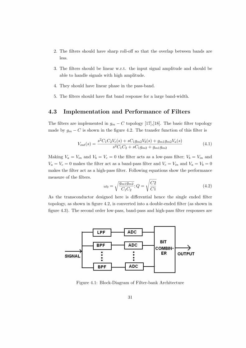
Figure 4.1: Block-Diagram of Filter-bank Architecture
31

Figure 4.2: Block-Diagram for gm-c filter (single-ended)
Figure 4.3: Block-Diagram for gm-c filter (double-ended)
32

shown in figure 4.4, 4.5 and 4.6. In my application, I tried to break the signal in two
Figure 4.4: Second-order Filter Low-pass Response (Upper one is Phase and Lowerone is Magnitude Response)
bands and hence I needed two filters. But as explained earlier, due to non-idealityof the filter-bank, I need to keep another filter. All three filters are designed inCMOS and simulated in CADENCE in commercially available 0.18µm technology.The order of the low pass filter designed is 8 and that of the band-pass filters are10. The low pass filter has a cut-off frequency of 100MHz. The center frequencyand bandwidth of the first band-pass filter are 130MHz and 50MHz and those ofthe second band-pass filter are 200MHz and 80MHz. The filter ac responses areshown in the figures 4.7, 4.8 and 4.9. To characterize the system, chirp signal is usedas input. This signal is used as it has all the frequency components in a specifiedband. Figure 4.10 shows the spectrum of the chirp signal used for characterization.This signal is passed through all the filters and the output of each filter (both thewaveform and the spectrum) are shown in figures 4.11, 4.12, 4.13, 4.14, 4.15, 4.16.
The linearity (w.r.t. the input signal amplitude) of the filters are measured.Figures 4.17, 4.18, 4.19 show the output amplitude versus the input amplitude for
33

these three filters. It can be noted that the low pass filter has more linearity,compared to the band-pass filters. The phase-response of the filters are also notlinear. In fact, as we increase the order of the filter, the linearity decreases andphase also becomes non-linear. To get same roll-off the order of the low-pass filteris less compared to that of the band-pass filter. That is why significant linearity canbe achieved in low-pass filters. But this architecture can break the signal in bands.The filters are of higher order and hence the foll-off is good. This architecture hasmany disadvantages (which will be explained in next chapter) and hence a newarchitecture is studied.
Figure 4.5: Second-order Filter Band-pass Response (Upper one is Phase and Lowerone is Magnitude Response)
34
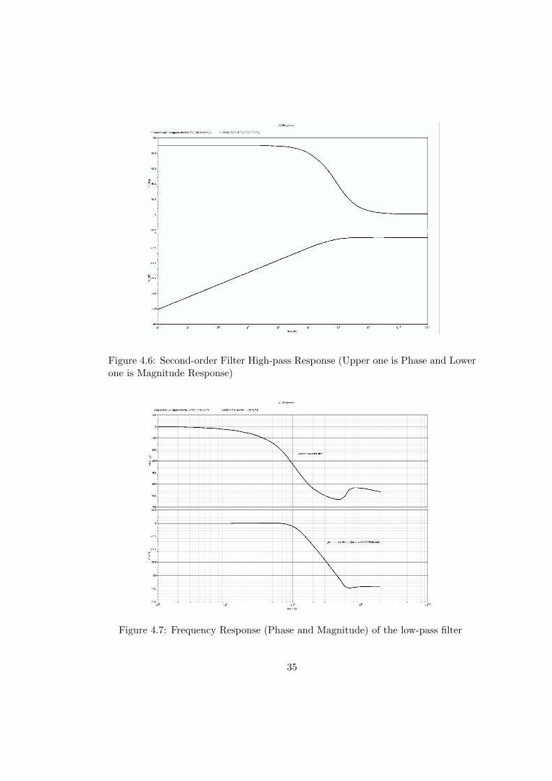
Figure 4.6: Second-order Filter High-pass Response (Upper one is Phase and Lowerone is Magnitude Response)
Figure 4.7: Frequency Response (Phase and Magnitude) of the low-pass filter
35

Figure 4.8: Frequency Response (Phase and Magnitude) of the first band-pass filter
Figure 4.9: Frequency Response (Phase and Magnitude) of the second band-passfilter
36
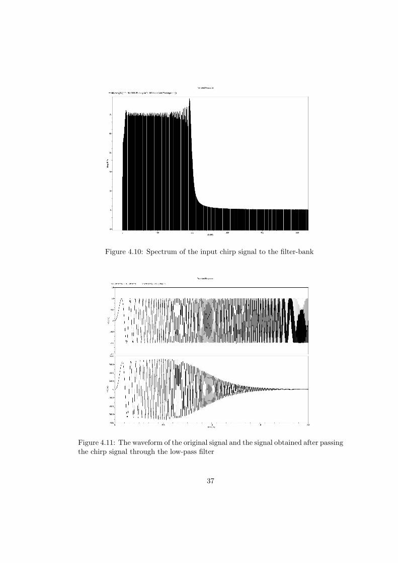
Figure 4.10: Spectrum of the input chirp signal to the filter-bank
Figure 4.11: The waveform of the original signal and the signal obtained after passingthe chirp signal through the low-pass filter
37

Figure 4.12: The spectrum of the output of the low-pass filter (the first band)
Figure 4.13: The waveform of the signal obtained after passing the chirp signalthrough the second band-pass filter (the second band)
38

Figure 4.14: The spectrum of the output of the second bandpass filter (the secondband)
Figure 4.15: The waveform of the signal obtained after passing the chirp signalthrough the second band-pass filter(the third band)
39

Figure 4.16: The spectrum of the signal obtained after passing the chirp signalthrough the second band-pass filter(the third band)
0 0.05 0.1 0.15 0.2 0.25 0.3 0.350
0.05
0.1
0.15
0.2
0.25
input amplitude
outp
ut a
mpl
itude
97M Hz input frequency72MHz input signal52MHz input frequency
Figure 4.17: The linearity of the low pass filter
40

0 0.1 0.2 0.3 0.40
0.01
0.02
0.03
0.04
0.05
0.06
0.07
0.08
input amplitude
outp
ut a
mpl
itude
Input frequency is109MHz
Figure 4.18: The linearity of the first band pass filter
0 0.05 0.1 0.15 0.20
20
40
60
80
100
input amplitude
outp
ut a
mpl
itude
Input Frequency is170M
Figure 4.19: The linearity of the second band pass filter
41

Chapter 5
Filter-bank:Second Architecture
5.1 Introduction
Due to many disadvantages (both in system level as well as from the perspectiveof implementation in silicon) this new architecture is proposed. This architecturehas many advantages over the previous architecture. But implementation of thisarchitecture is also much involved as it requires design of an analog delay block. Inthis chapter, the architecture is described and the implementation is elaborated.
5.2 Architecture and Its Advantages
Here without using any band-pass filter the signal is broken into bands by means oflow-pass filters (of different cut-off frequencies) and delay blocks. The schematic ofthe architecture is shown in the figure 2.10 and this is already discussed in chapter2. Here different bands are subtracted from original signal to get the residual signaland filtering is done on the residual signal. The virtue of this architecture over theprevious one is as follows:
1. The reconstruction in analog domain is guaranteed if the delays provided bythe delay block and the filter are same. In the previous architecture thebands are overlapping and hence in analog domain the reconstruction is notguaranteed.
2. The number of Low pass filters and delay blocks required is n − 1 each if wewant to break the signal in n bands. No additional filters are required for the
42

overlap band. But in Band-pass filter-bank (the previous architecture) extrafilters are needed.
3. Circuit complexity of delay blocks are much less than the band pass filters.Hence this architecture is less complex.
4. As only low pass filters are used, the order of the filters is much less as theroll- off of the low pass filters is more than that of the band-pass filters (orderbeing same as that of the low-pass filters).
5. In band-pass filter it is difficult to get a flat pass-band for a wide range offrequency. It is easy to get this in case of low-pass filters.
6. Low-pass filters are better than the band-pass filters in term of linearity w.r.t.input signal amplitude as well as phase linearity.
Although this architecture has many virtues, it is difficult to design an active delayblock which can give precise delay.
5.3 Design of Delay Block & Subtractor
Designing a proper delay bock in analog is very difficult as ideal delay is an infiniteorder system. Laplace domain representation of delay by T time-unit is e−sT . Thisinfinite series can be approximated upto first order as
e−sT =1− sT/21 + sT/2
(5.1)
In analog domain to get such a transfer function the circuit (as shown in figure5.1 is used. The idea is inspired by [19] but that was implemented in BJT. Here Ihave used MOS to design the delay. This is a source degenerated common sourceamplifier with a miller capacitance Ce. The following set of equations are written toget the approximate transfer function. All the capacitances except Ce are parasiticdevice capacitances.
Vx + Vp − Vin
Ri+ VxCGSs + (Vx + Vp − Vout)Ces = 0 (5.2)
(Vout − Vx − Vp)Ces + gmVx + Vout(1
Rd+ CDBs) = 0 (5.3)
43

Rs(VxCGSs + gmVx) = Vp (5.4)
These equations are solved to get the final result.
Vout
Vin=
Rd(−gm + (Ce + gmCeRs)s + CeCGSRss2)
RdRiRsCGSCeCDBs3 + (RiRdA + RsB)s2 + Cs + (1 + gmRs)(5.5)
whereA = CGSCDB + CDBCe + CeCGS (5.6)
B = RiCeCGS + Rd(CeCGS + CGSCDB) + RiRdgmCDBCe (5.7)
C = Ri(CGS+Ce+gmCeRd)+Rd(Ce+CDB)+Rs(RiCegm+CGS+CegmRd+gmCDBRd)(5.8)
Now in our case Ri = 0 and hence the third order equation is reduced to second-order equation with the second-order term having the coefficient as R−sRiCeCGS +Rd(CeCGS+CGSCDB)+RiRdgmCDBCe. This term is small for small values of Rs,Rd
and Ce. Again the second-order term in numerator is also small. So the equation
Figure 5.1: The circuit used for implementing delay in analog domain
44

can be written asVout
Vin=
Rd(−gm + (Ce + gmCeRs)s)Ds + (1 + gmRs)
(5.9)
whereD = Rd(Ce + CDB) + Rs(CGS + CegmRd + gmCDBRd) (5.10)
as Ri = 0. Now to have a good approximation of the equation 5.9 required conditionis
1 + gmRs = gmRd (5.11)
and the delay provided by the delay block is 2RdCe. The linear phase of the delayblock is mainly dependent on the equation 5.11 and the approximation (i.e., thethird and the second order terms are much less compared to the first order terms).This gives the design criteria for the delay block.
• Rd and Rs should not be kept very high. They should maintain the conditiongiven by equation 5.11. In my design, I have taken Rd and Rs to be 251Ω and8Ω.
• The capacitance Ce also should be kept low. In my design it is kept 4.8pF .
• The condition in equation 5.11 enforces gain to be 1. Hence no additionalrequirement is necessary to make the delay unity-gain. So the transistor sizingis not very crucial. Large size of transistor is avoided to reduce the devicecapacitances.
After the signal is delayed the already filtered signal is to be subtractedfrom the delayed signal. For subtractor the following circuit 5.2 is designed. Thissubtractor, which is nothing but a difference amplifier cannot handle large amplitudesignal. The following analysis shows the reason and as a support of the analysis,some plots are also given. If the input signals are like
Vin1 = V0 + ∆V ; Vin2 = V0 −∆V (5.12)
then,
I1 =β1
2(V0 + ∆V − Vp − Vth1)2 (5.13)
I2 =β2
2(V0 −∆V − Vp − Vth1)2 (5.14)
45

So the a.c. output voltage Vout can be written as
Vout = βR(∆V )2 (5.15)
where β1 = β2 = β. But if we do linear analysis, then a.c. output should come zeroas Vout = gm1∆V − gm2∆V = 0 if gm1 = gm2. Figure 5.3 shows the nonlinearityof the subtractor when proper differential signal is given to the subtractor.
This analog delay produced is very much process dependent. To make thedelay tunable, the resistances Rd and Rs are replaced by a PMOS and an NMOS,with biasing. Then Rd is provided by 1/gds of the PMOS and Rs is provided by1/gds of the NMOS. They can be changed by changing the voltage at the gate. Ifthe transistors are kept in linear region, then
1gds
=1
β(|VGS | − |Vth|) (5.16)
where VGS is the gate-to-source voltage of the MOS.
Figure 5.2: The circuit used for implementing subtractor in analog domain
46

Often the delay provided by one of this delay stage is not sufficient. For thisthe delay stages are to be cascaded. Cascading stages is difficult as due to high millercapacitance the previous stage is loaded by the next stage. To cascade two stagesa source follower is used as a buffer (figure 5.4). But due to miller capacitance thebuffer faces a capacitance Cm. If the resistance of the NMOS (in the source follower)is R then the transfer function of the source follower can be written as
Vout(s)Vin(s)
=gmR
1 + gmR + RCms(5.17)
So the cut-off frequency of the source-follower is 1+gmRRCm
. I have to increase thebandwidth to get good delay block. Band-width can be increased by increasing gm
or be decreasing Cm. To increase gm, more current is passed through the NMOS inthe source follower. Figure 5.5 shows the the actual signal, signal delayed by onestage and the signal delayed by two stages. Reducing Cm is same as reducing Ce.But that will reduce delay. In fact, if we want to give high delay in each stage, thenwe have to use high Ce. That will cause problem in cascading by increasing Cm.
0 0.05 0.1 0.15 0.2 0.25 0.3 0.350
0.5
1
1.5
2
2.5x 10
−3
amplitude of differential signal
outp
ut v
olta
ge
Figure 5.3: The output of the subtractor when input is totally differential
47

Figure 5.4: Cascaded delays (Cm is the load due to the next stage)
Figure 5.5: The actual signal, delayed signal by one stage delay, delayed single bytwo stages
48
Hence in each stage, the capacitance is to be reduced and by increasing number ofstages we can produce the required delay.
5.4 Result
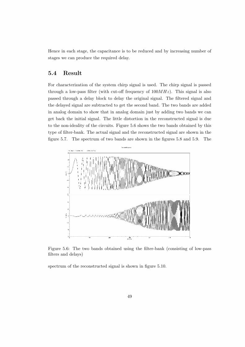
For characterization of the system chirp signal is used. The chirp signal is passedthrough a low-pass filter (with cut-off frequency of 100MHz). This signal is alsopassed through a delay block to delay the original signal. The filtered signal andthe delayed signal are subtracted to get the second band. The two bands are addedin analog domain to show that in analog domain just by adding two bands we canget back the initial signal. The little distortion in the reconstructed signal is dueto the non-ideality of the circuits. Figure 5.6 shows the two bands obtained by thistype of filter-bank. The actual signal and the reconstructed signal are shown in thefigure 5.7. The spectrum of two bands are shown in the figures 5.8 and 5.9. The
Figure 5.6: The two bands obtained using the filter-bank (consisting of low-passfilters and delays)
spectrum of the reconstructed signal is shown in figure 5.10.
49

Figure 5.7: The signal and the reconstructed signal (in analog domain) using thefilter-bank (consisting of low-pass filters and delays)
Figure 5.8: Spectrum of the first band (obtained by low-pass filtering)
50

Figure 5.9: Spectrum of the second band (obtained by subtracting the low-passsignal from the original signal)
Figure 5.10: Spectrum of the reconstructed signal (just adding the two signals inanalog domain)
51
Chapter 6
ADC Block
6.1 Introduction
After breaking the signal in several bands, in each band I have to digitize the signal.For this ADCs are to be designed. For designing a good ADC one has to designgood sample-hold circuit and good comparators. In this chapter, mainly the designof comparator and sample-hold circuit is described. Using those a 3− bit flash ADCis designed.
6.2 Sample-Hold
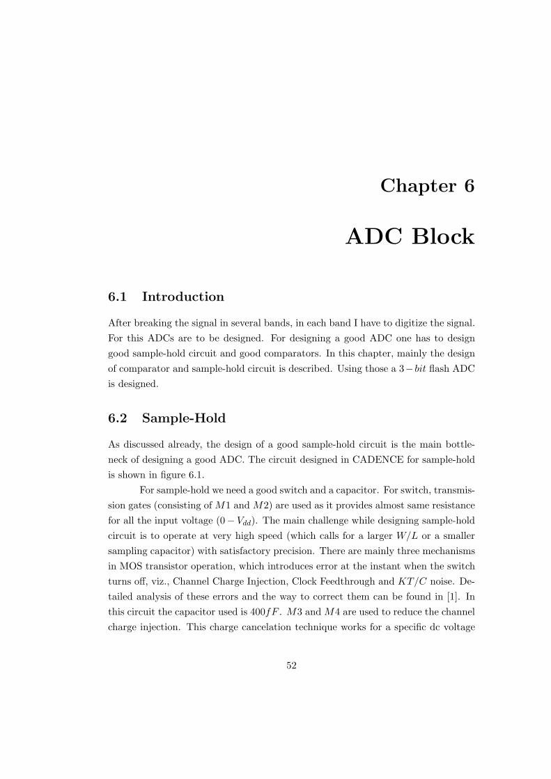
As discussed already, the design of a good sample-hold circuit is the main bottle-neck of designing a good ADC. The circuit designed in CADENCE for sample-holdis shown in figure 6.1.
For sample-hold we need a good switch and a capacitor. For switch, transmis-sion gates (consisting of M1 and M2) are used as it provides almost same resistancefor all the input voltage (0− Vdd). The main challenge while designing sample-holdcircuit is to operate at very high speed (which calls for a larger W/L or a smallersampling capacitor) with satisfactory precision. There are mainly three mechanismsin MOS transistor operation, which introduces error at the instant when the switchturns off, viz., Channel Charge Injection, Clock Feedthrough and KT/C noise. De-tailed analysis of these errors and the way to correct them can be found in [1]. Inthis circuit the capacitor used is 400fF . M3 and M4 are used to reduce the channelcharge injection. This charge cancelation technique works for a specific dc voltage
52

(which depends on the sizing of the transistors) of the signal. In my case it turnsout to be 783mV . This sample-hold circuit is not linear w.r.t. the input amplitude.
Figure 6.1: The Circuit Diagram for Sample and Hold
That causes some problem in ADC operation. A new method is suggested by Dr.Shanti Pavan [20] to solve that problem.
6.3 Comparator
For good ADC we need a good comparator. While designing comparator, clockedcomparator strategy is not used as it causes more jitter noise. Two types of com-parators are designed. The circuit diagram for both are shown in the figures 6.3and 6.4. The first comparator (open-loop) does not have any positive feedback andhence its working speed is not much. The range of reference voltage for which thecircuit is working is form 1.05V to 1.7V . Figure 6.5 shows the output of the com-parator when the reference voltage is 1.05V and figure 6.6 output of the comparatorwhen the reference voltage is 1.7V . The second one (regenerative and has positivefeedback) is faster. The range of reference voltages for which the circuit operates isfrom 1.05V to 1.45V . Figure 6.7 shows the output of the comparator when the ref-
53

Figure 6.2: The output of the Sample and Hold Circuit when the clock frequency is800MHz and the input signal is at 200MHz
Figure 6.3: The Circuit Diagram for Comparator(open-loop)
54

erence voltage is 1.05V and figure 6.8 output of the comparator when the referencevoltage is 1.45V .
Figure 6.4: The Circuit Diagram for Comparator(Regenerative)
Figure 6.5: The output of the open-loop comparator when reference voltage is low
55

Figure 6.6: The output of the open-loop comparator when reference voltage is high
Figure 6.7: The output of the regenerative comparator when reference voltage islow
56

6.4 Flash ADC
The designed Flash ADC is a 3-bit ADC. The already designed sample-hold and thecomparator are used to design the flash ADC. Figure 6.9 shows the basic architec-ture of a flash ADC. For 3-bit we need 8 comparators. The threshold of differentcomparators are different and generated by a resistor-array. As the same sample-
Figure 6.8: The output of the regenerative comparator when reference voltage ishigh
Figure 6.9: Block Diagram of Flash ADC
57

hold signal is going to many comparators hence the comparators should have lessinput capacitance to reduce the loading effect. Otherwise the input signal is loadedand the signal is distorted. Figure 6.10 shows the output of the flash ADC. Thedynamic range of the Flash-ADC is around 256mV .
58
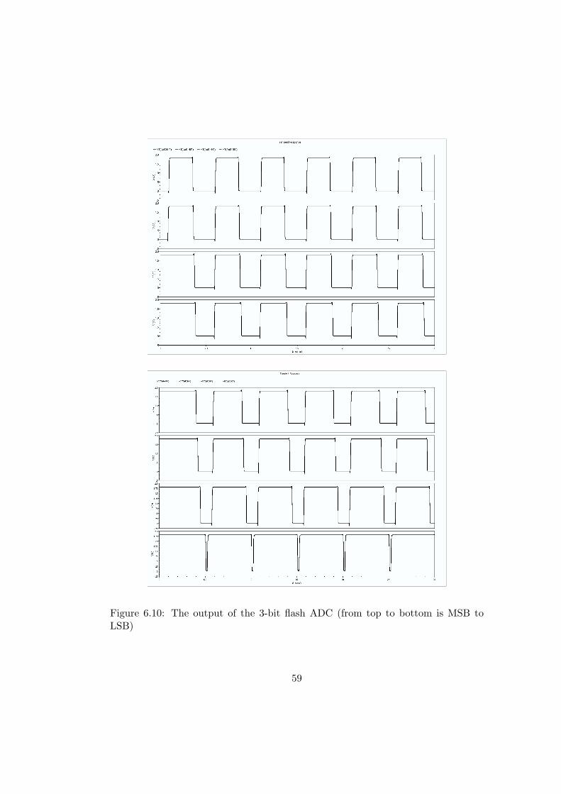
Figure 6.10: The output of the 3-bit flash ADC (from top to bottom is MSB toLSB)
59

Chapter 7
Reconstruction
7.1 Introduction
After analog-to-digital conversion the signals from different bands are to be com-bined to get the whole reconstructed signal. Just addition of signals from differentbands will not give the reconstructed signal. The error due to aliasing and over-lapping filter are to be minimized by some numerical methods (i.e., in circuit bysome digital filtering) as done for perfect reconstruction filter [22]. In my thesis,I am mainly concerned about the analog front-end which will break the signal inbands. Reconstruction of the signals from different bands is studied in algorithmiclevel only. The circuit implementations are not done for this portion. MATLAB 7.0is used to simulate the system and to check the performance of the heuristic usedto reconstruct the signal from different bands.
7.2 Methodology of Reconstruction
If perfect brick-walled filters were used for breaking the signal then there is nooverlap of bands. But the filters are not brick-walled. Again sampling creates signalin different bands. To remove the out-band contents of the signal due to sampling,we have to pass the signals through digital filters having the filter-characteristicssame as that of the analog filter used for that band. After that just addition of thesignals at different bands will approximately reconstruct the signal. The overlappingbetween bands is also removed due to digital filtering.
Here, In the first filter-bank architecture, the signals are overlapping and the
60

pass-bands are not fully flat. In second filter-bank they are not overlapped much,but then also the undesired signal appearing due to sampling are to be removed.And the pass-bands are more flat compared to the previous architecture but thatalso is not fully flat-band. So basically the problems which are to be solved are:
• The non-ideality due to overlapping filters is to be removed.
• The undesired signal obtained due to aliasing is to be removed.
• The non-flatness of the pass-band of the filter is to be removed.
7.2.1 The Main Concept
The main idea behind reconstruction is to use a filter whose transfer function isinverse of the transfer function of the analog filter in the pass band and zero other-wise. This filter is made as brick-wall as possible by using higher order. The firstcriteria ensures that the filtered signal which is not flat-band becomes flat-band;and the second criteria ensures that signal of undesired frequency is minimized. Toestimate the inverse of the filter invfreqz function in MATLAB is used. Simulationis performed over three bands and the result is shown in next section.
7.3 Simulation and Result
A chirp signal (with frequency from 200MHz to 800MHz) is passed through thefilters. The spectrum of the original signal is shown in figure 7.1. Figure 7.2 showsthe frequency response (magnitude only) of the analog filters. The three filters usedare band-pass filters. Now if the three bands are just added we do not get backthe actual signal as there are significant overlap as well as different filters producedifferent delay. Figure 7.3 show the spectrum of the signal when the three bands arejust added. Obviously this is much different from the original spectra. So we haveto design digital filters which will help to reconstruct the signal properly. Figure 7.4shows the desired frequency response (magnitude only) of the FIR filters for eachband. Figure 7.5 show the inverse response of the digital filters, approximated inMATLAB by invfreqz function. Figure 7.6 shows the spectrum after applying thedigital filter and then adding the signal.
To quantify the performance enhancement, I define a quantitative measuremean square error (MSE). The spectrum of the actual signal is found out. The
61

0 2 4 6 8 10
x 108
0
0.002
0.004
0.006
0.008
0.01
0.012
0.014
0.016
0.018
Frequency
spec
tral
com
pone
net
Figure 7.1: Spectrum of the Input Chirp Signal
0 2 4 6 8 10
x 108
0
0.001
0.002
0.003
0.004
0.005
0.006
0.007
0.008
0.009
0.01
frequency
spec
tral
com
pone
nt
First Analog Filter
Second Analog FilterThird Analog Filter
Figure 7.2: Magnitude Response of three analog filters
62

0 0.5 1 1.5 2
x 107
0
0.005
0.01
0.015
Frequency
Spe
ctra
l Com
pone
nts
Figure 7.3: The Spectrum of the signal when the three bands are just added
0 2 4 6 8 10
x 108
0
0.5
1
1.5
2
2.5
3
3.5
4
Frequency
The
des
ired
Spe
ctru
m
The First Band
The Second Band
The Third Band
Figure 7.4: The Desired Response of the FIR filters for all three bands
63

0 0.1 0.2 0.3 0.4 0.5 0.6 0.7 0.8 0.9 1−100
−50
0
50
100
Normalized Frequency (×π rad/sample)
Pha
se (
degr
ees)
0 0.1 0.2 0.3 0.4 0.5 0.6 0.7 0.8 0.9 1−20
−10
0
10
20
Normalized Frequency (×π rad/sample)
Mag
nitu
de (
dB)
0 0.1 0.2 0.3 0.4 0.5 0.6 0.7 0.8 0.9 1−100
−50
0
50
100
Normalized Frequency (×π rad/sample)
Pha
se (
degr
ees)
0 0.1 0.2 0.3 0.4 0.5 0.6 0.7 0.8 0.9 1−20
−10
0
10
20
Normalized Frequency (×π rad/sample)
Mag
nitu
de (
dB)
0 0.1 0.2 0.3 0.4 0.5 0.6 0.7 0.8 0.9 1−100
−50
0
50
100
Normalized Frequency (×π rad/sample)
Pha
se (
degr
ees)
0 0.1 0.2 0.3 0.4 0.5 0.6 0.7 0.8 0.9 1−15
−10
−5
0
5
10
15
Normalized Frequency (×π rad/sample)
Mag
nitu
de (
dB)
Figure 7.5: The response of three digital filters as designed in MATLAB
64
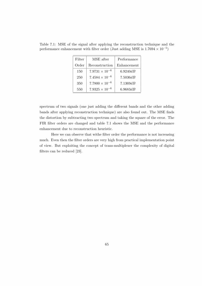
Table 7.1: MSE of the signal after applying the reconstruction technique and theperformance enhancement with filter order (Just adding MSE is 1.7694× 10⁻⁵)
Filter MSE after Performance
Order Reconstruction Enhancement
150 7.9731× 10⁻⁶ 6.9240dB
250 7.4584× 10⁻⁶ 7.5036dB
350 7.7800× 10⁻⁶ 7.1369dB
550 7.9325× 10⁻⁶ 6.9683dB
spectrum of two signals (one just adding the different bands and the other addingbands after applying reconstruction technique) are also found out. The MSE findsthe distortion by subtracting two spectrum and taking the square of the error. TheFIR filter orders are changed and table 7.1 shows the MSE and the performanceenhancement due to reconstruction heuristic.
Here we can observe that withe filter order the performance is not increasingmuch. Even then the filter orders are very high from practical implementation pointof view. But exploiting the concept of trans-multiplexer the complexity of digitalfilters can be reduced [23].
65

0 2 4 6 8 10
x 108
0
0.002
0.004
0.006
0.008
0.01
0.012
0.014
0.016
0.018
0.02
Frequency
Spe
ctra
l Com
pone
nt
Figure 7.6: The Spectrum of the signal after applying the digital filtering technique
66
Chapter 8
Other Supplementary Works
8.1 Introduction
In course of studying and designing the sub-band ADC, some other things are alsodesigned. They are not exactly relevant to the main discussion of the thesis. Hencethey are put in a different chapter.
8.2 Sub-sampling
I first planned to down-convert the signal to base-band so that the required samplingfrequency is less. To down-convert the signal, idea of sub-sampling (bandpass sam-pling) is used. The incoming signal (which is bandpass) is sampled at a frequencyless than its nyquist frequency but at a frequency more than twice the band-widthof the signal. It can be proved that if fc is the carrier frequency and fs is the sam-pling frequency then the fIF where the signal will be down-converted is given bythe following relations. If b fc
fs/2c is even then
fIF = rem(fc, fs) (8.1)
and if b fc
fs/2c is odd thenfIF = fs − rem(fc, fs) (8.2)
The result of sub-sampling is shown in figure 8.2. This is simulated in MATLABSimulink. Figure 8.3 shows the model used to simulate the sub-sampling receiver.
67

0 2 4 6 8 10
x 106
0
0.005
0.01
0.015
0.02
0.025
0.03
Frequency
Fre
quen
cy c
ompo
nent
Figure 8.1: Input spectra of the sub-sampling receiver output
0 2 4 6 8 10
x 106
0
0.005
0.01
0.015
0.02
0.025
0.03
0.035
0.04
0.045
0.05
Frequency
Fre
quen
cy C
ompo
nent
Figure 8.2: Output spectra of the sub-sampling receiver output
68

8.2.1 Implementation in silicon
This sub-sampling receiver is also designed and simulated in CADENCE. The circuitfor sub-sampling receiver as (shown in the figure 8.4) consists of mainly a sample-hold circuit followed by a buffer and a low-pass filter. Figure 8.5 shows the inputand output spectra of the signal.
8.3 Low-pass Sigma-Delta Modulator
It is a over-sampling analog to digital converter and it is basically used to increasethe resolution and to reduce the quantization noise. Figure 8.6 shows the circuit forsigma-delta modulator and figure 8.7 shows the output of sigma-delta modulator.This is a one bit and single loop implementation.
Figure 8.3: Architecture simulated in MATLAB Simulink for sub-sampling receiver
Figure 8.4: The Circuit Diagram for Sub-sampling
69

Figure 8.5: The Input and Output Spectra for Sub-sampling as simulated in CA-DENCE
70
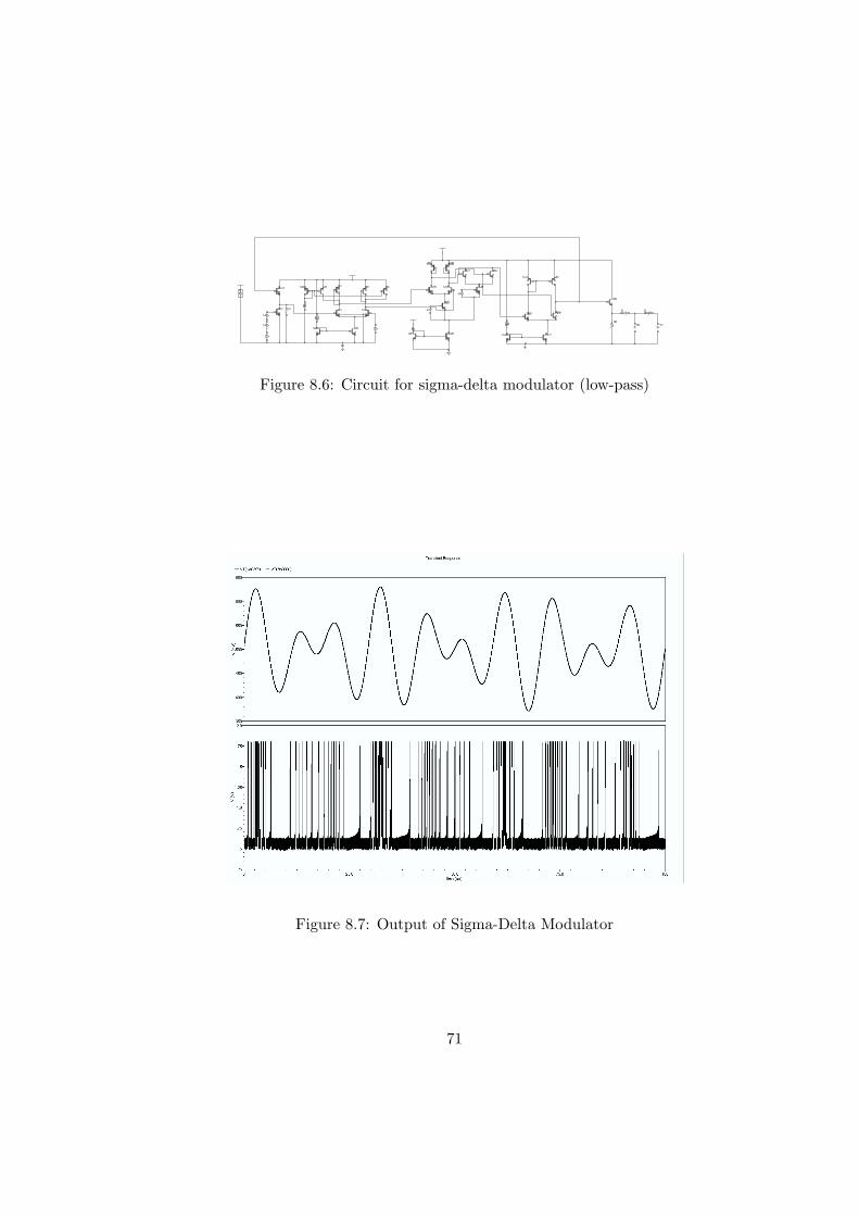
Figure 8.6: Circuit for sigma-delta modulator (low-pass)
Figure 8.7: Output of Sigma-Delta Modulator
71

8.4 Band-pass Filters
In previous chapters the design of band-pass filters is described in details. Here twoother approaches are described. By cascading one low-pass and one high-pass filtera flat-band band-pass filter can be obtained. Its response is shown in figure 8.8.
Figure 8.8: Filter Band-pass Response (Flat-band)
Another type of polyphase band-pass filter is implemented by gm −C topology. Itsresponse is shown in figure 8.9. This type of filter produce quadrature output asshown in figure 8.10.
8.5 Folding Architecture
To produce multi-bit in the flash bit the folding architecture is also studied. Figure8.12 shows the architecture of the folder and figure 8.11 shows the output of thefolder.
72

Figure 8.9: Filter Band-pass Response (this can generate quadrature output)
Figure 8.10: Quadrature wave-forms for the band-pass filter
73

Figure 8.11: The output of folder circuit
Figure 8.12: The Folding Circuit
74

Chapter 9
Conclusion and Future Work
9.1 Summary
This thesis mainly talks about the implementation of the filter-bank in a new typeof ADC, i.e., sub-band ADC. In some literature the concept of sub-band ADC isproposed, but no literature deals with the practical implementation of this ADC insilicon.
The performance enhancement due to sub-band ADC is reported in chapter2 of this thesis. Mathematically the reason behind performance enhancement isestablished and system level simulation affirms the theory. These simulations alsopoint to many design criteria, important for sub-band ADC. The possible practicalproblems faced during implementation in silicon is elaborated. One of the main partsof the ADC, i.e., the filter bank is designed. Two different architectures have beenproposed and both are implemented in silicon and simulated in CADENCE. Thesealong with the outputs are described in chapter 4 and 5. The advantages of thesecond architecture is established. Also the difficulties in implementing the analogdelay are described here. A possible implementation of analog delay in silicon is alsodescribed and theoretically the amount of delay is found out. Chapter 7 discussesthe digital back-end which is used to recombine the bit-stream. For this a newheuristic is found out. That heuristic give satisfactory performance. This part issimulated and the result is also reported.
75
9.2 Future Work
But this is not the end of the game. This is just a beginning of the work, I wantedto complete. But due to lack of time I could not finish the whole work. This systemhas lots of potential and it can be used with little variations for many applications.The future work can be listed below:
1. The delay used here can be made tunable by using NMOS and PMOS in placeof resistors or making the capacitances switched. But the performance is notmeasured by implementing them. That can be done to make the delay tunable.
2. Apart from the filter-bank, some part of ADCs are designed. Those can beintegrated to the filter-bank to make the whole ADC. Again the reconstructionalgorithm can be mapped to digital circuit and that will complete the wholeADC.
3. The whole system can be fabricated and tested, so that the performance im-provement, which is predicted theoretically and by system level simulation,can also be obtained in silicon.
4. Here I have excluded the possibility of down-converting the signal at the higherbands. In fact, if the signal has center frequency and band-width comparableto each other, then down-conversion is difficult. But if the whole band issituated at some higher center frequency then down-conversion is possible.This aspect can be investigated.
5. Without using the conventional ADCs for each band, we can use zero-crossingADCs. As the band-width in bands are small, from zero-crossings the signalcan be reconstructed easily.
76

Bibliography
[1] Behzad Razavi,“Design of Analog CMOS Integrated Circuits,”Tata McGrewHill Edition.
[2] R.D.Plassche,“CMOS Integrated Analog-to-Digital and Digital-to-Analog Con-verters,”Springer, second edition.
[3] SS Awad ,“Analysis of accumulated timing-jitter in the time domain ,” IEEET. Instrumentation and Measurement, 1998.
[4] DH.Shen et. al.,“A 900-MHz RF front-end with integrated discrete-time filter-ing,” IEEE J.Solid State Circuits, 1996.
[5] R.V.Cox et.al.,“New Directions in Subband Coding,”IEEE Journal on SelectedAreas in Communications, vol. 6, no. 2, February 1998.
[6] M. Win, R. Scholtz,“Impulse Radio: How it works,”IEEE Comm. Letters, vol.2, no. 10, Jan. 1998.
[7] Van der Tang et. al.,“ A 65 mW, 0.42.3 GHz Bandpass Filter for Satellite Re-ceivers,”Analog Integrated Circuits and Signal Processing, Volume 31, Number1, April, 2002.
[8] A.Papoulis,“Probability,Random Variables and Stochastic Processes,”Tata Mc-Grew Hill, Fourth Edition.
[9] C.Tseng et. al.,“Direct Downconversion of Multiple RF Signals Using BandpassSampling,”IEEE 2003.
[10] Won Namgoong,“Channelized Digital Receivers for Impulse Radio,” IEEE,2003, pp.2884-2888.
77

[11] G. Ding et. al.,“Frequency Interleaving Technique for High Speed A/D Con-version,”IEEE 2003.
[12] Ramirez A. J. et. al., “Programmable BiCMOS transconductor for capacitor-transconductor filters,”Electronics Letters,1992, vol. 28, No. 13, pp. 1185-1188.
[13] Deweerth S.P. et. al.,“Variable linear-range subthreshold OTA,”Electronics Let-ters, vol. 33, Issue 15,17 July,1997,pp 1309-1311.
[14] Yannis Tsividis et. al.,“Continuous Time MOSFET-C Filters in VLSI,”IEEEJournal of Solid-State Circuits, vol. sc.-21, no. 1, pp. 15-30, Feb. 1986.
[15] Yannis Tsividis et. al.,“Integrated Continuous Time Filter Design,”Custom In-tegrated Circuits Conference, IEEE 1993.
[16] Michael Tse,“High Frequency Filter Design,” September 2003.
[17] R.L.Geiger et.al.,“Active Filter Design Using Operational TransconductanceAmplifier: A Tutorial,”IEEE Circuits and Devices Magazine, vol. 1, pp 20-32,March 1985.
[18] E.Sanchez-Sinencio et. al.,“CMOS transconductance amplifiers, architectureand active filters: a tutorial,”IEE Proc. Circuits Devices Syst., vol. 147, no.1, February 2000.
[19] J. Buckwalter, Ali Hajimiri,“An Active Analog Delay and the Delay ReferenceLoop,”IEEE Radio Frequency Integrated Circuit Sympoaium, 2004.
[20] Venkata Srinivas, Shanti Pavan et. al.,“A Distortion Compensating FlashAnalog-to-Digital Conversion Technique,”IEEE Journal of Solid-State Circuits,vol. 41, no. 9, Sept. 2006.
[21] P.Allen,“CMOS Analog Circuit design,”Oxford University Press, second edi-tion.
[22] S.K.Mitra,“Digital Signal Processing,”Tata McGraw Hill Edition.
[23] M.J.Narasimha,“Design of a 24-Channel Transmultiplexer,”IEEE Trans. onAcoustics, Speech and Signal Processing, vol. ASSP-27, no. 6, December 1979.
78
Related Documents