1 2012/12/10 Field Programmable Gate Array

Welcome message from author
This document is posted to help you gain knowledge. Please leave a comment to let me know what you think about it! Share it to your friends and learn new things together.
Transcript
12012/12/10
Field Programmable Gate Array
22012/12/10
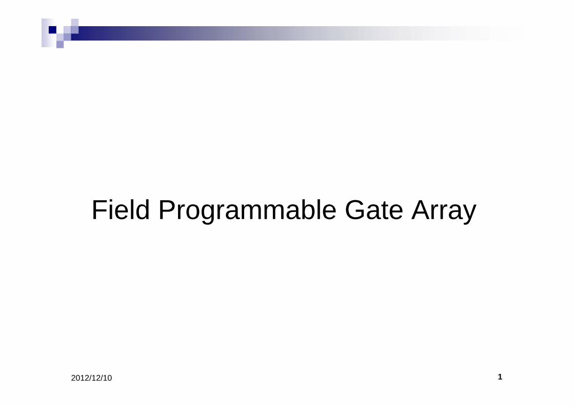
What is FPGA?
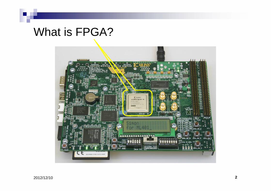
XGP System Implementation
2012/4/243
ANALOG FRONT END
BASEBAND PROCESSING FPGA
Additional BASEBANDand
MAC Layer by PPC uP
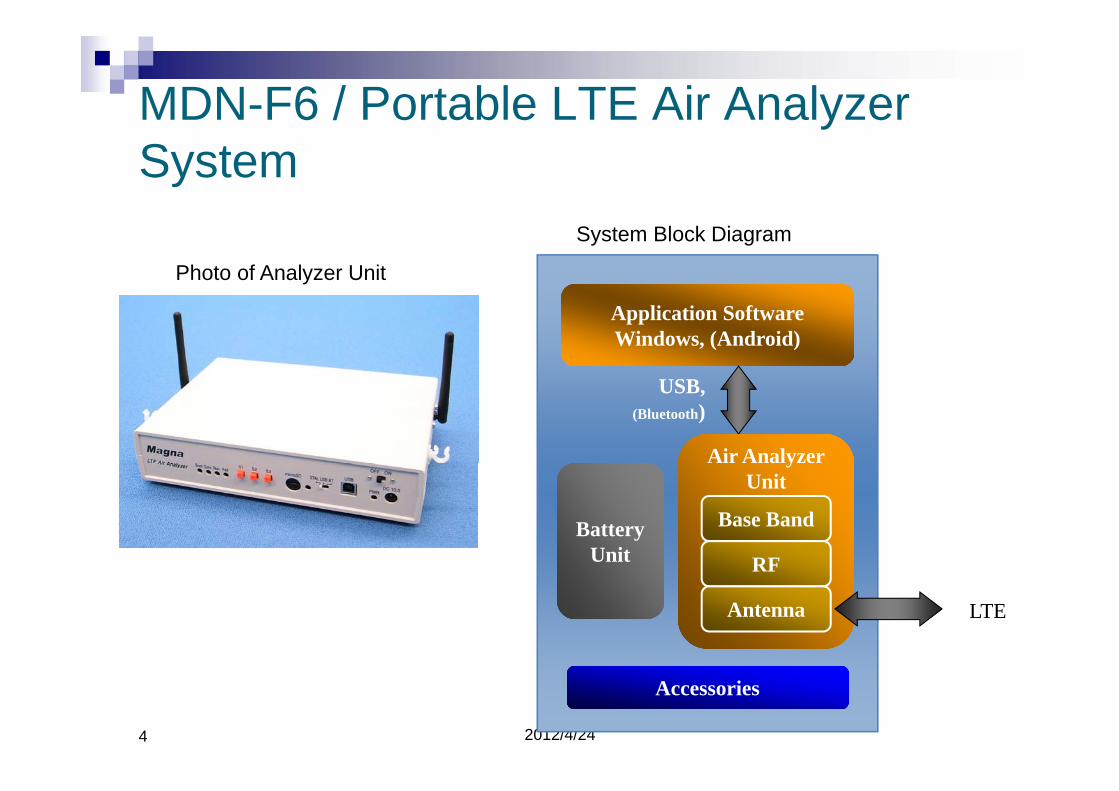
MDN-F6 / Portable LTE Air Analyzer System
2012/4/244
Application SoftwareWindows, (Android)Application SoftwareWindows, (Android)
USB,(Bluetooth)
Air AnalyzerUnit
Air AnalyzerUnit
Base Band
RF
Antenna
BatteryUnit
BatteryUnit
AccessoriesAccessories
LTE
Photo of Analyzer Unit
System Block Diagram
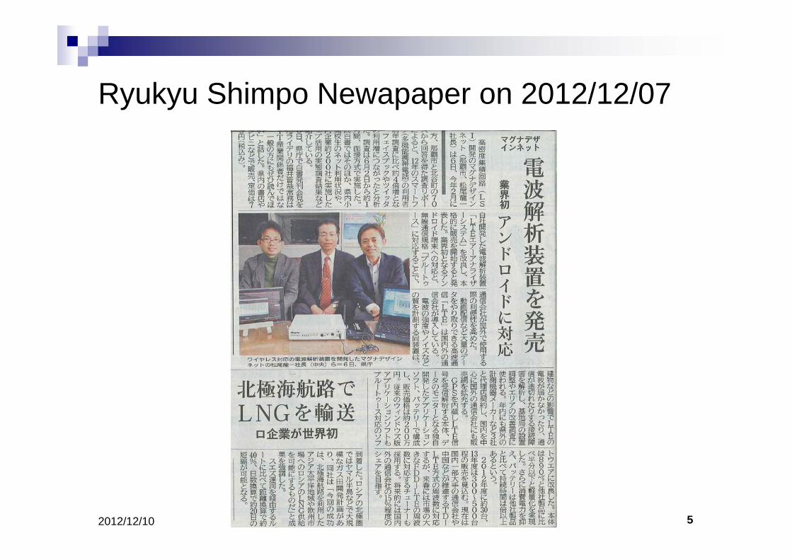
Ryukyu Shimpo Newapaper on 2012/12/07
52012/12/10
2012/4/246
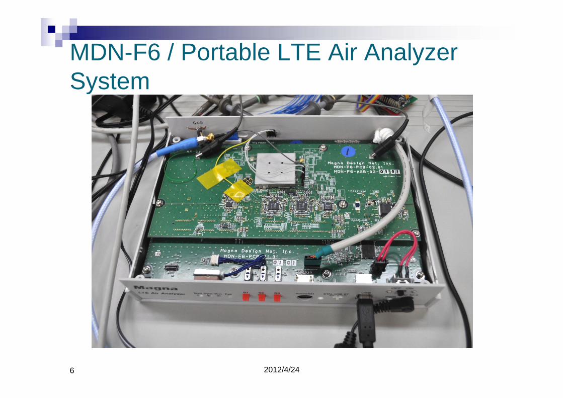
MDN-F6 / Portable LTE Air Analyzer System
72012/12/10
FPGAProgrammable (= reconfigurable) Digital SystemComponent
Basic componentsCombinational logicsFlip Flops
Macro componentsMultiplier ( large combinational logic)Random Access Memory (Large Density)Read Only memory (Large Density)CPU
Programmable InterconnectionProgrammable Input/Output circuitProgrammable Clock Generator
82012/12/10
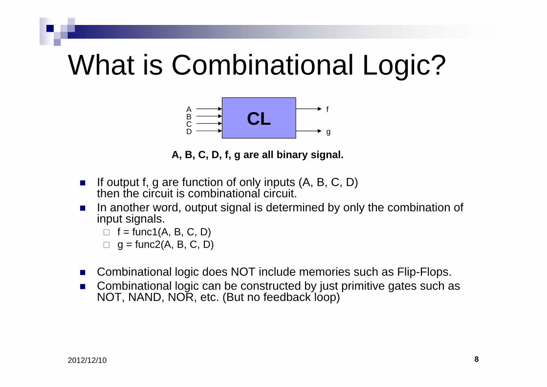
What is Combinational Logic?
CLABCD
f
g
A, B, C, D, f, g are all binary signal.
If output f, g are function of only inputs (A, B, C, D) then the circuit is combinational circuit.In another word, output signal is determined by only the combination of input signals.
f = func1(A, B, C, D)g = func2(A, B, C, D)
Combinational logic does NOT include memories such as Flip-Flops.Combinational logic can be constructed by just primitive gates such as NOT, NAND, NOR, etc. (But no feedback loop)
92012/12/10
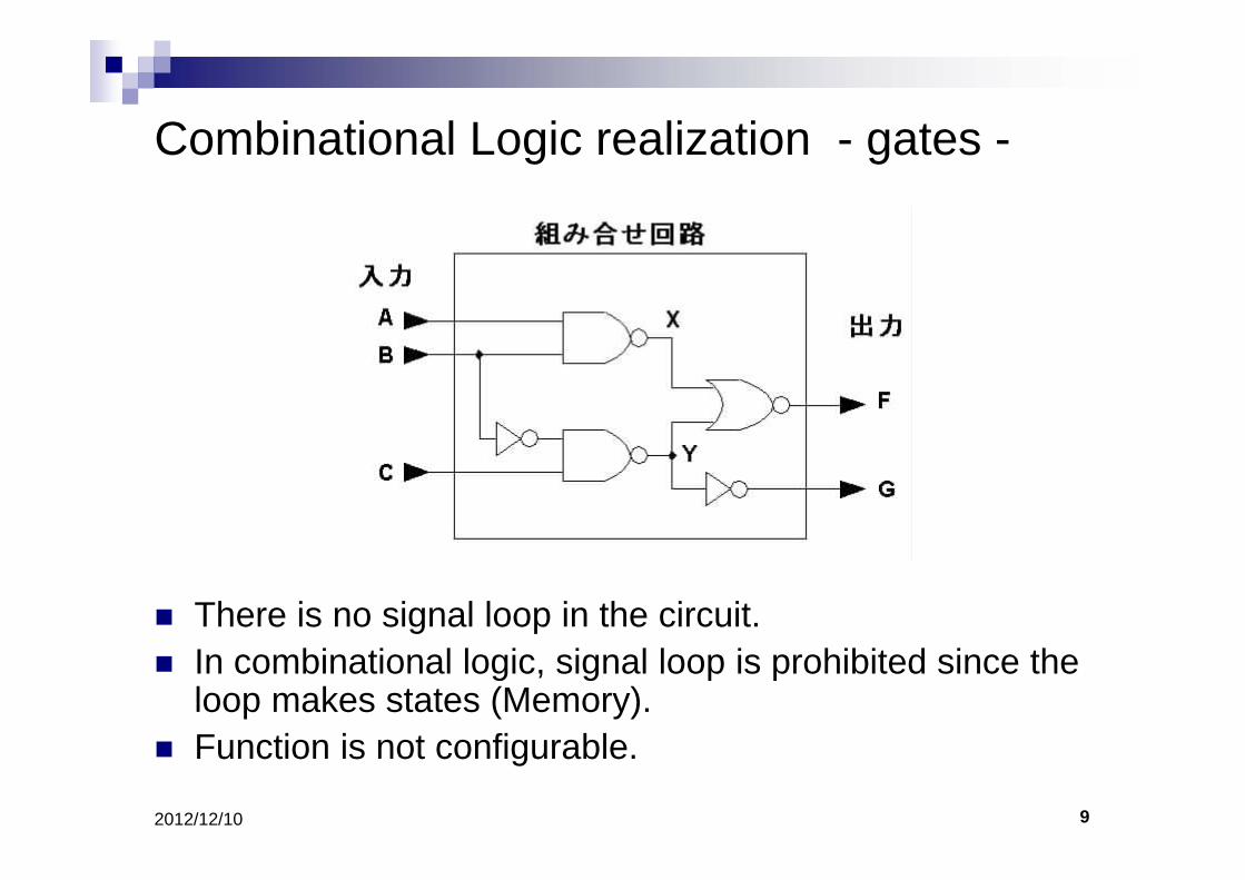
Combinational Logic realization - gates -
There is no signal loop in the circuit.In combinational logic, signal loop is prohibited since the loop makes states (Memory).Function is not configurable.
102012/12/10
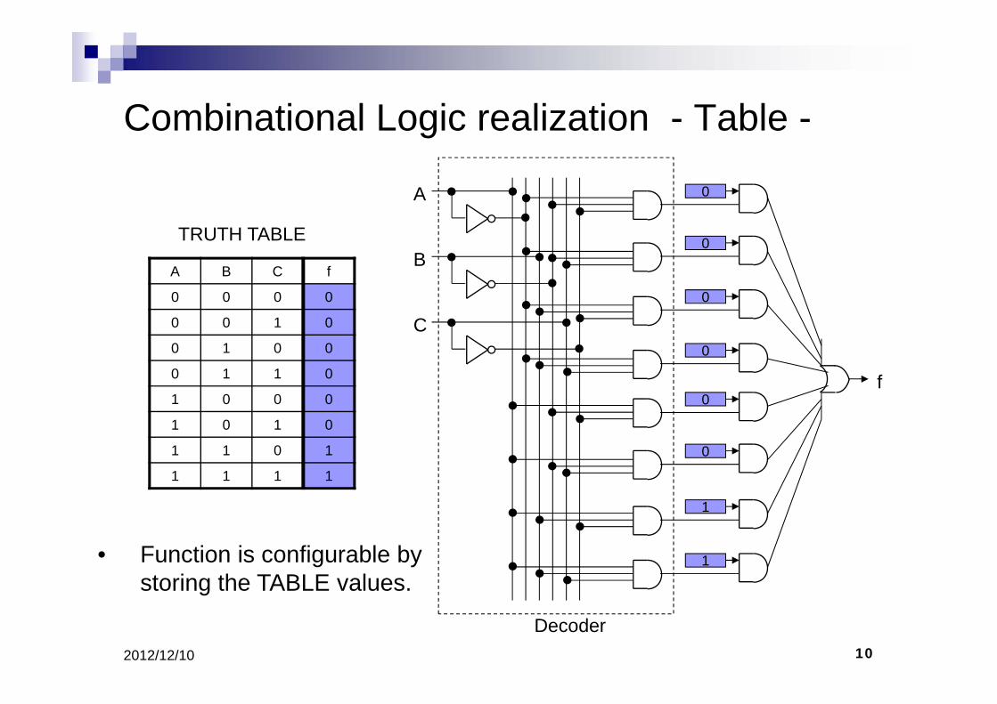
Combinational Logic realization - Table -
TRUTH TABLE
A B C f
0 0 0 0
0 0 1 0
0 1 0 0
0 1 1 0
1 0 0 0
1 0 1 0
1 1 0 1
1 1 1 1
A
B
C
0
0
0
0
0
0
1
1
f
Decoder
• Function is configurable by storing the TABLE values.
112012/12/10
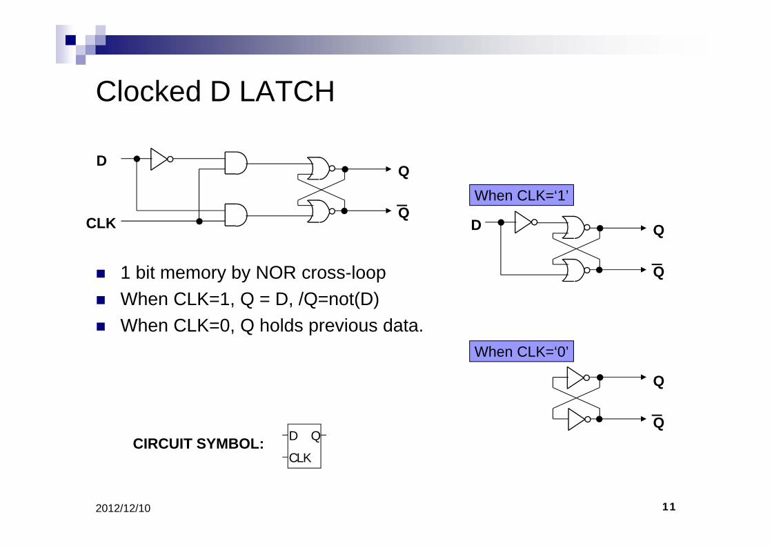
Clocked D LATCH
1 bit memory by NOR cross-loopWhen CLK=1, Q = D, /Q=not(D)When CLK=0, Q holds previous data.
D
CLK
Q
Q
Q
Q
When CLK=‘1’
D Q
Q
When CLK=‘0’
D Q
CLKCIRCUIT SYMBOL:
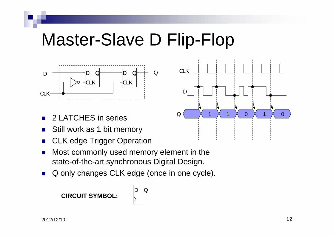
122012/12/10
Master-Slave D Flip-Flop
2 LATCHES in seriesStill work as 1 bit memoryCLK edge Trigger OperationMost commonly used memory element in the state-of-the-art synchronous Digital Design.Q only changes CLK edge (once in one cycle).
D Q
D Q
CLK
D Q
CLK
CLK
D Q
CIRCUIT SYMBOL:
CLK
D
Q 1 1 0 1 0
132012/12/10
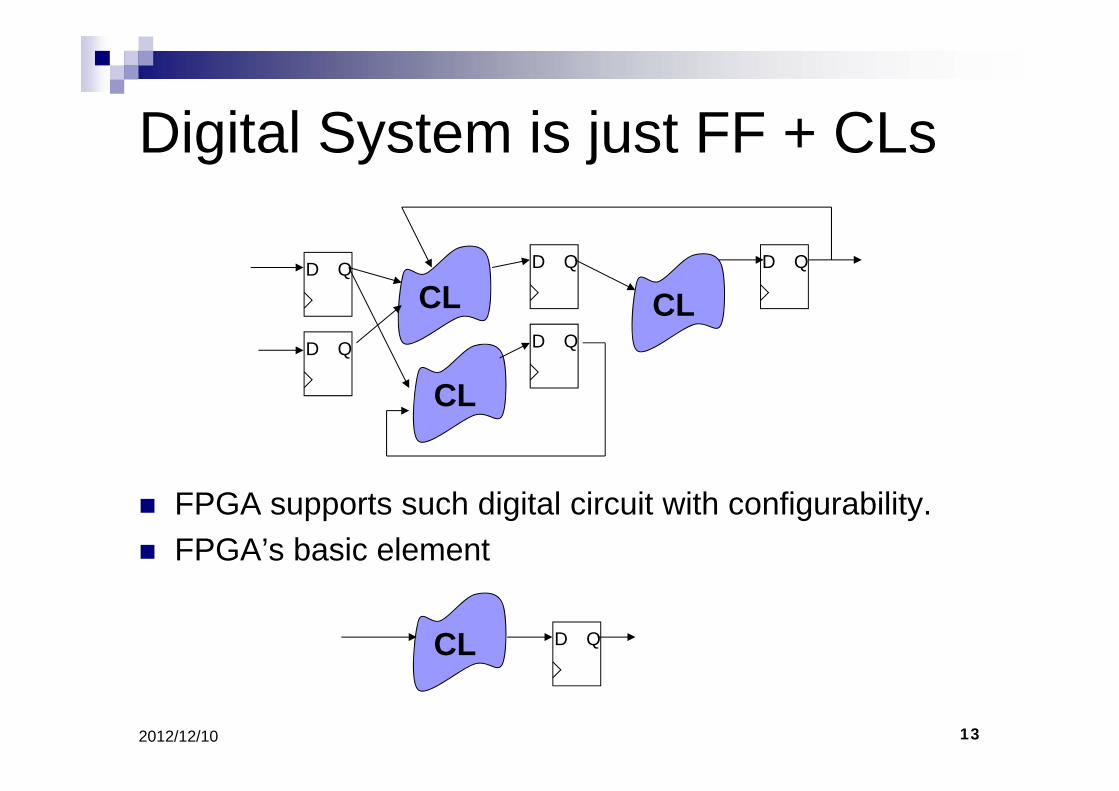
Digital System is just FF + CLs
FPGA supports such digital circuit with configurability.FPGA’s basic element
CLD Q
D Q
D Q
D Q
CL
CLD Q
D QCL
142012/12/10
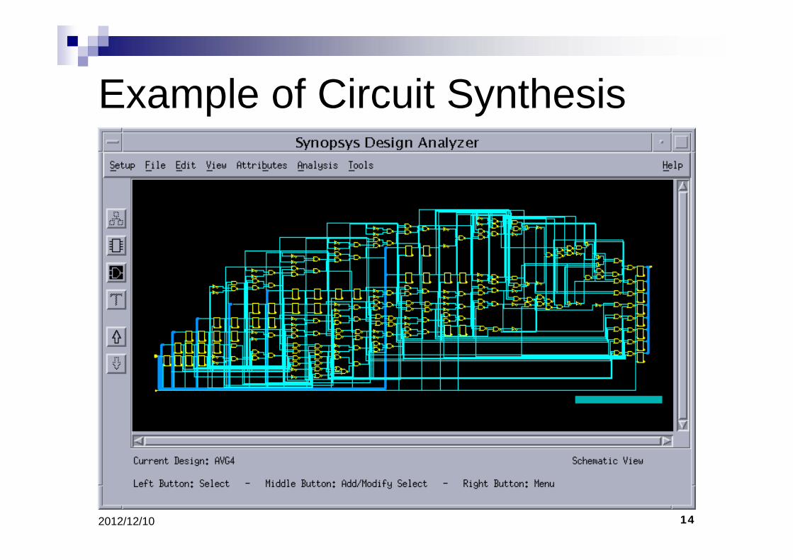
Example of Circuit Synthesis
152012/12/10
XILINX FPGA
Field Programmable Gate Array
162012/12/10
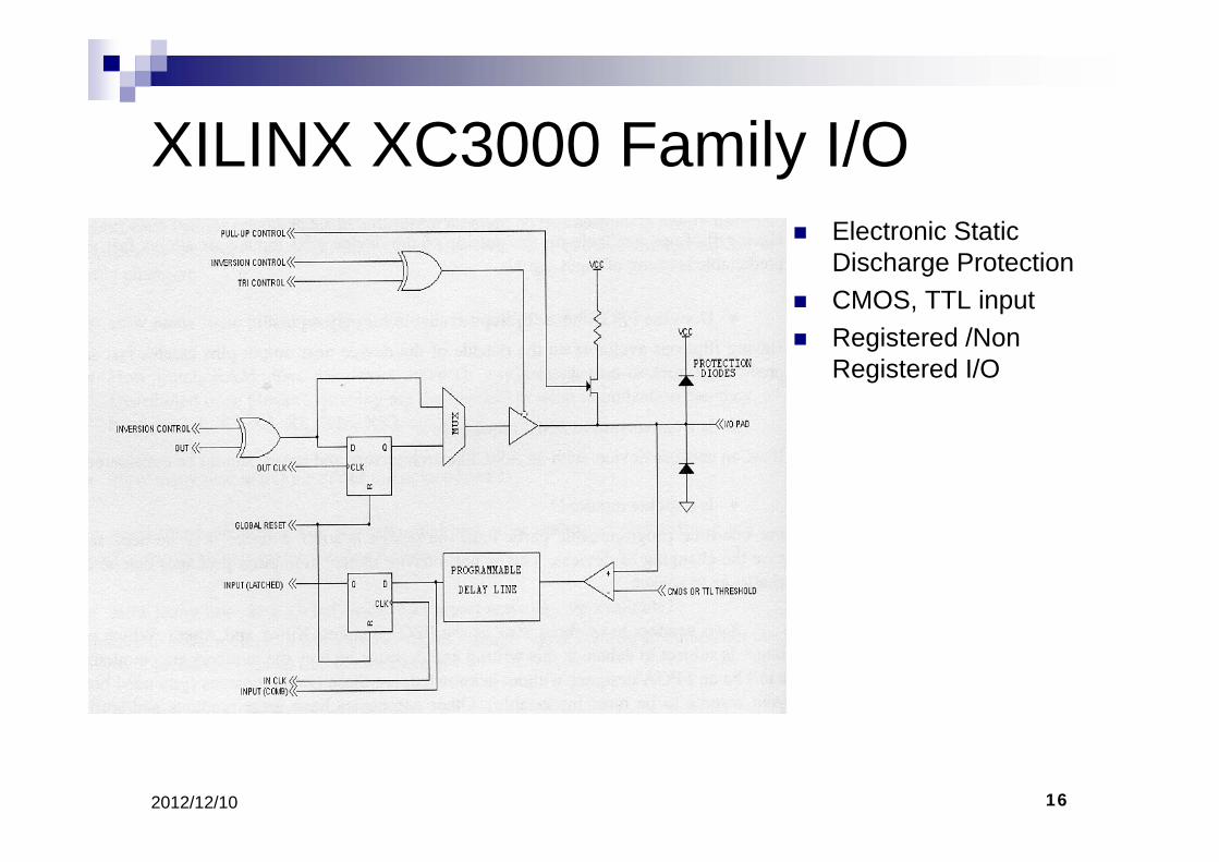
XILINX XC3000 Family I/OElectronic Static Discharge ProtectionCMOS, TTL inputRegistered /Non Registered I/O
172012/12/10
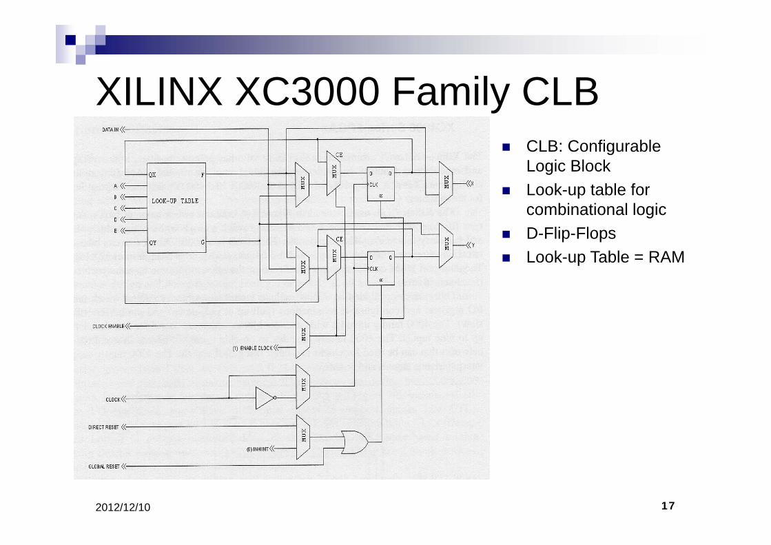
XILINX XC3000 Family CLBCLB: Configurable Logic BlockLook-up table for combinational logicD-Flip-FlopsLook-up Table = RAM
182012/12/10
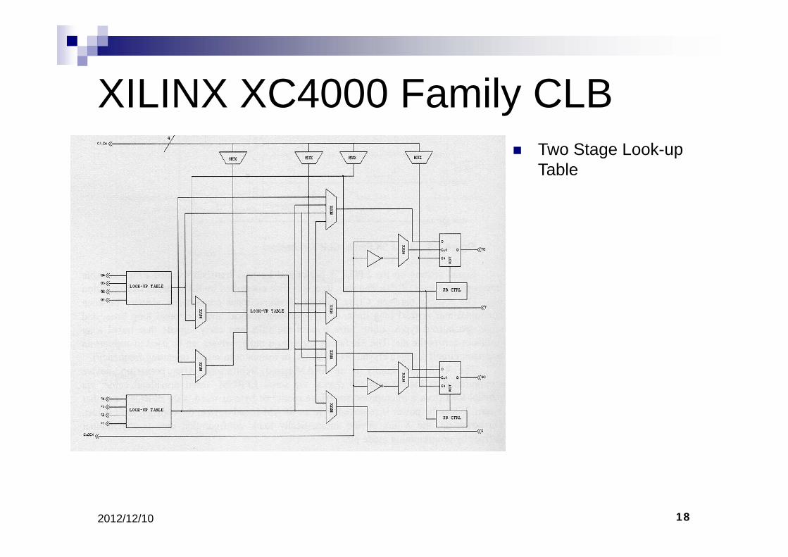
XILINX XC4000 Family CLBTwo Stage Look-up Table
192012/12/10
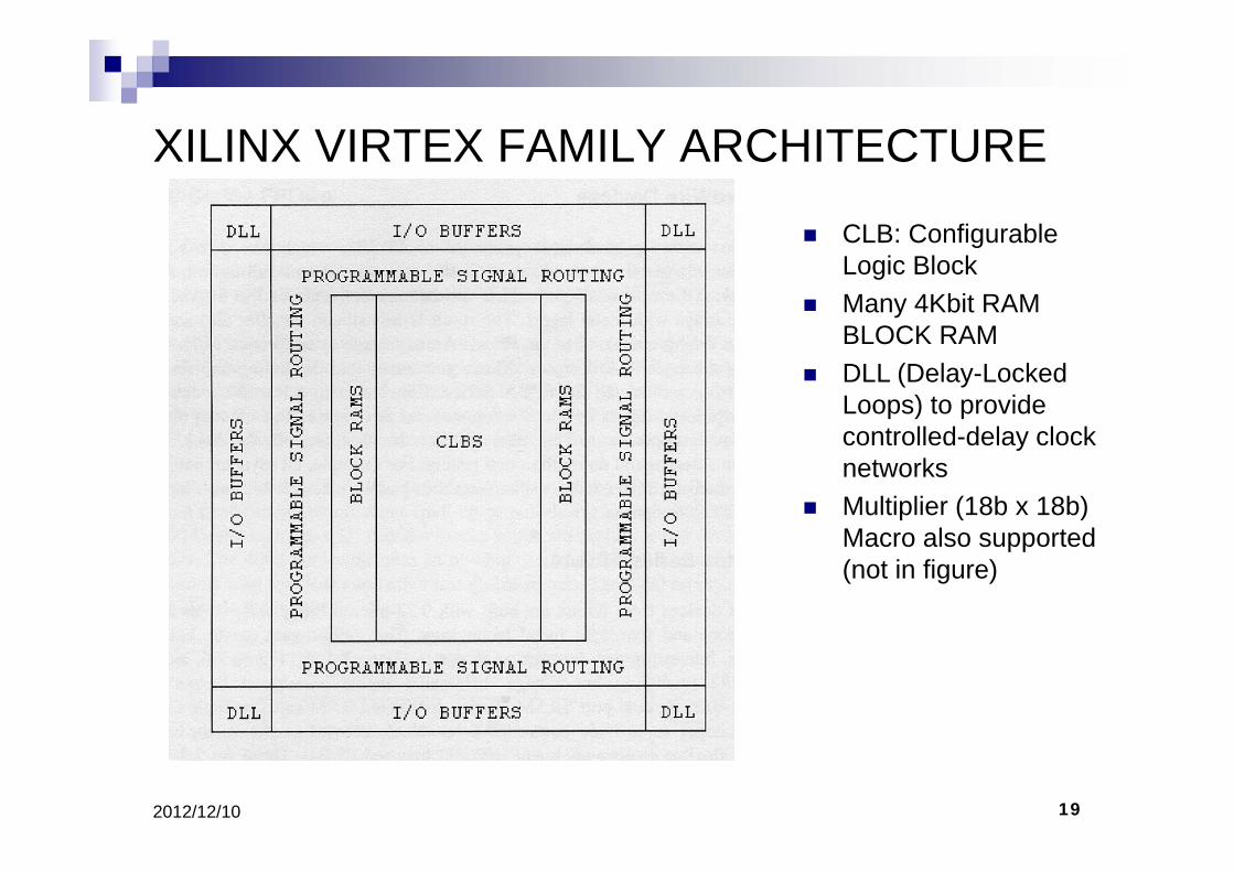
XILINX VIRTEX FAMILY ARCHITECTURE
CLB: Configurable Logic BlockMany 4Kbit RAM BLOCK RAMDLL (Delay-Locked Loops) to provide controlled-delay clock networksMultiplier (18b x 18b) Macro also supported (not in figure)
202012/12/10
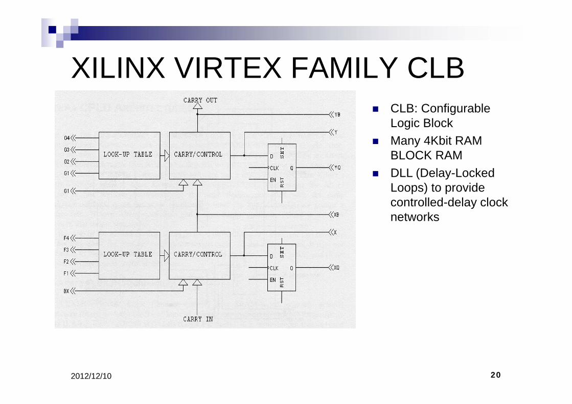
XILINX VIRTEX FAMILY CLBCLB: Configurable Logic BlockMany 4Kbit RAM BLOCK RAMDLL (Delay-Locked Loops) to provide controlled-delay clock networks
212012/12/10
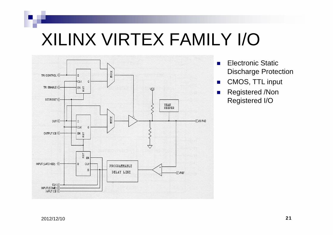
XILINX VIRTEX FAMILY I/OElectronic Static Discharge ProtectionCMOS, TTL inputRegistered /Non Registered I/O
222012/12/10
ALTERA CPLD
Complex Programmable Logic Devices
Altera uses less routing resource than XilinxAltera’s Logic Array Block (LAB) is more complex than Xilinx’s CLBs. Then fewer LABs in on chip than Xilinx’s CLBs.
232012/12/10
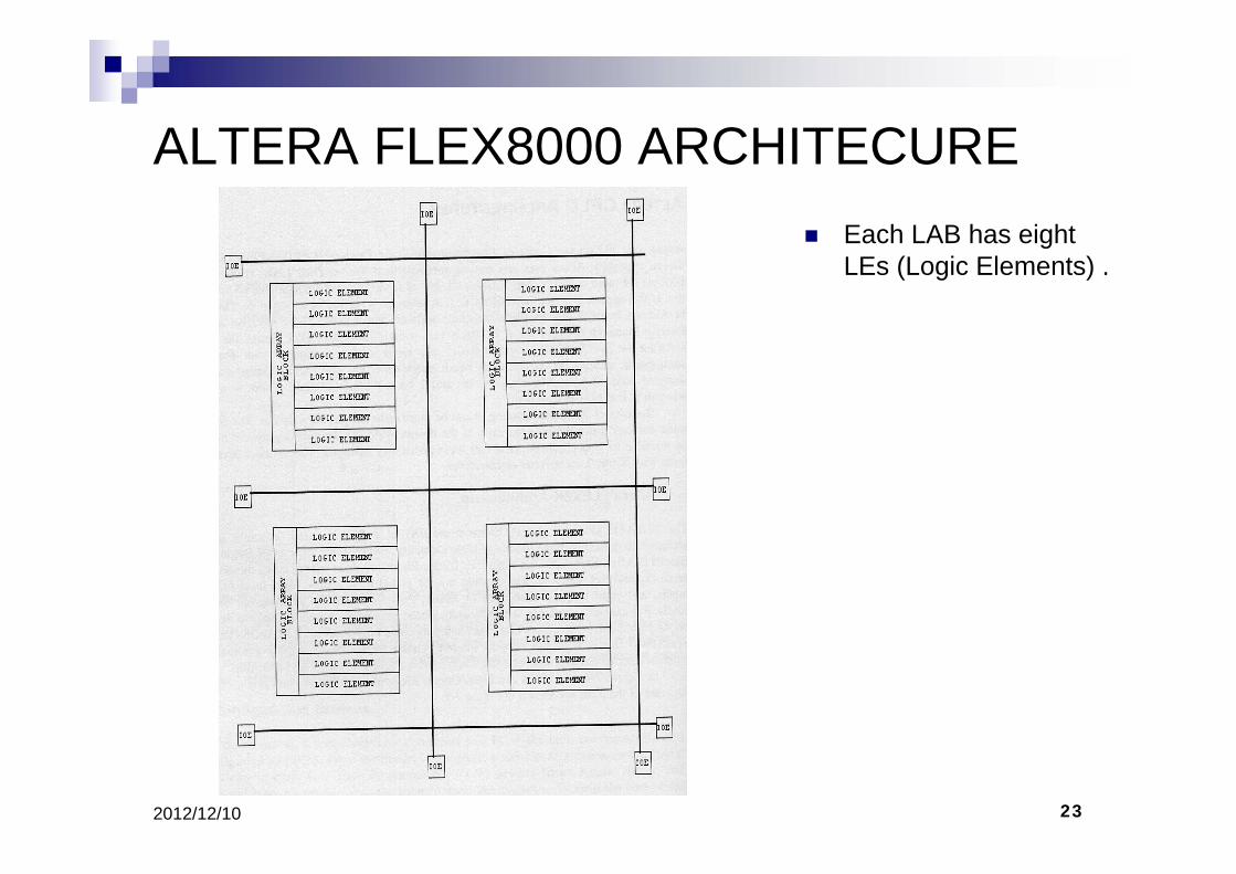
ALTERA FLEX8000 ARCHITECUREEach LAB has eight LEs (Logic Elements) .
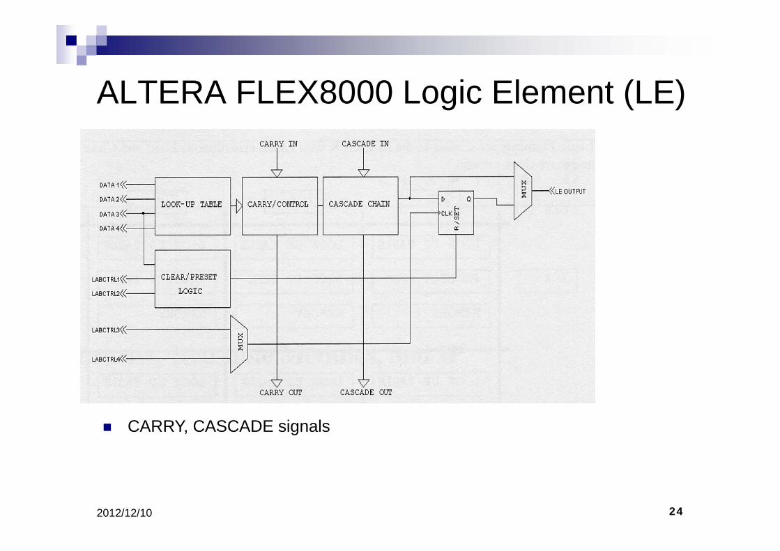
242012/12/10
ALTERA FLEX8000 Logic Element (LE)
CARRY, CASCADE signals
252012/12/10
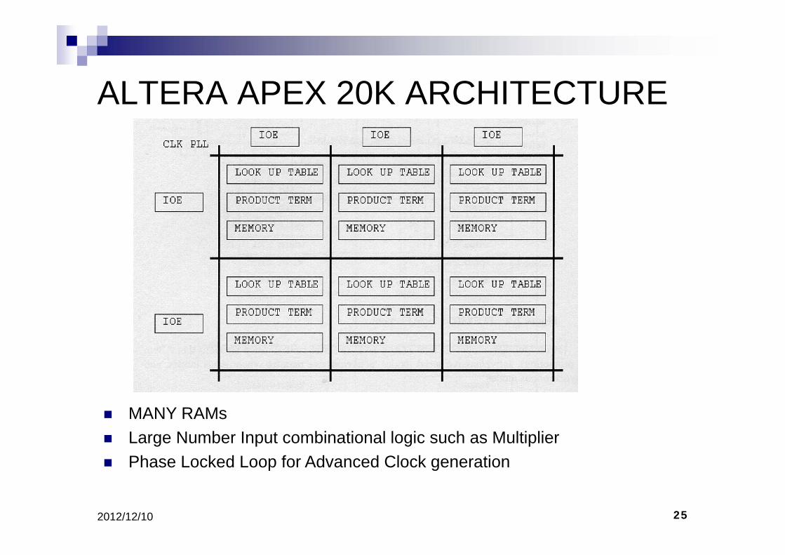
ALTERA APEX 20K ARCHITECTURE
MANY RAMsLarge Number Input combinational logic such as MultiplierPhase Locked Loop for Advanced Clock generation
262012/12/10
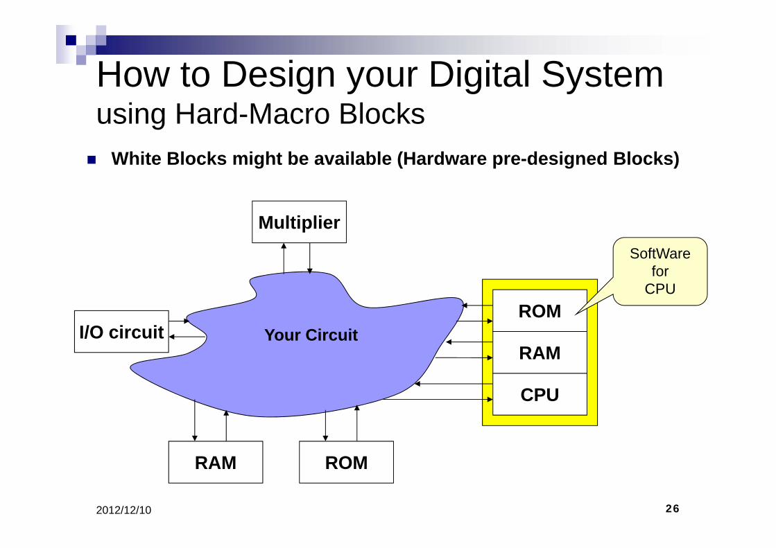
How to Design your Digital Systemusing Hard-Macro Blocks
Your Circuit
RAM
I/O circuit
ROM
Multiplier
CPU
RAM
ROM
White Blocks might be available (Hardware pre-designed Blocks)
SoftWarefor
CPU
272012/12/10
Hardware Description Languages (HDLs)
HDL is a software programming language used to model the intended operation of a piece of hardware.Two level of modeling
Abstract behavior modelingHardware structure modeling: Input to Circuit Synthesis
Two kinds of LanguageVHDL: Very High Speed Integrated Circuit hardware description language
Similar to Pascal Programming languageVerilog HDL:
Similar to C Programming language
282012/12/10
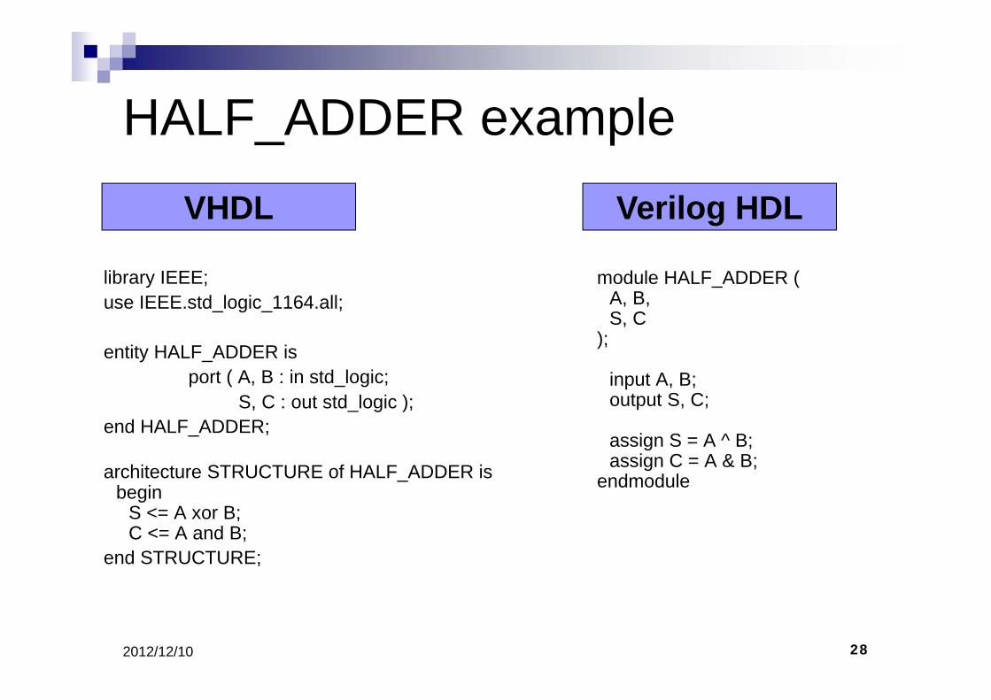
HALF_ADDER example
library IEEE;use IEEE.std_logic_1164.all;
entity HALF_ADDER isport ( A, B : in std_logic;
S, C : out std_logic );end HALF_ADDER;
architecture STRUCTURE of HALF_ADDER isbegin
S <= A xor B;C <= A and B;
end STRUCTURE;
module HALF_ADDER (A, B,S, C
);
input A, B;output S, C;
assign S = A ^ B;assign C = A & B;
endmodule
VHDL Verilog HDL
292012/12/10
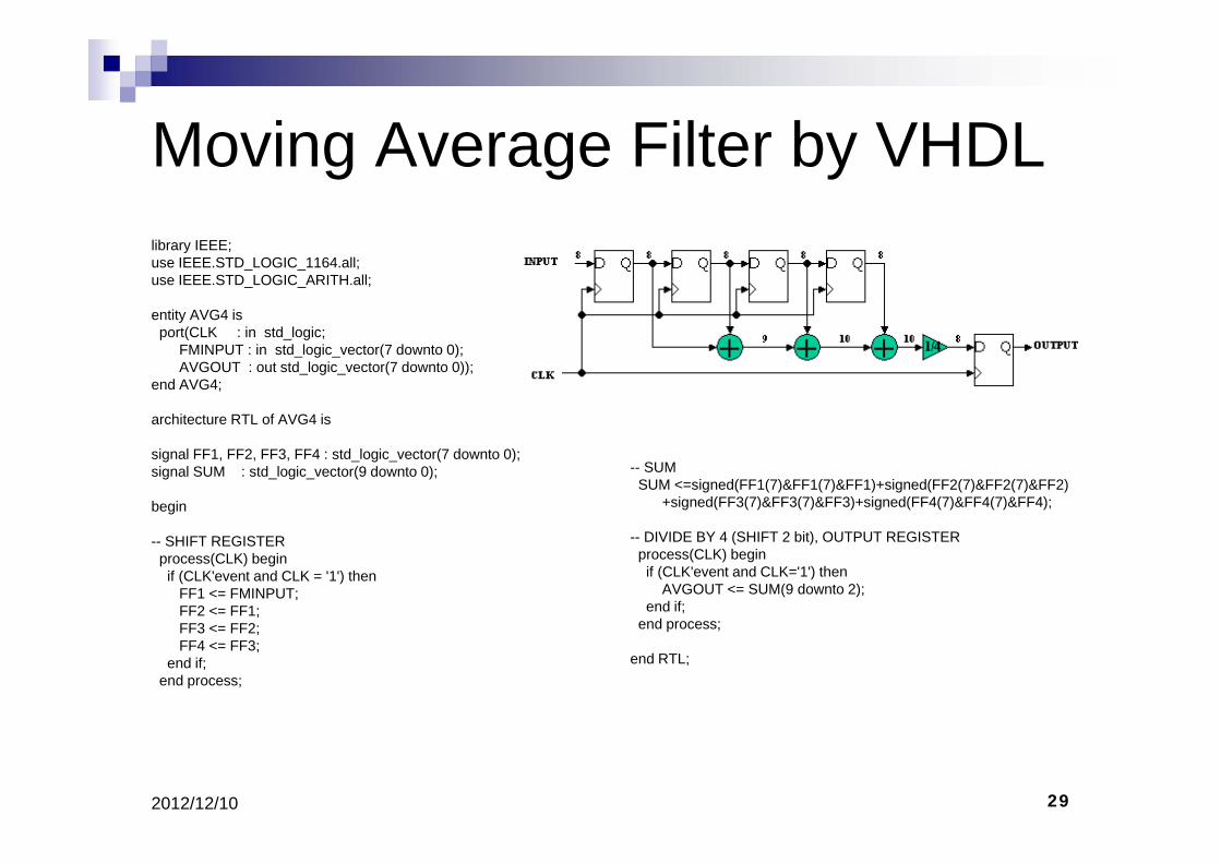
Moving Average Filter by VHDLlibrary IEEE;use IEEE.STD_LOGIC_1164.all;use IEEE.STD_LOGIC_ARITH.all;
entity AVG4 isport(CLK : in std_logic;
FMINPUT : in std_logic_vector(7 downto 0);AVGOUT : out std_logic_vector(7 downto 0));
end AVG4;
architecture RTL of AVG4 is
signal FF1, FF2, FF3, FF4 : std_logic_vector(7 downto 0);signal SUM : std_logic_vector(9 downto 0);
begin
-- SHIFT REGISTERprocess(CLK) beginif (CLK'event and CLK = '1') then
FF1 <= FMINPUT;FF2 <= FF1;FF3 <= FF2;FF4 <= FF3;
end if;end process;
-- SUMSUM <=signed(FF1(7)&FF1(7)&FF1)+signed(FF2(7)&FF2(7)&FF2)
+signed(FF3(7)&FF3(7)&FF3)+signed(FF4(7)&FF4(7)&FF4);
-- DIVIDE BY 4 (SHIFT 2 bit), OUTPUT REGISTERprocess(CLK) beginif (CLK'event and CLK='1') then
AVGOUT <= SUM(9 downto 2);end if;
end process;
end RTL;
302012/12/10
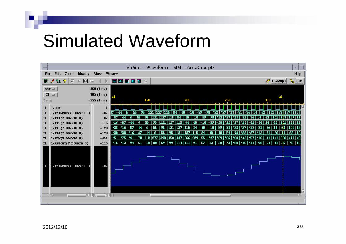
Simulated Waveform
312012/12/10
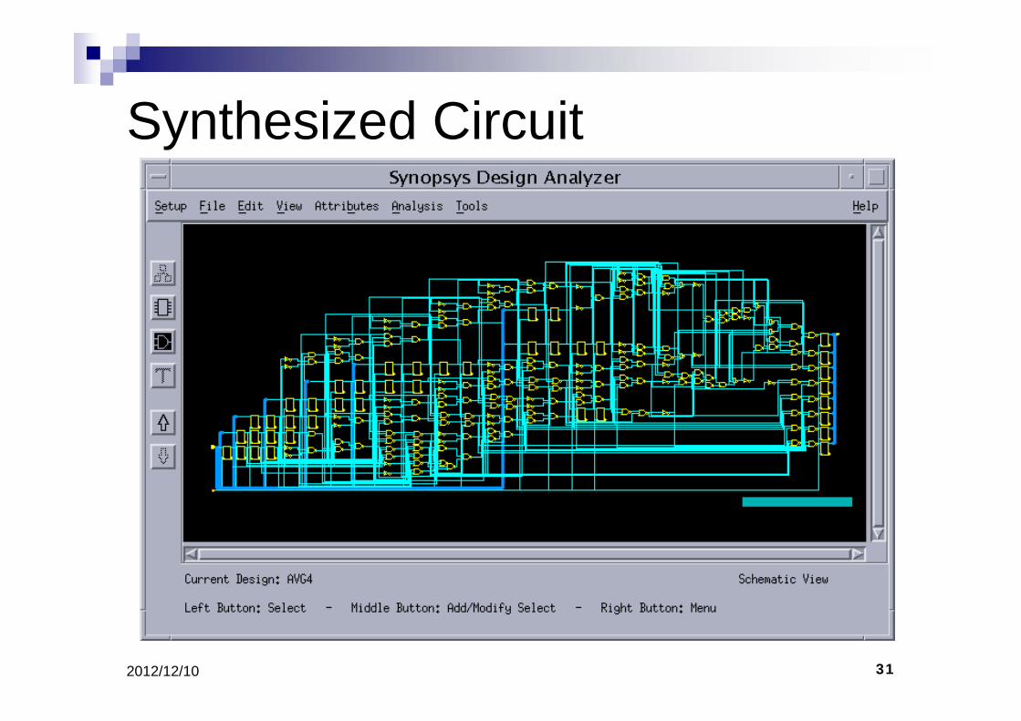
Synthesized Circuit
322012/12/10
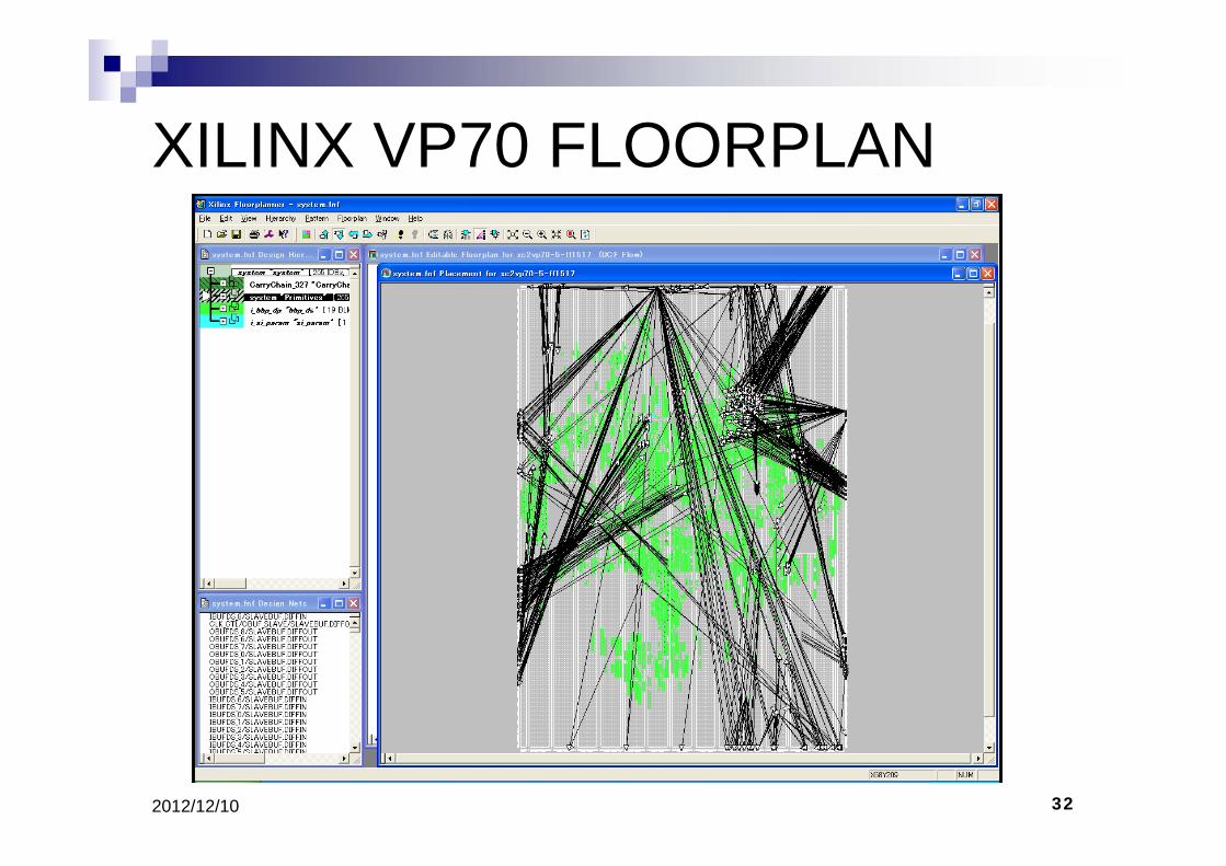
XILINX VP70 FLOORPLAN
Related Documents