Table Of Contents Special Options Specification Definitions Fiber Optic Enclosures • Outline Drawings Detailed Data Sheets • 5 kHz-2.5 GHz SLL Fiber Optc Link • 50 kHz - 3 GHz LBL Fiber Optic Link • 50 kHz - 4.5 GHz LBL Fiber Optic Link • 50 kHz - 6 GHz SCM Fiber Optic Link • 100 MHz - 11 GHz SCM Fiber Optic Link • 100 MHz - 13 GHz SCM Fiber Optic Link • 100 MHz - 15 GHz SCM Fiber Optic Link • 10 MHz - 18 GHz SCM Fiber Optic Link • 50 kHz - 6 GHz HRL Fiber Optic Link • 30 kHz - 12.5 GHz Optical Receiver • 100 kHz - 20 GHz Optical Receiver • Fiber Optic Links • Optical Receivers and Transmitters

Welcome message from author
This document is posted to help you gain knowledge. Please leave a comment to let me know what you think about it! Share it to your friends and learn new things together.
Transcript
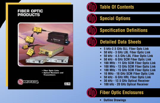
Table Of Contents
Special Options
Specification Definitions
Fiber Optic Enclosures
• Outline Drawings
100 Davids Drive • Hauppauge • NY 11788 • 631-436-7400 • Fax: 631-436-7431 • www. miteq.com
R
FIBER OPTIC PRODUCT DIRECTORY
Back toComponentHome PageComponentHome Page
Detailed Data Sheets• 5 kHz-2.5 GHz SLL Fiber Optc Link• 50 kHz - 3 GHz LBL Fiber Optic Link• 50 kHz - 4.5 GHz LBL Fiber Optic Link• 50 kHz - 6 GHz SCM Fiber Optic Link• 100 MHz - 11 GHz SCM Fiber Optic Link• 100 MHz - 13 GHz SCM Fiber Optic Link• 100 MHz - 15 GHz SCM Fiber Optic Link• 10 MHz - 18 GHz SCM Fiber Optic Link• 50 kHz - 6 GHz HRL Fiber Optic Link• 30 kHz - 12.5 GHz Optical Receiver• 100 kHz - 20 GHz Optical Receiver
• Fiber Optic Links• Optical Receivers and
Transmitters
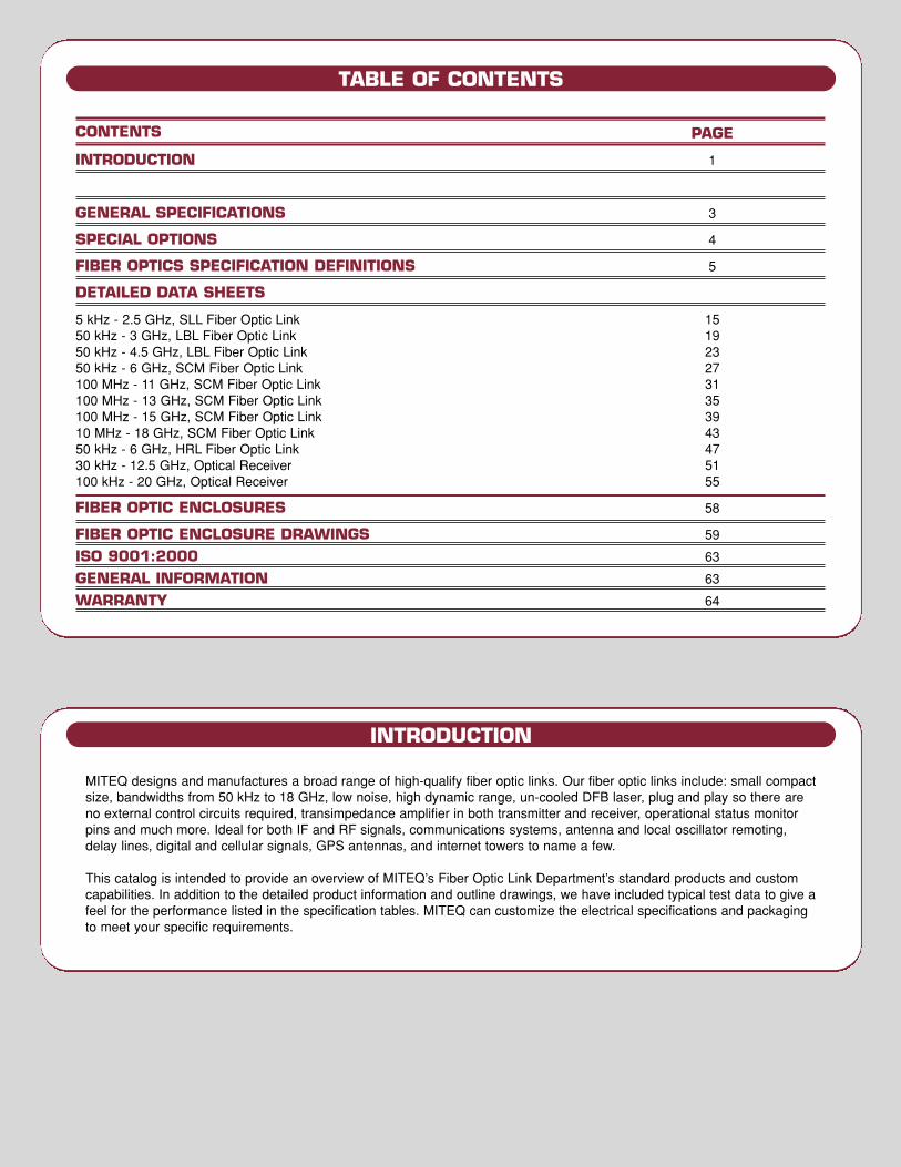
CONTENTS PAGE
INTRODUCTION 1
GENERAL SPECIFICATIONS 3
SPECIAL OPTIONS 4
FIBER OPTICS SPECIFICATION DEFINITIONS 5
DETAILED DATA SHEETS
5 kHz - 2.5 GHz, SLL Fiber Optic Link 1550 kHz - 3 GHz, LBL Fiber Optic Link 1950 kHz - 4.5 GHz, LBL Fiber Optic Link 2350 kHz - 6 GHz, SCM Fiber Optic Link 27100 MHz - 11 GHz, SCM Fiber Optic Link 31100 MHz - 13 GHz, SCM Fiber Optic Link 35100 MHz - 15 GHz, SCM Fiber Optic Link 3910 MHz - 18 GHz, SCM Fiber Optic Link 4350 kHz - 6 GHz, HRL Fiber Optic Link 4730 kHz - 12.5 GHz, Optical Receiver 51100 kHz - 20 GHz, Optical Receiver 55
FIBER OPTIC ENCLOSURES 58
FIBER OPTIC ENCLOSURE DRAWINGS 59
ISO 9001:2000 63
GENERAL INFORMATION 63
WARRANTY 64
TABLE OF CONTENTS
MITEQ designs and manufactures a broad range of high-qualify fiber optic links. Our fiber optic links include: small compactsize, bandwidths from 50 kHz to 18 GHz, low noise, high dynamic range, un-cooled DFB laser, plug and play so there areno external control circuits required, transimpedance amplifier in both transmitter and receiver, operational status monitorpins and much more. Ideal for both IF and RF signals, communications systems, antenna and local oscillator remoting,delay lines, digital and cellular signals, GPS antennas, and internet towers to name a few.
This catalog is intended to provide an overview of MITEQ’s Fiber Optic Link Department’s standard products and customcapabilities. In addition to the detailed product information and outline drawings, we have included typical test data to give afeel for the performance listed in the specification tables. MITEQ can customize the electrical specifications and packagingto meet your specific requirements.
INTRODUCTION

3 C-40100 Davids Drive, Hauppauge, NY 11788 • TEL: (631) 439-9220 • FAX: (631) 436-7430 • www.miteq.com
GENERAL SPECIFICATIONS
The following specifications are applied to all modelswithin this catalog:
POWER SUPPLY VARIATIONS
All fiber optic links include internal voltage regulatorsand reverse voltage protection diodes. They can,therefore, operate with an input voltage range from +11V to +20 V on their respective polarities and survivereverse polarity connection without damage. However,on the SCMT models, care has to be taken with the +5V used for the TEC drive current since it does not haveeither the voltage regulator nor the reverse biasprotection. The reason for this is that the TEC line candraw significant current based on ambient conditionseliminating the regulators/diodes on this line helps inlowering the voltage and reducing the heat dissipationthereby increasing the reliability of the product.
TEMPERATURE RANGES
All specifications are guaranteed at +23°C. All SLL,LBL, SBL and HRLmodels are guaranteed to operateover a temperature range of -20 to +70°C with slightlydegraded performance. The SCML model isguaranteed to operate from -20 to +50°C. Storagetemperature for all models is -40 to +85°C.
HEATSINKING
All transmitter modules and medium power receivers(output power greater than +10 dBm) require adequateheatsinking. If your application does not allow for amechanical heatsink, please contact MITEQ andrequest that one be supplied with the unit.
CONNECTORS
All models are supplied with SMA-female connectorsas standard. SMA-male, K-female, and K-maleconnectors can be specially requested on the modulesthemselves. BNC-female, N-male and N-femaleconnectors are optionally available for specialenclosure options. Connectors may be mixed. Pleasecontact MITEQ with your specific connectorrequirements.
STABILITY
All fiber links are guaranteed to be unconditionallystable. Small signal links may be operated into anysource or load impedance without damage. Mediumpower links must be terminated into 50 ohms at alltimes.
SECOND AND THIRD ORDERINTERCEPT POINTS
The third order intercept point is typically 10 dB abovethe 1 dB compression point for most models. Thesecond order intercept point is typically 20 dB abovethe 1 dB compression point.
MAXIMUM INPUT SIGNAL LEVELS
The input 1 dB compression is -14 dBm typical forstandard links and the maximum input power level forsurvival without damage is +10 dBm CW. Higher input1 dB compression links are also available having 0dBm input 1 dB compression and can survive themaximum input power level close to +20 dBm.
ENVIRONMENTAL SPECIFICATIONS
Humidity .....95% relative humidity, noncondensingVibration.....7.3 g’s rms, 20-20000 CPS,
Per MIL-STD-810B, Method 514,Procedure 5

4C-40100 Davids Drive, Hauppauge, NY 11788 • TEL: (631) 439-9220 • FAX: (631) 436-7430 • www.miteq.com
SPECIAL OPTIONS
OPTION -E1 (INDOOR ENLOSURES WITH R119” RACK MOUNT)
The fiber link can be purchased with a -E1 indoorenclosure option. This unit consists of two slideablehalf 1RU high enclosures housing transmit andreceive respectively in each half. Each enclosure isequipped with status and alarm LEDs. Theseenclosures are powered by 120 – 240 VAC powersupply. An additional Option, R1 can be purchasedwhich allows for the E1 enclosure halves to bemounted into a 19” wide 1RU chassis rack. For thistype of enclosure, you need to add a -E1 suffix at theend of the model number.
OPTION -WP (WEATHERPROOFENCLOSURE)
The fiber link can also be purchased with a -WPoutdoor weatherproof enclosure option. This is arugged housing with a rubber seal gasket. The DCconnector is a military grade weatherproof connector.The optical connector is also weatherproof with abuilt-in O-ring. The enclosure is powered by a single+12 V to +18 V DC supply and all status monitorvoltages are available on the connector. For this typeof enclosure, you need to add a -WP suffix at the endof the model number.
OPTION -SE (INDOOR SMALL ENCLOSURE)
The fiber link can also be purchased with a -SE indoorsmall enclosure option. This is a small housing withbuilt-in heatsink. The DC connector is a D-9 pinconnector with a choice of an optical connector. Theenclosure is powered by a single +12 V to +18 V DCsupply and all status monitor voltages are availableon the connector. For this type of enclosure, you needto add a -SE suffix at the end of the model number.
MULTI-CHANNEL TRANSMITTER / RECEIVEROPTION (MULTI-FIBER) IN INDOOR OROUTDOOR WEATHERPROOF HOUSING
Customer can request a custom designed multi-channel Transmitter, multi-channel Receiver, or acombination of transmitters and receivers in Option-E1 enclosure or full 19” wide rack mountable 1RUmountable enclosure, or in custom designedweatherproof outdoor housings. The number of fibersneeded would be equal to the number of channelsoffering complete isolation between channels. Theenclosure is powered by a 120 – 240 VAC powersupply plus an assortment of LED monitor alarms.
TRANSCEIVER OPTION (SINGLE FIBER)
Customer can choose to buy a Transmitter and aReceiver in the same -E1 enclosure that can be usedas a transceiver via a single fiber. The transmit andreceive signals can be on the same wavelength (1550nm or 1310 nm) or they can be on differentwavelengths (1310 nm and 1550 nm). Option isavailable for single channel transceiver or dualchannel transceiver using the same single fiber.
DELAY LINE
MITEQ can offer fiber links which can be used as adelay line also. The transmitter -E1 enclosure, or thereceiver -E1 enclosure, or both can be packaged witha fiber delay line ranging in value from a fewnanoseconds to 100 microseconds or more. We canalso incorporate fast switches to select differentdelays electronically if required.
GAIN CONTROL RECEIVER OPTION (WITH -GCSUFFIX)
MITEQ offers, as an option, wideband Gain ControlReceivers for optical links covering S, L, X, and Ku-Bands. The gain can be varied 20 dB on the receiver,which translates into a standard link continuous gainvariation of from +15 dB to -5 dB. The link noisefigure remains about the same over the entire gainvariation. It uses an analog gain control voltage whichcan be varied from +12 V to 0 V. The receiver has thesame form factor as the standard receiver, except thatit has a total of 4 pins: 12 V pin (100 mA); -12 V pin(15 mA); Monitor Pin (0 mA), and Gain Control Pin (5mA). These receivers are identified with a “-GC”suffix when ordering.
CUSTOM DESIGN SPECS FOR THE FIBERLINK
MITEQ specializes in catering to special designconfigurations for our customers, be it higher input 1dB compression, higher output 1 dB compression,higher overall link gain, lower noise figure, special RFbands, special optical wavelengths, special powerconstraints, custom housings, battery operatedsolutions, DC operated solutions, and AC operatedsolutions.

5 C-40100 Davids Drive, Hauppauge, NY 11788 • TEL: (631) 439-9220 • FAX: (631) 436-7430 • www.miteq.com
recorded over the operating frequency range. Unlessthe fiber link is specified to operate over a definedtemperature range, this measurement is per-formed at room ambient temperature (+23°C). If arange of temperatures is specified, the measurementmust also be verified at the temperature extremes.
NOISE FIGURE
Noise figure is classically defined as:
Since all fiber links add thermal noise, the signal-to-noise ratio at the output will be degraded; therefore,noise figure will be a ratio greater than one (NFdB = 10log10(NFRatio). The additive noise of a fiber link canalso be expressed in a parameter referred to as noisetemperature. In this approach, the noise temperatureof the fiber link is equal to the temperature (in degreesKelvin) of a 50 Ω termination at the input of an idealnoiseless fiber link with the same gain and generatingthe same output noise power.
The relationship between noise figure and noisetemperature is:
Noise figure data is measured at discrete frequenciesthroughout the band at +23°C unless specified otherwise.
INPUT AND OUTPUT POWER AT 1 dBCOMPRESSION
The input 1 dB compression point of a fiber link issimply defined as the input power level at which thegain deviates from the small signal gain by 1 dB.Similarly, the output 1dB compression point of a fiberlink is defined as the output power level at which thegain deviates from the small signal gain by 1 dB.
All active components have a linear dynamic range.This is the range over which the output power varieslinearly with respect to the input power. As the outputpower increases to near its maximum capability, thedevice will begin to saturate. The point at which thesaturation effects are 1 dB from linear is defined asthe 1 dB compression point. Because of the nonlinearrelation between the input and output power at thispoint, the following relationship holds:
Pout 1 dB = Pin 1 dB + Linear Gain - 1 dB
FIBER OPTICS SPECIFICATION DEFINITIONS
GENERAL SPECIFICATIONS
• Operating Frequency Range• Gain• Gain Flatness• Noise Figure• Input and Output Power at 1 dB Compression• Input and Output VSWR• DC Supply Voltage and Current Consumption
The following notes give detailed definitions to theseand additional specifications which may relate to yoursystem requirements.
OPERATING FREQUENCY RANGE
The operating frequency range is the range offrequencies over which the fiber link will meet orexceed the specification parameters. The fiber linkmay perform beyond this frequency range.
GAIN
Gain is defined as the ratio of the power measured atthe output of a fiber link to the power provided to theinput port. It is usually expressed in decibels and istypically measured in a swept fashion across theoperating frequency range. The gain of all fiber linksis verified by a swept measurement before shipmentfrom MITEQ.
GAIN FLATNESS
Gain flatness describes the variation in a fiber linksgain over the operating frequency range at any fixedtemperature within the operating temperature range.As such, it does not include the variation of gain as afunction of temperature (see Gain Variation vs.Temperature).
The gain flatness of a fiber link is measured byviewing the swept gain and determining the differencebetween the minimum gain and the maximum gain
Peak-to-Peak Gain Flatness
Operating Frequency Range(Measured at one temperature)
Max. Gain
Min. Gain
F Low F High
Noise Figure = 10 Log 10 +1Noise Temperature (Kelvin)290 Kelvin
Noise Figure = =Si/Ni
So/No
Signal-to-noise ratio at the fiber link inputSignal-to-noise ratio at the fiber link output

6C-40100 Davids Drive, Hauppauge, NY 11788 • TEL: (631) 439-9220 • FAX: (631) 436-7430 • www.miteq.com
FIBER OPTICS SPECIFICATION DEFINITIONS (CONT.)
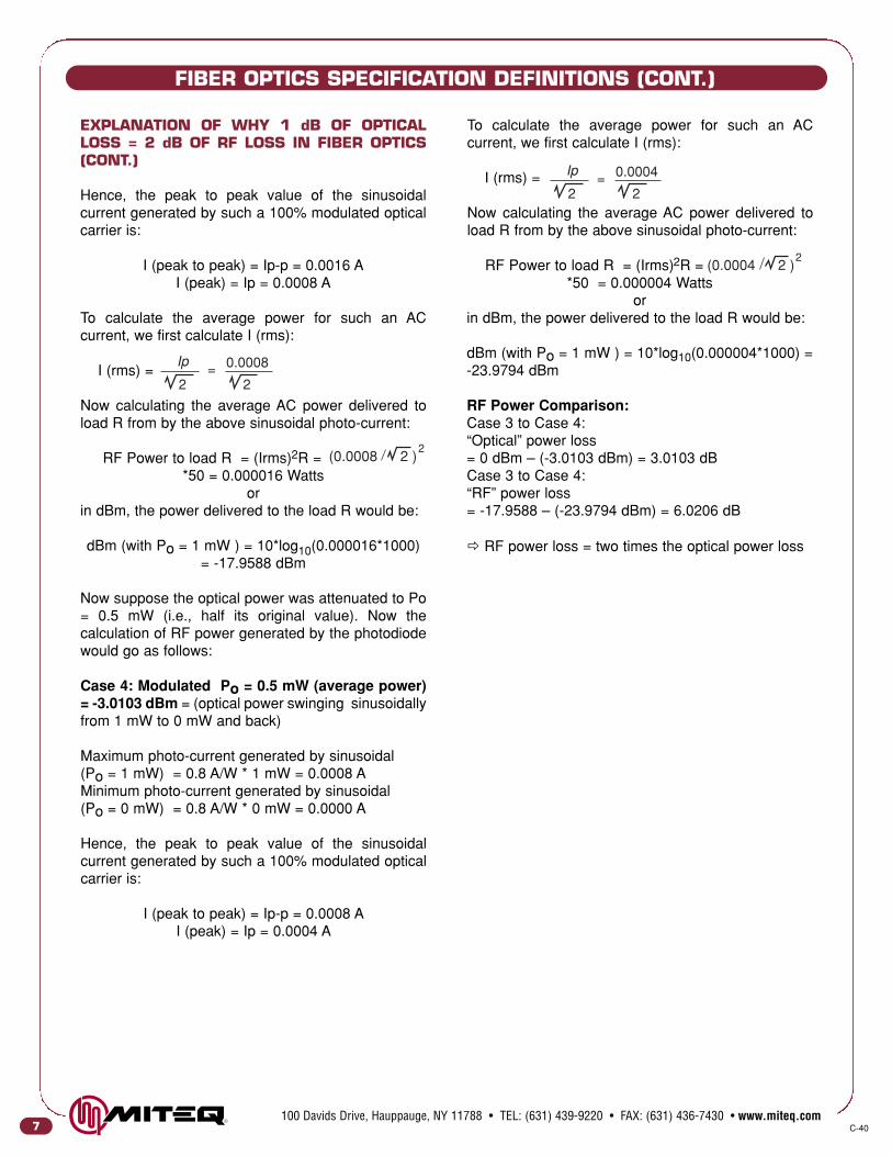
EXPLANATION OF WHY 1 dB OF OPTICALLOSS = 2 dB OF RF LOSS IN FIBER OPTICS
It is important to keep in mind that in fiber opticcommunications, every optical loss translates intotwice as much in RF loss. The reason being, that atthe photodiode level, a linear change in optical“power” generates a linear change in photo-“current”(not photo-“power”). In order to extract the “power”from the photo-current, we have to then again squarethe photo-“current” term using the load impedanceinto which the photo-current is being delivered. In logterms, this is equivalent to doubling the factor.
This will become clear with the following example:
1) DC Example:Suppose we have 1mW of optical power (Po) withoutany modulation and it is shining on a reverse-biasedphotodiode having responsivity of 0.8A/W. Thephotodiode is in turn terminated into a 50 ohm loadresistor (R). Then the DC power generated at the loadR would be calculated as follows:
Case 1: Unmodulated Po = 1 mW = 0 dBmPhoto-current generated (by Po = 1 mW) = 0.8 A/W
* 1 mW 0.0008 ADC Power delivered to the load by this photo-current
= I2R = (0.0008)2 *50 = 0.000032 Wattsor
in dBm, the power delivered to the load would be:
dBm (with Po = 1 mW )= 10*log10(0.000032*1000) = -14.9485 dBm
Now suppose the optical power was attenuated to Po= 0.5 mW (i.e., half its original value). Now thecalculation of DC power generated by the photodiodewould go as follows:
Case 2: Unmodulated Po = 0.5 mW = -3.0103 dBmPhoto-current generated (by Po = 0.5 mW) = 0.8 A/W
* 0.5 mW 0.0004 ADC Power delivered to the load by this photo-current
= I2R = (0.0004)2 *50 = 0.000008 Wattsor
in dBm, the power delivered to the load would be:
dBm (with Po = 0.5 mW) = 10*log10(0.000008*1000)= -20.9691 dBm
DC Power Comparison:Case 1 to Case 2:“Optical” power loss = 0 dBm – (-3.0103 dBm) =3.0103 dBCase 1 to Case 2:“DC” power loss = -14.9485 – (-20.9691 dBm) =6.0206 dB
DC power loss = two times the optical power loss
The same phenomenon occurs with the RF power aswell as had been a modulated optical carrier.
2) RF Example:Suppose we have 1 mW of average optical power(Po) with 100% modulation (i.e., it is swingingsinusoidally from 2 mW to 0 mW and back) and it isshining on a reverse-biased photodiode havingresponsivity of 0.8 A/W. The photodiode is in turnterminated into a 50 ohm load resistor (R). Then theAC power generated at the load R would becalculated as follows:
Case 3: Modulated Po = 1 mW (average power)= 0 dBm = (optical power swinging sinusoidally from2 mW to 0 mW and back)
Maximum photo-current generated by sinusoidal(Po = 2 mW) = 0.8 A/W * 2 mW = 0.0016 AMininum photo-current generated by sinusoidal(Po = 0 mW) = 0.8 A/W * 0 mW = 0.0000 A
7 C-40100 Davids Drive, Hauppauge, NY 11788 • TEL: (631) 439-9220 • FAX: (631) 436-7430 • www.miteq.com
FIBER OPTICS SPECIFICATION DEFINITIONS (CONT.)
EXPLANATION OF WHY 1 dB OF OPTICALLOSS = 2 dB OF RF LOSS IN FIBER OPTICS(CONT.)
Hence, the peak to peak value of the sinusoidalcurrent generated by such a 100% modulated opticalcarrier is:
I (peak to peak) = Ip-p = 0.0016 AI (peak) = Ip = 0.0008 A
To calculate the average power for such an ACcurrent, we first calculate I (rms):
I (rms) =
Now calculating the average AC power delivered toload R from by the above sinusoidal photo-current:
RF Power to load R = (Irms)2R =*50 = 0.000016 Watts
orin dBm, the power delivered to the load R would be:
dBm (with Po = 1 mW ) = 10*log10(0.000016*1000)= -17.9588 dBm
Now suppose the optical power was attenuated to Po= 0.5 mW (i.e., half its original value). Now thecalculation of RF power generated by the photodiodewould go as follows:
Case 4: Modulated Po = 0.5 mW (average power)= -3.0103 dBm = (optical power swinging sinusoidallyfrom 1 mW to 0 mW and back)
Maximum photo-current generated by sinusoidal(Po = 1 mW) = 0.8 A/W * 1 mW = 0.0008 AMinimum photo-current generated by sinusoidal(Po = 0 mW) = 0.8 A/W * 0 mW = 0.0000 A
Hence, the peak to peak value of the sinusoidalcurrent generated by such a 100% modulated opticalcarrier is:
I (peak to peak) = Ip-p = 0.0008 AI (peak) = Ip = 0.0004 A
To calculate the average power for such an ACcurrent, we first calculate I (rms):
I (rms) =
Now calculating the average AC power delivered toload R from by the above sinusoidal photo-current:
RF Power to load R = (Irms)2R =*50 = 0.000004 Watts
orin dBm, the power delivered to the load R would be:
dBm (with Po = 1 mW ) = 10*log10(0.000004*1000) =-23.9794 dBm
RF Power Comparison:Case 3 to Case 4:“Optical” power loss= 0 dBm – (-3.0103 dBm) = 3.0103 dBCase 3 to Case 4:“RF” power loss= -17.9588 – (-23.9794 dBm) = 6.0206 dB
RF power loss = two times the optical power loss
Ip
2= 0.0008
2
(0.0008 2 )2
Ip
2= 0.0004
2
(0.0004 2 )2
FIBER OPTICS SPECIFICATION DEFINITIONS (CONT.)
8C-40100 Davids Drive, Hauppauge, NY 11788 • TEL: (631) 439-9220 • FAX: (631) 436-7430 • www.miteq.com
INPUT AND OUTPUT VSWR (OR INPUT ANDOUTPUT RETURN LOSS)
Most RF and microwave systems are designedaround a 50 Ω impedance system. A fiber link’simpedance is designed to be as close as possible to50 Ω; however, this is not always possible, especiallywhen attempting to simultaneously achieve a goodnoise figure. The VSWR of a fiber link is a measure ofa fiber link’s actual impedance (Z) with respect to thedesired impedance (Zo) in most cases 50 Ω.
The VSWR is derived from the reflection coefficient ρ,where ρ is a ratio of the normalized impedance:
VSWR is "measured" with either a scalar or vectornetwork analyzer by analyzing the incident power andthe reflected power at both ports of the device todetermine the reflection coefficients which in turn areconverted and displayed as VSWR. The ratio of thereflected power to the incident power is also known asthe return loss.
SUPPLY VOLTAGE ANDCURRENT CONSUMPTION
Transmitter Modules:All standard models are internally voltage regulatedand reverse voltage protected. All un-cooled lasertransmitter modules are specified with two voltages:+12 V and -12 V while the cooled versions arespecified with three voltages: +12 V, -12 V and +5 V.The +12 V and -12 V are regulated and reversepolarity protected. Hence they can safely be operatedfrom ±11 V to ±20 V without any damage to the link.However, the higher the voltage, the higher the heatdissipation and so a nominal operating voltage of ±12V is recommended. Depending on the model, thecurrent could vary on the +12 V from 200 mA to 325mA, and on the -12 V from 100 mA to 250 mA.
In the case of the cooled laser modules, the thirdvoltage of +5 V is unregulated and not reverse polarityprotected in order to lower the heat dissipation due tohigh current consumption by the thermo-electricpeltier cooler inside. A voltage range of +3 V to +6 Vcan be applied on this pin with a recommendedvoltage of +4 V to +5 V.
SUPPLY VOLTAGE ANDCURRENT CONSUMPTION (CONT.)
All transmitters come with a laser monitor pin whichreads -2 V during normal operation and 0 V otherwise.In case of cooled lasers, an additional lasertemperature monitor pin is also available which readsnear 0 V for normal operation and ±1 V or higherotherwise.
All transmitter modules need to be properly heat sunk.
Receiver Modules:All non-gain control receiver modules come with asingle +12 V supply requirement which is regulatedand reverse polarity protected. The range of voltagethat can be applied on it can vary from +11 V to +20V, but +12 V is recommended to reduce the amount ofheat dissipation. The amount of current depends onthe model and can vary from 100 mA to 275 mA.
All gain control receiver modules come with dual +12V and -12 V supply requirement which are regulatedand reverse polarity protected. The currentconsumption on these pins are 150 mA on the +12 Vsupply and 20 mA on the -12 V supply.
ρ = Z - ZoZ + Zo
and:
VSWR =1 + ρ1 - ρ
9
FIBER OPTICS SPECIFICATION DEFINITIONS (CONT.)
C-40100 Davids Drive, Hauppauge, NY 11788 • TEL: (631) 439-9220 • FAX: (631) 436-7430 • www.miteq.com
OVERALL GAIN WINDOW
An overall gain window specification defines theabsolute minimum and maximum gain values overboth temperature and frequency.
It is the most complete way to specify a fiber link;however, it also impacts the price due to the additionaltesting and alignment required from adding thisconstraining parameter.
SECOND AND THIRD ORDER INTERCEPTPOINTS
Fiber optic links use solid state amplifiers to providegain. Although these amplifiers (FETS and bipolartransistor) are generally used in a linear mode theystill exhibit nonlinear phenomenon, such asintermodulation effects and harmonic generation.These effects are evident in spurious productspresent at the output. In the case of the single-tonecondition, the spurious signals are the harmonics ofthe fundamental input signal. In the case of the two-tone condition, the spurious signals are a mixingproduct of two input signals at the frequencies f1 andthe other at f2. The most commonly discussed beingthe second order and the third order two-tone spurs.
Second order two-tone spurs are the sum anddifference product of the fundamental inputfrequencies, i.e.;
fSPUR = f1 ± f2
The spurious signals are only of concern when theband is greater than on octave. If the frequency rangeis less than one octave, the two-tone second orderspurs will be out of band.
Peak-to-Peak Gain Flatness
Operating Frequency Range(Measured at room, hot and cold)
Max. Gain
Min. Gain
F Low F High
ADDITIONAL SPECIFICATIONS
In addition to the electrical specifications included formost of the models within this catalog, there areadditional specifications which are useful to theengineer designing around stringent systemrequirements:
• Gain Variation vs. Temperature• Overall Gain Window• Intercept Points• Dynamic Range• Harmonic Suppression• Reverse Isolation• Phase Linearity• Peak Wavelength• Spectral Width• Side Mode Suppression Ratio• Relative Intensity Noise• RF Loss vs. Optical Loss• Fiber Types• Optical Connector Types• Laser MTBF
GAIN VARIATION VS. TEMPERATURE
Gain variation versus temperature defines themaximum allowable variation of the linear gain due totemperature at any discrete frequency. As a result,this parameter does not account for drift overfrequency.
Gain variation versus temperature is measured byperforming swept gain measurements at the specifiedtemperature extremes and comparing the deviationsbetween the two sweeps at each frequency todetermine the greatest change. When a ± value isused, then the delta is taken at both temperatureextremes with respect to room temperature (+23°C).
Maximum Variation vs. Temperature
Operating Frequency Range(Measured at room, hot and cold)
coldroom
Gai
n
F Low F High
hot

10C-40100 Davids Drive, Hauppauge, NY 11788 • TEL: (631) 439-9220 • FAX: (631) 436-7430 • www.miteq.com
FIBER OPTICS SPECIFICATION DEFINITIONS (CONT.)
THIRD ORDER RELATIONSHIP WITH P1 dB
Third order intercept (TOI) is “sort of “ related with 1-dB compression point (P1) in that:
Output TOI (dBm) = Output P1 (dBm) +10 dB(approximately) Equation A
Input TOI (dBm) = Input P1 (dBm) +10 dB(approximately) Equation B
Also:Input P1 (dBm) = Output P1 (dBm) – Gain (dB)
Equation C
Sometimes the added figure can be 8 dB, other times12 dB above, but generally 10 dB is typical.
Also, dB below carrier (dBc) level of harmonics andIntermodulation Products (IM) is a measurement oflinearity of the Device Under Test (DUT). If the DUT isperfectly linear, there will not be any harmonics for a“sine-wave” input. However, if there are non-linearities, then the harmonics and IM products willstart to appear for the sine wave indicating that thereis some distortion of the carrier sine wave taking placein the DUT. All active devices exhibit some level ofdistortion. The lower the harmonics are from thecarrier (i.e., the higher the dBc), the better the linearityis of the DUT.
Usually the process entails a two-tone measurement.What this means is that two sine carriers equal inamplitude but slightly separated in frequency aroundthe frequency of interest are fed into the DUT (forexample; for 1 GHz measurement, the two sinecarriers can be set at 1 GHz and 1.05 GHz).Theoutput is monitored on the spectrum analyzer, whichtypically shows the two carrier sine waves plus thirdorder products and other harmonics. It is the thirdorder IM products that are of greatest concernbecause of their proximity to the carrier which makesit difficult to filter out plus their triple fold increaserelationship (i.e., every 1 dB increase in carrier causesthe third order IM products to increase by 3 dB). Therelationship used between the TOI and the dBc are:
Output TOI = dBc/2 + (carrier dBm)Equation D
Where:TOI: third order interceptdBc = the amount of dB down the IM product is from
the carrier sine wavedBm = the carrier frequency power
These spurious signals are characterized with respectto the input signal by means of a theoretical toolcalled an intercept point. These points are defined asthe point where the linear curve of input vs. outputpower of the fundamental would intersect with thelinear curve of the spurious signal if saturation effectswould not limit the output levels of these signals.Since it is known that the second order spuriousproducts have a slope of 2:1 with respect to thefundamental input power, the value of the spurs canbe estimated if the input signal power (PIN) and theoutput second order intercept point (OIP2) areknown. The relationship is as follows:
Two-Tone Second OrderSpurious Suppression = OIP2 - (PIN + G)
Two-Tone Second OrderSpurious Level = 2 (PIN + G) - OIP2
Third order spurious products result from combinationsof the fundamental signal and the second harmonics.
fSPUR = |2f1 ± f2| ± |f1 ± 2f2|
The slope of the third order spurious signals is 3:1with respect to the fundamental input power, andagain the value of the spurs can be estimated if theinput signal power (PIN) and the output third orderintercept point (OIP3) are known. The relationship isas follows:
Two-Tone Third OrderSpurious Suppression = 2 OIP3 - (PIN + G)
Two-Tone Third OrderSpurious Level = 3 (PIN + G) - 2 OIP3
TwoInputTones
f2-f1 f1-f22f1-f2 2f2-f1f1 2f1f2
2nd Order 2nd Order
3rd Order 3rd Order
2nd Harm.
Intermodulation Spurious Frequency Spectrum

11 C-40100 Davids Drive, Hauppauge, NY 11788 • TEL: (631) 439-9220 • FAX: (631) 436-7430 • www.miteq.com
FIBER OPTICS SPECIFICATION DEFINITIONS (CONT.)
DYNAMIC RANGE
Dynamic range can be defined in several ways. Thetwo classical approaches are to define the lineardynamic range, and the second being the spuriousfree dynamic range.
The linear dynamic range defines the differencebetween the minimum detectable signal (MDS),referred to the input of the fiber link or the maximumsignal level at which the fiber link remains linear.This is typically defined by the input 1 dBcompression point (PIN 1 dB). The minimumdetectable signal is defined by system constraintssuch as noise figure, bandwidth, and predetectionsignal-to-noise ratio.
SPURIOUS FREE DYNAMIC RANGE (SFDR)
Spurious Free Dynamic Range (SFDR), as the namesuggests, is the range of input levels for which theoutput would be free of any spurs or intermodulationproducts. In other words, starting at the noise floor atthe output (for a given bandwidth), it is the amount ofsignal in dBs that an input signal can be increased bybefore you start seeing the intermodulation productscreep out of the noise at the output. All activedevices exhibit non-linearities which result inharmonics and intermodulation products, and theones of particular concern are the third orderintermodulation products which can fall within thebandwidth of interest and are hard to filter outbecause of the proximity to the carriers. Also theygrow in power three times faster (1-dB increase incarrier level causes the third order products toincrease by 3 dB).
The commonly used equation to determine the spurfree dynamic range is as follows:
SFDR (dB) = 2/3 [Output Third Order Intercept or TOI(dBm) - Gain (dB) - kTB (dBm) + Noise Figure (dB) ]
Where:
1) The terms in a + b define the Noise Floor:a) Theoretical Minimum Noise Floor at 25°C:
kTB (in 1 Hz) = 10 log ((1.38 x 10e-23 x 298(degKelvin) x 1 (Hz)) x1000 (for mW) = -174 dBm/Hz
orkTB (in 1 MHz) = 10 log ((1.38 x 10e-23 x 298(degKelvin) x 1 x 10e+6(Hz)) x1000 (for mW) = -114
dBm/MHz
So, if the input P1 (dBm) and gain is known, as is thecase for the SCMT-18G which is -15 dBm and +18 dBrespectively (typical), then equation C and A yield:
Output P1 (dBm) = -15 dBm +18 dB = +3 dBmOutput TOI (dBm) = +3 dBm +10 dB = +13 dBm
(approximately)
If the minimum desired dBc is 75, then the maximumdBm of the carrier comes out from Equation D as:
+13 dBm = 75/2 + dBmCarrier (dBm) = -24.5 dBm (at the output)
What this tells us is that if the carrier power at theoutput of the SCMR-18G link is less than -24.5 dBm,then the dBc of the IM products would be greater than(or better than) 75 dBc across the band. (ORconversely if the carrier power into the SCMT-18G isless than -42.5 dBm, then the IM products would be atleast 75 dB further down across the band).
Similarly for a desired minimum dBc of 100, then themaximum power level of the carrier at the input of thetransmitter SCMT-18G would be -55 dBm.

FIBER OPTICS SPECIFICATION DEFINITIONS (CONT.)
12C-40100 Davids Drive, Hauppauge, NY 11788 • TEL: (631) 439-9220 • FAX: (631) 436-7430 • www.miteq.com
SPURIOUS FREE DYNAMIC RANGE (CONT.)
b) Noise figure (dB) of the system or DUT: Measuredusing the noise diode and a noise figuremeter/analyzer. The noise figure meter is calibratedusing the known Excess Noise Ratio (ENR)parameters of the noise diode. The DUT is nextconnected in line and the meter measures theadditional noise contributions of the DUT or thesystem (in dB). This figure, added to the theoreticalminimum in (a), defines the noise floor.
2) The term [Output Third Order Intercept (dBm) –Gain (dB)] translates the Output TOI to Input TOI.This is an input level where theoretically output thirdorder product will level off with the carrier.(Remember: 1 dB increase in carrier = 3 dB increasein third order product). (Practically the intercept isnever realized).
3) The term in square bracket can thus be simplifiedto:Total Dynamic Range = [Input Third Order Intercept
(dBm) - Noise Floor]= [Total Input Dynamic Range from Minimumdetection level to Maximum detection level]
4) Finally, to the mystery of the 2/3 factor: The termexplained in (3) gives the total dynamic range fromminimum to maximum levels. For spurious freedynamic range (i.e., the range of input where thereare no third order products present at the output), weback off the input level from its maximum detectionlevel (where the third order was at level with thecarrier) by 1/3. The third order products drop downthree times faster, and become leveled with thenoise floor. Hence, when the input is at two thirds ofits maximum range, the third order is at the noisefloor. This defines the maximum spurious freedynamic range.
In a typical LBL link:
Noise Figure = 10 dB (typ.)Input P1 = -9 dBm (typ.)Input TOI = 0 dBm
(approx. 9 dB higher than the input P1)
Therefore the SFDR calculates out to be:
SFDR = 2/3 [0 dBm - (-174 dBm + 10 dB)] dB/Hz= 109 dB/Hz*
*Sometimes the unit is also expressed as dB/Hz2/3
due to the fact that the 2/3 multiplication factor aheadof the log (dB) calculations translates into a powerfactor in the linear calculations.
SPURIOUS FREE DYNAMIC RANGECALCULATIONS
The calculations for SFDR (Spurious Free DynamicRange) for our 18 GHz link are as follows:
SFDR = 2/3 [Input TOI (dBm) - NF (dB) - kTBThermal Noise Floor for theReceiver Bandwidth (dBm)]
where:
TOI = Third Order Intercept of the LinkNF = Noise Figure of the Linkk = Boltzman Constant: 1.38e-23 J/KT = Temperature in KelvinB = Receiver Bandwidth
The kTB noise floor is the theoretical minimum noisefloor that can be had for a given bandwidth andtemperature. Hence for a 1 Hz bandwidth at roomtemperature (290 deg Kelvin), the kTB noise floor (indBm) calculates out to be:
kTB (in 1 Hz BW at room temp.) = 10 log (1.38e-23x290x1x1000) = -173.97 dBm
orkTB (in 1 MHz BW at room temp.) = 10 log (1.38e-
23x290x1e+6x1000) = -113.9 dBmor
kTB (in 300 MHz BW at room temp.) = 10 log(1.38e-23x290x300e+6x1000) = -89.21 dBm
So in a 300 MHz receiver bandwidth, the minimumtheoretical noise floor comes out to be -89.21dBm.Add to this the noise figure of the link which is sayabout 17 dB at the frequency of interest, then theMinimum Detectable Signal (MDS) comes out to be:
MDS (in 300 MHz BW) = kTB Noise Floor + NoiseFigure of the link= -89.21 dBm + 17 dB= -72.21 dBmThis means that if the link has a noise figure of 17dB, then any signal greater than -72.21 dBm isdetectable.
The SFDR calculates out to be:
SFDR (in 1 Hz BW) = 2/3 (Input TOI - NF + 174) dB/Hzor
SFDR (in 1 MHz BW) = 2/3 (Input TOI - NF + 114)dB/MHzor
SFDR (in 300 MHz BW) = 2/3 (Input TOI - NF + 89.21)dB/300 MHz

13
FIBER OPTICS SPECIFICATION DEFINITIONS (CONT.)
C-40100 Davids Drive, Hauppauge, NY 11788 • TEL: (631) 439-9220 • FAX: (631) 436-7430 • www.miteq.com
SPURIOUS FREE DYNAMIC RANGECALCULATIONS (CONT.)
The input TOI is typically 8 to 10 dB higher than the input1-dB compression point. In our SCMT-18G fiber opticlinks, the input 1 dB compression typically comes out tobe about -13 dBm and the noise figure is about 17 dB at15 GHz. Taking these numbers, the spur free dynamicrange at 15 GHz comes out to be:
SFDR (in 1 Hz BW) = 2/3 (-3 -17 + 174) = 102.67 dB/Hzor
SFDR (in 1 MHz BW) = 2/3 (-3 - 17 + 114) = 62.67 dB/MHzor
SFDR (in 300 MHz BW) = 2/3 (-3 - 17 + 89.21) = 46.14dB/300 MHz
Once knowing the input 1-dB compression and the noisefigure of a link, you can calculate the MDS and SFDRalong the lines of the above calculation.
MINIMUM DETECTABLE SIGNAL (MDS)/MINIMUM INPUT POWER/SENSITIVITYCALCULATIONS
The Minimum Detectable Signal (MDS) “or” the MinimumInput Power “or” the sensitivity of the fiber optic link is afunction of the receiver filter bandwidth and the noisefigure of the link. The wider the filter bandwidth at thereceiver end, the more thermal noise power will comethrough it. That in turn would raise the noise floor andmake it less sensitive to weak signals.
The MDS or the minimum input power is calculated as:
MDS (at particular frequency for given bandwidth) = kTBnoise floor (given bandwidth) + NF of the Link (atfrequency of interest)
where:
k = Boltzman Constant: 1.38e-23 J/KT = Temperature in KelvinB = Receiver BandwidthNF = Noise Figure of the Link at that particular frequencyof interest
The kTB noise floor is the theoretical minimum thermalnoise floor that can be had for a given bandwidth andtemperature. Hence for a given bandwidth at roomtemperature (290 deg Kelvin), the kTB noise floor (indBm) calculates out to be:
kTB (in 1 Hz BW at room temp.) = 10 log (1.38e-23x290x1x1000) = -173.97 dBm
or
kTB (in 1 MHz BW at room temp.) = 10 log (1.38e-23x290x1e+6x1000) = -113.9 dBm
orkTB (in 300 MHz BW at room temp.) = 10 log(1.38e-23x290x300e+6x1000) = -89.21 dBm
If the Noise Figure (NF) of the link is say about 17 dBat the frequency of interest (say at 15 GHz), then theMDS at 15 GHz for different filter bandwidths comesout to be:
MDS (in 1 Hz BW) = -173.97 dBm + 17 dB= -156.97 dBm = Minimum Input Power Level for
1 Hz BWMDS (in 1 MHz BW) = -113.9 dBm + 17 dB= -96.9 dBm = Minimum Input Power Level for
1 MHz BWMDS (in 300 MHz BW) = -89.21 dBm + 17 dB= -72.21 dBm = Minimum Input Power Level for
300 Hz BW
What the above states is that if the bandwidth is 1Hz, then any signal higher than -156.97 dBm wouldbe detectable at 15 GHz. Similarly, if the bandwidthis 1 MHz, then any signal higher than -96.9 dBmwould be detectable at 15 GHz. Similarly one cancalculate the MDS at any frequency once knowingthe noise figure at that frequency and the filterbandwidth.
Since the link has typically about +15 dB gain at theoutput, the output power level for the aboveminimum input signal levels would be:
Output Power for (MDS = -156.97 dBm in 1Hz BW)= -156.97 dBm + 15 dB = -141.97 dBm
Output Power for (MDS = -96.9 dBm in 1 MHz BW)= -96.9 dBm +15 dB = -81.9 dBm
Output Power for (MDS = -72.21 dBm in 300 MHzBW) = -72.21 dBm +15 dB = -57.21 dBm
REVERSE ISOLATION
Reverse isolation simply defines the isolationbetween the input and output. It is tested by injectinga signal to the output port and measuring its level atthe input. Since the optical transmitter and receiverpair are unidirectional, there is complete isolation inthe reverse direction. There can be no flow of signalfrom a receiver to a transmitter as there is no lightgenerated by the photodiode to transmit through thefiber toward the transmitter.

FIBER OPTICS SPECIFICATION DEFINITIONS (CONT.)
14C-40100 Davids Drive, Hauppauge, NY 11788 • TEL: (631) 439-9220 • FAX: (631) 436-7430 • www.miteq.com
PHASE LINEARITY
A phase of a signal versus frequency will be distorteddue to the nonlinear phase elements within the fiberlink. This distortion is called phase linearity and ismeasured by means of a vector network analyzeracross the operating frequency range.
PHASE NOISE
Phase noise is a measure of the stability of a referencefrequency generated by a synthesizer as it passesthrough a fiber link. MITEQ fiber optic links havemeasured exceptionally well typically reading below100 dBc at 1 Hz offset and below 120 dBc at 10 Hzoffset from the carrier frequency.
PEAK WAVELENGTH
Peak wavelength is the wavelength at which themaximum intensity emission mode occurs at specifiedoptical output power.
SPECTRAL WIDTH (-3 dB) OR FULL WIDTHHALF MAXIMUM (FWHM)
Spectral Width (-3 dB) is defined as the full width of theemission spectrum at half maximum of the peakspectrum intensity and at the specified optical outputpower. It is also known as FWHM or full width halfmaximum which translates into the full width of thespectrum at half its maximum power.
SIDE MODE SUPPRESSION RATIO (SMSR)
This parameter is the ratio of the intensity of the highestspectral peak to that of the second highest in theemission spectrum at a defined optical output powerand under a defined modulation (or CW) as describedin the graph.
RELATIVE INTENSITY NOISE (RIN)
RIN describes the instability in the power level of alaser. It can be generated from cavity vibration orfluctuations in the laser gain medium and isexacerbated with optical reflections into the lasercavity. RIN is plotted as a function of the frequencyor as a function of the operating current and isdefined by the following equation:
RF LOSS VS. OPTICAL LOSS (1 dB OPTICALLOSS = 2 dB RF LOSS)
In fiber optic communications, every dB of opticalloss translates into twice the RF loss. The reason isbecause a linear change in optical “power”generates a linear change in photo-“current” (notphoto-“power”). In order to extract the power fromthe photodiode, this linear photo-“current” has to be“squared” using the load impedance into which it isdelivered. In log terms this translates into doublingof gain or loss factor.
FIBER TYPES
MITEQ links are designed to be used strictly withsingle mode fiber which gives much stability andbetter bandwidth vs. distance performance. Thevariations within single mode fibers are commonlySMF-28 and LEAF fibers. The attenuation in fiber istypically 0.2 dB/km optical which translates into 0.4dB/km RF loss. For longer distances and widerbandwidths (>10 GHz), LEAF fiber tends to deliverbetter flatness as chromatic dispersion at 1550 nmwavelength is significantly less (2 ps/nm.km)compared to 15 ps/nm.km for SMF-28. The SMF-28is designed for zero dispersion at around 1310 nm.
OPTICAL CONNECTOR TYPES
Standard connector type is FC/APC. However,customer can specify any of the following: FC/PC,E-2000, SC/APC, SC/PC, ST, LC, Green Tweed FC-DRY (weatherproof connector for weatherproofenclosures).
LASER MEAN TIME BETWEEN FAILURE
The lasers used in our SCML models are activelycooled and maintained at room temperature. Basedon the accelerated aging data from the manufacturerand the bias operating parameters, the mean lifetimecalculates out to about 140 years.
RIN = 10*Log10 =[(Pn – Pno) /G* Bn] – 2* q < lph> Zo
I < lph > 2* Zo
Wavelength
Rel
ativ
eIn
tens
ity(d
B)
Side Mode SuppressionRatio

100 Davids Drive, Hauppauge, NY 11788 • TEL: (631) 439-9220 • FAX: (631) 436-7430 • www.miteq.comC-4015
FEATURES• Bandwidth.......................... 5 kHz to 2.5 GHz• Small size• Un-cooled DFB laser• No external control circuits required• Transimpedance amplifier in bothtransmitter and receiver
• Operational status monitor pins
APPLICATIONS• Antenna remoting• Local oscillator remoting• Interfacility communication links
5 kHz - 2.5 GHz SLL FIBER OPTIC LINK
ELECTRICAL SPECIFICATIONS
PARAMETERS CONDITION UNITS MIN. TYP. MAX.
Operating frequency* 3 dB bandwidth 5 kHz 2.5 GHzGain Measured from 10 kHz dB 5 12 15Noise figure dB 18 20Group delay Peak-to-peak ns 0.1 0.2VSWR Input/output 2:1Phase noise 100 Hz offset dBc 100Input power at 1 dB compression Option A dBm -14Spurious-free dynamic range 1 Hz bandwidth dB/Hz2/3 100Maximum input power No damage dBm +10Maximum output power Saturated dBm +10Impedance Input/output Ohms 50RF connectors SMA female (male optional)
NOTE: -30 dBm input power.* Data measured from 10 kHz and above. Substract bands also available.
OPTICAL PERFORMANCE SPECIFICATIONS
PARAMETERS CONDITION UNITS MIN. TYP. MAX.
Fiber optic connectors FC/APC(Other standard available)
Fiber Single mode fiber (9/125µm)Wavelength Other wavelengths available nm 1540 1550 1560Spectral width FWHM nm 0.1Optical power in fiber Reference only mW 3 4Side mode suppression ratio dB 30 40
DC POWER REQUIREMENTS
PARAMETERS CURRENT @ 25°C BASE PLATE UNITS MIN. TYP. MAX.
(VDC) (VDC) (VDC)
Transmitter 100 mA 2 +11 +12 +20
100 mA 1 -11 -12 -20
Receiver 100 mA 4 +11 +12 +20

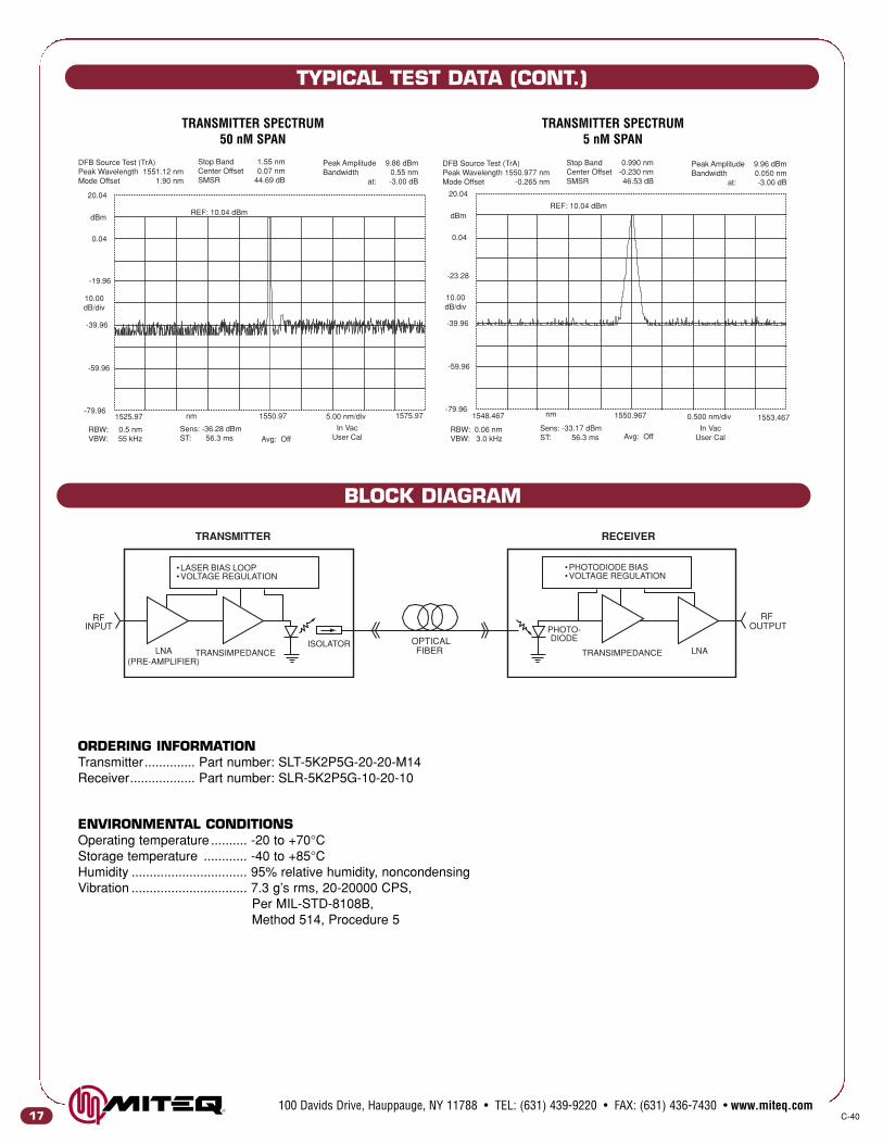
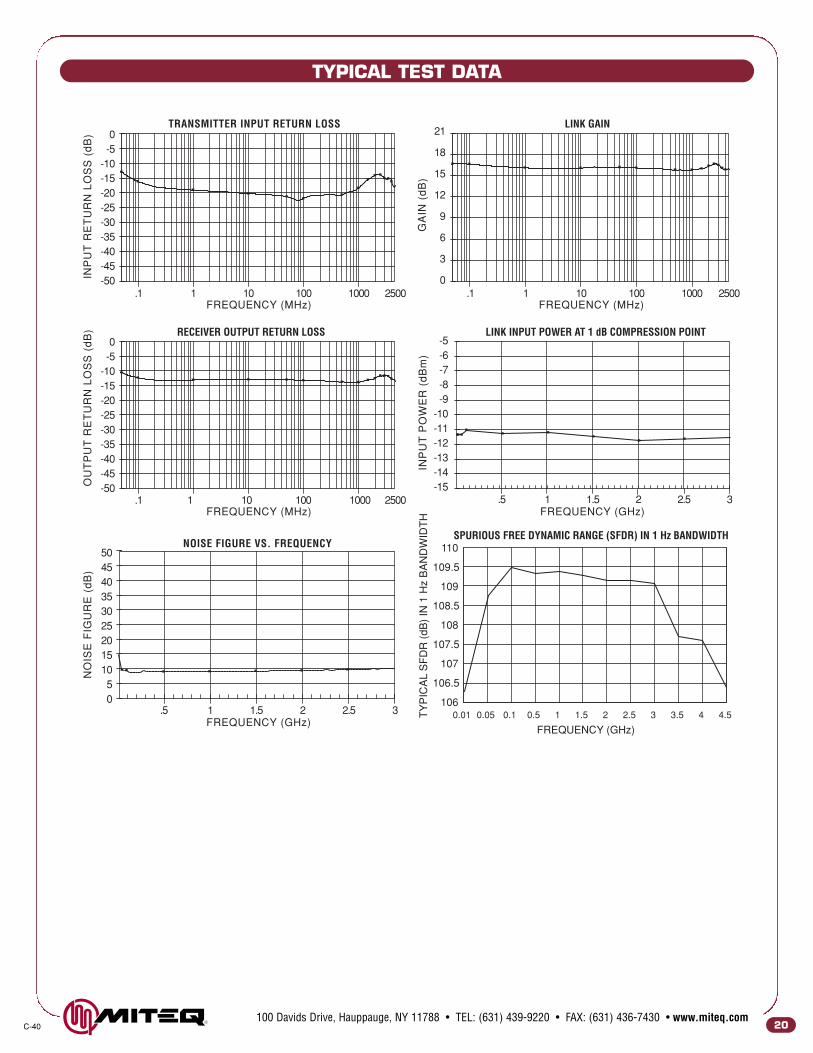
TYPICAL TEST DATA
16C-40100 Davids Drive, Hauppauge, NY 11788 • TEL: (631) 439-9220 • FAX: (631) 436-7430 • www.miteq.com
0-5
-10-15-20-25-30-35-40-45-50
15
12
9
6
3
0
0-5
-10-15-20-25-30-35-40-45-50
50454035302520151050
-5-6-7-8-9
-10-11-12-13-14-15
.01 .1 1 10 100 1000 2500
INP
UT
RE
TU
RN
LO
SS
(dB
)
FREQUENCY (MHz)
TRANSMITTER INPUT RETURN LOSS
.1 1 10 100 1000 2500
OU
TP
UT
RE
TU
RN
LO
SS
(dB
)
FREQUENCY (MHz)
RECEIVER OUTPUT RETURN LOSS
.01 .1 1 10 100 1000 2500
GA
IN(d
B)
FREQUENCY (MHz)
LINK GAIN
INP
UT
PO
WE
R(d
Bm
)
FREQUENCY (GHz)
LINK INPUT POWER AT 1 dB COMPRESSION POINT
.25 5 17.5 1.25 1.5 1.75 2 2.5
.25 5 17.5 1.25 1.5 1.75 2 2.5
NO
ISE
FIG
UR
E(d
B)
FREQUENCY (GHz)
NOISE FIGURE VS. FREQUENCY
C-40100 Davids Drive, Hauppauge, NY 11788 • TEL: (631) 439-9220 • FAX: (631) 436-7430 • www.miteq.com
TYPICAL TEST DATA (CONT.)
17
Avg: Off
1550.97
In VacUser Cal
5.00 nm/div 1575.97
-39.96
0.04
-19.96
10.00dB/div
-59.96
-79.96
RBW: 0.5 nmVBW: 55 kHz
Stop Band 1.55 nmCenter Offset 0.07 nmSMSR 44.69 dB
Sens: -36.28 dBmST: 56.3 ms
1525.97 nm
20.04
dBmREF: 10.04 dBm
DFB Source Test (TrA)Peak Wavelength 1551.12 nmMode Offset 1.90 nm
Peak Amplitude 9.86 dBmBandwidth 0.55 nm
at: -3.00 dB
0.500 nm/div
-39.96
0.04
-23.28
10.00dB/div
-59.96
-79.96
RBW: 0.06 nmVBW: 3.0 kHz
Sens: -33.17 dBmST: 56.3 ms Avg: Off
In VacUser Cal
1550.967 1553.4671548.467 nm
20.04
dBm
DFB Source Test (TrA)Peak Wavelength 1550.977 nmMode Offset -0.265 nm
Peak Amplitude 9.96 dBmBandwidth 0.050 nm
at: -3.00 dB
Stop Band 0.990 nmCenter Offset -0.230 nmSMSR 46.53 dB
REF: 10.04 dBm
ENVIRONMENTAL CONDITIONSOperating temperature .......... -20 to +70°CStorage temperature ............ -40 to +85°CHumidity ................................ 95% relative humidity, noncondensingVibration ................................ 7.3 g’s rms, 20-20000 CPS,
Per MIL-STD-8108B,Method 514, Procedure 5
ORDERING INFORMATIONTransmitter.............. Part number: SLT-5K2P5G-20-20-M14Receiver.................. Part number: SLR-5K2P5G-10-20-10
TRANSMITTER SPECTRUM50 nM SPAN
TRANSMITTER SPECTRUM5 nM SPAN
LNA(PRE-AMPLIFIER)
•LASER BIAS LOOP•VOLTAGE REGULATION
ISOLATOR OPTICALFIBER
RFINPUT
RFOUTPUT
TRANSIMPEDANCE
TRANSMITTER
LNA
•PHOTODIODE BIAS•VOLTAGE REGULATION
PHOTO-DIODE
TRANSIMPEDANCE
RECEIVER
BLOCK DIAGRAM
NOTE: DIMENSIONS SHOWN IN BRACKETS [ ] ARE IN MILLIMETERS.
100 Davids Drive, Hauppauge, NY 11788 • TEL: (631) 439-9220 • FAX: (631) 436-7430 • www.miteq.comC-40 18
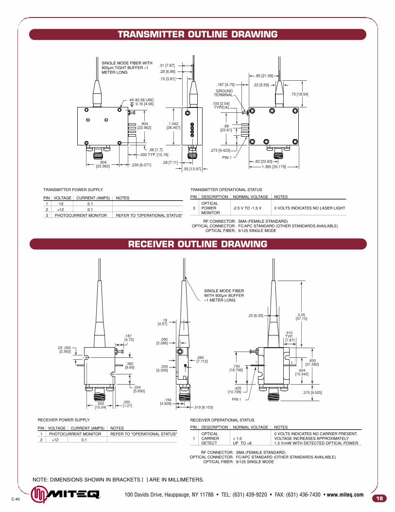
TRANSMITTER OUTLINE DRAWING
.224[5.690]
.187[4.75]
.319 [8.103]
.310TYP.[7.87]
.194[4.928]
.209[5.309]
.090[2.286]
.18[4.57]
2X .093[2.362]
.280[7.112]
.25 [6.35]
.425[10.795]
PIN 1
.740[18.796]
1 2
2.25[57.15]
.050[1.27]
.600[15.24]
.380[9.65]
.604[15.342]
.830[21.082]
.375 [9.525]
.273 [9.423]
.100 [2.54]TYPICAL
.82 [20.83]
.85 [21.59]
.22 [5.59]
.89[22.61]
1.042[26.467]
.904[22.962]
1.385 [35.179].55 [13.97]
.28 [7.11]
.187 [4.75]
.15 [3.81]
.28 [6.86]
.31 [7.87]
.73 [18.54]
.239 [6.071].904
[22.962]
PIN 1
GROUNDTERMINAL
.66 [1.7].400 TYP. [10.16]
4X #2-56 UNC0.16 [4.06]
RECEIVER OUTLINE DRAWING
TRANSMITTER POWER SUPPLY
PIN VOLTAGE CURRENT (AMPS) NOTES
1 -12 0.1
2 +12 0.1
3 PHOTOCURRENT MONITOR REFER TO "OPERATIONAL STATUS"
TRANSMITTER OPERATIONAL STATUS
PIN DESCRIPTION NORMAL VOLTAGE NOTES
OPTICAL3 POWER -2.5 V TO -1.5 V 0 VOLTS INDICATES NO LASER LIGHT
MONITOR
RF CONNECTOR: SMA (FEMALE STANDARD)OPTICAL CONNECTOR: FC/APC STANDARD (OTHER STANDARDS AVAILABLE)
OPTICAL FIBER: 9/125 SINGLE MODE
SINGLE MODE FIBER WITH900µm TIGHT BUFFER ≈1METER LONG
SINGLE MODE FIBERWITH 900µm BUFFER≈1 METER LONG
RF CONNECTOR: SMA (FEMALE STANDARD)OPTICAL CONNECTOR: FC/APC STANDARD (OTHER STANDARDS AVAILABLE)
OPTICAL FIBER: 9/125 SINGLE MODE
RECEIVER POWER SUPPLY
PIN VOLTAGE CURRENT (AMPS) NOTES
1 PHOTOCURRENT MONITOR REFER TO "OPERATIONAL STATUS"
2 +12 0.1
RECEIVER OPERATIONAL STATUS
PIN DESCRIPTION NORMAL VOLTAGE NOTES
OPTICAL 0 VOLTS INDICATES NO CARRIER PRESENT.1 CARRIER > 1.0 VOLTAGE INCREASES APPROXIMATELY
DETECT UP TO +8 1.3 V/mW WITH DETECTED OPTICAL POWER.

19
FEATURES• Bandwidth.......................... 50 kHz to 3 GHz• Small size• Un-cooled DFB laser• No external control circuits required• Transimpedance amplifier in bothtransmitter and receiver
• Operational status monitor pins
APPLICATIONS• Antenna remoting• Local oscillator remoting• Interfacility communication links
C-40100 Davids Drive, Hauppauge, NY 11788 • TEL: (631) 439-9220 • FAX: (631) 436-7430 • www.miteq.com
50 kHz - 3 GHz LBL FIBER OPTIC LINK
ELECTRICAL SPECIFICATIONS
PARAMETERS CONDITION UNITS MIN. TYP. MAX.
Operating frequency 3 dB bandwidth 50 kHz 3 GHzGain dB 12 17 22Noise figure Above 50 MHz dB 10 15Group delay Peak-to-peak ns 0.1 0.2VSWR Input/output 2:1Phase noise 100 Hz offset dBc 100Input power at 1 dB compression Option A dBm -14Spurious-free dynamic range 1 Hz bandwidth dB/Hz2/3 100 106Maximum input power No damage dBm +10Maximum output power Saturated dBm +10Impedance Input/output Ohms 50RF connectors SMA female (male optional)
NOTE: -30 dBm input power.
OPTICAL PERFORMANCE SPECIFICATIONS
PARAMETERS CONDITION UNITS MIN. TYP. MAX.
Fiber optic connectors FC/APC(Other standard available)
Fiber Single mode fiber (9/125µm)Wavelength Other wavelengths available nm 1540 1550 1560Spectral width FWHM nm 0.1Optical power in fiber Reference only mW 3 4Side mode suppression ratio dB 30 40
DC POWER REQUIREMENTS
PARAMETERS CURRENT @ 25°C BASE PLATE UNITS MIN. TYP. MAX.
(VDC) (VDC) (VDC)
Transmitter 200 mA 2 +11 +12 +20
100 mA 1 -11 -12 -20
Receiver 100 mA 4 +11 +12 +20
100 Davids Drive, Hauppauge, NY 11788 • TEL: (631) 439-9220 • FAX: (631) 436-7430 • www.miteq.comC-40
TYPICAL TEST DATA
20
0-5
-10-15-20-25-30-35-40-45-50
21
18
15
12
9
6
3
0
0-5
-10-15-20-25-30-35-40-45-50
50454035302520151050
-5-6-7-8-9
-10-11-12-13-14-15
.1 1 10 100 1000 2500
.1 1 10 100 1000 2500
INP
UT
RE
TU
RN
LO
SS
(dB
)
FREQUENCY (MHz)
TRANSMITTER INPUT RETURN LOSS
OU
TP
UT
RE
TU
RN
LO
SS
(dB
)
FREQUENCY (MHz)
RECEIVER OUTPUT RETURN LOSS
.1 1 10 100 1000 2500
GA
IN(d
B)
FREQUENCY (MHz)
LINK GAIN
INP
UT
PO
WE
R(d
Bm
)
FREQUENCY (GHz)
LINK INPUT POWER AT 1 dB COMPRESSION POINT
2.5.5 1 1.5 2 3
2.5.5 1 1.5 2 3
NO
ISE
FIG
UR
E(d
B)
FREQUENCY (GHz)
NOISE FIGURE VS. FREQUENCYSPURIOUS FREE DYNAMIC RANGE (SFDR) IN 1 Hz BANDWIDTH
0.01 1.50.1 10.05 0.5
FREQUENCY (GHz)
TY
PIC
AL
SF
DR
(dB
)IN
1H
zB
AN
DW
IDT
H
110
109
107.5
108.5
108
106
109.5
106.5
107
2 4.53 42.5 3.5
C-40100 Davids Drive, Hauppauge, NY 11788 • TEL: (631) 439-9220 • FAX: (631) 436-7430 • www.miteq.com
21
ENVIRONMENTAL CONDITIONSOperating temperature .... -20 to +70°CStorage temperature ........ -40 to +85°CHumidity .......................... 95% relative humidity, noncondensingVibration .......................... 7.3 g’s rms, 20-20000 CPS,
Per MIL-STD-8108B,Method 514, Procedure 5
ORDERING INFORMATIONTransmitter ...... Part number: LBT-50K-3G-25-15-M14Receiver .......... Part number: LBR-50K-3G-10-15-10
TYPICAL TEST DATA (CONT.)
Avg: Off
1550.97
In VacUser Cal
5.00 nm/div 1575.97
-39.96
0.04
-19.96
10.00dB/div
-59.96
-79.96
RBW: 0.5 nmVBW: 55 kHz
Stop Band 1.55 nmCenter Offset 0.07 nmSMSR 44.69 dB
Sens: -36.28 dBmST: 56.3 ms
1525.97 nm
20.04
dBmREF: 10.04 dBm
DFB Source Test (TrA)Peak Wavelength 1551.12 nmMode Offset 1.90 nm
Peak Amplitude 9.86 dBmBandwidth 0.55 nm
at: -3.00 dB
0.500 nm/div
-39.96
0.04
-23.28
10.00dB/div
-59.96
-79.96
RBW: 0.06 nmVBW: 3.0 kHz
Sens: -33.17 dBmST: 56.3 ms Avg: Off
In VacUser Cal
1550.967 1553.4671548.467 nm
20.04
dBm
DFB Source Test (TrA)Peak Wavelength 1550.977 nmMode Offset -0.265 nm
Peak Amplitude 9.96 dBmBandwidth 0.050 nm
at: -3.00 dB
Stop Band 0.990 nmCenter Offset -0.230 nmSMSR 46.53 dB
REF: 10.04 dBm
LNA(PRE-AMPLIFIER)
•LASER BIAS LOOP•VOLTAGE REGULATION
ISOLATOR OPTICALFIBER
RFINPUT
RFOUTPUT
TRANSIMPEDANCE
TRANSMITTER
LNA
•PHOTODIODE BIAS•VOLTAGE REGULATION
PHOTO-DIODE
TRANSIMPEDANCE
RECEIVER
BLOCK DIAGRAM
TRANSMITTER SPECTRUM50 nM SPAN
TRANSMITTER SPECTRUM5 nM SPAN
Data taken at:27°C35°C40°C45°C50°C55°C60°C65°C70°C75°C80°C85°C90°C95°C100°C
GA
IN(d
B)
15
12
9500 1000 2000 2500 30001500
FREQUENCY (MHz)
LBL TRANSMITTER GAIN VS. TEMPERATURE21
18

NOTE: DIMENSIONS SHOWN IN BRACKETS [ ] ARE IN MILLIMETERS.
100 Davids Drive, Hauppauge, NY 11788 • TEL: (631) 439-9220 • FAX: (631) 436-7430 • www.miteq.comC-40
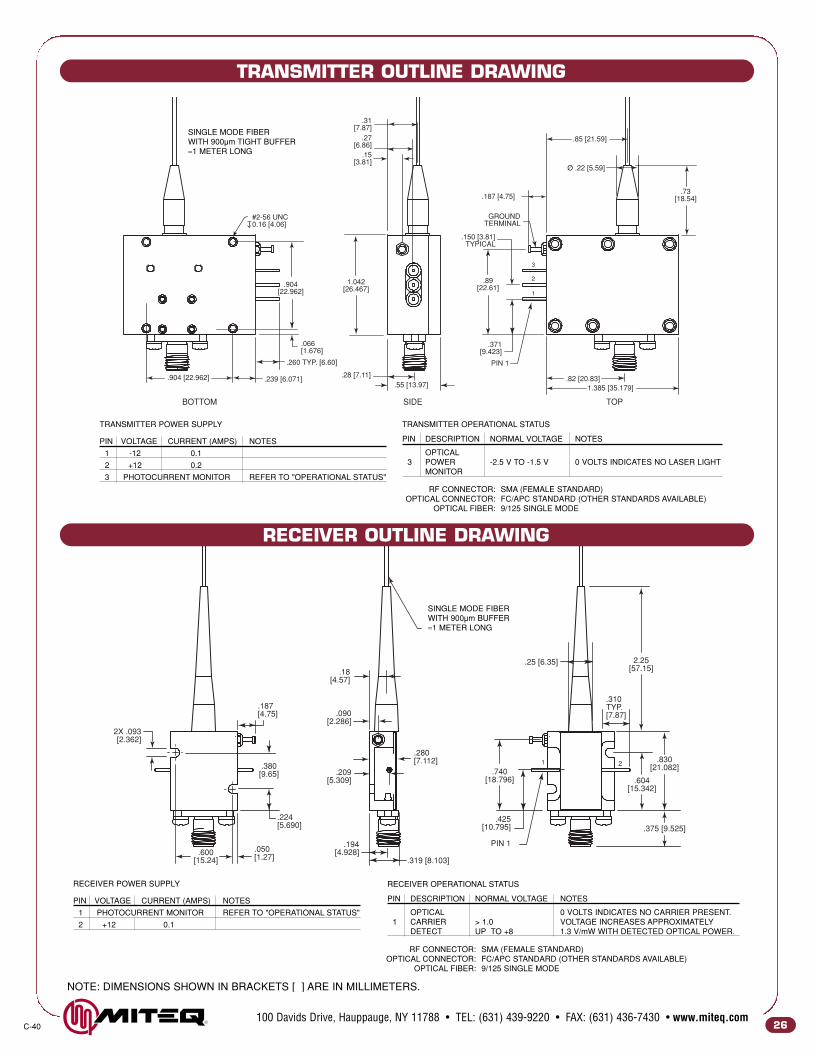
TRANSMITTER OUTLINE DRAWING
22
.224[5.690]
.187[4.75]
.319 [8.103]
.310TYP.[7.87]
.194[4.928]
.209[5.309]
.090[2.286]
.18[4.57]
2X .093[2.362]
.280[7.112]
.25 [6.35]
.425[10.795]
PIN 1
.740[18.796]
1 2
2.25[57.15]
.050[1.27]
.600[15.24]
.380[9.65]
.604[15.342]
.830[21.082]
.375 [9.525]
.066[1.676]
.28 [7.11]
.27[6.86]
.15[3.81]
.31[7.87]
.150 [3.81]TYPICAL
GROUNDTERMINAL
.85 [21.59]
.371[9.423]
PIN 1
.89[22.61]
1
2
3
.73[18.54]
.239 [6.071]
.260 TYP. [6.60]
.904 [22.962]
.904[22.962]
.55 [13.97]
1.042[26.467]
.82 [20.83]1.385 [35.179]
Ø .22 [5.59]
#2-56 UNC0.16 [4.06]
BOTTOM SIDE TOP
.187 [4.75]
RECEIVER OUTLINE DRAWING
TRANSMITTER POWER SUPPLY
PIN VOLTAGE CURRENT (AMPS) NOTES
1 -12 0.1
2 +12 0.2
3 PHOTOCURRENT MONITOR REFER TO "OPERATIONAL STATUS"
TRANSMITTER OPERATIONAL STATUS
PIN DESCRIPTION NORMAL VOLTAGE NOTES
OPTICAL3 POWER -2.5 V TO -1.5 V 0 VOLTS INDICATES NO LASER LIGHT
MONITOR
RF CONNECTOR: SMA (FEMALE STANDARD)OPTICAL CONNECTOR: FC/APC STANDARD (OTHER STANDARDS AVAILABLE)
OPTICAL FIBER: 9/125 SINGLE MODE
RF CONNECTOR: SMA (FEMALE STANDARD)OPTICAL CONNECTOR: FC/APC STANDARD (OTHER STANDARDS AVAILABLE)
OPTICAL FIBER: 9/125 SINGLE MODE
RECEIVER POWER SUPPLY
PIN VOLTAGE CURRENT (AMPS) NOTES
1 PHOTOCURRENT MONITOR REFER TO "OPERATIONAL STATUS"
2 +12 0.1
RECEIVER OPERATIONAL STATUS
PIN DESCRIPTION NORMAL VOLTAGE NOTES
OPTICAL 0 VOLTS INDICATES NO CARRIER PRESENT.1 CARRIER > 1.0 VOLTAGE INCREASES APPROXIMATELY
DETECT UP TO +8 1.3 V/mW WITH DETECTED OPTICAL POWER.
SINGLE MODE FIBERWITH 900µm BUFFER≈1 METER LONG
SINGLE MODE FIBERWITH 900µm TIGHT BUFFER≈1 METER LONG

100 Davids Drive, Hauppauge, NY 11788 • TEL: (631) 439-9220 • FAX: (631) 436-7430 • www.miteq.comC-4023
SINGLE-POLE SINGLE-THROW SWITCHES50 kHz - 4.5 GHz LBL FIBER OPTIC LINK
FEATURES• Bandwidth.......................... 50 kHz to 4.5 GHz• Small size• Un-cooled DFB laser• No external control circuits required• Transimpedance amplifier in bothtransmitter and receiver
• Operational status monitor pins
APPLICATIONS• Antenna remoting• Local oscillator remoting• Interfacility communication links
ELECTRICAL SPECIFICATIONS
PARAMETERS CONDITION UNITS MIN. TYP. MAX.
Operating frequency 3 dB bandwidth 50 kHz 4.5 GHzGain dB 12 17 25Noise figure Above 50 MHz dB 10 15Group delay Peak-to-peak ns 0.1 0.2VSWR Input/output 2:1Phase noise 100 Hz offset dBc 100Input power at 1 dB compression Option A dBm -14Spurious-free dynamic range 1 Hz bandwidth dB/Hz2/3 100 106Maximum input power No damage dBm +10Maximum output power Saturated dBm +10Impedance Input/output Ohms 50RF connectors SMA female (male optional)
NOTE: -30 dBm input power.
OPTICAL PERFORMANCE SPECIFICATIONS
PARAMETERS CONDITION UNITS MIN. TYP. MAX.
Fiber optic connectors FC/APC(Other standard available)
Fiber Single mode fiber (9/125µm)Wavelength Other wavelengths available nm 1540 1550 1560Spectral width FWHM nm 0.1Optical power in fiber Reference only mW 3 4Side mode suppression ratio dB 30 40
DC POWER REQUIREMENTS
PARAMETERS CURRENT @ 25°C BASE PLATE UNITS MIN. TYP. MAX.
(VDC) (VDC) (VDC)
Transmitter 200 mA 2 +11 +12 +20
100 mA 1 -11 -12 -20
Receiver 100 mA 4 +11 +12 +20

TYPICAL TEST DATA
24C-40100 Davids Drive, Hauppauge, NY 11788 • TEL: (631) 439-9220 • FAX: (631) 436-7430 • www.miteq.com
0-5
-10-15-20-25-30-35-40-45-50
0-5
-10-15-20-25-30-35-40-45-50
50454035302520151050
-5-6-7-8-9
-10-11-12-13-14-15
.1 1 10 100 1000 2500
.1 1 10 100 1000 2500
.1 1 10 100 1000 2500
INP
UT
RE
TU
RN
LO
SS
(dB
)
FREQUENCY (MHz)
TRANSMITTER INPUT RETURN LOSS
OU
TP
UT
RE
TU
RN
LO
SS
(dB
)
FREQUENCY (MHz)
RECEIVER OUTPUT RETURN LOSS
GA
IN(d
B)
FREQUENCY (MHz)
LINK GAIN
INP
UT
PO
WE
R(d
Bm
)
LINK INPUT POWER AT 1 dB COMPRESSION POINT
NO
ISE
FIG
UR
E(d
B)
NOISE FIGURE VS. FREQUENCY
2.5.5 1 1.5 2 3FREQUENCY (GHz)
2.5.5 1 1.5 2 3 3.5 4 4.5FREQUENCY (GHz)
21
18
15
12
9
6
3
0

C-40100 Davids Drive, Hauppauge, NY 11788 • TEL: (631) 439-9220 • FAX: (631) 436-7430 • www.miteq.com
25
TYPICAL TEST DATA (CONT.)
ORDERING INFORMATIONTransmitter.............. Part number: LBT-50K4P5G-25-15-M14Receiver.................. Part number: LBR-50K4P5G-10-15-10
ENVIRONMENTAL CONDITIONSOperating temperature .......... -20 to +70°CStorage temperature ............ -40 to +85°CHumidity ................................ 95% relative humidity, noncondensingVibration ................................ 7.3 g’s rms, 20-20000 CPS,
Per MIL-STD-8108B,Method 514, Procedure 5
Avg: Off
1550.97
In VacUser Cal
5.00 nm/div 1575.97
-39.96
0.04
-19.96
10.00dB/div
-59.96
-79.96
RBW: 0.5 nmVBW: 55 kHz
Stop Band 1.55 nmCenter Offset 0.07 nmSMSR 44.69 dB
Sens: -36.28 dBmST: 56.3 ms
1525.97 nm
20.04
dBmREF: 10.04 dBm
DFB Source Test (TrA)Peak Wavelength 1551.12 nmMode Offset 1.90 nm
Peak Amplitude 9.86 dBmBandwidth 0.55 nm
at: -3.00 dB
0.500 nm/div
-39.96
0.04
-23.28
10.00dB/div
-59.96
-79.96
RBW: 0.06 nmVBW: 3.0 kHz
Sens: -33.17 dBmST: 56.3 ms Avg: Off
In VacUser Cal
1550.967 1553.4671548.467 nm
20.04
dBm
DFB Source Test (TrA)Peak Wavelength 1550.977 nmMode Offset -0.265 nm
Peak Amplitude 9.96 dBmBandwidth 0.050 nm
at: -3.00 dB
Stop Band 0.990 nmCenter Offset -0.230 nmSMSR 46.53 dB
REF: 10.04 dBm
LNA(PRE-AMPLIFIER)
•LASER BIAS LOOP•VOLTAGE REGULATION
ISOLATOR OPTICALFIBER
RFINPUT
RFOUTPUT
TRANSIMPEDANCE
TRANSMITTER
LNA
•PHOTODIODE BIAS•VOLTAGE REGULATION
PHOTO-DIODE
TRANSIMPEDANCE
RECEIVER
BLOCK DIAGRAM
TRANSMITTER SPECTRUM50 nM SPAN
TRANSMITTER SPECTRUM5 nM SPAN
NOTE: DIMENSIONS SHOWN IN BRACKETS [ ] ARE IN MILLIMETERS.
100 Davids Drive, Hauppauge, NY 11788 • TEL: (631) 439-9220 • FAX: (631) 436-7430 • www.miteq.comC-40 2026
TRANSMITTER OUTLINE DRAWING
.224[5.690]
.187[4.75]
.319 [8.103]
.310TYP.[7.87]
.194[4.928]
.209[5.309]
.090[2.286]
.18[4.57]
2X .093[2.362]
.280[7.112]
.25 [6.35]
.425[10.795]
PIN 1
.740[18.796]
1 2
2.25[57.15]
.050[1.27]
.600[15.24]
.380[9.65]
.604[15.342]
.830[21.082]
.375 [9.525]
.066[1.676]
.28 [7.11]
.27[6.86]
.15[3.81]
.31[7.87]
.150 [3.81]TYPICAL
GROUNDTERMINAL
.85 [21.59]
.371[9.423]
PIN 1
.89[22.61]
1
2
3
.73[18.54]
.239 [6.071]
.260 TYP. [6.60]
.904 [22.962]
.904[22.962]
.55 [13.97]
1.042[26.467]
.82 [20.83]1.385 [35.179]
Ø .22 [5.59]
#2-56 UNC0.16 [4.06]
BOTTOM SIDE TOP
.187 [4.75]
RECEIVER OUTLINE DRAWING
TRANSMITTER POWER SUPPLY
PIN VOLTAGE CURRENT (AMPS) NOTES
1 -12 0.1
2 +12 0.2
3 PHOTOCURRENT MONITOR REFER TO "OPERATIONAL STATUS"
TRANSMITTER OPERATIONAL STATUS
PIN DESCRIPTION NORMAL VOLTAGE NOTES
OPTICAL3 POWER -2.5 V TO -1.5 V 0 VOLTS INDICATES NO LASER LIGHT
MONITOR
RF CONNECTOR: SMA (FEMALE STANDARD)OPTICAL CONNECTOR: FC/APC STANDARD (OTHER STANDARDS AVAILABLE)
OPTICAL FIBER: 9/125 SINGLE MODE
RF CONNECTOR: SMA (FEMALE STANDARD)OPTICAL CONNECTOR: FC/APC STANDARD (OTHER STANDARDS AVAILABLE)
OPTICAL FIBER: 9/125 SINGLE MODE
RECEIVER POWER SUPPLY
PIN VOLTAGE CURRENT (AMPS) NOTES
1 PHOTOCURRENT MONITOR REFER TO "OPERATIONAL STATUS"
2 +12 0.1
RECEIVER OPERATIONAL STATUS
PIN DESCRIPTION NORMAL VOLTAGE NOTES
OPTICAL 0 VOLTS INDICATES NO CARRIER PRESENT.1 CARRIER > 1.0 VOLTAGE INCREASES APPROXIMATELY
DETECT UP TO +8 1.3 V/mW WITH DETECTED OPTICAL POWER.
SINGLE MODE FIBERWITH 900µm BUFFER≈1 METER LONG
SINGLE MODE FIBERWITH 900µm TIGHT BUFFER≈1 METER LONG

27
FEATURES• Bandwidth.......................... 50 kHz to 6 GHz• Small size• No external control circuits required• Transimpedance amplifier in bothtransmitter and receiver
APPLICATIONS• Antenna remoting• Local oscillator remoting• Interfacility communication links
50 kHz - 6 GHz SCM FIBER OPTIC LINK
C-40100 Davids Drive, Hauppauge, NY 11788 • TEL: (631) 439-9220 • FAX: (631) 436-7430 • www.miteq.com
ELECTRICAL SPECIFICATIONS
PARAMETERS CONDITION UNITS MIN. TYP. MAX.
Operating frequency 3 dB bandwidth 50 kHz 6 GHzGain dB 10 18 25Noise figure Above 50 GHz dB 12 20Group delay Peak-to-peak ns 0.1 0.2VSWR Input/output 2:1Phase noise 100 Hz offset dBc 100Input power at 1 dB compression dBm -14 -13Spurious-free dynamic range 1 Hz bandwidth dB/Hz2/3 100 103Maximum input power No damage dBm +10Maximum output power Saturated dBm +10Impedance Input/output Ohms 50RF connectors SMA female (male optional)
NOTE: -30 dBm input power, 1m of fiber.
OPTICAL PERFORMANCE SPECIFICATIONS
PARAMETERS CONDITION UNITS MIN. TYP. MAX.
Fiber optic connectors FC/APC(Other standard available)
Fiber Single mode fiber (9/125µm)Wavelength Other wavelengths available nm 1530 1550 1560Spectral width FWHM nm 0.06 0.1Optical power in fiber Reference only mW 3 5 9Side mode suppression ratio dB 30 40
DC POWER REQUIREMENTS
PARAMETERS CURRENT @ 25°C BASE PLATE UNITS MIN. TYP. MAX.
(VDC) (VDC) (VDC)Transmitter 200 mA, 250 mA (max.) 4 +11 +12 +15
105 mA, 300 mA (max.)* 5 -11 -12 -15325** mA 1 +3 +4 +6
Receiver 100 mA 4 +11 +12 +15
* At low case temperatures, < 5°C, the laser cooler switches to heat mode and will exceed 105 mA typical current.** 1.2 A at maximum laser cooling.

TYPICAL TEST DATA
28C-40100 Davids Drive, Hauppauge, NY 11788 • TEL: (631) 439-9220 • FAX: (631) 436-7430 • www.miteq.com
0-5
-10-15-20-25-30-35-40-45-50
-3.5-3.6-3.7-3.8-3.9-4.0-4.1-4.2-4.3-4.4-4.5
-5-6-7-8-9
-10-11-12-13-14-15
50454035302520151050
0-5
-10-15-20-25-30-35-40-45-50
INP
UT
RE
TU
RN
LOS
S(d
B)
TRANSMITTER INPUT RETURN LOSS
OU
TP
UT
RE
TU
RN
LOS
S(d
B)
GROUP DELAY
.5 1 1.5 2 2.5 3 3.5 4 4.5 5 5.5 6
GA
IN(d
B)
FREQUENCY (GHz).5 1 1.5 2 2.5 3 3.5 4 4.5 5 5.5 6
FREQUENCY (GHz)
.5 1 1.5 2 2.5 3 3.5 4 4.5 5 5.5 6FREQUENCY (GHz)
.5 1 1.5 2 2.5 3 3.5 4 4.5 5 5.5 6FREQUENCY (GHz)
LINK GAIN
INP
UT
PO
WE
R(d
Bm
)
RECEIVER OUTPUT RETURN LOSS
NO
ISE
FIG
UR
E(d
B)
LINK INPUT POWER AT 1 dB COMPRESSION POINT NOISE FIGURE VS. FREQUENCY
FREQUENCY (GHz)2.5 3 3.51.5 2 4.5 5 5.5 642.5 3 3.51.5 1.5 2 4.5 5 5.5 64
FREQUENCY (GHz)
24
21
18
15
12
9
6
3
0
DE
LAY
(ns)
20
19
18
17
16
GA
IN(d
B)
15
14
13
12
25.2°C27°C29°C31°C
33.7°C37°C40°C42°C45°C48°C50°C52°C53°C54°C55°C61°C65°C
SCM 6 GHz FREQUENCY RESPONSE VS. TEMPERATURE
500 1000 1500 2000 2500 3000 3500 4000 4500 5000 5500 600FREQUENCY (MHz)
Data taken at:
100 Davids Drive, Hauppauge, NY 11788 • TEL: (631) 439-9220 • FAX: (631) 436-7430 • www.miteq.comC-4029
TYPICAL TEST DATA (CONT.)
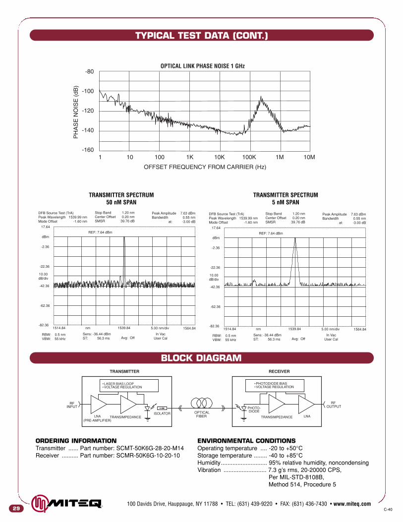
ORDERING INFORMATIONTransmitter ...... Part number: SCMT-50K6G-28-20-M14Receiver .......... Part number: SCMR-50K6G-10-20-10
LNA(PRE-AMPLIFIER)
•LASER BIAS LOOP•VOLTAGE REGULATION
ISOLATOR OPTICALFIBER
RFINPUT
RFOUTPUT
TRANSIMPEDANCE
TRANSMITTER
LNA
•PHOTODIODE BIAS•VOLTAGE REGULATION
PHOTO-DIODE
TRANSIMPEDANCE
RECEIVER
BLOCK DIAGRAM
ENVIRONMENTAL CONDITIONSOperating temperature .... -20 to +50°CStorage temperature ........ -40 to +85°CHumidity............................ 95% relative humidity, noncondensingVibration .......................... 7.3 g’s rms, 20-20000 CPS,
Per MIL-STD-8108B,Method 514, Procedure 5
5.00 nm/div
-42.36
-2.36
-22.36
10.00dB/div
-62.36
-82.36
RBW: 0.5 nmVBW: 55 kHz
Sens: -36.44 dBmST: 56.3 ms Avg: Off
In VacUser Cal
1539.84 1564.841514.84 nm
17.64
dBm
DFB Source Test (TrA)Peak Wavelength 1539.99 nmMode Offset -1.60 nm
Peak Amplitude 7.63 dBmBandwidth 0.55 nm
at: -3.00 dB
Stop Band 1.20 nmCenter Offset 0.20 nmSMSR 39.76 dB
REF: 7.64 dBm
TRANSMITTER SPECTRUM50 nM SPAN
TRANSMITTER SPECTRUM5 nM SPAN
-80
-100
-120
-140
-16010 100
OFFSET FREQUENCY FROM CARRIER (Hz)
PH
AS
EN
OIS
E(d
B)
OPTICAL LINK PHASE NOISE 1 GHz
1K 10K 100K 1M 10M1

NOTE: DIMENSIONS SHOWN IN BRACKETS [ ] ARE IN MILLIMETERS.
100 Davids Drive, Hauppauge, NY 11788 • TEL: (631) 439-9220 • FAX: (631) 436-7430 • www.miteq.comC-40 30
TRANSMITTER OUTLINE DRAWING
.224[5.690]
.187[4.75]
.319 [8.103]
.310TYP.[7.87]
.194[4.928]
.209[5.309]
.090[2.286]
.18[4.57]
2X .093[2.362]
.280[7.112]
.25 [6.35]
.425[10.795]
PIN 1
.740[18.796]
1 2
2.25[57.15]
.050[1.27]
.600[15.24]
.380[9.65]
.604[15.342]
.830[21.082]
.375 [9.525]
.29 [7.37]
.12 [3.05]
.16 [4.83]
.35 [8.89]
.49 [12.45]
.47 [11.94]GROUND
PIN 1
1.17[29.72]
1 2 3 4 5
6
7
1.06[26.92]
.10[2.54]
.38 [9.65]
.07 [1.78] .91 [23.11]
.187 [4.75]
.26 [6.60]
1.26[32.00]
Ø .03[0.76]
Ø .28[7.11]
.20[5.08]
.26[6.73]
.84[21.34]
.15[3.81]
.30 [7.62]
.81[20.57]
.25[6.35]
.31 [7.87]RF CONNECTOR
Ø 0.25[0.635]
.10 [2.54] TYP.
1.04 [26.42]
.16 [4.06]
.41 [10.41]4X #2-56 UNC
0.15 [3.81]
.300TYP.[7.62]
RECEIVER OUTLINE DRAWING
RF CONNECTOR: SMA (FEMALE STANDARD)OPTICAL CONNECTOR: FC/APC STANDARD (OTHER STANDARDS AVAILABLE)
OPTICAL FIBER: 9/125 SINGLE MODE
RECEIVER POWER SUPPLY
PIN VOLTAGE CURRENT (AMPS) NOTES
1 PHOTOCURRENT MONITOR REFER TO "OPERATIONAL STATUS"
2 +12 0.1
RECEIVER OPERATIONAL STATUS
PIN DESCRIPTION NORMAL VOLTAGE NOTES
OPTICAL 0 VOLTS INDICATES NO CARRIER PRESENT.1 CARRIER > 1.0 VOLTAGE INCREASES APPROXIMATELY
DETECT UP TO +8 1.3 V/mW WITH DETECTED OPTICAL POWER.
TRANSMITTER POWER SUPPLY
PIN VOLTAGE CURRENT (AMPS) NOTES
1 +4 0.325 @25°C BASE PLATE TEMP1.2 FOR MAXIMUM COOLING
2 SAME AS PIN 7
3 SAME AS PIN 6
4 +12 0.2
5 -12 0.12
TRANSMITTER OPERATIONAL STATUS
PIN DESCRIPTION NORMAL VOLTAGE NOTES
OPTICAL6 POWER -2.5 V TO -1.5 V 0 VOLTS INDICATES NO LASER LIGHT
MONITOR
LASER7 TEMP -0.5 V TO +0.5 V <-0.5 INDICATES HIGH LASER TEMP
MONITOR >+0.5 INDICATES LOW LASER TEMP
RF CONNECTOR: SMA (FEMALE STANDARD)OPTICAL CONNECTOR: FC/APC STANDARD (OTHER STANDARDS AVAILABLE)
OPTICAL FIBER: 9/125 SINGLE MODE
APPLY ALL VOLTAGES SIMULTANEOUSLY, OR IN THE FOLLOWING ORDER:• +4V• -12V• +12V
NOTE: ALLOW 2 MINUTES FOR LASER TEMPSTABILIZATION AFTER APPLYING POWER.
SINGLE MODE FIBERWITH 900µm BUFFER≈1 METER LONG
SINGLE MODE FIBERWITH 900µm TIGHT BUFFER≈1 METER LONG

100 Davids Drive, Hauppauge, NY 11788 • TEL: (631) 439-9220 • FAX: (631) 436-7430 • www.miteq.comC-4031
100 MHz - 11 GHz SCM FIBER OPTIC LINK
FEATURES• Bandwidth.......................... 100 MHz to 11 GHz• Small size• No external control circuits required• Transimpedance amplifier in bothtransmitter and receiver
APPLICATIONS• Antenna remoting• Local oscillator remoting• Interfacility communication links
ELECTRICAL SPECIFICATIONS
PARAMETERS CONDITION UNITS MIN. TYP. MAX.
Operating frequency 3 dB bandwidth 100 MHz 11 GHzGain dB 10 18 22Noise figure dB 18 20Group delay Peak-to-peak ns 0.1 0.2VSWR Input/output 2:1Phase noise 100 Hz offset dBc 100Input power at 1 dB compression dBm -14 -11Spurious-free dynamic range 1 Hz bandwidth dB/Hz2/3 100 103Maximum input power No damage dBm +10Maximum output power Saturated dBm +10Impedance Input/output Ohms 50RF connectors SMA female (male optional)
NOTE: -30 dBm input power, 1m of fiber.
OPTICAL PERFORMANCE SPECIFICATIONS
PARAMETERS CONDITION UNITS MIN. TYP. MAX.
Fiber optic connectors FC/APC(Other standard available)
Fiber Single mode fiber (9/125µm)Wavelength Other wavelengths available nm 1530 1550 1560Spectral width FWHM nm 0.06 0.1Optical power in fiber Reference only mW 3 5 9Side mode suppression ratio dB 35 40
DC POWER REQUIREMENTS
PARAMETERS CURRENT @ 25°C BASE PLATE PIN # MIN. TYP. MAX.
(VDC) (VDC) (VDC)Transmitter 200 mA 4 +11 +12 +15
115 mA, 300 mA (max.)* 5 -11 -12 -15325** mA 1 +3 +4 +6
Receiver 100 mA 4 +11 +12 +15
* At low case temperatures, < 5°C, the laser cooler switches to heat mode and will exceed 105 mA typical current.** 1.2 A at maximum laser cooling.

100 Davids Drive, Hauppauge, NY 11788 • TEL: (631) 439-9220 • FAX: (631) 436-7430 • www.miteq.comC-40 32
0-5
-10-15-20-25-30-35-40-45-50
0-5
-10-15-20-25-30-35-40-45-50
-4.0-4.14.2
-4.3-4.4-4.5-4.6-4.7-4.8-4.9-5.0
-5-6-7-8-9
-10-11-12-13-14-15
1 8 9 10 112 3 4 5 6 7
1 8 9 10 112 3 4 5 6 7
INP
UT
RE
TU
RN
LO
SS
(dB
)
FREQUENCY (GHz)
TRANSMITTER INPUT RETURN LOSS
OU
TP
UT
RE
TU
RN
LO
SS
(dB
)
FREQUENCY (GHz)
1 8 9 10 112 3 4 5 6 7
1 8 9 10 112 3 4 5 6 7
FREQUENCY (GHz)
FREQUENCY (GHz)
8 9 10 112 3 4 5 6 7FREQUENCY (GHz)
1 8 9 10 112 3 4 5 6 7FREQUENCY (GHz)
GROUP DELAY
GA
IN(d
B)
LINK GAIN
INP
UT
PO
WE
R(d
Bm
)
RECEIVER OUTPUT RETURN LOSS
DE
LA
Y(n
s)
LINK INPUT POWER AT 1 dB COMPRESSION POINT50454035302520151050
NO
ISE
FIG
UR
E(d
B)
NOISE FIGURE VS. FREQUENCY
24
21
18
15
12
9
6
3
0
TYPICAL TEST DATA
C-40100 Davids Drive, Hauppauge, NY 11788 • TEL: (631) 439-9220 • FAX: (631) 436-7430 • www.miteq.com
TYPICAL TEST DATA (CONT.)
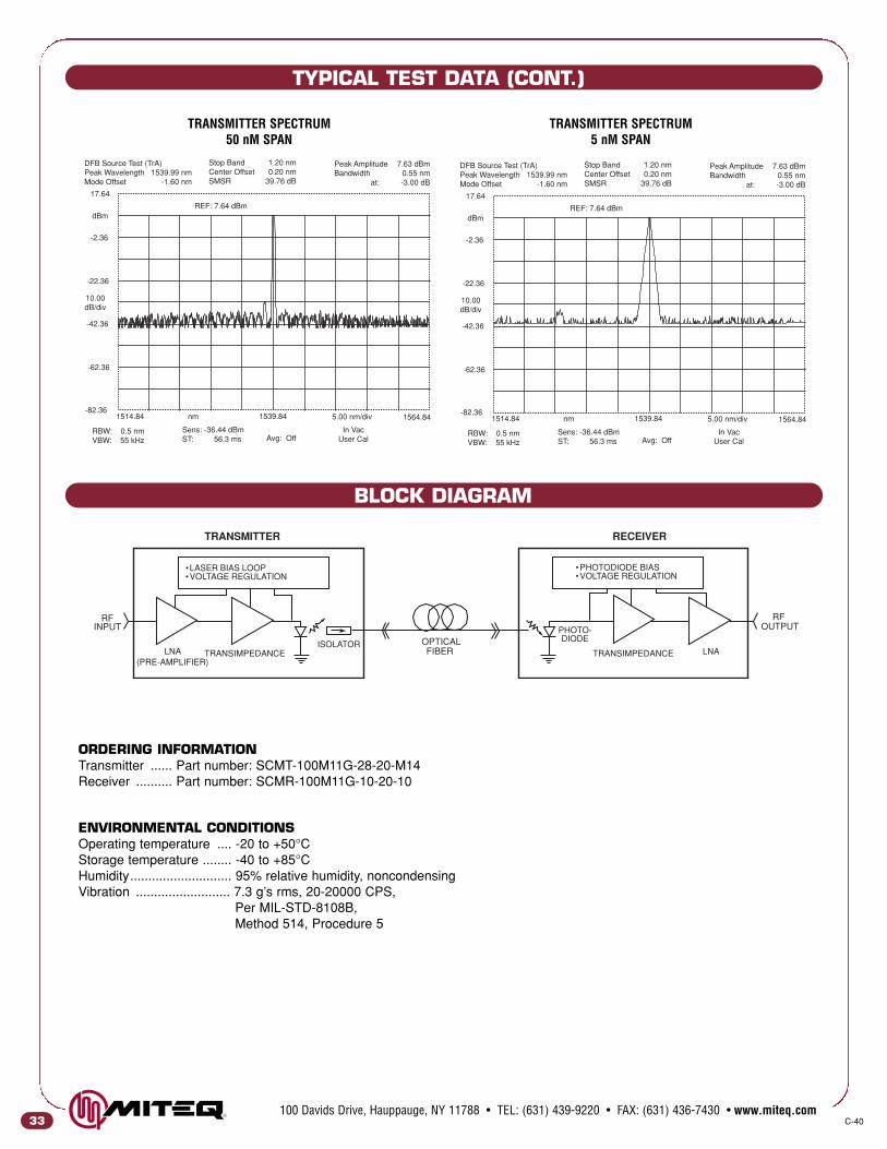
ORDERING INFORMATIONTransmitter ...... Part number: SCMT-100M11G-28-20-M14Receiver .......... Part number: SCMR-100M11G-10-20-10
ENVIRONMENTAL CONDITIONSOperating temperature .... -20 to +50°CStorage temperature ........ -40 to +85°CHumidity............................ 95% relative humidity, noncondensingVibration .......................... 7.3 g’s rms, 20-20000 CPS,
Per MIL-STD-8108B,Method 514, Procedure 5
33
LNA(PRE-AMPLIFIER)
•LASER BIAS LOOP•VOLTAGE REGULATION
ISOLATOR OPTICALFIBER
RFINPUT
RFOUTPUT
TRANSIMPEDANCE
TRANSMITTER
LNA
•PHOTODIODE BIAS•VOLTAGE REGULATION
PHOTO-DIODE
TRANSIMPEDANCE
RECEIVER
BLOCK DIAGRAM
5.00 nm/div
-42.36
-2.36
-22.36
10.00dB/div
-62.36
-82.36
RBW: 0.5 nmVBW: 55 kHz
Sens: -36.44 dBmST: 56.3 ms Avg: Off
In VacUser Cal
1539.84 1564.841514.84 nm
17.64
dBm
DFB Source Test (TrA)Peak Wavelength 1539.99 nmMode Offset -1.60 nm
Peak Amplitude 7.63 dBmBandwidth 0.55 nm
at: -3.00 dB
Stop Band 1.20 nmCenter Offset 0.20 nmSMSR 39.76 dB
REF: 7.64 dBm
TRANSMITTER SPECTRUM50 nM SPAN
TRANSMITTER SPECTRUM5 nM SPAN

NOTE: DIMENSIONS SHOWN IN BRACKETS [ ] ARE IN MILLIMETERS.
100 Davids Drive, Hauppauge, NY 11788 • TEL: (631) 439-9220 • FAX: (631) 436-7430 • www.miteq.comC-40
TRANSMITTER OUTLINE DRAWING
34
.224[5.690]
.187[4.75]
.319 [8.103]
.310TYP.[7.87]
.194[4.928]
.209[5.309]
.090[2.286]
.18[4.57]
2X .093[2.362]
.280[7.112]
.25 [6.35]
.425[10.795]
PIN 1
.740[18.796]
1 2
2.25[57.15]
.050[1.27]
.600[15.24]
.380[9.65]
.604[15.342]
.830[21.082]
.375 [9.525]
.29 [7.37]
.12 [3.05]
.16 [4.83]
.35 [8.89]
.49 [12.45]
.47 [11.94]GROUND
PIN 1
1.17[29.72]
1 2 3 4 5
6
7
1.06[26.92]
.10[2.54]
.38 [9.65]
.07 [1.78] .91 [23.11]
.187 [4.75]
.26 [6.60]
1.26[32.00]
Ø .03[0.76]
Ø .28[7.11]
.20[5.08]
.26[6.73]
.84[21.34]
.15[3.81]
.30 [7.62]
.81[20.57]
.25[6.35]
.31 [7.87]RF CONNECTOR
Ø 0.25 [0.635]
.10 [2.54] TYP.
1.04 [26.42]
.16 [4.06]
.41 [10.41]4X #2-56 UNC
0.15 [3.81]
.300TYP.[7.62]
RECEIVER OUTLINE DRAWING
RF CONNECTOR: SMA (FEMALE STANDARD)OPTICAL CONNECTOR: FC/APC STANDARD (OTHER STANDARDS AVAILABLE)
OPTICAL FIBER: 9/125 SINGLE MODE
RECEIVER POWER SUPPLY
PIN VOLTAGE CURRENT (AMPS) NOTES
1 PHOTOCURRENT MONITOR REFER TO "OPERATIONAL STATUS"
2 +12 0.1
RECEIVER OPERATIONAL STATUS
PIN DESCRIPTION NORMAL VOLTAGE NOTES
OPTICAL 0 VOLTS INDICATES NO CARRIER PRESENT.1 CARRIER > 1.0 VOLTAGE INCREASES APPROXIMATELY
DETECT UP TO +8 1.3 V/mW WITH DETECTED OPTICAL POWER.
TRANSMITTER POWER SUPPLY
PIN VOLTAGE CURRENT (AMPS) NOTES
1 +4 0.325 @25°C BASE PLATE TEMP1.2 FOR MAXIMUM COOLING
2 SAME AS PIN 7
3 SAME AS PIN 6
4 +12 0.2
5 -12 0.12
TRANSMITTER OPERATIONAL STATUS
PIN DESCRIPTION NORMAL VOLTAGE NOTES
OPTICAL6 POWER -2.5 V TO -1.5 V 0 VOLTS INDICATES NO LASER LIGHT
MONITOR
LASER7 TEMP -0.5 V TO +0.5 V <-0.5 INDICATES HIGH LASER TEMP
MONITOR >+0.5 INDICATES LOW LASER TEMP
RF CONNECTOR: SMA (FEMALE STANDARD)OPTICAL CONNECTOR: FC/APC STANDARD (OTHER STANDARDS AVAILABLE)
OPTICAL FIBER: 9/125 SINGLE MODE
APPLY ALL VOLTAGES SIMULTANEOUSLY, OR IN THE FOLLOWING ORDER:• +4V• -12V• +12V
NOTE: ALLOW 2 MINUTES FOR LASER TEMPSTABILIZATION AFTER APPLYING POWER.
SINGLE MODE FIBERWITH 900µm BUFFER≈1 METER LONG
SINGLE MODE FIBERWITH 900µm TIGHT BUFFER≈1 METER LONG

100 Davids Drive, Hauppauge, NY 11788 • TEL: (631) 439-9220 • FAX: (631) 436-7430 • www.miteq.comC-4035
100 MHz - 13 GHz SCM FIBER OPTIC LINK
FEATURES• Bandwidth.......................... 100 MHz to 13 GHz• Small size• No external control circuits required• Transimpedance amplifier in bothtransmitter and receiver
APPLICATIONS• Antenna remoting• Local oscillator remoting• Interfacility communication links
ELECTRICAL SPECIFICATIONSPARAMETERS CONDITION UNITS MIN. TYP. MAX.
Operating frequency 100 MHz 13 GHzGain dB 10 18 24Gain flatness dB ±2Noise figure dB 19 25Group delay Peak-to-peak ns 0.1 0.2VSWR Input/output 2:1Phase noise 100 Hz offset dBc 100Input power at 1 dB compression dBm -14 -13Spurious-free dynamic range 1 Hz bandwidth dB/Hz2/3 100 103Maximum input power No damage dBm +10Maximum output power Saturated dBm +10Impedance Input/output Ohms 50RF connectors SMA female (male optional)
NOTE: -30 dBm input power, 1m of fiber.
OPTICAL PERFORMANCE SPECIFICATIONS
PARAMETERS CONDITION UNITS MIN. TYP. MAX.
Fiber optic connectors FC/APC(Other standard available)
Fiber Single mode fiber (9/125µm)Wavelength Other wavelengths available nm 1530 1550 1560Spectral width FWHM nm 0.06 0.1Optical power in fiber Reference only mW 3 5 9Side mode suppression ratio dB 35 40
DC POWER REQUIREMENTS
PARAMETERS CURRENT @ 25°C BASE PLATE PIN # MIN. TYP. MAX.
(VDC) (VDC) (VDC)
Transmitter 200 mA 4 +11 +12 +15115 mA, 300 mA (max.)* 5 -11 -12 -15
325** mA 1 +3 +4 +6
Receiver 100 mA 4 +11 +12 +15
* At low case temperatures, < 5°C, the laser cooler switches to heat mode and will exceed 105 mA typical current.** 1.2 A at maximum laser cooling.

100 Davids Drive, Hauppauge, NY 11788 • TEL: (631) 439-9220 • FAX: (631) 436-7430 • www.miteq.comC-40 36
0-5
-10-15-20-25-30-35-40-45-50
0-5
-10-15-20-25-30-35-40-45-50
-4.0-4.14.2
-4.3-4.4-4.5-4.6-4.7-4.8-4.9-5.0
-5-6-7-8-9
-10-11-12-13-14-15
1 8 9 10 12 13112 3 4 5 6 7
1 8 9 10 12 13112 3 4 5 6 7
INP
UT
RE
TU
RN
LO
SS
(dB
)
FREQUENCY (GHz)
TRANSMITTER INPUT RETURN LOSS
OU
TP
UT
RE
TU
RN
LO
SS
(dB
)
FREQUENCY (GHz)1 8 9 131210 112 3 4 5 6 7
1 8 9 131210 112 3 4 5 6 7FREQUENCY (GHz)
FREQUENCY (GHz)
1 8 9 10 11 12 132 3 4 5 6 7FREQUENCY (GHz)
8 9 10 11 12 132 3 4 5 6 7FREQUENCY (GHz)
GROUP DELAY
GA
IN(d
B)
LINK GAIN
INP
UT
PO
WE
R(d
Bm
)
LINK INPUT POWER AT 1 dB COMPRESSION POINT
DE
LA
Y(n
s)
RECEIVER OUTPUT RETURN LOSS
50454035302520151050
NO
ISE
FIG
UR
E(d
B)
NOISE FIGURE VS. FREQUENCY
24
21
18
15
12
9
6
3
0
TYPICAL TEST DATA

C-40100 Davids Drive, Hauppauge, NY 11788 • TEL: (631) 439-9220 • FAX: (631) 436-7430 • www.miteq.com
TYPICAL TEST DATA (CONT.)
ORDERING INFORMATIONTransmitter ...... Part number: SCMT-100M13G-28-25-M14Receiver .......... Part number: SCMR-100M13G-10-25-10
ENVIRONMENTAL CONDITIONSOperating temperature .... -20 to +50°CStorage temperature ........ -40 to +85°CHumidity............................ 95% relative humidity, noncondensingVibration .......................... 7.3 g’s rms, 20-20000 CPS,
Per MIL-STD-8108B,Method 514, Procedure 5
37
LNA(PRE-AMPLIFIER)
•LASER BIAS LOOP•VOLTAGE REGULATION
ISOLATOR OPTICALFIBER
RFINPUT
RFOUTPUT
TRANSIMPEDANCE
TRANSMITTER
LNA
•PHOTODIODE BIAS•VOLTAGE REGULATION
PHOTO-DIODE
TRANSIMPEDANCE
RECEIVER
BLOCK DIAGRAM
5.00 nm/div
-42.36
-2.36
-22.36
10.00dB/div
-62.36
-82.36
RBW: 0.5 nmVBW: 55 kHz
Sens: -36.44 dBmST: 56.3 ms Avg: Off
In VacUser Cal
1539.84 1564.841514.84 nm
17.64
dBm
DFB Source Test (TrA)Peak Wavelength 1539.99 nmMode Offset -1.60 nm
Peak Amplitude 7.63 dBmBandwidth 0.55 nm
at: -3.00 dB
Stop Band 1.20 nmCenter Offset 0.20 nmSMSR 39.76 dB
REF: 7.64 dBm
5.00 nm/div
-42.36
-2.36
-22.36
10.00dB/div
-62.36
-82.36
RBW: 0.5 nmVBW: 55 kHz
Sens: -36.44 dBmST: 56.3 ms Avg: Off
In VacUser Cal
1539.84 1564.841514.84 nm
17.64
dBm
DFB Source Test (TrA)Peak Wavelength 1539.99 nmMode Offset -1.60 nm
Peak Amplitude 7.63 dBmBandwidth 0.55 nm
at: -3.00 dB
Stop Band 1.20 nmCenter Offset 0.20 nmSMSR 39.76 dB
REF: 7.64 dBm
TRANSMITTER SPECTRUM50 nM SPAN
TRANSMITTER SPECTRUM5 nM SPAN

NOTE: DIMENSIONS SHOWN IN BRACKETS [ ] ARE IN MILLIMETERS.
100 Davids Drive, Hauppauge, NY 11788 • TEL: (631) 439-9220 • FAX: (631) 436-7430 • www.miteq.comC-40
TRANSMITTER OUTLINE DRAWING
38
.224[5.690]
.187[4.75]
.319 [8.103]
.310TYP.[7.87]
.194[4.928]
.209[5.309]
.090[2.286]
.18[4.57]
2X .093[2.362]
.280[7.112]
.25 [6.35]
.425[10.795]
PIN 1
.740[18.796]
1 2
2.25[57.15]
.050[1.27]
.600[15.24]
.380[9.65]
.604[15.342]
.830[21.082]
.375 [9.525]
.29 [7.37]
.12 [3.05]
.16 [4.83]
.35 [8.89]
.49 [12.45]
.47 [11.94]GROUND
PIN 1
1.17[29.72]
1 2 3 4 5
6
7
1.06[26.92]
.10[2.54]
.38 [9.65]
.07 [1.78] .91 [23.11]
.187 [4.75]
.26 [6.60]
1.26[32.00]
Ø .03[0.76]
Ø .28[7.11]
.20[5.08]
.26[6.73]
.84[21.34]
.15[3.81]
.30 [7.62]
.81[20.57]
.25[6.35]
.31 [7.87]RF CONNECTOR
Ø 0.25 [0.635]
.10 [2.54] TYP.
1.04 [26.42]
.16 [4.06]
.41 [10.41]4X #2-56 UNC
0.15 [3.81]
.300TYP.[7.62]
RECEIVER OUTLINE DRAWING
RF CONNECTOR: SMA (FEMALE STANDARD)OPTICAL CONNECTOR: FC/APC STANDARD (OTHER STANDARDS AVAILABLE)
OPTICAL FIBER: 9/125 SINGLE MODE
RECEIVER POWER SUPPLY
PIN VOLTAGE CURRENT (AMPS) NOTES
1 PHOTOCURRENT MONITOR REFER TO "OPERATIONAL STATUS"
2 +12 0.1
RECEIVER OPERATIONAL STATUS
PIN DESCRIPTION NORMAL VOLTAGE NOTES
OPTICAL 0 VOLTS INDICATES NO CARRIER PRESENT.1 CARRIER > 1.0 VOLTAGE INCREASES APPROXIMATELY
DETECT UP TO +8 1.3 V/mW WITH DETECTED OPTICAL POWER.
TRANSMITTER POWER SUPPLY
PIN VOLTAGE CURRENT (AMPS) NOTES
1 +4 0.325 @25°C BASE PLATE TEMP1.2 FOR MAXIMUM COOLING
2 SAME AS PIN 7
3 SAME AS PIN 6
4 +12 0.2
5 -12 0.12
TRANSMITTER OPERATIONAL STATUS
PIN DESCRIPTION NORMAL VOLTAGE NOTES
OPTICAL6 POWER -2.5 V TO -1.5 V 0 VOLTS INDICATES NO LASER LIGHT
MONITOR
LASER7 TEMP -0.5 V TO +0.5 V <-0.5 INDICATES HIGH LASER TEMP
MONITOR >+0.5 INDICATES LOW LASER TEMP
RF CONNECTOR: SMA (FEMALE STANDARD)OPTICAL CONNECTOR: FC/APC STANDARD (OTHER STANDARDS AVAILABLE)
OPTICAL FIBER: 9/125 SINGLE MODE
APPLY ALL VOLTAGES SIMULTANEOUSLY, OR IN THE FOLLOWING ORDER:• +4V• -12V• +12V
NOTE: ALLOW 2 MINUTES FOR LASER TEMPSTABILIZATION AFTER APPLYING POWER.
SINGLE MODE FIBERWITH 900µm BUFFER≈1 METER LONG
SINGLE MODE FIBERWITH 900µm TIGHT BUFFER≈1 METER LONG

39
100 MHz - 15 GHz SCM FIBER OPTIC LINK
C-40100 Davids Drive, Hauppauge, NY 11788 • TEL: (631) 439-9220 • FAX: (631) 436-7430 • www.miteq.com
FEATURES• Bandwidth.......................... 100 MHz to 15 GHz• Small size• No external control circuits required• Transimpedance amplifier in bothtransmitter and receiver
APPLICATIONS• Antenna remoting• Local oscillator remoting• Interfacility communication links
ELECTRICAL SPECIFICATIONSPARAMETERS CONDITION UNITS MIN. TYP. MAX.
Operating frequency (standard)* ±2 dB bandwidth 100 MHz 15 GHzGain dB 10 18 25Gain flatness dB ±2Noise figure dB 19** 25Group delay Peak-to-peak (> 500 MHz) ns 0.1 0.2VSWR Tx Input/Rx output 2:1Phase noise 100 Hz offset dBc 100Input power at 1 dB compression dBm -15Spurious-free dynamic range At 15 GHz bandwidth dB/Hz2/3 101Maximum input power No damage dBm +10RF connectors SMA female (male optional)***Impedance Input/output Ohms 50NOTE: -30 dBm input power, 1m of fiber.* Optional 10 MHz start frequency.** At -15 GHz.*** “K” style optional.
OPTICAL PERFORMANCE SPECIFICATIONS
PARAMETERS CONDITION UNITS MIN. TYP. MAX.
Fiber optic connectors FC/APC standard (otherconnector types optional)
Fiber Single mode fiber (9/125µm)Wavelength From 100 MHz to 13 GHzSpectral width FWHM nm 0.06Optical power in fiber Reference only mW 3 5 9Side mode suppression ratio dB 30 40
DC POWER REQUIREMENTS
PARAMETERS CURRENT @ 25°C BASE PLATE PIN # MIN. TYP. MAX.
Transmitter 260 mA, 300 mA (max.) 4 +11V +12V +16V105 mA, 300 mA (max.)* 5 -11V -12V -16V100 mA @ 25°C, 1A (max.) 1 +3.5 +5 +6
Receiver 100 mA 2 +11V +12V +16V
* At low case temperatures, < 5°C, the laser cooler switches to heat mode and will exceed 105 mA typical current.
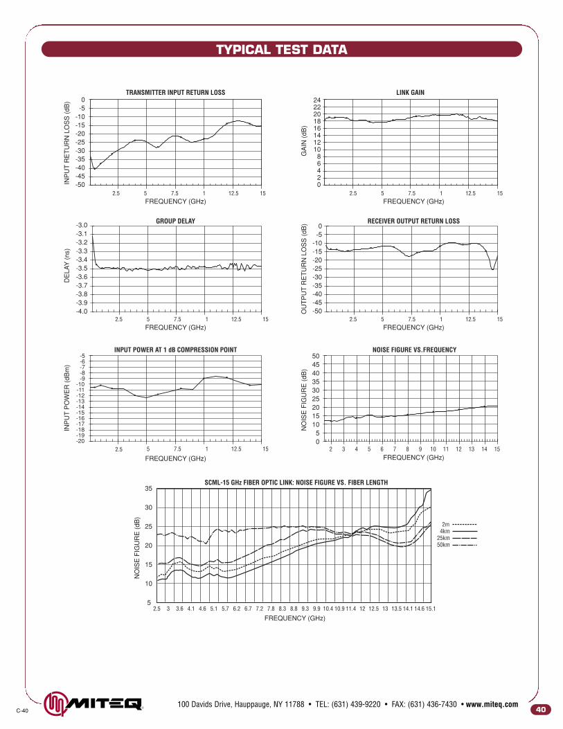
TYPICAL TEST DATA
40C-40100 Davids Drive, Hauppauge, NY 11788 • TEL: (631) 439-9220 • FAX: (631) 436-7430 • www.miteq.com
FREQUENCY (GHz)
SCML-15 GHz FIBER OPTIC LINK: NOISE FIGURE VS. FIBER LENGTH
NO
ISE
FIG
UR
E(d
B)
2m4km
25km50km
5
20
25
10
2.5 3 3.6 4.1 4.6 5.1 5.7 6.2 6.7 7.2 7.8 8.3 8.8 9.3 9.9 10.4 10.9 11.4 12 12.5 13 13.5 14.1 14.6 15.1
15
30
35
TRANSMITTER INPUT RETURN LOSS
INP
UT
RE
TU
RN
LOS
S(d
B) 24
22201816141210
86420
0-5
-10-15-20-25-30-35-40-45-50
0-5
-10-15-20-25-30-35-40-45-50
FREQUENCY (GHz)
FREQUENCY (GHz)FREQUENCY (GHz)
FREQUENCY (GHz)
FREQUENCY (GHz)
GROUP DELAY
DE
LAY
(ns)
-3.1
-3.7-3.6-3.5-3.4-3.3-3.2
-3.0
-3.9-4.0
-3.8
LINK GAIN
GA
IN(d
B)
RECEIVER OUTPUT RETURN LOSS
OU
TP
UT
RE
TU
RN
LOS
S(d
B)
INPUT POWER AT 1 dB COMPRESSION POINT
INP
UT
PO
WE
R(d
Bm
)
-14
-9
-11
-13-12
-10
-15-16-17-18-19-20
-6-5
-7-8
1512.57.55 12.5 1512.57.55 12.5
1512.57.55 12.51512.57.55 12.5
1512.57.55 12.5 7643 5 11108 9 141312 152FREQUENCY (GHz)
NOISE FIGURE VS.FREQUENCY
NO
ISE
FIG
UR
E(d
B)
5
30
20
1015
25
35
4540
50
0

TYPICAL TEST DATA (CONT.)
100 Davids Drive, Hauppauge, NY 11788 • TEL: (631) 439-9220 • FAX: (631) 436-7430 • www.miteq.comC-40
NOTE: Link gain, noise figure and power compression can be tailored for specific applications. Please contact MITEQ.
ORDERING INFORMATIONTransmitter ...... Part number: SCMT-100M15G-30-25-M15Receiver .......... Part number: SCMR-100M15G-10-25-10
Optional 10 MHz start frequencyTransmitter ...... Part number: SCMT-10M15G-30-25-M15Receiver .......... Part number: SCMR-10M15G-10-25-10
ENVIRONMENTAL CONDITIONSOperating temperature .... -20 to +50°CStorage temperature ........ -40 to +85°CHumidity............................ 95% relative humidity, noncondensingVibration............................ 7.3 g’s rms, 20-2000 CPS,
Per MIL-STD-810B, Method 514,Procedure 5
LNA(PRE-AMPLIFIER)
•LASER BIAS LOOP•VOLTAGE REGULATION
ISOLATOR OPTICALFIBER
RFINPUT
RFOUTPUT
TRANSIMPEDANCE
TRANSMITTER
LNA
•PHOTODIODE BIAS•VOLTAGE REGULATION
PHOTO-DIODE
TRANSIMPEDANCE
RECEIVER
BLOCK DIAGRAM
5.00 nm/div
-42.36
-2.36
-22.36
10.00dB/div
-62.36
-82.36
RBW: 0.5 nmVBW: 55 kHz
Sens: -36.44 dBmST: 56.3 ms Avg: Off
In VacUser Cal
1539.84 1564.841514.84 nm
17.64
dBm
DFB Source Test (TrA)Peak Wavelength 1539.99 nmMode Offset -1.60 nm
Peak Amplitude 7.63 dBmBandwidth 0.55 nm
at: -3.00 dB
Stop Band 1.20 nmCenter Offset 0.20 nmSMSR 39.76 dB
REF: 7.64 dBm
5.00 nm/div
-42.36
-2.36
-22.36
10.00dB/div
-62.36
-82.36
RBW: 0.5 nmVBW: 55 kHz
Sens: -36.44 dBmST: 56.3 ms Avg: Off
In VacUser Cal
1539.84 1564.841514.84 nm
17.64
dBm
DFB Source Test (TrA)Peak Wavelength 1539.99 nmMode Offset -1.60 nm
Peak Amplitude 7.63 dBmBandwidth 0.55 nm
at: -3.00 dB
Stop Band 1.20 nmCenter Offset 0.20 nmSMSR 39.76 dB
REF: 7.64 dBm
TRANSMITTER SPECTRUM50 nM SPAN
TRANSMITTER SPECTRUM5 nM SPAN
41
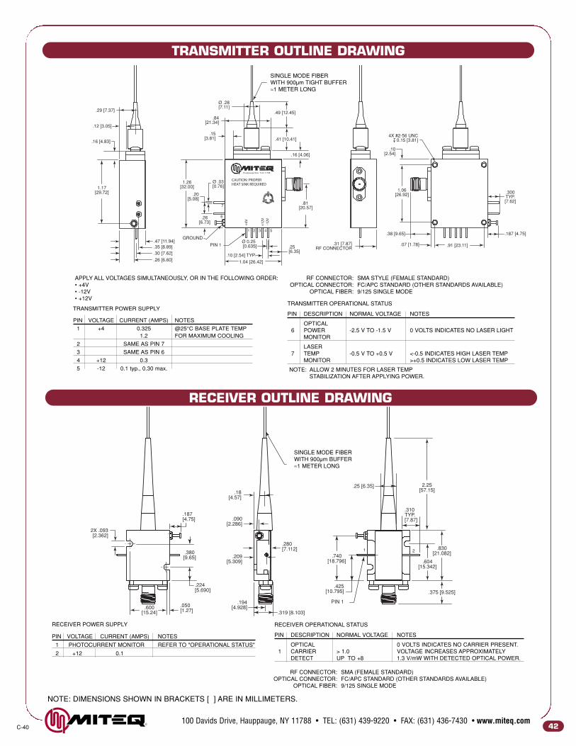
TRANSMITTER OUTLINE DRAWING
42C-40100 Davids Drive, Hauppauge, NY 11788 • TEL: (631) 439-9220 • FAX: (631) 436-7430 • www.miteq.com
NOTE: DIMENSIONS SHOWN IN BRACKETS [ ] ARE IN MILLIMETERS.
.224[5.690]
.187[4.75]
.319 [8.103]
.310TYP.[7.87]
.194[4.928]
.209[5.309]
.090[2.286]
.18[4.57]
2X .093[2.362]
.280[7.112]
.25 [6.35]
.425[10.795]
PIN 1
.740[18.796]
1 2
2.25[57.15]
.050[1.27]
.600[15.24]
.380[9.65]
.604[15.342]
.830[21.082]
.375 [9.525]
.29 [7.37]
.12 [3.05]
.16 [4.83]
.35 [8.89]
.49 [12.45]
.47 [11.94]GROUND
PIN 1
1.17[29.72]
1 2 3 4 5
6
7
1.06[26.92]
.10[2.54]
.38 [9.65]
.07 [1.78] .91 [23.11]
.187 [4.75]
.26 [6.60]
1.26[32.00]
Ø .03[0.76]
Ø .28[7.11]
.20[5.08]
.26[6.73]
.84[21.34]
.15[3.81]
.30 [7.62]
.81[20.57]
.25[6.35]
.31 [7.87]RF CONNECTOR
Ø 0.25[0.635]
.10 [2.54] TYP.
1.04 [26.42]
.16 [4.06]
.41 [10.41]4X #2-56 UNC
0.15 [3.81]
.300TYP.[7.62]
RECEIVER OUTLINE DRAWING
RF CONNECTOR: SMA (FEMALE STANDARD)OPTICAL CONNECTOR: FC/APC STANDARD (OTHER STANDARDS AVAILABLE)
OPTICAL FIBER: 9/125 SINGLE MODE
RECEIVER POWER SUPPLY
PIN VOLTAGE CURRENT (AMPS) NOTES
1 PHOTOCURRENT MONITOR REFER TO "OPERATIONAL STATUS"
2 +12 0.1
RECEIVER OPERATIONAL STATUS
PIN DESCRIPTION NORMAL VOLTAGE NOTES
OPTICAL 0 VOLTS INDICATES NO CARRIER PRESENT.1 CARRIER > 1.0 VOLTAGE INCREASES APPROXIMATELY
DETECT UP TO +8 1.3 V/mW WITH DETECTED OPTICAL POWER.
TRANSMITTER POWER SUPPLY
PIN VOLTAGE CURRENT (AMPS) NOTES
1 +4 0.325 @25°C BASE PLATE TEMP1.2 FOR MAXIMUM COOLING
2 SAME AS PIN 7
3 SAME AS PIN 6
4 +12 0.3
5 -12 0.1 typ., 0.30 max.
TRANSMITTER OPERATIONAL STATUS
PIN DESCRIPTION NORMAL VOLTAGE NOTES
OPTICAL6 POWER -2.5 V TO -1.5 V 0 VOLTS INDICATES NO LASER LIGHT
MONITOR
LASER7 TEMP -0.5 V TO +0.5 V <-0.5 INDICATES HIGH LASER TEMP
MONITOR >+0.5 INDICATES LOW LASER TEMP
RF CONNECTOR: SMA STYLE (FEMALE STANDARD)OPTICAL CONNECTOR: FC/APC STANDARD (OTHER STANDARDS AVAILABLE)
OPTICAL FIBER: 9/125 SINGLE MODE
APPLY ALL VOLTAGES SIMULTANEOUSLY, OR IN THE FOLLOWING ORDER:• +4V• -12V• +12V
NOTE: ALLOW 2 MINUTES FOR LASER TEMPSTABILIZATION AFTER APPLYING POWER.
SINGLE MODE FIBERWITH 900µm BUFFER≈1 METER LONG
SINGLE MODE FIBERWITH 900µm TIGHT BUFFER≈1 METER LONG

100 Davids Drive, Hauppauge, NY 11788 • TEL: (631) 439-9220 • FAX: (631) 436-7430 • www.miteq.comC-4043
10 MHz - 18 GHz SCM FIBER OPTIC LINK
FEATURES• Bandwidth.......................... 10 MHz to 18 GHz• Small size• No external control circuits required• Transimpedance amplifier in bothtransmitter and receiver
APPLICATIONS• Antenna remoting• Local oscillator remoting• Interfacility communication links
ELECTRICAL SPECIFICATIONSPARAMETERS CONDITION UNITS MIN. TYP. MAX.
Operating frequency (standard)* ±2 dB bandwidth 100 MHz 18 GHzGain dB 10 18 25Gain flatness dB ±2Noise figure dB 19** 25Group delay Peak-to-peak (> 500 MHz) ns 0.1 0.2VSWR Tx Input/Rx output 2:1Phase noise 100 Hz offset dBc 100Input power at 1 dB compression dBm -15Spurious-free dynamic range At 15 GHz bandwidth dB/Hz2/3 101Maximum input power No damage dBm +10RF connectors SMA female (male optional)***Impedance Input/output Ohms 50
NOTE: -30 dBm input power, 1m of fiber.* Optional 10 MHz start frequency.** At -15 GHz.*** “K” style optional.
OPTICAL PERFORMANCE SPECIFICATIONS
PARAMETERS CONDITION UNITS MIN. TYP. MAX.
Fiber optic connectors FC/APC standard (otherconnector types optional)
Fiber Single mode fiber (9/125µm)Wavelength From 100 MHz to 13 GHzSpectral width FWHM nm 0.06Optical power in fiber Reference only mW 3 5 9Side mode suppression ratio dB 30 40
DC POWER REQUIREMENTS
PARAMETERS CURRENT @ 25°C BASE PLATE PIN # MIN. TYP. MAX.
Transmitter 260 mA, 300 mA (max.) 4 +11V +12V +16V105 mA, 300 mA (max.)* 5 -11V -12V -16V100 mA @ 25°C, 1A (max.) 1 +3.5 +5 +6
Receiver 100 mA 2 +11V +12V +16V
* At low case temperatures, < 5°C, the laser cooler switches to heat mode and will exceed 105 mA typical current.
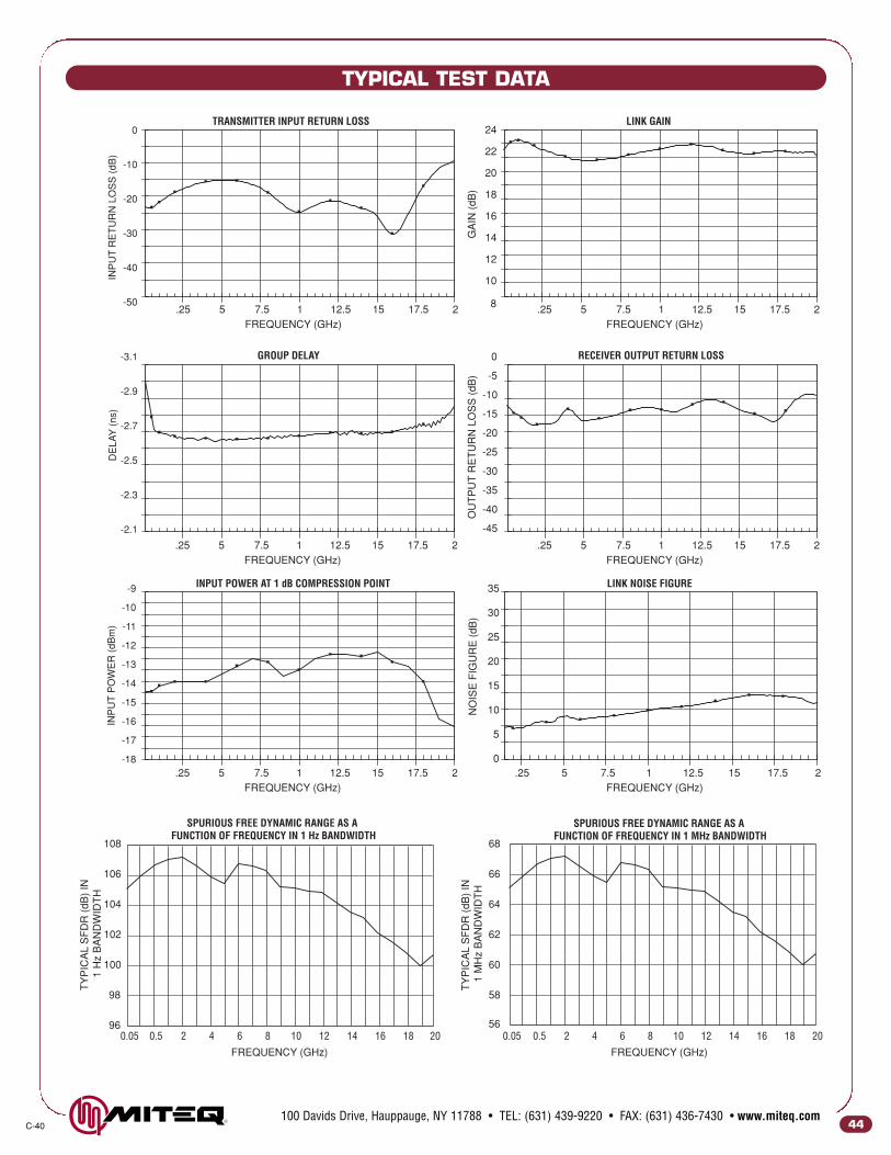
100 Davids Drive, Hauppauge, NY 11788 • TEL: (631) 439-9220 • FAX: (631) 436-7430 • www.miteq.comC-40 44
TRANSMITTER INPUT RETURN LOSSIN
PU
TR
ET
UR
NLO
SS
(dB
)
-50
0
-10
-20
-30
-40
FREQUENCY (GHz)
GROUP DELAY
DE
LAY
(ns)
-3.1
-2.9
-2.7
-2.3
-2.1
-2.5
LINK GAIN
GA
IN(d
B)
24
22
10
14
20
16
18
12
8
RECEIVER OUTPUT RETURN LOSS
OU
TP
UT
RE
TU
RN
LOS
S(d
B)
0
-10
-25
-20
-15
-40
-5
-35
-30
-45
INPUT POWER AT 1 dB COMPRESSION POINT
INP
UT
PO
WE
R(d
Bm
)
-14
-9
-11
-13
-12
-10
-15
-16
-17
-18
FREQUENCY (GHz)
SPURIOUS FREE DYNAMIC RANGE AS AFUNCTION OF FREQUENCY IN 1 Hz BANDWIDTH
TY
PIC
AL
SF
DR
(dB
)IN
1H
zB
AN
DW
IDT
H
98
108
104
100
102
106
9640.5 2 206 108 12 16 18140.05
FREQUENCY (GHz)
SPURIOUS FREE DYNAMIC RANGE AS AFUNCTION OF FREQUENCY IN 1 MHz BANDWIDTH
TY
PIC
AL
SF
DR
(dB
)IN
1M
Hz
BA
ND
WID
TH
58
68
64
60
62
66
5640.5 2 206 108 12 16 18140.05
1512.5 17.57.55 1 2.25FREQUENCY (GHz)
1512.5 17.57.55 1 2.25
FREQUENCY (GHz)1512.5 17.57.55 1 2.25
FREQUENCY (GHz)1512.5 17.57.55 1 2.25
FREQUENCY (GHz)1512.5 17.57.55 1 2.25
FREQUENCY (GHz)1512.5 17.57.55 1 2.25
LINK NOISE FIGURE
NO
ISE
FIG
UR
E(d
B)
5
30
20
10
15
25
35
0
TYPICAL TEST DATA

C-40
NOTE: Link gain, noise figure and power compression can be tailored for specific applications. Please contact MITEQ.
100 Davids Drive, Hauppauge, NY 11788 • TEL: (631) 439-9220 • FAX: (631) 436-7430 • www.miteq.com
TYPICAL TEST DATA (CONT.)
ORDERING INFORMATIONTransmitter ...... Part number: SCMT-100M18G-30-25-M15Receiver .......... Part number: SCMR-100M18G-10-25-10
Optional 10 MHz start frequencyTransmitter ...... Part number: SCMT-10M18G-30-25-M15Receiver .......... Part number: SCMR-10M18G-10-25-10
ENVIRONMENTAL CONDITIONSOperating temperature .... -20 to +50°CStorage temperature ........ -40 to +85°CHumidity............................ 95% relative humidity, noncondensingVibration............................ 7.3 g’s rms, 20-2000 CPS,
Per MIL-STD-810B, Method 514,Procedure 5
45
LNA(PRE-AMPLIFIER)
•LASER BIAS LOOP•VOLTAGE REGULATION
ISOLATOR OPTICALFIBER
RFINPUT
RFOUTPUT
TRANSIMPEDANCE
TRANSMITTER
M
LNA
•PHOTODIODE BIAS•VOLTAGE REGULATION
PHOTO-DIODE
TRANSIMPEDANCE
RECEIVER
BLOCK DIAGRAM
5.00 nm/div
-42.36
-2.36
-22.36
10.00dB/div
-62.36
-82.36
RBW: 0.5 nmVBW: 55 kHz
Sens: -36.44 dBmST: 56.3 ms Avg: Off
In VacUser Cal
1539.84 1564.841514.84 nm
17.64
dBm
DFB Source Test (TrA)Peak Wavelength 1539.99 nmMode Offset -1.60 nm
Peak Amplitude 7.63 dBmBandwidth 0.55 nm
at: -3.00 dB
Stop Band 1.20 nmCenter Offset 0.20 nmSMSR 39.76 dB
REF: 7.64 dBm
5.00 nm/div
-42.36
-2.36
-22.36
10.00dB/div
-62.36
-82.36
RBW: 0.5 nmVBW: 55 kHz
Sens: -36.44 dBmST: 56.3 ms Avg: Off
In VacUser Cal
1539.84 1564.841514.84 nm
17.64
dBm
DFB Source Test (TrA)Peak Wavelength 1539.99 nmMode Offset -1.60 nm
Peak Amplitude 7.63 dBmBandwidth 0.55 nm
at: -3.00 dB
Stop Band 1.20 nmCenter Offset 0.20 nmSMSR 39.76 dB
REF: 7.64 dBm
TRANSMITTER SPECTRUM50 nM SPAN
TRANSMITTER SPECTRUM5 nM SPAN
FREQUENCY (GHz)
IP3 VS FREQUENCY
TY
PIC
AL
INP
UT
TH
IRD
OR
DE
RIN
TE
RC
EP
TP
OIN
T(d
Bm
)
-5
0
-2
-4
-3
-1
-640.5 2 206 108 12 16 18140.05

NOTE: DIMENSIONS SHOWN IN BRACKETS [ ] ARE IN MILLIMETERS.
100 Davids Drive, Hauppauge, NY 11788 • TEL: (631) 439-9220 • FAX: (631) 436-7430 • www.miteq.comC-40
TRANSMITTER OUTLINE DRAWING
46
.224[5.690]
.187[4.75]
.319 [8.103]
.310TYP.[7.87]
.194[4.928]
.209[5.309]
.090[2.286]
.18[4.57]
2X .093[2.362]
.280[7.112]
.25 [6.35]
.425[10.795]
PIN 1
.740[18.796]
1 2
2.25[57.15]
.050[1.27]
.600[15.24]
.380[9.65]
.604[15.342]
.830[21.082]
.375 [9.525]
.29 [7.37]
.12 [3.05]
.16 [4.83]
.35 [8.89]
.49 [12.45]
.47 [11.94]GROUND
PIN 1
1.17[29.72]
1 2 3 4 5
6
7
1.06[26.92]
.10[2.54]
.38 [9.65]
.07 [1.78] .91 [23.11]
.187 [4.75]
.26 [6.60]
1.26[32.00]
Ø .03[0.76]
Ø .28[7.11]
.20[5.08]
.26[6.73]
.84[21.34]
.15[3.81]
.30 [7.62]
.81[20.57]
.25[6.35]
.31 [7.87]RF CONNECTOR
Ø 0.25[0.635]
.10 [2.54] TYP.
1.04 [26.42]
.16 [4.06]
.41 [10.41]4X #2-56 UNC
0.15 [3.81]
.300TYP.[7.62]
RECEIVER OUTLINE DRAWING
RF CONNECTOR: SMA (FEMALE STANDARD)OPTICAL CONNECTOR: FC/APC STANDARD (OTHER STANDARDS AVAILABLE)
OPTICAL FIBER: 9/125 SINGLE MODE
RECEIVER POWER SUPPLY
PIN VOLTAGE CURRENT (AMPS) NOTES
1 PHOTOCURRENT MONITOR REFER TO "OPERATIONAL STATUS"
2 +12 0.1
RECEIVER OPERATIONAL STATUS
PIN DESCRIPTION NORMAL VOLTAGE NOTES
OPTICAL 0 VOLTS INDICATES NO CARRIER PRESENT.1 CARRIER > 1.0 VOLTAGE INCREASES APPROXIMATELY
DETECT UP TO +8 1.3 V/mW WITH DETECTED OPTICAL POWER.
TRANSMITTER POWER SUPPLY
PIN VOLTAGE CURRENT (AMPS) NOTES
1 +4 0.325 @25°C BASE PLATE TEMP1.2 FOR MAXIMUM COOLING
2 SAME AS PIN 7
3 SAME AS PIN 6
4 +12 0.3
5 -12 0.1 typ., 0.30 max.
TRANSMITTER OPERATIONAL STATUS
PIN DESCRIPTION NORMAL VOLTAGE NOTES
OPTICAL6 POWER -2.5 V TO -1.5 V 0 VOLTS INDICATES NO LASER LIGHT
MONITOR
LASER7 TEMP -0.5 V TO +0.5 V <-0.5 INDICATES HIGH LASER TEMP
MONITOR >+0.5 INDICATES LOW LASER TEMP
RF CONNECTOR: SMA STYLE (FEMALE STANDARD)OPTICAL CONNECTOR: FC/APC STANDARD (OTHER STANDARDS AVAILABLE)
OPTICAL FIBER: 9/125 SINGLE MODE
APPLY ALL VOLTAGES SIMULTANEOUSLY, OR IN THE FOLLOWING ORDER:• +4V• -12V• +12V
NOTE: ALLOW 2 MINUTES FOR LASER TEMPSTABILIZATION AFTER APPLYING POWER.
SINGLE MODE FIBERWITH 900µm BUFFER≈1 METER LONG
SINGLE MODE FIBERWITH 900µm TIGHT BUFFER≈1 METER LONG

100 Davids Drive, Hauppauge, NY 11788 • TEL: (631) 439-9220 • FAX: (631) 436-7430 • www.miteq.comC-4047
50 kHz - 6 GHz HRL FIBER OPTIC LINK
FEATURES• Bandwidth ..................................... 50 kHz to 6 GHz• Wide operating temperature ....... -40 to +85°C• Small size• No external control circuits required• Transimpedance amplifier in bothtransmitter and receiver
APPLICATIONS• Antenna remoting• Local oscillator remoting• Interfacility communication links
ELECTRICAL SPECIFICATIONS
PARAMETERS CONDITION UNITS MIN. TYP. MAX.
Operating frequency 3 dB bandwidth 50 kHz 6 GHzGain dB 10 20 25Noise figure Above 50 MHz dB 12 20Group delay Peak-to-peak ns 0.1 0.2VSWR Input/output 2:1Phase noise 100 Hz offset dBc 100Input power at 1 dB compression dBm -14 -13Spurious-free dynamic range 1 Hz bandwidth dB/Hz2/3 100 103Maximum input power No damage dBm +10Maximum output power Saturated dBm +10Impedance Input/output Ohms 50RF connectors SMA female (male optional)
NOTE: -30 dBm input power, 1m of fiber.
OPTICAL PERFORMANCE SPECIFICATIONS
PARAMETERS CONDITION UNITS MIN. TYP. MAX.
Fiber optic connectors FC/APC(Other standard available)
Fiber Single mode fiber (9/125µm)Wavelength nm 1530 1550 1560Spectral width FWHM nm 0.06 0.1Optical power in fiber Reference only mW 3 5 9Side mode suppression ratio dB 30 40
DC POWER REQUIREMENTS
PARAMETERS CURRENT @ 25°C BASE PLATE PIN # MIN. TYP. MAX.
(VDC) (VDC) (VDC)Transmitter 200 mA 4 +11 +12 +15
115 mA, 300 mA (max.)* 5 -11 -12 -15325** mA 1 +3 +4 +6
Receiver 100 mA 4 +11 +12 +15
* At low case temperatures, < 5°C, the laser cooler switches to heat mode and will exceed 105 mA typical current.** 1.2 A at maximum laser cooling.
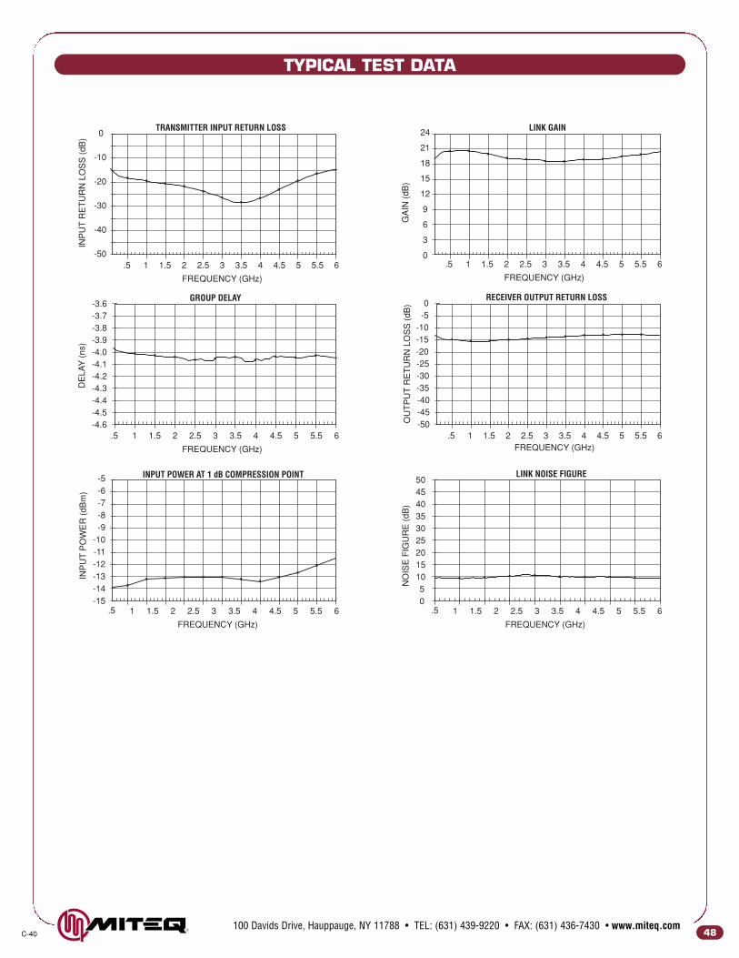
100 Davids Drive, Hauppauge, NY 11788 • TEL: (631) 439-9220 • FAX: (631) 436-7430 • www.miteq.comC-40 48
TRANSMITTER INPUT RETURN LOSS
INP
UT
RE
TU
RN
LOS
S(d
B)
-50
0
-10
-20
-30
-40
FREQUENCY (GHz)
GROUP DELAY
DE
LAY
(ns)
-3.6
-3.8-3.7
-3.9-4.0
-4.2
-4.4-4.5-4.6
-4.3
-4.1
LINK GAIN
GA
IN(d
B)
24
21
6
12
15
18
9
3
RECEIVER OUTPUT RETURN LOSS
OU
TP
UT
RE
TU
RN
LOS
S(d
B) 0
0
-10
-25-20-15
-40
-5
-35-30
-45-50
INPUT POWER AT 1 dB COMPRESSION POINT
INP
UT
PO
WE
R(d
Bm
)
-5-6-7-8-9
-10-11-12-13-14-15
52.5 5.54 4.51.51 2 3.53 6.5FREQUENCY (GHz)
52.5 5.54 4.51.51 2 3.53 6.5
FREQUENCY (GHz)
52.5 5.54 4.51.51 2 3.53 6.5FREQUENCY (GHz)
52.5 5.54 4.51.51 2 3.53 6.5
FREQUENCY (GHz)
52.5 5.54 4.51.51 2 3.53 6.5
FREQUENCY (GHz)
52.5 5.54 4.51.51 2 3.53 6.5
LINK NOISE FIGURE
NO
ISE
FIG
UR
E(d
B)
5
30
40
20
1015
25
35
4550
0
TYPICAL TEST DATA

C-40100 Davids Drive, Hauppauge, NY 11788 • TEL: (631) 439-9220 • FAX: (631) 436-7430 • www.miteq.com
TYPICAL TEST DATA (CONT.)
ORDERING INFORMATIONTransmitter ...... Part number: HRT-50K6G-28-20-M14Receiver .......... Part number: HRR-50K6G-10-20-10
LNA(PRE-AMPLIFIER)
•LASER BIAS LOOP•VOLTAGE REGULATION
ISOLATOR OPTICALFIBER
RFINPUT
RFOUTPUT
TRANSIMPEDANCE
TRANSMITTER
LNA
•PHOTODIODE BIAS•VOLTAGE REGULATION
PHOTO-DIODE
TRANSIMPEDANCE
RECEIVER
BLOCK DIAGRAM
ENVIRONMENTAL CONDITIONSOperating temperature .......... -40 to +85°CStorage temperature ............ -40 to +85°CHumidity ................................ 95% relative humidity, noncondensingVibration ................................ 7.3 g’s rms, 20-20000 CPS,
Per MIL-STD-8108B,Method 514, Procedure 5
1.591.571.56
WAVELENGTH (nm/1000)
OU
TP
UT
PO
WE
R(d
Bm
)
1.601.52 1.581.551.54
OUTPUT POWER VS. WAVELENGTH
1.53
-10
5
0
-5
-15
-20
-25
-30
-40
-45
-35
10
1.5521.5501.549 1.5531.545 1.5511.5481.547
OUTPUT POWER VS. WAVELENGTH
1.546
-10
5
0
-5
-15
-20
-25
-30
-40
-35
10
WAVELENGTH (nm/1000)
OU
TP
UT
PO
WE
R(d
Bm
)
49
TRANSMITTER SPECTRUM50 nM SPAN
TRANSMITTER SPECTRUM5 nM SPAN

NOTE: DIMENSIONS SHOWN IN BRACKETS [ ] ARE IN MILLIMETERS.
100 Davids Drive, Hauppauge, NY 11788 • TEL: (631) 439-9220 • FAX: (631) 436-7430 • www.miteq.comC-40
TRANSMITTER OUTLINE DRAWING
50
.224[5.690]
.187[4.75]
.319 [8.103]
.310TYP.[7.87]
.194[4.928]
.209[5.309]
.090[2.286]
.18[4.57]
2X .093[2.362]
.280[7.112]
.25 [6.35]
.425[10.795]
PIN 1
.740[18.796]
1 2
2.25[57.15]
.050[1.27]
.600[15.24]
.380[9.65]
.604[15.342]
.830[21.082]
.375 [9.525]
0.086[2.184]
0.822[20.088]
0.376[9.550]
0.078 [1.981]
1.383[35.128]
1.555[39.497]
0.100 [2.540]0.282 [7.163]0.381 [9.677]
0.246 [6.248]0.165 [4.191]
0.401[10.185]
0.345 TYP. [8.76]
0.187 [4.75]
(1)+
5V
(3)P
o(2
)T1
(4)G
ND
(6)-
12V
(5)+
12V
0.977 [24.816]
4X #1-72 UNF,0.164 [4.166]MINIMUM
6X GLASS SEAL
DC PIN.025 [6.35]SQUARE
RECEIVER OUTLINE DRAWING
TRANSMITTER POWER SUPPLY
PIN VOLTAGE CURRENT (AMPS) NOTES
1 +5 0.325 @25°C BASE PLATE TEMP1.2 FOR MAXIMUM COOLING
4 GROUND
5 +12V 0.31
6 -12V 0.12
SINGLE MODE FIBERWITH 900µm TIGHTBUFFER ≈1 METERLONG
TRANSMITTER OPERATIONAL STATUS
PIN DESCRIPTION NORMAL VOLTAGE NOTES
LASER2 TEMP -0.5 V TO +0.5 V <-0.5 INDICATES HIGH LASER LIGHT
MONITOR >+0.5 INDICATES LOW LASER LIGHT
OPTICAL3 POWER -2.5 V TO -1.5 V 0 VOLTS INDICATES NO LASER LIGHT
MONITOR
RF CONNECTOR: SMA (FEMALE STANDARD)OPTICAL CONNECTOR: FC/APC STANDARD (OTHER STANDARDS AVAILABLE)
OPTICAL FIBER: 9/125 SINGLE MODEAPPLY ALL VOLTAGES SIMULTANEOUSLY, OR IN THE FOLLOWING ORDER:• +5V• -12V• +12V
NOTE: ALLOW 2 MINUTES FOR LASER TEMPSTABILIZATION AFTER APPLYING POWER.
RF CONNECTOR: SMA (FEMALE STANDARD)OPTICAL CONNECTOR: FC/APC STANDARD (OTHER STANDARDS AVAILABLE)
OPTICAL FIBER: 9/125 SINGLE MODE
RECEIVER POWER SUPPLY
PIN VOLTAGE CURRENT (AMPS) NOTES
1 PHOTOCURRENT MONITOR REFER TO "OPERATIONAL STATUS"
2 +12 0.1
RECEIVER OPERATIONAL STATUS
PIN DESCRIPTION NORMAL VOLTAGE NOTES
OPTICAL 0 VOLTS INDICATES NO CARRIER PRESENT.1 CARRIER > 1.0 VOLTAGE INCREASES APPROXIMATELY
DETECT UP TO +8 1.3 V/mW WITH DETECTED OPTICAL POWER.
SINGLE MODE FIBERWITH 900µm BUFFER≈1 METER LONG

100 Davids Drive, Hauppauge, NY 11788 • TEL: (631) 439-9220 • FAX: (631) 436-7430 • www.miteq.comC-4051
30 kHz - 12.5 GHz OPTICAL RECEIVER
FEATURES• 10.7 and 12.5 Gb/s• Hermetic Kovar package• Available as “drop-in”• Single voltage supply• Customized packages andelectrical specifications available
MODEL: DR-125G-A
ELECTRICAL SPECIFICATIONS
PARAMETERS CONDITION UNITS MIN. TYP. MAX.
Bandwidth 3 dB electrical 30 kHz 13 GHzPhotodiode responsitivity A/W 0.8 0.9 0.97Transimpedance gain Ohms 2370 2818 3548Transimpedance gain (dB - Ω) dB, ohms 67 69 71Optical to electrical transfergain (see Note 1) V/W 2015 2395 3015Dark current nA 5 50Sensitivity (see Note 2) 10.7 Gb/s dBm -18
12.5 Gb/s dBm -17Group delay (see Note 3) ps 100 200RF output impedance Ohms 50RF output VSWR 2:1Maximum output voltage V, p-p 3.5 4.5 5Logic sense Inverting (non-inverting as option)
NOTES:1. Optical to electrical transfer gain measured as follows: Output V, p-p (in 50 ohm)/Input optical power (W, p-p).2. NRZ, PRBS = 231-1, B.E.R. = 10-10.3. Defined within the 3 dB optical to electrical bandwidth.
OPTICAL PERFORMANCE SPECIFICATIONS
PARAMETERS CONDITION UNITS MIN. TYP. MAX.
Optic connector (all standards available) FC/APC standardFiber (core/cladding) 9/125µm single mode fiber (1 meter)Input wavelength nm 1280 1580Microwave input power* Overload dBm +5Optical return loss dB 30* Maximum overload defined as the maximum optical input power while maintaining the Bit Error Rate (B.E.R.) of 10-10 or better.Test conditions: NRZ, 12.5 Gb/s, PRBS = 231-1, B.E.R. =10-10.
ORDERING INFORMATIONReceiver without monitor .......... Part number: DR-125G-AReceiver with monitor .............. Part number: DR-125G-MV
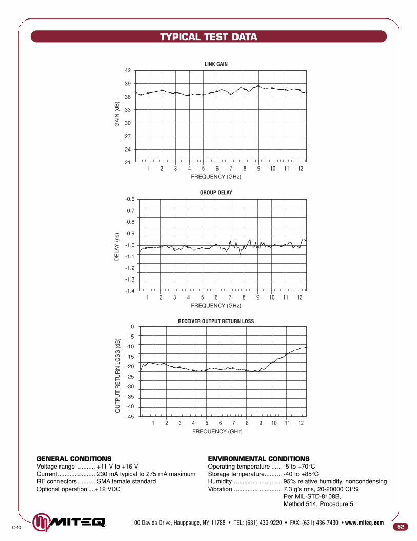
SINGLE-POLE SINGLE-THROW SWITCHES
52C-40100 Davids Drive, Hauppauge, NY 11788 • TEL: (631) 439-9220 • FAX: (631) 436-7430 • www.miteq.com
TYPICAL TEST DATA
GROUP DELAY
DE
LAY
(ns)
-0.6
-0.8
-0.7
-0.9
-1.0
-1.2
-1.4
-1.3
-1.1
LINK GAIN
GA
IN(d
B)
5 9 124 1181 2 103 6 7FREQUENCY (GHz)
5 9 124 1181 2 103 6 7FREQUENCY (GHz)
5 9 124 1181 2 103 6 7FREQUENCY (GHz)
RECEIVER OUTPUT RETURN LOSS
OU
TP
UT
RE
TU
RN
LOS
S(d
B)
42
33
36
39
24
27
30
21
0
-10
-25
-20
-15
-40
-5
-35
-30
-45
GENERAL CONDITIONSVoltage range .......... +11 V to +16 VCurrent...................... 230 mA typical to 275 mA maximumRF connectors .......... SMA female standardOptional operation ....+12 VDC
ENVIRONMENTAL CONDITIONSOperating temperature ...... -5 to +70°CStorage temperature.......... -40 to +85°CHumidity ............................ 95% relative humidity, noncondensingVibration ............................ 7.3 g’s rms, 20-20000 CPS,
Per MIL-STD-8108B,Method 514, Procedure 5

C-40100 Davids Drive, Hauppauge, NY 11788 • TEL: (631) 439-9220 • FAX: (631) 436-7430 • www.miteq.com
OPTICAL MEASUREMENTS
INPUT POWER 0 dBmINPUT POWER +1.5 dBm
INPUT POWER -10 dBmINPUT POWER -5 dBm
INPUT POWER -15 dBm INPUT POWER -18 dBm
53

100 Davids Drive, Hauppauge, NY 11788 • TEL: (631) 439-9220 • FAX: (631) 436-7430 • www.miteq.comC-40
RECEIVER OUTLINE DRAWING
54
.224[5.690]
.187[4.75]
.319 [8.103]
.310TYP.[7.87]
.194[4.928]
.209[5.309]
.090[2.286]
.18[4.57]
2X .093[2.362]
.280[7.112]
.25 [6.35]
.425[10.795]
PIN 1
.740[18.796]
1 2
2.25[57.15]
.050[1.27]
.600[15.24]
.380[9.65]
.604[15.342]
.830[21.082]
.375 [9.525]
RF CONNECTOR: SMA (FEMALE STANDARD)OPTICAL CONNECTOR: FC/APC STANDARD (OTHER STANDARDS AVAILABLE)
OPTICAL FIBER: 9/125 SINGLE MODE
RECEIVER POWER SUPPLY
PIN VOLTAGE CURRENT (AMPS) NOTES
1 PHOTOCURRENT MONITOR REFER TO "OPERATIONAL STATUS"
2 +12 0.23
RECEIVER OPERATIONAL STATUS
PIN DESCRIPTION NORMAL VOLTAGE NOTES
OPTICAL 0 VOLTS INDICATES NO CARRIER PRESENT.1 CARRIER > 1.0 VOLTAGE INCREASES APPROXIMATELY
DETECT UP TO +8 1.3 V/mW WITH DETECTED OPTICAL POWER.
NOTE: DIMENSIONS SHOWN IN BRACKETS [ ] ARE IN MILLIMETERS.
SINGLE MODE FIBERWITH 900µm BUFFER≈1 METER LONG
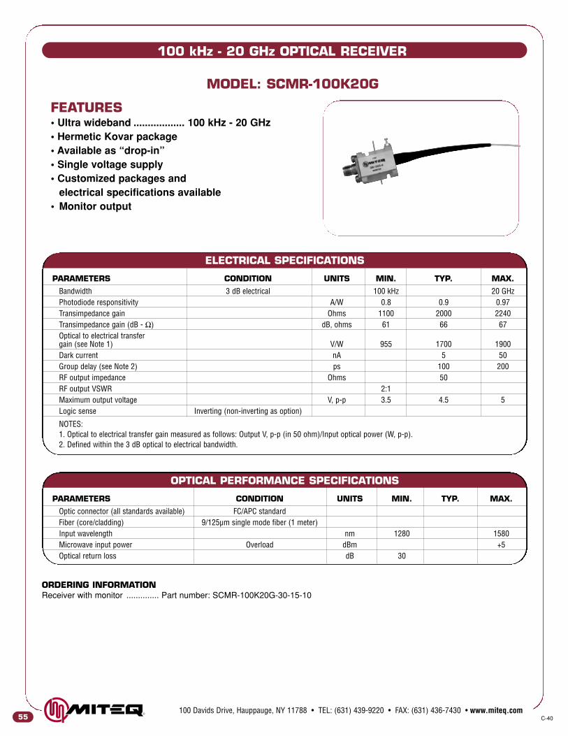
C-40100 Davids Drive, Hauppauge, NY 11788 • TEL: (631) 439-9220 • FAX: (631) 436-7430 • www.miteq.com
55
100 kHz - 20 GHz OPTICAL RECEIVER
FEATURES• Ultra wideband .................. 100 kHz - 20 GHz• Hermetic Kovar package• Available as “drop-in”• Single voltage supply• Customized packages andelectrical specifications available
• Monitor output
MODEL: SCMR-100K20G
ELECTRICAL SPECIFICATIONS
PARAMETERS CONDITION UNITS MIN. TYP. MAX.
Bandwidth 3 dB electrical 100 kHz 20 GHzPhotodiode responsitivity A/W 0.8 0.9 0.97Transimpedance gain Ohms 1100 2000 2240Transimpedance gain (dB - Ω) dB, ohms 61 66 67Optical to electrical transfergain (see Note 1) V/W 955 1700 1900Dark current nA 5 50Group delay (see Note 2) ps 100 200RF output impedance Ohms 50RF output VSWR 2:1Maximum output voltage V, p-p 3.5 4.5 5Logic sense Inverting (non-inverting as option)
NOTES:1. Optical to electrical transfer gain measured as follows: Output V, p-p (in 50 ohm)/Input optical power (W, p-p).2. Defined within the 3 dB optical to electrical bandwidth.
OPTICAL PERFORMANCE SPECIFICATIONS
PARAMETERS CONDITION UNITS MIN. TYP. MAX.
Optic connector (all standards available) FC/APC standardFiber (core/cladding) 9/125µm single mode fiber (1 meter)Input wavelength nm 1280 1580Microwave input power Overload dBm +5Optical return loss dB 30
ORDERING INFORMATIONReceiver with monitor .............. Part number: SCMR-100K20G-30-15-10
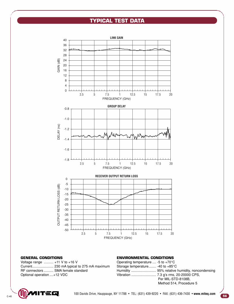
C-40100 Davids Drive, Hauppauge, NY 11788 • TEL: (631) 439-9220 • FAX: (631) 436-7430 • www.miteq.com
SINGLE-POLE SINGLE-THROW SWITCHES
56
TYPICAL TEST DATA
GROUP DELAY
DE
LAY
(ns)
-0.8
-1.0
-1.4
-1.8
-1.6
-1.2
LINK GAIN
GA
IN(d
B)
7.5 12.5 2017.512.5 155FREQUENCY (GHz)
7.5 12.5 2017.512.5 155FREQUENCY (GHz)
7.5 12.5 2017.512.5 155FREQUENCY (GHz)
40
28
32
36
12
16
20
24
8
0
4
-10
-5
0
-25
-20
-15
-40
-35
-30
-45
-50
OU
TP
UT
RE
TU
RN
LOS
S(d
B)
RECEIVER OUTPUT RETURN LOSS
GENERAL CONDITIONSVoltage range .......... +11 V to +16 VCurrent...................... 230 mA typical to 275 mA maximumRF connectors .......... SMA female standardOptional operation ....+12 VDC
ENVIRONMENTAL CONDITIONSOperating temperature .... -5 to +70°CStorage temperature........ -40 to +85°CHumidity .......................... 95% relative humidity, noncondensingVibration .......................... 7.3 g’s rms, 20-20000 CPS,
Per MIL-STD-8108B,Method 514, Procedure 5

C-40
RECEIVER OUTLINE DRAWING
100 Davids Drive, Hauppauge, NY 11788 • TEL: (631) 439-9220 • FAX: (631) 436-7430 • www.miteq.com
NOTE: DIMENSIONS SHOWN IN BRACKETS [ ] ARE IN MILLIMETERS.
.224[5.690]
.187[4.75]
.319 [8.103]
.310TYP.[7.87]
.194[4.928]
.209[5.309]
.090[2.286]
.18[4.57]
2X .093[2.362]
.280[7.112]
.25 [6.35]
.425[10.795]
PIN 1
.740[18.796]
1 2
2.25[57.15]
.050[1.27]
.600[15.24]
.380[9.65]
.604[15.342]
.830[21.082]
.375 [9.525]
RF CONNECTOR: SMA (FEMALE STANDARD)OPTICAL CONNECTOR: FC/APC STANDARD (OTHER STANDARDS AVAILABLE)
OPTICAL FIBER: 9/125 SINGLE MODE
RECEIVER POWER SUPPLY
PIN VOLTAGE CURRENT (AMPS) NOTES
1 PHOTOCURRENT MONITOR REFER TO "OPERATIONAL STATUS"
2 +12 0.23
RECEIVER OPERATIONAL STATUS
PIN DESCRIPTION NORMAL VOLTAGE NOTES
OPTICAL 0 VOLTS INDICATES NO CARRIER PRESENT.1 CARRIER > 1.0 VOLTAGE INCREASES APPROXIMATELY
DETECT UP TO +8 1.3 V/mW WITH DETECTED OPTICAL POWER.
SINGLE MODE FIBERWITH 900µm BUFFER≈1 METER LONG
57

FIBER OPTIC COMPONENT ENCLOSURES
100 Davids Drive, Hauppauge, NY 11788 • TEL: (631) 439-9220 • FAX: (631) 436-7430 • www.miteq.com
OPTION - EI (INDOOR RACK MOUNT)
OPTION - WP (WEATHERPROOF)
OPTION - SE (INDOOR SMALL ENCLOSURE)
58C-40
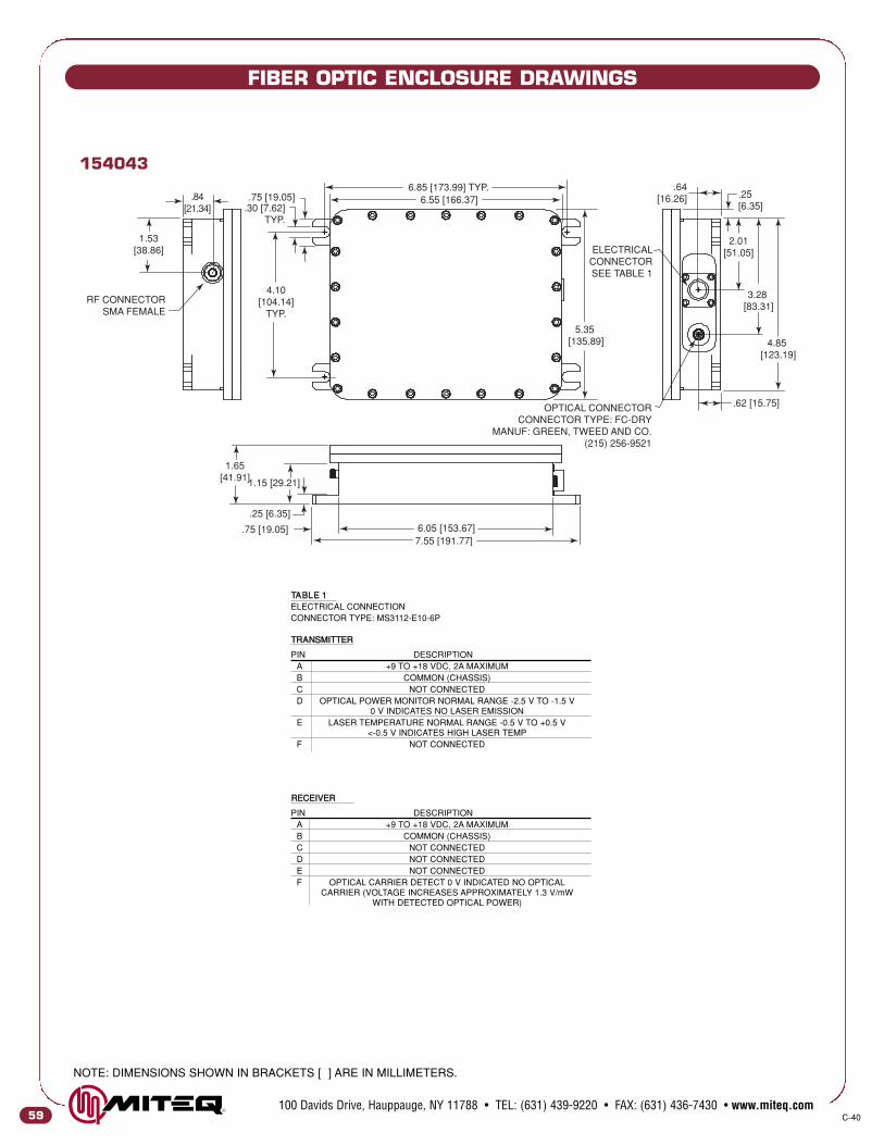
59
FIBER OPTIC ENCLOSURE DRAWINGS
C-40100 Davids Drive, Hauppauge, NY 11788 • TEL: (631) 439-9220 • FAX: (631) 436-7430 • www.miteq.com
NOTE: DIMENSIONS SHOWN IN BRACKETS [ ] ARE IN MILLIMETERS.
154043
6.55 [166.37]6.85 [173.99] TYP.
.75 [19.05] 6.05 [153.67]7.55 [191.77]
1.65[41.91]1.15 [29.21]
.25 [6.35]
ELECTRICALCONNECTORSEE TABLE 1
OPTICAL CONNECTORCONNECTOR TYPE: FC-DRY
MANUF: GREEN, TWEED AND CO.(215) 256-9521
.62 [15.75]
4.10[104.14]
TYP.
.75 [19.05].30 [7.62]
TYP.
4.85[123.19]
.25[6.35]
.64[16.26].84
[21.34]
1.53[38.86]
RF CONNECTORSMA FEMALE
3.28 [83.31]
5.35 [135.89]
2.01[51.05]
TTRRAANNSSMMIITTTTEERR
PIN DESCRIPTIONA +9 TO +18 VDC, 2A MAXIMUMB COMMON (CHASSIS)C NOT CONNECTEDD OPTICAL POWER MONITOR NORMAL RANGE -2.5 V TO -1.5 V
0 V INDICATES NO LASER EMISSIONE LASER TEMPERATURE NORMAL RANGE -0.5 V TO +0.5 V
<-0.5 V INDICATES HIGH LASER TEMPF NOT CONNECTED
TTAABBLLEE 11ELECTRICAL CONNECTIONCONNECTOR TYPE: MS3112-E10-6P
RREECCEEIIVVEERR
PIN DESCRIPTIONA +9 TO +18 VDC, 2A MAXIMUMB COMMON (CHASSIS)C NOT CONNECTEDD NOT CONNECTEDE NOT CONNECTEDF OPTICAL CARRIER DETECT 0 V INDICATED NO OPTICAL
CARRIER (VOLTAGE INCREASES APPROXIMATELY 1.3 V/mWWITH DETECTED OPTICAL POWER)
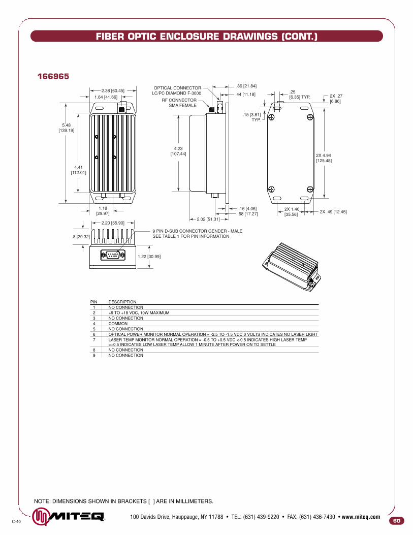
FIBER OPTIC ENCLOSURE DRAWINGS (CONT.)
60C-40 100 Davids Drive, Hauppauge, NY 11788 • TEL: (631) 439-9220 • FAX: (631) 436-7430 • www.miteq.com
NOTE: DIMENSIONS SHOWN IN BRACKETS [ ] ARE IN MILLIMETERS.
166965
2.38 [60.45]
1.64 [41.66]
5.48[139.19]
4.41[112.01]
1.18[29.97]
2.20 [55.90]
1.22 [30.99]
.8 [20.32]9 PIN D-SUB CONNECTOR GENDER - MALESEE TABLE 1 FOR PIN INFORMATION
.16 [4.06].68 [17.27]
.86 [21.84].25 [6.35] TYP.
.15 [3.81]TYP.
2X 1.40[35.56]
2X .49 [12.45]
2X 4.94 [125.48]
2X .27[6.86]
.44 [11.18]
2.02 [51.31]
4.23[107.44]
OPTICAL CONNECTORLC/PC DIAMOND F-3000
RF CONNECTORSMA FEMALE
PIN DESCRIPTION1 NO CONNECTION2 +9 TO +18 VDC, 10W MAXIMUM 3 NO CONNECTION4 COMMON5 NO CONNECTION6 OPTICAL POWER MONITOR NORMAL OPERATION = -2.5 TO -1.5 VDC 0 VOLTS INDICATES NO LASER LIGHT7 LASER TEMP MONITOR NORMAL OPERATION = -0.5 TO +0.5 VDC <-0.5 INDICATES HIGH LASER TEMP
>+0.5 INDICATES LOW LASER TEMP ALLOW 1 MINUTE AFTER POWER ON TO SETTLE8 NO CONNECTION9 NO CONNECTION

NOTE: DIMENSIONS SHOWN IN BRACKETS [ ] ARE IN MILLIMETERS.
61
FIBER OPTIC ENCLOSURE DRAWINGS (CONT.)
C-40 100 Davids Drive, Hauppauge, NY 11788 • TEL: (631) 439-9220 • FAX: (631) 436-7430 • www.miteq.com
162120
8.45 [214.63]
2.50 [63.50]
12.12[307.85]
0.60 [15.24]
CHASSIS LOCK
OPTICAL CONNECTORTYPE - OPTIONAL
RF CONNECTORSMA FEMALE
0.80 [20.32]
1.49[37.85]
0.77[19.56]
1.79[45.47]
4.33 [109.98]
8.66 [219.96]
1.90[48.26]
FRONT VIEW
REAR VIEW
0.65 [16.51]
GROUND
85-265 VAC INPUT, 50-60 HzIEC-320-C14 INPUT RECEPTACLE
FUSE, 1 AMP
162243
17.50 [444.50]
8.44[214.38]
19.000 [482.60]
18.34 [465.84]
A DETAIL A
17.75 [450.85]
.33 [8.38]
1.72 [43.69]
1.49 [37.85]
.24 [6.10]
R .12 [3.05]
.25 [6.35]
.12 [3.05]
.50 [12.70]
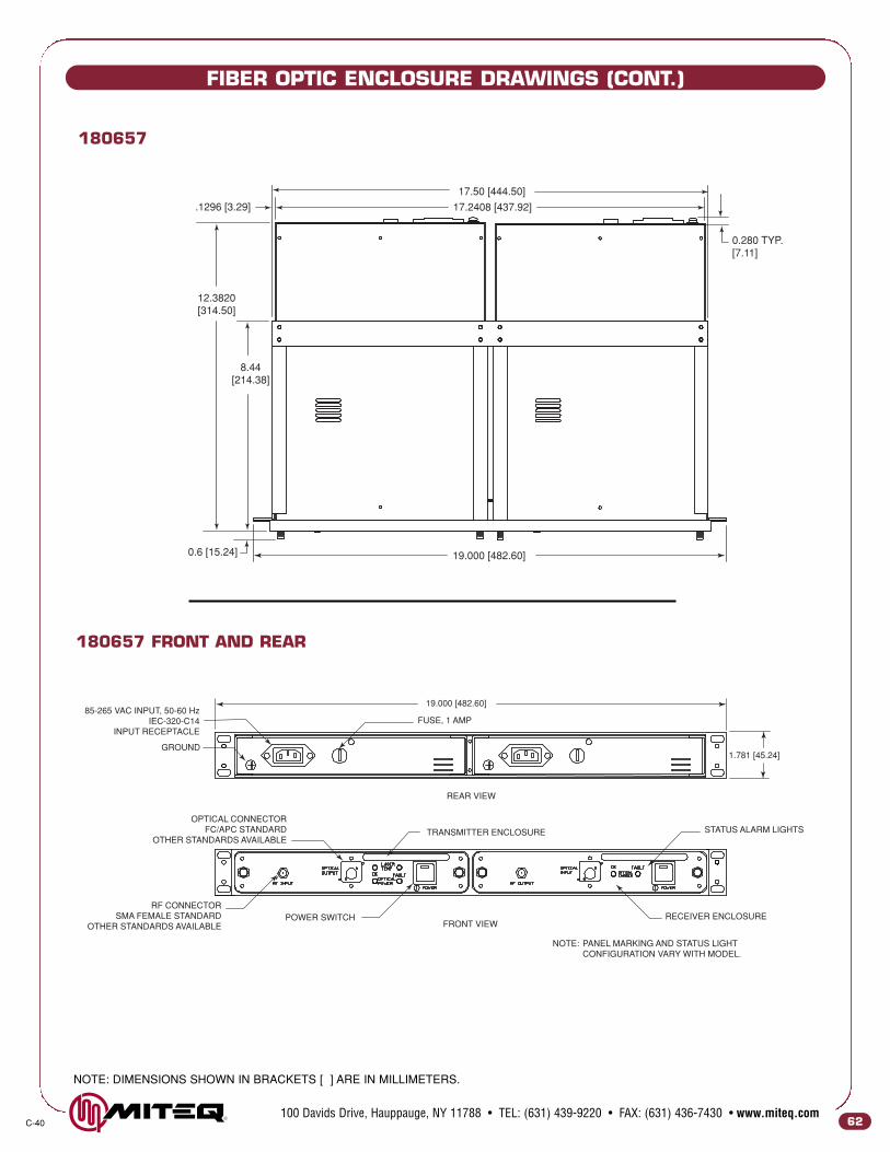
FIBER OPTIC ENCLOSURE DRAWINGS (CONT.)
62C-40 100 Davids Drive, Hauppauge, NY 11788 • TEL: (631) 439-9220 • FAX: (631) 436-7430 • www.miteq.com
NOTE: DIMENSIONS SHOWN IN BRACKETS [ ] ARE IN MILLIMETERS.
1.781 [45.24]
19.000 [482.60]
FUSE, 1 AMP85-265 VAC INPUT, 50-60 Hz
IEC-320-C14INPUT RECEPTACLE
GROUND
STATUS ALARM LIGHTS
RECEIVER ENCLOSURE
NOTE: PANEL MARKING AND STATUS LIGHT CONFIGURATION VARY WITH MODEL.
FRONT VIEW
REAR VIEW
POWER SWITCHRF CONNECTOR
SMA FEMALE STANDARDOTHER STANDARDS AVAILABLE
TRANSMITTER ENCLOSURE
OPTICAL CONNECTORFC/APC STANDARD
OTHER STANDARDS AVAILABLE
180657 FRONT AND REAR
17.2408 [437.92]
12.3820[314.50]
19.000 [482.60]
17.50 [444.50]
8.44[214.38]
.1296 [3.29]
0.6 [15.24]
0.280 TYP.[7.11]
180657

Related Documents