2008 Nuclear Science Symposium, Medical Imaging Conference and 16th Room Temperature Semiconductor Detector Workshop 19 - 25 October 2008 Dresden, Germany Session N14: Synchrotron Radiation and FEL Instrumentation Tuesday, Oct. 21 10:30-12:30 Femtosecond Radiation Experiment Detector for X-ray Free-Electron Laser (XFEL) Coherent X-ray Imaging Hugh T. Philipp, Lucas 1. Koerner, Marianne S. Hromalik, Mark W. Tate, Sol M. Gruner DOI: 10.1109/NSSMIC.2008.4774709

Welcome message from author
This document is posted to help you gain knowledge. Please leave a comment to let me know what you think about it! Share it to your friends and learn new things together.
Transcript
2008 Nuclear Science Symposium, Medical Imaging Conference and 16th Room Temperature Semiconductor Detector Workshop 19 - 25 October 2008 Dresden, Germany
Session N14: Synchrotron Radiation and FEL Instrumentation Tuesday, Oct. 21 10:30-12:30 Femtosecond Radiation Experiment Detector for X-ray Free-Electron Laser (XFEL) Coherent X-ray Imaging Hugh T. Philipp, Lucas 1. Koerner, Marianne S. Hromalik, Mark W. Tate, Sol M. Gruner DOI: 10.1109/NSSMIC.2008.4774709

2008 IEEE Nuclear Science Symposium Conference Record
Femtosecond Radiation Experiment Detector forX-ray Free-Electron Laser (XFEL)
Coherent X-ray ImagingHugh T. Philipp, Lucas 1. Koerner, Marianne S. Hromalik, Mark W. Tate, Sol M. Gruner
N14-5
Abstract-A pixel array detector (PAD) is being developed atCornell University for the collection of diffuse diffraction datain anticipation of coherent x-ray imaging experiments that willbe conducted at the Linac Coherent Light Source (LCLS) atthe Stanford Linear Accelerator Center (SLAC). The detectoris designed to collect x-rays scattered from femtosecond pulsesproduced by the LCLS x-ray laser at framing rates up to 120 Hz.Because x-rays will arrive on femtosecond time scales, the detector must be able to deal with instantaneous count-rates in excessof 1017 photons per second per pixel. A low-noise integratingfront-end allows the detector to simultaneously distinguish singlephoton events in low-flux regions of the diffraction pattern whilerecording up to several thousand x-rays per pixel in more intenseregions. The detector features a per-pixel programmable twolevel gain control that can be used to create an arbitrary 2-D,two-level gain pattern across the detector; massively parallel 14bit in-pixel digitization; and frame rates in excess of 120 Hz. Thefirst full-scale detector will be 758 x 758 pixels with a pixel size of110 x 110 microns made by tiling CMOS ASICs that are bumpbonded to high-resistivity silicon diodes. X-ray testing data ofthe first 185 x 194 pixel bump-bonded ASICs is presented. Themeasurements presented include confirmation of single photonsensitivity, pixel response profiles indicating a nearly single-pixelpoint spread function, radiation damage measurements and noiseperformance.
I. INTRODUCTION
NEW high-intensity x-ray sources like X-ray FreeElectron Lasers (XFEL) are opening new possibilities
into the types of x-ray studies that can be performed. Itis anticipated that intense, femtosecond time-scale pulsesproduced by XFELs will make the direct study of singleparticle electron density structure possible [1]. Even thoughthe energy absorbed by a particle during an ultra-intense XFELpulse will destroy its chemical structure because of massiveionization and a subsequent Coulomb explosion of the sample,a pulse that is short enough should still yield relevant scatteringinformation directly related to the original electron densityof the particle. This is because the Coulomb explosion ofthe particle is rate limited by the acceleration of ionized
This project has been supported by the United States Department ofEnergy (DOE) support of the LCLS at SLAC and DOE-HER grant DEFG02-97ER62443.
H. T. Philipp, L. J. Koerner, M. S. Hromalik and M. W. Tate arewith Cornell University, Laboratory of Atomic and Solid State Physics,Ithaca, NY 14850 USA (telephone: 607-255-8678, e-mail: [email protected],[email protected], [email protected], [email protected]).
S. M. Gruner is with Cornell University, Laboratory of Atomic andSolid State Physics, Ithaca, NY 14850 USA, and is director of Cornell'sHigh Energy Synchrotron Source (CHESS) (telephone: 607-255-3441, email:[email protected]).
particles/atoms. If the pulse is short enough, the x-rays arescattered before the Coulomb explosion occurs.
The experimental set-up, collection of data, and analysisof the collected data are non-trivial. Even if the x-ray pulseis short enough in duration and intense enough to producethe desired scattering pattern, other technological issues arenoteworthy and critical to the success of the experiment,including arranging temporal and spatial overlap of very shortpulses and single particles, the orientation of the particles inthe x-ray beam, and the best x-ray data collection strategy.Complicating matters, many frames of valid scattering dataare needed to reconstruct the original particle because muchof the scattering pattern, particularly in important high-q (largescattering angle) regions, will be extremely low flux. Forthe experiment being considered, the expected flux in theseregions is less than one photon per pixel. Another difficulty isthat in most single particle scattering schemes, the orientationof the particle is not determined and the scattering patternsmust be classified after the fact based on similarities of thescattering patterns themselves.
The pixel array detector presented here is one answer to thetechnological question of how to collect the scattering patternsfor the coherent x-ray imaging (CXI) of single particles atthe Linac Coherent Light Source (LCLS) XFEL. Many ofthe detector characteristics are tailored specifically for thedemands of the experiment, some of which are mentionedabove. Specific technical requirements include the ability todistinguish whether or not single x-ray photons have beendetected in any given pixel while maintaining the ability todetect thousands (>2500) of x-rays per pixel in other partsof the scattering pattern. This is particularly notable sincefor a pulse that approaches 10 fs in length, the instantaneouscount rate for some pixels will be greater than 1017 photonsper second. This count rate alone excludes the possibility ofusing a photon counting detector. Another notable technicalrequirement, related to the ability to distinguish single photons,is a pixel-limited point spread function. In addition, thedetector must be able to sustain a continuous frame-rate of120 Hz. This follows from the operating procedures plannedfor the LCLS, and the high number of frames required forreconstructing the electron density from the diffuse x-rayscattering patterns produced by coherent x-ray imaging of noncrystalline samples.
978-1-4244-2715-4/08/$25.00 <92008 IEEE 1567
i~;--Addressing and Array Readout-·
Count ~ ========================:::_Rst ];:....---------I\L _Data_Clock_-- :-:-:::-:-:-:-:::--~NW~1J\j\ NW~~~JL
ADC_Clock --JJiftMWififlMJIJIRamp ~,
~ --In-PlxeIDigitlzation---
~~
B' •..: :..: \. _-
••• - _•• - _•• - - Analog-to-Digital ConversionFront-end . - .
sa~·pi; ;~d -H·oiJ St:ge
tcharge
injectiontest circuit
Bump Bond
x-rays
~
Rev. Bias
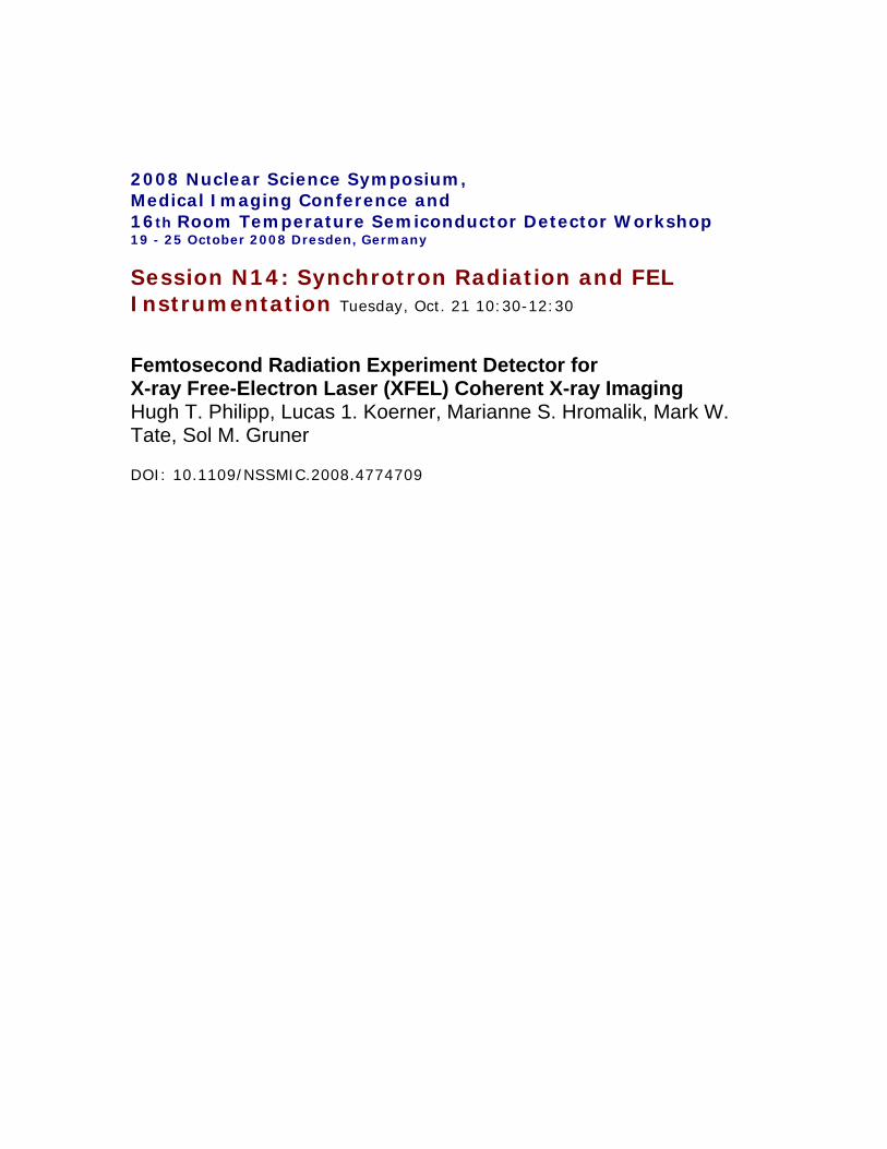
Fig. 1. High-level schematic of the pixel showing the major functionalcomponents: The front-end amplifier, the sample-and-hold bUff~r. and ~he
digitization components. In addition t~ these basic fun~t~~nal. umts, the I~
pixel programmable gain mechanism IS shown. The dlgltlzatlOn method IS
similar to that presented in reference [3].
Fig. 2. A simplified timing diagram of the detector showing a divisionbetween exposure time, digitization, and detector readout. The plannedexposure time for the CXI experiment is 10 J-LS. The digitization time isapproximately 4 ms and the readout of the ASIC takes 3.2 ms. A frame rateof 120 Hz (period 8.3 ms) is easily achieved with this timing division.
II. PHYSICAL CONSTRUCTION OF PIXEL ARRAYDETECTOR (PAD)
A PAD is composed of two layers, the detector layer and thesignal processing layer. These layers are mated together withisolated, pixel-level connections using solder bump-bonding l .
The detector layer is an array of diodes2 made from 500 J.tmthick high-resistivity (5 - 10 kO) n-type silicon. The thicknessof the diode layer gives a high quantum efficiency, greaterthan 0.99, when detecting 8 keY x-rays. The high resistivityof the diodes ensure over-depletion when a bias voltage of200 volts is applied. In operation, incident x-rays are absorbedby the silicon in the diodes and converted into charge carrierpairs. These charges migrate according to the applied electricfield and the respective mobilities of the charge carriers.For the PAD presented, holes are collected (reasons for thisare explained elsewhere [2]) by the signal processing layerthrough pixel-level connections. The signal processing layeris a 0.25 micron CMOS, mixed-mode application specificintegrated circuit (ASIC) manufactured by TSMC3. Each pixelof the ASIC has dedicated circuitry for processing the chargecollected from the diode. The pitch of the pixel connectionsacross the 2-D detector array is 110 J-lm. The size of the singlepixel layout in the CMOS ASIC corresponds to the pitch (i.e.the pixel size is 110 J-lm x 110 Jim).
III. PIXEL-LEVEL DESIGN AND OPERATION
A. Pixel Operation Description
A high-level schematic of the pixel is shown in figure 1.X-ray induced charge in the diode is collected at the 'in' nodeand integrated onto the feedback capacitance of the frontend capacitive transimpedance amplifier. The total feedbackcapacitance can be set to either the capacitance of cap1 orthe sum of cap1 and cap2 to configure the gain (volts perintegrated unit of charge) of the front-end. The selection ofthe capacitance is determined by I-bit in-pixel memory thatcan be individually programmed for each pixel in the array.
1Bump bonding done by RTI, International Center for Materials andElectronic Technologies, Research Triangle Park, NC, USA
2Detector diode manufactured by SINTEF, NO-7465 Trondheim, Norway3Taiwan Semiconductor Manufacturing Company Limited, No. 25, Li-Hsin
Rd., Hsinchu Science Park, Hsin-Chu, Taiwan 300
The capacitance of the feedback loop with and without cap2as part of the integrating feedback loop is 565 fF and 75 fF,respectively. Since x-ray conversion in silicon produces I electron per 3.65 eV of absorbed energy, the gain of the front-endstage is either 0.62 mV per 8-keV x-ray (low gain) or 4.7 mVper 8-keV x-ray (high gain). Since the usable voltage rangeof a pixel's analog stage is conservatively set to 1.7 V (setby the ramp, the digitization clock and Vref), the saturationof the pixel during normal operation is approximately 2700x-rays in low-gain and 360 x-rays in high-gain.
After the charge is integrated by the front-end, the voltageat node A is sampled by the sample-and-hold stage and heldconstant during the next stage of in-pixel data acquisition,which is digitization.
During digitization, the voltage at node B is compared toa globally transmitted ramp while a global analog-to-digitalconversion (ADC) clock increments an in-pixel I4-bit counter.When the voltage of the ramp crosses the the voltage held atnode B, the counter is disabled and the value of the counter istaken to be proportional to the total charge integrated by thepixel. The digitized value of each pixel is then shifted onto adigital bus with a readout clock. These values are the outputof the PAD.
B. Waveforms and Pixel Timing
Figure 2 shows a simplified timing diagram for the pixeloperating in a mode compatible with the requirements of theLCLS CXI experiment. The integration time shown is a smallfraction of the framing period and in normal operation onlyspans 10 J-ls. After the integration time, the output voltage issampled and digitized. Digitization in normal operation takes4 ms, occurring simultaneously for all pixels. Pixel readoutthen proceeds and requires addressing (not shown in figure 2).Each pixel is addressed and readout by switching the counterto act as a shift-register.
IV. CHIP-LEVEL ARCHITECTURE
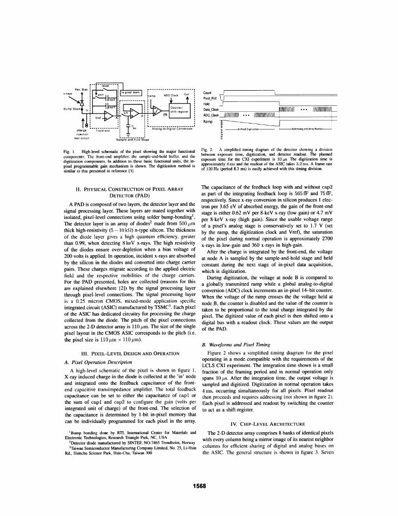
The 2-D detector array comprises 8 banks of identical pixelswith every column being a mirror image of its nearest neighborcolumns for efficient sharing of digital and analog buses onthe ASIC. The general structure is shown in figure 3. Seven
1568
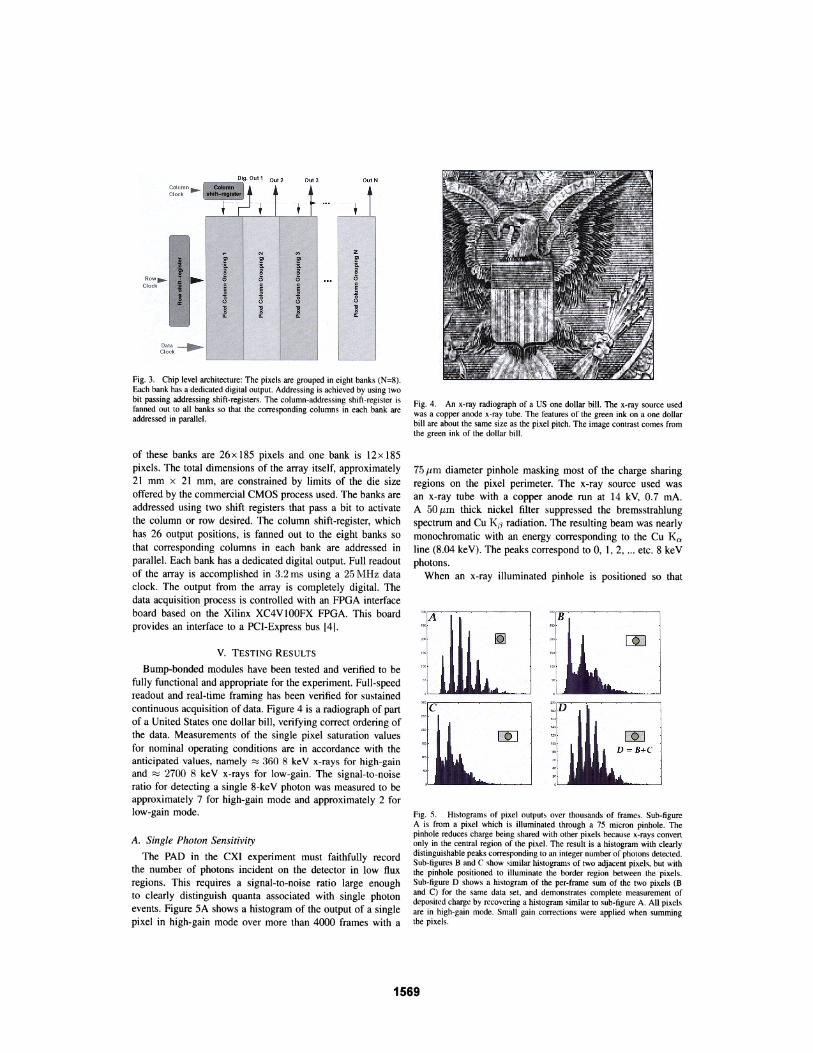
Fig. 3. Chip level architecture: The pixels are grouped in eight banks (N=8).Each bank has a dedicated digital output. Addressing is achieved by using twobit passing addressing shift-registers. The column-addressing shift-register isfanned out to all banks so that the corresponding columns in each bank areaddressed in parallel.
Fig. 4. An x-ray radiograph of a US one dollar bill. The x-ray source usedwas a copper anode x-ray tube. The features of the green ink on a one dollarbill are about the same size as the pixel pitch. The image contrast comes fromthe green ink of the dollar bill.
zr&cE
~1it
N ..I i fc:s
I I II 1 Iit
Column......~~t1r+lClock , ,
Row .....Clock
II
Fig. 5. Histograms of pixel outputs over thousands of frames. Sub-figureA is from a pixel which is illuminated through a 75 micron pinhole. Thepinhole reduces charge being shared with other pixels because x-rays convertonly in the central region of the pixel. The result is a histogram with clearlydistinguishable peaks corresponding to an integer number of photons detected.Sub-figures B and C show similar histograms of two adjacent pixels, but withthe pinhole positioned to illuminate the border region between the pixels.Sub-figure D shows a histogram of the per-frame sum of the two pixels (Band C) for the same data set, and demonstrates complete measurement ofdeposited charge by recovering a histogram similar to sub-figure A. All pixelsare in high-gain mode. Small gain corrections were applied when summingthe pixels.
3CO
A
c
75 /lID diameter pinhole masking most of the charge sharingregions on the pixel perimeter. The x-ray source used wasan x-ray tube with a copper anode run at 14 kV, 0.7 rnA.A 50/lID thick nickel filter suppressed the bremsstrahlungspectrum and Cu Kp radiation. The resulting beam was nearlymonochromatic with an energy corresponding to the Cu Ku
line (8.04 keY). The peaks correspond to 0, 1, 2, ... etc. 8 keYphotons.
When an x-ray illuminated pinhole is positioned so that
A. Single Photon Sensitivity
The PAD in the CXI experiment must faithfully recordthe number of photons incident on the detector in low fluxregions. This requires a signal-to-noise ratio large enoughto clearly distinguish quanta associated with single photonevents. Figure 5A shows a histogram of the output of a singlepixel in high-gain mode over more than 4000 frames with a
V. TESTING RESULTS
Bump-bonded modules have been tested and verified to befully functional and appropriate for the experiment. Full-speedreadout and real-time framing has been verified for sustainedcontinuous acquisition of data. Figure 4 is a radiograph of partof a United States one dollar bill, verifying correct ordering ofthe data. Measurements of the single pixel saturation valuesfor nominal operating conditions are in accordance with theanticipated values, namely ~ 360 8 keV x-rays for high-gainand ~ 2700 8 keY x-rays for low-gain. The signal-to-noiseratio for detecting a single 8-keV photon was measured to beapproximately 7 for high-gain mode and approximately 2 forlow-gain mode.
of these banks are 26 x 185 pixels and one bank is 12 x 185pixels. The total dimensions of the array itself, approximately21 mm x 21 mm, are constrained by limits of the die sizeoffered by the commercial CMOS process used. The banks areaddressed using two shift registers that pass a bit to activatethe column or row desired. The column shift-register, whichhas 26 output positions, is fanned out to the eight banks sothat corresponding columns in each bank are addressed inparallel. Each bank has a dedicated digital output. Full readoutof the array is accomplished in 3.2 IDS using a 25 MHz dataclock. The output from the array is completely digital. Thedata acquisition process is controlled with an FPGA interfaceboard based on the Xilinx XC4VI00FX FPGA. This boardprovides an interface to a PCI-Express bus [41.
1569

TABLE IDETECTOR SPECIFICATION SUMMARY
minimal. Dose testing of the un-bumped ASIC indicates thatdamage to the CMOS is recoverable by annealing.
Line Response
120 Hz in operation at LCLS
110 J.Lfi x 110 J.Lfi
2700 8-keV x-rays (Low-Gain)
350 8-keV x-rays (High-Gain)
0.97 8-keV x-rays
0.89 12-keV x-rays
0.48 18-keV x-rays
7 for 8-keV x-ray (High-Gain)
2 for 8-keV x-ray (Low-Gain)
Single ASIC: 185 x 194
TIled Detector (phase I): 758 x 758
TIled Detector (phase 2): 1516 x 1516
Array Size
Pixel Size
Frame Rate
~ ~61)' -4r -20 0 20 to
: Position (microns)
Measured Knife Edge Response
Pixel Saturation
Quantum Efficiency
Signal-to-Noise Ratio
(rms)
Fig. 6. Line spread function obtained from 100 fiS x-ray radiographs of ax-ray opaque 50 J.Lm thick tungsten knife edge. The x-ray source used wasan x-ray tube with a copper anode and a 50 J.Lm thick nickel filter operated at14 kV and 0.7 mAo Approximate pixel borders are shown with dashed lines.
VI. CONCLUSION
Detector development for new experiments like coherent xray imaging (CXI) has many challenges. Some of these challenges are foreseen and defined in the specifications outlinedat the beginning of the project. The detector ASIC we havedesigned and tested has shown that it is capable of meetingthese specifications.
This detector is, beyond an answer to the requirements ofone experiment, a template for further detector development.In-pixel digitization, for instance, is likely an increasing trendin CMOS imaging detectors for x-ray science. A purely digitalpixel output has the advantage of simplified readout electronicsand avoids pit-falls of high-speed analog multiplexing. Adjustable front-end gain is another feature likely to be usedmore often in charge integrating detector designs because iteffectively increases the dynamic range of the detector. Thereare other methods for increasing the dynamic range [5], butthese often limit instantaneous count rates to levels that areincompatible with new, brighter x-ray light sources beingdeveloped.
The measurements of charge sharing demonstrates an important advantage of charge integrating detectors that is oftenlost with counting detectors. This advantage is completemeasurement of deposited charge independent of the location
B. Line Spread Function
Directly collecting charge produced by x-rays absorbed ina fully-depleted silicon detector layer has several advantagesover x-ray detector methods that rely on detecting secondaryoptical photons emitted by a phosphor. One of these advantages is a comparatively superb point spread function. This isbecause after the charge is produced, it is directly collectedby the applied electric field. The spread of charge duringthe time it takes to migrate through the detector layer tothe pixel connection may give rise to charge sharing betweenpixels. Measurement of charge sharing and pixel response as afunction of position of incident photons can be accomplishedby measuring the line spread function with a knife-edge thatis held at a slight angle to the column (or row) so thatvarying degrees of pixel exposure are collected as a functionof position along a knife edge illuminated with a flat field.Additional, finer resolution data can be gathered by translating the detector behind the x-ray illuminated knife edge. Ameasurement of this sort is shown in figure 6. Pixel output isplotted as a function of mean knife edge position with respectto the pixel center. The derivative of this, also shown, givesthe line spread function. The line spread function recoveredis the convolution of the charge spreading in one dimensionwith a one-dimensional box function having the same widthas the pixel (110 {lID). The results of the measurements showdiscernible charge sharing up to 20 J-lffi from the nominal pixelboundary. Beyond this charge sharing region, the line spreadfunction is flat and dominated by pixelization. Since the pixelsare 110 J.LID wide, the line spread and point spread functionsare pixel-size limited. The width of the charge sharing regiondoes, however, indicate that a significant percentage (up to60%) of randomly distributed incident photons will be affectedby charge sharing to some degree, as they will be within 20 J-lffiof the pixel boundary.
C. Radiation Testing
Radiation damage of the bump-bonded pixel array detectorwas tested up to 75 MRad (Si) referenced to the face of thedetector using an 8 keV x-ray source. The results indicate thatleakage currents of the diode increase, but the impact on datacollected for the proposed experimental application will be
its projection straddles the border between two pixels, asignificant number of the photons incident on the detectorconvert in charge sharing regions where the charge producedby an absorbed photon is split between pixels. Since only afraction of the charge produced by a charge sharing event iscollected by an individual pixel, histograms of single pixeloutputs over many frames do not show a clear quantizedresponse. This effect is shown in figure 5B and 5C. In thiscase, the total charge deposited by a given x-ray event remainsconstant and a histogram of the frame-by-frame sum of thetwo pixels (calculated after a small gain correction) recoversdiscernible x-ray peaks (50). There is, however, a degradationin the quality of the histogram because the noise associatedwith the sum of pixels is greater (by a factor of J2) than thenoise associated with a single pixel.
1570
of x-ray conversion with respect to pixel borders. Whenusing a detector in the realm where loss of charge throughrecombination is small, the measurement of charge collectedby an integrating front-end is a direct measurement of the xray energy absorbed in the detector. In contrast, detectors thatcount photons based on pulse shape analysis using discrimination levels are hindered by count-rate limitations and chargesharing between pixels. At very high count-rates like thoseanticipated in many XFEL experiments, photon counting isnot possible.
ACKNOWLEDGMENT
The authors thank the following SLAC employees for theirsupport and guidance in the detector development process:Niels Van Bakel, Stefan Moeller and John Arthur.
REFERENCES
[l] R. Neutze, R. Wouts, D. van der Spoel, E. Weckert, and 1. Hajdu,"Potential for biomolecular imaging with femtosecond x-ray pulses,"Nature, vol. 406, no. 6797, pp. 752-757, Aug. 2000. [Online]. Available:http://dx.doi.orgll0.l038/35021099
[2] S. L. Barna, "Development of a microsecond framing two-dimensionalpixel array detector for time-resolved x-ray diffraction," Ph.D. dissertation, Cornell University, 1997.
[3] S. Kleinfelder, S. Lim, X. Liu, and A. E. Gamal, "A 10 000 frames/sCMOS digital pixel sensor," IEEE Journal ofSolid State Circuits, vol. 36,no. 12, pp. 2049-2059, 2001.
[4] M. S. Hromalik, H. T. Philipp, L. 1. Koerner, M. W. Tate, and S. M.Gruner, "Data acquisition and control for a pixel array detector (PAD)for single particle scattering at the linac coherent light source (LCLS),"in 2007 IEEE Nucl. Science Symposium Conference Record (2007) NSS'07. IEEE. 3, 1744-1750. (Honolulu, HA, Oct 27 - Nov 3, 2007. PaperNS-25.), 2007.
[5] D. Schuette, "A mixed analog and digital pixel array detector forsychrotron x-ray imaging," Ph.D. dissertation, Cornell University, 2008.
1571
Related Documents