Femtosecond laser structuring for micro/nano-photonics Xuewen Wang Supervisors: Saulius Juodkazis Co-supervisors: Alexander Babanin Ri˘ cardas Buividas Amin Chabchoub Centre for Micro-Photonics Faculty of Science, Engineering and Technology Swinburne University of Technology A thesis submitted for the degree of Doctor of Philosophy Melbourne, Australia, 2017

Welcome message from author
This document is posted to help you gain knowledge. Please leave a comment to let me know what you think about it! Share it to your friends and learn new things together.
Transcript

Femtosecond laser structuringfor micro/nano-photonics
Xuewen Wang
Supervisors: Saulius JuodkazisCo-supervisors: Alexander Babanin
Ricardas BuividasAmin Chabchoub
Centre for Micro-Photonics
Faculty of Science, Engineering and Technology
Swinburne University of Technology
A thesis submitted for the degree of
Doctor of Philosophy
Melbourne, Australia, 2017


Declaration
I, Xuewen Wang, declare that this thesis entitled:
”Femtosecond laser structuring for micro/nano-photonics”
is my own work and has not been submitted previously, in whole or in part inrespect of any other academic award.
Xuewen Wang
Centre for Micro-PhotonicsFaculty of Science, Engineering and TechnologySwinburne University of TechnologyAustralia
Dated this day, September 14, 2017
i

”The ideas that have lighted my way, and time after time havegiven me new courage to face life cheerfully, have been Kindness,Beauty and Truth. Without the sense of kinship with men of likemind, without the occupation with the objective world, the eternallyunattainable in the field of art and scientific endeavors, life wouldhave seemed empty to me.”
- Albert Einstein
ii

Preface: Femtosecond laser
fabrication - effective technique
for micro-/nano-photonics
Femtosecond lasers are becoming very powerful tools for material processingdue to their unique properties of ultra-short pulse and extremely high peakintensity, since the Kerr-lens mode locking technique [1] and the intracavitysemiconductor Fabry-Perot saturable absorber [2, 3] were invented, allowingthe generation of stable and high power of ultrashort pulse trains from a solidlaser system. The continuing trend of photon-cost reduction for ultrashortpulse laser optics and systems and the increasingly high output average powerfacilitate the wide use of femtosecond lasers and application developmentsacross different industries.
To give an example to illustrate ”ultrashort”, 100 fs (10–15 s) pulse du-ration is much shorter than the duration of the electron-ion energy exchangewhich is typically last tens of picoseconds. Such short pulse duration is shorterthan the electron-phonon coupling time for most of the materials, which leadsto suppression of the heat affected zone created by the laser irradiation andsub-micron fabrication resolution can be easily achieved. Even using 100 fem-tosecond lasers with low pulse energies which are smaller than 0.1 μJ, the peakintensity at the focus area is still able to reach more than 100 TW/cm2 (1 TW= 1012 W). This is sufficient to induce optical ionization in any materials in-cluding optical breakdown in dielectrics. The high peak intensity increases thepossibility of the nonlinear absorption process and enables the modificationor removal even in wide band gap dielectric materials. This ability is widelyused to fabricate high precision 3D structures with tightly focused laser beamclose to the diffraction limit in optically transparent materials. With the in-tense femtosecond pulse tightly focused irradiation, optically induced dielectricbreakdown will occur, which can lead to various of phase transformations ofmaterials, from solid to liquid, gaseous or plasma state. Within the suppressedheat affected zone, the surrounding medium can hold a micro-volume or evensubmicro-volume of ionized material with high temperature and pressure with-out cracks. This unique condition can leading to exotic phase structure for-
iii

mation of material, and can be demonstrated on creation of body-centeredcubic alumina [4], exotic phase of silicon [5] and provides a new route to formsuperdense material phases [6].
The excitation of free electrons or further disordering of the crystal latticeor glass matrix under the nonlinear photon absorption process with intensephoton flux irradiation can generate different type of defects or color centresinside the bulk or on the surface of the dielectrics, and thus changing the opticalproperties of the original materials, absorptive color centres [7], emission [8],refractive index [9] and birefringence [10] associated with the induced defects.These properties can be applied to fabricate different functional of optics orphotonic devices, like waveguides [9], micro resonators [11], microlasers [12] orphase plates [13]. The studies and achievements on laser induced defects havedemonstrated the efficiency, cost-effectiveness and simple process on defectsengineering comparing to other techniques like electron bombarding, X-rayirradiation, ion implanting, with its localized control with high spatial reso-lution and 3D capabilities. Femtosecond laser fabrication technique involvingdirect ablation, photon-polymerization and laser-induced nanograting fabrica-tion have achieved sub-micrometer or even sub-100 nm resolutions which ini-tiates the rapid development in 3D photonic crystals [14], super hydrophobicsurfaces [15], surface enhancement Raman scattering (SERS) substrate [16],biomimetic photonic structures [17]. Using the multi-beam interference tech-nique or applying diffractive optics, large scale of such photonic devices com-posed with micro or nanostructures can be realized [18–20].
Manipulating light in micro-/nano-scale has been emerging as an excitingdirection in the optics and photonics. Engineering the light-matter interactionin micro-/nano-scale brings many interesting and blooming applications. Theadvanced photonic devices or systems of single photon emission source, planarphase or polarization element, near field optics etc., require high integrationfor large capacity, ultra-high speed information processing, which are involvingmultiple nanofabrication processes thus hampering the practical applicationsand further development. Those challenges on the way of future photonictechnology development make the trials using femtosecond laser fabricationmeaningful and important.
Featuring all these attributes of femtosecond laser technologies that propelthe future trend of micro-/nano-photonics technologies toward high integrationand miniaturization, femtosecond laser fabrication is an effective technique formicro/nano-photonic applications. That’s the reason why the development ofvarious techniques on micro or nanostructuring with femtosecond lasers fordifferent optical and photonic functionalities are so attractive.
iv
Contents
Preface: Ultrafast laser fabrication - effective technique for micro-/nano-photonics iii
Abstract ix
Acknowledgments xi
1 Introduction 11.1 Ultrafast laser material processing . . . . . . . . . . . . . . . . . 1
1.1.1 Frontiers of ultrafast lasers . . . . . . . . . . . . . . . . . 11.1.2 State of the art of femtosecond laser processing . . . . . 2
1.2 Background of femtosecond laser processing . . . . . . . . . . . 51.2.1 Ultrafast laser-material interactions . . . . . . . . . . . . 51.2.2 Structural relaxation and modification . . . . . . . . . . 8
2 Experimental and Techniques 92.1 Femtosecond laser system . . . . . . . . . . . . . . . . . . . . . 92.2 Nano-lithography and nanofabrication techniques . . . . . . . . 11
2.2.1 Photolithography . . . . . . . . . . . . . . . . . . . . . . 112.2.2 Focused ion beam lithography . . . . . . . . . . . . . . . 142.2.3 Physical vapour deposition . . . . . . . . . . . . . . . . . 142.2.4 Reactive ion etching . . . . . . . . . . . . . . . . . . . . 15
2.3 Structure characterization . . . . . . . . . . . . . . . . . . . . . 162.4 Appendix A . . . . . . . . . . . . . . . . . . . . . . . . . . . . . 17
A1 A bactericidal microfluidic device constructed using nano-textured black silicon . . . . . . . . . . . . . . . . . . . . 18
3 Defects engineering for photonic applications 273.1 Introduction of common types of defects in crystals and amor-
phous solids . . . . . . . . . . . . . . . . . . . . . . . . . . . . . 273.2 Optical properties characterization and defect density estimation 293.3 Refractive index modification associated with defect formation . 313.4 Laser induced defects in KBr crystals . . . . . . . . . . . . . . . 323.5 Defects engineered in cubic and hexagonal-BN . . . . . . . . . . 36
v

3.6 High density E′ centres in fused silica and paramagnetic defectsin Fe:LiNbO3 . . . . . . . . . . . . . . . . . . . . . . . . . . . . 39
3.7 Discussion and Conclusions . . . . . . . . . . . . . . . . . . . . 413.8 Appendix B . . . . . . . . . . . . . . . . . . . . . . . . . . . . . 42
B1 Analysis of defects patterned by femotosecond pulses insideKBr and SiO2 glass . . . . . . . . . . . . . . . . . . . . . 42
B2 Photoluminescence from voids created by femtosecond laserpulses inside cubic-BN . . . . . . . . . . . . . . . . . . . 42
B3 Engineering and localization of quantum emitters in largehexagonal boron nitride layers . . . . . . . . . . . . . . . 42
4 Pancharatnam-Berry phase optical elements 614.1 Introduction . . . . . . . . . . . . . . . . . . . . . . . . . . . . . 614.2 Pancharatnam-Berry Phase . . . . . . . . . . . . . . . . . . . . 634.3 Fundamentals of geometric phase manipulation . . . . . . . . . 644.4 Polarization manipulation via optically anisotropic medium . . . 66
4.4.1 Birefringence induced by photoelasticity . . . . . . . . . 664.4.2 Birefringence induced by dielectric binary gratings . . . . 67
4.5 Dielectric geometric phase optical elements based on space-variantorientation birefringence . . . . . . . . . . . . . . . . . . . . . . 72
4.6 Femtosecond laser fabrication techniques . . . . . . . . . . . . . 744.6.1 3D Polymerization . . . . . . . . . . . . . . . . . . . . . 744.6.2 Direct laser ablation . . . . . . . . . . . . . . . . . . . . 854.6.3 Stress engineering . . . . . . . . . . . . . . . . . . . . . . 87
4.7 Optical characterization and Discussions . . . . . . . . . . . . . 904.8 Conclusions . . . . . . . . . . . . . . . . . . . . . . . . . . . . . 944.9 Appendix C . . . . . . . . . . . . . . . . . . . . . . . . . . . . . 94
C1 Dielectric geometric phase optical elements from femtosec-ond direct laser writing . . . . . . . . . . . . . . . . . . . 95
5 Plasmonic nano-printing for surface structuring 1015.1 Introduction . . . . . . . . . . . . . . . . . . . . . . . . . . . . . 1015.2 Mechanism of ripple formation induced by ultra-short pulses . . 1035.3 Period tuning of laser induced ripples . . . . . . . . . . . . . . . 1105.4 Orientation tuning of laser induced ripples . . . . . . . . . . . . 1125.5 Large scale ripple fabrication . . . . . . . . . . . . . . . . . . . . 114
5.5.1 Uniform subwavelength ripples on amorphous Si film . . 1155.5.2 Wafer-area nanogratings fabricated via cylindrical lens . 117
5.6 Conclusions . . . . . . . . . . . . . . . . . . . . . . . . . . . . . 1195.7 Appendix D . . . . . . . . . . . . . . . . . . . . . . . . . . . . . 120
D1 Laser structuring for control of coupling between THz lightand Phonon modes . . . . . . . . . . . . . . . . . . . . . 126
D2 Plasmonic nano-printing: large area nanoscale energy depo-sition for efficient surface texturing . . . . . . . . . . . . 150
vi

D3 Laser printed nano-gratings: orientation and period pecu-liarities . . . . . . . . . . . . . . . . . . . . . . . . . . . . 158
5.8 Appendix E . . . . . . . . . . . . . . . . . . . . . . . . . . . . . 158E1 Laser-induced translative hydrodynamic mass snapshots: map-
ping at nanoscale . . . . . . . . . . . . . . . . . . . . . . 166E2 Angle-multiplexed optical printing of biomimetic hierarchi-
cal 3D textures . . . . . . . . . . . . . . . . . . . . . . . 172E3 Silk: Optical Properties over 12.6 Octaves THz-IR-Visible-
UV Range . . . . . . . . . . . . . . . . . . . . . . . . . . 187E4 Silk patterns made by direct femtosecond laser writing . . . 194E5 Orientational Mapping Augmented Sub-Wavelength Hyper-
Spectral Imaging of Silk . . . . . . . . . . . . . . . . . . 204
Conclusions and Outlook 205
Publications during this PhD project 209
Bibliography 213
vii

viii

Abstract
The aim of this PhD project is to utilize unique properties of ultrashort laserpulse interaction with materials to fabricate micro/nano photonic devices forgenerating or manipulating the phase, polarization and intensity of light inthe near and far fields. To achieve this objective, different femtoseond laserfabrication techniques and approaches are proposed and demonstrated. Themain results are summarized as defensible thesis statements:
1. Tightly focused femtosecond laser pulses were used to create high densityof defects or color centres inside wide band gap dielectric materials whichcan result in high refractive index change, birefringence modificationand high density of dangling bonds. The femtosecond laser irradiationis proven to be an effective tool to create single photon emitters onhexagonal BN flakes.
2. Patterning of the optical birefringence can generate geometric phase forengineering the wavefront of the light due to polarization manipulation.Applying the polymerization, UV femtosecond laser direct ablation andlaser induced stress techniques, desired optical birefringence axis distri-bution can be realized. Thus the planar geometric phase optical ele-ments can be effectively fabricated using femtosecond laser structuringwith the design, fabrication and characterization of different functionalvortex beam generators and photonic spin Hall devices.
3. The phenomenon of laser induced periodic structures or ripples is ex-plained by the subsurface plasmonic wave excitation observation of dif-ferent periodicity nanograting formation under different thickness of in-dium tin oxide (ITO) films and was utilized to print uniform polarizationdependent nanogratings on silicon film and wafer-size scale grating struc-tures.
This PhD thesis is organized as a collection of published original research pa-pers with topical introductory descriptions and basic fundamentals, arranged
ix
in five chapters:
• Chapter 1 presents the state of the art of ultrafast lasers and the fem-tosecond micro/nano structuring techniques. The basic fundamentalsand unique characteristics of femtosecond laser material processing arealso introduced in this chapter.
• Chapter 2 gives a short introduction on the femtosecond system usedin this project and different use of nanofabrication techniques of pho-tolithography, focused ion beam lithography (FIB) and physical vapordeposition (PVD) and reactive ion etching (RIE). The structure charac-terization techniques are also introduced.
• Chapter 3 is focused on defect engineering applying the tightly focusedsingle femtosecond laser pulse irradiation inside wide band gap dielectricshalide alkali crystal KBr, glass (fused silica), lithium niobate (LiNbO3)and cubic- and hexagonal-BN. The defect density created by femtosec-ond laser irradiation is estimated through the absorption spectrum, andthe refractive index change is calculated following with the measure-ments of induced birefringence. The single photon emitters are inducedand characterized from the defects created by femtosecond irradiation ofhexagonal-BN flakes.
• Chapter 4 denotes the importance and effectiveness of femtosecond laserstructuring on birefringence engineering which can be used to fabricatedifferent geometric phase elements. The introduction of the fundamen-tals of phase front engineering by polarization manipulation is presented,followed by the different laser fabrication technique including polymer-ization, UV femtoseond laser direct ablation and laser induced stress en-gineering. The design, fabrication and characterization of vortex beamgenerator and photonic spin Hall device are presented.
• Chapter 5 presents the plasmonic printing by ultrafast laser interactionof semiconductor or dielectric materials. The mechanism of ultrafastlaser induced periodic nanostructures has been introduced. The tunabil-ity of period of induced subwavelength grating and orientation has beendemonstrated as well as the large scale fabrication technique has beenpresented.
x
Acknowledgments
The journey on science discovery is always full of challenges, frustrations andmistakes, which make the outputs so meaningful and precious. I was prettylucky to get the supports and guidance from the kind and brilliant peoplesurrounded in the past few years, and it is hard to express my gratitude enoughfor all of them.
First of all, I want to thank you my parents, who not only give me life butalso have provided me all the unconditional love. Their fulfilled supports giveme the courage and confidence to make all the steps into the challenges andunknown. Without them, I could never become the person I want to be andthe person more than I can be.
I am grateful to my supervisor Prof. Saulius Juodkazis, who has offered methe opportunity to join the Applied Plasmonics group and the chance to see thebeauty of ultrafast laser fabrication and related nanotechnologies. It is such agreat moment of the first time met in the late night at the Changchun airport,which changes the path of my career from engineer to scientist. I greatlyappreciate all the supports, guidances and trainings Saulius have provide tome which are pivotal to my future academic career.
I would also like to thank my brilliant colleagues in Applied Plasmon-ics group, Dr. Ricardas Buividas, Dr. Gediminas Seniutinas and ArmandasBalcytis for being not only supportive colleagues but also good friends. Espe-cial acknowledgement to Ricardas for the initial training on laser fabricationand massive discussions and advices on projects. I am grateful to PierretteMichaux for the trainings and guidance on nanofabrications.
I am also very grateful to our international and local collaborators, Dr.Aleksandr Kuchmizhak, Prof. Etienne Brasselet, Dr. Igor Aharonovich, Dr.Ksenia Maximova who are passionate and enthusiastic on sciences and creativeprojects. Many thanks to Barbara Gillespie, Jia Lou for their support onadministrative paperwork and Riaan Lourens for the lab support. My thanksalso to all co-authors whose name are not listed here for their valuable inputson our publications.
This project was conducted in the Centre for Micro-Photonics, I would alsolike to extend my thanks to all the people and friends I have met here, and spe-cial thanks to Prof. Baohua Jia for giving me many advices on self-motivationand researches. I also appreciate Swinburne University of Technology to offer
xi

me the SUPRA scholarship to ensure my research activities and AustralianResearch Council for the funding on consumptions and cost on my researchand conference activities.
xii
Chapter 1
Introduction
1.1 Ultrafast laser material processing
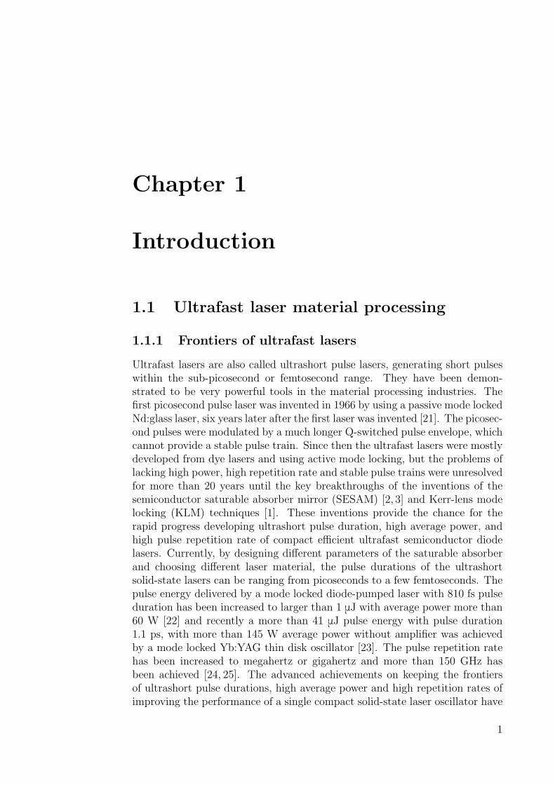
1.1.1 Frontiers of ultrafast lasers
Ultrafast lasers are also called ultrashort pulse lasers, generating short pulseswithin the sub-picosecond or femtosecond range. They have been demon-strated to be very powerful tools in the material processing industries. Thefirst picosecond pulse laser was invented in 1966 by using a passive mode lockedNd:glass laser, six years later after the first laser was invented [21]. The picosec-ond pulses were modulated by a much longer Q-switched pulse envelope, whichcannot provide a stable pulse train. Since then the ultrafast lasers were mostlydeveloped from dye lasers and using active mode locking, but the problems oflacking high power, high repetition rate and stable pulse trains were unresolvedfor more than 20 years until the key breakthroughs of the inventions of thesemiconductor saturable absorber mirror (SESAM) [2, 3] and Kerr-lens modelocking (KLM) techniques [1]. These inventions provide the chance for therapid progress developing ultrashort pulse duration, high average power, andhigh pulse repetition rate of compact efficient ultrafast semiconductor diodelasers. Currently, by designing different parameters of the saturable absorberand choosing different laser material, the pulse durations of the ultrashortsolid-state lasers can be ranging from picoseconds to a few femtoseconds. Thepulse energy delivered by a mode locked diode-pumped laser with 810 fs pulseduration has been increased to larger than 1 μJ with average power more than60 W [22] and recently a more than 41 μJ pulse energy with pulse duration1.1 ps, with more than 145 W average power without amplifier was achievedby a mode locked Yb:YAG thin disk oscillator [23]. The pulse repetition ratehas been increased to megahertz or gigahertz and more than 150 GHz hasbeen achieved [24, 25]. The advanced achievements on keeping the frontiersof ultrashort pulse durations, high average power and high repetition rates ofimproving the performance of a single compact solid-state laser oscillator have
1
Chapter 1. Introduction
opened many applications in ultrafast spectroscopies, ultra-dynamic imagingand other fields with its simplified system. However, for material processing,ultra-precise machining, especially use the nonlinear absorption process, thepeak intensity of current oscillators still not meet the needs. The excessiveheat deposited in the gain medium and large nonlinearity accumulated by thepulses during propagation challenge the current technologies on developinghigh average and high peak power ultrashort pulse oscillators. While by in-troducing the chirped pulse amplification (CPA) technique for microwave andradar technology into optics, the peak power of short pulses quickly increasedto terawatt level [26,27]. The first amplification of 100 fs pulses in a solid-stateamplifier was demonstrate in 1991 [28] followed by progress in a kilohertz rep-etition rate amplifiers [29]. Based on these achievements and the concepts ofCPA, further pulse shortening as well as the boosting of the pulse energy andaverage power have been improved by many orders of magnitude. High peakpower have been reached to the petawatt level based on the CPA technique ata moderate average power [30–33] and approaching kilowatt level of averagepower with moderate peak power pulses [34,35]. The improvements on pushingthe cutting edge limits of ultrashort pulse duration, ultrahigh repetition rate,ultrahigh pulse energy have led the way to continue reducing the photon-cost ofultrafast laser systems and open doors for material processing and machiningindustries, especially the applications for micro/nano-photonics.
1.1.2 State of the art of femtosecond laser processing
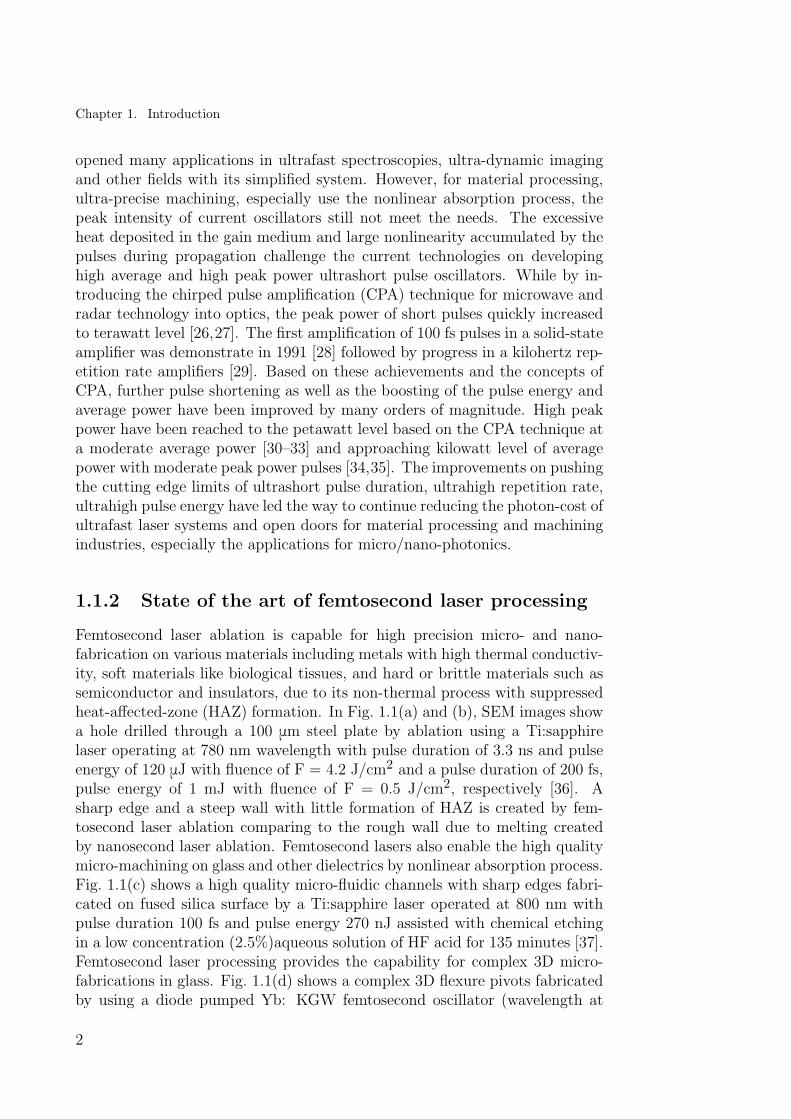
Femtosecond laser ablation is capable for high precision micro- and nano-fabrication on various materials including metals with high thermal conductiv-ity, soft materials like biological tissues, and hard or brittle materials such assemiconductor and insulators, due to its non-thermal process with suppressedheat-affected-zone (HAZ) formation. In Fig. 1.1(a) and (b), SEM images showa hole drilled through a 100 μm steel plate by ablation using a Ti:sapphirelaser operating at 780 nm wavelength with pulse duration of 3.3 ns and pulseenergy of 120 μJ with fluence of F = 4.2 J/cm2 and a pulse duration of 200 fs,pulse energy of 1 mJ with fluence of F = 0.5 J/cm2, respectively [36]. Asharp edge and a steep wall with little formation of HAZ is created by fem-tosecond laser ablation comparing to the rough wall due to melting createdby nanosecond laser ablation. Femtosecond lasers also enable the high qualitymicro-machining on glass and other dielectrics by nonlinear absorption process.Fig. 1.1(c) shows a high quality micro-fluidic channels with sharp edges fabri-cated on fused silica surface by a Ti:sapphire laser operated at 800 nm withpulse duration 100 fs and pulse energy 270 nJ assisted with chemical etchingin a low concentration (2.5%)aqueous solution of HF acid for 135 minutes [37].Femtosecond laser processing provides the capability for complex 3D micro-fabrications in glass. Fig. 1.1(d) shows a complex 3D flexure pivots fabricatedby using a diode pumped Yb: KGW femtosecond oscillator (wavelength at
2

1.1. Ultrafast laser material processing
1030 nm, pulse duration 380 fs, repetition rate 860 kHz, speed 5 mm/s andpulsed energy 215 nJ focused by NA 0.4 objective) and followed by chemicaletching in HF bath (2.5% concentration) for 18 hours in a 500 μm thick fusedsilica sample [38]. Complex micro-mechanical systems can be fabricated usingfemtosecond laser processing.
(a)
(c)
(b)
(d)
30 μm 30 μm
30 μm
200 μm
Figure 1.1: Hole drilled through a 100 μm steel plate by a Ti:sapphire laserpulses at 780 nm with a pulse duration of 3.3 ns, pulse energy of 120 μJ withfluence of F = 4.2 J/cm2 (a) and a pulse duration of 200 fs, pulse energyof 1 mJ with fluence of F = 0.5 J/cm2 (b) [36]; (c) Micro-channels ablatedon the fused silica surface by a Ti:sapphire laser operating at 800 nm, withpulse width 100 fs, pulse energy 270 nJ followed by chemical etching in a lowconcentration (2.5%)aqueous solution of HF acid for 135 minutes [37]; (d) A3D micro-mechanical cross-spring pivot fabricated from a 500 μm thick silicaby a diode pumped Yb: KGW femtosecond oscillator (wavelength at 1030 nm,pulse duration 380 fs, rapetition rate 860 kHz, speed 5 mm/s and pulsed energy215 nJ focused by NA 0.4 objective) and followed by chemical etching in HFbath (2.5% concentration) for 18 hours [38].
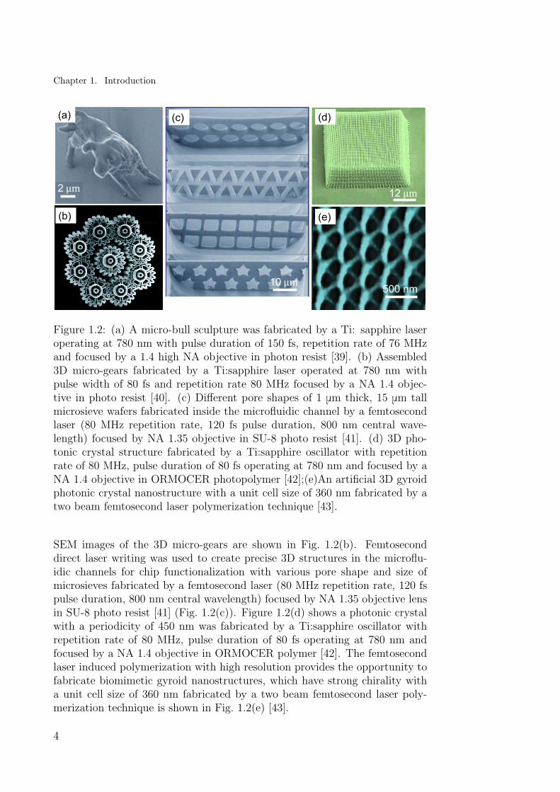
Apart of 3D complex structures fabrication in glass associated with chem-ical etchings, high resolution of direct polymerization in photo resist enabledby the nonlinear absorption process can be used to create nanoscale complex3D structures. Figure 1.2(a) shows a first demonstration of sub-diffraction-limit resolution of a 3D micro-bull sculpture fabricated by a Ti:sapphire fem-tosecond laser operated at 780 nm wavelength with a 150 fs pulse durationat 76 MHz repetition rate, tightly focused by a NA 1.4 objective lens [39].Complex 3D fabrication of assembled series of micro-gears were fabricated bya Ti:sapphire laser operated at 780 nm with pulse width of 80 fs and repe-tition rate 80 MHz focused by a NA 1.4 objective in photo resist [40]. The
3
Chapter 1. Introduction
12 μm
(a)
(b)
(d)(c)
(e)
500 nm10 μm
2 μm
Figure 1.2: (a) A micro-bull sculpture was fabricated by a Ti: sapphire laseroperating at 780 nm with pulse duration of 150 fs, repetition rate of 76 MHzand focused by a 1.4 high NA objective in photon resist [39]. (b) Assembled3D micro-gears fabricated by a Ti:sapphire laser operated at 780 nm withpulse width of 80 fs and repetition rate 80 MHz focused by a NA 1.4 objec-tive in photo resist [40]. (c) Different pore shapes of 1 μm thick, 15 μm tallmicrosieve wafers fabricated inside the microfluidic channel by a femtosecondlaser (80 MHz repetition rate, 120 fs pulse duration, 800 nm central wave-length) focused by NA 1.35 objective in SU-8 photo resist [41]. (d) 3D pho-tonic crystal structure fabricated by a Ti:sapphire oscillator with repetitionrate of 80 MHz, pulse duration of 80 fs operating at 780 nm and focused by aNA 1.4 objective in ORMOCER photopolymer [42];(e)An artificial 3D gyroidphotonic crystal nanostructure with a unit cell size of 360 nm fabricated by atwo beam femtosecond laser polymerization technique [43].
SEM images of the 3D micro-gears are shown in Fig. 1.2(b). Femtoseconddirect laser writing was used to create precise 3D structures in the microflu-idic channels for chip functionalization with various pore shape and size ofmicrosieves fabricated by a femtosecond laser (80 MHz repetition rate, 120 fspulse duration, 800 nm central wavelength) focused by NA 1.35 objective lensin SU-8 photo resist [41] (Fig. 1.2(c)). Figure 1.2(d) shows a photonic crystalwith a periodicity of 450 nm was fabricated by a Ti:sapphire oscillator withrepetition rate of 80 MHz, pulse duration of 80 fs operating at 780 nm andfocused by a NA 1.4 objective in ORMOCER polymer [42]. The femtosecondlaser induced polymerization with high resolution provides the opportunity tofabricate biomimetic gyroid nanostructures, which have strong chirality witha unit cell size of 360 nm fabricated by a two beam femtosecond laser poly-merization technique is shown in Fig. 1.2(e) [43].
4

1.2. Background of femtosecond laser processing
In summary, the unique characteristics of femtosecond laser processing withhigh quality surface micromachining and patterning and complex 3D structur-ing in glass or polymerization in photo resist with high resolution offer a widerange of practical applications in photonics.
1.2 Background of femtosecond laser
processing
1.2.1 Ultrafast laser-material interactions
Ultrafast laser material processing initiates with the single photon or multi-photon electronic excitations flowing with series of complex energy-exchangeprocesses which may result to varying combinations of outcomes from theseprocesses, like ion displacement, amorphization, recrystallization, ablation, lo-cal electronic structure modification, changes in material composition [44]. Theconfinement of energy deposition in focused spatial volume and ultrashort timedomain localized the absorption energy by suppressing the energy dissipation.The thermal diffusion length ld of the ultrafast laser-material interaction withpulse duration sufficiently shorter comparing to the electron-phonon couplingtime, for most of the metals is of the order of picoseconds [45]. When thematerial is heated to near the melting point Tim by irradiation, the ld can beestimated by [46,47]:
ld =
[128
π
]1/8 [ DCi
Timγ2C′e
]1/4
, (1.1)
where D is the thermal conductivity, Ci is the lattice heat capacity, C′e = Ce/Te
(Ce is the electron heat capacity and Te is the electron temperature) and γ isthe electron-phonon coupling constant [47]. For example, when gold is heatedup to its melting point 1337K, the thermal diffusion length ld is estimated to be313 nm [47]. For nonmetals, the penetration depths are much greater than thatfor metals with less spatial confinement and stress constraint are not solid evenwhen thermal confinement is guaranteed. The complex excitation and relax-ation processes involved during and after femtosecond laser irradiation for met-als, semiconductors and insulators are schematically shown in Fig. 1.3 [44,48].Unlike the longer pulse laser-matter interactions, which strongly dependenton the equilibrium thermal-dynamics of the irradiated area, the femtosecondpulse irradiation can be explained from the excitation density which considersthe quantized energies deposited per unit volume and unit time. Combiningthe excitation density and the electron-phonon coupling strength, the outcomeof the ultrafast laser-material interaction processes can be mostly determined.
5

Chapter 1. Introduction
electron-lattice heating
free-carrier generation
non-thermal melting
self-trapping lattice
distortion
bond-breaking and ablation
heterogeneous melting
homogeneous melting
e-h plasma
Metals Semiconductors Insulators
Intensityelectron-phonon coupling strength
fs
ps
ns
overcritical fluid
localized lattice relaxation
laser-electron heating
Figure 1.3: Schematics of the typical timescales and intensity ranges of physicalphenomena and processes occurring during and after the ultrafast laser pulseirradiation on a metal, semiconductors and insulators, indicating the initialexcitation duration and various energy-exchange and relaxation processes [44,48].
Metals
Due to the short pulse duration comparing to the electron-phonon couplingtime of femtosecond laser-matter interaction, the excitation of free-free transi-tions of conduction band electrons rapidly reach a high temperature far abovethe the normal equilibrium melting temperature by the end of the laser pulses.The normal crystalline phase will be disrupted and replaced by a disorderedliquid phase within a few picoseconds by the electron-phonon coupling, withthe electrons coming to the thermal equilibrium with the lattice. The processof laser energy transferring to the electrons and then from electrons to thelattice can be depicted by a two-temperature model [49]. If sufficient energyis deposited on the surface of a metal by a femtosecond laser pulse, ablationof the metal occurs initiating by a superheated phase in the irradiated regionunder high pressure and temperature. This superheating leads to a bubbleformation in tens of picoseconds. As the material near the surface starts anisentropic expansion into the environment, a two-phase mixture of vapor andliquid is formed. In this process, the speed of the sound is dramatically de-creased and the mixture phase expands into the environment. Because of theenergy conservation, it is possible that the ablation can occur without creationof a large HAZ as shown in Fig. 1.1 (a) and (b) comparing with a nanosecond
6

1.2. Background of femtosecond laser processing
laser ablation on a steel plate [36].
Semiconductors
Semiconductors are different from metals, due to a finite band gap and alarger electron-phonon coupling strength resulting in different interactions ofultrafast laser with semiconductors as compared with metals. The band-to-band transitions can be induced by the photons with larger energies than theband gap even at low irradiation fluence. The existing surface states or defectsin the band gap provide additional absorption bands that can facilitate thefree carrier excitation with lower photon energies, comparing to the perfectmaterial. Unlike the metals, nonlinear absorption process can also play a rolein the free carrier excitation by intense ultrafast laser pulse irradiation on wideband gap semiconductors. The density of the hot electron-hole (e-h) pairs canreach to a near-metallic conditions and create an electron-hole plasma. Thedensity of the laser excited electron-hole plasma plays an important role onthe final outcomes of material structure and the dynamic evolution during andafter the laser irradiation.
Insulators
Femtosecond laser pulses under tightly focusing can easily reach the peak inten-sity larger than 100 TW/cm2, which can result in strong nonlinear absorptionand is sufficient to induce optical ionization and even optically breakdown inwide band gap insulators. For wide band gap dielectrics, the photon energy offemtosecond laser with the visible or near-infrared wavelength is not sufficientto excite free electrons by linear absorption process. Instead, the valence elec-trons are excited to the conduction band through non-linear photoionization,like multiphoton ionization and tunneling photonionization depending on thelaser repetition rate and intensity. In the regime of high laser intensity andlow frequency, electron can be excited to the conduction band by the tunnelingionization due to the potential energy is strongly distorted by the intense elec-tric field and decrease the barriers for free electron generation rather by themultiphoton absorption (MPA). The nonlinear absorption process induced byan intense femtosecond laser pulse interacting with wide band gap insulatorsis shown schematically in Fig. 1.4. The probability of each process (MPA andtunneling ionization) in the femtosecond laser interaction with insulators canbe determined by the Keldysh parameter [50]:
γ =ω
e
√mecnε0Eg
I, (1.2)
where ω is the laser frequency, I is the laser intensity at the focus, me is theeffective electron mass, e is the fundamental electron charge, c is the speed oflight, n is the linear refractive index, Eg is the band gap of the material and ε0is the permittivity of free space. If γ << 1.5, tunneling ionization dominates,
7

Chapter 1. Introduction
and γ >> 1.5, the nonlinear absorption process is dominated by MPA, whenγ ∼ 1.5, photoionization is a combination of tunneling and multiphotonionization.
valence band Distance from nucleus
Ene
rgy
MPA Tunneling Ionization
Nonlinear absorption
ℎ𝑣 < 𝐸𝑔
conduction band
Figure 1.4: Schematics of the nonlinear absorption process of multiphotonabsorption (MPA) and tunneling ionization of ultrafast laser interaction withwide band gap insulators [47].
1.2.2 Structural relaxation and modification
The optically induced ionization from absorbing femtosecond laser pulses gen-erates free electrons, and energy then is transfered to the lattice by the elec-tron phonon coupling. The following physical processes including the thermalhydrodynamics, amorphization, recrystallization, ablation and structure mod-ification, which result to the final changes of morphology of the material. Thestructural modifications and morphology changes depend not only on the laserirradiation parameters such as pulse energy, fluence, scan speed, repetitionrate, wavelength, polarization, focal length and others, but also rely on thematerial properties, such as band gap, thermal conductivity, refractive indexand others. In dielectrics, three types of structural changes were observed,refractive index change, form birefringence refractive index modification andvoids formation, additional absorption bands in the band gap were commonlyobserved due to the induced structural defects by the ultrafast laser-materialinteraction [51–53].
8

Chapter 2
Experimental and Techniques
2.1 Femtosecond laser system
The advanced femtosecond laser structuring on the micro and nanoscale wasintroduced previously. With its unique properties, by optimizing the fabri-cation conditions including the wavelength, focal length, pulse energy, repe-tition rate, scan speed on different materials, the desired morphology or thestructural modification can be precisely delivered. In this project, the defectengineering inside wide band gap dielectrics and induced birefringence, DLWsurface patterning, 3D polymerization in photo resist, stress engineering in-side glass, induced uniform periodic nanostructures, induced nano-voids, andnano-jets are investigated for applications in optics and photonics.
LampCCD
Pharos
HWP
1030 nm
515 nm 257 nm
HWP
2D Motorized stage
Collimator
Figure 2.1: Schematics and photo of the femtosecond laser fabrication systemused in this project.
9

Chapter 2. Experimental and Techniques
200 nm 200 nm
(a)
1μm
1μm
200 nm
(d)
(e)
(f)
(g)
20μm
(b)
20μm
(c)
1μm
1μm
1μm
(d)
(e)
(f)
Figure 2.2: (a) Nano-ring structure with ring width around 250 nm fabricatedby single pulse irradiation on a silicon wafer; 1030 nm wavelength, focused bya NA 0.5 objective lens, pulse energy 54 nJ. (b) Nano-jet structure fabricatedby single pulse irradiation on a 50 nm Au film deposited on a cover glass;515 nm wavelength, focused by a NA 0.5 objective lens, pulse energy 1.7 nJ.(c) Precise structuring on a nano-textured silicon surface using femtosecondlaser operating at 1030 nm focused by a NA 0.7 objective lens, with repetitionrate of 100 kHz, scanning speed of 1 mm/s and with pulse energy 100 nJ.(d)Nanograting structures on 100 nm thick amorphous silicon film deposited onfused silica substrate fabricated by 257 nm wavelength beam focused by NA 0.4objective lens, scanning speed of 0.1 mm/s, with pulse energy of 0.01 nJ andpulse density of 50 pulses/μm. (e) Grating on 100 nm thick amorphous siliconfilm deposited on fused silica substrate fabricated by 257 nm wavelength beamfocused by a NA 0.4 objective lens, scanning speed of 0.1 mm/s, with pulseenergy of 1.08 nJ and pulse density of 20 pulses/μm. (f) A SZ2080 polymerizedspin-orbital coupler fabricated by 515 nm beam focused by a NA 1.4 objectivelens, pulse energy of 0.125 nJ, with scanning speed 0.1 mm/s and repetitionrate 200 kHz. (g) A direct ablated diffractive grating element on sapphiresubstrate by 257 nm beam focused by a NA 0.4 objective lens, pulse energy4.25 nJ, with scanning speed 1 mm/s and repetition rate of 100 kHz.
The femtosecond laser fabrication system used in this PhD project was
10

2.2. Nano-lithography and nanofabrication techniques
designed and built by combining the advanced stage controlling and commer-cially available laser system, which integrated with a Yb:KGW PHAROS laser,highly precise motorized stages, and controlling software. PHAROS is basedon the chirped pulse amplification and delivers up to 200 μJ per pulse andwith maximum 600 kHz repetition rate, using the seed oscillator, regenera-tive amplifier and pulse stretcher and compressor. It also equipped with twowavelength converters providing high power of second harmonic wavelengthat 515 nm and fourth harmonic at 257 nm. The pulse duration of this laseris tunable from 230 fs to 10 ps. The fundamental wavelength is centered at1030 nm. Three motorized attenuators and three polarization rotators wereintegrated. The schematic and photo of the femtosecond laser fabrication sys-tem are shown in Fig. 2.1. Few examples fabricated by using this laser systemwere shown in Fig. 2.3, including the nano-ring structures fabricated by singlelaser irradiation on silicon wafer, nanojets fabricated on 50 nm Au film, precisescribing on silicon nano-textured surface, nanogratings on silicon film, directablated gratings, photo-polymerized spin-orbital couplers in SZ2080 and di-rect ablated spin-orbital coupler on sapphire surface. The detailed fabricationconditions were depicted in Fig. 2.3.
2.2 Nano-lithography and nanofabrication
techniques
In this project, different nanofabrication techniques were used during the sam-ple preparation and fabrication process even though the main fabrication toolis femtosecond laser fabrication system. Among different nanofabrication tech-niques, they can be classified into two main types, top-down and bottom up.Both types have their unique advantages in different applications. The bottom-up is thought to be a cost effective approach with high quality of structuring,due to its layer by layer structuring applying the chemical and physical proper-ties. However this approach cannot be used for fabricating the nanostructureswith complex geometry and precise alignment. In this project, only the physi-cal vapour deposition was employed as the bottom-up approach for preparingdifferent film samples and for SEM characterization. Complex patterning orstructuring is better realized with top-down techniques, such as optical, fo-cused ion beam lithographies and reactive ion etching.
2.2.1 Photolithography
The dramatic increase in speed of the information processing and highly com-pact integration demand from the microelectronic industry, drive the inno-vation and progressing on the high resolution, high throughput lithographytechnologies which replicate a pattern rapidly from chip to chip, wafer towafer with effective cost. While the conflict on large scale manufacturing with
11

Chapter 2. Experimental and Techniques
nanoscale resolution is the main issue for many high resolution lithographytechnologies like electron, focused ion beam and probe scanning lithographytechniques. The Photolithography is widely applied in the semiconductor in-dustry for manufacturing microelectronics and optical devices due to its highthroughput [54].
+
pre-bake @95° 2.5 min
@100° 45 s
UV exposure (5s)
locate b-Si
hard bake @95°2.5 min
& development
PDMS glass slide teflon holder
PDMS Press b-Si
pattern transfer and bonding
AZ1518 SU8-2010
final device
Figure 2.3: The detailed processes for using photolithography to fabricate anintegrated black silicon (b-Si) microfluidic chip using positive and negative re-sist (AZ1518 and SU8-2010). The contact method was used with mask directlyaligned on the substrate. This microfludic chip was designed for testing thebactericidal effectiveness [55].
Photolithography uses light sensitive resist coated on the substrate andexposed under blue or ultraviolet light which can be selectively dissolved underspecific development [56]. Both positive and negative resist are available forphotolithography, where material removed under development is in the exposedand unexposed area. The patterns delineated on the resist are defined by thephotomask which selectively blocks the illumination light. There are threetypes of exposure methods, contact, proximity and projection. The contactmethod is directly put the mask on the substrate which is liable to damagethe mask and substrate. The proximity method leaves a gap between maskand substrate, due to the diffraction when light passing through the mask andprojecting on the substrate, the resolution of the proximity method is lowercomparing to the contact method. In most of the commercial photolithographysystem, the projection exposure method is employed. The fundamental limitof the resolution of a projection exposure system is determined by the Rayleigh
12

2.2. Nano-lithography and nanofabrication techniques
scaling equation [57]:
R = k1λ/NA,
DOF = K2λ/NA2,(2.1)
where R is the resolution and DOF is the corresponding depth of focus, λ isthe exposure wavelength, NA is numerical aperture of the optical system, andk1, k2 are the constant that dependent on the projection system, the resistmaterial, and the process. To obtain higher resolutions, shorter wavelengthand higher NA system are required. When high NA is used, the depth offocus becomes very small and the exposure process becomes very sensitive tothe height variation of the stage, uniformity of the resist thickness and theroughness of the substrate. The wavelength of the light source was developedfrom 436 nm (G line Hg lamp) to 248.3 nm (KrF laser), 157.6 nm (F2 laser) toextreme ultraviolet (EUV) 13.5 nm wavelength, which can achieve sub-10 nmresolution [54,58].
The process for photolithography is typically involving substrate prepara-tion, photoresist coating, pre-bake, exposure, post bake, development and dry.One example is shown in Fig. 2.3 on using photolithography to fabricate mi-crofludic chips using both positive (AZ1505) and negative (SU8-2010) resist.The mask was directly located on the substrate which was spin-coated on aglass substrate. The height of the patterned structure is determined by thethickness of the coated resist. After the delineated pattern is hard baked, thePolydimethylsiloxane (PDMS) solution is poured into a sealed teflon holderand bonded with a cover slide on a hotplate. The final device is shown inFig. 2.3, which was designed for bactericidal efficiency test in the enclosedmicrofluidic dynamic environment integrated with a nanotextured b-Si, whichwas demonstrated effectively bactericidal activity on the nanotexture Si sur-faces [55].
1 μm 100 nm
(a) (b)
Figure 2.4: SEM images of a cross-sectioned femtosecond laser inducednanograting on silicon wafer (a) and femtosecond laser induce nanobump on50 nm Au film (b) by FIB. Image courtesy by X. Li.
13

Chapter 2. Experimental and Techniques
2.2.2 Focused ion beam lithography
A focused ion beam (FIB) lithography tool is built and operated similarly toan electron beam lithography. It is used to fabricate masks for EUV or X-raylithography or write patterns in resist on substrate or directly write patternson substrate by deposit energy through ions rather electrons with down to sub-10 nm resolution [59]. The mechanism of energy exchange between resist andfocused ion beam is dependent on the deposition fluence and the mass of ions,namely, for ions with low or high mass to energy ratio, the energy exchangeis by electronic interaction and nuclei motion [60]. The most advantages ofthe FIB lithography is its maskless writing capability which can be used toremove material locally without damaging the rest. It is widely used for samplepreparation for the high resolution for transmission electron microscopy (TEM)specimens [61]. The material removal rate is dependent on the target material,primary ion species, their energy and incident angle of the ion beam. Henceit is very useful for cross-section cutting for characterizing nanostructures,e.g. the characterization of the thickness of the induced nanograting by UVfemtosecond laser irradiation on silicon wafer and the investigation of masstranslative redistribution of Au film under tighly focused femtosecond pulsemade by the FIB cross sectioning, shown in Fig 2.3.
2.2.3 Physical vapour deposition
Physical vapour deposition (PVD) is a bottom-up method, where the particlesfrom the target material to be deposited on the substrate layer by layer will betransformed into gaseous state by a physical process, thermal evaporation, orsputtered by high energy ion or electron impact. For thermal evaporation, thekenetic energy of atoms or molecules dependents on the evaporation temper-ature which allows most of the atoms and molecules be able to overcome theseparation energy and separation by heating. By high energy of ion or electronbombardment of ions, surface particles and second electrons will come off fromtarget and deposit on the substrate. An electron beam with electrons emittedfrom a thermal source and accelerated to the target material by strong mag-netic field or high voltage is commonly used to bombard the target materialand induce evaporation. High energy of argon ion plasma is induced close tothe target material with an direct current (DC), alternating current (AC) orradio frequency (RF) oscillating electric field between the plasma source andtarget material to accelerate the ion energy in order to achieve higher sput-tering efficiency [62, 63]. When the mean free path of the evaporated atomsand molecules is larger than the dimension of the vacuum chamber, the di-rectional condensation of the deposited atoms on the substrate and chamberwall occur if the operating pressure is lower, due to the high supersaturation ofdepositing atoms at a certain substrate temperature comparing with the equi-librium pressure [64]. This directional deposition can result in inhomogeneouscoating on most of the structured substrate and will cause the formation of
14
2.2. Nano-lithography and nanofabrication techniques
shadow effect. The directional motion of the depositing atoms and moleculescan be solved under higher pressure. Therefore, the argon plasma ignited thetarget material deposition process which requires high operating pressure, hasdiminished direction deposition and shadow effect, and the electron beam evap-oration process has more directional deposition for sputtering. In this project,the magnetron sputtering and electron beam evaporation were employed fortitanium, indium tin oxide (ITO), silicon, or alloy films preparation.
2.2.4 Reactive ion etching
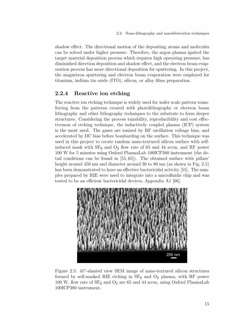
The reactive ion etching technique is widely used for wafer scale pattern trans-ferring from the patterns created with photolithography or electron beamlithography and other lithography techniques to the substrate to form deeperstructures. Considering the process tunability, reproducibility and cost effec-tiveness of etching technique, the inductively coupled plasma (ICP) systemis the most used. The gases are ionized by RF oscillation voltage bias, andaccelerated by DC bias before bombarding on the surface. This technique wasused in this project to create random nano-textured silicon surface with self-induced mask with SF6 and O2 flow rate of 65 and 44 sccm, and RF power100 W for 5 minutes using Oxford PlasmaLab 100ICP380 instrument (the de-tail conditions can be found in [55, 65]). The obtained surface with pillars’height around 450 nm and diameter around 30 to 80 nm (as shown in Fig. 2.5)has been demonstrated to have an effective bactericidal activity [55]. The sam-ples prepared by RIE were used to integrate into a microfluidic chip and wastested to be an efficient bactericidal devices, Appendix A1 [66].
200 nm
Figure 2.5: 45◦-slanted view SEM image of nano-textured silicon structuresformed by self-masked RIE etching in SF6 and O2 plasma, with RF power100 W, flow rate of SF6 and O2 are 65 and 44 sccm, using Oxford PlasmaLab100ICP380 instrument.
15

Chapter 2. Experimental and Techniques
2.3 Structure characterization
Different techniques were employed to characterize the fabricated micro/nano-structures from the morphology to optical property characterization in thisproject. The common morphology characterization techniques with sub-10 nmresolution used in this project are the scanning electron microscope (SEM)and atomic force microscope (AFM), which are widely used in the micro/nanomanufacturing research and industry. SEM provides images with informationof the sample’s topography and composition [67]. The electron source canbe a tungsten filament, a Schottky emitter or a tungsten field emission tip.The electrons are accelerated by high voltage (normally less than 30 kV forSEM) and then is focused to a diameter of 10 nm or even 1 nm beam by anaxially symmetric magnetic lens. By raster scanning the electron beam onthe sample surface, the secondary electrons (SE) or back-scattered electrons(BSE) escaped from the sample surface can be collected and used to excitephotons to generate SEM images that carry the information of the sampletopology and composition. Several parameters which influence the resolutionand quality of the SEM images, can be controlled with the SEM operator,like the acceleration voltage, working distance, diameter of the aperture. Theacceleration voltage determines the kinetic energy of the primary electronsand its penetration depth, thus affects the information depth of the SEMimages [68]. The quality of SEM images also dependent on the focus andastigmatism of the probe electron beam. The astigmatism of the beam canbe reduced to zero by adjusting the angle of the tilt in x- and y-planes. Thecharging effect will be an issue for inspect the insulating materials, due tothe specimen current Is (Is = Ip – IBSE – ISE, where Ip is the primary-beamcurrent and is constant, IBSE and ISE are varying during the probe scanning)cannot connect to the ground, and then undergoing an electrostatic chargingduring scanning [69]. The value of the specimen current Is can be positive andnegative, and it causes imaging artifacts when it is negative which will repel theincident electrons and deflect the probe beam, which can cause distortion andbrightness fluctuation on the SEM image. However, the charging problems canbe resolved by coating a 5 to 10 nm conductive film of metal or carbon. Fig. 2.6shows the SEM images of a laser polymerized SZ2080 spin splitter structure,with the magnification of ×700, working distance 10 mm, and aperture 30 μm,the acceleration voltage is 5 kV. In Fig. 2.6(a) the sample was not coated byany conductive film and charging was affecting the quality of the SEM images,even using the SE image. The charging effect was avoided when sample wascoated with a 5 nm Ti film as shown in Fig. 2.6(b), using the BSE image.When the coating of conductive film is not desirable, the charging effect canbe reduced by selecting optimized acceleration voltage, since the IBSE and ISEare dependent on the kinetic energy of the incident primary electrons.
Comparing to the high operation environment requirements with vacuumof SEM, AFM owing sub-nm resolution has been applied to a wide range of
16

2.4. Appendix A
(a) (b)
40μm
Figure 2.6: SEM images of a laser polymerized SZ2080 spin splitter fabricatedon the cover glass substrate under magnification of ×700, with an accelerationvoltage of 5 kV, aperture 30 μm in diameter and working distance at 10 mm.(a) SE image of SZ2080 structure with strong charge effect, (b) BSE image ofSZ2080 structure coated with 5 nm Ti film to remove specimen current.
disciplines, including solid-state physics, semiconductor science and technol-ogy, molecular engineering, polymer chemistry, molecule and cell biology andmedicine. This technique was introduced in 1986 based on the scanning tun-neling microscope and reported a sub-nm resolution in the air [70]. Withoptimizing the measurement field and scan speed, high resolution 3D surfacemorphology map can be created. Another morphology measurement techniquethat was used in this project is the 3D optical profilometer which has verti-cal resolution in sub-100 nm and a lateral resolution in sub-micrometer rangewhich depends on the resolution of the sample stage. Both of the AFM and3D optical profilometer were used to characterize the surface morphology ofthe laser scribed silk film, in Appendix A1. This tool was developed basedon the white light interferometry [71]. High precision profilometer with fasterscan speed and larger measurement range is very suitable for most of the ap-plications in the surface topology measurement in this project.
2.4 Appendix A
This section contains the published papers related to few examples appliedthe femtsecond laser fabrication techniques and other nanofabrication andnanocharacterization techniques as well as the applications in bio-microfludicsand bio-materials.
17

Chapter 2. Experimental and Techniques
A1: X. W. Wang, C. M. Bhadra, T. H. Y. Dang, R. Buividas, J.Wang, R. J. Crawford, E. P. Ivanova and S. Juodkazis. A bactericidal microflu-idic device constructed using nano-textured black silicon. RSC Advances, 6,26300-26306, 2016.
Nanotetured black Si fabricated by reactive ion etching was integrated intomicrofluidic device. This microfluidic device shows very efficient bactericidalactivity and effective extraction of cellular protein from the ruputured E. colibacterial cells.
18
A bactericidal microfluidic device constructedusing nano-textured black silicon
Xuewen Wang,†ab Chris M. Bhadra,†a Thi Hoang Yen Dang,a Ricardas Buividas,a
James Wang,a Russell J. Crawford,a Elena P. Ivanova*a and Saulius Juodkazis*ab
Nano-structured black silicon (bSi) was used as a substratum for the construction of a microfluidic device to
test the bactericidal action of this nano-textured surface against Pseudomonas aeruginosa bacteria. A
narrow 15 mm high and 1 cm wide flat flow channel was constructed that allowed the bacteria to come
into contact with the bactericidal nano-spikes present on the surface of the bSi. The narrow channel
within the device was designed such that a single layer of bacterial cells could reside at any given time
above the bSi substratum during flow. The large 1 � 2 cm2 surface area of the bSi was shown to be
efficient in being able to kill the bacterial cells, achieving an approximate 99% killing efficiency. The flow
rate required to fill the bSi chamber was found to be 0.1 mL s�1, with a 10 min equilibration time being
allowed for the bacterial cells to interact with the bSi surface. Complete rupturing of E. coli cells was
achieved after 15 cycles, allowing the effective release of cellular proteins from within the bacterial cells
(65.2 mg mL�1 from 3 � 108 cells per mL). The channel was then able to be re-used after washing of the
cell with 10 successive cycles of sterile MilliQ water. Larger volumes of bacterial suspensions have the
potential to be treated using a similar flow channel configuration if the dimensions of the flow channel
are scaled accordingly. This bactericidal microfluidic device provides a novel platform for studies carried
out under both static and dynamic (flow) conditions.
Introduction
Antibacterial surfaces1–3 are becoming imperative in applica-tions designed to curb the negative consequences associatedwith resistance to antibiotics present in food, water, and soil.4
Bacterial resistance arising from extensive exposure to antibi-otics has the potential to compromise our immune system,particularly with regard to our ability to effectively resistbacterial infections. Many natural and synthetic surfaces ach-ieve their self-cleaning, anti-fouling and/or bactericidal prop-erties through various mechanisms; they can be highlyoxidative, becoming bactericidal when activated by UV-light5
self-cleaning due to their surfaces being rendered hydrophobicvia modication of their chemical or mechanical properties,6–8
or anti-fouling due to their surface structures stericallyhindering the attachment of pathogens.4,9 Other applications ofmicro- and nano-structured surfaces in the biomedical industryinclude dermal patches, which possess painless needles thatallow the controlled release of drugs, and bandages that possessbio-compatible microbers that trigger increased levels of
healing when exposed to ultraviolet UV light.10 Surfaces thatdisplay mechanical means for antifouling and antibacterialproperties are a topic of signicant research as they providea substrate from which a fundamental understanding of themechanism takes place.11–14 These surfaces have wide applica-tions in the production of sanitary surfaces such as mobiletelephones and other household items.15
The search for inexpensive methods for the fabrication oflarge area nano-textured surfaces is currently underway. Siliconis a substratum that has been used extensively in the semi-conductor and solar cell industries.16–20 Being a relatively inex-pensive product, silicon represents one of the best substrata forthe fabrication of large areas of nano-textured surfaces, wherereproducible surfaces are currently able to be prepared oversurfaces of several centimetres in diameter. Such substrata canalso have electrical and photo-electrochemical device levelfunctionalities incorporated into their surface, which is usefulwhen producing micro-chips.21 Methods for preparing thesenano-textured surfaces using a silicon substratum includeplasma etching, where the deposition of electrical contacts isrequired for the fabrication of wafer sized bSi surfaces.22–26 Theunique nano-topography of bSi forms due to the self-organizedhard mask that results from the rst few seconds of etching.These are specic to the chemistry and chamber materialsbeing used for the production of the bSi.27 It is used in highlyefficient solar cells, as it represents a low reectance or
aFaculty of Science, Engineering and Technology, Swinburne University of Technology,
John St., Hawthorn, Vic. 3122, Australia. E-mail: [email protected]; eivanova@
swin.edu.au; Fax: +61 3 9214 5435; Tel: +61 3 9214 8718bMelbourne Centre for Nanofabrication (MCN), Australian National Fabrication
Facility (ANFF), Clayton, VIC 3168, Australia
† X. W. W. and C. M. B. have contributed equally.
Cite this: RSC Adv., 2016, 6, 26300
Received 11th February 2016Accepted 24th February 2016
DOI: 10.1039/c6ra03864f
www.rsc.org/advances
26300 | RSC Adv., 2016, 6, 26300–26306 This journal is © The Royal Society of Chemistry 2016
RSC Advances
PAPER
Publ
ishe
d on
01
Mar
ch 2
016.
Dow
nloa
ded
by S
win
burn
e U
nive
rsity
of T
echn
olog
y on
26/
04/2
017
09:1
1:34
.
View Article OnlineView Journal | View Issue
2.4. Appendix A
19

broadband absorbing surface. More recently it has been usedfor the production of sensors that are based on surfaceenhanced Raman scattering (SERS).28 bSi substrata haverecently been produced that possess a similar surface topog-raphy to that of dragony wings, and have been found to exhibita similar bactericidal efficiency when coming in contact withpathogenic bacteria and spores.29
Given this demonstrated bactericidal functionality of the bSisurface, a microuidic device was constructed incorporatinga bSi substrate to investigate whether this bactericidal actionwould be effectively translated within a ow channel ofa microuidic device. Applications of such devices, if effective,would be of great benet in many different elds, such as in thepharmaceutical industry for the detection and/or monitoring ofbacterial contamination.
Experimental
The bSi was prepared using a plasma etching process.28,30 AnOxford PlasmaLab 100 ICP380 plasma etcher was used forpatterning the surface of p-type boron-doped 4-inch diametersilicon wafers of specic resistivity 10–20 U cm�1, havinga h100i oriented surface (Atecom Ltd, Taiwan). The resultingsurface possessed pencil-like nano-spikes that were approxi-mately 500 nm in height and 95 nm in pillar diameter (at halfmaximum). The lateral distribution was relatively random, witha distance between neighbouring spikes being approximately450 � 200 nm. The lateral distribution of the needles wasdetermined from fast Fourier transform (FFT) processing of theSEM images (Fig. 1(a)). The static water contact angle on the bSiwas measured to be approximately 101�, displaying a similarhydrophobicity to that previously reported for bSi preparedunder the same conditions.29,31 Unmodied silicon wafers wereused as control surfaces.
The bSi and silicon wafers were precisely cut using a femto-second laser (Pharos, Light Conversion Ltd.) at a wavelength ofl¼ 515 nm, pulse duration of 230 fs, pulse energy 7 mJ per pulseat repetition rate of 100 kHz and scan speed 1 mm s�1. Theresulting wafer was mounted on 3-axis stage with 5 nm repeti-tion accuracy (Areotech Ltd.). The beam was focused to a 0.9 mmspot by an objective lens with a numerical aperture NA ¼ 0.7(d ¼ 1.22l/NA). The line scribing process was repeated 7 timesand took 40 min to scribe a single 4-inch wafer into 20 �10 mm2 pieces, which would be used for construction of themicro-uidic chip (Fig. 1). The scribing depth reached approx-imately 60 mm which was sufficient for clean cleavage of thewafer (Fig. 1). The lateral width of the laser cut was only 2–3times wider than the focal spot diameter. An arbitrarysubstratum shape could be prepared using this procedure (seecircular cuts in Fig. 1(a)).
The microuidic chip was assembled via a simple methodusing an adhesive tape spacer, which allowed the shape andheight of the microuidic channel to be dened.30,32 In sucha design, an adhesive double sided tape (ARclad IS-8026-15,Adhesives Research Inc.) was placed on the glass substratumwith the channel layout being dened by a laser cutter (CO2
laser VLS 2.30, Versa Laser). The chip was completed by placingthe top plate of the bSi in position and sealing the device withsilicone. The tubing, obtained from syringe needles, was addedand sealed in position, as required. Duplicate chips, fabricatedusing the control silicon wafer substrates, were used as negativecontrols. The channel height of both the bSi and control chipswas 15 mm, determined by the thickness of the adhesive tapeused in the construction of the device. This height was selectedin order to accommodate the rod-shaped P. aeruginosa cells,which had dimensions of approximately 2 mm � 1 mm.33
P. aeruginosa ATCC 9027 and E. coli K 12 cells, obtained fromthe American Type Culture Collection (ATCC, USA), were usedin this study. Bacterial stocks were prepared in 20% glycerolnutrient broth (Oxoid) and stored at �80 �C until needed. Priorto each experiment, the bacterial cultures were refreshed fromthe stock solution on nutrient agar (Oxoid), and a fresh bacterialsuspension was prepared from bacterial cells, which weregrown overnight in 100 mL of nutrient broth (in 0.5 L Erlen-meyer asks at 37 �C with shaking at 120 rpm). Bacterial cellswere collected at the logarithmic stage of growth (data notshown). The P. aeruginosa bacterial suspension was adjusted toOD600 ¼ 0.1 and diluted to produce bacterial suspension withan infectious dose of 105 cells per mL in a 10 mM phosphatebuffer solution (PBS), pH 7.4. A peristaltic pump (Minipulsevolution, Gilson Inc.) was used to introduce an infectious doseof P. aeruginosa cells into the micro-uidic chip at a ow speedof 0.1 mL s�1. A 3.2 mL aliquot was taken from the output andincubated on agar plates for 12 hours at 37 �C (Memmert,Heraeus CO2 incubator) to allow the colony forming units to bedetermined. All experiments were performed at room temper-ature (ca. 25 �C), with at least three independent experimentsbeing performed. Viability assays were performed using stan-dard plate counts,34 where colonies were counted and thenumber of colony forming units (cfu) per millilitre was calcu-lated. The calculated cfu numbers were assumed to be
Fig. 1 (a) (top) High resolution SEM image of bSi with a fast Fouriertransform (FFT) image (inset). (bottom) Side and top view SEM imagesof laser scribed line used for cleaving the 400 mm thick Si wafer. (b)(top) Micrograph of the assembled chip and a schematic diagram ofthe chip assembly (1 to 5), with the adhesive film determining thechannel height of �15 mm. The area of the bSi was 2 � 1 cm2, and thetime required to fill the channel above the bSi at a flow rate of 0.1 mL s�1
was 30 s.
This journal is © The Royal Society of Chemistry 2016 RSC Adv., 2016, 6, 26300–26306 | 26301
Paper RSC Advances
Publ
ishe
d on
01
Mar
ch 2
016.
Dow
nloa
ded
by S
win
burn
e U
nive
rsity
of T
echn
olog
y on
26/
04/2
017
09:1
1:34
.
View Article Online
Chapter 2. Experimental and Techniques
20

equivalent to the number of live cells present in suspension.34
The bactericidal efficiency was measured as the number ofinactivated cells per cm2 of sample per minute, relative to thecontrol surfaces. All experiments were completed within 3 h.
The bacterial solution was passed through the channel witha 10 min pause between repeated passes through the device(Fig. 2). Each experiment was repeated three times. The llingtime required for the entire volume of the channel was found tobe 45 s. Repeated cycles were timed in such a way that anequivalent volume of solution was used to ll the cell usinga forward and reverse rotation of the pump.
The bactericidal effect of the microuidic bSi channel wasalso evaluated aer each cycle by staining the dead and livecells, which were then visualised. Non-viable bacterial cells arestained red with propidium iodide, whereas the living bacteriaare stained green with SYTO 9 (Molecular Probes, Invitrogen,Grand Island, NY, USA). Imaging was carried out using a Flu-orview FV10i Confocal System with a water immersion objectivelens (UPLSAPO 60W) with a NA of 1.2 and working distance of2 mm. This allowed a large eld of view at a very high resolution0.61l/NAz 0.5 mm for the optimised red-green spectral range ofimaging; here l is the wavelength of uorescence. In addition,the cells of the surface of the ow channel were visualised usingscanning electron microscopy (SEM). SEM images were ob-tained using a eld-emission FESEM (ZEISS SUPRA 40VP) toolat 3 kV under magnication values of 1 k�, 5 k� and 20 k�respectively, as previously described.29
The ow channel was tested to evaluate its efficiency inachieving total cellular protein release from the ruptured E. coliK 12 cells (Fig. 2). Before each experiment, the bacterialsuspension was adjusted to OD600 ¼ 0.1. A peristaltic pump(Minipuls evolution, Gilson Inc.) was used to introduce theE. coli suspension (cell density of 3 � 108 cells per mL) into themicro-uidic chip. The bacterial cell suspension was subjectedto 20 repeated cycles through the microuidic device at a owspeed of 0.1 mL s�1. A 50 mL portion (in triplicate) of thesuspension was collected aer each cycle and the resulting total
protein concentration was quantied using a Bradford proteinassay35–38 using a NanoDrop 2000 (ThermoFisher, Australia).The total concentration of proteins from E. coli cells lysed usingenzyme treatment and sonication was determined as describedelsewhere39–41 for comparative purposes.
To test whether this microuidic device was able to be re-used, a washing procedure was adopted whereby the devicewas initially ushed using PBS buffer solution for 4 s, followedby washing with distilled water at speed of 5.7 mL s�1 for up to20 cycles. A forward and backward ow switching procedure wascarried out using the peristaltic pump for 2 s intervals in eachow direction, with a total washing time of 4 s being used.Several microuidic channels were fabricated to allowa comparison of the consistency between tests.
Results
The ow cell dimensions were optimised to achieve efficientelimination of bacterial cells by restricting the instances ofseveral bacterial cells being present within the cells on top ofeach other, maximising their exposure to the nano-texturedsurface of the black silicon. The fabricated microuidic devicecontained a 2 � 1 cm2 section of bSi, with a 15 mm gap abovethe bactericidal surface of the bSi, which is almost a twofoldreduction in available volume compared with previous celldesigns.42 This reduction in volume was essential in order toensure an efficient interaction occurred between the bSi surfaceand the bacterial suspension during ow. The wall effect causesa larger viscous drag near the substrate43 with a faster ow beingpresent in the centre of the cell. This means that there wasa greater probability that bacteria could be located at the centre,or mid-height, of the channel. When the ow was paused for thebacteria to come into contact with the bSi surface, the largerwidth and large surface area of bSi were also key features of themicrouidic chip. The peristaltic pump was pushing theP. aeruginosa cells through the channel, and a uniformadvancing front of air–liquid interface was observed under themicroscope, conrming the uniform height of the channel overthe entire area of the bSi.
The efficient bactericidal action of the bSi surface wasconrmed using standard staining techniques using propidiumiodide (red) for non-viable and SYTO 9 (green) for viablebacterial cells, respectively (Fig. 3). The SEM images of thebacterial cells on the bSi surface revealed changed cellmorphology conrming that structural damage to the cells hadoccurred.
To quantify the bactericidal performance of the owchannel, a portion of bacterial solution that had passed throughthe microuidic device was sampled aer each cycle and platedonto agar plates. The results presented in Fig. 4(a) demonstratethat the elimination of bacterial cells from the initial suspen-sion was dependent on the number of ltering cycles to whichthe initial suspension was subjected. A slight reduction in theconcentration of bacterial cells was also observed for the controlsurface, this being likely due to adhesion of the bacterial cellsonto the ow channel walls. There was, however, no evidence ofdamaged bacterial cells present on the microuidic channel
Fig. 2 Schematic diagram of the bacterial solution filtration processthrough the bSi-containing microfluidic chip, with the subsequentviability tests. An optical image, showing the recovered P. aeruginosacells before and after treatment with the microfluidic cell, is provided.
26302 | RSC Adv., 2016, 6, 26300–26306 This journal is © The Royal Society of Chemistry 2016
RSC Advances Paper
Publ
ishe
d on
01
Mar
ch 2
016.
Dow
nloa
ded
by S
win
burn
e U
nive
rsity
of T
echn
olog
y on
26/
04/2
017
09:1
1:34
.
View Article Online
2.4. Appendix A
21

with the control silicon surface, as conrmed by confocal andSEM image analysis (Fig. 3).
The bactericidal efficiency of the bSi-containing microuidicdevice was calculated by subtracting the extent of bacterialremoval using the control microuidic device under the sameexperimental conditions, the results of which are presented inFig. 4(b). The bacterial killing rate was calculated as a log10reduction value to analyse the bactericidal rate on a compara-tive scale, which revealed that up to 99% of the cells were killedaer 5 consecutive cycles through the bSi-containing micro-uidic device.
It is crucial to integrate cell lysis and fractionation steps toachieve a total micro analytical system for the analysis of cellsand their constituent proteins on-chip, without adding extrasteps.44 To determine the same functionality, the microuidicchannel was used to quantify the release of the total cellularproteins from ruptured E. coli cells from the cell suspension,which was being circulated through the channel (Fig. 5). Theprotein concentration was monitored aer each cycle and overthe entire 15 cycles. An additional 5 cycles were performed toensure the complete extraction of proteins. Approximately 65.2mg mL�1 of cellular protein was extracted aer 15 cycles, asconrmed using Bradford's assay (Table 1). These results are inagreement with an estimated amount of 60–66 mg mL�1 of totalcellular proteins, which can be obtained from 3 � 108 cells permL, taking into account that a single E. coli cell contains 0.2 pgprotein.45 Notably, it appeared that the combined enzyme and
sonication treatment was less efficient at extracting the cellularproteins than the mechanical rupture method that occurredwithin the microuidic device, which resulted in a total cellularprotein yield of 52.7 mg mL�1.
To assess whether the bSi-containing microuidic devicewas able to be cleaned and re-used, a single ush of the deviceusing PBS buffer solution was carried out at a 5.7 mL s�1
owrate for 4 s followed by 10 successive cycles of MilliQ water. Eachush was carried out at a rate of 5.7 mL s�1 for a period of 4 s,
Fig. 3 Bactericidal effect of the flow channel. (a) Micrograph of flu-orescently labelled P. aeruginosa cells and (b) SEM image of P. aeru-ginosa cells on the silicon control surface. (c) Microscopic and (d) SEMimages of P. aeruginosa cells on the bSi surface. Confocal images havebeen taken after 10 min of cell contact with respective substratum.Bacterial cells have been stained with SYTO 9 (green) and propidiumiodide (red) indicating live and dead bacteria, respectively.
Fig. 4 Bactericidal performance of the bSi-containing microfluidiccell. (a) log10 reduction in the number of P. aeruginosa cells asa function of consecutive cycle runs through the device. One cyclecorresponds to 45 s of filling the chamber followed by a 10 minstoppage time. (b) The killing rate of bacteria as a function of thenumber of cycles through the bSi-containing device.
Fig. 5 Estimation of total protein released from ruptured E. coli cells. Alinear gradient has been drawn to signify the increase in extractedproteins as a function of cycles through the bSi-containing device. Theprotein extracted from E. coli suspensions and the Si-control devicehas been included for comparison.
This journal is © The Royal Society of Chemistry 2016 RSC Adv., 2016, 6, 26300–26306 | 26303
Paper RSC Advances
Publ
ishe
d on
01
Mar
ch 2
016.
Dow
nloa
ded
by S
win
burn
e U
nive
rsity
of T
echn
olog
y on
26/
04/2
017
09:1
1:34
.
View Article Online
Chapter 2. Experimental and Techniques
22

followed by a forward and backward ow for 2 s each. Aer thewashing cycle, there was no evidence of any viable bacteriabeing present within the device, as conrmed by the directcolony counting technique. The total time required for cleaningthe microuidic device was 1 minute.
Discussion
The 10 minute ow stoppage that occurred during the bacterialow through the microuidic device was undertaken to allowthe bacterial cells sufficient time to come into contact with thebSi surface within the cell. The average thermal velocity thatoccurs through this process was estimated by assuming equalitybetween the kinetic and thermal energies taking place. This was
calculated using v ¼ ffiffiffiffiffiffiffiffiffiffiffiffiffiffiffiffiffi3kbT=m
pz 1:0 mm s�1, where kb is the
Boltzmann constant, T ¼ 293 K is the absolute temperature atnormal conditions, and m �10.0 pg is the mass of a single P.aeruginosa cell. The mean displacement of bacteria over time (t)occurs due to Brownian motion, and is calculated according to
Dx ðtÞ ¼ ffiffiffiffiffiffiffiffiffiffiffiffiffiffiffiffiffiffiffiffiffiffiffiffiffiffiffiffiffiffiffi32mtv2=81pmr
pis, where m ¼ 8.9 � 10�4 Pa s is the
dynamic viscosity of water. It takes only t� 2 min for bacteria tomove over Dx(t)¼ 15 mmwhich is comparable with the height ofthe microuidic channel. During the total exposure period, it istherefore almost certain that the bacteria would have come intocontact with the bSi surface within the microuidic device.
Further studies are now required to systematically investi-gate the bactericidal action of the bSi-containing microuidicdevice against other bacterial types, and to determine themaximum ow rate that can be used that will still achieve anefficient level of bactericidal action.
In our previous study,42 where a very high ow speed of morethan 1 m s�1 were used when pumping polystyrene beadsuspensions through a microuidic device with channels con-taining sharp micron-sized features, the beads were seen to beable to avoid contact with the sharp features by following thelaminar ow within the channel. Since the bSi components ofthe microuidic devices used in the current study wereprepared from 4-inch wafers, it is possible to constructa microuidic device that contains wider and longer bSisections, and perhaps to also contain multiple bSi channels forsequentially treating bacterial solutions. Studies involving suchcomponents would reveal whether it is possible to designa device for testing the bacterial contamination of grey water.The bactericidal action of the bSi component of the microuidicdevices could be further improved by incorporating ultraviolet
light-emitting diodes, making such devices applicable to a widerange of water disinfection and sterilisation applications.46–50
The microuidic device reported here has demonstrated that ithas a high sensitivity for the refractive index of the solutionbeing used; Dl/Dn ¼ 390 nm per RIU (refractive index units)20
and could be further assessed for its ability to recognisebacterial (or other) contamination by incorporating a sectionwithin the device that contains Fabry–Perot mirrors on theupper and lower walls of the channel. Such amicrouidic devicewould allow the in situ monitoring of refractive index changesthat could be related to the removal of bacteria from solution.
An additive pressure (DP), scales linearly with the owvelocity (v) in themicrouidic device, for a liquid of viscosity (m),inside a channel with the transverse dimension height (t), width(w) and length (l) according to: DP f mvl/(tw).51 Hence fora longer and narrower channel, DP would increase with thesecond power of the decreasing geometrical length and heightdimensions. To maintain a high throughput ow at as large aspractical, the width of the channel should be increased.
Micro and nano-fabricated devices have been designed toexpedite applied and basic research into cell biology andmorphology in dynamic ow through these devices.52–55 Proteinanalysis and quantication in clinical samples, such as bloodserum or whole-cell lysates presents certain challenges56 such asin the pre-treatment or fractionation of complex samples forintegration into the micro-analysis systems. Several groups havedeveloped microchip- or capillary-based two-dimensionalseparation systems, which are an integration of micellar elec-trokinetic chromatography (MEKC) or isoelectric focusing (IEF)with capillary electrophoresis.57–61 These reports are, howeverlimited by the fact that they are quite complex systems, anda number of additional steps become involved in the separationand identication of the desired protein analyte. A study hasalso been published where E. coli cells have been lysed usinga simple channel mechanism.62 This study, however, usesdetergent addition as an additional step to lyse the cells in ow,with the height and depth of the cell being 1000 mm and100 mm, respectively. Such width and height could be detri-mental to the attachment pattern of bacteria, which are notmore than 5 mm in their average dimension. Another studyincorporated a surface chemistry technique to detect E. coli cellsin clinical samples, where E. coli cells have been made tointeract with specic antibodies for detection.63 The device re-ported in this current study avoids these extra steps, as thebactericidal bSi surfaces have already been incorporated insidethe channel to lyse the cells. Moreover, the height of thechannel is such that it ensures the bacteria coming intoa contact with the bSi. Moreover, the width of channel can becontrolled by mechanically applied pressure.
Conclusions
In this study, a simple method was used to fabricate a micro-uidic device containing a channel that was 15 mm in heightover a relatively large 2 cm2 area. Incorporation of bSi into thedevice design resulted in a device that was bactericidal whenow into the cell was paused for 10 min aer lling the cell,
Table 1 Comparative protein extraction from E. coli cells
Lysis technique Protein concentrationa (mg mL�1)
Theoretical estimation �60–66Microuidic channel 65.2Sonication 29.6Enzyme treatment andsonication
52.7
a From 3 � 108 cells per mL.
26304 | RSC Adv., 2016, 6, 26300–26306 This journal is © The Royal Society of Chemistry 2016
RSC Advances Paper
Publ
ishe
d on
01
Mar
ch 2
016.
Dow
nloa
ded
by S
win
burn
e U
nive
rsity
of T
echn
olog
y on
26/
04/2
017
09:1
1:34
.
View Article Online
2.4. Appendix A
23

which took 45 s. Approximately 99% of P. aeruginosa cells fromthe infectious dose were eliminated aer 5 successive ll-stopcycles through the device. The bacterial killing rate was foundto be 2.3 � 103 cfu min�1 cm�2 for one cycle. The newlydesigned microuidic device was also used for the effectiveextraction of cellular protein from the ruptured E. coli bacterialcells. The device was shown to be able to be re-used aerwashing using a simple high speed ushing process.
The proposed simple microuidic device containing thenanotextured bSi could be used for surface enhanced Ramanspectroscopy applications under the required ow conditions.The device also has the capacity of incorporating electrodes tocarry out electrochemical surface cleaning (oxidation ofadventitious carbon) or/and removal of oxide.52 Such owdevices that have the potential for controlling the electro-chemical potential are expected to be useful for investigationsinto detailed surface chemical reactions and catalysis, e.g., inthe generation of hydrogen.64,65 The evolution of oxygen throughsuch electrodes could be achieved if an oxidative stress could beapplied to the bacterial cells. The incorporation of UV-LEDtreatment sections into the device would also be possible.
Acknowledgements
Partial support was obtained for this research through anAustralian Research Council DP130101205 grant. In addition,the collaborative research project being undertaken withAltechna Ltd., of which this work is a part, is acknowledged. Thetechnical assistance of Dr SHT Nguyen is gratefully acknowl-edged. X.W.W. and C.M.B. are recipients of Swinburne Univer-sity Postgraduate Awards. SJ acknowledges the start-up fundingof the Nanotechnology facility, available through a strategicinfrastructure grant provided from Swinburne University ofTechnology.
References
1 W. Zhuang, D. Yuan, J. R. Li, Z. Luo, H. C. Zhou, S. Bashirand J. Liu, Adv. Healthcare Mater., 2012, 1, 225–238.
2 E. P. Ivanova, J. Hasan, H. K. Webb, V. K. Truong,G. S. Watson, J. A. Watson, V. A. Baulin, S. Pogodin,J. Y. Wang and M. J. Tobin, Small, 2012, 8, 2489–2494.
3 A. H. Broderick, A. S. Breitbach, R. Frei, H. E. Blackwell andD. M. Lynn, Adv. Healthcare Mater., 2013, 2, 993–1000.
4 A. Jain, L. S. Duvvuri, S. Farah, N. Beyth, A. J. Domb andW. Khan, Adv. Healthcare Mater., 2014, 3, 1969–1985.
5 M. Sakai, M. Nishimura, Y. Morii, T. Furuta, T. Isobe,A. Fujishima and A. Nakajima, Journal of Materials Science,2012, 47, 8167–8173.
6 T. S. Santra and F. G. Tseng, Micromachines, 2013, 4, 333–356.
7 Y. Kikuchi, K. Sunada, T. Iyoda, K. Hashimoto andA. Fujishima, J. Photochem. Photobiol., A, 1997, 106, 51–56.
8 K. Kairyte, A. Kadys and Z. Luksiene, J. Photochem. Photobiol.,B, 2013, 128, 78–84.
9 M. V. Graham and N. C. Cady, Coatings, 2014, 4, 37–59.
10 C. Guimaraes, J. An, M. Humar, W. Goth and A. Yun, Proc.SPIE BiOS, 2015, 93410R.
11 J. Hasan, R. J. Crawford and E. P. Ivanova, Trends Biotechnol.,2013, 31, 295–304.
12 H. K. Webb, R. J. Crawford and E. P. Ivanova, in AntibacterialSurfaces, Springer, 2015, pp. 1–8.
13 G. D. Bixler and B. Bhushan, Crit. Rev. Solid State Mater. Sci.,2015, 40, 1–37.
14 M. V. Graham, A. P. Mosier, T. R. Kiehl, A. E. Kaloyeros andN. C. Cady, So Matter, 2013, 9, 6235–6244.
15 K.-C. Park, H. J. Choi, C.-H. Chang, R. E. Cohen,G. H. McKinley and G. Barbastathis, ACS Nano, 2012, 6,3789–3799.
16 A. Mavrokefalos, S. E. Han, S. Yerci, M. S. Branham andG. Chen, Nano Lett., 2012, 12, 2792–2796.
17 Y. Liu, T. Lai, H. Li, Y. Wang, Z. Mei, H. Liang, Z. Li, F. Zhang,W. Wang and A. Y. Kuznetsov, Small, 2012, 8, 1392–1397.
18 H. Hauser, B. Michl, S. Schwarzkopf, V. Kubler, C. Muller,M. Hermle and B. Blasi, IEEE Journal of Photovoltaics, 2012,2, 114–122.
19 S. Y. Reece, J. A. Hamel, K. Sung, T. D. Jarvi, A. J. Esswein,J. J. Pijpers and D. G. Nocera, Science, 2011, 334, 645–648.
20 B.-R. Huang, Y.-K. Yang, T.-C. Lin andW.-L. Yang, Sol. EnergyMater. Sol. Cells, 2012, 98, 357–362.
21 H. Savin, P. Repo, G. von Gastrow, P. Ortega, E. Calle,M. Garın and R. Alcubilla, Nat. Nanotechnol., 2015, 10,624–628.
22 L. Sainiemi, V. Jokinen, A. Shah, M. Shpak, S. Aura,P. Suvanto and S. Franssila, Adv. Mater., 2011, 23, 122–126.
23 M. Otto, M. Kroll, T. Kasebier, R. Salzer, A. Tunnermann andR. B. Wehrspohn, Appl. Phys. Lett., 2012, 100, 191603.
24 M. Gaudig, J. Hirsch, T. Schneider, A. N. Sprae, J. Ziegler,N. Bernhard and R. B. Wehrspohn, J. Vac. Sci. Technol., A,2015, 33, 05E132.
25 K. Nguyen, D. Abi-Saab, P. Basset, E. Richalot, M. Malak,N. Pavy, F. Flourens, F. Marty, D. Angelescu andY. Leprince-Wang, Microsyst. Technol., 2012, 18, 1807–1814.
26 K. Nguyen, P. Basset, F. Marty, Y. Leprince-Wang andT. Bourouina, J. Appl. Phys., 2013, 113, 194903.
27 H. Jansen, M. De Boer, S. Unnikrishnan, M. Louwerse andM. Elwenspoek, J. Micromech. Microeng., 2009, 19, 033001.
28 G. Seniutinas, G. Gervinskas, R. Verma, B. D. Gupta,F. Lapierre, P. R. Stoddart, F. Clark, S. L. McArthur andS. Juodkazis, Opt. Express, 2015, 23, 6763–6772.
29 E. P. Ivanova, J. Hasan, H. K. Webb, G. Gervinskas,S. Juodkazis, V. K. Truong, A. H. Wu, R. N. Lamb,V. A. Baulin and G. S. Watson, Nat. Commun., 2013, 4, 2838.
30 G. Gervinskas, D. Day and S. Juodkazis, Sens. Actuators, B,2011, 159, 39–43.
31 S. Pogodin, J. Hasan, V. A. Baulin, H. K. Webb, V. K. Truong,T. H. P. Nguyen, V. Boshkovikj, C. J. Fluke, G. S. Watson andJ. A. Watson, Biophys. J., 2013, 104, 835–840.
32 E. P. Ivanova, V. K. Truong, G. Gervinskas, N. Mitik-Dineva,D. Day, R. T. Jones, R. J. Crawford and S. Juodkazis, Biosens.Bioelectron., 2012, 35, 369–375.
33 I. Vallet-Gely and F. Boccard, PLoS Genet., 2013, 9, e1003492.34 J. Postgate, Methods Microbiol., 1969, 1, 611–628.
This journal is © The Royal Society of Chemistry 2016 RSC Adv., 2016, 6, 26300–26306 | 26305
Paper RSC Advances
Publ
ishe
d on
01
Mar
ch 2
016.
Dow
nloa
ded
by S
win
burn
e U
nive
rsity
of T
echn
olog
y on
26/
04/2
017
09:1
1:34
.
View Article Online
Chapter 2. Experimental and Techniques
24

35 H.-K. Ku, H.-M. Lim, K.-H. Oh, H.-J. Yang, J.-S. Jeong andS.-K. Kim, Anal. Biochem., 2013, 434, 178–180.
36 S. C. Silverio, S. Moreira, A. M. Milagres, E. A. Macedo,J. A. Teixeira and S. I. Mussatto, Anal. Biochem., 2012, 421,719–724.
37 N. Carlsson, A. Borde, S. Wolfel, B. Akerman and A. Larsson,Anal. Biochem., 2011, 411, 116–121.
38 M. M. Bradford, Anal. Biochem., 1976, 72, 248–254.39 P. Shrestha, T. M. Holland and B. C. Bundy, BioTechniques,
2012, 53, 163–174.40 L. Benov and J. Al-Ibraheem, J. Biochem. Mol. Biol., 2002, 35,
428–431.41 R. Mehigh, Sigma Origins 3, 2001, pp. 15–16.42 G. Gervinskas, D. J. Day and S. Juodkazis, Opt. Mater. Express,
2012, 2, 279–286.43 M. Miwa, S. Juodkazis and H. Misawa, Jpn. J. Appl. Phys.,
2000, 39, 1930.44 K. Aran, A. Fok, L. A. Sasso, N. Kamdar, Y. Guan, Q. Sun,
A. Undar and J. D. Zahn, Lab Chip, 2011, 11, 2858–2868.45 G. Carta and A. Jungbauer, Protein Chromatography: Process
Development and Scale-Up, Wiley, 2010.46 K. Y. Nelson, D. W. McMartin, C. K. Yost, K. J. Runtz and
T. Ono, Environ. Sci. Pollut. Res., 2013, 20, 5441–5448.47 M. Shatalov, A. Lunev, X. Hu, O. Bilenko, I. Gaska, W. Sun,
J. Yang, A. Dobrinsky, Y. Bilenko and R. Gaska, Int. J. HighSpeed Electron. Syst., 2012, 21, 1250011.
48 A. Venancio-Marques, F. Barbaud and D. Baigl, J. Am. Chem.Soc., 2013, 135, 3218–3223.
49 M. Wurtele, T. Kolbe, M. Lipsz, A. Kulberg, M. Weyers,M. Kneissl and M. Jekel, Water Res., 2011, 45, 1481–1489.
50 M. Mori, A. Hamamoto, A. Takahashi, M. Nakano,N. Wakikawa, S. Tachibana, T. Ikehara, Y. Nakaya,
M. Akutagawa and Y. Kinouchi, Med. Biol. Eng. Comput.,2007, 45, 1237–1241.
51 P. Tabeling, Introduction to microuidics, Oxford UniversityPress, 2010.
52 R. Buividas, N. Fahim, J. Juodkazyte and S. Juodkazis, Appl.Phys. A: Mater. Sci. Process., 2014, 114, 169–175.
53 F. Wu and C. Dekker, Chem. Soc. Rev., 2016, 45, 268–280.54 D. Gao, H. Liu, Y. Jiang and J.-M. Lin, TrAC, Trends Anal.
Chem., 2012, 35, 150–164.55 E. K. Sackmann, A. L. Fulton and D. J. Beebe, Nature, 2014,
507, 181–189.56 J. El-Ali, P. K. Sorger and K. F. Jensen, Nature, 2006, 442, 403–
411.57 Y.-C. Wang, M. H. Choi and J. Han, Anal. Chem., 2004, 76,
4426–4431.58 R. D. Rocklin, R. S. Ramsey and J. M. Ramsey, Anal. Chem.,
2000, 72, 5244–5249.59 J. Mok, M. N. Mindrinos, R. W. Davis and M. Javanmard,
Proc. Natl. Acad. Sci. U. S. A., 2014, 111, 2110–2115.60 I. M. Lazar and J. L. Kabulski, Lab Chip, 2013, 13, 2055–2065.61 R. Hu, X. Feng, P. Chen, M. Fu, H. Chen, L. Guo and
B.-F. Liu, J. Chromatogr. A, 2011, 1218, 171–177.62 E. A. Schilling, A. E. Kamholz and P. Yager, Anal. Chem.,
2002, 74, 1798–1804.63 S. Wang, F. Inci, T. L. Chaunzwa, A. Ramanujam,
A. Vasudevan, S. Subramanian, A. C. F. Ip, B. Sridharan,U. A. Gurkan and U. Demirci, Int. J. Nanomed., 2012, 7, 2591.
64 J. Juodkazyte, B. Sebeka and S. Juodkazis, Appl. Surf. Sci.,2014, 290, 13–17.
65 K. Juodkazis, J. Juodkazyte, E. Jelmakas, P. Kalinauskas,I. Valsiunas, P. Miecinskas and S. Juodkazis, Opt. Express,2010, 18, A147–A160.
26306 | RSC Adv., 2016, 6, 26300–26306 This journal is © The Royal Society of Chemistry 2016
RSC Advances Paper
Publ
ishe
d on
01
Mar
ch 2
016.
Dow
nloa
ded
by S
win
burn
e U
nive
rsity
of T
echn
olog
y on
26/
04/2
017
09:1
1:34
.
View Article Online
2.4. Appendix A
25

Chapter 2. Experimental and Techniques
26

Chapter 3
Defects engineering for photonic
applications
3.1 Introduction of common types of defects
in crystals and amorphous solids
𝐕𝐗′′
𝐕𝐌′′
𝐗𝐢′′
𝐌𝐢′′
𝐀𝐌′
𝐃𝐌⦁
𝐌𝐌𝐗 𝐗𝐗
𝐗
Figure 3.1: Illustration of common types of defects in crystals, here usingM+2X–2 as an example. MM and XX denote cations and anions on their re-spective sites, VM, VX and Mi, Xi denotes vacancies and interstitial of cationsand anions respectively, while DM and AM depicts the donor and acceptorsubstitutional impurities [72, 73].
In crystals, point defects represent the local disorder of long-range peri-odicity in the crystal lattice. The common types of defects in MX compound
27

Chapter 3. Defects engineering for photonic applications
materials are described in Fig 3.1, where M represents a cation, e.g. K, Na, Mgor Al, X is an anion, such as Cl, O, or N. These defects include vacancies andinterstitial states of M or X, and donor or acceptor substitutional impurities.The notations of these defects in Fig 3.1 are referring to Kroger-Vink nota-tion, where the first letter denotes either an atom or a vacancy, the subscriptspecifies the site in the lattice, and the superscript describes the charge withrespect to the lattice (×, neutral;/-, negative; an •–, positive) [72–74]. For ex-ample, M×M is an M2+
M atom located on an M2+M site. Defects form intrinsically
at elevated temperatures for entropic reasons, commonly in pairs to maintaincrystal site stoichiometry and overall electrical charge neutrality, like Schottky
(V//M – V••X ), Frenkel (V
//M – M••i ) and anti-Frenkel (X
//i – V••X ) defect pairs [73].
𝛟
O O
O
O
O
O
O
SiSi α = 120° − 180°
Figure 3.2: Schematic of a pure fragment of the regular silica structure, withthe main parameters of the Si-O bond length (d), the O-Si-O bonding angle(φ), the Si-O-Si bonding angle (α) [75].
In amorphous solids, the definition and formation of defects is more com-plicated than in crystals, due to the statistic fluctuation and lacking of longrange periodicity [76]. As one of the most common and widely used amor-phous materials, silicon dioxide has its basic structure unit of the SiO4 tetra-hedron, composed from four triangular faces with three of them meet ar eachvertex [75, 77, 78]. A pure fragment of a regular silica structure is shownschematically in Fig. 3.2 [75, 77, 78]. The Si-O bond has very high bondingenergy (4.5 eV) comparing to the Si-Si bond (2.3 eV), with a bond length d0.162± 0.005 nm in various modified silicates [75]. The O-Si-O bond angle φis close to 109.5◦, and Si-O-Si bond angle α varies according to the respectiveform of silicates, for vitreous SiO2 from 120◦ to 180◦ [75]. The defects in thesilica matrix include oxygen or silicon vacancies and their interstitials, Si-Si orO-O homobonds or under -coordinated silicons or oxygens [75]. The models ofcommon type of defects in silica are depicted in Fig. 3.3, including E′ centre,non-bridging oxygen hole center (NBOHC), oxygen deficiency centre (ODCI),peroxy radical (POR), and peroxy brige (POL) [75,76,79].
The E′ centre has an absorption band at 5.85 eV, while in NBOHC centre,two absorption band at 4.8 eV and 1.91 eV, and in ODCI, POL and POR, theabsorption bands are observed at 7.6 eV, 6.4 eV, and 7.7 eV respectively [75,
28

3.2. Optical properties characterization and defect density estimation
OO
OSi
OO
Si
O
OO
Si
O
OO
OSi
O
OO
OO
Si
O
O
O
Si
OO
OSi
O(a) (b) (c)
(d) (e)
Figure 3.3: Illustration of common types of defects in silica. (a) E′ centre;(b) non-bridging oxygen hole center (NBOHC); (c) oxygen deficiency centre(ODCI); (d) peroxy radical (POR); (e) peroxy brige (POL) [75,79].
76, 80]. E′ centre as shown in Fig. 3.3.(a), has an unpaired electron of Siatom bonded to just three oxygen atoms with an oxygen vacancy that formsa dangling bond, and generally denoted as ≡Si•, where the oxygen separatebonds to one silicon atom are presented by three parallel lines, and the dotdenotes the dangling bond, with the unpaired electron. The NBOHC centre isa simplest oxygen centre which has a broken bond on the oxygen part formingoxygen dangling bond, denoted as ≡Si-O•. The E′ and NBOHC centre are wellknown as paramagnetic defects in silica and can be characterized by electronparamagnetic resonance spectroscopy (EPR) [81]. The DOCI centre is a non-paramagnetic neutral oxygen vacancy, denoted as ≡Si-Si≡ (Fig. 3.3(c)), andthe POR is an excess oxygen defect with a delocalized hole over the oxygen-oxygen bond as shown in Fig. 3.3(d), and the POL is also an excess oxygendefect forming an O-O bond called peroxy bridge or peroxy linkage (≡Si-O-Si≡) shown in Fig. 3.3(e) [75, 82].
3.2 Optical properties characterization and
defect density estimation
Electronic transitions between ground and excited states of point defect gener-ally give rise to broad absorption/emission bands rather sharp spectral line dueto inhomogeneous broadening resulting from the different static local environ-ments of defects and homogeneous broadening due to the coupling of electronictransition to phonons [76]. The homogeneous broadening is the same for allrelated defect sites in the sample. The shape of the band is dependent on thecoupling strength S. For weak coupling (0 < S < 1), the optical absorptionand emission bands are dominated by the sharp zero-phonon line aside by weakside bands. The spectrum in case of a medium coupling (1 < S < 6) retains
29

Chapter 3. Defects engineering for photonic applications
an asymmetric, non-Gaussian shape. In the strong electron-phonon coupling(S > 10) defects, the optical bands have broad Gaussian-shape envelopes with-out any vibrational structure, most of optical absorption/emmision bands ofthe defects are belongs to this type in glasses or crystals [76]. Since the opti-cal absorption or emission are the intrinsic properties related to the electronictransitions and electron-phonon coupling of local defects, they can be used toidentify and characterize specific defects and also used for related optical ap-plications. Optical absorption is one of the most important optical propertiesof materials that result in many applications across the optics and photonics,while with the defects generated inside the materials, the absorption can beengineered. The optical absorption coefficient α(hω) is given by the Bouguer-Lambert-Beer’s law:
α = (1/d) ln(I0/I) = –1/d ln(T) (3.1)
where d is the sample thickness, I0 and I are the intensities of the incidentand transmitted light, respectively, and T is the transmittance. α is usuallymeasured in cm–1, while in spectrometers, the optical density (OD) for opticalabsorption is usually defined OD = – lg T. Absorption spectrum provides ameasurement of defects concentration N. Before obtaining the defect concen-tration N, the oscillator strength f if of an electron dipole transition of frequencyωif between the initial |i〉 and final |f〉 states should be know [76]:
f if =2meωif
3he2
1
gi|〈f|D|i〉|2 (3.2)
where gi is the degeneracy of the initial state, D is the dipole momentumoperator, me is the electron rest mass, h is the reduced Plank constant and eis the electron charge. The oscillator strength also can be estimated from thephoto-luminescence measurements [76]:
f =1
n(hω)2τ
(meh2c3
2e2
E0
Eeff
)2
≈ 1
n(hω)2τ
(E0
Eeff
)2
×2.305×10–8 [eV2s] (3.3)
where f is the estimated oscillator strength, τ is the measured luminescencedecay time, E0 is the electric field in the medium (E2
0 = E2free/n, n is the
refractive index of the medium and Efree is the electric field in free space); Eeffis the electric field surrounding the defect. In Lorentz-Lorenz approximation,the defect is modeled by a dielectric sphere located inside the cavity of themedium, and holds the same polarization as surroundings, which leads Eeff =n2+2
3 E0. With the general form of Smakula’s equation, the concentration ofdefects can be estimated [76]:
Nf = n
(E0
Eeff
)2
αmaxΓΔ
( mec
2π2e2h
)≈ n
(E0
Eeff
)2
αmaxΓΔ×9.111×10¹⁵ [eV–1cm–2]
(3.4)
30

3.3. Refractive index modification associated with defect formation
where αmax is the peak value andΔ is the full width of half maximum (FWHM)and Γ is a numerical coefficient depending on the bandshape (Γ ≈ 1.0645 and1.571 for a Gaussian and Lorentzian shape, respectively) of the absorptionband. For the most of defects induced in alkali halide ionic crystals and SiO2,the strength of coupling of electronic states to phonon are quite strong in theregion of S > 10. Hence the optical bands are close to Gaussian bandshape,resulting in a fitted Gaussian band form for estimating the defect concentra-tion [76,83]:
Nf ≈ 8.72× 10¹⁶ n
(n2 + 2)2αmaxΔ [eV–1cm–2]. (3.5)
This formula was used for analysis of laser induced defects.
3.3 Refractive index modification associated
with defect formation
LP1 LP2QWP Obj1
Sample
Obj2
Tube lens CCDFilterWL
image
100 μm
Figure 3.4: Schematic of a home-built Stokes polariscopy set-up. WL is awhite light source; LP1 and LP2 are linear polarizers; Obj1 and Obj2 are twoobjective (Obj1 has NA 0.26 to focusing the light and Obj2 has NA 0.5 tocollect the transmitted light); QWP is an achromatic quarter waveplate; CCDis a camera used for imaging and calculating the transmission intensity.
Deposition of ultrafast high energy single pulses inside confined area oftransparent bulk materials by tight focusing was demonstrated to generatecomparable pressure and temperature to multi-kilo-tons explosion and createdifferent transition phase of materials in Al2O3, SiO2, Si [5,84,85], associatingwith formation of voids and dense surroundings. In commercial crystals ofLiNbO3, KBr or fused silica and quartz, there are large amount of intrinsicdefects. By doping, the optical properties including the absorption/emissionand refractive index can be modified for specific applications. By exciting theintrinsic defects or by creating defects associated with inhomogeneous aggre-gation, the anisotropy of refractive index can be created. For characterizationanisotropy of the local modified region, a four Stokes parameter measurementwas used. The intensity of the transmitted light IT is measured using an anal-yser consisting of a λ/4 waveplate and linear polarizer at different orientational
31

Chapter 3. Defects engineering for photonic applications
angles β and α, respectively, according to [83,86]:
IT(α, β) = 1/2[I + (Q cos(2β) + U sin(2β)) cos(2(α – β)) + V sin(2(α – β))] (3.6)
where α and β are the rotation angles of the fast axis of the polarizer and wave-plate with respect to the horizontal axis. The measurement setup is schemat-ically showing in Fig.3.4. A white light laser source (SuperK Compact, NKTPhotonics) was used with a set of visible band pass filters, which are from400 nm to 800 nm with 10 nm band width. The incident light was polarized toan 45◦ linear polarized with a Glan polarizer and was focused to the fabrica-tion region of the sample with a numerical aperture (NA) 0.26 objective (×10,Mitutoyo). After the sample, a NA 0.5 objective lens (×100, Mitutoyo) wasused to collect the transmission light from the fabricated region. The sampleand two objectives were mounted on 3D stages. An analyser was used after thesecond objective consisted of an achromatic quarter waveplate (AQW) and aGlan polarizer. Tube lens and a 1024 × 768 pixel CCD were used for imagingthe sample and collect transmitted light. The scale of the CCD image wascalibrated with a standard target and the incident beam could be focused to5∼7 μm diameter, which ensures the measurement to be conducted on the fab-rication area. The four Stokes parameters, I, Q, U, V, that define an arbitrarystate of coherent or incoherent light, are determined by separate measurementswith the waveplate and analyser at fixed angles of α and β, given by:
I = IT(0, π/4) + IT(0, –π/4)
Q = 2IT(0, 0) – I,
U = 2IT(π/4, π/4) – I
V = 2IT(0, –π/4) – I.
(3.7)
The retardation for orthogonally polarized incident beams passing through thelaser modified region is ϕ = (V/U). Polariscopy was used to determine thephase delay of the linear polarized light and analyze the birefringence of thelaser induced defects and structures.
3.4 Laser induced defects in KBr crystals
Color centres in alkali halide crystals have been demonstrated in many appli-cations of single molecule trapping, super-continuum lasing, spintronics andsingle-photon source [8,87–90]. The types of point defects inside alkali halidesare shown in Fig. 3.1. Few typical absorption bands were observed and inves-tigated in alkali halides crystals, which are called V, F, R and M-centres. TheV-centre is formed by two neighboring alkali ion vacancies with two trappedholes, other subtypes of V-centre are dependent on the number of accumulatedanion vacancies or trapped holes. These types of absorption bands cannot beformed by doping at high-temperature halides vapour. F-centre is formed by a
32

3.4. Laser induced defects in KBr crystals
cation vacancy trapping one electron, and the subtypes of F-centre are also de-pendent on the number of trapped electrons. The aggregation of two F-centresforms the R band, with trapped different number of electrons. M-centre and itssub-types are formed by the combination of anion vacancies and R-centres [83].
100 μm 100 μm
(a) (b)
5
500 pulses/ μm
Figure 3.5: Photos and optical transmission microscopy images of laser in-scribed KBr crystal samples 100 μm below surface, using different fabricationconditions with the same pulse energy around 760 nJ, 600 kHz repetition rate,and NA 0.26. (a) Pulse density from left to right is 5, 10, 50, 100 and 500pulses/μm, each line is composed with three lines separated by 50 μm show-ing in the inset; (b) Constant frequency fabrication mode with scan speed 1.2mm/s was used for writing colored gratings inside KBr sample; the gratingperiod is 50 μm.
Potassium bromide is a wide band gap (7.6 eV) dielectric material thatcommonly used as optical windows with more than 90% transmission across0.4 - 20 μm wavelength span. Using tightly focused femtosecond laser pulses,different type of color centres can be created inside the KBr crystals in theirradiated region. A fundamental wavelength 1030 nm, 230 fs duration fem-tosecond laser system was employed in this experiment. In Fig. 3.5(a), differentlines were inscribed 100 μm below KBr surface, by focused beam (NA 0.26)with 760 nJ pulse energy under the repetition rate 600 kHz at different pulsedensity from 5, 10, 50, 100 to 500 pulses/μm, scanning speed is 1 mm/s. Whilein Fig.3.5(b), the scan speed 1.2 mm/s at the constant frequency mode. Afterinscription below surface, blue lines appeared and the darkness of the bluecolor is dependent on the pulse energy or pulse overlap.
The optical absorption properties were characterized by a UV-VIS spec-trometer (UV- 1601, Shimadzu) from the laser inscribed KBr sample. Thebeam was focused by a NA 0.7 lens, pulse energy was 25 nJ, pulse density100 pulses/μm with scan speed of 1 mm/s. The typical color centres wereidentified from the absorption spectrum, with assigned absorption peaks cor-responding to the established generic rules in alkali halides, λV = 61.5d1.10 ≈248 nm, λF = 70.3d1.84 ≈ 630 nm, λR1 = 81.6d1.84 ≈ 735 nm, λR2 =88.4d1.84 ≈ 810 nm and λM = 70.3d1.84 ≈ 940 nm (d = 0.329 nm is thelattice constant of KBr) [91,92]. The absorption band of each color centres arefitted using Gaussian peak fitting technique [93], as being shown in Fig. 3.6(a).
33

Chapter 3. Defects engineering for photonic applications
200 400 600 800 10000
1
2
Opt
ical
Den
sity
Wavelength(nm)
KBr + fs V @ 248 nm F 630 R1 735 R2 810 M 940
0.0
0.5
34567
Den
sity
of c
olou
r cen
tres
(1018
cm-3)
V F
R1
R2M
(b)(a)
Figure 3.6: (a). Optical absorption spectrum and assigned Gaussian fittedabsorption bands of different color centres of a KBr sample irradiated by fem-tosecond pulses under the conditions of 25 nJ pulse energy, 100 pulses/μmdensity, 0.7 NA, scanning speed of 1 mm/s; (b). The estimated defect densi-ties of each color centres using Eq. 3.5, α(λ) = ln10OD(λ)/d; OD is the opticaldensity and the thickness of the affected region is estimated by d ≈ 5 μm.
Employing Eq. 3.5, the concentration of each color centre in the laser affectedregion is estimated, shown in Fig. 3.6(b). Density of V and F-centres wereestimated as high as 5.1 × 1018 cm–3 and 5.3× 1018 cm–3, respectively.
By using the Kramers-Kroning relations between real n and imaginaryparts κ of the refractive index, the change of the refractive index induced bythe color centres can be estimated:
Δn(ω) =1
πP
∫ +∞
–∞κ(ω′)ω′ – ω
dω,
Δκ(ω) =1
πP
∫ +∞
–∞n(ω′) – 1
ω′ – ωdω,
(3.8)
where Δn is the change of refractive index due to the imaginary part of therefractive index κ(ω) and P is the Cauchy principal value. The applicableform of Eq. 3.8 to estimate the modification of the refractive index from theabsorption bands induced in KBr crystals is [94]:
Δn(ω) =αcλc
4π
2(ω – ωc)/Δω
1 + (2(ω – ωc)/Δω)2, (3.9)
where αc = 4πκcλc
(κc and λc are the peak extinction and the wavelength of peak
location) and Δω is the FWHM of the absorption bands of each color centre.The total refractive index change Δn plotted in in curve 6 shown in Fig. 3.7,and the refractive index changes resulting from V, F and M-centres are shownin curve 1, 2 and 5, respectively. The estimated maximum refractive indexchange is 3.44× 10⁻² in the short wavelength range and the most contribution
34

3.4. Laser induced defects in KBr crystals
250 500 750 1000-2
-1
0
1
2
3 6
5
2
34
1
5
34
21
n
Wavelength (nm)
nV
nF
nR1
nR2
nM
n
x10-2
6
Figure 3.7: The refractive index change Δn is estimated from the absorptionspectrum and Gaussian fit using Eq. 3.9 [94]
comes from F and M-centres. The refractive index modification generated fromthe color centres opens many potential applications of waveguide lasing and flatoptics. The refractive index modification also can result in anisotropy of theirradiated region and can be measured using the Stokes parameters setup andthe result is shown in Fig. 3.8(a) across the full visible range. The retardationis resulting from the anisotropy of Δn(no –ne) = ϕλ/2πd ≈ 5×10⁻³ (no and ne
are the ordinary and extraordinary refractive index for a birefringent material)at 532 nm, and over a wide spectrum shown in Fig. 3.8(b).
400 500 600 700 800
0.00
0.05
0.10
0.15
Ret
arda
tion
(radi
ans/)
Wavelength (nm)
fabricated KBr unfabricated KBr without sample
400 500 600 700 8000
1
2
3
4
5
n=
n o-ne
Wavelength (nm)
fabricated KBr unfabricated KBr
x 10-3
(a) (b)
Figure 3.8: (a) Phase retardation of orthogonal linear polarized light afterpassing of a single layer colored KBr crystal measured using the setup shownin Fig. 3.4. (b) Calculated the induced birefringence.
35

Chapter 3. Defects engineering for photonic applications
3.5 Defects engineered in cubic and
hexagonal-BN
Boron nitride has many different phases cubic (c-BN), hexagonal (h-BN) andwurzite (w-BN) [95]. The c-BN and h-BN are analogous to the cubic andhexagonal phases of carbon, diamond and graphite. c-BN has the secondhighest hardness and thermal conductivity that is comparable to diamond andalso can be used as insulator due to its wide band gap (6.4 eV) in high powerand high frequency electronic devices. The electronic conductivity of h-BN isdifferent to graphite which is conductive, as it is insulating with a high bandgap around 5 eV.
Region with fabricated voids
100µm 10 µm
Void
(a) (b)
400 800 1200 16000.1
1
10
h-BN 1350
530
LO:1305
Ram
an c
ount
s (a
rb. u
nits
)
Wavenumber (cm-1)
void in c-BN pristine c-BN
x104
TO:1054
(c)Wavelength (nm)
1030 nm/80 nJ
515 nm/18 nJ
c-BN
500 550 600 650 700
(d)
Inte
nsity
(arb
. uni
ts) (
nm)
Figure 3.9: (a) Photo of c-BN crystal with fabricated void structures inside20 μm below the surface 1030 nm and 515 nm wavelength, tight focusing by a1.42 NA. (b) Transmission optical microscope image of void structure arraysby 515 nm at 27 nJ. (c) Raman spectrum of the surface ablated region by800 nm 150 fs pulses, excitation of Raman scattering was at 785 nm; (d)Photoluminescence (PL) spectra from void structure created by 515 nm singlepulse irradiation at different pulse energies and wavelength, at a 10 μm depth.The excitation wavelength 405 nm, the inset shows confocal scan map withscale bar 10 μm. Courtesy by Ricardas Buividas for the two photos, and theRaman and PL spectrum measured by collaborators in Sydney University ofTechnology.
Defects engineered in wide band gap materials using femtosecond laserirradiation became very promising, and the single layered h-BN was found
36

3.5. Defects engineered in cubic and hexagonal-BN
Figure 3.10: Different magnified optical reflective microscope images of irra-diated h-BN flakes on silicon substrate by femtosecond laser under differentpulse energies from 90 to 225 nJ focused by NA 1.4 objective at wavelength515 nm. The irradiated h-BN flakes are clearly seen in the inset of (b).
to be a very efficient room temperature single photon emission source [96].Samples of c-BN were synthesized under 4∼6 GPa at 1500∼1700 ◦C for 20∼100hours [97]. The beam was tightly focused using NA 1.42 in the c-BN at 20 μmdepth from the surface. Different pulse energies were used for the fundamental(1030 nm) and second harmonic wavelength (515 nm). For 1030 nm, the pulseenergies are varying from 40 to 160 nJ with 40 nJ step, cand for 515 nm from4.5 to 90 nJ. Also similar arrays were ablated by a 800 nm, 150 fs laser pulseson the c-BN surface. The ablation region on surface were characterized byRaman spectroscopy and the voids created by single pulse irradiation insidethe c-BN were characterized using photoluminescence spectroscopy. One c-BN crystal sample is shown in Fig. 3.9(a), the voids array at 10 μm separationfabricated by 515 nm, 27 nJ as shown in Fig. 3.9(b). The transversal andlongitudinal optical phonon modes TO and LO were recognized in the surfaceablated c-BN sample as well as the pristine areas. While a broad peak at530 cm–1 was recognizable, which could be due to the α-rhombohedral B12(α-B12, (12 atoms in one icosahedron of the unit cell) formed, as this peak waspreviously predicted in theoretical calculations and experimental observationsas Eg mode of α-B12, due to the icosahedra libration [98–100]. The PL spectrafeatures of the voids fabricated by 515 nm at 18 nJ indicating the vibronicdefects RC1, RC2 and RC3 in c-BN corresponding to the observations by highenergy electrons [101].
Compared to the c-BN, the defects engineered in h-BN by femtosecondpulse can be used for single photon emission useful for quantum technologies.As we discussed in the Section. 3.2, for the weak electron phonon coupling(0 < S < 1), the optical absorption/emission band has a sharp dominated zerophonon line, and for medium coupling strength (1 < S < 6), the band shapewhich still has a sharp zero phonon line beside other phonon coupling modes.Material that is suitable as a single photon emission source should have efficientemission property and stable at room temperature [102, 103]. To determine atrue single photon emitter, a Hanbury Brown - Twiss (HBT) interferometry
setup is used to extract the second-order autocorrelation function g(2)(τ) from
37

Chapter 3. Defects engineering for photonic applications
Wavelength (nm)
Inte
nsity
(cou
nts)
600 650 700 750 8000
0.2
0.4
0.6
0.8
1.0(a) (b)
(c) (d)
-40 0 40Delay time (ns)
0
1
2g2(τ)
Figure 3.11: (a) is the same as the inset in Fig. 3.10(b), (b) is the correspondingconfocal scan map, and (c) is the PL spectra from the laser fabricated single
photon emitters; (d) is the collecting g(2)(τ) data and the fitted curve usingEq. 3.10 which confirming a true single photon emitter. The PL spectra andg(2)(τ) data were collected from the white circle region indicating in the (b).The scale bars in (a) and (b) are 5 μm. The PL measurements are conductedby my collabrators in University of Technology Sydeny.
luminescence signals (τ is the delay time). A true single photon emitter, the
g(2)(τ) curve has a clear dip below 0.5 at zero delay time (τ = 0) [96,103].h-BN layers were exfoliated from a bulk h-BN material using standard
scotch tape procedure, and then were transferred onto silicon substrate. Thefabrication method was the same as that in the voids fabrication inside c-BN,with pulse energy varied from 90 to 225 nJ with 10% increasing step. Singlepulse was irradiated on the h-BN flakes on silicon substrate to create defectssimilar as ion implantation, electron beam bombarding techniques [96]. Thefabricated arrays and irradiated h-BN flakes are shown in Fig. 3.10, Fig. 3.11(a) and the confocal map in Fig. 3.11(b). The emission from the defects inthe irradiated h-BN sample were collected by a scanning confocal microscopeusing the HBT setup, two avalanche photodiodes (APDs) on the end of afibre splitter after a dichroic mirror. The wavelength of the excitation laser is532 nm. The g(2)(τ) data was fitted using a three-level system equation:
g(2)(τ) = 1 – (1 + a)e–λ1τ + ae–λ2τ (3.10)
where λ1 and λ2 are the decay rates for the exited and metastable states,
38
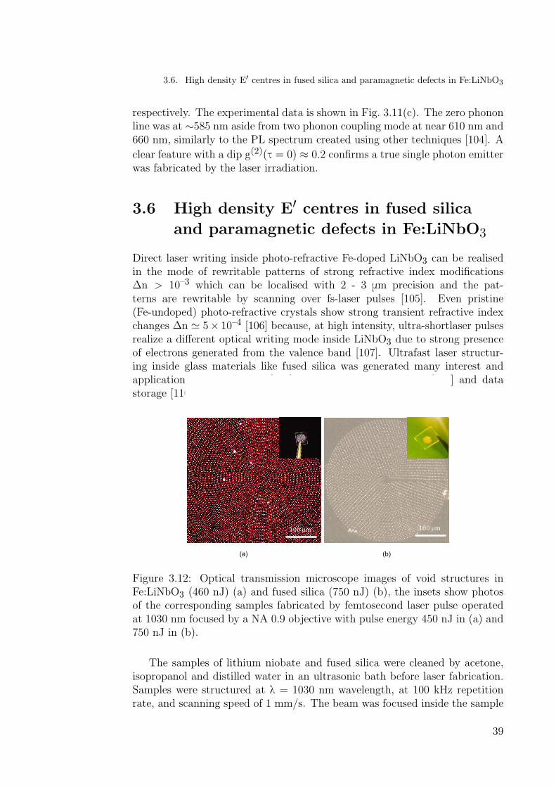
3.6. High density E′ centres in fused silica and paramagnetic defects in Fe:LiNbO3
respectively. The experimental data is shown in Fig. 3.11(c). The zero phononline was at ∼585 nm aside from two phonon coupling mode at near 610 nm and660 nm, similarly to the PL spectrum created using other techniques [104]. A
clear feature with a dip g(2)(τ = 0) ≈ 0.2 confirms a true single photon emitterwas fabricated by the laser irradiation.
3.6 High density E′ centres in fused silica
and paramagnetic defects in Fe:LiNbO3
Direct laser writing inside photo-refractive Fe-doped LiNbO3 can be realisedin the mode of rewritable patterns of strong refractive index modificationsΔn > 10–3 which can be localised with 2 - 3 μm precision and the pat-terns are rewritable by scanning over fs-laser pulses [105]. Even pristine(Fe-undoped) photo-refractive crystals show strong transient refractive indexchanges Δn ' 5× 10⁻⁴ [106] because, at high intensity, ultra-shortlaser pulsesrealize a different optical writing mode inside LiNbO3 due to strong presenceof electrons generated from the valence band [107]. Ultrafast laser structur-ing inside glass materials like fused silica was generated many interest andapplications in optofluidics [108], integrated photonic chips [109] and datastorage [110].
100 μm100 μm
(a) (b)
Figure 3.12: Optical transmission microscope images of void structures inFe:LiNbO3 (460 nJ) (a) and fused silica (750 nJ) (b), the insets show photosof the corresponding samples fabricated by femtosecond laser pulse operatedat 1030 nm focused by a NA 0.9 objective with pulse energy 450 nJ in (a) and750 nJ in (b).
The samples of lithium niobate and fused silica were cleaned by acetone,isopropanol and distilled water in an ultrasonic bath before laser fabrication.Samples were structured at λ = 1030 nm wavelength, at 100 kHz repetitionrate, and scanning speed of 1 mm/s. The beam was focused inside the sample
39

Chapter 3. Defects engineering for photonic applications
0 1500 3000 4500
-1000
-500
0
500
1000
Inte
nsity
(a.u
)
Magnetic field (Gauss)
Intrinsic Fe:LiNbO3
Modified Fe:LiNbO3
3500 3520 3540
-300
-200
-100
0
100
Inte
nsity
(a.u
)
Magnetic field (Gauss)
Intrinsic SiO2
Modified SiO2
Frequency =9.84GHz
Frequency =9.84GHz
(a) (b)
Figure 3.13: ESR spectroscopy measurements were conducted on Fe:LiNbO3(c-plane cut)(a) and fused silica (b). E′ was identified in silica and changes inFe3+ conformation was identified in Fe:LiNbO3. With the reference measure-ment of CuSO4.5:H2O (1.06×10¹⁸ and 1.81×10¹⁸ spin numbers of standardweight), the density of E′ defects in silica was estimated to be 1.4∼1.9 ×1020 cm–3. ESR spectroscopy experiments were conducted in Materials andStructures Laboratory, Tokyo Institute of Technology.
by a dry objective lens NA 0.9. The focal spot is '1.4 μm and the depth-of-focus was evaluated as '2.8 μm. Single pulse was irradiated inside the samplesas in the fabrication of c-BN samples. To get high volume density of voids,12 layers (10 μm separation) in a 0.2 mm thick LiNbO3 doped Fe sample wererecorded with an Archimedean spiral pattern r = a+bθ (a= 5 μm, b= 5/π μm),θ is the azimuthal angle) on each plane at 430 nJ pulse energy. While in the1 mm thick fused silica sample, concentric-ring pattern was used at 750 nJfor 40 layers. The separation of adjacent irradiation sites radially was 10 μmand in circumferentially 5 μm. For holding the high pressure conditions insideand avoiding cracks in the edge of each layer, an alternating 5 μm radial shiftbetween each layer. The fabrication structures were shown in Fig. 3.12.
From the UV-VIS-IR absorption spectrum measurements, colour centres inthe irradiated fused silica and LiNbO3 samples could not be clearly identified,due to small absorption changes in the modified region. Here the paramag-netic properties of defects were characterized with an electron spin resonance(ESR) spectrometer (Bruker-EMX, Bruker). To determine the density of para-magnetic spins (dangling bonds), a commercial standard reference sample ofCuSO4×5H2O with a known number of spins (1 mol of s = 1/2 spins) wasused for calibration. The ESR spectrum of the two samples are shown inFig. 3.13(a-b). Fig. 3.13(a-b) shows the ESR spectrum of fused silica (b) andLiNbO3 doped with Fe3+ (s = 5
2) (a) and exhibiting a typical form-factorknown for the configuration when c-axis of the crystal is perpendicular to themagnetic field H [111]. The spectrum was measured at ν = 9.84 GHz mi-crowave frequency of 0.205 mW excitation power and a modulation amplitudeof 0.5 Gauss (in SI units: 1 T = 104 G). An unpaired electron can transitbetween the Zeeman split energy levels when the microwave energy is equal tothe energy gap, i.e. hν = gμBB0; here μB is the Bohr magneton, g is the Lande
40
3.7. Discussion and Conclusions
factor, and B0 is the magnetic field strength at the resonance. The spectra(b) displays a feature at a magnetic field of 3515 Gauss, corresponding to aLande-factor of g ≈ 2.001 which is attribute to the E′ centre [8]. The estimatedaverage volume density of of E′ centres in the modified region around each sin-gle void is 1.9 × 1020 cm–3, determined by standard weighted CuSO4.5×H2Osample with spins of 1.81× 10¹⁸.
3.7 Discussion and Conclusions
Precise control of density of light absorbing defects and their location opens alittle explored avenues to write optical elements in photo-refractive host andharness geometrical phase in the plane of writing for an optical function of themicro-optical element. Absorption at visible and IR spectral range can be usedto ”switch on” an optical plasmonic response at THz spectral range and realiseall-optical elements at specific wavelengths in T-ray spectrum. THz generationin periodically poled lithium niobate was recently demonstrated [112]. Byusing direct laser writing with tightly focused ultra-short laser pulses it ispossible to control the pathways of material decomposition and synthesis viaphase transitions at elevated temperatures and pressures [4]. This might beused, e.g., for B2O3 doping by rare-earth oxide while maintaining good opticalglass quality [113].
Very high densities of induced defects in KBr crystal, especially the V andF centres, reaching 5.1 × 1018 cm–3 and 5.3 × 1018 cm–3 have been created bylaser irradiation. These centres are the anion or cation ion vacancies aggregatedwith free carriers (for V-centres, holes combined with anion vacancies and forF-centres, cation vacancies with trapped free electrons). The E′ centres formedSi dangling bonds determined by its signature in the ESR spectrum. Theestimated density of dangling bonds created by laser irradiation is reaching1.9 × 1020 cm–3. With such high free electron density, manipulating thetransverse electromagnetic field in THz range is theoretically feasible. The highbirefringence and refractive index modification associated with color centres inKBr, enable the operation of the phase and polarization accumulation of thepropagating light in visible range. Femtosecond laser direct writing providesthe opportunity to generate these defects and color centres in a 3D manner,that facilitate the design and fabrication for different functional optical devices.
The defects induced in c-BN by tightly focused laser pulse irradiation givea promising approach to create Boron clusters and N2 molecules inside the sec-ond hardest and thermal conductive dielectric material, which may opens manynew applications. In h-BN, single photon emitters were observed and deter-mined in the laser irradiated region. The direct laser irradiation technique, willgive a controllable way to generate efficient single photon emission sources thatwill facilitating the practical applications of the integrated quantum-photonicdevices.
41

Chapter 3. Defects engineering for photonic applications
3.8 Appendix B
This section contains the published papers related to the defects engineeringusing femtosecond laser irradiation inside wide band gap dielectrics.
B1: X. W. Wang, R. Buividas, F. Funabiki, P. R. Stoddart, H.Hosono, S. Juodkazis. Analysis of defects patterned by femotosecond pulsesinside KBr and SiO2 glass. Applied Physics A 122(3),1-8, 2016.
High density of color centres (5.1 × 1018 cm–3 V centre and 5.3 × 1018 cm–3
F centre) inside KBr and E′ defects (1.9 × 1020 cm–3) in fused silica werecreated using femtosecond laser pulse direct writing. The induced birefringenceproperty associated with the color centres was measured and discussed.
B2: R. Buividas, I. Aharonov, G. Seniutinas, X. W. Wang, L. Rapp,AV. Rode, T. Taniguchi, S. Juodkazis. Photoluminescence from voids createdby femtosecond laser pulses inside cubic-BN. Optical Letters 40(24), 5711-5713,2015.
Different defects induced by micro-explosion inside c-BN crystal by tightlyfocused femtosecond laser pulse irradiation are characterized by Raman andPL spectroscopy. A wide peak at 530 cm–1 in Raman spectra is observedafter laser irradiation which could be a signature of icosahedron libration of α-rhombohedral B12, indicating α-rhombohedral B12 clusters formed after strongsurface ablation on the c-BN.
B3: S. Choi, T. T. Tran, C. EiBadawi, C. Lobo, X. W. Wang, S.Juodkazis, G. Seniutinas, M. Toth, I. Aharonovich. Engineering and localiza-tion of quantum emitters in large hexagonal boron nitride layers. ACS AppliedMaterials & Interfaces 8(43), 29642-29648, 2016.
Large numbers of single photon emitters created by femtosecond laser irra-diation on h-BN flakes are determined by its PL spectrum and the g(2) curve,indicating the single photon emitters are fabricated. The comparison betweendifferent techniques including ion implantation, electron beam bombardmentand femtosecond laser irradiation shows the prevalent advantages of femtosec-ond laser irradiation, considering the large numbers of single photon emitterscreated, the feasibility, ease of control and cost-effectiveness of such techniqueand the larger dip of the g(2)(τ = 0). It indicates the future potential appli-cations of defects engineering by femtoseond laser irradiation on large scale ofintegrated quantum-photonics devices.
42

INVITED PAPER
Analysis of defects patterned by femtosecond pulses inside KBrand SiO2 glass
X. W. Wang1 • R. Buividas1 • F. Funabiki2 • P. R. Stoddart3 • H. Hosono2 •
S. Juodkazis1,4
Received: 10 October 2015 /Accepted: 20 January 2016 / Published online: 25 February 2016
� Springer-Verlag Berlin Heidelberg 2016
Abstract Colour centres in KBr and defects in silica
glass were formed by focused femtosecond laser pulses. It
is shown that under simple laser exposure, KBr develops a
similar colouration as that achieved with electron and ion
bombardment or high-energy X-ray irradiation. The three-
dimensional (3D) character of direct laser writing in the
volume of KBr allows a new level of control in the spatial
arrangement of colour centres and defects. Five different
colour centres were identified in KBr through the absorp-
tion spectrum; they have different charge and vacancy
distribution configurations. The densities of the V- and
F-centres were estimated to be 3.9 9 1019 and
3.4 9 1019 cm-3 using Smakula’s formula. In silica, a high
density of paramagnetic E0 centres *1.9 9 1020 cm-3 was
determined by quantitative electron spin resonance spec-
troscopy. Birefringence due to colour centres and laser-
induced defects was measured using Stokes polarimetry. In
the case of colour centres in KBr, retardation in excess of
0.05p was determined throughout the visible spectrum
from 400 to 800 nm. The use of polariscopy for analysis of
high-pressure and high-temperature phase formation
induced by 3D laser structuring is discussed.
1 Introduction
Investigations of high-pressure and high-temperature
materials are unravelling a new fundamental understanding
of atomic and molecular interactions. For example,
metallic deuterium was predicted in 1935 [1], but only
recently demonstrated via an insulator-to-metal transition,
which opens access to new properties [2]. With laser-in-
duced shocks, matter can be compressed to extreme pres-
sures. Under these highly nonequilibrium conditions, new
materials and their transformed phases are created.
Recently, by using a free electron laser, the formation of
grains and modifications of SiO2 has been temporally
resolved after nanosecond laser pulse-induced shock [3].
With even shorter sub-picosecond laser pulses, where the
pulse duration is shorter than the electron-to-lattice energy
transfer duration (typically up to few picoseconds), novel
metastable phases of materials can be created, as shown for
high-pressure/temperature phases of Si [4] and Al [5].
Structural changes at the warm dense matter (WDM) [6–8]
conditions created by a tightly focused laser beam have to
be mapped with picosecond resolution to reveal new phe-
nomena in an exotic pressure and temperature environment
that is typical for the interior of planets [9, 10]. Structural
modifications inside different transparent materials can be
controlled down to sub-wavelength resolution [11, 12] by
direct laser write and opens the possibility to create optical
and micro-/opto-fluidic elements [13, 14].
Laser-written patterns change the absorption coefficient
and refractive index in the vicinity of a focal spot. This is
related to structural defects which create optical darkening
around fs-laser micromachined regions in silicate glasses
[15], sodium chloride [16], and LiF crystals [17]. Among
optical materials, cubic alkali halide crystals and silica
glasses have wide usage. Alkali halides are known for their
& S. Juodkazis
1 Centre for Micro-Photonics, Swinburne University of
Technology, John St., Hawthorn, VIC 3122, Australia
2 Materials and Structures Laboratory, Tokyo Institute of
Technology, 4259 Nagatsuta, Yokohama 226-8503, Japan
3 Faculty of Science, Engineering and Technology, Swinburne
University of Technology, John St., Hawthorn, VIC 3122,
Australia
4 Center for Nanotechnology, King Abdulaziz University,
Jeddah 21589, Saudi Arabia
123
Appl. Phys. A (2016) 122:194
DOI 10.1007/s00339-016-9647-0
3.8. Appendix B
43
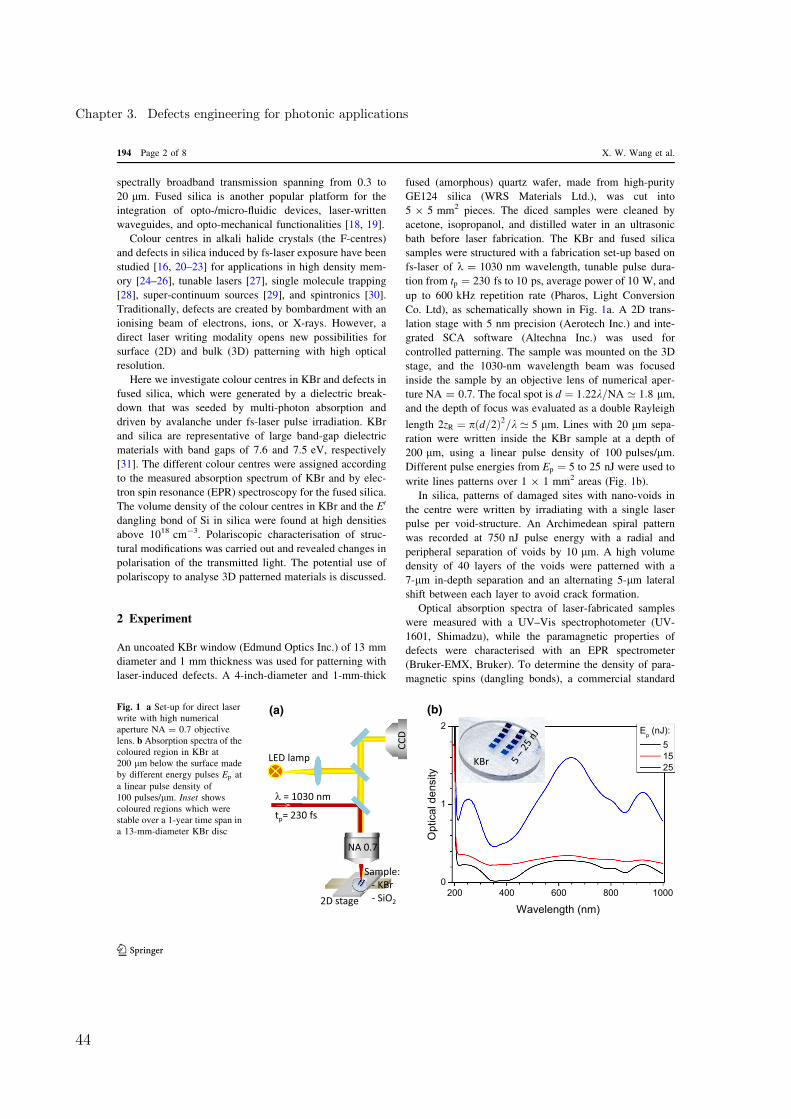
spectrally broadband transmission spanning from 0.3 to
20 lm. Fused silica is another popular platform for the
integration of opto-/micro-fluidic devices, laser-written
waveguides, and opto-mechanical functionalities [18, 19].
Colour centres in alkali halide crystals (the F-centres)
and defects in silica induced by fs-laser exposure have been
studied [16, 20–23] for applications in high density mem-
ory [24–26], tunable lasers [27], single molecule trapping
[28], super-continuum sources [29], and spintronics [30].
Traditionally, defects are created by bombardment with an
ionising beam of electrons, ions, or X-rays. However, a
direct laser writing modality opens new possibilities for
surface (2D) and bulk (3D) patterning with high optical
resolution.
Here we investigate colour centres in KBr and defects in
fused silica, which were generated by a dielectric break-
down that was seeded by multi-photon absorption and
driven by avalanche under fs-laser pulse irradiation. KBr
and silica are representative of large band-gap dielectric
materials with band gaps of 7.6 and 7.5 eV, respectively
[31]. The different colour centres were assigned according
to the measured absorption spectrum of KBr and by elec-
tron spin resonance (EPR) spectroscopy for the fused silica.
The volume density of the colour centres in KBr and the E0
dangling bond of Si in silica were found at high densities
above 1018 cm-3. Polariscopic characterisation of struc-
tural modifications was carried out and revealed changes in
polarisation of the transmitted light. The potential use of
polariscopy to analyse 3D patterned materials is discussed.
2 Experiment
An uncoated KBr window (Edmund Optics Inc.) of 13 mm
diameter and 1 mm thickness was used for patterning with
laser-induced defects. A 4-inch-diameter and 1-mm-thick
fused (amorphous) quartz wafer, made from high-purity
GE124 silica (WRS Materials Ltd.), was cut into
5 9 5 mm2 pieces. The diced samples were cleaned by
acetone, isopropanol, and distilled water in an ultrasonic
bath before laser fabrication. The KBr and fused silica
samples were structured with a fabrication set-up based on
fs-laser of k = 1030 nm wavelength, tunable pulse dura-
tion from tp ¼ 230 fs to 10 ps, average power of 10 W, and
up to 600 kHz repetition rate (Pharos, Light Conversion
Co. Ltd), as schematically shown in Fig. 1a. A 2D trans-
lation stage with 5 nm precision (Aerotech Inc.) and inte-
grated SCA software (Altechna Inc.) was used for
controlled patterning. The sample was mounted on the 3D
stage, and the 1030-nm wavelength beam was focused
inside the sample by an objective lens of numerical aper-
ture NA = 0.7. The focal spot is d ¼ 1:22k=NA ’ 1:8 lm,
and the depth of focus was evaluated as a double Rayleigh
length 2zR ¼ pðd=2Þ2=k ’ 5 lm. Lines with 20 lm sepa-
ration were written inside the KBr sample at a depth of
200 lm, using a linear pulse density of 100 pulses/lm.
Different pulse energies from Ep ¼ 5 to 25 nJ were used to
write lines patterns over 1 9 1 mm2 areas (Fig. 1b).
In silica, patterns of damaged sites with nano-voids in
the centre were written by irradiating with a single laser
pulse per void-structure. An Archimedean spiral pattern
was recorded at 750 nJ pulse energy with a radial and
peripheral separation of voids by 10 lm. A high volume
density of 40 layers of the voids were patterned with a
7-lm in-depth separation and an alternating 5-lm lateral
shift between each layer to avoid crack formation.
Optical absorption spectra of laser-fabricated samples
were measured with a UV–Vis spectrophotometer (UV-
1601, Shimadzu), while the paramagnetic properties of
defects were characterised with an EPR spectrometer
(Bruker-EMX, Bruker). To determine the density of para-
magnetic spins (dangling bonds), a commercial standard
(b) (a) Fig. 1 a Set-up for direct laser
write with high numerical
aperture NA = 0.7 objective
lens. b Absorption spectra of the
coloured region in KBr at
200 lm below the surface made
by different energy pulses Ep at
a linear pulse density of
100 pulses/lm. Inset shows
coloured regions which were
stable over a 1-year time span in
a 13-mm-diameter KBr disc
194 Page 2 of 8 X. W. Wang et al.
123
Chapter 3. Defects engineering for photonic applications
44

reference sample of CuSO4 9 5H2O with a known number
of spins (1 mol of s = 1/2 spins) was used for calibration.
3 Polariscopy: method and set-up
Polariscopy measurements were used to characterise the
polarisation changes in light traversing the laser-patterned
regions inside samples, with changes to the complex
refractive index, n� ¼ nþ ık, arising due to the cumulative
effect of stress, chemical, and structural modifications at
and around the laser-modified tracks. The intensity of the
transmitted light, IT, was measured using a k=4 waveplate
and analyser at different orientational angles b and a,respectively, according to [32]:
ITða; bÞ ¼1=2½I þ ðQ cosð2bÞ þ U sinð2bÞÞ cosð2ða� bÞÞþ V sinð2ða� bÞÞ�; ð1Þ
where a and b are the rotation angles of the fast axis of the
polariser and the waveplate with respect to the x-axis
(Fig. 2a).
The four Stokes parameters, S(I, Q, U, V), which define
an arbitrary state of coherent or incoherent light, are
determined by separate measurements with the waveplate
and analyser at fixed angles of a and b, given by:
I ¼ ITð0; p=4Þ þ ITð0;�p=4Þ;Q ¼ 2ITð0; 0Þ � I;
U ¼ 2ITðp=4; p=4Þ � I;
V ¼ 2ITð0;�p=4Þ � I:
ð2Þ
It is usual to present Stokes parameters on the Poincare
sphere. The retardation is then u ¼ atanðV=UÞ.Stokes polarimetry was carried out using the set-up
shown in Fig. 2. Filters of 10 nm spectral bandwidth were
used to select different central wavelengths from a white-
light super-continuum laser (SuperK Compact, NKT Pho-
tonics) in the range from 400 to 800 nm and focused to a 5-
to 7-lm spot on the sample. Phase retardation, u, of the 45�linear polarised beam (i.e. the phase delay between the s-
and p-polarised light) was measured as u ¼ 2pDnd=k,where Dn is the birefringence, d is the thickness of laser-
modified region, and k is the wavelength of the light filter
selected for measurements. The incident linearly polarised
light was set at 45� by a Glan–Taylor polariser (left LP in
Fig. 2a) and was focused on the laser-structured region of
the sample with an objective lens of numerical aperture
NA = 0.5 (109, Mitutoyo). After the sample, an NA = 0.5
objective lens (1009, Mitutoyo) was used to collect and
collimate the transmitted light for polarisation analysis. The
sample and two objectives were mounted on 2D positioning
stages. Polarisation analysis was carried out after the second
objective with an achromatic k=4-waveplate (QWP) and a
second Glan–Taylor polariser (LP). The tube lens and a
1024 9 768 pixel CCD were used for imaging and trans-
mission measurements (Fig. 2a). Typical lateral resolution
was 5–7 lm. Note that this set-up can be used for the
integrated intensity as well as for single pixel level analysis
by image processing according to Eqs. (1) and (2).
Calibration and sensitivity of the assembled polariscope
were tested by measuring the retardation, u, using a com-
mercial k=2 achromatic waveplate (Thorlabs) and comparing
the data with catalog values (Fig. 2b). A good match was
obtained between the catalog data and the measurement over
most of the range. The uncertainty of the measurement was
±0:01p, except for the shortest wavelengths at UV edge,
most probably due to the objective lenses not being optimised
for that spectral range. The limit of detection was *0:02pover the visible range. These test results confirm that changes
in polarisation caused by internal 3D modifications can be
measured and mapped onto the Poincare sphere (Fig. 2c).
4 Results and discussion
Laser damage within the bulk of the transparent samples
was made at an irradiance Ip [ 1 TW/cm2/pulse, thus
exceeding the threshold of dielectric breakdown. At the
LP LP QWP Obj1 Sample Obj2 Tube lens CCD Filter WL
Q
V
U A
B O
(a)
(c)(b)
z y
x
Fig. 2 a Polariscopy set-up to measure Stokes parameters
S(I, Q, U, V), where WL is white light source, a 10-nm wide notch
filter, QWP is the k=4 waveplate, LP is the linear polariser, and angles
a;b are the orientation angles (see Eq. 1) of the fast optical axis of the
optical elements shown in the boxed area. The objective lenses Obj
define the resolution of the set-up. b Calibration of the polariscope
using Thorlabs catalog data for an achromatic k=2-waveplate and an
experimental determination of the retardance. c Poincare sphere
representation of the Stokes parameters Q, U, V. Vector OB repre-
sents the polarisation state; the horizontal plane with V ¼ 0
represents all possible locations for linearly polarised light
Analysis of defects patterned by femtosecond pulses inside KBr and SiO2 glass Page 3 of 8 194
123
3.8. Appendix B
45

k ¼ 1030 nm wavelength used here, multi-photon ionisa-
tion seeds an avalanche ionisation process as the driving
mechanism of excitation [33]. The excited volume
becomes metal-like once the critical plasma den-
sity reaches Nc ¼ �0með2pc=kÞ2=e2 ¼ 1:05� 1021 cm-3,
where me and e are the electron mass and charge, respec-
tively, e0 is the permittivity of vacuum, and c is the speed
of light. The density of reflective and absorbing plasma is
further increased by the deposited pulse energy. Photo-
chemical- and avalanche-induced bond breaking was
responsible for the generation of colour centres in KBr and
defects in fused silica under these conditions [34]. The
electrons are excited faster than they can transfer their
excess energy to the lattice, which leads to ionic K-Br and
covalent Si–O bond breaking by avalanche. This process
continues in the hot plasma after the laser pulse. The
density of the defects after relaxation in the laser-damaged
regions is determined in the next section.
4.1 Colour centre density in KBr
When laser pulse energies from Ep ¼ 5 to 25 nJ were used
to write inside KBr, the modified region becomes indigo
blue with an increasing depth of colour, as shown in the
inset of Fig. 1b. As Ep increases, the absorption spectrum
(Fig. 1b) shows distinct peaks of a higher absorbance,
corresponding to the blue appearance. At the highest pulse
energy, the colour centres recorded inside the KBr sample
were stable over a period of several months (no colour
change after 1 year) under room conditions. However, for
the small Ep, temporal fading was observed over a period
of hours, in accordance with room temperature photo-ac-
tivation of reactions between the colour centres [35].
The spectral positions of the femtosecond-laser-induced
colour centres were found to follow the established generic
rules in the alkali halides [36]. Namely, five observed peak
positions can be assigned to: kV ¼ 61:5d1:10 � 248 nm,
kF ¼ 70:3d1:84 � 630 nm, kR1 ¼ 81:6d1:84 � 735 nm,
kR2 ¼ 88:4d1:84 � 810 nm and kM ¼ 70:3d1:84 � 940 nm
where d ¼ 0:329 nm is the lattice constant of KBr. Each of
these V, F, R1, R2 and M centres arise from different
arrangements of electrons trapped in the lattice [36]. The
V-centre is formed by two neighbouring K vacancies with
two trapped holes. Interestingly, this defect could not be
formed by chemical doping in a high-temperature Br
vapour due to its high energy level [35]. Under specific
conditions, fine structures named V1, V2 and V3 could be
found, depending on the accumulation of different numbers
of trapped holes and K vacancies [37].
The F-centre is formed by the Br vacancy trapping one
electron. In this process, F- can also be formed by
simultaneous trapping of two electrons. Under room
temperature conditions, the peaks of the F and F- colour
centres could not be resolved. The R1 and R2 centres are
formed by two F-centres accumulating together with dif-
ferent numbers of trapped electrons. In crystalline sapphire,
equivalent R1 and R2 centres are called colour F-centres,
e.g. the F? centre of the oxygen vacancy with a trapped
electron, found inside laser-damaged regions of sapphire,
and its neutral form F0 [34]; also di-vacancies and com-
plexes of defects are common. The M-centre was formed
by a R1 centre accumulated with a K-vacancy and has a
lower energy in the near-IR. At lower temperatures, a
different sub-type of the M centre has been reported,
depending on the number of electrons trapped and the
number of potassium vacancies accumulated [38].
The charge pattern configurations of these five types of
colour centres are shown in Fig. 3b. As previously estab-
lished, the F- and V-centres are first formed in the relax-
ation time around 6 ps after excitation. The other
configurations of colour centres are then formed by a
slower self-trapping process within *100 ps [20].
With the clear assignment of each colour centre, the
measured absorption spectrum was resolved by peak fit-
ting, as shown in Fig. 3a. The density qCC of each colour
centre, with oscillator strength f, was calculated using
Smakula’s formula (1930) [39]:
+ + -
-
- +
+ -
+ + -
- +
+ -
- +
+
V F R1 R2 M
- - +
-
+
-
electron
negative vacancy hole
positive vacancy
+
(b)
(a)
+ positive ion
Fig. 3 a Absorption spectra of the permanent colouration of KBr by
exposure to Ep ¼ 25 nJ pulses, together with Gaussian fits based on
the assigned peaks of different colour centres [36]. b Defect density
estimation for different colour centres calculated by Smakula’s
formula
194 Page 4 of 8 X. W. Wang et al.
123
Chapter 3. Defects engineering for photonic applications
46

qCC � f ¼ 9mec
4pe2�hn0
ðn20 þ 2Þ2Zband
lðEÞdE; ð3Þ
where me is the electron mass, Euler’s constant
e ¼ 2:71828, lðEÞ ¼ ln 10ODðEÞ=d is the absorption
coefficient over the energy span of an absorption band, d is
the thickness of the colour region d � 2zR ¼ 5 lm (a
double Rayleigh length), OD is the optical density, E is the
photon energy, n0 ¼ 1:7 is the refractive index of KBr, and
�h ¼ h=2p is Planck’s constant. This procedure has previ-
ously been used to estimate the density of defects in glass
ceramics after irradiation by fs-laser pulses [40]. The
oscillator strengths for different defects were fF ¼ 0:48,
fR1 � fR2 ¼ 0:43, fM ¼ 0:11 [41], and fV � 0:5 was used to
estimate the density of V-centres (no previous data).
The density of V- and F-centres was calculated to be as
high as 3.9 9 1019 and 3.4 9 1019 cm-3, respectively,
following the fits shown in Fig. 3a. Figure 3b presents a
summary of the analysis, together with diagrams repre-
senting the corresponding defect structures induced in KBr
by fs-laser pulses. Note that colour centre densities are
significantly smaller than the critical plasma density and
are consistent with previous studies [42].
4.2 Defect density in SiO2
In silica, several types of defects exist and can be induced
or modified by photolysis of the host network of Si–O–Si
bonds [43, 44]. The diamagnetic oxygen deficiency �Si–
Si� (ODCI or E-centre) and O–Si��O (ODCII) centres are
present in pure silicas (� represents an electron dangling
bond). The E0 [45] Si� and nonbridging oxygen hole centre
(NBOHC) Si–O� [46] can be formed from photolysis of Si–
O–Si. The Si–O–O� is the peroxy radical (POR) [47] centre
which occurs in damaged silica: Si–O–Si)�Si–
Si� ? Si–O–O–Si with a possibility of Si–O–O–Si) Si–
O–O� ? Si�. The major four centres that can be created are
E0, NBOHC, POR, and ODCI. These centres form the host
network and can also undergo reactions with each other in
the presence of oxygen interstitials. Thermal activation of
defect reactions is one method that can be used to control
their concentration.
These defects are induced by fs-laser irradiation and
have absorption in the deep UV region, while other centres
are absorbing in the longer visible range [25]. Clustering of
ODCI or Si–Si might even create precipitation centres for
the Si phase [48]. Defects in silica are studied for trans-
parency control at the band-gap edge region in the deep UV
[45, 49, 50]. In contrast, the UV–Vis–IR absorption spec-
trum usually shows weak absorption changes in the fs-
laser-modified regions. The defects introduced by focused
fs-laser pulses are typical for silica exposed to particle and
ionising radiation, e.g. silica exposed to electrons [51]. A
very high pulse energy of Ep ¼ 0:75 J was used for pat-
terning void-structures induced by single pulses in order to
achieve a high density of defects.
ESR measurements can be used to probe the dangling
bond-type defects existing in silica [30, 25]. Of the defects
discussed above, only a few are paramagnetic and ESR
detectable. The Si–Si bond (ODCI) is diamagnetic; how-
ever, the E0 centre shows an EPR signature at g ’ 2:001.
The NBOHC and POR are recognisable as g ’ 2:01 fea-
tures [52].
Figure 4a shows an ESR spectrum of the void-structures
patterned inside SiO2. The spectrum was measured with a
microwave frequency of m ¼ 9:84 GHz at 0.205 mW
excitation power and a modulation amplitude of 0.5 Gauss
(in SI units: 1 T = 104 G). An unpaired electron can
transition between the Zeeman split energy levels when the
microwave energy is equal to the energy gap, i.e. hm ¼glBB0 where lB is the Bohr magneton, g is the Lande
factor, and B0 is the magnetic field strength at the
resonance.
The spectrum displays a defect signature at a magnetic
field B0 ¼ 3515 G, corresponding to g � 2:001, which is
attributed to the E0 centre [25]. No free electron signature
was observed at g ¼ 2:0023 in silica, as well as in lithium
niobate which was tested for comparison. No NBOH nor
POR was detected in the fs-laser-modified silica.
To determine the average volume density of E0 centresin the modified region around each void, the modified
volume must be estimated. From side- and top-view optical
imaging, it can be determined that the modified volume is
Vm ’ 1 lm3, which provides an estimate of the defect-rich
regions near the void walls. To quantify the number of
Fig. 4 E0 signature in the ESR spectrum of the void-structures in
GE124 silica; inset is a photographic image of the laser-structured
region. The featureless ESR spectrum from a pristine sample is shown
with an offset for clarity
Analysis of defects patterned by femtosecond pulses inside KBr and SiO2 glass Page 5 of 8 194
123
3.8. Appendix B
47

spins in the modified silica, two CuSO4 9 5H2O samples
of standard weight and known spin numbers of
1.06 9 1018 and 1.81 9 1018 were used. Then, by extrap-
olating a linear dependence of the EPR signal from the two
standard sample points, the number of spins in the modified
silica was calculated to be NE0 ¼ ð1:6 0:2Þ � 1015.
Hence, the density is NE0=ðN � VmÞ ’ 1:9� 1020 cm-3,
where N ¼ 8:04� 106 is the total number of irradiated
spots in the sample (see inset of Fig. 5b).
4.3 Polariscopic read-out of 3D birefringence
Polariscopy was used to read out the birefringence induced
by fs-laser irradiation. This birefringence originates from a
complex interplay of photo-elastic, chemical, and structural
factors that always act together and define the polarisation
of light traversing the laser-structured sections [53, 54].
This opens the possibility to investigate the optical prop-
erties and also to create optical elements based on polari-
sation and birefringence control. The laser structuring was
carried out with linearly polarised pulses, which are
expected to impose a structural anisotropy due to defects,
nano-ripple formation, spatial chirp of the pulse (a front
tilt), etc. All of these factors are also coupled to the ani-
sotropy of the crystalline substrate and the direction of the
laser scan with respect to polarisation and wave front tilt.
In the KBr sample, more than u ¼ 0:05p retardation
was determined in the visible range from 400 to 800 nm
(Fig. 5a). The change in the polarisation state of the inci-
dent beam at k ¼ 500 nm from linear (p=4) to an elliptical
polarisation can be illustrated with a Poincare sphere,
where dAOB ¼ 0:08p represents the depolarisation (see
Fig. 2c); this corresponds to a 4 % shift in terms of
wavelength. In fused silica, no birefringence was detected
(Fig. 5b). The E0 centre (silicon dangling bond) is formed
by cleavage of the Si–O bond. It would appear that the
geometric distribution of the E0 centre was not strongly
dependent on the polarisation of the excitation laser beam.
Similarly, there was no strong polarisation dependence of
any post-pulse relaxation anisotropy of the 5- and
3-member ring structures known to be responsible for
densification of silica [55].
In the case of colour centres in KBr, a relatively large
birefringence was observed in the visible range from 400 to
800 nm. The microscopic 3D steric arrangement of
vacancies and interstitials, and their decoration by charges
forming F, R1, and R2 centres at high density are presumed
responsible for the polarisation change. As discussed above
(Fig. 3b), the F, R1, and R2 centres are formed because of
electron trapping by the Br-ion vacancies. Earlier studies
[56] showed that the largest refractive index changes are
expected due to F-centres in KBr.
After the electrons are excited by the linearly polarised
light, the free electrons are driven in oscillation by the
external light field. Evidence for an anisotropic charge
distribution dictated by polarisation could be expected,
given that the colour centres are formed in a weak polarity
local field. The weak polarity is due to the small electron–
lattice coupling in halides [57, 58], where the maximum
phonon energy is\200 cm-1. Future studies are expected
to address these polarisation effects of fs-laser-induced
defects, together with methods to influence their orientation
for birefringence control.
5 Conclusions and outlook
A very high density ([3 9 1019 cm-3) of V- and F-centres
has been generated by fs-laser direct writing inside KBr. A
high density of 1.9 9 1020 cm-3 of paramagnetic E0 cen-tres was created by the micro-explosion and void formation
(a) (b)
30 m
100 m
Fig. 5 a Retardation u as determined by polariscopy in the
permanently coloured region of KBr. The incident beam was linearly
polarised (OA in Fig. 2c) and shifted to OB after passing through the
fs-laser-structured region. Inset shows a true-colour optical image of
the line pattern recorded inside KBr. b Retardation u ’ 0 rad from
the void-structure pattern in SiO2; Ep ¼ 0:75 lJ/pulse. Inset micro-
scopic image of the Archemedean spiral written by single-pulse
damage inside SiO2
194 Page 6 of 8 X. W. Wang et al.
123
Chapter 3. Defects engineering for photonic applications
48

method using tightly focused fs-laser pulses in silica. The
birefringence due to structural modifications and colour
centres in KBr was u 0:05p over the full range of the
visible spectrum.
A high density ([1018 cm-3) of defects and electron
dangling bonds can be utilised for optically controlled
photo-conductivity and corresponds to a plasma frequency
of m ¼ 9 THz (Sect. 4). It may be possible to exert control
over the electronic photo-conductivity by exploiting the
strong optical absorption at the corresponding defect bands.
This, together with the potential to pattern larger areas with
cross sections of millimetres (see inset in Fig. 4),
empowers the creation of THz optical elements to control
intensity, angular momentum, and polarisation. Moreover,
such elements can be THz-wavelength tunable using an
external illumination at the defect absorption band.
3D nano-structuring of materials by ripples, filamenta-
tion, and ponderomotive effects at high intensity creates
complex 3D patterns of modification [59–61]. These pat-
terns should be characterised by an inherent 3D read-out
technique, such as X-ray diffraction [62], without releasing
stress and chemical modifications from the laser-affected
zone. As demonstrated here, analysis and imaging of the
polariscopic Stokes component may provide a useful and
simple method for such a 3D read-out.
Acknowledgments SJ is grateful for partial support via the Aus-
tralian Research Council Discovery Project DP130101205 and fs-
laser fabrication set-up via a technology transfer project with
Altechna Ltd.
References
1. M.D. Knudson, M.P. Desjarlais, A. Becker, R.W. Lemke, K.R.
Cochrane, M.E. Savage, D.E. Bliss, T.R. Mattsson, R. Redmer,
Direct observation of an abrupt insulator-to-metal transition in
dense liquid deuterium. Science 348(6242), 455–1460 (2015)
2. P.F. McMillan, New materials from high-pressure experiments.
Nat. Mater. 1, 19–25 (2002)
3. A. Gleason, C. Bolme, H. Lee, B. Nagler, E. Galtier, D.
Milathianaki, J. Hawreliak, R. Kraus, J. Eggert, D. Fratanduono,
G. Collins, R. Sandberg, W. Yang, W. Mao, Ultrafast visualiza-
tion of crystallization and grain growth in shock-compressed
SiO2. Nat. Commun. 6, 8191 (2015)
4. L. Rapp, B. Haberl, C. Pickard, J. Bradby, E. Gamaly, J. Wil-
liams, A. Rode, Experimental evidence of new tetragonal poly-
morphs of silicon formed through ultrafast laser-induced confined
microexplosion. Nat. Commun. 6, 7555 (2015)
5. A. Vailionis, E.G. Gamaly, V. Mizeikis, W. Yang, A. Rode, S.
Juodkazis, Evidence of super-dense aluminum synthesized by
ultra-fast micro-explosion. Nat. Commun. 2, 445 (2011)
6. R. Drake, High-energy-density physics. Phys. Today 63, 28–33(2010)
7. S. Ono, A.R. Oganov, T. Koyama, H. Shimizu, Stability and
compressibility of high-pressure phase of Al2O3 up to 200 GPa:
implications for electrical conductivity at the base of the lower
mantle. Earth Planet. Sci. Lett. 246, 326–335 (2006)
8. A.R. Oganov, S. Ono, The high pressure phase of alumina and
implications for Earth’s D layer. Proc. Natl. Acad. Sci. 102,10828–10831 (2005)
9. L.B. Fletcher, H.J. Lee, T. Doppner, E. Galtier, B. Nagler, P.
Heimann, C. Fortmann, S. LePape, T. Ma, M. Millot, A. Pak, D.
Turnbull, D.A. Chapman, D.O. Gericke, J. Vorberger, T. White,
G. Gregori, M. Wei, B. Barbrel, R.W. Falcone, C.-C. Kao, H.
Nuhn, J. Welch, U. Zastrau, P. Neumayer, J.B. Hastings, S.H.
Glenzer, Ultrabright X-ray laser scattering for dynamic warm
dense matter physics. Nat. Photonics 9, 274–279 (2015)
10. Y. Xu, T.J. Shankland, B.T. Poe, Laboratory-based electrical
conductivity in the Earth’s mantle. J. Geophys. Res. 105,27865–27875 (2000)
11. Y. Shimotsuma, P. Kazansky, J. Qiu, K. Hirao, Self-organized
nanogratings in glass irradiated by ultrashort light pulses. Phys.
Rev. Lett. 91, 1–4 (2003)
12. C. Hnatovsky, V. Shvedov, W. Krolikowski, A. Rode, Revealing
local field structure of focused ultrashort pulses. Phys. Rev. Lett.
106, 123901 (2011)
13. A. Marcinkevicius, S. Juodkazis, M. Watanabe, M. Miwa, S.
Matsuo, H. Misawa, J. Nishii, Femtosecond laser-assisted three-
dimensional microfabrication in silica. Opt. Lett. 26(5), 277–279(2001)
14. M. Beresna, M. Gecevicius, P.G. Kazansky, T. Gertus, Radially
polarized optical vortex converter created by femtosecond laser
nanostructuring of glass. Appl. Phys. Lett. 98(20), 201101 (2011)
15. O.M. Efimov, K. Gabel, S.V. Garnov, L.B. Glebov, S. Grantham,
M. Richardson, M.J. Soileau, Color-center generation in silicate
glasses exposed to infrared femtosecond pulses. J. Opt. Soc. Am.
B 15, 193 (1998)
16. J. Dickinson, S. Orlando, S. Avanesyan, S. Langford, Color
center formation in soda lime glass and NaCl single crystals with
femtosecond laser pulses. Appl. Phys. A 79, 859–864 (2004)
17. L.C. Courrol, R.E. Samad, L. Gomez, I.M. Ranieri, S.L. Bal-
dochi, A.Z. de Freitas, N.D. Vieira, Color center production by
femtosecond pulse laser irradiation in LiF crystals. Opt. Express
12(2), 288 (2004)
18. G. Della Valle, R. Osellame, P. Laporta, Micromachining of
photonic devices by femtosecond laser pulses. J. Opt. A Pure
Appl. 11, 013001 (2009)
19. Y. Bellouard, A.A. Said, P. Bado, Integrating optics and micro-
mechanics in a single substrate: a step toward monolithic inte-
gration in fused silica. Opt. Express 13(17), 6635 (2005)
20. T. Sugiyama, H. Fujiwara, T. Suzuki, K. Tanimura, Femtosecond
time-resolved spectroscopy of self-trapping processes of holes
and electron-hole pairs in alkali bromide crystals. Phys. Rev. B
54, 15109–15119 (1996)
21. J.B. Lonzaga, S.M. Avanesyan, S.C. Langford, J.T. Dickinson,
Color center formation in soda-lime glass with femtosecond laser
pulses. J. Appl. Phys. 94, 4332 (2003)
22. J. Dickinson, S. Langford, S. Avanesyan, S. Orlando, Color
center formation in KCl and KBr single crystals with femtosec-
ond laser pulses. Appl. Surf. Sci. 253, 7874–7878 (2007)
23. L.I. Bryukvina, S.V. Lipko, V. Kuznetsov, E.F. Martynovich,
Structural changes accompanying color center formation in
lithium fluoride exposed to femtosecond laser pulses. Inorg.
Mater. 50, 625–630 (2014)
24. M. Watanabe, H.-B. Sun, S. Juodkazis, T. Takahashi, S. Matsuo,
Y. Suzuki, J. Nishii, H. Misawa, Three-dimensional optical data
storage in vitreous silica. Jpn. J. Appl. Phys. 27(12B), L1527–L1530 (1998)
25. H.-B. Sun, S. Juodkazis, M. Watanabe, S. Matsuo, H. Misawa, J.
Nishii, Generation and recombination of defects in vitreous silica
induced by irradiation with a near-infrared femtosecond laser.
J. Phys. Chem. B 2000(104), 3450–3455 (2000)
Analysis of defects patterned by femtosecond pulses inside KBr and SiO2 glass Page 7 of 8 194
123
3.8. Appendix B
49

26. E.J. Caine, Optical data storage in LiF using electron beam
encoding. J. Vac. Sci. Technol. B 16, 3232 (1998)
27. V.V. Ter-Mikirtychev, T. Tsuboi, Stable room-temperature tun-
able color center lasers and passive Q-switchers. Prog. Quantum
Electron. 20, 219–268 (1996)
28. L. Nony, E. Gnecco, A. Baratoff, A. Alkauskas, R. Bennewitz, O.
Pfeiffer, S. Maier, A. Wetzel, E. Meyer, C. Gerber, Observation
of individual molecules trapped on a nanostructured insulator.
Nano Lett. 4, 2185–2189 (2004)
29. J.-E. Nimsch, J. Wachtveitl, LiF, an underestimated supercon-
tinuum source in femtosecond transient. Opt. Express 21(14),17060–17065 (2013)
30. K. Ambal, A. Payne, D.P. Waters, C.C. Williams, C. Boehme,
Spin-relaxation dynamics of E0 centers at high density in SiO2
thin films for single-spin tunneling force microscopy. Phys. Rev.
Appl. 4, 024008 (2015)
31. D. Grojo, S. Leyder, P. Delaporte, W. Marine, M. Sentis, O.
Uteza, Long-wavelength multiphoton ionization inside band-gap
solids. Phys. Rev. B 88, 195135 (2013)
32. H.G. Berry, G. Gabrielse, A.E. Livingston, Measurement of the
Stokes parameters of light. Appl. Opt. 16, 3200 (1977)
33. E. Gamaly, S. Juodkazis, V. Mizeikis, H. Misawa, A. Rode, W.
Krolokowski, Modification of refractive index by a single fs-
pulse confined inside a bulk of a photo-refractive crystal. Phys.
Rev. B 81(5), 054113 (2010)
34. T. Kudrius, G. Slekys, S. Juodkazis, Surface-texturing of sapphire
by femtosecond laser pulses for photonic applications. J. Phys.
D Appl. Phys. 43(14), 145501 (2010)
35. F. Seitz, Color centers in alkali halide crystals. II. Rev. Mod.
Phys. 26, 7–94 (1954)
36. H. Ivey, Spectral location of the absorption due to color centers in
alkali halide crystals. Phys. Rev. 72, 341–343 (1947)
37. R. Casler, P. Pringsheim, P. Yuster, V-centers in alkali halides.
J. Chem. Phys. 18(12), 1564 (1950)
38. T.J. Neubert, S. Susman, M centers in potassium bromide. I. J.
Chem. Phys. 43(8), 2819 (1965)
39. D.Y. Smith, G. Graham, Oscillator strengths of defects in insu-
lators: the generalization of Smakula’s equation. J. Phys. Colloq.
41(C6), 80–83 (1980)
40. S. Juodkazis, Optical properties of femtosecond irradiated photo-
thermo-refractive glass. Lith. J. Phys. 42(2), 119–126 (2002)
41. S.C. Jain, V.K. Jain, Optical and thermal stability, half-widths
and oscillator strengths of f-aggregate bands in highly pure kbr
crystals. J. Phys. C Solid State Phys. 1(4), 895 (1968)
42. G. Petite, P. Daguzan, S. Guizard, P. Martin, Conduction elec-
trons in wide-bandgap oxides: a subpicosecond time-resolved
optical study. Nucl. Instrum. Methods Phys. Res. B 107(1–4),97–101 (1996)
43. H. Hosono, Y. Abe, H. Imagawa, H. Imai, K. Arai, Experimental
evidence for the Si–Si bond model of the 7.6 eV band in glass.
Phys. Rev. B 44(21), 12043–12045 (1991)
44. M. Cannas, F.M. Gelardi, F. Pullara, M. Barbera, A. Collura, S.
Varisco, Absorption band at 7.6 eV induced by k-irradiation in
silica glasses. J. Non-Cryst. Solids 280, 188–192 (2001)
45. H. Hosono, Y. Ikuta, T. Kinoshita, K. Kajihara, M. Hirano,
Physical disorder and optical properties in the vacuum ultraviolet
region of amorphous SiO2. Phys. Rev. Lett. 87, 175501 (2001)
46. K. Kajihara, L. Skuja, M. Hirano, H. Hosono, Oxygen-excess
amorphous SiO2 with 18O-labeled interstitial oxygen molecules.
J. Non-Cryst. Solids 345–346, 219–223 (2004)
47. E.J. Friebele, D.L. Griscom, M. Stapelbroek, Fundamental defect
centres in glass: the peroxy radical in irradiated, high purity sil-
ica. Phys. Rev. Lett. 42, 1346–1349 (1979)
48. M. Watanabe, S. Juodkazis, H.-B. Sun, S. Matsuo, H. Misawa,
Luminescence and defect formation by visible and near-infrared
irradiation of vitreous silica. Phys. Rev. B 60(14), 9959–9964(1999)
49. L. Skuja, K. Kajihara, Y. Ikuta, M. Hirano, H. Hosono, Urbach
absorption edge of silica: reduction of glassy disorder by fluorine
doping. J. Non-Cryst. Solids 345–346, 328–331 (2004)
50. H. Hosono, M. Mizuguchi, H. Kawazoe, T. Ogawa, Effects of
fluorine dimer excimer laser radiation on the optical transmission
and defect formation of various types of synthetic SiO2 glasses.
Appl. Phys. Lett. 74, 2755–2757 (1999)
51. K. Kajihara, M. Hirano, L. Skuja, H. Hosono, Intrinsic defect
formation in amorphous SiO2 by electronic excitation: bond
dissociation versus Frenkel mechanisms. Phys. Rev. B 78,094201 (2008)
52. K.M. Davis, K. Miura, N. Sugimoto, K. Hirao, Writing waveg-
uides in glass with a femtosecond laser. Opt. Lett. 21(21),1729–1731 (1996)
53. J. Morikawa, A. Orie, T. Hashimoto, S. Juodkazis, Thermal and
optical properties of the femtosecond-laser-structured and stress-
induced birefringent regions of sapphire. Opt. Express 18(8),8300–8310 (2010)
54. M. Beresna, T. Gertus, R. Tomasiunas, H. Misawa, S. Juodkazis,
Three-dimensional modeling of the heat-affected zone in laser
machining applications. Laser Chem. 2008, 976205/1–6 (2008)
55. L. Bressel, D. de Ligny, C. Sonneville, V. Martinez-Andrieux, V.
Mizeikis, R. Buividas, S. Juodkazis, Femtosecond laser induced
density changes in GeO2 and SiO2 glasses: fictive temperature
effect. Opt. Mater. Express 1, 1150–1158 (2011)
56. K.E. Peiponen, A. Vaittinen, Light-induced refractive index
change in some F coloured alkali halide crystals. J. Phys. C Solid
State Phys. 15(13), L415 (1982)
57. K. Rademaker, Rare Earth-Doped Alkali-Lead-Halide Laser
Crystals of Low-phonon Energy (Cuvillier Verlag, Goettingen,
2005)
58. M. Velazquez, A. Ferrier, J.-L. Doualan, R. Moncorge, Rare-
Earth-Doped Low Phonon Energy Halide Crystals for Mid-In-
frared Laser Sources, in Solid State Lasers, ed. by A. Al-Khursan
(Intechopen, 2012)
59. S. Juodkazis, V. Mizeikis, S. Matsuo, K. Ueno, H. Misawa,
Three-dimensional micro- and nano-structuring of materials by
tightly focused laser radiation. Bull. Chem. Soc. Jpn. 81(4),411–448 (2008)
60. R. Buividas, M. Mikutis, S. Juodkazis, Surface and bulk struc-
turing of materials by ripples with long and short laser pulses:
recent advances. Prog. Quantum Electron. 38, 119–156 (2014)
61. C.J. de Jong, A. Lajevardipour, M. Gecevicius, M. Beresna, G.
Gervinskas, P.G. Kazansky, Y. Bellouard, A.H.A. Clayton, S.
Juodkazis, Deep-UV uorescence lifetime imaging microscopy.
Photonics Res. 3(5), 283–288 (2015)
62. S. Richter, D. Moncke, F. Zimmermann, E.I. Kamitsos, L.
Wondraczek, A. Tunnermann, S. Nolte, Ultrashort pulse induced
modifications in ULE—from nanograting formation to laser
darkening. Opt. Mat. Express 5(8), 1834–1850 (2015)
194 Page 8 of 8 X. W. Wang et al.
123
Chapter 3. Defects engineering for photonic applications
50

Photoluminescence from voids created byfemtosecond-laser pulses inside cubic-BNR. BUIVIDAS,1 I. AHARONOVICH,2 G. SENIUTINAS,1 X. W. WANG,1 L. RAPP,3
A. V. RODE,3 T. TANIGUCHI,4 AND S. JUODKAZIS1,*1Centre for Micro-Photonics, Swinburne University of Technology, John St., Hawthorn, VIC 3122, Australia2School of Mathematical and Physical Sciences, University of Technology Sydney, Thomas St., Ultimo, NSW 2007, Australia3Laser Physics Center, Research School of Physics & Engineering, Australian National University, ACT 0200, Australia4National Institute for Materials Science, 1-1 Namiki Tsukuba, Ibaraki 305-0044, Japan*Corresponding author: [email protected]
Received 19 October 2015; revised 12 November 2015; accepted 12 November 2015; posted 12 November 2015 (Doc. ID 252175);published 3 December 2015
Photoluminescence (PL) from femtosecond-laser-modifiedregions inside cubic-boron nitride (c-BN) was measuredunder UV and visible light excitation. Bright PL at thered spectral range was observed, with a typical excited statelifetime of ∼4 ns. Sharp emission lines are consistent withPL of intrinsic vibronic defects linked to the nitrogenvacancy formation (via Frenkel pair) observed earlier inhigh-energy electron-irradiated and ion-implanted c-BN.These, formerly known as the radiation centers, RC1,RC2, and RC3, have been identified at the locus of the voidsformed by a single femtosecond-laser pulse. The method ispromising to engineer color centers in c-BN for photonicapplications. © 2015 Optical Society of America
OCIS codes: (160.4760) Optical properties; (350.3390) Laser materi-
als processing; (180.2520) Fluorescence microscopy.
http://dx.doi.org/10.1364/OL.40.005711
Optical properties of boron nitrides are attracting increasingattention due to their large bandgap and optical transparency.In particular, there is a great motivation to engineer fluorescentcolor centers that can be potentially used as room-temperaturesingle-photon sources [1]. To this extent, subbandgap excita-tion of controllably formed and patterned defects in cubic-boron nitride (c-BN) is strongly anticipated. Indeed, theoreticalmodeling predicts an analog of the nitrogen-vacancy NV− cen-ters known in diamond for the B-vacancy oxygen pair in c-BN[2], which is yet to be confirmed experimentally. The stackingfault energy 191� 15 mJm−2 in c-BN is comparable to that indiamond [3], and a similar defect formation is expected.
Defect engineering in etch-resistive materials can beachieved using a direct laser write technique with subwave-length resolution [4,5]. A similar approach was previously uti-lized to create micro-optical [6] and mechanical [7] elements aswell as waveguides [8–10].
Here, we employ a femtosecond (fs)-laser irradiation tech-nique [11,12] to create optically active color centers in c-BN.
Using confocal microscopy and time resolved measurements,we show that the formed voids are extremely bright photolu-minescence (PL) sources and originate from the N-vacancy-related radiation-center (RC) defects [13] observed earlierin c-BN only by high-energy-particle or ionizing-radiationexposure [14].
Laser pulses of τp � 230 fs duration at fundamental λ �1030 nm and second harmonic 515 nm wavelengths werefocused at a 10–20 μm depth below the surface of a facet planeinside c-BN crystals (Fig. 1). Tight focusing using a lens ofnumerical aperture NA � 1.42 was implemented to formarrays of damage sites—voids—that were recorded at differentpulse energies Ep; the condition of a single pulse per void wasused. Separation between irradiation spots was 10 μm to elimi-nate a cross talk for void formation and optical characterization.For comparison, dense array of ablation patterns were fabri-cated with 800 nm/150 fs pulses focused with NA � 0.95on the surface of c-BN. Judgment of the void presence atthe center of the irradiated spot inside c-BN was made by asharp optical contrast change, which was identical to the voidformation in crystalline sapphire, quartz, and glasses of differentrefractive indices [15,16].
Photoluminescence and its transients were measured underlaser diode 405 nm/30 ps or 510 nm/100 ps (PiLAS; advancedLaser Diode systems) excitation using an NA � 0.7 objectivelens and a single-photon-counting avalanche photo diode(SPCM-AQRH-14) as a detector. A spectral window of PLcollection was filter selected at 620–650 nm. A piezo scannerwas implemented to record a PL map around the void struc-tures. PL spectra were recorded by a spectrometer (PrincetonInstruments). Raman spectra were acquired with an InViaStreamline microscope (Renishaw) under 785 nm excitationand NA � 0.4 focusing.
Strong optical-contrast changes were observed at the focusof a tightly focused NA � 1.42 fs laser pulse in c-BN at thethreshold values of Ep � 4.5 nJ (λ � 515 nm) and 80 nJ(1030 nm) estimated. Due to high refractive index of n ≃2.1 [17] at the used wavelength, a spherical aberration defines
Letter Vol. 40, No. 24 / December 15 2015 / Optics Letters 5711
0146-9592/15/245711-03$15/0$15.00 © 2015 Optical Society of America
3.8. Appendix B
51

the focal volume that became slightly larger [18] compared withthe diffraction-limited focal size of diameter d � 1.22λ∕NA.At such tight focusing, a self-focusing is avoided, i.e., a10 nJ pulse corresponds to only 43 kW/pulse power butreaches 7.1 TW∕cm2 irradiance for λ � 1030 nm. Theseare direct write conditions with irradiance of ∼10 TW∕cm2
when voids are formed in different transparent materials underequivalent focusing [15,16]. The voids are of subwavelength50–200 nm in diameters [15,16], and their actual size hasto be measured using focused ion-beam cross sections. ThePL observation threshold was corresponding to the recogniz-able structural damage threshold.
When void is formed in c-BN, it could be expected that re-laxation into a less dense phase of hexagonal h-BN or into anamorphous phase occurs. To test this conjecture, an ablationon the surface was carried out and Raman scattering measured.Characteristic transversal and longitudinal optical phononmodes TO and LO, respectively, were observed with smallbroadening at the high-energy side of the modes [Fig. 1(b)].A back-scattered Raman signal excited by 785 nm irradiationwas collected with a NA � 0.4 lens, averaging the responsefrom the area with several ablation sites made by single pulses.A wide peak at 530 cm−1 (65.7 meV) was the strongest modi-fication observed from surface-ablated regions made by800 nm/150 fs pulses. Presence of a lower density h-BNwas not
confirmed from ablated regions, which would be recognizableby its 1350 cm−1 E2g mode [19]. Widening of the Raman peakat the LO and TO modes could be related to disordering at thevoid region; however, there is no obvious shift to smaller wave-numbers, which takes place for nanocrystallites of c-BN [20].
Confocal microscopy with a 405 nm excitation source wasemployed to characterize the fabricated voids structures inc-BN. PL of nitrogen is well studied in atmospheric dischargeexperiments and lightning observations with lines at deep-ultraviolet wavelengths and at 455, 556, and 577 nm,identified as atomic neutral nitrogen N [21]. Under 405 nmillumination, PL from the void regions has recognizable fea-tures within a similar spectral range (Fig. 2). Molecular N2
PL, which occurs in a 300–400 nm window, was out of therange of observation in this first experiment. The confocalmap is shown in the inset of Fig. 2. The bright spots correspondto the locations of the voids.
The observed PL features match perfectly the intrinsicvibronic defects RC1, RC2, and RC3 reported in c-BN irradi-ated by high energy 1.9 MeV electrons [13,14]. It is notewor-thy that PL was measured at room temperature and nopostirradiation annealing was required as is usually the caseafter ion implantation. The intrinsic Frenkel pair defects,due to the N-vacancy formation earlier observed in cathodo-luminescence (CL) and identified as RC1 with zero phononline of (2.27 eV, 546.2 nm), RC2 (2.15 eV, 576.7 nm),and RC3 (1.99 eV, 623.1 nm) [13,14], were found to matchvery well the defect PL we observed from the voids made byfs-laser pulses (see, Table 1). Vibronic nature of the RC defectsis manifested by presence of satellite peaks better recognizableat the longer wavelength side (Fig. 2). Deterministic fabricationof these color centers is demonstrated here for the first timeusing ultrashort light pulses.
The PL excited at 510 nm/100 ps illumination showed closeto a single exponential decay with a time constant of 3.7 ns[Fig. 3(a)], while under the 405 nm/30 ps excitation, thedecay was also similar at 4 ns (not shown). Long stretched ex-ponential decay is usually indicative of a recombination of theelectrons and holes trapped on defects that are distributed inenergy and separated spatially by varying distances. Very long
Fig. 1. Sample of c-BN crystal and close up views of the laser struc-tured regions. (a) An optical image of the c-BN sample with an arrayfabricated by Ep � 27 nJ energy pulses at 515 nm wavelength focusedwith an objective lens of numerical aperture NA � 1.42 at depth of∼10 μm; pulse duration was 230 fs. (b) Raman spectra of surface abla-tion array recorded with 800 nm/150 fs pulses. Excitation wavelengthof Raman scattering was 785 nm. Inset shows field of view approx-imately 0.1 mm × 0.1 mm.
Fig. 2. Photoluminescence (PL) spectra from void structures inc-BN. PL excitation wavelength was 405 nm. The inset: a PL mapunder 532 nm excitation; the void structures were made withEp � 18 nJ single pulses of 515 nm wavelength at a 10 μm depth.
5712 Vol. 40, No. 24 / December 15 2015 / Optics Letters Letter
Chapter 3. Defects engineering for photonic applications
52

multi-exponential decays were observed in silica glass withnanogratings formed by fs-laser irradiation as measured by atime-domain method [22]. Very similar temporal transientsfrom pristine regions and void structures are consistent withself-trapping of electron-hole pairs (a pathway of excitonicdecay), which is typical for wide bandgap materials. Such ascenario is also consistent with stretched exponential decayand is observed in pristine regions of crystals and dielectrics.
The RC2 and RC3 centers were observed in CL under3.5 GPa pressure [13]. Following earlier studies of void struc-tures in sapphire and silica [23,24], even higher residual pres-sure was observed at the void region. Future studies arerequired to reveal internal morphology of the voids in c-BN,the presence of amorphization with better spatial resolution.Small changes of the Raman TO and LO phonon modes fromablated regions as well as �5 nm changes in PL of the RCdefects might be related to the presence of shock amorphizedc-BN as it was observed in sapphire [25], where voids had ashell of the metastable amorphous phase.
Void formation in c-BN by single fs-laser pulses was ob-served by strong optical-contrast changes at tens of micrometersbelow the surface. Three vibronic RC defects RC1, RC2, andRC3 were identified in c-BN by photon irradiation. PL fromsingle voids showed a fast 4 ns transient with a stretchedexponential slower tail of the decay. PL transients from regionswith and without defects were fitted by the same timeconstants. This corroborates an intrinsic character of the
Frenkel pair defects as they are, most probably, formed fromthe same precursors, which are active in self-trapping of photo-carriers in pristine c-BN. There were no indications of h-BNformation on the surface nor in the bulk from laser-treated vol-ume. Laser patterning of defects in wide bandgap materials withsubwavelength precision and 3D capability of their patterningis appealing for engineering of deterministic sources for pho-tonics in BN systems.
Funding. Air Force Office of Scientific Research (AFOSR)(FA9550-12-1-0482); Australian Research Council (ARC)(DP130101205).
Acknowledgment. S. J. is grateful for partial support viathe Australian Research Council Discovery projectDP130101205 and fs-laser fabrication setup via a technologytransfer project with Altechna Ltd. Authors are grateful to P. R.Stoddart for access to Raman setup.
REFERENCES
1. I. Aharonovich and E. Neu, Adv. Opt. Mater. 2, 911 (2014).2. T. A. Abtew, W. Gao, X. Gao, Y. Y. Sun, S. B. Zhang, and P. Zhang,
Phys. Rev. Lett. 113, 136401 (2014).3. L. Nistor, S. Nistor, G. Dinca, J. van Landuyt, D. Schoemaker, V.
Copaciu, P. Georgeoni, and N. Arnici, Diamond Relat. Mater. 8,738 (1999).
4. Y. Shimotsuma, P. Kazansky, J. Qiu, and K. Hirao, Phys. Rev. Lett.91, 247405 (2003).
5. C. Hnatovsky, V. Shvedov, W. Krolikowski, and A. Rode, Phys. Rev.Lett. 106, 123901 (2011).
6. M. Beresna, M. Gecevičius, P. G. Kazansky, and T. Gertus, Appl.Phys. Lett. 98, 201101 (2011).
7. Y. Bellouard, A. A. Said, and P. Bado, Opt. Express 13, 6635 (2005).8. J.Burghoff, S.Nolte, andA. Tünnermann,Appl. Phys.A89, 127 (2007).9. M. Ams, G. Marshall, P. Dekker, J. Piper, and M. Withford, Laser
Photon. Rev. 3, 535 (2009).10. G. Della Valle, R. Osellame, and P. Laporta, J. Opt. A 11, 013001
(2009).11. T. Kudrius, G.Šlekys, and S. Juodkazis, J. Phys. D 43, 145501 (2010).12. M. Watanabe, S. Juodkazis, H.-B. Sun, S. Matsuo, and H. Misawa,
Phys. Rev. B 60, 9959 (1999).13. E. M. Shishonok and J. W. Steeds, Phys. Solid State 46, 1011 (2004).14. R. M. Erasmus and J. D. Comins, Phys. Status Solidi C 1, 2269
(2004).15. S. Juodkazis, K. Nishimura, S. Tanaka, H. Misawa, E. E. Gamaly, B.
Luther-Davies, L. Hallo, P. Nicolai, and V. Tikhonchuk, Phys. Rev.Lett. 96, 166101 (2006).
16. T. Hashimoto, S. Juodkazis, and H. Misawa, Appl. Phys. A 83, 337(2006).
17. G. Cappellini, G. Satta, M. Palummo, and G. Onida, Phys. Rev. B 64,035104 (2001).
18. A. Marcinkevicius, V. Mizeikis, S. Juodkazis, S. Matsuo, and H.Misawa, Appl. Phys. A 76, 257 (2003).
19. S. Reich, A. C. Ferrari, R. Arenal, A. Loiseau, I. Bello, and J.Robertson, Phys. Rev. B 71, 205201 (2005).
20. T. Werninghaus, J. Hahn, F. Richter, and D. R. T. Zahn, Appl. Phys.Lett. 70, 958 (1997).
21. M. A. Uman, Lightning (Dover, 1984).22. C. J. de Jong, A. Lajevardipour, M. Gecevičius, M. Beresna, G.
Gervinskas, P. G. Kazansky, Y. Bellouard, A. H. A. Clayton, andS. Juodkazis, Photon. Res. 3, 283 (2015).
23. A. Vailionis, E. G. Gamaly, V. Mizeikis, W. Yang, A. Rode, and S.Juodkazis, Nat. Commun. 2, 445 (2011).
24. L. Rapp, B. Haberl, C. Pickard, J. Bradby, E. Gamaly, J. Williams, andA. Rode, Nat. Commun. 6, 7555 (2015).
25. S. Juodkazis, K. Nishimura, H. Misawa, T. Ebisui, R. Waki, S. Matsuo,and T. Okada, Adv. Mater. 18, 1361 (2006).
Table 1. Emission of RC Centers Created by Electronand Photon Irradiation
DefectRadiationCenter (RC)
CL [nm]4.5 MeV
Electrons [14]
PL [nm]fs-Laser Pulse(This Study)
RC1 546.2 542� 2RC2 576.7 578� 2RC3 623.1 628� 2
Fig. 3. (a) Photoluminescence (PL) transients from the voidstructure and from undamaged c-BN excitated by 510 nm/100 psillumination using objective lens NA � 0.7. Void was formed byEp � 27 nJ single pulses of 515 nm wavelength at a 10 μm depth.(b) Optical images of the typical laser damaged sites with void presentat the center for the brightest central spot; void structures made atdifferent pulse energies Ep and 515 and 1030 nm wavelengths.
Letter Vol. 40, No. 24 / December 15 2015 / Optics Letters 5713
3.8. Appendix B
53
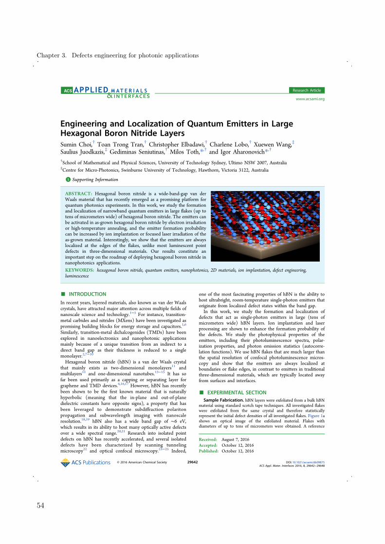
Engineering and Localization of Quantum Emitters in LargeHexagonal Boron Nitride LayersSumin Choi,† Toan Trong Tran,† Christopher Elbadawi,† Charlene Lobo,† Xuewen Wang,‡
Saulius Juodkazis,‡ Gediminas Seniutinas,† Milos Toth,*,† and Igor Aharonovich*,†
†School of Mathematical and Physical Sciences, University of Technology Sydney, Ultimo NSW 2007, Australia‡Centre for Micro-Photonics, Swinburne University of Technology, Hawthorn, Victoria 3122, Australia
*S Supporting Information
ABSTRACT: Hexagonal boron nitride is a wide-band-gap van derWaals material that has recently emerged as a promising platform forquantum photonics experiments. In this work, we study the formationand localization of narrowband quantum emitters in large flakes (up totens of micrometers wide) of hexagonal boron nitride. The emitters canbe activated in as-grown hexagonal boron nitride by electron irradiationor high-temperature annealing, and the emitter formation probabilitycan be increased by ion implantation or focused laser irradiation of theas-grown material. Interestingly, we show that the emitters are alwayslocalized at the edges of the flakes, unlike most luminescent pointdefects in three-dimensional materials. Our results constitute animportant step on the roadmap of deploying hexagonal boron nitride innanophotonics applications.
KEYWORDS: hexagonal boron nitride, quantum emitters, nanophotonics, 2D materials, ion implantation, defect engineering,luminescence
■ INTRODUCTION
In recent years, layered materials, also known as van der Waalscrystals, have attracted major attention across multiple fields ofnanoscale science and technology.1−5 For instance, transition-metal carbides and nitrides (MXens) have been investigated aspromising building blocks for energy storage and capacitors.1,6
Similarly, transition-metal dichalcogenides (TMDs) have beenexplored in nanoelectronics and nanophotonic applicationsmainly because of a unique transition from an indirect to adirect band gap as their thickness is reduced to a singlemonolayer.2,7−10
Hexagonal boron nitride (hBN) is a van der Waals crystalthat mainly exists as two-dimensional monolayers11 andmultilayers12 and one-dimensional nanotubes.13−15 It has sofar been used primarily as a capping or separating layer forgraphene and TMD devices.4,16,17 However, hBN has recentlybeen shown to be the first known material that is naturallyhyperbolic (meaning that the in-plane and out-of-planedielectric constants have opposite signs), a property that hasbeen leveraged to demonstrate subdiffraction polaritonpropagation and subwavelength imaging with nanoscaleresolution.18,19 hBN also has a wide band gap of ∼6 eV,which results in its ability to host many optically active defectsover a wide spectral range.20,21 Research into isolated pointdefects on hBN has recently accelerated, and several isolateddefects have been characterized by scanning tunnelingmicroscopy22 and optical confocal microscopy.23−25 Indeed,
one of the most fascinating properties of hBN is the ability tohost ultrabright, room-temperature single-photon emitters thatoriginate from localized defect states within the band gap.In this work, we study the formation and localization of
defects that act as single-photon emitters in large (tens ofmicrometers wide) hBN layers. Ion implantation and laserprocessing are shown to enhance the formation probability ofthe defects. We study the photophysical properties of theemitters, including their photoluminescence spectra, polar-ization properties, and photon emission statistics (autocorre-lation functions). We use hBN flakes that are much larger thanthe spatial resolution of confocal photoluminescence micros-copy and show that the emitters are always localized atboundaries or flake edges, in contrast to emitters in traditionalthree-dimensional materials, which are typically located awayfrom surfaces and interfaces.
■ EXPERIMENTAL SECTIONSample Fabrication. hBN layers were exfoliated from a bulk hBN
material using standard scotch tape techniques. All investigated flakeswere exfoliated from the same crystal and therefore statisticallyrepresent the initial defect densities of all investigated flakes. Figure 1ashows an optical image of the exfoliated material. Flakes withdiameters of up to tens of micrometers were obtained. A reference
Received: August 7, 2016Accepted: October 12, 2016Published: October 12, 2016
Research Article
www.acsami.org
© 2016 American Chemical Society 29642 DOI: 10.1021/acsami.6b09875ACS Appl. Mater. Interfaces 2016, 8, 29642−29648
Chapter 3. Defects engineering for photonic applications
54

sample and six substrates with exfoliated flakes were prepared forprocessing by ion implantation, laser ablation, and electron irradiation.Ion implantation was explored using boron (B), boron−nitrogen (BN)complexes, silicon (Si), and oxygen (O) ions. B and BN were selectedto test whether the formation probability of intrinsic defects wouldincrease, as these atoms generate mostly vacancies and interstitials.Silicon and oxygen atoms were chosen to determine whether theemitters are related to foreign common impurities, such as oxygen,which is known to be trapped within the hBN lattice during growthand exfoliation.26 A summary of the sample processing details is shownin Figure 1b. The laser ablation and electron beam irradiationtreatments are described below. Unless noted otherwise, the presenteddata are from samples that were annealed for 30 min at 850 °C in anargon environment,23,27 either after exfoliation (reference sample) orafter ion/laser processing.Defect Creation Using Femtosecond Laser Pulse Irradiation.
A Pharos laser system (Light Conversion Co. Ltd.) with a pulseduration (tp) tunable from 230 fs to 10 ps and an average power of 10W, operated using a repetition rate of 200 kHz, was used for laserprocessing of hBN. The second harmonic beam with a wavelength of515 nm was focused onto the sample surface by an oil immersionobjective with a numerical aperture (NA) of 1.4 (Olympus). The focusspot was about 450 nm (d = 1.22λ/NA). The pulse energy was variedin 10% steps from 225 to 90 nJ. A single pulse was delivered to eachsample area, and the irradiated areas were separated by 5 μm. See theSupporting Information for an optical image of the fabricated array.Electron Beam Irradiation of Exfoliated hBN Flakes. Bulk
hBN was mechanically exfoliated onto a Si(111) substrate coveredwith a native oxide layer. The exfoliated flakes were rinsed withacetone and isopropyl alcohol (IPA) and dried under flowing N2. The
samples were then loaded into a variable-pressure FEI field-emission-gun scanning electron microscope. The system was pumped down to ahigh vacuum, and the chamber was filled with water vapor at a pressureof 8 Pa. The hBN flakes were then located using a magnetic-field-assisted gas ionization cascade detector, and electron beam irradiationwas performed using a focused Gaussian electron beam that wasscanned for 1 h over an area of 600 μm2. An accelerating voltage of 15kV was used, and the electron beam fluence delivered to the exposedarea was 5 × 10¹⁸ electrons/cm2. A low electron beam dosage in aH2O environment was specifically used to allow for a very limitedamount of defect formation through an electron-beam-mediatedchemical etching procedure, as outlined in a previous study.28 Thiselectron beam dosage is much lower than that needed to causeelectron-beam-induced etching of hBN, and the irradiation processwas stopped by electron beam blanking.
■ RESULTS AND DISCUSSIONOptical Measurements. Single-photon emission character-
istics were measured at room temperature using scanningconfocal microscopy with a continuous-wave (cw) 532-nm laser(Gem 532, Laser Quantum Ltd.). The laser was directedthrough a half-wave plate and focused on the sample through ahigh-numerical-aperture objective lens (NA 0.9, Nikon).Scanning was performed using an X−Y piezo scanning mirror(FSM-300TM, Newport Corp.). The emission was collectedusing the same objective, filtered through a 532-nm dichroicmirror and a long-pass filter (Semrock), and coupled into amultimode fiber that served as a confocal aperture. Then, a fibersplitter was used to split the light path to two avalanchephotodiodes (APDs) (Excelitas Technologies) for single-photon counting and into a spectrometer (Acton SpectraPro,Princeton Instrument Inc.). While the emission spectra weremeasured using the spectrometer, single-photon detection wasperformed using a using a time-correlated single-photon-counting module (PicoHarp300, PicoQuant). The excitationpolarization of the single-photon emitters was controlled usinga half-wave plate, whereas the emission polarization wasmeasured using a linear polarizer at maximum excitationpolarization. The collected g(2)(τ) curves were fit using a three-level system equation
τ λ τ λ τ= − + − + −g a a( ) 1 (1 ) exp( ) exp( )(2)1 2
where λ1 and λ2 are the decay rates for the radiative andmetastable states, respectively. The polarization behavior was fitby
θ=I I cos imax2
where Imax is the maximum intensity and θi is the angle betweenthe initial polarization direction of light and the transmissionaxis of the polarizer.All optical characterization of the hBN emitters was
performed at room temperature. Panels a−d of Figure 2show photoluminescence (PL) spectra recorded from samplesimplanted with B, BN, O, and Si ions, respectively. The spectrain all cases are similar, showing a zero phonon line (ZPL) at∼600 nm and a weaker second peak near 650 nm. Althoughsome variation in the position of the ZPLs was observed, anabsolute majority of the spectra exhibited two peaks. Aninvestigation of 50 emitters revealed a similar range of spectrafrom each sample investigated in this work (i.e., there were nostatistically meaningful differences between the referencesample and samples subjected to the various ion, laser, andelectron beam irradiation treatments). Interestingly, thedifference between the two peaks seen in each spectrum is
Figure 1. (a) Optical image of exfoliated hBN flakes. (b) Table of theinvestigated samples, comprising a reference sample, four samples thatwere implanted with ions, one sample that was processed with a laserbeam, and one sample that was processed with an electron beam.
ACS Applied Materials & Interfaces Research Article
DOI: 10.1021/acsami.6b09875ACS Appl. Mater. Interfaces 2016, 8, 29642−29648
29643
3.8. Appendix B
55

approximately 160 meV, indicating that all of the emitters havesimilar structures within the hBN lattice.23,25
To ensure that the emission originates from localized singledefects, we recorded the second-order autocorrelation function,g(2)(τ), from each emitter. The functions are shown as insets inFigure 2. The dips at zero delay time (τ = 0) confirm that theluminescence originates from single-photon emitters. The data(blue dots) were fit using a standard three-level model (solidblack line).23 The deviations from zero at τ = 0 are attributed tobackground emissions.Figure 3a shows a comparison of the number of single
emitters found in the implanted flakes versus those found in thereference sample (which had undergone the same annealingtreatment as used to activate the emitters23,27 but without ionimplantation). The implanted flakes show considerably moreemitters than the reference. However, the ion species have littleinfluence on the formation probability of the defects. Thisindicates that the main role of the bombarding ions is tointroduce vacancies and to activate already-present intrinsicpoint defects, rather than to introduce foreign florescent defects(i.e., such as in the case of nitrogen implantation into diamondto produce nitrogen-vacancy (NV) centers29). In addition, weobserved that the emitters in the implanted flakes are mostlyoptically stable and do not exhibit blinking, whereas ∼40% of
the emitters in the reference flakes show severe blinking andeventual bleaching. Figure 3b,c shows typical intensity tracesfrom a stable defect in an ion-implanted flake and a blinkingemitter in a reference sample. We therefore conclude thatimplantation can be used to increase both the emitter activationprobability and the emitter photostability. Further studies areneeded to understand the improved stability of the ion-implanted species. One hypothesis is that the ion implantationprovides sufficient kinetic energy to eliminate some of thetrapped species in the vicinity of the emitter, thereforeeliminating blinking, as previously reported for the NV colorcenter in diamond.30 Finally, we note that emitters in annealedflakes were also observed when the flakes were exfoliated ontoother substrates such as copper or sapphire. We therefore donot believe that the substrate plays an important role in theformation of the emitters.Another important observation is the location of the emitters
within the flakes. In contrast to prior work done using small(∼200-nm-wide) flakes of hBN, the samples used here aresufficiently large to resolve emitter locations within the flakesby confocal microscopy. Figure 4 shows three confocal mapsfrom each implantation batch. White circles indicate quantumemitters. Remarkably, in all case, s the emitters are localized atflake edges. Although similar behavior was reported for excitonsin TMDs,31−33 such defect localization is an unexpectedphenomenon for stable luminescent defects in semiconductors.Indeed, in three-dimensional materials, the formation of stable,
Figure 2. (a−d) PL spectra from hBN flakes implanted with (a) B, (b)BN, (c) O, and (d) Si ions. The insets are second-orderautocorrelation functions, g(2)(τ), recorded from each sample,demonstrating that the emitters are single-photon sources. A spectrumfrom a reference sample and a corresponding g(2)(τ) function areshown in the Supporting Information (Figure S1).
Figure 3. (a) Table comparing the number of formed emitters foundin each ion-implanted sample and a reference sample that wassubjected only to annealing. (b,c) Examples of stability curves from asingle emitter in (b) an ion-implanted flake and (c) a reference flake.Blinking followed by bleaching was much more common in thereference sample than in the implanted samples.
ACS Applied Materials & Interfaces Research Article
DOI: 10.1021/acsami.6b09875ACS Appl. Mater. Interfaces 2016, 8, 29642−29648
29644
Chapter 3. Defects engineering for photonic applications
56

luminescent point defects near crystal edges and surfaces isextremely challenging, and the most stable and brightestemitters are typically located in the bulk, deep within thecrystal.34−36 Emitter localization at interfaces is desirable fordevice fabrication, as it can improve ultimate control overemitter placement and coupling to photonic and plasmoniccavities. We note that, because of the finite resolution of theconfocal microscope, which was ∼300 nm in our experimentalsetup, we cannot conclusively say how far the emitters are fromthe flake edges. However, there is no compelling reason tosuggest that point defects are localized tens or hundreds ofnanometers away from an edge, and it is therefore most likelythat the emitters decorate the edges and crystal boundaries.Interestingly, extended line defects in BN with different
chemical terminations and geometrical variations have beenmodeled and predicted to have unique optoelectronic proper-ties that can result in confined, optically active systems.37
Detailed atomistic modeling and super-resolution imaging willbe required to elucidate this behavior further.Figure 5 shows examples of excitation and emission
polarization recorded for different emitters from differentimplantation batches. More examples are shown in theSupporting Information. Although most of the emitters arefully polarized in both excitation and emission, we did observenumerous emitters that did not show full extinction. This ismost likely because the flakes were not properly adhered to thesubstrate post-exfoliation, creating an angle between the flakeand the excitation laser beam. The polarization behavior istherefore indicative of a dipole-like emitter, with a fastpolarization axis, in accord with earlier studies.23,25 Themisalignment between the excitation and the emissionpolarizations is likely due to redistribution of the excitedelectronic states.Next, we characterized flakes that were processed using an
ultrafast pulsed laser operated at a power just below thethreshold for rapid ablation.38 Ultrashort laser pulses areefficient sources of free-electron acceleration because of theirhigh peak intensities. Free electrons accelerated to energiesgreater than the band gap are efficient in forming defect andbreaking chemical bonds. Color center formation in dielectricmaterials is typical under femtosecond-laser irradiation at suchfluences/irradiances.39 Figure 6a shows a confocal map of thesample, whereas Figure 6b shows a photoluminescencespectrum recorded from a single emitter found in these flakes.The inset is a corresponding g(2)(τ) curve that confirms single-photon emission from this defect. Similarly to the ionimplantation case, the emitter exhibits full polarization behaviorin both excitation and emission, as can be seen in Figure 6c.The original size of the flakes was large, similar to those of
the flakes shown in Figure 1a. However, the laser processcaused some of the flakes to break up into many smallfragments. This resulted in more observed emitters per similarscan area.Finally, we used a deterministic electron-beam-induced
irradiation technique to fabricate the emitters in specific hBNflakes. (This technique was used previously to fabricate emittersin submicrometer hBN flakes that were too small to determineemitter locations within the limits of diffraction-limitedconfocal microscopy.27) Figure 7a,b shows a flake before andafter electron beam irradiation with a 15 keV electron beam in a
Figure 4. Confocal maps from (a−c) B-, (d−f) BN-, (g−i) O-, and (j−l) Si-implanted hBN flakes, demonstrating unambiguously that theemitters are always localized at flake edges. Large bright features seenaway from flake edges, as in map i, do not exhibit photon antibunchingand do not have the spectral characteristics of the single-photonemitters discussed in this study.
Figure 5. (a−d) Examples of excitation (red circles) and emission (blue squares) polarization plots of single emitters from each of the implantedsamples. All of the emitters exhibit dipole-like behavior in both excitation and emission.
ACS Applied Materials & Interfaces Research Article
DOI: 10.1021/acsami.6b09875ACS Appl. Mater. Interfaces 2016, 8, 29642−29648
29645
3.8. Appendix B
57

H2O vapor environment (see Experimental Section). Figure 7cshows photoluminescence spectra recorded from the pristineflake (blue) and after the irradiation treatment (red). Note thatthe spectra were recorded from the same location, as indicatedby the white circles in Figure 7a,b. The inset is a g(2)(τ)function that confirms that the probed emitter is a single-photon source. Figure 7d shows the corresponding polarization
measurements from the same emitter. This sample was notannealed after electron beam irradiation because annealing isnot required for emitter activation, in contrast to emittersgenerated by the ion and laser irradiation treatments. This canbe explained by the fact that ion implantation and laserirradiation generate significant damage in the hBN lattice thatpartly recovers during annealing. On the other hand, irradiation
Figure 6. Fabrication of emitters using laser processing. (a) Confocal map of the hBN flakes. The white circle indicates the presence of the locationof a single-photon emitter. (b) PL spectrum recorded from the emitter. Inset: g(2)(τ) curve confirming that it is indeed a single-photon emitter. (c)Excitation (red circles) and emission (blue squares) polarization curves recorded from this emitter.
Figure 7. Fabrication of emitters by electron beam irradiation. Confocal map of the same flake (a) before and (b) after electron beam irradiation.The energy of the beam was 15 keV. (c) Spectra recorded from a particular location before (blue curve) and after (red curve) irradiation. Inset:g(2)(τ) curve confirming that the formed defect is a single-photon source. (d) Excitation and emission polarization from the same defect. The samplewas not annealed after electron irradiation.
ACS Applied Materials & Interfaces Research Article
DOI: 10.1021/acsami.6b09875ACS Appl. Mater. Interfaces 2016, 8, 29642−29648
29646
Chapter 3. Defects engineering for photonic applications
58

with 15 keV electrons in H2O vapor is a subtler process thatchemically reforms the lattice, with minimal damage to thesurrounding crystallographic environment. The electron beamapproach is therefore appealing, as it allows emitter fabricationand localization in a single step, without the use of lithographicmasks or postprocessing treatments. The emitters fabricatedwith an electron beam had the same spectral and polarizationcharacteristics as those made by ion and laser irradiation, andthey were located consistently at flake edges. Further work isneeded to determine whether the electron beam creates newdefects or activates pre-existing defects that are present in as-grown hBN.
■ CONCLUSIONSTo summarize, we have presented an extensive study of singleemitters in large layered hBN. We found that ion implantationor laser ablation followed by annealing are efficient methods togenerate the emitters. According to our results, theimplantation species increase only the stability of the emittersbut not their formation probability. Further studies to elucidatethe role of the implanted species are required. We also observedthat the emitters are always localized at flake edges, indicatingthat flake morphological defects might play a role in theformation of these quantum emitters. Finally, we showed thatelectron beam irradiation can be used to fabricate emitters in aparticular flake. Overall, the emitters are polarized and opticallyphotostable, and therefore, they are very promising for futurequantum photonics and quantum optoelectronic applications.The ability to engineer the emitters in large hBN flakes that arereadily transferable to different substrates is promising for theuse of hBN in hybrid quantum photonic devices.
■ ASSOCIATED CONTENT*S Supporting InformationThe Supporting Information is available free of charge on theACS Publications website at DOI: 10.1021/acsami.6b09875.
Further optical characterization, including optical imagesand polarization measurments of the investigatedemitters and Monte Carlo modeling of the implantedspecies (PDF)
■ AUTHOR INFORMATIONCorresponding Authors*E-mail: [email protected].*E-mail: [email protected] authors declare no competing financial interest.
■ ACKNOWLEDGMENTSIon implantation was performed at the Department ofElectronic Materials Engineering, RSPE (ANU). The workwas supported in part by the Australian Research Council(ARC) (DP140102721, IH150100028 ARC Research Hub forIntegrated Device for End-User Analysis at Low Levels), FEICompany, and AOARD Grant FA2386-15-1-4044. I.A. is therecipient of an ARC Discovery Early Career Research Award(DE130100592).
■ REFERENCES(1) Naguib, M.; Mashtalir, O.; Carle, J.; Presser, V.; Lu, J.; Hultman,L.; Gogotsi, Y.; Barsoum, M. W. Two-Dimensional Transition MetalCarbides. ACS Nano 2012, 6, 1322−1331.
(2) Xia, F.; Wang, H.; Xiao, D.; Dubey, M.; Ramasubramaniam, A.Two-Dimensional Material Nanophotonics. Nat. Photonics 2014, 8,899−907.(3) Fiori, G.; Bonaccorso, F.; Iannaccone, G.; Palacios, T.; Neumaier,D.; Seabaugh, A.; Banerjee, S. K.; Colombo, L. Electronics Based onTwo-Dimensional Materials. Nat. Nanotechnol. 2014, 9, 768−779.(4) Geim, A. K.; Grigorieva, I. V. Van Der Waals Heterostructures.Nature 2013, 499, 419−425.(5) Yang, J.; Wang, Z.; Wang, F.; Xu, R.; Tao, J.; Zhang, S.; Qin, Q.;Luther-Davies, B.; Jagadish, C.; Yu, Z.; Lu, Y. Atomically Thin OpticalLenses and Gratings. Light: Sci. Appl. 2016, 5, e16046.(6) Chen, W.-F.; Muckerman, J. T.; Fujita, E. Recent Developmentsin Transition Metal Carbides and Nitrides as Hydrogen EvolutionElectrocatalysts. Chem. Commun. 2013, 49, 8896−8909.(7) Liu, X.; Galfsky, T.; Sun, Z.; Xia, F.; Lin, E.-c.; Lee, Y.-H.; Kena-Cohen, S.; Menon, V. M. Strong Light−Matter Coupling in Two-Dimensional Atomic Crystals. Nat. Photonics 2015, 9, 30−34.(8) Sie, E. J.; McIver, J. W.; Lee, Y.-H.; Fu, L.; Kong, J.; Gedik, N.Valley-Selective Optical Stark Effect in Monolayer WS2. Nat. Mater.2015, 14, 290−294.(9) Wu, S.; Buckley, S.; Schaibley, J. R.; Feng, L.; Yan, J.; Mandrus, D.G.; Hatami, F.; Yao, W.; Vuckovic, J.; Majumdar, A.; Xu, X. MonolayerSemiconductor Nanocavity Lasers with Ultralow Thresholds. Nature2015, 520, 69−72.(10) Eda, G.; Yamaguchi, H.; Voiry, D.; Fujita, T.; Chen, M.;Chhowalla, M. Photoluminescence from Chemically Exfoliated Mos2.Nano Lett. 2011, 11, 5111−5116.(11) Lin, Y.; Connell, J. W. Advances in 2d Boron NitrideNanostructures: Nanosheets, Nanoribbons, Nanomeshes, and Hybridswith Graphene. Nanoscale 2012, 4, 6908−39.(12) Pakdel, A.; Bando, Y.; Golberg, D. Nano Boron Nitride Flatland.Chem. Soc. Rev. 2014, 43, 934−959.(13) Jiang, X.-F.; Weng, Q.; Wang, X.-B.; Li, X.; Zhang, J.; Golberg,D.; Bando, Y. Recent Progress on Fabrications and Applications ofBoron Nitride Nanomaterials: A Review. J. Mater. Sci. Technol. 2015,31, 589−598.(14) Ahmad, P.; Khandaker, M. U.; Amin, Y. M. A ComprehensiveStudy of Boron Nitride Nanotubes Multiple Synthesis from a SinglePrecursor. Indian J. Phys. 2015, 89, 209−216.(15) Ahmad, P.; Khandaker, M. U.; Amin, Y. M. Synthesis of BoronNitride Nanotubes by Argon Supported Thermal Chemical VaporDeposition. Phys. E 2015, 67, 33−37.(16) Roy, T.; Tosun, M.; Kang, J. S.; Sachid, A. B.; Desai, S. B.;Hettick, M.; Hu, C. C.; Javey, A. Field-Effect Transistors Built from AllTwo-Dimensional Material Components. ACS Nano 2014, 8, 6259−6264.(17) Li, L. H.; Chen, Y. Atomically Thin Boron Nitride: UniqueProperties and Applications. Adv. Funct. Mater. 2016, 26, 2594−2608.(18) Dai, S.; Fei, Z.; Ma, Q.; Rodin, A. S.; Wagner, M.; McLeod, A.S.; Liu, M. K.; Gannett, W.; Regan, W.; Watanabe, K.; Taniguchi, T.;Thiemens, M.; Dominguez, G.; Neto, A. H. C.; Zettl, A.; Keilmann, F.;Jarillo-Herrero, P.; Fogler, M. M.; Basov, D. N. Tunable PhononPolaritons in Atomically Thin Van Der Waals Crystals of BoronNitride. Science 2014, 343, 1125−1129.(19) Caldwell, J. D.; Kretinin, A. V.; Chen, Y.; Giannini, V.; Fogler,M. M.; Francescato, Y.; Ellis, C. T.; Tischler, J. G.; Woods, C. R.;Giles, A. J.; Hong, M.; Watanabe, K.; Taniguchi, T.; Maier, S. A.;Novoselov, K. S. Sub-Diffractional Volume-Confined Polaritons in theNatural Hyperbolic Material Hexagonal Boron Nitride. Nat. Commun.2014, 5, 5221.(20) Cassabois, G.; Valvin, P.; Gil, B. Hexagonal Boron Nitride Is anIndirect Bandgap Semiconductor. Nat. Photonics 2016, 10, 262−266.(21) Museur, L.; Feldbach, E.; Kanaev, A. Defect-Related Photo-luminescence of Hexagonal Boron Nitride. Phys. Rev. B: Condens.Matter Mater. Phys. 2008, 78, 155204.(22) Wong, D.; Velasco, J., Jr; Ju, L.; Lee, J.; Kahn, S.; Tsai, H.-Z.;Germany, C.; Taniguchi, T.; Watanabe, K.; Zettl, A.; Wang, F.;Crommie, M. F. Characterization and Manipulation of Individual
ACS Applied Materials & Interfaces Research Article
DOI: 10.1021/acsami.6b09875ACS Appl. Mater. Interfaces 2016, 8, 29642−29648
29647
3.8. Appendix B
59
Defects in Insulating Hexagonal Boron Nitride Using ScanningTunnelling Microscopy. Nat. Nanotechnol. 2015, 10, 949−953.(23) Tran, T. T.; Bray, K.; Ford, M. J.; Toth, M.; Aharonovich, I.Quantum Emission from Hexagonal Boron Nitride Monolayers. Nat.Nanotechnol. 2016, 11, 37−41.(24) Tran, T. T.; Zachreson, C.; Berhane, A. M.; Bray, K.;Sandstrom, R. G.; Li, L. H.; Taniguchi, T.; Watanabe, K.;Aharonovich, I.; Toth, M. Quantum Emission from Defects inSingle-Crystalline Hexagonal Boron Nitride. Phys. Rev. Appl. 2016, 5,034005.(25) Jungwirth, N. R.; Calderon, B.; Ji, Y.; Spencer, M. G.; Flatte, M.E.; Fuchs, G. D. Temperature Dependence of Wavelength SelectableZero-Phonon Emission from Single Defects in Hexagonal BoronNitride. Nano Lett. 2016, 16, 6052.(26) Petravic, M.; Peter, R.; Kavre, I.; Li, L. H.; Chen, Y.; Fan, L.-J.;Yang, Y.-W. Decoration of Nitrogen Vacancies by Oxygen Atoms inBoron Nitride Nanotubes. Phys. Chem. Chem. Phys. 2010, 12, 15349−15353.(27) Tran, T. T.; Elbadawi, C.; Totonjian, D.; Lobo, C. J.; Grosso,G.; Moon, H.; Englund, D. R.; Ford, M. J.; Aharonovich, I.; Toth, M.Robust Multicolor Single Photon Emission from Point Defects inHexagonal Boron Nitride. ACS Nano 2016, 10, 7331−7338.(28) Elbadawi, C.; Tran, T. T.; Kolibal, M.; Sikola, T.; Scott, J.; Cai,Q.; Li, L. H.; Taniguchi, T.; Watanabe, K.; Toth, M.; Aharonovich, I.;Lobo, C. Electron Beam Directed Etching of Hexagonal BoronNitride. Nanoscale 2016, 8, 16182−16186.(29) Pezzagna, S.; Naydenov, B.; Jelezko, F.; Wrachtrup, J.; Meijer, J.Creation Efficiency of Nitrogen-Vacancy Centres in Diamond. New J.Phys. 2010, 12, 065017.(30) Wolters, J.; Sadzak, N.; Schell, A. W.; Schroder, T.; Benson, O.Measurement of the Ultrafast Spectral Diffusion of the OpticalTransition of Nitrogen Vacancy Centers in Nano-Size Diamond UsingCorrelation Interferometry. Phys. Rev. Lett. 2013, 110, 027401.(31) Tonndorf, P.; Schmidt, R.; Schneider, R.; Kern, J.; Buscema, M.;Steele, G. A.; Castellanos-Gomez, A.; van der Zant, H. S. J.; Michaelisde Vasconcellos, S.; Bratschitsch, R. Single-Photon Emission fromLocalized Excitons in an Atomically Thin Semiconductor. Optica2015, 2, 347−352.(32) Bao, W.; Borys, N. J.; Ko, C.; Suh, J.; Fan, W.; Thron, A.; Zhang,Y.; Buyanin, A.; Zhang, J.; Cabrini, S.; Ashby, P. D.; Weber-Bargioni,A.; Tongay, S.; Aloni, S.; Ogletree, D. F.; Wu, J.; Salmeron, M. B.;Schuck, P. J. Visualizing Nanoscale Excitonic Relaxation Properties ofDisordered Edges and Grain Boundaries in Monolayer MolybdenumDisulfide. Nat. Commun. 2015, 6, 7993.(33) Gutierrez, H. R.; Perea-Lopez, N.; Elías, A. L.; Berkdemir, A.;Wang, B.; Lv, R.; Lopez-Urías, F.; Crespi, V. H.; Terrones, H.;Terrones, M. Extraordinary Room-Temperature Photoluminescence inTriangular Ws2Monolayers. Nano Lett. 2013, 13, 3447−3454.(34) Staudacher, T.; Ziem, F.; Haussler, L.; Stohr, R.; Steinert, S.;Reinhard, F.; Scharpf, J.; Denisenko, A.; Wrachtrup, J. Enhancing theSpin Properties of Shallow Implanted Nitrogen Vacancy Centers inDiamond by Epitaxial Overgrowth. Appl. Phys. Lett. 2012, 101,212401.(35) Aharonovich, I.; Lee, J. C.; Magyar, A. P.; Buckley, B. B.; Yale, C.G.; Awschalom, D. D.; Hu, E. L. Homoepitaxial Growth of SingleCrystal Diamond Membranes for Quantum Information Processing.Adv. Mater. 2012, 24, OP54−OP59.(36) Santori, C.; Barclay, P. E.; Fu, K.-M. C.; Beausoleil, R. G.Vertical Distribution of Nitrogen-Vacancy Centers in DiamondFormed by Ion Implantation and Annealing. Phys. Rev. B: Condens.Matter Mater. Phys. 2009, 79, 125313.(37) Li, X.; Wu, X.; Zeng, X. C.; Yang, J. Band-Gap Engineering ViaTailored Line Defects in Boron-Nitride Nanoribbons, Sheets, andNanotubes. ACS Nano 2012, 6, 4104−4112.(38) Buividas, R.; Aharonovich, I.; Seniutinas, G.; Wang, X. W.; Rapp,L.; Rode, A. V.; Taniguchi, T.; Juodkazis, S. Photoluminescence fromVoids Created by Femtosecond-Laser Pulses inside Cubic-Bn. Opt.Lett. 2015, 40, 5711−5713.
(39) Kudrius, T.; Slekys, G.; Juodkazis, S. Surface-Texturing ofSapphire by Femtosecond Laser Pulses for Photonic Applications. J.Phys. D: Appl. Phys. 2010, 43, 145501.
ACS Applied Materials & Interfaces Research Article
DOI: 10.1021/acsami.6b09875ACS Appl. Mater. Interfaces 2016, 8, 29642−29648
29648
Chapter 3. Defects engineering for photonic applications
60
Chapter 4
Pancharatnam-Berry phase
optical elements
4.1 Introduction
Miniaturizing the feature dimensions of optical components and developinghighly integrated optical devices and systems is a long standing goal [114–116].The conventional optical components such as lenses, axicons, prisms, phaseplates, wave-plates and polarizers modify the wavefront of light using thephase accumulation along the optical pass along propagation. Since the refrac-tive indices of optical transparent materials in nature are limited, the opticallength for shaping the desired wavefront has to be many times longer thanthe designed wavelength of the incident light. The development of micro-nanofabrication techniques are presenting opportunities to control light in a waythat is not possible with the materials in nature. Artificial structures builtup from subwavelength elements can now be fabricated with a desired spatialdistribution of effective permittivity ε and permeability μ, thereby offering thepotential to guide and control the flow of electromagnetic energy in an engi-neered optical space. These artificial structures are also called metasurfaceshave opened the door to scale down the optical elements to subwavelengththickness.
Recently, new types of structured plasmonic metasurfaces that introduce anabrupt phase and polarization discontinuity on the sub-wavelength thicknessinterface for shaping the wavefront of electromagnetic waves have been demon-strated [117], which leads to many achievements and can replace bulky opticalelements by thin metasurfaces with different wavefront engineering functional-ities, such as nigh NA foucsing lens [118], broadband quarter waveplates [119],flat lenses and axicons [120–123], optical vortex plates [124, 125], and polariz-ers [126]. While the major issues such as the fundamental limitation of 25%efficiency [127] of a single layer metasurface, ohmic loss and cost-ineffectivefabrication of plasmonic metasurfaces are hampering the development of flat
61

Chapter 4. Pancharatnam-Berry phase optical elements
optics based on metasurface technologies and has to be resolved [128]. Low-losselectromagnetic responses covering all four quadrants of possible permittivitiesand permeabilities using transparent and high-refractive index dielectric build-ing blocks have received much attention during the recent years due to theircapability to address the efficiency issue in metallic metasurfaces [129,130].
One way to reduce the loss and break the fundamental efficiency limit isto use high contrast gratings fabricated from high refractive index dielectricsor semiconductors [127]. Different flat optical elements based on dielectricmetasurfaces were demonstrated. Large numerical aperture flat focusing lenswith 0.57 λ and focusing efficiency up to 82% was reported [118]. High re-flective flat focusing mirror was realized with dielectric gratings [131], mul-tiwavelength achromatic metasurfaces of flat lens based on silicon [132], po-larization converters with more than 98% efficiency [133] were demonstrated.With patterned elliptical silicon nano rods, high transmission efficiency ap-proaching 97% was reported [134], achromatic focusing lens with silicon arraysworking at telecommunication wavelength was realized [135]. One type of thedielectric metasurfaces based on high contrast subwavelength gratings couldintroduce geometrical phase by manipulating the localized polarization stateof the propagation beam in space varying orientation, which is also called thePancharatnam-Berry phase metasurface optical elements [116,136–145]. Manyendeavors are focused on this type of dielectric metasurfaces to achieve desiredflat optical elements, such as lenses, axicons, polarization converters, vortexgenerators working from IR to visible spectral range. Using the dielectric meta-surface optical elements based on dielectric materials could reduce the ohmicloss and improve the efficiency of transmissive properties. The high contrastdielectric materials like Si or Si3N4 are always associated with some amountof omnic losses in the visible wavelength even comparably much smaller thanthe plasmonic metallic materials. Much lower contrast materials like TiO2 areproposed recently to be applied to building up low loss and high transmissionand conversion efficiency photonic devices with scarifying the structure heightfrom 100 nm for Si to 600 nm [146,147]. However, the cost-ineffective fabrica-tion process involving electron beam lithography (EBL), ion beam lithography(IBL) and other nanofabrication based processes still hinder practical applica-tions and further developments of on-chip photonic devices.
A novel approach to achieve simple, effective and inexpensive fabrication offlat optical elements is to utilize the micro and nanoscale 3D fabrication capa-bility of direct femtosecond laser writing. The spatial resolution of femtosecondlaser writing features can reach to sub 100 nm scale, due to the nonlinear ab-sorption process for processing dielectric materials. With 3D direct writinginside the transparent dielectric materials, manipulating the wavefront of theincident light can be done by the fabricated structures inside the substrate or3D polymerization. Using nanogratings formed by femtosecond laser irradia-tion inside fused silica can be used as a phase plate to generate optical vortexbeams with rotational wavefront [148], or 3D laser polymerization of spiral
62

4.2. Pancharatnam-Berry Phase
plates to generate optical vortices [149].
Hence, the femtosecond laser pulses direct writing gives a way to over-come the cost-ineffective fabrication of planar optical elements, especially thePacharatnam-Berry phase optical elements based on varying the orientationof the axis of the birefringence for manipulation of the polarization states ofthe incident beam. With this approach, the design and fabrication of differ-ent optical functional planar optics are simply linked to the control of thegeometry of the structure by tuning the fabrication conditions and movementtranslation stages. This fabrication technique is only one step process, withoutvacuum and clean room environment requirements, which considerably reducethe fabrication time and complexity.
In this chapter, different laser fabrication techniques including direct laserpolymerization, direct laser ablation and stress engineering to create space-variant orientational birefringence structures will be presented and used todemonstrate the capability and novelty of direct femtosecond laser writing toachieve functional planar optical elements.
4.2 Pancharatnam-Berry Phase
When a polarized electromagnetic wave undergos a closed loop in the spaceof polarization states in the Poincare sphere, it acquires not only a dynamicphase, which is accumulated along its optical path, but also a geometric phase,which is half of the solid angle in the closed loop on the Poincare sphere [150].This geometric phase was firstly proposed by Pancharatnam in his work forgeneralization of interference fringes of different polarized beams [151]. In 1984,Berry observed an geometric phase factor induced in a quantum-mechanicalsystem when its Hamiltonian was slowly changed and return back to its originstate [152]. And later he connected Pancharatnam phase of electromagneticwaves induced by a cyclic change of polarization state on the Poincare sphereto any adiabatic phase changes for a slow cyclic quantum system, which is alsoan optical analogue to the Aharonov-Bohm effect [150]. Pancharatnam’s workgives a way to engineer optical phase via beam polarization manipulation in theclassical light field, while Berry’s work broadens this concept to the quantumsystem region. Regarding the importance of their work, the geometric phasewas also called Pancharatnam-Berry phase. This project is aiming to engineerthe wavefront of light by altering the localized polarization state of the beamto introduce Pancharatnam-Berry phase employing birefringence structuresfabricated by femtosecond laser pulses.
63

Chapter 4. Pancharatnam-Berry phase optical elements
LP QWP
BS 1
Lens CCDLaser
A
BS 2
Mirror Mirror
Analyser C
S2
S1
S3A
(B)O
C
Fringes
cb
a
Analyser B
1
2𝑎
Fast axis
HLP VLP
RCP
Figure 4.1: Illustration of the induced Pancharatnam-Berry phase of an ellipti-cal polarized beam A decomposed into two beams with specific linear polariza-tion states B and C, interference fringes could be observed on the CCD imageof B and C. The phase difference δ is half of the solid angle of the colored re-gion on the Poincare sphere (BC = a, AC = b, AB = c). BS1 and BS2 are thetwo beam splitters. LP is the linear polarizer; QWP is the quater waveplate.S1, S2 and S3 are the Stokes parameters of a Pointcare sphere. HLP, VLPand RCP are the horizontal linear polarization, vertical linear polarization andrigh-hand circular polarization, respectively. Analyzer B and C are of an anglea2 .
4.3 Fundamentals of geometric phase
manipulation
The intensity distribution A of the superposition of any two coherent beamsB and C, of intensities IB and IC in the polarization states of B and C, respec-tively, could be given by the general interference formula [151]:
IA = IB + IC + 2√
IBIC cos1
2a cos δ, (4.1)
where a is the angular separation of the states B and C on the Poincare sphere,which is also called ”similarity factor”, and δ is the phase difference betweentwo beams B and C.
While the inverse process of Eq. 4.1 is of concern in this project whichmanipulates the space variation of the polarization state to achieve desirablephase distribution of the beam. In the general case polarization manipulationinduces the Pancharatnam-Berry phase as shown in Fig. 4.1. If a beam inthe polarization state of A (arbitrarily polarized) with an intensity IA is de-composed into two coherent beams with specific polarization states of B and
64

4.3. Fundamentals of geometric phase manipulation
LP QWP
BS 1
Lens CCDLaser
A
BS 2
Mirror Mirror
HWP1
S2
S1
S3 (A)
O
Fringes
HWP2
B
B
𝜃
𝛼
Fast axis
RCP
LCP
HLPVLP
Figure 4.2: Illustration of the induced Pancharatnam-Berry phase δ of anRight-handed circular polarized (RCP) beam A passing through two successivehalf waveplates (HWP1 and HWP2); interference fringes could be observed onthe CCD image. The phase difference δ is half of the solid angle of the coloredregion on the Poincare sphere (δ = 1
2Ω = α = 2θ). LP is linear polarizer; QWPis quater waveplate (at 45◦ respect to LP); BS1 and BS2 are two non-polarizedbeam splitters. The fast axis of the HWP1 and HWP2 are with an angle of θ.
C (linearly polarized), these two beams will have a definite phase difference δbetween them and definite intensities IB and IC [151]:
IB = IA ·sin2 1
2b
sin2 12a
, IC = IA ·sin2 1
2c
sin2 12a
, (4.2)
δ = arccossin2 1
2b + sin2 12c – sin2 1
2a
2 sin 12a sin 1
2b sin 12c
=1
2Ω, (4.3)
here a, b and c are the angular separations of BC, CA and BA respectively,δ is the phase difference between two beams, and Ω is the enclosure sphericaltriangle area of these three polarization states on the Poincare sphere, whichis the solid angle of the sphere triangle Ω.
As a specific case when the polarization state of the light undergone aclosed loop on the Poincare sphere manipulated by a half waveplate, is shownin Fig. 4.2. Then an additional phase difference (disregarding the dynamicphase change) between the original beam and the output beam is given by:
δ =1
2Ω = 2θ (4.4)
where Ω is the area of the lune, as shown by coloured region in Fig. 4.2, whichis equal to 2α, while α = 2θ, θ is the rotation angle of the HWP2 respect toHWP1. The induced phase δ in Eq. 4.3 and Eq. 4.4 is called Pancharatnam-Berry phase.
65
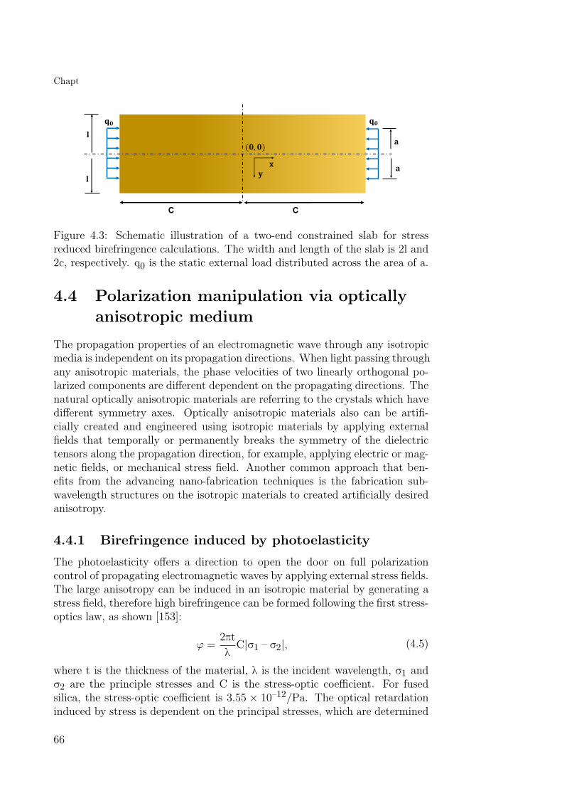
Chapter 4. Pancharatnam-Berry phase optical elements
𝐪𝟎 𝐪𝟎
C C
𝐥
𝐥
𝐚
𝐚𝐱
𝐲
(𝟎, 𝟎)
Figure 4.3: Schematic illustration of a two-end constrained slab for stressreduced birefringence calculations. The width and length of the slab is 2l and2c, respectively. q0 is the static external load distributed across the area of a.
4.4 Polarization manipulation via optically
anisotropic medium
The propagation properties of an electromagnetic wave through any isotropicmedia is independent on its propagation directions. When light passing throughany anisotropic materials, the phase velocities of two linearly orthogonal po-larized components are different dependent on the propagating directions. Thenatural optically anisotropic materials are referring to the crystals which havedifferent symmetry axes. Optically anisotropic materials also can be artifi-cially created and engineered using isotropic materials by applying externalfields that temporally or permanently breaks the symmetry of the dielectrictensors along the propagation direction, for example, applying electric or mag-netic fields, or mechanical stress field. Another common approach that ben-efits from the advancing nano-fabrication techniques is the fabrication sub-wavelength structures on the isotropic materials to created artificially desiredanisotropy.
4.4.1 Birefringence induced by photoelasticity
The photoelasticity offers a direction to open the door on full polarizationcontrol of propagating electromagnetic waves by applying external stress fields.The large anisotropy can be induced in an isotropic material by generating astress field, therefore high birefringence can be formed following the first stress-optics law, as shown [153]:
ϕ =2πt
λC|σ1 – σ2|, (4.5)
where t is the thickness of the material, λ is the incident wavelength, σ1 andσ2 are the principle stresses and C is the stress-optic coefficient. For fusedsilica, the stress-optic coefficient is 3.55 × 10⁻¹²/Pa. The optical retardationinduced by stress is dependent on the principal stresses, which are determined
66
4.4. Polarization manipulation via optically anisotropic medium
by the type of the loading forces and the geometry shape of the material. Theprincipal stresses can be calculated by the x, y and shear stress componentsusing [154]:
σ1,σ2 =σxx + σyy
2±√(σxx – σyy
2
)2+ τ2xy
(4.6)
where σxx, σyy and τxy are the x, y and shear component of stress. As anexample, for a two-end constraint slab model with applying force, as shownin Fig. 4.3, the x, y and shear components of stress field can be calculatedquantitatively by Finite Element Modeling (FEM) [155]:
σxx = β+ γ∞∑
m=1
sin(αa)
m
[αcch(αc) – sh(αc)]ch(αy) – αysh(αy)ch(αc)
sh(2αc) + 2αccos(αx),
σyy = –β – γ∞∑
m=1
sin(αa)
m
[αcch(αc) + sh(αc)]ch(αy) – αysh(αy)ch(αc)
sh(2αc) + 2αccos(αx),
τxy = β+ γ∞∑
m=1
sin(αa)
m
αcch(αc)sh(αy) – αych(αy)sh(αc)
sh(2αc) + 2αcsin(αx),
(4.7)
where α = mπl , β =
q0al , γ =
4q0Dlπ , sh = sinh, and ch = cosh,m is an integer.
Using this approach, polarizations can be manipulated in single optical fibresor photonic crystal fibres by using greatly different linear expansion coefficientmaterials for cladding and core by thermally/mechanically stretching [156,157].
4.4.2 Birefringence induced by dielectric binarygratings
When light passing through a binary grating, due to its periodical modula-tion properties of the spatial distribution of the refractive index, the phase,amplitude and polarization of the incident wave will be modified. The illustra-tion of a general case of an electromagnetic wave incident on a binary gratingstructure is shown in Fig. 4.4. A linearly polarized electromagnetic wave isincident at an arbitrary angle ξ and at an azimuthal angle θ. The gratingperiod Λ is, in general, consist of regions with different refractive indices. Herethe grating is composed by refractive index of air n0 and grating material n1.The width and height of grating are t1 and h, respectively, and the duty cycleis q = t1/Λ. The refractive index of the substrate is n2. When the gratingperiod is far smaller than the wavelength of the incident light (Λ << λ, calledsubwavelength grating), light propagating through the subwavelength gratingcould be approximately treated as light traveling through a homogenous me-dia [158]. Only the zero order diffraction beam is propagating and all theother orders are evanescent. The grating structures behave similar to uniaxialcrystals. From the grating diffraction equation, the threshold condition forthe nanograting period when only the zero order is propagating through the
67

Chapter 4. Pancharatnam-Berry phase optical elements
TE
𝛏
𝛉
𝐧𝟎=1 𝐱
𝐲
𝐳
𝐧𝟎𝐧𝟏
𝐧𝟐𝚲
𝐭𝟏
𝐪 = 𝐭𝟏/𝚲𝐡
air
air
substrate
𝐧𝟎=1
Figure 4.4: Illustration of an polarized beam passing through a nanogratingstructured surface from air with an incident angle of ξ respect to z axis andθ respect to x axis. The grating period is Λ and duty cycle ( fill factor ) isq = t1/Λ, t1 is width of the grating ridge. The thickness of the grating is h,and refractive index of air, film and substrate are n0, n1 and n2 respectively.
structure could be derived as:
Λth =
λ
(n0 sin ξ+ n2) cosθ, (4.8)
Since the subwavelength grating behaves like an uniaxial crystal, then onlyzero order propagates through, and the effective medium theory (EMT) couldbe used to analyze the polarization change after passing through the gratingstructure. In Fig. 4.4, the effective refractive indices and the retardation forlight polarized parallel (TE) and perpendicular (TM) to the gratings are givenby:
nTE =√
qn21 + (1 – q)n2
0, nTM =n1n0√
qn20 + (1 – q)n2
1
(4.9)
ϕ = ϕTE – ϕTM =2πh(nTE – nTM)
λ(4.10)
When the period of the grating is approaching to or larger than the wave-length of the incident electromagnetic wave (Λ ≥ λ), the effective medium isnot suitable to estimate the propagation property of the incident wave. Therigorous coupled-wave analysis (RCWA) method and modal analysis have beenwidely used for accurately analyzing the diffraction properties of different typeof grating structures. When a plane wave incidents from the air into the grat-ing, both the TE-polarized and TM-polarized components can be coupled into
68

4.4. Polarization manipulation via optically anisotropic medium
the grating to excite different grating modes. The excited modes can propagateforward in the grating ridge with different propagation constants β = 2π
λneff .
Different propagation modes can be calculated by solving the dispersionequations for TE- and TM-polarization as below derived from the grating andHelmholtz equation [159,160]: For TE-polarization:
F(n2eff) = cos k1(1 – q)Λ · cos k2qΛ –
k21 + k2
2
2k1k2sin k1(1 – q)Λ · sin k2qΛ
= cos αΛ.
(4.11)
and for TM-polarization:
F(n2eff) = cos k1(1 – q)Λ · cos k2qΛ –
n41k2
1 + k22
2n21k1k2
sin k1(1 – q)Λ · sin k2qΛ
= cos αΛ,(4.12)
where k1 = k0
√n2
0 – n2eff , k2 = k0
√n2
1 – n2eff , neff is the effective refractive
index of the excited modes, k0 = 2π/λ, are the wave vector in the groove,ridge and air respectively, α = k0 sin ξ is the wave vector of incident light. Theintersection between F(n2
eff) and cos(αΛ) leads to discrete values of the effectiveindex neff that corresponds to different discrete grating modes. The cos(αΛ) =1 is the case of normal incidence (ξ = 0). Using the dispersion equations,different excited modes both in TE and TM polarized components can becalculated. The efficiency of the incident beam coupled into different excitedmode can be determined by their overlap integrals. For TE-polarization [161,162]:
〈Einy (x)↔ um(x)〉 =
|∫ΛTE0 Ein
y (x)um(x)dx|2∫ΛTE0 |Ein
y (x)|2∫ΛTE0 |um(x)|2dx
, (4.13)
and TM-polarization:
〈Hiny (x)↔ un(x)〉 =
|∫ΛTM0 Hin
y (x)un(x)dx|2∫ΛTM0 |Hin
y (x)|2∫ΛTM0 |un(x)|2dx
, (4.14)
where the um(x) is the electric field of the mth excited grating mode and un(x)is the magnetic field of the nth excited grating mode. Ein
y (x) and Hiny (x) are
the electric and magnetic field of the incident waves. By solving the equationsEq. 4.13 and Eq. 4.14, the efficiency of the energy exchange between the inci-dent light and excited grating modes can be obtained for both polarizations.The excited modes in the grating region with stable phase difference propagateto the output plane and interfere with each other forming different diffractiveorders in the substrate and free space. The phase difference of the excitedmode i and j is given by Δψ = 2π
λ(ni,eff – nj,eff)h. The coupling efficiency of
69
Chapter 4. Pancharatnam-Berry phase optical elements
the excited mode to each diffractive order is given by the similar equation asEq. 4.13 and Eq. 4.14 for TE and TM polarized light. For TE-polarization:
〈Eyp(x)↔ um(x)〉 =|∫ΛTE0 Eyp(x)um(x)dx|2
∫ΛTE0 |Eyp(x)|2
∫ΛTE0 |um(x)|2dx
, (4.15)
and TM-polarization:
〈Hyw(x)↔ un(x)〉 =|∫ΛTM0 Hyw(x)un(x)dx|2
∫ΛTM0 |Hyw(x)|2
∫ΛTM0 |un(x)|2dx
, (4.16)
where Eyp(x) and Hyw(x) are the pth and wth diffraction order for TE and TMpolarization, respectively. The equations of Eq. 4.15 and Eq. 4.16 provide theinformation of the mount of energy exchange from the excited grating modesto the diffracted orders in the far field. The field distribution at the outputplane of the grating then can be expressed as for TE-polarization:
Ey(x, h) =m∑
–m
Epe–ip2πΛ
x =n∑
0
tin,juj(x)e–i2πλ
nj,effh, (4.17)
where m is the highest diffractive orders, and due to the normal incidence, thediffractive orders are symmetric, Ep is the complex amplitude of the electric
field of pth order. While n is the highest order of excited grating modes, j isthe jth grating order, nj,eff is the effective refractive index of the jth grating
mode; tin,j =√〈Ein
y (x)↔ uj(x)〉 is the amplitude of the uj(x) mode coupled
from the TE polarized incident light.and TM-polarization:
Hy(x, h) =m∑
–m
Hwe–iw 2πΛ
x =n∑
–n
tin,juj(x)e–i2πλ
nj,effh, (4.18)
where Hw is the complex amplitude of the magnetic field of wth order; tin,j =√〈Hin
y (x)↔ uj(x)〉 is the amplitude of the uj(x) mode coupled from the TM
polarized incident light. Therefore, the retardation ϕ between the TE and TMcomponents of the incident light after passing through the gratings with periodlarger than the wavelength can be extracted from the equations Eq. 4.17 andEq. 4.18 by applying the RCWA and modal analysis methods.
The change of the polarization state could be tracked using the Poincaresphere, when the phase retardation ϕ and the orientation of the fast axis θare known. If a polarized beam is incident on an uniaxial crystal, the polar-ization state of the emerging beam is the point of the incident polarizationstate reached when the Poincare sphere clockwise rotates ϕ around the fastaxis of the crystal. One example is shown in Fig. 4.5. Right-hand circular
70

4.4. Polarization manipulation via optically anisotropic medium
𝑆1
𝑆2
𝑆3(𝐴)RCP
LCP
HLP
45°LP
VLP
𝐵
𝜑
𝛼
𝑥
𝑦
𝜃
𝑘 (fast axis)
−45°LP
Figure 4.5: Illustration of the procedure to track the emerging polarizationstate (B) using Poincare sphere when an RCP beam (A) is passing througha birefringence structure which has a retardation of ϕ = ϕTE – ϕTM and ori-entation of fast axis is θ in respect to x axis. The Poincare sphere clockwiserotates an angle of ϕ around the fast axis which is α = 2θ respecting to S1axis, and the output polarization state is the point of the incident polarizationstate reached. HLP is horizontal linear polarization; VLP is vertical linear po-larization; RCP and LCP are the right-hand or left-hand circular polarization(the handness is defined for the beam propagating towards observer).
polarized (RCP) beam (definition of the handness is for the beam propagatingtowards observer) normally incidents on a birefringence structure, which hasan orientation of fast axis of θ respect to x axis (x axis is corresponding to thehorizontal linear polarization (HLP) on the Poincare sphere). The polariza-tion state of the output beam could be determined to be B when the Poincaresphere rotates ϕ around the fast axis which is α = 2θ in respect to the S1 axis.
As shown in Fig. 4.5, the retardation of the birefringent structure is ϕ = π,the polarization state of the emerging beam will be changed from RCP to LCPindependent on orientation of the fast axis. The evolution trajectory on thePoincare sphere of the polarization states is dependent on the orientation ofthe fast axis. Varying the orientations of the fast axis of structures, differentgeodesic loops on the Poincare sphere could be generated, at the same timethe different geometric phases will be introduced by Eq. 4.3 and Eq. 4.4.
71

Chapter 4. Pancharatnam-Berry phase optical elements
𝜎+
𝜎−
𝑧
Δ𝑥
𝑘𝑧
𝑘𝑥𝑧
𝑥
(a) (b)
𝑥
𝑑
𝜃
Figure 4.6: An illustration of a photonic spin Hall device that splits differentspins (σ+ for LCP and σ– for RCP polarized light) into different direction, byadding a spin-dependent wave-vector along one direction kx, and a birefrin-gence design (b) with fast-axis rotation along x-axis θ(x) = πx/d (d determinesthe rotational speed of the fast-axis for π), that generating a geometric phaseΨ(x, y) = –σ±2πx/d.
4.5 Dielectric geometric phase optical
elements based on space-variant
orientation birefringence
The birefringence can be artificially created using isotropic materials by ap-plying the photoelasticity with loading stress field, or induced by building theperiodic refractive index composites forming grating structures. Constant re-tardation as discussed above and geometric phases could be introduced fora polarized beam passing through the birefringence structures. By changingthe orientation distribution of the fast/slow axis of the birefringence, a desir-able specific geometric phase distributions can be generated after propagatingthrough a space-variant orientation birefringence structures.
It is convenient to employ the Jones calculus to describe behave of thepolarized beam propagating through a space-variant orientation θ(x, y) bire-fringent structure. The transmission matrix for any point of the element in thehelical basis with RCP and LCP polarization states |R〉 =
(10
)and |L〉 =
(01
)
is given by [137]:
T(x, y) = R(θ)–1T(0, 0)R(θ)
=1
2(tx + tyeiϕ)
(1 00 1
)+
1
2(tx – tyeiϕ)
(0 ei2θ(x,y)
e–i2θ(x,y) 0
),
(4.19)where tx and ty are the real amplitude transmission coefficients of the TE andTM components, θ(x, y) is the orientation of the fast axis in (x,y) position,and θ(0, 0) = 0; R(θ) is the rotation matrix.
For an incident plane wave |Ein〉 with arbitrary polarization state, the
72

4.5. Dielectric geometric phase optical elements based on space-variant orientationbirefringence
(a) (b) (c)
π
2π
0
Figure 4.7: Different birefringence designs (in the fist row) for different func-tional elements that generate different geometric phase and the theoreticalcalculated geometric phase-front that these elements can generate. (a) a lenselement, (b) an axicon element, (c) a vortex beam generator element (q-plate).
emerging electric field after passing through the element is:
|Eout〉 = T(x, y)|Ein〉=√ηE|Ein〉+
√ηRei2θ(x,y)|R〉+
√ηLe–i2θ(x,y)|L〉,
(4.20)
where ηE = |12(tx + tyeiϕ)|2, ηR = |12(tx – tyeiϕ)〈L|Ein〉|2, ηL = |12(tx –
tyeiϕ)〈R|Ein〉|2 are the polarization order coupling coefficients. Here the Diracbracket 〈α|β〉 denotes the inner product, indicating the amplitude of the |α〉component in |β〉.
From Eq. 4.20, it is obvious that the electric field contains three polarizationcomponents. The first term has the original polarization state and phase as theincident beam with an amplitude modification factor of ηE. The second termis the RCP component with an additional phase 2θ(x, y) and an amplitudemodification factor ηR which is not only related to the element but also theamplitude of LCP component in the incident beam, and the third term isthe LCP component with an additional phase opposite to that of the secondcomponent. This property opens a scope to future investigations on fabricatingphotonic spin Hall effect elements [142, 163]. For the specific case that thebirefringence element has retardation of π for TE and TM beams, and theincident wave is |R〉 polarized, the electric field of the emerging beam becomes:
|Eout〉 =1
2(tx – ty)|R〉+
1
2(tx + ty)e–i2θ(x,y)|L〉. (4.21)
From Eq. 4.21 above, the conversion of polarization state is observed, andwhen tx = ty = 1, the conversion efficiency appears 100%. The emerging field
73

Chapter 4. Pancharatnam-Berry phase optical elements
becomes |Eout〉 = e–i2θ(x,y)|L〉. Note that, the phase factor φ(x, y) = –2θ(x, y)is two times of the local fast axis orientation of birefringence structure, whichis according to Eq. 4.4. Hence, by designing the spatially variant orientationof the birefringence, desirable phase distribution of the emerging beam couldbe achieved. Accordingly, optical elements with specific wavefront engineeringfunctionalities could be build using spatially orientated birefringence fabri-cated on dielectric surfaces, such optical elements are called dielectric gradientmetasurface optical elements [140]. As shown in Fig. 4.6, a photonic spin Hallelement that splits the photons into different directions can be designed byvarying the orientation of the fast-axis along one axis with θ(x, y) = π
dx. The
geometric phase that added into the incident beam becomes Φ(x, y) = –σ± 2πd x.
The constant d is the length for the fast-axis to rotate 180 degree, which is alsocalled the rotational speed of the fast-axis, and defines the splitting strengthof the photonic spin Hall device, with Δx = –σ±λz/d. When azimuthallyrotating the fast-axis of the birefringence and keeping symmetric in the cylin-drical coordinates (α, r), cylindrical wavefront can be generated like spherical
phase front Φd(x, y) = 2πλ
(√
r2 + f2 – f) for focusing lens with focus length f,
linear phase front Φd(x, y) = 2πλ
nr tan β (n is the refractive index of a bulkaxicon element) for an axicon lens with base angle β and rotational phasefront Φd(x, y) = `α for vortex beam generators which is also called as q-plate(fast-axis rotating with azimuthal angle, θ(x, y) = qα) with topological charge`. Since the change of the orientation is discrete, the connection between thedesired phase distribution obtained with the discrete orientation of patternbecomes [164]:
θ(x, y)|modπ =FN[Φd(x, y)]
2, (4.22)
where FN() denotes the process that divides the desired phase Φd into Nequal steps. The diffraction efficiency is related to the discrete number N byC = [N
πsin( πN)]2. For N = 2, 4, 8, 16 and 32 discrete phase steps, the diffraction
efficiency becomes 40.5%, 81.1%, 95.0%, 98.7% and 99.7% respectively. Thenext section will depict the method to fabricate such optical elements withfemtosecond laser direct writing techniques.
4.6 Femtosecond laser fabrication techniques
4.6.1 3D Polymerization
Direct femtosecond laser writing in photosensitive materials with sub-100 nmresolution and mm-size has been demonstrated and established for many years.With the advanced computer-assisted-design (CAD) technologies, complex 3Dstructures can be fabricated with the nano-scale precision. The applicationsin 3D photonic crystals, waveguides, and micro-optics, based on this tech-nology have been developed. The nonlinear absorption process provides high
74
4.6. Femtosecond laser fabrication techniques
N
O
NCH3
CH3CH3
CH3N
C
NCH3
CH3CH3
CH3
OH
ZrO
Si
O
Zr
CH3CH3
CH3
CH3
CH3CH3
CH3
O
O
CH2
CH3N
CH3CH3
N
CH3
CH3
OH
ZrO
Si
O
Zr
CH3CH3
CH3
CH3
CH3CH3
CH3
O
O
CH3
CH2
N
C
NCH3
CH3CH3
CH3
OH
ℎ𝜈(i)
(ii)
4,4’-bis(diethylamino)benzophenone (PI)
Figure 4.8: Photon-polymerization reactions initiated by nonlinear absorp-tion of 4,4′-Bis(N,N-diethylamino)benzophenone molecules (i) and subsequentchemical pathways resulting in a cross-linked SZ2080 (ii) [165,166].
resolution 3D fabrication capability. By tightly focusing the beam inside thephotosensitive material, nonlinear absorption process can be initiated withinthe focal volume. With moving the translation stages or the laser focus, 3Dstructures can be fabricated.
Many types of photosensitive polymers that are suitable for nonlinear poly-merization have been developed, and most of them are negative photoresistssuch as expoxy-based photoresist SU-8, and some inorganic and organic hy-brid material e.g. SZ2080 [167]. Here we choose the hybrid photoresist SZ2080which is reported as an ultra-low shrinkage photopolymer due to organicallymodified zirconium n-propoxide (ZPO) [168]. The refractive index can beslightly tuned by changing the molar concentration of ZPO as showed in the ref-erence. By doping with some photoinitiator (PI) that generates active species,the photo-polymerization process can be facilitated. Here we use the SZ2080doped with 4,4′-Bis(N,N-diethylamino)benzophenone (BIS). It is a benzophe-none derivative and a hydrogen abstraction type free radical-generating PIwhich was firstly introduced as a photo-reactant in 1970 [165]. The moleculeof this PI contains both ketone and amine function groups, resulting in astrong absorption band in UV range, centred at 365 nm, but no significantabsorption band in the visible range [168, 169]. The photon-polymerizationprocess of the SZ2080 doped with BIS is shown in Fig. 4.8. With light ab-sorbed by the photoinitiator molecule, two radicals PI* are created (as showingin Fig. 4.8(i)) and react with the pre-polymer molecules creating a radicalizedmonomer SZ* (as showing in Fig. 4.8(ii)). Then a chain reaction and growth
75

Chapter 4. Pancharatnam-Berry phase optical elementsP
ulse
s de
nsity
from
100
–10
pul
ses/
Pulse energy from 0.032 – 0.32 nJ
50μm
Figure 4.9: SEM of a condition matrix used for searching the suitable fabrica-tion conditions (5 nm Au was coated for imaging). Pulse energy varies from0.032 to 0.32 nJ, and pulse density varies from 100 to 10 pulses/μm. Differentgratings with length and period 50 μm and 10 μm respectively were fabricatedusing 515 nm beam focused by NA 1.4 objective lens.
of an intertwined polymer matrix is initiated, which results in the insolubilityin the organic solvent.
(a) (b)(c)
2μm
10μm10μm
Figure 4.10: SEM images of grating structures fabricated at pulse energy of0.1 nJ and pulse density of 60 pulses/μm (a) and 10 pulses/μm (b) using 515 nmwavelength focused by NA 1.4 objective lens with repetition rate of 600 kHzat scan speed 1 mm/s, and (c) is the zoomed section in (b).
The SZ2080 resist doped with 1%wt. BIS photoinitiator was drop-castedon a clean cover glass and then dried under room conditions for 12 hours be-fore laser writing. A condition matrix for search of suitable polymerization
76

4.6. Femtosecond laser fabrication techniques
0.03 0.05 0.1 0.15
1
10
Aspe
ct ra
tio
Pulse Energy (nJ)
100 80 60 40 20 10 pulses/m
0.03 0.05 0.1 0.15 0.25 0.40
1000
2000
3000
4000
Line
wid
th (n
m)
Pulse Energy (nJ)
100 pulses/m 80 60 40 20 10
(a) (b)
Figure 4.11: The experiment data of structure linewidth (a) and aspect ratio(height : linewidth) (b) versus the pulse energy at different pulse densitiesfrom the condition matrix shown in Fig. 4.9. The colored region shows whenthe structures collapse.
window of 515 nm wavelength focusing by a NA 1.4 oil immersion objectivewas fabricated with various pulse energy from 0.032 to 0.32 nJ and variouspulse densities from 100 to 10 pulses per micrometer. The fabrication pro-cess was carried under the constant density mode, hence the scan speed wasused 1 mm/s at repetition rate of 600 kHz to reduce the fabrication time.After fabrication, the samples were developed in an isopropanol 1:2 solutionfor 10 minutes followed by a 1 minute acetone bath and 10 minutes rinse inisopropanol. Then the structures were dried on a hotplate at 50◦C for 10 min-utes. A 5 nm Au film was sputtered for structural characterization by SEM.The detailed SEM images are shown in Fig. 4.10. Clear ridge gratings withwidth ∼1.3 μm and height ∼5 μm at pulse energy 0.1 nJ and pulse density 60pulses/μm shown in Fig. 4.10(a).
The falling structures are observed in left-up corner of the matrix. Thezoomed SEM images are shown in Fig. 4.10(c). Ultrathin walls were fabri-cated with width ∼94 nm, and height ∼4 μm at 0.1 nJ and pulse density10 pulses/μm. These structures are falling down during the development pro-cess due to capillary forces. The linewidth of the grating structures are in-creasing according to the pulse energy and pulse densities, and when the pulsedensity are more than 60 pulses/μm, the dependence of the linewidth withthe pulse density is weaker than low pulse densities, as shown in Fig. 4.11(a).High aspect ratio (height:linewidth) more than 10:1 grating structures canbe fabricated with pulse energy below 0.1 nJ and pulse densities less then20 pulses/μm, shown in Fig. 4.11(b). The colored region shows the structuresthat will be collapsed after development.
From the condition matrix shown in Fig. 4.9 and the quantitative data inFig. 4.11, it is obvious to see that reducing the pulse density is a good approach
77
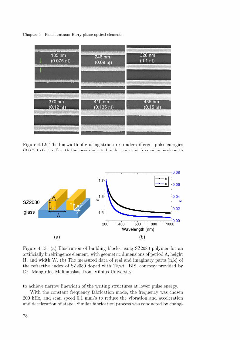
Chapter 4. Pancharatnam-Berry phase optical elements
185 nm(0.075 nJ)
246 nm(0.09 nJ)
328 nm(0.1 nJ)
370 nm(0.12 nJ)
410 nm(0.135 nJ)
435 nm(0.15 nJ)
Figure 4.12: The linewidth of grating structures under different pulse energies(0.075 to 0.15 nJ) with the laser operated under constant frequency mode withrepetition rate 200 kHz and scan speed 0.1 mm/s (comparing to pulse densityof 2 pulses/μm).
H
w
Λx
yz
200 400 600 800 1000
1.5
1.6
1.7 n
Wavelength (nm)
n
0.00
0.02
0.04
0.06
0.08
(a) (b)
glass
SZ2080
Figure 4.13: (a) Illustration of building blocks using SZ2080 polymer for anartificially birefringence element, with geometric dimensions of period Λ, heightH, and width W. (b) The measured data of real and imaginary parts (n,k) ofthe refractive index of SZ2080 doped with 1%wt. BIS, courtesy provided byDr. Mangirdas Malinauskas, from Vilnius University.
to achieve narrow linewidth of the writing structures at lower pulse energy.
With the constant frequency fabrication mode, the frequency was chosen200 kHz, and scan speed 0.1 mm/s to reduce the vibration and accelerationand deceleration of stage. Similar fabrication process was conducted by chang-
78

4.6. Femtosecond laser fabrication techniques
ing the pulse energy from 0.075 to 0.15 nJ, the pulse density 2 pulses/μm at200 kHz and 0.1 mm/s scan speed. Different gratings structures are shown inFig. 4.12. The linewidth of the writing structure can be precisely controlledfrom 185 to 435 nm by changing the laser pulse energy.
The precise control of direct laser writing technique to polymerize gratingstructures, provides a promising approach to writing artificially birefringenceelements for phase front engineering. A simple block that made from SZ2080polymer is schematically shown in Fig. 4.13(a). The refractive index of thereal part and imaginary part of the SZ2080 polymer doped with 1%wt. BISare measured using ellipsometer as shown in Fig. 4.13(b) [166].
400 500 600 700 800
84
87
90
93
96
99 TE-polarization
Tran
smis
sion
(%)
Wavelength (nm)
H=200 nm 400 600 800 1000
400 500 600 700 80084
87
90
93
96
TM-polarization
Tran
smis
sion
(%)
Wavelength (nm)
H = 200 nm 400 600 800 1000
400 500 600 700 800
87
90
93
96
TE-polarization
Tran
smis
sion
(%)
Wavelength (nm)
H = 200 nm 400 600 800 1000
400 500 600 700 800
84
88
92
96 TM-polarization
Tran
smis
sion
(%)
Wavelength (nm)
H = 200 nm 400 600 800 1000
Λ=400nm
Λ=800nm
Figure 4.14: The FDTD calculation results of the transmission coefficients forTE- and TM-polarized light passing through the building gratings with widthW = 200 nm, period Λ = 400 and 800 nm, and height H from 200 nm to 1 μm.
The geometric features of the writing structures by employing direct laserpolymerization using 515 nm with NA 1.4 objective are limited to the linewidthof ∼185 nm and aspect ratio to less than ∼ 10:1, which provides the capabilityto write such building blocks with period Λ ≥ 400 nm, width W ≥ 185 nm, andheight H ≥ 10W. Here we calculated the transmission coefficients for both TEand TM polarized light defined in Eq. 4.19 and Eq. 4.20 when passing throughthe SZ2080 gratings with different geometries with width W = 200 nm forperiod Λ = 400 nm and 800 nm. The height calculated from 200 to 1000 nm.The transmissions for both polarized components are more than 84% withstructure height less than 1 μm, across the whole visible band. The resultsas shown in Fig. 4.14 were calculated by using finite-difference time-domain
79

Chapter 4. Pancharatnam-Berry phase optical elements
0.2
0.5
1
400 600 800
H(μm)
𝜆 (nm)
Λ=400 nm Λ=600 nm
Λ=800 nm Λ=1000 nm
400 450 500 550 600 650 700 750 800
200
300
400
500
600
700
800
900
1000 0
5
10
15
20
25
30
35
40
45
50
5
10
15
20
25
30
0
35
40
45
50
0.2
0.5
1
400 600 800
H(μm)
η(%)
Figure 4.15: The conversion efficiency map calculated by the finite-differencetime-domain (FDTD) method across the whole visible band and differentstructure height from 200 nm to 1 μm for the SZ2080 polymer gratings withlinewidth 200 nm, period Λ = 400 nm, 600 nm, 800 nm and 1 μm, respectively.
0.2
0.5
1
400 600 800
H(μm)
𝜆 (nm)
W=200 nm W=300 nm W=400 nm
400 450 500 550 600 650 700 750 800
200
300
400
500
600
700
800
900
1000 0
5
10
15
20
25
30
35
5101520253035
0
η(%)
Figure 4.16: The FDTD calculated conversion efficiency map across the wholevisible band and different structure height from 200 nm to 1 μm for the SZ2080polymer gratings with linewidth 200 nm, 300 nm and 400 nm, at periodΛ = 1 μm, respectively.
(FDTD) simulation (Lumerical Solutions Inc.) with the measured (n, κ) datafor a circular polarized incident light. The raw data of the FDTD calculationswere provided by our collaborator Dr. Xiangping Li from Jinan University, andreploted and analyzed by myself. From Eq. 4.20 or Eq. 4.21, the conversionefficiency can be calculated with the transmission of both polarization (tx andty) and the retardation (ϕ) of the structure, using:
η = |12
(tx – tyeiϕ)|. (4.23)
80

4.6. Femtosecond laser fabrication techniques
Figure 4.17: 45◦-slanted-view SEM image of discretized photonic spin Halldevice, with d = 40 μm. Scale bars for the first and second rows are 20 μmand 4 μm.
The calculated conversion efficiency using Eq. 4.23 is the same for the op-posite handness polarization. The calculated map of the conversion efficienciesfor a SZ2080 polymer grating with linewidth 200 nm, period from Λ = 400,600 and 800 nm to 1 μm for different heights are shown in Fig. 4.15. The con-version efficiency can reach more than 35% when the grating period is 400, 600and 800 nm, across the whole visible band with height larger than 500 nm. Forthe period of Λ = 1 μm, more than 30% conversion efficiency can be achievedwith structure taller than 800 nm. The conversion efficiency is the highestwhen the linewidth is 200 nm at period 1 μm, height 1 μm as compared withthe linewidth of 300 nm and 400 nm (Fig. 4.16).
With the theoretical calculations of the conversion efficiency of the SZ2080polymer gratings, and the well controlled fabrication techniques for differentgeometric features, different functional geometric phase optical elements canbe fabricated using direct laser polymerization. The second harmonic beam515 nm was focused into the interface of the dried drop-casted SZ2080 pho-topolymer through a cover glass by an oil immersed objective NA 1.4, withsimilar fabrication process as in previous experiments. The pulse energy was0.075 nJ and scan speed is 0.1 mm/s at repetition rate 200 kHz. The linewidthis around 200 nm, as same as the structure shown in Fig. 4.12. A photonic spinHall device was fabricated as the design shown in Fig. 4.6 (b) with d = 40 μm.After development and drying, the structure was directly viewed using SEMafter sputtering 3 nm Ti on the structure. The 45◦ tilted image was shown inFig. 4.17. The height of the structure was measured to be 1 μm.
The same fabrication conditions are used to fabricate vortex generators
81
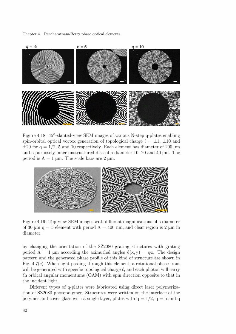
Chapter 4. Pancharatnam-Berry phase optical elements
q = ½ q = 5 q = 10
Figure 4.18: 45◦-slanted-view SEM images of various N-step q-plates enablingspin-orbital optical vortex generation of topological charge ` = ±1, ±10 and±20 for q = 1/2, 5 and 10 respectively. Each element has diameter of 200 μmand a purposely inner unstructured disk of a diameter 10, 20 and 40 μm. Theperiod is Λ = 1 μm. The scale bars are 2 μm.
Figure 4.19: Top-view SEM images with different magnifications of a diameterof 30 μm q = 5 element with period Λ = 400 nm, and clear region is 2 μm indiameter.
by changing the orientation of the SZ2080 grating structures with gratingperiod Λ = 1 μm according the azimuthal angles θ(x, y) = qα. The designpattern and the generated phase profile of this kind of structure are shown inFig. 4.7(c). When light passing through this element, a rotational phase frontwill be generated with specific topological charge `, and each photon will carry`h orbital angular momentums (OAM) with spin direction opposite to that inthe incident light.
Different types of q-plates were fabricated using direct laser polymeriza-tion of SZ2080 photopolymer. Structures were written on the interface of thepolymer and cover glass with a single layer, plates with q = 1/2, q = 5 and q
82

4.6. Femtosecond laser fabrication techniques
20 μm
10 μm
Figure 4.20: 45◦ slanted-view SEM of a 3D q = 10 plate with different mag-nifications. The diameter of the element is 200 μm and inner clear region is40 μm. The height of the structure was changing from 200 nm to 1 μm whenthe rotation angle change from 0 to 180◦.
0 50 100 150 200
0
250
500
750
1000
Hei
ght (
nm)
Lateral (µm)(a)
(b)
(c)
2μm
Figure 4.21: The morphology characterizations of a 3D q = 10 plate showingin Fig. 4.20 by 3D optical profilometer (a) and magnified 45◦-view SEM (c).The height of the structure is changing from ∼200 nm to 1 μm across onerotational pitch of the gratings (b).
= 10 were fabricated. It is unnecessary to structure the central part when thegrating period Λ is of the order of 2dinnerπ/N (N is the number of descretizedsteps), which gives dinner ' NΛ/π = 5, 13 and 25 μm for the q = 1/2, 5 and 10,respectively. Different magnifications of SEM images taken of the fabricatedq = 1/2, 5 and 10 plates are shown in Fig. 4.18. The diameter of all threeq-plates is 200 μm, and the diameter of inner clear region is 10 μm, 20 μm and40 μm respectively. The time was taken to fabricate these q-plates were 9, 25and 39 minutes for q = 1/2, 5 and 10, respectively. A 30 μm diameter q =5 plate was also fabricated on a 1 μm thick Si3N4 membrane with period Λ
83

Chapter 4. Pancharatnam-Berry phase optical elements
Laser 50/50 BS1
Attenuator
Objective
M1 M2
AHP LP1CCD
50/50 BS2
q-plate
(a)
(c) (d)(b)
Figure 4.22: (a) A Mach-Zehnder interferometer for characterization the phasedifference resulted from the height variation of the structure at 780 nm; BS1and BS2 are non-polarized beam splitters; AHP is an achromatic half-waveplate; M1 and M2 are metallic mirrors; LP1 is a linear polarizer. The outputof the laser before BS1 is horizontal linear polarized. (b) Reference interferencepattern without structures on a cover glass. (c) Interference pattern with a3D q= 1/2 plate, which shows a π phase shift across the full azimuthal angle.(d) Interference pattern with a 3D q = 10 plate in (Fig. 4.20), which shows aπ phase shift across each sector and a total phase 10π across the full azimuthalangle, meaning a topological charge ` = 10 with a spiral phase will be generatedby the height variation.
= 400 nm (Fig. 4.19). The height of the structure is around 500 nm, whichshould give more than 30% conversion efficiency across the whole visible band.
Multifunctional optical elements constructed from Si-based gradient meta-surface have been demonstrated and capable of achieving multiple distinctfunctions within a shared aperture. The optical imaging with simultaneouscolor separation using this concept was demonstrated [170]. By then, theshare-aperture concept was applied to achieve controlled multiple structuredwavefront of vortex beams carrying orbital angular momentum [171]. The op-portunities are opened to achieve multiple functionalities in the on chip pho-tonics devices especially in information processing using multiplexed-orbitalangular momenta.
Moving the focusing spot along the Z-axis by the translational stage en-ables the 3D structuring capability of the direct laser writing. It provides usa way to manipulate light by combining the geometric phase and propaga-tion accumulated phase to fabricated hybrid planar phase optical elements.Structuring light beams using a height varying plate, the spiral phase plate togenerate different orbital angular momenta has been demonstrated and real-
84
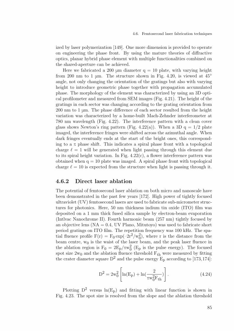
4.6. Femtosecond laser fabrication techniques
ized by laser polymerization [149]. One more dimension is provided to operateon engineering the phase front. By using the mature theories of diffractiveoptics, planar hybrid phase element with multiple functionalities combined onthe shared-aperture can be achieved.
Here we fabricated a 200 μm diameter q = 10 plate, with varying heightfrom 200 nm to 1 μm. The structure shown in Fig. 4.20, is viewed at 45◦angle, not only changing the orientation of the gratings but also with varyingheight to introduce geometric phase together with propagation accumulatedphase. The morphology of the element was characterized by using an 3D opti-cal profilometer and measured from SEM images (Fig. 4.21). The height of thegratings in each sector was changing according to the grating orientation from200 nm to 1 μm. The phase difference of each sector resulted from the heightvariation was characterized by a home-built Mach-Zehnder interferometer at780 nm wavelength (Fig. 4.22). The interference pattern with a clean coverglass shows Newton’s ring pattern (Fig. 4.22(a)). When a 3D q = 1/2 plateimaged, the interference fringes were shifted across the azimuthal angle. Whendark fringes eventually ends at the start of the bright ones, this correspond-ing to a π phase shift. This indicates a spiral phase front with a topologicalcharge ` = 1 will be generated when light passing through this element dueto its spiral height variation. In Fig. 4.22(c), a flower interference pattern wasobtained when q = 10 plate was imaged. A spiral phase front with topologicalcharge ` = 10 is expected from the structure when light is passing through it.
4.6.2 Direct laser ablation
The potential of femtosecond laser ablation on both micro and nanoscale havebeen demonstrated in the past few years [172]. High power of tightly focusedultraviolet (UV) femtosecond lasers are used to fabricate sub-micrometer struc-tures for photonics. Here, 50 nm thickness indium tin oxide (ITO) film wasdeposited on a 1 mm thick fused silica sample by electron-beam evaporation(Intlvac Nanochrome II). Fourth harmonic beam (257 nm) tightly focused byan objective lens (NA = 0.4, UV Plano, Mitutoyo) was used to fabricate shortperiod gratings on ITO film. The repetition frequency was 100 kHz. The spa-tial fluence profile F(r) = F0 exp(–2r2/w2
0), where r is the distance from thebeam centre, w0 is the waist of the laser beam, and the peak laser fluence inthe ablation region is F0 = 2Ep/πw2
0 (Ep is the pulse energy). The focusedspot size 2w0 and the ablation fluence threshold Fth were measured by fittingthe crater diameter square D2 and the pulse energy Ep according to [173,174]:
D2 = 2w20
[ln(Ep) + ln(
2
πw20Fth
)
]. (4.24)
Plotting D2 versus ln(Ep) and fitting with linear function is shown inFig. 4.23. The spot size is resolved from the slope and the ablation threshold
85

Chapter 4. Pancharatnam-Berry phase optical elements
Single pulse
0.5 1 5 15 25 350
2
4
6
8
Cra
ter d
iam
eter
squ
are
(m
2 )
Pulse energy (nJ)
Fth2=0.16 J/cm2Fth1=0.11 J/cm2
1008 nm
926 nm
0.5 1 5 15 25 350
5
10
Gro
ove
linew
idth
squ
are
(m
2 )
Pulse energy (nJ)
100 pulses/μm
Fth2=0.15 J/cm2Fth1=0.05J/cm2
1160 nm
1247 nm
Figure 4.23: The diameter square of the ablated crater on a 50 nm ITO film onfused silica substrate ablated by single laser pulse irradiation (a) and linewidthsquare of the ablated groove by multiple pulses irradiation (b) as a function ofthe pulse energy. The solid lines correspond to the linear fit of the experimentdata points. The ablation thresholds for single pulse on ITO film is 0.11 J/cm2,while for ablation through film to the substrate is 0.16 J/cm2 (a). The ablationthresholds for multiple pulses irradiation on ITO film is 0.05 J/cm2 twicesmaller than the single pulse irradiation, while for ablation film through to thesubstrate is 0.15 J/cm2 (b), similar to the single pulse irradiation.
fluence is calculated from the y– intercept. Two different slopes are observedin low laser fluence and high laser fluence conditions both in single shot irra-diation and multiple pulses irradiation. The splitting point for different slopesis found when at the laser fluence is sufficient to start to totally evaporate thematerial in the central region. When the laser fluence is lower than that, thefilm is partially ablated but not removed. The laser fluence threshold thatallows initial ablation of the film and created a crater for a single pulse or agroove on the film. The fluence threshold was found almost similar in the sin-gle pulse and multiple pulses irradiation for initiation of ablation with around≈ 0.15 J/cm2, while for the threshold of removal ITO, the pulse accumula-tion effect was demonstrated and reduce the ablation threshold around twicetimes comparing the single shot ablation threshold is 0.11 J/cm2. To fabricatebirefringent grating structures by direct laser ablation, the conditions for fabri-cating smallest period grating is possible when the film starts to ablate throughto the substrate. By using the linear dependence of the groove width vs. thelaser fluence, a well controlled laser ablation for geometric phase elements canbe achieved. The structure height is determined by the film thickness. A pho-tonics spin device with same rotational speed d = 40 μm and period Λ = 1 μm
86

4.6. Femtosecond laser fabrication techniques
10 μm
2 μm
Figure 4.24: A 100 μm diameter photonic spin Hall device fabricated by 257 nmfemtosecond laser direct ablation on 300 nm silicon film sputtered on coverglass substrate. The grating period is 1 μm, and rotational speed d = 40 μm.The laser pulse energy is 0.18 nJ with scan speed 1 mm/s at repetition rate100 kHz; 80 seconds TOOK to complete the fabrication.
(Fig. 4.24) was fabricated on a 300 nm thick silicon film sputtered on a fusedsilica substrate using 257 nm femtosecond laser direct ablation.
4.6.3 Stress engineering
Another well know path to introduce birefringence is stress, which occurs whilestretching or compressing the material. Strength of birefringence dependson the amount of stress and on a photoelastic coefficient, as introduced inSec. 4.4.1.
(a) (b)
20 μm
Figure 4.25: Optical transmission microscope images of laser inscribed singlelayer trajectories at 400 μm from the surface inside fused silica under brightfield (a) and cross-polarized field (b). The structures were fabricated by afemtosecond laser operating at 515 nm wavelength, repetition rate of 200 kHzand focused by a NA 0.5 objective lens, writing speed was 10 mm/s.
There are several sources of stress which occur after femtosecond laser
87
Chapter 4. Pancharatnam-Berry phase optical elements
irradiation. For crystals this is mainly material rarefication in the irradiatedzone related to micro-explosion. The stress produced in this way exhibitsspherical symmetry for a single shot conditions. If stress is induced by alaser inscribed line, the stress is perpendicular to the written structure, anexample as shown in Fig. 4.25. This type of stress is also widely exploited forimplementing waveguiding structures in crystalline materials. The expandingmaterial in the irradiated zone induces strain in the vicinity of the track andas a result refractive index increase. Waveguiding structures can be inducedbetween two or more adjacent laser tracks [175]. Another source of stress isnanostructure formation, which can be easily obtained with sub-picosecondpulses in silica glass. The nanograting formation leads to material expansionand stress. The stress lacks spherical symmetry and is stronger in the directionof nanogratings [155].
NA 0.5X 100
Figure 4.26: Schematic of a femtosecond laser direct writing technique to en-gineer a circularly symmetric stress distribution inside a transparent dielectricmaterial and a four-symmetric-lobes cross-polarized image of this structure.
The stress was introduced by using a femtosecond laser pulses at 200 kHzrepetition rate. Writing speed was 10 mm/s. Second harmonic beam 515 nmwas focused by a NA 0.5 objective lens inside the glass. To avoid unsymmetri-cal stress distributions resulted from nanogratings induced by laser irradiation,a quarter-waveplate was inserted into the beam to circularly polarize the beam.The schematic of the fabrication process and stress distribution is shown inFig. 4.26. For comparison, three different materials were used: 1 mm thicksoda lime glass and fused silica, and 0.35 mm thick sapphire. Different pulseenergies from from 90 to 900 nJ after objective were tested, with varying writ-ing speed from 5 to 20 mm/s in order to achieve the best fabrication conditions.The fabrication condition matrix shown in Fig. 4.27, used to find the strongestbirefringence before cracks happened inside 1-mm fused silica sample. Afterirradiation the fabricated elements were tested at 532 nm using two crossedpolarizers.
A size of 5 mm structure composed from concentric rings separated by10 μm was fabricated at 900 nJ with different layers (Fig. 4.27). The concen-tric ring structures are expected to generate a circular symmetric birefringence
88

4.6. Femtosecond laser fabrication techniques
Pulse Energy 𝐸𝑝 = 90 𝑛𝐽 − 900 𝑛𝐽
10 -
40 L
ayer
s
i-1 i-2
ii-1 ii-2
iii-1 iii-2
Figure 4.27: A laser condition matrix was written in a 1-mm thick fused silicasample by varying the laser pulse energy from 90 to 900 nJ, layers from 10to 40 layers. The radial separation of two concentric rings is 10 μm and layerseparation is 10 μm. Circular polarized second harmonic beam 515 nm wasfocused by a NA 0.5 objective. The first layer structure was written 200 μmbelow surface in fused silica. The pulse repetition rate was 200 kHz, scan speed10 mm/s. Large size elements with diameter 5 mm were written using 900 nJpulse energy by 10 layers (i-1), 30 layers (ii-1), 60 layers (iii-1), cross-polarizedimages (i-2), (ii-2) and (iii-2), correspondingly.
-200 -150 -100 -50 0 50 100 150 200-200
-150
-100
-50
0
50
100
150
200
(a) (b) (c)
Figure 4.28: (a) A more complex structure designed for engineering a stress dis-tribution generating rotational birefringence θ(x, y) = 5α, as shown in (b) (Thepattern is courtesy provided by our collaborator, Dr. Raymond C. Rumpf,from University of Texas at El Paso). (c) The cross-polarized image of thefabricated structure with 60 layers, diameter of 5 mm with 900 nJ pulse en-ergy and 10 mm/s scan speed with pulse repetition rate of 200 kHz.
distribution θ(x, y) = α which will create an optical vortex beam with topo-logical charge ` = 2. A more complex geometric design to introduce periodic
89

Chapter 4. Pancharatnam-Berry phase optical elements
tangential variation of stress were also fabricated (Fig. 4.28). Multiple layerswere inscribed in the bulk of fused silica to achieve a higher efficiency of vortexbeam conversion.
4.7 Optical characterization and Discussions
Figure 4.29: A single beam interference set-up for characterizing the q-plates.Two lasers are integrated into the set-up with 775 and 532 nm wavelength.LP and AQP are a linear polarizer and achromatic quarter waveplate.
Different femtsecond laser fabrication approaches are demonstrated to makeartificial birefringence structures to manipulate the wavefront of an electro-magnetic wave by modifying the polarization using a geometric phase that isnot related to the propagation effect. Functional planar optical elements suchas photonic spin Hall splitter, q-plates and 3D q-plates were fabricated usingpolymerization, direct laser ablation and stress engineering in the bulk of trans-parent materials. Here we focus on characterizing the rotational phase front ofthe light beam after passing the q-plates fabricated using polymerization andstress engineering.
A light beam propagating along a rotational trajectory carries angular mo-mentum not only related to its polarization defined by the spin angular mo-mentum (SAM), σ, but also related to its phase front trajectory according toits OAM [176]. SAM is quantised in ±h per photon and the sign is dependenton the handiness of polarization with left-handed SAM defined as positive.The amount of angular momentum per photon in the case of OAM is `h,where ` is an arbitrary integer, which is the topological charge of the OAMcarrying beam. Since SAM and OAM are independent degrees of freedom,it opens new avenues in manipulation of light, multiplexing optical informa-tion channels, and manipulation of matter at nano-/micro-scales [177]. Whena circularly polarized beam which carries only SAM passes through an opti-cally inhomogeneous and anisotropic media, the conversion of SAM into OAMoccurs due to spin-orbital coupling and the emerging beam gains OAM accord-ing to the total angular momentum and energy conservation [178, 179]. Theefficiency of spin-orbital conversion is defined in Eq. 4.23.
90
4.7. Optical characterization and Discussions
40 μmExperimentCalculation
(a)
q = 1/2
(b) (c)
q = 5
q = 10
Figure 4.30: (a) Fabricated structures SEM images. (b) Theoretical calcula-tions and (c) experiment of self interference when a right-hand circular beamilluminated on the q-plates fabricated by laser polymerization. The q-platesgenerated optical vortices at topological charges of ` = -1, -10 and -20, respec-tively at 775 nm wavelength.
𝛔 = −𝟏 𝛔 = +𝟏 𝛔 = −𝟏 𝛔 = +𝟏
𝐪 = 𝟏/𝟐
𝐪 = 𝟏𝟎
Figure 4.31: Single-beam interference patterns at 532 and 775 nm wavelengthresulting from spin-orbit optical vortex generation from the q-plates with q= 1/2, and q = 10. The generation of on-axis optical phase singularity oftopological charge ` = 2σq is identified from the number (given by |`|) and thehandness (given by the sign of `) of the spiralling patterns.
91
Chapter 4. Pancharatnam-Berry phase optical elements
ℓ = +𝟏𝟎
ℓ = +𝟐𝟎
3D 10 q-plate @ 532 nm
ℓ = +𝟐𝟎
ℓ = +𝟏𝟎
3D 10 q-plate @ 780 nm
Figure 4.32: Single-beam interference pattern at 532 and 775 nm wavelengthof a 3D q-plate q = 10 (Fig. 4.20) which has a hybrid phase composted withgeometric phase and dynamic phase. Two different topological charges weregenerated by two different phases; ` = 20 and ` = 10 are generated fromgeometric phase and dynamic phase, respectively.
Optical elements which perform spin-orbital conversion are form-birefringentpatterns whose fast-axis has local azimuthal, θ, angular orientation θ = qα,where q is a half-integer, hence, the q-plates [179,180]. Q-plates which generateoptical vortex carrying OAM ` = 2q can be made using optically anisotropicmaterials: liquid crystals, semiconductors, silica glass, and different design ofmetallic or dielectric metasurfaces [147,181–184].
A single beam and on-axis self-interference was demonstrated to character-ize a light beam that carries angular momentums with the determined featureof rotational spirals [185]. The set-up used for interference imaging (Fig. 4.29)consisted from two pairs of linear polarizers and achromatic quarter waveplates.Circular polarized beam was prepared before illuminating on the q-plates. Thetheoretical calculations of an interference pattern of a vortex beam with an on-axis Gaussian beam were carried out by using a Laguerre-Gaussian beam thatcarries a rotational phase front (Fig. 4.30) for topological charge ` = 1, 10 and20. The electric field of a Laguerre-Gaussian beam is given by [186]:
El0(r,θ, z) =
√2/(2π`!)(
√2r/w(z))`(2r2/w(z)2)L`
0ei`θe–ikr2/2q(z)eiψ (4.25)
where the wavevector k = 2π/λ; Gouy phase ψ(z) = (`+1) tan( –1)(z/zR); com-plex beam parameter q(z) = πR(z)w(z)2/πw(z)2 – iR(z)λ; evolving radius of
curvature R(z) = z[1 + (zR/z)]; evolving beam width w(z) = w0
√1 + (z/zR)2;
Rayleigh range zR = πw20/λ; L`
0 is the Laguerre polynomials.The experimental interference patterns for the right-handed circular beam
passing the polymerized q-plates with q = 1/2, 5 and 10 are same to thecalculations. The spiraling interference patterns show the emerging beams
92

4.7. Optical characterization and Discussions
(a) (b)
Figure 4.33: Transverse intensity profiles (a) of 60 layer stressed induced bire-fringence structures with topological charges ` = 2 and ` = 10 and single-beaminterference patterns (b) at 0.5 m and 2 m from the device exit plane, respec-tively.
carrying OAM of ` = -1, -10 and -20 that indicates the spin-orbital conversionafter passing through these structures. With different handness of circularbeam illuminating the q-plates, opposite rotations of handness are observed asshown in Fig. 4.31. The structures with height 1 μm, width around 300 nm havetheoretical conversion efficiency above 20% across the whole visible range asshown in Fig. 4.16, therefore, we also characterize the interference with 532 nmlaser. To demonstrate the concept on combining the function of the q-plate andspiral plate, a 3D q-plate device was fabricated with q = 10 (Fig. 4.20). Thisconcept provides a way to generate different OAMs not only by interleavedelements sharing surface area, but also by sharing the transverse dimension.The interference pattern shows that two collinear helical modes of topologicalcharges ` = 10, 20 are observed (Fig. 4.32) when light passing through a 3Dq-plate.
As it was described in the Sec. 4.6.3, the stress produced by material ex-pansion is normally perpendicular to the inscribed line. Thus by controllingdirection of the line one can control orientation of the stress. The simplestcase is inscribing series of concentric rings which will produce radially vari-ant stress (Fig. 4.27). As a result, the birefringence will be radially variant.Such configuration is known to produce charge ` = 2 optical vortex from circu-
93

Chapter 4. Pancharatnam-Berry phase optical elements
larly polarized light, demonstrated in Fig. 4.33. For characterization, series ofcharge ` = 2 optical vortex converters were written in silica glass with differentnumber of layers (10 - 70). With structures containing 60 - 70 layers, conver-sion efficiency reaches 88%. However, we observed high scattering up to 70%of incident light. Scattering can be reduced by optimising writing conditionsby discrete writing trajectories rather continuous line. In the geometry shownin Fig. 4.28, variant orientation of trajectory θ(x, y) = 5π defines charge ` =10 optical vortex. The beam profiles taken at 0.5 m and 2 m confirmed pres-ence of orbital angular momentum ` = 10 (Fig. 4.33), thus demonstrating thatcomplex phase elements can be fabricated by exploiting solely stress inducedbirefringence.
4.8 Conclusions
Promising applications in the fields of super resolution imaging, data stor-age, telecommunication, sensing are attractive using ultra-thin planar optics.Compact, light and highly integrated optical devices and systems are possi-ble to realize with geometric phase optical components. The major issues ofhigh loss, low efficiency and cost-ineffective fabrications are still unresolvedand hamper the full scale development in this field. High optical transmissiveplanar optics could be realized to engineer light propagation with artificiallygenerated birefringence structures builded by dielectric gratings or stress in-duced birefringence.
In this chapter, we proposed to apply the unique characteristics of femtosec-ond laser fabrication to simplify the fabrication process of geometric phaseoptics. This method not only can lead to a solution for effective and one-step fabrication process of these geometric phase optical elements, but alsocan drive development of novel planar optical elements to manipulate light atnano and macro scales.
4.9 Appendix C
This section contains the published papers related to the geometric phaseengineering using femtosecond laser direct writing technique.
C1: X. W. Wang, A. Kuchmizhak, E. Brasselet, S. Juodkazis. Di-electric geometric phase optical elements from femtosecond direct laser writing.Applied Physics Letter, 110, 181101, 2017.
This is the first demonstration of a dielectric optical element for spin-orbital
94

4.9. Appendix C
coupling and generation of optical vortex beam with an arbitrary designedtopological charge. Such optical elements have potential to perform at the100% conversion efficiency of a selected circular polarisation into a contra-circular polarisation carrying optical vortex (beam carrying an orbital angularmomentum). We have provided the design rules how to achieve such per-formance which is not available in current implementation of optical vortexgenerators. The fabrication flexibility and material performance at the usedwavelengths are demonstrated. The used direct laser writing/printing performsat fabrication speeds which are practical for micro- as well as macro-optical el-ements with cross sections in sub-1 cm range. Judging by fundamental scalingrules of optical breakdown, such optical elements are promising to withstandhigh laser power and intensity since they are made from glass forming mate-rials of high purity (sol-gel resist was used). The design principle used for theoptical elements is universal and can be tested for optical elements in differentspectral ranges from visible - to - sub-mm wavelengths (Terahertz frequencies).
95

Dielectric geometric phase optical elements fabricated by femtoseconddirect laser writing in photoresists
Xuewen Wang,1,a) Aleksandr A. Kuchmizhak,1,2 Etienne Brasselet,3,4
and Saulius Juodkazis1,5,b)1Centre for Micro-Photonics, Swinburne University of Technology, Hawthorn, VIC 3122, Australia2School of Natural Sciences, Far Eastern Federal University (FEFU), 8 Sukhanova Str., Vladivostok 690041,Russia3Universit�e de Bordeaux, LOMA, UMR 5798, F-33400 Talence, France4CNRS, LOMA, UMR 5798, F-33400 Talence, France5Melbourne Centre for Nanofabrication, ANFF, 151 Wellington Road, Clayton, VIC 3168, Australia
(Received 14 December 2016; accepted 14 March 2017; published online 1 May 2017)
We propose to use a femtosecond direct laser writing technique to realize dielectric optical
elements from photo-resist materials for the generation of structured light from purely geometrical
phase transformations. This is illustrated by the fabrication and characterization of spin-to-orbital
optical angular momentum couplers generating optical vortices of topological charge from 1 to 20.
In addition, the technique is scalable and allows obtaining microscopic to macroscopic flat optics.
These results thus demonstrate that direct 3D photopolymerization technology qualifies for the real-
ization of spin-controlled geometric phase optical elements. Published by AIP Publishing.[http://dx.doi.org/10.1063/1.4982602]
During the last two decades, the concept of geometric
phase optical elements1 established a new standard in the real-
ization of smart flat optics. The characteristic of such optical
elements is the capability to impart an arbitrary phase profile
to an incident light field by purely geometrical means. This is
made possible by preparing space-variant optically aniso-
tropic materials. In practice, this is achieved by preparing a
slab with an in-plane effective optical axis whose orientation
angle is spatially modulated, say wðx; yÞ. An essential feature
is the fact that the optical functionality encoded in the spatial
distribution of the optical axis is controlled by the polarization
state of the light. Indeed, considering the simplest situation
of a transparent slab having a birefringent phase retardation
of p, an incident circularly polarized light field impinging
at normal incidence (hence along the z axis) emerges as a
contra-circularly polarized field endowed with a space-
variant Pancharatnam-Berry phase2,3 Uðx; yÞ ¼ 2rwðx; yÞ,where r ¼ 61 refers to the helicity of the incident light.
Experimentally, the realization of geometric phase opti-
cal elements has started 15 years ago by designing space-
variant subwavelength gratings made from metals4 and semi-
conductors,5 though initially restricted to the mid-infrared
domain. The use of dielectric materials emerged a few years
later by implementing liquid crystals with inhomogeneous
in-plane molecular orientation,6 thus providing optical ele-
ments operating in the visible domain. Nowadays, photo-
alignment techniques allow obtaining arbitrary phase profiles
from patterned liquid crystal slabs.7 Still, several other tech-
niques have been explored in recent years towards the reali-
zation of dielectric geometric phase optical elements from
structured solid-state materials with great application poten-
tial owing to the enhanced lifetime and damage threshold.
One can mention femtosecond direct laser writing (DLW) in
glasses,8 which however suffers from large scattering losses
at visible frequencies, and electron beam lithography of sili-
con9–11 and titanium oxide.12
In practice, dielectrics offer the advantage of possible
transparency over a very large spectral range, which
favors the elaboration of high-transmission devices. On the
other hand, high-refractive indices enable optimal cross-
polarization conversion with thin layers with respect to
wavelength. Besides the average refractive index mismatch
between the external and structured media and the average
attenuation that both affect the overall transmission, the
dichroism (i.e., the anisotropy of the imaginary part of the
complex dielectric permittivity tensor) has a direct influence
on the helicity transformation r ! �r. More precisely,
the purity parameter g defined as the fraction of the output
power that corresponds to helicity-flipped field experiencing
the Pancharatnam-Berry phase can be expressed as13 g ¼ ð1�cosD0=coshD00Þ=2, where D0 ¼ khðn0k � n0?Þ and D00
¼ khðn00k � n00?Þ, with k the wavevector in vacuum, h the
thickness of the anisotropic layer, n0 þ in00 its complex
refractive index, and ðk;?Þ referring to the direction parallel
and perpendicular to the local effective optical axis.
Interestingly, the dichroism may enhance or reduce the
purity depending on the real birefringent phase retardation,
as illustrated in Fig. 1.
Here, we propose a yet unexplored approach for the fab-
rication of dielectric geometric phase optical elements based
on femtosecond DLW of photo-resists by a well matured
technology14 reaching a high fabrication throughput.15 An
asset of this approach is that it is easy-to-implement while
the realization of macroscopic dimensions is possible. This
contrasts to currently employed nanofabrication techniques
based on electron beam lithography, focused ion milling, and
atomic layer deposition of dielectric layers that remain
the privilege of cleanroom facilities and require high-level
technical support. Moreover, the inherent three-dimensional
a)Email: [email protected])Email: [email protected]
0003-6951/2017/110(18)/181101/4/$30.00 Published by AIP Publishing.110, 181101-1
APPLIED PHYSICS LETTERS 110, 181101 (2017)
Chapter 4. Pancharatnam-Berry phase optical elements
96

structuring capabilities of the proposed approach allow con-
sidering the fabrication of dielectric devices on curved and
flexible substrates15 while the structured material itself can be
reconfigurable under external forcing for instance by using
elastomers.16 In the present case, we choose the hybrid (20%
inorganic, 80% organic) photo-resist SZ2080 whose refrac-
tive index is n0 þ in00 ¼ 1:474þ i0:08 over the 500–800 nm
wavelength range.17 Such a material has a low shrinkage and
high optical transmissivity and is widely used for micro-
optical elements.18–21 In principle, highly pure geometric
phase optical elements can thus be formally obtained under
appropriate optimization of the designed structure following
the above discussion on the parameter g.Without the lack of generality, we restrict our demon-
stration to the realization and characterization of spin-to-
orbital optical angular momentum converters. Such elements
correspond to azimuthally varying optical axis orientation of
the form w ¼ q/ (q the half-integer and / the polar angle in
cylindrical coordinates) with, ideally, uniform real birefrin-
gent phase retardation of p.22 In turn, a spin-orbit coupler
transforms an incident field with helicity r (that is associated
with spin angular momentum r�h per photon) into a helicity
flipped field endowed with a spatial distribution of the phase
of the form Uð/Þ ¼ 2rq/ (that is associated with orbital
angular momentum 2rq�h per photon). The choice of such a
design to test our approach is motivated by a wide range of
applications in classical and quantum optics of these so-
called q-plates23 that have become a prototypical benchmark
for geometric phase optical elements.
The DLW experimental platform basically consists of a
regenerative amplified ytterbium-doped potassium gadolin-
ium tungstate (Yb:KGW) based femtosecond fs-laser system
(Pharos, Light Conversion Ltd.) operating at the second har-
monic wavelength of 515 nm with a pulse duration of 230 fs
and a repetition rate of 200 kHz. The laser beam is focused
with an oil-immersion objective lens of numerical aperture
NA¼ 1.42 (Olympus) onto the interface of a cover glass on
which the dielectric photo-resist doped with 1 wt. % 4,40-bis-diethylaminobenzophenone as a photoinitiator is drop-cast
and dried at room temperature for 12 h before laser writing.
The pulse energy after the objective is set to 0.12 nJ at the
scanning speed of 0.1mm/s. After fabrication, the samples
were developed in a methyl-isobutyl-ketone and isopropanol
(1:2) solution for 10min followed by a 1min acetone bath
and 10min rinse in isopropanol. Then, the structures were
dried on a hotplate at 50 �C for 10min. Finally, a 5-nm-thick
film of titanium was sputtered for structural characterization
by scanning electron microscopy (SEM).
A N-step discrete design is chosen for the space-variant
grating structure associated with a pitch K ’ 1 lm and filling
factor defined by the width-to-period ratio of the gratings
w=K ’ 0:3, as illustrated in Fig. 2 for q¼ 1/2 and N¼ 16.
High-charge elements have also been fabricated, as shown in
Fig. 3 for ðq;NÞ ¼ ð1=2; 16Þ, (5, 40), and (10, 80) that corre-
spond to fabrication times around 10, 35, and 40min, respec-
tively, which is acceptable for industrial DLW. In practice,
patterns of lower complexity and centimeter square area can
be made in several hours using faster scanning and higher
laser repetition rate.
The optical characterization of the fabricated spin-to-
orbital couplers is made by inspecting the spiraling phase
profile imprinted by the structures to the contra-circularly
polarized output field component. In practice, this is made in
a straightforward manner by illuminating the sample by a
r-polarized collimated beam of typical diameter 1mm and
subsequent polarization imaging the intensity distribution of
FIG. 1. Purity g as a function of the real (D0) and imaginary (D00) parts of thecomplex birefringent phase retardation. Positive and negative values for
ðD0; D00Þ refer to positive and negative uniaxial behaviors, respectively.
FIG. 2. (a) 45�-slanted SEM image of a 16-step 12-plate of diameter 200lm.
Note that surface charging alters the imaging contrast. (b) Top-view SEM
image of the local photo-polymerized grating characterized by the filling
factor w=K ’ 0:3. (c) SEM image at the rim of the element, where h ¼ 1lmis the height of the structure.
FIG. 3. Top-view SEM images of various N-step q-plates enabling spin-
orbit optical vortex generation of topological charge ‘ ¼ 61 (a), ‘ ¼ 610
(b), and ‘ ¼ 620 (c); top-row shows close up SEM images of the central
regions. Each element has a diameter of 200lm and a purposely inner
unstructured disk of diameter d ¼ 10lm (a), 20 lm (b), and 40lm (c).
Indeed, structuring of the central part is eventually not useful when the grat-
ing pitch K is of the order of dp=N, which gives d ’ NK=p ¼ 5, 13 and
25lm, respectively.
181101-2 Wang et al. Appl. Phys. Lett. 110, 181101 (2017)
4.9. Appendix C
97

the field that emerges from the sample. Indeed, the diffraction
of light on the finite size q-plate having the central unstruc-
tured area (see Fig. 3) leads to “single-beam interferometry”
by providing a coaxial overlap between the two circularly
polarized output field components, and hence there is no need
for an external reference beam. This leads to spiraling fringes
patterns whose contrast is optimized by adjusting the polariza-
tion state on which the total field is projected. This is made by
placing an achromatic quarter-waveplate followed by a polar-
izer after the sample and adjusting their relative orientation.
The results are illustrated in Fig. 4 for the structures shown in
Fig. 3 at two different wavelengths (532 nm and 775 nm) and
for incident helicity r ¼ 61. As expected, 2jrqj-arm spiral-
ing patterns with helicity-dependent handedness are observed,
which demonstrates the generation of optical vortex beams
associated with an optical phase singularity of topological
charge ‘ ¼ 2rq.On the other hand, the performance of the photo-
polymerized geometric phase optical elements is experimen-
tally evaluated to be a few percents. Although such a modest
value does not compromise the proof-of-the-principle that fem-
tosecond DLW of photo-polymeric materials is an approach
that is worth to explore further, this invites to consider how to
optimize it. For this purpose, an option is to calculate the com-
plex form birefringence phase retardation D ¼ D0 þ iD00,which can be done by using effective medium theories or brute
force finite-difference time-domain (FDTD) simulations. In
practice, inherent resolution of the DLW technique is restricted
to K�k in the visible range, see for instance Ref. 24 reporting
on grating pitch K ¼ 300–400 nm using standard DLW while
twice smaller values are accessible to super-resolution DLW
techniques.15,25 In turn, the second-order effective medium
theory appears as a relevant, yet simple, analytical tool to
design an optimal structure if grating pitch is small enough.
Indeed, the latter approach is typically considered valid up to
K ’ k=2.26 Although the chosen parameters for the present
experimental demonstration are obviously not optimal, it is
instructive to have a look on expected parameters enabling
optimal performances. This is done by applying the second-
order effective medium theory, see Eqs. (1) and (2) of Ref. 26,
assuming for the sake of illustration K ¼ k=2 with K¼ 500 nm
and n¼ 1.5. One gets an optical anisotropy that depends on the
filling factor according to Fig. 5(a) where nk and n? are the
effective refractive indices parallel and perpendicular to the
grating wavevector lying in the plane of the structure. Then,
the optimal height h� satisfying the optimal birefringent phase
retardation D ¼ p is evaluated from h� ¼ k=ðpjdnjÞ, see Fig.
5(b). The latter optimized structure height is in the range of
3:1–3:5 lm for the filling factor in the range of 0:3–0:6, whichimplies design flexibility. However, the ability to fabricate
polymerized lines with aspect ratio h=w � 5 should not be
eluded and certainly deserves further work to validate robust
processing solutions, since structures with an aspect ratio of
18 have been recovered by a wet bath development of a nega-
tive resist27 and even more delicate structures can be
retrieved by avoiding the capillary forces via a critical point
drying process.15 In practice, such conclusions regarding the
optimal purity still apply qualitatively in the case of moderate
dichroic losses (say jD0=D00j < 0:1) as shown in Fig. 1.As said above, geometric phase optical elements are not
restricted to spin-to-orbital angular momentum couplers and
DLW technology is versatile. This is illustrated in Fig. 6(a)
that shows the SEM image of a discretized optical spin splitter
enabling helicity dependent redirection of light. Such a device
consists of an one-dimensional grating orientation angle
distribution of the form w ¼ jx, leading to a spin-dependent
FIG. 4. Single-beam interference pat-
terns resulting from spin-orbit optical
vortex generation from the q-platesshown in Fig. 3. The generation of on-
axis optical phase singularity of topo-
logical charge ‘ ¼ 2rq is identified
from the number (given by j‘j) and the
handedness (given by the sign of ‘) ofthe spiraling patterns.
FIG. 5. (a) Optical form anisotropy calculated from second order effective
medium theory vs filling factor for K ¼ k=2 ¼ 500lm and n¼ 1.5, see text
for details. Inset: sketch of the subwavelength grating design with corre-
sponding definitions of the electric field components parallel and perpendicu-
lar to the grating’s wavevector. (b) Height of the structure giving an optimal
form birefringence as a function of the filling factor.
181101-3 Wang et al. Appl. Phys. Lett. 110, 181101 (2017)
Chapter 4. Pancharatnam-Berry phase optical elements
98
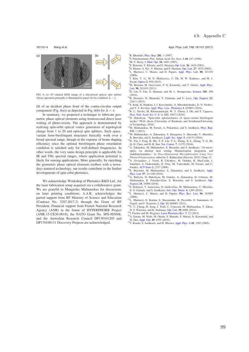
tilt of an incident phase front of the contra-circular output
component (Fig. 6(a)) as depicted in Fig. 6(b) for D ¼ p.In summary, we proposed a technique to fabricate geo-
metric phase optical elements using femtosecond direct laser
writing of photo-resists. The approach is demonstrated by
realizing spin-orbit optical vortex generators of topological
charge from 1 to 20 and optical spin splitters. Such space-
variant form-birefringent structures basically work over a
broad spectral range, though at the expense of beam shaping
efficiency since the optimal birefringent phase retardation
condition is satisfied only for well-defined frequencies. In
other words, the very same design principle is applicable for
IR and THz spectral ranges, where application potential is
likely for sensing applications. More generally, by enriching
the geometric phase optical elements toolbox with a nowa-
days matured technology, our results contribute to the further
developments of spin-orbit photonics.
We acknowledge Workshop of Photonics R&D Ltd., for
the laser fabrication setup acquired via a collaborative grant.
We are grateful to Mangirdas Malinauskas for discussions
on laser printing conditions. A.A.K. acknowledges the
partial support from RF Ministry of Science and Education
(Contract No. 3287.2017.2) through the Grant of RF
President. Financial support from French National Research
Agency (ANR) in the frame of HYPERPHORB Project
(ANR-15-CE30-0018), the NATO Grant No. SPS-985048,
and the Australian Research Council DP130101205 and
DP170100131 Discovery Projects are acknowledged.
1R. Bhandari, Phys. Rep. 281, 1 (1997).2S. Pancharatnam, Proc. Indian Acad. Sci. Sect. A 44, 247 (1956).3M. V. Berry, J. Mod. Opt. 34, 1401 (1987).4Z. Bomzon, V. Kleiner, and E. Hasman, Opt. Lett. 26, 1424 (2001).5G. Biener, A. Niv, V. Kleiner, and E. Hasman, Opt. Lett. 27, 1875 (2002).6L. Marrucci, C. Manzo, and D. Paparo, Appl. Phys. Lett. 88, 221102
(2006).7J. Kim, Y. Li, M. N. Miskiewicz, C. Oh, M. W. Kudenov, and M. J.
Escuti, Optica 2, 958 (2015).8M. Beresna, M. Gecevicius, P. G. Kazansky, and T. Gertus, Appl. Phys.
Lett. 98, 201101 (2011).9D. Lin, P. Fan, E. Hasman, and M. L. Brongersma, Science 345, 298
(2014).10B. Desiatov, N. Mazurski, Y. Fainman, and U. Levy, Opt. Express 23,
22611 (2015).11S. Kruk, B. Hopkins, I. I. Kravchenko, A. Miroshnichenko, D. N. Neshev,
and Y. S. Kivshar, Appl. Phys. Lett., Photonics 1, 030801 (2016).12R. C. Devlin, M. Khorasaninejad, W. T. Chena, J. Oh, and F. Capasso,
Proc. Natl. Acad. Sci. U. S. A. 113, 10473 (2016).13D. Hakobyan, “Spin-orbit optomechanics of space-variant birefringent
media,” Ph.D. thesis (University of Bordeaux and Swinburne/University
of Technology, 2016).14M. Malinauskas, M. Farsari, A. Piskarskas, and S. Juodkazis, Phys. Rep.
533, 1 (2013).15M. Malinauskas, A. �Zukauskas, S. Hasegawa, Y. Hayasaki, V. Mizeikis,
R. Buividas, and S. Juodkazis, Light: Sci. Appl. 5, e16133 (2016).16D. Yin, J. Feng, R. Ma, Y.-F. Liu, Y.-L. Zhang, X.-L. Zhang, Y.-G. Bi,
Q.-D. Chen, and H.-B. Sun, Nat. Comm. 7, 11573 (2016).17A. �Zukauskas, M. Malinauskas, E. Brasselet, and S. Juodkazis, “3d micro-
optics via ultrafast laser writing: Miniaturisation, integration, and
multifunctionalities,” in Three-Dimensional Microfabrication Using Two-Photon Polymerization, edited by T. Baldacchini (Elsevier, 2015), Chap. 12.
18A. Ovsianikov, J. Viertl, B. Chichkov, M. Oubaha, B. MacCraith, I.
Sakellari, A. Giakoumaki, D. Gray, M. Vamvakaki, M. Farsari, and C.
Fotakis, ACS Nano 2, 2257 (2008).19E. Brasselet, M. Malinauskas, A. �Zukauskas, and S. Juodkazis, Appl.
Phys. Lett. 97, 211108 (2010).20A. Balcytis, D. Hakobyan, M. Gabalis, A. �Zukauskas, D. Urbonas, M.
Malinauskas, R. Petru�skevicius, E. Brasselet, and S. Juodkazis, Opt.
Express 24, 16988 (2016).21S. Rek�styt _e, T. Jonavicius, D. Gailevicius, M. Malinauskas, V. Mizeikis,
E. G. Gamaly, and S. Juodkazis, Adv. Opt. Mater. 4, 1209 (2016).22L. Marrucci, C. Manzo, and D. Paparo, Phys. Rev. Lett. 96, 163905
(2006).23L. Marrucci, E. Karimi, S. Slussarenko, B. Piccirillo, E. Santamato, E.
Nagali, and F. Sciarrino, J. Opt. 13, 064001 (2011).24Y. C. Cheng, H. Zeng, J. Trull, C. Cojocaru, M. Malinauskas, T. Jukna,
D. S. Wiersma, and K. Staliunas, Opt. Lett. 39, 6086 (2014).25J. Fischer and M. Wegener, Laser Photonics Rev. 7, 22 (2013).26A. Emoto, M. Nishi, M. Okada, S. Manabe, S. Matsui, N. Kawatsuki, and
H. Ono, Appl. Opt. 49, 4355 (2010).27T. Kondo, S. Juodkazis, and H. Misawa, Appl. Phys. A 81, 1583 (2005).
FIG. 6. (a) 45�-slanted SEM image of a discretized optical spin splitter
whose operation principle is illustrated in panel (b) for condition D ¼ p.
181101-4 Wang et al. Appl. Phys. Lett. 110, 181101 (2017)
4.9. Appendix C
99

Chapter 4. Pancharatnam-Berry phase optical elements
100

Chapter 5
Plasmonic nano-printing for
surface structuring
5.1 Introduction
Laser-induced periodic surface structures (LIPSS), also termed as ripples werefirstly observed by Birnbaum in 1965 on germanium, silicon, GaAs, GaSb, InSband InAs irradiated by a ruby laser [187]. Different types of ripples irradiatedby nanosecond (ns), picosecond (ps) and femtosecond (fs) laser pulses with dif-ferent periodicity and orientation on different materials and at different laserconditions have been reported [188–191]. Ripples formed by the irradiation ofcw laser or ns or ps pulsed laser were found with the period comparable to theincidence wavelength and varies with the angle of incidence (Λ = λ/(1± sinθ),θ is the incident angle and Λ is the wavelength of the incident laser beam), andcan be explained by the inhomogeneous energy absorption resulting from thecoherent interference of the incident beam with the surface scattered wave justbeneath the surface [192]. While the ripples induced by fs laser irradiation havemuch more complex formation considering that the deposition of laser pulseenergy occurs much earlier than the thermal hydrodynamic destabilization ofmotion and the following resolidification process. The ability of processingany materials using femtosecond laser provides a lot of different ripple mor-phologies on different materials from metals, semiconductors to wide band gapdielectrics. Two types of ripples fabricated by femtosecond laser were foundwith period slightly smaller than the incident wavelength (0.6λ < Λ < λ, λ isthe ripple period) which are called sub-wavelength ripples (SWR) and periodsignificant smaller than the incident wavelength (Λ ≈ λ/2n, n is the refractiveindex of the substrate) called deep-subwavelength ripples (DSWR). These twotypes of ripples are mostly observed on semiconductors and dielectrics irradi-ated by femtosecond laser pulses. For example, SWR ripples were found withperiod 532 nm on Si and DSWR ripples (Λ = 139 and 215 nm) on LiF, as well
101
Chapter 5. Plasmonic nano-printing for surface structuring
as other DSWR ripples with different periods on SiO2, MgF2, Al2O3 irradi-ated under 800 nm wavelength were found [193]. By focusing the femtosecondlaser pulses inside the transparent dielectrics, SWR and DSWR structuresformed in the bulk have also been observed [194–196]. The femtosecond laserinduced SWR and DSWR structures provide the opportunity for overcomingthe optical diffraction limit, which attracts a lot of interests in investigationthe mechanism of ripple formation, the control of the uniform ripple growthand their applications considering the capability that almost any materials canbe processed by femtosecond laser pulses.
Another noteworthy property of the SWR and DSWR structures in laserirradiated area is the dependence of ripple orientation with the incident laserpolarization. This property offers the chance to engineer the birefringenceand to modify the polarization state of light that interacts with the SWR orDSWR structures. The local electric field in the laser focused area imprints theSWR or DSWR structures revealing the polarization vector field by formingthe varied orientation of SWRs or DSWRs [197]. This property facilitates therealization of polarization manipulation and phasefront engineering using fem-tosecond laser induced SWRs or DSWRs. A polarization diffraction gratingwas fabricated inside glass by femtosecond laser irradiation to induce the for-mation of DSWRs [198], as well as different vortex beam converters were fabri-cated inside glasses by azimuthally tuning the polarization of the femtosecondlaser beam synchronously during fabrication to form azimuthally orientationvaried DSWRs [199]. With the SWRs and DSWRs, we can build up artificialmaterials with desired spatial distribution of the effective permittivity ε andpermeability μ which could manipulate the phase, amplitude and polarizationof light in a novel way which is impossible in the nature materials. Using SWRsand DSWRs fabrication techniques, the geometry arrangement and orientationof the SWRs and DSWRs could be easily realized. In this manner, the de-sign and fabrication for functional metasurface optical elements especially thePancharatnam-Berry phase elements become simple and practical. Howeverthe mechanism of femtosecond laser induced SWRs and DSWRs are still notclearly understood, as well as the controllable, uniform and large area SWRsand DSWRs fabrication by femtosecond laser pulses are still not resolved.
In this chapter, the mechanism of the formation of SWRs and DSWRs willbe firstly introduced based on the experimental observation of distinct SWRsand DSWRs formed on two different thickness of indium tin oxide (ITO) filmson fused silica substrate by UV femtosecond laser pulses irradiation. ITO hascommonly used in flat pannel displays, organics-based electronics and solarcells due to their high transmittance in the visible range and good electricalconductivity. Patterning thin film of ITO on glass with narrow grooves is usingthe conventional photolithography method which involves multiple processesincluding the wet etching. It is very difficult to achieve very high resolutionpatterning with sub-micron groove width [200, 201]. Using UV femtosecondlaser pulses to patterning SWRs and DSWRs on thin ITO films could provide
102
5.2. Mechanism of ripple formation induced by ultra-short pulses
well defined edges and reduce the lost active area of solar cells or display paneland OLEDs. From the mechanism of SWRs and DSWRs formation, the abilityof tuning the period of SWRs and DSWRs was demonstrated by tuning thelaser fabrication conditions, which are the pulse energy and pulse density. Thedependence of the ripple orientation and laser beam polarization was investi-gated. Uniform of SWRs structures on amorphous silicon film was fabricatedby UV femtosecond laser pulses, as well as the technique on increasing thefabrication throughput by extending the beam using a cylindrical lens. Wafer-scale SWRs on silicon substrate was fabricated, which offers the opportunity todevelop the most effective and inexpensive technique to fabricate metasurfaceoptical elements to facilitate their wide use in super resolution imaging, datastorage, opto-fluidic, sensing and optical communications.
5.2 Mechanism of ripple formation induced
by ultra-short pulses
Since the first observation of ripple structure induced under laser irradiationon semiconductor surfaces, several models have been proposed to explain theinhomogeneous ablation. One of the generally accepted explanation is that theripples which have the periodicity close to the laser wavelength are caused bythe interference of incident laser with scattering waves from the surface rough-ness [190, 192, 202]. This explanation coincides with most of the experimentobservations of ripples induced by cw and long pulse lasers. Using femtosec-ond laser pulses, the period of SWRs was noticed to be smaller compared tothe laser wavelength under normal incidence, and DSWRs on surfaces and inbulk were observed on many materials in semiconductors and dielectrics whichcannot be explained by using the previous model. As it is well known that freeelectrons can be excited from the covalent band to conduction band throughlinear or nonlinear absorption under intense femtosecond laser pulse irradia-tion. The SWRs and DSWRs structures induced by femtosecond laser pulseswere attributed to the formed plasma under intensive irradiation on surfaceor in bulk of semiconductors and dielectrics, the surface waves are inducedat the interface between air and the metallic plasma layer, and the interfacebetween the plasma layer and substrate [203–205]. As a result, the periodicmaximum of the coupled surface wave corresponds to the strongest ionizationand inducing the surface ablation which formed the ripples. The wavelengthof the plasma wave is only dependent on the excited electron density, whichattributes to the laser deposited fluence and material properties. In differentexperimentally observed ripple periods on gallium nitride (GaN) film, the ex-cited surface plasma waves on both interface play an important role on thefinal ripple structure at different conditions [206]. The simultaneous formationof SWRs (730 nm) and DSWRs (180 nm) was also observed on the siliconcarbide (SiC) surface irradiated under 800 nm wavelength with 120 fs laser
103
Chapter 5. Plasmonic nano-printing for surface structuring
pulses under different laser fluence [207]. The further understanding on thelaser induced SWRs and DSWRs was required to explain the nature of thesestructures and controllable fabrication process of SWRs and DSWRs.
The free electron concentration excited by the absorption and ionizationis found to be important on the SWRs and DSWRs formation. A metal-lic like surface layer in the region with the strongest absorption is simul-taneously changing its dielectric constant. This thin plasma layer supportsthe surface plasmon polariton (SPP) wave on the interface of air/plasma andplasma/substrate interfaces. The surface wave can be excited under the condi-tions of the dielectric permitivity of the plasma layer Re(ε∗) < –n2 (n = 1, forair/plasma interface; n = nd, for the plasma/substrate interface) and a phasematching between the surface wave and the incident laser beam (|k| = 2π/λ),shown in Appendix D3. The optical property of the dense electron hole plasmain the femtosecond photo-excited ITO layer can be calculated by [208]:
ε∗ =
(1 + (εm – 1)
N0 – Ne
N0
)–ω
2p
ω2
1
1 + i(ωτD)–1, (5.1)
where τD is the Drude damping time or the impulse electron-phonon scatteringtime taken equal to the optical cycle at the wavelength of excitation [209], N0is the total density of the valence-band electrons, and Ne is the density of laserexcited electron hole pairs. εm is the dielectric constant of unexcited materialat the wavelength of excitation. ω is the cyclic frequency of the indent laserbeam, and ωp is the cyclic plasma frequency at the plasma density of Ne
calculated by:
ωp =
√Nee2
ε0m∗me, (5.2)
where the ε0 is the permitivity of vacuum, m∗ is the effective mass of electronin solid state material. Considering the SPP wave is coherent with the incidentlight and was launched during the ultra-short laser pulse before the electron-ionthermal interaction which takes place in several picoseconds, an unperturbedvalue of m∗ is used for simulations. The calculation of the dielectric permitivityof the excited plasma layer was taken the effect of the state and band fillingand the Drude contribution of free carriers, as seen in the first and second partin Eq. 5.1, respectively. The effect of the band filling is estimated from theratio of Ne to N0 [210]. The Drude contribution of free carriers is calculatedwith assuming that the carriers are uniformly distributed over the Brillouinzone. The wave vectors of the plasmon wave launching on the air/plasma orplasma/substrate interfaces are given by:
kspp1 = k0
√ε∗
1 + ε∗,
kspp2 = k0
√εd ∗ ε∗εd + ε∗
,
(5.3)
104

5.2. Mechanism of ripple formation induced by ultra-short pulses
where k = 2π/λ is the wave vector of the incident light, εd is the permitivityof the dielectric under the excited plasma layer. The periods of the surfacewaves launched in both interfaces can be calculated by:
λspp = 2π/Re(kspp). (5.4)
Under intensive irradiation by femtosecond pulses, the solid state plasmaof free electrons will drive the optical breakdown within few optical cycles ∼6 - 10 fs and creates breakdown when Re(ε∗) ≡ 0 at the plasma density largerthan the critical density for the excitation wavelength of Ncr = ε0me/e2
ω2.
The phase matching between the plasmon surface wave and incident lightcan be achieved by scattering, diffraction from the random surface rough-ness, or via parametric scattering [187, 190, 192, 211–213]. The observationsof the increasing period of SWRs in metals at larger laser deposition fluence,proves the coupling of a normally incident focused laser beam into a surfacewave [214, 215]. The SWRs and DSWRs are formed by the accumulation ofconsecutive laser pulses and absorbed energy and density of induced plasmaon the surface [214,216,217]. The normal SWRs were attributed to the inter-ference of the incident and light scattered from the surface based on the Sipe’smodel that the strongest absorption leads to the ablation with period Λ = λsp,and the period of DSWRs is Λ = λsp/2, which is attributed to the standingwave as result of coupling of the incident light with half of the Bragg wavevector.
However, considering the free carries can be generated by linear and multi-photon absorption (MPA) process for the semiconductors, the spatial profile ofplasma density, temperature and optical property will be affected by the spa-tial profile of the irradiated laser pulse intensity. In silicon carbide, both theSWRs and DSWRs have been observed under irradiation of 800 nm femtosec-ond laser pulses, and with the SWRs are observed in the central area of thefocused spots following with the DSWRs in the outside region [207]. It must benoted that the MPA process makes the dominating contribution to the plasmageneration. Therefore, MPA leads to a very steep spatial carrier distributionand cause the inhomogeneous spatial profile of the plasma permitivity, thusleads to the formation of SWRs and DSWRs.
Here we take the account of the direct and indirect band gap of indiumtin oxide (ITO) which are around 2.2 eV and 3.5 eV, respectively [218, 219],by irradiated under focused forth harmonic beam (NA = 0.4, λ = 257 nm).The focus spot size is around d = 1.22λ/NA ≈785 nm in diameter. Thesingle photon ionization is taking responsible for the carrier excitation in thefocus area. Hence the spatial inhomogeneous excitation caused by MPA isavoided, much more uniform ripple structure should be expected. As shownin Fig. 5.1, uniformly formed SWRs structures with period 196 nm are fab-ricated on the surface of 240 nm thick ITO film with pulse energy 0.31 nJwith pulse density 50 pulses/μm. A low resistivity high transparent ITO filmwas sputtered on a fused silica substrate using the electron-beam evapora-tion (Intlvac Nanochrome II system). It has the complex refractive index
105

Chapter 5. Plasmonic nano-printing for surface structuring
2μm
Figure 5.1: SEM image of uniformly formed SWRs structures with period196 nm on a 240 nm thick ITO film deposited on fused silica substrate irradi-ated by focused forth harmonic beam λ = 257 nm with NA 0.4 objective, withpulse energy 0.31 nJ, pulse density 50 pulses/μm, the scan speed is 0.1 mm/swith repetition rate 200 kHz.
n∗ = n – iκ = (2.3665 – 0.54360i) and the complex permittivity of unexcitedmaterial of ITO is ε∗ = (n2–κ2)–2nκi = 5.3048–2.5729i at 257 nm [220]. Sincethe static skin depth of ITO film at 257 nm is 75 nm, by changing the substratepermitivity as shown in Eq.5.3, the period of the supporting surface wave onthe plasma/substrate interface can be different. Two different thickness of ITOfilms were deposited on fused silica substrate. The FDTD simulation of theelectric field of the focused laser beam on both films are shown in Fig .5.2. Thepulse energy deposited on the ITO surface was 65% and 40% for 50 nm and240 nm film, respectively. This difference facilitate the lower optical excitationand ablation threshold on the 50 nm ITO film comparing to that of 240 nmthickness.
The multiple consecutive laser pulses, have been found playing a key roleon the non-thermal process of ripple formation and ablation [217, 221–225].The energy absorbed from the formal laser pulses creates additional absorp-tion band by exciting free carriers or inducing defects in the band gap, hencefacilitating the absorption of following pulses and reducing the ablation thresh-old by multiple consecutive femtosecond laser pulses. The threshold for singlepulse and 100 pulses/μm for the ablation threshold of 50 nm thick ITO film was110 mJ/cm2 and 50 mJ/cm2, respectively, as shown in Fig. 4.23. The ablationthreshold of multiple pulses with pulse density 100 pulses/μm has two timeslower threshold than single pulse ablation. Since only the one photon ioniza-tion is taking place for the free carrier excitation for ITO film under 257 nmfemtosecond laser irradiation, the free carrier density is linear to the laserfluence and the reflectivity of the excited surface, which is given by [208,210]:
Ne = αF01 – R
hω, (5.5)
106

5.2. Mechanism of ripple formation induced by ultra-short pulses
ITO
air
glass
50 nm 240 nm
I0=0.22
I0.05=0.65
I0=0.0005
I0.24=0.4
w0
100 nm
(a) (b)
Figure 5.2: The Finite-difference time-domain (FDTD) simulation of the elec-tric field of the forth harmonic beam focused by NA 0.4 objective on the ITOfilm on the fused silica substrate, with thickness of 50 nm (a) and 240 nm (b).The static skin depth of the ITO film at 257 nm is 75 nm and 65% and 40%intensity was deposited on the surface of 50 and 240 nm film, respectively.
where α is the linear absorption coefficient, F0 is the laser fluence with F0 =∫I(t)dt =
√πt0I0, considering the focused laser beam has a Gaussian envelope
I(t) = I0e(–t/t0)2 and I0 is the central intensity, R is the reflectivity of theplasma layer, and can be calculated from the Fresnel formula by [208]:
R =
√ε∗ – 1√ε∗ + 1
. (5.6)
In the experiment, DSWRs and SWRs were observed on the 50 nm and 240 nm,separately. The SEM images and the spatial frequency of the ripples structureson the surface of two different thickness film were shown in Fig. 5.3. The spatialfrequency shows the period of the DSWRs with 83 nm and 196 nm on 50 nmand 240 nm ITO film. The pulse energies are 0.27 nJ and 0.31 nJ for thefabrication with pulse density of 50 pulses/μm, with scanning speed 0.1 mm/sand repetition rate of 200 kHz. The lower pulse energy for the formation ofripple structures with same pulse density on the 50 nm film comparing to thaton the 240 nm ITO film is corresponding to the FDTD simulations shown inFig. 5.2, resulting from the smaller reflectivity of the laser beam on the 50 nmITO film.
By applying the equations in Eq. 5.1- 5.4, with the parameters that τDis ∼1.2 fs at the wavelength of excitation at 257 nm, N0 is estimated to 1 ×1023 cm–3 and for ITO the effective mass constant m∗ = 0.4 [220], the period
107

Chapter 5. Plasmonic nano-printing for surface structuring
20 40 60 80 1000
20
40
60
Den
sity
(a.
u.)
Frequency (m-1)
83 nm
10 20 30 40 500
20
40
60
Den
sity
(a. u
.)
Frequency (m-1)
196 nm 240 nm
50 nm
1 μm
Figure 5.3: SEM images and the spatial frequency of the induced DSWRs andSWRs with period 83 nm and 196 nm by the fourth harmonic femtosecondlaser beam irradiation on the 50 nm and 240 nm ITO films on fused silicasubstrate. The fabrication conditions for the DSWRs and SWRs are withpulse energy of 0.27 nJ and 0.31 nJ under pulse density of 50 pulses/μm. Thescan speed is 0.1 mm/s, and repetition rate is 200 kHz.
of the surface plasma wave replated to the can be estimated on the interfaces.With the plasma density larger than the critical density Ncr = ε0me/e2
ω2 =
1.68 × 1022 cm–3 at excitation wavelength 257 nm, the free electrons drivesthe breakdown. Figure 5.4 shows the dependence of the period of the formedSWRs and DSWRs with the plasma density. The simulation for the SWRs isbased on the interference of the surface wave on the air/plasma interface, withthe incident light based on the Sipe’s model, Λ = λspp1 [192]. For the DSWRs,considering the thickness of the ITO film is 50 nm which is much smaller thanthe static skin depth 75 nm of the ITO film under 257 nm, the whole film wasexcited under the intensive irradiation in the focus region, which generateda metallic plasma layer between the air and the fused silica substrate. Thestanding wave formed on the interface of the plasma and fused silica with thephase matching of half Bragg wave vector lead to the DSWRs formation, withperiod Λ = λs/2 [226]. The refractive index of the fused silica at 257 nm is1.5038 and permitivity εd = n2 = 2.2614 [227]. The observed ripple periodfor the SWRs on 240 nm film is 196 nm and DSWRs is 83 nm as shown inFig. 5.3, which confirms that the DSWRs are formed by the surface wave onthe interface with the plasma and fused silica, and SWRs are formed on theinterface between air and the plasma layer.
Since the single photon ionization dominates the free carrier generationin forming the plasma on the surface of ITO film by 257 nm irradiation, the
108

5.2. Mechanism of ripple formation induced by ultra-short pulses
1021 1022 10230
50
100
150
200
250
air/plasma plasma/glass Re(permitivity)
Plasma density (cm-3)
Rip
ple
perio
d (n
m)
-5
-4
-3
-2
-1
0
Re(
perm
itivi
ty)
Figure 5.4: Plasmonic excitation on the air/plasma and plasma/glass substrateinterfaces plotted with plasma density Ne. The period of the SWRs is same asthe surface wave on the air/plasma interface that is attributed to the coherentinterference with incident light according to Sipe’s theory, Λ = λspp [192]. Theperiod of the DSWRs is equal to the half of the period of the standing plasmonwave matching the half of the Bragg wave vector, with Λ = λspp/2 [226].The right side shows the real part of the optically excited plasma permitivityRe(ε∗). The light blue colored region shows the solid state of the ITO film andoptically induced breakdown at Re(ε∗) ≡ 0.
carrier density with the dependence of deposited laser fluence can be calcu-lated using Eq. 5.5. The linear absorption coefficient of ITO at 257 nm is2.6580×105cm–1 [228]. Simultaneous reflectivity dependent on the plasma per-mitivity can be calculated using the Eq. 5.6. Figure 5.5 shows the dependenceof plasma density Ne and the laser deposited fluence and the reflectivity of theplasma layer. The induced carrier concentration is increasing with the laserfluence and when laser fluence is at 25 mJ/cm2 which is two time lower thanthe ablation threshold, reflectivity of the plasma layer is the lowest, whichcorresponds to the dielectric breakdown occurring and solid state plasma isformed. It is noteworthy that under multiple pulses, the threshold of dielectricbreakdown and plasma formation were reduced. The simultaneous change ofthe reflectivity of the plasma layer is important for the effect that screens thelaser energy to transfer deeper to the ions and excite more electrons in thepropagation direction of incident laser beam.
Coherent surface excitation occurring simultaneously with the light pulseabsorption followed by ablation after the laser pulse initiates the imprint of thesurface wave. SPP modes can be excited only when the dielectric breakdown
109

Chapter 5. Plasmonic nano-printing for surface structuring
0 25 50 75
1021
1022
Fluence (mJ/cm2)
Plas
ma
dens
ity (c
m-3)
Ncr
0.3
0.4
0.5
0.6
0.7
Ref
lect
ion
Figure 5.5: Laser fluence determined the plasma excitation with sigle photonionization. The simultaneous reflectivity decreases with the laser fluence andreaches to the lowest when Re(ε∗) = 0 at dielectric breakdown taking place at25 mJ/cm2 which is two times lower than the ablation threshold.
happens Re(ε∗) < 0, and to support the excited surface wave on the interfacesof air/plasma and plasma/substrate, (ε∗) < –n2 as details shown in AppendixD2. The surface plasma layer has a skin depth for light intensity changingwith the excited carrier density within δ = c/(ωIm(
√ε∗)) = λ/(2πIm(
√ε∗))
of 40 nm to 5 nm from the plasma density creates dielectric breakdown Ne =8.6 × 1021 cm–3 to 1023 cm–3. The calculated skin depth and reflectivity ofthe plasma layer as a function of plasma density was shown in Fig. 5.6. Thereflectivity of the excited layer is decreasing as plasma density increases andreaches the lowest when the dielectric breakdown takes place at Re(ε∗) = 0 .
5.3 Period tuning of laser induced ripples
The presented above mechanism of SWRs and DSWRs formation was validatedexperimentally. Ripples were fabricated on ITO film at different pulse energiesand pulse densities and compared with period of the surface wave predictionsRe(ε∗) = –n2 for the air/plasma (–n2 = –1) and plasma/glass (–n2 = –2.2614)interfaces. Figure 5.4 shows the predictions of ripple period that forms theSWRs on the air/plasma interface and DSWRs on the plasma/glass substraterespect to the plasma density. Therefore, the ripple period can be tuned bychanging the fabrication parameters. The obvious way is to change the ex-citation wavelength to tune the ripple period [229], or change the dielectricpermitivity of the substrate on the plasma/dielectric interface by changing theambient environment [207, 230, 231]. Here, the period of SWRs and DSWRson ITO films was tuned by changing the laser deposition energy and pulse
110

5.3. Period tuning of laser induced ripples
1021 1022 10230
15
30
45
60
75
Skin depth Reflection
Plasma density (cm-3)
Skin
dep
th (n
m)
0.2
0.4
0.6
0.8
1.0
Ref
lect
ion
Figure 5.6: The calculated skin depth δ and plasma reflectivity as a function ofthe carrier density in the excited plasma layer. The lowest reflectivity of ITOshows the dielectric breakdown happens when Re(ε∗) ≡ 0 at plasma densityof 8.6 × 1021 cm–3. The surface wave is allowed to excited after breakdownhappens when the excited carrier density is larger than 8.6×1021 cm–3 and tosupport the surface wave on different interfaces, Re(ε∗) < –n2 seen in AppendixD2. The skin depth was reducing as the plasma density increases which leads tothe screening of the following deposited energy and an inhomogeneous spatialprofile of plasma density in the beam propagation direction occurs.
density, in the range of 70∼110 nm for DSWRs and 182∼252 nm for SWRs asshown in Fig. 5.4.
With the increasing of laser pulse energy or fluence, the photoexcited car-rier concentration increased and hence changes the dielectric permitivity ofthe excited layer which changes the period of the ripple structures. Consid-ering the screening effect occurs when the reflectivity starts increasing afterthe dielectric breakdown happening with the increasing plasma density, theactually deposited energy on the ITO film was reduced. Therefore, the vol-ume average photo-excited electron density was reduced since the dielectricbreakdown happens, and the nonuniform distribution of electron density inthe laser beam propagation direction was taken into consideration. The ex-periments with increasing pulse energy from 0.2 to 0.5 nJ with pulse densityof 100 pulses/μm valid the assumptions as shown in Fig. 5.7. The period ofthe SWRs and DSWRs was increasing when the pulse energy was increased.For SWRs on 240 nm thick film, the period was changing from 185 nm to250 nm, and for DSWRs on 50 nm film, the period varies from 70 nm to102 nm. The results indicate the excited plasma density was reducing whenincrease the pulse energy as shown in Fig.5.4 resulting from the screening effectshowing in Fig. 5.5 and Fig. 5.6. The ripple formation threshold of DSWRs on
111

Chapter 5. Plasmonic nano-printing for surface structuring
50 nm was found smaller than SWRs on 240 nm film at the pulse density of100 pulses/μm which corresponds to the previous analysis. This similar behav-ior was also found in the experiments when increasing the pulse density from20 pulses/μm to 100 pulses/μm under the pulse energy of 0.31 nJ as shownin Fig. 5.8. There was no clear periodic feature was found below the pulsedensity of 20 pulses/μm. The period was changing from 73 nm to 90 nm forDSWRs on 50 nm film and 185 nm to 198 nm for SWRs on 240 nm film. Thisobservation is different than the results which shows the decreasing of the pe-riods of SWRs in the experiments irradiated on silicon surface with increasingpulse density under 800 nm wavelength [224].
0.2 0.4 0.6
70
80
90
100
110
Per
iod
(nm
)
Pulse energy (nJ)
500nm
0.3 0.4 0.5
200
220
240
260
Per
iod
(nm
)
Pulse energy (nJ)
1 μm
(a) (b)
Figure 5.7: The experimental results for the period of DSWRs on the 50 nmand SWRs on the 240 nm thickness film with the dependence of femtosecondpulse energy. The pulse density for fabrication on both films is 100 pulses/μm.The variation of the ripple period for the DSWRs is from 70 nm to 102 nmand for SWRs is from 185 nm to 250 nm.
5.4 Orientation tuning of laser induced
ripples
The orientation of ripples induced by femtosecond laser that perpendicularto the incident laser polarization was one of the pronounced property thatarises from the surface wave excitation mechanism discussed above and wasdemonstrated both in the simulations and experiments [232]. This propertyopens applications to fabricate optical vortex converters using femtosecondlaser inside fused silica by changing the linear polarization to fabricate az-imuthally varied DSWRs structures [199]. Varied orientation of SWRs werefabricated on 240 nm thick ITO film under 0.31 nJ pulse energy with pulsedensity 50 pulses/μm by changing the linear polarization from 0◦ to 180◦ re-spect to the scan direction, as shown in Fig. 5.9. The period of the SWRsstructures is 196 nm. As it is shown in the FFT images, the orientation of
112
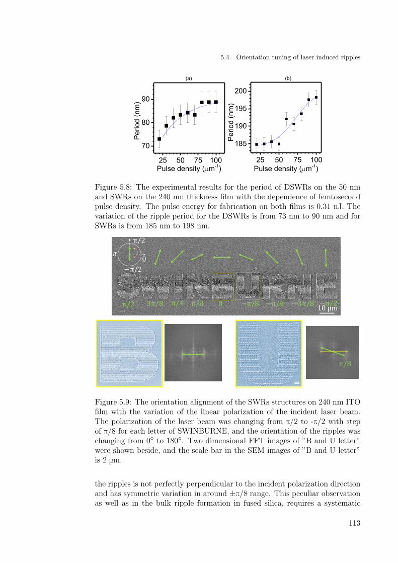
5.4. Orientation tuning of laser induced ripples
25 50 75 100
185
190
195
200
Per
iod
(nm
)
Pulse density (m-1)25 50 75 100
70
80
90
Per
iod
(nm
)
Pulse density (m-1)
(a) (b)
Figure 5.8: The experimental results for the period of DSWRs on the 50 nmand SWRs on the 240 nm thickness film with the dependence of femtosecondpulse density. The pulse energy for fabrication on both films is 0.31 nJ. Thevariation of the ripple period for the DSWRs is from 73 nm to 90 nm and forSWRs is from 185 nm to 198 nm.
3π/8 π/4 π/8 0 −π/8 −π/4 −3π/8 −π/210 μm
π/2
0
π/2
−π/2
𝜋
−π/8
Figure 5.9: The orientation alignment of the SWRs structures on 240 nm ITOfilm with the variation of the linear polarization of the incident laser beam.The polarization of the laser beam was changing from π/2 to -π/2 with stepof π/8 for each letter of SWINBURNE, and the orientation of the ripples waschanging from 0◦ to 180◦. Two dimensional FFT images of ”B and U letter”were shown beside, and the scale bar in the SEM images of ”B and U letter”is 2 μm.
the ripples is not perfectly perpendicular to the incident polarization directionand has symmetric variation in around ±π/8 range. This peculiar observationas well as in the bulk ripple formation in fused silica, requires a systematic
113
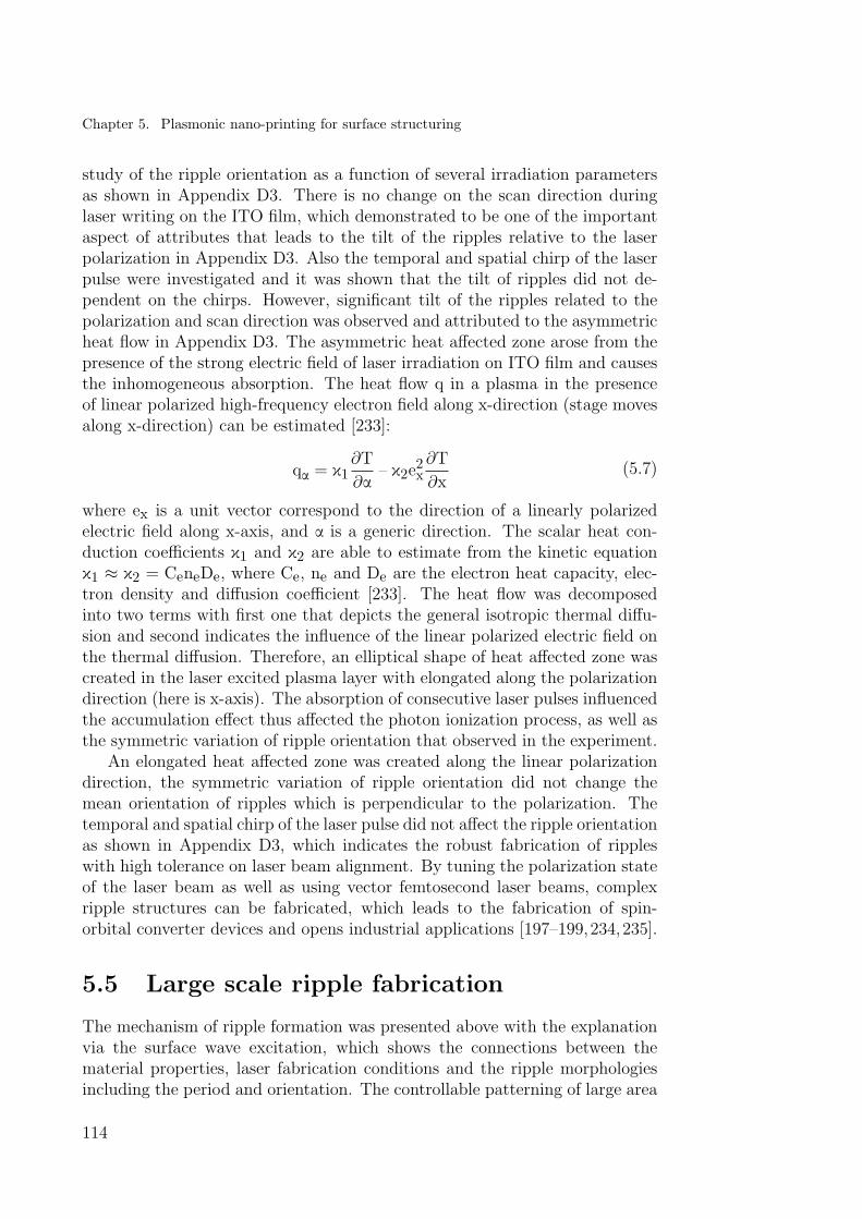
Chapter 5. Plasmonic nano-printing for surface structuring
study of the ripple orientation as a function of several irradiation parametersas shown in Appendix D3. There is no change on the scan direction duringlaser writing on the ITO film, which demonstrated to be one of the importantaspect of attributes that leads to the tilt of the ripples relative to the laserpolarization in Appendix D3. Also the temporal and spatial chirp of the laserpulse were investigated and it was shown that the tilt of ripples did not de-pendent on the chirps. However, significant tilt of the ripples related to thepolarization and scan direction was observed and attributed to the asymmetricheat flow in Appendix D3. The asymmetric heat affected zone arose from thepresence of the strong electric field of laser irradiation on ITO film and causesthe inhomogeneous absorption. The heat flow q in a plasma in the presenceof linear polarized high-frequency electron field along x-direction (stage movesalong x-direction) can be estimated [233]:
qα = κ1∂T
∂α– κ2e2
x∂T
∂x(5.7)
where ex is a unit vector correspond to the direction of a linearly polarizedelectric field along x-axis, and α is a generic direction. The scalar heat con-duction coefficients κ1 and κ2 are able to estimate from the kinetic equationκ1 ≈ κ2 = CeneDe, where Ce, ne and De are the electron heat capacity, elec-tron density and diffusion coefficient [233]. The heat flow was decomposedinto two terms with first one that depicts the general isotropic thermal diffu-sion and second indicates the influence of the linear polarized electric field onthe thermal diffusion. Therefore, an elliptical shape of heat affected zone wascreated in the laser excited plasma layer with elongated along the polarizationdirection (here is x-axis). The absorption of consecutive laser pulses influencedthe accumulation effect thus affected the photon ionization process, as well asthe symmetric variation of ripple orientation that observed in the experiment.
An elongated heat affected zone was created along the linear polarizationdirection, the symmetric variation of ripple orientation did not change themean orientation of ripples which is perpendicular to the polarization. Thetemporal and spatial chirp of the laser pulse did not affect the ripple orientationas shown in Appendix D3, which indicates the robust fabrication of rippleswith high tolerance on laser beam alignment. By tuning the polarization stateof the laser beam as well as using vector femtosecond laser beams, complexripple structures can be fabricated, which leads to the fabrication of spin-orbital converter devices and opens industrial applications [197–199,234,235].
5.5 Large scale ripple fabrication
The mechanism of ripple formation was presented above with the explanationvia the surface wave excitation, which shows the connections between thematerial properties, laser fabrication conditions and the ripple morphologiesincluding the period and orientation. The controllable patterning of large area
114

5.5. Large scale ripple fabrication
subwavelength grating structures by femtosecond laser irradiation still have alot of challenges. In this section, more technical details will be presented tofabricate uniform SWRs by line to line scanning or cylindrical beam shaping.
5.5.1 Uniform subwavelength ripples on amorphous Sifilm
1μm
Δy=2μm
10 20 30 40Frequency (m-1)
216 nm
Figure 5.10: SEM image of SWRs fabricated on a 100 nm thick a-Si film de-posited on fused silica substrate. The fabrication conditions are λ = 257 nm,pulse energy 0.05 nJ, NA 0.4, pulse density is 100 pulses/μm with scan speed0.1 mm/s. The separation distance of each lines in y-axis is 2 μm, and rip-ple period is 216 nm as measured with one dimension FFT technique. Thepolarization of the laser beam is parallel to the scan direction along x-axis.
Amorphous silicon (a-Si) film was sputtered by e-beam evaporation on a1 mm thick fused silica substrate. The 4th harmonic beam (λ = 257 nm) wasfocused by a NA 0.4 objective lens on the surface of a-Si film. The repetitionrate is 100 kHz and scan speed is 0.1 mm/s. Using the ripple formation theorypresented above, the period of SWRs on a-Si (n = 1.8385, κ = 2.8386 at257 nm wavelength [236]) is predicted in the range of 198 nm to 224 nm. Asshown in Fig. 5.10, SWRs structures were formed on the surface of a-Si filmwith period 216 nm calculated by one dimension FFT. The pulse energy andpulse density are 0.05 nJ and 100 pulses/μm. The beam was linearly polarizedalong scan direction (x-axis) and the separation of each lines in y-direction is2 μm. Ripples were formed under the pulse density over 20 pulses/μm at pulseenergy of 0.05 nJ.
By adjusting the overlap between the fabrication lines in the y-direction,the presence of defects and free carriers in the heat-affected zone enhancesthe ionization of material in the y-direction that generated by the previous
115

Chapter 5. Plasmonic nano-printing for surface structuring
1μm
(d)(c)
(b)(a)
Figure 5.11: SEM images of SWRs fabricated with different separation dis-tances in y-direction: (a) 500 nm; (b) 400 nm; (c) 300 nm and (d) 200 nm.The pulse energy is 0.035 nJ focused by a NA 0.4 objective lens. The pulsedensity is same of 100 pulses/μm, at scan speed 0.1 mm/s and repetition rateof 100 kHz.
laser irradiation. Due to the Gaussian spatial intensity distribution with afocal spot around 360 nm in radius focused by a NA 0.4 objective lens, thephoto-excited free carrier density is not uniform and determined by the locallaser fluence (Eq. 5.5). As shown in Fig. 5.11, the film was raster scannedat different separation distances from 500 nm to 200 nm in y-direction withsame pulse energy of 0.035 nJ with pulse density 100 pulses/μm. When theseparation distance is smaller than 300 nm, uniform and clear ripples wereobserved, which is roughly around one pulse overlap in the y-direction. It isnoteworthy that the threshold of ripple formation is also reduced comparingto the no overlap in y-direction (2 μm separation as shown in Fig. 5.10), whichis attributed to the existed defects or free electrons in the pre-modified areagenerated by previous irradiation. By adjusting the laser pulse energy andto balance the throughput of SWRs fabrication with raster scan, large areaof uniform SWRs were fabricated on a-Si film by femtosecond laser as shownin Fig. 5.12. The pulse energy is 0.01 nJ, and the separation distance in y-direction is 200 nm. The scan speed is 0.1 mm/s, pulse density 100 pulses/μmand repetition rate is 100 kHz. The period of the SWRs is around 200 nm asindicated in the two dimension FFT image. The polarization of the incidentlaser beam is 45◦ respect to x-axis (scan direction). Small variations of theorientation of ripples were observed in Fig. 5.12, which can be explained bythe asymmetric heat flow related to the polarization and scan direction asdiscussed above and in Appendix D3.
116

5.5. Large scale ripple fabrication
Λ = 200 nm
FFT
2μm
Figure 5.12: Uniform SWRs fabricated on a-Si film by 257 nm beam focused byNA 0.4 objective with pulse energy 0.01 nJ, separation distance in y-direction200 nm, pulse density is 100 pulses/μm, repetition rate is 100 kHz and scanspeed 0.1 mm/s. The polarization of the incident beam is 45◦ respect to x-axis(scan direction). The period is around 200 nm as shown in the inset of twodimension FFT image.
5.5.2 Wafer-area nanogratings fabricated viacylindrical lens
An efficient approach to fabricate nanogratings was proposed to apply theplasmonic nanoprinting by femtosecond laser irradiation to induce SWRs orDSWRs on the substrate surface. The fabrication of uniform SWRs andDSWRs were presented above, as well as their morphology tunabilities bychanging the fabrication conditions. As it is well known that gratings canbe obtained by many different techniques, for example two beam interference,diamond machining, and photo-lithography are widely used to fabricate mi-crometer scale period gratings and e-beam lithography and focused ion-beamlithography are widely used for sub-micrometer period gratings. The advan-tages for plasmonic nanoprinting SWRs or DSWRs by single femtosecond laserbeam irradiation are its fabrication flexibility, single step and low environmentrequirement especially the capability for 3D fabrication. However, this fabrica-tion technique requires the translation movement of the sample or laser beam,which reduces the fabrication throughput. Here a beam shaping technique toutilize a cylindrical lens to obtain a line focus was exploited. This techniquewas used to extend the exposure area and increase the fabrication throughputof ripples and was performed on GaAs, TiO2 and Si recently [237–239].
The surface plasmon wave coherently excited by the femtosecond laserpulses under the line focus region was schematically shown in Fig. 5.13 (a),with the mechanism explained above. A 4-inch Si wafer was nanotextured with
117

Chapter 5. Plasmonic nano-printing for surface structuring
(a) (b)
(c)
10 μm
2 μm
Figure 5.13: (a) Schematic of plamonic nanoprinting using cylindrical lenswhich improves the SWRs fabrication throughput, as shown in Appendix D3.(b) A photo of nanotextured 4-inch Si wafer by SWRs with period around 1 μmas shown in the SEM image in the inset by 1030 nm wavelength femtosecondlaser beam focused by a cylindrical lens at 500 kHz repetition rate and 50 mm/sscan speed, courtesy by R. Buividas . (c) Plasmonic nanoprinting of SWRswith period around 200 nm on Si wafer patterned by 4th harmonic beam(λ = 257 nm) focused by a fused silica cylindrical lens at 100 kHz repetitionrate, scan speed of 1 mm/s.
SWRs with period around 1 μm fabricated by 1030 nm femtosecond laser beamwith a high aspect ratio∼200 elliptical focus as shown in Fig. 5.13 (b). Thestage moves at 50 mm/s at the pulse repetition rate of 500 kHz to achieve therequired pulse overlap for uniform ripple formation. It was reported to be morethan 2×10⁷ times throughput comparing to the low repetition laser system inAppendix D2. With fused silica cylindrical lens, short period Λ = 200 nmwas fabricated by 4th harmonic femtosecond laser beam, at repetition rate of100 kHz and scan speed of 1 mm/s, as shown in Fig. 5.13 (c). By rotating thelinear polarization during scanning, the orientation of the ripples will keep fol-lowing the rotation of the polarization as shown in Fig. 5.9. This provides theopportunity to fabricate photonic spin Hall devices based on Pancharatnam-Berry phase on silicon surface as introduced in the last chapter. Continuouslyrotated ripples with rotation speed of 2◦/μm and period of 1 μm and rotationspeed of 45◦/μm and period of 200 nm were fabricated by 1030 nm and 257 nmbeams, respectively. Applying the line focus of femtosecond laser beam, effi-cient and high throughput uniform nanogratings can be patterned on differentmaterials.
118

5.6. Conclusions
10 μm 2 μm
(a) (b)
Figure 5.14: SEM images of photonic spin Hall devices based on rotationalSWRs fabricated on Si surface using cylindrical lens to increase the fabricationthroughput. (a) SWRs with period around 1 μm and rotational speed of 2◦/μmfabricated by 1030 nm wavelength beam at scan speed of 0.1 mm/s, courtesy byR. Buividas. (b) SWRs with period around 200 nm and fast rotational speedof 45◦/μm fabricated by 4th harmonic beam at scan speed of 0.01 mm/s.
5.6 Conclusions
In this chapter, it is determined that the SWRs and DSWRs are formed viaplasmonic nanoprinting of the excited surface wave with period related to theplasma density at the interface with the dielectric substrates. The simulta-neous change of the reflectivity on the metallic plasma layer relating to thegenerated electron density was found playing important role on the feedbackof the final ripple period which was confirmed in the experiments of ITO films.This proposed model was also valid in the predictions on ripple fabrications inother materials at different wavelength. By extending the beam with a cylin-drical lens to obtain line focus of femtosecond laser beam, large area of sub-wavelength ripples can be achived with period 1 μm and 200 nm with 1030 nmand 257 nm wavelength, respectively. Wafer-scale subwavelength gratings of-fers the opportunity to develop the most effective and inexpensive techniqueto fabricate metasurface optical elements especially the Pancharatnam-Berryphase optics to facilitate their wide applications. The DSWRs on surface andin volume of sapphire were also found impacting on the TO photon modesand modifying the reflection and transmission phonon spectrum, with the de-tails in Appendix D1, which opens a door on control the phonon spectrum viapatterned SWRs or DSWRs by femtosecond laser irradiation.
119

Chapter 5. Plasmonic nano-printing for surface structuring
5.7 Appendix D
This section contains the published papers related to the plasmonic nano-printing of ripples by femtosecond laser irradiation.
D1: X. W. Wang, G. Seniutinas, A. Balcytis, I. Kasalynas, V. Jakstas,V. Janonis, R. Venckevicius, R. Buividas, D. Appadoo, G. Valusis and S. Juod-kazis. Laser Structuring for control of coupling between THz light and Phononmodes. Journal of Laser Micro/Nanoengineering, 11, 3, 2016.
In this paper, the DSWRs on surface and in volume of sapphire patternedby femtosecond laser have been found to impact on softening TO phononmodes and changing reflectivity at specific modes, due to coupling of THzradiation with phonons. This opens the applications of laser patterned rippleson phonon spectrum control and photonic engineering.
D2: L. Wang, Q. Chen, X. Cao, R. Buividas, X. W. Wang, S. Juod-kazis and H. Sun. Plasmonic nano-printing: large-area nanoscale energy de-position for efficient surface texturing. submitted, 2017.
In this paper, the surface plasmon polariton standing wave on surface co-herently excited by femtosecond laser pulses has been proved to explain theexperiment observations on formation of subwavelength or deep subwavelengthstructures. With applying a cylindrical lens to obtain line focus on the surface,up to seven orders of magnitudes increase in the fabrication throughput havebeen achieved. The demonstrated mechanism of surface modification usingplasmonic waves and fabrication over large wafer-sized areas makes the plas-monic nano-printing a novel industrial method suitable for active research andapplications requiring large area nanograting patterning.
D3: V. Stankevic, G. Raciukaitis, F. Bragheri, X. W. Wang, E. Gamaly,R. Osellame and S. Juodkazis. Laser printed nano-gratings: orientation andperiod perculiarities. Scientific Reports, 7, 2017.
In this paper, the first systematic study of the influence of writing directionon the nanograting orientation in glass has been carried out and presented.A significant tilt of the orientation of ripples induced by femtosecond laserpulses have been observed depending on the scanning direction with respectto the laser polarization. It is also revealed that the polarization orientation iscoupled with a temperature gradient at the focal volume and affects formation
120

5.7. Appendix D
of nanogratings, influencing their period and orientation depending on thewriting directions.
121

JLMN-Journal of Laser Micro/Nanoengineering Vol. 11, No. 3, 2016
377
Laser Structuring for Control of Coupling Between THz Light and Phonon Modes
Xuewen Wang1,*, Gediminas Seniutinas1,2, Armandas Balčytis1,3, Irmantas Kašalynas3, Vytautas Jakštas3, Vytautas Janonis3, Rimvydas Venckevičius3, Ričardas Buividas1, Dominique Appadoo4, Gintaras Valušis3 and Saulius Juodkazis1
1 Centre for Micro-Photonics, Faculty of Engineering and Industrial Sciences, Swinburne University of Technology, Hawthorn, VIC 3122, Australia
E-mail: [email protected] 2 School of Mathematical and Physical Sciences, University of Technology Sydney, Thomas St, Ulti-
mo, NSW 2007, Australia 3 Center for Physical Sciences and Technology, Saulėtekio al. 3, LT-10222 Vilnius, Lithuania
4 Australian Synchrotron, Blackburn Road, Clayton, Victoria 3168, Australia
Modification of surface and volume of sapphire is shown to affect reflected and transmitted ra-diation at THz spectral range. Structural modifications were made using ultra-short 230 fs laser pulses at 1030 and 257.5 nm wavelengths forming surface ripples of ~250 nm and 60 nm period, re-spectively. Softening of the transverse optical phonon TO1 mode due to disorder was most pro-nounced in reflection from laser ablated surface. It is shown that sub-surface periodic patterns of la-ser damage sites have also modified reflection spectra due to coupling of THz radiation with pho-nons. Application potential of laser structuring and disordering for phononic engineering is dis-cussed.
Keywords: laser fabrication, nanotexturing, void formation, material engineering, phonon spectrum control, terahertz spectroscopy.
1. Introduction
Spectral properties at sub-1 mm wavelengths at around terahertz (1 THz = 1012 Hz) frequencies are important for understanding weak interaction in peptides and proteins [1,2], material response at vicinity of phase transitions [3,4], glass formation where low frequency Raman spectra exhib-it the low frequency 10-50 cm-1 boson peak due to rear-rangement of density of states in amorphous materials [5]. In silk, amorphous and crystalline structural components with proteins forming a 3D network of random and α-coils together with a crystalline β-sheet phase can be dis-tinguished in the THz spectral window [6-11].
Control of phonon spectrum is a new frontier in materi-al science for growth and deposition of layered structures of usually incompatible materials with different thermal expansion coefficients. Materials' optical properties at IR range can be engineered through control of the phonon spectrum. For example, surface phonon polaritons (SPP) are shown to control directionality of black body emission when coupled with surface gratings [12]. By introducing patterns with period Λ satisfying the grating equation:
Λ+=
πθλπ 2sin2
|| mk , (1)
where λ is the wavelength of emitted light (black body ra-diation), θ is the angle of emitted light, k|| is the surface wave component parallel to the surface (SPP), and m is an integer. It is thereby possible to create a strong directional out-coupling of the IR emission into free space out of the sample [12]. With a surface grating λ55.0=Λ directional emission was observed at λ = 11.36 μm from SiC surface
with intensity 20 times larger as that from a flat surface at the same temperature [12]. This is called Wolf's effect: at the angle, θ, of the largest emissivity, the reflectivity, R, has a dip. This corresponds to Kirchhoff's law: the polarized directional spectral emissivity ε is equal to the absorptivity α and is given by R−=≡ 1αε .
Surface nanotexturing of sapphire by fs-laser ablation is shown to enhance light extraction efficiency in light emit-ting diodes [13]. Surface patterns with periods about 1-5 μm with different duty cycles are used for epitaxial lat-eral overgrowth (ELO) for GaN to reduce the density of threading dislocations. A better understanding of nanotex-turing effects at the T-ray spectral range (phonon modes) is required for future material engineering. Nano-/micro-scale surface modifications can be readily made by direct writing with ultra-short fs-laser ablation.
Here, laser modifications on/in sapphire are identified in reflection at the THz spectral range. Such nano-/micro-scale patterns can be used for controlling the phonon spec-trum on the surface and in the bulk of polar semiconductors and dielectrics, hence, affecting heat transport, emissivity, coupling mechanisms between surface excitation in layered structures [14].
2. Samples and procedures
The THz/Far-IR Beamline at the Australian synchrotron was used to characterize laser modified samples at 40 – 800 cm-1 spectral range. The beamline is equipped with a Bruker IFS 125/HR Fourier Transform (FT) spectrometer and Opus software was used for initial data analysis. Up to
DOI: 10.2961/jlmn.2016.03.0017
Chapter 5. Plasmonic nano-printing for surface structuring
122

JLMN-Journal of Laser Micro/Nanoengineering Vol. 11, No. 3, 2016
378
100 spectral scans were captured and averaged to improve signal-to-noise (S/N) ratio. All measurements were con-ducted at room temperature. Also, the spectra of reflection and transmission at normal incidence were obtained for the range of 20-450 cm-1 with a resolution of 4 cm-1, using a customized Fourier-transform infrared (FT-IR) spectrome-ter with an evacuated chamber. The spectra were each measured 3 times at different sample positions, averaging up to 100 spectral scans. Variations between each of the spectra were within 10%. In the 100-400cm-1 spectral range the FT-IR spectrometer operates at ~5% precision.
Samples of c-plane sapphire (Shinkosha Ltd.) were used for femtosecond (fs-)laser structuring at λ = 1030 and 257.5 nm wavelengths (Pharos, Light Conversion). Fabri-cation conditions at λ = 257 nm: pulse duration τp ~ 230 fs, repetition rate of f = 0.2 MHz, linear scan speed of v = 1 mm/s. Exposure pattern was controlled via an inte-grated software-hardware solution (Workshop of Photonics, Ltd) equipped with Aerotech stages. Focusing objective lens of numerical aperture NA = 0.4 (50× magnification, PlanApo UV, Mitutoyo), which focused into focal spot with waist (radius) w0 = 0.61λ / NA ≈ 390 nm. The number of pulses per focal spot was N = 2w0 × f/v = 157. Fabrication conditions at λ = 1030 nm were: NA = 1.42 (100× magnifi-cation, PlanApo NIR, Mitutoyo) at v = 1 mm/s, f = 50 kHz, Ep = 1.52 μJ/pulse. A single pulse irradiance would corre-spond to Ip = 1.1 PW/cm2 and pulse power of Pp = 6.6 MW, which is above the self-focusing threshold. Together with a spherical aberration due to a deep focal spot position this smears the pulse energy axially, however, it is above the intrinsic threshold of void formation ~10 TW/cm2 [16]. In both cases, on the surface and in the bulk strong structural damage was induced. 3. Results and discussion
Figure 1(a) shows a pattern of grooves comprising an inhomogeneous birefringent plate with a topological defect
of charge q (hence q-plate) for the azimuthal patterning of the optical axis. The azimuthal dependence of the slow axis is given by Ψ = qφ, where, q is the half integer and φ is the polar angle. The laser ablated regions have a nanoscale pattern of ripples with periods scaling with wavelength and the refractive index, n, as Λ = λ/(2n) on dielectric (transpar-ent material) surfaces. Hence, through variation of wave-length different nano-structures can be formed. At tight focusing below the surface, voids can be created inside dielectric host materials when a single pulse irradiance is Ip > 10 TW/cm2 (Fig. 1(b)). Such surface and bulk modifi-cations can be patterned with high precision and their use for tailoring optical, mechanical, and thermal properties are of interest. Optical characterization of such patterns at T-ray region was carried out. Sapphire can be used as a sub-strate for optical elements due to its high transparency (Fig. 2) and performance of laser inscribed optical elements in T-ray region has to be well understood.
The TO phonon modes in α-Al2O3 are located at 385-388 cm-1 (TO1), 439 cm-1 (TO2) and 483 cm-1 (LO2) branches, 569 cm-1 (TO3) and 630 cm-1 (LO3), 633 cm-1 (TO4) and 1021 cm-1 (LO4) [17]; all the values were taken
Fig. 2 Measured (exp.) refractive index, n, (a) and absorption coefficient, αs, (b) of sapphire (c-face) in the T-ray region. Tabu-lated n values [15] for higher THz range are added in (a). The refractive index and absorption coefficient of sample were meas-ured using a THz-TDS system (Teravil-Ekspla).
Fig. 1 (a) SEM images of a q-plate pattern recorded on sapphire at different magnifications. The azimuthal dependence of the slow axis is given by Ψ = qφ where q = 1 and φ is the polar angle. Conditions: pulse energy Ep = 4.25 nJ (on sample), λ = 257 nm wavelength, τp = 230 fs pulse duration, v = 1 mm/s scan speed, repetition rate f = 200 kHz, focusing with NA = 0.4 objective lens (irradiance Ip = 3.8 TW/cm2/pulse). Diameter of q-plate is 200 μm and fabrication time 4 min. (b) Photo image of a grating inscribed in sapphire at 20-μm-depth by fs-laser 1030 nm/230 fs pulses using numerical aperture NA = 1.42 objective lens at v = 1 mm/s, repetition rate f = 50 kHz, Ep = 1.52 μJ/pulse.
5.7. Appendix D
123

JLMN-Journal of Laser Micro/Nanoengineering Vol. 11, No. 3, 2016
379
from Table 5.2 of Ref. [17]. However, the best numerical fit of experimental reflectivity of sapphire was achieved for LO4 at 906 cm-1 (not shown here). Figure 3(b) shows a strong alteration of reflectivity from laser ablated pattern of ripples at the TO1 mode at two different polarizer orienta-tions. Self-organized ripple structures with period of ~250 nm (Fig. 3(a)) or Λr ≈ λl/(2n) were recorded at the λl = 1030 nm laser wavelength used, and where refractive index of sapphire is n = 1.7. Strong relative reflectivity increase at the position of LO2 can be partially caused by a very low value of R for the c-plane sapphire sample (small values of denominator used in normalization) which turn the overall minor mode softening by laser structuring ap-pear as a large ratio. However, the value of this peak re-mained consistent throughout the measurements at all dif-ferent polarizations, hence, it being a numerical artifact appears unlikely. There is an observable change in R at the spectral location of TO4 mode. Reflection from the laser ablated surface shows spectrally broader TO1,4 bands (Fig. 3(b)), a sign of mode softening. Reflectivity interrogated at different linear polarizer angles showed a consistent change in R values of the TO1,4 bands (Fig. 3(c)).
Figure 4 shows transmission and reflection spectra from the pattern of laser inscribed lines with period Λ ≈ 24 μm. In the reflectance spectrum a broad band around λR = 294 cm-1 was observed (or λR = 34 μm in free space with refractive index n = 1). The reflected wavelength is also the same which is effectively absorbed, hence, coupled
into the structure/sample. The momentum conservation for the wavevectors of reflected light kR, structure/sample mode ks, (could be a surface wave, SPP, TO-mode), and a grating kg, is given by kR = ks - kg. This is the simplest grating mediated two wave mixing scenario. One can find the corresponding wavelength λs from the definition ks ≡ 2π/(λs / n), at which the energy is deposited (absorbed) from the right triangle rule:
Fig. 4 Reflection and transmission spectra at normal incidence from 365-μm-thick two-side polished sapphire flats without and with void grating inscribed at 20 μm depth. At wavenumbers larger than 400 cm-1 there are artifacts due to the low efficiency of the beam splitter used. Inset shows schematically a side view of the sample.
Fig. 3 (a) Typical SEM images of ripples laser ablated at 1030 nm/280 fs at different magnifications. Period of ripples Λ whereas kΛ is the wavevector. (b) Reflection from optical sapphire flat and ablated surface (ripples) at two polarizations 0˚ and 90˚; a metal wire grating polarizer placed before the sample was used with 0˚-orientation corresponding to polarization “aligned” (inset) with the surface ripples (or
λπ /2;THz =⊥ ΛΛ kkE ;) angle of incidence is close to normal. The highlighted box regions show spectral locations of the strongest mod-ifications at the sapphire's TO1 385 cm-1 and TO4 633 cm-1 phonon modes. (c) Relative reflectivity at several polarization angles. Spectra are offset for clarity. Inset shows geometry of experiment. T-ray source was the IR beamline at the Australian synchrotron.
Chapter 5. Plasmonic nano-printing for surface structuring
124

JLMN-Journal of Laser Micro/Nanoengineering Vol. 11, No. 3, 2016
380
2222
/2
/2
Λ
−
=
πλπ
λπ
nn sR
. (2)
Equation 2 allows to calculate the wavelength and energy of the mode which efficiently absorbs incoming IR light and, hence, effectively reflects it. One would find λs = 30.94 μm (323 cm-1) with n = 3.2 in sapphire for the high transmission region (Fig. 2). This did not fit the TO1 mode. The second reflectivity peak at 366 cm-1 (or λR = 27.3 μm in free space) corresponds to the λs = 25.64 μm or 390 cm-1 (Eqn. 2), which match the TO1 [17]. Since a square lattice was inscribed in sapphire (Fig. 2(c)), there is a mode with period Λ2 . For this peri-od the reflection peak at 366 cm-1 would correspond to λs = 26.43 μm or 378 cm-1, which is also close to the TO1. For the opaque region (shaded in Fig. 1(a)), n ≈ (4.5-5.5) for the TO1,2 region and the same analysis using Eqn. 2 suggests the 366 cm-1 peak being close to the TO1 mode; similarly, the broad 294 cm-1 feature has no match with phonon mode. The broad 294 cm-1 reflection band can be due to a coupling with acoustic modes [14] and would re-quire future experiments for different Λ values matching the phonon modes.
Even though the reflectivity changes are very weak in the normalized spectrum (Fig. 4), they are discernable on a Rayleigh scattering slope (approximated by a line in this narrow spectral window). This proves that a designed peri-odic pattern can be used to couple energy into a specific phonon mode.
4. Conclusions and outlook
It is demonstrated that surface and volume structuringof sapphire has direct impact on softening TO phonon modes and changing reflectivity at specific modes. Laser induced damage and structural disorder is the reason of this modification of the phonon spectrum. Control over phonon spectrum is strongly required for the growth of layered structures where different optical and acoustic modes are coupling with the interface waves [14]. Among other pos-sible applications are surface micro-texturing for ELO so-lutions in GaN-based LEDs, an electron mobility control in structures with strong phonon scattering, and in thermo-electrical materials for enhancement of difference between electron and phonon mean free path. Also a fast growing field of applications is in the design of flat optical elements using surface patterning [18] where fs-laser surface and bulk structuring has been well developed [19-21].
Acknowledgments and Appendixes
This study was carried out as a part of the Australian-synchrotron beamtime proposal M8468-2014. Partial sup-port via Research Council Discovery grant DP130101205 and collaborationproject with Workshop of Photonics, Ltd. is highly appreciated. Polished sapphire samples were do-nated by Tecdia Ltd. Financial support from the Research Council of Lithuania under the KITKAS project, contract No.LAT-04/2016. We acknowledge Teravil-Eksplafor the access to a commercial T-Spec THz-TDS system.
References [1] G. Mlnonl and G. Zerbl: J. Phys. Chem., 86, (1982)
4791. [2] G. M. Png, R. J. Falconer and D. Abbott: IEEE Trans.
Terahertz Sci. Technol., 6, (2016) 45.[3] J. Doucet, I. Denicolo and A. Craievich: J. Chem.
Phys., 75, (1981) 1523.[4] J. D. Barnes and B. M. Fanconi: J. Chem. Phys., 56,
(1972) 5190.[5] A. I. Chumakov, G. Monaco, A. Monaco, W. A.
Crichton, A. Bosak, R. Rüffer, A. Meyer, F. Kargl, L.Comez, D. Fioretto, H. Giefers, S. Roitsch, G. Wort-mann, M. H. Manghnani, A. Hushur, Q. Williams, V. J.Balogh, V. K. Parlinski, P. Jochym, and P. Piekarz:Phys. Rev. Lett., 106, (2011) 225501.
[6] X. Liu and K.-Q. Zhang: “Silk Fiber - Molecular For-mation Mechanism, Structure-Property Relationshipand Advanced Applications” ed. by C. Lesieur (InTech,2014) p.69.
[7] S. Kim, B. Marelli, M. A. Brenckle, A. N. Mitropoulos,E.-S. Gil, K. Tsioris, H. Tao, D. L. Kaplan andF. G. Omenetto: Nat. Nanotechnol., 9, (2014) 306.
[8] A. Balčytis, M. Ryu, G. Seniutinas, J. Juodkazytė,B. C. C. Cowie, P. R. Stoddart, J. Morikawa andS. Juodkazis: Nanoscale, 7, (2015) 18299.
[9] Y.-L. Sun, Q. Li, S.-M. Sun, J.-C. Huang, B.-Y. Zheng,Q.-D. Chen, Z.-Z. Shao and H.-B. Sun: Nat. Commun.,6, (2015) 8612.
[10] Y. Hu, Q. Zhang, R. You, L. Wang and M. Li: Adv.Mat. Sci. Engineer., 2012, (2012) 185905/1.
[11] J. Morikawa, M. Ryu, K. Maximova, A. Balčytis,G. Seniutinas, L. Fan, V. Mizeikis, J. L. Li,X. W. Wang, M. Zamengo, X. Wang and S. Juodkazis:RSC Adv., 6, (2015) 11863.
[12] J.-J. Greffet, R. Carminati, K. Joulain, J.-P. Mulet,S. Mainguy and Y. Chen: Nature, 416, (2002) 61.
[13] E. Jelmakas, A. Kadys, T. Malinauskas, D. Paipulas,D. Dobrovolskas, M. Dmukauskas, A. Selskis,S. Juodkazis and R. Tomašiūnas: J. Physics D: Appli.Phys., 48, (2015) 285104.
[14] Y. Ishitani: J. Appl. Phys., 112, (2012) 063531.[15] E. R. Dobrovinskaya, L. A. Lytvynov and V. Pishchik:
“Sapphire: Material, Manufacturing, Applications”,(Springer US, New York, 2009).
[16] O. Efimov, S. Juodkazis and H. Misawa: Phys. Rev. A,69, (2004) 042903.
[17] M. Schubert: “Infrared Ellipsometry on SemiconductorLayer Structures: Phonons, Plasmons, and Polaritons”,(Springer-Verlag Berlin Heidelberg, Berlin, 2004) p.75.
[18] J. JJ Nivas, S. He, A. Rubano, A. Vecchione,D. Paparo, L. Marrucci, R. Bruzzese and S. Amoruso:Sci. Rep., 5, (2015) 17929.
[19] E. Vanagas, I. Kudryashov, D. Tuzhilin, S. Juodkazis,S. Matsuo and H. Misawa: Appl. Phys. Lett., 82,(2003) 2901.
[20] S. Juodkazis, S. Matsuo, H. Misawa, V. Mizeikis,A. Marcinkevičius, H. B. Sun, Y. Tokuda,M. Takahashi, T. Yoko and J. Nishii: Appl. Surf. Sci.,197-198, (2002) 705.
[21] M. Malinauskas, A. Žukauskas, S. Hasegawa,Y. Hayasaki, V. Mizeikis, R. Buividas and S. Juodkazis: Light: Sci. Appl., 5, (2016) e16133.
(Received: May 22, 2016, Accepted: October 6, 2016)
5.7. Appendix D
125

- 1 -
Title: Plasmonic nano-printing: large-area nanoscale energy deposition for efficient 1 surface texturing 2 3 Lei Wang1, Qi-Dai Chen1,*, Xiao-Wen Cao1, Ricardas Buividas2,3, Xue-Wen Wang2,3, Saulius 4 Juodkazis2,3,*, and Hong-Bo Sun1,4,* 5 6 Affiliations 7 8 1State Key Laboratory on Integrated Optoelectronics, College of Electronic Science and 9 Engineering, Jilin University, 2699 Qianjin Street, Changchun, 130012, China 10 2Centre for Micro-Photonics, Faculty of Science, Engineering and Technology, Swinburne 11 University of Technology, Hawthorn, VIC, 3122, Australia 12 3Melbourne Centre for Nanofabrication, ANFF, 151 Wellington Road, Clayton VIC 3168, 13 Australia 14 4College of Physics, Jilin University, 2699 Qianjin Street, Changchun, 130023, China 15 16 Lei Wang [email protected] 17 Correspondence: 18 Prof. Qi-Dai Chen 19 State Key Laboratory on Integrated Optoelectronics, College of Electronic Science and 20 Engineering, Jilin University, 2699 Qianjin Street, Changchun, 130012, China 21 Tel: +86 431 85168242 8208 22 E-mail: [email protected] 23 24 Prof. Saulius Juodkazis 25 Centre for Micro-Photonics, Faculty of Science, Engineering and Technology, Swinburne 26 University of Technology, Hawthorn, VIC, 3122, Australia 27 Melbourne Centre for Nanofabrication, ANFF, 151 Wellington Road, Clayton VIC 3168, 28 Australia 29 Tel: +61 3 9214 8718 30 E-mail: [email protected] 31 32 Prof. Hong-Bo Sun 33 State Key Laboratory on Integrated Optoelectronics, College of Electronic Science and 34 Engineering, Jilin University, 2699 Qianjin Street, Changchun, 130012, China 35 College of Physics, Jilin University, 2699 Qianjin Street, Changchun, 130023, China 36 Tel (Fax): +86 431 85168281 37 E-mail: [email protected] 38 39 40 41 Co-authors: 42 Xiao-Wen Cao [email protected] 43 44 Ricardas Buividas [email protected] 45 46 Xue-Wen Wang [email protected] 47 48 49
50
Chapter 5. Plasmonic nano-printing for surface structuring
126

- 2 -
Abstract: 1
The lossy nature of plasmonic wave due to absorption is shown to become an 2
advantage for scaling-up a large area surface nanotexturing of transparent dielectrics 3
and semiconductors by a self-organized sub-wavelength energy deposition leading to 4
ablation pattern - ripples - using this plasmonic nano-printing. Irreversible nanoscale 5
modifications are delivered by surface plasmon polariton (SPP) using: (i) fast scan and 6
(ii) line focus of femtosecond laser pulses for a high patterning throughput. The 7
mechanism of ripple formation on ZnS dielectric is experimentally proven to occur via 8
surface wave at the substrate - plasma interface. The line focusing increase order of 9
ripples and facilitates fabrication over wafer-sized areas within a practical time span. 10
Nanoprinting using SPP is expected to open new applications in photo-catalysis, 11
tribology, and solar light harvesting via localized energy deposition rather scattering 12
used in photonic and sensing applications based on re-scattering of SPP modes into far-13
field modes. 14
15
Key words: plasmonic, laser induced periodic structures, large-area fabrication, 16
subwavelength structures, deep-subwavelength structures. 17
18
5.7. Appendix D
127

- 3 -
INTRODUCTION 1
Light driven excitation of surface charge waves – plasmons 1 - achieves light localization on 2
surfaces and nanoparticles of metals and dielectrics 2 down to the deep-subwavelength 3
nanoscale. This opens a new toolbox of instruments to engineer and tailor properties of light, 4
its intensity and phase as plasmons are back re-scattered into propagating light fields 3-5. In all 5
those plasmon applications of metamaterials a reversible nature of surface plasmon-polariton 6
(SPP) is at work, i.e., a surface bound charge-light wave is eventually scattered into a 7
propagating far-field. Remarkable properties of plasmons 6: their localization at nanoscale and 8
coherency with the driving light field have not yet been explored in the field of nano-9
technology/fabrication where there are no tools to deliver permanent modifications by direct 10
writing using light. The lossy nature of plasmons which hampers range of applications7, 8 11
makes here an advantage for the nanoscale patterning. In all practical application, a large 12
surface area coverage by uniform nanostructures is required and are expected to advance wide 13
range of new applications. 14
Self-organized surface structures – ripples 9-15 - first observed 50 years ago under laser 15
irradiation of surfaces - have revealed a strong potential applications.15-17 Sub-wavelength 16
ripples 18, 19 formed by exposure to ultra-short laser pulses expanded phenomenology of 17
ripples into an interior of transparent materials 20. Several theoretical models have been 18
proposed for subwavelength ripples on the surface and in the bulk capturing the important 19
aspects of their formation 20-25 including prediction of surface plasmon polariton wave 21, 23, 24, 20
which is here verified for the first time experimentally and by modeling. 21
Here, we show a plasmonic nanoprinting to scale up fabrication of ripples over areas of 22
centimeters in cross section, which are required for most of applications achieved in a 23
practical time span of ~ 1 hour. In the case of transparent materials, the debated ripple 24
formation mechanisms are resolved showing that surface wave model of an optically excited 25
plasma on the inner interface between the substrate and plasma, accounts quantitatively for 26
Chapter 5. Plasmonic nano-printing for surface structuring
128
- 4 -
the experimentally observed ripple period. The smallest ripple period is observed at the 1
smallest plasma reflection and is nanoimprinted on the interface between plasma and substrate 2
by ablation. At higher irradiance, period is decreasing due to reflectivity of plasma. It is 3
shown that previously considered conditions at the plasma-air interface Re(*) < −1 and the 4
optical breakdown Re(*) < 0 cannot explain the experimental observations providing further 5
insights into control of ripple formation by tailoring sub-surface electron density (hence the 6
permittivity) to support a plasma wave of required wavelength/period. 7
MATERIALS AND METHODS 8
Sample Fabrication 9
500-µm -thick p-type boron-doped single side polished silicon wafers of <100> surface 10
orientation (Atecom Technology Co., Ltd.) were used for large period ripple recording with 11
1030 nm/230 fs pulses. For sub-wavelength ripples, the β-ZnS was used. It has the complex 12
refractive index n* = n − iκ ≡ (2.313 − i10−4),(ref. 26) which is related to the permittivity via 13
ir iεεn* (εr = n2 − κ2, εi = 2nκ). The number density of valence electrons is NZn = 1 × 14
1023 cm−3 considering Zn2+ valence state and 4 Zn atoms per unit cell volume a3 = (0.5413 15
nm)3. 16
Optical properties 17
The permittivity of the optically excited plasma was calculated by27: 18
12
2
0
0
)(11)11(*
D
ped N
NN
(1) 19
where τD is the Drude damping time or the electron-phonon impulse scattering time taken 20
equal to the optical cycle of ~ 3 fs at the wavelength of irradiation. This assumption is used in 21
plasmonics28. The last term is reflecting the Drude contribution of free electrons with N0 being 22
valance band density of electrons with N0 = NZn for the results of ZnS discussed here. Details 23
about calculations of plasma formation are presented in the Supplementary Materials. 24
Laser fabrication 25
5.7. Appendix D
129

- 5 -
Ripples were recorded on surfaces of an absorbing Si and dielectric ZnS with 1030 nm/230 1
fs and 800 nm/150 fs laser pulses using cylindrical focusing (focal length < 10 cm). 2
Cylindrical lens was used in conjunction with standard microscope objectives for the final 3
beam delivery onto the surface where an elongated elliptical focal spot with two major cross 4
sections of large/small 10 ratio was created. In the case of 1030 nm/230 fs pulses (Pharos, 5
Light Conversion Ltd.), scanning at s = (10 − 50) mm/s was used at f = (0.1 − 0.5) MHz laser 6
repetition rate keeping ~ 15% pulse-to-pulse spot overlay (or 10 pulses per micrometer) and a 7
typical pulse energy Ep = 8 µJ on the sample. A cylindrical lens with focal length of 80 mm 8
was used in front of the objective lens of numerical aperture NA = 0.26. Cylindrical focusing 9
formed a dl = 1.25 mm long and ds = 5 µm wide line (at 1/e2 intensity level) on the surface of 10
sample, i.e., large/small ≡ dl/ds ≈ 250. The ablation length was ~ 0.4 mm corresponding to the 11
average 0.08 J/cm2 fluence or 3.5 W/cm2 intensity per pulse. For fabrication of patterns of 12
ripples with continuous changes in angular orientation a λ/2 plate as synchronously rotated 13
during scan (software solution by Altechna Ltd.). A strong air suction of ablation products 14
was implemented; experiments were carried out in a class 1000 (or ISO 6) cleanroom. 15
RESULTS AND DISCUSSION 16
Rapid fabrication of large-area structure surface by plasmonic printing 17
For ripples with periods close to the irradiation wavelength on the absorbing surfaces, the 18
light interference between the incoming and the light scattered from a selvage region of 19
surface is responsible for the ripples formation 11-13. The Fourier component of the surface 20
scattered field close to the wavelength of irradiation form the strongest interference which 21
leads towards the ripples by ablation. Ripples are formed in a multi-shot laser exposure with 22
surface roughness evolving as laser beam is scanned over the surface. An effective refractive 23
index of the surface is slightly smaller compared with that of the substrate due to roughness 24
causing a correspondingly smaller ripple periods by the mechanism presented earlier 11, 12. 25
The reduced reflectivity of ripple coated surface facilitates a stronger absorption and makes a 26
Chapter 5. Plasmonic nano-printing for surface structuring
130

- 6 -
positive feedback for ripple imprinting onto surface by ablation. An example of ripples with a 1
close-to-the-wavelength period is shown in Figure 2 with a new record high speed of surface 2
nanotexturing. A 4-inch wafer of Si was coated by ripples made by scanning a femtosecond 3
laser beam with a high aspect ratio ~ 200 elliptical focus. Fast linear scan of s = 5 cm/s was 4
matched with a high laser repetition rate of = 0.5 MHz to fulfill the required condition of a 5
strong overlap between adjacent pulses. In comparison with 1 kHz amplified fs-laser 6
productivity, the throughput of surface texturing is increased by ~ 500 × 2002 = 2 × 10⁷ times. 7
This method can be adopted to any absorbing surface. By utilizing cylindrical focusing and 8
rotation of linear polarization during scanning, a complex pattern of arbitrary ripples’ 9
orientation can be obtained as shown in Figure 2(c) for the case of circular grating. 10
When the elliptical-focus is aligned to the E-field polarization of light and is perpendicular 11
to the scan direction, ripples become more orderly. At such geometrical arrangement the 12
ripple pattern seeded by initial pulses is self-replicated along the scan. The ordering has 13
occurred on the absorbing Si and transparent ZnS substrates shown in Figure 2 and Figure 3, 14
respectively. This ordering is facilitated by simultaneous fabrication of large number of ripple 15
periods fitting the long focus dl/Λ ≥ 100, which could extend over tens of microns and even to 16
centimeters without breakpoint by optimized laser fabrication, as shown in Figure 3(a-b) and 17
Figure S1. Ripples are formed in multi-pulse irradiation and the scanning speed, s, controls 18
the number of pulses per spot N = (dl/s). As scan becomes faster, N increases and more 19
ordered ripples are formed as in Fourier analysis of scanning electron microscopy (SEM) 20
images (Figure 3(c-d)). This observation is consistent with recently demonstrated self-21
ordering due to anisotropic light scattering of defects in the sub-surface regions 25. Laser 22
polarization (linear) determined the direction of the deep-subwavelength structures (Figure 23
S2(a-g)) and can be changed during scanning to obtain rotation patterns of ripples, as shown 24
in Figure S2(h). The depth of ripples can be controlled by wet etching, as shown in Figure 25
5.7. Appendix D
131

- 7 -
3(e). Also, two-dimensional pattern of ripples can be obtained by criss-cross scanning. (Figure 1
3(f)) 2
Mechanism of plasmonic printing inside volume 3
Formation of the sub-wavelength ripples on surfaces of dielectrics cannot be explained by 4
the scattering theory 11, 12 which accounts for the large wavelength-sized ripples on absorbing 5
surfaces (see, Figure 2(b-c)). Coherent light scattering and resonant absorption are apparently 6
responsible for formation of sub-surface (in volume) ripples 21, 23, 25. 7
Analysis of sub-wavelength ripples on transparent β-ZnS is given next based on the surface 8
plasmon polariton (SPP) surface wave excitation at λ = 800 nm wavelength for the complex 9
refractive index n*= n− i≡(2.313 −i10−4), 26 which is related to the permittivity via n* = r − 10
ii (details in Materials and Methods section and Supplementary Materials). 11
The surface wave can be excited on a metal or plasma interface with dielectric when 1: (i) 12
the dielectric permittivity of plasma Re(p*) < −n2 (n = 1 for the interface with air) and (ii) a 13
phase matching between the surface wave (SPP) and the wavevector |k| = 2π/λ of photons is 14
fulfilled. The first condition is satisfied when plasma density becomes larger than the critical 15
density for the wavelength of excitation of Ncr = 1.745 × 1021 cm−3 at λ = 800 nm. At the Ncr, 16
a solid state plasma of free electrons in conduction band drives the dielectric breakdown 17
within few optical cycles ∼ 6-10 fs and creates breakdown defined by Re(*) ≡ 0. The cyclic 18
plasma frequency is related to the plasma density Ne by: 19
*0
2
meNe
p
, (2) 20
where 0 is the permittivity of vacuum, e is the electron charge, m*= m × me is the electron 21
mass me factored by the dimensionless constant m < 1 which accounts for the optical mass of 22
electron in solid state material (m = 0.4 for ZnS) 29 ; for the breakdown plasma m* = me. Since 23
the SPP is coherent with light and is launched during the ultra-short laser pulse before the 24
electron-ion thermalization which occurs in several picoseconds, an unperturbed value of m = 25
Chapter 5. Plasmonic nano-printing for surface structuring
132

- 8 -
0.4 is used for simulations. The optical electron mass is defined by the electron scattering 1
mechanisms and their concentration and temperature dependencies 30. 2
The wave vector of the plasmon surface wave riding a conductive-dielectric interface is 3
given by 31: 4
**
d
ds kk , (3) 5
where k = 2π/λ is the wavevector of the incident light, d is the permittivity of the dielectric 6
and ∗ is that of plasma which was calculated for strongly excited ZnS 27 (see Methods 7
section). 8
The phase matching between the plasmon surface wave ks and incident light k can be 9
achieved by either of scattering, diffraction from randomly occurring surface roughness, self-10
diffraction form the optically induced plasma, or via parametric scattering 9-12, 14, 22, 32. The 11
parametric phase matching was demonstrated for metals22 and shows an increasing period of 12
ripples Λ with irradiance. This proves that coupling of a normally incident focused laser beam 13
into a surface wave takes place. 14
Sub-wavelength ripples are formed by accumulation of consecutive pulses and control of 15
the absorbed energy deposition and plasma formation on the surface. A standing surface wave 16
can be formed when ks matches the half of the Bragg wave vector of the surface structure 17
period Λ 1, 23: 18
//2)Re( ssk , (4) 19
Hence, the period is Λ = λs/2 for ripples at the irradiance exceeding the dielectric breakdown 20
condition Re(ε*) < 0.(ref. 23) Equation 4 describes a generic condition of wave (phonons, 21
electrons, or photons) reflection at the edge of the first Brillouin zone in a periodic structure 22
such as a crystal for phonons and electrons or a photonic crystal for photons1. The wave 23
reflection corresponds to the smallest wavelength of a propagating wave of the corresponding 24
quasi-particle (phonon, electron, photon). The zone edge at the wave vector k = π/a along the 25
5.7. Appendix D
133

- 9 -
direction of propagation for the pattern with a period a is equal to the wave vector, ks = 2π/λs 1
(in the considered here case of plasmon wave) yielding in the period a = λs/2. From all the 2
other possible propagating plasmons existing on the plasma surface for which the wave vector 3
matching can be satisfied the smallest period exist for the standing wave which is finally 4
imprinted on the surface as shown next. 5
Imprint of surface wave starts from a coherent surface excitation occurring simultaneously 6
with the light pulse absorption followed by ablation step after the laser pulse. Surface has to 7
be excited to form plasma with Re(*) < −n2 to support the SPP wave on the plasma substrate 8
surface. Any spatially small perturbation of the surface plasma will cause scattering 9
(diffraction) with a Fourier component matching the standing SPP wave, hence, prevailing 10
among other moving surface waves with different periods. The free carrier absorption pattern 11
at the crests of the SPP wave makes deposition of energy, which, after the light pulse, drives 12
the ablation of the above laying skin layer of plasma (see schematic illustration in Figure 1). 13
When subsequent laser pulses are moving to the fresh sample surface by scanning, the 14
existing ripples are translated over the newly excited surface which supports SPP wave of the 15
already established period λs/2. This constitutes self-replication and can be driven over 16
indefinite areas similarly as shown for the large period ripples (Figure 2). Surface plasma 17
layer has a skin depth for light intensity changing within ))*Im(2/( c 18
))*Im(4/( ≈ (300 − 20) nm at plasma densities ranging from Ncr to 1022 cm3 and 19
only 30 - 10 nm for the conditions of sub-wavelength ripple recording (Figure S4). 20
The presented above mechanism was validated experimentally. Ripples were recorded on 21
ZnS at different pulse energies, number of overlapping pulses and compared with period of 22
the standing surface SPP wave prediction Re(*) = −n2 for the (i) air-plasma (−n2 = −1) and 23
(ii) plasma-ZnS (−n2 = −5.35) interfaces. Figure 4 shows the model predictions for the 24
ripples’ period at the (ii) plasma-substrate interface. If ripples were formed via ablation on the 25
Chapter 5. Plasmonic nano-printing for surface structuring
134

- 10 -
air-plasma interface the periods around 300 nm would be expected but were never observed in 1
experiments. 2
Figure 4 shows a dependence of ripple period on the plasma density calculated by Eqs 3, 4 3
for different optical effective mass of electron in ZnS at λ = 800 nm. The experimentally 4
observed ripples (Figure 3(d-e)) had periods Λex ≈ 210 ± 15 nm with a ± σ span around the 5
average estimated from FFT image analysis of SEM data. The experimentally observed 6
ripples with periods from 120 to 220 nm fall into conditions when surface wave is formed on 7
the inner interface between plasma and the substrate (Figure 4). 8
Experimentally determined ripple periods for the different number of pulses and pulse 9
energies are plotted in Figure 5. The plasma density, Ne, was calculated from the known pulse 10
intensity iteratively taking into account the actual time evolution of the Gaussian intensity 11
envelop in time, Ip(t). The corresponding avalanche (impact), wimp(t), and multiphoton, wmpi(t), 12
ionization rates at the instantaneous intensity were calculated together with temporal 13
evolution of plasma screening due to the changing reflectivity, R(t), according to formulae 14
given in Supplement. This procedure allows to compare the experimental data with theoretical 15
predictions earlier not attempted. Interestingly, the smallest periods Λ ≈ 120 nm corresponds 16
to the smallest reflectivity R or the lowest screening by plasma (Figure S3, S4). As plasma 17
density Ne grows (a larger pulse energy or pulse overlap), the period of ripples is evolving by 18
prediction of the standing surface plasmon wave outlined above (Figure 4). Theoretical curves 19
plotted for the different volume fraction, x, of air accounts for the actual reflectivity of the 20
surface as ripples already were formed by the previous pulses. The actual cross section of 21
ripples are consistent with x = 0.4 − 0.7.(ref. 16) For the smaller number of pulses, N, per focal 22
spot, smaller Λ were observed and corresponded to ripples with x = (0.4 - 0.5) judging from 23
SEM images. For the larger N, a larger portion of surface was ablated and ripples had an air 24
fraction x = (0.6 - 0.7). For the larger x values, surface becomes more anti-reflective and 25
larger ripple periods are observed for the larger pulse energy due to lower electronic 26
5.7. Appendix D
135

- 11 -
excitation reaching the plasma-substrate interface (a stronger plasma screening at the top air-1
plasma interface occurred). 2
The tendency Λ ∝ N was confirmed and can be rationalized by a defect accumulation effect 3
which is reflected in an increasing absorption Im(ε) of the substrate (Figure S3, S4). This 4
augmented absorption eventuates in higher values of Ne and Λ since the higher plasma 5
densities at the air-plasma region are screening excitation at the plasma-substrate interface 6
causing the larger Λ values as observed in experiment (Figure 5). 7
The nanoplasmonic imprinting model was also checked on other materials and compared 8
with the reported experimental results. Shown in Figure 6 and Table S1, deep-subwavelength 9
structures were simulated according to the experimentally reported conditions on silicon,33 10
GaAs,34 CdO,35 GaP,34 ZnSe,36 SiC,37 ZnO,38 GaN,23 sapphire39, 40 and silica41, 42 and 11
predictions of herein outlined model had a good correspondence with the experimental 12
observations (SiC and sapphire were structured at different wavelengths). The period 13
calculated for silica (x = 0) is coincided with experimental resultsand validated the plamonic 14
nano-imprinting model as universal to explain the origin of deep-subwavelength ripples. 15
CONCLUSIONS 16
It is demonstrated that indefinite areas can be nanotextured with ripples with limitation 17
defined only by surface processing speed proportional to the laser repetition rate. The use of a 18
cylindrical focusing facilitates large area fabrication of ripples as shown for Si. Surface 19
texturing at ~ 10 cm/s speed required by industry43 is already a feasible technology as shown 20
here by ~ 107 times improvement in surface texturing speed as compared with a low-kHz 21
repetition laser fabrication. Augmented fabrication throughput in surface nanotexturing will 22
impact applications in sensing, solar energy, fuel cells44, 45. 23
It is determined that sub-wavelength ripples are formed via plasmonc nano-imprinting of 24
the standing wave with period defined by the plasma density at the interface with the 25
dielectric substrate. The model accounting for the actual electron generation rate 26
Chapter 5. Plasmonic nano-printing for surface structuring
136

- 12 -
simultaneously with evolution of plasma reflectivity is validated for ZnS and confirmed by 1
experimental results on other materials. This shows how an absorptive nature of surface 2
plasmonics waves is utilized for energy deposition with nanoscale precision and becomes an 3
advantage in plasmonic nano-printing. 4
The presented analysis of ripple formation can be used to refine intricate electron scattering 5
constants and their temperature and concentration dependencies in a strongly nonuniform and 6
periodic density plasma which are currently known only approximately. 7
ACKNOWLEDGMENTS 8
HBS thanks the support by the National Science Foundation of China (Grant No. 90923037) 9
and the National Basic Research program of China (973 Program) (Grant No. 10
2011CB013005). SJ is thankful to Gintas Slekys for the partnership project with Workshop of 11
Photonics Ltd. on industrial femtosecond laser fabrication. Partial support via ARC Discovery 12
DP170100131 grant is acknowledged. We are grateful to Professors Eugene G. Gamaly and 13
Kenzo Miyazaki for discussion on laser ablation. 14
15
Supplementary information accompanies the manuscript on the Light: Science & Applications 16
website (http://www.nature.com/lsa/) 17
18
5.7. Appendix D
137

- 13 -
REFERENCES 1
1. Barnes WL, Dereux A, Ebbesen TW. Surface plasmon subwavelength optics. Nature 2003; 2
424: 824-830. 3
2. Kuznetsov AI, Miroshnichenko AE, Fu YH, Zhang J, Luk'Yanchuk B. Magnetic light. Sci 4
Rep 2012; 2: 134-134. 5
3. Yu N, Gaburro Z. Light Propagation with Phase Discontinuities: Generalized Laws of 6
Reflection and Refraction. Science 2011; 334: 333-337. 7
4. Lin D, Fan P, Hasman E, Brongersma ML. Dielectric gradient metasurface optical elements. 8
Science 2014; 345: 298-302. 9
5. Valentine J, Zhang S, Zentgraf T, Ulin-Avila E, Genov DA, Bartal G, et al. Three-10
dimensional optical metamaterial with a negative refractive index. Nature 2008; 455: 376-379. 11
6. Prodan E, Radloff C, Halas NJ, Nordlander P. A Hybridization Model for the Plasmon 12
Response of Complex Nanostructures. Science 2003; 302: 419-422. 13
7. Kuznetsov AI, Miroshnichenko AE, Brongersma ML, Kivshar YS, Lukyanchuk B. 14
Optically resonant dielectric nanostructures. Science 2016; 354. 15
8. Wang X, Deng Y, Li Q, Huang Y, Gong Z, B Tom K, et al. Excitation and propagation of 16
surface plasmon polaritons on a non-structured surface with a permittivity gradient. Light Sci 17
Appl 2016; 5: e16179. 18
9. Birnbaum M. Semiconductor Surface Damage Produced by Ruby Lasers. J Appl Phys 19
1966; 36: 3688 - 3689. 20
10. Guosheng Z, Fauchet PM, Siegman AE. Growth of spontaneous periodic surface 21
structures on solids during laser illumination. Phys Rev B 1982; 26: 5366-5381. 22
11. Sipe JE, Young JF, Preston JS, Van Driel HM. Laser-induced periodic surface structure. I. 23
Theory. Phys Rev B 1983; 27: 1141-1154. 24
12. Young JF, Preston JS, Van Driel HM, Sipe JE. Laser-induced periodic surface structure. II. 25
Experiments on Ge, Si, Al, and brass. Phys Rev B 1983; 27: 1155-1172. 26
Chapter 5. Plasmonic nano-printing for surface structuring
138

- 14 -
13. Jiang L, Han W, Li X, Wang Q, Meng F, Lu Y. Crystal orientation dependence of 1
femtosecond laser-induced periodic surface structure on (100) silicon. Opt Lett 2014; 39: 2
3114-3117. 3
14. Akhmanov SA, Emel'yanov VI, Koroteev NI, Seminogov VN. Interaction of powerful 4
laser radiation with the surfaces of semiconductors and metals: nonlinear optical effects and 5
nonlinear optical diagnostics. Sov Phys Usp 1985; 28: 1084-1124. 6
15. Sugioka K, Cheng Y. Ultrafast lasers - reliable tools for advanced materials processing. 7
Light Sci Appl 2014; 3: e149. 8
16. Buividas R, Mikutis M, Juodkazis S. Surface and bulk structuring of materials by ripples 9
with long and short laser pulses: Recent advances. Prog Quantum Electron 2014; 38: 119-156. 10
17. Malinauskas M, Zukauskas A, Hasegawa S, Hayasaki Y, Mizeikis V, Buividas R, et al. 11
Ultrafast laser processing of materials: from science to industry. Light Sci Appl 2016; 5: 12
e16133. 13
18. Liu P, Jiang L, Hu J, Zhang S, Lu Y. Self-organizing microstructures orientation control 14
in femtosecond laser patterning on silicon surface. Opt Express 2014; 22: 16669-16675. 15
19. Ozkan AM, Malshe AP, Railkar TA, Brown WD, Shirk MD, Molian PA. Femtosecond 16
laser-induced periodic structure writing on diamond crystals and microclusters. Appl Phys 17
Lett 1999; 75: 3716-3718. 18
20. Shimotsuma Y, Kazansky PG, Qiu J, Hirao K. Self-organized nanogratings in glass 19
irradiated by ultrashort light pulses. Phys Rev Lett 2003; 91: 12343. 20
21. Huang M, Zhao F, Cheng Y, Xu N, Xu Z. Origin of laser-induced near-subwavelength 21
ripples: interference between surface plasmons and incident laser. ACS Nano 2009; 3: 4062-22
4070. 23
22. Sakabe S, Hashida M, Tokita S, Namba S, Okamuro K. Mechanism for self-formation of 24
periodic grating structures on a metal surface by a femtosecond laser pulse. Phys Rev B 2009; 25
79: 033409. 26
5.7. Appendix D
139

- 15 -
23. Miyazaki K, Miyaji G. Nanograting formation through surface plasmon fields induced by 1
femtosecond laser pulses. J Appl Phys 2013; 114: 153108. 2
24. Liao Y, Ni J, Qiao L, Huang M, Bellouard Y, Sugioka K, et al. High-fidelity visualization 3
of formation of volume nanogratings in porous glass by femtosecond laser irradiation. Optica 4
2015; 2: 329-334. 5
25. Rudenko A, Colombier JP, Itina TE. From random inhomogeneities to periodic 6
nanostructures induced in bulk silica by ultrashort laser. Phys Rev B 2016; 93: 075427. 7
26. http://refractiveindex.info/?group=CRYSTALS&material=ZnS, 8
(checked on Dec 20 2016) online resource. 2016. 9
27. Sokolowski-Tinten K, von der Linde D. Generation of dense electron-hole plasmas in 10
silicon. Phys Rev B 2000; 61: 2643-2650. 11
28. Maier SA. Plasmonics: Fundamentals and Applications. New York: Springer, 2007. 12
29. Pankove JI. Optical processes in semiconductors. New York: Dover publications, Inc., 13
1975. 14
30. Gamaly E. Femtosecond laser-matter interactions: theory, experiments and applications. 15
Singapore: Pan Stanford Publishing Pte. Ltd., 2011. 16
31. Born M, Wolf E. Principles of Optics: Electromagnetic Theory of Propagation, 17
Interference and Diffraction of Light. Cambridge: Cambridge University Press, 2002. 18
32. Hashida M, Ikuta Y, Miyasaka Y, Tokita S, Sakabe S. Simple formula for the interspaces 19
of periodic grating structures self-organized on metal surfaces by femtosecond laser ablation. 20
Appl Phys Lett 2013; 102: 174106. 21
33. Straub M, Afshar M, Feili D, Seidel H, Koenig K. Periodic nanostructures on Si(100) 22
surfaces generated by high-repetition rate sub-15 fs pulsed near-infrared laser light. Opt Lett 23
2012; 37: 190-192. 24
Chapter 5. Plasmonic nano-printing for surface structuring
140

- 16 -
34. Wang C, Huo H, Johnson M, Shen M, Mazur E. The thresholds of surface nano-/micro-1
morphology modifications with femtosecond laser pulse irradiations. Nanotechnology 2010; 2
21: 75304-75308(75305). 3
35. Choi SG, Zuniga-Perez J, Munoz-Sanjose V, Norman AG, Perkins CL, Levi DH. 4
Complex dielectric function and refractive index spectra of epitaxial CdO thin film grown on 5
r-plane sapphire from 0.74 to 6.45 eV. J Vac Sci Technol, B 2010; 28: 1120-1124. 6
36. Wang S, Feng G, Zhou S. Microsized structures assisted nanostructure formation on ZnSe 7
wafer by femtosecond laser irradiation. Appl Phys Lett 2014; 105: 253110. 8
37. Ričardas B, Lorenzo R, Remigijus Š, Tadas K, Gintas Š, Vitaly D, et al. Mechanism of 9
fine ripple formation on surfaces of (semi)transparent materials via a half-wavelength cavity 10
feedback. Nanotechnology 2011; 22: 055304. 11
38. Bonse J, Rosenfeld A, Krüger J. Femtosecond laser-induced periodic surface structures: 12
recent approaches to explain their sub-wavelength periodicities. Proc. of SPIE 2011; 7994: 13
79940M-79940M. 14
39. Buividas R, Rekštytė S, Malinauskas M, Juodkazis S. Nano-groove and 3D fabrication by 15
controlled avalanche using femtosecond laser pulses. Opt Mater Express 2013; 3: 1674-1686. 16
40. Juodkazis S, Nishimura K, Misawa H. In-bulk and surface structuring of sapphire by 17
femtosecond pulses. Appl Surf Sci 2007; 253: 6539-6544. 18
41. Bhardwaj VR, Simova E, Rajeev PP, Hnatovsky C, Taylor RS, Rayner DM, et al. 19
Optically produced arrays of planar nanostructures inside fused silica. Phys Rev Lett 2006; 96: 20
057404-057404. 21
42. Sun Q, Liang F, Vallée R, Chin SL. Nanograting formation on the surface of silica glass 22
by scanning focused femtosecond laser pulses. Opt Lett 2008; 33: 2713-2715. 23
43. Cary HB, Helzer SC. Modern welding technology. New Jersey: Upper Saddle River, 2005. 24
44. Alison C, Esa J, Ricardas B, Gediminas S, Saulius J, Izake EL, et al. SERS substrate for 25
detection of explosives. Nanoscale 2012; 4: 7419-7424. 26
5.7. Appendix D
141

- 17 -
45. Buividas R, Stoddart PR, Juodkazis S. Laser fabricated ripple substrates for surface-1
enhanced Raman scattering. Ann Phys 2012; 524: L5–L10. 2
3
4
Chapter 5. Plasmonic nano-printing for surface structuring
142

- 18 -
TABLES AND FIGURES 1
2 3
Figure 1. Plasmonic nano-printing using an energy delivery by absorption of sub-4
surface sub-wavelength plasmons. Cylindrical lens and fast scanning improves of 5
nano-pattern formation up to 2 × 10⁷ times as compared with the low-kHz repetition 6
femtosecond lasers; typical aspect ratio length-to-width of the cylindrical focusing 7
was 200. 8
9
5.7. Appendix D
143

- 19 -
1
Figure 2. Large period ripples on an absorbing Si surface made by 1030 nm/230 fs 2
pulses. (a) Large (indefinite) area nanotexturing of Si surface by ripples using 3
cylindrical focusing at 0.5 MHz repetition rate and 50 mm/s scan speed; line focus 4
had aspect ratio length/width ≈ 200. (b) Closeup SEM view of the ripples; scale bar 5
10 m. (c) Circular grating made by cyllindircal focusing with linear polarisation 6
rotated at 2o/m using a = 0.1 mm/s linear scan speed; arcs mark tangential line to 7
the ripples‘ orientation. Scale bar 10 μm. 8
9
10
Chapter 5. Plasmonic nano-printing for surface structuring
144

- 20 -
1 2
Figure 3. The deep sub-wavelength period ripples on a dielectric surface. SEM 3
images of ripples on ZnS made by 500 pulse irradiation using the cylindrical lens 4
focusing without scanning. The profile line shows ripples’ continuity; the FFT image 5
(right) shows the period and the standard deviation, ±σ. Ripples recorded at the 6
higher scan velocities had better defined period: s = 0.2 µm/s (c) and s = 5 µm/s (d). 7
Insets (c,d) show FFT images corresponding to Λ = 207 ± 10 nm (c) and 212 ± 25 nm 8
(d); the error ±σ margins are shown. (e) Effect of mild etching in H2SO4 (pH ≈ 1) 9
solution for 10 min of the pattern shown in (d). (f) Two-dimensional pattern of ripples 10
obtained by criss-cross scanning. Irradiation conditions were: pulse intensity on 11
sample Ip = 6.67 TW/cm2, wavelength of 800 nm, pulse duration of 150 fs, a 12
5.7. Appendix D
145

- 21 -
cylindrical focusing, E-field was polarized perpendicular to the scan. A slight change 1
of period for two directions is caused by an effective decrease of refractive index of 2
the surface after the first ripples’ pattern was recorded. Scale bars (c-f) denote 1 μm; 3
linear polarisation is marker by arrow. 4
5
Chapter 5. Plasmonic nano-printing for surface structuring
146

- 22 -
1
Figure 4. Plasmonic excitation on the sub-surface plasma substrate boundary. The 2
period of standing plasmon wave is equal to the half of the ripples’ period, Λ = λs/2 3
plotted for different plasma densities Ne,effective mass of electrons m* = m × me, and 4
relaxation time of τD = 3 fs close to an optical cycle (see Methods and Supplement 5
sections for details). The right-side axis shows Re(ε*) dependence on Ne with 6
horizontal arrows indicating surface wave condition at different interfaces Re(ε*) < 7
−n2 (pictorial markers); breakdown plasma at Re(ε*) = 0. The experimental point 8
corresponding to the excitation conditions shown in Figure 3 c is presented by square 9
marker. Note, the plasma density is calculated by Equation 1 with electron mass m = 10
1 and vacuum wavelength λ. The period (left axis) is calculated for the plasma-11
substrate interface; periods on the air-plasma interface; periods on the air-plasma 12
interface are considerably larger and are not shown. 13
14
5.7. Appendix D
147

- 23 -
1
Figure 5. The ripple period, Λ, vs plasma density Ne calculated for different pulse 2
energies and number of the overlapping pulses per spot, N. Theoretical curves are 3
plotted for different ZnS fractions, (1-x), of an effective surface permittivity to account 4
for surface ripple formation and the corresponding change the surface reflectivity; x is 5
the fraction of air. 6
7
8
Chapter 5. Plasmonic nano-printing for surface structuring
148

- 24 -
1
Figure 6. Deep-subwavelength Period simulation for different materials. Λ denotes 2
the structure period in experiment while Λ_S is the simulation results.(Experimental 3
data of silicon,33 GaAs,34 CdO,35 GaP,34 ZnSe,36 SiC,37 ZnO,38 GaN,23 sapphire39, 40 4
and silica41, 42) 5
5.7. Appendix D
149

1SCIentIFIC REPORTS | 7:39989 | DOI: 10.1038/srep39989
www.nature.com/scientificreports
Laser printed nano-gratings: orientation and period peculiaritiesValdemar Stankevič1, Gediminas Račiukaitis1, Francesca Bragheri2, Xuewen Wang3, Eugene G. Gamaly4, Roberto Osellame2 & Saulius Juodkazis3,5
Understanding of material behaviour at nanoscale under intense laser excitation is becoming critical for future application of nanotechnologies. Nanograting formation by linearly polarised ultra-short laser pulses has been studied systematically in fused silica for various pulse energies at 3D laser printing/writing conditions, typically used for the industrial fabrication of optical elements. The period of the nanogratings revealed a dependence on the orientation of the scanning direction. A tilt of the nanograting wave vector at a fixed laser polarisation was also observed. The mechanism responsible for this peculiar dependency of several features of the nanogratings on the writing direction is qualitatively explained by considering the heat transport flux in the presence of a linearly polarised electric field, rather than by temporal and spatial chirp of the laser beam. The confirmed vectorial nature of the light-matter interaction opens new control of material processing with nanoscale precision.
Understanding of material behaviour at nanoscale under intense laser excitation is underpinning future laser processing technologies. Mechanical, optical, structural and compositional properties of materials could be tai-lored for novel alloy formation, catalytic and sensor applications. Light polarisation is an effective parameter to control the energy delivery in laser structuring of surfaces and volumes1–5. The orientation of self-organized deposition of materials6, melting and oxidation of thin films by dewetting7, laser ablation8,9, and self-organized ripple nano-patterns induced on the surface10,11 are some examples of polarisation related phenomena that gained interest recently.
The creation of surface ripples in metals or dielectric materials under laser irradiation is a well-known method to nanotexture a surface, where the ripple orientation can be finely controlled with the polarisation direction11 and extended over two dimensions field12,13. In dielectrics, nanostructuring is also possible below the surface, in the bulk of the material, by using femtosecond lasers. In particular, laser irradiation in the volume of a fused silica substrate can create self-organized nanogratings with a period in the order of a fraction of the laser wavelength14. Besides the fundamental interest in these nanogratings, which are the smallest structures that can be created by light in the volume of a transparent material, a few applications stemmed from these structures. In fact, it was understood that they are the basis of the microchannel formation when using the technique of femtosecond laser irradiation followed by chemical etching15, which paved the way for the development of several optofluidic devices for biophotonic applications16. Another important application of nanograting formation in fused silica is the direct writing of spin-orbital polarisation converters17, e.g. for the fabrication of q-plates18. In addition, nanograting can be exploited to write permanent optical memories with very high capacity19. In many of these devices, an ultrafine control of the laser-induced nanogratings is crucial. As an example, it was found that optical function of q-plates in silica is affected by nonhomogeneous fluorescence across the optical element due to a complex spatial pattern of the light absorbing defects20. This anisotropy is presumably due to a heat conduction alteration during fabrication, which affects the laser writing itself and, in the end, the performance of the optical element. Vectorial nature of light-matter interaction in the case of nanogratings21 formation has, therefore, to be better understood.
Here, a systematic study of the nanograting width, period and orientation as a function of several irradi-ation parameters and most notably of the writing scan direction was carried out in fused silica, which is an isotropic matrix regarding absorption and heat diffusion. Fourier analysis of scanning electronic microscope
1Center for Physical Sciences and Technology, Savanoriu Ave. 231, Vilnius LT-02300, Lithuania. 2Istituto di Fotonica e Nanotecnologie - CNR, P.za Leonardo da Vinci 32, I-20133 Milano, Italy. 3Center for Micro-Photonics, Faculty of Science, Engineering and Technology, Swinburne University of Technology, John St., Hawthorn, Melbourne VIC 3122, Australia. 4Laser Physics Centre, Research School of Physics & Engineering, The Australian National University, Canberra, Australia. 5Center of Nanotechnology, King Abdulaziz University, Jeddah 21589, Saudi Arabia. Correspondence and requests for materials should be addressed to V.S. (email: [email protected])
Received: 03 August 2016
Accepted: 25 November 2016
Published: 09 January 2017
OPEN
Chapter 5. Plasmonic nano-printing for surface structuring
150
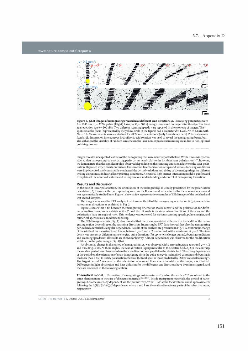
www.nature.com/scientificreports/
2SCIentIFIC REPORTS | 7:39989 | DOI: 10.1038/srep39989
images revealed unexpected features of the nanograting that were never reported before. While it was widely con-sidered that nanogratings are occurring perfectly perpendicular to the incident laser polarization22,23, however, we demonstrate that the significant tilt is observed depending on the scanning direction relative to the laser polar-isation. Repeated experiments on various femtosecond laser fabrication setups and various focusing conditions were implemented, and consistently confirmed the period variations and tilting of the nanogratings for different writing directions at industrial laser printing conditions. A vectorial light-matter interaction model is put forward to explain all the observed features and to improve our understanding and control of nanograting formation.
Results and DiscussionIn the case of linear polarisation, the orientation of the nanogratings is usually predefined by the polarisation orientation, Ey. However, the corresponding wave vector K was found to be affected by the scan orientation and was systematically studied here. Figure 1 shows a few representative examples of SEM images of the polished and wet-etched samples.
The images were used for FFT analysis to determine the tilt of the nanograting orientation Ψ (ϕ) precisely for various scan directions as explained in Fig. 2.
Figure 3 shows that a tilt between the nanograting orientation (wave vector) and the polarisation for differ-ent scan directions can be as high as Ψ ~ 2°, and the tilt angle is maximal when directions of the scan and the polarisation have an angle of ~π/4. This tendency was observed for various scanning speeds, pulse energies, and numerical apertures at a moderate focusing.
The SEM image analysis (Fig. 1) also revealed that there was an evident difference in the width of the nano-grating region depending on the scanning direction. Interestingly, FFT data showed that also the nanograting period had a remarkable angular dependence. Results of the analysis are presented in Fig. 4. A continuous change of the width of the nanostructured line,w, between ϕ = 0 and π/2 is observed, with a maximum at ϕ = 0. This ten-dency was present at different pulse energies, pulse durations (for up to twice longer pulses), focusing conditions and scanning speeds; not all results are shown for brevity. A linear dependence was observed for the modification width,w, on the pulse energy (Fig. 4(b)).
A substantial change in the period of nanogratings, Λ , was observed with a strong increase at around ϕ = π/2 and 3π/2 (Fig. 4(c)). At these angles, the scan direction is perpendicular to the electric field, Ey. On the contrary, the smallest period was observed when the scan direction was parallel to the electric field. The strong dependence of the period on the orientation of scans is intriguing since the pulse energy is maintained constant and focusing is too loose (NA < 0.7) to justify polarisation effects at the focal spot, as those predicted by Debye vectorial focusing24. The largest period Λ occurred at the orientation of scanned lines where the width of the line,w, was minimal. Differences in light absorption and heat diffusion for the different scan directions have been investigated, and they are discussed in the following section.
Theoretical model. Formation of nanogratings inside materials25 and on the surface26–28 are related to the same phenomenon in the case of dielectric materials10,11,29,30. Inside transparent materials, the period of nano-gratings becomes intensity dependent via the permittivity ε ≡ (n + ik)2 at the focal volume and is approximately following the Λ (I) ≅ (λ/n(I))/2 dependence; where n and k are the real and imaginary parts of the refractive index, respectively.
Figure 1. SEM images of nanogratings recorded at different scan directions ϕ. Processing parameters were λ = 1040 nm, τp = 317 fs pulses (HighQ Laser) of Ep = 600 nJ energy (measured on target after the objective lens) at a repetition rate f = 500 kHz. Two different scanning speeds v are reported in the two rows of images. The spot size at the focus (represented by the yellow circle in the figure) had a diameter d = 1.22λ/NA ≅ 2.1 μ m with NA = 0.6. Measurements were carried out for all 24 scan orientations (only 6 are shown here). Polarisation was fixed as Ey. Immersion into aqueous hydrofluoric acid solution was used to reveal the nanogratings better, but also enhanced the visibility of random scratches in the laser non-exposed surrounding areas due to non-optimal polishing process.
5.7. Appendix D
151

www.nature.com/scientificreports/
3SCIentIFIC REPORTS | 7:39989 | DOI: 10.1038/srep39989
A significant departure from such prediction is observed when surface plasma wave – the surface plasmon polariton (SPP) - is excited at the interface of plasma and the dielectric. The SPP wave between dielectric (glass) and plasma can be launched when Re(εp) ≤ − n2, where εp is the permittivity of plasma at the focal volume (a necessary condition with the Bragg phase-matching being the satisfactory condition)11,31–34. This follows from the requirement of the wave vector of the surface wave ε ε ε ε= +k k /( )spp p p0 to be a real number, where k0 = 2π/λ. Nanogratings are imprinted on the plasma-dielectric interface with a period corresponding to the half wavelength of the standing surface wave, the Bragg condition. This is why a smaller period is expected for a larger plasma density (more negative values of (− |Re(εp)|)), induced by a stronger absorption of the femtosecond laser pulses.
However, if the pulse energy is fixed, what can modulate the light absorption in the material? One possible mechanism is the incubation of defects in heat-affected zones. In fact, defects or modified bonds induced by laser irradiation can favour ionisation when the same region is irradiated again by subsequent laser pulses. We can, therefore, expect that absorption in an area that has been heat-affected by laser irradiation will be enhanced with respect to absorption in a previously unmodified zone. Heat accumulation effects in fused silica are not domi-nating, in particular at 500 kHz repetition rate35. Therefore, we expect a single-pulse modification of the material.
Figure 2. Determination of the nanograting tilt angle Ψ for different scanning directions. (a) SEM image of sub-surface nanogratings in fused silica recorded at 10 μ m depth and polished afterwards for observation. The wave vector K is defined as K = 2π/Λ , where Λ is the nanograting period, and the K direction is orthogonal to the nanograting orientation. (b) Fast Fourier transform (FFT) image of the SEM image shown in (a); polarisation Ey is fixed in all experiments. The angle Ψ p is defined as the angle between the horizontal reference axis and the nanograting wave vector. (c) Optical image of the “star” pattern with the Δ ϕ = 15° angle between subsequent rays. The red arrow shows ϕ = 0° position; inset shows fabrication orientation with all lines drawn from the centre outwards.
Figure 3. Tilt angle orientational distribution Ψ (ϕ) for the different scan speeds, v at pulse energies. (a) Ep = 400 nJ, NA = 0.6 and (b) Ep = 600 nJ, NA = 0.4. The inset in panel (a) defines all the relevant quantities. The dashed line is a sinusoidal function plotted as a guide for the eye. Schematic markers show the average orientation of nanogratings (corresponding to an electric field along the y-direction) while the block arrows mark the scan direction; the markers are placed at the corresponding ϕ positions. This figure presents an analysis of the data partially shown in Fig. 1; Error bars represent the standard deviation of data estimated from five different analysed areas of nanogratings.
Chapter 5. Plasmonic nano-printing for surface structuring
152

www.nature.com/scientificreports/
4SCIentIFIC REPORTS | 7:39989 | DOI: 10.1038/srep39989
This means that the incubation of defects should depend on the pulse energy and the number of pulses impinging on the same area and not on the time separation between pulses.
A careful analysis of the heat flow in the presence of E-field reveals that an anisotropic heat diffusion is present in an otherwise thermally isotropic material, and this causes a dependence of the absorption process on the scan direction. The heat conduction flux q in a plasma placed inside an external high-frequency electric field, linearly polarised along the y-direction, has the form36,37:
κα
κ= −∂∂
− | ⋅ |∂∂α α
→ →q T e e T
y,
(1)y1 2
where the unit vectors →αe and →e y correspond to a generic direction α and the direction of the electric field in our case, respectively. The coefficients κ1,2 are two scalar quantities obtained from the solution of the kinetic equa-tion37. It follows from Eq. 1 that the heat diffusion process can be decomposed into two terms. The first one is the conventional isotropic heat diffusion while the second one is influenced by the presence of the electric field and by its direction. In particular, we can observe that the field-related term induces an enhanced heat flux in the direction of the electric field while its contribution vanishes in the direction orthogonal to the electric field. The heat affected zone, after the creation of a plasma in the focal volume is therefore asymmetrically shaped with an elliptical cross section (see Fig. 5(a)), where the major axis is aligned with the linearly polarised electric field. The absorption of subsequent pulses with a strong spatial overlap (in our experimental conditions, we have ~103 pulses per spot) should thus be influenced by the shape of the pre-modified region. In fact, as previously dis-cussed, the presence of defects in the heat-affected zones enhances the ionisation of the material with respect to previously unmodified zones. The asymmetry of the heat-affected zone can explain the observed variations in the nanograting period, width and tilt, as discussed in details in the following sections. It should be noted that the manifestation of such enhanced heat diffusion along the E-field in 3D laser printing has also been observed in two-photon polymerization processes5.
Explanation of nanograting period and line-width dependencies. Figure 4 shows a general trend of width and period with respect to the pulse energy used to inscribe the nanogratings. In fact, for an increas-ing pulse energy, the width of the written lines expands and the nanograting period shrinks for all scanning directions. This general behaviour is explained by considering that the absorption process is nonlinear. Hence a stronger pulse intensity can broaden the absorption volume (thus increasing the width of the nanograting region) and also increase the plasma density38 (thus reducing the nanograting period, as discussed in the previous section). These two effects are rather straightforward, but they do not account for the observation that width and period of the nanogratings can also vary, at the same pulse energy, for different scan directions. We address this aspect now providing a simple explanation based on the theoretical model previously presented. The largest periods of the nanogratings were observed at the scan orientations equal to ϕ = π/2 and 3π/2, in correspond-ence to the minimum widths of the modified region. As previously mentioned, during the sample scanning, the laser absorption is modified by the defects accumulated in the heat-affected regions. As shown in Eq. 1, the heat diffusion process during the laser irradiation is anisotropic, and this creates a heat affected zone that is elliptical in the plane orthogonal to the direction of the laser beam propagation (see Fig. 5(a)). As a consequence, the
Figure 4. General variation trend of the width and period of the nanogratings. (a) The width of the nanogratings, w, vs. scanning orientation, ϕ, at different pulse energies, Ep. Focusing was NA = 0.5; laser pulses at λ = 1030 nm and τp = 570 fs (Pharos laser). (b) The span of the width of nanograting line (wmax − wmin) at different pulse energies Ep. (c) Period of nanogratings, Λ , vs. scan orientation, ϕ, at different scan speeds, v. Focusing was NA = 0.6; laser pulsesλ = 1040 nm, τp = 317 fs (HighQ Laser). Insets in (a) and (b) show corresponding SEM images; arrow markers in (c) show the scan direction and schematic nanograting orientation. In all cases, polarisation was Ey.
5.7. Appendix D
153

www.nature.com/scientificreports/
5SCIentIFIC REPORTS | 7:39989 | DOI: 10.1038/srep39989
beam moving in different scanning directions will encounter material that has been more or less pre-modified, and thus prepared to a larger or weaker absorption. Figure 5(b–d) clearly visualise three different situations. When the scanning direction is directed along the electric field (ϕ = 0, π), the subsequent pulses will encounter a pre-modified substrate and will experience the maximum absorption. When ϕ = π/2 and 3π/2, instead, the absorption is at the minimum, while, in all other directions, we have an intermediate behaviour. Since larger absorptions cause wider modifications with smaller nanograting periods, as already discussed, this mechanism fully explains the observed dependencies on the scanning directions.
A simple experimental estimation of the anisotropic diffusion of the heat-affected zone can be done from the data shown in Fig. 4a, where different widths of nanogratings with respect to the scan direction are presented. For 400 nJ pulse energy, the ratio between the minimum and maximum width of the nanogratings at 0° and 90° scan directions is ~72%.
Explanation of nanograting tilt. The tilt of the nanograting orientation is an even more puzzling phe-nomenon that is observed here for the first time (Fig. 3). No tilt of the nanograting orientation is observed for scanning directions corresponding to ϕ = 0, π/2, π and 3π/2; while the maximum rotation is observed for ϕ = π/4, 3π/4, 5π/4 and 7π/4.
Since the formation of nanogratings is defined primarily by the electronic plasma excitation, we investigated at first the possible role of the temporal and spatial chirp of the ultra-short laser pulses. Temporal and spatial chirps were measured, varied and correlated with the tilt and period of nanogratings (see Supplementary Information for details). Both the temporal and spatial chirps were found to influence the tilt of the nanogratings, but only at very large chirp values. In the conditions used for the experiments presented here, the pulse duration was the shortest, and the pulse front tilt was negligible. Therefore, temporal and spatial chirps cannot be invoked to explain the nanograting tilt dependence on the scanning direction.
Actually, the same theoretical model, used to explain the dependencies of the width and period of the nano-gratings, can also explain the tilting effect. The conditions where no tilt was observed correspond to a symmetric heat affected zone with respect to the scanning direction (see Fig. 5(b,c)), while the maximum tilt was observed where the heat affected zone has the largest unbalance with respect to the scanning direction. A symmetric heat affected zone means that the subsequent pulses will hit an evenly preheated material, and thus, the absorption
Figure 5. Schematics of thermal diffusion process affected by the coupling between the plasma electrons and the electric field. (a) The anisotropic heat affected zone (red region) due to an enhanced heat flux along the electric field direction. Yellow spot represents the plasma in the focal volume. (b)–(d) Three different scan directions (represented by the arrows) oriented relative to the heat affected region. The average orientation of the nanogratings is also schematically reported as a reference.
Chapter 5. Plasmonic nano-printing for surface structuring
154

www.nature.com/scientificreports/
6SCIentIFIC REPORTS | 7:39989 | DOI: 10.1038/srep39989
process will be the same in the whole focal volume, and the symmetry of the process will force the nanograting wave vector K to be parallel or orthogonal to the polarisation. On the contrary, when the heat affected zone is asymmetric with respect to the scanning direction, absorption will be different on the two sides of the focal vol-ume, and this will induce a nanograting period that is shorter (longer) in the pre-modified (unmodified) side. As a consequence, the overall nanograting orientation will be affected, with a wave vector K rotated toward the pre-modified side.
As an example, let’s consider Fig. 5(d), where we schematically represented the situation for ϕ = π/4. In this case, each new-coming light pulse meets the material that it pre-modified on the left side of the scanning direction and the untreated one on the right side. For this reason, the periodicity of the nanogratings (generally orthogonal to the electric field direction) is slightly reduced on the left side comparing to the right one as discussed in the text above. This results in a negative tilt Ψ < 0 of the nanogratings for this scanning direction, which is exactly what was observed experimentally (Fig. 3).
Figure 3 also shows that the amplitude of the nanograting tilt increases with the pulse fluence (compare panel (a) and (b), where we have used a fluence of 11.4 J/cm2 and 7.6 J/cm2, respectively), while the dependency on the scanning direction is the same. This further feature can also be explained by the above model. In fact, a larger pulse fluence means a stronger temperature gradient induced in the focal volume. According to Eq. 1, this cor-responds to a stronger contribution of the field-related term in the heat diffusion process, resulting in a more elliptical heat affected region. This causes even stronger unbalance of material temperature on the two sides of the scanning direction at ϕ = π/4, thus inducing a stronger rotation of the nanograting orientation. Consistently with the proposed model, at the larger pulse fluence, a larger tilt was observed.
Further studies are required to elucidate the effect of stress in writing of nanogratings. A presence of stress can cause alterations in heat transport in silica39. It could be expected, that coupling between pulse front tilt and stress takes place, however, in all our experiments the tilt of nanogratings was carried out for the chirp-free (temporal and spatial) pulses. Also, if stress were to play a significant role in the tilt of nanogratings, one would expect a strong variation of the effect at the different depths, according to a non-uniform stress distribution in that direc-tion40. However, this was not observed experimentally. Stress distribution around the affected zone was investi-gated earlier41, showing a dependence of the generated amount of stress on the scan direction. However, no stress asymmetry was observed around each scan line41 that could justify the nanogratings tilt discussed in this work.
ConclusionsA systematic study of the main nanograting features relative to the direction of the laser beam scanning was car-ried out on a broad range of the parameter space. In particular, different pulse energies, scanning speeds, focus-ing, and temporal and spatial chirps have been investigated. In all these conditions, we have shown for the first time a reproducible dependence of the nanograting width, period and tilt on the writing scan direction, which can affect the performance of directly written photonic components based on the properties of the nanogratings, as for example the laser-written q-plates.
For linearly polarised laser pulses, the strongest variations of the nanograting width and period were observed for the scanning directions parallel and perpendicular to the electric field direction while the maximum tilt of the nanograting orientation was observed when the scanning direction was at ϕ = 45° relative to the electric field direction. All these observations can be consistently explained by an anisotropic heat-diffusion model that takes into account coupling of the hot electrons in the plasma with the pulse electric field, enhancing the heat diffusion in the direction of the latter. This anisotropic heating of the substrate is responsible for a modulated absorption of light along the different scan directions and explains all the observed features.
The experimental results here reported represent a clear evidence of a polarization-affected light-matter inter-action process. The observed features are expected to be even richer in the case of vector beams and at the tight focusing, where vectorial nature of light has a strong presence. This work paves the way to a clearer understanding of these phenomena and their exploitation for optimisation of current devices and the design of innovative ones taking full advantage of the vectorial aspects of light-matter interaction.
MethodsFabrication of sub-surface nanogratings. Two different femtosecond lasers were used to record sub-sur-face nanogratings: (1) Pharos (Light Conversion) with the wavelength of 1030 or 515 nm, and the 260 fs laser pulses at the 500 kHz repetition rate and the scanning speed of 0.25 mm/s and 1 mm/s; (2) FemtoRegen (HighQ Laser) 1040 nm, 317 fs at the 500 kHz repetition rate and the scanning speeds from 0.25 to 5 mm/s. Focusing was carried out in case (1) with a 50× objective lens of numerical aperture NA = 0.55 (Olympus LMPlan). For case (2), the employed objectives had NA = 0.6 at 50× magnification (Leitz Wetzlar) or NA = 0.4, at 20× (Olympus LMPlan).
The pulse energy was measured after the objective lens at the sample location. Nanogratings were recorded in a multi-shot exposure regime, e.g., for a typical spot diameter at the focus of 2.5 μ m, f = 500 kHz laser repetition rate and a typical scan speed of v = 1 mm/s, there were N ≅ 1.3 × 10³ pulses per spot.
Nanogratings were recorded at 10 μ m depth below the surface of ultraviolet-grade fused silica glass (JGS1), and samples were mechanically polished to the depth of strongest modification. A short immersion into 5% wt. aqueous solution of hydrofluoric acid was used to facilitate the surface morphology analysis by scanning electron microscopy (SEM); a 5 nm thick gold coating was used for SEM imaging.
Estimation of the nanograting tilt angle. In order to determine the angle Ψ between the orientation of nanogratings and polarisation for different scanning directions, the following procedure was carried out (see Fig. 2). The orientation angle Ψ p of the wave vector K = 2π/Λ of the nanogratings was determined for each scan direction with respect to the SEM image x-axis. There were 24 scan directions, ϕ, with Δ ϕ = 15° separation
5.7. Appendix D
155

www.nature.com/scientificreports/
7SCIentIFIC REPORTS | 7:39989 | DOI: 10.1038/srep39989
between the neighbouring rays (Fig. 2(c)). A fixed polarisation, Ey, was used to write all the lines, i.e. a polari-sation parallel to the K wave vector at ϕ = 0°. The tilt angle of the nanograting wave vector with respect to the polarization direction was calculated as Ψ p(0°) − Ψ p(ϕ) for the various scanning directions in order to compen-sate for possible misalignments between the image x-axis and the ϕ = 90° orientation when placing the sample in the SEM; by this definition, the positive tilt + Ψ corresponds to a clockwise (cw) rotation of the nanograting orientation. To further reduce errors in positioning and judgement of nanograting orientation, the Fast Fourier Transform (FFT) of the images were calculated in random and sequential order with respect to the ϕ angles. In addition, a test of two different people carrying out the analysis using the same SEM images with Gwyddion and ImageJ freeware packages was used as a reference test.
References1. Sun, H. & Kawata, S. Two-Photon Photopolymerization and 3D Lithographic Microfabrication. (Springer-Verlag, 2004).2. Sun, H. B. et al. Experimental investigation of single voxels for laser nanofabrication via two-photon photopolymerization. Appl.
Phys. Lett. 83, 819 (2003).3. Klar, T., Wollhofen, R. & Jacak, J. Sub-Abbe resolution: from STED microscopy to STED lithography. Phys. Scr. T162, 014049 (2014).4. Cheng, Y. et al. Beam focalization in reflection from at dielectric subwavelength gratings. Opt. Lett. 39, 6086–6089 (2014).5. Rekštytė, S. et al. Nanoscale precision of 3D polymerization via polarization control. Adv. Opt. Mat. 4, online published, doi:
10.1002/adom.201600155 (2016).6. Xu, B. B. et al. Surface-plasmon-mediated programmable optical nanofabrication of an oriented silver nanoplate. ACS Nano 8(7),
6682–6692 (2014).7. Öktem, B. et al. Nonlinear laser lithography for indefinitely large area nanostructuring with femtosecond pulses. Nature Photonics
7, 897–901 (2013).8. Guay, J. M. et al. Polarization-dependent femtosecond laser ablation of poly-methyl methacrylate. New J. Phys. 14, 085010 (2012).9. Simanovskii, D. M., Schwettman, H. A., Lee, H. & Welch, A. J. Midinfrared optical breakdown in transparent dielectrics. Phys. Rev.
Lett. 91(10), 107601 (2003).10. Rudenko, A., Colombier, J. P. & Itina, T. E. From random inhomogeneities to periodic nanostructures induced in bulk silica by
ultrashort laser. Phys. Rev. B. 93, 075427 (2012).11. Buividas, R., Mikutis, M. & Juodkazis, S. Surface and bulk structuring of materials by ripples with long and short laser pulses: recent
advances. Prog. Quant. Electronics 38, 119–156 (2014).12. Puerto, D. et al. Femtosecond laser-controlled self-assembly of amorphous-crystalline nanogratings in silicon. Nanotechnology 27,
265602 (2016).13. Gottmann, J., Wortmann, D. & Wanger, R. Manufacturing of periodical nanostructures by fs-laser direct writing. Proc. SPIE 7022,
702202 (2008).14. Shimotsuma, Y., Kazansky, P., Qiu, J. & Hirao, K. Self-Organized nanogratings in glass irradiated by ultrashort light pulses. Phys. Rev.
Lett. 91(24), 1–4 (2003).15. Hnatovsky, C. et al. Polarization-selective etching in femtosecond laser-assisted microfluidic channel fabrication in fused silica. Opt.
Lett. 30(14), 1867–1869 (2005).16. Osellame, R., Hoekstra, H., Cerullo, G. & Pollnau, M. Femtosecond laser microstructuring: an enabling tool for optouidic lab-on-
chips. Laser Photonics Rev. 5, 442–463 (2011).17. Beresna, M., Gecevičius, M., Kazansky, P. G. & Gertus, T. Radially polarized optical vortex converter created by femtosecond laser
nanostructuring of glass. Applied Physics Letters 98(20), 201101–201101 (2011).18. Marrucci, L. et al. Spin-to-orbital conversion of the angular momentum of light and its classical and quantum applications. J. Opt.
13, 064001 (2011).19. Zhang, J., Gecevičius, M., Beresna, M. & Kazansky, P. G. Seemingly unlimited lifetime data storage in nanostructured glass. Phys.
Rev. Lett. 112, 033901 (2014).20. de Jong, C. J. et al. Deep-UV fluorescence lifetime imaging microscopy. Photon. Research 3(5), 283–288 (2015).21. Hnatovsky, C., Shvedov, V., Krolikowski, W. & Rode, A. Revealing Local Field Structure of Focused Ultrashort Pulses. Phys. Rev. Lett.
116, 123901 (2011).22. Bhardwaj, V. R. et al. Optically produced arrays of planar nanostructures inside fused silica. Phys. Rev. Lett. 96(5), 057404 (2006).23. Taylor, R., Hnatovsky, C. & Simova, E. Applications of femtosecond laser induced self-organized planar nanocracks inside fused
silica glass. Laser Photon. Rev. 2(1–2), 26–46 (2008).24. Juodkazis, S., Mizeikis, V., Matsuo, S., Ueno, K. & Misawa, H. Three-dimensional micro- and nano-structuring of materials by
tightly focused laser radiation. Bull. Chem. Soc. Jpn. 81(4), 411–448 (2008).25. Shimotsuma, Y., Kazansky, P., Qiu, J. & Hirao, K. Selforganized nanogratings in glass irradiated by ultrashort light pulses. Physical
review letters 91(24), 247405 (2003).26. Birnbaum, M. Semiconductor surface damage produced by ruby lasers. Journal of Applied Physics 36(11), 3688 (1965).27. Sipe, J., Young, J., Preston, J. & Van Driel, H. Laser-induced periodic surface structure. I. Theory. Physical Review B 27(2), 1141–1154
(1983).28. Young, J., Preston, J., Van Driel, H. & Sipe, J. Laser-induced periodic surface structure. II. Experiments on Ge, Si, Al, and brass.
Physical Review B 27(2), 1155–1172 (1983).29. Rajeev, P. et al. Memory in nonlinear ionization of transparent solids. Physical review letters 97(25), 253001 (2006).30. Buividas, R. et al. Mechanism of fine ripple formation on surfaces of (semi)transparent materials via a half-wavelength cavity
feedback. Nanotechnology 22, 055304 (2011).31. Miyazaki, K. & Miyaji, G. Nanograting formation through surface plasmon fields induced by femtosecond laser pulses. J. Appl. Phys.
114, 153108 (2013).32. Das, S. K., Messaoudi, H., Debroy, A., McGlynn, E. & Grunwald, R. Multiphoton excitation of surface plasmon-polaritons and
scaling of nanoripple formation in large bandgap materials. Opt. Mat. Express 3, 1705–1715 (2013).33. Liao, Y. et al. High-fidelity visualization of formation of volume nanogratings in porous glass by femtosecond laser irradiation.
Optica 2(1), 329–334 (2015).34. Sakabe, S., Hashida, M., Tokita, S., Namba, S. & Okamuro, K. Mechanism for self-formation of periodic grating structures on metal
surface by femtosecond laser pulse. Phys. Rev. B 79, 033409 (2009).35. Eaton, S. M. et al. Heat accumulation effects in femtosecond laser-written waveguides with variable repetition rate. Opt. Express 13,
4708–4716 (2005).36. Lifshitz, E. M. & Pitaevski, L. P. Physical Kinetics. (Pergamon Press, 1981).37. Gamaly, E. G. & Rode, A. V. Coupling of polarization of high-frequency electric field and electronic heat conduction in laser created
plasma. Optics Laser Technol. 82, 69–71 (2016).38. Puerto, D. et al. Transient reflectivity and transmission changes during plasma formation and ablation in fused silica induced by
femtosecond laser pulses. Appl. Phys. A 92, 803–808 (2008).
Chapter 5. Plasmonic nano-printing for surface structuring
156

www.nature.com/scientificreports/
8SCIentIFIC REPORTS | 7:39989 | DOI: 10.1038/srep39989
39. Sakakura, M., Terazima, M., Shimotsuma, Y., Miura, K. & Hirao, K. Thermal and shock induced modification inside a silica glass by focused femtosecond laser pulse. J. Appl. Phys. 109, 023503 (2011).
40. Sakakura, M., Terazima, M., Shimotsuma, Y., Miura, K. & Hirao, K. Observation of pressure wave generated by focusing a femtosecond laser pulse inside a glass. Opt. Express 15(9), 5674–5686 (2007).
41. Champion, A., Beresna, M., Kazansky, P. & Bellouard, Y. Stress distribution around femtosecond laser affected zones: effect of nanogratings orientation. Opt. Express 21(21), 24942–24951 (2013).
AcknowledgementsAuthors are grateful to Linas Giniunas for discussions on spatial chirp of Pharos laser pulses and Algirdas Selskis for help in taking multiple SEM images of laser-written stars. Partial support via ARC Discovery DP120102980 is acknowledged.
Author ContributionsV.S. and G.R. observed for the first time the nanograting tilt. V.S., after discussion with S.J., designed the experiment, fabricated the samples, measured and analysed all experimental data. R.O. together with F.B. provided the laboratory for experiments with a different setup. F.B. partly participated in the sample fabrication and data analysis. S.J. provided the initial phenomena explanation ideas, which were further discussed and refined together with R.O., X.W. performed the initial numerical simulations for phenomena understanding. E.G.G. provided advice and helpful discussion on the model. All authors discussed the results and contributed to the writing of the paper.
Additional InformationSupplementary information accompanies this paper at http://www.nature.com/srepCompeting financial interests: The authors declare no competing financial interests.How to cite this article: Stankevič, V. et al. Laser printed nano-gratings: orientation and period peculiarities. Sci. Rep. 7, 39989; doi: 10.1038/srep39989 (2017).Publisher's note: Springer Nature remains neutral with regard to jurisdictional claims in published maps and institutional affiliations.
This work is licensed under a Creative Commons Attribution 4.0 International License. The images or other third party material in this article are included in the article’s Creative Commons license,
unless indicated otherwise in the credit line; if the material is not included under the Creative Commons license, users will need to obtain permission from the license holder to reproduce the material. To view a copy of this license, visit http://creativecommons.org/licenses/by/4.0/ © The Author(s) 2017
5.7. Appendix D
157

Chapter 5. Plasmonic nano-printing for surface structuring
5.8 Appendix E
This section contains the published paper related femtosecond laser fabricationfor micro/nanophotonic application but not being illustrated in details in themain context.
E1: X. W. Wang, A. A. Kuchmizhak, X. Li, S. Juodkazis, O. B.Vitrik, Yu. N. Kulchin, V. V. Zhakhovsky, P. A. Danilov, A. A. Ionin, S.I. Kudryashov, A. A. Rudenko and N. A. Inogamov. Laser-induced transla-tive hydrodynamic mass snapshots: mapping at nanoscale, Physical ReviewApplied, 2017.
In this paper, the nanoscale thermally assisted hydrodynamic melt per-turbations induced by ultrafast laser energy deposition in noble-metal filmsproducing irreversible nanoscale translative mass redistributions have beeninvestigated. The mechanism on forming radially-symmetric frozen surfacestructures following with the ultrafast laser energy deposition has been pre-sented and simulated. The final 3D shape of the surface structures formedafter resolidification of the molten part of the film is shown to be governedby incident laser fluence and predicted theoretically via molecular dynamicsmodeling. This work presents the capability on precisely control of the fi-nal 3D geometric shape of the laser printed nanostructures, which had beendemonstrated strong plasmonic resonance in visible range of light.
E2: M. Abid, L. Wang, Q. Chen, X. W. Wang, S. Juodkazis and H.Sun. Angle-multiplexed optical printing of biomimetic hierarchical 3D tex-tures, Laser & Photonics Reviews, 11, 2, 2017.
In this paper, a novel approach has been proposed on mimicking the naturalhierarchical patterns in a quick and maskless fabrication by using two beaminterference lithography with angle-multiplexed exposures and scanning. Largearea of different complexed structures with a cascading resolution and 3Dprofiles have been fabricated by precisely controlling the exposure dose.
E3: A. Balcytis, M. Ryu, X. W. Wang, F. Novelli, G. Seniutinas, S.Du, X. Wang, J. Li, J. Davis, D. Appadoo, J. Morikawa and S. Juodkazis. Silk:Optical properties over 12.6 Octaves THz-IR-Visible-UV range, Materials, 10,2017.
In this paper, the Bombyx mori and Antheraea pernyi silk fibres have been
158

5.8. Appendix E
characterized over a wide spectral range from THz 8 cm–1 (λ = 1.25 mm, f =0.24 THz) to deep-UV 50×103 cm–1(λ = 200 nm, f = 1500 THz) wavelengthsor over a 12.6 octave frequency ranges, with the spectral features of β–sheet,α–coil and amorphous fibroin being analyzed.
159

Laser-induced Translative Hydrodynamic Mass Snapshots: mapping at nanoscale
X. W. Wang1, A. A. Kuchmizhak1,2,3,∗, X. Li1, S. Juodkazis1,4, O. B. Vitrik2,3, Yu.N. Kulchin3, V. V.Zhakhovsky5,6, P. A. Danilov3,7, A. A. Ionin7, S. I. Kudryashov3,7,8,9, A.A. Rudenko7, N. A. Inogamov5,6∗
1Center for Micro-Photonics, Swinburne University of Technology, John st., Hawthorn 3122, Victoria, Australia2School of Natural Sciences, Far Eastern Federal University, Vladivostok, Russia
3Institute of Automation and Control Processes, Far Eastern Branch,Russian Academy of Science, Vladivostok 690041, Russia
4Melbourne Centre for Nanofabrication, ANFF, 151 Wellington Road, Clayton, VIC 3168, Australia5Dukhov Research Institute of Automatics, Rosatom, Moscow 127055, Russia
6Landau Institute for Theoretical Physics, Russian Academy of Sciences, Chernogolovka 142432, Russia7Lebedev Physical Institute, Russian Academy of Sciences, Moscow 119991, Russia
8ITMO University, St. Peterburg 197101, Russia and9National Research Nuclear University MEPhI (Moscow Engineering Physics Institute), Moscow 115409, Russia
(Dated: March 16, 2017)
Nanoscale thermally assisted hydrodynamic melt perturbations induced by ultrafast laser energydeposition in noble-metal films produce irreversible nanoscale translative mass redistributions andresults in formation of radially-symmetric frozen surface structures. We demonstrate that the finalthree-dimensional (3D) shape of the surface structures formed after re-solidification of the moltenpart of the film is shown to be governed by incident laser fluence and, more importantly, predictedtheoretically via molecular dynamics modeling. Considering the underlying physical processes as-sociated with laser-induced energy absorption, electron-ion energy exchange, acoustic relaxationand hydrodynamic flows, the theoretical approach separating “slow” and “fast” physical processesand combining hybrid analytical two-temperature calculations, scalable molecular-dynamics sim-ulations, and a semi-analytical thin-shell model was shown to provide accurate prediction of thefinal nanoscale solidified morphologies, fully consistent with direct electron-microscopy visualizationof nanoscale focused ion-beam cuts of the surface structures produced at different incident laserfluences. Finally, these results are in reasonable quantitative agreement with mass distribution pro-files across the surface nanostructures, provided by their noninvasive and non-destructive nanoscalecharacterization based on energy-dispersive x-ray fluorescence spectroscopy, operating at variableelectron-beam energies.
I. INTRODUCTION
Precise high numerical-aperture (NA) nanoscale laserablation of thin films, using short (1 ps< τL < 300 ps)and ultrashort (τL < 10 ps) laser pulses, is a promis-ing emerging technology in processing thin-film transis-tors [1], scribing thin-film solar cells [2], ablative fabrica-tion and light-induced forward transfer (LIFT)-printingof advanced plasmonic and dielectric nanophotonic meta-surfaces and circuits [3–9].In comparison to short laserpulses, the ultrashort ones are broadly used during suchmesoscopic ablation, holding a promise of providing anultimate spatial resolution, despite the underlying moreintense response of electron subsystem to laser exposurewith dramatically higher electron/lattice temperature (ifτL < 1 ps) and pressure gradients, resulting in intensenanoscale hydrodynamic flows and ultrafast quenchingof corresponding transient melt configurations - e.g., ananodroplet, separating from a nanojet [10]. Commonly,such nanofeatures resolidified on thin supported metal-lic films, are qualitatively or semi-quantitatively visual-ized by top- or side-view scanning electron microscopy(SEM), with just a few sketchy studies revealing their
internal structure for some textures without quantita-tive acquisition of their parameters and without visual-ization of “hidden” sub-surface features (e.g., counter-jets, cavities) [11–16]. As a result, molecular dynam-ics (MD) simulations [17–19], attempting to envision theunderlying spatiotemporal dynamics of nanoscale hydro-dynamic flows as well as to describe quantitatively thecorresponding physical mechanisms, have no firm exper-imental background for comparative justification of theirresults and the starting point for future predictions andoptimization of focusing parameters, required to providean ultimate resolution during the pulsed-laser nanofabri-cation.
In this study, SEM inspection of nanoscale focused-ion beam (FIB) cuts and energy-dispersive X-ray fluores-cence (EDX) nanoscale profiling of individual radially-symmetric topological surface nanofeatures - separatenano-bumps and jets on nano-bumps, produced bysingle-shot ablation of 50-nm-thick glass-supported goldfilms by tightly focused fs-laser pulses of variable ener-gies were conducted to reveal quenched configurationsof melt, yielding from irreversible nanoscale translativehydrodynamic flows and nanoscale heat conduction. Bytaking into account all underlying physical processes as-sociated with laser-induced energy absorption, electron-ion energy exchange, acoustic relaxation and hydrody-namic flows, the theoretical approach based on separa-
arX
iv:s
ubm
it/18
3231
9 [p
hysi
cs.o
ptic
s] 1
6 M
ar 2
017
Chapter 5. Plasmonic nano-printing for surface structuring
160

2
tion of “slow” and “fast” physical processes and combin-ing hybrid analytical two-temperature calculations, scal-able molecular-dynamics simulations and semi-analyticalthin-shell model was shown to provide an unprecedentedaccuracy in prediction of such nanoscale resolidified mor-phologies.
II. ELECTRON MICROSCOPY STUDY OFNANOSCALE FOCUSED-ION-BEAM CUTS
To reveal for the first time the initial stage of metal filmblistering from its substrate exposed by tightly-focusedfs-laser pulse, as well as to follow the subsequent evo-lution of the molten material - nanoscale hydrodynamicflows and quenching of transient nanofeatures - from theparabola-shaped nanobumps to the small nanojets, wehave fabricated cross-sectional cuts using Ga+-ion FIBmilling (Raith IonLINE). To do this, an e-beam evap-orated 50-nm thick Au film, covering a silica glass sub-strate, was first patterned with well-ordered arrays of dif-ferent surface structures - smaller and larger nanobumps;with small nanojets atop for the larger fluences (Fig. 1(a-e)). The period of arrays was set 2 µm. These smallstructures are typically formed in the fluence range belowthe threshold for hole appearance (Fig. 1(f)). This rangeis highlighted by red color in Fig. 1. The small structureswere made for the following reasons. First, the mate-rial distribution during their initial formation stage canshed light on main physical nanoscale processes, includ-ing blistering, deformation, melting, hydrodynamic flows,recrystallization etc., which occur on the metal film un-der the action of the ultra-short laser pulse. Second, com-paring to high-aspect ratio nanojets, the actual materialdistribution for such small structures cannot be extractedfrom the tilted SEM imaging - e.g., because of hidden fea-tures such as a counter-jet [11], while this information,for example, can be used to explain a tunable plasmonicscattering response from these structures [6]. For laserpatterning, second-harmonic (λ = 515 nm), 230-fs laserpulses from a Yb:KGW laser system (PHAROS, LightConversion Ltd.) were focused into a sub-micrometerspot using a dry objective lens with NA = 0.5 (MitutoyoM Plan Apo NIR HR). Each surface structure presentedin the Fig.1(a-e) was produced by single-pulse irradia-tion, keeping the constant pulse energy E for each singlearray, while increasing stepwise the applied pulse energyfrom 0.9 to 1.7 nJ/pulse for subsequently patterned ar-rays (Fig. 1(a-e)). After such laser fabrication, the sam-ple, containing nanostructures, was overcoated with aprotective titanium (Ti) film. The Ti coating providesa good contrast of FIB cuts of the laser-fabricated nano-and microstructures during their SEM visualization. Forsmall parabola-shaped microbumps (Fig.1(a,b)), the 100-nm thick Ti film was post-deposited, while for tallerstructures a twice thicker protective layer was used to en-sure their complete coverage. The succeeding FIB millingof the sample was performed at the 30-kV acceleration
a
b
d
e
c
2
1 2 3 4
holes
bumps
lnE
6
10
0
22
D, μ
m
14
0 0.2 0.4 0.6-0.20
0.6
0.4
0.2
jets
D=0.87 μm
1/eE =0.86 nJ
th
D=2
.41 μm
1/eE
=7.4
nJ
th
lnE
f
FIG. 1. (Color online) (a-e) SEM images of the nanostruc-ture arrays fabricated at increasing pulse energies: 0.9 (a),1.2 (b), 1.38 (c), 1.62 (d) and 1.7 nJ (e); the insets presentside-view (view angle of 45◦) SEM images of the correspond-ing structures. The scale bars for these images correspondto 1 µm. Fig. 1(f) shows squared outer diameter D2 of thenanobumps, nanojets and through holes versus natural loga-rithm of the applied pulse energy lnE (E in nJ). The insetillustrates the magnified left-most part of this dependence,showing the threshold pulse energy for nanobumps. The slopeof fitting line indicates the characteristic energy deposition di-ameter, while the intersection with the x-axis – the thresholdpulse energies required to produce these structures.
voltage and the relatively small beam current of 50 pA toproduce smooth walls. For each type of nano- or micro-structure, at least 10 similar cuts were prepared to pro-vide statistical significance and to reveal small fluctua-tions due to instability of the laser pulse energy, as wellas stochastic inhomogeneities of the metal film/glass sub-strate. Finally, the fabricated FIB-cuts were visualized,using a field-emission SEM module of the e-beam lithog-raphy writer Raith 150-TWO.
By measuring the dependence of squared diameters D2
of the through-holes produced in the Au film vs. natu-ral logarithm of incident pulse energy, ln(E), the corre-sponding threshold pulse energy of Eth,hole = 7.0 ± 0.7nJ (green dots in Fig. 1(f)) was estimated, with its slopeindicating the characteristic energy deposition diameterD1/e,hole of 2.4 µm; Eth,hole is the point between the or-ange (jet) and green (hole) ranges on the axis lnE inFig. 1(f). This gives the deposited threshold fluenceFth,hole = A · Eth,hole(πR2
1/e)−1 = 0.046 ± 0.006 J/cm2
for the 50-nm-thick Au film absorbance A ≈ 0.3, which is
5.8. Appendix E
161

3
in good agreement with previously reported values. Sim-ilar dependences measured for nanobumps and jets (or-ange and red dots in Fig. 1(f)) indicate practically thesame deposited fluence Fth,bump = 0.042 ± 0.006 J/cm2
at the threshold pulse energy Eth,bump = 0.86 ± 0.09nJ and almost three-fold smaller energy deposition ra-dius D1/e,bump = 0.87 ± 0.09 µm. Obviously, the differ-ent energy deposition scales - D1/e,bump ≈ 0.9 µm andD1/e,hole ≈ 2.4 µm - indicate, for the same focusingconditions, the corresponding different temporal scalesof their formation, enabling for the laser-deposited en-ergy in the thin film to be transported laterally from thediffraction-limited focal spot (diameter D1/e,foc ≈ 0.5µm for the 0.5-NA dry objective lens) via electron heatconduction. Specifically, in the cases of bumps andholes tbump ≈ (D2
1/e,bump − D21/e,foc)/4χ ≈ 1 ns and
thole ≈ (D21/e,hole−D2
1/e,foc)/4χ ≈ 10 ns, respectively, for
the thermal diffusivity coefficient of gold χ ≈ 1.2 cm2/s,being comparable to previous similar estimates. [20, 21]
Series of side-view SEM images (Fig. 2(a-e)) demon-strate the central cross-section cuts of the different struc-tures produced on the surface of the Au film at the in-creasing pulse energy (each presented image illustratesthe cut of one of the surface structure previously shownin Fig. 1(a-e)). The detailed analysis of the cuts indi-cate that for parabolically-shaped nanobumps producedat the pulse energies slightly above the measured thresh-old for the nanobump formation (Eth> 0.87 nJ), thethickness of the Au film remains almost unchanged withsome negligible material redistribution, occurring onlynear the edges of the nanobump (Fig. 2(a1,b1)). Forthe increasing incident pulse energy (Fig. 2(c,d)), sig-nificant thinning of the film is observed (in some spe-cific points near the nanobump edge the film becomestwice thinner) and is associated with the correspondingincrease of the nanobump height. The subsequent evo-lution of the nanobump shape - from parabolic to con-ical one - occurs at the further increase of the incidentpulse energy (Fig. 2(d,d1)) accompanied with accumu-lation of the molten material at the nanobump tip inthe form of the 120-nm-high and 100-nm-wide protru-sion. The lateral and vertical dimensions of this pro-trusion continuously increase versus the incident pulseenergy (Fig. 2(d-e,d1-e1)), forming a nanojet, while thesurrounding nanobump becomes thinner through the jet-directed nanoscale hydrodynamic flow with its minimalexperimentally observed thickness, reaching ≈ 13 nmnear the nanojet edge and ≈ 20 nm near the nanobumpedge.
III. MOLECULAR DYNAMICS SIMULATIONS
In this study we have developed a comprehensive nu-merical approach representing, as we will show below,the next step toward accurate prediction of the transla-tive flow-assisted redistribution of the molten film ma-terial under the laser pulse exposure. To achieve this
goal, all relevant physical processes underlying the ultra-short laser pulse - metal interaction should be taken intoaccount. However, such simultaneous consideration ofthese multiple processes in the full-timescale and realisticlength-scale numerical model, including billions of atomsand their interaction, far exceeds the limits of currentlyavailable supercomputers. To overcome this limitation,we used time separation of “fast” and “slow” physicalprocesses, combining three previously developed numeri-cal models and adopting them to the utilised experimen-tal conditions.
The model, describing the first in time, short evolutionstage with its typical duration of the order of acoustictimescale ( ≈ 17 ps for our 50-nm-thick Au film and lon-gitudinal speed of sound in gold of 3 km/s) accounts forfast processes associated with electron pressure, electronheat conduction, electron-ion temperature relaxation ingold (7-10 ps, [22, 23]) and separation of the molten filmfrom the substrate with the separation velocity νcm(r),depending on the absorbed fluence Fabs(r). In this re-spect this model includes 1D two-temperature (2T) hy-drodynamic code (2T-HD) with full 2T physics concern-ing absorption, 2T electron heat conduction, energy ex-change between the electrons and atomic vibrations dueto the electron-phonon coupling and 2T equation of state.
This first stage can be also characterized by highstresses p1 ≈ 10 GPa = 105 bar stimulated by an iso-choric laser-generated heating of the film up to the tem-peratures of few kilo-Kelvin. This stress is responsible forthe film separation from the substrate with the moderateseparation velocities ≈ (Zs/Zf )(p1/B)cs (cs is the longi-tudinal speed of sound in gold; B is the bulk modulusof gold; Zs, Zf are acoustic impedances of the substrateand the film, respectively) ranging from 10 to 100 m/s.Temperature of the film is less than the boiling tempera-ture (≈ 3.2 kK), providing relatively small vapor pressure(smaller than 1 bar) and yielding in negligibly small dy-namic influence of surface evaporation, which was notobserved in our MD simulations.
The second, “slow” evolution stage with its typical du-ration of the order of tens of nanoseconds includes twomodels, providing MD simulation of the translative-flow-assisted redistribution of the molten film and its subse-quent resolidification via conductive cooling of the hot(cupola-like) shell. Such a long characteristic nanosec-ond duration exceeds achievable requirements of simula-tion resources, considering also the typical MD time stepof ∼1 fs and huge amount of involved atoms (≈ 109) forour experimental parameters. To overcome this issue, thescaling approach was used, implying two non-dimensionalregulating parameters - the capillary parameter Vσ =νσ/νcm and the thermal parameter Vκ = νχ/νcm, where
νσ = 2(σ/ρd)1/2, νχ = χ/rc, χ - thermal diffusivity, σ -surface tension, ρ - initial density, d - metal film thick-ness, νcm – on-axis separation velocity, rc - separationradius [18].
Both these regulating parameters are evaluated for ourparticular experimental case with well known parameters
Chapter 5. Plasmonic nano-printing for surface structuring
162

4
0
10050
150
0
0500
500
50
0 100 200 300 400 500lateral coordinate r, nm
100
200
300
50
150
250
350
a
Au filmglass
Ti film
b
c
d
r
z
e
c1d1
e1
re-deposited Ti layer
c1d1
ExperimentMD simulationsd
Film
thic
knes
s d,
nm
b2b1
c2
d2
e2
d
a1
0.1 0.2 0.5
simV σ
simVχ
0.1
0.2
0.3
0.4
holes
parabolic
bumps
jets
0.4
conic
albu
mps
1.2 nJ1.38 nJ
1.62 nJ
0.9 nJ
1.7 nJ
0 0.4 1.21.6
1.2
0.8
0.4
expVσ
expVχ
0.30
0.8
FIG. 2. (Color online) (a-e) Side-view SEM images (view angle of 45◦) of FIB cross-sectional cuts of single surface structuresproduced at the increasing pulse energy and previously shown in figure 1 (a-e), respectively. Orange areas in each imagehighlight the Au film. The scale bars for these images correspond to 100 nm. The darker grey layer under the Au film,appearing in the images (c-e), is attributed to the re-deposition of Ti during the FIB milling, which was confirmed by thecorresponding EDX measurements; (a1-e1) Film thickness d experimentally measured over 10 similar cuts of the 10 similarsurface structures produced at the same irradiation conditions (red curves), and recalculated via corresponding MD simulations(black dotted curve) as a function of the lateral r-coordinate defined in Fig. 2(a). Film thickness d is measured and recalculatedin the directions normal to the local section of the film (details are given in Fig.3(b)). Grey areas indicate the error bar; (b2-e2)Molecular-dynamics simulations showing the evolution of the metal shell. The simulations were performed for different valuesof the non-dimensional capillary and thermal parameters corresponding to each particular experimental case shown in theinset of Fig.(e2). The colored areas in this inset show the range of parameters required to reproduce the certain type of thesurface nanostructure (left and bottom axes), while the purple dots, marked with the corresponding incident pulse energy, wereestimated for each particular experimental case (right and upper axes) considering the constant separation velocity νcm=100m/s.
σ and χ (see the blue and purple dots in the inset of theFig. 2(e2)). We assume that in the case with largest en-ergy 1.7 nanoJ the separation velocity is νcm=100 m/s.According to our 2T-HD simulations, the velocity νcmis proportional to absorbed fluence Fabs and thus it isproportional to incident energy of a pulse (see Fig. 1(f)).This is the way how the blue dots in the inset of Fig. 2(e2)appears. Then the MD simulations were performed forβ=3–5 times smaller rc value and the smaller heat con-duction coefficient and βξ = 5-10 thinner thickness of themetal film, while the separation velocity value was alsoscaled to keep the similar ratio between νσ ∝ (βξ)1/2,νχ ∝ β and νcm (see inset in the Fig. 2(e2)).
Analysis of the FIB cuts performed on surface fea-tures produced at the different incident pulse energies(Fig. 2(a-e)) indicates several steps, characterizing themolten film evolution via corresponding translative hy-drodynamic flows and affecting the resulting thicknessdistribution along the produced surface structure: (i) in-
flation of the metal film in the form of the parabolic-shaped cupola, having constant thickness along its cir-cumference; (ii) weak redistribution of the cupola thick-ness, (iii) transformation from parabolic to conical shapeand, finally, (iv) appearance of the central protrusion.Despite the downscaled computation volume consideredfor direct MD simulations, all these steps are perfectlyreproduced in our model by varying the thermal and cap-illary parameters (Fig. 2(b2-e2)), which depend on theincident pulse energy, in its turn. Upscaling of the filmthickness via thin-shell recalculation also gives perfectqualitative agreement with the experimentally measuredthickness distributions for all surface structures, provid-ing the reliable way for theoretical simulation of the fab-ricated surface 3D-features. Some discrepancy betweenexperimental and theoretical results can be observed inthe area of the growing nanojet, being associated withthe scaling process for non-dimentional parameters Vσand Vκ.
5.8. Appendix E
163
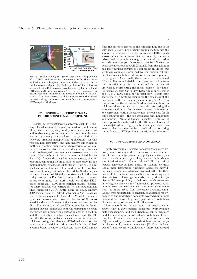
5
Film
thic
knes
s d,
nm
normal to the
substrate
normal to the local
section of the film
e-beamx-ray
fluorescencescanning
direction
Au filmglass substrate0
0
0 100 200 300 400 500lateral coordinate r, nm
100
200
300
50
150
250
350 FIB cuttingax-ray fluorescence
bb
FIG. 3. (Color online) (a) Sketch explaining the principleof the EDX profiling across the nanofeature by the e-beamexcitation and subsequent detection of the characteristic x-ray fluorescence signal. (b) Radial profiles of film thicknessmeasured using EDX cross-sectional analysis (blue curve) andFIB cutting/SEM visualization (red curve) recalculated topresent the film thickness in the direction normal to the sub-strate. The inset shows the difference between the actualthickness along the normal to its surface and the top-viewEDX-acquired thickness.
IV. ENERGY-DISPERSIVE X-RAYFLUORESCENCE NANOPROFILING
Despite its straightforward character, such FIB cut-ting of surface nanotextures produced on noble-metalfilms, which are typically weakly resistant to electron-and ion-beam exposures, requires additional sample over-coating by some protective layer, mostly excluding itsfollowing practical nanophotonic applications. In thisrespect, non-destructive and non-invasive experimentalmethods, enabling quantitative characterization of sup-ported nanoscale structures, are demanding. In thisstudy, we have performed nanoscale cross-sectional SEM-based EDX analysis of the structures depicted in theFig. 3(a). Among these surface nanostructures, the mi-crobump, containing the small nanojet atop, provides themaximal metal thickness redistribution - from the 13-nm-thick cap of the bump to a few hundred nm high protru-sion - as it was previously confirmed by SEM analysisof the FIB cuts. Additionally, the steep wall of the cen-tral protrusion in Fig. 2(e) represents almost a perfectobject to estimate the lateral resolution of this SEM-based approach. EDX cross-sectional (radial) elemen-tal micro-analysis was carried out with a field-emissionSEM microscope JEOL 7001F using an INCA Energy350XT spectrometer (Oxford Instruments Analytical), atthe electron energies of 10 and 30 keV, while the elec-tron beam current was chosen at the level of 79 pA toavoid its thermal damage of the nanostructures on thefilm. The acquisition of the EDX-profiles for the laser-induced surface nanofeatures at the particular electronenergies, which provide the penetration depths in the filmand the supporting substrate much larger, than the 50-nm film thickness, enables their calibration in terms ofthickness, using the reference EDX-signal value for thenon-irradiated gold film. More specifically, the 30-keVelectron beam provides too low and noisy EDX-signals
from the flattened regions of the thin gold film due to itsvery deep (2-3 µm) penetration through the film into thesupporting substrate, but the appropriate EDX-signalsacross the micron-tall nanofeatures, formed by the laser-driven melt accumulation (e.g., the central protrusionatop the nanobump). In contrast, the 10-keV electronbeam provides reasonable EDX-signals from the gold filmand laser-induced features of comparable thickness, butis almost completely absorbed by the micron-tall sur-face features, excluding calibration of the correspondingEDX-signals. As a result, the acquired cross-sectionalEDX-profiles were linked in the transition region fromthe thinned film within the bump and the tall centralprotrusion, representing the initial stage of the nano-jet formation, with the 30-keV EDX-signal in the centerand 10-keV EDX-signal at the periphery. Figure 3(b)shows the EDX-profiling results for the thickness of thenanojet with the surrounding nanobump (Fig. 2e,e1) incomparison to the side-view SEM measurements of itsthickness along the normal to the substrate, using thecross-sectional cuts. Both curves indicate their reason-able agreement within the experimental error bars for allthree topographies - the non-irradiated film, nanobumpand nanojet. Minor difference in spatial resolution ofthese approaches indicated by the 100 nm difference ofthe nanojet radius in Fig. 3, is a broadening artefact of anexternal electromagnetic noise in the local circuits duringthe prolongated EDX-profiling procedure (3-5 minutes).
V. CONCLUSIONS AND OUTLOOK
Highly irreversible transient nanoscale translative hy-drodynamic flows, quenched via nanoscale heat conduc-tion, formed radially-symmetric topological surface pat-terns: nano-bumps and jets. They were made by single-shot irradiation of a 50-nm-thick gold film by tightlyfocused femtosecond laser pulses at variable energies.Radial mass distribution (thickness) across the individ-ual features was quantitatively acquired either by theirnanoscale focused-ion beam cutting and following side-view electron microscopy analysis, or by direct top-view radial nanoprofiling of their relative thickness us-ing energy-dispersive x-ray fluorescence spectroscopy atdifferent electron-beam energies, calibrated by the signalfrom the unperturbed film. Molecular dynamics simu-lations were undertaken to envision spatiotemporal dy-namics of the underlying nanoscale hydrodynamic meltflows and were shown to provide quantitative predictionsof the evolution of the metal film thickness.
More generally, on the one hand, this study demon-strates that highly-transient nanoscale hydrodynamicmelt displacements and their dynamics can be preciselymodeled, enabling in future realistic predictions of morecomplex 3D nanostructures and 3D strucure materials[24] produced by focused ultra-short laser pulses, carry-ing, for example, angular momentum [25] (”vortex laserpulses”), and accurate simulations of more complicated
Chapter 5. Plasmonic nano-printing for surface structuring
164
6
systems, such as materials with new metastable amor-phous and crystalline phases [26, 27], phase-change ma-terials [28, 29] or metallic glasses [30]. On the other hand,our quantitative characterization of the mass distributionprofiles for the laser-fabricated 3D nanoscale structureslays down, for the first time, a solid basis for solution ofthe reverse problem, related to their evolution dynamics,to benchmark theoretical models. We can envisage thatcorrections required to equation-of-state to predict mod-ifications of material subjected to the high pressure andtemperature can be established.
ACKNOWLEDGMENTS
This research was supported by the Russian ScienceFoundation (grant no. 16-12-10165). S.J. acknowledgesWorkshop of Photonics R&D. Ltd. for the laser fab-rication setup acquired via a collaborative grant andthe Australian Research Council DP170100131 Discoveryproject. V.V.Z. and N.A.I. acknowledge Russian Foun-dation of Basic Research (project no. 16-08-01181-a).
[1] Y.-C. Wang, J.-M. Shieh, H.-W. Zan, and C.-L. Pan,Opt. Express 15, 6982 (2007).
[2] S. Haas, A. Gordijn, and H. Stiebig, Progress in Photo-voltaics: Research and Applications 16, 195 (2008).
[3] U. Zywietz, A. B. Evlyukhin, C. Reinhardt, and B. N.Chichkov, Nat. Commun. 5, 34022 (2014).
[4] C. W. Visser, R. Pohl, C. Sun, G.-W. Romer, B. Huisin t Veld, and D. Lohse, Adv. Mater. 27, 4087 (2015).
[5] P. A. Dmitriev, S. V. Makarov, V. A. Milichko, I. S.Mukhin, A. S. Gudovskikh, A. A. Sitnikova, A. K. Samu-sev, A. E. Krasnok, and P. A. Belov, Nanoscale 8, 5043(2016).
[6] A. Kuchmizhak, O. Vitrik, Y. Kulchin, D. Storozhenko,A. Mayor, A. Mirochnik, S. Makarov, V. Milichko,S. Kudryashov, V. Zhakhovsky, and N. Inogamov,Nanoscale 8, 12352 (2016).
[7] X. W. Wang, A. A. Kuchmizhak, E. Brasselet, andS. Juodkazis, arXiv:1612.04487 (2017).
[8] A. I. Kuznetsov, A. B. Evlyukhin, M. R. GonA§alves,C. Reinhardt, A. Koroleva, M. L. Arnedillo, R. Kiyan,O. Marti, and B. N. Chichkov, ACS Nano 5, 4843 (2011).
[9] M. Zenou, A. Sa’ar, and Z. Kotler, Small 11, 4082(2015).
[10] C. Unger, J. Koch, L. Overmeyer, and B. N. Chichkov,Optics Express 20, 24864 (2012).
[11] A. Kuznetsov, C. Unger, J. Koch, and B. Chichkov,Appl. Phys. A 106, 479 (2012).
[12] J. V. Obona, V. Ocelık, J. Rao, J. Skolski, G. Romer,A. H. in ´t ?Veld, and J. T. M. D. Hosson, Appl. Surf.Sci. 303, 118 (2014).
[13] Y. Nakata, N. Miyanaga, K. Momoo, and T. Hiromoto,Appl. Surf. Sci. 274, 27 (2013).
[14] D. Yuan, R. Acharya, and S. Das, Appl. Phys. Lett. 103,223101 (2013).
[15] C. Wu, M. S. Christensen, J.-M. Savolainen, P. Balling,and L. V. Zhigilei, Phys. Rev. B 91, 035413 (2015).
[16] D. S. Ivanov, V. P. Lipp, A. Blumenstein, F. Kleinwort,V. P. Veiko, E. Yakovlev, V. Roddatis, M. E. Garcia,B. Rethfeld, J. Ihlemann, and P. Simon, Phys. Rev. Ap-plied 4, 064006 (2015).
[17] C. Wu and L. Zhigiley, J. Phys. Chem. C 120, 4438(2016).
[18] N. A. Inogamov, V. V. Zhakhovsky, V. A. Khokhlov,Y. V. Petrov, and K. P. Migdal, Nanoscale Res. Lett.11, 1 (2016).
[19] M. E. Povarnitsyn, T. E. Itina, M. Sentis,K. Khishchenko, and P. Levashov, Phys. Rev. B75, 235414 (2007).
[20] Y. N. Kulchin, O. Vitrik, A. Kuchmizhak, A. Savchuk,A. Nepomnyashchii, P. Danilov, D. Zayarnyi, A. Ionin,S. Kudryashov, S. Makarov, A. Rudenko, V. Yurovskikh,and A. Samokhin, JETP 119, 15 (2014).
[21] P. A. Danilov, D. A. Zayarnyi, A. A. Ionin, S. I.Kudryashov, S. V. Makarov, A. A. Rudenko, V. I.Yurovskikh, Y. N. Kulchin, O. B. Vitrik, A. A. Kuch-mizhak, E. A. Drozdova, and S. B. Odinokov, QuantumElectron. 44, 540 (2014).
[22] N. A. Inogamov, V. V. Zhakhovsky, and V. A. Khohlov,JETP 120, 15 (2015).
[23] D. K. Ilnitskiy, V. A. Khokhlov, V. V. Zhakhovsky, Y. V.Petrov, K. P. Migdal, and N. A. Inogamov, J. Phys:Conf. Ser. 774, 012101 (2016).
[24] M. Malinauskas, A. Zukauskas, S. Hasegawa,Y. Hayasaki, V. Mizeikis, R. Buividas, and S. Juodkazis,Light: Sci. Appl. 5, e16133 (2016).
[25] K. Toyoda, F. Takahashi, S. Takizawa, Y. Tokizane,K. Miyamoto, R. Morita, and T. Omatsu, Phys. Rev.Lett. 110, 143603 (2013).
[26] A. Vailionis, E. G. Gamaly, V. Mizeikis, W. Yang,A. Rode, and S. Juodkazis, Nature Communications 2,445 (2011).
[27] L. Rapp, B. Haber, C. Pickard, J. Bradby, E. Gamaly,J. Williams, and A. Rode, Nat. Commun. 6, 7555 (2015).
[28] M. Hase, P. Fons, K. Mitrofanov, A. Kolobov, andJ. Tominaga, Nat. Commun. 6, 8367 (2015).
[29] E. Matsubara, S. Okada, T. Ichitsubo, T. Kawaguchi,A. Hirata, P. Guan, K. Tokuda, K. Tanimura, T. Mat-sunaga, M. Chen, and N. Yamada, Phys. Rev. Lett. 117,135501 (2016).
[30] L. Zhong, J. Wang, H. Sheng, Z. Zhang, and S. X. Mao,Nature 512, 177 (2014).
5.8. Appendix E
165

Laser Photonics Rev. 11, No. 2, 1600187 (2017) /DOI 10.1002/lpor.201600187
LASER& PHOTONICSREVIEWS
ORIGIN
AL
PAPER
Abstract Multi scale hierarchical structures underpin me-chanical, optical, and wettability behavior in nature. Herewe present a novel approach which can be used to mimicthe natural hierarchical patterns in a quick and easy mask-less fabrication. By using two-beam interference lithographywith angle-multiplexed exposures and scanning, we havesuccessfully printed large-area complex structures having acascading resolution and 3D surface profile . By preciselycontrolling the exposure dose we have demonstrated a ca-pability to create different 3D textured surfaces having com-parable aspect ratio with period spanning from 4 μm to 300nm (more than one order of magnitude) and the height span-ning from 0.9 μm to 40 nm, respectively. Up to three levelsof biomimetic hierarchical structures were obtained that showseveral natural phenomena: superhydrophobicity, iridescence,directionality of reflectivit , and polarization at different colors.
Angle-multiplexed optical printing of biomimetic hierarchical3D textures
Muhammad Irfan Abid1, Lei Wang1, Qi-Dai Chen1,∗, Xue-Wen Wang3,4,Saulius Juodkazis1,3,4,∗, and Hong-Bo Sun1,2,∗
1. Introduction
Multi scale hierarchical structures underpin mechanical,optical, and wettability behavior in nature [1–12]. Most ofthe fabrication procedures developed so far to mimic nat-ural hierarchy have experimental complexity and limitedfl xibility in structure symmetry [13–20], limitations in up-scaling over extended macroscopic areas and lack of capa-bility to structure 3D surfaces. Here, we show that using theangle-multiplexed exposure of two beam laser interference(2BI), hence a period modulation, combined with a lateralscan and precise exposure dose control, an endless varietyof hierarchical 3D surfaces with features spanning over anorder of magnitude in period and height made on micro-scaled surfaces with different geometrical symmetries canbe laser printed. Using this technique we have success-fully demonstrated hierarchical surfaces which mimic thewetting properties [21, 22] of natural plant leaves, opticalproperties of iridescence [23, 24], directionality of reflection and polarization of colors [15, 25] exhibited in nature.
1 State Key Laboratory on Integrated Optoelectronics, College of Electronic Science and Engineering, Jilin University, 2699 Qianjin Street,Changchun, 130012, China2 College of Physics, Jilin University, 2699 Qianjin Street, Changchun, 130023, China3 Centre for Micro-Photonics, Faculty of Science, Engineering and Technology, Swinburne University of Technology, Hawthorn, VIC, 3122, Australia4 Melbourne Centre for Nanofabrication, ANFF, 151 Wellington Road, Clayton VIC, 3168, AustraliaM. I. Abid and L. Wang contributed equally to this work.∗Corresponding author(s): e-mail: [email protected], [email protected] and [email protected]
The most significan advantage of our technique over theother surface patterning methods is that it is mask-less andoffers the f exibility to change the geometrical arrangementand axial symmetry of both micro and nanoscale surfacepatterns effortlessly. Another salient feature of our methodis that within a time of few seconds �5 × 5 mm2 regioncan be enlarged into areas with centimeter cross sectionsby sample translation which enables the mass production.
Many functions and properties exhibited by objects innature are result of hierarchical ordering of micro/nanoscalestructures and patterns by arranging simpler structures. Theself-cleaning surface of lotus leaf [1], the reduced drag andhydrodynamics surface of a shark skin [2,3], the anisotropicwetting surface of a rice leaf [4, 26], the highly adhesive,superhydrophobic and surface enhanced Raman scatteringsubstrate of a rose petal [5, 6], the water repellent legs ofa water strider [7, 8], the anti-fogging compound eyes ofmosquito [9] and fl [27], a reversible adhesion of a gecko’sfoot [10, 28], and structural colors of moths, butterflie[11] and bird feathers [12] are examples that have been
C© 2017 by WILEY-VCH Verlag GmbH & Co. KGaA, Weinheim
Chapter 5. Plasmonic nano-printing for surface structuring
166

LASER&PHOTONICSREVIEWS
1600187 (2 of 6) M. I. Abid et al.: Angle-multiplexed optical printing
Figure 1 Schematic of angle varied multiple exposure of 2BIprocess. The schematic showing dependence of the grating pe-riod on the angle of two interfering beams. The beams L1-L1’ withsmaller angle 2θ1 form a larger period (primary pattern), whereasthe beams L2-L2’ with a larger angle 2θ2 form the smaller period(secondary pattern) on the substrate (S). The sequential com-bination of two periods produces the hierarchical structure. Thesubstrate is mounted on a turn table which can be rotated at anangle (α) to achieve different patterns. Colors of butterfl wingswere obtained as shown in the bottom right.
the source of motivation to follow the nature’s rule of hier-archy for useful functions [24, 29–31].
Usually to make a hierarchical pattern, a micro-structured surface is fabricated in the f rst step and thenfurther processing is carried out to add nano-features overit at the second step [13, 18–20] by combining differentfabrication techniques with different resolutions [32–35]making a whole process long, complicated and limited to acertain geometrical shape.
In this paper, we present a novel approach which can beused to mimic the natural hierarchical patterns in a quickand easy maskless process. A simple expose-scan exper-imental setup is required to laser-print a complex struc-ture with cascading resolution and 3D surface profile Itis based on simplifie multi-beam interference lithography(MBI) [36] with only two beams (2BI) [37, 38]. We addedangle-multiplexed exposures and scanning to achieve f ex-ibility and larger area coverage as shown in Fig. 1 (seeSupplement for details). By precise exposure dose control,we demonstrate a capability to create 3D textured surfaceswith period spanning more than one order of magnitude(4 – to - 0.3 μm) while keeping the same aspect ratio ofdifferent patterns with height spanning 0.9 –to- 0.04 μm.This is achieved using long nanosecond laser pulses andbenefitin from a literally unlimited depth of the interfer-ence pattern into the depth of the sample. This is the keyto writing on existing 3D surface created by multiplexedexposures, the newly demonstrated capability of 2BI.
2. Experimental section
The glass substrates were firs cleaned with acetone and ab-solute ethanol and then rinsed with de-ionized water. TheBP-212 positive photoresist (Beijing Institute of Chemical
Reagents) was spin coated at 3000 rpm on the substrates fora thickness of about 3 μm. The glass substrates were thenprebaked on a hotplate at 110°C for 60 seconds. The sub-strates were cooled to the room temperature before expo-sure. The laser beam from a frequency-tripled, Q-switched,single-mode Nd:YAG laser (Spectra-physics) with about10 ns pulse width and 355 nm wavelength was split into twobeams. The two-beam laser interference setup was made asshown in Supplementary Figure S1. For the primary pat-terns of 3 μm period the power of �9 mm diameter laserbeam was set to 300 mW whereas for secondary patterns of300 nm the power was reduced to 200 mW. The exposuretime in all the cases was one second. The samples werethen developed in a 0.2% (w/v) aqueous solution of NaOHfor about 3 to 5 minutes. The morphologies of the struc-tures were studied using Field-emission SEM (JSM-7500F,JEOL, Japan) and AFM (Digital Instruments NanoscopeIIIA) in the tapping mode. Contact Angle was measuredusing an OCA 20 system (Data physics GmbH, Germany)at room temperature with droplet of about 0.5 μl. The im-ages of the iridescence from structures were taken using adigital camera. For measuring the optical reflect vity andpolarization characteristics, a 633-nm semiconductor laserlight source was used.
3. Results and discussion
Various combinations of one, two and three exposures foreach period with different axial symmetries between the pri-mary and secondary patterns from 3 μm to sub-wavelength300 nm are shown in scanning electron microscopy (SEM)images in Fig. 2. Heights of the primary and secondarypatterns depend on the exposure dose (SupplementaryFigure S3 and Fig. 3) and are from 700 nm to 900 nm for theprimary and 50 nm to 100 nm for the secondary exposures,respectively. The secondary pattern could be fabricated atan arbitrary angle relative to the primary one (Fig. 2(c–g)). These results demonstrate versatility and fl xibility ofprinting in which any symmetry (1D grating, 2D square, 2Dhexagonal) can be made either at the primary or secondarylevel with an added fl xibility of a phase shift in the axialorientation.
Further demonstration of capabilities of the proposedprinting method is presented next with three levels of hi-erarchical patterning (Fig. 2(h–i)). Three periods of 4 μm,1 μm and 300 nm were combined in the f rst, second andthird patterns. Exposure doses of second and third levelswere optimized to be lower as compared to the f rst level ofgratings. This results in a structure having a surface textureof a 3-level hierarchy (Supplementary Table S1 shows de-tails). Due to a shallower depth of structures with a smallerperiod, it was important to keep the following exposuresequence: first exposure of the lager period (deeper pat-tern) and, second, the smaller period patterns. The exposedresist had a weaker absorption and this facilitated fabrica-tion of deep patterns with alternating periods using multipleexposures.
C© 2017 by WILEY-VCH Verlag GmbH & Co. KGaA, Weinheim www.lpr-journal.org
5.8. Appendix E
167

ORIGINALPAPER
Laser Photonics Rev. 11, No. 2 (2017) (3 of 6) 1600187
Figure 2 SEM micrographs of surfaces fabricated by multiple exposure of angle varied 2BI. From (a) to (i) the variations in themorphologies of the surface patterns show the capability of the process: (a) 300 nm 1D grating at 90° orientation w.r.t. 3 μm1D grating; (b) 300 nm 1D grating at 0° orientation w.r.t. 3 μm 2D square patterns; (c) 300 nm 2D square pattern at 0° orientation w.r.t.3 μm 2D square pattern; (d) 300 nm 2D square pattern at 45° orientation w.r.t. 3 μm 2D square pattern; (e) 300 nm 2D square patternat 45° orientation w.r.t. 3 μm 1D grating; (f) 300 nm 2D hexagonal pattern at 0° orientation w.r.t. 3 μm 2D square pattern; (g) 300 nm2D hexagonal pattern at 0° orientation w.r.t. 3 μm 2D hexagonal pattern; (h) 300 nm and 1 μm 1D gratings at 90° orientation w.r.t. 4 μm1D gratings; (i) 1 μm 1D gratings at 90° orientation w.r.t. 300 nm and 4 μm 1D gratings. The scale bar in all images is 1 μm.
Figure 3 Wetting properties of hierarchical surfaces: (a) and (c) show the static contact angles of a droplet of water on the hierarchicalsurfaces shown in 3D AFM images; (b) and (d) show the series of images (from left to right) when 0.5 μl droplet of water approachesthe surface, touches it and then is pulled back from the surface of the structures of (a) and (c), respectively. The red circle in (d) showsthe little amount of water left on the surface in (c) due to stronger adhesion of the water droplet to the surface. The arrows indicatedirection of motion of the droplet.
www.lpr-journal.org C© 2017 by WILEY-VCH Verlag GmbH & Co. KGaA, Weinheim
Chapter 5. Plasmonic nano-printing for surface structuring
168

LASER&PHOTONICSREVIEWS
1600187 (4 of 6) M. I. Abid et al.: Angle-multiplexed optical printing
It is demonstrated next, that printed hierarchical micro-nano-structured surfaces can mimic the wettability of natu-ral leaves [1,22,39] and achieve super hydrophobicity witha contact angle θ >> 150°. Printed surfaces were treatedwith fluoroal ylsilane to add chemical hydrophobicity inaddition to that caused by structure. The static water con-tact angle on the structure which resemble the surface mor-phology of the leaf of hygoryza aristata [21] (Fig. 2 (d)) isshown in Fig. 3(a). The fla substrate surface had the contactangle θ = 114°, the surface with only primary square 2Dpattern of pins with 3μm period exhibited 130°, and even alarger static θ = 138°was observed on the similar surface of300 nm period (supplementary Figure S4). The contact an-gle increased to 154° (Fig. 3(a)) for the hierarchical struc-ture shown in Fig. 2(d).
Different surface wettability is underpinned by thechemical and structural composition of the surface. If theliquid and solid contours exactly connect to each other andliquid completely f lls the valleys between the peaks of arough surface, this corresponds to the Wenzel case with thecontact angle [40]:
cosθ = r cosθo, (1)
where r is the roughness factor define as the ratio of theactual surface area to the projected area, and θo is the con-tact angle on the fla surface of the same material. Forthe hierarchical texture shown in Fig. 2(d), the factor r =1.45 was measured directly from the AFM map over areaof 10 μm × 10 μm. With θ0 = 114°, it was found thatθ = 126° is expected (Equation (1)). However, the exper-imentally measured contact angle was larger. The Cassie-Baxter (CB) model [41] was applied where the droplet onlyresides on the peaks over a rough surface, forming air pock-ets between liquid and solid with the contact angle governedby:
cosθ = fs (cosθo + 1) − 1, (2)
where fs is the fractional contact area between the liquidand the solid. For the Fig. 2(d) texture with θ = 154° andθo= 114°, the value of solid fraction fs was evaluated as0.17.
When nanostructures form continuous grating lines onthe top of 2D micro structures (Fig. 2(b)) the wetting be-havior is different. The contact angle of this surface wasθ = 150° (Fig. 3(c)), only slightly lower as compared tothat of the structure in Fig. 2(d). The increased solid frac-tion fs was observed in this case. The following test revealeddynamic behavior of wetting with droplet gradually sink-ing into the structure until it touched the bottom surface. Itdid not spread out even when it was f rmly touched to thebottom surface. When dragged over the surface (Fig. 2(d)),the drop did not stick to the surface either and was easilydetached when raised up with the needle. In the case ofsurface shown in Fig. 2(b), the droplet showed a strongeradhesion (Fig. 3) while a small amount of water was lefton the surface after detachment in the case of a less hy-drophobic surface. The transitional state [42] of the droplet
between CB and Wenzel wetting define hydrophobicity ofthe printed surface.
Apart from wetting properties, surface coloration is an-other result of the surface structure. Iridescence - the hue ofsurface is varied by changing the viewing angle - is soughtafter in marking, security against counterfeiting and jew-elry. In butterflies iridescence is responsible for producingattractive colors [11,12,23]. In f owers, it provides a cue toanimal pollinators [43]. Structures that produce iridescentcolors are classifie into three types: multilayer reflectorsthree dimensional photonic crystals, and diffraction grat-ings. The structure shown in Fig. 2(a) has parallel ridgesresembling a diffraction grating with a color appearance dueto diffraction. The iridescence from the diffraction gratingsis different from the other types of structures as the col-ors are ordered from red to violet for observer at a fi edobservation angle according to the grating equation:
d(sinθr − sinθi ) = mλ, (3)
where d is the period of the gratings, θi is the angle ofincidence, θr is the angle of reflectio of the diffractionorder m, and λ is the wavelength of light. The flas y andshimmering colors: blue, green, orange and red are clearlyobserved as the viewing angle is gradually change (bottomof Fig. 4(a)).
In addition to the striking iridescence of such printedtextured surfaces, polarization and directionality of re-flectio are expected to be pronounced as exhibited byseveral biological species. The structural color reflectiofrom the shell of mollusk Helcion pruinosus [44] and onthe wing of moth Trichoplusia orichalcea [25] is foundto be highly directional. The structure of the wing (insetFig. 4(a)) is composed of raised ridges connected togetherby a herringbone pattern of microribs. This arrangement ofthe wing structure was reproduced by the proposed printing(Fig. 4(a)).
On the basis of diffraction theory Straton-Silver-Chu in-tegral [45,46], a theoretical model of the complex diffract-ing wing structure of Trichoplusia orichalcea to predict itspolarization, directionality of reflectio and color proper-ties was developed [25]. It was found by calculation andexperiment that under the condition of specular reflectio(the angle of incidence equal to the angle of diffraction),the diffraction intensity has a strong dependence on theangle of incidence and on the azimuthal orientation ofthe wing. Same analysis of the diffraction intensity andthe wing orientation for the printed structures is shown inFig. 4(b). The sample was mounted on a turning table whichcould be rotated around the y-axis to select different val-ues of incidence angles �i and also the azimuthal orien-tation was chosen by rotating around z-axis �r (Supple-mentary Figure S5). The sample was initially aligned alongthe line OA (parallel to the micro scale ridges: �r = 0°).The linear polarizers were placed in the path of both in-cident and reflecte beams to record the same S-type orP-type diffracted powers at 633 nm wavelength. Thediffracted power for the incidence angles of 45° and 60°under the condition of specular reflectio for both S and P
C© 2017 by WILEY-VCH Verlag GmbH & Co. KGaA, Weinheim www.lpr-journal.org
5.8. Appendix E
169

ORIGINALPAPER
Laser Photonics Rev. 11, No. 2 (2017) (5 of 6) 1600187
Figure 4 Optical properties of hierarchical surfaces. (a) SEM micrograph of the fabricated hierarchical structure mimicking the wing ofthe moth Trichoplusia orichalcea [19] (inset in (a) shows SEM image of the actual moth wing; scale bar 1 μm). The larger gratings havea period of 3 μm while the smaller is 300 nm. (b) Dependence of the diffracted power on the orientation of the mimicked wing structure(rotation in the plane of the sample). The rotation angle �r = 0° for the line OA (shown in (a)) corresponds to the vertical orientation.The measured results for both S and P polarized light for the incidence angles of 45° and 60° at the wavelength of 630 nm. The unitson the y-axis are normalized to the direct power measured without reflectio from the sample. (c) Colors of the visible spectrum fromviolet to red caused by iridescence by gradually lowering the viewing angle.
polarizations (Fig. 4(b)) showed that the diffraction inten-sity was increasing along the angle of incidence from 45°to 60° for both polarizations.
The presented results agree to a high degree with thetheoretical predictions and experimental finding for thereal wing structure of the moth Trichoplusia orichalce [25].When the orientation of the structure was changed from+90° to −90° in the azimuthal orientation, it correspondsto the path swapping betwen the incident and diffractedbeams. For the all incidence angles it was found that Spolarized light diffracted significantl stronger as comparedwith P polarization. So, under non-polarised illumination ofnatural light the structure can act as a linear polarizer witha high efficien y depending on the orientation angle �r.
4. Conclusions and outlook
We have demonstrated the multiple exposure of two beamlaser interference with angle variation and period mod-ulation as a potential technique for direct printing ofbiomimetic hierarchical structures. Based on sequence ofexposures, orientation angle of the sample and period of in-terference pattern, a variety of multiscale surfaces with ge-ometrically symmetrical structures has been be produced. Ithas been shown experimentally that the obtained structurescan be used to mimic several natural phenomena: superhydrophobicity, iridescence, directionality of reflect vity,
and polarization at different colors. The approach usedhere can be applied to fabricate biomimetic surfaces whichcan fin potential applications in wide range of disciplinesof microfluidics antifouling, decorative/holographic ele-ments, colored jewelry, micro/nano optics, polarizing f ltersand surface enhanced Raman scattering sensors. The pro-posed method of surface printing can be easily adopted forrandomized patterns which produce new functionalities,such as the low reflect vity and wide angular selectivity.Surfaces for thermal management of light at IR wavelengthusing Wolf’s effect can be made for narrow band emitters[47].
Supporting Information
Additional supporting information may be found in the online ver-sion of this article at the publisher’s website.
Acknowledgements. This work was supported by the Na-tional Natural Science Foundation of China and National 973Program under Grants # 61590930, 61435005, 2014CB921302,51335008, and 61378053.
Received: 11 July 2016, Revised: 18 December 2016,Accepted: 19 December 2016
Published online: 13 January 2017
Key words: Hierarchical structures, 3D printing, biomimetics,laser fabrication.
www.lpr-journal.org C© 2017 by WILEY-VCH Verlag GmbH & Co. KGaA, Weinheim
Chapter 5. Plasmonic nano-printing for surface structuring
170

LASER&PHOTONICSREVIEWS
1600187 (6 of 6) M. I. Abid et al.: Angle-multiplexed optical printing
References
[1] W. Barthlott and C. Neinhuis, Planta 202, 1–8 (1997).[2] P. Ball, Nature 400, 507–509 (1999).[3] L. Wen, J. C. Weaver, P. J. Thornycroft, and G. V. Lauder,
Bioinspir. Biomim. 10, 066010 (2015).[4] D. Wu, J. N. Wang, S. Z. Wu, Q. D. Chen, S. Zhao, H. Zhang,
H. B. Sun, and L. Jiang, Adv. Funct. Mater. 21, 2927–2932(2011).
[5] L. Feng, Y. Zhang, J. Xi, Y. Zhu, N. Wang, F. Xia, and L.Jiang, Langmuir 24, 4114–4119 (2008).
[6] B. B. Xu, Y. L. Zhang, W. Y. Zhang, X. Q. Liu, J. N. Wang,X. L. Zhang, D. D. Zhang, H. B. Jiang, R. Zhang, and H. B.Sun, Adv. Opt. Mater. 1, 56–60 (2013).
[7] X. Gao and L. Jiang, Nature 432, 36 (2004).[8] Q. Wang, X. Yao, H. Liu, D. Quere, and L. Jiang, PNAS 112,
9247–9252 (2015).[9] X. Gao, X. Yan, X. Yao, L. Xu, K. Zhang, J. Zhang, B. Yang,
and L. Jiang, Adv. Mater. 19, 2213–2217 (2007).[10] K. Autumn, Y. A. Liang, S. T. Hsieh, W. Zesch, W. P. Chan,
T. W. Kenny, R. Fearing, and R. J. Full, Nature 405, 681–685(2000).
[11] H. Ghiradella, Appl. Opt. 30, 3492–3500 (1991).[12] D. G. Stavenga, H. L. Leertouwer, D. C. Osorio, and B. D.
Wilts, Light Sci. Appl. 4, e243 (2015).[13] B. Bhushan, K. Koch, and C. J. Yong, Ultramicroscopy 109,
1029–1034 (2009).[14] X. Yao, Q. Chen, L. Xu, Q. Li, Y. Song, X. Gao, D. Quere,
and L. Jiang, Adv. Funct. Mater. 20, 656–662 (2010).[15] L. Feng, Y. Zhang, M. Li, Y. Zheng, W. Shen, and L. Jiang,
Langmuir 26, 14885–14888 (2010).[16] A. K. Geim, S. V. Dubonos, I. V. Grigorieva, K. S. Novoselov,
A. A. Zhukov, and S. Y. Shapoval, Nat. Mater. 2, 461–463(2003).
[17] K. Watanabe, T. Hoshino, K. Kanda, Y. Haruyama, and S.Matsui, Jpn. J. Appl. Phys. 44, L48-L50 (2004).
[18] D. Wu, Q. D. Chen, H. Xia, J. Jiao, B. B. Xu, X. F. Lin, Y.Xu, and H. B. Sun, Soft Matter 6, 263–267 (2010).
[19] S. J. Choi, M. K. Choi, D. Tahk, and H. Yoon, J. Mater.Chem. 21, 14936–14940 (2011).
[20] F. Zhang, J. Chan, and H. Y. Low, Appl. Surf. Sci. 254,2975–2979 (2008).
[21] C. Neinhuis and W. Barthlott, Ann. Bot. 79, 667–677(1997).
[22] M. Liu, S. Wang, and L. Jiang, Mrs Bull. 38, 375–382 (2013).[23] P. Vukusic, J. R. Sambles, and C. R. Lawrence, Nature 404,
457 (2000).
[24] R. Brunner, O. Sandfuchs, C. Pacholski, C. Morhard, and J.Spatz, Laser Photonics Rev. 6, 641–659 (2012).
[25] D. J. Brink, J. E. Smit, M. E. Lee, and A. Moller, Appl. Opt.34, 6049–6057 (1995).
[26] J. K. Oh, X. Lu, Y. Min, L. Cisneros-Zevallos, and M. Ak-bulut, Acs Appl. Mater. Inter. 7, 19274–19281 (2015).
[27] Z. Sun, T. Liao, K. Liu, L. Jiang, J. H. Kim, and S. X. Dou,Small 10, 3001–3006 (2014).
[28] D.-J. Guo, R. Liu, Y. Cheng, H. Zhang, L.-M. Zhou, S.-M.Fang, W. H. Elliott, and W. Tan, Acs Appl. Mater. Inter. 7,5480–5487 (2015).
[29] Y. L. Kong, M. K. Gupta, B. N. Johnson, and M. C.McAlpine, Nano Today 11, 330–350 (2016).
[30] Y. Jie, Q. Jiang, Y. Zhang, N. Wang, and X. Cao, NanoEnergy 27, 554–560 (2016).
[31] J. Yang, F. Luo, T. S. Kao, X. Li, G. W. Ho, J. Teng, X. Luo,and M. Hong, Light Sci. Appl. 3, e185 (2014).
[32] K. Golovin, D. H. Lee, J. M. Mabry, and A. Tuteja, AngewChem. Int. Edit. 52, 13007–13011 (2013).
[33] J. N. Wang, Y. L. Zhang, Y. Liu, W. Zheng, L. P. Lee, and H.B. Sun, Nanoscale 7, 7101–7114 (2015).
[34] T. P. N. Nguyen, R. Boukherroub, V. Thomy, and Y.Coff nier, J. Colloid Interf. Sci. 416, 280–288 (2014).
[35] M. Malinauskas, A. Zukauskas, S. Hasegawa, Y. Hayasaki,V. Mizeikis, R. Buividas, and S. Juodkazis, Light Sci Appl.5, e16133 (2016).
[36] G. M. Burrow and T. K. Gaylord, Micromachines 2, 221–257(2011).
[37] N. D. Lai, W. P. Liang, J. H. Lin, C. C. Hsu, and C. H. Lin,Opt. Express 13, 9605–9611 (2005).
[38] L. Wang, Z.-H. Lu, X.-F. Lin, Q.-D. Chen, B.-B. Xu, andH.-B. Sun, J. Lightwave Technol. 31, 276–281 (2013).
[39] Y. T. Cheng, D. E. Rodak, C. A. Wong, and C. A. Hayden,Nanotechnology 17, 1359–1362 (2006).
[40] R. N. Wenzel, Ind. Eng. Chem. 28, 988–994 (1936).[41] A. B. D. Cassie, Discuss Faraday Soc. 3, 11–16 (1948).[42] S. Wang and L. Jiang, Adv. Mater. 19, 3423–3424 (2007).[43] H. M. Whitney, M. Kolle, P. Andrew, L. Chittka, U. Steiner,
and B. J. Glover, Science 323, 130–133 (2009).[44] D. J. Brink, V. D. B. Ng, and A. J. Botha, Appl. Opt. 41,
717–722 (2002).[45] S. Silver, Microwave antenna theory and design, (McGraw-
Hill, New York, 1947).[46] R. M. A. Azzam and N. M. Bashara, Phys. Rev. B. 5, 4721–
4729 (1972).[47] J. J. Greffet, R. Carminati, K. Joulain, J. P. Mulet, S. Main-
guy, and Y. Chen, Nature 416, 61–64 (2002).
C© 2017 by WILEY-VCH Verlag GmbH & Co. KGaA, Weinheim www.lpr-journal.org
5.8. Appendix E
171

materialsArticle
Silk: Optical Properties over 12.6 OctavesTHz-IR-Visible-UV Range
Armandas Balcytis 1,2,*,†, Meguya Ryu 3,†, Xuewen Wang 1, Fabio Novelli 1,‡,Gediminas Seniutinas 1,§, Shan Du 4, Xungai Wang 4, Jingliang Li 4, Jeffrey Davis 1,Dominique Appadoo 5, Junko Morikawa 3,* and Saulius Juodkazis 1,6
1 School of Science, Faculty of Engineering and Industrial Sciences, Swinburne University of Technology,Hawthorn, VIC 3122, Australia; [email protected] (X.W.); [email protected] (F.N.);[email protected] (G.S.); [email protected] (J.D.); [email protected] (S.J.)
2 Department of Laser Technologies, Center for Physical Sciences and Technology, Savanoriu Ave. 231,LT-02300 Vilnius, Lithuania
3 Tokyo Institute of Technology, Meguro-ku, Tokyo 152-8550, Japan; [email protected] Australian Future Fibres Research and Innovation Centre, Institute for Frontier Materials, Deakin University,
Geelong, VIC 3220, Australia; [email protected] (S.D.); [email protected] (X.W.);[email protected] (J.L.)
5 Australian Synchrotron, Blackburn Road, Clayton, VIC 3168, Australia; [email protected] Melbourne Centre for Nanofabrication, the Victorian Node of the Australian National Fabrication Facility,
151 Wellington Rd., Clayton, VIC 3168, Australia* Correspondence: [email protected] (A.B.); [email protected] (J.M.)† These authors contributed equally to this work.‡ Current address: Ruhr-University Bochum, 44801 Bochum, Germany.§ Current address: Paul Scherrer Institut, CH-5232 Villigen PSI, Switzerland.
Academic Editor: Armando J. D. SilvestreReceived: 30 January 2017; Accepted: 23 March 2017; Published: 28 March 2017
Abstract: Domestic (Bombyx mori) and wild (Antheraea pernyi) silk fibers were characterised overa wide spectral range from THz 8 cm−1 (λ = 1.25 mm, f = 0.24 THz) to deep-UV 50× 103 cm−1
(λ = 200 nm, f = 1500 THz) wavelengths or over a 12.6 octave frequency range. Spectral featuresat β-sheet, α-coil and amorphous fibroin were analysed at different spectral ranges. Single fibercross sections at mid-IR were used to determine spatial distribution of different silk constituentsand revealed an α-coil rich core and more broadly spread β-sheets in natural silk fibers obtainedfrom wild Antheraea pernyi moths. Low energy T-ray bands at 243 and 229 cm−1 were observed incrystalline fibers of domestic and wild silk fibers, respectively, and showed no spectral shift downto 78 K temperature. A distinct 20± 4 cm−1 band was observed in the crystalline Antheraea pernyisilk fibers. Systematic analysis and assignment of the observed spectral bands is presented. Watersolubility and biodegradability of silk, required for bio-medical and sensor applications, are directlyinferred from specific spectral bands.
Keywords: silk; fibroin; biopolymer; terahertz; spectroscopy; solubility; proteins; biodegradablepolymers
1. Introduction
Spectral properties at sub-1 mm wavelengths at around and below terahertz frequencies(1 THz = 1012 Hz, corresponding to ≈33 cm−1 in wavenumbers) are important for understandingmaterials with bio-medical relevance [1]. For example, terahertz absorbance is related to conformationand structure of saturated fatty acids with long alkane chains, whose vibration frequency depends on
Materials 2017, 10, 356; doi:10.3390/ma10040356 www.mdpi.com/journal/materials
Chapter 5. Plasmonic nano-printing for surface structuring
172

Materials 2017, 10, 356 2 of 15
the length l of the chain as ν =√
Eρ /(2lc) [cm−1] for density ρ, Young modulus E, and speed of light
c—as demonstrated for polymethylene [2]. Those longitudinal accordion modes (LAMs) populatea 1–100 cm−1 low energy vibration window, edging towards low wavenumbers for long chains.Of relevance to material science are first order solid–solid phase transitions in alkane crystals—therotator phases [3]—occurring just a few degrees below melting point when the crystalline order stillexists; however, low energy rotations of molecules become allowed [4]. In glasses, low frequencyRaman spectra exhibit the 10–50 cm−1 Boson peak, which is another example of low energy phenomenadue to rearrangement of density of states in amorphous materials [5].
In protein based materials, a variety of molecular ordering and interactions occur, which, inturn, define their properties. It was shown that formation of protein fibrils can be monitoredat the THz spectral window [6]. Silk fibers offer a good example of the complexity of proteinmaterials as they have amorphous and crystalline structural components with proteins forming a 3Dnetwork of random α-coils and metastable β-turns (Silk I) together with a crystalline β-sheet phase(Silk II) [7]. Such composition results in a set of important properties such as a high mechanical strength,optical transparency and waveguiding [8] as well as biocompatibility and biodegradability [9,10].
Mechanisms controlling crystallisation of protein coils via ordered hydrogen bonding andtheir unzip-decomposition at different annealing temperatures, laser and electron beam exposureconditions are of interest for applications in material science and bio-medical fields [11–13]. Silk canbe used as a bio-compatible scaffold [14] with water solubility dependent on its crystallinity [15].Furthermore, the biodegradability and elasticity of silk make it an attractive platform for the creation ofnext-generation biocompatible and flexible optoelectronic devices [16]. Any active functional materialsused in such applications alongside silk would have to exhibit conformable mechanical characteristics.Two-dimensional transition metal oxides, with their wide variety of controllable physical properties,are especially promising in this regard [17]. While the field is still nascent, silk fibroin was alreadydemonstrated to be a viable template in preparing metal oxide composite nanomaterials for lithium-ionbattery anodes [18,19]. However, in order to tune the morphology of nanomaterials created in thisway, control over the self-assembly behavior of hierarchical fibroin structure is required [20].
Photo-thermal control of β-sheet formation in silk could provide a way to make silk-resists as wellas 3D bio-scaffolds, and would help to understand protein crystallisation mechanisms relevant to theβ-sheet plaque formation in Alzheimer’s disease. It was demonstrated using on-chip calorimetry that,through a fast 2000 K/s thermal quenching of molten silk, an amorphous phase (water soluble) can berecovered [21]. However, fast thermal quenching is hampered by the rather low thermal diffusivity ofsilk αT ' 1.5× 10⁻⁷ m2/s [22], likewise attributable to its complex structure. Similarly, the interactionof light with the multiple constituent structural components of silk fibers at frequencies spanning fromfar-IR to UV spectral ranges has to be well understood for a wide range of applications.
Here, transmittance measurements of silk over a broad spectral range from THz wavelengths(T-ray) until deep UV are reported and spectral signatures of the constituent components of silk:β-sheets, α-coils and amorphous fibroin are analysed. Since the spectral signatures characteristic of thesilk building blocks are present at very different wavelengths, a comprehensive analysis over the broadspectral range had to be made. Water solubility of silk can be inferred from the spectral properties andis essential for future applications of silk in wearable electronics, implants, and sensors.
2. Materials and Methods
2.1. Spectroscopy Setups and Techniques
The THz/Far-IR Beamline at the Australian synchrotron was used to characterise silk in the40–600 cm−1 spectral range. The beamline is equipped with a Bruker IFS 125/HR Fourier Transform(FT) spectrometer (Bremen, Germany) and OPUS 6.5 software (Bruker Optik GmbH, Ettlingen,Germany) was used for initial data analysis. Up to 100 spectral scans were captured and averaged to
5.8. Appendix E
173

Materials 2017, 10, 356 3 of 15
improve signal-to-noise (S/N) ratio. A liquid nitrogen cryostat was used to measure silk transmittance,T, down to ∼77 K temperature.
For the largest T-ray wavelengths in the 8–80 cm−1 spectral window, femtosecond time domainspectroscopy (TDS) was used due to the higher S/N ratio as compared to synchrotron T-ray radiation.Almost a single-cycle and 1 ps long THz-fields are generated in a 0.6% MgO doped LiNbO3 crystalby optical rectification of amplified laser pulses [23,24]. The radiation is focused onto the sample byan off-axis parabolic mirror with a focal length of 100 mm and imaged with two additional identicalmirrors onto the detection crystal. The single-cycle fields are detected via electro-optical sampling in a500 µm thick ZnTe [25].
The amplitude and phase-resolved fields transmitted through the silk samples, as well as througha reference (air), are Fourier transformed to give frequency-dependent amplitudes as well as theirphases. If the sample thickness is well defined and only the first Fresnel coefficient can be considered,the phase difference of these Fourier transforms is directly related to the real part of the index ofrefraction, whereas the ratio of the field magnitudes yields the absorption coefficient. In the caseof silk fibers, however, the sample thickness is not well defined, so only the absorbance, A, can beunambiguously deduced, calculated as -lg T, where T is the field transmittance corresponding tothe ratio of the Fourier magnitudes. The fields transmitted by a reference and by the sample arealternatively acquired 50 times to give the standard deviation shown as error bars in Figure 1.
Materials 2017, 10, 356 3 of 16
improve signal-to-noise (S/N) ratio. A liquid nitrogen cryostat was used to measure silk transmittance,T, down to ∼77 K temperature.
For the largest T-ray wavelengths in the 8–80 cm−1 spectral window, femtosecond time domainspectroscopy (TDS) was used due to the higher S/N ratio as compared to synchrotron T-ray radiation.Almost a single-cycle and 1 ps long THz-fields are generated in a 0.6% MgO doped LiNbO3 crystalby optical rectification of amplified laser pulses [23,24]. The radiation is focused onto the sample byan off-axis parabolic mirror with a focal length of 100 mm and imaged with two additional identicalmirrors onto the detection crystal. The single-cycle fields are detected via electro-optical sampling in a500 µm thick ZnTe [25].
The amplitude and phase-resolved fields transmitted through the silk samples, as well as througha reference (air), are Fourier transformed to give frequency-dependent amplitudes as well as theirphases. If the sample thickness is well defined and only the first Fresnel coefficient can be considered,the phase difference of these Fourier transforms is directly related to the real part of the index ofrefraction, whereas the ratio of the field magnitudes yields the absorption coefficient. In the caseof silk fibers, however, the sample thickness is not well defined, so only the absorbance, A, can beunambiguously deduced, calculated as -lg T, where T is the field transmittance corresponding tothe ratio of the Fourier magnitudes. The fields transmitted by a reference and by the sample arealternatively acquired 50 times to give the standard deviation shown as error bars in Figure 1.
0.6
0.4
0.2
0.0
Abs
orba
nce,
A
80604020
Wavenumber (cm-1)
2.01.51.00.5
Frequency (THz)
c-Brown c-White
Fie
ld a
mp
litu
de
A. pernyiB. mori
Figure 1. Absorbance, A = − lg T, spectra of B. mori and A. pernyi silk fibers measured by timedomain spectroscopy (TDS). The transmittance, T, is calculated as the ratio of the magnitudes of theFourier transforms of the field transmitted through the sample and through a reference (air). Error barsrepresent one standard deviation from 50 measurements.
Shorter wavelength characterisation was carried out with a UV-Vis spectrometer(Lambda 1050 UV/Vis, PerkinElmer, Waltham, MA, USA) by measuring total transmittanceand reflectance of fibers in a 150 mm integrating sphere geometry. Photoluminescence excitationspectra were collected using a fluorescence spectrometer LS55 (PerkinElmer), whereas a FT-IRspectrometer (Vertex70, Bruker) was used for far-IR-to-near-IR transmittance measurements. Spectralranges of the selected tools allowed for continuously covering an unprecedentedly wide spectral rangefrom T-rays to deep-UV.
The measured spectral properties over a large range of wavelengths have different contributions ofRayleigh scattering, which is proportional to λ−4 and Mie scattering, which becomes significant for size
Chapter 5. Plasmonic nano-printing for surface structuring
174

Materials 2017, 10, 356 4 of 15
parameter x = (2π/λ)d > 1, given here for spherical particles of radius d for which analytical solutionsare known. Mie scattering has very strong polarization and angular dependence [26], which makesabsorbance measurements sensitive to the numerical aperture. Furthermore, Mie scattering hasstronger intensity fluctuations for more absorbing materials. For direct estimation of Mie scattering ofrealistic samples, a large number of silk fibers would be required; however, this was out of the scope ofthe current study.
2.2. Silk Samples
Silk samples were prepared from domestic Bombyx mori and wild Antheraea pernyi species ofsilk worms. A. pernyi silkworm cocoons were obtained from Liaoning province, China. B. mori wascollected from the silk rearing house in Jiangsu province, China. The silk fiber from B. mori has superiorelasticity and toughness due to the way the disordered fibroin matrix is reinforced by glycine andalanine based β-sheets [27]. However, A. pernyi has a different primary structure of fibroin, composedof alternating appearances of large repetitive poly-alanine blocks and glycine rich regions [28]. This isin contrast to B. mori but has distinct similarities to spider dragline silk [29]. Furthermore, A. pernyisurvives at the lowest temperatures among all silk moths. Raw cocoons were degummed three timesusing 0.5% Na2CO3 solution at 98 ◦C for 1 h for A. pernyi cocoon, but 30 min for B. mori cocoon [30,31].Finally, the degummed silk fibers were thoroughly rinsed with warm deionised water (60 ◦C) prior tobeing dried in air.
Fibroin extraction from degummed B. mori silk fibers was done by first dissolving them in a1:8:2 molar ratio ternary mixture of CaCl2/H2O/CH3CH2OH 65 ◦C. Then, the solution was dialysedagainst ultra-pure water with dialysis tubing cellulose membrane (molecular weight cut-off 14 kDa,Sigma-Aldrich Co., St. Louis, MO, USA) at room temperature for 4 days. Finally, silk fibroin wasregenerated by lyophilizing the dialysed solution. The same procedure was used in prior work tomake a fibroin-based electron beam resist [22].
Silk fibroin samples spectroscopically investigated in this work allow for comparisons betweenβ-sheet rich, high-crystallinity, hence water-insoluble silk fibers, and soluble amorphous fibroinwithout significant β-sheet content. Furthermore, fibers originating from different silkworm speciesexhibiting variations in secondary structure are also probed in a broad spectral range.
3. Results and Discussion
Different spectral ranges of silk absorbance/transmittance have been probed using differentmethods; however, there was always an overlap between two adjacent spectral ranges. Absorbanceat the longest T-ray wavelengths at 8–80 cm−1 (0.24–2.4 THz; 1.25 mm–125 µm) was measured withTDS while, for the shorter wavelengths up to 600 cm−1 (18 THz; 16.6 µm), synchrotron beamline wasused. At wavenumbers above 600 cm−1, investigation was conducted by means of FT-IR spectroscopyup to 4000 cm−1 (120 THz; 2.5 µm), at which point near-IR-to-visible spectroscopy took over upto wavenumbers of 33,333 cm−1 (roughly corresponding to 1000 THz in frequency and 300 nm inwavelength). Finally, photoluminescence excitation spectroscopy aided in providing information atdeeper UV wavelengths up to 50,000 cm−1 (1500 THz; 200 nm).
3.1. T-Rays
The terahertz frequency range is associated with low frequency macromolecular motions stronglyrelated to the dynamics and conformational changes of proteins and peptides [32]. Hence, it is usefulin probing the secondary and to some extent the primary structure of complex biomaterials. Figure 1shows absorbance spectra measured with the TDS technique. Distinct 20 cm−1 and 67 cm−1 (0.6 THzand 2 THz) bands were observed in A. pernyi silk fibers.
Figure 2 shows room temperature (RT) far-IR synchrotron radiation absorbance, A, spectra ofdifferent silk samples. Sericin-free crystalline fibers of B. mori and A. pernyi silk have slightly differentspectral positions of the absorption bands. Amorphous water soluble fibroin had a spectrally broader
5.8. Appendix E
175

Materials 2017, 10, 356 5 of 15
absorption at ∼115 cm−1. All the spectra were measured with fibers or film (amorphous) suspendedover a hole though which a 3-mm-diameter T-ray beam was propagating. There were no artifacts dueto normalization to the background T-ray transmittance at those spectral locations.
100 200 300 4000.00
0.25
0.50
0.75
1.00115 cm-1
243 cm-1
A. pernyi B. mori amorphous A. pernyi: original B. mori: original
Abs
orba
nce,
A
Wavenumber (cm-1)
229 cm-1
Figure 2. T-ray absorbance, A, spectra of domestic (degummed B. mori) and wild (degummedA. pernyi) silk fibers together with amorphous fibroin extracted from B. mori silk and fibers from nondegummed, as harvested, silk cocoons with sercin. All spectra were measured at room temperature(RT). Data averaged over 100 scans.
Absorbance spectra of degummed B. mori and A. pernyi silk fibers as well as amorphous fibroinfrom B. mori subjected to hot plate annealing at 250 ◦C, i.e., at the onset of thermal degradation [33],for varying durations are shown in Figure 3. Degradation of silk with observable darker colorationwas consistent with high temperature oxidation. However, for the crystalline β-sheet rich fibers, therewere no strong changes in the absorption bands at ∼243 ± 15 cm−1 (B. mori) and ∼229 ± 15 cm−1
(A. pernyi) silk (Figure 3a,b). This is consistent with β-sheets exhibiting a higher resilience to thermaldecomposition than random coil structures. Furthermore, at elevated temperatures, metastable fibroinfractions in the secondary structure of silk are liable to transform into the stable β-sheet crystals [33].Hence, the observed variations in T-ray absorbance spectra for the different durations of heating at thelower edge of the thermal degradation range can tentatively be related to a decrease of water content orpreferential decomposition of the amorphous regions in comparison with β-sheets. Further support isprovided by spectral variations due to thermal degradation in amorphous B. mori fibroin. It experienceda strong reduction of absorbance throughout the investigated range, especially at larger wavenumbersand a disappearance of the ∼125 ± 15 cm−1 band (Figure 3c).
Chapter 5. Plasmonic nano-printing for surface structuring
176

Materials 2017, 10, 356 6 of 15
200 400 6000.0
0.5
1.0
546
427
335
B. mori 0 min 20 7 3
Ab
sorb
ance
, A
Wavenumber (cm-1)
243 cm-1
200 400 6000.0
0.5
1.0
439
A. pernyi 0 min 7 20
Wavenumber (cm-1)
229 cm-1
200 400 6000.0
0.5
1.0
326amorphous
0 min 20 7 3
Wavenumber (cm-1)
115 cm-1
(a) (b) (c)
Figure 3. Absorbance, A, spectra of (a) B. mori silk fibers; (b) A. pernyi silk fibers and (c) amorphous silkfibroin samples annealed on a hot plate for 3, 7, 20 min at cleanroom class 1000 conditions. Amount ofsilk in each sample was the same (0.6 mg) during annealing; however, for IR spectral measurements,a small amount of fibers was placed over the 3-mm-diameter aperture. Data averaged over 100 scans.Temperature of the hot plate was 250 ◦C.
The spectral range in the vicinity of 240 cm−1 is also associated with water absorption bands.In particular, at room temperature, liquid water has a broad spectral feature at 200 cm−1, assigned tothe stretching of intermolecular hydrogen bonds, and another at 700 cm−1, related to librationalmotions [34,35]. Therefore, it is important to ascertain whether the observed peaks are related towater content. As silk is heated, water removal by evaporation efficiently proceeds in the range from70 ◦C to ∼200 ◦C [36]. Therefore, if the peaks at around 240 cm−1 were related to water, they wouldbe expected to gradually disappear in the thermally treated samples, which was not observed inexperiment (Figure 3). Conversely, water can also be revealed by ice formation and a correspondingemergence of a spectrally narrow feature at around 230 cm−1 when cooled towards liquid nitrogen(77 K) temperature [37,38]. The crystalline and amorphous samples were cooled and their absorbancespectra measured (Figure 4). A spectrally narrow ice band was not observed. There were no spectralshifts with lowering temperature and only slight narrowing of the characteristic absorbance bands,best recognizable in A. pernyi silk (Figure 4b). Thereby, water can be ruled out as the cause of theobserved T-ray absorbance peaks.
The far-IR spectra of natural silk fibers are made more complex by the heterogeneous arrangementof their constituent proteins. However, for B. mori silk, in addition to the dominant 243 cm−1 absorptionband, three other peaks at 335, 427, and 546 cm−1 can be discerned, especially for heat-treated sampleswith reduced water content. Four bands have been previously observed in a similar spectral vicinity at250, 328, 427, and 553 cm−1, respectively, for β-sheet rich fibroin films [39]. In contrast, A. pernyi silkfibers have far-IR absorbance spectra with two discernible peaks—at 229 and 439 cm−1. The prevalenceof poly-alanine in wild silks provides a hint to their possible assignments. Stretched β-form ofpoly-L-alanine exhibits absorbance peaks at 240 and 432 cm−1 [39]. Lastly, amorphous B. mori fibroinspectra have a broad peak at ∼115 cm−1 as well as a shoulder at 326 cm−1, consistent with the α-helixstate of poly(alanine-glycine) (Ala-Gly) [39]. In addition, the observed variations of these spectralfeatures due to heat treatment would lend further credence to their assignment to the metastableSilk I state.
Overall, the peaks observed in the fibers at far-infrared exhibit slight shifts with respect to theirextracted counterparts; furthermore, they are generally broad and not well defined. This lends credenceto the view that, at the terahertz range, ensembles of resonances characterising the secondary structure
5.8. Appendix E
177

Materials 2017, 10, 356 7 of 15
of proteins are detected [40]. This, in turn, opens new possibilities to probe structural properties atT-ray bands beyond the scope of typical spectroscopic approaches.
200 400 6000.00
0.25
0.50
0.75
1.00
Wavenumber (cm-1)
amorphous at: 300 K 78
115 cm-1
439
200 400 6000.0
0.2
0.4
0.6
0.8
Wavenumber (cm-1)
A. Pernyi at: 300 K 78
229 cm-1
439
200 400 6000.0
0.2
0.4
0.6
0.8
335
Abso
rban
ce, A
Wavenumber (cm-1)
B. mori at: 300 K 272 250 200 100 78
243 cm-1
427
546
(a) (b) (c)
Figure 4. Temperature dependence of absorbance, A, spectra of (a) B. mori degummed silk fibers;(b) A. pernyi degummed silk fibers and amorphous (c) B. mori fibroin samples at different temperaturesusing a liquid nitrogen cryostat. Data averaged over 100 scans. Note different A scales between (a–c).
3.2. Mid-IR and IR Range
The spectral range in excess of 600 cm−1 wavenumbers, beyond synchrotron T-ray scope, wasprobed using mid-IR FT-IR spectroscopy and imaging. Fibroin based fibers have been extensivelystudied in this wavelength region [41,42]; therefore, measurements provide a way for verificationagainst the established body of work. Figure 5 shows cross polarised images of the samples.Degummed A. pernyi silk fibers were ∼50 µm in diameter and approximately 2–3 times thickerthan B. mori silk fibers.
Figure 6 shows mid-IR spectra of domestic B. mori and wild A. pernyi species’ silk fibers aswell as of extracted fibroin, taken using the attenuated total reflection (ATR) technique. The N–Hstretching, alkyl, and Amide bands represent the most prominent spectral features for all three samples.Some absorbance peaks of significant interest are the 961 cm−1 band attributed to poly-alanine (Ala)n
in β-sheets, observed primarily in wild silks [41]. Conversely, domesticated B. mori derived whitesilk fibers exhibit different, slightly subdued features at 975 and 998 cm−1, consistent with their(Ala-Gly)n based β-sheets [41,43]. The component at 1014 cm−1 is associated with random coil(Ala-Gly) sequences that have many interruptions by tyrosine (Tyr), valine (Val) or other peptidechains [43], and, as expected, it is most pronounced in the spectrum of disordered amorphous fibroin.Peaks in the vicinity of 1052 cm−1 fall within the ν(C–C) skeletal range and are expected to havevariations in different silks due to the presence of small amounts of other amino-acids in additionto Ala and Gly—with the 1052 cm−1 peak being more closely associated with α-coils and metastableβ-turns (i.e., Silk I), whereas 1052 cm−1 was shown to be related to anti-parallel β-sheets (Silk II) [43].The band at 1165 cm−1 is common among all silks and assigned to ν(N–Cα) vibrations [41]. Its width isgenerally larger for domesticated silk species and even more so for amorphous fibroin, indicating morevariety in conformation states.
Chapter 5. Plasmonic nano-printing for surface structuring
178

Materials 2017, 10, 356 8 of 15
500 mm
(a) (b) (c)P
A
B. mori A. pernyi amorphous
50 mm
Figure 5. Optical cross-polarised optical images of degummed fibers of B. mori (a); A. pernyi (b);and amorphous fibroin from B. mori silk (c). Samples were compressed with KBr powder to form∼100 µm thick pallets. Marked regions in (c) show locations of amorphous fibroin. An additionalλ/2-plate was introduced to set the best background contrast with the same color corresponding to thesame difference in the optical path length.
Amide A
Alkyl
Amide I II III961
975,998
16481625
16991340
137015461508
1456
14431419
1382 1268
12401219
1165
10701052
1014
4000 3500 3000 1500 10000.00
0.02
0.04
0.06
0.08
0.10
0.12
0.14
Abs
orba
nce,
A
Wavenumber (cm-1)
B. mori A. pernyi amorphous
Figure 6. Absorbance, A spectra of B. mori and A. pernyi silk fibers and amorphous fibroin powdermeasured using a diamond window and attenuated total reflection (ATR) method (Alpha, Bruker).
The Amide III band ranging from 1200 cm−1 to 1300 cm−1 is a complex spectral regionwith overlapping contributions from various amide side-chains in differing conformations [44].The components are typically assigned for β-sheets at 1219 cm−1, random coil at 1240 cm−1 andα-coils at 1268 cm−1 [41], with B. mori exhibiting a peak at 1232 cm−1 consistent with the Silk I form.Finally, a feature at 1308 cm−1 is generally associated with β-turns [41]; however, in the present case,the signature is weak. The amorphous fibroin spectrum has a broader, less defined line at the Amide IIIband, with more spread towards higher wavenumbers, in line with its disorder. Likewise, amorphousfibroin and, to a lesser extent, B. mori silk has a strong line at 1340 cm−1 due to δs(CH3) also associatedwith the Silk I form [43]. Signatures in the 1350–1420 cm−1 window likewise represent bendingvibrations δs(CH3) for polypeptides in various conformations [45]. The spectral line at 1443 cm−1
corresponds to asymmetric bending vibrations of δas(CH3) variety in β-sheets of both poly-alanine(Ala)n and Ala-Glyn [41], with intensity being highest in β-sheet rich domestic white silk and lowest
5.8. Appendix E
179

Materials 2017, 10, 356 9 of 15
for amorphous fibroin. The similarly δas(CH3) associated line at 1456 cm−1 is related to the moregeneric vibrations in alanine and valine.
The three distinct varieties of fibroin-based structures show distinct variations in the Amide I andAmide II regions that dominate the spectra. Each of these lines has a complex spectral compositiondue to conformational variations [43]. The major constituents of the Amide II band are assignedas 1508 cm−1 arising from β-sheets and 1546 cm−1 is associated with disordered fibroin, as isevidenced by its prevalence for the amorphous sample. Amide I band follows a similar distributionbut shows an even more pronounced structure, with components at ∼1625 cm−1 representingβ-sheets and 1648 cm−1 associated with irregular structures including random coil and extendedchains [43]. In addition, other signatures reported in literature are associated with Silk I, type IIβ-turns (1647–1654 cm−1), α-coils (1658–1664 cm−1) and turns and bends 1699 cm−1 [46] (unaffectedby the β-sheet disrupting fibroin extraction procedure). The Amide I, II bands were found broader intransmission (not shown) for the fibers as compared with amorphous fibroin [22], which is consistentwith a higher orientation arising due to drawing [47]. In the single beam transmittance, the signal isintegrated across the diameter of the fiber, whereas the ATR signal penetrates only a few micrometersfrom the surface. It is well known that the silk fiber has a core and shell structure, and the shell iscomprised of low molecular weight amides while the core is rich in extended (Ala-Gly)n or (Ala)n
chains [47]. Differences between degummed crystalline fibers of domestic (white) and wild (brown)silk are the most distinguishable around the 1000± 100 cm−1 region. It was likewise previouslyobserved that strong polarisation dependence exists at this wavelength range suitable for identificationof silk species [31].
A. pernyi silk
50 mm
1608 cm-1
1652 cm-1
b-sheets
a-coils
Abs.
2 mm
(b)
(c)
(d)
250 mm
0 0.4 0.8 1.2 1.6
(a)
Figure 7. (a) natural A. pernyi silk absorbance IR image taken at ∼1660 cm−1 band (the region of α-coilsabsorption); (b) photo of silk fibers embedded in a block of epoxy which was used for 5-µm-widemicrotome slices; (c,d) absorbance: axial cross sectional scans of A. pernyi fiber at β-sheet (1608 cm−1)and α-coils (1652 cm−1) bands. Resolution was 6.25 µm. Oval contours show circumference of the fibers.
In order to shed further light on the internal structure of silk transmittance, IR imaging wasperformed for natural (not degummed) sericin rich brown silk fibers embedded in a thin KBr pallet.Spectroscopic maps were acquired at the 1660 cm−1 absorbance band preferentially caused by α-coils,which were shown to be located towards the center of the fiber (Figure 7). The fiber is clearlydistinguished from the KBr matrix. Furthermore, for the cross-sectional observation, the naturalsilk fibers were aligned and embedded into an epoxy adhesive (jER 828, Mitsubishi Chemical Co.,Ltd., Kyoto, Japan) as shown in the Figure 7b. Fibers fixed in the epoxy matrix were cut in the
Chapter 5. Plasmonic nano-printing for surface structuring
180

Materials 2017, 10, 356 10 of 15
perpendicular direction to the fiber by microtome (RV-240, Yamato Khoki Industrial Co., Ltd., Saitama,Japan). Figure 7c,d shows mid-IR transmittance spectral imaging of the ∼100 µm-diameter fiber anda smaller whisker (oval contours) taken at different wavenumbers. The difference in distributionat 1608 cm−1 and and 1652 cm−1 absorption bands of β-sheets and α-coils, respectively, is clearlydistinguishable. The α coils are located preferentially at the center of the fiber (as inferred from Figure 7),while β-sheets are distributed over the entire cross section and are present at the rim. This is consistentwith observed differences between transmission and ATR measurements of silk absorbance showingslightly different absorption losses due to, respectively, throughout and evanescent propagation oflight in those two modes of measurement [47].
3.3. Vis-UV Range
Fibroin based compounds have a low molar absorptivity in the visible to near-infrared spectralregions. Furthermore, the effects of water vapour are negligible at such wavelengths. Figure 8 showsthe absorbance of domestic B. mori and wild A. pernyi silk fibers from the shortest UV wavelengths tonear-IR spectral range, deduced from total hemispherical reflectance and transmittance spectra.
500 1000 1500 2000 25000.00
0.20
0.40
0.60
0.80
1.00
B. mori A. pernyi
Abso
rban
ce, A
Wavelength (nm)
30 20 15 12 10 49 8 7 6
Wavenumber (x103 cm-1)5
51671935
Dark field image:
48552060
46052171
45252209
44252260
43482300
43032324
42192370
41052436
4050 cm-1
2469 nm
Figure 8. UV-near-IR Absorbance, A, spectra of degummed fibers of B. mori and A. pernyi. Inset showsan optical dark-field image of silk fibers. See text for the band assignment.
In the near-IR, absorbance lines in silk fibers can be attributed to the combination or overtonemodes of various vibrations of the chemical bonds of the constituent peptides [48]. An exampleof such combination modes are the vibrations of aliphatic C–H observed at 4010 cm−1 due toν(C–H)s/C-H skeletal vibrations and at 4105 cm−1 due to combined ν(C–H)as/C–H skeletal vibrations.Similarly, the lines at 4050 cm−1 and 4170 cm−1, respectively, are assigned to combination modes ofν(C–H)s/r(C–H) and ν(C–H)as/r(C–H). The next group of four vibration combinations has similarlybeen tied to ν(C–H)/δ(C–H) motions in symmetric/symmetric (4250 cm−1), asymmetric/symmetric(4303 cm−1), symmetric/asymmetric (4348 cm−1) and asymmetric/asymmetric (4425 cm−1)configurations, respectively.
The spectral range between 4500–4900 cm−1 is especially informative, since it contains thecombinations of various amide lines: Amide A and Amide III (4525 cm−1), Amide B and Amide II(4605 cm−1), Amide A and Amide II (4855 cm−1). Particularly, the Amide A and Amide III combinationat 4525 cm−1 has been shown to be associated with β-sheets as it relates to the strength and prevalence
5.8. Appendix E
181

Materials 2017, 10, 356 11 of 15
of hydrogen bonds [49]. In contrast, Amide A and Amide II at 4855 cm−1 tied to random α-coils [48,49].Thereby, the larger fraction of β-sheets in B. mori over the wild silk variety observed in mid-IR spectrais corroborated by results in the near-IR.
The pronounced peak at 5167 cm−1 is reported as arising due to ν(O–H) and δ(O–H) combinedvibrations [48]. Spectral features beyond 5200 cm−1 represent the first and second overtones ofvarious hydrogen bonds. The spectra reveal low scattering losses at visible wavelengths, whichwould follow ∝ λ−4 Rayleigh scattering scaling. Regenerated silk fibroin can be used to make opticalfibers with waveguiding losses <0.1 dB/cm (at 15,800 cm−1, or 633 nm in wavelength) comparablewith polymethylmetacrilate (PMMA) and even original silk fibers perform as optical waveguides of2.9 dB/mm at visible wavelengths [8].
Significant absorption starts to dominate the spectra at UV wavelengths. Figure 9 shows aphotoluminescence excitation spectrum (PLE) of degummed B. mori and A. pernyi fiber specimens.In both cases, a strong PL excitation band centered at the excitation wavelength of 15,800 cm−1
(∼280 nm) was present. It is typical for proteins in natural bio-materials and is related to π −→ π∗
transitions in amino acids that have aromatic rings such as tyrosine, phenylalanine, tryptophan andhistidine. Residues of tyrosine in particular have been shown to account for a significant portion ofabsorption in the 15,800 cm−1 (280 nm) region [50,51]. A remnant of sericin in the degummed fibers hasa signature with its absorption band at 42,550–46,500 cm−1 (215–235 nm) (FWHM) wavelengths [52].The bonds of most other peptides (including the main building blocks of fibroin—alanine, glycineand serine) absorb at wavelengths below 47,620 cm−1 (210 nm); however, due to the abundance andvariety of peptide bonds in biomaterials as well as overlapping absorption of other materials, thisspectral range presents considerable analytical challenges [53].
(a)
c-brownB. mori
(b)
1st2st3st
-2st
A. pernyi
1100
900
700
500
300
100
0
50 40 30 20 12.5
Excitation (x103 cm-1)50 40 30 20 12.5
Excitation (x103 cm-1)
12.5
20
30
40
50
12.5
20
30
40
50
Exci
tatio
n (x
103
cm-1
)
Figure 9. Photoluminescence excitation spectra (PLE) of degummed B. mori (a) and A. pernyi (b) silkfibers. The arrow in (a) shows center band excitation wavelength ∼35,714 cm−1 (∼280 nm). The firstand higher order diffraction artifacts are marked in (b). Photoluminescence (PL) at 15,625 cm−1
(640 nm) for the excitation of ∼35,714 cm−1 (∼280 nm) is caused by second order diffraction.
In crystalline A. pernyi fibers, photoluminescence was relatively stronger than for the B. mori fibersand an additional PL band exists for the longer∼26,315 cm−1 (∼380 nm) excitation wavelengths. It hasbeen reported that similar spectral signatures at ∼28,985 cm−1 (∼345 nm) are observed for sericinsolutions extracted from A. pernyi silks, with significant variations in UV spectral response of sericinfrom different silks [51]. The brown pigmentation of certain wild silks has also been hypothesised asresulting from ∼21,740 cm−1 (460 nm) absorbing chromophores created through UV photo-oxidationof tyrosine residues, which may play a part in UV protection of the silk cocoon in its pupal stage [51].
Chapter 5. Plasmonic nano-printing for surface structuring
182

Materials 2017, 10, 356 12 of 15
3.4. Discussion of the Band Assignment
Absorption band assignments for the wild, domestic and spider silks in IR spectral range havebeen analysed using a multivariate approach [41] and were used in this study for IR absorptionband assignment. It has been demonstrated by numerical modeling and spectral measurements thatpeptides form secondary structures and have spectrally broad absorption bands in the 100–500 cm−1
spectral region [54]. Typical bond energy in N-methylacetamide (the simplest peptide) is 120 cm−1,assigned to CO· · ·HN intermolecular hydrogen bonding, and 201 cm−1 for the C–N torsional vibrationof the peptide bond [54]. However, the assignment to specific bonds is difficult due to substantivebroadening occurring as a result of variations in the secondary structure.
Temperature of 77 K corresponds to the thermal energy of 53.5 cm−1. Since the absorption bandsdid not experience spectral narrowing (Figure 4), it was concluded that those vibrations are intrinsic tothe structural components of the crystalline silk fibers and for amorphous fibroin.
It has been demonstrated that Raman active bands observed in scattering of B. mori silk at1085, 1232, and 1667 cm−1 correspond to the absorption of random coils (1085 cm−1) and β-sheets,respectively. Hence, absorption and scattering have similarities in characteristic spectral bands.While bands at 412 and 260 cm−1 are ascribed to the -SO2- moiety [55], the quartet of spectralsignatures at around 250, 328, 427, and 553 cm−1, observed in β-sheet rich B. mori fibroin films,provide a closer correspondence [39]. The peak at 553 cm−1 is especially instructive as it is observed in(Ala-Gly)n copolymers, but not in either poly-alanine or poly-glycine. The absence of an equivalentpeak in A. pernyi fibers, where alanine and glycine rich regions are segregated, further reinforces thisassignment. The low energy bands are also found at the silk-I polypeptide recognisably by signaturesat about 1415, 1105, 950, 930, 865, 260, and 230 cm−1 [44]. The spectral features of A. pernyi fibersat 20 cm−1 and 67 cm−1 (0.6 THz and 2 THz) are, most probably, related to the hydrogen bondingO-H· · ·O where interaction between the neighboring segments define the acoustic response of materialin a similar way as in water, where a 70 cm−1 band has been ascribed to the third or fourth neighbornetwork response [56]. Since A. pernyi silk has a smaller amount of β-sheets [31] as compared with theB. mori silk which has 60%–65% crystallinity [57], the polymeric network is interacting via hydrogenbond linked segments. This defines spectroscopic differences at a low energy range of T-rays observedin experiments (Figure 1) and explains stretchability and contraction of silk [31]. In addition, significantdifferences between the spectral signatures of water insoluble fibers and soluble amorphous fibroin,uncovered in the 200–300 cm−1 far-IR spectral region, allow for the inference of important variationsin secondary structure of this biopolymer.
4. Conclusions
Spectral absorbance of silk over∼3.8 decades in frequency (3.8/ lg 2 = 12.6 octaves) was measuredranging from THz 8 cm−1 (λ = 1.25 mm, f = 0.24 THz) to deep-UV 50× 103 cm−1 (λ = 200 nm,f = 1500 THz). Whereas spectroscopy at the UV and visible ranges provides information aboutchemical composition, near- and mid-IR offers a wealth of information on the immediate environmentof certain bonds, T-ray spectra are exquisitely sensitive to variations in secondary structure, albeit atthe cost of specificity. Low energy T-ray bands at ∼243 and ∼229 cm−1, probably related to CO–NHtorsional vibrations [39] in domestic and wild degummed silk fibers, respectively, were observed andshowed no spectral shift down to 78 K temperature. The difference between domestic and wild silkcrystalline fibers was observed at 20 cm−1 and 67 cm−1 (0.6 THz and 2 THz) bands, which correspondto the spectral region of acoustic response in hydrogen bonding networks.
High transmittance of silk up to 35,714 cm−1 (280 nm) wavelengths and its birefringence makes ita promising material for micro-optical applications where polymerisable resists and resins usuallyhave low transmittance. This can be found to be appealing for micro-fluidic and opto-geneticapplications using aqueous and bio-tissue ambiance. Water solubility of silk, its biodegradabilityand in-body desorption are critically important for fabrication of bio-sensor platforms [58], implants,and wearable electronics which are fast developing using silk and can be better understood from
5.8. Appendix E
183

Materials 2017, 10, 356 13 of 15
spectroscopic analysis over a broad spectral range. Far-IR/THz spectroscopy bolsters the chemicalfingerprinting capability afforded by shorter wavelength-based methods, as it is capable of probingthe secondary structure of complex protein-based materials even in their natural states. In this study,silkworm spun fibers were investigated as a point for future reference. However, such broad spectrumanalysis is useful in investigating the structural hierarchy of silk to guide bottom-up methods forself-assembly of fibroin-based artificial biocompatible functional materials.
Acknowledgments: This work was part of the Melbourne synchrotron beamtime proposal 10457, experimentscarried out from 19 to 21 April 2016. Meguya Ryu is grateful for the travel grant from the Tokyo Institute ofTechnology. Junko Morikawa acknowledges the support of JSPS KAKENHI Grant No. 16K06768 and the supportin part by “Materials research by Information Integration” Initiative (MI2I) project of the Support Program for theStarting Up Innovation Hub from the Japan Science and Technology Agency (JST). Saulius Juodkazis is gratefulfor partial support via the Australian Research Council DP130101205 Discovery project, Swinburne’s startup grantfor nanotechnology facility, and by the nanotechnology Ambassador fellowship program at the Melbourne Centrefor Nanofabrication (MCN) in the Victorian Node of the Australian National Fabrication Facility (ANFF).
Author Contributions: Saulius Juodkazis and Junko Morikawa come up with the idea of experiments,Armandas Balcytis, Meguya Ryu, Xuewen Wang, Gediminas Seniutinas, Jingliang Li and Saulius Juodkazis carriedout experiments at the Melbourne synchrotron on the beamline supervised by Dominique Appadoo, silk sampleswere prepared by Shan Du under supervision of Xungai Wang and Jingliang Li, T-ray time-domain spectroscopycharacterisation was carried out by Fabio Novelli and Jeffrey Davis, measurements of FT-IR spectroscopy wereaccomplished by Meguya Ryu and Junko Morikawa, and UV-Vis-NIR spectroscopy measurements were performedby Armandas Balcytis. All the authors participated in discussion and analysis of the results and contributed toediting of the manuscript.
Conflicts of Interest: The authors declare no conflict of interest.
References
1. Mlnonl, G.; Zerbl, G. End Effects on Longitudinal Accordion Modes: Fatty Acids and Layered Systems.J. Phys. Chem. 1982, 86, 4791–4798.
2. Mizushima, S.; Shimanouchi, T. Raman frequencies of n-paraffin molecules. J. Am. Chem. Soc. 1949,7, 1320–1324.
3. Doucet, J.; Denicolo, I.; Craievich, A. X-ray study of the rotator phase of the odd numbered paraffins C17H36,C19H40, and C21H44. J. Chem. Phys. 1981, 75, 1523.
4. Barnes, J.D.; Fanconi, B.M. Raman Spectroscopy, Rotational Isomerism, and the “Rotator” Phase Transitionin n—Alkanes. J. Chem. Phys. 1972, 56, 5190–5192.
5. Chumakov, A.I.; Monaco, G.; Monaco, A.; Crichton, W.A.; Bosak, A.; Rüffer, R.; Meyer, A.; Kargl, F.;Comez, L.; Fioretto, D.; et al. Equivalence of the Boson Peak in Glasses to the Transverse Acoustic van HoveSingularity in Crystals. Phys. Rev. Lett. 2011, 106, 225501.
6. Png, G.M.; Falconer, R.J.; Abbott, D. Tracking Aggregation and Fibrillation of Globular Proteins UsingTerahertz and Far-Infrared Spectroscopies. IEEE Trans. Terahertz Ssci. Technol. 2016, 6, 45.
7. Liu, X.; Zhang, K.Q. Silk Fiber—Molecular Formation Mechanism, Structure- Property Relationship andAdvanced Applications. In Oligomerization of Chemical and Biological Compounds; Lesieur, C., Ed.; Intech:Rijeka, Croatia, 2014.
8. Kujala, S.; Mannila, A.; Karvonen, L.; Kieu, K.; Sun, Z. Natural Silk as a Photonics Component: A Study onIts Light Guiding and Nonlinear Optical Properties. Sci. Rep. 2016, 6, 22358.
9. Tao, H.; Kaplan, D.L.; Omenetto, F.G. Silk Materials: A Road to Sustainable High Technology. Adv. Mater.2012, 24, 2824–2837.
10. Li, G.; Li, Y.; Cher, G.; He, J.; Han, Y.; Wang, X.; Kaplan, D.L. Silk-Based Biomaterials in Biomedical Textilesand Fiber-Based Implants. Adv. Healthc. Mater. 2015, 4, 1134–1151.
11. Kim, S.; Marelli, B.; Brenckle, M.A.; Mitropoulos, A.N.; Gil, E.S.; Tsioris, K.; Tao, H.; Kaplan, D.L.;Omenetto, F.G. All-water-based electron-beam lithography using silk as a resist. Nat. Nanotechnol. 2014,9, 306–310.
12. Balcytis, A.; Ryu, M.; Seniutinas, G.; Juodkazyte, J.; Cowie, B.C.C.; Stoddart, P.R.; Morikawa, J.; Juodkazis, S.Black-CuO: Surface-enhanced Raman scattering and infrared properties. Nanoscale 2015, 7, 18299–18304.
13. Sun, Y.L.; Li, Q.; Sun, S.M.; Huang, J.C.; Zheng, B.Y.; Chen, Q.D.; Shao, Z.Z.; Sun, H.B. Aqueous multiphotonlithography with multifunctional silk-centred bio-resists. Nat. Commun. 2015, 6, 8612.
Chapter 5. Plasmonic nano-printing for surface structuring
184

Materials 2017, 10, 356 14 of 15
14. Kundu, B.; Rajkhowa, R.; Kundu, S.C.; Wang, X. Silk fibroin biomaterials for tissue regenerations. Adv. DrugDelivery Rev. 2013, 65, 457–470.
15. Hu, X.; Shmelev, K.; Sun, L.; Gil, E.S.; Park, S.H.; Cebe, P.; Kaplan, D.L. Regulation of Silk Material Structureby Temperature-Controlled Water Vapor Annealing. Biomacromolecules 2011, 12, 1686–1696.
16. Zhu, B.; Wang, H.; Leow, W.R.; Cai, Y.; Loh, X.J.; Han, M.Y.; Chen, X. Silk Fibroin for Flexible ElectronicDevices. Adv. Mater. 2016, 28, 4250–4265.
17. Kalantar-Zadeh, K.; Oua, J.Z.; Daeneke, T.; Mitchell, A.; Sasaki, T.; Fuhrer, M.S. Two dimensional and layeredtransition metal oxides. Appl. Mater. Today 2016, 5, 73–89.
18. Fei, X.; Shao, Z.; Chen, X. Synthesis of hierarchical three-dimensional copper oxide nanostructures through abiomineralization-inspired approach. Nanoscale 2013, 5, 7991–7997.
19. Sheng, W.; Zhu, G.; Kaplan, D.L.; Cao, C.; Zhu, H.; Lu, Q. Silk-regulated hierarchical hollowmagnetite/carbon nanocomposite spheroids for lithium-ion battery anodes. Nanotechnology 2015, 26, 115603.
20. Bai, S.; Zhang, X.; Lu, Q.; Sheng, W.; Liu, L.; Dong, B.; Kaplan, D.L.; Zhu, H. Reversible Hydrogel–SolutionSystem of Silk with High Beta-Sheet Content. Nanotechnology 2014, 15, 3044–3051.
21. Cebe, P.; Hu, X.; Kaplan, D.L.; Zhuravlev, E.; Wurm, A.; Arbeiter, D.; Schick, C. Beating the Heat—FastScanning Melts Silk Beta Sheet Crystals. Sci. Rep. 2013, 3, 1130.
22. Morikawa, J.; Ryu, M.; Balcytis, A.; Seniutinas, G.; Fan, L.; Mizeikis, V.; Li, J.L.; Wang, X.W.; Zamengo, M.;Wang, X.; et al. Silk fibroin as water-soluble bio-resist and its thermal properties. RSC Adv. 2015,6, 11863–11869.
23. Hebling, J.; Yeh, K.L.; Hoffmann, M.C.; Bartal, B.; Nelson, K.A. Generation of high-power terahertz pulsesby tilted-pulse-front excitation and their application possibilities. J. Opt. Soc. Am. B 2008, 25, B6–B19.
24. Novelli, F.; Chon, J.W.M.; Davis, J.A. Terahertz thermometry of gold nanospheres in water. Opt. Lett. 2016,41, 5801–5804.
25. Blanchard, F.; Sharma, G.; Razzari, L.; Ropagnol, X.; Bandulet, H.C.; Vidal, F.; Morandotti, R.; Kieffer, J.C.;Ozaki, T.; Tiedje, H.; et al. Generation of Intense Terahertz Radiation via Optical Methods. IEEE J. Sel. Top.Quant. Electron. 2011, 17, 5–16.
26. Juodkazis, S.; Mizeikis, V.; Matsuo, S.; Ueno, K.; Misawa, H. Three-Dimensional Micro- and Nano-Structuringof Materials by Tightly Focused Laser Radiation. Bull. Chem. Soc. Jpn. 2008, 81, 411–448.
27. Keten, S.; Xu, Z.; Ihle, B.; Buehler, M.J. Nanoconfinement controls stiffness, strength and mechanicaltoughness of β-sheet crystals in silk. Nat. Mater. 2010, 10, 359–367.
28. Sezutsu, H.; Yukuhiro, K. Dynamic Rearrangement Within the Antheraea pernyi Silk Fibroin Gene IsAssociated with Four Types of Repetitive Units. J. Mol. Evol. 2000, 51, 329–338.
29. Zhang, Y.; Yang, H.; Shao, H.; Hu, X. Antheraea pernyi Silk Fiber: A Potential Resource for ArtificiallyBiospinning Spider Dragline Silk. J. Biomed. Biotechnol. 2010, 2010, 683962.
30. Zuo, B..; Leigen, L.; Zhengyu, W. Effect on Properties of Regenerated Silk Fibroin Fiber Coagulated withAqueous Methanol/Ethanol. J. Appl. Polym. Sci. 2007, 106, 53–59.
31. Ling, S.; Qi, Z.; Knight, D.P.; Huang, Y.; Huang, L.; Zhou, H.; Shao, Z.; Chen, X. Insight into the structure ofsingle Antheraea pernyi silkworm fibers using synchrotron FTIR microspectroscopy. Biomacromolecules 2013,14, 1885–1892.
32. Falconer, R.J.; Markelz, A.G. Terahertz spectroscopic analysis of peptides and proteins. J. Infrared Milli.Terahz. Waves 2012, 33, 973–988.
33. Cho, S.Y.; Yun, Y.S.; Lee, S.; Jang, D.; Park, K.Y.; Kim, J.K.; Kim, B.H.; Kang, K.; Kaplan, D.L.; Jin, H.J.Carbonization of a stable β-sheet-rich silk protein into a pseudographitic pyroprotein. Nat. Commun. 2015,6, 7145.
34. Zelsmann, H.R. Temperature dependence of the optical constants for liquid H2O and D2O in the far IRregion. J. Mol. Struct. 1995, 350, 95–114.
35. Brubach, J.B.; Mermet, A.; Filabozzi, A.; Gerschel, A.; Roy, P. Signatures of the hydrogen bonding in theinfrared bands of water. J. Chem. Phys. 2005, 122, 184509.
36. Yazawa, K.; Ishida, K.; Masunaga, H.; Hikima, T.; Numata, K. Influence of Water Content on the β-SheetFormation, Thermal Stability, Water Removal, and Mechanical Properties of Silk Materials. Biomacromolecules2016, 17, 1057–1066.
37. Medcraft, C.; McNaughton, D.; Thompson, C.D.; Appadoo, D.; Bauerecker, S.; Robertson, E.G. Size andtemperature dependence in the far-IR spectra of water ice particles. Astrophys. J. 2012, 758, 17.
5.8. Appendix E
185

Materials 2017, 10, 356 15 of 15
38. Sun, C.Q.; Zhang, X.; Fu, X.; Zheng, W.; Kuo, J.L.; Zhou, Y.; Shen, Z.; Zhou, J. Density and Phonon-StiffnessAnomalies of Water and Ice in the Full Temperature Range. J. Phys. Chem. Lett. 2013, 4, 3238–3244.
39. Itoh, K.; Nakahara, T.; Shimanouchi, T.; Oya, M.; Uno, K.; Iwakura, Y. Far-infrared spectra of polyalanineswith α-helical and β-form structures. Biopolymers 1968, 6, 1759–1766.
40. Falconer, R.J.; Zakaria, H.A.; Fan, Y.Y.; Bradley, A.P.; Middelberg, A.P. Far-Infrared Spectroscopy of ProteinHigher-Order Structures. Appl. Spectrosc. 2010, 64, 1259–1264.
41. Boulet-Audet, M.; Vollrath, F.; Holland, C. Identification and classification of silks using infrared spectroscopy.J. Exp. Biol. 2015, 218, 3138–3149.
42. Papadopoulos, P.; Sölter, J.; Kremer, F. Structure-property relationships in major ampullate spider silk asdeduced from polarized FTIR spectroscopy. Eur. Phys. J. E 2007, 24, 193–199.
43. Taddei, P.; Monti, P. Vibrational infrared conformational studies of model peptides representing thesemicrystalline domains of Bombyx mori silk fibroin. Biopolymers 2005, 78, 249–258.
44. Monti, P.; Taddei, P.; Freddi, G.; Ohgo, K.; Asakura, T. Vibrational 13C-Cross-Polarization/Magic AngleSpinning NMR Spectroscopic and Thermal Characterization of Poly(alanine-glycine) as Model for Silk IBombyx mori Fibroin. Biopolymers 2003, 72, 329–338.
45. Moore, W.H.; Krimm, S. Vibrational analysis of peptides, polypeptides, and proteins. II. β-poly(L-alanine)and β-poly(L-alanylglycine). Biopolymers 1976, 15, 2465–2483.
46. Lu, Q.; Hu, X.; Wang, X.; Kluge, J.A.; Lu, S.; Cebe, P.; Kaplan, D.L. Water-insoluble silk films with silk Istructure. Acta Biomater. 2010, 6, 1380–1387.
47. Kazarian, S.G.; Chan, K.L.A. ATR-FTIR spectroscopic imaging: recent advances and applications to biologicalsystems. Analyst 2013, 138, 1940–1951.
48. Mo, C.; Wu, P.; Chen, X.; Shao, Z. Near-Infrared Characterization on the Secondary Structure of RegeneratedBombyx Mori Silk Fibroin. Appl. Spectrosc. 2006, 60, 1438–1441.
49. Yuan, Q.; Yao, J.; Huang, L.; Chen, X.; Shao, Z. Correlation between structural and dynamic mechanicaltransitions of regenerated silk fibroin. Polymer 2010, 51, 6278–6283.
50. Millington, K.R. Diffuse reflectance spectroscopy of fibrous proteins. Amino Acids 2012, 43, 1277–1285.51. Kaur, J.; Rajkhowa, R.; Tsuzuki, T.; Millington, K.; Zhang, J.; Wang, X. Photoprotection by Silk Cocoons.
Biomacromolecules 2013, 14, 3660–3667.52. Pushpa, A.; Goutham Vishnu, B.; Thippa Reddy, K.S. Preparation of nano silk sericin based hydrogels from
silk industry waste. J. Environ. Res. Develop. 2013, 8, 243–253.53. Noble, J.E.; Bailey, M.J.A. Chapter 8 Quantitation of Protein. In Guide to Protein Purification, 2nd ed.;
Burgess, R.R., Deutscher, M.P., Eds.; Methods in Enzymology; Academic Press: Cambridge, MA, USA, 2009;Volume 463, pp. 73–95.
54. Ding, T.; Huber, T.; Middelberg, A.P.; Falconer, R.J. Characterization of Low-Frequency Modes in AqueousPeptides Using Far-Infrared Spectroscopy and Molecular Dynamics Simulation. J. Phys. Chem. A 2011,115, 11559–11565.
55. Aguayo, T.; Garrido, C.; Clavijo, R.E.; Gómez-Jeria, J.S.; Monasterio, C.A.; Icaza, M.; Moraga, F.E.;Vallette, M.M.C. Raman and surface enhanced Raman scattering of a black dyed silk. J. Raman Spectrosc.2013, 44, 1238–1245.
56. Walrafen, G.E. Raman Spectrum of Water: Transverse and Longitudinal Acoustic Modes below 300 cm−1
and Optic Modes above 300 cm−1. J. Phys. Chem. 1990, 94, 2237–2239.57. Hu, X.; Kaplan, D.; Cebe, P. Determining Beta-Sheet Crystallinity in Fibrous Proteins by Thermal Analysis
and Infrared Spectroscopy. Macromolecules 2006, 39, 6161–6170.58. Maximova, K.; Wang, X.W.; Balcytis, A.; Fan, L.; Li, J.; Juodkazis, S. Silk patterns made by direct femtosecond
laser writing. Biomicrofluidics 2016, 10, 054101.
c© 2017 by the authors. Licensee MDPI, Basel, Switzerland. This article is an open accessarticle distributed under the terms and conditions of the Creative Commons Attribution(CC BY) license (http://creativecommons.org/licenses/by/4.0/).
Chapter 5. Plasmonic nano-printing for surface structuring
186

5.8. Appendix E
E4: K. Maximova, X. W. Wang, A. Balcytis, L. Fan, J. Li and S.Juodkazis. Silk patterns made by direct femtosecond laser writing. Biomi-crofluidics, 10, 054101-054106, 2016.
Laser induced conformational transformation from random coils to a-helicesof silk-I with a fraction of b-sheets leading to the modification of solubilityopens the possibility for the laser printing of protein-based water-insolublestructures starting from regenerated silk fibroin. Laser writing/printing ofsilk patterns for functionalization of sensor regions with metal nanoparticlesinside micro-sensor chips is expected to open a range of new capabilities inbio-medical and micro-fluidic fields.
E5: M. Ryu, A. Balcytis, X. W. Wang, J. Vongsvivut, Y. Hikima, J.Li, M. J. Tobin, S. Juodkazis, and J. Morikawa. Orientational Mapping Aug-mented Sub-Wavelength Hyper-Spectral Imaging of Silk, Scientific Reports,7:7419, 2017.
In this paper, a novel microscale IR spectrum mapping with vector anal-ysis is presented high resolution in vibrational IR spectroscopy imaging tocharacterize the optical properties of bio-materials.
187

Silk patterns made by direct femtosecond laser writing
Ksenia Maximova,1,a) Xuewen Wang,1 Armandas Balcytis,1,2 Linpeng Fan,3
Jingliang Li,3 and Saulius Juodkazis1,4,a)1Center for Micro-Photonics, Swinburne University of Technology, John St., Hawthorn,Victoria 3122, Australia2Department of Laser Technologies, Center for Physical Sciences and Technology,Savanoriu Ave. 231, LT-02300 Vilnius, Lithuania3Australian Future Fibers Research and Innovation Centre, Institute for Frontier Materials,Deakin University, Geelong, Victoria 3220, Australia4Melbourne Centre for Nanofabrication, The Victorian Node of the Australian NationalFabrication Facility, 151 Wellington Rd., Clayton, Victoria 3168, Australia
(Received 6 June 2016; accepted 24 August 2016; published online 2 September 2016)
Silk patterns in a film of amorphous water-soluble fibroin are created by tailored
exposure to femtosecond-laser pulses (1030 nm/230 fs) without the use of photo-
initiators. This shows that amorphous silk can be used as a negative tone photo-
resist. It is also shown that water insoluble crystalline silk films can be precisely
ablated from a glass substrate achieving the patterns of crystalline silk gratings
on a glass substrate. Bio-compatible/degradable silk can be laser structured to
achieve conformational transformations as demonstrated by infrared spectroscopy.
Published by AIP Publishing. [http://dx.doi.org/10.1063/1.4962294]
I. INTRODUCTION
There is a growing interest in a 3D material processing by direct writing via tailored light
exposure conditions in transparent resists, plastic, ceramic, and glassy materials, rather than
using doping additives to facilitate structural modifications guided by the locus of the scanned
laser beam. Ultra-short subpicosecond laser pulses are well suited for a high precision energy
delivery by the direct or non-linear absorption and creation of optimized thermal conditions for
required structural change.1,2 3D scaffolds for bio-medical applications made out of a polymeric
matrix using photo-polymerization are one clear example where toxic photo-initiators with
aromatic-ring additives, typically used to enhance absorption, have to be abolished. Without
photo-initiators, spectral requirements for the resonant excitation wavelength are relaxed and
energy delivery is tailored via intensity controlled avalanche absorption as it was demonstrated
in the case of 3D writing in pure silicone3 and SZ2080 resist.4
Currently, silk fibroin arouses a lot of interest as a material for bio-scaffolding because of
its bio-compatible and bio-degradable properties.5,6 The ability to form films and scaffolds
also makes it a promising substrate for microfluidic devices.7 It was demonstrated that a
water-based silk fibroin solution can be used as a positive tone resist in electron beam lithog-
raphy (EBL).8,9 Furthermore, optical properties of silk fibroin can be modified by high MeV
energy electron exposure and crystallization.8,10 A spin-coated film of silk fibroin was first
crystallized by methanol-ethanol treatment and then electron beam exposure caused unzipping
of the b-sheet network, typical for the secondary structure of crystallized silk, rendering the
exposed regions water-soluble.9 Recently, it was demonstrated by using the on-chip calorime-
try that amorphous water-soluble phase of silk can be recovered after fast 2000K/s thermal
quenching of molten silk.11 However, rapid thermal quenching is hampered by a markedly
low temperature diffusivity of silk aT� 1.5� 10�7 m2/s.9 It was shown that direct laser abla-
tion of thick silk films by using direct absorption of UV photons gave rise to 3D foams with
a)Electronic addresses: [email protected] and [email protected]
1932-1058/2016/10(5)/054101/6/$30.00 Published by AIP Publishing.10, 054101-1
BIOMICROFLUIDICS 10, 054101 (2016)
Reuse of AIP Publishing content is subject to the terms at: https://publishing.aip.org/authors/rights-and-permissions. Downloaded to IP: 104.249.167.95 On: Tue, 20 Sep2016 13:10:12
Chapter 5. Plasmonic nano-printing for surface structuring
188

large surface area, whereas ultra-short femtosecond laser pulses at near-IR wavelength
enabled the high precision laser cutting of silk.12
Through the use of photo-initiators, silk can be crystallized by direct fs-laser writing.13 The
application of ultra-short laser pulses for control of the crystallinity of silk without photo-
initiator was the aim of this study. Earlier attempts to polymerize silk on glass using high
82MHz repetition rate fs-laser pulses were not successful9 and only on a nanotextured black
Si14 surface coated by gold a water insoluble silk island was found after prolonged exposure.
Alternatively, very high electron exposure doses or MeV energies have to be used to induce
crystallization.8,10
Here, printing of a spin-coated silk fibroin film using femtosecond laser exposure is demon-
strated at the onset of glass surface ablation. This shows a realization of a silk negative tone
resist. Crystallized silk films were laser ablated to fabricate similar grating patterns.
II. SAMPLES AND PROCEDURES
Silk fibroin was extracted from Bombyx mori cocoons according to a previously described
method.9 Aqueous 10% silk solutions were used to make thin films on the surface of glass
slides and CaF2 windows. Fibroin solutions were spin-coated at a speed of 3000 rpm for 40 s
preceded by a low-speed spreading step for 10 s at 500 rpm. Subsequently, silk layers were
dried at 90 �C for 1min. The resultant silk film thickness was 2506 20 nm. The roughness of
amorphous silk films was about 20 nm according to the atomic force microscopy (AFM) meas-
urements. Thin films of an amorphous water-soluble silk fibroin were used for further laser-
induce crystallization experiments. Preparation of water-insoluble crystallized silk fibroin layers
amorphous silk films was carried out by soaking amorphous silk films in a methanol:ethanol
(1:1 v/v) mixture for 10min followed by water vapor annealing at 80 �C for 2 h.
Fibroin harvested from Antheraea pernyi living in the wild is structurally different from
that of domesticated B. mori and was also used for laser crystallization. Solubility of fibroin
from A. pernyi in water was slightly lower, however, spin coating and film thickness were very
similar to B. mori silk. The presence of the tripeptide sequence Arg-Gly-Asp is a signature of
A. pernyi fibroin and is in turn responsible for a special set of interactions with mammalian
cells which leads to the promotion of cell adhesion.15 Crystallinity and b-sheet content in
A. pernyi fibroin are lower as compared to B. mori.16 This makes the mechanical strength of
A. pernyi fiber lower than B. mori fibers, however, has superior elasticity and toughness.17,18
Laser writing was carried out using k¼ 1030 nm wavelength, tp¼ 230 fs duration pulses
(Pharos, Light Conversion) operating at a frequency of 100 kHz. Focusing was carried out by
an objective lens with a numerical aperture NA¼ 0.26 (Mitutoyo) and 0.5 as indicated where
applies. Damage threshold of the cover glass (sample had a 250 nm film of silk on top) was
Eth¼ 15.7 nJ/pulse for the 100 pulses per 1 lm writing speed for NA¼ 0.26. The irradiance/
intensity was Ith¼Eth/(px02tp)� 0.37 TW/cm2 corresponding to a fluence of Fth¼Eth/(px0
2)
� 86mJ/cm2, where the beam waist was determined as x0¼ 0.61k/NA, with 20 pulses overlap-
ping. These values are well below single pulse damage threshold of a glass. It was confirmed
by AFM that at a pulse energy of 0.95Eth only a trace of silk polymerization/crystallization
occurred. At a slightly higher pulse energy Eth¼ 20 nJ/pulse glass ablation occurred as can be
recognized by ripple formation, however, at those conditions, silk printing was also enhanced
and was used for experiments. Polarization of the laser beam E was perpendicular (and parallel)
to the scanning direction, which corresponded to reduced (enhanced) electronic thermal conduc-
tivity.19 However, at the employed low-NA focusing and repetition rate <0.2MHz, anisotropy
in heat flow was negligible and there was no measurable difference in the width of silk pat-
terned silk lines.
Fourier transform infrared (FTIR) spectroscopy measurements were performed on a Vertex70
(Bruker) IR spectrometer in a microscope mode. Spectra were recorded from 500� 500lm silk
patterns of closely packed lines on CaF2 windows in a transmission mode. Spectral range was
4000–900 cm�1 with a spectral resolution of 2 cm�1. The AFM investigations were performed on
054101-2 Maximova et al. Biomicrofluidics 10, 054101 (2016)
Reuse of AIP Publishing content is subject to the terms at: https://publishing.aip.org/authors/rights-and-permissions. Downloaded to IP: 104.249.167.95 On: Tue, 20 Sep2016 13:10:12
5.8. Appendix E
189

a Bruker Dimension iCon instrument in a contact mode. Surface mapping was done on a Bruker
Contour Elite 3D optical microscope.
III. RESULTS AND DISCUSSION
The films of amorphous silk were irradiated by a fs-laser beam. After the laser exposure at the
pulse density of 10 or 100 pulses/lm, the grating structures were developed in water. During the devel-
opment, the untreated water-soluble silk fibroin was removed, while the laser-exposed silk remained
forming 3-lm-wide at full width half maximum (FWHM) and�20-nm-high lines (Fig. 1(a)).
The structure of the protein can be revealed through the amide-I, amide-II, and amide-III
bands at the FTIR spectra and its second derivative (not shown) to better resolve overlapping
peaks (Fig. 2(a)). In general, in polypeptides, the amide-I band (1600–1700 cm�1) is mainly
due to stretching vibrations in C¼O and, to a lesser extent, of C-N groups. The more complex
FIG. 1. Optical profilometer surface mapping of an amorphous silk fibroin film after the laser exposure of 10lm period
grating pattern followed by the water development: top (a) and cross-sectional (b) views. Laser exposure conditions: pulse
energy Ep¼ 20 nJ, overlap of N¼ 105 pulses/mm at repetition rate of 100 kHz, NA¼ 0.26. Inset in (b) shows a typical
AFM 3D surface profile; E is orientation of the linear polarization.
FIG. 2. (a) FTIR absorbance spectra of silk fibroin films: (1) crystallized after methanol-ethanol treatment, (2) amorphous
water-soluble, (3) after laser irradiation, and (4) after laser irradiation and development in water. Color of the wavenumber
values that mark spectral features denote which secondary structure element they are associated with. (b) Dependence of
the intensity of amide-I band after laser irradiation and water development from the irradiation fluence. Laser exposure con-
ditions: base irradiation fluence Fth¼ 81 mJ/cm2, pulse density 100 pulses/lm (20 pulses overlapping) at a repetition rate of
100 kHz, using a NA¼ 0.5 lens. FTIR spectra recorded from 500� 500lm silk patterns on a CaF2 substrate on a Vertex70
Bruker FTIR microscope in the transmission mode.
054101-3 Maximova et al. Biomicrofluidics 10, 054101 (2016)
Reuse of AIP Publishing content is subject to the terms at: https://publishing.aip.org/authors/rights-and-permissions. Downloaded to IP: 104.249.167.95 On: Tue, 20 Sep2016 13:10:12
Chapter 5. Plasmonic nano-printing for surface structuring
190
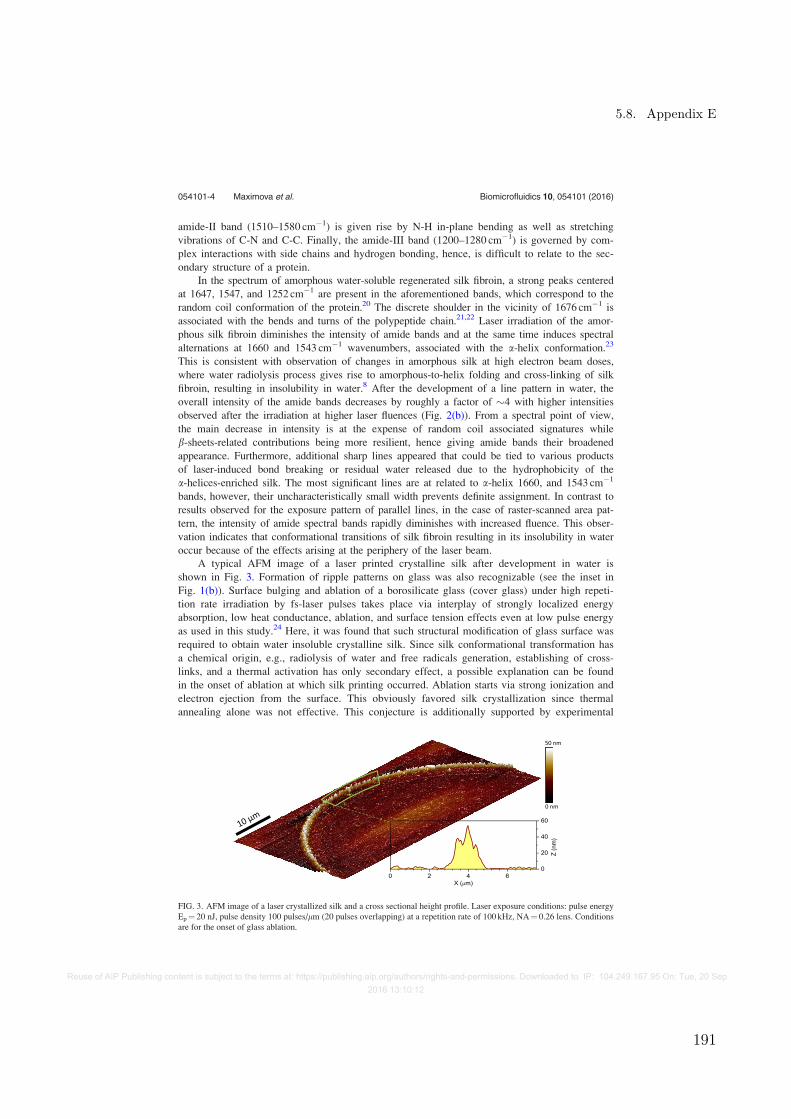
amide-II band (1510–1580 cm�1) is given rise by N-H in-plane bending as well as stretching
vibrations of C-N and C-C. Finally, the amide-III band (1200–1280 cm�1) is governed by com-
plex interactions with side chains and hydrogen bonding, hence, is difficult to relate to the sec-
ondary structure of a protein.
In the spectrum of amorphous water-soluble regenerated silk fibroin, a strong peaks centered
at 1647, 1547, and 1252 cm�1 are present in the aforementioned bands, which correspond to the
random coil conformation of the protein.20 The discrete shoulder in the vicinity of 1676 cm�1 is
associated with the bends and turns of the polypeptide chain.21,22 Laser irradiation of the amor-
phous silk fibroin diminishes the intensity of amide bands and at the same time induces spectral
alternations at 1660 and 1543 cm�1 wavenumbers, associated with the a-helix conformation.23
This is consistent with observation of changes in amorphous silk at high electron beam doses,
where water radiolysis process gives rise to amorphous-to-helix folding and cross-linking of silk
fibroin, resulting in insolubility in water.8 After the development of a line pattern in water, the
overall intensity of the amide bands decreases by roughly a factor of �4 with higher intensities
observed after the irradiation at higher laser fluences (Fig. 2(b)). From a spectral point of view,
the main decrease in intensity is at the expense of random coil associated signatures while
b-sheets-related contributions being more resilient, hence giving amide bands their broadened
appearance. Furthermore, additional sharp lines appeared that could be tied to various products
of laser-induced bond breaking or residual water released due to the hydrophobicity of the
a-helices-enriched silk. The most significant lines are at related to a-helix 1660, and 1543 cm�1
bands, however, their uncharacteristically small width prevents definite assignment. In contrast to
results observed for the exposure pattern of parallel lines, in the case of raster-scanned area pat-
tern, the intensity of amide spectral bands rapidly diminishes with increased fluence. This obser-
vation indicates that conformational transitions of silk fibroin resulting in its insolubility in water
occur because of the effects arising at the periphery of the laser beam.
A typical AFM image of a laser printed crystalline silk after development in water is
shown in Fig. 3. Formation of ripple patterns on glass was also recognizable (see the inset in
Fig. 1(b)). Surface bulging and ablation of a borosilicate glass (cover glass) under high repeti-
tion rate irradiation by fs-laser pulses takes place via interplay of strongly localized energy
absorption, low heat conductance, ablation, and surface tension effects even at low pulse energy
as used in this study.24 Here, it was found that such structural modification of glass surface was
required to obtain water insoluble crystalline silk. Since silk conformational transformation has
a chemical origin, e.g., radiolysis of water and free radicals generation, establishing of cross-
links, and a thermal activation has only secondary effect, a possible explanation can be found
in the onset of ablation at which silk printing occurred. Ablation starts via strong ionization and
electron ejection from the surface. This obviously favored silk crystallization since thermal
annealing alone was not effective. This conjecture is additionally supported by experimental
FIG. 3. AFM image of a laser crystallized silk and a cross sectional height profile. Laser exposure conditions: pulse energy
Ep¼ 20 nJ, pulse density 100 pulses/lm (20 pulses overlapping) at a repetition rate of 100 kHz, NA¼ 0.26 lens. Conditions
are for the onset of glass ablation.
054101-4 Maximova et al. Biomicrofluidics 10, 054101 (2016)
Reuse of AIP Publishing content is subject to the terms at: https://publishing.aip.org/authors/rights-and-permissions. Downloaded to IP: 104.249.167.95 On: Tue, 20 Sep2016 13:10:12
5.8. Appendix E
191

observation of only 20-nm-thick crystalline silk pattern out of the initial �250-nm amorphous
film as well as by the stronger spectral signature of parallel lines exposed patterns comparing to
raster-scanned areas.
Crystallized b-sheets-enriched water-insoluble silk fibroin films obtained through the
methanol-ethanol treatment followed by the water vapor annealing were exposed to the fs-laser
operating at 100 kHz repetition rate. Laser patterning results in a precise removal and stripping
silk from substrate (Fig. 4). Following water development practically did not change the depth
of the lines. The spectra do not change after the laser irradiation either. The direct ablation of
silk has no damage to the protein structure of the remaining film. Very similar results on laser
crystallization and ablation of the crystalline film were observed for A. pernyi fibroin.Inherent constraint in laser printing or ablation of thin <k/4 films is due to the light inten-
sity maximum being at k/4 distance above the surface (for light incident from the air onto
sample). This limits efficiency of light energy delivery by linear or nonlinear absorption to the
interface region, silk in this case. Using a polarization grating, interference effects, non-
paraxiality and a longitudinal E-field component, or back-side illumination, it is possible to
bring a higher light intensity to the interface.25,26 Follow-up experiments are planned to explore
high irradiance delivery exactly at the interface between the glass substrate and silk.
IV. CONCLUSIONS
Laser printing of micrometer-wide of crystalline silk is demonstrated using fs-laser expo-
sure of pure amorphous fibroin films of �250 nm in thickness. This is realization of a negative
tone photo-resist without use of any photo-initiator. Very similar patterns can be created by fs-
laser ablation of crystallized water-insoluble silk films. It is shown that laser exposure induces
the local conformational transformation from random coils to a-helices of silk-I with a fraction
of b-sheets. These changes lead to the modification of solubility in water. It opens the possibil-
ity for the laser printing of protein-based water-insoluble structures starting from regenerated
silk fibroin. Laser writing/printing of silk patterns for functionalization of sensor regions with
metal nanoparticles inside micro-sensor chips is expected to open a range of new capabilities in
bio-medical and micro-fluidic fields.
ACKNOWLEDGMENTS
K.M. was supported by the Australian Research Council’s Endeavour Research Fellowship
grant. S.J. is grateful for partial support via the Australian Research Council DP130101205
FIG. 4. Topology of the crystalline silk film laser ablated (a) and subsequently water washed (b). Laser exposure condi-
tions: pulse energy Ep¼ 22 nJ, pulse density 100 pulses/lm (20 pulses overlapping) at a repetition rate of 100 kHz,
NA¼ 0.26 lens.
054101-5 Maximova et al. Biomicrofluidics 10, 054101 (2016)
Reuse of AIP Publishing content is subject to the terms at: https://publishing.aip.org/authors/rights-and-permissions. Downloaded to IP: 104.249.167.95 On: Tue, 20 Sep2016 13:10:12
Chapter 5. Plasmonic nano-printing for surface structuring
192

Discovery project and toWoP—Workshop of Photonics, Ltd. for a technology transfer project. This
work was part of Melbourne synchrotron beamtime proposal 10457 in 2016 and the nanotechnology
ambassador fellowship program at the Melbourne Centre for Nanofabrication (MCN) in the
Victorian Node of the Australian National Fabrication Facility (ANFF).
1M. Malinauskas, A. �Zukauskas, S. Hasegawa, Y. Hayasaki, V. Mizeikis, R. Buividas, and S. Juodkazis, Light: Sci. Appl.5, e16133 (2016).
2M. Malinauskas, M. Farsari, A. Piskarskas, and S. Juodkazis, Phys. Rep. 533, 1 (2013).3S. Rek�styt _e, M. Malinauskas, and S. Juodkazis, Opt. Express 21, 17028 (2013).4M. Malinauskas, A. �Zukauskas, G. Bickauskait _e, R. Gadonas, and S. Juodkazis, Opt. Express 18, 10209 (2010).5Y. Hu, Q. Zhang, R. You, L. Wang, and M. Li, Adv. Mat. Sci. Eng. 2012, 185905 (2012).6G. Li, Y. Li, G. Chen, J. He, Y. Han, X. Wang, and D. L. Kaplan, Adv. Healthcare. Mater. 4, 1134 (2015).7K. Tsioris, G. E. Tilburey, A. R. Murphy, P. Domachuk, D. L. Kaplan, and F. G. Omenetto, Adv. Funct. Mater. 20, 1083(2010).
8S. Kim, B. Marelli, M. A. Brenckle, A. N. Mitropoulos, E.-S. Gil, K. Tsioris, H. Tao, D. L. Kaplan, and F. G. Omenetto,Nat. Nanotechnol. 9, 306 (2014).
9J. Morikawa, M. Ryu, K. Maximova, A. Balcytis, G. Senuitinas, L. Fan, V. Mizeikis, J. Li, X. Wang, M. Zamengo, X.Wang, and S. Juodkazis, RSC Adv. 6, 11863 (2016).
10S. Asha, Y. Sangappa, and S. Ganesh, J. Spectrosc. 2015, 879296 (2015).11P. Cebe, X. Hu, D. L. Kaplan, E. Zhuravlev, A. Wurm, D. Arbeiter, and C. Schick, Sci. Rep. 3, 1130 (2013).12S. Lazare, A. Sionkowska, M. Zaborowicz, A. Planecka, J. Lopez, M. Dijoux, C. Loum�ena, and M. C. Hernandez, Appl.Phys. A 106, 67 (2012).
13Y.-L. Sun, Q. Li, S.-M. Sun, J.-C. Huang, B.-Y. Zheng, Q.-D. Chen, Z.-Z. Shao, and H.-B. Sun, Nat. Commun. 6, 8612(2015).
14A. �Zukauskas, M. Malinauskas, A. Kadys, G. Gervinskas, G. Seniutinas, S. Kandasamy, and S. Juodkazis, Opt. Express21, 6901 (2013).
15S. Yan, C. Zhao, X. Wu, Q. Zhang, and M. Li, Sci. China Chem. 53, 535 (2010).16S. Ling, Z. Qi, D. P. Knight, Y. Huang, L. Huang, H. Zhou, Z. Shao, and X. Chen, Biomacromolecules 14, 1885 (2013).17S. Du, J. Li, J. Zhang, and X. Wang, Mater. Des. 65, 766 (2015).18H. Tao, D. L. Kaplan, and F. G. Omenetto, Adv. Mater. 24, 2824 (2012).19S. Rek�styt _e, T. J. D. Gailevicius, M. Malinauskas, V. Mizeikis, E. G. Gamaly, and S. Juodkazis, Adv. Opt. Mater. 4, 1209(2016).
20M. Boulet-Audet, F. Vollrath, and C. Holland, J. Exp. Biol. 218, 3138 (2015).21X. Hu, K. Shmelev, L. Sun, E.-S. Gil, S.-H. Park, P. Cebe, and D. L. Kaplan, Biomacromolecules 12, 1686 (2011).22Handbook of Fiber Chemistry, edited M. Lewin (Taylor & Francis Group, Boca Raton, FL, 2007).23H. Teramoto and M. Miyazawa, Biomacromolecules 6, 2049 (2005).24E. Vanagas, I. Kudryashov, D. Tuzhilin, S. Juodkazis, S. Matsuo, and H. Misawa, Appl. Phys. Lett. 82, 2901 (2003).25H. Iwase, S. Kokubo, S. Juodkazis, and H. Misawa, Opt. Express 17, 4388 (2009).26S. Jayawardhana, L. Rosa, S. Juodkazis, and P. R. Stoddart, Sci. Rep. 3, 2335 (2013).
054101-6 Maximova et al. Biomicrofluidics 10, 054101 (2016)
Reuse of AIP Publishing content is subject to the terms at: https://publishing.aip.org/authors/rights-and-permissions. Downloaded to IP: 104.249.167.95 On: Tue, 20 Sep2016 13:10:12
5.8. Appendix E
193

1Scientific REPORTS | 7: 7419 | DOI:10.1038/s41598-017-07502-3
www.nature.com/scientificreports
Orientational Mapping Augmented Sub-Wavelength Hyper-Spectral Imaging of SilkMeguya Ryu1, Armandas Balčytis2,3, Xuewen Wang2, Jitraporn Vongsvivut4, Yuta Hikima5, Jingliang Li6, Mark J. Tobin 4, Saulius Juodkazis2,7,8 & Junko Morikawa4
Molecular alignment underpins optical, mechanical, and thermal properties of materials, however, its direct measurement from volumes with micrometer dimensions is not accessible, especially, for structurally complex bio-materials. How the molecular alignment is linked to extraordinary properties of silk and its amorphous-crystalline composition has to be accessed by a direct measurement from a single silk fiber. Here, we show orientation mapping of the internal silk fiber structure via polarisation-dependent IR absorbance at high spatial resolution of 4.2 μm and 1.9 μm in a hyper-spectral IR imaging by attenuated total reflection using synchrotron radiation in the spectral fingerprint region around 6 μm wavelength. Free-standing longitudinal micro-slices of silk fibers, thinner than the fiber cross section, were prepared by microtome for the four polarization method to directly measure the orientational sensitivity of absorbance in the molecular fingerprint spectral window of the amide bands of β-sheet polypeptides of silk. Microtomed lateral slices of silk fibers, which may avoid possible artefacts that affect spectroscopic measurements with fibers of an elliptical cross sections were used in the study. Amorphisation of silk by ultra-short laser single-pulse exposure is demonstrated.
The infra-red (IR) spectral region from 3–10 μm, referred to as the fingerprint region, is used for the quantitative analysis of molecular species in a wide range of applications spanning fields of climate change1, environmental monitoring2, bio-medical3, material science4, and security5. All imaging methods have mounting challenges to characterise volumes with cross sections approaching the wavelength of the utilised light. In the UV-visible and IR spectral domains, near-field techniques using sharp nano-tips and plasmonic enhancement are used to reach nanoscale spatial resolutions, usually at the expense of polarisation information. However the application of polarised light permits analysis of the molecular orientation and chirality, which define mechanical, thermal, and optical properties6. At different wavelengths it is possible to access orientational information of hierarchical structures which underpins mechanical material properties and could be harnessed by engineering their artificial counterparts4.
Fourier transform IR (FT-IR) spectroscopy, when combined with a microscope accessory, provides hyper-spectral imaging when spectrally broadband or wavelength-tunable excitation sources are utilised. In the IR spectral range, a combination of sub-wavelength spatial resolution to characterise the anisotropy of absorb-ance due to local molecular orientation and spatial 2D (3D) mapping would enhance current analytical tech-niques and has high potential in material and bio-medical fields. In addition the use of a synchrotron beam offers highly collimated IR radiation with 102–103 times higher brightness than that available from laboratory-based IR sources (Globar®). Such a unique characteristic enables the acquisition of high-quality FT-IR spectra at diffraction-limited spatial resolution, making synchrotron-IR microspectrscopy an excellent analytical plat-form for acquiring spatially resolved chemical images of materials at a lateral resolution between 3–10 μm. Using
1Tokyo Institute of Technology, Meguro-ku, Tokyo, 152-8550, Japan. 2Nanotechnology facility, Center for Micro-Photonics, Swinburne University of Technology, John st., Hawthorn, Victoria, 3122, Australia. 3Department of Laser Technologies, Center for Physical Sciences and Technology, Savanoriu Ave. 231, LT-02300, Vilnius, Lithuania. 4Infrared Microspectroscopy Beamline, Australian Synchrotron, Clayton, Victoria, 3168, Australia. 5Department of Chemical Engineering, Graduate School of Engineering, Kyoto University, Nishikyo-ku, Kyoto, 615-8510, Japan. 6Institute for Frontier Materials, Deakin University, Waurn Ponds, Victoria, 3217, Australia. 7Center of Nanotechnology, King Abdulaziz University, Jeddah, 21589, Saudi Arabia. 8Melbourne Center for Nanofabrication, Australian National Fabrication Facility, Clayton, 3168, Australia. Correspondence and requests for materials should be addressed to S.J. (email: [email protected]) or J.M. (email: [email protected])
Received: 15 March 2017
Accepted: 28 June 2017
Published: xx xx xxxx
OPEN
Chapter 5. Plasmonic nano-printing for surface structuring
194
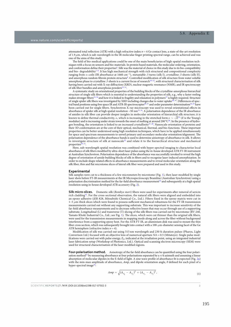
www.nature.com/scientificreports/
2Scientific REPORTS | 7: 7419 | DOI:10.1038/s41598-017-07502-3
attenuated total reflection (ATR) with a high refractive index n = 4 Ge contact lens, a state-of-the-art resolution of 1.9 μm, which is sub-wavelength in the IR molecular finger printing spectral range, can be achieved and was one of the aims of this study.
The field of bio-medical applications could be one of the main beneficiaries of high-spatial resolution tech-niques with a focus on sensors and bio-materials. In protein based materials, the molecular ordering, orientation, and conformation define their properties6. Silk was the material of choice in this study due to its bio-compatibility and bio- degradability7, 8. It has high mechanical strength with rich structural and compositional complexity ranging from α-coils (IR absorbance at 1660 cm−1), metastable β-turns (silk I), crystalline β-sheets (silk II), and amorphous random fibroin protein structure9. Controlled modification of silk structure from water soluble amorphous phase to crystalline β-sheets is a current focus of research10–12, with structural characterisation of silk having been carried out with X-ray diffraction (XRD), nuclear magnetic resonance (NMR), and IR spectroscopy of silk fiber bundles and amorphous powders13, 14.
A systematic study on orientational properties of the building blocks of the crystalline-amorphous hierarchial structure of single silk fibers which is essential to understanding the properties of silk, e.g., why a faster reeling makes stronger fibers15, 16 and how it is linked to fragility and relaxation in polymers17 is highly required. Structure of single spider silk fibers was investigated by XRD including changes due to water uptake18, 19. Differences of spec-tral band positions using free space IR and ATR-IR spectroscopies20, 21 and order parameter determination22, 23 have been carried out for single fibers. Synchrotron X-ray microscopy was used to reveal orientational effects in absorbance of spider silk at high spatial resolution ~50 nm23, 24. A polarisation dependence of the IR absorbance of amides in silk fiber can provide deeper insights in molecular orientation of hierarchial silk structure; it is known to define thermal conductivity, κ, which is increasing in the stretched form κ ∼ E 25 (E is the Young’s modulus) and is increasing under strain towards the onset of melting at around 200 °C26. In the presence of hydro-gen bonding, the orientation is linked to an increased crystallinity27, 28. Nanoscale orientation of proteins and their 3D conformation are at the core of their optical, mechanical, thermal, and bio-functions. These important properties can be better understood using high resolution techniques, which have to be applied simultaneously for space and spectrum measurements to unveil primary and secondary molecular orientation/alignment. The polarisation dependence of the absorbance bands is used to determine anisotropy of absorbance in silk. It allows to investigate structure of silk at nanoscale22 and relate it to the hierarchical structure and mechanical properties29–31.
Here, sub-wavelength spatial resolution was combined with hyper-spectral imaging to characterise local absorbance of silk fibers modified by ultra-short laser pulses using the in-house developed ATR FT-IR instrument at Australian Synchrotron. Polarisation dependence of the absorbance was successfully invoked to reveal the high degree of orientation of amide building blocks of silk in fibers and to recognise laser-induced amorphisation. In order to exclude shape related effects in absorbance measurements and to reveal molecular orientation along the silk fiber, thin and flat microtome slices of lateral silk fiber were prepared and used in this study.
ExperimentalSilk samples were cut to a thickness of a few micrometers by microtome (Fig. 1), then laser modified by single laser shots before FT-IR measurements at the IR Microspectroscopy Beamline (Australian Synchrotron) using a polarisation discrimination method for the far-field absorbance measurement32 and subsequently at a high spatial resolution using in-house developed ATR accessory (Fig. 2).
Silk micro-slices. Domestic silk (Bombyx mori) fibers were used for experiments after removal of sericin rich cladding12. For the cross-sectional observation, the natural silk fibers were aligned and embedded into an epoxy adhesive (jER 828, Mitsubishi Chemical Co., Ltd.). Fibers fixed in the epoxy matrix were cut in 1–5 μm-thick slices which were found to possess sufficient mechanical robustness for the FT-IR transmission measurements carried out without any supporting substrate. This was important to increase sensitivity of the far-field absorbance measurements and to decrease reflective losses that may occur through use of a supporting substrate. Longitudinal (L) and transverse (T) slicing of the silk fibers was carried out by microtome (RV-240, Yamato Khoki Industrial Co., Ltd.; see Fig. 1). The slices, which were cut thinner than the original silk fibers, were used for the transmission measurements in mapping mode along and across the fiber without background interference from a supporting epoxy host. For the ATR FT-IR, an aluminium disk was used to mount the thin fiber cross section, which was subsequently brought into contact with a 100-μm-diameter sensing facet of the Ge ATR hemisphere (refractive index n = 4).
Modification of silk was carried out using 515 nm wavelength and 230 fs duration pulses (Pharos, Light Converison Ltd.) focused with an objective lens of numerical aperture NA = 0.5 (Mitutoyo). Single pulse mod-ifcations were carried out with pulse energy, EP, indicated at the irradiation point, using an integrated industrial laser fabrication setup (Workshop of Photonics, Ltd.). Optical and scanning electron microscopy (SEM) were used for structural characterisation of the laser modified regions.
Four-polarisation method. Anisotropy of the far-field absorbance can be quantified using the four polari-sation method32 by measuring absorbance at four polarisations separated by a π/4 azimuth and assuming a linear absorption of molecular dipoles in the E-field of light. A sine wave profile of absorbance fit is expected (Fig. 2a) with the min-max amplitude of absorbance, Amp, and dipole orientation angle, θ defined for each pixel of a hyper-spectral image32:
= − + −φ φ φ φAmp A A A A( ) ( ) , (1)2 2
4 2 3 1
5.8. Appendix E
195

www.nature.com/scientificreports/
3Scientific REPORTS | 7: 7419 | DOI:10.1038/s41598-017-07502-3
θ =
−
−
φ φ
φ φ
−A A
A A12
tan ,(2)
1 3 1
4 2
where φA1,2,3,4
are absorbance at the four polarisation azimuths separated by π/4; Amp = Amax − Amin is defined by the maximum and minimum absorbances.
This four-polarisation method was implemented using a Cassegrainian FT-IR objective with the linear polarisation set right at the entrance of the objective lens by a wire-grid polariser. To test the validity of the four-polarisation method for this geometry, where two reflections on curved mirrors are encountered by linearly polarised incident beam in the Cassegrainian optic, a circular grating reference sample was made by electron beam lithography (EBL; ACE-7000/EBU, Sanyu Electron Ltd.) and a standard lift-off method. A 30 nm-thick Au coating was thermally evaporated on a 10 nm adhesion layer of Cr on a cover glass for the lift-off over the EBL defined circular pattern in ZEP520 resist; diameter of the circular grating was 0.5 mm. The grating with a width of Au rings of 1 μm and period of 2 μm represents a reflective sub-wavelength pattern of a constantly changing ori-entation at the IR wavelength of 1500 cm−1 or ~6.7 μm (Fig. 2b). By setting four polarisations with a π/4 separa-tion at incidence, the reflection maps from the circular grating measured with Spotlight, PerkinElmer are shown in Fig. 2b. Angular integration of the reflected intensity at any radial position closely followed the postulated sine wave rule (Fig. 2a); e.g., the four selected angle positions on the reflection maps are marked by φ1,2,3,4 and follow intensity changes by the sine wave form. The strongest reflection was observed for the polarisation which is tan-gential to the circumference of the grating ring pattern.
High spatial resolution FT-IR spectroscopy. The far-field transmission measurements were carried out with a NA = 0.5 and 36× magnification Cassegrainian objective lens. A wire-grid ZnSe polariser was used to set linear polarisation (Specac Ltd., Kent, UK).
Synchrontron IR microspectroscopic measurement was performed using a Bruker Hyperion 2000 FT-IR microscope (Bruker Optik GmbH, Ettlingen, Germany) coupled to a Vertex V80v FT-IR spectrometer, and equipped with a liquid nitrogen-cooled narrow-band mercury cadmium telluride (MCT) detector. As illustrated in Fig. 2c the in-house developed ATR FT-IR accessory equipped with a 100-μm-diameter facet Ge ATR crystal was used to acquire chemical images of the silk cross sections at a high speed and a spatial resolution down to 1.9 μm33. The Ge contact lens of ψ= .NA nsin 2 4 was used with n = 4 and the ψ = 36.9° half-angle of the focusing cone. Deep sub-wavelength resolution λ µ= . .r NA0 61 / 1 5IR m is achievable for the IR wavelengths of interest at the
Figure 1. (a) Longitudinal (L) and transverse (T) 5–10 μm-thin slices of silk embedded in epoxy were used for FT-IR micro-spectroscopic characterisation. Cross-polarised optical image of the sliced silk fiber obtained with a waveplate (λ) shifter. Sample preparation: silk fiber was aligned and epoxy embedded, microtome sliced for L and T directions. (b) SEM image of a single laser pulse melted silk; laser wavelength 515 nm, pulse duration 230 fs, focused with objective lens with numerical aperture NA = 0.5, pulse energy 85 nJ, linear polarisation was along the fiber (marked by arrow).
Chapter 5. Plasmonic nano-printing for surface structuring
196

www.nature.com/scientificreports/
4Scientific REPORTS | 7: 7419 | DOI:10.1038/s41598-017-07502-3
Figure 2. (a) Four-polarisation method in IR absorbance at different polarisation azimuths, A = f(Θ)32, which was used to determine the orientational anisotropy in far-field FT-IR measurements. (b) An optical image of a concentric 2-μm-period Au grating (with a duty cycle of 0.5) on a cover glass used for reflection FT-IR imaging carried out with a Cassegrainian objective lens with a focusing cone over a 17-to −30° range; dashed-line marks the top-view of the incidence plane. The diameter of the circular grating was 0.5 mm. Four reflection maps for a linearly polarised incidence at the specified polarisation angle (schematically also marked by arrows) at 1500 cm−1 (~6.7 μm) wavelength (Spotlight, PerkinElmer); IR,0 are the reflected and incidence intensities, respectively. (c) In-house developed ATR accessory for Hyperion 2000, Bruker microscope. Inset shows schematic illustration of optical geometry used in the ATR FT-IR measurement with a 100-μm diameter Ge tip (refractive index n = 4).
5.8. Appendix E
197

www.nature.com/scientificreports/
5Scientific REPORTS | 7: 7419 | DOI:10.1038/s41598-017-07502-3
amide band of λIR = 1600 − 1700 cm−1 or 6.25–5.9 μm. Use of the solid immersion lens also leads to a reduction of the mapping step size by ~4 times relative to the stage step motion and was 250 nm.
ResultsPolarisation dependence at single point. Figure 3 shows absorbance of silk measured in transmis-sion for four different azimuthal orientations of the linear polarisation with an angular separation of π/4 for silk (Bombyx mori) from laser exposed (a) and un- treated (b) regions. A xy-array of laser irradiated spots at 8.5 nJ/pulse was patterned with 2μm period while the IR spectra were acquired from a 4.2 μm spot. The Amide I and II regions34 were investigated for structural and compositional changes induced by laser irradiation. The Amide II band at 1508 cm−1 is assigned to β-sheet secondary structure, whilst the peak at 1546 cm−1 is associated with disordered (amorphous) fibroin. The Amide I band follows a similar distribution with components at ~ 1625 cm−1 (β-sheets) and 1648 cm−1, which are associated with irregular structures including random coil and extended chains34. Other characteristic bands are associated with Silk I, type II β-turns (1647–1654 cm−1), α-coils (1658–1664 cm−1) as well as turns and bends 1699 cm−135.
Laser irradiation was found to strongly affect the sharp absorbance peak at 1700 cm−1 when laser pulse energy was exceeding the threshold of structural damage at
E 8p nJ for the used focusing (Fig. 3). This is indicative of amorphisation, which would be expected based on the observed changes in the SEM images of the laser exposed silk shown in Fig. 1b. A distinct polarisation dependence was also observed, as expected from a crystalline rich (~85%) silk fibers at the β-sheet Amide I band. The strongest absorbance at the Amide II (C-N) stretching band at 0° polarisation corresponded to the C-N bond, which is aligned along the fiber direction. The Amide I (C=O) stretching band, on the other hand, showed an inverse correlation with the polarised absorbance spectrum of the Amide II band which was strongest at the perpendicular polarisation (Fig. 3) as expected from previous Raman scattering studies36. The N-H stretching band showed the same polarisation dependence as the C=O stretching band. Due to such unique and strong polarisation dependence of the absorbance at a single spot (Fig. 3), the far-field transmission measurement in the mapping mode was subsequently performed to gain additional insights into molecular orientation/alignment along the length of silk fibers made accessible via microtomed L cross sections.
Molecular orientation in silk: far-field case. The four polarisations method was applied to reveal ori-entational association of the amide bands using Eqns. 1 and 2. Figure 4 shows the chemical maps of the L cross section of silk fiber with measured ~4.2μm spatial resolution (NA = 0.5). Mapping data (as measured) are visual-ised by overlaying absorbance at the selected wavenumber values of Amide II and Amide A at 1512 cm−1 and 3288 cm−1, respectively. The corresponding vector plot (markers’ length Eqn. 1 and orientation Eqn. 2) revealed that the orientation is horizontal and the amplitude Amp is proportional to the length of the bar-marker (θ = 0° is horizontal). The vector plot represents a background-free component of absorbance change caused by a change in molecular alignment. Perpendicular orientation between C=O and C-N bonds observed in the single spot
Figure 3. Polarisation discriminated absorbance spectra of pristine (a) and laser 515 nm/230 fs irradiated (b) silk fiber; laser pulse energy was 8.5 nJ and pulse-to-pulse separation of 2 μm in xy-array. Area of laser patterning was 10 × 10 μm2; IR beam diameter at focus on the sample was 4.2 μm.
Chapter 5. Plasmonic nano-printing for surface structuring
198

www.nature.com/scientificreports/
6Scientific REPORTS | 7: 7419 | DOI:10.1038/s41598-017-07502-3
spectrum (Fig. 3) has been confirmed for the non-irradiated silk regions (Fig. 4(b) vs (c)). Nevertheless, some of the Amide II bands present in the epoxy matrix were found to possess a random orientation.
To quantify the order the standard second momentum P2(θ) of the orientation function also known as the Herman’s function can be expressed via the absorbance ratio at two perpendicular linear polarisations, the dichroic ratio, = ° °D A A/0 90 (see Supplement for details) as32, 37:
θθ
=−
P ( )3 cos 1
2, (3)2
2
where θ is the angle between the transition dipole moment and the selected orientation (along silk fiber). The second momentum of the C=O (Amide I) band was found P2(θ) = −0.36 from the Raman measurements36 (−0.5 corresponds to a pure perpendicular orientation to the fiber axis). A slightly less ordered C=O bonds were determined in this study with P2(θ) = −0.29 ± 0.026 (see, Supplement for details). The difference can be accounted by a fiber caused anisotropic diffraction in the case of Raman measurements while a flat cross section was used in this study. The order analysis reveals that silk fibers are up to ~60% crystalline (see, Supplement) which is approximately twice larger than observed by synchrotron FT-IR in regenerated silk fibroin after crystal-lisation in alcohol bath ~28%38.
High resolution ATR mapping. The highest spatial resolution was achieved using ATR FT-IR, with a NA = 2.6 focus, realised using the combination of a germanium solid immersion lens of n = 4, with a Cassegrainian objective of NA = 0.6 and 20× magnifcation. Although no polariser was used for the mapping, synchrotron beam had a dominant s-polarised linear component. It should be emphasised, that in addition to the enhanced lateral spatial resolution this ATR FT-IR optical configuration offered high surface sensitivity due to a low penetration depth of 0.5 μm of the IR radiation at the amide I absorption peak. Figure 5 shows the highest spatial resolution µ.r 1 9 m chemical maps of the L section of silk at a few spectral regions of interest selected
Figure 4. (a) An optical image of the L cross section of a Bombyx mori silk fiber with laser marked 20 × 20 μm2 regions and laser irradiated spots. The region mapped in (b,c) is shown in a solid rectangle in (a). (b,c) Orientation vector map (marker’s length Eqn. 1 and orientation Eqn. 2) overlayed with the far-field absorbance (color map) at the C-N (b) and N-H (c) bands; these bonds are known to be perpendicular. S-polarised incident light was perpendicular to the fiber; in the plane of image.
5.8. Appendix E
199

www.nature.com/scientificreports/
7Scientific REPORTS | 7: 7419 | DOI:10.1038/s41598-017-07502-3
from a single hyper- spectral FT-IR data set. The Amide A (N-H) band appeared to have the most uniform distri-bution across the fiber compared to those of the Amide I (C=O) and β- sheet, which were highly localised inside the core of the fiber. This could be rationalised by the low sensitivity of N-H absorption to a surrounding hierar-chial structure of the protein matrix, mainly, because of a low mass of hydrogen.
The distinct effect of laser irradiation on the molecular structure of silk fibers was revealed in this study for the first time by high-spatial resolution ATR FT-IR mapping of T-cross sections (Fig. 6). Single laser shots created an approximately 2 μm diameter ablation pits observable through both optical or/and SEM images (Fig. 4a). The pattern of irradiation spots was controlled with a high precision of ~50 nm. This was instrumental in identifying the irradiation locations on the absorbance maps (Fig. 6). Central localisation of β-sheets is well distinct in the T sectional images (Fig. 6).
The lowest laser pulse energy which made recognisable modifications to the fibres in a single shot was E 8 nJ. Spectral maps in Fig. 6a show that only modification at the Amide A band was observed after laser irra-
diation, while Amide I β-sheet structure was not affected. By doubling the laser pulse energy, the distribution of both the Amide A and I bands were found altered (Fig. 6b). This finding is consistent with the chemical bond strength which are 189 kJ/mol (Amide A) and 1076.5 kJ/mol (Amide I) in β-sheet, respectively40.
DiscussionSubstrate-free absorbance measurements of silk fibers, with lateral resolution defined by NA = 0.5 for the far-field transmission and NA = 2.4 for the ATR FT-IR hyper-spectral mapping, have shown consistency between spatial localisation of the Amide I and II bands in the silk fiber. The fiber core is β-sheet enriched, hence, crystalline, as revealed by L and T cross sections of silk fibers. Flat microtome slices eliminated fiber shape related optical distor-tions and allowed measurements of order parameters of the amide bands (see, online supplement). Such L-cross sections can be also beneficial for determination of order parameters by Raman scattering.
The four polarisation method was adopted in transmission mode for the high-brightness synchrotron IR radi-ation and applied to the L section of silk fibers to reveal unambiguously the orientational structure of the amide bands as illustrated in Fig. 7. The Amide A (N-H) and amide I (C=O) have slightly different P2 order parameters. It was confirmed that Amide A and Amide II bands are perpendicular (see, online supplement). The spatial mapping functionality demonstrated in this study possesses a capability to reveal silk amorphisation mechanisms activated by application of tightly focused ultra-short laser pulses. This distinct laser irradiation is required for a fast thermal quenching in excess of 2 × 10³ K/s for solidification of amorphous silk melts11. Understanding the mechanisms of amorphous fibroin crystallisation induced by ultra-short laser pulses at the ablation threshold of glass substrate12 requires structural sensitivity at high spatial resolution to confirm the role of electron avalanche in the formation of crystalline β-sheets in direct laser printing41. The 3D laser printing of silk scaffolds by a direct
Figure 5. High resolution 1.9 μm ATR FT-IR maps at 1.9 μm resolution of the longitudinal (L) cross sections of silk presented in auto-scale for better viewing; a background-corrected absorbance is ranging from 0 to approximately 0.2. Lateral step size between pixels was 0.5 μm; as-measured pixelated absorbance maps are presented. Polarisation of incident light onto ATR prism was s (in the plane of image; along y-axis).
Chapter 5. Plasmonic nano-printing for surface structuring
200
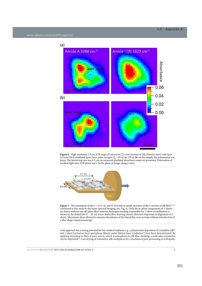
www.nature.com/scientificreports/
8Scientific REPORTS | 7: 7419 | DOI:10.1038/s41598-017-07502-3
write approach has a strong potential for bio-medical implants, e.g., a plasma laser deposition of crystalline silk42 and β-sheet formation form amorphous fibroin under 266 nm laser irradiation43 have been demonstrated. By applying stretching to films of pure sericin, which is amorphous in silk fiber cladding, a molecular orientation can be imprinted44. Cast-drying of volumetric silk workpieces for a mechanical post-processing in orthopedic
Figure 6. High resolution 1.9 μm ATR maps of transverse (T) cross sections of silk (Bombyx mori) with laser 515 nm/230 fs irradiated spots; laser pulse energies, Ep = 85 nJ (a) 170 nJ (b) on the sample; the polarisation was linear. The lateral step size was 0.5 μm; as-measured pixelated absorbance maps are presented. Polarisation of incident light onto ATR prism was s (in the plane of image; along y-axis).
Figure 7. The orientation of the C = O, C-N, and N-H bonds in amide structure of the L-section of silk fiber23, 39 confirmed in this study by the hyper-spectral imaging (see, Fig. 4). Only the in-plane components of β-sheets are drawn without out-off-plane alkyl moieties; hydrogen bonding responsible for β-sheet crystallisation is shown by the dotted line O
H. An arrow marks fiber drawing (strain) direction important to alignment of β-sheets. Microtome slices allowed to measure absorbance of the lateral flat cross sections without introduction of a fiber shape related anisotropy.
5.8. Appendix E
201
www.nature.com/scientificreports/
9Scientific REPORTS | 7: 7419 | DOI:10.1038/s41598-017-07502-3
applications has been recently demonstrated with a need to control nano-/micro-structure for the required spe-cific strength and modulus (stiffness)45–49 which can also be controlled by molecular alignment.
ConclusionsHigh spatial resolution has been achieved in hyper-spectral imaging ATR FT-IR imaging as demonstrated by the ~1.9μm (NA = 2.4) resolution chemical imaging of silk at λ µ 6IR m wavelengths. It is shown that the four polarisation method can be effectively used to reveal a prevalent orientational ordering using far-field IR absorb-ance mapping. In silk, a strong correlation between orthogonal dipole transition of C=O and C-N bonds has been confirmed. The order parameters of the amides was determined using micro-thin flat longitudinal microtome slices. For the C=O, order parameter P2(θ) = −0.30 ± 0.04 is comparable with values obtained by different meth-ods22, 23, 36. This four polarisation method can be used to recognise laser induced amorphisation of silk. Amorphous silk is water soluble.
Insights into the orientational structure of biomaterials responsible for their optical, mechanical, and thermal properties is critical for applications and design of new materials. Here a direct absorbance measurement of ori-entation of the chemical bonding in silk at a record high spatial resolution is reported using synchrotron based ATR FT-IR microspectroscopy. This technique has been shown to possess potential as a powerful analytical tool for a wide range of applications capable of establishing the link between micro-/nano-structures and specific properties of biomaterials. Hyper-spectral ATR FT-IR imaging represents an additional tool to determine molec-ular orientation.
References 1. Yang, J. et al. The role of satellite remote sensing in climate change studies. Nature Climate Change 3, 875–883 (2013). 2. Lu, R. et al. High-sensitivity infrared attenuated total reflectance sensors for in situ multicomponent detection of volatile organic
compounds in water. Nature Protocols 11, 377–386 (2016). 3. Stanley, R. Plasmonics in the mid-infrared. Nature Photonics 6, 409–411 (2012). 4. Wegst, U. G. K., Bai, H., Saiz, E., Tomsia, A. P. & Ritchie, R. O. Bioinspired structural materials. Nature Materials 14, 23–36 (2015). 5. Schliesser, A., Picqué, N. & Hänsch, T. W. Mid-infrared frequency combs. Nature Photonics 6, 440–449 (2012). 6. Yoshioka, T., Tashiro, K. & Ohta, N. Molecular orientation enhancement of silk by the hot-stretching-induced transition from
a-helix-HFIP complex to β-sheet. Biomacromolecules 17, 1437–1448 (2016). 7. Tao, H., Kaplan, D. L. & Omenetto, F. G. Silk materials: A road to sustainable high technology. Adv. Mater. 24, 2824–2837 (2012). 8. Li, G. et al. Silk-based biomaterials in biomedical textiles and fiber-based implants. Adv. Healthcare. Materials 4, 1134–1151 (2015). 9. Liu, X. & Zhang, K.-Q. Silk Fiber - Molecular Formation Mechanism, Structure- Property Relationship and Advanced Applications
(Intech, 2014). 10. Qin, N. et al. Nanoscale probing of electron-regulated structural transitions in silk proteins by near-field IR imaging and nano-
spectroscopy. Nature Communications 7, 13079 (2016). 11. Cebe, P. et al. Beating the heat - fast scanning melts silk beta sheet crystals. Macromolecules 3, 1130 (2013). 12. Maximova, K. et al. Silk patterns made by direct femtosecond laser writing. Biomicrofluidics 10, 054101 (2016). 13. Asakura, T. & Miller, T. (eds) Biotechnology of silk. Biologically-inspired systems 5 (Springer Science + Business Media, Dordrecht),
(2014). 14. Balčytis, A. et al. Silk: Optical properties over 12.6 octaves THz-IR-Visible-UV range. Materials 10, 356 (2017). 15. Shao, Z. & Vollrath, F. Surprising strength of silkworm silk. Nature 418, 741 (2002). 16. Du, N. et al. Design of superior spider silk: From nanostructure to mechanical properties. Biophysical J. 91, 4528–4535 (2006). 17. Dalle-Ferrier, C. et al. Why many polymers are so fragile: A new perspective. J. Chem. Phys. 145, 154901 (2016). 18. Riekel, C. et al. Aspects of X-ray diffraction on single spider fibers. Int. J. Biological Macromolecules 24, 179–186 (1999). 19. Sampath, S. & Yarger, J. L. Structural hysteresis in dragline spider silks induced by supercontraction: an X-ray fiber micro-diffraction
study. RSC Advances 5, 1462–1473 (2015). 20. Boulet-Audet, M., Lefèvre, T., Buffeteau, T. & Pézolet, M. Attenuated total reflection infrared spectroscopy: An efficient technique
to quantitatively determine the orientation and conformation of proteins in single silk fibers 62, 956–962 (2008). 21. Boulet-Audet, M., Buffeteau, T., Boudreault, S., Daugey, N. & Pézolet, M. Quantitative determination of band distortions in diamond
attenuated total reflectance infrared spectra. J. Phys. Chem. B 114, 8255–8261 (2010). 22. Paquet-Mercier, F., Lefèvre, T., Augera, M. & Pézolet, M. Evidence by infrared spectroscopy of the presence of two types of β-sheets
in major ampullate spider silk and silkworm silk. Soft Matter 9, 208–215 (2013). 23. Hernández Cruz, D., Rousseau, M.-E., West, M. M., Pézolet, M. & Hitchcock, A. P. Quantitative mapping of the orientation of fibroin
β-sheets in B. mori cocoon fibers by scanning transmission X-ray microscopy. Biomacromolecules 7, 836–843 (2006). 24. Rousseau, M.-E., Hernández Cruz, D., Hitchcock, M. M. W. A. P. & Pézolet, M. Nephila clavipes spider dragline silk microstructure
studied by scanning transmission X-ray microscopy. J. Am. Chem. Soc. 129, 3897–3905 (2007). 25. Huang, X., Liu, G. & Wang, X. New secrets of spider silk: Exceptionally high thermal conductivity and its abnormal change under
stretching. Adv. Mater. 24, 1482–1486 (2012). 26. Martel, A., Burghammer, M., Davies, R. J. & Riekel, C. Thermal behavior of bombyx mori silk: Evolution of crystalline parameters,
molecular structure, and mechanical properties. Biomacromolecules 8, 3548–3556 (2007). 27. Zhang, L., Bai, Z., Ban, H. & Liu, L. Effects of the amino acid sequence on thermal conduction through β-sheet crystals of natural
silk protein. Phys. Chem. Chem. Phys. 17, 29007 (2015). 28. Zhang, L., Chen, T., Ban, H. & Liu, L. Hydrogen bonding-assisted thermal conduction in β-sheet crystals of spider silk protein.
Nanoscale 6, 7786 (2014). 29. Papadopoulos, P., Sölter, J. & Kremer, F. Structure-property relationships in major ampullate spider silk as deduced from polarized
FTIR spectroscopy. J. European Physical E 24, 193–199 (2007). 30. Papadopoulos, P., Sölter, J. & Kremer, F. Hierarchies in the structural organization of spider silk - a quantitative model. Colloid
Plymer Sci. 2, 231–236 (2009). 31. Ene, R., Papadopoulos, P. & Kremer, F. Combined structural model of spider dragline silk. Soft Matter 5, 4568–4574 (2009). 32. Hikima, Y., Morikawa, J. & Hashimoto, T. FT-IR image processing algorithms for in-plane orientation function and azimuth angle
of uniaxially drawn polyethylene composite film. Macromolecules 44, 3950–3957 (2011). 33. Vongsvivut, J. et al. Rapid determination of protein contents in microencapsulated fish oil supplements by ATR-FTIR spectroscopy
and partial least square regression (PLSR) analysis. Food Bioprocess Technol. 7, 265–277 (2014). 34. Taddei, P. & Monti, P. Vibrational infrared conformational studies of model peptides representing the semicrystalline domains of
bombyx mori silk fibroin. Biopolymers 78, 249–258 (2005). 35. Lu, Q. et al. Water-insoluble silk films with silk i structure. Acta Biomater. 6, 1380–1387 (2010).
Chapter 5. Plasmonic nano-printing for surface structuring
202

www.nature.com/scientificreports/
1 0Scientific REPORTS | 7: 7419 | DOI:10.1038/s41598-017-07502-3
36. Rousseau, M.-E., Lefevre, T., Beaulieu, L., Asakura, T. & Pezolet, M. Study of protein conformation and orientation in silkworm and spider silk fibers using Raman microspectroscopy. Biomacromolecules 5, 2247–2257 (2004).
37. Hikima, Y., Morikawa, J. & Hashimoto, T. Imaging of two-dimensional distribution of molecular orientation in poly(ethylene oxide) spherulite using IR spectrum and birefringence. Macromolecules 45, 8356–8362 (2012).
38. Ling, S., Qi, Z., Knight, D. P., Shao, Z. & Chen, X. Synchrotron FTIR microspectroscopy of single natural silk fibers. Biomacromolecules 12, 3344–3349 (2011).
39. Alberts, B. et al. Molecular Biology of the Cell, chap. 3. 2002, 4 edn (New York, Garland Science, 2002). 40. Haynes, W. M. (ed.) CRC Handbook of Chemistry and Physics, 94 edn (CRC Press, Boca Raton, 2016). 41. Malinauskas, M. et al. Ultrafast laser processing of materials: from science to industry. Light: Sci. Appl. 5, e16133 (2016). 42. Tsuboi, Y., Goto, M. & Itaya, A. Pulsed laser deposition of silk protein: Effect of photosensitized-ablation on the secondary structure
in thin deposited films. J. Appl. Phys. 89, 7917–7923 (2001). 43. Tsuboi, Y., Ikejiri, T., Shiga, S., Yamada, K. & Itaya, A. Light can transform the secondary structure of silk protein. Appl. Phys. A 73,
637–640 (2001). 44. Teramoto, H. & Miyazawa, M. Molecular orientation behavior of silk sericin film as revealed by ATR infrared spectroscopy.
Biomacromolecules 6, 20–2057 (2005). 45. Li, C. et al. Regenerated silk materials for functionalized silk orthopedic devices by mimicking natural processing. Biomaterials 110,
24–33 (2016). 46. Cunningham, A., Davis, G. R. & Ward, I. M. Determination of molecular orientation by polarized infra-red radiation in an oriented
polymer of high polarizability. Polymer 15, 743–748 (1974). 47. Cunningham, A., Ward, I. M., Wills, H. & Zichy, V. An infra-red spectroscopic study of molecular orientation and conformational
changes in poly(ethylene terephthalate). Polymer 15, 749–756 (1974). 48. Jarvis, D. A., Hutchinson, I. H., Bower, D. I. & Ward, I. M. Characterization of biaxial orientation in poly(ethylene terephthalate) by
means of refractive index measurements and raman and infra-red spectroscopies. Polymer 21, 41–54 (1980). 49. Bieri, M. & Burgi, T. Adsorption kinetics, orientation, and self-assembling of n-acetyl-l-cysteine on gold: A combined ATR-IR, PM-
IRRAS, and QCM study. Phys. Chem. B 109, 22476–22485 (2005).
AcknowledgementsJ.M. acknowledges a partial support by a JSPS KAKENHI Grant No. 16K06768. We acknowledge the Swinburne’s startup grant for Nanotechnology facility and partial support via ARC Discovery DP130101205 and DP170100131 grants. The synchrotron-IR experiments were performed through the merit-based access program (Proposal ID. M11119) for the provision of the synchrotron beamtime at the Australian Synchrotron IRM Beamline. Window on Photonics R&D, Ltd. is acknowledged for joint development grant and laser fabrication facility. We are grateful to Ryohei Kikuchi for help with microtome slices.
Author ContributionsS.J. and J.M. initiated synchrotron proposal, J.M. and M.R. proposed molecular alignment measurements, A.B., M.R., X.W.W., J.M., S.J. carried out experiment at Melbourne synchrotron on the beamline under supervision of J.V. and M.T., X.W.W. made laser irradiation of silk, M.R. carried our microtome and spectral analysis, Y.H. and J.M. developed the four polarisation method, silk samples were prepared in J.L. team. All the authors participated in discussion and analysis of the results and contributed to editing of the manuscript.
Additional InformationSupplementary information accompanies this paper at doi:10.1038/s41598-017-07502-3Competing Interests: The authors declare that they have no competing interests.Publisher's note: Springer Nature remains neutral with regard to jurisdictional claims in published maps and institutional affiliations.
Open Access This article is licensed under a Creative Commons Attribution 4.0 International License, which permits use, sharing, adaptation, distribution and reproduction in any medium or
format, as long as you give appropriate credit to the original author(s) and the source, provide a link to the Cre-ative Commons license, and indicate if changes were made. The images or other third party material in this article are included in the article’s Creative Commons license, unless indicated otherwise in a credit line to the material. If material is not included in the article’s Creative Commons license and your intended use is not per-mitted by statutory regulation or exceeds the permitted use, you will need to obtain permission directly from the copyright holder. To view a copy of this license, visit http://creativecommons.org/licenses/by/4.0/. © The Author(s) 2017
5.8. Appendix E
203

Chapter 5. Plasmonic nano-printing for surface structuring
204

Conclusions and Outlook
The thesis is presented as a set of of published papers reflecting major mile-stones of this PhD project. The overall goal of the project was to develop anddemonstrate different approached and techniques to utilize unique propertiesof ultrashort laser pulse interaction with materials to fabricate micro/nanophotonic devices for generating or manipulating the phase, polarization andintensity of light in the near and far fields.
The first chapter presents the advanced development of compact ultrafastsolid laser systems with high power, high repetition and ultrashort pulse dura-tion, which leads to the continuously reducing the photon-cost and facilitatesthe ultrafast laser material processing and micro machining industrial appli-cations especially the applications for micro/nano-photonics. The capabilitiesof femtosecond laser ablation for high precision micro and nano fabrication onvarious materials including metals with high thermal conductivity, soft mate-rials like biological tissues and hard or brittle materials such as semiconductorand insulators due to its non-thermal process with suppressed heat-affectedzone formation have been presented. A short review on metal drilling, 3Dcomplex structuring on glass and high resolution 3D photo-polymerization byfemtosecond laser direct writing has been presented. Series of complex energy-exchange processes that may lead to varying combinations of outcomes of atomdisplacement, amorphization, recrystallization, ablation, local modification ofelectronic structure, or change of material composition are initiated with thesingle or multiple photon electronic excitations by ultrafast laser material pro-cessing. These processes result to the final morphologies and material proper-ties of the irradiated area and are dependent on the fabrication conditions andmaterial properties.
The second chapter briefly introduces the Pharos femtosecond laser systemthat widely used in this PhD project, and few different type of fabrication ex-amples were introduced. Different nano-lithography and nanofabrication tech-niques were used in this project for different purposes have been introduced.The principles of photolithography, focused ion beam lithography (FIB), re-active ion etching (RIE) and physical vapor deposition (PVD), as well as thestructural characterization techniques such as scanning electron microscopy(SEM) and atomic force microscopy (AFM) have been presented. The opticallithography has been used and recipes have been developed for bactericidal
205

Conclusions and Outlook
microfluidc devices with integrated black silicon as seen in Appendix A1. Anintroduction on focused ion beam lithography has been presented which hasbeen used for cross sectioning on nanostructured surface by femtosecond laserirradiation such as the laser induced subwavelength ripples on silicon film andnano bumps on Au films to measure the structure depth and vertical profileas one example shows in Appendix E1. Bactericidal black silicon surfaces areprepared by reactive ion etching by employing self-induced micro masking tocreate randomly distributed nanoneedles on silicon wafer. The SEM, AFMand 3D optical profilometer were widely used in this project for morphologycharacterization.
The defects engineered by tightly focused femtosecond laser beam wasdemonstrated in the third chapter. The excitation of free electrons or furtherdisordering of the crystal lattice or glass matrix under the nonlinear photonabsorption process with intense photon flux irradiation can generate differenttype of defects or color centres inside the bulk or on the surface of the di-electrics, and thus changing the optical properties of the original materials.These properties can be applied to fabricate different functional optics or pho-tonic devices, like waveguides, micro resonators, microlasers or phase plates.The studies and achievements on laser induced defects have demonstrated theefficiency, cost-effectiveness and simple process on defects engineering com-paring to other techniques like electron bombarding, X-ray irradiation, ionimplanting, with its localized control with high spatial resolution and 3D ca-pabilities. Very high density of induced defects in KBr crystal, especially theV and F centres reaching 5.1×1018cm–3 and 5.3×1018cm–3 have benn createdby femtosecond laser irradiation. High density of E′ centres formed Si dan-gling bonds in fused silica have been created by femtosecond laser irradiationwith 1.9 × 1020cm–3 estimated from the ESR spectrum. Such high free elec-tron densities offer the opportunities theoretically to manipulate the transverseelectromagnetic field in THz range. The large modification on the refractiveindex and birefringence attributed to the high defect density was presentedand enables the phase, polarization and amplitude of the light in visible rangein this chapter. Femtosecond laser direct writing provides the opportunity togenerate high density of defects and color centres in a 3D manner which facil-itates the design and fabrication for different functional optical devices. Thesingle photon emitters are determined in the laser irradiated h-BN flakes asshown in Appendix B3.
In the forth chapter, the mechanism of manipulating polarization stateto generate geometric phase has been introduced. By utilizing femtosecondlaser polymerization, direct ablation and direct writing inside materials, de-sired optical birefringence that generates geometric phase for engineering thewavefront of the light due to polarization manipulation have been realized,which demonstrates the effectiveness and high efficiency of fabricating geomet-ric phase optical elements by femtosecond laser structuring. Femtosecond laserfabrication technique involving direct ablation, photon-polymerization have
206

Conclusions and Outlook
achieved sub-micrometer or even sub-100 nm resolutions which initiates therapid development in 3D photonic crystals, super hydrophobic surfaces, sur-face enhancement Raman scattering (SERS) substrate, biomimetic photonicstructure. Using the multi-beam interference technique or applying diffractiveoptics, large scale of such photonic devices composited with micro or nanos-tructures can be realized. These techniques of femtosecond laser structuringnot only can solve the practical fabrication issues but also can drive the de-velopment of novel planar optical elements to manipulate light at nano andmacro scales.
Finally, the mechanism of laser induced periodic structures based on thesubsurface plasmonic wave excitation has been proposed in the last chapterand has been proven by the ripples created on different thickness of indiumtin oxide (ITO) films at different laser exposure conditions. The techniqueson fabricating large area uniform subwavelength gratings have been demon-strated in this project which have significant impacts on large area subwave-length structure fabrication and their industrial applications. Uniform 200 nmsubwavelength ripples have been fabricated on a-Si film and silicon wafer byUV femtosecond laser pulses. Wafer-size of subwavelength ripples have beenfabricated on silicon wafer with period around 1 μm by cylindrical lens focus-ing using 1030 nm wavelength beam. The periodic structuring on surface andin volume of sapphire were found impacting the phonon modes and modifythe reflection phonon spectrum, which opens a door on control the phononspectrum via patterned subwavelength ripples.
Main conclusions supporting the defensible
statements
1. High density of color centres (5.1 × 1018cm–3 of V-centres and 5.3 ×1018cm–3 of F-centres) inside KBr and E′ defects (1.9 × 1020cm–3) infused silica were created using femtosecond laser pulse direct writing.The induced birefringence associated with the color centres were mea-sured using the Stokes polariscopy and the change of refractive indexwas calculated from the Kramers-Kroning relations. The conclusions arebased on Appendix B1.
2. Different type of defects can be induced by micro-explosion inside c-BN crystal by tightly focused femtosecond laser pulse irradiation. Theconclusions are based on Appendix B2.
3. Femtosecond laser irradiation can be a very effective tool to create largearea of single photon emitter source on h-BN flakes. The conclusions arebased on Appendix B3.
4. Photo-polymerization can be an effective tool to fabricate dielectric geo-
207
Conclusions and Outlook
metric metasurfaces to engineering the wavefront of incident electromag-netic waves by changing the polarization states of the beam. Differenttype of q-plates have been fabricated and characterized. A first demon-stration of a dielectric optical element for spin-orbital coupling and gen-eration of optical vortex beam with an arbitrary designed topologicalcharge have been presented. The conclusions are based on Appendix C1.The novel approach by engineering the stress induced by femtosecondlaser irradiation inside fused silica and other transparent dielectrics bychanging the writing trajectory has been approached to generate geo-metric phase and to fabricate large size of q-plates.
5. The surface plasmon polariton standing wave on subsurface coherentlyexcited by femtosecond laser pulses has been proposed to explain for-mation of subwavelength and deep subwavlength ripples. The resultson different thickness of ITO films valid the explained mechanism andpresented the tunability of ripple period theoretically and experimen-tally. Uniform and large scale of subwavelength structures with periodof 200 nm and 1 μm can be fabricated by 257 and 1030 nm wavelength,and the beam extending to a line focus using a cylindrical lens has beenproven to be an effective technique on wafer-scale subwavelength rip-ple fabrication. The conclusions are based on Appendix D2. The sub-wavlength ripples can impact the phonon spectrum due to the couplingof THz radiation with phonons, which opens the applications of laserpatterned ripples on phonon spectrum control and photonic engineering.This conclusion is based on Appendix D1
To engineer the light-matter interaction in micro/nano-scale which bringsmany interesting and blooming applications by using multiple nanofabricationprocesses limits the further developments and practical applications due totheir long research and development period and high cost. By using femtosec-ond laser fabrication, it is possible to overcome some of the challenges on futurephotonic technology development. The trend of continuously reducing photon-cost of femtosecond laser technologies, and the development of ultrafast lasermaterial processing have pursued the future trend of micro-/nano-photonicstechnologies toward to high integration and miniaturization.
208
Publications during this PhD
project (2014 - 2017)
Journal articles:
1. R. Buividas, I. Aharonov, G. Seniutinas, X. W. Wang, L. Rapp, AV.Rode, T. Taniguchi, S. Juodkazis. Photoluminescence from voidscreated by femtosecond laser pulses inside cubic-BN. Optical Letters40(24), 5711-5713, 2015.
2. X. W. Wang, C. M. Bhadra, R. Buividas, J. Wang, R. J. Crawford,E. P. Ivanova, S. Juodkazis. Bactericidal microfluidic deviceconstructed using nano-textured black silicon. RSC Advances6(31),26300-26306, 2016.
3. X. W. Wang, R. Buividas, F. Funabiki, P. R. Stoddart, H. Hosono, S.Juodkazis. Analysis of defects patterned by femtosecond pulses insideKBr and SiO2 glass. Applied Physics A 122(3),1-8, 2016.
4. X. W. Wang, G. Seniutinas, A. Balcytis, I. Kasalynas, V. Jakstas, V.Janonis, R. Venckevicius, R. Buividas, D. Appadoo, G. Valusis, S.Juodkazis. Laser structuring for control of coupling between THz lightand phonon modes. Journal for Laser Micro/Nanoengineering 11(3),377-380, 2016.
5. K. Maximova, X. W. Wang, A. Balcytis, L. Fan, J. Liu, S. Juodkazis.Silk patterns made by direct femtosecond laser writing.Biomicrofluidics, 10(5), 054101, 2016.
6. J. Morikawa, M. Ryu, K. Maximova, A. Balcytis, G. Seniutinas, L. Fan,V. Mizeikis, J. Li, X. W. Wang, M. Zamengo, S. Juodkazis. Silkfibroin as water-soluble bio-resist and its Thermal properties. RSCAdvances 6(14),11863-11869, 2016.
209

7. J. Morikawa, M. Ryu, G. Seniutinas, A. Balcytis, K. Maximova, X. W.Wang, M. Zamengo, E. P. Ivanova, S. Juodkazis. Thermal and opticalproperties of cicada wing. Langmuir 32(18),4698-4703, 2016.
8. F. C.P. Masim, W. Hsu, C. Tsai, H. Liu, M. Porta, M. Nguyen, T.Yonezawa, A. Balcytis, X. W. Wang, S. Juodkazis, K. Hatanaka.MHz-ultrasound generation by chirped femtosecond laser pulses fromgold nano-colloidal suspensions. Optical Express, 24(15), 17050-17059,2016.
9. W. Hsu, F. C.P. Masim, C. Tsai, M. Porta, M. Nguyen, T. Yonezawa,A. Balcytis, X. W. Wang, L. Rosa, S. Juodkazis, K. Hatanaka.Femtosecond laser-induced hard X-ray generation in air from a solutionflow of Au nano-sphere suspension using an automatic positioningsystem. Optical Express, 24(18), 19994-20001, 2016.
10. A. Balcytis, T. Tolenis, X. W. Wang, G. Seniutinas, R. Drazdys, P.R. Stoddart, S. Juodkazis. Percolation threshold gold films oncolumnar coatings: characterization for SERS applications. AsianJournal of Physics, 25(7), 871-878, 2016.
11. S. Choi, T. T. Tran, C. EiBadawi, C. Lobo, X. W. Wang, S.Juodkazis, G. Seniutinas, M. Toth, I. Aharonovich. Engineering andlocalization of quantum emitters in large hexagonal boron nitridelayers. ACS Applied Materials and Interfaces, 8(43), 29642-29648, 2016.
12. X. W. Wang, A. A. Kuchmizhak, E. Brasselet, S. Juodkazis.Dielectric geometric phase optical elements fabricated by femtoseconddirect laser writing in photoresists. Applied Physics Letters,110(18),181101-181104, 2017.
13. V. Stankevic, G. Raciukaitis, F. Bragheri, X. W. Wang, E. Gamaly,R. Osellame, S. Juodkazis. Laser printed nano-gratings: orientationand period peculiarities. Scientific Report, 7 (39989), 1-8, 2017.
14. A. Balcytis, M. Ryu , X. W. Wang, F. Novelli , G. Seniutinas , S. Du, X. Wang , J. Li , J. Davis , D. Appadoo , J. Morikawa, S. Juodkazis.Silk: optical properties over 12.6 octaves THz-IR-Visible-UV range.Materials, 2017.
15. M. Abid, L. Wang, Q. D. Chen, X. W. Wang, S. Juodkazis, H. B.Sun. Angle-multiplexed optical printing of biomimetic hierarchical 3Dtextures. Laser and Photonics Reviews, 1600187, 2017.
16. X. W. Wang, A. A. Kuchmizhak, X. Li, S. Juodkazis, O. B. Vitrik,Yu.N. Kulchin, V. V. Zhakhovsky, P. A. Danilov, A. A. Ionin, S. I.Kudryashov, A.A. Rudenko, N. A. Inogamov. Laser-induced
210

Translative Hydrodynamic Mass Snapshots: mapping at nanoscale.Physics Review Applied, 2017. (under review)
Conferences:
1. X. W. Wang, C. M. Bhadra, R. Buividas, E. P. Ivanova, S. Juodkazis.Bactericidal microfluidic chip integrated with black silicon. 6thAustralia + New Zealand Nano-Microfluidics Symposium. Melbourne,Australia, 2015.
2. X. W. Wang, R. Buividas, F. Funabiki, H. Hosono, S. Juodkazis.Colour centres in KBr induced by femtosecond laser pulses. 13thInternational Conference on Laser Ablation (COLA 2015). Cairns,Australia, 2015.
3. R. Buividas, I. Aharonov, G. Seniutinas, X. W. Wang, L. Rapp, AV.Rode, T. Taniguchi, S. Juodkazis. Characterisation of femtosecondlaser structured cubic-BN. 13th International Conference on LaserAblation (COLA 2015). Cairns, Australia, 2015.
4. X. W. Wang. Nano-structuring of ITO films with UV femtosecondlaser pulses. The 8th International OSA Network of StudentsConference on Optics, Atoms and Laser Applications (IONS-KOALA2015). Auckland, New Zealand, 2015.
5. K. Maximova, X. W. Wang, A. Balcytis, J. Li, S. Juodkazis, Writingof bio-compatible silk patterns: 3D laser nano-printing. CLEO:Applications and Technology. San Jose, United States, 2016.
6. X. W. Wang, S. Juodkazis. Nano-structuring of ITO films with UVfemtosecond laser pulses. 17th International Symposium on LaserPrecision Microfabrication. Xi’An, China, 2016.
7. V. Stankevic, G. Raciukaitis, F. Bragheri, X. W. Wang, E. Gamaly,R. Osellame, S. Juodkazis. Orientation instabilities of nanogratingsrecorded by femtosecond laser pulses in silica. Bragg Gratings,Photosensitivity and Poling in Glass Waveguides. Sydney, Australia,2016.
8. X. W. Wang, S. Juodkazis. Surface Patterning by Laser Ablation andPolymerization. Progress in Electromagnetics Research Symposium(PIERS). Shanghai, China, 2016.
211

9. A. Balcytis, X. W. Wang, S. Juodkazis. Random Nano-texturedSurfaces for Sensing. Progress in Electromagnetics ResearchSymposium (PIERS). Shanghai, China, 2016.
10. X. W. Wang, A. A. Kuchmizhak, E. Brasselet, S. Juodkazis.Two-photon polymerized dielectric metasurface spin-orbital angularmomentum couplers. The 9th International OSA Network of StudentsConference on Optics, Atoms and Laser Applications (IONS-KOALA2016). Melbourne, Australia, 2016.
212

Bibliography
[1] D. E. Spence, P. N. Kean, and W. Sibbett, “60-fs pulse generation from aself-mode-locked Ti:sapphire laser,” Opt. Lett. 16, pp. 42–44, Jan 1991.
[2] U. Keller, D. A. B. Miller, G. D. Boyd, T. H. Chiu, J. F. Ferguson,and M. T. Asom, “Solid-state low-loss intracavity saturable absorber forNd:YLF lasers: an antiresonant semiconductor Fabry–Perot saturableabsorber,” Opt. Lett. 17, pp. 505–507, Apr 1992.
[3] U. Keller, K. J. Weingarten, F. X. Kartner, D. Kopf, B. Braun, I. D.Jung, R. Fluck, C. Honninger, N. Matuschek, and J. A. Der Au, “Semi-conductor saturable absorber mirrors for femtosecond to nanosecondpulse generation in solid-state lasers,” IEEE J. Sel. Top. Quantum Elec-tron. 2(3), pp. 435–453, 1996.
[4] A. Vailionis, E. G. Gamaly, V. Mizeikis, W. Yang, A. Rode, and S. Juod-kazis, “Evidence of super-dense Aluminum synthesized by ultra-fastmicro-explosion,” Nat. Commun. 2, p. 445, 2011.
[5] L. Rapp, B. Haber, C. Pickard, J. Bradby, E. G. andb J.S. Williams,and A. Rode, “Experimental evidence of new tetragonal polymorphs ofsilicon formed through ultrafast laser-induced confined microexplosion,”Nat. Commun. 6, p. 7555, 2015.
[6] L. Rapp, B. Haberl, J. E. Bradby, J. S. Gamaly, Eugene G.and Williams,and A. V. Rode, Ultrafast Laser Induced Confined Microexplosion: ANew Route to Form Super-Dense Material Phases, pp. 3–26. SpringerInternational Publishing, 2014.
[7] O. M. Efimov, K. Gabel, S. V. Garnov, L. B. Glebov, S. Grantham,M. Richardson, and M. J. Soileau, “Color-center generation in silicateglasses exposed to infrared femtosecond pulses,” J. Opt. Soc. Am. B 15,p. 193, jan 1998.
[8] H. B. Sun and S. Juodkazis, “Generation and Recombination of Defectsin Vitreous Silica Induced by Irradiation with a Near-Infrared Femtosec-ond Laser,” J. Phys. Chem B 2000(104), pp. 3450–3455, 2000.
213

Bibliography
[9] K. M. Davis, K. Miura, N. Sugimoto, and K. Hirao, “Writing waveguidesin glass with a femtosecond laser,” Opt. Lett. 21, p. 1729, nov 1996.
[10] P. Yang, G. R. Burns, J. Guo, T. S. Luk, and G. A. Vawter, “Fem-tosecond laser-pulse-induced birefringence in optically isotropic glass,”J. Appl. Phys. 95(10), pp. 5280–5283, 2004.
[11] J. Lin, Y. Xu, Z. Fang, M. Wang, J. Song, N. Wang, L. Qiao, W. Fang,and Y. Cheng, “Fabrication of high-q lithium niobate microresonatorsusing femtosecond laser micromachining,” Sci. Rep. 5, p. 8072, 2015.
[12] K.-i. Kawamura, M. Hirano, T. Kurobori, D. Takamizu, T. Kamiya,and H. Hosono, “Femtosecond-laser-encoded distributed-feedback colorcenter laser in lithium fluoride single crystals,” Appl. Phys. Lett. 84(3),p. 311, 2004.
[13] E. Bricchi, J. D. Mills, P. G. Kazansky, B. G. Klappauf, and J. J. Baum-berg, “Birefringent fresnel zone plates in silica fabricated by femtosecondlaser machining,” Opt. Lett. 27, pp. 2200–2202, Dec 2002.
[14] H.-B. Sun, S. Matsuo, and H. Misawa, “Three-dimensional photonic crys-tal structures achieved with two-photon-absorption photopolymerizationof resin,” Applied Physics Letters 74(6), pp. 786–788, 1999.
[15] T. Baldacchini, J. E. Carey, M. Zhou, and E. Mazur, “Superhydropho-bic surfaces prepared by microstructuring of silicon using a femtosecondlaser,” Langmuir 22(11), pp. 4917–4919, 2006. PMID: 16700574.
[16] R. Buividas, P. Stoddart, and S. Juodkazis, “Laser fabricated rip-ple substrates for surface-enhanced raman scattering,” Ann. Phys.(Berlin) 524(11), pp. L5–L10, 2012.
[17] M. D. Turner, M. Saba, Q. Zhang, B. P. Cumming, G. E. Schroder-Turk,and M. Gu, “Miniature chiral beamsplitter based on gyroid photoniccrystals,” Nat. Photon. 7(10), pp. 801–805, 2013.
[18] T. Kondo, S. Matsuo, S. Juodkazis, and H. Misawa, “Femtosecond laserinterference technique with diffractive beam splitter for fabrication ofthree-dimensional photonic crystals,” Appl. Phys. Lett. 79(6), pp. 725–727, 2001.
[19] S. Matsuo, T. Kondo, S. Juodkazis, V. Mizeikis, and H. Misawa, “Fab-rication of three-dimensional photonic crystals by femtosecond laser in-terference,” 2002.
[20] T. Kondo, S. Matsuo, S. Juodkazis, V. Mizeikis, and H. Misawa, “Mul-tiphoton fabrication of periodic structures by multibeam interference offemtosecond pulses,” Appl. Phys. Lett. 82(17), pp. 2758–2760, 2003.
214

Bibliography
[21] A. J. DeMaria, D. A. Stetser, and H. Heynau, “Self mode-locking oflasers with saturable absorbers,” Appl. Phys. Lett. 8(7), pp. 174–176,1966.
[22] E. Innerhofer, T. Sudmeyer, F. Brunner, R. Haring, A. Aschwanden,R. Paschotta, C. Honninger, M. Kumkar, and U. Keller, “60 W averagepower in 810 fs pulses from a thin-disk Yb:YAG laser,” Opt. Lett. 28(5),pp. 367–369, 2003.
[23] D. Bauer, I. Zawischa, D. H. Sutter, A. Killi, and T. Dekorsy, “Mode-locked Yb:YAG thin-disk oscillator with 41 μj pulse energy at 145 Waverage infrared power and high power frequency conversion,” Opt. Ex-press 20, pp. 9698–9704, Apr 2012.
[24] L. Krainer, R. Paschotta, S. Lecomte, M. Moser, K. J. Weingarten, andU. Keller, “Compact Nd:YVO/sub 4/ lasers with pulse repetition ratesup to 160 GHz,” IEEE J. Quant. Electron. 38(10), pp. 1331–1338, 2002.
[25] E. J. Saarinen, V. Filippov, Y. Chamorovskiy, K. Golant, M. Tavast,A. Rantamki, and O. G. Okhotnikov, “193-ghz 53-w subpicosecond pulsesource,” IEEE Photon. Technol. Lett. 27, pp. 778–781, April 2015.
[26] D. Strickland and G. Mourou, “Compression of amplified chirped opticalpulses,” Opt. Commun. 55(6), pp. 447–449, 1985.
[27] P. Maine, D. Strickland, P. Bado, M. Pessot, and G. Mourou, “Gen-eration of ultrahigh peak power pulses by chirped pulse amplification,”IEEE J. Quant. Electron. 24(2), pp. 398–403, 1988.
[28] J. Squier, D. Harter, F. Salin, and G. Mourou, “100 fs pulse generationand amplification in Ti:Al2O3,” Opt. Lett. 16(5), pp. 324–326, 1991.
[29] F. Salin, G. Vaillancourt, J. Squier, and G. Mourou, “Multikilo-hertz Ti:Al2O3 amplifier for high-power femtosecond pulses,” Opt.Lett. 16(24), pp. 1964–1966, 1991.
[30] Z. Wang, C. Liu, Z. Shen, Q. Zhang, H. Teng, and Z. Wei, “High-contrast1.16 PW Ti: sapphire laser system combined with a doubled chirped-pulse amplification scheme and a femtosecond optical-parametric ampli-fier,” Opt. Lett. 36(16), pp. 3194–3196, 2011.
[31] T. J. Yu, S. K. Lee, J. H. Sung, J. W. Yoon, T. M. Jeong, and J. Lee,“Generation of high-contrast, 30 fs, 1.5 PW laser pulses from chirped-pulse amplification Ti: sapphire laser,” Opt. Express 20(10), pp. 10807–10815, 2012.
[32] Y. Chu, X. Liang, L. Yu, Y. Xu, L. Xu, L. Ma, X. Lu, Y. Liu, Y. Leng,R. Li, et al., “High-contrast 2.0 petawatt Ti: sapphire laser system,”Opt. Express 21(24), pp. 29231–29239, 2013.
215

Bibliography
[33] C. Danson, D. Hillier, N. Hopps, and D. Neely, “Petawatt class lasersworldwide,” High Power Laser Sci. Eng. 3, p. e3, 2015.
[34] S. Hadrich, A. Klenke, A. Hoffmann, T. Eidam, T. Gottschall, J. Roth-hardt, J. Limpert, and A. Tunnermann, “Nonlinear compression to sub-30-fs, 0.5 mJ pulses at 135 W of average power,” Opt. Lett. 38(19),pp. 3866–3869, 2013.
[35] A. A. Eilanlou, Y. Nabekawa, M. Kuwata-Gonokami, and K. Mi-dorikawa, “Femtosecond laser pulses in a Kerr lens mode-locked thin-disk ring oscillator with an intra-cavity peak power beyond 100 MW,”Jpn. J. Appl. Phys. 53(8), p. 082701, 2014.
[36] C. Momma, S. Nolte, B. N. Chichkov, F. v. Alvensleben, and A. Tun-nermann, “Precise laser ablation with ultrashort pulses,” Appl. Surf.Sci. 109 - 110, pp. 15 – 19, 1997.
[37] Y. Bellouard, A. Said, M. Dugan, and P. Bado, “Fabrication of high-aspect ratio, micro-fluidic channels and tunnels using femtosecond laserpulses and chemical etching,” Opt. Express 12(10), p. 2120, 2004.
[38] V. Tielen and Y. Bellouard, “Three-dimensional glass monolithic micro-flexure fabricated by femtosecond laser exposure and chemical etching,”Micromachines 5(3), pp. 697–710, 2014.
[39] S. Kawata, H.-B. Sun, T. Tanaka, and K. Takada, “Finer features forfunctional microdevices,” Nature 412(6848), pp. 697–698, 2001.
[40] X.-Z. Dong, Z.-S. Zhao, and X.-M. Duan, “Micronanofabrication of as-sembled three-dimensional microstructures by designable multiple beamsmultiphoton processing,” Appl. Phys. Lett. 91(12), p. 124103, 2007.
[41] J. Wang, Y. He, H. Xia, L.-G. Niu, R. Zhang, Q.-D. Chen, Y.-L. Zhang,Y.-F. Li, S.-J. Zeng, J.-H. Qin, B.-C. Lin, and H.-B. Sun, “Embellish-ment of microfluidic devices via femtosecond laser micronanofabricationfor chip functionalization,” Lab Chip 10, pp. 1993–1996, 2010.
[42] J. Serbin, A. Egbert, A. Ostendorf, B. N. Chichkov, R. Houbertz, G. Do-mann, J. Schulz, C. Cronauer, L. Frohlich, and M. Popall, “Femtosec-ond laser-induced two-photon polymerization of inorganic–organic hy-brid materials for applications in photonics,” Opt. Lett. 28, pp. 301–303,Mar 2003.
[43] Z. Gan, M. D. Turner, and M. Gu, “Biomimetic gyroid nanostructuresexceeding their natural origins,” Sci. Adv. 2(5), 2016.
[44] R. F. Haglund, Photophysics and photochemistry of ultrafast laser ma-terials processing, pp. 139–179. Wiley Online Library, 2006.
216

Bibliography
[45] S. I. Anisimov and B. Rethfeld, “Theory of ultrashort laser pulse inter-action with a metal,” in Nonresonant Laser-matter Interaction, pp. 192–203, International Society for Optics and Photonics, 1997.
[46] P. Corkum, F. Brunel, N. Sherman, and T. Srinivasan-Rao, “Ther-mal response of metals to ultrashort-pulse laser excitation,” Phys. Rev.Lett. 61(25), p. 2886, 1988.
[47] K. Sugioka and Y. Cheng, “Femtosecond laser three-dimensional micro-and nanofabrication,” Appl. Phys. Rev. 1(4), p. 041303, 2014.
[48] B. Rethfeld, K. Sokolowski-Tinten, D. Von Der Linde, and S. Anisimov,“Timescales in the response of materials to femtosecond laser excitation,”Appl. Phys. A Mater. Sci. Process. 79(4), pp. 767–769, 2004.
[49] B. Rethfeld, A. Kaiser, M. Vicanek, and G. Simon, “Ultrafast dynamicsof nonequilibrium electrons in metals under femtosecond laser irradia-tion,” Phys. Rev. B 65(21), p. 214303, 2002.
[50] L. Keldysh et al., “Ionization in the field of a strong electromagneticwave,” Sov. Phys. JETP 20(5), pp. 1307–1314, 1965.
[51] Y. Shimotsuma, P. G. Kazansky, J. Qiu, and K. Hirao, “Self-organizednanogratings in glass irradiated by ultrashort light pulses,” Phys. Rev.Lett. 91(24), p. 247405, 2003.
[52] S. Mao, F. Quere, S. Guizard, X. Mao, R. Russo, G. Petite, and P. Mar-tin, “Dynamics of femtosecond laser interactions with dielectrics,” Appl.Phys. A Mater. Sci. Process. 79(7), pp. 1695–1709, 2004.
[53] R. R. Gattass and E. Mazur, “Femtosecond laser micromachining intransparent materials,” Nat. Photonics 2, pp. 219–225, apr 2008.
[54] T. A. Brunner, “Why optical lithography will live forever,” J. Vac.Sci. Technol. B Microelectron. Nanometer Struct. Process. Meas. Phe-nom. 21(6), pp. 2632–2637, 2003.
[55] E. P. Ivanova, S. H. Nguyen, H. K. Webb, J. Hasan, V. K. Truong, R. N.Lamb, X. Duan, M. J. Tobin, P. J. Mahon, and R. J. Crawford, “Molec-ular organization of the nanoscale surface structures of the dragonflyHemianax papuensis wing epicuticle.,” PLoS One 8, p. e67893, jan 2013.
[56] F. H. Dill, “Optical lithography,” IEEE Trans. Electron. Dev. 22(7),pp. 440–444, 1975.
[57] S. Okazaki, “Resolution limits of optical lithography,” J. Vac. Sci. Tech-nol. B Microelectron. Nanometer Struct. Process Meas. Phenom. 9(6),pp. 2829–2833, 1991.
217
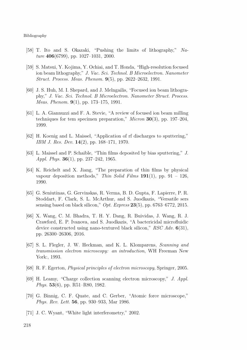
Bibliography
[58] T. Ito and S. Okazaki, “Pushing the limits of lithography,” Na-ture 406(6799), pp. 1027–1031, 2000.
[59] S. Matsui, Y. Kojima, Y. Ochiai, and T. Honda, “High-resolution focusedion beam lithography,” J. Vac. Sci. Technol. B Microelectron. NanometerStruct. Process. Meas. Phenom. 9(5), pp. 2622–2632, 1991.
[60] J. S. Huh, M. I. Shepard, and J. Melngailis, “Focused ion beam lithogra-phy,” J. Vac. Sci. Technol. B Microelectron. Nanometer Struct. Process.Meas. Phenom. 9(1), pp. 173–175, 1991.
[61] L. A. Giannuzzi and F. A. Stevie, “A review of focused ion beam millingtechniques for tem specimen preparation,” Micron 30(3), pp. 197–204,1999.
[62] H. Koenig and L. Maissel, “Application of rf discharges to sputtering,”IBM J. Res. Dev. 14(2), pp. 168–171, 1970.
[63] L. Maissel and P. Schaible, “Thin films deposited by bias sputtering,” J.Appl. Phys. 36(1), pp. 237–242, 1965.
[64] K. Reichelt and X. Jiang, “The preparation of thin films by physicalvapour deposition methods,” Thin Solid Films 191(1), pp. 91 – 126,1990.
[65] G. Seniutinas, G. Gervinskas, R. Verma, B. D. Gupta, F. Lapierre, P. R.Stoddart, F. Clark, S. L. McArthur, and S. Juodkazis, “Versatile serssensing based on black silicon,” Opt. Express 23(5), pp. 6763–6772, 2015.
[66] X. Wang, C. M. Bhadra, T. H. Y. Dang, R. Buividas, J. Wang, R. J.Crawford, E. P. Ivanova, and S. Juodkazis, “A bactericidal microfluidicdevice constructed using nano-textured black silicon,” RSC Adv. 6(31),pp. 26300–26306, 2016.
[67] S. L. Flegler, J. W. Heckman, and K. L. Klomparens, Scanning andtransmission electron microscopy: an introduction, WH Freeman NewYork:, 1993.
[68] R. F. Egerton, Physical principles of electron microscopy, Springer, 2005.
[69] H. Leamy, “Charge collection scanning electron microscopy,” J. Appl.Phys. 53(6), pp. R51–R80, 1982.
[70] G. Binnig, C. F. Quate, and C. Gerber, “Atomic force microscope,”Phys. Rev. Lett. 56, pp. 930–933, Mar 1986.
[71] J. C. Wyant, “White light interferometry,” 2002.
218

Bibliography
[72] H. L. Tuller and S. R. Bishop, “Tailoring material properties throughdefect engineering,” Chem. Lett. 39(12), pp. 1226–1231, 2010.
[73] H. L. Tuller and S. R. Bishop, “Point defects in oxides: tailoring materi-als through defect engineering,” Annu. Rev. Mater. Res. 41, pp. 369–398,2011.
[74] F. Kroger and H. Vink, “Relations between the concentrations of imper-fections in solids,” J. Phys. Chem. Solids 5(3), pp. 208–223, 1958.
[75] R. Salh, Defect related luminescence in silicon dioxide network a review,pp. 135–172. InTech, 2011.
[76] L. Skuja, Optical properties of defects in silica, pp. 73–116. Springer,2000.
[77] R. L. Mozzi and B. E. Warren, “The structure of vitreous silica,” J.Appl. Cryst. 2, pp. 164–172, 1969.
[78] T. Gerber and B. Himmel, “The structure of silica glass,” J. Non-Cryst.Solids 83(3), pp. 324–334, 1986.
[79] H. Hosono, Y. Ikuta, T. Kinoshita, K. Kajihara, and M. Hirano, “Phys-ical disorder and optical properties in the vacuum ultraviolet region ofamorphous SiO2,” Phys. Rev. Lett. 87(17), p. 175501, 2001.
[80] H. Hosono, Y. Abe, H. Imagawa, H. Imai, and K. Arai, “Physical disorderand optical properties in the vacuum ultraviolet region of amorphousSiO2,” Phys. Rev. B 44(21), p. 12043, 1991.
[81] R. A. Weeks, “Paramagnetic resonance of lattice defects in irradiatedquartz,” J. Appl. Phys. 27(11), pp. 1376–1381, 1956.
[82] L. Skuja, M. Hirano, H. Hosono, and K. Kajihara, “Defects in oxideglasses,” Phys. Stat. Sol. 2(1), pp. 15–24, 2005.
[83] X. W. Wang, R. Buividas, F. Funabiki, P. R. Stoddart, H. Hosono, andS. Juodkazis, “Analysis of defects patterned by femtosecond pulses insideKBr and SiO2 glass,” Appl. Phys. A 122(3), pp. 1–8, 2016.
[84] S. Juodkazis, K. Nishimura, S. Tanaka, H. Misawa, E. G. Gamaly,B. Luther-Davies, L. Hallo, P. Nicolai, and V. T. Tikhonchuk, “Laser-induced microexplosion confined in the bulk of a sapphire crystal: Evi-dence of multimegabar pressures,” Phys. Rev. Lett. 96, p. 166101, 2006.
[85] S. Juodkazis, H. Misawa, T. Hashimoto, E. G. Gamaly, and B. Luther-Davies, “Laser-induced microexplosion confined in a bulk of silica: For-mation of nanovoids,” Appl. Phys. Lett. 88(20), p. 201909, 2006.
219

Bibliography
[86] H. G. Berry, G. Gabrielse, and A. E. Livingston, “Measurement of thestokes parameters of light,” Appl. Opt. 16, pp. 3200–3205, Dec 1977.
[87] V. V. Ter-Mikirtychev and T. Tsuboi, “Stable room-temperature tunablecolor center lasers and passive Q-switchers,” Prog. Quant. Electron. 20,pp. 219–268, jan 1996.
[88] L. Nony, E. Gnecco, A. Baratoff, A. Alkauskas, R. Bennewitz, O. Pfeif-fer, a. A. W. S. Maier, and E. M. C. Gerber, “Observation of Individ-ual Molecules Trapped on a Nanostructured Insulator,” Nano Lett. 4,pp. 2185–2189, nov 2004.
[89] J. Nimsch and J. Wachtveitl, “LiF , an underestimated supercontinuumsource in femtosecond transient,” Opt. Express 21(14), pp. 17060–17065,2013.
[90] K. Ambal, A. Payne, D. P. Waters, C. C. Williams, and C. Boehme,“Spin-relaxation dynamics of E′ centers at high density in SiO2 thinfilms for single-spin tunneling force microscopy,” Phys. Rev. Appl. 4,p. 024008, aug 2015.
[91] F. Seitz, “Color Centers in Alkali Halide Crystals. II,” Rev. Mod.Phys. 26, pp. 7–94, jan 1954.
[92] H. Ivey, “Spectral Location of the Absorption Due to Color Centers inAlkali Halide Crystals,” Phys. Rev. 72, pp. 341–343, aug 1947.
[93] D. B. Fitchen, R. H. Silsbee, T. A. Fulton, and E. L. Wolf, “Zero-phonon transitions of color centres in alkali halides,” Phys. Rev. Lett. 11,pp. 275–277, 1963.
[94] D. V. Martyshkin, A. V. Fedorov, A. Arumugam, D. J. Hilton, V. V.Fedorov, and S. Mirov, “Mid-ir volumetric bragg grating based on LiFcolor center crystal,” Opt. Mater. Express 2, pp. 1209–1218, Sep 2012.
[95] S. Reich, A. C. Ferrari, R. Arenal, A. Loiseau, I. Bello, and J. Robertson,“Resonant raman scattering in cubic and hexagonal boron nitride,” Phys.Rev. B 71(20), p. 205201, 2005.
[96] T. T. Tran, K. Bray, M. J. Ford, M. Toth, and I. Aharonovich, “Quan-tum emission from hexagonal boron nitride monolayers,” Nat. Nanotech-nol. 11(1), pp. 37–41, 2016.
[97] Y. Kubota and T. Taniguchi, “Synthesis of cubic boron nitride crys-tals using ni–cr and ni–cr–al solvents under high pressure,” J. J. Appl.Phys. 48(7R), p. 071004, 2009.
220

Bibliography
[98] N. Vast, S. Baroni, G. Zerah, J. M. Besson, A. Polian, M. Grimsditch,and J. C. Chervin, “Lattice dynamics of icosahedral α-Boron under pres-sure,” Phys. Rev. Lett. 78, pp. 693–696, Jan 1997.
[99] N. Vast, S. Baroni, G. Zerah, J. M. Besson, A. Polian, M. Grimsditch,and J. C. Chervin, “Lattice dynamics of a-boron from ab-initio cal-culation and raman scattering under high pressure,” Phys. Stat. Sol.B 198(1), pp. 115–119, 1996.
[100] A. Polian, J. C. Chervin, P. Munsch, and M. Gauthier, “α-boron at veryhigh pressure: structural and vibrational properties,” J. Phys. 121(4),p. 042017, 2008.
[101] R. M. Erasmus and J. D. Comins, “Photoluminescence spectroscopy ofelectron-irradiation induced defects in cubic boron nitride (c-BN),” Phys.Stat. Sol. C 1(9), pp. 2269–2273, 2004.
[102] C. Kurtsiefer, S. Mayer, P. Zarda, and H. Weinfurter, “Stable solid-statesource of single photons,” Phys. Rev. Lett. 85(2), p. 290, 2000.
[103] B. Lounis and M. Orrit, “Single-photon sources,” Rep. Prog. Phys. 68(5),p. 1129, 2005.
[104] S. Choi, T. T. Tran, C. Elbadawi, C. Lobo, X. W. Wang, S. Juodkazis,G. Seniutinas, M. Toth, and I. Aharonovich, “Engineering and localiza-tion of quantum emitters in large hexagonal boron nitride layers,” ACSAppl. Mater. Interfaces 8(43), pp. 29642–29648, 2016.
[105] S. Juodkazis, M. Sudzius, V. Mizeikis, H. Misawa, E. G. Gamaly, Y. Liu,O. A. Louchev, and K. Kitamura, “Three-dimensional recording bytightly focused femtosecond pulses in LiNbO3,” Appl. Phys. Lett. 89,p. 062903, 2006.
[106] S. Juodkazis, V. Mizeikis, M. Sudzius, H. Misawa, K. Kitamura,S. Takekawa, E. G. Gamaly, W. Z. Krolikowski, and A. V. Rode, “Laserinduced memory bits in photorefractive LiNbO3 and LiTaO3,” Appl.Phys. A 93(1), pp. 129–133, 2008.
[107] E. Gamaly, S.Juodkazis, V.Mizeikis, H. Misawa, A. Rode, andW. Krolokowski, “Modification of refractive index by a single fs-pulseconfined inside a bulk of a photo-refractive crystal,” Phys. Rev. B 81(5),p. 054113, 2010.
[108] A. Marcinkevicius, S. Juodkazis, M. Watanabe, M. Miwa, S. Matsuo,H. Misawa, and J. Nishii, “Femtosecond laser-assisted three-dimensionalmicrofabrication in silica,” Opt. Lett. 26, pp. 277–279, Mar 2001.
221
Bibliography
[109] M. Ams, G. D. Marshall, D. J. Spence, and M. J. Withford, “Slit beamshaping method for femtosecond laser direct-write fabrication of sym-metric waveguides in bulk glasses,” Opt. Express 13, pp. 5676–5681, Jul2005.
[110] E. N. Glezer, M. Milosavljevic, L. Huang, R. J. Finlay, T.-H. Her, J. P.Callan, and E. Mazur, “Three-dimensional optical storage inside trans-parentmaterials,” Opt. Lett. 21, pp. 2023–2025, Dec 1996.
[111] H. H. Towner, Y. M. Kim, and H. S. Story, “EPR studies of crystalfield parameters in Fe3+:LiNbO3,” J. Chem. Phys. 56(7), pp. 3676–3679,1972.
[112] Y. Avestisyan, C. Zhang, I. Kawayama, H. Murakami, T. Somekawa,H. Chosrowjan, M. Fujita, and M. Tonouchi, “Terahertz generation byoptical rectification in lithium niobate crystal using a shadow mask,”Opt. Express 20(23), pp. 25752 – 25757, 2012.
[113] F. Funabiki, S. Matsuishi, and H. Hosono, “Local structure around rare-earth ions in B2O3 glass at high pressure,” J. Appl. Phys. 113, p. 223508,2013.
[114] J. Jahns and A. Huang, “Planar integration of free-space optical compo-nents,” Appl. Opt. 28, pp. 1602–1605, 1989.
[115] R. R. P. &. M. L. Vilson R. Almeida, Carlos A. Barrios, “All opticalcontrol of light on a silicon chip,” Nature 431, pp. 1081–1084, 2004.
[116] N. I. Zheludev and Y. S. Kivshar, “From metamaterials to metadevices.,”Nat. Mater. 11, pp. 917–924, 2012.
[117] N. Yu, P. Genevet, M. A. Kats, F. Aieta, J.-P. Tetienne, F. Capasso, andZ. Gaburro, “Light propagation with phase discontinuities: Generalizedlaws of reflection and refraction,” Science 334, pp. 333–337, 2011.
[118] A. Arbabi, Y. Horie, A. J. Ball, M. Bagheri, and A. Faraon,“Subwavelength-thick lenses with high numerical apertures and large ef-ficiency based on high contrast transmitarrays,” Nat. Commun. 6, pp. 1–10, 2015.
[119] N. Yu, F. Aieta, P. Genevet, M. A. Kats, Z. Gaburro, and F. Capasso,“A broadband, background-free quarter-wave plate based on plasmonicmetasurfaces,” Nano Lett. 12, pp. 6328–6333, 2012.
[120] B. Memarzadeh and H. Mosallaei, “Array of planar plasmonic scatterersfunctioning as light concentrator,” Opt. Lett. 36, pp. 2569–2571, 2011.
222
Bibliography
[121] F. Aieta, P. Genevet, M. Kats, and N. Yu, “Aberration-free ultrathinflat lenses and axicons at telecom wavelengths based on plasmonic meta-surfaces,” Nano Lett. 12, pp. 4932–4936, 2012.
[122] N. Yu, P. Genevet, F. Aieta, M. Kats, R. Blanchard, G. Aoust, J.-P.Tetienne, Z. Gaburro, and F. Capasso, “Flat optics: Controlling wave-fronts with optical antenna metasurfaces,” IEEE J. Sel. Top. Quant. 19,pp. 4700423–4700423, 2013.
[123] X. Chen, M. Chen, M. Q. Mehmood, D. Wen, F. Yue, C.-W. Qiu,and S. Zhang, “Longitudinal multifoci metalens for circularly polarizedlight,” Adv. Opt. Mater. 3, pp. 1201–1206, 2015.
[124] J. Q. Zhuang, H. M. Wu, Y. G. Yang, Y. C. Cao, D. B. Williams, C. B.Carter, T. Electron, L. D. Marks, D. J. Smith, Y. Nagaoka, T. Wang,J. Lynch, D. Lamontagne, and P. Ball, “Integrated compact optical ver-tex beam emitters,” Science 338, pp. 363–367, 2012.
[125] E. Karimi, S. Sebastian A, I. De Leon, H. Qassim, J. Upham, and R. W.Boyd, “Generating optical orbital angular momentum at visible wave-lengths using a plasmonic metasurface,” Light Sci. Appl. 3, pp. 6328–6333, 2014.
[126] Y. Zhao, M. a. Belkin, and A. Alu, “Twisted optical metamaterials forplanarized ultrathin broadband circular polarizers,” Nat. Commun. 3,pp. 870–877, 2012.
[127] A. Arbabi and A. Faraon, “Fundamental limits of ultrathin metasur-faces,” arXiv Prepr. arXiv1411.2537 , pp. 1–14, 2014.
[128] A. V. Kildishev, A. Boltasseva, and V. M. Shalaev, “Planar photonicswith metasurfaces,” Science 339, pp. 1232009–1232009, 2013.
[129] S. Jahani and Z. Jacob, “All-dielectric metamaterials,” Nature nanotech-nology 11(1), p. 23, 2016.
[130] H.-T. Chen, A. J. Taylor, and N. Yu, “A review of metasurfaces: physicsand applications,” Reports on Progress in Physics 79(7), p. 076401, 2016.
[131] D. Fattal, J. Li, Z. Peng, M. Fiorentino, and R. G. Beausoleil, “Flatdielectric grating reflectors with focusing abilities,” Nat. Photon. 4,pp. 466–470, 2010.
[132] F. Aieta, M. Kats, P. Genevet, and F. Capasso, “Multiwavelength achro-matic metasurfaces by dispersive phase compensation,” Science 347,pp. 1342–1346, 2015.
223

Bibliography
[133] Y. Yang, W. Wang, P. Moitra, I. I. Kravchenko, D. P. Briggs, andJ. Valentine, “Dielectric meta-reflectarray for broadband linear polariza-tion conversion and optical vortex generation,” Nano Lett. 14, pp. 1394–1399, 2014.
[134] A. Arbabi, Y. Horie, M. Bagheri, and A. Faraon, “Dielectric metasurfacesfor complete control of phase and polarization with subwavelength spatialresolution and high transmission,” Nat. Nanotechnol. , pp. 1–9, 2015.
[135] M. Khorasaninejad, F. Aieta, P. Kanhaiya, M. A. Kats, P. Genevet,D. Rousso, and F. Capasso, “Achromatic metasurface lens at telecom-munication wavelengths,” Nano Lett. 15, pp. 5358–5362, 2015.
[136] Z. Bomzon, V. Kleiner, and E. Hasman, “Pancharatnam–berry phase inspace-variant polarization-state manipulations with subwavelength grat-ings,” Opt. Lett. 26, pp. 1424–1426, 2001.
[137] E. Hasman, V. Kleiner, G. Biener, and A. Niv, “Polarization dependentfocusing lens by use of quantized pancharatnam - berry phase diffractiveoptics,” Appl. Phys. Lett. 82, p. 328, 2003.
[138] A. Niv, Y. Gorodetski, V. Kleiner, and E. Hasman, “Topological spin-orbit interaction of light in anisotropic inhomogeneous subwavelengthstructures,” Opt. Lett. 33, pp. 2910–2912, 2008.
[139] N. Yu and F. Capasso, “Flat optics with designer metasurfaces,” Nat.Mater. 13, pp. 139–50, 2014.
[140] D. Lin, P. Fan, E. Hasman, and M. L. Brongersma, “Dielectric gradientmetasurface optical elements,” Science 345, pp. 298–302, 2014.
[141] Y. Ke, Y. Liu, Y. He, J. Zhou, H. Luo, and S. Wen, “Realization ofspin-dependent splitting with arbitrary intensity patterns based on all-dielectric metasurfaces,” arXiv Prepr. , pp. 19–22, 2015.
[142] X. Ling, X. Zhou, X. Yi, W. Shu, Y. Liu, S. Chen, H. Luo, S. Wen,and D. Fan, “Giant photonic spin hall effect in momentum space in astructured metamaterial with spatially varying birefringence,” Light Sci.Appl. 4, p. e290, 2015.
[143] H. Chen, Z. Chen, Q. Li, H. Lv, Q. Yu, and X. Yi, “Generation of vectorbeams based on dielectric metasurfaces,” J. Mod. Opt. 62, pp. 638–643,2015.
[144] A. E. Minovich, A. E. Miroshnichenko, A. Y. Bykov, T. V. Murzina,D. N. Neshev, and Y. S. Kivshar, “Functional and nonlinear opticalmetasurfaces,” Laser Photon. Rev. 9, pp. 195–213, 2015.
224
Bibliography
[145] D. Veksler, E. Maguid, N. Shitrit, D. Ozeri, V. Kleiner, and E. Hasman,“Multiple wavefront shaping by metasurface based on mixed randomantenna groups,” ACS Photonics 2, pp. 661–667, 2015.
[146] M. Khorasaninejad, W. T. Chen, R. C. Devlin, J. Oh, A. Y. Zhu,and F. Capasso, “Metalenses at visible wavelengths: Diffraction-limitedfocusing and subwavelength resolution imaging,” Science 352(6290),pp. 1190–1194, 2016.
[147] R. C. Devlin, A. Ambrosio, D. Wintz, S. L. Oscurato, A. Y. Zhu, M. Kho-rasaninejad, J. Oh, P. Maddalena, and F. Capasso, “Spin-to-orbital an-gular momentum conversion in dielectric metasurfaces,” Opt. Express 25,pp. 377–393, Jan 2017.
[148] M. Beresna, M. GecevicAius, P. G. Kazansky, and T. Gertus, “Radiallypolarized optical vortex converter created by femtosecond laser nanos-tructuring of glass,” Appl. Phys. Lett. 98(20), p. 201101, 2011.
[149] E. Brasselet, M. Malinauskas, A. Zukauskas, and S. Juodkazis, “Pho-topolymerized microscopic vortex beam generators: Precise delivery ofoptical orbital angular momentum,” Appl. Phys. Lett. 97(21), p. 211108,2010.
[150] M. Berry, “The adiabatic phase and pancharatnam’s phase for polarizedlight,” J. Mod. Opt. 34, pp. 1401–1407, 1987.
[151] S. Pancharatnam, “Generalized theory of interference and its applica-tions: Part i. coherent pencils,” Proc. India Acad. Sci. XLIV, pp. 247–262, 1956.
[152] M. V. Berry, “Quantal phase factors accompanying adiabatic changes,”Proc. R. Soc. London 392, pp. 45–57, 1984.
[153] W. Primak and D. Post, “Photoelastic constants of vitreous silica and itselastic coefficient of refractive index,” J. Appl. Phys. 30(5), pp. 779–788,1959.
[154] H. Matsuoka and T. Nakai, “Stress-deformation and strength charac-teristics of soil under three different principal stresses,” in Proc. JSCE,232(9), pp. 59–70, 1974.
[155] B. McMillen, C. Athanasiou, and Y. Bellouard, “Femtosecond laserdirect-write waveplates based on stress-induced birefringence,” Opt. Ex-press 24, pp. 27239–27252, Nov 2016.
[156] A. Barlow and D. Payne, “The stress-optic effect in optical fibers,” IEEEJ. Quant. Electron. 19, pp. 834–839, May 1983.
225

Bibliography
[157] T. Schreiber, H. Schultz, O. Schmidt, F. Roser, J. Limpert, andA. Tunnermann, “Stress-induced birefringence in large-mode-area micro-structured optical fibers,” Opt. Express 13, pp. 3637–3646, May 2005.
[158] E. B. Grann, M. G. Moharam, and D. A. Pommet, “Artificial uniaxialand biaxial dielectrics with use of two-dimensional subwavelength binarygratings,” J. Opt. Soc. Am. A 11, pp. 2695–2703, 1994.
[159] T. Clausnitzer, T. Kampfe, E.-B. Kley, A. Tunnermann, U. Peschel,A. Tishchenko, and O. Parriaux, “An intelligible explanation of highly-efficient diffraction in deep dielectric rectangular transmission gratings,”Opt. Express 13, pp. 10448–10456, Dec 2005.
[160] M. G. Moharam and T. K. Gaylord, “Rigorous coupled-wave analysis ofplanar-grating diffraction,” J. Opt. Soc. Am. 71, pp. 811–818, Jul 1981.
[161] J. Feng, C. Zhou, B. Wang, J. Zheng, W. Jia, H. Cao, and P. Lv, “Three-port beam splitter of a binary fused-silica grating,” Appl. Opt. 47,pp. 6638–6643, Dec 2008.
[162] H. Li, B. Wang, H. Pei, L. Chen, L. Lei, and J. Zhou, “Fused-silicasandwiched three-port grating under second bragg angle incidence,” Su-perlattices Microstruct. 93, pp. 157 – 162, 2016.
[163] N. Shitrit, I. Yulevich, E. Maguid, D. Ozeri, D. Veksler, V. Kleiner, andE. Hasman, “Spin-optical metamaterial route to spin-controlled photon-ics,” Science 340, pp. 724–726, 2013.
[164] A. Niv, G. Biener, V. Kleiner, and E. Hasman, “Spiral phase elementsobtained by use of discrete space-variant subwavelength gratings,” Opt.Commun. 251, pp. 306–314, 2005.
[165] G. S. Hammond, C. C. Wamser, C. T. Chang, and C. Baylor, “Photore-action of michler’s ketone with benzophenone. triplet exciplex,” J. Am.Chem. Soc. 92(21), pp. 6362–6363, 1970.
[166] L. Jonusauskas, D. Gailevicius, L. Mikoliunaite, D. Sakalauskas,S. Sakirzanovas, S. Juodkazis, and M. Malinauskas, “Optically clear andresilient free-form μ-optics 3d-printed via ultrafast laser lithography,”Materials 10(1), 2017.
[167] M. Malinauskas, M. Farsari, A. Piskarskas, and S. Juodkazis”, “Ultrafastlaser nanostructuring of photopolymers: A decade of advances,” Phys.Rep. 533(1), pp. ”1 – 31”, 2013.
[168] A. Ovsianikov, J. Viertl, B. Chichkov, M. Oubaha, B. MacCraith,I. Sakellari, A. Giakoumaki, D. Gray, M. Vamvakaki, M. Farsari, and
226
Bibliography
C. Fotakis, “Ultra-low shrinkage hybrid photosensitive material for two-photon polymerization microfabrication,” ACS Nano 2(11), pp. 2257–2262, 2008.
[169] D.-H. Lee, H. N. Mai, J.-C. Yang, and T.-Y. Kwon, “The effect of 4,4’-bis (N, N-diethylamino) benzophenone on the degree of conversion inliquid photopolymer for dental 3d printing,” J. Adv. Prosthodont. 7(5),pp. 386–391, 2015.
[170] D. Lin, A. L. Holsteen, E. Maguid, G. Wetzstein, P. G. Kik, E. Hasman,and M. L. Brongersma, “Photonic multitasking interleaved si nanoan-tenna phased array,” Nano Lett. 16(12), pp. 7671–7676, 2016. PMID:27960478.
[171] E. Maguid, I. Yulevich, D. Veksler, V. Kleiner, M. L. Brongersma, andE. Hasman, “Photonic spin-controlled multifunctional shared-apertureantenna array,” Science 352(6290), pp. 1202–1206, 2016.
[172] K. Sugioka and Y. Cheng, “Ultrafast lasersreliable tools for advancedmaterials processing,” Light Sci. Appl. 3(4), p. e149, 2014.
[173] M. J. Liu, “Simple technique for measurements of pulsed gaussian-beamspot sizes,” Opt. Lett. 7, pp. 196–198, 1982.
[174] C. H. Wolff, S. Whitlock, R. M. Lowe, A. I. Sidorov, and B. V. Hall,“Fabricating atom chips with femtosecond laser ablation,” J. Phys. B:A. Mol. Opt. Phys. 42, p. 085301, 2009.
[175] A. G. Okhrimchuk, A. V. Shestakov, I. Khrushchev, and J. Mitchell,“Depressed cladding, buried waveguide laser formed in a yag:nd3+ crys-tal by femtosecond laser writing,” Opt. Lett. 30, pp. 2248–2250, Sep2005.
[176] A. M. Yao and M. J. Padgett, “Orbital angular momentum: origins,behavior and applications,” Adv. Opt. Photon. 3, pp. 161–204, Jun 2011.
[177] L. Marrucci, E. Karimi, S. Slussarenko, B. Piccirillo, E. Santamato,E. Nagali, and F. Sciarrino, “Spin-to-orbital conversion of the angu-lar momentum of light and its classical and quantum applications,” J.Opt. 13, p. 064001, jun 2011.
[178] G. W. A. Z. Alois Mair, Alipasha Vaziri, “Entanglement of the orbitalangular momentum states of photons,” Nature 412, pp. 313–316, July2001.
[179] L. Marrucci, C. Manzo, and D. Paparo, “Optical spin-to-orbital angularmomentum conversion in inhomogeneous anisotropic media,” Phys. Rev.Lett. 96, p. 163905, Apr 2006.
227

Bibliography
[180] S. Slussarenko, A. Murauski, T. Du, V. Chigrinov, L. Marrucci, andE. Santamato, “Tunable liquid crystal q-plates with arbitrary topologicalcharge,” Opt. Express 19, pp. 4085–4090, Feb 2011.
[181] Y. Shimotsuma, P. G. Kazansky, J. Qiu, and K. Hirao, “Self-organizednanogratings in glass irradiated by ultrashort light pulses,” Phys. Rev.Lett. 91, p. 247405, 2003.
[182] E. Karimi, S. A. Schulz, I. De Leon, H. Qassim, J. Upham, and R. W.Boyd, “Generating optical orbital angular momentum at visible wave-lengths using a plasmonic metasurface,” Light Sci. Appl. 3, p. 4, 05 2014.
[183] G. Li, M. Kang, S. Chen, S. Zhang, E. Y.-B. Pun, K. W. Cheah, andJ. Li, “Spin-enabled plasmonic metasurfaces for manipulating orbitalangular momentum of light,” Nano Lett. 13(9), pp. 4148–4151, 2013.PMID: 23965168.
[184] D. Hakobyan, H. Magallanes, G. Seniutinas, S. Juodkazis, and E. Bras-selet, “Tailoring orbital angular momentum of light in the visible domainwith metallic metasurfaces,” Adv. Opt. Mater. 4(2), pp. 306–312, 2016.
[185] B. Etienne, M. Mangirdas, Zukauskas Albertas, and J. Saulius, “Pho-topolymerized microscopic vortex beam generators: Precise delivery ofoptical orbital angular momentum,” Appl. Phys. Lett. 97(21), p. ””,2010.
[186] L. Allen, M. W. Beijersbergen, R. J. C. Spreeuw, and J. P. Woerdman,“Orbital angular momentum of light and the transformation of laguerre-gaussian laser modes,” Phys. Rev. A 45, pp. 8185–8189, Jun 1992.
[187] M. Birnbaum, “Semiconductor surface damage produced by ruby lasers,”J. Appl. Phys. 36, p. 3688, 1965.
[188] D. C. Emmony, “Laser mirror damage in germanium at 10.6 μm,” Appl.Phys. Lett. 23(11), p. 598, 1973.
[189] M. Becker, R. Walser, Y. Jhee, and D. Sheng, “Picosecond laser damagemechanisms at semiconductor surfaces,” Proc. SPIE , pp. 93–98, 1982.
[190] J. F. Young, J. Preston, H. Van Driel, and J. Sipe, “Laser-induced pe-riodic surface structure. ii. experiments on ge, si, al, and brass,” Phys.Rev. B 27(2), p. 1155, 1983.
[191] A. Borowiec, M. MacKenzie, G. Weatherly, and H. Haugen, “Trans-mission and scanning electron microscopy studies of single femtosecond-laser-pulse ablation of silicon,” Appl. Phys. A Mater. Sci. Process. 76,pp. 201–207, feb 2003.
228

Bibliography
[192] J. Sipe, J. Young, J. Preston, and H. van Driel, “Laser-induced periodicsurface structure. I. Theory,” Phys. Rev. B 27, pp. 1141–1154, jan 1983.
[193] R. Wagner and J. Gottmann, “Sub-wavelength ripple formation on var-ious materials induced by tightly focused femtosecond laser radiation,”J. Phys. Conf. Ser. 59, pp. 333–337, 2007.
[194] P. P. Rajeev, M. Gertsvolf, C. Hnatovsky, E. Simova, R. S. Taylor, P. B.Corkum, D. M. Rayner, and V. R. Bhardwaj, “Transient nanoplasmonicsinside dielectrics,” J. Phys. B At. Mol. Opt. Phys. 40, pp. S273–S282,jun 2007.
[195] R. S. Taylor, C. Hnatovsky, E. Simova, P. P. Rajeev, D. M. Rayner, andP. B. Corkum, “Femtosecond laser erasing and rewriting of self-organizedplanar nanocracks in fused silica glass,” Opt. Lett. 32(19), p. 2888, 2007.
[196] R. S. Taylor, E. Simova, and C. Hnatovsky, “Creation of chiral structuresinside fused silica glass,” Opt. Lett. 33, p. 1312, jun 2008.
[197] C. Hnatovsky, V. Shvedov, W. Krolikowski, and A. Rode, “Revealinglocal field structure of focused ultrashort pulses,” Phys. Rev. Lett. 106,p. 123901, Mar 2011.
[198] M. Beresna and P. G. Kazansky, “Polarization diffraction grating pro-duced by femtosecond laser nanostructuring in glass,” Opt. Lett. 35,pp. 1662–1664, May 2010.
[199] M. Beresna, M. Gecevicius, P. G. Kazansky, and T. Gertus, “Radiallypolarized optical vortex converter created by femtosecond laser nanos-tructuring of glass,” Appl. Phys. Lett. 98(20), p. 201101, 2011.
[200] Q. Bian, X. Yu, B. Zhao, Z. Chang, and S. Lei, “Femtosecond laserablation of indium tin-oxide narrow grooves for thin film solar cells,”Opt Laser Technol. 45, pp. 395 – 401, 2013.
[201] M. Park, B. H. Chon, H. S. Kim, S. C. Jeoung, D. Kim, J.-I. Lee,H. Y. Chu, and H. R. Kim, “Ultrafast laser ablation of indium tin ox-ide thin films for organic light-emitting diode application,” Opt LasersEng. 44(2), pp. 138 – 146, 2006.
[202] J. F. Young, J. Sipe, and H. Van Driel, “Laser-induced periodic surfacestructure. iii. fluence regimes, the role of feedback, and details of theinduced topography in germanium,” Phys. Rev. B 30(4), p. 2001, 1984.
[203] M. Huang, F. Zhao, Y. Cheng, N. Xu, and Z. Xu, “Mechanisms of ul-trafast laser-induced deep-subwavelength gratings on graphite and dia-mond,” Phys. Rev. B 79, p. 125436, mar 2009.
229

Bibliography
[204] M. Hashida, Y. Ikuta, Y. Miyasaka, S. Tokita, and S. Sakabe, “Sim-ple formula for the interspaces of periodic grating structures self-organized on metal surfaces by femtosecond laser ablation,” Appl. Phys.Lett. 102(17), p. 174106, 2013.
[205] K. Miyazaki and G. Miyaji, “Periodic nanostructure formation on siliconirradiated with multiple low-fluence femtosecond laser pulses in water,”Phys. Procedia 39, pp. 674 – 682, 2012.
[206] K. Miyazaki and G. Miyaji, “Nanograting formation through sur-face plasmon fields induced by femtosecond laser pulses,” J. Appl.Phys. 114(15), p. 153108, 2013.
[207] R. A. Ganeev, M. Baba, T. Ozaki, and H. Kuroda, “Long- and short-period nanostructure formation on semiconductor surfaces at differentambient conditions,” J. Opt. Soc. Am. B 27, p. 1077, apr 2010.
[208] K. Sokolowski-Tinten and D. von der Linde, “Generation of denseelectron-hole plasmas in silicon,” Phys. Rev. B 61(4), p. 2643, 2000.
[209] N. Smith, “Classical generalization of the drude formula for the opticalconductivity,” Phys. Rev. B 64(15), p. 155106, 2001.
[210] W. Kuett, A. Esser, K. Seibert, U. Lemmer, and H. Kurz, “Femtosecondstudies of plasma formation in crystalline and amorphous silicon,” 1990.
[211] Z. Guosheng, P. Fauchet, and A. Siegman, “Growth of spontaneous pe-riodic surface structures on solids during laser illumination,” Phys. Rev.B 26(10), p. 5366, 1982.
[212] S. Sakabe, M. Hashida, S. Tokita, S. Namba, and K. Okamuro, “Mecha-nism for self-formation of periodic grating structures on a metal surfaceby a femtosecond laser pulse,” Phys. Rev. B 79, p. 033409, jan 2009.
[213] M. Hashida, Y. Ikuta, Y. Miyasaka, S. Tokita, and S. Sakabe, “Sim-ple formula for the interspaces of periodic grating structures self-organized on metal surfaces by femtosecond laser ablation,” Appl. Phys.Lett. 102(17), p. 174106, 2013.
[214] D. Dufft, A. Rosenfeld, S. K. Das, R. Grunwald, and J. Bonse, “Fem-tosecond laser-induced periodic surface structures revisited: A compar-ative study on ZnO,” J. Appl. Phys. 105(3), p. 034908, 2009.
[215] J. Bonse, J. Kruger, S. Hohm, and A. Rosenfeld, “Femtosecond laser-induced periodic surface structures,” J. Laser Appl. 24, pp. 0420061–0420067, 2012.
230

Bibliography
[216] A. Borowiec and H. K. Haugen, “Subwavelength ripple formation on thesurfaces of compound semiconductors irradiated with femtosecond laserpulses,” Appl. Phys. Lett. 82, p. 4462, 2003.
[217] M. Couillard, A. Borowiec, H. K. Haugen, J. S. Preston, E. M. Gris-wold, and G. a. Botton, “Subsurface modifications in indium phosphideinduced by single and multiple femtosecond laser pulses: A study on theformation of periodic ripples,” J. Appl. Phys. 101(3), p. 033519, 2007.
[218] O. N. Mryasov and A. J. Freeman, “Electronic band structure of indiumtin oxide and criteria for transparent conducting behavior,” Phys. Rev.B 64, p. 233111, Dec 2001.
[219] P. Erhart, A. Klein, R. G. Egdell, and K. Albe, “Band structure ofindium oxide: Indirect versus direct band gap,” Phys. Rev. B 75,p. 153205, Apr 2007.
[220] R. J. Moerland and J. P. Hoogenboom, “Subnanometer-accuracy opticaldistance ruler based on fluorescence quenching by transparent conduc-tors,” Optica 3(2), pp. 112–117, 2016.
[221] J. Reif, O. Varlamova, and F. Costache, “Femtosecond laser inducednanostructure formation: self-organization control parameters,” Appl.Phys. A 92, pp. 1019–1024, jun 2008.
[222] S. Richter and M. Heinrich, “Nanogratings in fused silica: Formation,control, and applications,” J. Laser . . . 24(4), p. 042008, 2012.
[223] W. X. Jiang, C.-W. Qiu, T. C. Han, Q. Cheng, H. F. Ma, S. Zhang,and T. J. Cui, “Broadband all-dielectric magnifying lens for far-fieldhigh-resolution imaging.,” Adv. Mater. 25, pp. 6963–8, dec 2013.
[224] J. Bonse and J. KruI?ger, “Pulse number dependence of laser-inducedperiodic surface structures for femtosecond laser irradiation of silicon,”J. Appl. Phys. 108(3), p. 034903, 2010.
[225] O. Efimov, S. Juodkazis, and H. Misawa, “Intrinsic single- and multiple-pulse laser-induced damage in silicate glasses in the femtosecond-to-nanosecond region,” Phys. Rev. A 69, p. 042903, apr 2004.
[226] R. Buividas, M. Mikutis, and S. Juodkazis, “Surface and bulk struc-turing of materials by ripples with long and short laser pulses: Recentadvances,” Prog. Quant. Electron. 38(3), pp. 119 – 156, 2014.
[227] I. H. Malitson, “Interspecimen comparison of the refractive index of fusedsilica,” J. Opt. Soc. Am. 55, pp. 1205–1209, Oct 1965.
231

Bibliography
[228] T. A. F. Kronig, P. A. Ledin, J. Kerszulis, M. A. Mahmoud, M. A. El-Sayed, J. R. Reynolds, and V. V. Tsukruk, “Electrically tunable plas-monic behavior of nanocube polymer nanomaterials induced by a redox-active electrochromic polymer,” ACS Nano 8(6), pp. 6182–6192, 2014.PMID: 24870253.
[229] T. Crawford and H. Haugen, “Sub-wavelength surface structures on sil-icon irradiated by femtosecond laser pulses at 1300 and 2100 nm wave-lengths,” Appl. Surf. Sci. 253, pp. 4970–4977, 2007.
[230] F. Umran, Y. Liao, M. Elias, and K. Sugioka, “Formation of nanogratingsin a transparent material with tunable ionization property by femtosec-ond laser irradiation,” Opt. Express 21(13), pp. 746–749, 2013.
[231] M. Huang, F. Zhao, Y. Cheng, N. Xu, and Z. Xu, “Origin of laser-inducednear-subwavelength ripples: interference between surface plasmons andincident laser,” ACS Nano 3, pp. 4062–4070, 2009.
[232] O. Varlamova, J. Reif, S. Varlamov, and M. Bestehorn, “The laser polar-ization as control parameter in the formation of laser-induced periodicsurface structures: Comparison of numerical and experimental results,”Appl. Surf. Sci. 257, pp. 5465–5469, apr 2011.
[233] E. G. Gamaly and A. V. Rode, “Coupling of polarisation of high fre-quency electric field and electronic heat conduction in laser createdplasma,” Opt. Laser Technol. 82, pp. 69 – 71, 2016.
[234] E. Skoulas, A. Manousaki, C. Fotakis, and E. Stratakis, “Biomimeticsurface structuring using cylindrical vector femtosecond laser beams,”Sci. Rep. 7, p. 45114, 2017.
[235] J. J. Nivas, F. Cardano, Z. Song, A. Rubano, R. Fittipaldi, A. Vecchione,D. Paparo, L. Marrucci, R. Bruzzese, and S. Amoruso, “Surface struc-turing with polarization-singular femtosecond laser beams generated bya q-plate,” Sci. Rep. 7, 2017.
[236] D. T. Pierce and W. E. Spicer, “Electronic structure of amorphous sifrom photoemission and optical studies,” Phys. Rev. B 5, pp. 3017–3029,Apr 1972.
[237] R. Ganeev, “Formation of different periodic nanostructures on semicon-ductors,” Opt. Spectrosc. 106(1), pp. 142–146, 2009.
[238] S. K. Das, K. Dasari, A. Rosenfeld, and R. Grunwald, “Extended-areananostructuring of tio 2 with femtosecond laser pulses at 400 nm usinga line focus,” Nanotechnology 21(15), p. 155302, 2010.
232

Bibliography
[239] L. Hong, X. Wang, H. Zheng, H. Wang, H. Yu, et al., “Femtosecond laserfabrication of large-area periodic surface ripple structure on si substrate,”Appl. Surf. Sci. 297, pp. 134–138, 2014.
233
Related Documents