Hongliang Wang Panjawat Kongsuwan Gen Satoh Y. Lawrence Yao Department of Mechanical Engineering, Columbia University, New York, NY 10027 Femtosecond Laser-Induced Simultaneous Surface Texturing and Crystallization of a-Si:H Thin Film: Absorption and Crystallinity Hydrogenated amorphous silicon (a-Si:H) thin films have been considered for use in so- lar cell applications because of their significantly reduced cost. Their overall efficiency and stability, however, are less than that of their bulk crystalline counterparts. Limited work has been performed on solving the efficiency and stability issues of a-Si:H simulta- neously. In this study, both surface texturing and crystallization on a-Si:H thin film are achieved through one-step femtosecond laser processing. The nanoscale conical and pillar-shaped spikes formed on the surface of a-Si:H films by femtosecond laser irradia- tion in both air and water are presented and enhanced light absorption is observed due to light trapping based on surface geometry changes, while the formation of a mixture of hydrogenated nanocrystalline silicon (nc-Si:H) and a-Si:H after crystallization suggests that the overall material stability can potentially be increased. The relationship among crystallinity, fluence, and scan speed is also discussed. Furthermore, a comparison of ab- sorptance spectra for various surface morphologies is developed. Finally, the absorp- tance measurement across the solar spectrum shows that the combination of surface texturing and crystallization induced by femtosecond laser processing is very promising for a-Si:H thin film solar cell applications. [DOI: 10.1115/1.4006548] 1 Introduction Many industrial solar cells in use today use bulk materials as absorbers with crystalline silicon being the most prevalent. How- ever, crystalline silicon suffers from the disadvantage of high ma- terial cost since relatively large thicknesses are required primarily due to its low absorption coefficient. Recently, thin film absorbers are becoming more and more attractive based on their potential for low-cost modules, possibility to create tandem junctions, and large-scale manufacturability [1–3]. a-Si:H is the most popular material for use in thin film form due to its low energy economy (cost=watt). The main issue with a-Si:H is the high order of dan- gling bonds which act as recombination centers that severely reduce the carrier lifetime which results in the solar cell efficiency being below 10%. Additionally, this initial efficiency will decrease by 50% or more when exposed to sunlight over a period of months which is known as the Staebler–Wronski effect or SWE [4,5]. Surface texturing by laser processing is a way to improve effi- ciency, but the SWE remains. The most important material prop- erties that play a role in the SWE are the high disorder in the Si network and high concentration of impurities, which cause some atoms to have dangling bonds that act as defects. Although these dangling bonds can be passivated by hydrogen, light exposure generates electron-hole pairs that will combine. The released energy can break the Si-H bond and promote H to a transport state. The diffusing H-atom successively breaks Si-Si bonds creat- ing Si-H bonds and a neighboring dangling bond. This increasing defect density caused by the so-called SWE can further reduce the cell efficiency. In a thermal annealing process, the hydrogen atoms will revert back to their original positions. This process can reverse the SWE; however, the same degradation process will happen again when the material is exposed to sunlight [5,6]. In order to reduce the SWE, hybrid a-Si:H=nc-Si:H tandem modules have been developed and are able to achieve both higher effi- ciency and stability compared with single junction a-Si:H [7]. a-Si:H with reduced thickness will contain less defects, and the nanocrystalline silicon (nc-Si:H) is more stable and has wider spectral absorption compared to a-Si:H. To eliminate the need for two deposition steps, laser-induced crystallization of a-Si:H has been proposed to produce a mixture of nc-Si:H and a-Si:H and simultaneously form a light trapping texture on the surface of the material. Therefore, laser-based treatment of a-Si:H may solve the efficiency and stability issues in a one-step process, which is a promising methodology for thin film solar cell fabrication. While both nanosecond and femtosecond pulsed lasers are use- ful tools for a-Si:H crystallization [8,9], the femtosecond laser- induced crystallization includes a nonthermal ultrafast phase tran- sition, followed by a thermal process which is different from rapid thermal melting and resolidification caused by a nanosecond laser [10]. However, due to the much smaller thermal diffusion and heat-affected-zones, femtosecond laser processing is more desira- ble for texturing the limited thickness of thin films. Extensive work on surface texturing of crystalline bulk silicon had been reported by Mazur et al. [11,12]. Micron-size conical spikes have been generated on crystalline silicon a few hundred-micrometers thick when irradiated with a femtosecond laser in different back- ground gases, such as SF 6 ,N 2 , and air, and a significant enhance- ment in light absorptance is achieved after texturing. However, limited work is presented for a-Si:H thin films. Nayak et al. [13] showed the observation of crystallization and simultaneous forma- tion of surface structures on roughly 2 lm-thick a-Si:H thin films through femtosecond laser processing in air and showed that the nanosizes spikes resulted in similar absorption enhancement to that of laser processed crystalline bulk silicon. However, the light absorption for different surface geometries on a-Si:H surfaces has Contributed by the Manufacturing Engineering Division of ASME for publication in the JOURNAL OF MANUFACTURING SCIENCE AND ENGINEERING. Manuscript received November 4, 2010; final manuscript received March 27, 2012; published online May 4, 2012. Assoc. Editor: Yong Huang. Journal of Manufacturing Science and Engineering JUNE 2012, Vol. 134 / 031006-1 Copyright V C 2012 by ASME Downloaded 22 May 2012 to 128.59.150.102. Redistribution subject to ASME license or copyright; see http://www.asme.org/terms/Terms_Use.cfm

Welcome message from author
This document is posted to help you gain knowledge. Please leave a comment to let me know what you think about it! Share it to your friends and learn new things together.
Transcript

Hongliang Wang
Panjawat Kongsuwan
Gen Satoh
Y. Lawrence Yao
Department of Mechanical Engineering,
Columbia University,
New York, NY 10027
Femtosecond Laser-InducedSimultaneous Surface Texturingand Crystallization of a-Si:HThin Film: Absorption andCrystallinityHydrogenated amorphous silicon (a-Si:H) thin films have been considered for use in so-lar cell applications because of their significantly reduced cost. Their overall efficiencyand stability, however, are less than that of their bulk crystalline counterparts. Limitedwork has been performed on solving the efficiency and stability issues of a-Si:H simulta-neously. In this study, both surface texturing and crystallization on a-Si:H thin film areachieved through one-step femtosecond laser processing. The nanoscale conical andpillar-shaped spikes formed on the surface of a-Si:H films by femtosecond laser irradia-tion in both air and water are presented and enhanced light absorption is observed dueto light trapping based on surface geometry changes, while the formation of a mixture ofhydrogenated nanocrystalline silicon (nc-Si:H) and a-Si:H after crystallization suggeststhat the overall material stability can potentially be increased. The relationship amongcrystallinity, fluence, and scan speed is also discussed. Furthermore, a comparison of ab-sorptance spectra for various surface morphologies is developed. Finally, the absorp-tance measurement across the solar spectrum shows that the combination of surfacetexturing and crystallization induced by femtosecond laser processing is very promisingfor a-Si:H thin film solar cell applications. [DOI: 10.1115/1.4006548]
1 Introduction
Many industrial solar cells in use today use bulk materials asabsorbers with crystalline silicon being the most prevalent. How-ever, crystalline silicon suffers from the disadvantage of high ma-terial cost since relatively large thicknesses are required primarilydue to its low absorption coefficient. Recently, thin film absorbersare becoming more and more attractive based on their potentialfor low-cost modules, possibility to create tandem junctions, andlarge-scale manufacturability [1–3]. a-Si:H is the most popularmaterial for use in thin film form due to its low energy economy(cost=watt). The main issue with a-Si:H is the high order of dan-gling bonds which act as recombination centers that severelyreduce the carrier lifetime which results in the solar cell efficiencybeing below 10%. Additionally, this initial efficiency willdecrease by 50% or more when exposed to sunlight over a periodof months which is known as the Staebler–Wronski effect or SWE[4,5].
Surface texturing by laser processing is a way to improve effi-ciency, but the SWE remains. The most important material prop-erties that play a role in the SWE are the high disorder in the Sinetwork and high concentration of impurities, which cause someatoms to have dangling bonds that act as defects. Although thesedangling bonds can be passivated by hydrogen, light exposuregenerates electron-hole pairs that will combine. The releasedenergy can break the Si-H bond and promote H to a transportstate. The diffusing H-atom successively breaks Si-Si bonds creat-ing Si-H bonds and a neighboring dangling bond. This increasingdefect density caused by the so-called SWE can further reduce thecell efficiency. In a thermal annealing process, the hydrogenatoms will revert back to their original positions. This process can
reverse the SWE; however, the same degradation process willhappen again when the material is exposed to sunlight [5,6]. Inorder to reduce the SWE, hybrid a-Si:H=nc-Si:H tandem moduleshave been developed and are able to achieve both higher effi-ciency and stability compared with single junction a-Si:H [7].a-Si:H with reduced thickness will contain less defects, and thenanocrystalline silicon (nc-Si:H) is more stable and has widerspectral absorption compared to a-Si:H. To eliminate the need fortwo deposition steps, laser-induced crystallization of a-Si:H hasbeen proposed to produce a mixture of nc-Si:H and a-Si:H andsimultaneously form a light trapping texture on the surface of thematerial. Therefore, laser-based treatment of a-Si:H may solve theefficiency and stability issues in a one-step process, which is apromising methodology for thin film solar cell fabrication.
While both nanosecond and femtosecond pulsed lasers are use-ful tools for a-Si:H crystallization [8,9], the femtosecond laser-induced crystallization includes a nonthermal ultrafast phase tran-sition, followed by a thermal process which is different from rapidthermal melting and resolidification caused by a nanosecond laser[10]. However, due to the much smaller thermal diffusion andheat-affected-zones, femtosecond laser processing is more desira-ble for texturing the limited thickness of thin films. Extensivework on surface texturing of crystalline bulk silicon had beenreported by Mazur et al. [11,12]. Micron-size conical spikes havebeen generated on crystalline silicon a few hundred-micrometersthick when irradiated with a femtosecond laser in different back-ground gases, such as SF6, N2, and air, and a significant enhance-ment in light absorptance is achieved after texturing. However,limited work is presented for a-Si:H thin films. Nayak et al. [13]showed the observation of crystallization and simultaneous forma-tion of surface structures on roughly 2 lm-thick a-Si:H thin filmsthrough femtosecond laser processing in air and showed that thenanosizes spikes resulted in similar absorption enhancement tothat of laser processed crystalline bulk silicon. However, the lightabsorption for different surface geometries on a-Si:H surfaces has
Contributed by the Manufacturing Engineering Division of ASME for publicationin the JOURNAL OF MANUFACTURING SCIENCE AND ENGINEERING. Manuscript receivedNovember 4, 2010; final manuscript received March 27, 2012; published online May4, 2012. Assoc. Editor: Yong Huang.
Journal of Manufacturing Science and Engineering JUNE 2012, Vol. 134 / 031006-1Copyright VC 2012 by ASME
Downloaded 22 May 2012 to 128.59.150.102. Redistribution subject to ASME license or copyright; see http://www.asme.org/terms/Terms_Use.cfm

not been characterized after laser irradiation in different process-ing environments, such as background gases and water.
In the previous study [14–16], the formation of nanoscale coni-cal and pillar-shaped spikes on a-Si:H surfaces has been studiedthrough scanning electron microscopy (SEM) and atomic forcemicroscopy (AFM) for femtosecond laser irradiation in both airand water. Base on the parametric study of the relationshipbetween the surface morphologies and processing conditions, thedependence of light absorptance on typical surface structure isstudied by spectrophotometry while the effect of laser processingon crystallinity is investigated by X-ray diffractometry (XRD).The combined effects of light trapping surface structure and crys-tallization on a-Si:H suggests a one-step process for potentiallyenhancing the efficiency and stability of thin film solar cells.
2 Background
2.1 Factors Affecting Light Absorption. The light absorp-tion capabilities of a material depend on its optical properties (re-fractive index, absorption coefficient), film thickness, and surfaceroughness. This paper mainly focuses on a-Si:H, and thus, the op-tical properties are considered to be consistent between samples.As known, the thicker the film, the higher the light absorption.However, a thick a-Si:H layer increases the number of recombina-tion centers. As a result, the stability performance deteriorates andthe cost increases. Antireflection coating is also a way to improveabsorption, but additional costs for the material and depositionprocess are also introduced. Therefore, changing the surface ge-ometry is the most economical and efficient way for enhancingthe light absorptance.
Yagi et al. [17] showed a significant reduction in the reflectanceof crystalline silicon with a pyramidal textured surface by aniso-tropic etching and also found that the reflectance of silicon depos-ited on V-shaped glass substrates increases with increasing angleof the V-shape. Halbwax et al. [18] investigated the dependenceof absorption on different shape surface structures and showedconical spikes had the best absorption, followed by pillars andpyramids. Hua et al. [19] showed the absorption caused by differ-ent surface geometries, and found that surface structures withhigher density, smaller top angle, and a spike shape that can intro-duce a greater number of reflections within the periodic structures,will absorb a larger fraction of the incoming light.
2.2 Femtosecond Laser-induced Crystallization. Duringfemtosecond laser irradiation, the conservation equation for elec-trons excited by multiphoton absorption can be written as [10]
@Nðx; tÞ@t
¼ ð1� RÞaIðx; tÞh�
þ ð1� RÞ2bI2ðx; tÞ2h�
(1)
where N is electron density, R is reflectivity, a is linear absorptioncoefficient, h� is the photon energy of the laser beam, b is the twophoton absorption coefficient, and I(x,t) is the laser intensityexpressed as follows [10]:
@Iðx; tÞ@t
¼ �ðaþHNÞI (2)
where H is the free carrier absorption cross section.If the critical density of electrons, which is estimated to be 1022
cm�3 [10], is exceeded, they are excited out of the bonding statesof the valence band into the conduction band, and a nonthermalultrafast phase transition will occur. Due to the removal of a sig-nificant number of electrons from the material, the bond chargewill be so weak that the material structure will no longer be stableand will collapse caused by the atoms’ enhanced mobility. Thus,the phase changes to liquid without thermal effects [20,21]. Thisultrafast phase transition caused by a high-density photo-excitedplasma without increasing the materials thermal energy is called
the plasma annealing mechanism. Van Vechten et al. [20] showedthat, as the plasma becomes less dense due to expansion andenergy transfer to the material, the material will pass back throughthe phase transition and covalent bonding will gradually reappear.Crystallization of the material can occur if this solidification pro-cess does not occur too quickly. Choi et al. [10] considered thatthe nonthermally melted layer vanishes in a few picoseconds dur-ing which time a portion of the covalent bonds start to reappeardue to relaxation of electrons back to the valence band. Within ananosecond, the surface starts to be melted due to thermal diffu-sion after the transfer of energy from the excited electrons to thematerial. Resolidification of this thermal melting layer causes thefinal crystallization. Callan et al. [22] also suggests that the ultra-fast nonthermal phase transition described above does not lead toa thermodynamically stable crystalline phase, but to a nonequili-brium disordered phase, and this disorder-to-disorder phase transi-tion can cause defect formation which is considered to be thedriving force for subsequent rapid nucleation [10]. This processwhich includes nonthermal and thermal melting leading to solidi-fication describes femtosecond laser-induced crystallization,which is different from nanosecond laser crystallization whereonly a rapid thermal melting and solidification process occurs.
3 Experimental Setup
Amorphous silicon films of 1.6 lm-thick were deposited on0.525 mm-thick glass substrate using plasma enhanced chemicalvapor deposition. The films were deposited at a rate of 60 A=s in ahydrogen diluted silane environment at 380 �C with a hydrogenatomic concentration of around 20 at. %. Femtosecond laser tex-turing was carried out using a commercial Ti:sapphire oscillatorand regenerative amplifier system. The system delivered 130-fspulses of linearly polarized light at a 1 kHz repetition rate, and acentral wavelength of 800 nm.
The sample is mounted on a three-axis translation stage andirradiated by laser pulses focused by a 60 mm focal-length lens.When changing the environment to water, the sample is placed ina plastic container, and the laser beam focused by the same lenstravels through 5 mm of distilled water before striking the samplesurface. The focal plane of the laser is moved below the samplesurface in order to adjust the beam spot size. For both air andwater cases the beam spot on the sample surface was circular witha diameter of 150 lm. The spikes generated at different fluencesin water have a similar geometry, which suggests that they willhave similar absorptance. Therefore, a fluence of 1.2 J=cm2 isselected to produce typical results for underwater treatment. Inorder to reproduce the surface morphology observed for stationaryprocessing at a fluence of 0.4 J=cm2 with 100 pulses in air and at afluence of 1.2 J=cm2 with 50 pulses in water, 10 � 15 mm2 areaswere processed at specific scan speeds. The scan speed, v, is setby the Full width at half maximum (FWHM) of the Gaussianbeam profile, d, the number of pulses, N, and the repetition rate ofthe laser, f, through the relation v¼ df=N [23].
The untreated and treated samples were also observed throughSEM. Surface roughness and the distribution of spikes in thetreated samples were examined using an AFM. The optical trans-mittance and reflectance of both untreated and treated sampleswere measured by a spectrophotometer over a wavelength rangeof 250 nm–2500 nm which corresponds to the main spectral rangeof solar irradiation [24]. The reflectance (R in %) and transmit-tance (T in %) are then used to calculate the absorptance (A in %)of the film: A¼ 100�R�T. X-ray diffraction (Cu Ka-line) wasused for crystallinity estimation. X-ray photoelectron spectros-copy (XPS) is used for composition analysis.
4 Results and Discussion
4.1 Surface Morphology After Laser Scanning. Whenobserved optically, the surface of the processed a-Si:H film ismuch darker than the original shiny reddish gray color which
031006-2 / Vol. 134, JUNE 2012 Transactions of the ASME
Downloaded 22 May 2012 to 128.59.150.102. Redistribution subject to ASME license or copyright; see http://www.asme.org/terms/Terms_Use.cfm
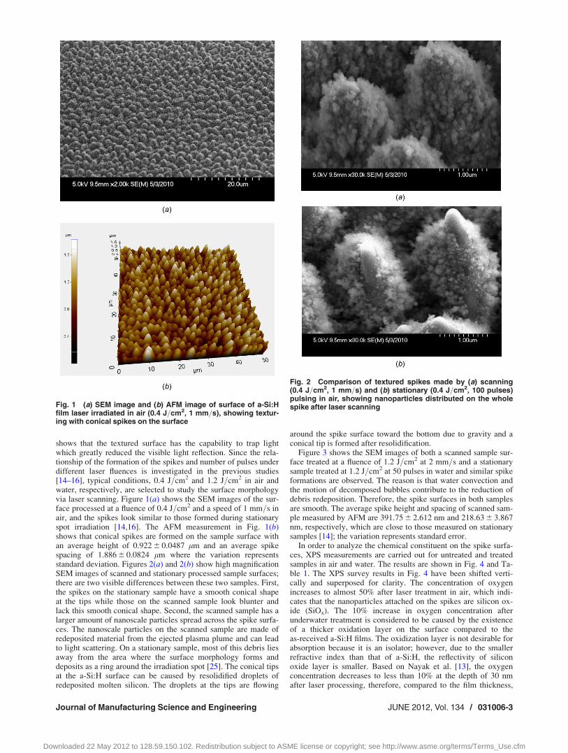
shows that the textured surface has the capability to trap lightwhich greatly reduced the visible light reflection. Since the rela-tionship of the formation of the spikes and number of pulses underdifferent laser fluences is investigated in the previous studies[14–16], typical conditions, 0.4 J=cm2 and 1.2 J=cm2 in air andwater, respectively, are selected to study the surface morphologyvia laser scanning. Figure 1(a) shows the SEM images of the sur-face processed at a fluence of 0.4 J=cm2 and a speed of 1 mm=s inair, and the spikes look similar to those formed during stationaryspot irradiation [14,16]. The AFM measurement in Fig. 1(b)shows that conical spikes are formed on the sample surface withan average height of 0.922 6 0.0487 lm and an average spikespacing of 1.886 6 0.0824 lm where the variation representsstandard deviation. Figures 2(a) and 2(b) show high magnificationSEM images of scanned and stationary processed sample surfaces;there are two visible differences between these two samples. First,the spikes on the stationary sample have a smooth conical shapeat the tips while those on the scanned sample look blunter andlack this smooth conical shape. Second, the scanned sample has alarger amount of nanoscale particles spread across the spike surfa-ces. The nanoscale particles on the scanned sample are made ofredeposited material from the ejected plasma plume and can leadto light scattering. On a stationary sample, most of this debris liesaway from the area where the surface morphology forms anddeposits as a ring around the irradiation spot [25]. The conical tipsat the a-Si:H surface can be caused by resolidified droplets ofredeposited molten silicon. The droplets at the tips are flowing
around the spike surface toward the bottom due to gravity and aconical tip is formed after resolidification.
Figure 3 shows the SEM images of both a scanned sample sur-face treated at a fluence of 1.2 J=cm2 at 2 mm=s and a stationarysample treated at 1.2 J=cm2 at 50 pulses in water and similar spikeformations are observed. The reason is that water convection andthe motion of decomposed bubbles contribute to the reduction ofdebris redeposition. Therefore, the spike surfaces in both samplesare smooth. The average spike height and spacing of scanned sam-ple measured by AFM are 391.75 6 2.612 nm and 218.63 6 3.867nm, respectively, which are close to those measured on stationarysamples [14]; the variation represents standard error.
In order to analyze the chemical constituent on the spike surfa-ces, XPS measurements are carried out for untreated and treatedsamples in air and water. The results are shown in Fig. 4 and Ta-ble 1. The XPS survey results in Fig. 4 have been shifted verti-cally and superposed for clarity. The concentration of oxygenincreases to almost 50% after laser treatment in air, which indi-cates that the nanoparticles attached on the spikes are silicon ox-ide (SiOx). The 10% increase in oxygen concentration afterunderwater treatment is considered to be caused by the existenceof a thicker oxidation layer on the surface compared to theas-received a-Si:H films. The oxidization layer is not desirable forabsorption because it is an isolator; however, due to the smallerrefractive index than that of a-Si:H, the reflectivity of siliconoxide layer is smaller. Based on Nayak et al. [13], the oxygenconcentration decreases to less than 10% at the depth of 30 nmafter laser processing, therefore, compared to the film thickness,
Fig. 1 (a) SEM image and (b) AFM image of surface of a-Si:Hfilm laser irradiated in air (0.4 J=cm2, 1 mm=s), showing textur-ing with conical spikes on the surface
Fig. 2 Comparison of textured spikes made by (a) scanning(0.4 J=cm2, 1 mm=s) and (b) stationary (0.4 J=cm2, 100 pulses)pulsing in air, showing nanoparticles distributed on the wholespike after laser scanning
Journal of Manufacturing Science and Engineering JUNE 2012, Vol. 134 / 031006-3
Downloaded 22 May 2012 to 128.59.150.102. Redistribution subject to ASME license or copyright; see http://www.asme.org/terms/Terms_Use.cfm

the oxidization layer is so thin that cannot affect the final absorp-tion. The carbon peaks for both cases decrease almost to zero, thisis due to the formation of carbon oxide (COx) during the process-ing, so that the solid-phase carbon changes to gas-phase carbon
oxide and is released into the air environment or forms bubbleswhich are suspended in the water.
4.2 Effect of Laser Processing on Absorption. Based on thespike formation by laser scanning, an area of 10 � 15 mm2 istreated in order to investigate the effect of morphology change onabsorption. Figure 5 shows the comparison of absorptance measure-ments of untreated and treated samples with surface texture consist-ing of low-density conical spikes formed in air and high-densitypillar-shaped spikes formed in water. A dramatic increase in the ab-sorptance can be seen for the treated a-Si:H films over the entirespectrum. The absorptance spectra for both treated samples go upto more than 90% from UV wavelengths to the bandgap of a-Si:H(730 nm) due to multiple reflections enabled by the surface texture,and decrease to around 45% and 30% in the below-bandgap region,for the air and water treated samples, respectively. The laser-induced oxidization layer can be also helpful for absorptionenhancement, because it causes a reflection decrease at the surfacedue to the refractive index change. In the above-bandgap range, theabsorptions for the samples processed under different conditions asa function of wavelength show different trends. The increase in ab-sorptance for the untreated sample from UV wavelengths to thebandgap is mainly caused by the material’s optical properties,which indicates that the absorption coefficient increases withincreasing wavelength. However, the opposite trend is observed inthe sample treated in air which may be caused by light scatteringby the nanoparticles attached to the surface of the conical spikes(Fig. 2). According to Rayleigh scattering theory, when the radiusof the particle is much smaller than the wavelength of the incidentlight, the intensity of scattered light is inversely proportional to thefourth power of the wavelength [26]
IðkÞscattering /IðkÞincident
k4(3)
Fig. 3 Comparison of textured spikes made by (a) scanning(1.2 J=cm2, 2 mm=s) and (b) stationary (1.2 J=cm2, 50 pulses)pulsing in water, showing similar pillar-shaped spikes texturedon the both sample surfaces
Fig. 5 Comparison of absorptance spectra of as-received andlaser treated a-Si:H films at fluences of 0.4 J=cm2 (scan speed 1mm=s) and 1.2 J=cm2 (scan speed 2 mm=s) in air and water byspectrophotometry, showing increase in absorptance overentire spectrum for both treated samples
Table 1 Chemical constituent concentrations of the a-Si:Hsample surfaces for as-received, laser irradiated in air and laserirradiated in water
ElementsSamples O1s (%) C1s (%) Si2s (%) Si2p (%)
Untreated a-Si:H 22.1 23.6 21.6 32.6Treated in water 32.01 3.44 31.26 33.29Treated in air 47.4 4.28 22.86 25.46
Fig. 4 XPS spectra of a-Si:H sample surfaces of as-received,laser irradiated in air (0.4 J=cm2, 1 mm=s) and in water (1.2J=cm2, 2 mm=s). The spectra have been shifted up for clarity.Note increase in oxygen and decrease in carbon after laserprocessing.
031006-4 / Vol. 134, JUNE 2012 Transactions of the ASME
Downloaded 22 May 2012 to 128.59.150.102. Redistribution subject to ASME license or copyright; see http://www.asme.org/terms/Terms_Use.cfm

where I and k are intensity and wavelength, respectively. There-fore, at shorter wavelengths, a larger fraction of the incident lightis scattered by the nanoparticles, which causes the highest absorp-tance to occur at the shortest wavelength. The absorptance spec-trum of the sample treated in water is almost flat, which can becaused by much fewer nanoparticles being generated on the spikesdue to the influence of water, thus a smaller fraction of light isscattered.
The differences in the below-bandgap absorptance of thetreated a-Si:H samples could be attributed to different levels ofcrystallinity (bandgap of nc-Si:H is 1.1 eV) [27] which broadensthe absorption range to 1100 nm while the textured surface intro-duces light trapping through multiple reflections as well as scatter-ing by the nanoparticles. Moreover, the water environment mayintroduce less impurities and defects during processing which cancause fewer sub-bandgaps to form, which causes the material toabsorb a smaller fraction of light with longer wavelengths com-pared to the sample treated in air. The reason why the absorptancestarts decreasing at 730 nm rather than 1100 nm is due to the ma-terial remaining primarily amorphous with a bandgap of 730 nm.In the below-bandgap range, unlike for untreated a-Si:H, the ab-sorptance curves for the treated films do not oscillate. The multi-ple reflections caused by the textured surface change thetransmitted light paths through the film such that rays are not
reflected back along their original paths, eliminating internalinterference.
Overall, it is shown that the absorption can depend on the sur-face geometry, such as spike shape, density and attached nanopar-ticles, as well as crystallinity and impurity concentrations.
4.3 Modeling of Surface Geometry Effect onAbsorption. In order to analyze the effect of surface geometry, aray-tracing method [19,28] is used for calculating the path ofwaves through a system with regions of varying propagation ve-locity and absorption characteristics, based on geometrical optics.A solution is achieved by repeatedly advancing idealized narrowbeams called rays through a medium by discrete amounts. A givenray is specified at a point, P0, as shown in Fig. 6, in a referencecoordinate system ðX;Y;ZÞ with origin Oðx0; y0; z0Þ, and has acertain wavelength, intensity and a direction of travel, ðk; l;mÞ.An absorbing material with a surface, S, that is specified by anequation F(X,Y,Z)¼ 0 is defined in coordinate system (X,Y,Z) hav-ing its origin at point O.
The first step is to transform the ray coordinates and directioncosine into their values in the (X,Y,Z) coordinate system. If therotation angles between the (X,Y,Z) system and the ðX;Y;ZÞ sys-tem are (a,b,c), the transformation matrix can be written as [28]
Q ¼ðcos a cos cþ sin a sin b sin cÞ � cos b sin c ð� sin a cos cþ cos a sin b sin cÞðcos a sin c� sin a sin b cos cÞ cos b cos c ð� sin a sin cþ cos a sin b cos cÞ
sin a cos b sin b cos a cos b
24
35 (4)
If P0 in coordinate (X,Y,Z) is ðX0;Y0; Z0Þ, the transformation equa-tions for P0 and the ray direction vector are
X0
Y0
Z0
24
35 ¼ Q
X0 � x0
Y0 � y0
Z0 � z0
24
35and
klm
24
35 ¼ Q
klm
24
35 (5)
Second, the point of intersection of the ray with the surface S isfound. The parametric equations of the given ray may be writtenas [28]
X ¼ X0 þ ks; Y ¼ Y0 þ ls; Z ¼ Z0 þ ms (6)
Fig. 6 Schematic of cross-sectional absorption simulation model for textured a-Si:H film on glass substrate,total thickness is 1.6 lm, real and imaginary parts of refractive index of a-Si:H film are n and k, s and n0 are therefractive index of the substrate and air, respectively. Magnified image in the right shows the reference and localcoordinate systems ðX ;Y ;Z Þ and (X, Y, Z), where S denotes the spike surface that reflects the ray passingthrough point P0
Journal of Manufacturing Science and Engineering JUNE 2012, Vol. 134 / 031006-5
Downloaded 22 May 2012 to 128.59.150.102. Redistribution subject to ASME license or copyright; see http://www.asme.org/terms/Terms_Use.cfm

where s is the distance along the ray measured from (X0, Y0, Z0). sis determined by satisfying the equation F(X,Y,Z) ¼ 0, which canbe calculated by a numerical method such as the Newton–Raphson iteration technique as follows [28]
sjþ1 ¼ sj � F Xj; Yj; Zj
� �=F0 Xj; Yj; Zj
� �(7)
where, Xj = X0 þ ksj, Yj = Y0þ lsj, Zj = Z0 þmsj, and
F0ðXj; Yj; ZjÞ ¼ dF=dsðs ¼ sjÞ ¼@F
@Xjk þ @F
@Yjlþ @F
@Zjm (8)
This process starts from the first approximation, s1 = 0, and is ter-minated with the value sf for which sf � sf�1
�� �� < e, where e is asmall pre-assigned tolerance.
Third, the change in direction at the intersection point of theray and the surface is found. Reflection is based on Snell’s lawand the intensity change is determined by Fresnel’s equations.
Fourth, the second and third steps are repeated to find the subse-quent points of intersection of the reflected ray with the surface,and the absorption caused by the ray traveling through the mate-rial is calculated based on Beer Lambert’s law, until the intensityof the ray decreases to a negligible amount, e.g., 0.1% of the origi-nal intensity. The absorptance, A(k,i), reflectance, R(k,i), andtransmittance, T(k,i) of a given ray i at wavelength k are the totalabsorbed, reflected, and transmitted intensities, respectively, di-vided by the initial ray intensity I(k,i).
Lastly, if the light source is defined by a spectrum from k1 tok2, and for each wavelength it can be divided into a discrete num-ber of rays, p, at different initial points P0 and propagation direc-tions ðk; l;mÞ, the relationship between absorptance, reflectance,transmittance, and source intensity can be described as
Xk2
k1
Xi¼p
i¼1
½Aðk; iÞ þ Rðk; iÞ þ Tðk; iÞ�Iðk; iÞ ¼ Ilightsource (9)
In this paper, the model is realized by a ray-tracing softwareTRACEPRO [19]. The Monte Carlo method is used to sample the dis-tribution of rays emanating from light sources and each ray with acertain intensity, direction and wavelength is traced through themodel structure. Consequently, portions of the ray are reflected orrefracted at every interface and absorbed through the film, withthe fraction being calculated by the angle of incidence and the op-tical properties. The model configuration consisting of an a-Si:Hthin film on a glass substrate is shown in Fig. 6. Since the absorp-tion coefficient of crystalline silicon is 2 orders of magnitude lessthan that of a-Si:H, and the amount of crystalline silicon aftercrystallization is much smaller than that of a-Si:H, the model doesnot consider the effect of crystallization on the thin film absorp-tance. The model also assumes that the entire structure is uniformand no nanoparticles are attached on the spikes; therefore internaldefects and Rayleigh scattering are not simulated. The surfacestructures are designed with dimensions similar to the conical andpillar-shaped spikes formed in air and water, respectively. Thesimulated area is 300 � 300 lm2, and the diameter of the circularlight source is 200 lm with a wavelength range between 250 nmand 2500 nm. The wavelength step is 10 nm, and a set of 60,000rays are randomly generated with a total intensity of 1 W. Thelight is normally incident to the textured surface with conicalspikes, and has a 45 deg incident angle to the surface with pillar-shaped spikes.
Figures 7 and 8 show the comparison between the simulatedand measured absorptance spectra of the samples treated in airand water, respectively. The overall trends of the simulationcurves are similar to the measurement spectra except in theabove-bandgap range. All of the simulated results show a similartrend to the untreated sample in this wavelength range (Fig. 5),which suggests that the difference is neglect of the Rayleigh
scattering effect by the nanoparticles as discussed above. Theunderestimate in the below-bandgap region can be caused byneglecting the scattering effect. Moreover, ignoring the crystalli-zation effect, defects, and impurities generated after laser process-ing could be another reason of underprediction. As known, thedefects can act as recombination centers for electron-hole pairs,and the impurities may introduce sub-bandgaps that absorb lightwith longer wavelengths. Furthermore, the simplification of peri-odic surface structure in the model differs from the exact spikesgenerated after laser processing, especially since the pillar-shapedspikes formed in water are pointed in different directions and aremore irregular than the simulated model geometry. Therefore, thereal spike shape and distribution can obtain a greater number ofreflections at the surface than the regular pillar-shaped surfacesimulation, which causes underestimation of the absorptance overthe entire spectrum. However, most of the characteristics of themeasurement are captured by the simulated curves, so that themodel can be used for estimating the effect of different surfacegeometries on the absorptance. During the comparison, it can beseen that the conical spikes have better absorption performancethan pillar-shape spikes.
Fig. 7 Comparison of simulated and measured absorptancespectra of the laser treated sample in air with the textured sur-face of conical spikes, with height of 900 nm and top angle of90 deg
Fig. 8 Comparison of simulated and measured absorptancespectra of the laser treated samples in water with textured sur-face of pillar-shaped spikes with height of 400 nm height and adiameter of 100 nm
031006-6 / Vol. 134, JUNE 2012 Transactions of the ASME
Downloaded 22 May 2012 to 128.59.150.102. Redistribution subject to ASME license or copyright; see http://www.asme.org/terms/Terms_Use.cfm

In order to further understand the effect of different geometricfactors, two models with different spike densities and heights areinvestigated. Figure 9 shows the simulated absorptance spectra oftextured surfaces with conical spikes of different densities. Theinset image shows the schematic of the spike distribution on thesurface. It is assumed that the spike geometric parameters, such asheight (900 nm) and top angle (90 deg), are the same, and theonly difference is the density, one is 4 times as the other. Duringthe spike formation process, when the surface shows a bead-likestructure as seeds of the spikes, the average bead spacing, whichis similar to the final average spike spacing, is different under dif-ferent fluences. And then using different number of pulses underthose fluence conditions can generate similar geometries of thespikes with different distances between the adjacent spike bases.In order to simplify the problem, it is treated as a flat area inbetween the spike bases during the simulation.
The results indicate that the surface with higher density spikeshas better absorption performance. This is because the samplewith higher density has less open space in between the spikebases, which cannot cause multiple reflections. The reflectance ona unit surface with higher density spikes will be much less so thatthe absorptance is higher. However, in the below-bandgap region,the absorption performance deteriorates when the wavelengthincreases. The light with longer wavelength is more difficult to beabsorbed due to the low photon energy, although the multiplereflections still occur. This can also explain why the differencebetween the absorptance spectra becomes smaller and smaller.According to the better absorption performance by the surfacewith high-density conical spikes, it can be seen that the factor ofspike shape plays a more important role in absorption. The simu-lated absorptance spectra of textured surfaces with different heightof conical spikes are shown in Fig. 10, and the inset image showsthe schematic of the spike distribution on the surface. It isassumed that the spikes are closed-packed (spikes are connectedtogether) and the shape and top angle are the same, and one sam-ple has a twice height texturing as the other. It shows that the ab-sorptance performances for different height spikes are almost thesame. The reason is that for those closed-packed spikes with thesame top angle, no matter how the spike height and density are,the number of times a ray is reflected between spikes is the same,so that the distance traveled by the rays inside the two samples arevery similar, and the total absorptance is similar.
4.4 Effect of Laser Processing on Crystallinity. In order tostudy the crystallization of the treated films, X-ray diffraction pat-
terns were taken for the untreated and treated a-Si:H films in airand water and are shown in Fig. 11. The spectra have been shiftedvertically for clarity. All the spectra show an amorphous peakaround 2h¼ 25 deg, which is caused by the internal constructiveinterference of the amorphous Si network. Three peaks at around2h¼ 29 deg, 47 deg, and 56 deg emerge after processing in airwhich indicate a structural change after laser irradiation and canbe indexed to the (111), (220), and (311) crystalline orientationsof silicon. During femtosecond laser processing an ultrafast non-thermal disorder-to-disorder phase transition occurs within a fewpicoseconds of the laser pulse which cannot lead to crystallization.The material is then partially melted due to thermal diffusion afterenergy transfer from the excited electrons to the material. Theresolidification of the melted layer proceeds via vertical growthfrom the remaining unmelted material and results in random crys-tal orientations due to the amorphous structure of the film.According to the silicon powder diffraction file, the highest threeintensities of X-ray diffraction are for the (111), (220), and (311)orientations and are the same as observed in Fig. 11. The crystalli-zation is considered to be under the partial melting regime, result-ing in no preferential orientation during solidification. This
Fig. 9 Comparison of simulated absorptance spectra for thetextured surfaces with two different densities of conical spikes,showing the surface with higher density spikes has higherabsorptance
Fig. 10 Comparison of simulated absorptance spectra for tex-tured surfaces with different heights of conical spikes, showingsimilar absorptance over the entire wavelength range
Fig. 11 X-ray diffraction spectra of as-received a-Si:H film,laser treated films at 0.4 J=cm2, 1 mm=s and 1.2 J=cm2, 2 mm=sin air and water, respectively. All the spectra show an“amorphous peak” at around 2h 5 25 deg and no signs of crys-tallinity for the untreated sample and that treated in water. Sam-ple treated in air shows three different peaks for (111), (220),and (311) orientation of silicon. The spectra have been shiftedfor clarity.
Journal of Manufacturing Science and Engineering JUNE 2012, Vol. 134 / 031006-7
Downloaded 22 May 2012 to 128.59.150.102. Redistribution subject to ASME license or copyright; see http://www.asme.org/terms/Terms_Use.cfm

suggests that the laser irradiated film becomes a mixture of nc-Si:H and a-Si:H with most of the nc-Si:H believed to be containedwithin the top melted surface. However, the XRD pattern alsoshows that the sample treated in water at 1.2 J=cm2 with a scanspeed of 2 mm=s has no crystallinity.
In order to further understand the laser processing parameters,fluence and scan speed, effect on crystallinity in water, a film wastreated with a lower fluence (0.5 J=cm2) at 2 mm=s and at a higherscan speed (25 mm=s). The XRD patterns are shown in Fig. 12.Only the sample treated at 0.5 J=cm2 with scan speed of 25 mm=shas two small peaks that can be indexed to the (111) and (220) ori-entations of silicon. The reason is due to the higher cooling rate ina water environment than in air; the melted silicon resolidifies soquickly that much less material is able to crystallize. The sampleprocessed at the same fluence, 0.5 J=cm2, but lower scan speed of2 mm=s has no crystallinity; the reason could be the higher pulseoverlap during processing. Daminelli et al. [29] showed that theablation threshold of silicon decreases with increasing number ofpulses due to modification of the absorption behavior of the filmsuch that subsequent surface texturing occurs at fluence levelslower than for previous pulses. Processing with this decreasedthreshold caused by higher overlap can be considered to be equiv-alent to processing at a higher fluence and lower overlap. Thefemtosecond laser-induced crystallization is ablation-dominantprocess rather than that of nanosecond laser which crystallinity isproportional to the laser energy since it is a melting-dominant pro-cess. Therefore, more material will be removed by a higher energyinput, resulting in a deeper buried melting thin layer underneath.This deeper melting layer will cause larger temperature gradientsthrough thickness direction compared to that of lower energyinput. Therefore, a higher cooling rate is induced during the solid-ification process and the liquid layer does not have enough time tobe crystallized. Similarly, Fig. 13 shows the XRD pattern of sam-ples treated at the same scan speed, 25 mm=s, but different fluen-ces from 0.5 to 0.8 J=cm2. It can be seen that the crystallinitydecreases with increasing fluence, and fluences larger than 0.7J=cm2 do not introduce crystallinity. The femtosecond laser-induced crystallization has a nonthermal melting process within 1about picosecond; however, it will not affect the crystallization.The crystallization happened at nanosecond scale when the energytransferred back from free electrons to material and started melt-ing the material. Therefore, Eq. (1) is no longer valid for analyz-ing the temperature distribution at this point. It is assumed that theprocess can be separated by two models—nonlinear absorption(free electron excitation) and linear thermal diffusion (energy
transferred back to material). Therefore, for the crystallizationprocess, it can be assumed that the heat source is from those freeelectrons rather than the laser and the energy loss during the elec-tron movement is negligible. The thermal effects of laser process-ing on crystallization can be described using a model that is basedon one-dimensional heat flow given by [30]
csðTÞqsðTÞ@Tðx; tÞ@t
¼ @
@xjðTÞ @Tðx; tÞ
@x
� �þ Sðx; tÞ (10)
where Tðx; tÞ is the temperature distribution, csðTÞ is the specificheat, qsðTÞ is the density, jðTÞ is the thermal conductivity, andSðx; tÞ is the source which is proportional to the energy absorbedby the surface layer estimated by
Sðx; tÞ ¼ aðtÞIðx; tÞ and Iðx; tÞ ¼ I0ðtÞ 1� RðTÞ½ �e�aðTÞx (11)
where RðTÞ is the reflectivity, aðtÞ is absorption coefficient, andI0ðtÞ is the intensity that absorbed by free electrons which is pro-portional to the laser pulse intensity.
As discussed in Sec. 2.2, thermal melting occurs underneath theablated layer and is caused by thermal diffusion, thus the higher thefluence, the thicker the ablated layer, and the deeper the thermallymelted layer will be. Based on Eq. (10), the influence of laser flu-ence on the temperature distribution along the depth of the film isshown in Ref. [30]; it can be seen that the temperature gradientincreases with increasing fluence and depth into the film. Thus, thethermal melting caused by higher fluences introduces steeper tem-perature gradients compared to lower fluence treated samples andcan be solidified quicker. Thus, the higher fluence can cause ahigher cooling rate, which accelerates the cooling=resolidificationprocess and reduces crystallinity.
4.5 Effect of Crystallinity on Absorption. Figure 14(a)shows an SEM image of an a-Si:H film surface laser treated at afluence of 0.5 J=cm2 with a scan speed of 25 mm=s in water. Thesmall nanosize spikes with blunt tips are randomly orientated andirregularly distributed on the surface after laser treatment. Thesurface roughness and spike distribution is further observed in theAFM image in Fig. 14(b), which shows an average spike height of138 6 2.58 nm and an average spike spacing of 216 6 6.77 nmwhere the variation represents standard error. Visually, the surfacetexture is similar to that of samples treated at a higher fluence of1.2 J=cm2 at a scan speed of 2 mm=s (Fig. 3), moreover, the spike
Fig. 12 X-ray diffraction spectra of a-Si:H films laser treated atfluences of 0.5 J=cm2 and 1.2 J=cm2, and scan speeds of 2mm=s and 25 mm=s in water. An “amorphous peak” around2h 5 25 deg is observed for all samples. Sample processed at0.5 J=cm2 and 25 mm=s shows existence of two peaks for (111)and (220) orientation of silicon, showing the effect of differentlaser parameters on crystallinity
Fig. 13 X-ray diffraction spectrum of laser treated a-Si:H filmat different fluences from 0.5 J=cm2 to 0.8 J=cm2 with the samescan speed of 25 mm=s in water. An “amorphous peak” around2h 5 25 deg is observed for all samples. Existence of two overalldifferent peaks for (111) and (220) orientation of silicon is foundexcept for the condition at 0.8 J=cm2, showing that the crystal-linity decreases with increasing of fluence.
031006-8 / Vol. 134, JUNE 2012 Transactions of the ASME
Downloaded 22 May 2012 to 128.59.150.102. Redistribution subject to ASME license or copyright; see http://www.asme.org/terms/Terms_Use.cfm

spacing measured through AFM of the two samples are also close,and spike heights are 138 nm and 391 nm, respectively. Therefore,the absorptance of these two samples should be similar if both arenot crystallized, since the spike height does not affect the result asdiscussed above. In fact, the sample processed at 25 mm=s is par-tially crystalline while the sample processed at 2 mm=s is not.The comparison of these two samples can show the effect of crys-tallization on absorption. Figure 15 shows the absorptance versuswavelength for both the crystallized and noncrystallized samples,and the untreated sample is also included for comparison. Asseen, due to the similar surface texture, in the above-bandgapregion, the absorptance spectra of both laser treated samples arealmost the same, no matter how deep the spikes are. The changein crystallinity is not significant here since the majority of the ma-terial is still a-Si:H after processing. The highest absorptance fromthe bandgap to around 1600 nm is for the crystallized sampleprocessed at 0.5 J=cm2, followed by the noncrystallized sampletreated at 1.2 J=cm2; the reason could be that the crystallized por-tion of the sample has a bandgap of 1.1 eV, which helps to absorblight with wavelengths up to 1100 nm. Moreover, the crystallizedsample has a thicker a-Si:H layer due to the formation of shorterspikes and the resulting higher defect and impurity concentrationscould also cause higher absorption. The reason that the crystal-lized sample has lower absorption for wavelengths above 1600nm is not well understood. However, based on the solar radiationspectrum, the radiation intensity in this range is a very small por-tion of the total intensity [24], which suggests that lower absorp-tion at these higher wavelengths will only have a small effect onthe total energy absorption. Therefore, over the entire range of the
spectrum, it can be concluded that with similar surface structure, acrystallized sample has better absorption performance due to thecombination of both surface texturing and crystallization.
4.6 Effect of Processing Medium on Absorption. In orderto compare the effect on different factors, such as surface geometryand crystallinity, absorptance spectra for samples treated in air(0.4 J=cm2 and 1 mm=s) and in water (0.5 J=cm2 and 25 mm=s) areshown in Fig. 16. It shows that the sample treated in air has betterabsorptance performance over the entire spectrum. In the above-bandgap region, the conical spikes and attached nanoparticlesformed on the sample treated in air can induce greater light reflec-tion and scattering between the spikes, which play a more importantrole in absorptance than spike density, which is higher for the watertreated sample. The conical spikes, greater crystallinity, as well asthe defects and impurities formed during the laser processing in airintroduce greater numbers of reflections, a wider absorption spec-trum, and sub-bandgaps for the sample treated in air. These effectsall work to increase the absorptance in the below-bandgap region to
Fig. 14 (a) SEM image and (b) AFM image of surface of a-Si:Hfilm laser irradiated in water (0.5 J=cm2, 25 mm=s), showing tex-turing with randomly oriented spikes on the surface
Fig. 15 Comparison of absorptance spectra measured byspectrophotometry of as-received and laser irradiated a-Si:Hfilms with and without crystallinity at different fluences andscan speeds (0.5 J=cm2 at 25 mm=s, 1.2 J=cm2 at 2 mm=s) inwater, showing the effect of crystallinity on absorption
Fig. 16 Comparison of absorptance spectra measured byspectrophotometry of as-received and laser irradiated a-Si:Hfilm in air (0.4 J=cm2, 1 mm=s) and water (0.5 J=cm2, 25 mm=s),showing the effect of different factors, such as surface geome-try, crystallinity and processing medium on absorption
Journal of Manufacturing Science and Engineering JUNE 2012, Vol. 134 / 031006-9
Downloaded 22 May 2012 to 128.59.150.102. Redistribution subject to ASME license or copyright; see http://www.asme.org/terms/Terms_Use.cfm

above that achieved by the sample treated in water. Therefore, witha sufficient thickness of a-Si:H left after laser processing for absorp-tion, a treated sample surface having regular spike shapes withsharper angles, attached nanoparticles, more crystallinity, greaterdefect and impurity concentrations, and larger spike densities willhave better absorptance. Compared to the absorptance spectra ofthe crystalline silicon wafers laser treated in different backgroundgas environments as show by Younkin et al. [11], it can be seenthat both textured crystalline bulk silicon and a-Si:H thin films inair have similar absorptance performance in the above-bandgapregion. In the below-bandgap range, the absorptance of crystallinesilicon drops quickly to almost zero, but for the a-Si:H film, the ab-sorptance only drops to around 45% and remains more or less con-stant with increasing wavelength. Therefore, comparing thethicknesses of a few hundred microns for crystalline silicon and 1.6lm for a-Si:H, it can be concluded that a-Si:H thin films havegreater absorptance while being more economical than c-Si andmay be ideal for solar cell fabrication.
5 Conclusion
In conclusion, it has been demonstrated that simultaneouslyimproving the absorptance of sunlight and the stability against theSWE of a-Si:H thin films is possible through femtosecond laserirradiation in both air and water. Absorptance enhancement iscaused by light trapping based on the surface geometry changes, aswell as increased defect and impurity concentrations caused bylaser processing. The change in crystallinity after processingreduces the thickness of the a-Si:H layer but may allow for greaterstability in a-Si:H-based solar cells and broadens the absorptancerange to 1100 nm. Furthermore, the correlation between the crystal-linity, scan speed and fluence when treated in water have beeninvestigated; the crystallinity decreases with increasing laser flu-ence and decreasing scan speed, which may be due to the increasedcooling rate caused by the higher surface temperature and tempera-ture gradient. Finally, the absorptance spectra indicate that the sam-ples treated in air with regular conical spikes, crystallization andhigh defect and impurity concentration have the best absorptionperformance over the solar radiation spectrum. Compared with theabsorptance of laser textured crystalline bulk silicon, it can be con-cluded that femtosecond laser processing of a-Si:H thin films mayallow for more efficient and economical solar cell applications.
Acknowledgment
Research carried out in part at the Center for Functional Nano-materials, Brookhaven National Laboratory, which is supportedby the U.S. Department of Energy, Office of Basic Energy Scien-ces, under Contract No. DE-AC02-98CH10886. The use of mate-rial characterization equipment at Materials Research Science andEngineering Center, Columbia University is gratefully acknowl-edged. The authors also would like to thank Professor VijayModi, Department of Mechanical Engineering, Columbia Univer-sity, for helpful discussion and suggestions.
References[1] Luque, A., and Hegedus, S., 2003, Handbook of Photovoltaic Science and Engi-
neering, Wiley, UK, Chap. 7-8.[2] Chopra, K. L., Paulson, P. D., and Dutta, V., 2004, “Thin-Film Solar Cells: An
Overview,” Prog. Photovoltaics, 12, pp. 69–92.[3] Kazmerski, L. L., 2006, “Solar Photovoltaics R&D at the Tipping Point: A
2005 Technology Overview,” J. Electron Spectrosc. Relat. Phenom., 150,pp. 105–135.
[4] Miles, R. W., Hynes, K. M., and Forbes, I., 2005, “Photovoltaic Solar Cells: AnOverview of State-of-the-Art Cell Development and Environmental Issues,”Prog. Cryst. Growth Charact. of Mater., 51, pp. 1–42.
[5] Staebler, D. L., and Wronski, C. R., 1980, “Optically Induced ConductivityChanges in Discharge-Produced Hydrogenated Amorphous Silicon,” J. Appl.Phys., 51(6),p. 3262.
[6] Kolodziej, A., 2004, “Staebler-Wronski Effect in Amorphous Silicon and ItsAlloys,” Opto-Electron. Rev., 12(1), pp. 21–32.
[7] Yamamoto, K., Nakajima, A., Yoshimi, M., Sawada, T., Fukuda, S., Suezaki,T., Ichikawa, M., Koi, Y., Goto, M., Meguro, T., Matsuda, T., Kondo, M.,Sasaki, T., and Tawada, Y., 2004, “A High Efficiency Thin Film Silicon SolarCell and Module,” Sol. Energy, 77, pp. 939–949.
[8] Gosain, D. P., Machida, A., Fujino, T., Hitsuda, Y., Nakano, K., and Sato, J.,2003, “Formation of (100)-Textured Si Film Using an Excimer Laser on a GlassSubstrate,” Jpn. J. Appl. Phys., Part 2, 42, pp. L135–L137.
[9] Shieh, J., Chen, Z., and Dai, B., 2004, “Near-Infrared Femtosecond Laser-Induced Crystallization of Amorphous Silicon,” Appl. Phys. Lett., 85(7), pp.1232–1234.
[10] Choi, T. Y., Hwang, D. J., and Grigoropoulos, C. P., 2003, “Ultrafast Laser-Induced Crystallization of Amorphous Silicon Films,” Opt. Eng., 42(11), pp.3383–3388.
[11] Younkin, R., Carey, J. E., Mazur, E., and Levinson, J. A., and Friend, C. M.,2003, “Infrared Absorption by Conical Silicon Microstructures Made in a Vari-ety of Background Gases Using Femtosecond-Laser Pulses,” J. Appl. Phys.,93(5), pp. 2626–2629.
[12] Sheehy, M. A., Winston, L., Carey, J. E., Friend, C. M., and Mazur, E., 2005,“Role of the Background Gas in the Morphology and Optical Properties ofLaser-Microstructured Silicon,” Chem. Mater, 17, pp. 3582–3586.
[13] Nayak, B. K., and Gupta, M. C., 2007, “Femtosecond-Laser-Induced-Crystalli-zation and Simultaneous Formation of Light Trapping Microstructures in Thina-Si:H Films,” Appl. Phys. A, 89, pp. 663–666.
[14] Wang, H., Kongsuwan, P., Satoh, G., and Yao, Y. L., “Femtosecond Laser-Induced Simultaneous Surface Texturing and Crystallization of a-Si:H ThinFilm: Morphology Study,” Int. J. Adv. Manuf. Technol. (in press).
[15] Wang, H., Kongsuwan, P., Satoh, G., and Yao, Y. L., 2011, “Effect of Process-ing Medium and Condition on Absorption Enhancement of Femtosecond LaserTreated a-Si:H Thin Film,” Proceedings of the 2011 North American Manufac-turing Research, Corvallis, OR.
[16] Wang, H., Kongsuwan, P., Satoh, G., and Yao, Y. L., 2010, “FemtosecondLaser-Induced Simultaneous Surface Texturing and Crystallization of a-Si:HThin Film,” Proceedings of the 2010 International Manufacturing Science andEngineering Conference, Erie, PA.
[17] Yagi, T., Uraoka, Y., and Fuyuki, T., 2006, “Ray-Trace Simulation of LightTrapping in Silicon Solar Cell With Texture Structures,” Sol. Energy Mater.Sol. Cells, 90, pp. 2647–2656.
[18] Halbwax, M., Sarnet, T., Delaporte, P., Sentis, M., Etienne, H., Torregrosa, F.,Vervisch, V., Perichaud, I., and Martinuzzi, S., 2008, “Micro and Nano-structure of Silicon by Femtosecond Laser: Application to Silicon PhotovoltaicCells Fabrication,” Thin Solid Films, 516, pp. 6791–6795.
[19] Hua, X., Zhang, Y., and Wang, H., 2010, “The Effect of Texture Unit Shape onSilicon Surface on the Absorption Properties,” Sol. Energy Mater. Sol. Cells,94, pp. 258–262.
[20] Vechten, J. A., Tsu, R., and Saris, F. W., 1979, “Nonthermal Pulsed LaserAnnealing of Si; Plasma Annealing,” Phys. Lett. A, 74(6), pp. 422–426.
[21] Linde, D., and Fabricius, N., 1982, “Observation of an Electronic Plasma inPicosecond Laser Annealing of Silicon,” Appl. Phys. Lett., 41(10), pp.991–993.
[22] Callan, J. P., Kim, A, Roeser, C. A. D., Mazur, E., Solis, J., and Siegel, J.,Afonso, C. N., 2001, “Ultrafast Laser-Induced Phase Transitions in AmorphousGeSb Films,” Phys. Rev. Lett., 86(16), pp. 3650–3653.
[23] Crouch, C. H., Carey, J. E., Shen, M., Mazur, E., and Fenin, F. Y., 2004,“Infrared Absorption by Sulfur-Doped Silicon Formed by Femtosecond LaserIrradiation,” Appl. Phys. A, 79, pp. 1635–1641.
[24] Goetzberger, A., Knobloch, J., and Voss, B., 1998, Crystalline Silicon SolarCells, Wiley, Chichester, Chap. 2.
[25] Carey, J. E., 2004, “Femtosecond-Laser Microstructuring of Silicon for NovelOptoelectronic Devices,” Ph.D. dissertation, Harvard University, Cambridge, MA.
[26] Steen, W., 2003, Laser Material Processing, 3rd ed., Springer-Verkag, London,pp. 76–77.
[27] Meillaud, F., Feltrin, A., Domine, D., Buehlmann, P., Python, M., Bugnon, G.,Billet, A., Parascandolo, G., Bailat, J., Fay, S., Wyrsch, N., Ballif, C., and Shah,A., 2009, “Limiting Factors in the Fabrication of Microcrystalline Silicon SolarCells and Microcrystalline=Amorphous (‘Micromorph’) Tandems,” Philos.Mag., 89(28), pp. 2599–2621.
[28] Spencer, C. H., and Murty, M. V. R. K., 1962, “General Ray-TracingProcedure,” J. Opt. Soc. Am., 52(6), pp. 672–678.
[29] Daminelli, G., Kruger, J., and Kautek, W., 2004, “Femtosecond Laser Interac-tion With Silicon Under Water Confinement,” Thin Solid Films, 467, pp.334–341.
[30] Palani, I. A., Vasa, N. J., and Singaperumal, M., 2008, “Crystallization andAblation in Annealing of Amorphous-Si Thin Film on Glass and Crystalline-SiSubstrates Irradiated by Third Harmonics of Nd3þ: YAG Laser,” Mater. Sci.Semicond. Process., 11, pp. 107–116.
031006-10 / Vol. 134, JUNE 2012 Transactions of the ASME
Downloaded 22 May 2012 to 128.59.150.102. Redistribution subject to ASME license or copyright; see http://www.asme.org/terms/Terms_Use.cfm
Related Documents