ECE 304: Feedback Examples Read S&S § 8.3-8.6, pp. 798-831 1 Given the voltage amplifier shown in Fig. 1 with input resistance R i and output resistance R o , and a choice of drivers from Fig. 2, we are going to connect the appropriate driver from Fig. 2 to a resistor load R L using two different feedback amplifiers. + V i – A υ V i + – Figure 1: Voltage amplifier R TH I N R N Thevenin voltage driver Norton current driver + V TH – Figure 2: Two possible sources to drive the feedback amplifier. Use an idealized feedback network to produce each of the following 1.1 A VOLTAGE AMPLIFIER 1.1.a Select the appropriate driver from Fig. 2. Explain your choice. Solution: The gain of the voltage amplifier has dimensions V/V. That is, input variable is voltage: therefore we want to use a Thevenin voltage source from Fig. 2. 1.1.b If the input resistance seen by V TH or I N with feedback is called R i,f , is R i,f increased or decreased by feedback? Explain why the change is desirable for this type of amplifier. Solution: R i,f should be increased by feedback so that more voltage will be coupled into the amplifier from the input voltage divider. 1.1.c If the output resistance seen by V TH or I N with feedback is called R o,f , is R o,f increased or decreased by feedback? Explain why the change is desirable for this type of amplifier. Would you model the entire amplifier including feedback as a Norton source or as a Thevenin source? Explain. Solution: For a voltage amplifier the output variable is voltage. Therefore the entire amplifier should be modeled as a Thevenin source. For a Thevenin source we want the Thevenin Unpublished work © 3/29/05 JR Brews Page 1 3/29/2005

Welcome message from author
This document is posted to help you gain knowledge. Please leave a comment to let me know what you think about it! Share it to your friends and learn new things together.
Transcript

ECE 304: Feedback Examples Read S&S § 8.3-8.6, pp. 798-831 1 Given the voltage amplifier shown in Fig. 1 with input resistance Ri and output resistance Ro,
and a choice of drivers from Fig. 2, we are going to connect the appropriate driver from Fig. 2 to a resistor load RL using two different feedback amplifiers.
+ Vi –
AυVi + –
Figure 1: Voltage amplifier
RTH
IN
RN
Thevenin voltage driver Norton current driver
+ VTH –
Figure 2: Two possible sources to drive the feedback amplifier. Use an idealized feedback network to produce each of the following 1.1 A VOLTAGE AMPLIFIER 1.1.a Select the appropriate driver from Fig. 2. Explain your choice. Solution: The gain of the voltage amplifier has dimensions V/V. That is, input variable is voltage: therefore we want to use a Thevenin voltage source from Fig. 2. 1.1.b If the input resistance seen by VTH or IN with feedback is called Ri,f, is Ri,f increased or
decreased by feedback? Explain why the change is desirable for this type of amplifier. Solution: Ri,f should be increased by feedback so that more voltage will be coupled into the amplifier from the input voltage divider. 1.1.c If the output resistance seen by VTH or IN with feedback is called Ro,f, is Ro,f increased or
decreased by feedback? Explain why the change is desirable for this type of amplifier. Would you model the entire amplifier including feedback as a Norton source or as a Thevenin source? Explain.
Solution: For a voltage amplifier the output variable is voltage. Therefore the entire amplifier should be modeled as a Thevenin source. For a Thevenin source we want the Thevenin
Unpublished work © 3/29/05 JR Brews Page 1 3/29/2005
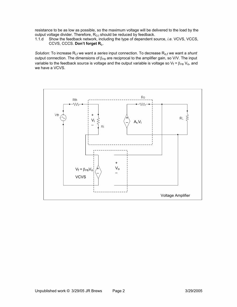
resistance to be as low as possible, so the maximum voltage will be delivered to the load by the output voltage divider. Therefore, RO,f should be reduced by feedback. 1.1.d Show the feedback network, including the type of dependent source, i.e. VCVS, VCCS,
CCVS, CCCS. Don’t forget RL. Solution: To increase Ri,f we want a series input connection. To decrease Ro,f we want a shunt output connection. The dimensions of βFB are reciprocal to the amplifier gain, so V/V. The input variable to the feedback source is voltage and the output variable is voltage so Vf = βFB Vo, and we have a VCVS.
Voltage Amplifier
VCVS
+ Vi –
AυVi + –
+ Vo–
+ –
Vf = βFBVo
Unpublished work © 3/29/05 JR Brews Page 2 3/29/2005

1.2 A TRANSCONDUCTANCE AMPLIFIER 1.2.a Select the appropriate driver from Fig. 2. Explain your choice. Solution: The gain of the transconductance amplifier is A/V. That is, voltage is the input variable. Therefore the appropriate driver is the Thevenin voltage source. 1.2.b If the input resistance seen by VTH or IN with feedback is called Ri,f, is Ri,f increased or
decreased by feedback? Explain why the change is desirable for this type of amplifier. Solution: Feedback should increase Ri,f to insure more voltage is input to Ri of the amplifier by the voltage divider at the input. 1.2.c If the output resistance seen by VTH or IN with feedback is called Ro,f, is Ro,f increased or
decreased by feedback? Explain why the change is desirable for this type of amplifier. From the standpoint of the output, would you model the entire amplifier including feedback as a Norton source or as a Thevenin source? Explain.
Solution: For the transconductance amplifier gain is A/V → output is current. Therefore we model the entire amplifier as a Norton source, and we want Ro,f as large as possible so that the Norton resistance of the entire amplifier will be large, coupling more current from the output current divider into the load resistance. Therefore, RO,f should be increased by feedback. 1.2.d Show the feedback network, including the type of dependent source, i.e. VCVS, VCCS,
CCVS, CCCS. Don’t forget RL. Solution: To increase Ri,f we want a series input connection. To increase Ro,f we want a series output connection. The dimensions of βFB are reciprocal to the amplifier gain, so V/A = Ω. The input variable to the feedback source is current and the output variable is voltage so Vf = βFB Io, and we have a CCVS.
Transconductance Amplifier
+ – CCVS
+ Vi –
AυVi
Vf = βFBIo
Io
+ –
Unpublished work © 3/29/05 JR Brews Page 3 3/29/2005

1.3 A TRANSRESISTANCE AMPLIFIER 1.3.a Select the appropriate driver from Fig. 2. Explain your choice. Solution: The gain of the transresistance amplifier is V/A. That is, current is the input variable. Therefore the appropriate driver is the Norton current source. 1.3.b If the input resistance seen by VTH or IN with feedback is called Ri,f, is Ri,f increased or
decreased by feedback? Explain why the change is desirable for this type of amplifier. Solution: Feedback should decrease Ri,f to insure more current is input to Ri of the amplifier by the current divider at the input. 1.3.c If the output resistance seen by VTH or IN with feedback is called Ro,f, is Ro,f increased or
decreased by feedback? Explain why the change is desirable for this type of amplifier. From the standpoint of the output, would you model the entire amplifier including feedback as a Norton source or as a Thevenin source? Explain.
Solution: For the transresistance amplifier gain is V/A → output is voltage. Therefore we model the entire amplifier as a Thevenin source, and we want Ro,f as small as possible so that the Thevenin resistance of the entire amplifier will be small, coupling more voltage from the output voltage divider into the load resistance. Therefore, RO,f should be reduced by feedback. 1.3.d Show the feedback network, including the type of dependent source, i.e. VCVS, VCCS,
CCVS, CCCS. Don’t forget RL. Solution: To decrease Ri,f we want a shunt input connection. To decrease Ro,f we want a shunt output connection. The dimensions of βFB are reciprocal to the amplifier gain, so A/V = S. The input variable to the feedback source is voltage and the output variable is current so If = βFB Vo, and we have a VCCS.
If = βFBVo + Vo –
+ –
+ Vi –
AυVi
VCCS
Transresistance Amplifier
Unpublished work © 3/29/05 JR Brews Page 4 3/29/2005
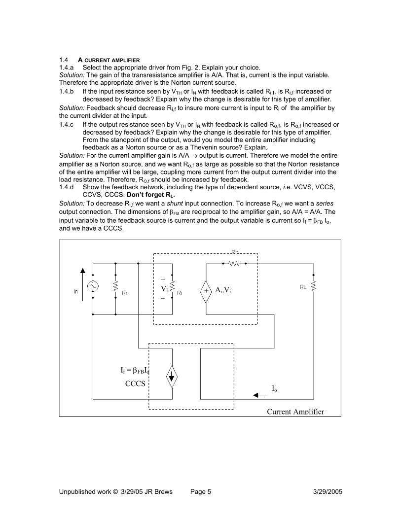
1.4 A CURRENT AMPLIFIER 1.4.a Select the appropriate driver from Fig. 2. Explain your choice. Solution: The gain of the transresistance amplifier is A/A. That is, current is the input variable. Therefore the appropriate driver is the Norton current source. 1.4.b If the input resistance seen by VTH or IN with feedback is called Ri,f, is Ri,f increased or
decreased by feedback? Explain why the change is desirable for this type of amplifier. Solution: Feedback should decrease Ri,f to insure more current is input to Ri of the amplifier by the current divider at the input. 1.4.c If the output resistance seen by VTH or IN with feedback is called Ro,f, is Ro,f increased or
decreased by feedback? Explain why the change is desirable for this type of amplifier. From the standpoint of the output, would you model the entire amplifier including feedback as a Norton source or as a Thevenin source? Explain.
Solution: For the current amplifier gain is A/A → output is current. Therefore we model the entire amplifier as a Norton source, and we want Ro,f as large as possible so that the Norton resistance of the entire amplifier will be large, coupling more current from the output current divider into the load resistance. Therefore, RO,f should be increased by feedback. 1.4.d Show the feedback network, including the type of dependent source, i.e. VCVS, VCCS,
CCVS, CCCS. Don’t forget RL. Solution: To decrease Ri,f we want a shunt input connection. To increase Ro,f we want a series output connection. The dimensions of βFB are reciprocal to the amplifier gain, so A/A = A/A. The input variable to the feedback source is current and the output variable is current so If = βFB Io, and we have a CCCS.
+ –
AυVi
+ Vi –
If = βFBIo
Io CCCS
Current Amplifier
Unpublished work © 3/29/05 JR Brews Page 5 3/29/2005

Problem 2 2 The voltage amplifier of Fig.1 is hooked up using a T-section resistor network (as shown in
Fig. 3) as feedback arrangement.
RA RB
RC
Figure 3: T-section resistor network for use as a feedback network. 2.1 To produce a voltage amplifier. The amplifier is to drive a load RL. 2.1.a Select the appropriate driver from Fig. 2. Solution: Thevenin source, see Part 1. 2.1.b Sketch the appropriate circuit connections using the T-section. Don’t forget RL. Solution: The selection of series-shunt connections follows Part 1.1.d.
Unpublished work © 3/29/05 JR Brews Page 6 3/29/2005

Voltage Amplifier
Sensing (Right) Port
Feedback (Left) Port
+ Vi –
+ –
AυVi
2.1.c Sketch the appropriate circuit connections using the appropriate two-port. Solution: The reasoning for a series-shunt connection follows that of Part 1. However, instead of the ideal feedback network we must use a non-ideal network corresponding to the T-section of resistors. We have to decide which type of dependent sources should be used.
+ Vo
I
+ –
Aυ
+ Vi
+– β21Ιf
CCCS Vf = βFBVoVCVS
Unpublished work © 3/29/05 JR Brews Page 7 3/29/2005
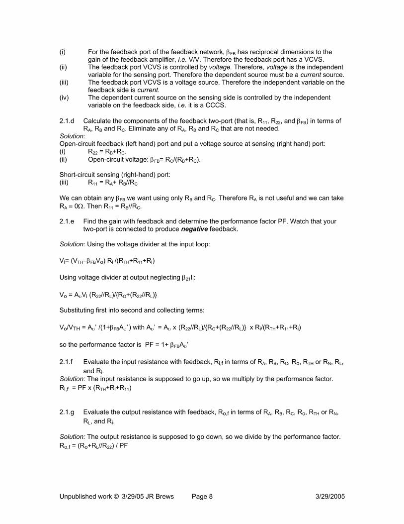
(i) For the feedback port of the feedback network, βFB has reciprocal dimensions to the gain of the feedback amplifier, i.e. V/V. Therefore the feedback port has a VCVS.
(ii) The feedback port VCVS is controlled by voltage. Therefore, voltage is the independent variable for the sensing port. Therefore the dependent source must be a current source.
(iii) The feedback port VCVS is a voltage source. Therefore the independent variable on the feedback side is current.
(iv) The dependent current source on the sensing side is controlled by the independent variable on the feedback side, i.e. it is a CCCS.
2.1.d Calculate the components of the feedback two-port (that is, R11, R22, and βFB) in terms of
RA, RB and RC. Eliminate any of RA, RB and RC that are not needed. Solution: Open-circuit feedback (left hand) port and put a voltage source at sensing (right hand) port: (i) R22 = RB+RC. (ii) Open-circuit voltage: βFB= RC/(RB+RC). Short-circuit sensing (right-hand) port: (iii) R11 = RA+ RB//RC We can obtain any βFB we want using only RB and RC. Therefore RA is not useful and we can take RA ≡ 0Ω. Then R11 = RB//RC. 2.1.e Find the gain with feedback and determine the performance factor PF. Watch that your
two-port is connected to produce negative feedback. Solution: Using the voltage divider at the input loop: Vi= (VTH–βFBVo) Ri /(RTH+R11+Ri) Using voltage divider at output neglecting β21Ii: Vo = AυVi (R22//RL)/RO+(R22//RL) Substituting first into second and collecting terms: Vo/VTH = Aυ’ /(1+βFBAυ’ ) with Aυ’ = Aυ x (R22//RL)/RO+(R22//RL) x Ri/(RTH+R11+Ri) so the performance factor is PF = 1+ βFBAυ’ 2.1.f Evaluate the input resistance with feedback, Ri,f in terms of RA, RB, RC, Ro, RTH or RN, RL,
and Ri. Solution: The input resistance is supposed to go up, so we multiply by the performance factor. Ri,f = PF x (RTH+Ri+R11)
2.1.g Evaluate the output resistance with feedback, Ro,f in terms of RA, RB, RC, Ro, RTH or RN,
RL, and Ri.
Solution: The output resistance is supposed to go down, so we divide by the performance factor. Ro,f = (Ro+RL//R22) / PF
Unpublished work © 3/29/05 JR Brews Page 8 3/29/2005

++
+
+
-
+
1VLR22ROR
LR//22R
THR11RiRiR
A1V'A
++
++υ=υ
RO//RL//R22
+ VO −
+ −
RTH
Ri
R11
+ V1 −
VTH
+ −
+ VO − VFB = βFBVO
Ideal feedback circuit arranged by sliding resistors and making Thevenin equivalent of the main amplifier; we can read directly PF = 1 + βFBAυ''; feed forward is neglected.
2.2 To produce a transconductance amplifier. The amplifier is to drive a load RL. 2.2.a Select the appropriate driver from Fig. 2. Solution: Thevenin source, see Part 1. 2.2.b Sketch the appropriate circuit connections using the T-section. Don’t forget RL. Solution: The selection of series-series connections follows Part 1.2.d.
Transconductance Amplifier
Sensing (Right) Port
Feedback (Left) Port
+ Vi –
+ – AυVi
Unpublished work © 3/29/05 JR Brews Page 9 3/29/2005
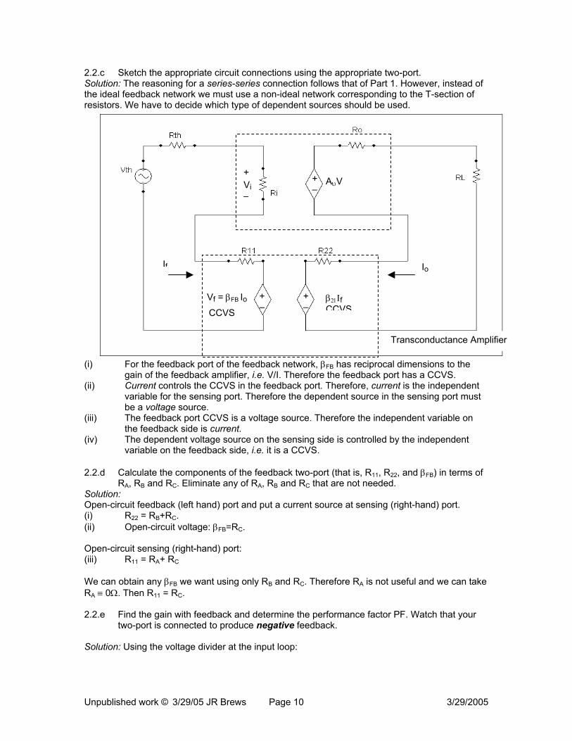
2.2.c Sketch the appropriate circuit connections using the appropriate two-port. Solution: The reasoning for a series-series connection follows that of Part 1. However, instead of the ideal feedback network we must use a non-ideal network corresponding to the T-section of resistors. We have to decide which type of dependent sources should be used.
Transconductance Amplifier
CCVS
+ –
Io If
β21Ιf CCVS
+–
Vf = βFB Io
+ Vi –
AυV+–
(i) For the feedback port of the feedback network, βFB has reciprocal dimensions to the gain of the feedback amplifier, i.e. V/I. Therefore the feedback port has a CCVS.
(ii) Current controls the CCVS in the feedback port. Therefore, current is the independent variable for the sensing port. Therefore the dependent source in the sensing port must be a voltage source.
(iii) The feedback port CCVS is a voltage source. Therefore the independent variable on the feedback side is current.
(iv) The dependent voltage source on the sensing side is controlled by the independent variable on the feedback side, i.e. it is a CCVS.
2.2.d Calculate the components of the feedback two-port (that is, R11, R22, and βFB) in terms of
RA, RB and RC. Eliminate any of RA, RB and RC that are not needed. Solution: Open-circuit feedback (left hand) port and put a current source at sensing (right-hand) port. (i) R22 = RB+RC. (ii) Open-circuit voltage: βFB=RC. Open-circuit sensing (right-hand) port: (iii) R11 = RA+ RC We can obtain any βFB we want using only RB and RC. Therefore RA is not useful and we can take RA ≡ 0Ω. Then R11 = RC. 2.2.e Find the gain with feedback and determine the performance factor PF. Watch that your
two-port is connected to produce negative feedback. Solution: Using the voltage divider at the input loop:
Unpublished work © 3/29/05 JR Brews Page 10 3/29/2005

(i) Vi= (VTH–βFBIo) Ri /(RTH+R11+Ri) Using voltage divider at output neglecting β21Ii: (ii) Io = AυVi /RO+ RL +R22 Substituting first into second and collecting terms: (iii) Io/VTH = Aυ’ /(1+βFBAυ’ ) with Aυ’ = Aυ /RO+ RL +R22 x Ri /(RTH+R11+Ri) so the performance factor is PF = 1+ βFBAυ’ . Notice that A'υ has dimensions of transconductance. 2.2.f Evaluate the input resistance with feedback, Ri,f in terms of RA, RB, RC, Ro, RTH or RN, RL,
and Ri. Solution: The input resistance is supposed to go up, so we multiply by the performance factor. (i) Ri,f = PF x (RTH+Ri+R11) 2.2.g Evaluate the output resistance with feedback, Ro,f in terms of RA, RB, RC, Ro, RTH or RN,
RL, and Ri. Solution: The output resistance is supposed to go up, so we multiply by the performance factor. (i) Ro,f = (Ro+RL+R22) x PF
+
-
+
+
++
+ −
1V22RLROR
1
THR11RiRiR
A1VgA
++
++υ=
RTH
Ri
R11 RO+RL+R22
IO
+ V1 −
VTH
VFB = βFBIO
Ideal trans G amplifier obtained by sliding resistors and making a Norton equivalent of the main amplifier; by inspection PF = 1 + βFBAg
Unpublished work © 3/29/05 JR Brews Page 11 3/29/2005

2.3 To produce a transresistance amplifier. The amplifier is to drive a load RL. 2.3.a Select the appropriate driver from Fig. 2. Solution: Norton source, see Part 1. 2.3.b Sketch the appropriate circuit connections using the T-section. Don’t forget RL. Solution: The selection of shunt-shunt connections follows Part 1.3.d.
+ Vi –
Sensing (Right) Port
Feedback (Left) Port
+ –
AυVi
Figure 1
2.3.c Sketch the appropriate circuit connections using the appropriate two-port. Solution: The reasoning for a shunt-shunt connection follows that of Part 1. However, instead of the ideal feedback network we must use a non-ideal network corresponding to the T-section of resistors. We have to decide which type of dependent sources should be used.
Transresistance Amplifier
+ Vo –
+ Vf–
If = βFBVo VCCS
β21Vf VCCS
+ Vi –
AυVi +–
Figure 2: Result of the two-port analysis that follows.
Unpublished work © 3/29/05 JR Brews Page 12 3/29/2005
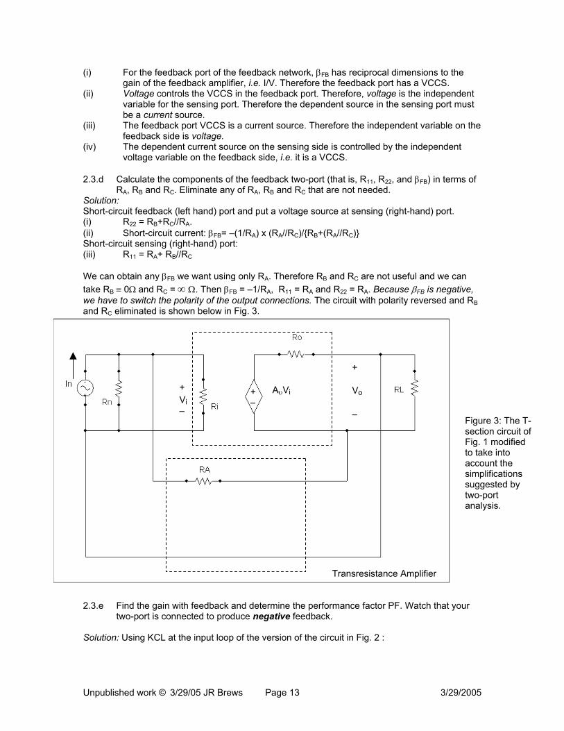
(i) For the feedback port of the feedback network, βFB has reciprocal dimensions to the gain of the feedback amplifier, i.e. I/V. Therefore the feedback port has a VCCS.
(ii) Voltage controls the VCCS in the feedback port. Therefore, voltage is the independent variable for the sensing port. Therefore the dependent source in the sensing port must be a current source.
(iii) The feedback port VCCS is a current source. Therefore the independent variable on the feedback side is voltage.
(iv) The dependent current source on the sensing side is controlled by the independent voltage variable on the feedback side, i.e. it is a VCCS.
2.3.d Calculate the components of the feedback two-port (that is, R11, R22, and βFB) in terms of
RA, RB and RC. Eliminate any of RA, RB and RC that are not needed. Solution: Short-circuit feedback (left hand) port and put a voltage source at sensing (right-hand) port. (i) R22 = RB+RC//RA. (ii) Short-circuit current: βFB= –(1/RA) x (RA//RC)/RB+(RA//RC) Short-circuit sensing (right-hand) port: (iii) R11 = RA+ RB//RC We can obtain any βFB we want using only RA. Therefore RB and RC are not useful and we can take RB ≡ 0Ω and RC = ∞ Ω. Then βFB = –1/RA, R11 = RA and R22 = RA. Because βFB is negative, we have to switch the polarity of the output connections. The circuit with polarity reversed and RB and RC eliminated is shown below in Fig. 3.
Transresistance Amplifier
+ Vo
–
+ Vi –
+ –
AυVi
Figure 3: The T-section circuit of Fig. 1 modified to take into account the simplifications suggested by two-port analysis.
2.3.e Find the gain with feedback and determine the performance factor PF. Watch that your
two-port is connected to produce negative feedback. Solution: Using KCL at the input loop of the version of the circuit in Fig. 2 :
Unpublished work © 3/29/05 JR Brews Page 13 3/29/2005
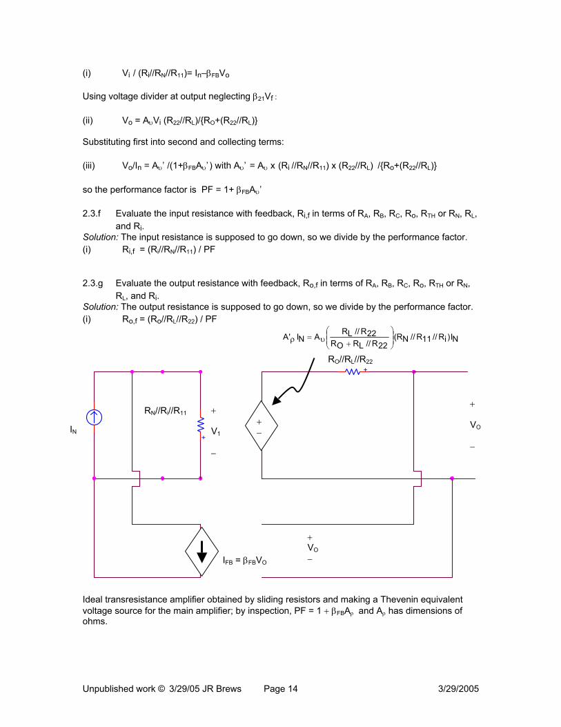
(i) Vi / (Ri//RN//R11)= In–βFBVo Using voltage divider at output neglecting β21Vf : (ii) Vo = AυVi (R22//RL)/RO+(R22//RL) Substituting first into second and collecting terms: (iii) Vo/In = Aυ’ /(1+βFBAυ’ ) with Aυ’ = Aυ x (Ri //RN//R11) x (R22//RL) /Ro+(R22//RL) so the performance factor is PF = 1+ βFBAυ’ 2.3.f Evaluate the input resistance with feedback, Ri,f in terms of RA, RB, RC, Ro, RTH or RN, RL,
and Ri. Solution: The input resistance is supposed to go down, so we divide by the performance factor. (i) Ri,f = (Ri//RN//R11) / PF 2.3.g Evaluate the output resistance with feedback, Ro,f in terms of RA, RB, RC, Ro, RTH or RN,
RL, and Ri. Solution: The output resistance is supposed to go down, so we divide by the performance factor. (i) Ro,f = (Ro//RL//R22) / PF
+
+
+ VO − IFB = βFBVO
NI)iR//11R//NR(22R//LROR
22R//LRANI'A
+υ=ρ
RO//RL//R22
+ V1 −
RN//Ri//R11
+ −
+ VO −
IN
Ideal transresistance amplifier obtained by sliding resistors and making a Thevenin equivalent voltage source for the main amplifier; by inspection, PF = 1 + βFBAρ and Aρ has dimensions of ohms.
Unpublished work © 3/29/05 JR Brews Page 14 3/29/2005

2.4 To produce a current amplifier. The amplifier is to drive a load RL. 2.4.a Select the appropriate driver from Fig. 2. Solution: Norton source, see Part 1. 2.4.b Sketch the appropriate circuit connections using the T-section. Don’t forget RL. Solution: The selection of shunt-series connections follows Part 1.4.d.
Current Amplifier
Sensing (Right) Port
Feedback (Left) Port
+ Vi –
+ –
AυVi
2.4.c Sketch the appropriate circuit connections using the appropriate two-port. Solution: The reasoning for a shunt-series connection follows that of Part 1. However, instead of the ideal feedback network we must use a non-ideal network corresponding to the T-section of resistors. We have to decide which type of dependent sources should be used.
Current Amplifier
+ –
Io
β21Vf VCVS
+ Vi –
If = βFBIo CCCS
+ Vf –
AυVi +–
Unpublished work © 3/29/05 JR Brews Page 15 3/29/2005
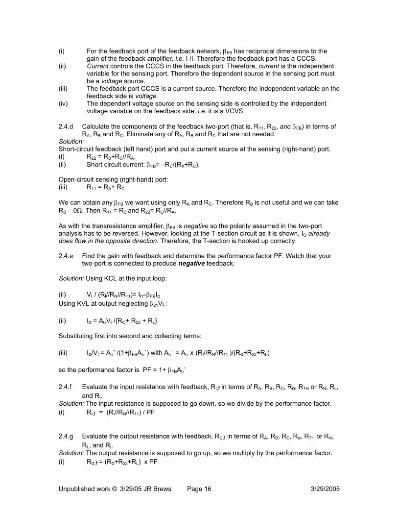
(i) For the feedback port of the feedback network, βFB has reciprocal dimensions to the gain of the feedback amplifier, i.e. I /I. Therefore the feedback port has a CCCS. (ii) Current controls the CCCS in the feedback port. Therefore, current is the independent variable for the sensing port. Therefore the dependent source in the sensing port must be a voltage source. (iii) The feedback port CCCS is a current source. Therefore the independent variable on the
feedback side is voltage. (iv) The dependent voltage source on the sensing side is controlled by the independent
voltage variable on the feedback side, i.e. it is a VCVS. 2.4.d Calculate the components of the feedback two-port (that is, R11, R22, and βFB) in terms of
RA, RB and RC. Eliminate any of RA, RB and RC that are not needed. Solution: Short-circuit feedback (left hand) port and put a current source at the sensing (right-hand) port. (i) R22 = RB+RC//RA. (ii) Short circuit current: βFB= –RC/(RA+RC). Open-circuit sensing (right-hand) port: (iii) R11 = RA+ RC We can obtain any βFB we want using only RA and RC. Therefore RB is not useful and we can take RB ≡ 0Ω. Then R11 = RC and R22= RC//RA. As with the transresistance amplifier, βFB is negative so the polarity assumed in the two-port analysis has to be reversed. However, looking at the T-section circuit as it is shown, IO already does flow in the opposite direction. Therefore, the T-section is hooked up correctly. 2.4.e Find the gain with feedback and determine the performance factor PF. Watch that your
two-port is connected to produce negative feedback. Solution: Using KCL at the input loop: (ii) Vi / (Ri//RN//R11)= In–βFBIo Using KVL at output neglecting β21Vf : (ii) Io = AυVi /RO+ R22 + RL Substituting first into second and collecting terms: (iii) Io/Vi = Aυ’ /(1+βFBAυ’ ) with Aυ’ = Aυ x (Ri//RN//R11 )/(Ro+R22+RL) so the performance factor is PF = 1+ βFBAυ’ 2.4.f Evaluate the input resistance with feedback, Ri,f in terms of RA, RB, RC, Ro, RTH or RN, RL,
and Ri. Solution: The input resistance is supposed to go down, so we divide by the performance factor. (i) Ri,f = (Ri//RN//R11) / PF 2.4.g Evaluate the output resistance with feedback, Ro,f in terms of RA, RB, RC, Ro, RTH or RN,
RL, and Ri. Solution: The output resistance is supposed to go up, so we multiply by the performance factor. (i) Ro,f = (Ro+R22+RL) x PF
Unpublished work © 3/29/05 JR Brews Page 16 3/29/2005

Unpublished work © 3/29/05 JR Brews Page 17 3/29/2005
+ +
NI22RLROR
)iR//11R//NR(ANIA
++υ=ι
RO+RL+R22 RN//Ri//R11 + V1 −
IN
IO
IFB = βFBIO
Ideal current feedback obtained by sliding resistors and making a Norton equivalent of the main amplifier; by inspection PF = 1 + βFBAι
Related Documents