February 4, 2010 CS152, Spring 2010 CS 152 Computer Architecture and Engineering Lecture 6 - Memory Krste Asanovic Electrical Engineering and Computer Sciences University of California at Berkeley http://www.eecs.berkeley.edu/~krste http://inst.eecs.berkeley.edu/~cs152

February 4, 2010CS152, Spring 2010 CS 152 Computer Architecture and Engineering Lecture 6 - Memory Krste Asanovic Electrical Engineering and Computer Sciences.
Dec 21, 2015
Welcome message from author
This document is posted to help you gain knowledge. Please leave a comment to let me know what you think about it! Share it to your friends and learn new things together.
Transcript

February 4, 2010 CS152, Spring 2010
CS 152 Computer Architecture and
Engineering
Lecture 6 - Memory
Krste AsanovicElectrical Engineering and Computer Sciences
University of California at Berkeley
http://www.eecs.berkeley.edu/~krstehttp://inst.eecs.berkeley.edu/~cs152

February 4, 2010 CS152, Spring 2010 2
Last time in Lecture 5
• Control hazards (branches, interrupts) are most difficult to handle as they change which instruction should be executed next
• Speculation commonly used to reduce effect of control hazards (predict sequential fetch, predict no exceptions)
• Branch delay slots make control hazard visible to software
• Precise exceptions: stop cleanly on one instruction, all previous instructions completed, no following instructions have changed architectural state
• To implement precise exceptions in pipeline, shift faulting instructions down pipeline to “commit” point, where exceptions are handled in program order

February 4, 2010 CS152, Spring 2010 3
Early Read-Only Memory Technologies
Punched cards, From early 1700s through Jaquard Loom, Babbage, and then IBM
Punched paper tape, instruction stream in Harvard Mk 1
IBM Card Capacitor ROS
IBM Balanced Capacitor ROS
Diode Matrix, EDSAC-2 µcode store

February 4, 2010 CS152, Spring 2010 4
Early Read/Write Main Memory Technologies
Williams Tube, Manchester Mark 1, 1947
Babbage, 1800s: Digits stored on mechanical wheels
Mercury Delay Line, Univac 1, 1951
Also, regenerative capacitor memory on Atanasoff-Berry computer, and rotating magnetic drum memory on IBM 650

February 4, 2010 CS152, Spring 2010 5
Core Memory• Core memory was first large scale reliable main memory
– invented by Forrester in late 40s/early 50s at MIT for Whirlwind project
• Bits stored as magnetization polarity on small ferrite cores threaded onto 2 dimensional grid of wires
• Coincident current pulses on X and Y wires would write cell and also sense original state (destructive reads)
DEC PDP-8/E Board, 4K words x 12 bits, (1968)
• Robust, non-volatile storage• Used on space shuttle
computers until recently• Cores threaded onto wires
by hand (25 billion a year at peak production)
• Core access time ~ 1ms
February 4, 2010 CS152, Spring 2010 6
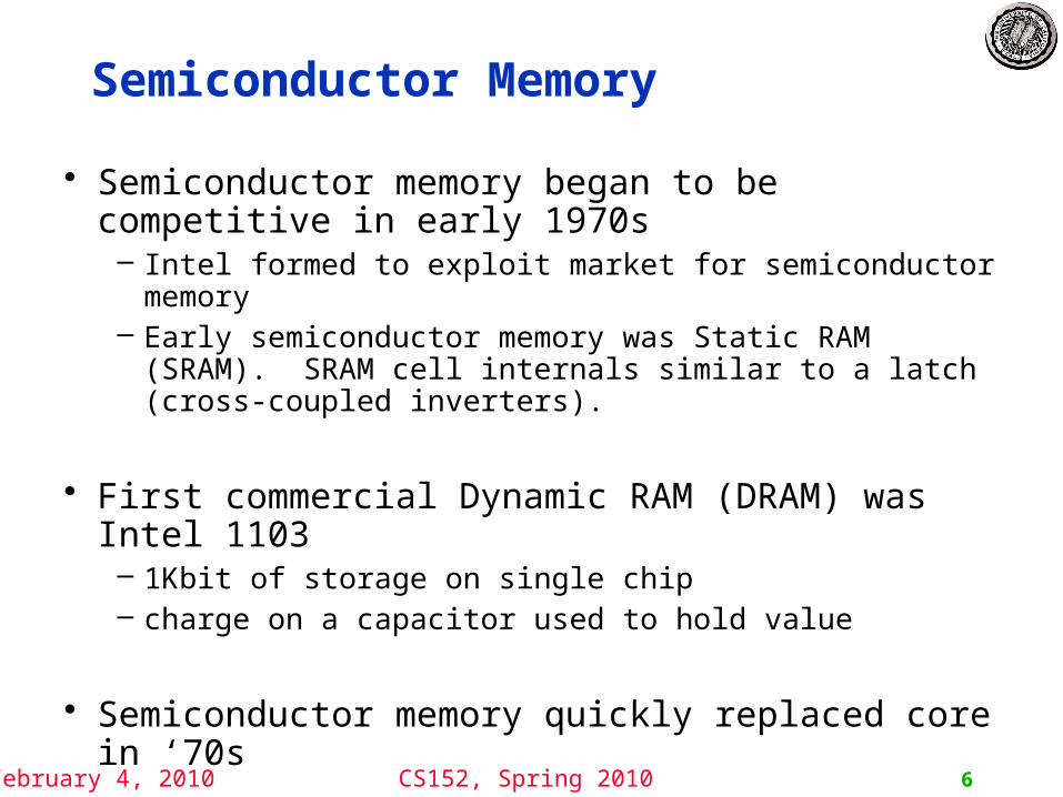
Semiconductor Memory
• Semiconductor memory began to be competitive in early 1970s– Intel formed to exploit market for semiconductor memory– Early semiconductor memory was Static RAM (SRAM). SRAM
cell internals similar to a latch (cross-coupled inverters).
• First commercial Dynamic RAM (DRAM) was Intel 1103– 1Kbit of storage on single chip– charge on a capacitor used to hold value
• Semiconductor memory quickly replaced core in ‘70s
February 4, 2010 CS152, Spring 2010 7
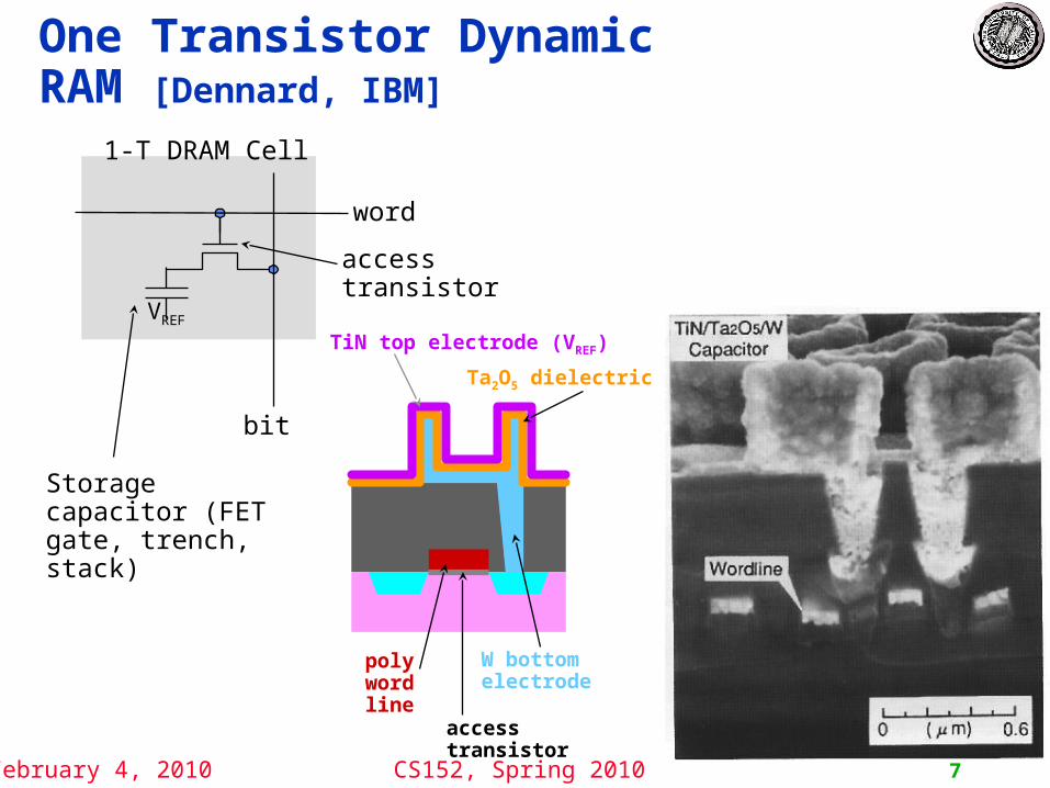
One Transistor Dynamic RAM [Dennard, IBM]
TiN top electrode (VREF)
Ta2O5 dielectric
W bottomelectrode
polywordline
access transistor
1-T DRAM Cell
word
bit
access transistor
Storagecapacitor (FET gate, trench, stack)
VREF

February 4, 2010 CS152, Spring 2010 8
Modern DRAM Structure
[Samsung, sub-70nm DRAM, 2004]

February 4, 2010 CS152, Spring 2010 9
DRAM Architecture
Row
Ad
dre
ss
Deco
der
Col.1
Col.2M
Row 1
Row 2N
Column Decoder & Sense Amplifiers
M
N
N+M
bit linesword lines
Memory cell(one bit)
DData
• Bits stored in 2-dimensional arrays on chip
• Modern chips have around 4 logical banks on each chip– each logical bank physically implemented as many smaller arrays

February 4, 2010 CS152, Spring 2010 10
DRAM OperationThree steps in read/write access to a given bank• Row access (RAS)
– decode row address, enable addressed row (often multiple Kb in row)– bitlines share charge with storage cell– small change in voltage detected by sense amplifiers which latch whole
row of bits– sense amplifiers drive bitlines full rail to recharge storage cells
• Column access (CAS)– decode column address to select small number of sense amplifier
latches (4, 8, 16, or 32 bits depending on DRAM package)– on read, send latched bits out to chip pins– on write, change sense amplifier latches which then charge storage
cells to required value– can perform multiple column accesses on same row without another
row access (burst mode)• Precharge
– charges bit lines to known value, required before next row access
Each step has a latency of around 15-20ns in modern DRAMsVarious DRAM standards (DDR, RDRAM) have different ways of encoding the
signals for transmission to the DRAM, but all share same core architecture

February 4, 2010 CS152, Spring 2010 11
Double-Data Rate (DDR2) DRAM
[ Micron, 256Mb DDR2 SDRAM datasheet ]
Row Column Precharge Row’
Data
200MHz Clock
400Mb/s Data Rate
February 4, 2010 CS152, Spring 2010 12
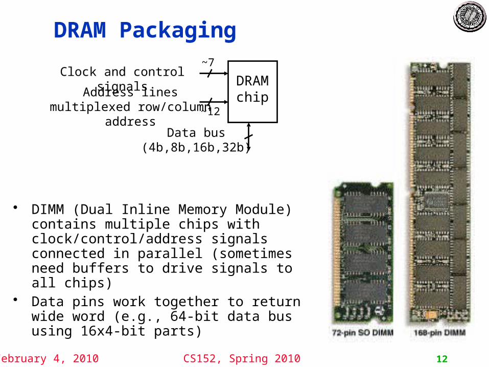
DRAM Packaging
• DIMM (Dual Inline Memory Module) contains multiple chips with clock/control/address signals connected in parallel (sometimes need buffers to drive signals to all chips)
• Data pins work together to return wide word (e.g., 64-bit data bus using 16x4-bit parts)
Address lines multiplexed row/column address
Clock and control signals
Data bus(4b,8b,16b,32b)
DRAM chip
~12
~7

February 4, 2010 CS152, Spring 2010 13
CPU-Memory Bottleneck
MemoryCPU
Performance of high-speed computers is usuallylimited by memory bandwidth & latency
• Latency (time for a single access)Memory access time >> Processor cycle time
• Bandwidth (number of accesses per unit time)if fraction m of instructions access memory,
1+m memory references / instructionÞ CPI = 1 requires 1+m memory refs / cycle
(assuming MIPS RISC ISA)

February 4, 2010 CS152, Spring 2010 14
Processor-DRAM Gap (latency)
Time
µProc 60%/year
DRAM7%/year
1
10
100
1000198
0198
1
198
3198
4198
5198
6198
7
198
8198
9199
0199
1199
2199
3199
4199
5199
6199
7199
8199
9200
0
DRAM
CPU198
2
Processor-MemoryPerformance Gap:(grows 50% / year)
Perf
orm
ance
Four-issue 2GHz superscalar accessing 100ns DRAM could execute 800 instructions during time for one memory access!

February 4, 2010 CS152, Spring 2010 15
Physical Size Affects Latency
Small Memory
CPU
Big Memory
CPU
• Signals have further to travel
• Fan out to more locations
February 4, 2010 CS152, Spring 2010 16
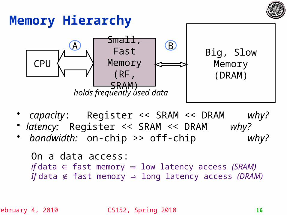
Memory Hierarchy
Small,Fast
Memory(RF, SRAM)
• capacity: Register << SRAM << DRAM why?• latency: Register << SRAM << DRAM why?• bandwidth: on-chip >> off-chip why?
On a data access:if data Î fast memory low latency access (SRAM)If data Ï fast memory long latency access (DRAM)
CPUBig, Slow Memory(DRAM)
A B
holds frequently used data

February 4, 2010 CS152, Spring 2010 17
Relative Memory Cell Sizes
[ Foss, “Implementing Application-Specific
Memory”, ISSCC 1996 ]
DRAM on memory chip
On-Chip SRAM in logic chip

February 4, 2010 CS152, Spring 2010 18
CS152 Administrivia
• Class accounts available today• Handed out in Section at 2pm

February 4, 2010 CS152, Spring 2010 19
Management of Memory Hierarchy
• Small/fast storage, e.g., registers– Address usually specified in instruction– Generally implemented directly as a register file
» but hardware might do things behind software’s back, e.g., stack management, register renaming
• Larger/slower storage, e.g., main memory– Address usually computed from values in register– Generally implemented as a hardware-managed
cache hierarchy» hardware decides what is kept in fast memory» but software may provide “hints”, e.g., don’t cache or
prefetch

February 4, 2010 CS152, Spring 2010
Real Memory Reference Patterns
Donald J. Hatfield, Jeanette Gerald: Program Restructuring for Virtual Memory. IBM Systems Journal 10(3): 168-192 (1971)
Time
Mem
ory
Ad
dre
ss (
on
e d
ot
per
acc
ess)

February 4, 2010 CS152, Spring 2010
Typical Memory Reference PatternsAddress
Time
Instruction fetches
Stackaccesses
Dataaccesses
n loop iterations
subroutine call
subroutine return
argument access
vector access
scalar accesses
February 4, 2010 CS152, Spring 2010
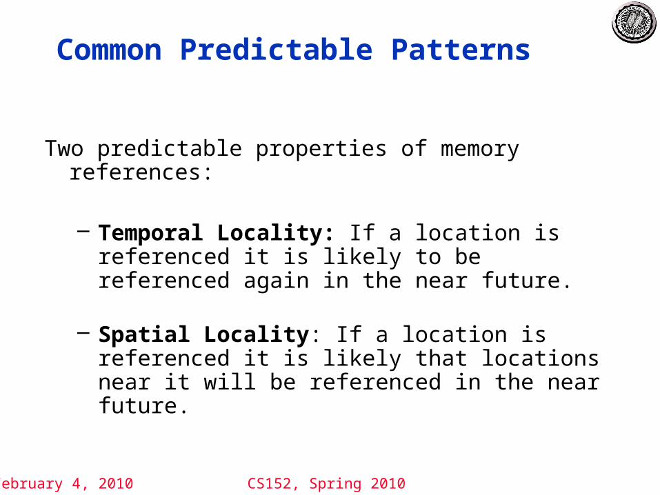
Common Predictable Patterns
Two predictable properties of memory references:
– Temporal Locality: If a location is referenced it is likely to be referenced again in the near future.
– Spatial Locality: If a location is referenced it is likely that locations near it will be referenced in the near future.
February 4, 2010 CS152, Spring 2010
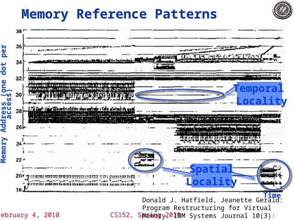
Memory Reference Patterns
Donald J. Hatfield, Jeanette Gerald: Program Restructuring for Virtual Memory. IBM Systems Journal 10(3): 168-192 (1971)
Time
Mem
ory
Ad
dre
ss (
on
e d
ot
per
acc
ess)
SpatialLocality
Temporal Locality

February 4, 2010 CS152, Spring 2010
Caches
Caches exploit both types of predictability:
– Exploit temporal locality by remembering the contents of recently accessed locations.
– Exploit spatial locality by fetching blocks of data around recently accessed locations.

February 4, 2010 CS152, Spring 2010
Inside a Cache
CACHEProcessor MainMemory
Address Address
DataData
Address Tag
Data Block
DataByte
DataByte
DataByte
Line100
304
6848
copy of mainmemorylocation 100
copy of mainmemorylocation 101
416
February 4, 2010 CS152, Spring 2010
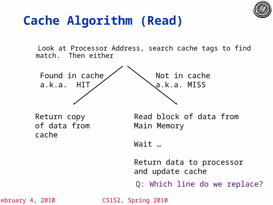
Cache Algorithm (Read)
Look at Processor Address, search cache tags to find match. Then either
Found in cachea.k.a. HIT
Return copyof data fromcache
Not in cachea.k.a. MISS
Read block of data fromMain Memory
Wait …
Return data to processorand update cache
Q: Which line do we replace?

February 4, 2010 CS152, Spring 2010 27
Placement Policy
0 1 2 3 4 5 6 70 1 2 3Set Number
Cache
Fully (2-way) Set DirectAssociative Associative Mappedanywhere anywhere in only into
set 0 block 4 (12 mod 4) (12 mod 8)
0 1 2 3 4 5 6 7 8 91 1 1 1 1 1 1 1 1 1 0 1 2 3 4 5 6 7 8 9
2 2 2 2 2 2 2 2 2 2 0 1 2 3 4 5 6 7 8 9
3 30 1
Memory
Block Number
block 12 can be placed
February 4, 2010 CS152, Spring 2010
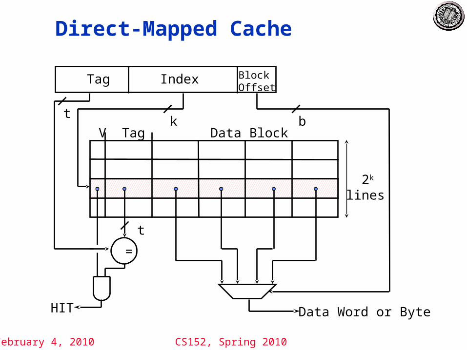
Direct-Mapped Cache
Tag Data Block V
=
BlockOffset
Tag Index
t k b
t
HIT Data Word or Byte
2k
lines

February 4, 2010 CS152, Spring 2010
Direct Map Address Selectionhigher-order vs. lower-order address bits
Tag Data Block V
=
BlockOffset
Index
t k b
t
HIT Data Word or Byte
2k
lines
Tag

February 4, 2010 CS152, Spring 2010
2-Way Set-Associative Cache
Tag Data Block V
=
BlockOffset
Tag Index
t k
b
HIT
Tag Data Block V
DataWordor Byte
=
t
February 4, 2010 CS152, Spring 2010
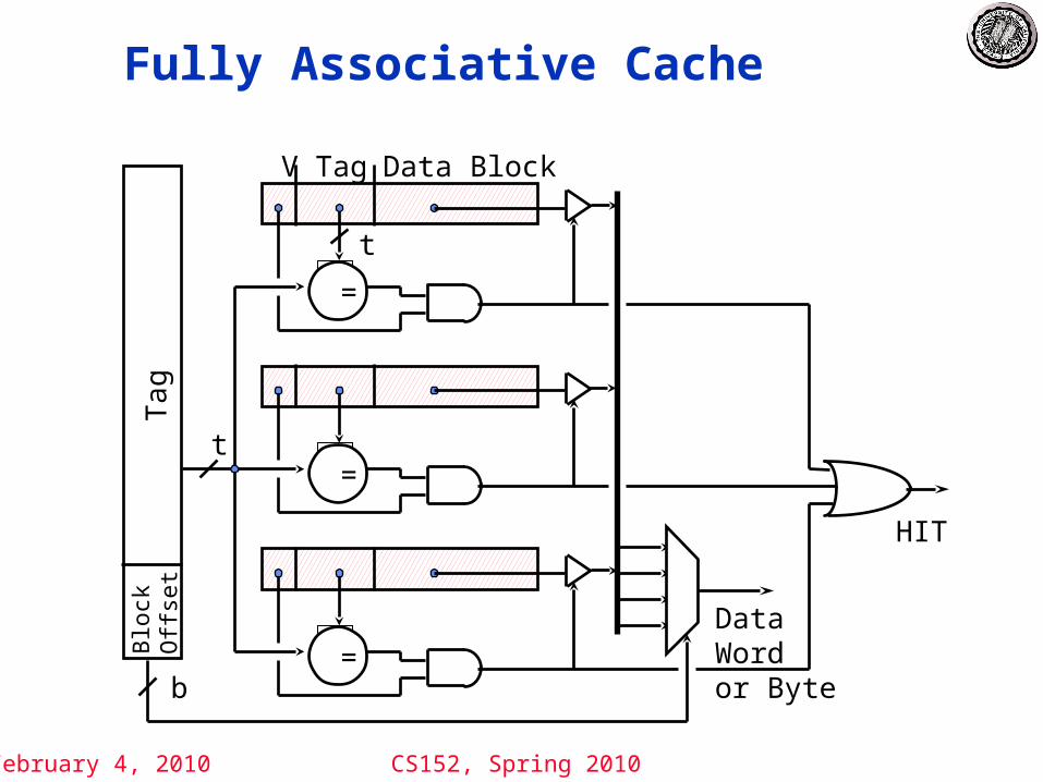
Fully Associative Cache
Tag Data Block V
=
Blo
ckO
ffse
t
Tag
t
b
HIT
DataWordor Byte
=
=
t

February 4, 2010 CS152, Spring 2010 32
Replacement Policy
In an associative cache, which block from a set should be evicted when the set becomes full?
• Random
• Least Recently Used (LRU)• LRU cache state must be updated on every access• true implementation only feasible for small sets (2-way)• pseudo-LRU binary tree often used for 4-8 way
• First In, First Out (FIFO) a.k.a. Round-Robin• used in highly associative caches
• Not Least Recently Used (NLRU)• FIFO with exception for most recently used block or blocks
This is a second-order effect. Why?
Replacement only happens on misses

February 4, 2010 CS152, Spring 2010 33
Acknowledgements
• These slides contain material developed and copyright by:
– Arvind (MIT)– Krste Asanovic (MIT/UCB)– Joel Emer (Intel/MIT)– James Hoe (CMU)– John Kubiatowicz (UCB)– David Patterson (UCB)
• MIT material derived from course 6.823• UCB material derived from course CS252
Related Documents