Fast Fast Communication Communication for Multi – Core for Multi – Core SOPC SOPC Technion – Israel Institute of Technology Department of Electrical Engineering High Speed Digital Systems Lab Supervisor: Evgeny Fiksman Performed by: Moshe Bino Alex Tikh Spring 2007 1’st Semester 1’st Semester Presentation Presentation 1

Fast Communication for Multi – Core SOPC Technion – Israel Institute of Technology Department of Electrical Engineering High Speed Digital Systems Lab.
Dec 20, 2015
Welcome message from author
This document is posted to help you gain knowledge. Please leave a comment to let me know what you think about it! Share it to your friends and learn new things together.
Transcript

Fast Communication Fast Communication for Multi – Core SOPCfor Multi – Core SOPC
Technion – Israel Institute of TechnologyDepartment of Electrical EngineeringHigh Speed Digital Systems Lab
Supervisor: Evgeny Fiksman
Performed by:Moshe BinoAlex Tikh
Spring 2007
1’st Semester Presentation1’st Semester Presentation
1

Table of ContentTable of Content
• Introduction
• Hardware Design
• Software Design
• Debug Process
• Time Table
2Table of Content

Table of ContentTable of Content
• Introduction
• Hardware Design
• Software Design
• Debug Process
• Time Table
3Table of Content

Problem statementProblem statement
• Single CPU is reaching its technological limits, e.g. heat dissipation and cost/power ratio.
• Thus parallel computing evolved, utilizing multi core processor paradigm.
• Three major inter-communication techniques are: Message passing, Shared memory and Remote procedure calls.
4Introduction

Project descriptionProject description
• Multi core system of four MicroBlaze processors is to be built on Xilinx FPGA.
• Message passing model is chosen for processor inter-communication.
• Implemented as MPI library specification.• Network-on-Chip (NoC) methodology employed for cores
interconnect.• Dedicated NoC router is implemented.
5Introduction

Project descriptionProject description
6Introduction

Project descriptionProject description• The project is a basic SoPC platform for
programmable chips.• The system can be combined to a multi-core
processor, which efficiently handles designated tasks or as a group of hardware accelerators which support the main processor unit.
• The system can be expanded into a larger network depending on the device resources.
• The system provides relatively high and flexible computation power on a small device, board etc.
7Introduction

The following components are to be implemented:• Quad core system.• NoC router (4 ports) and infrastructure for fast
communication in multi-core system.• Chosen MPI functions written in C.• Software application demonstrating the advantages of a
parallel system (written in C).
Project goalsProject goals
8Introduction

Constrains:• FPGA (V2P) maximum clock frequency 400MHz.• MicroBlaze core maximum frequency 100MHz.• Processors Memory size 64kbyte. (code + data).• Processor to FSL access time - 3 clock cycles.• Maximum FSL buffer depth is 128 - equals 0.5kbyte.• Interrupt handle time - 20 clock cycles (no interrupts nesting).
Preferences:• Router works at maximum frequency.• Router is designed for relatively small messages – maximum
1kbyte due to processors memory size.
System specificationsSystem specifications
9Introduction

1010
MPI - Message Passing InterfaceMPI - Message Passing Interface• MPI is a library specification (language independent) for
message-passing, proposed as a standard by a broadly based committee of vendors, implementers, and users.
• Designed for high performance on both massively parallel machines and on workstation clusters.
• MPI is widely available, with both free available and vendor-supplied implementations.
Introduction

11
• The upper word is the Header. • The lower word is the Tail. • Data is located in the middle.• Each word is 32 bit.
Message structureMessage structure
TSRCTAGEMPTY SCOMM
Header - Data - Tail
EMPTY HCOMM DSTDATA CNT TYPE CMD
031
Introduction

• The Header consist of the fields:
Message payload Message payload
12
NameSize
(bits)Order Description
H 1 0 Represent the Header
DST 4 1:4 The message destination in the COMM
COMM 4 5:8 The group of cores in the message destination
CMD 4 9:12 The command name for this message (Send, Bcast)
TYPE 4 13:16 The date type in this message
DATA CNT 10 17:26 The number of words in this message
NameSize
(bits)Order Description
T 1 0 Represent the Tail
SRC 4 1:4 The message source port in it’s SCOMM
SCOMM 4 5:8 Group of cores in the message source port
TAG 11 9:19 Message code, group of messages in the same topic\issue
* Empty fields where left to allow network and functionality extensions.
• The Tail consist of the fields:
Introduction

Block diagramBlock diagram
13Introduction
#3
#1
#4#2
MEMORY
FSL BUS FSL BUS
FS
L B
US
FS
L B
US
MPIROUTER
LM
B B
US
OP
B B
US
MEMORY
I/O
MEMORY
LMB BUS
MEMORY
LM
B B
US
* OPB – On Chip Peripheral Bus* FSL – Fast Simplex Link* LMB – Local Memory Bus
OP
B B
US
CLKMuktiplier
x1x4
Rout
er
MB
CLK
Int Hdler
Int Hdler
Int Hdler
Int Hdler

Table of ContentTable of Content
• Introduction
• Hardware Design
• Software Design
• Debug Process
• Time Table
14Table of Content

CROSS BAR
FSL
FSL
MicroB
laze #4
H/TCtrl Bit
FSL
FSL
MicroBlaze #1
H/T
Ctrl B
it
FSL
FSL
MicroB
laze #2
H/TCtrl Bit
FSL
FSL
MicroBlaze #4
H/TCtrl Bit
Router ImplementationRouter Implementation
15Hardware Design

Router specificationRouter specification• The router consists of one major block called Cross Bar.• The Cross Bar is a network switch configured for
switching data across multiple ports. it utilizes an efficient arbiter based on Round Robin mechanism.
• The Cross Bar supports port to port message passing. and broadcasting (not simultaneously).
• The Cross Bar comprise of 2 main units:1. Permission unit.2. Port FSM (for each port).
16Hardware Design

CROSS – BAR CROSS – BAR
17Hardware Design
Cross Bar – Low Level
Clk Rst
Req
Des
t
Prem
it
Req
Des
t
Pre
mit
Req
Dest
Premit
Req
Dest
Premit
Control B
us II
Control Bus II
Control Bus II
Permission Unit
Port
Controls3
Timer & Enable Unit
Control Bus I
Control Bus I
Data Bus 32 Bits
Data Bus 32 Bits
Data B
us
Data B
us
2
Bus I Interface Port2
Bus I Interface
Port2
Bus I Interface
Bus
I In
terf
ace
Por
t 2Port
2
Fsl_S
_Data
Fsl
_M_D
ata
Port #3 FSM
Fsl
_S_R
ead
Fsl
_S_C
ontr
ol
Fsl
_S_H
asD
ata
TO\FROM FSL
Fsl_M
_Write
Fsl_M
_Control
Fsl_M
_Full
Bus II & Data Bus Interface
Port
2
Fsl_S_Data
Fsl_M_Data
Por
t #2
FS
M
Fsl_S_Read
Fsl_S_Control
Fsl_S_HasData
TO
\FR
OM
FS
L
Fsl_M_Write
Fsl_M_Control
Fsl_M_Full
Port2
Fsl
_S_D
ata
Fsl_M
_Data
Port #1 FSM
Fsl_S
_Read
Fsl_S
_Control
Fsl_S
_HasD
ata
TO\FROM FSL
Fsl
_M_W
rite
Fsl
_M_C
ontr
ol
Fsl
_M_F
ull
Por
t2
Fsl_S_Data
Fsl_M_Data
Port #4 F
SM
Fsl_S_Read
Fsl_S_Control
Fsl_S_HasData
TO
\FR
OM
FS
L
Fsl_M_Write
Fsl_M_Control
Fsl_M_Full
Port2
Bus
II &
Dat
a
Bus
Inte
rfac
e
Bus II &
Data
Bus Interface
Bus II & Data Bus Interface
Dest2
Dest
2
Dest2
Des
t2
Dest2

CONTROLLER
Permission Unit
Clk Rst
Timer & EnableUnit
BUSY
TO
\FR
OM
Co
ntro
l Bu
s I
2
2 Port
Des
t
2
Port 2
3 1 2 4
LAST WRITING PORT1 2 3 4
MUX 4X2
1 0 1 0
BUSY PORTS1 2 3 4
MUX 4x1
LAST
Dest
Premit
2 2
2
2 2
Req1Req2Req3Req4
Req
Permission process Permission process
18Hardware Design
• Round Robin arbiter- service order according to loop.
• Check if Dest’ is not busy. • Permit for a ‘time slot’. • If not requesting, service next
requesting port.• BUSY and LAST writing ports
are saved.

Timer Unit Timer Unit
• Timing generator - enables each port for constant ‘time slot’.• When ‘Permit’ input is de-asserted the present time slot is
switched to the next requesting port.• If all ports request permission, priority privilege is by order.• select relevant Req signal to Controller.
19Hardware Design
(EN)Req(EN) Req
EN = L1
Cnt = SlotTime
Permit = 0Cnt = Cnt+1
Y
N
Y
N
Cnt = 0
Timer & EnableUnit
Checks Per 1 Clock Cycle
Clk
Rst
PORT2
Permit
Req1Req2Req3Req4
EN = L2
Last = EN
Req(L1)=1NN
YYY
N
L1 = Last +1
L2 = Last +2
Ln-1 = Last + n-1
L1 < NL2 < NLn-1 < NNN
YYY
N
Req(L2)=1Req(Ln-1)=1
EN = L3
Y
L3 < N
Y
Req(L3)=1N
N
EN = Ln-1

Controller checks (per 1 clock cycle)
CONTROLLER
N
Y
Y
Busy = 1
Port = Last Permit = 0
Busy = 1
Last = Port
Permit =1
N
Permit
Last
Busy
Port
Dest
Clk Rst
Req = 1N
Y
Req
Port = LastN
Busy = 0
Y
ControllerController
20Hardware Design
• Checks if enabled port request permission.• Checks for busy ports with last writing port.• Permit last source port until message delivery ends.• Updates busy and last writing port signals.

Port FSM Port FSM
Message Existence
check
Read Header
Extract Data
Send Data
Read Data
if HasD
ata If C
ontrol = 1/R
eq=1,
Dest =
iIf P
ermitted&
FS
l not Full \ R
eq =1
Perm
itted&
FS
L not Full &
Control =
0 \ write =
1
Has
Dat
a /
Rea
d =
1
Port FSM – State Diagram
Fsl_M_Data
Fsl_S_Read
Fsl_S_Control
Fsl_S_HasData
Fsl_S_Data TO\FROM FSL
Fsl_M_Control/Write/Full
HasData = 0/ Req=0
Clk Rst
Req
Perm
it
TO\FROM CROSS BAR
Dest
2
If Bcast & dest \= MyDest& permitted / dest+1
If co
ntro
l was
1 /
req=
0
1
0
1
1
2
3
21Hardware Design
• Destination is extracted from Header.
• Request is asserted high. • Permission is checked before
any state transition. • When granted, message is
delivered to destination until tail is found.
• In BCAST, each read word is sent to each port destination in a loop. ports written are saved.
• request is de-asserted at end.

22
Control Path Arbiter Control Path Arbiter
• Connects Dest & Permit signals to/from the control Bus according to PORT address.
• Tri-state Buffers - unused Dest signals are fed with high Z.• Unused Permit signals (Port FSM direction) are fed with ‘0’.
PORT
To/From Permission unit
Dest
Perm
it
Permit
Dest
From
/To
port
FSM
If PO
RT =
MY
then
Des
tOut
<=
Dest
In P
erm
itOut
<=
Perm
itIn
Else
Des
tOut
<=
High
Z P
erm
it <=
‘0’
End
if
Dest
Perm
it
Permit
Dest
From
/To
port
FSM
If PO
RT =
MY
then
Des
tOut
<=
Dest
In P
erm
itOut
<=
Perm
itIn
Else
Des
tOut
<=
High
Z P
erm
it <=
‘0’
End
if
Dest
Perm
it
Permit
Dest
From
/To
port
FSM
If PO
RT =
MY
then
Des
tOut
<=
Dest
In P
erm
itOut
<=
Perm
itIn
Else
Des
tOut
<=
High
Z P
erm
it <=
‘0’
End
if
CONTROL PATH ARBITER
Hardware Design

• Connects the appropriate controls and data to the Buses according to PORT address.
• Connects the buses to the appropriate fsl according to DEST address.
• Generally - buses allows increasing ports number by adding Bus Interfaces with the sequential port address.
23Hardware Design
Data Path Arbiter Data Path Arbiter
RX
\TX
RX
\TX
RX
\TX
PO
RT
DE
ST
If P
OR
T=
MY
th
en
T
x <
= T
xS
ign
als
Els
e
Tx
<=
Hig
hZ
En
d i
f
If D
ES
T=
MY
th
en
R
x <
= R
xS
ign
als
En
d i
f
TxSignals
RxSignals
Tx
Rx
If P
OR
T=
MY
th
en
T
x <
= T
xS
ign
als
Els
e
Tx
<=
Hig
hZ
En
d i
f
If D
ES
T=
MY
th
en
R
x <
= R
xS
ign
als
En
d i
f
TxSignals
RxSignals
Tx
Rx
To
FS
LF
rom
po
rt F
SM
To
FS
LF
rom
po
rt F
SM
DATA PATH ARBITER
If P
OR
T=
MY
th
en
T
x <
= T
xS
ign
als
Els
e
Tx
<=
Hig
hZ
En
d i
f
If D
ES
T=
MY
th
en
R
x <
= R
xS
ign
als
En
d i
f
TxSignals
RxSignals
Tx
Rx
To
FS
LF
rom
po
rt F
SM

Example 1 Example 1
• At each time slot part of the message is send to it’s destination as long as the destination port is not busy.
• When Port is busy the next requesting port is service (no delay).
1
H
1
H
1
H
1
H
3
2
3
2
3
2 T4
T
T 4
5
T
1 2 4 1 2 4 1 2 3 4 3 4
Port
T4321H
T321H
T1H
Messages
t
Message Data
MESSAGES DELIVERY EXAMPLE
Destination
1
2
3
4
2
1
2
3T4321H 5
NextNext Next
2 1 3 2 1 3 2 1 2 3 2 3DST
SRC
24Hardware Design

Example 2Example 2
• If one port has no data (port 2) other ports are serviced by order.
1
H
1
H
3
2
3
2 4
T
1 3 4 1 3 4 1
Port
T4321H
T1H
Messages
t
Message Data
MESSAGES DELIVERY EXAMPLE
Destination
1
2
3
4
2
4
3T4321H 5
1
H
Next Next
T
Next
4
5
T
4 4
Next
2 4 3 2 4 3 2 3 3DST
SRC
25Hardware Design

Example 3Example 3
• Handling BCAST command and port arbitrating while 2 ports has the same destination.
1
H
1
H H 1
3
2
T
2 H TT H 1
T
H
Port
T321H
T21H
T1H
Messages
t
Message Data
MESSAGES DELIVERY EXAMPLE
Destination
1
2
3
4
2
1
BCAST
2T4321H
Next
1 T 1
2
3
4
T
DEST
BCAST BCAST BCAST BCAST BCAST BCAST
2 1 4 2 1 1 2 2 14 42 21 2 2 2
Next Next Next Next Next Next Next Next
1 2 3 1 2 3 1 3 3 3 3 4SRC 4 4
26Hardware Design

(MB direction)
H T
t
t
Control bit
Interrupt
Timing diagram
• The fifo control bit is “bubbled” in the fifo, representing the message Header and Tail.
• In the MicroBlaze (MB) direction, This bit indicates the MB about message pending in the fsl pipe. (Interrupt)
• In the router direction, This bit indicates the router about start/end of message.
27Hardware Design
Interrupt HandlerInterrupt Handler

HeaderTail DataDataDataHeaderDataData
FSL Control Bit
InputData
Controls Controls
OutputData
FSL
• Messages data and FSL control bit are bubbled along the FSL channel.
28Hardware Design
FSL – data & controlFSL – data & control

Table of ContentTable of Content
• Introduction
• Hardware Design
• Software Design
• Debug Process
• Time Table
29Table of Content

Software LayersSoftware Layers
• Application Layer: MPI functions interface
• Network Layer: hardware independent implementation of these functions
• Data layer: relies on command bit fields
• Physical layer: designed for FSL bus
Network layer
Application layer
Data layer
Physical layer
30Software Design

MPI Functions setMPI Functions set•Every MPI function returns an error value.•Some of the implemented functions are trivial, and present because required by MPI standard.
MPI_Init( int *argc, char ***argv );
MPI_Comm_rank ( MPI_Comm comm, int *rank );
MPI_Comm_size ( MPI_Comm comm, int *size );
MPI_Finalize();
31Software Design
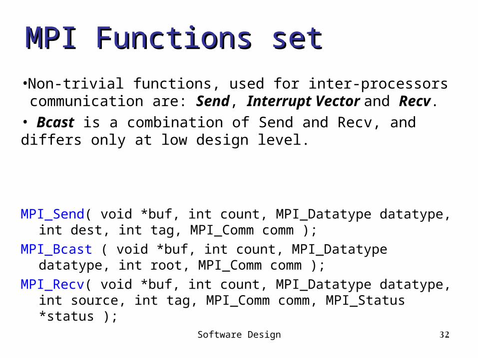
MPIMPI Functions setFunctions set•Non-trivial functions, used for inter-processors communication are: Send, Interrupt Vector and Recv.• Bcast is a combination of Send and Recv, and differs only at low design level.
MPI_Send( void *buf, int count, MPI_Datatype datatype, int dest, int tag, MPI_Comm comm );
MPI_Bcast ( void *buf, int count, MPI_Datatype datatype, int root, MPI_Comm comm );
MPI_Recv( void *buf, int count, MPI_Datatype datatype, int source, int tag, MPI_Comm comm, MPI_Status *status );
32Software Design

33
MPI Functions setMPI Functions set
•Three additional complimentary functions.•Supply additional info about the received message.
MPI_Get_source( MPI_Status* status, MPI_Datatype
datatype, int *source );
MPI_Get_count( MPI_Status* status, MPI_Datatype
datatype, int *count );
MPI_Get_tag( MPI_Status* status, MPI_Datatype datatype,
int *tag );
Software Design

MPI_Send
Compose Header and
Tail
Send Header
Send Message
(body)
Send Tail
return
MPI_Send: composes header and
tail, and sends it with the message
(body)
Sending the messageSending the message
34Software Design

Receiving the Receiving the messagemessage
Interrupt Vector: receives
incoming messages, and stores
them in suitable linked list
Interrupt Vector
Receive Header
Allocate Node according to Header info
Receive Message
Receive Tail
Construct Node
return
Add Node to end of appropriate list
35Software Design

36
Return received Return received messagemessage
MPI_Recv: message
details received from user.
Looks for this message in
linked list of already
received messages
MPI_Recv
Compose search Key for linked list
Look for message Node
Is Node found?Remove from list
Return message
Jump to Interrupt Vector (when return, some
message had arrived)noyes
Software Design

Example applicationExample applicationMatrix - Vector multiplicationMatrix - Vector multiplication
• Typical example of highly parallel application.• Root processor broadcasts VectorVector.• Selected Matrix Row Matrix Row sent by root to each
processor.• Each processor computes and returns its result.• Computed results are combined into a vector by
root processor.
37Software Design

Example applicationExample applicationMatrix - Vector multiplicationMatrix - Vector multiplication
11 12 13 1
21 22 23 2
31 32 33 3
a a a b
a a a b
a a a b
1
11 12 13 2
3
b
a a a b
b
38Software Design
Root

Table of ContentTable of Content
• Introduction
• Hardware Design
• Software Design
• Debug Process
• Time Table
39Table of Content
40
CROSS BAR
FSL
FSL
FSL_writer/reader
Autom
aticTest Bench H/T
Ctrl Bit
FSL
FSL
FSL_writer/readerAutomaticTest Bench
H/T
Ctrl Bit
FSL
FSL
FSL_writer/reader
Autom
aticTest Bench
H/TCtrl Bit
FSL
FSL
FSL_writer/readerAutomaticTest Bench
H/TCtrl Bit
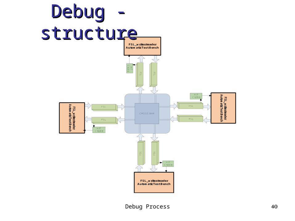
Debug - structureDebug - structure
Debug Process

InputMessages
File
OutputMessages
File
OutputMessages
File
Write ToFSL
Read FromFSL
Fsl_out_data
Fsl_in_data
Test Bench
• The Test Bench reads
messages from a file and
write them into the FSL pipe
(MB output side).
• It also reads messages from
the pipe (MB input side).
• Signals can also be viewed
in ModelSim
Debug – Test BenchDebug – Test Bench
41Debug Process

Table of ContentTable of Content
• Introduction
• Hardware Design
• Software Design
• Debug Process
• Time Table
42Table of Content

Semester 2 - TasksSemester 2 - Tasks
43
• Build a quad core system Done
• Implement router for the system• build a modular router in VHDL
01-03-08
• Test and debug• Router (hardware)
• MPI API (software)
01-04-08
• Run a test application• measure speed-up as function of average message size and messages amount
25-04-08
Time Table

QUESTIONS ?QUESTIONS ?
Related Documents