November 2013 © 2009 Fairchild Semiconductor Corporation www.fairchildsemi.com FAN7602C • Rev. 1.0.1 FAN7602C — Green Current Mode PWM Controller FAN7602C Green Current Mode PWM Controller Features Green Current Mode PWM Controller Random Frequency Fluctuation for Low EMI Internal High-Voltage Startup Switch Burst Mode Operation Line Voltage Feedforward to Limit Maximum Power Line Under-Voltage Protection Latch Protection & Internal Soft-Start (10ms) Function Overload Protection (OLP) Over-Voltage Protection (OVP) Over-Temperature Protection (OTP) Low Operation Current: 1 mA Typical Available in the 8-Lead SOP Package Applications Adapter LCD Monitor Power Auxiliary Power Supply Related Resources AN-6014- Green Current Mode PWM Controller (Except for frequency fluctuation part in AN-6014) Description The FAN7602C is a green current-mode PWM controller. It is specially designed for off-line adapter applications; DVDP, VCR, LCD monitor applications; and auxiliary power supplies. The internal high-voltage startup switch and the burst mode operation reduce the power loss in standby mode. As a result, the input power is lower than 1 W when the input line voltage is 265 VAC and the load is 0.5 W. At no-load condition, input power is under 0.15 W. The maximum power can be limited constantly, regardless of the line voltage change, using the power limit function. The switching frequency is not fixed and has random frequency fluctuation. The FAN7602C includes various protections for the system reliability and the internal soft-start prevents the output voltage over-shoot at startup. Ordering Information Part Number Operating Junction Temperature Package Packing Method Top Mark FAN7602CMX -40°C to +150°C 8-Lead Small Outline Package (SOP) Tape and Reel FAN7602C

Welcome message from author
This document is posted to help you gain knowledge. Please leave a comment to let me know what you think about it! Share it to your friends and learn new things together.
Transcript

November 2013
© 2009 Fairchild Semiconductor Corporation www.fairchildsemi.com FAN7602C • Rev. 1.0.1
FAN
7602C —
Green C
urrent Mode PW
M C
ontroller
FAN7602C Green Current Mode PWM Controller Features Green Current Mode PWM Controller Random Frequency Fluctuation for Low EMI Internal High-Voltage Startup Switch Burst Mode Operation Line Voltage Feedforward to Limit Maximum Power Line Under-Voltage Protection Latch Protection & Internal Soft-Start (10ms) Function Overload Protection (OLP) Over-Voltage Protection (OVP) Over-Temperature Protection (OTP) Low Operation Current: 1 mA Typical Available in the 8-Lead SOP Package
Applications Adapter LCD Monitor Power Auxiliary Power Supply
Related Resources
AN-6014- Green Current Mode PWM Controller (Except for frequency fluctuation part in AN-6014)
Description The FAN7602C is a green current-mode PWM controller. It is specially designed for off-line adapter applications; DVDP, VCR, LCD monitor applications; and auxiliary power supplies.
The internal high-voltage startup switch and the burst mode operation reduce the power loss in standby mode. As a result, the input power is lower than 1 W when the input line voltage is 265 VAC and the load is 0.5 W. At no-load condition, input power is under 0.15 W.
The maximum power can be limited constantly, regardless of the line voltage change, using the power limit function.
The switching frequency is not fixed and has random frequency fluctuation.
The FAN7602C includes various protections for the system reliability and the internal soft-start prevents the output voltage over-shoot at startup.
Ordering Information
Part Number Operating Junction Temperature Package Packing Method Top Mark
FAN7602CMX -40°C to +150°C 8-Lead Small Outline Package (SOP) Tape and Reel FAN7602C
© 2009 Fairchild Semiconductor Corporation www.fairchildsemi.com FAN7602C • Rev. 1.0.1 2
FAN
7602C —
Green C
urrent Mode PW
M C
ontroller
Typical Application Diagram
FAN7602C
LUVP
CS/FB
GND
VSTR
VCC
Out
Latch/Plimit NC
Figure 1. Typical Flyback Application
Internal Block Diagram
Soft- Start
Delay Circuit
GND
PlimitOffset
5V Ref
VCC
LUVP
OUT
CS/FB
UVLO
6
19V
OVP
12V/8V
5
3
0.95V/0.88V
8
1
4
VSTR
2V/1.5V
4V
Latch/Plimit 2
PlimitOffset
Generator
Driver Circuit
Latch
OLP
OLP
10ms Soft-Start
SS End
PWMBlock
Power Limit
Soft-Start
PWM+
PlimitOffset
PlimitOffset
SS End
LUVP
Reset Circuit
OSC
LatchOVP
OLP
VCC
TSDAuto RestartProtection
Latch Protection
Random
Figure 2. Functional Block Diagram
© 2009 Fairchild Semiconductor Corporation www.fairchildsemi.com FAN7602C • Rev. 1.0.1 3
FAN
7602C —
Green C
urrent Mode PW
M C
ontroller
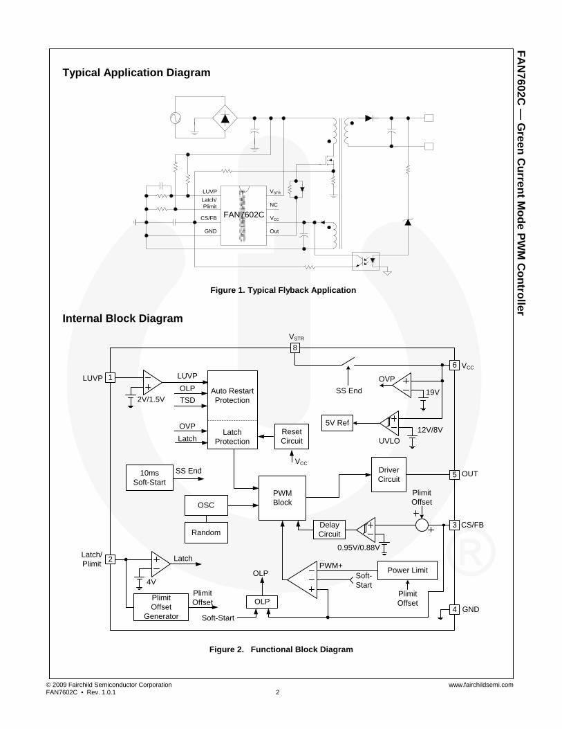
Pin Configuration
F A N 7 6 0 2 C
1 2
6 58 7
3 4
Latch/Plimit
GNDCS/FBLUVP
VSTR NC VCC Out
Y W W
Figure 3. Pin Configuration (Top View)
Pin Definitions Pin # Name Description
1 LUVP Line Under-Voltage Protection Pin. This pin is used to protect the set when the input voltage is lower than the rated input voltage range.
2 Latch/Plimit Latch Protection and Power Limit Pin. When the pin voltage exceeds 4 V, the latch protection works. The latch protection is reset when the VCC voltage is lower than 5 V. For the power limit function, the OCP level decreases as the pin voltage increases.
3 CS/FB Current Sense and Feedback Pin. This pin is used to sense the MOSFET current for the current mode PWM and OCP. The output voltage feedback information and the current sense information are added using an external RC filter.
4 GND Ground Pin. This pin is used for the ground potential of all the pins. For proper operation, the signal ground and the power ground should be separated.
5 OUT Gate Drive Output Pin. This pin is an output pin to drive an external MOSFET. The peak sourcing current is 450 mA and the peak sinking current is 600 mA. For proper operation, the stray inductance in the gate driving path must be minimized.
6 VCC Supply Voltage Pin. IC operating current and MOSFET driving current are supplied using this pin.
7 NC No Connection.
8 VSTR Startup Pin. This pin is used to supply IC operating current during IC startup. After startup, the internal JFET is turned off to reduce power loss.
© 2009 Fairchild Semiconductor Corporation www.fairchildsemi.com FAN7602C • Rev. 1.0.1 4
FAN
7602C —
Green C
urrent Mode PW
M C
ontroller
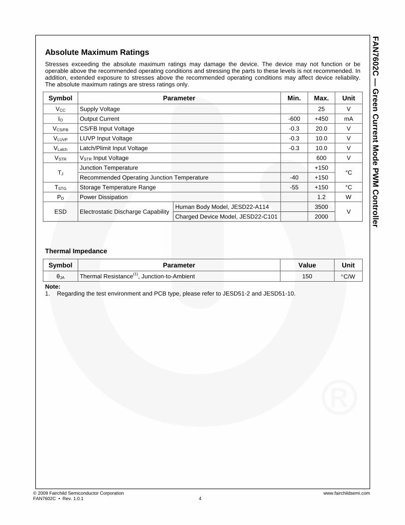
Absolute Maximum Ratings Stresses exceeding the absolute maximum ratings may damage the device. The device may not function or be operable above the recommended operating conditions and stressing the parts to these levels is not recommended. In addition, extended exposure to stresses above the recommended operating conditions may affect device reliability. The absolute maximum ratings are stress ratings only.
Symbol Parameter Min. Max. Unit VCC Supply Voltage 25 V IO Output Current -600 +450 mA
VCS/FB CS/FB Input Voltage -0.3 20.0 V VLUVP LUVP Input Voltage -0.3 10.0 V VLatch Latch/Plimit Input Voltage -0.3 10.0 V VSTR VSTR Input Voltage 600 V
TJ Junction Temperature +150
°C Recommended Operating Junction Temperature -40 +150
TSTG Storage Temperature Range -55 +150 °C PD Power Dissipation 1.2 W
ESD Electrostatic Discharge Capability Human Body Model, JESD22-A114 3500
V Charged Device Model, JESD22-C101 2000
Thermal Impedance
Symbol Parameter Value Unit θJA Thermal Resistance(1), Junction-to-Ambient 150 °C/W
Note: 1. Regarding the test environment and PCB type, please refer to JESD51-2 and JESD51-10.
© 2009 Fairchild Semiconductor Corporation www.fairchildsemi.com FAN7602C • Rev. 1.0.1 5
FAN
7602C —
Green C
urrent Mode PW
M C
ontroller
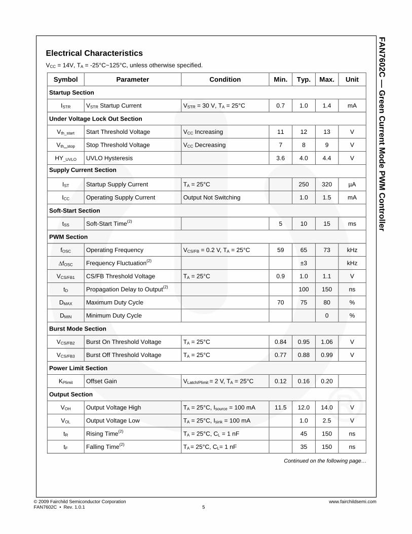
Electrical Characteristics VCC = 14V, TA = -25°C~125°C, unless otherwise specified.
Symbol Parameter Condition Min. Typ. Max. Unit
Startup Section
ISTR VSTR Startup Current VSTR = 30 V, TA = 25°C 0.7 1.0 1.4 mA
Under Voltage Lock Out Section
Vth_start Start Threshold Voltage VCC Increasing 11 12 13 V
Vth_stop Stop Threshold Voltage VCC Decreasing 7 8 9 V
HY_UVLO UVLO Hysteresis 3.6 4.0 4.4 V
Supply Current Section
IST Startup Supply Current TA = 25°C 250 320 µA
ICC Operating Supply Current Output Not Switching 1.0 1.5 mA
Soft-Start Section
tSS Soft-Start Time(2) 5 10 15 ms
PWM Section
fOSC Operating Frequency VCS/FB = 0.2 V, TA = 25°C 59 65 73 kHz
∆fOSC Frequency Fluctuation(2) ±3 kHz
VCS/FB1 CS/FB Threshold Voltage TA = 25°C 0.9 1.0 1.1 V
tD Propagation Delay to Output(2) 100 150 ns
DMAX Maximum Duty Cycle 70 75 80 %
DMIN Minimum Duty Cycle 0 %
Burst Mode Section
VCS/FB2 Burst On Threshold Voltage TA = 25°C 0.84 0.95 1.06 V
VCS/FB3 Burst Off Threshold Voltage TA = 25°C 0.77 0.88 0.99 V
Power Limit Section
KPlimit Offset Gain VLatch/Plimit = 2 V, TA = 25°C 0.12 0.16 0.20
Output Section
VOH Output Voltage High TA = 25°C, Isource = 100 mA 11.5 12.0 14.0 V
VOL Output Voltage Low TA = 25°C, Isink = 100 mA 1.0 2.5 V
tR Rising Time(2) TA = 25°C, CL = 1 nF 45 150 ns
tF Falling Time(2) TA = 25°C, CL= 1 nF 35 150 ns
Continued on the following page…
© 2009 Fairchild Semiconductor Corporation www.fairchildsemi.com FAN7602C • Rev. 1.0.1 6
FAN
7602C —
Green C
urrent Mode PW
M C
ontroller
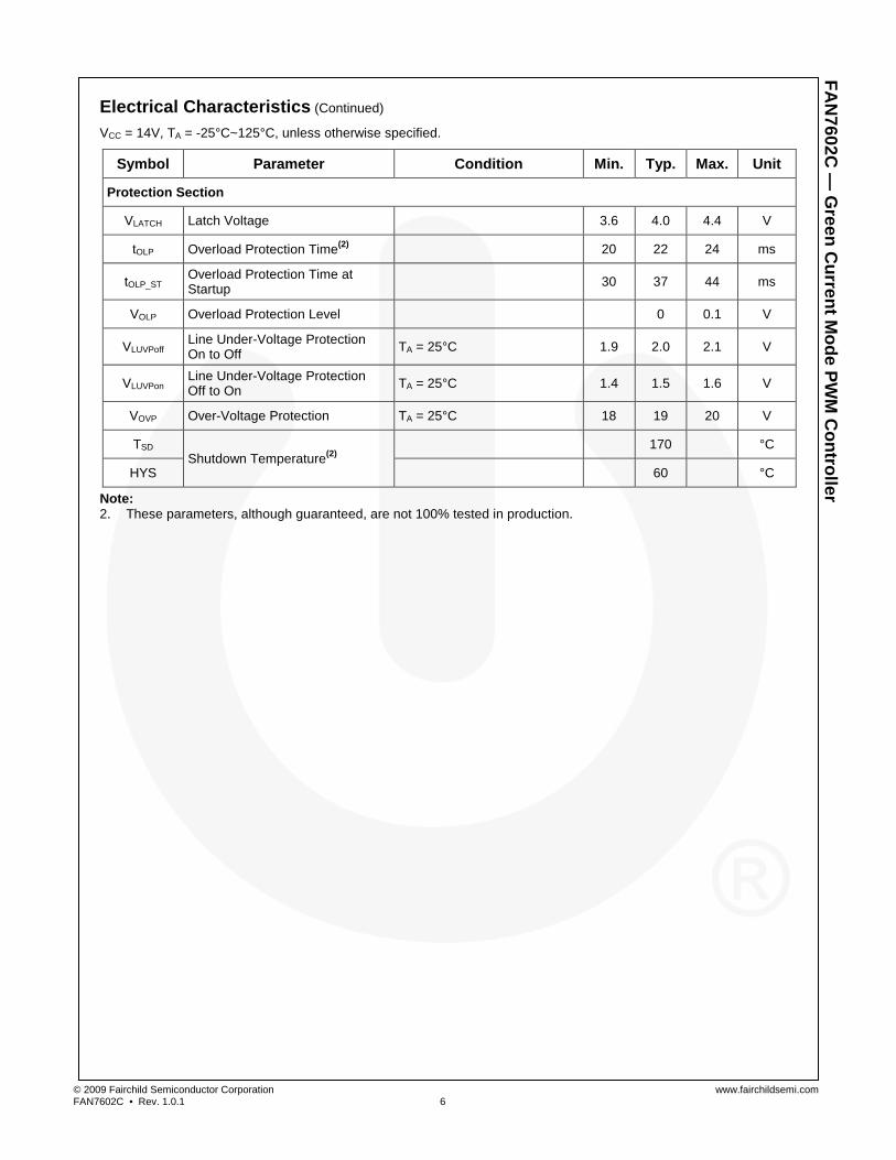
Electrical Characteristics (Continued) VCC = 14V, TA = -25°C~125°C, unless otherwise specified.
Symbol Parameter Condition Min. Typ. Max. Unit
Protection Section
VLATCH Latch Voltage 3.6 4.0 4.4 V
tOLP Overload Protection Time(2) 20 22 24 ms
tOLP_ST Overload Protection Time at Startup 30 37 44 ms
VOLP Overload Protection Level 0 0.1 V
VLUVPoff Line Under-Voltage Protection On to Off TA = 25°C 1.9 2.0 2.1 V
VLUVPon Line Under-Voltage Protection Off to On TA = 25°C 1.4 1.5 1.6 V
VOVP Over-Voltage Protection TA = 25°C 18 19 20 V
TSD Shutdown Temperature(2)
170 °C
HYS 60 °C
Note: 2. These parameters, although guaranteed, are not 100% tested in production.
© 2009 Fairchild Semiconductor Corporation www.fairchildsemi.com FAN7602C • Rev. 1.0.1 7
FAN
7602C —
Green C
urrent Mode PW
M C
ontroller
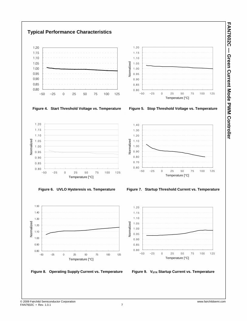
Typical Performance Characteristics
0.80
0.85
0.90
0.95
1.00
1.05
1.10
1.15
1.20
-50 -25 0 25 50 75 100 125
Nor
mal
ized
0.80
0.85
0.90
0.95
1.00
1.05
1.10
1.15
1.20
-50 -25 0 25 50 75 100 125
Temperature [°C]
Figure 4. Start Threshold Voltage vs. Temperature Figure 5. Stop Threshold Voltage vs. Temperature
Nor
mal
ized
0.80
0.85
0.90
0.95
1.00
1.05
1.10
1.15
1.20
-50 -25 0 25 50 75 100 125
Temperature [°C]
0.60
0.70
0.80
0.90
1.00
1.10
1.20
1.30
1.40
-50 -25 0 25 50 75 100 125
Nor
mal
ized
Temperature [°C]
Figure 6. UVLO Hysteresis vs. Temperature Figure 7. Startup Threshold Current vs. Temperature
0.80
0.90
1.00
1.10
1.20
1.30
1.40
1.50
-50 -25 0 25 50 75 100 125
Nor
mal
ized
Temperature [°C]
Nor
mal
ized
0.80
0.85
0.90
0.95
1.00
1.05
1.10
1.15
1.20
-50 -25 0 25 50 75 100 125
Temperature [°C]
Figure 8. Operating Supply Current vs. Temperature Figure 9. VSTR Startup Current vs. Temperature
© 2009 Fairchild Semiconductor Corporation www.fairchildsemi.com FAN7602C • Rev. 1.0.1 8
FAN
7602C —
Green C
urrent Mode PW
M C
ontroller
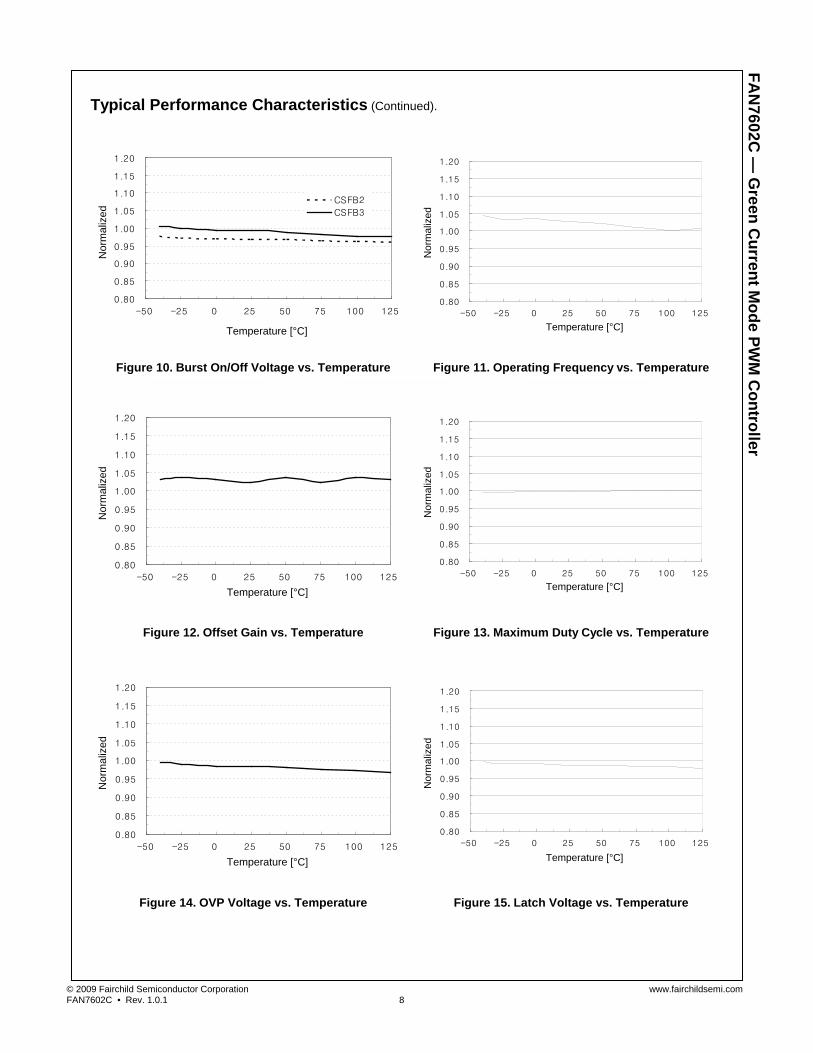
Typical Performance Characteristics (Continued). N
orm
aliz
ed
Temperature [°C]
0.80
0.85
0.90
0.95
1.00
1.05
1.10
1.15
1.20
-50 -25 0 25 50 75 100 125
CSFB2
CSFB3
Nor
mal
ized
Temperature [°C]
0.80
0.85
0.90
0.95
1.00
1.05
1.10
1.15
1.20
-50 -25 0 25 50 75 100 125
Figure 10. Burst On/Off Voltage vs. Temperature Figure 11. Operating Frequency vs. Temperature
Nor
mal
ized
Temperature [°C]
0.80
0.85
0.90
0.95
1.00
1.05
1.10
1.15
1.20
-50 -25 0 25 50 75 100 125
Nor
mal
ized
Temperature [°C]
0.80
0.85
0.90
0.95
1.00
1.05
1.10
1.15
1.20
-50 -25 0 25 50 75 100 125
Figure 12. Offset Gain vs. Temperature Figure 13. Maximum Duty Cycle vs. Temperature
Nor
mal
ized
Temperature [°C]
0.80
0.85
0.90
0.95
1.00
1.05
1.10
1.15
1.20
-50 -25 0 25 50 75 100 125
Nor
mal
ized
Temperature [°C]
0.80
0.85
0.90
0.95
1.00
1.05
1.10
1.15
1.20
-50 -25 0 25 50 75 100 125
Figure 14. OVP Voltage vs. Temperature Figure 15. Latch Voltage vs. Temperature
© 2009 Fairchild Semiconductor Corporation www.fairchildsemi.com FAN7602C • Rev. 1.0.1 9
FAN
7602C —
Green C
urrent Mode PW
M C
ontroller
Typical Performance Characteristics (Continued) N
orm
aliz
ed
Temperature [°C]
0.80
0.85
0.90
0.95
1.00
1.05
1.10
1.15
1.20
-50 -25 0 25 50 75 100 125
Nor
mal
ized
Temperature [°C]
0.80
0.85
0.90
0.95
1.00
1.05
1.10
1.15
1.20
-50 -25 0 25 50 75 100 125
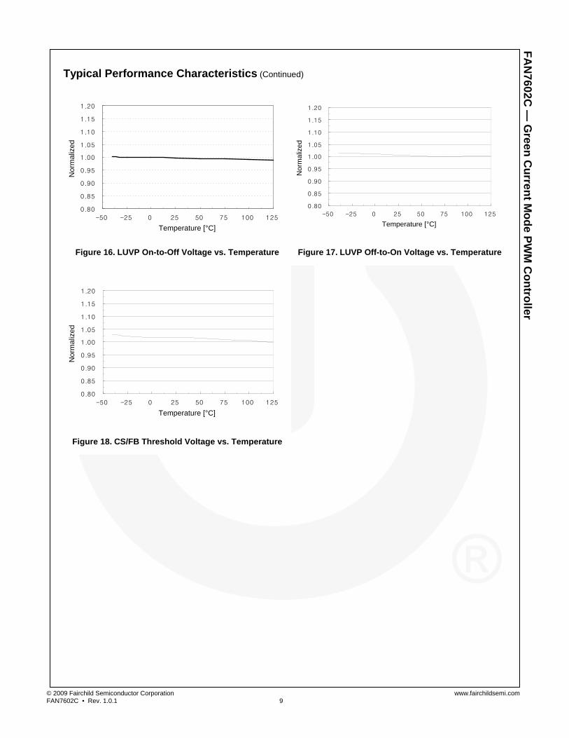
Figure 16. LUVP On-to-Off Voltage vs. Temperature Figure 17. LUVP Off-to-On Voltage vs. Temperature
Nor
mal
ized
Temperature [°C]
0.80
0.85
0.90
0.95
1.00
1.05
1.10
1.15
1.20
-50 -25 0 25 50 75 100 125
Figure 18. CS/FB Threshold Voltage vs. Temperature
© 2009 Fairchild Semiconductor Corporation www.fairchildsemi.com FAN7602C • Rev. 1.0.1 10
FAN
7602C —
Green C
urrent Mode PW
M C
ontroller
Application Information
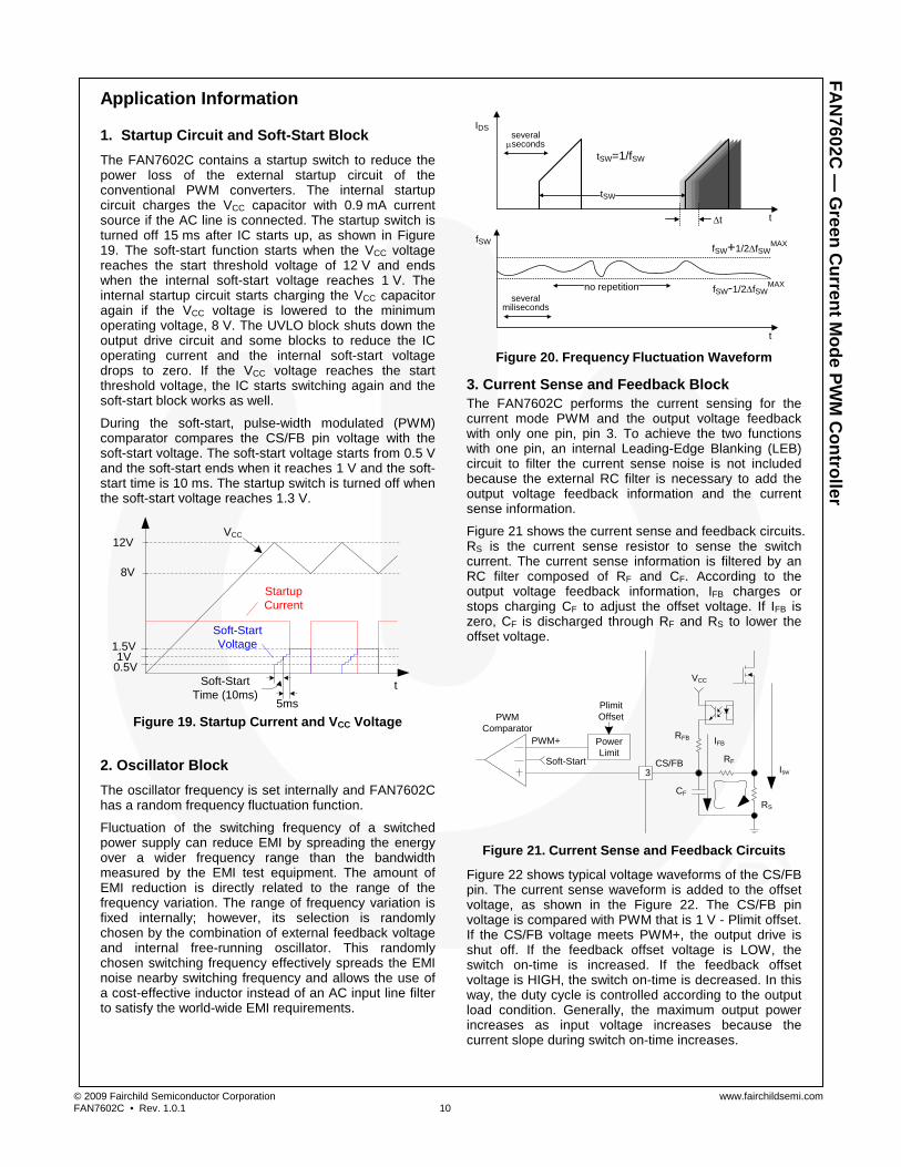
1. Startup Circuit and Soft-Start Block The FAN7602C contains a startup switch to reduce the power loss of the external startup circuit of the conventional PWM converters. The internal startup circuit charges the VCC capacitor with 0.9 mA current source if the AC line is connected. The startup switch is turned off 15 ms after IC starts up, as shown in Figure 19. The soft-start function starts when the VCC voltage reaches the start threshold voltage of 12 V and ends when the internal soft-start voltage reaches 1 V. The internal startup circuit starts charging the VCC capacitor again if the VCC voltage is lowered to the minimum operating voltage, 8 V. The UVLO block shuts down the output drive circuit and some blocks to reduce the IC operating current and the internal soft-start voltage drops to zero. If the VCC voltage reaches the start threshold voltage, the IC starts switching again and the soft-start block works as well.
During the soft-start, pulse-width modulated (PWM) comparator compares the CS/FB pin voltage with the soft-start voltage. The soft-start voltage starts from 0.5 V and the soft-start ends when it reaches 1 V and the soft-start time is 10 ms. The startup switch is turned off when the soft-start voltage reaches 1.3 V.
tSoft-StartTime (10ms)
12V
8V
VCC
Startup Current
Soft-StartVoltage
1V1.5V
0.5V
5ms Figure 19. Startup Current and VCC Voltage
2. Oscillator Block The oscillator frequency is set internally and FAN7602C has a random frequency fluctuation function.
Fluctuation of the switching frequency of a switched power supply can reduce EMI by spreading the energy over a wider frequency range than the bandwidth measured by the EMI test equipment. The amount of EMI reduction is directly related to the range of the frequency variation. The range of frequency variation is fixed internally; however, its selection is randomly chosen by the combination of external feedback voltage and internal free-running oscillator. This randomly chosen switching frequency effectively spreads the EMI noise nearby switching frequency and allows the use of a cost-effective inductor instead of an AC input line filter to satisfy the world-wide EMI requirements.
tSW
∆t
IDS
t
t
fSWfSW+1/2∆fSW
MAX
fSW-1/2∆fSWMAXno repetition
several µseconds
several miliseconds
tSW=1/fSW
Figure 20. Frequency Fluctuation Waveform
3. Current Sense and Feedback Block The FAN7602C performs the current sensing for the current mode PWM and the output voltage feedback with only one pin, pin 3. To achieve the two functions with one pin, an internal Leading-Edge Blanking (LEB) circuit to filter the current sense noise is not included because the external RC filter is necessary to add the output voltage feedback information and the current sense information. Figure 21 shows the current sense and feedback circuits. RS is the current sense resistor to sense the switch current. The current sense information is filtered by an RC filter composed of RF and CF. According to the output voltage feedback information, IFB charges or stops charging CF to adjust the offset voltage. If IFB is zero, CF is discharged through RF and RS to lower the offset voltage.
Soft-Start CS/FB3
PWM Comparator
VCC
CF
RF
RS
RFB IFB
Isw
PlimitOffset
Power Limit
PWM+
Figure 21. Current Sense and Feedback Circuits
Figure 22 shows typical voltage waveforms of the CS/FB pin. The current sense waveform is added to the offset voltage, as shown in the Figure 22. The CS/FB pin voltage is compared with PWM that is 1 V - Plimit offset. If the CS/FB voltage meets PWM+, the output drive is shut off. If the feedback offset voltage is LOW, the switch on-time is increased. If the feedback offset voltage is HIGH, the switch on-time is decreased. In this way, the duty cycle is controlled according to the output load condition. Generally, the maximum output power increases as input voltage increases because the current slope during switch on-time increases.
© 2009 Fairchild Semiconductor Corporation www.fairchildsemi.com FAN7602C • Rev. 1.0.1 11
FAN
7602C —
Green C
urrent Mode PW
M C
ontroller
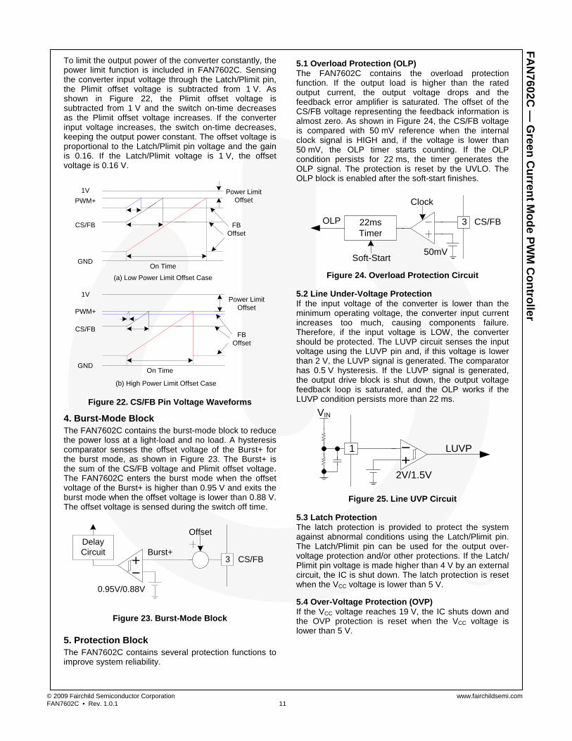
To limit the output power of the converter constantly, the power limit function is included in FAN7602C. Sensing the converter input voltage through the Latch/Plimit pin, the Plimit offset voltage is subtracted from 1 V. As shown in Figure 22, the Plimit offset voltage is subtracted from 1 V and the switch on-time decreases as the Plimit offset voltage increases. If the converter input voltage increases, the switch on-time decreases, keeping the output power constant. The offset voltage is proportional to the Latch/Plimit pin voltage and the gain is 0.16. If the Latch/Plimit voltage is 1 V, the offset voltage is 0.16 V.
PWM+
CS/FB
GNDOn Time
FBOffset
1V Power Limit Offset
(a) Low Power Limit Offset Case
PWM+
CS/FB
GNDOn Time
FBOffset
1VPower Limit
Offset
(b) High Power Limit Offset Case
Figure 22. CS/FB Pin Voltage Waveforms
4. Burst-Mode Block The FAN7602C contains the burst-mode block to reduce the power loss at a light-load and no load. A hysteresis comparator senses the offset voltage of the Burst+ for the burst mode, as shown in Figure 23. The Burst+ is the sum of the CS/FB voltage and Plimit offset voltage. The FAN7602C enters the burst mode when the offset voltage of the Burst+ is higher than 0.95 V and exits the burst mode when the offset voltage is lower than 0.88 V. The offset voltage is sensed during the switch off time.
CS/FB
Delay Circuit
3+−
0.95V/0.88V
Burst+
Offset
Figure 23. Burst-Mode Block
5. Protection Block The FAN7602C contains several protection functions to improve system reliability.
5.1 Overload Protection (OLP) The FAN7602C contains the overload protection function. If the output load is higher than the rated output current, the output voltage drops and the feedback error amplifier is saturated. The offset of the CS/FB voltage representing the feedback information is almost zero. As shown in Figure 24, the CS/FB voltage is compared with 50 mV reference when the internal clock signal is HIGH and, if the voltage is lower than 50 mV, the OLP timer starts counting. If the OLP condition persists for 22 ms, the timer generates the OLP signal. The protection is reset by the UVLO. The OLP block is enabled after the soft-start finishes.
OLP
50mV
22ms Timer
Soft-Start
Clock
CS/FB3
Figure 24. Overload Protection Circuit
5.2 Line Under-Voltage Protection If the input voltage of the converter is lower than the minimum operating voltage, the converter input current increases too much, causing components failure. Therefore, if the input voltage is LOW, the converter should be protected. The LUVP circuit senses the input voltage using the LUVP pin and, if this voltage is lower than 2 V, the LUVP signal is generated. The comparator has 0.5 V hysteresis. If the LUVP signal is generated, the output drive block is shut down, the output voltage feedback loop is saturated, and the OLP works if the LUVP condition persists more than 22 ms.
2V/1.5V
1+− LUVP
VIN
Figure 25. Line UVP Circuit
5.3 Latch Protection The latch protection is provided to protect the system against abnormal conditions using the Latch/Plimit pin. The Latch/Plimit pin can be used for the output over- voltage protection and/or other protections. If the Latch/ Plimit pin voltage is made higher than 4 V by an external circuit, the IC is shut down. The latch protection is reset when the VCC voltage is lower than 5 V.
5.4 Over-Voltage Protection (OVP) If the VCC voltage reaches 19 V, the IC shuts down and the OVP protection is reset when the VCC voltage is lower than 5 V.
© 2009 Fairchild Semiconductor Corporation www.fairchildsemi.com FAN7602C • Rev. 1.0.1 12
FAN
7602C —
Green C
urrent Mode PW
M C
ontroller
6. Output Drive Block The FAN7602C contains a single totem-pole output stage to drive a power MOSFET. The drive output is capable of up to 450 mA sourcing current and 600 mA
sinking current with typical rise and fall time of 45 ns and 35 ns, respectively, with a 1 nF load.
Typical Application Circuit
Application Output Power Input Voltage Output Voltage
Adaptor 48 W Universal Input (85 ~ 265 VAC) 12V
Features Low stand-by power (<0.15 W at 265 VAC) Constant output power control
Key Design Notes All the IC-related components should be placed close to IC, especially C107 and C110. If R106 value is too low, there can be subharmonic oscillation. R109 should be designed carefully to make the VCC voltage higher than 8 V when the input voltage is 265 VAC at
no load. R110 should be designed carefully to make the VCC voltage lower than OVP level when the input voltage is 85 VAC
at full load. R103 should be designed to keep the MOSFET VDS voltage lower than maximum rating when the output is
shorted.
© 2009 Fairchild Semiconductor Corporation www.fairchildsemi.com FAN7602C • Rev. 1.0.1 13
FAN
7602C —
Green C
urrent Mode PW
M C
ontroller
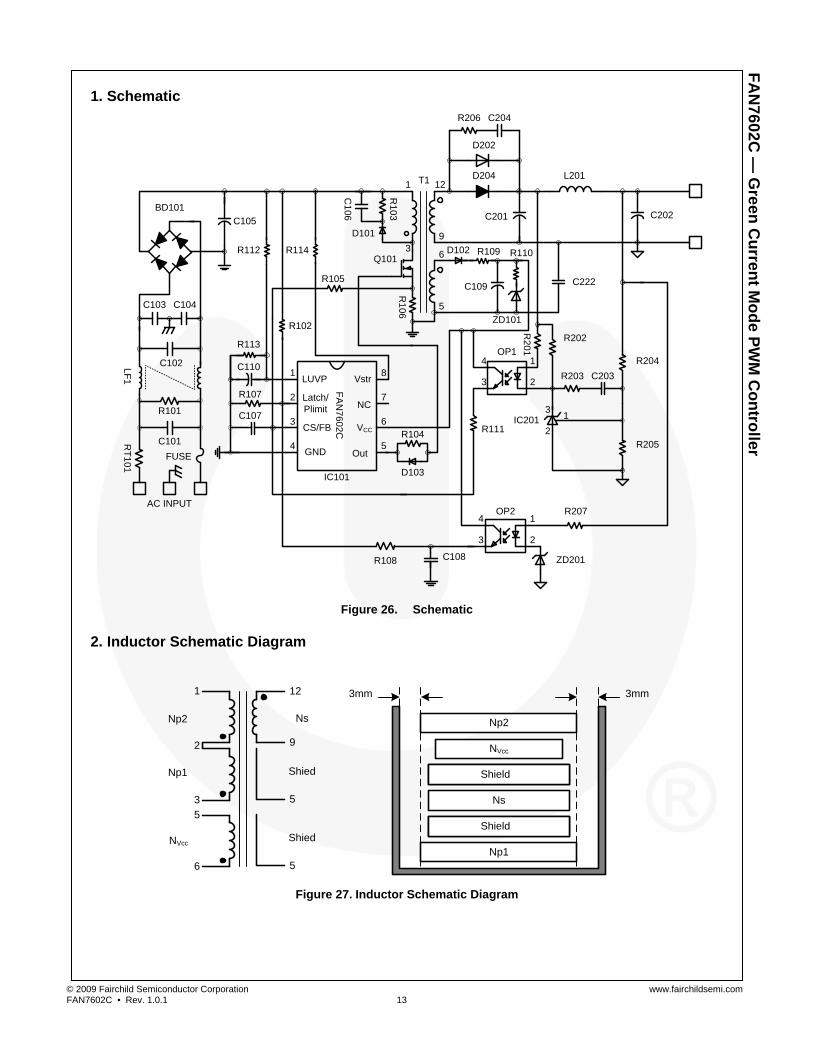
1. Schematic
FUSE
AC INPUT
C101
LF1
C102
RT101
BD101C105 C202
D204 L201
R204
R103
R101
5
6
7
8
NC
Vstr
VCC
Out
LUVP
CS/FB
Latch/Plimit
GND
FAN
7602C
1
2
3
4 R205
C203R203
R202
R201
C201
D102
IC201
OP1
R111R104
D103
R106
Q101
T1
C106
D101
R105
IC101
C110
R113
C107
C204R206
D202
C109
C103 C104
C222
1
23
4
C108
5
6
1
3
12
9
R207
ZD201R108
OP21
23
4
R109R112
R102
R107
12
3
R110
ZD101
R114
Figure 26. Schematic
2. Inductor Schematic Diagram
Np2
5
6
1
2
12
9
3
NVcc
Ns
Np1 Shied
5
Shied
5
3mm 3mm
Ns
Np1
Np2
NVcc
NsShield
NsShield
Figure 27. Inductor Schematic Diagram
© 2009 Fairchild Semiconductor Corporation www.fairchildsemi.com FAN7602C • Rev. 1.0.1 14
FAN
7602C —
Green C
urrent Mode PW
M C
ontroller
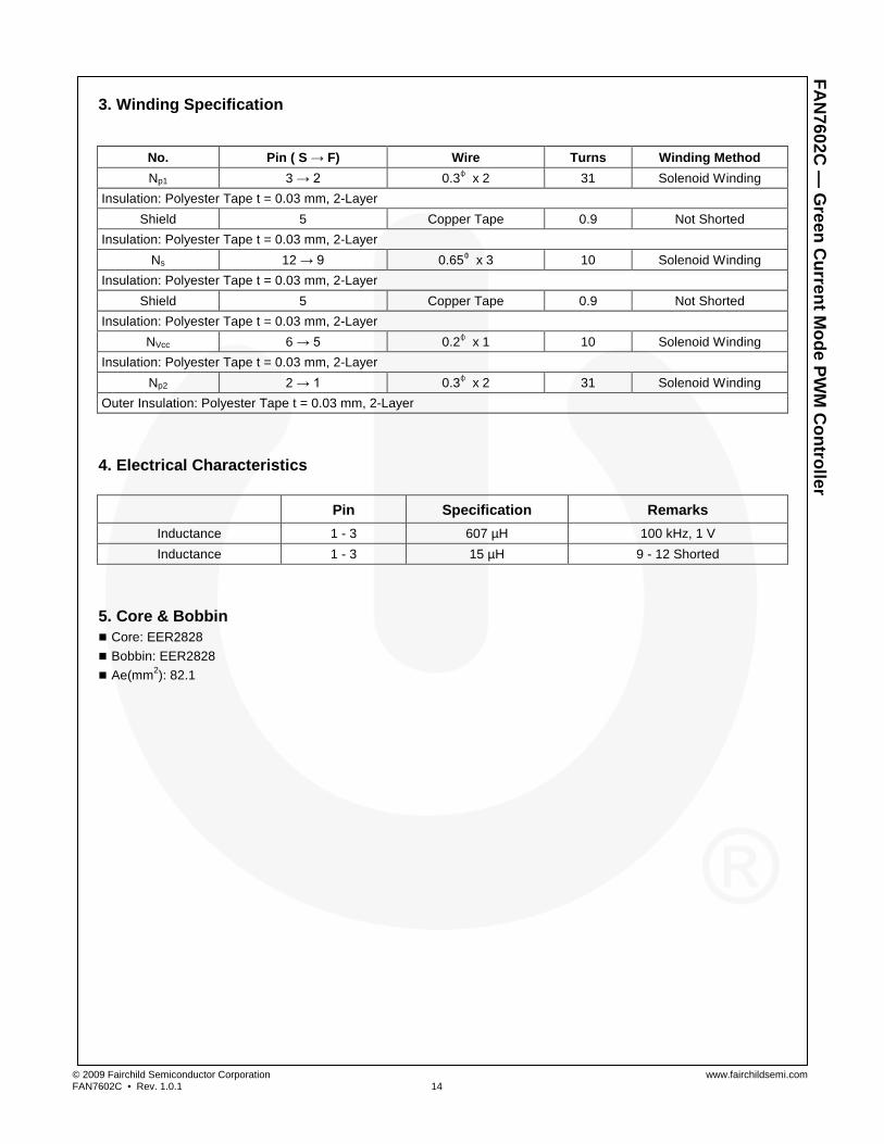
3. Winding Specification
No. Pin ( S → F) Wire Turns Winding Method Np1 3 → 2 0.3φ x 2 31 Solenoid Winding
Insulation: Polyester Tape t = 0.03 mm, 2-Layer Shield 5 Copper Tape 0.9 Not Shorted
Insulation: Polyester Tape t = 0.03 mm, 2-Layer Ns 12 → 9 0.65φ x 3 10 Solenoid Winding
Insulation: Polyester Tape t = 0.03 mm, 2-Layer Shield 5 Copper Tape 0.9 Not Shorted
Insulation: Polyester Tape t = 0.03 mm, 2-Layer NVcc 6 → 5 0.2φ x 1 10 Solenoid Winding
Insulation: Polyester Tape t = 0.03 mm, 2-Layer Np2 2 → 1 0.3φ x 2 31 Solenoid Winding
Outer Insulation: Polyester Tape t = 0.03 mm, 2-Layer
4. Electrical Characteristics
Pin Specification Remarks Inductance 1 - 3 607 µH 100 kHz, 1 V Inductance 1 - 3 15 µH 9 - 12 Shorted
5. Core & Bobbin Core: EER2828 Bobbin: EER2828 Ae(mm2): 82.1
© 2009 Fairchild Semiconductor Corporation www.fairchildsemi.com FAN7602C • Rev. 1.0.1 15
FAN
7602C —
Green C
urrent Mode PW
M C
ontroller
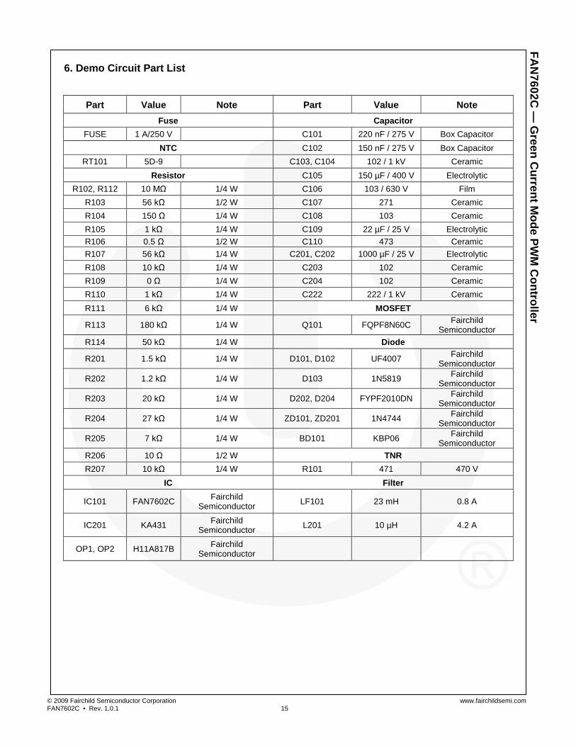
6. Demo Circuit Part List
Part Value Note Part Value Note Fuse Capacitor
FUSE 1 A/250 V C101 220 nF / 275 V Box Capacitor NTC C102 150 nF / 275 V Box Capacitor
RT101 5D-9 C103, C104 102 / 1 kV Ceramic Resistor C105 150 µF / 400 V Electrolytic
R102, R112 10 MΩ 1/4 W C106 103 / 630 V Film R103 56 kΩ 1/2 W C107 271 Ceramic R104 150 Ω 1/4 W C108 103 Ceramic R105 1 kΩ 1/4 W C109 22 µF / 25 V Electrolytic R106 0.5 Ω 1/2 W C110 473 Ceramic R107 56 kΩ 1/4 W C201, C202 1000 µF / 25 V Electrolytic R108 10 kΩ 1/4 W C203 102 Ceramic R109 0 Ω 1/4 W C204 102 Ceramic R110 1 kΩ 1/4 W C222 222 / 1 kV Ceramic R111 6 kΩ 1/4 W MOSFET
R113 180 kΩ 1/4 W Q101 FQPF8N60C Fairchild Semiconductor
R114 50 kΩ 1/4 W Diode
R201 1.5 kΩ 1/4 W D101, D102 UF4007 Fairchild Semiconductor
R202 1.2 kΩ 1/4 W D103 1N5819 Fairchild Semiconductor
R203 20 kΩ 1/4 W D202, D204 FYPF2010DN Fairchild Semiconductor
R204 27 kΩ 1/4 W ZD101, ZD201 1N4744 Fairchild Semiconductor
R205 7 kΩ 1/4 W BD101 KBP06 Fairchild Semiconductor
R206 10 Ω 1/2 W TNR R207 10 kΩ 1/4 W R101 471 470 V
IC Filter
IC101 FAN7602C Fairchild Semiconductor LF101 23 mH 0.8 A
IC201 KA431 Fairchild Semiconductor L201 10 µH 4.2 A
OP1, OP2 H11A817B Fairchild Semiconductor
© 2009 Fairchild Semiconductor Corporation www.fairchildsemi.com FAN7602C • Rev. 1.0.1 16
FAN
7602C —
Green C
urrent Mode PW
M C
ontroller
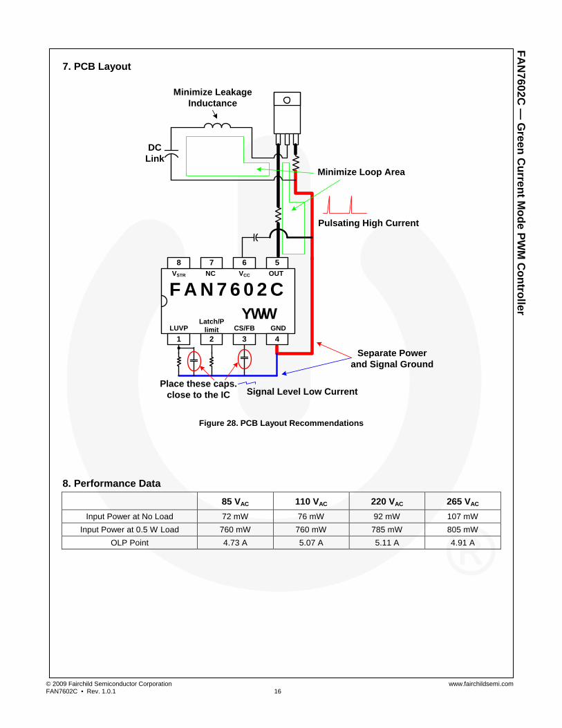
7. PCB Layout
Minimize Loop Area
Separate Power and Signal Ground
Minimize LeakageInductance
F A N 7 6 0 2 C
1 2
6 58 7
YWW3 4
Latch/Plimit GNDCS/FBLUVP
VSTR NC VCC OUT
Place these caps.close to the IC
DCLink
Pulsating High Current
Signal Level Low Current
Figure 28. PCB Layout Recommendations
8. Performance Data
85 VAC 110 VAC 220 VAC 265 VAC Input Power at No Load 72 mW 76 mW 92 mW 107 mW
Input Power at 0.5 W Load 760 mW 760 mW 785 mW 805 mW OLP Point 4.73 A 5.07 A 5.11 A 4.91 A
© Fairchild Semiconductor Corporation www.fairchildsemi.com
TRADEMARKS The following includes registered and unregistered trademarks and service marks, owned by Fairchild Semiconductor and/or its global subsidiaries, and is not intended to be an exhaustive list of all such trademarks.
AccuPower AttitudeEngine™ Awinda® AX-CAP®* BitSiC Build it Now CorePLUS CorePOWER CROSSVOLT CTL Current Transfer Logic DEUXPEED® Dual Cool™ EcoSPARK® EfficientMax ESBC
Fairchild® Fairchild Semiconductor® FACT Quiet Series FACT® FastvCore FETBench FPS
F-PFS FRFET®
Global Power ResourceSM
GreenBridge Green FPS Green FPS e-Series Gmax GTO IntelliMAX ISOPLANAR Making Small Speakers Sound Louder
and Better™
MegaBuck MICROCOUPLER MicroFET MicroPak MicroPak2 MillerDrive MotionMax MotionGrid® MTi® MTx® MVN® mWSaver® OptoHiT OPTOLOGIC®
OPTOPLANAR®
®
Power Supply WebDesigner PowerTrench®
PowerXS™ Programmable Active Droop QFET® QS Quiet Series RapidConfigure
Saving our world, 1mW/W/kW at a time™ SignalWise SmartMax SMART START Solutions for Your Success SPM® STEALTH SuperFET® SuperSOT-3 SuperSOT-6 SuperSOT-8 SupreMOS® SyncFET Sync-Lock™
®*
TinyBoost® TinyBuck® TinyCalc TinyLogic® TINYOPTO TinyPower TinyPWM TinyWire TranSiC TriFault Detect TRUECURRENT®* SerDes
UHC® Ultra FRFET UniFET VCX VisualMax VoltagePlus XS™ Xsens™ 仙童®
* Trademarks of System General Corporation, used under license by Fairchild Semiconductor.
DISCLAIMER
FAIRCHILD SEMICONDUCTOR RESERVES THE RIGHT TO MAKE CHANGES WITHOUT FURTHER NOTICE TO ANY PRODUCTS HEREIN TO IMPROVE RELIABILITY, FUNCTION, OR DESIGN. TO OBTAIN THE LATEST, MOST UP-TO-DATE DATASHEET AND PRODUCT INFORMATION, VISIT OUR WEBSITE AT HTTP://WWW.FAIRCHILDSEMI.COM. FAIRCHILD DOES NOT ASSUME ANY LIABILITY ARISING OUT OF THE APPLICATION OR USE OF ANY PRODUCT OR CIRCUIT DESCRIBED HEREIN; NEITHER DOES IT CONVEY ANY LICENSE UNDER ITS PATENT RIGHTS, NOR THE RIGHTS OF OTHERS. THESE SPECIFICATIONS DO NOT EXPAND THE TERMS OF FAIRCHILD’S WORLDWIDE TERMS AND CONDITIONS, SPECIFICALLY THE WARRANTY THEREIN, WHICH COVERS THESE PRODUCTS.
AUTHORIZED USE
Unless otherwise specified in this data sheet, this product is a standard commercial product and is not intended for use in applications that require extraordinary levels of quality and reliability. This product may not be used in the following applications, unless specifically approved in writing by a Fairchild officer: (1) automotive or other transportation, (2) military/aerospace, (3) any safety critical application – including life critical medical equipment – where the failure of the Fairchild product reasonably would be expected to result in personal injury, death or property damage. Customer’s use of this product is subject to agreement of this Authorized Use policy. In the event of an unauthorized use of Fairchild’s product, Fairchild accepts no liability in the event of product failure. In other respects, this product shall be subject to Fairchild’s Worldwide Terms and Conditions of Sale, unless a separate agreement has been signed by both Parties.
ANTI-COUNTERFEITING POLICY
Fairchild Semiconductor Corporation's Anti-Counterfeiting Policy. Fairchild's Anti-Counterfeiting Policy is also stated on our external website, www.fairchildsemi.com, under Terms of Use
Counterfeiting of semiconductor parts is a growing problem in the industry. All manufacturers of semiconductor products are experiencing counterfeiting of their parts. Customers who inadvertently purchase counterfeit parts experience many problems such as loss of brand reputation, substandard performance, failed applications, and increased cost of production and manufacturing delays. Fairchild is taking strong measures to protect ourselves and our customers from the proliferation of counterfeit parts. Fairchild strongly encourages customers to purchase Fairchild parts either directly from Fairchild or from Authorized Fairchild Distributors who are listed by country on our web page cited above. Products customers buy either from Fairchild directly or from Authorized Fairchild Distributors are genuine parts, have full traceability, meet Fairchild's quality standards for handling and storage and provide access to Fairchild's full range of up-to-date technical and product information. Fairchild and our Authorized Distributors will stand behind all warranties and will appropriately address any warranty issues that may arise. Fairchild will not provide any warranty coverage or other assistance for parts bought from Unauthorized Sources. Fairchild is committed to combat this global problem and encourage our customers to do their part in stopping this practice by buying direct or from authorized distributors.
PRODUCT STATUS DEFINITIONS
Definition of Terms
Datasheet Identification Product Status Definition
Advance Information Formative / In Design Datasheet contains the design specifications for product development. Specifications may change in any manner without notice.
Preliminary First Production Datasheet contains preliminary data; supplementary data will be published at a later date. Fairchild Semiconductor reserves the right to make changes at any time without notice to improve design.
No Identification Needed Full Production Datasheet contains final specifications. Fairchild Semiconductor reserves the right to make changes at any time without notice to improve the design.
Obsolete Not In Production Datasheet contains specifications on a product that is discontinued by Fairchild Semiconductor. The datasheet is for reference information only.
Rev. I77
®

Mouser Electronics
Authorized Distributor
Click to View Pricing, Inventory, Delivery & Lifecycle Information: Fairchild Semiconductor:
FAN7602CMX
Related Documents